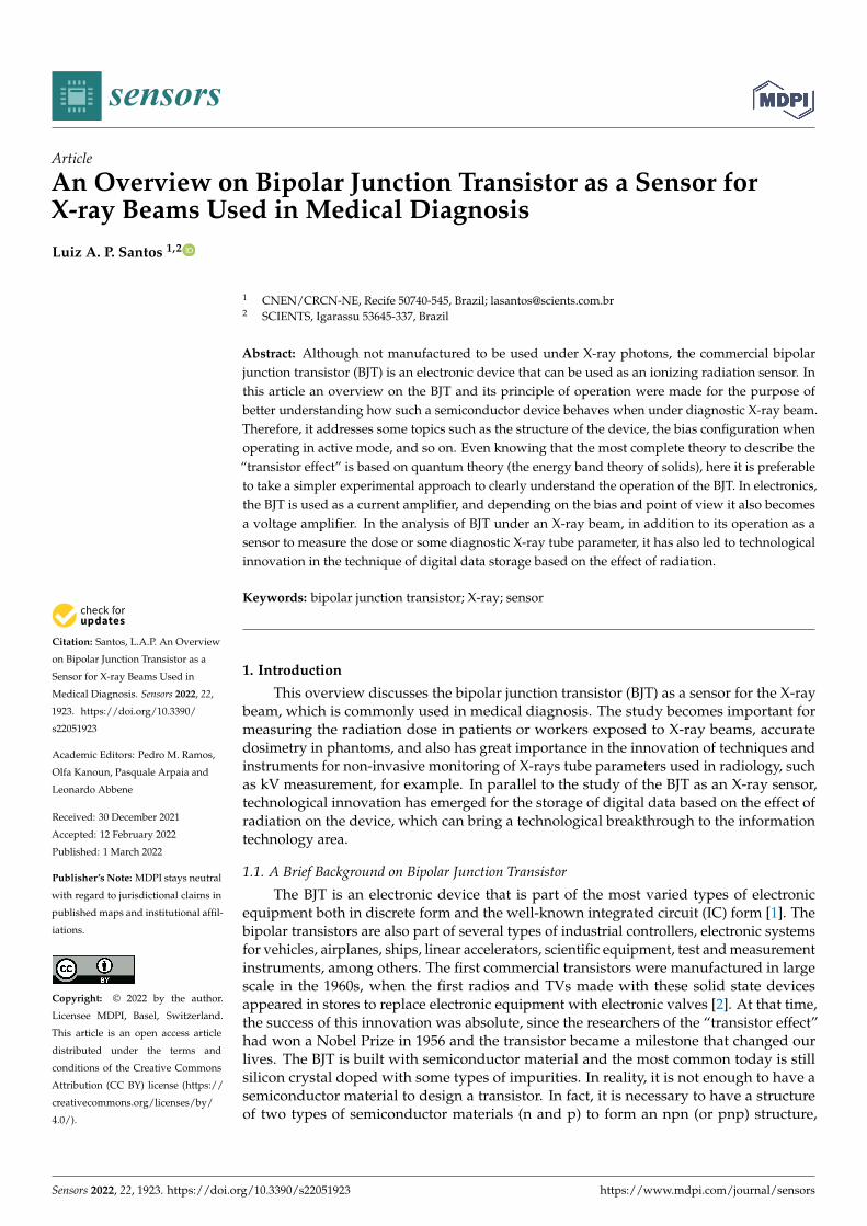
An Overview on Bipolar Junction Transistor as a Sensor for X ...
28
Citation: Santos, L.A.P. An Overview on Bipolar Junction Transistor as a Sensor for X-ray Beams Used in Medical Diagnosis. Sensors 2022, 22, 1923. https://doi.org/10.3390/ s22051923 Academic Editors: Pedro M. Ramos, Olfa Kanoun, Pasquale Arpaia and Leonardo Abbene Received: 30 December 2021 Accepted: 12 February 2022 Published: 1 March 2022 Publisher’s Note: MDPI stays neutral with regard to jurisdictional claims in published maps and institutional affil- iations. Copyright: © 2022 by the author. Licensee MDPI, Basel, Switzerland. This article is an open access article distributed under the terms and conditions of the Creative Commons Attribution (CC BY) license (https:// creativecommons.org/licenses/by/ 4.0/). sensors Article An Overview on Bipolar Junction Transistor as a Sensor for X-ray Beams Used in Medical Diagnosis Luiz A. P. Santos 1,2 1 CNEN/CRCN-NE, Recife 50740-545, Brazil; [email protected] 2 SCIENTS, Igarassu 53645-337, Brazil Abstract: Although not manufactured to be used under X-ray photons, the commercial bipolar junction transistor (BJT) is an electronic device that can be used as an ionizing radiation sensor. In this article an overview on the BJT and its principle of operation were made for the purpose of better understanding how such a semiconductor device behaves when under diagnostic X-ray beam. Therefore, it addresses some topics such as the structure of the device, the bias configuration when operating in active mode, and so on. Even knowing that the most complete theory to describe the “transistor effect” is based on quantum theory (the energy band theory of solids), here it is preferable to take a simpler experimental approach to clearly understand the operation of the BJT. In electronics, the BJT is used as a current amplifier, and depending on the bias and point of view it also becomes a voltage amplifier. In the analysis of BJT under an X-ray beam, in addition to its operation as a sensor to measure the dose or some diagnostic X-ray tube parameter, it has also led to technological innovation in the technique of digital data storage based on the effect of radiation. Keywords: bipolar junction transistor; X-ray; sensor 1. Introduction This overview discusses the bipolar junction transistor (BJT) as a sensor for the X-ray beam, which is commonly used in medical diagnosis. The study becomes important for measuring the radiation dose in patients or workers exposed to X-ray beams, accurate dosimetry in phantoms, and also has great importance in the innovation of techniques and instruments for non-invasive monitoring of X-rays tube parameters used in radiology, such as kV measurement, for example. In parallel to the study of the BJT as an X-ray sensor, technological innovation has emerged for the storage of digital data based on the effect of radiation on the device, which can bring a technological breakthrough to the information technology area. 1.1. A Brief Background on Bipolar Junction Transistor The BJT is an electronic device that is part of the most varied types of electronic equipment both in discrete form and the well-known integrated circuit (IC) form [1]. The bipolar transistors are also part of several types of industrial controllers, electronic systems for vehicles, airplanes, ships, linear accelerators, scientific equipment, test and measurement instruments, among others. The first commercial transistors were manufactured in large scale in the 1960s, when the first radios and TVs made with these solid state devices appeared in stores to replace electronic equipment with electronic valves [2]. At that time, the success of this innovation was absolute, since the researchers of the “transistor effect” had won a Nobel Prize in 1956 and the transistor became a milestone that changed our lives. The BJT is built with semiconductor material and the most common today is still silicon crystal doped with some types of impurities. In reality, it is not enough to have a semiconductor material to design a transistor. In fact, it is necessary to have a structure of two types of semiconductor materials (n and p) to form an npn (or pnp) structure, Sensors 2022, 22, 1923. https://doi.org/10.3390/s22051923 https://www.mdpi.com/journal/sensors
-
Upload
khangminh22 -
Category
Documents
-
view
2 -
download
0
Transcript of An Overview on Bipolar Junction Transistor as a Sensor for X ...
Citation: Santos, L.A.P. An Overview
on Bipolar Junction Transistor as a
Sensor for X-ray Beams Used in
Medical Diagnosis. Sensors 2022, 22,
1923. https://doi.org/10.3390/
s22051923
Academic Editors: Pedro M. Ramos,
Olfa Kanoun, Pasquale Arpaia and
Leonardo Abbene
Received: 30 December 2021
Accepted: 12 February 2022
Published: 1 March 2022
Publisher’s Note: MDPI stays neutral
with regard to jurisdictional claims in
published maps and institutional affil-
iations.
Copyright: © 2022 by the author.
Licensee MDPI, Basel, Switzerland.
This article is an open access article
distributed under the terms and
conditions of the Creative Commons
Attribution (CC BY) license (https://
creativecommons.org/licenses/by/
4.0/).
sensors
Article
An Overview on Bipolar Junction Transistor as a Sensor forX-ray Beams Used in Medical DiagnosisLuiz A. P. Santos 1,2
1 CNEN/CRCN-NE, Recife 50740-545, Brazil; [email protected] SCIENTS, Igarassu 53645-337, Brazil
Abstract: Although not manufactured to be used under X-ray photons, the commercial bipolarjunction transistor (BJT) is an electronic device that can be used as an ionizing radiation sensor. Inthis article an overview on the BJT and its principle of operation were made for the purpose ofbetter understanding how such a semiconductor device behaves when under diagnostic X-ray beam.Therefore, it addresses some topics such as the structure of the device, the bias configuration whenoperating in active mode, and so on. Even knowing that the most complete theory to describe the“transistor effect” is based on quantum theory (the energy band theory of solids), here it is preferableto take a simpler experimental approach to clearly understand the operation of the BJT. In electronics,the BJT is used as a current amplifier, and depending on the bias and point of view it also becomesa voltage amplifier. In the analysis of BJT under an X-ray beam, in addition to its operation as asensor to measure the dose or some diagnostic X-ray tube parameter, it has also led to technologicalinnovation in the technique of digital data storage based on the effect of radiation.
Keywords: bipolar junction transistor; X-ray; sensor
1. Introduction
This overview discusses the bipolar junction transistor (BJT) as a sensor for the X-raybeam, which is commonly used in medical diagnosis. The study becomes important formeasuring the radiation dose in patients or workers exposed to X-ray beams, accuratedosimetry in phantoms, and also has great importance in the innovation of techniques andinstruments for non-invasive monitoring of X-rays tube parameters used in radiology, suchas kV measurement, for example. In parallel to the study of the BJT as an X-ray sensor,technological innovation has emerged for the storage of digital data based on the effect ofradiation on the device, which can bring a technological breakthrough to the informationtechnology area.
1.1. A Brief Background on Bipolar Junction Transistor
The BJT is an electronic device that is part of the most varied types of electronicequipment both in discrete form and the well-known integrated circuit (IC) form [1]. Thebipolar transistors are also part of several types of industrial controllers, electronic systemsfor vehicles, airplanes, ships, linear accelerators, scientific equipment, test and measurementinstruments, among others. The first commercial transistors were manufactured in largescale in the 1960s, when the first radios and TVs made with these solid state devicesappeared in stores to replace electronic equipment with electronic valves [2]. At that time,the success of this innovation was absolute, since the researchers of the “transistor effect”had won a Nobel Prize in 1956 and the transistor became a milestone that changed ourlives. The BJT is built with semiconductor material and the most common today is stillsilicon crystal doped with some types of impurities. In reality, it is not enough to have asemiconductor material to design a transistor. In fact, it is necessary to have a structureof two types of semiconductor materials (n and p) to form an npn (or pnp) structure,
Sensors 2022, 22, 1923. https://doi.org/10.3390/s22051923 https://www.mdpi.com/journal/sensors
Sensors 2022, 22, 1923 2 of 28
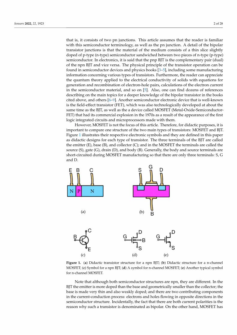
that is, it consists of two pn junctions. This article assumes that the reader is familiarwith this semiconductor terminology, as well as the pn junction. A detail of the bipolartransistor junctions is that the material of the medium consists of a thin slice slightlydoped of p-type (n-type) semiconductor sandwiched between two pieces of n-type (p-type)semiconductor. In electronics, it is said that the pnp BJT is the complementary pair (dual)of the npn BJT and vice versa. The physical principle of the transistor operation can befound in semiconductor devices and physics books [3–5], including some manufacturinginformation concerning various types of transistors. Furthermore, the reader can appreciatethe quantum theory applied to the electrical conductivity of solids with equations forgeneration and recombination of electron-hole pairs, calculations of the electron currentin the semiconductor material, and so on [5]. Also, one can find dozens of referencesdescribing on the main topics for a deeper knowledge of the bipolar transistor in the bookscited above, and others [6–9]. Another semiconductor electronic device that is well-knownis the field-effect transistor (FET), which was also technologically developed at about thesame time as the BJT, as well as the a device called MOSFET (Metal-Oxide-Semiconductor-FET) that had its commercial explosion in the 1970s as a result of the appearance of the firstlogic integrated circuits and microprocessors made with them.
However, MOSFET is not the focus of this article. Therefore, for didactic purposes, it isimportant to compare one structure of the two main types of transistors: MOSFET and BJT.Figure 1 illustrates their respective electronic symbols and they are defined in this paperas didactic designs for each type of transistor. The three terminals of the BJT are calledthe emitter (E), base (B), and collector (C); and in the MOSFET the terminals are called thesource (S), gate (G), drain (D), and body (B). Generally, the body and source terminals areshort-circuited during MOSFET manufacturing so that there are only three terminals: S, Gand D.
Sensors 2022, 22, x FOR PEER REVIEW 2 of 29
to have a structure of two types of semiconductor materials (n and p) to form an npn (or pnp) structure, that is, it consists of two pn junctions. This article assumes that the reader is familiar with this semiconductor terminology, as well as the pn junction. A detail of the bipolar transistor junctions is that the material of the medium consists of a thin slice slightly doped of p-type (n-type) semiconductor sandwiched between two pieces of n-type (p-type) semiconductor. In electronics, it is said that the pnp BJT is the comple-mentary pair (dual) of the npn BJT and vice versa. The physical principle of the transistor operation can be found in semiconductor devices and physics books [3–5], including some manufacturing information concerning various types of transistors. Furthermore, the reader can appreciate the quantum theory applied to the electrical conductivity of solids with equations for generation and recombination of electron-hole pairs, calcula-tions of the electron current in the semiconductor material, and so on [5]. Also, one can find dozens of references describing on the main topics for a deeper knowledge of the bipolar transistor in the books cited above, and others [6–9]. Another semiconductor electronic device that is well-known is the field-effect transistor (FET), which was also technologically developed at about the same time as the BJT, as well as the a device called MOSFET (Metal-Oxide-Semiconductor-FET) that had its commercial explosion in the 1970s as a result of the appearance of the first logic integrated circuits and microproces-sors made with them.
However, MOSFET is not the focus of this article. Therefore, for didactic purposes, it is important to compare one structure of the two main types of transistors: MOSFET and BJT. Figure 1 illustrates their respective electronic symbols and they are defined in this paper as didactic designs for each type of transistor. The three terminals of the BJT are called the emitter (E), base (B), and collector (C); and in the MOSFET the terminals are called the source (S), gate (G), drain (D), and body (B). Generally, the body and source terminals are short-circuited during MOSFET manufacturing so that there are only three terminals: S, G and D.
Figure 1. (a) Didactic transistor structure for a npn BJT; (b) Didactic structure for a n-channel MOSFET; (c) Symbol for a npn BJT; (d) A symbol for n-channel MOSFET; (e) Another typical symbol for n-channel MOSFET.
Note that although both semiconductor structures are npn, they are different. In the BJT the emitter is more doped than the base and geometrically smaller than the collector; the base is made very thin and also weakly doped; and there are two contributing com-
Figure 1. (a) Didactic transistor structure for a npn BJT; (b) Didactic structure for a n-channelMOSFET; (c) Symbol for a npn BJT; (d) A symbol for n-channel MOSFET; (e) Another typical symbolfor n-channel MOSFET.
Note that although both semiconductor structures are npn, they are different. In theBJT the emitter is more doped than the base and geometrically smaller than the collector; thebase is made very thin and also weakly doped; and there are two contributing componentsin the current-conduction process: electrons and holes flowing in opposite directions in thesemiconductor structure. Incidentally, the fact that there are both current polarities is thereason why such a transistor is denominated as bipolar. On the other hand, MOSFET has

Sensors 2022, 22, 1923 3 of 28
certain symmetry in its semiconductor structure, and its operating principle is based on theformation of an electrical charge carrier concentration (a so-called channel) just below theinsulator (usually silicon dioxide—SiO2) induced by the electric field generated betweenthe gate and the body. The dimension of the channel (in this case n-channel) is proportionalto the gate-source voltage (VGS), and hence the electrical resistance between the drain andsource decreases substantially if the bias VGS exceeds a threshold voltage Vt [8]. There ispractically only one current polarity (electrons) through the n-channel and the MOSFETis called unipolar. There are other types of semiconductor junction structures to becomea MOSFET.
1.2. Principle of Operation of the BJT
Figure 2 shows the typical bias for npn and pnp bipolar junction transistors: (1) acurrent source IB at the base-emitter junction; (2) a voltage source VCE between the collectorand the emitter. A voltage source with a series resistor can be used to bias the base ofthe BJT rather than a current source, there is equivalence between them [8,10]; however,in this overview the current source is preferred for reasons to be appreciated later. It canalso be seen that the standard symbols represent the flow of the conventional currentat the transistor terminals, however it is known that the electron flow is in the oppositedirection. The analysis will be based on taking the circuit of Figure 2, which is termed thecommon-emitter circuit because the emitter terminal is part of both the input signal (IB) andthe output signal (IC). In this article the common-emitter configuration will often be used.
Sensors 2022, 22, x FOR PEER REVIEW 3 of 29
ponents in the current-conduction process: electrons and holes flowing in opposite di-rections in the semiconductor structure. Incidentally, the fact that there are both current polarities is the reason why such a transistor is denominated as bipolar. On the other hand, MOSFET has certain symmetry in its semiconductor structure, and its operating principle is based on the formation of an electrical charge carrier concentration (a so-called channel) just below the insulator (usually silicon dioxide—SiO2) induced by the electric field generated between the gate and the body. The dimension of the channel (in this case n-channel) is proportional to the gate-source voltage (VGS), and hence the elec-trical resistance between the drain and source decreases substantially if the bias VGS ex-ceeds a threshold voltage Vt [8]. There is practically only one current polarity (electrons) through the n-channel and the MOSFET is called unipolar. There are other types of sem-iconductor junction structures to become a MOSFET.
1.2. Principle of Operation of the BJT Figure 2 shows the typical bias for npn and pnp bipolar junction transistors: (1) a
current source IB at the base-emitter junction; (2) a voltage source VCE between the col-lector and the emitter. A voltage source with a series resistor can be used to bias the base of the BJT rather than a current source, there is equivalence between them [8,10]; how-ever, in this overview the current source is preferred for reasons to be appreciated later. It can also be seen that the standard symbols represent the flow of the conventional current at the transistor terminals, however it is known that the electron flow is in the opposite direction. The analysis will be based on taking the circuit of Figure 2, which is termed the common-emitter circuit because the emitter terminal is part of both the input signal (IB) and the output signal (IC). In this article the common-emitter configuration will often be used.
(a) (b)
Figure 2. BJT biasing for devices in common-emitter configuration: (a) npn; (b) pnp.
To understand how a BJT works, at this point it is interesting to take a simplified approach. First, consider that the BJT is npn type, and the understanding for the pnp it must be to reverse the polarities and exchange electrons for holes. Initially, assume that the base current bias is zero (IB = 0). This is equivalent to saying that the potential differ-ence and current is zero at the base-emitter pn junction (JBE), a condition called electronic equilibrium, at the pn junction [5]. This is also equivalent to saying that the base of the transistor is in the virtual ground (a short circuit between the base and the emitter) and the BJT works like a diode. In this case, there is only the reverse bias (VCE) at the base-collector pn junction (JBC), so the collector current (IC) is minimal, in fact practically negligible, because it is an ultra-low leakage current due to the temperature or genera-tion-recombination of charge carriers, for a while. This electrical state (a so-called cutoff) is like an open switch, or it can be said that the electrical resistance between collector and emitter is extremely high (RCE ≈ GΩ or RCE ≈ TΩ). Now, in applying a current source bias to the base of the transistor (IB > 0), there is a direct bias at the JBE, where a base-emitter
Figure 2. BJT biasing for devices in common-emitter configuration: (a) npn; (b) pnp.
To understand how a BJT works, at this point it is interesting to take a simplifiedapproach. First, consider that the BJT is npn type, and the understanding for the pnpit must be to reverse the polarities and exchange electrons for holes. Initially, assumethat the base current bias is zero (IB = 0). This is equivalent to saying that the potentialdifference and current is zero at the base-emitter pn junction (JBE), a condition calledelectronic equilibrium, at the pn junction [5]. This is also equivalent to saying that the baseof the transistor is in the virtual ground (a short circuit between the base and the emitter)and the BJT works like a diode. In this case, there is only the reverse bias (VCE) at thebase-collector pn junction (JBC), so the collector current (IC) is minimal, in fact practicallynegligible, because it is an ultra-low leakage current due to the temperature or generation-recombination of charge carriers, for a while. This electrical state (a so-called cutoff) islike an open switch, or it can be said that the electrical resistance between collector andemitter is extremely high (RCE ≈ GΩ or RCE ≈ TΩ). Now, in applying a current source biasto the base of the transistor (IB > 0), there is a direct bias at the JBE, where a base-emittervoltage VBE appears, normally referred to as the built-in pn junction potential, Vpn [5].For a typical silicon BJT, the value of VBE can be approximately between 0.3 V to 0.8 Vdepending on the current intensity (nA to mA) through the JBE, and in general an averagevalue of 0.7 V can be considered for current values in the order of µA. Actually, in the 1960sand 1970s, the radios and TVs that operated with transistors had electrical currents of theorder of microamperes in their electronic circuits, and for this reason the engineers used
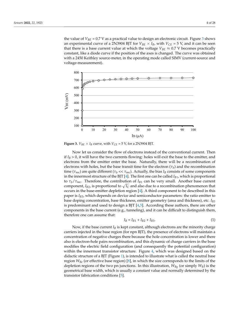
Sensors 2022, 22, 1923 4 of 28
the value of VBE = 0.7 V as a practical value to design an electronic circuit. Figure 3 showsan experimental curve of a 2N3904 BJT for VBE × IB, with VCE = 5 V, and it can be seenthat there is a base current value at which the voltage VBE ≈ 0.7 V becomes practicallyconstant, like a diode curve if the position of the axes is changed. The curve was obtainedwith a 2450 Keithley source-meter, in the operating mode called SIMV (current-source andvoltage-measurement).
Sensors 2022, 22, x FOR PEER REVIEW 4 of 29
voltage VBE appears, normally referred to as the built-in pn junction potential, Vpn [5]. For a typical silicon BJT, the value of VBE can be approximately between 0.3 V to 0.8 V de-pending on the current intensity (nA to mA) through the JBE, and in general an average value of 0.7 V can be considered for current values in the order of µA. Actually, in the 1960s and 1970s, the radios and TVs that operated with transistors had electrical currents of the order of microamperes in their electronic circuits, and for this reason the engineers used the value of VBE = 0.7 V as a practical value to design an electronic circuit. Figure 3 shows an experimental curve of a 2N3904 BJT for VBE × IB, with VCE = 5 V, and it can be seen that there is a base current value at which the voltage VBE ≈ 0.7 V becomes practically constant, like a diode curve if the position of the axes is changed. The curve was obtained with a 2450 Keithley source-meter, in the operating mode called SIMV (current-source and voltage-measurement).
Figure 3. VBE × IB curve, with VCE = 5 V, for a 2N3904 BJT.
Now let us consider the flow of electrons instead of the conventional current. Then if IB > 0, it will have the two currents flowing: holes will exit the base to the emitter, and electrons from the emitter enter the base. Naturally, there will be a recombination of electrons with holes, but the base transit time for the electron (τb) and the recombination time (τrec) are quite different (τb << τrec). Actually, the bias IB consists of some components in the innermost structure of the BJT [4]. The first one can be called IB1, which is propor-tional to τb/τrec. Therefore, the contribution of IB1 can be very small. Another base current component, IB2, is proportional to 𝐼 and also due to a recombination phenomenon that occurs in the base-emitter depletion region [4]. A third component to be described in this paper is IB3, which depends on device and semiconductor parameters: the ratio emitter to base doping concentration, base thickness, emitter geometry (area and thickness), etc. IB3
is predominant and used to design a BJT [4,5]. According these authors, there are other components in the base current (e.g., tunneling), and it can be difficult to distinguish them, therefore one can assume that:
IB = IB1 + IB2 + IB3. (1)
Now, if the base current IB is kept constant, although electrons are the minority charge carriers injected in the base region (for npn BJT), the presence of electrons will maintain a concentration of negative charges there because the hole concentration is lower and there also is electron-hole pairs recombination, and this dynamic of charge carriers in the base modifies the electric field configuration (and consequently the poten-tial configuration) within the innermost transistor structure. Figure 4, which was de-signed based on the didactic structure of a BJT (Figure 1), is intended to illustrate what is called the neutral base region WBe (or effective base region) [8], in which the size corre-
100
200
300
400
500
600
700
800
0 10 20 30 40 50 60 70 80 90 100
VBE
(mV
)
IB (μA)
Figure 3. VBE × IB curve, with VCE = 5 V, for a 2N3904 BJT.
Now let us consider the flow of electrons instead of the conventional current. Thenif IB > 0, it will have the two currents flowing: holes will exit the base to the emitter, andelectrons from the emitter enter the base. Naturally, there will be a recombination ofelectrons with holes, but the base transit time for the electron (τb) and the recombinationtime (τrec) are quite different (τb << τrec). Actually, the bias IB consists of some componentsin the innermost structure of the BJT [4]. The first one can be called IB1, which is proportionalto τb/τrec. Therefore, the contribution of IB1 can be very small. Another base currentcomponent, IB2, is proportional to
√IC and also due to a recombination phenomenon that
occurs in the base-emitter depletion region [4]. A third component to be described in thispaper is IB3, which depends on device and semiconductor parameters: the ratio emitter tobase doping concentration, base thickness, emitter geometry (area and thickness), etc. IB3is predominant and used to design a BJT [4,5]. According these authors, there are othercomponents in the base current (e.g., tunneling), and it can be difficult to distinguish them,therefore one can assume that:
IB = IB1 + IB2 + IB3. (1)
Now, if the base current IB is kept constant, although electrons are the minority chargecarriers injected in the base region (for npn BJT), the presence of electrons will maintain aconcentration of negative charges there because the hole concentration is lower and therealso is electron-hole pairs recombination, and this dynamic of charge carriers in the basemodifies the electric field configuration (and consequently the potential configuration)within the innermost transistor structure. Figure 4, which was designed based on thedidactic structure of a BJT (Figure 1), is intended to illustrate what is called the neutral baseregion WBe (or effective base region) [8], in which the size corresponds to the limits of thedepletion regions of the two pn junctions. In this illustration, WBg (or simply WB) is thegeometrical base width, which is usually a constant value and normally determined by thetransistor fabrication conditions [5].
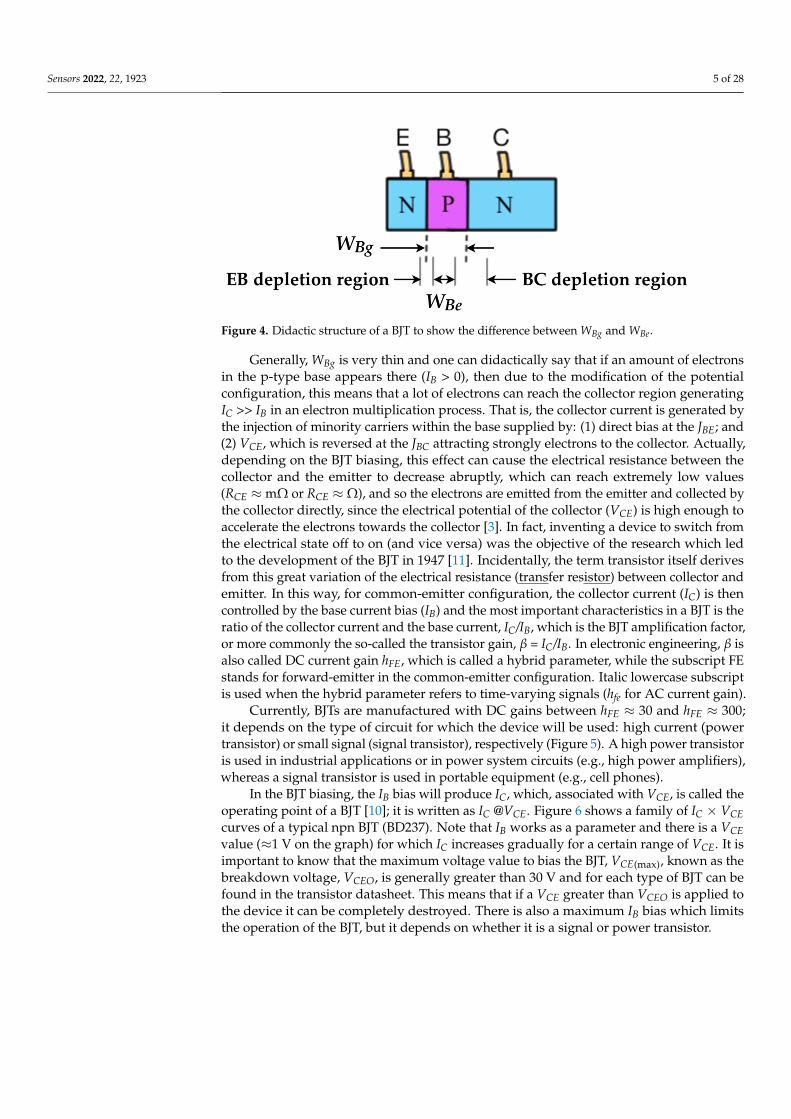
Sensors 2022, 22, 1923 5 of 28
Sensors 2022, 22, x FOR PEER REVIEW 5 of 29
sponds to the limits of the depletion regions of the two pn junctions. In this illustration, WBg (or simply WB) is the geometrical base width, which is usually a constant value and normally determined by the transistor fabrication conditions [5].
Figure 4. Didactic structure of a BJT to show the difference between WBg and WBe.
Generally, WBg is very thin and one can didactically say that if an amount of elec-trons in the p-type base appears there (IB > 0), then due to the modification of the potential configuration, this means that a lot of electrons can reach the collector region generating IC >> IB in an electron multiplication process. That is, the collector current is generated by the injection of minority carriers within the base supplied by: (1) direct bias at the JBE; and (2) VCE, which is reversed at the JBC attracting strongly electrons to the collector. Actually, depending on the BJT biasing, this effect can cause the electrical resistance between the collector and the emitter to decrease abruptly, which can reach extremely low values (RCE
≈ mΩ or RCE ≈ Ω), and so the electrons are emitted from the emitter and collected by the collector directly, since the electrical potential of the collector (VCE) is high enough to ac-celerate the electrons towards the collector [3]. In fact, inventing a device to switch from the electrical state off to on (and vice versa) was the objective of the research which led to the development of the BJT in 1947 [11]. Incidentally, the term transistor itself derives from this great variation of the electrical resistance (transfer resistor) between collector and emitter. In this way, for common-emitter configuration, the collector current (IC) is then controlled by the base current bias (IB) and the most important characteristics in a BJT is the ratio of the collector current and the base current, IC/IB, which is the BJT ampli-fication factor, or more commonly the so-called the transistor gain, β = IC/IB. In electronic engineering, β is also called DC current gain hFE, which is called a hybrid parameter, while the subscript FE stands for forward-emitter in the common-emitter configuration. Italic lowercase subscript is used when the hybrid parameter refers to time-varying sig-nals (hfe for AC current gain).
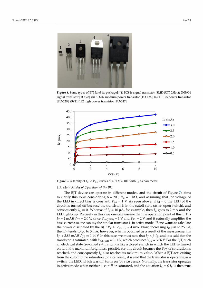
Currently, BJTs are manufactured with DC gains between hFE ≈ 30 and hFE ≈ 300; it depends on the type of circuit for which the device will be used: high current (power transistor) or small signal (signal transistor), respectively (Figure 5). A high power tran-sistor is used in industrial applications or in power system circuits (e.g., high power am-plifiers), whereas a signal transistor is used in portable equipment (e.g., cell phones).
In the BJT biasing, the IB bias will produce IC, which, associated with VCE, is called the operating point of a BJT [10]; it is written as IC @VCE. Figure 6 shows a family of IC × VCE curves of a typical npn BJT (BD237). Note that IB works as a parameter and there is a VCE value (≈1 V on the graph) for which IC increases gradually for a certain range of VCE. It is important to know that the maximum voltage value to bias the BJT, VCE(max), known as the breakdown voltage, VCEO, is generally greater than 30 V and for each type of BJT can be found in the transistor datasheet. This means that if a VCE greater than VCEO is applied to the device it can be completely destroyed. There is also a maximum IB bias which limits the operation of the BJT, but it depends on whether it is a signal or power transistor.
Figure 4. Didactic structure of a BJT to show the difference between WBg and WBe.
Generally, WBg is very thin and one can didactically say that if an amount of electronsin the p-type base appears there (IB > 0), then due to the modification of the potentialconfiguration, this means that a lot of electrons can reach the collector region generatingIC >> IB in an electron multiplication process. That is, the collector current is generated bythe injection of minority carriers within the base supplied by: (1) direct bias at the JBE; and(2) VCE, which is reversed at the JBC attracting strongly electrons to the collector. Actually,depending on the BJT biasing, this effect can cause the electrical resistance between thecollector and the emitter to decrease abruptly, which can reach extremely low values(RCE ≈mΩ or RCE ≈ Ω), and so the electrons are emitted from the emitter and collected bythe collector directly, since the electrical potential of the collector (VCE) is high enough toaccelerate the electrons towards the collector [3]. In fact, inventing a device to switch fromthe electrical state off to on (and vice versa) was the objective of the research which ledto the development of the BJT in 1947 [11]. Incidentally, the term transistor itself derivesfrom this great variation of the electrical resistance (transfer resistor) between collector andemitter. In this way, for common-emitter configuration, the collector current (IC) is thencontrolled by the base current bias (IB) and the most important characteristics in a BJT is theratio of the collector current and the base current, IC/IB, which is the BJT amplification factor,or more commonly the so-called the transistor gain, β = IC/IB. In electronic engineering, β isalso called DC current gain hFE, which is called a hybrid parameter, while the subscript FEstands for forward-emitter in the common-emitter configuration. Italic lowercase subscriptis used when the hybrid parameter refers to time-varying signals (hfe for AC current gain).
Currently, BJTs are manufactured with DC gains between hFE ≈ 30 and hFE ≈ 300;it depends on the type of circuit for which the device will be used: high current (powertransistor) or small signal (signal transistor), respectively (Figure 5). A high power transistoris used in industrial applications or in power system circuits (e.g., high power amplifiers),whereas a signal transistor is used in portable equipment (e.g., cell phones).
In the BJT biasing, the IB bias will produce IC, which, associated with VCE, is called theoperating point of a BJT [10]; it is written as IC @VCE. Figure 6 shows a family of IC × VCEcurves of a typical npn BJT (BD237). Note that IB works as a parameter and there is a VCEvalue (≈1 V on the graph) for which IC increases gradually for a certain range of VCE. It isimportant to know that the maximum voltage value to bias the BJT, VCE(max), known as thebreakdown voltage, VCEO, is generally greater than 30 V and for each type of BJT can befound in the transistor datasheet. This means that if a VCE greater than VCEO is applied tothe device it can be completely destroyed. There is also a maximum IB bias which limitsthe operation of the BJT, but it depends on whether it is a signal or power transistor.
Sensors 2022, 22, 1923 6 of 28Sensors 2022, 22, x FOR PEER REVIEW 6 of 29
Figure 5. Some types of BJT [and its package]: (1) BC846 signal transistor [SMD SOT-23]; (2) 2N3904 signal transistor [TO-92]; (3) BD237 medium power transistor [TO-126]; (4) TIP125 power transistor [TO-220]; (5) TIP142 high power transistor [TO-247].
Figure 6. A family of IC × VCE curves of a BD237 BJT with IB as parameter.
1.3. Main Modes of Operation of the BJT The BJT device can operate in different modes, and the circuit of Figure 7a aims to
clarify this topic considering β = 200, RC = 1 kΩ, and assuming that the voltage of the LED in direct bias is constant, Vpn = 1 V. As seen above, if IB = 0 the LED of the circuit is turned off because the transistor is in the cutoff state (as an open switch), and consequently IC ≈ 0. Whereas if IB = 10 µA, for example, then IC goes to 2 mA and the LED lights up. Precisely in this case one can assume that the operation point of this BJT is IC = 2 mA@VCE = 2.0 V, since Vpn(LED) = 1 V and VRc = 2 V, and it naturally amplifies the base current so one can say the bipolar transistor is in active mode. If one wants to calculate the power dissipated by the BJT: PT ≈ VCE·IC = 4 mW. Now, increasing IB just to 25 µA, then IC tends to go to 5 mA; however, what is obtained as a result of the measurement is IC ≈ 3.86 mA@VCE ≈ 0.14 V. In this case, we must note that IC < β·IB, and it is said that the transistor is saturated, with VCE(sat) = 0.14 V, which produces VRc = 3.86 V. For the BJT, such an electrical state (so-called saturation) is like a closed switch in which the LED is turned on with the maximum brightness possible for this circuit because the VCE of saturation is reached, and conse-quently IC also reaches its maximum value. When a BJT acts exiting from the cutoff to the saturation (or vice versa), it is said that the transistor is operating as a switch: the LED, which was off, turns on (or vice versa). Normally, the transistor operates in active mode when neither is cutoff or saturated, and the equation IC = β·IB is then true. Figure 6 shows
0
50
100
150
200
250
300
350
400
450
0 2 4 6 8 10
IC(m
A)
VCE (V)
IB (mA)3.02.52.01.51.00.5
Figure 5. Some types of BJT [and its package]: (1) BC846 signal transistor [SMD SOT-23]; (2) 2N3904signal transistor [TO-92]; (3) BD237 medium power transistor [TO-126]; (4) TIP125 power transistor[TO-220]; (5) TIP142 high power transistor [TO-247].
Sensors 2022, 22, x FOR PEER REVIEW 6 of 29
Figure 5. Some types of BJT [and its package]: (1) BC846 signal transistor [SMD SOT-23]; (2) 2N3904 signal transistor [TO-92]; (3) BD237 medium power transistor [TO-126]; (4) TIP125 power transistor [TO-220]; (5) TIP142 high power transistor [TO-247].
Figure 6. A family of IC × VCE curves of a BD237 BJT with IB as parameter.
1.3. Main Modes of Operation of the BJT The BJT device can operate in different modes, and the circuit of Figure 7a aims to
clarify this topic considering β = 200, RC = 1 kΩ, and assuming that the voltage of the LED in direct bias is constant, Vpn = 1 V. As seen above, if IB = 0 the LED of the circuit is turned off because the transistor is in the cutoff state (as an open switch), and consequently IC ≈ 0. Whereas if IB = 10 µA, for example, then IC goes to 2 mA and the LED lights up. Precisely in this case one can assume that the operation point of this BJT is IC = 2 mA@VCE = 2.0 V, since Vpn(LED) = 1 V and VRc = 2 V, and it naturally amplifies the base current so one can say the bipolar transistor is in active mode. If one wants to calculate the power dissipated by the BJT: PT ≈ VCE·IC = 4 mW. Now, increasing IB just to 25 µA, then IC tends to go to 5 mA; however, what is obtained as a result of the measurement is IC ≈ 3.86 mA@VCE ≈ 0.14 V. In this case, we must note that IC < β·IB, and it is said that the transistor is saturated, with VCE(sat) = 0.14 V, which produces VRc = 3.86 V. For the BJT, such an electrical state (so-called saturation) is like a closed switch in which the LED is turned on with the maximum brightness possible for this circuit because the VCE of saturation is reached, and conse-quently IC also reaches its maximum value. When a BJT acts exiting from the cutoff to the saturation (or vice versa), it is said that the transistor is operating as a switch: the LED, which was off, turns on (or vice versa). Normally, the transistor operates in active mode when neither is cutoff or saturated, and the equation IC = β·IB is then true. Figure 6 shows
0
50
100
150
200
250
300
350
400
450
0 2 4 6 8 10
IC(m
A)
VCE (V)
IB (mA)3.02.52.01.51.00.5
Figure 6. A family of IC × VCE curves of a BD237 BJT with IB as parameter.
1.3. Main Modes of Operation of the BJT
The BJT device can operate in different modes, and the circuit of Figure 7a aimsto clarify this topic considering β = 200, RC = 1 kΩ, and assuming that the voltage ofthe LED in direct bias is constant, Vpn = 1 V. As seen above, if IB = 0 the LED of thecircuit is turned off because the transistor is in the cutoff state (as an open switch), andconsequently IC ≈ 0. Whereas if IB = 10 µA, for example, then IC goes to 2 mA and theLED lights up. Precisely in this case one can assume that the operation point of this BJT isIC = 2 mA@VCE = 2.0 V, since Vpn(LED) = 1 V and VRc = 2 V, and it naturally amplifies thebase current so one can say the bipolar transistor is in active mode. If one wants to calculatethe power dissipated by the BJT: PT ≈ VCE·IC = 4 mW. Now, increasing IB just to 25 µA,then IC tends to go to 5 mA; however, what is obtained as a result of the measurement isIC ≈ 3.86 mA@VCE ≈ 0.14 V. In this case, we must note that IC < β·IB, and it is said that thetransistor is saturated, with VCE(sat) = 0.14 V, which produces VRc = 3.86 V. For the BJT, suchan electrical state (so-called saturation) is like a closed switch in which the LED is turnedon with the maximum brightness possible for this circuit because the VCE of saturation isreached, and consequently IC also reaches its maximum value. When a BJT acts exitingfrom the cutoff to the saturation (or vice versa), it is said that the transistor is operating as aswitch: the LED, which was off, turns on (or vice versa). Normally, the transistor operatesin active mode when neither is cutoff or saturated, and the equation IC = β·IB is then true.

Sensors 2022, 22, 1923 7 of 28
Figure 6 shows that the transistor is saturated for practically VCE < 0.5 V [10]. In fact, anelectronic engineer designs a sound amplifier circuit so that the BJT is in active mode, so theoperating point is kept away (1) from saturation voltage (VCE > VCE(sat)); and (2) from thecutoff region so that it avoids the harmonic distortion in the amplified sound, for example.
Sensors 2022, 22, x FOR PEER REVIEW 7 of 29
that the transistor is saturated for practically VCE < 0.5 V [10]. In fact, an electronic engi-neer designs a sound amplifier circuit so that the BJT is in active mode, so the operating point is kept away (1) from saturation voltage (VCE > VCE(sat)); and (2) from the cutoff region so that it avoids the harmonic distortion in the amplified sound, for example.
(a) (b)
Figure 7. (a) Biasing the BJT to light an LED; (b) BJT operation to amplify an AC signal, vb(t).
Figure 7b shows another example where there is a time-varying voltage signal source (vb) in series with the DC bias VB = 1.7 V, RB = 100 kΩ, and chose RC = 5 kΩ. As-suming β = 200, vb(t) = 0.5·sin𝜔t (V), and taking VBE ≈ 0.7 V then the base bias will also vary over time: ib(t) ≈ 10 + 5·sin𝜔t (µA). The output voltage signal at the collector vce(t) ≈ 10 + 5·sin𝜔t (V) is then obtained. Note that the transistor operating point is 2 mA@10 V, and therefore, as vce(t) is not less than 5 V (VCE > VCE(sat)), it is in the active region, resulting in a 20 dB voltage amplifier, however the BJT actually amplifies the current ib(t). On the other hand, to turn on an LED, ideally, the transistor should go to saturation (VCE ≈ VCE(sat) or RCE
≈ mΩ) resulting in very low power dissipation (PT ≈ VCE·IC = RCE·IC2). Therefore, the mode of operation of the BJT to be chosen depends on the type of circuit: amplification or switching, although in both modes the BJT is a current amplifier.
1.4. A Brief Overview on Manufacturing of BJTs The ways of manufacturing transistors are various, such as with the thermal process
of diffusion, ion implantation, sputtering, etc. [6,12]. In this overview, the dou-ble-diffused silicon planar transistor by ion implantation technique will be summarized [5,13,14]. Actually, the process consists of manufacturing hundreds or thousands of de-vices practically at the same time in a semiconductor wafer. After manufacturing the wafer containing a large amount of transistors, they are cleaved to become individual transistors. Finally, the transistor structure is metal-wired to the external terminals for use in electronic circuits. Figure 8 displays a practical design for an npn BJT semicon-ductor structure, and some steps in the manufacturing process are suppressed here for didactic simplification purposes. To facilitate understanding, it is much better to look at how an individual npn transistor is built.
Firstly, an n-type silicon chip is exposed to a beam of positive ions to produce the p-type base. The ion diffusion depth can depend on both the energy and the dose of the particle beam applied to the chip. In turn, the ion implantation dose is correlated to the particle intensity and time at which the semiconductor material is exposed to the beam [12]. Also, other aspects inherent to the manufacturing process, as a heat treatment, must be taken into account [15] to provide annealing and minimize semiconductor defects, for example. Secondly, the chip is exposed to another beam of negative ions, and to indicate that the concentration of negative particles in the emitter is larger than in the base, it is usually called an n+ doped emitter. Note that in this simplified process the geometrical base thickness, WBg, corresponds to the distance between the interfaces of the two pn
Figure 7. (a) Biasing the BJT to light an LED; (b) BJT operation to amplify an AC signal, vb(t).
Figure 7b shows another example where there is a time-varying voltage signal source(vb) in series with the DC bias VB = 1.7 V, RB = 100 kΩ, and chose RC = 5 kΩ. As-suming β = 200, vb(t) = 0.5·sinωt (V), and taking VBE ≈ 0.7 V then the base bias willalso vary over time: ib(t) ≈ 10 + 5·sinωt (µA). The output voltage signal at the collec-tor vce(t) ≈ 10 + 5·sinωt (V) is then obtained. Note that the transistor operating point is2 mA@10 V, and therefore, as vce(t) is not less than 5 V (VCE > VCE(sat)), it is in the ac-tive region, resulting in a 20 dB voltage amplifier, however the BJT actually amplifiesthe current ib(t). On the other hand, to turn on an LED, ideally, the transistor shouldgo to saturation (VCE ≈ VCE(sat) or RCE ≈ mΩ) resulting in very low power dissipation(PT ≈ VCE·IC = RCE·IC
2). Therefore, the mode of operation of the BJT to be chosen dependson the type of circuit: amplification or switching, although in both modes the BJT is acurrent amplifier.
1.4. A Brief Overview on Manufacturing of BJTs
The ways of manufacturing transistors are various, such as with the thermal processof diffusion, ion implantation, sputtering, etc. [6,12]. In this overview, the double-diffusedsilicon planar transistor by ion implantation technique will be summarized [5,13,14]. Actu-ally, the process consists of manufacturing hundreds or thousands of devices practicallyat the same time in a semiconductor wafer. After manufacturing the wafer containing alarge amount of transistors, they are cleaved to become individual transistors. Finally, thetransistor structure is metal-wired to the external terminals for use in electronic circuits.Figure 8 displays a practical design for an npn BJT semiconductor structure, and somesteps in the manufacturing process are suppressed here for didactic simplification purposes.To facilitate understanding, it is much better to look at how an individual npn transistoris built.
Firstly, an n-type silicon chip is exposed to a beam of positive ions to produce thep-type base. The ion diffusion depth can depend on both the energy and the dose of theparticle beam applied to the chip. In turn, the ion implantation dose is correlated to theparticle intensity and time at which the semiconductor material is exposed to the beam [12].Also, other aspects inherent to the manufacturing process, as a heat treatment, must betaken into account [15] to provide annealing and minimize semiconductor defects, forexample. Secondly, the chip is exposed to another beam of negative ions, and to indicatethat the concentration of negative particles in the emitter is larger than in the base, it isusually called an n+ doped emitter. Note that in this simplified process the geometrical basethickness, WBg, corresponds to the distance between the interfaces of the two pn junctions.

Sensors 2022, 22, 1923 8 of 28
There is also a step called the surface passivation process (it could be the first step). Such astep consists of depositing a layer of inert material (often SiO2) on top of the chip to protectagainst changes in the electrical properties of the semiconductor materials. After theseinitial manufacturing procedure steps of the npn structure, metallization is performed inorder to be able to connect the metal wires on the chip. These metal wires, which are oftengold, will also be connected on the device’s external metallic terminals, as can be seen inFigure 9.
Sensors 2022, 22, x FOR PEER REVIEW 8 of 29
junctions. There is also a step called the surface passivation process (it could be the first step). Such a step consists of depositing a layer of inert material (often SiO2) on top of the chip to protect against changes in the electrical properties of the semiconductor materials. After these initial manufacturing procedure steps of the npn structure, metallization is performed in order to be able to connect the metal wires on the chip. These metal wires, which are often gold, will also be connected on the device’s external metallic terminals, as can be seen in Figure 9.
Figure 8. A simplified illustration for the BJT manufacturing process by the double-diffused silicon planar ion implantation: (a) n-type Si; (b) 1st diffusion; (c) p-type diffused on n-type Si; (d) 2nd diffusion; (e) n-type diffused on p-type Si, and SiO2 layer; (f) gold wire connections.
Figure 9. A didactic illustration of the inside of a BJT [16].
1.5. Variables That Can Change the Output Signal of the BJTs As reported in the previous sections, there are some parameters that determine the
gain of the transistor: base width, emitter geometry, doping ratio at the emitter and base, and other variables [4–6]. Some of these parameters of the BJT are usually set at a con-stant value determined by the manufacturing conditions of the transistor. However, the
Figure 8. A simplified illustration for the BJT manufacturing process by the double-diffused siliconplanar ion implantation: (a) n-type Si; (b) 1st diffusion; (c) p-type diffused on n-type Si; (d) 2nddiffusion; (e) n-type diffused on p-type Si, and SiO2 layer; (f) gold wire connections.
Sensors 2022, 22, x FOR PEER REVIEW 8 of 29
junctions. There is also a step called the surface passivation process (it could be the first step). Such a step consists of depositing a layer of inert material (often SiO2) on top of the chip to protect against changes in the electrical properties of the semiconductor materials. After these initial manufacturing procedure steps of the npn structure, metallization is performed in order to be able to connect the metal wires on the chip. These metal wires, which are often gold, will also be connected on the device’s external metallic terminals, as can be seen in Figure 9.
Figure 8. A simplified illustration for the BJT manufacturing process by the double-diffused silicon planar ion implantation: (a) n-type Si; (b) 1st diffusion; (c) p-type diffused on n-type Si; (d) 2nd diffusion; (e) n-type diffused on p-type Si, and SiO2 layer; (f) gold wire connections.
Figure 9. A didactic illustration of the inside of a BJT [16].
1.5. Variables That Can Change the Output Signal of the BJTs As reported in the previous sections, there are some parameters that determine the
gain of the transistor: base width, emitter geometry, doping ratio at the emitter and base, and other variables [4–6]. Some of these parameters of the BJT are usually set at a con-stant value determined by the manufacturing conditions of the transistor. However, the
Figure 9. A didactic illustration of the inside of a BJT [16].
1.5. Variables That Can Change the Output Signal of the BJTs
As reported in the previous sections, there are some parameters that determine thegain of the transistor: base width, emitter geometry, doping ratio at the emitter and base,and other variables [4–6]. Some of these parameters of the BJT are usually set at a constantvalue determined by the manufacturing conditions of the transistor. However, the outputsignal of a BJT can be altered by some variable, such as: (1) temperature; (2) incidence oflight; and (3) its operation point itself.

Sensors 2022, 22, 1923 9 of 28
1.5.1. Temperature
First of all, according to the electron energy band theory of semiconductor crystal, atroom temperature, the effect of lattice vibration produces the generation of electron-holepairs. So, for intrinsic or extrinsic silicon, when the temperature rises it will result in acombined increasing in the conductivity of electrons and holes. The effect of temperature ona BJT can be found in its datasheet and Figure 10 presents graphs obtained with a 2N3904BJT for two temperature values (see [17] for more values). Notice that both hFE, IC andVBE are a function of temperature [10]. In addition, it is also observed that each variabledepends on the other. As mentioned in the introduction, there are several referencescontaining equations that correlate currents and voltages in the BJT. It is clear that thetemperature variation can make the BJT output signal become noisy. In practice, when anengineer designs an electronic circuit with BJT, there is always an electronic componentor a small circuit connected to it (as a feedback circuit) providing compensation for thetemperature effect. However, if the ambient temperature practically does not vary, as in atypical laboratory, then there is no need for such a compensation circuit.
Sensors 2022, 22, x FOR PEER REVIEW 9 of 29
output signal of a BJT can be altered by some variable, such as: (1) temperature; (2) inci-dence of light; and (3) its operation point itself.
1.5.1. Temperature First of all, according to the electron energy band theory of semiconductor crystal, at
room temperature, the effect of lattice vibration produces the generation of electron-hole pairs. So, for intrinsic or extrinsic silicon, when the temperature rises it will result in a combined increasing in the conductivity of electrons and holes. The effect of temperature on a BJT can be found in its datasheet and Figure 10 presents graphs obtained with a 2N3904 BJT for two temperature values (see [17] for more values). Notice that both hFE, IC and VBE are a function of temperature [10]. In addition, it is also observed that each var-iable depends on the other. As mentioned in the introduction, there are several references containing equations that correlate currents and voltages in the BJT. It is clear that the temperature variation can make the BJT output signal become noisy. In practice, when an engineer designs an electronic circuit with BJT, there is always an electronic component or a small circuit connected to it (as a feedback circuit) providing compensation for the temperature effect. However, if the ambient temperature practically does not vary, as in a typical laboratory, then there is no need for such a compensation circuit.
Figure 10. Effect of temperature on a BJT parameters: hFE, VBE and IC.
1.5.2. Incidence of Light Another variable that could change the output signal of the transistor is the inci-
dence of light. However, in a typical discrete BJT, such an effect does not occur because the package of the device is opaque, and often black. On the other hand, if the encapsu-lation is transparent, then the device becomes a phototransistor. In this way, the photons of light that reach the chip itself will produce the photoelectric effect at the two pn junc-tions where the electron-hole pairs at JBC become the bias IB which enters into the JBE and is amplified by gain, β. In fact, JBC works like a photodiode [18,19]. It is worthy of note that, under the same light photon intensity, although the sensitive area of a phototransistor can be 10 times smaller than a typical photodiode, the photocurrent IC in the phototran-sistor can be magnified tenfold greater than the photocurrent produced in the photodi-ode Iph because of the current gain, β. Furthermore, in general the external base terminal of a typical phototransistor does not need to be connected because JBC works as a photo-diode, so there are only the collector and emitter terminals, and the device is known as a floating base phototransistor (Figure 11).
Figure 10. Effect of temperature on a BJT parameters: hFE, VBE and IC.
1.5.2. Incidence of Light
Another variable that could change the output signal of the transistor is the incidenceof light. However, in a typical discrete BJT, such an effect does not occur because thepackage of the device is opaque, and often black. On the other hand, if the encapsulationis transparent, then the device becomes a phototransistor. In this way, the photons oflight that reach the chip itself will produce the photoelectric effect at the two pn junctionswhere the electron-hole pairs at JBC become the bias IB which enters into the JBE and isamplified by gain, β. In fact, JBC works like a photodiode [18,19]. It is worthy of note that,under the same light photon intensity, although the sensitive area of a phototransistor canbe 10 times smaller than a typical photodiode, the photocurrent IC in the phototransistorcan be magnified tenfold greater than the photocurrent produced in the photodiode Iphbecause of the current gain, β. Furthermore, in general the external base terminal of atypical phototransistor does not need to be connected because JBC works as a photodiode,so there are only the collector and emitter terminals, and the device is known as a floatingbase phototransistor (Figure 11).
1.5.3. The Operation Point
Another way for the transistor output signal to change undesirably is to alter theoperating point itself. Figure 6 shows that the transistor gain gradually increases as afunction of VCE (VCE > 1 V) for any value of IB. This is known as the Early effect [10,21],or referred to as base width modulation [5,22]. To understand how this effect can disturbthe transistor output signal, one can suppose that there is a constant input signal, IB, to beamplified by exactly β times. However, if the VCE bias varies then β will also vary, and theoutput current IC is no longer constant. Then, the VCE variation will produce a noisy signalat the transistor output. One way to avoid this noisy effect is to apply a well-regulatedvoltage source to keep VCE constant. To understand the effect of base width modulation

Sensors 2022, 22, 1923 10 of 28
more deeply, one can use Figure 4 and an expression (Equation (2)), which correlates β withsome parameters of the transistor [6]. The device parameters are: WBe already defined; τb isthe minority carrier lifetime in the base; Dn and Dp are the diffusion constant for electronsand holes, respectively; Lp corresponds to the diffusion length for holes in the base, and fornpn BJT, NA/ND is the ratio base to emitter doping.
1β= WBe·
(WBe
2τbDn+
Dp
Dn
1Lp
NAND
). (2)
Sensors 2022, 22, x FOR PEER REVIEW 10 of 29
Figure 11. Illustration of a floating base phototransistor [20].
1.5.3. The Operation Point Another way for the transistor output signal to change undesirably is to alter the
operating point itself. Figure 6 shows that the transistor gain gradually increases as a function of VCE (VCE > 1 V) for any value of IB. This is known as the Early effect [10,21], or referred to as base width modulation [5,22]. To understand how this effect can disturb the transistor output signal, one can suppose that there is a constant input signal, IB, to be amplified by exactly β times. However, if the VCE bias varies then β will also vary, and the output current IC is no longer constant. Then, the VCE variation will produce a noisy signal at the transistor output. One way to avoid this noisy effect is to apply a well-regulated voltage source to keep VCE constant. To understand the effect of base width modulation more deeply, one can use Figure 4 and an expression (Equation (2)), which correlates β with some parameters of the transistor [6]. The device parameters are: WBe already de-fined; τb is the minority carrier lifetime in the base; Dn and Dp are the diffusion constant for electrons and holes, respectively; Lp corresponds to the diffusion length for holes in the base, and for npn BJT, NA/ND is the ratio base to emitter doping. 1𝛽 𝑊 ∙ 𝑊2𝜏 𝐷 𝐷𝐷 1𝐿 𝑁𝑁 (2)
There are two main components whose can alter β. The first component corresponds to the recombination phenomenon and the second one is practically correlated to the device parameters. Notice that making ND >> NA and minimizing WBg (consequently minimizing WBe) can maximize the gain β, and it is actually done in BJT manufacturing processes [6]. Also, if the VCE bias is increased, then the depletion region of the JBC is also increased, which actually makes WBe decrease and consequently increases the gain β. If VCE increases too much, WBe can become minimal and cause an avalanche of electrons between emitter and collector so that a thermal runaway will occur due to the strong in-crease in IC current. That is, the power in the transistor (PT ≈ VCE·IC) may exceed the limit of total power dissipation of the device (PD) indicated in its datasheet, and then the BJT would be completely destroyed.
1.6. Electrical Stress in a BJT The transistor chip may experience mechanical stress during the packaging process,
causing changes in the device’s electrical properties [23]. However, what matters most here is the electrical stress, then a brief comment on this subject will be made. There are
Figure 11. Illustration of a floating base phototransistor [20].
There are two main components whose can alter β. The first component correspondsto the recombination phenomenon and the second one is practically correlated to thedevice parameters. Notice that making ND >> NA and minimizing WBg (consequentlyminimizing WBe) can maximize the gain β, and it is actually done in BJT manufacturingprocesses [6]. Also, if the VCE bias is increased, then the depletion region of the JBC is alsoincreased, which actually makes WBe decrease and consequently increases the gain β. If VCEincreases too much, WBe can become minimal and cause an avalanche of electrons betweenemitter and collector so that a thermal runaway will occur due to the strong increase inIC current. That is, the power in the transistor (PT ≈ VCE·IC) may exceed the limit of totalpower dissipation of the device (PD) indicated in its datasheet, and then the BJT would becompletely destroyed.
1.6. Electrical Stress in a BJT
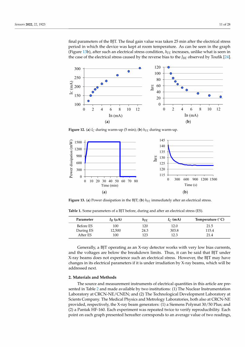
The transistor chip may experience mechanical stress during the packaging process,causing changes in the device’s electrical properties [23]. However, what matters mosthere is the electrical stress, then a brief comment on this subject will be made. There aresome conditions that cause electrical stress in a BJT, for example, high base current, reversebias VBE, voltage spikes, etc. Toufik [24], in his work, demonstrated the degradation in theBJT gain due to the reverse bias to the JBE. Here in this paper, a BJT (2N3903) was keptfor 50 min with VCE = 5 V and IC ≈ 304 mA, dissipating the power of PD ≈ 1.5 W, whichis above the maximum allowed for the device, and for this it was chosen to exceed themaximum collector current, which is IC = 200 mA [25]. Figure 12a shows how IC variedin the first five minutes, and Figure 12b shows how hFE varied during this slow warm-up.Figure 13a shows the curve of the power dissipated by the BJT in the time of electrical stress(50 min). The graph of Figure 13b corresponds to hFE immediately after the stress period,when the temperature was 115.4 C in the BJT package. Table 1 brings some initial and
Sensors 2022, 22, 1923 11 of 28
final parameters of the BJT. The final gain value was taken 25 min after the electrical stressperiod in which the device was kept at room temperature. As can be seen in the graph(Figure 13b), after such an electrical stress condition, hFE increases, unlike what is seen inthe case of the electrical stress caused by the reverse bias to the JBE observed by Toufik [24].
Sensors 2022, 22, x FOR PEER REVIEW 11 of 29
some conditions that cause electrical stress in a BJT, for example, high base current, re-verse bias VBE, voltage spikes, etc. Toufik [24], in his work, demonstrated the degradation in the BJT gain due to the reverse bias to the JBE. Here in this paper, a BJT (2N3903) was kept for 50 min with VCE = 5 V and IC ≈ 304 mA, dissipating the power of PD ≈ 1.5 W, which is above the maximum allowed for the device, and for this it was chosen to exceed the maximum collector current, which is IC = 200 mA [25]. Figure 12a shows how IC varied in the first five minutes, and Figure 12b shows how hFE varied during this slow warm-up. Figure 13a shows the curve of the power dissipated by the BJT in the time of electrical stress (50 min). The graph of Figure 13b corresponds to hFE immediately after the stress period, when the temperature was 115.4 °C in the BJT package. Table 1 brings some ini-tial and final parameters of the BJT. The final gain value was taken 25 min after the elec-trical stress period in which the device was kept at room temperature. As can be seen in the graph (Figure 13b), after such an electrical stress condition, hFE increases, unlike what is seen in the case of the electrical stress caused by the reverse bias to the JBE observed by Toufik [24].
(a) (b)
Figure 12. (a) IC during warm-up (5 min); (b) hFE during warm-up.
(a) (b)
Figure 13. (a) Power dissipation in the BJT; (b) hFE immediately after an electrical stress.
Table 1. Some parameters of a BJT before, during and after an electrical stress (ES).
Parameter IB (μA) hFE IC (mA) Temperature (°C) Before ES 100 120 12.0 21.5 During ES 12,500 24.3 303.8 115.4 After ES 100 123 12.3 21.4
Generally, a BJT operating as an X-ray detector works with very low bias currents, and the voltages are below the breakdown limits. Thus, it can be said that BJT under X-ray beams does not experience such an electrical stress. However, the BJT may have
100
150
200
250
300
0 2 4 6 8 10 12
IC(m
A)
IB (mA)
020406080
100120
0 2 4 6 8 10 12
hFE
IB (mA)
0
300
600
900
1200
1500
0 10 20 30 40 50 60 70 80
Pow
er d
issip
atio
n(m
W)
Time (min)
115120125130135140145
0 300 600 900 1200 1500
hFE
Time (s)
Figure 12. (a) IC during warm-up (5 min); (b) hFE during warm-up.
Sensors 2022, 22, x FOR PEER REVIEW 11 of 29
some conditions that cause electrical stress in a BJT, for example, high base current, re-verse bias VBE, voltage spikes, etc. Toufik [24], in his work, demonstrated the degradation in the BJT gain due to the reverse bias to the JBE. Here in this paper, a BJT (2N3903) was kept for 50 min with VCE = 5 V and IC ≈ 304 mA, dissipating the power of PD ≈ 1.5 W, which is above the maximum allowed for the device, and for this it was chosen to exceed the maximum collector current, which is IC = 200 mA [25]. Figure 12a shows how IC varied in the first five minutes, and Figure 12b shows how hFE varied during this slow warm-up. Figure 13a shows the curve of the power dissipated by the BJT in the time of electrical stress (50 min). The graph of Figure 13b corresponds to hFE immediately after the stress period, when the temperature was 115.4 °C in the BJT package. Table 1 brings some ini-tial and final parameters of the BJT. The final gain value was taken 25 min after the elec-trical stress period in which the device was kept at room temperature. As can be seen in the graph (Figure 13b), after such an electrical stress condition, hFE increases, unlike what is seen in the case of the electrical stress caused by the reverse bias to the JBE observed by Toufik [24].
(a) (b)
Figure 12. (a) IC during warm-up (5 min); (b) hFE during warm-up.
(a) (b)
Figure 13. (a) Power dissipation in the BJT; (b) hFE immediately after an electrical stress.
Table 1. Some parameters of a BJT before, during and after an electrical stress (ES).
Parameter IB (μA) hFE IC (mA) Temperature (°C) Before ES 100 120 12.0 21.5 During ES 12,500 24.3 303.8 115.4 After ES 100 123 12.3 21.4
Generally, a BJT operating as an X-ray detector works with very low bias currents, and the voltages are below the breakdown limits. Thus, it can be said that BJT under X-ray beams does not experience such an electrical stress. However, the BJT may have
100
150
200
250
300
0 2 4 6 8 10 12
IC(m
A)
IB (mA)
020406080
100120
0 2 4 6 8 10 12
hFE
IB (mA)
0
300
600
900
1200
1500
0 10 20 30 40 50 60 70 80
Pow
er d
issip
atio
n(m
W)
Time (min)
115120125130135140145
0 300 600 900 1200 1500
hFE
Time (s)
Figure 13. (a) Power dissipation in the BJT; (b) hFE immediately after an electrical stress.
Table 1. Some parameters of a BJT before, during and after an electrical stress (ES).
Parameter IB (µA) hFE IC (mA) Temperature (C)
Before ES 100 120 12.0 21.5During ES 12,500 24.3 303.8 115.4After ES 100 123 12.3 21.4
Generally, a BJT operating as an X-ray detector works with very low bias currents,and the voltages are below the breakdown limits. Thus, it can be said that BJT underX-ray beams does not experience such an electrical stress. However, the BJT may havechanges in its electrical parameters if it is under irradiation by X-ray beams, which will beaddressed next.
2. Materials and Methods
The source and measurement instruments of electrical quantities in this article are pre-sented in Table 2 and made available by two institutions: (1) The Nuclear InstrumentationLaboratory at CRCN-NE/CNEN; and (2) The Technological Development Laboratory atScients Company. The Medical Physics and Metrology Laboratories, both also at CRCN-NEprovided, respectively, the X-ray beam generators: (1) a Siemens Polymat 30/50 Plus; and(2) a Pantak HF-160. Each experiment was repeated twice to verify reproducibility. Eachpoint on each graph presented hereafter corresponds to an average value of two readings,

Sensors 2022, 22, 1923 12 of 28
unless otherwise noted. The relative measurement uncertainties are represented by the sizeof the marker in each graph and were always less than 0.6% in any experiment performed.
Table 2. Main instruments used in this article.
Instrument Model Manufacturer Lab.
Semiconductoranalyzer 4200A-SCS Keithley 1
Source-meter 1 6430 Keithley 1Source-meter 2 6430 Keithley 1Source-meter 3 2450 Keithley 2Source-meter 4 EFF1705 Scients 2
2.1. BJT Typical Operation as an X-ray Sensor
A very common device used to measure radiation intensity in diagnostic X-ray beamsis the photodiode [26] and also the phototransistor [27]. The BJT has also been used as adetector in diagnostic X-ray and radiotherapy beams [28–30]. Before analyzing the BJToperating as an X-ray sensor, a brief description of how a pn junction works under anX-ray photon beam is outlined, taking into account four aspects: (1) X-ray photon energy;(2) device package; (3) scattered radiation; (4) angular dependence.
2.1.1. X-ray Photon Energy
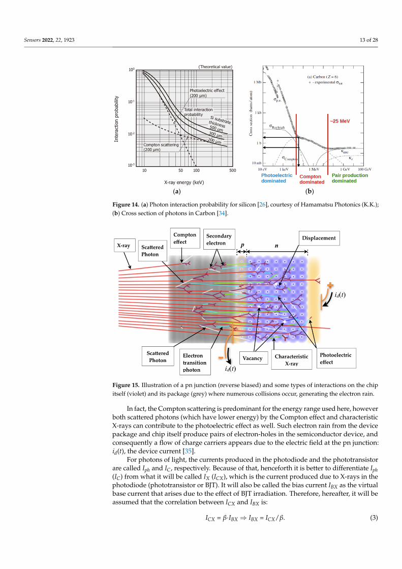
Firstly, consider a device such as a photodiode or a phototransistor which has anencapsulation to filter out ambient light, and only the infrared band (~1.4 eV photons)passes through. Remember that the photodiode has a reverse bias VPD, and in the caseof the phototransistor it also has a reverse bias, VCE. When the infrared light reachesthe photodiode pn junction (JBC in the phototransistor), the photoelectric effect naturallyoccurs and a photocurrent called Iph (IC) is produced on the photodiode (phototransistor).Without infrared light there will only be a noisy leakage current, in, due to the effect oftemperature and the generation and recombination of electrons and holes. On the otherhand, unlike photons of light, X-ray photons generally have energy of at least four or fiveorders of magnitude greater than photons of light. The X-ray photon energy will dependon whether the X-ray generating equipment is for examinations of dental radiography(70 kV), conventional radiography (70–125 kV), computed tomography (70–150 kV), etc.;and it also depends on the manufacturer. This means that in the X-ray energy range usedin medical diagnosis, the X-ray tube potential can vary between 70 kV and 150 kV (fortypical modern medical diagnostic equipment), and it corresponds to X-ray effective energyapproximately between 50 keV and 100 keV (see Table 1 in [31]). Actually, the effectiveenergy depends on the X-ray tube potential and the radiation filtration [31–33]. In this case,for the photon energy range from 50 keV to 100 keV, the Compton effect predominates, ascan be seen in the graphs of Figure 14a,b for the silicon [26] and carbon [34], respectively,the main elements of which the chip itself and its package is made. Figure 14a showsthat the probability of the photoelectric effect occurring in 300µm of silicon is less than 3%for energies above 50 keV. Figure 14b is very representative for estimating the probabilityof photon interactions in materials with a low effective atomic number. For example,above 50 keV the photoelectric effect is at least 10 times smaller than Compton scatteringfor carbon (see black arrows in graph—Figure 14b). The interactions that occur are withthe device as a whole (package + pn junction) generating secondary electrons (so-calledelectron rain) resulting from both the Compton and photoelectric effect, and multipleelectron-electron collisions, as can be seen in Figure 15.
Sensors 2022, 22, 1923 13 of 28
Sensors 2022, 22, x FOR PEER REVIEW 13 of 29
[34], respectively, the main elements of which the chip itself and its package is made. Figure 14a shows that the probability of the photoelectric effect occurring in 300µm of silicon is less than 3% for energies above 50 keV. Figure 14b is very representative for es-timating the probability of photon interactions in materials with a low effective atomic number. For example, above 50 keV the photoelectric effect is at least 10 times smaller than Compton scattering for carbon (see black arrows in graph—Figure 14b). The inter-actions that occur are with the device as a whole (package + pn junction) generating secondary electrons (so-called electron rain) resulting from both the Compton and pho-toelectric effect, and multiple electron-electron collisions, as can be seen in Figure 15.
(a) (b)
Figure 14. (a) Photon interaction probability for silicon [26], courtesy of Hamamatsu Photonics (K.K.); (b) Cross section of photons in Carbon [34].
Figure 15. Illustration of a pn junction (reverse biased) and some types of interactions on the chip itself (violet) and its package (grey) where numerous collisions occur, generating the electron rain.
In fact, the Compton scattering is predominant for the energy range used here, however both scattered photons (which have lower energy) by the Compton effect and characteristic X-rays can contribute to the photoelectric effect as well. Such electron rain from the device package and chip itself produce pairs of electron-holes in the semicon-
Figure 14. (a) Photon interaction probability for silicon [26], courtesy of Hamamatsu Photonics (K.K.);(b) Cross section of photons in Carbon [34].
Sensors 2022, 22, x FOR PEER REVIEW 13 of 29
[34], respectively, the main elements of which the chip itself and its package is made. Figure 14a shows that the probability of the photoelectric effect occurring in 300µm of silicon is less than 3% for energies above 50 keV. Figure 14b is very representative for es-timating the probability of photon interactions in materials with a low effective atomic number. For example, above 50 keV the photoelectric effect is at least 10 times smaller than Compton scattering for carbon (see black arrows in graph—Figure 14b). The inter-actions that occur are with the device as a whole (package + pn junction) generating secondary electrons (so-called electron rain) resulting from both the Compton and pho-toelectric effect, and multiple electron-electron collisions, as can be seen in Figure 15.
(a) (b)
Figure 14. (a) Photon interaction probability for silicon [26], courtesy of Hamamatsu Photonics (K.K.); (b) Cross section of photons in Carbon [34].
Figure 15. Illustration of a pn junction (reverse biased) and some types of interactions on the chip itself (violet) and its package (grey) where numerous collisions occur, generating the electron rain.
In fact, the Compton scattering is predominant for the energy range used here, however both scattered photons (which have lower energy) by the Compton effect and characteristic X-rays can contribute to the photoelectric effect as well. Such electron rain from the device package and chip itself produce pairs of electron-holes in the semicon-
Figure 15. Illustration of a pn junction (reverse biased) and some types of interactions on the chipitself (violet) and its package (grey) where numerous collisions occur, generating the electron rain.
In fact, the Compton scattering is predominant for the energy range used here, howeverboth scattered photons (which have lower energy) by the Compton effect and characteristicX-rays can contribute to the photoelectric effect as well. Such electron rain from the devicepackage and chip itself produce pairs of electron-holes in the semiconductor device, andconsequently a flow of charge carriers appears due to the electric field at the pn junction:id(t), the device current [35].
For photons of light, the currents produced in the photodiode and the phototransistorare called Iph and IC, respectively. Because of that, henceforth it is better to differentiate Iph(IC) from what it will be called IX (ICX), which is the current produced due to X-rays in thephotodiode (phototransistor or BJT). It will also be called the bias current IBX as the virtualbase current that arises due to the effect of BJT irradiation. Therefore, hereafter, it will beassumed that the correlation between ICX and IBX is:
ICX = β·IBX ⇒ IBX = ICX/β. (3)
Sensors 2022, 22, 1923 14 of 28
The device current, id, is proportional to both electrical current (IXRT) and potential(kV) in the X-ray tube. It is known that IXRT (mA) imposes the photonic intensity of theX-ray beam [32], and the X-ray photon energy spectrum (and consequently both mean andeffective photon energy) is determined by the potential (kV). Also, other parameters thatdetermine the X-ray photon energy spectrum are both type of material and thickness of theradiation filtration [32,33].
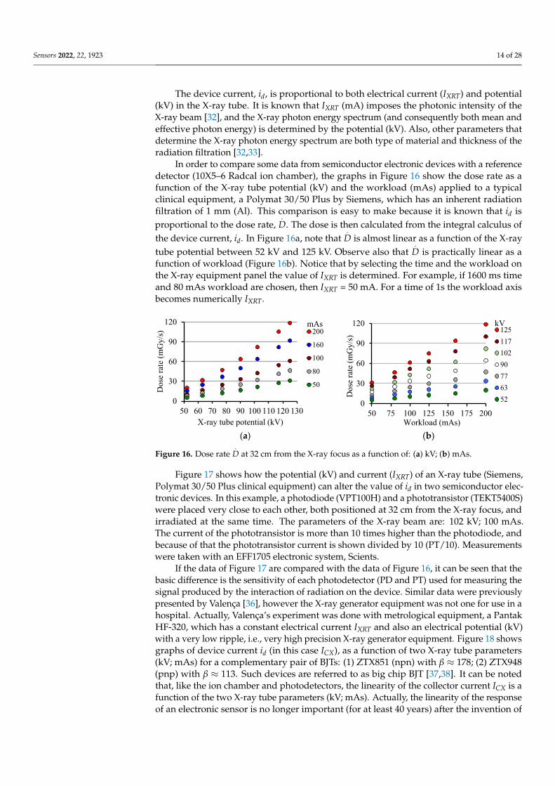
In order to compare some data from semiconductor electronic devices with a referencedetector (10X5–6 Radcal ion chamber), the graphs in Figure 16 show the dose rate as afunction of the X-ray tube potential (kV) and the workload (mAs) applied to a typicalclinical equipment, a Polymat 30/50 Plus by Siemens, which has an inherent radiationfiltration of 1 mm (Al). This comparison is easy to make because it is known that id isproportional to the dose rate,
.D. The dose is then calculated from the integral calculus of
the device current, id. In Figure 16a, note that.
D is almost linear as a function of the X-raytube potential between 52 kV and 125 kV. Observe also that
.D is practically linear as a
function of workload (Figure 16b). Notice that by selecting the time and the workload onthe X-ray equipment panel the value of IXRT is determined. For example, if 1600 ms timeand 80 mAs workload are chosen, then IXRT = 50 mA. For a time of 1s the workload axisbecomes numerically IXRT.
Sensors 2022, 22, x FOR PEER REVIEW 14 of 29
ductor device, and consequently a flow of charge carriers appears due to the electric field at the pn junction: id(t), the device current [35].
For photons of light, the currents produced in the photodiode and the phototran-sistor are called Iph and IC, respectively. Because of that, henceforth it is better to differen-tiate Iph (IC) from what it will be called IX (ICX), which is the current produced due to X-rays in the photodiode (phototransistor or BJT). It will also be called the bias current IBX as the virtual base current that arises due to the effect of BJT irradiation. Therefore, hereafter, it will be assumed that the correlation between ICX and IBX is:
ICX = β·IBX IBX = ICX/β. (3)
The device current, id, is proportional to both electrical current (IXRT) and potential (kV) in the X-ray tube. It is known that IXRT (mA) imposes the photonic intensity of the X-ray beam [32], and the X-ray photon energy spectrum (and consequently both mean and effective photon energy) is determined by the potential (kV). Also, other parameters that determine the X-ray photon energy spectrum are both type of material and thickness of the radiation filtration [32,33].
In order to compare some data from semiconductor electronic devices with a refer-ence detector (10X5–6 Radcal ion chamber), the graphs in Figure 16 show the dose rate as a function of the X-ray tube potential (kV) and the workload (mAs) applied to a typical clinical equipment, a Polymat 30/50 Plus by Siemens, which has an inherent radiation filtration of 1 mm (Al). This comparison is easy to make because it is known that id is proportional to the dose rate, 𝐷. The dose is then calculated from the integral calculus of the device current, id. In Figure 16a, note that 𝐷 is almost linear as a function of the X-ray tube potential between 52 kV and 125 kV. Observe also that 𝐷 is practically linear as a function of workload (Figure 16b). Notice that by selecting the time and the workload on the X-ray equipment panel the value of IXRT is determined. For example, if 1600 ms time and 80 mAs workload are chosen, then IXRT = 50 mA. For a time of 1s the workload axis becomes numerically IXRT.
(a) (b)
Figure 16. Dose rate 𝐷 at 32 cm from the X-ray focus as a function of: (a) kV; (b) mAs.
Figure 17 shows how the potential (kV) and current (IXRT) of an X-ray tube (Siemens, Polymat 30/50 Plus clinical equipment) can alter the value of id in two semiconductor electronic devices. In this example, a photodiode (VPT100H) and a phototransistor (TEKT5400S) were placed very close to each other, both positioned at 32 cm from the X-ray focus, and irradiated at the same time. The parameters of the X-ray beam are: 102 kV; 100 mAs. The current of the phototransistor is more than 10 times higher than the photodiode, and because of that the phototransistor current is shown divided by 10 (PT/10). Measurements were taken with an EFF1705 electronic system, Scients.
0
30
60
90
120
50 60 70 80 90 100 110 120 130
Dos
e ra
te (m
Gy/
s)
X-ray tube potential (kV)
mAs200
160
100
80
50
0
30
60
90
120
50 75 100 125 150 175 200
Dos
e ra
te (m
Gy/
s)
Workload (mAs)
kV12511710290776352
Figure 16. Dose rate.
D at 32 cm from the X-ray focus as a function of: (a) kV; (b) mAs.
Figure 17 shows how the potential (kV) and current (IXRT) of an X-ray tube (Siemens,Polymat 30/50 Plus clinical equipment) can alter the value of id in two semiconductor elec-tronic devices. In this example, a photodiode (VPT100H) and a phototransistor (TEKT5400S)were placed very close to each other, both positioned at 32 cm from the X-ray focus, andirradiated at the same time. The parameters of the X-ray beam are: 102 kV; 100 mAs.The current of the phototransistor is more than 10 times higher than the photodiode, andbecause of that the phototransistor current is shown divided by 10 (PT/10). Measurementswere taken with an EFF1705 electronic system, Scients.
If the data of Figure 17 are compared with the data of Figure 16, it can be seen that thebasic difference is the sensitivity of each photodetector (PD and PT) used for measuring thesignal produced by the interaction of radiation on the device. Similar data were previouslypresented by Valença [36], however the X-ray generator equipment was not one for use in ahospital. Actually, Valença’s experiment was done with metrological equipment, a PantakHF-320, which has a constant electrical current IXRT and also an electrical potential (kV)with a very low ripple, i.e., very high precision X-ray generator equipment. Figure 18 showsgraphs of device current id (in this case ICX), as a function of two X-ray tube parameters(kV; mAs) for a complementary pair of BJTs: (1) ZTX851 (npn) with β ≈ 178; (2) ZTX948(pnp) with β ≈ 113. Such devices are referred to as big chip BJT [37,38]. It can be notedthat, like the ion chamber and photodetectors, the linearity of the collector current ICX is afunction of the two X-ray tube parameters (kV; mAs). Actually, the linearity of the responseof an electronic sensor is no longer important (for at least 40 years) after the invention of

Sensors 2022, 22, 1923 15 of 28
the microprocessor, which can be programmed for measuring any function (exponential,polynomial, etc.).
Sensors 2022, 22, x FOR PEER REVIEW 15 of 29
(a) (b)
Figure 17. id of a photodiode (PD) and a phototransistor (PT), irradiated simultaneously positioned together (at 32 cm), as a function of: (a) X-ray tube potential at 100 mAs; (b) Workload at 102 kV.
If the data of Figure 17 are compared with the data of Figure 16, it can be seen that the basic difference is the sensitivity of each photodetector (PD and PT) used for meas-uring the signal produced by the interaction of radiation on the device. Similar data were previously presented by Valença [36], however the X-ray generator equipment was not one for use in a hospital. Actually, Valença’s experiment was done with metrological equipment, a Pantak HF-320, which has a constant electrical current IXRT and also an electrical potential (kV) with a very low ripple, i.e., very high precision X-ray generator equipment. Figure 18 shows graphs of device current id (in this case ICX), as a function of two X-ray tube parameters (kV; mAs) for a complementary pair of BJTs: (1) ZTX851 (npn) with β ≈ 178; (2) ZTX948 (pnp) with β ≈ 113. Such devices are referred to as big chip BJT [37,38]. It can be noted that, like the ion chamber and photodetectors, the linearity of the collector current ICX is a function of the two X-ray tube parameters (kV; mAs). Actually, the linearity of the response of an electronic sensor is no longer important (for at least 40 years) after the invention of the microprocessor, which can be programmed for measur-ing any function (exponential, polynomial, etc.).
(a) (b)
Figure 18. ICX for npn and pnp BJTs, irradiated simultaneously at the same position (32 cm), as a function of: (a) X-ray tube potential (kV@200 mAs); (b) Workload (mAs@102 kV).
2.1.2. Device Package There is influence of the device package in the current signal produced when the
device is under diagnostic X-rays. This effect is due to the radiation scattered in front of the semiconductor chip (Figure 15). It is known as the build-up cap effect [39], in which the dose rate increases with the package thickness, tp. There is a thickness called tmax in which the dose rate reaches its maximum, 𝐷 , and if the thickness is greater than tmax the id signal decreases. Alves [28] points out in her research that a BC846 signal transistor, which has SMD (Surface-Mount Device) package, presents tmax of around 5 mm. To per-
R² = 0.9991
R² = 0.9979
0
125
250
375
500
625
750
50 60 70 80 90 100 110 120 130Phot
odet
ecto
r cur
rent
(nA
)
X-ray tube potential (kV)
PD
PT/10
R² = 0.9998
R² = 0.9977
0
250
500
750
1000
1250
25 50 75 100 125 150 175 200
Phot
odet
ecto
r cur
rent
(nA
)
Workload (mAs)
PD
PT/10
R² = 0.996
R² = 0.9986
0
400
800
1200
1600
2000
50 70 90 110 130
Colle
ctor
cur
rent
(nA
)
X-ray tube potential (kV)
NPN
PNP
R² = 0.9997
R² = 0.9994
0
200
400
600
800
1000
1200
1400
25 50 75 100 125 150 175 200
Colle
ctor
cur
rent
(nA
)
Workload (mAs)
NPN
PNP
Figure 17. id of a photodiode (PD) and a phototransistor (PT), irradiated simultaneously positionedtogether (at 32 cm), as a function of: (a) X-ray tube potential at 100 mAs; (b) Workload at 102 kV.
Sensors 2022, 22, x FOR PEER REVIEW 15 of 29
(a) (b)
Figure 17. id of a photodiode (PD) and a phototransistor (PT), irradiated simultaneously positioned together (at 32 cm), as a function of: (a) X-ray tube potential at 100 mAs; (b) Workload at 102 kV.
If the data of Figure 17 are compared with the data of Figure 16, it can be seen that the basic difference is the sensitivity of each photodetector (PD and PT) used for meas-uring the signal produced by the interaction of radiation on the device. Similar data were previously presented by Valença [36], however the X-ray generator equipment was not one for use in a hospital. Actually, Valença’s experiment was done with metrological equipment, a Pantak HF-320, which has a constant electrical current IXRT and also an electrical potential (kV) with a very low ripple, i.e., very high precision X-ray generator equipment. Figure 18 shows graphs of device current id (in this case ICX), as a function of two X-ray tube parameters (kV; mAs) for a complementary pair of BJTs: (1) ZTX851 (npn) with β ≈ 178; (2) ZTX948 (pnp) with β ≈ 113. Such devices are referred to as big chip BJT [37,38]. It can be noted that, like the ion chamber and photodetectors, the linearity of the collector current ICX is a function of the two X-ray tube parameters (kV; mAs). Actually, the linearity of the response of an electronic sensor is no longer important (for at least 40 years) after the invention of the microprocessor, which can be programmed for measur-ing any function (exponential, polynomial, etc.).
(a) (b)
Figure 18. ICX for npn and pnp BJTs, irradiated simultaneously at the same position (32 cm), as a function of: (a) X-ray tube potential (kV@200 mAs); (b) Workload (mAs@102 kV).
2.1.2. Device Package There is influence of the device package in the current signal produced when the
device is under diagnostic X-rays. This effect is due to the radiation scattered in front of the semiconductor chip (Figure 15). It is known as the build-up cap effect [39], in which the dose rate increases with the package thickness, tp. There is a thickness called tmax in which the dose rate reaches its maximum, 𝐷 , and if the thickness is greater than tmax the id signal decreases. Alves [28] points out in her research that a BC846 signal transistor, which has SMD (Surface-Mount Device) package, presents tmax of around 5 mm. To per-
R² = 0.9991
R² = 0.9979
0
125
250
375
500
625
750
50 60 70 80 90 100 110 120 130Phot
odet
ecto
r cur
rent
(nA
)
X-ray tube potential (kV)
PD
PT/10
R² = 0.9998
R² = 0.9977
0
250
500
750
1000
1250
25 50 75 100 125 150 175 200
Phot
odet
ecto
r cur
rent
(nA
)
Workload (mAs)
PD
PT/10
R² = 0.996
R² = 0.9986
0
400
800
1200
1600
2000
50 70 90 110 130
Colle
ctor
cur
rent
(nA
)
X-ray tube potential (kV)
NPN
PNP
R² = 0.9997
R² = 0.9994
0
200
400
600
800
1000
1200
1400
25 50 75 100 125 150 175 200
Colle
ctor
cur
rent
(nA
)
Workload (mAs)
NPN
PNP
Figure 18. ICX for npn and pnp BJTs, irradiated simultaneously at the same position (32 cm), as afunction of: (a) X-ray tube potential (kV@200 mAs); (b) Workload (mAs@102 kV).
2.1.2. Device Package
There is influence of the device package in the current signal produced when thedevice is under diagnostic X-rays. This effect is due to the radiation scattered in front of thesemiconductor chip (Figure 15). It is known as the build-up cap effect [39], in which thedose rate increases with the package thickness, tp. There is a thickness called tmax in which
the dose rate reaches its maximum,.
Dmax, and if the thickness is greater than tmax the idsignal decreases. Alves [28] points out in her research that a BC846 signal transistor, whichhas SMD (Surface-Mount Device) package, presents tmax of around 5 mm. To perform herexperiment, the thickness was varied using a 0.5 mm step ladder-shaped piece made ofPMMA (Figure 19) to gradually simulate a thicker package. The material (PMMA) waschosen because it has an approximate effective atomic number of the material that the BJTpackage is normally made of. To perform such an experiment, the piece was positionedtightly against the transistor. The same piece from Alves’ experiment [28] and another3 pieces of PMMA, 5 mm tick, were used to illustrate graphically how the thickness ofthe package can influence the ICX signal produced by a complementary pair of BJT, andFigure 20 shows data from these BJTs simultaneously irradiated. Each BJT has differentgains: β1 ≈ 178 (npn); β2 ≈ 113 (pnp).

Sensors 2022, 22, 1923 16 of 28
Sensors 2022, 22, x FOR PEER REVIEW 16 of 29
form her experiment, the thickness was varied using a 0.5 mm step ladder-shaped piece made of PMMA (Figure 19) to gradually simulate a thicker package. The material (PMMA) was chosen because it has an approximate effective atomic number of the ma-terial that the BJT package is normally made of. To perform such an experiment, the piece was positioned tightly against the transistor. The same piece from Alves’ experiment [28] and another 3 pieces of PMMA, 5 mm tick, were used to illustrate graphically how the thickness of the package can influence the ICX signal produced by a complementary pair of BJT, and Figure 20 shows data from these BJTs simultaneously irradiated. Each BJT has different gains: β1 ≈ 178 (npn); β2 ≈ 113 (pnp).
Figure 19. A 0.5 mm step ladder-shaped piece made of PMMA to simulate thicker packages.
Looking at the graph in Figure 20, it can be seen that the curve shape of each BJT is very similar regardless of the gain and polarity of each one. That is, the ICX current in-creases with the increase in the thickness of the simulated package and then from tp ≈ 4 mm onwards ICX starts to decrease. The difference in the Alves’ result and those in Figure 20 is that the BC846 device used by Alves [28] has a SOT-123 SMD package, which is about 1 mm thinner than the big chip BJT used here, then the difference in result was expected.
Figure 20. Build-up cap effect for two BJTs, irradiated simultaneously (102 kV@125 mA) at the same position (32 cm), each one has different gains: β1 ≈ 178 (npn); β2 ≈ 113 (pnp).
2.1.3. Scattered Radiation It must be evaluated whether scattered radiation far from the device can be signifi-
cant in the radiation measurement procedure with BJTs. Such an evaluation can be im-portant if the device is used to measure only primary radiation (e.g., non-invasive kV measurement). One way to analyze such an effect is to place a radiation filtration plate at a distance from the device (Figure 21). By placing a collimator between the plate and the device under radiation, it is possible to verify how much the scattered photons on the
0200400600800
100012001400
0 3 5 8 10 13 15 18 20 23 25
Colle
ctor
cur
rent
(nA
)
Simulated thickness (mm)
NPN
PNP
Figure 19. A 0.5 mm step ladder-shaped piece made of PMMA to simulate thicker packages.
Sensors 2022, 22, x FOR PEER REVIEW 16 of 29
form her experiment, the thickness was varied using a 0.5 mm step ladder-shaped piece made of PMMA (Figure 19) to gradually simulate a thicker package. The material (PMMA) was chosen because it has an approximate effective atomic number of the ma-terial that the BJT package is normally made of. To perform such an experiment, the piece was positioned tightly against the transistor. The same piece from Alves’ experiment [28] and another 3 pieces of PMMA, 5 mm tick, were used to illustrate graphically how the thickness of the package can influence the ICX signal produced by a complementary pair of BJT, and Figure 20 shows data from these BJTs simultaneously irradiated. Each BJT has different gains: β1 ≈ 178 (npn); β2 ≈ 113 (pnp).
Figure 19. A 0.5 mm step ladder-shaped piece made of PMMA to simulate thicker packages.
Looking at the graph in Figure 20, it can be seen that the curve shape of each BJT is very similar regardless of the gain and polarity of each one. That is, the ICX current in-creases with the increase in the thickness of the simulated package and then from tp ≈ 4 mm onwards ICX starts to decrease. The difference in the Alves’ result and those in Figure 20 is that the BC846 device used by Alves [28] has a SOT-123 SMD package, which is about 1 mm thinner than the big chip BJT used here, then the difference in result was expected.
Figure 20. Build-up cap effect for two BJTs, irradiated simultaneously (102 kV@125 mA) at the same position (32 cm), each one has different gains: β1 ≈ 178 (npn); β2 ≈ 113 (pnp).
2.1.3. Scattered Radiation It must be evaluated whether scattered radiation far from the device can be signifi-
cant in the radiation measurement procedure with BJTs. Such an evaluation can be im-portant if the device is used to measure only primary radiation (e.g., non-invasive kV measurement). One way to analyze such an effect is to place a radiation filtration plate at a distance from the device (Figure 21). By placing a collimator between the plate and the device under radiation, it is possible to verify how much the scattered photons on the
0200400600800
100012001400
0 3 5 8 10 13 15 18 20 23 25
Colle
ctor
cur
rent
(nA
)
Simulated thickness (mm)
NPN
PNP
Figure 20. Build-up cap effect for two BJTs, irradiated simultaneously (102 kV@125 mA) at the sameposition (32 cm), each one has different gains: β1 ≈ 178 (npn); β2 ≈ 113 (pnp).
Looking at the graph in Figure 20, it can be seen that the curve shape of each BJT is verysimilar regardless of the gain and polarity of each one. That is, the ICX current increaseswith the increase in the thickness of the simulated package and then from tp ≈ 4 mmonwards ICX starts to decrease. The difference in the Alves’ result and those in Figure 20is that the BC846 device used by Alves [28] has a SOT-123 SMD package, which is about1 mm thinner than the big chip BJT used here, then the difference in result was expected.
2.1.3. Scattered Radiation
It must be evaluated whether scattered radiation far from the device can be significantin the radiation measurement procedure with BJTs. Such an evaluation can be important ifthe device is used to measure only primary radiation (e.g., non-invasive kV measurement).One way to analyze such an effect is to place a radiation filtration plate at a distance fromthe device (Figure 21). By placing a collimator between the plate and the device underradiation, it is possible to verify how much the scattered photons on the plate are measuredor not by a BJT. Such an experiment can be performed by varying the area of the collimatorfor measuring how ICX varies as a function of collimation (Table 3).

Sensors 2022, 22, 1923 17 of 28
Sensors 2022, 22, x FOR PEER REVIEW 17 of 29
plate are measured or not by a BJT. Such an experiment can be performed by varying the area of the collimator for measuring how ICX varies as a function of collimation (Table 3).
Table 3. Influence of scattered radiation on the measurement of X-rays with the BJT.
Collimator Area (cm2) ~200 100 64 36 16 4 1 ~0.2
ICX (nA) 1021.9 1009.4 1003.9 995.4 997.0 970.4 936.3 901.6
Table 3 indicates that ICX practically varies about ±1.5% for the areas of collimators between 100 cm2 and 16 cm2. Comparing the readings for 100 cm2 and 1 cm2 it can be seen that the contribution of scattered radiation is around 7%. The last column of Table 3 shows that the area of the radiation field is practically the area of the device package. For the collimation which exactly covers the transistor package (~0.2 cm2), the contribution of scattered radiation is about 11% in relation to 100 cm2. In the previous approach on the build-up cap effect, it was observed that the scattered radiation near the semiconductor chip contributes to the increase in ICX. However, if the BJT is used to measure the dose at a specific point, as in the case of a dosimeter, it must measure both direct and scattered contributions delivered to a patient undergoing examination. That is, as the BJT is a very small electronic component, it becomes advantageous to perform high accuracy dosime-try studies in phantoms to then obtain data without the need for human beings, for ex-ample.
Figure 21. Illustration of experimental setup to analyze the effect of the scattered radiation in a BJT.
2.1.4. Angular Dependence Angular dependence corresponds to an analysis of how the detector signal varies as
a function of the angle of incidence of the X-ray beam on the device face. To assess the angular effect, it is enough to vary the angle of the normal vector to the chip plane in degrees, for example, as Alves [28] also did. Table 4 presents an angular dependence for a BJT and it is similar to what Alves [28] found. Note that in rotating the device clockwise the signal is slightly less than when rotating it counterclockwise. Actually, in addition to the fact that the chip area decreases in relation to the direction of the incident radiation beam, it is due to two effects: (1) the X-ray path is increased when the device is rotated, resulting in the build-up cap effect; and (2) the connecting wire between the emitter and its own external metallic terminal (see Figure 9) causes a slight attenuation of the radia-tion beam that reaches the JBC if the device is rotated clockwise.
Figure 21. Illustration of experimental setup to analyze the effect of the scattered radiation in a BJT.
Table 3. Influence of scattered radiation on the measurement of X-rays with the BJT.
CollimatorArea (cm2) ~200 100 64 36 16 4 1 ~0.2
ICX (nA) 1021.9 1009.4 1003.9 995.4 997.0 970.4 936.3 901.6
Table 3 indicates that ICX practically varies about ±1.5% for the areas of collimatorsbetween 100 cm2 and 16 cm2. Comparing the readings for 100 cm2 and 1 cm2 it can beseen that the contribution of scattered radiation is around 7%. The last column of Table 3shows that the area of the radiation field is practically the area of the device package. Forthe collimation which exactly covers the transistor package (~0.2 cm2), the contribution ofscattered radiation is about 11% in relation to 100 cm2. In the previous approach on thebuild-up cap effect, it was observed that the scattered radiation near the semiconductorchip contributes to the increase in ICX. However, if the BJT is used to measure the dose ata specific point, as in the case of a dosimeter, it must measure both direct and scatteredcontributions delivered to a patient undergoing examination. That is, as the BJT is a verysmall electronic component, it becomes advantageous to perform high accuracy dosimetrystudies in phantoms to then obtain data without the need for human beings, for example.
2.1.4. Angular Dependence
Angular dependence corresponds to an analysis of how the detector signal variesas a function of the angle of incidence of the X-ray beam on the device face. To assessthe angular effect, it is enough to vary the angle of the normal vector to the chip plane indegrees, for example, as Alves [28] also did. Table 4 presents an angular dependence for aBJT and it is similar to what Alves [28] found. Note that in rotating the device clockwisethe signal is slightly less than when rotating it counterclockwise. Actually, in addition tothe fact that the chip area decreases in relation to the direction of the incident radiationbeam, it is due to two effects: (1) the X-ray path is increased when the device is rotated,resulting in the build-up cap effect; and (2) the connecting wire between the emitter and itsown external metallic terminal (see Figure 9) causes a slight attenuation of the radiationbeam that reaches the JBC if the device is rotated clockwise.
Table 4. Angular dependence of a ZTX851 BJT as a sensor in a diagnostic X-ray beam.
Rotation Counterclockwise Clockwise
Angle 60 45 30 0 30 45 60
ICX (nA) 951.8 988.4 1047.2 1020.5 1000.6 946.9 929.6

Sensors 2022, 22, 1923 18 of 28
All data presented in the approaches above can be found in the literature, althoughsome of them were obtained especially for this article. The main devices used in thisarticle consist of complementary pairs of BJTs with several different gains: ZTX851 (npn)and ZTX948 (pnp), which have an E-Line type package (TO-92 compatible). Anothercomplementary pair of BJTs, with package TO-220, were also used only for comparisonpurposes: TIP41 (npn) and TIP42 (pnp). Before presenting the main results, it will be shownhow these BJTs were biased and how to obtain the collector current ICX.
2.2. Method for Measuring ICX in a BJT
First of all, before irradiating the transistor, it is electrically biased to help us under-stand how the BJT works as an X-ray sensor. Therefore, an experiment is done by biasingthe transistor with an ultra-low IB value (e.g., 1 nA) so that there is an initial collectorcurrent IC ≈ 178 nA, for a ZTX851 BJT with β ≈ 178 as shown in Figure 22a. Second,Figure 22b illustrates the biased BJT under an X-ray beam and this results in IC = 702 nA.The calculation of ICX must be done by subtracting the component of the initial collectorcurrent IC = 178 nA, then ICX = 524 nA, for the example. From the value of ICX, one cancalculate the value of IBX ≈ 2.9 nA, which would correspond to a base current componentonly due to X-rays. Thus, it is assumed that IBX was supposedly amplified by β, as pre-viously shown in Equation (3). In this approach, the parameters of the X-ray tube were102 kV; 200 mAs; and 1600 ms, resulting in an X-ray tube current of 125 mA, and the devicewas positioned 32 cm from the X-ray source.
Sensors 2022, 22, x FOR PEER REVIEW 19 of 29
complementary BJTs behave when under irradiation. To perform such an experiment, a
pair of BJTs (β1 ≈ 101, npn; β2 ≈ 101, pnp; for IB = 10 nA) never before irradiated were se-
lected. Table 5 presents the results, and hFE corresponds to the gain value for IB without
X-ray incidence on the BJT. ICX was measured and IBX calculated from Equation (3). Note
that ICX is not the same for every value of IB, and there does not appear to be a monotonic
correlation, although ICX increases with IB.
(a) (b)
Figure 23. (a) Measured gain behavior of a complementary pair of BJTs with β1 = β2 @ 15 nA; (b)
Measured gain behavior of a complementary pair of BJTs with β1 ≈ β2 @ 4 nA.
Table 5. Variation in IB to analyze its influence on the measurements of ICX and IBX.
BJT NPN PNP
IB (nA) hFE IC (nA) ICX (nA) IBX (nA) hFE IC (nA) ICX (nA) IBX (nA)
5 100.0 500.2 704.0 7.0 101.9 509.4 483.7 4.7
10 100.6 1006.3 872.4 8.7 100.7 1007.4 650.6 6.5
20 100.7 2014.0 836.7 8.4 125.1 2501.8 601.1 4.8
30 100.0 3001.5 795.8 8.0 130.0 3899.1 555.4 4.3
40 100.2 4008.1 974.8 9.7 132.5 5301.9 646.0 4.9
50 103.3 5163.4 942.1 9.1 135.5 6774.1 705.3 5.2
By analyzing in a general way the results of Figure 23 and Table 5, one can see that:
(1) there is a certain influence of IB on the transistor gain (with or without radiation); (2)
IBX is higher in the npn transistor than in the pnp transistor, i.e., npn BJT seems to be more
sensitive to X-ray beams normally used in medical diagnosis; (3) IBX of the pnp BJT
reaches the highest value for IB = 10 nA, whereas for the npn BJT it occurs at IB = 40 nA. In
fact, it was seen earlier in Figure 10 that IC (and hence IB) varies with the transistor gain
and vice versa, so this is nothing new. However, there seems to be a doubt about IBX be-
cause Table 5 provides estimated values for the virtual bias, IBX, since the current IBX itself
influences the gain and vice versa. Actually, there is a way to measure IBX. It is known
that X-ray photons reach the chip itself generating electron-hole pairs there, and this
contributes to a fraction of ICX. Remember that the device is irradiated as a whole. Then,
knowing that the Compton effect is predominant in the package, part of the electron rain
from the package reaches both the JBE and the JBC. Looking at Figure 8, one can see the JBE
is just above JBC and it is the first region on the chip itself that receives the electron rain
from the transistor package. Another fraction of radiation (photons and secondary elec-
trons) reaches the back of the device (usually a metal substrate) and probably does not
contribute significantly to ICX. From this point of view, ICX is formed by a complex com-
bination of Compton and photoelectric effects, and interactions from scattered photons
and secondary electrons from both package and chip itself (see Figure 15). In this paper,
what matters is the result of that combination of all components that will act as the virtual
base bias, IBX, which is supposedly amplified by β, and it can be assumed that:
Figure 22. (a) Biasing a BJT with β =178 before irradiation. (b) IC during irradiation.
3. Results
Taking into account the approaches above, it will be explained how the BJT behaveswhen under X-ray beams used in the medical diagnostic energy range. It is assumed in thisexplanation that the BJT is the planar type as described in the BJT fabrication overview.
3.1. Influence of IB for a BJT Operating as an X-ray Sensor
In the previous analysis, a bias of IB = 1 nA was used. However, if one wants toknow how much IB influences the sensitivity of BJT to X-ray beams, it is necessary to varyIB. First, the BJT gain behavior without any irradiation is presented in Figure 23 for twocomplementary pairs of BJTs. For very low IB values (between 1 nA and 5 nA), the gainsof the two devices vary significantly. However, after 10 nA they vary much less than forlow IB, for both types of transistors. Second, another experiment was made to verify howcomplementary BJTs behave when under irradiation. To perform such an experiment, apair of BJTs (β1 ≈ 101, npn; β2 ≈ 101, pnp; for IB = 10 nA) never before irradiated wereselected. Table 5 presents the results, and hFE corresponds to the gain value for IB withoutX-ray incidence on the BJT. ICX was measured and IBX calculated from Equation (3). Notethat ICX is not the same for every value of IB, and there does not appear to be a monotoniccorrelation, although ICX increases with IB.

Sensors 2022, 22, 1923 19 of 28
Sensors 2022, 22, x FOR PEER REVIEW 19 of 29
complementary BJTs behave when under irradiation. To perform such an experiment, a pair of BJTs (β1 ≈ 101, npn; β2 ≈ 101, pnp; for IB = 10 nA) never before irradiated were se-lected. Table 5 presents the results, and hFE corresponds to the gain value for IB without X-ray incidence on the BJT. ICX was measured and IBX calculated from Equation (3). Note that ICX is not the same for every value of IB, and there does not appear to be a monotonic correlation, although ICX increases with IB.
(a) (b)
Figure 23. (a) Measured gain behavior of a complementary pair of BJTs with β1 = β2 @ 15 nA; (b) Measured gain behavior of a complementary pair of BJTs with β1 ≈ β2 @ 4 nA.
Table 5. Variation in IB to analyze its influence on the measurements of ICX and IBX.
BJT NPN PNP IB (nA) hFE IC (nA) ICX (nA) IBX (nA) hFE IC (nA) ICX (nA) IBX (nA)
5 100.0 500.2 704.0 7.0 101.9 509.4 483.7 4.7 10 100.6 1006.3 872.4 8.7 100.7 1007.4 650.6 6.5 20 100.7 2014.0 836.7 8.4 125.1 2501.8 601.1 4.8 30 100.0 3001.5 795.8 8.0 130.0 3899.1 555.4 4.3 40 100.2 4008.1 974.8 9.7 132.5 5301.9 646.0 4.9 50 103.3 5163.4 942.1 9.1 135.5 6774.1 705.3 5.2
By analyzing in a general way the results of Figure 23 and Table 5, one can see that: (1) there is a certain influence of IB on the transistor gain (with or without radiation); (2) IBX is higher in the npn transistor than in the pnp transistor, i.e., npn BJT seems to be more sensitive to X-ray beams normally used in medical diagnosis; (3) IBX of the pnp BJT reaches the highest value for IB = 10 nA, whereas for the npn BJT it occurs at IB = 40 nA. In fact, it was seen earlier in Figure 10 that IC (and hence IB) varies with the transistor gain and vice versa, so this is nothing new. However, there seems to be a doubt about IBX be-cause Table 5 provides estimated values for the virtual bias, IBX, since the current IBX itself influences the gain and vice versa. Actually, there is a way to measure IBX. It is known that X-ray photons reach the chip itself generating electron-hole pairs there, and this contributes to a fraction of ICX. Remember that the device is irradiated as a whole. Then, knowing that the Compton effect is predominant in the package, part of the electron rain from the package reaches both the JBE and the JBC. Looking at Figure 8, one can see the JBE is just above JBC and it is the first region on the chip itself that receives the electron rain from the transistor package. Another fraction of radiation (photons and secondary elec-trons) reaches the back of the device (usually a metal substrate) and probably does not contribute significantly to ICX. From this point of view, ICX is formed by a complex com-bination of Compton and photoelectric effects, and interactions from scattered photons and secondary electrons from both package and chip itself (see Figure 15). In this paper, what matters is the result of that combination of all components that will act as the virtual base bias, IBX, which is supposedly amplified by β, and it can be assumed that:
0255075
100125150175200
0 5 10 15 20
hFE
IB (nA)
PNPNPN
0255075
100125150175200
0 10 20 30 40 50
hFE
IB (nA)
PNPNPN
Figure 23. (a) Measured gain behavior of a complementary pair of BJTs with β1 = β2 @ 15 nA;(b) Measured gain behavior of a complementary pair of BJTs with β1 ≈ β2 @ 4 nA.
Table 5. Variation in IB to analyze its influence on the measurements of ICX and IBX.
BJT NPN PNP
IB (nA) hFE IC (nA) ICX (nA) IBX (nA) hFE IC (nA) ICX (nA) IBX (nA)
5 100.0 500.2 704.0 7.0 101.9 509.4 483.7 4.710 100.6 1006.3 872.4 8.7 100.7 1007.4 650.6 6.520 100.7 2014.0 836.7 8.4 125.1 2501.8 601.1 4.830 100.0 3001.5 795.8 8.0 130.0 3899.1 555.4 4.340 100.2 4008.1 974.8 9.7 132.5 5301.9 646.0 4.950 103.3 5163.4 942.1 9.1 135.5 6774.1 705.3 5.2
By analyzing in a general way the results of Figure 23 and Table 5, one can see that:(1) there is a certain influence of IB on the transistor gain (with or without radiation); (2) IBXis higher in the npn transistor than in the pnp transistor, i.e., npn BJT seems to be moresensitive to X-ray beams normally used in medical diagnosis; (3) IBX of the pnp BJT reachesthe highest value for IB = 10 nA, whereas for the npn BJT it occurs at IB = 40 nA. In fact, itwas seen earlier in Figure 10 that IC (and hence IB) varies with the transistor gain and viceversa, so this is nothing new. However, there seems to be a doubt about IBX because Table 5provides estimated values for the virtual bias, IBX, since the current IBX itself influencesthe gain and vice versa. Actually, there is a way to measure IBX. It is known that X-rayphotons reach the chip itself generating electron-hole pairs there, and this contributes to afraction of ICX. Remember that the device is irradiated as a whole. Then, knowing that theCompton effect is predominant in the package, part of the electron rain from the packagereaches both the JBE and the JBC. Looking at Figure 8, one can see the JBE is just above JBCand it is the first region on the chip itself that receives the electron rain from the transistorpackage. Another fraction of radiation (photons and secondary electrons) reaches the backof the device (usually a metal substrate) and probably does not contribute significantly toICX. From this point of view, ICX is formed by a complex combination of Compton andphotoelectric effects, and interactions from scattered photons and secondary electrons fromboth package and chip itself (see Figure 15). In this paper, what matters is the result ofthat combination of all components that will act as the virtual base bias, IBX, which issupposedly amplified by β, and it can be assumed that:
IEX = ICX + IBX = (β + 1)·IBX (4)
IBX = IBX(JBC) + IBX(JBE). (5)
Equation (4) is known and derives from charge conservation (Kirchhoff’s law), whereasEquation (5) is to propose separating IBX into two components: (1) in the JBE; (2) in the JBC.

Sensors 2022, 22, 1923 20 of 28
Then, making a short-circuit in the JBE, one can estimate the contribution only dueto JBC and then know directly the value of IBX(JBC) from Equation (5), since in this caseIBX(JBE) = 0. When the transistor is irradiated without short-circuiting in the JBE, it is thenpossible to estimate IBX(JBE) from Equation (5) with the previous values of IBX(JBC) whenthere was a short-circuiting in the JBE. For comparison purposes, two complementary pairsof BJTs were irradiated simultaneously (each pair at a time) in order to compare whetherIBX(JBE) or IBX(JBC) are significantly different from each other. For IB ≈ 10 nA, the firstpair has gains of 91 (NPN1) and 99 (PNP1); and the other pair has gains of 83 (NPN2)and 84 (PNP2). Figure 24 shows graphically the results of IBX(JBC) as a function of theX-ray tube parameters (kV and mAs). Notice that the response of each transistor does notcorrelate with the gain since the JBE is short-circuited.
Sensors 2022, 22, x FOR PEER REVIEW 20 of 29
IEX = ICX + IBX = (β + 1)·IBX (4)
IBX = IBX(JBC) + IBX(JBE). (5)
Equation (4) is known and derives from charge conservation (Kirchhoff’s law), whereas Equation (5) is to propose separating IBX into two components: (1) in the JBE; (2) in the JBC.
Then, making a short-circuit in the JBE, one can estimate the contribution only due to JBC and then know directly the value of IBX(JBC) from Equation (5), since in this case IBX(JBE) = 0. When the transistor is irradiated without short-circuiting in the JBE, it is then possible to estimate IBX(JBE) from Equation (5) with the previous values of IBX(JBC) when there was a short-circuiting in the JBE. For comparison purposes, two complementary pairs of BJTs were irradiated simultaneously (each pair at a time) in order to compare whether IBX(JBE) or IBX(JBC) are significantly different from each other. For IB ≈ 10 nA, the first pair has gains of 91 (NPN1) and 99 (PNP1); and the other pair has gains of 83 (NPN2) and 84 (PNP2). Figure 24 shows graphically the results of IBX(JBC) as a function of the X-ray tube param-eters (kV and mAs). Notice that the response of each transistor does not correlate with the gain since the JBE is short-circuited.
(a) (b)
Figure 24. IBX(JBC) measurement (short-circuiting in the JBE) as a function of X-ray tube parameters for two complementary pairs of BJTs (ZTX851 & ZTX948): (a) 100 mAs; (b) 200 mAs.
The JBC component varies linearly with both parameters (kV and mAs) similarly to BJT under radiation with IB ≠ 0 (see Figure 18). Furthermore, the sensitivity is practically the same for each type of BJT, i.e., although the gains are different, the trend line is prac-tically the same. Figure 25 brings the response to the X-ray beam from each device in Figure 24 without a short circuit in the JBE, and it can be seen that each device has its sen-sitivity according to the gain and its own characteristics. Transistor package, current gain, and chip doping are typical examples of BJT parameters that can make the electrical response of a device to X-rays different from a similar one.
(a) (b)
0
2
4
6
8
10
12
70 80 90 100 110 120 130
JBC
curre
nt (n
A)
X-ray tube potential (kV)
NPN1
NPN2
PNP1
PNP2
0
5
10
15
20
25
70 80 90 100 110 120 130JB
Ccu
rrent
(nA
)X-ray tube potential (kV)
NPN1
NPN2
PNP1
PNP2
0200400600800
10001200
70 80 90 100 110 120 130
ICX
curre
nt (n
A)
X-ray tube potential (kV)
NPN1
NPN2
PNP1
PNP2
0
500
1000
1500
2000
2500
70 80 90 100 110 120 130
ICX
curre
nt (n
A)
X-ray tube potential (kV)
NPN1
NPN2
PNP1
PNP2
Figure 24. IBX(JBC) measurement (short-circuiting in the JBE) as a function of X-ray tube parametersfor two complementary pairs of BJTs (ZTX851 & ZTX948): (a) 100 mAs; (b) 200 mAs.
The JBC component varies linearly with both parameters (kV and mAs) similarly to BJTunder radiation with IB 6= 0 (see Figure 18). Furthermore, the sensitivity is practically thesame for each type of BJT, i.e., although the gains are different, the trend line is practicallythe same. Figure 25 brings the response to the X-ray beam from each device in Figure 24without a short circuit in the JBE, and it can be seen that each device has its sensitivityaccording to the gain and its own characteristics. Transistor package, current gain, and chipdoping are typical examples of BJT parameters that can make the electrical response of adevice to X-rays different from a similar one.
Sensors 2022, 22, x FOR PEER REVIEW 20 of 29
IEX = ICX + IBX = (β + 1)·IBX (4)
IBX = IBX(JBC) + IBX(JBE). (5)
Equation (4) is known and derives from charge conservation (Kirchhoff’s law), whereas Equation (5) is to propose separating IBX into two components: (1) in the JBE; (2) in the JBC.
Then, making a short-circuit in the JBE, one can estimate the contribution only due to JBC and then know directly the value of IBX(JBC) from Equation (5), since in this case IBX(JBE) = 0. When the transistor is irradiated without short-circuiting in the JBE, it is then possible to estimate IBX(JBE) from Equation (5) with the previous values of IBX(JBC) when there was a short-circuiting in the JBE. For comparison purposes, two complementary pairs of BJTs were irradiated simultaneously (each pair at a time) in order to compare whether IBX(JBE) or IBX(JBC) are significantly different from each other. For IB ≈ 10 nA, the first pair has gains of 91 (NPN1) and 99 (PNP1); and the other pair has gains of 83 (NPN2) and 84 (PNP2). Figure 24 shows graphically the results of IBX(JBC) as a function of the X-ray tube param-eters (kV and mAs). Notice that the response of each transistor does not correlate with the gain since the JBE is short-circuited.
(a) (b)
Figure 24. IBX(JBC) measurement (short-circuiting in the JBE) as a function of X-ray tube parameters for two complementary pairs of BJTs (ZTX851 & ZTX948): (a) 100 mAs; (b) 200 mAs.
The JBC component varies linearly with both parameters (kV and mAs) similarly to BJT under radiation with IB ≠ 0 (see Figure 18). Furthermore, the sensitivity is practically the same for each type of BJT, i.e., although the gains are different, the trend line is prac-tically the same. Figure 25 brings the response to the X-ray beam from each device in Figure 24 without a short circuit in the JBE, and it can be seen that each device has its sen-sitivity according to the gain and its own characteristics. Transistor package, current gain, and chip doping are typical examples of BJT parameters that can make the electrical response of a device to X-rays different from a similar one.
(a) (b)
0
2
4
6
8
10
12
70 80 90 100 110 120 130
JBC
curre
nt (n
A)
X-ray tube potential (kV)
NPN1
NPN2
PNP1
PNP2
0
5
10
15
20
25
70 80 90 100 110 120 130JB
Ccu
rrent
(nA
)X-ray tube potential (kV)
NPN1
NPN2
PNP1
PNP2
0200400600800
10001200
70 80 90 100 110 120 130
ICX
curre
nt (n
A)
X-ray tube potential (kV)
NPN1
NPN2
PNP1
PNP2
0
500
1000
1500
2000
2500
70 80 90 100 110 120 130
ICX
curre
nt (n
A)
X-ray tube potential (kV)
NPN1
NPN2
PNP1
PNP2
Figure 25. ICX as a function of X-ray tube parameters without short-circuit in the JBE: (a) 100 mAs;(b) 200 mAs.
Tables 6 and 7 present some values of the JBC component and the respective valuesof JBE, calculated from Equation (5), for another complementary pair of BJTs, both withβ ≈ 100. Note that for any X-ray tube parameters the behavior trend is similar. Moreover,
Sensors 2022, 22, 1923 21 of 28
observe that for both npn and pnp transistors the JBE component is smaller than the JBCcomponent, mainly for the npn transistor, which is about 10% on average. This is correlatedwith the fact that JBE is a thin film on the chip surface, whereas JBC consists of most of thetransistor volume. Even knowing that for each BJT operating as an X-ray sensor has its owncharacteristics and the fact that β can vary with IB, consolidating the results from Figure 24and Tables 6 and 7 leads to the conclusion that IBX actually works as a base current bias inparallel to IB. This is why it was decided to use IB bias as a current source rather than avoltage source in Section 1.2.
Table 6. IBX(JBC) and IBX(JBE) results for a pair of BJTs (β ≈ 100) irradiated with 100 mAs.
BJT X-ray Tube Potential (kV) 77 102 125
npnβ ≈ 100
Measured IBX(JBC) (nA) 5.2 8.3 11.0Measured ICX (nA) 569.5 922.3 1229.1
Estimated IBX(JBE) (nA) 0.5 0.9 1.3
pnpβ ≈ 100
Measured IBX(JBC) (nA) 2.9 4.9 6.3Measured ICX (nA) 396.7 652.3 874.5
Estimated IBX(JBE) (nA) 1.1 1.6 2.4
Table 7. IBX(JBC) and IBX(JBE) results for a pair of BJTs (β ≈ 100) irradiated with 200 mAs.
BJT X-ray Tube Potential (kV) 77 102 125
npnβ ≈ 100
Measured IBX(JBC) (nA) 9.9 16.2 21.9Measured ICX (nA) 1099.9 1770.8 2356.1
Estimated IBX(JBE) (nA) 1.1 1.5 1.7
pnpβ ≈ 100
Measured IBX(JBC) (nA) 5.6 9.3 12.4Measured ICX (nA) 799.3 1282.1 1722.7
Estimated IBX(JBE) (nA) 2.4 3.5 4.8
The statement above becomes even more evident if another experiment is performed,by varying the X-ray tube potential (kV) to inject into the base a value of IB equal to −IBXfor each X-ray tube potential. Performing this technique, it was verified that each IBXvalue is then canceled resulting in each value of ICX ≈ 0 for each kV value. To guaranteenullifying the effect of IBX, it was necessary to inject values of IB ≈ −1.05·IBX, i.e., about 5%of the estimated value of IBX in Tables 6 and 7. Actually, this technique became a way todetermine the peak potential value of the X-ray tube (kVp) for which the patent applicationwas made [40].
3.2. Radiation Damage in BJT as an X-ray Sensor
The last topic in this overview concerns the radiation damage in BJT. It is well knownthat if a BJT is exposed to radiation its electrical characteristics can change, and it dependson the type and energy of the particle, and also on the radiation dose received by thedevice [41,42]. Basically, following these authors and others [43–45], two types of damagein BJT can be considered as the most important: ionization and displacement. The radiation-induced defects can occur in the bulk semiconductor (Si), insulating layer (SiO2), or Si-SiO2interface [41–45]. The damage can be unstable and it can also be neutralized under heattreatment, for example [9,41–45]. However, in this paper what matters is the resultingeffect of all radiation damage components on the device, which can modify the electricalparameters of the BJT. In this way, it can be seen in Figure 26 [29] that there is variation ofthe collector current of a signal transistor in real-time: before, during and immediately afterexposure to X-rays. The graph (extracted from [29]) was based on measurements madewith a 2N3904 BJT, with β0 ≈ 104, IB ≈ 10 nA, under continuous X-ray beam, generatedby the Pantak HF-320 equipment, with the potential of 100 kV, an X-ray beam spectrumoriginated by an aluminum radiation filter with a thickness of 2.5 mm, and the dose rate ofaround 10 mGy/s. Note that the step up in the value of IC before irradiation is practically

Sensors 2022, 22, 1923 22 of 28
equal to the step down after irradiation, about 38 nA, which was previously named as ICX.Then, one can say that IBX ≈ 0.37 nA. Furthermore, looking at IC, it is important to note thatthe electrical state of the transistor (i.e., hFE) systematically changes during the irradiationprocedure, since IB and IBX are theoretically constants.
Sensors 2022, 22, x FOR PEER REVIEW 22 of 29
modify the electrical parameters of the BJT. In this way, it can be seen in Figure 26 [29] that there is variation of the collector current of a signal transistor in real-time: before, during and immediately after exposure to X-rays. The graph (extracted from [29]) was based on measurements made with a 2N3904 BJT, with β0 ≈ 104, IB ≈ 10 nA, under con-tinuous X-ray beam, generated by the Pantak HF-320 equipment, with the potential of 100 kV, an X-ray beam spectrum originated by an aluminum radiation filter with a thickness of 2.5 mm, and the dose rate of around 10 mGy/s. Note that the step up in the value of IC before irradiation is practically equal to the step down after irradiation, about 38 nA, which was previously named as ICX. Then, one can say that IBX ≈ 0.37 nA. Fur-thermore, looking at IC, it is important to note that the electrical state of the transistor (i.e., hFE) systematically changes during the irradiation procedure, since IB and IBX are theoret-ically constants.
Figure 26. IC of a 2N3904 BJT before (ICb), during (ICd) and after (ICa) exposure to standard X-rays.
From the last result, in a practical and didactic way, one can say it is the parameter hFE of the transistor which systematically decreases with the accumulated dose of X-rays in the energy range used in medical diagnosis, as can be seen in Figure 27. This experi-ment consisted in reproducing the technique used by Monte [46,47] to measure the gain hFE and the output resistance, ro, of a complementary pair of BJTs (TIP 41 and TIP 42), nominal hFE ≈ 30 [48,49]. The experiment was performed with the Pantak HF-160 X-ray generator (100 kV@10 mA; 1 mm Al radiation filter), which can bombard the device with X-ray photons continuously since it has a coolant for continuous cooling. Figure 28 shows that ro increases after the accumulated dose up to 100 Gy on the devices. Other authors [42] also report an increase in the collector resistance, which is ro, assuming the small-signal equivalent circuit [10,46] that is due to radiation-induced defects in the semiconductor region corresponding to the collector. Table 8 summarizes the behavior of the parameters hFE and ro (for |VCE| = 25 V) on the complementary pair of BJTs, parame-terized with the accumulated dose of an X-ray beam in the energy range of the diagnos-tic: the BJT gain decreases whereas the output resistance increases.
Figure 26. IC of a 2N3904 BJT before (ICb), during (ICd) and after (ICa) exposure to standard X-rays.
From the last result, in a practical and didactic way, one can say it is the parameter hFEof the transistor which systematically decreases with the accumulated dose of X-rays inthe energy range used in medical diagnosis, as can be seen in Figure 27. This experimentconsisted in reproducing the technique used by Monte [46,47] to measure the gain hFE andthe output resistance, ro, of a complementary pair of BJTs (TIP 41 and TIP 42), nominalhFE ≈ 30 [48,49]. The experiment was performed with the Pantak HF-160 X-ray generator(100 kV@10 mA; 1 mm Al radiation filter), which can bombard the device with X-rayphotons continuously since it has a coolant for continuous cooling. Figure 28 shows thatro increases after the accumulated dose up to 100 Gy on the devices. Other authors [42]also report an increase in the collector resistance, which is ro, assuming the small-signalequivalent circuit [10,46] that is due to radiation-induced defects in the semiconductorregion corresponding to the collector. Table 8 summarizes the behavior of the parametershFE and ro (for |VCE| = 25 V) on the complementary pair of BJTs, parameterized with theaccumulated dose of an X-ray beam in the energy range of the diagnostic: the BJT gaindecreases whereas the output resistance increases.
27
(a) (b)
28
(a) (b)
Figure 27. hFE as a function of VCE for a pair of BJTs (nominal β ≈ 30 [48,49]): (a) TIP41; (b) TIP42.

Sensors 2022, 22, 1923 23 of 28
27
(a) (b)
28
(a) (b)
Figure 28. ro as a function of VCE for a pair of BJTs (nominal β ≈ 30 [48,49]): (a) TIP41; (b) TIP42.
Table 8. Variation of hFE and ro parameters of a pair of BJTs after irradiation (|VCE| = 25 V).
BJT Type TIP41 (npn) TIP42 (pnp)
Dose (Gy) hFE ro (kΩ) hFE ro (kΩ)
0 35.6 76.2 25.6 54.220 30.7 90.8 20.9 59.740 26.1 111.5 17.5 70.560 22.1 135.5 14.3 77.980 18.5 171.3 11.9 91.4
100 15.6 212.0 10.4 102.6
Regarding the BJT input resistance, here called rin, which can be called RBE or rπ in thesmall-signal equivalent circuit [10,46], some authors also report its increase after irradiatingBJT under high energy particles (see [42] and references therein). In order to verify howrin and ro of a BJT behaves during a sequence of 40 exposures of the device in a typicaldiagnostic X-ray photon beam of a clinical equipment (Siemens, Polymat 30/50 Plus; with102 [email protected] mA), another experiment was performed with a ZTX851 device never beforeirradiated, hFE ≈ 100, of which the experimental setup is presented in Figure 29.
Sensors 2022, 22, x FOR PEER REVIEW 24 of 29
Figure 29. Circuit used for a reverse biased JBC and JBE irradiation procedure to analyze how the transistor behaves during 40 exposures with X-ray tube parameters selected to be 102 kV@100 mAs.
The BJT has been reverse biased to both JBC and JBE, each junction on each source- meter instrument was measured simultaneously. The first results are shown in Figure 30a, and it can be seen that both junction currents at the time of exposure to the X-ray beam do not change significantly after the fifth and twelfth exposure for JBE and JBC, re-spectively. Figure 30b shows the results of the BJT junction behavior during the time in-terval when the X-ray beam is off, which is for approximately nine minutes between every three X-ray shots.
(a) (b)
Figure 30. (a) Behavior of the JBC and JBE currents during exposures (for the circuit in Figure 29); (b) Behavior of the JBC and JBE currents between intervals in which the X-ray beam is off.
Note that the JBC reverse current systematically decreases (red trend line), which suggests that the ro resistance increases. The graph also shows that the reverse current in JBE decreases (blue trend line), thus suggesting that rin also increases. Although the trend of rin and ro were shown (dashed lines), the determination of these parameters is complex for the following reasons: (1) the collector resistance (and then ro) is strongly dependent on the device operating point [10], as can be seen in Figure 26; and (2) the emitter re-sistance is not unique, as it depends on the base current [9].
Some authors formulate the effect of BJT gain degradation as the decrease in collec-tor current with the increase in some component of the BJT base current (Equation (1)), which is commonly called excess base current [50–53]. Also, Equation (2), which presents some variables or parameters of the device, can be (for a certain type of radiation) the source of variation of the BJT gain. However, for simplicity, such an analysis is not ade-quate here. Taking into account that IB is kept constant, it will be assumed that the dam-ages produced by radiation on the BJT, in all parts of the device, lead to a decrease in the gain and consequently in the collector current. In a practical way, one can didactically say
0
1500
3000
4500
6000
7500
9000
0 300 600 900 1200 1500 1800
Curre
nt (p
A)
Dose (mGy)
Jbc
Jbe
R² = 0.9802
R² = 0.8682
0
300
600
900
1200
1500
1800
0 300 600 900 1200 1500 1800
Curre
nt (p
A)
Dose (mGy)
Figure 29. Circuit used for a reverse biased JBC and JBE irradiation procedure to analyze how thetransistor behaves during 40 exposures with X-ray tube parameters selected to be 102 kV@100 mAs.
The BJT has been reverse biased to both JBC and JBE, each junction on each source-meter instrument was measured simultaneously. The first results are shown in Figure 30a,and it can be seen that both junction currents at the time of exposure to the X-ray beam donot change significantly after the fifth and twelfth exposure for JBE and JBC, respectively.

Sensors 2022, 22, 1923 24 of 28
Figure 30b shows the results of the BJT junction behavior during the time interval when theX-ray beam is off, which is for approximately nine minutes between every three X-ray shots.
Sensors 2022, 22, x FOR PEER REVIEW 24 of 29
Figure 29. Circuit used for a reverse biased JBC and JBE irradiation procedure to analyze how the transistor behaves during 40 exposures with X-ray tube parameters selected to be 102 kV@100 mAs.
The BJT has been reverse biased to both JBC and JBE, each junction on each source- meter instrument was measured simultaneously. The first results are shown in Figure 30a, and it can be seen that both junction currents at the time of exposure to the X-ray beam do not change significantly after the fifth and twelfth exposure for JBE and JBC, re-spectively. Figure 30b shows the results of the BJT junction behavior during the time in-terval when the X-ray beam is off, which is for approximately nine minutes between every three X-ray shots.
(a) (b)
Figure 30. (a) Behavior of the JBC and JBE currents during exposures (for the circuit in Figure 29); (b) Behavior of the JBC and JBE currents between intervals in which the X-ray beam is off.
Note that the JBC reverse current systematically decreases (red trend line), which suggests that the ro resistance increases. The graph also shows that the reverse current in JBE decreases (blue trend line), thus suggesting that rin also increases. Although the trend of rin and ro were shown (dashed lines), the determination of these parameters is complex for the following reasons: (1) the collector resistance (and then ro) is strongly dependent on the device operating point [10], as can be seen in Figure 26; and (2) the emitter re-sistance is not unique, as it depends on the base current [9].
Some authors formulate the effect of BJT gain degradation as the decrease in collec-tor current with the increase in some component of the BJT base current (Equation (1)), which is commonly called excess base current [50–53]. Also, Equation (2), which presents some variables or parameters of the device, can be (for a certain type of radiation) the source of variation of the BJT gain. However, for simplicity, such an analysis is not ade-quate here. Taking into account that IB is kept constant, it will be assumed that the dam-ages produced by radiation on the BJT, in all parts of the device, lead to a decrease in the gain and consequently in the collector current. In a practical way, one can didactically say
0
1500
3000
4500
6000
7500
9000
0 300 600 900 1200 1500 1800
Curre
nt (p
A)
Dose (mGy)
Jbc
Jbe
R² = 0.9802
R² = 0.8682
0
300
600
900
1200
1500
1800
0 300 600 900 1200 1500 1800
Curre
nt (p
A)
Dose (mGy)
Figure 30. (a) Behavior of the JBC and JBE currents during exposures (for the circuit in Figure 29);(b) Behavior of the JBC and JBE currents between intervals in which the X-ray beam is off.
Note that the JBC reverse current systematically decreases (red trend line), whichsuggests that the ro resistance increases. The graph also shows that the reverse current inJBE decreases (blue trend line), thus suggesting that rin also increases. Although the trendof rin and ro were shown (dashed lines), the determination of these parameters is complexfor the following reasons: (1) the collector resistance (and then ro) is strongly dependent onthe device operating point [10], as can be seen in Figure 26; and (2) the emitter resistance isnot unique, as it depends on the base current [9].
Some authors formulate the effect of BJT gain degradation as the decrease in collectorcurrent with the increase in some component of the BJT base current (Equation (1)), whichis commonly called excess base current [50–53]. Also, Equation (2), which presents somevariables or parameters of the device, can be (for a certain type of radiation) the sourceof variation of the BJT gain. However, for simplicity, such an analysis is not adequatehere. Taking into account that IB is kept constant, it will be assumed that the damagesproduced by radiation on the BJT, in all parts of the device, lead to a decrease in the gainand consequently in the collector current. In a practical way, one can didactically say thatthe irradiation of diagnostic X-ray beams in the BJT changes the electrical state of the device,and one way to determine its new electrical state is to measure hFE (or IC), for example.Looking from the point of view of the inverse problem, by measuring the new electricalstate of the device one can then determine the radiation dose received by the device, whichwas a suggestion given by Monte [46,47].
3.3. Repeatability in Measurements Made with BJT as an X-ray Sensor
At this point, it is important to evaluate the following aspects: (1) What is the repeata-bility the ICX signal provides under diagnostic X-rays?; and (2) For typical dose values insome radiograph examinations, after repeated use of the BJT as a sensor, how much doesthe BJT gain degrade?
Regarding the first question, Figure 31a shows the ICX behavior for two npn BJTs bothbiased with IB ≈ 5 nA, which were exposed to an X-ray beam (102 kV@100 mAs), and thedose rate is set to be
.D = 42.7 mGy/s. Each marker corresponds to the average of three
measurements of ICX during the X-ray shot, which had a duration of 1600 ms. Figure 31bshows the hFE behavior for the same pair of transistors, and each marker is the averageof 180 measurements of hFE corresponding to the time interval (3 min) in which the X-raytube is cooling down.

Sensors 2022, 22, 1923 25 of 28
Sensors 2022, 22, x FOR PEER REVIEW 25 of 29
that the irradiation of diagnostic X-ray beams in the BJT changes the electrical state of the device, and one way to determine its new electrical state is to measure hFE (or IC), for example. Looking from the point of view of the inverse problem, by measuring the new electrical state of the device one can then determine the radiation dose received by the device, which was a suggestion given by Monte [46,47].
3.3. Repeatability in Measurements Made with BJT as an X-ray Sensor At this point, it is important to evaluate the following aspects: (1) What is the re-
peatability the ICX signal provides under diagnostic X-rays?; and (2) For typical dose values in some radiograph examinations, after repeated use of the BJT as a sensor, how much does the BJT gain degrade?
Regarding the first question, Figure 31a shows the ICX behavior for two npn BJTs both biased with IB ≈ 5 nA, which were exposed to an X-ray beam (102 kV@100 mAs), and the dose rate is set to be 𝐷 = 42.7 mGy/s. Each marker corresponds to the average of three measurements of ICX during the X-ray shot, which had a duration of 1600 ms. Figure 31b shows the hFE behavior for the same pair of transistors, and each marker is the average of 180 measurements of hFE corresponding to the time interval (3 min) in which the X-ray tube is cooling down.
(a) (b)
Figure 31. (a) ICX behavior of two npn BJTs during a sequence of 40 exposures to an X-ray beam with the X-ray tube parameters: 102 kV@100 mAs; (b) hFE behavior of the same pair of BJTs.
For both transistors, regardless of hFE, the degradation was approximately −5% for the accumulated dose of around 2.8 Gy. Figure 32 was originated from the analysis of a complementary pair of BJTs (ZTX851 & ZTX948) both biased with IB ≈ 10 nA irradiated simultaneously under an X-ray beam with parameters to be 102 kV@200 mAs, and the dose rate was 𝐷 = 82.1 mGy/s. The duration of the X-ray shot was also 1600 ms.
(a) (b)
Figure 32. (a) ICX behavior of a complementary pair of BJTs during a sequence of 40 exposures to an X-ray beam with the parameters: 102 kV@200 mAs; (b) hFE behavior of the same pair of BJTs.
200
400
600
800
1000
0 500 1000 1500 2000 2500 3000
I CX
(nA
)
Dose (mGy)
NPN1
NPN2
0
25
50
75
100
125
150
0 500 1000 1500 2000 2500 3000
h FE
Dose (mGy)
NPN1
NPN2
900
1100
1300
1500
1700
0 1000 2000 3000 4000 5000
I CX
(nA
)
Dose (mGy)
NPNPNP
60
70
80
90
100
110
0 1000 2000 3000 4000 5000
h FE
Dose (mGy)
NPN
PNP
Figure 31. (a) ICX behavior of two npn BJTs during a sequence of 40 exposures to an X-ray beam withthe X-ray tube parameters: 102 kV@100 mAs; (b) hFE behavior of the same pair of BJTs.
For both transistors, regardless of hFE, the degradation was approximately −5% forthe accumulated dose of around 2.8 Gy. Figure 32 was originated from the analysis of acomplementary pair of BJTs (ZTX851 & ZTX948) both biased with IB ≈ 10 nA irradiatedsimultaneously under an X-ray beam with parameters to be 102 kV@200 mAs, and the doserate was
.D = 82.1 mGy/s. The duration of the X-ray shot was also 1600 ms.
Sensors 2022, 22, x FOR PEER REVIEW 25 of 29
that the irradiation of diagnostic X-ray beams in the BJT changes the electrical state of the device, and one way to determine its new electrical state is to measure hFE (or IC), for example. Looking from the point of view of the inverse problem, by measuring the new electrical state of the device one can then determine the radiation dose received by the device, which was a suggestion given by Monte [46,47].
3.3. Repeatability in Measurements Made with BJT as an X-ray Sensor At this point, it is important to evaluate the following aspects: (1) What is the re-
peatability the ICX signal provides under diagnostic X-rays?; and (2) For typical dose values in some radiograph examinations, after repeated use of the BJT as a sensor, how much does the BJT gain degrade?
Regarding the first question, Figure 31a shows the ICX behavior for two npn BJTs both biased with IB ≈ 5 nA, which were exposed to an X-ray beam (102 kV@100 mAs), and the dose rate is set to be 𝐷 = 42.7 mGy/s. Each marker corresponds to the average of three measurements of ICX during the X-ray shot, which had a duration of 1600 ms. Figure 31b shows the hFE behavior for the same pair of transistors, and each marker is the average of 180 measurements of hFE corresponding to the time interval (3 min) in which the X-ray tube is cooling down.
(a) (b)
Figure 31. (a) ICX behavior of two npn BJTs during a sequence of 40 exposures to an X-ray beam with the X-ray tube parameters: 102 kV@100 mAs; (b) hFE behavior of the same pair of BJTs.
For both transistors, regardless of hFE, the degradation was approximately −5% for the accumulated dose of around 2.8 Gy. Figure 32 was originated from the analysis of a complementary pair of BJTs (ZTX851 & ZTX948) both biased with IB ≈ 10 nA irradiated simultaneously under an X-ray beam with parameters to be 102 kV@200 mAs, and the dose rate was 𝐷 = 82.1 mGy/s. The duration of the X-ray shot was also 1600 ms.
(a) (b)
Figure 32. (a) ICX behavior of a complementary pair of BJTs during a sequence of 40 exposures to an X-ray beam with the parameters: 102 kV@200 mAs; (b) hFE behavior of the same pair of BJTs.
200
400
600
800
1000
0 500 1000 1500 2000 2500 3000
I CX
(nA
)
Dose (mGy)
NPN1
NPN2
0
25
50
75
100
125
150
0 500 1000 1500 2000 2500 3000
h FE
Dose (mGy)
NPN1
NPN2
900
1100
1300
1500
1700
0 1000 2000 3000 4000 5000
I CX
(nA
)
Dose (mGy)
NPNPNP
60
70
80
90
100
110
0 1000 2000 3000 4000 5000
h FE
Dose (mGy)
NPN
PNP
Figure 32. (a) ICX behavior of a complementary pair of BJTs during a sequence of 40 exposures to anX-ray beam with the parameters: 102 kV@200 mAs; (b) hFE behavior of the same pair of BJTs.
Note that the dose rate received by the devices in Figure 32 is nearly double that ofFigure 31, and the hFE variation was also approximately −5%. Basically, the differencebetween these two experiments consists of IB, D, and
.D; both parameters were doubled.
4. Discussion
As the results of percentage gain degradation were similar, it is noted that the lowerdose rate experiment produced a more significant effect on the BJT. The dose rate depen-dence of gain degradation on BJT under radiation was already analyzed [50]. Furthermore,the irradiation of BJTs with and without bias was also recently analyzed [46], and it wasobserved that there is a difference in the results. These results lead to the conclusion thatboth IB and
.D can influence changes in the transistor gain when irradiated.
According to these last two graphs, the answer to the first question is: BJT gaindegradation is a function of the dose received by the device and can be measured from thevalue of hFE (and hence IC), which varied about −5% after approximately 5.6 Gy. Fromthese results, as well as Table 8, in which TO-220 package BJTs were analyzed and wherehFE degradation could be estimated about −5% after approximately a 7 Gy accumulateddose, one can say that both types of BJT and their packages play an important role inmeasuring diagnostic X-ray beams applied to medical diagnosis.

Sensors 2022, 22, 1923 26 of 28
Based on all results presented here, it is important to comment on the limitationsof using BJT as a sensor in diagnostic X-ray beams. Therefore, the answer to the secondquestion from the previous subsection can be elaborated on by taking into account thedose delivered to a patient, Dpat, in a typical radiograph examination. At present, Dpatcan vary between 0.4 and 40 mGy [54], depending on whether it is a posterior-anterior(PA) projection, lateral (LAT) projection, etc. It also depends on the type of organ: chest(~0.9 mGy), skull (~4 mGy), dental (~6 mGy), lumbar spine (~27 mGy), etc. Knowingthat the most frequent radiographic examination is that of the chest, one can assume thatthe weighted average dose is approximately less than 4 mGy (~3.5 mGy). Although theresponse of the BJT to the X-ray beam depends on certain conditions such as the bias, thedose rate, the radiation filter (X-ray beam spectrum), etc., for the purpose of just havingan example, for a BJT to operate as an X-ray sensor continuously receiving an averagedose of 3.5 mGy (each X-ray shot), the error in collector current would reach about −5%(≈7 Gy for TIP41 at VCE = 25 V) only after about 2000 radiograph examinations. This couldmean changing the device after about 10 weeks in a typical radiography clinic, or at leasta recalibration process should be made within that time period. If the BJT is used oncea week for radiation beam monitoring purposes then it could be used for up to one yearbefore the first recalibration.
Finally, there are two additional comments arising from the effect of radiation onBJTs: (1) Although this overview presents the option of the BJT to operate as an X-raysensor in the medical diagnostic energy range, other studies are underway for such atransistor to be used in higher energy beams such radiotherapy and even higher energieslike synchrotron light, for example; (2) As it was observed that the electrical state of theBJT systematically changes with the dose received by the device, some researchers havecreated an innovative technique for storing numerical data in a single transistor usingX-rays [55]. Such a technique can bring a technological advance to increase the density ofdigital information per area in the memory integrated circuit. That is, with a high-resolutioninstrument for measuring the electrical state of the device, a 64-bit numerical value (whichtypically can use 64 or 128 transistors to store the value) can be stored in a single transistor,for example [56].
5. Conclusions
This overview demonstrated how the bipolar junction transistor can become an X-raysensor in the energy range normally used in medical diagnosis. Some technical detailsregarding its internal semiconductor structure, electronics concepts, and radiation effectswere discussed. The behavior of the irradiated BJT is presented based on these discussionsand several references. Also, results were shown of how some BJT electrical parameters canvary after continuous use under X-ray beams. After the demonstrations of the BJT operatingprinciple and the effects of radiation on some of its electrical parameters, a practicalway of understanding how the transistor can operate as an X-ray sensor was presented.Finally, these studies actually open up a range of options for using the BJT in several otherapplications: radiotherapy, synchrotron light, innovative techniques for measuring someparameters in ionizing radiation beams, and its use in information technology as a digitalmemory cell based on the effect of X-ray beams.
6. Patents
1. Multimeter Electronic System for Measuring parameters of Diagnostic X-rayEquipment—“Sistema Eletrônico Multimedidor de Parâmetros de Equipamentosde Raios-X Diagnósticos”, Brazil Patent BR102015008361-0.
2. Electronic Memory System Using X-rays—“Sistema de Memória Eletrônica UsandoRaios-X”, WIPO Patent PCT/BR2020/050387.
Sensors 2022, 22, 1923 27 of 28
Funding: This research was funded by CNPq Brazilian Agency, grant number 315215/2018-6; andthe company Scients whose contract is 190930.
Acknowledgments: David S. Monte, Francisco A. Cavalcanti, and Luiz C. Gonçalves Filho for theirtechnical support; CNPq for the grant’s financial support; and mainly the Scients company for the enor-mous technical and financial support for the development of these technological innovation researches.
Conflicts of Interest: The author is one of the inventors of the cited patent applications. Fundinginstitutions encourage the results of this technological development to be published as long as it doesnot compromise the ongoing patent applications.
References1. Duncan, T. Electronics for Today and Tomorrow; John Murray: London, UK, 1998.2. Harrison, P. The Cassell Dictionary of Physics; Cassell Wellington House: London, UK, 1998.3. Landshoff, P.; Metherell, A.; Rees, G. Transistors. In Essential Quantum Physics; Cambridge University Press: Cambridge, UK, 1998.4. Sze, S.M. Modern Semiconductor Device Physics; John Willey & Sons: New York, NY, USA, 1998.5. Sah, C.T. Fundamentals of Solid State Electronics; World Scientific: Singapore, 2006.6. Gray, P.R.; Hurst, P.J.; Lewis, S.H.; Meyer, R.G. Analysis and Design of Analog Integrated Circuits, 4th ed.; John Wiley & Sons: New
York, NY, USA, 2001.7. Reisch, M. High-Frequency Bipolar Transistors; Springer: Berlin/Heidelberg, Germany, 2003.8. Sedra, A.S.; Smith, K.C. Microrelectronic Circuits; Oxford University Press: New York, NY, USA, 2004.9. Schroder, D.K. Semiconductor Material and Device Characterization, 3rd ed.; John Willey & Sons: New Jersey, NJ, USA, 2005.10. Tietze, U.; Schenk, C.; Gamm, E. Electronic Circuits, 2nd ed.; Springer: Berlin/Heidelberg, Germany, 2008.11. Ross, I.M. The invention of the transistor. Proc. IEEE 1998, 86, 7–28. [CrossRef]12. Rimini, E. Ion Implantation: Basics to Device Fabrication; Springer Science + Business Media LLC: New York, NY, USA, 1995.13. Bower, R.W.; Shifrin, G.A. Method of Making Bipolar Transistor Devices. U.S. Patent 3523042A, 4 August 1970.14. Sullivan, P.A.; Collins, G.J. Process for Fabricating a Bipolar Transistor with a Thin Base and an Abrupt Base-Collector Junction.
U.S. Patent 4,523,370, 18 June 1985.15. Fair, R.B. History of some early developments in ion-implantation technology leading to silicon transistor manufacturing. Proc.
IEEE 1998, 86, 111–137. [CrossRef]16. Costa, A.M. BJT Inside. Available online: https://pt.wikipedia.org/wiki/Ficheiro:Transistor_Bipolar_por_dentro_211016.jpeg
(accessed on 29 December 2021).17. ONSEMI. 2N3904 Datasheet. Available online: https://www.onsemi.com/pdf/datasheet/2n3904-d.pdf (accessed on 11 Febru-
ary 2022).18. Morris, A.S.; Langari, R. Measument and Instrumentation: Theory and Application; Academic Press: Whaltham, MA, USA, 2012.19. Sze, S.M.; Lee, M.K. Semiconductor Devices: Physics and Technology; John Willey & Sons: New York, NY, USA, 2012.20. Costa, A.M. Photo-BJT. Available online: https://commons.wikimedia.org/wiki/File:Fototransistor_base_flutuante_220212.jpg
(accessed on 11 February 2022).21. Early, J.M. Effects of space-charge layer widening in junction transistors. Proc. IRE 1952, 40, 1401–1406. [CrossRef]22. Messenger, G.C.; Ash, M.S. The Effects of Radiation on Electronic System; Springer: New York, NY, USA, 1986.23. Creemer, J.F. The Effect of Mechanical Stress on Bipolar Transistor Characteristics. Ph.D. Thesis, Technical University of Delft,
Delft, The Netherlands, 2002.24. Toufik, N.; Mialhe, P. Degradation of junction parameters of an electrically stressed bipolar transistor. Act. Passiv. Electron.
Compon. 2001, 24, 053209. [CrossRef]25. Central Semiconductor. 2N3903 datasheet. Available online: https://my.centralsemi.com/datasheets/2N3903.PDF (accessed on
2 December 2021).26. Hamamatsu Photonics. X-ray Detectors/Technical Note. Available online: https://www.hamamatsu.com/resources/pdf/ssd/X-
ray_kmpd9016e.pdf (accessed on 20 January 2022).27. Magalhães, C.M.S.; Sobrinho, M.L.; Souza, D.N.; Antonio Filho, J.; Silva, E.F., Jr.; Santos, L.A.P. A novel dosimetry system for
computed tomography using phototransistor. Radiat. Meas. 2012, 47, 30–33. [CrossRef]28. Alves, A.N. Caracterização de Transistor Bipolar de Junção para Avaliação da dose em Profundidade em Feixes de Raios-X
Diagnosticos. Master’s Thesis, Universidade Federal de Pernambuco, Recife, Brazil, 2014.29. Santos, L.A.P.; Cavalcanti, F.A.; Monte, D.S.; Araujo, G.G.; Alves, A.N.; Nobrega, G.S.; Santos, M.A.P. Techniques for measuring
some characteristics of ionizing radiation beams using bipolar junction transistor as a detector. In Proceedings of the 20133rd International Conference on Advancements in Nuclear Instrumentation, Measurement Methods and Their Applications(ANIMMA), Marseille, France, 23–27 June 2013.
30. Santos, L.A.P.; Araujo, G.G.; Oliveira, F.L.; Silva, E.F., Jr.; Santos, M.A.P. An alternative method for using bipolar junctiontransistors as a radiation dosimetry detector in breast cancer treatment. Radiat. Meas. 2014, 71, 407–411. [CrossRef]

Sensors 2022, 22, 1923 28 of 28
31. Haba, T.; Koyama, S.; Aoyama, T.; Kinomura, Y.; Ida, Y.; Kobayashi, M.; Kameyama, H.; Tsutsumi, Y. Pin-photodiode array for themeasurement of fan-beam energy and air kerma distribution of X-ray CT scanners. Phys. Med. 2016, 32, 905–913. [CrossRef][PubMed]
32. IAEA. Diagnostic Radiology Physics: A Handbook for Teachers and Students; IAEA: Vienna, Austria, 2014.33. McLean, D. X-ray spectra and beam qualities. In Proceedings of the Joint ICTP-IAEA Advanced School on Dosimetry in Diagnostic
Radiology, Trieste, Italy, 11–15 May 2009.34. Lechner, A. Proceedings of the CAS-CERN Accelerator School: Beam Injection, Extraction and Transfer, Erice, Italy, 10–19 March 2017;
CERN Yellow Reports: Geneve, Switzerland, 2018.35. Lutz, G. Semiconductor Radiation Detector; Springer: Berlin/Heidelberg, Germany, 1999.36. Valença, C.P.V.; Gonçalves Filho, L.C.; Macedo, M.A.; Aguiar, J.A.; Santos, L.A.P. Comparison between Photodetectors, Tran-
sistors and a ZnO Nanodevice under Standard Diagnostic X-ray Beams. In Proceedings of the ANIMMA 2019, Portoroz,Slovenia, 17–21 June 2019; Available online: http://www.animma.com/wp-content/uploads/xyz987/09-1352.pdf (accessed on16 November 2021).
37. Diodes Incorporated. ZTX851 Datasheet. Available online: https://www.diodes.com/assets/Datasheets/ZTX851.pdf (accessedon 16 November 2021).
38. Diodes Incorporated. ZTX948 Datasheet. Available online: https://www.diodes.com/assets/Datasheets/ZTX948.pdf (accessedon 16 November 2021).
39. Turner, J.E. Atoms, Radiation, and Radiation Protection, 3rd ed.; Willey-VCH Verlag GmbH & Co. KGaA: Weinheim, Germany, 2007.40. Monte, D.S.; Cavalcanti, F.A.; Santos, L.A.P. Sistema Eletrônico Multimedidor de Parâmetros de Equipamentos de Raios-X
Diagnósticos. Brazil Patent No. 102015008361-0, 2018.41. Claeys, C.; Simoen, E. Radiation Effects in Advanced Semiconductors Materials and Devices; Springer: Berlin/Heidelberg, Germany, 2002.42. Leroy, C.; Rancoita, P.G. Particle interaction and displacement damage in silicon devices operated in radiation environments. Rep.
Prog. Phys. 2007, 70, 493. [CrossRef]43. Srour, J.R.; Marshall, C.J.; Marshall, P.W. Review of displacement damage effects in silicon devices. IEEE Trans. Nucl. Sci. 2003, 50,
653–670. [CrossRef]44. Oldham, T.R.; McLean, F.B. Total ionizing dose effects in MOS oxide and devices. IEEE Trans. Nucl. Sci. 2003, 50, 483–499.
[CrossRef]45. Schwank, J.R.; Shaneyfelt, M.R.; Fleetwood, D.M.; Felix, J.A.; Dodd, P.E.; Paillet, P.; Ferlet-Cravois, V. Radiation Effects in MOS
Oxides. IEEE Trans. Nucl. Sci. 2008, 55, 1833–1853. [CrossRef]46. Monte, D.S.; Santos, L.A.P. A method for measuring ionizing radiation dose by analyzing hybrid-π parameters of transistors.
In Proceedings of the 2020 IEEE International Instrumentation and Measurement Technology Conference, Dubrovnik, Croatia,25–28 May 2020. [CrossRef]
47. Monte, D.S. Efeito da Radiação X, Nível Radiodiagnóstico, Sobre os Parâmetros Pi-Híbridos de Transistors. Ph.D. Thesis,Universidade Federal de Pernambuco, Recife, Brazil, 2020.
48. Central Semiconductor. TIP41 Datasheet. Available online: https://my.centralsemi.com/datasheets/TIP41.PDF (accessed on15 November 2021).
49. Central Semiconductor. TIP42 Datasheet. Available online: https://my.centralsemi.com/datasheets/TIP42.PDF (accessed on15 November 2021).
50. Schmidt, D.M.; Fleetwood, D.M.; Schrimpf, R.D.; Pease, R.L.; Graves, R.J.; Johnson, G.H.; Galloway, K.F.; Combs, W.E. Comparisonof ionizing radiation-induced gain degradation in lateral, substrate, and vertical PNP BJTs. IEEE Trans. Nucl. Sci. 1995, 42,1541–1549. [CrossRef]
51. Wu, A.; Schrimpf, R.D.; Barnaby, H.J.; Fleetwood, D.M.; Pease, R.L.; Kosier, S.L. Radiation-induced gain degradation in lateralPNP BJTs with lightly and heavily doped emitters. IEEE Trans. Nucl. Sci. 1997, 44, 1914–1921. [CrossRef]
52. Chen, X.J.; Barnaby, H.J.; Schrimpf, R.D.; Fleetwood, D.M.; Pease, R.L.; Platteter, D.G.; Dunham, G.W. Nature of interface defectbuildup in gated bipolar devices under low dose rate irradiation. IEEE Trans. Nucl. Sci. 2006, 53, 3649–3654. [CrossRef]
53. Barnaby, H.J.; Schrimpf, R.D.; Galloway, K.F.; Li, X.; Yang, J.; Liu, C. Displacement damage in bipolar junction transistor: BeyondMessenger-Spratt. IEEE Trans. Nucl. Sci. 2017, 64, 149–155. [CrossRef]
54. IAEA. Applying Radiation Safety Standards in Diagnostic Radiology and Interventional Procedures Using X rays; Safety Report SeriesNo. 39; IAEA: Vienna, Austria, 2006.
55. Santos, L.A.P.; Monte, D.S.; Prazeres, P.J.N.B.; Santos, L.R.R.P.; Santos, J.A.P. Sistema de Memória Eletrônica Usando Raios-X.WIPO Patent No. PCT/BR/2020/050387, 2020.
56. Scients. Available online: http://www.scients.com.br/blog/?p=6 (accessed on 21 December 2021).