
An Efficient Timing and Clock Tree Aware Placement Flow ...
54
An Efficient Timing and Clock Tree Aware Placement Flow with Multibit Flip-Flops for Power Reduction by Jasmine Kaur Gulati MT14081 Under the Supervision of Dr. Sumit Darak Bhanu Prakash, ST Microelectronics Submitted in partial fulfillment of the requirements for the degree of Master of Technology in Electronics & Communication Engineering with specialization in VLSI & Embedded Systems to Indraprastha Institute of Information Technology Delhi June, 2016
-
Upload
khangminh22 -
Category
Documents
-
view
0 -
download
0
Transcript of An Efficient Timing and Clock Tree Aware Placement Flow ...

An Efficient Timing and Clock Tree Aware
Placement Flow with Multibit Flip-Flops for
Power Reduction
by
Jasmine Kaur Gulati
MT14081
Under the Supervision ofDr. Sumit Darak
Bhanu Prakash, ST Microelectronics
Submittedin partial fulfillment of the requirements for the degree ofMaster of Technology in Electronics & Communication
Engineering with specialization in VLSI & Embedded Systems
to
Indraprastha Institute of Information Technology DelhiJune, 2016

©Indraprastha Institute of Information Technology (IIITD), New Delhi 2016

Abstract
Power consumption has become a bottleneck for modern system-on-chip(SoC) designs. With the advancement towards the deep sub-micron tech-nology, the SoC design consists of components that prompt to a higherpower density. In VLSI designs, the performance of an integrated circuit(IC) is governed by the frequency of the clock at which it operates, thusclocking is the major source of power dissipation in a design. Designingclock network is a critical task for high-performance circuits as it directlyimpacts clock skew, jitter, chip power and area of SoC under process vari-ations.
Multi-bit flip-flops (MBFFs) have appeared as a low-power solution for thenanometer technology. The number of clock sinks reduces during clock treesynthesis (CTS) with the application of MBFFs. As a result, the clocknetwork shows increment in core utilization, improvement in routing, re-duction in power consumption and timing violations. The clock insertiondelay (CID) is another key metric of clock network and decreasing CIDresults in shorter clock network, less impact on crosstalk, less impact ofprocess variation, and reduction in hold penalties.
This work introduces a novel placement strategy in integration with theelectronic design automation (EDA) tool for MBFF generation having theprerequisite knowledge of clock tree architecture. The strategy irrespectiveof traditional placement flow consists of MBFFs that are generated by re-placing single-bit FFs iteratively during placement. FF merging and MBFFgeneration algorithm have been proposed. The approach is made timing-aware with useful skew optimization. Experiment results show improvementin chip power by 44%, core density by 11.3% and clock power by 10.4%.
In addition to the above, another algorithm for minimizing the CID of thedesign has been proposed. This algorithm splits up the clock tree sinks withmaximum CID to a separate pool, after the deep analysis of the clock treestructure. It also takes into account the floorplan of the chip, placementpin and the macro placement changes on the sinks. The results show thatthe average CID reduces by 9.2%.

Certificate
This is to certify that the thesis titled ”An Efcient Timing and Clock Tree AwarePlacement ow with Multibit Flip-Flop Generation for Power Reduction” sub-mitted by Jasmine Kaur Gulati to Indraprastha Institute of Information Technol-ogy, Delhi for the award of the Master of Technology in Electronics and Communication& Engineering is an original research work carried out by her under my guidance andsupervision.
The results enclosed in the thesis have not been submitted in any other university orinstitute for the reward of any other degree.
Dr. Sumit DarakIndraprastha Institute of Information Technology Delhi
Bhanu PrakashConsumer Product Division, ST MicroelectronicsGreater Noida

Acknowledgements
This study would not have been successful without the support and directionof number of people who have contributed and assisted in the completionof my thesis work in multiple ways.
I would like to express my sincere gratitude to Dr. Sumit Darak, Assi-tant Professor, IIIT Delhi, for his valuable guidance and encouragementthroughout my thesis work.
Bhanu Prakash, CPD, ST Microelectronics, for his motivation, patience,and concern for my research work. I am also thankful to him for all thetechnical knowledge he has shared with me.
Last but not the least, I would like to thank my father, my mother and mybrother for being patient and supportive throughout my life.

Contents
List of Figures v
List of Tables vi
List of Abbreviations vii
1 Introduction 11.1 Overview of Physical Design Flow . . . . . . . . . . . . . . . . . . . . . 3
1.1.1 Floorplanning . . . . . . . . . . . . . . . . . . . . . . . . . . . . . 31.1.2 Placement . . . . . . . . . . . . . . . . . . . . . . . . . . . . . . . 31.1.3 Clock Tree Synthesis . . . . . . . . . . . . . . . . . . . . . . . . . 41.1.4 Routing . . . . . . . . . . . . . . . . . . . . . . . . . . . . . . . . 4
1.2 Challenges of Clock Network in Physical Design Flow . . . . . . . . . . 61.2.1 Process Variations . . . . . . . . . . . . . . . . . . . . . . . . . . 61.2.2 Power Supply Variations . . . . . . . . . . . . . . . . . . . . . . . 61.2.3 Temperature Variations . . . . . . . . . . . . . . . . . . . . . . . 71.2.4 Signal Integrity Issue . . . . . . . . . . . . . . . . . . . . . . . . . 71.2.5 Timing Violations . . . . . . . . . . . . . . . . . . . . . . . . . . 81.2.6 Design Complexity . . . . . . . . . . . . . . . . . . . . . . . . . . 9
1.3 Conceptual Overview . . . . . . . . . . . . . . . . . . . . . . . . . . . . . 91.3.1 Useful Skew Optimization . . . . . . . . . . . . . . . . . . . . . . 91.3.2 Multi-Stage Clock Gating . . . . . . . . . . . . . . . . . . . . . . 101.3.3 Clock Insertion Delay . . . . . . . . . . . . . . . . . . . . . . . . 101.3.4 Multi-bit Flip-Flop . . . . . . . . . . . . . . . . . . . . . . . . . . 11
1.4 Motivation . . . . . . . . . . . . . . . . . . . . . . . . . . . . . . . . . . 13
2 State of the Art 152.1 Related Work . . . . . . . . . . . . . . . . . . . . . . . . . . . . . . . . . 152.2 Current Methodology . . . . . . . . . . . . . . . . . . . . . . . . . . . . 15
3 Proposed Timing and Clock Tree Aware Placement Flow with Multi-bit Flip-Flop Generation 173.1 Methodology Overview . . . . . . . . . . . . . . . . . . . . . . . . . . . . 173.2 Steps of Methodology . . . . . . . . . . . . . . . . . . . . . . . . . . . . 19

3.2.1 Timing-driven global placement . . . . . . . . . . . . . . . . . . . 193.2.2 Fast CTS . . . . . . . . . . . . . . . . . . . . . . . . . . . . . . . 203.2.3 MBFF ECO generation . . . . . . . . . . . . . . . . . . . . . . . 213.2.4 Merging FF Combinations . . . . . . . . . . . . . . . . . . . . . . 233.2.5 Timing-driven Incremental placement . . . . . . . . . . . . . . . 25
4 Proposed Clock Insertion Delay Reduction Algorithm 274.1 Algorithm Overview . . . . . . . . . . . . . . . . . . . . . . . . . . . . . 274.2 Steps Involved in Algorithm . . . . . . . . . . . . . . . . . . . . . . . . . 29
4.2.1 Extraction of Outliers for Dominant Clock . . . . . . . . . . . . . 304.2.2 Skew Group formation . . . . . . . . . . . . . . . . . . . . . . . . 304.2.3 Full CTS with Useful Skew Optimization . . . . . . . . . . . . . 31
5 Results And Discussions 325.1 Simulation Setup . . . . . . . . . . . . . . . . . . . . . . . . . . . . . . . 325.2 Comparison of Traditional placement flow without MBFFs and Proposed
Timing and Clock Tree aware Placement Flow with MBFFs . . . . . . . 335.3 Comparison of Proposed CID Reduction Algorithm with traditional ap-
proach of CTS . . . . . . . . . . . . . . . . . . . . . . . . . . . . . . . . 35
6 Conclusion And Future Work 396.1 Conclusion . . . . . . . . . . . . . . . . . . . . . . . . . . . . . . . . . . 396.2 Future Work . . . . . . . . . . . . . . . . . . . . . . . . . . . . . . . . . 40
6.2.1 Higher-bit MBFF . . . . . . . . . . . . . . . . . . . . . . . . . . . 406.2.2 Clock Mesh Framework . . . . . . . . . . . . . . . . . . . . . . . 40
References 41

List of Figures
1.1 SoC Design flow . . . . . . . . . . . . . . . . . . . . . . . . . . . . . . . 21.2 Balancing during CTS . . . . . . . . . . . . . . . . . . . . . . . . . . . . 51.3 Cell Delay with respect to Process-Voltage-Temperature Variations . . . 81.4 Crosstalk Noise due to Capacitive Coupling . . . . . . . . . . . . . . . . 91.5 Useful Skew Optimization . . . . . . . . . . . . . . . . . . . . . . . . . . 101.6 2-Level Clock Gating . . . . . . . . . . . . . . . . . . . . . . . . . . . . . 111.7 Components of CID . . . . . . . . . . . . . . . . . . . . . . . . . . . . . 111.8 Merging two 1-bit FFs to one 2-bit FF . . . . . . . . . . . . . . . . . . . 121.9 Clock tree structure after MBFF generation . . . . . . . . . . . . . . . . 13
3.1 Proposed Clock Tree Aware Placement Flow with MBFFs . . . . . . . 183.2 Inputs to Timing-driven global placement stage . . . . . . . . . . . . . . 193.3 Clustering during CTS . . . . . . . . . . . . . . . . . . . . . . . . . . . . 203.4 Example clock tree structure . . . . . . . . . . . . . . . . . . . . . . . . 223.5 FF merging and MBFF generation . . . . . . . . . . . . . . . . . . . . . 26
4.1 CID Reduction Algorithm Overview . . . . . . . . . . . . . . . . . . . . 284.2 Outliers in Clock Tree . . . . . . . . . . . . . . . . . . . . . . . . . . . . 294.3 Skew Group Formation . . . . . . . . . . . . . . . . . . . . . . . . . . . . 30
5.1 Comparison of Flows without and with MBFFs . . . . . . . . . . . . . . 355.2 Comparison of the number of Violating Paths . . . . . . . . . . . . . . . 365.3 Comparison of the TNS of the designs . . . . . . . . . . . . . . . . . . . 375.4 Distribution of Power Consumption . . . . . . . . . . . . . . . . . . . . . 385.5 Results for Clock Network CID of design after CTS . . . . . . . . . . . . 38

List of Tables
5.1 Setup for Experiment . . . . . . . . . . . . . . . . . . . . . . . . . . . . 325.2 Specifications of Design at 28nm Technology Node . . . . . . . . . . . . 335.3 Comparison between the Non-MBFF Flow and the Proposed MBFF
Flow for Design I and Design II . . . . . . . . . . . . . . . . . . . . . . . 345.4 Comparison of Power Consumption of the designs . . . . . . . . . . . . . 345.5 Experimental Results for Dominant Clock by CID Reduction Algorithm 36

List of Abbreviations
ASIC Application-Specific Integrated CircuitCID Clock Insertion DelayCTS Clock Tree SynthesisDRC Design Rule ConstraintsECO Engineering Change OrderEDA Electronic Design AutomationFF Flip-FlopHFN High Fan-Out NetIC Integrated CircuitIP Intellectual PropertyMBFF Multi-bit Flip-FlopOCV On-Chip VariationPLL Phase-Locked LoopPnR Place and RoutePPA Power, Performance and AreaPPO Post-Placement OptimizationRTL Register-Transfer LevelSDC Synopsys Design ConstraintSI Signal IntegritySoC System on ChipVLSI Very Large Scale IntegrationWL Wire-length


Chapter 1
Introduction
Design of a System-on-chip (SoC) is becoming complicated as more functionality per-taining to the user requirements are being integrated onto the chip [1]. The semicon-ductor industry is moving on the path of Moores law and hence the process node isshrinking with an increase in the complexity of the design. With the integration ofmore and more components on a SoC, power density of the chip also increases. Thevarious blocks on the chip may have different frequency requirements and hence, thedesign cycle has evolved to cater the need of high-speed implementations [2]. Thehigh-frequency design consumes huge amount of power, therefore, power reduction isessential for improvement in the battery life and overheating situations.
In a SoC, clock distribution network synchronizes the flow of data signals across datapaths. Design of these networks is a challenging task due to technology scaling whichin turn can affect the system-wide performance and reliability [3]. Deep sub-microntechnology nodes exhibit wire delay variation, temperature inversion, crosstalk penaltyon signal and clock paths. Also, the clock networks consume a major amount of powerof the whole design. Hence, with limited power budgets, clock power consumption isa key problem area in the modern VLSI designs as it influences the correctness, area,speed, and reliability of the synthesized system.
In the SoC design flow [4] [5], the steps from the specification of the design to thefinal tape-out of SoC are shown in Fig. 1.1. The entire flow is divided into two phases:front-end design and the back-end (physical) design. For the front-end design, thearchitecture according to the design specifications is laid out and the register-transferlevel (RTL) code is generated. After the RTL verification, logic synthesis is carriedout to map the RTL to gate-level logic. The next and the important step is the statictiming analysis (STA) to verify and optimize the timing constraints of the design. Theentire process is iteratively performed from RTL optimization to STA until the viola-tions are controlled. After the final verification, the final gate-level netlist is handed tothe physical design stage. The physical design flow is explained in the following section.

Figure 1.1: SoC Design flow
With the emergence of new technology, design methodologies to reduce the powerconsumption of the chip are required to achieve the power, performance and area (PPA)targets. The need of the hour is to find an approach which can attain the targets withefficient timing closure. The objective of this work is to address the PPA targets of

the real designs and provide a solution in integration with the current electronic designtools (EDA).
1.1 Overview of Physical Design Flow
Physical design is an integral part of design planning process [6]. The gate-level netlist,timing constraints, the technology file, the cell library file of the design are the inputsof this stage. It begins with floorplanning and continues till the final tape-out of thechip. The following sub-sections explain the steps involved in physical design flow indetail.
1.1.1 Floorplanning
Floorplanning is the first and the most challenging stage in the physical design process[7]. As a SoC consists of the various intellectual property (IP) blocks, memories, analogblocks and multiple power domains, thereby the positioning of blocks on the die affectsthe quality of the design. The process of floorplanning aims to provide a proper ar-rangement of blocks, pins and power grids for their efficient operation in parallel. Theprocess includes the following integral steps:
• IO Pad PlacementIn this step, the signal pad, power supply pad, and analog pads positions aredefined by a padring.
• Macro PlacementThe objective here is to arrange the hard macros to optimize the remaining areafor placement of logic cells. Macro and routing blockages are designed in this stepto prevent the congestion on the chip.
• Power Grid PlacementTo supply the power to all the blocks in the design, power grids are designed.The top two metal layers are reserved for the power grids to prevent the voltagedrop [8]. If the power rails are routed in the lower metal layers, the usage of lowerrouting resources will increase and hence, the congestion.
As the floorplan significantly affects the performance of the design and the timingviolations, the floorplan designers undergo various iterations to achieve the best qualityfloorplan.
1.1.2 Placement
Once the optimized floorplan is ready, the next step is the placement of standardlogic cells to locations on the chip [9]. Placement tool determines the location of thecomponents on the die corresponding to the timing constraints, interconnect and wire

lengths and power dissipation. Another objective of placement is to optimize the timingof the design by removing the violations due to timing. The placement algorithm usedby the tool determines the interconnect length and hence, the routability of the design.The placement optimization is performed in four stages:
• Pre-placement optimizationIn this phase, before the placement begins, design netlist is optimized. Thehigh fan-out nets (HFNs) such as reset, enable are synthesized during the logicsynthesis in front-end flow without the placement information. Therefore, duringplacement HFNs are collapsed for re-synthesis. Since the clock latency is notknown, clocks are checked to be ideal before the synthesis of HFNs, otherwise,the HFN synthesis will be done on clock nets.
• In-placement optimizationFurther optimization of the design involves re-sizing and change in position ofcells. Timing optimization based on setup and hold requirements is performed.Congestion analysis and optimization are a part of this phase of placement.
• Post Placement Optimization (PPO) before CTSBefore the clocks are in the propagated mode after the CTS, this phase analysesand fixes the timing violations.
• Post Placement Optimization (PPO) after CTSAfter the CTS, clocks are in the propagated mode and hence to preserve the skewin the design, timing check is performed again [10].
1.1.3 Clock Tree Synthesis
The standard cells and the macros are placed at a fixed optimized location, but the clockis still in the ideal mode. Since the data transfer between the various functional elementson the chip is carried out by the clock signals, the clock enters into the propagated mode.For a design to attain setup and hold requirements, the clock input of each sequentialelement must be in synchronization. A single clock net cannot drive the huge numberof sequential elements present in the design. The clock distribution network distributesthe clock signals from common point to all the clock pins of the elements. CTS is theprocess of balancing clock skew [11] and minimizing the uncertainty of arrival time. InFig. 1.2a, a single clock source drives n number of FFs and the clock network is notbalanced. In Fig. 1.2b, CTS balances the clock network and buffers are added to clocknets.
1.1.4 Routing
After CTS, the next stage is to determine the precise paths for interconnections. Thetool has the netlist about the logical connectivity in the design. The aim of the routingprocess is to ensure that no design rule violations exist in completing the routes as well

(a) Clock net before Balancing
(b) Clock net after CTS
Figure 1.2: Balancing during CTS

as the timing constraints and clock skew are met [5]. Routing is carried out in twophases:
• Global RoutingThe design is partitioned in various routing regions and the route is analyzedby the number of available tracks in each region. The estimation of congestioncorresponding to the available routing tracks is done. The congestion map isanalyzed before detailed routing to evaluate routing issues.
• Detailed RoutingIn this phase, the tool tries to fix all design rule violations after the global routelays the actual interconnecting wires. The entire design is traversed by the tooluntil entire routing is pass with no major violations.
1.2 Challenges of Clock Network in Physical Design Flow
The main task for the SoC designers is to ensure that the clock reaches with no skew andalmost no jitter in the entire chip. Multitude of clocks present in the modern designs hasshifted the paradigm to multiple clock domains and thus, attainment of clock balancingand zero skew are difficult. Physical design flow starting from floorplanning make surethat at every stage optimization is performed. The design of the chip should not havesevere setup and hold violations. There are factors which act as key issues related toCTS during physical design flow. Following subsections address the dominant hurdlesin the design flow.
1.2.1 Process Variations
The variations due to the shrinking of devices are increasing with the newer technologynodes [12, 13]. A single chip consists of million of transistors packed on it, the variationsarise during the manufacturing of these transistors. Wafer-to-wafer variations includevariations due to dopants, oxide-growth rates, and the variation in the gate oxide stresslevels. Due to scaling, the number of dopant atoms has decreased and concentration ofthe dopants has become a pronounced factor. Width and length of the transistor arethe key factors of a device. Variability due to width and length affect the switchingspeed and the amount of leakage current in a device. The direct impact of processvariations is on the yield and the performance of the design. The variations in thestandard cell result in the mismatch across the various clock trees in the clock network.
1.2.2 Power Supply Variations
Supply voltage scaling causes variations in the switching activity across the die. Theuneven power dissipation across the die is the result of fluctuations in the demand ofcurrent over a short interval of time. Eq. 1.1 gives the self-induced electromotive force,

the amplitude of the voltage drop due to sudden current variations.
V = L× dI
dt(1.1)
where I is the current and L is the self-inductance through the supply line.Ripples or noise voltage is induced in the supply lines due to the presence of par-
asitic inductance. The current flows in the chip via interconnect which has a finiteresistance. The variation in the resistance leads to IR drop. Referring to Fig. 1.3b, thepropagation delay improves at high voltage and the cell becomes fast.
1.2.3 Temperature Variations
Temperature varies continuously on the chip while it is operating due to the powerdissipation on the chip. Eq. 1.2 gives the dynamic power dissipation, where α is theactivity factor, C is the load capacitance and V is the supply voltage. With the increasein temperature the drain current decreases. Both device and interconnect depend onthe temperature and hence, are affected by the variations in the temperature. As shownin Fig. 1.3c, the propagation delay of the cell increases with the increase in temperatureas mobility of electrons decreases. The threshold voltage of a transistor also dependson temperature. With the increase in temperature, the threshold voltage increases.
P = α× C × V × (f)2 (1.2)
1.2.4 Signal Integrity Issue
Signal integrity (SI) issues include crosstalk, IR drop, and electromigration. Referringto fig 1.4, relative switching of wires on account of the capacitive coupling results incrosstalk noise. Depending on the amplitude of the crosstalk noise, a delay uncertaintyis superimposed on the victim net. With the increase in the clock frequency rates, thecapacitive coupling dominates and results in significant delay in data paths.
IR drop in the wires is caused by the current from the supply voltage and thefinite resistance of the wire. In case the wire resistance is very high or the currentthrough the transistor is higher than estimated, there is an unwanted voltage drop.This unpredicted drop causes timing degradation in the signal and clock nets. It pro-duces unwanted clock skew in the design and hampers the signal integrity of the design.
Electromigration depends on the current density and for high current density wires,it causes wear out of metal interconnects [14]. The metal ions migrate with the ”elec-tron wind” induced by the high current density.

(a) Cell Delay vs Process
(b) Cell Delay vs Voltage
(c) Cell Delay vs Voltage
Figure 1.3: Cell Delay with respect to Process-Voltage-Temperature Variations
In the SoC design flow Fig. 1.1, signal integrity analysis is performed after routingduring the post-layout. But it can lead to costly iterations and many designs fail toclose due to SI effects.
1.2.5 Timing Violations
A design consists of millions of gate and multiple clocks. There is multitude of timingpaths for analysis and without the proper definition of clocks, the complete timing pathbecomes invisible to the timing analysis tool. Timing violations due to setup and hold,clock skew and due to the signal integrity issue cause hindrance towards the timingclosure for a design.

Figure 1.4: Crosstalk Noise due to Capacitive Coupling
1.2.6 Design Complexity
Modern designs have millions of cells and the single chip is broken down into a hierarchyof modules. The timing budgets are created for the whole design, which permits theengineers to use hierarchical design methodology and work on their modules for thetiming closure. To ease the CTS for designs with multi-million flip-flops (FFs), multi-stage clock gating structures are incorporated. Complex clock structures due to themultitude of clocks present in the design impose a challenge for setting up the optimisticenvironment for the designers. Multi-mode and multi-corner scenarios increase with thetechnology proceeding towards few nanometers. Hence, the timing closure, as well asthe clock network, have become a challenge to the SoC designers.
1.3 Conceptual Overview
It is imperative to understand few concepts for the problem statement of this thesiswork. In this section, to develop the background for the proposed work useful skewmethodology, multi-stage clock gating, clock insertion delay (CID) and multi-bit flip-flop (MBFF) are explained .
1.3.1 Useful Skew Optimization
In order to achieve target skew, useful skew optimization [15, 16] is incorporated. Theviolating path can be fixed not only with the data path changes but also with theclock path changes as shown in Fig. 1.5. In Fig. 1.5a, violating path exists betweenlaunch FF and the capture FF due to negative skew. Clock buffers are added to thecapture clock path as show in Fig. 1.5b to balance the skew. The clock latencies ofFFs are skewed intentionally to achieve the target skew. Further, in this manner thebenefits are increased clock frequency and the timing margins of the design. Hence,

the skew transforms into a manageable resource and is useful to improvise the timingperformance of the design.
(a) Negative Slack
(b) Useful Skew to achieve Target timing
Figure 1.5: Useful Skew Optimization
1.3.2 Multi-Stage Clock Gating
Multi-level Clock Gating [17], is implemented for dynamic power reduction of the in-active blocks or the sub-blocks. In this method of clock gating, the clock of first-levelclock-gating is gated by the next-level clock gating as shown in Fig. 1.6. Similarly,multiple levels of clock gating can be employed in a design. In this manner, the powercan be switched off for any module or modules, to save power. The modern VLSIdesigns consist of multiple levels of clock gating.
1.3.3 Clock Insertion Delay
The time taken by the clock signal to reach the clock tree sink from the clock sourcesuch as the phase-locked loop (PLL) is termed as the CID. It is classified into twocategories:
• Clock Source LatencyIt is defined as the time interval the clock signal takes to reach from the clockgenerator source to clock root pins of the design.

Figure 1.6: 2-Level Clock Gating
• Clock Network LatencyThe delay of the clock signal from the clock root pins of the design to clock treesink pins of FFs in the design.
Fig. 4.1 shows the two components of CID in an example design. CID is the sum ofclock source and clock network latency.
Figure 1.7: Components of CID
1.3.4 Multi-bit Flip-Flop
FFs are prominently used in the synchronous designs and for the storage of n-bit data,n independent single-bit FFs are incorporated. Referring to Fig. 1.8, each single-bitFF consists of two inverters to generate the clock signals which are opposite in phase,one master and a slave latch. With the advancement in technology nodes, multiple FFscan be driven by a minimum-sized clock driver. As a consequence, several redundantinverters are eliminated and power dissipation is reduced. Therefore, MBFFs haveevolved as a solution to save power and area of a chip [18, 19].
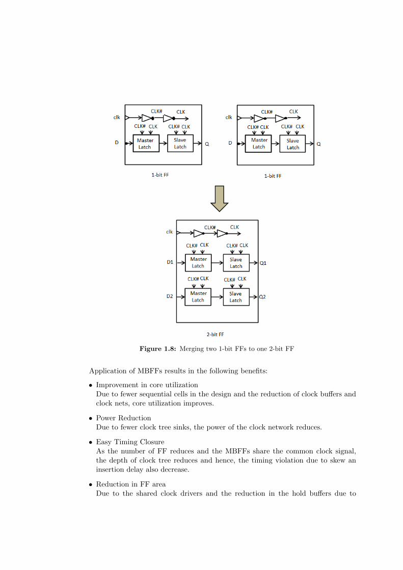
Figure 1.8: Merging two 1-bit FFs to one 2-bit FF
Application of MBFFs results in the following benefits:
• Improvement in core utilizationDue to fewer sequential cells in the design and the reduction of clock buffers andclock nets, core utilization improves.
• Power ReductionDue to fewer clock tree sinks, the power of the clock network reduces.
• Easy Timing ClosureAs the number of FF reduces and the MBFFs share the common clock signal,the depth of clock tree reduces and hence, the timing violation due to skew aninsertion delay also decrease.
• Reduction in FF areaDue to the shared clock drivers and the reduction in the hold buffers due to

internal scan chains, total FF area reduces.
Fig. 1.9a shows an example of a simple clock tree network with 1-bit FFs and Fig 1.9bwith 2-bit FFs, after replacement the clock tree has fewer sinks.
(a) Clock tree with 1-bit FFs
(b) Same Clock tree with 2-bit MBFFs
Figure 1.9: Clock tree structure after MBFF generation
1.4 Motivation
For the nanometer technology nodes, the yield of the high-performance designs is ofprime importance to achieve the major objectives of timing, SI, power, and area. Withthe growing complexity of the design, the designers look for alternate techniques toenhance the performance of the design with no extra burden for the designer. To re-duce the design effort and to cope up with the shorter product cycles, ASIC designincorporates reuse of IP components. This integration of the various components in-creases the product complexity and hence, affects the PPA targets. In order to stabilizethe cost function of a chip which is dependent on the PPA, the focus has shifted forimprovement in current design methodologies and the SoC design flow. The physical

design flow used in the industry incorporates single-bit FFs using EDA tools. In orderto reduce the power consumption and improve the timing closure of the design, thereis a need for an efficient methodology during physical design flow. The power savingmethods and components can be incorporated in the modern VLSI designs. Since, theclock is considered as the major power-dissipating component of the chip, thus CTSbecomes the target of optimization for the semiconductor industry.

Chapter 2
State of the Art
This chapter highlights the work related to this study, in use by the industry andthe academia, followed by explaining the details of the issues existing in the currentmethodology.
2.1 Related Work
A robust tool such as Cadence Innovus [20] is capable of timing driven placementand routing. The latest version incorporates clock concurrent optimization for timingoptimization. It merges the clock tree synthesis with the physical optimization and si-multaneously achieves timing convergence. Several design methodologies such as clockgating [21], [22], power gating [23], buffer sizing [24], and MBFFs [18, 25, 26] have beenintroduced to minimize the power consumption of the design due to clocking. MBFFsproved as the promising solution for low-power designs. MBFFs have been introducedat different stages of the design flow i.e. during RTL Mapping, during physical synthe-sis [27] and post-placement [28].
However, it is complicated to introduce MBFFs without floorplan and placementinformation as it can degrade the timing and congestion budgets. The practical indus-trial flow infers to MBFFs at the synthesis stage with the floorplan information addedto it. This methodology benefits the designer as it reduces the chances of congestionand timing violations in the backend ow. For more accurate timing analysis, recentwork [29, 30] applies MBFFs during the backend flow after the placement stage. How-ever, due to the fixed combination logic cells in the design after their placement, thenumber of mergeable FFs is less. Also, as the size of MBFF is more, it may causedifficulty in placement legalization and hence congestion in the design.
2.2 Current Methodology
In the recent work [31, 32], placement optimization with clock tree aware MBFF genera-tion has been introduced to minimize power consumption and latency of clock network.

The merging of 1-bit FFs is performed according to the clock tree topology. Throughthe placement iterations, the FFs are progressively merged by referring to the origi-nal clock tree topology. This approach offers power reduction without degrading theperformance of the design but it has limitations to address in the real designs for themerging of the FFs. This include:
• A design can have millions of instances due to its complex functionality. If themerging of the FFs is improper, then the complete design may suffer from con-gestion and timing violations. As the number of FFs increases dramatically, theneed for full scenario exploration coupled with fast turn-around time is a must.
• As the designs today are vast and complex, the single chip is broken down intoa hierarchy of modules. The timing budgets are created for the whole design,which permits the engineers to use hierarchical design methodology and work ontheir modules for the timing closure. The merging algorithm has to follow thehierarchical approach to target the FFs at the same hierarchy level.
• With gated clocks widely used in the design for dynamic power reduction, thegrouping of FFs should combine similar toggling of the clock pulse. If the mergingof a gated and non-gated driven FF takes place due to any reason, then the logicwill get affected.
• Complex clock structures due to the multitude of clocks present in the designimpose a challenge for setting up the optimistic environment for grouping theFFs. This limits the number of FFs for merging.
• Further, SoC designers use benchmark CAD tools for the physical design flowwhich target for the minimization of cost function PPA (power, performance, andarea). The integration of the algorithm with these benchmark tools will result inhuge benefits, especially when the technology is advancing to the nanometer.
To achieve proper and reliable flop merging, it is important to consider all the above-mentioned points and modify the merging algorithms for the real designs. In this work,MBFF generation algorithm is formulated to tackle the above-mentioned challenges ofreal designs.

Chapter 3
Proposed Timing and Clock TreeAware Placement Flow withMultibit Flip-Flop Generation
This chapter introduces a novel placement methodology with clock-tree aware MBFFgeneration for power optimization and the corresponding proposed algorithm for FFmerging. The methodology offers an additional feature to the EDA tools to integrateMBFFs during placement iterations with the knowledge of the clock-tree structure ofthe design. Timing is considered as a strict constraint, therefore at each stage timingis checked and hence the methodology is also timing-aware. Merging of the FFs resultsin the reduction in power consumption of the design and improved routability of thedesign. The proposed methodology consists of four major steps: 1) timing-driven globalplacement; 2) fast CTS; 3) MBFF ECO generation and 4) timing-driven incrementalplacement.
3.1 Methodology Overview
Referring to Fig. 3.1, the first step of the methodology is timing-driven global place-ment. It generates the locations of the cells based on the minimum placement densityand minimum interconnecting wire-length (WL) criteria. Further, CTS is performedwith the initial cell locations and clock tree is generated. In order to minimize therun-time, it is performed in the fast mode without the trial route. The merging of FFsis done after this step when MBFF ECO is generated based on the merging conditions.FFs are progressively merged and are replaced with MBFFs; they are placed duringtiming-driven incremental placement. The process of merging is iterative and repetitiveso as to avoid congestion and timing violations. Until the largest bit number of MBFFis achieved and no more MBFF can be applied, merging is repeated. Timing violationsare checked after the MBFF are generated, if the timing is worse than the initial global

placement timing then the MBFF corresponding to the timing violations are iterativelydisintegrated into smaller bit number FFs. At the final stage, legalized placement isobtained with the MBFFs in the design. It is to be noted that, Cadence Innovus doesnot automatically merge the FFs. Hence, the FF merging algorithm has been proposedto find the best candidates of FFs to be merged and replaced with MBFF. Hence, theMBFF ECO generation is integrated with the FF merging algorithm. Also, variousreports are generated at every step for the understanding of the user.
Figure 3.1: Proposed Clock Tree Aware Placement Flow with MBFFs

3.2 Steps of Methodology
In this section, the steps involved in the placement flow are explained. The placementand CTS optimizations are done by EDA tool. However, the mode of operation of theintegrated steps such as placement and CTS is varied according to the proposed work.The following sections elaborate the steps involved in the proposed placement flow.
3.2.1 Timing-driven global placement
In the first stage, timing-aware global placement is performed with the design netlist,MBFF library, floorplan and timing constraints as inputs as shown in Fig. 3.2. Place-ment is done in the timing-driven mode so that the timing violations can be tested atan early stage. Tool efficiently fulfills the objective of minimized WL and placementdensity during the placement of logic cells. The placement is done with the EDA toolto find the best locations of the cell and to consider the two objectives of general globalplacement for best trade-off.
minW (x, y) (3.1)
minD(x, y) (3.2)
where W(x,y) is the WL function of all the signal nets and D(x,y) is the placementdensity function for each bin in the core.
Figure 3.2: Inputs to Timing-driven global placement stage

These are the two basic objectives, but the EDA tools use complex algorithms tominimize the total collaborative function of these two equations, Eq. 3.1 and Eq. 3.2so as to obtain the optimum placement with millions of cells in the real design.
3.2.2 Fast CTS
After the cells are placed and the timing is satisfied, CTS is performed. In order toensure that it does not incur huge run-times, it is done without trial routing. CTSinvolve the following three steps:
1. ClusteringIn this stage, the logic elements operated in the same clock domain or with similarinput timing registers are grouped into clusters. In the cluster based clock treeapproach, the clusters are optimized individually to meet the DRC constraintssuch as maximum capacitance, maximum fan-out and maximum transition arechecked. Fig. 3.3 depicts an example of cluster formation.
(a) FFs Before Clustering (b) Formation of clusters after Clustering
Figure 3.3: Clustering during CTS
The major advantage of clustering is that the insertion delay and skew can beplanned by designers to achieve the minimum timing requirements. The registerclustering algorithms combine the logic elements after the placement is done andcontinuously shrink it with respect to the target skew and the target insertiondelay. As the chip consists of both clock and the signal nets, there could be anegative impact of clustering on the signal nets due to the movement of the reg-isters. Moreover, it may lead to congestion or routing failure in the design.
Henceforth, due to the process variations and the requirement of timing closure,new design methodologies are being incorporated by the EDA companies. Thealgorithm for clustering is a customized cluster-based CTS for Cadence Innovusand hence, it utilizes the best solution to improve the performance of the designand meet the timing margins.
2. Constraint AnalysisAfter the clusters are formed, the timing constraints included in the SDC are

identified and their inter-relation is modeled. The skew and insertion delay tar-gets are mapped with an additional amount of delay to satisfy these constraints.In this step, the amount of delay to be added for balancing the clock tree nodesis calculated under all possible scenarios.
3. Virtual Delay Balancing & ImplementationVirtual delay balancing is the methodology by which the additional delay is an-notated on the clock nodes to achieve the solution found by constraints analysis.The clock enters the propagated mode and thus virtual delay is the extra delay tomatch the ideal mode timing and the timing due to its propagation. The virtualdelay is implemented through real physical cells loaded in the input library files.
Further, the refinement is done to achieve the best possible solution through thereal physical cells. Thus, this is the timing optimization step where the objectiveis the target propagated clock timing. It maps the gap be the ideal and propagatedtiming of clocks. The complete clock architecture is ready at this stage and ispassed as an input to the next stage to find the merge-able flops in the clock tree.
Fig. 3.4, shows an example of the clock tree built after CTS. In Fig. 3.4a, balancedclock routing tree is shown and in Fig. 3.4b, corresponding levels in the clock tree areshown. The clock tree level helps in determining the insertion delay for the particularFF present in the level. The next step works on the synthesized clock tree generatedduring this step to find the set of merge-able FFs.
3.2.3 MBFF ECO generation
Before the MBFF generation, a look-up table is generated for FF merging with theconsideration of timing, insertion delay, signal net and clock net Wl. Thus, to mergethe FFs of a particular clock tree, merge-able conditions are defined. These conditionscater the design complexity for FF merging. Each clock tree is then checked for itscapacity to merge the FFs into MBFF. The merge-able conditions between two flopsf(i) and f(j), are derived to ensure the correct and efficient replacement of FFs toMBFF. These are defined as:
• The merging of FFs far from each other affects the placement quality and hence, itis required to merge FFs placed near to each other. The distance, in terms of co-ordinates, between fi and fj should be less than a maximum set value, dist(max).Based on Eq. 3.3, the violations due to timing and routing are constrained as theresultant MBFF will not be very far away from its parent single-bit FFs.
dist(fi, fj) ≤ dist(max) (3.3)

(a) Clock tree structure
(b) Corresponding tree with levels
Figure 3.4: Example clock tree structure
• The two FFs are merge-able if the difference between their respective levels,level(fi,fj), from the root is equal or less than a constant, k. In order to pre-serve the latency of the clock-tree, FFs with close tree levels are considered tobe merge-able. The value of k cannot be too small or too large as the number ofFFs reduces after the MBFF generation. Also, the clock tree levels and the clocknet WL decreases dramatically.
Henceforth, the value of the constant k is set to be 1, to ensure maximum mergingand FF power optimization.

|level(fi)− level(fj)| ≤ k (3.4)
• As the single chip is broken down into a hierarchy of modules. The timing budgetsare created for the whole design, which permits the engineers to use hierarchi-cal design methodology and work on their modules for the timing closure. Themerging algorithm has to follow the hierarchical approach to target the FFs atthe same hierarchy level. The candidates FFs, fi and fj, should be in the samehierarchy level, Hi and have same pin configuration. As the clock architecture ofmodern SoC designs is hierarchical, this checkpoint is compulsory to ensure thecorrect merging of FFs.
• With gated clocks widely used in the design for dynamic power reduction, thegrouping of FFs should combine similar toggling of the clock pulse. If the mergingof a gated and non-gated driven FF takes place due to any reason, then the logicwill get affected. Either both or none of the candidates FFs should be gated inthe same clock-path. This condition is of utmost importance because it is difficultto infer during placement if the resultant MBFF should be gated or not. Thisdecision is critical since it tends to affect the logical functionality of the module.
The algorithm 1 depicts the procedure for FF merging. At first, a particular clocktree is selected and all its sinks are included in the database. On these sinks, the con-ditions for merging are applied. To save the memory and to prevent extra run-time,distance is given the first priority. Inside the circular area, of radius, dist(max), aroundfi, all the clock tree sinks are taken for further analysis of merge-able conditions and areadded to a list, mergeflops. Rest all clock tree sinks are eliminated for merging with fi.With the elimination, the analysis of the other merge-able conditions is broken downinto a smaller number of sinks. The other conditions are applied on the mergeflops. Ifmore than one FF satisfies all the merge-able conditions, the one with the minimumdistance from fi is the best candidate for merging.
Similarly, the method is repeated for all the sinks of the clock tree. The samealgorithm is replicated on other clock trees as well. After performing the merging algo-rithm, the optimum solution for all FFs is obtained in the look-up table. On the basisof the results, the merging of FFs to MBFFs is performed and the netlist with MBFFsis generated.
3.2.4 Merging FF Combinations
Once the look-up table is generated, the weight of each FF with its candidates iscalculated and it is denoted by wfij . In the FF look-up table, the weight function from

Algorithm 1 FF Merging
1: clock trees← get clock trees()2: for tree in clock trees do3: clock tree sinks← collection of all sinks of clock tree4: for sink in clock tree sinks do
calculate position of sink or fi, x and y co-ordinates5: sink pos← calculate position()6: sink x pos← extract x coordinate from sink pos7: sink y pos← extract y coordinate from sink pos
calculate level of sink in clock tree8: level(sink)← level clock tree()
create a circle of radii, dist (max) around sink withcenter as (sink x pos, sink y pos)
9: candidate merge list← collection of all sinks in that regionApply conditions one by one on list of candidates
10: for candidate in candidate merge list do11: level(candidate)← level clock tree()12: if (|level(fi)− level(fj)| ≤ k) && hierarchy && clock gating then
add the candidate to the look-up table13: mergeflops← candidate14: end if15: end for
calculate weight of all candidates in look-up table16: for mergeableflops in mergeflops do17: weight sink ← calculate weight(mergeableflops)
weight is proportional to distance of the candidate from fi18: end for
the less weight one is put in the combination table with fi19: best to merge← min(weight sink)
fi can merge with best to merge20: end for21: end for

Eq. 3.5 finds the best match such that the resultant signal net WL, clock latency, andthe power consumption is minimum during MBFF generation.
wfij ∝ dist(fi, fj) (3.5)
Fig. 3.5 gives an example to illustrate the formation of MBFF based on the FF mergingalgorithm. Fig. 3.5a, corresponds to the initial clock routing tree after initial timing-driven global placement. After performing the merging algorithm, the resultant 1-bitFF pairs are merged and are replaced by 2-bit FFs. Fig. 3.5b shows newly generatedupdated clock routing tree with 2-bit FFs. The 1-bit FFs are not merged to largestbit number FF available in the library but progressively to elude sudden change inplacement profile.
3.2.5 Timing-driven Incremental placement
After the netlist consisting of MBFFs is generated, incremental placement is done tofind the legal location of the MBFF. As the size of MBFF is larger than the single bitFF, congestion and timing constraints can be violated hence timing-driven incremen-tal placement performed. To ensure that the placement is legalizable and the timingconstraints are met, timing-driven incremental placement refines the locations of com-binational cells, sequential logic cells, and the newly generated MBFFs.
It is difficult to locate a legal location for a MBFF, and could be hazardous forthe placement density constraints. Hence, to ensure a legalizable placement, Innovusimplementation system incorporates new GigaPlace which accounts for slack and skewoptimization.
In case after the MBFF generation, the timing results obtained from the incre-mental placement are worse than those in the initial placement stage, the MBFFs areiteratively disassembled to single-bit FFs. Once the timing slacks are improves, legal-ized placement with MBFFs is obtained after placement legalization. Further, CTSis performed with MBFFs and the clock routing tree is obtained. Later, the entirephysical design with MBFFs is accomplished upto route stage.
In this section, an overview of MBFF generation based on the clock tree during theplacement iterations has been described. The intent of using MBFF instead of single-bit FF is to reduce the overall power and the net WL of the design. As explained inthe previous sections, the candidates for the merging are picked from all the scenariosand then filtering based on the weight function as given in Eq. 3.5 takes place with theiterative placement. The iterations in placement continue until no more MBFFs canbe generated in the clock routing tree. Clock tree is built after every MBFF forma-tion as it lowers the risk in skew due to the movement of FFs during iterative placement.

(a) Mergeable Conditions applied to clock tree with single-bit FFs
(b) Final clock tree with newly generated MBFFs
Figure 3.5: FF merging and MBFF generation

Chapter 4
Proposed Clock Insertion DelayReduction Algorithm
To overcome the wire delay variations, crosstalk penalty on signal and clock nets, extrapessimism to model the on-chip variations, a specific method to mitigate such challengeshas been identified. CID reduction is pointed out as a solution for all the above-listedchallenges. The current flow used in the industry does not target the violating inser-tion delay clock tree sinks. However, performing the check on the violating clock netsand the clock tree sinks can significantly improve the performance in terms of insertiondelay of the clock tree structure.
This chapter introduces a novel way to reduce CID of all or selected clocks usingintuitive and step by step approach. The methodology works on extracting the dom-inant clock for a design and the violating clock tree sinks at the early CTS stage. Italso explains the significance of the proposed algorithm.
4.1 Algorithm Overview
Referring to the Fig. 4.1a, the flow of the proposed algorithm is illustrated and asshown, the CID reduction algorithm is integrated with the CTS stage. Fig. 4.1b showsthe integral steps of the algorithm. The first step is to find the dominant clock in thedesign after the cluster CTS. The clock termed as the dominant clock is the one witheither or all of the characteristics, which are, the one with maximum frequency or theone with maximum number of sinks spread in the clock tree structure or the one withthe most critical path. After the analysis of clock tree and its balancing requirements,dominant clock is identified.The next step involves the extraction of the sinks of the dominant clock which pull the
CID to a maximum. The clock tree sinks which constrain the balancing requirementsduring CTS and increase the CID to the maximum are considered as outliers in thisalgorithm. After the placement is completed, a clock tree specification file is generatedthat captures all the design constraints. As the clock is in the propagated mode during

(a) Physical Design Flow with CID Reduction Algorithm
(b) Integrated Steps of Algorithm
Figure 4.1: CID Reduction Algorithm Overview
CTS, thus the constraints can be infeasible. In the Fig. 4.2, it can be seen that to bal-ance the CID of FFs with the hard macro (memory), the CID of the FFs is increased.In Fig. 4.2a, the insertion delay of FF1-FF4 is less than that of macro blocks and inFig. 4.2b, the insertion delay of entire block is maximum after CTS.

(a) Before CTS Balancing cid ¡ CID of FF1-FF4
(b) After CTS balancing
Figure 4.2: Outliers in Clock Tree
Innovus does not automatically perform the analysis for the reduction of insertiondelay for clock nets. Hence, the algorithm filters the outliers from the clock routingtree and fixes the outliers clock tree sinks for improvement in average CID.
4.2 Steps Involved in Algorithm
In this section, the integral steps of the algorithm are explained. The sub-sectionsdescribe the method of extraction of outliers and the formation of dedicated skew-groups of outliers.

4.2.1 Extraction of Outliers for Dominant Clock
After the Timing driven placement, the next step is the clock tree prototyping usingtransition fixing only. This is similar to the cluster CTS as explained in the previouschapter. The purpose of transition fixing in CTS is to theoretically extract the lowestCID and to understand which clock tree sink is pulling it to maximum.
Next step is to analyze the clock tree structure and identify the dominant clock.The approach is therefore, to find the outliers that are the root cause of increment inCID. By the what-if analysis of the placement pin and the macro placement changeson the sinks with maximum CID, a group of outliers can be filtered out. In the laterstage, the chip is divided into four quadrants and the outliers present in each quadrantare extracted and grouped separately. This process is the filtration process wherein,firstly a database of outliers is maintained and later on the basis of their positions andthe architecture of clock tree, groups are created.
4.2.2 Skew Group formation
Once the outliers groups are determined, the outliers are grouped in separate skewgroups based on their grouping in the last step. In this way, parent clock skew group’sinsertion delay targets are unblocked. With the help of a handful of outliers, eachand every clock tree sink is satisfied with the ease of its timing targets. The previouslygenerated clock specification file is modified automatically with the added skew groups.The modified specification file is the input for the next stage of the algorithm. Referringto the Fig. 4.2a, the new skew grouping is shown in the Fig. 4.3.
Figure 4.3: Skew Group Formation

4.2.3 Full CTS with Useful Skew Optimization
Outlier grouping leads to change in the timing paths of the outlier sinks to the othersinks. One suspected result of path grouping is the timing violations either setup orhold violations. To fix the timing violations, useful skew with CTS is conducted. Thisincludes violating path fixing not only by the data path changes but also with launchor capture path or both clock path and the data path changes. This clock path changecan happen across multiple clock paths. Hence, the CTS in this stage is with usefulskew optimization.
The CTS is followed by the post-CTS optimization to further improve the setupand hold violating paths. Post-CTS fix the remaining violations of design such as DRVsand optimizes the timing paths as now the clocks are in propagated mode. The timingconstraints vary for post-CTS, it includes the clock uncertainty to model jitter. Fur-ther, the routing is performed after removing the critical timing violations.
In this section, the process of filtering out the insertion delay increasing clock treesinks is shown. The objective of outlier filtering process is to reduce the clock insertiondelay for a design. As explained in the sections above the outliers are extracted fromall possible cases, and then the clock tree specification file is modified. The completeCTS with useful skew optimization is performed with the updated specification file.The run-time for picking the outliers and re-run of CTS is a rewarding trade-off. Thus,it does not affect the run-time to a greater extent and improves the performance ofclock tree in terms of the insertion delay.

Chapter 5
Results And Discussions
In this chapter, the results obtained in the experiment have been presented and dis-cussed. Firstly, it provides the experimental setup of the system on which the trialshave been performed. Next, specifications of design under study during the experimentare depicted. This is followed by results obtained for the proposed placement flow andthe CID reduction algorithm at each step of the methodology.
5.1 Simulation Setup
The placement flow algorithm has been implemented on Red Hat Enterprise Linux v5.9operating system using Cadence Innovus 15.2. Table 5.1 illustrates the specificationsof the simulation setup and Table 5.2 design specifications on which the tests areperformed.
Table 5.1: Setup for Experiment
Operating SystemRed Hat Enterprise Linux Serverrelease 6.7 (Santiago)
Number of ProcessingCores
14
Vendor ID Intel(R) Xeon(R) CPU E5-2697
Processor Speed (GHz) 2.6
Tool Cadence Innovus(TM) v15.20-p005 1
Scripting Language TCL

Table 5.2: Specifications of Design at 28nm Technology Node
Design I Design II
Total Standard CellNumber
186920 990416
Total Hard Macros 18 33
Total Chip Area 0.65 mmˆ2 2.07 mmˆ2
5.2 Comparison of Traditional placement flow without MBFFsand Proposed Timing and Clock Tree aware Place-ment Flow with MBFFs
The baseline flow and the proposed placement flow are shown in Fig. 5.1a and Fig.5.1b respectively. All the inputs are provided at the beginning of the backend designflow.
Table 5.3 shows the results of the comparative analysis of various attributes per-formed on the two designs. Due to the applied merging algorithm and the MBFFs inthe design, the number of clock tree sinks decreases in both designs by 1.5%. Thenumber of merge-able flops for a design depends on its complexity, logic and size. Asthe undertaken designs are that of secured IP and complex, the merge-ability is limited.
According to the Table 5.3 for the design I and II, the number of timing violatingpaths reduces by 17.6% and 68% respectively which enables the designer for easy tim-ing closure. Fig. 5.2 shows the improvement in the violating paths for design I anddesign II. Core density improves by 9.8% and clock power reduces by 11.8% for designI. Due to the fewer clock tree sinks, reduction in clock inverters and clock nets, thechip utilization improves. For design II, core utilization increases by 12.8% and clockpower optimize by 9%.
Table 5.4 depicts the analysis of power consumption by the two approaches. Fig.5.4 shows the power distribution and it is observed that reduction in power is by 50.46%and 37.7% respectively for two designs. The results for worst negative slack (WNS) isalmost similar from the both the flows. From Fig. 5.3, the total negative slack (TNS)for setup has improved by a considerable amount for both the designs. The perfor-mance of the design is not degraded after the application of MBFFs because the CTSis performed with useful skew optimization. Similarly is for the TNS for hold mode.
Consequently, the proposed timing and clock tree aware placement flow with MBFFgeneration leads to improved performance of the designs in terms of chip power by 44%,core density by 11.3% and clock power by 10.4%. Also, the corresponding FF mergingalgorithm proves effective by considering the real-time design scenarios.

Table 5.3: Comparison between the Non-MBFF Flow and the Proposed MBFF Flow forDesign I and Design II
Design I Design IIBaseline
FlowProposed
FlowBaseline
FlowProposed
Flow
# of 1-bitFFs
135623 72682 23586 17333
# of 2-bitFFs
0 1714 0 3125
# of ClockTree Sinks
135623 133548 23586 20458
WNS (Setup)(ns)
-0.018 -0.02 -9.637 -9.548
WNS (Hold)(ns)
-0.001 0 -0.706 -0.447
TNS (Setup)(ns)
-0.278 -0.183 -1007.2 -566.438
TNS (Hold)(ns)
-0.001 0 -73.863 -22.183
ViolatingPaths
91 75 1701 546
# of StandardCell
990416 990383 186920 182342
Total Standard CellArea (mmˆ2)
0.854 0.853 0.17 0.16
Core Density(%)
71.415 78.402 73.314 82.702
Total WL(m)
26.22 26.23 4.2 4.1
Clock Power(mW)
37.56 33.21 7.45 6.78
Table 5.4: Comparison of Power Consumption of the designs
Power(mW)
Design I Design IIBaseline
FlowProposed
FlowBaseline
FlowProposed
Flow
Internal 130.11 119.2 31.53 26.62
Switching 342.13 114.88 54.475 31.23
Leakage 0.024 0.023 0.0126 0.0114
Total 472.27 234.108 86.0165 57.88

(a) Baseline Flow without MBFFs (b) Placement Flow with MBFFs
Figure 5.1: Comparison of Flows without and with MBFFs
5.3 Comparison of Proposed CID Reduction Algorithmwith traditional approach of CTS
According to Table 5.5, the results of the CID reduction algorithm, average CID cutsby 19.5.%. It can be attributed to the outlier group which was excluded from thedominant clock group. It translates effectively into less CID of parent clock and allassociated benefits such as controlled clock tree structure and reduced WL. Thus, witha handful of outliers, we are able to improve the rest of clock tree sinks in terms ofCID. Fig. 5.5, which shows that the for the entire design after applying the proposedalgorithm, the average CID reduces by 9.2%.

(a) Violating paths for Design I
(b) Violating paths for Design II
Figure 5.2: Comparison of the number of Violating Paths
Table 5.5: Experimental Results for Dominant Clock by CID Reduction Algorithm
Dominant ClockAttributes
BaseAlgorithm
Proposed CIDAlgorithm
Minimum CID (ns) 0.954 0.740
Maximum CID (ns) 1.116 0.902
Average CID (ns) 1.078 0.868
# of Inverters 1125 1078
WL after CTS (um) 201323.3 198488.836

(a) TNS for Design I
(b) TNS for Design II
Figure 5.3: Comparison of the TNS of the designs

(a) Power distribution for Design I
(b) Power distribution for Design II
Figure 5.4: Distribution of Power Consumption
Figure 5.5: Results for Clock Network CID of design after CTS

Chapter 6
Conclusion And Future Work
6.1 Conclusion
This thesis presents an effective timing and clock tree aware placement strategy withMBFF generation and the corresponding algorithm for FF merging. It is focused onthe analysis of real-time designs and tackles all complex scenarios efciently. The pro-posed strategy is unified with the industry EDA tool, Cadence Innovus, as a result,it allows the designer to use benchmark platform for the physical design flow. It alsoaccelerates the timing closure of the design with the useful skew optimization techniqueincorporated during CTS. The thesis demonstrates the impact of MBFFs on the power,performance and area (PPA) on a SoC design.
Experimental results for the presented placement ow prove its efficiency from thenon-MBFFs traditional placement flow. This approach shows the reduction in power,improvement in the utilization of the core for two designs without the degradation inthe design performance. For the design I, core density increases by 9.8%, clock powerdecreases by 11.8% and overall total power reduces by 50.46%. For design II, coreutilization increases by 12.8%, clock power optimizes by 9% and total power for de-sign reduces by 37.7%. In the end, the algorithm for the optimization of CID is alsopresented which results in minimization of average insertion delay of the design. Theresults show 9.2% reduction in the average CID of entire design after applying theproposed algorithm. Reduction in CID infers to controlled clock structure due to thereduction in the amount of buffer or inverter in the clock path. Controlled clock treearchitecture implies less crosstalk penalty and hence, the CRPR is in control.
Hence, this placement strategy seamlessly integrates with the EDA tools for thephysical design process and significantly optimizes the PPA.

6.2 Future Work
6.2.1 Higher-bit MBFF
The MBFF cell library in this work includes 2-bit FFs only. With the higher bit MBFFssuch as 4-bit in the MBFF library, further merging of the 2-bit FFs can be done. In-tegrating 4-bit FFs in the library would make the power consumption even less. Thenumber of clock tree sinks will eventually reduce and hence the power utilization of thechip. With higher bit MBFFs than 4-bit MBFF there could be an issue with congestionin the design.
So the analysis of the proposed algorithms with higher bit MBFFs will lead toimproved core density and reduced power.
6.2.2 Clock Mesh Framework
Clock meshes are robust to the process variations and hence, are used by the designersfor tighter skew control, lower insertion delay and high tolerance towards OCV [33, 34].Due to their resistance towards the variations, many EDA tools incorporated clockmesh synthesis with the physical design flow. In some designs, mesh architectures con-sume less power than the clock trees but in general, they can consume more power. Itis preferred for high fanout clock networks as they reduce the adverse effects of OCVand improve the performance of the chip.
In this work, placement flow involves CTS methodology, but the physical designflow and the proposed FF merging algorithm can also be performed with clock meshsynthesis. The work can be extended to clock mesh framework and their power con-sumption can also be reduced by the proposed methodology.
The clock meshes provide lower insertion delay, and it can be further reduced withthe application of the CID reduction algorithm. The results and the analysis can bedone in future for the performance of design with clock meshes.

References
[1] B. H. Lorincz, Y. , X. Li, K. Mai, L. T. Pileggi, R. A. Rutenbar, and K. L. Shep-ard, “Digital circuit design challenges and opportunities in the era of nanoscalecmos,” Proceedings of the IEEE, pp. 343365, Feb. 2008.
[2] H. -L. Roh, “Driving forces the technological challenges for soc development oftomorrow,” IEEE Workshop on Signal Processing Systems, pp. 2-, Aug. 2003.
[3] S. Roy, P. M. Mattheakis, L. Masse-Navette, and D. Z. Pan, “Evolving challengesand techniques for nanometer soc clock network synthesis,” 12th IEEE InternationalConference on Solid-State and Integrated Circuit Technology (ICSICT), pp. 1-4,Oct. 2014.
[4] R. A. Bergamaschi and J. Cohn, “The a to z of socs,” IEEE/ACM InternationalConference on Computer Aided Design, pp. 791798, Nov. 2002.
[5] L. Xiu, “VLSI Circuit Design Methodology Demystified:A Conceptual Taxonomy,Springer, 2008.
[6] J. Lu and B. Taskin, “From RTL to GDSII: An ASIC design course developmentusing Synopsys #x00AE University Program,” IEEE International Conference onMicroelectronic Systems Education (MSE), pp. 7275, June 2009.
[7] S. N. Adya and I. L. Markov, “Power distribution network design for VLSI,” IEEETransactions on Very Large Scale Integration (VLSI) Systems, vol. 11, no. 6, pp.11201135, Dec. 2003.
[8] Q. K. Zhu, “Fixed-outline floorplanning: enabling hierarchical design, John Wiley& Sons, Dec. 2003.
[9] B. Halpin and N. Sehgal and C. Y. R. Chen, “Detailed placement with net lengthconstraints,” The 3rd IEEE International Workshop on System-on-Chip for Real-Time Applications, pp. 22-27, June 2003.
[10] L. N. Kannan and P. R. Suaris and Hong-Gee Fang, “A Methodology and Algo-rithms for Post-Placement Delay Optimization,” 31st Conference on Design Au-tomation, pp. 327-332, June 1994.

[11] A. Balboni, C. Costi, M. Pellencin, A. Quadrini, and D. Sciuto, “Clock skewreduction in asic logic design: a methodology for clock tree management,” IEEETransactions on Computer-Aided Design of Integrated Circuits and Systems, vol. 17,no. 4, pp. 344356, Apr. 1998.
[12] S. Borkar, “Design challenges of technology scaling,” IEEE Micro, vol. 19, no. 4,pp. 2329, Jul. 1999.
[13] M. Dietrich and J. Haase, “Process Variations and Probabilistic Integrated CircuitDesign, Springer Science & Business Media, 2011.
[14] P. B. Ghate, “Electromigration-induced failures in vlsi interconnects,” 20th AnnualReliability Physics Symposium, pp. 292299, March 1982.
[15] T. B. Chan, A. B. Kahng, and J. Li, “Nolo: A no-loop, predictive useful skewmethodology for improved timing in ic implementation,” Fifteenth InternationalSymposium on Quality Electronic Design, pp. 504509, March 2014.
[16] H. M. Chou, H. Yu, and S. C. Chang, “Useful-skew clock optimization for mul-tipower mode designs,” IEEE/ACM International Conference on Computer AidedDesign (ICCAD) , pp. 647650, Nov. 2011.
[17] X. Man and S. Kimura, “Comparison of optimized multi-stage clock gating withstructural gating approach,” IEEE Region 10 Conference in TENCON, pp. 651656,Nov. 2011.
[18] M. P. H. Lin, C. C. Hsu, and Y. T. Chang, “Recent research in clock power savingwith multi-bit flip-flops,” IEEE 54th International Midwest Symposium on Circuitsand Systems (MWSCAS), pp. 14, Aug. 2011.
[19] G. Prakash, K. Sathishkumar, B. Sakthibharathi, S. Saravanan, and R. Vijaysai,“Achieveing reduced area by multi-bit flip flop design,” International Conferenceon Computer Communication and Informatics (ICCCI), pp. 14, Jan. 2013.
[20] Innovus User Guide.
[21] S. K. Teng and N. Soin, “Low power clock gates optimization for clock tree dis-tribution,” 11th International Symposium on Quality Electronic Design (ISQED),pp. 488492, March 2010.
[22] M. P. Dev, D. Baghel, B. Pandey, M. Pattanaik, and A. Shukla, “Clock gated lowpower sequential circuit design,” IEEE Conference on Information CommunicationTechnologies (ICT), pp. 440444, April 2013.
[23] S. Y. Chen, R. B. Lin, H. H. Tung, and K. W. Lin, “Power gating design forstandard-cell-like structured asics,” Design, Automation Test in Europe ConferenceExhibition (DATE), pp. 514519, March 2010.

[24] W. M. D. J. G. Xi, “Buffer insertion and sizing under process variations forlow power clock distribution,” 32nd Conference on Design Automation (DAC),pp. 491496, 1995.
[25] J. T. Yan and Z. W. Chen, “Construction of constrained multi-bit flip-flops forclock power reduction,” International Conference on Green Circuits and Systems(ICGCS), pp. 675678, June 2010.
[26] Y. T. Shyu, J. M. Lin, C. P. Huang, C. W. Lin, Y. Z. Lin, and S. J. Chang, “Effec-tive and efficient approach for power reduction by using multi-bit flip-flops,” IEEETransactions on Very Large Scale Integration (VLSI) Systems, vol. 21, no. 4,pp. 624635, April 2013.
[27] C. Santos, R. Reis, G. Godoi, M. Barros, and F. Duarte, “Multi-bit flip-flop usageimpact on physical synthesis,” 25th Symposium on Integrated Circuits and SystemsDesign (SBCCI), pp. 16, Aug. 2012.
[28] M. P. H. Lin, C. C. Hsu, and Y. T. Chang, “Post-placement power optimizationwith multi-bit flip-flops,” IEEE Transactions on Computer-Aided Design of Inte-grated Circuits and Systems, vol. 30, no. 12, pp. 18701882, Dec. 2011.
[29] H. Moon and T. Kim, “Design and allocation of loosely coupled multi-bit flip-flopsfor power reduction in post-placement optimization,” 21st Asia and South PacificDesign Automation Conference (ASP-DAC), pp. 268273, Jan. 2016.
[30] W. Chen and J. T. Yan, “Routability-driven flip-flop merging process for clockpower reduction,” IEEE International Conference on Computer Design (ICCD),pp. 203208, Oct 2010.
[31] C. C. Hsu, Y. C. Chen, and M. P. H. Lin, “In-placement clock-tree aware multibitflip-flop generation for power optimization,” IEEE/ACM International Conferenceon Computer-Aided Design (ICCAD), pp. 592598, Nov. 2013.
[32] M. P. H. Lin, C. C. Hsu, and Y. C. Chen, “Clock-tree aware multibit flip-flopgeneration during placement for power optimization,” IEEE Transactions on Com-puterAided Design of Integrated Circuits and Systems, vol. 34, no. 2, pp. 280292,Feb. 2015.
[33] P. Chakrabarti, V. Bhatt, D. Hill, and A. Cao, “Clock mesh framework,” Thir-teenth International Symposium on Quality Electronic Design (ISQED), pp. 424431,March 2012.
[34] A. Rajaram and D. Z. Pan, “Meshworks: An efficient framework for planning,synthesis and optimization of clock mesh networks,” Asia and South Pacific DesignAutomation Conference, pp. 250257, March 2008.