An Asymptotic Approach for the Scan Impedance in Infinite ...
14
HAL Id: hal-03268736 https://hal.archives-ouvertes.fr/hal-03268736 Submitted on 30 Jun 2021 HAL is a multi-disciplinary open access archive for the deposit and dissemination of sci- entific research documents, whether they are pub- lished or not. The documents may come from teaching and research institutions in France or abroad, or from public or private research centers. L’archive ouverte pluridisciplinaire HAL, est destinée au dépôt et à la diffusion de documents scientifiques de niveau recherche, publiés ou non, émanant des établissements d’enseignement et de recherche français ou étrangers, des laboratoires publics ou privés. An Asymptotic Approach for the Scan Impedance in Infinite Phased Arrays of Dipoles A.J. Pascual, R. Sauleau, D. Gonzalez-Ovejero To cite this version: A.J. Pascual, R. Sauleau, D. Gonzalez-Ovejero. An Asymptotic Approach for the Scan Impedance in Infinite Phased Arrays of Dipoles. IEEE Transactions on Antennas and Propagation, Institute of Electrical and Electronics Engineers, 2021, 10.1109/TAP.2021.3070716. hal-03268736
-
Upload
khangminh22 -
Category
Documents
-
view
2 -
download
0
Transcript of An Asymptotic Approach for the Scan Impedance in Infinite ...

HAL Id: hal-03268736https://hal.archives-ouvertes.fr/hal-03268736
Submitted on 30 Jun 2021
HAL is a multi-disciplinary open accessarchive for the deposit and dissemination of sci-entific research documents, whether they are pub-lished or not. The documents may come fromteaching and research institutions in France orabroad, or from public or private research centers.
L’archive ouverte pluridisciplinaire HAL, estdestinée au dépôt et à la diffusion de documentsscientifiques de niveau recherche, publiés ou non,émanant des établissements d’enseignement et derecherche français ou étrangers, des laboratoirespublics ou privés.
An Asymptotic Approach for the Scan Impedance inInfinite Phased Arrays of DipolesA.J. Pascual, R. Sauleau, D. Gonzalez-Ovejero
To cite this version:A.J. Pascual, R. Sauleau, D. Gonzalez-Ovejero. An Asymptotic Approach for the Scan Impedancein Infinite Phased Arrays of Dipoles. IEEE Transactions on Antennas and Propagation, Institute ofElectrical and Electronics Engineers, 2021, 10.1109/TAP.2021.3070716. hal-03268736

ACCEPTED MANUSCRIPT
This article has been accepted for publication in a future issue of this journal, but has not been fully edited. Content may change prior to final publication. Citation information: DOI 10.1109/TAP.2021.3070716, IEEETransactions on Antennas and Propagation
IEEE TRANSACTIONS ON ANTENNAS AND PROPAGATION, VOL. X, NO. X, MONTH YYYY 1
An Asymptotic Approach for the Scan Impedancein Infinite Phased Arrays of Dipoles
Alvaro J. Pascual, Ronan Sauleau, Fellow, IEEE, and David Gonzalez-Ovejero, Senior Member, IEEE
Abstract—This work presents an analytic model to derive thescan impedance of planar infinite phased arrays of dipoles at adielectric interface when only the (0, 0) Floquet mode propagates.The proposed model builds on the boundary conditions met bythe fundamental Floquet mode at the interface to provide a novelderivation of the equivalent circuit for the scan impedance. Theanalysis is also extended to include the effect of a sufficientlythick grounded substrate that does not affect the elements currentdistribution and does not interact with the evanescent fields. Next,formulas for the ratio of intensity radiated towards each half-space for an interfacial array are provided. In a consecutivestep, an asymptotic approximation is derived for the currentdistribution in arrays of arbitrary loaded dipoles, and thereactance of a dipole in the array environment is related to theinductance of a grid of wires. This model constitutes a usefultool to clearly identify the role of the different array variables(dipole dimensions, relative permittivity of the substrate, period-icity, end-load, and scan angle in the principal planes) on thescan impedance by simple expressions and equivalent circuits.The model predictions are in good agreement with full-wavesimulations and with previously published works.
Index Terms—Equivalent circuit, scan impedance, infinite ar-ray, phased array, dipole array, planarly layered media, planewave expansion.
I. INTRODUCTION
PHASED arrays represent a broad class of antennas towhich extensive research efforts have been dedicated [1]–
[3]. In particular, planar phased arrays of printed elements,such as dipoles or slots, have received most of the attention.Wide-band, dual-linear, and wide-scan performance have beenreported for connected or tightly coupled arrays of dipoles [4]–[6].
As the number of elements in the array increases for afixed element spacing, the central elements behave like thosewithin an infinite array [7], [1, Ch. 7]. Thus, the infinite arrayapproach is an analysis method suitable for large arrays whereedge elements and edge-related effects do not substantiallyaffect the overall performance.
The authors are with Univ Rennes, CNRS, IETR (Institut d’Electroniqueet des Technologies du numeRique)- UMR 6164, F-35000, Rennes, France.E-mail: alvaro-jose.pascual, ronan.sauleau, [email protected].
Manuscript received Month DD, 2020; revised Month DD, YYYY; acceptedMonth DD, YYYY. Date of publication Month DD, YYYY. (Correspndingauthor: D. Gonzalez-Ovejero).
This work is supported by the European Union through the EuropeanRegional Development Fund (ERDF), and by the French region of Brittany,Ministry of Higher Education and Research, Rennes Metropole and ConseilDepartemental 35, through the CPER Project SOPHIE / STIC & Ondes.
Digital Object Identifier XXXXXXXXXXXXXXXXXX.
Previous studies on infinite phased arrays of dipoles arenumerous. Indeed, the periodicity of the array enables theexpansion of the fields in a discrete set of plane waves orFloquet modes (spectral approach). This approach generallyleads to simplified mathematical expressions that can be read-ily evaluated numerically or even analytically in some cases.In [8], the current sheet model was presented as the simplestinfinite phased array in the limiting case of closely spacedHertzian dipoles. This model led to simple expressions for thescan resistance, and the concept was later extended in [9] forprinted elements on a semi-infinite dielectric interface. Arraysof disconnected dipoles in free-space were considered eitherassuming a current distribution [10], [11], [12, Ch. 3], or byan integral equation technique [13]. Later on, the study wasextended to solve disconnected dipoles printed on semi-infinitesubstrates or on a grounded dielectric slab using a Method ofMoments (MoM) [14]. Since then, extensive numerical studies,implementations, and theoretical modeling of connected ortightly coupled arrays have been carried out, for instance in[15]–[21]. Of special relevance are the works by Munk andcollaborators [22], [23] based on a periodic MoM approach todetermine expressions for the dipole scan impedance. How-ever, in the aforementioned studies, the arrays in multilayeredmedia were always embedded in a homogeneous region, andnever at the interfaces, as it is usually the case in practicalrealizations.
Despite the extensive efforts devoted in the past to theanalysis of infinite phased arrays of dipoles, to date, thereis no model to readily interpret the impact of the arrayvariables on the scan impedance, especially on the reactance.The numerical methods such as those in [14], [22], [24]or the description in [19], are rigorous and computationallypowerful but mask the fundamental impedance features ofthe array. Therefore, one is forced to carry out exhaustivecomputation and parametric sweeps to gain physical insightinto the array operation for different configurations. For in-stance, the spectral expansion approach by [22] yields a doubleinfinite sum to calculate the scan reactance. From this, generalconclusions can be hardly inferred. On the other hand, anapproximate analytic method is more appropriate to evaluatein a simple manner how the different phenomena affect thescan impedance for diverse array configurations. We provide inthis paper a novel and insightful circuit approach that readilyshows the role of the main variables of a phased array ofdipoles on the scan impedance as defined in [1, Ch. 1]. Thesevariables include the dipole dimensions and type of end-load,
0000–0000/00$00.00 © 2021 IEEE

ACCEPTED MANUSCRIPT
This article has been accepted for publication in a future issue of this journal, but has not been fully edited. Content may change prior to final publication. Citation information: DOI 10.1109/TAP.2021.3070716, IEEETransactions on Antennas and Propagation
IEEE TRANSACTIONS ON ANTENNAS AND PROPAGATION, VOL. X, NO. X, MONTH YYYY 2
n = 1, ( 0, µ0)
n 1, (n20, µ0)
1
2
(a)
Y
X
Z
r
(b)
1
X
Y1
Z
X
Y
Z
2
2
w
l
py
px
s = 0
q = 0
θ
θ
θ
ε
ε
≥
φ φ
φ
Fig. 1. (a) Hertzian dipole printed on the interface between two losslessdielectrics. Medium 1 (z > 0) is characterized by n = 1 and medium 2(z < 0) is characterized by n ≥ 1. (b) Cut of the infinite interfacial arrayof dipoles in a rectangular lattice, relevant geometrical parameters, and therespective coordinate system for each half-space.
the array periodicity, the relative permittivity of the substratefor a printed array, and the scan angle in the principal planes.Although the Green’s function approach was used in [18] toderive equivalent circuits for interfacial arrays of connecteddipoles, the circuits and expressions in this work stem insteadfrom the boundary conditions met by the fundamental Floquetmode and an asymptotic approximation of the current, whichcan handle arbitrary loads.
The paper is organized as follows: In Section II, we exploitthe far-field plane wave expansion of a dipole array on aninterface to obtain boundary conditions at the interface forthe radiated fundamental Floquet mode. In Section III, theboundary conditions are used to obtain equivalent networksand expressions for the scan resistance when the array lies ata dielectric interface. The ratio of intensity radiated towardseach half-space is also derived. In Section IV, the analysis isextended to cases where a ground plane backs the interfacialarray. We assume a thick substrate so that the ground planedoes not affect the elements current distribution and it doesnot interact with the evanescent fields. Such assumptionsare fulfilled by a typical substrate thickness of λ/4. Next,Section V is devoted to the derivation of the current alongthe dipole and an equivalent network for the scan reactance atbroadside. The results obtained with the proposed model arecompared to full-wave simulations in Section VI, followed bythe results for the principal scan planes in Section VII. Weconclude the analysis with remarks on the scan impedanceand general conclusions in Sections VIII and IX, respectively.
II. PLANE WAVE EXPANSION ON THE RADIATED FIELDS
In order to derive the electric field radiated by an infinitephased array of dipoles lying on a dielectric interface, first weadd the individual contributions of interfacial Hertzian dipoles.Then, this sum is written in the spectral domain as a discreteset of plane waves or Floquet modes. We will show that thetangential electric field is equal at both sides of the interfacefor the fundamental Floquet mode. This result will constitutethe basis of the subsequent discussion.
The electric field of a Hertzian dipole in a homogeneousmedium admits a closed-form expression both in the near-and far-field regions. This is not the case for a dipole placed
parallel, and at the interface between two different dielectrics.This hurdle, however, can be conveniently overcome usingthe far-field of the interfacial Hertzian dipole in [25]. TheHertzian dipole is of length ∆l, its current I , and the interfaceis composed of two lossless dielectrics as shown in Fig. 1(a).The upper dielectric is characterized by n1 = 1 and the lowerone by n2 = n ≥ 1. That is, the ratio of dielectric index is n.For a harmonic time dependence ejωt, the expression is writtenas
dEθ,φi =jk0niI∆l
2πZ0f
θ,φi (θ, φ)
e−jnik0r
r, (1)
where i denotes the medium, and Z0 is the impedance of aTEM wave in free-space. Expression (1) is valid when k0r →∞ and 0 ≤ θ ≤ π/2 in medium 1, and when nk0rs→∞ andπ − θc ≤ θ ≤ π in medium 2. The angle θc is obtained fromsin θc = 1/n, and it will be the maximum scan angle allowedin medium 2. The pattern functions in (1) are defined as
fθ1 =
cos2 θ
cos θ + (n2 − sin2 θ)1/2− sin2 θ cos θ
· cos θ − (n2 − sin2 θ)1/2
n2 cos θ + (n2 − sin2 θ)1/2
cosφ (2a)
fφ1 = − cos θ sinφ
cos θ + (n2 − sin2 θ)1/2(2b)
fθ2 =
sin2 θ cos θ
(1− n2 sin2 θ)1/2 + n cos θ
n(1− n2 sin2 θ)1/2 − cos θ
− cos2 θ
(1− n2 sin2 θ)1/2 − n cos θ
cosφ (2c)
fφ2 =cos θ sinφ
(1− n2 sin2 θ)1/2 − n cos θ, (2d)
where the subscript and superscript in f refer to the corre-sponding medium and polarization, respectively.
The Hertzian element is now replicated to form a doubleinfinite array of dipoles in a rectangular lattice. The elementperiodicity is given by px and py , as shown in Fig. 1(b).The dipoles of length l and width w are centered-fed byideal δ-gap generators with uniform current amplitude andlinear phase progression, defined for the (q, s) element asIqs = I00e−jq∆αe−js∆β . I00 is the current of the (0, 0)element, located at the origin of coordinates, and the phaseprogression is defined (recall n1 = 1):
∆α = pxk1 sin θ cosφ = pxk0sx, (3a)∆β = pyk1 sin θ sinφ = pyk0sy. (3b)
The electric far-field of the array is obtained by summationof all individual contributions of the Hertzian elements anddouble application of Poisson’s sum formula. Following aprocedure similar to [22, Ch. 4], we have
Ei =Z0
pxpy
+∞∑u=−∞
+∞∑v=−∞
fi(θ, φ)
sze±jkizsze−jk0x(sx+u(λ0px ))
e−jk0y
(sy+v
(λ0py
)) ∫ l/2
−l/2I(x′)ejk0x
′(sx+u(λ0px ))dx′, (4)
ACCEPTED MANUSCRIPT
This article has been accepted for publication in a future issue of this journal, but has not been fully edited. Content may change prior to final publication. Citation information: DOI 10.1109/TAP.2021.3070716, IEEETransactions on Antennas and Propagation
IEEE TRANSACTIONS ON ANTENNAS AND PROPAGATION, VOL. X, NO. X, MONTH YYYY 3
with
sz =
√1−
(sxni
+ u
(λipx
))2
−(syni
+ v
(λipy
))2
. (5)
In (4), z ≶ 0, and the sign in the exponential is takenaccordingly for propagation away from the interface. Thepolarization superscripts in E and in the pattern functions havebeen omitted, and we have assumed that the current flowsalong the longitudinal axis of the dipole.
Equation (4) is the electric field resultant from the additionof the far-fields of Hertzian dipoles. It yields a discrete sum ofplane waves or Floquet modes with wavevector componentsat a discrete set of directions in space. For sz real, the (u, v)mode propagates and decays exponentially otherwise. Note thetotal electric field is weighed by the dipole pattern function,according to the principle of pattern multiplication.
If the scan angle in medium 2 is limited below θc, the (0, 0)Floquet mode always propagates in both media. In addition, ifthe spacing is such that the other modes do not propagate,the (0, 0) mode in (4) corresponds to the electric field ofthe radiated plane wave, and is the only term contributingto the scan resistance. The remainder of terms representthe contribution of the Hertzian dipole far-field to the scanreactance in the array environment.
Let us now focus on the propagating term. One can note thatthe excitation, as defined in (3), determines the wavevectorcomponents, sx, sy of the (0, 0) Floquet mode. To obtaina simpler expression for the radiated field, it is convenientto use a different reference system for each half-space, asshown in Fig. 1(b). To that end, we apply the the followingtransformations: θ1 = θ, φ1 = φ in medium 1, and θ2 = π−θ,φ2 = −φ in medium 2. The angles of propagation of the(0, 0) mode in each medium are related by φ2 = −φ1 andn sin θ2 = sin θ1. In view of the previous discussion, theradiated electric field in each half-space is expressed as
Ei =Z0
pxpyfi(θi, φi)
e−j~ki ~ri
cos θi
∫ l/2
−l/2I(x′)ejk0x
′sxdx′, (6)
where ~ri is the observation point in each coordinate system,~k1 = k0(sx, sy, cos θ1), and ~k2 = k0(sx,−sy, n cos θ2). Atbroadside, it is not difficult to see that E1 = E2 at the interfaceplane (zi → 0+). Similarly, comparing in (6) for both media,after some algebra, one finds the following relations
E1θ cos θ1 = E2θ cos θ2, E1φ = −E2φ. (7)
The relations are valid for any scan angle (recall 0 ≤ θ2 <θc, or equivalently, 0 ≤ θ1 < π/2). Therefore, the tangentialcomponent of the electric field is equal at both sides of theinterface for the fundamental Floquet mode, analogously tothe classical boundary condition. We will also refer to (7) asboundary condition even if this expression is true in the far-field. In general, (7) is valid for any two loss-less dielectricscharacterized by n1 and n2 ≥ n1, with θ1 and θ2 related bythe Snell’s law. The minus sign for E2φ in (7) appears giventhat φi are reversed as measured from system of reference 2with respect to system of reference 1.
The boundary conditions in (7) have been derived for themode that concerns our present study. However, it is not
R
jX
V
(a) (b)
n2 n1
|E2|2/2Z2 |E1|
2/2Z1
A1A2
θ1
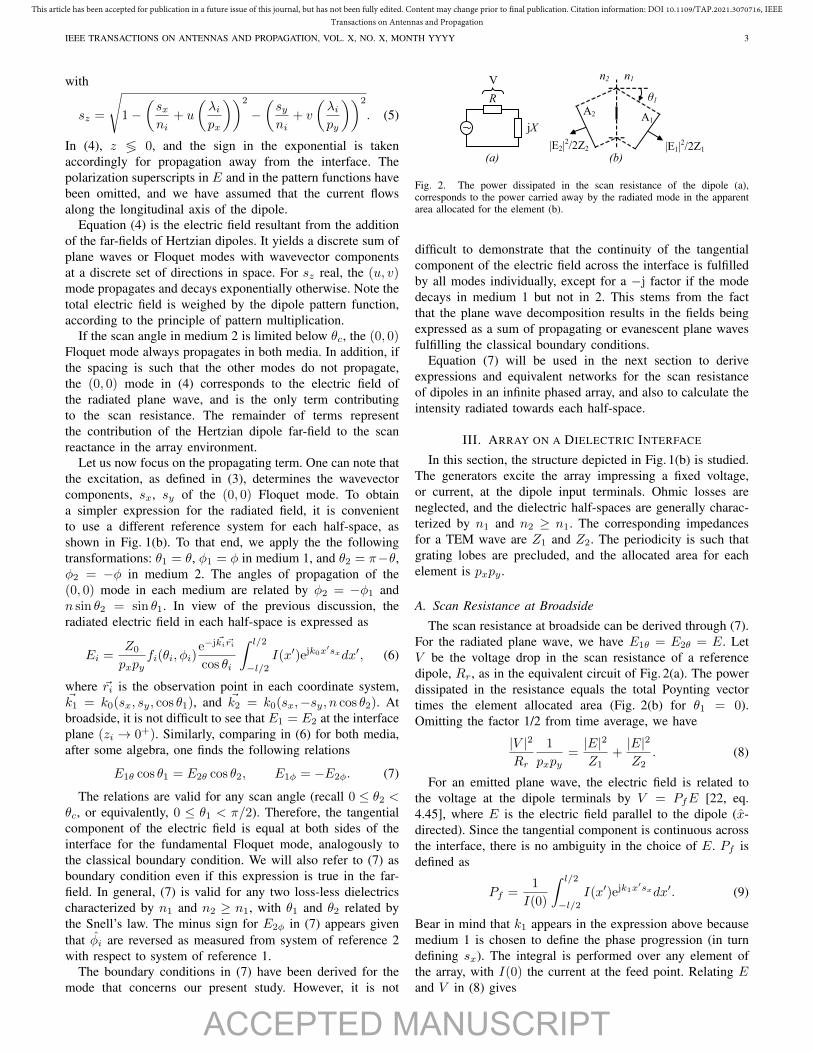
Fig. 2. The power dissipated in the scan resistance of the dipole (a),corresponds to the power carried away by the radiated mode in the apparentarea allocated for the element (b).
difficult to demonstrate that the continuity of the tangentialcomponent of the electric field across the interface is fulfilledby all modes individually, except for a −j factor if the modedecays in medium 1 but not in 2. This stems from the factthat the plane wave decomposition results in the fields beingexpressed as a sum of propagating or evanescent plane wavesfulfilling the classical boundary conditions.
Equation (7) will be used in the next section to deriveexpressions and equivalent networks for the scan resistanceof dipoles in an infinite phased array, and also to calculate theintensity radiated towards each half-space.
III. ARRAY ON A DIELECTRIC INTERFACE
In this section, the structure depicted in Fig. 1(b) is studied.The generators excite the array impressing a fixed voltage,or current, at the dipole input terminals. Ohmic losses areneglected, and the dielectric half-spaces are generally charac-terized by n1 and n2 ≥ n1. The corresponding impedancesfor a TEM wave are Z1 and Z2. The periodicity is such thatgrating lobes are precluded, and the allocated area for eachelement is pxpy .
A. Scan Resistance at Broadside
The scan resistance at broadside can be derived through (7).For the radiated plane wave, we have E1θ = E2θ = E. LetV be the voltage drop in the scan resistance of a referencedipole, Rr, as in the equivalent circuit of Fig. 2(a). The powerdissipated in the resistance equals the total Poynting vectortimes the element allocated area (Fig. 2(b) for θ1 = 0).Omitting the factor 1/2 from time average, we have
|V |2
Rr
1
pxpy=|E|2
Z1+|E|2
Z2. (8)
For an emitted plane wave, the electric field is related tothe voltage at the dipole terminals by V = PfE [22, eq.4.45], where E is the electric field parallel to the dipole (x-directed). Since the tangential component is continuous acrossthe interface, there is no ambiguity in the choice of E. Pf isdefined as
Pf =1
I(0)
∫ l/2
−l/2I(x′)ejk1x
′sxdx′. (9)
Bear in mind that k1 appears in the expression above becausemedium 1 is chosen to define the phase progression (in turndefining sx). The integral is performed over any element ofthe array, with I(0) the current at the feed point. Relating Eand V in (8) gives

ACCEPTED MANUSCRIPT
This article has been accepted for publication in a future issue of this journal, but has not been fully edited. Content may change prior to final publication. Citation information: DOI 10.1109/TAP.2021.3070716, IEEETransactions on Antennas and Propagation
IEEE TRANSACTIONS ON ANTENNAS AND PROPAGATION, VOL. X, NO. X, MONTH YYYY 4
jX0
Z1
Zd1:N
Z2
Fig. 3. Equivalent network for the scan impedance of an infinite interfacialphased array of dipoles.
Rr = (Z1 ‖ Z2)|Pf |2
pxpy. (10)
B. Scan Resistance for Principal Scan Planes
Let us now examine how the scan resistance varies at theprincipal scan planes. As explained above, the power deliveredto Rr equals the total Poynting vector times the apparent orprojected area allocated for the element. Thus we have
Rr =|Pf |2
pxpy
Z0n1
cos θ1+
n2
cos θ2
= N2(Z1 cos θ1 ‖ Z2 cos θ2),
(11a)
Rr =|Pf |2
pxpy
Z0
n1 cos θ1 + n2 cos θ2= N2
(Z1
cos θ1‖ Z2
cos θ2
),
(11b)
where (11a) and (11b) stand for E- and H-plane scan respec-tively. Arbitrary scan angles shall be treated similarly, andnoting that E1θ/E1φ = f1θ/f1φ, which is known analytically.The shunt impedance in (10) indicates that the scan resistancecan be expressed in terms of an equivalent network composedof two shunt infinite transmission lines (TLs), while the factor|Pf |2/pxpy = N2 is accounted for by a transformer. Atbroadside, the scan impedance, Zd, corresponds to the equiv-alent network of Fig. 3, and by transforming Zi → Zi cos θi,Zi → Zi/ cos θi, analog networks follow for E- and H-planescan respectively. X0 in the equivalent network accounts forthe scan reactance, and depends in general on n1 and n2, thearray geometry, the scan angle, and the frequency. Note thatthe current distribution is also required to calculate Pf and inturn the scan resistance. These two aspects will be studied inSection V. For a homogeneous medium, we obtain a resultequivalent to those obtained in [12], [22].
C. The Intensity Radiated Toward Each Half-Space
Let us now examine the ratio of intensity (S) radiatedtoward each half space. For H-plane scan, using (7) one caneasily obtain S1 = n1|E1φ|2/Z0, and S2 = n2|E1φ|2/Z0.Hence:
S2
S1=n2
n1. (12)
In this plane, the ratio is constant with the scan angle.For an air-dielectric interface, it equals ε
1/2r , with εr the
relative permittivity of the dielectric. For E-plane scan, S1 =n1|E1θ|2/Z0, and S2 = n2|E2θ|2/Z0. Then, using (7):
S2
S1=n2 cos2 θ1
n1 cos2 θ2. (13)
0 15 30 45 60 75 900
1
2
3
4
θ1, deg (scan angle in air)
Sd
iele
ctri
c/Sai
r
E
H
E
εr
= 2.55 H
εr
= 12.8
SimulatedNumerical from [14]Closed form
Fig. 4. Ratio of Poynting vector modulus in the principal planes for the moderadiated by an infinite phased array of dipoles. We consider two different air-dielectric interfaces: Duroid (εr = 2.55) and GaAs (εr = 12.8). Full-wavesimulations with ANSYS HFSS [26] (solid lines), present model (squares),and numerical calculation from [14] (circles). The dimensions are px = py =0.2184λ0, l = 0.182λ0, w = 0.01λ0.
The ratio of intensity is in general different from that ofa single dipole, which equals ε3/2r at broadside for an air-dielectric interface, as can be inferred from (1)-(2), and alsonoted in [14]. Fig. 4 shows the intensity ratio calculated by(12)-(13) for two different air-dielectric interfaces. Resultspractically overlap with full-wave simulations and are in goodagreement with those calculated in [14, Fig. 9]. The powerratio would be obtained by multiplying S times the projectedarea allocated for each element in the direction of the scanangle. In particular, at broadside both projected areas coincideand the power ratio also equals ε
1/2r for an air-dielectric
interface. Since at broadside E1 = E2, the ratio must bethe same for any planar antenna regardless of its currentdistribution, even if the antenna is not linear.
IV. ARRAY ON A DIELECTRIC INTERFACE BACKED BY AGROUND PLANE
Since the initial radiated fields are known by the boundaryconditions, it is possible to account for the effect of a groundplane reflector by computing the multiple reflections. Calcu-lation of the real and complex power leads to expressions forthe scan impedance for broadside and for the principal scanplanes. It is assumed that the reflector is placed at a distance dfrom the interface in any medium, say medium 2, such that theevanescent modes do not interact with it and that its presencedoes not alter the current distribution of the elements. Forthe sake of simplicity, the broadside case is treated first andthe expressions for E- and H-plane scan are derived next byanalogy. Under the previous assumptions, the scan impedanceis written as the sum of three terms: X0, the initial reactivepart, RGP
r , a term related to the amplitude of the plane waveemerging from the structure and, XGP, related to the reactiveenergy stored due to the presence of the ground plane:
Zd = RGPr + jXGP + jX0. (14)

ACCEPTED MANUSCRIPT
This article has been accepted for publication in a future issue of this journal, but has not been fully edited. Content may change prior to final publication. Citation information: DOI 10.1109/TAP.2021.3070716, IEEETransactions on Antennas and Propagation
IEEE TRANSACTIONS ON ANTENNAS AND PROPAGATION, VOL. X, NO. X, MONTH YYYY 5
d
1+x+x2+x3+... = 1/1-x
x = -Γe-2jk2d
(a) Broadside E( ) or H ( ) scan
-Eejk2d
ETOTAL
Z
|x| 1
Z1 Z2
Array plane
EE
E1+E2
s = d/cosθ2
sE1
E2
θ2
θ1
2d tanθ2
x = -Γ ( , )
e-2jk2se2jdk1sinθ1tanθ2
dZ
Z1 Z2Γ
T
1-x
x( , )
( , )
<
(b)
Fig. 5. Longitudinal cut of the infinite dipole array backed by a groundplaneat a distance d. (a) Broadside emission (top-bottom): evanescent fields inz-direction do not interact with the groundplane, initially radiated fields,resultant electric field from the partially standing wave, and sum formulafor multiple reflections. (b) E- or H-scan (top-bottom): emerging field at theinterface plane after multiple reflections, initially radiated fields, and directionsof propagation.
A. Scan Impedance at Broadside
The situation where the array radiates at broadside isdepicted in Fig. 5(a).
1) Real Power and Resistance: The resultant electric fieldemerging from the structure at the interface plane, afterconsideration of the multiple reflections, is given by
Etotal = E
(1− e−2jk2d
1 + Γe−2jk2d
), (15)
where Γ is the Fresnel’s reflection coefficient from medium 2to 1 for normal incidence:
Γ =n2 − n1
n2 + n1. (16)
The power radiated per allocated element area is
|I(0)|2
pxpyRGPr =
|E|2
Z1
∣∣∣∣∣ 1− e−2jk2d
1 + Γe−2jk2d
∣∣∣∣∣2
. (17)
On the other hand, the power delivered to each element perallocated area when there is no ground plane is given by
|I(0)|2
pxpyRr =
|E|2
Z1 ‖ Z2, (18)
combining (17) and (18), one obtains
RGPr = Rr
n2/n1 + 1
1 +
(n2
n1 tan(k2d)
)2 . (19)
For a homogeneous medium, (19) reduces to RGPr =
2Rr sin2(k2d). Examination of (19) indicates that for k2d =mπ, with m = 0, 1, 2..., the ground plane short-circuitsthe array and the scan resistance equals 0. The positions ofmaximum scan resistance occur at k2d = (2m + 1)π/2 andyield RGP
r = Rr(1 +n2/n1). Finally, for tan2(k2d) = n2/n1,the ground plane leaves the scan resistance of the arrayuntouched, RGP
r = Rr. The first position occurs at d = λ/8 for
jX0
Z1
Zd1:N
Z2
d
Fig. 6. Equivalent network for the scan impedance of an infinite interfacialphased array of dipoles backed by a ground plane.
a homogeneous medium (radiated field to the left and reflectedadd in quadrature), but the position deviates when the array isat an interface.
2) Complex Power and Reactance: To calculate the reactivepart associated with the presence of the ground plane, first, theresulting fields inside the structure are computed:
Etotal =E
1 + Γe−2jk2d
(e−jk2z − e−jk2dejk2(z−d)
), (20a)
Htotal =E
Z2(1 + Γe−2jk2d)
(e−jk2z + e−jk2dejk2(z−d)
),
(20b)
where 0 ≤ z ≤ d. The calculation of the reactive power, PX ,per allocated area yields
PXpxpy
=∂(∫ d
0(We −Wm)dx
)∂t
(21)
= j|E|2
Z2|1 + Γe−2jk2d|2sin(2k2d).
We and Wm are, respectively, the electric and magneticenergy densities. Comparing the reactive power delivered tothe reactance XGP by the ideal current generator and the powerdelivered to the scan resistance when there is no reflector (18),yields
XGP = Rrn1 + n2
2
(n2 cos2(k2d) +
n21
n2sin2(k2d)
) sin(2k2d).
(22)When the initially radiated field adds in phase with the
reflections, the scan resistance is maximum and XGP equals0. XGP takes this value again when the ground plane short-circuits the antenna; then the zeros of XGP occur for k2d =mπ/2. XGP takes extreme values larger than ±Rr whenZ2 < Z1 and lower otherwise. For a homogeneous medium,(22) reduces to XGP = Rr sin(2k2d), and XGP takes valuesbetween ±Rr. In particular, when RGP
r equals Rr, so does|XGP|.
Finally, it can be seen that (14), where RGPr is given by (19),
and XGP is given by (22), corresponds to the input impedanceof the equivalent network of Fig. 6.
B. Scan Impedance for Principal Scan Planes
Let the array now scan in a principal plane that correspondsto an angle θ1 in medium 1.

ACCEPTED MANUSCRIPT
This article has been accepted for publication in a future issue of this journal, but has not been fully edited. Content may change prior to final publication. Citation information: DOI 10.1109/TAP.2021.3070716, IEEETransactions on Antennas and Propagation
IEEE TRANSACTIONS ON ANTENNAS AND PROPAGATION, VOL. X, NO. X, MONTH YYYY 6
1) Real Power and Resistance: The resultant electric fieldemerging from the structure at the interface plane, afteraddition of the multiple reflections (see Fig. 5(b)) is
Etotal = E1
(1− e−2jk2d cos θ2
1 + Γ‖,⊥e−2jk2d cos θ2
), (23)
where the relation Γ⊥−T⊥ = Γ‖−T‖ cos θ1/ cos θ2 = −1 hasbeen used to compute the sum, with T being the electric fieldtransmission coefficient from medium 2 to 1. The subscripts⊥, ‖ denote TE and TM polarization for the H- and E-planerespectively. In turn, the Fresnel reflection coefficients aregiven by
Γ⊥ =n2 cos θ2 − n1 cos θ1
n2 cos θ2 + n1 cos θ1, (24a)
Γ‖ =n2/ cos θ2 − n1/ cos θ1
n2/ cos θ2 + n1/ cos θ1. (24b)
By substituting d → d cos θ2, Zi → Zi cos θi (E-plane),Zi → Zi/ cos θi (H-plane) in (15) and (16), one retrieves (23)and (24). Then, applying these transformations in (19) sufficesto obtain RGP
r in the principal scan planes.2) Complex Power and Reactance: The electric field within
the structure can be written as
Etotal =E2
1 + Γ‖,⊥e−2jk2d cos θ2(e−jk2z cos θ2 u+ − e−jk2(z−d) cos θ2ejk2(z−d) cos θ2 u−
), (25)
where u± = y cos θ2∓z sin θ2, and u± = x for E- and H-planescan respectively. In turn, the reactive power per allocatedelement area is given by
PXpxpy
= j|E2|2 cos θ2
Z2|1 + Γ‖,⊥e−2jk2d cos θ2 |2sin(2k2d cos θ2). (26)
After comparing (26) with (21) and the Fresnel’s reflectioncoefficients, it is found that XGP in the principal scan planescan be also obtained applying in (22) the transformations: d→d cos θ2, Zi → Zi cos θi (E-plane), Zi → Zi/ cos θi (H-plane).Since both the real and imaginary parts transform the samefor either E- or H-plane scan, the equivalent networks andconclusions are analog to those drawn for the broadside casein Section IV-A.
Although we have treated here the case of an array backedby a ground plane reflector, a similar treatment can be de-veloped for other structures (i.e. grids [27] or an arbitraryimpedance sheet) where the reflection coefficients are knownfor TE and TM polarization. In particular, one can observethat the radiated plane wave propagates along the layers ofthe structure much like a TEM wave does on a TL withdifferent segments and loads. Then, it is possible to extend theequivalent networks presented here to multilayered structuresas long as their equivalent network is known in terms of planewave propagation with the corresponding polarization.
Finally, note that a grounded dielectric slab may introduceadditional solutions of propagation in the form of surfacewaves, potentially causing scan blindness [28]. A condition forthis to occur is that the k-vector component of a radiated mode
along the interface, kt, matches the propagation constant of thesurface wave, βSW. Nevertheless, the scan angle in the medium1 (recall n1 ≤ n2) is limited below 90, so kt < k1 for thefundamental Floquet mode, with k1 ≤ βSW. Hence, it cannotexcite a surface wave and it is necessary that at least a gratinglobe exists. The assumption that only the (0, 0) Floquet modepropagates precludes the appearance of this phenomenon.
V. ASYMPTOTIC CURRENT APPROXIMATION
The plane wave expansion in (6) has enabled the derivationof expressions and equivalent networks for the scan resistanceand the reactance term due to a ground plane, if present. Tocompute them, however, the dipole current distribution mustbe known, so that it can be inserted in (9). In addition, onlythe far-field from the Hertzian dipole has been accounted forin the plane wave expansion. Hence, the decaying terms in thesum of (4) do not represent the total evanescent fields, and thePoynting theorem [10] cannot be used to calculate X0. Thissection is devoted to the analysis of the scan reactance andcurrent distribution.
Let us start by examining the current distribution along onerow of the array presented in Fig. 1(b). In the most generalcase, the dipoles can be connected through lumped loads ofimpedance ZL. The load can be an open circuit (disconnectedarms with moderate gap), a short-circuit (connected arms) oran interdigitated capacitor [29]. For convenience, we assumethe q element centered at the origin of coordinates as shownin Fig. 7(a).
In the source-free regions of a linear antenna, it wasdemonstrated in [30, Ch. 8] that the current satisfies ordinaryTL equations when the dipole width w → 0, and the effect ofradiation resistance on the current is neglected. Under theseassumptions, hereinafter referred to as asymptotic approxima-tion, one can write
d2Iq(x)
dx2+ β2Iq(x) = 0. (27)
Iq(x) denotes the current along the row due to the q generator,with all others disconnected, and β is the propagation constantin the medium in which the array is located [30, Ch. 8]. Theinterface can be simply treated as an homogeneous medium ofeffective dielectric constant [14] εeff = (ε1 + ε2)/2. We definethe source-free domain as Ω := x ∈ R−ml, m ∈ Z. That is,the length of the row except the points where the sources arelocated. The corresponding boundary consists of the positionsof the generators (x = ml).
To solve for the total current along the row, I(x), itsuffices to solve (27) and later apply superposition with theproper phased excitation, as shown schematically in Fig. 7(b).Equation (27) is a homogeneous Helmholtz equation whichgeneral solution is well known. To solve it we apply Dirichletboundary conditions such that ∀x ∈ ∂Ω−0, Iq(x) = 0 andIq(0) = I(0)e−jq∆α. We also enforce the continuity of thecurrent. It is not difficult to see that Iq(x) = 0 for |x| ≥ l.In addition, by symmetry, Iq(x) = Iq(−x), so actually weonly need to solve for 0 ≤ x ≤ l, as in Fig. 7(c). This regioncorresponds to the right arm of dipole q and left arm of dipoleq + 1.

ACCEPTED MANUSCRIPT
This article has been accepted for publication in a future issue of this journal, but has not been fully edited. Content may change prior to final publication. Citation information: DOI 10.1109/TAP.2021.3070716, IEEETransactions on Antennas and Propagation
IEEE TRANSACTIONS ON ANTENNAS AND PROPAGATION, VOL. X, NO. X, MONTH YYYY 7
=ZL ZL ZL ZL
I0 e-j(q-1) I0 e
-jq I0 e-j(q+1)
x x = l
(a)
Iq=0 I0 e
-jq
x x = l
(b)
Iq=0
x = l/2
I= Iq q
=I0 e
-jq
x = l(c) (d)
x = l/2
I0 e-jq
x = lx = l/2+
IqA
x = lx = l/2
IqBIL
q
ΣΔαΔαΔα
Δα
Δα
Δα
Fig. 7. Derivation of the current distribution: (a) whole row, (b) solution by superposition. (c) and (d) derivation of the current along the dipole by superpositionof the generator q and the load equivalent generator.
To determine Iq(x) in 0 ≤ x ≤ l, we also substitute theload by an equivalent generator whose value is the current inthe load when only the q generator is connected, IqL. Then,Iq(x) in this region is given by the superposition of currentsfrom the generator q, denoted as IAq , and the load equivalentgenerator, denoted as IBq , both fulfilling (27). Thus, Iq(x) =IAq (x) + IBq (x) as schematically shown in Fig. 7(d). They areexpressed as
IAq (x) =
I(0)e−jq∆α
1− e−jβl
(e−jβx − ejβ(x−l)) , 0 ≤ x < l/2
0, l/2 ≤ x ≤ l.(28)
IBq (x) =
IqL
e−jβx − ejβx
e−jβl/2 − ejβl/2, 0 ≤ x < l/2
IqLejβ(x−l) − e−jβ(x−l)
e−jβl/2 − ejβl/2, l/2 ≤ x ≤ l.
(29)
To determine IqL we use the telegrapher’s equation for thecurrent derivative:dIq
dx
∣∣∣∣∣l/2−
− dIqdx
∣∣∣∣∣l/2+
= jωCIqLZL, (30)
where IqLZL = (Vl/2− − Vl/2+). Combining (28)-(30):
IqL =I(0)e−jq∆α
(zL + 1)ejβl/2 − (zL − 1)e−jβl/2, (31)
we have defined zL = ZL/(2Zc), and ωC = β/Zc has beenused. Zc is the characteristic impedance of the wire. Thecurrent along the row due to generator q is then given by(28), (29) and (31), and it vanishes for |x| ≥ l.
Let us solve now for the total current I , along the q element:the contributions to the right arm are given by IAq , IBq , andIBq+1. Similarly, for the left arm IAq , IBq , and IBq−1 contribute.Note also the current due to the q±1 generator takes the sameform, only centered around x′ = x∓l. Hence, the current alongthe dipole q reads
I(x) = I(0)e−jq∆α
[e−jβ|x| − ejβ(|x|−l)
1− e−jβl
+1 + ΓI
2(ejβl/2 + ΓIe−jβl/2)
e−jβ|x| − ejβ|x|
e−jβl/2 − ejβl/2(1 + e±j∆α)
].
(32)
The minus sign in the exponential of (32) corresponds to theright arm and the plus sign to the left arm. Analogously to atransmission line, we have defined the current-wave reflectioncoefficient in the load as ΓI = (1− zL)/(1 + zL). Note that,by superposition, I(x) is also solution of (27). The current isquasi-periodic, forced by the excitation, and it is symmetric if∆α = 0, as expected.
For an array composed of infinite rows, we will assumethat the current along the row maintains the same shape.Coupling among the rows will be taken into account throughZc, determined after. Under this assumption, it is clear thatfor H-plane scan the current along the row is the same as forbroadside.
A. Special Cases
There are several important cases where I(x) adopts asimple form. The first is broadside emission, where the currentis symmetric. We can write (q = 0 element)
I(x) = I(0)ejβ(l/2−|x|) + ΓIe
−jβ(l/2−|x|)
ejβl/2 + ΓIe−jβl/2. (33)
Then, at broadside (or H-plane scan), the asymptotic currentdistribution along the dipoles is that of a TL. In particu-lar, for a disconnected array, assuming ΓI = −1, it takesthe familiar form I(x) = I(0) sinβ(l/2 − |x|)/ sin(βl/2).For a connected array ΓI = 1, and it takes the formI(x) = I(0) cosβ(l/2 − |x|)/ cos(βl/2). In addition, for adisconnected array the current distribution is also independentof E-plane scan as it can be seen from (33). This is not thecase for connected arrays, where the current takes the form:
I(x) =I(0)
e−jβl − ejβl
[ejβ|x|(e−jβl − e±j∆α) (34)
+e−jβ|x|(e±j∆α − ejβl)
].
The solid line in Fig. 8 shows the current distributionobtained from (34) for an array of connected dipoles scanningin the E-plane at 40. The total phase change along the dipoleequals ∆α, forced by the excitation, and can be easily notedin (33). For comparison, full-wave simulation results obtainedfor the same configuration by CST Studio Suite [31] are alsoplotted. As it can be seen, both curves are in good agreement.Near the dipole feed, where the current is minimum, the effect

ACCEPTED MANUSCRIPT
This article has been accepted for publication in a future issue of this journal, but has not been fully edited. Content may change prior to final publication. Citation information: DOI 10.1109/TAP.2021.3070716, IEEETransactions on Antennas and Propagation
IEEE TRANSACTIONS ON ANTENNAS AND PROPAGATION, VOL. X, NO. X, MONTH YYYY 8
−8 −6 −4 −2 0 2 4 6 81.8
1.9
2
2.1
2.2
x (mm)
Mag
. I
(a.u
.)
Asymptotic Approx.
CST
−8 −6 −4 −2 0 2 4 6 8−60
−40
−20
0
x (mm)
Ph
ase
I (d
eg)
Fig. 8. Current distribution for an infinite phased array of connected dipolesin free-space scanning in E-plane at 40. px = py = l = λ/5, and w =λ/1000.
of the radiation resistance causes some discrepancy in thephase as discussed in Section VIII. Finally, the results shownare also in agreement with the MoM analysis in [32].
B. The Asymptotic Equivalent Network at Broadside
In (33) we have seen that at broadside the current alongthe dipole is analogous to that of a TL. Therefore, X0 can beretrieved from the network shown in Fig. 9(a). It is composedof a TL of length l/2 (as the dipole arm) terminated inZL. However, the characteristic impedance of the TL remainsunknown.
Assuming TEM wave propagation, Zc can be calculatedfrom the inductance per unit length of the structure, L, usingZc = Lc/
√εeff. The value of L is retrieved as follows: let
a grid of vertical and parallel strips of width w and periodpy be illuminated by a plane wave at normal incidence, suchthat a uniform current distribution is excited along the strips,the electric field being parallel to the strips. The impedanceof this structure has been studied in e. g. [27], [33], [34]. Inparticular, as discussed in [35], the inductance of the grid perstrip and per unit length is given by
L =Z0
2πcln
1
sin(πw2py
) . (35)
For the interface case, it is assumed that µ ≈ µ0 for bothdielectrics, so L remains unaltered [27]. Finally, to accountfor the two arms of the dipole, the characteristic impedanceof the network is given by 2Zc, twice that of the wire. Thisdefinition is also in agreement with the definition of zL forΓI above.
Once the characteristic impedance of the TL is determined,it is worth mentioning that X0 calculated with the equivalentnetwork of Fig.9(a) takes automatically into account the dipoleend load, including disconnected dipoles (ZL →∞).
R1
C1
C2
L1
ZL2Zc
l/2
jX0
(a) (b)
Fig. 9. (a) Equivalent network representing the scan reactance. (b) Equivalentlossy lumped element circuit that represents the scan impedance.
Now, it is possible to calculate the impedance for broadsideemission (principal scan planes will be dealt with in Sec-tion VII). The current distribution for broadside given by (33)can be inserted in (9) to obtain the transformer relation, N , inthe equivalent networks of Fig.3 (interface) or Fig.6 (interfaceand backing ground plane). Besides, X0 can be obtained fromthe network of Fig. 9(a), where the inductance per unit lengthin (35) is used to calculate 2Zc.
Nevertheless, the asymptotic current approximation is onlyvalid when w approaches 0 so that the scan impedance ismainly dominated by a reactance and the effect of the radi-ation resistance on the current distribution can be neglected.This approximation gives in general accurate results for thindipoles except in the regions where the current at the dipolefeed approaches zero (anti-resonance). In the latter case, (33)diverges at all times, independently of the dipole width, whichis clearly wrong. To overcome this issue, and for more precisecalculations, we have derived a lumped element circuit thataccounts for variations in the stored energy and finite radiationlosses in the impedance curves, as shown in Fig. 9(b). Onthe the other hand, we can rely on the simple networks toextract qualitative conclusions. For simplicity, we will restrictthe analysis of the scan impedance when there is no groundplane in the cases of connected and disconnected dipoles.
To derive the lumped element circuit one can reason asfollows: when losses are absent, it follows the curve ofX0 given by the network of Fig. 9(a). Then, L1 and C1
determine the resonance frequency as predicted by the TL(X0 = 0), besides, L1, C1, and C2 determine anti-resonance(X0 → ±∞). The third condition is to guarantee that thecircuit yields the input reactance of the network model at lowfrequencies. Last, losses are included in the circuit by a lumpedresistor R1 so that the input resistance of the lumped elementcircuit is that of the network model when f → 0. The valuesrelating the different lumped elements with the network modelare summarized in Table I for connected and disconnecteddipoles. This circuit equivalent is valid up to, approximately,anti-resonance. An alternative circuit was developed in [36]but it utilizes the dipole auto-inductance. Furthermore, it isonly valid for tightly coupled and connected arrays, and doesnot arise from a physical explanation of the scan impedance.
VI. RESULTS FOR BROADSIDE EMISSION
To test the validity of the proposed model, it is comparedwith full-wave simulations carried out with ANSYS HFSS[26]. For a central frequency of f = 1 cycle per unit-time that determines λc, the nominal parameters are: px =

ACCEPTED MANUSCRIPT
This article has been accepted for publication in a future issue of this journal, but has not been fully edited. Content may change prior to final publication. Citation information: DOI 10.1109/TAP.2021.3070716, IEEETransactions on Antennas and Propagation
IEEE TRANSACTIONS ON ANTENNAS AND PROPAGATION, VOL. X, NO. X, MONTH YYYY 9
TABLE ILUMPED ELEMENT CIRCUIT PARAMETERS.
Parameter Connected Disconnected
L1 Ll (C1ω2R)−1
C1 ∞ 3/16ln2eff/(Lc
2)
C2 (L1ω2AR)−1 C1/3
R1 Rr,f→0 16/9Rr,f→0
ωAR πc/(neffl) 2πc/(neffl)
ωR 0 πc/(neffl)
py = λc,eff/2, l = 1.0px (connected) or 0.9px (disconnected),w = λc,eff/1000, and feed port length λc,eff/100. The arrayis freestanding or in a vacuum-dielectric interface. In thefollowing, results are presented for a variation of one nominalparameter at a time. The calculated values in Figs. 10-11 havebeen obtained using the lumped element circuit in Fig. 9(b)explained in the preceding section.
A. Varying End Load
The resonant behavior of dipole arrays is highly dependenton the load and can be simply examined by inspection ofthe input reactance in the equivalent network of Fig. 9(a). Forconnected dipoles X0 = 2Zc tan(βl/2), therefore resonancesoccur at l/λ = n with n a natural number, whereas anti-resonances occur at l/λ = n + 1/2. In the latter, theopen circuit condition is effectively achieved and I(0) = 0,consequently, Rr will diverge too. Conversely, for discon-nected arrays of dipoles, X0 = −2Zc/ tan(βl/2) and theresonant/anti-resonant frequencies will be swapped with re-spect to connected dipoles of the same length (see for instanceFig. 11). This fundamental difference between connected anddisconnected dipoles stems from the fact that in the formerthe maximum current occurs at the dipole end (ΓI = 1)whereas, for disconnected dipoles, the current at the edgeis always minimum (ΓI = −1). The π phase differencein the reflection coefficient is responsible for the λ/2 shiftof the resonances. In the usual case of capacitively loadeddipoles, the phase of the reflection coefficient for the current-wave lies between the previous cases, then the resonanceslie between the aforementioned limiting cases. Furthermore,the fact that connected dipoles show resonant response atlow frequencies makes them amenable to array design withlarge scan angles. In this case, the lattice can be kept < λ/2,whereas for disconnected dipoles px > λ/2 limited by theresonant length of the dipole. This is even more evident for adielectric interface, where the required spacing to avoid gratinglobes is λ/(2n2) but the dipole length scales down only as neff.
B. Varying εrPractical array designs require printing the antennas on an
interface, for mechanical support or to diminish the effect ofa ground plane. In the latter case, it is more convenient toposition the ground plane in the medium with lower dielectricindex for a broadband design, since it renders the impedanceless dependent on frequency. Also, it is to be observed that
0.2 0.4 0.6 0.8 1 1.2 1.40
50
100
150
Frequency (a.u.)
Rea
l par
t Z
(O
hm
)
εr= 1 ε
r= 2.55 ε
r= 12.8
0.2 0.4 0.6 0.8 1 1.2 1.4
−500
0
500
Frequency (a. u.)Imag
inar
y p
art
Z (
Ohm
)
Fig. 10. Real and imaginary parts of the broadside impedance for discon-nected dipoles: simulated (solid lines), and calculated (squares) for threedifferent relative permittivities of the substrate.
the short-circuit will occur at DC and certain frequenciesregardless of the interface, hence, imposing a fundamentallimit in the absolute impedance bandwidth of the array.
As shown in the previous subsection, X0 is proportionalto Zc and in turn to 1/
√εeff for connected or disconnected
dipoles. Thus, a high permittivity dielectric substrate flattensthe dipole reactance. Fig. 10 shows the variation of thesimulated and calculated broadside impedance with εr for dis-connected dipoles. εr corresponds to the relative permittivityof the substrate when the array is printed in an air-dielectricinterface as shown in Fig. 1(b). It is important to note that px,and py are scaled by λc,eff and so the dipole electrical lengthremains fixed as seen in Fig. 10.
C. Varying Dipole Width
Fig. 11 shows the simulated and calculated broadsideimpedance for different dipole widths for connected (a), anddisconnected (b) dipoles. If we calculated the scan resistancefrom the asymptotic current approximation in (33), where ΓIdoes not depend on w, it would yield a result also independenton w. In practice, this is true only for regions far away fromanti-resonance. As w increases, the resonance quality factordecreases, and the impedance curves are affected. The lossylumped element circuit predicts this behavior reasonably wellfor connected dipoles, as shown in Fig. 11(a). However, fordisconnected dipoles the model loses validity. In particular,variations of effective dipole length with dipole width arenot taken into account. We will discuss it in more detailin Section VIII. Finally, note a wider dipole yields a flatterreactance, as can be inferred from (35).
D. Varying Lattice (px, py)
The dipole length has been defined as 100% or 90% of px,therefore, variations in px would scale the curves accordingly.Conversely, variations in py influence the coupling amongneighboring rows, and can be used to modify the impedance.

ACCEPTED MANUSCRIPT
This article has been accepted for publication in a future issue of this journal, but has not been fully edited. Content may change prior to final publication. Citation information: DOI 10.1109/TAP.2021.3070716, IEEETransactions on Antennas and Propagation
IEEE TRANSACTIONS ON ANTENNAS AND PROPAGATION, VOL. X, NO. X, MONTH YYYY 10
0 0.2 0.4 0.6 0.8 10
1000
2000
Frequency (a. u.)
Rea
l p
art
Z (
Oh
m)
(a)
0 0.2 0.4 0.6 0.8 1
−500
0
500
1000
1500
Frequency (a. u.)
Imag
inar
y p
art
Z (O
hm
)
w = λc/1000
w = λc/100
w = λc/25
0.2 0.4 0.6 0.8 1 1.2 1.40
100
200
Frequency (a.u.)
Rea
l par
t Z
(O
hm
)
(b)
0.2 0.4 0.6 0.8 1 1.2 1.4
−500
0
500
Frequency (a.u.)
Imag
inar
y p
art
Z (
Ohm
)
w = λc/1000 w = λ
c/100 w = λ
c/25
(b)
Fig. 11. Real and imaginary parts of the broadside impedance: simulated(solid lines), and calculated (squares) for three different dipole widths. (a)connected dipoles, (b) disconnected dipoles.
From the network model we can observe that the factor N2
is inversely proportional to py . Since within this approximationthe current distribution does not change with py for connectedor disconnected dipoles, Rr scales inversely proportional topy . On the other hand, from (35), L decreases with py ,so narrower spacing decreases X0 and flattens the dipolereactance. Coupling, as is clear from the network model, canbe used to obtain broadband arrays.
VII. EXTENSION FOR PRINCIPAL SCAN PLANES
In section V, we have seen that at broadside emission thecurrent distribution along the dipole in asymptotic approxima-tion is that of a transmission line. Therefore, it was possibleto identify X0 with the equivalent network of Fig. 9(a), andultimately compute the scan impedance at broadside using alossy lumped element circuit. For scan in the principal planes,we need to examine the variations of the inductance per unitlength on the equivalent TL and of the current distribution, ifany.
The inductance of a grid of strips for a plane wave inoblique incidence with the tangent electric field parallel tothe wires was calculated in [34, Ch. 4]. We can express thegrid inductance per unit length as
L =Z0
2πcln
1
sin(πw2py
)(1− cos2 φ sin2 θ
). (36)
For H-plane scan, φ = 90, and L does not change.Also, according to our model, the current is the same asfor broadside. Therefore, it is still possible to compute theimpedance with the lossy lumped element circuit and extractconclusions from the network model. Results calculated usingthe lossy lumped element circuit for an array of connecteddipoles are shown in Fig. 12(a) for different scan angles andnominal array parameters. As radiation losses increase whileL is maintained, anti-resonance becomes wider and flatter,and this behavior is well captured. Conversely, the equivalentnetwork would predict that X0 is maintained and Rr is scaledby 1/ cos θ because it does not capture the consequences of alower quality factor in the resonance. This is specially clearat large scan angles. Finally, for scan at 80 near f = 1 a.u.the curve deviates from simulation as the onset of a gratinglobe is approached.
For E-plane scan, we need to distinguish between connectedand disconnected dipoles. In the latter case, the current in(32) is the same as for broadside emission, so X0 remainsthe same and Rr scales with cos θ. Note that, even if in (36)L varies, this is for a plane wave in oblique incidence thatgenerates a linear phase progression along the wires of thegrid. For the array of disconnected dipoles, there is no linearphase progression, and the expression for L at broadside hasto be used.
On the other hand, for connected dipoles, the scanimpedance can be obtained as follows: the current at thedipole feed is I(0), whereas the voltage is the superpositionof the voltages impressed by all generators in x = 0. As wehave seen before, for the q element, only q − 1, q, q + 1contribute to the current. When only the q generator is active,we use the fact that the current along the dipole is that ofan open-ended transmission line of length l. The dipole self-reactance is then Zq,q = V q(0)/I(0) = −j2Zc/ tan(βl).When only one of the q ± 1 generators is on, the voltageat the dipole feed corresponds to that of the open-endedtransmission line of length l at the position of the load, soZq±1,q = V q±1(x = 0)/I(0) = jZce
±∆α/ sin(βl). Thus, thescan reactance is given by the sum of the three terms:
X0 = 2Zc
(cos ∆α
sin(βl)− 1
tan(βl)
). (37)
It is interesting to note that (37) reduces to 2Zc tan(βl/2)when ∆α = 0 and is an alternative way to calculate the scanreactance based on mutual impedances. Fig. 12(b) shows theresults for an array of connected dipoles and nominal arrayconfiguration. Calculations are performed inserting the currentdistribution given by (34) in (9) to calculate Rr from thenetwork of Fig.3. X0 is calculated using (37). In this case, thecurrent distribution no longer follows that of a TL, and it is not

ACCEPTED MANUSCRIPT
This article has been accepted for publication in a future issue of this journal, but has not been fully edited. Content may change prior to final publication. Citation information: DOI 10.1109/TAP.2021.3070716, IEEETransactions on Antennas and Propagation
IEEE TRANSACTIONS ON ANTENNAS AND PROPAGATION, VOL. X, NO. X, MONTH YYYY 11
0.2 0.4 0.6 0.8 10
500
1000
1500
Frequency (a.u.)
Rea
l par
t Z
(O
hm
)
0.2 0.4 0.6 0.8 1
−500
0
500
1000
1500
Frequency (a.u.)
Imag
inar
y p
art
Z (
Ohm
)
0o
20o
40o
60o
80o
(a)
0.2 0.4 0.6 0.8 10
500
1000
Frequency (a.u.)
Rea
l par
t Z
(O
hm
)
0° 20° 40° 60° 80°
0.2 0.4 0.6 0.8 1
0
500
1000
Frequency (a.u.)
Imag
inar
y p
art
Z (
Ohm
)
(b)
Fig. 12. Real and imaginary parts of the scan impedance: simulated (solidlines), and calculated (squares) for a connected array of dipoles at differentscan angles in (a) H-plane, and (b) E-plane.
possible to map the impedance curves with the lossy lumpedelement circuit used before, causing the model to deviate closeto anti-resonance.
VIII. LIMITATIONS OF THE MODEL
As already mentioned, the asymptotic current approxima-tion neglects the effect on the current due to the radiationresistance. It constitutes a term in quadrature with the currentimpressed by the generator and the distribution is that of areflecting antenna, as noted by [30]. Since Rr 6= 0, thisterm is present event when w → 0 and it dominates thecurrent at the dipole input terminals at anti-resonance whenthe asymptotic current distribution approaches zero and theimpedance takes a maximum value. Thus, in this region, theTL model loses validity. This limitation can be overcomefor the interfacial array by using a lossy lumped elementexcept for E-plane scan with connected dipoles. In general,
multilayered media or a ground plane will affect Rr and so,the associated term in the current distribution. On the otherhand, following the discussion of [30], the asymptotic currentdistribution stems from a TEM wave that propagates alonga linear antenna. When discontinuities exist, such as at theends of disconnected dipoles, a TEM wave cannot match theboundary conditions and higher-order waves must exist. Theywill have an impact on the current distribution. In particular, itresults in the model being more accurate for connected dipolesthan for disconnected ones. Similarly, it is known that as agrating lobe is close to its onset, it affects the scan impedance[1, Ch. 7], then, in this case, some deviation from the modelshould be expected. Last, the expression for L becomes invalidif the spacing is comparable to the wavelength [27]. In thiscase, it is invalid when grating lobes appear and the inductanceof the grid can no longer be expressed by a single lumpedelement.
Finally, as for the inclusion of a ground plane, a com-parative of the network model (Figs. 3 and 6) with full-wave simulations shows Zd = 55.7 − j109.4 Ω versusZd = 59.7 − j91.0 Ω respectively, when there is no groundplane, and Zd = 111.4−j109.4 Ω versus Zd = 118.6−j98.6 Ωrespectively, for a ground plane at d = λ/4. The numberscorrespond to an array of nominal parameters (as detailed inSection VI) for f = 1 and disconnected dipoles, and indicatethat the model is still valid.
IX. CONCLUSION
A model has been presented to determine the scanimpedance of infinite phased arrays of dipoles at a dielectricinterface. First, equivalent circuits and expressions for thescan resistance in the principal scan planes are derived usingthe boundary conditions for the fundamental Floquet mode.This derivation provides a straightforward interpretation ofthe role played on the scan impedance by the pattern of theHertzian dipole, apparent allocated area, or partially stationarywaves formed by the presence of a ground plane or interface.Using such boundary conditions, closed-form expressions havealso been derived for the ratio of intensity radiated towardseach half-space of the interfacial array. Second, an asymptoticapproximation is introduced to determine the current along thearray. Besides, the scan reactance is related to the inductanceper unit length of an inductive grid of strips. To perform thecalculations of the scan impedance, a lossy lumped elementcircuit is generally preferred because it conveniently removesthe divergence of the impedance at anti-resonance of theasymptotic approximation, and it also accounts for variationsin the impedance curves associated with the quality factor ofthe resonance. The model shows how fundamental differencesin the current distribution between connected and disconnecteddipoles relate to different impedance curves at broadside andin the principal scan planes. Indeed, the derivation of a modelbased on physical grounds has permitted us to illustrate withequivalent circuits and simple expressions how the principalarray variables affect the scan impedance.
REFERENCES
[1] R. C. Hansen, Phased Array Antennas, 2nd ed. Wiley, 2009.

ACCEPTED MANUSCRIPT
This article has been accepted for publication in a future issue of this journal, but has not been fully edited. Content may change prior to final publication. Citation information: DOI 10.1109/TAP.2021.3070716, IEEETransactions on Antennas and Propagation
IEEE TRANSACTIONS ON ANTENNAS AND PROPAGATION, VOL. X, NO. X, MONTH YYYY 12
[2] A. K. Bhattacharyya, Phased Array Antennas: Floquet Analysis, Syn-thesis, BFNs and Active Array Systems. Wiley-Interscience, 2006.
[3] C. Craeye and D. Gonzalez-Ovejero, “A review on array mutual couplinganalysis,” Radio Sci., vol. 46, no. 02, pp. 1–25, 2011.
[4] M. Jones and J. Rawnick, “A new approach to broadband array designusing tightly coupled elements,” in MILCOM 2007 - IEEE Mil. Commun.Conf., Oct 2007, pp. 1–7.
[5] S. S. Holland and M. N. Vouvakis, “The planar ultrawideband modularantenna (PUMA) array,” IEEE Trans. Antennas Propag., vol. 60, no. 1,pp. 130–140, Jan 2012.
[6] D. Cavallo and A. Neto, “A connected array of slots supporting broad-band leaky waves,” IEEE Trans. Antennas Propag., vol. 61, no. 4, pp.1986–1994, Apr 2013.
[7] D. Pozar, “Analysis of finite phased arrays of printed dipoles,” IEEETrans. Antennas Propag., vol. 33, no. 10, pp. 1045–1053, Oct 1985.
[8] H. Wheeler, “Simple relations derived fom a phased-array antenna madeof an infinite current sheet,” IEEE Trans. Antennas Propag., vol. 13,no. 4, pp. 506–514, July 1965.
[9] D. Pozar, “General relations for a phased array of printed antennasderived from infinite current sheets,” IEEE Trans. Antennas Propag.,vol. 33, no. 5, pp. 498–504, May 1985.
[10] L. Stark, “Radiation impedance of a dipole in an infinite planar phasedarray,” Radio Sci., vol. 1, no. 3, pp. 361–377, Mar 1966.
[11] B. L. Diamond, “A generalized approach to the analysis of infinite planararray antennas,” Proc. IEEE, vol. 56, no. 11, pp. 1837–1851, Nov 1968.
[12] R. C. Hansen, Microwave Scanning Antennas, Vol. II: Array Theory andPractice. New York: Academic, 1966.
[13] V. W. H. Chang, “Infinite phased dipole array,” Proc. IEEE, vol. 56,no. 11, pp. 1892–1900, Nov 1968.
[14] M. Kominami, D. Pozar, and D. Schaubert, “Dipole and slot elementsand arrays on semi-infinite substrates,” IEEE Trans. Antennas Propag.,vol. 33, no. 6, pp. 600–607, June 1985.
[15] R. C. Hansen, “Non-Foster and connected planar arrays,” Radio Sci.,vol. 39, no. 4, pp. 1–14, Aug 2004.
[16] C. Mias and A. Freni, “Application of Wait’s formulation to connectedarray antennas,” IEEE Antennas Wireless Propag. Lett., vol. 12, pp.1535–1538, 2013.
[17] A. Neto, D. Cavallo, G. Gerini, and G. Toso, “Scanning performances ofwideband connected arrays in the presence of a backing reflector,” IEEETrans. Antennas Propag., vol. 57, no. 10, pp. 3092–3102, Oct 2009.
[18] D. Cavallo, A. Neto, and G. Gerini, “Green’s function based equivalentcircuits for connected arrays in transmission and in reception,” IEEETrans. Antennas Propag., vol. 59, no. 5, pp. 1535–1545, May 2011.
[19] D. Cavallo, A. Neto, and G. Gerini, “Analytical description and designof printed dipole arrays for wideband wide-scan applications,” IEEETrans. Antennas Propag., vol. 60, no. 12, pp. 6027–6031, Dec 2012.
[20] E. A. Alwan, K. Sertel, and J. L. Volakis, “Circuit model basedoptimization of ultra-wideband arrays,” in Proc. 2012 IEEE Int. Symp.Antennas Propag., July 2012, pp. 1–2.
[21] Y. Zhou et al., “Tightly coupled array antennas for ultra-widebandwireless systems,” IEEE Access, vol. 6, pp. 61 851–61 866, 2018.
[22] B. A. Munk, Frequency Selective Surfaces: Theory and Design. Wiley-Blackwell, 2000.
[23] ——, Finite Antenna Arrays and FSS. Wiley-Interscience, 2003.[24] S. N. Makarov, A. Puzella, and V. Iyer, “Scan impedance for an
infinite dipole array: Accurate theoretical model compared to numericalsoftware,” IEEE Antennas Propag. Mag., vol. 50, no. 6, pp. 132–149,2008.
[25] N. Engheta, C. H. Papas, and C. Elachi, “Radiation patterns of interfacialdipole antennas,” Radio Sci., vol. 17, no. 06, pp. 1557–1566, Nov 1982.
[26] ANSYS, “High Frequency Structure Simulator,” 2019, ver. 19.0.0.[27] O. Luukkonen et al., “Simple and accurate analytical model of planar
grids and high-impedance surfaces comprising metal strips or patches,”IEEE Trans. Antennas Propag., vol. 56, no. 6, pp. 1624–1632, June2008.
[28] D. Pozar and D. Schaubert, “Scan blindness in infinite phased arraysof printed dipoles,” IEEE Trans. Antennas Propag., vol. 32, no. 6, pp.602–610, June 1984.
[29] G. D. Alley, “Interdigital capacitors and their application to lumped-element microwave integrated circuits,” IEEE Trans. Microw. TheoryTechn., vol. 18, no. 12, pp. 1028–1033, 1970.
[30] S. A. Schelkunoff and H. T. Friis, “Antenna current,” in Antennas:Theory and Practice. Wiley, 1952.
[31] Computer Simulation Technology, “CST Studio Suite,” ver. 2018.[32] R. Hansen, “Linear connected arrays [coupled dipole arrays],” IEEE
Antennas Wireless Propag. Lett., vol. 3, pp. 154–156, 2004.
[33] L. B. Whitbourn and R. C. Compton, “Equivalent-circuit formulas formetal grid reflectors at a dielectric boundary,” Appl. Opt., vol. 24, no. 2,pp. 217–220, Jan 1985.
[34] S. Tretyakov, “Periodical structures, arrays and meshes,” in AnalyticalModelling in Applied Electromagnetics. Artech House, 2003.
[35] G. G. Macfarlane, “Quasi-stationary field theory and its application todiaphragms and junctions in transmission lines and wave guides,” J. IEE- Part IIIA: Radiolocation, vol. 93, no. 4, pp. 703–719, 1946.
[36] B. Riviere, H. Jeuland, and S. Bolioli, “New equivalent circuit modelfor a broadband optimization of dipole arrays,” IEEE Antennas WirelessPropag. Lett., vol. 13, pp. 1300–1304, 2014.
Alvaro J. Pascual received the B.Sc. degree inPhysics from the University of Zaragoza in 2015,and the M.Sc. degree in Photonics (cum laude) fromthe Polytechnic University of Catalonia (UPC) in2016. During 2015-2016 he was a research assistantat the Group of Optical Communications at UPC.He was an R&D intern with Aragon Photonics Labs(Zaragoza) in the summer of 2015, and with MelexisTechnologies NV (Tessenderlo, Belgium) in the lastthird of 2016. Since November 2017 he workstowards the PhD degree in Electronic Engineering
at the Institute of Electronics and numeRical Technologies (IETR) in Rennes,France. In 2019 was a visiting student at the Group of Photonic Technologiesand the Radiofrequency and Antennas Group at University Carlos III, Madrid,Spain. His research interests include photonic-enabled mm-wave antennaarrays and phased array antenna theory. Among other journals, Mr. Pascualhas served as a reviewer of IEEE Transactions on Antennas and Propagation.
Ronan Sauleau (M’04–SM’06–F’18) graduated inelectrical engineering and radio communicationsfrom the Institut National des Sciences Appliquees,Rennes, France, in 1995. He received the Agregationdegree from the Ecole Normale Superieure deCachan, France, in 1996, and the Doctoral degreein signal processing and telecommunications and the“Habilitation a Diriger des Recherches” degree, bothfrom the University of Rennes 1, France, in 1999 and2005, respectively.
He was an Assistant Professor and Associate Pro-fessor at the University of Rennes 1, between September 2000 and November2005, and between December 2005 and October 2009, respectively. He hasbeen appointed as a full Professor in the same University since November2009. His current research fields are numerical modeling (mainly FDTD),millimeter-wave printed and reconfigurable (MEMS) antennas, substrateintegrated waveguide antennas, lens-based focusing devices, periodic andnon-periodic structures (electromagnetic bandgap materials, metamaterials,reflectarrays, and transmitarrays) and biological effects of millimeter waves.He has been involved in more than 60 research projects at the national andEuropean levels and has co-supervised 23 post-doctoral fellows, 44 PhDstudents and 50 master students.
He has received 17 patents and is the author or coauthor of more than260 journal papers and 510 publications in international conferences andworkshops. He has shared the responsibility of the research activities onantennas at IETR in 2010 and 2011. He was co-director of the researchDepartment ‘Antenna and Microwave Devices’ at IETR and deputy directorof IETR between 2012 and 2016. He is now director of IETR. Prof.Sauleau received the 2004 ISAP Conference Young Researcher ScientistFellowship (Japan) and the first Young Researcher Prize in Brittany, France,in 2001 for his research work on gain-enhanced Fabry-Perot antennas.In September 2007, he was elevated to Junior member of the “InstitutUniversitaire de France”. He was awarded the Bronze medal by CNRS in2008, and the silver medal in 2020. He was the co-recipient of severalinternational conference awards with some of his students (Int. Sch. of BioEM2005, BEMS’2006, MRRS’2008, E-MRS’2011, BEMS’2011, IMS’2012, An-tem’2012, BioEM’2015, EuCAP’2019). He served as a guest editor for theIEEE Antennas Propogat. Special Issue on “Antennas and Propagation at mmand sub mm waves”. He served as a national delegate for several EU COSTactions. He has served as a national delegate for EurAAP and as a memberof the board of Director of EurAAP from 2013 to 2018.

ACCEPTED MANUSCRIPT
This article has been accepted for publication in a future issue of this journal, but has not been fully edited. Content may change prior to final publication. Citation information: DOI 10.1109/TAP.2021.3070716, IEEETransactions on Antennas and Propagation
IEEE TRANSACTIONS ON ANTENNAS AND PROPAGATION, VOL. X, NO. X, MONTH YYYY 13
David Gonzalez-Ovejero (S’01–M’13–SM’17) wasborn in Gandıa, Spain, in 1982. He received thetelecommunication engineering degree from the Uni-versidad Politecnica de Valencia, Valencia, Spain, in2005, and the Ph.D. degree in electrical engineeringfrom the Universite catholique de Louvain, Louvain-la-Neuve, Belgium, in 2012.
From 2006 to 2007, he was as a Research Assis-tant with the Universidad Politecnica de Valencia.In 2007, he joined the Universite catholique deLouvain, where he was a Research Assistant until
2012. From 2012 to 2014, he worked as Research Associate at the Universityof Siena, Siena, Italy. In 2014, he joined the Jet Propulsion Laboratory,California Institute of Technology, Pasadena, CA, USA, where he was a MarieCurie Postdoctoral Fellow until 2016. Since then, he has been a ResearchScientist with the French National Center for Scientific Research (CNRS),appointed at the Institut d’Electronique et de Telecommunications de Rennes,France.
Dr. Gonzalez-Ovejero was a recipient of a Marie Curie InternationalOutgoing Fellowship from the European Commission in 2013, the SergeiA. Schelkunoff Transactions Prize Paper Award from the IEEE Antennas andPropagation Society in 2016, and the Best Paper Award in Antenna Design andApplications at the 11th European Conference on Antennas and Propagationin 2017. Since 2019, he has been an Associate Editor of the IEEE Transactionson Antennas and Propagation and the IEEE Transactions on Terahertz Scienceand Technology.