An Activity Monitor for Diabetic Individuals
615
i Project Number: RAP 7027 An Activity Monitor for Diabetic Individuals A Major Qualifying Project Report: Submitted to the Faculty Of the WORCESTER POLYTECHNIC INSTITUTE In partial fulfillment of the requirements for the Degree of Bachelor of Science by Elizabeth Kinnal Towa Matsumura Shannon O'Toole Nathan Occhialini Submitted: April 24, 2008 Approved: Prof. Robert Peura, Major Advisor 1. diabetes 4.ECG 2. activity monitoring 5. accelerometer 3. energy expenditure Prof. Peder Pedersen,Co-Advisor
-
Upload
khangminh22 -
Category
Documents
-
view
0 -
download
0
Transcript of An Activity Monitor for Diabetic Individuals
i
Project Number: RAP 7027
An Activity Monitor for Diabetic Individuals
A Major Qualifying Project Report:
Submitted to the Faculty
Of the
WORCESTER POLYTECHNIC INSTITUTE
In partial fulfillment of the requirements for the
Degree of Bachelor of Science
by
Elizabeth Kinnal
Towa Matsumura
Shannon O'Toole
Nathan Occhialini
Submitted: April 24, 2008
Approved:
Prof. Robert Peura, Major Advisor
1. diabetes 4.ECG 2. activity monitoring 5. accelerometer 3. energy expenditure
Prof. Peder Pedersen,Co-Advisor

ii
ACKNOWLEDGMENTS We would like to thank Prof. Robert A. Peura and Prof. Pederson for advising this
project. We would also like to thank Prof. Stephen Bitar and Prof. Susan Jarvis for providing
insight in regards to the circuitry and the digital system of the device. The biomedical
engineering department manager Lisa Wall for providing us with access to several tools needed
to complete this project. Tom Angelotii and Pat Morisson of the electrical and computer
engineering shop provided us with the tools and guidance to assemble our device housing.
Finally, we would like to thank the WPI student body for volunteering their time to be our test
subjects and both the biomedical and electrical and computer engineering department for
providing us with use of their facilities.

iii
ABSTRACT An activity monitor that diabetic individuals can wear continuously will provide
important information on how these individuals should make adjustments to their exercise, diet,
and insulin dosage in order to maintain a healthy lifestyle. The device is composed of both heart
rate sensing components and components to measure the magnitude of physical movement. The
energy expenditure is calculated using an algorithm that continuously adjusts depending on the
type of activity. The system display provides the carbohydrates burned in order to be adjunctive
to carbohydrate counting, a common technique used for glucose management.

iv
EXECUTIVE SUMMARY Diabetic individuals must be aware of their blood glucose levels at all times to avoid both
short term and long term complications. Hyperglycemia can result in a slowed healing of cuts
and sores, unexplained weight loss, and a higher frequency of infection. Alternatively,
hypoglycemia symptoms include feeling shaky, sweaty and a pounding heart beat and if left
untreated the diabetic person may become unconscious. The long-term consequences of poor
blood glucose management can lead to other serious disease such as diabetic retinopathy,
neuropathy, retinopathy, cardiovascular disease, cerebrovascualar disease, peripheral artery
disease, and more.
Insulin dependent diabetic individuals make adjustments to their insulin dosage based
upon their carbohydrate intake. For example, if they plan on eating a large meal, they will take a
larger dosage of insulin before their mealtime. However, if a diabetic individual is exercising,
they are burning carbohydrates and therefore he or she should make an adjustment to his or her
insulin dosage, eat extra carbohydrates, or do a combination of the both. An activity monitor can
provide important information on how many carbohydrates are being burned so that appropriate
adjustments can be made. The monitor can also be used as an important tool for diabetic
individuals to get their high blood glucose levels back down where they need to be. Additionally,
this device can serve as a platform for further research concerning activity levels of diabetic
patients.
Activity monitors available to the population today are generally designed for use during
specific activities and there are no activity monitors on the market tailored specifically for
diabetic individuals who requires continuous monitoring of variety of activities. Heart rate and
accelerometry are two valid parameters for determining energy expenditure; however both of

them have their disadvantages. Heart rate monitoring can overestimate energy expenditure when
an individual experiences increased heart rate due to factors other than physical activity such as
increased stress and accelerometers can underestimate high intensity activities due to its inability
to account for resistance during activities such as weight training. Therefore, our activity monitor
utilizes an algorithm that weighs the contribution of the two inputs to calculate the energy
expenditure depending on the activity level. Additionally, the output of the device is in terms of
carbohydrates instead of calories burned so that it will be useful for diabetic individuals.
To measure the heart rate of each individual, electrodes were placed on the person in an
arrangement that provided for a potential difference between the two locations. The
electrocardiogram is obtained by plotting this potential difference against time. To obtain heart
rate, monitoring the occurrence of the QRS cycle is sufficient. Therefore the electrodes were
placed in an orientation that would capture maximum R wave signal. As can be seen from Figure
1, the maximum signal for an R wave happens at a diagonal vector starting from the top right and
ending at the bottom left corner of the heart.
Figure 1: Seen here is the dipole around the heart. This arrangement allows for the maximal R wave within the QRS complex.
Electrodes 1 and 2 were place accordingly and Figure 2 shows the placement of the
electrodes. Both electrodes were placed in an area that is relatively bony, since tissue tends to
decrease SNR and can also give rise to increased motion artifacts through the relative movement
v

of the tissue to the heart. Electrode 3 was used to create a common reference between the two
electrical circuits; the patient and the device circuitry. Electrodes 1 and 2 were connected to the
circuitry through shielded leads. When used properly, shielded leads help reduce 60 Hz noise
which arise from the capacitive coupling between power lines (wall outlet etc.) and the leads.
Unshielded leads were used for electrode 3 since it is only used tie the body and the circuit to the
same electrical reference point.
Figure 2: The red circles show the locations of each of the electrodes. The two superior electrodes were used to measure the electric potential across the heart and the inferior electrode was used as a common ground between the user and the circuitry of the device.
Signals from electrodes 1 and 2 were fed into a driven shield buffer, and those buffered
signals were used as an input for the instrumentation amplifier stage. Since a slight DC offset
that may arise from the characteristic of electrodes in the order of mV could saturate the system,
so the gain at this stage was experimentally set to moderate level. The differentiated signal was
of filtered to improve SNR. The filter stage has a bandwidth of 3 Hz with a center frequency at
17 Hz. Gain was added to the signal to further increase SNR and also in order to create a large
enough signal to feed into a comparator. The comparator will output a 3V square pulse for every
QRS cycle. The overall gain of the ECG instrumentation/signal processing circuit is roughly
4dB.
vi

vii
To measure the magnitude of physical movement, two biaxial ADXL321 accelerometers
were used. Bi-axial accelerometers are less expensive than tri-axial accelerometers and by
placing the accelerometers orthogonally to one another, motion in a three dimensions can be
measured. The output corresponding to each axis was buffered to isolate the signal source from
the rest of the system, then filtered and rectified. The filter has a pass band frequency of 0.5 Hz-
3.5 Hz, which has been shown to be the frequency range present in human motion[5]. The
rectification allowed the system to output the magnitude of the acceleration as a scalar quantity
rather than as a vector. This eliminates any canceling errors that would occur from negative
accelerations. The three signals were then summed to yield the total acceleration in all three
dimensions that pertains to human movement.
Both the signal from the ECG measurement and the accelerometry measurement were
input into the digital system. The digital system mainly consists of a MSP430F449
microcontroller with some peripherals such as LCD display and a buzzer. Since the ECG signal
has been conditioned into a 3V pulse per QRS cycle, it can be directly fed into the chip as a
digital input. Heart rate is calculated by measuring the time interval between two beats, which
outputs highly accurate real time heart rate. The signal from the accelerometry system is fed into
an analog to digital converter. Simple mathematical operations can bring the bit output of the
ADC to a voltage level. The algorithm used in our study does not require high frequency
sampling due to the low frequency nature of physical human motion, so the ADC input was
taken at 1Hz and integrated over 15 seconds to give an output. This information, heart rate and
accelerometer count, is used to calculate carbohydrate usage per minute with a special algorithm
programmed into the digital system.

After assembling the device components we tested the heart rate sensing circuitry, the
accelerometer sensing circuitry, and digital design before testing the entire device itself on
human subjects. The heart rate sensing circuitry was tested by connecting the ECG leads to the
member of the design team. An oscilloscope probe was connected to the circuit prior to the final
gain stage. The individual then moved around as much as possible and ran nine miles per hour on
the treadmill. This test was considered a success as figure 3 demonstrates that the QRS
waveform can easily be distinguished, proving that the filter gives a clean workable signal.
Figure 3: Electrocardiograph waveform prior to the final gain stage. This output was obtained while a user was wearing the device and running on a treadmill at 9 mph.
Another test was performed on the heart rate sensing circuitry as the ECG leads were
connected to an ECG simulator. The oscilloscope probes were connected to stages of the circuit
both before and after the comparator. Figure 4 below demonstrates that the comparator can
efficiently detect each QRS complex and convert it into a digital pulse. It can be seen that the
pulse occurs every QRS cycle and the pulse amplitude is 3V. This voltage will successfully
register as a digital high on the MSP430 microcontroller with some margin. The heart rate
calculation algorithm programmed into the microcontroller has a worst case error of ±2%.
viii

Figure 4: These two waveforms both represent the heart rate of the user. The top waveform, shown in yellow, is the filtered and amplified signal of the user’s heart rate. The bottom waveform, shown in teal, is the corresponding digital pulse. Each time the heart beats, the QRS complex is output and the digital system pulses.
The accelerometer components were tested by moving the circuitry exclusively in one
axis at a time. An oscilloscope probe was placed at the output of the rectifier to confirm that the
peaks of the same magnitude are generated in each direction for the same movement. Finally, an
oscilloscope probe was placed at the output of the summer. The device was once again shaken in
all three axes and it was confirmed that the voltage output of the summer rises as movement in
any of the axes occurs.
During design work approval for human subject testing was received through the WPI
Institutional Review Board (IRB). This process included creating a study protocol, a case report
form, a consent form, and an IRB application. Before obtaining final approval the group
participated in online training through the National Institutes of Health (NIH). Once approved
the group was able to test the device on students attending WPI on a volunteer basis.
The purpose of the human subject testing was to confirm that the device functions
properly as an activity monitor. This study was based on a study conducted using the ActiHeart
described previously in this report. The study for ActiHeart involved putting the device on users
and asking them to participate in several activities for a period of five minutes. The data was then
ix

x
gathered in beats per minute (bpm) for the ECG acquisition and counts per minute (cpm) for the
accelerometry acquisition. For each activity the average bpm and the average cpm were given in
the published paper previously
After completing the study the data acquired from the study was compared to the data
given in the ActiHeart study. When the average heart rate of the investigational device was
compared to the average heart rate published in the study using the ActiHeart device, the points
were within one standard deviation of one another. Because of this the points can be considered
statistically similar. For accelerometry counts, the data acquired from the investigational device
and from the ActiHeart device are very similar. With the exception of data acquired while
running, the data points are within one standard deviation of one another and can be considered
statistically similar. The difference in accelerometry counts can be attributed to the change in the
location of the accelerometer.
The intension of this project was to design, build, and test a device to be implemented by
diabetic individuals to quantify their activity. As result of completing this project, we have
demonstrated proof of concept that it is possible to create a device that will accurately measure
physical activity of diabetic individuals and output advisory information to making adjustment to
diet, exercise, and medication in order to maintain tight glycemic control and improve one’s
quality of life.

xi
Table of Contents
1 Introduction ........................................................................................................................................... 1 2 Literature Review .................................................................................................................................. 6
2.1 Glucose, Insulin, and the Diabetic ................................................................................................ 6 2.1.1 The Normal Glucose and Insulin Response .......................................................................... 6 2.1.2 Defining Diabetes ................................................................................................................. 7
2.2 A Healthy Lifestyle ....................................................................................................................... 8 2.2.1 Diet ........................................................................................................................................ 8 2.2.2 Exercise ............................................................................................................................... 10 2.2.3 Weight Loss ........................................................................................................................ 11 2.2.4 Types of Insulin for IDDM Patients.................................................................................... 11
2.3 What the Diabetic Person Does Daily ......................................................................................... 13 2.3.1 Average Glucose Measurements in a Day .......................................................................... 14 2.3.2 Diet and Exercise ................................................................................................................ 14 2.3.3 Consequences of Poor Blood Glucose Management .......................................................... 19
2.4 Activity Monitors ........................................................................................................................ 21 2.4.1 Monitoring Physical Activity in Laboratory Conditions..................................................... 22 2.4.2 Monitoring Activity in Non-Laboratory Conditions ........................................................... 23
2.1 Designing an Activity Monitor for Diabetic Individuals ............................................................ 29 3 Design Approach: An Activity Monitor for Diabetic individuals....................................................... 32
3.1 Goals and Aims ........................................................................................................................... 32 3.1.1 Indications for Use .............................................................................................................. 32 3.1.2 Aesthetics ............................................................................................................................ 33 3.1.3 Ease of Use ......................................................................................................................... 33 3.1.4 Device Placement ................................................................................................................ 33 3.1.5 User Interface ...................................................................................................................... 34 3.1.6 Device Performance ............................................................................................................ 34
3.2 Stakeholders ................................................................................................................................ 34 3.3 Original/Revise Client Statement ................................................................................................ 36 3.4 Objectives to Accomplish Goal .................................................................................................. 37 3.5 General Design Constraints ........................................................................................................ 39 3.6 Potential Problems with the Use of the Device ........................................................................... 40 3.7 Sensors ........................................................................................................................................ 40
4 Device Design ..................................................................................................................................... 41 4.1 Device Specification ................................................................................................................... 41 4.2 System Architecture .................................................................................................................... 42 4.3 Device Ideas ................................................................................................................................ 44
4.3.1 Design Idea One .................................................................................................................. 44 4.3.2 Design Two ......................................................................................................................... 46 4.3.3 Design Three ....................................................................................................................... 47
4.4 Final Design System -Overview ................................................................................................. 49 4.4.1 Design Four ......................................................................................................................... 50 4.4.2 Sensors ................................................................................................................................ 50 4.4.3 Analog Circuit ..................................................................................................................... 51 4.4.4 Digital System ..................................................................................................................... 52
4.5 Final Design System –Analog ..................................................................................................... 53 4.5.1 ECG Circuit ........................................................................................................................ 54

xii
4.5.2 Accelerometer Circuit ......................................................................................................... 62 4.5.3 System Power ...................................................................................................................... 66
4.6 Final Design System –Digital ..................................................................................................... 68 4.6.1 Heart Rate Calculator .......................................................................................................... 70 4.6.2 Accelerometer Counter ....................................................................................................... 72 4.6.3 Display Generator ............................................................................................................... 74
4.7 Implementation of the Stages ...................................................................................................... 74 4.8 Algorithm Adjustment ................................................................................................................ 75 4.1 Device Housing ........................................................................................................................... 78
5 System Functionality Testing and Results .......................................................................................... 80 5.1 ECG Circuit Testing.................................................................................................................... 80 5.2 Accelerometry Circuit Testing .................................................................................................... 83 5.3 Digital Design Testing ................................................................................................................ 83
6 Device Validation Study ..................................................................................................................... 85 6.1 Study Approval ........................................................................................................................... 85 6.2 Conducting the Study .................................................................................................................. 86
7 Device Testing Results ....................................................................................................................... 89 8 Analysis and Discussion of Device Testing ........................................................................................ 92 9 Conclusions ......................................................................................................................................... 94 10 Recommendations ............................................................................................................................... 96

xiii
TABLE OF FIGURES
Figure 2-1 The ADA Food Pyramid for Diabetics has been adapted from the USDA Food Pyramid. This pyramid better represents the dietary needs of the diabetic by grouping foods together by the carbohydrate value. Additionally serving sizes for most foods is adjusted. ....................................................................... 9
Figure 2-2 The Digiwalker is considered to be the “gold standard” of pedometers because of the ability to most accurately count the number of steps a person takes over a period of time22. .................................... 24
Figure 2-3 The Polar activity monitor measures a person’s activity level using heart rate. Heart rate is measured with a band around the chest, depicted here in black. The heart rate is displayed to the user through the watch. ....................................................................................................................................... 25
Figure 2-4 To use the Nike + iPod Sport Kit, the user places the piezoelectric accelerometer in their shoe. The accelerometer device transmits a signal each time the user’s foot hits the ground. This signal is transmitted to the user’s iPod which counts each step. The iPod then converts the steps to distance, pace, and calories burned. .................................................................................................................................... 26
Figure 2-5 The Caltrac activity monitore is an accelerometer based monitor that utilizes an electronic chip that converts mechanical movement in a uni-axial direction into an electric signal. This signal is interpreted by a microprocessor and the amount of calories the user has burned is displayed. The Caltrac has been tested in numerous studies and is thought to be the best monitor on the market for measuring activity when exercising. ............................................................................................................................ 27
Figure 2-6 The mean error and standard deviation of energy expenditure/minute in various activities measured by the Tritrac tria-xaial accelerometer, WAM uni-axial accelerometer, heart rate, and a hip pedometer worn by 30 children in reference to gas analysis. This figure shows that all four monitors overestimated energy expenditure during crayoning and underestimated energy expenditure during running at 10km/hr. The tri-axial accelerometer had the smallest margin of error while the other three were considered to be around the same. ..................................................................................................... 28
Figure 2-7 Placement of ActiHeart on small patient. .................................................................................. 29
Figure 3-1 This objectives tree shows a breakdown of the goals of this project. This break down helps to interpret the problem, foresee the constraints, and evaluate the potential solutions. .................................. 38
Figure 4-1 The block diagram displays the black box approach to the solution for this problem. By using this method, the problem could be solved while initially ignoring the details of the components of the device, better establishing objectives and outcomes for the design of the components. ............................ 43
Figure 4-2 Design idea one is a wristwatch shape which at the top contains an accelerometer, a microprocessor, an output, an ultrasound transmitter and an ultrasound receiver. The accelerometer would measure the movement of the user and the ultrasound transmitter and receiver would measure the heart rate of the user. The microprocessor would combine the two signals and produce an output displayed for the user. ....................................................................................................................................................... 44

xiv
Figure 4-3 Design idea two also utilized a wristwatch accelerometer setup. To measure the heart rate of the use, the wristwatch was outfitted with LEDs and a photo-electrode to create a pulse oximeter. The two signals would be combined and output to the user. .................................................................................... 46
Figure 4-4 Design idea three utilizes an accelerometer on the hip of the user while the heart rate is measured through dry electrodes worn at the wrists. These electrodes would measure the ECG signal of the user and wirelessly transmit the data to the microprocessor, housed with the accelerometer. The microprocessor would combine the two signals and an output displayed. ................................................. 47
Figure 4-6 Design idea four houses an accelerometer and a microprocessor on the hip of the user and places electrodes on the hip the sternum of the user. These electrodes measure the ECG of the user. The microprocessor in the casing on the hip processes the accelerometry and ECG signals and outputs data for the user. ....................................................................................................................................................... 50
Figure 4-7 Electrodes and leads for BioPac ................................................................................................ 51
Figure 4-8 Evaluation board of ADXL321 Accelerometer Device (Courtesy of SparkFun Website) ....... 52
Figure 4-9 Olimex MSP431-449STK2 (Courtesy of Olimex website)....................................................... 53
Figure 4-10 Flow chart for ECG signal acquisition and analog processing ................................................ 54
Figure 4-11 Driven Shield Circuit Diagram ............................................................................................... 55
Figure 4-12 Instrumentation Amplifier Circuit Diagram ............................................................................ 56
Figure 4-13 Relative power spectra of ECG wave components, muscle noise and motion artifacts .......... 57
Figure 4-14 SNR of the QRS complex ....................................................................................................... 57
Figure 4-15 Sallen-Key circuit diagram ...................................................................................................... 58
Figure 4-16 Second-order HPF and LPF Butterworth filter ....................................................................... 60
Figure 4-17 Intermediate gain and DC offset elimination filter circuit diagram ........................................ 60
Figure 4-18 Final gain and comparator circuit diagram .............................................................................. 61
Figure 4-19 Flow chart for accelerometer signal acquisition and analog processing for a single channel X .................................................................................................................................................................... 62
Figure 4-20 Rectifier Circuit ....................................................................................................................... 64
Figure 4-21 Schematic of Summing and inverting amplifiers .................................................................... 65
Figure 4-22 LM317LZ voltage regulator circuit (Courtesy of Fairchild Semiconductor) .......................... 67
Figure 4-23 Schematic Diagram of Power System ..................................................................................... 68

xv
Figure 4-24 Flow chart of the digital software which takes in the analog signal from the accelerometer system and the digital signal from the ECG system and displays the calculated results ............................ 70
Figure 4-25 The x-axis represents the number of heart beats missed consecutively by the ECG system. The y-axis represents the calculated HR. The actual HR used for the error calculation in this plot is 60 bpm. ............................................................................................................................................................ 72
Figure 4-26 The x-axis represents the time interval between two consecutive heart beats. The y-axis represents the calculated HR. ...................................................................................................................... 73
Figure 4-27 The relative contribution of muscle glycogen, plasma glucose, plasma free fatty acids, and other fat sources during exercises of various intensity. The percentage of the body’s reliance of glucose and glycogen increases as exercise intensity increases. Therefore, individuals burn more carbohydrates and less fat as exercise intensity increases58. .............................................................................................. 76
Figure 4-28 Final device used in preliminary testing. The belt is visible to either side of the board. The red show at the top and bottom of the device are parts of the case. Seen on top is the LCD showing the beats per minute (bpm). Alternatively this display flashed the accelerometry counts (cpm). ............................. 79
Figure 5-1 Frequency response of the band- pass filter. The red lines indicate target cutoff frequencies and the green line indicates the center frequency. -3dB drop does not occur at the cutoff frequencies relative to the achieved peak magnitude at the center frequency. ................................................................................ 80
Figure 5-2 The narrowness of the bandwidth does not allow the magnitude to achieve maximum gain ... 81
Figure 5-3 The orange signal was taken after the final gain stage and before the comparator. The teal signal is the final output of the entire ECG system. .................................................................................... 82
Figure 5-4 Pre-comparator stage signal while the subject was running at 9 mph. ...................................... 82
Figure 5-5 ADC output counts against actual voltage ................................................................................ 84
Figure 7-1 The comparison of average heart rate shows that the acquisition from the device discussed in this report is similar to the ActiHeart device. The numbers in the X-Axis correspond to the activities in Table 7-1. The data for the ActiHeart was acquired from a published study and the data for the investigational device was acquired from 23 volunteers from the WPI undergraduate student body; 11 females and 12 males. The data shown here corresponds to the following activities: 1 resting, 2 sitting, 3 standing, 4 filing papers, 5 washing dishes, 6 slow walking (3.1 mph), 7 sweeping, 8 fast walking (3.8 mph), 9 ascending/descending stairs, and 10 running (5.9 mph) ................................................................ 90
Figure 7-2 The comparison of average accelerometry counts shows that for each activity the device in this report and the ActiHeart device have some linear correlation. The ActiHeart accelerometry counts are much larger so in order to show the ActiHeart counts on the same graph a secondary Y-axis to the right of the chart was implemented. The investigational device data corresponds to primary Y-axis to the left of the chart. The numbers in the X-Axis correspond to the activities in Table 7-1 summarized here: 1 resting, 2 sitting, 3 standing, 4 filing papers, 5 washing dishes, 6 slow walking (3.1 mph), 7 sweeping, 8 fast

xvi
walking (3.8 mph), 9 ascending/descending stairs, and 10 running (5.9 mph). Data acquired with this study came from 23 volunteers from the WPI undergraduate student body; 11 females and 12 males. .... 90
Figure 7-3 Comparison of average accelerometer counts when the counts of the investigational device were multiplied by 50, the linear correlation between the investigational device data and the ActiHeart data. The numbers in the X-Axis correspond to the activities in Table 7-1 summarized here: 1 resting, 2 sitting, 3 standing, 4 filing papers, 5 washing dishes, 6 slow walking (3.1 mph), 7 sweeping, 8 fast walking (3.8 mph), 9 ascending/descending stairs, and 10 running (5.9 mph). Data acquired with this study came from 23 volunteers from the WPI undergraduate student body; 11 females and 12 males. .... 91

xvii
TABLE OF TABLES
Table 2-1 Classification of types of exercises adapted from the ADA. These exercises range from activities a patient can do right away without previous training, such as taking the stairs, as well as activities to build up to, such as tennis. By participating in these activities the patient is better able to care for themselves. ............................................................................................................................................ 11
Table 2-2 Types of insulin broken down by chemical compound, time to take before a meal, onset time, peak time, and duration. This table is used by patients and physicians to create the best insulin treatment for the patient28. ........................................................................................................................................... 14
Table 2-3: The 450 and 1500 rules and the 500 and 1800 rules are used to determine the diabetic patient’s insulin sensitivity. Initially, the patient’s insulin therapy is trial and error. Once the total daily dose is established the patient can determine the insulin sensitivity using these rules and will then be able to adjust their insulin dose size to fit their lifestyle. For example, if this patient measured his blood glucose level target is 85 mg/dl and the measurement before a meal of 45 carbohydrates is 160, the patients would give himself 6 units of regular insulin or 7.2 units of rapid acting insulin. ................................................ 17
Table 2-4: Table of ExCarbs for various activities54. .................................................................................. 18
Table 2-5 A patient would use this sliding scale to determine the units of insulin needed at a given time based on their blood glucose level at that time. .......................................................................................... 19
Table 2-6: The relative contribution of the activity counts and heart rate to the combined ActiHeart algorithm ..................................................................................................................................................... 30
Table 3-1 A Pair Wise Comparison was conducted to evaluate the importance of each objective. A “1” indicates the objective in the corresponding row is more important than the objective in the corresponding column. Like wise a “0” indicates the objective in the corresponding row is less important than the objective in the corresponding column. A “.5” indicates the objectives are equal in importance. ............. 37
Table 3-2 Once the pair wise comparison was done, the objectives were weighted and placed in order. Each objective is broken down in to sub objectives to ensure that all areas covered by each objective are fulfilled during device design. .................................................................................................................... 39
Table 4-1 ECG system main filter component values ................................................................................ 59
Table 4-2 Accelerometer system filter component values .......................................................................... 62
Table 4-3 The ActiHeart algorithm is composed of two separate algorithms - one for heart rate and one for accelerometer counts. The activity algorithm changes when the accelerometer counts exceed 133 counts per minute Abbreviations: AEE, activity energy expenditure; HRaS, heart rate above sleep. Sex: 0=female, 1=male, age is in years48. ........................................................................................................... 78
Table 7-1 Table of activities and the corresponding numbers shown in Figures 7-1 and 7-2 .................... 91

xviii
TABLE OF EQUATIONS
Equation 4-1 Energy distribution in ultrasound return signal ..................................................................... 45
Equation 4-2 Gain equation for the instrumentation amplifier ................................................................... 55
Equation 4-3 Calculated gain of the instrumentation amplifier .................................................................. 55
Equation 4-4 Generalized transfer function of a Sallen-Key architecture .................................................. 58
Equation 4-5 Simplified transfer function of a Sallen-Key architecture ..................................................... 59
Equation 4-6 Low pass filter transfer function ........................................................................................... 59
Equation 4-7 High pass filter transfer function ........................................................................................... 59
Equation 4-8 Cutoff frequency ................................................................................................................... 59
Equation 4-9 Gain for inverting amplifier .................................................................................................. 60
Equation 4-10 Total gain for all circuitry ................................................................................................... 61
Equation 4-11 Gain of summing stage ........................................................................................................ 65
Equation 4-12 Adjustable regulated voltage equation ................................................................................ 68
Equation 4-13 Clock error at ACLK frequency .......................................................................................... 69
Equation 4-14 Clock error at SMCLK frequency ....................................................................................... 69
Equation 4-15 Heart rate calculation algorithm .......................................................................................... 70
Equation 4-16 Two different heart rate calculation algorithms .................................................................. 71
Equation 4-17 Error associated with heart rate calculation algorithm ........................................................ 71
Equation 4-18 ADC resolution ................................................................................................................... 73
Equation 4-19 Accelerometer count conversion ......................................................................................... 74

1
1 Introduction
Diabetes is a disease is which one is unable to efficiently produce or use insulin properly,
resulting in abnormally high blood glucose levels. There are 20.8 million individuals in the
United States, or 7% of the population that is living with diabetes, and that number is anticipated
to continuously increase1. Diabetes is a serious condition as the complications from diabetes can
lead to other life threatening diseases. “Each year, an estimated 12,000–24,000 people become
blind because of diabetic eye disease. In addition, nearly 43,000 people with diabetes begin
treatment for kidney failure each year, and about 82,000 undergo diabetes-related lower
extremity amputations”2. Studies have shown that the best way to improve one’s odds against
developing these diseases is through tight glycemic control.
Glycemic control is measured by Hemoglobin A1C (HbA1C) levels, which are a
measurement of the mean glucose over a period of 2 to 3 months. Studies have shown that
simply lowering your HbA1C level by as little as 10% will reduce one’s odd of developing the
conditions mentioned above by 40%3. Additionally, better glycemic control will prevent to
biochemical imbalances that can cause acute life-threatening events, such as diabetic
ketoacidosis and hyperosmolar (nonketotic) coma1.
Both the American Diabetes Association (ADA) and the National Diabetes Education
Program claim that they key gain to tight glycemic control is through eating healthy, exercising,
testing your blood glucose frequently, and adjusting your insulin dose for how much you plan to
eat and how active you expect to be4,5. Carbohydrate counting is a diet method for improving
glycemic control that has been around for decades, but it gained a great deal of attention after
being used in the Diabetes Control and Complication Trial (DCCT), the largest, most

2
comprehensive diabetes study ever conducted6. The way it works is before mealtimes, an
individual will count the amount of carbohydrates he is going to ingest and by using the
carbohydrate to insulin ratio for the type of insulin he is using, he can determine exactly how
much insulin to take. Carbohydrate counting is a convenient method of meal planning because it
allows much more flexibility as opposed to sticking to a set meal schedule of consistently
ingesting the same amount of carbohydrates. Additionally, carbohydrate counting can be used
along with the ExCarbs (Extra Carbohydrates for Exercise) system.
The ExCarbs system is a method for incorporating exercise into one’s blood sugar control
routine. This system involves a table that lists the carbohydrates that are expended during one
hour of performing various activities for different weights. From this table, one can determine
roughly how many carbohydrates are required before he performs his activity. As a result, he can
choose to eat those extra carbohydrates, use that number as a guide for lowing his insulin dosage,
or do a combination of the two7.
While the ExCarb system may seem convenient at a glance, there are major
disadvantages to this system. First, the ExCarbs system requires an individual to look at the table
before participating in their physical activity and then adjust his insulin accordingly. Second, the
ExCarbs system only provides a rough estimate of how many carbohydrates he will be expended
and there is no way of him knowing if he expended more or less than the estimate. Finally, the
ExCarbs system can be challenging to use if one generally leads a physically active lifestyle. For
example, the individual using the system may be one who walks to work, performs various
physical tasks a work such as lifting boxes, and then performs several household chores at home;
keeping track of the minute spent during each activity and what type of activity it was can be a
very difficult task.

3
One solution to the issues mentioned above concerning the ExCarbs system is to replace
the ExCarbs tables with an activity monitor that can be worn continuously. An activity monitor
would allow an individual to see how many carbohydrates he has expended mid-activity. As a
result, he can choose to eat extra carbohydrates and/or lower his insulin dosage before exercise,
and he will know when he should stop exercising or eat more carbohydrates. Additionally, an
activity monitor can be used along with blood glucose monitors as a method for lowing blood
glucose levels through exercise rather than taking extra insulin. Another important advantage of
having an activity monitor is that is can be used as a learning tool. For example, an individual
who wears the device for a few weeks may begin to notice the he always expends the same
amount of carbohydrates almost every afternoon and therefore he can adjust his diet and insulin
dosage according in order to maintain ideal blood glucose levels. Finally, an activity monitor that
is based upon physiological parameters and individual characteristics such as age, sex and weight
will be much more accurate than using a table that simply provides a rough estimate.
The team’s goal in this project was to create, test, and provide education on an activity
monitor that can be worn by a diabetic individual continuously and determine the amount of
carbohydrate expended during virtually any activity in order to enable the individual to make
adjustments to his or her diet, exercise, and insulin dosage in order to maintain an optimal level
of glycemic control. The methods that were used to achieve this goal were to research and
develop the device, test the device for accuracy, and create a user’s guide. The team first
researched the different parameters that can be used to assess physical activity and determined
the appropriate algorithm to output the necessary information. After the device was designed and
assembled, the team tested the device for accuracy by performing a clinical trial. Finally, a guide
was created that emphasized the importance of glycemic control, provided instructions on how to

4
use the device, and educated the individual on how to appropriately make adjustments to diet,
exercise, and insulin dosage.
Previous studies have determined that for obtaining an accurate measurement of energy
expenditure for a variety of activities, a combination of a measurement of the magnitude of
physical movement and the measurement of heart rate is optimal8. The magnitude of physical
movement for a variety of activities is best measured by a triaxial accelerometer as opposed to a
uniaxial accelerometer or a pedometer. Heart rate can be measured with the least amount of
motion artifact through obtaining the electrocardiogram (ECG) signal by placing two ECG leads
on the chest in a particular configuration which lends itself to a signal of the greatest magnitude
and the least amount of muscle noise. After determining the parameters to use, the team
discovered the an existing algorithm that is dependent upon the user’s characteristics including
their resting heart rate, weight, sex, and age. The algorithm also continuously adjusts itself for
the type of activity being performed, meaning that the determination of expenditure is dependent
mostly upon the magnitude of movement for low intensity exercises and mostly dependent upon
heart rate for high intensity movements. This is important because estimating energy expenditure
using heart rate has a tendency to overestimate energy expenditure at low intensities due to an
increase in heart rate due to other factors such as stress and accelerometers have a tendency to
underestimate high intensity exercises that involve resistance such as weight lifting.
The team made adjustments to the algorithm in order for it to accommodate for the
device’s accelerometer specifications and output its reading in terms of carbohydrate expenditure
rather than caloric expenditure. The algorithm was adjusted, and tested, and tested for safety and
accuracy through conducting a clinical trial that mimicked the clinical trial that was used to

5
developed the original algorithm. Additionally, the final output of the algorithm was altered by
creating method for translating caloric expenditure into carbohydrate expenditure.
Finally the team developed a user’s guide to accompany the device. This guide provided
education for diabetic individuals on the importance of glycemic control, provided instructions
for use, and provided instructions on how to make adjustments to one’s diet, exercise, and insulin
dosage in order to maintain optimal glycemic control. The following chapters will go into much
greater details of the team’s research, methods, and design.

6
2 Literature Review
2.1 Glucose, Insulin, and the Diabetic
Diabetes is a disease in which one is unable to maintain stable blood glucose levels.
Diabetic persons must be aware of the blood glucose levels at all times to avoid both short term
and long term complications. For those who have type 1 diabetes, insulin is essential to maintain
blood glucose levels in an acceptable range. The following sections will discuss in greater detail
glucose and insulin variations in non diabetic individuals, what it means to be a person with
diabetes, how diabetic persons are encouraged to live a healthy lifestyle, the typical lifestyle of a
diabetic individual, current activity monitors and how an activity monitor customized to meet the
needs of a person with diabetes would enable better control of blood glucose levels.
2.1.1 The Normal Glucose and Insulin Response
Glucose is a major source of energy for the human body as it is the primary fuel for most
cells9, 2.Glucose isn’t produced in the body, but it is contained in the food we eat. When sugars or
starches are digested, they are broken down into glucose. Glucose is then absorbed from the
gastrointestinal tract into the bloodstream where it is transported to the cells that require the
glucose for fuel9..
Glucose diffuses across cell membranes very slowly. Insulin speeds the passage of
glucose across the cell membrane by causing protein channels within the membrane to form
pores permeable to glucose9, 10, 12. Insulin also allows excess glucose to be stored in the body
through promoting the conversion of excess glucose into glycogen in the liver in addition to
promoting the conversion of excess glucose into fat9, 12. This process results in lowering blood
glucose levels. Insulin is secreted by the beta cells located in the islets of Langerhans in the
pancreas at a high rate when glucose is absorbed from the gastrointestinal tract9.

7
Glucagon opposes the effect of insulin. It is secreted by the alpha cell in the pancreas10.
The secretion of Glucagon causes the liver cells to break down glycogen to form glucose. The
glucose then enters into the bloodstream, resulting in an increase in blood glucose levels12.
Insulin secretion operates on a negative feedback mechanism. Insulin levels will rise
when glucose is absorbed from the gastrointestinal tract. The level of insulin will drop to normal
levels during the presence of glucagon. Insulin levels in a healthy person therefore fluctuate all
day long in order to maintain a stable blood glucose level12.
2.1.2 Defining Diabetes
About 1 in 14 people in the United States suffer from a disease in which their body is
unable to maintain stable glucose levels, resulting in an abnormally high blood glucose levels,
which is a condition commonly referred to as hyperglycemia11. This disease is known as
diabetes. There are four different types of diabetes, each of which will be explained in the
following paragraphs.
Type I diabetes (also referred to as insulin dependent diabetes mellitus or IDDM) is
caused by the destruction of the beta cells in the pancreas by immune mechanisms11, 7. This
results in little or no insulin secreted by the pancreas. Type II diabetes (also referred to as non
insulin dependent diabetes mellitus or NIDDM) is cause by a combination of the resistance of
the action of insulin in tissues such as muscle and fat cells and failure of insulin to inhibit the
production of glucose in the liver combined with a relative insulin deficiency7,12. Pre-diabetes is
a condition that almost always develops before patients are diagnosed with Type II Diabetes.
Those with pre-diabetes generally have high blood glucose levels, but the levels aren’t high
enough to be diagnosed with type-II diabetes9. Gestational diabetes, whose cause is unknown, is
characterized by an increase insulin resistance during pregnancy9.

8
While the other three types of diabetes can be treated with proper diet and exercise, all
type I diabetics must be self treated with insulin in addition to a proper diet and exercise. Patients
with type I diabetes inject themselves with insulin two to four times a day and ensure an even
distribution of carbohydrates ingested throughout the day. Type I diabetics measure their blood
glucose levels to ensure that their blood glucose levels within acceptable range.
2.2 A Healthy Lifestyle
Type 1 Diabetes Mellitus is a serious condition that must be cared for and monitored but
is not fatal. Most deaths that are linked to diabetes are actually due to complications of the
disease. To prevent these complications, the American Diabetes Association (ADA), backed by
many medical institutions such as the Joslin Diabetes Center (JDC), have laid out
recommendations including guidelines for diet, exercise, weight loss, and glucose monitoring
which are four areas, that when taken care of will work together to maintain the overall good
health of the patient. If any one of these areas is neglected, complications will arise and the
patient’s health will be compromised.
2.2.1 Diet
The leading concern for diabetic persons is diet. Because this a metabolic disease, the
food a person with diabetes eats directly and instantly affects the biological activity of the
patient. By controlling the caloric intake and by monitoring the amount of carbohydrates eaten,
the patient will have a much better time managing their glucose levels. To begin a new diet, the
ADA has created a modified food pyramid for the diabetic population. Rather than grouping
foods by their type, they are grouped by their carbohydrate and protein level. Figure 2-1 shows
this pyramid.

Most foods are in the same category as the USDA Food Guide Pyramid* but some have
been repositioned. Starchy vegetables, such as potatoes and corn, are classified as vegetables in
the USDA Pyramid, but are in the grain category of the ADA Pyramid. This is because the
carbohydrate content of these types of vegetables are more like grains and will have a metabolic
reaction more similar to a grain, not a vegetable. Some dairy products such as cheese are grouped
with the meat group rather than the dairy group because the protein content of these items is
closer to meat than to other dairy products. Consequently these dairy products will have a
metabolic reaction more resembling meat than dairy.
Figure 2-1 The ADA Food Pyramid for Diabetics has been adapted from the USDA Food Pyramid. This pyramid better represents the dietary needs of the diabetic by grouping foods together by the carbohydrate value. Additionally serving sizes for most foods is adjusted.
9
In addition to these food changes in groups, the ADA pyramid also reevaluated serving
size to better reflect the carbohydrate level in foods and beverages. For example the USDA ** In April of 2005 the USDA released a new food pyramid, titled “MyPyramid”. The Food Pyramid referred to here is the pyramid used until April of 2005.

10
Pyrami
e
To aid in the regulation of blood glucose levels without using medication, the ADA
exercise regimen. The ADA first cautions patients to check with their
physici
f
after
. These
d lists 1 cup of ready to eat cereal as a serving, but the ADA lists ¾ cup of the same
cereal as a serving. This is because ¾ cup of most cereals has the approximate carbohydrate
amount as a slice of white bread, the standard in assessing the nutritional value of foods for
diabetic individuals34. By regulating the diabetic individuals intake of food using the ADA
Pyramid, a patient will have a much better understanding of their average carbohydrate intak
and will be much more able to control their glucose level not only using medication.
2.2.2 Exercise
recommends adopting an
an before beginning new exercise. Once checked, a diabetic individual is instructed to
begin with an easy exercise to not push himself too much. Studies have shown that 30 minutes o
aerobic exercise five days a week is sufficient. The ADA has several tips for adding activity to
daily life and to begin an exercise program. These can be seen in Table 2-1. Before starting any
activity that is intended to be exercise, a diabetic individual is instructed to check her blood
glucose level. Because exercise burns calories it will lower the blood glucose level. If this level
is too low initially, it may drop too low during exercise and the diabetic person may enter
hypoglycemia. In addition to checking the blood glucose level, individuals with diabetes are told
to drink plenty of water before, during, and after exercise and to have a snack prepared for
their exercise period. This is to ensure their blood sugar will not continue to drop after
exercising. Though this method is useful for activities that are intended to be exercise, it is not as
effective with everyday activities such as household chores or climbing a flight of stairs
activities have the same affect on blood glucose levels in the body, though the magnitude of the
effect is less. If any two or more of these activities are paired together within a short amount of

11
t can do right away without previous training, such as taking the stairs, as well as activities to build up to, such as
vities the patient is better able to care for themselves.
time, approximately 30 minutes, they will begin to affect blood glucose significantly enough to
be a cause of some concern.
Table 2-1 Classification of types of exercises adapted from the ADA. These exercises range from activities a patien
tennis. By participating in these acti
Type Of Exercise Examples Time Aerobic Exercise Take a brisk walk (outside or inside on a
treadmill) 5-10 Minutes per day tostart
Go dancing impact aerobics class
Try ice-skating or roller-skating
moving towards 20
minutes per day, 5 days a week Take a low-
Swim or do water aerobic exercises
Play tennis Stationary bicycle indoors
Strength Training
me
3-5 Times Per week, increasing weight size incrementally
Weight Training In a Class At ho
Flexibility Exercise 5-10 minutes everyday Stretching Additional Walking instead of driving
sing s evator arking lot
house cleaning
U tairs, not elPark at the far end of a pYard work/
Everyday
2.2.3 Weight L
When first diagn
ter glucose control. To do this safely the diabetic person is advised
to follo
patient may be prescribed35: rapid-acting,
inhaled, short-acting, intermediate-acting, and long-acting. The types of insulin are broken down
by the onset time, the peak time, and the duration of the dose. For each time period, there is a
oss
osed, some diabetes individuals are advised to lose weight to achieve a
body mass that allows for bet
w a restricted diet and to exercise more, up to five or six times a week, for 30 minute
intervals. Once the diabetic person reaches his target weight, he is encouraged to increase his diet
to the standard diet for the diabetic population.
2.2.4 Types of Insulin for IDDM Patients
There are five types of Insulin an IDDM

12
ave the same sensitivity to insulin. Each
type is
2.2.4.1 Rapid-Acting Insulin
Rapid -acting insulin is taken as 0-15 minutes before eating. Any earlier than this and the
diabetic individual may begin to experience hypoglycemia. The onset of hypoglycemia can occur
between 10 and 30 minutes after the insulin dose. If the diabetic individual were to take the dose
f insu insulin would have already begun to stimulate the uptake
of gluc
2.2.4.2 Inhaled Insulin
Inhaled Insulin is the newest insulin type approved by the Food and Drug Administration
(FDA) and is taken at the start of the meal or up to 10 minutes before. Rather than injecting the
insulin dose, the diabetic individual inhales a powdered form of insulin. The onset will occur
etwee ill peak after 30-120 minutes. Inhaled insulin has an expected
duratio
2.2.4.3 Short-Acting Insulin
Short-acting insulin is commonly referred to as regular insulin and was the first type of
insulin to be offered to patients. This type is still used often because of its response curve.
Though the initial onset occurs at 30 minutes, there is typically not a significant variance in this
range, rather than a set time, because not all patients h
described below and summarized in Table 2-2
36
o lin 30 minutes before eating, the
ose into tissue cells and intensified glycogenesis in the liver. Because of this, the blood
glucose level will drop and without an intake of food, the diabetic individual will experience
hypoglycemia. The peak of the effectiveness of the insulin is expected between 30 and 180
minutes, and will last up to five hours, though some patients will experience the affects for only
three hours.
36
b n 10 and 20 minutes and w
n of six hours.
36

13
time pe ed on this onset, the short-acting insulin is injected 30
minute
t will
act throughout the day or night, keeping an elevated level of insulin in the body at all times. The
and 26
during sleep at night, because it has a very broad peak and contributes only to a more constant
et begins one to two hours after the injection and will last up to 24 hours.
The ins e insulin level, but is not significant enough to affect
glucose
The ADA has established a plan for diabetic persons. Many diabetic persons do not
follow this plan, however, and will suffer because of this. Without controlling diet and exercise
and without checking their blood glucose level an individual with diabetes will have no way to
riod from patient to patient. Bas
s before the meal. The effect of the dose reaches its peak anywhere from 1-5 hours after
injection, and is expected to last 8 hours. This is especially helpful for meals that the patien
be sharing with others because the patient may inject in the insulin in private and then have up to
30 minutes before needing to eat, making the diabetic more socially comfortable.
2.2.4.4 Intermediate-Acting Insulin36
Intermediate-acting insulin is not taken at meal time. This type of insulin is most used to
effect of the dose onsets at one to four hours, peaks at four to twelve hours and lasts between 14
hours.
2.2.4.5 Long-Acting Insulin36
Long-acting insulin is useful in regulating glucose levels over the course of the day or
level of insulin. The ons
ulin dose does cause a rise in th
levels more than by assisting in glucose level maintenance.
2.3 What the Diabetic Person Does Daily
know his metabolic state.
14
Table 2- e, and duration. This table is used by patients and physicians to create the best insulin treatment for the patient .
Type of Insulin
2 Types of insulin broken down by chemical compound, time to take before a meal, onset time, peak tim28
Product When to Take Before Meal
Onset Peak Duration
Rapid-Acting Lispro, Aspart, e
0-15 min. 10-30 min.
30-180 min.
3-5 hours Glulisin
Inhaled Human inhalation powder
0-10 min. 10-20 min.
30-120 min.
6 hours
Short-Acting Regular, Human 30 min. 30 min. 1-5 hours 8 hours Intermediate-Acting Neutral rotamine
Hagedorn, Human rs ours s P N/A 1-4 hou 4-12 h 14-26 hour
Long-Acting Glargine, Detemir 1-2 hours Negligible Up to 24 N/A hours
2.3.1 Average Glucose Measurements in a Day
r e sho at most ID s e
of them d elve
.3.2 Diet and Exercise
ating in less activity
than in previous years. IDDM patients are par
physically active, which was described to the
inutes or more of moderate or vigorous activity at least three
times a
Many obse vational studies hav wn th DM patient only test onc a day
and many on’t ever test thems s37.
2
Trends in physical activity show that the U.S. population is particip
ticipating in even less activity. In 2003 only 56.4%
of the 23,226 participants surveyed reported being
participants as participating in 30 m
week. Moderate activity was explained as causing light sweating or a slight rise in
breathing rate or heart rate. Vigorous activity was explained as causing heavy sweating and a
large increase in the breathing or heart rates. Of the approximate 23,000 participants surveyed,
1,825 of them were diagnosed with diabetes. The remaining 21,401 participants had not been
diagnosed with diabetes. When the activity level of the two groups was compared, the non-

15
ontrol his weight and therefore will have increased difficulty with glycemic control.
u
though, a standard plan is used and then adapted to each patient. This plan is outlined below.
40
treatment plan tailored more closely to the diabetic individual. A sliding scale is basically a scale
that tel
t
umalog
or Nov
diabetic persons had a rate of 57.8% activity, while the diabetic persons had a rate of only 38.5%
activity38.
The effect insulin will have in the treatment of a patient and the ability to control
glycemic levels is heavily linked to weight39. Without exercise, the diabetic individual will not
be able to c
2.3.2.1 Insulin Treatment
No two patients are alike, so the ins lin treatment varies from patient to patient. To begin,
2.3.2.2 The 500 and 1500 rules
Both the 500 rule and the 1500 rule are used to establish the amount of units needed for
each insulin dosage. These rules further the information given by the sliding scale and create a
ls the diabetic how much insulin to take depending on their current blood glucose level.
The rules can only be used for type I patients, because those persons with type II diabetes are no
completely dependent on insulin. For type II diabetic individuals, their pancreas is still producing
some insulin that is unable to be counted towards the total daily dose of insulin (TDD).
The 500 rule establishes the amount of carbohydrates that are compensated for by each
unit of rapid-acting insulin. To calculate this amount, a diabetic person will divide the number
500 by the TDD. The result of this calculation is the grams of carbohydrates per unit of H
olog insulin, also known as rapid-acting insulin.

16
his is done because regular insulin is
slightly
th
1500. 1
e
an
the
sensitivity and prescribe the insulin that is best suited to the diabetic persons needs. If a
patient
t
ount of
ed for by each unit of insulin. The ExCarbs system is similar to the 500
and 450 exercise.
The 450 rule is implemented if the insulin being used is regular insulin rather than rapid-
acting insulin. In this case, 450 is divided by the TDD. T
less effective than rapid-acting insulin, due to the longer peak time of regular insulin37.
The 1500 rule determines the amount that the blood glucose level (mg/dL) will drop wi
each unit of insulin. Rather than dividing the TDD into 500 or 450, the TDD is divided into
500 is used for regular insulin, but there exists some dispute over the number
corresponding to rapid-acting insulin. Some researchers believe it should be only 1700, whil
other researchers believe the number should be closer to 2200. Because this is used as
estimate, most researchers agree that 1800 is a good compromise and will give a reasonable
result.
By using these two rules together the diabetic person and her physician can determine
insulin
were to take 30 units of regular insulin in a day, using the 450 and 1500 rules the patient
could determine that 1 unit of regular insulin will lower the blood glucose 50 mg/dL and accoun
for 15 grams of carbohydrates. Based on this information, a diabetic person would then be able
to figure out the desired insulin dose. If the patient was going to eat a meal that contained 30
carbohydrates he would know to give himself two units of regular insulin.
2.3.2.3 ExCarbs
As mentioned above, the 500 and 450 rules are used to establish the am
carbohydrates compensat
rules as it is used to establish the amount of carbohydrates compensated for by
Prior to exercise, diabetic individuals can look at a table such as Table 2-4 below to determine
how many carbohydrates the activity they are anticipating to perform will expend. As a result of

17
ir
e higher the percentage of carbohydrates used
as fuel.
sensitivity. Initially, the patient’s insulin therapy is trial and error. Once the total daily dose is established the patient to fit their
lifestyle. For example, if this patient measured his blood glucose level target is 85 mg/dl and the measurement
knowing this information, the individual can choose to either eat more carbohydrates, lower the
insulin dosage, or do a combination of the two49.
ExCarbs are dependent on both calories burned during the activity and the intensity of the
activity - the higher the intensity of the activity, th
For a low intensity exercise such as walking, about for 30% of the calories burned are
from carbohydrates. In the case of a 150lb individual walking for one hour, they will burn 300
calories. Therefore 90 of those calories are from carbohydrates. Since there are four calories in
every gram of carbohydrate, that individual’s ExCarbs for walking for one hour is 2250.
Table 2-3: The 450 and 1500 rules and the 500 and 1800 rules are used to determine the diabetic patient’s insulin
can determine the insulin sensitivity using these rules and will then be able to adjust their insulin dose size
before a meal of 45 carbohydrates is 160, the patients would give himself 6 units of regular insulin or 7.2 units of rapid acting insulin.
Patient’s TDD =40 units Regular Insulin Rapid Acting Insulin
450 Rule 1500 Rule 500 Rule 1800 Rule 450/40=11.25g 1500/40=37.5mg/dl 500/40=12.5g 1800/40=45mg/dl 1 unit of regular insulin would treat each 11.25g of carbohydrates
or wou l
1 unit of rapid-acting insulin would treat ea ates
or wouldgluc
consumed ld lower thispatient’s blood g ucose level 37.5mg/dl
ch 12.5g of carbohydrconsumed lower this patient’s blood ose level 45mg/dl
2.3.2.1
o types of Insulin Therapy a patient may use, conventional therapy and
M Patients cannot use conventional therapy because conventional
therapy o
The Sliding Scale
There are tw
Intensive Therapy. Most IDD
relies on additional insulin that is produced by the body. Conventional therapy is als
difficult for patients who do not follow the same schedule everyday because it relies heavily on
anticipation of the patient’s insulin needs. Intensive therapy, however, works two fold. First it
18
Table 2-4: Table of ExCarbs for various activities54.
Approximate Grams of Carb Used Per Hour In Different Exercises
Activity Grams of carb used per hour
Wt: 100 lbs. 150 lbs. 200 lbs.
Baseball 25 38 50
Bicycling
6 mph 20 27 34
10 mph 35 48 61
18 mph 95 130 165
Dancing
Moderate 17 25 33
Vigorous 28 43 57
Digging 45 65 83
Eating 6 8 10
Golfing with Pullcart 23 35 46
Handball 59 88 117
Jump rope 80/min 73 109 145
Mopping 16 23 30
Mountain climbing 60 90 120
Raking leaves 19 28 38
Running
5 mph 45 68 90
8 mph 96 145 190
10 mph 126 189 252
Shoveling 31 45 57
Skiing
Cross-country 5 mph 76 105 133
Downhill 52 72 92
Water 42 58 74
Soccer 45 67 89
Swimming
Slow crawl 41 56 71
Fast crawl 69 95 121
Walking
3 mph 15 22 29
4.5 mph 30 45 59

19
anticipates tensive therapy also responds to the
present level
To account for the current blood glucose level, a s e is s scale lists
various ranges of blood glucose levels and instructs the patient to take a certain number of
insulin units based on the glucose level at that time. A sliding scale is specific to each patient
because it is dependent o lin sensitiv ined using the 500 and
1500 rules. An exam iding scale can be seen in the following table.
Table 2-5 A patient wou ding scale to determine th its of insulin ed at a giv me based on their blood glucose level at that ti .
Blood Sugar Ra Dose of Regular Insulin (units)
the patient’s insulin needs but in addition, in
s of blood glucose at the moment of dosing36.
liding scal used. Thi
n the patient’s insu ity which is determ
ple of a sl
ld use this sli e un need en time
nge Breakfast Prelunc Predinner Bedtime h
0-50 5 0 4 4 51-100 7 0 5 5 101-150 8 6 6 0 151-200 9 0 6 6 201-250 10 0 7 7 251-300 11 0 8 8 301-400 12 9 9 0 >400 13 0 10 10
2.3.3 Consequences of Poor Blood Glucos anageme
Many side effects of diabetes occur when a patient ignores proper care. Without
monitoring glucose l throughout the day a ithout taking the proper insulin dosage
at the appropriate tim equences may arise resulting in poor health.
2.3.3.1 Hypoglycemia and Hyperglycemia
Hyperglycemia and hypoglycemia both refer to blood glucose levels; hyperglycemia is a
high blood glucose level and hypoglycemia is a low blood glucose level.
e M nt
evels often nd w
e of day, undesired cons

20
d urination. If hyperglycemia
continu ,
in
k the urine for the
ketoacidosis. Ketoacidosis is a buildup of ketones, which are a type of acid that are produced
when the body begins to bu ergy. T cur w ycem there is
a lack of insulin, which is needed for the body to use glucose as energy. Without insulin, the
glucose can’t be used which leads to hyperglycemia and the body begins to get energy from
other sources, potentially causing ketoacidosis41. If a person is experiencing ketoacidosis he is
strongly urged to seek medical help
m both
icrovascular and macrovascular diseases. While the mechanism that causes microvascular and
45
these diseases42, 43, 44. Microvascular disease is characterized by the progression of abnormalities
ost structural abnormalities that occur in the
vessels
46.
Hyperglycemia is a blood glucose level above 160 mg/dl41. Symptoms include dry
mouth, fatigue, blurred vision, increased thirst, and increase
es over a period of days or weeks it can also lead to a slowed healing of cuts and sores
unexplained weight loss, and a higher frequency of infection. To correct hyperglycemia,
appropriate insulin must be present. For persons with type I diabetes this means injecting insul
and for those with type II some insulin may be present but additional insulin may also be needed.
If the blood glucose level is above 240 mg/dl a person is urged to chec
presence of a high amount of ketones. This is an indicator of the serious condition known as
rn fat for en his can oc ith hypergl ia because
.
Hyperglycemia is also linked to long-term complications that can arise fro
m
microvascular disease is unknown, studies have shown that improving glycemic control through
lowering blood glucose levels, especially after meals , greatly reduces the risks of developing
in the small blood vessels. One of the first and forem
is the thickening of the basement membrane. The blood vessels become more porous and
less able to carry oxygen to nearby tissues – which over time become malnourished and sickly

21
Other d
ild up
sease,
Alternatively, hypoglycemia is when the blood glucose level is below 70 mg/dl. The most
common symptoms include feeling shaky, sweaty, and a pounding heart beat . If left untreated
the diabetic person may become unconscious. To correct hypoglycemia a person is instructed to
eat a serving of a food with a high sugar content, such as a piece of hard candy or a glass of fruit
juice. If a person becomes unconscious an option to correct the condition is to inject glucagon.
Glucagon is the storage state of glucose. The glucagon will be broken down into glucose and the
insulin will aid in the proper absorption of the glucose .
As previously mentioned, most diabetic individuals only measure their blood glucose
levels once a day. Only taking one measurement a day does not provide any information to the
diabetic person about the fluctuation of his blood glucose levels. The implementation of a
continuous use activity monitor could educate a diabetic individual on how his daily activities
affect his blood glucose levels. While having a tool that would enable a diabetic person to predict
how his blood glucose levels are fluctuating throughout the day would not replace blood glucose
monitors, the tool would enable him to make better decisions on how to keep his blood glucose
levels in control. An activity monitor would enable diabetic persons to better predict insulin
iseases that can arise from microvascular disease include diabetic retinopathy,
neuropathy, and nephropathy46. Macrovascular disease occurs when fat and blood clots bu
in the large blood vessels of the body44. This can lead to the slowing or blocking the flow of
blood. Complications that can arise from macrovascular disease include cardiovascular di
cerebrovascular disease, and peripheral artery disase13.
36
36
2.4 Activity Monitors

22
g hyper or
ing fitness while working out, for
motivation to reach weight loss goals, and for research and educational use.
g in increased oxygen consumption and
carbon dioxide production. Additionally, the heart rate increases to increase blood flow in order
provide working muscles with the necessary oxygen47. Therefore, energy expenditure has been
found to be related to CO2 production and heart rate.
CO2 production rate is directly related to energy expenditure . In the laboratory, gas
analysis is the ideal method to validate activity monitoring devices . Gas analysis involves a
lightweight, low-resistance mouthpiece from which samples of the expired air are drawn,
allowing breath-by-breath volumes to be monitored continuously . For validating activity
monitoring devices in free living conditions, doubly labeled water (DLW) is the “gold standard”.
DLW involves administering two stable isotopic forms of water (H2 O and H2O) and then
monitor the disappearance rates of the isotopes. The disappearance rate of H2O relates to water
flux, while the disappearance rate of H218O reflects water flux plus carbon dioxide (CO2)
dosing and how many carbohydrates should be ingested, reducing the risks of becomin
hypoglycemic.
While there are currently no activity monitors out on the market today customized for
diabetic individuals, there are several activity monitors that are made for professional and
personal use. These monitors are advertised for monitor
2.4.1 Monitoring Physical Activity in Laboratory Conditions
When exercising, several muscles are extending and/or flexing to enable movement. The
work done by the muscles requires energy. In the body energy is found in the form of adenosine
triphosphate or ATP. ATP is produced when glucose is oxidized in the cell. Therefore, when
exercise takes place, muscle cells require more oxygen to produce more ATP. In order to provide
this extra oxygen, a person tends to breathe more, resultin
to
33
20
20
18 2
2

23
With knowledge of the composition of the diet, total energy expenditure can be
calcula
riety of different
measur
movement detected. The step count is then displayed on a screen. Pedometers do not account for
all, light-weight, and
unobtrusive – in addition to being in
been considered to be the 'Gold Standard' of pedometers by many researchers . Developers of
production rate. The difference between the two disappearance rates is used to calculate the CO2
production rate.
ted. DLW is a very expensive method which does not lend itself to continuously
monitoring energy expenditure in individuals32.
2.4.2 Monitoring Activity in Non-Laboratory Conditions
Currently, there is no universally accepted device for measuring free-living physical
activity in individuals17. The activity monitors on the market today use a va
ement parameters. Three very common parameters that activity monitors utilize are heart
rate, pedometer counts, and accelerometer counts.
2.4.2.1 Pedometers
A pedometer typically includes a horizontal, spring suspended lever arm that moves up
and down with each step. This lever arm is an electrical switch that closes the circuit with each
the velocity or intensity of movement and are only ideal for ambulatory movement19.
Pedometers are ideal for everyday wear as they are generally sm
expensive due to the simple design20.
An example of a pedometer is shown below in Figure 2-2. The Digiwalker pedometer has
22
the Digiwalker claim the device to be superior due to its well balanced lever arm for smooth
accurate counting, quality coiled spring to retain accuracy, and damped conductive post to
reduce noise and prevent corrosion22.. In a study to validate pedometry for assessing energy
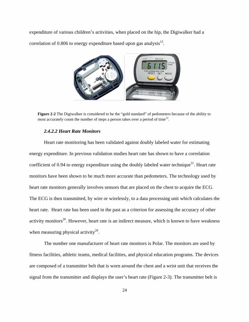
expenditure of various children’s activities, when placed on the hip, the Digiwalker had a
correlation of 0.806 to energy expenditure based upon gas analysis12.
24
2.4.2.2 Heart Rate Monitors
has been validated against doubly labeled water for estimating
energy
e ECG.
culates the
he accuracy of other
activity
y
vices
the
signal from the transmitter and displays the user’s heart rate (Figure 2-3). The transmitter belt is
Figure 2-2 The Digiwalker is considered to be the “gold standard” of pedometers because of the ability to 22most accurately count the number of steps a person takes over a period of time .
Heart rate monitoring
expenditure. In previous validation studies heart rate has shown to have a correlation
coefficient of 0.94 to energy expenditure using the doubly labeled water technique31. Heart rate
monitors have been shown to be much more accurate than pedometers. The technology used by
heart rate monitors generally involves sensors that are placed on the chest to acquire th
The ECG is then transmitted, by wire or wirelessly, to a data processing unit which cal
heart rate. Heart rate has been used in the past as a criterion for assessing t
monitors20. However, heart rate is an indirect measure, which is known to have weakness
when measuring physical activity20.
The number one manufacturer of heart rate monitors is Polar. The monitors are used b
fitness facilities, athletic teams, medical facilities, and physical education programs. The de
are composed of a transmitter belt that is worn around the chest and a wrist unit that receives

25
ged so
ifference between the two
electrodes is transmitted to the wrist unit where the heart rate is calculated by the changes in the
potential difference. The user’s heart rate is then displayed18.
Accelerometers
eters are a feasible method for detecting human activity because they not only
detect when a patient is in motion; they are also able to detect the intensity and frequency of
hum
accelerometer can be conditioned to isolate the relevant frequency band associated with human
ovement. For these reasons, accelerometry provides a powerful tool for quantifying human
activity and has been found to be an even better criterion of assessing physical activity than heart
rate20.
a soft fabric strap that has two electrodes incorporated into it. The two electrodes are arran
a potential difference can be measured across the chest. The potential d
2.4.2.3
Accelerom
an movement. By applying various signal processing techniques, the output of the
m
Figure 2-3 The Polar activity monitor measures a person’s activity level using heart rate. Heart rate is meuser
asured with a band around the chest, depicted here in black. The heart rate is displayed to the through the watch.
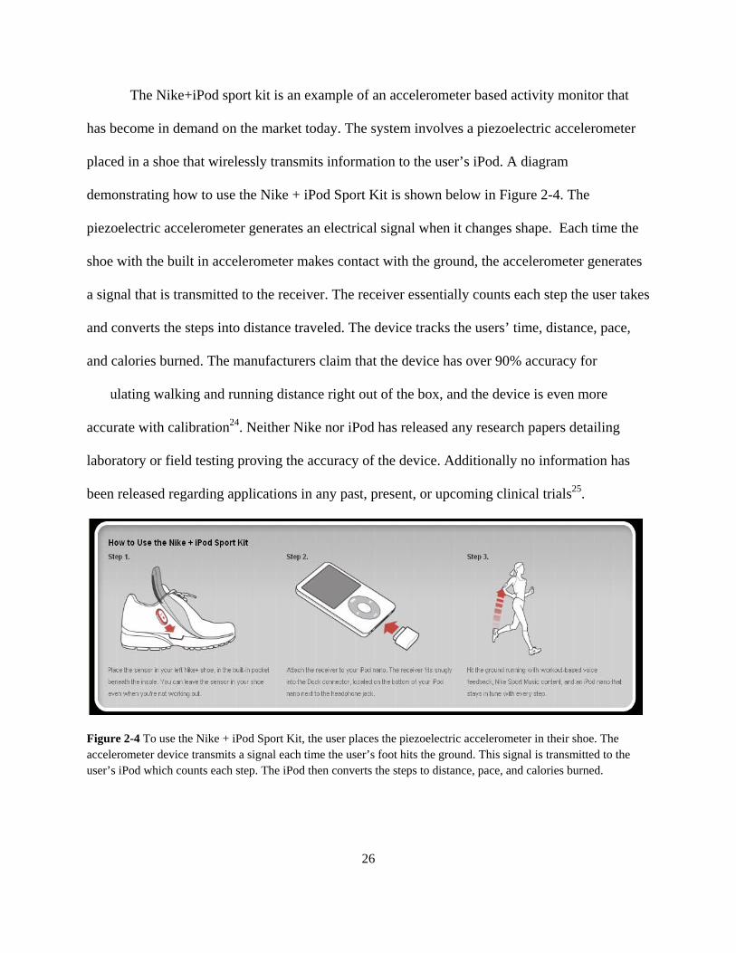
26
elow in Figure 2-4. The
s an electrical signal when it changes shape. Each time the
oe wi
es
accurate with calibration24. Neither Nike nor iPod has released any research papers detailing
laboratory or field testing proving the accuracy of the device. Additionally no information has
been released regarding applications in any past, present, or upcoming clinical trials25.
Figu + iPod Sport Kit, the user places the piezoelectric accelerometer in their shoe. The accelerometer device transmits a signal each time the user’s foot hits the ground. This signal is transmitted to the
The Nike+iPod sport kit is an example of an accelerometer based activity monitor that
has become in demand on the market today. The system involves a piezoelectric accelerometer
placed in a shoe that wirelessly transmits information to the user’s iPod. A diagram
demonstrating how to use the Nike + iPod Sport Kit is shown b
piezoelectric accelerometer generate
sh th the built in accelerometer makes contact with the ground, the accelerometer generates
a signal that is transmitted to the receiver. The receiver essentially counts each step the user tak
and converts the steps into distance traveled. The device tracks the users’ time, distance, pace,
and calories burned. The manufacturers claim that the device has over 90% accuracy for
calculating walking and running distance right out of the box, and the device is even more
re 2 To use the Nike -4
user’s iPod which counts each step. The iPod then converts the steps to distance, pace, and calories burned.

27
l
The device
ents of
2.4.2.4 Multiple Parameter Activity Monitors
The Caltrac Calorie Counter, shown in Figure 2-5, is another example of a widely used
accelerometer-based activity monitoring device. It has been tested and verified in over 60 clinica
trials and the manufactures claim that it is a valid predictor of energy expenditure26.
utilizes a single-plane accelerometer that is designed to monitor the up-and-down movem
the body. A major limitation of the Caltrac accelerometer is that the device does not accurately
estimate energy expenditure for isometric forms of exercise and activities in which the body
weight is partially supported, such as in bicycling or rowing27.
Having a device which utilizes only one accelerometer has limitations. It has been shown that
mounting three Caltrac accelerometers orthogonally results in an even better prediction of energy
expenditure28. Upon comparing triaxial accelerometry, uniaxial accelerometry, heart rate, and
pedometry for estimating energy expenditure in children’s activities, it was discovered that the
Figure 2-5 The Caltrac activity monitore is an accelerometer based monitor that utilizes an electronic chip that converts mechanical movement in a uni-axial direction into an electric signal. This signal is interpreted by a microprocessor and the amount of calories the user has burned is displayed. The Caltrac has been tested in numerou studies and is thought to be the best monitor on the market for measuring activity when exercising. s

28
triaxial
CG electrodes on the
21
30
accelerometer is the single best predictor of energy expenditure while uniaxial
accelerometry and heart rate appeared to be just as valid as the inexpensive “low tech” measure
of pedometry. A chart of each device’s mean error and standard deviation for each activity is
shown below in Figure 2-6. The study concluded that combining triaxial accelerometry with
heart rate would provide the best estimate of energy expenditure20.
An example of combined heart rate and motion sensing technology is the ActiHeart. The
ActiHeart is a single-piece device that is designed to clip on two standard E
chest . A picture of the device placement is shown below in Figure 2-7. The ActiHeart contains
a triaxial piezoelectric accelerometer and calculates the heart rate by digitizing the ECG signal
and calculating the R-to-R ratio, a technique more accurate than peak detection for free-living
activities . The combining of heart rate and full body accelerometry is a much better tool for
measurement of a wider range of activities as accelerometers tend to underestimate the energy
Figure 2-6 The mean error and standard deviation of energy expenditure/minute in various activities measuthe Tritrac tria-xaial accelerometer, WAM uni-axial accelerometer, heart rate, and a hip pedometer worn bchildren in reference to gas analysis. This figure shows that all four monitors overestimated energy expenditu
red by y 30
re during ayoning and underestimated energy expenditure during running at 10km/hr. The tri-axial accelerometer had the allest margin of error while the other three were considered to be around the same.
crsm

29
ting30.
2.1 Designing an Activity Monitor for Diabetic Individuals
Most of the activity monitors described above are designed for use during exercise and
are not designed for continuous use. Some of the monitors are ideal for a limited range of
activities as they may overestimate or underestimate energy expenditure for other activities. The
Digiwalker and the Nike+iPod sport kit are only ideal for walking or running activities. The
Caltrac is ideal for estimating energy expenditure for any non-weight bearing activities. While
heart rate monitoring can estimate energy expenditure for virtually all activities, it can
overestimate energy expenditure when an individual experiences increased heart rate due to
factors other than physical activity such as increased stress.
f
performed. The ActiHeart algorithm is dependent upon full body accelerometry when an
expenditure for ambulatory activities such as bike riding, skate boarding, and weight lif
The main limitation of heart rate is that it is influenced by factors other than physical activity29.
Figure 2-7 Placement of ActiHeart on small patient.
The ActiHeart would be ideal for measuring all activities continuously as the algorithm
or determining energy expenditure adjusts depending upon what type of activity is being

30
n
Table 2-6: The relative contribution of the activity counts and heart rate to the combined ActiHeart algorithm
individual is at rest and doing activities such as computer work. This prevents the overestimatio
of energy expenditure due to increased heart rate from factors other than physical activity.
Relative contribution of activity counts
and HR to the combined ActiHeart algorithm50
Activity (%) HR (%)
Lying 90 10
Computer work 90 10
Standing 50 50
Filing papers 50 50
Washing dishes 50 50
Washing windows 50 50
Slow walk (avg. 82 m min-1) 50 50
Vacuum 50 50
Sweep/mop 50 50
Raking grass/leaves 50 50
Fast wa k (avg. 103 m min-1) l 50 50
Lawn mowing 10 90
Station ry cycling (avg. 99 W) a 10 90
Ascending/descending stairs 50 50
Racque all tb 10 90
Basketball 10 90
Slow run (avg. 157 m min-1) 10 90
Fast run (avg. 191 m min-1) 10 90
Average for all activities 50 50
uring high int ependent upon heart rate to
revent the underestimating of accelerometry due to accelerometer’s inability to account for
ow
D ensity activities, the ActiHeart algorithm is d
p
resistance. The relative contribution that the accelerometer and heart rate components that the
device has is shown below in Table 2-6.
One major drawback of the ActiHeart activity monitor is that the device must be
connected to a computer to display information. Therefore, if a diabetic person needs to kn

31
all
expenditure in terms of calories burned; however
adjustments to hiss calculate adjusted their insulin dosage based upon carbohydrates ingested or
n activity monitor custom for diabetic individuals should therefore
ormation directly on the monitor and should be related to carbohydrates rather than
how much she should adjust her insulin dosage, she needs to find the nearest computer. This is
not an ideal situation. An activity monitor customized for diabetic individuals should display
essential information directly on the device itself. Additionally, the ActiHeart outputs energy
, a diabetic individual most often calculates
carbohydrates burned. A ized
display inf
calories burned.

32
at were made while designing this device including goals and aims, the
stakeho , the client statement, objectives, constraints, and any potential problems that may be
associated with the use of the device.
3.1 Goals and Aims
The project goal was to design an activity monitor that is specifically indicated for use by
diabetic individuals. An individual should be able to wear the device continuously without
feeling uncomfortable or self-conscious. The device would be accurate and not be influenced by
motion artifact or external influences such as those exposed to while traveling in motor vehicles.
The device will produce an output that will indicate adjustments to insulin dosage. The following
sections will go into detail about specific goals and aims in regards to each aspect of the device.
3.1.1 Indications for Use
The initial hypothesis that was developed was that this device will be used in conjunction
with the diabetic individual’s blood glucose monitoring devices and would be used to better aid
the patient in blood glucose regulation. As a result, the assumption was made that when using
this device, the diabetic individual would still use the tools given to him by his physician to
3 Design Approach: An Activity Monitor for Diabetic individuals
The main objective of this project was to build a device that a diabetic individual can
wear continuously and receive feedback on adjustments to his insulin dosage, diet, or level of
physical activity based upon his carbohydrates burned, which is a function of energy
expenditure. There is currently no device on the market which monitors physical activity that is
specifically designed for diabetic individuals. The following sections will describe the
considerations th
lders

33
monitor his blood glucose (i.e. a blood glucose monitor), to calculate their insulin (i.e. sliding
to
develop
3.1.2 Aesthetics
This device will be worn on a regular basis by diabetic individuals Therefore, it was
assumed that individuals will not wish to use the device if they feel uncomfortable wearing it. As
a result, the aim was to design a device that is comfortable to wear and is inconspicuous to
others. This would limit the choice of sensors, placement of sensors, and the size of the device.
to develop a device that will be easy to use by people of all ages including children and the
Therefore another aim was to develop the device so that the user will simply have to put the
3.1.4 Device Placement
device every morning, this device must be as easy to put on
as possib
body that will allow for accurate readings. The diabetic individual will not wish to use the device
scale or other dosage algorithm), and will track his carbohydrate intake. Therefore the aim was
a device that can be used along with the tools diabetic individuals already use. The
device was designed to not replace any of the tools diabetic individuals use, only to enhance
them.
3.1.3 Ease of Use
Due to the diverse population of the patients who will be using the device, it was desired
elderly. Individuals will not want to use the device if it is complicated or difficult to operate.
device on when he gets up each morning and will not have to program the device.
As the user has to put on the
le, will stay on all day, will be comfortable to wear, and will be placed in an area of the
if it takes a while to put on, requires maintenance throughout the day, interferes with his
everyday activities, or if he gets inaccurate readings. The device was developed to take under a

34
The desired output of the device must be easy to integrate into the patient’s current
. If the output is too complicated, and the patient cannot easily add the
output ress
e this device in their everyday activities. The patient’s activity level
could b
3.2 Stakeholders
s involved must be considered. This starts as early as the
initial b
e of
minute to put on. The main component of the device will stay on the user’s hip and electrodes
will be placed underneath his clothes. This device will not interfere with the patient’s everyday
activities.
3.1.5 User Interface
insulin dosing calculations
to their calculations for their insulin dose, then the device will not be effective. To add
this problem, the output was created to be easy to understand. The user will be educated on how
to use the device output to make adjustments to his insulin dosage, diet, or exercise.
3.1.6 Device Performance
Individuals would us
e low intensity as they may do activities such as cleaning, gardening, and walking, or the
patient could have a high intensity activity level as they may do activities such as running or
biking. Therefore, it was desired to design a device that will measure both large and small
movements accurately.
To begin a project, all partie
rainstorming and continues all the way through to the implementation and use of the
device.
The first stakeholder involved in a project is always the client. It is the client who says
there is a need for this device. The designers then sit down and fulfill that need. In the cas
this project, the client was Professor Peura’s son, Brent. The client brought forward a problem to

35
he case of this medical device the students in this MQP group are considered to be the
olved with this project that the group had to take. This project was
onstrai e
Also, the group was constrained to stay within the allotted budget of $500. This budget
n the group, with a certain dollar amount given to the
group p
ss the
ce and can be done at a low cost and in an efficient way. This is a
vice that can be readily manufactured. For
his dev
If
were common and the design simple, the cost of production would be lower and the
device
d
be addressed and solved. The solution would involve a medical device and the subsequent
education of the patient on use of this device.
In t
designers. There were risks inv
c ned on its own and through the group. Because of the academic nature of this project, th
students in the group were constrained in terms of time, balancing the work on the device with
time needed to complete work for other courses. The project was considered to be an equivalent
of a typical WPI course so any given week the students were expected to work on the project
between 15 and 20 hours.
was based on the number of students i
er student. Any funds needed beyond this amount were to be provided by the students in
the group. Because of this, caution was taken when making decisions that would cost more than
25 dollars, 5% of the total budget.
The best design ideas and best device will never make it off of the design page unle
device is easy to reprodu
challenge to any designer; designing and creating a de
t ice, parts used had to be common parts that could be purchased from a supplier. Any
custom parts had to be as simple as possible using the lowest number of components needed.
the parts
will be more profitable from the onset.
The most influential stakeholder in any endeavor is the person who will be most affecte
by the project. In the case of this project, those most affected were Insulin Dependent Diabetic

36
d.
ts would be wearing the device, the types of
activity
tient while he or she changes the insulin dosing based on the output of
this dev
it
an to check on the activity level of the patient as closely as
previou
3.3 Original/Revise Client Statement
Evaluating the problem presented to the project group, an initial client statement was
created.
To build a device that will determine the activity of the patient and output advisory
information for insulin algorithm adjustments.
After working with the problem further, a revised client statement was created to better
meet the needs of the project.
Patients. These patients had to be taken into consideration when the device is being designe
Some areas addressed were the fact that patien
that needed to be measured, the type of output needed, and the ability to factor the output
of the device into a new insulin algorithm.
With the improvement of the patient’s care of his or her insulin and glucose levels, the
job of the physicians and other health care professionals the patient encounters will be made
easier, at least in this one area. At the start of the patient’s use of this device, the physician will
have active in the patient’s care. Just as when the patient was first put on insulin, the physician
will have to monitor the pa
ice. However, once a new algorithm is in place that both factors in the output of the
device and allows the patient to live a healthy life, the physician’s role will return to the state
was before the device was introduced. In many cases the physicians’ role may even decrease as
the device will monitor the patient’s activity and tell him or her how to adjust the insulin dose,
eliminating the need for the physici
sly needed.

37
This device will be low cost, patient friendly,
aesthet
3.4 Objectives to Accomplish Goal
To begin the project objectives and the sub objectives corresponding to each objective
were entered into an objective tree, seen in Figure 3-1. The objectives were then evaluated and
weighted to best judge all design ideas. A Pair-Wise Comparison was conducted to evaluate the
objectives chosen by the group. This can be seen in Table 3-1. These objectives were then
entered into Table 3-2 to show their respective weights and the sub objectives that correspond to
the objectives.
e
s the objectives are equal in importance.
Ease of Cost Device ce
Power Practicality Safety
To build a device to be worn continuously that will determine the activity of the insulin
dependent diabetic individuals and output advisory information for insulin algorithm
adjustments. Activity will be measured using multiple parameters to allow for increased
efficiency in measuring all types of activity.
ically pleasing, and feasible for everyday use.
Table 3-1 A Pair Wise Comparison was conducted to evaluate the importance of each objective. A “1” indicates thobjective in the corresponding row is more important than the objective in the corresponding column. Like wise a “0” indicates the objective in the corresponding row is less important than the objective in the corresponding column. A “.5” indicate
Use Performan
Ease of Use --- 1 0 1 5 0 Cost 0 --- 0 1 0 0 Device
mance 1 1 --- 1 1 1
PerforPower 0 0 0 --- 0 0 Practicality 5 1 0 1 --- 0 Safety 1 1 0 1 1 ---
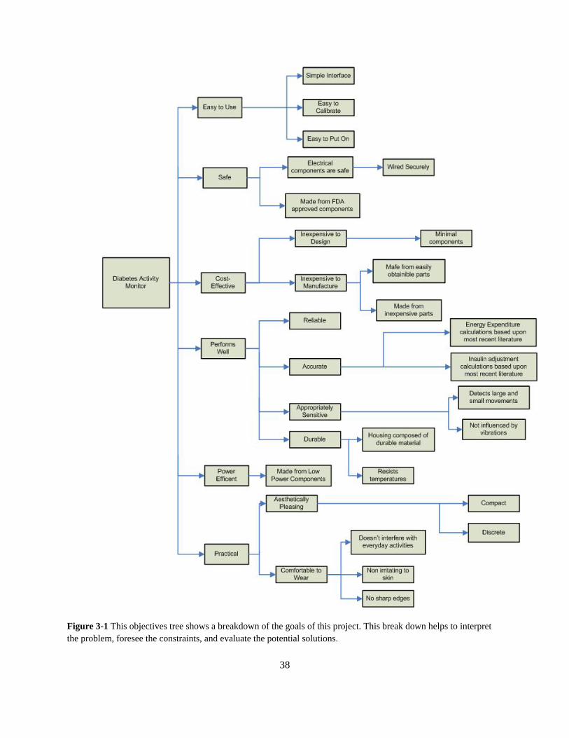
38
Figure 3-1 This objectives tree shows a breakdown of the goals of this project. This break down helps to interpret the problem, foresee the constraints, and evaluate the potential solutions.

39
Table 3-2 Once the pair wise comparison was done, the objectives were weighted and placed in order. Each objective is broken down in to sub objectives to ensure that all areas covered by each objective are fulfilled during device design.
3.5 General Design Constraints
There were several constraints applied to the design of this device which had to be
fulfilled in addition to meeting the set objectives. Table 3-3 lists the major constraints and their
descriptions.
Table 3-3 General Design Constraints
Constraint Description Time We must complete the research, design, construction, and testing of
the device by the end of D-term 2008 Project Budget The allotted budget from the Biomedical Engineering department for
the design and the construction of the device is $610 Power The device is portable and therefore must be battery powered.
Size The device must be small enough to be worn comfortably.
Safety The device cannot carry any risk of harming the patient.
Materials All materials used in the device must be readily available and FDA approved for use in a medical device
Objective Sub Objectives Device Performance - 28.57% Reliable
Accurate Sensitive Durable
Safety-23.81% Made from FDA Approved Parts Electronics Follow IEEE Standards
Ease of Use -16.67% Simple Patient Interface Ease of Calibration Ease of Placement
Practicality -16.67% Aesthetics Comfort Appealing for Continuous Wear
Cost Effective-9.52% Cost of Design Cost of Manufacture
Power Efficiency-4.76% Components are Low Power

40
are many problems that could potentially arise with a device that has electronic
compon ts and dividuals of all ages and technical abilities. If any part of the device isn’t
working correctly, the device will not output the correct in r output anything at all.
Additionally, there could be user error associated with the he device isn’t worn correctly, the
output o e inaccurate. It is also importan vice
will inte djustments to her diet, m individual is not
correctl ed on how to interpret the device correctly curate reading, she could
make adjustments to her diet, medication, or exercise that trimental to her health. Finally,
electrica here is a chance that the user is the
device is
the
user is a diabetic patient is not be desirable. Also some sensors require application
of energy to the body system and sensor choice affects
patien ionally the ulfill these requirements while giving reliable
measurement readings. s, there existed several sensor
types that had to be nar e the design.
3.6 Potential Problems with the Use of the Device
There
en is used by in
formation o
device. If t
f the device may b t to note that the individual using the de
rpret the output to make a edication, or exercise. If the
y inform or if she gets an inac
could be de
l safety is important and t device may send voltage through the
wired incorrectly.
3.7 Sensors
Sensor selection was an important step in the design process. As mentioned before,
choice of sensor greatly affects the aesthetics of the device. A sensor that makes it obvious to
others that the
measuring the return output. Therefore
t safety. Addit sensor has to f
For each of the measurement parameter
rowed down to a single choice per parameter to optimiz

41
e
ain
f
Each of the designs was carefully considered before deciding on the final design.
curate measure of human activity, as defined in Chapter 2. In defining
design were better able to meet all aims and objectives within the given
onstra
100
e
s in
motion. So, the output display had to be large enough to be read while still fitting within the
casing of the device and allowing space for other components to be mounted on the outer surface
of the device.
Power is another major concern for any consumer electronics, especially for a
continuous monitoring device. Defining specific amp-hour rating to the device posed too great of
4 Device Design
An effective device design must address user needs and provide a feasible solution to th
problem at hand. After addressing these needs, the design was broken down into three m
areas: system architecture, measurement parameters, and sensors. Using various combinations o
possible options from each of the focuses, several different designs for the device were made.
4.1 Device Specification
The design chosen had to have certain parameters to ensure patient safety and comfort
while still providing an ac
design specifications, the
c ints, optimizing the design to best meet the needs laid out by the client.
As a continuous monitor, the device had to be compact and light weight. A majority of
the population carry electronic devices, such as cell phones, on their person every day. Therefore
it was reasonable to have a device with parameters of size and weight similar to a cell phone. A
typical cell phone has dimensions 2 in x 3.5 in x 0.5 in (W x L x H) and may weigh between
and 150 grams. Of the total physical dimension of the device, the output display would consum
most of the surface. The output must be clearly observable during rest and when the patient i

42
a constriction during circuit design. Therefore, power requirements were expressed as the
of the device. The device should be able to run off a set of
batterie
4.2 System Architecture
plying the black box model to formulate the overall
system n
atient. The
output
ssed and integrated. At the time of the initial design, the designers were aware
that me
frequency of battery replacement
s for 6~12 months. If this is not achieved, a rechargeable battery option would be a
sufficient alternative. There is also a low battery indicator.
For safety, the housing of the device was made of plastic and has no protruding sharp
edges. Efforts were made to keep wiring to a minimum.
The design process began by ap
architecture. Because the processing required to produce the desired output was unknow
at the start of the project, the black box approach best facilitated the design process and allowed
the designers to consider all design choices one at a time. The model began with an input
entering the black box. The input for this device was the physical activity of the p
of the black box was an intuitive, symbolic, or numerical indication, which a diabetic can
use the information to adjust his/her insulin/glucose intake.
Part of the project was to determine parameters that could be measured to accurately
deduce an activity level. The parameters chosen influenced what kind of sensors the device
required. For example, if the parameter involves biopotentials, instrumentation analog circuitry
in the device can be foreseen. Research was done on the subject to identify the most feasible
parameter.
In order for the black box to output some indication of activity level, the measurements
had to be proce
asurements may not be directly useable or coherent due to associated noise. The

43
ter in
ty
tient. The device designed in this
project
atient was not involved in activity at
ation had to be integrated carefully by some
aradigm to accurately deduce activity levels. Research was done related to this topic in order to
determine a feasible processing and integration technique.
After processing the information obtained by parameter measurements and deducing an
activity level indication, the black box will output the information by intuitive means to the
patient-friendly information. The system architecture can be seen in Figure 4-1
measurement signals had to be processed in order to produce useable signals of the parame
question. Additionally, not all parameters can be directly interpreted to deduce activity level.
Because most current market activity monitors are worn only during exercise, activi
measured by the device corresponds to the activity of the pa
is to be worn continuously. Therefore, the designers had to address the problem that
occurred when the device registered activity though the p
that time. As a result, sensor sourced inform
p
Fi od, the p ing objectives a
gure 4-1 The block diagram displays the black box approach to the solution for this problem. By using this methroblem could be solved while initially ignoring the details of the components of the device, better establishnd outcomes for the design of the components.
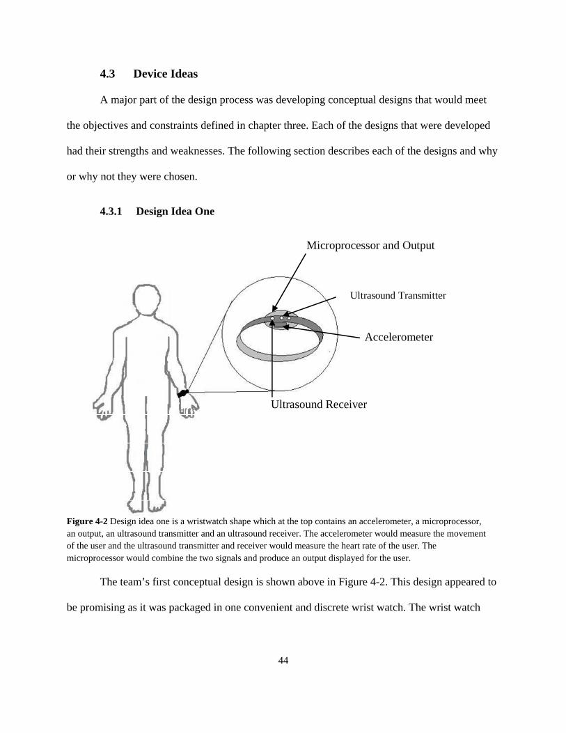
44
t
the obj
hy
4.3.1 Design Idea One
he team’s first conceptual design is shown above in Figure 4-2. This design appeared to
4.3 Device Ideas
A major part of the design process was developing conceptual designs that would mee
ectives and constraints defined in chapter three. Each of the designs that were developed
had their strengths and weaknesses. The following section describes each of the designs and w
or why not they were chosen.
Microprocessor and Output
T
be promising as it was packaged in one convenient and discrete wrist watch. The wrist watch
Accelerometer
Ultrasound Transmitter
Ultrasound Receiver
Figure 4-2 Design idea one is a wristwatch shape which at the top contains an accelerometer, a microprocessor, an output, an ultrasound transmitter and an ultrasound receiver. The accelerometer would measure the movement of the user and the ultrasound transmitter and receiver would measure the heart rate of the user. The microprocessor would combine the two signals and produce an output displayed for the user.

45
nd ultrasound components. The accelerometer component senses
body m
cells. Energy cannot be destroyed; hence all energy applied to the
body will be conserved. Some energy will be absorbed by the tissue, and the other will be
measured by the sensor. If measurements are taken over an artery, the return signal will be a
time-varying ac signal riding over a DC offset. This is due to the pulsatile nature of blood flow.
During systole, there is an increase is blood pressure. Since the dimension of the artery stay
relative nstant, the density will increase every time the heart beats. If the artery is denser
more signal bounces off of it, creating a stronger return signal compared to during diastole. By
looking at the ac component of the return signal, the occurrence of each heart beat can be
identified, hence making it possible to calculate heart rate.
where
Equation 4-1 Energy distribution in ultrasound return signal
If the sensor is not placed on the extremity, there will be larger tissue absorption,
making the return signal smaller. A smaller return signal will have even smaller ac component,
s wearing the
device.
on
are in the audible range. For example, assuming a higher heart rate of 180bpm, the frequency of
contained both accelerometer a
ovements while the ultrasound component detects the heart rate.
Ultrasound systems use high frequency sound waves (20kHz and higher, and in the
mega-Hz ranges in many applications) as energy source and measure the return echo signal from
the movement of the red blood
ly co
making the signal very susceptible to noise. This forced the sensor to be placed on the
extremities directly over an artery, which would make it obvious that the user i
The frequency components of the part of the processed signal with heart rate informati

46
artifacts, making it
difficul with
design
t as
d, but instead of using ultrasound as the energy source, it uses light. Due its similarity
with th
the first harmonic of blood flow is 3Hz in which significant portion of the total power of the
signal is present. However, this overlaps with the power spectra of motion
t to filter out motion artifacts while conserving power of the useful signal especially
a low order filter that is feasible in the analog domain.
4.3.2 Design Two
The second design approach continued to utilize the wrist watch accelerometer
using pulse oximetry to measure the heart rate. Pulse oximetry works off of the same concep
ultrasoun
Pulse-Ox Transmitter (LED)
Accelerometer
Pulse-Ox Receiver (Photo electrode)
Microprocessor and Output
Figure 4-3 Design idea two also utilized a wristwatch accelerometer setup. To measure the heart rate of the use, th wristwasignals would be combined and output to the user.
e tch was outfitted with LEDs and a photo-electrode to create a pulse oximeter. The two
e ultrasound it shares the same disadvantages. In addition to it, the designers had some
experience with designing devices similar to the pulse oximeter, and found it very difficult to get
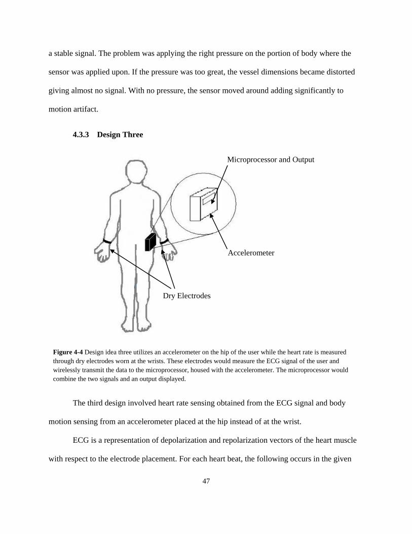
47
a stable signal. The problem was applying the right pressure on the portion of body where the
sensor was applied upon. If the pressure was too great, the vessel dimensions became distorted
giving almost no signal. With no pressure, the sensor moved around adding significantly to
motion artifact.
4.3.3 Design Three
Microprocessor and Output
Accelerometer
Dry Electrodes
The third design involved heart rate sensing obtained from the ECG signal and body
motion sensing from an accelerometer placed at the hip instead of at the wrist.
ECG is a representation of depolarization and repolarization vectors of the heart muscle
with respect to the electrode placement. For each heart beat, the following occurs in the given
Figure 4-4 Design idea three utilizes an accelerometer on the hip of the user while the heart rate is measthrough dry electrodes worn at the wrists. These ele
ured ctrodes would measure the ECG signal of the user and
wirelessly transmit the data to the microprocessor, housed with the accelerometer. The microprocessor would combine the two signals and an output displayed.

48
t.
ge
hat appears in a PQRST complex. Figure 2-3 below shows the presence of a
eat. Counting the number of occurrences of the
ECG signal over a time period will give the heart rate.
e
c
impossible to deduce heart rate. SNR is also poor when the electrodes are placed on fatty areas of
the bod is
uscle cells as
they are
f
order: atrial depolarization, ventricular depolarization, atrial repolarization, and ventricular
repolarization. This dynamic of electrical charge gives an overall vector for charge displacemen
The magnitude of the vector is measured in respect to the electrode orientation, and this chan
in magnitude is w
distinct shape for the ECG with every heart b
Figure 4-5 The typical ECG rrelate to the activity of the heart at any given point.
wave21 has several components, each labeled by a single letter, that co
The ECG has a wide power spectrum, making it susceptible to all sorts of noise. N is
an easi y be great enough to completely mask the PQRST waveform, making it virtually
o
l
y. Muscle flexion can also cause a disturbance by producing another biopotential that
picked up by the electrodes called EMG. These are the electrical signals of the m
activated by the peripheral nervous system. Placing an electrode in an area with heavy
skeletal motion will increase this type of noise. One convenient aspect of the power spectrum o

49
ot
s
electrodes disguised as a set of bracelets
that would transmit wirelessly to the main device component on the hip, which also houses the
accelerometer. However a quick search on the web revealed that wet electrodes are more readily
available than dry electrodes for consumer use. The subject using this device would need regular
replacement of electrodes, so dry electrodes were not ideal. Also the wrist placement of
electrodes would make the device somewhat conspicuous. Also the team was unable to get a
clear and stable ECG signal with electrodes placed at the wrist with wet electrodes and dry
electrodes would have contributed to even more noise. Also the circuitry for transmitting and
receiving a wireless signal was complex and not within the scope of this project.
esign four and design three is the choice to use wet electrodes
and to place the electrodes at the torso. One electrode was placed on the sternum, another below
the pectoral muscle and the last one on the hip. This electrode placement allows for concealment
with proper clothing, adding to the aesthetics factor. These electrodes are all connected by wire
to the main component of the device on the hip.
an ECG signal is that significant amounts of power are located in frequency ranges that do n
overlap with the motion artifact power spectrum. This implies that with proper filtering, motion
artifact may pose no threat when attempting to acquire non-diagnostic level ECG’s.
The accelerometer was moved to the hip as measurements of full-body acceleration are
the most accurate at this location. In order to avoid the inconvenience wet electrodes and wire
for sensing the ECG signal, it was decided to utilize dry
The difference between d
4.4 Final Design System -Overview
The sensors that were implemented in the final design were ECG electrode system with
torso electrode placement and tri-axial accelerometer mounted at the waist. In the functional unit

4.4.1 Design Four
50
level, the final design consists of analog circuitry to acquire and condition the signals from the
sensors
Goleta, CA). They are pre-jelled to reduce the
adhesive, and relatively inexpensive.
Howev
Figure 4-5 Design idea four houses an accelerometer and a microprocessor on the hip of the user and places electrodes on the hip the sternum of the user. These electrodes measure the ECG of the user. The microprocessor in the casing on the hip processes the accelerometry and ECG signals and outputs data for the user.
, and a digital system to produce an output.
4.4.2 Sensors
In order to obtain an electrocardiogram, an electrical interface between the device and the
body is needed, and wet surface electrodes are used in most application. The electrode chosen,
EL503, can be obtained from BioPac Systems (
hassle for the user, less painful to take off due to less
er, the device itself is not dependant on the type of electrode as long as it stays on the
patient securely for an extended period of time and provides good electrical contact.
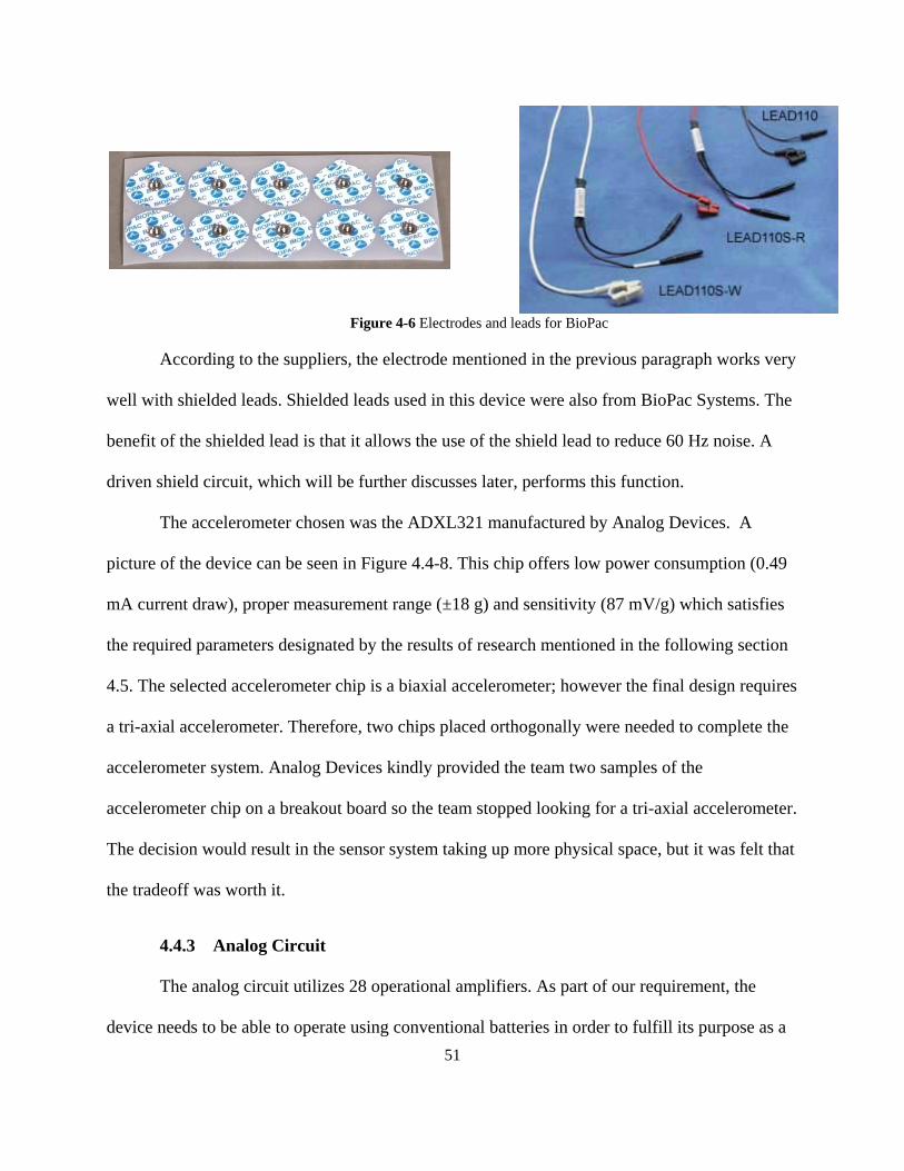
51
Figure 4-6 Electrodes and leads for BioPac
ccording to the suppliers, the electrode mentioned in the previous paragraph works very
well with shielded leads. Shielded leads used in this device were also from BioPac Systems. The
benefit of the shielded lead is that it allows the use of the shield lead to reduce 60 Hz noise. A
driven shield circuit, which will be further discusses later, performs this function.
The accelerometer chosen was the ADXL321 manufactured by Analog Devices. A
p (0.49
mA current draw), proper measurement range (±18 g) and sensitivity (87 mV/g) which satisfies
the required parameters designated by the results of research mentioned in the following section
4.5. The selected accelerometer chip is a biaxial accelerometer; however the final design requires
a tri-axial accelerometer. Therefore, two chips placed orthogonally were needed to complete the
nalog Devices kindly provided the team two samples of the
acceler
t
4.4.3 Analog Circuit
The analog circuit utilizes 28 operational amplifiers. As part of our requirement, the
device needs to be able to operate using conventional batteries in order to fulfill its purpose as a
A
icture of the device can be seen in Figure 4.4-8. This chip offers low power consumption
accelerometer system. A
ometer chip on a breakout board so the team stopped looking for a tri-axial accelerometer.
The decision would result in the sensor system taking up more physical space, but it was felt tha
the tradeoff was worth it.

52
Figure 4-7 Evaluation board of ADXL321 Accelerometer Device (Courtesy of SparkFun Website)
continuous monitor. The MCP604X series from
required. However, the MCP604X has a gain ba
4.4.4 Digital System
of a microcontroller and an input/output device. The
MSP430F449 is a powerful 16-bit m
Mircrochip was a perfect match to the needs of
the device. The MCP604x draws 600 nA, which is less than 1% of what a 741 series would
draw. It can also operate off a power supply voltage as low as 1.4 V. Because EKG and full-body
acceleration are low frequency signals, high slew rates or gain-bandwidth products were not
ndwidth product of 14 kHz. Even with the
highest single stage gain (46 dB), the bandwidth is significantly wider than the frequency
spectrum required for analysis. Instrumentation systems are sensitive to offsets depending on the
largest single stage gain present in the circuit so the op amp also must have high CMMR. The
MCP604x has a maximum of ±3 mV and even with a 46 dB gain, the highest single-stage gain in
our design, the offset is 0.59 V. Although 0.59 V covers more than 1/8 of the circuit’s operating
range (power supply was ±2 V), it was discussed and agreed upon between the designers that this
worst case scenario was tolerable for the purpose of this device. The CMMR this op-amp offers
is 80 dB (1E40 V/V).
The digital unit consists
icrocontroller with useful on-chip features such as LCD
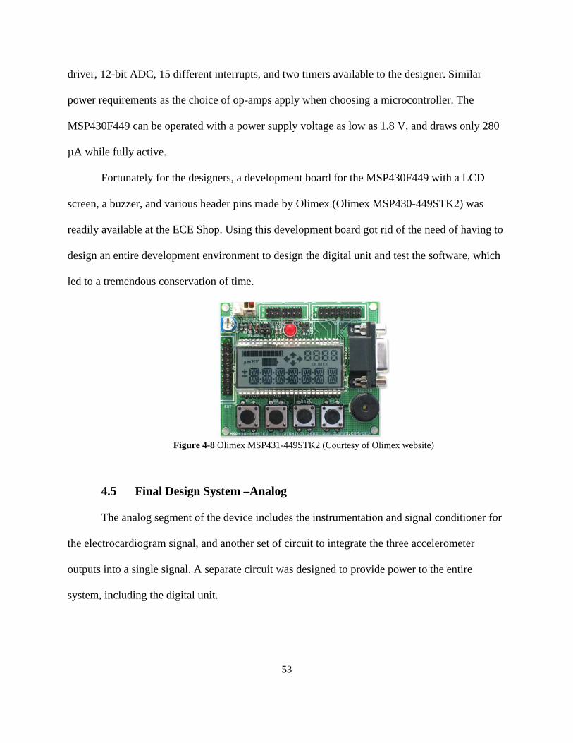
53
driver, 12-bit ADC, 15 different interrupts, and two timers available to the designer. Similar
power requirements as the choice of op-amps apply when choosing a microcontroller. The
MSP430F449 can be operated with a power supply voltage as low as 1.8 V, and draws only 280
µA while fully active.
Fortunately for the designers, a development board for the MSP430F449 with a LCD
screen, a buzzer, and various header pins made by Olimex (Olimex SP430-449STK2) was
ich
ignal, and another set of circuit to integrate the three accelerometer
outputs into a single signal. A separate circuit was designed to provide power to the entire
stem, including the digital unit.
M
readily available at the ECE Shop. Using this development board got rid of the need of having to
design an entire development environment to design the digital unit and test the software, wh
led to a tremendous conservation of time.
Figure 4-8 Olimex MSP431-449STK2 (Courtesy of Olimex website)
4.5 Final Design System –Analog
The analog segment of the device includes the instrumentation and signal conditioner for
the electrocardiogram s
sy
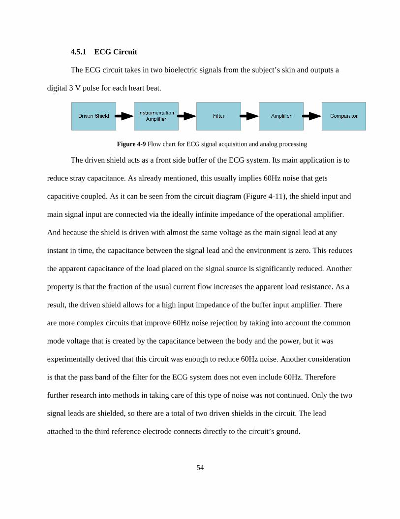
54
a
4.5.1 ECG Circuit
The ECG circuit takes in two bioelectric signals from the subject’s skin and outputs
digital 3 V pulse for each heart beat.
Figure 4-9 Flow chart for ECG signal acquisition and analog processing
The driven shield acts as a front side buffer of the ECG system. Its main application is to
reduce stray capacitance. As already mentioned, this usually implies 60Hz noise that gets
capacitive coupled. As it can be seen from the circuit diagram (Figure 4-11), the shield input and
main signal input are connected via the ideally infinite impedance of the operational amplifier.
And because the shield is driven with almost the same voltage as the main signal lead at any
instant in time, the capacitance between the signal lead and the environment is zero. This reduces
the apparent capacitance of the load placed on the signal source is significantly reduced. Another
property is that the fraction of the usual current flow increases the apparent load resistance. As a
result, the driven shield allows for a high input impedance of the buffer input amplifier. There
re more complex circuits that improve 60Hz noise rejection by taking into account the common
tween the body and the power, but it was
xperim
e two
re a total of two driven shields in the circuit. The lead
the circuit’s ground.
a
mode voltage that is created by the capacitance be
e entally derived that this circuit was enough to reduce 60Hz noise. Another consideration
is that the pass band of the filter for the ECG system does not even include 60Hz. Therefore
further research into methods in taking care of this type of noise was not continued. Only th
signal leads are shielded, so there a
attached to the third reference electrode connects directly to

55
Figure 4-10 Driven Shield Circuit Diagram
An instrumentation amplifier follows the driven shields. Ideally, a large gain is desired at
this stage to take adva lf cell
potenti
ntage of the differential amplification. However, due to the ha
al of the electrodes and difference in the properties of the skin where the electrodes are
placed on the subject, DC offset voltages can exists at the output of the instrumentation
amplifier. If the gain is too high, the DC offset voltages will saturate the operational amplifier
and the signal will be lost. The gain of the instrumentation amplifier is
2 ·1 ·
Equation 4-2 Gain equation for the instrumentation amplifier
The gain was experimentally determined and designed for 11.2 V/V or roughly 20 dB. In
order to reduce the current flow in the circuit and conserve power, relatively high resistance
values were used to achieve this gain (R1= 510kΩ R2= 100kΩ R3= 510kΩ R4= 510kΩ).
2 · 510100
5105101 · 11.2
l
toff
l ECG
requires a pass band of 0.05 ~ 200 Hz. These cutoff frequencies make the system highly
Equation 4-3 Calculated gain of the instrumentation amplifier
To increase the signal to noise ratio, the signal was high-pass and low-pass filtered and amplified
further. The high-pass filter gets rid of the DC offset, allowing for additional gain to the signa
without saturating the system, and the low-pass filter reduces high-frequency noise that is present
in the signal, including the remaining 60 Hz noise and EMGs. To determine the desired cu
frequencies, the designers re-examined the requirements. A typical diagnostic leve

56
Instrumentation Amplifier Circuit Diagram
h
purpose. Therefore a narrower pass al51. studied the relative power
spectra of the entire ECG55 d signals such as
motion artifacts and m
displayed. Therefore a hig reduce unwanted or
unnecessary signals.
Thakor et al. did another study where they studied the spectral plots of ECG and QRS
complex and looked at the signal to noise ratios (SNR) over a range of frequencies. The plot
below from this paper shows a peak at around 17 Hz. Therefore the center frequency of the
designed pass band was set at 17 Hz.
Figure 4-11
susceptible to motion artifacts. However, the device only needs to measure the heart rate, whic
means that as long as the signal giv d very heart beat, it serves the es a istinct indication for e
band is justified. Thakor et
, distinct wave components of the ECG and unwante
uscle noise. At frequencies over 15 Hz, the power of the P and T waves
are gone and the ECG and QRS power spectrum is almost equal. Motion artifact is almost non-
existent, and muscle noise seem e frequency bands to be relatively constant throughout th
h pass filter with a cutoff around 15 Hz should
52

57
Figure 4-12 Relativ nd motion artifacts
Figure 4-13 SNR of the QRS complex
,
eats. At a rate of 300 beats per minute, which is an
xtremely high value, each beat occurs every 200 ms. Therefore the ringing must end before 200
ms for the oscillation due to each beat to not interfere with each other. Previously it was
e power spectra of ECG wave components, muscle noise a
The relationship between bandwidth and center frequency must also be taken into
account. If the bandwidth of the pass band is too narrow relative to a certain center frequency
the response becomes highly oscillatory. This ringing must be kept within a certain length in
order to distinguish consecutive heart b
e
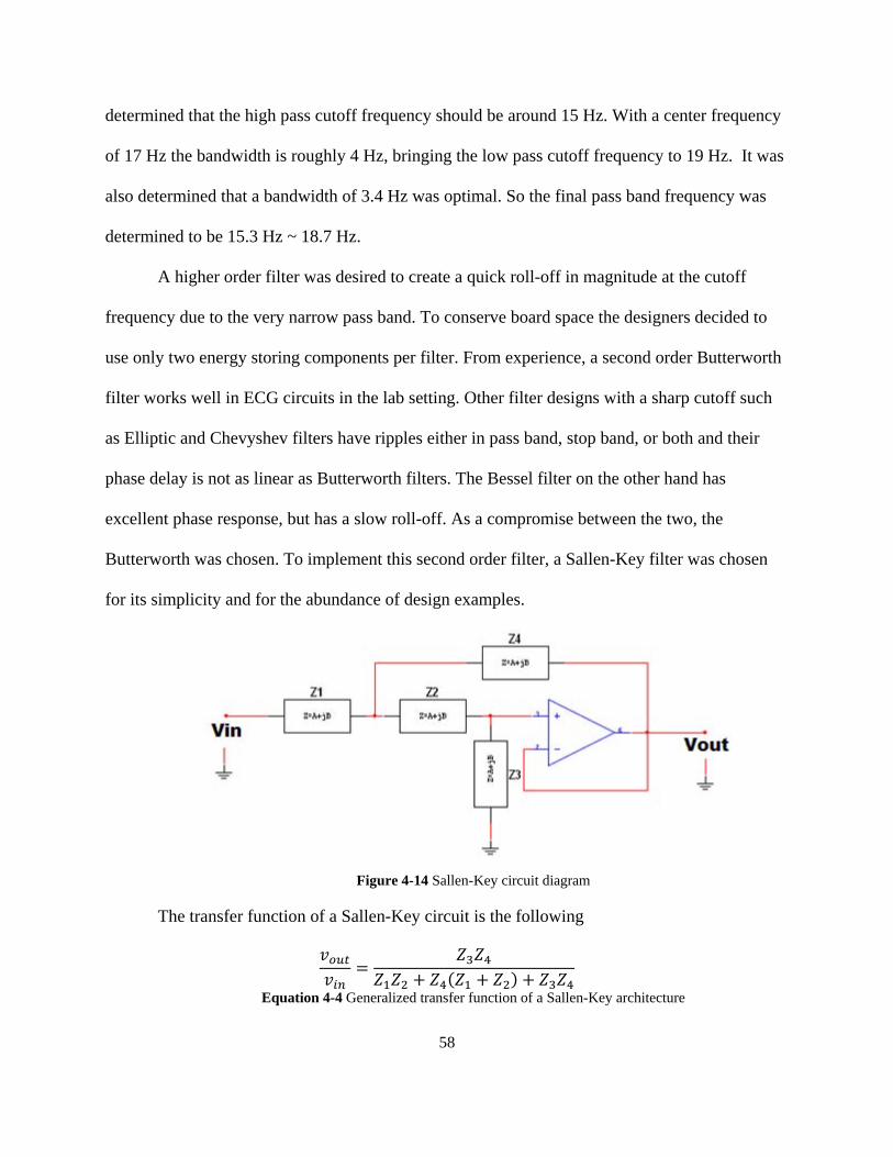
58
determined that the high pass cutoff frequency should be around 15 Hz. With a center frequency
of 17 Hz the bandwidth is roughly 4 Hz, bringing the low pass cutoff frequency to 19 Hz. It was
also determined that a bandwidth of 3.4 Hz was optimal. So the final pass band frequency was
determined to be 15.3 Hz ~ 18.7 Hz.
A higher order filter was desired to create a quick roll-off in magnitude at the cutoff
frequency due to the very narrow pass band. To conserve board space the designers decided to
use only two energy storing components per filter. From experience, a second order Butterworth
filter works well in ECG circuits in the lab setting. Other filter designs with a sharp cu f such
as Elliptic and Chevyshev filters have ripp
phase delay is not as linear as Butterworth filters. The Bessel filter on the other hand has
excellent phase response, but has a slow roll-off. As a compromise between the two, the
Butterworth was chosen. To implement this second order filter, a Sallen-Key filter was chosen
for its simplicity and for the abundance of design examples.
tof
les either in pass band, stop band, or both and their
Figure 4-14 Sallen-Key circuit diagram
The transfer function of a Sallen-Key circuit is the following
Equation 4-4 Generalized transfer function of a Sallen-Key architecture

59
If Za = Z1 = Z2 and Zb = Z3 = Z4, and since Za and Zb are either impedances of a resistor
or a capacitor ( and · ·
), the transfer function reduces to
2 · · · 2 · 1· ·
· 2 · 1
Equation 4-5 Simplified transfer function of a Sallen-Key architecture
In a low pass configuration the transfer function becomes
1
As it can be seen, the denominator of the Sallen-Key transfer function is symmetrical, s
changing the circuit configuration from low-pass to high-pass will still result in the same
denominator. However the numerator changes, making the high pass transfer function
·· 2 ·
Equation 4-6 Low pass filter transfer function
o
1
Equation 4-7 High pass filter transfer function
Looking at the transfer function, it is easily seen that the cutoff frequency of these two
filters is
1
12
Equation 4-8 Cutoff frequency
To match the desired cutoff frequencies (15.3Hz and 18.7Hz), the following values were
calculated.
alues
er
Table 4-1 ECG system main filter component v
High Pass Filter Low Pass FiltZ a C = 2.2μF R =3.9kΩZb R = 4.7kΩ C = 2.2μF fcutoff 15.39Hz 18.55Hz
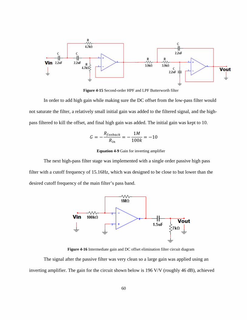
60
ig filter
In order to add hig he low-pass filter would
not saturate the filter, a rel ed signal, and the high-
pass fil
F ure 4-15 Second-order HPF and LPF Butterworth
h gain while making sure the DC offset from t
atively small initial gain was added to the filter
tered to kill the offset, and final high gain was added. The initial gain was kept to 10.
1100 10
Equation 4-9 Gain or inverting amplifier
filter stage was implemented with a single ord
cy of 15.16Hz, which was designed to be clos
f
The next high-pass er passive high pass
filter with a cutoff frequen
desired
Figure 4-16 uit diagram
The signal after the passive filt o pplied using an
inverting amplifier. The gain the ci below i roughly 46 dB), achieved
e to but lower than the
cutoff frequency of the main filter’s pass band.
Intermediate gain and DC offset elimination filter circ
er was very clean s a large gain was a
for rcuit shown s 196 V/V (

61
by an input resistance of 51 kΩ and an output resistance 1 MΩ. This brings the total gain of the
analog system to 21592 V/V (roughly 87 dB).
12 · 510
100 ·510510
1100
15.1
21961 87
r is
to create a digital pulse for eac icrocontroller to take in the
signal containing heart rate info og to digital conversion. The
digital pulse can simply trigger a d rtbeat. The MSP430F449
cannot recognize a voltage
comparator is powered with the same power system as the digital system, 0~3 V.
Figure 4-17 Final gain and comparator circuit diagram
Equation 4-10 Total gain for all circuitry
This amplified signal was fed into a comparator’s non-inverting input. The inverting
input of the comparator is made adjustable by a potentiometer. The purpose of the comparato
h heart beat. This would allow the m
rmation without conducting an anal
igital input interrupt to indicate a hea
less than 80% of the supplied power voltage. The digital system
operates at 3 V so the minimum input voltage required to register a logical high is 2.4 V. The
analog circuits are powered off of ±2 V so a logical high cannot be achieved. Therefore the final

62
i magnitude of a patient’s full body
accelerometry. The sys
f
The
direction will
yield signals below the DC offset level.
Table 4-2 Accelerometer system filter component values
4.5.2 Accelerometer Circuit
The designed accelerometer system obta ns the
tem descri t o be elow in re 4-19. p i n can seen b Figu
Figure 4-18 Flow chart for accelerometer signal acquisition and analog processing for a single channel X
Three separate signals representing the magnitude of applied acceleration as a function o
time in the X, Y, and Z directions in a three dimensional field are propagated to input buffers for
each signal. The input buffer’s high input impedance serves as a way to obtain the signal while
limiting current draw from the ADXL321 accelerometers and thus the system power supply.
accelerometer‘s output signal rides on a DC offset equivalent to ½ VCC. The ADXL321 sets a
reference direction for each axis it measures. Applied accelerations in the reference direction
will yield signals above the DC offset level, signals opposite to the chip’s reference

63
th a cutoff of 0.5 Hz is the stage after the input buffer.
The hig resent
lected frequency band.
The removal off the DC component was necessary as the signal needed to be rectified in the next
stage. In order to achieve this, the signal could not have a DC component. A description of
Sallen-Key filter architecture can be seen in Figure 4-15 and is described in section 4.5.1.
This section in the design description marks a good point to mention the selection of the
accelerometer system frequency band. As the entire system’s output will eventually represent the
total his
informa
an
a rectifier. The rectifier that was used in the team’s
design can be seen in Figure 4-20. The chosen rectifier was selected as it allowed the signal to
be rectified without attenuating or adding gain to the signal. The circuit’s positive attributes also
include simplicity as it only takes two operational amplifiers to build it. As the rectification
circuitry uses operational amplifiers as opposed to a transformer or diode bridge commonly seen
in some rectification designs the selected rectification circuit provided a cost effective way to
achieve the desired output.
A Sallen-Key high-pass filter wi
h pass filter was selected to come after the input buffer to eliminate the DC offset p
in the acceleration signals as well as set the high pass component of the se
magnitude of a patient’s full body accelerometry the frequency components pertinent to t
tion had to be isolated. Signal artifacts such as, but not limited to 60 Hz noise, fatty
tissue vibration when worn on a patient, and erroneous acceleration readings such as when a
patient is turning a corner in a car had to be rejected. A frequency band of 0.5 Hz ~ 3.5 Hz was
selected to meet the aforementioned design criteria. This frequency band was determined upon
from the research results of Sun and Hill et. al.53 The results of their study stated that human
motion is confined to the frequency band of 0.5Hz ~ 3.5 Hz. The component value selection c
be seen in Table 4-2. Use Figure 4.5.6 to reference schematic.
Following the s high-pass filter is
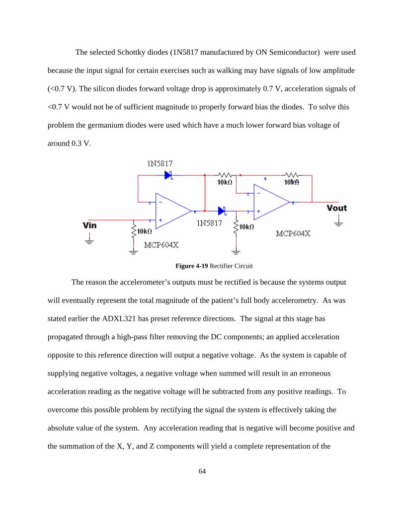
64
d
The reason the accelerometer’s outputs must be rectified is because the systems output
will eventually represent the total magnitude of the patient’s full body accelerometry. As was
l at this stage has
propagated through a high-pass filter removing the DC components; an applied acceleration
opposite to this reference direction will output a negative voltage. As the system is capable of
supplying negative voltages, a negative voltage when summed will result in an erroneous
acceleration reading as the negative voltage will be subtracted from any positive readings. To
absolute value of the system. Any acceleration reading that is negative will become positive and
the summation of the X, Y, and Z components will yield a complete representation of the
The selected Schottky diodes (1N5817 manufactured by ON Semiconductor) were use
because the input signal for certain exercises such as walking may have signals of low amplitude
(<0.7 V). The silicon diodes forward voltage drop is approximately 0.7 V, acceleration signals of
<0.7 V would not be of sufficient magnitude to properly forward bias the diodes. To solve this
problem the germanium diodes were used which have a much lower forward bias voltage of
around 0.3 V.
Figure 4-19 Rectifier Circuit
stated earlier the ADXL321 has preset reference directions. The signa
overcome this possible problem by rectifying the signal the system is effectively taking the
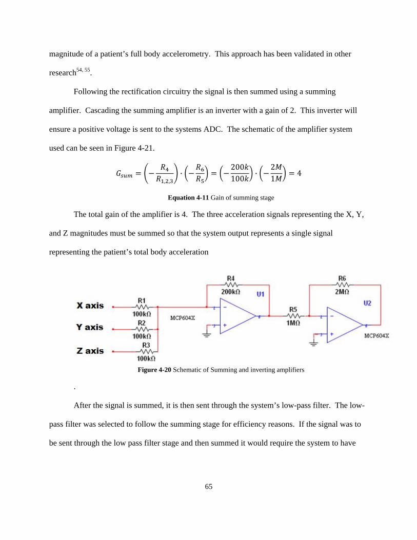
65
magnit
in Figure 4-21.
, ,
ude of a patient’s full body accelerometry. This approach has been validated in other
research54, 55.
Following the rectification circuitry the signal is then summed using a summing
amplifier. Cascading the summing amplifier is an inverter with a gain of 2. This inverter will
ensure a positive voltage is sent to the systems ADC. The schematic of the amplifier system
used can be seen
·200100 ·
21 4
Equation 4-11 Gain of summing stage
The total gain of the amplifier is 4. The three acceleration signals representing the X, Y,
and Z magnitudes must be summed so that the system output represents a single signal
representing the patient’s total body acceleration
-
to
Figure 4-20 Schematic of Summing and inverting amplifiers
.
After the signal is summed, it is then sent through the system’s low-pass filter. The low
pass filter was selected to follow the summing stage for efficiency reasons. If the signal was
be sent through the low pass filter stage and then summed it would require the system to have

66
w-
stem will only need one filter. This approach will conserve board space.
more
ty
s.
omain eliminated t d for additional components that
add cost and size to
4.5.3 Syste
by
powered from two 3.3 V lithium button
batteries connected in series to provide ±3.3V. This design would be inexpensive to implement
and be light weight. This final design did not work as the button batteries did not allow for drop-
out voltage which is needed for the voltage regulator to work, and another problem was that the
final device circuitry did not provide an adequate load to the turn on the devices. It simply did
not draw enough current. This problem was noticed too close to the deadline, so to correct this
problem a newly designed power system was built.
final power system design is powered by two 9 volt alkaline batteries. These
batteries, although bulky and heavy, were chosen
responsible for supplying the +2 V rail for the amplifiers and a +3 V rail responsible for
powering the system MSP430F449 microcontroller, the comparator at the final stage of the ECG
three low-pass filters for each axis signal. If the signal is summed and then sent thorough a lo
pass filter the sy
The systems analog to digital conversion and software integrator are described in
depth in section 4.6. The signal undergoes an integration stage at the end to yield a final quanti
that represents total body acceleration. An integrator can be created using analog component
However, integrating in the digital d he nee
the final design.
m Power
The team originally designed a power system around the KA317TU positive 1.5 A
voltage regulator and the KA337TU 1.5 A negative voltage regulator both manufactures
Fairchild Semiconductor. These devices would be
The
because they provide an inexpensive way to
power the device with sufficient headroom for drop-out. One battery is responsible for powering
the -2 V rail, which supplies negative voltage to 21 operational amplifiers. The other battery is

system, and the two ADXL321 accelerometers. The team took careful measures to design a low
power system by choosing proper components with power usage in mind the final system only
67
drew 3.
esistors. The two positive rails were created this way. The
can be seen in Figure 4-22.
68 mA. The current draw was so low that the system only required voltage regulators
capable of supplying small amounts of current. The chosen voltage regulator was the LM317LZ
manufactured by Fairchild Semiconductor. The LM317LZ is capable of supplying 100 mA of
current with a max drop-out voltage of 3 V over a range of 1.2 V ~ 30 V. The output voltage is
programmed by setting two external r
programmable circuit for the LM317LZ
One drawback of the LM317LZ is it cannot source negative voltages. In order to get a -2
V rail the +2 V rail was sent to an inverting amplifier as the input. The ±9 V batteries directly
powered a LM741 which was configured as an inverter. The resulting output was a -2 V rail that
could be used to power the system. The LM741 was chosen to for its ability to use higher
voltages and source more current than the MSP604X. The entire power system schematic can be
seen in Figure 4-23.
Figure 4-21 LM317LZ voltage regulator circuit (Courtesy of Fairchild Semiconductor)
68
1.25 1 ·
Equation 4-12 Adjustable regulated voltage equation
Figure 4-22 Schematic Diagram of Power System
4.6 Final Design System –Digital
The main function of the digital system is to take in the conditioned ECG and
accelerometer signals and display this information on the LCD screen. The main components of
this system are the heart rate calculator, accelerometer counter, and the display generator There
are two timers (
SP430F449, but Timer A is already used by the LCD driver. Because the LCD is used to
Timer A and Timer B, both maximum of 16-bit) available for use on a
M
69
display the output which is essen lected to keep track of internal
time. To maximize the resolut timer was utilized.
A resolution of 0.01 sec was needed for the purpose of calculating heart rate to a reasonable
level. This will be justified later on in this section.
The SMCLK was selected as the clock source. The SMCLK oscillates at a frequency 32
times faster (1.04 MHz) than the ACLK (32768 Hz). At the ACLK frequency with a resolution
of 10 msec, the Timer B interrupt service routine needs to be triggered every 327.68 clock ticks.
However clock ticks can only happen in integer numbers, so the ISR must be programmed to
trigger every 328 clock cycles. This rounding will accumulate and cause error in the time. The
error is 0.32 clock ticks for every 10 msec. By the time the Timer B ISR counts up to 1025x10
msec= 10.25 seconds, there is an error of 10 msec, or a full time resolution.
328 10
tial to the device, Timer B was se
ion of the time the full 16-bit capability of the
327.68 10
0.32 10
328 0.32 1025 10.25
Equation 4-13 Clock error at ACLK frequency
However, because the oscillation frequency of 1.04 MHz is close to an integer power of
10, the timer will have a higher ion, accuracy over time. Repeating the calculat
10486 10
10485.7610
0.24 10
10486 0.24 43692 437
Equation 4-14 Clock error at SMCLK frequency
Changing the clock frequency improved the error to 10 msec for every 437 sec, compar
previous 10.25 sec.
edto the

70
Figure 4-23 Flow chart of celerometer system and the digital signal from the EC
4.6.1 Heart Rate Ca
The algorithm to calculate the heart rate uses the time in between two QRS wave cycles.
Every time the microcontroller sees a high to low transition on port 2 pin 0, in which the ECG
circuit, an interrupt uses the current
time to be recorded s the difference
the time since the last t
the digita anal rom the acG syste
l software which takes in the og signal fm and displays the calculated results
lculator
occurs. The digital input interrupt service routine simply ca
on to a va s n calculate
ime a h
riable and sound a buzzer beep. It the
eart beat occurred.
60
Equation 4-15 Heart rate calculation algorithm

71
The advantage of this algorithm is that most recent heart beat can be obtained every heart
beat. This gives a more accurate measurement than counting the number of heart beat over a
short time interval and calculating the heart rate. For example, let us assume the heart rate is 60
bpm. HRA calculates by counting the number of heart beats over 15 sec and multiplying the
number with 4.HRB takes the average of all the heart rates calculated over the 15 sec epoch. The
following equations represent the two algorithms, where N stands for the number of heart beats
that occurred in the epoch.
4
∑ 60
Equation 4-16 Two different heart rate calculation algorithms
In the case of HRA, the error associated with it is a multiple of 4, meaning a small
dependent upon the number of consecutive heart beats missed. If a single heart beat was missed,
ne of the heart rate measurements will read 30 bpm. Averaging the heart rates over 15-1=14
heart beats, the calculated HR is 57.9 bpm. This results in highly accurate heart rate calculation.
More in general, where M represents the number of consecutive heart beats missed,
miscount will result in a large error. However, the worst case error associated with HRB is
o
· 1 2 ·1
Equation 4-17 Error associated with
uperiority of th
heart rate calculation algorithm
When compared on a graph, the s e second algorithm is obvious.
72
Figure 4-24 The x-axis represents the num cutively by the ECG system. The y-axis represents the calculated HR. The actual H in this plot is 60 bpm.
Since time can only be kept iscr ents, heart rate can also only be
calcula f 10
t
ce to say for
now that the HR opposite is
true at low HRs.
r
frequency, and since the activity les do not make sudden changes, high sampling frequency was
0
10
20
30
40
50
60
70
0 1 2 3 4 5 6
HR_A
HR_B
ber of heart beats missed conseR used for the error calculation
track in d ete increm
ted in discrete increments. Below is a graph of the possible HRs with a resolution o
msec. The higher the heart rate, the higher the error will be when the actual HR is compared with
the calculated HR. However the slope of the curve gets flatter and flatter as the HR decreases,
indicating improved accuracy at lower HRs. Error at higher HRs will also not cause significan
error in energy expenditure calculation due to the algorithm used to do the energy expenditure
calculation. The algorithm will be covered more extensively later on, but it will suffi
information is weighted less when the calculated HR is high. The
4.6.2 Accelerometer Counter Since the final analog signal from the accelerometer system is composed of lowe

y = 60x‐1R² = 1
0
50
100
150
200
250
300
350
0 0.5 1 1.5 2 2.5
Figure 4-25 The x-axis represents the time interval between two consecutive heart beats. The y-axis represents the calculated HR.
73
not nec the
Equation 4-18 ADC resolution
les for 15 sec and output the average value. Since the
size of ount,
became integer values.
essary. The ADC sample rate was set to 1 Hz. This was done by creating a counter in
Timer B ISR that counts up to 1 second and then turns on the ADC configured for single
conversion. After each conversion, the value is bit-wise ANDed with 0x0FFF. This is to make
sure that there are no random bits other than the 12-bits of actual conversion data. The 12-bit
ADC of the MSP430F449 operating with a 0~3 V will have a resolution of roughly 732 µV/bit.
The device was set to obtain samp
the screen only allowed for a 3-digit numeral to be displayed for an accelerometer c
the voltage value was multiplied by 100 so that the first 3 highest orders of the voltage value

74
. 0 0800 2048 · 732 1.499 150
Equation 4-19 Accelerometer count conversion
4.6.3 Display Generator
To display numeric values on the LCD screen, the numeric value must be converted to
hex ASCII code. This is simply done by cycling through each digit and adding 48. The main
program multiplexes through the heart rate and acceleration count displays. In fact, this is the
only role the main function has and the rest of the functions are implemented in the various ISR.
By only deviating from the main program flow when a new input is detected, it eliminates
polling if user interface inputs are to be added to the software.
4.7 Implementation of the Stages
To minimize the size and weight of the device as well as insuring a rugged design for a
high acceleration application, a printed circuit board (PCB) was an ideal option. The final board
that was designed was a 4 layer board with a ground layer and a power layer which the team
used as its +2 V rail. For the +3 V and -2 V rails copper fill layers were added to the two
external layers. Using the schematic capture and PCB layout tools provided to us by
PCBexpress.com the team generated the schematic file and PCB board. The final designs can be
seen in the appendix.
The team encountered problems with the manufactured PCB. The problem that was
found occurred whenever the IC labeled U7 was added to the PCB. When the IC was introduced
to the board, the PCB would draw large amount of current, heating the board. After looking over
the PCB design and talking with the engineers at PCBexpress.com it was concluded the error
arose due to a manufacturing error. As the team was under a limited budget and running out of
time, a quick and cost effective solution had to be implemented. The solution that was arrived

75
upon was to use an add y that didn’t work on
the PCB.
nnect the various systems together were constructed. The
digital
d.
c casing. Both analog boards
board was placed outside the case to make
e LC
Tri-
gging
rt rate to predict energy expenditure isn’t always accurate. “In the range
where r
itional through-hole board to implement the circuitr
Several wire interfaces to co
system was already complete in the form of an Olimex development board, so the only
thing required was to make jumper wires to connect the analog system to the digital system.
Some more jumper wires were made for connecting the accelerometer chips to the analog boar
The ECG leads manufactured by BioPac did not come with female connectors, so a customized
connector was created to interface the leads with the analog system.
To house the systems electronics we used a small plasti
were placed inside the case, and the digital Olimex
th D screen visible. This entire case was then placed on a belt so the patient would be able
to wear the device.
4.8 Algorithm Adjustment
Both methods of accelerometry and heart rate have their strengths and weaknesses.
axial accelerometers have a tendency to overestimate activities such as walking and jo
while they underestimate activities such as stair climbing, stationary cycling, and arm
ergometry56. Using hea
esting and working heart rates overlap (typically between 80 and 110 beats/min) the
prediction of energy expenditure from heart rate is uncertain and this is precisely where the heart
rate of most people engaged in light activity is encountered Also a variety of factors (such as
meals, change in posture, and cigarette smoking) affect heart rate proportionally more than
energy expenditure”57. To reduce the error from these factors, the design utilizes the ActiHeart
algorithm in which the relative contribution of the activity counts and heart rate are dependent
76
y counts during light activity and heart rate during heavy activity.
t
ke,
burned are from low
intensit
Figure 4-26 The relative contribution of muscle glycogen, plasma glucose, plasma free fatty
reliance of glucose and glycogen increases as exercise intensity increases. Therefore, individuals
The existing ActiHeart algorithm is shown below in Table 4-3. The ActiHeart outputs a
reading in terms of calories per kilogram per minute. An ideal activity monitor for diabetics
upon the type of activity. From the table in section 2.5, one can see the algorithm is dependent
upon activit
As previously mentioned in section Table 2-6, one of the drawbacks of the ActiHeart
algorithm is that it expresses energy expenditure in terms of calories burned. Due to the fact tha
many diabetic individuals make adjustment to their insulin based upon their carbohydrate inta
it is desired to have an activity monitor that will output carbohydrates burned. Figure 3-1 below
demonstrates that as exercise intensity increases, an individual tends to burn more carbohydrates
and less fat. During low intensity activities, 30% of the carbohydrates
y sources. As exercise intensity increases the percentage of calories burned from
carbohydrates can increase to 70%7. Additionally, each gram of carbohydrate burned is equal to
4 calories.
acids, and other fat sources during exercises of various intensity. The percentage of the body’s
burn more carbohydrates and less fat as exercise intensity increases58.

77
t, the user’s weight
will be
-1
tput in terms of total carbohydrates, the microprocessor will determine the
carbohydrates per minute being burned once every 15 seconds. This number will be divided by
four and will be added to the total of all of the previous intervals.
The same algorithm was implemented in the MQP device. Two different sets of code
were written for the digital system. Both are very similar with the only difference being the
output display. The first set of code had the ActiHeart algorithm implemented to calculate the
energy expenditure. And by using the information mentioned in the background, this energy
expenditure was converted into carbs burnt. However, a carbs-burnt-display will not allow the
team to tell which part of the system failed with merely a carbs-burnt display. Therefore, this
code w
should output a reading in terms of total carbohydrates burned throughout the day. In order to
accomplish this, there must be several adjustments made to the algorithm. Firs
input into the algorithm so that the output isn’t in terms of calories per kilogram per
minute but it is now in terms of calories per minute. When <25 counts min-1 and HRaS <23
beats min-1, it is estimated that 30% of the calories burned are from carbohydrates. Therefore, the
total number of calories/min will be multiplied by 0.30 and then divided by four because there
are 4 calories in one gram of carbohydrate. When HRaS is between 23 and 80 beats min-1, it is
estimated that 50% of the calories burned are from carbohydrates and when >25 counts min
and HRaS ≥80 beats min-1, it is estimated that 70% of the calories burned are from
carbohydrates. The output of the algorithm is now in terms of carbohydrates per minute. Finally,
to get the ou
team to debug the system. If the system failed to correctly measure the heart rate and
accelerometer counts contributing to an inaccurate carbs-burnt display, there is no way for the
as not used in the device. The second code displays the heart rate and the accelerometer
count, which can be used to compare against the ActiHeart results.

78
accelerometer counts. The activity algorithm changes when the accelerometer counts exceed 133 counts per minute
years .
Table 4-3 The ActiHeart algorithm is composed of two separate algorithms - one for heart rate and one for
Abbreviations: AEE, activity energy expenditure; HRaS, heart rate above sleep. Sex: 0=female, 1=male, age is in 48
Activity algorithm (AEE, kcals kg-1 min-1)
<133 counts min-1 0.203 · 133 0.75 · 83 · 46
133·
4186.8
≥133 counts min -1 0.203 · 0.75 · 83 · 464186.8
Heart rate algorithm (AEE, kcals kg-1 min-1)
HRaS <23 beats min-1 5.95 · 0.23 · 84 · 13423
·4186.8
HRaS ≥23 beats min -1 5.95 · 0.23 · 84 ·4186.8
134
Combined activity and heart rate algorithm (AEE, kcals kg-1 min-1)
<25 counts min and -1
HRaS <23 beats min-1 0.1 · 0.9 ·
HRaS between 23 and 80 beats min -1 0.5 · 0.5 ·
>25 counts min-1 and HRaS ≥80 beats min -1 0.9 · 0.1 ·
4.1 Device Housing
Completing the device design was the device housing. The circuitry for the ECG and full
body accelerometry acquisition were housed inside a case. The case was fixed to a belt worn
around the user's waist. The Olimex board was placed on the outside of the case to allow for
power connections and easy access to read the output of the LCD display. The accelerometer
chips were also fixed to the case to ensure stability for the chips, thus eliminating any extraneous
movement should the circuit boards move within the device. Finally, the two 9V batteries
powering the system were fixed to the bottom of the device. The final device can be seen in
Figure 4-28.
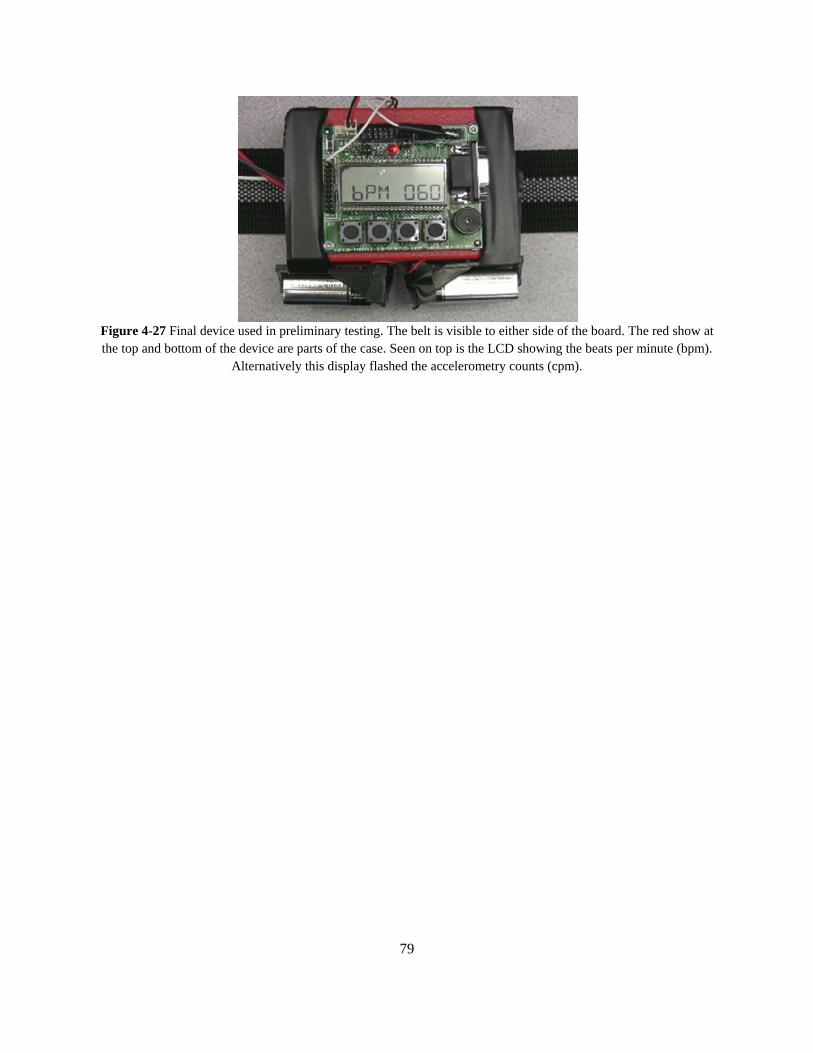
79
Figure the top and bottom of the device are parts of the c
y this display
ng. The belt is visible to either side of the board. The red show at ase. Seen on top is the LCD showing the beats per minute (bpm). flash
4-27 Final device used in preliminary testi
Alternativel ed the accelerometry counts (cpm).

80
5 System Functionality Testing and Results
To see if the entire device works as intended, primary components that make up the
device, namely the ECG circuit, the accelerometry circuit and the digital unit, were tested.
5.1 ECG Circuit Testing
The filter response was tested at frequencies ranging from 10 Hz to 26 Hz and the results
are plotted below. The red lines indicate the intended cutoff frequencies and the green line
i
slope after the pass band, because the addition of the extra passive filter effectively made a third
rder high pass filter. However, another observation that can be made is that the -3 dB drop does
occur at the desired frequencies normalized to the peak magnitude. This is probably is related to
the bandwidth. The narrowness of the bandwidth does not allow the magnitude to achieve
maximum gain as the frequency increases before it starts to get attenuated again by the low pass
filter.
Figure 5-1 Frequency response of the band- pass filter. The red lines indicate target cutoff frequencies and the green line indicates the center frequency. -3dB drop does not occur at the cutoff frequencies relative to the achieved peak magnitude at the center frequency.
ndicates the center frequency. The slope of the before the pass band is steeper compared to the
o
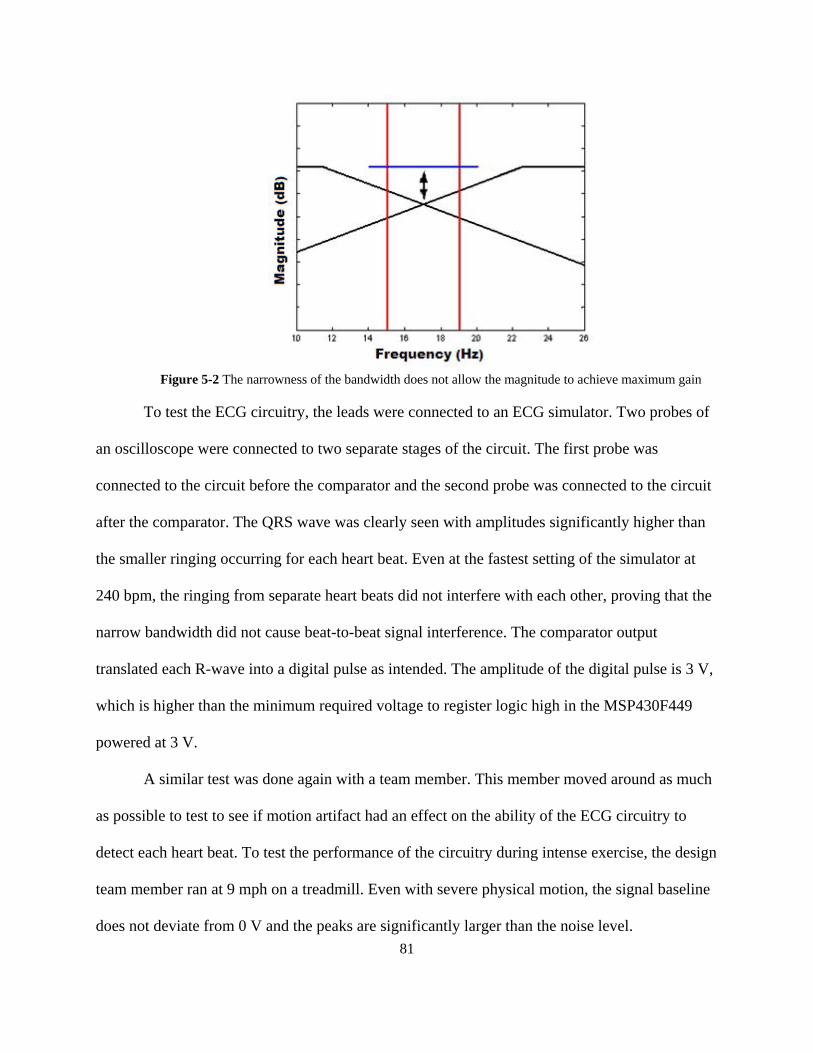
81
ircuit
rring for each heart beat. Even at the fastest setting of the simulator at
240 bpm, the ringing from separate heart beats did not interfere with each other, proving that the
narrow bandwidth did not cause beat-to-beat signal interference. The comparator output
translated each R-wave into a digital pulse as intended. The amplitude of the digital pulse is 3 V,
which is higher than the minimum required voltage to register logic high in the MSP430F449
powered at 3 V.
A similar test was done again with a team member. This member moved around as much
as possible to test to see if motion artifact had an effect on the ability of the ECG circuitry to
a treadmill. Even with severe physical motion, the signal baseline
does not deviate from 0 V and the peaks are significantly larger than the noise level.
Figure 5-2 The narrowness of the bandwidth does not allow the magnitude to achieve maximum gain
To test the ECG circuitry, the leads were connected to an ECG simulator. Two probes of
an oscilloscope were connected to two separate stages of the circuit. The first probe was
connected to the circuit before the comparator and the second probe was connected to the c
after the comparator. The QRS wave was clearly seen with amplitudes significantly higher than
the smaller ringing occu
detect each heart beat. To test the performance of the circuitry during intense exercise, the design
team member ran at 9 mph on
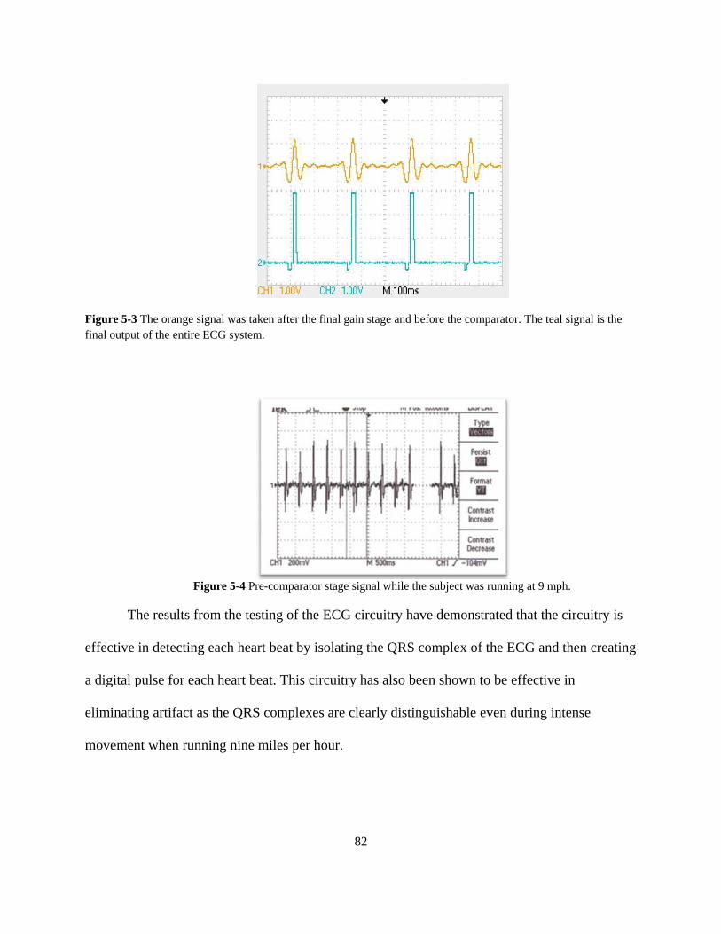
82
Figure 5-3 The orange signal was taken after the final gain stage and before the comparator. The teal signal is the final output
t beat by isolating the QRS complex of the ECG and then creating
a digital pu
of the entire ECG system.
Figure 5-4 Pre-comparator stage signal while the subject was running at 9 mph.
The results from the testing of the ECG circuitry have demonstrated that the circuitry is
effective in detecting each hear
lse for each heart beat. This circuitry has also been shown to be effective in
eliminating artifact as the QRS complexes are clearly distinguishable even during intense
movement when running nine miles per hour.

83
5.2 Accelerometry Circuit Testing
To test the accelerometer circuit, an oscilloscope probe was placed at the output of the
rectifier. A 1.5 Hz sinusoid with amplitude of 1 V was used as a simulated accelerometer signal.
The amplitude of the ripples after the rectifier was equal for all axes and full-wave rectification
was also confirmed by the lack of flat line signals. Next the summer output was examined. At
constant frequency and at constant amplitude, the output was a constant voltage. When the
ied, the output voltage settled at different voltages.
5.3 Digital Design Testing
Testing of the digital system requires testing to determine if the system accurately
displays the heart rate and acceleration of an individual wearing the device. This process
involves ensuring that the method used to calculate the heart rate through measuring the R-wave
intervals was accurate, and also that the ADC accurately converted the analog output of the
summer from the accelerometer circuit into a 12-bit digital signal.
To test the h ect of the digital system, the software creates an audible beep
each tim
scope.
he
, the analog to digital converter was
tested. A known DC voltage was applied to the input of the ADC, and this voltage value was
frequency and amplitude was var
eart rate asp
e a heart beat is detected. The ECG leads of the device were connected to the ECG
simulator. An oscilloscope probe was connected before the comparator to monitor each heart
beat. The beeps occurred simultaneously as the QRS wave cycle appeared on the oscillo
Additionally, it was confirmed that the heart rate displayed on the digital device matched t
setting of the ECG simulator.
To test the accelerometer aspect of the digital system

84
compared against the calculated voltage (Figure 5-5). The slope is very close to 100, which
he output was scaled y 100 due to the fact
at the LCD screen could only output 3 digits.) The two values were very similar and linearly
correlated, but slight systematic offset was observed. This may have been due to rounding error
or a dc offset occurring in the analog system. Regardless, this offset is not as relevant for the
proof of concept device since the accelerometry count is an arbitrary count proportional to the
magnitude of movement.
Figure 5-5 ADC output counts against actual voltage
would mean the relationship is very close to linear (T
th
y = 101R²
.97x + 0.3393 = 0.9996
0
200
2.00 2.50
50
100
150
0.00 0.50 1.00 1.50
250
85
6 Device Validation Study
To determine that the device functions as an activity monitor, a proof of concept study
was conducted. This study was based on a study conducted using the ActiHeart described
previously in this report. This comparative ActiHeart study involved putting the MQP device on
subjects and asking them to participate in several activities for a period of five minutes. The data
was then gathered in beats per minute (bpm) for the ECG acquisition and counts per minute
(cpm) for the accelerometry acquisition. For each activity the average bpm and the average cpm
were given in the published paper previously.
6.1 Study Approval
Before conducting this study approval was needed from the WPI Institutional Review
Board (IRB). To gain approval and application was assembled along with the written protocol, a
written consent form, and a case report form. These four forms were submitted to the chair of the
IRB, Professor Kent Rissmiller, and to the office of Research Administration at WPI. The
documents were reviewed and returned with comments for edits. These comments included
typographical errors, adjustme ents
more clear, and questions regarding logistics of the study. These errors were corrected and the
questions were answered satisfactorily. Approval for this study was then granted and the study
could proceed. To follow the procedures set forth by the WPI IRB only a consent form stamped
by the office of Research and Administration could be used. A copy of each of these four
documents can be seen in the Appendix of this document.
nts in the protocol and consent form to make the two docum

86
6.2 Conducting the Study
Participants for this study were recruited from the WPI Undergraduate Student Body. 11
females and 12 males volunteered to participate in the study. To begin a group member of the
same gender as the study participant would enter the WPI locker rooms in Alumni Gymnasium
and assist the participant in placing the three electrodes on the torso. Once this was done the
participant returned to the area of the study and the leads of the device were connected to the
electrodes. The device belt was adjusted to fit the subject orienting the device just behind the left
hip. The subject was asked to move around to be sure the belt holding the device was tight
enough. The study could then begin. First the subject lay on the floor for five minutes to
rt rate data was verified using a pulse oximeter from the WPI
BME d
to the
s
int up the stairs. The five minute
rst step. After four minutes of activity the
accelerometry count per minute and the beats per minute were gathered from the device and
establish a base heart rate. This hea
epartment. Once this data was collected the first activity period could begin.
The protocol for this study was outlined to test the subject on a treadmill, establish a post
activity period activity level, test the subject with common household chores, and complete a
second post activity period activity level. Because of the electrodes this project was limited
order of the activity periods were switched when conducting the study to ensure the electrode
would stay on for the duration of the study. If the study had been conducted in the order outlined
in the study protocol, the sweating induced from walking and running on the treadmill would
interfere with the data acquisition in the second activity period.
The subject was asked to begin the activity period by ascending and descending the stairs
in the testing area. The subjects were instructed to use the stairs as they would if they were
headed to class on time. They were all instructed not to spr
period began when the subject stepped up the fi

87
. These two pieces of data were gathered while the
subject
e
ctivity
because the
dishes
e
t
deposited the correct sheet in
the cor
om the
recorded on the subject’s case report form
was still participating in the activity to ensure the data corresponded to the activity and
not the period immediately following the activity period. After an additional minute the subject
was instructed to stop. This process was repeated for an additional four activities.
The subject began the activity and the activity time was started. After four minutes the
two pieces of data were collected while the subject continued to participate in the activity. The
activity was complete one minute later. The second activity in this period was sweeping. The
subject was given a broom as asked to sweep the test area. Each of the subjects started in on
area of the room and progressed across the area until the end of the test period. The next a
was washing dishes. A sponge and common household dishes were placed on a surface at
approximately waist height. The subjects were instructed to simulate washing dishes
were clean and no water was involved. Following this activity the subject filed papers. 52
pieces of paper were printed. Half of this set was labeled with the 26 letters of the alphabet, on
letter per page, and the other half was labeled with the numbers 1-26, one letter on each sheet.
These pages were all mixed together. Two filing baskets were placed at opposite ends of the tes
area. One basket had 25 folders, one for each letter with letters “Y” and “Z” in the same folder.
The second basket had 25 folders, one for each of the numbers with numbers “25” and “26” in
the same folder. The subject walked between the two baskets and
rect folder. To complete the activity period the subject stood still for the five minute
duration.
After the tasks were completed, the subject sat down and the pulse oximeter was then
placed on the same finger as in the pre-activity period. The heart rate was then recorded fr

88
ked
egan to walk
at 3.1 m .
e.
s
investigational device discussed in this report and from the pulse oximeter. Questions were as
of the subject regarding comfort and ease of use.
Beginning the next activity period the accelerometry counts and heart rate was recorded
while the subject was still sitting. The subject was then moved to a treadmill and b
ph. Again, after four minutes the heart rate and the accelerometry counts were recorded
The subject then continued to walk for an additional minute. The speed of the treadmill was
increased to 3.8 mph to simulate a fast walk. Again, the measurement time period was the sam
Finally, the speed of the treadmill was increased to 5.9 mph to bring the subject to a run. Again
the measurements were taken after four minutes and the subject completed the activity after an
additional one minute.
To complete the study, the subject was again instructed to sit. The pulse oximeter was
placed on the same finger for a third time and the heart rate was recorded from the
investigational device and the pulse oximeter. For the final time, the subject was also asked if
any discomfort or skin discoloration had occurred. The device was removed and the subject wa
thanked for volunteering for the study. Within two days, the study participant was asked a series
of follow up questions. The data collected from this study can be seen in the following chapter.

89
7 Device Testing Results
Once the device data was collected it was organized according to activity. These
activities, discussed in chapter 6 of this report, were chosen because of their use in the ActiHeart
study. The ten activities chosen were, in the order presented in the figure below, resting, sitting,
standing, filing papers, washing dished, slow walking (3.1 mph), sweeping, fast walking (3.8
mph), ascending/descending stairs, and running (5.9 mph). For each activity the average heart
rate and the average accelerometry from the 23 study participants was found as well as the
standard deviation for this data. To determine the average for each activity the data from each of
the 23 participants was placed in a table in excel and the average and the standard deviation were
found. This table of raw data as well as the table of averages and standard deviations for each
activity can be seen in Appendix C. After calculating the averages, the data was graphically
compared to the ActiHeart averages published in the study discussed previously in this report.
This ActiHeart study was the foundation of the study for the device discussed in this report.
Therefore the two sets of data were able to be compared. These comparisons can be seen in
Figures 7-1 and 7-2.
After doing an initial comparison of the accelerometry data, a linear correlation was
found. By multiplying the investigational device data by 50, the data points followed the path of
the data from the ActiHeart device. This new comparison can be seen in Figure 7-3
90
volunteers from the WPI undergraduate student body; 11 females and 12 males. The data shown here corresponds to ),
Figure 7-2 The comparison of average accelerometry counts shows that for each activity the device in this report and the ActiHeart device have some linear correlation. The ActiHeart accelerometry counts are much larger so in order to show the ActiHeart counts on the same graph a secondary Y-axis to the right of the chart was implemented. The investigational device data corresponds to primary Y-axis to the left of the chart. The numbers in the X-Axis correspond to the activities in Table 7-1 summarized here: 1 resting, 2 sitting, 3 standing, 4 filing papers, 5 washing dishes, 6 slow walking (3.1 mph), 7 sweeping, 8 fast walking (3.8 mph), 9 ascending/descending stairs, and 10 running (5.9 mph). Data acquired with this study came from 23 volunteers from the WPI undergraduate student body; 11 females and 12 males.
Investigational Device
Figure 7-1 The comparison of average heart rate shows that the acquisition from the device discussed in this report is similar to the ActiHeart device. The numbers in the X-Axis correspond to the activities in Table 7-1. The data for the ActiHeart was acquired from a published study and the data for the investigational device was acquired from 23
the following activities: 1 resting, 2 sitting, 3 standing, 4 filing papers, 5 washing dishes, 6 slow walking (3.1 mph7 sweeping, 8 fast walking (3.8 mph), 9 ascending/descending stairs, and 10 running (5.9 mph)
40
60
100
120
140
0 1 2 3 4 5 6 7 8 9 10 11
(bpm
)
Activity
80
160
Average
HeartRa
te
RatesComparison of Heart ActiHeart
‐500
0
500
‐10
0
10
Accelerom
etry Count Average
1000
1500
2000
30
40
0 1 2 3 4 5 6 7 8 9 10 11
(ActiH
eart,cpm) A
ccelerom
etry
(Investigation
al
Activity
2500
20
50
Average C
ounts
Device,cpm)
Comparison of Accelerometry Counts Investigational DeviceActiHeart
91
anding, 4 filing papers, 5 washing dishes, 6 slow walking (3.1 mph), 7 sweeping, 8 fast walking (3.8 mph), 9 ascending/descending stairs, and 10 running (5.9 mph). Data acquired with this study ame from 23 volunteers from the WPI undergraduate student body; 11 females and 12 males.
Table 7-1 Table of activities and the corresponding numbers shown in Figures 7-1 and 7-2
Number on Chart
Activity in Study
Figure 7-3 Comparison of average accelerometer counts when the counts of the investigational device were multiplied by 50, the linear correlation between the investigational device data and the ActiHeart data. The numbers in the X-Axis correspond to the activities in Table 7-1 summarized here: 1 resting, 2 sitting, 3 st
‐500
0
500
1000
1500
2000
2500
0 1 2 3 4 5 6 7 8 9 10 11
Average
Accelerom
etry Cou
nts
(Investigation
al Device,cpm)
Investigational DeviceComparison of Accelerometry Counts
ActiHeart
Activity
c
1 Resting 2 Sitting 3 Standing 4 Filing Papers 5 Washing Dishes 6 Slow Walk (3.1 mph) 7 Sweeping 8 Fast Walk (3.8 mph) 9 Ascending/Descending Stairs 10 Running (5.9 mph)
92
8 Analysis and Discussion of Device Testing
After completing the study to verify that the activity monitor described in this paper is
equivalent to the ActiHeart device the data acquired from the study was compared to the data
given in the ActiHeart study. When the average heart rate of the investigational device was
compared to the average heart rate published in the study using the ActiHeart device, the data
was within one standard deviation of one another. Because of this the data can be considered
statistically similar. The discrepancies seen in Figure 7-1 are the four activities that correspond to
the least amount of activity. The heightened heart rate acquired with the investigational device
s
e.
s were
believed to be
For accelerome e data acquired onal device and from the
ActiHeart device are very sim acquired while running, the data
points are within one standard deviation of one another and can be considered statistically
similar. The difference in accelerometry coun d to the change in the location of
the accelerometer. The accelero ter in the A ted on the chest close to the
left shoulder. The acceleromete r the inves lower back behind
the left hip. When the data poin r each act s they are in Figures 6-2 and
6-3, a specific line shape is formed. This line follows that as activities grow in intensity, the data
points rise. This shape can be in both the given ActiHeart data and the data acquired with the
investigational device. This also allows for the conclusion that these devices are similar and the
can be attributed to the population of the study participants. For the study conducted for thi
project, the study participants were WPI undergraduate students, many of whom rarely exercis
The participant population in the ActiHeart study was slightly older and the participant
more active than the WPI students tested.
try counts, th
ila
from the investigati
r. With the exception of data
ts can be attribute
me ctiHeart device is loca
r fo tigational device is worn on the
ts fo ivity are connected, a

93
algorithm used to calculate calories with the ActiHeart device can also be used for the
investigational device.

94
9 Conclusions
The intension of this project was to design, build, and test a device to be implemented by
a diabetic individual to quantify his activity level. After designing, building, and testing this
device it can be deduced that this device can serve as an activity monitor. Because of the
correlation between the results from the study on the investigational device and the ActiHeart
device study results, this device has been shown to accurately measure heart rate and full body
accelerometry. Additionally, the pulse oximeter used during the study confirms the ability of the
device to precisely measure the heart rate of the user. The similarities between the two devices
allows for the implementation of the ActiHeart algorithm to calculate caloric burn. Then, based
on prior research, this can be converted to carbohydrate burn.
With the implementation of the algorithm to calculate caloric and then carbohydrate burn,
a diabetic individual will be able to read this information from the device. She will then know in
real time the amount of energy used when carrying out the daily activities of her life. With this
new information the diabetic user will be able to adjust her insulin dosing and her eating habits
to better reflect her activity level and the subsequent energy usage from the activities she
participates in from day to day. This method of accounting for energy output as well as energy
input will allow the diabetic individual to more closely control their glycemic levels at all times.
Though the device outlined in this report is only a preliminary prototype, the results are
very promising. Extensive research reveals no device currently marketed to diabetic persons for
the purpose of measuring activity. With this device, a diabetic individual will be able to quantify
the amount of activity he performs throughout the day and will be able to adjust his insulin

95
dosing, eating, and exercising habits to better care for himself. In doing this, a diabetic person
i l a life of much higher quality. w ll e d a

96
ototype to a marketable device will require some
commended will contribute to reducing the size of the device,
improving the user interface including outputting the amount of carbohydrates used for a given
activity or set of activities, or allowing the device to become more efficient either in power
supply and signal processing.
The largest obstacle encountered in this project was the partial malfunction of the printed
circuit board. Because the board had technical problems that were outside the scope of this
project an additional board was needed to replace the malfunctioning portions of the board. This
additional board used standard components and therefore added significant bulk to the circuitry.
By solving this problem with the PCB the size of the device would be reduced.
Size could also be reduced by incorporating additional digital signal processing. This will
reduced the number of analog components required and reduce board space. Another advantage
to digital signal processing is the plasticity of the system. For example, time required conducting
experiments with different cutoff frequencies and gains will be significantly reduced. This will
allow future MQP groups to build on the project with efficiency, making improvements over
improvements without having to design a whole new system.
Improving the power system will also benefit the user. Currently the circuit requires three
different voltages for various parts of the circuitry. The majority of the circuitry runs on ±2V,
while the accelerometer chips, the microprocessor, and the comparator require 0-3V. Each of
these voltages requires a voltage regulation and the negative voltage rail creates a need for a
second battery package. If the entire system could be powered by a single rail, only one battery
package and one voltage regulator circuit would be needed. Also the device should be improved
10 Recommendations
Converting this device from a pr
changes. Many of the changes re

97
arger 9V battery implemented in this prototype design.
All thes
e
reen
ould allow the user to read off all the information he needs at a
single g
d for the general
purpose
to use coin cell batteries instead of the l
e improvements on the power system will greatly reduce device weight and size.
The screen used for this device only allowed for limited information to be displayed. Th
outputs had to be multiplexed, the output digits were limited, and a 7-segment display is not the
easiest output to read. Therefore the next generation device should have an un-segmented sc
with larger display area. This w
lance.
Finally, by implementing wireless communication, this device would be able to
wirelessly transmit information and possess data logging capabilities, allowing the device to
reach full potential. Doctors would then be able to monitor their patient off site, reducing a
number of doctor visits for the diabetic individuals. The device could also be use
of monitoring health status of the elderly.

98
References
1. Diabetes Statistics. December 2006. 2 September 2007. 2. Diabetes. Public Health. Kansas City, Missouri: Community Health Assessment,
3. Ong, Yong Yau. "Clinical Approach to Medicine (2nd Edition)." River Edge, NJ:
4. Reviewed: Funnell, Martha. Four Steps to Control Your Diabetes.
2006.
USA: World Scientific Publishing Company, 2004. 270. October 2006.
5. Tight Diabetes Control.September 2007 <http://www.ndep.nih.gov/diabetes/control/4Steps.htm#Step3>.
2007. September 2007 <http://www.diabetes.org/type-1-
6. National Diabetes Information Clearinghouse. Diabetes Control and diabetes/tight-control.jsp>.
Complications Trial. 1983-1993. 10 November 2007 <http://diabetes.niddk.nih.gov/dm/pubs/statistics/>.
oaster.7. Walsh, John, Ruth Roberts and Lois Jovanovic-Peterson. Stop the Rollerc
rs San Diego, California: Torrey Pines Press, 1996.
8. Puyau, Maurice, et al. "Validation and Calibration of Physical Activity Monitoin Children." Obesity Research 10.3 (2002): 150-158.
9. Sayers, George. Insulin. 2007. Grolier Online. 24 November 2007 <http://ea.grolier.com/cgi-bin/article?assetid=0215870-00>.
10. Ryan, James. "Physiology: PretTest Seff-Assessment and Review." Blacklick, OH: McGraw-Hill Professional, 2002. 43.
11. Tuch, Bernard. "Diabetes Research:CRC Press, 2000. 1-14.
A Guide for Postgraduates." London, UK:
12. Bassett, Steven. "Anatomy and Physiology." Hoboken, NJ: John Wiley & Sons, Incorporated, 2005. 211.
13. Hall, Gwen. "Providing Diabetes Care in General Practice (5th Edition)." London, UK: Class Publishing, 2007. 311.
14. National Diabetes Statistics. November 2005. National Institutes of Health National Institue of Diabetes and Digestive and Kidney Disease. 10 November 2007 <http://diabetes.niddk.nih.gov/dm/pubs/statistics/>.
15. Saudek, Christopher. Johns Hopkins guide to Diabetes: For Today and Tomorrow. Baltimore, MD: The Johns Hopkins University Press, 1997.
16. American Diabetes Association. Diabetes Information. 2007. 5 November 2007 <http://www.diabetes.org/about-diabetes.jsp>.
17. Chen, Yue and Yang Mao. "Obesity and Leisure Time Physical Activity Among Canadians." Preventive Medicine 42.4 (2006): 261-265.
18. Polar USA. Official Polar US Website. 2007. 8 September 2007 <http://www.polarusa.com>.
19. Tudor-Loske, Catrine. Taking Steps toward Increased Physical Activity: using Pedometers to Measure and Motivate. Washington, DC: President's Council on Physical Fitness and Sports Research Digest, 2002.
20. Eston, RG, AV Rowlands and DK Ingledew. "Validity of heart rate, pedometry, and accelerometry for predicting the energy cost of children's activities." Journal of Applied Physiology (1998).

99
lectricity." Encyclopedia Americana21. "Piezoe 2007. 2. Yamax. The Yamax Digiwalker Pedometer.2 2005. New Lifestyle. 12 October
gineering, LLC. The Anatomy of a Pedometer.
2007 <http://www.new-lifestyles.com/DIGIWALKER/FlashEnabled/index_flash.html>.
23. JSC En 2004. 30 November 2007. 24. Apple. Apple - Nike + iPod - Gear. 2008. 14 January 2008
<http://www.apple.com/ipod/nike/gear.html>. 25. National Institutes of Health. Clinical Trials. 2007. 17 December 2007
<http://www.clinicaltrials.gov>. 26. Caltrac Calorie Counter. 19 June 2001. 1 September 2007
<http://www.muscledynamics.net/caltrac/index2.html>. validation
sical Therapy27. Balogun, Joseph, Daniel Martin and Martha Clendenin. "Calorimetric
of the Caltra accelerometer during level walking." Phy 69.6 (1989):
rans Biomed Eng.
501-510. 28. Bouten, CV, et al. "A triaxial acceleromter and protable data processing unit for
the assessment of daily physical activity." IEEE T 44.3 (1997):
d heart rate and movement 136-147.
29. Brage, S, et al. "Reliability and validity of the combinesensor ActiHeart." European Journal of Clinical Nutrition 59.4 (200
30. MiniMitter. 5): 561-570.
ActiHeart. 5 September 2007 <http://www.minimitter.com/Products/Actiheart/index.html>.
31. Ceesay, SM, et al. "The use of heart rate monitoring in the estimation of energy expenditure: a validation study using indirect whole-body calorimetry." British Journal of Nutrition 61 (1983): 175-186.
32. Panel on Macronutrients (CB). Dietary Reference Intakes for Energy, Carbohydrate, Fiber, Fat, Fatty Acids, Cholesterol, Protein, and Amino Acids (Macronutrients). Washington, DC: National Academies Press, 2005.
33. "Metabolism." Grolier Multimedia Encyclopedia. Ed. Aaron Freedman. Grolier
Online, 2007.
34. "An insulin index of foods: the insulin demand generated by 1000-kJ portions ofcommon foods." American Journal of Clinical Nutrition 66 (1997): 1264-1276.
35. Lewis, Carol. "Insulin Preparations." FDA Consumer Magazine January2002.
-February
36. Beaser, Richard. Joslin Guide to Diabetes (2nd Edition). New York, NY: Firesid1995.
e,
J
37. Evans, Josie, et al. "Frequency of blood glucose mintoring in relation to glycemiccontrol: observational study with diabetes database." BM 319.7202 (1999): 83-
l Activity in U.S. Adults With Diabetes and At 86.
38. Morrato, Elaine, et al. "PhysicaRisk for Developing Diabetes." Diabetes Care 30 (2007): 203-209
39. "Noninsulin-Dependent Diabetes." (1997). 40. Diabetes and Insulin: Calculating Carb to Insulin Ratio. 2007. 17 January 2008
<http://www.bddiabetes.com/US/main.aspx?cat=1&id=303>. 41. Conditions and Treatment. 2007. January 2008 < http://www.diabetes.org/type-1-
diabetes/treatment-conditions.jsp>.

100
rd. "Estimated Benefits of s of
42. Vijan, Sandeep, Timothy Hofer and Rodney HaywaGlycemic Control in Microvascular Complications in Type 2 Diabetes." AnnalInternal Medicine 127 (1
43. "Implications of the Diabetes Control and Complications Trial." 997): 788-795.
iabetes CareD 26
t disease risk in erosis risk in communities study."
(2003): S25-S27. 44. Selvin, Coresch, et al. "Glycemic control and coronary hear
persons with and without diabetes: the atherosclArchives of Internal Medicine 165.16 (2005): 1910-1916.
45. Brancati, Frederick. "Resolving the Glucose Response Curve: the Underestimated al of Managed CareImportance of Postprandial Glucose." The American Journ 6
(2000): s1082-s1088. 46. Rov, Savon and Tsuvoshi Sato. "Role of Vascular Basement Membrane
Components in Diabetic Microangiopathy." Drug News and Perspectives 2.91 (2000).
47. Berne, Robert. Physiology (5th Edition). Student Consult: Physiology (5th Edition). Elsevier, 2004.
48. Crouter, SE, JR Churilla and DR Bassett. "Accuracy of the Actiheart for the Assessment of Energy Expenditure in Adults." European Journal of Clinical Nutrition (2007).
49. Jovanovic-Peterson, Lois. ExCarbs, a New Way of Control through Exercise. 1 July 1995. 8 November 2007 <http://www.diabeteshealth.com/read/1995/07/01/397.htm>.
50. Diabetes Service, Inc. Table 1: Excarbs. 2007. December 2007 <http://www.diabetesnet.com/diabetes_control_tips/table1.php>
51. Thakor, NV, JG Webster and WJ Tompkins. "Optimal QRS detector." Medical and Biological Engineering p. 343-50.
52. Thakor, NV, JG Webster and WJ Tompkins. "Estimation of QRS complex power spectra for design of a QRS filter." IEEE Trans. Biomed. Eng BME-31 p. 702-705.
53. Sun, M and JO Hill. "A method for measuring mechanical work and work efficiency during human activities." Biomechanics 26 p. 229-241
54. Mathie, MJ, et al. "A specification for a home telecare system for patients with congestive heart failure."Proc. 10th Int. Conf. on Biomedical Engineering.
WW and R Williams. "Fully proportional actigraphy: a new instrument." Singapore, 2000
55. Tryon,Behav. Res. Methods Instrum Comput 28 p. 392-403
56. Campbell, KL, PRE Crocker and DC McKenzie. "Field evaluation of energy expenditure in women using Tritrac accelerometers." Med. Sci. Sports. Exerc.
rgy n. Rev. Nutr.
34.10 (2002): 1667-1674. 57. Jdquier, Eric, Kevin Acheson and Yves Schutz. "Assessment of ene
expenditure and fuel utilization in man." An (1987): 187-208. 58. vanLoon, Luc, et al. "The effects of increasing exercise intensity on muscle fuel
utilization in humans." Journal of Physiology 536 (2001): 295-304.

101
Appen rd layout
Appendix C: Institutional Review Board application including the application, protocol, sample r
AppenAppen
deviceAppendix G: Digital Code for the device
Comb
Appendices
dix A: Circuit Schematic and Printed Circuit BoaAppendix B: Specification sheets for circuitry components used in the device
case report form, and the approved consent form. Institutional Review Board approval lettedix D: Case report forms from the proof of concept study conducted during this project dix E: Raw data acquired using the project device
Appendix F: Averages and standard deviations for each activity in the study. Both the MQP acquisitions and the ActiHeart acquisitions found in the research are presented
Appendix H: A Proposed Guide for Individuals Living with Type I Diabetes: Using the ined Heart Rate and Accelerometer Activity Monitor to Improve Glycemic Control

Appendix A: Circuit Schematic and Printed Circuit Board Layout

Circ
uit S
chem
atic
late
r lin
ked
with
the
PCB
layo
ut so
ftwar
e
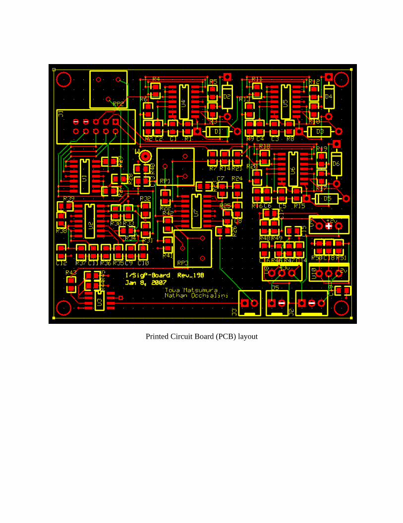
Printed Circuit Board (PCB) layout

Appendix B: Specification Sheets for Device Components
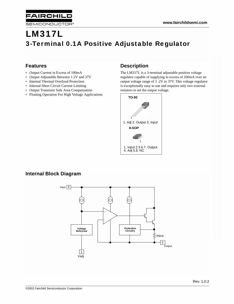
©2002 Fairchild Semiconductor Corporation
www.fairchildsemi.com
Rev. 1.0.2
Features• Output Current in Excess of 100mA• Output Adjustable Between 1.2V and 37V• Internal Thermal Overload Protection• Internal Short Circuit Current Limiting• Output Transistor Safe Area Compensation• Floating Operation For High Voltage Applications
DescriptionThe LM317L is a 3-terminal adjustable positive voltage regulator capable of supplying in excess of 100mA over an output voltage range of 1 .2V to 37V. This voltage regulator is exceptionally easy to use and requires only two external resistors to set the output voltage.
TO-92
1. Adj 2. Output 3. Input1
1
8-SOP
1. Input 2.3.6.7. Output 4. Adj 5.8. NC
Internal Block Diagram
Rlimit
3Vin
Vo
1
VoltageReference
Vadj
2
ProtectionCircuitry
+
-
Input
Output
LM317L3-Terminal 0.1A Positive Adjustable Regulator

LM317L
2
Absolute Maximum Ratings
Electrical Characteristics(VI - VO = 5V, IO = 40mA, 0°C ≤ TJ ≤ +125°C, PDMAX = 625mW, unless otherwise specified)
• Load and Line regulation are specified at constant junction temperature. Change in VO due to heating effects must be taken into account separately. Pulse testing with low duty cycle is used.
Parameter Symbol Value UnitInput-Output Voltage Differential VI - VO 40 VPower Dissipation PD Internally limited WOperating Junction Temperature Range Tj 0 ~ +125 °CStorage Temperature Range TSTG -65 ~+125 °C
Parameter Symbol Conditions Min. Typ. Max. Unit
*Line Regulation RlineTA = +25°C3V ≤ VI − VO ≤ 40V - 0.01 0.04 %/V3V ≤ VI − VO ≤ 40V - 0.02 0.07
*Load Regulation Rloal
TA = +25°C10mA ≤ IO ≤100mAVO ≤ 5VVO ≥5V
- 50.1
250.5
mV%/ VO
10mA ≤ IO ≤ 100mAVO ≤ 5VVO ≥ 5V
- 200.3
701.5
mV%/ VO
Adjustment Pin Current IADJ - - 50 100 µA
Adjustment Pin Current Change ∆IADJ3V ≤ VI - VO ≤ 40V10mA ≤ IO ≤ 100mAPD < PDMAX
- 0.2 5 µA
Reference Voltage VREF3V < VI - VO <40V10mA ≤ IO ≤100mAPD ≤ PDMAX
1.20 1.25 1.30 V
Temperature Stability STT - - 0.7 - %Minimum Load Current to Maintain Regulation IL(MIN) VI - VO = 40V - 3.5 10 mA
Maximum output CurrentIO(MAX)
VI - VO ≤ 15V, PD < PDMAX 100 200 - mA
VI - VO ≤ 40VPD < PDMAX, TA = +25°C 25 50 -
RMS Noise, % of VOUT eN TA =+ 25°C, 10Hz < f <10KHz - 0.003 - %/ VO
Ripple Rejection RRVO = 10V, f = 120Hzwithout CADJCADJ = 10uF
66 6580
- dB
Long-Term Stability ST TJ = +125 °C, 1000 Hours - 0.3 - %

LM317L
3
Typical Application
Figure 1. 5V Electronic Shutdown Regulator
D1 protects the device during an input short circuit.
Figure 2. Slow Turn-On Regulator
Figure 3. Current Regulator
LM317LInput
Output
LM317LInput Output
LM317LInput
Output
LM317L
4
Mechanical DimensionsPackage
0.46 ±0.10
1.27TYP
(R2.29)
3.86
MA
X
[1.27 ±0.20]
1.27TYP
[1.27 ±0.20]
3.60 ±0.20
14.4
7 ±0
.40
1.02
±0.
10
(0.2
5)4.
58 ±
0.20
4.58+0.25–0.15
0.38+0.10–0.05
0.38
+0.1
0–0
.05
TO-92
LM317L
5
Mechanical Dimensions (Continued)
Package
8-SOP
4.92
±0.
20
0.19
4 ±0
.008
0.41
±0.
10
0.01
6 ±0
.004
1.27
0.05
0
5.720.225
1.55 ±0.20
0.061 ±0.008
0.1~0.250.004~0.001
6.00 ±0.30
0.236 ±0.012
3.95 ±0.20
0.156 ±0.008
0.50 ±0.20
0.020 ±0.008
5.13
0.20
2M
AX
#1
#4 #5
0~8°
#8
0.56
0.02
2(
)
1.800.071
MA
X0.
10M
AX
0.00
4
MAX
MIN
+0.10
-0.050.15
+0.004
-0.0020.006

LM317L
6
Ordering InformationProduct Number Package Operating Temperature
LM317LZ TO-920°C to + 125°C
LM317LM 8-SOP

LM317L
7

LM317L
3/5/02 0.0m 001Stock#DSxxxxxxxx
2002 Fairchild Semiconductor Corporation
LIFE SUPPORT POLICY FAIRCHILD’S PRODUCTS ARE NOT AUTHORIZED FOR USE AS CRITICAL COMPONENTS IN LIFE SUPPORT DEVICES OR SYSTEMS WITHOUT THE EXPRESS WRITTEN APPROVAL OF THE PRESIDENT OF FAIRCHILD SEMICONDUCTOR CORPORATION. As used herein:
1. Life support devices or systems are devices or systems which, (a) are intended for surgical implant into the body, or (b) support or sustain life, and (c) whose failure to perform when properly used in accordance with instructions for use provided in the labeling, can be reasonably expected to result in a significant injury of the user.
2. A critical component in any component of a life support device or system whose failure to perform can be reasonably expected to cause the failure of the life support device or system, or to affect its safety or effectiveness.
www.fairchildsemi.com
DISCLAIMER FAIRCHILD SEMICONDUCTOR RESERVES THE RIGHT TO MAKE CHANGES WITHOUT FURTHER NOTICE TO ANY PRODUCTS HEREIN TO IMPROVE RELIABILITY, FUNCTION OR DESIGN. FAIRCHILD DOES NOT ASSUME ANY LIABILITY ARISING OUT OF THE APPLICATION OR USE OF ANY PRODUCT OR CIRCUIT DESCRIBED HEREIN; NEITHER DOES IT CONVEY ANY LICENSE UNDER ITS PATENT RIGHTS, NOR THE RIGHTS OF OTHERS.

This datasheet has been download from:
www.datasheetcatalog.com
Datasheets for electronics components.

2002 Microchip Technology Inc. DS21669B-page 1
M MCP6041/2/3/4
Features• Low Quiescent Current: 600 nA/Amplifier (typ)• Rail-to-Rail Input: -0.3 V to VDD+0.3 V (max)• Rail-to-Rail Output:
VSS+10 mV to VDD-10 mV (max)• Gain Bandwidth Product: 14 kHz (typ)• Wide Supply Voltage Range: 1.4 V to 5.5 V (max)• Unity Gain Stable• Available in Single, Dual and Quad• Chip Select (CS) with MCP6043• 5-lead SOT-23 package (MCP6041 only)
Applications• Toll Booth Tags• Wearable Products• Temperature Measurement• Battery Powered
Available Tools• Spice macro models (at www.microchip.com)• FilterLab® Software (at www.microchip.com)
Package Types
DescriptionThe MCP6041/2/3/4 family of operational amplifiersfrom Microchip Technology, Inc. operate with a singlesupply voltage as low as 1.4 V, while drawing less than1 µA (max) of quiescent current per amplifier. Thesedevices are also designed to support rail-to-rail inputand output operation. This combination of features sup-ports battery-powered and portable applications.
The MCP6041/2/3/4 amplifiers have a typical gainbandwidth product of 14 kHz (typ) and are unity gainstable. These specs make these operational amplifiersappropriate for low frequency applications, such asbattery current monitoring and sensor conditioning.The MCP6041/2/3/4 family operational amplifiers areoffered in single (MCP6041), single with a Chip Select(CS) feature (MCP6043), dual (MCP6042) and quad(MCP6044) configurations. The MCP6041 device isavailable in the 5-lead SOT-23 package.
Typical Application
+IN-IN
VSS
VDDOUT
1234
8765
-+
NC
NCNC
+INA-INA
VSS
1234
8765
-OUTA
+ -+A
B
VDD
OUTB-INB+INB
+IN-IN
VSS
VDDOUT
1234
8765
-+
NC
CSNC
+INA1-INA1
VSS
1234
14131211
-OUTA
+ -+A D
VDD
OUTD-IND+IND
1098
567OUTB1
-INB+INB +INC
-INC
OUTC
+-B C-+
MCP6041PDIP, SOIC, MSOP
MCP6042PDIP, SOIC, MSOP
MCP6043PDIP, SOIC, MSOP
MCP6044PDIP, SOIC, TSSOP
MCP6041SOT-23-5
VDD
+IN
1
2
3
5
-IN
VSS
OUT
4
-+
VDD
10 Ω MCP604X
100 kΩ
1 MΩ
VDD
IDD
+2.5 Vto
5.5 V
VSS
High Side Battery Current Sensor
600 nA, Rail-to-Rail Input/Output Op Amps

MCP6041/2/3/4
DS21669B-page 2 2002 Microchip Technology Inc.
1.0 ELECTRICAL CHARACTERISTICS
1.1 Maximum Ratings*VDD - VSS ......................................................................................7.0 VAll inputs and outputs................................... VSS –0.3 V to VDD +0.3 VDifference Input voltage ..................................................... |VDD - VSS|Output Short Circuit Current ...............................................continuousCurrent at Input Pins ..................................................................±2 mACurrent at Output and Supply Pins ..........................................±30 mAStorage temperature ...................................................-65°C to +150°CAmbient temp. with power applied ..............................-55°C to +125°CESD protection on all pins (HBM).....................................................≥ 4 kV*Notice: Stresses above those listed under “Maximum Ratings” maycause permanent damage to the device. This is a stress rating only andfunctional operation of the device at those or any other conditionsabove those indicated in the operational listings of this specification isnot implied. Exposure to maximum rating conditions for extended peri-ods may affect device reliability.
PIN FUNCTION TABLE
MCP6041/2/3/4 DC ELECTRICAL SPECIFICATIONS
Name Function+IN/+INA/+INB/+INC/+IND Non-inverting Inputs-IN/-INA/-INB/-INC/-IND Inverting InputsVDD Positive Power SupplyVSS Negative Power SupplyOUT/OUTA/OUTB/OUTC/OUTD OutputsCS Chip Select
NC No internal connection to IC
Electrical Characteristics: Unless otherwise indicated, all limits are specified for VDD = +1.4 V to +5.5 V, VSS = GND, TA = 25 °C, VCM = VDD/2, RL = 1 MΩ to VDD/2, and VOUT ~ VDD/2
Parameters Sym Min Typ Max Units Conditions
Input Offset: VCM = VSS
Input Offset Voltage VOS -3.0 — +3.0 mVDrift with Temperature ∆VOS/∆T — ±1.5 — µV/°C TA= -40°C to+85°CPower Supply Rejection PSRR 70 85 — dB
Input Bias Current and Impedance:Input Bias Current IB — 1.0 — pAInput Bias Current Over Temperature IB — — 100 pA TA= -40°C to+85°Input Offset Current IOS — 1.0 — pACommon Mode Input Impedance ZCM — 1013||6 — Ω||pFDifferential Input Impedance ZDIFF — 1013||6 — Ω||pF
Common Mode:Common-Mode Input Range VCMR VSS−0.3 — VDD+0.3 VCommon-Mode Rejection Ratio CMRR 62 80 — dB VDD = 5 V,
VCM = -0.3 V to 5.3 V 60 75 — dB VDD = 5 V,
VCM = 2.5 V to 5.3 V 60 80 — dB VDD = 5 V,
VCM = -0.3 V to 2.5 V
Open Loop Gain:DC Open Loop Gain (large signal) AOL 95 115 — dB RL = 50 kΩ to VDD/2,
100 mV < VOUT < (VDD − 100 mV)
Output:Maximum Output Voltage Swing VOL, VOH VSS + 10 — VDD − 10 mV RL = 50 kΩ to VDD/2Linear Region Output Voltage Swing VOVR VSS + 100 — VDD − 100 mV RL = 50 kΩ to VDD/2,
AOL ≥ 95 dBOutput Short Circuit Current IO — 21 — mA VOUT = 2.5 V, VDD = 5 V
Power Supply:Supply Voltage VDD 1.4 — 5.5 VQuiescent Current per amplifier IQ 0.3 0.6 1.0 µA IO = 0
2002 Microchip Technology Inc. DS21669B-page 3
MCP6041/2/3/4MCP6041/2/3/4 AC ELECTRICAL SPECIFICATIONS
SPECIFICATIONS FOR MCP6043 CHIP SELECT FEATURE
MCP6041/2/3/4 TEMPERATURE SPECIFICATIONS
Electrical Characteristics: Unless otherwise indicated, all limits are specified for VDD = +5 V, VSS = GND, TA = 25 °C,VCM = VDD/2, RL = 1 MΩ to VDD/2, CL = 60 pF, and VOUT ~ VDD/2
Parameters Sym Min Typ Max Units ConditionsGain Bandwidth Product GBWP — 14 — kHzSlew Rate SR — 3.0 — V/msPhase Margin PM — 65 — ° G = +1Input Voltage Noise En — 5.0 — µVp-p f = 0.1 Hz to 10 HzInput Voltage Noise Density en — 170 — nV/√Hz f = 1 kHzInput Current Noise Density in — 0.6 — fA/√Hz f = 1 kHz
Electrical Characteristics: Unless otherwise indicated, all limits are specified for VDD = +1.4 V to +5.5 V, VSS = GND, TA = 25 °C, VCM = VDD/2, RL = 1 MΩ to VDD/2, CL = 60 pF, and VOUT ~ VDD/2
Parameters Sym Min Typ Max Units Conditions
CS Low Specifications:CS Logic Threshold, Low VIL VSS — VSS + 0.3 V For entire VDD range
CS Input Current, Low ICSL — 5.0 — pA CS = VSS
CS High Specifications:CS Logic Threshold, High VIH VDD - 0.3 — VDD V For entire VDD range
CS Input Current, High ICSH — 5.0 — pA CS = VDD
CS Input High, GND Current IQ — 20 — pA CS = VDD
Amplifier Output Leakage, CS High — 20 — pA CS = VDD
Dynamic Specifications:CS Low to Amplifier Output High Turn-on Time
tON — 2.0 50 ms CS low = VSS + 0.3 V, G = +1 V/V,VOUT = 0.9 VDD/2
CS High to Amplifier Output High Z tOFF — 10 — µs CS high = VDD - 0.3 V, G = +1 V/VVOUT = 0.1 VDD/2
Hysteresis VHYST — 0.6 — V VDD = 5 V
Electrical Characteristics: Unless otherwise indicated, all limits are specified for VDD = +1.4 V to +5.5 V, VSS = GNDParameters Symbol Min Typ Max Units Conditions
Temperature Ranges:Specified Temperature Range TA -40 — +85 °COperating Temperature Range TA -40 — +125 °C Note 1Storage Temperature Range TA -65 — +150 °C
Thermal Package Resistances:Thermal Resistance, 5L-SOT23 θJA — 256 — °C/W
Thermal Resistance, 8L-PDIP θJA — 85 — °C/W
Thermal Resistance, 8L-SOIC θJA — 163 — °C/W
Thermal Resistance, 8L-MSOP θJA — 206 — °C/W
Thermal Resistance, 14L-PDIP θJA — 70 — °C/W
Thermal Resistance, 14L-SOIC θJA — 120 — °C/W
Thermal Resistance, 14L-TSSOP θJA — 100 — °C/WNote 1: The MCP6041/2/3/4 family of op amps operates over this extended range, but with reduced performance.
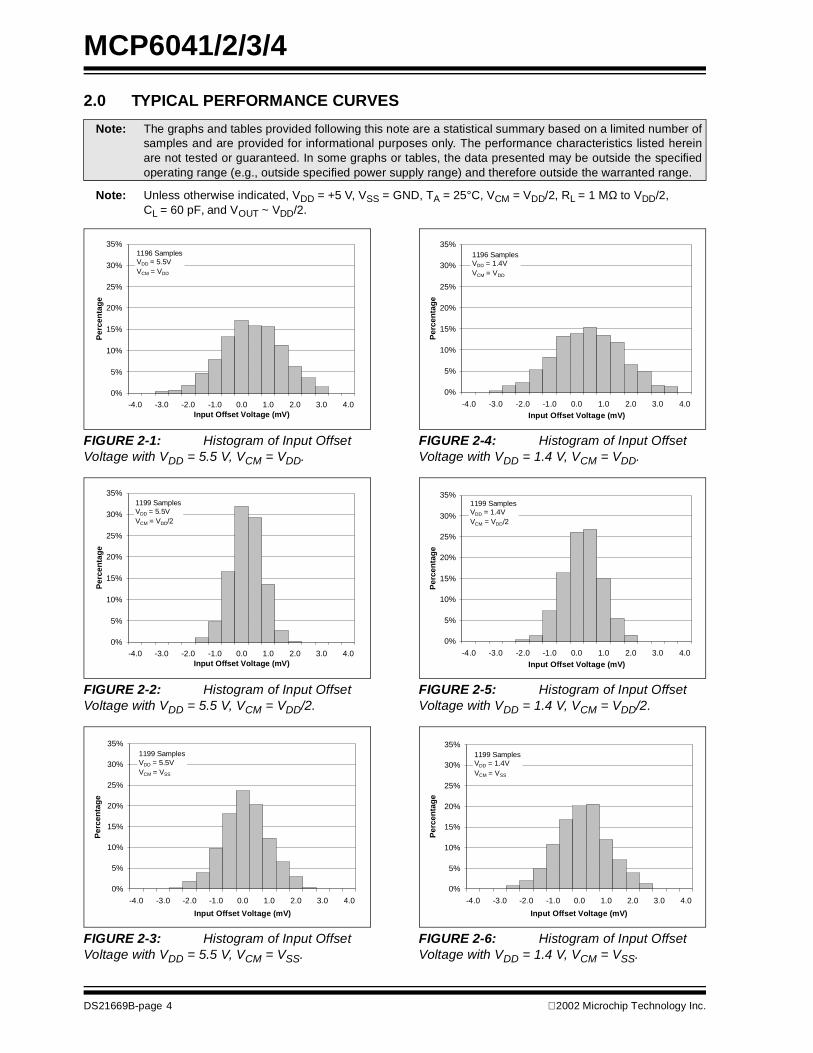
MCP6041/2/3/4
DS21669B-page 4 2002 Microchip Technology Inc.
2.0 TYPICAL PERFORMANCE CURVES
Note: Unless otherwise indicated, VDD = +5 V, VSS = GND, TA = 25°C, VCM = VDD/2, RL = 1 MΩ to VDD/2, CL = 60 pF, and VOUT ~ VDD/2.
FIGURE 2-1: Histogram of Input Offset Voltage with VDD = 5.5 V, VCM = VDD.
FIGURE 2-2: Histogram of Input Offset Voltage with VDD = 5.5 V, VCM = VDD/2.
FIGURE 2-3: Histogram of Input Offset Voltage with VDD = 5.5 V, VCM = VSS.
FIGURE 2-4: Histogram of Input Offset Voltage with VDD = 1.4 V, VCM = VDD.
FIGURE 2-5: Histogram of Input Offset Voltage with VDD = 1.4 V, VCM = VDD/2.
FIGURE 2-6: Histogram of Input Offset Voltage with VDD = 1.4 V, VCM = VSS.
Note: The graphs and tables provided following this note are a statistical summary based on a limited number ofsamples and are provided for informational purposes only. The performance characteristics listed hereinare not tested or guaranteed. In some graphs or tables, the data presented may be outside the specifiedoperating range (e.g., outside specified power supply range) and therefore outside the warranted range.
0%
5%
10%
15%
20%
25%
30%
35%
-4.0 -3.0 -2.0 -1.0 0.0 1.0 2.0 3.0 4.0Input Offset Voltage (mV)
Perc
enta
ge
1196 SamplesVDD = 5.5VVCM = VDD
0%
5%
10%
15%
20%
25%
30%
35%
-4.0 -3.0 -2.0 -1.0 0.0 1.0 2.0 3.0 4.0Input Offset Voltage (mV)
Perc
enta
ge
1199 SamplesVDD = 5.5VVCM = VDD/2
0%
5%
10%
15%
20%
25%
30%
35%
-4.0 -3.0 -2.0 -1.0 0.0 1.0 2.0 3.0 4.0Input Offset Voltage (mV)
Perc
enta
ge
1199 SamplesVDD = 5.5VVCM = VSS
0%
5%
10%
15%
20%
25%
30%
35%
-4.0 -3.0 -2.0 -1.0 0.0 1.0 2.0 3.0 4.0Input Offset Voltage (mV)
Perc
enta
ge
1196 SamplesVDD = 1.4VVCM = VDD
0%
5%
10%
15%
20%
25%
30%
35%
-4.0 -3.0 -2.0 -1.0 0.0 1.0 2.0 3.0 4.0Input Offset Voltage (mV)
Perc
enta
ge
1199 SamplesVDD = 1.4VVCM = VDD/2
0%
5%
10%
15%
20%
25%
30%
35%
-4.0 -3.0 -2.0 -1.0 0.0 1.0 2.0 3.0 4.0Input Offset Voltage (mV)
Perc
enta
ge
1199 SamplesVDD = 1.4VVCM = VSS

2002 Microchip Technology Inc. DS21669B-page 5
MCP6041/2/3/4Note: Unless otherwise indicated, VDD = +5 V, VSS = GND, TA = 25°C, VCM = VDD/2, RL = 1 MΩ to VDD/2,
CL = 60 pF, and VOUT ~ VDD/2.
FIGURE 2-7: Histogram of Input Offset Voltage Drift with VDD = 5.5 V, VCM = VDD/2.
FIGURE 2-8: Histogram of Input Offset Voltage Drift with VDD = 5.5 V, VCM = VSS.
FIGURE 2-9: Histogram of Input Offset Voltage Drift with VDD = 1.4 V, VCM = VSS.
FIGURE 2-10: Input Offset Voltage vs. Common Mode Input Voltage vs. Temperature with VDD = 5.5 V.
FIGURE 2-11: Input Offset Voltage vs. Common Mode Input Voltage vs. Temperature with VDD = 1.4 V.
FIGURE 2-12: Input Offset Voltage vs. Output Voltage vs. Power Supply Voltage.
0%
5%
10%
15%
20%
25%
30%
35%-1
0 -8 -6 -4 -2 0 2 4 6 8 10
Input Offset Voltage Drift (µV/°C)
Perc
enta
ge
1176 SamplesVDD = 5.5VVCM = VDD/2
0%
5%
10%
15%
20%
25%
30%
35%
-10 -8 -6 -4 -2 0 2 4 6 8 10
Input Offset Voltage Drift (µV/°C)
Perc
enta
ge
1143 SamplesVDD = 5.5VVCM = VSS
0%
5%
10%
15%
20%
25%
30%
35%
-10 -8 -6 -4 -2 0 2 4 6 8 10
Input Offset Voltage Drift (µV/°C)
Perc
enta
ge
1124 SamplesVDD = 1.4VVCM = VSS
-400
-300
-200
-100
0
100
200
300
400
-0.5 0.0 0.5 1.0 1.5 2.0 2.5 3.0 3.5 4.0 4.5 5.0 5.5 6.0Common Mode Input Voltage (V)
Inpu
t Offs
et V
olta
ge (µ
V)
TA = -40°C
VDD = 5.5V
TA = +25°CTA = +85°C
TA = -40°CTA = +25°CTA = +85°C
-1000
-800
-600
-400
-200
0
200
400
600
800
1000
-0.5 0.0 0.5 1.0 1.5 2.0Common Mode Input Voltage (V)
Inpu
t Offs
et V
olta
ge (µ
V)
TA = +85°C
VDD = 1.4V
TA = -40°C
TA = +25°C
TA = +85°C
TA = +85°C
250
300
350
400
450
500
0.0 0.5 1.0 1.5 2.0 2.5 3.0 3.5 4.0 4.5 5.0 5.5
Output Voltage (V)
Inpu
t Offs
et V
olta
ge (µ
V)
RL = 50 kΩ
VDD = 5.5V
VDD = 1.4V
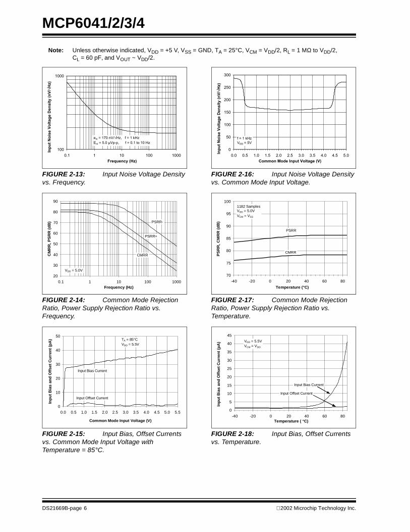
MCP6041/2/3/4
DS21669B-page 6 2002 Microchip Technology Inc.
Note: Unless otherwise indicated, VDD = +5 V, VSS = GND, TA = 25°C, VCM = VDD/2, RL = 1 MΩ to VDD/2, CL = 60 pF, and VOUT ~ VDD/2.
FIGURE 2-13: Input Noise Voltage Density vs. Frequency.
FIGURE 2-14: Common Mode Rejection Ratio, Power Supply Rejection Ratio vs. Frequency.
FIGURE 2-15: Input Bias, Offset Currents vs. Common Mode Input Voltage with Temperature = 85°C.
FIGURE 2-16: Input Noise Voltage Density vs. Common Mode Input Voltage.
FIGURE 2-17: Common Mode Rejection Ratio, Power Supply Rejection Ratio vs. Temperature.
FIGURE 2-18: Input Bias, Offset Currents vs. Temperature.
100
1000
0.1 1 10 100 1000
Frequency (Hz)
eni = 170 nV/ Hz, f = 1 kHz
Eni = 5.0 µVp-p, f = 0.1 to 10 Hz
Inp
ut
No
ise V
olt
ag
e D
en
sit
y (
nV
/H
z)
20
30
40
50
60
70
80
90
0.1 1 10 100 1000Frequency (Hz)
CM
RR
, PSR
R (d
B)
VDD = 5.0V
CMRR
PSRR+
PSRR-
0
10
20
30
40
50
0.0 0.5 1.0 1.5 2.0 2.5 3.0 3.5 4.0 4.5 5.0 5.5
Common Mode Input Voltage (V)
Inpu
t Bia
s an
d O
ffset
Cur
rent
(pA
)
Input Bias Current
Input Offset Current
TA = 85°CVDD = 5.5V
0
50
100
150
200
250
300
0.0 0.5 1.0 1.5 2.0 2.5 3.0 3.5 4.0 4.5 5.0
Common Mode Input Voltage (V)
f = 1 kHz
VDD = 5V
Inp
ut
No
ise V
olt
ag
e D
en
sit
y (
nV
/H
z)
70
75
80
85
90
95
100
-40 -20 0 20 40 60 80Temperature (°C)
PSR
R, C
MR
R (d
B)
PSRR
CMRR
1182 SamplesVDD = 5.0VVCM = VSS
0
5
10
15
20
25
30
35
40
45
-40 -20 0 20 40 60 80Temperature ( °C)
Inpu
t Bia
s an
d O
ffset
Cur
rent
(pA
)
Input Offset Current
Input Bias Current
VDD = 5.5VVCM = VDD
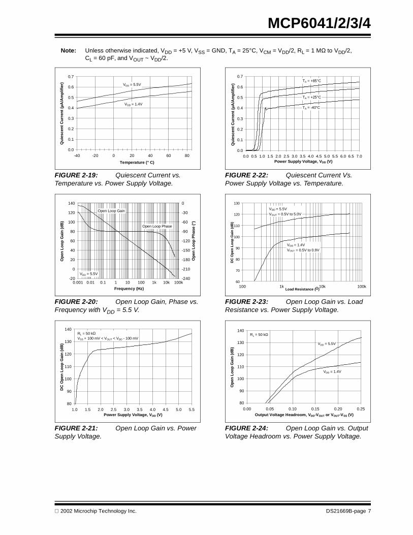
2002 Microchip Technology Inc. DS21669B-page 7
MCP6041/2/3/4Note: Unless otherwise indicated, VDD = +5 V, VSS = GND, TA = 25°C, VCM = VDD/2, RL = 1 MΩ to VDD/2,
CL = 60 pF, and VOUT ~ VDD/2.
FIGURE 2-19: Quiescent Current vs. Temperature vs. Power Supply Voltage.
FIGURE 2-20: Open Loop Gain, Phase vs. Frequency with VDD = 5.5 V.
FIGURE 2-21: Open Loop Gain vs. Power Supply Voltage.
FIGURE 2-22: Quiescent Current Vs. Power Supply Voltage vs. Temperature.
FIGURE 2-23: Open Loop Gain vs. Load Resistance vs. Power Supply Voltage.
FIGURE 2-24: Open Loop Gain vs. Output Voltage Headroom vs. Power Supply Voltage.
0.0
0.1
0.2
0.3
0.4
0.5
0.6
0.7
-40 -20 0 20 40 60 80Temperature (° C)
Qui
esce
nt C
urre
nt (µ
A/A
mpl
ifier
)
VDD = 1.4V
VDD = 5.5V
-20
0
20
40
60
80
100
120
140
1.E-03 1.E-02 1.E-01 1.E+00 1.E+01 1.E+02 1.E+03 1.E+04 1.E+05
Frequency (Hz)
Ope
n Lo
op G
ain
(dB
)
-240
-210
-180
-150
-120
-90
-60
-30
0
Ope
n Lo
op P
hase
(°)
VDD = 5.5V
0.001 0.01 0.1 1 10 100 1k 10k 100k
Open Loop Gain
Open Loop Phase
80
90
100
110
120
130
140
1.0 1.5 2.0 2.5 3.0 3.5 4.0 4.5 5.0 5.5Power Supply Voltage, VDD (V)
DC
Ope
n Lo
op G
ain
(dB
)
RL = 50 kΩVSS + 100 mV < VOUT < VDD - 100 mV
0.0
0.1
0.2
0.3
0.4
0.5
0.6
0.7
0.0 0.5 1.0 1.5 2.0 2.5 3.0 3.5 4.0 4.5 5.0 5.5 6.0 6.5 7.0Power Supply Voltage, VDD (V)
Qui
esce
nt C
urre
nt (µ
A/A
mpl
ifier
)
TA = -40°C
TA = +25°C
TA = +85°C
60
70
80
90
100
110
120
130
1. E+0 2 1. E+0 3 1. E+0 4 1. E+0 5
Load Resistance (Ω)
DC O
pen
Loop
Gai
n (d
B)
VDD = 1.4VVOUT = 0.5V to 0.9V
VDD = 5.5VVOUT = 0.5V to 5.0V
100 1k 10k 100k
80
90
100
110
120
130
140
0.00 0.05 0.10 0.15 0.20 0.25Output Voltage Headroom, VDD-VOUT or VOUT-VSS (V)
Ope
n Lo
op G
ain
(dB
)
RL = 50 kΩ
VDD = 5.5V
VDD = 1.4V

MCP6041/2/3/4
DS21669B-page 8 2002 Microchip Technology Inc.
Note: Unless otherwise indicated, VDD = +5 V, VSS = GND, TA = 25°C, VCM = VDD/2, RL = 1 MΩ to VDD/2, CL = 60 pF, and VOUT ~ VDD/2.
FIGURE 2-25: Channel to Channel Separation vs. Frequency (MCP6042 and MCP6044 only).
FIGURE 2-26: Gain Bandwidth Product, Phase Margin vs. Temperature with VDD = 5.5 V, Unity Gain.
FIGURE 2-27: Unity Loop Gain Frequency, Phase Margin vs. Load Capacitance.
FIGURE 2-28: Gain Bandwidth Product, Phase Margin vs. Common Mode Input Voltage with Unity Gain.
FIGURE 2-29: Gain Bandwidth Product, Phase Margin vs. Temperature with VDD = 1.4 V, Unity Gain.
FIGURE 2-30: Output Short Circuit Current vs. Temperature vs. Power Supply Voltage.
60
70
80
90
100
110
120
130
1.E+02 1.E+03 1.E+04
Frequency (Hz)100 1k 10k
Input ReferredCha
nnel
to C
hann
el S
epar
atio
n (d
B)
0
2
4
6
8
10
12
14
16
18
-40 -20 0 20 40 60 80Temperature (°C)
0
10
20
30
40
50
60
70
80
90
Phas
e M
argi
n (°
)
Phase MarginGain Bandwidth Product
VDD = 5.5VG = +1 V/VG
ain
Ban
dwid
th P
rodu
ct (k
Hz)
0
2
4
6
8
10
12
14
16
18
10 100 1000Load Capacitance (pF)
0
10
20
30
40
50
60
70
80
90
Phas
e M
argi
n (°
)
Unity Loop Gain Frequency
Phase Margin
VDD = 5.5VG = +1 V/VRL = 10 kΩ
Uni
ty L
oop
Gai
n Fr
eque
ncy
(kH
z)
0
2
4
6
8
10
12
14
16
18
0.0 0.5 1.0 1.5 2.0 2.5 3.0 3.5 4.0 4.5 5.0Common Mode Input Voltage(V)
0
10
20
30
40
50
60
70
80
90
Phas
e M
argi
n (°
)
Phase Margin
Gain Bandwidth Product
VDD = 5VRL = 100 kΩG = +1 V/VG
ain
Ban
dwid
th P
rodu
ct (k
Hz)
0
2
4
6
8
10
12
14
16
18
-40 -20 0 20 40 60 80Temperature (°C)
0
10
20
30
40
50
60
70
80
90
Phas
e M
argi
n (°
)
Phase Margin
Gain Bandwidth Product
VDD = 1.4VG = +1 V/V
Gai
n B
andw
idth
Pro
duct
(kH
z)
0
5
10
15
20
25
30
35
40
-40 -20 0 20 40 60 80Temperature (°C)
Out
put S
hort
Circ
uit C
urre
nt (m
A)
| ISC- | @ VDD=5.5V
ISC+ @ VDD=5.5V
| ISC- | @ VDD=1.4VISC+ @ VDD=1.4V

2002 Microchip Technology Inc. DS21669B-page 9
MCP6041/2/3/4Note: Unless otherwise indicated, VDD = +5 V, VSS = GND, TA = 25°C, VCM = VDD/2, RL = 1 MΩ to VDD/2,
CL = 60 pF, and VOUT ~ VDD/2.
FIGURE 2-31: Slew Rate vs. Temperature.
FIGURE 2-32: Output Voltage Headroom vs. Load Resistance vs. Power Supply Voltage.
FIGURE 2-33: Small Signal Non-Inverting Pulse Response.
FIGURE 2-34: Output Voltage Swing vs. Frequency vs. Power Supply Voltage.
FIGURE 2-35: Output Voltage Headroom vs. Temperature.
FIGURE 2-36: Small Signal Inverting Pulse Response.
0
1
2
3
4
5
6
-40 -20 0 20 40 60 80Temperature (°C)
Slew
Rat
e (V
/ms)
High-to-Low Transition
Low-to-High Transition
VDD = 5.0V
1
10
100
1.E+03 1.E+04 1.E+05
Load Resistance ( )
Ou
tpu
t V
olt
ag
e H
ead
roo
m,
VD
D-V
OH o
r V
OL-V
SS (
mV
)
VOL-VSS @ VDD = 5.5V
1k 10k 100k
VOL-VSS @ VDD = 1.4V
VDD-VOH @ VDD = 5.5V
VDD-VOH @ VDD = 1.4V
-3.E-02
-2.E-02
-2.E-02
-1.E-02
-5.E-03
0.E+00
5.E-03
1.E-02
2.E-02
2.E-02
3.E-02
0.E+00 1.E-04 2.E-04 3.E-04 4.E-04 5.E-04 6.E-04 7.E-04 8.E-04 9.E-04 1.E-03
Time (100 µs/div)
Out
put V
olta
ge (5
mV/
div)
VDD = 5.0VG = +1 V/VRL = 50 kΩ
0.1
1
10
1.E+01 1.E+02 1.E+03 1.E+04
Frequency (Hz)
Out
put V
olta
ge S
win
g (V
p-p)
10 100 1k 10k
VDD = 5.5V
VDD = 1.4V
0
1
2
3
4
5
-40 -20 0 20 40 60 80Temperature (°C)
Out
put V
olta
ge H
eadr
oom
,V D
D - V
OH
or V
OL -
VSS
(mV)
VOL - VSS
VDD - VOH
VDD = 5.5VRL = 50 kΩ
-0.025
-0.020
-0.015
-0.010
-0.005
0.000
0.005
0.010
0.015
0.020
0.025
0.0E+00 1.0E-04 2.0E-04 3.0E-04 4.0E-04 5.0E-04 6.0E-04 7.0E-04 8.0E-04 9.0E-04 1.0E-03
Time (100 µs/div)
Volta
ge (5
mV/
div)
VDD = 5.0VG = -1 V/VRL = 50 kΩ

MCP6041/2/3/4
DS21669B-page 10 2002 Microchip Technology Inc.
Note: Unless otherwise indicated, VDD = +5 V, VSS = GND, TA = 25°C, VCM = VDD/2, RL = 1 MΩ to VDD/2, CL = 60 pF, and VOUT ~ VDD/2.
FIGURE 2-37: Large Signal Non-Inverting Pulse Response.
FIGURE 2-38: Chip Select (CS) to Amplifier Output Response Time (MCP6043 only).
FIGURE 2-39: The MCP6041/2/3/4 family shows no phase reversal (for information only–the Maximum Absolute Input Voltage is still VSS-0.3 V and VDD+0.3 V).
FIGURE 2-40: Large Signal Inverting Pulse Response.
FIGURE 2-41: Chip Select (CS) Hysteresis (MCP6043 only).
0.0
0.5
1.0
1.5
2.0
2.5
3.0
3.5
4.0
4.5
5.0
0.E+00 1.E-03 2.E-03 3.E-03 4.E-03 5.E-03 6.E-03 7.E-03 8.E-03 9.E-03 1.E-02
Time (1 ms/div)
Out
put V
olta
ge (V
)
VDD = 5.0VG = +1 V/VRL = 50 kΩ
-20.0
-17.5
-15.0
-12.5
-10.0
-7.5
-5.0
-2.5
0.0
2.5
5.0
7.5
0.E+
00
1.E-
03
2.E-
03
3.E-
03
4.E-
03
5.E-
03
6.E-
03
7.E-
03
8.E-
03
9.E-
03
1.E-
02
Time (1 ms/div)-1.0
-0.5
0.0
0.5
1.0
1.5
2.0
2.5
3.0
3.5
4.0
4.5
Out
put V
olta
ge (V
)VDD = 5.0V
Chi
p Se
lect
(CS)
Vol
tage
(V)
VOUT
CS
Output Hi-Z Output Hi-ZOutput Driven
-1
0
1
2
3
4
5
6
0.00E+00 5.00E-03 1.00E-02 1.50E-02 2.00E-02 2.50E-02
Time (5 ms/div)
Out
put V
olta
ge (V
)
VIN
VDD = 5.0VG = +2 V/V
VOUT
0.0
0.5
1.0
1.5
2.0
2.5
3.0
3.5
4.0
4.5
5.0
0.E+00 1.E-03 2.E-03 3.E-03 4.E-03 5.E-03 6.E-03 7.E-03 8.E-03 9.E-03 1.E-02
Time (1 ms/div)
Out
put V
olta
ge (V
)
VDD = 5.0VG = -1 V/VRL = 50 kΩ
-0.5
0.0
0.5
1.0
1.5
2.0
2.5
3.0
0 1 2 3 4 5
CS Input Voltage (V)
Amplifier Output–Active (driven)
Amplifier Output–Hi-Z
VDD = 5.0V
CS Input Highto Low CS Input Low
to HighHys
tere
sis
Inte
rnal
CS
Switc
h O
utpu
t (V)

2002 Microchip Technology Inc. DS21669B-page 11
MCP6041/2/3/43.0 APPLICATIONS INFORMATIONThe MCP6041/2/3/4 family of operational amplifiersare fabricated on Microchip’s state-of-the-art CMOSprocess. They are unity gain stable and suitable for awide range of applications requiring very low powerconsumption. With these op amps, the power supplypin needs to be by-passed with a 0.1 µF capacitor.
3.1 Rail to Rail InputThe input stage of the family of devices uses two differ-ential input stages in parallel; one operates at low VCM(common mode input voltage) and the other at highVCM. With this topology, the MCP6041/2/3/4 familyoperates with VCM up to 300 mV past either supply rail.The Input Offset Voltage is measured at bothVCM = VSS - 0.3 V and VDD + 0.3 V to ensure properoperation.
3.2 Output Loads and Battery LifeThe MCP6041/2/3/4 op amp family has outstandingquiescent current, which supports battery-poweredapplications. There is minimal quiescent current glitch-ing when chip select (CS) is raised or lowered. Thisprevents excessive current draw and reduced batterylife, when the part is turned off or on.
Heavy resistive loads at the output can cause exces-sive battery drain. Driving a DC voltage of 2.5 V acrossa 100 kΩ load resistor will cause the supply current toincrease by 25 µA, depleting the battery 43 times asfast as IQ (0.6 µA typ) alone.
High frequency signals (fast edge rate) across capaci-tive loads will also significantly increase supply current.For instance, a 0.1 µF capacitor at the output presentsan AC impedance of 15.9 kΩ (1/2πfC) to a 100 Hzsinewave. It can be shown that the average powerdrawn from the battery by a 5.0 Vp-p sinewave(1.77 Vrms), under these conditions, is:
EQUATION
This will drain the battery 18 times as fast as IQ alone.
3.3 Rail to Rail OutputThe output voltage range of the MCP6041/2/3/4 familyis specified two ways. The first specification, MaximumOutput Voltage Swing, defines the maximum swingpossible under a particular output load. According tothe spec table, the output can reach ≤ 10 mV of eithersupply rail when RL = 50 kΩ. See Figure 2-32 for infor-mation on Maximum Output Voltage Swing vs. loadresistance.
The second specification, Linear Region Output Volt-age Swing, details the output voltage range that sup-ports the specified Open Loop Gain (AOL ≥ 95 dB withRL = 50 kΩ).
3.4 Input Voltage and Phase ReversalThe MCP6041/2/3/4 op amp family uses CMOS tran-sistors at the input. It is designed to not exhibit phaseinversion when the input pins exceed the supply volt-ages. Figure 2-39 shows an input voltage exceedingboth supplies with no resulting phase inversion.
The maximum operating VCM (common mode inputvoltage) that can be applied to the inputs is VSS -0.3 Vand VDD +0.3 V. Voltage on the input that exceed thisabsolute maximum rating can cause excessive currentto flow in or out of the input pins. Current beyond ±2 mAcan cause possible reliability problems. Applicationsthat exceed this rating must be externally limited withan input resistor as shown in Figure 3-1.
FIGURE 3-1: An input resistor, RIN, should be used to limit excessive input current if the inputs exceed the Absolute Maximum specification.
3.5 Capacitive Load and StabilityDriving capacitive loads can cause stability problemswith voltage feedback op amps. A buffer configuration(G = +1) is the most sensitive to capacitive loads.Figure 2-27 shows how increasing the load capaci-tance will decrease the phase margin. While a phasemargin above 60° is ideal, 45° is sufficient. As can beseen, up to CL = 150 pF can be placed on theMCP6041/2/3/4 op amp outputs without any problems,while 250 pF is usable with a 45° phase margin.When the op amp is required to drive large capacitiveloads (CL >150 pF), a small series resistor (RISO inFigure 3-2) at the output of the amplifier improves thephase margin. This resistor makes the output loadresistive at higher frequencies, which improves thephase margin. The bandwidth reduction caused by thecapacitive load, however, is not changed. To selectRISO, start with 1 kΩ, then use the MCP6041 SPICE
PSUPPLY VDD VSS–( ) IQ VL p p–( )+ fCL( )=
3.0µW 50µW+=5V( ) 0.6µA 5.0Vp p–+ 100Hz 0.1µF••( )=
RINVSS Minimum expected VIN( )–
2 mA----------------------------------------------------------------------------≥
RINMaximum expected VIN( ) VDD–
2 mA-------------------------------------------------------------------------------≥
VIN
RIN VOUTMCP604X
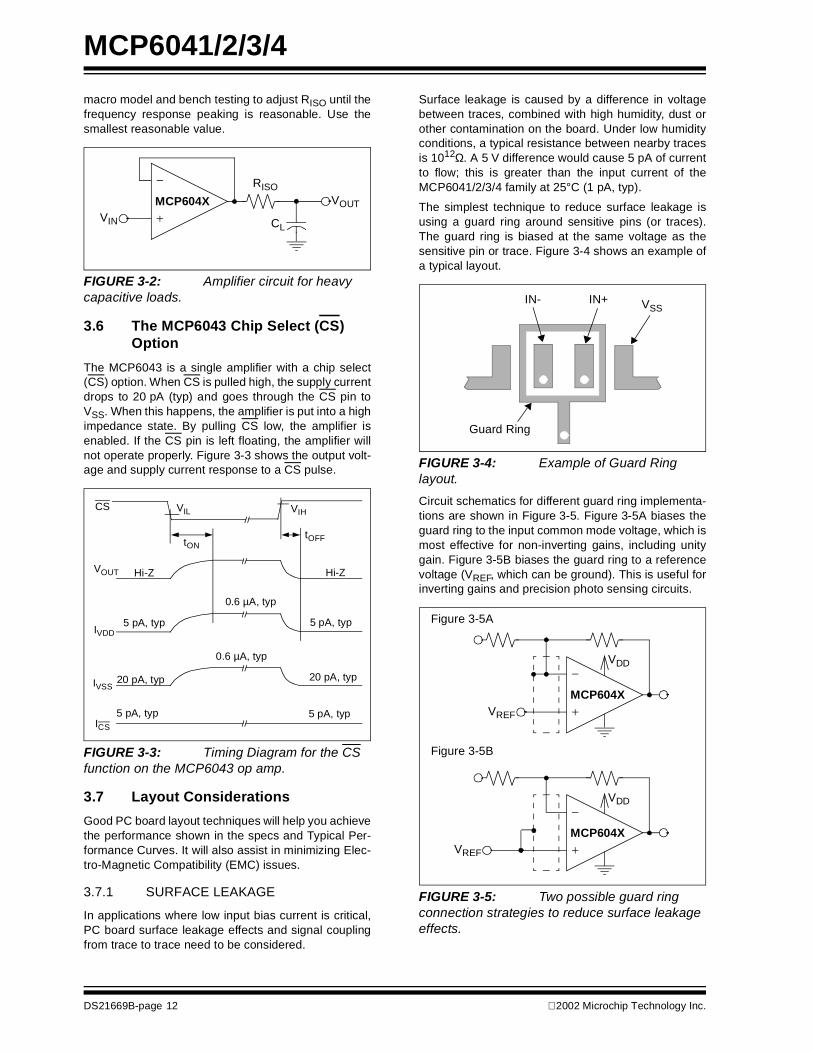
MCP6041/2/3/4
DS21669B-page 12 2002 Microchip Technology Inc.
macro model and bench testing to adjust RISO until thefrequency response peaking is reasonable. Use thesmallest reasonable value.
FIGURE 3-2: Amplifier circuit for heavy capacitive loads.
3.6 The MCP6043 Chip Select (CS) Option
The MCP6043 is a single amplifier with a chip select(CS) option. When CS is pulled high, the supply currentdrops to 20 pA (typ) and goes through the CS pin toVSS. When this happens, the amplifier is put into a highimpedance state. By pulling CS low, the amplifier isenabled. If the CS pin is left floating, the amplifier willnot operate properly. Figure 3-3 shows the output volt-age and supply current response to a CS pulse.
FIGURE 3-3: Timing Diagram for the CS function on the MCP6043 op amp.
3.7 Layout ConsiderationsGood PC board layout techniques will help you achievethe performance shown in the specs and Typical Per-formance Curves. It will also assist in minimizing Elec-tro-Magnetic Compatibility (EMC) issues.
3.7.1 SURFACE LEAKAGE
In applications where low input bias current is critical,PC board surface leakage effects and signal couplingfrom trace to trace need to be considered.
Surface leakage is caused by a difference in voltagebetween traces, combined with high humidity, dust orother contamination on the board. Under low humidityconditions, a typical resistance between nearby tracesis 1012Ω. A 5 V difference would cause 5 pA of currentto flow; this is greater than the input current of theMCP6041/2/3/4 family at 25°C (1 pA, typ).The simplest technique to reduce surface leakage isusing a guard ring around sensitive pins (or traces).The guard ring is biased at the same voltage as thesensitive pin or trace. Figure 3-4 shows an example ofa typical layout.
FIGURE 3-4: Example of Guard Ring layout.Circuit schematics for different guard ring implementa-tions are shown in Figure 3-5. Figure 3-5A biases theguard ring to the input common mode voltage, which ismost effective for non-inverting gains, including unitygain. Figure 3-5B biases the guard ring to a referencevoltage (VREF, which can be ground). This is useful forinverting gains and precision photo sensing circuits.
FIGURE 3-5: Two possible guard ring connection strategies to reduce surface leakage effects.
VIN
RISOVOUTMCP604X
CL
VIL
Hi-Z
tON
VIHCS
tOFF
VOUT
IVDD
20 pA, typ
Hi-Z
IVSS
ICS5 pA, typ 5 pA, typ
20 pA, typ
0.6 µA, typ
5 pA, typ
0.6 µA, typ
5 pA, typ
Guard Ring
VSSIN- IN+
VREF
MCP604X
Figure 3-5A
Figure 3-5B
VDD
VREF
MCP604X
VDD
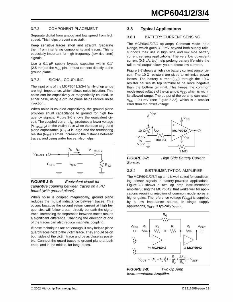
2002 Microchip Technology Inc. DS21669B-page 13
MCP6041/2/3/43.7.2 COMPONENT PLACEMENT
Separate digital from analog and low speed from highspeed. This helps prevent crosstalk.Keep sensitive traces short and straight. Separatethem from interfering components and traces. This isespecially important for high frequency (low rise time)signals.Use a 0.1 µF supply bypass capacitor within 0.1”(2.5 mm) of the VDD pin. It must connect directly to theground plane.
3.7.3 SIGNAL COUPLING
The input pins of the MCP6041/2/3/4 family of op ampsare high impedance, which allows noise injection. Thisnoise can be capacitively or magnetically coupled. Ineither case, using a ground plane helps reduce noiseinjection.When noise is coupled capacitively, the ground planeprovides shunt capacitance to ground for high fre-quency signals. Figure 3-6 shows the equivalent cir-cuit. The coupled current, IM, produces a lower voltage(VTRACE 2) on the victim trace when the trace to groundplane capacitance (CSH2) is large and the terminatingresistor (RT2) is small. Increasing the distance betweentraces, and using wider traces, also helps.
FIGURE 3-6: Equivalent circuit for capacitive coupling between traces on a PC board (with ground plane).When noise is coupled magnetically, ground planereduces the mutual inductance between traces. Thisoccurs because the ground return current at high fre-quencies will follow a path directly beneath the signaltrace. Increasing the separation between traces makesa significant difference. Changing the direction of oneof the traces can also reduce magnetic coupling.If these techniques are not enough, it may help to placeguard traces next to the victim trace. They should be onboth sides of the victim trace and be as close as possi-ble. Connect the guard traces to ground plane at bothends, and in the middle, for long traces.
3.8 Typical Applications
3.8.1 BATTERY CURRENT SENSING
The MCP6041/2/3/4 op amps’ Common Mode InputRange, which goes 300 mV beyond both supply rails,supports their use in high side and low side batterycurrent sensing applications. The very low quiescentcurrent (0.6 µA, typ) help prolong battery life while therail-to-rail output allows you to detect low currents.Figure 3-7 shows a high side battery current sensor cir-cuit. The 10 Ω resistors are sized to minimize powerlosses. The battery current (IDD) through the 10 Ωresistor causes its top terminal to be more negativethan the bottom terminal. This keeps the commonmode input voltage of the op amp ≤ VDD, which is withinits allowed range. The output of the op amp can reachVDD - 0.1 mV (see Figure 2-32), which is a smallererror than the offset voltage.
FIGURE 3-7: High Side Battery Current Sensor.
3.8.2 INSTRUMENTATION AMPLIFIERThe MCP6041/2/3/4 op amp is well suited for condition-ing sensor signals in battery-powered applications.Figure 3-8 shows a two op amp instrumentationamplifier, using the MCP6042, that works well for appli-cations requiring rejection of common mode noise athigher gains. The reference voltage (VREF) is suppliedby a low impedance source. In single supplyapplications, VREF is typically VDD/2.
FIGURE 3-8: Two Op Amp Instrumentation Amplifier.
VTRACE 1
RT2
CM
CSH2CSH1
VTRACE 2IM
VDD
10 Ω MCP604X
100 kΩ
1 MΩ
VDD
IDD
+2.5 Vto
5.5 V
VSS
VREF
½ MCP6042
R1
RG
VOUTR1 R1 R1
V2
V1½ MCP6042
VOUT V1 V2–( ) 1R1R2------
2R1RG---------+ +
VREF+=

MCP6041/2/3/4
DS21669B-page 14 2002 Microchip Technology Inc.
4.0 SPICE MACRO MODELThe Spice macro model for the MCP6041, MCP6042,MCP6043 and MCP6044 simulates the typical ampli-fier performance of: offset voltage, DC power supplyrejection, input capacitance, DC common mode rejec-tion, open loop gain over frequency, phase margin, out-put swing, DC power supply current, power supplycurrent change with supply voltage, input commonmode range, output voltage range vs. load and inputvoltage noise.The characteristics of the MCP6041, MCP6042,MCP6043 and MCP6044 amplifiers are similar in termsof performance and behavior. This single op ampmacro model supports all four devices with the excep-tion of the chip select function of the MCP6043, whichis not modeled.The listing for this macro model is shown on the nextpage. The most recent revision of the model can bedownloaded from Microchip’s web site atwww.microchip.com.
2002 Microchip Technology Inc. DS21669B-page 15
MCP6041/2/3/4
Software License AgreementThe software supplied herewith by Microchip Technology Incorporated (the “Company”) is intended and supplied to you, the Com-pany’s customer, for use solely and exclusively on Microchip products.The software is owned by the Company and/or its supplier, and is protected under applicable copyright laws. All rights are reserved.Any use in violation of the foregoing restrictions may subject the user to criminal sanctions under applicable laws, as well as to civilliability for the breach of the terms and conditions of this license.THIS SOFTWARE IS PROVIDED IN AN “AS IS” CONDITION. NO WARRANTIES, WHETHER EXPRESS, IMPLIED OR STATU-TORY, INCLUDING, BUT NOT LIMITED TO, IMPLIED WARRANTIES OF MERCHANTABILITY AND FITNESS FOR A PARTICU-LAR PURPOSE APPLY TO THIS SOFTWARE. THE COMPANY SHALL NOT, IN ANY CIRCUMSTANCES, BE LIABLE FORSPECIAL, INCIDENTAL OR CONSEQUENTIAL DAMAGES, FOR ANY REASON WHATSOEVER.
.SUBCKT MCP6041 1 2 3 4 5* | | | | |* | | | | Output* | | | Negative Supply* | | Positive Supply* | Inverting Input* Non-inverting Input** Macromodel for the MCP6041/2/3/4 op amp family:* MCP6041 (single)* MCP6042 (dual)* MCP6043 (single w/ CS; chip select is not modeled)* MCP6044 (quad)** Revision History:* REV A: 7-9-01 created KEB** Recommendations:* Use PSPICE (other simulators may require translation)* For a quick, effective design, use a com-bination of: data sheet* specs, bench testing, and simulations with this macromodel* For high impedance circuits, set GMIN=100F in the.OPTIONS* statement** Supported:* Typical performance at room temperature (25 degrees C)* DC, AC, Transient, and Noise analyses.* Most specs, including: offsets, PSRR, CMRR, input impedance,* open loop gain, voltage ranges, supply current,..., etc.** Not Supported:* Chip Select (MCP6043)* Variation in specs vs. Power Supply Volt-age* Distortion (detailed non-linear behavior)* Temperature analysis* Process variation* Behavior outside normal operating region** Input StageV10 3 10 -0.3R10 10 11 78K
R11 10 12 78KC11 11 12 4.9PC12 1 0 6PE12 1 14 POLY(4) 20 0 21 0 26 0 27 0 1M 1 1 1 1G12 14 0 POLY(2) 22 0 23 0 1.5P 1U 1UM12 11 14 15 15 NMIC13 14 2 3PM14 12 2 15 15 NMIG14 2 0 POLY(2) 24 0 25 0 0.5P 1U 1UC14 2 0 6PI15 15 4 500NV16 16 4 0.18D16 16 15 DLV13 3 13 0.00D13 14 13 DL** Noise SourcesI20 21 20 17.2ND20 20 0 DN1D21 0 21 DN1I22 23 22 588UD22 22 0 DN23D23 0 23 DN23I24 25 24 588UD24 24 0 DN23D25 0 25 DN23** PSRR and CMRRG26 0 26 POLY(1) 3 4 110U -20UR26 26 0 1G27 0 27 POLY(2) 1 3 2 4 -275U 50U 50UR27 27 0 1** Open Loop Gain, Slew RateG30 0 30 POLY(1) 12 11 0 1MEGR30 30 0 1C30 30 0 11.4G31 0 31 POLY(1) 30 0 0 1R31 31 0 1C31 31 0 775N** Output StageG40 0 40 POLY(1) 45 5 0 22.7MD41 40 41 DLR41 41 0 1KD42 42 40 DLR42 42 0 1KG43 3 0 POLY(1) 41 0 100N 1MG47 0 4 POLY(1) 42 0 100N -1ME43 43 0 POLY(1) 3 0 0 1

MCP6041/2/3/4
DS21669B-page 16 2002 Microchip Technology Inc.
E47 47 0 POLY(1) 4 0 0 1V44 43 44 1MD44 45 44 DLSD46 46 45 DLSV46 46 47 1MG45 47 45 POLY(2) 31 0 3 4 0 8U 4UR45 45 47 125KR48 45 5 44C48 5 0 2P** Models.MODEL NMI NMOS L=2 W=42.MODEL DL D N=1 IS=1F.MODEL DLS D N=1M IS=1F.MODEL DN1 D IS=1F KF=1.13E-18 AF=1.MODEL DN23 D IS=1F KF=3E-20 AF=1*.ENDS MCP6041
2002 Microchip Technology Inc. DS21669B-page 17
MCP6041/2/3/45.0 PACKAGING INFORMATION
5.1 Package Marking Information
XXXXXXXXXXXXXNNN
YYWW
8-Lead PDIP (300 mil) Example:
8-Lead SOIC (150 mil) Example:
XXXXXXXXXXXXYYWW
NNN
Legend: XX...X Customer specific information*YY Year code (last 2 digits of calendar year)WW Week code (week of January 1 is week ‘01’)NNN Alphanumeric traceability code
Note: In the event the full Microchip part number cannot be marked on one line, it willbe carried over to the next line thus limiting the number of available charactersfor customer specific information.
* Standard marking consists of Microchip part number, year code, week code, traceability code (facilitycode, mask rev#, and assembly code). For marking beyond this, certain price adders apply. Pleasecheck with your Microchip Sales Office.
MCP6041I/PNNN
YYWW
MCP6041I/SNYYWW
NNN
8-Lead MSOP Example:
XXXXXX
YWWNNN
6041
YWWNNN
1 2 3
5 4
5-Lead SOT-23 (MCP6041 only) Example:
XXNN
1 2 3
5 4
SBNN
MCP6041/2/3/4
DS21669B-page 18 2002 Microchip Technology Inc.
5.1 Package Marking Information (Continued)
14-Lead PDIP (300 mil) (MCP6044) Example:
14-Lead TSSOP (MCP6044) Example:
14-Lead SOIC (150 mil) (MCP6044) Example:
XXXXXXXXXXXXXXXXXXXXXXXXXXXX
YYWWNNN
XXXXXXXXXX
YYWWNNN
XXXXXXYYWW
NNN
Legend: XX...X Customer specific information*YY Year code (last 2 digits of calendar year)WW Week code (week of January 1 is week ‘01’)NNN Alphanumeric traceability code
Note: In the event the full Microchip part number cannot be marked on one line, it willbe carried over to the next line thus limiting the number of available charactersfor customer specific information.
* Standard marking consists of Microchip part number, year code, week code, traceability code (facilitycode, mask rev#, and assembly code). For marking beyond this, certain price adders apply. Pleasecheck with your Microchip Sales Office.
MCP6044-I/PXXXXXXXXXXXXXX
YYWWNNN
6044STYYWW
NNN
XXXXXXXXXXMCP6044ISL
YYWWNNN
XXXXXXXXXX
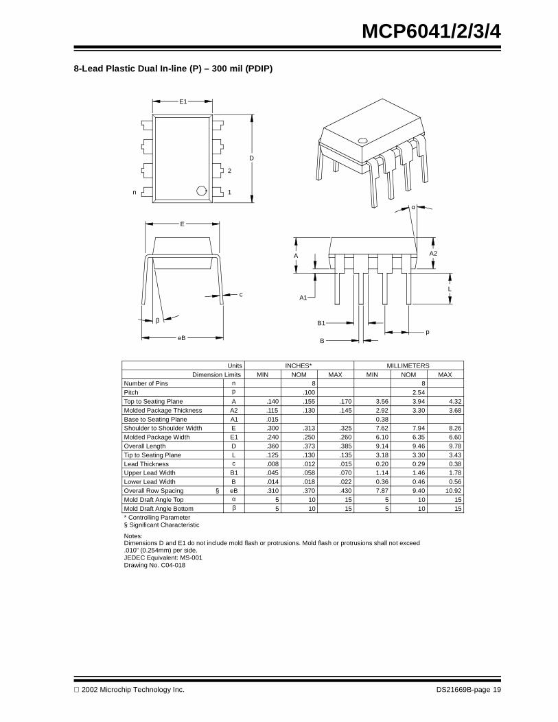
2002 Microchip Technology Inc. DS21669B-page 19
MCP6041/2/3/48-Lead Plastic Dual In-line (P) – 300 mil (PDIP)
B1
B
A1
A
L
A2
p
α
E
eB
β
c
E1
n
D
1
2
Units INCHES* MILLIMETERSDimension Limits MIN NOM MAX MIN NOM MAX
Number of Pins n 8 8Pitch p .100 2.54Top to Seating Plane A .140 .155 .170 3.56 3.94 4.32Molded Package Thickness A2 .115 .130 .145 2.92 3.30 3.68Base to Seating Plane A1 .015 0.38Shoulder to Shoulder Width E .300 .313 .325 7.62 7.94 8.26Molded Package Width E1 .240 .250 .260 6.10 6.35 6.60Overall Length D .360 .373 .385 9.14 9.46 9.78Tip to Seating Plane L .125 .130 .135 3.18 3.30 3.43Lead Thickness c .008 .012 .015 0.20 0.29 0.38Upper Lead Width B1 .045 .058 .070 1.14 1.46 1.78Lower Lead Width B .014 .018 .022 0.36 0.46 0.56Overall Row Spacing § eB .310 .370 .430 7.87 9.40 10.92Mold Draft Angle Top α 5 10 15 5 10 15Mold Draft Angle Bottom β 5 10 15 5 10 15* Controlling Parameter
Notes:Dimensions D and E1 do not include mold flash or protrusions. Mold flash or protrusions shall not exceed
JEDEC Equivalent: MS-001Drawing No. C04-018
.010” (0.254mm) per side.
§ Significant Characteristic

MCP6041/2/3/4
DS21669B-page 20 2002 Microchip Technology Inc.
8-Lead Plastic Small Outline (SN) – Narrow, 150 mil (SOIC)
Foot Angle φ 0 4 8 0 4 8
1512015120βMold Draft Angle Bottom1512015120αMold Draft Angle Top
0.510.420.33.020.017.013BLead Width0.250.230.20.010.009.008cLead Thickness
0.760.620.48.030.025.019LFoot Length0.510.380.25.020.015.010hChamfer Distance5.004.904.80.197.193.189DOverall Length3.993.913.71.157.154.146E1Molded Package Width6.206.025.79.244.237.228EOverall Width0.250.180.10.010.007.004A1Standoff §1.551.421.32.061.056.052A2Molded Package Thickness1.751.551.35.069.061.053AOverall Height
1.27.050pPitch88nNumber of Pins
MAXNOMMINMAXNOMMINDimension LimitsMILLIMETERSINCHES*Units
2
1
D
n
p
B
E
E1
h
Lβ
c
45°
φ
A2
α
A
A1
* Controlling Parameter
Notes:Dimensions D and E1 do not include mold flash or protrusions. Mold flash or protrusions shall not exceed .010” (0.254mm) per side.JEDEC Equivalent: MS-012Drawing No. C04-057
§ Significant Characteristic

2002 Microchip Technology Inc. DS21669B-page 21
MCP6041/2/3/48-Lead Plastic Micro Small Outline Package (MS) (MSOP)
p
A
A1
A2
D
L
c
Dimensions D and E1 do not include mold flash or protrusions. Mold flash or protrusions shall not
.037.035FFootprint (Reference)
exceed .010" (0.254mm) per side.
Notes:
Drawing No. C04-111
*Controlling Parameter
Mold Draft Angle TopMold Draft Angle Bottom
Foot Angle
Lead WidthLead Thickness
βα
cB
φ
77
.004
.010
0.006.012
(F)
β
Dimension Limits
Overall HeightMolded Package Thickness
Molded Package WidthOverall LengthFoot Length
Standoff §Overall Width
Number of PinsPitch
A
L
E1D
A1E
A2
.016
.114
.114.022
.118
.118
.002
.030
.193
.034
MIN
pn
Units
.026
NOM8
INCHES
1.000.950.90.039
0.150.30
.008
.016
60.100.25
0
77
0.200.40
6
MILLIMETERS*
0.65
0.86
3.003.000.55
4.90
.044
.122
.028
.122
.038
.006
0.40
2.902.90
0.050.76
MINMAX NOM
1.18
0.70
3.103.10
0.150.97
MAX8
α
E1
E
Bn 1
2
φ
§ Significant Characteristic
.184 .200 4.67 .5.08

MCP6041/2/3/4
DS21669B-page 22 2002 Microchip Technology Inc.
5-Lead Plastic Small Outline Transistor (OT) (SOT23)
10501050βMold Draft Angle Bottom10501050αMold Draft Angle Top
0.500.430.35.020.017.014BLead Width0.200.150.09.008.006.004cLead Thickness
10501050φFoot Angle0.550.450.35.022.018.014LFoot Length3.102.952.80.122.116.110DOverall Length1.751.631.50.069.064.059E1Molded Package Width3.002.802.60.118.110.102EOverall Width0.150.080.00.006.003.000A1Standoff §1.301.100.90.051.043.035A2Molded Package Thickness1.451.180.90.057.046.035AOverall Height
1.90.075p1Outside lead pitch (basic)0.95.038pPitch
55nNumber of PinsMAXNOMMINMAXNOMMINDimension Limits
MILLIMETERSINCHES*Units
1
p
DB
n
E
E1
L
c
βφ
α
A2A
A1
p1
* Controlling Parameter
Notes:Dimensions D and E1 do not include mold flash or protrusions. Mold flash or protrusions shall not exceed .010” (0.254mm) per side.JEDEC Equivalent: MO-178Drawing No. C04-091
§ Significant Characteristic

2002 Microchip Technology Inc. DS21669B-page 23
MCP6041/2/3/414-Lead Plastic Dual In-line (P) – 300 mil (PDIP)
E1
n
D
1
2
eBβ
E
c
A
A1
B
B1
L
A2
p
α
Units INCHES* MILLIMETERSDimension Limits MIN NOM MAX MIN NOM MAX
Number of Pins n 14 14Pitch p .100 2.54Top to Seating Plane A .140 .155 .170 3.56 3.94 4.32Molded Package Thickness A2 .115 .130 .145 2.92 3.30 3.68Base to Seating Plane A1 .015 0.38Shoulder to Shoulder Width E .300 .313 .325 7.62 7.94 8.26Molded Package Width E1 .240 .250 .260 6.10 6.35 6.60Overall Length D .740 .750 .760 18.80 19.05 19.30Tip to Seating Plane L .125 .130 .135 3.18 3.30 3.43Lead Thickness c .008 .012 .015 0.20 0.29 0.38Upper Lead Width B1 .045 .058 .070 1.14 1.46 1.78Lower Lead Width B .014 .018 .022 0.36 0.46 0.56Overall Row Spacing § eB .310 .370 .430 7.87 9.40 10.92Mold Draft Angle Top α 5 10 15 5 10 15
β 5 10 15 5 10 15Mold Draft Angle Bottom* Controlling Parameter
Notes:Dimensions D and E1 do not include mold flash or protrusions. Mold flash or protrusions shall not exceed .010” (0.254mm) per side.JEDEC Equivalent: MS-001Drawing No. C04-005
§ Significant Characteristic

MCP6041/2/3/4
DS21669B-page 24 2002 Microchip Technology Inc.
14-Lead Plastic Small Outline (SL) – Narrow, 150 mil (SOIC)
Foot Angle φ 0 4 8 0 4 8
1512015120βMold Draft Angle Bottom1512015120αMold Draft Angle Top
0.510.420.36.020.017.014BLead Width0.250.230.20.010.009.008cLead Thickness
1.270.840.41.050.033.016LFoot Length0.510.380.25.020.015.010hChamfer Distance8.818.698.56.347.342.337DOverall Length3.993.903.81.157.154.150E1Molded Package Width6.205.995.79.244.236.228EOverall Width0.250.180.10.010.007.004A1Standoff §1.551.421.32.061.056.052A2Molded Package Thickness1.751.551.35.069.061.053AOverall Height
1.27.050pPitch1414nNumber of Pins
MAXNOMMINMAXNOMMINDimension LimitsMILLIMETERSINCHES*Units
2
1
D
p
nB
E
E1
h
L
c
β
45°
φ
α
A2A
A1
* Controlling Parameter
Notes:Dimensions D and E1 do not include mold flash or protrusions. Mold flash or protrusions shall not exceed .010” (0.254mm) per side.JEDEC Equivalent: MS-012Drawing No. C04-065
§ Significant Characteristic
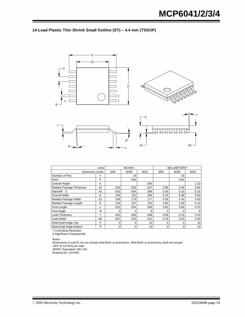
2002 Microchip Technology Inc. DS21669B-page 25
MCP6041/2/3/414-Lead Plastic Thin Shrink Small Outline (ST) – 4.4 mm (TSSOP)
840840φFoot Angle
10501050βMold Draft Angle Bottom10501050αMold Draft Angle Top
0.300.250.19.012.010.007B1Lead Width0.200.150.09.008.006.004cLead Thickness
0.700.600.50.028.024.020LFoot Length5.105.004.90.201.197.193DMolded Package Length4.504.404.30.177.173.169E1Molded Package Width6.506.386.25.256.251.246EOverall Width0.150.100.05.006.004.002A1Standoff §0.950.900.85.037.035.033A2Molded Package Thickness1.10.043AOverall Height
0.65.026pPitch1414nNumber of Pins
MAXNOMMINMAXNOMMINDimension LimitsMILLIMETERS*INCHESUnits
Lβ
c
φ
2
1
D
nB
p
E1
E
α
A2A1
A
* Controlling Parameter
Notes:Dimensions D and E1 do not include mold flash or protrusions. Mold flash or protrusions shall not exceed .005” (0.127mm) per side.JEDEC Equivalent: MO-153Drawing No. C04-087
§ Significant Characteristic

MCP6041/2/3/4
DS21669B-page 26 2002 Microchip Technology Inc.
NOTES:

2002 Microchip Technology Inc. DS21669B-page 27
MCP6041/2/3/4Systems Information and Upgrade Hot Line The Systems Information and Upgrade Line providessystem users a listing of the latest versions of all ofMicrochip's development systems software products.Plus, this line provides information on how customerscan receive any currently available upgrade kits.TheHot Line Numbers are: 1-800-755-2345 for U.S. and most of Canada, and
1-480-792-7302 for the rest of the world.
ON-LINE SUPPORTMicrochip provides on-line support on the MicrochipWorld Wide Web (WWW) site.
The web site is used by Microchip as a means to makefiles and information easily available to customers. Toview the site, the user must have access to the Internetand a web browser, such as Netscape or MicrosoftExplorer. Files are also available for FTP downloadfrom our FTP site.
Connecting to the Microchip Internet Web Site The Microchip web site is available by using yourfavorite Internet browser to attach to:
www.microchip.comThe file transfer site is available by using an FTP ser-vice to connect to:
ftp://ftp.microchip.comThe web site and file transfer site provide a variety ofservices. Users may download files for the latestDevelopment Tools, Data Sheets, Application Notes,User's Guides, Articles and Sample Programs. A vari-ety of Microchip specific business information is alsoavailable, including listings of Microchip sales offices,distributors and factory representatives. Other dataavailable for consideration is:
• Latest Microchip Press Releases• Technical Support Section with Frequently Asked
Questions • Design Tips• Device Errata• Job Postings• Microchip Consultant Program Member Listing• Links to other useful web sites related to
Microchip Products• Conferences for products, Development Systems,
technical information and more• Listing of seminars and events
013001

MCP6041/2/3/4
DS21669B-page 28 2002 Microchip Technology Inc.
READER RESPONSEIt is our intention to provide you with the best documentation possible to ensure successful use of your Microchip prod-uct. If you wish to provide your comments on organization, clarity, subject matter, and ways in which our documentationcan better serve you, please FAX your comments to the Technical Publications Manager at (480) 792-4150.
Please list the following information, and use this outline to provide us with your comments about this Data Sheet.
1. What are the best features of this document?
2. How does this document meet your hardware and software development needs?
3. Do you find the organization of this data sheet easy to follow? If not, why?
4. What additions to the data sheet do you think would enhance the structure and subject?
5. What deletions from the data sheet could be made without affecting the overall usefulness?
6. Is there any incorrect or misleading information (what and where)?
7. How would you improve this document?
8. How would you improve our software, systems, and silicon products?
To: Technical Publications Manager
RE: Reader ResponseTotal Pages Sent
From: Name
CompanyAddressCity / State / ZIP / Country
Telephone: (_______) _________ - _________Application (optional):
Would you like a reply? Y N
Device: Literature Number:
Questions:
FAX: (______) _________ - _________
DS21669BMCP6041/2/3/4

2002 Microchip Technology Inc. DS21669B-page 29
MCP6041/2/3/4PRODUCT IDENTIFICATION SYSTEMTo order or obtain information, e.g., on pricing or delivery, refer to the factory or the listed sales office.
Sales and SupportData SheetsProducts supported by a preliminary Data Sheet may have an errata sheet describing minor operational differences and recom-mended workarounds. To determine if an errata sheet exists for a particular device, please contact one of the following:
1. Your local Microchip sales office2. The Microchip Corporate Literature Center U.S. FAX: (480) 792-72773. The Microchip Worldwide Site (www.microchip.com)
Please specify which device, revision of silicon and Data Sheet (include Literature #) you are using.
New Customer Notification SystemRegister on our web site (www.microchip.com/cn) to receive the most current information on our products.
PART NO. X /XX
PackageTemperatureRange
Device
Device: MCP6041: CMOS Single Op Amp
MCP6041T: CMOS Single Op Amp(Tape and Reel for SOT-23, SOIC, MSOP)
MCP6042: CMOS Dual Op AmpMCP6042T: CMOS Dual Op Amp
(Tape and Reel for SOIC and TSSOP)MCP6043: CMOS Single Op Amp w/CS FunctionMCP6043T: CMOS Single Op Amp w/CS Function
(Tape and Reel for SOIC and MSOP)MCP6044: CMOS Quad Op AmpMCP6044T: CMOS Quad Op Amp
(Tape and Reel for SOIC and TSSOP)
Temperature Range: I = -40°C to +85°C
Package: MS = Plastic MSOP, 8-leadP = Plastic DIP (300 mil Body), 8-lead, 14-leadSN = Plastic SOIC (150 mil Body), 8-leadOT = Plastic Small Outline Transistor (SOT-23),
5-lead (Tape and Reel - MCP6041 only) SL = Plastic SOIC (150 mil Body), 14-leadST = Plastic TSSOP (4.4mm Body), 14-lead
Examples:a) MCP6041-I/P: Industrial temperature,
PDIP package.b) MCP6041T-I/OT: Tape and Reel, Indus-
trial temperature, SOT-23 package.c) MCP6042-I/SN: Industrial temperature,
SOIC package.d) MCP6043-I/MS: Industrial temperature,
MSOP package.e) MCP6044-I/SL: Industrial temperature,
SIOC package.f) MCP6044-I/ST: Industrial temperature,
TSSOP package.

MCP6041/2/3/4
DS21669B-page 30 2002 Microchip Technology Inc.
NOTES:
2002 Microchip Technology Inc. DS21669B - page 31
Information contained in this publication regarding deviceapplications and the like is intended through suggestion onlyand may be superseded by updates. It is your responsibility toensure that your application meets with your specifications.No representation or warranty is given and no liability isassumed by Microchip Technology Incorporated with respectto the accuracy or use of such information, or infringement ofpatents or other intellectual property rights arising from suchuse or otherwise. Use of Microchip’s products as critical com-ponents in life support systems is not authorized except withexpress written approval by Microchip. No licenses are con-veyed, implicitly or otherwise, under any intellectual propertyrights.
Trademarks
The Microchip name and logo, the Microchip logo, FilterLab,KEELOQ, microID, MPLAB, PIC, PICmicro, PICMASTER,PICSTART, PRO MATE, SEEVAL and The Embedded ControlSolutions Company are registered trademarks of Microchip Tech-nology Incorporated in the U.S.A. and other countries.
dsPIC, ECONOMONITOR, FanSense, FlexROM, fuzzyLAB,In-Circuit Serial Programming, ICSP, ICEPIC, microPort,Migratable Memory, MPASM, MPLIB, MPLINK, MPSIM,MXDEV, MXLAB, PICC, PICDEM, PICDEM.net, rfPIC, SelectMode and Total Endurance are trademarks of MicrochipTechnology Incorporated in the U.S.A.
Serialized Quick Turn Programming (SQTP) is a service markof Microchip Technology Incorporated in the U.S.A.
All other trademarks mentioned herein are property of theirrespective companies.
© 2002, Microchip Technology Incorporated, Printed in theU.S.A., All Rights Reserved.
Printed on recycled paper.
Microchip received QS-9000 quality system certification for its worldwide headquarters, design and wafer fabrication facilities in Chandler and Tempe, Arizona in July 1999 and Mountain View, California in March 2002. The Company’s quality system processes and procedures are QS-9000 compliant for its PICmicro® 8-bit MCUs, KEELOQ® code hopping devices, Serial EEPROMs, microperipherals, non-volatile memory and analog products. In addition, Microchip’s quality system for the design and manufacture of development systems is ISO 9001 certified.

DS21669B-page 32 2002 Microchip Technology Inc.
MAMERICASCorporate Office2355 West Chandler Blvd.Chandler, AZ 85224-6199Tel: 480-792-7200 Fax: 480-792-7277Technical Support: 480-792-7627Web Address: http://www.microchip.comRocky Mountain2355 West Chandler Blvd.Chandler, AZ 85224-6199Tel: 480-792-7966 Fax: 480-792-4338
Atlanta500 Sugar Mill Road, Suite 200BAtlanta, GA 30350Tel: 770-640-0034 Fax: 770-640-0307Boston2 Lan Drive, Suite 120Westford, MA 01886Tel: 978-692-3848 Fax: 978-692-3821Chicago333 Pierce Road, Suite 180Itasca, IL 60143Tel: 630-285-0071 Fax: 630-285-0075Dallas4570 Westgrove Drive, Suite 160Addison, TX 75001Tel: 972-818-7423 Fax: 972-818-2924DetroitTri-Atria Office Building 32255 Northwestern Highway, Suite 190Farmington Hills, MI 48334Tel: 248-538-2250 Fax: 248-538-2260Kokomo2767 S. Albright Road Kokomo, Indiana 46902Tel: 765-864-8360 Fax: 765-864-8387Los Angeles18201 Von Karman, Suite 1090Irvine, CA 92612Tel: 949-263-1888 Fax: 949-263-1338New York150 Motor Parkway, Suite 202Hauppauge, NY 11788Tel: 631-273-5305 Fax: 631-273-5335San JoseMicrochip Technology Inc.2107 North First Street, Suite 590San Jose, CA 95131Tel: 408-436-7950 Fax: 408-436-7955Toronto6285 Northam Drive, Suite 108Mississauga, Ontario L4V 1X5, CanadaTel: 905-673-0699 Fax: 905-673-6509
ASIA/PACIFICAustraliaMicrochip Technology Australia Pty LtdSuite 22, 41 Rawson StreetEpping 2121, NSWAustraliaTel: 61-2-9868-6733 Fax: 61-2-9868-6755China - BeijingMicrochip Technology Consulting (Shanghai)Co., Ltd., Beijing Liaison OfficeUnit 915Bei Hai Wan Tai Bldg.No. 6 Chaoyangmen Beidajie Beijing, 100027, No. ChinaTel: 86-10-85282100 Fax: 86-10-85282104China - ChengduMicrochip Technology Consulting (Shanghai)Co., Ltd., Chengdu Liaison OfficeRm. 2401, 24th Floor, Ming Xing Financial TowerNo. 88 TIDU StreetChengdu 610016, ChinaTel: 86-28-86766200 Fax: 86-28-86766599China - FuzhouMicrochip Technology Consulting (Shanghai)Co., Ltd., Fuzhou Liaison OfficeUnit 28F, World Trade PlazaNo. 71 Wusi RoadFuzhou 350001, ChinaTel: 86-591-7503506 Fax: 86-591-7503521China - ShanghaiMicrochip Technology Consulting (Shanghai)Co., Ltd.Room 701, Bldg. BFar East International PlazaNo. 317 Xian Xia RoadShanghai, 200051Tel: 86-21-6275-5700 Fax: 86-21-6275-5060China - ShenzhenMicrochip Technology Consulting (Shanghai)Co., Ltd., Shenzhen Liaison OfficeRm. 1315, 13/F, Shenzhen Kerry Centre,Renminnan LuShenzhen 518001, ChinaTel: 86-755-2350361 Fax: 86-755-2366086China - Hong Kong SARMicrochip Technology Hongkong Ltd.Unit 901-6, Tower 2, Metroplaza223 Hing Fong RoadKwai Fong, N.T., Hong KongTel: 852-2401-1200 Fax: 852-2401-3431IndiaMicrochip Technology Inc.India Liaison OfficeDivyasree Chambers1 Floor, Wing A (A3/A4)No. 11, O’Shaugnessey RoadBangalore, 560 025, IndiaTel: 91-80-2290061 Fax: 91-80-2290062
JapanMicrochip Technology Japan K.K.Benex S-1 6F3-18-20, ShinyokohamaKohoku-Ku, Yokohama-shiKanagawa, 222-0033, JapanTel: 81-45-471- 6166 Fax: 81-45-471-6122KoreaMicrochip Technology Korea168-1, Youngbo Bldg. 3 FloorSamsung-Dong, Kangnam-KuSeoul, Korea 135-882Tel: 82-2-554-7200 Fax: 82-2-558-5934SingaporeMicrochip Technology Singapore Pte Ltd.200 Middle Road#07-02 Prime CentreSingapore, 188980Tel: 65-6334-8870 Fax: 65-6334-8850TaiwanMicrochip Technology (Barbados) Inc., Taiwan Branch11F-3, No. 207Tung Hua North RoadTaipei, 105, TaiwanTel: 886-2-2717-7175 Fax: 886-2-2545-0139
EUROPEDenmarkMicrochip Technology Nordic ApSRegus Business CentreLautrup hoj 1-3Ballerup DK-2750 DenmarkTel: 45 4420 9895 Fax: 45 4420 9910FranceMicrochip Technology SARLParc d’Activite du Moulin de Massy43 Rue du Saule TrapuBatiment A - ler Etage91300 Massy, FranceTel: 33-1-69-53-63-20 Fax: 33-1-69-30-90-79GermanyMicrochip Technology GmbHGustav-Heinemann Ring 125D-81739 Munich, GermanyTel: 49-89-627-144 0 Fax: 49-89-627-144-44ItalyMicrochip Technology SRLCentro Direzionale Colleoni Palazzo Taurus 1 V. Le Colleoni 120041 Agrate BrianzaMilan, Italy Tel: 39-039-65791-1 Fax: 39-039-6899883United KingdomMicrochip Ltd.505 Eskdale RoadWinnersh TriangleWokingham Berkshire, England RG41 5TUTel: 44 118 921 5869 Fax: 44-118 921-5820AustriaMicrochip Technology Austria GmbHDurisolstrasse 2A-4600 WelsAustriaTel: 43-7242-2244-399Fax: 43-7242-2244-393
05/16/02
WORLDWIDE SALES AND SERVICE

This datasheet has been download from:
www.datasheetcatalog.com
Datasheets for electronics components.

Small and Thin ±18 g Accelerometer ADXL321
Rev. 0 Information furnished by Analog Devices is believed to be accurate and reliable. However, no responsibility is assumed by Analog Devices for its use, nor for any infringements of patents or other rights of third parties that may result from its use. Specifications subject to change without notice. No license is granted by implication or otherwise under any patent or patent rights of Analog Devices. Trademarks and registered trademarks are the property of their respective owners.
One Technology Way, P.O. Box 9106, Norwood, MA 02062-9106, U.S.A. Tel: 781.329.4700 www.analog.com Fax: 781.326.8703 © 2007 Analog Devices, Inc. All rights reserved.
FEATURES
Small and thin 4 mm × 4 mm × 1.45 mm LFCSP package
3 mg resolution at 50 Hz Wide supply voltage range: 2.4 V to 6 V Low power: 350 μA at VS = 2.4 V (typ) Good zero g bias stability Good sensitivity accuracy X-axis and Y-axis aligned to within 0.1° (typ) BW adjustment with a single capacitor Single-supply operation 10,000 g shock survival Compatible with Sn/Pb and Pb-free solder processes
APPLICATIONS
Vibration monitoring and compensation Abuse event detection Sports equipment
GENERAL DESCRIPTION
The ADXL321 is a small and thin, low power, complete dual-axis accelerometer with signal conditioned voltage outputs, which is all on a single monolithic IC. The product measures acceleration with a full-scale range of ±18 g (typical). It can also measure both dynamic acceleration (vibration) and static acceleration (gravity).
The ADXL321’s typical noise floor is 320 μg/√Hz, allowing signals below 3 mg to be resolved in tilt-sensing applications using narrow bandwidths (<50 Hz).
The user selects the bandwidth of the accelerometer using capacitors CX and CY at the XOUT and YOUT pins. Bandwidths of 0.5 Hz to 2.5 kHz may be selected to suit the application.
The ADXL321 is available in a very thin 4 mm × 4 mm × 1.45 mm, 16-lead, plastic LFCSP.
FUNCTIONAL BLOCK DIAGRAM
0529
1-00
1
ADXL321
SENSOR
+3V
OUTPUTAMP
OUTPUTAMP
COM ST
VS
CDC DEMODAC
AMP
RFILT32kΩ
XOUTCX
YOUTCY
RFILT32kΩ
Figure 1.

ADXL321
Rev. 0 | Page 2 of 16
TABLE OF CONTENTS Specifications..................................................................................... 3
Absolute Maximum Ratings............................................................ 4
ESD Caution.................................................................................. 4
Pin Configuration and Function Descriptions............................. 5
Typical Performance Characteristics (VS = 3.0 V) ....................... 7
Theory of Operation ...................................................................... 11
Performance ................................................................................ 11
Applications..................................................................................... 12
Power Supply Decoupling ......................................................... 12
Setting the Bandwidth Using CX and CY ................................. 12
Self-Test ....................................................................................... 12
Design Trade-Offs for Selecting Filter Characteristics: The Noise/BW Trade-Off.................................................................. 12
Use with Operating Voltages Other than 3 V............................. 13
Use as a Dual-Axis Tilt Sensor ................................................. 13
Outline Dimensions ....................................................................... 14
Ordering Guide .......................................................................... 14
REVISION HISTORY
12/04—Revision 0: Initial Version

ADXL321
Rev. 0 | Page 3 of 16
SPECIFICATIONS1
TA = 25°C, VS = 3 V, CX = CY = 0.1 μF, Acceleration = 0 g, unless otherwise noted.
Table 1. Parameter Conditions Min Typ Max Unit SENSOR INPUT Each axis
Measurement Range ±18 g Nonlinearity % of full scale ±0.2 % Package Alignment Error ±1 Degrees Alignment Error X sensor to Y sensor ±0.1 Degrees Cross Axis Sensitivity ±2 %
SENSITIVITY (RATIOMETRIC)2 Each axis Sensitivity at XOUT, YOUT VS = 3 V 51 57 63 mV/g Sensitivity Change due to Temperature3 VS = 3 V 0.01 %/°C
ZERO g BIAS LEVEL (RATIOMETRIC) Each axis 0 g Voltage at XOUT, YOUT VS = 3 V 1.4 1.5 1.6 V 0 g Offset vs. Temperature ±2 mg/°C
NOISE PERFORMANCE Noise Density @ 25°C 320 μg/√Hz rms
FREQUENCY RESPONSE4 CX, CY Range5 0.002 10 μF RFILT Tolerance 32 ± 15% kΩ Sensor Resonant Frequency 5.5 kHz
SELF-TESTT
6 Logic Input Low 0.6 V Logic Input High 2.4 V ST Input Resistance to Ground 50 kΩ Output Change at XOUT, YOUT Self-test 0 to 1 18 mV
OUTPUT AMPLIFIER Output Swing Low No load 0.3 V Output Swing High No load 2.6 V
POWER SUPPLY Operating Voltage Range 2.4 6 V Quiescent Supply Current 0.49 mA Turn-On Time7 20 ms
TEMPERATURE Operating Temperature Range −20 +70 °C
1 All minimum and maximum specifications are guaranteed. Typical specifications are not guaranteed. 2 Sensitivity is essentially ratiometric to VS. 3 Defined as the change from ambient-to-maximum temperature or ambient-to-minimum temperature. 4 Actual frequency response controlled by user-supplied external capacitor (CX, CY). 5 Bandwidth = 1/(2 × π × 32 kΩ × C). For CX, CY = 0.002 μF, bandwidth = 2500 Hz. For CX, CY = 10 μF, bandwidth = 0.5 Hz. Minimum/maximum values are not tested. 6 Self-test response changes cubically with VS. 7 Larger values of CX, CY increase turn-on time. Turn-on time is approximately 160 × CX or CY + 4 ms, where CX, CY are in μF.

ADXL321
Rev. 0 | Page 4 of 16
ABSOLUTE MAXIMUM RATINGS
Table 2. Parameter Rating
Stresses above those listed under Absolute Maximum Ratings may cause permanent damage to the device. This is a stress rating only; functional operation of the device at these or any other conditions above those indicated in the operational section of this specification is not implied. Exposure to absolute maximum rating conditions for extended periods may affect device reliability.
Acceleration (Any Axis, Unpowered) 10,000 g Acceleration (Any Axis, Powered) 10,000 g V −0.3 V to +7.0 V S
All Other Pins (COM − 0.3 V) to (VS + 0.3 V)
Output Short-Circuit Duration (Any Pin to Common) Indefinite Operating Temperature Range −55°C to +125°C
Storage Temperature −65°C to +150°C
ESD CAUTION ESD (electrostatic discharge) sensitive device. Electrostatic charges as high as 4000 V readily accumulate on the human body and test equipment and can discharge without detection. Although this product features proprietary ESD protection circuitry, permanent damage may occur on devices subjected to high energy electrostatic discharges. Therefore, proper ESD precautions are recommended to avoid performance degradation or loss of functionality.
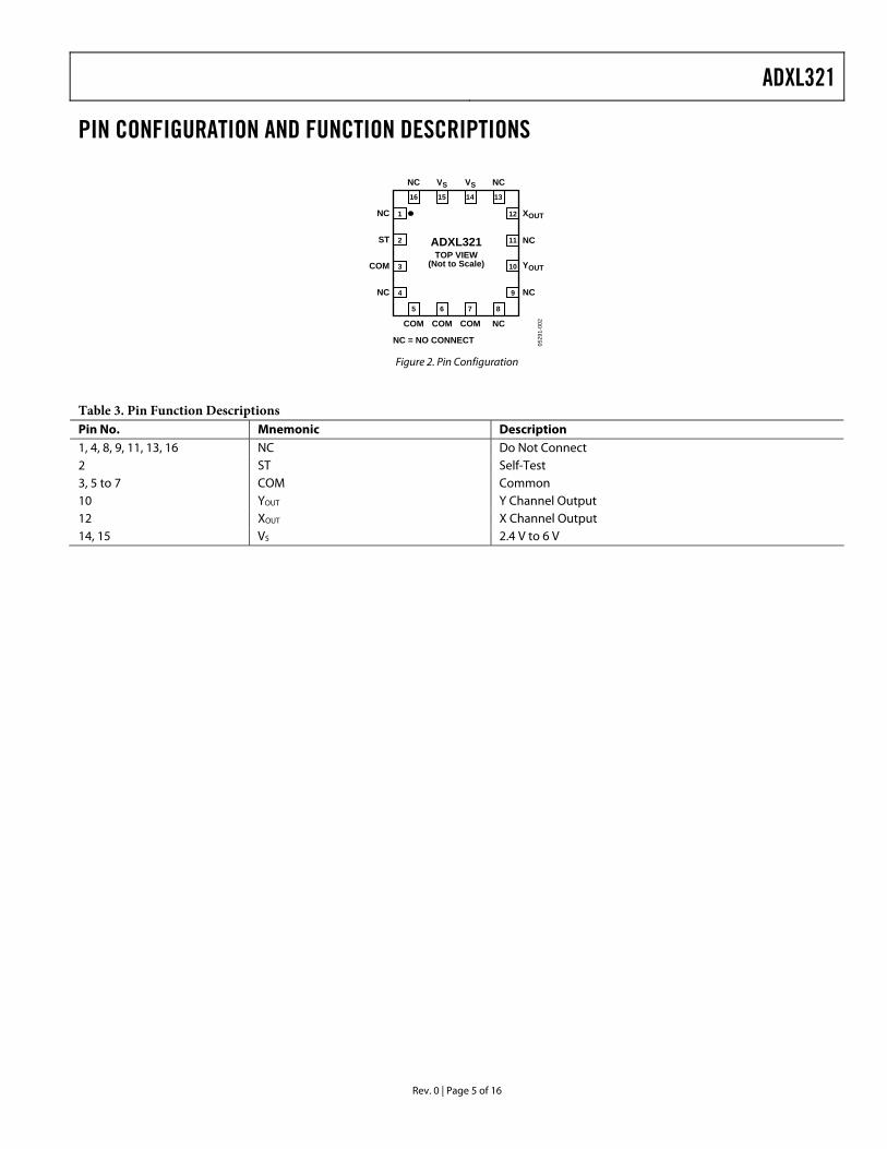
ADXL321
Rev. 0 | Page 5 of 16
PIN CONFIGURATION AND FUNCTION DESCRIPTIONS
NC XOUT
ST NC
COM YOUT
NC NC
COM COM COM NC
NC VS VS NC
NC = NO CONNECT
ADXL321TOP VIEW
(Not to Scale)
0529
1-00
2
1
2
3
4
5 6 7 8
16 15 14 13
12
11
10
9
Figure 2. Pin Configuration
Table 3. Pin Function Descriptions Pin No. Mnemonic Description 1, 4, 8, 9, 11, 13, 16 NC Do Not Connect 2 ST Self-Test 3, 5 to 7 COM Common 10 YOUT Y Channel Output 12 XOUT X Channel Output 14, 15 V 2.4 V to 6 V S

ADXL321
Rev. 0 | Page 6 of 16
0529
1-00
3
tP
tL
t25°C TO PEAK
tSPREHEAT
CRITICAL ZONETL TO TP
TEM
PER
ATU
RE
TIME
RAMP-DOWN
RAMP-UP
TSMIN
TSMAX
TP
TL
Figure 3. Recommended Soldering Profile
Table 4. Recommended Soldering Profile Profile Feature Sn63/Pb37 Pb-Free Average Ramp Rate (TL to T ) 3°C/s max 3°C/s max P
Preheat Minimum Temperature (TSMIN) 100°C 150°C Minimum Temperature (TSMAX) 150°C 200°C Time (TSMIN to TSMAX), t 60 s − 120 s 60 s − 150 s S
TSMAX to T L
Ramp-Up Rate 3°C/s 3°C/s Time Maintained Above Liquidous (TL) Liquidous Temperature (TL) 183°C 217°C Time (tL) 60 s − 150 s 60 s − 150 s Peak Temperature (TP) 240°C + 0°C/−5°C 260°C + 0°C/−5°C Time within 5°C of Actual Peak Temperature (tP) 10 s − 30 s 20 s − 40 s Ramp-Down Rate 6°C/s max 6°C/s max Time 25°C to Peak Temperature 6 min max 8 min max
ADXL321
Rev. 0 | Page 7 of 16
TYPICAL PERFORMANCE CHARACTERISTICS (VS = 3.0 V) 25
20
15
10
5
01.40 1.42 1.44 1.46 1.48 1.50 1.52 1.54 1.56 1.58 1.60
0529
1-00
4
VOLTS
% O
F PO
PULA
TIO
N
25
20
15
10
5
01.40 1.42 1.44 1.46 1.48 1.50 1.52 1.54 1.56 1.58 1.60
0529
1-00
7
VOLTS
% O
F PO
PULA
TIO
N
Figure 4. X-Axis Zero g Bias at 25°C Figure 7. Y-Axis Zero g Bias at 25°C
25
20
15
10
5
0–10 –8 –6 –4 –2 0 2 4 6 8 10
0529
1-00
5
mg/°C
% O
F PO
PULA
TIO
N
25
20
15
10
5
0–10 –8 –6 –4 –2 0 2 4 6 8 10
0529
1-00
8
mg/°C
% O
F PO
PULA
TIO
N
Figure 5. X-Axis Zero g Bias Temperature Coefficient Figure 8. Y-Axis Zero g Bias Temperature Coefficient
50
45
40
35
30
25
20
15
10
5
052 53 54 55 56 57 58 59 60
0529
1-00
6
mV/g
% O
F PO
PULA
TIO
N
50
45
40
35
30
25
20
15
10
5
052 53 54 55 56 57 58 59 60
0529
1-00
9
mV/g
% O
F PO
PULA
TIO
N
Figure 6. X-Axis Sensitivity at 25°C Figure 9. Y-Axis Sensitivity at 25°C

ADXL321
Rev. 0 | Page 8 of 16
1.600
1.575
1.550
1.525
1.500
1.475
1.450
1.425
1.400–30 –20 –10 0 10 20 30 40 50 60 70 80
0529
1-01
0
TEMPERATURE (°C)
OU
TPU
T (S
CA
LE =
56m
V/g)
0.060
0.059
0.058
0.057
0.056
0.055
0.054
0.053
0.052–30 –10 10 30 50 70
0529
1-01
3
SEN
SITI
VITY
(mV/
g)
TEMPERATURE (°C)
Figure 10. Zero g Bias vs. Temperature—Parts Soldered to PCB Figure 13. Sensitivity vs. Temperature—Parts Soldered to PCB
30
20
25
15
10
5
0200 220 240 260 280 300 320 340
0529
1-01
1
NOISE DENSITY (μg/ Hz)
% O
F PO
PULA
TIO
N
30
20
25
15
10
5
0200 220 240 260 280 300 320 340
0529
1-01
4
NOISE DENSITY (μg/ Hz)
% O
F PO
PULA
TIO
N
Figure 11. X-Axis Noise Density at 25°C Figure 14. Y-Axis Noise Density at 25°C
25
20
15
10
5
0–5 –4 –3 –2 –1 0 1 2 3 4 5
0529
1-01
2
PERCENT SENSITIVITY (%)
% O
F PO
PULA
TIO
N
30
25
20
15
10
5
0–5 –4 –3 –2 –1 0 1 2 3 4 5
0529
1-01
5
PERCENT SENSITIVITY (%)
% O
F PO
PULA
TIO
N
Figure 12. Z vs. X Cross-Axis Sensitivity Figure 15. Z vs. Y Cross-Axis Sensitivity
ADXL321
Rev. 0 | Page 9 of 16
0529
1-01
9
16
14
12
10
8
6
4
2
010 2120191817161514131211
0529
1-01
6
mV
% O
F PO
PULA
TIO
N
Figure 19. Turn-On Time—CFigure 16. X-Axis Self-Test Response at 25°C
40
35
30
25
20
15
10
5
0420 430 440 450 460 470 480 490 500 510 520 530
0529
1-01
7
CURRENT (μA)
% O
F PO
PULA
TIO
N
Figure 17. Supply Current at 25°C
16
14
12
10
8
6
4
2
010 2120191817161514131211
0529
1-01
8
mV
% O
F PO
PULA
TIO
N
Figure 18. Y-Axis Self-Test Response at 25°C
X, C = 0.1 μF, Time Scale = 2 ms/DIV Y
ADXL321
Rev. 0 | Page 10 of 16
0529
1-02
0
XOUT = 1.500V
YOUT = 1.500V
XOUT = 1.500V
YOUT = 1.443V
XOUT = 1.443V
YOUT = 1.500V
XOUT = 1.557V
YOUT = 1.50V
XOUT = 1.500V
YOUT = 1.557V
EARTH'S SURFACE
XL321J
#12345678P
XL321J#12345678PXL 32
1J#1
234
5678
P
XL321J
#12345678P
Figure 20. Output Response vs. Orientation (Top View)
ADXL321
Rev. 0 | Page 11 of 16
THEORY OF OPERATION The ADXL321 is a complete acceleration measurement system on a single monolithic IC. The ADXL321 has a measurement range of ±18 g. It contains a polysilicon surface-micromachined sensor and signal conditioning circuitry to implement an open-loop acceleration measurement architecture. The output signals are analog voltages that are proportional to acceleration. The accelerometer measures static acceleration forces, such as gravity, which allows it to be used as a tilt sensor.
The sensor is a polysilicon surface-micromachined structure built on top of a silicon wafer. Polysilicon springs suspend the structure over the surface of the wafer and provide a resistance against acceleration forces. Deflection of the structure is measured using a differential capacitor that consists of independent fixed plates and plates attached to the moving mass. The fixed plates are driven by 180° out-of-phase square waves. Acceleration deflects the beam and unbalances the differential capacitor, resulting in an output square wave whose amplitude is proportional to acceleration. Phase-sensitive demodulation techniques are then used to rectify the signal and determine the direction of the acceleration.
The demodulator’s output is amplified and brought off-chip through a 32 kΩ resistor. The user then sets the signal bandwidth of the device by adding a capacitor. This filtering improves measurement resolution and helps prevent aliasing.
PERFORMANCE Rather than using additional temperature compensation circuitry, innovative design techniques have been used to ensure high performance is built-in. As a result, there is neither quantization error nor nonmonotonic behavior, and temperature hysteresis is very low (typically less than 10 mg over the −20°C to +70°C temperature range).
Figure 10 shows the zero g output performance of eight parts (X- and Y-axis) over a −20°C to +70°C temperature range.
Figure 13 demonstrates the typical sensitivity shift over temperature for supply voltages of 3 V. This is typically better than ±1% over the −20°C to +70°C temperature range.
ADXL321
Rev. 0 | Page 12 of 16
APPLICATIONS POWER SUPPLY DECOUPLING DESIGN TRADE-OFFS FOR SELECTING FILTER
CHARACTERISTICS: THE NOISE/BW TRADE-OFF For most applications, a single 0.1 μF capacitor, CDC, adequately decouples the accelerometer from noise on the power supply. However, in some cases, particularly where noise is present at the 140 kHz internal clock frequency (or any harmonic thereof), noise on the supply may cause interference on the ADXL321 output. If additional decoupling is needed, a 100 Ω (or smaller) resistor or ferrite bead may be inserted in the supply line. Additionally, a larger bulk bypass capacitor (in the 1 μF to 4.7 μF range) may be added in parallel to C
The accelerometer bandwidth selected ultimately determines the measurement resolution (smallest detectable acceleration). Filtering can be used to lower the noise floor, which improves the resolution of the accelerometer. Resolution is dependent on the analog filter bandwidth at X
DC.
SETTING THE BANDWIDTH USING CX AND CY
The ADXL321 has provisions for band-limiting the XOUT and YOUT pins. Capacitors must be added at these pins to implement low-pass filtering for antialiasing and noise reduction. The equation for the 3 dB bandwidth is
F−3 dB = 1/(2π(32 kΩ) × C(X, Y))
or more simply,
F–3 dB = 5 μF/C(X, Y)
The tolerance of the internal resistor (RFILT) typically varies as much as ±15% of its nominal value (32 kΩ), and the bandwidth varies accordingly. A minimum capacitance of 2000 pF for CX and CY is required in all cases.
Table 5. Filter Capacitor Selection, CX and CY
Bandwidth (Hz) Capacitor (μF) 1 4.7 10 0.47 50 0.10 100 0.05 200 0.027 500 0.01
SELF-TEST The ST pin controls the self-test feature. When this pin is set to VS, an electrostatic force is exerted on the accelerometer beam. The resulting movement of the beam allows the user to test if the accelerometer is functional. The typical change in output is 315 mg (corresponding to 18 mV). This pin may be left open-circuit or connected to common (COM) in normal use.
The ST pin should never be exposed to voltages greater than VS + 0.3 V. If this cannot be guaranteed due to the system design (for instance, if there are multiple supply voltages), then a low VF clamping diode between ST and VS is recommended.
OUT and YOUT.
The output of the ADXL321 has a typical bandwidth of 2.5 kHz. The user must filter the signal at this point to limit aliasing errors. The analog bandwidth must be no more than half the A/D sampling frequency to minimize aliasing. The analog bandwidth may be further decreased to reduce noise and improve resolution.
The ADXL321 noise has the characteristics of white Gaussian noise, which contributes equally at all frequencies and is described in terms of μg/√Hz (the noise is proportional to the square root of the accelerometer’s bandwidth). The user should limit bandwidth to the lowest frequency needed by the application in order to maximize the resolution and dynamic range of the accelerometer.
With the single-pole, roll-off characteristic, the typical noise of the ADXL321 is determined by
)1.6BW()Hzμg/(320 ××=rmsNoise
At 100 Hz bandwidth the noise will be
mg4)1.6100()Hzμg/(320 =××=rmsNoise
Often, the peak value of the noise is desired. Peak-to-peak noise can only be estimated by statistical methods. A factor of 6 is generally used to convert rms to peak-to-peak. Table 6 is useful for estimating the probabilities of exceeding various peak values, given the rms value.
Table 6. Estimation of Peak-to-Peak Noise % of Time That Noise Exceeds Nominal Peak-to-Peak Value Peak-to-Peak Value
2 × rms 32 4 × rms 4.6 6 × rms 0.27 8 × rms 0.006

ADXL321
Rev. 0 | Page 13 of 16
Peak-to-peak noise values give the best estimate of the uncertainty in a single measurement. Table 7 gives the typical noise output of the ADXL321 for various CX and CY values.
Table 7. Filter Capacitor Selection (CX, CY)
Bandwidth (Hz)
CX, CY (μF)
RMS Noise (mg)
Peak-to-Peak Noise Estimate (mg)
10 0.47 1.3 7.8 50 0.1 2.9 17.4 100 0.047 4 24 500 0.01 9.1 54.6
USE WITH OPERATING VOLTAGES OTHER THAN 3 V The ADXL321 is tested and specified at VS = 3 V; however, it can be powered with VS as low as 2.4 V or as high as 6 V. Note that some performance parameters change as the supply voltage is varied.
The ADXL321 output is ratiometric, so the sensitivity (or scale factor) varies proportionally to supply voltage. At VS = 5 V, the sensitivity is typically 100 mV/g. At VS = 2.4 V, the sensitivity is typically 45 mV/g.
The zero g bias output is also ratiometric, so the zero g output is nominally equal to VS/2 at all supply voltages.
The output noise is not ratiometric but is absolute in volts; therefore, the noise density decreases as the supply voltage increases. This is because the scale factor (mV/g) increases while the noise voltage remains constant. At VS = 5 V, the noise density is typically 190 μg/√Hz, while at VS = 2.4 V, the noise density is typically 400 μg/√Hz,
Self-test response in g is roughly proportional to the square of the supply voltage. However, when ratiometricity of sensitivity is factored in with supply voltage, the self-test response in volts is roughly proportional to the cube of the supply voltage. For example, at VS = 5 V, the self-test response for the ADXL321 is approximately 80 mV. At VS = 2.4 V, the self-test response is approximately 8 mV.
The supply current decreases as the supply voltage decreases. Typical current consumption at VS = 5 V is 750 μA, and typical current consumption at VS = 2.4 V is 350 μA.
USE AS A DUAL-AXIS TILT SENSOR An accelerometer is most sensitive to tilt when its sensitive axis is perpendicular to the force of gravity (that is, when it is parallel to the earth’s surface). At this orientation, its sensitivity to changes in tilt is highest. When the accelerometer is oriented on axis to gravity (near its +1 g or −1 g reading), the change in output acceleration per degree of tilt is negligible. When the accelerometer is perpendicular to gravity, its output changes nearly 17.5 mg per degree of tilt. At 45°, its output changes at only 12.2 mg per degree of tilt, and resolution declines.
Converting Acceleration to Tilt
When the accelerometer is oriented so both its X-axis and Y-axis are parallel to the earth’s surface, it can be used as a 2-axis tilt sensor with both a roll axis and pitch axis. Once the output signal from the accelerometer has been converted to an acceleration that varies between −1 g and +1 g, the output tilt in degrees is calculated as
PITCH = arcsine(AX/1 g)
ROLL = arcsine(AY/1 g)
Be sure to account for overranges. It is possible for the accelerometers to output a signal greater than ±1 g due to vibration, shock, or other accelerations.
ADXL321
Rev. 0 | Page 14 of 16
OUTLINE DIMENSIONS
16
5
13
8
9
12 1
40.65 BSC
2.431.75 SQ1.08
1.95 BSC
0.20 MIN PIN 1INDICATOR
BOTTOMVIEW
0.20 MIN
SEATINGPLANE
1.501.451.40
PIN 1INDICATOR TOP
VIEW
COPLANARITY0.05
0.05 MAX0.02 NOM
0.350.300.25
0.550.500.45
4.154.00 SQ3.85
*STACKED DIE WITH GLASS SEAL. 0726
06-A
Figure 21. 16-Lead Lead Frame Chip Scale Package [MQ_LFCSP_LQ] 4 mm × 4 mm Body, Thick Quad
(CP-16-5a*) Dimensions shown in millimeters
(Drawing Not to Scale)
ORDERING GUIDE Measurement Range
Specified Voltage (V)
Temperature Range Model Package Description
Package Option
ADXL321JCP ±18 g 3 −20°C to +70°C 16-Lead LFCSP_LQ CP-16-5a 1
ADXL321JCP–REEL ±18 g 3 −20°C to +70°C 16-Lead LFCSP_LQ CP-16-5a ADXL321EB Evaluation Board
1 Lead finish—Matte tin.

ADXL321
Rev. 0 | Page 15 of 16
NOTES

ADXL321
Rev. 0 | Page 16 of 16
NOTES
© 2007 Analog Devices, Inc. All rights reserved. Trademarks and registered trademarks are the property of their respective owners. D05291–0–6/07(0)

LM741QMLOperational AmplifierGeneral DescriptionThe LM741 is a general purpose operational amplifier whichfeatures improved performance over industry standardssuch as the LM709. They are direct, plug-in replacements forthe 709C, LM201, MC1439 and 748 in most applications.
FeaturesThe amplifier offers many features which make their appli-cation nearly foolproof: overload protection on the input andoutput, no latch-up when the common mode range is ex-ceeded, as well as freedom from oscillations.
Ordering InformationNS Part Number JAN Part Number NS Package Number Package Description
LM741H/883 H08C 8 LD Metal Can
LM741J/883 J08A 8LD CERDIP
LM741W/883 W10A 10LD CERPACK
LM741WG/883 WG10A 10LD Ceramic SOIC
Connection Diagrams
Metal Can Package Dual-In-LinePackage
20143902
See NS Package Number H08C20143903
See NS Package Number J08A
Ceramic Flatpak and SOIC Package
20143906
See NS Package Number W10A & WG10A
August 2005LM
741QM
LO
perationalAm
plifier
© 2005 National Semiconductor Corporation DS201439 www.national.com
Schematic Diagram
20143901
LM74
1QM
L
www.national.com 2
Absolute Maximum Ratings (Note 1)
Supply Voltage ±22V
Power Dissipation (Note 2) 500 mW
Differential Input Voltage ±30V
Input Voltage (Note 3) ±15V
Output Short Circuit Duration Continuous
Operating Temperature Range −55˚C ≤ TA ≤ +125˚C
Storage Temperature Range −65˚C ≤ TA ≤ +150˚C
Junction Temperature (TJ) 150˚C
Lead Temperature (Soldering, 10 Seconds) 300˚C
Thermal Resistance
θJA
Metal Can (Still Air) 167˚C/W
Metal Can (500LF / Min Air Flow) 100˚C/W
CERDIP (Still Air) TBD
CERDIP (500LF / Min Air Flow) TBD
CERPACK (Still Air) 228˚C/W
CERPACK (500LF / Min Air Flow) 154˚C/W
Ceramic SOIC (Still Air) 228˚C/W
Ceramic SOIC (500LF / Min Air Flow) 154˚C/W
θJC
Metal Can 44˚C/W
CERDIP TBD
CERPACK 27˚C/W
Ceramic SOIC 27˚C/W
Package Weight (typical)
Metal Can 1000mg
CERDIP 1100mg
CERPACK 260mg
Ceramic SOIC 225mg
ESD Tolerance (Note 4) 400V
Quality Conformance InspectionMil-Std-883, Method 5005 - Group A
Subgroup Description Temp ˚C
1 Static tests at 25
2 Static tests at 125
3 Static tests at -55
4 Dynamic tests at 25
5 Dynamic tests at 125
6 Dynamic tests at -55
7 Functional tests at 25
8A Functional tests at 125
8B Functional tests at -55
9 Switching tests at 25
10 Switching tests at 125
11 Switching tests at -55
12 Settling time at 25
13 Settling time at 125
14 Settling time at -55
LM741Q
ML
www.national.com3
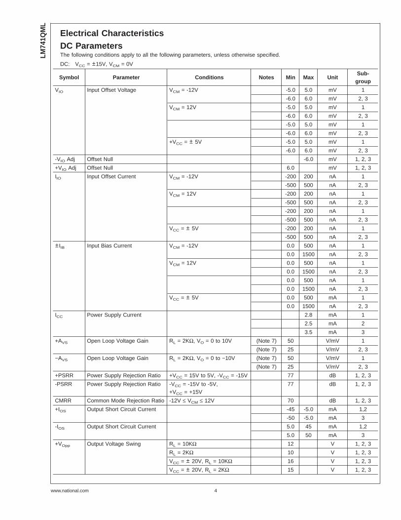
Electrical CharacteristicsDC ParametersThe following conditions apply to all the following parameters, unless otherwise specified.
DC: VCC = ±15V, VCM = 0V
Symbol Parameter Conditions Notes Min Max UnitSub-
group
VIO Input Offset Voltage VCM = -12V -5.0 5.0 mV 1
-6.0 6.0 mV 2, 3
VCM = 12V -5.0 5.0 mV 1
-6.0 6.0 mV 2, 3
-5.0 5.0 mV 1
-6.0 6.0 mV 2, 3
+VCC = ± 5V -5.0 5.0 mV 1
-6.0 6.0 mV 2, 3
-VIO Adj Offset Null -6.0 mV 1, 2, 3
+VIO Adj Offset Null 6.0 mV 1, 2, 3
IIO Input Offset Current VCM = -12V -200 200 nA 1
-500 500 nA 2, 3
VCM = 12V -200 200 nA 1
-500 500 nA 2, 3
-200 200 nA 1
-500 500 nA 2, 3
VCC = ± 5V -200 200 nA 1
-500 500 nA 2, 3±IIB Input Bias Current VCM = -12V 0.0 500 nA 1
0.0 1500 nA 2, 3
VCM = 12V 0.0 500 nA 1
0.0 1500 nA 2, 3
0.0 500 nA 1
0.0 1500 nA 2, 3
VCC = ± 5V 0.0 500 mA 1
0.0 1500 nA 2, 3
ICC Power Supply Current 2.8 mA 1
2.5 mA 2
3.5 mA 3
+AVS Open Loop Voltage Gain RL = 2KΩ, VO = 0 to 10V (Note 7) 50 V/mV 1
(Note 7) 25 V/mV 2, 3
−AVS Open Loop Voltage Gain RL = 2KΩ, VO = 0 to −10V (Note 7) 50 V/mV 1
(Note 7) 25 V/mV 2, 3
+PSRR Power Supply Rejection Ratio +VCC = 15V to 5V, -VCC = -15V 77 dB 1, 2, 3
-PSRR Power Supply Rejection Ratio -VCC = -15V to -5V,+VCC = +15V
77 dB 1, 2, 3
CMRR Common Mode Rejection Ratio -12V ≤ VCM ≤ 12V 70 dB 1, 2, 3
+IOS Output Short Circuit Current -45 -5.0 mA 1,2
-50 -5.0 mA 3
-IOS Output Short Circuit Current 5.0 45 mA 1,2
5.0 50 mA 3
+VOpp Output Voltage Swing RL = 10KΩ 12 V 1, 2, 3
RL = 2KΩ 10 V 1, 2, 3
VCC = ± 20V, RL = 10KΩ 16 V 1, 2, 3
VCC = ± 20V, RL = 2KΩ 15 V 1, 2, 3
LM74
1QM
L
www.national.com 4
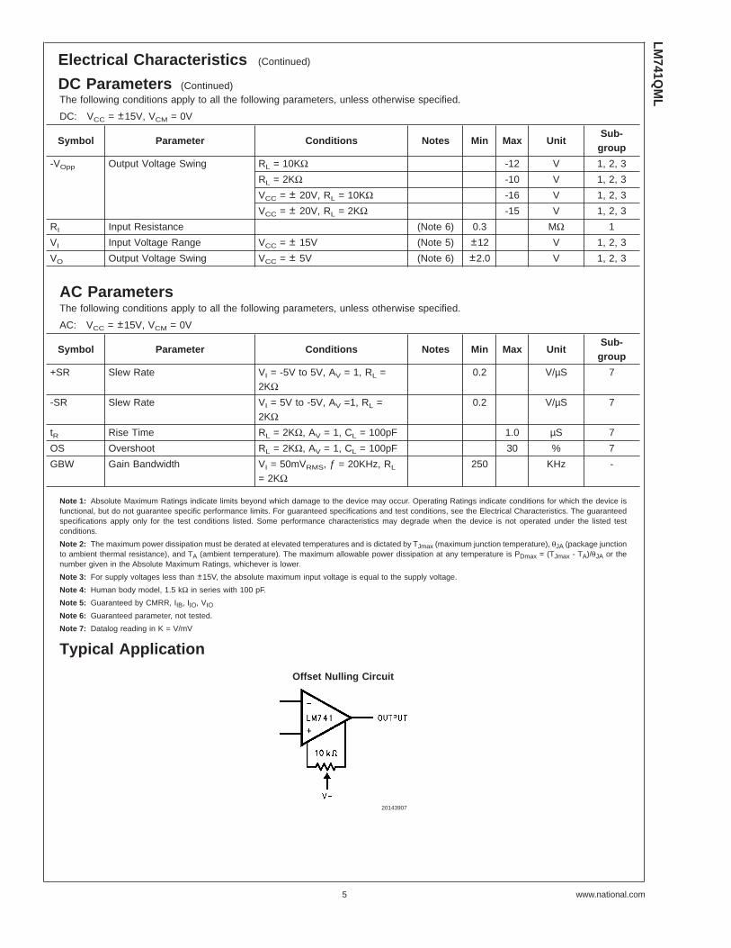
Electrical Characteristics (Continued)
DC Parameters (Continued)The following conditions apply to all the following parameters, unless otherwise specified.
DC: VCC = ±15V, VCM = 0V
Symbol Parameter Conditions Notes Min Max UnitSub-
group
-VOpp Output Voltage Swing RL = 10KΩ -12 V 1, 2, 3
RL = 2KΩ -10 V 1, 2, 3
VCC = ± 20V, RL = 10KΩ -16 V 1, 2, 3
VCC = ± 20V, RL = 2KΩ -15 V 1, 2, 3
RI Input Resistance (Note 6) 0.3 MΩ 1
VI Input Voltage Range VCC = ± 15V (Note 5) ±12 V 1, 2, 3
VO Output Voltage Swing VCC = ± 5V (Note 6) ±2.0 V 1, 2, 3
AC ParametersThe following conditions apply to all the following parameters, unless otherwise specified.
AC: VCC = ±15V, VCM = 0V
Symbol Parameter Conditions Notes Min Max UnitSub-
group
+SR Slew Rate VI = -5V to 5V, AV = 1, RL =2KΩ
0.2 V/µS 7
-SR Slew Rate VI = 5V to -5V, AV =1, RL =2KΩ
0.2 V/µS 7
tR Rise Time RL = 2KΩ, AV = 1, CL = 100pF 1.0 µS 7
OS Overshoot RL = 2KΩ, AV = 1, CL = 100pF 30 % 7
GBW Gain Bandwidth VI = 50mVRMS, ƒ = 20KHz, RL
= 2KΩ250 KHz -
Note 1: Absolute Maximum Ratings indicate limits beyond which damage to the device may occur. Operating Ratings indicate conditions for which the device isfunctional, but do not guarantee specific performance limits. For guaranteed specifications and test conditions, see the Electrical Characteristics. The guaranteedspecifications apply only for the test conditions listed. Some performance characteristics may degrade when the device is not operated under the listed testconditions.
Note 2: The maximum power dissipation must be derated at elevated temperatures and is dictated by TJmax (maximum junction temperature), θJA (package junctionto ambient thermal resistance), and TA (ambient temperature). The maximum allowable power dissipation at any temperature is PDmax = (TJmax - TA)/θJA or thenumber given in the Absolute Maximum Ratings, whichever is lower.
Note 3: For supply voltages less than ±15V, the absolute maximum input voltage is equal to the supply voltage.
Note 4: Human body model, 1.5 kΩ in series with 100 pF.
Note 5: Guaranteed by CMRR, IIB, IIO, VIO
Note 6: Guaranteed parameter, not tested.
Note 7: Datalog reading in K = V/mV
Typical Application
Offset Nulling Circuit
20143907
LM741Q
ML
www.national.com5

Revision History
DateReleased
Revision Section Originator Changes
08/22/05 A New Release to the corporate format L. Lytle 1 MDS datasheet converted into onecorporate datasheet format. Since drift is notperformed on 883 product, the table wasremoved. MNLM741-X Rev 1A0 will bearchived.
LM74
1QM
L
www.national.com 6
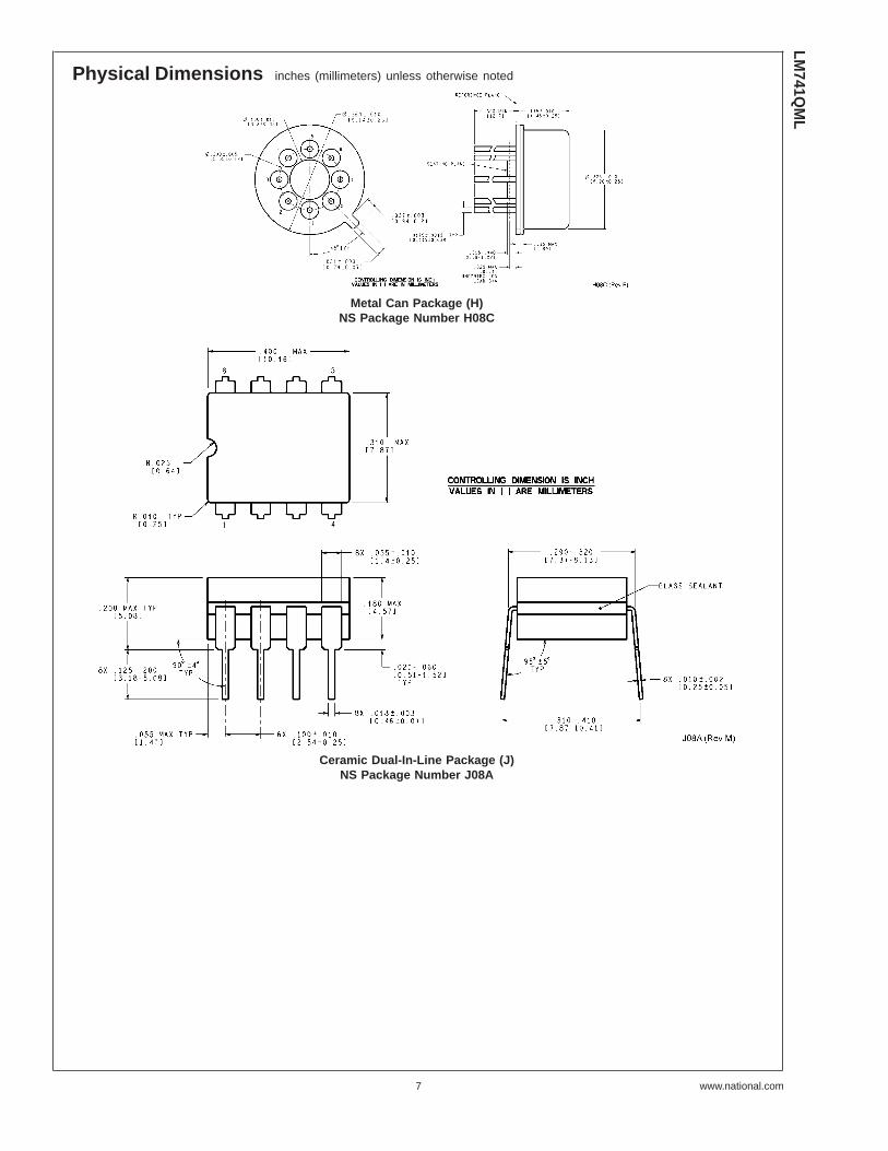
Physical Dimensions inches (millimeters) unless otherwise noted
Metal Can Package (H)NS Package Number H08C
Ceramic Dual-In-Line Package (J)NS Package Number J08A
LM741Q
ML
www.national.com7
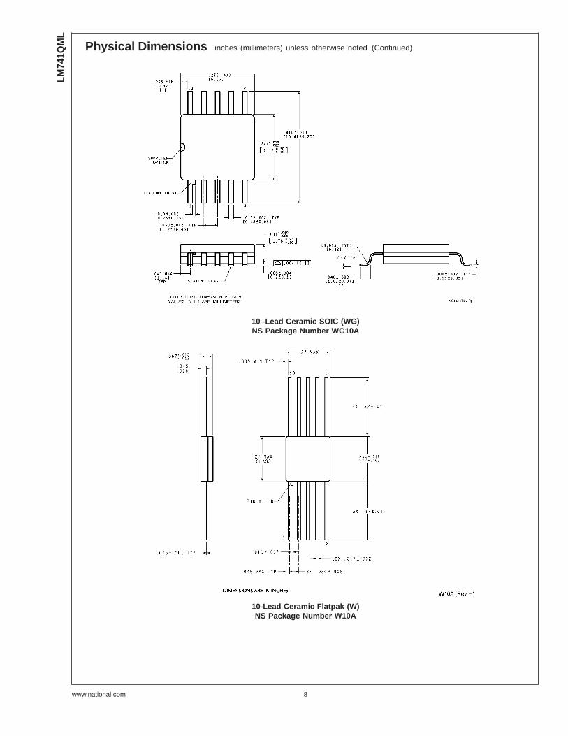
Physical Dimensions inches (millimeters) unless otherwise noted (Continued)
10–Lead Ceramic SOIC (WG)NS Package Number WG10A
10-Lead Ceramic Flatpak (W)NS Package Number W10A
LM74
1QM
L
www.national.com 8

Notes
National does not assume any responsibility for use of any circuitry described, no circuit patent licenses are implied and National reservesthe right at any time without notice to change said circuitry and specifications.
For the most current product information visit us at www.national.com.
LIFE SUPPORT POLICY
NATIONAL’S PRODUCTS ARE NOT AUTHORIZED FOR USE AS CRITICAL COMPONENTS IN LIFE SUPPORT DEVICES OR SYSTEMSWITHOUT THE EXPRESS WRITTEN APPROVAL OF THE PRESIDENT AND GENERAL COUNSEL OF NATIONAL SEMICONDUCTORCORPORATION. As used herein:
1. Life support devices or systems are devices or systemswhich, (a) are intended for surgical implant into the body, or(b) support or sustain life, and whose failure to perform whenproperly used in accordance with instructions for useprovided in the labeling, can be reasonably expected to resultin a significant injury to the user.
2. A critical component is any component of a life supportdevice or system whose failure to perform can be reasonablyexpected to cause the failure of the life support device orsystem, or to affect its safety or effectiveness.
BANNED SUBSTANCE COMPLIANCE
National Semiconductor manufactures products and uses packing materials that meet the provisions of the Customer ProductsStewardship Specification (CSP-9-111C2) and the Banned Substances and Materials of Interest Specification (CSP-9-111S2) and containno ‘‘Banned Substances’’ as defined in CSP-9-111S2.
Leadfree products are RoHS compliant.
National SemiconductorAmericas CustomerSupport CenterEmail: [email protected]: 1-800-272-9959
National SemiconductorEurope Customer Support Center
Fax: +49 (0) 180-530 85 86Email: [email protected]
Deutsch Tel: +49 (0) 69 9508 6208English Tel: +44 (0) 870 24 0 2171Français Tel: +33 (0) 1 41 91 8790
National SemiconductorAsia Pacific CustomerSupport CenterEmail: [email protected]
National SemiconductorJapan Customer Support CenterFax: 81-3-5639-7507Email: [email protected]: 81-3-5639-7560
www.national.com
LM741Q
ML
OperationalA
mplifier
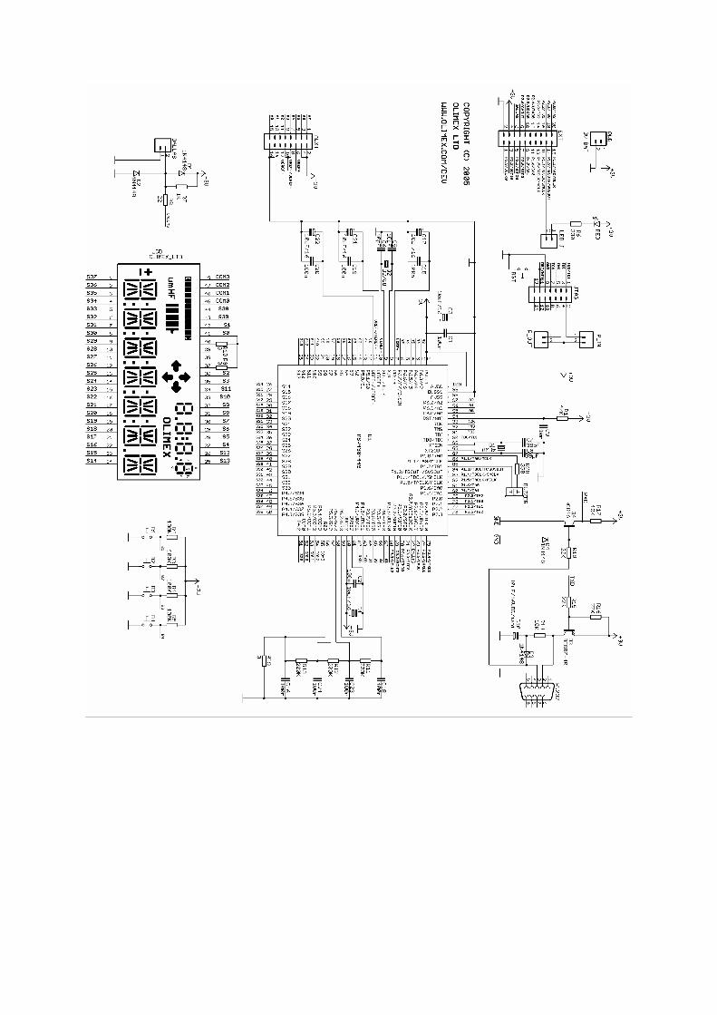

MSP430x43x1, MSP430x43x, MSP430x44xMIXED SIGNAL MICROCONTROLLER
SLAS344F − JANUARY 2002 − REVISED MAY 2007
1POST OFFICE BOX 655303 • DALLAS, TEXAS 75265
Low Supply-Voltage Range, 1.8 V to 3.6 V
Ultralow-Power Consumption:− Active Mode: 280 μA at 1 MHz, 2.2 V− Standby Mode: 1.1 μA− Off Mode (RAM Retention): 0.1 μA
Five Power Saving Modes
Wake-Up From Standby Mode in Less Than 6 μs
16-Bit RISC Architecture,125-ns Instruction Cycle Time
12-Bit A/D Converter With InternalReference, Sample-and-Hold andAutoscan Feature
16-Bit Timer_B With Three† or Seven‡
Capture/Compare-With-Shadow Registers
16-Bit Timer_A With ThreeCapture/Compare Registers
On-Chip Comparator
Serial Communication Interface (USART),Select Asynchronous UART orSynchronous SPI by Software:− Two USARTs (USART0, USART1) —
MSP430x44x Devices− One USART (USART0) —
MSP430x43x(1) Devices
Brownout Detector
Supply Voltage Supervisor/Monitor WithProgrammable Level Detection
Serial Onboard Programming,No External Programming Voltage NeededProgrammable Code Protection by SecurityFuse
Integrated LCD Driver for up to160 Segments
Bootstrap Loader
Family Members Include:− MSP430F435, MSP430F4351§:
16KB+256B Flash Memory,512B RAM
− MSP430F436, MSP430F4361§:24KB+256B Flash Memory,1KB RAM
− MSP430F437, MSP430F4371§:32KB+256B Flash Memory,1KB RAM
− MSP430F447:32KB+256B Flash Memory,1KB RAM
− MSP430F448:48KB+256B Flash Memory,2KB RAM
− MSP430F449:60KB+256B Flash Memory,2KB RAM
For Complete Module Descriptions, SeeThe MSP430x4xx Family User’s Guide,Literature Number SLAU056
† ’F435, ’F436, and ’F437 devices‡ ’F447, ’F448, and ’F449 devices§ The MSP430F43x1 devices are identical to the MSP430F43x
devices with the exception that the ADC12 module is notimplemented.
description
The Texas Instruments MSP430 family of ultralow power microcontrollers consists of several devices featuringdifferent sets of peripherals targeted for various applications. The architecture, combined with five low-powermodes, is optimized to achieve extended battery life in portable measurement applications. The device featuresa powerful 16-bit RISC CPU, 16-bit registers, and constant generators that contribute to maximum codeefficiency. The digitally controlled oscillator (DCO) allows wake-up from low-power modes to active mode in lessthan 6 μs.
This integrated circuit can be damaged by ESD. Texas Instruments recommends that all integrated circuits be handled withappropriate precautions. Failure to observe proper handling and installation procedures can cause damage. ESD damage can rangefrom subtle performance degradation to complete device failure. Precision integrated circuits may be more susceptible to damagebecause very small parametric changes could cause the device not to meet its published specifications. These devices have limitedbuilt-in ESD protection.
PRODUCTION DATA information is current as of publication date.Products conform to specifications per the terms of Texas Instrumentsstandard warranty. Production processing does not necessarily includetesting of all parameters.
Copyright © 2002−2007, Texas Instruments Incorporated
Please be aware that an important notice concerning availability, standard warranty, and use in critical applications ofTexas Instruments semiconductor products and disclaimers thereto appears at the end of this data sheet.

MSP430x43x1, MSP430x43x, MSP430x44xMIXED SIGNAL MICROCONTROLLER
SLAS344F − JANUARY 2002 − REVISED MAY 2007
2 POST OFFICE BOX 655303 • DALLAS, TEXAS 75265
description (continued)
The MSP430x43x(1) and the MSP430x44x series are microcontroller configurations with two built-in 16-bittimers, a fast 12-bit A/D converter (not implemented on the MSP430F43x1 devices), one or two universal serialsynchronous/asynchronous communication interfaces (USART), 48 I/O pins, and a liquid crystal driver (LCD)with up to 160 segments.
Typical applications include sensor systems that capture analog signals, convert them to digital values, andprocess and transmit the data to a host system, or process this data and display it on a LCD panel. The timersmake the configurations ideal for industrial control applications such as ripple counters, digital motor control,EE-meters, hand-held meters, etc. The hardware multiplier enhances the performance and offers a broad codeand hardware-compatible family solution.
AVAILABLE OPTIONS
PACKAGED DEVICES
TA PLASTIC 80-PIN QFP(PN)
PLASTIC 100-PIN QFP(PZ)
−40°C to 85°C
MSP430F435IPNMSP430F436IPNMSP430F437IPN
MSP430F4351IPNMSP430F4361IPNMSP430F4371IPN
MSP430F435IPZMSP430F436IPZMSP430F437IPZ
MSP430F4351IPZMSP430F4361IPZMSP430F4371IPZ
MSP430F447IPZMSP430F448IPZMSP430F449IPZ

MSP430x43x1, MSP430x43x, MSP430x44xMIXED SIGNAL MICROCONTROLLER
SLAS344F − JANUARY 2002 − REVISED MAY 2007
3POST OFFICE BOX 655303 • DALLAS, TEXAS 75265
pin designation, MSP430x4351IPN, MSP430x4361IPN, MSP430x4371IPN
22 23
P1.7/CA1P2.0/TA2P2.1/TB0P2.2/TB1P2.3/TB2P2.4/UTXD0P2.5/URXD0DVSS2DVCC2P5.7/R33P5.6/R23P5.5/R13R03P5.4/COM3P5.3/COM2P5.2/COM1COM0P3.0/STE0/S31P3.1/SIMO0/S30P3.2/SOMI0/S29
6059585756555453525150494847464544434241
24
1234567891011121314151617181920
DVCC1P6.3P6.4P6.5P6.6
P6.7/SVSINReserved
XINXOUTDVSSDVSS
P5.1/S0P5.0/S1P4.7/S2P4.6/S3P4.5/S4P4.4/S5P4.3/S6P4.2/S7P4.1/S8
25 26 27 28
PN PACKAGE(TOP VIEW)
TDO
/TD
I
79 78 77 76 7580 74
P6.
1P
6.0
RS
T/N
MI
TCK
TMS
P2.
6/C
AO
UT/
S19
S21
S15
S16
S17
72 71 7073
29 30 31 32 33
69 68
21
P4.
0/S
9
XT2
OU
T
67 66 65 64
34 35 36 37
S22
S23
P3.
7/S
24P
3.6/
S25
P1.
0/TA
0P
1.1/
TA0/
MC
LKP
1.2/
TA1
P1.
3/TB
OU
TH/S
VS
OU
T
P3.
5/S
26P
3.4/
S27
38 39 40
P1.
4/TB
CLK
/SM
CLK
P1.
5/TA
CLK
/AC
LK
63 62 61
TDI/T
CLK
XT2
IN
P1.
6/C
A0
S10
S20
P3.
3/U
CLK
0/S
28S11
S12
S13
S14
P2.
7/S
18
P6.
2
MSP430F4351IPNMSP430F4361IPNMSP430F4371IPN
SS
1D
VCC
AV
SS
AV
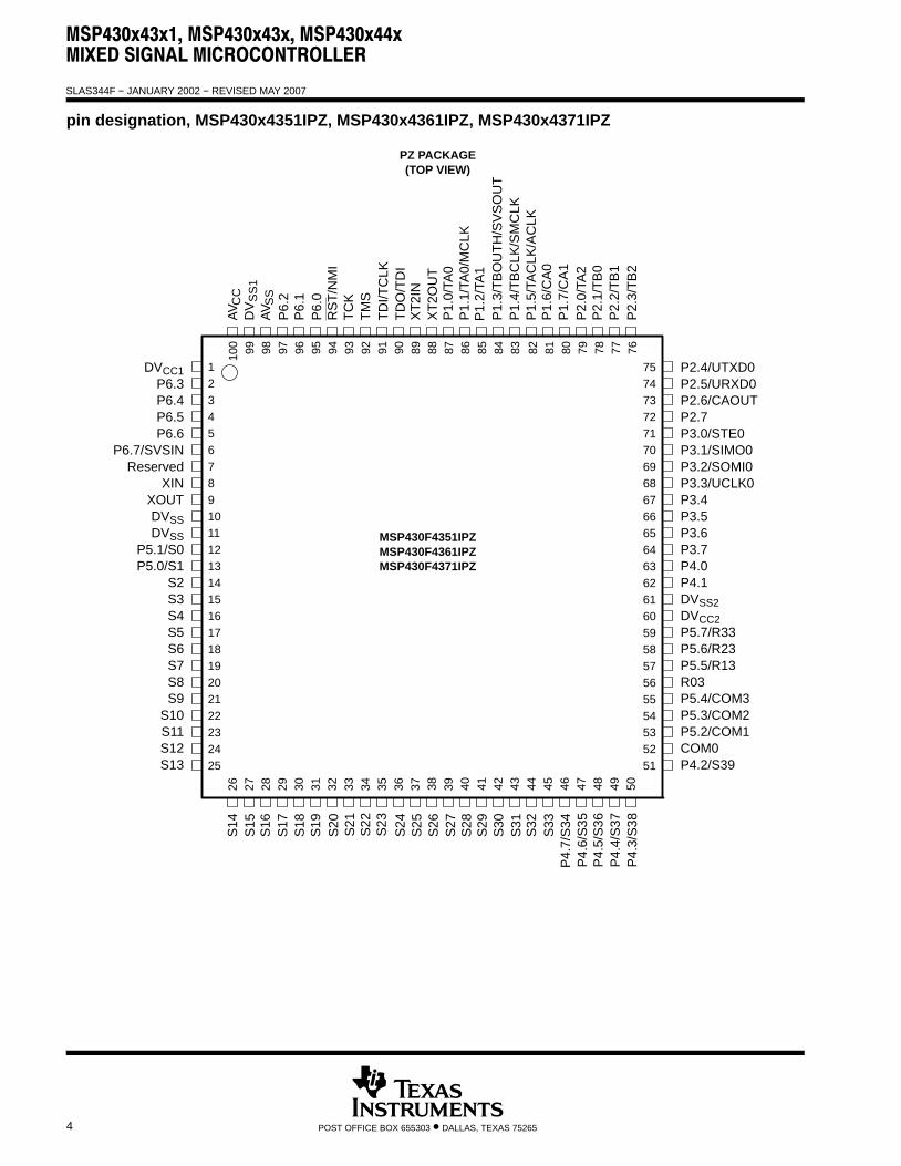
MSP430x43x1, MSP430x43x, MSP430x44xMIXED SIGNAL MICROCONTROLLER
SLAS344F − JANUARY 2002 − REVISED MAY 2007
4 POST OFFICE BOX 655303 • DALLAS, TEXAS 75265
pin designation, MSP430x4351IPZ, MSP430x4361IPZ, MSP430x4371IPZ
12345678910111213141516171819202122232425
767778798081828384858687888990919293949596979899100
75747372717069686766656463626160595857565554535251
50494847464544434241403938373635343332313029282726
P1.
7/C
A1
P6.
1P
6.0
RS
T/N
MI
XT2
INX
T2O
UT
P1.
3/TB
OU
TH/S
VS
OU
TP
1.4/
TBC
LK/S
MC
LKP
1.5/
TAC
LK/A
CLK
P1.
6/C
A0
P2.
3/TB
2
S14
S15
S16
S17
S18
S20
S25
S26
S27
S28
S29
S31
P4.
7/S
34
S30
PZ PACKAGE(TOP VIEW)
P1.
0/TA
0
TDI/T
CLK
TDO
/TD
I
S21
SS
1D
V
P6.
2
P1.
2/TA
1
S24
P4.
6/S
35
DVCC1P6.3P6.4P6.5P6.6
P6.7/SVSINReserved
XINXOUTDVSSDVSS
P5.1/S0P5.0/S1
S2S3S4S5S6S7S8S9
S10S11S12S13
P2.4/UTXD0P2.5/URXD0P2.6/CAOUTP2.7P3.0/STE0P3.1/SIMO0P3.2/SOMI0P3.3/UCLK0P3.4P3.5P3.6P3.7P4.0P4.1DVSS2DVCC2P5.7/R33P5.6/R23P5.5/R13R03P5.4/COM3P5.3/COM2P5.2/COM1COM0P4.2/S39
S19 S22
S23
S33
S32
P4.
5/S
36P
4.4/
S37
P4.
3/S
38
CC
AV
SS
AV TCK
TMS
P1.
1/TA
0/M
CLK
P2.
0/TA
2P
2.1/
TB0
P2.
2/TB
1
MSP430F4351IPZMSP430F4361IPZMSP430F4371IPZ
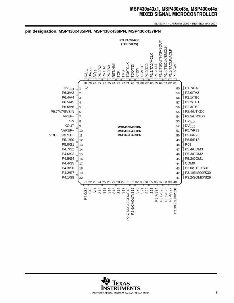
MSP430x43x1, MSP430x43x, MSP430x44xMIXED SIGNAL MICROCONTROLLER
SLAS344F − JANUARY 2002 − REVISED MAY 2007
5POST OFFICE BOX 655303 • DALLAS, TEXAS 75265
pin designation, MSP430x435IPN, MSP430x436IPN, MSP430x437IPN
22 23
P1.7/CA1P2.0/TA2P2.1/TB0P2.2/TB1P2.3/TB2P2.4/UTXD0P2.5/URXD0DVSS2DVCC2P5.7/R33P5.6/R23P5.5/R13R03P5.4/COM3P5.3/COM2P5.2/COM1COM0P3.0/STE0/S31P3.1/SIMO0/S30P3.2/SOMI0/S29
6059585756555453525150494847464544434241
24
1234567891011121314151617181920
DVCC1P6.3/A3P6.4/A4P6.5/A5P6.6/A6
P6.7/A7/SVSINVREF+
XINXOUT
VeREF+VREF−/VeREF−
P5.1/S0P5.0/S1P4.7/S2P4.6/S3P4.5/S4P4.4/S5P4.3/S6P4.2/S7P4.1/S8
25 26 27 28
PN PACKAGE(TOP VIEW)
TDO
/TD
I
79 78 77 76 7580 74
P6.
1/A
1P
6.0/
A0
RS
T/N
MI
TCK
TMS
P2.
6/C
AO
UT/
S19
S21
S15
S16
S17
72 71 7073
29 30 31 32 33
69 68
21
P4.
0/S
9
XT2
OU
T
67 66 65 64
34 35 36 37
S22
S23
P3.
7/S
24P
3.6/
S25
P1.
0/TA
0P
1.1/
TA0/
MC
LKP
1.2/
TA1
P1.
3/TB
OU
TH/S
VS
OU
T
P3.
5/S
26P
3.4/
S27
38 39 40
P1.
4/TB
CLK
/SM
CLK
P1.
5/TA
CLK
/AC
LK
63 62 61
TDI/T
CLK
XT2
IN
P1.
6/C
A0
S10
S20
P3.
3/U
CLK
0/S
28S11
S12
S13
S14
P2.
7/A
DC
12C
LK/S
18
P6.
2/A
2
MSP430F435IPNMSP430F436IPNMSP430F437IPN
SS
1D
VCC
AV
SS
AV

MSP430x43x1, MSP430x43x, MSP430x44xMIXED SIGNAL MICROCONTROLLER
SLAS344F − JANUARY 2002 − REVISED MAY 2007
6 POST OFFICE BOX 655303 • DALLAS, TEXAS 75265
pin designation, MSP430x435IPZ, MSP430x436IPZ, MSP430x437IPZ
12345678910111213141516171819202122232425
767778798081828384858687888990919293949596979899100
75747372717069686766656463626160595857565554535251
50494847464544434241403938373635343332313029282726
P1.
7/C
A1
P6.
1/A
1P
6.0/
A0
RS
T/N
MI
XT2
INX
T2O
UT
P1.
3/TB
OU
TH/S
VS
OU
TP
1.4/
TBC
LK/S
MC
LKP
1.5/
TAC
LK/A
CLK
P1.
6/C
A0
P2.
3/TB
2
S14
S15
S16
S17
S18
S20
S25
S26
S27
S28
S29
S31
P4.
7/S
34
S30
PZ PACKAGE(TOP VIEW)
P1.
0/TA
0
TDI/T
CLK
TDO
/TD
I
S21
SS
1D
V
P6.
2/A
2
P1.
2/TA
1
S24
P4.
6/S
35
DVCC1P6.3/A3P6.4/A4P6.5/A5P6.6/A6
P6.7/A7/SVSINVREF+
XINXOUT
VeREF+VREF−/VeREF−
P5.1/S0P5.0/S1
S2S3S4S5S6S7S8S9
S10S11S12S13
P2.4/UTXD0P2.5/URXD0P2.6/CAOUTP2.7/ADC12CLKP3.0/STE0P3.1/SIMO0P3.2/SOMI0P3.3/UCLK0P3.4P3.5P3.6P3.7P4.0P4.1DVSS2DVCC2P5.7/R33P5.6/R23P5.5/R13R03P5.4/COM3P5.3/COM2P5.2/COM1COM0P4.2/S39
S19 S22
S23
S33
S32
P4.
5/S
36P
4.4/
S37
P4.
3/S
38
CC
AV
SS
AV TCK
TMS
P1.
1/TA
0/M
CLK
P2.
0/TA
2P
2.1/
TB0
P2.
2/TB
1
MSP430F435IPZMSP430F436IPZMSP430F437IPZ

MSP430x43x1, MSP430x43x, MSP430x44xMIXED SIGNAL MICROCONTROLLER
SLAS344F − JANUARY 2002 − REVISED MAY 2007
7POST OFFICE BOX 655303 • DALLAS, TEXAS 75265
pin designation, MSP430x447IPZ, MSP430x448IPZ, MSP430x449IPZ
12345678910111213141516171819202122232425
767778798081828384858687888990919293949596979899100
75747372717069686766656463626160595857565554535251
50494847464544434241403938373635343332313029282726
P1.
7/C
A1
P6.
1/A
1P
6.0/
A0
RS
T/N
MI
XT2
INX
T2O
UT
P1.
3/TB
OU
TH/S
VS
OU
TP
1.4/
TBC
LK/S
MC
LKP
1.5/
TAC
LK/A
CLK
P1.
6/C
A0
P2.
3/TB
2
S14
S15
S16
S17
S18
S20
S25
S26
S27
S28
S29
S31
P4.
7/S
34
S30
PZ PACKAGE(TOP VIEW)
P1.
0/TA
0
TDI/T
CLK
TDO
/TD
I
S21
SS
1D
V
P6.
2/A
2
P1.
2/TA
1
S24
P4.
6/S
35
DVCC1P6.3/A3P6.4/A4P6.5/A5P6.6/A6
P6.7/A7/SVSINVREF+
XINXOUT
VeREF+VREF−/VeREF−
P5.1/S0P5.0/S1
S2S3S4S5S6S7S8S9
S10S11S12S13
P2.4/UTXD0P2.5/URXD0P2.6/CAOUTP2.7/ADC12CLKP3.0/STE0P3.1/SIMO0P3.2/SOMI0P3.3/UCLK0P3.4/TB3P3.5/TB4P3.6/TB5P3.7/TB6P4.0/UTXD1P4.1/URXD1DVSS2DVCC2P5.7/R33P5.6/R23P5.5/R13R03P5.4/COM3P5.3/COM2P5.2/COM1COM0P4.2/STE1/S39
S19 S22
S23
S33
S32
P4.
5/U
CLK
1/S
36P
4.4/
SO
MI1
/S37
4.3/
SIM
O1/
S38
CC
AV
SS
AV TCK
TMS
P1.
1/TA
0/M
CLK
P2.
0/TA
2P
2.1/
TB0
P2.
2/TB
1
MSP430F447IPZMSP430F448IPZMSP430F449IPZ
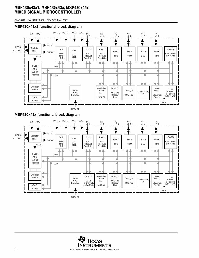
MSP430x43x1, MSP430x43x, MSP430x44xMIXED SIGNAL MICROCONTROLLER
SLAS344F − JANUARY 2002 − REVISED MAY 2007
8 POST OFFICE BOX 655303 • DALLAS, TEXAS 75265
MSP430x43x1 functional block diagram
Comparator_A
DVCC1/2 DVSS1/2 AVCC AVSS
RST/NMI
P2
Flash
32KB24KB16KB
RAM
1KB512B
WatchdogTimerWDT
15/16-Bit
Port 2
8 I/OInterrupt
Capability
POR/SVS/
Brownout
BasicTimer 1
1 InterruptVector
LCD128/160
Segments1,2,3,4 MUX
fLCD
8
MCLK
XOUT
JTAGInterface
XIN
SMCLK
ACLK
MDB
MAB
Emulation
P3
Port 3
8 I/O
8
Module Timer_A3
3 CC Reg
P1
Port 1
8 I/OInterrupt
Capability
8P5
Port 5
8 I/O
8P6
Port 6
6 I/O
8P4
Port 4
8 I/O
8
Timer_B3
3 CC RegShadow
Reg
USART0
UART ModeSPI Mode
XT2IN
XT2OUTOscillator
FLL+
8 MHzCPU
incl. 16Registers
MSP430x43x functional block diagram
Comparator_A
DVCC1/2 DVSS1/2 AVCC AVSS
RST/NMI
P2
Flash
32KB24KB16KB
RAM
1KB512B
WatchdogTimerWDT
15/16-Bit
Port 2
8 I/OInterrupt
Capability
POR/SVS/
Brownout
BasicTimer 1
1 InterruptVector
LCD128/160
Segments1,2,3,4 MUX
fLCD
8
MCLK
XOUT
JTAGInterface
XIN
SMCLK
ACLK
MDB
MAB
Emulation
P3
Port 3
8 I/O
8
Module Timer_A3
3 CC Reg
P1
Port 1
8 I/OInterrupt
Capability
8P5
Port 5
8 I/O
8P6
Port 6
6 I/O
8P4
Port 4
8 I/O
8
Timer_B3
3 CC RegShadow
Reg
USART0
UART ModeSPI Mode
XT2IN
XT2OUT
ADC12
12-Bit8 Channels<10μs Conv.
OscillatorFLL+
8 MHzCPU
incl. 16Registers

MSP430x43x1, MSP430x43x, MSP430x44xMIXED SIGNAL MICROCONTROLLER
SLAS344F − JANUARY 2002 − REVISED MAY 2007
9POST OFFICE BOX 655303 • DALLAS, TEXAS 75265
MSP430x44x functional block diagram
Comparator_A
DVCC1/2 DVSS1/2 AVCC AVSS
RST/NMI
P2
Flash
60KB48KB32KB
RAM
2KB1KB
WatchdogTimerWDT
15/16-Bit
Port 2
8 I/OInterrupt
Capability
POR/SVS/
Brownout
BasicTimer 1
1 InterruptVector
LCD160
Segments1,2,3,4 MUX
fLCD
8
MCLK
XOUT
JTAGInterface
XIN
SMCLK
ACLK
MDB
MAB
Emulation
P3
Port 3
8 I/O
8
Module Timer_A3
3 CC Reg
P1
Port 1
8 I/OInterrupt
Capability
8P5
Port 5
8 I/O
8P6
Port 6
6 I/O
8P4
Port 4
8 I/O
8
Timer_B7
7 CC RegShadow
Reg
USART0USART1
UART ModeSPI Mode
XT2IN
XT2OUT
ADC12
12-Bit8 Channels<10μs Conv.
OscillatorFLL+
8 MHzCPU
incl. 16Registers
HardwareMultiplier
MPY, MPYSMAC,MACS

MSP430x43x1, MSP430x43x, MSP430x44xMIXED SIGNAL MICROCONTROLLER
SLAS344F − JANUARY 2002 − REVISED MAY 2007
10 POST OFFICE BOX 655303 • DALLAS, TEXAS 75265
MSP430x43x1 Terminal Functions
TERMINAL
PNI/O
PZI/O
DESCRIPTION
NAME NO.I/O
NAME NO.I/O
DESCRIPTION
DVCC1 1 DVCC1 1 Digital supply voltage, positive terminal.
P6.3 2 I/O P6.3 2 I/O General-purpose digital I/O
P6.4 3 I/O P6.4 3 I/O General-purpose digital I/O
P6.5 4 I/O P6.5 4 I/O General-purpose digital I/O
P6.6 5 I/O P6.6 5 I/O General-purpose digital I/O
P6.7/SVSIN 6 I/O P6.7/SVSIN 6 I/O General-purpose digital I/O / input to brownout, supply voltagesupervisor
Reserved 7 Reserved 7 Reserved, do not connect externally
XIN 8 I XIN 8 IInput port for crystal oscillator XT1. Standard or watch crystals can beconnected.
XOUT 9 O XOUT 9 O Output terminal of crystal oscillator XT1
DVSS 10 I DVSS 10 I Connect to DVSS
DVSS 11 I DVSS 11 I Connect to DVSS
P5.1/S0 12 I/O P5.1/S0 12 I/O General-purpose digital I/O / LCD segment output 0
P5.0/S1 13 I/O P5.0/S1 13 I/O General-purpose digital I/O / LCD segment output 1
P4.7/S2 14 I/O S2 14 O General-purpose digital I/O / LCD segment output 2
P4.6/S3 15 I/O S3 15 O General-purpose digital I/O / LCD segment output 3
P4.5/S4 16 I/O S4 16 O General-purpose digital I/O / LCD segment output 4
P4.4/S5 17 I/O S5 17 O General-purpose digital I/O / LCD segment output 5
P4.3/S6 18 I/O S6 18 O General-purpose digital I/O / LCD segment output 6
P4.2/S7 19 I/O S7 19 O General-purpose digital I/O / LCD segment output 7
P4.1/S8 20 I/O S8 20 O General-purpose digital I/O / LCD segment output 8
P4.0/S9 21 I/O S9 21 O General-purpose digital I/O / LCD segment output 9
S10 22 O S10 22 O LCD segment output 10
S11 23 O S11 23 O LCD segment output 11
S12 24 O S12 24 O LCD segment output 12
S13 25 O S13 25 O LCD segment output 13
S14 26 O S14 26 O LCD segment output 14
S15 27 O S15 27 O LCD segment output 15
S16 28 O S16 28 O LCD segment output 16
S17 29 O S17 29 O LCD segment output 17
P2.7/S18 30 I/O S18 30 O General-purpose digital I/O / LCD segment output 18
P2.6/CAOUT/S19 31 I/O S19 31 OGeneral-purpose digital I/O / Comparator_A output / LCD segmentoutput 19
S20 32 O S20 32 O LCD segment output 20
S21 33 O S21 33 O LCD segment output 21
S22 34 O S22 34 O LCD segment output 22
S23 35 O S23 35 O LCD segment output 23
P3.7/S24 36 I/O S24 36 O General-purpose digital I/O / LCD segment output 24
P3.6/S25 37 I/O S25 37 O General-purpose digital I/O / LCD segment output 25
P3.5/S26 38 I/O S26 38 O General-purpose digital I/O / LCD segment output 26
P3.4/S27 39 I/O S27 39 O General-purpose digital I/O / LCD segment output 27

MSP430x43x1, MSP430x43x, MSP430x44xMIXED SIGNAL MICROCONTROLLER
SLAS344F − JANUARY 2002 − REVISED MAY 2007
11POST OFFICE BOX 655303 • DALLAS, TEXAS 75265
MSP430x43x1 Terminal Functions (Continued)
TERMINAL
PNI/O
PZI/O
DESCRIPTION
NAME NO.I/O
NAME NO.I/O
DESCRIPTION
P3.3/UCLK0/S28 40 I/O S28 40 OGeneral-purpose digital I/O / ext. clock i/p—USART0/UART or SPImode, clock o/p—USART0/SPI mode / LCD segment output 28
P3.2/SOMI0/S29 41 I/O S29 41 OGeneral-purpose digital I/O / slave out/master in of USART0/SPI mode/ LCD segment output 29
P3.1/SIMO0/S30 42 I/O S30 42 OGeneral-purpose digital I/O / slave out/master out of USART0/SPImode / LCD segment output 30
P3.0/STE0/S31 43 I/O S31 43 OGeneral-purpose digital I/O / slave transmit enable-USART0/SPImode / LCD segment output 31
S32 44 O LCD segment output 32
S33 45 O LCD segment output 33
P4.7/S34 46 I/O General-purpose digital I/O / LCD segment output 34
P4.6/S35 47 I/O General-purpose digital I/O / LCD segment output 35
P4.5/S36 48 I/O General-purpose digital I/O / LCD segment output 36
P4.4/S37 49 I/O General-purpose digital I/O / LCD segment output 37
P4.3/S38 50 I/O General-purpose digital I/O / LCD segment output 38
P4.2/S39 51 I/O General-purpose digital I/O / LCD segment output 39
COM0 44 O COM0 52 O COM0−3 are used for LCD backplanes.
P5.2/COM1 45 I/O P5.2/COM1 53 I/OGeneral-purpose digital I/O / common output, COM0−3 are used forLCD backplanes.
P5.3/COM2 46 I/O P5.3/COM2 54 I/OGeneral-purpose digital I/O / common output, COM0−3 are used forLCD backplanes.
P5.4/COM3 47 I/O P5.4/COM3 55 I/OGeneral-purpose digital I/O / common output, COM0−3 are used forLCD backplanes.
R03 48 I R03 56 I Input port of fourth positive (lowest) analog LCD level (V5)
P5.5/R13 49 I/O P5.5/R13 57 I/OGeneral-purpose digital I/O / input port of third most positive analogLCD level (V4 or V3)
P5.6/R23 50 I/O P5.6/R23 58 I/OGeneral-purpose digital I/O / input port of second most positive analogLCD level (V2)
P5.7/R33 51 I/O P5.7/R33 59 I/OGeneral-purpose digital I/O / output port of most positive analog LCDlevel (V1)
DVCC2 52 DVCC2 60 Digital supply voltage, positive terminal.
DVSS2 53 DVSS2 61 Digital supply voltage, negative terminal.
P4.1 62 I/O General-purpose digital I/O
P4.0 63 I/O General-purpose digital I/O
P3.7 64 I/O General-purpose digital I/O
P3.6 65 I/O General-purpose digital I/O
P3.5 66 I/O General-purpose digital I/O
P3.4 67 I/O General-purpose digital I/O
P3.3/UCLK0 68 I/OGeneral-purpose digital I/O / external clock input—USART0/UART orSPI mode, clock output—USART0/SPI mode
P3.2/SOMI0 69 I/O General-purpose digital I/O / slave out/master in of USART0/SPI mode
P3.1/SIMO0 70 I/O General-purpose digital I/O / slave in/master out of USART0/SPI mode
P3.0/STE0 71 I/O General-purpose digital I/O / slave transmit enable USART0/SPI mode
P2.7 72 I/O General-purpose digital I/O
P2.6/CAOUT 73 I/O General-purpose digital I/O / Comparator_A output
P2.5/URXD0 54 I/O P2.5/URXD0 74 I/O General-purpose digital I/O / receive data in—USART0/UART mode
MSP430x43x1, MSP430x43x, MSP430x44xMIXED SIGNAL MICROCONTROLLER
SLAS344F − JANUARY 2002 − REVISED MAY 2007
12 POST OFFICE BOX 655303 • DALLAS, TEXAS 75265
MSP430x43x1 Terminal Functions (Continued)
TERMINAL
PNI/O
PZI/O
DESCRIPTION
NAME NO.I/O
NAME NO.I/O
DESCRIPTION
P2.4/UTXD0 55 I/O P2.4/UTXD0 75 I/O General-purpose digital I/O / transmit data out—USART0/UART mode
P2.3/TB2 56 I/O P2.3/TB2 76 I/OGeneral-purpose digital I/O / Timer_B3 CCR2. Capture: CCI2A/CCI2B input, compare: Out2 output
P2.2/TB1 57 I/O P2.2/TB1 77 I/OGeneral-purpose digital I/O / Timer_B3 CCR1. Capture: CCI1A/CCI1B input, compare: Out1 output
P2.1/TB0 58 I/O P2.1/TB0 78 I/OGeneral-purpose digital I/O / Timer_B3 CCR0. Capture: CCI0A/CCI0B input, compare: Out0 output
P2.0/TA2 59 I/O P2.0/TA2 79 I/OGeneral-purpose digital I/O / Timer_ACapture: CCI2A input, compare: Out2 output
P1.7/CA1 60 I/O P1.7/CA1 80 I/O General-purpose digital I/O / Comparator_A input
P1.6/CA0 61 I/O P1.6/CA0 81 I/O General-purpose digital I/O / Comparator_A input
P1.5/TACLK/ACLK 62 I/O
P1.5/TACLK/ACLK 82 I/O
General-purpose digital I/O / Timer_A, clock signal TACLK input / ACLK output (divided by 1, 2, 4, or 8)
P1.4/TBCLK/SMCLK 63 I/O
P1.4/TBCLK/SMCLK 83 I/O
General-purpose digital I/O / input clock TBCLK—Timer_B3 / submainsystem clock SMCLK output
P1.3/TBOUTH/SVSOUT 64 I/O
P1.3/TBOUTH/SVSOUT 84 I/O
General-purpose digital I/O / switch all PWM digital output ports to highimpedance—Timer_B3 TB0 to TB2 / SVS: output of SVS comparator
P1.2/TA1 65 I/O P1.2/TA1 85 I/OGeneral-purpose digital I/O / Timer_A, Capture: CCI1A input,compare: Out1 output
P1.1/TA0/MCLK 66 I/O P1.1/TA0/MCLK 86 I/OGeneral-purpose digital I/O / Timer_A. Capture: CCI0B input / MCLKoutput. Note: TA0 is only an input on this pin / BSL receive
P1.0/TA0 67 I/O P1.0/TA0 87 I/OGeneral-purpose digital I/O / Timer_A. Capture: CCI0A input,compare: Out0 output / BSL transmit
XT2OUT 68 O XT2OUT 88 O Output terminal of crystal oscillator XT2
XT2IN 69 I XT2IN 89 IInput port for crystal oscillator XT2. Only standard crystals can beconnected.
TDO/TDI 70 I/O TDO/TDI 90 I/OTest data output port. TDO/TDI data output or programming data inputterminal
TDI/TCLK 71 I TDI/TCLK 91 ITest data input or test clock input. The device protection fuse isconnected to TDI/TCLK.
TMS 72 I TMS 92 ITest mode select. TMS is used as an input port for device programmingand test.
TCK 73 I TCK 93 I Test clock. TCK is the clock input port for device programming and test.
RST/NMI 74 I RST/NMI 94 IGeneral-purpose digital I/O / reset input or nonmaskable interrupt inputport
P6.0 75 I/O P6.0 95 I/O General-purpose digital I/O
P6.1 76 I/O P6.1 96 I/O General-purpose digital I/O
P6.2 77 I/O P6.2 97 I/O General-purpose digital I/O
AVSS 78 AVSS 98Analog supply voltage, negative terminal. Supplies SVS, brownout,oscillator, comparator_A, port 1, and LCD resistive divider circuitry.
DVSS1 79 DVSS1 99 Digital supply voltage, negative terminal.
AVCC 80 AVCC 100Analog supply voltage, positive terminal. Supplies SVS, brownout,oscillator, comparator_A, port 1, and LCD resistive divider circuitry;must not power up prior to DVCC1/DVCC2.

MSP430x43x1, MSP430x43x, MSP430x44xMIXED SIGNAL MICROCONTROLLER
SLAS344F − JANUARY 2002 − REVISED MAY 2007
13POST OFFICE BOX 655303 • DALLAS, TEXAS 75265
MSP430x43x Terminal Functions
TERMINAL
PNI/O
PZI/O
DESCRIPTION
NAME NO.I/O
NAME NO.I/O
DESCRIPTION
DVCC1 1 DVCC1 1 Digital supply voltage, positive terminal.
P6.3/A3 2 I/O P6.3/A3 2 I/O General-purpose digital I/O / analog input a3—12-bit ADC
P6.4/A4 3 I/O P6.4/A4 3 I/O General-purpose digital I/O / analog input a4—12-bit ADC
P6.5/A5 4 I/O P6.5/A5 4 I/O General-purpose digital I/O / analog input a5—12-bit ADC
P6.6/A6 5 I/O P6.6/A6 5 I/O General-purpose digital I/O / analog input a6—12-bit ADC
P6.7/A7/SVSIN 6 I/O P6.7/A7/SVSIN 6 I/O General-purpose digital I/O / analog input a7—12-bit ADC, analog /input to brownout, supply voltage supervisor
VREF+ 7 O VREF+ 7 O Output of positive terminal of the reference voltage in the ADC
XIN 8 I XIN 8 IInput port for crystal oscillator XT1. Standard or watch crystals can beconnected.
XOUT 9 O XOUT 9 O Output terminal of crystal oscillator XT1
VeREF+ 10 I VeREF+ 10 I Input for an external reference voltage to the ADC
VREF−/VeREF− 11 I VREF−/VeREF− 11 INegative terminal for the ADC’s reference voltage for both sources, theinternal reference voltage, or an external applied reference voltage.
P5.1/S0 12 I/O P5.1/S0 12 I/O General-purpose digital I/O / LCD segment output 0
P5.0/S1 13 I/O P5.0/S1 13 I/O General-purpose digital I/O / LCD segment output 1
P4.7/S2 14 I/O S2 14 O General-purpose digital I/O / LCD segment output 2
P4.6/S3 15 I/O S3 15 O General-purpose digital I/O / LCD segment output 3
P4.5/S4 16 I/O S4 16 O General-purpose digital I/O / LCD segment output 4
P4.4/S5 17 I/O S5 17 O General-purpose digital I/O / LCD segment output 5
P4.3/S6 18 I/O S6 18 O General-purpose digital I/O / LCD segment output 6
P4.2/S7 19 I/O S7 19 O General-purpose digital I/O / LCD segment output 7
P4.1/S8 20 I/O S8 20 O General-purpose digital I/O / LCD segment output 8
P4.0/S9 21 I/O S9 21 O General-purpose digital I/O / LCD segment output 9
S10 22 O S10 22 O LCD segment output 10
S11 23 O S11 23 O LCD segment output 11
S12 24 O S12 24 O LCD segment output 12
S13 25 O S13 25 O LCD segment output 13
S14 26 O S14 26 O LCD segment output 14
S15 27 O S15 27 O LCD segment output 15
S16 28 O S16 28 O LCD segment output 16
S17 29 O S17 29 O LCD segment output 17
P2.7/ADC12CLK/S18
30 I/O S18 30 O General-purpose digital I/O / conversion clock—12-bit ADC / LCDsegment output 18
P2.6/CAOUT/S19 31 I/O S19 31 OGeneral-purpose digital I/O / Comparator_A output / LCD segmentoutput 19
S20 32 O S20 32 O LCD segment output 20
S21 33 O S21 33 O LCD segment output 21
S22 34 O S22 34 O LCD segment output 22
S23 35 O S23 35 O LCD segment output 23
P3.7/S24 36 I/O S24 36 O General-purpose digital I/O / LCD segment output 24
P3.6/S25 37 I/O S25 37 O General-purpose digital I/O / LCD segment output 25
P3.5/S26 38 I/O S26 38 O General-purpose digital I/O / LCD segment output 26
P3.4/S27 39 I/O S27 39 O General-purpose digital I/O / LCD segment output 27
MSP430x43x1, MSP430x43x, MSP430x44xMIXED SIGNAL MICROCONTROLLER
SLAS344F − JANUARY 2002 − REVISED MAY 2007
14 POST OFFICE BOX 655303 • DALLAS, TEXAS 75265
MSP430x43x Terminal Functions (Continued)
TERMINAL
PNI/O
PZI/O
DESCRIPTION
NAME NO.I/O
NAME NO.I/O
DESCRIPTION
P3.3/UCLK0/S28 40 I/O S28 40 OGeneral-purpose digital I/O / ext. clock i/p—USART0/UART or SPImode, clock o/p—USART0/SPI mode / LCD segment output 28
P3.2/SOMI0/S29 41 I/O S29 41 OGeneral-purpose digital I/O / slave out/master in of USART0/SPI mode/ LCD segment output 29
P3.1/SIMO0/S30 42 I/O S30 42 OGeneral-purpose digital I/O / slave out/master out of USART0/SPImode / LCD segment output 30
P3.0/STE0/S31 43 I/O S31 43 OGeneral-purpose digital I/O / slave transmit enable-USART0/SPImode / LCD segment output 31
S32 44 O LCD segment output 32
S33 45 O LCD segment output 33
P4.7/S34 46 I/O General-purpose digital I/O / LCD segment output 34
P4.6/S35 47 I/O General-purpose digital I/O / LCD segment output 35
P4.5/S36 48 I/O General-purpose digital I/O / LCD segment output 36
P4.4/S37 49 I/O General-purpose digital I/O / LCD segment output 37
P4.3/S38 50 I/O General-purpose digital I/O / LCD segment output 38
P4.2/S39 51 I/O General-purpose digital I/O / LCD segment output 39
COM0 44 O COM0 52 O COM0−3 are used for LCD backplanes.
P5.2/COM1 45 I/O P5.2/COM1 53 I/OGeneral-purpose digital I/O / common output, COM0−3 are used forLCD backplanes.
P5.3/COM2 46 I/O P5.3/COM2 54 I/OGeneral-purpose digital I/O / common output, COM0−3 are used forLCD backplanes.
P5.4/COM3 47 I/O P5.4/COM3 55 I/OGeneral-purpose digital I/O / common output, COM0−3 are used forLCD backplanes.
R03 48 I R03 56 I Input port of fourth positive (lowest) analog LCD level (V5)
P5.5/R13 49 I/O P5.5/R13 57 I/OGeneral-purpose digital I/O / input port of third most positive analogLCD level (V4 or V3)
P5.6/R23 50 I/O P5.6/R23 58 I/OGeneral-purpose digital I/O / input port of second most positive analogLCD level (V2)
P5.7/R33 51 I/O P5.7/R33 59 I/OGeneral-purpose digital I/O / output port of most positive analog LCDlevel (V1)
DVCC2 52 DVCC2 60 Digital supply voltage, positive terminal.
DVSS2 53 DVSS2 61 Digital supply voltage, negative terminal.
P4.1 62 I/O General-purpose digital I/O
P4.0 63 I/O General-purpose digital I/O
P3.7 64 I/O General-purpose digital I/O
P3.6 65 I/O General-purpose digital I/O
P3.5 66 I/O General-purpose digital I/O
P3.4 67 I/O General-purpose digital I/O
P3.3/UCLK0 68 I/OGeneral-purpose digital I/O / external clock input—USART0/UART orSPI mode, clock output—USART0/SPI mode
P3.2/SOMI0 69 I/O General-purpose digital I/O / slave out/master in of USART0/SPI mode
P3.1/SIMO0 70 I/O General-purpose digital I/O / slave in/master out of USART0/SPI mode
P3.0/STE0 71 I/O General-purpose digital I/O / slave transmit enable USART0/SPI mode
P2.7/ADC12CLK 72 I/O General-purpose digital I/O / conversion clock—12-bit ADC
P2.6/CAOUT 73 I/O General-purpose digital I/O / Comparator_A output
P2.5/URXD0 54 I/O P2.5/URXD0 74 I/O General-purpose digital I/O / receive data in—USART0/UART mode

MSP430x43x1, MSP430x43x, MSP430x44xMIXED SIGNAL MICROCONTROLLER
SLAS344F − JANUARY 2002 − REVISED MAY 2007
15POST OFFICE BOX 655303 • DALLAS, TEXAS 75265
MSP430x43x Terminal Functions (Continued)
TERMINAL
PNI/O
PZI/O
DESCRIPTION
NAME NO.I/O
NAME NO.I/O
DESCRIPTION
P2.4/UTXD0 55 I/O P2.4/UTXD0 75 I/O General-purpose digital I/O / transmit data out—USART0/UART mode
P2.3/TB2 56 I/O P2.3/TB2 76 I/OGeneral-purpose digital I/O / Timer_B3 CCR2. Capture: CCI2A/CCI2B input, compare: Out2 output
P2.2/TB1 57 I/O P2.2/TB1 77 I/OGeneral-purpose digital I/O / Timer_B3 CCR1. Capture: CCI1A/CCI1B input, compare: Out1 output
P2.1/TB0 58 I/O P2.1/TB0 78 I/OGeneral-purpose digital I/O / Timer_B3 CCR0. Capture: CCI0A/CCI0B input, compare: Out0 output
P2.0/TA2 59 I/O P2.0/TA2 79 I/OGeneral-purpose digital I/O / Timer_ACapture: CCI2A input, compare: Out2 output
P1.7/CA1 60 I/O P1.7/CA1 80 I/O General-purpose digital I/O / Comparator_A input
P1.6/CA0 61 I/O P1.6/CA0 81 I/O General-purpose digital I/O / Comparator_A input
P1.5/TACLK/ACLK 62 I/O
P1.5/TACLK/ACLK 82 I/O
General-purpose digital I/O / Timer_A, clock signal TACLK input / ACLK output (divided by 1, 2, 4, or 8)
P1.4/TBCLK/SMCLK 63 I/O
P1.4/TBCLK/SMCLK 83 I/O
General-purpose digital I/O / input clock TBCLK—Timer_B3 / submainsystem clock SMCLK output
P1.3/TBOUTH/SVSOUT 64 I/O
P1.3/TBOUTH/SVSOUT 84 I/O
General-purpose digital I/O / switch all PWM digital output ports to highimpedance—Timer_B3 TB0 to TB2 / SVS: output of SVS comparator
P1.2/TA1 65 I/O P1.2/TA1 85 I/OGeneral-purpose digital I/O / Timer_A, Capture: CCI1A input,compare: Out1 output
P1.1/TA0/MCLK 66 I/O P1.1/TA0/MCLK 86 I/OGeneral-purpose digital I/O / Timer_A. Capture: CCI0B input / MCLKoutput. Note: TA0 is only an input on this pin / BSL receive
P1.0/TA0 67 I/O P1.0/TA0 87 I/OGeneral-purpose digital I/O / Timer_A. Capture: CCI0A input,compare: Out0 output / BSL transmit
XT2OUT 68 O XT2OUT 88 O Output terminal of crystal oscillator XT2
XT2IN 69 I XT2IN 89 IInput port for crystal oscillator XT2. Only standard crystals can beconnected.
TDO/TDI 70 I/O TDO/TDI 90 I/OTest data output port. TDO/TDI data output or programming data inputterminal
TDI/TCLK 71 I TDI/TCLK 91 ITest data input or test clock input. The device protection fuse isconnected to TDI/TCLK.
TMS 72 I TMS 92 ITest mode select. TMS is used as an input port for device programmingand test.
TCK 73 I TCK 93 I Test clock. TCK is the clock input port for device programming and test.
RST/NMI 74 I RST/NMI 94 IGeneral-purpose digital I/O / reset input or nonmaskable interrupt inputport
P6.0/A0 75 I/O P6.0/A0 95 I/O General-purpose digital I/O / analog input a0 − 12-bit ADC
P6.1/A1 76 I/O P6.1/A1 96 I/O General-purpose digital I/O / analog input a1 − 12-bit ADC
P6.2/A2 77 I/O P6.2/A2 97 I/O General-purpose digital I/O / analog input a2 − 12-bit ADC
AVSS 78 AVSS 98Analog supply voltage, negative terminal. Supplies SVS, brownout,oscillator, comparator_A, ADC12, port 1, and LCD resistive dividercircuitry.
DVSS1 79 DVSS1 99 Digital supply voltage, negative terminal.
AVCC 80 AVCC 100Analog supply voltage, positive terminal. Supplies SVS, brownout,oscillator, comparator_A, ADC12, port 1, and LCD resistive dividercircuitry; must not power up prior to DVCC1/DVCC2.
MSP430x43x1, MSP430x43x, MSP430x44xMIXED SIGNAL MICROCONTROLLER
SLAS344F − JANUARY 2002 − REVISED MAY 2007
16 POST OFFICE BOX 655303 • DALLAS, TEXAS 75265
MSP430x44x Terminal Functions
TERMINALI/O DESCRIPTION
NAME NO.I/O DESCRIPTION
DVCC1 1 Digital supply voltage, positive terminal.
P6.3/A3 2 I/O General-purpose digital I/O / analog input a3—12-bit ADC
P6.4/A4 3 I/O General-purpose digital I/O / analog input a4—12-bit ADC
P6.5/A5 4 I/O General-purpose digital I/O / analog input a5—12-bit ADC
P6.6/A6 5 I/O General-purpose digital I/O / analog input a6—12-bit ADC
P6.7/A7/SVSIN 6 I/OGeneral-purpose digital I/O / analog input a7—12-bit ADC / analog input to brownout, supply voltagesupervisor
VREF+ 7 O Output of positive terminal of the reference voltage in the ADC
XIN 8 I Input port for crystal oscillator XT1. Standard or watch crystals can be connected.
XOUT 9 O Output terminal of crystal oscillator XT1
VeREF+ 10 I Input for an external reference voltage to the ADC
VREF−/VeREF− 11 INegative terminal for the ADC’s reference voltage for both sources, the internal reference voltage, or anexternal applied reference voltage
P5.1/S0 12 I/O General-purpose digital I/O / LCD segment output 0
P5.0/S1 13 I/O General-purpose digital I/O / LCD segment output 1
S2 14 O LCD segment output 2
S3 15 O LCD segment output 3
S4 16 O LCD segment output 4
S5 17 O LCD segment output 5
S6 18 O LCD segment output 6
S7 19 O LCD segment output 7
S8 20 O LCD segment output 8
S9 21 O LCD segment output 9
S10 22 O LCD segment output 10
S11 23 O LCD segment output 11
S12 24 O LCD segment output 12
S13 25 O LCD segment output 13
S14 26 O LCD segment output 14
S15 27 O LCD segment output 15
S16 28 O LCD segment output 16
S17 29 O LCD segment output 17
S18 30 O LCD segment output 18
S19 31 O LCD segment output 19
S20 32 O LCD segment output 20
S21 33 O LCD segment output 21
S22 34 O LCD segment output 22
S23 35 O LCD segment output 23
S24 36 O LCD segment output 24
S25 37 O LCD segment output 25
S26 38 O LCD segment output 26
S27 39 O LCD segment output 27
S28 40 O LCD segment output 28
MSP430x43x1, MSP430x43x, MSP430x44xMIXED SIGNAL MICROCONTROLLER
SLAS344F − JANUARY 2002 − REVISED MAY 2007
17POST OFFICE BOX 655303 • DALLAS, TEXAS 75265
MSP430x44x Terminal Functions (Continued)
TERMINAL
PN I/O DESCRIPTION
NAME NO.
S29 41 O LCD segment output 29
S30 42 O LCD segment output 30
S31 43 O LCD segment output 31
S32 44 O LCD segment output 32
S33 45 O LCD segment output 33
P4.7/S34 46 I/O General-purpose digital I/O / LCD segment output 34
P4.6/S35 47 I/O General-purpose digital I/O / LCD segment output 35
P4.5/UCLK1/S36 48 I/OGeneral-purpose digital I/O / external clock input—USART1/UART or SPI mode, clockoutput—USART1/SPI MODE / LCD segment output 36
P4.4/SOMI1/S37 49 I/O General-purpose digital I/O / slave out/master in of USART1/SPI mode / LCD segment output 37
P4.3/SIMO1/S38 50 I/O General-purpose digital I/O / slave in/master out of USART1/SPI mode / LCD segment output 38
P4.2/STE1/S39 51 I/O General-purpose digital I/O / slave transmit enable—USART1/SPI mode / LCD segment output 39
COM0 52 O COM0−3 are used for LCD backplanes.
P5.2/COM1 53 I/O General-purpose digital I/O / common output, COM0−3 are used for LCD backplanes.
P5.3/COM2 54 I/O General-purpose digital I/O / common output, COM0−3 are used for LCD backplanes.
P5.4/COM3 55 I/O General-purpose digital I/O / common output, COM0−3 are used for LCD backplanes.
R03 56 I Input port of fourth positive (lowest) analog LCD level (V5)
P5.5/R13 57 I/O General-purpose digital I/O / Input port of third most positive analog LCD level (V4 or V3)
P5.6/R23 58 I/O General-purpose digital I/O / Input port of second most positive analog LCD level (V2)
P5.7/R33 59 I/O General-purpose digital I/O / Output port of most positive analog LCD level (V1)
DVCC2 60 Digital supply voltage, positive terminal.
DVSS2 61 Digital supply voltage, negative terminal.
P4.1/URXD1 62 I/O General-purpose digital I/O / receive data in—USART1/UART mode
P4.0/UTXD1 63 I/O General-purpose digital I/O / transmit data out—USART1/UART mode
P3.7/TB6 64 I/O General-purpose digital I/O / Timer_B7 CCR6 / Capture: CCI6A/CCI6B input, compare: Out6 output
P3.6/TB5 65 I/O General-purpose digital I/O / Timer_B7 CCR5 / Capture: CCI5A/CCI5B input, compare: Out5 output
P3.5/TB4 66 I/O General-purpose digital I/O / Timer_B7 CCR4 / Capture: CCI4A/CCI4B input, compare: Out4 output
P3.4/TB3 67 I/O General-purpose digital I/O / Timer_B7 CCR3 / Capture: CCI3A/CCI3B input, compare: Out3 output
P3.3/UCLK0 68 I/OGeneral-purpose digital I/O / external clock input—USART0/UART or SPI mode, clockoutput—USART0/SPI mode
P3.2/SOMI0 69 I/O General-purpose digital I/O / slave out/master in of USART0/SPI mode
P3.1/SIMO0 70 I/O General-purpose digital I/O / slave in/master out of USART0/SPI mode
P3.0/STE0 71 I/O General-purpose digital I/O / slave transmit enable—USART0/SPI mode
P2.7/ADC12CLK 72 I/O General-purpose digital I/O / conversion clock—12-bit ADC
P2.6/CAOUT 73 I/O General-purpose digital I/O / Comparator_A output
P2.5/URXD0 74 I/O General-purpose digital I/O / receive data in—USART0/UART mode
P2.4/UTXD0 75 I/O General-purpose digital I/O / transmit data out—USART0/UART mode
P2.3/TB2 76 I/O General-purpose digital I/O / Timer_B7 CCR2. Capture: CCI2A/CCI2B input, compare: Out2 output
P2.2/TB1 77 I/O General-purpose digital I/O / Timer_B7 CCR1. Capture: CCI1A/CCI1B input, compare: Out1 output
P2.1/TB0 78 I/O General-purpose digital I/O / Timer_B7 CCR0. Capture: CCI0A/CCI0B input, compare: Out0 output
P2.0/TA2 79 I/O General-purpose digital I/O / Timer_A Capture: CCI2A input, compare: Out2 output
P1.7/CA1 80 I/O General-purpose digital I/O / Comparator_A input

MSP430x43x1, MSP430x43x, MSP430x44xMIXED SIGNAL MICROCONTROLLER
SLAS344F − JANUARY 2002 − REVISED MAY 2007
18 POST OFFICE BOX 655303 • DALLAS, TEXAS 75265
MSP430x44x Terminal Functions (Continued)
TERMINAL
PN I/O DESCRIPTION
NAME NO.
P1.6/CA0 81 I/O General-purpose digital I/O / Comparator_A input
P1.5/TACLK/ACLK 82 I/O General-purpose digital I/O / Timer_A, clock signal TACLK input / ACLK output (divided by 1, 2, 4, or 8)
P1.4/TBCLK/SMCLK 83 I/O General-purpose digital I/O / input clock TBCLK—Timer_B7 / submain system clock SMCLK output
P1.3/TBOUTH/SVSOUT 84 I/O
General-purpose digital I/O / switch all PWM digital output ports to high impedance—Timer_B7 TB0 to TB6/ SVS: output of SVS comparator
P1.2/TA1 85 I/O General-purpose digital I/O / Timer_A, Capture: CCI1A input, compare: Out1 output
P1.1/TA0/MCLK 86 I/OGeneral-purpose digital I/O / Timer_A. Capture: CCI0B input / MCLK output. Note: TA0 is only an input on this pin / BSL receive
P1.0/TA0 87 I/O General-purpose digital I/O / Timer_A. Capture: CCI0A input, compare: Out0 output / BSL transmit
XT2OUT 88 O Output terminal of crystal oscillator XT2
XT2IN 89 I Input port for crystal oscillator XT2. Only standard crystals can be connected.
TDO/TDI 90 I/O Test data output port. TDO/TDI data output or programming data input terminal
TDI/TCLK 91 I Test data input or test clock input. The device protection fuse is connected to TDI/TCLK.
TMS 92 I Test mode select. TMS is used as an input port for device programming and test.
TCK 93 I Test clock. TCK is the clock input port for device programming and test.
RST/NMI 94 I Reset input or nonmaskable interrupt input port
P6.0/A0 95 I/O General-purpose digital I/O, analog input a0—12-bit ADC
P6.1/A1 96 I/O General-purpose digital I/O, analog input a1—12-bit ADC
P6.2/A2 97 I/O General-purpose digital I/O, analog input a2—12-bit ADC
AVSS 98Analog supply voltage, negative terminal. Supplies SVS, brownout, oscillator, comparator_A, ADC12,port 1, and LCD resistive divider circuitry.
DVSS1 99 Digital supply voltage, negative terminal.
AVCC 100Analog supply voltage, positive terminal. Supplies SVS, brownout, oscillator, comparator_A, ADC12, port 1,and LCD resistive divider circuitry; must not power up prior to DVCC1/DVCC2.
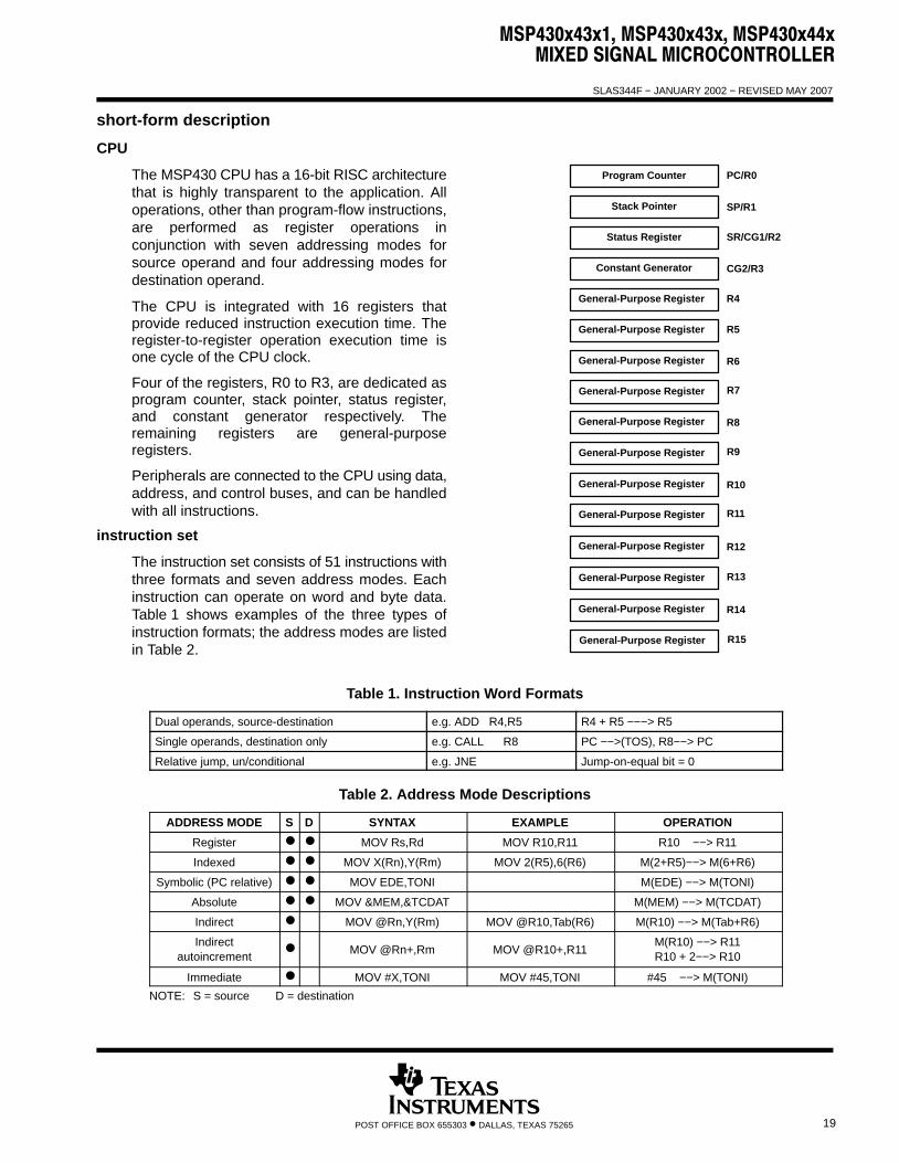
General-Purpose Register
Program Counter
Stack Pointer
Status Register
Constant Generator
General-Purpose Register
General-Purpose Register
General-Purpose Register
PC/R0
SP/R1
SR/CG1/R2
CG2/R3
R4
R5
R12
R13
General-Purpose Register
General-Purpose Register
R6
R7
General-Purpose Register
General-Purpose Register
R8
R9
General-Purpose Register
General-Purpose Register
R10
R11
General-Purpose Register
General-Purpose Register
R14
R15
MSP430x43x1, MSP430x43x, MSP430x44xMIXED SIGNAL MICROCONTROLLER
SLAS344F − JANUARY 2002 − REVISED MAY 2007
19POST OFFICE BOX 655303 • DALLAS, TEXAS 75265
short-form description
CPU
The MSP430 CPU has a 16-bit RISC architecturethat is highly transparent to the application. Alloperations, other than program-flow instructions,are performed as register operations inconjunction with seven addressing modes forsource operand and four addressing modes fordestination operand.
The CPU is integrated with 16 registers thatprovide reduced instruction execution time. Theregister-to-register operation execution time isone cycle of the CPU clock.
Four of the registers, R0 to R3, are dedicated asprogram counter, stack pointer, status register,and constant generator respectively. Theremaining registers are general-purposeregisters.
Peripherals are connected to the CPU using data,address, and control buses, and can be handledwith all instructions.
instruction set
The instruction set consists of 51 instructions withthree formats and seven address modes. Eachinstruction can operate on word and byte data.Table 1 shows examples of the three types ofinstruction formats; the address modes are listedin Table 2.
Table 1. Instruction Word Formats
Dual operands, source-destination e.g. ADD R4,R5 R4 + R5 −−−> R5
Single operands, destination only e.g. CALL R8 PC −−>(TOS), R8−−> PC
Relative jump, un/conditional e.g. JNE Jump-on-equal bit = 0
Table 2. Address Mode Descriptions
ADDRESS MODE S D SYNTAX EXAMPLE OPERATION
Register MOV Rs,Rd MOV R10,R11 R10 −−> R11
Indexed MOV X(Rn),Y(Rm) MOV 2(R5),6(R6) M(2+R5)−−> M(6+R6)
Symbolic (PC relative) MOV EDE,TONI M(EDE) −−> M(TONI)
Absolute MOV &MEM,&TCDAT M(MEM) −−> M(TCDAT)
Indirect MOV @Rn,Y(Rm) MOV @R10,Tab(R6) M(R10) −−> M(Tab+R6)
Indirectautoincrement MOV @Rn+,Rm MOV @R10+,R11
M(R10) −−> R11R10 + 2−−> R10
Immediate MOV #X,TONI MOV #45,TONI #45 −−> M(TONI)
NOTE: S = source D = destination

MSP430x43x1, MSP430x43x, MSP430x44xMIXED SIGNAL MICROCONTROLLER
SLAS344F − JANUARY 2002 − REVISED MAY 2007
20 POST OFFICE BOX 655303 • DALLAS, TEXAS 75265
operating modes
The MSP430 has one active mode and five software selectable low-power modes of operation. An interruptevent can wake up the device from any of the five low-power modes, service the request and restore back tothe low-power mode on return from the interrupt program.
The following six operating modes can be configured by software:
Active mode (AM)
− All clocks are active
Low-power mode 0 (LPM0)
− CPU is disabledACLK and SMCLK remain active. MCLK is disabledFLL+ loop control remains active
Low-power mode 1 (LPM1)
− CPU is disabledFLL+ loop control is disabledACLK and SMCLK remain active. MCLK is disabled
Low-power mode 2 (LPM2)
− CPU is disabledMCLK, FLL+ loop control, and DCOCLK are disabledDCO’s dc-generator remains enabledACLK remains active
Low-power mode 3 (LPM3)
− CPU is disabledMCLK, FLL+ loop control, and DCOCLK are disabledDCO’s dc-generator is disabledACLK remains active
Low-power mode 4 (LPM4)
− CPU is disabledACLK is disabledMCLK, FLL+ loop control, and DCOCLK are disabledDCO’s dc-generator is disabledCrystal oscillator is stopped

MSP430x43x1, MSP430x43x, MSP430x44xMIXED SIGNAL MICROCONTROLLER
SLAS344F − JANUARY 2002 − REVISED MAY 2007
21POST OFFICE BOX 655303 • DALLAS, TEXAS 75265
interrupt vector addresses
The interrupt vectors and the power-up starting address are located in the address range 0FFFFh−0FFE0h. Thevector contains the 16-bit address of the appropriate interrupt-handler instruction sequence.
Table 3. Interrupt Sources, Flags, and Vectors of 4xx Configurations
INTERRUPT SOURCE INTERRUPT FLAG SYSTEM INTERRUPTWORD
ADDRESS PRIORITY
Power-UpExternal Reset
WatchdogFlash Memory
WDTIFGKEYV
(see Note 1)
Reset 0FFFEh 15, highest
NMIOscillator Fault
Flash Memory Access Violation
NMIIFG (see Notes 1 and 3)OFIFG (see Notes 1 and 3)
ACCVIFG (see Notes 1 and 3)
(Non)maskable(Non)maskable(Non)maskable
0FFFCh 14
Timer_B7† TBCCR0 CCIFG (see Note 2) Maskable 0FFFAh 13
Timer_B7† TBCCR1 to TBCCR6 CCIFGsTBIFG (see Notes 1 and 2) Maskable 0FFF8h 12
Comparator_A CAIFG Maskable 0FFF6h 11
Watchdog Timer WDTIFG Maskable 0FFF4h 10
USART0 Receive URXIFG0 Maskable 0FFF2h 9
USART0 Transmit UTXIFG0 Maskable 0FFF0h 8
ADC12 (see Note 4) ADC12IFG (see Notes 1 and 2) Maskable 0FFEEh 7
Timer_A3 TACCR0 CCIFG (see Note 2) Maskable 0FFECh 6
Timer_A3TACCR1 and TACCR2 CCIFGs,
TAIFG (see Notes 1 and 2) Maskable 0FFEAh 5
I/O Port P1 (Eight Flags)P1IFG.0 to P1IFG.7(see Notes 1 and 2) Maskable 0FFE8h 4
USART1 Receive‡ URXIFG1 Maskable 0FFE6h 3
USART1 Transmit‡ UTXIFG1 Maskable 0FFE4h 2
I/O Port P2 (Eight Flags)P2IFG.0 to P2IFG.7(see Notes 1 and 2) Maskable 0FFE2h 1
Basic Timer1 BTIFG Maskable 0FFE0h 0, lowest† ’43x(1) uses Timer_B3 with TBCCR0, 1 and 2 CCIFG flags, and TBIFG. ’44x uses Timer_B7 with TBCCR0 CCIFG, TBCCR1 to TBCCR6
CCIFGs, and TBIFG‡ USART1 is implemented in ’44x only.NOTES: 1. Multiple source flags
2. Interrupt flags are located in the module.3. (Non)maskable: the individual interrupt-enable bit can disable an interrupt event, but the general-interrupt enable can not disable
it.4. ADC12 is not implemented in MSP430x43x1 devices.

MSP430x43x1, MSP430x43x, MSP430x44xMIXED SIGNAL MICROCONTROLLER
SLAS344F − JANUARY 2002 − REVISED MAY 2007
22 POST OFFICE BOX 655303 • DALLAS, TEXAS 75265
special function registers
Most interrupt and module-enable bits are collected in the lowest address space. Special-function register bitsnot allocated to a functional purpose are not physically present in the device. This arrangement provides simplesoftware access.
interrupt enable 1 and 2
7 6 5 4 0
UTXIE0 OFIE WDTIE
3 2 1
rw–0 rw–0 rw–0
Address
0h URXIE0 ACCVIE NMIIE
rw–0 rw–0 rw–0
WDTIE: Watchdog-timer interrupt enable. Inactive if watchdog mode is selected. Active if watchdogtimer is configured in interval timer mode.
OFIE: Oscillator-fault-interrupt enable
NMIIE: Nonmaskable-interrupt enable
ACCVIE: Flash access violation interrupt enable
URXIE0: USART0: UART and SPI receive-interrupt enable
UTXIE0: USART0: UART and SPI transmit-interrupt enable
7 6 5 4 0
UTXIE1
3 2 1
rw–0 rw–0
Address
01h URXIE1
rw–0
BTIE
URXIE1: USART1: UART and SPI receive-interrupt enable (MSP430F44x devices only)
UTXIE1: USART1: UART and SPI transmit-interrupt enable (MSP430F44x devices only)
BTIE: Basic timer interrupt enable
interrupt flag register 1 and 2
7 6 5 4 0
UTXIFG0 OFIFG WDTIFG
3 2 1
rw–0 rw–1 rw–(0)
Address
02h URXIFG0 NMIIFG
rw–1 rw–0
WDTIFG: Set on watchdog timer overflow (in watchdog mode) or security key violation. Reset on VCCpower up or a reset condition at the RST/NMI pin in reset mode.
OFIFG: Flag set on oscillator fault
NMIIFG: Set via RST/NMI pin
URXIFG0: USART0: UART and SPI receive flag
UTXIFG0: USART0: UART and SPI transmit flag
7 6 5 4 0
UTXIFG1
3 2 1
rw–1 rw–0
Address
03h URXIFG1BTIFG
rw
URXIFG1: USART1: UART and SPI receive flag (MSP430F44x devices only)
UTXIFG1: USART1: UART and SPI transmit flag (MSP430F44x devices only)
BTIFG: Basic timer flag
MSP430x43x1, MSP430x43x, MSP430x44xMIXED SIGNAL MICROCONTROLLER
SLAS344F − JANUARY 2002 − REVISED MAY 2007
23POST OFFICE BOX 655303 • DALLAS, TEXAS 75265
module enable registers 1 and 2
7 6 5 4 0UTXE0
3 2 1
rw–0 rw–0
Address
04h URXE0USPIE0
URXE0: USART0: UART mode receive enable
UTXE0: USART0: UART mode transmit enable
USPIE0: USART0: SPI mode transmit and receive enable
7 6 5 4 0UTXE1
3 2 1
rw–0 rw–0
Address
05h URXE1USPIE1
URXE1: USART1: UART mode receive enable (MSP430F44x devices only)
UTXE1: USART1: UART mode transmit enable (MSP430F44x devices only)
USPIE1: USART1: SPI mode transmit and receive enable (MSP430F44x devices only)
rw–0,1:Legend: rw: Bit Can Be Read and Written
Bit Can Be Read and Written. It Is Reset or Set by PUC.Bit Can Be Read and Written. It Is Reset or Set by POR.SFR Bit Not Present in Device
rw–(0,1):
memory organization
MSP430F435 MSP430F436MSP430F437MSP430F447 MSP430F448 MSP430F449
MemoryMain: interrupt vectorMain: code memory
SizeFlashFlash
16KB0FFFFh − 0FFE0h0FFFFh − 0C000h
24KB0FFFFh − 0FFE0h0FFFFh − 0A000h
32KB0FFFFh − 0FFE0h0FFFFh − 08000h
48KB0FFFFh − 0FFE0h0FFFFh − 04000h
60KB0FFFFh − 0FFE0h0FFFFh − 01100h
Information memory SizeFlash
256 Byte010FFh − 01000h
256 Byte010FFh − 01000h
256 Byte010FFh − 01000h
256 Byte010FFh − 01000h
256 Byte010FFh − 01000h
Boot memory SizeROM
1KB0FFFh − 0C00h
1KB0FFFh − 0C00h
1KB0FFFh − 0C00h
1KB0FFFh − 0C00h
1KB0FFFh − 0C00h
RAM Size 512 Byte03FFh − 0200h
1KB05FFh − 0200h
1KB05FFh − 0200h
2KB09FFh − 0200h
2KB09FFh − 0200h
Peripherals 16-bit8-bit
8-bit SFR
01FFh − 0100h0FFh − 010h
0Fh − 00h
01FFh − 0100h0FFh − 010h
0Fh − 00h
01FFh − 0100h0FFh − 010h
0Fh − 00h
01FFh − 0100h0FFh − 010h
0Fh − 00h
01FFh − 0100h0FFh − 010h
0Fh − 00h
bootstrap loader (BSL)
The MSP430 bootstrap loader (BSL) enables users to program the flash memory or RAM using a UART serialinterface. Access to the MSP430 memory via the BSL is protected by user-defined password. For completedescription of the features of the BSL and its implementation, see the Application report Features of the MSP430Bootstrap Loader, Literature Number SLAA089.
BSL Function PN Package Pins PZ Package Pins
Data Transmit 67 - P1.0 87 - P1.0
Data Receive 66 - P1.1 86 - P1.1
MSP430x43x1, MSP430x43x, MSP430x44xMIXED SIGNAL MICROCONTROLLER
SLAS344F − JANUARY 2002 − REVISED MAY 2007
24 POST OFFICE BOX 655303 • DALLAS, TEXAS 75265
flash memory
The flash memory can be programmed via the JTAG port, the bootstrap loader, or in-system by the CPU. TheCPU can perform single-byte and single-word writes to the flash memory. Features of the flash memory include:
Flash memory has n segments of main memory and two segments of information memory (A and B) of 128bytes each. Each segment in main memory is 512 bytes in size.
Segments 0 to n may be erased in one step, or each segment may be individually erased.
Segments A and B can be erased individually, or as a group with segments 0−n.Segments A and B are also called information memory.
New devices may have some bytes programmed in the information memory (needed for test duringmanufacturing). The user should perform an erase of the information memory prior to the first use.
Segment 0w/ Interrupt Vectors
Segment 1
Segment 2
Segment n-1
Segment n
Segment A
Segment B
MainMemory
InformationMemory
24KB
0FFFFh
0FE00h0FDFFh
0FC00h0FBFFh
0FA00h0F9FFh
16KB
0FFFFh
0FE00h0FDFFh
0FC00h0FBFFh
0FA00h0F9FFh
32KB
0FFFFh
0FE00h0FDFFh
0FC00h0FBFFh
0FA00h0F9FFh
48KB
0FFFFh
0FE00h0FDFFh
0FC00h0FBFFh
0FA00h0F9FFh
60KB
0FFFFh
0FE00h0FDFFh
0FC00h0FBFFh
0FA00h0F9FFh
0A400h0A3FFh
0A200h0A1FFh
0A000h010FFh
01080h0107Fh
01000h
0C400h0C3FFh
0C200h0C1FFh
0C000h010FFh
01080h0107Fh
01000h
08400h083FFh
08200h081FFh
08000h010FFh
01080h0107Fh
01000h
04400h043FFh
04200h041FFh
04000h010FFh
01080h0107Fh
01000h
01400h013FFh
01200h011FFh
01100h010FFh
01080h0107Fh
01000h
MSP430x43x1, MSP430x43x, MSP430x44xMIXED SIGNAL MICROCONTROLLER
SLAS344F − JANUARY 2002 − REVISED MAY 2007
25POST OFFICE BOX 655303 • DALLAS, TEXAS 75265
peripherals
Peripherals are connected to the CPU through data, address, and control busses and can be handled usingall instructions. For complete module descriptions, refer to the MSP430x4xx Family User’s Guide, literaturenumber SLAU056.
digital I/O
There are six 8-bit I/O ports implemented—ports P1 through P6:
All individual I/O bits are independently programmable. Any combination of input, output, and interrupt conditions is possible. Edge-selectable interrupt input capability for all the eight bits of ports P1 and P2. Read/write access to port-control registers is supported by all instructions.
oscillator and system clock
The clock system in the MSP430x43x(1) and MSP43x44x family of devices is supported by the FLL+ modulethat includes support for a 32768-Hz watch crystal oscillator, an internal digitally-controlled oscillator (DCO) anda high frequency crystal oscillator. The FLL+ clock module is designed to meet the requirements of both lowsystem cost and low-power consumption. The FLL+ features a digital frequency locked loop (FLL) hardwarewhich in conjunction with a digital modulator stabilizes the DCO frequency to a programmable multiple of thewatch crystal frequency. The internal DCO provides a fast turn-on clock source and stabilizes in less than 6 μs.The FLL+ module provides the following clock signals:
Auxiliary clock (ACLK), sourced from a 32768-Hz watch crystal or a high frequency crystal. Main clock (MCLK), the system clock used by the CPU. Sub-Main clock (SMCLK), the sub-system clock used by the peripheral modules. ACLK/n, the buffered output of ACLK, ACLK/2, ACLK/4, or ACLK/8.
brownout, supply voltage supervisor
The brownout circuit is implemented to provide the proper internal reset signal to the device during power onand power off. The supply voltage supervisor (SVS) circuitry detects if the supply voltage drops below a userselectable level and supports both supply voltage supervision (the device is automatically reset) and supplyvoltage monitoring (SVM, the device is not automatically reset).
The CPU begins code execution after the brownout circuit releases the device reset. However, VCC may nothave ramped to VCC(min) at that time. The user must insure the default FLL+ settings are not changed until VCCreaches VCC(min). If desired, the SVS circuit can be used to determine when VCC reaches VCC(min).
hardware multiplier (MSP430x44x Only)
The multiplication operation is supported by a dedicated peripheral module. The module performs 1616,168, 816, and 88 bit operations. The module is capable of supporting signed and unsigned multiplicationas well as signed and unsigned multiply and accumulate operations. The result of an operation can be accessedimmediately after the operands have been loaded into the peripheral registers. No additional clock cycles arerequired.
watchdog timer
The primary function of the watchdog timer (WDT) module is to perform a controlled system restart after asoftware problem occurs. If the selected time interval expires, a system reset is generated. If the watchdogfunction is not needed in an application, the module can be configured as an interval timer and can generateinterrupts at selected time intervals.

MSP430x43x1, MSP430x43x, MSP430x44xMIXED SIGNAL MICROCONTROLLER
SLAS344F − JANUARY 2002 − REVISED MAY 2007
26 POST OFFICE BOX 655303 • DALLAS, TEXAS 75265
USART0
The MSP430x43x(1) and the MSP430x44x have one hardware universal synchronous/asynchronous receivetransmit (USART0) peripheral module that is used for serial data communication. The USART supportssynchronous SPI (3 or 4 pin) and asynchronous UART communication protocols, using double-bufferedtransmit and receive channels.
USART1 (MSP430x44x Only)
The MSP430x44x has a second hardware universal synchronous/asynchronous receive transmit (USART1)peripheral module that is used for serial data communication. The USART supports synchronous SPI (3 or 4pin) and asynchronous UART communication protocols, using double-buffered transmit and receive channels.Operation of USART1 is identical to USART0.
timer_A3
Timer_A3 is a 16-bit timer/counter with three capture/compare registers. Timer_A3 can support multiplecapture/compares, PWM outputs, and interval timing. Timer_A3 also has extensive interrupt capabilities.Interrupts may be generated from the counter on overflow conditions and from each of the capture/compareregisters.
Timer_A3 Signal Connections
Input Pin Number Device Input Module Input Module Module Output Output Pin Number
PN PZDevice Input
SignalModule Input
NameModuleBlock
Module OutputSignal PN PZ
62 - P1.5 82 - P1.5 TACLK TACLK
ACLK ACLKTimer NA
SMCLK SMCLKTimer NA
62 - P1.5 82 - P1.5 TACLK INCLK
67 - P1.0 87 - P1.0 TA0 CCI0A 67 - P1.0 87 - P1.0
66 - P1.1 86 - P1.1 TA0 CCI0BCCR0 TA0
DVSS GNDCCR0 TA0
DVCC VCC
65 - P1.2 85 - P1.2 TA1 CCI1A 14 - P1.2 85 - P1.2
CAOUT (internal) CCI1BCCR1 TA1
ADC12 (internal)
DVSS GNDCCR1 TA1
DVCC VCC
59 - P2.0 79 - P2.0 TA2 CCI2A 15 - P1.3 79 - P2.0
ACLK (internal) CCI2BCCR2 TA2
DVSS GNDCCR2 TA2
DVCC VCC
timer_B3 (MSP430x43x(1) Only)
Timer_B3 is a 16-bit timer/counter with three capture/compare registers. Timer_B3 can support multiplecapture/compares, PWM outputs, and interval timing. Timer_B3 also has extensive interrupt capabilities.Interrupts may be generated from the counter on overflow conditions and from each of the capture/compareregisters.

MSP430x43x1, MSP430x43x, MSP430x44xMIXED SIGNAL MICROCONTROLLER
SLAS344F − JANUARY 2002 − REVISED MAY 2007
27POST OFFICE BOX 655303 • DALLAS, TEXAS 75265
timer_B7 (MSP430x44x Only)
Timer_B7 is a 16-bit timer/counter with seven capture/compare registers. Timer_B7 can support multiplecapture/compares, PWM outputs, and interval timing. Timer_B7 also has extensive interrupt capabilities.Interrupts may be generated from the counter on overflow conditions and from each of the capture/compareregisters.
Timer_B3/B7 Signal Connections†
Input Pin Number Device Input Module Input Module Module Output Output Pin Number
PN PZDevice Input
SignalModule Input
NameModuleBlock
Module OutputSignal PN PZ
63 - P1.4 83 - P1.4 TBCLK TBCLK
ACLK ACLKTimer NA
SMCLK SMCLKTimer NA
63 - P1.4 83 - P1.4 TBCLK INCLK
58 - P2.1 78 - P2.1 TB0 CCI0A 58 - P2.1 78 - P2.1
58 - P2.1 78 - P2.1 TB0 CCI0BCCR0 TB0
ADC12 (internal)
DVSS GNDCCR0 TB0
DVCC VCC
57 - P2.2 77 - P2.2 TB1 CCI1A 57 - P2.2 77 - P2.2
57 - P2.2 77 - P2.2 TB1 CCI1BCCR1 TB1
ADC12 (internal)
DVSS GNDCCR1 TB1
DVCC VCC
56 - P2.3 76 - P2.3 TB2 CCI2A 56 - P2.3 76 - P2.3
56 - P2.3 76 - P2.3 TB2 CCI2BCCR2 TB2
DVSS GNDCCR2 TB2
DVCC VCC
67 - P3.4 TB3 CCI3A 67 - P3.4
67 - P3.4 TB3 CCI3BCCR3 TB3
DVSS GNDCCR3 TB3
DVCC VCC
66 - P3.5 TB4 CCI4A 66 - P3.5
66 - P3.5 TB4 CCI4BCCR4 TB4
DVSS GNDCCR4 TB4
DVCC VCC
65 - P3.6 TB5 CCI5A 65 - P3.6
65 - P3.6 TB5 CCI5BCCR5 TB5
DVSS GNDCCR5 TB5
DVCC VCC
64 - P3.7 TB6 CCI6A 64 - P3.7
ACLK (internal) CCI6BCCR6 TB6
DVSS GNDCCR6 TB6
DVCC VCC
† Timer_B3 implements three capture/compare blocks (CCR0, CCR1 and CCR2 only).

MSP430x43x1, MSP430x43x, MSP430x44xMIXED SIGNAL MICROCONTROLLER
SLAS344F − JANUARY 2002 − REVISED MAY 2007
28 POST OFFICE BOX 655303 • DALLAS, TEXAS 75265
comparator_A
The primary function of the comparator_A module is to support precision slope analog−to−digital conversions,battery−voltage supervision, and monitoring of external analog signals.
ADC12 (Not implemented in the MSP430x43x1)The ADC12 module supports fast, 12-bit analog-to-digital conversions. The module implements a 12-bit SARcore, sample select control, reference generator and a 16 word conversion-and-control buffer. Theconversion-and-control buffer allows up to 16 independent ADC samples to be converted and stored withoutany CPU intervention.
Basic Timer1
The Basic Timer1 has two independent 8-bit timers which can be cascaded to form a 16-bit timer/counter. Bothtimers can be read and written by software. The Basic Timer1 can be used to generate periodic interrupts andclock for the LCD module.
LCD drive
The LCD driver generates the segment and common signals required to drive an LCD display. The LCDcontroller has dedicated data memory to hold segment drive information. Common and segment signals aregenerated as defined by the mode. Static, 2-MUX, 3-MUX, and 4-MUX LCDs are supported by this peripheral.

MSP430x43x1, MSP430x43x, MSP430x44xMIXED SIGNAL MICROCONTROLLER
SLAS344F − JANUARY 2002 − REVISED MAY 2007
29POST OFFICE BOX 655303 • DALLAS, TEXAS 75265
peripheral file map
PERIPHERALS WITH WORD ACCESS
Watchdog Watchdog timer control WDTCTL 0120h
Timer_B7/ Capture/compare register 6 TBCCR6 019Eh_Timer_B3(see Note 1)
Capture/compare register 5 TBCCR5 019Ch(see Note 1)
Capture/compare register 4 TBCCR4 019Ah
Capture/compare register 3 TBCCR3 0198h
Capture/compare register 2 TBCCR2 0196h
Capture/compare register 1 TBCCR1 0194h
Capture/compare register 0 TBCCR0 0192h
Timer_B register TBR 0190h
Capture/compare control 6 TBCCTL6 018Eh
Capture/compare control 5 TBCCTL5 018Ch
Capture/compare control 4 TBCCTL4 018Ah
Capture/compare control 3 TBCCTL3 0188h
Capture/compare control 2 TBCCTL2 0186h
Capture/compare control 1 TBCCTL1 0184h
Capture/compare control 0 TBCCTL0 0182h
Timer_B control TBCTL 0180h
Timer_B interrupt vector TBIV 011Eh
Timer_A3 Reserved 017Eh_
Reserved 017Ch
Reserved 017Ah
Reserved 0178h
Capture/compare register 2 TACCR2 0176h
Capture/compare register 1 TACCR1 0174h
Capture/compare register 0 TACCR0 0172h
Timer_A register TAR 0170h
Reserved 016Eh
Reserved 016Ch
Reserved 016Ah
Reserved 0168h
Capture/compare control 2 TACCTL2 0166h
Capture/compare control 1 TACCTL1 0164h
Capture/compare control 0 TACCTL0 0162h
Timer_A control TACTL 0160h
Timer_A interrupt vector TAIV 012Eh
Hardware Sum extend SUMEXT 013EhMultiplier(MSP430x44x only)
Result high word RESHI 013Ch(MSP430x44x only)
Result low word RESLO 013Ah
Second operand OP2 0138h
Multiply signed + accumulate/operand1 MACS 0136h
Multiply + accumulate/operand1 MAC 0134h
Multiply signed/operand1 MPYS 0132h
Multiply unsigned/operand1 MPY 0130hNOTE 1: Timer_B7 in the MSP430x44x family has seven CCRs; Timer_B3 in the MSP430x43x(1) family has three CCRs.

MSP430x43x1, MSP430x43x, MSP430x44xMIXED SIGNAL MICROCONTROLLER
SLAS344F − JANUARY 2002 − REVISED MAY 2007
30 POST OFFICE BOX 655303 • DALLAS, TEXAS 75265
peripheral file map (continued)
PERIPHERALS WITH WORD ACCESS (CONTINUED)
Flash Flash control 3 FCTL3 012Ch
Flash control 2 FCTL2 012Ah
Flash control 1 FCTL1 0128h
ADC12 Conversion memory 15 ADC12MEM15 015Eh
Conversion memory 14 ADC12MEM14 015Ch
Conversion memory 13 ADC12MEM13 015Ah
Conversion memory 12 ADC12MEM12 0158h
Conversion memory 11 ADC12MEM11 0156h
Conversion memory 10 ADC12MEM10 0154h
Conversion memory 9 ADC12MEM9 0152h
Conversion memory 8 ADC12MEM8 0150h
Conversion memory 7 ADC12MEM7 014Eh
Conversion memory 6 ADC12MEM6 014Ch
Conversion memory 5 ADC12MEM5 014Ah
Conversion memory 4 ADC12MEM4 0148h
Conversion memory 3 ADC12MEM3 0146h
Conversion memory 2 ADC12MEM2 0144h
Conversion memory 1 ADC12MEM1 0142h
Conversion memory 0 ADC12MEM0 0140h
Interrupt-vector-word register ADC12IV 01A8h
Inerrupt-enable register ADC12IE 01A6h
Inerrupt-flag register ADC12IFG 01A4h
Control register 1 ADC12CTL1 01A2h
Control register 0 ADC12CTL0 01A0h
ADC memory-control register15 ADC12MCTL15 08Fh
ADC memory-control register14 ADC12MCTL14 08Eh
ADC memory-control register13 ADC12MCTL13 08Dh
ADC memory-control register12 ADC12MCTL12 08Ch
ADC memory-control register11 ADC12MCTL11 08Bh
ADC memory-control register10 ADC12MCTL10 08Ah
ADC memory-control register9 ADC12MCTL9 089h
ADC memory-control register8 ADC12MCTL8 088h
ADC memory-control register7 ADC12MCTL7 087h
ADC memory-control register6 ADC12MCTL6 086h
ADC memory-control register5 ADC12MCTL5 085h
ADC memory-control register4 ADC12MCTL4 084h
ADC memory-control register3 ADC12MCTL3 083h
ADC memory-control register2 ADC12MCTL2 082h
ADC memory-control register1 ADC12MCTL1 081h
ADC memory-control register0 ADC12MCTL0 080h

MSP430x43x1, MSP430x43x, MSP430x44xMIXED SIGNAL MICROCONTROLLER
SLAS344F − JANUARY 2002 − REVISED MAY 2007
31POST OFFICE BOX 655303 • DALLAS, TEXAS 75265
peripheral file map (continued)PERIPHERALS WITH BYTE ACCESS
LCD LCD memory 20:LCD memory 16LCD memory 15:LCD memory 1LCD control and mode
LCDM20:LCDM16LCDM15:LCDM1LCDCTL
0A4h:0A0h09Fh:091h090h
USART1 Transmit buffer U1TXBUF 07Fh(Only in ‘x44x) Receive buffer U1RXBUF 07Eh
Baud rate U1BR1 07Dh
Baud rate U1BR0 07Ch
Modulation control U1MCTL 07Bh
Receive control U1RCTL 07Ah
Transmit control U1TCTL 079h
USART control U1CTL 078hUSART0 Transmit buffer U0TXBUF 077h
Receive buffer U0RXBUF 076h
Baud rate U0BR1 075h
Baud rate U0BR0 074h
Modulation control U0MCTL 073h
Receive control U0RCTL 072h
Transmit control U0TCTL 071h
USART control U0CTL 070hComparator_A Comparator_A port disable CAPD 05Bhp _
Comparator_A control2 CACTL2 05Ah
Comparator_A control1 CACTL1 059h
BrownOUT, SVS SVS control register (Reset by brownout signal) SVSCTL 056h
FLL+ Clock FLL+ Control1 FLL_CTL1 054h
FLL+ Control0 FLL_CTL0 053h
System clock frequency control SCFQCTL 052h
System clock frequency integrator SCFI1 051h
System clock frequency integrator SCFI0 050h
Basic Timer1 BT counter2BT counter1BT control
BTCNT2BTCNT1BTCTL
047h046h040h
Port P6 Port P6 selection P6SEL 037h
Port P6 direction P6DIR 036h
Port P6 output P6OUT 035h
Port P6 input P6IN 034hPort P5 Port P5 selection P5SEL 033h
Port P5 direction P5DIR 032h
Port P5 output P5OUT 031h
Port P5 input P5IN 030h

MSP430x43x1, MSP430x43x, MSP430x44xMIXED SIGNAL MICROCONTROLLER
SLAS344F − JANUARY 2002 − REVISED MAY 2007
32 POST OFFICE BOX 655303 • DALLAS, TEXAS 75265
peripheral file map (continued)PERIPHERALS WITH BYTE ACCESS (CONTINUED)
Port P4 Port P4 selection P4SEL 01Fh
Port P4 direction P4DIR 01Eh
Port P4 output P4OUT 01Dh
Port P4 input P4IN 01ChPort P3 Port P3 selection P3SEL 01Bh
Port P3 direction P3DIR 01Ah
Port P3 output P3OUT 019h
Port P3 input P3IN 018hPort P2 Port P2 selection P2SEL 02Eh
Port P2 interrupt enable P2IE 02Dh
Port P2 interrupt-edge select P2IES 02Ch
Port P2 interrupt flag P2IFG 02Bh
Port P2 direction P2DIR 02Ah
Port P2 output P2OUT 029h
Port P2 input P2IN 028hPort P1 Port P1 selection P1SEL 026h
Port P1 interrupt enable P1IE 025h
Port P1 interrupt-edge select P1IES 024h
Port P1 interrupt flag P1IFG 023h
Port P1 direction P1DIR 022h
Port P1 output P1OUT 021h
Port P1 input P1IN 020hSpecial functions SFR module enable2 ME2 005hp
SFR module enable1 ME1 004h
SFR interrupt flag2 IFG2 003h
SFR interrupt flag1 IFG1 002h
SFR interrupt enable2 IE2 001h
SFR interrupt enable1 IE1 000h
absolute maximum ratings over operating free-air temperature (unless otherwise noted)†
Voltage applied at VCC to VSS −0.3 V to 4.1 V. . . . . . . . . . . . . . . . . . . . . . . . . . . . . . . . . . . . . . . . . . . . . . . . . . . . . . Voltage applied to any pin (see Note) −0.3 V to VCC + 0.3 V. . . . . . . . . . . . . . . . . . . . . . . . . . . . . . . . . . . . . . . . . . Diode current at any device terminal . ±2 mA. . . . . . . . . . . . . . . . . . . . . . . . . . . . . . . . . . . . . . . . . . . . . . . . . . . . . . Storage temperature, Tstg: (unprogrammed device) −55°C to 150°C. . . . . . . . . . . . . . . . . . . . . . . . . . . . . . . . . .
(programmed device) −40°C to 85°C. . . . . . . . . . . . . . . . . . . . . . . . . . . . . . . . . . . . . † Stresses beyond those listed under “absolute maximum ratings” may cause permanent damage to the device. These are stress ratings only, and
functional operation of the device at these or any other conditions beyond those indicated under “recommended operating conditions” is notimplied. Exposure to absolute-maximum-rated conditions for extended periods may affect device reliability.
NOTE: All voltages referenced to VSS. The JTAG fuse-blow voltage, VFB, is allowed to exceed the absolute maximum rating. The voltage is appliedto the TDI/TCLK pin when blowing the JTAG fuse.
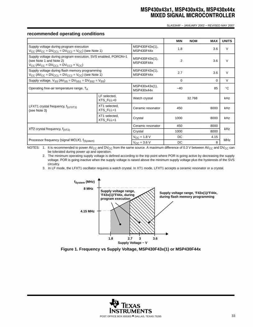
MSP430x43x1, MSP430x43x, MSP430x44xMIXED SIGNAL MICROCONTROLLER
SLAS344F − JANUARY 2002 − REVISED MAY 2007
33POST OFFICE BOX 655303 • DALLAS, TEXAS 75265
recommended operating conditions
MIN NOM MAX UNITS
Supply voltage during program executionVCC (AVCC = DVCC1 = DVCC2 = VCC) (see Note 1)
MSP430F43x(1),MSP430F44x 1.8 3.6 V
Supply voltage during program execution, SVS enabled, PORON=1(see Note 1 and Note 2)VCC (AVCC = DVCC1 = DVCC2 = VCC)
MSP430F43x(1),MSP430F44x 2 3.6 V
Supply voltage during flash memory programmingVCC (AVCC = DVCC1 = DVCC2 = VCC) (see Note 1)
MSP430F43x(1),MSP430F44x 2.7 3.6 V
Supply voltage, VSS (AVSS = DVSS1 = DVSS2 = VSS) 0 0 V
Operating free-air temperature range, TAMSP430x43x(1),MSP430x44x −40 85 °C
LF selected,XTS_FLL=0 Watch crystal 32.768 kHz
LFXT1 crystal frequency, f(LFXT1)(see Note 3)
XT1 selected,XTS_FLL=1 Ceramic resonator 450 8000 kHz
(see Note 3)
XT1 selected,XTS_FLL=1 Crystal 1000 8000 kHz
XT2 crystal frequency fCeramic resonator 450 8000
kHzXT2 crystal frequency, f(XT2) Crystal 1000 8000kHz
Processor frequency (signal MCLK) fVCC = 1.8 V DC 4.15
MHzProcessor frequency (signal MCLK), f(System) VCC = 3.6 V DC 8MHz
NOTES: 1. It is recommended to power AVCC and DVCC from the same source. A maximum difference of 0.3 V between AVCC and DVCC canbe tolerated during power up and operation.
2. The minimum operating supply voltage is defined according to the trip point where POR is going active by decreasing the supplyvoltage. POR is going inactive when the supply voltage is raised above the minimum supply voltage plus the hysteresis of the SVScircuitry.
3. In LF mode, the LFXT1 oscillator requires a watch crystal. In XT1 mode, LFXT1 accepts a ceramic resonator or a crystal.
1.8 3.62.7 3
ÎÎÎÎÎÎÎÎÎÎÎÎÎÎÎÎÎÎÎÎÎÎÎÎÎÎÎÎÎÎÎÎÎÎÎÎÎÎÎÎ
4.15 MHz
8 MHz
Supply Voltage − V
Supply voltage range, ’F43x(1)/’F44x,during flash memory programming
Supply voltage range,’F43x(1)/’F44x, duringprogram execution
fSystem (MHz)
Figure 1. Frequency vs Supply Voltage, MSP430F43x(1) or MSP430F44x

MSP430x43x1, MSP430x43x, MSP430x44xMIXED SIGNAL MICROCONTROLLER
SLAS344F − JANUARY 2002 − REVISED MAY 2007
34 POST OFFICE BOX 655303 • DALLAS, TEXAS 75265
electrical characteristics over recommended operating free-air temperature (unless otherwisenoted)supply current into AVCC + DVCC excluding external current
PARAMETER TEST CONDITIONS MIN NOM MAX UNIT
I
Active mode, (see Note 1)f(MCLK) = f(SMCLK) = 1 MHz,
T 40°C to 85°CVCC = 2.2 V 280 350
AI(AM)f(MCLK) = f(SMCLK) = 1 MHz,f(ACLK) = 32,768 HzXTS_FLL=0, SELM=(0,1)
TA = −40°C to 85°CVCC = 3 V 420 560
μA
ILow-power mode, (LPM0)
T 40°C to 85°CVCC = 2.2 V 32 45
AI(LPM0)Low power mode, (LPM0)(see Note 1 and Note 4) TA = −40°C to 85°C
VCC = 3 V 55 70μA
I
Low-power mode, (LPM2),f(MCLK) = f (SMCLK) = 0 MHz,
T 40°C to 85°CVCC = 2.2 V 11 14
AI(LPM2)f(MCLK) = f (SMCLK) = 0 MHz,f(ACLK) = 32,768 Hz, SCG0 = 0 (see Note 2 andNote 4)
TA = −40°C to 85°CVCC = 3 V 17 22
μA
TA = −40°C 1 1.5
TA = 25°CV 2 2 V
1.1 1.5ALow-power mode, (LPM3)
f(MCLK) = f(SMCLK) = 0 MHzTA = 60°C
VCC = 2.2 V2 3
μA
I
f(MCLK) = f(SMCLK) = 0 MHz,f(ACLK) = 32,768 Hz, SCG0 = 1 TA = 85°C 3.5 6
I(LPM3)f(ACLK) = 32,768 Hz, SCG0 = 1(see Note 3 and Note 4) TA = −40°C 1.8 2.2( )
TA = 25°CV 3 V
1.6 1.9A
TA = 60°CVCC = 3 V
2.5 3.5μA
TA = 85°C 4.2 7.5
TA = −40°C 0.1 0.5
TA = 25°CV 2 2 V
0.1 0.5A
Low-power mode (LPM4)TA = 60°C
VCC = 2.2 V0.7 1.1
μA
I
Low-power mode, (LPM4)f(MCLK) = 0 MHz, f(SMCLK) = 0 MHz, TA = 85°C 1.7 3
I(LPM4)f(MCLK) = 0 MHz, f(SMCLK) = 0 MHz,f(ACLK) = 0 Hz, SCG0 = 1( N t 2 d N t 4)
TA = −40°C 0.1 0.5(ACLK)(see Note 2 and Note 4) TA = 25°C
V 3 V0.1 0.5
ATA = 60°C
VCC = 3 V0.8 1.2
μA
TA = 85°C 1.9 3.5
NOTES: 1. Timer_B is clocked by f(DCOCLK) = f(DCO) = 1 MHz. All inputs are tied to 0 V or to VCC. Outputs do not source or sink any current.2. All inputs are tied to 0 V or to VCC. Outputs do not source or sink any current.3. All inputs are tied to 0 V or to VCC. Outputs do not source or sink any current. The current consumption in LPM3 is measured with
active Basic Timer1 and LCD (ACLK selected). The current consumption of the Comparator_A and the SVS module are specifiedin the respective sections. The LPM3 currents are characterized with a KDS Daishinku DT−38 (6 pF) crystal and OSCCAPx=1h.
4. Current consumption for brownout included.
Current consumption of active mode versus system frequency
I(AM) = I(AM) [1 MHz] × f(System) [MHz]
Current consumption of active mode versus supply voltage
I(AM) = I(AM) [3 V] + 175 μA/V × (VCC – 3 V)

MSP430x43x1, MSP430x43x, MSP430x44xMIXED SIGNAL MICROCONTROLLER
SLAS344F − JANUARY 2002 − REVISED MAY 2007
35POST OFFICE BOX 655303 • DALLAS, TEXAS 75265
electrical characteristics over recommended operating free-air temperature (unless otherwisenoted) (continued)
SCHMITT-trigger inputs − ports P1, P2, P3, P4, P5, and P6PARAMETER TEST CONDITIONS MIN TYP MAX UNIT
V Positive going input threshold voltageVCC = 2.2 V 1.1 1.5
VVIT+ Positive-going input threshold voltageVCC = 3 V 1.5 1.9
V
V Negative going input threshold voltageVCC = 2.2 V 0.4 0.9
VVIT− Negative-going input threshold voltageVCC = 3 V 0.9 1.3
V
V Input voltage hysteresis (V V )VCC = 2.2 V 0.3 1.1
VVhys Input voltage hysteresis (VIT+ − VIT−)VCC = 3 V 0.5 1
V
standard inputs − RST/NMI; JTAG: TCK, TMS, TDI/TCLKPARAMETER TEST CONDITIONS MIN TYP MAX UNIT
VIL Low-level input voltageV = 2 2 V / 3 V
VSS VSS+0.6 V
VIH High-level input voltageVCC = 2.2 V / 3 V
0.8×VCC VCC V
inputs Px.x, TAx, TBxPARAMETER TEST CONDITIONS VCC MIN TYP MAX UNIT
P t P1 P2 P1 t P2 t l t i i l2.2 V/3 V 1.5 cycle
t(int) External interrupt timingPort P1, P2: P1.x to P2.x, external trigger signalfor the interrupt flag, (see Note 1)
2.2 V 62ns
(int) p g for the interrupt flag, (see Note 1)3 V 50
ns
Timer A Timer B captureTA0, TA1, TA2 2.2 V 62
t(cap)Timer_A, Timer_B capturetiming TB0, TB1, TB2, TB3, TB4, TB5, TB6
(see Note 2) 3 V 50ns
f(TAext) Timer_A, Timer_B clockfrequency externally applied TACLK TBCLK INCLK: t = t
2.2 V 8MHz
f(TBext)frequency externally appliedto pin
TACLK, TBCLK, INCLK: t(H) = t(L)3 V 10
MHz
f(TAint) Timer_A, Timer_B clockSMCLK or ACLK signal selected
2.2 V 8MHz
f(TBint)
Timer_A, Timer_B clockfrequency SMCLK or ACLK signal selected
3 V 10MHz
NOTES: 1. The external signal sets the interrupt flag every time the minimum t(int) cycle and time parameters are met. It may be set even withtrigger signals shorter than t(int). Both the cycle and timing specifications must be met to ensure the flag is set. t(int) is measured inMCLK cycles.
2. Seven capture/compare registers in ’x44x and three capture/compare registers in ’x43x(1).
leakage current (see Notes 1 and 2)PARAMETER TEST CONDITIONS MIN TYP MAX UNIT
Ilkg(P1.x) Port P1 Port 1: V(P1.x) ±50
Ilkg(P2.x) Port P2 Port 2: V(P2.x) ±50
Ilkg(P3.x) Leakage Port P3 Port 3: V(P3.x)V = 2 2 V/3 V
±50nA
Ilkg(P4.x)
Leakagecurrent Port P4 Port 4: V(P4.x)
VCC = 2.2 V/3 V±50
nA
Ilkg(P5.x) Port P5 Port 5: V(P5.x) ±50
Ilkg(P6.x) Port P6 Port 6: V(P6.x) ±50
NOTES: 1. The leakage current is measured with VSS or VCC applied to the corresponding pin(s), unless otherwise noted.2. The port pin must be selected as input and there must be no optional pullup or pulldown resistor.
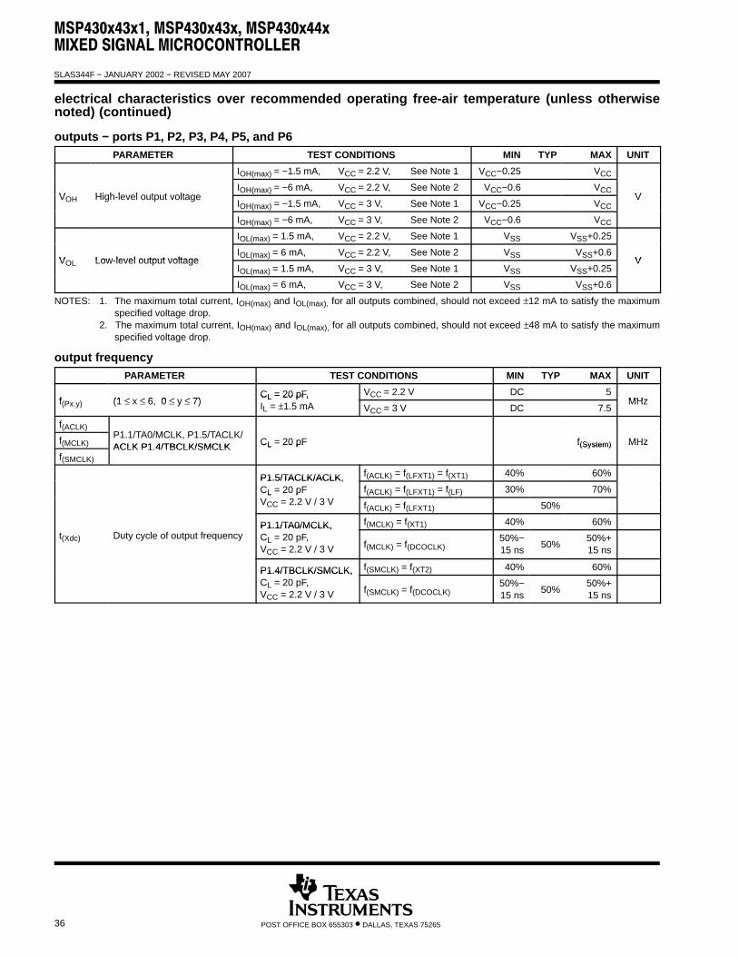
MSP430x43x1, MSP430x43x, MSP430x44xMIXED SIGNAL MICROCONTROLLER
SLAS344F − JANUARY 2002 − REVISED MAY 2007
36 POST OFFICE BOX 655303 • DALLAS, TEXAS 75265
electrical characteristics over recommended operating free-air temperature (unless otherwisenoted) (continued)
outputs − ports P1, P2, P3, P4, P5, and P6PARAMETER TEST CONDITIONS MIN TYP MAX UNIT
IOH(max) = −1.5 mA, VCC = 2.2 V, See Note 1 VCC−0.25 VCC
V High level output voltageIOH(max) = −6 mA, VCC = 2.2 V, See Note 2 VCC−0.6 VCC
VVOH High-level output voltageIOH(max) = −1.5 mA, VCC = 3 V, See Note 1 VCC−0.25 VCC
V
IOH(max) = −6 mA, VCC = 3 V, See Note 2 VCC−0.6 VCC
IOL(max) = 1.5 mA, VCC = 2.2 V, See Note 1 VSS VSS+0.25
V Low level output voltageIOL(max) = 6 mA, VCC = 2.2 V, See Note 2 VSS VSS+0.6
VVOL Low-level output voltageIOL(max) = 1.5 mA, VCC = 3 V, See Note 1 VSS VSS+0.25
V
IOL(max) = 6 mA, VCC = 3 V, See Note 2 VSS VSS+0.6
NOTES: 1. The maximum total current, IOH(max) and IOL(max), for all outputs combined, should not exceed ±12 mA to satisfy the maximumspecified voltage drop.
2. The maximum total current, IOH(max) and IOL(max), for all outputs combined, should not exceed ±48 mA to satisfy the maximumspecified voltage drop.
output frequencyPARAMETER TEST CONDITIONS MIN TYP MAX UNIT
f (1 ≤ x ≤ 6 0 ≤ y ≤ 7)CL = 20 pF, VCC = 2.2 V DC 5
MHzf(Px.y) (1 ≤ x ≤ 6, 0 ≤ y ≤ 7)CL = 20 pF,IL = ±1.5 mA VCC = 3 V DC 7.5
MHz
f(ACLK)P1 1/TA0/MCLK P1 5/TACLK/f(MCLK)P1.1/TA0/MCLK, P1.5/TACLK/ACLK P1 4/TBCLK/SMCLK CL = 20 pF f(System) MHz
f(SMCLK)ACLK P1.4/TBCLK/SMCLK CL 20 pF f(System) MHz
P1.5/TACLK/ACLK, f(ACLK) = f(LFXT1) = f(XT1) 40% 60%P1.5/TACLK/ACLK,CL = 20 pF f(ACLK) = f(LFXT1) = f(LF) 30% 70%CL 20 pFVCC = 2.2 V / 3 V f(ACLK) = f(LFXT1) 50%
P1.1/TA0/MCLK, f(MCLK) = f(XT1) 40% 60%t(Xdc) Duty cycle of output frequency
P1.1/TA0/MCLK,CL = 20 pF,VCC = 2.2 V / 3 V f(MCLK) = f(DCOCLK)
50%−15 ns 50%
50%+15 ns
P1.4/TBCLK/SMCLK, f(SMCLK) = f(XT2) 40% 60%P1.4/TBCLK/SMCLK,CL = 20 pF,VCC = 2.2 V / 3 V f(SMCLK) = f(DCOCLK)
50%−15 ns 50%
50%+15 ns

MSP430x43x1, MSP430x43x, MSP430x44xMIXED SIGNAL MICROCONTROLLER
SLAS344F − JANUARY 2002 − REVISED MAY 2007
37POST OFFICE BOX 655303 • DALLAS, TEXAS 75265
electrical characteristics over recommended operating free-air temperature (unless otherwisenoted) (continued)
outputs − Ports P1, P2, P3, P4, P5, and P6 (continued)
Figure 2
VOL − Low-Level Output Voltage − V
0
2
4
6
8
10
12
14
16
0.0 0.5 1.0 1.5 2.0 2.5
VCC = 2.2 VP2.7
TYPICAL LOW-LEVEL OUTPUT CURRENTvs
LOW-LEVEL OUTPUT VOLTAGE
TA = 25°C
TA = 85°C
OL
I−
Typ
ical
Lo
w-l
evel
Ou
tpu
t C
urr
ent
− m
A
Figure 3
VOL − Low-Level Output Voltage − V
0
5
10
15
20
25
0.0 0.5 1.0 1.5 2.0 2.5 3.0 3.5
VCC = 3 VP2.7
TYPICAL LOW-LEVEL OUTPUT CURRENTvs
LOW-LEVEL OUTPUT VOLTAGE
TA = 25°C
TA = 85°C
OL
I−
Typ
ical
Lo
w-l
evel
Ou
tpu
t C
urr
ent
− m
A
Figure 4
VOH − High-Level Output Voltage − V
−14
−12
−10
−8
−6
−4
−2
0
0.0 0.5 1.0 1.5 2.0 2.5
VCC = 2.2 VP2.7
TYPICAL HIGH-LEVEL OUTPUT CURRENTvs
HIGH-LEVEL OUTPUT VOLTAGE
TA = 25°C
TA = 85°C
OL
I−
Typ
ical
Hig
h-l
evel
Ou
tpu
t C
urr
ent
− m
A
Figure 5VOH − High-Level Output Voltage − V
−30
−25
−20
−15
−10
−5
0
0.0 0.5 1.0 1.5 2.0 2.5 3.0 3.5
VCC = 3 VP2.7
TYPICAL HIGH-LEVEL OUTPUT CURRENTvs
HIGH-LEVEL OUTPUT VOLTAGE
TA = 25°C
TA = 85°C
OL
I−
Typ
ical
Hig
h-l
evel
Ou
tpu
t C
urr
ent
− m
A

MSP430x43x1, MSP430x43x, MSP430x44xMIXED SIGNAL MICROCONTROLLER
SLAS344F − JANUARY 2002 − REVISED MAY 2007
38 POST OFFICE BOX 655303 • DALLAS, TEXAS 75265
electrical characteristics over recommended operating free-air temperature (unless otherwisenoted) (continued)
wake-up LPM3PARAMETER TEST CONDITIONS MIN TYP MAX UNIT
f = 1 MHz 6
td(LPM3) Delay time f = 2 MHz VCC = 2.2 V/3 V 6 μstd(LPM3) Delay time
f = 3 MHz
VCC 2.2 V/3 V
6
μs
RAMPARAMETER TEST CONDITIONS MIN TYP MAX UNIT
VRAMh CPU halted (see Note 1) 1.6 V
NOTE 1: This parameter defines the minimum supply voltage when the data in program memory RAM remain unchanged. No program executionshould take place during this supply voltage condition.
LCDPARAMETER TEST CONDITIONS MIN TYP MAX UNIT
V(33) Voltage at P5.7/R33 2.5 VCC + 0.2
V(23)Analog voltage
Voltage at P5.6/R23V 3 V
[V(33)−V(03)] × 2/3 + V(03)V
V(13)Analog voltage
Voltage at P5.5/R13VCC = 3 V
[V(33)−V(03)] × 1/3 + V(03)V
V(33) − V(03) Voltage at R33 to R03 2.5 VCC + 0.2
I(R03) R03 = VSS No load at all ±20
I(R13) Input leakage P5.5/R13 = VCC/3 segment andcommon lines
±20 nA
I(R23)
p g
P5.6/R23 = 2 × VCC/3common lines,VCC = 3 V ±20
V(Sxx0) V(03) V(03) − 0.1
V(Sxx1) Segment line I = 3 μA V = 3 VV(13) V(13) − 0.1
VV(Sxx2)
Segment linevoltage
I(Sxx) = −3 μA, VCC = 3 VV(23) V(23) − 0.1
V
V(Sxx3) V(33) V(33) + 0.1
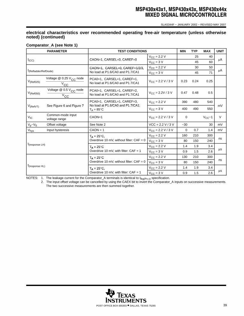
MSP430x43x1, MSP430x43x, MSP430x44xMIXED SIGNAL MICROCONTROLLER
SLAS344F − JANUARY 2002 − REVISED MAY 2007
39POST OFFICE BOX 655303 • DALLAS, TEXAS 75265
electrical characteristics over recommended operating free-air temperature (unless otherwisenoted) (continued)
Comparator_A (see Note 1)PARAMETER TEST CONDITIONS MIN TYP MAX UNIT
I CAON 1 CARSEL 0 CAREF 0VCC = 2.2 V 25 40
AI(CC) CAON=1, CARSEL=0, CAREF=0VCC = 3 V 45 60
μA
ICAON=1, CARSEL=0, CAREF=1/2/3, VCC = 2.2 V 30 50
AI(Refladder/RefDiode)CAON=1, CARSEL=0, CAREF=1/2/3,No load at P1.6/CA0 and P1.7/CA1 VCC = 3 V 45 71
μA
V(Ref025)Voltage @ 0.25 VCC node
VCC
PCA0=1, CARSEL=1, CAREF=1,No load at P1.6/CA0 and P1.7/CA1 VCC = 2.2 V / 3 V 0.23 0.24 0.25
V(Ref050)Voltage @ 0.5 VCC node
VCC
PCA0=1, CARSEL=1, CAREF=2,No load at P1.6/CA0 and P1.7/CA1 VCC = 2.2V / 3 V 0.47 0.48 0.5
V See Figure 6 and Figure 7PCA0=1, CARSEL=1, CAREF=3,No load at P1 6/CA0 and P1 7/CA1;
VCC = 2.2 V 390 480 540mVV(RefVT) See Figure 6 and Figure 7 No load at P1.6/CA0 and P1.7/CA1;
TA = 85°C VCC = 3 V 400 490 550mV
VICCommon-mode inputvoltage range CAON=1 VCC = 2.2 V / 3 V 0 VCC−1 V
Vp−VS Offset voltage See Note 2 VCC = 2.2 V / 3 V −30 30 mV
Vhys Input hysteresis CAON = 1 VCC = 2.2 V / 3 V 0 0.7 1.4 mV
TA = 25°C, VCC = 2.2 V 160 210 300ns
t
TA = 25 C,Overdrive 10 mV, without filter: CAF = 0 VCC = 3 V 80 150 240
ns
t(response LH)TA = 25°C VCC = 2.2 V 1.4 1.9 3.4
sTA = 25 COverdrive 10 mV, with filter: CAF = 1 VCC = 3 V 0.9 1.5 2.6
μs
TA = 25°C VCC = 2.2 V 130 210 300ns
t
TA = 25 COverdrive 10 mV, without filter: CAF = 0 VCC = 3 V 80 150 240
ns
t(response HL)TA = 25°C, VCC = 2.2 V 1.4 1.9 3.4
sTA = 25 C,Overdrive 10 mV, with filter: CAF = 1 VCC = 3 V 0.9 1.5 2.6
μs
NOTES: 1. The leakage current for the Comparator_A terminals is identical to Ilkg(Px.x) specification.2. The input offset voltage can be cancelled by using the CAEX bit to invert the Comparator_A inputs on successive measurements.
The two successive measurements are then summed together.
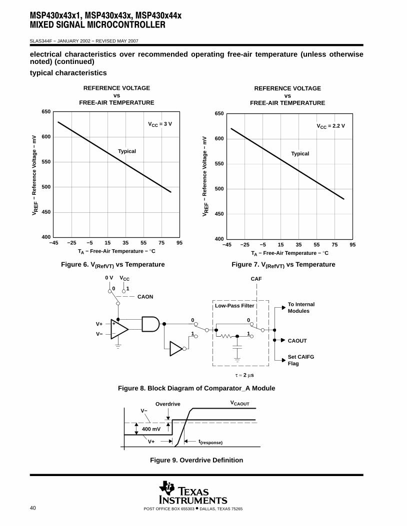
MSP430x43x1, MSP430x43x, MSP430x44xMIXED SIGNAL MICROCONTROLLER
SLAS344F − JANUARY 2002 − REVISED MAY 2007
40 POST OFFICE BOX 655303 • DALLAS, TEXAS 75265
electrical characteristics over recommended operating free-air temperature (unless otherwisenoted) (continued)
typical characteristics
TA − Free-Air Temperature − °C
400
450
500
550
600
650
−45 −25 −5 15 35 55 75 95
VCC = 3 V
Figure 6. V(RefVT) vs Temperature
VR
EF
− R
efer
ence
Vo
ltag
e −
mV
Typical
REFERENCE VOLTAGEvs
FREE-AIR TEMPERATURE
Figure 7. V(RefVT) vs Temperature
TA − Free-Air Temperature − °C
400
450
500
550
600
650
−45 −25 −5 15 35 55 75 95
VCC = 2.2 V
Typical
REFERENCE VOLTAGEvs
FREE-AIR TEMPERATURE
VR
EF
− R
efer
ence
Vo
ltag
e −
mV
_+
CAON
0
1
V+0
1
CAF
Low-Pass Filter
τ ≈ 2 μs
To InternalModules
Set CAIFGFlag
CAOUTV−
VCC
1
0 V
0
Figure 8. Block Diagram of Comparator_A Module
Overdrive VCAOUT
t(response)V+
V−
400 mV
Figure 9. Overdrive Definition
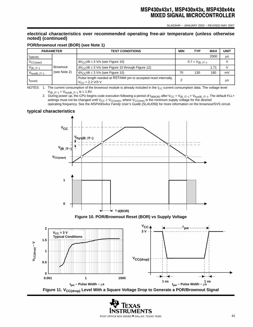
MSP430x43x1, MSP430x43x, MSP430x44xMIXED SIGNAL MICROCONTROLLER
SLAS344F − JANUARY 2002 − REVISED MAY 2007
41POST OFFICE BOX 655303 • DALLAS, TEXAS 75265
electrical characteristics over recommended operating free-air temperature (unless otherwisenoted) (continued)POR/brownout reset (BOR) (see Note 1)
PARAMETER TEST CONDITIONS MIN TYP MAX UNIT
td(BOR) 2000 μs
VCC(start) dVCC/dt ≤ 3 V/s (see Figure 10) 0.7 × V(B_IT−) V
V(B_IT−) Brownout dVCC/dt ≤ 3 V/s (see Figure 10 through Figure 12) 1.71 V
Vhys(B_IT−) (see Note 2) dVCC/dt ≤ 3 V/s (see Figure 10) 70 130 180 mV
t(reset)Pulse length needed at RST/NMI pin to accepted reset internally,VCC = 2.2 V/3 V 2 μs
NOTES: 1. The current consumption of the brownout module is already included in the ICC current consumption data. The voltage level V(B_IT−) + Vhys(B_IT−) is ≤ 1.8V.
2. During power up, the CPU begins code execution following a period of td(BOR) after VCC = V(B_IT−) + Vhys(B_IT−). The default FLL+settings must not be changed until VCC ≥ VCC(min), where VCC(min) is the minimum supply voltage for the desiredoperating frequency. See the MSP430x4xx Family User’s Guide (SLAU056) for more information on the brownout/SVS circuit.
typical characteristics
0
1
t d(BOR)
VCC
V(B_IT−)
Vhys(B_IT−)
VCC(start)
Figure 10. POR/Brownout Reset (BOR) vs Supply Voltage
VCC(drop)
VCC3 V
tpw
0
0.5
1
1.5
2
0.001 1 1000
Typical Conditions
1 ns 1 nstpw − Pulse Width − μs tpw − Pulse Width − μs
VCC = 3 V
VC
C(d
rop
) − V
Figure 11. VCC(drop) Level With a Square Voltage Drop to Generate a POR/Brownout Signal

MSP430x43x1, MSP430x43x, MSP430x44xMIXED SIGNAL MICROCONTROLLER
SLAS344F − JANUARY 2002 − REVISED MAY 2007
42 POST OFFICE BOX 655303 • DALLAS, TEXAS 75265
typical characteristics (Continued)VCC
0
0.5
1
1.5
2
VCC(drop)
tpw
tpw − Pulse Width − μs
3 V
0.001 1 1000 tf trtpw − Pulse Width − μs
tf = tr
Typical Conditions
VCC = 3 V
VC
C(d
rop
) − V
Figure 12. VCC(drop) Level With a Triangle Voltage Drop to Generate a POR/Brownout Signal
electrical characteristics over recommended operating free-air temperature (unless otherwisenoted) (continued)
SVS (supply voltage supervisor/monitor)PARAMETER TEST CONDITIONS MIN NOM MAX UNIT
tdVCC/dt > 30 V/ms (see Figure 13) 5 150 μs
t(SVSR) dVCC/dt ≤ 30 V/ms 2000 μs
td(SVSon) SVSon, switch from VLD=0 to VLD ≠ 0, VCC = 3 V 20 150 μs
tsettle VLD ≠ 0‡ 12 μs
V(SVSstart) VLD ≠ 0, VCC/dt ≤ 3 V/s (see Figure 13) 1.55 1.7 V
VLD = 1 70 120 155 mV
Vhys(SVS_IT−)
VCC/dt ≤ 3 V/s (see Figure 13)VLD = 2 .. 14
V(SVS_IT−) × 0.004
V(SVS_IT−)× 0.008Vhys(SVS_IT−)
VCC/dt ≤ 3 V/s (see Figure 13), external voltage appliedon A7 VLD = 15 4.4 10.4 mV
VLD = 1 1.8 1.9 2.05
VLD = 2 1.94 2.1 2.25
VLD = 3 2.05 2.2 2.37
VLD = 4 2.14 2.3 2.48
VLD = 5 2.24 2.4 2.6
VLD = 6 2.33 2.5 2.71
V /dt ≤ 3 V/s (see Figure 13)VLD = 7 2.46 2.65 2.86
V(SVS IT )
VCC/dt ≤ 3 V/s (see Figure 13)VLD = 8 2.58 2.8 3
VV(SVS_IT−)VLD = 9 2.69 2.9 3.13
V
VLD = 10 2.83 3.05 3.29
VLD = 11 2.94 3.2 3.42
VLD = 12 3.11 3.35 3.61†
VLD = 13 3.24 3.5 3.76†
VLD = 14 3.43 3.7† 3.99†
VCC/dt ≤ 3 V/s (see Figure 13), external voltage appliedon A7 VLD = 15 1.1 1.2 1.3
ICC(SVS)(see Note 1) VLD ≠ 0, VCC = 2.2 V/3 V 10 15 μA
† The recommended operating voltage range is limited to 3.6 V.‡ tsettle is the settling time that the comparator o/p needs to have a stable level after VLD is switched VLD ≠ 0 to a different VLD value somewhere
between 2 and 15. The overdrive is assumed to be > 50 mV.NOTE 1: The current consumption of the SVS module is not included in the ICC current consumption data.
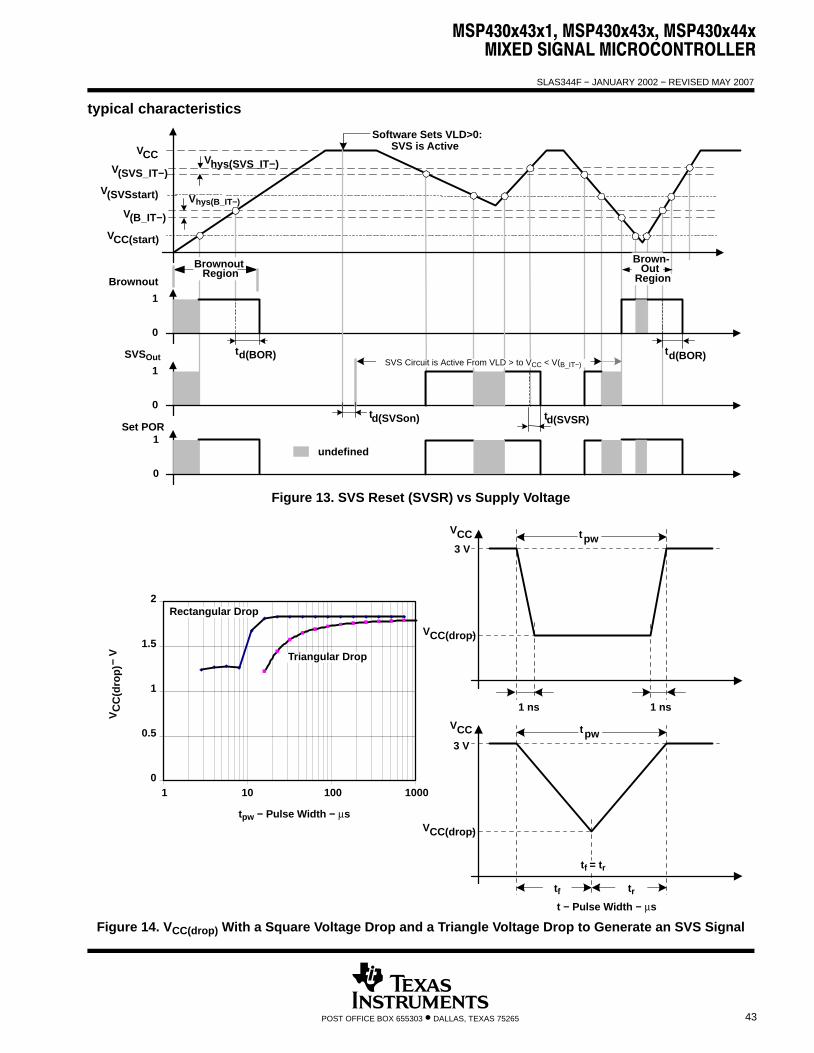
MSP430x43x1, MSP430x43x, MSP430x44xMIXED SIGNAL MICROCONTROLLER
SLAS344F − JANUARY 2002 − REVISED MAY 2007
43POST OFFICE BOX 655303 • DALLAS, TEXAS 75265
typical characteristics
VCC(start)
VCC
V(B_IT−)
BrownoutRegion
V(SVSstart)
V(SVS_IT−)
Software Sets VLD>0:SVS is Active
td(SVSR)
undefined
Vhys(SVS_IT−)
0
1
td(BOR)
Brownout
0
1
td(SVSon)
td(BOR)
0
1Set POR
Brown-Out
Region
SVS Circuit is Active From VLD > to VCC < V(B_IT−)SVSOut
Vhys(B_IT−)
Figure 13. SVS Reset (SVSR) vs Supply Voltage
0
0.5
1
1.5
2
VCC
VCC
1 ns 1 ns
VCC(drop)
tpw
tpw − Pulse Width − μs
VC
C(d
rop
)− V
3 V
1 10 1000
tf tr
t − Pulse Width − μs
100
tpw3 V
tf = tr
Rectangular Drop
Triangular Drop
VCC(drop)
Figure 14. VCC(drop) With a Square Voltage Drop and a Triangle Voltage Drop to Generate an SVS Signal
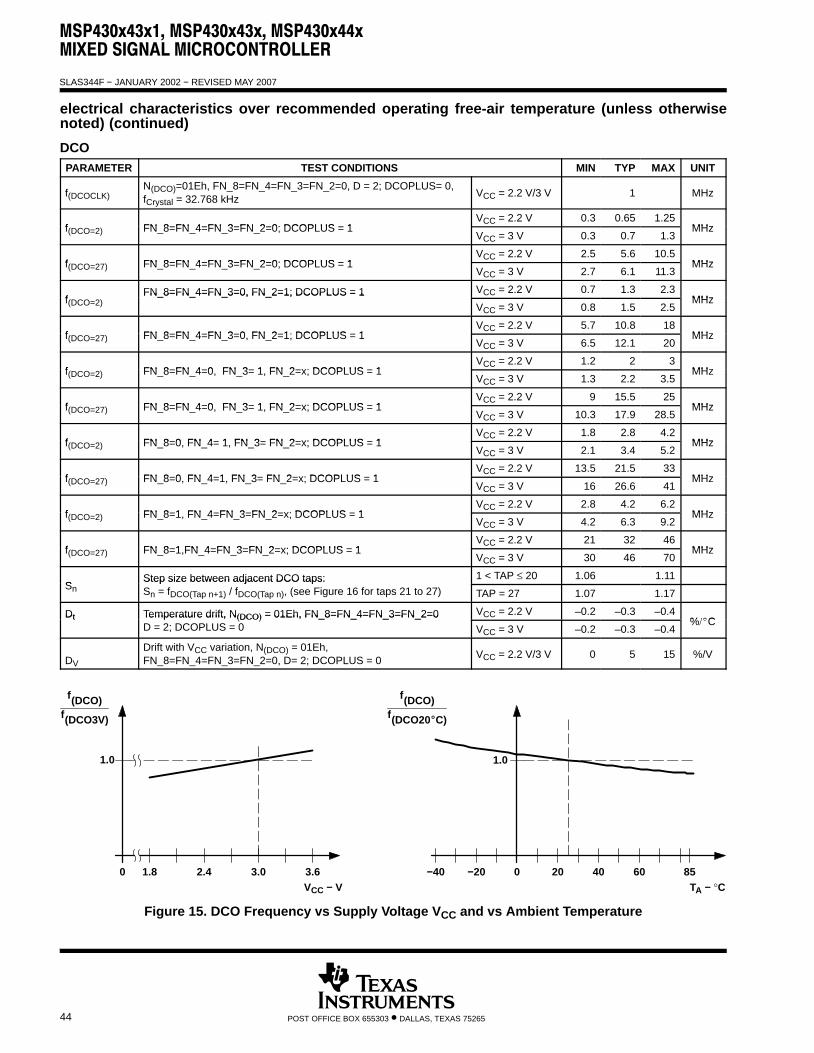
MSP430x43x1, MSP430x43x, MSP430x44xMIXED SIGNAL MICROCONTROLLER
SLAS344F − JANUARY 2002 − REVISED MAY 2007
44 POST OFFICE BOX 655303 • DALLAS, TEXAS 75265
electrical characteristics over recommended operating free-air temperature (unless otherwisenoted) (continued)
DCOPARAMETER TEST CONDITIONS MIN TYP MAX UNIT
f(DCOCLK)N(DCO)=01Eh, FN_8=FN_4=FN_3=FN_2=0, D = 2; DCOPLUS= 0,fCrystal = 32.768 kHz VCC = 2.2 V/3 V 1 MHz
f FN 8 FN 4 FN 3 FN 2 0; DCOPLUS 1VCC = 2.2 V 0.3 0.65 1.25
MHzf(DCO=2) FN_8=FN_4=FN_3=FN_2=0; DCOPLUS = 1VCC = 3 V 0.3 0.7 1.3
MHz
f FN 8 FN 4 FN 3 FN 2 0; DCOPLUS 1VCC = 2.2 V 2.5 5.6 10.5
MHzf(DCO=27) FN_8=FN_4=FN_3=FN_2=0; DCOPLUS = 1VCC = 3 V 2.7 6.1 11.3
MHz
fFN_8=FN_4=FN_3=0, FN_2=1; DCOPLUS = 1 VCC = 2.2 V 0.7 1.3 2.3
MHzf(DCO=2)FN_8=FN_4=FN_3=0, FN_2=1; DCOPLUS = 1
VCC = 3 V 0.8 1.5 2.5MHz
f FN 8 FN 4 FN 3 0 FN 2 1; DCOPLUS 1VCC = 2.2 V 5.7 10.8 18
MHzf(DCO=27) FN_8=FN_4=FN_3=0, FN_2=1; DCOPLUS = 1VCC = 3 V 6.5 12.1 20
MHz
f FN 8 FN 4 0 FN 3 1 FN 2 x; DCOPLUS 1VCC = 2.2 V 1.2 2 3
MHzf(DCO=2) FN_8=FN_4=0, FN_3= 1, FN_2=x; DCOPLUS = 1VCC = 3 V 1.3 2.2 3.5
MHz
f FN 8 FN 4 0 FN 3 1 FN 2 x; DCOPLUS 1VCC = 2.2 V 9 15.5 25
MHzf(DCO=27) FN_8=FN_4=0, FN_3= 1, FN_2=x; DCOPLUS = 1VCC = 3 V 10.3 17.9 28.5
MHz
f FN 8 0 FN 4 1 FN 3 FN 2 x; DCOPLUS 1VCC = 2.2 V 1.8 2.8 4.2
MHzf(DCO=2) FN_8=0, FN_4= 1, FN_3= FN_2=x; DCOPLUS = 1VCC = 3 V 2.1 3.4 5.2
MHz
f FN 8 0 FN 4 1 FN 3 FN 2 x; DCOPLUS 1VCC = 2.2 V 13.5 21.5 33
MHzf(DCO=27) FN_8=0, FN_4=1, FN_3= FN_2=x; DCOPLUS = 1VCC = 3 V 16 26.6 41
MHz
f FN 8 1 FN 4 FN 3 FN 2 x; DCOPLUS 1VCC = 2.2 V 2.8 4.2 6.2
MHzf(DCO=2) FN_8=1, FN_4=FN_3=FN_2=x; DCOPLUS = 1VCC = 3 V 4.2 6.3 9.2
MHz
f FN 8 1 FN 4 FN 3 FN 2 x; DCOPLUS 1VCC = 2.2 V 21 32 46
MHzf(DCO=27) FN_8=1,FN_4=FN_3=FN_2=x; DCOPLUS = 1VCC = 3 V 30 46 70
MHz
SStep size between adjacent DCO taps: 1 < TAP ≤ 20 1.06 1.11
SnStep size between adjacent DCO taps:Sn = fDCO(Tap n+1) / fDCO(Tap n), (see Figure 16 for taps 21 to 27) TAP = 27 1.07 1.17
Dt Temperature drift, N(DCO) = 01Eh, FN_8=FN_4=FN_3=FN_2=0 VCC = 2.2 V –0.2 –0.3 –0.4%/C
Dt Temperature drift, N(DCO) = 01Eh, FN_8=FN_4=FN_3=FN_2=0D = 2; DCOPLUS = 0 VCC = 3 V –0.2 –0.3 –0.4
%/C
DV
Drift with VCC variation, N(DCO) = 01Eh,FN_8=FN_4=FN_3=FN_2=0, D= 2; DCOPLUS = 0 VCC = 2.2 V/3 V 0 5 15 %/V
TA − °CVCC − V
f(DCO)f(DCO20C)
f(DCO)f(DCO3V)
1.8 3.02.4 3.6
1.0
20 6040 85
1.0
0−20−400
Figure 15. DCO Frequency vs Supply Voltage VCC and vs Ambient Temperature
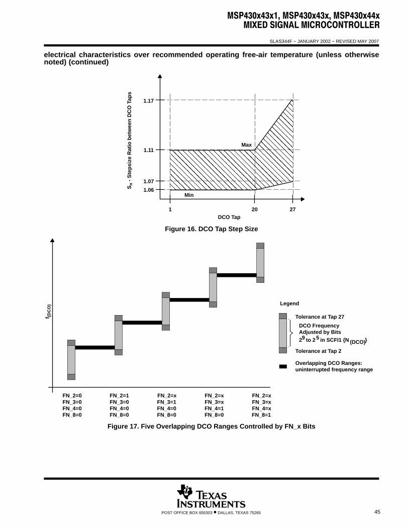
MSP430x43x1, MSP430x43x, MSP430x44xMIXED SIGNAL MICROCONTROLLER
SLAS344F − JANUARY 2002 − REVISED MAY 2007
45POST OFFICE BOX 655303 • DALLAS, TEXAS 75265
electrical characteristics over recommended operating free-air temperature (unless otherwisenoted) (continued)
ÎÎÎÎÎÎÎÎÎÎÎÎÎÎÎÎÎÎÎÎÎÎÎÎÎÎÎÎÎÎÎÎÎÎÎÎÎÎÎÎÎÎÎÎÎÎÎÎÎÎÎÎÎÎÎÎÎÎÎÎÎÎÎÎÎÎÎÎÎÎÎÎÎÎÎÎÎÎÎÎÎÎÎÎÎÎÎÎÎÎÎÎÎÎÎÎÎÎÎÎÎÎÎÎÎÎÎÎÎÎÎÎÎÎÎÎÎÎÎÎÎÎÎÎÎÎÎÎÎÎ
1 2720
1.11
1.17
DCO Tap
Sn -
Ste
psi
ze R
atio
bet
wee
n D
CO
Tap
s
Min
Max
1.07
1.06
Figure 16. DCO Tap Step Size
FN_2=0FN_3=0FN_4=0FN_8=0
FN_2=1FN_3=0FN_4=0FN_8=0
FN_2=xFN_3=1FN_4=0FN_8=0
FN_2=xFN_3=xFN_4=1FN_8=0
FN_2=xFN_3=xFN_4=xFN_8=1
Legend
Tolerance at Tap 27
Tolerance at Tap 2
DCO FrequencyAdjusted by Bits29 to 25 in SCFI1 N (DCO)
Overlapping DCO Ranges:uninterrupted frequency range
f (D
CO
)
Figure 17. Five Overlapping DCO Ranges Controlled by FN_x Bits
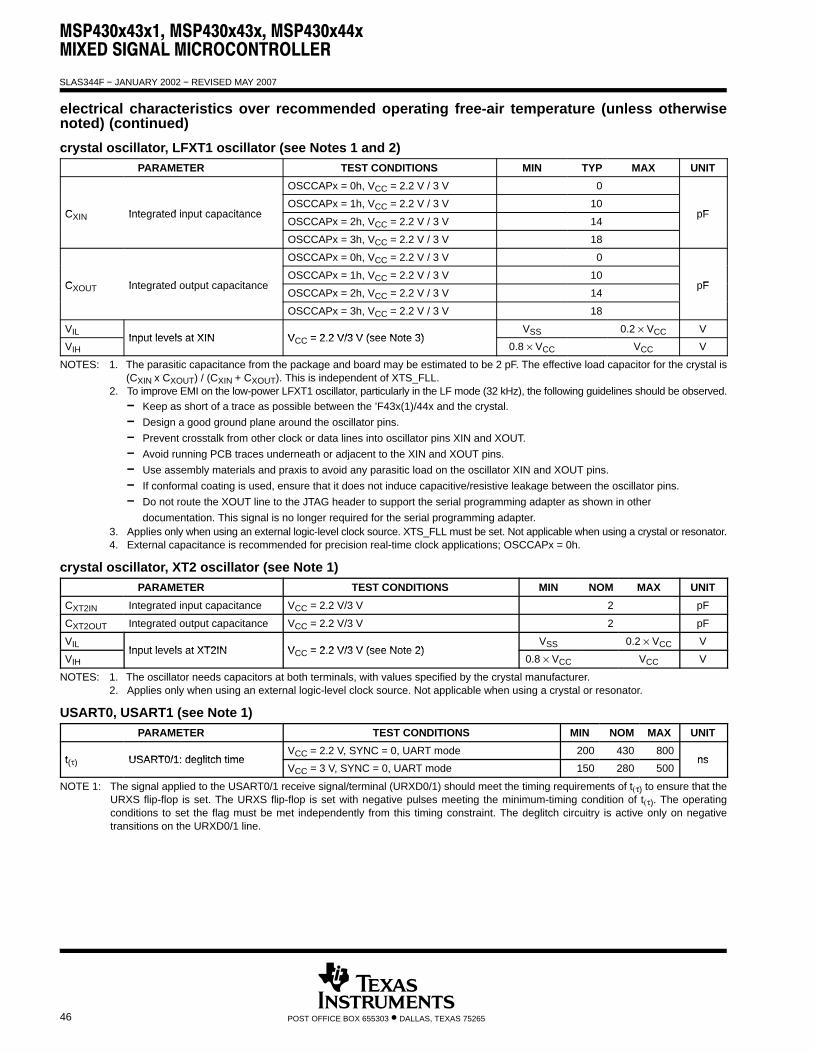
MSP430x43x1, MSP430x43x, MSP430x44xMIXED SIGNAL MICROCONTROLLER
SLAS344F − JANUARY 2002 − REVISED MAY 2007
46 POST OFFICE BOX 655303 • DALLAS, TEXAS 75265
electrical characteristics over recommended operating free-air temperature (unless otherwisenoted) (continued)
crystal oscillator, LFXT1 oscillator (see Notes 1 and 2)PARAMETER TEST CONDITIONS MIN TYP MAX UNIT
OSCCAPx = 0h, VCC = 2.2 V / 3 V 0
C Integrated input capacitanceOSCCAPx = 1h, VCC = 2.2 V / 3 V 10
pFCXIN Integrated input capacitanceOSCCAPx = 2h, VCC = 2.2 V / 3 V 14
pF
OSCCAPx = 3h, VCC = 2.2 V / 3 V 18
OSCCAPx = 0h, VCC = 2.2 V / 3 V 0
C Integrated output capacitanceOSCCAPx = 1h, VCC = 2.2 V / 3 V 10
pFCXOUT Integrated output capacitanceOSCCAPx = 2h, VCC = 2.2 V / 3 V 14
pF
OSCCAPx = 3h, VCC = 2.2 V / 3 V 18
VILInput levels at XIN V = 2 2 V/3 V (see Note 3)
VSS 0.2 × VCC V
VIHInput levels at XIN VCC = 2.2 V/3 V (see Note 3)
0.8 × VCC VCC V
NOTES: 1. The parasitic capacitance from the package and board may be estimated to be 2 pF. The effective load capacitor for the crystal is(CXIN x CXOUT) / (CXIN + CXOUT). This is independent of XTS_FLL.
2. To improve EMI on the low-power LFXT1 oscillator, particularly in the LF mode (32 kHz), the following guidelines should be observed.− Keep as short of a trace as possible between the ’F43x(1)/44x and the crystal.− Design a good ground plane around the oscillator pins.− Prevent crosstalk from other clock or data lines into oscillator pins XIN and XOUT.− Avoid running PCB traces underneath or adjacent to the XIN and XOUT pins.− Use assembly materials and praxis to avoid any parasitic load on the oscillator XIN and XOUT pins.− If conformal coating is used, ensure that it does not induce capacitive/resistive leakage between the oscillator pins.− Do not route the XOUT line to the JTAG header to support the serial programming adapter as shown in other
documentation. This signal is no longer required for the serial programming adapter.3. Applies only when using an external logic-level clock source. XTS_FLL must be set. Not applicable when using a crystal or resonator.4. External capacitance is recommended for precision real-time clock applications; OSCCAPx = 0h.
crystal oscillator, XT2 oscillator (see Note 1)PARAMETER TEST CONDITIONS MIN NOM MAX UNIT
CXT2IN Integrated input capacitance VCC = 2.2 V/3 V 2 pF
CXT2OUT Integrated output capacitance VCC = 2.2 V/3 V 2 pF
VILInput levels at XT2IN VCC = 2 2 V/3 V (see Note 2)
VSS 0.2 × VCC V
VIHInput levels at XT2IN VCC = 2.2 V/3 V (see Note 2)
0.8 × VCC VCC V
NOTES: 1. The oscillator needs capacitors at both terminals, with values specified by the crystal manufacturer.2. Applies only when using an external logic-level clock source. Not applicable when using a crystal or resonator.
USART0, USART1 (see Note 1)PARAMETER TEST CONDITIONS MIN NOM MAX UNIT
t USART0/1: deglitch timeVCC = 2.2 V, SYNC = 0, UART mode 200 430 800
nst(τ) USART0/1: deglitch timeVCC = 3 V, SYNC = 0, UART mode 150 280 500
ns
NOTE 1: The signal applied to the USART0/1 receive signal/terminal (URXD0/1) should meet the timing requirements of t(τ) to ensure that theURXS flip-flop is set. The URXS flip-flop is set with negative pulses meeting the minimum-timing condition of t(τ). The operatingconditions to set the flag must be met independently from this timing constraint. The deglitch circuitry is active only on negativetransitions on the URXD0/1 line.

MSP430x43x1, MSP430x43x, MSP430x44xMIXED SIGNAL MICROCONTROLLER
SLAS344F − JANUARY 2002 − REVISED MAY 2007
47POST OFFICE BOX 655303 • DALLAS, TEXAS 75265
electrical characteristics over recommended operating free-air temperature (unless otherwisenoted) (continued)
12-bit ADC, power supply and input range conditions (see Note 1)PARAMETER TEST CONDITIONS VCC MIN NOM MAX UNIT
AVCC Analog supply voltageAVCC and DVCC are connected togetherAVSS and DVSS are connected togetherV(AVSS) = V(DVSS) = 0 V
2.2 3.6 V
V(P6.x/Ax)Analog input voltagerange (see Note 2)
All P6.0/A0 to P6.7/A7 terminals. Analog inputs selected in ADC12MCTLx register and P6Sel.x=10 ≤ x ≤ 7; V(AVSS) ≤ VP6.x/Ax ≤ V(AVCC)
0 VAVCC V
IOperating supply currentinto AV terminal
fADC12CLK = 5.0 MHzADC12ON 1 REFON 0
2.2 V 0.65 1.3mAIADC12 into AVCC terminal
(see Note 3)ADC12ON = 1, REFON = 0SHT0=0, SHT1=0, ADC12DIV=0 3 V 0.8 1.6
mA
IOperating supply currenti t AV t i l
fADC12CLK = 5.0 MHzADC12ON = 0, REFON = 1, REF2_5V = 1
3 V 0.5 0.8 mA
IREF+ into AVCC terminal (see Note 4) fADC12CLK = 5.0 MHz
ADC12ON 02.2 V 0.5 0.8
mA(see Note 4)
ADC12ON = 0, REFON = 1, REF2_5V = 0 3 V 0.5 0.8
mA
CI Input capacitanceOnly one terminal can be selectedat one time, P6.x/Ax 2.2 V 40 pF
RI Input MUX ON resistance 0V ≤ VAx ≤ VAVCC 3 V 2000 ΩNOTES: 1. The leakage current is defined in the leakage current table with P6.x/Ax parameter.
2. The analog input voltage range must be within the selected reference voltage range VR+ to VR− for valid conversion results.3. The internal reference supply current is not included in current consumption parameter IADC12.4. The internal reference current is supplied via terminal AVCC. Consumption is independent of the ADC12ON control bit, unless a
conversion is active. The REFON bit enables to settle the built-in reference before starting an A/D conversion.
12-bit ADC, external reference (see Note 1)PARAMETER TEST CONDITIONS VCC MIN NOM MAX UNIT
VeREF+Positive externalreference voltage input VeREF+ > VREF−/VeREF− (see Note 2) 1.4 VAVCC V
VREF− /VeREF−Negative externalreference voltage input VeREF+ > VREF−/VeREF− (see Note 3) 0 1.2 V
(VeREF+ −VREF−/VeREF−)
Differential externalreference voltage input VeREF+ > VREF−/VeREF− (see Note 4) 1.4 VAVCC V
IVeREF+ Static input current 0V ≤VeREF+ ≤ VAVCC 2.2 V/3 V ±1 μA
IVREF−/VeREF− Static input current 0V ≤ VeREF− ≤ VAVCC 2.2 V/3 V ±1 μA
NOTES: 1. The external reference is used during conversion to charge and discharge the capacitance array. The input capacitance, Ci, is alsothe dynamic load for an external reference during conversion. The dynamic impedance of the reference supply should follow therecommendations on analog-source impedance to allow the charge to settle for 12-bit accuracy.
2. The accuracy limits the minimum positive external reference voltage. Lower reference voltage levels may be applied with reducedaccuracy requirements.
3. The accuracy limits the maximum negative external reference voltage. Higher reference voltage levels may be applied with reducedaccuracy requirements.
4. The accuracy limits minimum external differential reference voltage. Lower differential reference voltage levels may be applied withreduced accuracy requirements.
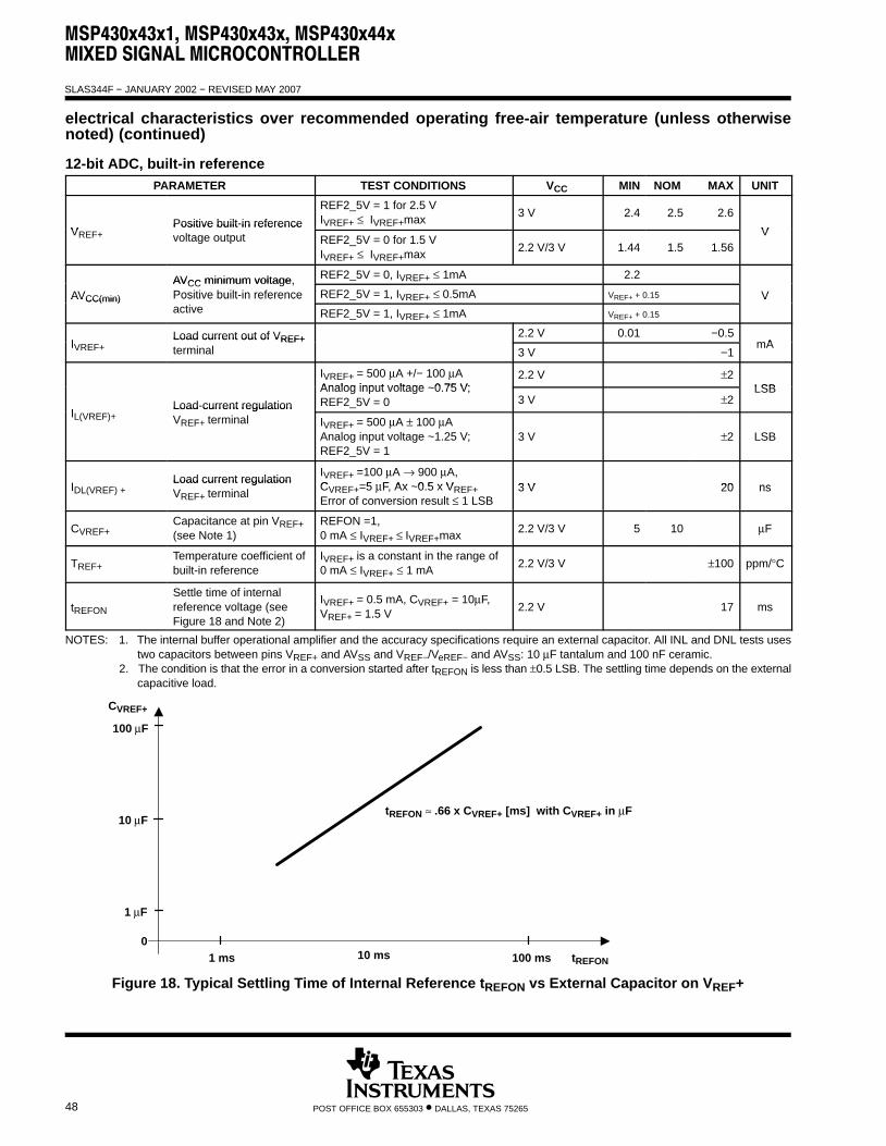
MSP430x43x1, MSP430x43x, MSP430x44xMIXED SIGNAL MICROCONTROLLER
SLAS344F − JANUARY 2002 − REVISED MAY 2007
48 POST OFFICE BOX 655303 • DALLAS, TEXAS 75265
electrical characteristics over recommended operating free-air temperature (unless otherwisenoted) (continued)
12-bit ADC, built-in referencePARAMETER TEST CONDITIONS VCC MIN NOM MAX UNIT
VPositive built-in reference
REF2_5V = 1 for 2.5 VIVREF+ ≤ IVREF+max 3 V 2.4 2.5 2.6
VVREF+Positive built in referencevoltage output REF2_5V = 0 for 1.5 V
IVREF+ ≤ IVREF+max 2.2 V/3 V 1.44 1.5 1.56V
AVCC minimum voltage, REF2_5V = 0, IVREF+ ≤ 1mA 2.2
AVCC(min)
AVCC minimum voltage,Positive built-in reference REF2_5V = 1, IVREF+ ≤ 0.5mA VREF+ + 0.15 VAVCC(min) Positive built in referenceactive REF2_5V = 1, IVREF+ ≤ 1mA VREF+ + 0.15
V
ILoad current out of VREF+ 2.2 V 0.01 −0.5
mAIVREF+Load current out of VREF+terminal 3 V −1
mA
IVREF+ = 500 μA +/− 100 μAAnalog input voltage 0 75 V;
2.2 V ±2LSB
ILoad-current regulation
Analog input voltage ~0.75 V; REF2_5V = 0 3 V ±2
LSB
IL(VREF)+Load current regulationVREF+ terminal IVREF+ = 500 μA ± 100 μA
Analog input voltage ~1.25 V;REF2_5V = 1
3 V ±2 LSB
ILoad current regulation IVREF+ =100 μA → 900 μA,
C 5 μF Ax 0 5 x V 3 V 20 nsIDL(VREF) +Load current regulationVREF+ terminal CVREF+=5 μF, Ax ~0.5 x VREF+
Error of conversion result ≤ 1 LSB3 V 20 ns
CVREF+Capacitance at pin VREF+(see Note 1)
REFON =1,0 mA ≤ IVREF+ ≤ IVREF+max 2.2 V/3 V 5 10 μF
TREF+Temperature coefficient ofbuilt-in reference
IVREF+ is a constant in the range of0 mA ≤ IVREF+ ≤ 1 mA 2.2 V/3 V ±100 ppm/°C
tREFON
Settle time of internalreference voltage (seeFigure 18 and Note 2)
IVREF+ = 0.5 mA, CVREF+ = 10μF,VREF+ = 1.5 V 2.2 V 17 ms
NOTES: 1. The internal buffer operational amplifier and the accuracy specifications require an external capacitor. All INL and DNL tests usestwo capacitors between pins VREF+ and AVSS and VREF−/VeREF− and AVSS: 10 μF tantalum and 100 nF ceramic.
2. The condition is that the error in a conversion started after tREFON is less than ±0.5 LSB. The settling time depends on the externalcapacitive load.
CVREF+
1 μF
01 ms 10 ms 100 ms tREFON
tREFON ≈ .66 x CVREF+ [ms] with CVREF+ in μF
100 μF
10 μF
Figure 18. Typical Settling Time of Internal Reference tREFON vs External Capacitor on VREF+

MSP430x43x1, MSP430x43x, MSP430x44xMIXED SIGNAL MICROCONTROLLER
SLAS344F − JANUARY 2002 − REVISED MAY 2007
49POST OFFICE BOX 655303 • DALLAS, TEXAS 75265
+−
10 μF 100 nFAVSS
MSP430F43x
MSP430F44x
+−
+−
10 μF 100 nF
10 μF 100 nF
AVCC
10 μF 100 nFDVSS1
DVCC1FromPowerSupply
ApplyExternal
Reference
+−
Apply External Reference [VeREF+]or Use Internal Reference [VREF+] VREF+ or VeREF+
VREF−/VeREF−
/DVCC2
/DVSS2
Figure 19. Supply Voltage and Reference Voltage Design VREF−/VeREF− External Supply
+−
10 μF 100 nFAVSS
MSP430F43x
MSP430F44x
+−
10 μF 100 nF
AVCC
10 μF 100 nF
FromPowerSupply
+−
Apply External Reference [VeREF+]or Use Internal Reference [VREF+] VREF+ or VeREF+
VREF−/VeREF−Reference Is InternallySwitched to AVSS
DVSS1
DVCC1/DVCC2
/DVSS2
Figure 20. Supply Voltage and Reference Voltage Design VREF−/VeREF− = AVSS, Internally Connected
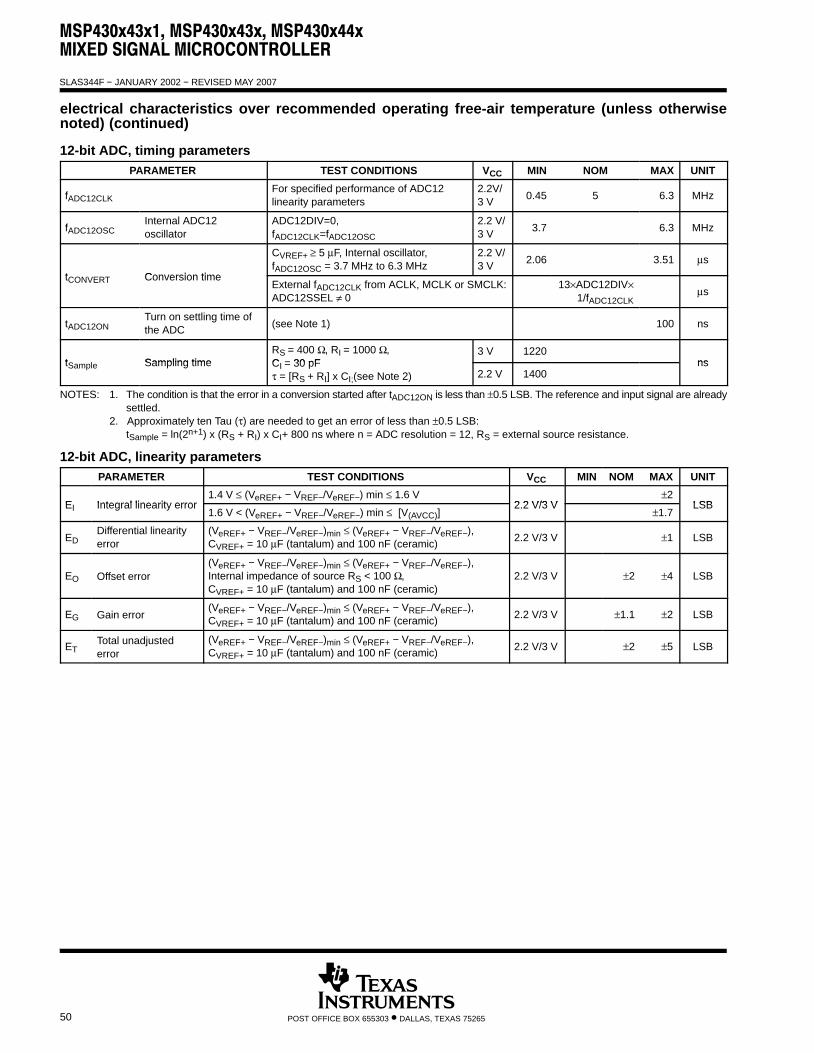
MSP430x43x1, MSP430x43x, MSP430x44xMIXED SIGNAL MICROCONTROLLER
SLAS344F − JANUARY 2002 − REVISED MAY 2007
50 POST OFFICE BOX 655303 • DALLAS, TEXAS 75265
electrical characteristics over recommended operating free-air temperature (unless otherwisenoted) (continued)
12-bit ADC, timing parametersPARAMETER TEST CONDITIONS VCC MIN NOM MAX UNIT
fADC12CLKFor specified performance of ADC12linearity parameters
2.2V/3 V 0.45 5 6.3 MHz
fADC12OSCInternal ADC12oscillator
ADC12DIV=0,fADC12CLK=fADC12OSC
2.2 V/3 V 3.7 6.3 MHz
t Conversion time
CVREF+ ≥ 5 μF, Internal oscillator,fADC12OSC = 3.7 MHz to 6.3 MHz
2.2 V/3 V 2.06 3.51 μs
tCONVERT Conversion timeExternal fADC12CLK from ACLK, MCLK or SMCLK:ADC12SSEL ≠ 0
13×ADC12DIV×1/fADC12CLK
μs
tADC12ONTurn on settling time ofthe ADC (see Note 1) 100 ns
t Sampling timeRS = 400 Ω, RI = 1000 Ω, C 30 pF
3 V 1220nstSample Sampling time CI = 30 pF
τ = [RS + RI] x CI;(see Note 2) 2.2 V 1400ns
NOTES: 1. The condition is that the error in a conversion started after tADC12ON is less than ±0.5 LSB. The reference and input signal are alreadysettled.
2. Approximately ten Tau (τ) are needed to get an error of less than ±0.5 LSB:tSample = ln(2n+1) x (RS + RI) x CI+ 800 ns where n = ADC resolution = 12, RS = external source resistance.
12-bit ADC, linearity parametersPARAMETER TEST CONDITIONS VCC MIN NOM MAX UNIT
E Integral linearity error1.4 V ≤ (VeREF+ − VREF−/VeREF−) min ≤ 1.6 V
2 2 V/3 V±2
LSBEI Integral linearity error1.6 V < (VeREF+ − VREF−/VeREF−) min ≤ [V(AVCC)]
2.2 V/3 V±1.7
LSB
EDDifferential linearityerror
(VeREF+ − VREF−/VeREF−)min ≤ (VeREF+ − VREF−/VeREF−),CVREF+ = 10 μF (tantalum) and 100 nF (ceramic) 2.2 V/3 V ±1 LSB
EO Offset error(VeREF+ − VREF−/VeREF−)min ≤ (VeREF+ − VREF−/VeREF−),Internal impedance of source RS < 100 Ω,CVREF+ = 10 μF (tantalum) and 100 nF (ceramic)
2.2 V/3 V ±2 ±4 LSB
EG Gain error(VeREF+ − VREF−/VeREF−)min ≤ (VeREF+ − VREF−/VeREF−),CVREF+ = 10 μF (tantalum) and 100 nF (ceramic) 2.2 V/3 V ±1.1 ±2 LSB
ETTotal unadjustederror
(VeREF+ − VREF−/VeREF−)min ≤ (VeREF+ − VREF−/VeREF−),CVREF+ = 10 μF (tantalum) and 100 nF (ceramic) 2.2 V/3 V ±2 ±5 LSB

MSP430x43x1, MSP430x43x, MSP430x44xMIXED SIGNAL MICROCONTROLLER
SLAS344F − JANUARY 2002 − REVISED MAY 2007
51POST OFFICE BOX 655303 • DALLAS, TEXAS 75265
electrical characteristics over recommended operating free-air temperature (unless otherwisenoted) (continued)
12-bit ADC, temperature sensor and built-in VMID
PARAMETER TEST CONDITIONS VCC MIN NOM MAX UNIT
IOperating supply current into REFON = 0, INCH = 0Ah, 2.2 V 40 120
AISENSOROperating supply current intoAVCC terminal (see Note 1)
REFON = 0, INCH = 0Ah,ADC12ON=NA, TA = 25C 3 V 60 160
μA
VADC12ON = 1, INCH = 0Ah, 2.2 V 986 986±5%
mVVSENSORADC12ON = 1, INCH = 0Ah, TA = 0°C 3 V 986 986±5%
mV
TC ADC12ON 1 INCH 0Ah2.2 V 3.55 3.55±3%
mV/°CTCSENSOR ADC12ON = 1, INCH = 0Ah3 V 3.55 3.55±3%
mV/°C
tSample time required if channel ADC12ON = 1, INCH = 0Ah, 2.2 V 30
stSENSOR(sample)Sample time required if channel10 is selected (see Note 2)
ADC12ON = 1, INCH = 0Ah,Error of conversion result ≤ 1 LSB 3 V 30
μs
I Current into divider at channel 11ADC12ON = 1, INCH = 0Bh, 2.2 V NA
AIVMID Current into divider at channel 11ADC12ON = 1, INCH = 0Bh,(see Note 3) 3 V NA
μA
V AV divider at channel 11ADC12ON = 1, INCH = 0Bh, 2.2 V 1.1 1.1±0.04
VVMID AVCC divider at channel 11ADC12ON = 1, INCH = 0Bh,VMID is ~0.5 x VAVCC 3 V 1.5 1.50±0.04
V
t Sample time required if channel ADC12ON = 1, INCH = 0Bh, 2.2 V 1400nstVMID(sample)
Sample time required if channel11 is selected (see Note 4)
ADC12ON = 1, INCH = 0Bh,Error of conversion result ≤ 1 LSB 3 V 1220
ns
NOTES: 1. The sensor current ISENSOR is consumed if (ADC12ON = 1 and REFON=1), or (ADC12ON=1 AND INCH=0Ah and sample signalis high). Therefore it includes the constant current through the sensor and the reference.
2. The typical equivalent impedance of the sensor is 51 kΩ. The sample time required includes the sensor-on time tSENSOR(on).3. No additional current is needed. The VMID is used during sampling.4. The on-time tVMID(on) is included in the sampling time tVMID(sample); no additional on time is needed.
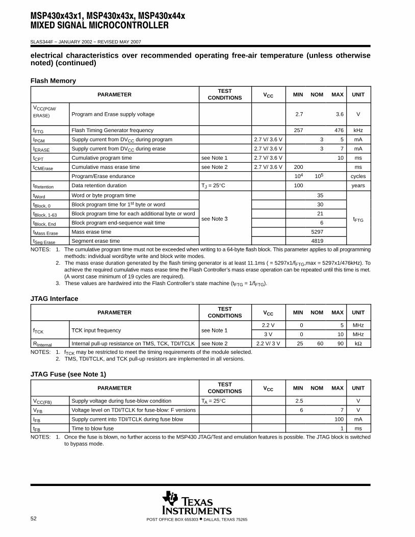
MSP430x43x1, MSP430x43x, MSP430x44xMIXED SIGNAL MICROCONTROLLER
SLAS344F − JANUARY 2002 − REVISED MAY 2007
52 POST OFFICE BOX 655303 • DALLAS, TEXAS 75265
electrical characteristics over recommended operating free-air temperature (unless otherwisenoted) (continued)
Flash Memory
PARAMETERTEST
CONDITIONS VCC MIN NOM MAX UNIT
VCC(PGM/ERASE) Program and Erase supply voltage 2.7 3.6 V
fFTG Flash Timing Generator frequency 257 476 kHz
IPGM Supply current from DVCC during program 2.7 V/ 3.6 V 3 5 mA
IERASE Supply current from DVCC during erase 2.7 V/ 3.6 V 3 7 mA
tCPT Cumulative program time see Note 1 2.7 V/ 3.6 V 10 ms
tCMErase Cumulative mass erase time see Note 2 2.7 V/ 3.6 V 200 ms
Program/Erase endurance 104 105 cycles
tRetention Data retention duration TJ = 25°C 100 years
tWord Word or byte program time 35
tBlock, 0 Block program time for 1st byte or word 30
tBlock, 1-63 Block program time for each additional byte or wordsee Note 3
21t
tBlock, End Block program end-sequence wait timesee Note 3
6tFTG
tMass Erase Mass erase time 5297
tSeg Erase Segment erase time 4819
NOTES: 1. The cumulative program time must not be exceeded when writing to a 64-byte flash block. This parameter applies to all programmingmethods: individual word/byte write and block write modes.
2. The mass erase duration generated by the flash timing generator is at least 11.1ms ( = 5297x1/fFTG,max = 5297x1/476kHz). Toachieve the required cumulative mass erase time the Flash Controller’s mass erase operation can be repeated until this time is met.(A worst case minimum of 19 cycles are required).
3. These values are hardwired into the Flash Controller’s state machine (tFTG = 1/fFTG).
JTAG Interface
PARAMETERTEST
CONDITIONS VCC MIN NOM MAX UNIT
f TCK input frequency see Note 12.2 V 0 5 MHz
fTCK TCK input frequency see Note 13 V 0 10 MHz
RInternal Internal pull-up resistance on TMS, TCK, TDI/TCLK see Note 2 2.2 V/ 3 V 25 60 90 kΩNOTES: 1. fTCK may be restricted to meet the timing requirements of the module selected.
2. TMS, TDI/TCLK, and TCK pull-up resistors are implemented in all versions.
JTAG Fuse (see Note 1)
PARAMETERTEST
CONDITIONS VCC MIN NOM MAX UNIT
VCC(FB) Supply voltage during fuse-blow condition TA = 25°C 2.5 V
VFB Voltage level on TDI/TCLK for fuse-blow: F versions 6 7 V
IFB Supply current into TDI/TCLK during fuse blow 100 mA
tFB Time to blow fuse 1 ms
NOTES: 1. Once the fuse is blown, no further access to the MSP430 JTAG/Test and emulation features is possible. The JTAG block is switchedto bypass mode.
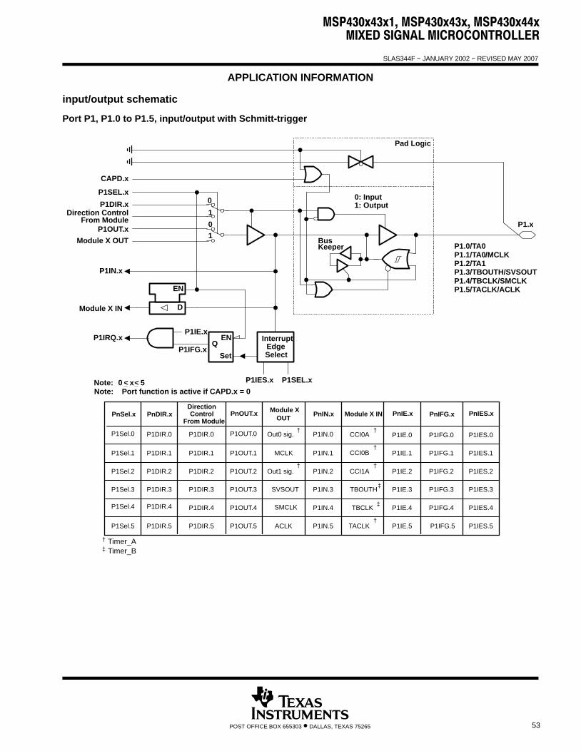
MSP430x43x1, MSP430x43x, MSP430x44xMIXED SIGNAL MICROCONTROLLER
SLAS344F − JANUARY 2002 − REVISED MAY 2007
53POST OFFICE BOX 655303 • DALLAS, TEXAS 75265
APPLICATION INFORMATION
input/output schematic
Port P1, P1.0 to P1.5, input/output with Schmitt-trigger
P1OUT.x
Module X OUT
P1DIR.xDirection Control
From Module
P1SEL.x
D
EN
InterruptEdgeSelect
P1IES.x P1SEL.x
P1IE.x
P1IFG.x
P1IRQ.x
P1.x
EN
Set
Q
0
1
1
0
Pad Logic
0: Input1: Output
BusKeeper
CAPD.x
Note: 0 < x< 5Note: Port function is active if CAPD.x = 0
PnSel.x PnDIR.xDirection
From ModulePnOUT.x Module X
OUTPnIN.x PnIE.x PnIFG.x PnIES.xModule X IN
P1Sel.1 P1DIR.1 P1OUT.1 P1IN.1 P1IE.1 P1IFG.1 P1IES.1
P1Sel.2 P1DIR.2 P1OUT.2 P1IN.2 P1IE.2 P1IFG.2 P1IES.2
P1Sel.3 P1DIR.3 P1OUT.3 P1IN.3 P1IE.3 P1IFG.3 P1IES.3
P1Sel.4 P1DIR.4 P1OUT.4 P1IN.4 P1IE.4 P1IFG.4 P1IES.4
P1Sel.5 P1DIR.5 P1OUT.5 P1IN.5 P1IE.5 P1IFG.5 P1IES.5
P1Sel.0 P1DIR.0 P1OUT.0 P1IN.0 P1IE.0 P1IFG.0 P1IES.0
SVSOUT
Out0 sig.
Out1 sig.
CCI0A
CCI1A
TBOUTH
TBCLK
TACLK
P1DIR.1
P1DIR.2
P1DIR.3
P1DIR.4
P1DIR.5
P1DIR.0
SMCLK
ACLK
MCLK
Module X IN
P1IN.x
P1.5/TACLK/ACLK
P1.0/TA0P1.1/TA0/MCLKP1.2/TA1
P1.4/TBCLK/SMCLKP1.3/TBOUTH/SVSOUT
CCI0B
†
†
†
†
†
†
Control
‡
‡
† Timer_A‡ Timer_B
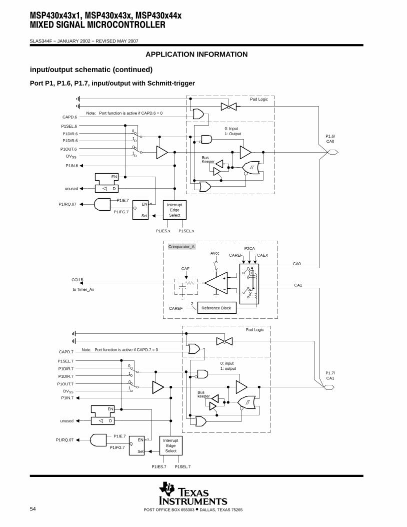
MSP430x43x1, MSP430x43x, MSP430x44xMIXED SIGNAL MICROCONTROLLER
SLAS344F − JANUARY 2002 − REVISED MAY 2007
54 POST OFFICE BOX 655303 • DALLAS, TEXAS 75265
APPLICATION INFORMATION
input/output schematic (continued)
Port P1, P1.6, P1.7, input/output with Schmitt-trigger
P1OUT.7
P1DIR.7
P1SEL.7
D
EN
InterruptEdgeSelect
P1IES.7 P1SEL.7
P1IE.7
P1IFG.7
P1IRQ.07 EN
Set
Q
0
1
1
0
CAPD.7
P1OUT.6
P1DIR.6
P1SEL.6
D
EN
InterruptEdgeSelect
P1IES.x P1SEL.x
P1IE.7
P1IFG.7
P1IRQ.07
P1.6/CA0
EN
Set
Q
0
1
1
0
CAPD.6Note: Port function is active if CAPD.6 = 0
P1IN.6
unused
P1.7/CA1
Comparator_A
Reference Block
CCI1B
CAF
CAREF
P2CA
CAEX
CAREF
to Timer_Ax −
+
2
AVcc
CA0
CA1
Pad Logic
0: Input1: Output
BusKeeper
Pad Logic
0: input1: output
Buskeeper
P1DIR.6
P1DIR.7
P1IN.7
unused
Note: Port function is active if CAPD.7 = 0
DVSS
DVSS
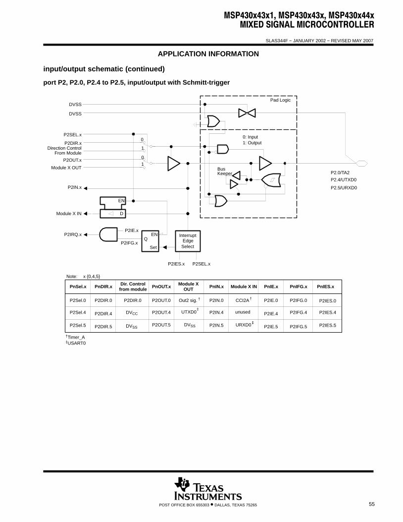
MSP430x43x1, MSP430x43x, MSP430x44xMIXED SIGNAL MICROCONTROLLER
SLAS344F − JANUARY 2002 − REVISED MAY 2007
55POST OFFICE BOX 655303 • DALLAS, TEXAS 75265
APPLICATION INFORMATION
input/output schematic (continued)
port P2, P2.0, P2.4 to P2.5, input/output with Schmitt-trigger
P2OUT.x
Module X OUT
P2DIR.xDirection Control
From Module
P2SEL.x
D
EN
InterruptEdge
Select
P2IES.x P2SEL.x
P2IE.x
P2IFG.x
P2IRQ.x EN
Set
Q
0
1
1
0
PnSel.x PnDIR.x Dir. Controlfrom module PnOUT.x Module X
OUT PnIN.x PnIE.x PnIFG.x PnIES.xModule X IN
P2Sel.4 P2DIR.4 P2OUT.4 P2IN.4 P2IE.4 P2IFG.4 P2IES.4
P2Sel.5 P2DIR.5 P2OUT.5 P2IN.5 P2IE.5 P2IFG.5 P2IES.5
P2Sel.0 P2DIR.0 P2OUT.0 P2IN.0 P2IE.0 P2IFG.0 P2IES.0Out2 sig. CCI2AP2DIR.0
UTXD0
DVSS
P2.5/URXD0
P2.0/TA2P2.4/UTXD0
Module X IN
P2IN.x
x 0,4,5Note:
Pad Logic
0: Input1: Output
BusKeeper
URXD0
unused
DVSS
†Timer_A‡USART0
†
‡
†
‡
DVCC
DVSS DVSS
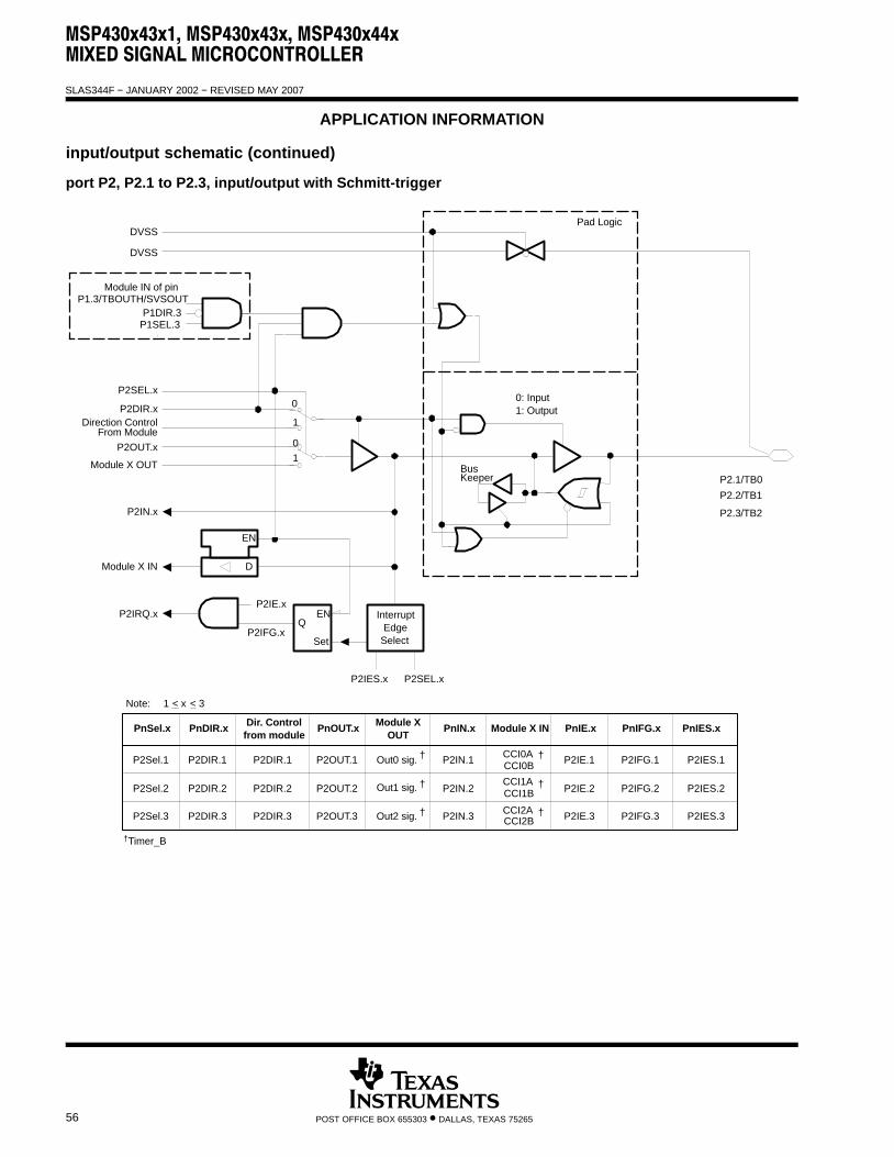
MSP430x43x1, MSP430x43x, MSP430x44xMIXED SIGNAL MICROCONTROLLER
SLAS344F − JANUARY 2002 − REVISED MAY 2007
56 POST OFFICE BOX 655303 • DALLAS, TEXAS 75265
APPLICATION INFORMATION
input/output schematic (continued)
port P2, P2.1 to P2.3, input/output with Schmitt-trigger
P2OUT.x
Module X OUT
P2DIR.xDirection Control
From Module
P2SEL.x
D
EN
InterruptEdge
Select
P2IES.x P2SEL.x
P2IE.x
P2IFG.x
P2IRQ.x EN
Set
Q
0
1
1
0
PnSel.x PnDIR.x Dir. Controlfrom module
PnOUT.x Module XOUT
PnIN.x PnIE.x PnIFG.x PnIES.xModule X IN
P2Sel.1 P2DIR.1 P2OUT.1 P2IN.1 P2IE.1 P2IFG.1 P2IES.1
P2Sel.2 P2DIR.2 P2OUT.2 P2IN.2 P2IE.2 P2IFG.2 P2IES.2
P2Sel.3 P2DIR.3 P2OUT.3 P2IN.3 P2IE.3 P2IFG.3 P2IES.3
P2DIR.1
P2DIR.2
P2.1/TB0P2.2/TB1
P2.3/TB2
Out0 sig.
Module X IN
P2IN.x
1 < x < 3Note:
Pad Logic
0: Input1: Output
BusKeeper
P2DIR.3 Out2 sig.
Out1 sig.
CCI0ACCI0BCCI1ACCI1B
CCI2ACCI2B
DVSS
DVSS
Module IN of pinP1.3/TBOUTH/SVSOUT
P1SEL.3P1DIR.3
†Timer_B
†
†
†
†
†
†
MSP430x43x1, MSP430x43x, MSP430x44xMIXED SIGNAL MICROCONTROLLER
SLAS344F − JANUARY 2002 − REVISED MAY 2007
57POST OFFICE BOX 655303 • DALLAS, TEXAS 75265
APPLICATION INFORMATION
input/output schematic (continued)
port P2, P2.6 to P2.7, input/output with Schmitt-trigger
P2OUT.x
Module X OUT
P2DIR.xDirection Control
From Module
P2SEL.x
D
EN
InterruptEdge
Select
P2IES.x P2SEL.x
P2IE.x
P2IFG.x
P2IRQ.x EN
Set
Q
0
1
1
0
PnSel.x PnDIR.x Dir. Controlfrom module
PnOUT.x Module XOUT
PnIN.x PnIE.x PnIFG.x PnIES.xModule X IN
0: Port active1: Segment xx function active
P2Sel.6 P2DIR.6
P2Sel.7 P2DIR.7
P2DIR.6
P2DIR.7
P2OUT.6
P2OUT.7
P2IN.6
P2IN.7 unused
CAOUT
ADC12CLK
P2IE.6
P2IE.7
P2IFG.6
P2IFG.7
P2IES.6
P2IES.7
Module X IN
P2IN.x
6 < x < 7Note:
Pad Logic
0: Input1: Output
BusKeeper
unused
Port/LCD
0: LCDM<40h
0: LCDM<40h
Port/LCD‡
Segment xx‡
P2.6/CAOUT/S19‡
P2.7/ADC12CLK/S18‡
‡Segment functiononly available withMSP430x43x(1)IPN
‡
‡
‡†
§
† Comparator_A‡Port/LCD signal is 1 only with MSP430xIPN and LCDM ≥40h.§ ADC12
MSP430x43x1, MSP430x43x, MSP430x44xMIXED SIGNAL MICROCONTROLLER
SLAS344F − JANUARY 2002 − REVISED MAY 2007
58 POST OFFICE BOX 655303 • DALLAS, TEXAS 75265
APPLICATION INFORMATION
input/output schematic (continued)
port P3, P3.0 to P3.3, input/output with Schmitt-trigger
P3OUT.x
Module X OUT
P3DIR.xDirection Control
From Module
P3SEL.x
D
EN
0
1
1
0
PnSel.x PnDIR.x PnOUT.xModule X
OUTPnIN.x Module X IN
P3Sel.1 P3DIR.1 P3OUT.1 P3IN.1
P3Sel.2 P3DIR.2 P3OUT.2 P3IN.2
P3Sel.3 P3DIR.3 P3OUT.3 P3IN.3
P3Sel.0 P3DIR.0 P3OUT.0 P3IN.0
UCLK0(out)
SOMIO(out)
DCM_SIMO0
DCM_SOMI0
DCM_UCLK0
Segment xx
0: Port active1: Segment xx function active
SIMO0(out)
UCLK0(in)
SOMI0(in)
SIMO0(in)
STE0(in)
Module X IN
P3IN.x
Pad Logic
0: Input1: Output
BusKeeper
LCDM.5LCDM.6
LCDM.7
Direction
From ModuleControl
DVSSDVSS
x43xIPZ and x44xIPZ have no segment
P3.0/STEO/S31†
P3.1/SIMO0/S30†
P3.2/SOMI0/S29†
P3.3/UCLK0/S28†
function on Port P3: Both lines are low.
Note: 0 ≤ x ≤ 3
MSP430x43x(1)IPN (80-Pin) Only
† S24 to S31 shared with port function only at MSP430x43x(1)IPN (80-pin QFP)
SYNCMM
STC
STE
SYNCMM
STC
STE
DCM_SOMI0DCM_SIMO0DCM_UCLK0
Direction Control for SOMI0Direction Control for SIMO0 and UCLK0
MSP430x43x1, MSP430x43x, MSP430x44xMIXED SIGNAL MICROCONTROLLER
SLAS344F − JANUARY 2002 − REVISED MAY 2007
59POST OFFICE BOX 655303 • DALLAS, TEXAS 75265
APPLICATION INFORMATION
input/output schematic (continued)
port P3, P3.4 to P3.7, input/output with Schmitt-trigger
P3OUT.x
Module XOUT
P3DIR.xDirection Control
From Module
P3SEL.x
D
EN
0
1
1
0
PnSel.x PnDIR.xDir. Control
from module PnOUT.xModule X
OUT PnIN.x Module X IN
P3Sel.4 P3DIR.4 P3OUT.4 P3IN.4
P3Sel.5 P3DIR.5 P3OUT.5 P3IN.5
P3DIR.4
0: Port active1: Segment xx function active
P3Sel.6 P3DIR.6
P3Sel.7 P3DIR.7
P3OUT.6
P3OUT.7
P3IN.6
P3IN.7 unusedCCI6A
unusedCCI5A/B
unusedCCI4A/B
unusedCCI3A/B
Module X IN
P3IN.x
4 < x < 7Note:
Pad Logic
0: Input1: Output
BusKeeper
P3.4/S27P3.5/S26P3.6/S25P3.7/S24
P3.4P3.5P3.6P3.7
P3.4/TB3P3.5/TB4P3.6/TB5P3.7/TB6
P3DIR.5
P3DIR.6
P3DIR.7
DVSSOUT3DVSSOUT4DVSSOUT5DVSSOUT6
Module IN of pinP1.3/TBOUTH/SVSOUT
P1SEL.3
’x43x(1)IPN ’x43xIPZ ’x44x
P3SEL.x
TBOUTHiZP1DIR.3
P3DIR.x
LCDM.7† or DVSS‡
Segmentxx† or DVSS‡
TBOUTHiZ# or DVSS§
† MSP430x43x(1)IPN‡ MSP430x43xIPZ, MSP430x44xIPZ§ MSP430x43x(1)# MSP430x44x
§#
§#
§#
§#
§#
§#
§#
§#
80-Pin 100-Pin

MSP430x43x1, MSP430x43x, MSP430x44xMIXED SIGNAL MICROCONTROLLER
SLAS344F − JANUARY 2002 − REVISED MAY 2007
60 POST OFFICE BOX 655303 • DALLAS, TEXAS 75265
APPLICATION INFORMATION
input/output schematic (continued)
port P4, P4.0 to P4.7, input/output with Schmitt-trigger
P4OUT.x
Module X OUT
P4DIR.xDirection Control
From Module
P4SEL.x
D
EN
0
1
1
0
PnSel.x PnDIR.x PnOUT.xModule X
OUTPnIN.x Module X IN
P4Sel.1 P4DIR.1 P4OUT.1 P4IN.1
P4Sel.2 P4DIR.2 P4OUT.2 P4IN.2
P4Sel.3 P4DIR.3 P4OUT.3 P4IN.3
P4Sel.4 P4DIR.4 P4OUT.4 P4IN.4
P4Sel.5 P4DIR.5 P4OUT.5 P4IN.5
P4Sel.0 P4DIR.0 P4OUT.0 P4IN.0
Segment xx
0: Port active1: Segment xx function active
P4Sel.6 P4DIR.6
P4Sel.7 P4DIR.7
P4DIR.6
P4DIR.7
P4OUT.6
P4OUT.7
P4IN.6
P4IN.7 unused
unused
unused
Module X IN
P4IN.x
0 < x < 7Note:
Pad Logic
0: Input1: Output
BusKeeper
Direction
From ModuleControl
DVSS†
UTXD1‡
DVSS
DVSS
DVSS
DVSS
Port/LCD§
x43x(1)IPN80-PinQFP:
P4.7/S2P4.6/S3P4.5/S4P4.3/S6P4.4/S5P4.2/S7P4.1/S8P4.0/S9
x43xIPZ100-PinQFP:
P4.7/S34P4.6/S35P4.5/S36P4.3/S37P4.4/S38P4.2/S39P4.0P4.1
x44x
P4.7/S34P4.6/S35P4.5/UCLK1/S36P4.4/SMO1/S37P4.3/SIMO1/S38P4.2/STE1/S39P4.1/URXD1P4.0/UTXD1
P4DIR.0†
DVCC‡
P4DIR.1†
DVSS‡
P4DIR.2†
DVSS‡
P4DIR3.†DCM_SIMO1‡
P4DIR4.†DCM_SOMI1‡
P4DIR5.†DCM_UCLK1‡
DVSS†
SIMO1(out)‡
DVSS†
SOMI1(out)‡
DVSS†
UCLK1(out)‡
unused†
URXD1‡
unused†STE1(in)‡
unused†SIMO1(in)‡
unusedSOMI1(in)‡
unused†UCLK1(in)‡
† Signal at MSP430x43x(1)‡ Signal at MSP430x44x
DEVICE PORT BITS PORT FUNCTION LCD SEG. FUNCTION
x43x(1)IPN 80-pin QFP P4.0 . . .P4.7 LCDM < 020h LCDM ≥ 020h
x43xIPZ 100-pin QFP P4.2 . . .P4.5 LCDM < 0E0h LCDM ≥ 0E0h
x44xIPZ 100-pin QFP P4.6 . . .P4.7 LCDM < 0C0h LCDM ≥ 0C0h

MSP430x43x1, MSP430x43x, MSP430x44xMIXED SIGNAL MICROCONTROLLER
SLAS344F − JANUARY 2002 − REVISED MAY 2007
61POST OFFICE BOX 655303 • DALLAS, TEXAS 75265
APPLICATION INFORMATION
input/output schematic (continued)
port P4, P4.0 to P4.7, input/output with Schmitt-trigger (continued)
SYNCMM
STC
STE
SYNCMM
STC
STE
DCM_SOMI1DCM_SIMO1DCM_UCLK1
Direction Control for SIMO1 and UCLK1 Direction Control for SOMI1
port P5, P5.0 to P5.1, input/output with Schmitt-trigger
P5OUT.x
Module X OUT
P5DIR.xDirection Control
From Module
P5SEL.x
D
EN
0
1
1
0
PnSel.x PnDIR.x Dir. Controlfrom module
PnOUT.xModule X
OUTPnIN.x Module X IN
P5Sel.1 P5DIR.1 P5OUT.1 P5IN.1
P5Sel.0 P5DIR.0 P5OUT.0 P5IN.0
P5DIR.1
P5DIR.0
Segment
0: Port active1: Segment function active
Segment
unused
unused
Module X IN
P5IN.x
0 < x < 1Note:
Port Pad Logic
0: Input
1: Output
BusKeeper
Segment Pad Logic
Port/LCD
Port/LCD
P5.0/S1P5.1/S0
S1
S0
0: LCDM<20h
0: LCDM<20h
DVSS
DVSS

MSP430x43x1, MSP430x43x, MSP430x44xMIXED SIGNAL MICROCONTROLLER
SLAS344F − JANUARY 2002 − REVISED MAY 2007
62 POST OFFICE BOX 655303 • DALLAS, TEXAS 75265
APPLICATION INFORMATION
input/output schematic (continued)
port P5, P5.2 to P5.4, input/output with Schmitt-trigger
P5OUT.x
Module X OUT
P5DIR.xDirection Control
From Module
P5SEL.x
D
EN
0
1
1
0
PnSel.x PnDIR.x Dir. Controlfrom module PnOUT.x Module X
OUT PnIN.x Module X IN
P5Sel.2 P5DIR.2 P5OUT.2 P5IN.2
P5Sel.3 P5DIR.3 P5OUT.3 P5IN.3
P5Sel.4 P5DIR.4 P5OUT.4 P5IN.4
LCD signal
0: Port active1: LCD function active
LCD signal
unused
unused
unused
Module X IN
P5IN.x
2 < x < 4Note:
Pad Logic
0: Input1: Output
BusKeeper
P5DIR.3
P5DIR.2
P5DIR.4
Port/LCD
Port/LCD
P5.2/COM1P5.3/COM2P5.4/COM3
COM1
COM2
COM3
P5SEL.2
P5SEL.3
P5SEL.4DVSS
DVSS
DVSS
MSP430x43x1, MSP430x43x, MSP430x44xMIXED SIGNAL MICROCONTROLLER
SLAS344F − JANUARY 2002 − REVISED MAY 2007
63POST OFFICE BOX 655303 • DALLAS, TEXAS 75265
APPLICATION INFORMATION
input/output schematic (continued)
port P5, P5.5 to P5.7, input/output with Schmitt-trigger
P5OUT.x
Module X OUT
P5DIR.xDirection Control
From Module
P5SEL.x
D
EN
0
1
1
0
PnSel.x PnDIR.x Dir. Controlfrom module PnOUT.x Module X
OUT PnIN.x Module X IN
P5Sel.5 P5DIR.5 P5OUT.5 P5IN.5
P5Sel.6 P5DIR.6 P5OUT.6 P5IN.6
P5Sel.7 P5DIR.7 P5OUT.7 P5IN.7
LCD signal
0: Port active1: LCD function active
LCD signal
unused
unused
unused
Module X IN
P5IN.x
5 < x < 7Note:
Pad Logic
0: Input1: Output
BusKeeper
P5DIR.6
P5DIR.5
P5DIR.7
Port/LCD
Port/LCD
R13 P5SEL.5
P5.5/R13P5.6/R23P5.7/R33
R23
R33
P5SEL.6
P5SEL.7DVSS
DVSS
DVSS

MSP430x43x1, MSP430x43x, MSP430x44xMIXED SIGNAL MICROCONTROLLER
SLAS344F − JANUARY 2002 − REVISED MAY 2007
64 POST OFFICE BOX 655303 • DALLAS, TEXAS 75265
APPLICATION INFORMATION
input/output schematic (continued)
port P6, P6.0 to P6.6, input/output with Schmitt-trigger
P6.6/A6
P6IN.x
Module X IN
Pad Logic
EN
D
P6OUT.x
P6DIR.x
P6SEL.x
Module X OUT
Direction ControlFrom Module
0
1
0
1
Bus Keeper
To ADC
From ADC
0: Input
1: Output
x: Bit Identifier, 0 to 6 for Port P6
P6.0/A0 ..
NOTE: Analog signals applied to digital gates can cause current flow from the positive to the negative terminal. The throughput current flows ifthe analog signal is in the range of transitions 0→1 or 1→0. The value of the throughput current depends on the driving capability of thegate. For MSP430, it is approximately 100 μA.Use P6SEL.x=1 to prevent throughput current. P6SEL.x should be set, even if the signal at the pin is not being used by the ADC12.
PnSel.x PnDIR.xDir. Control
From Module PnOUT.x Module X OUT PnIN.x Module X IN
P6Sel.0 P6DIR.0 P6DIR.0 P6OUT.0 DVSS P6IN.0 unused
P6Sel.1 P6DIR.1 P6DIR.1 P6OUT.1 DVSS P6IN.1 unused
P6Sel.2 P6DIR.2 P6DIR.2 P6OUT.2 DVSS P6IN.2 unused
P6Sel.3 P6DIR.3 P6DIR.3 P6OUT.3 DVSS P6IN.3 unused
P6Sel.4 P6DIR.4 P6DIR.4 P6OUT.4 DVSS P6IN.4 unused
P6Sel.5 P6DIR.5 P6DIR.5 P6OUT.5 DVSS P6IN.5 unused
P6Sel.6 P6DIR.6 P6DIR.6 P6OUT.6 DVSS P6IN.6 unused
NOTE: The signal at pins P6.x/Ax is used by the 12-bit ADC module.

MSP430x43x1, MSP430x43x, MSP430x44xMIXED SIGNAL MICROCONTROLLER
SLAS344F − JANUARY 2002 − REVISED MAY 2007
65POST OFFICE BOX 655303 • DALLAS, TEXAS 75265
APPLICATION INFORMATION
input/output schematic (continued)
port P6, P6.7, input/output with Schmitt-trigger
P6.7/A7/SVSIN
P6IN.x
Module X IN
Pad Logic
EN
D
P6OUT.x
P6DIR.x
P6SEL.x
Module X OUT
Direction ControlFrom Module
0
1
0
1
Bus Keeper
To ADC
From ADC
0: Input
1: Output
x: Bit Identifier, 7 for Port P6
To Brownout/SVS Module
VLP(SVS)=15
Note: Not implemented in the MSP430x43x1 devices
NOTE: Analog signals applied to digital gates can cause current flow from the positive to the negative terminal. The throughput current flows ifthe analog signal is in the range of transitions 0→1 or 1→0. The value of the throughput current depends on the driving capability of thegate. For MSP430, it is approximately 100 μA.Use P6SEL.x=1 to prevent throughput current. P6SEL.x should be set, even if the signal at the pin is not being used by the ADC12.
PnSel.x PnDIR.xDir. Control
From Module PnOUT.x Module X OUT PnIN.x Module X IN
P6Sel.7 P6DIR.7 P6DIR.7 P6OUT.7 DVSS P6IN.7 unused
NOTE: The signal at pins P6.x/Ax is used by the 12-bit ADC module.The signal at pin P6.7/A7/SVSIN is also connected to the input multiplexer in the module brownout/supply voltage supervisor.
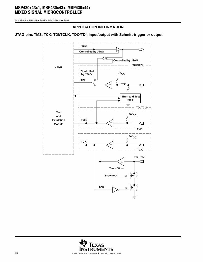
MSP430x43x1, MSP430x43x, MSP430x44xMIXED SIGNAL MICROCONTROLLER
SLAS344F − JANUARY 2002 − REVISED MAY 2007
66 POST OFFICE BOX 655303 • DALLAS, TEXAS 75265
APPLICATION INFORMATION
JTAG pins TMS, TCK, TDI/TCLK, TDO/TDI, input/output with Schmitt-trigger or output
TDI
TDO
TMS
TDI/TCLK
TDO/TDI
Controlledby JTAG
TCK
TMS
TCK
DVCC
Controlled by JTAG
Test
JTAG
and
Emulation
Module
DVCC
DVCC
Burn and TestFuse
RST/NMI
GD
SU
GD
SUTCK
Tau ~ 50 ns
Brownout
Controlled by JTAG
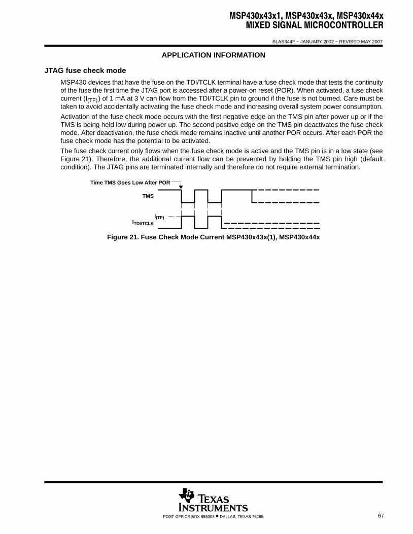
MSP430x43x1, MSP430x43x, MSP430x44xMIXED SIGNAL MICROCONTROLLER
SLAS344F − JANUARY 2002 − REVISED MAY 2007
67POST OFFICE BOX 655303 • DALLAS, TEXAS 75265
APPLICATION INFORMATION
JTAG fuse check mode
MSP430 devices that have the fuse on the TDI/TCLK terminal have a fuse check mode that tests the continuityof the fuse the first time the JTAG port is accessed after a power-on reset (POR). When activated, a fuse checkcurrent (I(TF)) of 1 mA at 3 V can flow from the TDI/TCLK pin to ground if the fuse is not burned. Care must betaken to avoid accidentally activating the fuse check mode and increasing overall system power consumption.Activation of the fuse check mode occurs with the first negative edge on the TMS pin after power up or if theTMS is being held low during power up. The second positive edge on the TMS pin deactivates the fuse checkmode. After deactivation, the fuse check mode remains inactive until another POR occurs. After each POR thefuse check mode has the potential to be activated.The fuse check current only flows when the fuse check mode is active and the TMS pin is in a low state (seeFigure 21). Therefore, the additional current flow can be prevented by holding the TMS pin high (defaultcondition). The JTAG pins are terminated internally and therefore do not require external termination.
Time TMS Goes Low After POR
TMS
I(TF)ITDI/TCLK
Figure 21. Fuse Check Mode Current MSP430x43x(1), MSP430x44x

MSP430x43x1, MSP430x43x, MSP430x44xMIXED SIGNAL MICROCONTROLLER
SLAS344F − JANUARY 2002 − REVISED MAY 2007
68 POST OFFICE BOX 655303 • DALLAS, TEXAS 75265
Data Sheet Revision History
LiteratureNumber Summary
SLAS344E
Added MSP430F43x1 devicesUpdated functional block diagram (page 6)Clarified test conditions in recommended operating conditions table (page 27)Clarified test conditions in electrical characteristics table (page 28)Added Port 2 through Port 5 to leakage current table (page 29)Corrected y-axis unit on Figures 6 and 7; changed from V to mV (page 34)Clarified test conditions in USART0/USART1 table (page 40)Changed tCPT maximum value from 4 ms to 10 ms in Flash memory table (page 46)
SLAS344F Added MSP430F43x1 devices in PZ (100 pin) package
NOTE: Page and figure numbers refer to the respective document revision.
PACKAGING INFORMATION
Orderable Device Status (1) PackageType
PackageDrawing
Pins PackageQty
Eco Plan (2) Lead/Ball Finish MSL Peak Temp (3)
MSP430F4351IPN ACTIVE LQFP PN 80 119 Green (RoHS &no Sb/Br)
CU NIPDAU Level-3-260C-168 HR
MSP430F4351IPNR ACTIVE LQFP PN 80 1000 Green (RoHS &no Sb/Br)
CU NIPDAU Level-3-260C-168 HR
MSP430F4351IPZ ACTIVE LQFP PZ 100 90 Green (RoHS &no Sb/Br)
CU NIPDAU Level-3-260C-168 HR
MSP430F4351IPZR ACTIVE LQFP PZ 100 1000 Green (RoHS &no Sb/Br)
CU NIPDAU Level-3-260C-168 HR
MSP430F435IPN ACTIVE LQFP PN 80 119 Green (RoHS &no Sb/Br)
CU NIPDAU Level-3-260C-168 HR
MSP430F435IPNR ACTIVE LQFP PN 80 1000 Green (RoHS &no Sb/Br)
CU NIPDAU Level-3-260C-168 HR
MSP430F435IPZ ACTIVE LQFP PZ 100 90 Green (RoHS &no Sb/Br)
CU NIPDAU Level-3-260C-168 HR
MSP430F435IPZR ACTIVE LQFP PZ 100 1000 Green (RoHS &no Sb/Br)
CU NIPDAU Level-3-260C-168 HR
MSP430F4361IPN ACTIVE LQFP PN 80 119 Green (RoHS &no Sb/Br)
CU NIPDAU Level-3-260C-168 HR
MSP430F4361IPNR ACTIVE LQFP PN 80 1000 Green (RoHS &no Sb/Br)
CU NIPDAU Level-3-260C-168 HR
MSP430F4361IPZ ACTIVE LQFP PZ 100 90 Green (RoHS &no Sb/Br)
CU NIPDAU Level-3-260C-168 HR
MSP430F4361IPZR ACTIVE LQFP PZ 100 1000 Green (RoHS &no Sb/Br)
CU NIPDAU Level-3-260C-168 HR
MSP430F436IPN ACTIVE LQFP PN 80 119 Green (RoHS &no Sb/Br)
CU NIPDAU Level-3-260C-168 HR
MSP430F436IPNR ACTIVE LQFP PN 80 1000 Green (RoHS &no Sb/Br)
CU NIPDAU Level-3-260C-168 HR
MSP430F436IPZ ACTIVE LQFP PZ 100 90 Green (RoHS &no Sb/Br)
CU NIPDAU Level-3-260C-168 HR
MSP430F436IPZR ACTIVE LQFP PZ 100 1000 Green (RoHS &no Sb/Br)
CU NIPDAU Level-3-260C-168 HR
MSP430F4371IPN ACTIVE LQFP PN 80 119 Green (RoHS &no Sb/Br)
CU NIPDAU Level-3-260C-168 HR
MSP430F4371IPNR ACTIVE LQFP PN 80 1000 Green (RoHS &no Sb/Br)
CU NIPDAU Level-3-260C-168 HR
MSP430F4371IPZ ACTIVE LQFP PZ 100 90 Green (RoHS &no Sb/Br)
CU NIPDAU Level-3-260C-168 HR
MSP430F4371IPZR ACTIVE LQFP PZ 100 1000 Green (RoHS &no Sb/Br)
CU NIPDAU Level-3-260C-168 HR
MSP430F437IPN ACTIVE LQFP PN 80 119 Green (RoHS &no Sb/Br)
CU NIPDAU Level-3-260C-168 HR
MSP430F437IPNR ACTIVE LQFP PN 80 1000 Green (RoHS &no Sb/Br)
CU NIPDAU Level-3-260C-168 HR
MSP430F437IPZ ACTIVE LQFP PZ 100 90 Green (RoHS &no Sb/Br)
CU NIPDAU Level-3-260C-168 HR
MSP430F437IPZR ACTIVE LQFP PZ 100 1000 Green (RoHS &no Sb/Br)
CU NIPDAU Level-3-260C-168 HR
MSP430F447IPZ ACTIVE LQFP PZ 100 90 Green (RoHS &no Sb/Br)
CU NIPDAU Level-3-260C-168 HR
PACKAGE OPTION ADDENDUM
www.ti.com 10-Dec-2007
Addendum-Page 1

Orderable Device Status (1) PackageType
PackageDrawing
Pins PackageQty
Eco Plan (2) Lead/Ball Finish MSL Peak Temp (3)
MSP430F447IPZR ACTIVE LQFP PZ 100 1000 Green (RoHS &no Sb/Br)
CU NIPDAU Level-3-260C-168 HR
MSP430F448IPZ ACTIVE LQFP PZ 100 90 Green (RoHS &no Sb/Br)
CU NIPDAU Level-3-260C-168 HR
MSP430F448IPZR ACTIVE LQFP PZ 100 1000 Green (RoHS &no Sb/Br)
CU NIPDAU Level-3-260C-168 HR
MSP430F449IPZ ACTIVE LQFP PZ 100 90 Green (RoHS &no Sb/Br)
CU NIPDAU Level-3-260C-168 HR
MSP430F449IPZR ACTIVE LQFP PZ 100 1000 Green (RoHS &no Sb/Br)
CU NIPDAU Level-3-260C-168 HR
(1) The marketing status values are defined as follows:ACTIVE: Product device recommended for new designs.LIFEBUY: TI has announced that the device will be discontinued, and a lifetime-buy period is in effect.NRND: Not recommended for new designs. Device is in production to support existing customers, but TI does not recommend using this part ina new design.PREVIEW: Device has been announced but is not in production. Samples may or may not be available.OBSOLETE: TI has discontinued the production of the device.
(2) Eco Plan - The planned eco-friendly classification: Pb-Free (RoHS), Pb-Free (RoHS Exempt), or Green (RoHS & no Sb/Br) - please checkhttp://www.ti.com/productcontent for the latest availability information and additional product content details.TBD: The Pb-Free/Green conversion plan has not been defined.Pb-Free (RoHS): TI's terms "Lead-Free" or "Pb-Free" mean semiconductor products that are compatible with the current RoHS requirementsfor all 6 substances, including the requirement that lead not exceed 0.1% by weight in homogeneous materials. Where designed to be solderedat high temperatures, TI Pb-Free products are suitable for use in specified lead-free processes.Pb-Free (RoHS Exempt): This component has a RoHS exemption for either 1) lead-based flip-chip solder bumps used between the die andpackage, or 2) lead-based die adhesive used between the die and leadframe. The component is otherwise considered Pb-Free (RoHScompatible) as defined above.Green (RoHS & no Sb/Br): TI defines "Green" to mean Pb-Free (RoHS compatible), and free of Bromine (Br) and Antimony (Sb) based flameretardants (Br or Sb do not exceed 0.1% by weight in homogeneous material)
(3) MSL, Peak Temp. -- The Moisture Sensitivity Level rating according to the JEDEC industry standard classifications, and peak soldertemperature.
Important Information and Disclaimer:The information provided on this page represents TI's knowledge and belief as of the date that it isprovided. TI bases its knowledge and belief on information provided by third parties, and makes no representation or warranty as to theaccuracy of such information. Efforts are underway to better integrate information from third parties. TI has taken and continues to takereasonable steps to provide representative and accurate information but may not have conducted destructive testing or chemical analysis onincoming materials and chemicals. TI and TI suppliers consider certain information to be proprietary, and thus CAS numbers and other limitedinformation may not be available for release.
In no event shall TI's liability arising out of such information exceed the total purchase price of the TI part(s) at issue in this document sold by TIto Customer on an annual basis.
PACKAGE OPTION ADDENDUM
www.ti.com 10-Dec-2007
Addendum-Page 2

MECHANICAL DATA
MTQF010A – JANUARY 1995 – REVISED DECEMBER 1996
1POST OFFICE BOX 655303 • DALLAS, TEXAS 75265
PN (S-PQFP-G80) PLASTIC QUAD FLATPACK
4040135 /B 11/96
0,170,27
0,13 NOM
40
21
0,25
0,450,75
0,05 MIN
Seating Plane
Gage Plane
4160
61
80
20
SQ
SQ
1
13,8014,20
12,20
9,50 TYP
11,80
1,451,35
1,60 MAX 0,08
0,50 M0,08
0°–7°
NOTES: A. All linear dimensions are in millimeters.B. This drawing is subject to change without notice.C. Falls within JEDEC MS-026

MECHANICAL DATA
MTQF013A – OCTOBER 1994 – REVISED DECEMBER 1996
1POST OFFICE BOX 655303 • DALLAS, TEXAS 75265
PZ (S-PQFP-G100) PLASTIC QUAD FLATPACK
4040149/B 11/96
50
26 0,13 NOM
Gage Plane
0,25
0,450,75
0,05 MIN
0,27
51
25
75
1
12,00 TYP
0,17
76
100
SQ
SQ15,8016,20
13,80
1,351,45
1,60 MAX
14,20
0°–7°
Seating Plane
0,08
0,50 M0,08
NOTES: A. All linear dimensions are in millimeters.B. This drawing is subject to change without notice.C. Falls within JEDEC MS-026

IMPORTANT NOTICE
Texas Instruments Incorporated and its subsidiaries (TI) reserve the right to make corrections, modifications, enhancements,improvements, and other changes to its products and services at any time and to discontinue any product or service without notice.Customers should obtain the latest relevant information before placing orders and should verify that such information is current andcomplete. All products are sold subject to TI’s terms and conditions of sale supplied at the time of order acknowledgment.
TI warrants performance of its hardware products to the specifications applicable at the time of sale in accordance with TI’sstandard warranty. Testing and other quality control techniques are used to the extent TI deems necessary to support thiswarranty. Except where mandated by government requirements, testing of all parameters of each product is not necessarilyperformed.
TI assumes no liability for applications assistance or customer product design. Customers are responsible for their products andapplications using TI components. To minimize the risks associated with customer products and applications, customers shouldprovide adequate design and operating safeguards.
TI does not warrant or represent that any license, either express or implied, is granted under any TI patent right, copyright, maskwork right, or other TI intellectual property right relating to any combination, machine, or process in which TI products or servicesare used. Information published by TI regarding third-party products or services does not constitute a license from TI to use suchproducts or services or a warranty or endorsement thereof. Use of such information may require a license from a third party underthe patents or other intellectual property of the third party, or a license from TI under the patents or other intellectual property of TI.
Reproduction of TI information in TI data books or data sheets is permissible only if reproduction is without alteration and isaccompanied by all associated warranties, conditions, limitations, and notices. Reproduction of this information with alteration is anunfair and deceptive business practice. TI is not responsible or liable for such altered documentation. Information of third partiesmay be subject to additional restrictions.
Resale of TI products or services with statements different from or beyond the parameters stated by TI for that product or servicevoids all express and any implied warranties for the associated TI product or service and is an unfair and deceptive businesspractice. TI is not responsible or liable for any such statements.
TI products are not authorized for use in safety-critical applications (such as life support) where a failure of the TI product wouldreasonably be expected to cause severe personal injury or death, unless officers of the parties have executed an agreementspecifically governing such use. Buyers represent that they have all necessary expertise in the safety and regulatory ramificationsof their applications, and acknowledge and agree that they are solely responsible for all legal, regulatory and safety-relatedrequirements concerning their products and any use of TI products in such safety-critical applications, notwithstanding anyapplications-related information or support that may be provided by TI. Further, Buyers must fully indemnify TI and itsrepresentatives against any damages arising out of the use of TI products in such safety-critical applications.
TI products are neither designed nor intended for use in military/aerospace applications or environments unless the TI products arespecifically designated by TI as military-grade or "enhanced plastic." Only products designated by TI as military-grade meet militaryspecifications. Buyers acknowledge and agree that any such use of TI products which TI has not designated as military-grade issolely at the Buyer's risk, and that they are solely responsible for compliance with all legal and regulatory requirements inconnection with such use.
TI products are neither designed nor intended for use in automotive applications or environments unless the specific TI productsare designated by TI as compliant with ISO/TS 16949 requirements. Buyers acknowledge and agree that, if they use anynon-designated products in automotive applications, TI will not be responsible for any failure to meet such requirements.
Following are URLs where you can obtain information on other Texas Instruments products and application solutions:
Products Applications
Amplifiers amplifier.ti.com Audio www.ti.com/audio
Data Converters dataconverter.ti.com Automotive www.ti.com/automotive
DSP dsp.ti.com Broadband www.ti.com/broadband
Interface interface.ti.com Digital Control www.ti.com/digitalcontrol
Logic logic.ti.com Military www.ti.com/military
Power Mgmt power.ti.com Optical Networking www.ti.com/opticalnetwork
Microcontrollers microcontroller.ti.com Security www.ti.com/security
RFID www.ti-rfid.com Telephony www.ti.com/telephony
Low Power www.ti.com/lpw Video & Imaging www.ti.com/videoWireless
Wireless www.ti.com/wireless
Mailing Address: Texas Instruments, Post Office Box 655303, Dallas, Texas 75265Copyright © 2007, Texas Instruments Incorporated

Appendix C: Institutional Review Board Application, Study Protocol, Sample Case Report Form, Sample Consent Form. Institutional Review Board approved letter

WORCESTER POLYTECHNIC INSTITUTE Institutional Review Board
Application for Approval to Use Human Subjects in Research
WPI IRB use only IRB # Date:
________ ________
WPI INSTITUTIONAL REVIEW BOARD APPLICATION FOR APPROVAL TO USE HUMAN SUBJECTS IN RESEARCH
revised 10/26/06 1 of 5
If your project has any federal sponsorship (e.g. federal funding), either prime or pass-through, the WPI IRB is not authorized to perform a review. Please contact Christina DeVries in Research Administration at (508) 831-6716 for direction to an appropriate IRB. DO NOT submit an application to the WPI IRB.
This application is for: (Please check one) Expedited Review Full Review WPI IRB
Principal Investigator (PI) or Project Faculty Advisor: (NOT a student or fellow; must be a WPI employee) use only
Name: Robert Peura Tel No: E-Mail Address: [email protected]
Department: Biomedical Engineering Co-Investigator(s): (Co-PI(s)/non students)
Name: Tel No: E-Mail Address:
Name: Tel No: E-Mail Address:
Student Investigator(s):
Name: Liz Kinnal Tel No: 978 618 7945 E-Mail Address: [email protected]
Name: Shannon O'Toole Tel No: 617 893 8901 E-Mail Address: [email protected]
Check if: Undergraduate project (MQP, IQP, Suff., other) Diabetes Activity Monitor Graduate project (M.S. Ph.D., other) Has an IRB ever suspended or terminated a study of any investigator listed above? No Yes (Attach a summary of the event and resolution.) Vulnerable Populations: The proposed research will involve the following (Check all that apply): pregnant women human fetuses neonates minors/children prisoners students individuals with mental disabilities individuals with physical disabilities Collaborating Institutions: (Please list all collaborating Institutions.) Locations of Research: (If at WPI, please indicate where on campus. If off campus, please give details of locations.) WPI Fitness Center Funding: (If the research is funded, please enclose one copy of the research proposal or most recent draft with your application.)
Funding Agency: WPI Fund:
Project Title: Human Subjects Research: (All study personnel having direct contact with subjects must take and pass a training course on human subjects research. There is a link to a web-based training course that can be accessed under the Training link on the IRB web site http://www.wpi.edu/Admin/Research/IRB/training.html. The IRB requires a copy of the completion certificate from the course or proof of an equivalent program.) Anticipated Dates of Research:
Start Date: February 15, 2008 Completion Date: April 14, 2008

WPI INSTITUTIONAL REVIEW BOARD APPLICATION FOR APPROVAL TO USE HUMAN SUBJECTS IN RESEARCH
revised 11/3/2005
2 of 5
Instructions: Answer all questions. If you are asked to provide an explanation, please do so with adequate details. If needed, attach itemized replies. Any incomplete application will be returned. 1.) Purpose of Study: (Please provide a concise statement of the background, nature and reasons for the proposed study. Insert below using non-technical language that can be understood by non-scientist members of the IRB.) For this project a device has been built to measure the activiy of a patient during activities they participate in during the day. The device will measure this in two ways: Part of the device will be worn on the hip converting mechanical energy into electrical energy and through electrodes on the chest and hips to measure the heart rate. To be sure the device is universal it will be used by several subjects to gather camparitive data. At perriodic intervals the subjects will place a pulse oximeter on their index finger to assure that the device output is equal to the subject's heart rate.
2.) Study Protocol: (Please attach sufficient information for effective review by non-scientist members of the IRB. Define all abbreviations and use simple words. Unless justification is provided this part of the application must not exceed 5 pages. Attaching sections of a grant application is not an acceptable substitute.) A.) For biomedical, engineering and related research, please provide an outline of the actual experiments to be performed. Where applicable, provide a detailed description of the experimental devices or procedures to be used, detailed information on the exact dosages of drugs or chemicals to be used, total quantity of blood samples to be used, and descriptions of special diets.
B.) For applications in the social sciences, management and other non-biomedical disciplines please provide a detailed description of your proposed study. Where applicable, include copies of any questionnaires or standardized tests you plan to incorporate into your study. If your study involves interviews please submit an outline indicating the types of questions you will include.
C.) If the study involves investigational drugs or investigational medical devices, and the PI is obtaining an Investigational New Drug (IND) number or Investigational Device Exemption (IDE) number from the FDA, please provide details.
D.) Please note if any hazardous materials are being used in this study.
E.) Please note if any special diets are being used in this study.
3.) Subject Information: A.) Please provide the exact number of subjects you plan to enroll in this study and describe your subject population. (eg. WPI students, WPI staff, UMASS Medical patient, other)
Males: 20 Females: 20 Description: WPI Students B.) Will subjects who do not understand English be enrolled?
No Yes (Please insert below the language(s) that will be translated on the consent form.)
C.) Are there any circumstances under which your study population may feel coerced into participating in this study?
No Yes (Please insert below a description of how you will assure your subjects do not feel coerced.)
The patients will be asked on a volunteer only basis, with full disclosure of the study before they sign up for the study. D.) Are the subjects at risk of harm if their participation in the study becomes known?
No Yes (Please insert below a description of possible effects on your subjects.)

WPI INSTITUTIONAL REVIEW BOARD APPLICATION FOR APPROVAL TO USE HUMAN SUBJECTS IN RESEARCH
revised 11/3/2005
3 of 5
E.) How will subjects be recruited for participation? (Check all that apply.)
Referral: (By whom) Project Members
Direct subject advertising, including: (Please provide a copy of the proposed ad. All direct subject advertising must be approved by the WPI IRB prior to use.)
Other: (Identify) Newspaper Bulletin board Database: (Describe how database populated) Radio Flyers
Television Letters F.) Have the subjects in the database agreed to be contacted for research projects? No Yes N/A
Internet E-mail
G.) Are the subjects being paid for participating? (Consider all types of reimbursement, ex. stipend, parking, travel.)
No Yes (Check all that apply.) Cash Check Gift certificate Other: Amount of compensation
4.) Informed Consent: A.) Who will discuss the study with and obtain consent of prospective subjects? (Check all that apply.)
Principal Investigator Co-Investigator(s) Student Investigator(s) B.) Are you aware that subjects must read and sign and Informed Consent Form prior to conducting any study-related procedures and agree that all subjects will be consented prior to initiating study related procedures? No Yes
C.) Are you aware that you must consent subjects using only the IRB-approved Informed Consent Form? No Yes
D.) Will subjects be consented in a private room, not in a public space? No Yes
E.) Do you agree to spend as much time as needed to thoroughly explain and respond to any subject’s questions about the study, and allow them as much time as needed to consider their decision prior to enrolling them as subjects? No Yes
F.) Do you agree that the person obtaining consent will explain the risks of the study, the subject’s right to decide not to participate, and the subject’s right to withdraw from the study at any time? No Yes (If you answer No to any of the questions above, please provide an explanation.)
5.) Potential Risks: (A risk is a potential harm that a reasonable person would consider important in deciding whether to participate in research. Risks can be categorized as physical, psychological, sociological, economic and legal, and include pain, stress, invasion of privacy, embarrassment or exposure of sensitive or confidential data. All potential risks and discomforts must be minimized to the greatest extent possible by using e.g. appropriate monitoring, safety devices and withdrawal of a subject if there is evidence of a specific adverse event.) A.) What are the risks / discomforts associated with each intervention or procedure in the study?
The electrodes must be placed on the chest and hip of the patient. B.) What procedures will be in place to prevent / minimize potential risks or discomfort?
The subjects will be instructed to wear a button down shirt. There are both males and females within the investigating group and the subjects will be assisted by the gender corresponding student investigator, males investigator for male subjects and female investigators for female subjects. The subjects will be given a private area for application of the electrodes. The electrode at the hip is above the pants and therefore will not require removal of any clothing.

WPI INSTITUTIONAL REVIEW BOARD APPLICATION FOR APPROVAL TO USE HUMAN SUBJECTS IN RESEARCH
revised 11/3/2005
4 of 5
6.) Potential Benefits: A.) What potential benefits other than payment may subjects receive from participating in the study?
N/A B.) What potential benefits can society expect from the study?
If this study proves the device works in the manner expected, diabteic patients will begin to better dose themselves based on the output of this device 7.) Data Collection, Storage, and Confidentiality: A.) How will data be collected?
Using data sheets filled in by student investigators and using an occiloscope B.) Will a subject’s voice, face or identifiable body features (eg. tattoo, scar) be recorded by audio or videotaping? No Yes (Explain the recording procedures you plan to follow.)
C.) Will personal identifying information be recorded? No Yes (If yes, explain how the identifying information will be protected. How will personal identifying information be coded and how will the code key be kept confidential?)
D.) Where will the data be stored and how will it be secured?
The data wil be stored in only one electronic location and any hard copies created will be numbered and then collected when the project is completed and destroyed. E.) What will happen to the data when the study is completed?
Any data not documented in the report will be destroyed, and data documented in the report will be only in the report F.) Can data acquired in the study adversely affect a subject’s relationship with other individuals? (i.e. employee-supervisor, student-teacher, family relationships)
No G.) Do you plan to use or disclose identifiable information outside of the investigation personnel?
No Yes (Please explain.)
H.) Do you plan to use or disclose identifiable information outside of WPI including non-WPI investigators?
No Yes (Please explain.)
8.) Deception: (Investigators must not exclude information from a subject that a reasonable person would want to know in deciding whether to participate in a study.) Will the information about the research purpose and design be withheld from the subjects?
No Yes (Please explain.)

WPI INSTITUTIONAL REVIEW BOARD APPLICATION FOR APPROVAL TO USE HUMAN SUBJECTS IN RESEARCH
revised 11/3/2005
5 of 5
9.) Adverse effects: (Serious or unexpected adverse reactions or injuries must be reported to the WPI IRB within 48 hours. Other adverse events should be reported within 10 working days.) What follow-up efforts will be made to detect any harm to subjects and how will the WPI IRB be kept informed?
Sunjects will have a one on one follow up session with a group member within 48 hours of the completion of the test 10.) Informed consent: (Documented informed consent must be obtained from all participants in studies that involve human subjects. You must use the templates available on the WPI IRB web-site to prepare these forms. Informed consent forms must be included with this application. Under certain circumstances the WPI IRB may waive the requirement for informed consent.) Investigator’s Assurance: I certify the information provided in this application is complete and correct. I understand that I have ultimate responsibility for the conduct of the study, the ethical performance of the project, the protection of the rights and welfare of human subjects, and strict adherence to any stipulations imposed by the WPI IRB. I agree to comply with all WPI policies, as well all federal, state and local laws on the protection of human subjects in research, including:
• ensuring the satisfactory completion of human subjects training. • performing the study in accordance with the WPI IRB approved protocol. • implementing study changes only after WPI IRB approval. • obtaining informed consent from subjects using only the WPI IRB approved consent form. • promptly reporting significant adverse effects to the WPI IRB.
Signature of Principal Investigator Date
Print Full Name and Title
Please return a signed hard copy of this application to the WPI IRB c/o Research Administration. If you have any questions, please call (508) 831-6716.

Clinical Study Protocol
Calibration and Testing of the Combined Heart Rate and Accelerometer for Determining Energy Expenditure
Investigational Product: The Combined Heart Rate and Accelerometer Activity Monitor
Protocol Version Number: 1.0
Date: February 8, 2008

ART Advanced Research Technologies Inc. Clinical Study Protocol SSC-311 Confidential Adjunctive Efficacy Study Of The SoftScan® Optical Breast Imaging System
Protocol Number: DAM-010
Protocol Title: Preliminary Calibration and Testing of the Combined Heart Rate and Accelerometer for Determining Energy Expenditure
Study Sponsor: Worcester Polytechnic Institute, Worcester MA
Investigational Product: The Combined Heart Rate and Accelerometer Activity Monitoring Device
Study Objectives:
Primary Study Objectives Include: • Calibrate the combined heart rate and accelerometer monitoring device to accurately
predict energy expenditure; • Screening for potential safety issues.
Study Design:
Overview: • Prospective, simultaneously-recruited, un-blinded, preliminary study • Number of subjects = up to 40 • The primary study endpoint -device calibration- will be achieved through having
subjects perform a variety of different activities while measuring their heart rate and accelerometer outputs in order to adjust the activity algorithm. Healthy volunteers will be enrolled accordingly to the inclusion/exclusion criteria. Prior to the activity period, the subjects will lie down in a comfortable area for five minutes while wearing the investigational device and a pulse oximeter. The resting heart rate from both devices will be obtained at the end of five minutes. During the first activity period, the subjects will wear the investigational device while performing different activities for five minutes with at least five minutes of rest in between activities. The activities that the subjects will be performing and the order that they will perform them in are listed as follows: sitting, slow walk on the treadmill (3.10 mph), fast walk on the treadmill (3.80 mph), and running on the treadmill (5.90 mph). The activity counts and heart rate will be obtained from the investigational device during the final minute of each activity. Within one minute after the completion of the first activity period, the subject’s heart rate will be recorded using both the investigational device and a pulse oximeter. During the second activity period, the subjects will be wearing the investigational device while performing the following activities in the given order with five minutes rest in between: ascending/descending stairs, sweeping, washing dishes, filing papers, and standing. The activity counts and heart rate will be obtained from the investigational device during the final minute of each activity. Within one minute after the completion of the first activity period, the subject’s heart rate will be recorded using both the investigational device and a pulse oximeter. The student investigators will compare the accelerometer counts per minute against the counts per minute of the Actiheart combined heart rate and accelerometer activity monitor published in the European Journal of Clinical Nutrition. Using linear regression techniques, the student investigators will determine the correlation coefficient between the two accelerometer’s counts per minute. This number will be used to adjust the existing Actiheart activity algorithm to our accelerometer specifications.
Study Methods
Primary Study Endpoints:• Activity monitor calibration, preformed by adapting published algorithms for an
existing combined heart rate and movement sensor.

ART Advanced Research Technologies Inc. Clinical Study Protocol SSC-311 Confidential Adjunctive Efficacy Study Of The SoftScan® Optical Breast Imaging System
Key Secondary Study Endpoints Include:• Heart Rate stand alone accuracy, measured by the difference between the heart rate
measurements obtained by the investigational device and the measurements obtained by a pulse-oximeter.
Key Safety Assessments Include:
• Potential effects of electrode placement, as measured by observed and reported discomfort and changes in skin during and after the testing period.
Study Conduct
In Accordance With:• Principles of Good Clinical Practice; • Principles of Declaration of Helsinki (1989); • Title 21 Parts 50, 54, 56, and 812 of the U.S. Code of Federal Regulations; • The Medical Research Council’s Code of Ethical Conduct for Research Involving
Humans (1997); and • All federal, provincial, state, and local laws of the pertinent regulatory authorities.
Subject Selection
Major Study Inclusion Criteria Include:• Men and women between 18 and 25 years of age; and • Healthy volunteers
Major Study Exclusion Criteria Include:
• Subjects with a history of respiratory problems (e.g., asthma) • Subjects with a history of heart problems (i.e. irregular heartbeat) • Subjects who are recovering from injury or surgery; and • Subjects who for any reason are unable to perform physical activities.
Study Plan
Study Periods Include:• Baseline Period (up to 30 days); • Calibration and Testing Period (up to 4 hours); • Follow Up Period (approximately 24 hours); and • Analysis Period (up to 30 days).
Statistical Methods
Statistical Methods Include:• Primary study endpoint: Tests for differences in accuracy will be conducted using a
paired t-test.
Study Sample Size: • Total Male Enrollment Population: up to 20 subjects • Total Female Enrollment Population: up to 20 subjects • Total Study Subject Enrollment Population: up to 40 subjects.

Case Report Form (Preliminary Protocol)
Calibration and Testing of the Combined Heart Rate and Accelerometer for Determining Energy Expenditure
Protocol Number:
DAM-010
Version Date:
January 12, 2008

GENERAL INSTRUCTIONS FOR COMPLETING CRFS
WPI Worcester Polytechnic Institute Calibration and Testing
Protocol Site ID Subject ID Code Date S S C - 2 0 7
-
- -
Day Month Year
011808-studyprotocolICRF Edit.doc Confidential Page i of i
General Instructions for Completing CRFs
> Use only black or blue ink pen for completion of forms, as other colors will not copy correctly.
> The subject’s ID code will be determined by a three-letter code (e.g., ABC) and a three-digit number (e.g., 001).
> To correct an error: − Draw a single line through the error; − Write the correct entry next to the data field; − Write your initials and the date beside the correction information; and − Do not erase, use correction fluid (e.g., White-Out®), write over, or scribble out entries.
> Please write your answer legibly.
> Do not write in the margins. Use comment fields.
> Avoid the use of abbreviations.
> Draw a diagonal line across any page that is intentionally left blank. Initial and date.

STUDY PERIOD
WPI Worcester Polytechnic Institute Calibration and Testing
Protocol Site ID Subject ID Code Date D A M - 0 1 0
-
- -
Day Month Year
011808-studyprotocolICRF Edit.doc Confidential Page 2 of 12
Enrollment Period
1. Date of enrollment - -
Day Month Year
2. Has the subject signed the informed consent? Yes No 3. Does the subject meet all inclusion criteria? Yes No 4. Does the subject meet all exclusion criteria? Yes No
DO NOT PROCEED WITH THE REST OF THE STUDY PERIOD IF “NO” IS PROVIDED AS AN ANSWER FOR ANY OF THE ABOVE
QUESTIONS.
Inclusion Criteria
5. Is the subject a healthy individual at least 18 year old? Yes No 6. Is the subject fully aware of all details stated in the informed consent? Yes No 7. Is the subject willing to comply with the mandatory follow up to be
completed within three days after the study period? Yes No
Exclusion Criteria
8. Does the subject have a history of respiratory problems (i.e. asthma)? Yes No 9. Is the subject currently healing from any injuries or surgery? Yes No 10. Is there any reason why the student investigated may deem the subject unfit
for participation in the study? Yes No
Comments
11. As appropriate, provide additional comments.

STUDY PERIOD
WPI Worcester Polytechnic Institute Calibration and Testing
Protocol Site ID Subject ID Code Date
D A M - 0 1 0
- - -
Day Month Year
011808-studyprotocolICRF Edit.doc Confidential Page 3 of 12
Subject Information
12. Date of birth - -
Day Month Year
13. Height -
Feet Inches
14. Weight Pounds
15. Sex Male Female
Study Period
16. Date of study period - -
Day Month Year
17. Time of initiation of study period - -
Hour Minute AM/PM
Device Placement
18. Is device placed exactly as shown in the picture below?
Yes No
19. Please rate the ease of placement
Easy 1 2
3 4
Difficult 5
20. Is the subject experiencing any discomfort or skin discoloration? If so, please fill out an adverse experience form. Yes No

STUDY PERIOD
WPI Worcester Polytechnic Institute Calibration and Testing
Protocol Site ID Subject ID Code Date D A M - 0 1 0
-
- -
Day Month Year
011808-studyprotocolICRF Edit.doc Confidential Page 4 of 12
Comments
21. As appropriate, provide additional comments.
Pre-Activity Period Have the subject lie down in a comfortable area for 5 minutes until they are completely relaxed before taking heart rate measurements
22. Resting Heart Rate (Obtained from investigational device) B.P.M
23. Resting Heart Rate (Obtained from pulse oximeter) B.P.M
24. Sleeping Heart Rate B.P.M

STUDY PERIOD
WPI Worcester Polytechnic Institute Calibration and Testing
Protocol Site ID Subject ID Code Date D A M - 0 1 0
-
- -
Day Month Year
011808-studyprotocolICRF Edit.doc Confidential Page 5 of 12
Activity Period I The subject must complete each of the following activities for five minutes. At the very end of the five minutes, take record both the heart rate and accelerometery outputs from the investigational device before having the subject stop the exercise.
Heart Rate (beats per minute)
Accelerometry (counts per min)
25. Sitting B.P.M
Counts Per Minute
26. Slow Walk 3.10 MPH B.P.M
Counts Per Minute
27. Fast Walk 3.80 MPH B.P.M
Counts Per Minute
28. Running 5.90 MPH B.P.M
Counts Per Minute

STUDY PERIOD
WPI Worcester Polytechnic Institute Calibration and Testing
Protocol Site ID Subject ID Code Date D A M - 0 1 0
-
- -
Day Month Year
011808-studyprotocolICRF Edit.doc Confidential Page 6 of 12
Mid-Activity Period The sitting heart rate measurements must be obtained within one minute after the completion of activity period I. Following the measurements, ask the patient if they are experiencing any discomfort or skin discoloration.
29. Sitting Heart Rate (Obtained from investigational device) B.P.M
30. Sitting Heart Rate (Obtained from pulse oximeter) B.P.M
31. Is the subject experiencing any discomfort or skin discoloration? If so, please fill out an adverse experience form.
Yes No
32. Did the device remain in the correct position? Yes No
Comments
33. As appropriate, provide additional comments.

STUDY PERIOD
WPI Worcester Polytechnic Institute Calibration and Testing
Protocol Site ID Subject ID Code Date D A M - 0 1 0
-
- -
Day Month Year
011808-studyprotocolICRF Edit.doc Confidential Page 7 of 12
Activity Period II The subject must complete each of the following activities for five minutes. At the very end of the five minutes, take record both the heart rate and accelerometery outputs from the investigational device before having the subject stop the exercise.
Heart Rate Accelerometry
34. Ascending/Descending Stairs B.P.M
Counts Per Minute
35. Sweeping B.P.M
Counts Per Minute
36. Washing Dishes B.P.M
Counts Per Minute
37. Filing Papers B.P.M
Counts Per Minute
38. Standing B.P.M
Counts Per Minute

STUDY PERIOD
WPI Worcester Polytechnic Institute Calibration and Testing
Protocol Site ID Subject ID Code Date D A M - 0 1 0
-
- -
Day Month Year
011808-studyprotocolICRF Edit.doc Confidential Page 8 of 12
Post-Activity Period The sitting heart rate measurements must be obtained within one minute after the completion of activity period I. Following the measurements, ask the patient if they are experiencing any discomfort or skin discoloration.
39. Sitting Heart Rate (Obtained from investigational device) B.P.M
40. Sitting Heart Rate (Obtained from pulse oximeter) B.P.M
41. Is the subject experiencing any discomfort or skin discoloration? If so, please fill out an adverse experience form.
Yes No
42. Did the device remain in the correct position? Yes No
43. Rate the ease of use of the device
Easy 1 2
3 4
Difficult 5
Comments
44. As appropriate, provide additional comments.

FOLLOW UP PERIOD
WPI Worcester Polytechnic Institute Calibration and Testing
Protocol Site ID Subject ID Code Date D A M - 0 1 0
-
- -
Day Month Year
011808-studyprotocolICRF Edit.doc Confidential Page 9 of 12
Subject Follow-Up
45. Date of follow-up
- -
Day Month Year
46. Time of follow-up
- -
Hour Minute AM/PM
47. Did the subject follow-up take place within 48 hours after the study period? Yes No
48. Method of contact Phone 1 In-person 2
49. Is the subject experiencing any discomfort or skin discoloration? If so, please fill out an adverse experience form. Yes No
Comments
50. As appropriate, provide additional comments.

ADVERSE EXPERIENCE FORM
WPI Worcester Polytechnic Institute Calibration and Testing
Protocol Site ID Subject ID Code Date D A M - 0 1 0
-
- -
Day Month Year
011808-studyprotocolICRF Edit.doc Confidential Page 10 of 12
Adverse Experience
Please fill out one form for each adverse experience.
51. Date of adverse experience
- -
Day Month Year
52. Time of adverse experience
- -
Hour Minute AM/PM
53. Period which the adverse experience took place
Pre-activity Period 1 Activity Period I 2
Mid-activity Period 3 Activity Period II 4
Post-activity Period 5 Follow-Up Period 6
54. Body area: Please specify body part and location (i.e. right arm).
55. Pain level
No pain 0 Mild 1
Discomforting 2 Distressing 3
Intense 4 Excruciating 5
56. Description of adverse experience
57. Is the adverse experience related to the investigational device? Most likely unrelated 1
Possibly related 2 Most likely related 3

ADVERSE EXPERIENCE FORM
WPI Worcester Polytechnic Institute Calibration and Testing
Protocol Site ID Subject ID Code Date D A M - 0 1 0
-
- -
Day Month Year
011808-studyprotocolICRF Edit.doc Confidential Page 11 of 12
Adverse Experience
Please fill out one form for each adverse experience.
58. Has the adverse experience been resolved? Yes No
59. Date of adverse experience resolution
- -
Day Month Year
60. Time of adverse experience resolution - -
Hour Minute AM/PM
Comments
61. As appropriate, provide additional comments.

STUDENT INVESTIGATOR STATEMENT
WPI Worcester Polytechnic Institute Calibration and Testing
Protocol Site ID Subject ID Code Date D A M - 0 1 0
-
- -
Day Month Year
011808-studyprotocolICRF Edit.doc Confidential Page 12 of 12
Student Investigator Statement I certify that:
I have carefully reviewed every entry on all pages of the Case Report Form for this subject.
I certify that each entry is accurate and complete.
Investigator Name (Please Print)
Investigator Signature Date Comments:


Appendix D: Case Report Forms for Proof of Concept Study


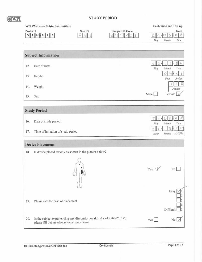


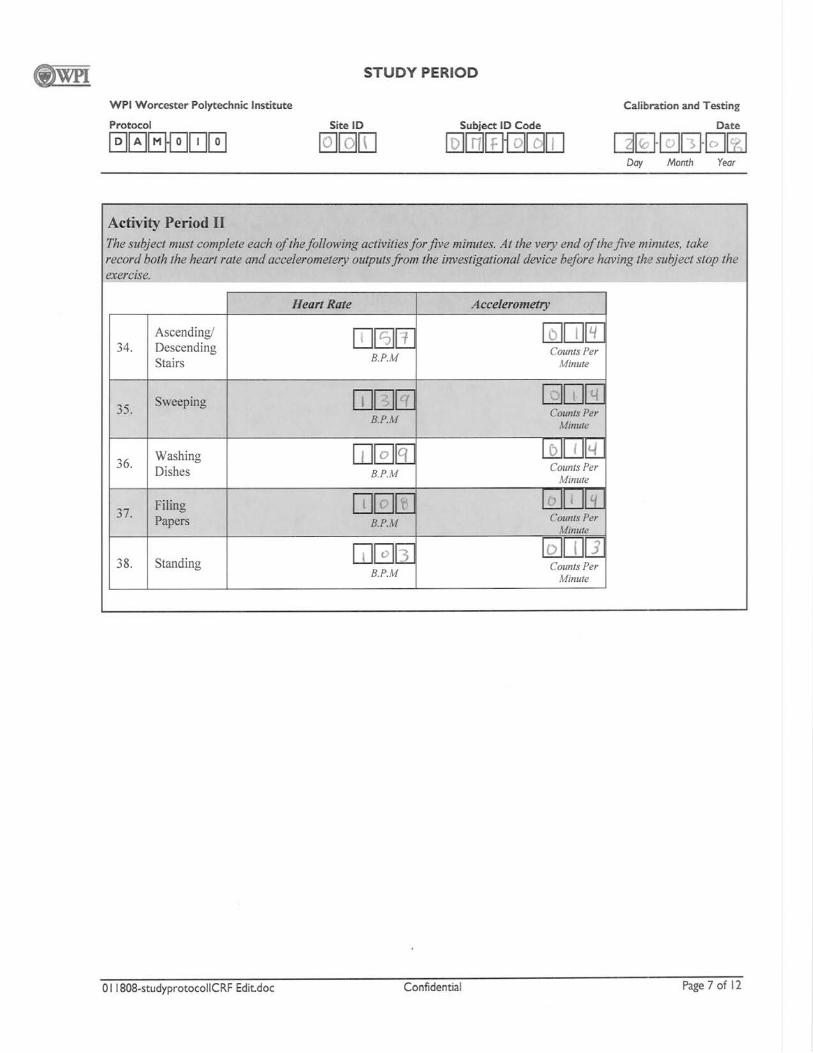


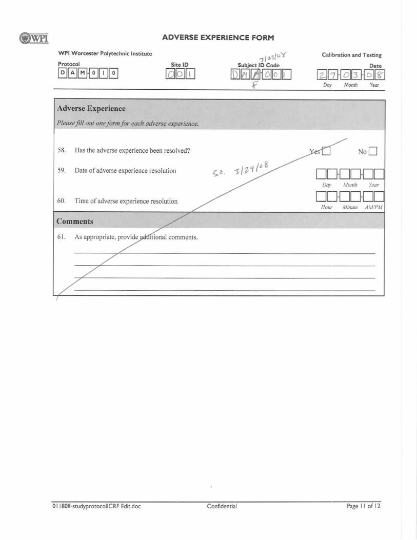


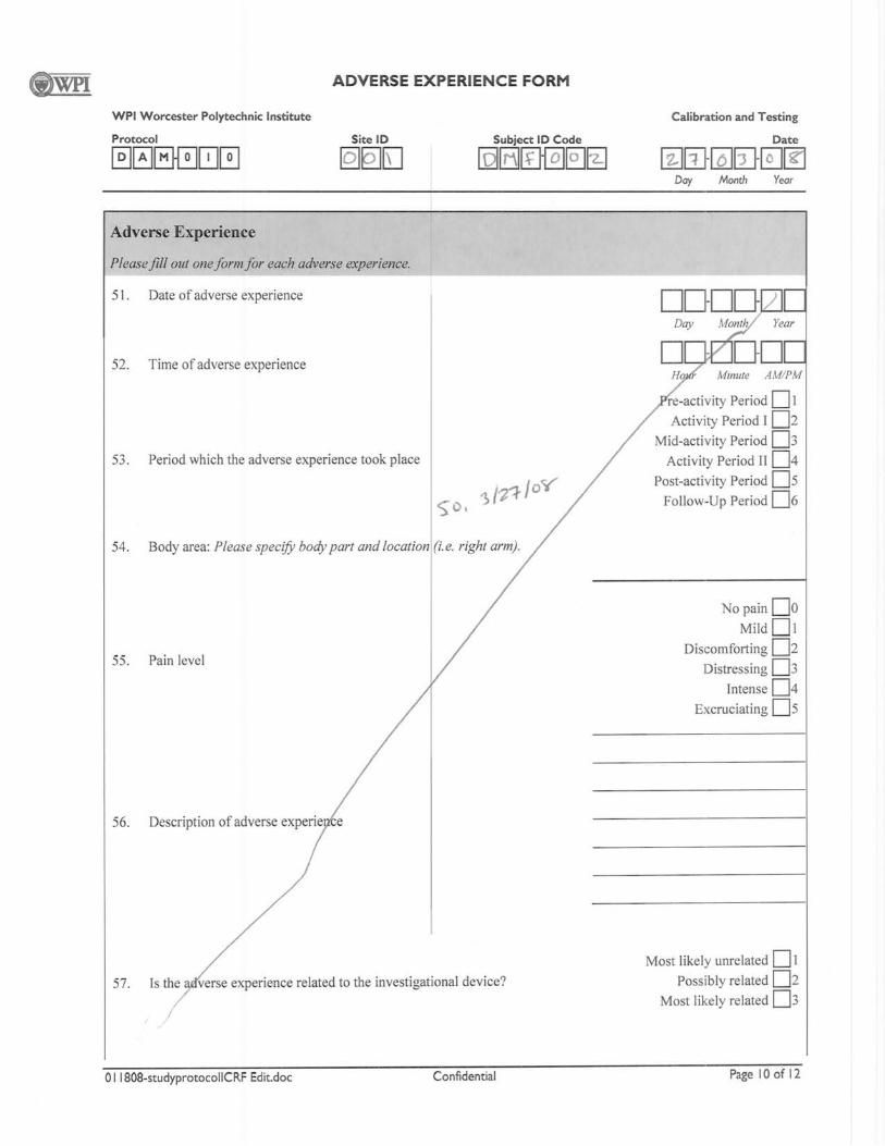


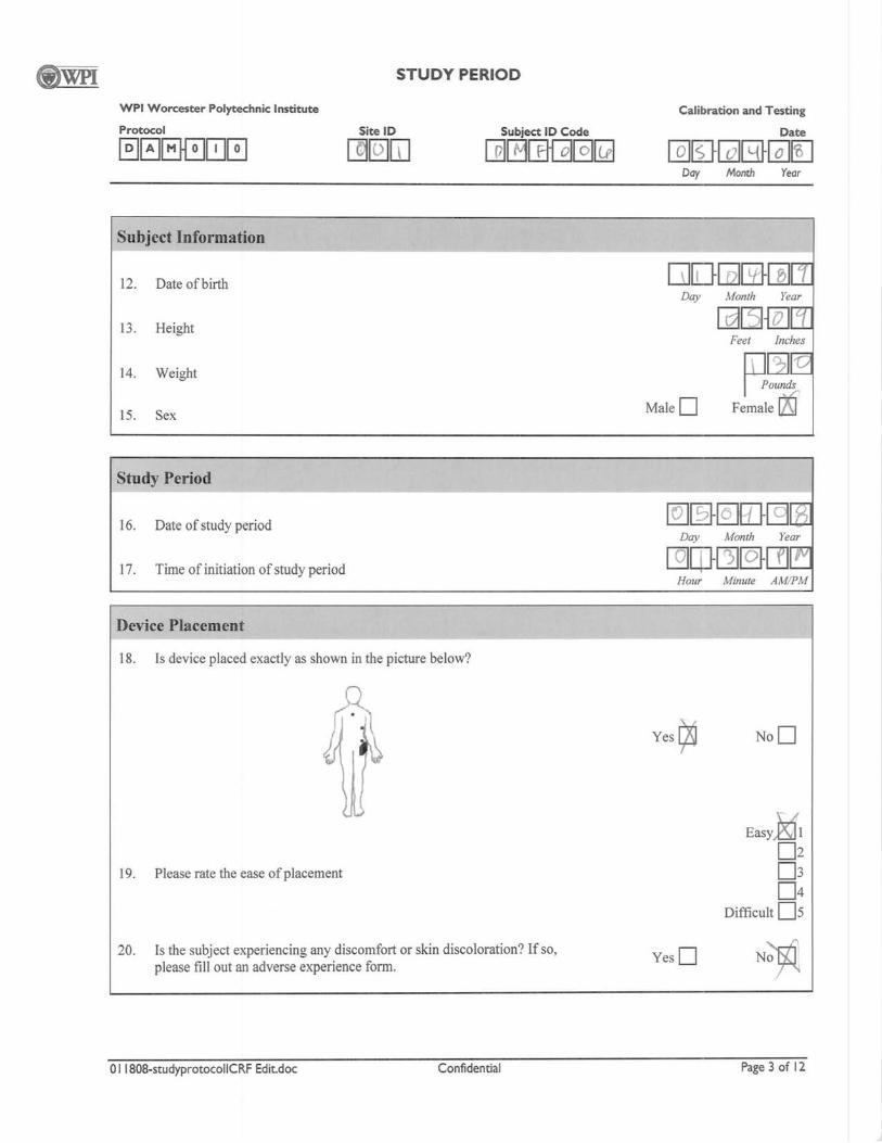


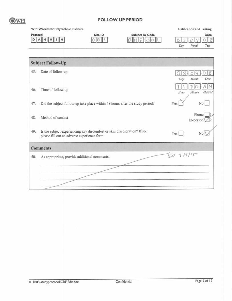


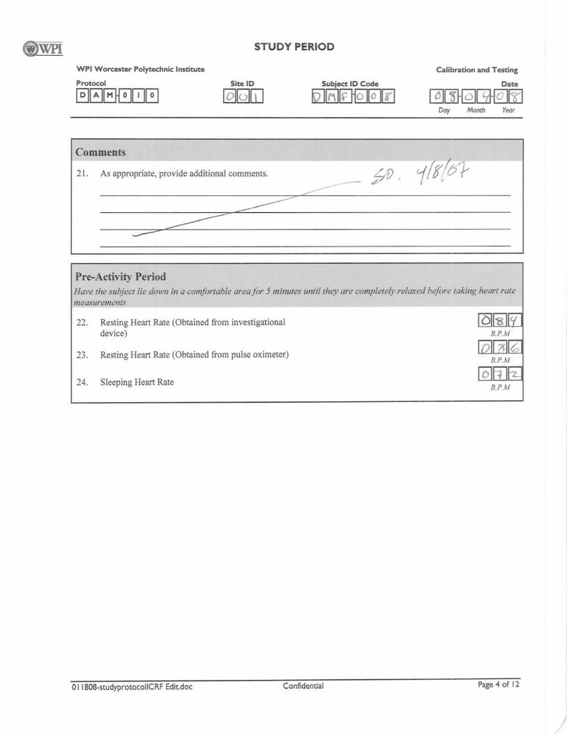


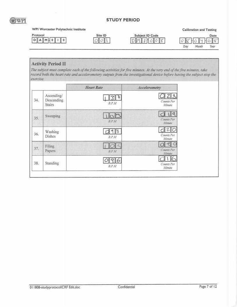


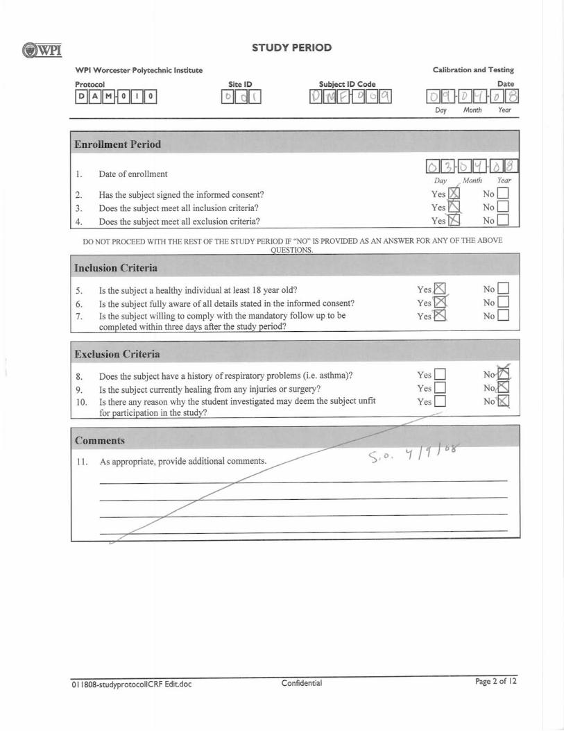

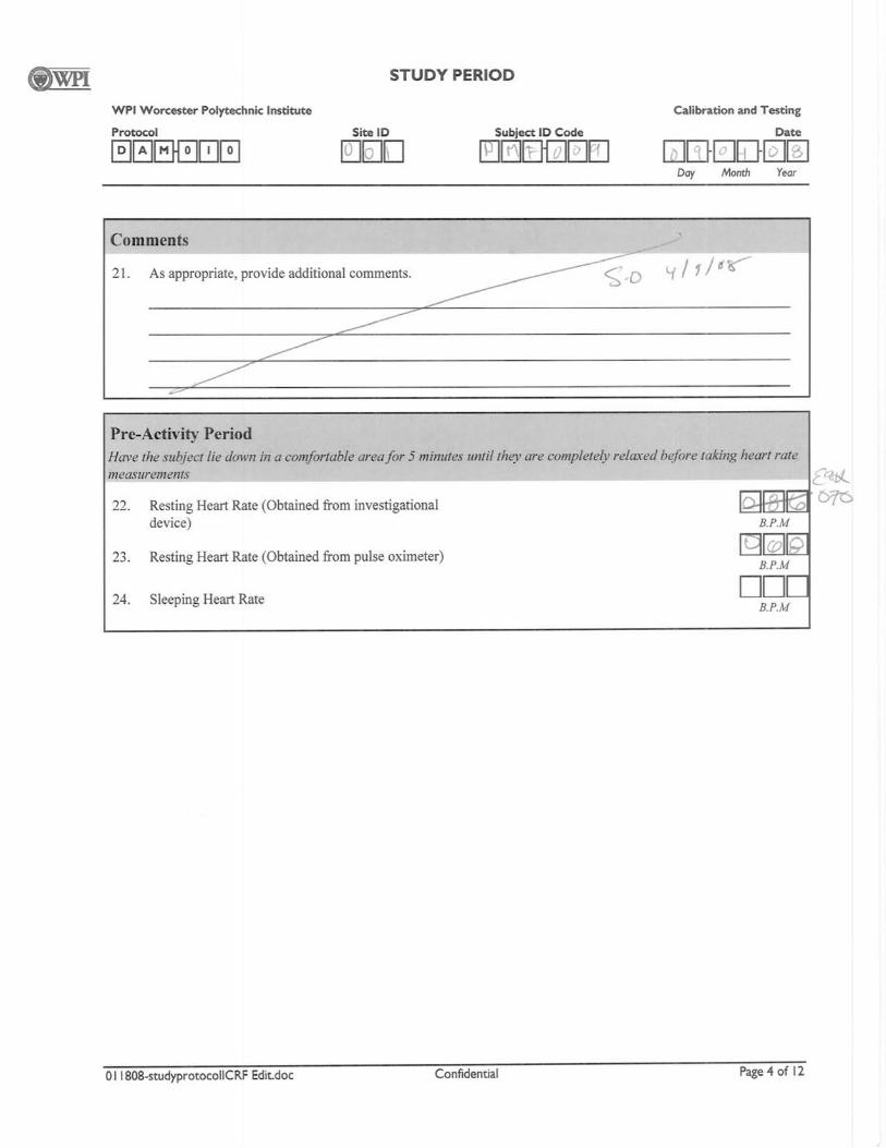


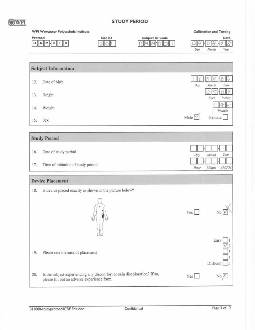
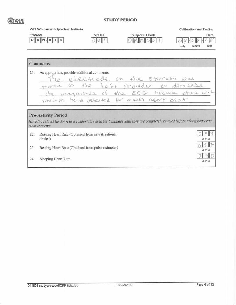


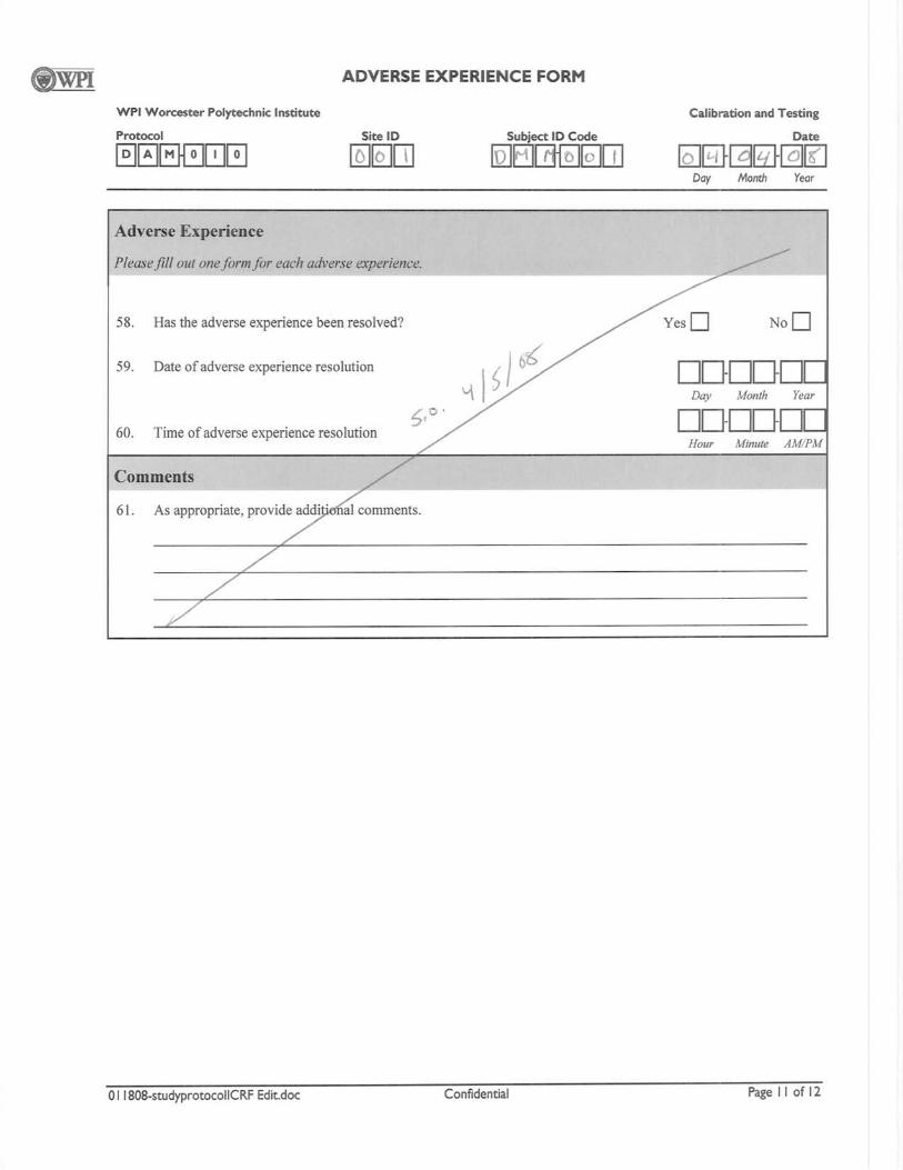


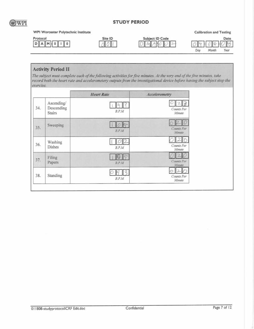


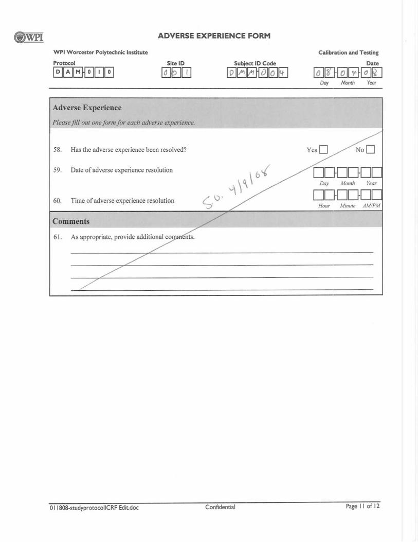


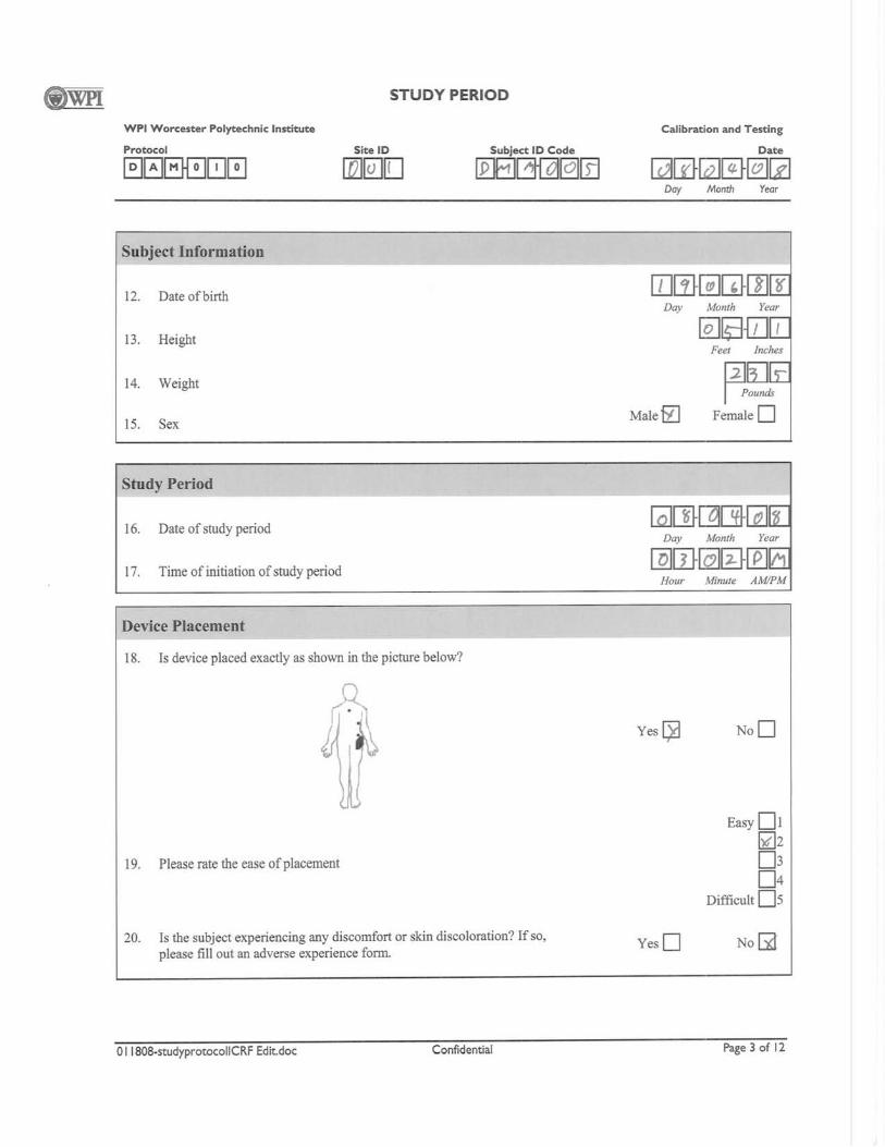


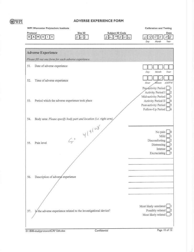
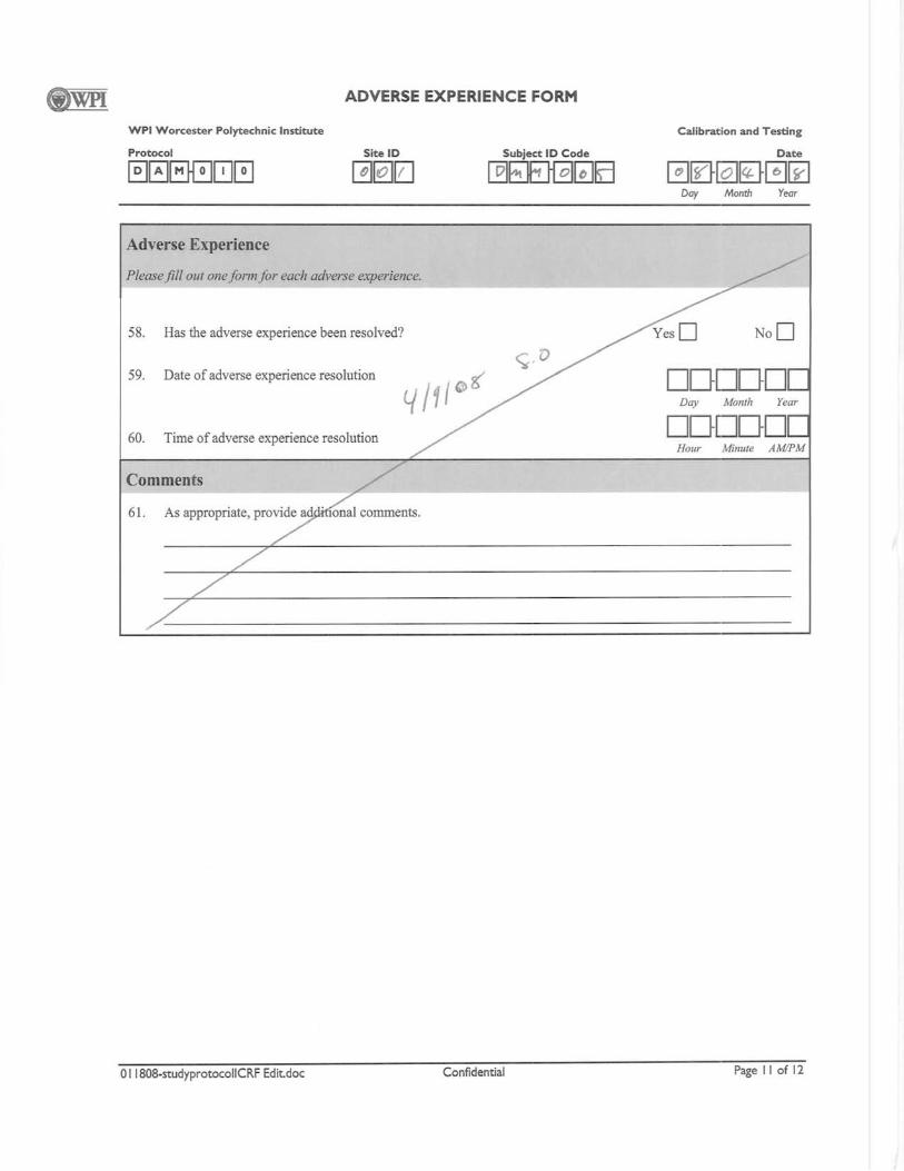


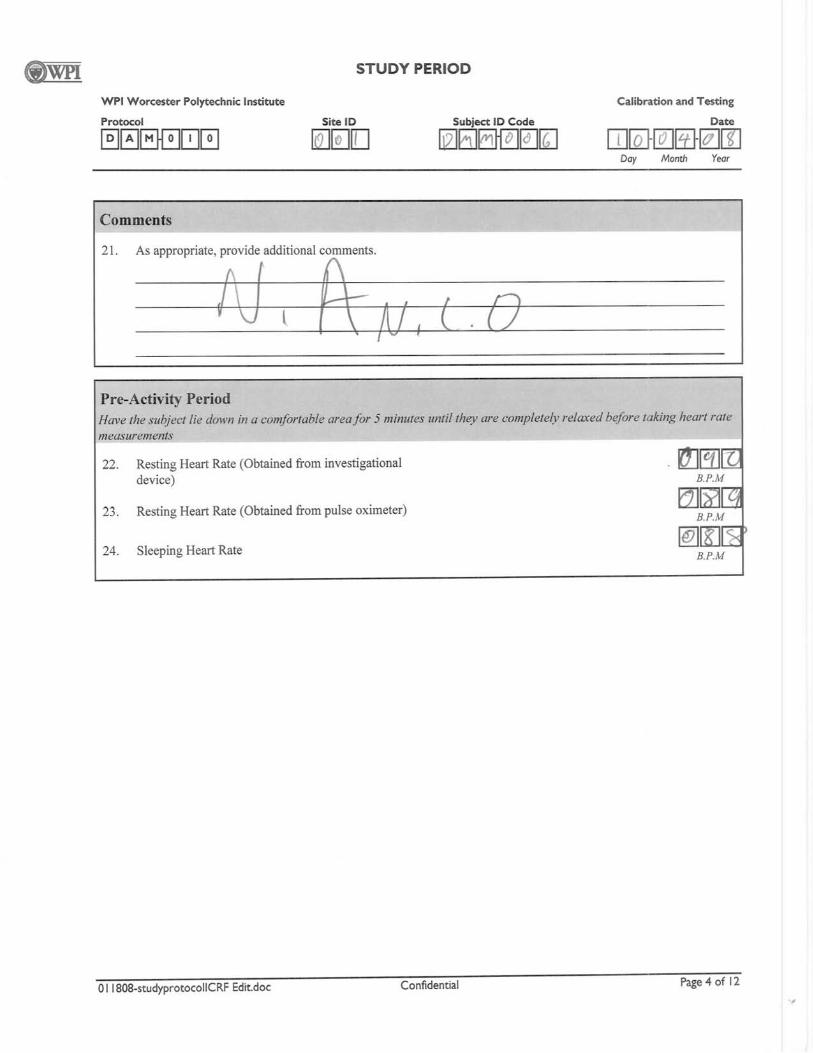
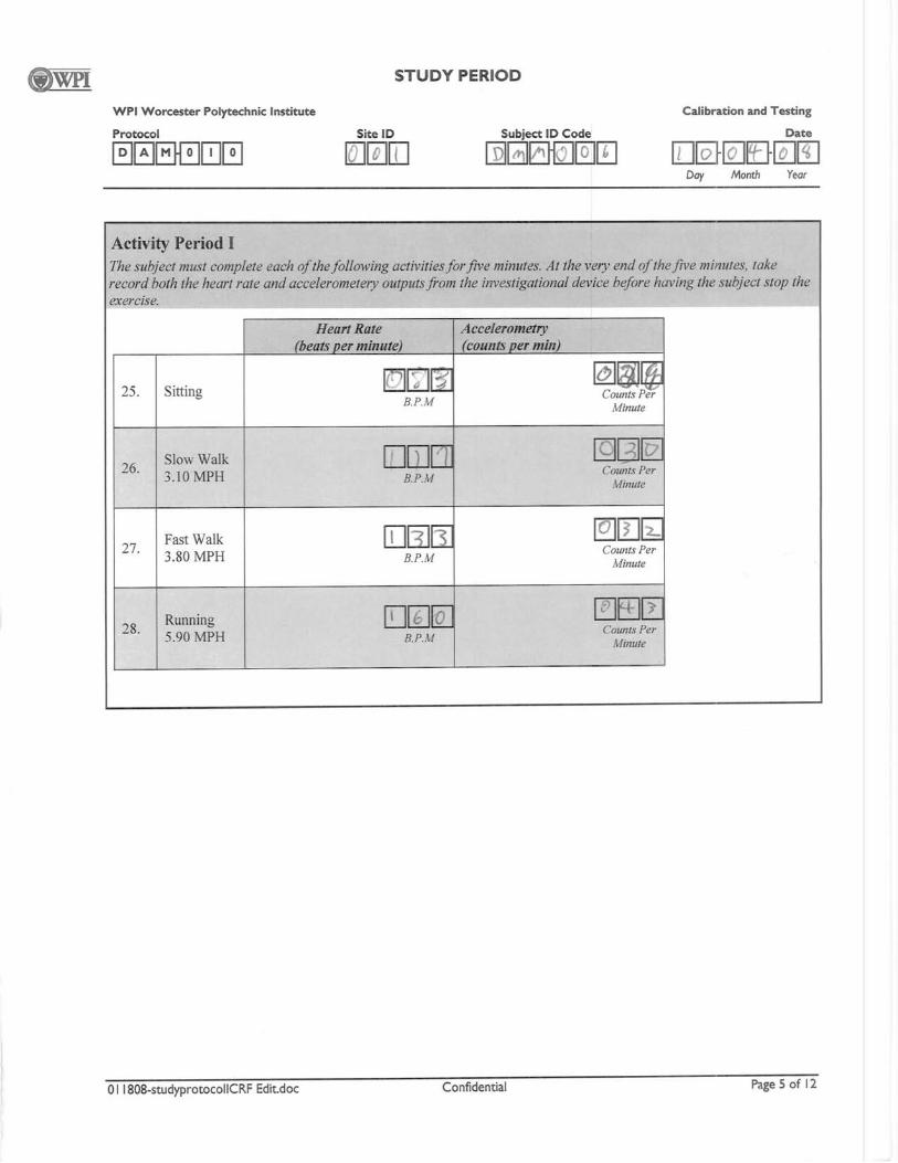


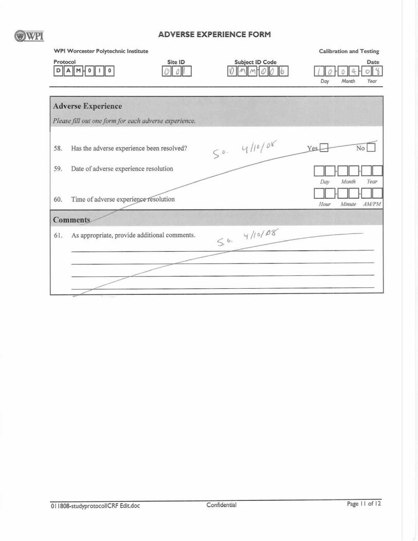


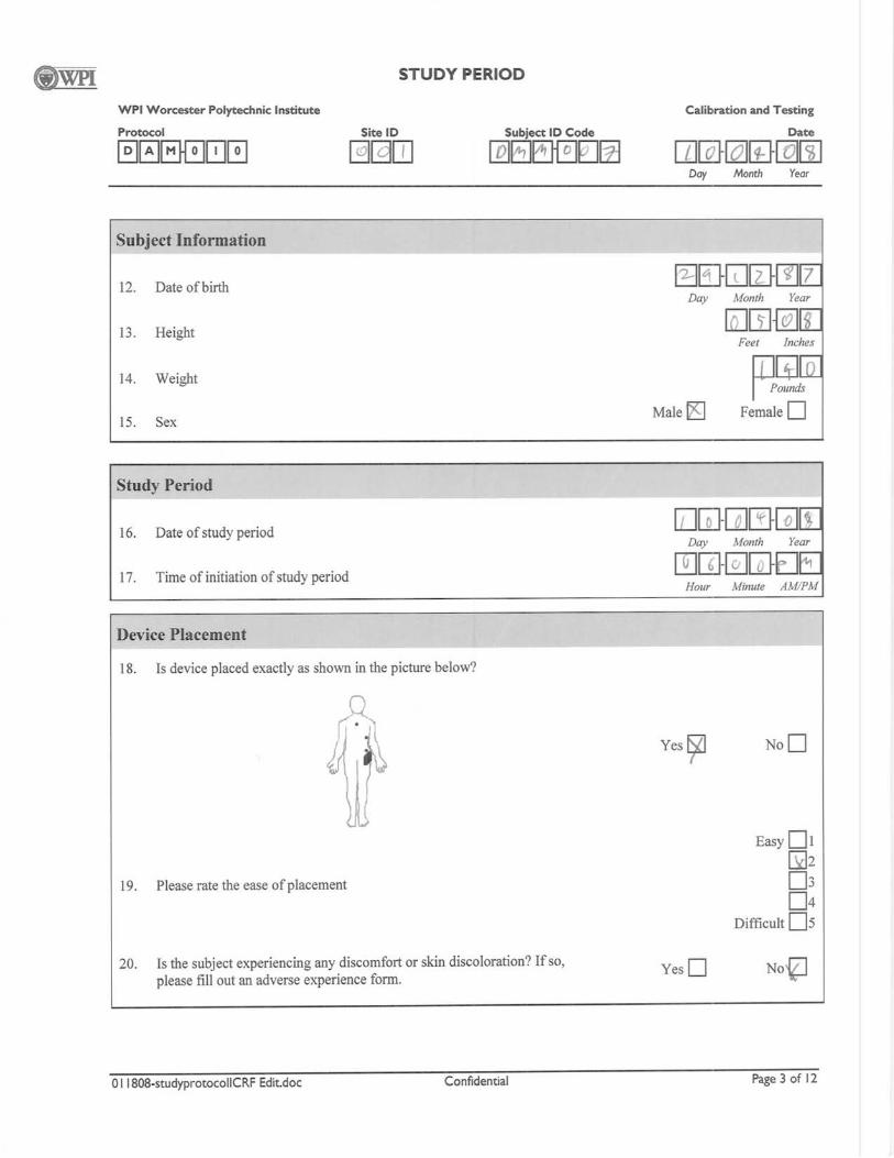


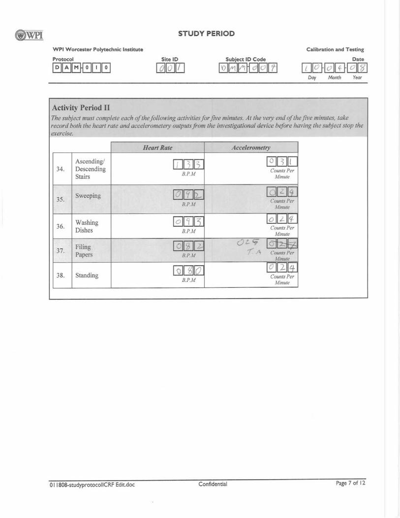


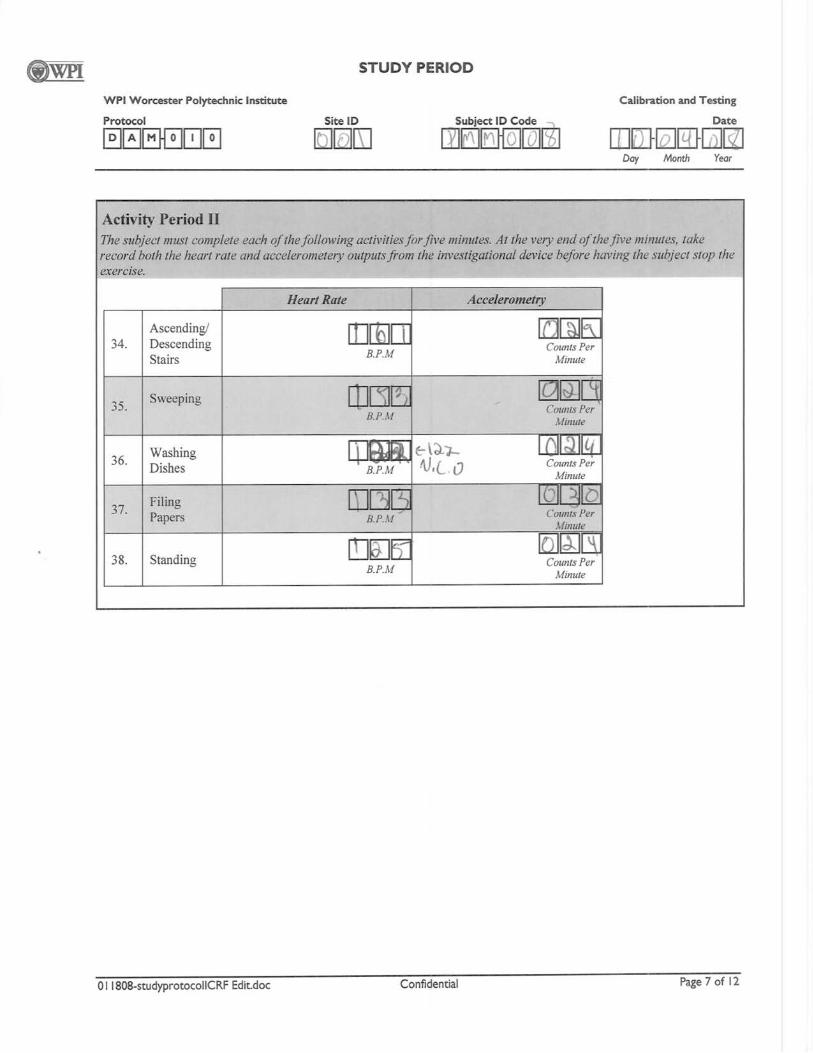

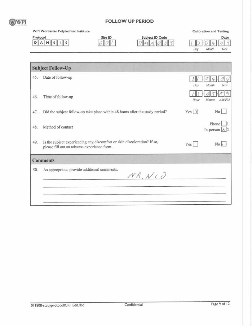
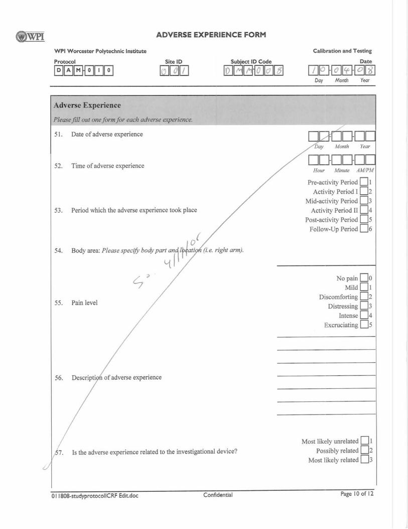


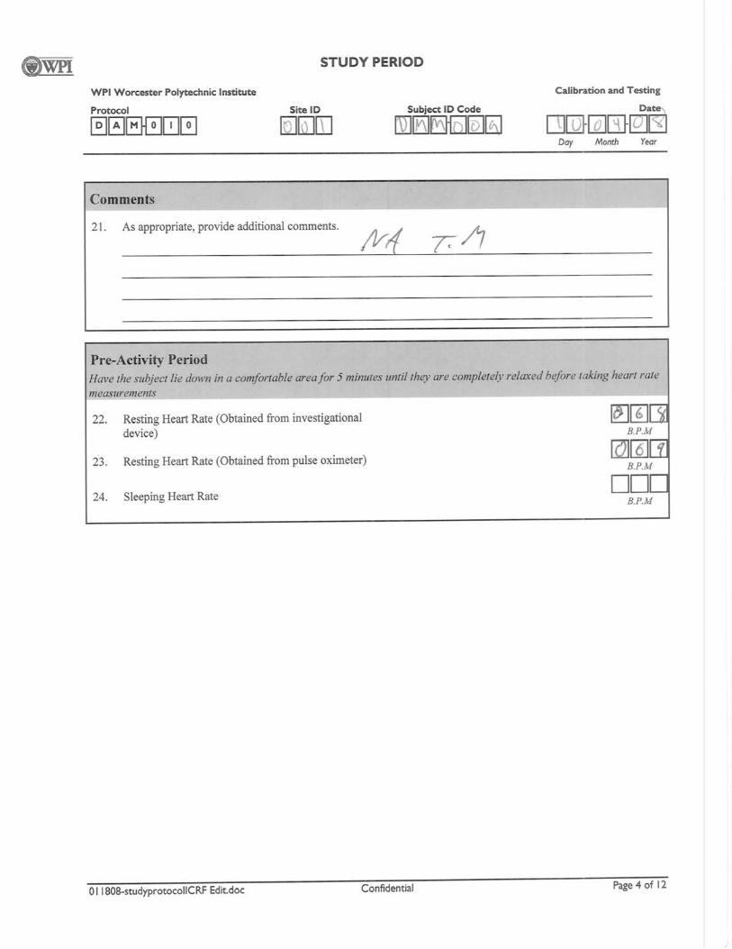


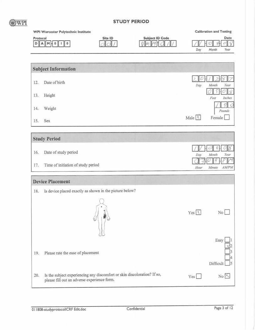
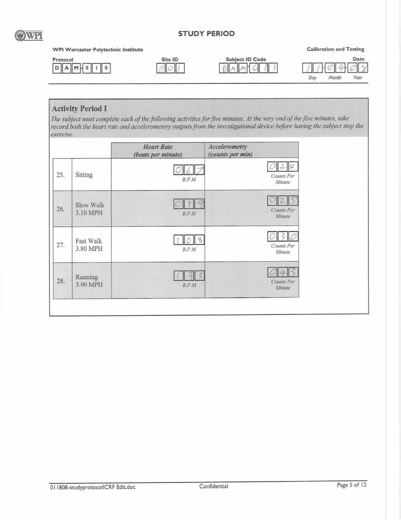


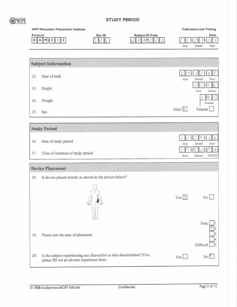


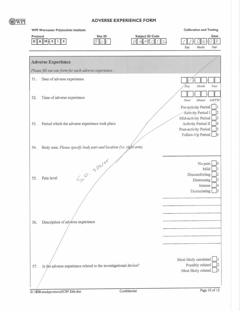


Appendix E: Data from Case Report Forms summarized

Date DOB Height Weight SexTest ID Inclusion Exclusion HR ACC
DMF-001 3/25/2004 Met Met 11/25/1982 5'1" 120 F 92 13DMF-002 3/25/2004 Met Met 4/4/1982 5'9" 180 F 68 13DMF-003 3/31/2004 Met Met 7/1/1982 5'2" 189 F 90 16DMF-004 4/3/2004 Met Met 12/19/1983 5'6" 126 F 133 13DMF-005 4/4/2004 Met Met 8/18/1981 5'9" 175 F 42 21DMF-006 4/4/2004 Met Met 4/10/1985 5'9" 130 F 85 21DMF-007 4/6/2004 Met Met 7/9/1982 5'4" 162 F 61 22DMF-008 4/7/2004 Met Met 12/30/1982 5'2" 125 F 105 16DMF-009 4/8/2004 Met Met 4/13/1983 5'4" 105 F 81 21DMF-010 4/10/2004 Met Met 8/22/1984 5'5" 145 F 101 30DMF-011 4/10/2004 Met Met 1/25/1984 5'4" 122 F 79 23
DMM-001 4/3/2004 Met Met 4/15/2004 5'9" 145 M 98 14DMM-002 4/3/2004 Met Met 8/8/1984 5'11" 180 M 80 20
Study Participant InformationCriteria Sitting (Pre Activity)
DMM-003 4/3/2004 Met Met 2/23/1984 5'6" 135 M 84 24DMM-004 4/7/2004 Met Met 10/7/1982 6'1" 193 M 55 21DMM-005 4/7/2004 Met Met 6/18/1984 5'11" 235 M 91 23DMM-006 4/9/2004 Met Met 8/28/1984 5'11" 210 M 83 26DMM-007 4/9/2004 Met Met 12/28/1983 5'8" 190 M 71 24DMM-008 4/9/2004 Met Met 5/8/1984 5'9" 150 M 114 24DMM-009 4/9/2004 Met Met 10/19/1982 5'11" 180 M 90 22DMM-010 4/10/2004 Met Met 4/25/1982 5'10" 205 M 105 24DMM-011 4/10/2004 Met Met 12/19/1983 5'8" 150 M 67 24DMM-012 4/10/2004 Met Met 7/28/1983 5'6" 140 M 133 23
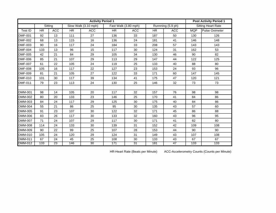
Test ID HR ACC HR ACC HR ACC HR ACC MQP Pulse OximeterDMF-001 92 13 111 27 136 33 187 50 130 126DMF-002 68 13 115 16 136 24 181 41 146 148DMF-003 90 16 117 24 184 33 208 57 143 143DMF-004 133 13 96 15 117 30 124 31 162 53DMF-005 42 21 84 29 105 34 130 46 90 82DMF-006 85 21 107 29 113 29 147 44 122 125DMF-007 61 22 105 24 119 25 133 40 88 80DMF-008 105 16 117 22 127 23 153 24 93 96DMF-009 81 21 105 27 122 33 171 60 147 145DMF-010 101 30 117 39 134 41 175 47 120 121DMF-011 79 23 113 24 130 25 146 32 73 73
DMM-001 98 14 105 20 117 32 157 76 98 98DMM-002 80 20 133 23 146 25 170 41 84 86
Post Activity Period 1Activity Period 1Sitting Heart RateSitting Slow Walk (3.10 mph) Fast Walk (3.80 mph) Runnning (5.9 ph)
DMM-003 84 24 117 29 125 30 175 40 84 86DMM-004 55 21 86 25 95 30 135 43 57 60DMM-005 91 23 107 30 122 32 171 45 86 88DMM-006 83 26 117 30 133 32 160 43 96 95DMM-007 71 24 107 29 117 30 171 41 82 80DMM-008 114 24 133 30 139 31 152 42 109 108DMM-009 90 22 99 25 107 28 153 44 90 90DMM-010 105 24 120 29 124 31 149 43 107 108DMM-011 67 24 45 25 108 30 133 43 67 67DMM-012 133 23 146 30 171 31 181 47 133 133
ACC-Accelerometry Counts (Counts per Minute)HR-Heart Rate (Beats per Minute)

HR ACC HR ACC HR ACC HR ACC HR ACC157 14 139 14 109 14 108 14 103 13151 21 101 14 99 14 105 14 98 13153 24 115 16 108 16 103 20 107 16146 23 127 14 119 15 119 17 101 15113 23 95 21 82 22 85 22 85 21127 28 105 22 103 22 90 25 113 22153 28 105 22 99 23 88 22 85 23130 23 103 19 98 20 105 20 96 16133 25 92 21 101 21 99 22 90 21122 37 109 31 83 31 83 31 86 30122 25 95 22 77 22 92 23 76 22
147 19 130 15 111 14 115 16 103 14153 23 105 20 102 20 105 20 93 20
Activity Period 2Ascening/Descending Stairs Sweeping Washing Dishes Filing Papers Standing
111 25 103 24 98 24 101 24 89 24111 24 85 21 86 21 88 22 70 21146 26 95 23 99 23 103 23 90 23162 35 125 23 113 23 103 24 95 22133 31 92 24 93 24 82 25 80 24161 29 153 24 127 24 133 30 125 24105 27 90 23 85 22 82 22 83 22130 31 105 23 108 23 98 24 107 23130 31 89 24 83 24 80 25 70 24147 28 122 24 128 23 130 24 117 23
HR-Heart Rate (Beats per Minute) ACC-Accelerometry Counts (Counts per Minute)

Test ID Sitting Slow Walk Fast Walk Run Stairs Sweep Dishes Filing StandingDMF-001 13 14 20 37 1 1 1 1 0DMF-002 13 3 11 28 8 1 1 1 0DMF-003 16 8 17 41 8 0 0 4 0DMF-004 13 2 17 18 10 1 2 4 2DMF-005 21 8 13 25 2 0 1 1 0DMF-006 21 8 8 23 7 1 1 4 1DMF-007 22 2 3 18 6 0 1 0 1DMF-008 16 6 7 8 7 3 4 4 0DMF-009 21 6 12 39 4 0 0 1 0DMF-010 30 9 11 17 7 1 1 1 0DMF-011 23 1 2 9 2 -1 -1 0 -1
DMM-001 14 6 18 62 5 1 0 2 0DMM-002 20 3 5 21 3 0 0 0 0DMM-003 24 5 6 16 1 0 0 0 0
Scaled Accelerometry Counts
DMM-004 21 4 9 22 3 0 0 1 0DMM-005 23 7 9 22 3 0 0 0 0DMM-006 26 4 6 17 9 -3 -3 -2 -4DMM-007 24 5 6 17 7 0 0 1 0DMM-008 24 6 7 18 5 0 0 6 0DMM-009 22 3 6 22 5 1 0 0 0DMM-010 24 5 7 19 7 -1 -1 0 -1DMM-011 24 1 6 19 7 0 0 1 0DMM-012 23 7 8 24 5 1 0 1 0
Scaled accelerometry was obtained by subtracting the obtained accelerometry counts per minute when sittingfrom the accelerometry counts per minuts obtained during each activity

Appendix F: Average accelerometry counts and heart rate for each activity measured with the device discussed in this report and summarized in the published ActiHeart study

Mean 102 110 105.81818 126.09091 135.3636364 159.0909091
Average Heart Rate and Accelerometry Count for Each Activity with Standard DeviationActiHeart Device
Heart RateResting HR Sitting Standing Filing Dishes Slow Walk Sweeping Fast Walk Stairs Runnning
Mean 66 73 81 83 104 105 109 120 130 155St. Dev 15.5 17.7 15.7 21.8 26.6 35 15.9 20.7 25.7 18.9
AccelerometryResting ACC Sitting Standing Filing Dishes Slow Walk Sweeping Fast Walk Stairs Runnning
Mean 0.1 0.3 1.2 5 10.6 101.9 77.5 597.1 351 1776St. Dev 0.2 0.8 1.3 5.1 7.6 157.2 32.5 132.1 103.1 286.3
MQP DeviceHeart Rate
Resting HR Sitting Standing Filing Dishes Slow Walk Sweeping Fast Walk Stairs RunnningMean 81.27272781.27272733 88.45488.4545555 92.692.636363636 100100.4545.4545 102 110 105.81818 126.09091 135.3636364 159.0909091St. Dev 21.0622454 22.19173 17.74978 17.96309 15.71623 27.371518 20.346096 20.954496 20.24486467 16.08387109
AccelerometryResting ACC Sitting Standing Filing Dishes Slow Walk Sweeping Fast Walk Stairs Runnning
Mean 0 0 ‐0.45455 0.727273 ‐0.36364 4.5454545 ‐0.1818182 6.8181818 5 19.72727273St. Dev 0 0 1.21356 1.954017 0.924416 1.8090681 1.0787198 1.3280197 2.366431913 2.611164839
Scaled AccelerometryResting ACC Sitting Standing Filing Dishes Slow Walk Sweeping Fast Walk Stairs Runnning
Mean 0 0 ‐22.7273 36.36364 ‐18.1818 227.27273 ‐9.0909091 340.90909 250 986.3636364St. Dev 0 0 60.67799 97.70084 46.22081 90.453403 53.935989 66.400986 118.3215957 130.558242

Appendix G: Digital code for the device

file:///R|/MQP/HR_ACC_disp_2.txt
#include "msp430x44x.h" // Definitions, constants, etc for msp430F449#include <string.h> #include <stdio.h>#include <stdlib.h>#include <math.h>#include <in430.h>
#define a (0x80) // definitions for LCD seegments on the Olimex LCD. 4-Mux operation is assumed#define b (0x40) // For more details on 4-Mux operation, gather your LCD datasheet, #define c (0x20) // TI's MSP430F449 User Guide (look for LCD Controller, then 4-Mux),#define d (0x01) // and MSP-449STK-2 schematic. You will need ALL these 3 when defining#define e (0x02) // each number or character. Remember, the Olimex LCD doesn't use a LCD driver!#define f (0x08) // You tell the LCD what characters to display. It's very time consuming!!#define g (0x04)#define h (0x10)char *LCD = LCDMEM; // pointer to LCD Memory Segments
float occurence[2] = 0, 0; //heart beat occurence time record arrayunsigned char i = 0;unsigned char next = 0;unsigned char j; //conversion factorfloat time = 0; //time float t1 = 0;float t2 = 0;float dt = 0;unsigned char busy;unsigned int ACC = 0;unsigned int bufferACC = 0;unsigned int volts = 0;unsigned int HR = 0; //heart rateunsigned char switchCnt = 0; //display switch counterunsigned char adc_in = 0; unsigned int avgHR = 0;unsigned char HRcnt = 0;unsigned int bufferHR = 0;
unsigned int vectorHR[256] = 0; //store ADC12 measurements unsigned char arrayHR[256] = 0; //store past HR calculationsunsigned char charHR[4];//store character version of heart rateunsigned char beat = 0;void setupADC12(void);void setupTimerB(void);void setupEKG(void);void init_sys(void);void writeWord(const char *word);void initLCD(void);void clearLCD(void);void writeLetter(int position,char letter);void setupBtn(void);void buzzerOn(void);void buzzerOff(void);void HRdisp(unsigned char heartRate);void ACCdisp(unsigned char energy);void swDelay(unsigned int max_cnt);
/********************* MAIN FUNCTION *********************/void main(void)
file:///R|/MQP/HR_ACC_disp_2.txt (1 of 7) [4/23/2008 2:34:10 AM]
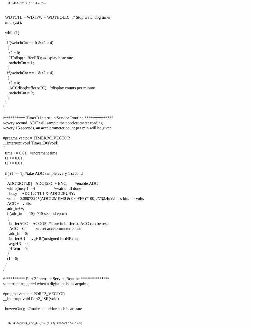
file:///R|/MQP/HR_ACC_disp_2.txt
WDTCTL = WDTPW + WDTHOLD; // Stop watchdog timer init_sys(); while(1) if(switchCnt == 0 & t2 > 4) t2 = 0; HRdisp(bufferHR); //display heartrate switchCnt = 1; if(switchCnt == 1 & t2 > 4) t2 = 0; ACCdisp(bufferACC); //display counts per minute switchCnt = 0;
/********** TimerB Interruup Service Routine *************///every second, ADC will sample the accelerometer reading//every 15 seconds, an accelerometer count per min will be given
#pragma vector = TIMERB0_VECTOR__interrupt void Timer_B0(void) time += 0.01; //increment time t1 += 0.01; t2 += 0.01; if( t1 >= 1) //take ADC sample every 1 second ADC12CTL0 |= ADC12SC + ENC; //enable ADC while(busy != 0) //wait until done busy = ADC12CTL1 & ADC12BUSY; volts = 0.0007324*(ADC12MEM0 & 0x0FFF)*100; //732.4uV/bit x bits => volts ACC += volts; adc_in++; if(adc_in == 15) //15 second epoch bufferACC = ACC/15; //store in buffer so ACC can be reset ACC = 0; //reset accelerometer count adc_in = 0; bufferHR = avgHR/(unsigned int)HRcnt; avgHR = 0; HRcnt = 0; t1 = 0;
/********** Port 2 Interrupt Service Routine *************///interrupt triggered when a digital pulse is acquired
#pragma vector = PORT2_VECTOR __interrupt void Port2_ISR(void) buzzerOn(); //make sound for each heart rate
file:///R|/MQP/HR_ACC_disp_2.txt (2 of 7) [4/23/2008 2:34:10 AM]
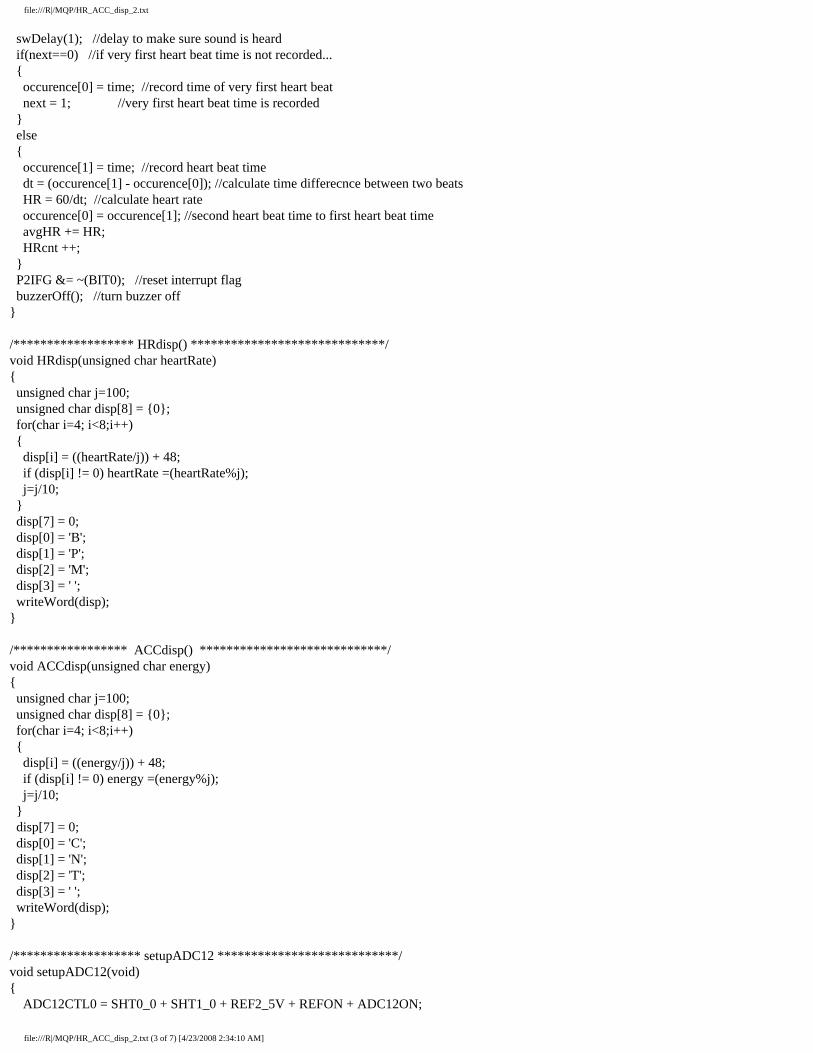
file:///R|/MQP/HR_ACC_disp_2.txt
swDelay(1); //delay to make sure sound is heard if(next==0) //if very first heart beat time is not recorded... occurence[0] = time; //record time of very first heart beat next = 1; //very first heart beat time is recorded else occurence[1] = time; //record heart beat time dt = (occurence[1] - occurence[0]); //calculate time differecnce between two beats HR = 60/dt; //calculate heart rate occurence[0] = occurence[1]; //second heart beat time to first heart beat time avgHR += HR; HRcnt ++; P2IFG &= ~(BIT0); //reset interrupt flag buzzerOff(); //turn buzzer off
/****************** HRdisp() *****************************/void HRdisp(unsigned char heartRate) unsigned char j=100; unsigned char disp[8] = 0; for(char i=4; i<8;i++) disp[i] = ((heartRate/j)) + 48; if (disp[i] != 0) heartRate =(heartRate%j); j=j/10; disp[7] = 0; disp[0] = 'B'; disp[1] = 'P'; disp[2] = 'M'; disp[3] = ' '; writeWord(disp);
/***************** ACCdisp() ****************************/void ACCdisp(unsigned char energy) unsigned char j=100; unsigned char disp[8] = 0; for(char i=4; i<8;i++) disp[i] = ((energy/j)) + 48; if (disp[i] != 0) energy =(energy%j); j=j/10; disp[7] = 0; disp[0] = 'C'; disp[1] = 'N'; disp[2] = 'T'; disp[3] = ' '; writeWord(disp);
/******************* setupADC12 ***************************/void setupADC12(void) ADC12CTL0 = SHT0_0 + SHT1_0 + REF2_5V + REFON + ADC12ON;
file:///R|/MQP/HR_ACC_disp_2.txt (3 of 7) [4/23/2008 2:34:10 AM]

file:///R|/MQP/HR_ACC_disp_2.txt
//SHT1/SHT0: both 768 ADC12CLK ticks //MSC: burst mode off //REFON/REF2_5V: use internal reference voltage 2.5V //ADC12ON: turn ADC on ADC12CTL1 = SHP; //CSTART ADDx: start conversion with ADC12MEM0 //SHSx: use SW conversion initiation trigger, ADC12SC bits //SHP: SAMPCON signal sourced from sampling timer //ISSH:sample input signal not inverted //ADC12DIVx: divide ADC12CLK by 1 //ADC12SSEL: ADC12OSC clock 5MHz //CONSEQx: single channel, single conversion //ADC12BUSY: no ADC operation active ADC12MCTL0 = SREF_0 + INCH_0; //use channel 0 for Accelerometer input P6SEL |= (BIT0); //set port 6 bit 0 to function mode (ADC12) ADC12IE |= 0x0001; //Enable ADC12 interrupt for channel 0
/******************* setupTimerB **************************/void setupTimerB(void) TBCTL = TBSSEL_2 + CNTL_0 + MC_1; //TBSSEL: sourc SMCLK //CNTL: 16 bit //MC: upmode to CCR0 //ID: input CLK divided by 1 TBCCR0 = 10485; //10485 SMCLK ticks = 0.01 second TBCCTL0 = CCIE; //TBCCR0 interrupt enabled
/********************** setupEKG() ************************************/void setupEKG(void) P2SEL &= ~(BIT0); // P2.0 I/O option (0) P2DIR &= ~(BIT0); // Set P2.0 to input direction (0) P2IES |= (BIT0); //flag set with high to low transition (1) P2IFG &= ~(BIT0); P2IE |= (BIT0); //Enable intterupt
/**********************************************************************************************************************************The code below this line is from the ECE2801 course that has been editted to fit the project***********************************************************************************************************************************************/
/******************* swDelay() ************************/void swDelay(unsigned int max_cnt) unsigned int cnt1=0, cnt2; while (cnt1 < max_cnt) cnt2 = 0; while (cnt2 < 2000) cnt2++; cnt1++;
/******************** initSys() *****************************/
file:///R|/MQP/HR_ACC_disp_2.txt (4 of 7) [4/23/2008 2:34:10 AM]

file:///R|/MQP/HR_ACC_disp_2.txt
void init_sys(void) initLCD(); // Setup LCD for work clearLCD(); // Clear LCD display setupBtn(); // Setup Button ports setupADC12(); // Setup ADC12 setupEKG(); setupTimerB(); _BIS_SR(GIE); //global interrupt enable// **************************** initLCD ***************************************void initLCD(void) // initialize the various registers for LCD to work // (code obtained from sample demos of MSP430F449) FLL_CTL0 = XCAP10PF; //set load capacitance for 32k xtal // Initialize LCD driver (4Mux mode) LCDCTL = LCDSG0_7 + LCD4MUX + LCDON; // 4mux LCD, segs16-23 = outputs BTCTL = BT_fLCD_DIV128; // set LCD frame freq = ACLK P5SEL = 0xFC; // set Rxx and COM pins for LCD
// **************************** clearLCD ***************************************void clearLCD(void) // makes the LCD blank // clear LCD memory to clear display unsigned int iLCD; for (iLCD =0; iLCD<20; iLCD++) // clears all 20 LCD memory segments LCD[iLCD] = 0;
// *************************** writeLetter ************************************void writeLetter(int position,char letter) // writes single character on the LCD. // User can specify position as well // DO NOT PLAY WITH THE CODE BELOW ----------------------------------------- if (position == 1) // this is position adjustment for compatibility position = position + 6; else if ( (position > 1) & (position < 8) ) position = ((position * 2) - 1) + 6; // adjust position // -------------------------------------------------------------------------
switch(letter) // letter // LCDM7 // LCDM8 // End case 'A': LCD[position-1] = a + b + c + e; LCD[position] = b + c + g; break; case 'B': LCD[position-1] = c + h + e; LCD[position] = b + c + g; break; case 'C': LCD[position-1] = a + h; LCD[position] = b + c; break; case 'D': LCD[position-1] = b + c + h + e; LCD[position] = c + g; break; case 'E': LCD[position-1] = a + h + e; LCD[position] = b + c + g; break; case 'F': LCD[position-1] = a; LCD[position] = b + c + g; break; case 'G': LCD[position-1] = a + c + h + e; LCD[position] = b + c; break; case 'H': LCD[position-1] = b + c + e; LCD[position] = b + c + g; break; case 'I': LCD[position-1] = a + h + f; LCD[position] = d; break; case 'J': LCD[position-1] = b + h + c; LCD[position] = c; break; case 'K': LCD[position-1] = d + g; LCD[position] = b + c + g; break; case 'L': LCD[position-1] = h; LCD[position] = b + c ; break; case 'M': LCD[position-1] = b + c + g; LCD[position] = b + c + f; break; case 'N': LCD[position-1] = b + c + d; LCD[position] = b + c + f; break; case 'O': LCD[position-1] = a + b + c + h; LCD[position] = b + c; break;
file:///R|/MQP/HR_ACC_disp_2.txt (5 of 7) [4/23/2008 2:34:10 AM]

file:///R|/MQP/HR_ACC_disp_2.txt
case 'P': LCD[position-1] = a + b + e; LCD[position] = b + c + g; break; case 'Q': LCD[position-1] = a + b + c + h + d; LCD[position] = b + c; break; case 'R': LCD[position-1] = a + b + d + e; LCD[position] = b + c + g; break; case 'S': LCD[position-1] = a + c + h + e; LCD[position] = b + g; break; case 'T': LCD[position-1] = a + f + b; LCD[position] = d + b; break; case 'U': LCD[position-1] = b + c + h; LCD[position] = b + c; break; case 'V': LCD[position-1] = g; LCD[position] = b + c + e; break; case 'W': LCD[position-1] = b + c + d; LCD[position] = b + c + e; break; case 'X': LCD[position-1] = d + g; LCD[position] = e + f; break; case 'Y': LCD[position-1] = b + c + h + e; LCD[position] = f; break; case 'Z': LCD[position-1] = a + h + g; LCD[position] = e; break; // number // LCDM7 // LCDM8 // END case '0': LCD[position-1] = a + b + c + h; LCD[position] = b + c; break; case '1': LCD[position-1] = b + c; LCD[position] = d & a; break; case '2': LCD[position-1] = a + b + e + h; LCD[position] = c + g; break; case '3': LCD[position-1] = a + b + c + e + h; LCD[position] = g; break; case '4': LCD[position-1] = b + c + e; LCD[position] = b + g; break; case '5': LCD[position-1] = a + c + h + e; LCD[position] = b + g; break; case '6': LCD[position-1] = a + c + h + e; LCD[position] = b + c + g; break; case '7': LCD[position-1] = a + b + c; LCD[position] = d & a; break; case '8': LCD[position-1] = a + b + c + e + h; LCD[position] = b + c + g; break; case '9': LCD[position-1] = a + b + c + e ; LCD[position] = b + g; break; // others case '.': LCD[position] = h; break; // decimal point case '^': LCDM2 = c; break; // top arrow case '!': LCDM2 = a; break; // bottom arrow case '>': LCDM2 = b; break; // right arrow case '<': LCDM2 = h; break; // left arrow case '+': LCDM20= a; break; // plus sign case '-': LCDM20= h; break; // minus sign case '&': LCDM2 = d; break; // zero battery case '*': LCDM2 = d + f; break; // low battery case '(': LCDM2 = d + f + g; break; // medium battery case ')': LCDM2 = d + e + f + g; break; // full battery */
// ****************************** writeWord ***********************************void writeWord(const char *word) // displays a word upto 7 characters -- why 7? // words must be in upper case (why?) unsigned int strLength = 0; // variable to store length of word unsigned int i; // dummy variable strLength = strlen(word); // get the length of word now for (i = 1; i <= strLength; i++) // display word writeLetter(strLength - i + 1,word[i-1]); // displays each letter in the word
/******************* setupBtn() ************************/void setupBtn(void) P3SEL &= ~(BIT7|BIT6|BIT5|BIT4); // P3.7-4 I/O Function [0000 xxxx] P3DIR &= ~(BIT7|BIT6|BIT5|BIT4); // P3.7-4 Push buttons input [0000 xxxx]
file:///R|/MQP/HR_ACC_disp_2.txt (6 of 7) [4/23/2008 2:34:10 AM]

file:///R|/MQP/HR_ACC_disp_2.txt
/***************** buzzerOn() ************************/void buzzerOn(void) FLL_CTL0 |= XCAP10PF; // Configure load caps P1DIR |= BIT2|BIT0; // P1.2,0 output P1SEL &= ~BIT2; // P1.2 I/O option P1OUT &= ~BIT2; // P1.2 output = 0 P1SEL |= BIT0; // P1.0 TA0 option CCTL0 = OUTMOD_7; // CCR0 reset/set CCR0 = 0x0f; // PWM Period TACTL = TASSEL_1 + MC_1 + ID_0; // ACLK, up mode, 1 divider
/***************** buzzerOff() ************************/void buzzerOff(void) TACTL = MC_0; // Stop Timer P1DIR |= BIT2|BIT0; // P1.2,0 output P1SEL &= ~(BIT2|BIT0); // P1.2,0 I/O option P1OUT &= ~(BIT2|BIT0); // P1.2,0 output = 0
file:///R|/MQP/HR_ACC_disp_2.txt (7 of 7) [4/23/2008 2:34:10 AM]

Appendix H: A Proposed Guide for Individuals Living with Type I Diabetes: Using the Combined Heart Rate and Accelerometer Activity Monitor to Improve Glycemic Control

A Proposed Guide for Individuals Living with Type I Diabetes:
Using the Combined Heart Rate and Accelerometer Activity Monitor to Improve
Glycemic Control
Disclaimer: The information and procedures contained in this document have not yet been proven to be effective. As always, contact your physician before changing your diet, exercise program, or insulin dosage.

Living with diabetes can be difficult. You must always be aware of your body and how
your blood glucose levels react to your diet, exercise, and medication. It is important to realize
that just because you have to take extra steps to maintain a healthy blood glucose level, you can
still live your life to the fullest. The purpose of this guide is to provide you information on your
disease and how to use the activity monitor in order to significantly improve your quality of life.
What Is Diabetes?
Diabetes is a disease in which one is unable to maintain stable blood glucose levels.
There are two major types of diabetes: type I and type II. Type I diabetes, which is also known as
insulin dependent diabetes, occurs when one’s body is unable to produce insulin. Type II
diabetes, which is the most common and known as non insulin dependent diabetes, occurs when
one’s body is unable to produce enough and/or sufficiently use insulin.
Why Should I Control My Blood Glucose Levels?
There are both short term and long term effects of having unstable blood glucose levels.
The short-term effects of having low blood glucose include feeling shaky, sweaty, and a
pounding heart beat and if left untreated the individual may become unconscious. The short
term-effects of having high blood glucose include fatigue, blurred vision, increased thirst, and
increased urination. Consistently having poor glycemic control can lead to other complications
such as eye, nerve, kidney, and heart disease.

Why Should I Exercise?
Exercise can significantly improve the quality of life for a diabetic individual. The
following points below highlight just some of the many reasons you should consider
incorporating a daily exercise routine into part of your life:
• Exercise improves cardiovascular fitness to decrease your risk of developing coronary
artery disease - the most common complication of diabetes.
• Exercise decreases the LDL cholesterol (“bad” cholesterol) and increases the HDL
cholesterol (“good” cholesterol).
• Exercise improves blood glucose control by allowing your muscles to use insulin more
effectively, by maintaining or reducing your weight and by increasing muscle to promote
glucose use. This may decrease the amount of insulin or oral hypoglycemic agent you
need.
• Exercise reduces blood pressure and may reduce your chances of developing the
complications of diabetes.
How Does My Diet Affect My Blood Glucose Levels?
Glucose is the primary source of energy for the body. We receive glucose from digesting
carbohydrates and breaking them down into their simplest form. Our bodies then use insulin to
initiate the uptake of glucose by the cells of our peripheral tissues to be metabolized or stored as
glycogen for later use. Fat and protein generally have a minimal effect of blood glucose levels
and therefore carbohydrate counting can be a sufficient method to aid in blood glucose control.
However, if eaten in sufficient amounts, fats and proteins can have a significant affect on blood
glucose levels.

In a person without diabetes, metabolizing proteins releases amino acids, which
stimulates the secretion of both glucagon and insulin. Since glucagon opposes the effect of
insulin, the two cancel out and the individual’s blood glucose remains stable. But in people with
diabetes, the release of glucagon without insulin or with impaired insulin response can cause our
blood glucose to rise several hours after a meal high in protein.
Additionally, both proteins and fats can be converted into glucose through a process
known as gluconeogensis. Generally speaking, the amount of protein and fats converted to
glucose is quite small, except under conditions of intense exercise or metabolic starvation
How Is My Blood Glucose Affected By Different Types of Exercise?
When we exercise, our bodies are primarily burning fat and carbohydrates. The
percentage of carbohydrates burned is usually dependent on the intensity of the exercise. The
high intensity - the greater our bodies’ reliance on carbohydrates for energy will be. Other factors
that increase the reliance on carbohydrate include the following:
• Long-duration activity
• Exercise in hot and cold temperature extremes
• Exercise at high altitude
• Age (higher in young boys than in men)
What Should I Know Before Using this Device?
Before using this device, it is extremely important to recognize the fact that everybody is
different and everyone will react differently to using this method of counting carbohydrates

ingested and estimating carbohydrates burned. Please consult with your doctor before beginning
the program and please take the following points into consideration:
• While many people are instructed to ignore fat and protein in their bolus calculations,
there are several ways that they can affect the blood glucose. For some people this is an
extremely subtle effect; for others it is more obvious and must be taken into account
when calculating a bolus.
• Individuals with diabetes may have a slightly greater reliance on fat as an energy source
and slightly lower rate of carbohydrate metabolism. The amount of the reliance on fat can
vary from person to person.
• The absorption of insulin may be increased with exercise due to:
o Increased blood flow resulting from exercise
o A rise in body temperature
• Plasma insulin levels do not decrease during exercise
o This causes a relative hyperinsulinemia that impairs hepatic glucose production
and initiates hypoglycemia
• There is an exercise-induced increase in skeletal muscle insulin sensitivity
• In individuals with poor metabolic control, exercise can cause exaggerated hepatic
glucose production and impairment
o This leads to increase in blood glucose concentration and ketoacidosis.

How Do I Use This Device?
Before you use the device to help you make decisions on how to adjust your diet,
exercise, and insulin dosage, it is recommended that you wear the device for several days and
observe the carbohydrates that you typically burn throughout the day and during specific
activities. Once you become more familiar with how your daily routine impacts your blood
glucose level through burning your carbohydrate stores, you will be able to educated decisions
on how to make adjustments to your diet and medication. The follow paragraphs will describe in
more detail the strategies you can use to establish and maintain healthy blood glucose levels, but
first a description on how to wear the device will be provided.
The device is made up of a combined accelerometer and heart-rate sensor. With the
exception of the three electrode leads, the entire device is inside the case which is attached to a
belt. Each morning, put the device on by snugly placing the belt around your hip. The device can
be other either right or left side, but it must be placed so that it will not bounce as you walk or
perform other daily activities. Before you put on the electrodes, make sure your skin is clean and
any dry skin in exfoliated. Additionally, be sure to use a new set of electrodes everyday and
throw them away each time you take them off. Place one electrode on the same hip as the device,
one the sternum, and one on your lower left rib. After the electrodes are in place, connect the
white lead to the electrode on the hip, the red lead on the sternum, and the black lead on the rib.
Finally, turn the device on and watch the display throughout the day to see how many
carbohydrates you are burning.
Before making adjustments to your diet or insulin dosage it is necessary to determine
your blood glucose to insulin ratio (BG/I), carbohydrate to insulin ratio (Carb/I), and blood
glucose to carbohydrate ratio (BG/Carb). These ratios are essential for determining adjustments
to insulin, diet, and exercise.
• Blood Glucose / Insulin ratio (BG/I) the number of blood glucose points lowered by a
unit of insulin
o How to measure directly:
Fast for 4-5 hours prior to beginning the test.
With blood glucose near 150, bolus 1 unit of Humalog. You may adjust
your blood glucose using glucose tablets, however wait at least 20 minutes
after taking glucose and test your blood glucose again before
administering the 1 unit bolus.
Wait 2 1/2 to 3 hours and check your blood glucose, record the difference
from the original reading, this is the BG/I ratio.
Note: This test could be performed using Regular insulin, however, the
wait period would be 4 1/2 to 5 hours rather than 2 - 3 with Humalog.
o How to calculate using the 1500 rule:
Divide 1500 by your total daily dose of insulin, this is the BG/I ratio.
Note: The number1500 is sometimes replaced by 1700, 1800, or 2000.
The number to use is dependent on how fast acting the insulin in – your
healthcare provider will normally provide you with which number to use
o How to calculate when Carb/I and BG/Carb are known:
BG/I = Carb/I x BG/Carbs

• Carbohydrate / Insulin ratio (Carb/I) the amount of carbohydrate required for each unit
of insulin
o How to calculate using the 500 rule:
Divide 500 by your total daily dose of insulin, this is the Carb/I ratio.
Note: The number 500 is sometimes replaced by 450 if using regular
insulin – your healthcare provider will normally provide you with which
number to use.
o How to calculate when BG/I and BG/Carb are known:
Carb/I = BG/I ÷ BG/Carb
• Blood Glucose / Carbohydrate ratio (BG/Carb) the number of blood glucose points raised
by one gram of carbohydrate
o How to measure directly:
Fast for 4-5 hours prior to beginning the test.
With blood glucose between 80 and 100, eat one or two glucose tablets.
Wait 20 to 30 minutes and check your blood glucose, record the difference
from the original reading.
Divide the difference in the blood glucose readings from the beginning to
the end of the test by the number of grams of carbohydrate ingested in the
glucose tablets. This is the BG/Carb ratio.
o How to calculate when BG/I and Carb/I are known:
BG/Carb = BG/I ÷ Carb/I

These three ratios, along with the output of the activity monitor, will enable you to make
the appropriate adjustments to keep your blood glucose level where it is or to get your blood
glucose level to where you want it to be. These methods are explained below:
• How to keep your blood glucose where you want it:
o Reset the device each morning and go about your daily routine. Check
your activity monitor at least every couple of hours and replace the
carbohydrates you burned with a healthy snack.
o If you plan on exercising, or if you notice that you always burn a certain
amount of carbohydrates during a particular part of your day, you can
make adjustments to your insulin dosage using your Carb/I ratio.
Example: Susan usually burns 15 grams of carbohydrates when she
does household chores in the afternoon. Her lunch contains 30
grams of carbohydrates. She therefore only needs to take enough
insulin to cover 15 grams of carbohydrates. With a Carb/I ratio of
15, she only needs to take 1 unit of insulin.
• How to get your blood glucose level to where you want it to be:
o Measure your blood glucose level. Subtract your desired blood glucose
level from your actual blood glucose level.
o If this number is negative (your blood glucose is too low), use the
BG/Carb ratio to determine how many carbohydrates you need to eat to
get your blood glucose back to normal.
o If this number is positive (your blood glucose is too high), use the
BG/Carb ratio to determine how many carbohydrates you need to burn

and/or use the BG/I ratio to determine how much insulin you need to
offset the extra carbohydrates. You can also choose to use a combination
of the two.
Example: Susan’s blood glucose level is 230mg/dl. Her target
blood glucose level is 130mg/dl. She therefore needs to lower her
blood glucose by 100mg/dl. With a BG/Carb ratio of 3.33, she
determines that she would need to burn 30 g of carbohydrates.
With a BG/I ratio of 50, she would need to take 2 units of insulin.
Susan decides to take 1 unit of insulin and burn 15 g of
carbohydrates.