
An AC High Frequency Quasi Square Wave Bus Voltage for the Next Generation of Distributed Power...
20
An AC High Frequency Quasi Square Wave Bus Voltage for the Next Generation of Distributed Power Systems Dr. Angel Gentchev Analog Devices, Inc. 1500 Space Park Drive Santa Clara, CA 95052 Phone: 408-562-7334, Fax: 408- 562-2603 E-mail: [email protected] Douglas P. Arduini - Consultant Arduini Design & Development (AD&D) 2415 San Ramon Valley Blvd., #4-415 San Ramon, California 94583-1651 Phone/FAX 925-804-6063 E-Mail: [email protected] URL: http://www.AD-and-D.com (Presented and published in Proceedings of High Frequency Power Conversion HFPC ’98 Conference, November 1998, Revised 10-14-00, Updated October 2009) Abstract - An advanced Alternating Current Distributed Power System (AC-DPS) is proposed as a new low-price and high-performance alternative to the typical Direct Current Distributed Power System (DC-DPS). A high frequency quasi square wave or trapezoidal AC waveform is distributed on the DPS power bus from the Bulk Power Front-End Rectifier/Inverter Stage, to a variety of AC to DC Secondary Power Converters. Zero-Voltage (ZV) switching is used in the DC/AC inverter, and various types of AC/DC power conversion stages are available at the board level or point-of-use loads, including Zero-Current (ZC) Resonant Switching, for post regulation, if needed. This next generation DPS can provide lower cost, board space, simplicity, improved reliability, and manufacturability. This technology may also be well suited for distributed power in the higher power Personal Computer (PC), with solutions for higher di/dt power demands of the modern microprocessors. A 250W prototype system with 48VAC DPS bus at 250KHz was tested. INTRODUCTION The demand for new features and higher performance digital electronics and CPUs in nearly every application in modern electronic industry presents a major challenge to the power supply and power distribution design. The trend to lower the CPU supply voltages with tighter tolerances, higher currents, faster load steps, plus the need for more output voltages to various analog, digital, and optical support chips, creates difficult problems to maintain power quality in a cost-effective manner. Centralized power distribution is no longer capable of providing power quality used in the modern and future digital electronics [1,2], including the new high power personal computer (PC) and workstation, for the following reasons: 1. Additional supply voltages, typically including +12V, +5V, +3.3V, -5.2V, document.doc Page 1 of 20
-
Upload
independent -
Category
Documents
-
view
2 -
download
0
Transcript of An AC High Frequency Quasi Square Wave Bus Voltage for the Next Generation of Distributed Power...

An AC High Frequency Quasi Square Wave Bus Voltagefor the Next Generation of Distributed Power Systems
Dr. Angel Gentchev
Analog Devices, Inc.1500 Space Park DriveSanta Clara, CA 95052Phone: 408-562-7334, Fax: 408-562-2603E-mail: [email protected]
Douglas P. Arduini - ConsultantArduini Design & Development (AD&D)2415 San Ramon Valley Blvd., #4-415San Ramon, California 94583-1651Phone/FAX 925-804-6063E-Mail: [email protected]: http://www.AD-and-D.com
(Presented and published in Proceedings of High Frequency Power Conversion HFPC ’98 Conference, November 1998, Revised 10-14-00, Updated October 2009)
Abstract - An advanced Alternating Current Distributed Power System (AC-DPS) isproposed as a new low-price and high-performance alternative to the typicalDirect Current Distributed Power System (DC-DPS). A high frequency quasisquare wave or trapezoidal AC waveform is distributed on the DPS power busfrom the Bulk Power Front-End Rectifier/Inverter Stage, to a variety of AC toDC Secondary Power Converters. Zero-Voltage (ZV) switching is used in theDC/AC inverter, and various types of AC/DC power conversion stages areavailable at the board level or point-of-use loads, including Zero-Current(ZC) Resonant Switching, for post regulation, if needed. This next generationDPS can provide lower cost, board space, simplicity, improved reliability, andmanufacturability. This technology may also be well suited for distributedpower in the higher power Personal Computer (PC), with solutions for higherdi/dt power demands of the modern microprocessors. A 250W prototype systemwith 48VAC DPS bus at 250KHz was tested.
INTRODUCTION
The demand for new features and higher performance digital electronics andCPUs in nearly every application in modern electronic industry presents amajor challenge to the power supply and power distribution design. The trendto lower the CPU supply voltages with tighter tolerances, higher currents,faster load steps, plus the need for more output voltages to various analog,digital, and optical support chips, creates difficult problems to maintainpower quality in a cost-effective manner. Centralized power distribution isno longer capable of providing power quality used in the modern and futuredigital electronics [1,2], including the new high power personal computer (PC)and workstation, for the following reasons:
1. Additional supply voltages, typically including +12V, +5V, +3.3V, -5.2V,
document.doc Page 1 of 20

and -2.1V.
2. Very Fast Transient Response (0.1-10A/nS) at low supply voltage (2.0-3.6V), not possible from the bulk power supply as direct power source ofthe modern CPU electronics. Therefore most systems use low voltageDC/DC Converters, which are required as secondary converters forregulation at the point-of-use,
3. Higher currents for lower CPU supply voltages, up to 50A in someapplications. Without a DC or AC power distribution system at highervoltage level and therefore lower current level, the pure resistivelosses and heavy wiring become an unacceptable solution,
4. Static and dynamic load regulation with tight tolerances, +/-5% to +/-2%at voltage levels of 3.6V to 2.0V and lower at various critical loads inthe system is not practical from a single bulk supply,
5. Cross regulation effects between the outputs of a single bulk converter,add to the problems with the tight regulation requirements of many ofthe modern digital electronic circuit specifications.
The DC-DPS is a popular solution for high power digital systems, but itrequires large quantities of DC/DC converters on the point-of-use boards andloads, and require distributed input filters for isolation from converterinteraction and they are sensitive to impedance instability [1,2,3,4 and 7].Inrush current control switch circuits on each board for turn-on currentlimiting are also usually required. The DC-DPS solution is also complex witha large quantity components, filters, and DC/DC power supplies that add a highcost to the system, take up a large amount of board space, lower reliabilitywith high parts count, and require second sources that are form, fit, andfunction compatible. The DC-DPS is also being considered as the solution forthe high power PCs and workstations.
An improved power system would be one that could provide all the advantages ofa DC-DPS over the centralized power supply distribution, but at a lower cost,smaller board space, and fewer components. Low voltage 24VAC DPS powersystems are used today at 60Hz for security and survival systems, outdoorlighting, and control systems. But, 60Hz is impractical for small size,lightweight, and low cost at high power. Higher frequency AC sine wavesystems above 20KHz have been used, but exhibited power factor problems thatwould be expensive to correct at every board or load [1]. The advantages ofan AC-DPS using square or rectangular (trapezoidal) waves are discussed indetail in references [1,4].
DESCRIPTION OF A PRACTICAL AC-DPS
A basic DC-DPS is shown in Figure1 and compared to basic AC-DPS shown in
document.doc Page 2 of 20

Figure 2, showing the rectifier and switching stages of each. It is shownthat the AC-DPS has one or two less switches (optional inrush control), oneless rectifier stage less at the intermediate voltage level, and one less setof filters at the intermediate voltage level. The AC-DPS also has smallercapacitance sizes on the low voltage level because the AC distribution voltageis pre-regulated with little or no need for post regulation. When postregulation is needed for load changes and tighter regulation, power conversionis optimized with high duty cycles and the need for small PWM regulationbandwidth. The component savings improves performance at a reduced cost withsimple on-board regulators that eliminate the need for typical DC/DC converter“bricks,” and in some cases need no post regulator. Efficiency savings areobvious due to fewer switches, rectifiers, and filters, as shown in Figures 1and 2 as a comparison between the typical DC-DPS with 73% efficiency exampleand an AC-DPS with 81% efficiency example.
As in every distributed power system, the main advantages are flexibility, elimination of distributionlosses, improved point-of-load regulation, and fault tolerance. However, the complexity of the systemand the multiple power conversion cycles in series, effect the overall price of these systems, thus the DC-DPS is a poor choice in price-sensitive commercial electronic products and systems.
Figure 3 shows the 7 power conversion stages from the input Line 50/60Hz toDC/DC converter output of that DC-DPS. As a logical improvement, as was knownin the power utility industry more than a century ago, AC distribution is abetter distribution system than DC. Two intermediate AC/DC and DC/AC powerconversion cycles can be avoided in the structure of DC-DPS by implementationof an AC-DPS. It is shown in Figure 4 that the “Middle-Man” DC/DC converteris effectively not necessary and can be eliminated, thus cutting the overallpower conversion steps from 7 to 5. The direct result from employing “NoMiddle-Man” in the AC-DPS approach is a significant price reduction andperformance enhancement. Therefore one full conversion cycle of DC/AC andAC/DC can be avoided with corresponding improvement of less hardware, lesscomplexity, higher efficiency and price reduction with the AC-DPS. A goodexample of such an AC-DSP based system is described in reference [4] with somecomparisons and practical results.
Due to the novelty of the AC-DPS, including for low power electronic systemslike the PC, there are some important questions and considerations regardingan AC-DPS, as follows:
1. What frequency should be used on the AC Bus? The answer can be anyfrequency in the range of 20KHz to >1MHz, which gives proper fit to thesystem specification goals. If the highest priority is miniaturization,then higher frequency is better, but if the priority is simplicity athigher efficiency and lower risk, then lower frequency is better forperformance of the AC DPS.
2. What should be the Bus Voltage Waveform Shape? There are mainly three
document.doc Page 3 of 20

choices – sine wave and quasi sine wave, square wave, or quasi square wave(trapezoid shape). The simplest waveform to generate is the square wave,but it is the most difficult one to be EMC managed, due to the highharmonic content of AC Bus voltages and currents. The sine wave bus is thebest for very low EMI and RFI, but it is the most difficult one to generateand regulate efficiently with high power and high frequencies, plus itsuffers heavily from power factor or form factor. The square wave is thesimplest waveform to generate, but the switching speeds of voltage andcurrent provide high EMI and RFI, plus high switching losses. A goodcompromise is the quasi square wave or trapezoid wave bus voltage, withcontrolled rise and fall dead times with transitions times of 5-15% of theAC pulse period, thus greatly reducing the high frequency power harmoniccontent of the AC distributed bus voltage.
Line Regulation Bulk Front-End: The input line voltage is regulated to a DCbus voltage to the DC/AC inverter as regulated peak-to-peak voltage of the AC-DPS trapezoidal waveform, typically with a PFC AC/DC Converter or a DC/DCconverter. This inverter stage requires no isolation because transformerisolation is automatically provided at the DPS load AC/DC converter stages,and transformer isolation is optional at the inverter DC/AC inverter front-endstage. Load regulation can be improved with an additional voltage feedbackloop with peak detection of the AC-DPS trapezoidal voltage waveform.
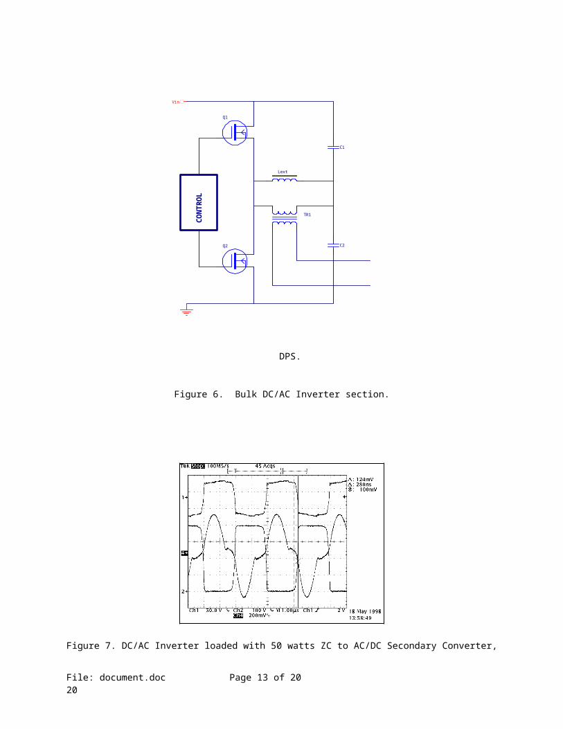
DC/AC Inverter Bulk Front-End with Zero-Voltage switching is an ideal solutionfor generating controllable Soft Switching bus voltage waveforms. The ACtrapezoidal waveform voltage can be generated in the front-end converter by ahalf (or full) bridge converter where the transitions of the peak voltagesfrom rail-to-rail are set by the Voltage Mode resonant loop formed by the sumof the node capacitance and the inductance of external ZV mode choke. Thus,the slew rate of that voltage does not depend on load changes. The simplifiedschematic and the corresponding switching node waveforms are shown in Figures6 and 7. The inverter stage replaces the bulk front-end DC/DC converter andtogether with the Power Factor Correction in front provides peak-to-peakvoltage regulation of the line to provide a minimum need for post regulationat the loads. The trapezoidal wave is an improvement over other square wavedistribution systems, with approximately 5-15% transition duty cycle requiringsmall filter sections, limiting dV/dt for reduced EMI and transient effects.Shielded bus transmissions line techniques or twisted pair technique areappropriate ways to reduce furthermore still radiated EMI fields in thebackplane where needed. A design goal of less than +/-2% line/load regulationof the AC Bus including ripple and noise that can be achieved by the PFC lineregulator, controlling the DC bus (usually 400V) to maintain the invertertransformer output voltage to +/-48Vpeak triangle wave on the AC-DPS bussystem backplane. Additional sensing of the backplane peak voltage can beadded to the PFC voltage loop control if required.
EMI Considerations: EMI radiation with square or rectangular wave power
document.doc Page 4 of 20

distribution is an obvious concern. The use of a trapezoid wave is animprovement over the pure square wave for harmonic content. Noise sourceenergy is minimized with Zero Voltage and Zero Current topologies that arechoices at the Bulk Inverter stage and Secondary Converter stages of theproposed AC distribution system. In fact, this AC-DP System is a directderivative from the innovative designs reported in [5,6,10 and 13]. If isnecessary, the transmission line can be additionally shielded from radiationin coaxial or shielded PC power planes or strip transmission line [1, 4].
Load Regulation: Post regulation and filtering complexities are minimizedwith the regulated AC trapezoid input waveform. Small high frequencytransformers isolate the power at each board or load area, with secondaryrectifier filters for each voltage requirement. Synchronous rectifiers canalso be incorporated to improve efficiency. Load voltage accuracy andregulation can be held within +/-5% with proper design to eliminate postregulation to some loads [1][2]. For other load, requirements a variety ofdifferent low-cost post regulator designs could be used [1]. Mostapplications will favor using low dropout regulators (LDOs), Mag-Amps, and aZero-Current Fully Regulated (ZC) Resonant Converters, to supplement the ZeroVoltage switching of AC/DC Bulk Converter. Another choice good choice is asecondary controlled synchronous rectifier PWM. Typical board or loadregulators for the DC-DPS are shown in Figure 3, and a variety of choices areshown for the AC-DPS are shown in Figures 4, 5, 10, 11, and 12.
Simple Transformer Rectifier as Low Cost Secondary Converter: The bipolartrapezoidal wave from a transformer secondary of the AC-DPS bus provides goodline regulation of about 3-6% load dependent DC voltage after a rectifierstage. This is accomplished with low copper and core loss transformer designsand robust sizing of rectifiers for low dynamic resistance for small forwardvoltage changes with load current changes. The cost of this simpletransformer/rectifier/filter is 5 to 10 times lower than the price of “bricks”in the DC-DPS counterpart. This design has no stability concerns from aregulator loop control or negative impedance effects on the input filter ordistributed filters. Also, the filter size is smaller because of a fixed 85-95% duty cycle, with no ride-through time requirement for PWM step recoverytime from load step response.
However, there may be a need for ride-through or holdup time in fault tolerantsystem designs with energy storage for fuse fault clearing that can drop thebus voltage. This energy storage will be at the lower end-point voltage levelversus the at intermediate DC level in a DC-DPS, thereby requiring morecapacitance.
The bipolar waveform can use self driven synchronous rectifiers for half-wave(42.5% to 47.5% duty) or full-wave rectification (85% to 95% duty) as shown inFigures 10,11.and 12. The catch or free-wheeling rectifier in the full-waverectifier circuit can use a standard Schottky diode in place of a FET
document.doc Page 5 of 20

synchronous rectifier, with little effect on efficiency because of the highduty cycle, therefore the low conduction time.
Synchronous Rectifier PWM Secondary Converter: The bipolar trapezoidal wavefrom a transformer secondary from the AC-DPS bus can be post regulated withphase modulated synchronous rectifier switches with PWM secondary control.The bipolar waveform precludes a typical synchronous rectifier phasemodulation, but can be controlled with MOSFETs switched in pairs as bi-directional switches for blocking and conducting.
Mag-Amp PWM based Secondary Converter: The well known Magnetic Amplifier isperfectly suited for AC-DPS post regulation function. One consideration is invery high current and low voltage applications, where the effects oftransmission line and transformer leakage reduce the maximal output powercapability to the load. But this solution is one of the simplest andeffective to perform the load regulation on a particular DC output, especiallywhen the output voltage needs to be tightly regulated for the modern fastCPUs.
ZC Phase-Modulated Resonant Converter: This is one or the best postregulation choices because it is the only way to eliminate the negative effectof noted distributed line inductance plus the leakage inductance of thetransformer(s). Here a controllable series resonant loop is formed by the sumof all and the series resonant capacitor are used. The resonant loop can becontrolled by primary side magnetic amplifier or by phase-modulated electronicswitch at constant frequency and duty ratio. The Zero Voltage and Zero Currentswitching and the way to achieve control over the power transfer between inputand output of such a resonant system are well described in [5,10,11 and 13].A magnetic amplifier control can be used as a simple control of the resonantpower transfer as shown in [9].
Low Dropout (LDO) Regulator based Secondary Converter: The bipolar trapezoidalwaveform from a transformer secondary of the AC-DPS bus provides regulated 3-6% DC voltage after a rectifier stage. It is easy to use the line regulatedonly bus voltage as a regulated headroom voltage for an LDO. This is aninexpensive regulator, often using a standard 3-terminal regulator. Withregulated headroom, efficiency is competitive to DC/DC converters, with up to84% efficiency at 3.3V output and 70% overall including the rectifiers [3].This is an attractive solution to critical loads requiring low noise and tightregulation tolerances. The high speed dynamic response, tight regulationaccuracy, low ripple and noise of the LDO linear regulator can provide thebest power quality with the least filtering requirements at the lowest costand smallest board space for critical loads as the new CPUs and support chips[3].
Pentium II Synchronous Buck Converter modified for AC-DPS Secondary Converter:A version of a Secondary DC/DC post regulator for an AC-DPS can be build using
document.doc Page 6 of 20

synchronous switching regulator from the Buck topology. The AC bus voltage ofthe AC DPS can be transformed and rectified to DC voltage via small HFtransformer and simple full-wave rectifier/filter. The output DC voltage ispost regulated for load changes, where the AC input line is stabilized at theAC Bus voltage by the PFC/Inverter stage. To achieve a precise stabilized andprogrammable DC output as is required by the latest generation of Pentium IICPUs and the next generation, is a highly efficient synchronous switchingregulator as an appropriate solution.
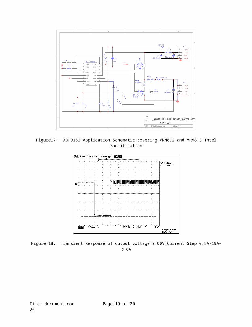
An example of such a controller is the ADP3152 from Analog Devices, speciallyoptimized to supply Pentium II Processors, having a 5-bit DAC to read avoltage identification code directly from the processor. This controllermeets Intel’s stringent transient specifications VRM8.2 and VRM8.3, andpossesses the minimum number of output capacitors and the smallest footprint.The application schematic is given in Figure 17. The transient response isshown in Figure 18 for the step 0.8A-19A-0.8A with optimal compensation,reported in the Proceedings of IEEE APEC’98 [12].
AC-DPS PROOF-OF-CONCEPT PROTOTYPE
AC-DPS Prototype: An AC-DPS proof-of-concept and practical implementation prototype was built for the purpose of fine tuning the design procedure and totest and debug the AC solution from both the theoretical and practical point of view. The input voltage is Worldwide 85 to 265 VAC to an active PFC AC/DC converter. The output power is only a demonstration level of 250W, the outputDC/AC inverter provides an AC Bus at +/-48VAC peak trapezoidal waveform at 250KHz. Three secondary post regulators were tested, a Mag-Amp PWM, a ZC Resonant Converter, and an LDO.
Prototype Test Results: Prototype test results from a prototype 250W systemwith 250kHz AC bus 48V DPS have shown excellent performance, minimum crossregulation and efficiency of 81% from AC bus to multiple +5V, +12V and +24Voutputs. Figures 13 to 16 show the performance of the prototype and itsswitching waveforms to demonstrate the cancellation effect of ZV and ZCswitching on transmission line impedances. A power distribution to threeremote loads with up to 5 to 7 foot cable lengths was used to demonstrate theproper operation under the worst-case bus parasitics.
Cost Comparisons and AC-DPS Saving: A price comparison of a typical DC-DPSsystem versus an AC-DPS system at 600W is shown in Table 1, with a 37% overallsystem cost saving (with a 55% reduction in components cost for the SecondaryModules) for the AC-DPS. The comparison was made as objective as possible,using the standard components and off-the-shelf products of well-known powersupply companies. The reduction in complexity and by the conversion to ACdistribution reflected the lower component and labor price at both modular andsystem level.
document.doc Page 7 of 20

CONCLUSION
The advantages of an AC-DPS have been shown to include savings and advantagesin cost, board space, component parts, complexity, and reliability, plus theuse of distributed DC/DC converters bricks can be avoided. Flexible andsimple power design changes can be implemented as needed with minimum impacton cost and schedule. The addition of another voltage or increasing theoutput power for a board upgrade is as simple as adding a new transformerwinding and changing the rectifier/filter section.
From the brief description of an advanced AC-Distributed Power System, theauthors have shown an improved alternate method to distributed power todifferent PCB’s, modules, and loads that are used in a variety of modernelectronic equipment. A price comparison between two as parameters typical ACand DC based Distributed Power Systems has been shown, giving 37% lower costin favor to the AC-DPS.
A proof-of-concept 250W prototype was built for 250KHz operation, with goodoperating results. This fully functional AC-DPS delivered 250W to threeremote loads, using three different post regulator secondary converters, withadditional features of the Soft Switching AC Power Distribution. Theadvantages are shown at the boards or point-of-use loads, with the eliminationof many DC/DC converters to lower costs, weight, complexity, filtersrequirements, board space, qualification costs, second source requirements,reliability, design risk, and faster time-to-market schedules.
With the DC-DPS and its variations [1] as the accepted standard replacement tothe centralized power distribution systems, the AC-DPS will find the typicalresistance to acceptance and change. Replacement of arrays of DC/DC converter“bricks” in systems with simpler and lower cost regulated solutions is adrastic concept. The strong incentive for lower cost, smaller board space,lower parts count, and fast time-to-market with low risk designs should proveas an incentive to consider the AC-DPS for new designs.
REFERENCES
[1] D. Arduini, “Distributed Power System using AC to solve DC Distributed Power Problems,” HPFC 1995.
[2] D. Arduini, ”A Distributed Power System with a Low-Cost Universal DC/DC Converters”, Power Conversion Electronics 1995 Conference.
[3] D. Arduini, “A DC/DC Converter Using a PWM/LDO “Hybrid” for Low Voltage Power Solutions,”
document.doc Page 8 of 20

Power Conversion Electronics 1995 Conference.
[4] R.Watson, W.Chen, G.Hua and F.C.Lee, ”Component Development for a High-Frequency AC Distributed Power System,” Proceedings of IEEE 1996, pp.657-663.
[5] Angel Gentchev, ”A New Low Noise Multiresonant Converter,” Proceedings of PCIM’92Conference in Nurnberg, Germany, pp.419-427.
[6] M. Jovanovic, R. Farrington and F. C. Lee, ”Comparison of Half-Bridge, ZCS-QRC and ZVS-MRC,” IEEE Transactions on Aerospace and Electronic Systems, Vol. 26, No.2. pp.326-336, March 1990.
[7] Per Lindman and Lars Thorsell, ”Applying Distributed Power Modules in Telecom Systems,” Proceedings of IEEE-PESC’94, pp.777-785.
[8] Barry Arbetter and Dragan Maksimovic, ”DC-DC Converter with Fast Transient Response and High Efficiency for Low-Voltage Microprocessor Loads,” Proceedings of IEEE-APEC’98.
[9] A.S.Kislovski, ”Linear Variable Inductor in power processing,” Proceedings of APEC’87, pp.87-92.
[10] Kosuoke Harada and Katsuaki Murata, ”Controlled Resonant Converters with Switching Frequency Fixed,” Proceedings of IEEE-PESC’87, pp.431-438.
[11] A.H.Weinberg and L.Ghislanzoni, ”A new Zero Voltage and Zero Current Power Switching Technique,” Proceedings of IEEE-PESC’89, pp.909-919.
[12] Richard Redl, Brian Erisman and Zoltan Zansky, “Optimizing the Load Transient Response of the Buck Converter”, IEEE APEC’98, p.170-p.177.
[13] Angel Gentchev, “A Novel Fully Stabilized Multiresonant Converter”, Proceedings of PCIM’93, Nuerberg, Germany, p. – p.
document.doc Page 9 of 20

Figure 1. Typical DC-DPS with efficiencies.
Figure 2. Typical AC-DPS with efficiencies.
File: document.doc Page 10 of 2020
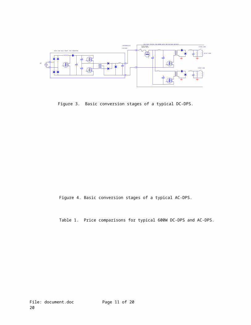
Figure 3. Basic conversion stages of a typical DC-DPS.
Figure 4. Basic conversion stages of a typical AC-DPS.
Table 1. Price comparisons for typical 600W DC-DPS and AC-DPS.
File: document.doc Page 11 of 2020
HIGH SIDE BULK FRONT- END CONVERTER
AC
INTERMEDIATE LOW SIDE TIPICAL PCB BOARD WITH TWO VOLTAGE OUTPUTS
VOLTAGEFILTER INRUSH CONTROL SWITCH FIXED LOAD
dI/dT LOAD
FIXED LOAD
FILTER
POWER
AC/DC RECTIFIER
~/=PFC
=/=DC/DC CONVERTER
=/=
DC/DC CONVERTERS OUTPUTFILTER
LARGE VALUECAP
LARGE VALUECAP
ISOLATION TRANSFORMERS
dI/dT LOAD
AC
AC/DC RECTIFIER~/=
PFC
=/=DC/AC CONVERTER
=/
AC/DC CONVERTER OUTPUT FILTERS
LOW VALUECAP
LOW VALUECAP
ISOLATION TRANSFORMERS
FIXED LOAD
FIXED LOAD
dI/dT LOAD
dI/dT LOAD

Figure 5. DPS conversion stage comparisons choices for typical DC-DPS and AC-
File: document.doc Page 12 of 2020
Vin
Vin
48V DC
DC - DPS
INRUSH CONTROL EMI FILTER DC/DC PEM CONVERTER i
Vi
VnDC/DC PEM CONVERTER n
LDO
AC - DPS
Vin
Vin
48V AC
QUASI-SINUS WAVE
V1LINE REGULATION ONLY 5% LINE-LOAD REGULATION
V2
V2
LINE REGULATION ONLY 5% LINE-LOAD REGULATION
V3
V4
V5
5V .1%
.1%
.1%
MAG. AMP
SYNCHRONOUS
RECTIFIER
STABILISED
SYNCHRONOUSCONVERTER
STABILISED
RECTIFIER
V6 .1%
V7
V8
BASIC POINT OF USE REGULATION DESIGN CHOICES
Figure.7
DPS.
Figure 6. Bulk DC/AC Inverter section.
Figure 7. DC/AC Inverter loaded with 50 watts ZC to AC/DC Secondary Converter,
File: document.doc Page 13 of 2020
TR1
Lext
Q1
Q2
C1
C2
CONTROL
Vin
AC BUS
400 VDC
Figure.5

CH1 is AC BUS Voltage, CH2 is a Switching Node Voltage of the DC/ACConverter,
CH4 is the AC BUS Current supplying Zero Current AC/DC Secondary Converter.
Figure 8. Prototype ZC AC/DC converter.
File: document.doc Page 14 of 2020
F1
Q
R2
R1
D1
D2
C2
R3
R5
R6
R4
C4
C5
VR1
INPUT 48VAC/250kHz
DC OUTPUT
Stabilized AC/DC Converter
T2
T1
C1
C3

Figure 9. Prototype Mag-Amp AC/DC converter.
Figure 10. Self-driven half-wave synchronous rectifier/filter secondary powersupply.
File: document.doc Page 15 of 2020
T
F1
L1
L2
CR1
CR2
L3
Q
R2R1
D2D1
C2 C3
R3
R4
R6
R7
R5
C1
C4
VR1
INPUT 48VAC/250kHzDC OUTPUT
Stabilized AC/DC Converter
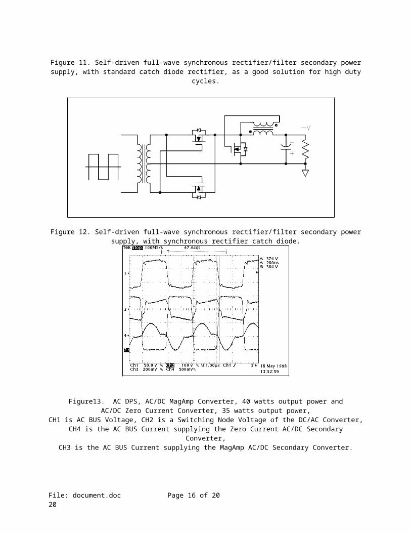
Figure 11. Self-driven full-wave synchronous rectifier/filter secondary powersupply, with standard catch diode rectifier, as a good solution for high duty
cycles.
Figure 12. Self-driven full-wave synchronous rectifier/filter secondary powersupply, with synchronous rectifier catch diode.
Figure13. AC DPS, AC/DC MagAmp Converter, 40 watts output power andAC/DC Zero Current Converter, 35 watts output power,
CH1 is AC BUS Voltage, CH2 is a Switching Node Voltage of the DC/AC Converter,CH4 is the AC BUS Current supplying the Zero Current AC/DC Secondary
Converter,CH3 is the AC BUS Current supplying the MagAmp AC/DC Secondary Converter.
File: document.doc Page 16 of 2020

Figure 14. AC DPS, AC/DC MagAmp Converter at 40 watts output power andAC/DC Zero Current Converter at zero watts output power,CH1 is AC BUS Voltage at the Secondary Converter Input,CH2 is a Switching Node Voltage of the DC/AC Converter,
CH4 is the AC BUS Current supplying the Zero Current AC/DC SecondaryConverter,
CH3 is the AC BUS Current supplying the MagAmp AC/DC Secondary Converter.
Figure 15. AC DPS, AC/DC MagAmp Converter at zero watts output power andAC/DC Zero Current Converter at 35 watts output power,
File: document.doc Page 17 of 2020

CH1 is AC BUS Voltage, CH2 is a Switching Node Voltage of the DC/AC Converter,CH3 is the AC BUS Current supplying the Zero Current AC/DC Secondary
Converter,CH4 is the AC BUS Current supplying the MagAmp AC/DC Secondary Converter.
Figure16. AC DPS, both AC/DC MagAmp Converter andAC/DC Zero Current Converter are at zero watts output power,
CH1 is AC BUS Voltage, CH2 is a Switching Node Voltage of the DC/AC Converter,CH3 is the AC BUS Current supplying the Zero Current AC/DC Secondary
Converter,CH4 is the AC BUS Current supplying the MagAmp AC/DC Secondary
Converter.
File: document.doc Page 18 of 2020
1 2 3 4
A
B
C
D
4321
D
C
B
ATitle
Number RevisionSize
C
Date: 2-Apr-1998 Sheet of File: C:\ADP315~1\ADP3152R.SCH Drawn By:
Q5IRL3803
Q6IRL3803
C3200pFC11
1nF
C101nF
R5220
R4220
C122uF
C2
6.2nF
R12 2.5mOm, 1W
C74x1500uF/6.3V
R610
0K
D11N5822
PGOOD
12345 6
78910
S1
L2 1uH
C12100uF/6.3v
VID0 16
P-GND 15
DRIVE1 14
DRIVE2 13
VID11
VID22
VID33
VID44
AGND5
SD6 PWRGD 11
Vin 12
CMP 10
Ct 9
SENSE-7
SENSE+8
U1 ADP3152
FBEAD2643000101
22
33
44
12Vin
5Vin
5VRTN
12VRTN
11
JP1
R110k
R747
k
R14 10
C88x1500uF/6.3V
11
22
33
44
VccP
VccP
Vss
Vss
JP2
SD
L13.3uH
Enhanced power option 2.0V/0-19AADP3152
Figure17. ADP3152 Application Schematic covering VRM8.2 and VRM8.3 IntelSpecification
Figure 18. Transient Response of output voltage 2.00V,Current Step 0.8A-19A-0.8A
File: document.doc Page 19 of 2020

File: document.doc Page 20 of 2020