
AN-2292 Designing an Isolated Buck (Fly-Buck) Converter
12
Application Report SNVA674C – August 2012 – Revised December 2014 AN-2292 Designing an Isolated Buck (Fly-Buck) Converter Vijay Choudhary ABSTRACT In many applications, one or more low-cost, simple to use, isolated power supplies working from input voltages up to 100 V are needed. Traditional solutions use flyback converters to generate this bias supply. Flyback designs typically utilize asymmetric transformers turns ratios for primary and secondary power windings, with an optocoupler and reference, or an auxiliary winding for feedback regulation. Additionally, flyback converters need an elaborate compensation design for stability. This results in a tedious design process, bulky solution, with a higher component count and cost. An isolated buck converter (Fly-Buck) uses a synchronous buck converter with coupled inductor windings to create isolated outputs. Isolated converters utilizing Fly-Buck topology use a smaller transformer for an equivalent power transfer as the transformer primary and secondary turns ratios are better matched. There is no need for an optocoupler or auxiliary winding as the secondary output closely tracks the primary output voltage, resulting in smaller solution size and cost. This article presents the basic operating principle of an isolated buck converter. The operating current and voltage waveforms are explained and design equations are derived. The design example shows a step-by- step procedure for designing a practical two-output 3 W isolated buck converter. Contents 1 Fly-Buck Converter .......................................................................................................... 1 2 Maximum Output Current Equations ...................................................................................... 4 3 Design Example.............................................................................................................. 5 4 Conclusions ................................................................................................................. 10 5 References .................................................................................................................. 10 List of Figures 1 Complete Schematic for an LM5017–Based Isolated Converter ...................................................... 9 2 Efficiency at 750 kHz, V OUT1 = 10 V ........................................................................................ 9 3 Steady State Waveform (V IN = 48 V, I OUT1 = 100 mA, I OUT2 = 200 mA) ................................................ 9 4 Step Load Response (V IN = 48 V, I OUT1 = 0, Step Load on I OUT2 = 100 mA to 200 mA). ............................ 9 List of Tables 1 Isolated Buck Regulator Design Equations .............................................................................. 5 2 Component Calculation/Selection Steps for a Two-Output Isolated Buck ........................................... 6 1 Fly-Buck Converter An isolated buck converter, also known as Fly-Buck converter, is created by replacing the output filter inductor (L1) in a synchronous buck converter with a coupled inductor (X1) or flyback-type transformer, and rectifying the secondary winding voltage using a diode (D1) and a capacitor (C OUT2 ). The topology can be extended to any number of isolated secondary outputs. It also can be used to generate one or more inverting outputs. All trademarks are the property of their respective owners. 1 SNVA674C – August 2012 – Revised December 2014 AN-2292 Designing an Isolated Buck (Fly-Buck) Converter Submit Documentation Feedback Copyright © 2012–2014, Texas Instruments Incorporated
-
Upload
khangminh22 -
Category
Documents
-
view
3 -
download
0
Transcript of AN-2292 Designing an Isolated Buck (Fly-Buck) Converter
Application ReportSNVA674C–August 2012–Revised December 2014
AN-2292 Designing an Isolated Buck (Fly-Buck) Converter
VijayChoudhary
ABSTRACTIn many applications, one or more low-cost, simple to use, isolated power supplies working from inputvoltages up to 100 V are needed. Traditional solutions use flyback converters to generate this bias supply.Flyback designs typically utilize asymmetric transformers turns ratios for primary and secondary powerwindings, with an optocoupler and reference, or an auxiliary winding for feedback regulation. Additionally,flyback converters need an elaborate compensation design for stability. This results in a tedious designprocess, bulky solution, with a higher component count and cost.
An isolated buck converter (Fly-Buck) uses a synchronous buck converter with coupled inductor windingsto create isolated outputs. Isolated converters utilizing Fly-Buck topology use a smaller transformer for anequivalent power transfer as the transformer primary and secondary turns ratios are better matched.There is no need for an optocoupler or auxiliary winding as the secondary output closely tracks theprimary output voltage, resulting in smaller solution size and cost.
This article presents the basic operating principle of an isolated buck converter. The operating current andvoltage waveforms are explained and design equations are derived. The design example shows a step-by-step procedure for designing a practical two-output 3 W isolated buck converter.
Contents1 Fly-Buck Converter .......................................................................................................... 12 Maximum Output Current Equations ...................................................................................... 43 Design Example.............................................................................................................. 54 Conclusions ................................................................................................................. 105 References .................................................................................................................. 10
List of Figures
1 Complete Schematic for an LM5017–Based Isolated Converter ...................................................... 92 Efficiency at 750 kHz, VOUT1 = 10 V........................................................................................ 93 Steady State Waveform (VIN = 48 V, IOUT1 = 100 mA, IOUT2 = 200 mA) ................................................ 94 Step Load Response (VIN = 48 V, IOUT1 = 0, Step Load on IOUT2 = 100 mA to 200 mA). ............................ 9
List of Tables
1 Isolated Buck Regulator Design Equations .............................................................................. 52 Component Calculation/Selection Steps for a Two-Output Isolated Buck ........................................... 6
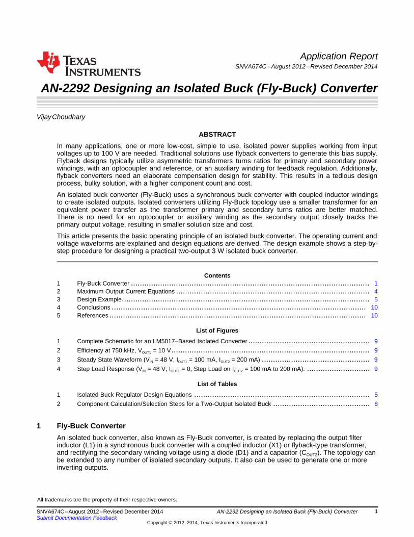
1 Fly-Buck ConverterAn isolated buck converter, also known as Fly-Buck converter, is created by replacing the output filterinductor (L1) in a synchronous buck converter with a coupled inductor (X1) or flyback-type transformer,and rectifying the secondary winding voltage using a diode (D1) and a capacitor (COUT2). The topology canbe extended to any number of isolated secondary outputs. It also can be used to generate one or moreinverting outputs.
All trademarks are the property of their respective owners.
1SNVA674C–August 2012–Revised December 2014 AN-2292 Designing an Isolated Buck (Fly-Buck) ConverterSubmit Documentation Feedback
Copyright © 2012–2014, Texas Instruments Incorporated
VIN xN2N1
N2N1
VOUT2 = VOUT1 - VF
VOUT1 = TON
VIN = D x VINTON + TOFF
VOUTQ1
SW
Q2
VIN L1
COUT
N1
N2
VOUT2
VOUT1
VIN
Q1SW
Q2
X1
COUT1
COUT2D1
1a) A Synchronous Buck Converter
1b) An Isolated Buck Converter (Fly-buck)
Fly-Buck Converter www.ti.com
Creating an Isolated Buck Converter by Modifying a Synchronous Buck Converter
The primary output voltage equation is identical to a buck converter and is given by Equation 1:
(1)
and the secondary output voltage is given by Equation 2:
(2)
where VF is the forward voltage drop of the secondary rectifier diode, and N1, N2 are the number of turnsin the primary and secondary windings, respectively. The secondary output (VOUT2) closely tracks theprimary output voltage (VOUT1) without the need for additional transformer winding or an optocoupler forfeedback across the isolation boundary.
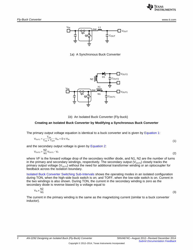
Isolated Buck Converter Switching Sub-Intervals shows the operating modes in an isolated configurationduring TON, when the high-side buck switch is on; and TOFF, when the low-side switch is on. Current inthe two windings is also shown. During TON, the current in the secondary winding is zero as thesecondary diode is reverse biased by a voltage equal to
(3)
The current in the primary winding is the same as the magnetizing current (similar to a buck converterinductor).
2 AN-2292 Designing an Isolated Buck (Fly-Buck) Converter SNVA674C–August 2012–Revised December 2014Submit Documentation Feedback
Copyright © 2012–2014, Texas Instruments Incorporated
SW1
IL1
GND
SW2
IL2
TON TOFF
VOUT2IGND
VOUT2
VOUT1
VIN
Q1
SW
IL1 = IM
IL2 = 0
COUT1
COUT2
IMQ2
VOUT2
VOUT1
VINSW
Q2
COUT2
COUT1
IL2
IL1 = IM + I
IM
IL2'
2a) TON (Q1: ON, Q2: OFF)
2b) TOFF (Q1: OFF, Q2: ON)
www.ti.com Fly-Buck Converter
Creating an Isolated Buck Converter by Modifying a Synchronous Buck Converter (continued)
Isolated Buck Converter Switching Sub-Intervals
During TOFF, the current in the secondary winding is decided by the resonant tank formed by COUT1, theleakage inductance of the coupled inductor, and COUT2. The current in the primary winding is the sum ofthe magnetizing current (similar to a buck converter inductor current), and the reflected current from thesecondary winding. These operating waveforms are shown in Isolated Buck Operating Waveforms.
Isolated Buck Operating Waveforms
3SNVA674C–August 2012–Revised December 2014 AN-2292 Designing an Isolated Buck (Fly-Buck) ConverterSubmit Documentation Feedback
Copyright © 2012–2014, Texas Instruments Incorporated
(VIN (MAX) ± VOUT)L1 x fSW
'IL1 =VOUT
VIN (MAX)
'IL1
2IOUT1 + IOUT2 = ILIM (MIN) -N2N1
'IL1
2IOUT1 + IOUT2 = ILIM (MIN) -
isw(peak) = iL1(peak) = IL1 + IL2 +'IL1 + 'IL2
2'IL1
2= IOUT1 + IOUT2 +
+
VOUT1
COUT1
+
VOUT2D1
COUT2
N1:
N2
SW1
SW2
L1
L2
IOUT2
IOUT1
IL1
IL2
IL2 = IOUT2
IL1 = IOUT1
Maximum Output Current Equations www.ti.com
Isolated Buck Operating Waveforms (continued)
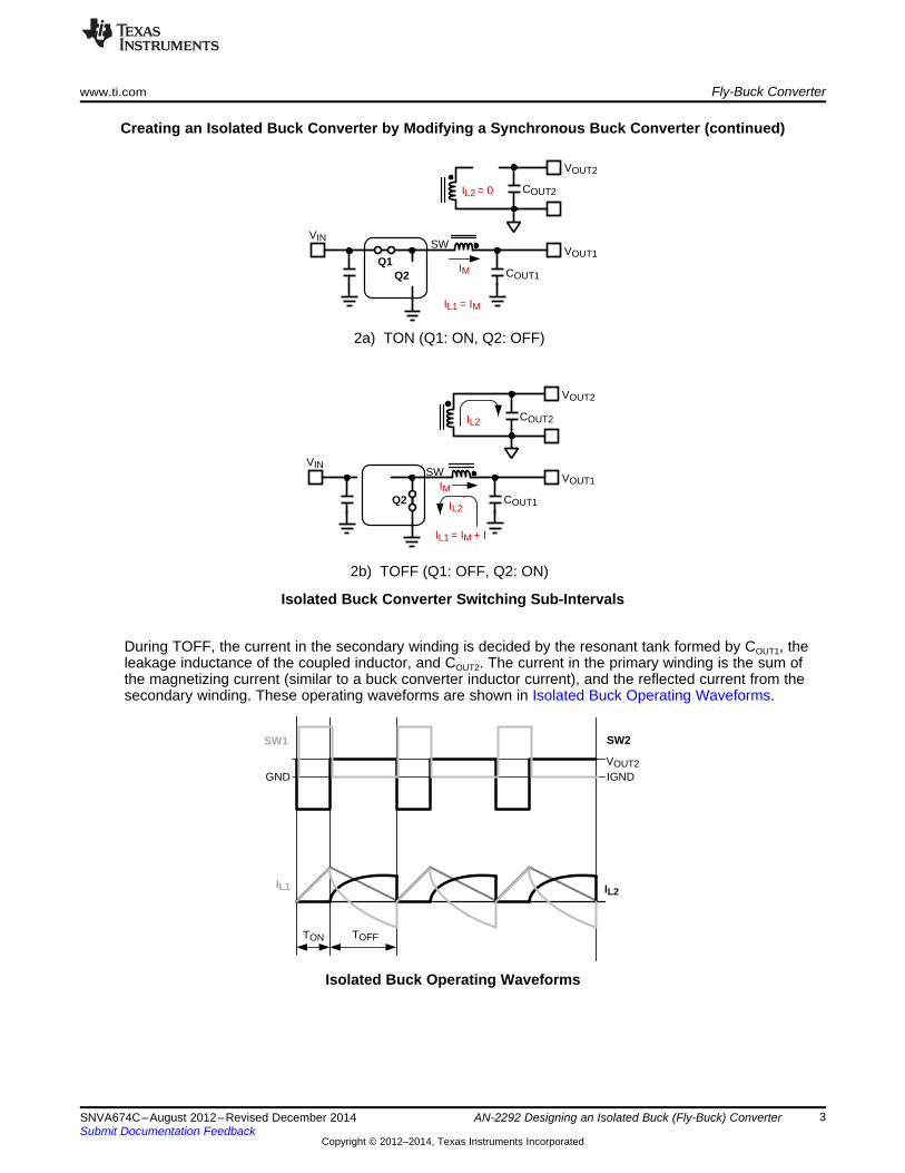
2 Maximum Output Current EquationsOn a cycle-by-cycle average basis, the winding and output currents have the following relationshipIsolated Buck Output Stage with Coupled Inductor.
(4)
and(5)
Isolated Buck Output Stage with Coupled Inductor
The combined inductor current waveform (iL1+ iL2), which is equal to the magnetizing current, is identical toa buck converter. The peak inductor and switch current during on-time is given by Equation 6:
(6)
where we make use of the fact that during on-time (TON) there is no current in secondary winding.Therefore, the maximum total load current is given by Equation 7:
(7)
where the total load current is defined as the sum of the load currents at the two outputs. For turn-ratios(N2/N1) not equal to unity, IOUT2 should be multiplied by the turn-ratio in Equation 7, shown here inEquation 8:
(8)
The maximum peak-to-peak current ripple in the primary winding is given by Isolated Buck Regulator withThree Outputs:
(9)
4 AN-2292 Designing an Isolated Buck (Fly-Buck) Converter SNVA674C–August 2012–Revised December 2014Submit Documentation Feedback
Copyright © 2012–2014, Texas Instruments Incorporated
(VIN (MAX) ± VOUT)L1 x fSW
'IL1 =VOUT
VIN (MAX)
IOUT2 + isw(peak) = iL1(peak) = IOUT1 +N2N1
N3N1
'IL1
2IOUT3 +
IL3 = IOUT3
IL2 = IOUT2
IL1 = IOUT1
VOUT3 = VOUT1 - VFN3N1
VOUT2 = VOUT1 - VFN2N1
VOUT1 = TON
VIN = D x VINTON + TOFF
N1
N2
N3
VOUT3
VOUT2
VOUT1
VIN
Q1SW
Q2
X1
COUT1
COUT2
COUT3
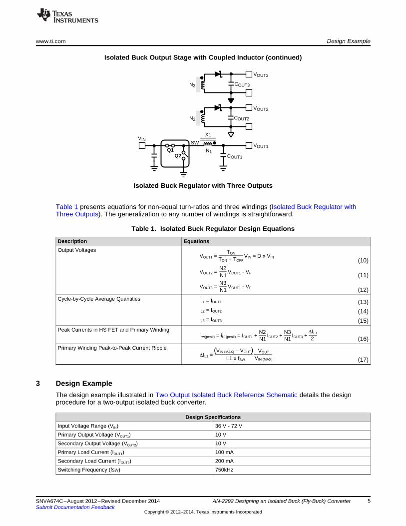
www.ti.com Design Example
Isolated Buck Output Stage with Coupled Inductor (continued)
Isolated Buck Regulator with Three Outputs
Table 1 presents equations for non-equal turn-ratios and three windings (Isolated Buck Regulator withThree Outputs). The generalization to any number of windings is straightforward.
Table 1. Isolated Buck Regulator Design Equations
Description EquationsOutput Voltages
(10)
(11)
(12)Cycle-by-Cycle Average Quantities (13)
(14)(15)
Peak Currents in HS FET and Primary Winding
(16)Primary Winding Peak-to-Peak Current Ripple
(17)
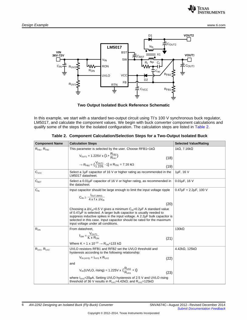
3 Design ExampleThe design example illustrated in Two Output Isolated Buck Reference Schematic details the designprocedure for a two-output isolated buck converter.
Design SpecificationsInput Voltage Range (VIN) 36 V - 72 VPrimary Output Voltage (VOUT1) 10 VSecondary Output Voltage (VOUT2) 10 VPrimary Load Current (IOUT1) 100 mASecondary Load Current (IOUT2) 200 mASwitching Frequency (fsw) 750kHz
5SNVA674C–August 2012–Revised December 2014 AN-2292 Designing an Isolated Buck (Fly-Buck) ConverterSubmit Documentation Feedback
Copyright © 2012–2014, Texas Instruments Incorporated
VIN (UVLO, rising) = 1.225V x RUV2 + 1)(RUV1
VIN (HYS) = IHYS x RUV2
VOUT1fSW = .x RON
CIN t IOUT (MAX)
x f x 'VIN4
x RFB1 = 7.16 k:VOUT1
:RFB2 = 1.225- 1)(
)RFB2VOUT1 = 1.225V x ( RFB11+
+
+
+
+
VIN
BST
RON
RTN
SW
VCC
FB
UVLO
VINVOUT1
VOUT2
RFB1
RUV1
RON
COUT1
CBST
D1
CIN
COUT2
RFB2
RUV2
X1
Rr NP
NSLM5017
CVCC+
D2
36V-72V
Cr
Cac
Design Example www.ti.com
Two Output Isolated Buck Reference Schematic
In this example, we start with a standard two-output circuit using TI’s 100 V synchronous buck regulator,LM5017, and calculate the component values. We begin with buck converter component calculations andqualify some of the steps for the isolated configuration. The calculation steps are listed in Table 2.
Table 2. Component Calculation/Selection Steps for a Two-Output Isolated Buck
Component Name Calculation Steps Selected Value/RatingRFB1, RFB2 This parameter is selected by the user. Choose RFB1=1kΩ 1kΩ, 7.16kΩ
(18)
(19)CVCC Select a 1µF capacitor of 16 V or higher rating as recommended in the 1µF, 16 V
LM5017 datasheet.CBST Select a 0.01µF capacitor of 16 V or higher rating, as recommended in 0.01µF, 16 V
the datasheet.CIN Input capacitor should be large enough to limit the input voltage ripple 0.47µF + 2.2µF, 100 V
(20)Choosing a ΔVIN=0.5 V gives a minimum CIN=0.2μF A standard valueof 0.47μF is selected. A larger bulk capacitor is usually needed tosuppress inductive spikes in the input voltage. A 2.2μF bulk capacitor isselected in this case. Input capacitor should be rated for the maximuminput voltage under all conditions.
RON From datasheet, 130kΩ
(21)Where K = 1 x 10⁻¹⁰ → RON=133 kΩ
RUV1, RUV2 UVLO resistors RFB1 and RFB2 set the UVLO threshold and 4.42kΩ, 125kΩhysteresis according to the following relationship:
(22)and
(23)where IHYS=20μA. Setting UVLO hysteresis of 2.5 V and UVLO risingthreshold of 36 V results in RUV1=4.42kΩ; and RUV2=125kΩ
6 AN-2292 Designing an Isolated Buck (Fly-Buck) Converter SNVA674C–August 2012–Revised December 2014Submit Documentation Feedback
Copyright © 2012–2014, Texas Instruments Incorporated
N2N1
VD1 = VIN
N2N1
VOUT2 = VOUT1 - VF | 9.3V
(VIN (MAX) ± VOUT)L1 x fSW
'IL1 =VOUT
VIN (MAX)
(VIN (MAX) ± VOUT)'IL1 x fSW
L1 =VOUT
VIN (MAX)= 14.4 PH
N1'IL1 = (0.7 - IOUT1 - IOUT2 x
N2) x 2 = 0.8A
www.ti.com Design Example
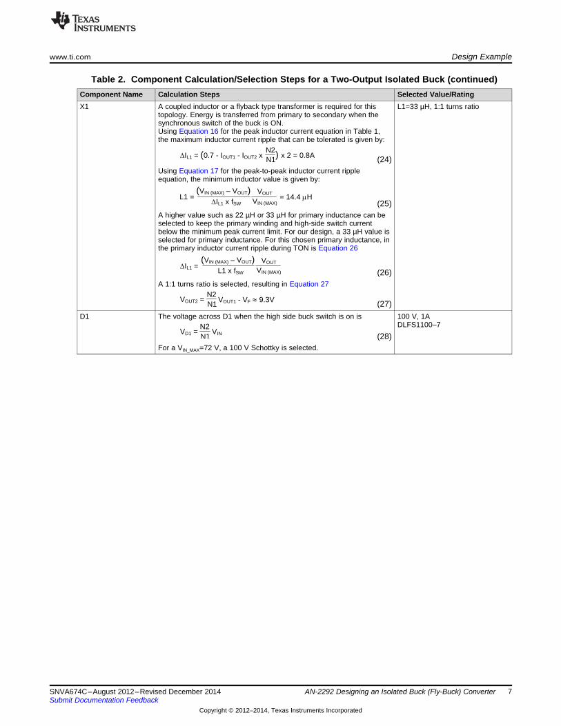
Table 2. Component Calculation/Selection Steps for a Two-Output Isolated Buck (continued)Component Name Calculation Steps Selected Value/RatingX1 A coupled inductor or a flyback type transformer is required for this L1=33 µH, 1:1 turns ratio
topology. Energy is transferred from primary to secondary when thesynchronous switch of the buck is ON.Using Equation 16 for the peak inductor current equation in Table 1,the maximum inductor current ripple that can be tolerated is given by:
(24)Using Equation 17 for the peak-to-peak inductor current rippleequation, the minimum inductor value is given by:
(25)A higher value such as 22 µH or 33 µH for primary inductance can beselected to keep the primary winding and high-side switch currentbelow the minimum peak current limit. For our design, a 33 µH value isselected for primary inductance. For this chosen primary inductance, inthe primary inductor current ripple during TON is Equation 26
(26)A 1:1 turns ratio is selected, resulting in Equation 27
(27)D1 The voltage across D1 when the high side buck switch is on is 100 V, 1A
DLFS1100–7(28)
For a VIN_MAX=72 V, a 100 V Schottky is selected.
7SNVA674C–August 2012–Revised December 2014 AN-2292 Designing an Isolated Buck (Fly-Buck) ConverterSubmit Documentation Feedback
Copyright © 2012–2014, Texas Instruments Incorporated
COUT2'VOUT2 =
IOUT2 x TON (MAX)
IL2
IOUT2
TON(MAX) x IOUT2
IL2
IOUT2
TON(MAX) x IOUT2
IL1
TON(MAX) x IOUT2 x N2/N1
COUT1'VOUT1 =
N2N1
(IOUT2 x| 75 mV
) x TON (MAX)
'VOUT = 'IL1
x f x COUT1
f
Design Example www.ti.com
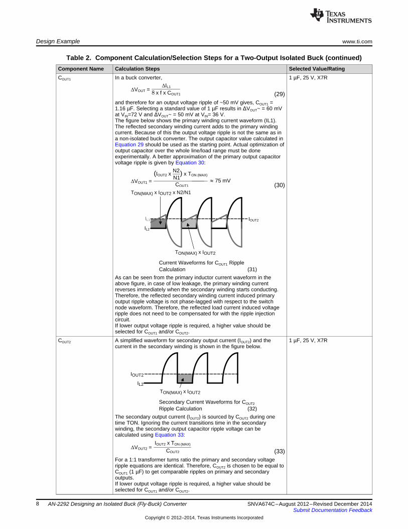
Table 2. Component Calculation/Selection Steps for a Two-Output Isolated Buck (continued)Component Name Calculation Steps Selected Value/RatingCOUT1 In a buck converter, 1 µF, 25 V, X7R
(29)and therefore for an output voltage ripple of ~50 mV gives, COUT1 =1.16 µF. Selecting a standard value of 1 µF results in ΔVOUT~ = 60 mVat VIN=72 V and ΔVOUT~ = 50 mV at VIN= 36 V.The figure below shows the primary winding current waveform (IL1).The reflected secondary winding current adds to the primary windingcurrent. Because of this the output voltage ripple is not the same as ina non-isolated buck converter. The output capacitor value calculated inEquation 29 should be used as the starting point. Actual optimization ofoutput capacitor over the whole line/load range must be doneexperimentally. A better approximation of the primary output capacitorvoltage ripple is given by Equation 30:
(30)
Current Waveforms for COUT1 RippleCalculation (31)
As can be seen from the primary inductor current waveform in theabove figure, in case of low leakage, the primary winding currentreverses immediately when the secondary winding starts conducting.Therefore, the reflected secondary winding current induced primaryoutput ripple voltage is not phase-lagged with respect to the switchnode waveform. Therefore, the reflected load current induced voltageripple does not need to be compensated for with the ripple injectioncircuit.If lower output voltage ripple is required, a higher value should beselected for COUT1 and/or COUT2.
COUT2 A simplified waveform for secondary output current (IOUT2) and the 1 µF, 25 V, X7Rcurrent in the secondary winding is shown in the figure below.
Secondary Current Waveforms for COUT2
Ripple Calculation (32)The secondary output current (IOUT2) is sourced by COUT2 during onetime TON. Ignoring the current transitions time in the secondarywinding, the secondary output capacitor ripple voltage can becalculated using Equation 33:
(33)For a 1:1 transformer turns ratio the primary and secondary voltageripple equations are identical. Therefore, COUT2 is chosen to be equal toCOUT1 (1 µF) to get comparable ripples on primary and secondaryoutputs.If lower output voltage ripple is required, a higher value should beselected for COUT1 and/or COUT2.
8 AN-2292 Designing an Isolated Buck (Fly-Buck) Converter SNVA674C–August 2012–Revised December 2014Submit Documentation Feedback
Copyright © 2012–2014, Texas Instruments Incorporated
+
VOUT2D1
C4
T1
9.5V
+
+
+
VIN
BST
RON
RTN
SW
VCC
FB
VIN VOUT1
R6
R2
R3
C3
C2
C1
R4
R1
UVLO
C6
LM5017
20V-100V
1
2
3
4
5
6
8
7
(TP7)
+C52.2 F 0.47 F
127 N
8.25 N
130 N
GND
(TP1)
(TP2)
UVLO U1R5
(TP3)
(TP4)
GND
R8
C7C8
+
D2
R9
EXP
0
1 N
7.32 N
1 F
0
33 H0.01 F
1 F
3300 pF
0.1 F
46.4 N
(TP11)SW
10V(1:1)
(TP6)
2200 pF
IGND
C9
2000V
1 F
(TP5)
TP8TP10
R10
R7
02 N
Cr = 1000 pFCac = 0.1 PF
50 mVRrCr d
(VIN (MIN) - VOUT) x TON
GND
Rr
Cac
Cr
R
To FB
R
L1
FB1
FB2
COUT
VOUT
www.ti.com Design Example
Table 2. Component Calculation/Selection Steps for a Two-Output Isolated Buck (continued)Component Name Calculation Steps Selected Value/RatingRr, Cr, Cac Type III ripple circuit as described in the LM5017 datasheet is preferred 46kΩ, 0805, 1000 pF, 0.1 µF (25
for isolated configuration. Type I and Type II ripple circuits suffer from V)larger jitter as the reflected load current affects the feedback ripple. Fora constant on time converter to be stable, the injected in-phase rippleshould be larger than the capacitive ripple on COUT1.
Type II Ripple Circuit (34)Using type III ripple circuit equations, the target ripple should begreater than the capacitive ripple generated at the primary output.
(35)Resulting in Rr= 180kΩ. This is the borderline case of stable ripple.Half to a fourth of this resistance should be selected for sufficientmargin for variations in TON, COUT1, and other components. For thisdesign Rr = 46.4kΩ; is selected for robust operation.
D2 (optional) D2 is an optional diode connected between VOUT1 and VCC regulator 20 V, 50 mAoutput. When VOUT1 is > VCC the VCC supplied from VOUT1. This results inreduced losses in VCC regulator inside the IC.
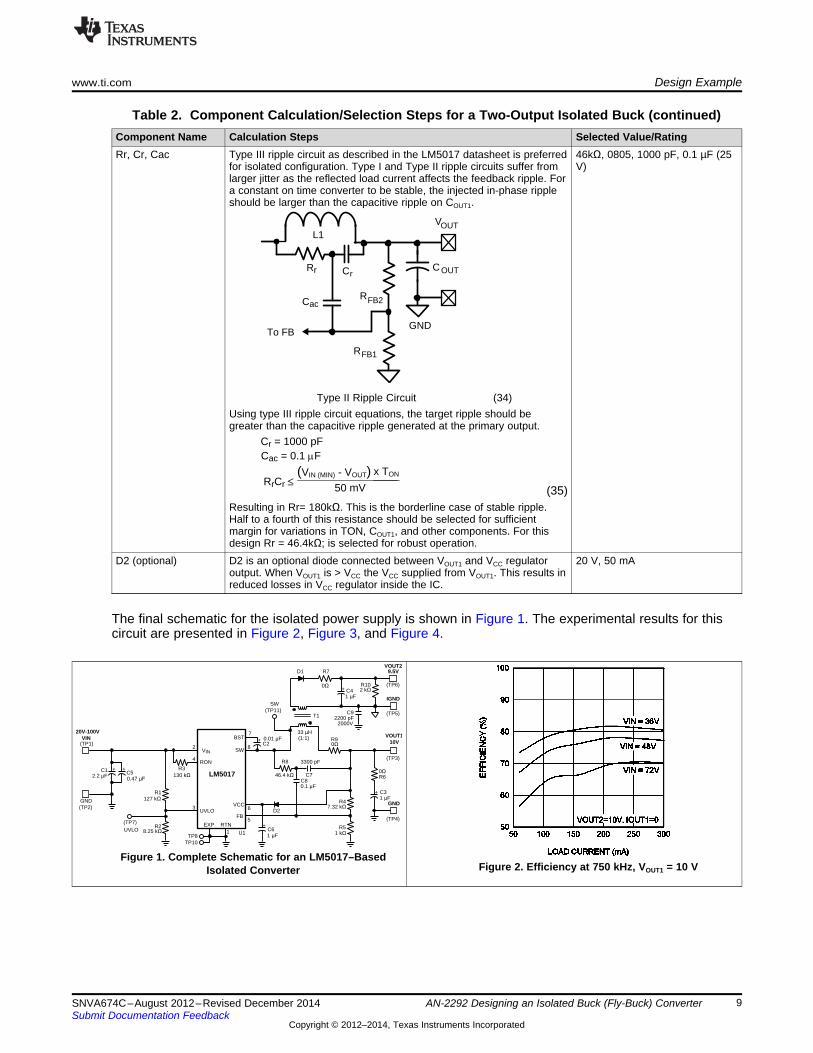
The final schematic for the isolated power supply is shown in Figure 1. The experimental results for thiscircuit are presented in Figure 2, Figure 3, and Figure 4.
Figure 1. Complete Schematic for an LM5017–BasedFigure 2. Efficiency at 750 kHz, VOUT1 = 10 VIsolated Converter
9SNVA674C–August 2012–Revised December 2014 AN-2292 Designing an Isolated Buck (Fly-Buck) ConverterSubmit Documentation Feedback
Copyright © 2012–2014, Texas Instruments Incorporated
Conclusions www.ti.com
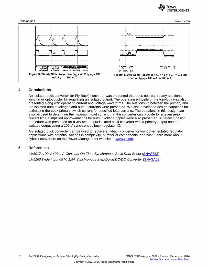
Figure 3. Steady State Waveform (VIN = 48 V, IOUT1 = 100 Figure 4. Step Load Response (VIN = 48 V, IOUT1 = 0, StepmA, IOUT2 = 200 mA) Load on IOUT2 = 100 mA to 200 mA).
4 ConclusionsAn isolated buck converter (or Fly-Buck) converter was presented that does not require any additionalwinding or optocoupler for regulating an isolated output. The operating principle of the topology was alsopresented along with operating current and voltage waveforms. The relationship between the primary andthe isolated output voltages and output currents were presented. We also developed design equations forestimating the peak primary switch current for specified load currents. The equations in this design canalso be used to determine the maximum load current that the converter can provide for a given peakcurrent limit. Simplified approximations for output voltage ripples were also presented. A detailed designprocedure was presented for a 3W two-output isolated buck converter with a primary output and anisolated output using a 100 V synchronous buck regulator IC.
An isolated buck converter can be used to replace a flyback converter for low-power isolated regulatorapplications with potential savings in complexity, number of components, and cost. Learn more aboutflyback converters on the Power Management website at www.ti.com.
5 ReferencesLM5017: 100 V,600 mA Constant On-Time Synchronous Buck Data Sheet (SNVS783)
LM5160 Wide Input 65 V, 1.5A Synchronous Step-Down DC-DC Converter (SNVSA03)
10 AN-2292 Designing an Isolated Buck (Fly-Buck) Converter SNVA674C–August 2012–Revised December 2014Submit Documentation Feedback
Copyright © 2012–2014, Texas Instruments Incorporated
www.ti.com Revision History
Revision History
Changes from B Revision (May 2013) to C Revision ...................................................................................................... Page
• Changed 8 to 4 ............................................................................................................................ 6• Changed value from 1.24 to 0.2......................................................................................................... 6• Added two sentences ..................................................................................................................... 6• Added 0.47 +............................................................................................................................... 6• Added reference ......................................................................................................................... 10
NOTE: Page numbers for previous revisions may differ from page numbers in the current version.
11SNVA674C–August 2012–Revised December 2014 Revision HistorySubmit Documentation Feedback
Copyright © 2012–2014, Texas Instruments Incorporated

IMPORTANT NOTICE
Texas Instruments Incorporated and its subsidiaries (TI) reserve the right to make corrections, enhancements, improvements and otherchanges to its semiconductor products and services per JESD46, latest issue, and to discontinue any product or service per JESD48, latestissue. Buyers should obtain the latest relevant information before placing orders and should verify that such information is current andcomplete. All semiconductor products (also referred to herein as “components”) are sold subject to TI’s terms and conditions of salesupplied at the time of order acknowledgment.TI warrants performance of its components to the specifications applicable at the time of sale, in accordance with the warranty in TI’s termsand conditions of sale of semiconductor products. Testing and other quality control techniques are used to the extent TI deems necessaryto support this warranty. Except where mandated by applicable law, testing of all parameters of each component is not necessarilyperformed.TI assumes no liability for applications assistance or the design of Buyers’ products. Buyers are responsible for their products andapplications using TI components. To minimize the risks associated with Buyers’ products and applications, Buyers should provideadequate design and operating safeguards.TI does not warrant or represent that any license, either express or implied, is granted under any patent right, copyright, mask work right, orother intellectual property right relating to any combination, machine, or process in which TI components or services are used. Informationpublished by TI regarding third-party products or services does not constitute a license to use such products or services or a warranty orendorsement thereof. Use of such information may require a license from a third party under the patents or other intellectual property of thethird party, or a license from TI under the patents or other intellectual property of TI.Reproduction of significant portions of TI information in TI data books or data sheets is permissible only if reproduction is without alterationand is accompanied by all associated warranties, conditions, limitations, and notices. TI is not responsible or liable for such altereddocumentation. Information of third parties may be subject to additional restrictions.Resale of TI components or services with statements different from or beyond the parameters stated by TI for that component or servicevoids all express and any implied warranties for the associated TI component or service and is an unfair and deceptive business practice.TI is not responsible or liable for any such statements.Buyer acknowledges and agrees that it is solely responsible for compliance with all legal, regulatory and safety-related requirementsconcerning its products, and any use of TI components in its applications, notwithstanding any applications-related information or supportthat may be provided by TI. Buyer represents and agrees that it has all the necessary expertise to create and implement safeguards whichanticipate dangerous consequences of failures, monitor failures and their consequences, lessen the likelihood of failures that might causeharm and take appropriate remedial actions. Buyer will fully indemnify TI and its representatives against any damages arising out of the useof any TI components in safety-critical applications.In some cases, TI components may be promoted specifically to facilitate safety-related applications. With such components, TI’s goal is tohelp enable customers to design and create their own end-product solutions that meet applicable functional safety standards andrequirements. Nonetheless, such components are subject to these terms.No TI components are authorized for use in FDA Class III (or similar life-critical medical equipment) unless authorized officers of the partieshave executed a special agreement specifically governing such use.Only those TI components which TI has specifically designated as military grade or “enhanced plastic” are designed and intended for use inmilitary/aerospace applications or environments. Buyer acknowledges and agrees that any military or aerospace use of TI componentswhich have not been so designated is solely at the Buyer's risk, and that Buyer is solely responsible for compliance with all legal andregulatory requirements in connection with such use.TI has specifically designated certain components as meeting ISO/TS16949 requirements, mainly for automotive use. In any case of use ofnon-designated products, TI will not be responsible for any failure to meet ISO/TS16949.
Products ApplicationsAudio www.ti.com/audio Automotive and Transportation www.ti.com/automotiveAmplifiers amplifier.ti.com Communications and Telecom www.ti.com/communicationsData Converters dataconverter.ti.com Computers and Peripherals www.ti.com/computersDLP® Products www.dlp.com Consumer Electronics www.ti.com/consumer-appsDSP dsp.ti.com Energy and Lighting www.ti.com/energyClocks and Timers www.ti.com/clocks Industrial www.ti.com/industrialInterface interface.ti.com Medical www.ti.com/medicalLogic logic.ti.com Security www.ti.com/securityPower Mgmt power.ti.com Space, Avionics and Defense www.ti.com/space-avionics-defenseMicrocontrollers microcontroller.ti.com Video and Imaging www.ti.com/videoRFID www.ti-rfid.comOMAP Applications Processors www.ti.com/omap TI E2E Community e2e.ti.comWireless Connectivity www.ti.com/wirelessconnectivity
Mailing Address: Texas Instruments, Post Office Box 655303, Dallas, Texas 75265Copyright © 2014, Texas Instruments Incorporated