AN-2122 SM3320-RF-EV Reference Design - Mouser ...
12
Application Report SNOSB82D – December 2010 – Revised October 2011 AN-2122 SM3320-RF-EV Reference Design Arief Hernadi .................................................................................................................................. ABSTRACT The SolarMagic™ SM3320-RF-EV reference design integrates a power optimizer and a low-cost 2.4GHz radio to add a remote shutdown feature to a PV system. The remote shutdown feature can be used during installation, maintenance, or emergency situations to de-energize the PV system. Contents 1 Introduction .................................................................................................................. 2 2 System Overview ........................................................................................................... 2 3 SM3320-RF-EV Design Specification .................................................................................... 3 4 Schematic .................................................................................................................... 9 List of Figures 1 System Overview Showing Intended Application of SM3320-RF-EV Board in a PV System..................... 3 2 Forced Panel-Mode and Reset using nRF24LE1....................................................................... 4 3 Power Line Antenna Implementation ..................................................................................... 5 4 Inductor Dimension ......................................................................................................... 5 5 Connector Board interface ................................................................................................. 6 6 Test Setup for SM3320-RF-EV............................................................................................ 8 7 RF Shutdown ................................................................................................................ 8 List of Tables 1 Pinouts for 10 Pin Headers and Nordic Motherboard .................................................................. 6 All trademarks are the property of their respective owners. 1 SNOSB82D – December 2010 – Revised October 2011 AN-2122 SM3320-RF-EV Reference Design Submit Documentation Feedback Copyright © 2010–2011, Texas Instruments Incorporated
-
Upload
khangminh22 -
Category
Documents
-
view
2 -
download
0
Transcript of AN-2122 SM3320-RF-EV Reference Design - Mouser ...

Application ReportSNOSB82D–December 2010–Revised October 2011
AN-2122 SM3320-RF-EV Reference DesignArief Hernadi ..................................................................................................................................
ABSTRACT
The SolarMagic™ SM3320-RF-EV reference design integrates a power optimizer and a low-cost 2.4GHzradio to add a remote shutdown feature to a PV system. The remote shutdown feature can be used duringinstallation, maintenance, or emergency situations to de-energize the PV system.
Contents1 Introduction .................................................................................................................. 22 System Overview ........................................................................................................... 23 SM3320-RF-EV Design Specification .................................................................................... 34 Schematic .................................................................................................................... 9
List of Figures
1 System Overview Showing Intended Application of SM3320-RF-EV Board in a PV System..................... 3
2 Forced Panel-Mode and Reset using nRF24LE1....................................................................... 4
3 Power Line Antenna Implementation..................................................................................... 5
4 Inductor Dimension ......................................................................................................... 5
5 Connector Board interface ................................................................................................. 6
6 Test Setup for SM3320-RF-EV............................................................................................ 8
7 RF Shutdown ................................................................................................................ 8
List of Tables
1 Pinouts for 10 Pin Headers and Nordic Motherboard .................................................................. 6
All trademarks are the property of their respective owners.
1SNOSB82D–December 2010–Revised October 2011 AN-2122 SM3320-RF-EV Reference DesignSubmit Documentation Feedback
Copyright © 2010–2011, Texas Instruments Incorporated

Introduction www.ti.com
(1)
1 Introduction
The SolarMagic™ SM3320-RF-EV reference design integrates a power optimizer and a low-cost 2.4GHzradio to add a remote shutdown feature to a PV system. The remote shutdown feature can be used duringinstallation, maintenance, or emergency situations to de-energize the PV system.
Although its principal purpose is to communicate shutdown intent, this RF system is 2-way and can beused for a wide variety of communication applications, including monitoring, security and identification.
The SolarMagic™ SM3320-RF-EV is based off of the SM3320-1A1 power optimizer, and shares all of itsbest-in-class power optimization features. This includes its ability to mitigate real-world mismatch, its99.5% peak efficiency, and its Panel-Mode operation. In addition, the same ultra-low profile form factor ofthe original SM3320-1A1 is maintained so that it can be integrated into the same junction box designs.This evaluation board should work as a power optimizer even without a transmitter
The wireless RF communications in the SM3320-RF-EV is implemented using a low-cost NordicnRF24LE1 chip. This is a low-cost, 2.4GHz radio and 8051 microcontroller on a single chip. The 2.4GHzradio uses narrow band modulation (as opposed to direct sequence spread spectrum), which can be usedeither with or without frequency hopping. Example software is provided that implements the remoteshutdown feature on the 8051 microcontroller in the nRF24LE1.
One of the unique features of the SM3320-RF-EV is its use of the DC power lines as an RF antenna andtransmission line. This enables the SM3320-RF-EV to maintain radio communication even when it ismounted in the junction box of the module. This antenna design can be used with other 2.4GHz radiochipsets besides the nRF24LE1 by straightforward modification of the provided design files.
The SM3320-RF-EV reference design provides a flexible platform for developing value added features infirmware with no additional hardware development. Examples of these features include module-levelmonitoring, security (theft-detection and theft-deterrence), and identification. Similarly, firmwaredevelopment on this platform can be used to customize the SM3320-RF-EV to be compatible with anexisting monitoring system or inverter communication protocol if a customer desires.
SolarMagic™ technology is an overall solution that works in existing and new installations, residential,commercial, and utility scale projects. National Semiconductor’s 50 years of experience in the electronicsindustry delivers unsurpassed manufacturing, design, and development technology.
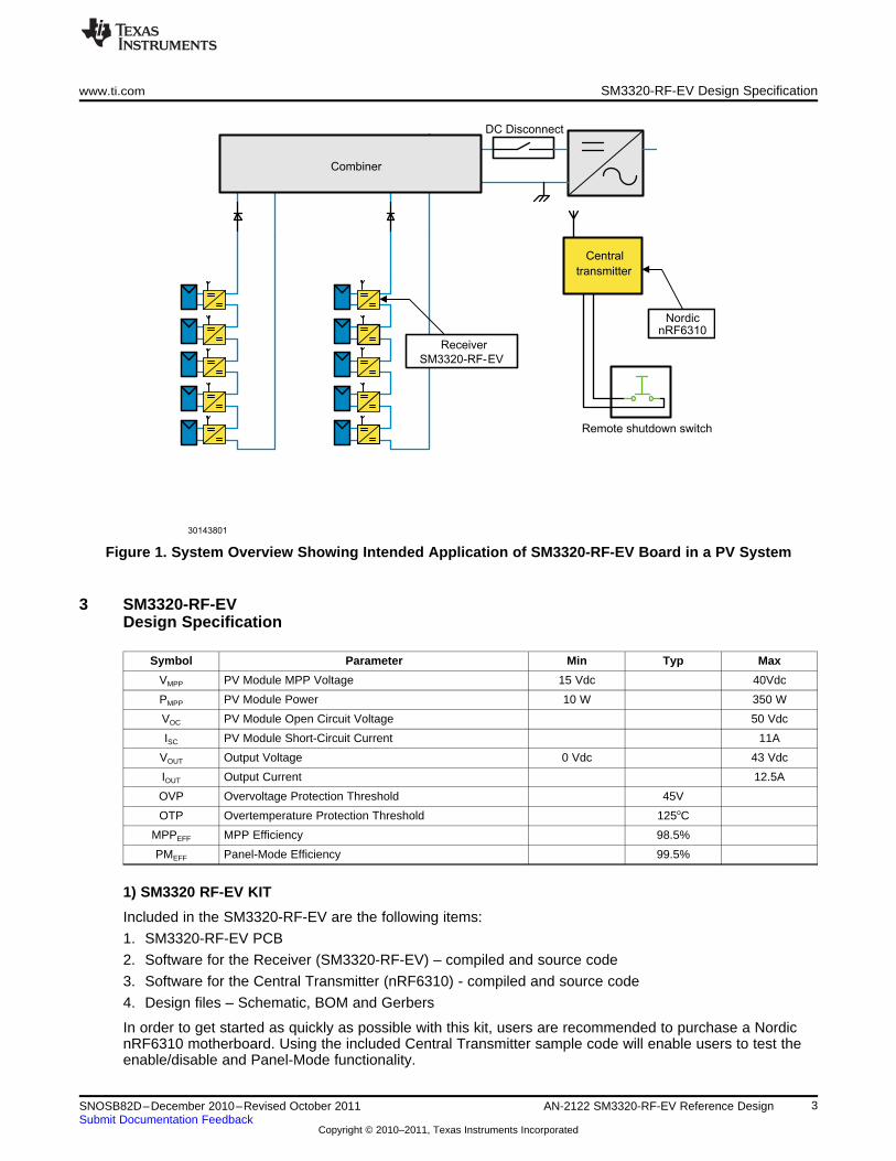
2 System Overview
Figure 1 depicts how the SM3320-RF-EV design would be implemented in its intended application. In thisexample, every module is connected to an SM3320-RF-EV power optimizer. Under normal conditions, thecentral transmitter sends a signal to each SM3320-RF-EV power optimizer indicating that it is ok tooperate and output power. When an emergency condition occurs, the central transmitter will send a signalcommand to all the SM3320-RF-EV to shutdown. This de-energizes the output of each SM3320-RF-EV,and in doing so brings down the voltage of the DC bus and all DC wiring to a safe voltage level.
2 AN-2122 SM3320-RF-EV Reference Design SNOSB82D–December 2010–Revised October 2011Submit Documentation Feedback
Copyright © 2010–2011, Texas Instruments Incorporated
Combiner
Remote shutdown switch
Central
transmitter
DC Disconnect
Nordic
nRF6310
Receiver
SM3320-RF-EV
30143801
www.ti.com SM3320-RF-EV Design Specification
Figure 1. System Overview Showing Intended Application of SM3320-RF-EV Board in a PV System
3 SM3320-RF-EVDesign Specification
Symbol Parameter Min Typ Max
VMPP PV Module MPP Voltage 15 Vdc 40Vdc
PMPP PV Module Power 10 W 350 W
VOC PV Module Open Circuit Voltage 50 Vdc
ISC PV Module Short-Circuit Current 11A
VOUT Output Voltage 0 Vdc 43 Vdc
IOUT Output Current 12.5A
OVP Overvoltage Protection Threshold 45V
OTP Overtemperature Protection Threshold 125oC
MPPEFF MPP Efficiency 98.5%
PMEFF Panel-Mode Efficiency 99.5%
1) SM3320 RF-EV KIT
Included in the SM3320-RF-EV are the following items:
1. SM3320-RF-EV PCB
2. Software for the Receiver (SM3320-RF-EV) – compiled and source code
3. Software for the Central Transmitter (nRF6310) - compiled and source code
4. Design files – Schematic, BOM and Gerbers
In order to get started as quickly as possible with this kit, users are recommended to purchase a NordicnRF6310 motherboard. Using the included Central Transmitter sample code will enable users to test theenable/disable and Panel-Mode functionality.
3SNOSB82D–December 2010–Revised October 2011 AN-2122 SM3320-RF-EV Reference DesignSubmit Documentation Feedback
Copyright © 2010–2011, Texas Instruments Incorporated
nRF24LE1F16Q32
P0.0
P0.1
5V
5V SM72442
RST
PM
10k
10k
60.4k
60.4k
2N7002
2N7002
SM3320-RF-EV Design Specification www.ti.com
2) FEATURES• Wireless shutdown for SM3320-1A1
• Wireless Panel-Mode operation for SM3320-1A1
• MPPT for Photovoltaic Panel
• 2.4 GHz ISM band operation
• Enhanced 8 bit 8051 compatible microcontroller
• Power line antenna
3) DESIGN DESCRIPTION
The Sirius RF evaluation board shares the same power specifications as the SolarMagic SM3320-1A1Power Optimizer. The controller for the power optimizer consists of an SM72442 programmable MPPTcontroller for PV panels and a Nordic nRF24LE1 low power system-on-chip wireless solution. ThenRF24LE1 has a built in 2.4GHz transceiver (250kbps, 1Mbps and 2Mbps air data rates) and an 8051compatible microcontroller. Operation at 250kbps is recommended.
Receiver
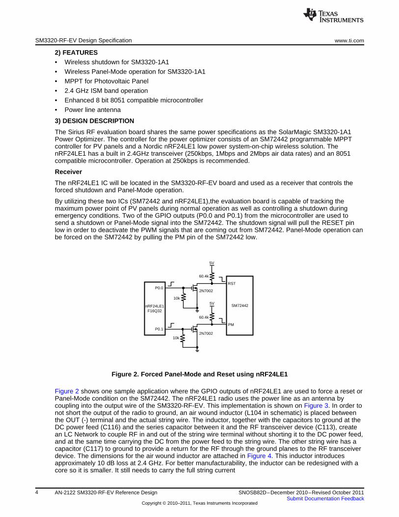
The nRF24LE1 IC will be located in the SM3320-RF-EV board and used as a receiver that controls theforced shutdown and Panel-Mode operation.
By utilizing these two ICs (SM72442 and nRF24LE1),the evaluation board is capable of tracking themaximum power point of PV panels during normal operation as well as controlling a shutdown duringemergency conditions. Two of the GPIO outputs (P0.0 and P0.1) from the microcontroller are used tosend a shutdown or Panel-Mode signal into the SM72442. The shutdown signal will pull the RESET pinlow in order to deactivate the PWM signals that are coming out from SM72442. Panel-Mode operation canbe forced on the SM72442 by pulling the PM pin of the SM72442 low.
Figure 2. Forced Panel-Mode and Reset using nRF24LE1
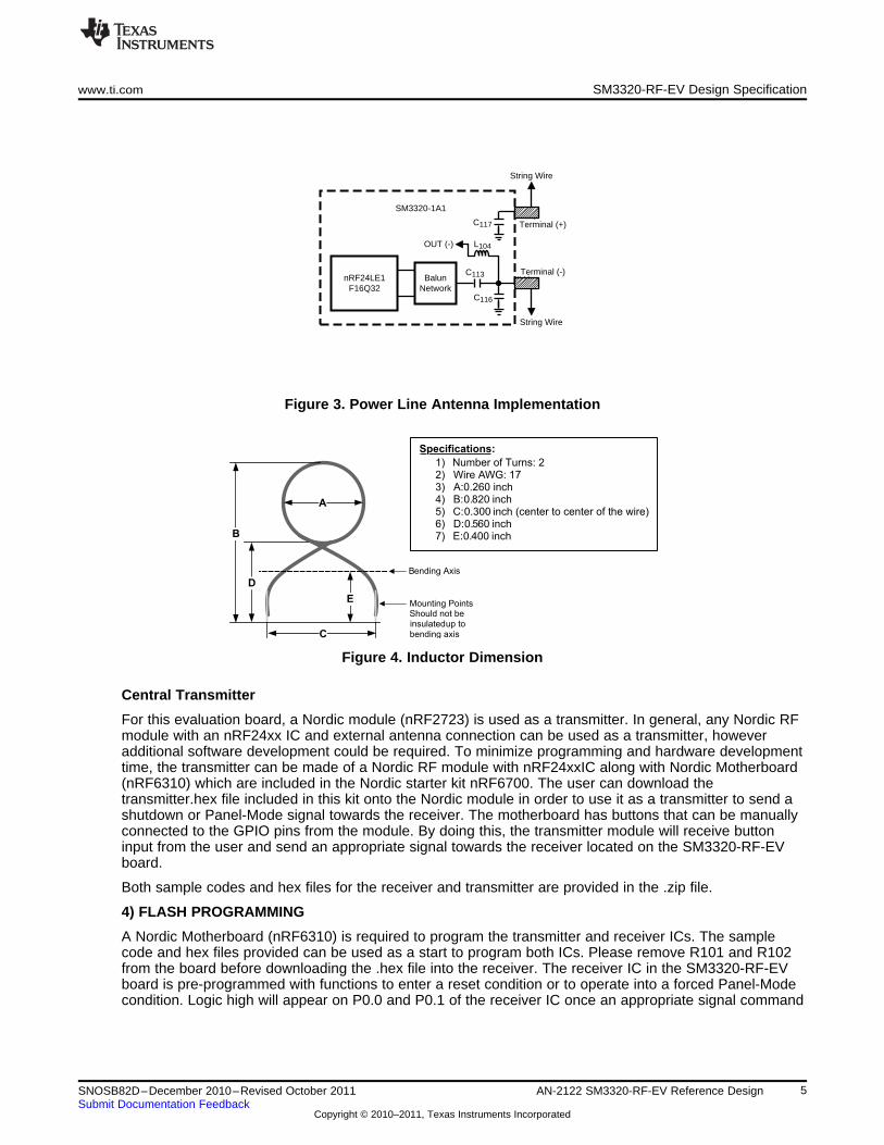
Figure 2 shows one sample application where the GPIO outputs of nRF24LE1 are used to force a reset orPanel-Mode condition on the SM72442. The nRF24LE1 radio uses the power line as an antenna bycoupling into the output wire of the SM3320-RF-EV. This implementation is shown on Figure 3. In order tonot short the output of the radio to ground, an air wound inductor (L104 in schematic) is placed betweenthe OUT (-) terminal and the actual string wire. The inductor, together with the capacitors to ground at theDC power feed (C116) and the series capacitor between it and the RF transceiver device (C113), createan LC Network to couple RF in and out of the string wire terminal without shorting it to the DC power feed,and at the same time carrying the DC from the power feed to the string wire. The other string wire has acapacitor (C117) to ground to provide a return for the RF through the ground planes to the RF transceiverdevice. The dimensions for the air wound inductor are attached in Figure 4. This inductor introducesapproximately 10 dB loss at 2.4 GHz. For better manufacturability, the inductor can be redesigned with acore so it is smaller. It still needs to carry the full string current
4 AN-2122 SM3320-RF-EV Reference Design SNOSB82D–December 2010–Revised October 2011Submit Documentation Feedback
Copyright © 2010–2011, Texas Instruments Incorporated
B
D
Bending Axis
Mounting PointsShould not beinsulatedup tobending axisC
E
A
Specifications:
1) Number of Turns: 22) Wire AWG: 173) A:0.260 inch4) B:0.820 inch5) C:0.300 inch (center to center of the wire)6) D:0.560 inch7) E:0.400 inch
Terminal (-)nRF24LE1
F16Q32
Balun Network
String Wire
OUT (-)
Terminal (+)
String Wire
SM3320-1A1
L104
C113
C116
C117
www.ti.com SM3320-RF-EV Design Specification
Figure 3. Power Line Antenna Implementation
Figure 4. Inductor Dimension
Central Transmitter
For this evaluation board, a Nordic module (nRF2723) is used as a transmitter. In general, any Nordic RFmodule with an nRF24xx IC and external antenna connection can be used as a transmitter, howeveradditional software development could be required. To minimize programming and hardware developmenttime, the transmitter can be made of a Nordic RF module with nRF24xxIC along with Nordic Motherboard(nRF6310) which are included in the Nordic starter kit nRF6700. The user can download thetransmitter.hex file included in this kit onto the Nordic module in order to use it as a transmitter to send ashutdown or Panel-Mode signal towards the receiver. The motherboard has buttons that can be manuallyconnected to the GPIO pins from the module. By doing this, the transmitter module will receive buttoninput from the user and send an appropriate signal towards the receiver located on the SM3320-RF-EVboard.
Both sample codes and hex files for the receiver and transmitter are provided in the .zip file.
4) FLASH PROGRAMMING
A Nordic Motherboard (nRF6310) is required to program the transmitter and receiver ICs. The samplecode and hex files provided can be used as a start to program both ICs. Please remove R101 and R102from the board before downloading the .hex file into the receiver. The receiver IC in the SM3320-RF-EVboard is pre-programmed with functions to enter a reset condition or to operate into a forced Panel-Modecondition. Logic high will appear on P0.0 and P0.1 of the receiver IC once an appropriate signal command
5SNOSB82D–December 2010–Revised October 2011 AN-2122 SM3320-RF-EV Reference DesignSubmit Documentation Feedback
Copyright © 2010–2011, Texas Instruments Incorporated
SM3320-RF-EV Design Specification www.ti.com
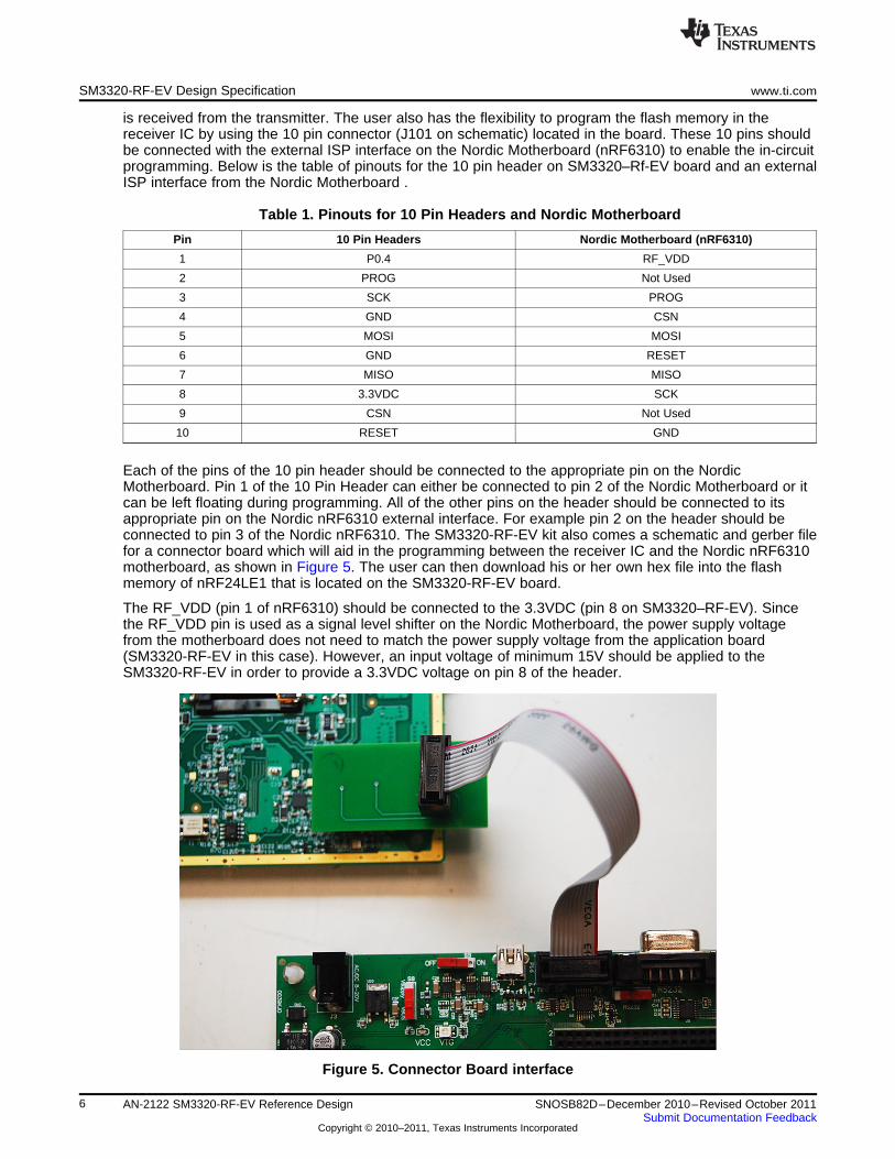
is received from the transmitter. The user also has the flexibility to program the flash memory in thereceiver IC by using the 10 pin connector (J101 on schematic) located in the board. These 10 pins shouldbe connected with the external ISP interface on the Nordic Motherboard (nRF6310) to enable the in-circuitprogramming. Below is the table of pinouts for the 10 pin header on SM3320–Rf-EV board and an externalISP interface from the Nordic Motherboard .
Table 1. Pinouts for 10 Pin Headers and Nordic Motherboard
Pin 10 Pin Headers Nordic Motherboard (nRF6310)
1 P0.4 RF_VDD
2 PROG Not Used
3 SCK PROG
4 GND CSN
5 MOSI MOSI
6 GND RESET
7 MISO MISO
8 3.3VDC SCK
9 CSN Not Used
10 RESET GND
Each of the pins of the 10 pin header should be connected to the appropriate pin on the NordicMotherboard. Pin 1 of the 10 Pin Header can either be connected to pin 2 of the Nordic Motherboard or itcan be left floating during programming. All of the other pins on the header should be connected to itsappropriate pin on the Nordic nRF6310 external interface. For example pin 2 on the header should beconnected to pin 3 of the Nordic nRF6310. The SM3320-RF-EV kit also comes a schematic and gerber filefor a connector board which will aid in the programming between the receiver IC and the Nordic nRF6310motherboard, as shown in Figure 5. The user can then download his or her own hex file into the flashmemory of nRF24LE1 that is located on the SM3320-RF-EV board.
The RF_VDD (pin 1 of nRF6310) should be connected to the 3.3VDC (pin 8 on SM3320–RF-EV). Sincethe RF_VDD pin is used as a signal level shifter on the Nordic Motherboard, the power supply voltagefrom the motherboard does not need to match the power supply voltage from the application board(SM3320-RF-EV in this case). However, an input voltage of minimum 15V should be applied to theSM3320-RF-EV in order to provide a 3.3VDC voltage on pin 8 of the header.
Figure 5. Connector Board interface
6 AN-2122 SM3320-RF-EV Reference Design SNOSB82D–December 2010–Revised October 2011Submit Documentation Feedback
Copyright © 2010–2011, Texas Instruments Incorporated

www.ti.com SM3320-RF-EV Design Specification
In order to start programming on the nRF radio IC, the following software has to be downloaded:
1. µVision IDE from Keil
2. nRFgo Studio
The nRFgo Studio is provided on the nRFgo Starter Kit (nRF 6700). The nRFgo Studio will download the.hex file generated by µVision IDE into the flash memory on the receiver. To program the flash using theexternal ISP interface from the motherboard, an nRF ISP interface has to be manually selected in thenRFgo Studio. A complete download of the hex file into the IC is indicated by a successful verification ofthe flash memory. Please note that both R101 and R102 (refer to the schematic) on the SM3320-RF-EVboard have to be removed during the programming.
5) I2C INTERFACE
Using a connector board that is supplied in this kit, the user has the ability to access the SCL and SDApins on the SM72442 as well as W2SCL (P0.4) and W2SDA (P0.5) on the 32 pin nRF24LE1. Pin 1 and 3on the 10 Pin Header are connected to P0.4 and P0.5 respectively through R101 and R102 (refer to theschematic). Please make sure that both resistors are assembled on the SM3320-RF-EV board. TheSM72442 and nRF24LE1 are configured as a slave. A master can be used to communicate to SM72442.External pull-up resistor of 2kΩ to 3.3V is required. The address for SM72442 is 1 whereas the addressfor the nRF24LE1 can be configured using setting the address W2SADR on the SFR register (Please referto nRF24LE1 datasheet for more information). The I2C protocol for communicating with SM72442 can befound on the SM72442 datasheet.
6) LAYOUT CONSIDERATION1. RF IC layout assumes an adjacent ground plane. If the adjacent layer is a power plane, a bypass
capacitor should be added between ground and power plane in the vicinity of the RF IC. In our case,three 0.01µF and three 100pF capacitors are connected between ground and the power plane, and areplaced near nRF24LE1.
2. The distance from an RF trace and a plane around it should be at least two times the width of the RFtrace to avoid co-planar coupling that lowers the line impedance, unless co-planar ground flood isincluded in the calculation.
3. The trace going into the crystal oscillator should be wide enough (~15 mils in our case) to reduce theline inductance for more reliable starting at low temperature. On the other hand, increasing thesetraces should also increase the line capacitance to ground which can affect starting as well. However,this effect can be counteracted by reducing the value of C105 and C106.
7) HEATSINKING
SM3320-RF-EV evaluation board does not come with a heatsink. Therefore, in order to run the evaluationboard at elevated power ratings, an appropriate heatsink should be added on Q1, Q2, Q3 and Q4 as wellas diode D1. Care must be taken prevent electrical contact between the drains of the MOSFETs in theprocess of proper heatsinking. At elevated power operation please note the increase in temperatureacross these semiconductor devices.
8) TEST SETUP
To perform an evaluation on a single SM3320-RF-EV, it is suggested that the user connect the input to aSAS (Solar Array Simulator) and the output to a load bank.
7SNOSB82D–December 2010–Revised October 2011 AN-2122 SM3320-RF-EV Reference DesignSubmit Documentation Feedback
Copyright © 2010–2011, Texas Instruments Incorporated
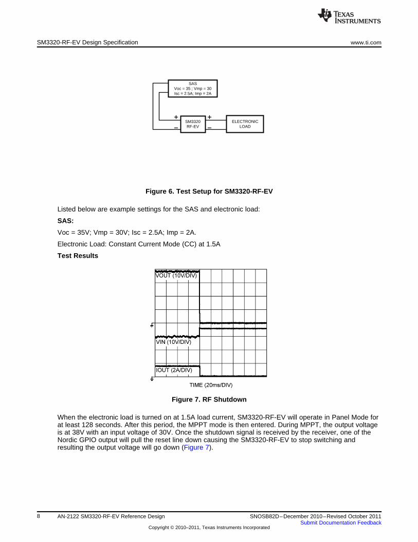
SASVoc = 35 ; Vmp = 30Isc = 2.5A; Imp = 2A
SM3320 RF-EV
ELECTRONIC LOAD
SM3320-RF-EV Design Specification www.ti.com
Figure 6. Test Setup for SM3320-RF-EV
Listed below are example settings for the SAS and electronic load:
SAS:
Voc = 35V; Vmp = 30V; Isc = 2.5A; Imp = 2A.
Electronic Load: Constant Current Mode (CC) at 1.5A
Test Results
Figure 7. RF Shutdown
When the electronic load is turned on at 1.5A load current, SM3320-RF-EV will operate in Panel Mode forat least 128 seconds. After this period, the MPPT mode is then entered. During MPPT, the output voltageis at 38V with an input voltage of 30V. Once the shutdown signal is received by the receiver, one of theNordic GPIO output will pull the reset line down causing the SM3320-RF-EV to stop switching andresulting the output voltage will go down (Figure 7).
8 AN-2122 SM3320-RF-EV Reference Design SNOSB82D–December 2010–Revised October 2011Submit Documentation Feedback
Copyright © 2010–2011, Texas Instruments Incorporated
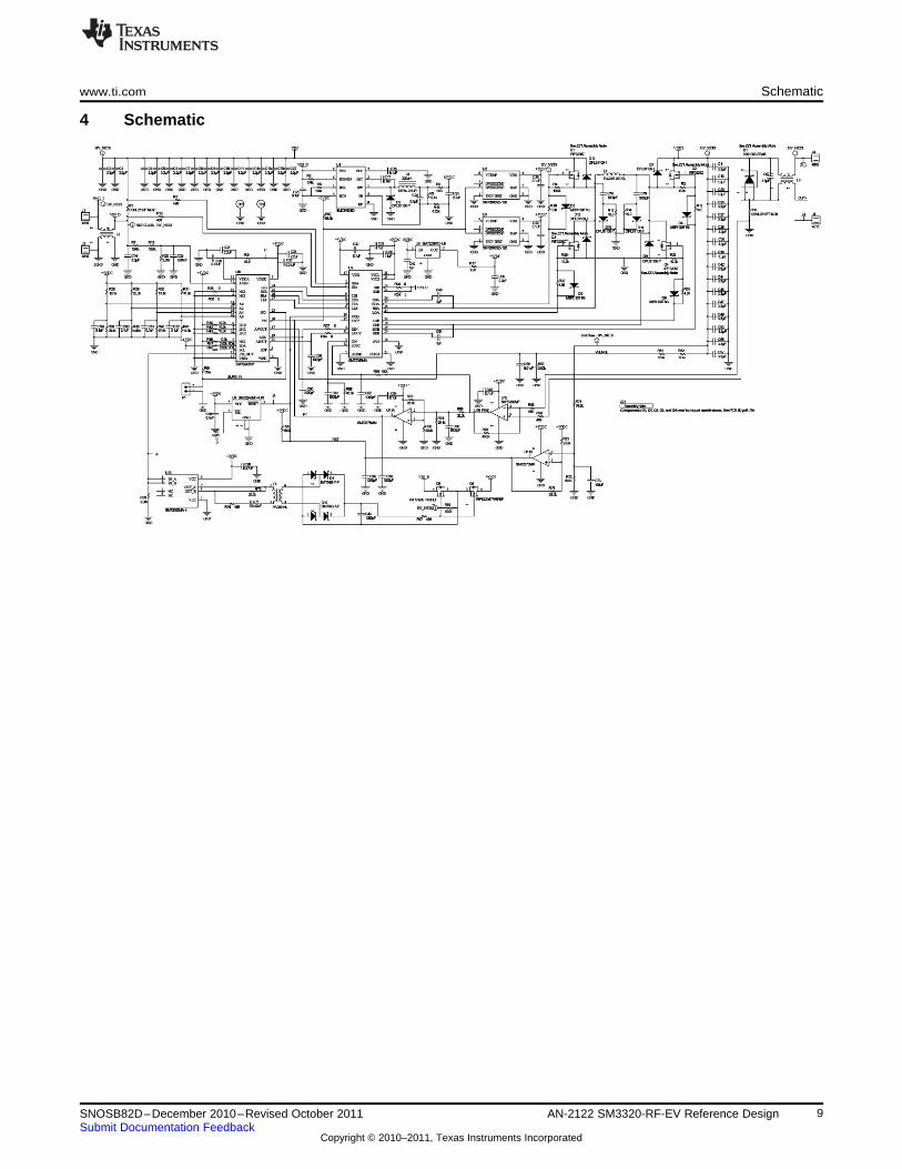
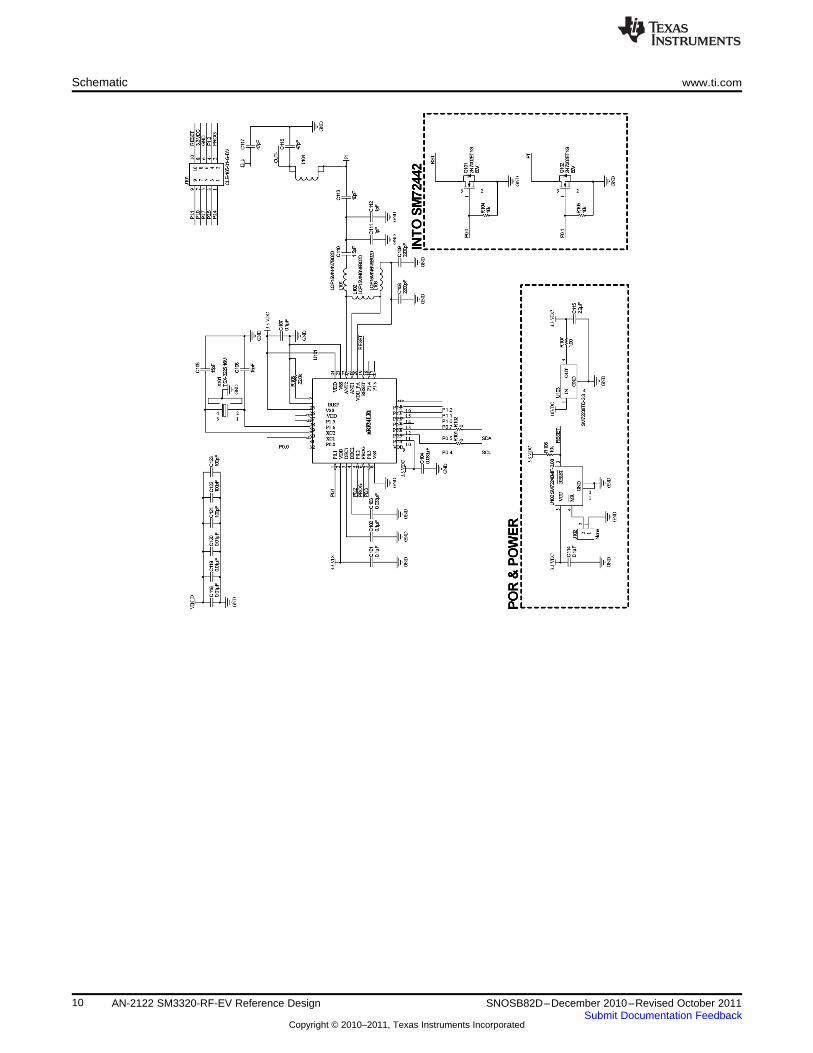
www.ti.com Schematic
4 Schematic
9SNOSB82D–December 2010–Revised October 2011 AN-2122 SM3320-RF-EV Reference DesignSubmit Documentation Feedback
Copyright © 2010–2011, Texas Instruments Incorporated
Schematic www.ti.com
10 AN-2122 SM3320-RF-EV Reference Design SNOSB82D–December 2010–Revised October 2011Submit Documentation Feedback
Copyright © 2010–2011, Texas Instruments Incorporated

IMPORTANT NOTICE
Texas Instruments Incorporated and its subsidiaries (TI) reserve the right to make corrections, enhancements, improvements and otherchanges to its semiconductor products and services per JESD46, latest issue, and to discontinue any product or service per JESD48, latestissue. Buyers should obtain the latest relevant information before placing orders and should verify that such information is current andcomplete. All semiconductor products (also referred to herein as “components”) are sold subject to TI’s terms and conditions of salesupplied at the time of order acknowledgment.
TI warrants performance of its components to the specifications applicable at the time of sale, in accordance with the warranty in TI’s termsand conditions of sale of semiconductor products. Testing and other quality control techniques are used to the extent TI deems necessaryto support this warranty. Except where mandated by applicable law, testing of all parameters of each component is not necessarilyperformed.
TI assumes no liability for applications assistance or the design of Buyers’ products. Buyers are responsible for their products andapplications using TI components. To minimize the risks associated with Buyers’ products and applications, Buyers should provideadequate design and operating safeguards.
TI does not warrant or represent that any license, either express or implied, is granted under any patent right, copyright, mask work right, orother intellectual property right relating to any combination, machine, or process in which TI components or services are used. Informationpublished by TI regarding third-party products or services does not constitute a license to use such products or services or a warranty orendorsement thereof. Use of such information may require a license from a third party under the patents or other intellectual property of thethird party, or a license from TI under the patents or other intellectual property of TI.
Reproduction of significant portions of TI information in TI data books or data sheets is permissible only if reproduction is without alterationand is accompanied by all associated warranties, conditions, limitations, and notices. TI is not responsible or liable for such altereddocumentation. Information of third parties may be subject to additional restrictions.
Resale of TI components or services with statements different from or beyond the parameters stated by TI for that component or servicevoids all express and any implied warranties for the associated TI component or service and is an unfair and deceptive business practice.TI is not responsible or liable for any such statements.
Buyer acknowledges and agrees that it is solely responsible for compliance with all legal, regulatory and safety-related requirementsconcerning its products, and any use of TI components in its applications, notwithstanding any applications-related information or supportthat may be provided by TI. Buyer represents and agrees that it has all the necessary expertise to create and implement safeguards whichanticipate dangerous consequences of failures, monitor failures and their consequences, lessen the likelihood of failures that might causeharm and take appropriate remedial actions. Buyer will fully indemnify TI and its representatives against any damages arising out of the useof any TI components in safety-critical applications.
In some cases, TI components may be promoted specifically to facilitate safety-related applications. With such components, TI’s goal is tohelp enable customers to design and create their own end-product solutions that meet applicable functional safety standards andrequirements. Nonetheless, such components are subject to these terms.
No TI components are authorized for use in FDA Class III (or similar life-critical medical equipment) unless authorized officers of the partieshave executed a special agreement specifically governing such use.
Only those TI components which TI has specifically designated as military grade or “enhanced plastic” are designed and intended for use inmilitary/aerospace applications or environments. Buyer acknowledges and agrees that any military or aerospace use of TI componentswhich have not been so designated is solely at the Buyer's risk, and that Buyer is solely responsible for compliance with all legal andregulatory requirements in connection with such use.
TI has specifically designated certain components which meet ISO/TS16949 requirements, mainly for automotive use. Components whichhave not been so designated are neither designed nor intended for automotive use; and TI will not be responsible for any failure of suchcomponents to meet such requirements.
Products Applications
Audio www.ti.com/audio Automotive and Transportation www.ti.com/automotive
Amplifiers amplifier.ti.com Communications and Telecom www.ti.com/communications
Data Converters dataconverter.ti.com Computers and Peripherals www.ti.com/computers
DLP® Products www.dlp.com Consumer Electronics www.ti.com/consumer-apps
DSP dsp.ti.com Energy and Lighting www.ti.com/energy
Clocks and Timers www.ti.com/clocks Industrial www.ti.com/industrial
Interface interface.ti.com Medical www.ti.com/medical
Logic logic.ti.com Security www.ti.com/security
Power Mgmt power.ti.com Space, Avionics and Defense www.ti.com/space-avionics-defense
Microcontrollers microcontroller.ti.com Video and Imaging www.ti.com/video
RFID www.ti-rfid.com
OMAP Applications Processors www.ti.com/omap TI E2E Community e2e.ti.com
Wireless Connectivity www.ti.com/wirelessconnectivity
Mailing Address: Texas Instruments, Post Office Box 655303, Dallas, Texas 75265Copyright © 2012, Texas Instruments Incorporated

Mouser Electronics
Authorized Distributor
Click to View Pricing, Inventory, Delivery & Lifecycle Information: Texas Instruments:
SM3320-RF-EV/NOPB