AN-1733 Load Transient Testing Simplified - Texas Instruments
10
Application Report SNOA507 – November 2007 AN-1733 Load Transient Testing Simplified ..................................................................................................................................................... ABSTRACT The load transient test may be the simplest diagnostic tool available to instantly analyze the loop stability of a system: the visual appearance of the output voltage as the voltage regulator responds to a change in load current directly correlates to phase margin. This article will demonstrate how to easily perform load transient testing, and how to estimate phase margin based upon the results of this test. Contents 1 Introduction .................................................................................................................. 2 2 Voltage Regulation .......................................................................................................... 2 3 Anatomy of a Load Transient .............................................................................................. 2 4 Output Voltage Transient Response ..................................................................................... 3 5 Transient Response and Phase Margin ................................................................................. 4 6 Manually Testing Load Transients ........................................................................................ 6 7 Guidelines For Getting Accurate Data When Testing Load Transients .............................................. 6 8 Electronic Load Transient Tester ......................................................................................... 7 9 Guidelines For Using the Electronic Load Tester ....................................................................... 8 List of Figures 1 Basic Voltage Regulator Operation ....................................................................................... 2 2 Regulator Responds To Change In Load Current ...................................................................... 3 3 Output Voltage Transient .................................................................................................. 3 4 Output Voltage Transient Response for 49° Phase Margin ........................................................... 4 5 Output Voltage Transient Response for 30° Phase Margin ........................................................... 5 6 Output Voltage Transient Response for 17° Phase Margin ........................................................... 5 7 Output Voltage Transient Response for 5° Phase Margin............................................................. 5 8 Circuit For Manually Testing Load Transient Response ............................................................... 6 9 Using a Sense Resistor To Measure Load Current .................................................................... 7 10 Comparison Showing Current Probe Bandwidth Limitations .......................................................... 7 11 Electronic Load Transient Tester ......................................................................................... 8 12 Table 1. Load Current Pulse Slew Rates For Various Values of C5 ................................................. 8 13 Transient Waveforms With Low Inductance Ground Connection Between the Pulse Tester and Regulator Under Test ................................................................................................................... 9 14 Load Current Waveform Distorted By Increased Ground Inductance Between Pulse Tester and Regulator Under Test....................................................................................................... 9 All trademarks are the property of their respective owners. 1 SNOA507 – November 2007 AN-1733 Load Transient Testing Simplified Submit Documentation Feedback Copyright © 2007, Texas Instruments Incorporated
-
Upload
khangminh22 -
Category
Documents
-
view
0 -
download
0
Transcript of AN-1733 Load Transient Testing Simplified - Texas Instruments
Application ReportSNOA507–November 2007
AN-1733 Load Transient Testing Simplified.....................................................................................................................................................
ABSTRACT
The load transient test may be the simplest diagnostic tool available to instantly analyze the loop stabilityof a system: the visual appearance of the output voltage as the voltage regulator responds to a change inload current directly correlates to phase margin. This article will demonstrate how to easily perform loadtransient testing, and how to estimate phase margin based upon the results of this test.
Contents1 Introduction .................................................................................................................. 22 Voltage Regulation .......................................................................................................... 23 Anatomy of a Load Transient .............................................................................................. 24 Output Voltage Transient Response ..................................................................................... 35 Transient Response and Phase Margin ................................................................................. 46 Manually Testing Load Transients ........................................................................................ 67 Guidelines For Getting Accurate Data When Testing Load Transients .............................................. 68 Electronic Load Transient Tester ......................................................................................... 79 Guidelines For Using the Electronic Load Tester ....................................................................... 8
List of Figures
1 Basic Voltage Regulator Operation....................................................................................... 2
2 Regulator Responds To Change In Load Current ...................................................................... 3
3 Output Voltage Transient .................................................................................................. 3
4 Output Voltage Transient Response for 49° Phase Margin ........................................................... 4
5 Output Voltage Transient Response for 30° Phase Margin ........................................................... 5
6 Output Voltage Transient Response for 17° Phase Margin ........................................................... 5
7 Output Voltage Transient Response for 5° Phase Margin............................................................. 5
8 Circuit For Manually Testing Load Transient Response ............................................................... 6
9 Using a Sense Resistor To Measure Load Current .................................................................... 7
10 Comparison Showing Current Probe Bandwidth Limitations .......................................................... 7
11 Electronic Load Transient Tester ......................................................................................... 8
12 Table 1. Load Current Pulse Slew Rates For Various Values of C5................................................. 8
13 Transient Waveforms With Low Inductance Ground Connection Between the Pulse Tester and RegulatorUnder Test ................................................................................................................... 9
14 Load Current Waveform Distorted By Increased Ground Inductance Between Pulse Tester andRegulator Under Test....................................................................................................... 9
All trademarks are the property of their respective owners.
1SNOA507–November 2007 AN-1733 Load Transient Testing SimplifiedSubmit Documentation Feedback
Copyright © 2007, Texas Instruments Incorporated

Introduction www.ti.com
1 Introduction
The load transient test may be the simplest diagnostic tool available to instantly analyze the loop stabilityof a system: the visual appearance of the output voltage as the voltage regulator responds to a change inload current directly correlates to phase margin. This article will demonstrate how to easily perform loadtransient testing, and how to estimate phase margin based upon the results of this test.
2 Voltage Regulation
Virtually all electronic devices require a supply voltage that is held within a specified tolerance range, evenwhen the load current varies. This fixed voltage is provided by a voltage regulator (Figure 1).
The output voltage is sensed through a resistive divider and the error amplifier adjusts the current sourceIREG to hold the output at the nominal voltage.
The voltage regulator must be able to hold it’s output voltage constant as the load current demand variesanywhere from zero up to full load, even if the change occurs in a relatively short time: such suddenchanges in load current are called load transients. How well a voltage regulator holds it’s output voltageconstant during a load transient is defined as it’s load transient response.
It’s fairly easy to hold the output voltage constant as long as the load current changes slowly. But, whenthe load current “steps” quickly enough, the output voltage will change. It is how much the output voltagechanges when subjected to a change in load current that defines load transient performance.
Key principles in understanding load transients:
1) A voltage regulator acts as a voltage-controlled current source which drives current to the load (thecurrent source is adjusted by voltage feedback from the output). The regulator’s current source can neverbe changed in zero time, so it follows that if we make the load current change quickly enough, it will forcethe output voltage to change. How much it changes will be dependent on the speed of the regulator,amount and type of output capacitor, and the di/dt of the load current change.
2) During the time interval while the regulator’s control loop is adjusting for the change in load, the onlything supplying the difference in load current between the former steady-state value and the new loadcurrent value is the output capacitor. So, output capacitors are essential to controlling the output voltageduring load transients, and the electrical characteristics of these capacitors significantly affect transientresponse.
3) The faster the regulator’s control loop can respond, the less the output capacitor’s voltage will changebefore the loop corrects to the new value of load current. Therefore, it follows that a faster regulator canhold the same VOUT tolerance range with less output capacitance (which can save money).
Figure 1. Basic Voltage Regulator Operation
3 Anatomy of a Load Transient
To see how a load transient works, we will analyze an example where the load current goes from IL1 to ahigher value (IL2) in essentially zero time (Figure 2).
2 AN-1733 Load Transient Testing Simplified SNOA507–November 2007Submit Documentation Feedback
Copyright © 2007, Texas Instruments Incorporated

www.ti.com Output Voltage Transient Response
Figure 2. Regulator Responds To Change In Load Current
The regulator’s current source (IREG) can not change instantly, therefore at time “t = 0+" (the instant afterthe load increases to IL2), IREG = IL1. By simple node analysis, it follows that the output capacitor is requiredto source:
ICOUT = IL2 - IL1 (1)
COUT will continue to supply some of the load current until the control loop adjusts IREG to the new value IL2,causing the voltage across the capacitor to decrease as it discharges. The voltage across COUT is alsoreduced by the voltage drops across the capacitor’s internal ESR (equivalent series resistance) and ESL(equivalent series inductance), which are present in every capacitor.
4 Output Voltage Transient Response
As shown in Figure 2, capacitors contain parasitic resistance (called “ESR” for equivalent seriesresistance) and also parasitic inductance (called “ESL” for equivalent series inductance), both of whichaffect transient response. Figure 3 shows an actual voltage waveform recorded on the output of a linearregulator when the load current was increased very quickly (similar to the example shown in Figure 2):
Figure 3. Output Voltage Transient
It can be seen that ESL causes a narrow spike voltage drop which is highly dependent upon the rise timeof the load transient: the faster the load changes, the bigger the ESL spike on the output voltagewaveform will be. The spike only exists during the time the load current is changing, since inductance onlycreates a voltage in response to a changing current as given by:
V = L x di/dt (2)
3SNOA507–November 2007 AN-1733 Load Transient Testing SimplifiedSubmit Documentation Feedback
Copyright © 2007, Texas Instruments Incorporated

Transient Response and Phase Margin www.ti.com
When the load current reaches the new value (IL2), the ESL voltage spike will be over. The faster the risetime of the load current transient is, the more critical inductance becomes, both in the output capacitor aswell as the PC board traces connecting it to the load. Large value ceramic capacitors are extremely low inboth ESR and ESL, and are usually placed at the load terminals of devices with fast rising load transientrequirements. They also improve transient response if used on the output of voltage regulators.
The output capacitor’s ESR causes a change in output voltage anytime COUT is sourcing (or sinking)current, and this is shown on the waveform as the “ESR step”. During the interval of time before thecontrol loop increases IREG, the output voltage is reduced by both the voltage drop across the ESR and theamount that COUT discharges.
Eventually, the error amplifier begins to increase IREG in response to the drop in VOUT. It should be notedthat the value of IREG typically does not go directly to the new value of IL2, rather the error amplifier willusually turn the current source on fully to try to drive the output voltage up (often going into currentlimiting). Then, in most cases, the output voltage overshoots the nominal value and then falls back andeventually locks into the new equilibrium (this settling action can be seen in Figure 3). The distinctiveappearance of VOUT as it settles gives an accurate indication of phase margin (detailed in the next section).
When the control loop reaches the new steady-state condition (where the regulator’s current source isproviding IL2), the output capacitor is again providing no current to the load. It is important to note that the“ESR step” is a DC voltage change in the regulated output during a load transient. The ESR step can bequite significant, which means ESR is a critical consideration when designing for the maximum allowable“voltage tolerance window” the regulated voltage must meet. High performance aluminum and tantalumelectrolytic capacitors are made specifically to meet the needs of ultra low ESR applications.
5 Transient Response and Phase Margin
When the load current is suddenly changed, the operating point of the control loop is “unsettled”, and it isforced to go to a new operating point. The appearance of the output voltage waveform during thistransition is a very accurate indicator of the phase margin the loop has at the new operating point.
To illustrate this, Figure 4 is a scope plot of the output of a voltage regulator which was subjected to a fastload current step. The phase margin was measured using a network analyzer and determined to be 49°:
Figure 4. Output Voltage Transient Response for 49° Phase Margin
The appearance is what is known as “critically damped”, which means it extinguishes very cleanly in onlya single complete ring. This is ideal performance, because it gives the fastest possible settling time (andvery good stability).
In Figure 5, we see how the transient response is degraded if the phase margin is reduced to 30°:
4 AN-1733 Load Transient Testing Simplified SNOA507–November 2007Submit Documentation Feedback
Copyright © 2007, Texas Instruments Incorporated

www.ti.com Transient Response and Phase Margin
Figure 5. Output Voltage Transient Response for 30° Phase Margin
The settling characteristics now show a bit more ringing after the transient occurs (the higher DC levelafter the load change is a result of poor load regulation for this particular device, it is not related to phasemargin or transient response). It can be seen that even though the phase margin is only 30°, the settling isfairly clean and probably acceptable for most applications.
However, if the phase margin is further reduced to 17°, we see the settling of the loop beginning to showmore pronounced ringing (Figure 6):
Figure 6. Output Voltage Transient Response for 17° Phase Margin
It can be seen that the ringing is beginning to take on the appearance of a sine wave oscillation, becomingeven more obvious as the phase margin is reduced to only 5° (Figure 7):
Figure 7. Output Voltage Transient Response for 5° Phase Margin
With only 5° of phase margin, the waveform shows an unmistakable sine wave which barely extinguishes.This tells the designer that the phase margin is so low the loop is on the verge of sustaining oscillations.The progressive change in the appearance of the output voltage waveforms as the phase margindiminishes illustrates how a designer can estimate phase margin using only a load transient test. This canbe done very easily without special equipment, and the following section shows how.
5SNOA507–November 2007 AN-1733 Load Transient Testing SimplifiedSubmit Documentation Feedback
Copyright © 2007, Texas Instruments Incorporated
Manually Testing Load Transients www.ti.com
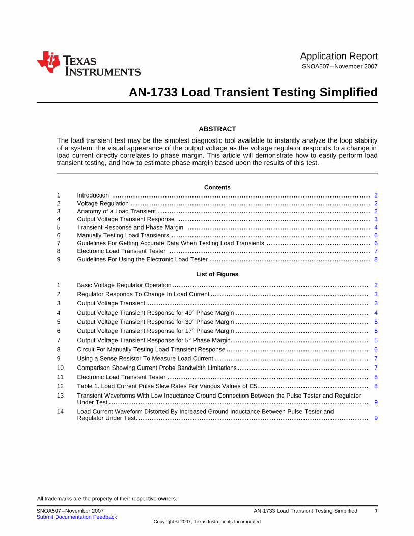
6 Manually Testing Load Transients
A “load step” can be implemented by simply connecting (or disconnecting) the load resistor(s) to theregulator’s output and observing the change in VOUT (Figure 8).
Manual testing provides a quick and easy way to check phase margin and transient response, but doesnot allow for adjustment of the rise time of the load current pulse. The di/dt rate of the current pulse isprimarily determined by the lead inductance in series with the load resistor.
Figure 8. Circuit For Manually Testing Load Transient Response
7 Guidelines For Getting Accurate Data When Testing Load Transients1. The switch shown as “contact” can be a mechanical switch or the ends of two clip leads. The load
resistor can also be soldered to the ground pad on the PC board and tapped on the output terminal tocreate the load pulse.
2. The negative side of the output capacitor MUST be used as a single point ground for all connections.
3. The oscilloscope used to read the output waveform must be connected DIRECTLY across COUT.
4. Use a storage scope with single sweep capture capability (TEKTRONIX TDS 3014 or similar). Set thescope to trigger on negative going transients, since the output will drop the instant the load isconnected.
5. The input capacitor CIN must be sufficient to keep the input source to the regulator under test fromringing when the load step is applied. Any high frequency ringing on the input will be conductedthrough and seen on the output waveform. To prevent this, CIN may need to be substantial:recommended values for CIN are about 100 µF ceramic capacitance paralleled by an ultra-low ESRelectrolytic capacitor of at least 1000 µF. The grounds of these capacitors must connect directly to thesingle point ground.
6. Metal-oxide or metal-film resistors work best as load resistors for transient load testing because theyare non-inductive.
7. If the current step is to be measured on an oscilloscope, use a resistor and NOT a current probe(Figure 9). The scope’s trigger can be activated by the rising edge of the current pulse seen acrossRSENSE.
A sense resistor should be used because the bandwidth limitations of even very good current probes willnot allow them to accurately measure the rising edges of the current waveform which may exceed slewrates of 50A/µs. A metal-film resistor of 50 mΩ value was used for my data. Make certain the ground endof this resistor is tied directly to the negative side of the output capacitor, or ringing will be induced by theinductance between the ground node and the resistor.
Figure 10 shows a comparison of the actual current waveform (measured across the 50 mΩ resistor)produced by a 0.1A - 3A load step and the waveform produced by a Tektronix AM503 current probemeasuring the same current. The rate of change of the load current was measured as about 75A/µs (3Arise in about 40 ns).
6 AN-1733 Load Transient Testing Simplified SNOA507–November 2007Submit Documentation Feedback
Copyright © 2007, Texas Instruments Incorporated

www.ti.com Electronic Load Transient Tester
Figure 9. Using a Sense Resistor To Measure Load Current
Figure 10. Comparison Showing Current Probe Bandwidth Limitations
As shown, the waveform from the current probe shows a slow and rounded leading edge due to it’sbandwidth limitations when trying to measure a very fast current change.
Manual testing gives an easy technique to evaluate loop stability, but the main limitation of this method isthat the rise and fall times of the current step are not adjustable. The next section presents how to buildan electronic load with adjustable slew rate.
8 Electronic Load Transient Tester
An inexpensive electronic load can be built which allows the user to adjust the rise and fall time of the loadcurrent (Figure 11).
The circuit uses N-FET (Q1) as a switch, which allows current to flow through the load resistance (R10)when it’s gate is driven on. R10 should be selected to provide the desired load current when Q1 is on. The50 mΩ resistor (R11) is used to sense the current in case a current waveform is desired (it can be deletedif current monitoring is not needed). Any good N-FET with low ON resistance and good switchingcharacteristics can be used for Q1. Since the tester usually operates at a low duty cycle, power dissipationin the FET is not excessive and PCB copper can provide adequate heatsinking for most applications. C6and R9 are used to reduce the ringing across Q1 when it switches.
U1 is a free-running oscillator whose frequency is adjusted by R2. U2 is a one-shot triggered by U1, andthe on time of the one shot is adjusted by R6. Using R2 and R6, both the frequency and duty cycle of theload pulse may be varied. For the components shown, the frequency can be adjusted from about 130 Hzup to about 2 kHz, and the pulse width can be adjusted from about 20 µs to 400 µs.
The rise and fall times of the load current pulse can be adjusted by varying the rise and fall time of thevoltage applied to the gate of Q1. Since the output of U2 drives the gate of Q1, an R-C network whichslows the rise (and fall) time of this voltage will provide the desired adjustment to the di/dt rate of the loadcurrent pulse. R8 working with C5 slows the rise time of the gate voltage, while R7 working with C5 slowsthe fall time (D1 and D2 isolate the rising and falling drive signals so they can be adjusted independently).
The value of C5 must be adjusted based on the rise/fall times desired: for fastest possible rise times(50A/µs or more) C5 can be omitted. For slow rise times (like 0.5A/µs), a value of about 0.1 µF can beused, with R7 and R8 dialing in the slew rate of each edge.
7SNOA507–November 2007 AN-1733 Load Transient Testing SimplifiedSubmit Documentation Feedback
Copyright © 2007, Texas Instruments Incorporated

Guidelines For Using the Electronic Load Tester www.ti.com
When selecting C5, it should be noted the drive to the gate of Q1 is not symmetric: the output of U2 pullsup to about 11V, but only pulls down to ground. So, the FET has much stronger gate drive turning ONthan OFF, which will tend to make the rising edge of the load pulse faster than the falling edge.
Table 1 shows the load current pulse slew rates which can be obtained by adjusting R7 and R8 fromminimum to maximum for various values of C5. This data was taken for a 0 – 3A load current pulse.
If equal times are desired for the rising and falling edges: The rising edge has a wider min/max rangeof slew rate for any given value of C5. Therefore, C5 should be selected so the desired value of the fallingedge slew rate is within the ranges shown in Table 1. Then, adjust R7 until the falling edge slew rate iscorrect and adjust R8 to get the rising edge to match the falling edge.
Figure 11. Electronic Load Transient Tester
Figure 12. Table 1. Load Current Pulse Slew Rates For Various Values of C5
9 Guidelines For Using the Electronic Load Tester1. Minimize all trace lengths along the current path from the input to output, through the FET. Inductance
along this path will degrade rise time and cause ringing.
2. Use low inductance resistors like metal-film or metal-oxide for load and sense resistors.
3. The ground connection tying the tester negative terminal to the negative output of the regulator is mostcritical: the scope probe measuring VOUT has it’s ground lead connected to the ground side of COUT. Theprobe measuring across the current sense resistor (R11) has it’s ground connected to the negativeside of the sense resistor. The electrical connection between those two nodes must be low inductanceor ringing will occur, distorting the current waveform. If necessary, the current sense resistor can bephysically moved to the regulator ground (on the negative side of COUT) so there will be no groundbounce between the scope ground points.
To illustrate the effects of ground bounce caused by inductance between the two ground points, Figure 13shows a transient scope shot of both the regulated output and the current waveform measured acrossR11. In this case, the tester negative load terminal was connected to the regulator ‘s output capacitornegative terminal via a piece of copper braid about ¼” wide and ¾” in length, which has fairly lowinductance:
8 AN-1733 Load Transient Testing Simplified SNOA507–November 2007Submit Documentation Feedback
Copyright © 2007, Texas Instruments Incorporated

www.ti.com Guidelines For Using the Electronic Load Tester
Figure 13. Transient Waveforms With Low Inductance Ground Connection Between the Pulse Tester andRegulator Under Test
To increase the amount of ground lead inductance, the same measurement as shown in Figure 13 wasrepeated EXCEPT that the ground lead between the negative side of the regulator’s output capacitor andthe negative terminal of the pulse tester was connected using a 2” piece of 18# wire (which has moreinductance than the short lead used in the first test). Figure 14 shows the degradation in the load currentwaveform due to ground bounce resulting from the voltage developed across the inductance of the 2” wirewhich causes the ground of the scope probe connected across the current sense resistor to bounce withrespect to probe measuring the output voltage.
Figure 14. Load Current Waveform Distorted By Increased Ground Inductance Between Pulse Tester andRegulator Under Test
In comparing with Figure 13, it can be seen that the current waveform in Figure 14 shows excessiveovershoot in both directions and also the peak amplitude is larger than actual value. A very closeexamination of Figure 13 shows the current waveform there also shows very slight overshoot (the effectsof ground lead inductance) since no lead has zero inductance. But, when inductance is excessive theaccuracy of the reading is corrupted (Figure 14). This illustrates why when two scope probes are used,care must be taken that the grounds are not bouncing with respect to each other.
9SNOA507–November 2007 AN-1733 Load Transient Testing SimplifiedSubmit Documentation Feedback
Copyright © 2007, Texas Instruments Incorporated

IMPORTANT NOTICE
Texas Instruments Incorporated and its subsidiaries (TI) reserve the right to make corrections, enhancements, improvements and otherchanges to its semiconductor products and services per JESD46, latest issue, and to discontinue any product or service per JESD48, latestissue. Buyers should obtain the latest relevant information before placing orders and should verify that such information is current andcomplete. All semiconductor products (also referred to herein as “components”) are sold subject to TI’s terms and conditions of salesupplied at the time of order acknowledgment.
TI warrants performance of its components to the specifications applicable at the time of sale, in accordance with the warranty in TI’s termsand conditions of sale of semiconductor products. Testing and other quality control techniques are used to the extent TI deems necessaryto support this warranty. Except where mandated by applicable law, testing of all parameters of each component is not necessarilyperformed.
TI assumes no liability for applications assistance or the design of Buyers’ products. Buyers are responsible for their products andapplications using TI components. To minimize the risks associated with Buyers’ products and applications, Buyers should provideadequate design and operating safeguards.
TI does not warrant or represent that any license, either express or implied, is granted under any patent right, copyright, mask work right, orother intellectual property right relating to any combination, machine, or process in which TI components or services are used. Informationpublished by TI regarding third-party products or services does not constitute a license to use such products or services or a warranty orendorsement thereof. Use of such information may require a license from a third party under the patents or other intellectual property of thethird party, or a license from TI under the patents or other intellectual property of TI.
Reproduction of significant portions of TI information in TI data books or data sheets is permissible only if reproduction is without alterationand is accompanied by all associated warranties, conditions, limitations, and notices. TI is not responsible or liable for such altereddocumentation. Information of third parties may be subject to additional restrictions.
Resale of TI components or services with statements different from or beyond the parameters stated by TI for that component or servicevoids all express and any implied warranties for the associated TI component or service and is an unfair and deceptive business practice.TI is not responsible or liable for any such statements.
Buyer acknowledges and agrees that it is solely responsible for compliance with all legal, regulatory and safety-related requirementsconcerning its products, and any use of TI components in its applications, notwithstanding any applications-related information or supportthat may be provided by TI. Buyer represents and agrees that it has all the necessary expertise to create and implement safeguards whichanticipate dangerous consequences of failures, monitor failures and their consequences, lessen the likelihood of failures that might causeharm and take appropriate remedial actions. Buyer will fully indemnify TI and its representatives against any damages arising out of the useof any TI components in safety-critical applications.
In some cases, TI components may be promoted specifically to facilitate safety-related applications. With such components, TI’s goal is tohelp enable customers to design and create their own end-product solutions that meet applicable functional safety standards andrequirements. Nonetheless, such components are subject to these terms.
No TI components are authorized for use in FDA Class III (or similar life-critical medical equipment) unless authorized officers of the partieshave executed a special agreement specifically governing such use.
Only those TI components which TI has specifically designated as military grade or “enhanced plastic” are designed and intended for use inmilitary/aerospace applications or environments. Buyer acknowledges and agrees that any military or aerospace use of TI componentswhich have not been so designated is solely at the Buyer's risk, and that Buyer is solely responsible for compliance with all legal andregulatory requirements in connection with such use.
TI has specifically designated certain components which meet ISO/TS16949 requirements, mainly for automotive use. Components whichhave not been so designated are neither designed nor intended for automotive use; and TI will not be responsible for any failure of suchcomponents to meet such requirements.
Products Applications
Audio www.ti.com/audio Automotive and Transportation www.ti.com/automotive
Amplifiers amplifier.ti.com Communications and Telecom www.ti.com/communications
Data Converters dataconverter.ti.com Computers and Peripherals www.ti.com/computers
DLP® Products www.dlp.com Consumer Electronics www.ti.com/consumer-apps
DSP dsp.ti.com Energy and Lighting www.ti.com/energy
Clocks and Timers www.ti.com/clocks Industrial www.ti.com/industrial
Interface interface.ti.com Medical www.ti.com/medical
Logic logic.ti.com Security www.ti.com/security
Power Mgmt power.ti.com Space, Avionics and Defense www.ti.com/space-avionics-defense
Microcontrollers microcontroller.ti.com Video and Imaging www.ti.com/video
RFID www.ti-rfid.com
OMAP Applications Processors www.ti.com/omap TI E2E Community e2e.ti.com
Wireless Connectivity www.ti.com/wirelessconnectivity
Mailing Address: Texas Instruments, Post Office Box 655303, Dallas, Texas 75265Copyright © 2012, Texas Instruments Incorporated