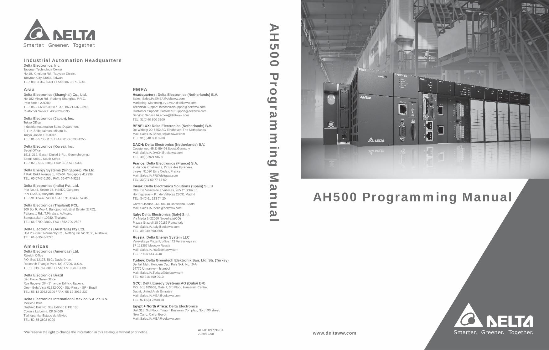
AH500 Programming Manual - Delta EMEA
829
Industrial Automation Headquarters Delta Electronics, Inc. Taoyuan Technology Center No.18, Xinglong Rd., Taoyuan District, Taoyuan City 33068, Taiwan TEL: 886-3-362-6301 / FAX: 886-3-371-6301 Asia Delta Electronics (Shanghai) Co., Ltd. No.182 Minyu Rd., Pudong Shanghai, P.R.C. Post code : 201209 TEL: 86-21-6872-3988 / FAX: 86-21-6872-3996 Customer Service: 400-820-9595 Delta Electronics (Japan), Inc. Tokyo Office Industrial Automation Sales Department 2-1-14 Shibadaimon, Minato-ku Tokyo, Japan 105-0012 TEL: 81-3-5733-1155 / FAX: 81-3-5733-1255 Delta Electronics (Korea), Inc. Seoul Office 1511, 219, Gasan Digital 1-Ro., Geumcheon-gu, Seoul, 08501 South Korea TEL: 82-2-515-5305 / FAX: 82-2-515-5302 Delta Energy Systems (Singapore) Pte Ltd. 4 Kaki Bukit Avenue 1, #05-04, Singapore 417939 TEL: 65-6747-5155 / FAX: 65-6744-9228 Delta Electronics (India) Pvt. Ltd. Plot No.43, Sector 35, HSIIDC Gurgaon, PIN 122001, Haryana, India TEL: 91-124-4874900 / FAX : 91-124-4874945 Delta Electronics (Thailand) PCL. 909 Soi 9, Moo 4, Bangpoo Industrial Estate (E.P.Z), Pattana 1 Rd., T.Phraksa, A.Muang, Samutprakarn 10280, Thailand TEL: 66-2709-2800 / FAX : 662-709-2827 Delta Electronics (Australia) Pty Ltd. Unit 20-21/45 Normanby Rd., Notting Hill Vic 3168, Australia TEL: 61-3-9543-3720 Americas Delta Electronics (Americas) Ltd. Raleigh Office P.O. Box 12173, 5101 Davis Drive, Research Triangle Park, NC 27709, U.S.A. TEL: 1-919-767-3813 / FAX: 1-919-767-3969 Delta Electronics Brazil São Paulo Sales Office Rua Itapeva, 26 - 3°, andar Edificio Itapeva, One - Bela Vista 01332-000 - São Paulo - SP - Brazil TEL: 55-12-3932-2300 / FAX: 55-12-3932-237 Delta Electronics International Mexico S.A. de C.V. Mexico Office Gustavo Baz No. 309 Edificio E PB 103 Colonia La Loma, CP 54060 Tlalnepantla, Estado de México TEL: 52-55-3603-9200 *We reserve the right to change the information in this catalogue without prior notice. EMEA Headquarters: Delta Electronics (Netherlands) B.V. Sales: [email protected] Marketing: [email protected] Technical Support: [email protected] Customer Support: [email protected] Service: [email protected] TEL: 31(0)40 800 3900 BENELUX: Delta Electronics (Netherlands) B.V. De Witbogt 20, 5652 AG Eindhoven, The Netherlands Mail: [email protected] TEL: 31(0)40 800 3900 DACH: Delta Electronics (Netherlands) B.V. Coesterweg 45, D-59494 Soest, Germany Mail: [email protected] TEL: 49(0)2921 987 0 France: Delta Electronics (France) S.A. ZI du bois Challand 2, 15 rue des Pyrénées, Lisses, 91090 Evry Cedex, France Mail: [email protected] TEL: 33(0)1 69 77 82 60 Iberia: Delta Electronics Solutions (Spain) S.L.U Ctra. De Villaverde a Vallecas, 265 1º Dcha Ed. Hormigueras – P.I. de Vallecas 28031 Madrid TEL: 34(0)91 223 74 20 Carrer Llacuna 166, 08018 Barcelona, Spain Mail: [email protected] Italy: Delta Electronics (Italy) S.r.l. Via Meda 2–22060 Novedrate(CO) Piazza Grazioli 18 00186 Roma Italy Mail: [email protected] TEL: 39 039 8900365 Russia: Delta Energy System LLC Vereyskaya Plaza II, office 112 Vereyskaya str. 17 121357 Moscow Russia Mail: [email protected] TEL: 7 495 644 3240 Turkey: Delta Greentech Elektronik San. Ltd. Sti. (Turkey) Şerifali Mah. Hendem Cad. Kule Sok. No:16-A 34775 Ümraniye – İstanbul Mail: [email protected] TEL: 90 216 499 9910 GCC: Delta Energy Systems AG (Dubai BR) P.O. Box 185668, Gate 7, 3rd Floor, Hamarain Centre Dubai, United Arab Emirates Mail: [email protected] TEL: 971(0)4 2690148 Egypt + North Africa: Delta Electronics Unit 318, 3rd Floor, Trivium Business Complex, North 90 street, New Cairo, Cairo, Egypt Mail: [email protected] AH500 Programming Manual www.deltaww.com AH500 Programming Manual AH-0109720-04 2020/12/08
-
Upload
khangminh22 -
Category
Documents
-
view
0 -
download
0
Transcript of AH500 Programming Manual - Delta EMEA
Industrial Automation HeadquartersDelta Electronics, Inc. Taoyuan Technology CenterNo.18, Xinglong Rd., Taoyuan District, Taoyuan City 33068, TaiwanTEL: 886-3-362-6301 / FAX: 886-3-371-6301
AsiaDelta Electronics (Shanghai) Co., Ltd.No.182 Minyu Rd., Pudong Shanghai, P.R.C.Post code : 201209 TEL: 86-21-6872-3988 / FAX: 86-21-6872-3996Customer Service: 400-820-9595
Delta Electronics (Japan), Inc.Tokyo Office Industrial Automation Sales Department 2-1-14 Shibadaimon, Minato-kuTokyo, Japan 105-0012TEL: 81-3-5733-1155 / FAX: 81-3-5733-1255
Delta Electronics (Korea), Inc.Seoul Office1511, 219, Gasan Digital 1-Ro., Geumcheon-gu, Seoul, 08501 South KoreaTEL: 82-2-515-5305 / FAX: 82-2-515-5302
Delta Energy Systems (Singapore) Pte Ltd.4 Kaki Bukit Avenue 1, #05-04, Singapore 417939TEL: 65-6747-5155 / FAX: 65-6744-9228
Delta Electronics (India) Pvt. Ltd.Plot No.43, Sector 35, HSIIDC Gurgaon, PIN 122001, Haryana, IndiaTEL: 91-124-4874900 / FAX : 91-124-4874945
Delta Electronics (Thailand) PCL. 909 Soi 9, Moo 4, Bangpoo Industrial Estate (E.P.Z), Pattana 1 Rd., T.Phraksa, A.Muang, Samutprakarn 10280, ThailandTEL: 66-2709-2800 / FAX : 662-709-2827
Delta Electronics (Australia) Pty Ltd.Unit 20-21/45 Normanby Rd., Notting Hill Vic 3168, AustraliaTEL: 61-3-9543-3720
AmericasDelta Electronics (Americas) Ltd.Raleigh OfficeP.O. Box 12173, 5101 Davis Drive, Research Triangle Park, NC 27709, U.S.A.TEL: 1-919-767-3813 / FAX: 1-919-767-3969
Delta Electronics Brazil São Paulo Sales Office Rua Itapeva, 26 - 3°, andar Edificio Itapeva, One - Bela Vista 01332-000 - São Paulo - SP - Brazil TEL: 55-12-3932-2300 / FAX: 55-12-3932-237
Delta Electronics International Mexico S.A. de C.V.Mexico OfficeGustavo Baz No. 309 Edificio E PB 103Colonia La Loma, CP 54060Tlalnepantla, Estado de MéxicoTEL: 52-55-3603-9200
*We reserve the right to change the information in this catalogue without prior notice.
EMEAHeadquarters: Delta Electronics (Netherlands) B.V. Sales: [email protected] Marketing: [email protected] Technical Support: [email protected] Customer Support: [email protected] Service: [email protected]: 31(0)40 800 3900
BENELUX: Delta Electronics (Netherlands) B.V.De Witbogt 20, 5652 AG Eindhoven, The Netherlands Mail: [email protected]: 31(0)40 800 3900
DACH: Delta Electronics (Netherlands) B.V.Coesterweg 45, D-59494 Soest, GermanyMail: [email protected]: 49(0)2921 987 0
France: Delta Electronics (France) S.A.ZI du bois Challand 2, 15 rue des Pyrénées, Lisses, 91090 Evry Cedex, France Mail: [email protected]: 33(0)1 69 77 82 60
Iberia: Delta Electronics Solutions (Spain) S.L.UCtra. De Villaverde a Vallecas, 265 1º Dcha Ed. Hormigueras – P.I. de Vallecas 28031 Madrid TEL: 34(0)91 223 74 20
Carrer Llacuna 166, 08018 Barcelona, SpainMail: [email protected]
Italy: Delta Electronics (Italy) S.r.l.Via Meda 2–22060 Novedrate(CO) Piazza Grazioli 18 00186 Roma ItalyMail: [email protected]: 39 039 8900365
Russia: Delta Energy System LLC Vereyskaya Plaza II, office 112 Vereyskaya str. 17 121357 Moscow Russia Mail: [email protected]: 7 495 644 3240
Turkey: Delta Greentech Elektronik San. Ltd. Sti. (Turkey) Şerifali Mah. Hendem Cad. Kule Sok. No:16-A 34775 Ümraniye – İstanbulMail: [email protected]: 90 216 499 9910
GCC: Delta Energy Systems AG (Dubai BR)P.O. Box 185668, Gate 7, 3rd Floor, Hamarain Centre Dubai, United Arab Emirates Mail: [email protected]: 971(0)4 2690148
Egypt + North Africa: Delta ElectronicsUnit 318, 3rd Floor, Trivium Business Complex, North 90 street, New Cairo, Cairo, Egypt Mail: [email protected]
AH500 Programming Manual
www.deltaww.com
AH
500 Prog
ramm
ing
Man
ual
AH-0109720-042020/12/08
JOYCELW.CHOU
打字機文字
JOYCELW.CHOU
打字機文字
AH500 Programming Manual Revision History
Version Revision Date
1st The first version is published. 2012/11/09
2nd
1. Chapter 1: updated the model description in section 1.1.2 2. Chapter 2: updated device list in section 2.1.1, latched areas in
the device range in section 2.1.4, strings in section 2.2.3, special auxiliary relays in section 2.2.7, refresh time of special data registers in section 2.2.8, special data registers in section 2.2.14, refresh time of special data registers in section 2.2.15, additional remarks on special auxiliary relays and special data registers in section 2.2.16.
3. Chapter 3: added new instructions of API0117, API0118, API0708 and API1812.
4. Chapter 4: updated restrictions on the use of the instructions in section 4.2.
5. Chapter 6: added new instructions of API0114, API0204, API0205, API0212, API0217, API0218, API0219, API0310, API0702, API0703, API0705, API0707, API1000, API1002, API1003, API1004, API1301, API1510, API1516, API1701, API1702, API1703, API1704, API1800, API1803, API1806, API1807, API1809, API1810, API1811, API2100, API2103, API2108, API2110, API2200, API2201, API2202, API2203, API2204, API2205, and API2300.
6. Chapter 7: updated contents of 7.1.1, 7.1.2, 7.1.3, 7.1.4, 7.1.8, 7.1.9, and 7.1.10.
2016/08/15
3rd
1. Chapter 1: updated contents in section 1.1.1 and added information for new models including AH15SCM-5A, AHRTU-ETHN-5A, AH15EN-5A, AHCPU501-RS2, AHCPU521-RS2, AHCPU531-RS2, AHCPU501-EN. Revise the wiring model name.
2. Chapter 2: updated ASCII table in section 2.2.3 and added information for new models including AHCPU560-EN2, AHCPU501-RS2, AHCPU521-RS2, AHCPU531-RS2, and AHCPU501-EN. Added and update information concerning SM/SR in section 2.2.8, 2.2.14, 2.2.15 and 2.2.16.
3. Chapter 3: Added new API2900 and API2901 in the instruction table and updated INV symbol in section 3.3.
4. Chapter 6: Updated the following APIs 0702, 0904, 1111, 1503-1505, 1701, 1702, 1800, 1812, 2116, 2200, 2300-2302, 2900 and 2901.
5. Chapter 7: Updated contents in section 7.1.1 and added information for new models AH15SCM-5A and AH15EN-5A.
2018/06/05

i i
Version Revision Date
4th
1. Chapter 2: added new product information for AHAHCPU521-DNP3 in section 2.2.7. Added new flag information for SM454-SM457, SM2304-SM2319, and updated flag information for SM2048-SM2303. Added new product information for AHCPU521-DNP3 in section 2.2.14. Added new flag information for SR418-SR430, SR900-SR902, SR2046-SR2047and updated flag information for SR2048-SR2559. Updated item 15 “Setting the TCP/UDP Socket”, updated item 19 “The flags related to power module”, updated item 20 “The connection status of the redundant extension backplane” and updated item 22 “The flags related to EtherNet/IP” in section 2.2.16.
2. Chapter 3: Added new API1607 and API2208 in section 3.1.2. Added 64-bit instructions in section 3.4. Added new contents for API1607 and API2208.
3. Chapter 6: Updated API0104: adding item 2 in the explanation section; API1103: updating examples; API1401: adding explanation on the application of AH Redundancy System; API1500-1516: adding 64-bit instruction related explanation; API1607, API1808: adding explanation on 0x05 and 0x06. Added new API2208 and updated API2901: explanation on operands D and S.
4. Chapter 7: Added new error codes, 16#0068, 16#212A, 16#6013, 16#E206-16#E28B, 16#E2A0-16#E2AB, and updated error codes, 16#2026, 16#2029, 16#6010, 16#6011, 16#6212-16#6214, 16#6218-16#621A, 16#6400-16#6405.
2020/12/08
i
AH500 Programming Manual
Contents Chapter 1 Introduction 1.1 Overview ............................................................................................. 1-2
1.1.1 Related Manuals ............................................................................ 1-2
1.1.2 Model Description .......................................................................... 1-3
1.2 Software ............................................................................................ 1-10
1.2.1 Program Editor ............................................................................ 1-10
1.2.2 Program Organization Units and Tasks ............................................ 1-12
Chapter 2 Devices 2.1 Introduction of Devices ......................................................................... 2-2
2.1.1 Devise List .................................................................................... 2-2
2.1.2 Basic Structure of I/O Storages ....................................................... 2-4
2.1.3 Relation between the PLC Action and the Device Type ......................... 2-4
2.1.4 Latched Areas in the Device Range ................................................... 2-5
2.2 Functions of Devices ............................................................................. 2-6
2.2.1 Values and Constants ..................................................................... 2-6
2.2.2 Floating-point Numbers .................................................................. 2-8
2.2.3 Strings ....................................................................................... 2-10
2.2.4 Input Relays ................................................................................ 2-11
2.2.5 Output Relays .............................................................................. 2-11
2.2.6 Auxiliary Relays ........................................................................... 2-12
2.2.7 Special Auxiliary Relays ................................................................ 2-12
2.2.8 Refresh Time of Special Auxiliary Relays ......................................... 2-40
2.2.9 Stepping Relays ........................................................................... 2-48
2.2.10 Timers ........................................................................................ 2-48
2.2.11 Counters ..................................................................................... 2-50
2.2.12 32-bit Counters ........................................................................... 2-51
2.2.13 Data Registers ............................................................................. 2-53
2.2.14 Special Data Registers .................................................................. 2-54
2.2.15 Refresh Time of Special Data Registers ........................................... 2-83
2.2.16 Additional Remarks on Special Auxiliary Relays and Special Data
Registers .................................................................................... 2-86
2.2.17 Link Registers ............................................................................. 2-101
2.2.18 Index Registers ........................................................................... 2-101
i i
Chapter 3 Instruction Tables 3.1 Instructions ...................................................................................... 3-2
3.1.1 Basic Instructions .......................................................................... 3-2
3.1.2 Applied Instructions ....................................................................... 3-3
3.2 Instruction Tables .............................................................................. 3-4
3.2.1 Basic Instructions .......................................................................... 3-4
3.2.2 Applied Instructions ....................................................................... 3-5
3.2.3 Applied Instructions (Sorted Alphabetically) ...................................... 3-6
3.2.4 Device Tables ................................................................................ 3-7
3.3 Lists of Basic Instructions ................................................................... 3-8
3.4 Lists of Applied Instructions ............................................................... 3-11
3.4.1 Applied Instructions ...................................................................... 3-11
3.4.2 Applied Instructions (Sorted Alphabetically) ..................................... 3-37
Chapter 4 Analog Input/Output Module 4.1 Composition of Applied Instructions ...................................................... 4-2
4.2 Restrictions on the Use of the Instructions ............................................. 4-6
4.3 Index Registers .................................................................................. 4-7
4.4 Pointer Registers ................................................................................ 4-9
4.5 Pointer Registers of Timers ................................................................. 4-11
4.6 Pointer Registers of 16-bit Counters ..................................................... 4-13
4.7 Pointer Registers of 32-bit Counters ..................................................... 4-15
Chapter 5 Basic Instructions 5.1 List of Basic Instructions........................................................................ 5-2
5.2 Basic Instructions ................................................................................. 5-3
Chapter 6 Applied Instructions 6.1 Comparison Instructions ........................................................................ 6-3
6.1.1 List of Comparison Instructions ...................................................... 6-3
6.1.2 Explanation of Comparison Instructions ........................................... 6-6
6.2 Arithmetic Instructions ......................................................................... 6-36
6.2.1 List of Arithmetic Instructions ........................................................ 6-36
6.2.2 Explanation of Arithmetic Instructions ............................................ 6-37
6.3 Data Conversion Instructions ................................................................ 6-74
6.3.1 List of Data Conversion Instructions ............................................... 6-74
6.3.2 Explanation of Data Conversion Instructions .................................... 6-75
6.4 Data Transfer Instructions ................................................................... 6-112
i i i
6.4.1 List of Data Transfer Instructions ................................................. 6-112
6.4.2 Explanation of Data Transfer Instructions ...................................... 6-113
6.5 Jump Instructions .............................................................................. 6-135
6.5.1 List of Jump Instructions ............................................................. 6-135
6.5.2 Explanation of Jump Instructions ................................................. 6-136
6.6 Program Execution Instructions ........................................................... 6-144
6.6.1 List of Program Execution Instructions .......................................... 6-144
6.6.2 Explanation of Program Execution Instructions .............................. 6-145
6.7 I/O Refreshing Instructions ................................................................. 6-152
6.7.1 List of I/O Refreshing Instructions ................................................ 6-152
6.7.2 Explanation of I/O Refreshing Instructions .................................... 6-153
6.8 Miscellaneous Instructions .................................................................. 6-155
6.8.1 List of Miscellaneous Instructions ................................................. 6-155
6.8.2 Explanation of Miscellaneous Instructions ...................................... 6-156
6.9 Logic Instructions .............................................................................. 6-193
6.9.1 List of Logic Instructions ............................................................. 6-193
6.9.2 Explanation of Logic Instructions .................................................. 6-194
6.10 Rotation Instructions .......................................................................... 6-217
6.10.1 List of Rotation Instructions ......................................................... 6-217
6.10.2 Explanation of Rotation Instructions ............................................. 6-218
6.11 Timer and Counter Instructions ........................................................... 6-228
6.11.1 List of Timer and Counter Instructions .......................................... 6-228
6.11.2 Explanation of Timer and Counter Instructions............................... 6-229
6.12 Shift Instructions ............................................................................... 6-236
6.12.1 List of Shift Instructions .............................................................. 6-236
6.12.2 Explanation of Shift Instructions .................................................. 6-237
6.13 Data Processing Instructions ............................................................... 6-263
6.13.1 List of Data Processing Instructions .............................................. 6-263
6.13.2 Explanation of Data Processing Instructions .................................. 6-264
6.14 Structure Creation Instructions ............................................................ 6-308
6.14.1 List of Structure Creation Instructions .......................................... 6-308
6.14.2 Explanation of Structure Creation Instructions ............................... 6-309
6.15 Module Instructions ............................................................................ 6-316
6.15.1 List of Module Instructions .......................................................... 6-316
6.15.2 Explanation of Module Instructions ............................................... 6-317
6.16 Floating-point Number Instructions ...................................................... 6-322
6.16.1 List of Floating-point Number Instructions ..................................... 6-322
6.16.2 Explanation of Floating-point Number Instructions ......................... 6-323
i v
6.17 Real-time Clock Instructions ............................................................... 6-367
6.17.1 List of Real-time Clock Instructions .............................................. 6-367
6.17.2 Explanation of Real-time Clock Instructions ................................... 6-368
6.18 Peripheral Instructions ....................................................................... 6-391
6.18.1 List of Peripheral Instructions ...................................................... 6-391
6.18.2 Explanation of Peripheral Instructions ........................................... 6-392
6.19 Communication Instructions ................................................................ 6-405
6.19.1 List of Communication Instructions .............................................. 6-405
6.19.2 Explanation of Communication Instructions ................................... 6-406
6.20 Other Instructions ............................................................................. 6-442
6.20.1 List of Other Instructions ............................................................ 6-442
6.20.2 Explanation of Other Instructions ................................................. 6-443
6.21 String Processing Instructions ............................................................. 6-452
6.21.1 List of String Processing Instructions ............................................ 6-452
6.21.2 Explanation of String Processing Instructions ................................ 6-453
6.22 Ethernet Instructions ......................................................................... 6-514
6.22.1 List of Ethernet Instructions ........................................................ 6-514
6.22.2 Explanation of Ethernet Instructions ............................................. 6-515
6.23 Memory Card Instructions ................................................................... 6-551
6.23.1 List of Memory Card Instructions ................................................. 6-551
6.23.2 Explanation of Memory Card Instructions ...................................... 6-552
6.24 Task Control Instructions .................................................................... 6-563
6.24.1 List of Task Control Instructions ................................................... 6-563
6.24.2 Explanation of Task Control Instructions ....................................... 6-564
6.25 SFC Instructions ................................................................................ 6-566
6.25.1 List of SFC Instructions ............................................................... 6-566
6.25.2 Explanation of SFC Instructions ................................................... 6-567
6.26 Redundant Instructions ...................................................................... 6-573
6.26.1 List of Redundant Instructions ..................................................... 6-573
6.26.2 Explanation of Redundant Instructions .......................................... 6-574
Chapter 7 Error Codes 7.1 Error Codes and LED Indicators .............................................................. 7-2
7.1.1 CPU Modules ................................................................................. 7-3
7.1.2 Analog I/O Modules and Temperature Measurement Modules ............. 7-26
7.1.3 AH02HC-5A/AH04HC-5A ................................................................ 7-28
7.1.4 AH05PM-5A / AH10PM-5A / AH15PM-5A .......................................... 7-29

v
7.1.5 AH20MC-5A ................................................................................. 7-30
7.1.6 AH10EN-5A / AH-15EN-5A ............................................................ 7-31
7.1.7 AH10SCM-5A / AH15SCM-5A ......................................................... 7-31
7.1.8 AH10DNET-5A ............................................................................. 7-31
7.1.9 AH10PFBM-5A ............................................................................. 7-32
7.1.10 AH10PFBS-5A .............................................................................. 7-33
7.1.11 AH10COPM-5A ............................................................................. 7-33

1-1
Chapter 1 Introduction
Table of Contents 1.1 Overview .................................................................................................. 1-2
1.1.1 Related Manuals ............................................................................... 1-2 1.1.2 Model Description .............................................................................. 1-3
1.2 Software ..................................................................................................1-10 1.2.1 Program Editor .................................................................................1-10 1.2.2 Program Organization Units and Tasks ............................................1-12

AH500 Programming Manual
1-2
1.1 Overview This manual introduces the programming of the AH500 series programmable logic controllers, the basic instructions, and the applied instructions.
1.1.1 Related Manuals
The related manuals of the AH500 series programmable logic controllers are composed of the following. AH500 Quick Start
It guides users to use the system before they read the related manuals. AH500 Programming Manual
It introduces the programming of the AH500 series programmable logic controllers, the basic instructions, and the applied instructions.
ISPSoft User Manual It introduces the use of ISPSoft, the programming languages (ladder diagrams, instruction lists, sequential function charts, function block diagrams, and structured texts), the concept of POUs, and the concept of tasks.
AH500 Hardware Manual It introduces electrical specifications, appearances, dimensions, and etc.
AH500 Operation Manual It introduces functions of CPUs, devices, module tables, troubleshooting, and etc.
AH500 Module Manual It introduces the use of special I/O modules. For example, network modules, analog I/O modules, temperature measurement modules, and etc.
AH500 Motion Control Module Manual It introduces the specifications for the motion control modules, the wiring, the instructions, and the functions.
PMSoft User Manual It introduces the use of PMSoft, including the editing mode, the connection, and the password
setting. AH500 Redundancy System Operation Manual
It introduces the AH500 redundancy structures, establishments, programming designs, and operations.

Chapter 1 Introduct ion
1-3
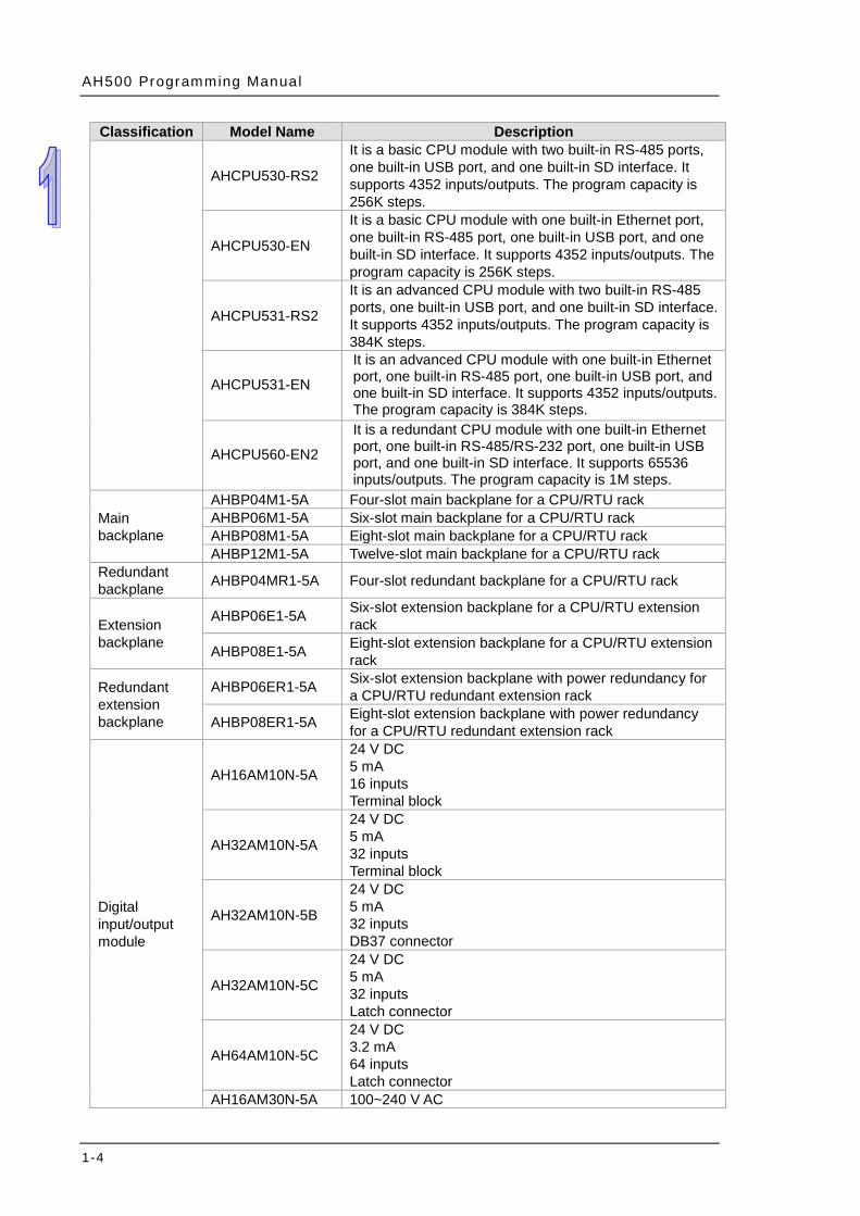
1.1.2 Model Description
Classification Model Name Description
Power supply module
AHPS05-5A 100~240 V AC 50/60 Hz
AHPS15-5A 24 V DC
CPU module
AHCPU500-RS2
It is a basic CPU module with two built-in RS-485 ports, one built-in USB port, and one built-in SD interface. It supports 768 inputs/outputs. The program capacity is 32K steps.
AHCPU500-EN
It is a basic CPU module with one built-in Ethernet port, one built-in RS-485 port, one built-in USB port, and one built-in SD interface. It supports 768 inputs/outputs. The program capacity is 32K steps.
AHCPU501-RS2
It is an advanced CPU module with two built-in RS-485 ports, one built-in USB port, and one built-in SD interface. It supports 768 inputs/outputs. The program capacity is 48K steps.
AHCPU501-EN
It is an advanced CPU module with one built-in Ethernet port, one built-in RS-485 port, one built-in USB port, and one built-in SD interface. It supports 768 inputs/outputs. The program capacity is 48K steps.
AHCPU510-RS2
It is a basic CPU module with two built-in RS-485 ports, one built-in USB port, and one built-in SD interface. It supports 1280 inputs/outputs. The program capacity is 64K steps.
AHCPU510-EN
It is a basic CPU module with one built-in Ethernet port, one built-in RS-485 port, one built-in USB port, and one built-in SD interface. It supports 1280 inputs/outputs. The program capacity is 64K steps.
AHCPU511-RS2
It is an advanced CPU module with two built-in RS-485
ports, one built-in USB port, and one built-in SD interface.
It supports 1280 inputs/outputs. The program capacity is
96K steps.
AHCPU511-EN
It is an advanced CPU module with one built-in Ethernet port, one built-in RS-485 port, one built-in USB port, and one built-in SD interface. It supports 1280 inputs/outputs. The program capacity is 96K steps.
AHCPU520-RS2
It is a basic CPU module with two built-in RS-485 ports, one built-in USB port, and one built-in SD interface. It supports 2304 inputs/outputs. The program capacity is 128K steps.
AHCPU520-EN
It is a basic CPU module with one built-in Ethernet port, one built-in RS-485 port, one built-in USB port, and one built-in SD interface. It supports 2304 inputs/outputs. The program capacity is 128K steps.
AHCPU521-RS2
It is an advanced CPU module with two built-in RS-485 ports, one built-in USB port, and one built-in SD interface. It supports 2304 inputs/outputs. The program capacity is 192K steps.
AHCPU521-EN
It is an advanced CPU module with one built-in Ethernet port, one built-in RS-485 port, one built-in USB port, and one built-in SD interface. It supports 2304 inputs/outputs. The program capacity is 192K steps.
AH500 Programming Manual
1-4
Classification Model Name Description
AHCPU530-RS2
It is a basic CPU module with two built-in RS-485 ports, one built-in USB port, and one built-in SD interface. It supports 4352 inputs/outputs. The program capacity is 256K steps.
AHCPU530-EN
It is a basic CPU module with one built-in Ethernet port, one built-in RS-485 port, one built-in USB port, and one built-in SD interface. It supports 4352 inputs/outputs. The program capacity is 256K steps.
AHCPU531-RS2
It is an advanced CPU module with two built-in RS-485 ports, one built-in USB port, and one built-in SD interface. It supports 4352 inputs/outputs. The program capacity is 384K steps.
AHCPU531-EN
It is an advanced CPU module with one built-in Ethernet port, one built-in RS-485 port, one built-in USB port, and one built-in SD interface. It supports 4352 inputs/outputs. The program capacity is 384K steps.
AHCPU560-EN2
It is a redundant CPU module with one built-in Ethernet port, one built-in RS-485/RS-232 port, one built-in USB port, and one built-in SD interface. It supports 65536 inputs/outputs. The program capacity is 1M steps.
Main backplane
AHBP04M1-5A Four-slot main backplane for a CPU/RTU rack AHBP06M1-5A Six-slot main backplane for a CPU/RTU rack AHBP08M1-5A Eight-slot main backplane for a CPU/RTU rack AHBP12M1-5A Twelve-slot main backplane for a CPU/RTU rack
Redundant backplane AHBP04MR1-5A Four-slot redundant backplane for a CPU/RTU rack
Extension backplane
AHBP06E1-5A Six-slot extension backplane for a CPU/RTU extension rack
AHBP08E1-5A Eight-slot extension backplane for a CPU/RTU extension rack
Redundant extension backplane
AHBP06ER1-5A Six-slot extension backplane with power redundancy for a CPU/RTU redundant extension rack
AHBP08ER1-5A Eight-slot extension backplane with power redundancy for a CPU/RTU redundant extension rack
Digital input/output module
AH16AM10N-5A
24 V DC 5 mA 16 inputs Terminal block
AH32AM10N-5A
24 V DC 5 mA 32 inputs Terminal block
AH32AM10N-5B
24 V DC 5 mA 32 inputs DB37 connector
AH32AM10N-5C
24 V DC 5 mA 32 inputs Latch connector
AH64AM10N-5C
24 V DC 3.2 mA 64 inputs Latch connector
AH16AM30N-5A 100~240 V AC
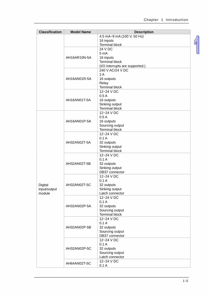
Chapter 1 Introduct ion
1-5
Classification Model Name Description 4.5 mA~9 mA (100 V, 50 Hz) 16 inputs Terminal block
AH16AR10N-5A
24 V DC 5 mA 16 inputs Terminal block (I/O interrupts are supported.)
AH16AN01R-5A
240 V AC/24 V DC 2 A 16 outputs Relay Terminal block
AH16AN01T-5A
12~24 V DC 0.5 A 16 outputs Sinking output Terminal block
Digital input/output module
AH16AN01P-5A
12~24 V DC 0.5 A 16 outputs Sourcing output Terminal block
AH32AN02T-5A
12~24 V DC 0.1 A 32 outputs Sinking output Terminal block
AH32AN02T-5B
12~24 V DC 0.1 A 32 outputs Sinking output DB37 connector
AH32AN02T-5C
12~24 V DC 0.1 A 32 outputs Sinking output Latch connector
AH32AN02P-5A
12~24 V DC 0.1 A 32 outputs Sourcing output Terminal block
AH32AN02P-5B
12~24 V DC 0.1 A 32 outputs Sourcing output DB37 connector
AH32AN02P-5C
12~24 V DC 0.1 A 32 outputs Sourcing output Latch connector
AH64AN02T-5C 12~24 V DC 0.1 A
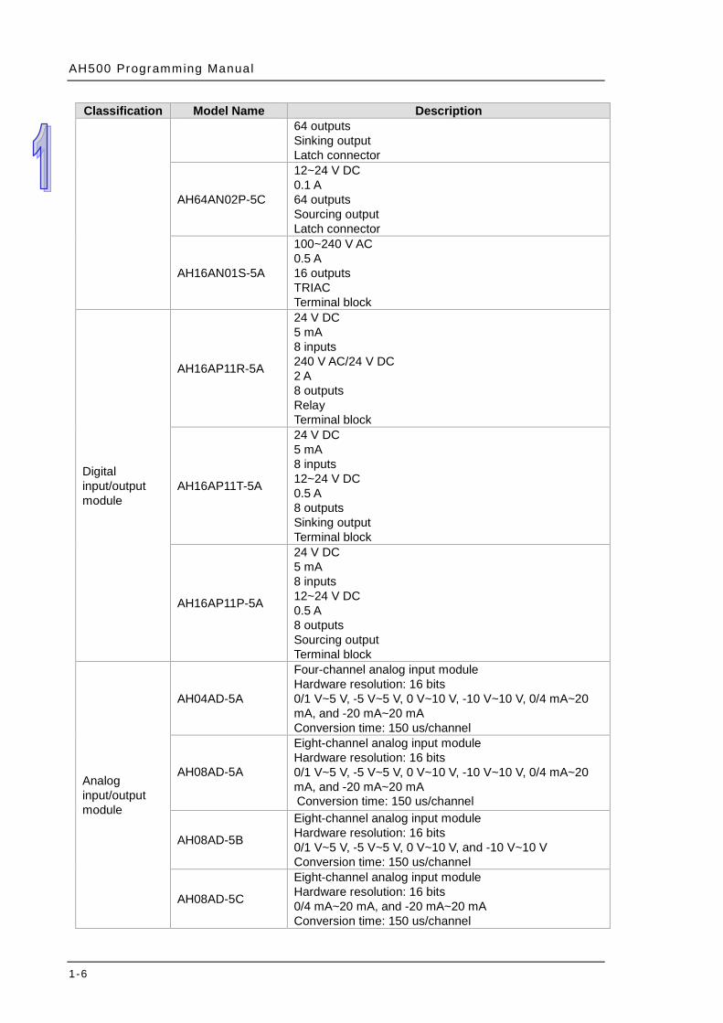
AH500 Programming Manual
1-6
Classification Model Name Description 64 outputs Sinking output Latch connector
AH64AN02P-5C
12~24 V DC 0.1 A 64 outputs Sourcing output Latch connector
AH16AN01S-5A
100~240 V AC 0.5 A 16 outputs TRIAC Terminal block
Digital input/output module
AH16AP11R-5A
24 V DC 5 mA 8 inputs 240 V AC/24 V DC 2 A 8 outputs Relay Terminal block
AH16AP11T-5A
24 V DC 5 mA 8 inputs 12~24 V DC 0.5 A 8 outputs Sinking output Terminal block
AH16AP11P-5A
24 V DC 5 mA 8 inputs 12~24 V DC 0.5 A 8 outputs Sourcing output Terminal block
Analog input/output module
AH04AD-5A
Four-channel analog input module Hardware resolution: 16 bits 0/1 V~5 V, -5 V~5 V, 0 V~10 V, -10 V~10 V, 0/4 mA~20 mA, and -20 mA~20 mA Conversion time: 150 us/channel
AH08AD-5A
Eight-channel analog input module Hardware resolution: 16 bits 0/1 V~5 V, -5 V~5 V, 0 V~10 V, -10 V~10 V, 0/4 mA~20 mA, and -20 mA~20 mA Conversion time: 150 us/channel
AH08AD-5B
Eight-channel analog input module Hardware resolution: 16 bits 0/1 V~5 V, -5 V~5 V, 0 V~10 V, and -10 V~10 V Conversion time: 150 us/channel
AH08AD-5C
Eight-channel analog input module Hardware resolution: 16 bits 0/4 mA~20 mA, and -20 mA~20 mA Conversion time: 150 us/channel

Chapter 1 Introduct ion
1-7
Classification Model Name Description
AH04DA-5A
Four-channel analog output module Hardware resolution: 16 bits 0/1 V~5 V, -5 V~5 V, 0 V~10 V, -10 V~10 V, and 0/4 mA~20 mA Conversion time: 150 us/channel
AH08DA-5A
Eight-channel analog input module Hardware resolution: 16 bits 0/1 V~5 V, -5 V~5 V, 0 V~10 V, -10 V~10 V, 0/4 mA~20 mA Conversion time: 150 us/channel
AH08DA-5B
Eight-channel analog output module Hardware resolution: 16 bits 0/1 V~5 V, -5 V~5 V, 0 V~10 V, and -10 V~10 V Conversion time: 150 us/channel
AH08DA-5C
Eight-channel analog output module Hardware resolution: 16 bits 0/4 mA~20 mA Conversion time: 150 us/channel
Analog input/output module
AH06XA-5A
Four-channel analog input module Hardware resolution: 16 bits 0/1 V~5 V, -5 V~5 V, 0 V~10 V, -10 V~10 V, 0/4 mA~20 mA, and -20 mA~20 mA Conversion time: 150 us/channel Two-channel analog output module Hardware resolution: 16 bits 0/1 V~5 V, -5 V~5 V, 0 V~10 V, -10 V~10 V, and 0/4 mA~20 mA Conversion time: 150 us/channel
Temperature measurement module
AH04PT-5A
Four-channel four-wire/three-wire RTD Sensor type: Pt100/Pt1000/Ni100/Ni1000 sensor, and
0~300 Ω input impedance Resolution: 0.1°C/0.1°F (16 bits) Four-wire conversion time: 150 ms/channel Three-wire conversion time: 300 ms/channel
AH08PTG-5A
Eight-channel four-wire/three-wire/two-wire RTD Sensor type: Pt100/Pt1000/Ni100/Ni1000, and 0~300 Ω
input impedance Resolution: 0.1°C/0.1°F (16 bits) Conversion time: 20 ms/4 channels and 200 ms/8 channels
AH04TC-5A
Four-channel thermocouple Sensor type: J, K, R, S, T, E, N, and -150~+150 mV Resolution: 0.1°C/0.1°F Conversion time: 200 ms/channel
AH08TC-5A
Eight-channel thermocouple Sensor type: J, K, R, S, T, E, N, and -150~+150 mV Resolution: 0.1°C/0.1°F Conversion time: 200 ms/channel
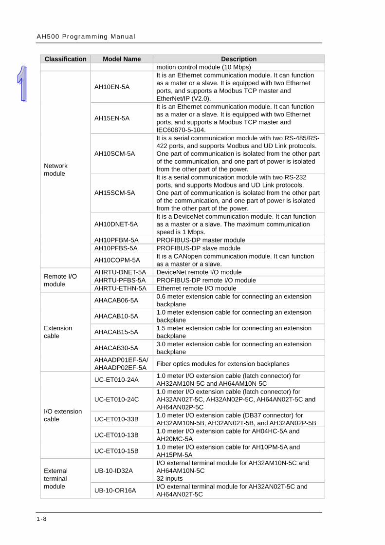
Motion control module
AH02HC-5A Two-channel high-speed counter module (200 kHz) AH04HC-5A Four-channel high-speed counter module (200 kHz) AH05PM-5A Two-axis pulse train motion control module (1 MHz)
AH10PM-5A Six-axis pulse train motion control module (Four axes: 1 MHz; Two axes: 200 kHz)
AH15PM-5A Four-axis pulse train motion control module (1 MHz ) AH20MC-5A Twelve-axis DMCNET (Delta Motion Control Network)
AH500 Programming Manual
1-8
Classification Model Name Description motion control module (10 Mbps)
Network module
AH10EN-5A
It is an Ethernet communication module. It can function as a mater or a slave. It is equipped with two Ethernet ports, and supports a Modbus TCP master and EtherNet/IP (V2.0).
AH15EN-5A
It is an Ethernet communication module. It can function as a mater or a slave. It is equipped with two Ethernet ports, and supports a Modbus TCP master and IEC60870-5-104.
AH10SCM-5A
It is a serial communication module with two RS-485/RS-422 ports, and supports Modbus and UD Link protocols. One part of communication is isolated from the other part of the communication, and one part of power is isolated from the other part of the power.
AH15SCM-5A
It is a serial communication module with two RS-232 ports, and supports Modbus and UD Link protocols. One part of communication is isolated from the other part of the communication, and one part of power is isolated from the other part of the power.
AH10DNET-5A It is a DeviceNet communication module. It can function as a master or a slave. The maximum communication speed is 1 Mbps.
AH10PFBM-5A PROFIBUS-DP master module AH10PFBS-5A PROFIBUS-DP slave module
AH10COPM-5A It is a CANopen communication module. It can function as a master or a slave.
Remote I/O module
AHRTU-DNET-5A DeviceNet remote I/O module AHRTU-PFBS-5A PROFIBUS-DP remote I/O module AHRTU-ETHN-5A Ethernet remote I/O module
Extension cable
AHACAB06-5A 0.6 meter extension cable for connecting an extension backplane
AHACAB10-5A 1.0 meter extension cable for connecting an extension backplane
AHACAB15-5A 1.5 meter extension cable for connecting an extension backplane
AHACAB30-5A 3.0 meter extension cable for connecting an extension backplane
AHAADP01EF-5A/ AHAADP02EF-5A Fiber optics modules for extension backplanes
I/O extension cable
UC-ET010-24A 1.0 meter I/O extension cable (latch connector) for AH32AM10N-5C and AH64AM10N-5C
UC-ET010-24C 1.0 meter I/O extension cable (latch connector) for AH32AN02T-5C, AH32AN02P-5C, AH64AN02T-5C and AH64AN02P-5C
UC-ET010-33B 1.0 meter I/O extension cable (DB37 connector) for AH32AM10N-5B, AH32AN02T-5B, and AH32AN02P-5B
UC-ET010-13B 1.0 meter I/O extension cable for AH04HC-5A and AH20MC-5A
UC-ET010-15B 1.0 meter I/O extension cable for AH10PM-5A and AH15PM-5A
External terminal module
UB-10-ID32A I/O external terminal module for AH32AM10N-5C and AH64AM10N-5C 32 inputs
UB-10-OR16A I/O external terminal module for AH32AN02T-5C and AH64AN02T-5C
Chapter 1 Introduct ion
1-9
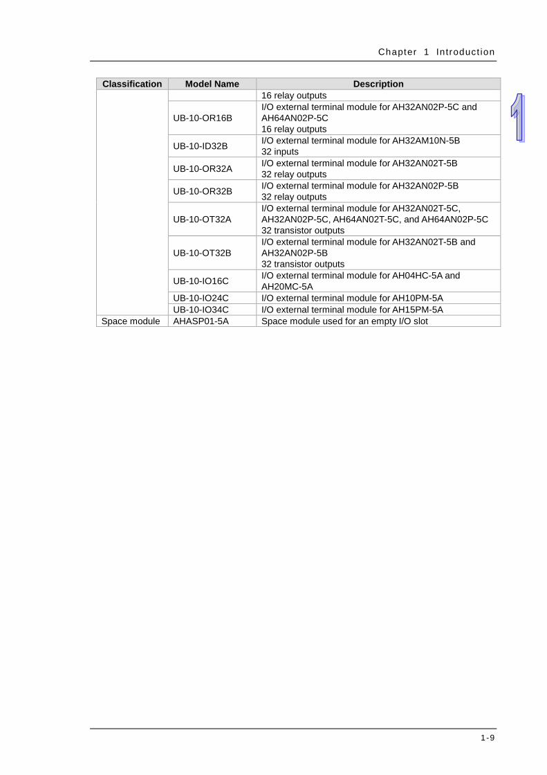
Classification Model Name Description 16 relay outputs
UB-10-OR16B I/O external terminal module for AH32AN02P-5C and AH64AN02P-5C 16 relay outputs
UB-10-ID32B I/O external terminal module for AH32AM10N-5B 32 inputs
UB-10-OR32A I/O external terminal module for AH32AN02T-5B 32 relay outputs
UB-10-OR32B I/O external terminal module for AH32AN02P-5B 32 relay outputs
UB-10-OT32A I/O external terminal module for AH32AN02T-5C, AH32AN02P-5C, AH64AN02T-5C, and AH64AN02P-5C 32 transistor outputs
UB-10-OT32B I/O external terminal module for AH32AN02T-5B and AH32AN02P-5B 32 transistor outputs
UB-10-IO16C I/O external terminal module for AH04HC-5A and AH20MC-5A
UB-10-IO24C I/O external terminal module for AH10PM-5A UB-10-IO34C I/O external terminal module for AH15PM-5A
Space module AHASP01-5A Space module used for an empty I/O slot
AH500 Programming Manual
1-10
1.2 Software
1.2.1 Program Editor
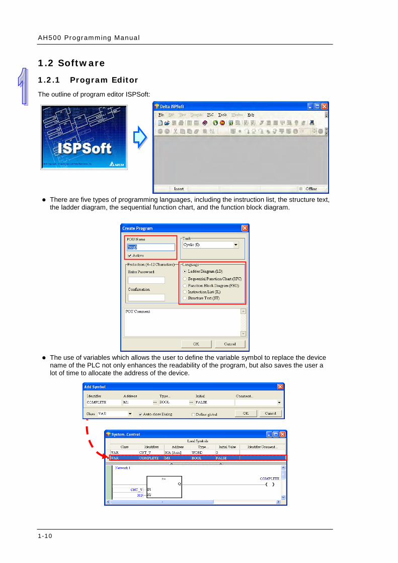
The outline of program editor ISPSoft:
There are five types of programming languages, including the instruction list, the structure text,
the ladder diagram, the sequential function chart, and the function block diagram.
The use of variables which allows the user to define the variable symbol to replace the device
name of the PLC not only enhances the readability of the program, but also saves the user a lot of time to allocate the address of the device.
Chapter 1 Introduct ion
1-11
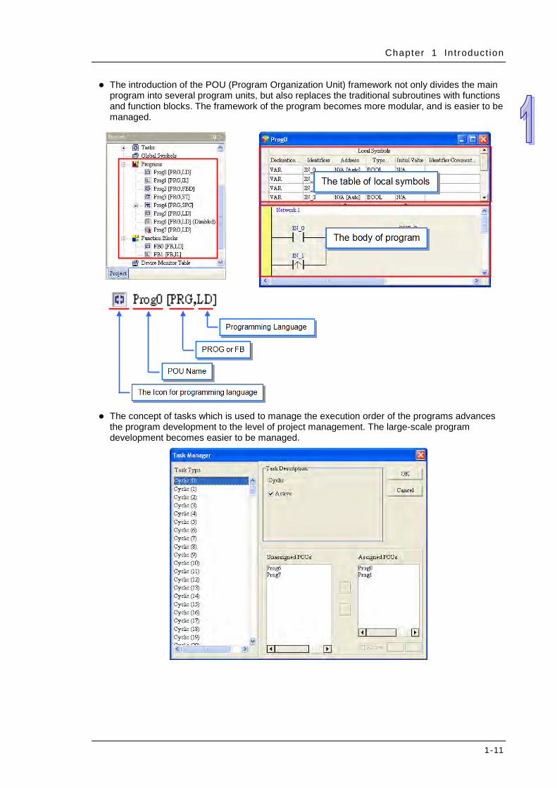
The introduction of the POU (Program Organization Unit) framework not only divides the main program into several program units, but also replaces the traditional subroutines with functions and function blocks. The framework of the program becomes more modular, and is easier to be managed.
The concept of tasks which is used to manage the execution order of the programs advances the program development to the level of project management. The large-scale program development becomes easier to be managed.
AH500 Programming Manual
1-12
1.2.2 Program Organization Units and Tasks
The POUs (Program Organization Units) are the basic elements which constitute the PLC program. Differing from the traditional PLC program, the character of the program framework introduced by IEC 61131-3 lies in the fact that the large program is divided into several small units. These small units are called POUs. The POUs can be classified into three types. 1. Program (PROG): The POU of the program type plays the role of the primary program in the
PLC program. The designer can define the execution of the POU of the program type as the cyclic scan or the interrupt, and arrange the scan order in the task list for the POUs of the program type.
2. Function block (FB): The meaning of the function block (FB) in itself is similar to the subroutine. The program defined within the function block is executed after the function block is called by the POU of the program type and the related parameters are entered.
3. Function (FC): The meaning of the function (FC) in itself is close to the macro instruction. That is, users can write many operation instructions or functions into the function POU, and then call them into use in the POU of the program type or the function block.
The task is a function which stipulates that programs are executed in certain order or according to certain interrupt condition. The meaning of the task lies in the fact that it provides each POU of the program type with a specific execution task, and specifies the execution order for the POUs of the program type or the way to enable them. Basically, not all of the POUs of the program type in a project will take part in the practical execution. Whether to execute the POU of the program type or not, and how to execute it depend on the assignment of the task. If the POU of the program type is not assigned the task, it will be saved as an ordinary source code with the project instead of being compiled as an execution code of the PLC. In addition, only the POU of the program type needs to be assigned the task. The execution of the function blocks or functions depends on the superior POU of the program type which calls them. There are three types of tasks. 1. Cyclic task: The POUs of the program type assigned to the cyclic task will be scanned
cyclically, and executed in order. 2. Timed interrupt task: If the time of interrupting is reached, all POUs of the program type
assigned to the timed interrupt task will be executed in order. 3. Conditional interrupt task: Conditional Interrupts can be divided into several types. For
example, the external interrupts, the I/O interrupts, and etc. Users have to make sure of the interrupts supported by the PLC before they create a project. If the POU of the program type is assigned to the conditional interrupt task, the function of the POU of the program type is similar to the interrupt subroutine. If the interrupt condition is satisfied, e.g. the contact of the external interrupt is triggered, all POUs of the program type assigned to the task will be executed in order.
2-1
Chapter 2 Devices
Table of Contents 2.1 Introduction of Devices ............................................................................. 2-2
2.1.1 Devise List ......................................................................................... 2-2 2.1.1.1 AH500 Basic CPU Modules (AHCPU500/510/520/530) ................... 2-2 2.1.1.2 AH500 Advanced CPU Modules (AHCPU501/511/521/531) ........... 2-3
2.1.2 Basic Structure of I/O Storages ......................................................... 2-4 2.1.3 Relation between the PLC Action and the Device Type .................... 2-4 2.1.4 Latched Areas in the Device Range .................................................. 2-5
2.2 Functions of Devices ................................................................................ 2-6 2.2.1 Values and Constants ....................................................................... 2-6 2.2.2 Floating-point Numbers ..................................................................... 2-8
2.2.2.1 Single-precision Floating-point Numbers ................................... 2-8 2.2.2.2 Double-precision Floating-point Numbers .................................. 2-8 2.2.2.3 Decimal Floating-point Numbers ................................................ 2-9
2.2.3 Strings ..............................................................................................2-10 2.2.4 Input Relays .....................................................................................2-11 2.2.5 Output Relays ..................................................................................2-11 2.2.6 Auxiliary Relays ................................................................................2-12 2.2.7 Special Auxiliary Relays ...................................................................2-12 2.2.8 Refresh Time of Special Auxiliary Relays .........................................2-40 2.2.9 Stepping Relays ...............................................................................2-48 2.2.10 Timers ...........................................................................................2-48 2.2.11 Counters .......................................................................................2-50 2.2.12 32-bit Counters .............................................................................2-51 2.2.13 Data Registers ..............................................................................2-53 2.2.14 Special Data Registers .................................................................2-54 2.2.15 Refresh Time of Special Data Registers .......................................2-83 2.2.16 Additional Remarks on Special Auxiliary Relays and Special Data
Registers .......................................................................................2-86 2.2.17 Link Registers .............................................................................2-101 2.2.18 Index Registers ...........................................................................2-101
AH500 Programming Manual
2-2
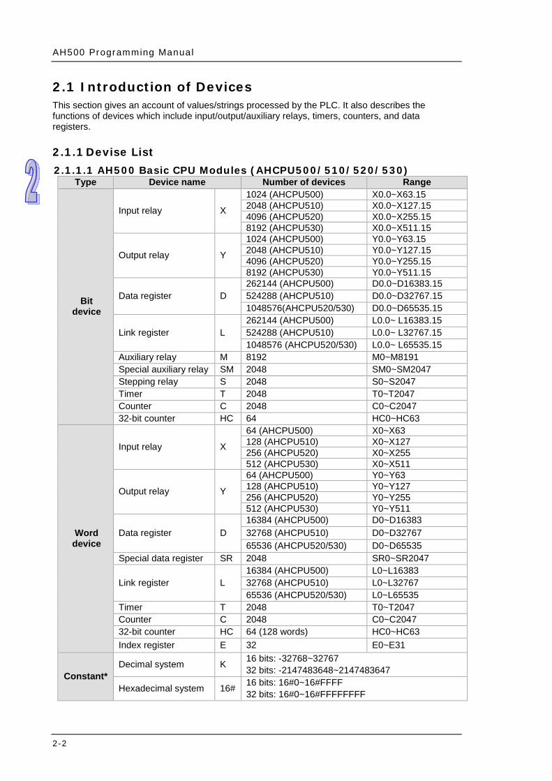
2.1 Introduction of Devices This section gives an account of values/strings processed by the PLC. It also describes the functions of devices which include input/output/auxiliary relays, timers, counters, and data registers. 2.1.1 Devise List 2.1.1.1 AH500 Basic CPU Modules (AHCPU500/510/520/530)
Type Device name Number of devices Range
Bit device
Input relay X
1024 (AHCPU500) X0.0~X63.15 2048 (AHCPU510) X0.0~X127.15 4096 (AHCPU520) X0.0~X255.15 8192 (AHCPU530) X0.0~X511.15
Output relay Y
1024 (AHCPU500) Y0.0~Y63.15 2048 (AHCPU510) Y0.0~Y127.15 4096 (AHCPU520) Y0.0~Y255.15 8192 (AHCPU530) Y0.0~Y511.15
Data register D 262144 (AHCPU500) D0.0~D16383.15 524288 (AHCPU510) D0.0~D32767.15 1048576(AHCPU520/530) D0.0~D65535.15
Link register L 262144 (AHCPU500) L0.0~ L16383.15 524288 (AHCPU510) L0.0~ L32767.15 1048576 (AHCPU520/530) L0.0~ L65535.15
Auxiliary relay M 8192 M0~M8191 Special auxiliary relay SM 2048 SM0~SM2047 Stepping relay S 2048 S0~S2047 Timer T 2048 T0~T2047 Counter C 2048 C0~C2047 32-bit counter HC 64 HC0~HC63
Word device
Input relay X
64 (AHCPU500) X0~X63 128 (AHCPU510) X0~X127 256 (AHCPU520) X0~X255 512 (AHCPU530) X0~X511
Output relay Y
64 (AHCPU500) Y0~Y63 128 (AHCPU510) Y0~Y127 256 (AHCPU520) Y0~Y255 512 (AHCPU530) Y0~Y511
Data register D 16384 (AHCPU500) D0~D16383 32768 (AHCPU510) D0~D32767 65536 (AHCPU520/530) D0~D65535
Special data register SR 2048 SR0~SR2047
Link register L 16384 (AHCPU500) L0~L16383 32768 (AHCPU510) L0~L32767 65536 (AHCPU520/530) L0~L65535
Timer T 2048 T0~T2047 Counter C 2048 C0~C2047 32-bit counter HC 64 (128 words) HC0~HC63 Index register E 32 E0~E31
Constant* Decimal system K 16 bits: -32768~32767
32 bits: -2147483648~2147483647
Hexadecimal system 16# 16 bits: 16#0~16#FFFF 32 bits: 16#0~16#FFFFFFFF

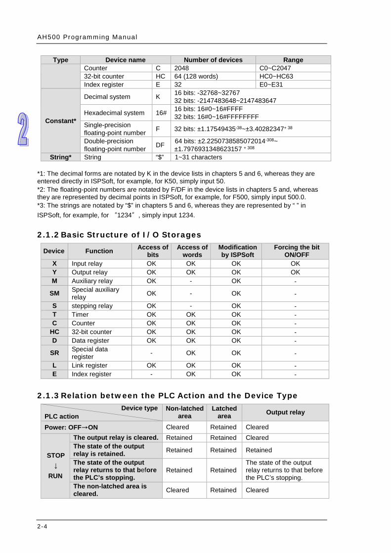
Chapter 2 Devices
2-3
Type Device name Number of devices Range Single-precision floating-point number F 32 bits: ±1.17549435-38~±3.40282347+38
Double-precision floating-point number DF 64 bits: ±2.2250738585072014-308~
±1.7976931348623157+308 String* String “$” 1~31 characters
*1: The decimal forms are notated by K in the device lists in chapters 5 and 6, whereas they are entered directly in ISPSoft, for example, for K50, simply input 50. *2: The floating-point numbers are notated by F/DF in the device lists in chapters 5 and, whereas they are represented by decimal points in ISPSoft, for example, for F500, simply input 500.0. *3: The strings are notated by “$” in chapters 5 and 6, whereas they are represented by “ ” in ISPSoft, for example, for “1234”, simply input 1234. 2.1.1.2 AH500 Advanced CPU Modules (AHCPU501/511/521/531)
Type Device name Number of devices Range
Bit device
Input relay X
2048 (AHCPU501) X0.0~X127.15 4096 (AHCPU511) X0.0~X255.15 8192 (AHCPU521) X0.0~X511.15 16384 (AHCPU531) X0.0~X1023.15
Output relay Y
2048 (AHCPU501) Y0.0~Y127.15 4096 (AHCPU511) Y0.0~Y255.15 8192 (AHCPU521) Y0.0~Y511.15 16384 (AHCPU531) Y0.0~Y1023.15
Data register D
393216 (AHCPU501) D0.0~D24575.15 786432 (AHCPU511) D0.0~D49151.15 1572864 (AHCPU521) D0.0~D98303.15 2097152 (AHCPU531) D0.0~D131071.15
Link register L
393216 (AHCPU501) L0.0~L24575.15 786432 (AHCPU511) L0.0~L49151.15 1572864 (AHCPU521) L0.0~L98303.15 2097152 (AHCPU531) L0.0~L131071.15
Auxiliary relay M 8192 M0~M8191 Special auxiliary relay SM 4096 SM0~SM4095 Stepping relay S 2048 S0~S2047 Timer T 2048 T0~T2047 Counter C 2048 C0~C2047 32-bit counter HC 64 HC0~HC63
Word device
Input relay X
128 (AHCPU501) X0~X127 256 (AHCPU511) X0~X255 512 (AHCPU521) X0~X511 1024 (AHCPU531) X0~X1023
Output relay Y
128 (AHCPU501) Y0~Y127 256 (AHCPU511) Y0~Y255 512 (AHCPU521) Y0~Y511 1024 (AHCPU531) Y0~Y1023
Data register D
24576 (AHCPU501) D0~D24575 49152 (AHCPU511) D0~D49151 98304 (AHCPU521) D0~D98303 131072 (AHCPU531) D0~D131071
Special data register SR 4096 SR0~SR4095
Link register L
24576 (AHCPU501) L0~L24575 49152 (AHCPU511) L0~L49151 98304 (AHCPU521) L0~L98303 131072 (AHCPU531) L0~L131071
Timer T 2048 T0~T2047
AH500 Programming Manual
2-4
Type Device name Number of devices Range Counter C 2048 C0~C2047 32-bit counter HC 64 (128 words) HC0~HC63 Index register E 32 E0~E31
Constant*
Decimal system K 16 bits: -32768~32767 32 bits: -2147483648~2147483647
Hexadecimal system 16# 16 bits: 16#0~16#FFFF 32 bits: 16#0~16#FFFFFFFF
Single-precision floating-point number F 32 bits: ±1.17549435-38~±3.40282347+ 38
Double-precision floating-point number DF 64 bits: ±2.2250738585072014-308~
±1.7976931348623157 + 308 String* String “$” 1~31 characters
*1: The decimal forms are notated by K in the device lists in chapters 5 and 6, whereas they are entered directly in ISPSoft, for example, for K50, simply input 50. *2: The floating-point numbers are notated by F/DF in the device lists in chapters 5 and, whereas they are represented by decimal points in ISPSoft, for example, for F500, simply input 500.0. *3: The strings are notated by “$” in chapters 5 and 6, whereas they are represented by “ ” in ISPSoft, for example, for “1234”, simply input 1234. 2.1.2 Basic Structure of I/O Storages
Device Function Access of bits
Access of words
Modification by ISPSoft
Forcing the bit ON/OFF
X Input relay OK OK OK OK Y Output relay OK OK OK OK M Auxiliary relay OK - OK -
SM Special auxiliary relay OK - OK -
S stepping relay OK - OK - T Timer OK OK OK - C Counter OK OK OK -
HC 32-bit counter OK OK OK - D Data register OK OK OK -
SR Special data register - OK OK -
L Link register OK OK OK - E Index register - OK OK -
2.1.3 Relation between the PLC Action and the Device Type Device type PLC action
Non-latched area
Latched area Output relay
Power: OFF→ON Cleared Retained Cleared
STOP ↓
RUN
The output relay is cleared. Retained Retained Cleared The state of the output relay is retained. Retained Retained Retained
The state of the output relay returns to that before the PLC’s stopping.
Retained Retained The state of the output relay returns to that before the PLC’s stopping.
The non-latched area is cleared. Cleared Retained Cleared
Chapter 2 Devices
2-5
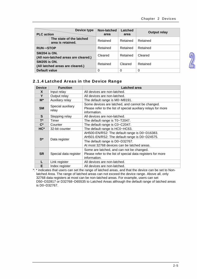
Device type PLC action
Non-latched area
Latched area Output relay
The state of the latched area is retained. Retained Retained Retained
RUN→STOP Retained Retained Retained SM204 is ON. (All non-latched areas are cleared.) Cleared Retained Cleared
SM205 is ON. (All latched areas are cleared.) Retained Cleared Retained
Default value 0 0 0
2.1.4 Latched Areas in the Device Range Device Function Latched area
X Input relay All devices are non-latched. Y Output relay All devices are non-latched. M* Auxiliary relay The default range is M0~M8191.
SM Special auxiliary relay
Some devices are latched, and cannot be changed. Please refer to the list of special auxiliary relays for more information.
S Stepping relay All devices are non-latched. T* Timer The default range is T0~T2047. C* Counter The default range is C0~C2047.
HC* 32-bit counter The default range is HC0~HC63.
D* Data register
AH500-EN/RS2: The default range is D0~D16383. AH501-EN/RS2: The default range is D0~D24575. The default range is D0~D32767. At most 32768 devices can be latched areas.
SR Special data register Some are latched, and can not be changed. Please refer to the list of special data registers for more information.
L Link register All devices are non-latched. E Index register All devices are non-latched.
*: * indicates that users can set the range of latched areas, and that the device can be set to Non-latched Area. The range of latched areas can not exceed the device range. Above all, only 32768 data registers at most can be non-latched areas. For example, users can set D50~D32817 or D32768~D65535 to Latched Areas although the default range of latched areas is D0~D32767.
AH500 Programming Manual
2-6
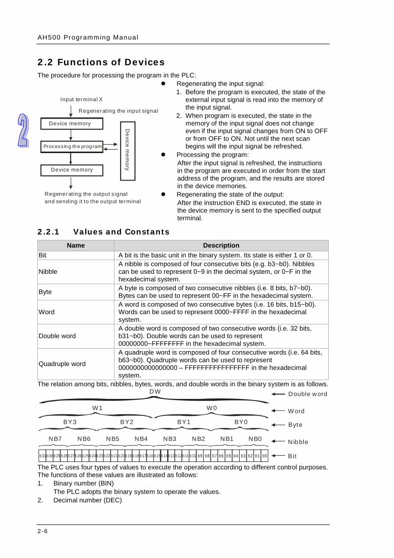
2.2 Functions of Devices The procedure for processing the program in the PLC:
Input terminal X
Device memory
Processin g th e prog ram
Device m
emory
Regenerating the output s ignaland sending it to the output terminal
Regenerating the input signal
Device memory
Regenerating the input signal: 1. Before the program is executed, the state of the
external input signal is read into the memory of the input signal.
2. When program is executed, the state in the memory of the input signal does not change even if the input signal changes from ON to OFF or from OFF to ON. Not until the next scan begins will the input signal be refreshed.
Processing the program: After the input signal is refreshed, the instructions in the program are executed in order from the start address of the program, and the results are stored in the device memories.
Regenerating the state of the output: After the instruction END is executed, the state in the device memory is sent to the specified output terminal.
2.2.1 Values and Constants Name Description
Bit A bit is the basic unit in the binary system. Its state is either 1 or 0.
Nibble A nibble is composed of four consecutive bits (e.g. b3~b0). Nibbles can be used to represent 0~9 in the decimal system, or 0~F in the hexadecimal system.
Byte A byte is composed of two consecutive nibbles (i.e. 8 bits, b7~b0). Bytes can be used to represent 00~FF in the hexadecimal system.
Word A word is composed of two consecutive bytes (i.e. 16 bits, b15~b0). Words can be used to represent 0000~FFFF in the hexadecimal system.
Double word A double word is composed of two consecutive words (i.e. 32 bits, b31~b0). Double words can be used to represent 00000000~FFFFFFFF in the hexadecimal system.
Quadruple word
A quadruple word is composed of four consecutive words (i.e. 64 bits, b63~b0). Quadruple words can be used to represent 0000000000000000 – FFFFFFFFFFFFFFFF in the hexadecimal system.
The relation among bits, nibbles, bytes, words, and double words in the binary system is as follows.
b31b30 b29 b28 b27b26 b25 b24b23 b22 b21 b20b19 b18 b17 b16 b15b14 b13 b12b11 b10 b9 b8 b7 b6 b5 b4 b3 b2 b1 b0
NB0NB1NB2NB3NB4NB5NB6NB7
BY3 BY2 BY1 BY0
W1
DW
W0
Double word
Word
Byte
N ibble
Bit
The PLC uses four types of values to execute the operation according to different control purposes. The functions of these values are illustrated as follows: 1. Binary number (BIN)
The PLC adopts the binary system to operate the values. 2. Decimal number (DEC)
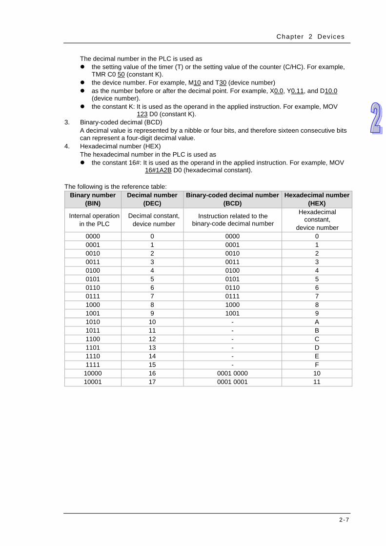
Chapter 2 Devices
2-7
The decimal number in the PLC is used as the setting value of the timer (T) or the setting value of the counter (C/HC). For example,
TMR C0 50 (constant K). the device number. For example, M10 and T30 (device number) as the number before or after the decimal point. For example, X0.0, Y0.11, and D10.0
(device number). the constant K: It is used as the operand in the applied instruction. For example, MOV
123 D0 (constant K). 3. Binary-coded decimal (BCD)
A decimal value is represented by a nibble or four bits, and therefore sixteen consecutive bits can represent a four-digit decimal value.
4. Hexadecimal number (HEX) The hexadecimal number in the PLC is used as the constant 16#: It is used as the operand in the applied instruction. For example, MOV
16#1A2B D0 (hexadecimal constant). The following is the reference table:
Binary number (BIN)
Decimal number (DEC)
Binary-coded decimal number (BCD)
Hexadecimal number (HEX)
Internal operation in the PLC
Decimal constant, device number
Instruction related to the binary-code decimal number
Hexadecimal constant,
device number 0000 0 0000 0 0001 1 0001 1 0010 2 0010 2 0011 3 0011 3 0100 4 0100 4 0101 5 0101 5 0110 6 0110 6 0111 7 0111 7 1000 8 1000 8 1001 9 1001 9 1010 10 - A 1011 11 - B 1100 12 - C 1101 13 - D 1110 14 - E 1111 15 - F
10000 16 0001 0000 10 10001 17 0001 0001 11
AH500 Programming Manual
2-8
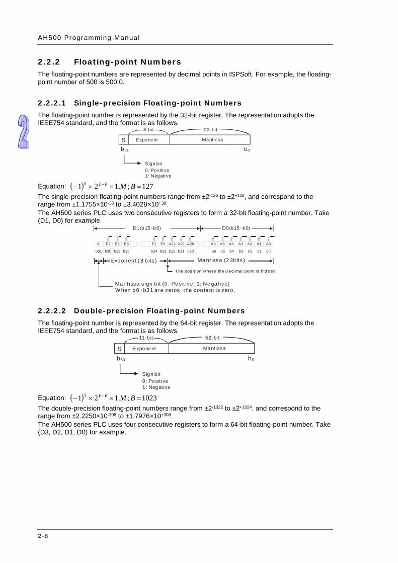
2.2.2 Floating-point Numbers The floating-point numbers are represented by decimal points in ISPSoft. For example, the floating-point number of 500 is 500.0.
2.2.2.1 Single-precision Floating-point Numbers The floating-point number is represented by the 32-bit register. The representation adopts the IEEE754 standard, and the format is as follows.
S Exponent Mantissa
8-b it 23-bi t
b31 b0
Sign b it0 : Positive1: Negative
Equation: ( ) 127;.121 =××− − BMBES The single-precision floating-point numbers range from ±2-126 to ±2+128, and correspond to the range from ±1.1755×10-38 to ±3.4028×10+38. The AH500 series PLC uses two consecutive registers to form a 32-bit floating-point number. Take (D1, D0) for example.
S E7 E6 E5 E1 E0 A22 A21 A20 A6 A5 A4 A3 A2 A1 A0
b0b1b2b3b4b5b6b20b21b22b23b24b28b29b30b31
2 2 2 2 2 2 2 2 2 2 2 2 22 2
D1(b15~b0) D0(b15~b0)
Exp on en t ( 8 b its) Ma nt issa (2 3b its)
Ma nt issa sign b it (0 : Po sit ive; 1: Ne ga tive)W hen b 0~b3 1 a re zeros, the con te nt is zero .
The pos it ion w here the d eci mal point is hid den
2.2.2.2 Double-precision Floating-point Numbers The floating-point number is represented by the 64-bit register. The representation adopts the IEEE754 standard, and the format is as follows.
Equation: ( ) 1023;.121 =××− − BMBES The double-precision floating-point numbers range from ±2-1022 to ±2+1024, and correspond to the range from ±2.2250×10-308 to ±1.7976×10+308. The AH500 series PLC uses four consecutive registers to form a 64-bit floating-point number. Take (D3, D2, D1, D0) for example.
S Exponent Mantissa
11-bi t 52-bi t
b63 b0
Sign b it0 : Positive1: Negative
Chapter 2 Devices
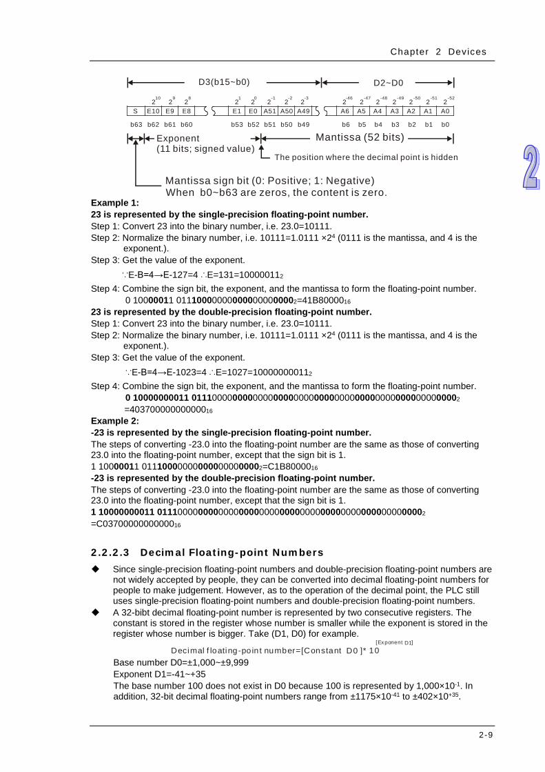
2-9
Example 1: 23 is represented by the single-precision floating-point number. Step 1: Convert 23 into the binary number, i.e. 23.0=10111. Step 2: Normalize the binary number, i.e. 10111=1.0111 ×24 (0111 is the mantissa, and 4 is the
exponent.). Step 3: Get the value of the exponent.
∵E-B=4→E-127=4 ∴E=131=100000112 Step 4: Combine the sign bit, the exponent, and the mantissa to form the floating-point number.
0 10000011 011100000000000000000002=41B8000016
23 is represented by the double-precision floating-point number. Step 1: Convert 23 into the binary number, i.e. 23.0=10111. Step 2: Normalize the binary number, i.e. 10111=1.0111 ×24 (0111 is the mantissa, and 4 is the
exponent.). Step 3: Get the value of the exponent.
∵E-B=4→E-1023=4 ∴E=1027=100000000112 Step 4: Combine the sign bit, the exponent, and the mantissa to form the floating-point number.
0 10000000011 01110000000000000000000000000000000000000000000000002
=40370000000000016
Example 2: -23 is represented by the single-precision floating-point number. The steps of converting -23.0 into the floating-point number are the same as those of converting 23.0 into the floating-point number, except that the sign bit is 1. 1 10000011 011100000000000000000002=C1B8000016
-23 is represented by the double-precision floating-point number. The steps of converting -23.0 into the floating-point number are the same as those of converting 23.0 into the floating-point number, except that the sign bit is 1. 1 10000000011 01110000000000000000000000000000000000000000000000002
=C0370000000000016
2.2.2.3 Decimal Floating-point Numbers Since single-precision floating-point numbers and double-precision floating-point numbers are
not widely accepted by people, they can be converted into decimal floating-point numbers for people to make judgement. However, as to the operation of the decimal point, the PLC still uses single-precision floating-point numbers and double-precision floating-point numbers.
A 32-bibt decimal floating-point number is represented by two consecutive registers. The constant is stored in the register whose number is smaller while the exponent is stored in the register whose number is bigger. Take (D1, D0) for example.
10Decimal f loating-point number=[Constant ]*D0[Exponent ]D1
Base number D0=±1,000~±9,999
Exponent D1=-41~+35 The base number 100 does not exist in D0 because 100 is represented by 1,000×10-1. In addition, 32-bit decimal floating-point numbers range from ±1175×10-41 to ±402×10+35.
S E10 E9 E8 E1 E0 A51 A50 A49 A6 A5 A4 A3 A2 A1 A0
b0b1b2b3b4b5b6b49b50b51b52b53b60b61b62b63
2 2 2 2 2 2 2 2 2 2 2 2 22 210 9 8 1 0 -1 -2 -3 -46 -47 -48 -49 -50 -51 -52
D3(b15~b0) D2~D0
Exponent (11 bits; signed value)
Mantissa (52 bits)
Mantissa sign bit (0: Positive; 1: Negative)When b0~b63 are zeros, the content is zero.
The position where the decimal point is hidden
AH500 Programming Manual
2-10
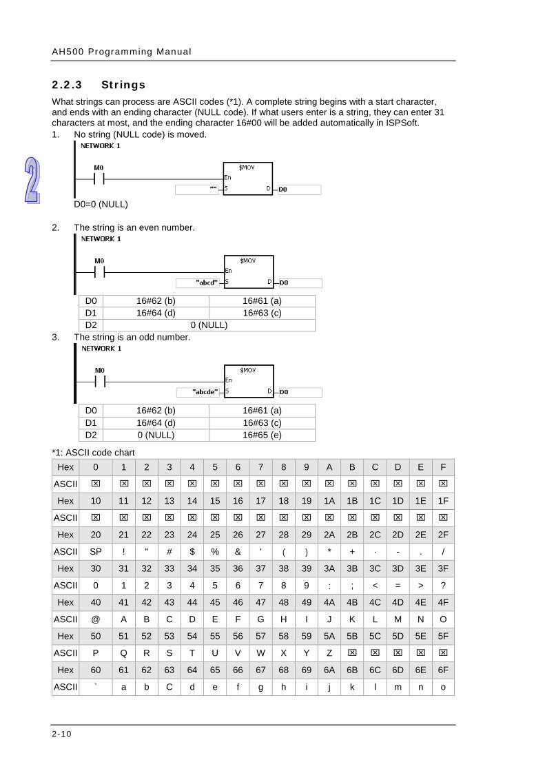
2.2.3 Strings What strings can process are ASCII codes (*1). A complete string begins with a start character, and ends with an ending character (NULL code). If what users enter is a string, they can enter 31 characters at most, and the ending character 16#00 will be added automatically in ISPSoft. 1. No string (NULL code) is moved.
D0=0 (NULL)
2. The string is an even number.
D0 16#62 (b) 16#61 (a) D1 16#64 (d) 16#63 (c) D2 0 (NULL)
3. The string is an odd number.
D0 16#62 (b) 16#61 (a) D1 16#64 (d) 16#63 (c) D2 0 (NULL) 16#65 (e)
*1: ASCII code chart Hex 0 1 2 3 4 5 6 7 8 9 A B C D E F
ASCII
Hex 10 11 12 13 14 15 16 17 18 19 1A 1B 1C 1D 1E 1F
ASCII
Hex 20 21 22 23 24 25 26 27 28 29 2A 2B 2C 2D 2E 2F
ASCII SP ! " # $ % & ' ( ) * + , - . /
Hex 30 31 32 33 34 35 36 37 38 39 3A 3B 3C 3D 3E 3F
ASCII 0 1 2 3 4 5 6 7 8 9 : ; < = > ?
Hex 40 41 42 43 44 45 46 47 48 49 4A 4B 4C 4D 4E 4F
ASCII @ A B C D E F G H I J K L M N O
Hex 50 51 52 53 54 55 56 57 58 59 5A 5B 5C 5D 5E 5F
ASCII P Q R S T U V W X Y Z
Hex 60 61 62 63 64 65 66 67 68 69 6A 6B 6C 6D 6E 6F
ASCII ` a b C d e f g h i j k l m n o
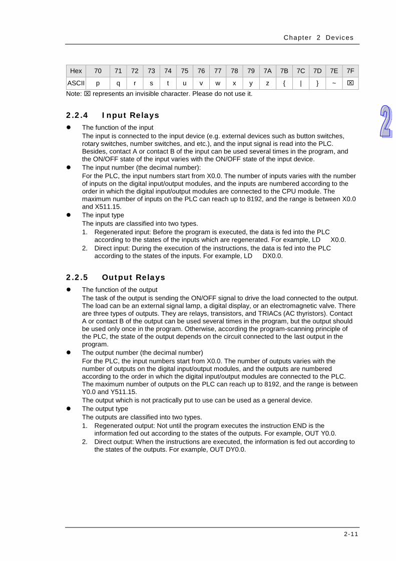
Chapter 2 Devices
2-11
Hex 70 71 72 73 74 75 76 77 78 79 7A 7B 7C 7D 7E 7F
ASCII p q r s t u v w x y z { | } ~ Note: represents an invisible character. Please do not use it.
2.2.4 Input Relays The function of the input
The input is connected to the input device (e.g. external devices such as button switches, rotary switches, number switches, and etc.), and the input signal is read into the PLC. Besides, contact A or contact B of the input can be used several times in the program, and the ON/OFF state of the input varies with the ON/OFF state of the input device.
The input number (the decimal number): For the PLC, the input numbers start from X0.0. The number of inputs varies with the number of inputs on the digital input/output modules, and the inputs are numbered according to the order in which the digital input/output modules are connected to the CPU module. The maximum number of inputs on the PLC can reach up to 8192, and the range is between X0.0 and X511.15.
The input type The inputs are classified into two types. 1. Regenerated input: Before the program is executed, the data is fed into the PLC
according to the states of the inputs which are regenerated. For example, LD X0.0. 2. Direct input: During the execution of the instructions, the data is fed into the PLC
according to the states of the inputs. For example, LD DX0.0.
2.2.5 Output Relays The function of the output
The task of the output is sending the ON/OFF signal to drive the load connected to the output. The load can be an external signal lamp, a digital display, or an electromagnetic valve. There are three types of outputs. They are relays, transistors, and TRIACs (AC thyristors). Contact A or contact B of the output can be used several times in the program, but the output should be used only once in the program. Otherwise, according the program-scanning principle of the PLC, the state of the output depends on the circuit connected to the last output in the program.
The output number (the decimal number) For the PLC, the input numbers start from X0.0. The number of outputs varies with the number of outputs on the digital input/output modules, and the outputs are numbered according to the order in which the digital input/output modules are connected to the PLC. The maximum number of outputs on the PLC can reach up to 8192, and the range is between Y0.0 and Y511.15. The output which is not practically put to use can be used as a general device.
The output type The outputs are classified into two types. 1. Regenerated output: Not until the program executes the instruction END is the
information fed out according to the states of the outputs. For example, OUT Y0.0. 2. Direct output: When the instructions are executed, the information is fed out according to
the states of the outputs. For example, OUT DY0.0.

AH500 Programming Manual
2-12
2.2.6 Auxiliary Relays The auxiliary relay has contact A and contact B. It can be used several times in the program. Users can combine the control loops by means of the auxiliary relay, but can not drive the external load by means of the auxiliary relay. The auxiliary relays can be divided into two types according to their attributes. 1. For general use: If an electric power cut occurs when the PLC is running, the auxiliary relay for
general use will be reset to OFF. When the power supply is restored, the auxiliary relay for general use is still OFF.
2. For latched use: If an electric power cut occurs when the PLC is running, the state of the auxiliary relay for latched use will be retained. When the power supply is restored, the state remains the same as that before the power electric cut.
2.2.7 Special Auxiliary Relays Every special auxiliary relay has its specific function. Please do not use the special auxiliary relays which are not defined. The special auxiliary relays and their functions are listed as follows. As to the SM numbers marked “*”, users can refer to the additional remarks on special auxiliary relays/special data registers. “R” in the attribute column indicates that the special auxiliary relay can read the data, whereas “R/W” in the attribute column indicates that it can read and write the data. In addition, the mark “–” indicates that the status of the special auxiliary relay does not make any change. The mark “#” indicates that the system will be set according to the status of the PLC, and users can read the setting value and refer to the related manual for more information.
SM Function
CPU
5X0-RS2
CPU
5X0-EN
CPU
5X1-RS2
CPU
5X1-EN
CPU
560-EN2
CPU
521-DN
P3
OFF
ON
STOP
RUN
RUN
STOP
Attribute
Default
SM0 Operation error O O O O O O OFF OFF – R OFF SM1 The operation error is locked. O O O O O O OFF OFF – R OFF SM5 Instruction/Operand inspection error O O O O O O OFF OFF – R OFF *SM8 Watchdog timer error O O O O O O OFF – – R OFF SM9 System error O O O O O O OFF – – R OFF
SM10 I/O bus error O O O O O O OFF – – R OFF *SM20 Power supply error log O O O O O O OFF – – R OFF *SM22 Clearing the error log O O O O O O OFF – – R/W OFF SM23 Clearing the download log O O O O O O OFF – – R/W OFF SM24 Clearing the state-changing log of the PLC O O O O O O OFF – – R/W OFF
SM25 The online-editing processing flag is on when the online-editing mode starts. O O O O O O OFF – – R OFF
SM26 The debugging mode processing flag is on when the debugging mode starts. O O O O O O OFF – – R OFF
*SM96 The data is sent through COM1. O O O O O O OFF OFF – R/W OFF *SM97 The data is sent through COM2. O Χ O Χ Χ Χ OFF OFF – R/W OFF *SM98 Waiting to receive the reply through COM1 O O O O O O OFF OFF – R OFF
*SM99 Waiting to receive the reply through COM2 O Χ O Χ Χ Χ OFF OFF – R OFF
*SM100 Reception through COM1 is complete. O O O O O O OFF OFF – R/W OFF *SM101 Reception through COM2 is complete. O Χ O Χ Χ Χ OFF OFF – R/W OFF
*SM102 An error occurs during the reception of the data through COM1 by using the instruction MODRW or the instruction RS.
O O O O O O OFF OFF – R OFF
*SM103 An error occurs during the reception of the data through COM2 by using the instruction MODRW or the instruction RS.
O Χ O Χ Χ Χ OFF OFF – R OFF
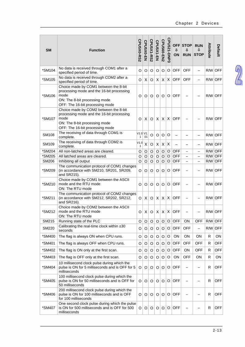
Chapter 2 Devices
2-13
SM Function
CPU
5X0-RS2
CPU
5X0-EN
CPU
5X1-RS2
CPU
5X1-EN
CPU
560-EN2
CPU
521-DN
P3
OFF
ON
STOP
RUN
RUN
STOP
Attribute
Default
*SM104 No data is received through COM1 after a specified period of time. O O O O O O OFF OFF – R/W OFF
*SM105 No data is received through COM2 after a specified period of time. O Χ O Χ Χ Χ OFF OFF – R/W OFF
*SM106
Choice made by COM1 between the 8-bit processing mode and the 16-bit processing mode ON: The 8-bit processing mode OFF: The 16-bit processing mode
O O O O O O OFF – – R/W OFF
*SM107
Choice made by COM2 between the 8-bit processing mode and the 16-bit processing mode ON: The 8-bit processing mode OFF: The 16-bit processing mode
O Χ O Χ Χ Χ OFF – – R/W OFF
SM108 The receiving of data through COM1 is complete.
V1.01
V1.01 O O O O – – – R/W OFF
SM109 The receiving of data through COM2 is complete.
V1.01 Χ O Χ Χ Χ – – – R/W OFF
*SM204 All non-latched areas are cleared. O O O O O O OFF – – R/W OFF *SM205 All latched areas are cleared. O O O O O O OFF – – R/W OFF SM206 Inhibiting all output O O O O O O OFF – – R/W OFF
*SM209 The communication protocol of COM1 changes (in accordance with SM210, SR201, SR209, and SR215).
O O O O O O OFF – – R/W OFF
*SM210 Choice made by COM1 between the ASCII mode and the RTU mode ON: The RTU mode
O O O O O O OFF – – R/W OFF
*SM211 The communication protocol of COM2 changes (in accordance with SM212, SR202, SR212, and SR216).
O Χ O Χ Χ Χ OFF – – R/W OFF
*SM212 Choice made by COM2 between the ASCII mode and the RTU mode ON: The RTU mode
O Χ O Χ Χ Χ OFF – – R/W OFF
SM215 Running state of the PLC O O O O O O OFF ON OFF R/W OFF
SM220 Calibrating the real-time clock within ±30 seconds O O O O O O OFF OFF – R/W OFF
*SM400 The flag is always ON when CPU runs. O O O O O O ON ON ON R ON
*SM401 The flag is always OFF when CPU runs. O O O O O O OFF OFF OFF R OFF
*SM402 The flag is ON only at the first scan. O O O O O O OFF ON OFF R OFF
*SM403 The flag is OFF only at the first scan. O O O O O O ON OFF ON R ON
*SM404 10 millisecond clock pulse during which the pulse is ON for 5 milliseconds and is OFF for 5 milliseconds
O O O O O O OFF – – R OFF
*SM405 100 millisecond clock pulse during which the pulse is ON for 50 milliseconds and is OFF for 50 milliseconds
O O O O O O OFF – – R OFF
*SM406 200 millisecond clock pulse during which the pulse is ON for 100 milliseconds and is OFF for 100 milliseconds
O O O O O O OFF – – R OFF
*SM407 One second clock pulse during which the pulse is ON for 500 milliseconds and is OFF for 500 milliseconds
O O O O O O OFF – – R OFF
AH500 Programming Manual
2-14
SM Function
CPU
5X0-RS2
CPU
5X0-EN
CPU
5X1-RS2
CPU
5X1-EN
CPU
560-EN2
CPU
521-DN
P3
OFF
ON
STOP
RUN
RUN
STOP A
ttribute
Default
*SM408 Two second clock pulse during which the pulse is ON for one second and is OFF for one second
O O O O O O OFF – – R OFF
*SM409 2n second clock pulse during which the pulse is ON for n seconds and is OFF for n seconds The interval n is specified by SR409.
O O O O O O OFF – – R OFF
*SM410
2n millisecond clock pulse during which the pulse is ON for n milliseconds and is OFF for n milliseconds The interval n is specified by SR410.
O O O O O O OFF – – R OFF
*SM418 Port 2 connection status of backplane 1 (main backplane) Χ Χ O O O O OFF – – R OFF
*SM420 Port 2 connection status of backplane 2 (1st redundant extension backplane) Χ Χ O O O O OFF – – R OFF
*SM421 Port 4 connection status of backplane 2 (1st redundant extension backplane) Χ Χ O O O O OFF – – R OFF
*SM422 Port 2 connection status of backplane 3 (2nd redundant extension backplane) Χ Χ O O O O OFF – – R OFF
*SM423 Port 4 connection status of backplane 3 (2nd redundant extension backplane) Χ Χ O O O O OFF – – R OFF
*SM424 Port 2 connection status of backplane 4 (3rd redundant extension backplane) Χ Χ O O O O OFF – – R OFF
*SM425 Port 4 connection status of backplane 4 (3rd redundant extension backplane) Χ Χ O O O O OFF – – R OFF
*SM426 Port 2 connection status of backplane 5 (4th redundant extension backplane) Χ Χ O O O O OFF – – R OFF
*SM427 Port 4 connection status of backplane 5 (4th redundant extension backplane) Χ Χ O O O O OFF – – R OFF
*SM428 Port 2 connection status of backplane 6 (5th redundant extension backplane) Χ Χ O O O O OFF – – R OFF
*SM429 Port 4 connection status of backplane 6 (5th redundant extension backplane) Χ Χ O O O O OFF – – R OFF
*SM430 Port 2 connection status of backplane 7 (6th redundant extension backplane) Χ Χ O O O O OFF – – R OFF
*SM431 Port 4 connection status of backplane 7 (6th redundant extension backplane) Χ Χ O O O O OFF – – R OFF
*SM450 Whether the memory card exists ON: The memory card exists. OFF: The memory card does not exist.
O O O O O O OFF – – R OFF
*SM451 Write protection switch on the memory card ON: The memory card is write protected. OFF: The memory card is not write protected.
O O O O O O OFF – – R OFF
*SM452
The data in the memory card is being accessed. ON: The data in the memory card is being accessed. OFF: The data in the memory card is not accessed.
O O O O O O OFF – – R OFF
*SM453 An error occurs during the operation of the memory card. ON: An error occurs.
O O O O O O OFF – – R OFF
SM454 Enabling data logger (ON: enabled; OFF: Disabled) Χ Χ V2.
01 V2.01
V1.01 O OFF – – R/W OFF
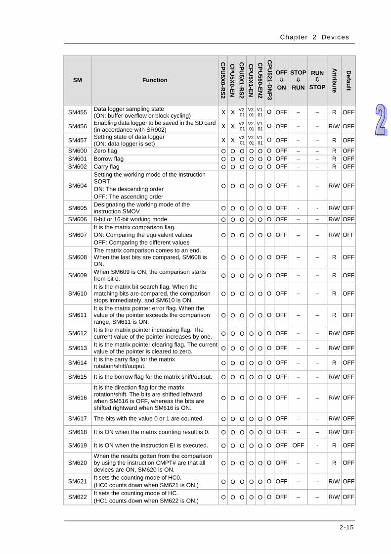
Chapter 2 Devices
2-15
SM Function
CPU
5X0-RS2
CPU
5X0-EN
CPU
5X1-RS2
CPU
5X1-EN
CPU
560-EN2
CPU
521-DN
P3
OFF
ON
STOP
RUN
RUN
STOP
Attribute
Default
SM455 Data logger sampling state (ON: buffer overflow or block cycling) Χ Χ V2.
01 V2.01
V1.01 O OFF – – R OFF
SM456 Enabling data logger to be saved in the SD card (in accordance with SR902) Χ Χ V2.
01 V2.01
V1.01 O OFF – – R/W OFF
SM457 Setting state of data logger (ON: data logger is set) Χ Χ V2.
01 V2.01
V1.01 O OFF – – R OFF
SM600 Zero flag O O O O O O OFF – – R OFF SM601 Borrow flag O O O O O O OFF – – R OFF SM602 Carry flag O O O O O O OFF – – R OFF
SM604
Setting the working mode of the instruction SORT. ON: The descending order OFF: The ascending order
O O O O O O OFF – – R/W OFF
SM605 Designating the working mode of the instruction SMOV O O O O O O OFF - - R/W OFF
SM606 8-bit or 16-bit working mode O O O O O O OFF – – R/W OFF
SM607 It is the matrix comparison flag. ON: Comparing the equivalent values OFF: Comparing the different values
O O O O O O OFF – – R/W OFF
SM608 The matrix comparison comes to an end. When the last bits are compared, SM608 is ON.
O O O O O O OFF – – R OFF
SM609 When SM609 is ON, the comparison starts from bit 0. O O O O O O OFF – – R OFF
SM610 It is the matrix bit search flag. When the matching bits are compared, the comparison stops immediately, and SM610 is ON.
O O O O O O OFF – – R OFF
SM611 It is the matrix pointer error flag. When the value of the pointer exceeds the comparison range, SM611 is ON.
O O O O O O OFF – – R OFF
SM612 It is the matrix pointer increasing flag. The current value of the pointer increases by one. O O O O O O OFF – – R/W OFF
SM613 It is the matrix pointer clearing flag. The current value of the pointer is cleared to zero. O O O O O O OFF – – R/W OFF
SM614 It is the carry flag for the matrix rotation/shift/output. O O O O O O OFF – – R OFF
SM615 It is the borrow flag for the matrix shift/output. O O O O O O OFF – – R/W OFF
SM616
It is the direction flag for the matrix rotation/shift. The bits are shifted leftward when SM616 is OFF, whereas the bits are shifted rightward when SM616 is ON.
O O O O O O OFF – – R/W OFF
SM617 The bits with the value 0 or 1 are counted. O O O O O O OFF – – R/W OFF
SM618 It is ON when the matrix counting result is 0. O O O O O O OFF – – R/W OFF
SM619 It is ON when the instruction EI is executed. O O O O O O OFF OFF - R OFF
SM620 When the results gotten from the comparison by using the instruction CMPT# are that all devices are ON, SM620 is ON.
O O O O O O OFF – – R OFF
SM621 It sets the counting mode of HC0. (HC0 counts down when SM621 is ON.) O O O O O O OFF – – R/W OFF
SM622 It sets the counting mode of HC. (HC1 counts down when SM622 is ON.) O O O O O O OFF – – R/W OFF

AH500 Programming Manual
2-16
SM Function
CPU
5X0-RS2
CPU
5X0-EN
CPU
5X1-RS2
CPU
5X1-EN
CPU
560-EN2
CPU
521-DN
P3
OFF
ON
STOP
RUN
RUN
STOP A
ttribute
Default
SM623 It sets the counting mode of HC2. (HC2 counts down when SM623 is ON.) O O O O O O OFF – – R/W OFF
SM624 It sets the counting mode of HC3. (HC3 counts down when SM624 is ON.) O O O O O O OFF – – R/W OFF
SM625 It sets the counting mode of HC4. (HC4 counts down when SM625 is ON.) O O O O O O OFF – – R/W OFF
SM626 It sets the counting mode of HC5. (HC5 counts down when SM626 is ON.) O O O O O O OFF – – R/W OFF
SM627 It sets the counting mode of HC6. (HC6 counts down when SM627 is ON.) O O O O O O OFF – – R/W OFF
SM628 It sets the counting mode of HC7. (HC7 counts down when SM628 is ON.) O O O O O O OFF – – R/W OFF
SM629 It sets the counting mode of HC8. (HC8 counts down when SM629 is ON.) O O O O O O OFF – – R/W OFF
SM630 It sets the counting mode of HC9. (HC9 counts down when SM630 is ON.) O O O O O O OFF – – R/W OFF
SM631 It sets the counting mode of HC10. (HC10 counts down when SM631 is ON.) O O O O O O OFF – – R/W OFF
SM632 It sets the counting mode of HC11. (HC11 counts down when SM632 is ON.) O O O O O O OFF – - R/W OFF
SM633 It sets the counting mode of HC12. (HC12 counts down when SM633 is ON.) O O O O O O OFF – - R/W OFF
SM634 It sets the counting mode of HC13. (HC13 counts down when SM634 is ON.) O O O O O O OFF – – R/W OFF
SM635 It sets the counting mode of HC14. (HC14 counts down when SM635 is ON.) O O O O O O OFF – – R/W OFF
SM636 It sets the counting mode of HC15. (HC15 counts down when SM636 is ON.) O O O O O O OFF – – R/W OFF
SM637 It sets the counting mode of HC16. (HC16 counts down when SM637 is ON.) O O O O O O OFF – – R/W OFF
SM638 It sets the counting mode of HC17. (HC17 counts down when SM638 is ON.) O O O O O O OFF – – R/W OFF
SM639 It sets the counting mode of HC18. (HC18 counts down when SM639 is ON.) O O O O O O OFF – – R/W OFF
SM640 It sets the counting mode of HC19. (HC19 counts down when SM640 is ON.) O O O O O O OFF – – R/W OFF
SM641 It sets the counting mode of HC20. (HC20 counts down when SM641 is ON.) O O O O O O OFF – – R/W OFF
SM642 It sets the counting mode of HC21. (HC21 counts down when SM642 is ON.) O O O O O O OFF – – R/W OFF
SM643 It sets the counting mode of HC22. (HC22 counts down when SM643 is ON.) O O O O O O OFF – – R/W OFF
SM644 It sets the counting mode of HC23. (HC23 counts down when SM644 is ON.) O O O O O O OFF – – R/W OFF
SM645 It sets the counting mode of HC24. (HC24 counts down when SM645 is ON.) O O O O O O OFF – – R/W OFF
SM646 It sets the counting mode of HC25. (HC25 counts down when SM646 is ON.) O O O O O O OFF – – R/W OFF
SM647 It sets the counting mode of HC26. (HC26 counts down when SM647 is ON.) O O O O O O OFF – – R/W OFF
SM648 It sets the counting mode of HC27. O O O O O O OFF – – R/W OFF
Chapter 2 Devices
2-17
SM Function
CPU
5X0-RS2
CPU
5X0-EN
CPU
5X1-RS2
CPU
5X1-EN
CPU
560-EN2
CPU
521-DN
P3
OFF
ON
STOP
RUN
RUN
STOP
Attribute
Default
(HC27 counts down when SM648 is ON.)
SM649 It sets the counting mode of HC28. (HC28 counts down when SM649 is ON.) O O O O O O OFF – – R/W OFF
SM650 It sets the counting mode of HC29. (HC29 counts down when SM650 is ON.) O O O O O O OFF – – R/W OFF
SM651 It sets the counting mode of HC30. (HC30 counts down when SM651 is ON.) O O O O O O OFF – – R/W OFF
SM652 It sets the counting mode of HC31. (HC31 counts down when SM652 is ON.) O O O O O O OFF – – R/W OFF
SM653 It sets the counting mode of HC32. (HC32 counts down when SM653 is ON.) O O O O O O OFF – – R/W OFF
SM654 It sets the counting mode of HC33. (HC33 counts down when SM653 is ON.) O O O O O O OFF – – R/W OFF
SM655 It sets the counting mode of HC34. (HC34 counts down when SM655 is ON.) O O O O O O OFF – – R/W OFF
SM656 It sets the counting mode of HC35. (HC35 counts down when SM656 is ON.) O O O O O O OFF – – R/W OFF
SM657 It sets the counting mode of HC36. (HC36 counts down when SM657 is ON.) O O O O O O OFF – – R/W OFF
SM658 It sets the counting mode of HC37. (HC37 counts down when SM658 is ON.) O O O O O O OFF – – R/W OFF
SM659 It sets the counting mode of HC38. (HC38 counts down when SM659 is ON.) O O O O O O OFF – – R/W OFF
SM660 It sets the counting mode of HC39. (HC39 counts down when SM660 is ON.) O O O O O O OFF – – R/W OFF
SM661 It sets the counting mode of HC40. (HC40 counts down when SM661 is ON.) O O O O O O OFF – – R/W OFF
SM662 It sets the counting mode of HC41. (HC41 counts down when SM662 is ON.) O O O O O O OFF – – R/W OFF
SM663 It sets the counting mode of HC42. (HC42 counts down when SM663 is ON.) O O O O O O OFF – – R/W OFF
SM664 It sets the counting mode of HC43. (HC43 counts down when SM664 is ON.) O O O O O O OFF – – R/W OFF
SM665 It sets the counting mode of HC44. (HC44 counts down when SM665 is ON.) O O O O O O OFF – – R/W OFF
SM666 It sets the counting mode of HC45. (HC45 counts down when SM666 is ON.) O O O O O O OFF – – R/W OFF
SM667 It sets the counting mode of HC46. (HC46 counts down when SM667 is ON.) O O O O O O OFF – – R/W OFF
SM668 It sets the counting mode of HC47. (HC47 counts down when SM668 is ON.) O O O O O O OFF – – R/W OFF
SM669 It sets the counting mode of HC48. (HC48 counts down when SM669 is ON.) O O O O O O OFF – – R/W OFF
SM670 It sets the counting mode of HC49. (HC49 counts down when SM670 is ON.) O O O O O O OFF – – R/W OFF
SM671 It sets the counting mode of HC50. (HC50 counts down when SM671 is ON.) O O O O O O OFF – – R/W OFF
SM672 It sets the counting mode of HC51. (HC51 counts down when SM672 is ON.) O O O O O O OFF – – R/W OFF
SM673 It sets the counting mode of HC52. (HC52 counts down when SM673 is ON.) O O O O O O OFF – – R/W OFF
AH500 Programming Manual
2-18
SM Function
CPU
5X0-RS2
CPU
5X0-EN
CPU
5X1-RS2
CPU
5X1-EN
CPU
560-EN2
CPU
521-DN
P3
OFF
ON
STOP
RUN
RUN
STOP A
ttribute
Default
SM674 It sets the counting mode of HC53. (HC53 counts down when SM674 is ON.) O O O O O O OFF – – R/W OFF
SM675 It sets the counting mode of HC54. (HC54 counts down when SM675 is ON.) O O O O O O OFF – – R/W OFF
SM676 It sets the counting mode of HC55. (HC55 counts down when SM676 is ON.) O O O O O O OFF – – R/W OFF
SM677 It sets the counting mode of HC56. (HC56 counts down when SM677 is ON.) O O O O O O OFF – – R/W OFF
SM678 It sets the counting mode of HC57. (HC57 counts down when SM678 is ON.) O O O O O O OFF – – R/W OFF
SM679 It sets the counting mode of HC58. (HC58 counts down when SM679 is ON.) O O O O O O OFF – – R/W OFF
SM680 It sets the counting mode of HC59. (HC59 counts down when SM680 is ON.) O O O O O O OFF – – R/W OFF
SM681 It sets the counting mode of HC60. (HC60 counts down when SM681 is ON.) O O O O O O OFF – – R/W OFF
SM682 It sets the counting mode of HC61. (HC61 counts down when SM682 is ON.) O O O O O O OFF – – R/W OFF
SM683 It sets the counting mode of HC62. (HC62 counts down when SM683 is ON.) O O O O O O OFF – – R/W OFF
SM684 It sets the counting mode of HC63. (HC63 counts down when SM684 is ON.) O O O O O O OFF – – R/W OFF
SM685 The instruction DSCLP uses the floating-point operation. O O O O O O OFF – – R/W OFF
SM686 Execute the instruction RAMP unceasingly O O O O O O OFF – – R/W OFF
SM687 The execution of the instruction RAMP is complete. O O O O O O OFF – – R/W OFF
SM688 The execution of the instruction INCD is complete. O O O O O O OFF – – R/W OFF
SM690 String control mode O O O O O O OFF – – R/W OFF
SM691
The input mode of the instruction HKY is the 16-bit mode. The input is the hexadecimal input if SM691 is ON, whereas A~F are function keys if it is OFF.
O O O O O O OFF – – R/W OFF
SM692 After the execution of the instruction HKY is complete, SM692 is ON for a scan cycle. O O O O O O OFF – – R/W OFF
SM693 After the execution of the instruction SEGL is complete, SM693 is ON for a scan cycle. O O O O O O OFF – – R/W OFF
SM694 After the execution of the instruction DSW is complete, SM694 is ON for a scan cycle. O O O O O O OFF – – R/W OFF
SM695 It is the radian/degree flag. ON: The degree O O O O O O OFF – – R/W OFF
SM699 An error occurs when MODBUS TCP is initialized. Χ V1.
01 Χ O O O OFF – – R OFF
SM700 Enabling Modbus TCP connection 1 Χ V1.01 Χ O O O OFF – – R/W OFF
SM701 Enabling Modbus TCP connection 2 Χ V1.01 Χ O O O OFF – – R/W OFF
SM702 Enabling Modbus TCP connection 3 Χ V1.01 Χ O O O OFF – – R/W OFF
Chapter 2 Devices
2-19
SM Function
CPU
5X0-RS2
CPU
5X0-EN
CPU
5X1-RS2
CPU
5X1-EN
CPU
560-EN2
CPU
521-DN
P3
OFF
ON
STOP
RUN
RUN
STOP
Attribute
Default
SM703 Enabling Modbus TCP connection 4 Χ V1.01 Χ O O O OFF – – R/W OFF
SM704 Enabling Modbus TCP connection 5 Χ V1.01 Χ O O O OFF – – R/W OFF
SM705 Enabling Modbus TCP connection 6 Χ V1.01 Χ O O O OFF – – R/W OFF
SM706 Enabling Modbus TCP connection 7 Χ V1.01 Χ O O O OFF – – R/W OFF
SM707 Enabling Modbus TCP connection 8 Χ V1.01 Χ O O O OFF – – R/W OFF
SM708 Enabling Modbus TCP connection 9 Χ V1.01 Χ O O O OFF – – R/W OFF
SM709 Enabling Modbus TCP connection 10 Χ V1.01 Χ O O O OFF – – R/W OFF
SM710 Enabling Modbus TCP connection 11 Χ V1.01 Χ O O O OFF – – R/W OFF
SM711 Enabling Modbus TCP connection 12 Χ V1.01 Χ O O O OFF – – R/W OFF
SM712 Enabling Modbus TCP connection 13 Χ V1.01 Χ O O O OFF – – R/W OFF
SM713 Enabling Modbus TCP connection 14 Χ V1.01 Χ O O O OFF – – R/W OFF
SM714 Enabling Modbus TCP connection 15 Χ V1.01 Χ O O O OFF – – R/W OFF
SM715 Enabling Modbus TCP connection 16 Χ V1.01 Χ O O O OFF – – R/W OFF
SM716 Enabling Modbus TCP connection 17 Χ O*1 Χ O*6 O O OFF – – R/W OFF
SM717 Enabling Modbus TCP connection 18 Χ O*1 Χ O*6 O O OFF – – R/W OFF
SM718 Enabling Modbus TCP connection 19 Χ O*1 Χ O*6 O O OFF – – R/W OFF
SM719 Enabling Modbus TCP connection 20 Χ O*1 Χ O*6 O O OFF – – R/W OFF
SM720 Enabling Modbus TCP connection 21 Χ O*1 Χ O*6 O O OFF – – R/W OFF
SM721 Enabling Modbus TCP connection 22 Χ O*1 Χ O*6 O O OFF – – R/W OFF
SM722 Enabling Modbus TCP connection 23 Χ O*1 Χ O*6 O O OFF – – R/W OFF
SM723 Enabling Modbus TCP connection 24 Χ O*1 Χ O*6 O O OFF – – R/W OFF
SM724 Enabling Modbus TCP connection 25 Χ O*1 Χ O*6 O O OFF – – R/W OFF
SM725 Enabling Modbus TCP connection 26 Χ O*1 Χ O*6 O O OFF – – R/W OFF
SM726 Enabling Modbus TCP connection 27 Χ O*1 Χ O*6 O O OFF – – R/W OFF
SM727 Enabling Modbus TCP connection 28 Χ O*1 Χ O*6 O O OFF – – R/W OFF
SM728 Enabling Modbus TCP connection 29 Χ O*1 Χ O*6 O O OFF – – R/W OFF
SM729 Enabling Modbus TCP connection 30 Χ O*1 Χ O*6 O O OFF – – R/W OFF
SM730 Enabling Modbus TCP connection 31 Χ O*1 Χ O*6 O O OFF – – R/W OFF
SM731 Enabling Modbus TCP connection 32 Χ O*1 Χ O*6 O O OFF – – R/W OFF
AH500 Programming Manual
2-20
SM Function
CPU
5X0-RS2
CPU
5X0-EN
CPU
5X1-RS2
CPU
5X1-EN
CPU
560-EN2
CPU
521-DN
P3
OFF
ON
STOP
RUN
RUN
STOP A
ttribute
Default
SM732 Enabling Modbus TCP connection 33 Χ O*2 Χ O*4 O O OFF – – R/W OFF
SM733 Enabling Modbus TCP connection 34 Χ O*2 Χ O*4 O O OFF – – R/W OFF
SM734 Enabling Modbus TCP connection 35 Χ O*2 Χ O*4 O O OFF – – R/W OFF
SM735 Enabling Modbus TCP connection 36 Χ O*2 Χ O*4 O O OFF – – R/W OFF
SM736 Enabling Modbus TCP connection 37 Χ O*2 Χ O*4 O O OFF – – R/W OFF
SM737 Enabling Modbus TCP connection 38 Χ O*2 Χ O*4 O O OFF – – R/W OFF
SM738 Enabling Modbus TCP connection 39 Χ O*2 Χ O*4 O O OFF – – R/W OFF
SM739 Enabling Modbus TCP connection 40 Χ O*2 Χ O*4 O O OFF – – R/W OFF
SM740 Enabling Modbus TCP connection 41 Χ O*2 Χ O*4 O O OFF – – R/W OFF
SM741 Enabling Modbus TCP connection 42 Χ O*2 Χ O*4 O O OFF – – R/W OFF
SM742 Enabling Modbus TCP connection 43 Χ O*2 Χ O*4 O O OFF – – R/W OFF
SM743 Enabling Modbus TCP connection 44 Χ O*2 Χ O*4 O O OFF – – R/W OFF
SM744 Enabling Modbus TCP connection 45 Χ O*2 Χ O*4 O O OFF – – R/W OFF
SM745 Enabling Modbus TCP connection 46 Χ O*2 Χ O*4 O O OFF – – R/W OFF
SM746 Enabling Modbus TCP connection 47 Χ O*2 Χ O*4 O O OFF – – R/W OFF
SM747 Enabling Modbus TCP connection 48 Χ O*2 Χ O*4 O O OFF – – R/W OFF
SM748 Enabling Modbus TCP connection 49 Χ O*2 Χ O*4 O O OFF – – R/W OFF
SM749 Enabling Modbus TCP connection 50 Χ O*2 Χ O*4 O O OFF – – R/W OFF
SM750 Enabling Modbus TCP connection 51 Χ O*2 Χ O*4 O O OFF – – R/W OFF
SM751 Enabling Modbus TCP connection 52 Χ O*2 Χ O*4 O O OFF – – R/W OFF
SM752 Enabling Modbus TCP connection 53 Χ O*2 Χ O*4 O O OFF – – R/W OFF
SM753 Enabling Modbus TCP connection 54 Χ O*2 Χ O*4 O O OFF – – R/W OFF
SM754 Enabling Modbus TCP connection 55 Χ O*2 Χ O*4 O O OFF – – R/W OFF
SM755 Enabling Modbus TCP connection 56 Χ O*2 Χ O*4 O O OFF – – R/W OFF
SM756 Enabling Modbus TCP connection 57 Χ O*2 Χ O*4 O O OFF – – R/W OFF
SM757 Enabling Modbus TCP connection 58 Χ O*2 Χ O*4 O O OFF – – R/W OFF
SM758 Enabling Modbus TCP connection 59 Χ O*2 Χ O*4 O O OFF – – R/W OFF
SM759 Enabling Modbus TCP connection 60 Χ O*2 Χ O*4 O O OFF – – R/W OFF

Chapter 2 Devices
2-21
SM Function
CPU
5X0-RS2
CPU
5X0-EN
CPU
5X1-RS2
CPU
5X1-EN
CPU
560-EN2
CPU
521-DN
P3
OFF
ON
STOP
RUN
RUN
STOP
Attribute
Default
SM760 Enabling Modbus TCP connection 61 Χ O*2 Χ O*4 O O OFF – – R/W OFF
SM761 Enabling Modbus TCP connection 62 Χ O*2 Χ O*4 O O OFF – – R/W OFF
SM762 Enabling Modbus TCP connection 63 Χ O*2 Χ O*4 O O OFF – – R/W OFF
SM763 Enabling Modbus TCP connection 64 Χ O*2 Χ O*4 O O OFF – – R/W OFF
SM764 Enabling Modbus TCP connection 65 Χ O*3 Χ O*5 O Χ OFF – – R/W OFF
SM765 Enabling Modbus TCP connection 66 Χ O*3 Χ O*5 O Χ OFF – – R/W OFF
SM766 Enabling Modbus TCP connection 67 Χ O*3 Χ O*5 O Χ OFF – – R/W OFF
SM767 Enabling Modbus TCP connection 68 Χ O*3 Χ O*5 O Χ OFF – – R/W OFF
SM768 Enabling Modbus TCP connection 69 Χ O*3 Χ O*5 O Χ OFF – – R/W OFF
SM769 Enabling Modbus TCP connection 70 Χ O*3 Χ O*5 O Χ OFF – – R/W OFF
SM770 Enabling Modbus TCP connection 71 Χ O*3 Χ O*5 O Χ OFF – – R/W OFF
SM771 Enabling Modbus TCP connection 72 Χ O*3 Χ O*5 O Χ OFF – – R/W OFF
SM772 Enabling Modbus TCP connection 73 Χ O*3 Χ O*5 O Χ OFF – – R/W OFF
SM773 Enabling Modbus TCP connection 74 Χ O*3 Χ O*5 O Χ OFF – – R/W OFF
SM774 Enabling Modbus TCP connection 75 Χ O*3 Χ O*5 O Χ OFF – – R/W OFF
SM775 Enabling Modbus TCP connection 76 Χ O*3 Χ O*5 O Χ OFF – – R/W OFF
SM776 Enabling Modbus TCP connection 77 Χ O*3 Χ O*5 O Χ OFF – – R/W OFF
SM777 Enabling Modbus TCP connection 78 Χ O*3 Χ O*5 O Χ OFF – – R/W OFF
SM778 Enabling Modbus TCP connection 79 Χ O*3 Χ O*5 O Χ OFF – – R/W OFF
SM779 Enabling Modbus TCP connection 80 Χ O*3 Χ O*5 O Χ OFF – – R/W OFF
SM780 Enabling Modbus TCP connection 81 Χ O*3 Χ O*5 O Χ OFF – – R/W OFF
SM781 Enabling Modbus TCP connection 82 Χ O*3 Χ O*5 O Χ OFF – – R/W OFF
SM782 Enabling Modbus TCP connection 83 Χ O*3 Χ O*5 O Χ OFF – – R/W OFF
SM783 Enabling Modbus TCP connection 84 Χ O*3 Χ O*5 O Χ OFF – – R/W OFF
SM784 Enabling Modbus TCP connection 85 Χ O*3 Χ O*5 O Χ OFF – – R/W OFF
SM785 Enabling Modbus TCP connection 86 Χ O*3 Χ O*5 O Χ OFF – – R/W OFF
SM786 Enabling Modbus TCP connection 87 Χ O*3 Χ O*5 O Χ OFF – – R/W OFF
SM787 Enabling Modbus TCP connection 88 Χ O*3 Χ O*5 O Χ OFF – – R/W OFF
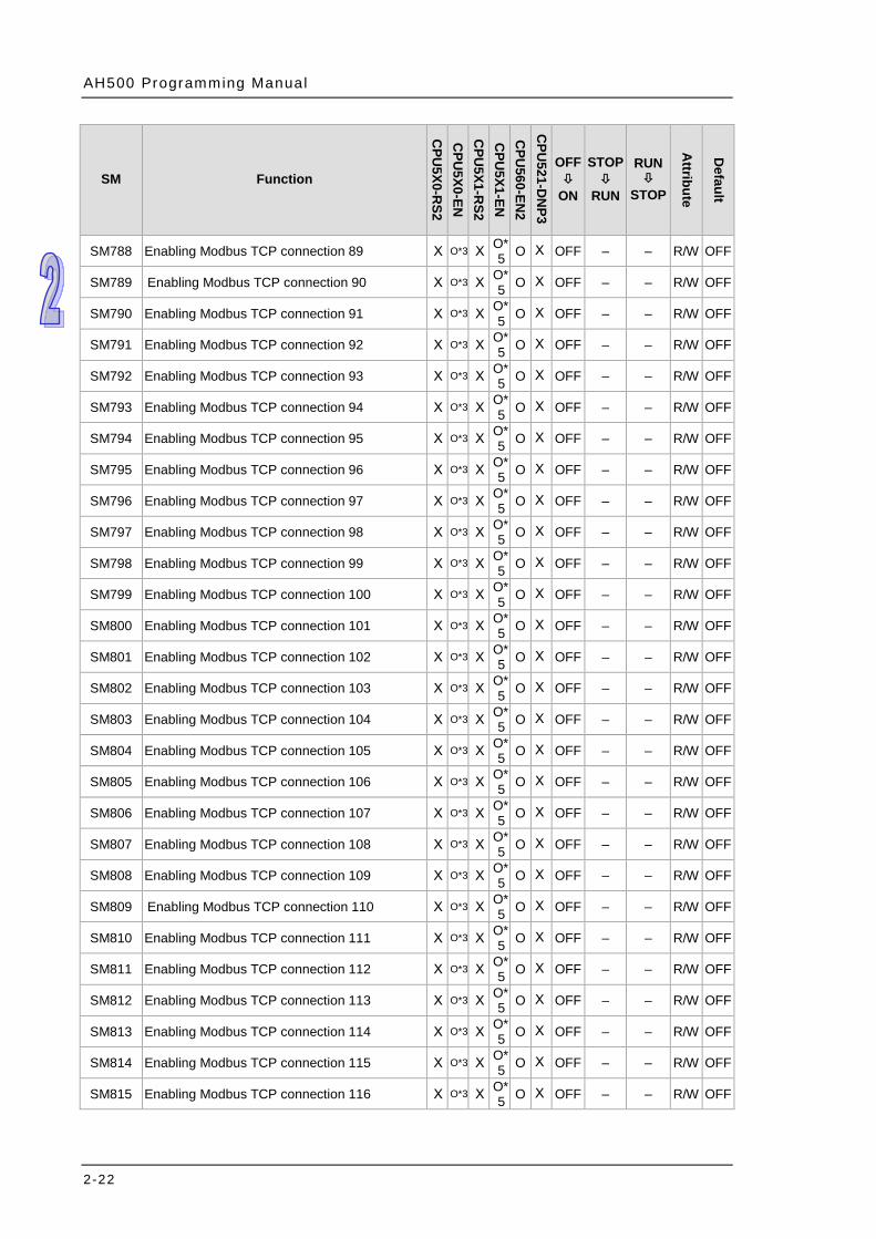
AH500 Programming Manual
2-22
SM Function
CPU
5X0-RS2
CPU
5X0-EN
CPU
5X1-RS2
CPU
5X1-EN
CPU
560-EN2
CPU
521-DN
P3
OFF
ON
STOP
RUN
RUN
STOP A
ttribute
Default
SM788 Enabling Modbus TCP connection 89 Χ O*3 Χ O*5 O Χ OFF – – R/W OFF
SM789 Enabling Modbus TCP connection 90 Χ O*3 Χ O*5 O Χ OFF – – R/W OFF
SM790 Enabling Modbus TCP connection 91 Χ O*3 Χ O*5 O Χ OFF – – R/W OFF
SM791 Enabling Modbus TCP connection 92 Χ O*3 Χ O*5 O Χ OFF – – R/W OFF
SM792 Enabling Modbus TCP connection 93 Χ O*3 Χ O*5 O Χ OFF – – R/W OFF
SM793 Enabling Modbus TCP connection 94 Χ O*3 Χ O*5 O Χ OFF – – R/W OFF
SM794 Enabling Modbus TCP connection 95 Χ O*3 Χ O*5 O Χ OFF – – R/W OFF
SM795 Enabling Modbus TCP connection 96 Χ O*3 Χ O*5 O Χ OFF – – R/W OFF
SM796 Enabling Modbus TCP connection 97 Χ O*3 Χ O*5 O Χ OFF – – R/W OFF
SM797 Enabling Modbus TCP connection 98 Χ O*3 Χ O*5 O Χ OFF – – R/W OFF
SM798 Enabling Modbus TCP connection 99 Χ O*3 Χ O*5 O Χ OFF – – R/W OFF
SM799 Enabling Modbus TCP connection 100 Χ O*3 Χ O*5 O Χ OFF – – R/W OFF
SM800 Enabling Modbus TCP connection 101 Χ O*3 Χ O*5 O Χ OFF – – R/W OFF
SM801 Enabling Modbus TCP connection 102 Χ O*3 Χ O*5 O Χ OFF – – R/W OFF
SM802 Enabling Modbus TCP connection 103 Χ O*3 Χ O*5 O Χ OFF – – R/W OFF
SM803 Enabling Modbus TCP connection 104 Χ O*3 Χ O*5 O Χ OFF – – R/W OFF
SM804 Enabling Modbus TCP connection 105 Χ O*3 Χ O*5 O Χ OFF – – R/W OFF
SM805 Enabling Modbus TCP connection 106 Χ O*3 Χ O*5 O Χ OFF – – R/W OFF
SM806 Enabling Modbus TCP connection 107 Χ O*3 Χ O*5 O Χ OFF – – R/W OFF
SM807 Enabling Modbus TCP connection 108 Χ O*3 Χ O*5 O Χ OFF – – R/W OFF
SM808 Enabling Modbus TCP connection 109 Χ O*3 Χ O*5 O Χ OFF – – R/W OFF
SM809 Enabling Modbus TCP connection 110 Χ O*3 Χ O*5 O Χ OFF – – R/W OFF
SM810 Enabling Modbus TCP connection 111 Χ O*3 Χ O*5 O Χ OFF – – R/W OFF
SM811 Enabling Modbus TCP connection 112 Χ O*3 Χ O*5 O Χ OFF – – R/W OFF
SM812 Enabling Modbus TCP connection 113 Χ O*3 Χ O*5 O Χ OFF – – R/W OFF
SM813 Enabling Modbus TCP connection 114 Χ O*3 Χ O*5 O Χ OFF – – R/W OFF
SM814 Enabling Modbus TCP connection 115 Χ O*3 Χ O*5 O Χ OFF – – R/W OFF
SM815 Enabling Modbus TCP connection 116 Χ O*3 Χ O*5 O Χ OFF – – R/W OFF

Chapter 2 Devices
2-23
SM Function
CPU
5X0-RS2
CPU
5X0-EN
CPU
5X1-RS2
CPU
5X1-EN
CPU
560-EN2
CPU
521-DN
P3
OFF
ON
STOP
RUN
RUN
STOP
Attribute
Default
SM816 Enabling Modbus TCP connection 117 Χ O*3 Χ O*5 O Χ OFF – – R/W OFF
SM817 Enabling Modbus TCP connection 118 Χ O*3 Χ O*5 O Χ OFF – – R/W OFF
SM818 Enabling Modbus TCP connection 119 Χ O*3 Χ O*5 O Χ OFF – – R/W OFF
SM819 Enabling Modbus TCP connection120 Χ O*3 Χ O*5 O Χ OFF – – R/W OFF
SM820 Enabling Modbus TCP connection 121 Χ O*3 Χ O*5 O Χ OFF – – R/W OFF
SM821 Enabling Modbus TCP connection 122 Χ O*3 Χ O*5 O Χ OFF – – R/W OFF
SM822 Enabling Modbus TCP connection 123 Χ O*3 Χ O*5 O Χ OFF – – R/W OFF
SM823 Enabling Modbus TCP connection 124 Χ O*3 Χ O*5 O Χ OFF – – R/W OFF
SM824 Enabling Modbus TCP connection 125 Χ O*3 Χ O*5 O Χ OFF – – R/W OFF
SM825 Enabling Modbus TCP connection 126 Χ O*3 Χ O*5 O Χ OFF – – R/W OFF
SM826 Enabling Modbus TCP connection 127 Χ O*3 Χ O*5 O Χ OFF – – R/W OFF
SM827 Enabling Modbus TCP connection 128 Χ O*3 Χ O*5 O Χ OFF – – R/W OFF
SM828 An error occurs in Modbus TCP connection 1. Χ V1.01 Χ O O O OFF – – R OFF
SM829 An error occurs in Modbus TCP connection 2. Χ V1.01 Χ O O O OFF – – R OFF
SM830 An error occurs in Modbus TCP connection 3. Χ V1.01 Χ O O O OFF – – R OFF
SM831 An error occurs in Modbus TCP connection 4. Χ V1.01 Χ O O O OFF – – R OFF
SM832 An error occurs in Modbus TCP connection 5. Χ V1.01 Χ O O O OFF – – R OFF
SM833 An error occurs in Modbus TCP connection 6. Χ V1.01 Χ O O O OFF – – R OFF
SM834 An error occurs in Modbus TCP connection 7. Χ V1.01 Χ O O O OFF – – R OFF
SM835 An error occurs in Modbus TCP connection 8. Χ V1.01 Χ O O O OFF – – R OFF
SM836 An error occurs in Modbus TCP connection 9. Χ V1.01 Χ O O O OFF – – R OFF
SM837 An error occurs in Modbus TCP connection 10. Χ V1.01 Χ O O O OFF – – R OFF
SM838 An error occurs in Modbus TCP connection 11. Χ V1.01 Χ O O O OFF – – R OFF
SM839 An error occurs in Modbus TCP connection 12. Χ V1.01 Χ O O O OFF – – R OFF
SM840 An error occurs in Modbus TCP connection 13. Χ V1.01 Χ O O O OFF – – R OFF
SM841 An error occurs in Modbus TCP connection 14. Χ V1.01 Χ O O O OFF – – R OFF
SM842 An error occurs in Modbus TCP connection 15. Χ V1.01 Χ O O O OFF – – R OFF
SM843 An error occurs in Modbus TCP connection 16. Χ V1.01 Χ O O O OFF – – R OFF
SM844 An error occurs in Modbus TCP connection 17. Χ O*1 Χ O*6 O O OFF – – R OFF
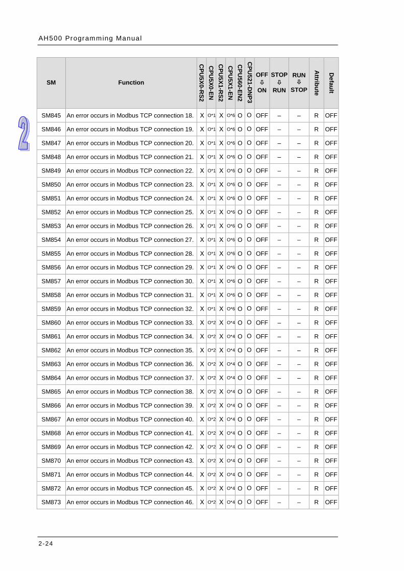
AH500 Programming Manual
2-24
SM Function
CPU
5X0-RS2
CPU
5X0-EN
CPU
5X1-RS2
CPU
5X1-EN
CPU
560-EN2
CPU
521-DN
P3
OFF
ON
STOP
RUN
RUN
STOP A
ttribute
Default
SM845 An error occurs in Modbus TCP connection 18. Χ O*1 Χ O*6 O O OFF – – R OFF
SM846 An error occurs in Modbus TCP connection 19. Χ O*1 Χ O*6 O O OFF – – R OFF
SM847 An error occurs in Modbus TCP connection 20. Χ O*1 Χ O*6 O O OFF – – R OFF
SM848 An error occurs in Modbus TCP connection 21. Χ O*1 Χ O*6 O O OFF – – R OFF
SM849 An error occurs in Modbus TCP connection 22. Χ O*1 Χ O*6 O O OFF – – R OFF
SM850 An error occurs in Modbus TCP connection 23. Χ O*1 Χ O*6 O O OFF – – R OFF
SM851 An error occurs in Modbus TCP connection 24. Χ O*1 Χ O*6 O O OFF – – R OFF
SM852 An error occurs in Modbus TCP connection 25. Χ O*1 Χ O*6 O O OFF – – R OFF
SM853 An error occurs in Modbus TCP connection 26. Χ O*1 Χ O*6 O O OFF – – R OFF
SM854 An error occurs in Modbus TCP connection 27. Χ O*1 Χ O*6 O O OFF – – R OFF
SM855 An error occurs in Modbus TCP connection 28. Χ O*1 Χ O*6 O O OFF – – R OFF
SM856 An error occurs in Modbus TCP connection 29. Χ O*1 Χ O*6 O O OFF – – R OFF
SM857 An error occurs in Modbus TCP connection 30. Χ O*1 Χ O*6 O O OFF – – R OFF
SM858 An error occurs in Modbus TCP connection 31. Χ O*1 Χ O*6 O O OFF – – R OFF
SM859 An error occurs in Modbus TCP connection 32. Χ O*1 Χ O*6 O O OFF – – R OFF
SM860 An error occurs in Modbus TCP connection 33. Χ O*2 Χ O*4 O O OFF – – R OFF
SM861 An error occurs in Modbus TCP connection 34. Χ O*2 Χ O*4 O O OFF – – R OFF
SM862 An error occurs in Modbus TCP connection 35. Χ O*2 Χ O*4 O O OFF – – R OFF
SM863 An error occurs in Modbus TCP connection 36. Χ O*2 Χ O*4 O O OFF – – R OFF
SM864 An error occurs in Modbus TCP connection 37. Χ O*2 Χ O*4 O O OFF – – R OFF
SM865 An error occurs in Modbus TCP connection 38. Χ O*2 Χ O*4 O O OFF – – R OFF
SM866 An error occurs in Modbus TCP connection 39. Χ O*2 Χ O*4 O O OFF – – R OFF
SM867 An error occurs in Modbus TCP connection 40. Χ O*2 Χ O*4 O O OFF – – R OFF
SM868 An error occurs in Modbus TCP connection 41. Χ O*2 Χ O*4 O O OFF – – R OFF
SM869 An error occurs in Modbus TCP connection 42. Χ O*2 Χ O*4 O O OFF – – R OFF
SM870 An error occurs in Modbus TCP connection 43. Χ O*2 Χ O*4 O O OFF – – R OFF
SM871 An error occurs in Modbus TCP connection 44. Χ O*2 Χ O*4 O O OFF – – R OFF
SM872 An error occurs in Modbus TCP connection 45. Χ O*2 Χ O*4 O O OFF – – R OFF
SM873 An error occurs in Modbus TCP connection 46. Χ O*2 Χ O*4 O O OFF – – R OFF
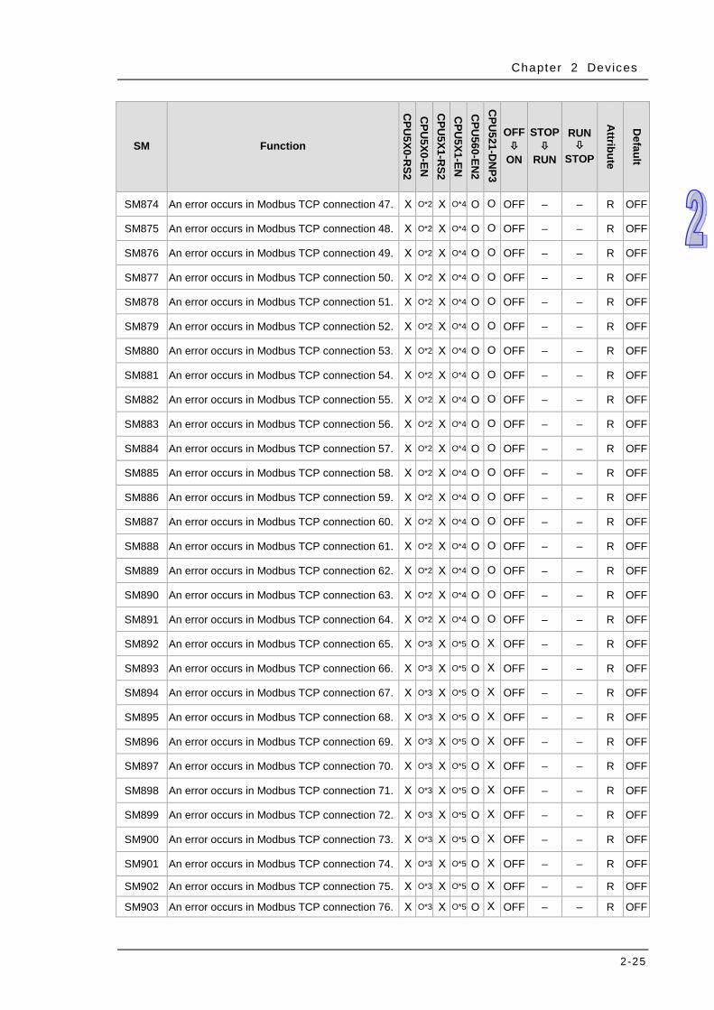
Chapter 2 Devices
2-25
SM Function
CPU
5X0-RS2
CPU
5X0-EN
CPU
5X1-RS2
CPU
5X1-EN
CPU
560-EN2
CPU
521-DN
P3
OFF
ON
STOP
RUN
RUN
STOP
Attribute
Default
SM874 An error occurs in Modbus TCP connection 47. Χ O*2 Χ O*4 O O OFF – – R OFF
SM875 An error occurs in Modbus TCP connection 48. Χ O*2 Χ O*4 O O OFF – – R OFF
SM876 An error occurs in Modbus TCP connection 49. Χ O*2 Χ O*4 O O OFF – – R OFF
SM877 An error occurs in Modbus TCP connection 50. Χ O*2 Χ O*4 O O OFF – – R OFF
SM878 An error occurs in Modbus TCP connection 51. Χ O*2 Χ O*4 O O OFF – – R OFF
SM879 An error occurs in Modbus TCP connection 52. Χ O*2 Χ O*4 O O OFF – – R OFF
SM880 An error occurs in Modbus TCP connection 53. Χ O*2 Χ O*4 O O OFF – – R OFF
SM881 An error occurs in Modbus TCP connection 54. Χ O*2 Χ O*4 O O OFF – – R OFF
SM882 An error occurs in Modbus TCP connection 55. Χ O*2 Χ O*4 O O OFF – – R OFF
SM883 An error occurs in Modbus TCP connection 56. Χ O*2 Χ O*4 O O OFF – – R OFF
SM884 An error occurs in Modbus TCP connection 57. Χ O*2 Χ O*4 O O OFF – – R OFF
SM885 An error occurs in Modbus TCP connection 58. Χ O*2 Χ O*4 O O OFF – – R OFF
SM886 An error occurs in Modbus TCP connection 59. Χ O*2 Χ O*4 O O OFF – – R OFF
SM887 An error occurs in Modbus TCP connection 60. Χ O*2 Χ O*4 O O OFF – – R OFF
SM888 An error occurs in Modbus TCP connection 61. Χ O*2 Χ O*4 O O OFF – – R OFF
SM889 An error occurs in Modbus TCP connection 62. Χ O*2 Χ O*4 O O OFF – – R OFF
SM890 An error occurs in Modbus TCP connection 63. Χ O*2 Χ O*4 O O OFF – – R OFF
SM891 An error occurs in Modbus TCP connection 64. Χ O*2 Χ O*4 O O OFF – – R OFF
SM892 An error occurs in Modbus TCP connection 65. Χ O*3 Χ O*5 O Χ OFF – – R OFF
SM893 An error occurs in Modbus TCP connection 66. Χ O*3 Χ O*5 O Χ OFF – – R OFF
SM894 An error occurs in Modbus TCP connection 67. Χ O*3 Χ O*5 O Χ OFF – – R OFF
SM895 An error occurs in Modbus TCP connection 68. Χ O*3 Χ O*5 O Χ OFF – – R OFF
SM896 An error occurs in Modbus TCP connection 69. Χ O*3 Χ O*5 O Χ OFF – – R OFF
SM897 An error occurs in Modbus TCP connection 70. Χ O*3 Χ O*5 O Χ OFF – – R OFF
SM898 An error occurs in Modbus TCP connection 71. Χ O*3 Χ O*5 O Χ OFF – – R OFF
SM899 An error occurs in Modbus TCP connection 72. Χ O*3 Χ O*5 O Χ OFF – – R OFF
SM900 An error occurs in Modbus TCP connection 73. Χ O*3 Χ O*5 O Χ OFF – – R OFF
SM901 An error occurs in Modbus TCP connection 74. Χ O*3 Χ O*5 O Χ OFF – – R OFF
SM902 An error occurs in Modbus TCP connection 75. Χ O*3 Χ O*5 O Χ OFF – – R OFF
SM903 An error occurs in Modbus TCP connection 76. Χ O*3 Χ O*5 O Χ OFF – – R OFF
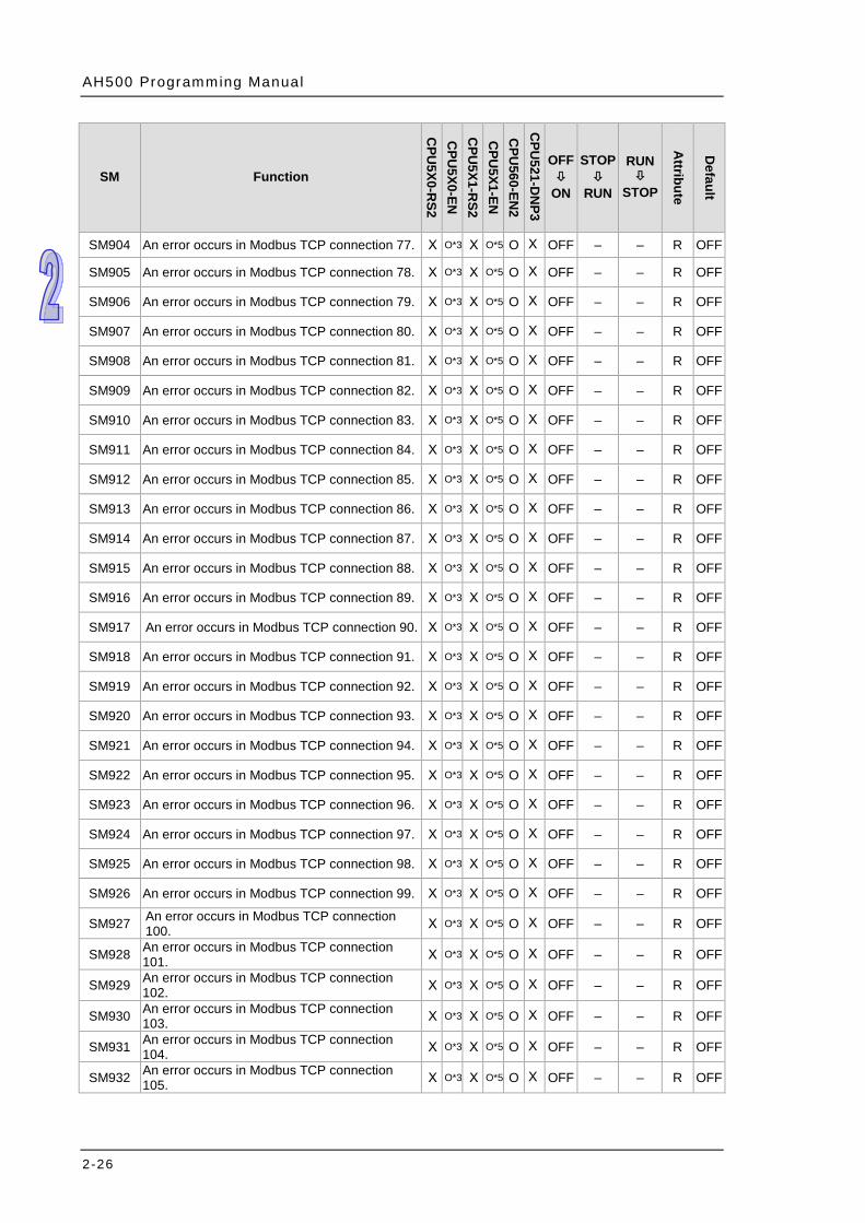
AH500 Programming Manual
2-26
SM Function
CPU
5X0-RS2
CPU
5X0-EN
CPU
5X1-RS2
CPU
5X1-EN
CPU
560-EN2
CPU
521-DN
P3
OFF
ON
STOP
RUN
RUN
STOP A
ttribute
Default
SM904 An error occurs in Modbus TCP connection 77. Χ O*3 Χ O*5 O Χ OFF – – R OFF
SM905 An error occurs in Modbus TCP connection 78. Χ O*3 Χ O*5 O Χ OFF – – R OFF
SM906 An error occurs in Modbus TCP connection 79. Χ O*3 Χ O*5 O Χ OFF – – R OFF
SM907 An error occurs in Modbus TCP connection 80. Χ O*3 Χ O*5 O Χ OFF – – R OFF
SM908 An error occurs in Modbus TCP connection 81. Χ O*3 Χ O*5 O Χ OFF – – R OFF
SM909 An error occurs in Modbus TCP connection 82. Χ O*3 Χ O*5 O Χ OFF – – R OFF
SM910 An error occurs in Modbus TCP connection 83. Χ O*3 Χ O*5 O Χ OFF – – R OFF
SM911 An error occurs in Modbus TCP connection 84. Χ O*3 Χ O*5 O Χ OFF – – R OFF
SM912 An error occurs in Modbus TCP connection 85. Χ O*3 Χ O*5 O Χ OFF – – R OFF
SM913 An error occurs in Modbus TCP connection 86. Χ O*3 Χ O*5 O Χ OFF – – R OFF
SM914 An error occurs in Modbus TCP connection 87. Χ O*3 Χ O*5 O Χ OFF – – R OFF
SM915 An error occurs in Modbus TCP connection 88. Χ O*3 Χ O*5 O Χ OFF – – R OFF
SM916 An error occurs in Modbus TCP connection 89. Χ O*3 Χ O*5 O Χ OFF – – R OFF
SM917 An error occurs in Modbus TCP connection 90. Χ O*3 Χ O*5 O Χ OFF – – R OFF
SM918 An error occurs in Modbus TCP connection 91. Χ O*3 Χ O*5 O Χ OFF – – R OFF
SM919 An error occurs in Modbus TCP connection 92. Χ O*3 Χ O*5 O Χ OFF – – R OFF
SM920 An error occurs in Modbus TCP connection 93. Χ O*3 Χ O*5 O Χ OFF – – R OFF
SM921 An error occurs in Modbus TCP connection 94. Χ O*3 Χ O*5 O Χ OFF – – R OFF
SM922 An error occurs in Modbus TCP connection 95. Χ O*3 Χ O*5 O Χ OFF – – R OFF
SM923 An error occurs in Modbus TCP connection 96. Χ O*3 Χ O*5 O Χ OFF – – R OFF
SM924 An error occurs in Modbus TCP connection 97. Χ O*3 Χ O*5 O Χ OFF – – R OFF
SM925 An error occurs in Modbus TCP connection 98. Χ O*3 Χ O*5 O Χ OFF – – R OFF
SM926 An error occurs in Modbus TCP connection 99. Χ O*3 Χ O*5 O Χ OFF – – R OFF
SM927 An error occurs in Modbus TCP connection 100. Χ O*3 Χ O*5 O Χ OFF – – R OFF
SM928 An error occurs in Modbus TCP connection 101. Χ O*3 Χ O*5 O Χ OFF – – R OFF
SM929 An error occurs in Modbus TCP connection 102. Χ O*3 Χ O*5 O Χ OFF – – R OFF
SM930 An error occurs in Modbus TCP connection 103. Χ O*3 Χ O*5 O Χ OFF – – R OFF
SM931 An error occurs in Modbus TCP connection 104. Χ O*3 Χ O*5 O Χ OFF – – R OFF
SM932 An error occurs in Modbus TCP connection 105. Χ O*3 Χ O*5 O Χ OFF – – R OFF

Chapter 2 Devices
2-27
SM Function
CPU
5X0-RS2
CPU
5X0-EN
CPU
5X1-RS2
CPU
5X1-EN
CPU
560-EN2
CPU
521-DN
P3
OFF
ON
STOP
RUN
RUN
STOP
Attribute
Default
SM933 An error occurs in Modbus TCP connection 106. Χ O*3 Χ O*5 O Χ OFF – – R OFF
SM934 An error occurs in Modbus TCP connection 107. Χ O*3 Χ O*5 O Χ OFF – – R OFF
SM935 An error occurs in Modbus TCP connection 108. Χ O*3 Χ O*5 O Χ OFF – – R OFF
SM936 An error occurs in Modbus TCP connection 109. Χ O*3 Χ O*5 O Χ OFF – – R OFF
SM937 An error occurs in Modbus TCP connection 110. Χ O*3 Χ O*5 O Χ OFF – – R OFF
SM938 An error occurs in Modbus TCP connection 111. Χ O*3 Χ O*5 O Χ OFF – – R OFF
SM939 An error occurs in Modbus TCP connection 112. Χ O*3 Χ O*5 O Χ OFF – – R OFF
SM940 An error occurs in Modbus TCP connection 113. Χ O*3 Χ O*5 O Χ OFF – – R OFF
SM941 An error occurs in Modbus TCP connection 114. Χ O*3 Χ O*5 O Χ OFF – – R OFF
SM942 An error occurs in Modbus TCP connection 115. Χ O*3 Χ O*5 O Χ OFF – – R OFF
SM943 An error occurs in Modbus TCP connection 116. Χ O*3 Χ O*5 O Χ OFF – – R OFF
SM944 An error occurs in Modbus TCP connection 117. Χ O*3 Χ O*5 O Χ OFF – – R OFF
SM945 An error occurs in Modbus TCP connection 118. Χ O*3 Χ O*5 O Χ OFF – – R OFF
SM946 An error occurs in Modbus TCP connection 119. Χ O*3 Χ O*5 O Χ OFF – – R OFF
SM947 An error occurs in Modbus TCP connection 120. Χ O*3 Χ O*5 O Χ OFF – – R OFF
SM948 An error occurs in Modbus TCP connection 121. Χ O*3 Χ O*5 O Χ OFF – – R OFF
SM949 An error occurs in Modbus TCP connection 122. Χ O*3 Χ O*5 O Χ OFF – – R OFF
SM950 An error occurs in Modbus TCP connection 123. Χ O*3 Χ O*5 O Χ OFF – – R OFF
SM951 An error occurs in Modbus TCP connection 124. Χ O*3 Χ O*5 O Χ OFF – – R OFF
SM952 An error occurs in Modbus TCP connection 125. Χ O*3 Χ O*5 O Χ OFF – – R OFF
SM953 An error occurs in Modbus TCP connection 126. Χ O*3 Χ O*5 O Χ OFF – – R OFF
SM954 An error occurs in Modbus TCP connection 127. Χ O*3 Χ O*5 O Χ OFF – – R OFF
SM955 An error occurs in Modbus TCP connection 128. Χ O*3 Χ O*5 O Χ OFF – – R OFF
SM1000 It is the Ethernet setting flag. When SM1000 is ON, the data in SR1000~SR1006 is written into the flash memory.
Χ O Χ O O O - – – R/W OFF
*SM1001 Port1 Ethernet connection status Χ Χ Χ O O O – – – R OFF
*SM1002 Port2 Ethernet connection status Χ Χ Χ Χ O Χ – – – R OFF
*SM1003 Fiber for synchronization connection status Χ Χ Χ Χ O Χ – – – R OFF
*SM1089 MODBUS TCP connection has reached its limit Χ V1.06. Χ V2.
00 O O OFF – – R OFF
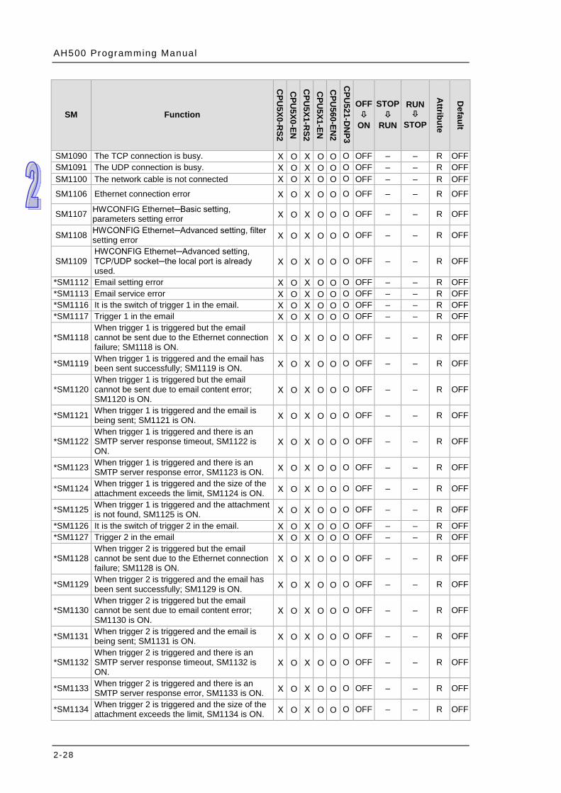
AH500 Programming Manual
2-28
SM Function
CPU
5X0-RS2
CPU
5X0-EN
CPU
5X1-RS2
CPU
5X1-EN
CPU
560-EN2
CPU
521-DN
P3
OFF
ON
STOP
RUN
RUN
STOP A
ttribute
Default
SM1090 The TCP connection is busy. Χ O Χ O O O OFF – – R OFF SM1091 The UDP connection is busy. Χ O Χ O O O OFF – – R OFF SM1100 The network cable is not connected Χ O Χ O O O OFF – – R OFF
SM1106 Ethernet connection error Χ O Χ O O O OFF – – R OFF
SM1107 HWCONFIG Ethernet─Basic setting, parameters setting error Χ O Χ O O O OFF – – R OFF
SM1108 HWCONFIG Ethernet─Advanced setting, filter setting error Χ O Χ O O O OFF – – R OFF
SM1109 HWCONFIG Ethernet─Advanced setting, TCP/UDP socket─the local port is already used.
Χ O Χ O O O OFF – – R OFF
*SM1112 Email setting error Χ O Χ O O O OFF – – R OFF *SM1113 Email service error Χ O Χ O O O OFF – – R OFF *SM1116 It is the switch of trigger 1 in the email. Χ O Χ O O O OFF – – R OFF *SM1117 Trigger 1 in the email Χ O Χ O O O OFF – – R OFF
*SM1118 When trigger 1 is triggered but the email cannot be sent due to the Ethernet connection failure; SM1118 is ON.
Χ O Χ O O O OFF – – R OFF
*SM1119 When trigger 1 is triggered and the email has been sent successfully; SM1119 is ON. Χ O Χ O O O OFF – – R OFF
*SM1120 When trigger 1 is triggered but the email cannot be sent due to email content error; SM1120 is ON.
Χ O Χ O O O OFF – – R OFF
*SM1121 When trigger 1 is triggered and the email is being sent; SM1121 is ON. Χ O Χ O O O OFF – – R OFF
*SM1122 When trigger 1 is triggered and there is an SMTP server response timeout, SM1122 is ON.
Χ O Χ O O O OFF – – R OFF
*SM1123 When trigger 1 is triggered and there is an SMTP server response error, SM1123 is ON. Χ O Χ O O O OFF – – R OFF
*SM1124 When trigger 1 is triggered and the size of the attachment exceeds the limit, SM1124 is ON. Χ O Χ O O O OFF – – R OFF
*SM1125 When trigger 1 is triggered and the attachment is not found, SM1125 is ON. Χ O Χ O O O OFF – – R OFF
*SM1126 It is the switch of trigger 2 in the email. Χ O Χ O O O OFF – – R OFF *SM1127 Trigger 2 in the email Χ O Χ O O O OFF – – R OFF
*SM1128 When trigger 2 is triggered but the email cannot be sent due to the Ethernet connection failure; SM1128 is ON.
Χ O Χ O O O OFF – – R OFF
*SM1129 When trigger 2 is triggered and the email has been sent successfully; SM1129 is ON. Χ O Χ O O O OFF – – R OFF
*SM1130 When trigger 2 is triggered but the email cannot be sent due to email content error; SM1130 is ON.
Χ O Χ O O O OFF – – R OFF
*SM1131 When trigger 2 is triggered and the email is being sent; SM1131 is ON. Χ O Χ O O O OFF – – R OFF
*SM1132 When trigger 2 is triggered and there is an SMTP server response timeout, SM1132 is ON.
Χ O Χ O O O OFF – – R OFF
*SM1133 When trigger 2 is triggered and there is an SMTP server response error, SM1133 is ON. Χ O Χ O O O OFF – – R OFF
*SM1134 When trigger 2 is triggered and the size of the attachment exceeds the limit, SM1134 is ON. Χ O Χ O O O OFF – – R OFF
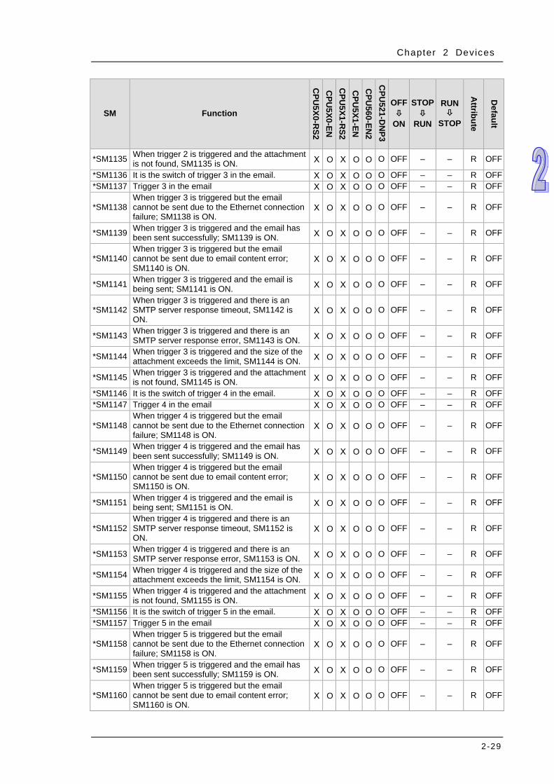
Chapter 2 Devices
2-29
SM Function
CPU
5X0-RS2
CPU
5X0-EN
CPU
5X1-RS2
CPU
5X1-EN
CPU
560-EN2
CPU
521-DN
P3
OFF
ON
STOP
RUN
RUN
STOP
Attribute
Default
*SM1135 When trigger 2 is triggered and the attachment is not found, SM1135 is ON. Χ O Χ O O O OFF – – R OFF
*SM1136 It is the switch of trigger 3 in the email. Χ O Χ O O O OFF – – R OFF *SM1137 Trigger 3 in the email Χ O Χ O O O OFF – – R OFF
*SM1138 When trigger 3 is triggered but the email cannot be sent due to the Ethernet connection failure; SM1138 is ON.
Χ O Χ O O O OFF – – R OFF
*SM1139 When trigger 3 is triggered and the email has been sent successfully; SM1139 is ON. Χ O Χ O O O OFF – – R OFF
*SM1140 When trigger 3 is triggered but the email cannot be sent due to email content error; SM1140 is ON.
Χ O Χ O O O OFF – – R OFF
*SM1141 When trigger 3 is triggered and the email is being sent; SM1141 is ON. Χ O Χ O O O OFF – – R OFF
*SM1142 When trigger 3 is triggered and there is an SMTP server response timeout, SM1142 is ON.
Χ O Χ O O O OFF – – R OFF
*SM1143 When trigger 3 is triggered and there is an SMTP server response error, SM1143 is ON. Χ O Χ O O O OFF – – R OFF
*SM1144 When trigger 3 is triggered and the size of the attachment exceeds the limit, SM1144 is ON. Χ O Χ O O O OFF – – R OFF
*SM1145 When trigger 3 is triggered and the attachment is not found, SM1145 is ON. Χ O Χ O O O OFF – – R OFF
*SM1146 It is the switch of trigger 4 in the email. Χ O Χ O O O OFF – – R OFF *SM1147 Trigger 4 in the email Χ O Χ O O O OFF – – R OFF
*SM1148 When trigger 4 is triggered but the email cannot be sent due to the Ethernet connection failure; SM1148 is ON.
Χ O Χ O O O OFF – – R OFF
*SM1149 When trigger 4 is triggered and the email has been sent successfully; SM1149 is ON. Χ O Χ O O O OFF – – R OFF
*SM1150 When trigger 4 is triggered but the email cannot be sent due to email content error; SM1150 is ON.
Χ O Χ O O O OFF – – R OFF
*SM1151 When trigger 4 is triggered and the email is being sent; SM1151 is ON. Χ O Χ O O O OFF – – R OFF
*SM1152 When trigger 4 is triggered and there is an SMTP server response timeout, SM1152 is ON.
Χ O Χ O O O OFF – – R OFF
*SM1153 When trigger 4 is triggered and there is an SMTP server response error, SM1153 is ON. Χ O Χ O O O OFF – – R OFF
*SM1154 When trigger 4 is triggered and the size of the attachment exceeds the limit, SM1154 is ON. Χ O Χ O O O OFF – – R OFF
*SM1155 When trigger 4 is triggered and the attachment is not found, SM1155 is ON. Χ O Χ O O O OFF – – R OFF
*SM1156 It is the switch of trigger 5 in the email. Χ O Χ O O O OFF – – R OFF *SM1157 Trigger 5 in the email Χ O Χ O O O OFF – – R OFF
*SM1158 When trigger 5 is triggered but the email cannot be sent due to the Ethernet connection failure; SM1158 is ON.
Χ O Χ O O O OFF – – R OFF
*SM1159 When trigger 5 is triggered and the email has been sent successfully; SM1159 is ON. Χ O Χ O O O OFF – – R OFF
*SM1160 When trigger 5 is triggered but the email cannot be sent due to email content error; SM1160 is ON.
Χ O Χ O O O OFF – – R OFF

AH500 Programming Manual
2-30
SM Function
CPU
5X0-RS2
CPU
5X0-EN
CPU
5X1-RS2
CPU
5X1-EN
CPU
560-EN2
CPU
521-DN
P3
OFF
ON
STOP
RUN
RUN
STOP A
ttribute
Default
*SM1161 When trigger 5 is triggered and the email is being sent; SM1161 is ON. Χ O Χ O O O OFF – – R OFF
*SM1162 When trigger 5 is triggered and there is an SMTP server response timeout, SM1162 is ON.
Χ O Χ O O O OFF – – R OFF
*SM1163 When trigger 5 is triggered and there is an SMTP server response error, SM1163 is ON. Χ O Χ O O O OFF – – R OFF
*SM1164 When trigger 5 is triggered and the size of the attachment exceeds the limit, SM1164 is ON. Χ O Χ O O O OFF – – R OFF
*SM1165 When trigger 5 is triggered and the attachment is not found, SM1165 is ON. Χ O Χ O O O OFF – – R OFF
*SM1166 It is the switch of trigger 6 in the email. Χ O Χ O O O OFF – – R OFF *SM1167 Trigger 6 in the email Χ O Χ O O O OFF – – R OFF
*SM1168 When trigger 6 is triggered but the email cannot be sent due to the Ethernet connection failure; SM1168 is ON.
Χ O Χ O O O OFF – – R OFF
*SM1169 When trigger 6 is triggered and the email has been sent successfully; SM1169 is ON. Χ O Χ O O O OFF – – R OFF
*SM1170 When trigger 6 is triggered but the email cannot be sent due to email content error; SM1170 is ON.
Χ O Χ O O O OFF – – R OFF
*SM1171 When trigger 6 is triggered and the email is being sent; SM1171 is ON. Χ O Χ O O O OFF – – R OFF
*SM1172 When trigger 6 is triggered and there is an SMTP server response timeout, SM1172 is ON.
Χ O Χ O O O OFF – – R OFF
*SM1173 When trigger 6 is triggered and there is an SMTP server response error, SM1173 is ON. Χ O Χ O O O OFF – – R OFF
*SM1174 When trigger 6 is triggered and the size of the attachment exceeds the limit, SM1174 is ON. Χ O Χ O O O OFF – – R OFF
*SM1175 When trigger 6 is triggered and the attachment is not found, SM1175 is ON. Χ O Χ O O O OFF – – R OFF
*SM1176 It is the switch of trigger 7 in the email. Χ O Χ O O O OFF – – R OFF *SM1177 Trigger 7 in the email Χ O Χ O O O OFF – – R OFF
*SM1178 When trigger 7 is triggered but the email cannot be sent due to the Ethernet connection failure; SM1178 is ON.
Χ O Χ O O O OFF – – R OFF
*SM1179 When trigger 7 is triggered and the email has been sent successfully; SM1179 is ON. Χ O Χ O O O OFF – – R OFF
*SM1180 When trigger 7 is triggered but the email cannot be sent due to email content error; SM1180 is ON.
Χ O Χ O O O OFF – – R OFF
*SM1181 When trigger 7 is triggered and the email is being sent; SM1181 is ON. Χ O Χ O O O OFF – – R OFF
*SM1182 When trigger 7 is triggered and there is an SMTP server response timeout, SM1182 is ON.
Χ O Χ O O O OFF – – R OFF
*SM1183 When trigger 7 is triggered and there is an SMTP server response error, SM1183 is ON. Χ O Χ O O O OFF – – R OFF
*SM1184 When trigger 7 is triggered and the size of the attachment exceeds the limit, SM1184 is ON. Χ O Χ O O O OFF – – R OFF
*SM1185 When trigger 7 is triggered and the attachment is not found, SM1185 is ON. Χ O Χ O O O OFF – – R OFF
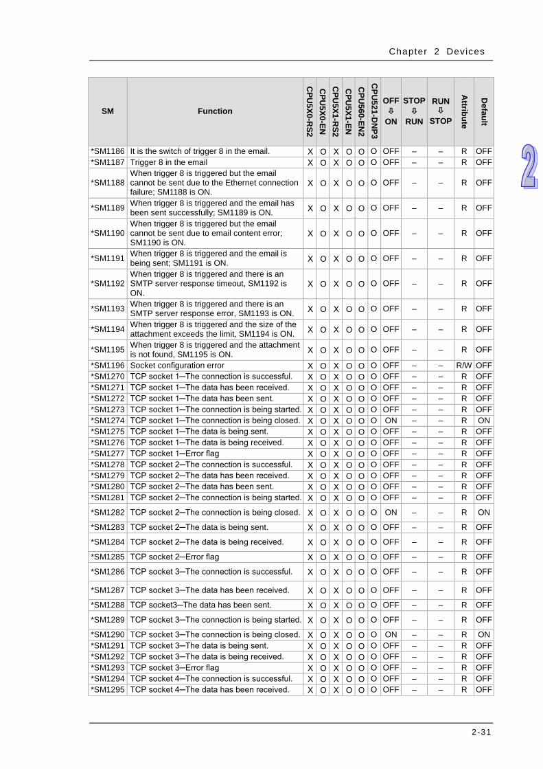
Chapter 2 Devices
2-31
SM Function
CPU
5X0-RS2
CPU
5X0-EN
CPU
5X1-RS2
CPU
5X1-EN
CPU
560-EN2
CPU
521-DN
P3
OFF
ON
STOP
RUN
RUN
STOP
Attribute
Default
*SM1186 It is the switch of trigger 8 in the email. Χ O Χ O O O OFF – – R OFF *SM1187 Trigger 8 in the email Χ O Χ O O O OFF – – R OFF
*SM1188 When trigger 8 is triggered but the email cannot be sent due to the Ethernet connection failure; SM1188 is ON.
Χ O Χ O O O OFF – – R OFF
*SM1189 When trigger 8 is triggered and the email has been sent successfully; SM1189 is ON. Χ O Χ O O O OFF – – R OFF
*SM1190 When trigger 8 is triggered but the email cannot be sent due to email content error; SM1190 is ON.
Χ O Χ O O O OFF – – R OFF
*SM1191 When trigger 8 is triggered and the email is being sent; SM1191 is ON. Χ O Χ O O O OFF – – R OFF
*SM1192 When trigger 8 is triggered and there is an SMTP server response timeout, SM1192 is ON.
Χ O Χ O O O OFF – – R OFF
*SM1193 When trigger 8 is triggered and there is an SMTP server response error, SM1193 is ON. Χ O Χ O O O OFF – – R OFF
*SM1194 When trigger 8 is triggered and the size of the attachment exceeds the limit, SM1194 is ON. Χ O Χ O O O OFF – – R OFF
*SM1195 When trigger 8 is triggered and the attachment is not found, SM1195 is ON. Χ O Χ O O O OFF – – R OFF
*SM1196 Socket configuration error Χ O Χ O O O OFF – – R/W OFF *SM1270 TCP socket 1─The connection is successful. Χ O Χ O O O OFF – – R OFF *SM1271 TCP socket 1─The data has been received. Χ O Χ O O O OFF – – R OFF *SM1272 TCP socket 1─The data has been sent. Χ O Χ O O O OFF – – R OFF *SM1273 TCP socket 1─The connection is being started. Χ O Χ O O O OFF – – R OFF *SM1274 TCP socket 1─The connection is being closed. Χ O Χ O O O ON – – R ON *SM1275 TCP socket 1─The data is being sent. Χ O Χ O O O OFF – – R OFF *SM1276 TCP socket 1─The data is being received. Χ O Χ O O O OFF – – R OFF *SM1277 TCP socket 1─Error flag Χ O Χ O O O OFF – – R OFF *SM1278 TCP socket 2─The connection is successful. Χ O Χ O O O OFF – – R OFF *SM1279 TCP socket 2─The data has been received. Χ O Χ O O O OFF – – R OFF *SM1280 TCP socket 2─The data has been sent. Χ O Χ O O O OFF – – R OFF *SM1281 TCP socket 2─The connection is being started. Χ O Χ O O O OFF – – R OFF
*SM1282 TCP socket 2─The connection is being closed. Χ O Χ O O O ON – – R ON
*SM1283 TCP socket 2─The data is being sent. Χ O Χ O O O OFF – – R OFF
*SM1284 TCP socket 2─The data is being received. Χ O Χ O O O OFF – – R OFF
*SM1285 TCP socket 2─Error flag Χ O Χ O O O OFF – – R OFF
*SM1286 TCP socket 3─The connection is successful. Χ O Χ O O O OFF – – R OFF
*SM1287 TCP socket 3─The data has been received. Χ O Χ O O O OFF – – R OFF
*SM1288 TCP socket3─The data has been sent. Χ O Χ O O O OFF – – R OFF
*SM1289 TCP socket 3─The connection is being started. Χ O Χ O O O OFF – – R OFF
*SM1290 TCP socket 3─The connection is being closed. Χ O Χ O O O ON – – R ON *SM1291 TCP socket 3─The data is being sent. Χ O Χ O O O OFF – – R OFF *SM1292 TCP socket 3─The data is being received. Χ O Χ O O O OFF – – R OFF *SM1293 TCP socket 3─Error flag Χ O Χ O O O OFF – – R OFF *SM1294 TCP socket 4─The connection is successful. Χ O Χ O O O OFF – – R OFF *SM1295 TCP socket 4─The data has been received. Χ O Χ O O O OFF – – R OFF
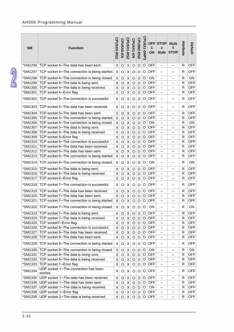
AH500 Programming Manual
2-32
SM Function
CPU
5X0-RS2
CPU
5X0-EN
CPU
5X1-RS2
CPU
5X1-EN
CPU
560-EN2
CPU
521-DN
P3
OFF
ON
STOP
RUN
RUN
STOP A
ttribute
Default
*SM1296 TCP socket 4─The data has been sent. Χ O Χ O O O OFF – – R OFF
*SM1297 TCP socket 4─The connection is being started. Χ O Χ O O O OFF – – R OFF
*SM1298 TCP socket 4─The connection is being closed. Χ O Χ O O O ON – – R ON *SM1299 TCP socket 4─The data is being sent. Χ O Χ O O O OFF – – R OFF *SM1300 TCP socket 4─The data is being received. Χ O Χ O O O OFF – – R OFF *SM1301 TCP socket 4─Error flag Χ O Χ O O O OFF – – R OFF
*SM1302 TCP socket 5─The connection is successful. Χ O Χ O O O OFF – – R OFF
*SM1303 TCP socket 5─The data has been received. Χ O Χ O O O OFF – – R OFF
*SM1304 TCP socket 5─The data has been sent. Χ O Χ O O O OFF – – R OFF *SM1305 TCP socket 5─The connection is being started. Χ O Χ O O O OFF – – R OFF *SM1306 TCP socket 5─The connection is being closed. Χ O Χ O O O ON – – R ON *SM1307 TCP socket 5─The data is being sent. Χ O Χ O O O OFF – – R OFF *SM1308 TCP socket 5─The data is being received. Χ O Χ O O O OFF – – R OFF *SM1309 TCP socket 5─Error flag Χ O Χ O O O OFF – – R OFF *SM1310 TCP socket 6─The connection is successful. Χ O Χ O O O OFF – – R OFF *SM1311 TCP socket 6─The data has been received. Χ O Χ O O O OFF – – R OFF *SM1312 TCP socket 6─The data has been sent. Χ O Χ O O O OFF – – R OFF *SM1313 TCP socket 6─The connection is being started. Χ O Χ O O O OFF – – R OFF
*SM1314 TCP socket 6─The connection is being closed. Χ O Χ O O O ON – – R ON
*SM1315 TCP socket 6─The data is being sent. Χ O Χ O O O OFF – – R OFF *SM1316 TCP socket 6─The data is being received. Χ O Χ O O O OFF – – R OFF *SM1317 TCP socket 6─Error flag Χ O Χ O O O OFF – – R OFF
*SM1318 TCP socket 7─The connection is successful. Χ O Χ O O O OFF – – R OFF
*SM1319 TCP socket 7─The data has been received. Χ O Χ O O O OFF – – R OFF *SM1320 TCP socket 7─The data has been sent. Χ O Χ O O O OFF – – R OFF *SM1321 TCP socket 7─The connection is being started. Χ O Χ O O O OFF – – R OFF
*SM1322 TCP socket 7─The connection is being closed. Χ O Χ O O O ON – – R ON
*SM1323 TCP socket 7─The data is being sent. Χ O Χ O O O OFF – – R OFF *SM1324 TCP socket 7─The data is being received. Χ O Χ O O O OFF – – R OFF *SM1325 TCP socket7─Error flag Χ O Χ O O O OFF – – R OFF *SM1326 TCP socket 8─The connection is successful. Χ O Χ O O O OFF – – R OFF *SM1327 TCP socket 8─The data has been received. Χ O Χ O O O OFF – – R OFF *SM1328 TCP socket 8─The data has been sent. Χ O Χ O O O OFF – – R OFF
*SM1329 TCP socket 8─The connection is being started. Χ O Χ O O O OFF – – R OFF
*SM1330 TCP socket 8─The connection is being closed. Χ O Χ O O O ON – – R ON *SM1331 TCP socket 8─The data is being sent. Χ O Χ O O O OFF – – R OFF *SM1332 TCP socket 8─The data is being received. Χ O Χ O O O OFF – – R OFF *SM1333 TCP socket 1─Error flag Χ O Χ O O O OFF – – R OFF
*SM1334 UDP socket 1─The connection has been started. Χ O Χ O O O OFF – – R OFF
*SM1335 UDP socket 1─The data has been received. Χ O Χ O O O OFF – – R OFF *SM1336 UDP socket 1─The data has been sent. Χ O Χ O O O OFF – – R OFF *SM1337 UDP socket 1─The data is being received. Χ O Χ O O O ON – – R OFF *SM1338 UDP socket 1─Error flag Χ O Χ O O O OFF – – R OFF *SM1339 UDP socket 2─The data is being received. Χ O Χ O O O OFF – – R OFF
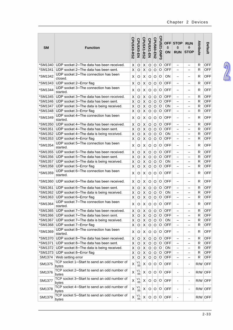
Chapter 2 Devices
2-33
SM Function
CPU
5X0-RS2
CPU
5X0-EN
CPU
5X1-RS2
CPU
5X1-EN
CPU
560-EN2
CPU
521-DN
P3
OFF
ON
STOP
RUN
RUN
STOP
Attribute
Default
*SM1340 UDP socket 2─The data has been received. Χ O Χ O O O OFF – – R OFF *SM1341 UDP socket 2─The data has been sent. Χ O Χ O O O OFF – – R OFF
*SM1342 UDP socket 2─The connection has been closed. Χ O Χ O O O ON – – R OFF
*SM1343 UDP socket 2─Error flag Χ O Χ O O O OFF – – R OFF
*SM1344 UDP socket 3─The connection has been started. Χ O Χ O O O OFF – – R OFF
*SM1345 UDP socket 3─The data has been received. Χ O Χ O O O OFF – – R OFF *SM1346 UDP socket 3─The data has been sent. Χ O Χ O O O OFF – – R OFF *SM1347 UDP socket 3─The data is being received. Χ O Χ O O O ON – – R OFF *SM1348 UDP socket 3─Error flag Χ O Χ O O O OFF – – R OFF
*SM1349 UDP socket 4─The connection has been started. Χ O Χ O O O OFF – – R OFF
*SM1350 UDP socket 4─The data has been received. Χ O Χ O O O OFF – – R OFF *SM1351 UDP socket 4─The data has been sent. Χ O Χ O O O OFF – – R OFF *SM1352 UDP socket 4─The data is being received. Χ O Χ O O O ON – – R OFF *SM1353 UDP socket 4─Error flag Χ O Χ O O O OFF – – R OFF
*SM1354 UDP socket 5─The connection has been started. Χ O Χ O O O OFF – – R OFF
*SM1355 UDP socket 5─The data has been received. Χ O Χ O O O OFF – – R OFF *SM1356 UDP socket 5─The data has been sent. Χ O Χ O O O OFF – – R OFF *SM1357 UDP socket 5─The data is being received. Χ O Χ O O O ON – – R OFF *SM1358 UDP socket 5─Error flag Χ O Χ O O O OFF – – R OFF
*SM1359 UDP socket 6─The connection has been started. Χ O Χ O O O OFF – – R OFF
*SM1360 UDP socket 6─The data has been received. Χ O Χ O O O OFF – – R OFF
*SM1361 UDP socket 6─The data has been sent. Χ O Χ O O O OFF – – R OFF *SM1362 UDP socket 6─The data is being received. Χ O Χ O O O ON – – R OFF *SM1363 UDP socket 6─Error flag Χ O Χ O O O OFF – – R OFF
*SM1364 UDP socket 7─The connection has been started. Χ O Χ O O O OFF – – R OFF
*SM1365 UDP socket 7─The data has been received. Χ O Χ O O O OFF – – R OFF *SM1366 UDP socket 7─The data has been sent. Χ O Χ O O O OFF – – R OFF *SM1367 UDP socket 7─The data is being received. Χ O Χ O O O ON – – R OFF *SM1368 UDP socket 7─Error flag Χ O Χ O O O OFF – – R OFF
*SM1369 UDP socket 8─The connection has been started. Χ O Χ O O O OFF – – R OFF
*SM1370 UDP socket 8─The data has been received. Χ O Χ O O O OFF – – R OFF *SM1371 UDP socket 8─The data has been sent. Χ O Χ O O O OFF – – R OFF *SM1372 UDP socket 8─The data is being received. Χ O Χ O O O ON – – R OFF *SM1373 UDP socket 8─Error flag Χ O Χ O O O OFF – – R OFF SM1374 Web setting error Χ O Χ O O O OFF – – R OFF
SM1375 TCP socket 1─Start to send an odd number of bytes Χ V1.
05 Χ O O O OFF - - R/W OFF
SM1376 TCP socket 2─Start to send an odd number of bytes Χ V1.
05 Χ O O O OFF - - R/W OFF
SM1377 TCP socket 3─Start to send an odd number of bytes Χ V1.
05 Χ O O O OFF - - R/W OFF
SM1378 TCP socket 4─Start to send an odd number of bytes Χ V1.
05 Χ O O O OFF - - R/W OFF
SM1379 TCP socket 5─Start to send an odd number of bytes Χ V1.
05 Χ O O O OFF - R/W OFF
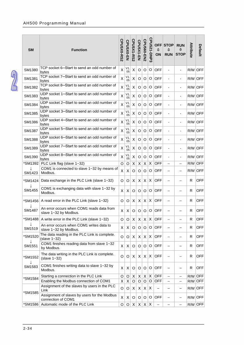
AH500 Programming Manual
2-34
SM Function
CPU
5X0-RS2
CPU
5X0-EN
CPU
5X1-RS2
CPU
5X1-EN
CPU
560-EN2
CPU
521-DN
P3
OFF
ON
STOP
RUN
RUN
STOP A
ttribute
Default
SM1380 TCP socket 6─Start to send an odd number of bytes Χ V1.
05 Χ O O O OFF - - R/W OFF
SM1381 TCP socket 7─Start to send an odd number of bytes Χ V1.
05 Χ O O O OFF - - R/W OFF
SM1382 TCP socket 8─Start to send an odd number of bytes Χ V1.
05 Χ O O O OFF - - R/W OFF
SM1383 UDP socket 1─Start to send an odd number of bytes Χ V1.
05 Χ O O O OFF - - R/W OFF
SM1384 UDP socket 2─Start to send an odd number of bytes Χ V1.
05 Χ O O O OFF - - R/W OFF
SM1385 UDP socket 3─Start to send an odd number of bytes Χ V1.
05 Χ O O O OFF - - R/W OFF
SM1386 UDP socket 4─Start to send an odd number of bytes Χ V1.
05 Χ O O O OFF - - R/W OFF
SM1387 UDP socket 5─Start to send an odd number of bytes Χ V1.
05 Χ O O O OFF - - R/W OFF
SM1388 UDP socket 6─Start to send an odd number of bytes Χ V1.
05 Χ O O O OFF - - R/W OFF
SM1389 UDP socket 7─Start to send an odd number of bytes Χ V1.
05 Χ O O O OFF - - R/W OFF
SM1390 UDP socket 8─Start to send an odd number of bytes Χ V1.
05 Χ O O O OFF - - R/W OFF
*SM1392 ↓
SM1423
PLC Link flag (slave 1~32) O O Χ Χ Χ Χ OFF – – R/W OFF COM1 is connected to slave 1~32 by means of Modbus. Χ Χ O O O O OFF – – R/W OFF
*SM1424 ↓
SM1455
Data exchange in the PLC Link (slave 1~32) O O Χ Χ Χ Χ OFF – – R OFF
COM1 is exchanging data with slave 1~32 by Modbus. Χ Χ O O O O OFF – – R OFF
*SM1456 ↓
SM1487
A read error in the PLC Link (slave 1~32) O O Χ Χ Χ Χ OFF – – R OFF
An error occurs when COM1 reads data from slave 1~32 by Modbus. Χ Χ O O O O OFF – – R OFF
*SM1488 ↓
SM1519
A write error in the PLC Link (slave 1~32) O O Χ Χ Χ Χ OFF – – R OFF An error occurs when COM1 writes data to slave 1~32 by Modbus. Χ Χ O O O O OFF – – R OFF
*SM1520 ↓
SM1551
The data reading in the PLC Link is complete. (slave 1~32) O O Χ Χ Χ Χ OFF – – R OFF
COM1 finishes reading data from slave 1~32 by Modbus. Χ Χ O O O O OFF – – R OFF
*SM1552 ↓
SM1583
The data writing in the PLC Link is complete. (slave 1~32) O O Χ Χ Χ Χ OFF – – R OFF
COM1 finishes writing data to slave 1~32 by Modbus. Χ Χ O O O O OFF – – R OFF
*SM1584 Starting a connection in the PLC Link O O Χ Χ Χ Χ OFF – – R/W OFF Enabling the Modbus connection of COM1 Χ Χ O O O O OFF – – R/W OFF
*SM1585
Assignment of the slaves by users in the PLC Link O O Χ Χ Χ Χ – – – R/W OFF
Assignment of slaves by users for the Modbus connection of COM1 Χ Χ O O O O OFF – – R/W OFF
*SM1586 Automatic mode of the PLC Link O O Χ Χ Χ Χ – – – R/W OFF
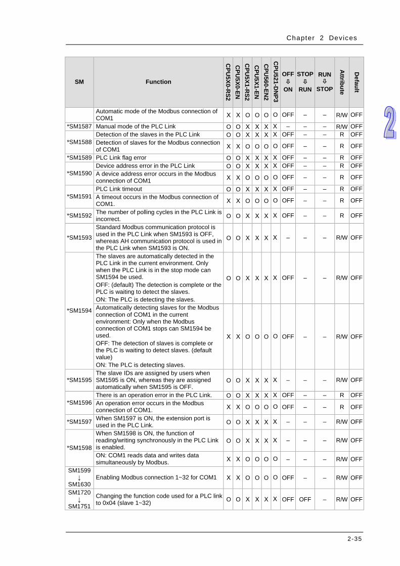
Chapter 2 Devices
2-35
SM Function
CPU
5X0-RS2
CPU
5X0-EN
CPU
5X1-RS2
CPU
5X1-EN
CPU
560-EN2
CPU
521-DN
P3
OFF
ON
STOP
RUN
RUN
STOP
Attribute
Default
Automatic mode of the Modbus connection of COM1 Χ Χ O O O O OFF – – R/W OFF
*SM1587 Manual mode of the PLC Link O O Χ Χ Χ Χ – – – R/W OFF
*SM1588 Detection of the slaves in the PLC Link O O Χ Χ Χ Χ OFF – – R OFF Detection of slaves for the Modbus connection of COM1 Χ Χ O O O O OFF – – R OFF
*SM1589 PLC Link flag error O O Χ Χ Χ Χ OFF – – R OFF
*SM1590 Device address error in the PLC Link O O Χ Χ Χ Χ OFF – – R OFF A device address error occurs in the Modbus connection of COM1 Χ Χ O O O O OFF – – R OFF
*SM1591 PLC Link timeout O O Χ Χ Χ Χ OFF – – R OFF A timeout occurs in the Modbus connection of COM1. Χ Χ O O O O OFF – – R OFF
*SM1592 The number of polling cycles in the PLC Link is incorrect. O O Χ Χ Χ Χ OFF – – R OFF
*SM1593
Standard Modbus communication protocol is used in the PLC Link when SM1593 is OFF, whereas AH communication protocol is used in the PLC Link when SM1593 is ON.
O O Χ Χ Χ Χ – – – R/W OFF
*SM1594
The slaves are automatically detected in the PLC Link in the current environment. Only when the PLC Link is in the stop mode can SM1594 be used. OFF: (default) The detection is complete or the PLC is waiting to detect the slaves. ON: The PLC is detecting the slaves.
O O Χ Χ Χ Χ OFF – – R/W OFF
Automatically detecting slaves for the Modbus connection of COM1 in the current environment: Only when the Modbus connection of COM1 stops can SM1594 be used. OFF: The detection of slaves is complete or the PLC is waiting to detect slaves. (default value) ON: The PLC is detecting slaves.
Χ Χ O O O O OFF – – R/W OFF
*SM1595 The slave IDs are assigned by users when SM1595 is ON, whereas they are assigned automatically when SM1595 is OFF.
O O Χ Χ Χ Χ – – – R/W OFF
*SM1596 There is an operation error in the PLC Link. O O Χ Χ Χ Χ OFF – – R OFF An operation error occurs in the Modbus connection of COM1. Χ Χ O O O O OFF – – R OFF
*SM1597 When SM1597 is ON, the extension port is used in the PLC Link. O O Χ Χ Χ Χ – – – R/W OFF
*SM1598
When SM1598 is ON, the function of reading/writing synchronously in the PLC Link is enabled.
O O Χ Χ Χ Χ – – – R/W OFF
ON: COM1 reads data and writes data simultaneously by Modbus. Χ Χ O O O O – – – R/W OFF
SM1599 ↓
SM1630 Enabling Modbus connection 1~32 for COM1 Χ Χ O O O O OFF – – R/W OFF
SM1720 ↓
SM1751
Changing the function code used for a PLC link to 0x04 (slave 1~32) O O Χ Χ Χ Χ OFF OFF – R/W OFF
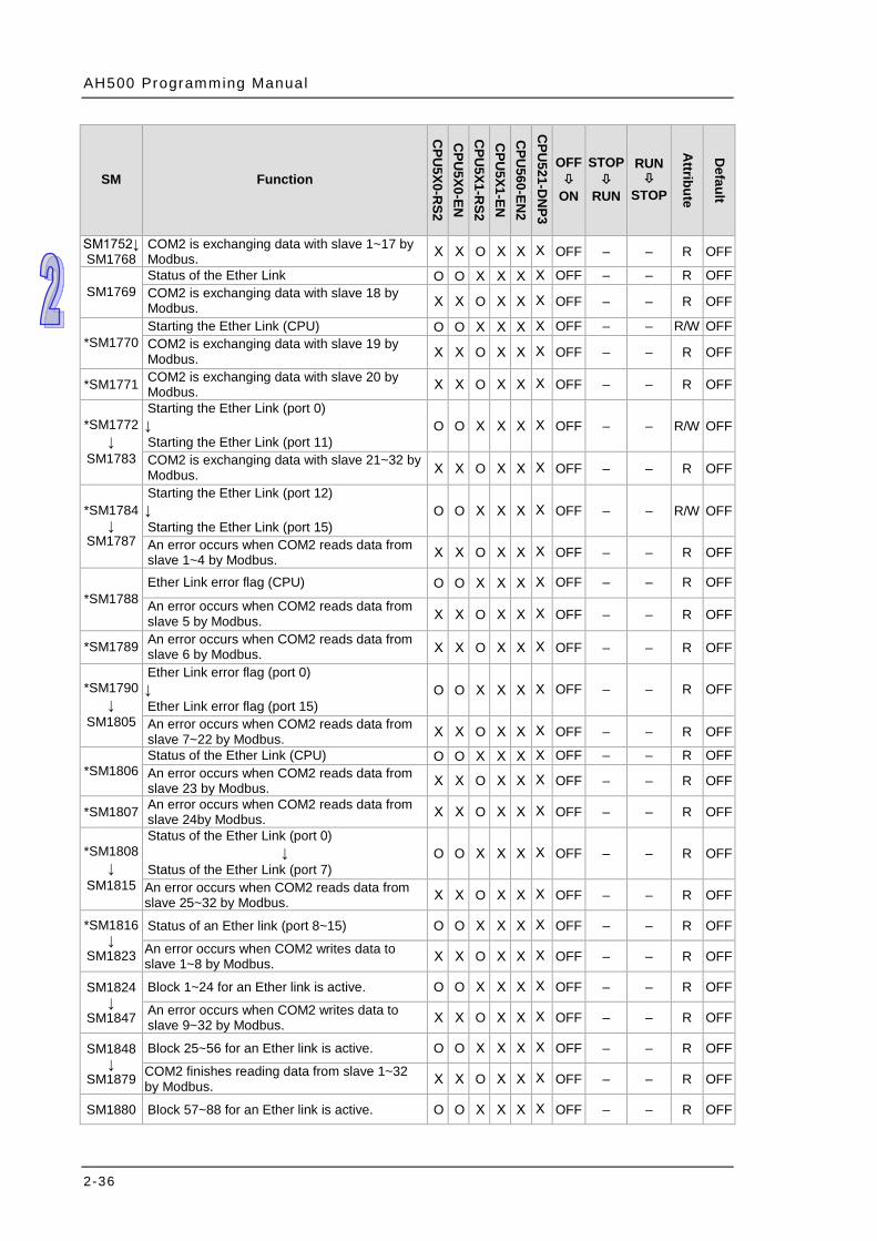
AH500 Programming Manual
2-36
SM Function
CPU
5X0-RS2
CPU
5X0-EN
CPU
5X1-RS2
CPU
5X1-EN
CPU
560-EN2
CPU
521-DN
P3
OFF
ON
STOP
RUN
RUN
STOP A
ttribute
Default
SM1752↓ SM1768
COM2 is exchanging data with slave 1~17 by Modbus. Χ Χ O Χ Χ Χ OFF – – R OFF
SM1769 Status of the Ether Link O O Χ Χ Χ Χ OFF – – R OFF COM2 is exchanging data with slave 18 by Modbus. Χ Χ O Χ Χ Χ OFF – – R OFF
*SM1770 Starting the Ether Link (CPU) O O Χ Χ Χ Χ OFF – – R/W OFF COM2 is exchanging data with slave 19 by Modbus. Χ Χ O Χ Χ Χ OFF – – R OFF
*SM1771 COM2 is exchanging data with slave 20 by Modbus. Χ Χ O Χ Χ Χ OFF – – R OFF
*SM1772 ↓
SM1783
Starting the Ether Link (port 0) ↓ Starting the Ether Link (port 11)
O O Χ Χ Χ Χ OFF – – R/W OFF
COM2 is exchanging data with slave 21~32 by Modbus. Χ Χ O Χ Χ Χ OFF – – R OFF
*SM1784 ↓
SM1787
Starting the Ether Link (port 12) ↓ Starting the Ether Link (port 15)
O O Χ Χ Χ Χ OFF – – R/W OFF
An error occurs when COM2 reads data from slave 1~4 by Modbus. Χ Χ O Χ Χ Χ OFF – – R OFF
*SM1788 Ether Link error flag (CPU) O O Χ Χ Χ Χ OFF – – R OFF
An error occurs when COM2 reads data from slave 5 by Modbus. Χ Χ O Χ Χ Χ OFF – – R OFF
*SM1789 An error occurs when COM2 reads data from slave 6 by Modbus. Χ Χ O Χ Χ Χ OFF – – R OFF
*SM1790 ↓
SM1805
Ether Link error flag (port 0) ↓ Ether Link error flag (port 15)
O O Χ Χ Χ Χ OFF – – R OFF
An error occurs when COM2 reads data from slave 7~22 by Modbus. Χ Χ O Χ Χ Χ OFF – – R OFF
*SM1806 Status of the Ether Link (CPU) O O Χ Χ Χ Χ OFF – – R OFF An error occurs when COM2 reads data from slave 23 by Modbus. Χ Χ O Χ Χ Χ OFF – – R OFF
*SM1807 An error occurs when COM2 reads data from slave 24by Modbus. Χ Χ O Χ Χ Χ OFF – – R OFF
*SM1808 ↓
SM1815
Status of the Ether Link (port 0) ↓
Status of the Ether Link (port 7) O O Χ Χ Χ Χ OFF – – R OFF
An error occurs when COM2 reads data from slave 25~32 by Modbus. Χ Χ O Χ Χ Χ OFF – – R OFF
*SM1816 ↓
SM1823
Status of an Ether link (port 8~15) O O Χ Χ Χ Χ OFF – – R OFF
An error occurs when COM2 writes data to slave 1~8 by Modbus. Χ Χ O Χ Χ Χ OFF – – R OFF
SM1824 ↓
SM1847
Block 1~24 for an Ether link is active. O O Χ Χ Χ Χ OFF – – R OFF
An error occurs when COM2 writes data to slave 9~32 by Modbus. Χ Χ O Χ Χ Χ OFF – – R OFF
SM1848 ↓
SM1879
Block 25~56 for an Ether link is active. O O Χ Χ Χ Χ OFF – – R OFF
COM2 finishes reading data from slave 1~32 by Modbus. Χ Χ O Χ Χ Χ OFF – – R OFF
SM1880 Block 57~88 for an Ether link is active. O O Χ Χ Χ Χ OFF – – R OFF
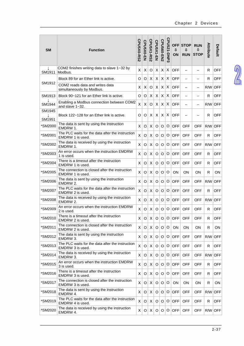
Chapter 2 Devices
2-37
SM Function
CPU
5X0-RS2
CPU
5X0-EN
CPU
5X1-RS2
CPU
5X1-EN
CPU
560-EN2
CPU
521-DN
P3
OFF
ON
STOP
RUN
RUN
STOP
Attribute
Default
↓ SM1911
COM2 finishes writing data to slave 1~32 by Modbus. Χ Χ O Χ Χ Χ OFF – – R OFF
SM1912 Block 89 for an Ether link is active. O O Χ Χ Χ Χ OFF – – R OFF
COM2 reads data and writes data simultaneously by Modbus. Χ Χ O Χ Χ Χ OFF – – R/W OFF
SM1913 ↓
SM1944
Block 90~121 for an Ether link is active. O O Χ Χ Χ Χ OFF – – R OFF
Enabling a Modbus connection between COM2 and slave 1~32. Χ Χ O Χ Χ Χ OFF – – R/W OFF
SM1945 ↓
SM1951 Block 122~128 for an Ether link is active. O O Χ Χ Χ Χ OFF – – R OFF
*SM2000 The data is sent by using the instruction EMDRW 1. Χ O Χ O O O OFF OFF OFF R/W OFF
*SM2001 The PLC waits for the data after the instruction EMDRW 1 is used. Χ O Χ O O O OFF OFF OFF R OFF
*SM2002 The data is received by using the instruction EMDRW 1. Χ O Χ O O O OFF OFF OFF R/W OFF
*SM2003 An error occurs when the instruction EMDRW 1 is used. Χ O Χ O O O OFF OFF OFF R OFF
*SM2004 There is a timeout after the instruction EMDRW 1 is used. Χ O Χ O O O OFF OFF OFF R OFF
*SM2005 The connection is closed after the instruction EMDRW 1 is used. Χ O Χ O O O ON ON ON R ON
*SM2006 The data is sent by using the instruction EMDRW 2. Χ O Χ O O O OFF OFF OFF R/W OFF
*SM2007 The PLC waits for the data after the instruction EMDRW 2 is used. Χ O Χ O O O OFF OFF OFF R OFF
*SM2008 The data is received by using the instruction EMDRW 2. Χ O Χ O O O OFF OFF OFF R/W OFF
*SM2009 An error occurs when the instruction EMDRW 2 is used. Χ O Χ O O O OFF OFF OFF R OFF
*SM2010 There is a timeout after the instruction EMDRW 2 is used. Χ O Χ O O O OFF OFF OFF R OFF
*SM2011 The connection is closed after the instruction EMDRW 2 is used. Χ O Χ O O O ON ON ON R ON
*SM2012 The data is sent by using the instruction EMDRW 3. Χ O Χ O O O OFF OFF OFF R/W OFF
*SM2013 The PLC waits for the data after the instruction EMDRW 3 is used. Χ O Χ O O O OFF OFF OFF R OFF
*SM2014 The data is received by using the instruction EMDRW 3. Χ O Χ O O O OFF OFF OFF R/W OFF
*SM2015 An error occurs when the instruction EMDRW 3 is used. Χ O Χ O O O OFF OFF OFF R OFF
*SM2016 There is a timeout after the instruction EMDRW 3 is used. Χ O Χ O O O OFF OFF OFF R OFF
*SM2017 The connection is closed after the instruction EMDRW 3 is used. Χ O Χ O O O ON ON ON R ON
*SM2018 The data is sent by using the instruction EMDRW 4. Χ O Χ O O O OFF OFF OFF R/W OFF
*SM2019 The PLC waits for the data after the instruction EMDRW 4 is used. Χ O Χ O O O OFF OFF OFF R OFF
*SM2020 The data is received by using the instruction EMDRW 4. Χ O Χ O O O OFF OFF OFF R/W OFF
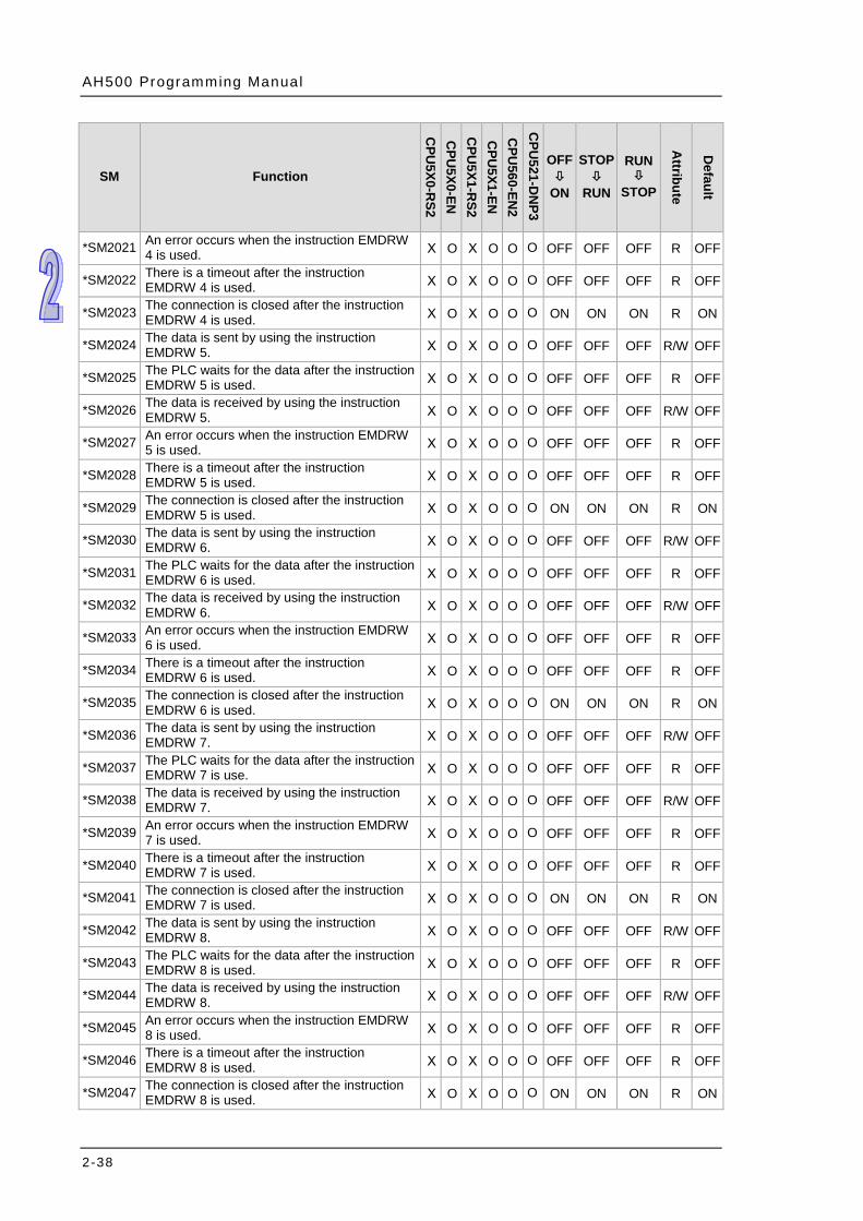
AH500 Programming Manual
2-38
SM Function
CPU
5X0-RS2
CPU
5X0-EN
CPU
5X1-RS2
CPU
5X1-EN
CPU
560-EN2
CPU
521-DN
P3
OFF
ON
STOP
RUN
RUN
STOP A
ttribute
Default
*SM2021 An error occurs when the instruction EMDRW 4 is used. Χ O Χ O O O OFF OFF OFF R OFF
*SM2022 There is a timeout after the instruction EMDRW 4 is used. Χ O Χ O O O OFF OFF OFF R OFF
*SM2023 The connection is closed after the instruction EMDRW 4 is used. Χ O Χ O O O ON ON ON R ON
*SM2024 The data is sent by using the instruction EMDRW 5. Χ O Χ O O O OFF OFF OFF R/W OFF
*SM2025 The PLC waits for the data after the instruction EMDRW 5 is used. Χ O Χ O O O OFF OFF OFF R OFF
*SM2026 The data is received by using the instruction EMDRW 5. Χ O Χ O O O OFF OFF OFF R/W OFF
*SM2027 An error occurs when the instruction EMDRW 5 is used. Χ O Χ O O O OFF OFF OFF R OFF
*SM2028 There is a timeout after the instruction EMDRW 5 is used. Χ O Χ O O O OFF OFF OFF R OFF
*SM2029 The connection is closed after the instruction EMDRW 5 is used. Χ O Χ O O O ON ON ON R ON
*SM2030 The data is sent by using the instruction EMDRW 6. Χ O Χ O O O OFF OFF OFF R/W OFF
*SM2031 The PLC waits for the data after the instruction EMDRW 6 is used. Χ O Χ O O O OFF OFF OFF R OFF
*SM2032 The data is received by using the instruction EMDRW 6. Χ O Χ O O O OFF OFF OFF R/W OFF
*SM2033 An error occurs when the instruction EMDRW 6 is used. Χ O Χ O O O OFF OFF OFF R OFF
*SM2034 There is a timeout after the instruction EMDRW 6 is used. Χ O Χ O O O OFF OFF OFF R OFF
*SM2035 The connection is closed after the instruction EMDRW 6 is used. Χ O Χ O O O ON ON ON R ON
*SM2036 The data is sent by using the instruction EMDRW 7. Χ O Χ O O O OFF OFF OFF R/W OFF
*SM2037 The PLC waits for the data after the instruction EMDRW 7 is use. Χ O Χ O O O OFF OFF OFF R OFF
*SM2038 The data is received by using the instruction EMDRW 7. Χ O Χ O O O OFF OFF OFF R/W OFF
*SM2039 An error occurs when the instruction EMDRW 7 is used. Χ O Χ O O O OFF OFF OFF R OFF
*SM2040 There is a timeout after the instruction EMDRW 7 is used. Χ O Χ O O O OFF OFF OFF R OFF
*SM2041 The connection is closed after the instruction EMDRW 7 is used. Χ O Χ O O O ON ON ON R ON
*SM2042 The data is sent by using the instruction EMDRW 8. Χ O Χ O O O OFF OFF OFF R/W OFF
*SM2043 The PLC waits for the data after the instruction EMDRW 8 is used. Χ O Χ O O O OFF OFF OFF R OFF
*SM2044 The data is received by using the instruction EMDRW 8. Χ O Χ O O O OFF OFF OFF R/W OFF
*SM2045 An error occurs when the instruction EMDRW 8 is used. Χ O Χ O O O OFF OFF OFF R OFF
*SM2046 There is a timeout after the instruction EMDRW 8 is used. Χ O Χ O O O OFF OFF OFF R OFF
*SM2047 The connection is closed after the instruction EMDRW 8 is used. Χ O Χ O O O ON ON ON R ON
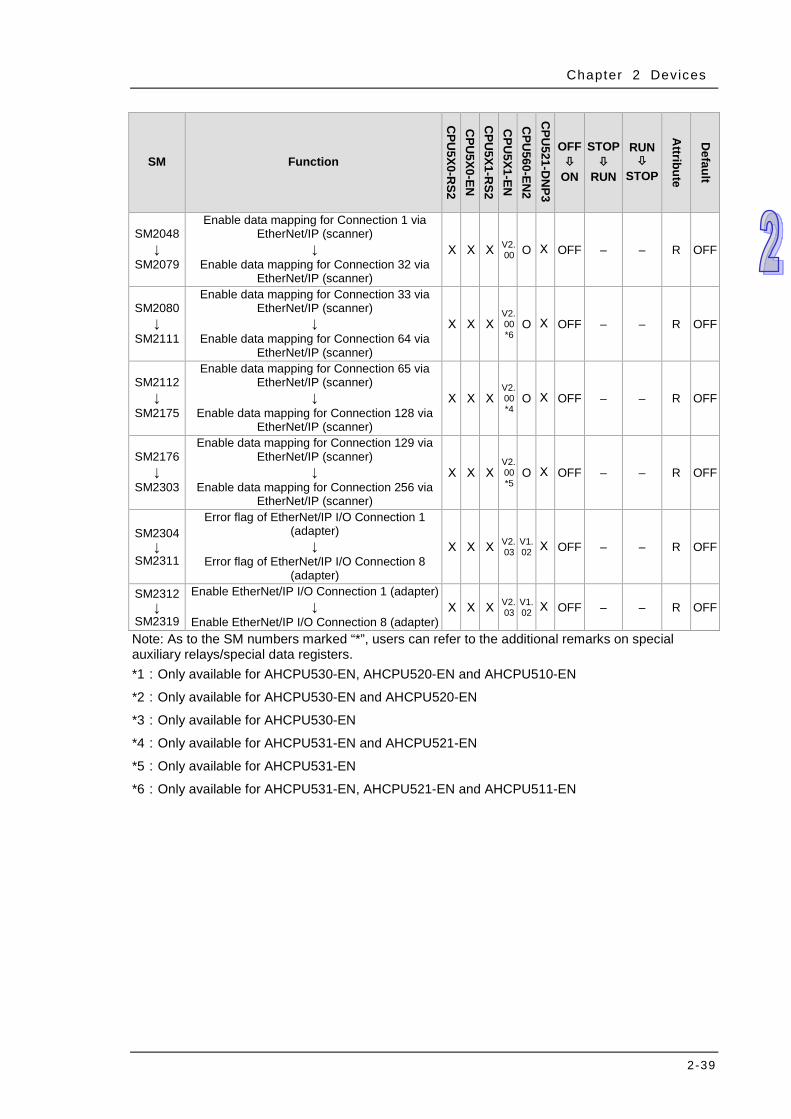
Chapter 2 Devices
2-39
SM Function
CPU
5X0-RS2
CPU
5X0-EN
CPU
5X1-RS2
CPU
5X1-EN
CPU
560-EN2
CPU
521-DN
P3
OFF
ON
STOP
RUN
RUN
STOP
Attribute
Default
SM2048 ↓
SM2079
Enable data mapping for Connection 1 via EtherNet/IP (scanner)
↓ Enable data mapping for Connection 32 via
EtherNet/IP (scanner)
Χ Χ Χ V2.00 O Χ OFF – – R OFF
SM2080 ↓
SM2111
Enable data mapping for Connection 33 via EtherNet/IP (scanner)
↓ Enable data mapping for Connection 64 via
EtherNet/IP (scanner)
Χ Χ Χ V2.00 *6
O Χ OFF – – R OFF
SM2112 ↓
SM2175
Enable data mapping for Connection 65 via EtherNet/IP (scanner)
↓ Enable data mapping for Connection 128 via
EtherNet/IP (scanner)
Χ Χ Χ V2.00 *4
O Χ OFF – – R OFF
SM2176 ↓
SM2303
Enable data mapping for Connection 129 via EtherNet/IP (scanner)
↓ Enable data mapping for Connection 256 via
EtherNet/IP (scanner)
Χ Χ Χ V2.00 *5
O Χ OFF – – R OFF
SM2304 ↓
SM2311
Error flag of EtherNet/IP I/O Connection 1 (adapter)
↓ Error flag of EtherNet/IP I/O Connection 8
(adapter)
Χ Χ Χ V2.03
V1.02 Χ OFF – – R OFF
SM2312 ↓
SM2319
Enable EtherNet/IP I/O Connection 1 (adapter) ↓
Enable EtherNet/IP I/O Connection 8 (adapter) Χ Χ Χ V2.
03 V1.02 Χ OFF – – R OFF
Note: As to the SM numbers marked “*”, users can refer to the additional remarks on special auxiliary relays/special data registers. *1:Only available for AHCPU530-EN, AHCPU520-EN and AHCPU510-EN
*2:Only available for AHCPU530-EN and AHCPU520-EN
*3:Only available for AHCPU530-EN
*4:Only available for AHCPU531-EN and AHCPU521-EN
*5:Only available for AHCPU531-EN
*6:Only available for AHCPU531-EN, AHCPU521-EN and AHCPU511-EN
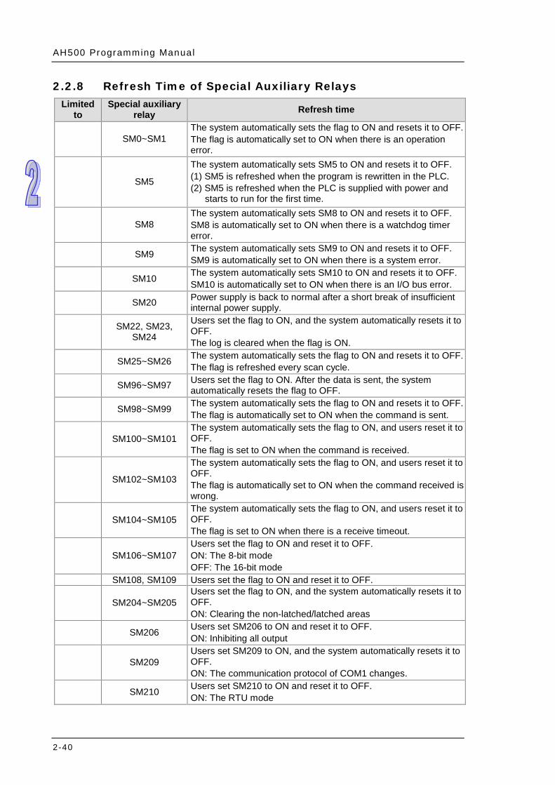
AH500 Programming Manual
2-40
2.2.8 Refresh Time of Special Auxiliary Relays Limited
to Special auxiliary
relay Refresh time
SM0~SM1
The system automatically sets the flag to ON and resets it to OFF. The flag is automatically set to ON when there is an operation error.
SM5
The system automatically sets SM5 to ON and resets it to OFF. (1) SM5 is refreshed when the program is rewritten in the PLC. (2) SM5 is refreshed when the PLC is supplied with power and
starts to run for the first time.
SM8 The system automatically sets SM8 to ON and resets it to OFF. SM8 is automatically set to ON when there is a watchdog timer error.
SM9 The system automatically sets SM9 to ON and resets it to OFF. SM9 is automatically set to ON when there is a system error.
SM10 The system automatically sets SM10 to ON and resets it to OFF. SM10 is automatically set to ON when there is an I/O bus error.
SM20 Power supply is back to normal after a short break of insufficient internal power supply.
SM22, SM23, SM24
Users set the flag to ON, and the system automatically resets it to OFF. The log is cleared when the flag is ON.
SM25~SM26 The system automatically sets the flag to ON and resets it to OFF. The flag is refreshed every scan cycle.
SM96~SM97 Users set the flag to ON. After the data is sent, the system automatically resets the flag to OFF.
SM98~SM99 The system automatically sets the flag to ON and resets it to OFF. The flag is automatically set to ON when the command is sent.
SM100~SM101
The system automatically sets the flag to ON, and users reset it to OFF. The flag is set to ON when the command is received.
SM102~SM103
The system automatically sets the flag to ON, and users reset it to OFF. The flag is automatically set to ON when the command received is wrong.
SM104~SM105
The system automatically sets the flag to ON, and users reset it to OFF. The flag is set to ON when there is a receive timeout.
SM106~SM107
Users set the flag to ON and reset it to OFF. ON: The 8-bit mode OFF: The 16-bit mode
SM108, SM109 Users set the flag to ON and reset it to OFF.
SM204~SM205 Users set the flag to ON, and the system automatically resets it to OFF. ON: Clearing the non-latched/latched areas
SM206 Users set SM206 to ON and reset it to OFF. ON: Inhibiting all output
SM209
Users set SM209 to ON, and the system automatically resets it to OFF. ON: The communication protocol of COM1 changes.
SM210 Users set SM210 to ON and reset it to OFF. ON: The RTU mode

Chapter 2 Devices
2-41
Limited to
Special auxiliary relay Refresh time
SM211
Users set SM211 to ON, and the system automatically resets it to OFF. ON: The communication protocol of COM2 changes.
SM212 Users set SM212 to ON and reset it to OFF. ON: The RTU mode
SM215 Users set SM215 to ON and reset it to OFF. ON: The PLC runs.
SM220 Users set SM220 to ON and reset it to OFF. ON: Calibrating the real-time clock within ±30 seconds
SM400~SM401
The system automatically sets the flag to ON and resets it to OFF when CPU runs. The flag is refreshed every scan cycle.
SM402~SM403
The system automatically sets the flag to ON and resets it to OFF when CPU runs. The flag is refreshed whenever the instruction END is executed.
SM404 The system automatically sets the flag to ON and resets it to OFF. SM404 is refreshed every 5 milliseconds.
SM405 The system automatically sets SM405 to ON and resets it to OFF. SM405 is refreshed every 50 milliseconds.
SM406 The system automatically sets SM406 to ON and resets it to OFF. SM406 is refreshed every 100 milliseconds.
SM407 The system automatically sets SM407 to ON and resets it to OFF. SM407 is refreshed every 500 seconds.
SM408 The system automatically sets SM408 to ON and resets it to OFF. SM408 is refreshed every second.
SM409 The system automatically sets SM409 to ON and resets it to OFF. SM409 is refreshed every n seconds, n is specified by SR409.
SM410
The system automatically sets SM410 to ON and resets it to OFF. SM410 is refreshed every n seconds, and n is specified by SR410.
SM418 The system automatically sets the flag to ON and resets it to OFF. SM420-SM431 The system automatically sets the flag to ON and resets it to OFF. SM450 The system automatically sets SM450 to ON and resets it to OFF.
ON: The memory card is inserted into the PLC. SM451 Users set SM451 to ON and reset it to OFF.
ON: The memory card is write protected. SM452 The system automatically sets SM452 to ON and resets it to OFF.
ON: The data in the memory card is being accessed. SM453 The system automatically sets SM453 to ON and resets it to OFF.
ON: An error occurs during the operation of the memory card. SM454 Users set the flag to ON and resets it to OFF. SM455 The system automatically sets the flag to ON and resets it to OFF. SM456 Users setss the flag to ON to save and then the system
automatically resets it to OFF. SM457 The system automatically sets the flag to ON and resets it to OFF. SM600~SM602 The system automatically sets the flag to ON and resets it to OFF.
The flag is refreshed when the instruction is executed.
SM604 Users set SM604 to ON and reset it to OFF. SM604 is refreshed when the instruction SORT whose mode is the descending order is executed.
SM605 Users set SM605 to ON and reset it to OFF.
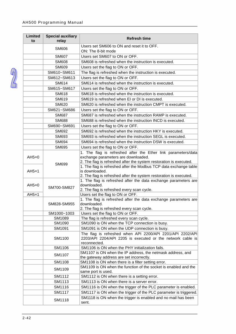
AH500 Programming Manual
2-42
Limited to
Special auxiliary relay Refresh time
SM606 Users set SM606 to ON and reset it to OFF. ON: The 8-bit mode
SM607 Users set SM607 to ON or OFF. SM608 SM608 is refreshed when the instruction is executed. SM609 Users set the flag to ON or OFF. SM610~SM611 The flag is refreshed when the instruction is executed. SM612~SM613 Users set the flag to ON or OFF. SM614 SM614 is refreshed when the instruction is executed. SM615~SM617 Users set the flag to ON or OFF. SM618 SM618 is refreshed when the instruction is executed. SM619 SM619 is refreshed when EI or DI is executed. SM620 SM620 is refreshed when the instruction CMPT is executed. SM621~SM686 Users set the flag to ON or OFF. SM687 SM687 is refreshed when the instruction RAMP is executed. SM688 SM688 is refreshed when the instruction INCD is executed. SM690~SM691 Users set the flag to ON or OFF. SM692 SM692 is refreshed when the instruction HKY is executed. SM693 SM693 is refreshed when the instruction SEGL is executed. SM694 SM694 is refreshed when the instruction DSW is executed. SM695 Users set the flag to ON or OFF.
AH5×0
SM699
1. The flag is refreshed after the Ether link parameters/data exchange parameters are downloaded. 2. The flag is refreshed after the system restoration is executed.
AH5×1 1. The flag is refreshed after the Modbus TCP data exchange table is downloaded. 2. The flag is refreshed after the system restoration is executed.
AH5×0 SM700-SM827
1. The flag is refreshed after the data exchange parameters are downloaded. 2. The flag is refreshed every scan cycle.
AH5×1 Users set the flag to ON or OFF.
SM828-SM955 1. The flag is refreshed after the data exchange parameters are downloaded. 2. The flag is refreshed every scan cycle.
SM1000~1003 Users set the flag to ON or OFF. SM1089 The flag is refreshed every scan cycle. SM1090 SM1090 is ON when the TCP connection is busy. SM1091 SM1091 is ON when the UDP connection is busy.
SM1100 The flag is refreshed when API 2200/API 2201/API 2202/API 2203/API 2204/API 2205 is executed or the network cable is reconnected.
SM1106 SM1106 is ON when the PHY initialization fails. SM1107 SM1107 is ON when the IP address, the netmask address, and
the gateway address are set incorrectly. SM1108 SM1108 is ON when there is a filter setting error. SM1109 SM1109 is ON when the function of the socket is enabled and the
same port is used. SM1112 SM1112 is ON when there is a setting error. SM1113 SM1113 is ON when there is a server error. SM1116 SM1116 is ON when the trigger of the PLC parameter is enabled. SM1117 SM1117 is ON when the trigger of the PLC parameter is triggered. SM1118 SM1118 is ON when the trigger is enabled and no mail has been
sent.
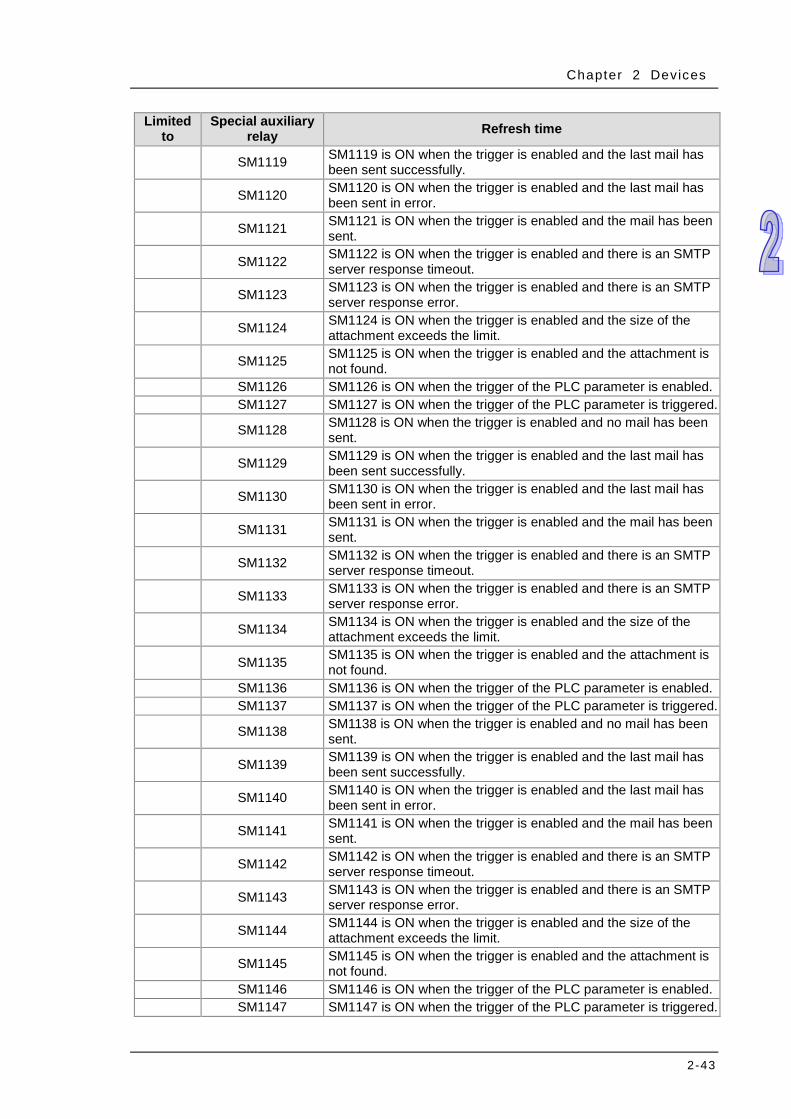
Chapter 2 Devices
2-43
Limited to
Special auxiliary relay Refresh time
SM1119 SM1119 is ON when the trigger is enabled and the last mail has been sent successfully.
SM1120 SM1120 is ON when the trigger is enabled and the last mail has been sent in error.
SM1121 SM1121 is ON when the trigger is enabled and the mail has been sent.
SM1122 SM1122 is ON when the trigger is enabled and there is an SMTP server response timeout.
SM1123 SM1123 is ON when the trigger is enabled and there is an SMTP server response error.
SM1124 SM1124 is ON when the trigger is enabled and the size of the attachment exceeds the limit.
SM1125 SM1125 is ON when the trigger is enabled and the attachment is not found.
SM1126 SM1126 is ON when the trigger of the PLC parameter is enabled. SM1127 SM1127 is ON when the trigger of the PLC parameter is triggered. SM1128 SM1128 is ON when the trigger is enabled and no mail has been
sent. SM1129 SM1129 is ON when the trigger is enabled and the last mail has
been sent successfully. SM1130 SM1130 is ON when the trigger is enabled and the last mail has
been sent in error. SM1131 SM1131 is ON when the trigger is enabled and the mail has been
sent. SM1132 SM1132 is ON when the trigger is enabled and there is an SMTP
server response timeout. SM1133 SM1133 is ON when the trigger is enabled and there is an SMTP
server response error. SM1134 SM1134 is ON when the trigger is enabled and the size of the
attachment exceeds the limit. SM1135 SM1135 is ON when the trigger is enabled and the attachment is
not found. SM1136 SM1136 is ON when the trigger of the PLC parameter is enabled. SM1137 SM1137 is ON when the trigger of the PLC parameter is triggered. SM1138 SM1138 is ON when the trigger is enabled and no mail has been
sent. SM1139 SM1139 is ON when the trigger is enabled and the last mail has
been sent successfully. SM1140 SM1140 is ON when the trigger is enabled and the last mail has
been sent in error. SM1141 SM1141 is ON when the trigger is enabled and the mail has been
sent. SM1142 SM1142 is ON when the trigger is enabled and there is an SMTP
server response timeout. SM1143 SM1143 is ON when the trigger is enabled and there is an SMTP
server response error. SM1144 SM1144 is ON when the trigger is enabled and the size of the
attachment exceeds the limit. SM1145 SM1145 is ON when the trigger is enabled and the attachment is
not found. SM1146 SM1146 is ON when the trigger of the PLC parameter is enabled. SM1147 SM1147 is ON when the trigger of the PLC parameter is triggered.
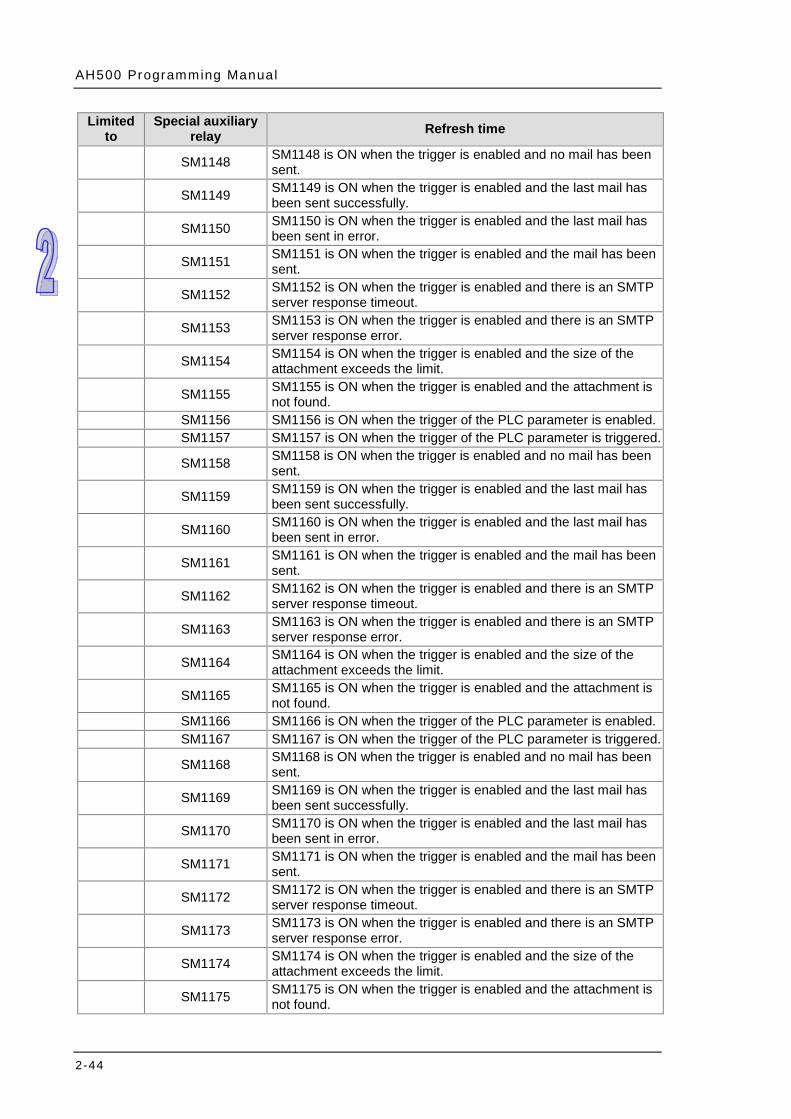
AH500 Programming Manual
2-44
Limited to
Special auxiliary relay Refresh time
SM1148 SM1148 is ON when the trigger is enabled and no mail has been sent.
SM1149 SM1149 is ON when the trigger is enabled and the last mail has been sent successfully.
SM1150 SM1150 is ON when the trigger is enabled and the last mail has been sent in error.
SM1151 SM1151 is ON when the trigger is enabled and the mail has been sent.
SM1152 SM1152 is ON when the trigger is enabled and there is an SMTP server response timeout.
SM1153 SM1153 is ON when the trigger is enabled and there is an SMTP server response error.
SM1154 SM1154 is ON when the trigger is enabled and the size of the attachment exceeds the limit.
SM1155 SM1155 is ON when the trigger is enabled and the attachment is not found.
SM1156 SM1156 is ON when the trigger of the PLC parameter is enabled. SM1157 SM1157 is ON when the trigger of the PLC parameter is triggered. SM1158 SM1158 is ON when the trigger is enabled and no mail has been
sent. SM1159 SM1159 is ON when the trigger is enabled and the last mail has
been sent successfully. SM1160 SM1160 is ON when the trigger is enabled and the last mail has
been sent in error. SM1161 SM1161 is ON when the trigger is enabled and the mail has been
sent. SM1162 SM1162 is ON when the trigger is enabled and there is an SMTP
server response timeout. SM1163 SM1163 is ON when the trigger is enabled and there is an SMTP
server response error. SM1164 SM1164 is ON when the trigger is enabled and the size of the
attachment exceeds the limit. SM1165 SM1165 is ON when the trigger is enabled and the attachment is
not found. SM1166 SM1166 is ON when the trigger of the PLC parameter is enabled. SM1167 SM1167 is ON when the trigger of the PLC parameter is triggered. SM1168 SM1168 is ON when the trigger is enabled and no mail has been
sent. SM1169 SM1169 is ON when the trigger is enabled and the last mail has
been sent successfully. SM1170 SM1170 is ON when the trigger is enabled and the last mail has
been sent in error. SM1171 SM1171 is ON when the trigger is enabled and the mail has been
sent. SM1172 SM1172 is ON when the trigger is enabled and there is an SMTP
server response timeout. SM1173 SM1173 is ON when the trigger is enabled and there is an SMTP
server response error. SM1174 SM1174 is ON when the trigger is enabled and the size of the
attachment exceeds the limit. SM1175 SM1175 is ON when the trigger is enabled and the attachment is
not found.
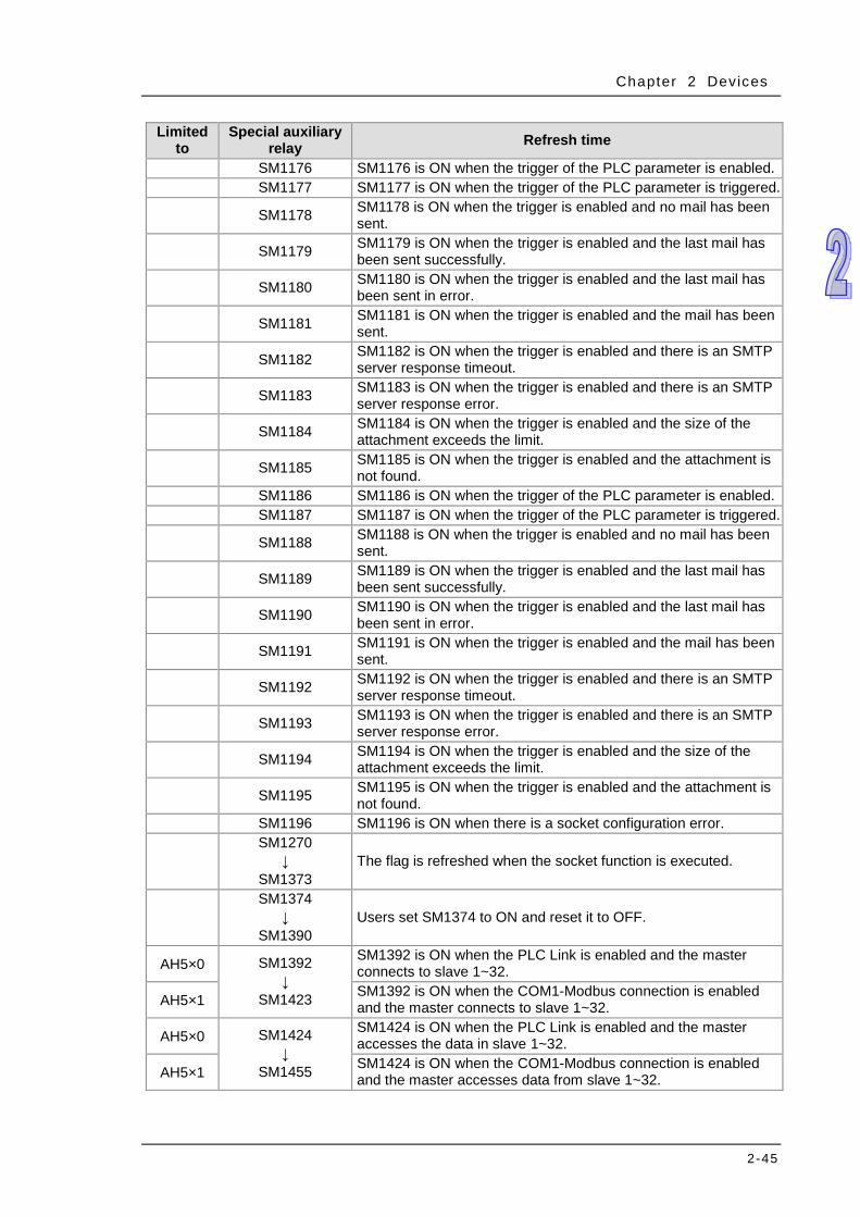
Chapter 2 Devices
2-45
Limited to
Special auxiliary relay Refresh time
SM1176 SM1176 is ON when the trigger of the PLC parameter is enabled. SM1177 SM1177 is ON when the trigger of the PLC parameter is triggered. SM1178 SM1178 is ON when the trigger is enabled and no mail has been
sent. SM1179 SM1179 is ON when the trigger is enabled and the last mail has
been sent successfully. SM1180 SM1180 is ON when the trigger is enabled and the last mail has
been sent in error. SM1181 SM1181 is ON when the trigger is enabled and the mail has been
sent. SM1182 SM1182 is ON when the trigger is enabled and there is an SMTP
server response timeout. SM1183 SM1183 is ON when the trigger is enabled and there is an SMTP
server response error. SM1184 SM1184 is ON when the trigger is enabled and the size of the
attachment exceeds the limit. SM1185 SM1185 is ON when the trigger is enabled and the attachment is
not found. SM1186 SM1186 is ON when the trigger of the PLC parameter is enabled. SM1187 SM1187 is ON when the trigger of the PLC parameter is triggered. SM1188 SM1188 is ON when the trigger is enabled and no mail has been
sent. SM1189 SM1189 is ON when the trigger is enabled and the last mail has
been sent successfully. SM1190 SM1190 is ON when the trigger is enabled and the last mail has
been sent in error. SM1191 SM1191 is ON when the trigger is enabled and the mail has been
sent. SM1192 SM1192 is ON when the trigger is enabled and there is an SMTP
server response timeout. SM1193 SM1193 is ON when the trigger is enabled and there is an SMTP
server response error. SM1194 SM1194 is ON when the trigger is enabled and the size of the
attachment exceeds the limit. SM1195 SM1195 is ON when the trigger is enabled and the attachment is
not found. SM1196 SM1196 is ON when there is a socket configuration error. SM1270
↓ SM1373
The flag is refreshed when the socket function is executed.
SM1374 ↓
SM1390 Users set SM1374 to ON and reset it to OFF.
AH5×0 SM1392 ↓
SM1423
SM1392 is ON when the PLC Link is enabled and the master connects to slave 1~32.
AH5×1 SM1392 is ON when the COM1-Modbus connection is enabled and the master connects to slave 1~32.
AH5×0 SM1424 ↓
SM1455
SM1424 is ON when the PLC Link is enabled and the master accesses the data in slave 1~32.
AH5×1 SM1424 is ON when the COM1-Modbus connection is enabled and the master accesses data from slave 1~32.
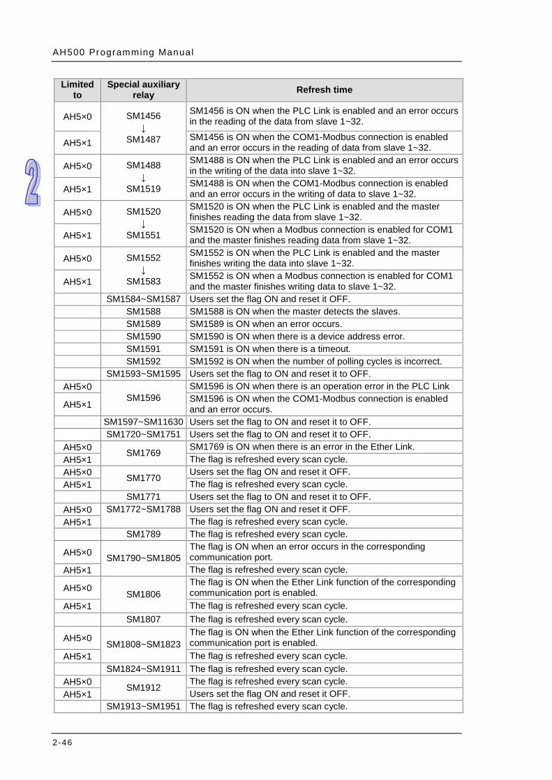
AH500 Programming Manual
2-46
Limited to
Special auxiliary relay Refresh time
AH5×0 SM1456 ↓
SM1487
SM1456 is ON when the PLC Link is enabled and an error occurs in the reading of the data from slave 1~32.
AH5×1 SM1456 is ON when the COM1-Modbus connection is enabled and an error occurs in the reading of data from slave 1~32.
AH5×0 SM1488 ↓
SM1519
SM1488 is ON when the PLC Link is enabled and an error occurs in the writing of the data into slave 1~32.
AH5×1 SM1488 is ON when the COM1-Modbus connection is enabled and an error occurs in the writing of data to slave 1~32.
AH5×0 SM1520 ↓
SM1551
SM1520 is ON when the PLC Link is enabled and the master finishes reading the data from slave 1~32.
AH5×1 SM1520 is ON when a Modbus connection is enabled for COM1 and the master finishes reading data from slave 1~32.
AH5×0 SM1552 ↓
SM1583
SM1552 is ON when the PLC Link is enabled and the master finishes writing the data into slave 1~32.
AH5×1 SM1552 is ON when a Modbus connection is enabled for COM1 and the master finishes writing data to slave 1~32.
SM1584~SM1587 Users set the flag ON and reset it OFF. SM1588 SM1588 is ON when the master detects the slaves. SM1589 SM1589 is ON when an error occurs. SM1590 SM1590 is ON when there is a device address error. SM1591 SM1591 is ON when there is a timeout. SM1592 SM1592 is ON when the number of polling cycles is incorrect. SM1593~SM1595 Users set the flag to ON and reset it to OFF.
AH5×0 SM1596
SM1596 is ON when there is an operation error in the PLC Link
AH5×1 SM1596 is ON when the COM1-Modbus connection is enabled and an error occurs.
SM1597~SM11630 Users set the flag to ON and reset it to OFF. SM1720~SM1751 Users set the flag to ON and reset it to OFF.
AH5×0 SM1769 SM1769 is ON when there is an error in the Ether Link. AH5×1 The flag is refreshed every scan cycle. AH5×0 SM1770 Users set the flag ON and reset it OFF. AH5×1 The flag is refreshed every scan cycle.
SM1771 Users set the flag to ON and reset it to OFF. AH5×0 SM1772~SM1788 Users set the flag ON and reset it OFF. AH5×1 The flag is refreshed every scan cycle.
SM1789 The flag is refreshed every scan cycle.
AH5×0 SM1790~SM1805 The flag is ON when an error occurs in the corresponding communication port.
AH5×1 The flag is refreshed every scan cycle.
AH5×0 SM1806 The flag is ON when the Ether Link function of the corresponding communication port is enabled.
AH5×1 The flag is refreshed every scan cycle. SM1807 The flag is refreshed every scan cycle.
AH5×0 SM1808~SM1823 The flag is ON when the Ether Link function of the corresponding communication port is enabled.
AH5×1 The flag is refreshed every scan cycle. SM1824~SM1911 The flag is refreshed every scan cycle.
AH5×0 SM1912 The flag is refreshed every scan cycle. AH5×1 Users set the flag ON and reset it OFF.
SM1913~SM1951 The flag is refreshed every scan cycle.

Chapter 2 Devices
2-47
Limited to
Special auxiliary relay Refresh time
SM2000 User define. The flag is refreshed, after the transmission is done. SM2001 The flag is refreshed when the instruction EMDRW is executed. SM2002 The flag is refreshed when the instruction EMDRW is executed. SM2003 The flag is refreshed when the instruction EMDRW is executed
and an error occurs. SM2004 The flag is refreshed when the instruction EMDRW is executed
and there is a response timeout. SM2005 The flag is refreshed when the instruction EMDRW is executed. SM2006 User define. The flag is refreshed, after the transmission is done. SM2007 The flag is refreshed when the instruction EMDRW is executed. SM2008 The flag is refreshed when the instruction EMDRW is executed. SM2009 The flag is refreshed when the instruction EMDRW is executed
and an error occurs. SM2010 The flag is refreshed when the instruction EMDRW is executed
and there is a response timeout. SM2011 The flag is refreshed when the instruction EMDRW is executed. SM2012 User define. The flag is refreshed, after the transmission is done. SM2013 The flag is refreshed when the instruction EMDRW is executed. SM2014 The flag is refreshed when the instruction EMDRW is executed. SM2015 The flag is refreshed when the instruction EMDRW is executed
and an error occurs. SM2016 The flag is refreshed when the instruction EMDRW is executed
and there is a response timeout. SM2017 The flag is refreshed when the instruction EMDRW is executed. SM2018 User define. The flag is refreshed, after the transmission is done. SM2019 The flag is refreshed when the instruction EMDRW is executed. SM2020 The flag is refreshed when the instruction EMDRW is executed. SM2021 The flag is refreshed when the instruction EMDRW is executed
and an error occurs. SM2022 The flag is refreshed when the instruction EMDRW is executed
and there is a response timeout. SM2023 The flag is refreshed when the instruction EMDRW is executed. SM2024 User define. The flag is refreshed, after the transmission is done. SM2025 The flag is refreshed when the instruction EMDRW is executed. SM2026 The flag is refreshed when the instruction EMDRW is executed. SM2027 The flag is refreshed when the instruction EMDRW is executed
and an error occurs. SM2028 The flag is refreshed when the instruction EMDRW is executed
and there is a response timeout. SM2029 The flag is refreshed when the instruction EMDRW is executed. SM2030 User define. The flag is refreshed, after the transmission is done. SM2031~SM2032 The flag is refreshed when the instruction EMDRW is executed. SM2033 SM2033 is refreshed when the instruction EMDRW is executed
and an error occurs. SM2034 SM2034 is refreshed when the instruction EMDRW is executed
and there is a response timeout. SM2035 The flag is refreshed when the instruction EMDRW is executed. SM2036 User define. The flag is refreshed, after the transmission is done. SM2037 The flag is refreshed when the instruction EMDRW is executed. SM2038 The flag is refreshed when the instruction EMDRW is executed.
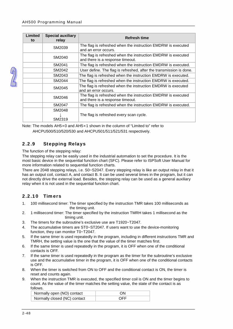
AH500 Programming Manual
2-48
Limited to
Special auxiliary relay Refresh time
SM2039 The flag is refreshed when the instruction EMDRW is executed and an error occurs.
SM2040 The flag is refreshed when the instruction EMDRW is executed and there is a response timeout.
SM2041 The flag is refreshed when the instruction EMDRW is executed. SM2042 User define. The flag is refreshed, after the transmission is done. SM2043 The flag is refreshed when the instruction EMDRW is executed. SM2044 The flag is refreshed when the instruction EMDRW is executed. SM2045 The flag is refreshed when the instruction EMDRW is executed
and an error occurs. SM2046 The flag is refreshed when the instruction EMDRW is executed
and there is a response timeout. SM2047 The flag is refreshed when the instruction EMDRW is executed. SM2048
↓ SM2319
The flag is refreshed every scan cycle.
Note: The models AH5×0 and AH5×1 shown in the column of “Limited to” refer to AHCPU500/510/520/530 and AHCPU501/511/521/531 respectively.
2.2.9 Stepping Relays The function of the stepping relay: The stepping relay can be easily used in the industrial automation to set the procedure. It is the most basic device in the sequential function chart (SFC). Please refer to ISPSoft User Manual for more information related to sequential function charts. There are 2048 stepping relays, i.e. S0~S2047. Every stepping relay is like an output relay in that it has an output coil, contact A, and contact B. It can be used several times in the program, but it can not directly drive the external load. Besides, the stepping relay can be used as a general auxiliary relay when it is not used in the sequential function chart.
2.2.10 Timers 1. 100 millisecond timer: The timer specified by the instruction TMR takes 100 milliseconds as
the timing unit. 2. 1 millisecond timer: The timer specified by the instruction TMRH takes 1 millisecond as the
timing unit. 3. The timers for the subroutine’s exclusive use are T1920~T2047. 4. The accumulative timers are ST0~ST2047. If users want to use the device-monitoring
function, they can monitor T0~T2047. 5. If the same timer is used repeatedly in the program, including in different instructions TMR and
TMRH, the setting value is the one that the value of the timer matches first. 6. If the same timer is used repeatedly in the program, it is OFF when one of the conditional
contacts is OFF. 7. If the same timer is used repeatedly in the program as the timer for the subroutine’s exclusive
use and the accumulative timer in the program, it is OFF when one of the conditional contacts is OFF.
8. When the timer is switched from ON to OFF and the conditional contact is ON, the timer is reset and counts again.
9. When the instruction TMR is executed, the specified timer coil is ON and the timer begins to count. As the value of the timer matches the setting value, the state of the contact is as follows.
Normally open (NO) contact ON Normally closed (NC) contact OFF

Chapter 2 Devices
2-49
A. The general-purpose timer
When the instruction TMR is executed, the general-purpose timer begins to count. As the value of the timer matches the setting value, the output coil is ON. When X0.0 is ON, the timer T0 takes 100 milliseconds as the timing unit and counts up. As
the current value of the timer matches the setting value 100, the output coil of T0 is ON. When X0.0 is OFF or there is a power cut, the current value of the timer is reset to 0 and
the output coil is switched OFF.
B. The accumulative timer
When the instruction TMR is executed, the accumulative timer begins to count. As the value of the timer matches the setting value, the output coil is ON. As long as users add the letter S in front of the letter T, the timer becomes the accumulative timer. When the conditional contact is OFF, the value of the accumulative timer is not reset. When the conditional contact is ON, the timer counts from the current value. When X0.0 is ON, the timer T250 takes 100 milliseconds as the timing unit and counts up.
As the current value of the timer matches the setting value 100, the output coil of T250 is ON.
When X0.0 is OFF, the timer T250 stops counting and the current value of the timer remains unchanged. Not until X0.0 is switched ON will the timer counts again. When the timer counts up from the current value to the setting value 100, the output coil of T250 is ON.

AH500 Programming Manual
2-50
C. The timer used in the function block
T1920~T2047 are the timers which users can use in the functional block or the interrupt. When the instruction TMR or END is executed, the timer used in the functional block begins to count. As the value of the timer matches the setting value, the output coil is ON. If the general-purpose timer is used in the functional block or the interrupt, and the functional is not executed, the timer can not count correctly.
2.2.11 Counters The characteristics of the 16-bit counter:
Item 16-bit counter Type General type Number C0~C2047 Direction Counting up Setting value 0~32,767
Specification of the setting value The setting value can be either the constant or the value in the data register.
Change of the current value The counter stops counting when the value of the counter matches the setting value.
Output contact The contact is ON when the value of the counter matches the setting value.
Reset When the instruction RST is executed, the current value is cleared to zero, and the contact is reset of OFF.
Action of the contact After the scan is complete, the contact acts. The function of the counter: Each time the input switches from OFF to ON, the value of the counter increases by one increment. When the value of the counter matches the setting value, the output coil is ON. Users can use either the decimal constant or the value in the data register as the setting value. The 16-bit counter: 1. Setting range: 0~32,767 (The setting values 0 and 1 mean the same thing in that the output
contact is ON when the counter counts for the first time.) 2. For the general-purpose counter, the current value of the counter is cleared when there is a
power cut. If the counter is the latched one, the current value of the counter and the state of the contact before the power cut will be retained. The latched counter counts from the current value when the power supply is restored.
3. If users use the instruction MOV or ISPSoft to transmit a value bigger than the setting value to the current value register C0, the contact of the counter C0 will be ON and the current value will become the same as the setting value next time ×0.1 is switched from OFF to ON.
4. Users can use either the constant or the value in the register as the setting value of the counter.
5. The setting value of the counter can be a positive or a negative. If the counter counts up from 32,767, the next current value becomes -32,768.
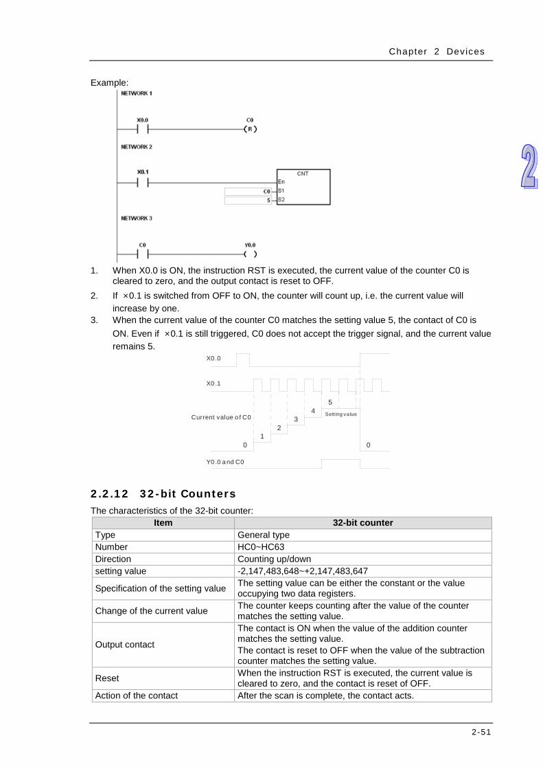
Chapter 2 Devices
2-51
Example:
1. When X0.0 is ON, the instruction RST is executed, the current value of the counter C0 is
cleared to zero, and the output contact is reset to OFF. 2. If ×0.1 is switched from OFF to ON, the counter will count up, i.e. the current value will
increase by one. 3. When the current value of the counter C0 matches the setting value 5, the contact of C0 is
ON. Even if ×0.1 is still triggered, C0 does not accept the trigger signal, and the current value remains 5.
X0 .0
X0 .1
Y0 .0 a nd C0
Current value o f C0
01
23
45
Sett ing value
0
2.2.12 32-bit Counters The characteristics of the 32-bit counter:
Item 32-bit counter Type General type Number HC0~HC63 Direction Counting up/down setting value -2,147,483,648~+2,147,483,647
Specification of the setting value The setting value can be either the constant or the value occupying two data registers.
Change of the current value The counter keeps counting after the value of the counter matches the setting value.
Output contact
The contact is ON when the value of the addition counter matches the setting value. The contact is reset to OFF when the value of the subtraction counter matches the setting value.
Reset When the instruction RST is executed, the current value is cleared to zero, and the contact is reset of OFF.
Action of the contact After the scan is complete, the contact acts.
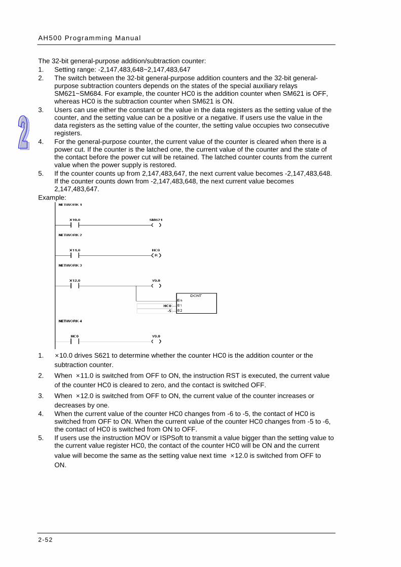
AH500 Programming Manual
2-52
The 32-bit general-purpose addition/subtraction counter: 1. Setting range: -2,147,483,648~2,147,483,647 2. The switch between the 32-bit general-purpose addition counters and the 32-bit general-
purpose subtraction counters depends on the states of the special auxiliary relays SM621~SM684. For example, the counter HC0 is the addition counter when SM621 is OFF, whereas HC0 is the subtraction counter when SM621 is ON.
3. Users can use either the constant or the value in the data registers as the setting value of the counter, and the setting value can be a positive or a negative. If users use the value in the data registers as the setting value of the counter, the setting value occupies two consecutive registers.
4. For the general-purpose counter, the current value of the counter is cleared when there is a power cut. If the counter is the latched one, the current value of the counter and the state of the contact before the power cut will be retained. The latched counter counts from the current value when the power supply is restored.
5. If the counter counts up from 2,147,483,647, the next current value becomes -2,147,483,648. If the counter counts down from -2,147,483,648, the next current value becomes 2,147,483,647.
Example:
1. ×10.0 drives S621 to determine whether the counter HC0 is the addition counter or the
subtraction counter. 2. When ×11.0 is switched from OFF to ON, the instruction RST is executed, the current value
of the counter HC0 is cleared to zero, and the contact is switched OFF. 3. When ×12.0 is switched from OFF to ON, the current value of the counter increases or
decreases by one. 4. When the current value of the counter HC0 changes from -6 to -5, the contact of HC0 is
switched from OFF to ON. When the current value of the counter HC0 changes from -5 to -6, the contact of HC0 is switched from ON to OFF.
5. If users use the instruction MOV or ISPSoft to transmit a value bigger than the setting value to the current value register HC0, the contact of the counter HC0 will be ON and the current value will become the same as the setting value next time ×12.0 is switched from OFF to ON.
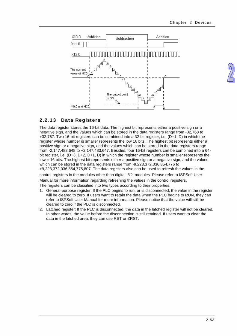
Chapter 2 Devices
2-53
2.2.13 Data Registers The data register stores the 16-bit data. The highest bit represents either a positive sign or a negative sign, and the values which can be stored in the data registers range from -32,768 to +32,767. Two 16-bit registers can be combined into a 32-bit register, i.e. (D+1, D) in which the register whose number is smaller represents the low 16 bits. The highest bit represents either a positive sign or a negative sign, and the values which can be stored in the data registers range from -2,147,483,648 to +2,147,483,647. Besides, four 16-bit registers can be combined into a 64-bit register, i.e. (D+3, D+2, D+1, D) in which the register whose number is smaller represents the lower 16 bits. The highest bit represents either a positive sign or a negative sign, and the values which can be stored in the data registers range from -9,223,372,036,854,776 to +9,223,372,036,854,775,807. The data registers also can be used to refresh the values in the control registers in the modules other than digital I/○ modules. Please refer to ISPSoft User Manual for more information regarding refreshing the values in the control registers. The registers can be classified into two types according to their properties: 1. General-purpose register: If the PLC begins to run, or is disconnected, the value in the register
will be cleared to zero. If users want to retain the data when the PLC begins to RUN, they can refer to ISPSoft User Manual for more information. Please notice that the value will still be cleared to zero if the PLC is disconnected.
2. Latched register: If the PLC is disconnected, the data in the latched register will not be cleared. In other words, the value before the disconnection is still retained. If users want to clear the data in the latched area, they can use RST or ZRST.

AH500 Programming Manual
2-54
2.2.14 Special Data Registers Every special data register has its definition and specific function. The system statuses and the error messages are stored in the special data registers. Besides, the special data registers can be used to monitor the system statuses. The special data registers and their functions are listed as follows. As to the SR numbers marked “*”, users can refer to the additional remarks on special auxiliary relays/special data registers. The “R” in the attribute column indicates that the special data register can read the data, whereas the “R/W” in the attribute column indicates that it can read and write the data. In addition, the mark “–” indicates that the status of the special data register does not make any change. The mark “#” indicates that the system will be set according to the status of the PLC, and users can read the setting value and refer to the related manual for more information.
SR Function
CPU
5×0-RS2
CPU
5×0-EN
CPU
5×1-RS2
CPU
5×1-EN
CPU
560-EN2
CPU
521-DN
P3 OFF
ON
STOP
RUN
RUN
STOP
Attribute
Default
SR0 Error-detecting code of the PLC operation error ○ ○ ○ ○ ○ ○ 0 0 – R 0
SR1 ↓
SR2
The address of the operation error is locked. ○ ○ ○ ○ ○ ○ 0 0 – R 0
SR4 Error-detecting code of the grammar check error ○ ○ ○ ○ ○ ○ 0 0 – R 0
SR5 Address of the instruction/operand check error Step address at which the watchdog timer is ON
○ ○ ○ ○ ○ ○ 0 0 – R 0
SR6 ○ ○ ○ ○ ○ ○ 0 0 – R 0 SR8 ○ ○ ○ ○ ○ ○ 0 – – R 0
SR24 ↓
SR25
Data amount from the last cyclic synchronization (Kbyte) × × × × ○ × 0 – – R 0
SR26 ↓
SR27
Maximum synchronized data amount (Kbyte) × × × × ○ × 0 – – R 0
SR28 ↓
SR29 Noncyclic synchronization time (ms) × × × × ○ × 0 – – R 0
SR30 ↓
SR31 Cyclic synchronization time (ms) × × × × ○ × 0 – – R 0
*SR32 Status of the master power module V1.08
V1.08 ○ ○ ○ ○ – – – R 0
*SR33 Status of the standby power module V1.08
V1.08 ○ ○ ○ ○ – – – R 0
*SR40 Number of error logs ○ ○ ○ ○ ○ ○ – – – R 0 *SR41 Error log pointer ○ ○ ○ ○ ○ ○ – – – R 0
*SR42 Error log 1: The rack number and the slot number ○ ○ ○ ○ ○ ○ – – – R 0
*SR43 Error log 1: The module ID ○ ○ ○ ○ ○ ○ – – – R 0 *SR44 Error log 1: The error code ○ ○ ○ ○ ○ ○ – – – R 0 *SR45 Error log 1: The year and the month ○ ○ ○ ○ ○ ○ – – – R 0 *SR46 Error log 1: The day and the hour ○ ○ ○ ○ ○ ○ – – – R 0 *SR47 Error log 1: The minute and the second ○ ○ ○ ○ ○ ○ – – – R 0
*SR48 Error log 2: The rack number and the slot number ○ ○ ○ ○ ○ ○ – – – R 0
*SR49 Error log 2: The module ID ○ ○ ○ ○ ○ ○ – – – R 0 *SR50 Error log 2: The error code ○ ○ ○ ○ ○ ○ – – – R 0 *SR51 Error log 2: The year and the month ○ ○ ○ ○ ○ ○ – – – R 0 *SR52 Error log 2: The day and the hour ○ ○ ○ ○ ○ ○ – – – R 0

Chapter 2 Devices
2-55
SR Function
CPU
5×0-RS2
CPU
5×0-EN
CPU
5×1-RS2
CPU
5×1-EN
CPU
560-EN2
CPU
521-DN
P3
OFF
ON
STOP
RUN
RUN
STOP
Attribute
Default
*SR53 Error log 2: The minute and the second ○ ○ ○ ○ ○ ○ – – – R 0
*SR54 Error log 3: The rack number and the slot number ○ ○ ○ ○ ○ ○ – – – R 0
*SR55 Error log 3: The module ID ○ ○ ○ ○ ○ ○ – – – R 0 *SR56 Error log 3: The error code ○ ○ ○ ○ ○ ○ – – – R 0 *SR57 Error log 3: The year and the month ○ ○ ○ ○ ○ ○ – – – R 0 *SR58 Error log 3: The day and the hour ○ ○ ○ ○ ○ ○ – – – R 0 *SR59 Error log 3: The minute and the second ○ ○ ○ ○ ○ ○ – – – R 0
*SR60 Error log 4: The rack number and the slot number ○ ○ ○ ○ ○ ○ – – – R 0
*SR61 Error log 4: The module ID ○ ○ ○ ○ ○ ○ – – – R 0 *SR62 Error log 4: The error code ○ ○ ○ ○ ○ ○ – – – R 0 *SR63 Error log 4: The year and the month ○ ○ ○ ○ ○ ○ – – – R 0 *SR64 Error log 4: The day and the hour ○ ○ ○ ○ ○ ○ – – – R 0 *SR65 Error log 4: The minute and the second ○ ○ ○ ○ ○ ○ – – – R 0
*SR66 Error log 4: The rack number and the slot number ○ ○ ○ ○ ○ ○ – – – R 0
SR67 Error log 5: The rack number and the slot number ○ ○ ○ ○ ○ ○ – – – R 0
SR68 Error log 5: The module ID ○ ○ ○ ○ ○ ○ – – – R 0 SR69 Error log 5: The error code ○ ○ ○ ○ ○ ○ – – – R 0 SR70 Error log 5: The year and the month ○ ○ ○ ○ ○ ○ – – – R 0 SR71 Error log 5: The day and the hour ○ ○ ○ ○ ○ ○ – – – R 0
SR72 Error log 6: The rack number and the slot number ○ ○ ○ ○ ○ ○ – – – R 0
*SR73 Error log 6: The module ID ○ ○ ○ ○ ○ ○ – – – R 0 *SR74 Error log 6: The error code ○ ○ ○ ○ ○ ○ – – – R 0 *SR75 Error log 6: The year and the month ○ ○ ○ ○ ○ ○ – – – R 0 *SR76 Error log 6: The day and the hour ○ ○ ○ ○ ○ ○ – – – R 0 *SR77 Error log 6: The minute and the second ○ ○ ○ ○ ○ ○ – – – R 0
*SR78 Error log 7: The rack number and the slot number ○ ○ ○ ○ ○ ○ – – – R 0
*SR79 Error log 7: The module ID ○ ○ ○ ○ ○ ○ – – – R 0 *SR80 Error log 7: The error code ○ ○ ○ ○ ○ ○ – – – R 0 *SR81 Error log 7: The year and the month ○ ○ ○ ○ ○ ○ – – – R 0 *SR82 Error log 7: The day and the hour ○ ○ ○ ○ ○ ○ – – – R 0 *SR83 Error log 7: The minute and the second ○ ○ ○ ○ ○ ○ – – – R 0
*SR84 Error log 8: The rack number and the slot number ○ ○ ○ ○ ○ ○ – – – R 0
*SR85 Error log 8: The module ID ○ ○ ○ ○ ○ ○ – – – R 0 *SR86 Error log 8: The error code ○ ○ ○ ○ ○ ○ – – – R 0 *SR87 Error log 8: The year and the month ○ ○ ○ ○ ○ ○ – – – R 0 *SR88 Error log 8: The day and the hour ○ ○ ○ ○ ○ ○ – – – R 0 *SR89 Error log 8: The minute and the second ○ ○ ○ ○ ○ ○ – – – R 0
*SR90 Error log 9: The rack number and the slot number ○ ○ ○ ○ ○ ○ – – – R 0
*SR91 Error log 9: The module ID ○ ○ ○ ○ ○ ○ – – – R 0 *SR92 Error log 9: The error code ○ ○ ○ ○ ○ ○ – – – R 0 *SR93 Error log 9: The year and the month ○ ○ ○ ○ ○ ○ – – – R 0 *SR94 Error log 9: The day and the hour ○ ○ ○ ○ ○ ○ – – – R 0
AH500 Programming Manual
2-56
SR Function
CPU
5×0-RS2
CPU
5×0-EN
CPU
5×1-RS2
CPU
5×1-EN
CPU
560-EN2
CPU
521-DN
P3
OFF
ON
STOP
RUN
RUN
STOP A
ttribute
Default
*SR95 Error log 9: The minute and the second ○ ○ ○ ○ ○ ○ – – – R 0
*SR96 Error log 10: The rack number and the slot number ○ ○ ○ ○ ○ ○ – – – R 0
*SR97 Error log 10: The module ID ○ ○ ○ ○ ○ ○ – – – R 0 *SR98 Error log 10: The error code ○ ○ ○ ○ ○ ○ – – – R 0 *SR99 Error log 10: The year and the month ○ ○ ○ ○ ○ ○ – – – R 0
*SR100 Error log 10: The day and the hour ○ ○ ○ ○ ○ ○ – – – R 0 *SR101 Error log 10: The minute and the second ○ ○ ○ ○ ○ ○ – – – R 0
*SR102 Error log 11: The rack number and the slot number ○ ○ ○ ○ ○ ○ – – – R 0
*SR103 Error log 11: The module ID ○ ○ ○ ○ ○ ○ – – – R 0 *SR104 Error log 11: The error code ○ ○ ○ ○ ○ ○ – – – R 0 *SR105 Error log 11: The year and the month ○ ○ ○ ○ ○ ○ – – – R 0 *SR106 Error log 11: The day and the hour ○ ○ ○ ○ ○ ○ – – – R 0 *SR107 Error log 11: The minute and the second ○ ○ ○ ○ ○ ○ – – – R 0
*SR108 Error log 12: The rack number and the slot number ○ ○ ○ ○ ○ ○ – – – R 0
*SR109 Error log 12: The module ID ○ ○ ○ ○ ○ ○ – – – R 0 *SR110 Error log 12: The error code ○ ○ ○ ○ ○ ○ – – – R 0 *SR111 Error log 12: The year and the month ○ ○ ○ ○ ○ ○ – – – R 0 *SR112 Error log 12: The day and the hour ○ ○ ○ ○ ○ ○ – – – R 0 *SR113 Error log 12: The minute and the second ○ ○ ○ ○ ○ ○ – – – R 0
*SR114 Error log 13: The rack number and the slot number ○ ○ ○ ○ ○ ○ – – – R 0
*SR115 Error log 13: The module ID ○ ○ ○ ○ ○ ○ – – – R 0 *SR116 Error log 13: The error code ○ ○ ○ ○ ○ ○ – – – R 0 *SR117 Error log 13: The year and the month ○ ○ ○ ○ ○ ○ – – – R 0 *SR118 Error log 13: The day and the hour ○ ○ ○ ○ ○ ○ – – – R 0 *SR119 Error log 13: The minute and the second ○ ○ ○ ○ ○ ○ – – – R 0
*SR120 Error log 13: The rack number and the slot number ○ ○ ○ ○ ○ ○ – – – R 0
*SR121 Error log 14: The rack number and the slot number ○ ○ ○ ○ ○ ○ – – – R 0
*SR122 Error log 14: The module ID ○ ○ ○ ○ ○ ○ – – – R 0 *SR123 Error log 14: The error code ○ ○ ○ ○ ○ ○ – – – R 0 *SR124 Error log 14: The year and the month ○ ○ ○ ○ ○ ○ – – – R 0 *SR125 Error log 14: The day and the hour ○ ○ ○ ○ ○ ○ – – – R 0
*SR126 Error log 15: The rack number and the slot number ○ ○ ○ ○ ○ ○ – – – R 0
*SR127 Error log 15: The module ID ○ ○ ○ ○ ○ ○ – – – R 0 *SR128 Error log 15: The error code ○ ○ ○ ○ ○ ○ – – – R 0 *SR129 Error log 15: The year and the month ○ ○ ○ ○ ○ ○ – – – R 0 *SR130 Error log 15: The day and the hour ○ ○ ○ ○ ○ ○ – – – R 0 *SR131 Error log 15: The minute and the second ○ ○ ○ ○ ○ ○ – – – R 0
*SR132 Error log 16: The rack number and the slot number ○ ○ ○ ○ ○ ○ – – – R 0
*SR133 Error log 16: The module ID ○ ○ ○ ○ ○ ○ – – – R 0 *SR134 Error log 16: The error code ○ ○ ○ ○ ○ ○ – – – R 0 *SR135 Error log 16: The year and the month ○ ○ ○ ○ ○ ○ – – – R 0 *SR136 Error log 16: The day and the hour ○ ○ ○ ○ ○ ○ – – – R 0

Chapter 2 Devices
2-57
SR Function
CPU
5×0-RS2
CPU
5×0-EN
CPU
5×1-RS2
CPU
5×1-EN
CPU
560-EN2
CPU
521-DN
P3
OFF
ON
STOP
RUN
RUN
STOP
Attribute
Default
*SR137 Error log 16: The minute and the second ○ ○ ○ ○ ○ ○ – – – R 0
*SR138 Error log 17: The rack number and the slot number ○ ○ ○ ○ ○ ○ – – – R 0
*SR139 Error log 17: The module ID ○ ○ ○ ○ ○ ○ – – – R 0 *SR140 Error log 17: The error code ○ ○ ○ ○ ○ ○ – – – R 0 *SR141 Error log 17: The year and the month ○ ○ ○ ○ ○ ○ – – – R 0 SR142 Error log 17: The day and the hour ○ ○ ○ ○ ○ ○ – – – R 0 *SR143 Error log 17: The minute and the second ○ ○ ○ ○ ○ ○ – – – R 0
*SR144 Error log 18: The rack number and the slot number ○ ○ ○ ○ ○ ○ – – – R 0
*SR145 Error log 18: The module ID ○ ○ ○ ○ ○ ○ – – – R 0 *SR146 Error log 18: The error code ○ ○ ○ ○ ○ ○ – – – R 0 *SR147 Error log 18: The year and the month ○ ○ ○ ○ ○ ○ – – – R 0 *SR148 Error log 18: The day and the hour ○ ○ ○ ○ ○ ○ – – – R 0 *SR149 Error log 18: The minute and the second ○ ○ ○ ○ ○ ○ – – – R 0
*SR150 Error log 19: The rack number and the slot number ○ ○ ○ ○ ○ ○ – – – R 0
*SR151 Error log 19: The module ID ○ ○ ○ ○ ○ ○ – – – R 0 *SR152 Error log 19: The error code ○ ○ ○ ○ ○ ○ – – – R 0 *SR153 Error log 19: The year and the month ○ ○ ○ ○ ○ ○ – – – R 0 *SR154 Error log 19: The day and the hour ○ ○ ○ ○ ○ ○ – – – R 0 *SR155 Error log 19: The minute and the second ○ ○ ○ ○ ○ ○ – – – R 0
*SR156 Error log 20: The rack number and the slot number ○ ○ ○ ○ ○ ○ – – – R 0
*SR157 Error log 20: The module ID ○ ○ ○ ○ ○ ○ – – – R 0 *SR158 Error log 20: The error code ○ ○ ○ ○ ○ ○ – – – R 0 *SR159 Error log 20: The year and the month ○ ○ ○ ○ ○ ○ – – – R 0 *SR160 Error log 20: The day and the hour ○ ○ ○ ○ ○ ○ – – – R 0 *SR161 Error log 20: The minute and the second ○ ○ ○ ○ ○ ○ – – – R 0 *SR201 Communication address of COM1 ○ ○ ○ ○ ○ ○ – – – R/W 1 *SR202 Communication address of COM2 ○ × ○ × ○ × – – – R/W 3
*SR209 Communication protocol of COM1 ○ ○ ○ ○ ○ ○ – – – R/W 16#0024
*SR210 COM1 communication timeout ○ ○ ○ ○ ○ ○ 3000 ms – – R/W 3000
ms
*SR211 Number of times the command is resent through COM1 ○ ○ ○ ○ ○ ○ – – – R/W 3
*SR212 Communication protocol of COM2 ○ × ○ × ○ × – – – R/W 16#0024
*SR213 COM2 communication timeout ○ × ○ × ○ × 3000 ms – – R/W 3000
ms
*SR214 Number of times the command is resent through COM2 ○ ○ ○ ○ × ○ – – – R/W 3
*SR215 Interface code of COM1 ○ ○ ○ ○ ○ ○ – – – R/W 0 *SR216 Interface code of COM2 ○ × ○ × ○ × – – – R/W 0
*SR220 Value of the year in the real-time clock (RTC): 00~99 (A.D.) ○ ○ ○ ○ ○ ○ – – – R 0
*SR221 Value of the month in the real-time clock (RTC): 01~12 ○ ○ ○ ○ × ○ – – – R 1
*SR222 Value of the day in the real-time clock (RTC): 1~31 ○ ○ ○ ○ × ○ – – – R 1

AH500 Programming Manual
2-58
SR Function
CPU
5×0-RS2
CPU
5×0-EN
CPU
5×1-RS2
CPU
5×1-EN
CPU
560-EN2
CPU
521-DN
P3
OFF
ON
STOP
RUN
RUN
STOP A
ttribute
Default
*SR223 Value of the hour in the real-time clock (RTC): 00~23 ○ ○ ○ ○ × ○ – – – R 0
*SR224 Value of the minute in the real-time clock (RTC): 00~59 ○ ○ ○ ○ ○ ○ – – – R 0
*SR225 Value of the second in the real-time clock (RTC): 00~59 ○ ○ ○ ○ × ○ – – – R 0
*SR226 Value of the week in the real-time clock (RTC): 1~7 ○ ○ ○ ○ ○ ○ – – – R 1
*SR227 Number of download logs (The maximum number is 20.) ○ ○ ○ ○ ○ ○ – – – R 0
*SR228 Download log pointer ○ ○ ○ ○ ○ ○ – – – R 0 *SR229 Download log 1: The action number ○ ○ ○ ○ ○ ○ – – – R 0 *SR230 Download log 1: The year and the month ○ ○ ○ ○ ○ ○ – – – R 0 *SR231 Download log 1: The day and the hour ○ ○ ○ ○ ○ ○ – – – R 0
*SR232 Download log 1: The minute and the second ○ ○ ○ ○ ○ ○ – – – R 0
*SR233 Download log 2: The action number ○ ○ ○ ○ ○ ○ – – – R 0 *SR234 Download log 2: The year and the month ○ ○ ○ ○ ○ ○ – – – R 0 *SR235 Download log 2: The day and the hour ○ ○ ○ ○ ○ ○ – – – R 0
*SR236 Download log 2: The minute and the second ○ ○ ○ ○ ○ ○ – – – R 0
*SR237 Download log 3: The action number ○ ○ ○ ○ ○ ○ – – – R 0 *SR238 Download log 3: The year and the month ○ ○ ○ ○ ○ ○ – – – R 0 *SR239 Download log 3: The day and the hour ○ ○ ○ ○ ○ ○ – – – R 0
*SR240 Download log 3: The minute and the second ○ ○ ○ ○ ○ ○ – – – R 0
*SR241 Download log 4: The action number ○ ○ ○ ○ ○ ○ – – – R 0 *SR242 Download log 4: The year and the month ○ ○ ○ ○ ○ ○ – – – R 0 *SR243 Download log 4: The day and the hour ○ ○ ○ ○ ○ ○ – – – R 0
*SR244 Download log 4: The minute and the second ○ ○ ○ ○ ○ ○ – – – R 0
*SR245 Download log 5: The action number ○ ○ ○ ○ ○ ○ – – – R 0 *SR246 Download log 5: The year and the month ○ ○ ○ ○ ○ ○ – – – R 0 *SR247 Download log 5: The day and the hour ○ ○ ○ ○ ○ ○ – – – R 0
*SR248 Download log 5: The minute and the second ○ ○ ○ ○ ○ ○ – – – R 0
*SR249 Download log 6: The action number ○ ○ ○ ○ ○ ○ – – – R 0 *SR250 Download log 6: The year and the month ○ ○ ○ ○ ○ ○ – – – R 0 *SR251 Download log 6: The day and the hour ○ ○ ○ ○ ○ ○ – – – R 0
*SR252 Download log 6: The minute and the second ○ ○ ○ ○ ○ ○ – – – R 0
*SR253 Download log 7: The action number ○ ○ ○ ○ ○ ○ – – – R 0 *SR254 Download log 7: The year and the month ○ ○ ○ ○ ○ ○ – – – R 0 *SR255 Download log 7: The day and the hour ○ ○ ○ ○ ○ ○ – – – R 0
*SR256 Download log 7: The minute and the second ○ ○ ○ ○ ○ ○ – – – R 0
*SR257 Download log 8: The action number ○ ○ ○ ○ ○ ○ – – – R 0 *SR258 Download log 8: The year and the month ○ ○ ○ ○ ○ ○ – – – R 0 *SR259 Download log 8: The day and the hour ○ ○ ○ ○ ○ ○ – – – R 0
Chapter 2 Devices
2-59
SR Function
CPU
5×0-RS2
CPU
5×0-EN
CPU
5×1-RS2
CPU
5×1-EN
CPU
560-EN2
CPU
521-DN
P3
OFF
ON
STOP
RUN
RUN
STOP
Attribute
Default
*SR260 Download log 8: The minute and the second ○ ○ ○ ○ ○ ○ – – – R 0
*SR261 Download log 9: The action number ○ ○ ○ ○ ○ ○ – – – R 0 *SR262 Download log 9: The year and the month ○ ○ ○ ○ ○ ○ – – – R 0 *SR263 Download log 9: The day and the hour ○ ○ ○ ○ ○ ○ – – – R 0
*SR264 Download log 9: The minute and the second ○ ○ ○ ○ ○ ○ – – – R 0
*SR265 Download log 10: The action number ○ ○ ○ ○ ○ ○ – – – R 0 *SR266 Download log 10: The year and the month ○ ○ ○ ○ ○ ○ – – – R 0 *SR267 Download log 10: The day and the hour ○ ○ ○ ○ ○ ○ – – – R 0
*SR268 Download log 10: The minute and the second ○ ○ ○ ○ ○ ○ – – – R 0
*SR269 Download log 11: The action number ○ ○ ○ ○ ○ ○ – – – R 0 *SR270 Download log 11: The year and the month ○ ○ ○ ○ ○ ○ – – – R 0 *SR271 Download log 11: The day and the hour ○ ○ ○ ○ ○ ○ – – – R 0
*SR272 Download log 11: The minute and the second ○ ○ ○ ○ ○ ○ – – – R 0
*SR273 Download log 12: The action number ○ ○ ○ ○ ○ ○ – – – R 0 *SR274 Download log 12: The year and the month ○ ○ ○ ○ ○ ○ – – – R 0 *SR275 Download log 12: The day and the hour ○ ○ ○ ○ ○ ○ – – – R 0
*SR276 Download log 12: The minute and the second ○ ○ ○ ○ ○ ○ – – – R 0
*SR277 Download log 13: The action number ○ ○ ○ ○ ○ ○ – – – R 0 *SR278 Download log 13: The year and the month ○ ○ ○ ○ ○ ○ – – – R 0 *SR279 Download log 13: The day and the hour ○ ○ ○ ○ ○ ○ – – – R 0
*SR280 Download log 13: The minute and the second ○ ○ ○ ○ ○ ○ – – – R 0
*SR281 Download log 14: The action number ○ ○ ○ ○ ○ ○ – – – R 0 *SR282 Download log 14: The year and the month ○ ○ ○ ○ ○ ○ – – – R 0 *SR283 Download log 14: The day and the hour ○ ○ ○ ○ ○ ○ – – – R 0
*SR284 Download log 14: The minute and the second ○ ○ ○ ○ ○ ○ – – – R 0
*SR285 Download log 15: The action number ○ ○ ○ ○ ○ ○ – – – R 0 *SR286 Download log 15: The year and the month ○ ○ ○ ○ ○ ○ – – – R 0 *SR287 Download log 15: The day and the hour ○ ○ ○ ○ ○ ○ – – – R 0
*SR288 Download log 15: The minute and the second ○ ○ ○ ○ ○ ○ – – – R 0
*SR289 Download log 16: The action number ○ ○ ○ ○ ○ ○ – – – R 0 *SR290 Download log 16: The year and the month ○ ○ ○ ○ ○ ○ – – – R 0 *SR291 Download log 16: The day and the hour ○ ○ ○ ○ ○ ○ – – – R 0
*SR292 Download log 16: The minute and the second ○ ○ ○ ○ ○ ○ – – – R 0
*SR293 Download log 17: The action number ○ ○ ○ ○ ○ ○ – – – R 0 *SR294 Download log 17: The year and the month ○ ○ ○ ○ ○ ○ – – – R 0 *SR295 Download log 17: The day and the hour ○ ○ ○ ○ ○ ○ – – – R 0
*SR296 Download log 17: The minute and the second ○ ○ ○ ○ ○ ○ – – – R 0
*SR297 Download log 18: The action number ○ ○ ○ ○ ○ ○ – – – R 0 *SR298 Download log 18: The year and the month ○ ○ ○ ○ ○ ○ – – – R 0 *SR299 Download log 18: The day and the hour ○ ○ ○ ○ ○ ○ – – – R 0
AH500 Programming Manual
2-60
SR Function
CPU
5×0-RS2
CPU
5×0-EN
CPU
5×1-RS2
CPU
5×1-EN
CPU
560-EN2
CPU
521-DN
P3
OFF
ON
STOP
RUN
RUN
STOP A
ttribute
Default
*SR300 Download log 18: The minute and the second ○ ○ ○ ○ ○ ○ – – – R 0
*SR301 Download log 19: The action number ○ ○ ○ ○ ○ ○ – – – R 0 *SR302 Download log 19: The year and the month ○ ○ ○ ○ ○ ○ – – – R 0 *SR303 Download log 19: The day and the hour ○ ○ ○ ○ ○ ○ – – – R 0
*SR304 Download log 19: The minute and the second ○ ○ ○ ○ ○ ○ – – – R 0
*SR305 Download log 20: The action number ○ ○ ○ ○ ○ ○ – – – R 0 *SR306 Download log 20: The year and the month ○ ○ ○ ○ ○ ○ – – – R 0 *SR307 Download log 20: The day and the hour ○ ○ ○ ○ ○ ○ – – – R 0
*SR308 Download log 20: The minute and the second ○ ○ ○ ○ ○ ○ – – – R 0
*SR309 Number of PLC status change logs (The maximum number is 20.) ○ ○ ○ ○ ○ ○ – – – R 0
*SR310 PLC status change log pointer ○ ○ ○ ○ ○ ○ – – – R 0
*SR311 PLC status change log 1: The action number ○ ○ ○ ○ ○ ○ – – – R 0
*SR312 PLC status change log 1: The year and the month ○ ○ ○ ○ ○ ○ – – – R 0
*SR313 PLC status change log 1: The day and the hour ○ ○ ○ ○ ○ ○ – – – R 0
*SR314 PLC status change log 1: The minute and the second ○ ○ ○ ○ ○ ○ – – – R 0
*SR315 PLC status change log 2: The action number ○ ○ ○ ○ ○ ○ – – – R 0
*SR316 PLC status change log 2: The year and the month ○ ○ ○ ○ ○ ○ – – – R 0
*SR317 PLC status change log 2: The day and the hour ○ ○ ○ ○ ○ ○ – – – R 0
*SR318 PLC status change log 2: The minute and the second ○ ○ ○ ○ ○ ○ – – – R 0
*SR319 PLC status change log 3: The action number ○ ○ ○ ○ ○ ○ – – – R 0
*SR320 PLC status change log 3: The year and the month ○ ○ ○ ○ ○ ○ – – – R 0
*SR321 PLC status change log 3: The day and the hour ○ ○ ○ ○ ○ ○ – – – R 0
*SR322 PLC status change log 3: The minute and the second ○ ○ ○ ○ ○ ○ – – – R 0
*SR323 PLC status change log 4: The action number ○ ○ ○ ○ ○ ○ – – – R 0
*SR324 PLC status change log 4: The year and the month ○ ○ ○ ○ ○ ○ – – – R 0
*SR325 PLC status change log 4: The day and the hour ○ ○ ○ ○ ○ ○ – – – R 0
*SR326 PLC status change log 4: The minute and the second ○ ○ ○ ○ ○ ○ – – – R 0
*SR327 PLC status change log 5: The action number ○ ○ ○ ○ ○ ○ – – – R 0
*SR328 PLC status change log 5: The year and the month ○ ○ ○ ○ ○ ○ – – – R 0
*SR329 PLC status change log 5: The day and the hour ○ ○ ○ ○ ○ ○ – – – R 0
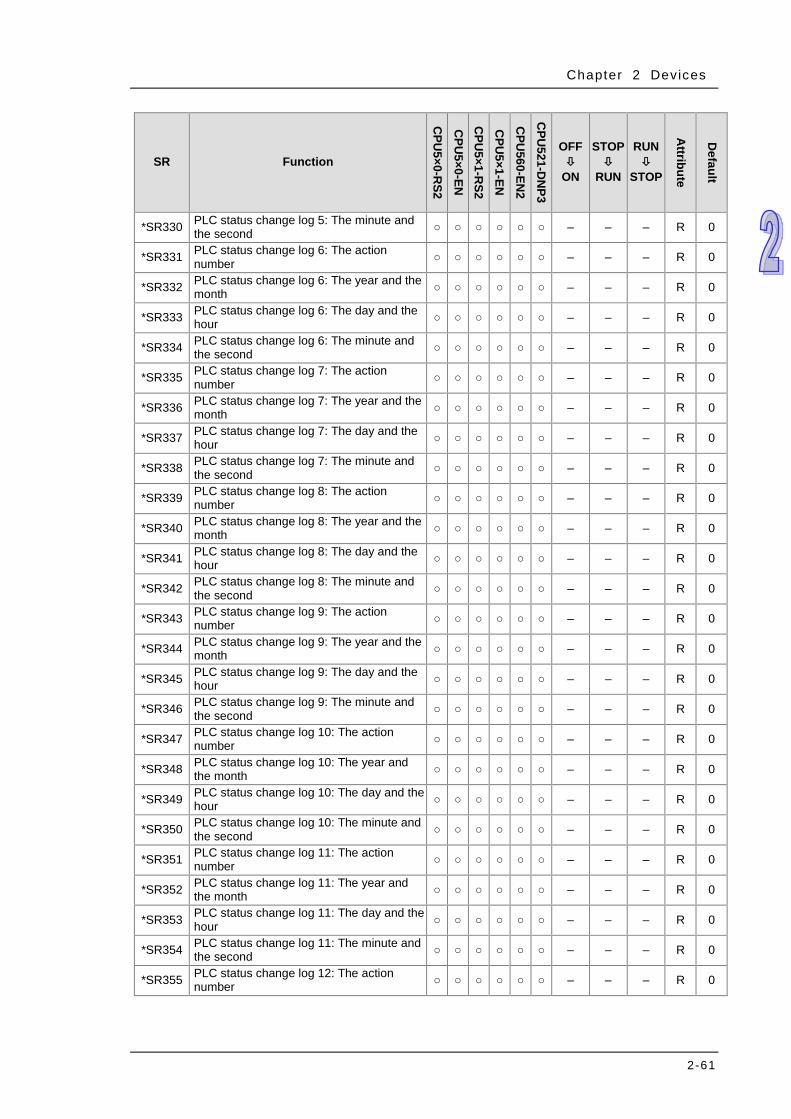
Chapter 2 Devices
2-61
SR Function
CPU
5×0-RS2
CPU
5×0-EN
CPU
5×1-RS2
CPU
5×1-EN
CPU
560-EN2
CPU
521-DN
P3
OFF
ON
STOP
RUN
RUN
STOP
Attribute
Default
*SR330 PLC status change log 5: The minute and the second ○ ○ ○ ○ ○ ○ – – – R 0
*SR331 PLC status change log 6: The action number ○ ○ ○ ○ ○ ○ – – – R 0
*SR332 PLC status change log 6: The year and the month ○ ○ ○ ○ ○ ○ – – – R 0
*SR333 PLC status change log 6: The day and the hour ○ ○ ○ ○ ○ ○ – – – R 0
*SR334 PLC status change log 6: The minute and the second ○ ○ ○ ○ ○ ○ – – – R 0
*SR335 PLC status change log 7: The action number ○ ○ ○ ○ ○ ○ – – – R 0
*SR336 PLC status change log 7: The year and the month ○ ○ ○ ○ ○ ○ – – – R 0
*SR337 PLC status change log 7: The day and the hour ○ ○ ○ ○ ○ ○ – – – R 0
*SR338 PLC status change log 7: The minute and the second ○ ○ ○ ○ ○ ○ – – – R 0
*SR339 PLC status change log 8: The action number ○ ○ ○ ○ ○ ○ – – – R 0
*SR340 PLC status change log 8: The year and the month ○ ○ ○ ○ ○ ○ – – – R 0
*SR341 PLC status change log 8: The day and the hour ○ ○ ○ ○ ○ ○ – – – R 0
*SR342 PLC status change log 8: The minute and the second ○ ○ ○ ○ ○ ○ – – – R 0
*SR343 PLC status change log 9: The action number ○ ○ ○ ○ ○ ○ – – – R 0
*SR344 PLC status change log 9: The year and the month ○ ○ ○ ○ ○ ○ – – – R 0
*SR345 PLC status change log 9: The day and the hour ○ ○ ○ ○ ○ ○ – – – R 0
*SR346 PLC status change log 9: The minute and the second ○ ○ ○ ○ ○ ○ – – – R 0
*SR347 PLC status change log 10: The action number ○ ○ ○ ○ ○ ○ – – – R 0
*SR348 PLC status change log 10: The year and the month ○ ○ ○ ○ ○ ○ – – – R 0
*SR349 PLC status change log 10: The day and the hour ○ ○ ○ ○ ○ ○ – – – R 0
*SR350 PLC status change log 10: The minute and the second ○ ○ ○ ○ ○ ○ – – – R 0
*SR351 PLC status change log 11: The action number ○ ○ ○ ○ ○ ○ – – – R 0
*SR352 PLC status change log 11: The year and the month ○ ○ ○ ○ ○ ○ – – – R 0
*SR353 PLC status change log 11: The day and the hour ○ ○ ○ ○ ○ ○ – – – R 0
*SR354 PLC status change log 11: The minute and the second ○ ○ ○ ○ ○ ○ – – – R 0
*SR355 PLC status change log 12: The action number ○ ○ ○ ○ ○ ○ – – – R 0
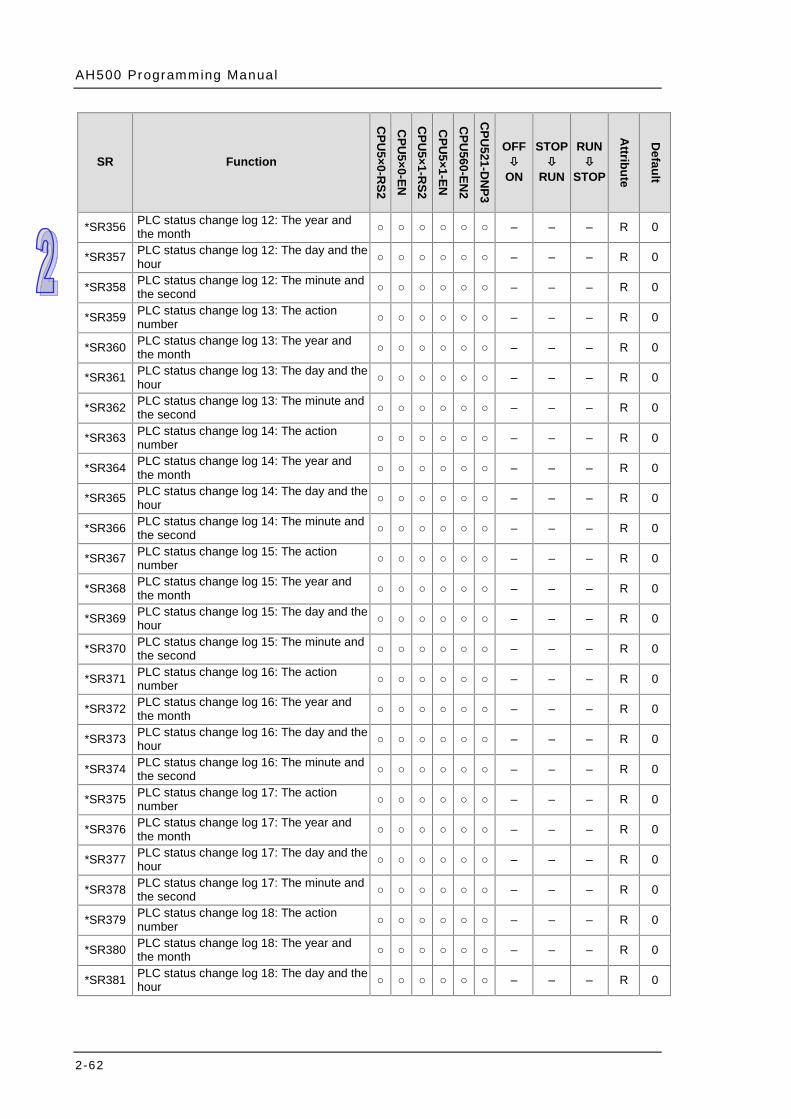
AH500 Programming Manual
2-62
SR Function
CPU
5×0-RS2
CPU
5×0-EN
CPU
5×1-RS2
CPU
5×1-EN
CPU
560-EN2
CPU
521-DN
P3
OFF
ON
STOP
RUN
RUN
STOP A
ttribute
Default
*SR356 PLC status change log 12: The year and the month ○ ○ ○ ○ ○ ○ – – – R 0
*SR357 PLC status change log 12: The day and the hour ○ ○ ○ ○ ○ ○ – – – R 0
*SR358 PLC status change log 12: The minute and the second ○ ○ ○ ○ ○ ○ – – – R 0
*SR359 PLC status change log 13: The action number ○ ○ ○ ○ ○ ○ – – – R 0
*SR360 PLC status change log 13: The year and the month ○ ○ ○ ○ ○ ○ – – – R 0
*SR361 PLC status change log 13: The day and the hour ○ ○ ○ ○ ○ ○ – – – R 0
*SR362 PLC status change log 13: The minute and the second ○ ○ ○ ○ ○ ○ – – – R 0
*SR363 PLC status change log 14: The action number ○ ○ ○ ○ ○ ○ – – – R 0
*SR364 PLC status change log 14: The year and the month ○ ○ ○ ○ ○ ○ – – – R 0
*SR365 PLC status change log 14: The day and the hour ○ ○ ○ ○ ○ ○ – – – R 0
*SR366 PLC status change log 14: The minute and the second ○ ○ ○ ○ ○ ○ – – – R 0
*SR367 PLC status change log 15: The action number ○ ○ ○ ○ ○ ○ – – – R 0
*SR368 PLC status change log 15: The year and the month ○ ○ ○ ○ ○ ○ – – – R 0
*SR369 PLC status change log 15: The day and the hour ○ ○ ○ ○ ○ ○ – – – R 0
*SR370 PLC status change log 15: The minute and the second ○ ○ ○ ○ ○ ○ – – – R 0
*SR371 PLC status change log 16: The action number ○ ○ ○ ○ ○ ○ – – – R 0
*SR372 PLC status change log 16: The year and the month ○ ○ ○ ○ ○ ○ – – – R 0
*SR373 PLC status change log 16: The day and the hour ○ ○ ○ ○ ○ ○ – – – R 0
*SR374 PLC status change log 16: The minute and the second ○ ○ ○ ○ ○ ○ – – – R 0
*SR375 PLC status change log 17: The action number ○ ○ ○ ○ ○ ○ – – – R 0
*SR376 PLC status change log 17: The year and the month ○ ○ ○ ○ ○ ○ – – – R 0
*SR377 PLC status change log 17: The day and the hour ○ ○ ○ ○ ○ ○ – – – R 0
*SR378 PLC status change log 17: The minute and the second ○ ○ ○ ○ ○ ○ – – – R 0
*SR379 PLC status change log 18: The action number ○ ○ ○ ○ ○ ○ – – – R 0
*SR380 PLC status change log 18: The year and the month ○ ○ ○ ○ ○ ○ – – – R 0
*SR381 PLC status change log 18: The day and the hour ○ ○ ○ ○ ○ ○ – – – R 0
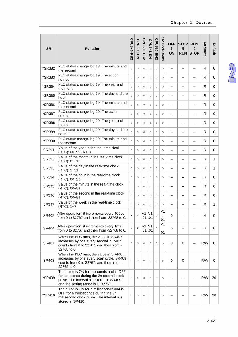
Chapter 2 Devices
2-63
SR Function
CPU
5×0-RS2
CPU
5×0-EN
CPU
5×1-RS2
CPU
5×1-EN
CPU
560-EN2
CPU
521-DN
P3
OFF
ON
STOP
RUN
RUN
STOP
Attribute
Default
*SR382 PLC status change log 18: The minute and the second ○ ○ ○ ○ ○ ○ – – – R 0
*SR383 PLC status change log 19: The action number ○ ○ ○ ○ ○ ○ – – – R 0
*SR384 PLC status change log 19: The year and the month ○ ○ ○ ○ ○ ○ – – – R 0
*SR385 PLC status change log 19: The day and the hour ○ ○ ○ ○ ○ ○ – – – R 0
*SR386 PLC status change log 19: The minute and the second ○ ○ ○ ○ ○ ○ – – – R 0
*SR387 PLC status change log 20: The action number ○ ○ ○ ○ ○ ○ – – – R 0
*SR388 PLC status change log 20: The year and the month ○ ○ ○ ○ ○ ○ – – – R 0
*SR389 PLC status change log 20: The day and the hour ○ ○ ○ ○ ○ ○ – – – R 0
*SR390 PLC status change log 20: The minute and the second ○ ○ ○ ○ ○ ○ – – – R 0
SR391 Value of the year in the real-time clock (RTC): 00~99 (A.D.) ○ ○ ○ ○ ○ ○ – – – R 0
SR392 Value of the month in the real-time clock (RTC): 01~12 ○ ○ ○ ○ ○ ○ – – – R 1
SR393 Value of the day in the real-time clock (RTC): 1~31 ○ ○ ○ ○ ○ ○ – – – R 1
SR394 Value of the hour in the real-time clock (RTC): 00~23 ○ ○ ○ ○ ○ ○ – – – R 0
SR395 Value of the minute in the real-time clock (RTC): 00~59 ○ ○ ○ ○ ○ ○ – – – R 0
SR396 Value of the second in the real-time clock (RTC): 00~59 ○ ○ ○ ○ ○ ○ – – – R 0
SR397 Value of the week in the real-time clock (RTC): 1~7 ○ ○ ○ ○ ○ ○ – – – R 1
SR402 After operation, it increments every 100μs from 0 to 32767 and then from -32768 to 0. × × V1
.01 V1.01 ○
V1.
01 0 – – R 0
SR404 After operation, it increments every 1ms from 0 to 32767 and then from -32768 to 0. × × V1
.01 V1.01 ○
V1.
01 0 – – R 0
SR407
When the PLC runs, the value in SR407 increases by one every second. SR407 counts from 0 to 32767, and then from -32768 to 0.
○ ○ ○ ○ ○ ○ 0 0 – R/W 0
SR408
When the PLC runs, the value in SR408 increases by one every scan cycle. SR408 counts from 0 to 32767, and then from -32768 to 0.
○ ○ ○ ○ ○ ○ 0 0 – R/W 0
*SR409
The pulse is ON for n seconds and is OFF for n seconds during the 2n second clock pulse. The interval n is stored in SR409, and the setting range is 1~32767.
○ ○ ○ ○ ○ ○ – – – R/W 30
*SR410
The pulse is ON for n milliseconds and is OFF for n milliseconds during the 2n millisecond clock pulse. The interval n is stored in SR410.
○ ○ ○ ○ ○ ○ – – – R/W 30
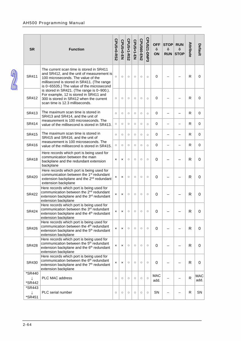
AH500 Programming Manual
2-64
SR Function
CPU
5×0-RS2
CPU
5×0-EN
CPU
5×1-RS2
CPU
5×1-EN
CPU
560-EN2
CPU
521-DN
P3
OFF
ON
STOP
RUN
RUN
STOP A
ttribute
Default
SR411
The current scan time is stored in SR411 and SR412, and the unit of measurement is 100 microseconds. The value of the millisecond is stored in SR411. (The range is 0~65535.) The value of the microsecond is stored in SR421. (The range is 0~900.). For example, 12 is stored in SR411 and 300 is stored in SR412 when the current scan time is 12.3 milliseconds.
○ ○ ○ ○ ○ ○ 0 – – R 0
SR412 ○ ○ ○ ○ ○ ○ 0 – – R 0
SR413 The maximum scan time is stored in SR413 and SR414, and the unit of measurement is 100 microseconds. The value of the millisecond is stored in SR413.
○ ○ ○ ○ ○ ○ 0 – – R 0
SR414 ○ ○ ○ ○ ○ ○ 0 – – R 0
SR415 The maximum scan time is stored in SR415 and SR416, and the unit of measurement is 100 microseconds. The value of the millisecond is stored in SR415.
○ ○ ○ ○ ○ ○ 0 – – R 0
SR416 ○ ○ ○ ○ ○ ○ 0 – – R 0
SR418
Here records which port is being used for communication between the main backplane and the redundant extension backplane
× × ○ ○ ○ ○ 0 – – R 0
SR420
Here records which port is being used for communication between the 1st redundant extension backplane and the 2nd redundant extension backplane
× × ○ ○ ○ ○ 0 – – R 0
SR422
Here records which port is being used for communication between the 2nd redundant extension backplane and the 3rd redundant extension backplane
× × ○ ○ ○ ○ 0 – – R 0
SR424
Here records which port is being used for communication between the 3rd redundant extension backplane and the 4th redundant extension backplane
× × ○ ○ ○ ○ 0 – – R 0
SR426
Here records which port is being used for communication between the 4th redundant extension backplane and the 5th redundant extension backplane
× × ○ ○ ○ ○ 0 – – R 0
SR428
Here records which port is being used for communication between the 5th redundant extension backplane and the 6th redundant extension backplane
× × ○ ○ ○ ○ 0 – – R 0
SR430
Here records which port is being used for communication between the 6th redundant extension backplane and the 7th redundant extension backplane
× × ○ ○ ○ ○ 0 – – R 0
*SR440 ↓
*SR442 PLC MAC address ○ ○ ○ ○ ○ ○ MAC
add. – – R MACadd.
*SR443 ↓
*SR451 PLC serial number ○ ○ ○ ○ ○ ○ SN – – R SN
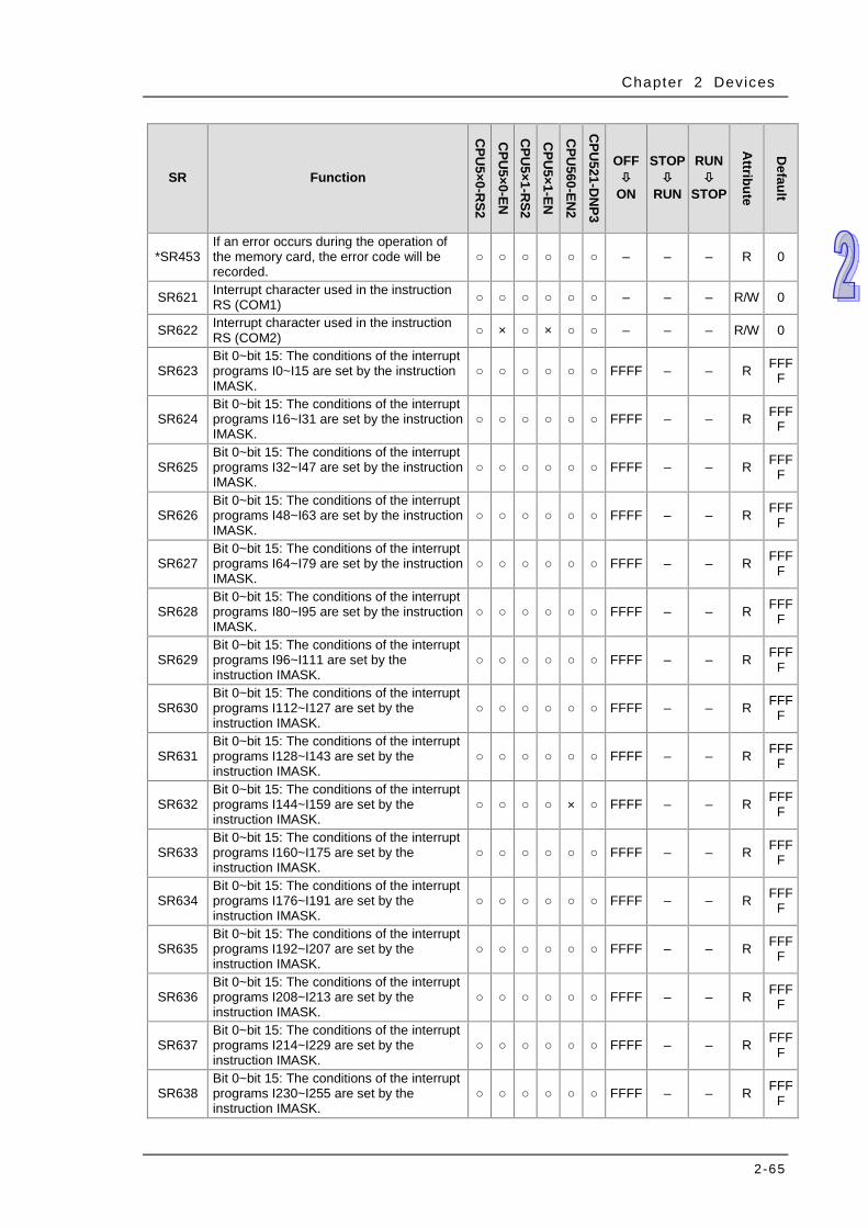
Chapter 2 Devices
2-65
SR Function
CPU
5×0-RS2
CPU
5×0-EN
CPU
5×1-RS2
CPU
5×1-EN
CPU
560-EN2
CPU
521-DN
P3
OFF
ON
STOP
RUN
RUN
STOP
Attribute
Default
*SR453 If an error occurs during the operation of the memory card, the error code will be recorded.
○ ○ ○ ○ ○ ○ – – – R 0
SR621 Interrupt character used in the instruction RS (COM1) ○ ○ ○ ○ ○ ○ – – – R/W 0
SR622 Interrupt character used in the instruction RS (COM2) ○ × ○ × ○ ○ – – – R/W 0
SR623 Bit 0~bit 15: The conditions of the interrupt programs I0~I15 are set by the instruction IMASK.
○ ○ ○ ○ ○ ○ FFFF – – R FFFF
SR624 Bit 0~bit 15: The conditions of the interrupt programs I16~I31 are set by the instruction IMASK.
○ ○ ○ ○ ○ ○ FFFF – – R FFFF
SR625 Bit 0~bit 15: The conditions of the interrupt programs I32~I47 are set by the instruction IMASK.
○ ○ ○ ○ ○ ○ FFFF – – R FFFF
SR626 Bit 0~bit 15: The conditions of the interrupt programs I48~I63 are set by the instruction IMASK.
○ ○ ○ ○ ○ ○ FFFF – – R FFFF
SR627 Bit 0~bit 15: The conditions of the interrupt programs I64~I79 are set by the instruction IMASK.
○ ○ ○ ○ ○ ○ FFFF – – R FFFF
SR628 Bit 0~bit 15: The conditions of the interrupt programs I80~I95 are set by the instruction IMASK.
○ ○ ○ ○ ○ ○ FFFF – – R FFFF
SR629 Bit 0~bit 15: The conditions of the interrupt programs I96~I111 are set by the instruction IMASK.
○ ○ ○ ○ ○ ○ FFFF – – R FFFF
SR630 Bit 0~bit 15: The conditions of the interrupt programs I112~I127 are set by the instruction IMASK.
○ ○ ○ ○ ○ ○ FFFF – – R FFFF
SR631 Bit 0~bit 15: The conditions of the interrupt programs I128~I143 are set by the instruction IMASK.
○ ○ ○ ○ ○ ○ FFFF – – R FFFF
SR632 Bit 0~bit 15: The conditions of the interrupt programs I144~I159 are set by the instruction IMASK.
○ ○ ○ ○ × ○ FFFF – – R FFFF
SR633 Bit 0~bit 15: The conditions of the interrupt programs I160~I175 are set by the instruction IMASK.
○ ○ ○ ○ ○ ○ FFFF – – R FFFF
SR634 Bit 0~bit 15: The conditions of the interrupt programs I176~I191 are set by the instruction IMASK.
○ ○ ○ ○ ○ ○ FFFF – – R FFFF
SR635 Bit 0~bit 15: The conditions of the interrupt programs I192~I207 are set by the instruction IMASK.
○ ○ ○ ○ ○ ○ FFFF – – R FFFF
SR636 Bit 0~bit 15: The conditions of the interrupt programs I208~I213 are set by the instruction IMASK.
○ ○ ○ ○ ○ ○ FFFF – – R FFFF
SR637 Bit 0~bit 15: The conditions of the interrupt programs I214~I229 are set by the instruction IMASK.
○ ○ ○ ○ ○ ○ FFFF – – R FFFF
SR638 Bit 0~bit 15: The conditions of the interrupt programs I230~I255 are set by the instruction IMASK.
○ ○ ○ ○ ○ ○ FFFF – – R FFFF

AH500 Programming Manual
2-66
SR Function
CPU
5×0-RS2
CPU
5×0-EN
CPU
5×1-RS2
CPU
5×1-EN
CPU
560-EN2
CPU
521-DN
P3
OFF
ON
STOP
RUN
RUN
STOP A
ttribute
Default
*SR655 ↓
SR662
Recording the mapping error occurring in the module table for rack 1 or the error occurring in the I/○ module of rack 1
↓ Recording the mapping error occurring in the module table for rack 8 or the error occurring in the I/○ module of rack 8
○ ○ ○ ○ ○ ○ 0 – – R 0
*SR663 ↓
SR674
Recording the mapping error code occurring in the module table for rack 1 whose slot number is 0
↓ Recording the mapping error code occurring in the module table for rack 1 whose slot number is 11
○ ○ ○ ○ ○ ○ 0 – – R 0
*SR675 ↓
SR682
Recording the mapping error code occurring in the module table for rack 2 whose slot number is 0
↓ Recording the mapping error code occurring in the module table for rack 2 whose slot number is 7
○ ○ ○ ○ ○ ○ 0 – – R 0
*SR683 ↓
SR690
Recording the mapping error code occurring in the module table for rack 3 whose slot number is 0
↓ Recording the mapping error code occurring in the module table for rack 3 whose slot number is 7
○ ○ ○ ○ ○ ○ 0 – – R 0
*SR691 ↓
SR698
Recording the mapping error code occurring in the module table for rack 4 whose slot number is 0
↓ Recording the mapping error code occurring in the module table for rack 4 whose slot number is 7
○ ○ ○ ○ ○ ○ 0 – – R 0
*SR699 ↓
SR706
Recording the mapping error code occurring in the module table for rack 5 whose slot number is 0
↓ Recording the mapping error code occurring in the module table for rack 5 whose slot number is 7
○ ○ ○ ○ ○ ○ 0 – – R 0
*SR707 ↓
SR714
Recording the mapping error code occurring in the module table for rack 6 whose slot number is 0
↓ Recording the mapping error code occurring in the module table for rack 6 whose slot number is 7
○ ○ ○ ○ ○ ○ 0 – – R 0
*SR715 ↓
SR722
Recording the mapping error code occurring in the module table for rack 7 whose slot number is 0
↓
○ ○ ○ ○ ○ ○ 0 – – R 0
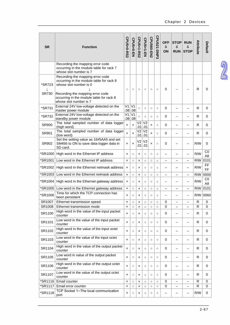
Chapter 2 Devices
2-67
SR Function
CPU
5×0-RS2
CPU
5×0-EN
CPU
5×1-RS2
CPU
5×1-EN
CPU
560-EN2
CPU
521-DN
P3
OFF
ON
STOP
RUN
RUN
STOP
Attribute
Default
Recording the mapping error code occurring in the module table for rack 7 whose slot number is 7
*SR723 ↓
SR730
Recording the mapping error code occurring in the module table for rack 8 whose slot number is 0
↓ Recording the mapping error code occurring in the module table for rack 8 whose slot number is 7
○ ○ ○ ○ ○ ○ 0 – – R 0
*SR731 External 24V low-voltage detected on the master power module
V1.08
V1.08 ○ ○ ○ ○ 0 – – R 0
*SR732 External 24V low-voltage detected on the standby power module
V1.08
V1.08 ○ ○ ○ ○ 0 – – R 0
SR900 The total sampled number of data logger (high word) × × V2
.01 V2.01 × ○ 0 – – R 0
SR901 The total sampled number of data logger (low word) × × V2
.01 V2.01 × ○ 0 – – R 0
SR902 Set the setting value as 16#5AA5 and set SM456 to ON to save data logger data in SD card.
× × V2.01
V2.01 × ○ 0 – – R/W 0
*SR1000 High word in the Ethernet IP address × ○ × ○ ○ ○ – – – R/W C0 A8
*SR1001 Low word in the Ethernet IP address × ○ × ○ ○ ○ – – – R/W 0101
*SR1002 High word in the Ethernet netmask address × ○ × ○ ○ ○ – – – R/W FF FF
*SR1003 Low word in the Ethernet netmask address × ○ × ○ ○ ○ – – – R/W 0000
*SR1004 High word in the Ethernet gateway address × ○ × ○ ○ ○ – – – R/W C0 A8
*SR1005 Low word in the Ethernet gateway address × ○ × ○ ○ ○ – – – R/W 0101
*SR1006 Time for which the TCP connection has been persistent × ○ × ○ ○ ○ – – – R/W 0060
SR1007 Ethernet transmission speed × ○ × ○ ○ ○ 0 – – R 0 SR1008 Ethernet transmission mode × ○ × ○ ○ ○ 0 – – R 0
SR1100 High word in the value of the input packet counter × ○ × ○ ○ ○ 0 – – R 0
SR1101 Low word in the value of the input packet counter × ○ × ○ ○ ○ 0 – – R 0
SR1102 High word in the value of the input octet counter × ○ × ○ ○ ○ 0 – – R 0
SR1103 Low word in the value of the input octet counter × ○ × ○ ○ ○ 0 – – R 0
SR1104 High word in the value of the output packet counter × ○ × ○ ○ ○ 0 – – R 0
SR1105 Low word in value of the output packet counter × ○ × ○ ○ ○ 0 – – R 0
SR1106 High word in the value of the output octet counter × ○ × ○ ○ ○ 0 – – R 0
SR1107 Low word in the value of the output octet counter × ○ × ○ ○ ○ 0 – – R 0
*SR1116 Email counter × ○ × ○ ○ ○ 0 – – R 0 *SR1117 Email error counter × ○ × ○ ○ ○ 0 – – R 0
*SR1118 TCP Socket 1─The local communication port × ○ × ○ ○ ○ – – – R/W 0
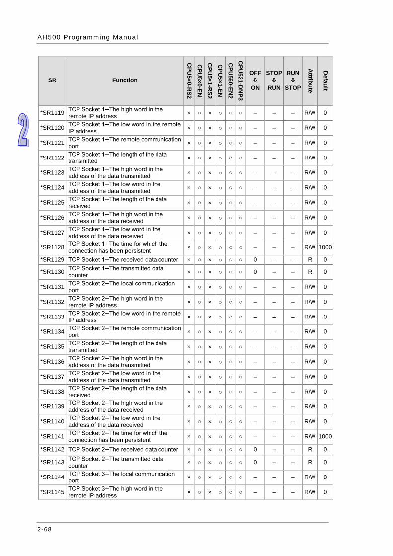
AH500 Programming Manual
2-68
SR Function
CPU
5×0-RS2
CPU
5×0-EN
CPU
5×1-RS2
CPU
5×1-EN
CPU
560-EN2
CPU
521-DN
P3
OFF
ON
STOP
RUN
RUN
STOP A
ttribute
Default
*SR1119 TCP Socket 1─The high word in the remote IP address × ○ × ○ ○ ○ – – – R/W 0
*SR1120 TCP Socket 1─The low word in the remote IP address × ○ × ○ ○ ○ – – – R/W 0
*SR1121 TCP Socket 1─The remote communication port × ○ × ○ ○ ○ – – – R/W 0
*SR1122 TCP Socket 1─The length of the data transmitted × ○ × ○ ○ ○ – – – R/W 0
*SR1123 TCP Socket 1─The high word in the address of the data transmitted × ○ × ○ ○ ○ – – – R/W 0
*SR1124 TCP Socket 1─The low word in the address of the data transmitted × ○ × ○ ○ ○ – – – R/W 0
*SR1125 TCP Socket 1─The length of the data received × ○ × ○ ○ ○ – – – R/W 0
*SR1126 TCP Socket 1─The high word in the address of the data received × ○ × ○ ○ ○ – – – R/W 0
*SR1127 TCP Socket 1─The low word in the address of the data received × ○ × ○ ○ ○ – – – R/W 0
*SR1128 TCP Socket 1─The time for which the connection has been persistent × ○ × ○ ○ ○ – – – R/W 1000
*SR1129 TCP Socket 1─The received data counter × ○ × ○ ○ ○ 0 – – R 0
*SR1130 TCP Socket 1─The transmitted data counter × ○ × ○ ○ ○ 0 – – R 0
*SR1131 TCP Socket 2─The local communication port × ○ × ○ ○ ○ – – – R/W 0
*SR1132 TCP Socket 2─The high word in the remote IP address × ○ × ○ ○ ○ – – – R/W 0
*SR1133 TCP Socket 2─The low word in the remote IP address × ○ × ○ ○ ○ – – – R/W 0
*SR1134 TCP Socket 2─The remote communication port × ○ × ○ ○ ○ – – – R/W 0
*SR1135 TCP Socket 2─The length of the data transmitted × ○ × ○ ○ ○ – – – R/W 0
*SR1136 TCP Socket 2─The high word in the address of the data transmitted × ○ × ○ ○ ○ – – – R/W 0
*SR1137 TCP Socket 2─The low word in the address of the data transmitted × ○ × ○ ○ ○ – – – R/W 0
*SR1138 TCP Socket 2─The length of the data received × ○ × ○ ○ ○ – – – R/W 0
*SR1139 TCP Socket 2─The high word in the address of the data received × ○ × ○ ○ ○ – – – R/W 0
*SR1140 TCP Socket 2─The low word in the address of the data received × ○ × ○ ○ ○ – – – R/W 0
*SR1141 TCP Socket 2─The time for which the connection has been persistent × ○ × ○ ○ ○ – – – R/W 1000
*SR1142 TCP Socket 2─The received data counter × ○ × ○ ○ ○ 0 – – R 0
*SR1143 TCP Socket 2─The transmitted data counter × ○ × ○ ○ ○ 0 – – R 0
*SR1144 TCP Socket 3─The local communication port × ○ × ○ ○ ○ – – – R/W 0
*SR1145 TCP Socket 3─The high word in the remote IP address × ○ × ○ ○ ○ – – – R/W 0
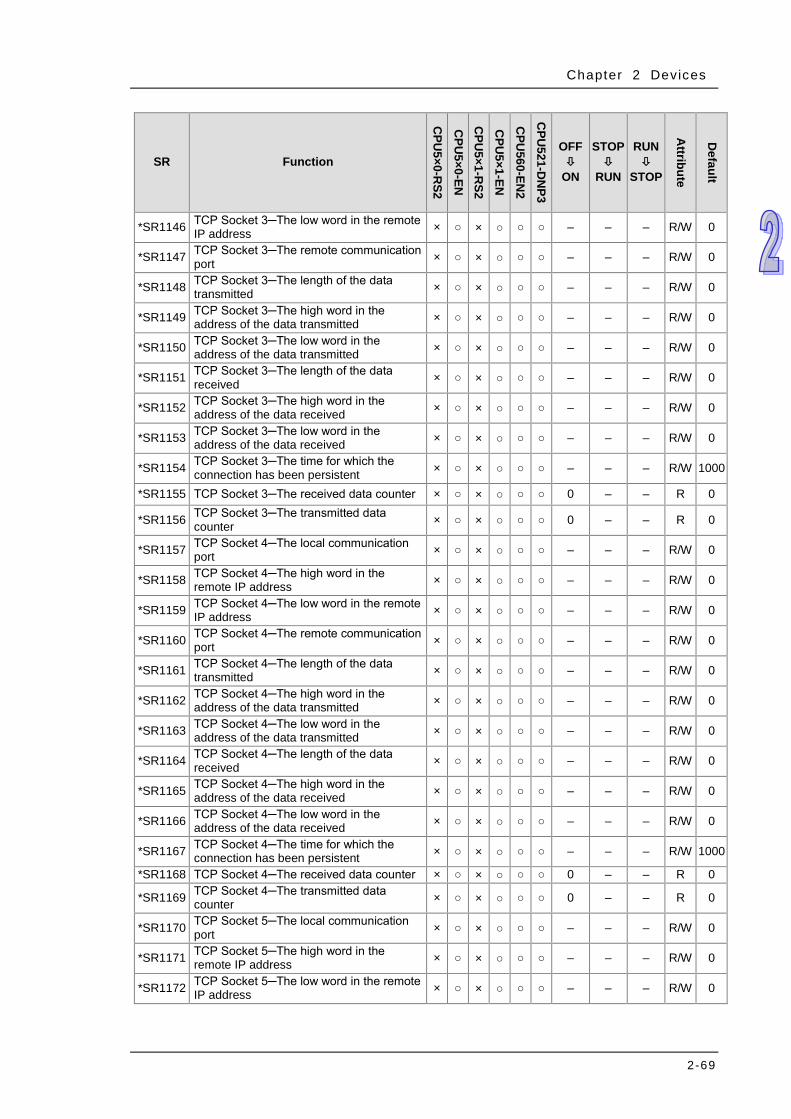
Chapter 2 Devices
2-69
SR Function
CPU
5×0-RS2
CPU
5×0-EN
CPU
5×1-RS2
CPU
5×1-EN
CPU
560-EN2
CPU
521-DN
P3
OFF
ON
STOP
RUN
RUN
STOP
Attribute
Default
*SR1146 TCP Socket 3─The low word in the remote IP address × ○ × ○ ○ ○ – – – R/W 0
*SR1147 TCP Socket 3─The remote communication port × ○ × ○ ○ ○ – – – R/W 0
*SR1148 TCP Socket 3─The length of the data transmitted × ○ × ○ ○ ○ – – – R/W 0
*SR1149 TCP Socket 3─The high word in the address of the data transmitted × ○ × ○ ○ ○ – – – R/W 0
*SR1150 TCP Socket 3─The low word in the address of the data transmitted × ○ × ○ ○ ○ – – – R/W 0
*SR1151 TCP Socket 3─The length of the data received × ○ × ○ ○ ○ – – – R/W 0
*SR1152 TCP Socket 3─The high word in the address of the data received × ○ × ○ ○ ○ – – – R/W 0
*SR1153 TCP Socket 3─The low word in the address of the data received × ○ × ○ ○ ○ – – – R/W 0
*SR1154 TCP Socket 3─The time for which the connection has been persistent × ○ × ○ ○ ○ – – – R/W 1000
*SR1155 TCP Socket 3─The received data counter × ○ × ○ ○ ○ 0 – – R 0
*SR1156 TCP Socket 3─The transmitted data counter × ○ × ○ ○ ○ 0 – – R 0
*SR1157 TCP Socket 4─The local communication port × ○ × ○ ○ ○ – – – R/W 0
*SR1158 TCP Socket 4─The high word in the remote IP address × ○ × ○ ○ ○ – – – R/W 0
*SR1159 TCP Socket 4─The low word in the remote IP address × ○ × ○ ○ ○ – – – R/W 0
*SR1160 TCP Socket 4─The remote communication port × ○ × ○ ○ ○ – – – R/W 0
*SR1161 TCP Socket 4─The length of the data transmitted × ○ × ○ ○ ○ – – – R/W 0
*SR1162 TCP Socket 4─The high word in the address of the data transmitted × ○ × ○ ○ ○ – – – R/W 0
*SR1163 TCP Socket 4─The low word in the address of the data transmitted × ○ × ○ ○ ○ – – – R/W 0
*SR1164 TCP Socket 4─The length of the data received × ○ × ○ ○ ○ – – – R/W 0
*SR1165 TCP Socket 4─The high word in the address of the data received × ○ × ○ ○ ○ – – – R/W 0
*SR1166 TCP Socket 4─The low word in the address of the data received × ○ × ○ ○ ○ – – – R/W 0
*SR1167 TCP Socket 4─The time for which the connection has been persistent × ○ × ○ ○ ○ – – – R/W 1000
*SR1168 TCP Socket 4─The received data counter × ○ × ○ ○ ○ 0 – – R 0
*SR1169 TCP Socket 4─The transmitted data counter × ○ × ○ ○ ○ 0 – – R 0
*SR1170 TCP Socket 5─The local communication port × ○ × ○ ○ ○ – – – R/W 0
*SR1171 TCP Socket 5─The high word in the remote IP address × ○ × ○ ○ ○ – – – R/W 0
*SR1172 TCP Socket 5─The low word in the remote IP address × ○ × ○ ○ ○ – – – R/W 0
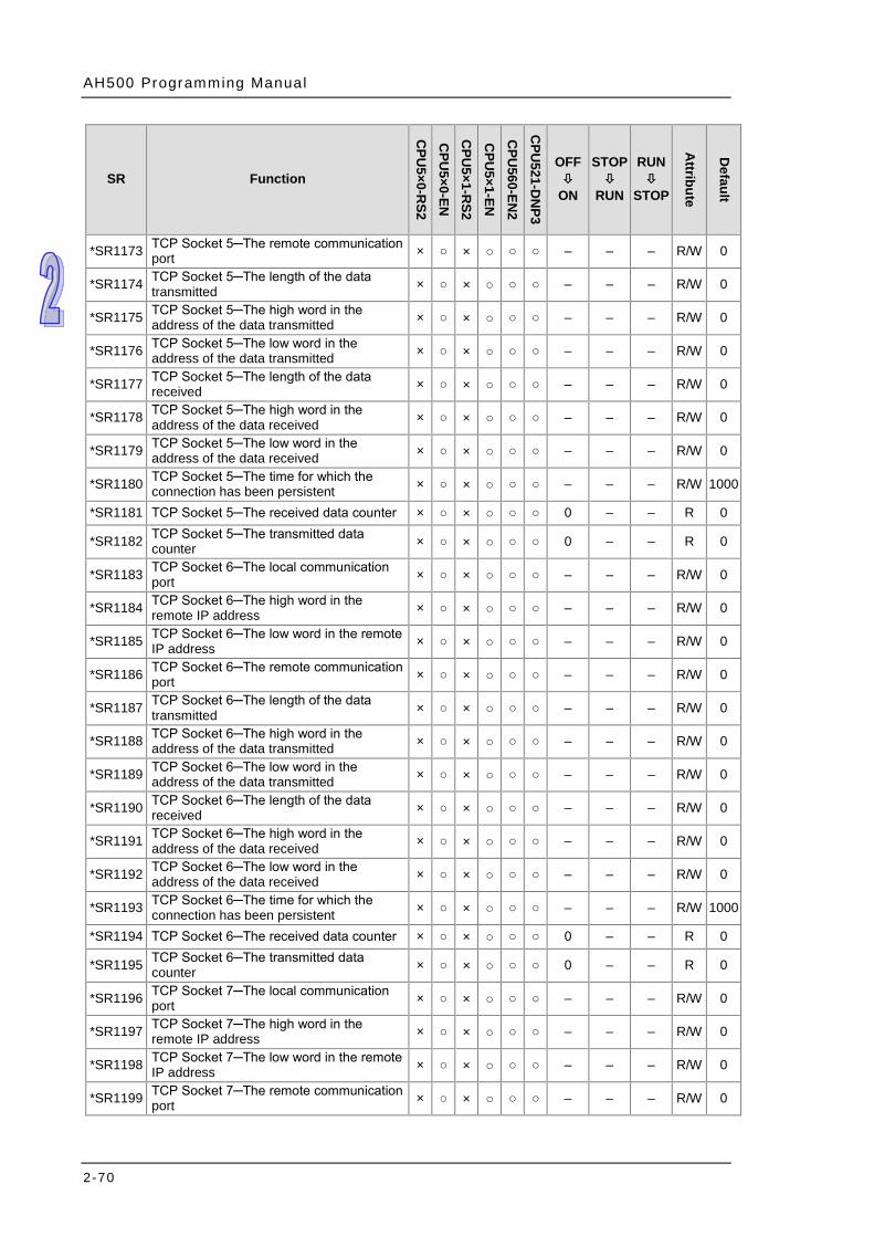
AH500 Programming Manual
2-70
SR Function
CPU
5×0-RS2
CPU
5×0-EN
CPU
5×1-RS2
CPU
5×1-EN
CPU
560-EN2
CPU
521-DN
P3
OFF
ON
STOP
RUN
RUN
STOP A
ttribute
Default
*SR1173 TCP Socket 5─The remote communication port × ○ × ○ ○ ○ – – – R/W 0
*SR1174 TCP Socket 5─The length of the data transmitted × ○ × ○ ○ ○ – – – R/W 0
*SR1175 TCP Socket 5─The high word in the address of the data transmitted × ○ × ○ ○ ○ – – – R/W 0
*SR1176 TCP Socket 5─The low word in the address of the data transmitted × ○ × ○ ○ ○ – – – R/W 0
*SR1177 TCP Socket 5─The length of the data received × ○ × ○ ○ ○ – – – R/W 0
*SR1178 TCP Socket 5─The high word in the address of the data received × ○ × ○ ○ ○ – – – R/W 0
*SR1179 TCP Socket 5─The low word in the address of the data received × ○ × ○ ○ ○ – – – R/W 0
*SR1180 TCP Socket 5─The time for which the connection has been persistent × ○ × ○ ○ ○ – – – R/W 1000
*SR1181 TCP Socket 5─The received data counter × ○ × ○ ○ ○ 0 – – R 0
*SR1182 TCP Socket 5─The transmitted data counter × ○ × ○ ○ ○ 0 – – R 0
*SR1183 TCP Socket 6─The local communication port × ○ × ○ ○ ○ – – – R/W 0
*SR1184 TCP Socket 6─The high word in the remote IP address × ○ × ○ ○ ○ – – – R/W 0
*SR1185 TCP Socket 6─The low word in the remote IP address × ○ × ○ ○ ○ – – – R/W 0
*SR1186 TCP Socket 6─The remote communication port × ○ × ○ ○ ○ – – – R/W 0
*SR1187 TCP Socket 6─The length of the data transmitted × ○ × ○ ○ ○ – – – R/W 0
*SR1188 TCP Socket 6─The high word in the address of the data transmitted × ○ × ○ ○ ○ – – – R/W 0
*SR1189 TCP Socket 6─The low word in the address of the data transmitted × ○ × ○ ○ ○ – – – R/W 0
*SR1190 TCP Socket 6─The length of the data received × ○ × ○ ○ ○ – – – R/W 0
*SR1191 TCP Socket 6─The high word in the address of the data received × ○ × ○ ○ ○ – – – R/W 0
*SR1192 TCP Socket 6─The low word in the address of the data received × ○ × ○ ○ ○ – – – R/W 0
*SR1193 TCP Socket 6─The time for which the connection has been persistent × ○ × ○ ○ ○ – – – R/W 1000
*SR1194 TCP Socket 6─The received data counter × ○ × ○ ○ ○ 0 – – R 0
*SR1195 TCP Socket 6─The transmitted data counter × ○ × ○ ○ ○ 0 – – R 0
*SR1196 TCP Socket 7─The local communication port × ○ × ○ ○ ○ – – – R/W 0
*SR1197 TCP Socket 7─The high word in the remote IP address × ○ × ○ ○ ○ – – – R/W 0
*SR1198 TCP Socket 7─The low word in the remote IP address × ○ × ○ ○ ○ – – – R/W 0
*SR1199 TCP Socket 7─The remote communication port × ○ × ○ ○ ○ – – – R/W 0

Chapter 2 Devices
2-71
SR Function
CPU
5×0-RS2
CPU
5×0-EN
CPU
5×1-RS2
CPU
5×1-EN
CPU
560-EN2
CPU
521-DN
P3
OFF
ON
STOP
RUN
RUN
STOP
Attribute
Default
*SR1200 TCP Socket 7─The length of the data transmitted × ○ × ○ ○ ○ – – – R/W 0
*SR1201 TCP Socket 7─The high word in the address of the data transmitted × ○ × ○ ○ ○ – – – R/W 0
*SR1202 TCP Socket 7─The low word in the address of the data transmitted × ○ × ○ ○ ○ – – – R/W 0
*SR1203 TCP Socket 7─The length of the data received × ○ × ○ ○ ○ – – – R/W 0
*SR1204 TCP Socket 7─The high word in the address of the data received × ○ × ○ ○ ○ – – – R/W 0
*SR1205 TCP Socket 7─The low word in the address of the data received × ○ × ○ ○ ○ – – – R/W 0
*SR1206 TCP Socket 7─The time for which the connection has been persistent × ○ × ○ ○ ○ – – – R/W 1000
*SR1207 TCP Socket 7─The received data counter × ○ × ○ ○ ○ 0 – – R 0
*SR1208 TCP Socket 7─The transmitted data counter × ○ × ○ ○ ○ 0 – – R 0
*SR1209 TCP Socket 8─The local communication port × ○ × ○ ○ ○ – – – R/W 0
*SR1210 TCP Socket 8─The high word in the remote IP address × ○ × ○ ○ ○ – – – R/W 0
*SR1211 TCP Socket 8─The low word in the remote IP address × ○ × ○ ○ ○ – – – R/W 0
*SR1212 TCP Socket 8─The remote communication port × ○ × ○ ○ ○ – – – R/W 0
*SR1213 TCP Socket 8─The length of the data transmitted × ○ × ○ ○ ○ – – – R/W 0
*SR1214 TCP Socket 8─The high word in the address of the data transmitted × ○ × ○ ○ ○ – – – R/W 0
*SR1215 TCP Socket 8─The low word in the address of the data transmitted × ○ × ○ ○ ○ – – – R/W 0
*SR1216 TCP Socket 8─The length of the data received × ○ × ○ ○ ○ – – – R/W 0
*SR1217 TCP Socket 8─The high word in the address of the data received × ○ × ○ ○ ○ – – – R/W 0
*SR1218 TCP Socket 8─The low word in the address of the data received × ○ × ○ ○ ○ – – – R/W 0
*SR1219 TCP Socket 8─The time for which the connection has been persistent × ○ × ○ ○ ○ – – – R/W 1000
*SR1220 TCP Socket 8─The received data counter × ○ × ○ ○ ○ 0 – – R 0
*SR1221 TCP Socket 8─The transmitted data counter × ○ × ○ ○ ○ 0 – – R 0
*SR1222 UDP Socket 1─The local communication port × ○ × ○ ○ ○ – – – R/W 0
*SR1223 UDP Socket 1─The high word in the remote IP address × ○ × ○ ○ ○ – – – R/W 0
*SR1224 UDP Socket 1─The low word in the remote IP address × ○ × ○ ○ ○ – – – R/W 0
*SR1225 UDP Socket 1─The remote communication port × ○ × ○ ○ ○ – – – R/W 0
*SR1226 UDP Socket 1─The length of the data transmitted × ○ × ○ ○ ○ – – – R/W 0
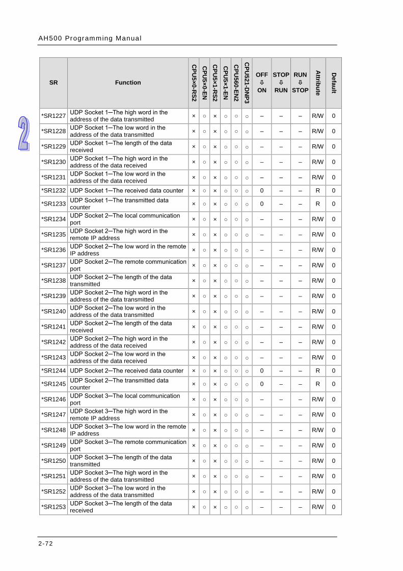
AH500 Programming Manual
2-72
SR Function
CPU
5×0-RS2
CPU
5×0-EN
CPU
5×1-RS2
CPU
5×1-EN
CPU
560-EN2
CPU
521-DN
P3
OFF
ON
STOP
RUN
RUN
STOP A
ttribute
Default
*SR1227 UDP Socket 1─The high word in the address of the data transmitted × ○ × ○ ○ ○ – – – R/W 0
*SR1228 UDP Socket 1─The low word in the address of the data transmitted × ○ × ○ ○ ○ – – – R/W 0
*SR1229 UDP Socket 1─The length of the data received × ○ × ○ ○ ○ – – – R/W 0
*SR1230 UDP Socket 1─The high word in the address of the data received × ○ × ○ ○ ○ – – – R/W 0
*SR1231 UDP Socket 1─The low word in the address of the data received × ○ × ○ ○ ○ – – – R/W 0
*SR1232 UDP Socket 1─The received data counter × ○ × ○ ○ ○ 0 – – R 0
*SR1233 UDP Socket 1─The transmitted data counter × ○ × ○ ○ ○ 0 – – R 0
*SR1234 UDP Socket 2─The local communication port × ○ × ○ ○ ○ – – – R/W 0
*SR1235 UDP Socket 2─The high word in the remote IP address × ○ × ○ ○ ○ – – – R/W 0
*SR1236 UDP Socket 2─The low word in the remote IP address × ○ × ○ ○ ○ – – – R/W 0
*SR1237 UDP Socket 2─The remote communication port × ○ × ○ ○ ○ – – – R/W 0
*SR1238 UDP Socket 2─The length of the data transmitted × ○ × ○ ○ ○ – – – R/W 0
*SR1239 UDP Socket 2─The high word in the address of the data transmitted × ○ × ○ ○ ○ – – – R/W 0
*SR1240 UDP Socket 2─The low word in the address of the data transmitted × ○ × ○ ○ ○ – – – R/W 0
*SR1241 UDP Socket 2─The length of the data received × ○ × ○ ○ ○ – – – R/W 0
*SR1242 UDP Socket 2─The high word in the address of the data received × ○ × ○ ○ ○ – – – R/W 0
*SR1243 UDP Socket 2─The low word in the address of the data received × ○ × ○ ○ ○ – – – R/W 0
*SR1244 UDP Socket 2─The received data counter × ○ × ○ ○ ○ 0 – – R 0
*SR1245 UDP Socket 2─The transmitted data counter × ○ × ○ ○ ○ 0 – – R 0
*SR1246 UDP Socket 3─The local communication port × ○ × ○ ○ ○ – – – R/W 0
*SR1247 UDP Socket 3─The high word in the remote IP address × ○ × ○ ○ ○ – – – R/W 0
*SR1248 UDP Socket 3─The low word in the remote IP address × ○ × ○ ○ ○ – – – R/W 0
*SR1249 UDP Socket 3─The remote communication port × ○ × ○ ○ ○ – – – R/W 0
*SR1250 UDP Socket 3─The length of the data transmitted × ○ × ○ ○ ○ – – – R/W 0
*SR1251 UDP Socket 3─The high word in the address of the data transmitted × ○ × ○ ○ ○ – – – R/W 0
*SR1252 UDP Socket 3─The low word in the address of the data transmitted × ○ × ○ ○ ○ – – – R/W 0
*SR1253 UDP Socket 3─The length of the data received × ○ × ○ ○ ○ – – – R/W 0
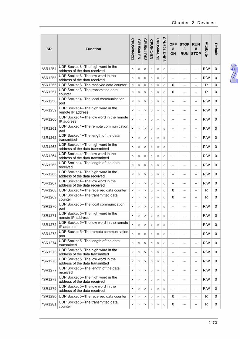
Chapter 2 Devices
2-73
SR Function
CPU
5×0-RS2
CPU
5×0-EN
CPU
5×1-RS2
CPU
5×1-EN
CPU
560-EN2
CPU
521-DN
P3
OFF
ON
STOP
RUN
RUN
STOP
Attribute
Default
*SR1254 UDP Socket 3─The high word in the address of the data received × ○ × ○ ○ ○ – – – R/W 0
*SR1255 UDP Socket 3─The low word in the address of the data received × ○ × ○ ○ ○ – – – R/W 0
*SR1256 UDP Socket 3─The received data counter × ○ × ○ ○ ○ 0 – – R 0
*SR1257 UDP Socket 3─The transmitted data counter × ○ × ○ ○ ○ 0 – – R 0
*SR1258 UDP Socket 4─The local communication port × ○ × ○ ○ ○ – – – R/W 0
*SR1259 UDP Socket 4─The high word in the remote IP address × ○ × ○ ○ ○ – – – R/W 0
*SR1260 UDP Socket 4─The low word in the remote IP address × ○ × ○ ○ ○ – – – R/W 0
*SR1261 UDP Socket 4─The remote communication port × ○ × ○ ○ ○ – – – R/W 0
*SR1262 UDP Socket 4─The length of the data transmitted × ○ × ○ ○ ○ – – – R/W 0
*SR1263 UDP Socket 4─The high word in the address of the data transmitted × ○ × ○ ○ ○ – – – R/W 0
*SR1264 UDP Socket 4─The low word in the address of the data transmitted × ○ × ○ ○ ○ – – – R/W 0
*SR1265 UDP Socket 4─The length of the data received × ○ × ○ ○ ○ – – – R/W 0
*SR1266 UDP Socket 4─The high word in the address of the data received × ○ × ○ ○ ○ – – – R/W 0
*SR1267 UDP Socket 4─The low word in the address of the data received × ○ × ○ ○ ○ – – – R/W 0
*SR1268 UDP Socket 4─The received data counter × ○ × ○ ○ ○ 0 – – R 0
*SR1269 UDP Socket 4─The transmitted data counter × ○ × ○ ○ ○ 0 – – R 0
*SR1270 UDP Socket 5─The local communication port × ○ × ○ ○ ○ – – – R/W 0
*SR1271 UDP Socket 5─The high word in the remote IP address × ○ × ○ ○ ○ – – – R/W 0
*SR1272 UDP Socket 5─The low word in the remote IP address × ○ × ○ ○ ○ – – – R/W 0
*SR1273 UDP Socket 5─The remote communication port × ○ × ○ ○ ○ – – – R/W 0
*SR1274 UDP Socket 5─The length of the data transmitted × ○ × ○ ○ ○ – – – R/W 0
*SR1275 UDP Socket 5─The high word in the address of the data transmitted × ○ × ○ ○ ○ – – – R/W 0
*SR1276 UDP Socket 5─The low word in the address of the data transmitted × ○ × ○ ○ ○ – – – R/W 0
*SR1277 UDP Socket 5─The length of the data received × ○ × ○ ○ ○ – – – R/W 0
*SR1278 UDP Socket 5─The high word in the address of the data received × ○ × ○ ○ ○ – – – R/W 0
*SR1279 UDP Socket 5─The low word in the address of the data received × ○ × ○ ○ ○ – – – R/W 0
*SR1280 UDP Socket 5─The received data counter × ○ × ○ ○ ○ 0 – – R 0
*SR1281 UDP Socket 5─The transmitted data counter × ○ × ○ ○ ○ 0 – – R 0

AH500 Programming Manual
2-74
SR Function
CPU
5×0-RS2
CPU
5×0-EN
CPU
5×1-RS2
CPU
5×1-EN
CPU
560-EN2
CPU
521-DN
P3
OFF
ON
STOP
RUN
RUN
STOP A
ttribute
Default
*SR1282 UDP Socket 6─The local communication port × ○ × ○ ○ ○ – – – R/W 0
*SR1283 UDP Socket 6─The high word in the remote IP address × ○ × ○ ○ ○ – – – R/W 0
*SR1284 UDP Socket 6─The low word in the remote IP address × ○ × ○ ○ ○ – – – R/W 0
*SR1285 UDP Socket 6─The remote communication port × ○ × ○ ○ ○ – – – R/W 0
*SR1286 UDP Socket 6─The length of the data transmitted × ○ × ○ ○ ○ – – – R/W 0
*SR1287 UDP Socket 6─The high word in the address of the data transmitted × ○ × ○ ○ ○ – – – R/W 0
*SR1288 UDP Socket 6─The low word in the address of the data transmitted × ○ × ○ ○ ○ – – – R/W 0
*SR1289 UDP Socket 6─The length of the data received × ○ × ○ ○ ○ – – – R/W 0
*SR1290 UDP Socket 6─The high word in the address of the data received × ○ × ○ ○ ○ – – – R/W 0
*SR1291 UDP Socket 6─The low word in the address of the data received × ○ × ○ ○ ○ – – – R/W 0
*SR1292 UDP Socket 6─The received data counter × ○ × ○ ○ ○ 0 – – R 0
*SR1293 UDP Socket 6─The transmitted data counter × ○ × ○ ○ ○ 0 – – R 0
*SR1294 UDP Socket 7─The local communication port × ○ × ○ ○ ○ – – – R/W 0
*SR1295 UDP Socket 7─The high word in the remote IP address × ○ × ○ ○ ○ – – – R/W 0
*SR1296 UDP Socket 7─The low word in the remote IP address × ○ × ○ ○ ○ – – – R/W 0
*SR1297 UDP Socket 7─The remote communication port × ○ × ○ ○ ○ – – – R/W 0
*SR1298 UDP Socket 7─The length of the data transmitted × ○ × ○ ○ ○ – – – R/W 0
*SR1299 UDP Socket 7─The high word in the address of the data transmitted × ○ × ○ ○ ○ – – – R/W 0
*SR1300 UDP Socket 7─The low word in the address of the data transmitted × ○ × ○ ○ ○ – – – R/W 0
*SR1301 UDP Socket 7─The length of the data received × ○ × ○ ○ ○ – – – R/W 0
*SR1302 UDP Socket 7─The high word in the address of the data received × ○ × ○ ○ ○ – – – R/W 0
*SR1303 UDP Socket 7─The low word in the address of the data received × ○ × ○ ○ ○ – – – R/W 0
*SR1304 UDP Socket 7─The received data counter × ○ × ○ ○ ○ 0 – – R 0
*SR1305 UDP Socket 7─The transmitted data counter × ○ × ○ ○ ○ 0 – – R 0
*SR1306 UDP Socket 8─The local communication port × ○ × ○ ○ ○ – – – R/W 0
*SR1307 UDP Socket 8─The high word in the remote IP address × ○ × ○ ○ ○ – – – R/W 0
*SR1308 UDP Socket 8─The low word in the remote IP address × ○ × ○ ○ ○ – – – R/W 0
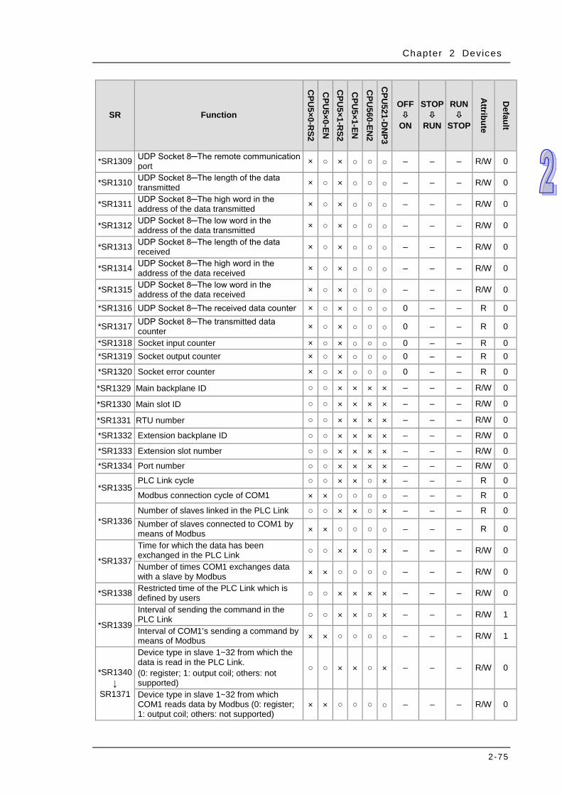
Chapter 2 Devices
2-75
SR Function
CPU
5×0-RS2
CPU
5×0-EN
CPU
5×1-RS2
CPU
5×1-EN
CPU
560-EN2
CPU
521-DN
P3
OFF
ON
STOP
RUN
RUN
STOP
Attribute
Default
*SR1309 UDP Socket 8─The remote communication port × ○ × ○ ○ ○ – – – R/W 0
*SR1310 UDP Socket 8─The length of the data transmitted × ○ × ○ ○ ○ – – – R/W 0
*SR1311 UDP Socket 8─The high word in the address of the data transmitted × ○ × ○ ○ ○ – – – R/W 0
*SR1312 UDP Socket 8─The low word in the address of the data transmitted × ○ × ○ ○ ○ – – – R/W 0
*SR1313 UDP Socket 8─The length of the data received × ○ × ○ ○ ○ – – – R/W 0
*SR1314 UDP Socket 8─The high word in the address of the data received × ○ × ○ ○ ○ – – – R/W 0
*SR1315 UDP Socket 8─The low word in the address of the data received × ○ × ○ ○ ○ – – – R/W 0
*SR1316 UDP Socket 8─The received data counter × ○ × ○ ○ ○ 0 – – R 0
*SR1317 UDP Socket 8─The transmitted data counter × ○ × ○ ○ ○ 0 – – R 0
*SR1318 Socket input counter × ○ × ○ ○ ○ 0 – – R 0 *SR1319 Socket output counter × ○ × ○ ○ ○ 0 – – R 0
*SR1320 Socket error counter × ○ × ○ ○ ○ 0 – – R 0
*SR1329 Main backplane ID ○ ○ × × × × – – – R/W 0
*SR1330 Main slot ID ○ ○ × × × × – – – R/W 0
*SR1331 RTU number ○ ○ × × × × – – – R/W 0
*SR1332 Extension backplane ID ○ ○ × × × × – – – R/W 0
*SR1333 Extension slot number ○ ○ × × × × – – – R/W 0
*SR1334 Port number ○ ○ × × × × – – – R/W 0
*SR1335 PLC Link cycle ○ ○ × × ○ × – – – R 0
Modbus connection cycle of COM1 × × ○ ○ ○ ○ – – – R 0
*SR1336 Number of slaves linked in the PLC Link ○ ○ × × ○ × – – – R 0 Number of slaves connected to COM1 by means of Modbus × × ○ ○ ○ ○ – – – R 0
*SR1337
Time for which the data has been exchanged in the PLC Link ○ ○ × × ○ × – – – R/W 0
Number of times COM1 exchanges data with a slave by Modbus × × ○ ○ ○ ○ – – – R/W 0
*SR1338 Restricted time of the PLC Link which is defined by users ○ ○ × × × × – – – R/W 0
*SR1339
Interval of sending the command in the PLC Link ○ ○ × × ○ × – – – R/W 1
Interval of COM1’s sending a command by means of Modbus × × ○ ○ ○ ○ – – – R/W 1
*SR1340 ↓
SR1371
Device type in slave 1~32 from which the data is read in the PLC Link. (0: register; 1: output coil; others: not supported)
○ ○ × × ○ × – – – R/W 0
Device type in slave 1~32 from which COM1 reads data by Modbus (0: register; 1: output coil; others: not supported)
× × ○ ○ ○ ○ – – – R/W 0
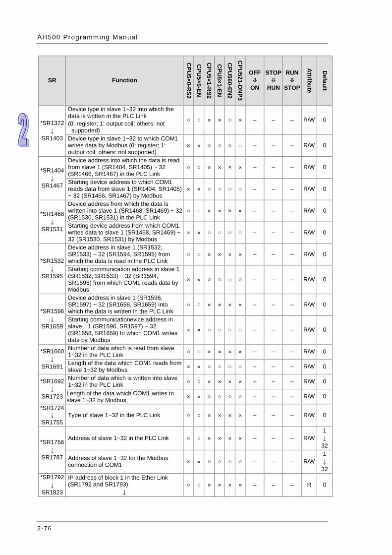
AH500 Programming Manual
2-76
SR Function
CPU
5×0-RS2
CPU
5×0-EN
CPU
5×1-RS2
CPU
5×1-EN
CPU
560-EN2
CPU
521-DN
P3
OFF
ON
STOP
RUN
RUN
STOP A
ttribute
Default
*SR1372 ↓
SR1403
Device type in slave 1~32 into which the data is written in the PLC Link (0: register; 1: output coil; others: not
supported)
○ ○ × × ○ × – – – R/W 0
Device type in slave 1~32 to which COM1 writes data by Modbus (0: register; 1: output coil; others: not supported)
× × ○ ○ ○ ○ – – – R/W 0
*SR1404 ↓
SR1467
Device address into which the data is read from slave 1 (SR1404, SR1405) ~ 32 (SR1466, SR1467) in the PLC Link
○ ○ × × × × – – – R/W 0
Starting device address to which COM1 reads data from slave 1 (SR1404, SR1405) ~ 32 (SR1466, SR1467) by Modbus
× × ○ ○ ○ ○ – – – R/W 0
*SR1468 ↓
SR1531
Device address from which the data is written into slave 1 (SR1468, SR1469) ~ 32 (SR1530, SR1531) in the PLC Link
○ ○ × × × × – – – R/W 0
Starting device address from which COM1 writes data to slave 1 (SR1468, SR1469) ~ 32 (SR1530, SR1531) by Modbus
× × ○ ○ ○ ○ – – – R/W 0
*SR1532 ↓
SR1595
Device address in slave 1 (SR1532, SR1533) ~ 32 (SR1594, SR1595) from which the data is read in the PLC Link
○ ○ × × × × – – – R/W 0
Starting communication address in slave 1 (SR1532, SR1533) ~ 32 (SR1594, SR1595) from which COM1 reads data by Modbus
× × ○ ○ ○ ○ – – – R/W 0
*SR1596 ↓
SR1659
Device address in slave 1 (SR1596, SR1597) ~ 32 (SR1658, SR1659) into which the data is written in the PLC Link
○ ○ × × × × – – – R/W 0
Starting communicationevice address in slave 1 (SR1596, SR1597) ~ 32 (SR1658, SR1659) to which COM1 writes data by Modbus
× × ○ ○ ○ ○ – – – R/W 0
*SR1660 ↓
SR1691
Number of data which is read from slave 1~32 in the PLC Link ○ ○ × × × × – – – R/W 0
Length of the data which COM1 reads from slave 1~32 by Modbus × × ○ ○ ○ ○ – – – R/W 0
*SR1692 ↓
SR1723
Number of data which is written into slave 1~32 in the PLC Link ○ ○ × × × × – – – R/W 0
Length of the data which COM1 writes to slave 1~32 by Modbus × × ○ ○ ○ ○ – – – R/W 0
*SR1724↓
SR1755 Type of slave 1~32 in the PLC Link ○ ○ × × × × – – – R/W 0
*SR1756 ↓
SR1787
Address of slave 1~32 in the PLC Link ○ ○ × × × × – – – R/W 1 ↓
32
Address of slave 1~32 for the Modbus connection of COM1 × × ○ ○ ○ ○ – – – R/W
1 ↓
32 *SR1792
↓ SR1823
IP address of block 1 in the Ether Link (SR1792 and SR1793)
↓ ○ ○ × × × × – – – R 0
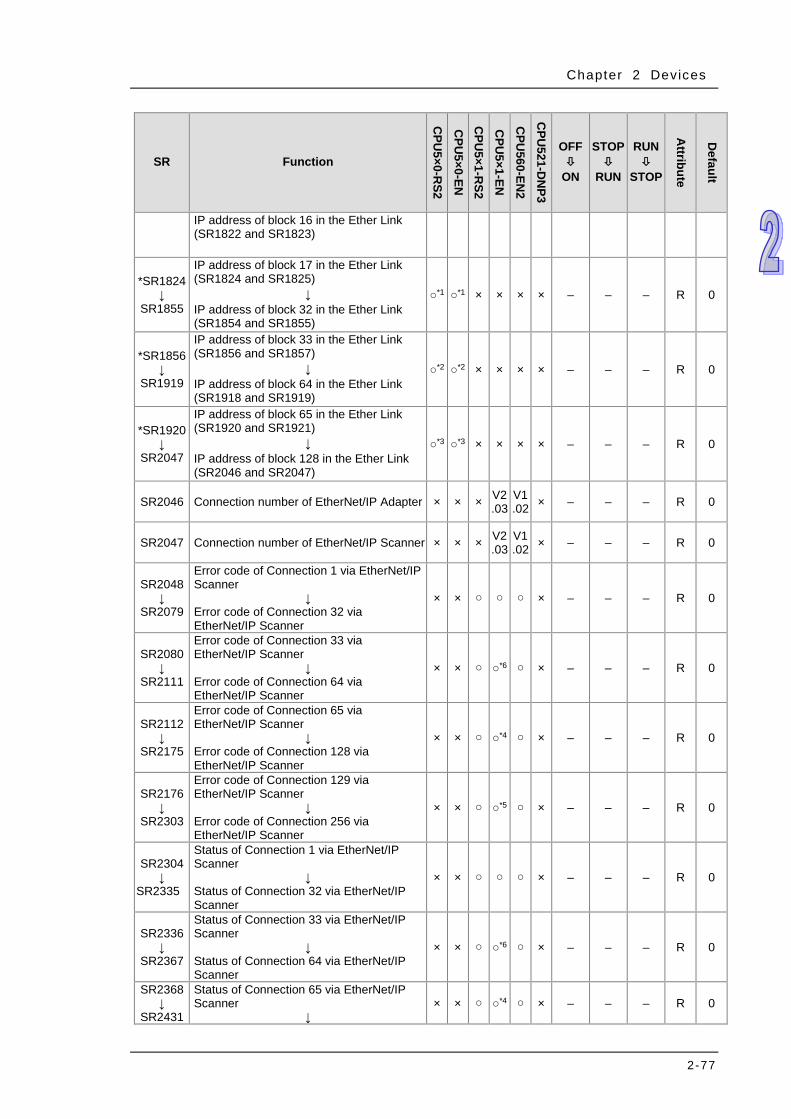
Chapter 2 Devices
2-77
SR Function
CPU
5×0-RS2
CPU
5×0-EN
CPU
5×1-RS2
CPU
5×1-EN
CPU
560-EN2
CPU
521-DN
P3
OFF
ON
STOP
RUN
RUN
STOP
Attribute
Default
IP address of block 16 in the Ether Link (SR1822 and SR1823)
*SR1824 ↓
SR1855
IP address of block 17 in the Ether Link (SR1824 and SR1825)
↓ IP address of block 32 in the Ether Link (SR1854 and SR1855)
○*1 ○*1 × × × × – – – R 0
*SR1856 ↓
SR1919
IP address of block 33 in the Ether Link (SR1856 and SR1857)
↓ IP address of block 64 in the Ether Link (SR1918 and SR1919)
○*2 ○*2 × × × × – – – R 0
*SR1920 ↓
SR2047
IP address of block 65 in the Ether Link (SR1920 and SR1921)
↓ IP address of block 128 in the Ether Link (SR2046 and SR2047)
○*3 ○*3 × × × × – – – R 0
SR2046 Connection number of EtherNet/IP Adapter × × × V2.03
V1.02 × – – – R 0
SR2047 Connection number of EtherNet/IP Scanner × × × V2.03
V1.02 × – – – R 0
SR2048 ↓
SR2079
Error code of Connection 1 via EtherNet/IP Scanner
↓ Error code of Connection 32 via EtherNet/IP Scanner
× × ○ ○ ○ × – – – R 0
SR2080 ↓
SR2111
Error code of Connection 33 via EtherNet/IP Scanner
↓ Error code of Connection 64 via EtherNet/IP Scanner
× × ○ ○*6 ○ × – – – R 0
SR2112 ↓
SR2175
Error code of Connection 65 via EtherNet/IP Scanner
↓ Error code of Connection 128 via EtherNet/IP Scanner
× × ○ ○*4 ○ × – – – R 0
SR2176 ↓
SR2303
Error code of Connection 129 via EtherNet/IP Scanner
↓ Error code of Connection 256 via EtherNet/IP Scanner
× × ○ ○*5 ○ × – – – R 0
SR2304 ↓
SR2335
Status of Connection 1 via EtherNet/IP Scanner
↓ Status of Connection 32 via EtherNet/IP Scanner
× × ○ ○ ○ × – – – R 0
SR2336 ↓
SR2367
Status of Connection 33 via EtherNet/IP Scanner
↓ Status of Connection 64 via EtherNet/IP Scanner
× × ○ ○*6 ○ × – – – R 0
SR2368 ↓
SR2431
Status of Connection 65 via EtherNet/IP Scanner
↓ × × ○ ○*4 ○ × – – – R 0
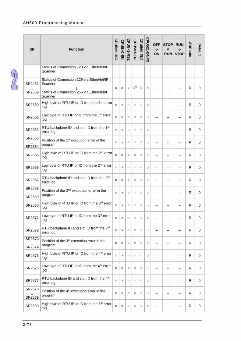
AH500 Programming Manual
2-78
SR Function
CPU
5×0-RS2
CPU
5×0-EN
CPU
5×1-RS2
CPU
5×1-EN
CPU
560-EN2
CPU
521-DN
P3
OFF
ON
STOP
RUN
RUN
STOP A
ttribute
Default
Status of Connection 128 via EtherNet/IP Scanner
SR2432 ↓
SR2559
Status of Connection 129 via EtherNet/IP Scanner
↓ Status of Connection 256 via EtherNet/IP Scanner
× × ○ ○*5 ○ × – – – R 0
SR2560 High byte of RTU IP or ID from the 1st error log × × ○ ○ ○ ○ – – – R 0
SR2561 Low byte of RTU IP or ID from the 1st error log × × ○ ○ ○ ○ – – – R 0
SR2562 RTU backplane ID and slot ID from the 1st error log × × ○ ○ ○ ○ – – – R 0
SR2563 ↓
SR2564
Position of the 1st execution error in the program × × ○ ○ ○ ○ – – – R 0
SR2565 High byte of RTU IP or ID from the 2nd error log × × ○ ○ ○ ○ – – – R 0
SR2566 Low byte of RTU IP or ID from the 2nd error log × × ○ ○ ○ ○ – – – R 0
SR2567 RTU backplane ID and slot ID from the 2nd error log × × ○ ○ ○ ○ – – – R 0
SR2568 ↓
SR2569
Position of the 2nd execution error in the program × × ○ ○ ○ ○ – – – R 0
SR2570 High byte of RTU IP or ID from the 3rd error log × × ○ ○ ○ ○ – – – R 0
SR2571 Low byte of RTU IP or ID from the 3rd error log × × ○ ○ ○ ○ – – – R 0
SR2572 RTU backplane ID and slot ID from the 3rd error log × × ○ ○ ○ ○ – – – R 0
SR2573 ↓
SR2574
Position of the 3rd execution error in the program × × ○ ○ ○ ○ – – – R 0
SR2575 High byte of RTU IP or ID from the 4th error log × × ○ ○ ○ ○ – – – R 0
SR2576 Low byte of RTU IP or ID from the 4th error log × × ○ ○ ○ ○ – – – R 0
SR2577 RTU backplane ID and slot ID from the 4th error log × × ○ ○ ○ ○ – – – R 0
SR2578 ↓
SR2579
Position of the 4th execution error in the program × × ○ ○ ○ ○ – – – R 0
SR2580 High byte of RTU IP or ID from the 5th error log × × ○ ○ ○ ○ – – – R 0
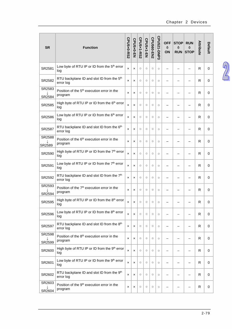
Chapter 2 Devices
2-79
SR Function
CPU
5×0-RS2
CPU
5×0-EN
CPU
5×1-RS2
CPU
5×1-EN
CPU
560-EN2
CPU
521-DN
P3
OFF
ON
STOP
RUN
RUN
STOP
Attribute
Default
SR2581 Low byte of RTU IP or ID from the 5th error log × × ○ ○ ○ ○ – – – R 0
SR2582 RTU backplane ID and slot ID from the 5th error log × × ○ ○ ○ ○ – – – R 0
SR2583 ↓
SR2584
Position of the 5th execution error in the program × × ○ ○ ○ ○ – – – R 0
SR2585 High byte of RTU IP or ID from the 6th error log × × ○ ○ ○ ○ – – – R 0
SR2586 Low byte of RTU IP or ID from the 6th error log × × ○ ○ ○ ○ – – – R 0
SR2587 RTU backplane ID and slot ID from the 6th error log × × ○ ○ ○ ○ – – – R 0
SR2588 ↓
SR2589
Position of the 6th execution error in the program × × ○ ○ ○ ○ – – – R 0
SR2590 High byte of RTU IP or ID from the 7th error log × × ○ ○ ○ ○ – – – R 0
SR2591 Low byte of RTU IP or ID from the 7th error log × × ○ ○ ○ ○ – – – R 0
SR2592 RTU backplane ID and slot ID from the 7th error log × × ○ ○ ○ ○ – – – R 0
SR2593 ↓
SR2594
Position of the 7th execution error in the program × × ○ ○ ○ ○ – – – R 0
SR2595 High byte of RTU IP or ID from the 8th error log × × ○ ○ ○ ○ – – – R 0
SR2596 Low byte of RTU IP or ID from the 8th error log × × ○ ○ ○ ○ – – – R 0
SR2597 RTU backplane ID and slot ID from the 8th error log × × ○ ○ ○ ○ – – – R 0
SR2598 ↓
SR2599
Position of the 8th execution error in the program × × ○ ○ ○ ○ – – – R 0
SR2600 High byte of RTU IP or ID from the 9th error log × × ○ ○ ○ ○ – – – R 0
SR2601 Low byte of RTU IP or ID from the 9th error log × × ○ ○ ○ ○ – – – R 0
SR2602 RTU backplane ID and slot ID from the 9th error log × × ○ ○ ○ ○ – – – R 0
SR2603 ↓
SR2604
Position of the 9th execution error in the program × × ○ ○ ○ ○ – – – R 0

AH500 Programming Manual
2-80
SR Function
CPU
5×0-RS2
CPU
5×0-EN
CPU
5×1-RS2
CPU
5×1-EN
CPU
560-EN2
CPU
521-DN
P3
OFF
ON
STOP
RUN
RUN
STOP A
ttribute
Default
SR2605 High byte of RTU IP or ID from the 10th error log × × ○ ○ ○ ○ – – – R 0
SR2606 Low byte of RTU IP or ID from the 10th error log × × ○ ○ ○ ○ – – – R 0
SR2607 RTU backplane ID and slot ID from the 10th error log × × ○ ○ ○ ○ – – – R 0
SR2608 ↓
SR2609
Position of the 10th execution error in the program × × ○ ○ ○ ○ – – – R 0
SR2610 High byte of RTU IP or ID from the 11th error log × × ○ ○ ○ ○ – – – R 0
SR2611 Low byte of RTU IP or ID from the 11th error log × × ○ ○ ○ ○ – – – R 0
SR2612 RTU backplane ID and slot ID from the 11th error log × × ○ ○ ○ ○ – – – R 0
SR2613 ↓
SR2614
Position of the 11th execution error in the program × × ○ ○ ○ ○ – – – R 0
SR2615 High byte of RTU IP or ID from the 12th error log × × ○ ○ ○ ○ – – – R 0
SR2616 Low byte of RTU IP or ID from the 12th error log × × ○ ○ ○ ○ – – – R 0
SR2617 RTU backplane ID and slot ID from the 12th error log × × ○ ○ ○ ○ – – – R 0
SR2618 ↓
SR2619
Position of the 12th execution error in the program × × ○ ○ ○ ○ – – – R 0
SR2620 High byte of RTU IP or ID from the 13th error log × × ○ ○ ○ ○ – – – R 0
SR2621 Low byte of RTU IP or ID from the 13th error log × × ○ ○ ○ ○ – – – R 0
SR2622 RTU backplane ID and slot ID from the 13th error log × × ○ ○ ○ ○ – – – R 0
SR2623 ↓
SR2624
Position of the 13th execution error in the program × × ○ ○ ○ ○ – – – R 0
SR2625 High byte of RTU IP or ID from the 14th error log × × ○ ○ ○ ○ – – – R 0
SR2626 Low byte of RTU IP or ID from the 14th error log × × ○ ○ ○ ○ – – – R 0
SR2627 RTU backplane ID and slot ID from the 14th error log × × ○ ○ ○ ○ – – – R 0
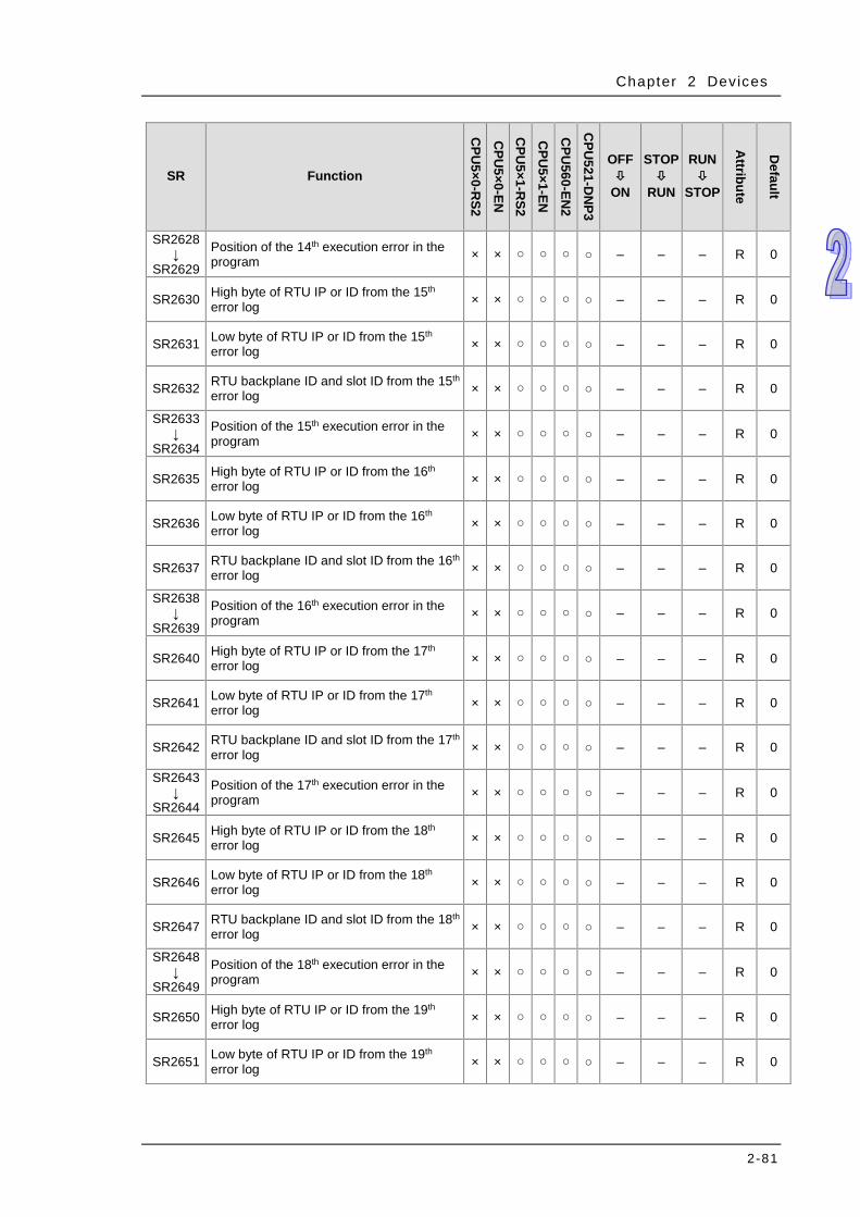
Chapter 2 Devices
2-81
SR Function
CPU
5×0-RS2
CPU
5×0-EN
CPU
5×1-RS2
CPU
5×1-EN
CPU
560-EN2
CPU
521-DN
P3
OFF
ON
STOP
RUN
RUN
STOP
Attribute
Default
SR2628 ↓
SR2629
Position of the 14th execution error in the program × × ○ ○ ○ ○ – – – R 0
SR2630 High byte of RTU IP or ID from the 15th error log × × ○ ○ ○ ○ – – – R 0
SR2631 Low byte of RTU IP or ID from the 15th error log × × ○ ○ ○ ○ – – – R 0
SR2632 RTU backplane ID and slot ID from the 15th error log × × ○ ○ ○ ○ – – – R 0
SR2633 ↓
SR2634
Position of the 15th execution error in the program × × ○ ○ ○ ○ – – – R 0
SR2635 High byte of RTU IP or ID from the 16th
error log × × ○ ○ ○ ○ – – – R 0
SR2636 Low byte of RTU IP or ID from the 16th error log × × ○ ○ ○ ○ – – – R 0
SR2637 RTU backplane ID and slot ID from the 16th error log × × ○ ○ ○ ○ – – – R 0
SR2638 ↓
SR2639
Position of the 16th execution error in the program × × ○ ○ ○ ○ – – – R 0
SR2640 High byte of RTU IP or ID from the 17th error log × × ○ ○ ○ ○ – – – R 0
SR2641 Low byte of RTU IP or ID from the 17th error log × × ○ ○ ○ ○ – – – R 0
SR2642 RTU backplane ID and slot ID from the 17th error log × × ○ ○ ○ ○ – – – R 0
SR2643 ↓
SR2644
Position of the 17th execution error in the program × × ○ ○ ○ ○ – – – R 0
SR2645 High byte of RTU IP or ID from the 18th error log × × ○ ○ ○ ○ – – – R 0
SR2646 Low byte of RTU IP or ID from the 18th error log × × ○ ○ ○ ○ – – – R 0
SR2647 RTU backplane ID and slot ID from the 18th error log × × ○ ○ ○ ○ – – – R 0
SR2648 ↓
SR2649
Position of the 18th execution error in the program × × ○ ○ ○ ○ – – – R 0
SR2650 High byte of RTU IP or ID from the 19th error log × × ○ ○ ○ ○ – – – R 0
SR2651 Low byte of RTU IP or ID from the 19th error log × × ○ ○ ○ ○ – – – R 0
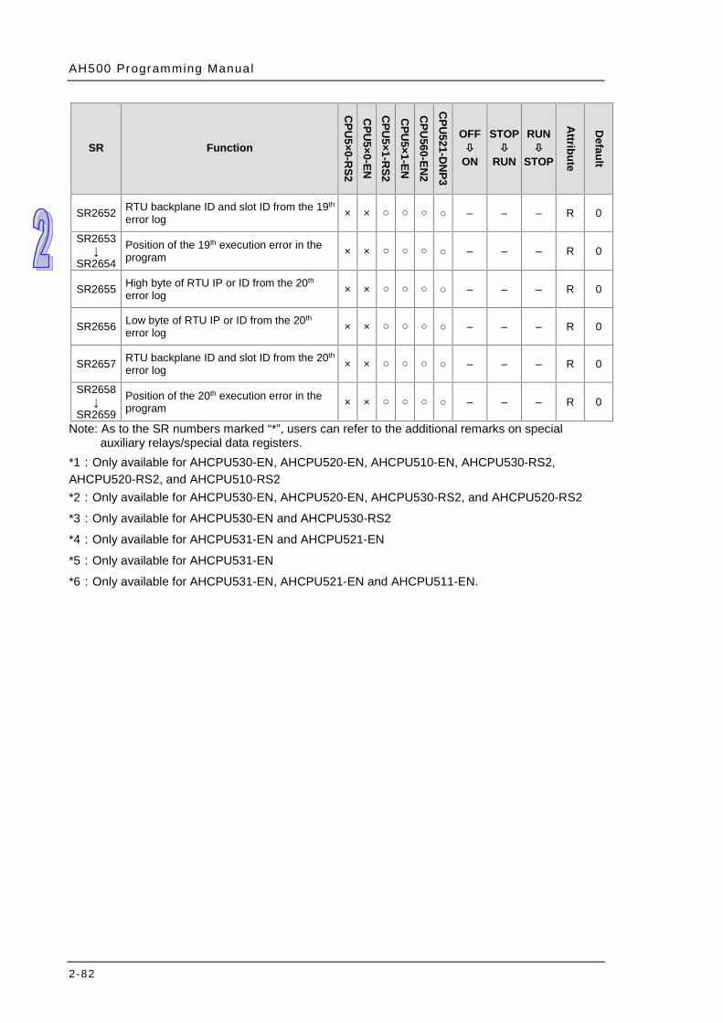
AH500 Programming Manual
2-82
SR Function
CPU
5×0-RS2
CPU
5×0-EN
CPU
5×1-RS2
CPU
5×1-EN
CPU
560-EN2
CPU
521-DN
P3
OFF
ON
STOP
RUN
RUN
STOP A
ttribute
Default
SR2652 RTU backplane ID and slot ID from the 19th error log × × ○ ○ ○ ○ – – – R 0
SR2653 ↓
SR2654
Position of the 19th execution error in the program × × ○ ○ ○ ○ – – – R 0
SR2655 High byte of RTU IP or ID from the 20th error log × × ○ ○ ○ ○ – – – R 0
SR2656 Low byte of RTU IP or ID from the 20th error log × × ○ ○ ○ ○ – – – R 0
SR2657 RTU backplane ID and slot ID from the 20th error log × × ○ ○ ○ ○ – – – R 0
SR2658 ↓
SR2659
Position of the 20th execution error in the program × × ○ ○ ○ ○ – – – R 0
Note: As to the SR numbers marked “*”, users can refer to the additional remarks on special auxiliary relays/special data registers.
*1:Only available for AHCPU530-EN, AHCPU520-EN, AHCPU510-EN, AHCPU530-RS2, AHCPU520-RS2, and AHCPU510-RS2 *2:Only available for AHCPU530-EN, AHCPU520-EN, AHCPU530-RS2, and AHCPU520-RS2
*3:Only available for AHCPU530-EN and AHCPU530-RS2
*4:Only available for AHCPU531-EN and AHCPU521-EN
*5:Only available for AHCPU531-EN
*6:Only available for AHCPU531-EN, AHCPU521-EN and AHCPU511-EN.
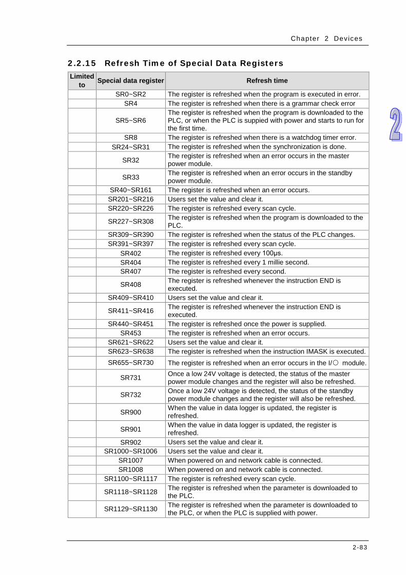
Chapter 2 Devices
2-83
2.2.15 Refresh Time of Special Data Registers Limited
to Special data register Refresh time
SR0~SR2 The register is refreshed when the program is executed in error. SR4 The register is refreshed when there is a grammar check error
SR5~SR6 The register is refreshed when the program is downloaded to the PLC, or when the PLC is suppied with power and starts to run for the first time.
SR8 The register is refreshed when there is a watchdog timer error. SR24~SR31 The register is refreshed when the synchronization is done. SR32 The register is refreshed when an error occurs in the master
power module. SR33 The register is refreshed when an error occurs in the standby
power module. SR40~SR161 The register is refreshed when an error occurs. SR201~SR216 Users set the value and clear it. SR220~SR226 The register is refreshed every scan cycle. SR227~SR308 The register is refreshed when the program is downloaded to the
PLC. SR309~SR390 The register is refreshed when the status of the PLC changes. SR391~SR397 The register is refreshed every scan cycle. SR402 The register is refreshed every 100μs. SR404 The register is refreshed every 1 millie second. SR407 The register is refreshed every second. SR408 The register is refreshed whenever the instruction END is
executed. SR409~SR410 Users set the value and clear it. SR411~SR416 The register is refreshed whenever the instruction END is
executed. SR440~SR451 The register is refreshed once the power is supplied. SR453 The register is refreshed when an error occurs. SR621~SR622 Users set the value and clear it. SR623~SR638 The register is refreshed when the instruction IMASK is executed. SR655~SR730 The register is refreshed when an error occurs in the I/○ module. SR731 Once a low 24V voltage is detected, the status of the master
power module changes and the register will also be refreshed. SR732 Once a low 24V voltage is detected, the status of the standby
power module changes and the register will also be refreshed. SR900 When the value in data logger is updated, the register is
refreshed. SR901 When the value in data logger is updated, the register is
refreshed. SR902 Users set the value and clear it. SR1000~SR1006 Users set the value and clear it. SR1007 When powered on and network cable is connected. SR1008 When powered on and network cable is connected. SR1100~SR1117 The register is refreshed every scan cycle. SR1118~SR1128 The register is refreshed when the parameter is downloaded to
the PLC. SR1129~SR1130 The register is refreshed when the parameter is downloaded to
the PLC, or when the PLC is supplied with power.

AH500 Programming Manual
2-84
Limited to Special data register Refresh time
SR1131~SR1141 The register is refreshed when the parameter is downloaded to the PLC.
SR1142~SR1143 The register is refreshed when the parameter is downloaded to the PLC, or when the PLC is supplied with power.
SR1144~SR1154 The register is refreshed when the parameter is downloaded to the PLC.
SR1155~SR1156 The register is refreshed when the parameter is downloaded to the PLC, or when the PLC is supplied with power.
SR1157~SR1167 The register is refreshed when the parameter is downloaded to the PLC.
SR1168~SR1169 The register is refreshed when the parameter is downloaded to the PLC, or when the PLC is supplied with power.
SR1170~SR1180 The register is refreshed when the parameter is downloaded to the PLC.
SR1181~SR1182 The register is refreshed when the parameter is downloaded to the PLC, or when the PLC is supplied with power.
SR1183~SR1193 The register is refreshed when the parameter is downloaded to the PLC.
SR1194~SR1195 The register is refreshed when the parameter is downloaded to the PLC, or when the PLC is supplied with power.
SR1196~SR1206 The register is refreshed when the parameter is downloaded to the PLC.
SR1207~SR1208 The register is refreshed when the parameter is downloaded to the PLC, or when the PLC is supplied with power.
SR1209~SR1219 The register is refreshed when the parameter is downloaded to the PLC.
SR1220~SR1221 The register is refreshed when the parameter is downloaded to the PLC, or when the PLC is supplied with power.
SR1222~SR1231 The register is refreshed when the parameter is downloaded to the PLC.
SR1232~SR1233 The register is refreshed when the parameter is downloaded to the PLC, or when the PLC is supplied with power.
SR1234~SR1243 The register is refreshed when the parameter is downloaded to the PLC.
SR1244~SR1245 The register is refreshed when the parameter is downloaded to the PLC, or when the PLC is supplied with power.
SR1246~SR1255 The register is refreshed when the parameter is downloaded to the PLC.
SR1256~SR1257 The register is refreshed when the parameter is downloaded to the PLC, or when the PLC is supplied with power.
SR1258~SR1267 The register is refreshed when the parameter is downloaded to the PLC.
SR1268~SR1269 The register is refreshed when the parameter is downloaded to the PLC, or when the PLC is supplied with power.
SR1270~SR1279 The register is refreshed when the parameter is downloaded to the PLC.
SR1280~SR1281 The register is refreshed when the parameter is downloaded to the PLC, or when the PLC is supplied with power.
SR1282~SR1291 The register is refreshed when the parameter is downloaded to the PLC.
SR1292~SR1293 The register is refreshed when the parameter is downloaded to the PLC, or when the PLC is supplied with power.

Chapter 2 Devices
2-85
Limited to Special data register Refresh time
SR1294~SR1303 The register is refreshed when the parameter is downloaded to the PLC.
SR1304~SR1305 The register is refreshed when the parameter is downloaded to the PLC, or when the PLC is supplied with power.
SR1306~SR1315 The register is refreshed when the parameter is downloaded to the PLC.
SR1316~SR1320 The register is refreshed when the parameter is downloaded to the PLC, or when the PLC is supplied with power.
SR1329~SR1334 Users set the value and clear it.
AH5×0 SR1335~SR1336 The register is refreshed every scan cycle when the PLC Link is enabled.
AH5×1 Modbus connection cycle of COM1 SR1337~SR1787 Users set the value and clear it. SR1792~SR2559 The register is refreshed every scan cycle. SR2560~SR2659 The register is refreshed whenever an error occurs.
Note: The models AH5×0 and AH5×1 shown in the column of “Limited to” refer to AHCPU500/510/520/530 and AHCPU501/511/521/531 respectively.
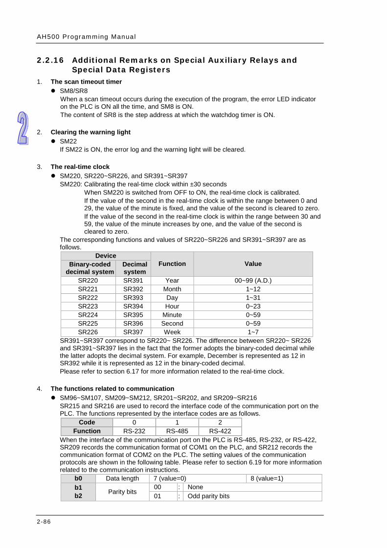
AH500 Programming Manual
2-86
2.2.16 Additional Remarks on Special Auxiliary Relays and Special Data Registers
1. The scan timeout timer SM8/SR8
When a scan timeout occurs during the execution of the program, the error LED indicator on the PLC is ON all the time, and SM8 is ON. The content of SR8 is the step address at which the watchdog timer is ON.
2. Clearing the warning light SM22
If SM22 is ON, the error log and the warning light will be cleared.
3. The real-time clock SM220, SR220~SR226, and SR391~SR397
SM220: Calibrating the real-time clock within ±30 seconds When SM220 is switched from OFF to ON, the real-time clock is calibrated. If the value of the second in the real-time clock is within the range between 0 and 29, the value of the minute is fixed, and the value of the second is cleared to zero. If the value of the second in the real-time clock is within the range between 30 and 59, the value of the minute increases by one, and the value of the second is cleared to zero.
The corresponding functions and values of SR220~SR226 and SR391~SR397 are as follows.
Device Function Value Binary-coded
decimal system Decimal system
SR220 SR391 Year 00~99 (A.D.) SR221 SR392 Month 1~12 SR222 SR393 Day 1~31 SR223 SR394 Hour 0~23 SR224 SR395 Minute 0~59 SR225 SR396 Second 0~59 SR226 SR397 Week 1~7
SR391~SR397 correspond to SR220~ SR226. The difference between SR220~ SR226 and SR391~SR397 lies in the fact that the former adopts the binary-coded decimal while the latter adopts the decimal system. For example, December is represented as 12 in SR392 while it is represented as 12 in the binary-coded decimal. Please refer to section 6.17 for more information related to the real-time clock.
4. The functions related to communication SM96~SM107, SM209~SM212, SR201~SR202, and SR209~SR216
SR215 and SR216 are used to record the interface code of the communication port on the PLC. The functions represented by the interface codes are as follows.
Code 0 1 2 Function RS-232 RS-485 RS-422
When the interface of the communication port on the PLC is RS-485, RS-232, or RS-422, SR209 records the communication format of COM1 on the PLC, and SR212 records the communication format of COM2 on the PLC. The setting values of the communication protocols are shown in the following table. Please refer to section 6.19 for more information related to the communication instructions.
b0 Data length 7 (value=0) 8 (value=1) b1 b2 Parity bits
00 : None 01 : Odd parity bits
Chapter 2 Devices
2-87
10 : Even parity bits b3 Stop bit 1 bit (value=0) 2 bits (value=1) b4 b5 b6 b7
0001 (16#1) : 4800 0010 (16#2) : 9600 0011 (16#3) : 19200 0100 (16#4) : 38400 0101 (16#5) : 57600 0110 (16#6) : 115200
0111 (16#7) : 230400 RS-232 does not support the baud rate.
1000 (16#8) : 460800 RS-232 does not support the baud rate.
1001 (16#9) : 921600 RS-232 does not support the baud rate.
b8~b15 Undefined (reserved)
5. Clearing the contents of the device SM204/SM205
Device number Device which is cleared
SM204 All non-latched areas are
cleared.
The non-latched areas in the input relays, the output relays, the stepping relays, the auxiliary relays, and the link registers are cleared. The non-latched areas in the timers, the counters, and the 32-bit counters are cleared. The non-latched areas in the data registers and the index registers are cleared. It takes 530 milliseconds to clear the device. The watchdog timer does not act during this period of time.
SM205 All latched areas are
cleared.
The latched areas in the timers, counters, and 32-bit counters are cleared. The latched auxiliary relays are cleared. The latched data registers are cleared. It takes 30 milliseconds to clear the device. The watchdog timer does not act during this period of time.
Please refer to section 2.1.4 for more information related to the latched areas in the device range.
6. The error log in the PLC SR40~SR161
SR40: The maximum number of error logs which are stored in SR40 is 20. Every error log occupies 6 registers.
SR41: The error log pointer points to the latest error log. When an error occurs, the value of the error log pointer increases by one. The range of pointer values is 0~19. For example, the error log pointer points to the fourth error log when the value in SR41 is 3.
The time when the errors occur and the positions where the errors occur are recorded in SR42~SR161. The corresponding functions of these data registers are as follows.
Number Rack Slot Module ID
Error code
Time when the error occurs Year Month Day Hour Minute Second
1 SR42 High byte
SR42 Low byte SR43 SR44 SR45
High byte SR45
Low byte SR46
High byte SR46
Low byte SR47
High byte SR47
Low byte
2 SR48 High byte
SR48 Low byte SR49 SR50 SR51
High byte SR51
Low byte SR52
High byte SR52
Low byte SR53
High byte SR53
Low byte
AH500 Programming Manual
2-88
Number Rack Slot Module ID
Error code
Time when the error occurs Year Month Day Hour Minute Second
3 SR54 High byte
SR54 Low byte SR55 SR56 SR57
High byte SR57
Low byte SR58
High byte SR58
Low byte SR59
High byte SR59
Low byte
4 SR60 High byte
SR60 Low byte SR61 SR62 SR63
High byte SR63
Low byte SR64
High byte SR64
Low byte SR65
High byte SR65
Low byte
5 SR66 High byte
SR66 Low byte SR67 SR68 SR69
High byte SR69
Low byte SR70
High byte SR70
Low byte SR71
High byte SR71
Low byte
6 SR72 High byte
SR72 Low byte SR73 SR74 SR75
High byte SR75
Low byte SR76
High byte SR76
Low byte SR77
High byte SR77
Low byte
7 SR78 High byte
SR78 Low byte SR79 SR80 SR81
High byte SR81
Low byte SR82
High byte SR82
Low byte SR83
High byte SR83
Low byte
8 SR84 High byte
SR84 Low byte SR85 SR86 SR87
High byte SR87
Low byte SR88
High byte SR88
Low byte SR89
High byte SR89
Low byte
9 SR90 High byte
SR90 Low byte SR91 SR92 SR93
High byte SR93
Low byte SR94
High byte SR94
Low byte SR95
High byte SR95
Low byte
10 SR96 High byte
SR96 Low byte SR97 SR98 SR99
High byte SR99
Low byte SR100
High byte SR100 Low byte
SR101 High byte
SR101 Low byte
11 SR102 High byte
SR102 Low byte SR103 SR104 SR105
High byte SR105
Low byte SR106
High byte SR106 Low byte
SR107 High byte
SR107 Low byte
12 SR108 High byte
SR108 Low byte SR109 SR110 SR111
High byte SR111
Low byte SR112
High byte SR112 Low byte
SR113 High byte
SR113 Low byte
13 SR114 High byte
SR114 Low byte SR115 SR116 SR117
High byte SR117
Low byte SR118
High byte SR118 Low byte
SR119 High byte
SR119 Low byte
14 SR120 High byte
SR120 Low byte SR121 SR122 SR123
High byte SR123
Low byte SR124
High byte SR124 Low byte
SR125 High byte
SR125 Low byte
15 SR126 High byte
SR126 Low byte SR127 SR128 SR129
High byte SR129
Low byte SR130
High byte SR130 Low byte
SR131 High byte
SR131 Low byte
16 SR132 High byte
SR132 Low byte SR133 SR134 SR135
High byte SR135
Low byte SR136
High byte SR136 Low byte
SR137 High byte
SR137 Low byte
17 SR138 High byte
SR138 Low byte SR139 SR140 SR141
High byte SR141
Low byte SR142
High byte SR142 Low byte
SR143 High byte
SR143 Low byte
18 SR144 High byte
SR144 Low byte SR145 SR146 SR147
High byte SR147
Low byte SR148
High byte SR148 Low byte
SR149 High byte
SR149 Low byte
19 SR150 High byte
SR150 Low byte SR151 SR152 SR153
High byte SR153
Low byte SR154
High byte SR154 Low byte
SR155 High byte
SR155 Low byte
20 SR156 High byte
SR156 Low byte SR157 SR158 SR159
High byte SR159
Low byte SR160
High byte SR160 Low byte
SR161 High byte
SR161 Low byte
7. The download log in the PLC
SR227~SR308 SR227: The maximum number of download logs which are stored in SR227 is 20. Every
download log occupies 4 registers. The download actions which are recorded are numbered, as shown in the following table.
Download action Number Downloading the program 1 Downloading the setting of the PLC 2 Downloading the module table 3
SR228: The download log pointer points to the latest download log. When a download action is executed, the value of the download log pointer increases by one. The range of pointer values is 0~19. For example, the download log pointer points to the fourth download log when the value in SR228 is 3.
The time when the downloading actions occur and the action numbers are recorded in SR229~SR30. The corresponding functions of these data registers are as follows.
Number Action number
*Time when the download action occurs Year Month Day Hour Minute Second
1 SR229 SR230 High byte
SR230 Low byte
SR231 High byte
SR231 Low byte
SR232 High byte
SR232 Low byte
2 SR233 SR234 SR234 SR235 SR235 SR236 SR236

Chapter 2 Devices
2-89
Number Action number
*Time when the download action occurs Year Month Day Hour Minute Second
High byte Low byte High byte Low byte High byte Low byte
3 SR237 SR238 High byte
SR238 Low byte
SR239 High byte
SR239 Low byte
SR240 High byte
SR240 Low byte
4 SR241 SR242 High byte
SR242 Low byte
SR243 High byte
SR243 Low byte
SR244 High byte
SR244 Low byte
5 SR245 SR246 High byte
SR246 Low byte
SR247 High byte
SR247 Low byte
SR248 High byte
SR248 Low byte
6 SR249 SR250 High byte
SR250 Low byte
SR251 High byte
SR251 Low byte
SR252 High byte
SR252 Low byte
7 SR253 SR254 High byte
SR254 Low byte
SR255 High byte
SR255 Low byte
SR256 High byte
SR256 Low byte
8 SR257 SR258 High byte
SR258 Low byte
SR259 High byte
SR259 Low byte
SR260 High byte
SR260 Low byte
9 SR261 SR262 High byte
SR262 Low byte
SR263 High byte
SR263 Low byte
SR264 High byte
SR264 Low byte
10 SR265 SR266 High byte
SR266 Low byte
SR267 High byte
SR267 Low byte
SR268 High byte
SR268 Low byte
11 SR269 SR270 High byte
SR270 Low byte
SR271 High byte
SR271 Low byte
SR272 High byte
SR272 Low byte
12 SR273 SR274 High byte
SR274 Low byte
SR275 High byte
SR275 Low byte
SR276 High byte
SR276 Low byte
13 SR277 SR278 High byte
SR278 Low byte
SR279 High byte
SR279 Low byte
SR280 High byte
SR280 Low byte
14 SR281 SR282 High byte
SR282 Low byte
SR283 High byte
SR283 Low byte
SR284 High byte
SR284 Low byte
15 SR285 SR286 High byte
SR286 Low byte
SR287 High byte
SR287 Low byte
SR288 High byte
SR288 Low byte
16 SR289 SR290 High byte
SR290 Low byte
SR291 High byte
SR291 Low byte
SR292 High byte
SR292 Low byte
17 SR293 SR294 High byte
SR294 Low byte
SR295 High byte
SR295 Low byte
SR296 High byte
SR296 Low byte
18 SR297 SR298 High byte
SR298 Low byte
SR299 High byte
SR299 Low byte
SR300 High byte
SR300 Low byte
19 SR301 SR302 High byte
SR302 Low byte
SR303 High byte
SR303 Low byte
SR304 High byte
SR304 Low byte
20 SR305 SR306 High byte
SR306 Low byte
SR307 High byte
SR307 Low byte
SR308 High byte
SR308 Low byte
*Time when the download action occurs: The data is stored as the values in the binary-coded decimal. The range of values is as follows.
Function Value Year 00~99 (A.D.)
Month 01~12 Day 01~31 Hour 00~23
Minute 00~59 Second 00~59
8. The PLC status change log
SR309~SR390 SR309: The maximum number of PLC status change logs which are stored in SR309 is 20.
Every PLC status change log occupies 4 registers. The PLC status change actions which are recorded are numbered, as shown in the following table.

AH500 Programming Manual
2-90
PLC status change Number The PLC is supplied with power. 1 The PLC is disconnected. 2 The PLC starts to run. 3 The PLC stops running. 4 Default setting of the PLC (1. RST button; 2. Communication command) 5
Pressing the CLR button on the PLC (Clearing the data in the latched device) 6
SR310: The PLC status change log pointer points to the latest PLC status change log. When the PLC status is changed once, the value of the PLC status change log pointer increases by one. The range of pointer values is 0~19. For example, the PLC status change log pointer points to the fourth PLC status change log when the value in SR310 is 3.
The time when the PLC status change actions occur is recorded in SR311~SR390. The corresponding functions of these data registers are as follows.
Number Action number
*Time when the PLC status change action occurs Year Month Day Hour Minute Second
1 SR311 SR312 High byte
SR312 Low byte
SR313 High byte
SR313 Low byte
SR314 High byte
SR314 Low byte
2 SR315 SR316 High byte
SR316 Low byte
SR317 High byte
SR317 Low byte
SR318 High byte
SR318 Low byte
3 SR319 SR320 High byte
SR320 Low byte
SR321 High byte
SR321 Low byte
SR322 High byte
SR322 Low byte
4 SR323 SR324 High byte
SR324 Low byte
SR325 High byte
SR325 Low byte
SR326 High byte
SR326 Low byte
5 SR327 SR328 High byte
SR328 Low byte
SR329 High byte
SR329 Low byte
SR330 High byte
SR330 Low byte
6 SR331 SR332 High byte
SR332 Low byte
SR333 High byte
SR333 Low byte
SR334 High byte
SR334 Low byte
7 SR335 SR336 High byte
SR336 Low byte
SR337 High byte
SR337 Low byte
SR338 High byte
SR338 Low byte
8 SR339 SR340 High byte
SR340 Low byte
SR341 High byte
SR341 Low byte
SR342 High byte
SR342 Low byte
9 SR343 SR344 High byte
SR344 Low byte
SR345 High byte
SR345 Low byte
SR346 High byte
SR346 Low byte
10 SR347 SR348 High byte
SR348 Low byte
SR349 High byte
SR349 Low byte
SR350 High byte
SR350 Low byte
11 SR351 SR352 High byte
SR352 Low byte
SR353 High byte
SR353 Low byte
SR354 High byte
SR354 Low byte
12 SR355 SR356 High byte
SR356 Low byte
SR357 High byte
SR357 Low byte
SR358 High byte
SR358 Low byte
13 SR359 SR360 High byte
SR360 Low byte
SR361 High byte
SR361 Low byte
SR362 High byte
SR362 Low byte
14 SR363 SR364 High byte
SR364 Low byte
SR365 High byte
SR365 Low byte
SR366 High byte
SR366 Low byte
15 SR367 SR368 High byte
SR368 Low byte
SR369 High byte
SR369 Low byte
SR370 High byte
SR370 Low byte
16 SR371 SR372 High byte
SR372 Low byte
SR373 High byte
SR373 Low byte
SR374 High byte
SR374 Low byte
17 SR375 SR376 High byte
SR376 Low byte
SR377 High byte
SR377 Low byte
SR378 High byte
SR378 Low byte
18 SR379 SR380 High byte
SR380 Low byte
SR381 High byte
SR381 Low byte
SR382 High byte
SR382 Low byte
19 SR383 SR384 SR384 SR385 SR385 SR386 SR386

Chapter 2 Devices
2-91
Number Action number
*Time when the PLC status change action occurs Year Month Day Hour Minute Second
High byte Low byte High byte Low byte High byte Low byte
20 SR387 SR388 High byte
SR388 Low byte
SR389 High byte
SR389 Low byte
SR390 High byte
SR390 Low byte
*Time when the PLC status change action occurs: The data is stored as the values in the binary-coded decimal. The range of values is as follows.
Function Value Year 00~99 (A.D.)
Month 01~12 Day 01~31 Hour 00~23
Minute 00~59 Second 00~59
9. The PLC operation flag
SM400~SM403 SM400: The flag is always ON when CPU runs.
SM401: The flag is always OFF when CPU runs. SM402: The flag is ON only at the first scan. The pulse width equals one scan time. Users
can use this contact to do the initial setting. SM403: The flag is OFF only at the first scan. That is, the negative pulse is generated the
moment the PLC runs.
The PLC runs .
SM400
SM401
SM402
SM403
Scan ti me
10. The initial clock pulse SM404~SM410, and SR409~SR410
The PLC provides seven types of clock pulses. When the PLC is supplied with power, the seven types of clock pulses act automatically. Users can set the interval of the clock pulse in SM409 and SM410.
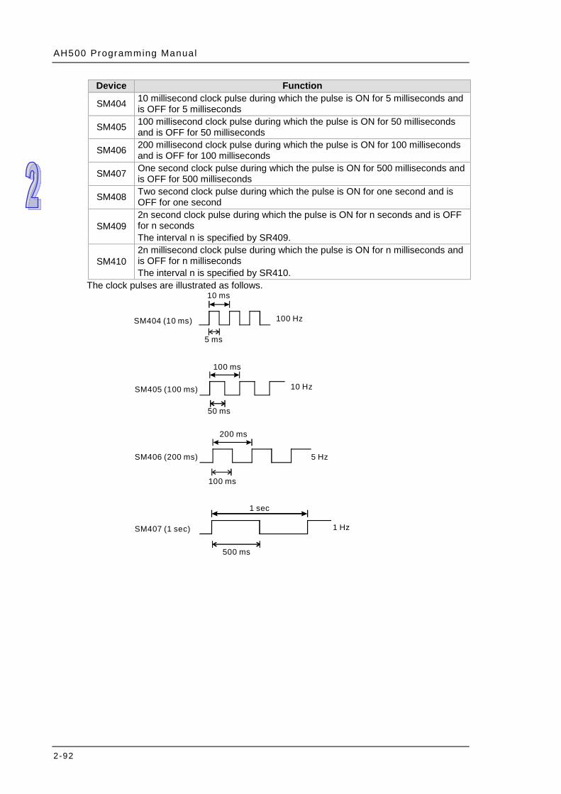
AH500 Programming Manual
2-92
Device Function
SM404 10 millisecond clock pulse during which the pulse is ON for 5 milliseconds and is OFF for 5 milliseconds
SM405 100 millisecond clock pulse during which the pulse is ON for 50 milliseconds and is OFF for 50 milliseconds
SM406 200 millisecond clock pulse during which the pulse is ON for 100 milliseconds and is OFF for 100 milliseconds
SM407 One second clock pulse during which the pulse is ON for 500 milliseconds and is OFF for 500 milliseconds
SM408 Two second clock pulse during which the pulse is ON for one second and is OFF for one second
SM409 2n second clock pulse during which the pulse is ON for n seconds and is OFF for n seconds The interval n is specified by SR409.
SM410 2n millisecond clock pulse during which the pulse is ON for n milliseconds and is OFF for n milliseconds The interval n is specified by SR410.
The clock pulses are illustrated as follows.
SM404 (10 ms)
SM405 (100 ms)
SM406 (200 ms)
SM407 (1 sec)
1 Hz
5 Hz
10 Hz
500 ms
100 Hz
100 ms
50 ms
5 ms
1 sec
200 ms
100 ms
10 ms
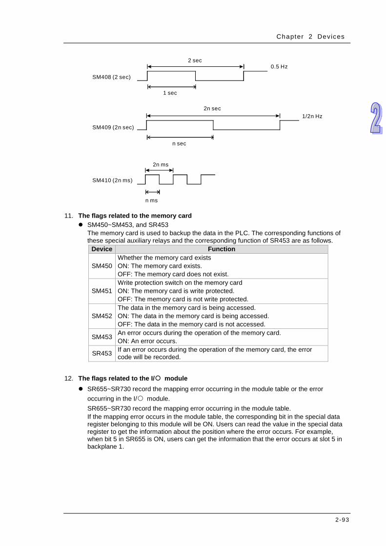
Chapter 2 Devices
2-93
SM408 (2 sec)
SM409 (2n sec)
SM410 (2n ms)
2n sec
2 sec
1 sec
n sec
2n ms
n ms
0.5 Hz
1/2n Hz
11. The flags related to the memory card SM450~SM453, and SR453
The memory card is used to backup the data in the PLC. The corresponding functions of these special auxiliary relays and the corresponding function of SR453 are as follows.
Device Function
SM450 Whether the memory card exists ON: The memory card exists. OFF: The memory card does not exist.
SM451 Write protection switch on the memory card ON: The memory card is write protected. OFF: The memory card is not write protected.
SM452 The data in the memory card is being accessed. ON: The data in the memory card is being accessed. OFF: The data in the memory card is not accessed.
SM453 An error occurs during the operation of the memory card. ON: An error occurs.
SR453 If an error occurs during the operation of the memory card, the error code will be recorded.
12. The flags related to the I/○ module
SR655~SR730 record the mapping error occurring in the module table or the error occurring in the I/○ module. SR655~SR730 record the mapping error occurring in the module table. If the mapping error occurs in the module table, the corresponding bit in the special data register belonging to this module will be ON. Users can read the value in the special data register to get the information about the position where the error occurs. For example, when bit 5 in SR655 is ON, users can get the information that the error occurs at slot 5 in backplane 1.
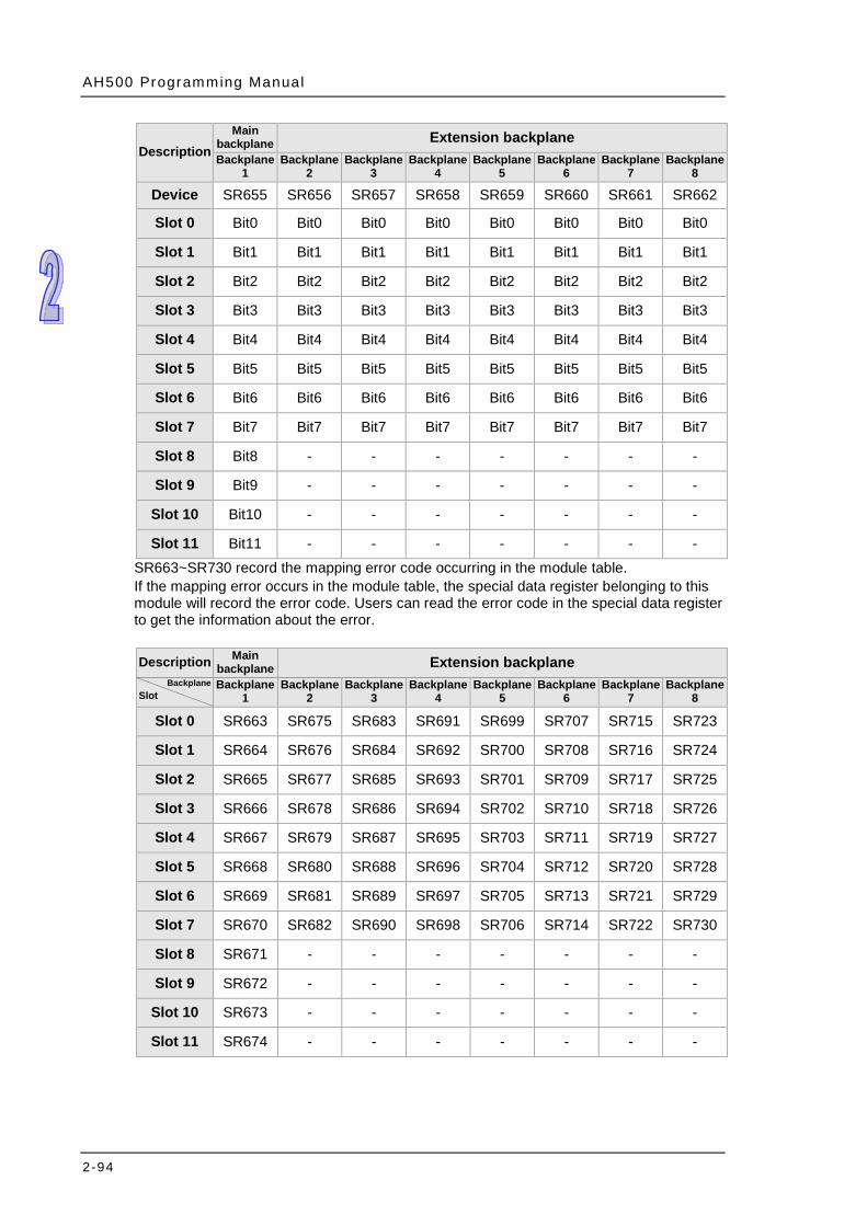
AH500 Programming Manual
2-94
Description Main
backplane Extension backplane Backplane
1 Backplane
2 Backplane
3 Backplane
4 Backplane
5 Backplane
6 Backplane
7 Backplane
8 Device SR655 SR656 SR657 SR658 SR659 SR660 SR661 SR662
Slot 0 Bit0 Bit0 Bit0 Bit0 Bit0 Bit0 Bit0 Bit0
Slot 1 Bit1 Bit1 Bit1 Bit1 Bit1 Bit1 Bit1 Bit1
Slot 2 Bit2 Bit2 Bit2 Bit2 Bit2 Bit2 Bit2 Bit2
Slot 3 Bit3 Bit3 Bit3 Bit3 Bit3 Bit3 Bit3 Bit3
Slot 4 Bit4 Bit4 Bit4 Bit4 Bit4 Bit4 Bit4 Bit4
Slot 5 Bit5 Bit5 Bit5 Bit5 Bit5 Bit5 Bit5 Bit5
Slot 6 Bit6 Bit6 Bit6 Bit6 Bit6 Bit6 Bit6 Bit6
Slot 7 Bit7 Bit7 Bit7 Bit7 Bit7 Bit7 Bit7 Bit7
Slot 8 Bit8 - - - - - - -
Slot 9 Bit9 - - - - - - -
Slot 10 Bit10 - - - - - - -
Slot 11 Bit11 - - - - - - - SR663~SR730 record the mapping error code occurring in the module table. If the mapping error occurs in the module table, the special data register belonging to this module will record the error code. Users can read the error code in the special data register to get the information about the error. Description Main
backplane Extension backplane Backplane
Slot Backplane
1 Backplane
2 Backplane
3 Backplane
4 Backplane
5 Backplane
6 Backplane
7 Backplane
8 Slot 0 SR663 SR675 SR683 SR691 SR699 SR707 SR715 SR723
Slot 1 SR664 SR676 SR684 SR692 SR700 SR708 SR716 SR724
Slot 2 SR665 SR677 SR685 SR693 SR701 SR709 SR717 SR725
Slot 3 SR666 SR678 SR686 SR694 SR702 SR710 SR718 SR726
Slot 4 SR667 SR679 SR687 SR695 SR703 SR711 SR719 SR727
Slot 5 SR668 SR680 SR688 SR696 SR704 SR712 SR720 SR728
Slot 6 SR669 SR681 SR689 SR697 SR705 SR713 SR721 SR729
Slot 7 SR670 SR682 SR690 SR698 SR706 SR714 SR722 SR730
Slot 8 SR671 - - - - - - -
Slot 9 SR672 - - - - - - -
Slot 10 SR673 - - - - - - -
Slot 11 SR674 - - - - - - -
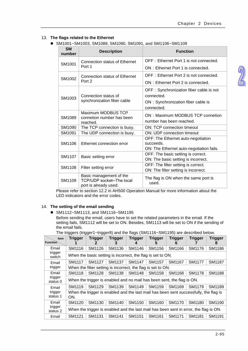
Chapter 2 Devices
2-95
13. The flags related to the Ethernet SM1001~SM1003, SM1089, SM1090, SM1091, and SM1106~SM1109
SM number Description Function
SM1001 Connection status of Ethernet Port 1
OFF:Ethernet Port 1 is not connected.
ON:Ethernet Port 1 is connected.
SM1002 Connection status of Ethernet Port 2
OFF:Ethernet Port 2 is not connected.
ON:Ethernet Port 2 is connected.
SM1003 Connection status of synchronization fiber cable
OFF:Synchronization fiber cable is not connected. ON:Synchronization fiber cable is connected.
SM1089 Maximum MODBUS TCP connetion number has been reached.
ON:Maximum MODBUS TCP connetion number has been reached.
SM1090 The TCP connection is busy. ON: TCP connection timeout SM1091 The UDP connection is busy. ON: UDP connection timeout
SM1106 Ethernet connection error OFF: The Ethernet auto-negotiation succeeds. ON: The Ethernet auto-negotiation fails.
SM1107 Basic setting error OFF: The basic setting is correct. ON: The basic setting is incorrect.
SM1108 Filter setting error OFF: The filter setting is correct. ON: The filter setting is incorrect.
SM1109 Basic management of the TCP/UDP socket─The local port is already used.
The flag is ON when the same port is used.
Please refer to section 12.2 in AH500 Operation Manual for more information about the LED indicators and the error codes.
14. The setting of the email sending SM1112~SM1113, and SM1116~SM1195
Before sending the email, users have to set the related parameters in the email. If the setting fails, SM1112 will be set to ON. Besides, SM1113 will be set to ON if the sending of the email fails. The triggers (trigger1~trigger8) and the flags (SM1116~SM1195) are described below. Item
Function Trigger
1 Trigger
2 Trigger
3 Trigger
4 Trigger
5 Trigger
6 Trigger
7 Trigger
8 Email trigger switch
SM1116 SM1126 SM1136 SM1146 SM1156 SM1166 SM1176 SM1186 When the basic setting is incorrect, the flag is set to ON.
Email trigger
SM1117 SM1127 SM1137 SM1147 SM1157 SM1167 SM1177 SM1187 When the filter setting is incorrect, the flag is set to ON.
Email trigger
status 0
SM1118 SM1128 SM1138 SM1148 SM1158 SM1168 SM1178 SM1188 When the trigger is enabled and no mail has been sent, the flag is ON.
Email trigger
status 1
SM1119 SM1129 SM1139 SM1149 SM1159 SM1169 SM1179 SM1189 When the trigger is enabled and the last mail has been sent successfully, the flag is ON.
Email trigger
status 2
SM1120 SM1130 SM1140 SM1150 SM1160 SM1170 SM1180 SM1190 When the trigger is enabled and the last mail has been sent in error, the flag is ON.
Email SM1121 SM1131 SM1141 SM1151 SM1161 SM1171 SM1181 SM1191
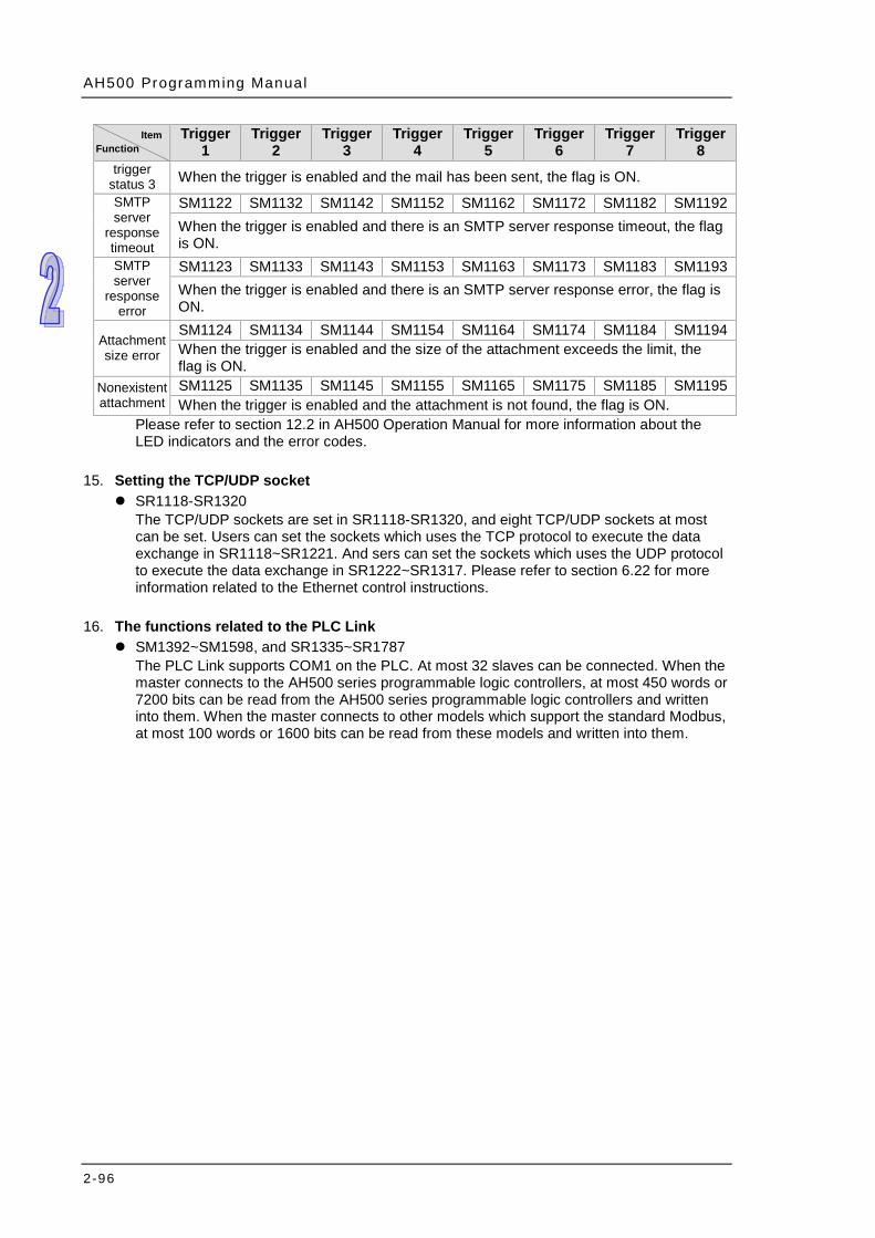
AH500 Programming Manual
2-96
Item Function
Trigger 1
Trigger2
Trigger 3
Trigger 4
Trigger 5
Trigger 6
Trigger 7
Trigger 8
trigger status 3 When the trigger is enabled and the mail has been sent, the flag is ON. SMTP server
response timeout
SM1122 SM1132 SM1142 SM1152 SM1162 SM1172 SM1182 SM1192 When the trigger is enabled and there is an SMTP server response timeout, the flag is ON.
SMTP server
response error
SM1123 SM1133 SM1143 SM1153 SM1163 SM1173 SM1183 SM1193 When the trigger is enabled and there is an SMTP server response error, the flag is ON.
Attachment size error
SM1124 SM1134 SM1144 SM1154 SM1164 SM1174 SM1184 SM1194 When the trigger is enabled and the size of the attachment exceeds the limit, the flag is ON.
Nonexistent attachment
SM1125 SM1135 SM1145 SM1155 SM1165 SM1175 SM1185 SM1195 When the trigger is enabled and the attachment is not found, the flag is ON.
Please refer to section 12.2 in AH500 Operation Manual for more information about the LED indicators and the error codes.
15. Setting the TCP/UDP socket SR1118-SR1320
The TCP/UDP sockets are set in SR1118-SR1320, and eight TCP/UDP sockets at most can be set. Users can set the sockets which uses the TCP protocol to execute the data exchange in SR1118~SR1221. And sers can set the sockets which uses the UDP protocol to execute the data exchange in SR1222~SR1317. Please refer to section 6.22 for more information related to the Ethernet control instructions.
16. The functions related to the PLC Link SM1392~SM1598, and SR1335~SR1787
The PLC Link supports COM1 on the PLC. At most 32 slaves can be connected. When the master connects to the AH500 series programmable logic controllers, at most 450 words or 7200 bits can be read from the AH500 series programmable logic controllers and written into them. When the master connects to other models which support the standard Modbus, at most 100 words or 1600 bits can be read from these models and written into them.
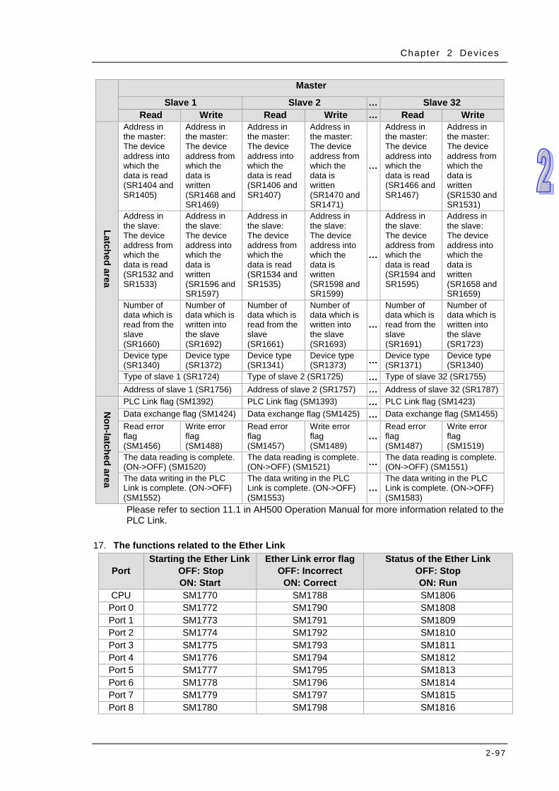
Chapter 2 Devices
2-97
Master
Slave 1 Slave 2 … Slave 32 Read Write Read Write … Read Write
Latched area
Address in the master: The device address into which the data is read (SR1404 and SR1405)
Address in the master: The device address from which the data is written (SR1468 and SR1469)
Address in the master: The device address into which the data is read (SR1406 and SR1407)
Address in the master: The device address from which the data is written (SR1470 and SR1471)
…
Address in the master: The device address into which the data is read (SR1466 and SR1467)
Address in the master: The device address from which the data is written (SR1530 and SR1531)
Address in the slave: The device address from which the data is read (SR1532 and SR1533)
Address in the slave: The device address into which the data is written (SR1596 and SR1597)
Address in the slave: The device address from which the data is read (SR1534 and SR1535)
Address in the slave: The device address into which the data is written (SR1598 and SR1599)
…
Address in the slave: The device address from which the data is read (SR1594 and SR1595)
Address in the slave: The device address into which the data is written (SR1658 and SR1659)
Number of data which is read from the slave (SR1660)
Number of data which is written into the slave (SR1692)
Number of data which is read from the slave (SR1661)
Number of data which is written into the slave (SR1693)
…
Number of data which is read from the slave (SR1691)
Number of data which is written into the slave (SR1723)
Device type (SR1340)
Device type (SR1372)
Device type (SR1341)
Device type (SR1373) … Device type
(SR1371) Device type (SR1340)
Type of slave 1 (SR1724) Type of slave 2 (SR1725) … Type of slave 32 (SR1755) Address of slave 1 (SR1756) Address of slave 2 (SR1757) … Address of slave 32 (SR1787)
Non-latched area
PLC Link flag (SM1392) PLC Link flag (SM1393) … PLC Link flag (SM1423) Data exchange flag (SM1424) Data exchange flag (SM1425) … Data exchange flag (SM1455) Read error flag (SM1456)
Write error flag (SM1488)
Read error flag (SM1457)
Write error flag (SM1489)
… Read error flag (SM1487)
Write error flag (SM1519)
The data reading is complete. (ON->OFF) (SM1520)
The data reading is complete. (ON->OFF) (SM1521) … The data reading is complete.
(ON->OFF) (SM1551) The data writing in the PLC Link is complete. (ON->OFF) (SM1552)
The data writing in the PLC Link is complete. (ON->OFF) (SM1553)
… The data writing in the PLC Link is complete. (ON->OFF) (SM1583)
Please refer to section 11.1 in AH500 Operation Manual for more information related to the PLC Link.
17. The functions related to the Ether Link
Port Starting the Ether Link
OFF: Stop ON: Start
Ether Link error flag OFF: Incorrect
ON: Correct
Status of the Ether Link OFF: Stop ON: Run
CPU SM1770 SM1788 SM1806 Port 0 SM1772 SM1790 SM1808 Port 1 SM1773 SM1791 SM1809 Port 2 SM1774 SM1792 SM1810 Port 3 SM1775 SM1793 SM1811 Port 4 SM1776 SM1794 SM1812 Port 5 SM1777 SM1795 SM1813 Port 6 SM1778 SM1796 SM1814 Port 7 SM1779 SM1797 SM1815 Port 8 SM1780 SM1798 SM1816
AH500 Programming Manual
2-98
Port Starting the Ether Link
OFF: Stop ON: Start
Ether Link error flag OFF: Incorrect
ON: Correct
Status of the Ether Link OFF: Stop ON: Run
Port 9 SM1781 SM1799 SM1817 Port 10 SM1782 SM1800 SM1818 Port 11 SM1783 SM1801 SM1819 Port 12 SM1784 SM1802 SM1820 Port 13 SM1785 SM1803 SM1821 Port 14 SM1786 SM1804 SM1822 Port 15 SM1787 SM1805 SM1823
Please refer to section 11.2 in AH500 Operation Manual for more information related to the Ether Link.
18. Setting the IP address SR1792~SR2047
Device Function Description
SR1792 IP address of block 1
High eight bits in the IP address of block 1 Example: If the remote IP address is 192.168.1.100, the
value in the register is 16#C0A8.
SR1793 IP address of block 1
Low eight bits in the IP address of block 1 Example: If the remote IP address is 192.168.1.100, the
value in the register is 16#0164.
….
SR2046 IP address of block 128
High eight bits in the IP address of block 128 Example: If the remote IP address is 192.168.1.100, the
value in the register is 16#C0A8.
SR2047 IP address of block 128
Low eight bits in the IP address of block 128 Example: If the remote IP address is 192.168.1.100, the
value in the register is 16#0164. Please refer to section 11.2 in AH500 Operation Manual for more information related to the Ether Link.
19. The flags related to power module SM20, SR32-SR33, SR731, SR732
Device Function Description
SM20 Power supply error log
Power supply is back to normal after a short break of insufficient internal power supply.
SR32 Status of the left-side power module
ON: Something went wrong in the left-side power module OFF: Nothing went wrong in the left-side power module
SR33 Status of the right-side power module
ON: Something went wrong in the right-side power module OFF: Nothing went wrong in the right-side power module
SR731 External 24V low-voltage detected on the left-side power module
ON: Something wrong is detected in the external 24V input of the left-side power module OFF: Nothing wrong is detected in the external 24V input of the left-side r power module
SR732 External 24V low-voltage detected on the right-side power module
ON: Something wrong is detected in the external 24V input of the right-side power module OFF: Nothing wrong is detected in the external 24V input of the right-side power module

Chapter 2 Devices
2-99
Description Power module status External 24V low-voltage
detection Left-side
power module
Right-side Power module
Left-side power
module
Right-side Power module
Device SR32 SR33 SR731 SR732 Main
backplane Backplane 1 Bit0 Bit0 Bit0 Bit0
Redundant backplane
Backplane 2 Bit1 Bit1 Bit1 Bit1 Backplane 3 Bit2 Bit2 Bit2 Bit2 Backplane 4 Bit3 Bit3 Bit3 Bit3 Backplane 5 Bit4 Bit4 Bit4 Bit4 Backplane 6 Bit5 Bit5 Bit5 Bit5 Backplane 7 Bit6 Bit6 Bit6 Bit6 Backplane 8 Bit7 Bit7 Bit7 Bit7
20. The connection status of the redundant extension backplane
SM418~431: communication port status of the redundant extension backplane (ON: normal ; OFF: abnormal)
Description Communication port status
Port2 Port4 Main
backplane in the redundancy
system Backplane 1 SM418 -
Redundant extension backplane
Backplane 2 SM420 SM421 Backplane 3 SM422 SM423 Backplane 4 SM424 SM425 Backplane 5 SM426 SM427 Backplane 6 SM428 SM429 Backplane 7 SM430 SM431
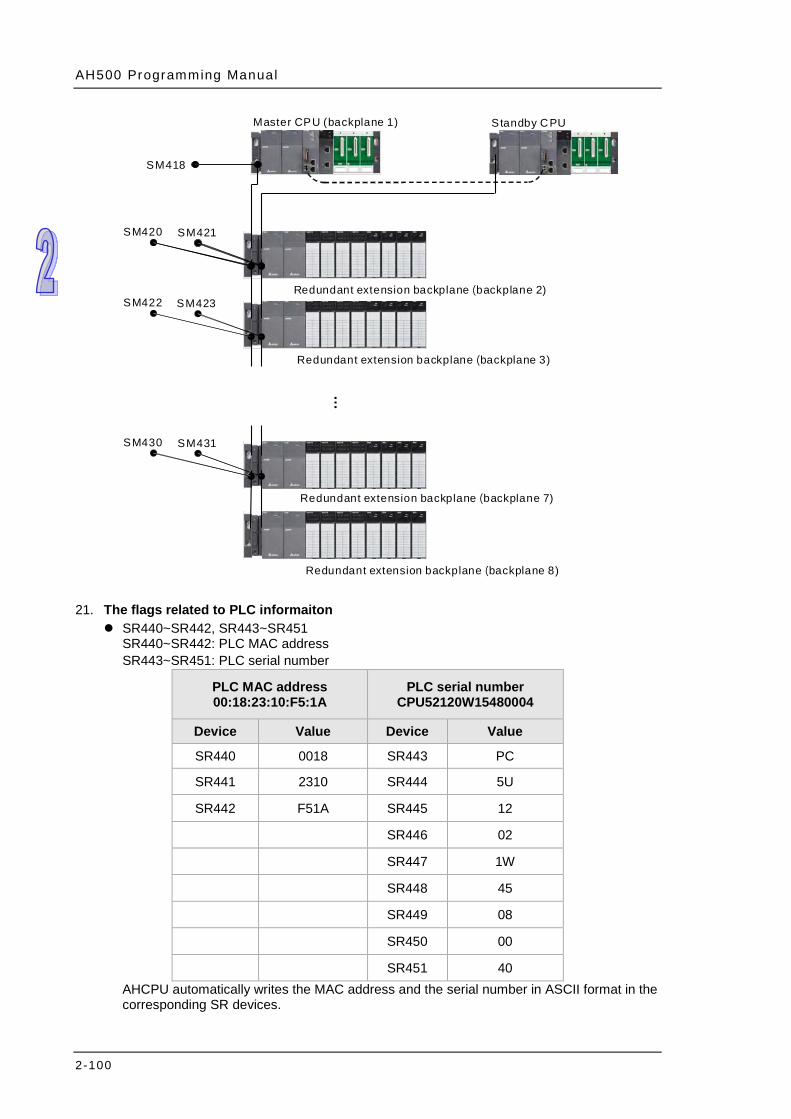
AH500 Programming Manual
2-100
1
Redundant extension backplane backplane 2) (
Standby CPUMaster CPU (backplane 1)
SM418
SM420 SM421
…
SM422 SM423
SM430 SM431
Redundant extension backplane backplane 3) (
Redundant extension backplane backplane 7) (
Redundant extension backplane backplane 8) (
21. The flags related to PLC informaiton SR440~SR442, SR443~SR451
SR440~SR442: PLC MAC address SR443~SR451: PLC serial number
PLC MAC address 00:18:23:10:F5:1A
PLC serial number CPU52120W15480004
Device Value Device Value
SR440 0018 SR443 PC
SR441 2310 SR444 5U
SR442 F51A SR445 12
SR446 02
SR447 1W
SR448 45
SR449 08
SR450 00
SR451 40 AHCPU automatically writes the MAC address and the serial number in ASCII format in the corresponding SR devices.
Chapter 2 Devices
2-101
22. The flags related to EtherNet/IP SM2048 ~ SM2303: flags to enable data mapping for connection 1~256 via EtherNet/IP
Scanner. You can use the flags to enable or disable the connection between AH Series PLC CPU and its adapters. ON: Enable data mapping for the connection. OFF: Disable data mapping for the connection.
SM2304~ SM2311: flags to show the error status of EtherNet/IP Adapter connection 1~8. You can use the flas to check if the connection between AH Series PLC CPU and its scanner is working. ON: The connection is NOT working. OFF: The connection is working.
SM2312~ SM2319: flags to show the connection status of EtherNet/IP Adapter connection 1~8. You can use the flags to check the connection status between AH Series PLC CPU and its scanner. ON: The connection is established. OFF: The connection is NOT established.
SR2047: Number of the EtherNet/IP scanner connections You can use the flag to see the number of connections between AH Series PLC CPU (scanner) and its adapters.
SR2048~SR2303: Erroor codes of data mapping for connection 1~256 via EtherNet/IP Scanner. Refer to Chapter 6 Troubleshooting from EtherNet/IP Operation Manual.
SR2304~SR2559: The operation status of the connection 1~256 for data mapping via EtherNet/IP Scanner. The values 0 and 1 in this SR indicates: 0: This connection is abnormal or not established. Refer to the corresponding register SR2048~SR2303 to learn more about the error. 1: The connection is working.
2.2.17 Link Registers The link register is mainly used in the PLC Link or the Ether Link. When the data exchange occurs between the AH500 series programmable logic controllers, the link register can be used as the buffer. Please refer to chapter 12 in AH500 Operation Manual for more information. The link registers L0~L65535 add up to 65536 words. Besides, the link register can be used as the general auxiliary register.
2.2.18 Index Registers The index register is the 16-bit data register. It is like the general register in that the data can be read from it and written into it. However, it is mainly used as the index register. The range of index registers is E0~E13. Please refer to section 4.3 for more information related to the index register.

AH500 Programming Manual
2-102
MEMO

3-1
Chapter 3 Instruction Tables
Table of Contents 3.1 Instructions ............................................................................................ 3-2
3.1.1 Basic Instructions .............................................................................. 3-2 3.1.2 Applied Instructions ........................................................................... 3-3
3.2 Instruction Tables .................................................................................. 3-4 3.2.1 Basic Instructions .............................................................................. 3-4 3.2.2 Applied Instructions ........................................................................... 3-5 3.2.3 Applied Instructions (Sorted Alphabetically) ...................................... 3-6 3.2.4 Device Tables ................................................................................... 3-7
3.3 Lists of Basic Instructions ...................................................................... 3-8 3.4 Lists of Applied Instructions ..................................................................3-11
3.4.1 Applied Instructions ..........................................................................3-11 3.4.2 Applied Instructions (Sorted Alphabetically) .....................................3-37
AH500 Programming Manual
3-2
3.1 Instructions Instructions used in the AH500 series PLC include basic instructions and applied instructions.
3.1.1 Basic Instructions Classification Description
Contact instructions Loading the contact, connecting the contact in series, connecting the contact in parallel, and etc.
Connection instructions Storing and reading the operation result Output instructions Bit device output; pulse output Master control Instructions Setting and resetting the master control
Rising-edge/Falling-edge detection contact instructions
Triggering the instructions that load the contact, connect the contacts in series, and connect the contacts in parallel
Rising-edge/Falling-edge output instructions Bit device output
Other instructions Other instructions
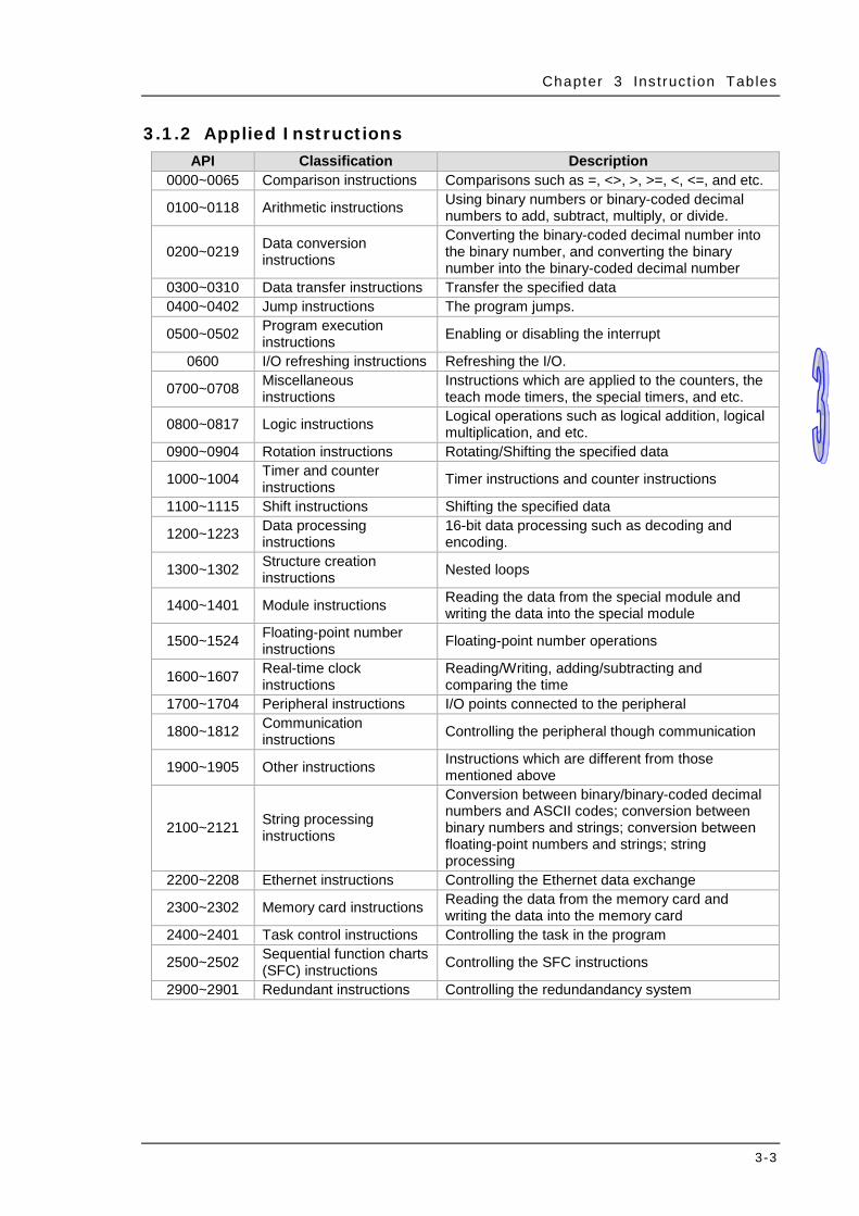
Chapter 3 Ins truct ion Tables
3-3
3.1.2 Applied Instructions API Classification Description
0000~0065 Comparison instructions Comparisons such as =, <>, >, >=, <, <=, and etc.
0100~0118 Arithmetic instructions Using binary numbers or binary-coded decimal numbers to add, subtract, multiply, or divide.
0200~0219 Data conversion instructions
Converting the binary-coded decimal number into the binary number, and converting the binary number into the binary-coded decimal number
0300~0310 Data transfer instructions Transfer the specified data 0400~0402 Jump instructions The program jumps.
0500~0502 Program execution instructions Enabling or disabling the interrupt
0600 I/O refreshing instructions Refreshing the I/O.
0700~0708 Miscellaneous instructions
Instructions which are applied to the counters, the teach mode timers, the special timers, and etc.
0800~0817 Logic instructions Logical operations such as logical addition, logical multiplication, and etc.
0900~0904 Rotation instructions Rotating/Shifting the specified data
1000~1004 Timer and counter instructions Timer instructions and counter instructions
1100~1115 Shift instructions Shifting the specified data
1200~1223 Data processing instructions
16-bit data processing such as decoding and encoding.
1300~1302 Structure creation instructions Nested loops
1400~1401 Module instructions Reading the data from the special module and writing the data into the special module
1500~1524 Floating-point number instructions Floating-point number operations
1600~1607 Real-time clock instructions
Reading/Writing, adding/subtracting and comparing the time
1700~1704 Peripheral instructions I/O points connected to the peripheral
1800~1812 Communication instructions Controlling the peripheral though communication
1900~1905 Other instructions Instructions which are different from those mentioned above
2100~2121 String processing instructions
Conversion between binary/binary-coded decimal numbers and ASCII codes; conversion between binary numbers and strings; conversion between floating-point numbers and strings; string processing
2200~2208 Ethernet instructions Controlling the Ethernet data exchange
2300~2302 Memory card instructions Reading the data from the memory card and writing the data into the memory card
2400~2401 Task control instructions Controlling the task in the program
2500~2502 Sequential function charts (SFC) instructions Controlling the SFC instructions
2900~2901 Redundant instructions Controlling the redundandancy system
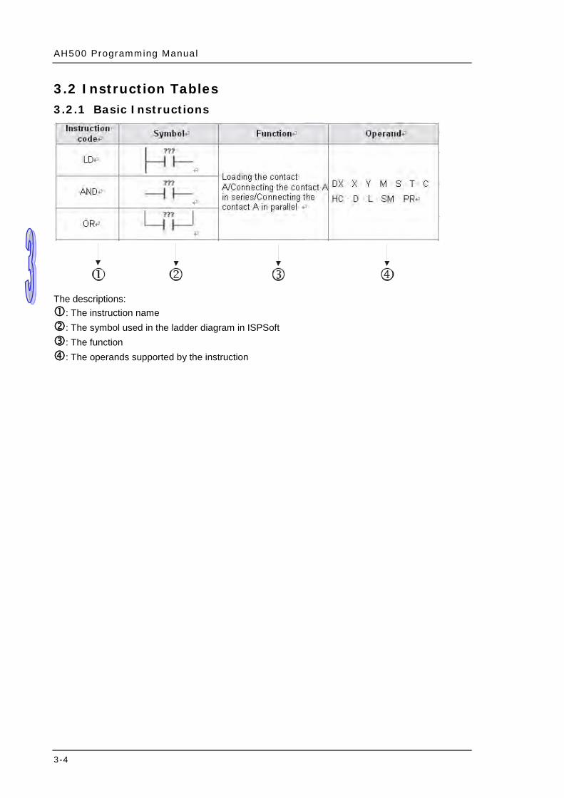
AH500 Programming Manual
3-4
3.2 Instruction Tables 3.2.1 Basic Instructions
The descriptions: : The instruction name : The symbol used in the ladder diagram in ISPSoft : The function : The operands supported by the instruction
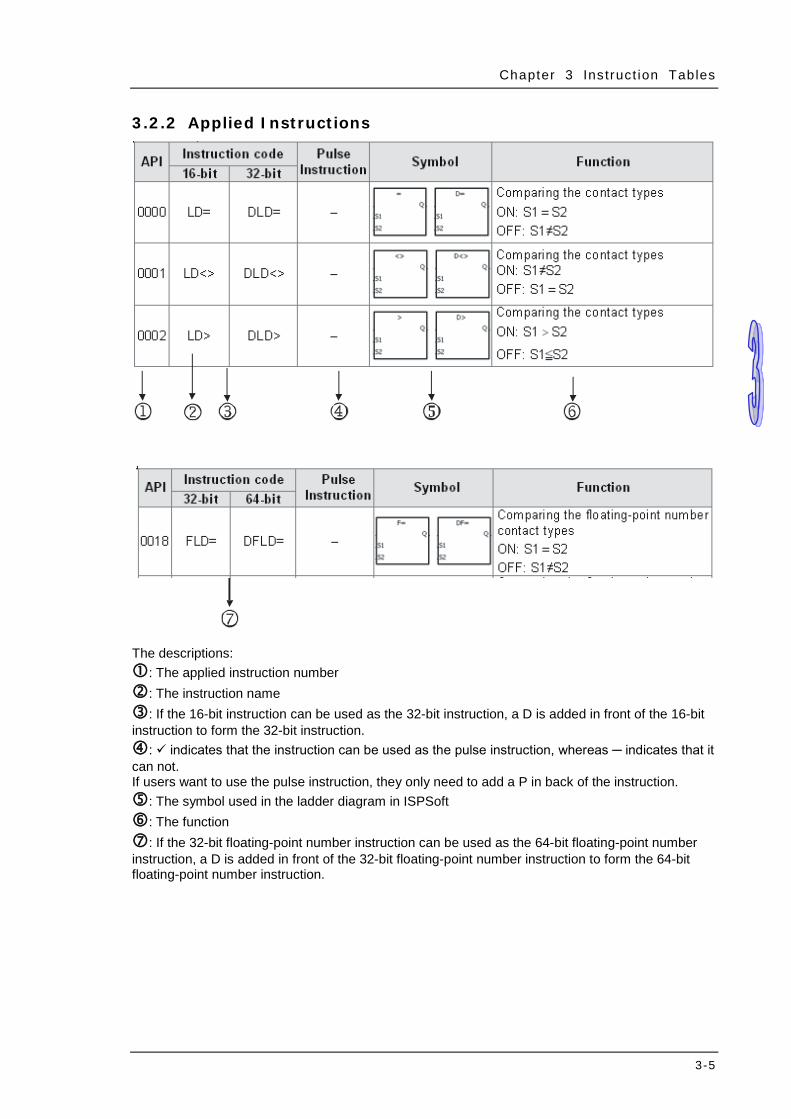
Chapter 3 Ins truct ion Tables
3-5
3.2.2 Applied Instructions
The descriptions: : The applied instruction number : The instruction name : If the 16-bit instruction can be used as the 32-bit instruction, a D is added in front of the 16-bit instruction to form the 32-bit instruction. : indicates that the instruction can be used as the pulse instruction, whereas ─ indicates that it can not. If users want to use the pulse instruction, they only need to add a P in back of the instruction. : The symbol used in the ladder diagram in ISPSoft : The function : If the 32-bit floating-point number instruction can be used as the 64-bit floating-point number instruction, a D is added in front of the 32-bit floating-point number instruction to form the 64-bit floating-point number instruction.
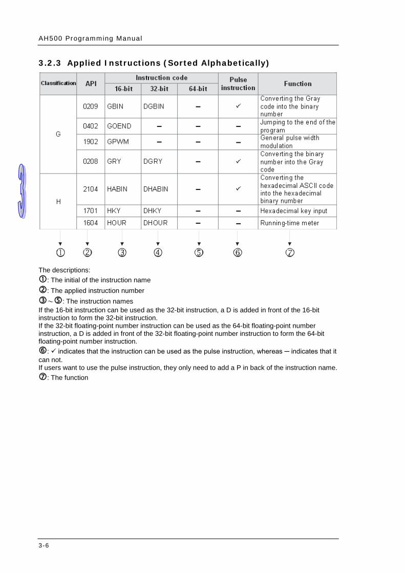
AH500 Programming Manual
3-6
3.2.3 Applied Instructions (Sorted Alphabetically)
The descriptions: : The initial of the instruction name : The applied instruction number ~: The instruction names If the 16-bit instruction can be used as the 32-bit instruction, a D is added in front of the 16-bit instruction to form the 32-bit instruction. If the 32-bit floating-point number instruction can be used as the 64-bit floating-point number instruction, a D is added in front of the 32-bit floating-point number instruction to form the 64-bit floating-point number instruction. : indicates that the instruction can be used as the pulse instruction, whereas ─ indicates that it can not. If users want to use the pulse instruction, they only need to add a P in back of the instruction name. : The function
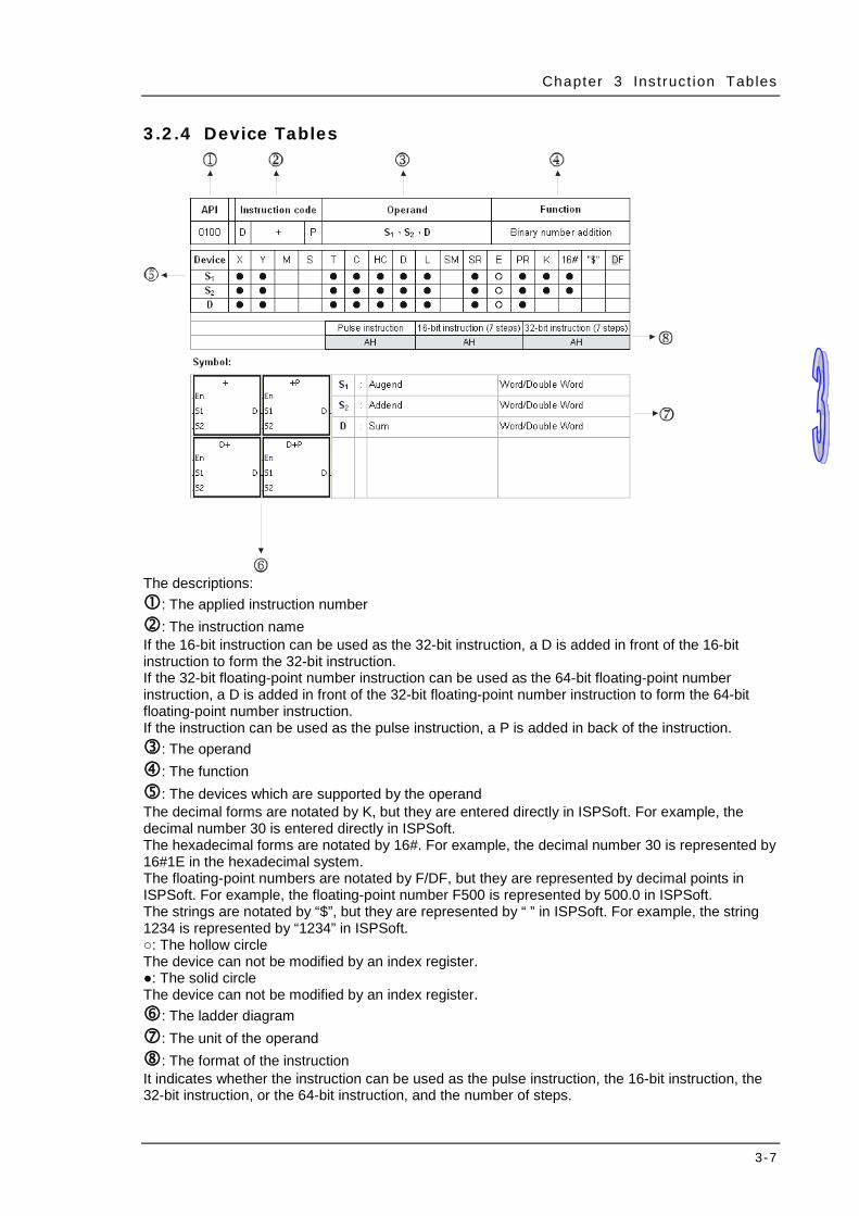
Chapter 3 Ins truct ion Tables
3-7
3.2.4 Device Tables
The descriptions: : The applied instruction number : The instruction name If the 16-bit instruction can be used as the 32-bit instruction, a D is added in front of the 16-bit instruction to form the 32-bit instruction. If the 32-bit floating-point number instruction can be used as the 64-bit floating-point number instruction, a D is added in front of the 32-bit floating-point number instruction to form the 64-bit floating-point number instruction. If the instruction can be used as the pulse instruction, a P is added in back of the instruction. : The operand : The function : The devices which are supported by the operand The decimal forms are notated by K, but they are entered directly in ISPSoft. For example, the decimal number 30 is entered directly in ISPSoft. The hexadecimal forms are notated by 16#. For example, the decimal number 30 is represented by 16#1E in the hexadecimal system. The floating-point numbers are notated by F/DF, but they are represented by decimal points in ISPSoft. For example, the floating-point number F500 is represented by 500.0 in ISPSoft. The strings are notated by “$”, but they are represented by “ ” in ISPSoft. For example, the string 1234 is represented by “1234” in ISPSoft. ○: The hollow circle The device can not be modified by an index register. ●: The solid circle The device can not be modified by an index register. : The ladder diagram : The unit of the operand : The format of the instruction It indicates whether the instruction can be used as the pulse instruction, the 16-bit instruction, the 32-bit instruction, or the 64-bit instruction, and the number of steps.
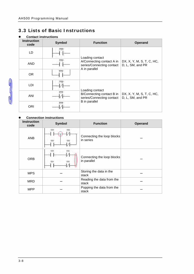
AH500 Programming Manual
3-8
3.3 Lists of Basic Instructions Contact instructions
Instruction code Symbol Function Operand
LD Loading contact
A/Connecting contact A in series/Connecting contact A in parallel
DX, X, Y, M, S, T, C, HC, D, L, SM, and PR AND
OR
LDI Loading contact
B/Connecting contact B in series/Connecting contact B in parallel
DX, X, Y, M, S, T, C, HC, D, L, SM, and PR ANI
ORI
Connection instructions
Instruction code Symbol Function Operand
ANB
Connecting the loop blocks in series ─
ORB
Connecting the loop blocks in parallel ─
MPS ─ Storing the data in the stack ─
MRD ─ Reading the data from the stack ─
MPP ─ Popping the data from the stack ─
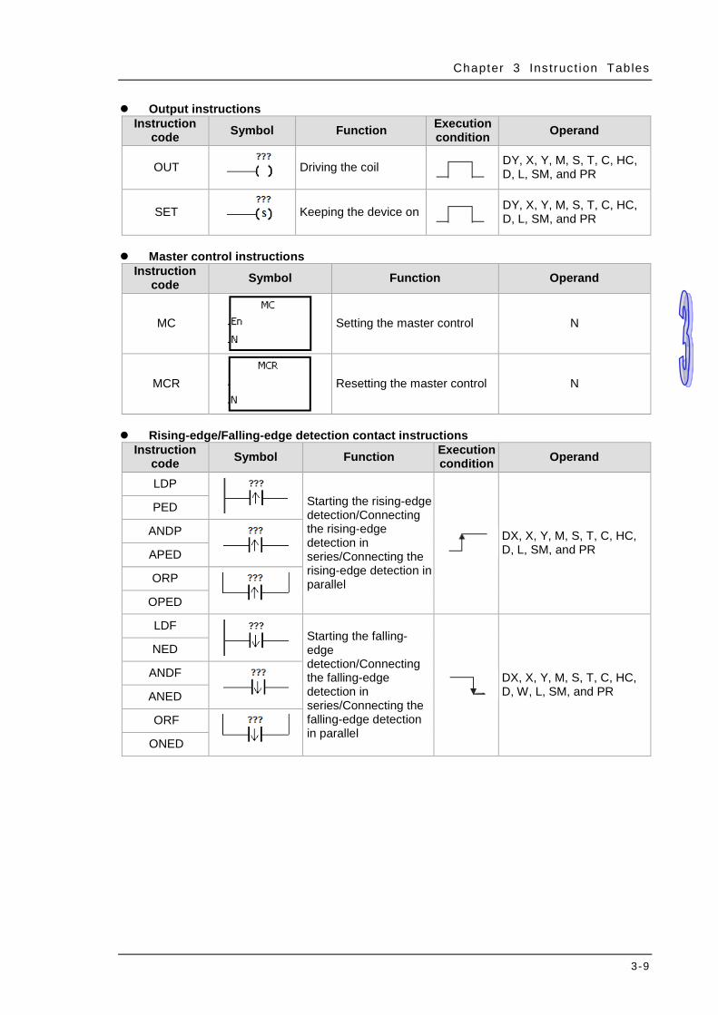
Chapter 3 Ins truct ion Tables
3-9
Output instructions Instruction
code Symbol Function Execution condition Operand
OUT
Driving the coil
DY, X, Y, M, S, T, C, HC, D, L, SM, and PR
SET
Keeping the device on
DY, X, Y, M, S, T, C, HC, D, L, SM, and PR
Master control instructions
Instruction code Symbol Function Operand
MC
Setting the master control N
MCR
Resetting the master control N
Rising-edge/Falling-edge detection contact instructions
Instruction code Symbol Function Execution
condition Operand
LDP
Starting the rising-edge detection/Connecting the rising-edge detection in series/Connecting the rising-edge detection in parallel
DX, X, Y, M, S, T, C, HC, D, L, SM, and PR
PED
ANDP
APED
ORP
OPED
LDF
Starting the falling-edge detection/Connecting the falling-edge detection in series/Connecting the falling-edge detection in parallel
DX, X, Y, M, S, T, C, HC, D, W, L, SM, and PR
NED
ANDF
ANED
ORF
ONED

AH500 Programming Manual
3-10
Rising-edge/Falling-edge output instructions Instruction
code Symbol Function Execution condition Operand
PLS
Rising-edge output DY, X, Y, M, S, T, C, HC, D, L, SM, and PR
PLF
Falling-edge output DY, X, Y, M, S, T, C, HC, D, L, SM, and PR
Other instructions
Instruction code Symbol Function Operand
INV
Inverting the logical operation result –
NOP – No operation –
PSTOP
Stopping executing the PLC program –
NP The circuit is rising edge-triggered. –
PN
The circuit is falling edge-triggered. –
FB_NP
The circuit is rising edge-triggered. S
FB_PN
The circuit is falling edge-triggered. S
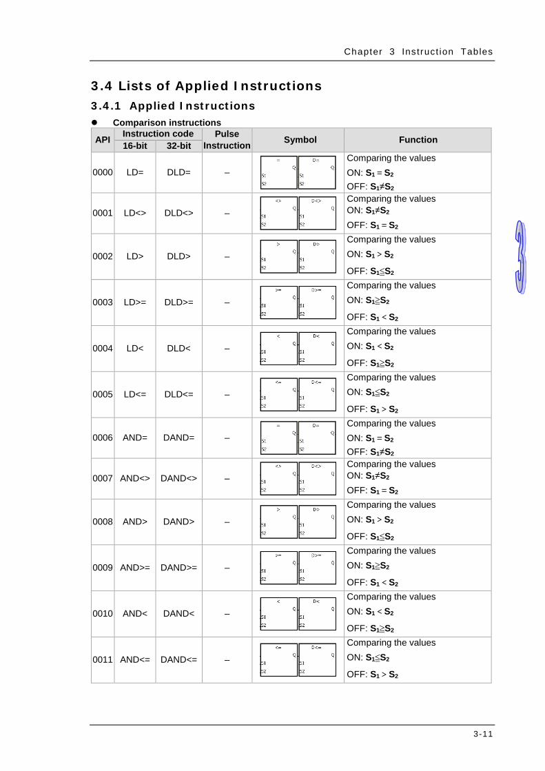
Chapter 3 Ins truct ion Tables
3-11
3.4 Lists of Applied Instructions 3.4.1 Applied Instructions Comparison instructions
API Instruction code Pulse Instruction Symbol Function 16-bit 32-bit
0000 LD= DLD= –
Comparing the values ON: S1=S2 OFF: S1≠S2
0001 LD<> DLD<> –
Comparing the values ON: S1≠S2 OFF: S1=S2
0002 LD> DLD> –
Comparing the values ON: S1>S2
OFF: S1≦S2
0003 LD>= DLD>= –
Comparing the values ON: S1≧S2
OFF: S1<S2
0004 LD< DLD< –
Comparing the values ON: S1<S2
OFF: S1≧S2
0005 LD<= DLD<= –
Comparing the values ON: S1≦S2
OFF: S1>S2
0006 AND= DAND= –
Comparing the values ON: S1=S2 OFF: S1≠S2
0007 AND<> DAND<> –
Comparing the values ON: S1≠S2 OFF: S1=S2
0008 AND> DAND> –
Comparing the values ON: S1>S2
OFF: S1≦S2
0009 AND>= DAND>= –
Comparing the values ON: S1≧S2
OFF: S1<S2
0010 AND< DAND< –
Comparing the values ON: S1<S2
OFF: S1≧S2
0011 AND<= DAND<= –
Comparing the values ON: S1≦S2
OFF: S1>S2
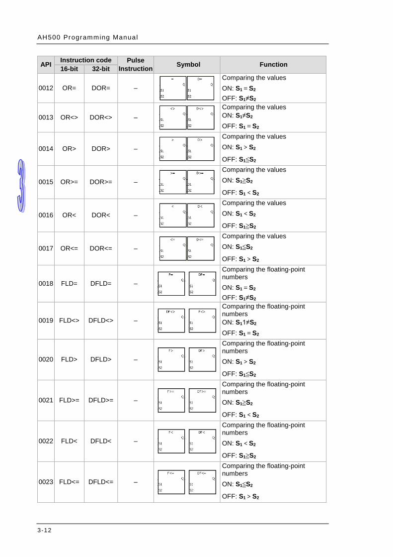
AH500 Programming Manual
3-12
API Instruction code Pulse Instruction Symbol Function 16-bit 32-bit
0012 OR= DOR= –
Comparing the values ON: S1=S2 OFF: S1≠S2
0013 OR<> DOR<> –
Comparing the values ON: S1≠S2 OFF: S1=S2
0014 OR> DOR> –
Comparing the values ON: S1>S2
OFF: S1≦S2
0015 OR>= DOR>= –
Comparing the values ON: S1≧S2
OFF: S1<S2
0016 OR< DOR< –
Comparing the values ON: S1<S2
OFF: S1≧S2
0017 OR<= DOR<= –
Comparing the values ON: S1≦S2
OFF: S1>S2
0018 FLD= DFLD= –
Comparing the floating-point numbers ON: S1=S2 OFF: S1≠S2
0019 FLD<> DFLD<> –
Comparing the floating-point numbers ON: S11≠S2 OFF: S1=S2
0020 FLD> DFLD> –
Comparing the floating-point numbers ON: S1>S2
OFF: S1≦S2
0021 FLD>= DFLD>= –
Comparing the floating-point numbers ON: S1≧S2
OFF: S1<S2
0022 FLD< DFLD< –
Comparing the floating-point numbers ON: S1<S2
OFF: S1≧S2
0023 FLD<= DFLD<= –
Comparing the floating-point numbers ON: S1≦S2
OFF: S1>S2
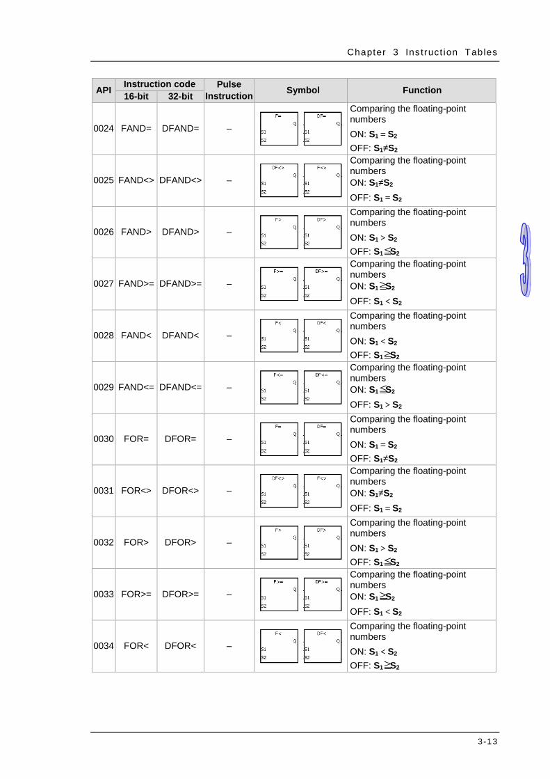
Chapter 3 Ins truct ion Tables
3-13
API Instruction code Pulse Instruction Symbol Function 16-bit 32-bit
0024 FAND= DFAND= –
Comparing the floating-point numbers ON: S1=S2 OFF: S1≠S2
0025 FAND<> DFAND<> –
Comparing the floating-point numbers ON: S1≠S2 OFF: S1=S2
0026 FAND> DFAND> –
Comparing the floating-point numbers ON: S1>S2 OFF: S1≦S2
0027 FAND>= DFAND>= –
Comparing the floating-point numbers ON: S1≧S2 OFF: S1<S2
0028 FAND< DFAND< –
Comparing the floating-point numbers ON: S1<S2 OFF: S1≧S2
0029 FAND<= DFAND<= –
Comparing the floating-point numbers ON: S1≦S2 OFF: S1>S2
0030 FOR= DFOR= –
Comparing the floating-point numbers ON: S1=S2 OFF: S1≠S2
0031 FOR<> DFOR<> –
Comparing the floating-point numbers ON: S1≠S2 OFF: S1=S2
0032 FOR> DFOR> –
Comparing the floating-point numbers ON: S1>S2 OFF: S1≦S2
0033 FOR>= DFOR>= –
Comparing the floating-point numbers ON: S1≧S2 OFF: S1<S2
0034 FOR< DFOR< –
Comparing the floating-point numbers ON: S1<S2 OFF: S1≧S2
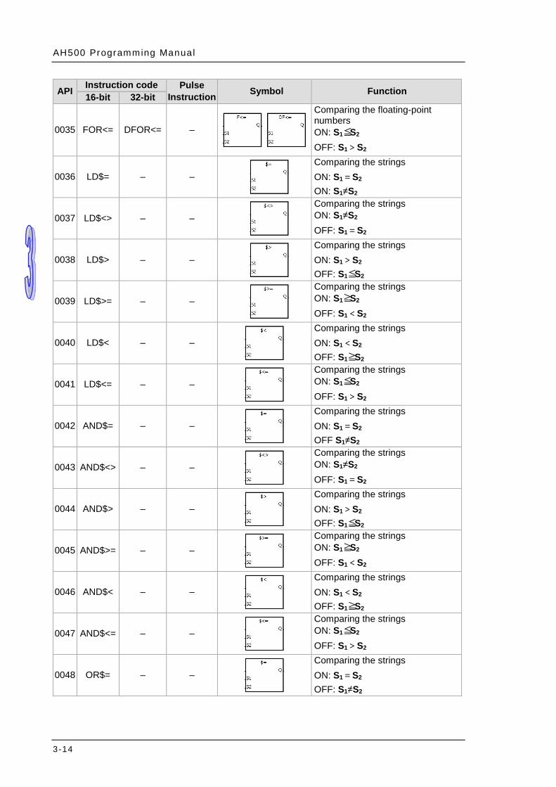
AH500 Programming Manual
3-14
API Instruction code Pulse Instruction Symbol Function 16-bit 32-bit
0035 FOR<= DFOR<= –
Comparing the floating-point numbers ON: S1≦S2 OFF: S1>S2
0036 LD$= – –
Comparing the strings ON: S1=S2 ON: S1≠S2
0037 LD$<> – –
Comparing the strings ON: S1≠S2 OFF: S1=S2
0038 LD$> – –
Comparing the strings ON: S1>S2 OFF: S1≦S2
0039 LD$>= – –
Comparing the strings ON: S1≧S2 OFF: S1<S2
0040 LD$< – –
Comparing the strings ON: S1<S2 OFF: S1≧S2
0041 LD$<= – –
Comparing the strings ON: S1≦S2 OFF: S1>S2
0042 AND$= – –
Comparing the strings ON: S1=S2 OFF S1≠S2
0043 AND$<> – –
Comparing the strings ON: S1≠S2 OFF: S1=S2
0044 AND$> – –
Comparing the strings ON: S1>S2 OFF: S1≦S2
0045 AND$>= – –
Comparing the strings ON: S1≧S2 OFF: S1<S2
0046 AND$< – –
Comparing the strings ON: S1<S2 OFF: S1≧S2
0047 AND$<= – –
Comparing the strings ON: S1≦S2 OFF: S1>S2
0048 OR$= – –
Comparing the strings ON: S1=S2 OFF: S1≠S2
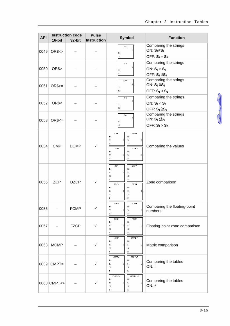
Chapter 3 Ins truct ion Tables
3-15
API Instruction code Pulse Instruction Symbol Function 16-bit 32-bit
0049 OR$<> – –
Comparing the strings ON: S1≠S2 OFF: S1=S2
0050 OR$> – –
Comparing the strings ON: S1>S2 OFF: S1≦S2
0051 OR$>= – –
Comparing the strings ON: S1≧S2 OFF: S1<S2
0052 OR$< – –
Comparing the strings ON: S1<S2 OFF: S1≧S2
0053 OR$<= – –
Comparing the strings ON: S1≦S2 OFF: S1>S2
0054 CMP DCMP
Comparing the values
0055 ZCP DZCP
Zone comparison
0056 – FCMP
Comparing the floating-point numbers
0057 – FZCP
Floating-point zone comparison
0058 MCMP –
Matrix comparison
0059 CMPT= –
Comparing the tables ON: =
0060 CMPT<> –
Comparing the tables ON: ≠
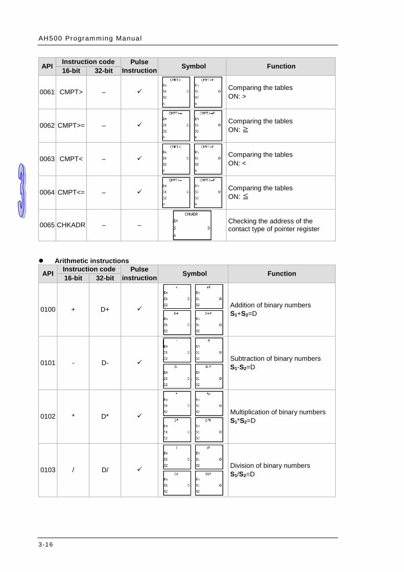
AH500 Programming Manual
3-16
API Instruction code Pulse Instruction Symbol Function 16-bit 32-bit
0061 CMPT> –
Comparing the tables ON: >
0062 CMPT>= –
Comparing the tables ON: ≧
0063 CMPT< –
Comparing the tables ON: <
0064 CMPT<= –
Comparing the tables ON: ≦
0065 CHKADR – –
Checking the address of the contact type of pointer register
Arithmetic instructions
API Instruction code Pulse instruction Symbol Function 16-bit 32-bit
0100 + D+
Addition of binary numbers S1+S2=D
0101 - D-
Subtraction of binary numbers S1-S2=D
0102 * D*
Multiplication of binary numbers S1*S2=D
0103 / D/
Division of binary numbers S1/S2=D
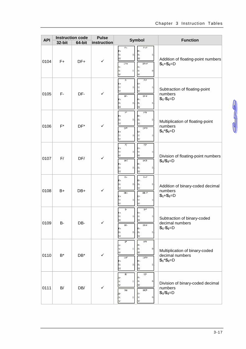
Chapter 3 Ins truct ion Tables
3-17
API Instruction code Pulse instruction Symbol Function 32-bit 64-bit
0104 F+ DF+
Addition of floating-point numbers S1+S2=D
0105 F- DF-
Subtraction of floating-point numbers S1-S2=D
0106 F* DF*
Multiplication of floating-point numbers S1*S2=D
0107 F/ DF/
Division of floating-point numbers S1/S2=D
0108 B+ DB+
Addition of binary-coded decimal numbers S1+S2=D
0109 B- DB-
Subtraction of binary-coded decimal numbers S1-S2=D
0110 B* DB*
Multiplication of binary-coded decimal numbers S1*S2=D
0111 B/ DB/
Division of binary-coded decimal numbers S1/S2=D

AH500 Programming Manual
3-18
API Instruction code Pulse instruction Symbol Function 32-bit 64-bit
0112 BK+ –
Addition of binary numbers in blocks
0113 BK- –
Subtraction of binary numbers in blocks
0114 $+ –
Linking the strings
0115 INC DINC
Adding one to the binary number
0116 DEC DDEC
Subtracting one from the binary number
0117 MUL16 MUL32
Multiplication of binary numbers for 16-bit Multiplication of binary numbers for 32-bit
0118 DIV16 DIV32
Division of binary numbers for 16-bit Division of binary numbers for 32-bit
Data conversion instructions
API Instruction code Pulse instruction Symbol Function 16-bit 32-bit
0200 BCD DBCD
Converting the binary number into the binary-coded decimal number
0201 BIN DBIN
Converting the binary-coded decimal number into the binary number
0202 FLT DFLT
Converting the binary integer into the binary floating-point number

Chapter 3 Ins truct ion Tables
3-19
API Instruction code Pulse instruction Symbol Function 16-bit 32-bit
0203 FLTD DFLTD
Converting the binary integer into the 64-bit floating-point number
0204 INT DINT
Converting the 32-bit floating-point number into the binary integer
0205 DFINT DFINT
Converting the 64-bit floating-point number into the binary integer
0206 MMOV –
Converting the 16-bit value into the 32-bit value
0207 RMOV –
Converting the 32-bit value into the 16-bit value
0208 GRY DGRY
Converting the binary number into the Gray code
0209 GBIN DGBIN
Converting the Gray code into the binary number
0210 NEG DNEG
Two’s complement
0211 – FNEG
Reversing the sign of the 32-bit floating-point number
0212 – FBCD
Converting the binary floating-point number into the decimal floating-point number
0213 – FBIN
Converting the decimal floating-point number into the binary floating-point number
0214 BKBCD –
Converting the binary numbers in blocks into the binary-coded decimal numbers in blocks
0215 BKBIN –
Converting the binary numbers in blocks into the binary-coded decimal numbers in blocks
0216 SCAL –
Scale value operation
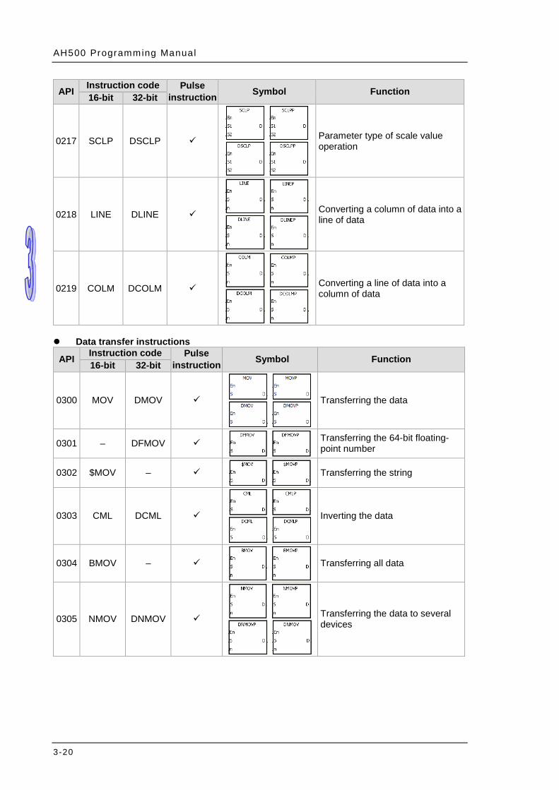
AH500 Programming Manual
3-20
API Instruction code Pulse instruction Symbol Function 16-bit 32-bit
0217 SCLP DSCLP
Parameter type of scale value operation
0218 LINE DLINE
Converting a column of data into a line of data
0219 COLM DCOLM
Converting a line of data into a column of data
Data transfer instructions
API Instruction code Pulse instruction Symbol Function 16-bit 32-bit
0300 MOV DMOV
Transferring the data
0301 – DFMOV
Transferring the 64-bit floating-point number
0302 $MOV –
Transferring the string
0303 CML DCML
Inverting the data
0304 BMOV –
Transferring all data
0305 NMOV DNMOV
Transferring the data to several devices
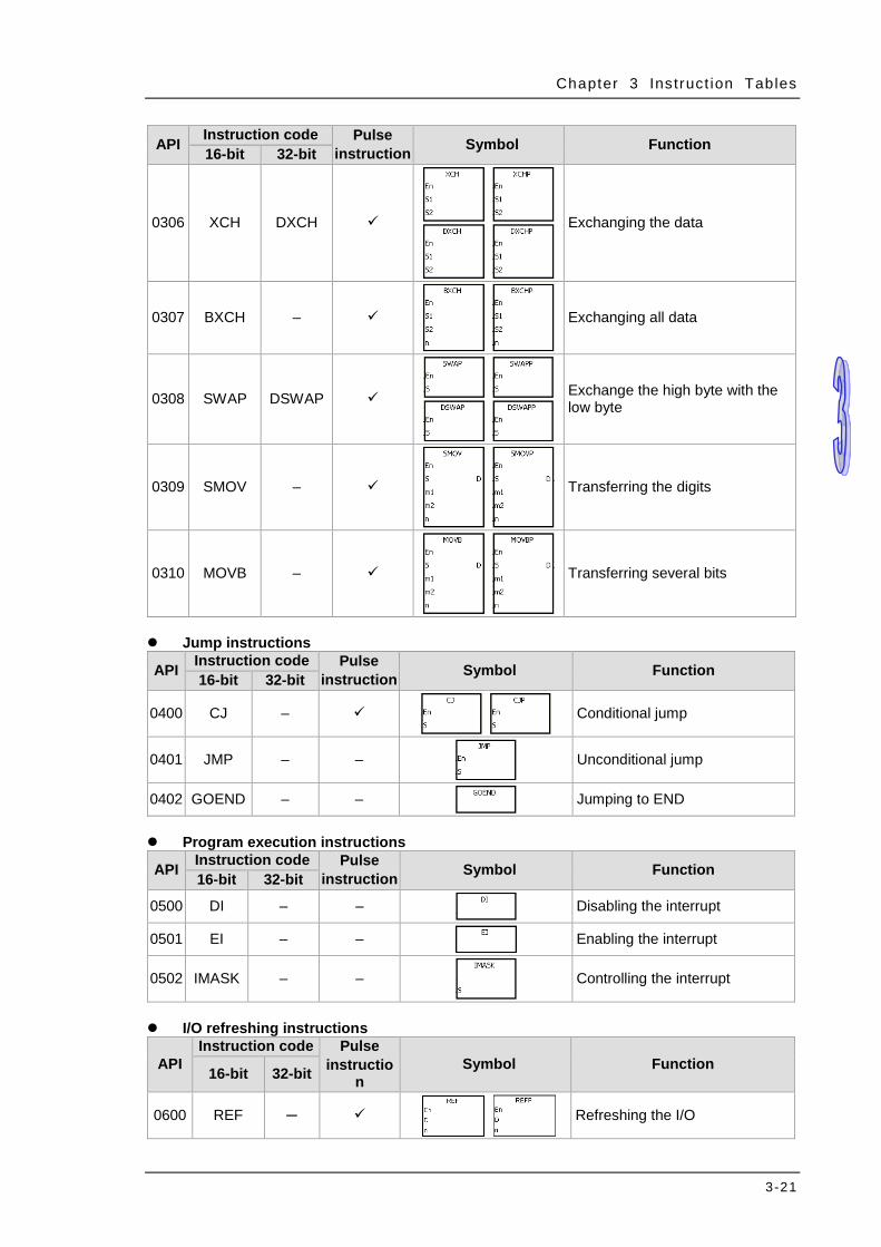
Chapter 3 Ins truct ion Tables
3-21
API Instruction code Pulse instruction Symbol Function 16-bit 32-bit
0306 XCH DXCH
Exchanging the data
0307 BXCH –
Exchanging all data
0308 SWAP DSWAP
Exchange the high byte with the low byte
0309 SMOV –
Transferring the digits
0310 MOVB –
Transferring several bits
Jump instructions
API Instruction code Pulse instruction Symbol Function 16-bit 32-bit
0400 CJ –
Conditional jump
0401 JMP – –
Unconditional jump
0402 GOEND – – Jumping to END
Program execution instructions
API Instruction code Pulse instruction Symbol Function 16-bit 32-bit
0500 DI – – Disabling the interrupt
0501 EI – – Enabling the interrupt
0502 IMASK – –
Controlling the interrupt
I/O refreshing instructions
API Instruction code Pulse
instruction
Symbol Function 16-bit 32-bit
0600 REF ─
Refreshing the I/O
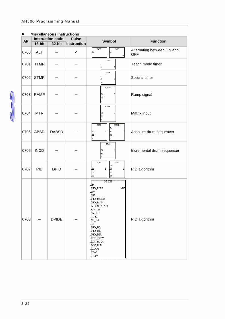
AH500 Programming Manual
3-22
Miscellaneous instructions
API Instruction code Pulse instruction Symbol Function 16-bit 32-bit
0700 ALT ─
Alternating between ON and OFF
0701 TTMR ─ ─
Teach mode timer
0702 STMR ─ ─
Special timer
0703 RAMP ─ ─
Ramp signal
0704 MTR ─ ─
Matrix input
0705 ABSD DABSD ─
Absolute drum sequencer
0706 INCD ─ ─
Incremental drum sequencer
0707 PID DPID ─
PID algorithm
0708 ─ DPIDE ─
PID algorithm
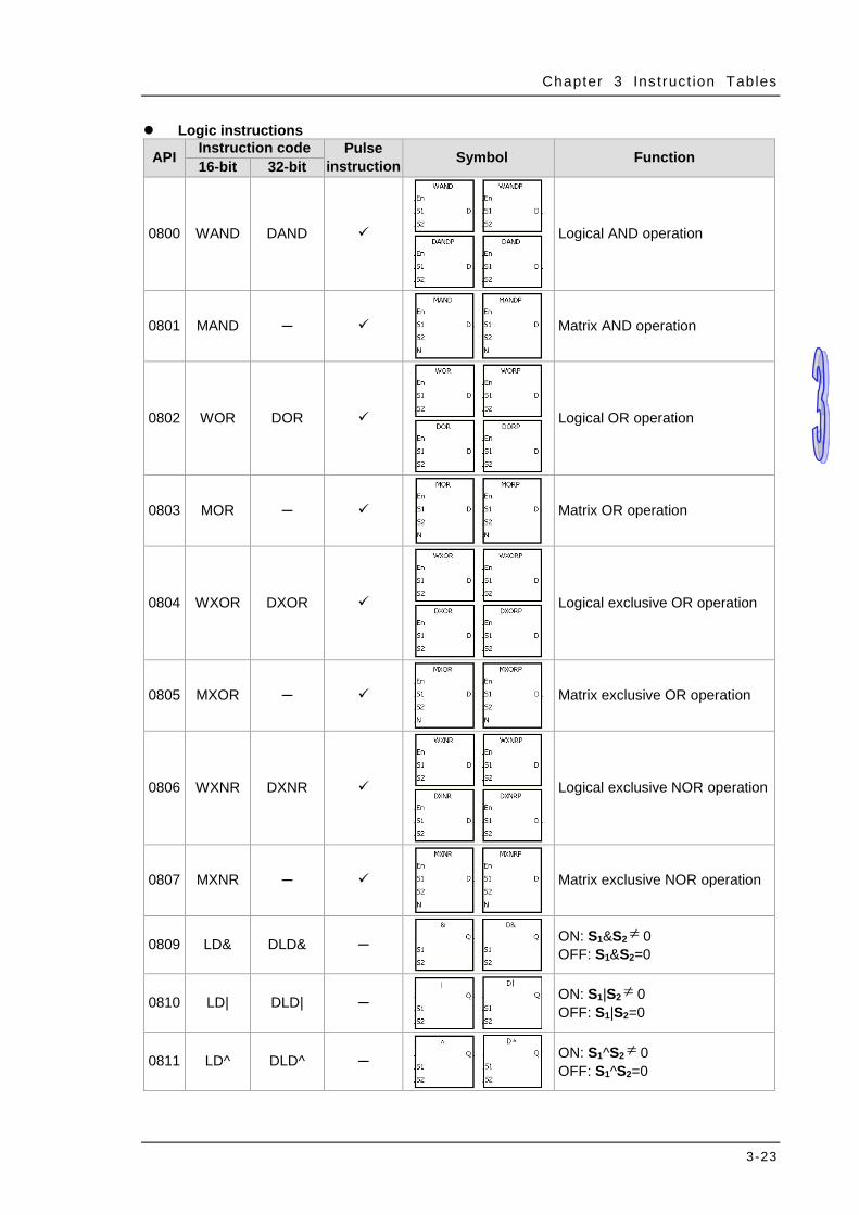
Chapter 3 Ins truct ion Tables
3-23
Logic instructions
API Instruction code Pulse instruction Symbol Function 16-bit 32-bit
0800 WAND DAND
Logical AND operation
0801 MAND ─
Matrix AND operation
0802 WOR DOR
Logical OR operation
0803 MOR ─
Matrix OR operation
0804 WXOR DXOR
Logical exclusive OR operation
0805 MXOR ─
Matrix exclusive OR operation
0806 WXNR DXNR
Logical exclusive NOR operation
0807 MXNR ─
Matrix exclusive NOR operation
0809 LD& DLD& ─
ON: S1&S2 ≠ 0 OFF: S1&S2=0
0810 LD| DLD| ─
ON: S1|S2 ≠ 0 OFF: S1|S2=0
0811 LD^ DLD^ ─
ON: S1^S2 ≠ 0 OFF: S1^S2=0
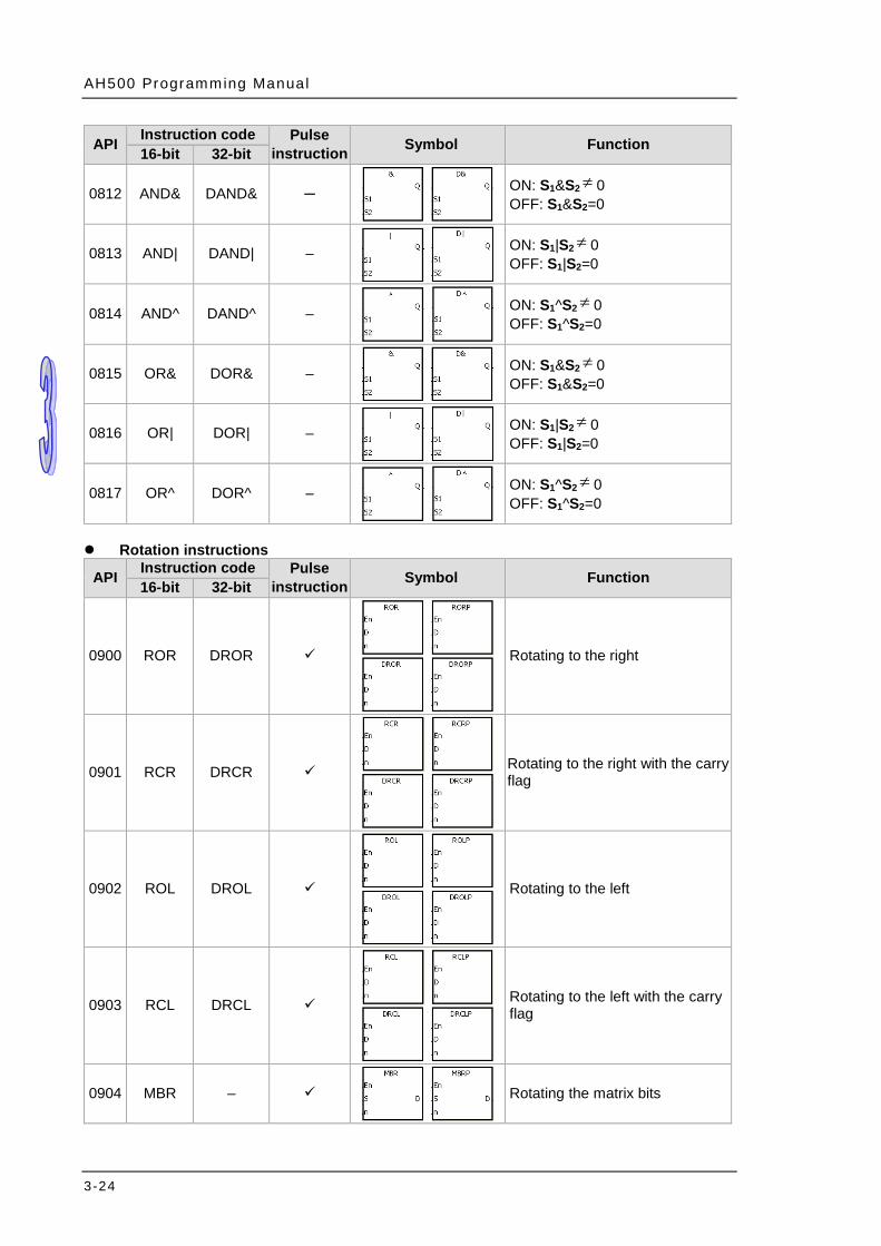
AH500 Programming Manual
3-24
API Instruction code Pulse instruction Symbol Function 16-bit 32-bit
0812 AND& DAND& ─
ON: S1&S2 ≠ 0 OFF: S1&S2=0
0813 AND| DAND| –
ON: S1|S2 ≠ 0 OFF: S1|S2=0
0814 AND^ DAND^ –
ON: S1^S2 ≠ 0 OFF: S1^S2=0
0815 OR& DOR& –
ON: S1&S2 ≠ 0 OFF: S1&S2=0
0816 OR| DOR| –
ON: S1|S2 ≠ 0 OFF: S1|S2=0
0817 OR^ DOR^ –
ON: S1^S2 ≠ 0 OFF: S1^S2=0
Rotation instructions
API Instruction code Pulse instruction Symbol Function 16-bit 32-bit
0900 ROR DROR
Rotating to the right
0901 RCR DRCR
Rotating to the right with the carry flag
0902 ROL DROL
Rotating to the left
0903 RCL DRCL
Rotating to the left with the carry flag
0904 MBR –
Rotating the matrix bits
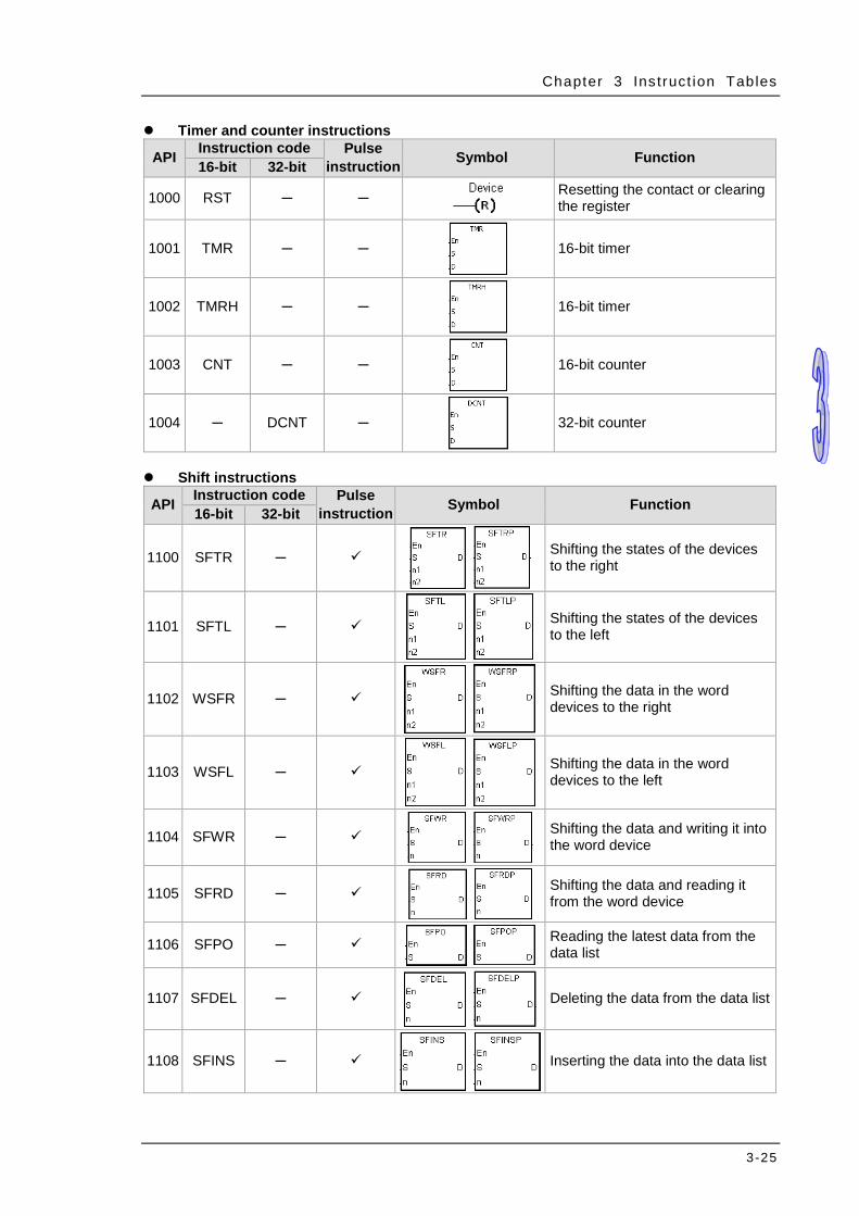
Chapter 3 Ins truct ion Tables
3-25
Timer and counter instructions
API Instruction code Pulse instruction Symbol Function 16-bit 32-bit
1000 RST ─ ─
Resetting the contact or clearing the register
1001 TMR ─ ─
16-bit timer
1002 TMRH ─ ─
16-bit timer
1003 CNT ─ ─
16-bit counter
1004 ─ DCNT ─
32-bit counter
Shift instructions
API Instruction code Pulse instruction Symbol Function 16-bit 32-bit
1100 SFTR ─
Shifting the states of the devices to the right
1101 SFTL ─
Shifting the states of the devices to the left
1102 WSFR ─
Shifting the data in the word devices to the right
1103 WSFL ─
Shifting the data in the word devices to the left
1104 SFWR ─
Shifting the data and writing it into the word device
1105 SFRD ─
Shifting the data and reading it from the word device
1106 SFPO ─
Reading the latest data from the data list
1107 SFDEL ─
Deleting the data from the data list
1108 SFINS ─
Inserting the data into the data list
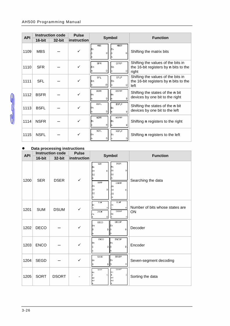
AH500 Programming Manual
3-26
API Instruction code Pulse instruction Symbol Function 16-bit 32-bit
1109 MBS ─
Shifting the matrix bits
1110 SFR ─
Shifting the values of the bits in the 16-bit registers by n bits to the right
1111 SFL ─
Shifting the values of the bits in the 16-bit registers by n bits to the left
1112 BSFR ─
Shifting the states of the n bit devices by one bit to the right
1113 BSFL ─
Shifting the states of the n bit devices by one bit to the left
1114 NSFR ─
Shifting n registers to the right
1115 NSFL ─
Shifting n registers to the left
Data processing instructions
API Instruction code Pulse instruction Symbol Function 16-bit 32-bit
1200 SER DSER
Searching the data
1201 SUM DSUM
Number of bits whose states are ON
1202 DECO ─
Decoder
1203 ENCO ─
Encoder
1204 SEGD ─
Seven-segment decoding
1205 SORT DSORT -
Sorting the data

Chapter 3 Ins truct ion Tables
3-27
API Instruction code Pulse instruction Symbol Function 16-bit 32-bit
1206 ZRST ─
Resetting the zone
1207 BON DBON
Checking the state of the bit
1208 MEAN DMEAN
Mean
1209 CCD ─
Sum check
1210 ABS DABS
Absolute value
1211 MINV ─
Inverting the matrix bits
1212 MBRD ─
Reading the matrix bit
1213 MBWR ─
Writing the matrix bit
1214 MBC ─
Counting the bits with the value 0 or 1
1215 DIS ─
Disuniting the 16-bit data
1216 UNI ─
Uniting the 16-bit data

AH500 Programming Manual
3-28
API Instruction code Pulse instruction Symbol Function 16-bit 32-bit
1217 WSUM DWSUM
Getting the sum
1218 BSET ─
Setting the bit in the word device to ON
1219 BRST ─
Resetting the bit in the word device
1220 BKRST ─
Resetting the specified zone
1221 LIMIT DLIMIT
Confining the value within the bounds
1222 BAND DBAND
Deadband control
1223 ZONE DZONE
Controlling the zone
Structure creation instructions
API Instruction code Pulse instruction Symbol Function 16-bit 32-bit
1300 FOR ─ ─
Start of the nested loop
1301 NEXT ─ ─
End of the nested loop
1302 BREAK ─
Terminating the FOR-NEXT loop
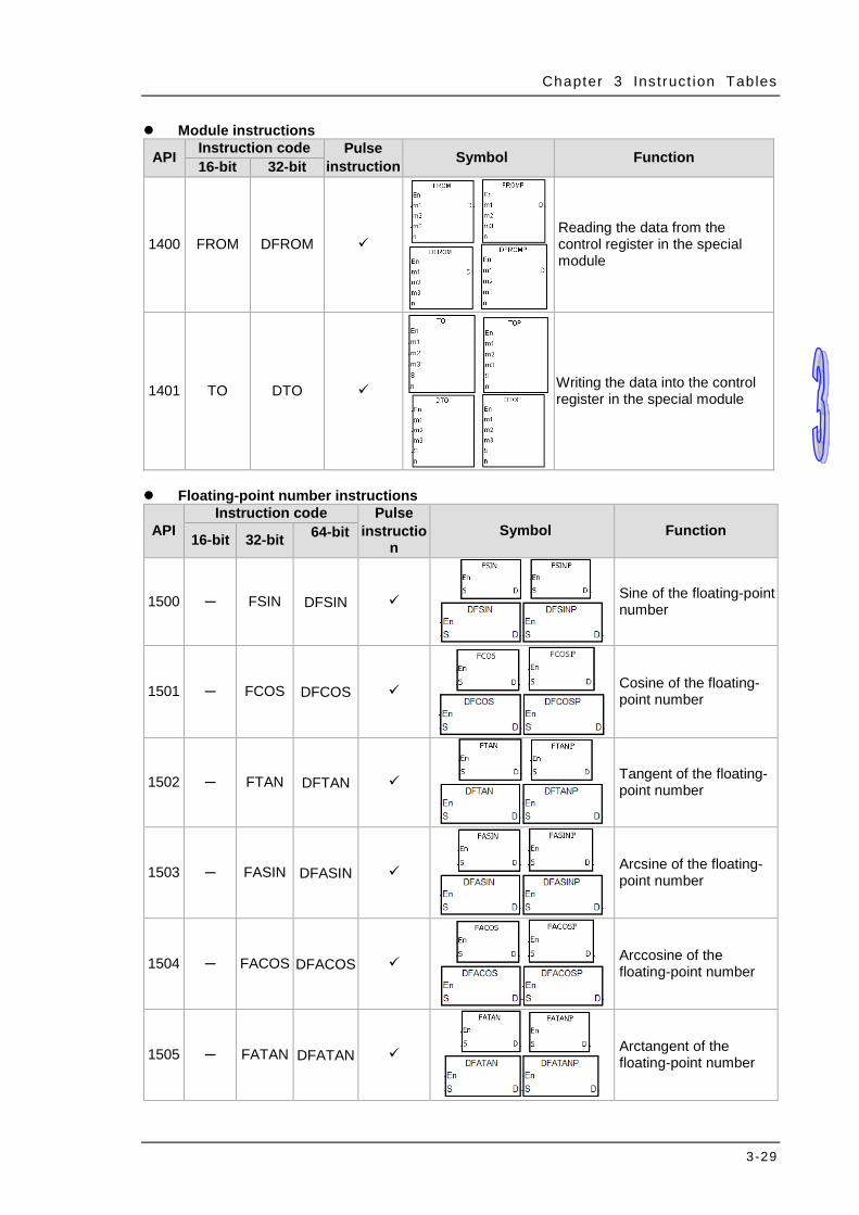
Chapter 3 Ins truct ion Tables
3-29
Module instructions
API Instruction code Pulse instruction Symbol Function 16-bit 32-bit
1400 FROM DFROM
Reading the data from the control register in the special module
1401 TO DTO
Writing the data into the control register in the special module
Floating-point number instructions
API Instruction code Pulse
instruction
Symbol Function 16-bit 32-bit 64-bit
1500 ─ FSIN DFSIN
Sine of the floating-point number
1501 ─ FCOS DFCOS
Cosine of the floating-point number
1502 ─ FTAN DFTAN
Tangent of the floating-point number
1503 ─ FASIN DFASIN
Arcsine of the floating-point number
1504 ─ FACOS DFACOS
Arccosine of the floating-point number
1505 ─ FATAN DFATAN
Arctangent of the floating-point number
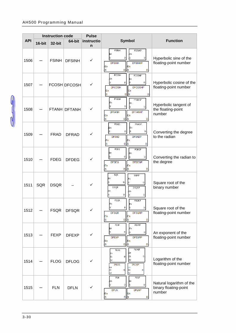
AH500 Programming Manual
3-30
API Instruction code Pulse
instruction
Symbol Function 16-bit 32-bit 64-bit
1506 ─ FSINH DFSINH
Hyperbolic sine of the floating-point number
1507 ─ FCOSH DFCOSH
Hyperbolic cosine of the floating-point number
1508 ─ FTANH DFTANH
Hyperbolic tangent of the floating-point number
1509 ─ FRAD DFRAD
Converting the degree to the radian
1510 ─ FDEG DFDEG
Converting the radian to the degree
1511 SQR DSQR –
Square root of the binary number
1512 ─ FSQR DFSQR
Square root of the floating-point number
1513 ─ FEXP DFEXP
An exponent of the floating-point number
1514 ─ FLOG DFLOG
Logarithm of the floating-point number
1515 ─ FLN DFLN
Natural logarithm of the binary floating-point number
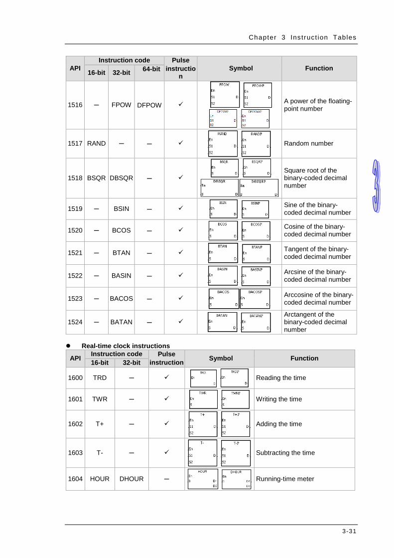
Chapter 3 Ins truct ion Tables
3-31
API Instruction code Pulse
instruction
Symbol Function 16-bit 32-bit 64-bit
1516 ─ FPOW DFPOW
A power of the floating-point number
1517 RAND ─ ─
Random number
1518 BSQR DBSQR ─
Square root of the binary-coded decimal number
1519 ─ BSIN ─
Sine of the binary-coded decimal number
1520 ─ BCOS ─
Cosine of the binary-coded decimal number
1521 ─ BTAN ─
Tangent of the binary-coded decimal number
1522 ─ BASIN ─
Arcsine of the binary-coded decimal number
1523 ─ BACOS ─
Arccosine of the binary-coded decimal number
1524 ─ BATAN ─
Arctangent of the binary-coded decimal number
Real-time clock instructions
API Instruction code Pulse instruction Symbol Function 16-bit 32-bit
1600 TRD ─
Reading the time
1601 TWR ─
Writing the time
1602 T+ ─
Adding the time
1603 T- ─
Subtracting the time
1604 HOUR DHOUR ─
Running-time meter
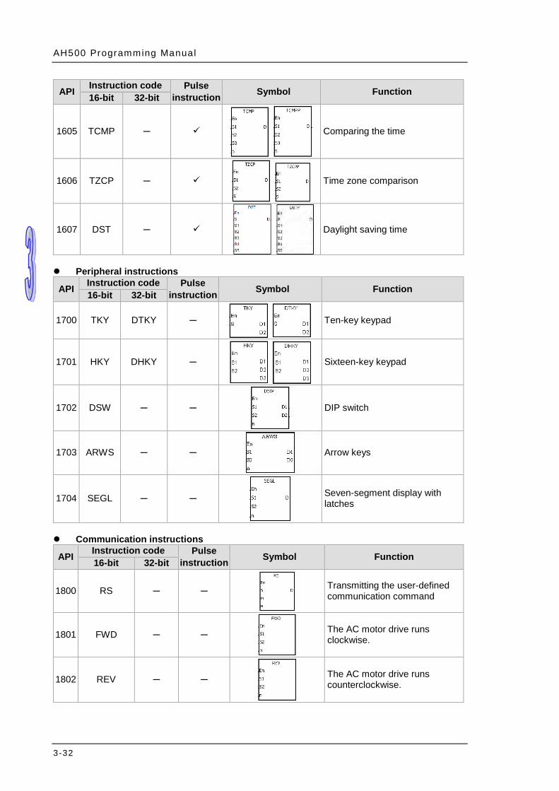
AH500 Programming Manual
3-32
API Instruction code Pulse instruction Symbol Function 16-bit 32-bit
1605 TCMP ─
Comparing the time
1606 TZCP ─
Time zone comparison
1607 DST ─
Daylight saving time
Peripheral instructions
API Instruction code Pulse instruction Symbol Function 16-bit 32-bit
1700 TKY DTKY ─
Ten-key keypad
1701 HKY DHKY ─
Sixteen-key keypad
1702 DSW ─ ─
DIP switch
1703 ARWS ─ ─
Arrow keys
1704 SEGL ─ ─
Seven-segment display with latches
Communication instructions
API Instruction code Pulse instruction Symbol Function 16-bit 32-bit
1800 RS ─ ─
Transmitting the user-defined communication command
1801 FWD ─ ─
The AC motor drive runs clockwise.
1802 REV ─ ─
The AC motor drive runs counterclockwise.
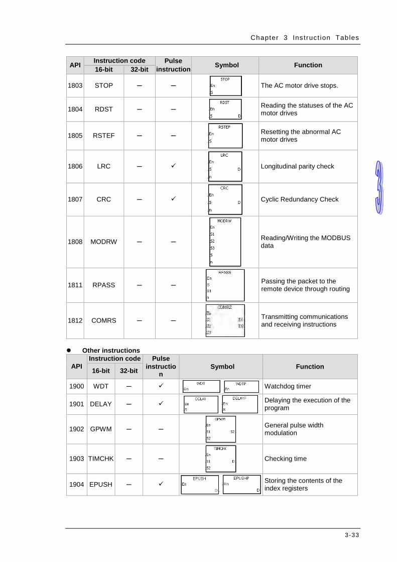
Chapter 3 Ins truct ion Tables
3-33
API Instruction code Pulse instruction Symbol Function 16-bit 32-bit
1803 STOP ─ ─
The AC motor drive stops.
1804 RDST ─ ─
Reading the statuses of the AC motor drives
1805 RSTEF ─ ─
Resetting the abnormal AC motor drives
1806 LRC ─
Longitudinal parity check
1807 CRC ─
Cyclic Redundancy Check
1808 MODRW ─ ─
Reading/Writing the MODBUS data
1811 RPASS ─ ─
Passing the packet to the remote device through routing
1812 COMRS ─ ─
Transmitting communications and receiving instructions
Other instructions
API Instruction code Pulse
instruction
Symbol Function 16-bit 32-bit
1900 WDT ─
Watchdog timer
1901 DELAY ─
Delaying the execution of the program
1902 GPWM ─ ─
General pulse width modulation
1903 TIMCHK ─ ─
Checking time
1904 EPUSH ─
Storing the contents of the index registers

AH500 Programming Manual
3-34
API Instruction code Pulse
instruction
Symbol Function 16-bit 32-bit
1905 EPOP ─
Reading the data into the index registers
String processing instructions
API Instruction code Pulse instruction Symbol Function 16-bit 32-bit
2100 BINDA DBINDA
Converting the singed decimal number into the ASCII code
2101 BINHA DBINHA
Converting the binary hexadecimal number into the hexadecimal ASCII code
2102 BCDDA DBCDDA
Converting the binary-coded decimal number into the ASCII code
2103 DABIN DDABIN
Converting the signed decimal ASCII code into the signed decimal binary number
2104 HABIN DHABIN
Converting the hexadecimal ASCII code into the hexadecimal binary number
2105 DABCD DDABCD
Converting the ASCII code into the binary-coded decimal number
2106 $LEN ─
Calculating the length of the string
2107 $STR $DSTR
Converting the binary number into the string

Chapter 3 Ins truct ion Tables
3-35
API Instruction code Pulse instruction Symbol Function 16-bit 32-bit
2108 $VAL $DVAL
Converting the string into the binary number
2109 $FSTR ─
Converting the floating-point number into the string
2110 $FVAL ─
Converting the string into the floating-point number
2111 $RIGHT ─
The retrieve of the characters in the string begins from the right.
2112 $LEFT ─
The retrieve of the characters in the string begins from the left.
2113 $MIDR ─
Retrieving a part of the string
2114 $MIDW ─
Replacing a part of the string
2115 $SER ─
Searching the string
2116 $RPLC ─
Replacing the characters in the string
2117 $DEL ─
Deleting the characters in the string
2118 $CLR ─
Clearing the string
2119 $INS ─
Inserting the string
2120 $FMOD ─
Converting the floating-point number into the binary-coded decimal floating-point number
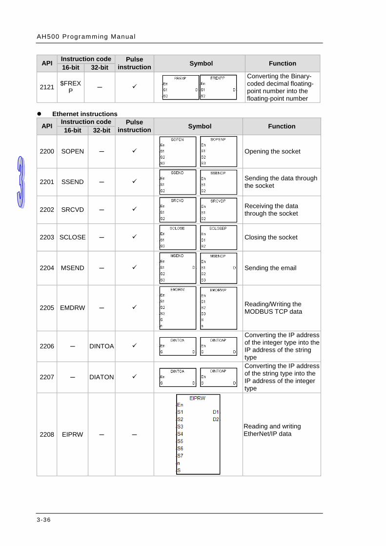
AH500 Programming Manual
3-36
API Instruction code Pulse instruction Symbol Function 16-bit 32-bit
2121 $FREXP ─
Converting the Binary-coded decimal floating-point number into the floating-point number
Ethernet instructions
API Instruction code Pulse instruction Symbol Function 16-bit 32-bit
2200 SOPEN ─
Opening the socket
2201 SSEND ─
Sending the data through the socket
2202 SRCVD ─
Receiving the data through the socket
2203 SCLOSE ─
Closing the socket
2204 MSEND ─
Sending the email
2205 EMDRW ─
Reading/Writing the MODBUS TCP data
2206 ─ DINTOA
Converting the IP address of the integer type into the IP address of the string type
2207 ─ DIATON
Converting the IP address of the string type into the IP address of the integer type
2208 EIPRW ─ ─
Reading and writing EtherNet/IP data
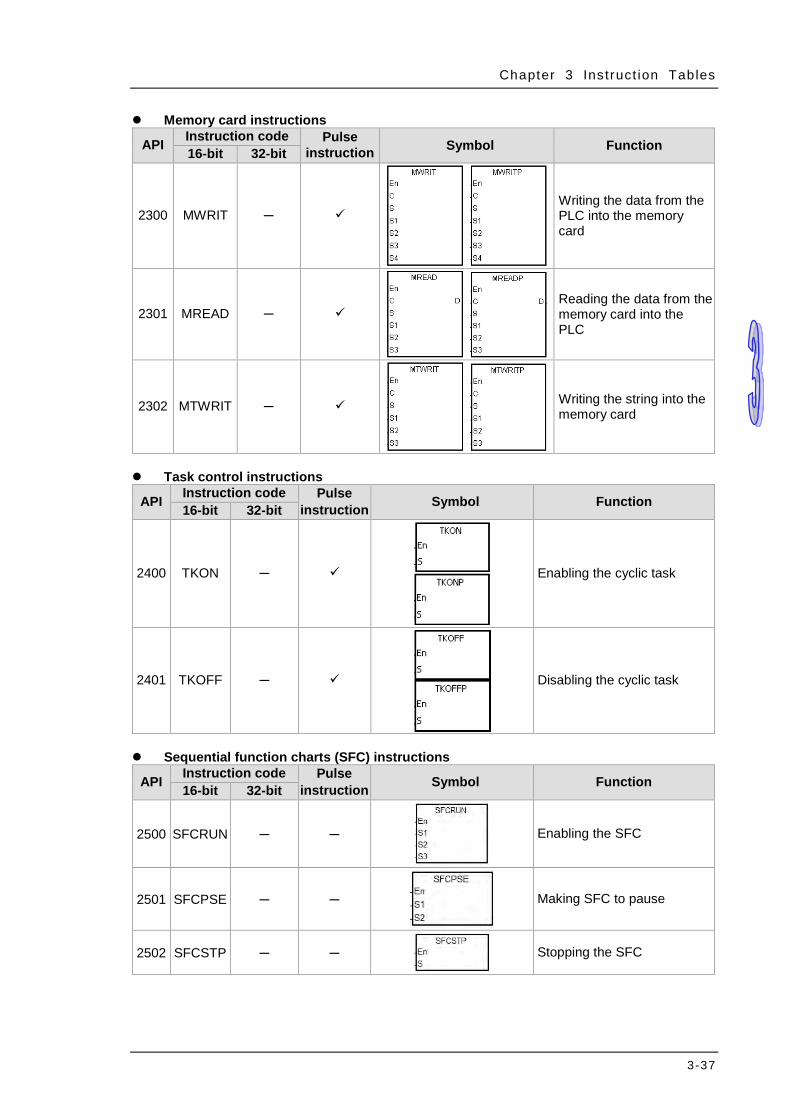
Chapter 3 Ins truct ion Tables
3-37
Memory card instructions
API Instruction code Pulse instruction Symbol Function 16-bit 32-bit
2300 MWRIT ─
Writing the data from the PLC into the memory card
2301 MREAD ─
Reading the data from the memory card into the PLC
2302 MTWRIT ─
Writing the string into the memory card
Task control instructions
API Instruction code Pulse instruction Symbol Function 16-bit 32-bit
2400 TKON ─
Enabling the cyclic task
2401 TKOFF ─
Disabling the cyclic task
Sequential function charts (SFC) instructions
API Instruction code Pulse instruction Symbol Function 16-bit 32-bit
2500 SFCRUN ─ ─
Enabling the SFC
2501 SFCPSE ─ ─
Making SFC to pause
2502 SFCSTP ─ ─
Stopping the SFC
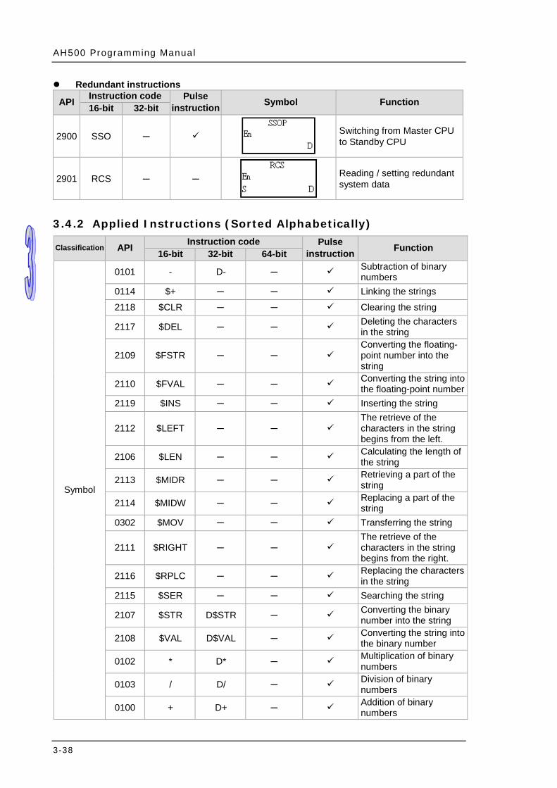
AH500 Programming Manual
3-38
Redundant instructions
API Instruction code Pulse instruction Symbol Function 16-bit 32-bit
2900 SSO ─
Switching from Master CPU to Standby CPU
2901 RCS ─ ─
Reading / setting redundant system data
3.4.2 Applied Instructions (Sorted Alphabetically)
Classification API Instruction code Pulse instruction Function 16-bit 32-bit 64-bit
Symbol
0101 - D- ─ Subtraction of binary numbers
0114 $+ ─ ─ Linking the strings 2118 $CLR ─ ─ Clearing the string
2117 $DEL ─ ─ Deleting the characters in the string
2109 $FSTR ─ ─ Converting the floating-point number into the string
2110 $FVAL ─ ─ Converting the string into the floating-point number
2119 $INS ─ ─ Inserting the string
2112 $LEFT ─ ─ The retrieve of the characters in the string begins from the left.
2106 $LEN ─ ─ Calculating the length of the string
2113 $MIDR ─ ─ Retrieving a part of the string
2114 $MIDW ─ ─ Replacing a part of the string
0302 $MOV ─ ─ Transferring the string
2111 $RIGHT ─ ─ The retrieve of the characters in the string begins from the right.
2116 $RPLC ─ ─ Replacing the characters in the string
2115 $SER ─ ─ Searching the string
2107 $STR D$STR ─ Converting the binary number into the string
2108 $VAL D$VAL ─ Converting the string into the binary number
0102 * D* ─ Multiplication of binary numbers
0103 / D/ ─ Division of binary numbers
0100 + D+ ─ Addition of binary numbers

Chapter 3 Ins truct ion Tables
3-39
Classification API Instruction code Pulse instruction Function 16-bit 32-bit 64-bit
A
1210 ABS DABS ─ Absolute value
0705 ABSD DABSD ─ ─ Absolute drum sequencer
0700 ALT ─ ─ Alternating between ON and OFF
0046 AND$< ─ ─ ─ Comparing the strings ON: S1<S2 OFF: S1≧S2
0047 AND$<= ─ ─ ─ Comparing the strings ON: S1≦S2 OFF: S1>S2
0043 AND$<> ─ ─ ─ Comparing the strings ON: S1≠S2 OFF: S1=S2
0042 AND$= ─ ─ ─ Comparing the strings ON: S1=S2 OFF S1≠S2
0044 AND$> ─ ─ ─ Comparing the strings ON: S1>S2 OFF: S1≦S2
0045 AND$>= ─ ─ ─ Comparing the strings ON: S1≧S2 OFF: S1<S2
0812 AND& DAND& ─ ─ ON: S1&S2 ≠ 0 OFF: S1&S2=0
0814 AND^ DAND^ ─ ─ ON: S1^S2≠ 0 OFF: S1^S2=0
0813 AND| DAND| ─ ─ ON: S1|S2 ≠ 0 OFF: S1|S2=0
0010 AND< DAND< ─ ─
Comparing the values ON: S1<S2
OFF: S1≧S2
0011 AND<= DAND<= ─ ─
Comparing the values ON: S1≦S2
OFF: S1>S2
0007 AND<> DAND<> ─ ─ Comparing the values ON: S1≠S2 OFF: S1=S2
0006 AND= DAND= ─ ─ Comparing the values ON: S1=S2 OFF: S1≠S2
0008 AND> DAND> ─ ─
Comparing the values ON: S1>S2
OFF: S1≦S22
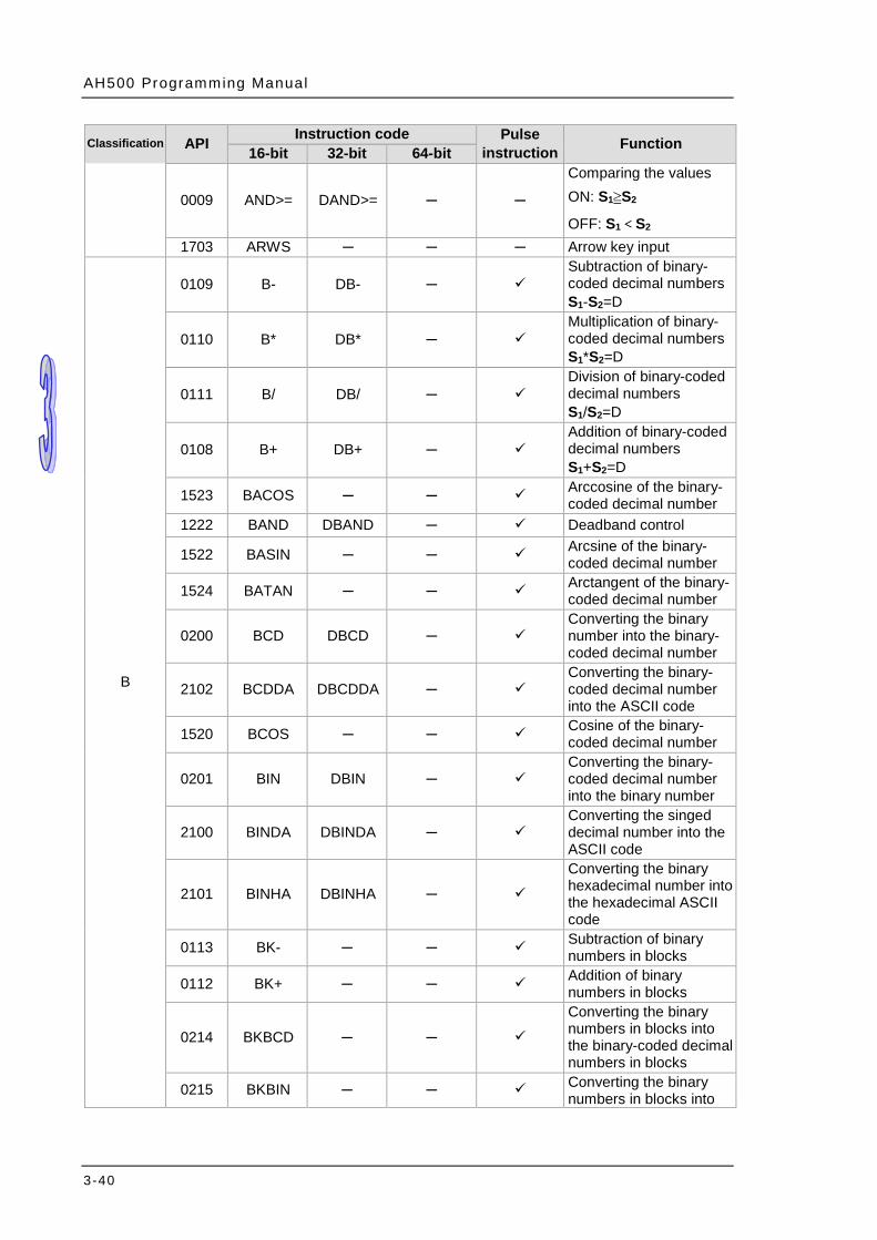
AH500 Programming Manual
3-40
Classification API Instruction code Pulse instruction Function 16-bit 32-bit 64-bit
0009 AND>= DAND>= ─ ─
Comparing the values ON: S1≧S2
OFF: S1<S2 1703 ARWS ─ ─ ─ Arrow key input
B
0109 B- DB- ─ Subtraction of binary-coded decimal numbers S1-S2=D
0110 B* DB* ─ Multiplication of binary-coded decimal numbers S1*S2=D
0111 B/ DB/ ─ Division of binary-coded decimal numbers S1/S2=D
0108 B+ DB+ ─ Addition of binary-coded decimal numbers S1+S2=D
1523 BACOS ─ ─ Arccosine of the binary-coded decimal number
1222 BAND DBAND ─ Deadband control
1522 BASIN ─ ─ Arcsine of the binary-coded decimal number
1524 BATAN ─ ─ Arctangent of the binary-coded decimal number
0200 BCD DBCD ─ Converting the binary number into the binary-coded decimal number
2102 BCDDA DBCDDA ─ Converting the binary-coded decimal number into the ASCII code
1520 BCOS ─ ─ Cosine of the binary-coded decimal number
0201 BIN DBIN ─ Converting the binary-coded decimal number into the binary number
2100 BINDA DBINDA ─ Converting the singed decimal number into the ASCII code
2101 BINHA DBINHA ─ Converting the binary hexadecimal number into the hexadecimal ASCII code
0113 BK- ─ ─ Subtraction of binary numbers in blocks
0112 BK+ ─ ─ Addition of binary numbers in blocks
0214 BKBCD ─ ─ Converting the binary numbers in blocks into the binary-coded decimal numbers in blocks
0215 BKBIN ─ ─ Converting the binary numbers in blocks into
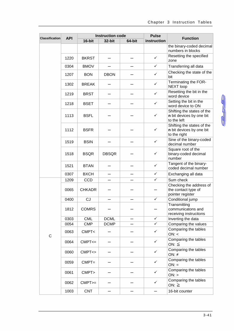
Chapter 3 Ins truct ion Tables
3-41
Classification API Instruction code Pulse instruction Function 16-bit 32-bit 64-bit
the binary-coded decimal numbers in blocks
1220 BKRST ─ ─ Resetting the specified zone
0304 BMOV ─ ─ Transferring all data
1207 BON DBON ─ Checking the state of the bit
1302 BREAK ─ ─ Terminating the FOR-NEXT loop
1219 BRST ─ ─ Resetting the bit in the word device
1218 BSET ─ ─ Setting the bit in the word device to ON
1113 BSFL ─ ─ Shifting the states of the n bit devices by one bit to the left
1112 BSFR ─ ─ Shifting the states of the n bit devices by one bit to the right
1519 BSIN ─ ─ Sine of the binary-coded decimal number
1518 BSQR DBSQR ─ Square root of the binary-coded decimal number
1521 BTAN ─ ─ Tangent of the binary-coded decimal number
0307 BXCH ─ ─ Exchanging all data
C
1209 CCD ─ ─ Sum check
0065 CHKADR ─ ─ ─ Checking the address of the contact type of pointer register
0400 CJ ─ ─ Conditional jump
1812 COMRS ─ ─ ─ Transmitting communicatons and receiving instrucitons
0303 CML DCML ─ Inverting the data 0054 CMP DCMP ─ Comparing the values
0063 CMPT< ─ ─ Comparing the tables ON: <
0064 CMPT<= ─ ─ Comparing the tables ON: ≦
0060 CMPT<> ─ ─ Comparing the tables ON: ≠
0059 CMPT= ─ ─ Comparing the tables ON: =
0061 CMPT> ─ ─ Comparing the tables ON: >
0062 CMPT>= ─ ─ Comparing the tables ON: ≧
1003 CNT ─ ─ ─ 16-bit counter

AH500 Programming Manual
3-42
Classification API Instruction code Pulse instruction Function 16-bit 32-bit 64-bit
0219 COLM DCOLM ─ Converting a line of data into a column of data
1807 CRC ─ ─ ─ Cyclic Redundancy Check
D
2105 DABCD DDABCD ─ Converting the ASCII code into the binary-coded decimal number
2103 DABIN DDABIN ─
Converting the signed decimal ASCII code into the signed decimal binary number
1004 DCNT ─ ─ – 32-bit counter
0116 DEC DDEC ─ Subtracting one from the binary number
1202 DECO ─ ─ Decoder
1901 DELAY ─ ─ Delaying the execution of the program
0301 ─ ─ DFMOV Transferring the 64-bit floating-point number
0500 DI ─ ─ ─ Disabling the interrupt
2207 DIATON ─ ─ Converting the IP address of the string type into the IP address of the integer type
2206 DINTOA ─ ─
Converting the IP address of the integer type into the IP address of the string type
1215 DIS ─ ─ Disuniting the 16-bit data
0118 DIV16 DIV32 ─ Division of binary numbers for 16-bit/32-bit
0708 ─ DPIDE ─ ─ PID algorithm
1607 DST ─ ─ Daylight saving time 1702 DSW ─ ─ ─ Digital switch input
E
0501 EI ─ ─ ─ Enabling the interrupt
2205 EMDRW ─ ─ Reading/Writing the MODBUS TCP data
1203 ENCO ─ ─ Encoder
1905 EPOP ─ ─ Reading the data into the index registers
1904 EPUSH ─ ─ Storing the contents of the index registers
2208 EIPRW ─ ─ ─ Reading and writing EtherNet/IP data
F
0105 ─ F- DF- Subtraction of floating-point numbers S1-S2=D
0106 ─ F* DF* Multiplication of floating-point numbers S1*S2=D
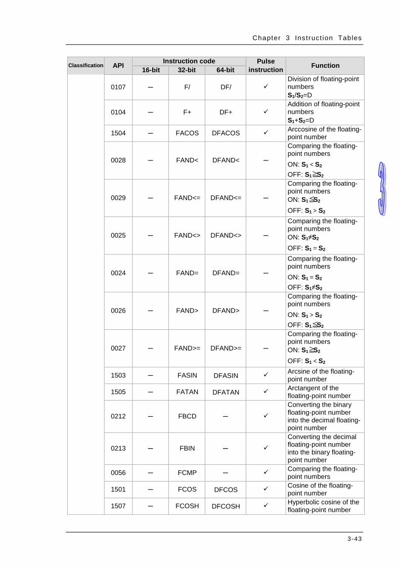
Chapter 3 Ins truct ion Tables
3-43
Classification API Instruction code Pulse instruction Function 16-bit 32-bit 64-bit
0107 ─ F/ DF/ Division of floating-point numbers S1/S2=D
0104 ─ F+ DF+ Addition of floating-point numbers S1+S2=D
1504 ─ FACOS DFACOS Arccosine of the floating-point number
0028 ─ FAND< DFAND< ─
Comparing the floating-point numbers ON: S1<S2 OFF: S1≧S2
0029 ─ FAND<= DFAND<= ─
Comparing the floating-point numbers ON: S1≦S2 OFF: S1>S2
0025 ─ FAND<> DFAND<> ─
Comparing the floating-point numbers ON: S1≠S2 OFF: S1=S2
0024 ─ FAND= DFAND= ─
Comparing the floating-point numbers ON: S1=S2 OFF: S1≠S2
0026 ─ FAND> DFAND> ─
Comparing the floating-point numbers ON: S1>S2 OFF: S1≦S2
0027 ─ FAND>= DFAND>= ─
Comparing the floating-point numbers ON: S1≧S2 OFF: S1<S2
1503 ─ FASIN DFASIN Arcsine of the floating-point number
1505 ─ FATAN DFATAN Arctangent of the floating-point number
0212 ─ FBCD ─
Converting the binary floating-point number into the decimal floating-point number
0213 ─ FBIN ─ Converting the decimal floating-point number into the binary floating-point number
0056 ─ FCMP ─ Comparing the floating-point numbers
1501 ─ FCOS DFCOS Cosine of the floating-point number
1507 ─ FCOSH DFCOSH Hyperbolic cosine of the floating-point number

AH500 Programming Manual
3-44
Classification API Instruction code Pulse instruction Function 16-bit 32-bit 64-bit
1510 ─ FDEG DFDEG Converting the radian to the degree
1513 ─ FEXP DFEXP An exponent of the floating-point number
0205 ─ FINT DFINT Converting the 64-bit floating-point number into the binary integer
0022 ─ FLD< DFLD< ─
Comparing the floating-point numbers ON: S1<S2
OFF: S1≧S2
0023 ─ FLD<= DFLD<= ─
Comparing the floating-point numbers ON: S1≦S2
OFF: S1>S2
0019 ─ FLD<> DFLD<> ─
Comparing the floating-point numbers ON: S1≠S2 OFF: S1=S2
0018 ─ FLD= DFLD= ─
Comparing the floating-point numbers ON: S1=S2 OFF: S1≠S2
0020 ─ FLD> DFLD> ─
Comparing the floating-point numbers ON: S1>S2
OFF: S1≦S2
0021 ─ FLD>= DFLD>= ─
Comparing the floating-point numbers ON: S1≧S2
OFF: S1<S2
1515 ─ FLN DFLN Natural logarithm of the binary floating-point number
1514 ─ FLOG DFLOG Logarithm of the floating-point number
0202 FLT DFLT ─ Converting the binary integer into the binary floating-point number
0203 FLTD DFLTD ─ Converting the binary integer into the 64-bit floating-point number
2120 FMOD ─ ─ Converting the floating-point number into the binary-coded decimal floating-point number
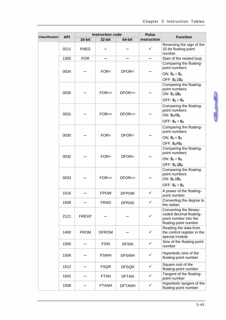
Chapter 3 Ins truct ion Tables
3-45
Classification API Instruction code Pulse instruction Function 16-bit 32-bit 64-bit
0211 FNEG ─ ─ Reversing the sign of the 32-bit floating-point number
1300 FOR ─ ─ ─ Start of the nested loop
0034 ─ FOR< DFOR< ─
Comparing the floating-point numbers ON: S1<S2 OFF: S1≧S2
0035 ─ FOR<= DFOR<= ─
Comparing the floating-point numbers ON: S1≦S2 OFF: S1>S2
0031 ─ FOR<> DFOR<> ─
Comparing the floating-point numbers ON: S1≠S2 OFF: S1=S2
0030 ─ FOR= DFOR= ─
Comparing the floating-point numbers ON: S1=S2 OFF: S1≠S2
0032 ─ FOR> DFOR> ─
Comparing the floating-point numbers ON: S1>S2 OFF: S1≦S2
0033 ─ FOR>= DFOR>= ─
Comparing the floating-point numbers ON: S1≧S2 OFF: S1<S2
1516 ─ FPOW DFPOW A power of the floating-point number
1509 ─ FRAD DFRAD Converting the degree to the radian
2121 FREXP ─ ─ Converting the Binary-coded decimal floating-point number into the floating-point number
1400 FROM DFROM ─ Reading the data from the control register in the special module
1500 ─ FSIN DFSIN Sine of the floating-point number
1506 ─ FSINH DFSINH Hyperbolic sine of the floating-point number
1512 ─ FSQR DFSQR Square root of the floating-point number
1502 ─ FTAN DFTAN Tangent of the floating-point number
1508 ─ FTANH DFTANH Hyperbolic tangent of the floating-point number

AH500 Programming Manual
3-46
Classification API Instruction code Pulse instruction Function 16-bit 32-bit 64-bit
1801 FWD ─ ─ ─ The AC motor drive runs clockwise.
0057 ─ FZCP ─ Floating-point zone comparison
G
0209 GBIN DGBIN ─ Converting the Gray code into the binary number
0402 GOEND ─ ─ ─ Jumping to END
1902 GPWM ─ ─ ─ General pulse width modulation
0208 GRY DGRY ─ Converting the binary number into the Gray code
H 2104 HABIN DHABIN ─
Converting the hexadecimal ASCII code into the hexadecimal binary number
1701 HKY DHKY ─ ─ Hexadecimal key input 1604 HOUR DHOUR ─ ─ Running-time meter
I
0502 IMASK ─ ─ ─ Controlling the interrupt
0115 INC DINC ─ Adding one to the binary number
0706 INCD ─ ─ ─ Incremental drum sequencer
0204 INT DINT ─ Converting the 32-bit floating-point number into the binary integer
J 0401 JMP ─ ─ ─ Unconditional jump
L
0040 LD$< ─ ─ ─ Comparing the strings ON: S1<S2 OFF: S1≧S2
0041 LD$<= ─ ─ ─ Comparing the strings ON: S1≦S2 OFF: S1>S2
0037 LD$<> ─ ─ ─ Comparing the strings ON: S1≠S2 OFF: S1=S2
0036 LD$= ─ ─ ─ Comparing the strings ON: S1=S2 ON: S1≠S2
0038 LD$> ─ ─ ─ Comparing the strings ON: S1>S2 OFF: S1≦S2
0039 LD$>= ─ ─ ─ Comparing the strings ON: S1≧S2 OFF: S1<S2
0809 LD& DLD& ─ ─ ON: S1&S2 ≠ 0 OFF: S1&S2=0
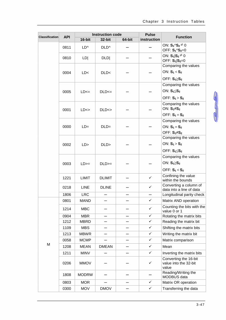
Chapter 3 Ins truct ion Tables
3-47
Classification API Instruction code Pulse instruction Function 16-bit 32-bit 64-bit
0811 LD^ DLD^ ─ ─ ON: S1^S2≠ 0 OFF: S1^S2=0
0810 LD| DLD| ─ ─ ON: S1|S2 ≠ 0 OFF: S1|S2=0
0004 LD< DLD< ─ ─
Comparing the values ON: S1<S2
OFF: S1≧S2
0005 LD<= DLD<= ─ ─
Comparing the values ON: S1≦S2
OFF: S1>S2
0001 LD<> DLD<> ─ ─ Comparing the values ON: S1≠S2 OFF: S1=S2
0000 LD= DLD= ─ ─ Comparing the values ON: S1=S2 OFF: S1≠S2
0002 LD> DLD> ─ ─
Comparing the values ON: S1>S2
OFF: S1≦S2
0003 LD>= DLD>= ─ ─
Comparing the values ON: S1≧S2
OFF: S1<S2
1221 LIMIT DLIMIT ─ Confining the value within the bounds
0218 LINE DLINE ─ Converting a column of data into a line of data
1806 LRC ─ ─ ─ Longitudinal parity check
M
0801 MAND ─ ─ Matrix AND operation
1214 MBC ─ ─ Counting the bits with the value 0 or 1
0904 MBR ─ ─ Rotating the matrix bits 1212 MBRD ─ ─ Reading the matrix bit 1109 MBS ─ ─ Shifting the matrix bits 1213 MBWR ─ ─ Writing the matrix bit 0058 MCMP ─ ─ Matrix comparison
1208 MEAN DMEAN ─ Mean
1211 MINV ─ ─ Inverting the matrix bits
0206 MMOV ─ ─ Converting the 16-bit value into the 32-bit value
1808 MODRW ─ ─ ─ Reading/Writing the MODBUS data
0803 MOR ─ ─ Matrix OR operation 0300 MOV DMOV ─ Transferring the data

AH500 Programming Manual
3-48
Classification API Instruction code Pulse instruction Function 16-bit 32-bit 64-bit
0310 MOVB ─ ─ Transferring several bits
2301 MREAD ─ ─ ─ Reading the data from the memory card into the PLC
2204 MSEND ─ ─ Sending the email 0704 MTR ─ ─ ─ Matrix input
2302 MTWRIT ─ ─ ─ Writing the string into the memory card
0117 MUL16 MUL32 ─ Multiplication of binary numbers for 16-bit/32-bit
2300 MWRIT ─ ─ ─ Writing the data from the PLC into the memory card
0807 MXNR ─ ─ Matrix exclusive NOR operation
0805 MXOR ─ ─ Matrix exclusive OR operation
N
0210 NEG DNEG ─ Two’s complement 1301 NEXT ─ ─ ─ End of the nested loop
0305 NMOV DNMOV ─ Transferring the data to several devices
1115 NSFL ─ ─ Shifting n registers to the left
1114 NSFR ─ ─ Shifting n registers to the right
O
0052 OR$< ─ ─ ─ Comparing the strings ON: S1<S2 OFF: S1≧S2
0053 OR$<= ─ ─ ─ Comparing the strings ON: S1≦S2 OFF: S1>S2
0049 OR$<> ─ ─ ─ Comparing the strings ON: S1≠S2 OFF: S1=S2
0048 OR$= ─ ─ ─ Comparing the strings ON: S1=S2 OFF: S1≠S2
0050 OR$> ─ ─ ─ Comparing the strings ON: S1>S2 OFF: S1≦S2
0051 OR$>= ─ ─ ─ Comparing the strings ON: S1≧S2 OFF: S11<S22
0815 OR& DOR& ─ ─ ON: S1&S2 ≠ 0 OFF: S1&S22=0
0817 OR^ DOR^ ─ ─ ON: S1^S2 ≠ 0 OFF: S1^S2=0
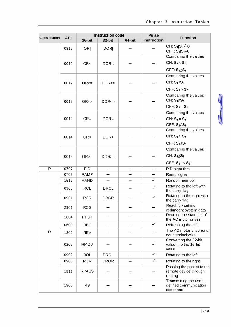
Chapter 3 Ins truct ion Tables
3-49
Classification API Instruction code Pulse instruction Function 16-bit 32-bit 64-bit
0816 OR| DOR| ─ ─ ON: S1|S2 ≠ 0 OFF: S1|S2=0
0016 OR< DOR< ─ ─
Comparing the values ON: S1<S2
OFF: S1≧S2
0017 OR<= DOR<= ─ ─
Comparing the values ON: S1≦S2
OFF: S1>S2
0013 OR<> DOR<> ─ ─ Comparing the values ON: S1≠S2 OFF: S1=S2
0012 OR= DOR= ─ ─ Comparing the values ON: S1=S2 OFF: S1≠S2
0014 OR> DOR> ─ ─
Comparing the values ON: S1>S2
OFF: S1≦S2
0015 OR>= DOR>= ─ ─
Comparing the values ON: S1≧S2
OFF: S11<S2 P 0707 PID ─ ─ ─ PID algorithm
R
0703 RAMP ─ ─ ─ Ramp signal 1517 RAND ─ ─ Random number
0903 RCL DRCL ─ Rotating to the left with the carry flag
0901 RCR DRCR ─ Rotating to the right with the carry flag
2901 RCS ─ ─ ─ Reading / setting redundant system data
1804 RDST ─ ─ ─ Reading the statuses of the AC motor drives
0600 REF ─ ─ Refreshing the I/O
1802 REV ─ ─ ─ The AC motor drive runs counterclockwise.
0207 RMOV ─ ─ Converting the 32-bit value into the 16-bit value
0902 ROL DROL ─ Rotating to the left 0900 ROR DROR ─ Rotating to the right
1811 RPASS ─ ─ ─ Passing the packet to the remote device through routing
1800 RS ─ ─ ─ Transmitting the user-defined communication command
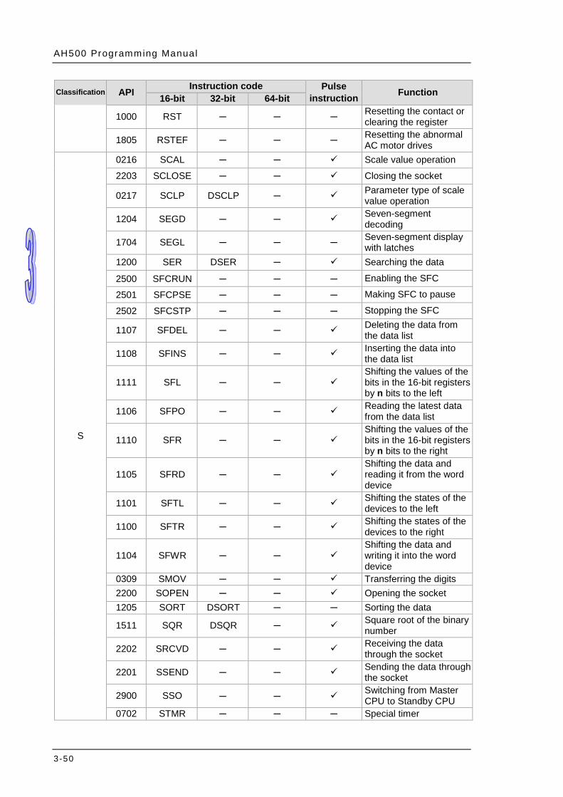
AH500 Programming Manual
3-50
Classification API Instruction code Pulse instruction Function 16-bit 32-bit 64-bit
1000 RST ─ ─ ─ Resetting the contact or clearing the register
1805 RSTEF ─ ─ ─ Resetting the abnormal AC motor drives
S
0216 SCAL ─ ─ Scale value operation
2203 SCLOSE ─ ─ Closing the socket
0217 SCLP DSCLP ─ Parameter type of scale value operation
1204 SEGD ─ ─ Seven-segment decoding
1704 SEGL ─ ─ ─ Seven-segment display with latches
1200 SER DSER ─ Searching the data
2500 SFCRUN ─ ─ ─ Enabling the SFC
2501 SFCPSE ─ ─ ─ Making SFC to pause
2502 SFCSTP ─ ─ ─ Stopping the SFC
1107 SFDEL ─ ─ Deleting the data from the data list
1108 SFINS ─ ─ Inserting the data into the data list
1111 SFL ─ ─ Shifting the values of the bits in the 16-bit registers by n bits to the left
1106 SFPO ─ ─ Reading the latest data from the data list
1110 SFR ─ ─ Shifting the values of the bits in the 16-bit registers by n bits to the right
1105 SFRD ─ ─ Shifting the data and reading it from the word device
1101 SFTL ─ ─ Shifting the states of the devices to the left
1100 SFTR ─ ─ Shifting the states of the devices to the right
1104 SFWR ─ ─ Shifting the data and writing it into the word device
0309 SMOV ─ ─ Transferring the digits 2200 SOPEN ─ ─ Opening the socket 1205 SORT DSORT ─ ─ Sorting the data
1511 SQR DSQR ─ Square root of the binary number
2202 SRCVD ─ ─ Receiving the data through the socket
2201 SSEND ─ ─ Sending the data through the socket
2900 SSO ─ ─ Switching from Master CPU to Standby CPU
0702 STMR ─ ─ ─ Special timer
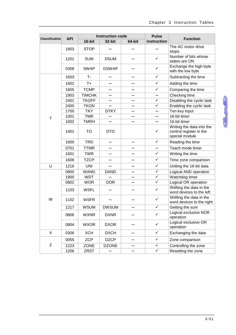
Chapter 3 Ins truct ion Tables
3-51
Classification API Instruction code Pulse instruction Function 16-bit 32-bit 64-bit
1803 STOP ─ ─ ─ The AC motor drive stops.
1201 SUM DSUM ─ Number of bits whose states are ON
0308 SWAP DSWAP ─ Exchange the high byte with the low byte
T
1603 T- ─ ─ Subtracting the time 1602 T+ ─ ─ Adding the time 1605 TCMP ─ ─ Comparing the time 1903 TIMCHK ─ ─ ─ Checking time 2401 TKOFF ─ ─ Disabling the cyclic task 2400 TKON ─ ─ Enabling the cyclic task 1700 TKY DTKY ─ ─ Ten key input 1001 TMR ─ ─ ─ 16-bit timer 1002 TMRH ─ ─ ─ 16-bit timer
1401 TO DTO Writing the data into the control register in the special module
1600 TRD ─ ─ Reading the time 0701 TTMR ─ ─ ─ Teach mode timer 1601 TWR ─ ─ Writing the time 1606 TZCP ─ ─ Time zone comparison
U 1216 UNI ─ ─ Uniting the 16-bit data
W
0800 WAND DAND ─ Logical AND operation 1900 WDT ─ ─ Watchdog timer 0802 WOR DOR ─ Logical OR operation
1103 WSFL ─ ─ Shifting the data in the word devices to the left
1102 WSFR ─ ─ Shifting the data in the word devices to the right
1217 WSUM DWSUM ─ Getting the sum
0806 WXNR DXNR ─ Logical exclusive NOR operation
0804 WXOR DXOR ─ Logical exclusive OR operation
X 0306 XCH DXCH ─ Exchanging the data
Z 0055 ZCP DZCP ─ Zone comparison 1223 ZONE DZONE ─ Controlling the zone 1206 ZRST ─ ─ Resetting the zone

AH500 Programming Manual
3-52
MEMO
4-1
Chapter 4 Instruction Structure
Table of Contents 4.1 Composition of Applied Instructions ....................................................... 4-2 4.2 Restrictions on the Use of the Instructions ............................................. 4-6 4.3 Index Registers ...................................................................................... 4-7 4.4 Pointer Registers .................................................................................... 4-9 4.5 Pointer Registers of Timers ................................................................... 4-11 4.6 Pointer Registers of 16-bit Counters .....................................................4-13 4.7 Pointer Registers of 32-bit Counters .....................................................4-15
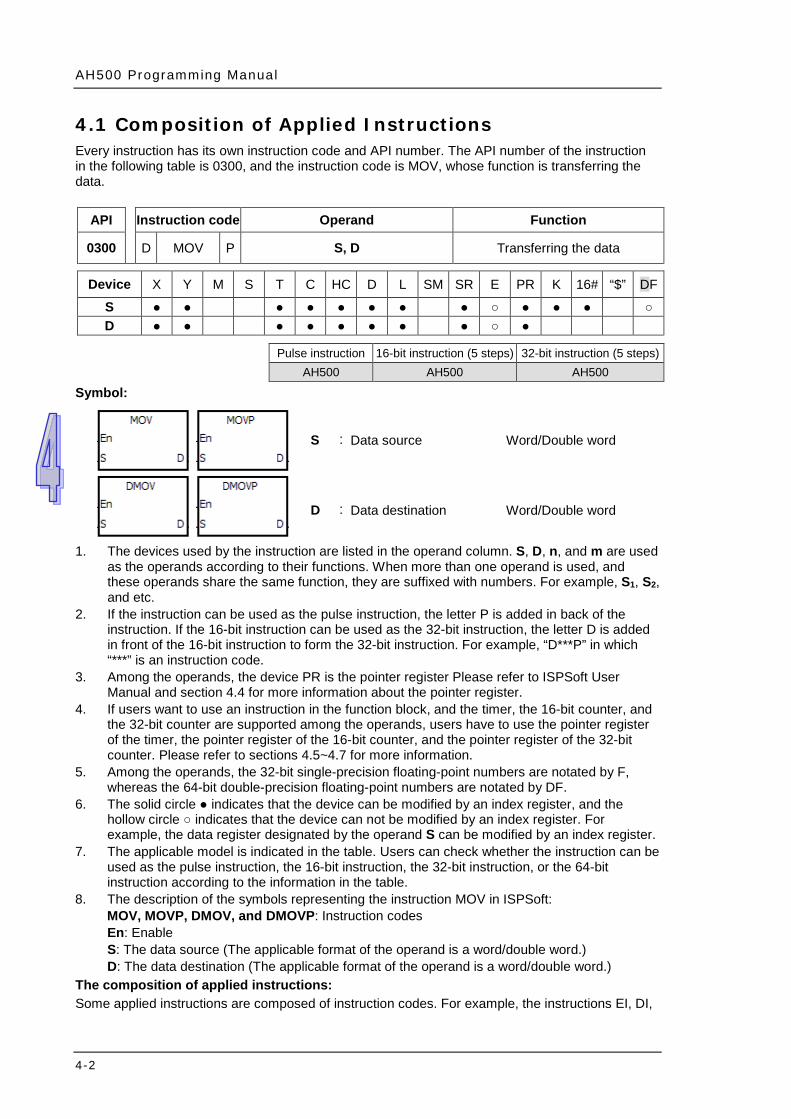
AH500 Programming Manual
4-2
4.1 Composition of Applied Instructions Every instruction has its own instruction code and API number. The API number of the instruction in the following table is 0300, and the instruction code is MOV, whose function is transferring the data.
API Instruction code Operand Function
0300 D MOV P S, D Transferring the data
Device X Y M S T C HC D L SM SR E PR K 16# “$” DF
S ● ● ● ● ● ● ● ● ○ ● ● ● ○ D ● ● ● ● ● ● ● ● ○ ●
Pulse instruction 16-bit instruction (5 steps) 32-bit instruction (5 steps)
AH500 AH500 AH500
Symbol:
S : Data source Word/Double word
D : Data destination Word/Double word
1. The devices used by the instruction are listed in the operand column. S, D, n, and m are used as the operands according to their functions. When more than one operand is used, and these operands share the same function, they are suffixed with numbers. For example, S1, S2, and etc.
2. If the instruction can be used as the pulse instruction, the letter P is added in back of the instruction. If the 16-bit instruction can be used as the 32-bit instruction, the letter D is added in front of the 16-bit instruction to form the 32-bit instruction. For example, “D***P” in which “***” is an instruction code.
3. Among the operands, the device PR is the pointer register Please refer to ISPSoft User Manual and section 4.4 for more information about the pointer register.
4. If users want to use an instruction in the function block, and the timer, the 16-bit counter, and the 32-bit counter are supported among the operands, users have to use the pointer register of the timer, the pointer register of the 16-bit counter, and the pointer register of the 32-bit counter. Please refer to sections 4.5~4.7 for more information.
5. Among the operands, the 32-bit single-precision floating-point numbers are notated by F, whereas the 64-bit double-precision floating-point numbers are notated by DF.
6. The solid circle ● indicates that the device can be modified by an index register, and the hollow circle ○ indicates that the device can not be modified by an index register. For example, the data register designated by the operand S can be modified by an index register.
7. The applicable model is indicated in the table. Users can check whether the instruction can be used as the pulse instruction, the 16-bit instruction, the 32-bit instruction, or the 64-bit instruction according to the information in the table.
8. The description of the symbols representing the instruction MOV in ISPSoft: MOV, MOVP, DMOV, and DMOVP: Instruction codes En: Enable S: The data source (The applicable format of the operand is a word/double word.) D: The data destination (The applicable format of the operand is a word/double word.)
The composition of applied instructions: Some applied instructions are composed of instruction codes. For example, the instructions EI, DI,

Chapter 4 Ins truct ion Structure
4-3
WDT, and etc. however, most applied instructions consist of instruction codes and several operands. Every applied instruction has its own API number and instruction code. For example, the instruction code of API0300 is MOV (transferring the data). Entering the instruction directly: Users can enter the instruction by means of ISPSoft. For the
instruction MOV, users only need to enter the instruction name and the operands to designate “MOV D0 D1”.
Entering the instruction by dragging: Users can drag the instruction MOV from APIs in ISPSoft to
the area where the ladder diagram can be edited. Entering the instruction by the toolbar: Users can click API/FB Selection on the toolbar in ISPSoft,
and then choose API. Finally, they can choose the instruction MOV in Data Transfer. The operands are extra designated.
S Source operand If there is more than one source operand, these source operands are represented by S1, S2, and etc.
D Destination operand If there is more than one destination operand, these destination operand is represented by D1, D2, and etc.
If the operand only can designate the constant K/H or the register, it is represented by m, m1, m2, n, n1, or n2.
The length of the operand (the 16-bit instruction, the 32-bit instruction, or the floating-point number instruction): The 16-bit instruction or the 32-bit instruction The values of the operands can be divided into the 16-bit values and the 32-bit values. Accordingly, in order to process data of difference lengths, the instructions are divided into the 16-bit instructions and the 32-bit instructions. To separate the 32-bit instruction from the 16-bit one, a D is added in front of the 16-bit instruction. 16-bit instruction MOV
When M1 is ON, the data in D0 is transferred to D1.
32-bit instruction DMOV
When M1 is ON, the data in (D1, D0) is transferred to (D3, D2).
The floating-point number instruction The floating-point number instructions can be divided into the 32-bit floating-point number instructions and the 64-bit floating-point number instructions, which correspond to the single-precision floating-point number instructions and the double-precision floating-point number instructions respectively. Users can refer to chapter 2 for more information about the floating-point
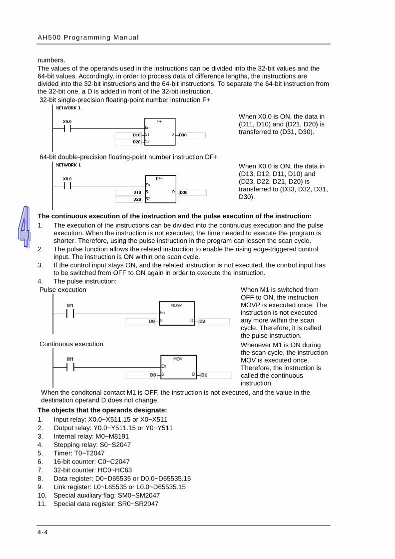
AH500 Programming Manual
4-4
numbers. The values of the operands used in the instructions can be divided into the 32-bit values and the 64-bit values. Accordingly, in order to process data of difference lengths, the instructions are divided into the 32-bit instructions and the 64-bit instructions. To separate the 64-bit instruction from the 32-bit one, a D is added in front of the 32-bit instruction. 32-bit single-precision floating-point number instruction F+
When X0.0 is ON, the data in (D11, D10) and (D21, D20) is transferred to (D31, D30).
64-bit double-precision floating-point number instruction DF+
When X0.0 is ON, the data in (D13, D12, D11, D10) and (D23, D22, D21, D20) is transferred to (D33, D32, D31, D30).
The continuous execution of the instruction and the pulse execution of the instruction: 1. The execution of the instructions can be divided into the continuous execution and the pulse
execution. When the instruction is not executed, the time needed to execute the program is shorter. Therefore, using the pulse instruction in the program can lessen the scan cycle.
2. The pulse function allows the related instruction to enable the rising edge-triggered control input. The instruction is ON within one scan cycle.
3. If the control input stays ON, and the related instruction is not executed, the control input has to be switched from OFF to ON again in order to execute the instruction.
4. The pulse instruction: Pulse execution
When M1 is switched from OFF to ON, the instruction MOVP is executed once. The instruction is not executed any more within the scan cycle. Therefore, it is called the pulse instruction.
Continuous execution
Whenever M1 is ON during the scan cycle, the instruction MOV is executed once. Therefore, the instruction is called the continuous instruction.
When the conditonal contact M1 is OFF, the instruction is not executed, and the value in the destination operand D does not change.
The objects that the operands designate: 1. Input relay: X0.0~X511.15 or X0~X511 2. Output relay: Y0.0~Y511.15 or Y0~Y511 3. Internal relay: M0~M8191 4. Stepping relay: S0~S2047 5. Timer: T0~T2047 6. 16-bit counter: C0~C2047 7. 32-bit counter: HC0~HC63 8. Data register: D0~D65535 or D0.0~D65535.15 9. Link register: L0~L65535 or L0.0~D65535.15 10. Special auxiliary flag: SM0~SM2047 11. Special data register: SR0~SR2047
Chapter 4 Ins truct ion Structure
4-5
12. Index register: E0~E31 13. Pointer register: PR0~PR15 14. Pointer register of the timer: TR0~TR7 15. Pointer register of the 16-bit counter: CR0~CR7 16. Pointer register of the 32-bit counter: HCR0~HCR7 17. Constant: The decimal constants are notated by K, and the hexadecimal constants
are notated by 16#. 18. String: “$” 19. Floating-point number: The single-precision floating-point numbers are notated by F, and the
double-precision floating-point numbers are notated by DF. 20. The length of the data in one register is generally 16 bits. If users want to store the 32-bit data
in the register, they have to designate two consecutive registers. 21. If the operand used in the 32-bit instruction designates D0, the 32-bit data register composed
of (D1, D0) is occupied. D1 represents the higher 16 bits, and D0 represents the lower 16 bits. The same rule applies to the timer and the 16-bit counter.。
22. When the 32-bit counter HC is used as the data register, it is only can be designated by the operand used in the 32-bit instruction.
PS. Please refer to chapter 2 for more information about devices.
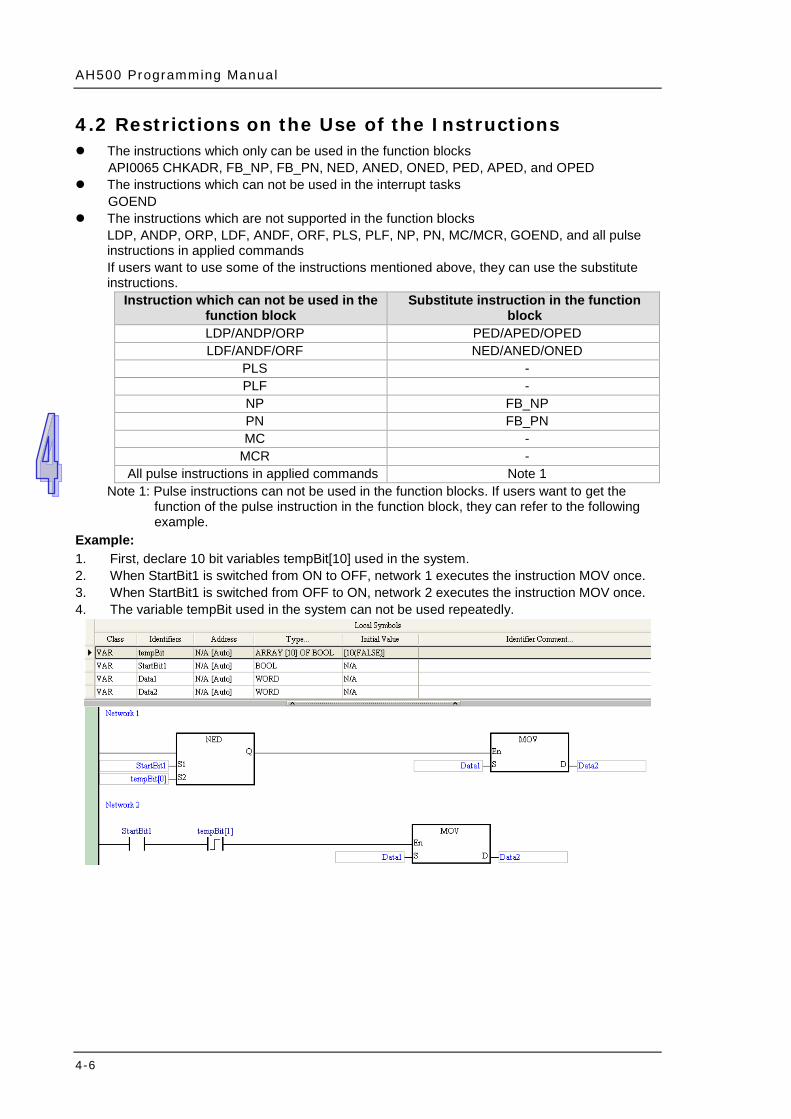
AH500 Programming Manual
4-6
4.2 Restrictions on the Use of the Instructions The instructions which only can be used in the function blocks
API0065 CHKADR, FB_NP, FB_PN, NED, ANED, ONED, PED, APED, and OPED The instructions which can not be used in the interrupt tasks
GOEND The instructions which are not supported in the function blocks
LDP, ANDP, ORP, LDF, ANDF, ORF, PLS, PLF, NP, PN, MC/MCR, GOEND, and all pulse instructions in applied commands If users want to use some of the instructions mentioned above, they can use the substitute instructions.
Instruction which can not be used in the function block
Substitute instruction in the function block
LDP/ANDP/ORP PED/APED/OPED LDF/ANDF/ORF NED/ANED/ONED
PLS - PLF - NP FB_NP PN FB_PN MC -
MCR - All pulse instructions in applied commands Note 1
Note 1: Pulse instructions can not be used in the function blocks. If users want to get the function of the pulse instruction in the function block, they can refer to the following example.
Example: 1. First, declare 10 bit variables tempBit[10] used in the system. 2. When StartBit1 is switched from ON to OFF, network 1 executes the instruction MOV once. 3. When StartBit1 is switched from OFF to ON, network 2 executes the instruction MOV once. 4. The variable tempBit used in the system can not be used repeatedly.
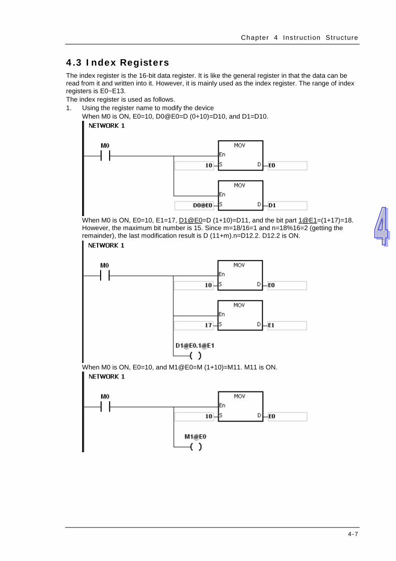
Chapter 4 Ins truct ion Structure
4-7
4.3 Index Registers The index register is the 16-bit data register. It is like the general register in that the data can be read from it and written into it. However, it is mainly used as the index register. The range of index registers is E0~E13. The index register is used as follows. 1. Using the register name to modify the device
When M0 is ON, E0=10, D0@E0=D (0+10)=D10, and D1=D10.
When M0 is ON, E0=10, E1=17, D1@E0=D (1+10)=D11, and the bit part 1@E1=(1+17)=18. However, the maximum bit number is 15. Since m=18/16=1 and n=18%16=2 (getting the remainder), the last modification result is D (11+m).n=D12.2. D12.2 is ON.
When M0 is ON, E0=10, and M1@E0=M (1+10)=M11. M11 is ON.
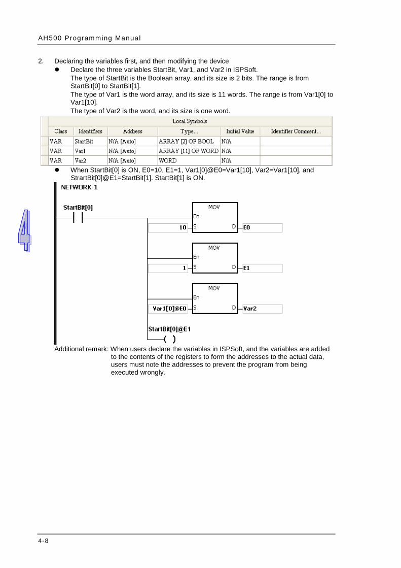
AH500 Programming Manual
4-8
2. Declaring the variables first, and then modifying the device Declare the three variables StartBit, Var1, and Var2 in ISPSoft.
The type of StartBit is the Boolean array, and its size is 2 bits. The range is from StartBit[0] to StartBit[1]. The type of Var1 is the word array, and its size is 11 words. The range is from Var1[0] to Var1[10]. The type of Var2 is the word, and its size is one word.
When StartBit[0] is ON, E0=10, E1=1, Var1[0]@E0=Var1[10], Var2=Var1[10], and
StrartBit[0]@E1=StartBit[1]. StartBit[1] is ON.
Additional remark: When users declare the variables in ISPSoft, and the variables are added
to the contents of the registers to form the addresses to the actual data, users must note the addresses to prevent the program from being executed wrongly.

Chapter 4 Ins truct ion Structure
4-9
4.4 Pointer Registers ISPSoft supports the function blocks. When the variable declaration type is VAR_IN_OUT,
and the data type is POINTER, the variable is the pointer register. The value in the pointer register can refer directly to the value stored in the device X, Y, D, or L, and the pointer register can point to the address associated with the variable set automatically in ISPSoft.
Users can declare 16 pointer registers in every function block. The range is PR0~PR15, or PR0.0~PR15.15.
Example: 1. Establish a program organization unit (POU) in ISPSoft first. 2. Establish a function block which is called FB0.
3. The program in the function block FB0
4. Declare the varaible in the function block FB0.
Choose VAR_IN_OUT as the declaration type, Point1 as the identifier, POINTER as the data type. The variable is the pointer register.
5. Declare the variable in the program organization unit (POU).
6. Call the function block FB0 in the program organization unit (POU). 7. The program in the program organization unit (POU)
Network 1: When StartBit[0] is ON, the address of D0 is transmitted to Point 1 in FB0.

AH500 Programming Manual
4-10
When VarBit1 in FB0 is ON, E0=1, Var1=D0, Point1@E0=D (0+1)=D1, and Var2=D1.
Network 2: When StartBit[1] is ON, the address of CVar1[0] is transmitted to Point1 in FB0.
When VarBit1 in FB0 is ON, E0=1, Var1=CVar1[0], Point1@E0=CVar1 (0+1)=Cvar1[1], and Var2=CVar1[1].
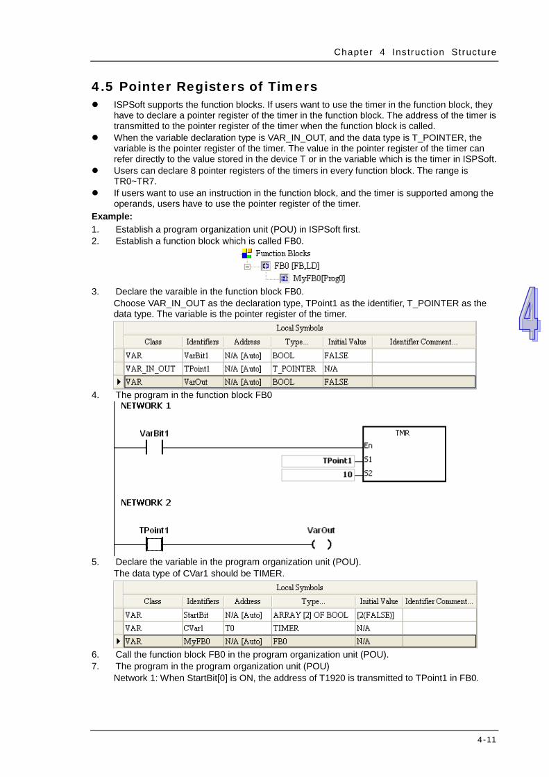
Chapter 4 Ins truct ion Structure
4-11
4.5 Pointer Registers of Timers ISPSoft supports the function blocks. If users want to use the timer in the function block, they
have to declare a pointer register of the timer in the function block. The address of the timer is transmitted to the pointer register of the timer when the function block is called.
When the variable declaration type is VAR_IN_OUT, and the data type is T_POINTER, the variable is the pointer register of the timer. The value in the pointer register of the timer can refer directly to the value stored in the device T or in the variable which is the timer in ISPSoft.
Users can declare 8 pointer registers of the timers in every function block. The range is TR0~TR7.
If users want to use an instruction in the function block, and the timer is supported among the operands, users have to use the pointer register of the timer.
Example: 1. Establish a program organization unit (POU) in ISPSoft first. 2. Establish a function block which is called FB0.
3. Declare the varaible in the function block FB0.
Choose VAR_IN_OUT as the declaration type, TPoint1 as the identifier, T_POINTER as the data type. The variable is the pointer register of the timer.
4. The program in the function block FB0
5. Declare the variable in the program organization unit (POU).
The data type of CVar1 should be TIMER.
6. Call the function block FB0 in the program organization unit (POU). 7. The program in the program organization unit (POU)
Network 1: When StartBit[0] is ON, the address of T1920 is transmitted to TPoint1 in FB0.
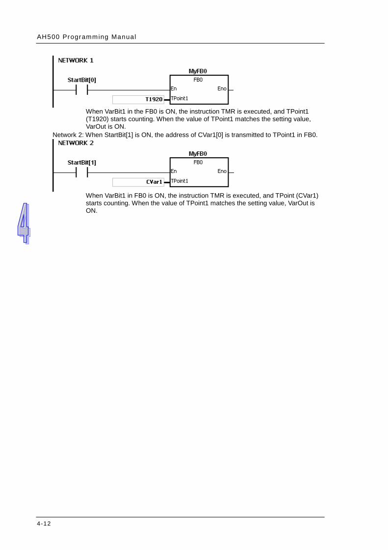
AH500 Programming Manual
4-12
When VarBit1 in the FB0 is ON, the instruction TMR is executed, and TPoint1 (T1920) starts counting. When the value of TPoint1 matches the setting value, VarOut is ON.
Network 2: When StartBit[1] is ON, the address of CVar1[0] is transmitted to TPoint1 in FB0.
When VarBit1 in FB0 is ON, the instruction TMR is executed, and TPoint (CVar1) starts counting. When the value of TPoint1 matches the setting value, VarOut is ON.
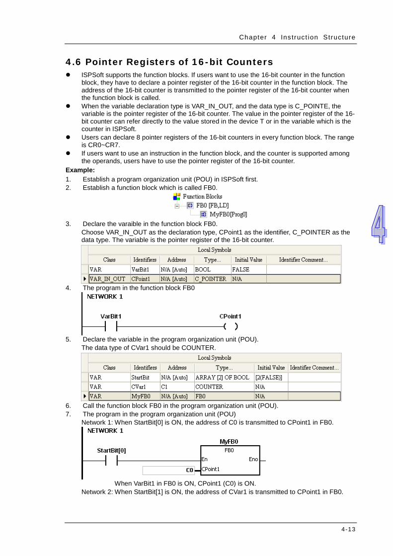
Chapter 4 Ins truct ion Structure
4-13
4.6 Pointer Registers of 16-bit Counters ISPSoft supports the function blocks. If users want to use the 16-bit counter in the function
block, they have to declare a pointer register of the 16-bit counter in the function block. The address of the 16-bit counter is transmitted to the pointer register of the 16-bit counter when the function block is called.
When the variable declaration type is VAR_IN_OUT, and the data type is C_POINTE, the variable is the pointer register of the 16-bit counter. The value in the pointer register of the 16-bit counter can refer directly to the value stored in the device T or in the variable which is the counter in ISPSoft.
Users can declare 8 pointer registers of the 16-bit counters in every function block. The range is CR0~CR7.
If users want to use an instruction in the function block, and the counter is supported among the operands, users have to use the pointer register of the 16-bit counter.
Example: 1. Establish a program organization unit (POU) in ISPSoft first. 2. Establish a function block which is called FB0.
3. Declare the varaible in the function block FB0.
Choose VAR_IN_OUT as the declaration type, CPoint1 as the identifier, C_POINTER as the data type. The variable is the pointer register of the 16-bit counter.
4. The program in the function block FB0
5. Declare the variable in the program organization unit (POU).
The data type of CVar1 should be COUNTER.
6. Call the function block FB0 in the program organization unit (POU). 7. The program in the program organization unit (POU)
Network 1: When StartBit[0] is ON, the address of C0 is transmitted to CPoint1 in FB0.
When VarBit1 in FB0 is ON, CPoint1 (C0) is ON.
Network 2: When StartBit[1] is ON, the address of CVar1 is transmitted to CPoint1 in FB0.

AH500 Programming Manual
4-14
When VarBit1 in FB0 is ON, CPoint1 (CVar1) is ON.
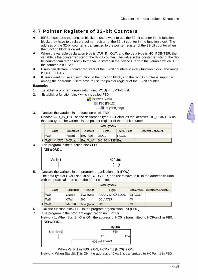
Chapter 4 Ins truct ion Structure
4-15
4.7 Pointer Registers of 32-bit Counters ISPSoft supports the function blocks. If users want to use the 32-bit counter in the function
block, they have to declare a pointer register of the 32-bit counter in the function block. The address of the 32-bit counter is transmitted to the pointer register of the 32-bit counter when the function block is called.
When the variable declaration type is VAR_IN_OUT, and the data type is HC_POINTER, the variable is the pointer register of the 32-bit counter. The value in the pointer register of the 32-bit counter can refer directly to the value stored in the device HC or in the variable which is the counter in ISPSoft.
Users can declare 8 pointer registers of the 32-bit counters in every function block. The range is HCR0~HCR7.
If users want to use an instruction in the function block, and the 32-bit counter is supported among the operands, users have to use the pointer register of the 32-bit counter.
Example: 1. Establish a program organization unit (POU) in ISPSoft first. 2. Establish a function block which is called FB0.
3. Declare the varaible in the function block FB0.
Choose VAR_IN_OUT as the declaration type, HCPoint1 as the identifier, HC_POINTER as the data type. The variable is the pointer register of the 32-bit counter.
4. The program in the function block FB0
5. Declare the variable in the program organization unit (POU).
The data type of CVar1 should be COUNTER, and users have to fill in the address column with the practical address of the 32-bit counter.
6. Call the function block FB0 in the program organization unit (POU). 7. The program in the program organization unit (POU)
Network 1: When StartBit[0] is ON, the address of HC0 is transmitted to HCPoint1 in FB0.
When VarBit1 in FB0 is ON, HCPoint1 (HC0) is ON.
Network: When StartBit[1] is ON, the address of CVar1 is transmitted to HCPoint1 in FB0.
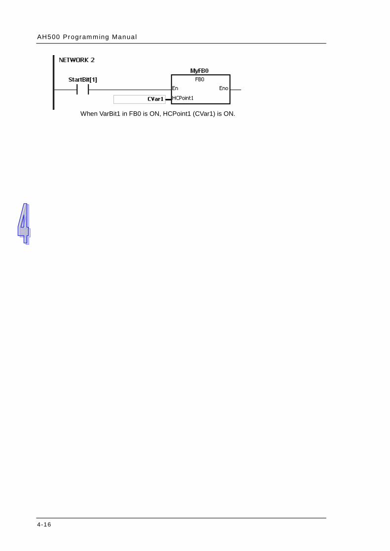
AH500 Programming Manual
4-16
When VarBit1 in FB0 is ON, HCPoint1 (CVar1) is ON.
5-1
Chapter 5 Basic Instructions
Table of Contents 5.1 List of Basic Instructions ......................................................................... 5-2 5.2 Basic Instructions ................................................................................... 5-3

AH500 Programming Manual
5-2
5.1 List of Basic Instructions Instruction code Function Operand Step
LD/AND/OR Loading contact A/Connecting contact A in series/Connecting contact A in parallel
DX, X, Y, M, SM, S, T, C, HC, D, L, and PR 1-2
LDI/ANI/ORI Loading contact B/Connecting contact B in series/Connecting contact B in parallel
DX, X, Y, M, SM, S, T, C, HC, D, L, and PR 1-2
ANB/ORB Connecting the loop blocks in series/parallel – 1
MPS/MRD/MPP
Storing the data in the stack/Reading the data from the stack/Popping the data from the stack
– 1
OUT Driving the coil DY, X, Y, M, SM, S, T, C, HC, D, L, and PR 1-2
SET Keeping the device on DY, X, Y, M, SM, S, T, C, HC, D, L, and PR 1-2
MC/MCR Setting/Resetting the master control N 1
LDP/ANDP/ORP
Starting the rising-edge detection/Connecting the rising-edge detection in series/Connecting the rising-edge detection in parallel
DX, X, Y, M, SM, S, T, C, HC, D, L, and PR 1-2
LDF/ANDF/ORF
Starting the falling-edge detection/Connecting the falling-edge detection in series/Connecting the falling-edge detection in parallel
DX, X, Y, M, SM, S, T, C, HC, D, L, and PR 1-2
PED/APED/OPED
Starting the rising-edge detection/Connecting the rising edge-detection in series/Connecting the rising-edge detection in parallel
X, Y, M, SM, S, T, C, HC, D, L, and PR 5
NED/ANED/ONED
Starting the falling-edge detection/Connecting the falling-edge detection in series/Connecting the falling-edge detection in parallel
X, Y, M, SM, S, T, C, HC, D, L, and PR 5
PLS Rising-edge output DY, X, Y, M, SM, S, T, C, HC, D, L, and PR 1-2
PLF Falling-edge output DY, X, Y, M, SM, S, T, C, HC, D, L, and PR 1-2
INV Inverting the logical operation result – 1
NOP No operation – 1 NP The circuit is rising edge-triggered. – 1 PN The circuit is falling edge-triggered. – 1
FB_NP The circuit is rising edge-triggered. X, Y, M, SM, S, T, C, HC, D, L, and PR 1-2
FB_PN The circuit is falling edge-triggered. X, Y, M, SM, S, T, C, HC, D, L, and PR 1-2
PSTOP Stopping executing the program in the PLC – 1
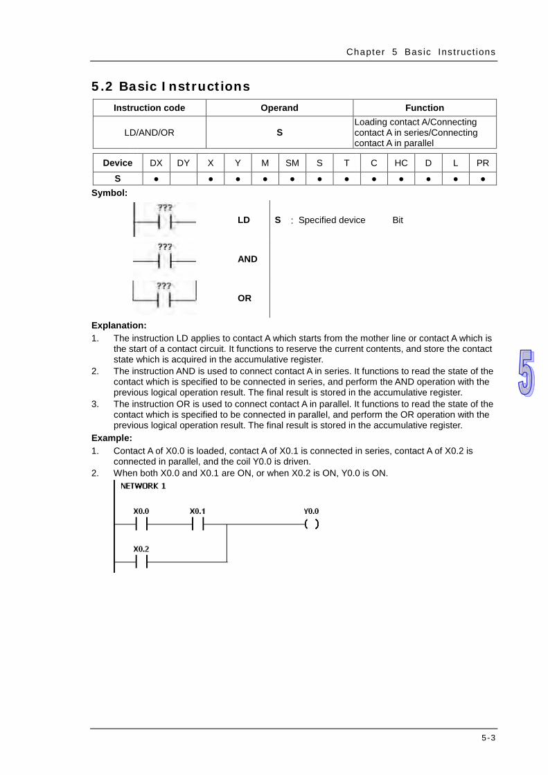
Chapter 5 Bas ic Ins t ruct ions
5-3
5.2 Basic Instructions Instruction code Operand Function
LD/AND/OR S Loading contact A/Connecting contact A in series/Connecting contact A in parallel
Device DX DY X Y M SM S T C HC D L PR
S ● ● ● ● ● ● ● ● ● ● ● ● Symbol:
LD S : Specified device Bit
AND
OR
Explanation: 1. The instruction LD applies to contact A which starts from the mother line or contact A which is
the start of a contact circuit. It functions to reserve the current contents, and store the contact state which is acquired in the accumulative register.
2. The instruction AND is used to connect contact A in series. It functions to read the state of the contact which is specified to be connected in series, and perform the AND operation with the previous logical operation result. The final result is stored in the accumulative register.
3. The instruction OR is used to connect contact A in parallel. It functions to read the state of the contact which is specified to be connected in parallel, and perform the OR operation with the previous logical operation result. The final result is stored in the accumulative register.
Example: 1. Contact A of X0.0 is loaded, contact A of X0.1 is connected in series, contact A of X0.2 is
connected in parallel, and the coil Y0.0 is driven. 2. When both X0.0 and X0.1 are ON, or when X0.2 is ON, Y0.0 is ON.
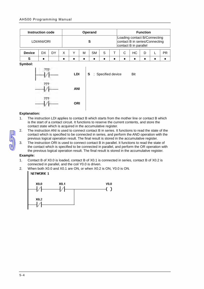
AH500 Programming Manual
5-4
Instruction code Operand Function
LDI/ANI/ORI S Loading contact B/Connecting contact B in series/Connecting contact B in parallel
Device DX DY X Y M SM S T C HC D L PR
S ● ● ● ● ● ● ● ● ● ● ● ● Symbol:
LDI S : Specified device Bit
ANI
ORI
Explanation: 1. The instruction LDI applies to contact B which starts from the mother line or contact B which
is the start of a contact circuit. It functions to reserve the current contents, and store the contact state which is acquired in the accumulative register.
2. The instruction ANI is used to connect contact B in series. It functions to read the state of the contact which is specified to be connected in series, and perform the AND operation with the previous logical operation result. The final result is stored in the accumulative register.
3. The instruction ORI is used to connect contact B in parallel. It functions to read the state of the contact which is specified to be connected in parallel, and perform the OR operation with the previous logical operation result. The final result is stored in the accumulative register.
Example: 1. Contact B of X0.0 is loaded, contact B of X0.1 is connected in series, contact B of X0.2 is
connected in parallel, and the coil Y0.0 is driven. 2. When both X0.0 and X0.1 are ON, or when X0.2 is ON, Y0.0 is ON.
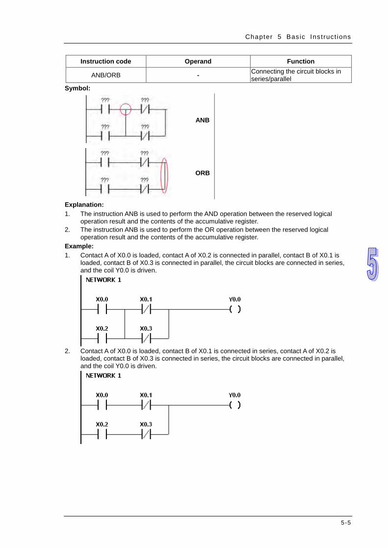
Chapter 5 Bas ic Ins t ruct ions
5-5
Instruction code Operand Function
ANB/ORB - Connecting the circuit blocks in series/parallel
Symbol:
ANB
ORB
Explanation: 1. The instruction ANB is used to perform the AND operation between the reserved logical
operation result and the contents of the accumulative register. 2. The instruction ANB is used to perform the OR operation between the reserved logical
operation result and the contents of the accumulative register. Example: 1. Contact A of X0.0 is loaded, contact A of X0.2 is connected in parallel, contact B of X0.1 is
loaded, contact B of X0.3 is connected in parallel, the circuit blocks are connected in series, and the coil Y0.0 is driven.
2. Contact A of X0.0 is loaded, contact B of X0.1 is connected in series, contact A of X0.2 is
loaded, contact B of X0.3 is connected in series, the circuit blocks are connected in parallel, and the coil Y0.0 is driven.
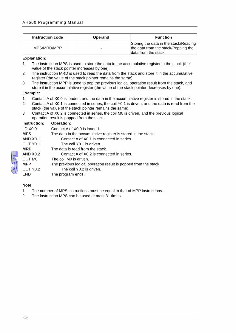
AH500 Programming Manual
5-6
Instruction code Operand Function
MPS/MRD/MPP - Storing the data in the stack/Reading the data from the stack/Popping the data from the stack
Explanation: 1. The instruction MPS is used to store the data in the accumulative register in the stack (the
value of the stack pointer increases by one). 2. The instruction MRD is used to read the data from the stack and store it in the accumulative
register (the value of the stack pointer remains the same). 3. The instruction MPP is used to pop the previous logical operation result from the stack, and
store it in the accumulative register (the value of the stack pointer decreases by one). Example: 1. Contact A of X0.0 is loaded, and the data in the accumulative register is stored in the stack. 2. Contact A of X0.1 is connected in series, the coil Y0.1 is driven, and the data is read from the
stack (the value of the stack pointer remains the same). 3. Contact A of X0.2 is connected in series, the coil M0 is driven, and the previous logical
operation result is popped from the stack. Instruction: Operation: LD X0.0 Contact A of X0.0 is loaded. MPS The data in the accumulative register is stored in the stack. AND X0.1 Contact A of X0.1 is connected in series. OUT Y0.1 The coil Y0.1 is driven. MRD The data is read from the stack. AND X0.2 Contact A of X0.2 is connected in series. OUT M0 The coil M0 is driven. MPP The previous logical operation result is popped from the stack. OUT Y0.2 The coil Y0.2 is driven. END The program ends. Note: 1. The number of MPS instructions must be equal to that of MPP instructions. 2. The instruction MPS can be used at most 31 times.

Chapter 5 Bas ic Ins t ruct ions
5-7
Instruction code Operand Function
OUT S Driving the coil
Device DX DY X Y M SM S T C HC D L PR
S ● ● ● ● ● ● ● ● ● ● ● ● Symbol:
S : Specified device Bit
Explanation: 1. The logical operation result prior to the application of the instruction OUT is output into the
specified device. 2. The action of the coil contact:
Operation result
OUT
Coil Contact
Contact A (normally open)
Contact B (normally closed)
False OFF OFF ON True ON ON OFF
Example: 1. Contact B of X0.0 is loaded, contact A of X0.1 is connected in series, and the coil Y0.0 is
driven. 2. When X0.0 is OFF, and X0.1 is ON, Y0.0 is ON.
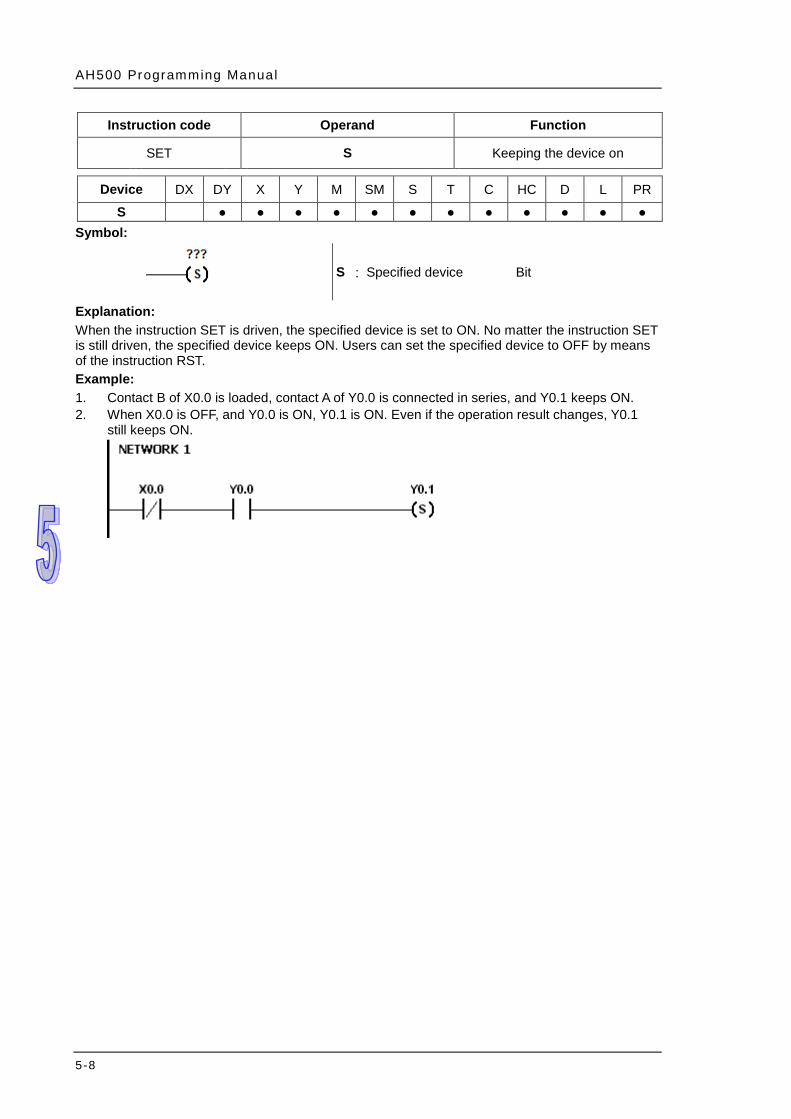
AH500 Programming Manual
5-8
Instruction code Operand Function
SET S Keeping the device on
Device DX DY X Y M SM S T C HC D L PR
S ● ● ● ● ● ● ● ● ● ● ● ● Symbol:
S : Specified device Bit
Explanation: When the instruction SET is driven, the specified device is set to ON. No matter the instruction SET is still driven, the specified device keeps ON. Users can set the specified device to OFF by means of the instruction RST. Example: 1. Contact B of X0.0 is loaded, contact A of Y0.0 is connected in series, and Y0.1 keeps ON. 2. When X0.0 is OFF, and Y0.0 is ON, Y0.1 is ON. Even if the operation result changes, Y0.1
still keeps ON.
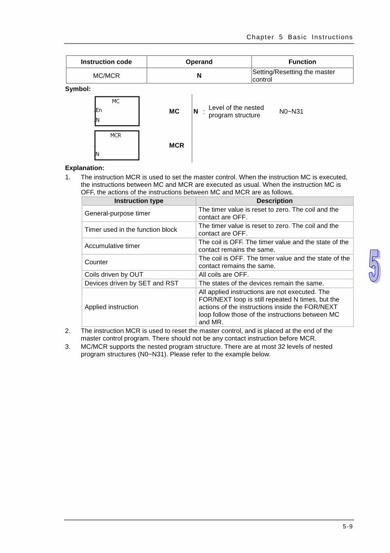
Chapter 5 Bas ic Ins t ruct ions
5-9
Instruction code Operand Function
MC/MCR N Setting/Resetting the master control
Symbol:
MC N : Level of the nested program structure N0~N31
MCR
Explanation: 1. The instruction MCR is used to set the master control. When the instruction MC is executed,
the instructions between MC and MCR are executed as usual. When the instruction MC is OFF, the actions of the instructions between MC and MCR are as follows.
Instruction type Description
General-purpose timer The timer value is reset to zero. The coil and the contact are OFF.
Timer used in the function block The timer value is reset to zero. The coil and the contact are OFF.
Accumulative timer The coil is OFF. The timer value and the state of the contact remains the same.
Counter The coil is OFF. The timer value and the state of the contact remains the same.
Coils driven by OUT All coils are OFF. Devices driven by SET and RST The states of the devices remain the same.
Applied instruction
All applied instructions are not executed. The FOR/NEXT loop is still repeated N times, but the actions of the instructions inside the FOR/NEXT loop follow those of the instructions between MC and MR.
2. The instruction MCR is used to reset the master control, and is placed at the end of the master control program. There should not be any contact instruction before MCR.
3. MC/MCR supports the nested program structure. There are at most 32 levels of nested program structures (N0~N31). Please refer to the example below.

AH500 Programming Manual
5-10
Example:
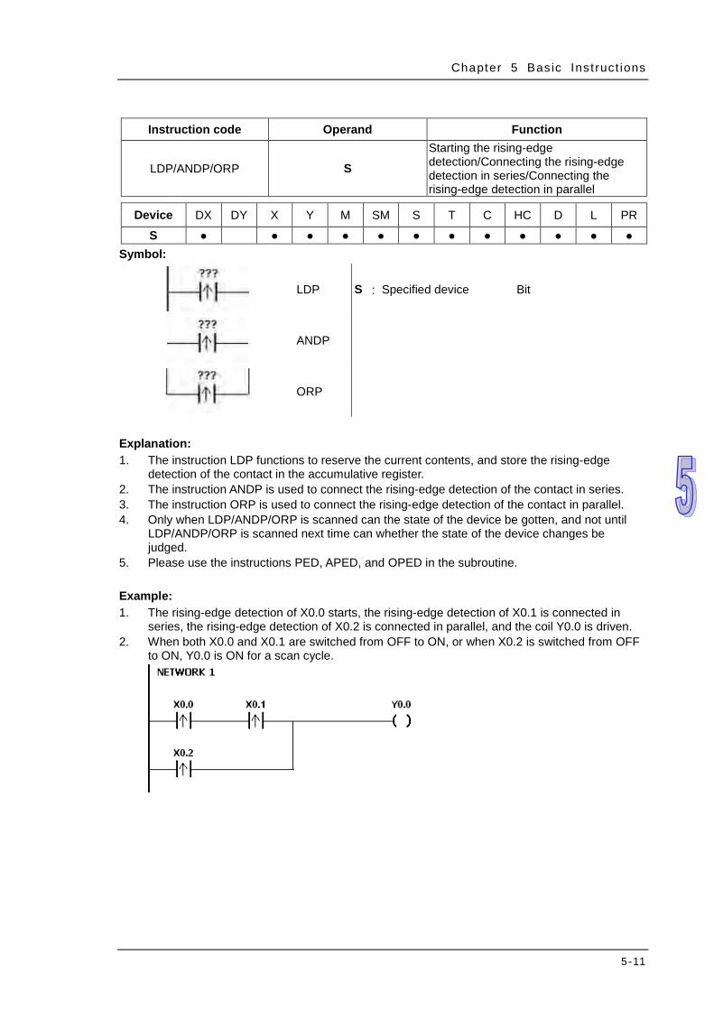
Chapter 5 Bas ic Ins t ruct ions
5-11
Instruction code Operand Function
LDP/ANDP/ORP S Starting the rising-edge detection/Connecting the rising-edge detection in series/Connecting the rising-edge detection in parallel
Device DX DY X Y M SM S T C HC D L PR
S ● ● ● ● ● ● ● ● ● ● ● ● Symbol:
LDP S : Specified device Bit
ANDP
ORP
Explanation: 1. The instruction LDP functions to reserve the current contents, and store the rising-edge
detection of the contact in the accumulative register. 2. The instruction ANDP is used to connect the rising-edge detection of the contact in series. 3. The instruction ORP is used to connect the rising-edge detection of the contact in parallel. 4. Only when LDP/ANDP/ORP is scanned can the state of the device be gotten, and not until
LDP/ANDP/ORP is scanned next time can whether the state of the device changes be judged.
5. Please use the instructions PED, APED, and OPED in the subroutine. Example: 1. The rising-edge detection of X0.0 starts, the rising-edge detection of X0.1 is connected in
series, the rising-edge detection of X0.2 is connected in parallel, and the coil Y0.0 is driven. 2. When both X0.0 and X0.1 are switched from OFF to ON, or when X0.2 is switched from OFF
to ON, Y0.0 is ON for a scan cycle.

AH500 Programming Manual
5-12
Instruction code Operand Function
LDF/ANDF/ORF S
Starting the falling-edge detection/Connecting the falling-edge detection in series/Connecting the falling-edge detection in parallel
Device DX DY X Y M SM S T C HC D L PR
S ● ● ● ● ● ● ● ● ● ● ● ● Symbol:
LDF S : Specified device Bit
ANDF
ORF
Explanation: 1. The instruction LDF functions to reserve the current contents, and store the falling-edge
detection of the contact in the accumulative register. 2. The instruction ANDF is used to connect the falling-edge detection of the contact in series. 3. The instruction ORP is used to connect the falling-edge detection of the contact in parallel. 4. Only when LDF/ANDF/ORF is scanned can the state of the device be gotten, and not until
LDF/ANDF/ORF is scanned next time can whether the state of the device changes be judged. 5. Please use the instructions NED, ANED, and ONED in the subroutine. Example: 1. The falling-edge detection of X0.0 starts, the falling-edge detection of X0.1 is connected in
series, the falling-edge detection of X0.2 is connected in parallel, and the coil Y0.0 is driven. 2. When both X0.0 and X0.1 are switched from OFF to ON, or when X0.2 is switched from OFF
to ON, Y0.0 is ON for a scan cycle.
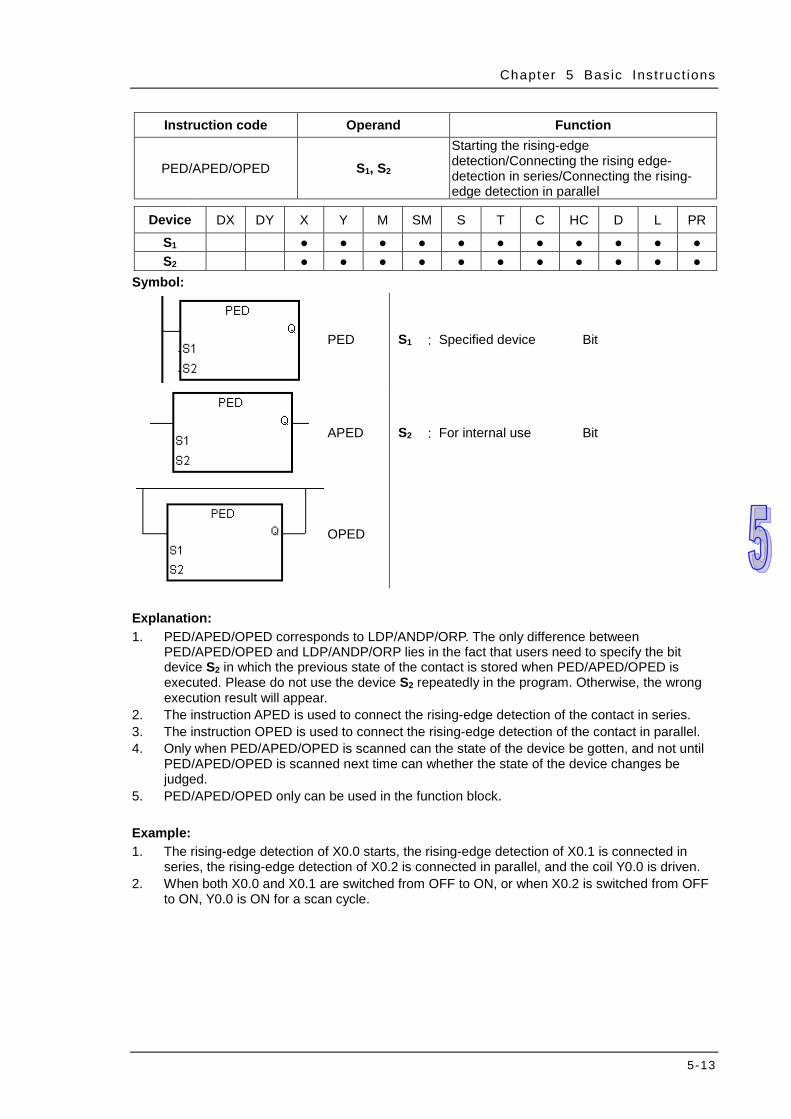
Chapter 5 Bas ic Ins t ruct ions
5-13
Instruction code Operand Function
PED/APED/OPED S1, S2 Starting the rising-edge detection/Connecting the rising edge-detection in series/Connecting the rising-edge detection in parallel
Device DX DY X Y M SM S T C HC D L PR
S1 ● ● ● ● ● ● ● ● ● ● ● S2 ● ● ● ● ● ● ● ● ● ● ●
Symbol:
PED S1 : Specified device Bit
APED S2 : For internal use Bit
OPED
Explanation: 1. PED/APED/OPED corresponds to LDP/ANDP/ORP. The only difference between
PED/APED/OPED and LDP/ANDP/ORP lies in the fact that users need to specify the bit device S2 in which the previous state of the contact is stored when PED/APED/OPED is executed. Please do not use the device S2 repeatedly in the program. Otherwise, the wrong execution result will appear.
2. The instruction APED is used to connect the rising-edge detection of the contact in series. 3. The instruction OPED is used to connect the rising-edge detection of the contact in parallel. 4. Only when PED/APED/OPED is scanned can the state of the device be gotten, and not until
PED/APED/OPED is scanned next time can whether the state of the device changes be judged.
5. PED/APED/OPED only can be used in the function block. Example: 1. The rising-edge detection of X0.0 starts, the rising-edge detection of X0.1 is connected in
series, the rising-edge detection of X0.2 is connected in parallel, and the coil Y0.0 is driven. 2. When both X0.0 and X0.1 are switched from OFF to ON, or when X0.2 is switched from OFF
to ON, Y0.0 is ON for a scan cycle.
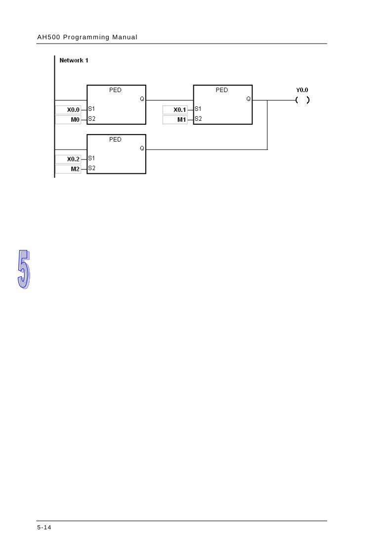
AH500 Programming Manual
5-14
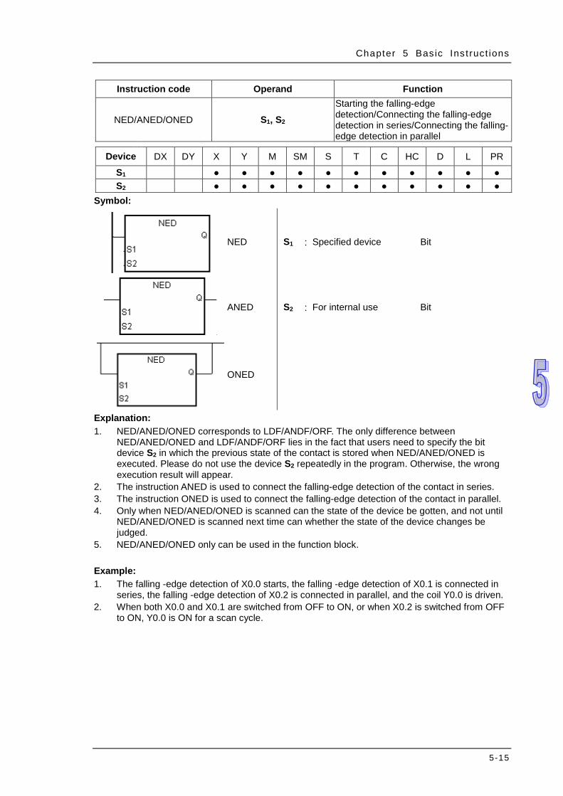
Chapter 5 Bas ic Ins t ruct ions
5-15
Instruction code Operand Function
NED/ANED/ONED S1, S2 Starting the falling-edge detection/Connecting the falling-edge detection in series/Connecting the falling-edge detection in parallel
Device DX DY X Y M SM S T C HC D L PR
S1 ● ● ● ● ● ● ● ● ● ● ● S2 ● ● ● ● ● ● ● ● ● ● ●
Symbol:
NED S1 : Specified device Bit
ANED S2 : For internal use Bit
ONED
Explanation: 1. NED/ANED/ONED corresponds to LDF/ANDF/ORF. The only difference between
NED/ANED/ONED and LDF/ANDF/ORF lies in the fact that users need to specify the bit device S2 in which the previous state of the contact is stored when NED/ANED/ONED is executed. Please do not use the device S2 repeatedly in the program. Otherwise, the wrong execution result will appear.
2. The instruction ANED is used to connect the falling-edge detection of the contact in series. 3. The instruction ONED is used to connect the falling-edge detection of the contact in parallel. 4. Only when NED/ANED/ONED is scanned can the state of the device be gotten, and not until
NED/ANED/ONED is scanned next time can whether the state of the device changes be judged.
5. NED/ANED/ONED only can be used in the function block. Example: 1. The falling -edge detection of X0.0 starts, the falling -edge detection of X0.1 is connected in
series, the falling -edge detection of X0.2 is connected in parallel, and the coil Y0.0 is driven. 2. When both X0.0 and X0.1 are switched from OFF to ON, or when X0.2 is switched from OFF
to ON, Y0.0 is ON for a scan cycle.

AH500 Programming Manual
5-16
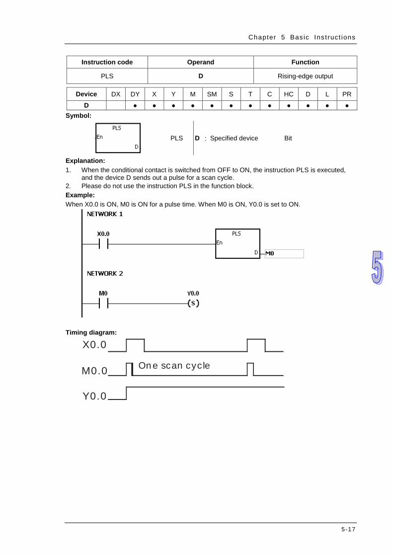
Chapter 5 Bas ic Ins t ruct ions
5-17
Instruction code Operand Function
PLS D Rising-edge output
Device DX DY X Y M SM S T C HC D L PR
D ● ● ● ● ● ● ● ● ● ● ● ● Symbol:
PLS D : Specified device Bit
Explanation: 1. When the conditional contact is switched from OFF to ON, the instruction PLS is executed,
and the device D sends out a pulse for a scan cycle. 2. Please do not use the instruction PLS in the function block. Example: When X0.0 is ON, M0 is ON for a pulse time. When M0 is ON, Y0.0 is set to ON.
Timing diagram:
X0.0
M0.0
Y0.0
On e scan cycle
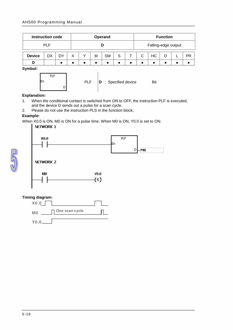
AH500 Programming Manual
5-18
Instruction code Operand Function
PLF D Falling-edge output
Device DX DY X Y M SM S T C HC D L PR
D ● ● ● ● ● ● ● ● ● ● ● ● Symbol:
PLF D : Specified device Bit
Explanation: 1. When the conditional contact is switched from ON to OFF, the instruction PLF is executed,
and the device D sends out a pulse for a scan cycle. 2. Please do not use the instruction PLS in the function block. Example: When X0.0 is ON, M0 is ON for a pulse time. When M0 is ON, Y0.0 is set to ON.
Timing diagram:
X0.0
M0
Y0.0
One scan cycle
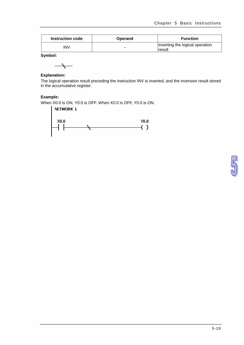
Chapter 5 Bas ic Ins t ruct ions
5-19
Instruction code Operand Function
INV - Inverting the logical operation result
Symbol:
Explanation: The logical operation result preceding the instruction INV is inverted, and the inversion result stored in the accumulative register. Example: When X0.0 is ON, Y0.0 is OFF. When X0.0 is OFF, Y0.0 is ON.
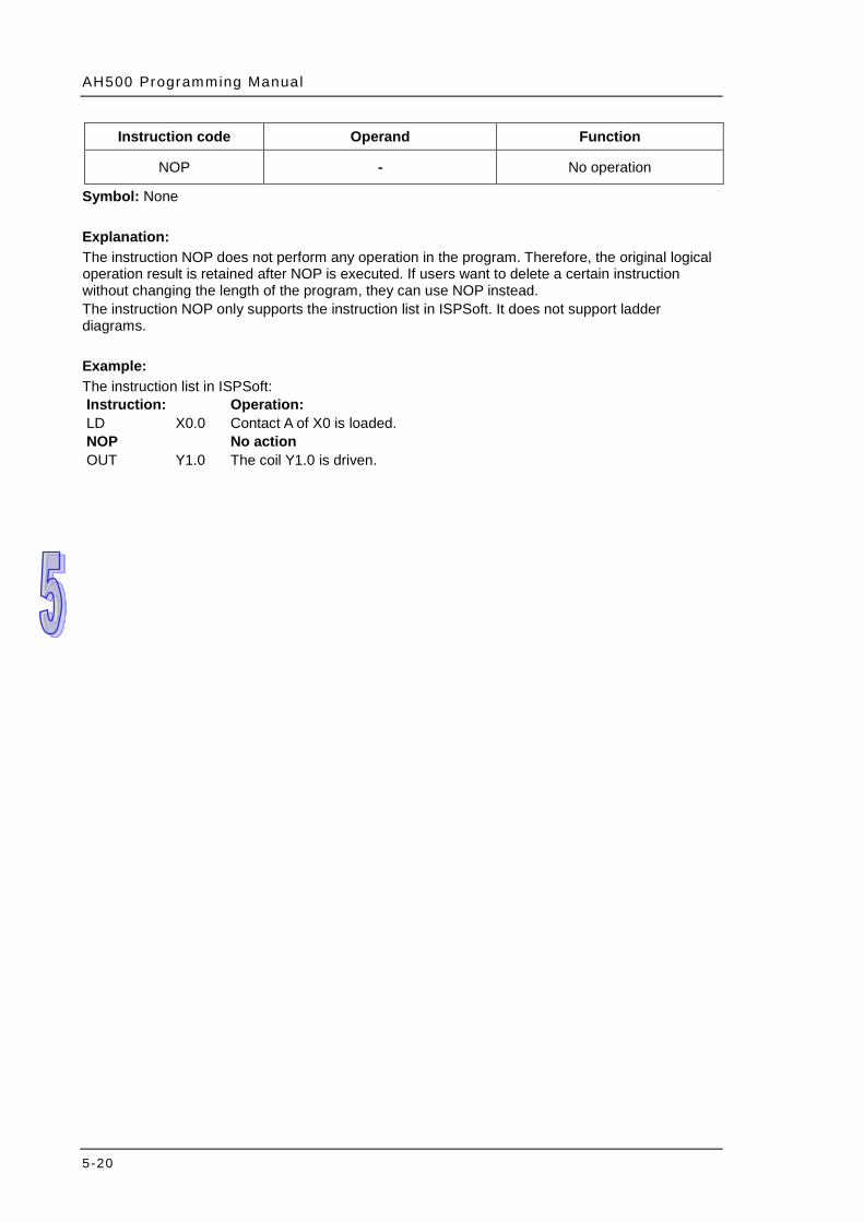
AH500 Programming Manual
5-20
Instruction code Operand Function
NOP - No operation
Symbol: None Explanation: The instruction NOP does not perform any operation in the program. Therefore, the original logical operation result is retained after NOP is executed. If users want to delete a certain instruction without changing the length of the program, they can use NOP instead. The instruction NOP only supports the instruction list in ISPSoft. It does not support ladder diagrams. Example: The instruction list in ISPSoft: Instruction: Operation: LD X0.0 Contact A of X0 is loaded. NOP No action OUT Y1.0 The coil Y1.0 is driven.
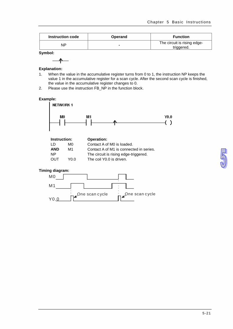
Chapter 5 Bas ic Ins t ruct ions
5-21
Instruction code Operand Function
NP - The circuit is rising edge-triggered.
Symbol:
Explanation: 1. When the value in the accumulative register turns from 0 to 1, the instruction NP keeps the
value 1 in the accumulative register for a scan cycle. After the second scan cycle is finished, the value in the accumulative register changes to 0.
2. Please use the instruction FB_NP in the function block. Example:
Instruction: Operation: LD M0 Contact A of M0 is loaded. AND M1 Contact A of M1 is connected in series. NP The circuit is rising edge-triggered. OUT Y0.0 The coil Y0.0 is driven.
Timing diagram:
M0
Y0.0
M1
One scan cycle One scan cycle
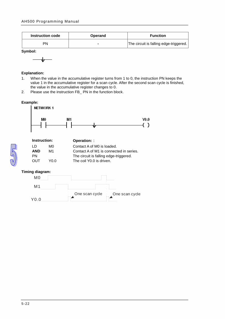
AH500 Programming Manual
5-22
Instruction code Operand Function
PN - The circuit is falling edge-triggered.
Symbol:
Explanation: 1. When the value in the accumulative register turns from 1 to 0, the instruction PN keeps the
value 1 in the accumulative register for a scan cycle. After the second scan cycle is finished, the value in the accumulative register changes to 0.
2. Please use the instruction FB_ PN in the function block. Example:
Instruction: Operation:: LD M0 Contact A of M0 is loaded. AND M1 Contact A of M1 is connected in series. PN The circuit is falling edge-triggered. OUT Y0.0 The coil Y0.0 is driven.
Timing diagram:
One scan cycle
M0
Y0.0
M1One scan cycle

Chapter 5 Bas ic Ins t ruct ions
5-23
Instruction code Operand Function
FB_NP S The circuit is rising edge-triggered.
Device DX DY X Y M SM S T C HC D L PR
S ● ● ● ● ● ● ● ● ● ● ● Symbol:
S : For internal use Bit
Explanation: 1. When the value in the accumulative register turns from 0 to 1, the instruction FB_NP keeps
the value 1 in the accumulative register for a scan cycle. After the second scan cycle is finished, the value in the accumulative register changes to 0.
2. The previous state of the contact is stored in the bit device S. Please do not use S repeatedly in the program. Otherwise, the wrong execution result will appear.
3. The instruction FB_NP only can be used in the function block. Example:
Instruction: Operation: LD M0 Contact A of M0 is loaded. AND M1 Contact A of M1 is connected in series. FB_NP D0.0 The circuit is rising edge-triggered. OUT Y0.0 The coil Y0.0 is driven.
Timing diagram:
One scan cycl e One scan cycl e
M0
Y0.0
M1
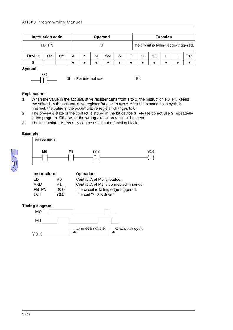
AH500 Programming Manual
5-24
Instruction code Operand Function
FB_PN S The circuit is falling edge-triggered.
Device DX DY X Y M SM S T C HC D L PR
S ● ● ● ● ● ● ● ● ● ● ● Symbol:
S : For internal use Bit
Explanation: 1. When the value in the accumulative register turns from 1 to 0, the instruction FB_PN keeps
the value 1 in the accumulative register for a scan cycle. After the second scan cycle is finished, the value in the accumulative register changes to 0.
2. The previous state of the contact is stored in the bit device S. Please do not use S repeatedly in the program. Otherwise, the wrong execution result will appear.
3. The instruction FB_PN only can be used in the function block. Example:
Instruction: Operation: LD M0 Contact A of M0 is loaded. AND M1 Contact A of M1 is connected in series. FB_PN D0.0 The circuit is falling edge-triggered. OUT Y0.0 The coil Y0.0 is driven.
Timing diagram:
One scan cycle
M0
Y0.0
M1One scan cycle
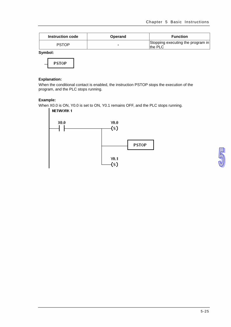
Chapter 5 Bas ic Ins t ruct ions
5-25
Instruction code Operand Function
PSTOP - Stopping executing the program in the PLC
Symbol:
Explanation: When the conditional contact is enabled, the instruction PSTOP stops the execution of the program, and the PLC stops running. Example: When X0.0 is ON, Y0.0 is set to ON, Y0.1 remains OFF, and the PLC stops running.

AH500 Programming Manual
5-26
MEMO

6-1
Chapter 6 Applied Instructions
Table of Contents 6.1 Comparison Instructions ........................................................................... 6-3
6.1.1 List of Comparison Instructions ........................................................ 6-3 6.1.2 Explanation of Comparison Instructions ........................................... 6-6
6.2 Arithmetic Instructions .............................................................................6-36 6.2.1 List of Arithmetic Instructions...........................................................6-36 6.2.2 Explanation of Arithmetic Instructions .............................................6-37
6.3 Data Conversion Instructions ...................................................................6-74 6.3.1 List of Data Conversion Instructions ................................................6-74 6.3.2 Explanation of Data Conversion Instructions ..................................6-75
6.4 Data Transfer Instructions ...................................................................... 6-112 6.4.1 List of Data Transfer Instructions ................................................... 6-112 6.4.2 Explanation of Data Transfer Instructions ..................................... 6-113
6.5 Jump Instructions ..................................................................................6-135 6.5.1 List of Jump Instructions ...............................................................6-135 6.5.2 Explanation of Jump Instructions ..................................................6-136
6.6 Program Execution Instructions .............................................................6-144 6.6.1 List of Program Execution Instructions ..........................................6-144 6.6.2 Explanation of Program Execution Instructions .............................6-145
6.7 I/O Refreshing Instructions ....................................................................6-152 6.7.1 List of I/O Refreshing Instructions .................................................6-152 6.7.2 Explanation of I/O Refreshing Instructions ....................................6-153
6.8 Miscellaneous Instructions .....................................................................6-155 6.8.1 List of Miscellaneous Instructions ..................................................6-155 6.8.2 Explanation of Miscellaneous Instructions ....................................6-156
6.9 Logic Instructions ...................................................................................6-193 6.9.1 List of Logic Instructions ................................................................6-193 6.9.2 Explanation of Logic Instructions ...................................................6-194
6.10 Rotation Instructions ..............................................................................6-217 6.10.1 List of Rotation Instructions ...........................................................6-217 6.10.2 Explanation of Rotation Instructions ..............................................6-218
6.11 Timer and Counter Instructions ..............................................................6-228 6.11.1 List of Timer and Counter Instructions ...........................................6-228 6.11.2 Explanation of Timer and Counter Instructions..............................6-229
6.12 Shift Instructions ....................................................................................6-236 6.12.1 List of Shift Instructions .................................................................6-236 6.12.2 Explanation of Shift Instructions ....................................................6-237
6.13 Data Processing Instructions .................................................................6-263 6.13.1 List of Data Processing Instructions ..............................................6-263 6.13.2 Explanation of Data Processing Instructions .................................6-264
6.14 Structure Creation Instructions ..............................................................6-308 6.14.1 List of Structure Creation Instructions ...........................................6-308 6.14.2 Explanation of Structure Creation Instructions ..............................6-309
6.15 Module Instructions ...............................................................................6-316 6.15.1 List of Module Instructions ............................................................6-316
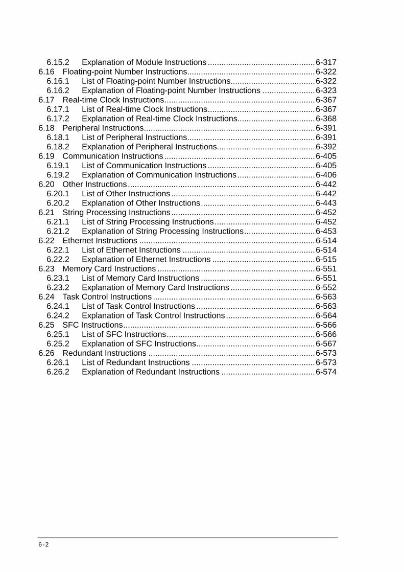
6-2
6.15.2 Explanation of Module Instructions ............................................... 6-317 6.16 Floating-point Number Instructions ........................................................ 6-322
6.16.1 List of Floating-point Number Instructions..................................... 6-322 6.16.2 Explanation of Floating-point Number Instructions ....................... 6-323
6.17 Real-time Clock Instructions .................................................................. 6-367 6.17.1 List of Real-time Clock Instructions ............................................... 6-367 6.17.2 Explanation of Real-time Clock Instructions .................................. 6-368
6.18 Peripheral Instructions ........................................................................... 6-391 6.18.1 List of Peripheral Instructions ........................................................ 6-391 6.18.2 Explanation of Peripheral Instructions........................................... 6-392
6.19 Communication Instructions .................................................................. 6-405 6.19.1 List of Communication Instructions ............................................... 6-405 6.19.2 Explanation of Communication Instructions .................................. 6-406
6.20 Other Instructions .................................................................................. 6-442 6.20.1 List of Other Instructions ............................................................... 6-442 6.20.2 Explanation of Other Instructions .................................................. 6-443
6.21 String Processing Instructions ............................................................... 6-452 6.21.1 List of String Processing Instructions ............................................ 6-452 6.21.2 Explanation of String Processing Instructions ............................... 6-453
6.22 Ethernet Instructions ............................................................................. 6-514 6.22.1 List of Ethernet Instructions .......................................................... 6-514 6.22.2 Explanation of Ethernet Instructions ............................................. 6-515
6.23 Memory Card Instructions ..................................................................... 6-551 6.23.1 List of Memory Card Instructions .................................................. 6-551 6.23.2 Explanation of Memory Card Instructions ..................................... 6-552
6.24 Task Control Instructions ....................................................................... 6-563 6.24.1 List of Task Control Instructions .................................................... 6-563 6.24.2 Explanation of Task Control Instructions ....................................... 6-564
6.25 SFC Instructions .................................................................................... 6-566 6.25.1 List of SFC Instructions ................................................................. 6-566 6.25.2 Explanation of SFC Instructions .................................................... 6-567
6.26 Redundant Instructions ......................................................................... 6-573 6.26.1 List of Redundant Instructions ...................................................... 6-573 6.26.2 Explanation of Redundant Instructions ......................................... 6-574
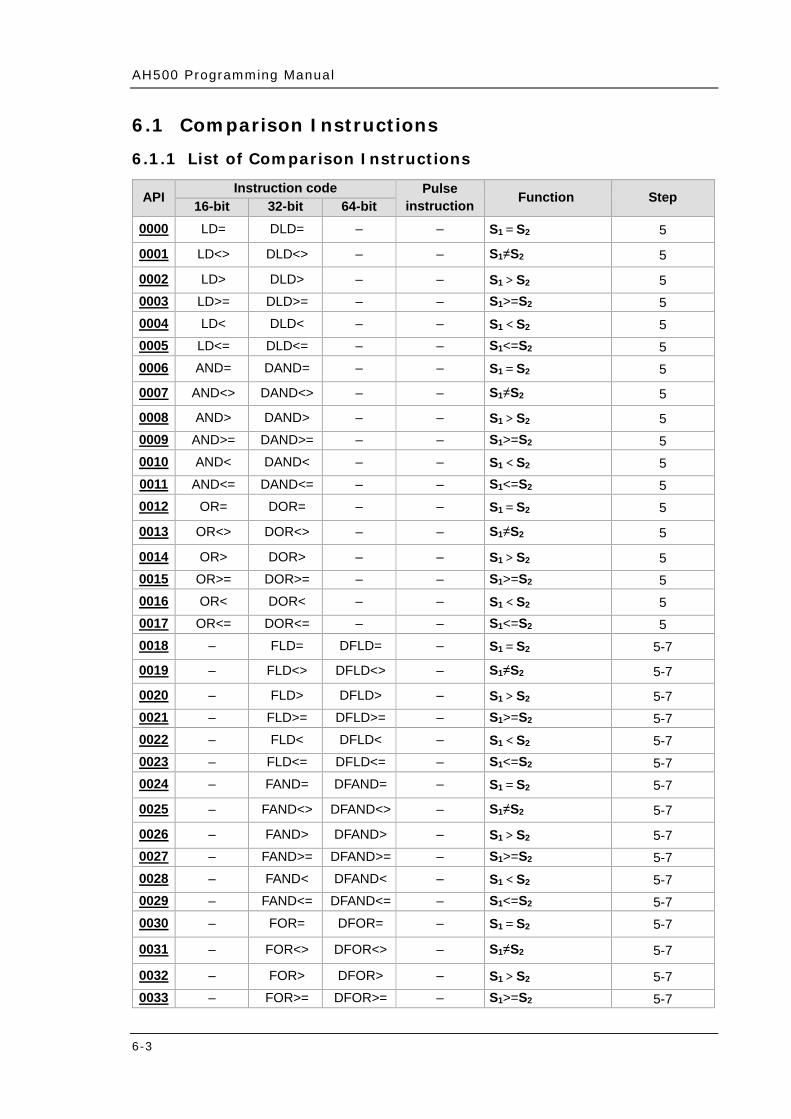
AH500 Programming Manual
6-3
6.1 Comparison Instructions
6.1.1 List of Comparison Instructions
API Instruction code Pulse instruction Function Step 16-bit 32-bit 64-bit
0000 LD= DLD= – – S1=S2 5
0001 LD<> DLD<> – – S1≠S2 5
0002 LD> DLD> – – S1>S2 5 0003 LD>= DLD>= – – S1>=S2 5 0004 LD< DLD< – – S1<S2 5 0005 LD<= DLD<= – – S1<=S2 5 0006 AND= DAND= – – S1=S2 5
0007 AND<> DAND<> – – S1≠S2 5
0008 AND> DAND> – – S1>S2 5 0009 AND>= DAND>= – – S1>=S2 5 0010 AND< DAND< – – S1<S2 5 0011 AND<= DAND<= – – S1<=S2 5 0012 OR= DOR= – – S1=S2 5
0013 OR<> DOR<> – – S1≠S2 5
0014 OR> DOR> – – S1>S2 5 0015 OR>= DOR>= – – S1>=S2 5 0016 OR< DOR< – – S1<S2 5 0017 OR<= DOR<= – – S1<=S2 5 0018 – FLD= DFLD= – S1=S2 5-7
0019 – FLD<> DFLD<> – S1≠S2 5-7
0020 – FLD> DFLD> – S1>S2 5-7 0021 – FLD>= DFLD>= – S1>=S2 5-7 0022 – FLD< DFLD< – S1<S2 5-7 0023 – FLD<= DFLD<= – S1<=S2 5-7 0024 – FAND= DFAND= – S1=S2 5-7
0025 – FAND<> DFAND<> – S1≠S2 5-7
0026 – FAND> DFAND> – S1>S2 5-7 0027 – FAND>= DFAND>= – S1>=S2 5-7 0028 – FAND< DFAND< – S1<S2 5-7 0029 – FAND<= DFAND<= – S1<=S2 5-7 0030 – FOR= DFOR= – S1=S2 5-7
0031 – FOR<> DFOR<> – S1≠S2 5-7
0032 – FOR> DFOR> – S1>S2 5-7 0033 – FOR>= DFOR>= – S1>=S2 5-7
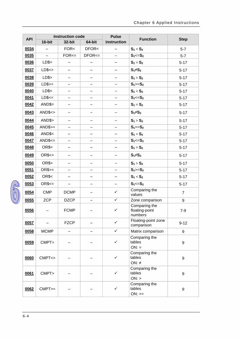
Chapter 6 Appl ied Inst ruct ions
6-4
API Instruction code Pulse instruction Function Step 16-bit 32-bit 64-bit
0034 – FOR< DFOR< – S1<S2 5-7 0035 – FOR<= DFOR<= – S1<=S2 5-7 0036 LD$= – – – S1=S2 5-17
0037 LD$<> – – – S1≠S2 5-17
0038 LD$> – – – S1>S2 5-17 0039 LD$>= – – – S1>=S2 5-17 0040 LD$< – – – S1<S2 5-17 0041 LD$<= – – – S1<=S2 5-17 0042 AND$= – – – S1=S2 5-17
0043 AND$<> – – – S1≠S2 5-17
0044 AND$> – – – S1>S2 5-17 0045 AND$>= – – – S1>=S2 5-17 0046 AND$< – – – S1<S2 5-17 0047 AND$<= – – – S1<=S2 5-17 0048 OR$= – – – S1=S2 5-17
0049 OR$<> – – – S1≠S2 5-17
0050 OR$> – – – S1>S2 5-17 0051 OR$>= – – – S1>=S2 5-17 0052 OR$< – – – S1<S2 5-17
0053 OR$<= – – – S1<=S2 5-17
0054 CMP DCMP – Comparing the values 7
0055 ZCP DZCP – Zone comparison 9
0056 – FCMP – Comparing the floating-point numbers
7-9
0057 – FZCP – Floating-point zone comparison 9-12
0058 MCMP – – Matrix comparison 9
0059 CMPT= – – Comparing the tables ON: =
9
0060 CMPT<> – – Comparing the tables ON: ≠
9
0061 CMPT> – – Comparing the tables ON: >
9
0062 CMPT>= – – Comparing the tables ON: >=
9

AH500 Programming Manual
6-5
API Instruction code Pulse instruction Function Step 16-bit 32-bit 64-bit
0063 CMPT< – – Comparing the tables ON: <
9
0064 CMPT<= – – Comparing the tables ON: <=
9
0065 CHKADR – – –
Checking the address of the contact type of pointer register
7
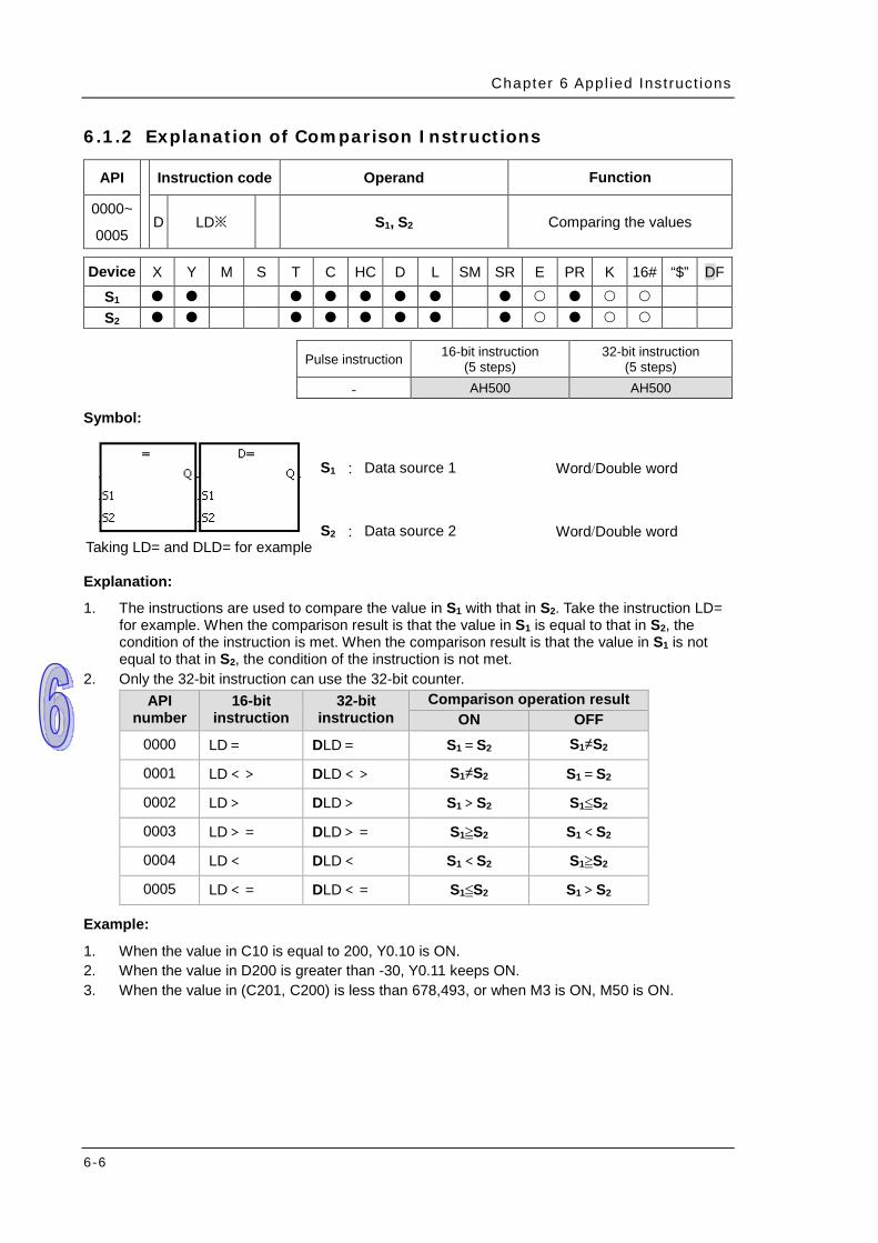
Chapter 6 Appl ied Inst ruct ions
6-6
6.1.2 Explanation of Comparison Instructions
API Instruction code Operand Function
0000~
0005 D LD※ S1, S2 Comparing the values
Device X Y M S T C HC D L SM SR E PR K 16# “$” DF
S1 S2
Pulse instruction 16-bit instruction
(5 steps) 32-bit instruction
(5 steps) - AH500 AH500
Symbol:
Taking LD= and DLD= for example
S1 : Data source 1 Word/Double word
S2 : Data source 2 Word/Double word
Explanation:
1. The instructions are used to compare the value in S1 with that in S2. Take the instruction LD= for example. When the comparison result is that the value in S1 is equal to that in S2, the condition of the instruction is met. When the comparison result is that the value in S1 is not equal to that in S2, the condition of the instruction is not met.
2. Only the 32-bit instruction can use the 32-bit counter. API
number 16-bit
instruction 32-bit
instruction Comparison operation result
ON OFF 0000 LD= DLD= S1=S2 S1≠S2
0001 LD<> DLD<> S1≠S2 S1=S2
0002 LD> DLD> S1>S2 S1≦S2
0003 LD>= DLD>= S1≧S2 S1<S2
0004 LD< DLD< S1<S2 S1≧S2
0005 LD<= DLD<= S1≦S2 S1>S2
Example:
1. When the value in C10 is equal to 200, Y0.10 is ON. 2. When the value in D200 is greater than -30, Y0.11 keeps ON. 3. When the value in (C201, C200) is less than 678,493, or when M3 is ON, M50 is ON.
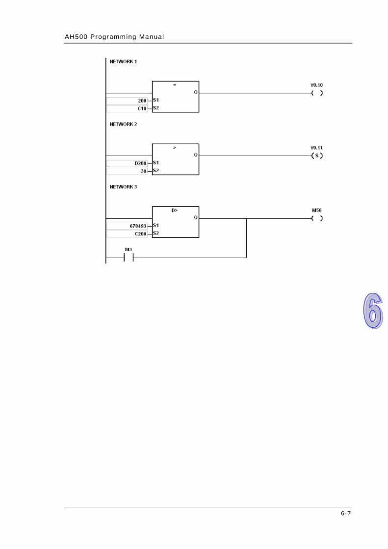
AH500 Programming Manual
6-7

Chapter 6 Appl ied Inst ruct ions
6-8
API Instruction code Operand Function
0006~
0011 D AND※ S1, S2 Comparing the values
Device X Y M S T C HC D L SM SR E PR K 16# “$” DF
S1 S2
Pulse instruction 16-bit instruction
(5 steps) 32-bit instruction
(5 steps) - AH500 AH500
Symbol:
Taking AND= and DAND= for example
S1 : Data source 1 Word/Double word
S2 : Data source 2 Word/Double word
Explanation: 1. The instructions are used to compare the value in S1 with that in S2. Take the instruction
AND= for example. When the comparison result is that the value in S1 is equal to that in S2, the condition of the instruction is met. When the comparison result is that the value in S1 is not equal to that in S2, the condition of the instruction is not met.
2. Only the 32-bit instruction can use the 32-bit counter. API
number 16-bit
instruction 32-bit
instruction Comparison operation result
ON OFF 0006 AND= DAND= S1=S2 S1≠S2
0007 AND<> DAND<> S1≠S2 S1=S2
0008 AND> DAND> S1>S2 S1≦S2
0009 AND>= DAND>= S1≧S2 S1<S2
0010 AND< DAND< S1<S2 S1≧S2
0011 AND<= DAND<= S1≦S2 S1>S2

AH500 Programming Manual
6-9
Example:
1. When X0.0 is ON and the current value in C10 is equal to 100, Y0.10 is ON. 2. When X0.1 is OFF and the value in D0 is not equal to -10, Y0.11 keeps ON. 3. When X0.2 is ON and the value in (D11, D10) is less than 678,493, or when M3 is ON, M50 is
ON.
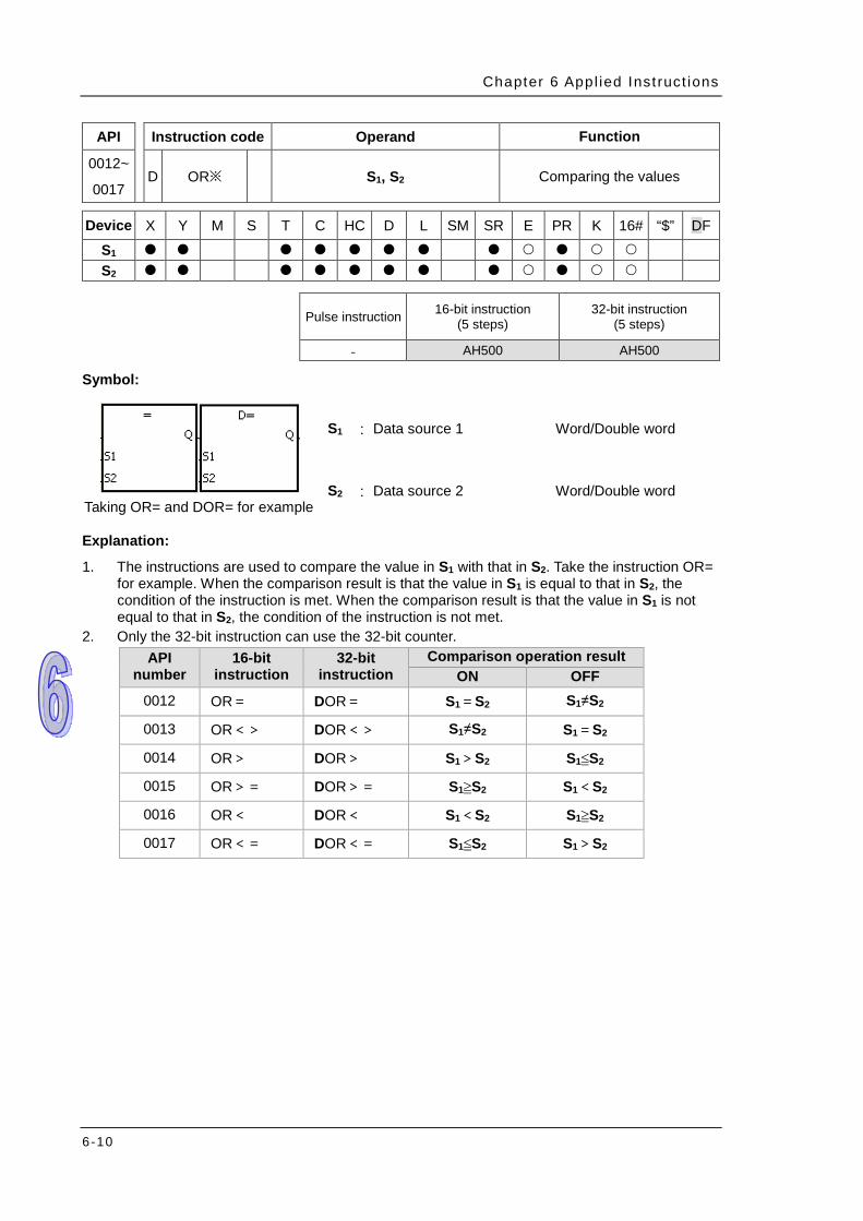
Chapter 6 Appl ied Inst ruct ions
6-10
API Instruction code Operand Function
0012~
0017 D OR※ S1, S2 Comparing the values
Device X Y M S T C HC D L SM SR E PR K 16# “$” DF
S1 S2
Pulse instruction 16-bit instruction
(5 steps) 32-bit instruction
(5 steps)
- AH500 AH500
Symbol:
Taking OR= and DOR= for example
S1 : Data source 1 Word/Double word
S2 : Data source 2 Word/Double word
Explanation:
1. The instructions are used to compare the value in S1 with that in S2. Take the instruction OR= for example. When the comparison result is that the value in S1 is equal to that in S2, the condition of the instruction is met. When the comparison result is that the value in S1 is not equal to that in S2, the condition of the instruction is not met.
2. Only the 32-bit instruction can use the 32-bit counter. API
number 16-bit
instruction 32-bit
instruction Comparison operation result
ON OFF 0012 OR= DOR= S1=S2 S1≠S2
0013 OR<> DOR<> S1≠S2 S1=S2
0014 OR> DOR> S1>S2 S1≦S2
0015 OR>= DOR>= S1≧S2 S1<S2
0016 OR< DOR< S1<S2 S1≧S2
0017 OR<= DOR<= S1≦S2 S1>S2
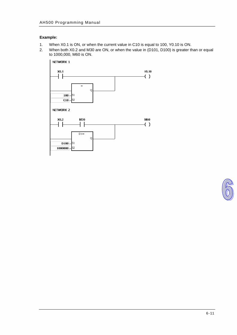
AH500 Programming Manual
6-11
Example:
1. When X0.1 is ON, or when the current value in C10 is equal to 100, Y0.10 is ON. 2. When both X0.2 and M30 are ON, or when the value in (D101, D100) is greater than or equal
to 1000,000, M60 is ON.
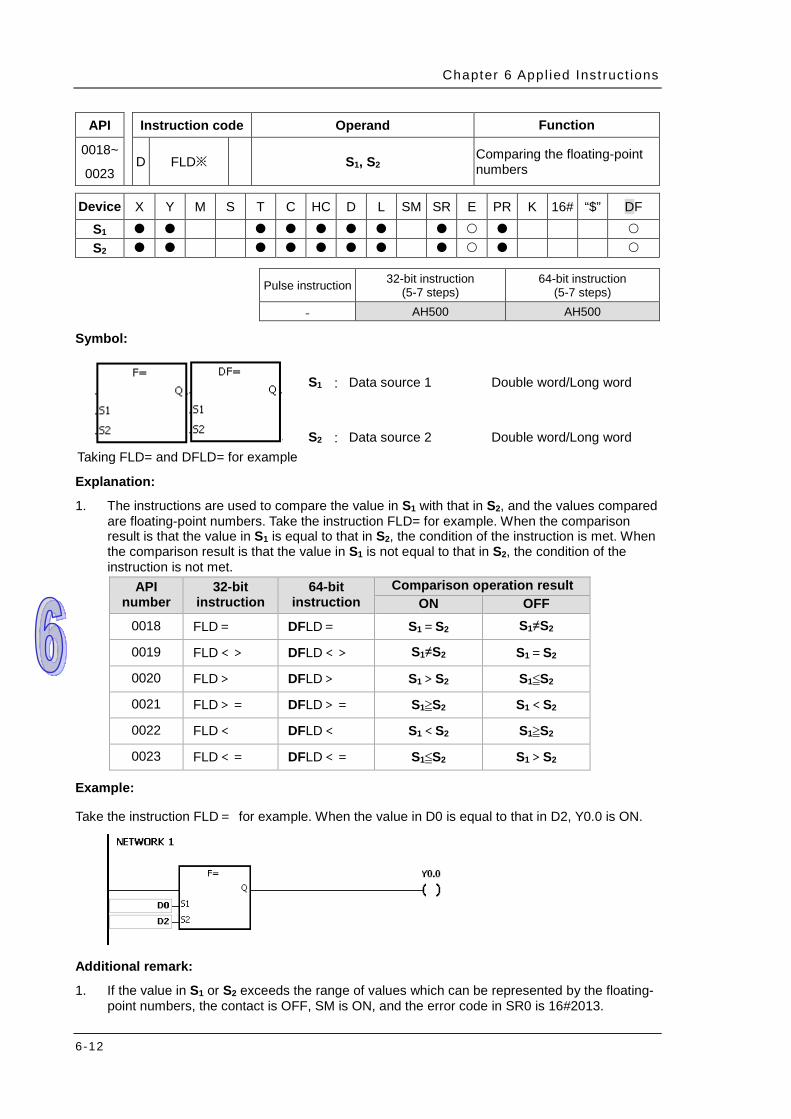
Chapter 6 Appl ied Inst ruct ions
6-12
API Instruction code Operand Function
0018~
0023 D FLD※ S1, S2 Comparing the floating-point
numbers
Device X Y M S T C HC D L SM SR E PR K 16# “$” DF
S1 S2
Pulse instruction 32-bit instruction
(5-7 steps) 64-bit instruction
(5-7 steps) - AH500 AH500
Symbol:
Taking FLD= and DFLD= for example
S1 : Data source 1 Double word/Long word
S2 : Data source 2 Double word/Long word
Explanation:
1. The instructions are used to compare the value in S1 with that in S2, and the values compared are floating-point numbers. Take the instruction FLD= for example. When the comparison result is that the value in S1 is equal to that in S2, the condition of the instruction is met. When the comparison result is that the value in S1 is not equal to that in S2, the condition of the instruction is not met.
API number
32-bit instruction
64-bit instruction
Comparison operation result ON OFF
0018 FLD= DFLD= S1=S2 S1≠S2
0019 FLD<> DFLD<> S1≠S2 S1=S2
0020 FLD> DFLD> S1>S2 S1≦S2
0021 FLD>= DFLD>= S1≧S2 S1<S2
0022 FLD< DFLD< S1<S2 S1≧S2
0023 FLD<= DFLD<= S1≦S2 S1>S2
Example:
Take the instruction FLD= for example. When the value in D0 is equal to that in D2, Y0.0 is ON.
Additional remark:
1. If the value in S1 or S2 exceeds the range of values which can be represented by the floating-point numbers, the contact is OFF, SM is ON, and the error code in SR0 is 16#2013.

AH500 Programming Manual
6-13
API Instruction code Operand Function
0024~
0029 D FAND※ S1, S2 Comparing the floating-point
numbers
Device X Y M S T C HC D L SM SR E PR K 16# “$” DF
S1 S2
Pulse instruction 32-bit instruction
(5-7 steps) 64-bit instruction
(5-7 steps) - AH500 AH500
Symbol:
Taking FAND= and DFAND= for example
S1 : Data source 1 Double word/Long word
S2 : Data source 2 Double word/Long word
Explanation:
1. The instructions are used to compare the value in S1 with that in S2, and the values compared are floating-point numbers. Take the instruction FAND= for example. When the comparison result is that the value in S1 is equal to that in S2, the condition of the instruction is met. When the comparison result is that the value in S1 is not equal to that in S2, the condition of the instruction is not met.
API number
32-bit instruction
64-bit instruction
Comparison operation result ON OFF
0024 FAND= DFAND= S1=S2 S1≠S2
0025 FAND<> DFAND<> S1≠S2 S1=S2
0026 FAND> DFAND> S1>S2 S1≦S2
0027 FAND>= DFAND>= S1≧S2 S1<S2
0028 FAND< DFAND< S1<S2 S1≧S2
0029 FAND<= DFAND<= S1≦S2 S1>S2
Example:
Take the instruction FAND= for example. When X1.0 is ON and the value in D1 is equal to that in D2, Y1.0 is ON.
Additional remark:
1. If the value in S1 or S2 exceeds the range of values which can be represented by the floating-point numbers, the contact is OFF, SM is ON, and the error code in SR0 is 16#2013.

Chapter 6 Appl ied Inst ruct ions
6-14
API Instruction code Operand Function
0030~
0035 D FOR※ S1, S2 Comparing the floating-point
numbers
Device X Y M S T C HC D L SM SR E PR K 16# “$” DF
S1 S2
Pulse instruction 32-bit instruction
(5-7 steps) 64-bit instruction
(5-7 steps)
- AH500 AH500
Symbol:
Taking FOR= and DFOR= for example
S1 : Data source 1 Double word/Long word
S2 : Data source 2 Double word/Long word
Explanation:
1. The instructions are used to compare the value in S1 with that in S2, and the values compared are floating-point numbers. Take the instruction FOR= for example. When the comparison result is that the value in S1 is equal to that in S2, the condition of the instruction is met. When the comparison result is that the value in S1 is not equal to that in S2, the condition of the instruction is not met.
API number
32-bit instruction
64-bit instruction
Comparison operation result ON OFF
0030 FOR= DFOR= S1=S2 S1≠S2
0031 FOR<> DFOR<> S1≠S2 S1=S2
0032 FOR> DFOR> S1>S2 S1≦S2
0033 FOR>= DFOR>= S1≧S2 S1<S2
0034 FOR< DFOR< S1<S2 S1≧S2
0035 FOR<= DFOR<= S1≦S2 S1>S2
Example:
When X1.0 is ON, or when the value in D1 is equal to that in D2, Y1.0 is ON.
Additional remark: 1. If the value in S1 or S2 exceeds the range of values which can be represented by the floating-
point numbers, the contact is OFF, SM is ON, and the error code in SR0 is 16#2013.
AH500 Programming Manual
6-15
API Instruction code Operand Function
0036~
0041 LD$※ S1, S2 Comparing the strings
Device X Y M S T C HC D L SM SR E PR K 16# “$” DF
S1 S2
Pulse
instruction 16-bit instruction
(5-17 steps) 32-bit instruction
- AH500 -
Symbol:
Taking LD$= for example
S1 : Data source 1 String
S2 : Data source 2 String
Explanation:
1. The instructions are used to compare the data in S1 with that in S2, and the data compared is strings. Take the instruction LD$= for example. When the comparison result is that the data in S1 is equal to that in S2, the condition of the contact is met. When the comparison result is that the data in S1 is not equal to that in S2, the condition of the contact is not met.
API number Instruction Comparison operation result
ON OFF 0036 LD$= S1=S2 S1≠S2
0037 LD$<> S1≠S2 S1=S2
0038 LD$> S1>S2 S1≦S2
0039 LD$>= S1≧S2 S1<S2
0040 LD$< S1<S2 S1≧S2
0041 LD$<= S1≦S2 S1>S2 2. Only when the data in S~S+n (n indicates the nth device) includes 16#00 can the data be
judged as a complete string.
16#31(1)
16#33(3)
16#32(2)
16#34(4)
16#35(5)16#00
S
S+1
S+2
b15 b8 b7 b0
" "12345 3. When two strings are the same, the corresponding comparison operation results of the
instructions are listed below.

Chapter 6 Appl ied Inst ruct ions
6-16
16#41(A)
16#43(C)
16#42(B)
16#44(D)
16#45(E)16#00
S1
S1
S1
+1
+2
b15 b8 b7 b0
" "ABCDE
16#41(A)
16#43(C)
16#42(B)
16#44(D)
16#45(E)16#00
S2
S2
S2
+1
+2
b15 b8 b7 b0
" "ABCDE
Comparison sign
Comparison symbol Comparison operation result $= ON
$<> OFF
$> OFF
$>= ON
$< OFF
$<= ON 4. When the lengths of the strings are the same, but their contents are different, the first different
values (ASCII codes) met in the strings are compared. For example, the string in S1 is “ABCDF”, and the string in S1 is “ABCDE”. The first different values met in the strings are “F” (16#46) and “E” (16#45). Owing to the fact that 16#46 is greater than 16#45, the string in S1 is greater than that in S1. The corresponding comparison operation results of the instructions are listed below.
16#41(A)
16#43(C)
16#42(B)
16#44(D)
16#46(F)16#00
S1
S1
S1
+1
+2
b15 b8 b7 b0
" "ABCDF
16#41(A)
16#43(C)
16#42(B)
16#44(D)
16#45(E)16#00
S2
S2
S2
+1
+2
b15 b8 b7 b0
" "ABCDE
Compar ison sign
Comparison symbol Comparison operation result $= OFF
$<> ON
$> ON
$>= ON
$< OFF
$<= OFF 5. When the lengths of the strings are different, the string whose length is longer is greater than
the string whose length is shorter. For example, the string in S1 is “1234567”, and the string in S2 is “99999””. Owing to the fact that the string in S1 is composed of 7 characters, and the string in S2 is composed of 5 characters, the string in S1 is greater than the string in S2. The corresponding comparison operation results of the instructions are listed below.
16#31(1)
16#33(3)
16#32(2)
16#34(4)
16#35(5)16#00
S1
S1
S1
+1
+2
b15 b8 b7 b0
" "1234567
16#39(9)
16#39(9)
16#39(9)
16#39(9)
16#39(9)16#00
S2
S2
S2
+1
+2
b15 b8 b7 b0
" "99999
Comparison sign
16#36(6)16#37(7)S1 +3
AH500 Programming Manual
6-17
Comparison symbol Comparison operation result $= OFF
$<> ON
$> ON
$>= ON
$< OFF
$<= OFF
Example:
When the string starting with the data in D0 is equal to the string staring with D2, Y0.0 is ON.
Additional remark:
1. If the string does not end with 16#00, the instruction is not executed, SM is ON, and the error code in SR0 is 16#200E.

Chapter 6 Appl ied Inst ruct ions
6-18
API Instruction code Operand Function
0042~
0047 AND$※ S1, S2 Comparing the strings
Device X Y M S T C HC D L SM SR E PR K 16# “$” DF
S1 S2
Pulse instruction 16-bit instruction
(5-17 steps) 32-bit instruction
- AH500 -
Symbol:
Taking AND$= for example
S1 : Data source 1 String
S2 : Data source 2 String
Explanation:
1. The instructions are used to compare the data in S1 with that in S2, and the data compared is strings. Take the instruction AND$= for example. When the comparison result is that the data in S1 is equal to that in S2, the condition of the contact is met. When the comparison result is that the data in S1 is not equal to that in S2, the condition of the contact is not met.
2. Only when the data in S~S+n (n indicates the nth device) includes 16#00 can the data be judged as a complete string.
3. When the strings are completely the same, the corresponding comparison operation results of the instructions are listed below.
16#41(A)
16#43(C)
16#42(B)
16#44(D)
16#45(E)16#00
S1
S1
S1
+1
+2
b15 b8 b7 b0
" "ABCDE
16#41(A)
16#43(C)
16#42(B)
16#44(D)
16#45(E)16#00
S2
S2
S2
+1
+2
b15 b8 b7 b0
" "ABCDE
Compar ison sign
Comparison symbol Comparison operation result
$= ON
$<> OFF
$> OFF
$>= ON
$< OFF
$<= ON 4. When the lengths of the strings are the same, but their contents are different, the first different
values (ASCII codes) met in the strings are compared. For example, the string in S1 is “ABCDF”, and the string in S1 is “ABCDE”. The first different values met in the strings are “F” (16#46) and “E” (16#45). Owing to the fact that 16#46 is greater than 16#45, the string in S1 is greater than that in S1. The corresponding comparison operation results of the instructions are listed below.
AH500 Programming Manual
6-19
16#41(A)
16#43(C)
16#42(B)
16#44(D)
16#46(F)16#00
S1
S1
S1
+1
+2
b15 b8 b7 b0
" "ABCDF
16#41(A)
16#43(C)
16#42(B)
16#44(D)
16#45(E)16#00
S2
S2
S2
+1
+2
b15 b8 b7 b0
" "ABCDE
Compar ison sign
Comparison symbol Comparison operation result $= OFF
$<> ON
$> ON
$>= ON
$< OFF
$<= OFF 5. When the lengths of the strings are different, the string whose length is longer is greater than
the string whose length is shorter. For example, the string in S1 is “1234567”, and the string in S2 is “99999””. Owing to the fact that the string in S1 is composed of 7 characters, and the string in S2 is composed of 5 characters, the string in S1 is greater than the string in S2. The corresponding comparison operation results of the instructions are listed below.
16#31(1)
16#33(3)
16#32(2)
16#34(4)
16#35(5)16#00
S1
S1
S1
+1
+2
b15 b8 b7 b0
" "1234567
16#39(9)
16#39(9)
16#39(9)
16#39(9)
16#39(9)16#00
S2
S2
S2
+1
+2
b15 b8 b7 b0
" "99999
Comparison sign
16#36(6)16#37(7)S1 +3
Comparison symbol Comparison operation result $= OFF
$<> ON
$> ON
$>= ON
$< OFF
$<= OFF
Example:
When M0 is ON and the string starting with the data in D0 is equal to the string staring with D2, Y0.0 is ON.
Chapter 6 Appl ied Inst ruct ions
6-20
API Instruction code Operand Function
0048~
0053 OR$※ S1, S2 Comparing the strings
Device X Y M S T C HC D L SM SR E PR K 16# “$” DF
S1 S2
Pulse instruction 16-bit instruction
(5-17 steps) 32-bit instruction
- AH500 -
Symbol:
Taking OR$= for example
S1 : Data source 1 String
S2 : Data source 2 String
Explanation:
1. The instructions are used to compare the data in S1 with that in S2, and the data compared is strings. Take the instruction OR$= for example. When the comparison result is that the data in S1 is equal to that in S2, the condition of the contact is met. When the comparison result is that the data in S1 is not equal to that in S2, the condition of the contact is not met.
2. Only when the data in S~S+n (n indicates the nth device) includes 16#00 can the data be judged as a complete string.
3. When the strings are completely the same, the corresponding comparison operation results of the instructions are listed below.
16#41(A)
16#43(C)
16#42(B)
16#44(D)
16#45(E)16#00
S1
S1
S1
+1
+2
b15 b8 b7 b0
" "ABCDE
16#41(A)
16#43(C)
16#42(B)
16#44(D)
16#45(E)16#00
S2
S2
S2
+1
+2
b15 b8 b7 b0
" "ABCDE
Compar ison sign
Comparison symbol Comparison operation result $= ON
$<> OFF
$> OFF
$>= ON
$< OFF
$<= ON 4. When the lengths of the strings are the same, but their contents are different, the first different
values (ASCII codes) met in the strings are compared. For example, the string in S1 is “ABCDF”, and the string in S1 is “ABCDE”. The first different values met in the strings are “F” (16#46) and “E” (16#45). Owing to the fact that 16#46 is greater than 16#45, the string in S1 is greater than that in S1. The corresponding comparison operation results of the instructions are listed below.
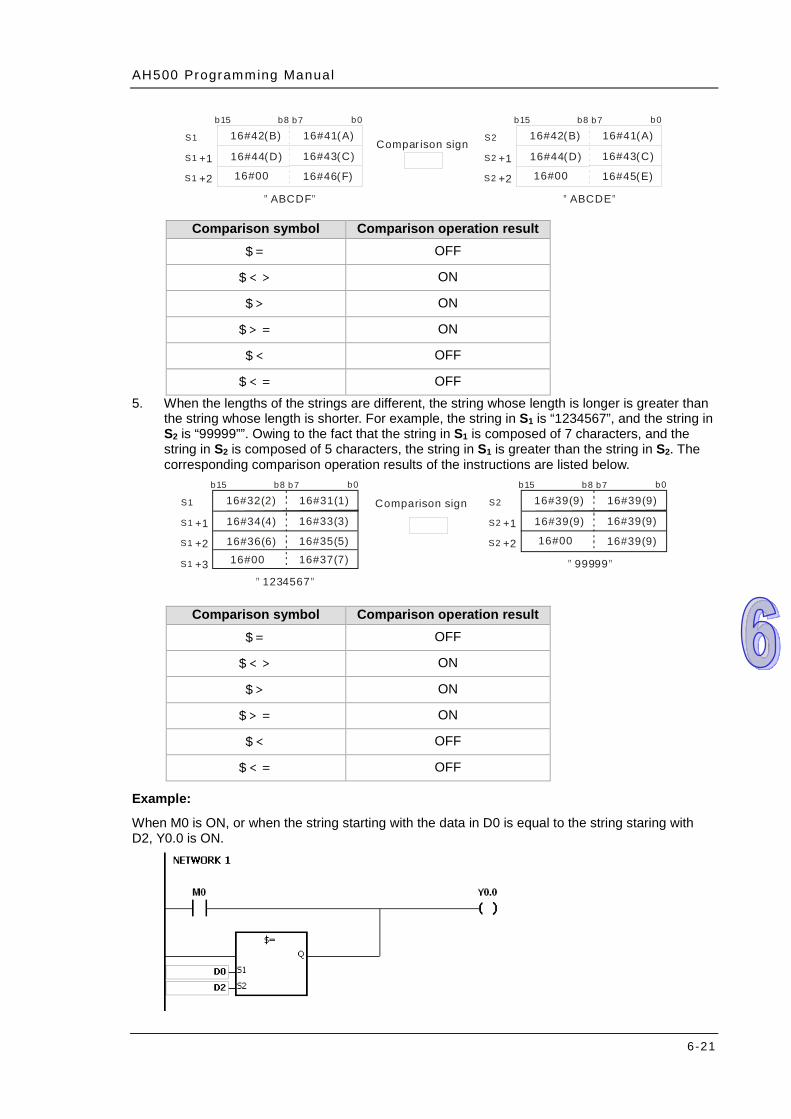
AH500 Programming Manual
6-21
16#41(A)
16#43(C)
16#42(B)
16#44(D)
16#46(F)16#00
S1
S1
S1
+1
+2
b15 b8 b7 b0
" "ABCDF
16#41(A)
16#43(C)
16#42(B)
16#44(D)
16#45(E)16#00
S2
S2
S2
+1
+2
b15 b8 b7 b0
" "ABCDE
Compar ison sign
Comparison symbol Comparison operation result $= OFF
$<> ON
$> ON
$>= ON
$< OFF
$<= OFF 5. When the lengths of the strings are different, the string whose length is longer is greater than
the string whose length is shorter. For example, the string in S1 is “1234567”, and the string in S2 is “99999””. Owing to the fact that the string in S1 is composed of 7 characters, and the string in S2 is composed of 5 characters, the string in S1 is greater than the string in S2. The corresponding comparison operation results of the instructions are listed below.
16#31(1)
16#33(3)
16#32(2)
16#34(4)
16#35(5)16#00
S1
S1
S1
+1
+2
b15 b8 b7 b0
" "1234567
16#39(9)
16#39(9)
16#39(9)
16#39(9)
16#39(9)16#00
S2
S2
S2
+1
+2
b15 b8 b7 b0
" "99999
Comparison sign
16#36(6)16#37(7)S1 +3
Comparison symbol Comparison operation result $= OFF
$<> ON
$> ON
$>= ON
$< OFF
$<= OFF
Example:
When M0 is ON, or when the string starting with the data in D0 is equal to the string staring with D2, Y0.0 is ON.
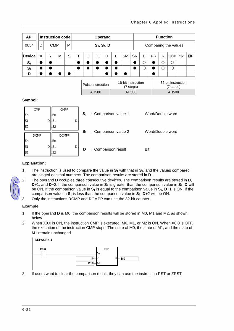
Chapter 6 Appl ied Inst ruct ions
6-22
API Instruction code Operand Function
0054 D CMP P S1, S2, D Comparing the values
Device X Y M S T C HC D L SM SR E PR K 16# “$” DF
S1 S2 D
Pulse instruction 16-bit instruction
(7 steps) 32-bit instruction
(7 steps) AH500 AH500 AH500
Symbol:
S1 : Comparison value 1 Word/Double word
S2 : Comparison value 2 Word/Double word
D : Comparison result Bit
Explanation:
1. The instruction is used to compare the value in S1 with that in S2, and the values compared are singed decimal numbers. The comparison results are stored in D.
2. The operand D occupies three consecutive devices. The comparison results are stored in D, D+1, and D+2. If the comparison value in S1 is greater than the comparison value in S2, D will be ON. If the comparison value in S1 is equal to the comparison value in S2, D+1 is ON. If the comparison value in S1 is less than the comparison value in S2, D+2 will be ON.
3. Only the instructions DCMP and DCMPP can use the 32-bit counter.
Example:
1. If the operand D is M0, the comparison results will be stored in M0, M1 and M2, as shown below.
2. When X0.0 is ON, the instruction CMP is executed. M0, M1, or M2 is ON. When X0.0 is OFF, the execution of the instruction CMP stops. The state of M0, the state of M1, and the state of M1 remain unchanged.
3. If users want to clear the comparison result, they can use the instruction RST or ZRST.
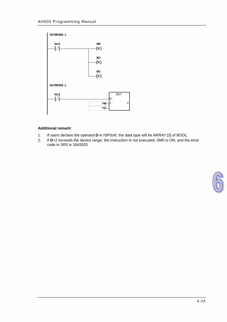
AH500 Programming Manual
6-23
Additional remark:
1. If users declare the operand D in ISPSoft, the data type will be ARRAY [3] of BOOL. 2. If D+2 exceeds the device range, the instruction is not executed, SM0 is ON, and the error
code in SR0 is 16#2003.
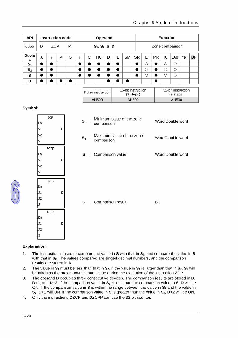
Chapter 6 Appl ied Inst ruct ions
6-24
API Instruction code Operand Function
0055 D ZCP P S1, S2, S, D Zone comparison
Device
X Y M S T C HC D L SM SR E PR K 16# “$” DF S1 S2 S D
Pulse instruction 16-bit instruction
(9 steps) 32-bit instruction
(9 steps) AH500 AH500 AH500
Symbol:
S1 : Minimum value of the zone comparison Word/Double word
S2 : Maximum value of the zone comparison Word/Double word
S : Comparison value Word/Double word
D : Comparison result Bit
Explanation:
1. The instruction is used to compare the value in S with that in S1, and compare the value in S with that in S2. The values compared are singed decimal numbers, and the comparison results are stored in D.
2. The value in S1 must be less than that in S2. If the value in S1 is larger than that in S2, S1 will be taken as the maximum/minimum value during the execution of the instruction ZCP.
3. The operand D occupies three consecutive devices. The comparison results are stored in D, D+1, and D+2. If the comparison value in S1 is less than the comparison value in S, D will be ON. If the comparison value in S is within the range between the value in S1 and the value in S2, D+1 will ON. If the comparison value in S is greater than the value in S2, D+2 will be ON.
4. Only the instructions DZCP and DZCPP can use the 32-bit counter.
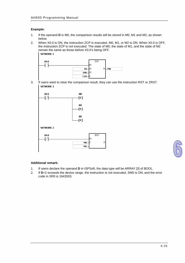
AH500 Programming Manual
6-25
Example:
1. If the operand D is M0, the comparison results will be stored in M0, M1 and M2, as shown below.
2. When X0.0 is ON, the instruction ZCP is executed. M0, M1, or M2 is ON. When X0.0 is OFF, the instruction ZCP is not executed. The state of M0, the state of M1, and the state of M2 remain the same as those before X0.0’s being OFF.
3. If users want to clear the comparison result, they can use the instruction RST or ZRST.
Additional remark:
1. If users declare the operand D in ISPSoft, the data type will be ARRAY [3] of BOOL. 2. If D+2 exceeds the device range, the instruction is not executed, SM0 is ON, and the error
code in SR0 is 16#2003.
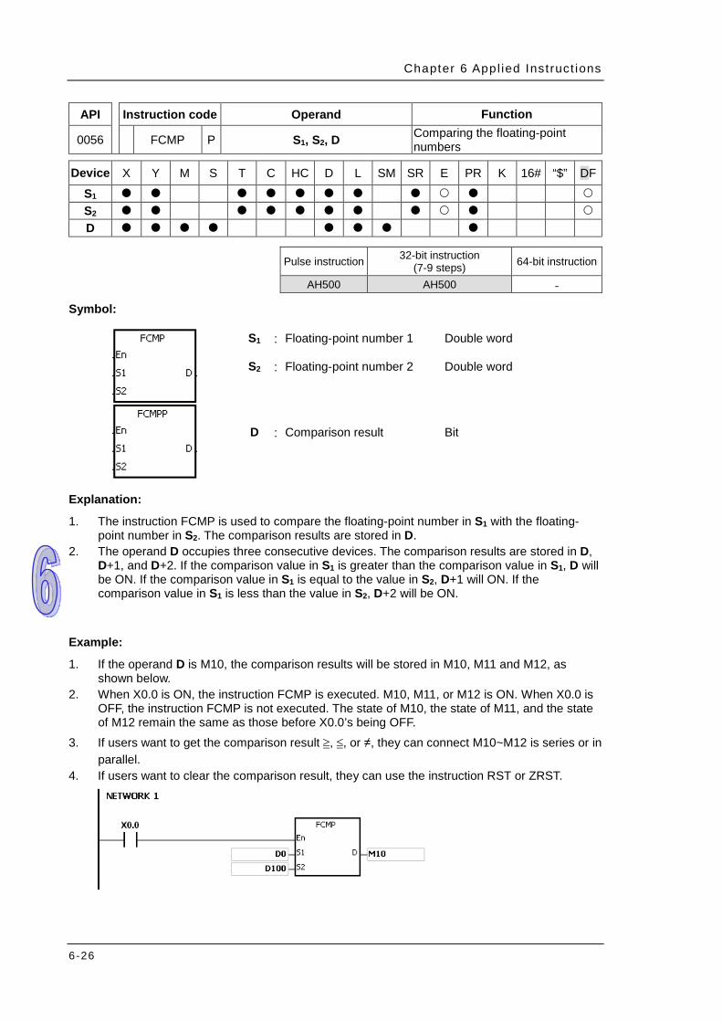
Chapter 6 Appl ied Inst ruct ions
6-26
API Instruction code Operand Function
0056 FCMP P S1, S2, D Comparing the floating-point numbers
Device X Y M S T C HC D L SM SR E PR K 16# “$” DF
S1 S2 D
Pulse instruction 32-bit instruction
(7-9 steps) 64-bit instruction
AH500 AH500 -
Symbol:
S1 : Floating-point number 1 Double word
S2 : Floating-point number 2 Double word
D : Comparison result Bit
Explanation:
1. The instruction FCMP is used to compare the floating-point number in S1 with the floating-point number in S2. The comparison results are stored in D.
2. The operand D occupies three consecutive devices. The comparison results are stored in D, D+1, and D+2. If the comparison value in S1 is greater than the comparison value in S1, D will be ON. If the comparison value in S1 is equal to the value in S2, D+1 will ON. If the comparison value in S1 is less than the value in S2, D+2 will be ON.
Example:
1. If the operand D is M10, the comparison results will be stored in M10, M11 and M12, as shown below.
2. When X0.0 is ON, the instruction FCMP is executed. M10, M11, or M12 is ON. When X0.0 is OFF, the instruction FCMP is not executed. The state of M10, the state of M11, and the state of M12 remain the same as those before X0.0’s being OFF.
3. If users want to get the comparison result ≧, ≦, or ≠, they can connect M10~M12 is series or in parallel.
4. If users want to clear the comparison result, they can use the instruction RST or ZRST.
AH500 Programming Manual
6-27
Additional remark:
1. If the value in S1 or S2 exceeds the range of values which can be represented by the floating-point numbers, the contact is OFF, SM is ON, and the error code in SR0 is 16#2013.
2. If users declare the operand D in ISPSoft, the data type will ARRAY [3] of BOOL. 3. If D+2 exceeds the device range, the instruction is not executed, SM0 is ON, and the error
code in SR0 is 16#2003.
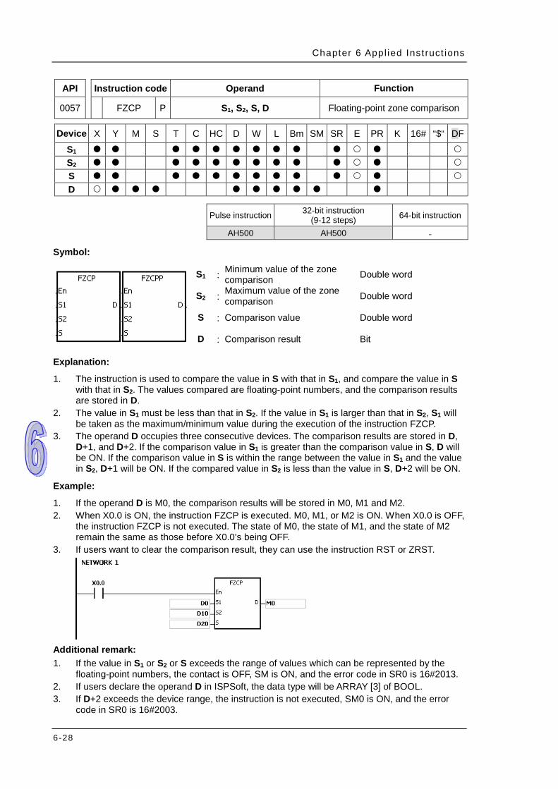
Chapter 6 Appl ied Inst ruct ions
6-28
API Instruction code Operand Function
0057 FZCP P S1, S2, S, D Floating-point zone comparison
Device X Y M S T C HC D W L Bm SM SR E PR K 16# “$“ DF
S1 S2 S D
Pulse instruction 32-bit instruction
(9-12 steps) 64-bit instruction
AH500 AH500 -
Symbol:
S1 : Minimum value of the zone comparison Double word
S2 : Maximum value of the zone comparison Double word
S : Comparison value Double word
D : Comparison result Bit
Explanation:
1. The instruction is used to compare the value in S with that in S1, and compare the value in S with that in S2. The values compared are floating-point numbers, and the comparison results are stored in D.
2. The value in S1 must be less than that in S2. If the value in S1 is larger than that in S2, S1 will be taken as the maximum/minimum value during the execution of the instruction FZCP.
3. The operand D occupies three consecutive devices. The comparison results are stored in D, D+1, and D+2. If the comparison value in S1 is greater than the comparison value in S, D will be ON. If the comparison value in S is within the range between the value in S1 and the value in S2, D+1 will be ON. If the compared value in S2 is less than the value in S, D+2 will be ON.
Example:
1. If the operand D is M0, the comparison results will be stored in M0, M1 and M2. 2. When X0.0 is ON, the instruction FZCP is executed. M0, M1, or M2 is ON. When X0.0 is OFF,
the instruction FZCP is not executed. The state of M0, the state of M1, and the state of M2 remain the same as those before X0.0’s being OFF.
3. If users want to clear the comparison result, they can use the instruction RST or ZRST.
Additional remark: 1. If the value in S1 or S2 or S exceeds the range of values which can be represented by the
floating-point numbers, the contact is OFF, SM is ON, and the error code in SR0 is 16#2013. 2. If users declare the operand D in ISPSoft, the data type will be ARRAY [3] of BOOL. 3. If D+2 exceeds the device range, the instruction is not executed, SM0 is ON, and the error
code in SR0 is 16#2003.
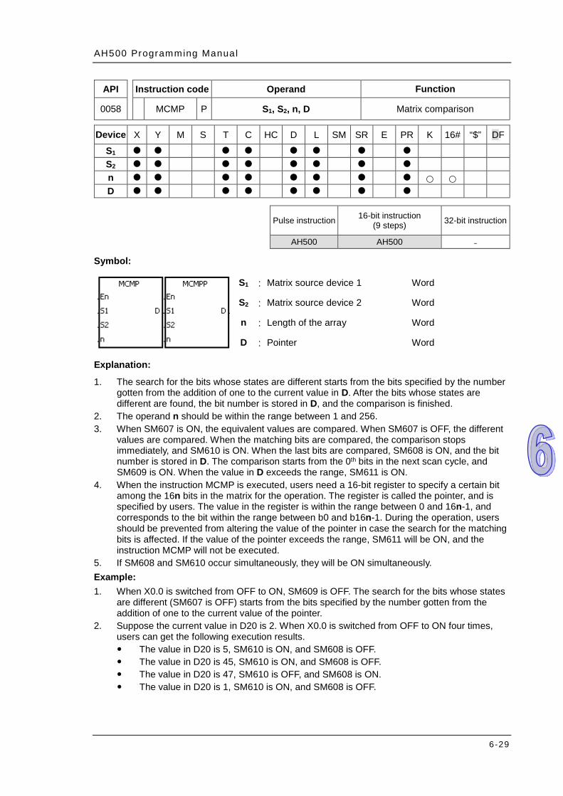
AH500 Programming Manual
6-29
API Instruction code Operand Function
0058 MCMP P S1, S2, n, D Matrix comparison
Device X Y M S T C HC D L SM SR E PR K 16# “$” DF
S1 S2 n D
Pulse instruction 16-bit instruction
(9 steps) 32-bit instruction
AH500 AH500 -
Symbol:
S1 : Matrix source device 1 Word
S2 : Matrix source device 2 Word
n : Length of the array Word
D : Pointer Word
Explanation:
1. The search for the bits whose states are different starts from the bits specified by the number gotten from the addition of one to the current value in D. After the bits whose states are different are found, the bit number is stored in D, and the comparison is finished.
2. The operand n should be within the range between 1 and 256. 3. When SM607 is ON, the equivalent values are compared. When SM607 is OFF, the different
values are compared. When the matching bits are compared, the comparison stops immediately, and SM610 is ON. When the last bits are compared, SM608 is ON, and the bit number is stored in D. The comparison starts from the 0th bits in the next scan cycle, and SM609 is ON. When the value in D exceeds the range, SM611 is ON.
4. When the instruction MCMP is executed, users need a 16-bit register to specify a certain bit among the 16n bits in the matrix for the operation. The register is called the pointer, and is specified by users. The value in the register is within the range between 0 and 16n-1, and corresponds to the bit within the range between b0 and b16n-1. During the operation, users should be prevented from altering the value of the pointer in case the search for the matching bits is affected. If the value of the pointer exceeds the range, SM611 will be ON, and the instruction MCMP will not be executed.
5. If SM608 and SM610 occur simultaneously, they will be ON simultaneously. Example: 1. When X0.0 is switched from OFF to ON, SM609 is OFF. The search for the bits whose states
are different (SM607 is OFF) starts from the bits specified by the number gotten from the addition of one to the current value of the pointer.
2. Suppose the current value in D20 is 2. When X0.0 is switched from OFF to ON four times, users can get the following execution results. The value in D20 is 5, SM610 is ON, and SM608 is OFF. The value in D20 is 45, SM610 is ON, and SM608 is OFF. The value in D20 is 47, SM610 is OFF, and SM608 is ON. The value in D20 is 1, SM610 is ON, and SM608 is OFF.
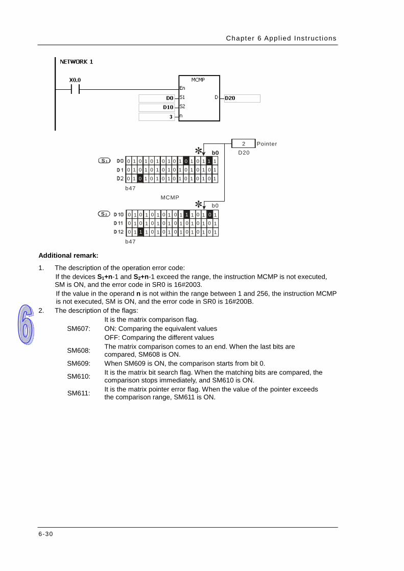
Chapter 6 Appl ied Inst ruct ions
6-30
b0
S 2 1 0 11000
1 0 00 11000
1 0 00 1100
11
1
11
1
11
1
D202
11
1
00
0
00
0
11
1
Pointer
10 10 10 10 10 1 10 110 10 10 10 10 10 10 10
10 1 10 10 10 10 10 10
b47
b0
MCMP
S 1
b47
b0
0
0 1
1
1 0
Additional remark:
1. The description of the operation error code: If the devices S1+n-1 and S2+n-1 exceed the range, the instruction MCMP is not executed, SM is ON, and the error code in SR0 is 16#2003. If the value in the operand n is not within the range between 1 and 256, the instruction MCMP is not executed, SM is ON, and the error code in SR0 is 16#200B.
2. The description of the flags:
SM607: It is the matrix comparison flag. ON: Comparing the equivalent values OFF: Comparing the different values
SM608: The matrix comparison comes to an end. When the last bits are compared, SM608 is ON.
SM609: When SM609 is ON, the comparison starts from bit 0.
SM610: It is the matrix bit search flag. When the matching bits are compared, the comparison stops immediately, and SM610 is ON.
SM611: It is the matrix pointer error flag. When the value of the pointer exceeds the comparison range, SM611 is ON.

AH500 Programming Manual
6-31
API Instruction code Operand Function 0059~ 0064 CMPT※ P S1, S2, n, D Comparing the tables
Device X Y M S T C HC D L SM SR E PR K 16# “$” DF
S1 S2 n D
Pulse instruction 16-bit instruction
(9 steps) 32-bit instruction
AH500 AH500 -
Symbol:
S1 : Source device 1 Word
S2 : Source device 2 Word
n : Data length Word
D : Comparison result Bit
Explanation:
1. The instruction is used to compare n pieces of data in devices starting from S1 with those in devices starting from S2. The values compared are signed decimal numbers, and the comparison results are stored in D.
2. The operand n should be within the range between 1 and 256. 3. The value which is written into the operand D is a one-bit value. 4. When the results gotten from the comparison by using the instruction CMPT# are that all
devices are ON, SM620 is ON. Otherwise, SM620 is OFF. 5. If the operand S1 is a device, the comparison will be as shown below.
S1
+1+2 Compar ison sign+3
+(N-2)
S1
S1
S1
S1
+(N-1)S1
~
n
S2
+1+2+3
+(N-2)
S2
S2
S2
S2
+(N-1)S2
~
n
1234(BIN)5678(BIN)5000(BIN)1000(BIN)
10(BIN)90(BIN)
1111(B IN)2222(BIN)3333(BIN)4444(BIN)
8888(BIN)9999(BIN)
D
+1+2+3
+(N-2)
D
D
D
D
+(N-1)D
~
1110
00
>
Compar ison result
6. If the operand S1 is a constant within the range between -32768 and 32767, the comparison
will be as shown below.
Compar iosn sign
S2
+1+2+3
+(N-2)
S2
S2
S2
S2
+(N-1)S2
~
n3333(BIN)
1111(B IN)2222(BIN)3333(BIN)4444(BIN)
8888(BIN)9999(BIN)
D
+1+2+3
+(N-2)
D
D
D
D
+(N-1)D
~
0010
00
=
Compar ison result
S1
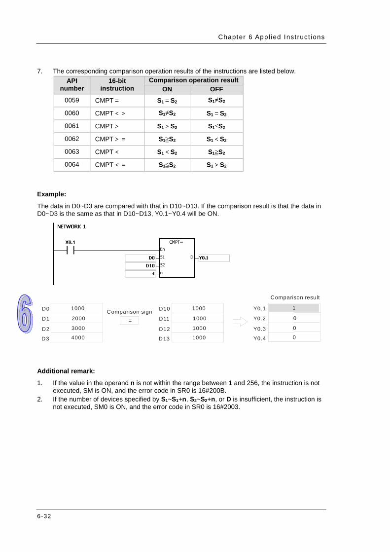
Chapter 6 Appl ied Inst ruct ions
6-32
7. The corresponding comparison operation results of the instructions are listed below.
API number
16-bit instruction
Comparison operation result ON OFF
0059 CMPT= S1=S2 S1≠S2
0060 CMPT<> S1≠S2 S1=S2
0061 CMPT> S1>S2 S1≦S2
0062 CMPT>= S1≧S2 S1<S2
0063 CMPT< S1<S2 S1≧S2
0064 CMPT<= S1≦S2 S1>S2
Example:
The data in D0~D3 are compared with that in D10~D13. If the comparison result is that the data in D0~D3 is the same as that in D10~D13, Y0.1~Y0.4 will be ON.
D0
D1
1000 Comparison sign
D2
2000
3000
4000D3
=
D10
D11
1000
D12
1000
1000
1000D13
Y0.1
Y0.2
1
Y0.3
0
0
0Y0.4
Comparison result
Additional remark:
1. If the value in the operand n is not within the range between 1 and 256, the instruction is not executed, SM is ON, and the error code in SR0 is 16#200B.
2. If the number of devices specified by S1~S1+n, S2~S2+n, or D is insufficient, the instruction is not executed, SM0 is ON, and the error code in SR0 is 16#2003.
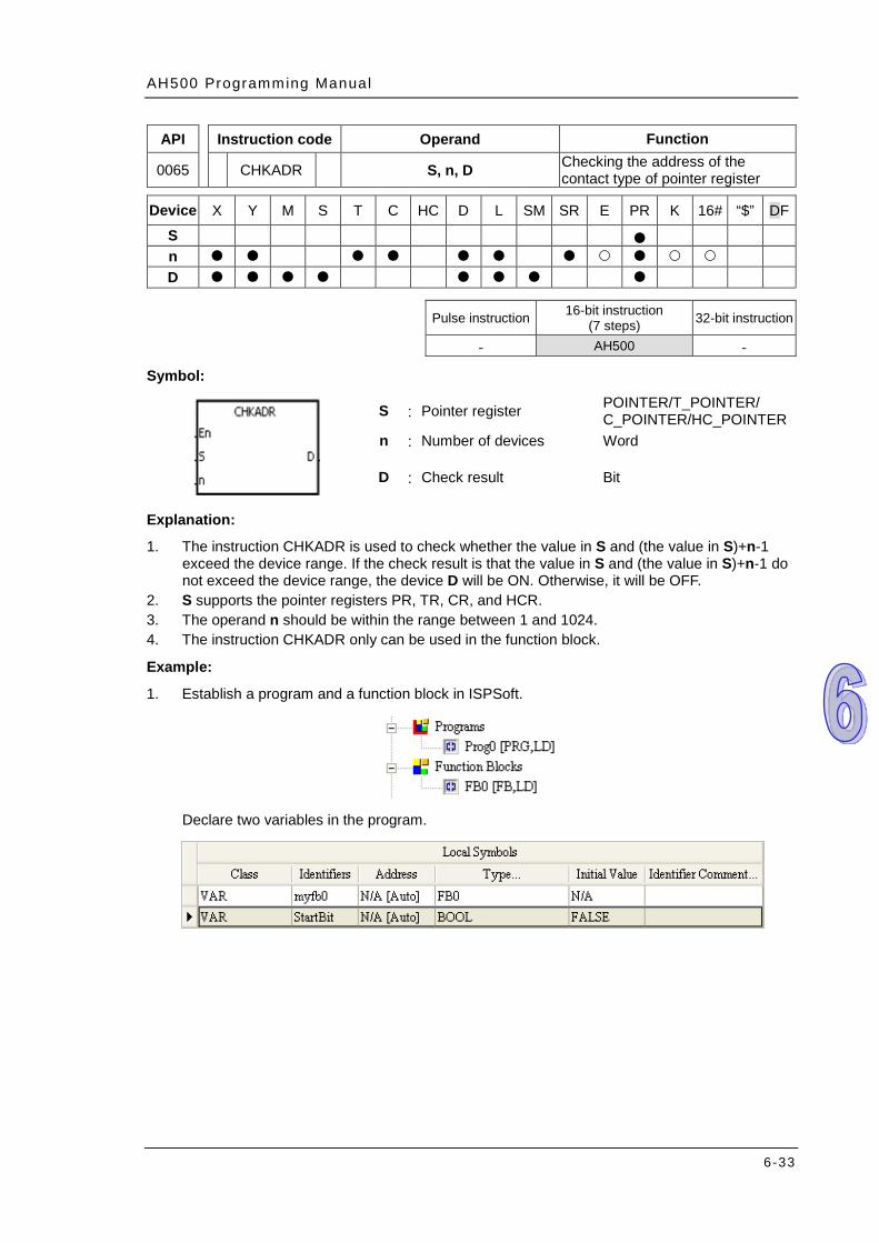
AH500 Programming Manual
6-33
API Instruction code Operand Function
0065 CHKADR S, n, D Checking the address of the contact type of pointer register
Device X Y M S T C HC D L SM SR E PR K 16# “$” DF
S n D
Pulse instruction 16-bit instruction
(7 steps) 32-bit instruction
- AH500 -
Symbol:
S : Pointer register POINTER/T_POINTER/ C_POINTER/HC_POINTER
n : Number of devices Word
D : Check result Bit
Explanation:
1. The instruction CHKADR is used to check whether the value in S and (the value in S)+n-1 exceed the device range. If the check result is that the value in S and (the value in S)+n-1 do not exceed the device range, the device D will be ON. Otherwise, it will be OFF.
2. S supports the pointer registers PR, TR, CR, and HCR. 3. The operand n should be within the range between 1 and 1024. 4. The instruction CHKADR only can be used in the function block.
Example:
1. Establish a program and a function block in ISPSoft.
Declare two variables in the program.
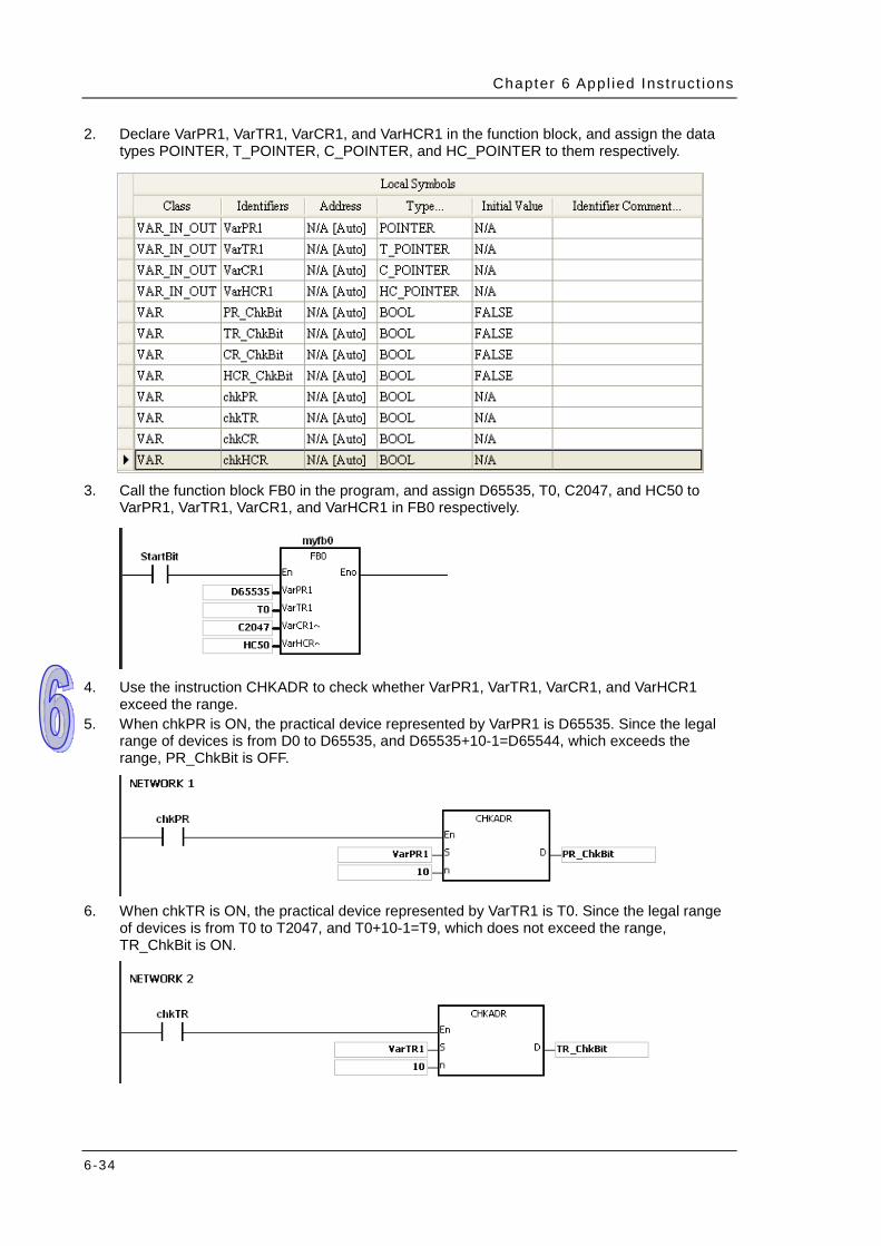
Chapter 6 Appl ied Inst ruct ions
6-34
2. Declare VarPR1, VarTR1, VarCR1, and VarHCR1 in the function block, and assign the data types POINTER, T_POINTER, C_POINTER, and HC_POINTER to them respectively.
3. Call the function block FB0 in the program, and assign D65535, T0, C2047, and HC50 to
VarPR1, VarTR1, VarCR1, and VarHCR1 in FB0 respectively.
4. Use the instruction CHKADR to check whether VarPR1, VarTR1, VarCR1, and VarHCR1
exceed the range. 5. When chkPR is ON, the practical device represented by VarPR1 is D65535. Since the legal
range of devices is from D0 to D65535, and D65535+10-1=D65544, which exceeds the range, PR_ChkBit is OFF.
6. When chkTR is ON, the practical device represented by VarTR1 is T0. Since the legal range
of devices is from T0 to T2047, and T0+10-1=T9, which does not exceed the range, TR_ChkBit is ON.
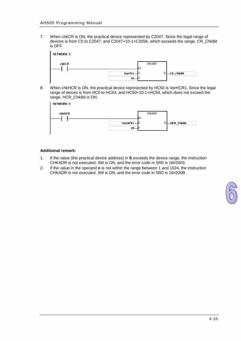
AH500 Programming Manual
6-35
7. When chkCR is ON, the practical device represented by C2047. Since the legal range of devices is from C0 to C2047, and C2047+10-1=C2056, which exceeds the range, CR_ChkBit is OFF.
8. When chkHCR is ON, the practical device represented by HC50 is VarHCR1. Since the legal
range of deices is from HC0 to HC63, and HC50+10-1=HC59, which does not exceed the range, HCR_ChkBit is ON.
Additional remark:
1. If the value (the practical device address) in S exceeds the device range, the instruction CHKADR is not executed, SM is ON, and the error code in SR0 is 16#2003.
2. If the value in the operand n is not within the range between 1 and 1024, the instruction CHKADR is not executed, SM is ON, and the error code in SR0 is 16#200B.
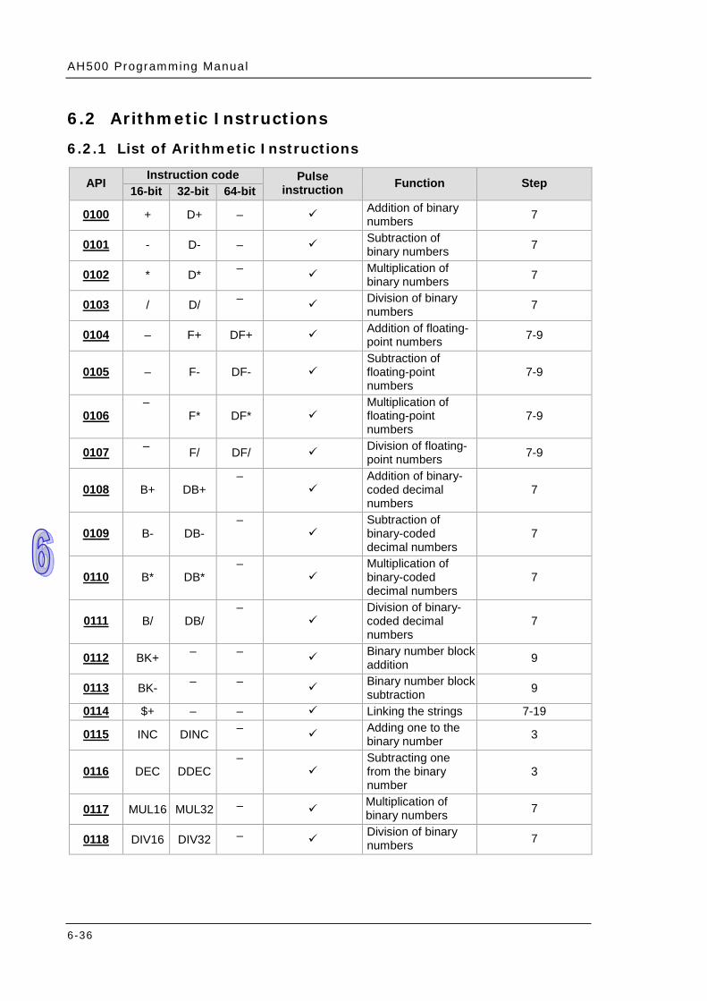
AH500 Programming Manual
6-36
6.2 Arithmetic Instructions
6.2.1 List of Arithmetic Instructions
API Instruction code Pulse instruction Function Step 16-bit 32-bit 64-bit
0100 + D+ – Addition of binary numbers 7
0101 - D- – Subtraction of binary numbers 7
0102 * D* – Multiplication of binary numbers 7
0103 / D/ – Division of binary numbers 7
0104 – F+ DF+ Addition of floating-point numbers 7-9
0105 – F- DF- Subtraction of floating-point numbers
7-9
0106 –
F* DF* Multiplication of floating-point numbers
7-9
0107 – F/ DF/ Division of floating-point numbers 7-9
0108 B+ DB+ –
Addition of binary-coded decimal numbers
7
0109 B- DB- –
Subtraction of binary-coded decimal numbers
7
0110 B* DB* –
Multiplication of binary-coded decimal numbers
7
0111 B/ DB/ –
Division of binary-coded decimal numbers
7
0112 BK+ – – Binary number block addition 9
0113 BK- – – Binary number block subtraction 9
0114 $+ – – Linking the strings 7-19
0115 INC DINC – Adding one to the binary number 3
0116 DEC DDEC –
Subtracting one from the binary number
3
0117 MUL16 MUL32 – Multiplication of binary numbers 7
0118 DIV16 DIV32 – Division of binary numbers 7
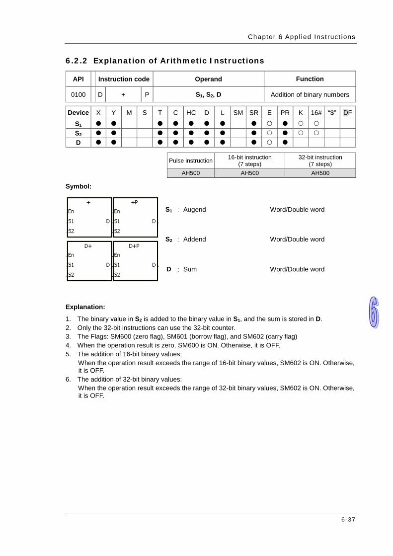
Chapter 6 Appl ied Inst ruct ions
6-37
6.2.2 Explanation of Arithmetic Instructions
API Instruction code Operand Function
0100 D + P S1, S2, D Addition of binary numbers
Device X Y M S T C HC D L SM SR E PR K 16# “$” DF
S1 S2 D
Pulse instruction 16-bit instruction
(7 steps) 32-bit instruction
(7 steps) AH500 AH500 AH500
Symbol:
S1 : Augend Word/Double word
S2 : Addend Word/Double word
D : Sum Word/Double word
Explanation:
1. The binary value in S2 is added to the binary value in S1, and the sum is stored in D. 2. Only the 32-bit instructions can use the 32-bit counter. 3. The Flags: SM600 (zero flag), SM601 (borrow flag), and SM602 (carry flag) 4. When the operation result is zero, SM600 is ON. Otherwise, it is OFF. 5. The addition of 16-bit binary values:
When the operation result exceeds the range of 16-bit binary values, SM602 is ON. Otherwise, it is OFF.
6. The addition of 32-bit binary values: When the operation result exceeds the range of 32-bit binary values, SM602 is ON. Otherwise, it is OFF.
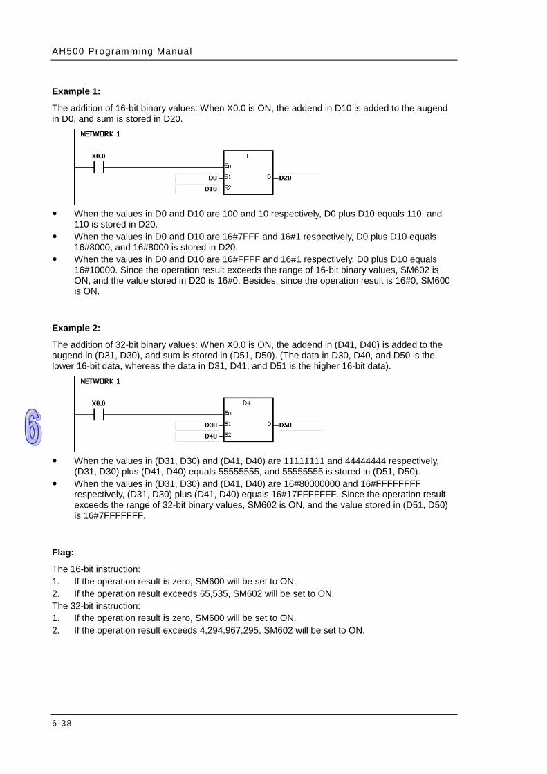
AH500 Programming Manual
6-38
Example 1: The addition of 16-bit binary values: When X0.0 is ON, the addend in D10 is added to the augend in D0, and sum is stored in D20.
When the values in D0 and D10 are 100 and 10 respectively, D0 plus D10 equals 110, and
110 is stored in D20. When the values in D0 and D10 are 16#7FFF and 16#1 respectively, D0 plus D10 equals
16#8000, and 16#8000 is stored in D20. When the values in D0 and D10 are 16#FFFF and 16#1 respectively, D0 plus D10 equals
16#10000. Since the operation result exceeds the range of 16-bit binary values, SM602 is ON, and the value stored in D20 is 16#0. Besides, since the operation result is 16#0, SM600 is ON.
Example 2:
The addition of 32-bit binary values: When X0.0 is ON, the addend in (D41, D40) is added to the augend in (D31, D30), and sum is stored in (D51, D50). (The data in D30, D40, and D50 is the lower 16-bit data, whereas the data in D31, D41, and D51 is the higher 16-bit data).
When the values in (D31, D30) and (D41, D40) are 11111111 and 44444444 respectively,
(D31, D30) plus (D41, D40) equals 55555555, and 55555555 is stored in (D51, D50). When the values in (D31, D30) and (D41, D40) are 16#80000000 and 16#FFFFFFFF
respectively, (D31, D30) plus (D41, D40) equals 16#17FFFFFFF. Since the operation result exceeds the range of 32-bit binary values, SM602 is ON, and the value stored in (D51, D50) is 16#7FFFFFFF.
Flag:
The 16-bit instruction: 1. If the operation result is zero, SM600 will be set to ON. 2. If the operation result exceeds 65,535, SM602 will be set to ON. The 32-bit instruction: 1. If the operation result is zero, SM600 will be set to ON. 2. If the operation result exceeds 4,294,967,295, SM602 will be set to ON.
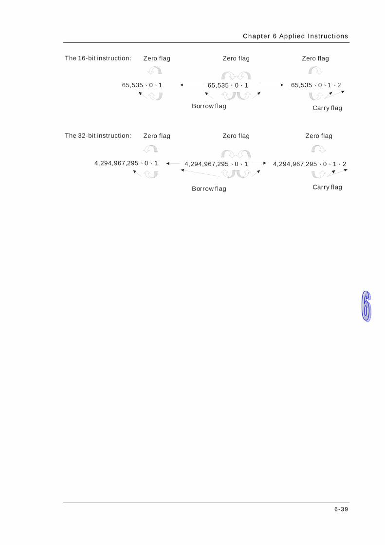
Chapter 6 Appl ied Inst ruct ions
6-39
The 16-bit instruction:
65,535 0 1、 、 、 、0 165,535 65,535 0 1 2、 、 、
4,294,967,295 0 1、 、 4,294,967,295 0 1、 、 4,294,967,295 0 1 2、 、 、
Zero flag Zero flag Zero flag
Borrow flag Carry flag
The 32-bit instruction: Zero flag Zero flag Zero flag
Borrow flag Carry flag
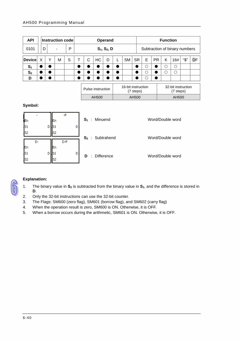
AH500 Programming Manual
6-40
API Instruction code Operand Function
0101 D - P S1, S2, D Subtraction of binary numbers
Device X Y M S T C HC D L SM SR E PR K 16# “$” DF
S1 S2 D
Pulse instruction 16-bit instruction
(7 steps) 32-bit instruction
(7 steps) AH500 AH500 AH500
Symbol:
S1 : Minuend Word/Double word
S2 : Subtrahend Word/Double word
D : Difference Word/Double word
Explanation:
1. The binary value in S2 is subtracted from the binary value in S1, and the difference is stored in D.
2. Only the 32-bit instructions can use the 32-bit counter. 3. The Flags: SM600 (zero flag), SM601 (borrow flag), and SM602 (carry flag) 4. When the operation result is zero, SM600 is ON. Otherwise, it is OFF. 5. When a borrow occurs during the arithmetic, SM601 is ON. Otherwise, it is OFF.
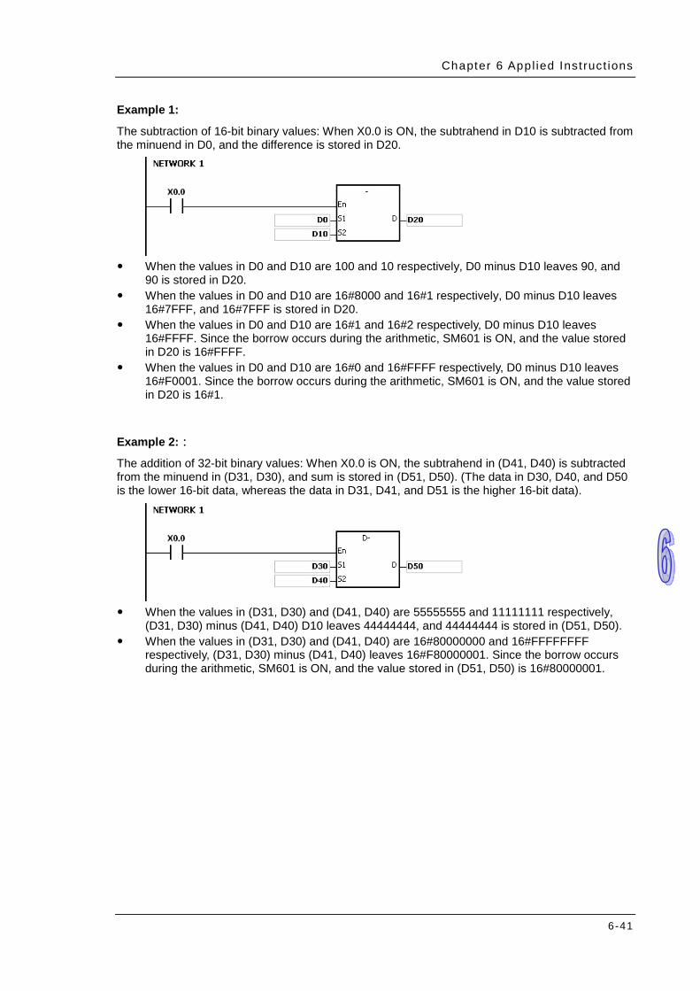
Chapter 6 Appl ied Inst ruct ions
6-41
Example 1:
The subtraction of 16-bit binary values: When X0.0 is ON, the subtrahend in D10 is subtracted from the minuend in D0, and the difference is stored in D20.
When the values in D0 and D10 are 100 and 10 respectively, D0 minus D10 leaves 90, and
90 is stored in D20. When the values in D0 and D10 are 16#8000 and 16#1 respectively, D0 minus D10 leaves
16#7FFF, and 16#7FFF is stored in D20. When the values in D0 and D10 are 16#1 and 16#2 respectively, D0 minus D10 leaves
16#FFFF. Since the borrow occurs during the arithmetic, SM601 is ON, and the value stored in D20 is 16#FFFF.
When the values in D0 and D10 are 16#0 and 16#FFFF respectively, D0 minus D10 leaves 16#F0001. Since the borrow occurs during the arithmetic, SM601 is ON, and the value stored in D20 is 16#1.
Example 2::
The addition of 32-bit binary values: When X0.0 is ON, the subtrahend in (D41, D40) is subtracted from the minuend in (D31, D30), and sum is stored in (D51, D50). (The data in D30, D40, and D50 is the lower 16-bit data, whereas the data in D31, D41, and D51 is the higher 16-bit data).
When the values in (D31, D30) and (D41, D40) are 55555555 and 11111111 respectively,
(D31, D30) minus (D41, D40) D10 leaves 44444444, and 44444444 is stored in (D51, D50). When the values in (D31, D30) and (D41, D40) are 16#80000000 and 16#FFFFFFFF
respectively, (D31, D30) minus (D41, D40) leaves 16#F80000001. Since the borrow occurs during the arithmetic, SM601 is ON, and the value stored in (D51, D50) is 16#80000001.
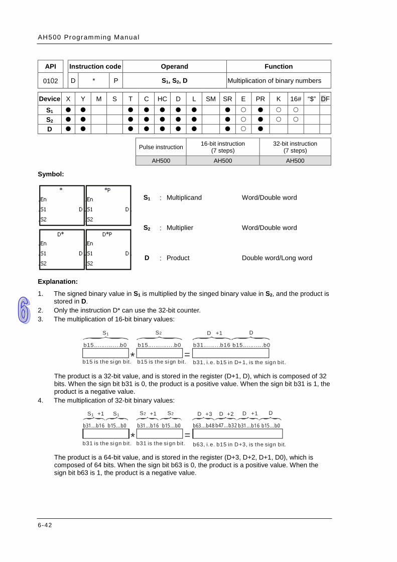
AH500 Programming Manual
6-42
API Instruction code Operand Function
0102 D * P S1, S2, D Multiplication of binary numbers
Device X Y M S T C HC D L SM SR E PR K 16# “$” DF
S1 S2 D
Pulse instruction 16-bit instruction
(7 steps) 32-bit instruction
(7 steps) AH500 AH500 AH500
Symbol:
S1 : Multiplicand Word/Double word
S2 : Multiplier Word/Double word
D : Product Double word/Long word
Explanation:
1. The signed binary value in S1 is multiplied by the singed binary value in S2, and the product is stored in D.
2. Only the instruction D* can use the 32-bit counter. 3. The multiplication of 16-bit binary values:
b15.... .. . . .. . . . .b0 b31.... .. . . .b16
* =b15...... . . .. . . . .b0 b15.... .. . . .. .b0
b15 is the si gn bit. b15 is the si gn bit. b31, i.e. b15 in D+ 1, is the sign bit.
S D1 2 DS +1
The product is a 32-bit value, and is stored in the register (D+1, D), which is composed of 32 bits. When the sign bit b31 is 0, the product is a positive value. When the sign bit b31 is 1, the product is a negative value.
4. The multiplication of 32-bit binary values:
b31 is the si gn bit. b31 is the si gn bit. b63, i.e. b15 in D+3, is the sign bit. * =
D +1 DDD2S2SS1 S1+1 +1 +2+3
b31...b16 b15...b0 b63...b48 b47...b32 b31...b16 b15...b0b31...b16 b15...b0
The product is a 64-bit value, and is stored in the register (D+3, D+2, D+1, D0), which is composed of 64 bits. When the sign bit b63 is 0, the product is a positive value. When the sign bit b63 is 1, the product is a negative value.
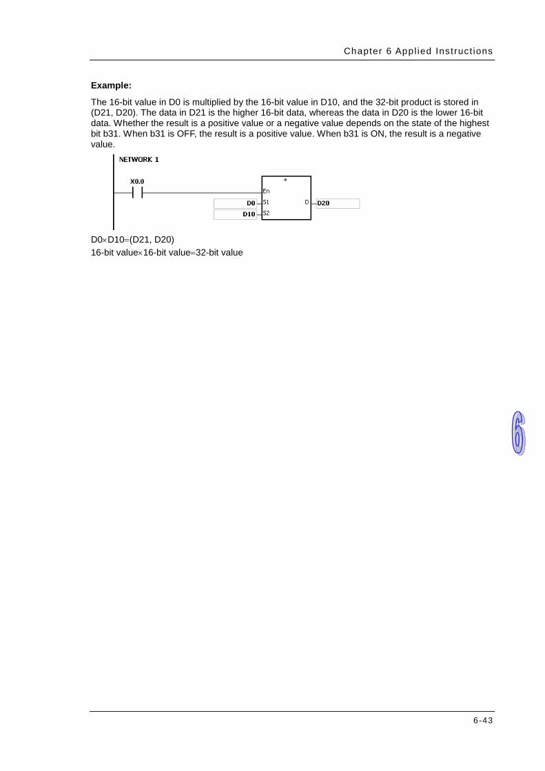
Chapter 6 Appl ied Inst ruct ions
6-43
Example:
The 16-bit value in D0 is multiplied by the 16-bit value in D10, and the 32-bit product is stored in (D21, D20). The data in D21 is the higher 16-bit data, whereas the data in D20 is the lower 16-bit data. Whether the result is a positive value or a negative value depends on the state of the highest bit b31. When b31 is OFF, the result is a positive value. When b31 is ON, the result is a negative value.
D0×D10=(D21, D20) 16-bit value×16-bit value=32-bit value
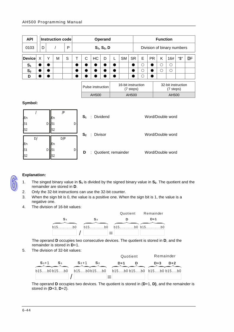
AH500 Programming Manual
6-44
API Instruction code Operand Function
0103 D / P S1, S2, D Division of binary numbers
Device X Y M S T C HC D L SM SR E PR K 16# “$” DF
S1 S2 D
Pulse instruction 16-bit instruction
(7 steps) 32-bit instruction
(7 steps) AH500 AH500 AH500
Symbol:
S1 : Dividend Word/Double word
S2 : Divisor Word/Double word
D : Quotient; remainder Word/Double word
Explanation:
1. The singed binary value in S1 is divided by the signed binary value in S2. The quotient and the remainder are stored in D.
2. Only the 32-bit instructions can use the 32-bit counter. 3. When the sign bit is 0, the value is a positive one. When the sign bit is 1, the value is a
negative one. 4. The division of 16-bit values:
b15.... .. . . .. . . . .b0
S 1 S 2 D+1D
=/b15...... . . .. . . . .b0 b15.... .. . . .. . . . .b0 b15.... .. . . .. . . . .b0
Quotient Remainder
The operand D occupies two consecutive devices. The quotient is stored in D, and the remainder is stored in D+1.
5. The division of 32-bit values: Quotient Remainder
+1
/ =b15.....b0 b15.....b0 b15.....b0 b15.....b0 b15.....b0 b15.....b0 b15.....b0 b15.....b0
S 1 S 2S 1 S 2 +1 D+1 D D+3 D+2
The operand D occupies two devices. The quotient is stored in (D+1, D), and the remainder is stored in (D+3, D+2).
Chapter 6 Appl ied Inst ruct ions
6-45
Example:
When X0.0 is ON, the dividend in D0 is divided by the divisor in D10, the quotient is stored in D20, and the remainder is stored in D21. Whether the result is a positive value or a negative value depends on the state of the highest bit.
Additional remark:
1. If the device exceeds the range, the instruction is not executed, SM0 is ON, and the error code in SR0 is 16#2003.
2. If the divisor is 0, the instruction is not executed, SM0 is ON, and the error code in SR0 is 16#2012.
3. If the operand D used during the execution of the 16-bit instruction is declared in ISPSoft, the data type will be ARRAY [2] of WORD/INT.
4. If the operand D used during the execution of the 32-bit instruction is declared in ISPSoft, the data type will be ARRAY [2] of DWORD/DINT.

AH500 Programming Manual
6-46
API Instruction code Operand Function
0104 D F+ P S1, S2, D Addition of floating-point numbers
Device X Y M S T C HC D L SM SR E PR K 16# “$” DF
S1 S2 D
Pulse instruction 32-bit instruction
(7-9 steps) 64-bit instruction
(7-9 steps) AH500 AH500 AH500
Symbol:
S1 : Augend Double word/Long word
S2 : Addend Double word/Long word
D : Sum Double word/Long word
Explanation:
1. The floating-point number in S2 is added to the floating-point number in S1, and the sum is stored in D.
2. When the operation result is zero, SM600 is ON. 3. The addition of 32-bit single-precision floating-point numbers:
When the operation result is zero, SM600 is ON. When the absolute value of the operation result is less than the value which can be
represented by the minimum floating-point number, the value in D is 16#FF7FFFFF. When the absolute value of the operation result is larger than the value which can be
represented by the maximum floating-point number, the value in D is 16#7F7FFFFF. 4. The addition of 64-bit double-precision floating-point numbers:
When the operation result is zero, SM600 is ON. When the absolute value of the operation result is less than the value which can be
represented by the minimum floating-point number, the value in D is 16#FFEFFFFFFFFFFFFF.
When the absolute value of the operation result is larger than the value which can be represented by the maximum floating-point number, the value in D is 16#7FEFFFFFFFFFFFFF.
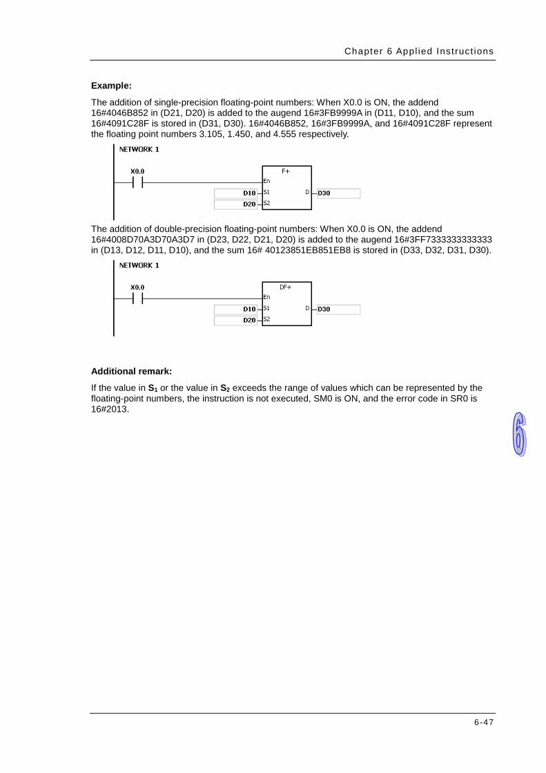
Chapter 6 Appl ied Inst ruct ions
6-47
Example:
The addition of single-precision floating-point numbers: When X0.0 is ON, the addend 16#4046B852 in (D21, D20) is added to the augend 16#3FB9999A in (D11, D10), and the sum 16#4091C28F is stored in (D31, D30). 16#4046B852, 16#3FB9999A, and 16#4091C28F represent the floating point numbers 3.105, 1.450, and 4.555 respectively.
The addition of double-precision floating-point numbers: When X0.0 is ON, the addend 16#4008D70A3D70A3D7 in (D23, D22, D21, D20) is added to the augend 16#3FF7333333333333 in (D13, D12, D11, D10), and the sum 16# 40123851EB851EB8 is stored in (D33, D32, D31, D30).
Additional remark:
If the value in S1 or the value in S2 exceeds the range of values which can be represented by the floating-point numbers, the instruction is not executed, SM0 is ON, and the error code in SR0 is 16#2013.
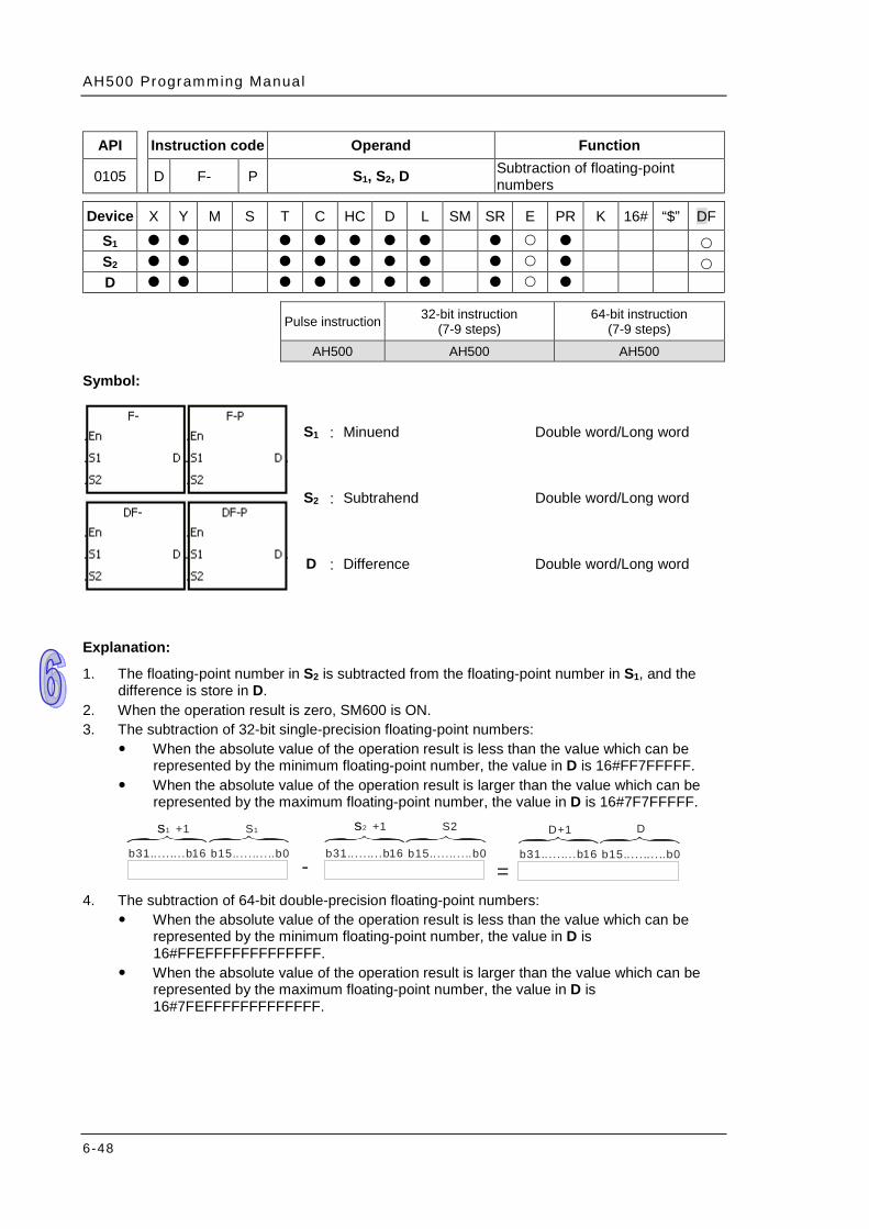
AH500 Programming Manual
6-48
API Instruction code Operand Function
0105 D F- P S1, S2, D Subtraction of floating-point numbers
Device X Y M S T C HC D L SM SR E PR K 16# “$” DF
S1 S2 D
Pulse instruction 32-bit instruction
(7-9 steps) 64-bit instruction
(7-9 steps) AH500 AH500 AH500
Symbol:
S1 : Minuend Double word/Long word
S2 : Subtrahend Double word/Long word
D : Difference Double word/Long word
Explanation:
1. The floating-point number in S2 is subtracted from the floating-point number in S1, and the difference is store in D.
2. When the operation result is zero, SM600 is ON. 3. The subtraction of 32-bit single-precision floating-point numbers:
When the absolute value of the operation result is less than the value which can be represented by the minimum floating-point number, the value in D is 16#FF7FFFFF.
When the absolute value of the operation result is larger than the value which can be represented by the maximum floating-point number, the value in D is 16#7F7FFFFF.
b31.... . .. . .b16
=b15..... .. . . ..b0
D+1 D
b31..... .. . .b16 b15.... . .. . . ..b0
S1 +1
b31.... . .. . .b16 b15.... . .. . . ..b0
S S1 S2 +1S S2
- 4. The subtraction of 64-bit double-precision floating-point numbers:
When the absolute value of the operation result is less than the value which can be represented by the minimum floating-point number, the value in D is 16#FFEFFFFFFFFFFFFF.
When the absolute value of the operation result is larger than the value which can be represented by the maximum floating-point number, the value in D is 16#7FEFFFFFFFFFFFFF.
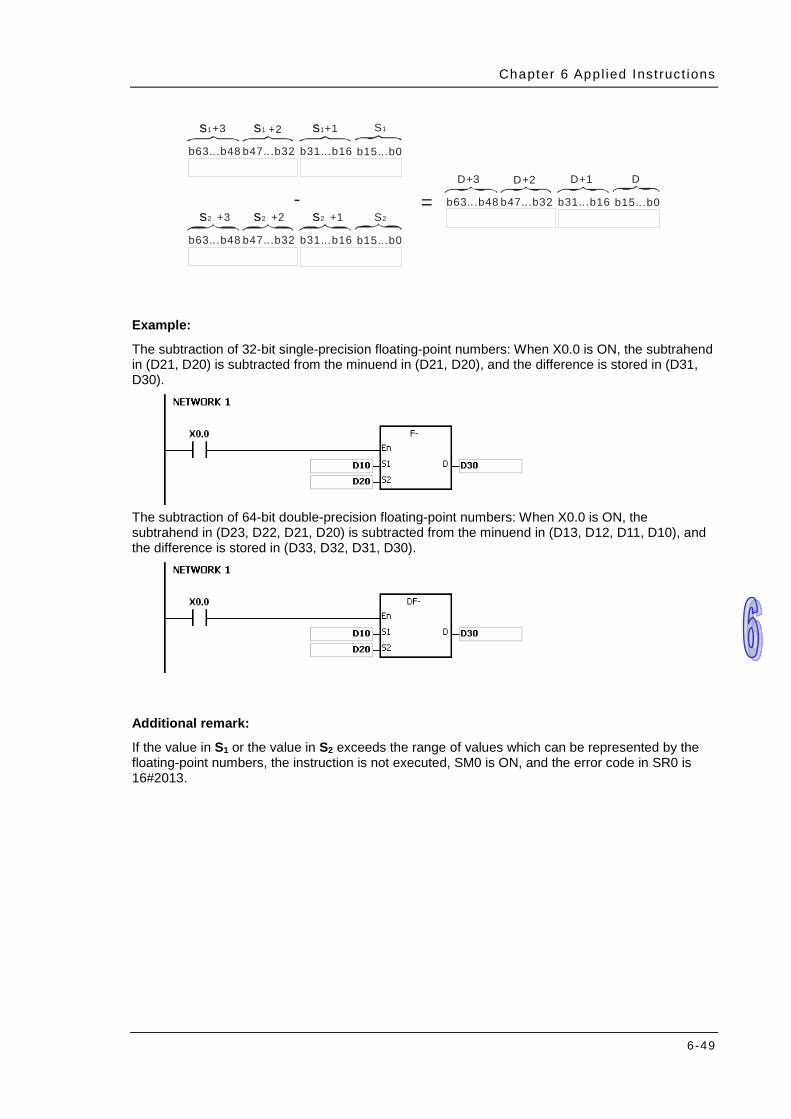
Chapter 6 Appl ied Inst ruct ions
6-49
=
b63...b48 b47...b32
S1+1
b31...b16 b15...b0
S S1
-
S1+3S S1 +2S
b63...b48 b47...b32 b31...b16 b15...b0
D+1 DD+3
b63...b48 b47...b32
S2 +1
b31...b16 b15...b0
S S2S2 +3S S2 +2S
D+2
Example:
The subtraction of 32-bit single-precision floating-point numbers: When X0.0 is ON, the subtrahend in (D21, D20) is subtracted from the minuend in (D21, D20), and the difference is stored in (D31, D30).
The subtraction of 64-bit double-precision floating-point numbers: When X0.0 is ON, the subtrahend in (D23, D22, D21, D20) is subtracted from the minuend in (D13, D12, D11, D10), and the difference is stored in (D33, D32, D31, D30).
Additional remark:
If the value in S1 or the value in S2 exceeds the range of values which can be represented by the floating-point numbers, the instruction is not executed, SM0 is ON, and the error code in SR0 is 16#2013.
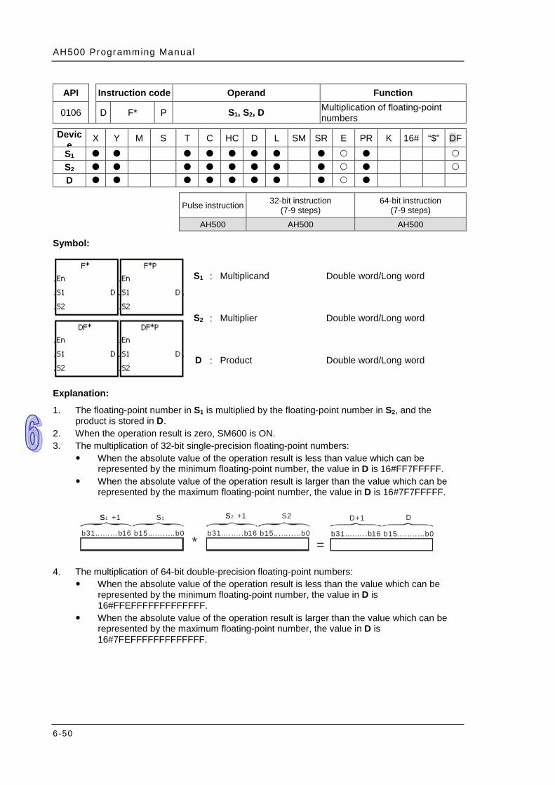
AH500 Programming Manual
6-50
API Instruction code Operand Function
0106 D F* P S1, S2, D Multiplication of floating-point numbers
Device
X Y M S T C HC D L SM SR E PR K 16# “$” DF S1 S2 D
Pulse instruction 32-bit instruction
(7-9 steps) 64-bit instruction
(7-9 steps) AH500 AH500 AH500
Symbol:
S1 : Multiplicand Double word/Long word
S2 : Multiplier Double word/Long word
D : Product Double word/Long word
Explanation:
1. The floating-point number in S1 is multiplied by the floating-point number in S2, and the product is stored in D.
2. When the operation result is zero, SM600 is ON. 3. The multiplication of 32-bit single-precision floating-point numbers:
When the absolute value of the operation result is less than value which can be represented by the minimum floating-point number, the value in D is 16#FF7FFFFF.
When the absolute value of the operation result is larger than the value which can be represented by the maximum floating-point number, the value in D is 16#7F7FFFFF.
b31.... .. . . .b16
=b15...... . . . ..b0
D+1 D
b31...... . . .b16 b15.... .. . . . ..b0
S1 +1
b31.... .. . . .b16 b15.... .. . . . ..b0
S S1 S2 +1S S2
*
4. The multiplication of 64-bit double-precision floating-point numbers: When the absolute value of the operation result is less than the value which can be
represented by the minimum floating-point number, the value in D is 16#FFEFFFFFFFFFFFFF.
When the absolute value of the operation result is larger than the value which can be represented by the maximum floating-point number, the value in D is 16#7FEFFFFFFFFFFFFF.
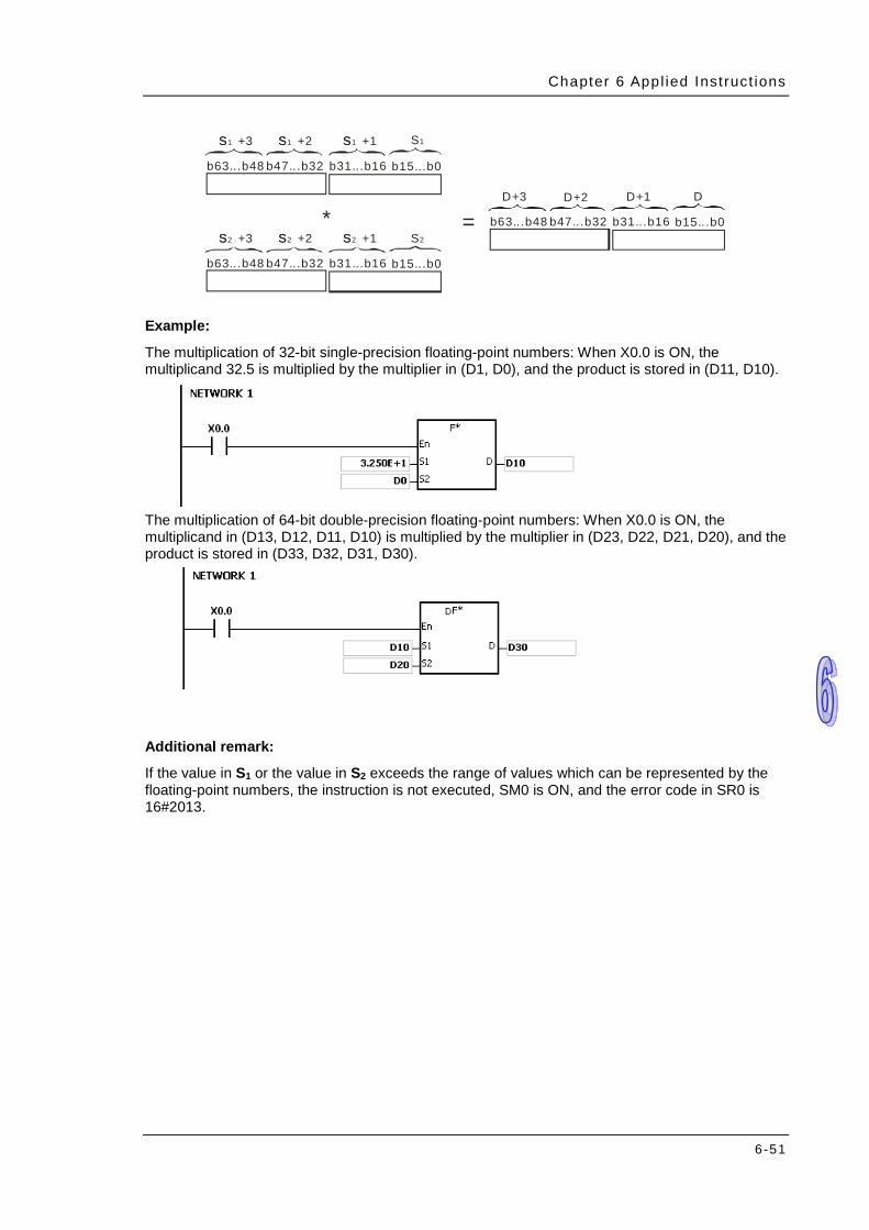
Chapter 6 Appl ied Inst ruct ions
6-51
=
b63...b48 b47...b32
S1 +1
b31...b16 b15...b0
S S1
*
S1 +3S S1 +2S
b63...b48 b47...b32 b31...b16 b15...b0
D+1 DD+3
b63...b48 b47...b32
S2 +1
b31...b16 b15...b0
S S2S2 +3S S2 +2S
D+2
Example:
The multiplication of 32-bit single-precision floating-point numbers: When X0.0 is ON, the multiplicand 32.5 is multiplied by the multiplier in (D1, D0), and the product is stored in (D11, D10).
The multiplication of 64-bit double-precision floating-point numbers: When X0.0 is ON, the multiplicand in (D13, D12, D11, D10) is multiplied by the multiplier in (D23, D22, D21, D20), and the product is stored in (D33, D32, D31, D30).
Additional remark:
If the value in S1 or the value in S2 exceeds the range of values which can be represented by the floating-point numbers, the instruction is not executed, SM0 is ON, and the error code in SR0 is 16#2013.
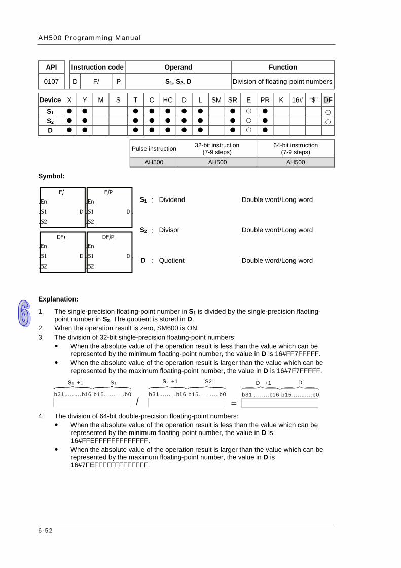
AH500 Programming Manual
6-52
API Instruction code Operand Function
0107 D F/ P S1, S2, D Division of floating-point numbers
Device X Y M S T C HC D L SM SR E PR K 16# “$” DF
S1 S2 D
Pulse instruction 32-bit instruction
(7-9 steps) 64-bit instruction
(7-9 steps) AH500 AH500 AH500
Symbol:
S1 : Dividend Double word/Long word
S2 : Divisor Double word/Long word
D : Quotient Double word/Long word
Explanation:
1. The single-precision floating-point number in S1 is divided by the single-precision flaoting-point number in S2. The quotient is stored in D.
2. When the operation result is zero, SM600 is ON. 3. The division of 32-bit single-precision floating-point numbers:
When the absolute value of the operation result is less than the value which can be represented by the minimum floating-point number, the value in D is 16#FF7FFFFF.
When the absolute value of the operation result is larger than the value which can be represented by the maximum floating-point number, the value in D is 16#7F7FFFFF.
b31.... . .. . .b16
=b15..... .. . . ..b0
D D+1
b31..... .. . .b16 b15.... . .. . . ..b0
S1 +1
b31.... . .. . .b16 b15.... . .. . . ..b0
S S1 S2 +1S S2
/ 4. The division of 64-bit double-precision floating-point numbers:
When the absolute value of the operation result is less than the value which can be represented by the minimum floating-point number, the value in D is 16#FFEFFFFFFFFFFFFF.
When the absolute value of the operation result is larger than the value which can be represented by the maximum floating-point number, the value in D is 16#7FEFFFFFFFFFFFFF.
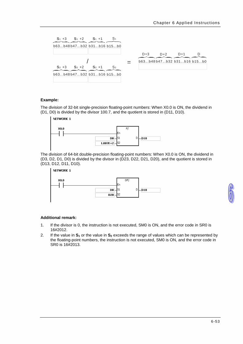
Chapter 6 Appl ied Inst ruct ions
6-53
=
b63...b48 b47...b32
S1 +1
b31...b16 b15...b0
S S1
/
S1 +3S S1 +2S
b63...b48 b47...b32 b31...b16 b15...b0
D+1 DD+3
b63...b48 b47...b32
S2 +1
b31...b16 b15...b0
S S2S2 +3S S2 +2S
D+2
Example:
The division of 32-bit single-precision floating-point numbers: When X0.0 is ON, the dividend in (D1, D0) is divided by the divisor 100.7, and the quotient is stored in (D11, D10).
The division of 64-bit double-precision floating-point numbers: When X0.0 is ON, the dividend in (D3, D2, D1, D0) is divided by the divisor in (D23, D22, D21, D20), and the quotient is stored in (D13, D12, D11, D10).
Additional remark:
1. If the divisor is 0, the instruction is not executed, SM0 is ON, and the error code in SR0 is 16#2012.
2. If the value in S1 or the value in S2 exceeds the range of values which can be represented by the floating-point numbers, the instruction is not executed, SM0 is ON, and the error code in SR0 is 16#2013.
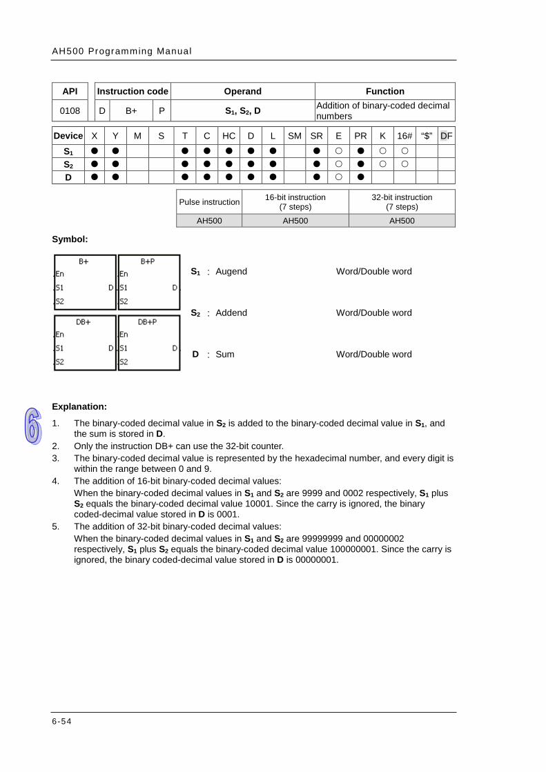
AH500 Programming Manual
6-54
API Instruction code Operand Function
0108 D B+ P S1, S2, D Addition of binary-coded decimal numbers
Device X Y M S T C HC D L SM SR E PR K 16# “$” DF
S1 S2 D
Pulse instruction 16-bit instruction
(7 steps) 32-bit instruction
(7 steps) AH500 AH500 AH500
Symbol:
S1 : Augend Word/Double word
S2 : Addend Word/Double word
D : Sum Word/Double word
Explanation:
1. The binary-coded decimal value in S2 is added to the binary-coded decimal value in S1, and the sum is stored in D.
2. Only the instruction DB+ can use the 32-bit counter. 3. The binary-coded decimal value is represented by the hexadecimal number, and every digit is
within the range between 0 and 9. 4. The addition of 16-bit binary-coded decimal values:
When the binary-coded decimal values in S1 and S2 are 9999 and 0002 respectively, S1 plus S2 equals the binary-coded decimal value 10001. Since the carry is ignored, the binary coded-decimal value stored in D is 0001.
5. The addition of 32-bit binary-coded decimal values: When the binary-coded decimal values in S1 and S2 are 99999999 and 00000002 respectively, S1 plus S2 equals the binary-coded decimal value 100000001. Since the carry is ignored, the binary coded-decimal value stored in D is 00000001.

Chapter 6 Appl ied Inst ruct ions
6-55
Example:
When X0.0 is ON, the constants 1234 and 5678 are converted into the binary-coded decimal values which are stored in D0 and D1 respectively. The binary-coded decimal value in D1 is added to the binary-coded decimal value in D0, and the sum is stored in D10.
Additional remark:
1. If the value in S1 or the value in S2 exceeds the range of values which can be represented by the binary-coded decimal values, i.e. 0~9999, the instruction B+ is not executed, SM0 is ON, and the error code in SR0 is 16#200D (The binary-coded decimal value is represented by the hexadecimal number, but one of digits is not within the range between 0 and 9.).
2. If the value in S1 or the value in S2 exceeds the range of values which can be represented by the binary-coded decimal values, i.e. 0~99999999, the instruction DB+ is not executed, SM0 is ON, and the error code in SR0 is 16#200D (The binary-coded decimal value is represented by the hexadecimal number, but one of digits is not within the range between 0 and 9.).
3. The instruction does not support SM600, SM601 and SM602.
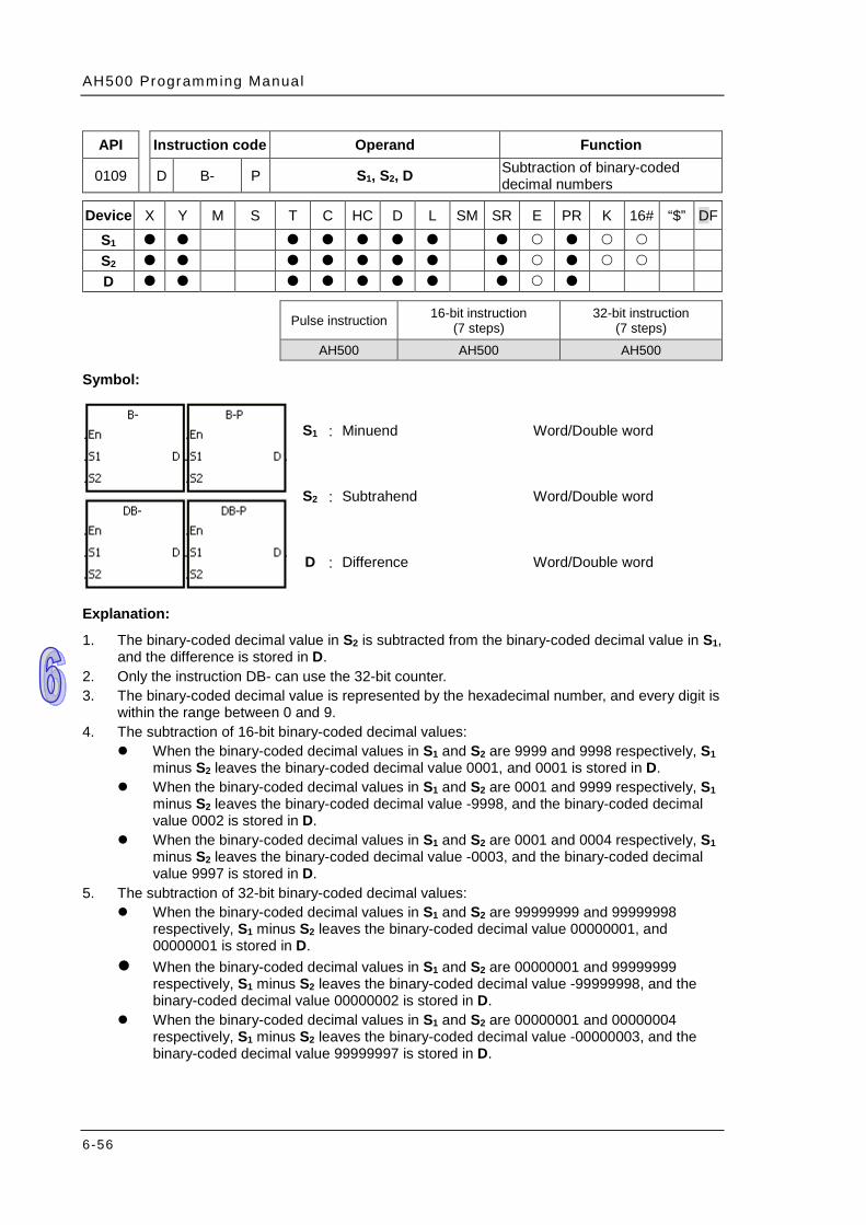
AH500 Programming Manual
6-56
API Instruction code Operand Function
0109 D B- P S1, S2, D Subtraction of binary-coded decimal numbers
Device X Y M S T C HC D L SM SR E PR K 16# “$” DF
S1 S2 D
Pulse instruction 16-bit instruction
(7 steps) 32-bit instruction
(7 steps) AH500 AH500 AH500
Symbol:
S1 : Minuend Word/Double word
S2 : Subtrahend Word/Double word
D : Difference Word/Double word
Explanation:
1. The binary-coded decimal value in S2 is subtracted from the binary-coded decimal value in S1, and the difference is stored in D.
2. Only the instruction DB- can use the 32-bit counter. 3. The binary-coded decimal value is represented by the hexadecimal number, and every digit is
within the range between 0 and 9. 4. The subtraction of 16-bit binary-coded decimal values:
When the binary-coded decimal values in S1 and S2 are 9999 and 9998 respectively, S1 minus S2 leaves the binary-coded decimal value 0001, and 0001 is stored in D.
When the binary-coded decimal values in S1 and S2 are 0001 and 9999 respectively, S1 minus S2 leaves the binary-coded decimal value -9998, and the binary-coded decimal value 0002 is stored in D.
When the binary-coded decimal values in S1 and S2 are 0001 and 0004 respectively, S1 minus S2 leaves the binary-coded decimal value -0003, and the binary-coded decimal value 9997 is stored in D.
5. The subtraction of 32-bit binary-coded decimal values: When the binary-coded decimal values in S1 and S2 are 99999999 and 99999998
respectively, S1 minus S2 leaves the binary-coded decimal value 00000001, and 00000001 is stored in D.
When the binary-coded decimal values in S1 and S2 are 00000001 and 99999999 respectively, S1 minus S2 leaves the binary-coded decimal value -99999998, and the binary-coded decimal value 00000002 is stored in D.
When the binary-coded decimal values in S1 and S2 are 00000001 and 00000004 respectively, S1 minus S2 leaves the binary-coded decimal value -00000003, and the binary-coded decimal value 99999997 is stored in D.
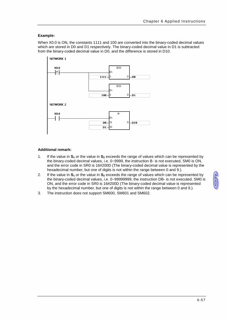
Chapter 6 Appl ied Inst ruct ions
6-57
Example:
When X0.0 is ON, the constants 1111 and 100 are converted into the binary-coded decimal values which are stored in D0 and D1 respectively. The binary-coded decimal value in D1 is subtracted from the binary-coded decimal value in D0, and the difference is stored in D10.
Additional remark:
1. If the value in S1 or the value in S2 exceeds the range of values which can be represented by the binary-coded decimal values, i.e. 0~9999, the instruction B- is not executed, SM0 is ON, and the error code in SR0 is 16#200D (The binary-coded decimal value is represented by the hexadecimal number, but one of digits is not within the range between 0 and 9.).
2. If the value in S1 or the value in S2 exceeds the range of values which can be represented by the binary-coded decimal values, i.e. 0~99999999, the instruction DB- is not executed, SM0 is ON, and the error code in SR0 is 16#200D (The binary-coded decimal value is represented by the hexadecimal number, but one of digits is not within the range between 0 and 9.).
3. The instruction does not support SM600, SM601 and SM602.
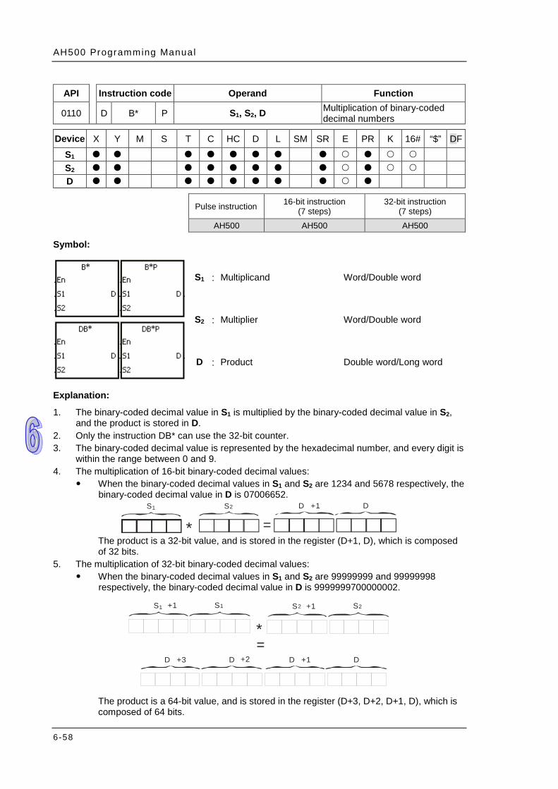
AH500 Programming Manual
6-58
API Instruction code Operand Function
0110 D B* P S1, S2, D Multiplication of binary-coded decimal numbers
Device X Y M S T C HC D L SM SR E PR K 16# “$” DF
S1 S2 D
Pulse instruction 16-bit instruction
(7 steps) 32-bit instruction
(7 steps) AH500 AH500 AH500
Symbol:
S1 : Multiplicand Word/Double word
S2 : Multiplier Word/Double word
D : Product Double word/Long word
Explanation:
1. The binary-coded decimal value in S1 is multiplied by the binary-coded decimal value in S2, and the product is stored in D.
2. Only the instruction DB* can use the 32-bit counter. 3. The binary-coded decimal value is represented by the hexadecimal number, and every digit is
within the range between 0 and 9. 4. The multiplication of 16-bit binary-coded decimal values:
When the binary-coded decimal values in S1 and S2 are 1234 and 5678 respectively, the binary-coded decimal value in D is 07006652.
* =S D1 2 DS +1
The product is a 32-bit value, and is stored in the register (D+1, D), which is composed of 32 bits.
5. The multiplication of 32-bit binary-coded decimal values: When the binary-coded decimal values in S1 and S2 are 99999999 and 99999998
respectively, the binary-coded decimal value in D is 9999999700000002.
*=
S
D
1 1
D
S
+3
S2 2S
D D+1+2
+1 +1
The product is a 64-bit value, and is stored in the register (D+3, D+2, D+1, D), which is composed of 64 bits.
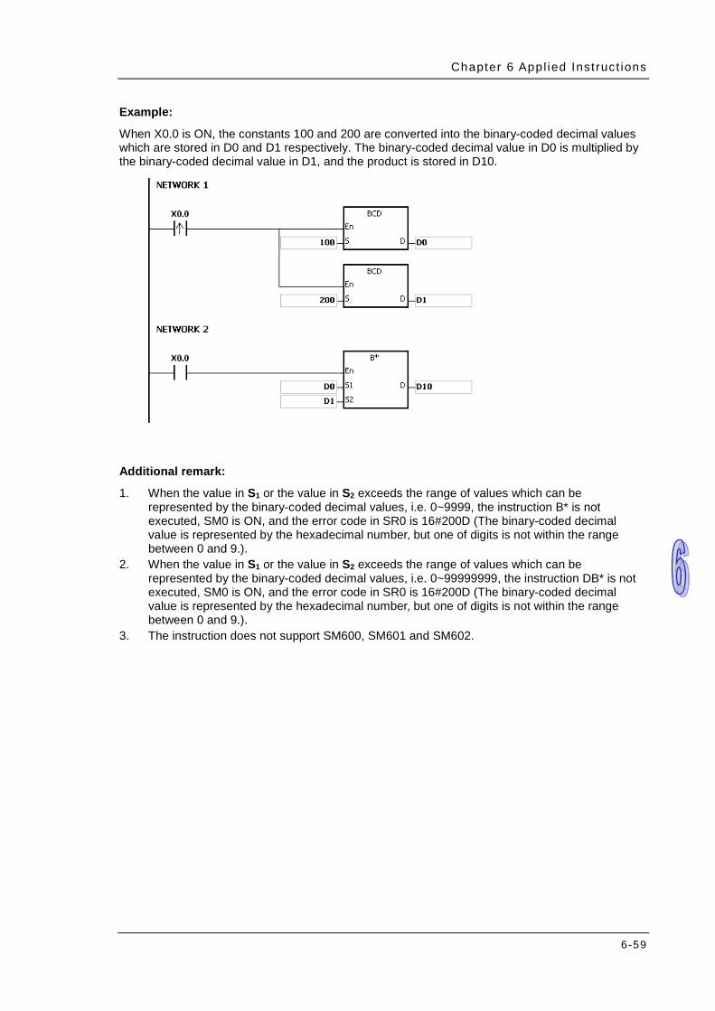
Chapter 6 Appl ied Inst ruct ions
6-59
Example:
When X0.0 is ON, the constants 100 and 200 are converted into the binary-coded decimal values which are stored in D0 and D1 respectively. The binary-coded decimal value in D0 is multiplied by the binary-coded decimal value in D1, and the product is stored in D10.
Additional remark:
1. When the value in S1 or the value in S2 exceeds the range of values which can be represented by the binary-coded decimal values, i.e. 0~9999, the instruction B* is not executed, SM0 is ON, and the error code in SR0 is 16#200D (The binary-coded decimal value is represented by the hexadecimal number, but one of digits is not within the range between 0 and 9.).
2. When the value in S1 or the value in S2 exceeds the range of values which can be represented by the binary-coded decimal values, i.e. 0~99999999, the instruction DB* is not executed, SM0 is ON, and the error code in SR0 is 16#200D (The binary-coded decimal value is represented by the hexadecimal number, but one of digits is not within the range between 0 and 9.).
3. The instruction does not support SM600, SM601 and SM602.
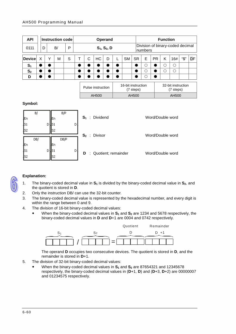
AH500 Programming Manual
6-60
API Instruction code Operand Function
0111 D B/ P S1, S2, D Division of binary-coded decimal numbers
Device X Y M S T C HC D L SM SR E PR K 16# “$” DF
S1 S2 D
Pulse instruction 16-bit instruction
(7 steps) 32-bit instruction
(7 steps) AH500 AH500 AH500
Symbol:
S1 : Dividend Word/Double word
S2 : Divisor Word/Double word
D : Quotient; remainder Word/Double word
Explanation:
1. The binary-coded decimal value in S1 is divided by the binary-coded decimal value in S2, and the quotient is stored in D.
2. Only the instruction DB/ can use the 32-bit counter. 3. The binary-coded decimal value is represented by the hexadecimal number, and every digit is
within the range between 0 and 9. 4. The division of 16-bit binary-coded decimal values:
When the binary-coded decimal values in S1 and S2 are 1234 and 5678 respectively, the binary-coded decimal values in D and D+1 are 0004 and 0742 respectively.
Quotient Remainder
/ =S D1 2 DS +1
The operand D occupies two consecutive devices. The quotient is stored in D, and the remainder is stored in D+1.
5. The division of 32-bit binary-coded decimal values: When the binary-coded decimal values in S1 and S2 are 87654321 and 12345678
respectively, the binary-coded decimal values in (D+1, D) and (D+3, D+2) are 00000007 and 01234575 respectively.
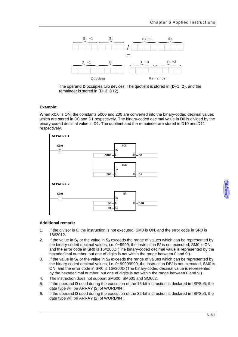
Chapter 6 Appl ied Inst ruct ions
6-61
Quotient Remainder
/=
S
D
1 1
D
S
+3
S2 2S
+2
+1 +1
D D+1
The operand D occupies two devices. The quotient is stored in (D+1, D), and the remainder is stored in (D+3, D+2).
Example:
When X0.0 is ON, the constants 5000 and 200 are converted into the binary-coded decimal values which are stored in D0 and D1 respectively. The binary-coded decimal value in D0 is divided by the binary-coded decimal value in D1. The quotient and the remainder are stored in D10 and D11 respectively.
Additional remark:
1. If the divisor is 0, the instruction is not executed, SM0 is ON, and the error code in SR0 is 16#2012.
2. If the value in S1 or the value in S2 exceeds the range of values which can be represented by the binary-coded decimal values, i.e. 0~9999, the instruction B/ is not executed, SM0 is ON, and the error code in SR0 is 16#200D (The binary-coded decimal value is represented by the hexadecimal number, but one of digits is not within the range between 0 and 9.).
3. If the value in S1 or the value in S2 exceeds the range of values which can be represented by the binary-coded decimal values, i.e. 0~99999999, the instruction DB/ is not executed, SM0 is ON, and the error code in SR0 is 16#200D (The binary-coded decimal value is represented by the hexadecimal number, but one of digits is not within the range between 0 and 9.).
4. The instruction does not support SM600, SM601 and SM602. 5. If the operand D used during the execution of the 16-bit instruction is declared in ISPSoft, the
data type will be ARRAY [2] of WORD/INT. 6. If the operand D used during the execution of the 32-bit instruction is declared in ISPSoft, the
data type will be ARRAY [2] of WORD/INT.
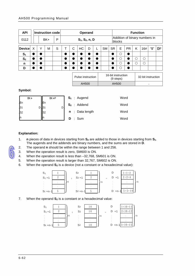
AH500 Programming Manual
6-62
API Instruction code Operand Function
0112 BK+ P S1, S2, n, D Addition of binary numbers in blocks
Device X Y M S T C HC D L SM SR E PR K 16# “$” DF
S1 S2 n D
Pulse instruction 16-bit instruction
(9 steps) 32-bit instruction
AH500 AH500 -
Symbol:
S1 : Augend Word
S2 : Addend Word
n : Data length Word
D : Sum Word
Explanation:
1. n pieces of data in devices starting from S2 are added to those in devices starting from S1. The augends and the addends are binary numbers, and the sums are stored in D.
2. The operand n should be within the range between 1 and 256. 3. When the operation result is zero, SM600 is ON. 4. When the operation result is less than –32,768, SM601 is ON. 5. When the operation result is larger than 32,767, SM602 is ON. 6. When the operand S2 is a device (not a constant or a hexadecimal value):
S1
S1 +1.....
S +n-1
S2
S2 +1.....
S +n-11 2} }n n
+
D
D +1.....
D +n-1}n
=
1
2
5
1
2
.
.
5
1+1=2
2+2=4
5+5=10
.
.
.
.
.
.
.
.
.
.
7. When the operand S2 is a constant or a hexadecimal value:
S1
S1 +1.....
S +n-1
S2
S2.....
S1 2} }n n
+
D
D +1.....
D +n-1}n
=
101
2
.
.
5
1+10=11
5+10=15
.
.
.
.
.
.
.
.
.
.
10
10
2+10=12
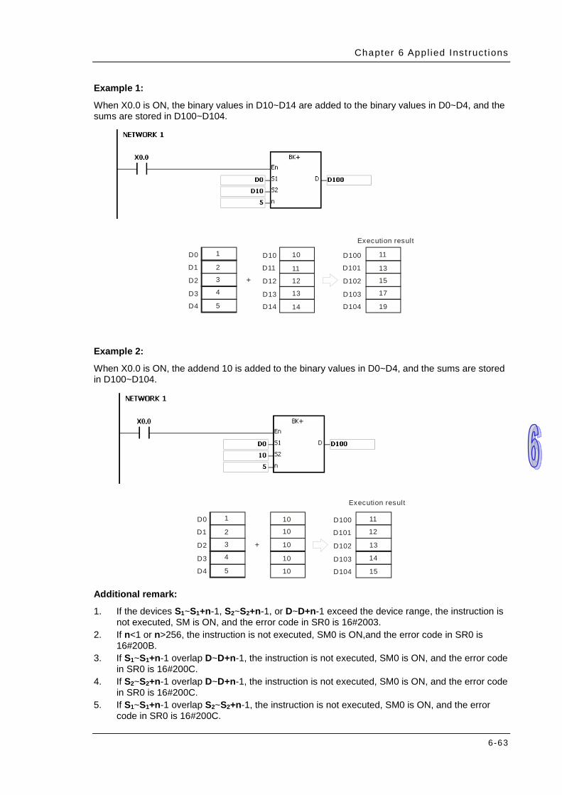
Chapter 6 Appl ied Inst ruct ions
6-63
Example 1:
When X0.0 is ON, the binary values in D10~D14 are added to the binary values in D0~D4, and the sums are stored in D100~D104.
D0
D1
D2
D3
D4
D10
D11
D12
D13
D14
D100
D101
D102
D103
D104
+
Execution result
1
2
3
4
5
10
11
12
13
14
11
13
15
17
19
Example 2:
When X0.0 is ON, the addend 10 is added to the binary values in D0~D4, and the sums are stored in D100~D104.
Execution result
D0
D1
D2
D3
D4
D100
D101
D102
D103
D104
+
1
2
3
4
5
10 11
15
10
10
10
10
13
12
14
Additional remark:
1. If the devices S1~S1+n-1, S2~S2+n-1, or D~D+n-1 exceed the device range, the instruction is not executed, SM is ON, and the error code in SR0 is 16#2003.
2. If n<1 or n>256, the instruction is not executed, SM0 is ON,and the error code in SR0 is 16#200B.
3. If S1~S1+n-1 overlap D~D+n-1, the instruction is not executed, SM0 is ON, and the error code in SR0 is 16#200C.
4. If S2~S2+n-1 overlap D~D+n-1, the instruction is not executed, SM0 is ON, and the error code in SR0 is 16#200C.
5. If S1~S1+n-1 overlap S2~S2+n-1, the instruction is not executed, SM0 is ON, and the error code in SR0 is 16#200C.
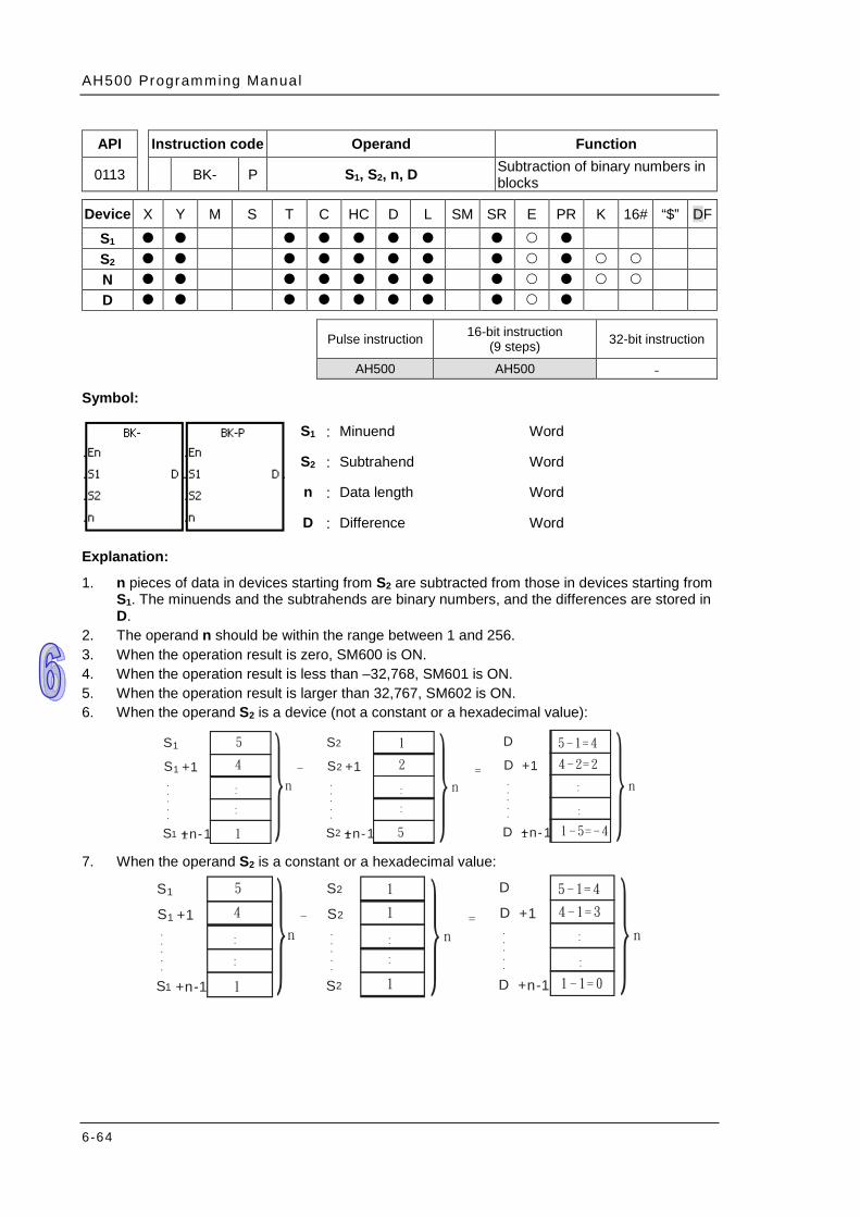
AH500 Programming Manual
6-64
API Instruction code Operand Function
0113 BK- P S1, S2, n, D Subtraction of binary numbers in blocks
Device X Y M S T C HC D L SM SR E PR K 16# “$” DF
S1 S2 N D
Pulse instruction 16-bit instruction
(9 steps) 32-bit instruction
AH500 AH500 -
Symbol:
S1 : Minuend Word
S2 : Subtrahend Word
n : Data length Word
D : Difference Word
Explanation:
1. n pieces of data in devices starting from S2 are subtracted from those in devices starting from S1. The minuends and the subtrahends are binary numbers, and the differences are stored in D.
2. The operand n should be within the range between 1 and 256. 3. When the operation result is zero, SM600 is ON. 4. When the operation result is less than –32,768, SM601 is ON. 5. When the operation result is larger than 32,767, SM602 is ON. 6. When the operand S2 is a device (not a constant or a hexadecimal value):
S1
S1 +1.....
S 1+n-1
S2
S2 +1.....
S 1+n-11 2} }n n
-
D
D +1.....
D 1+n-1}n
=
1
2
51
4
.
.
5 5-1=4
4-2=2
1-5=-4
.
.
.
.
.
.
.
.
.
.
7. When the operand S2 is a constant or a hexadecimal value:
S1
S1 +1.....
S +n-1
S2
S2.....
S1 2} }n n
-
D
D +1.....
D +n-1}n
=
1
1
4
.
.
5 5-1=4
4-1=3
1-1=0
.
.
.
.
.
.
.
.
.
.
1
1

Chapter 6 Appl ied Inst ruct ions
6-65
Example 1:
When X0.0 is ON, the binary values in D10~D14 are subtracted from the binary values in D0~D4, and the differences are stored in D100~D104.
Execution result
D0
D1
D2
D3
D4
D10
D11
D12
D13
D14
D100
D101
D102
D103
D104
-
1
2
3
4
5
0
2
4
SM6 00
11
2
3
4
5 -4
-2
Example 2:
When X0.0 is ON, the subtrahend 1 is subtracted from the binary values in D0~D4, and the differences are stored in D100~D104.
Execution result
D0
D1
D2
D3
D4
D100
D101
D102
D103
D104
-
6
7
89
10 1
1
1
1
1
6
7
89
5 Additional remark:
1. If the devices S1~S1+n-1, S2~S2+n-1, or D~D+n-1 exceed the device range, the instruction is not executed, SM is ON, and the error code in SR0 is 16#2003.
2. If n<1 or n>256, the instruction is not executed, SM0 is ON,and the error code in SR0 is 16#200B.
3. If S1~S1+n-1 overlap D~D+n-1, the instruction is not executed, SM0 is ON, and the error code in SR0 is 16#200C.
4. If S2~S2+n-1 overlap D~D+n-1, the instruction is not executed, SM0 is ON, and the error code in SR0 is 16#200C.
5. If S1~S1+n-1 overlap S2~S2+n-1, the instruction is not executed, SM0 is ON, and the error code in SR0 is 16#200C.
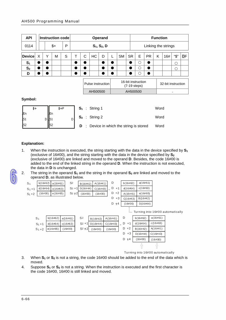
AH500 Programming Manual
6-66
API Instruction code Operand Function
0114 $+ P S1, S2, D Linking the strings
Device X Y M S T C HC D L SM SR E PR K 16# “$” DF
S1 S2 D
Pulse instruction 16-bit instruction
(7-19 steps) 32-bit instruction
AH500500 AH500500 -
Symbol:
S1 : String 1 Word
S2 : String 2 Word
D : Device in which the string is stored Word
Explanation:
1. When the instruction is executed, the string starting with the data in the device specified by S1 (exclusive of 16#00), and the string starting with the data in the device specified by S2 (exclusive of 16#00) are linked and moved to the operand D. Besides, the code 16#00 is added to the end of the linked string in the operand D. When the instruction is not executed, the data in D is unchanged.
2. The string in the operand S1 and the string in the operand S2 are linked and moved to the operand D, as illustrated below.
S1
S1 +1
D
D +1
D 1+4
=
b(16#62) S2
S2 +1S 1+22S1 +2 D +2
D +3
a(16#61)
d(16#64) c(16#63)
e(16#65)(16#00)
B(16#42) b(16#62)A(16#41)
D(16#44) C(16#43)
(16#00) (16#00)
a(16#61)
d(16#64) c(16#63)
A(16#41) e(16#65)
C(16#43) B(16#42)
D(16#44)(16#00)
Turn ing in to 16#00 automatica lly
Turning in to 16#00 automatica lly
S1
S1 +1
D
D +1
D 1+4
=
b(16#62) S2
S2 +1
S 1+22S1 +2 D +2D +3
a(16#61)
d(16#64) c(16#63)
e(16#65) (16#00)
B(16#42) b(16#62)A(16#41)
D(16#44) C(16#43)
(16#00) (16#00)
a(16#61)
d(16#64) c (16#63)
A(16#41)
C(16#43)
B(16#42)
D(16#44)
(16#00) (16#00)
3. When S1 or S2 is not a string, the code 16#00 should be added to the end of the data which is
moved. 4. Suppose S1 or S2 is not a string. When the instruction is executed and the first character is
the code 16#00, 16#00 is still linked and moved.
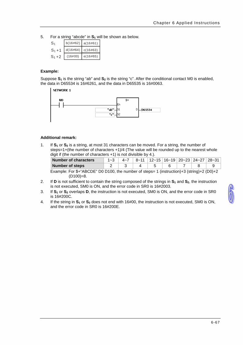
Chapter 6 Appl ied Inst ruct ions
6-67
5. For a string “abcde” in S1 will be shown as below. S1
S1 +1
b(16#62)
S1 +2
a(16#61)
d(16#64) c(16#63)
e(16#65)(16#00)
Example:
Suppose S1 is the string “ab” and S2 is the string “c”. After the conditional contact M0 is enabled, the data in D65534 is 16#6261, and the data in D65535 is 16#0063.
Additional remark:
1. If S1 or S2 is a string, at most 31 characters can be moved. For a string, the number of steps=1+(the number of characters +1)/4 (The value will be rounded up to the nearest whole digit if (the number of characters +1) is not divisible by 4.). Number of characters 1~3 4~7 8~11 12~15 16~19 20~23 24~27 28~31 Number of steps 2 3 4 5 6 7 8 9
Example: For $+“ABCDE” D0 D100, the number of steps= 1 (instruction)+3 (string)+2 (D0)+2 (D100)=8.
2. If D is not sufficient to contain the string composed of the strings in S1 and S2, the instruction is not executed, SM0 is ON, and the error code in SR0 is 16#2003.
3. If S1 or S2 overlaps D, the instruction is not executed, SM0 is ON, and the error code in SR0 is 16#200C.
4. If the string in S1 or S2 does not end with 16#00, the instruction is not executed, SM0 is ON, and the error code in SR0 is 16#200E.

AH500 Programming Manual
6-68
API Instruction code Operand Function
0115 D INC P D Adding one to the binary number
Device X Y M S T C HC D L SM SR E PR K 16# “$” DF
D
Pulse instruction 16-bit instruction (3 steps)
32-bit instruction (3 steps)
AH500 AH500 AH500
Symbol:
D : Destination device Word/Double word
Explanation:
1. One is added to the value in D. 2. Only the instruction DINC can use the 32-bit counter. 3. When the 16-bit operation is performed, 32,767 plus 1 equals -32,768. When the 32-bit
operation is performed, 2,147,483,647 plus 1 equals -2,147,483,648.
Example:
When X0.0 is switched from OFF to ON, the value in D0 increases by one.
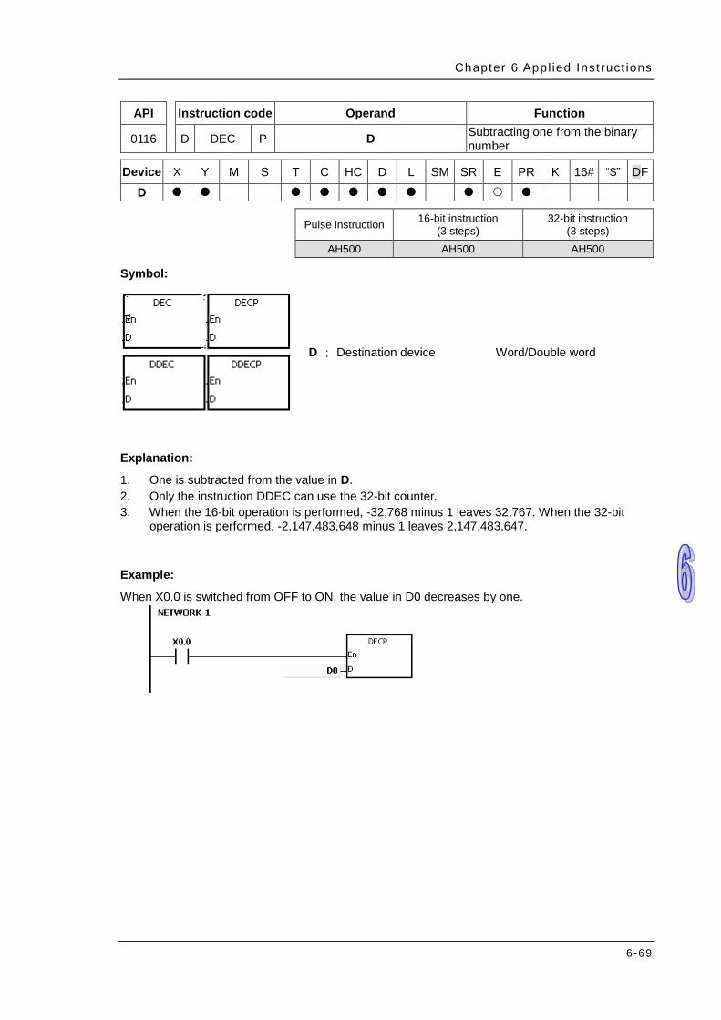
Chapter 6 Appl ied Inst ruct ions
6-69
API Instruction code Operand Function
0116 D DEC P D Subtracting one from the binary number
Device X Y M S T C HC D L SM SR E PR K 16# “$” DF
D
Pulse instruction 16-bit instruction (3 steps)
32-bit instruction (3 steps)
AH500 AH500 AH500
Symbol:
D : Destination device Word/Double word
Explanation:
1. One is subtracted from the value in D. 2. Only the instruction DDEC can use the 32-bit counter. 3. When the 16-bit operation is performed, -32,768 minus 1 leaves 32,767. When the 32-bit
operation is performed, -2,147,483,648 minus 1 leaves 2,147,483,647.
Example:
When X0.0 is switched from OFF to ON, the value in D0 decreases by one.
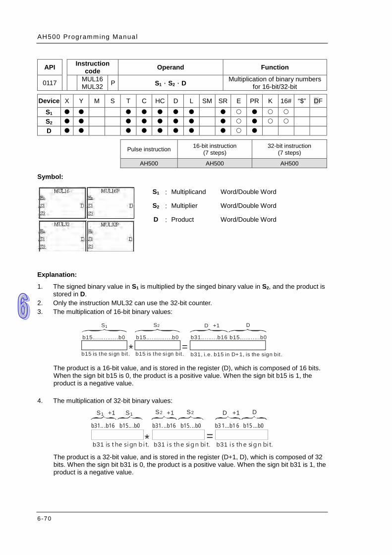
AH500 Programming Manual
6-70
API Instruction code Operand Function
0117 MUL16 MUL32 P S1,S2,D Multiplication of binary numbers
for 16-bit/32-bit
Device X Y M S T C HC D L SM SR E PR K 16# “$” DF S1 S2 D
Pulse instruction 16-bit instruction
(7 steps) 32-bit instruction
(7 steps)
AH500 AH500 AH500
Symbol:
S1 : Multiplicand Word/Double Word
S2 : Multiplier Word/Double Word
D : Product Word/Double Word
Explanation:
1. The signed binary value in S1 is multiplied by the singed binary value in S2, and the product is stored in D.
2. Only the instruction MUL32 can use the 32-bit counter. 3. The multiplication of 16-bit binary values:
b15.... .. . . .. . . . .b0 b31.... .. . . .b16
* =b15...... . . .. . . . .b0 b15.... .. . . .. .b0
b15 is the si gn bit. b15 is the si gn bit. b31, i.e. b15 in D+ 1, is the sign bit.
S D1 2 DS +1
The product is a 16-bit value, and is stored in the register (D), which is composed of 16 bits. When the sign bit b15 is 0, the product is a positive value. When the sign bit b15 is 1, the product is a negative value.
4. The multiplication of 32-bit binary values:
* =b31 i s th e sign bi t.b31 i s th e sign bi t.
D +1 D2S2S +1
b3 1...b1 6 b15 ...b0b31. ..b16 b15. ..b0
b31 is t he sign b i t.
S1 S1+1
b31.. .b16 b15.. .b0
The product is a 32-bit value, and is stored in the register (D+1, D), which is composed of 32 bits. When the sign bit b31 is 0, the product is a positive value. When the sign bit b31 is 1, the product is a negative value.
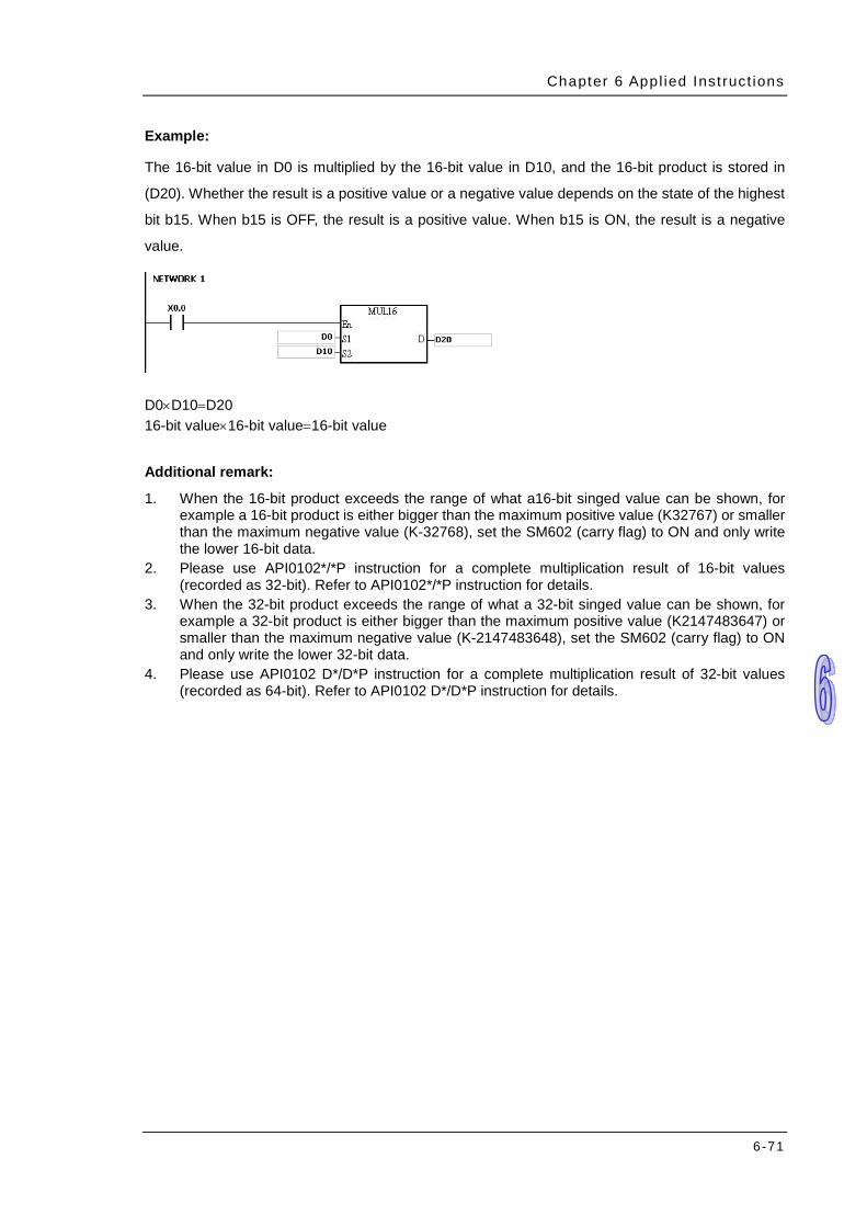
Chapter 6 Appl ied Inst ruct ions
6-71
Example:
The 16-bit value in D0 is multiplied by the 16-bit value in D10, and the 16-bit product is stored in
(D20). Whether the result is a positive value or a negative value depends on the state of the highest
bit b15. When b15 is OFF, the result is a positive value. When b15 is ON, the result is a negative
value.
D0×D10=D20 16-bit value×16-bit value=16-bit value
Additional remark:
1. When the 16-bit product exceeds the range of what a16-bit singed value can be shown, for example a 16-bit product is either bigger than the maximum positive value (K32767) or smaller than the maximum negative value (K-32768), set the SM602 (carry flag) to ON and only write the lower 16-bit data.
2. Please use API0102*/*P instruction for a complete multiplication result of 16-bit values (recorded as 32-bit). Refer to API0102*/*P instruction for details.
3. When the 32-bit product exceeds the range of what a 32-bit singed value can be shown, for example a 32-bit product is either bigger than the maximum positive value (K2147483647) or smaller than the maximum negative value (K-2147483648), set the SM602 (carry flag) to ON and only write the lower 32-bit data.
4. Please use API0102 D*/D*P instruction for a complete multiplication result of 32-bit values (recorded as 64-bit). Refer to API0102 D*/D*P instruction for details.
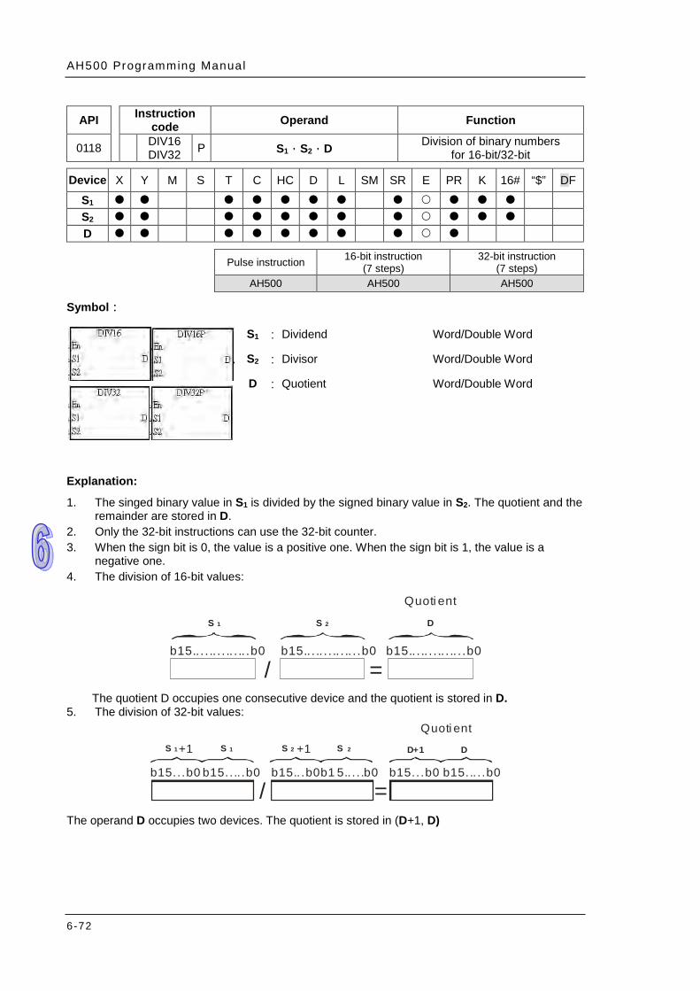
AH500 Programming Manual
6-72
API Instruction code Operand Function
0118 DIV16 DIV32 P S1,S2,D Division of binary numbers
for 16-bit/32-bit
Device X Y M S T C HC D L SM SR E PR K 16# “$” DF S1 S2 D
Pulse instruction 16-bit instruction
(7 steps) 32-bit instruction
(7 steps) AH500 AH500 AH500
Symbol:
S1 : Dividend Word/Double Word
S2 : Divisor Word/Double Word
D : Quotient Word/Double Word
Explanation:
1. The singed binary value in S1 is divided by the signed binary value in S2. The quotient and the remainder are stored in D.
2. Only the 32-bit instructions can use the 32-bit counter. 3. When the sign bit is 0, the value is a positive one. When the sign bit is 1, the value is a
negative one. 4. The division of 16-bit values:
b15.. . . .. . . .. . .. .b0
S 1 S 2 D
=/b15.. . .. . . .. . .. . .b0 b15.. . .. . . .. . .. . .b0
Quoti ent
The quotient D occupies one consecutive device and the quotient is stored in D.
5. The division of 32-bit values:
+1
/ =b15.. .b0 b15.. .. .b0 b15.. .b0b1 5.. . . .b0 b15.. .b0 b15... . .b0
Quoti entS 1 S 2S 1 S 2 +1 D+1 D
The operand D occupies two devices. The quotient is stored in (D+1, D)
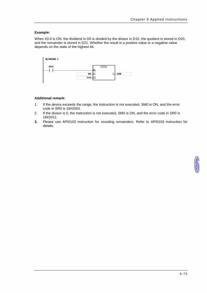
Chapter 6 Appl ied Inst ruct ions
6-73
Example:
When X0.0 is ON, the dividend in D0 is divided by the divisor in D10, the quotient is stored in D20, and the remainder is stored in D21. Whether the result is a positive value or a negative value depends on the state of the highest bit.
Additional remark:
1. If the device exceeds the range, the instruction is not executed, SM0 is ON, and the error code in SR0 is 16#2003.
2. If the divisor is 0, the instruction is not executed, SM0 is ON, and the error code in SR0 is 16#2012.
3. Please use API0103 instruction for recoding remainders. Refer to API0103 instruction for details.

AH500 Programming Manual
6-74
6.3 Data Conversion Instructions
6.3.1 List of Data Conversion Instructions
API Instruction code Pulse instruction Function Step 16-bit 32-bit 64-bit
0200 BCD DBCD – Converting the binary number into the binary-coded decimal number 5
0201 BIN DBIN – Converting the binary-coded decimal number into the binary number 5
0202 FLT DFLT – Converting the binary integer into the binary floating-point number 5
0203 FLTD DFLTD – Converting the binary integer into the 64-bit floating-point number 5
0204 INT DINT – Converting the 32-bit floating-point number into the binary integer 5
0205 – FINT DFINT Converting the 64-bit floating-point number into the binary integer 5
0206 MMOV – – Converting the 16-bit value into the 32-bit value 5
0207 RMOV – – Converting the 32-bit value into the 16-bit value 5
0208 GRY DGRY – Converting the binary number into the Gray code 5
0209 GBIN DGBIN – Converting the Gray code into the binary number 5
0210 NEG DNEG – Two’s complement 3
0211 – FNEG – Reversing the sign of the 32-bit floating-point number 3
0212 – FBCD – Converting the binary floating-point number into the decimal floating-point number
5
0213 – FBIN – Converting the decimal floating-point number into the binary floating-point number
5
0214 BKBCD – –
Converting the binary numbers in blocks into the binary-coded decimal numbers in blocks
7
0215 BKBIN – –
Converting the binary numbers in blocks into the binary-coded decimal numbers in blocks
7
0216 SCAL – – Scale value operation 9 0217 SCLP DSCLP – Parameter type of scale value operation 9
0218 LINE DLINE – Converting a column of data into a line of data 7
0219 COLM DCOLM – Converting a line of data into a column of data 7
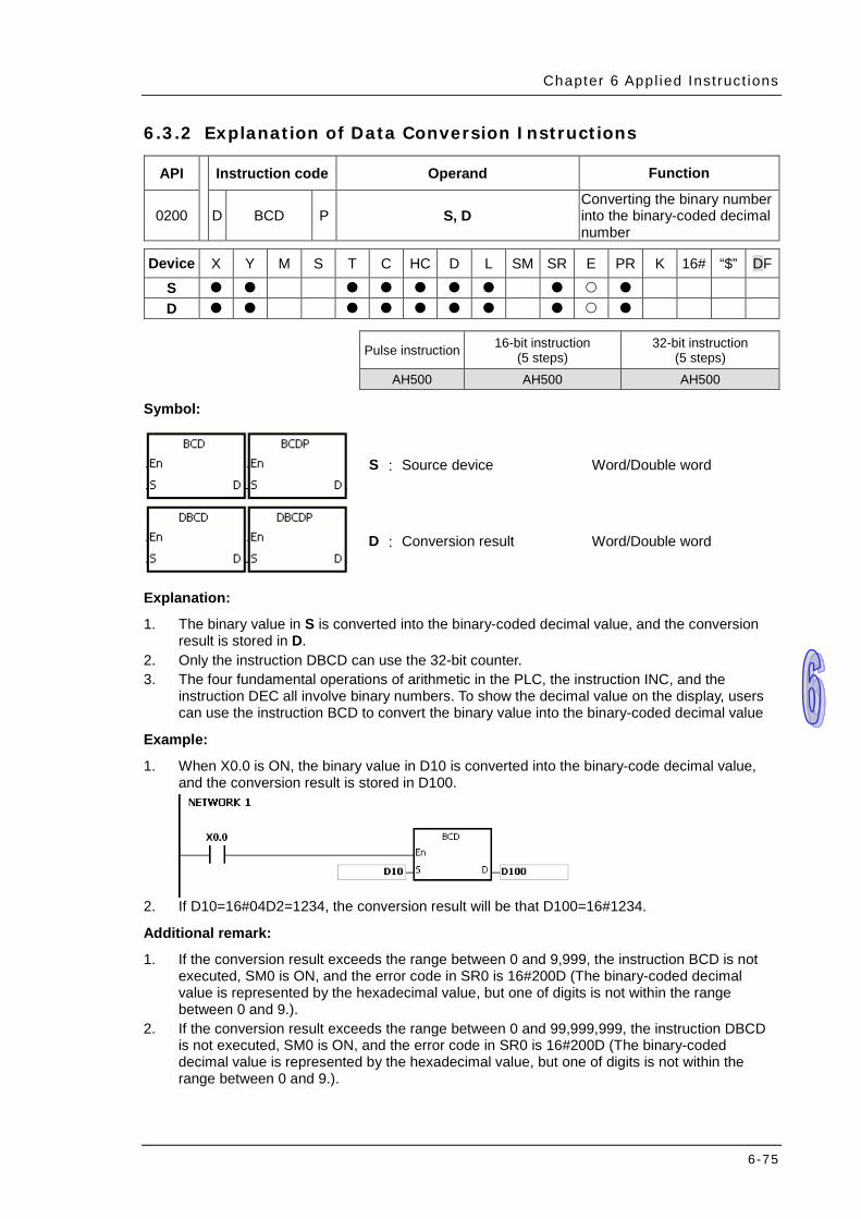
Chapter 6 Appl ied Inst ruct ions
6-75
6.3.2 Explanation of Data Conversion Instructions
API Instruction code Operand Function
0200 D BCD P S, D Converting the binary number into the binary-coded decimal number
Device X Y M S T C HC D L SM SR E PR K 16# “$” DF
S D
Pulse instruction 16-bit instruction
(5 steps) 32-bit instruction
(5 steps) AH500 AH500 AH500
Symbol:
S : Source device Word/Double word
D : Conversion result Word/Double word
Explanation:
1. The binary value in S is converted into the binary-coded decimal value, and the conversion result is stored in D.
2. Only the instruction DBCD can use the 32-bit counter. 3. The four fundamental operations of arithmetic in the PLC, the instruction INC, and the
instruction DEC all involve binary numbers. To show the decimal value on the display, users can use the instruction BCD to convert the binary value into the binary-coded decimal value
Example:
1. When X0.0 is ON, the binary value in D10 is converted into the binary-code decimal value, and the conversion result is stored in D100.
2. If D10=16#04D2=1234, the conversion result will be that D100=16#1234.
Additional remark:
1. If the conversion result exceeds the range between 0 and 9,999, the instruction BCD is not executed, SM0 is ON, and the error code in SR0 is 16#200D (The binary-coded decimal value is represented by the hexadecimal value, but one of digits is not within the range between 0 and 9.).
2. If the conversion result exceeds the range between 0 and 99,999,999, the instruction DBCD is not executed, SM0 is ON, and the error code in SR0 is 16#200D (The binary-coded decimal value is represented by the hexadecimal value, but one of digits is not within the range between 0 and 9.).
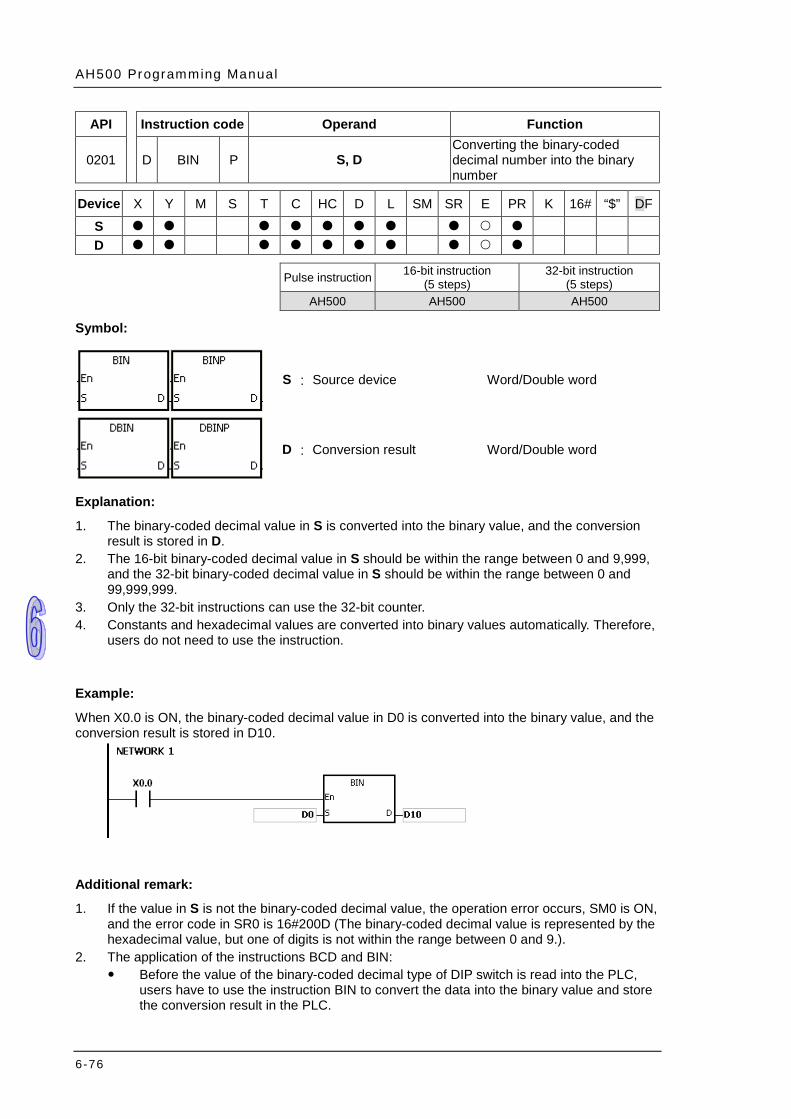
AH500 Programming Manual
6-76
API Instruction code Operand Function
0201 D BIN P S, D Converting the binary-coded decimal number into the binary number
Device X Y M S T C HC D L SM SR E PR K 16# “$” DF
S D
Pulse instruction 16-bit instruction
(5 steps) 32-bit instruction
(5 steps) AH500 AH500 AH500
Symbol:
S : Source device Word/Double word
D : Conversion result Word/Double word
Explanation:
1. The binary-coded decimal value in S is converted into the binary value, and the conversion result is stored in D.
2. The 16-bit binary-coded decimal value in S should be within the range between 0 and 9,999, and the 32-bit binary-coded decimal value in S should be within the range between 0 and 99,999,999.
3. Only the 32-bit instructions can use the 32-bit counter. 4. Constants and hexadecimal values are converted into binary values automatically. Therefore,
users do not need to use the instruction.
Example:
When X0.0 is ON, the binary-coded decimal value in D0 is converted into the binary value, and the conversion result is stored in D10.
Additional remark:
1. If the value in S is not the binary-coded decimal value, the operation error occurs, SM0 is ON, and the error code in SR0 is 16#200D (The binary-coded decimal value is represented by the hexadecimal value, but one of digits is not within the range between 0 and 9.).
2. The application of the instructions BCD and BIN: Before the value of the binary-coded decimal type of DIP switch is read into the PLC,
users have to use the instruction BIN to convert the data into the binary value and store the conversion result in the PLC.

Chapter 6 Appl ied Inst ruct ions
6-77
If users want to display the data stored inside the PLC in a seven-segment display of the binary-coded decimal type, they have to use the instruction BCD to convert the data into the binary-coded decimal value before the data is sent to the seven-segment display.
When X1.0 is ON, the binary-coded decimal value in X0.0~X0.15 is converted into the binary value, and the conversion result is stored in D100. Subsequently, the binary value in D100 is converted into the binary-coded decimal value, and the conversion result is stored in Y0.0~Y0.15.
4 2
8 1
101
100
6 6
103
102
8 1 8 18 1
X0.15 X0.0
Y0.15 Y0.0
Four -digit binary -coded deci mal value
The instruction B IN is used to store the binary value in D100.
The instruction B CD is used to conver tthe value in D100 into the four-di gi t binary-coded decimal value.
Four -digit binary -coded deci mal type of seven-segment display
Four -digit binary -coded decimal type of DIP switch
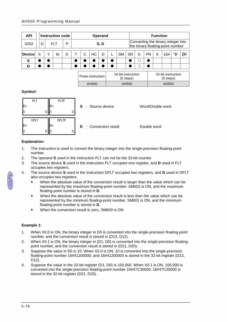
AH500 Programming Manual
6-78
API Instruction code Operand Function
0202 D FLT P S, D Converting the binary integer into the binary floating-point number
Device X Y M S T C HC D L SM SR E PR K 16# “$” DF
S D
Pulse instruction 16-bit instruction
(5 steps) 32-bit instruction
(5 steps) AH500 AH500 AH500
Symbol:
S : Source device Word/Double word
D : Conversion result Double word
Explanation:
1. The instruction is used to convert the binary integer into the single-precision floating-point number.
2. The operand S used in the instruction FLT can not be the 32-bit counter. 3. The source device S used in the instruction FLT occupies one register, and D used in FLT
occupies two registers. 4. The source device S used in the instruction DFLT occupies two registers, and D used in DFLT
also occupies two registers. When the absolute value of the conversion result is larger than the value which can be
represented by the maximum floating-point number, SM602 is ON, and the maximum floating-point number is stored in D.
When the absolute value of the conversion result is less than the value which can be represented by the minimum floating-point number, SM601 is ON, and the minimum floating-point number is stored in D.
When the conversion result is zero, SM600 is ON.
Example 1:
1. When X0.0 is ON, the binary integer in D0 is converted into the single-precision floating-point number, and the conversion result is stored in (D13, D12).
2. When X0.1 is ON, the binary integer in (D1, D0) is converted into the single-precision floating-point number, and the conversion result is stored in (D21, D20).
3. Suppose the value in D0 is 10. When X0.0 is ON, 10 is converted into the single-precision floating-point number 16#41200000, and 16#41200000 is stored in the 32-bit register (D13, D12).
4. Suppose the value in the 32-bit register (D1, D0) is 100,000. When X0.1 is ON, 100,000 is converted into the single-precision floating-point number 16#47C35000, 16#47C35000 is stored in the 32-bit register (D21, D20).
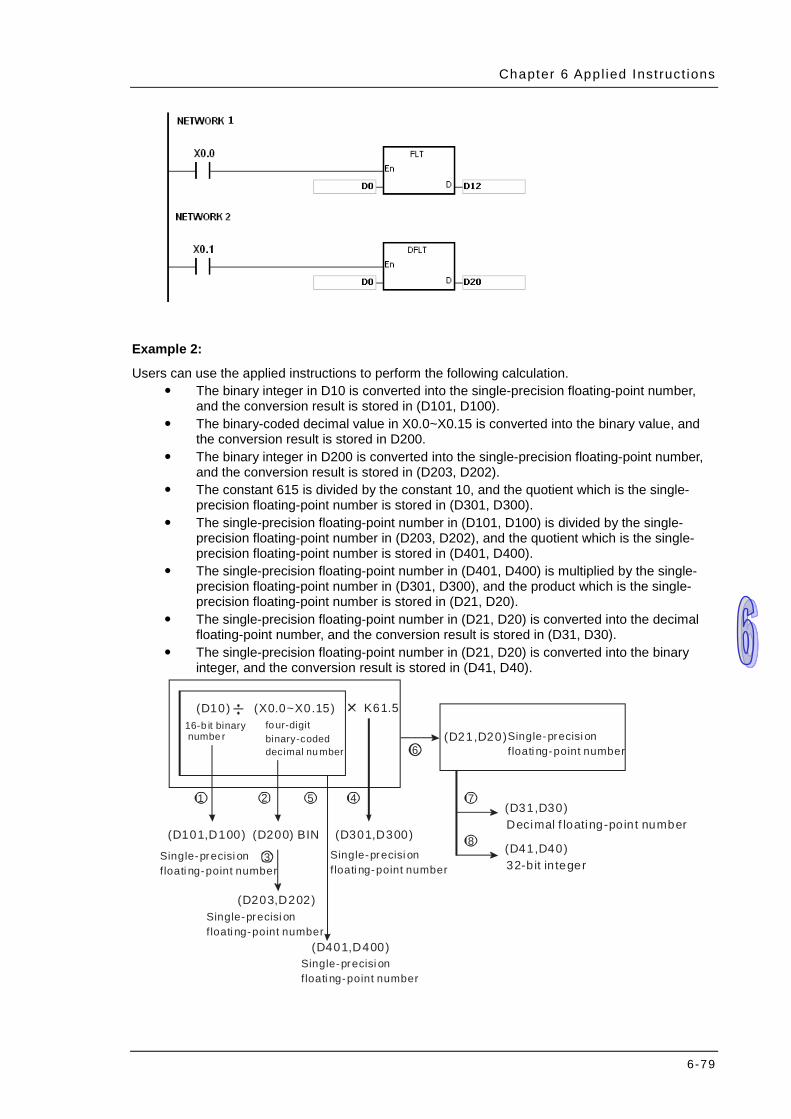
Chapter 6 Appl ied Inst ruct ions
6-79
Example 2:
Users can use the applied instructions to perform the following calculation. The binary integer in D10 is converted into the single-precision floating-point number,
and the conversion result is stored in (D101, D100). The binary-coded decimal value in X0.0~X0.15 is converted into the binary value, and
the conversion result is stored in D200. The binary integer in D200 is converted into the single-precision floating-point number,
and the conversion result is stored in (D203, D202). The constant 615 is divided by the constant 10, and the quotient which is the single-
precision floating-point number is stored in (D301, D300). The single-precision floating-point number in (D101, D100) is divided by the single-
precision floating-point number in (D203, D202), and the quotient which is the single-precision floating-point number is stored in (D401, D400).
The single-precision floating-point number in (D401, D400) is multiplied by the single-precision floating-point number in (D301, D300), and the product which is the single-precision floating-point number is stored in (D21, D20).
The single-precision floating-point number in (D21, D20) is converted into the decimal floating-point number, and the conversion result is stored in (D31, D30).
The single-precision floating-point number in (D21, D20) is converted into the binary integer, and the conversion result is stored in (D41, D40).
(D10) (X0.0~X0.15) K61.5
1 2 5 4
6
7
83
16-b it binary numbe r
fo ur-digit binary-coded decimal nu mber
(D21,D20)
(D200) BIN(D101,D100)
Single-precisi onfloati ng-point number
(D301,D300)
(D31,D30)Decimal f loating-point number
(D41,D40)32-b it in teger
(D203,D202)
(D401,D400)
Single-precisi onfloati ng-point number
Single-precisi onfloati ng-point number
Single-precisi onfloati ng-point number
Single-precisi onfloati ng-point number
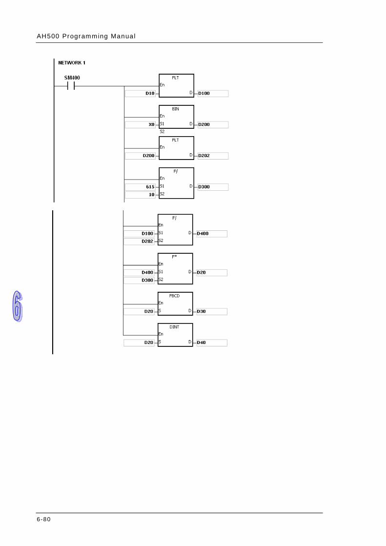
AH500 Programming Manual
6-80
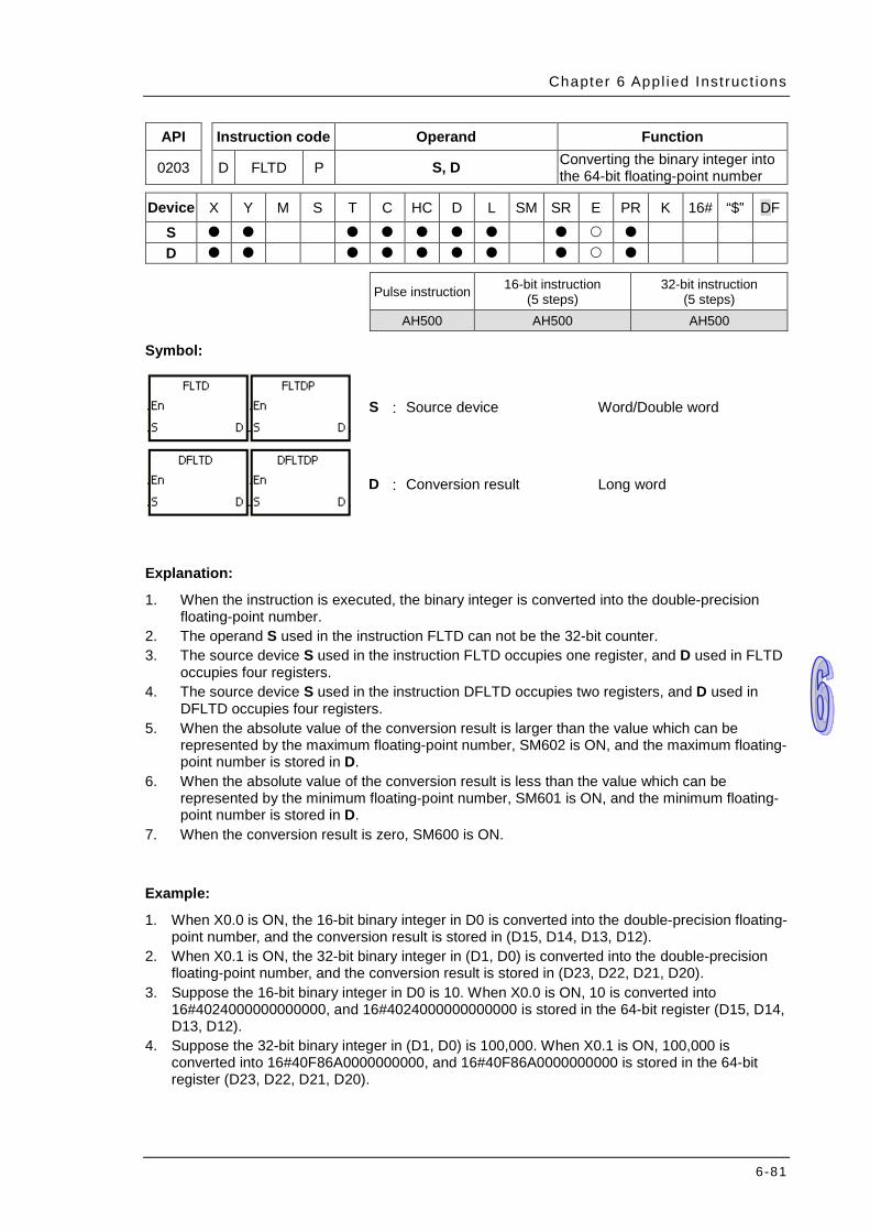
Chapter 6 Appl ied Inst ruct ions
6-81
API Instruction code Operand Function
0203 D FLTD P S, D Converting the binary integer into the 64-bit floating-point number
Device X Y M S T C HC D L SM SR E PR K 16# “$” DF
S D
Pulse instruction 16-bit instruction
(5 steps) 32-bit instruction
(5 steps) AH500 AH500 AH500
Symbol:
S : Source device Word/Double word
D : Conversion result Long word
Explanation:
1. When the instruction is executed, the binary integer is converted into the double-precision floating-point number.
2. The operand S used in the instruction FLTD can not be the 32-bit counter. 3. The source device S used in the instruction FLTD occupies one register, and D used in FLTD
occupies four registers. 4. The source device S used in the instruction DFLTD occupies two registers, and D used in
DFLTD occupies four registers. 5. When the absolute value of the conversion result is larger than the value which can be
represented by the maximum floating-point number, SM602 is ON, and the maximum floating-point number is stored in D.
6. When the absolute value of the conversion result is less than the value which can be represented by the minimum floating-point number, SM601 is ON, and the minimum floating-point number is stored in D.
7. When the conversion result is zero, SM600 is ON.
Example:
1. When X0.0 is ON, the 16-bit binary integer in D0 is converted into the double-precision floating-point number, and the conversion result is stored in (D15, D14, D13, D12).
2. When X0.1 is ON, the 32-bit binary integer in (D1, D0) is converted into the double-precision floating-point number, and the conversion result is stored in (D23, D22, D21, D20).
3. Suppose the 16-bit binary integer in D0 is 10. When X0.0 is ON, 10 is converted into 16#4024000000000000, and 16#4024000000000000 is stored in the 64-bit register (D15, D14, D13, D12).
4. Suppose the 32-bit binary integer in (D1, D0) is 100,000. When X0.1 is ON, 100,000 is converted into 16#40F86A0000000000, and 16#40F86A0000000000 is stored in the 64-bit register (D23, D22, D21, D20).

AH500 Programming Manual
6-82
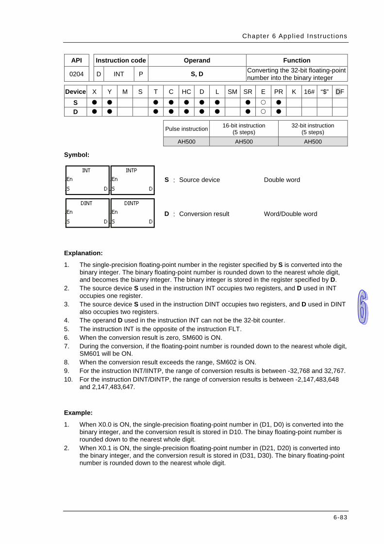
Chapter 6 Appl ied Inst ruct ions
6-83
API Instruction code Operand Function
0204 D INT P S, D Converting the 32-bit floating-point number into the binary integer
Device X Y M S T C HC D L SM SR E PR K 16# “$” DF
S D
Pulse instruction 16-bit instruction
(5 steps) 32-bit instruction
(5 steps) AH500 AH500 AH500
Symbol:
S : Source device Double word
D : Conversion result Word/Double word
Explanation:
1. The single-precision floating-point number in the register specified by S is converted into the binary integer. The binary floating-point number is rounded down to the nearest whole digit, and becomes the bianry integer. The binary integer is stored in the register specified by D.
2. The source device S used in the instruction INT occupies two registers, and D used in INT occupies one register.
3. The source device S used in the instruction DINT occupies two registers, and D used in DINT also occupies two registers.
4. The operand D used in the instruction INT can not be the 32-bit counter. 5. The instruction INT is the opposite of the instruction FLT. 6. When the conversion result is zero, SM600 is ON. 7. During the conversion, if the floating-point number is rounded down to the nearest whole digit,
SM601 will be ON. 8. When the conversion result exceeds the range, SM602 is ON. 9. For the instruction INT/IINTP, the range of conversion results is between -32,768 and 32,767. 10. For the instruction DINT/DINTP, the range of conversion results is between -2,147,483,648
and 2,147,483,647.
Example:
1. When X0.0 is ON, the single-precision floating-point number in (D1, D0) is converted into the binary integer, and the conversion result is stored in D10. The binay floating-point number is rounded down to the nearest whole digit.
2. When X0.1 is ON, the single-precision floating-point number in (D21, D20) is converted into the binary integer, and the conversion result is stored in (D31, D30). The binary floating-point number is rounded down to the nearest whole digit.
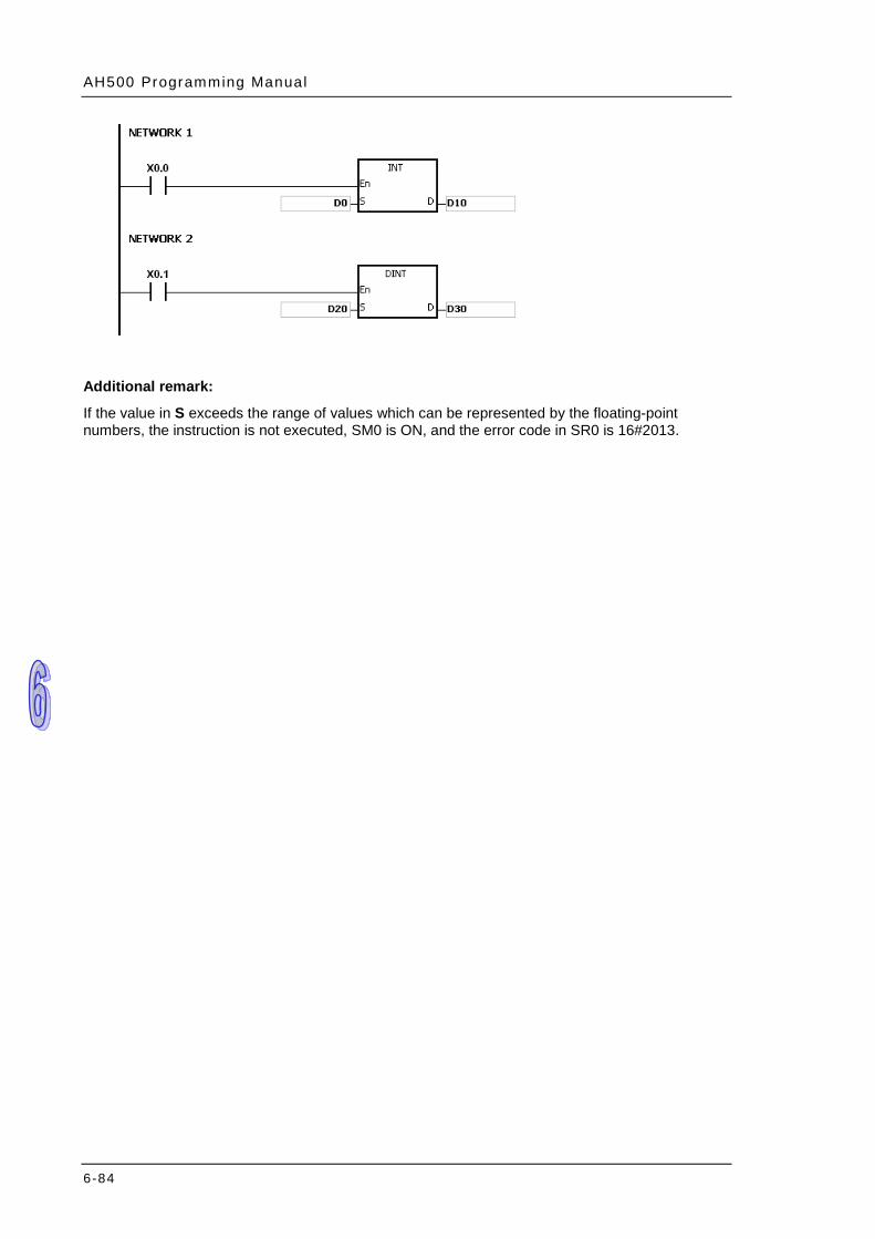
AH500 Programming Manual
6-84
Additional remark:
If the value in S exceeds the range of values which can be represented by the floating-point numbers, the instruction is not executed, SM0 is ON, and the error code in SR0 is 16#2013.

Chapter 6 Appl ied Inst ruct ions
6-85
API Instruction code Operand Function
0205 D FINT P S, D Converting the 64-bit floating-point number into the binary integer
Device X Y M S T C HC D L SM SR E PR K 16# “$” DF
S D
Pulse instruction 32-bit instruction
(5 steps) 64-bit instruction
(5 steps) AH500 AH500 AH500
Symbol:
S : Source device Long word
D : Conversion result Word/Double word
Explanation:
1. The double-precision floating-point number in the register specified by S is converted into the binary integer. The binary floating-point number is rounded down to the nearest whole digit, and becomes the bianry integer. The binary integer is stored in the register specified by D.
2. The source device S used in the instruction FINT occupies four registers, and D used in FINT occupies one register.
3. The source device S used in the instruction DFINT occupies four registers, and D used in DFINT occupies two registers.
4. The operand D used in the instructions FINT and FLTP can not be the 32-bit counter. 5. The instruction FINT is the opposite of the instruction FLTD. 6. When the conversion result is zero, SM600 is ON. 7. During the conversion, if the floating-point number is rounded down to the nearest whole digit,
SM601 will be ON. 8. When the conversion result exceeds the range, SM602 is ON.
For the instruction FINT/FINTP, the range of conversion results is between -32,768 and 32,767. For the instruction DFINT/DFINTP, the range of conversion results is between -2,147,483,648 and 2,147,483,647.
Example:
1. When X0.0 is ON, the double-precision floating-point number in (D3, D2, D1, D0) is converted into the binary integer, and the conversion result is stored in D10. The binay floating-point number is rounded down to the nearest whole digit.
2. When X0.1 is ON, the double-precision floating-point number in (D23, D22, D21, D20) is converted into the binary integer, and the conversion result is stored in (D31, D30). The binay floating-point number is rounded down to the nearest whole digit.
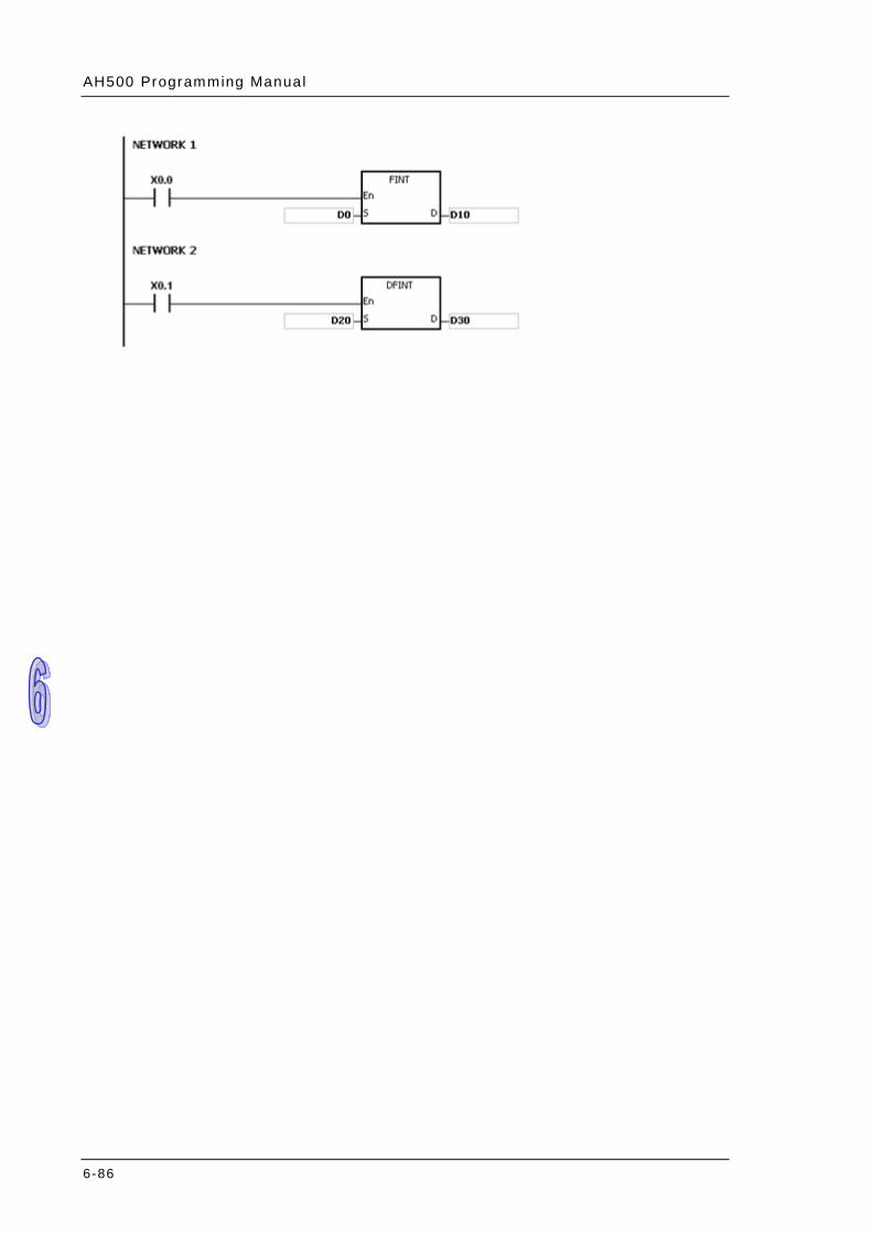
AH500 Programming Manual
6-86
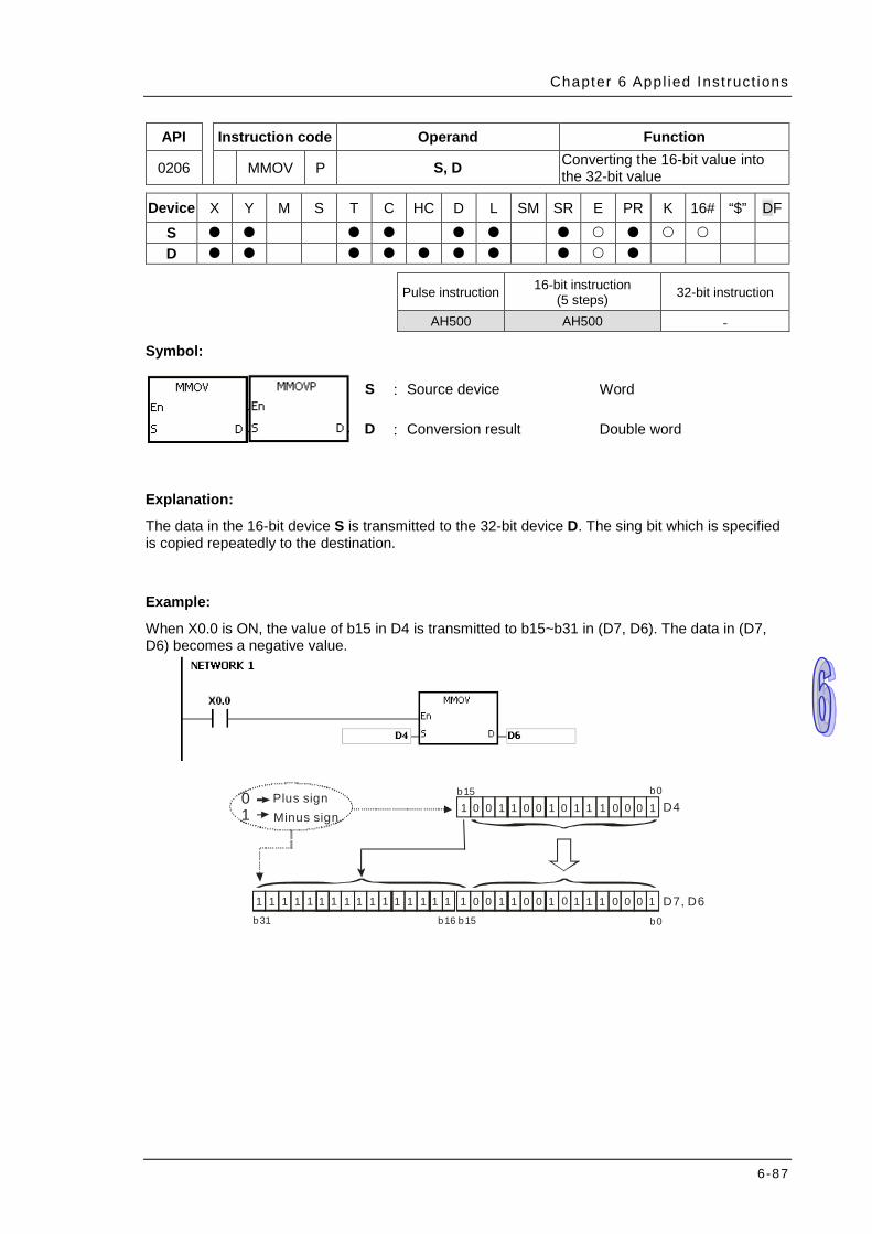
Chapter 6 Appl ied Inst ruct ions
6-87
API Instruction code Operand Function
0206 MMOV P S, D Converting the 16-bit value into the 32-bit value
Device X Y M S T C HC D L SM SR E PR K 16# “$” DF
S D
Pulse instruction 16-bit instruction
(5 steps) 32-bit instruction
AH500 AH500 -
Symbol:
S : Source device Word
D : Conversion result Double word
Explanation:
The data in the 16-bit device S is transmitted to the 32-bit device D. The sing bit which is specified is copied repeatedly to the destination.
Example:
When X0.0 is ON, the value of b15 in D4 is transmitted to b15~b31 in (D7, D6). The data in (D7, D6) becomes a negative value.
0 0 1 1 1
0
0
0
1 1
1
10 0 0b15 b0
0 0 0 0 0 1111 D7, D6
1
11111111b31 b16
1
b0b15
D4
0
1
1
00
111111111
Plus sign 01
Minus sign
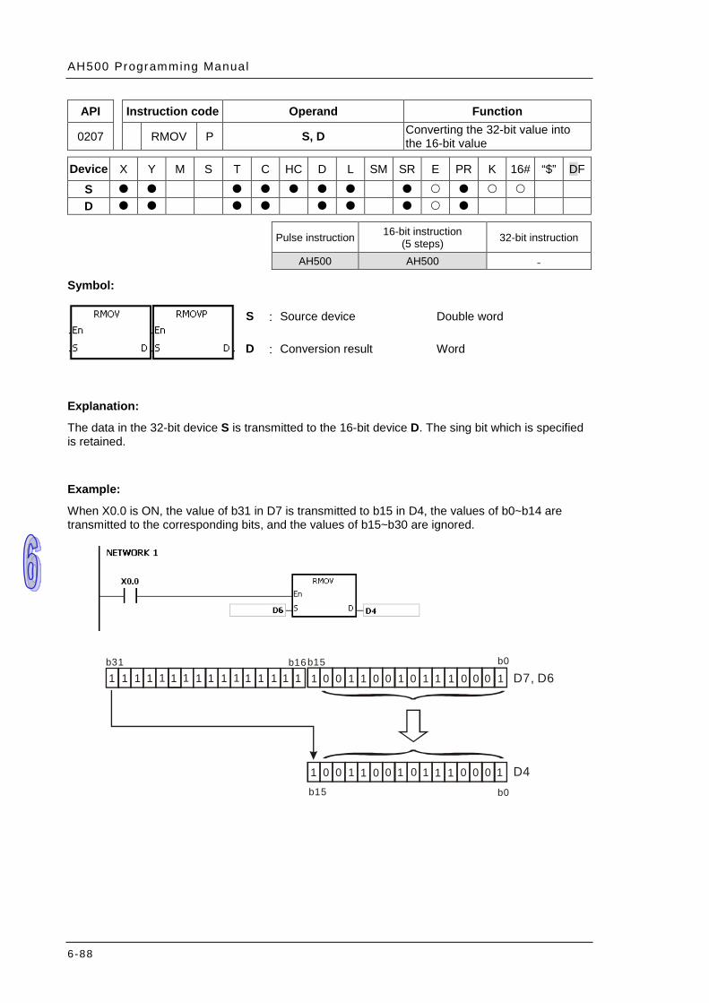
AH500 Programming Manual
6-88
API Instruction code Operand Function
0207 RMOV P S, D Converting the 32-bit value into the 16-bit value
Device X Y M S T C HC D L SM SR E PR K 16# “$” DF
S D
Pulse instruction 16-bit instruction
(5 steps) 32-bit instruction
AH500 AH500 -
Symbol:
S : Source device Double word
D : Conversion result Word
Explanation:
The data in the 32-bit device S is transmitted to the 16-bit device D. The sing bit which is specified is retained.
Example:
When X0.0 is ON, the value of b31 in D7 is transmitted to b15 in D4, the values of b0~b14 are transmitted to the corresponding bits, and the values of b15~b30 are ignored.
0 0 1 1 1
0
0
0
1 1
1
10 0 0b15 b0
0 0 0 0 0 1111
D7, D61
1
1111111b31 b161
b0b15
D40
1
1
00
1
11111111
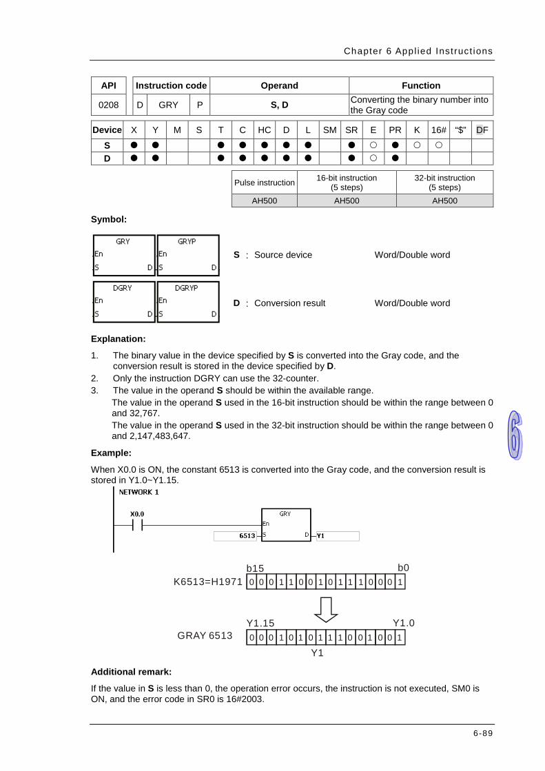
Chapter 6 Appl ied Inst ruct ions
6-89
API Instruction code Operand Function
0208 D GRY P S, D Converting the binary number into the Gray code
Device X Y M S T C HC D L SM SR E PR K 16# “$” DF
S D
Pulse instruction 16-bit instruction
(5 steps) 32-bit instruction
(5 steps) AH500 AH500 AH500
Symbol:
S : Source device Word/Double word
D : Conversion result Word/Double word
Explanation:
1. The binary value in the device specified by S is converted into the Gray code, and the conversion result is stored in the device specified by D.
2. Only the instruction DGRY can use the 32-counter. 3. The value in the operand S should be within the available range.
The value in the operand S used in the 16-bit instruction should be within the range between 0 and 32,767. The value in the operand S used in the 32-bit instruction should be within the range between 0 and 2,147,483,647.
Example:
When X0.0 is ON, the constant 6513 is converted into the Gray code, and the conversion result is stored in Y1.0~Y1.15.
0 0 0 1 1 10 0 0 1 1 1 10 0 0b15 b0
K6513=H1971
0 0 0 0 0 0 0 0 0 1111111
Y1
Y1.15 Y1.0GRAY 6513
Additional remark:
If the value in S is less than 0, the operation error occurs, the instruction is not executed, SM0 is ON, and the error code in SR0 is 16#2003.

AH500 Programming Manual
6-90
API Instruction code Operand Function
0209 D GBIN P S, D Converting the Gray code into the binary number
Device X Y M S T C HC D L SM SR E PR K 16# “$” DF
S D
Pulse instruction 16-bit instruction
(5 steps) 32-bit instruction
(5 steps) AH500 AH500 AH500
Symbol:
S : Source device Word/Double word
D : Conversion result Word/Double word
Explanation:
1. The Gray code in the device specified by S is converted into the binary value, and the conversion result is stored in the device specified by D.
2. The instruction is used to convert the Gary code in the absolute position encoder which is connected to the input terminal of the PLC to the binary value, and the conversion result is stored in the register which is specified.
3. The value in the operand S should be within the available range. The value in the operand S used in the 16-bit instruction should be within the range between 0 and 32,767. The value in the operand S used in the 32-bit instruction should be within the range between 0 and 2,147,483,647.
Example:
When X0.0 is ON, the Gary code in the absolute position encoder which is connected to the inputs X0.0~X0.15 is converted into the binary value, and the conversion result is stored in D10.
0 0 0 1 10 11 10 0 0
b15 b0
H1971=K6513 0 0 0 0 0 0 111111
X0.15 X0.0
GRAY CODE 6513
X0
0 1 0 1
0 0 1 0
Additional remark:
If the value in S is less than 0, the operation error occurs, the instruction is not executed, SM0 is ON, and the error code in SR0 is 16#2003.
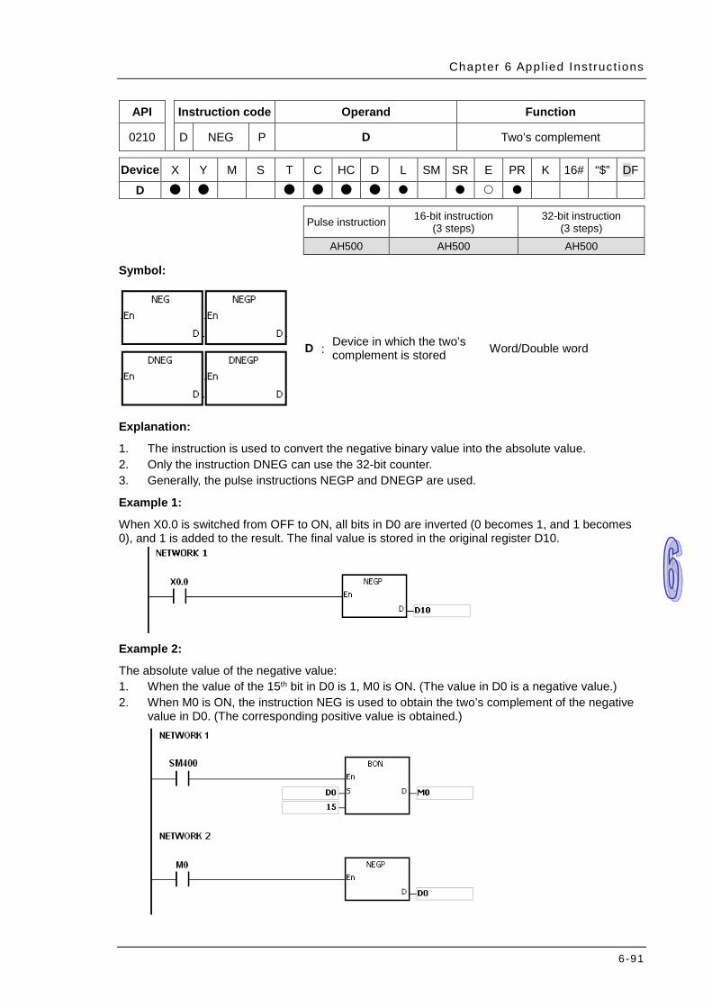
Chapter 6 Appl ied Inst ruct ions
6-91
API Instruction code Operand Function
0210 D NEG P D Two’s complement
Device X Y M S T C HC D L SM SR E PR K 16# “$” DF
D
Pulse instruction 16-bit instruction (3 steps)
32-bit instruction (3 steps)
AH500 AH500 AH500
Symbol:
D : Device in which the two’s complement is stored Word/Double word
Explanation:
1. The instruction is used to convert the negative binary value into the absolute value. 2. Only the instruction DNEG can use the 32-bit counter. 3. Generally, the pulse instructions NEGP and DNEGP are used.
Example 1:
When X0.0 is switched from OFF to ON, all bits in D0 are inverted (0 becomes 1, and 1 becomes 0), and 1 is added to the result. The final value is stored in the original register D10.
Example 2:
The absolute value of the negative value: 1. When the value of the 15th bit in D0 is 1, M0 is ON. (The value in D0 is a negative value.) 2. When M0 is ON, the instruction NEG is used to obtain the two’s complement of the negative
value in D0. (The corresponding positive value is obtained.)
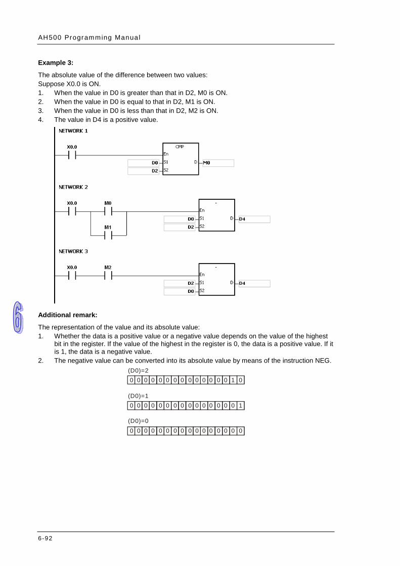
AH500 Programming Manual
6-92
Example 3:
The absolute value of the difference between two values: Suppose X0.0 is ON. 1. When the value in D0 is greater than that in D2, M0 is ON. 2. When the value in D0 is equal to that in D2, M1 is ON. 3. When the value in D0 is less than that in D2, M2 is ON. 4. The value in D4 is a positive value.
Additional remark:
The representation of the value and its absolute value: 1. Whether the data is a positive value or a negative value depends on the value of the highest
bit in the register. If the value of the highest in the register is 0, the data is a positive value. If it is 1, the data is a negative value.
2. The negative value can be converted into its absolute value by means of the instruction NEG.
0 0 0 0 0 0 0 0 0 0 0 0 0 0 01
0 0 0 0 0 0 0 0 0 0 0 0 0 0 10
0 0 0 0 0 0 0 0 0 0 0 0 0 0 00
(D0)=2
(D0)=1
(D0)=0
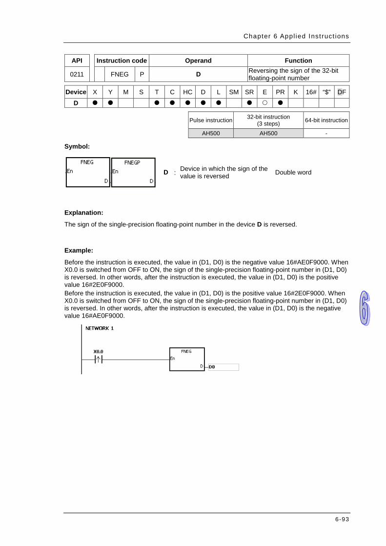
Chapter 6 Appl ied Inst ruct ions
6-93
API Instruction code Operand Function
0211 FNEG P D Reversing the sign of the 32-bit floating-point number
Device X Y M S T C HC D L SM SR E PR K 16# “$” DF
D
Pulse instruction 32-bit instruction (3 steps) 64-bit instruction
AH500 AH500 -
Symbol:
D : Device in which the sign of the value is reversed Double word
Explanation:
The sign of the single-precision floating-point number in the device D is reversed.
Example:
Before the instruction is executed, the value in (D1, D0) is the negative value 16#AE0F9000. When X0.0 is switched from OFF to ON, the sign of the single-precision floating-point number in (D1, D0) is reversed. In other words, after the instruction is executed, the value in (D1, D0) is the positive value 16#2E0F9000. Before the instruction is executed, the value in (D1, D0) is the positive value 16#2E0F9000. When X0.0 is switched from OFF to ON, the sign of the single-precision floating-point number in (D1, D0) is reversed. In other words, after the instruction is executed, the value in (D1, D0) is the negative value 16#AE0F9000.
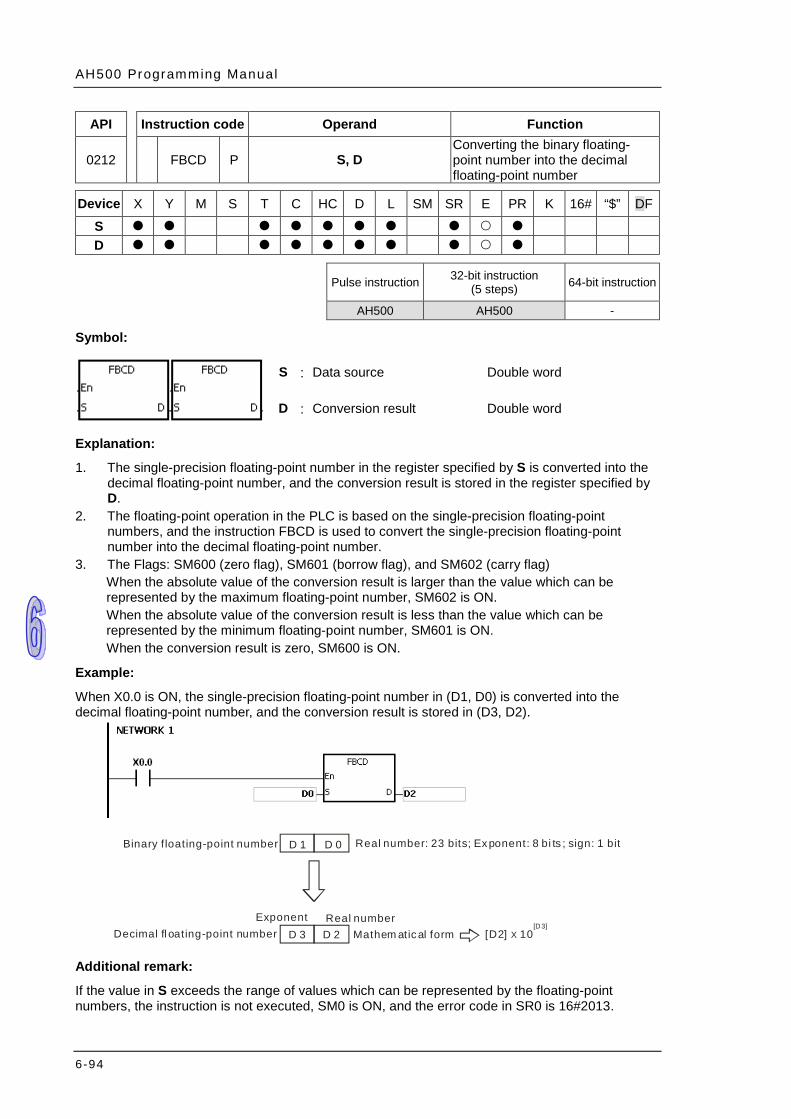
AH500 Programming Manual
6-94
API Instruction code Operand Function
0212 FBCD P S, D Converting the binary floating-point number into the decimal floating-point number
Device X Y M S T C HC D L SM SR E PR K 16# “$” DF
S D
Pulse instruction 32-bit instruction
(5 steps) 64-bit instruction
AH500 AH500 -
Symbol:
S : Data source Double word
D : Conversion result Double word
Explanation:
1. The single-precision floating-point number in the register specified by S is converted into the decimal floating-point number, and the conversion result is stored in the register specified by D.
2. The floating-point operation in the PLC is based on the single-precision floating-point numbers, and the instruction FBCD is used to convert the single-precision floating-point number into the decimal floating-point number.
3. The Flags: SM600 (zero flag), SM601 (borrow flag), and SM602 (carry flag) When the absolute value of the conversion result is larger than the value which can be represented by the maximum floating-point number, SM602 is ON. When the absolute value of the conversion result is less than the value which can be represented by the minimum floating-point number, SM601 is ON. When the conversion result is zero, SM600 is ON.
Example:
When X0.0 is ON, the single-precision floating-point number in (D1, D0) is converted into the decimal floating-point number, and the conversion result is stored in (D3, D2).
D 1 D 0Binary f loating-point number
Decimal fl oating-point number D 3 D 2Exponent Real number
[D2] 10X[D3]
Real number: 23 bits; Exponent: 8 bi ts ; sign: 1 bit
Mathem atical form Additional remark:
If the value in S exceeds the range of values which can be represented by the floating-point numbers, the instruction is not executed, SM0 is ON, and the error code in SR0 is 16#2013.

Chapter 6 Appl ied Inst ruct ions
6-95
API Instruction code Operand Function
0213 FBIN P S, D Converting the decimal floating-point number into the binary floating-point number
Device X Y M S T C HC D L SM SR E PR K 16# “$” DF
S D
Pulse instruction 32-bit instruction
(5 steps) 64-bit instruction
AH500 AH500 -
Symbol:
S : Data source Double word
D : Conversion result Double word
Explanation:
1. The decimal floating-point number in the register specified by S is converted into the single-precision floating-point number, and the conversion result is stored in the register specified by D.
2. Suppose the value in S is 1234, and the value in S+1 is 3. The value in S is converted into 1.234x10⁶.
3. The value in D should be a single-precision floating-point number, and the values in S and S+1 represent the decimal real number and the decimal exponent respectively.
4. The instruction FBIN is used to convert the decimal floating-point number into the single-precision floating-point number.
5. The real number of decimal floating-point numbers range from -9,999 to +9,999, the exponents of decimal floating-point numbers range from -41 to +35, and the practical range of decimal floating-point numbers in PLC is between ±1175×10-41 and ±3402×10+35. When the operation result is zero, SM600 is ON.
Example 1:
When X0.0 is ON, the decimal floating-point number in the register in (D1, D0) is converted into the single-precision floating-point number, and the conversion result is stored in (D3, D2).
Binary f loating-point number
Decimal fl oating-point numberExponent Real number
Real number: 23 bits; Exponent: 8 bits ; sign: 1 bit
Mathematical formD 1 D 0
D 3 D 2
[D0] 10X[D1]
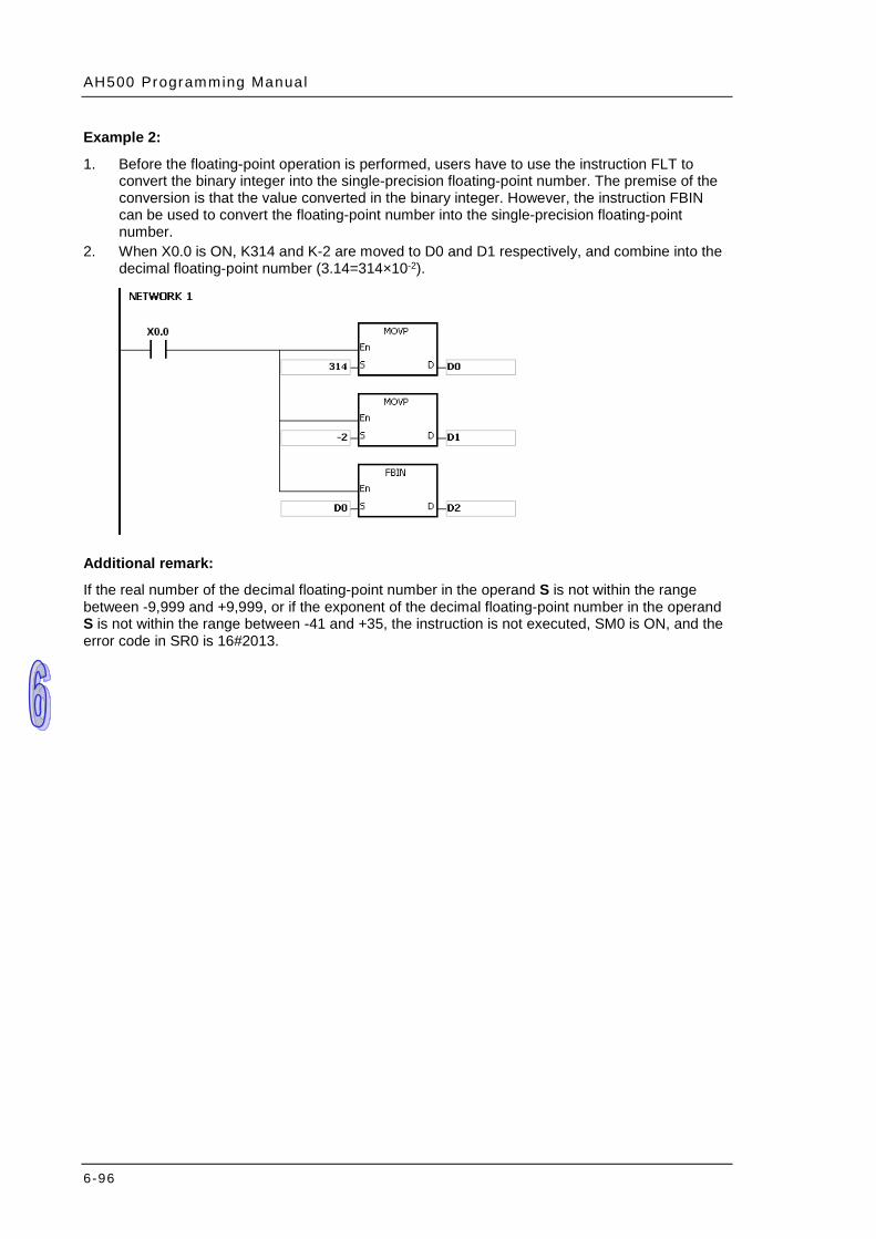
AH500 Programming Manual
6-96
Example 2:
1. Before the floating-point operation is performed, users have to use the instruction FLT to convert the binary integer into the single-precision floating-point number. The premise of the conversion is that the value converted in the binary integer. However, the instruction FBIN can be used to convert the floating-point number into the single-precision floating-point number.
2. When X0.0 is ON, K314 and K-2 are moved to D0 and D1 respectively, and combine into the decimal floating-point number (3.14=314×10-2).
Additional remark:
If the real number of the decimal floating-point number in the operand S is not within the range between -9,999 and +9,999, or if the exponent of the decimal floating-point number in the operand S is not within the range between -41 and +35, the instruction is not executed, SM0 is ON, and the error code in SR0 is 16#2013.

Chapter 6 Appl ied Inst ruct ions
6-97
API Instruction code Operand Function
0214 BKBCD P S, n, D Converting the binary numbers in blocks into the binary-coded decimal numbers in blocks
Device X Y M S T C HC D L SM SR E PR K 16# “$” DF
S n D
Pulse instruction 16-bit instruction
(7 steps) 32-bit instruction
AH500 AH500 -
Symbol:
S : Data source Word
n : Data length Word
D : Conversion result Word
Explanation:
1. n pieces of data (the binary values) in devices starting from S are converted into the binary-coded decimal values, and the conversion results are stored in D.
2. The operand n should be within the range between 1 and 256.
Example:
When M1 is ON, the binary values in D0 and D1 are converted into the binary-coded decimal values, and the conversion results are stored in D4 and D5.
Additional remark:
1. If n is less than 1, or when n is larger than 256, the instruction is not execute, SM0 is ON, and the error code in SR0 is 16#200B.
2. If the devices specified by S+n-1 and D+n-1 exceed the range, the instruction is not executed, SM0 is ON, and the error code in SR0 is 16#2003.
3. If the conversion result is not within the range between 0 and 9,999, the instruction is not executed, and the error code in SR0 is 16#200D (The binary-coded decimal value is represented by the hexadecimal number, but one of digits is not within the range between 0 and 9.).
4. If S~S+n-1 overlap D~D+n-1, the instruction is not executed, SM0 is ON, and the error code in SR0 is 16#200C.

AH500 Programming Manual
6-98
API Instruction code Operand Function
0215 BKBIN P S, n, D Converting the binary numbers in blocks into the binary-coded decimal numbers in blocks
Device X Y M S T C HC D L SM SR E PR K 16# “$” DF
S ○ n ○ D ○
Pulse instruction 16-bit instruction
(7 steps) 32-bit instruction
AH500 AH500 -
Symbol:
S : Data source Word
n : Data length Word
D : Conversion result Word
Explanation:
1. n pieces of data (the binary-coded decimal values) in devices starting from S are converted into the binary values, and the conversion results are stored in D.
2. The binary-coded decimal value in S should be within the range between 0 and 9,999. 3. The operand n should be within the rang between 1 and 256.
Example:
When M1 is ON, the binary-code decimal values in D0 and D1 are converted into the binary values, and the conversion results are stored in D4 and D5.
Additional remark:
1. If n is less than 1, or when n is larger than 256, the instruction is not execute, SM0 is ON, and the error code in SR0 is 16#200B.
2. If the devices specified by S+n-1 and D+n-1 exceed the range, the instruction is not executed, SM0 is ON, and the error code in SR0 is 16#2003.
3. If the data in S is not the binary-coded decimal, the instruction is not executed, and the error code in SR0 is 16#200D (The binary-coded decimal value is represented by the hexadecimal number, but one of digits is not within the range between 0 and 9.).
4. If S~S+n-1 overlap D~D+n-1, the instruction is not executed, SM0 is ON, and the error code in SR0 is 16#200C.
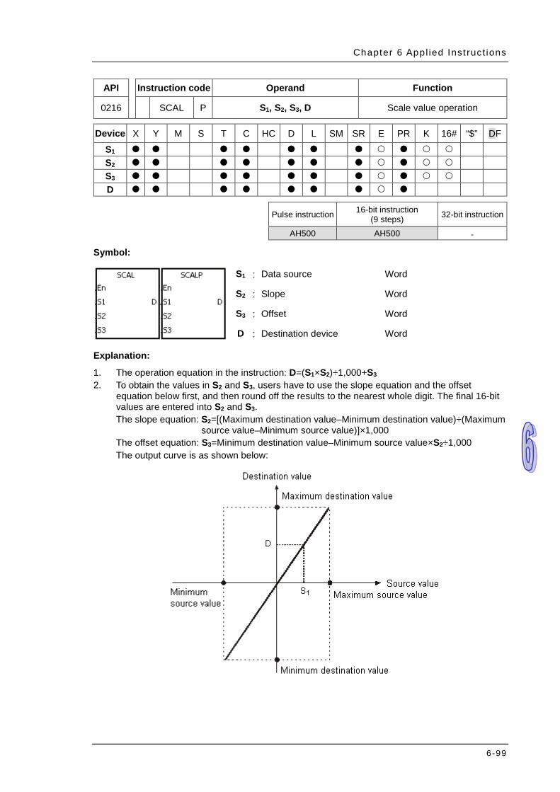
Chapter 6 Appl ied Inst ruct ions
6-99
API Instruction code Operand Function
0216 SCAL P S1, S2, S3, D Scale value operation
Device X Y M S T C HC D L SM SR E PR K 16# “$” DF
S1 S2 S3 D
Pulse instruction 16-bit instruction
(9 steps) 32-bit instruction
AH500 AH500 -
Symbol:
S1 : Data source Word
S2 : Slope Word
S3 : Offset Word
D : Destination device Word
Explanation:
1. The operation equation in the instruction: D=(S1×S2)÷1,000+S3 2. To obtain the values in S2 and S3, users have to use the slope equation and the offset
equation below first, and then round off the results to the nearest whole digit. The final 16-bit values are entered into S2 and S3. The slope equation: S2=[(Maximum destination value–Minimum destination value)÷(Maximum
source value–Minimum source value)]×1,000 The offset equation: S3=Minimum destination value–Minimum source value×S2÷1,000 The output curve is as shown below:
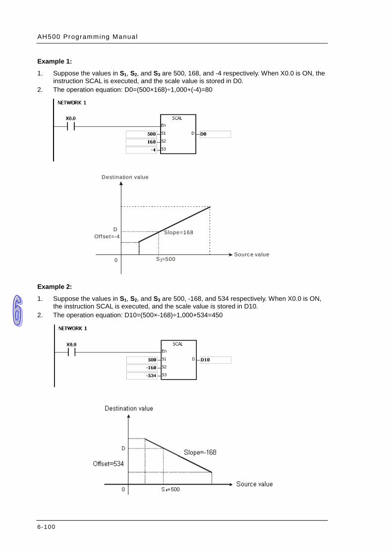
AH500 Programming Manual
6-100
Example 1:
1. Suppose the values in S1, S2, and S3 are 500, 168, and -4 respectively. When X0.0 is ON, the instruction SCAL is executed, and the scale value is stored in D0.
2. The operation equation: D0=(500×168)÷1,000+(-4)=80
D
S10 =500
Slope=168Offset=-4
Source value
Destination value
Example 2:
1. Suppose the values in S1, S2, and S3 are 500, -168, and 534 respectively. When X0.0 is ON, the instruction SCAL is executed, and the scale value is stored in D10.
2. The operation equation: D10=(500×-168)÷1,000+534=450

Chapter 6 Appl ied Inst ruct ions
6-101
Additional remark:
1. Only when the slope and the offset are known can the instruction SCAL be used. If the slope and the offset are unknown, users are suggested to use the instruction SCLP to perform the operation.
2. The value entered into S2 should be within the range between –32,768 and 32,767. (The practical value is within the range between –32,768 and 32,767.
3. When users use the slope equation, they have to notice that the maximum source value should be larger than the minimum source value. However, the maximum destination value is not necessarily larger than the minimum destination value.
4. If the value in D is larger than 32,767, the value stored in D will be 32,767. If the value in D is less than -32,768, the value stored in D will be -32,768.
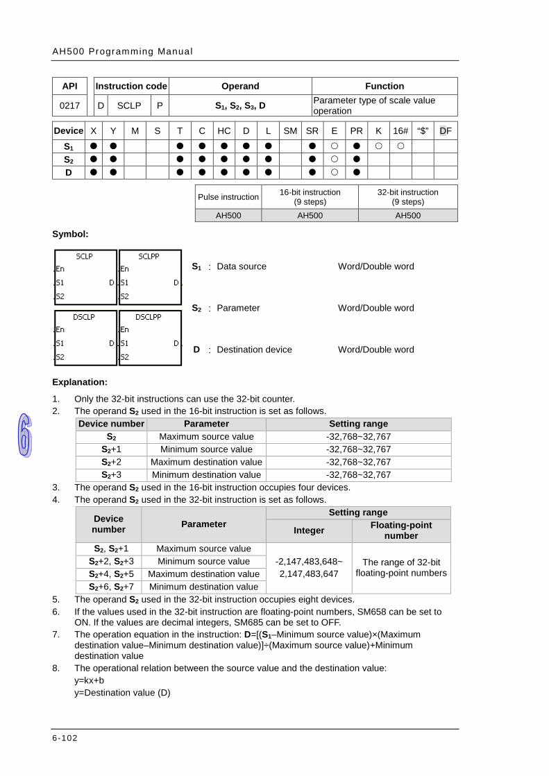
AH500 Programming Manual
6-102
API Instruction code Operand Function
0217 D SCLP P S1, S2, S3, D Parameter type of scale value operation
Device X Y M S T C HC D L SM SR E PR K 16# “$” DF
S1 S2 D
Pulse instruction 16-bit instruction
(9 steps) 32-bit instruction
(9 steps) AH500 AH500 AH500
Symbol:
S1 : Data source Word/Double word
S2 : Parameter Word/Double word
D : Destination device Word/Double word
Explanation:
1. Only the 32-bit instructions can use the 32-bit counter. 2. The operand S2 used in the 16-bit instruction is set as follows.
Device number Parameter Setting range S2 Maximum source value -32,768~32,767
S2+1 Minimum source value -32,768~32,767 S2+2 Maximum destination value -32,768~32,767 S2+3 Minimum destination value -32,768~32,767
3. The operand S2 used in the 16-bit instruction occupies four devices. 4. The operand S2 used in the 32-bit instruction is set as follows.
Device number Parameter
Setting range
Integer Floating-point number
S2, S2+1 Maximum source value -2,147,483,648~ 2,147,483,647
The range of 32-bit floating-point numbers
S2+2, S2+3 Minimum source value S2+4, S2+5 Maximum destination value S2+6, S2+7 Minimum destination value
5. The operand S2 used in the 32-bit instruction occupies eight devices. 6. If the values used in the 32-bit instruction are floating-point numbers, SM658 can be set to
ON. If the values are decimal integers, SM685 can be set to OFF. 7. The operation equation in the instruction: D=[(S1–Minimum source value)×(Maximum
destination value–Minimum destination value)]÷(Maximum source value)+Minimum destination value
8. The operational relation between the source value and the destination value: y=kx+b y=Destination value (D)
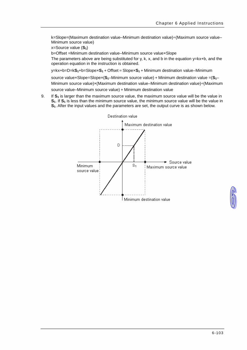
Chapter 6 Appl ied Inst ruct ions
6-103
k=Slope=(Maximum destination value–Minimum destination value)÷(Maximum source value–Minimum source value) x=Source value (S1) b=Offset =Minimum destination value–Minimum source value×Slope The parameters above are being substituted for y, k, x, and b in the equation y=kx+b, and the operation equation in the instruction is obtained. y=kx+b=D=kS1+b=Slope×S1+Offset=Slope×S1+Minimum destination value–Minimum
source value×Slope=Slope×(S1–Minimum source value)+Minimum destination value =(S1–Minimum source value)×(Maximum destination value–Minimum destination value)÷(Maximum source value–Minimum source value)+Minimum destination value
9. If S1 is larger than the maximum source value, the maximum source value will be the value in S1. If S1 is less than the minimum source value, the minimum source value will be the value in S1. After the input values and the parameters are set, the output curve is as shown below.
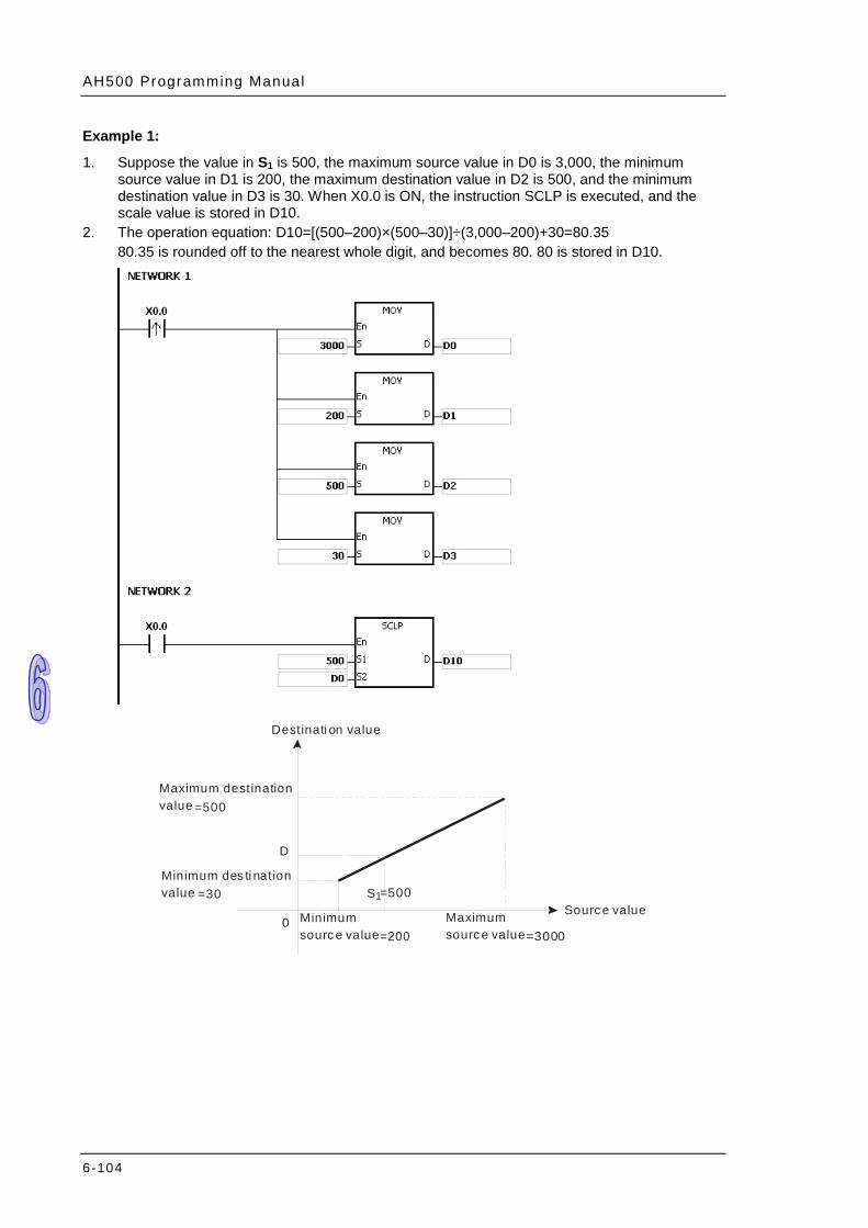
AH500 Programming Manual
6-104
Example 1:
1. Suppose the value in S1 is 500, the maximum source value in D0 is 3,000, the minimum source value in D1 is 200, the maximum destination value in D2 is 500, and the minimum destination value in D3 is 30. When X0.0 is ON, the instruction SCLP is executed, and the scale value is stored in D10.
2. The operation equation: D10=[(500–200)×(500–30)]÷(3,000–200)+30=80.35 80.35 is rounded off to the nearest whole digit, and becomes 80. 80 is stored in D10.
D
S1
0
=500
=3000 =200
=30
=500
Source valueMaximum source value
Minimum source value
Maximum destinationvalue
Minimum des ti nation value
Destinati on value
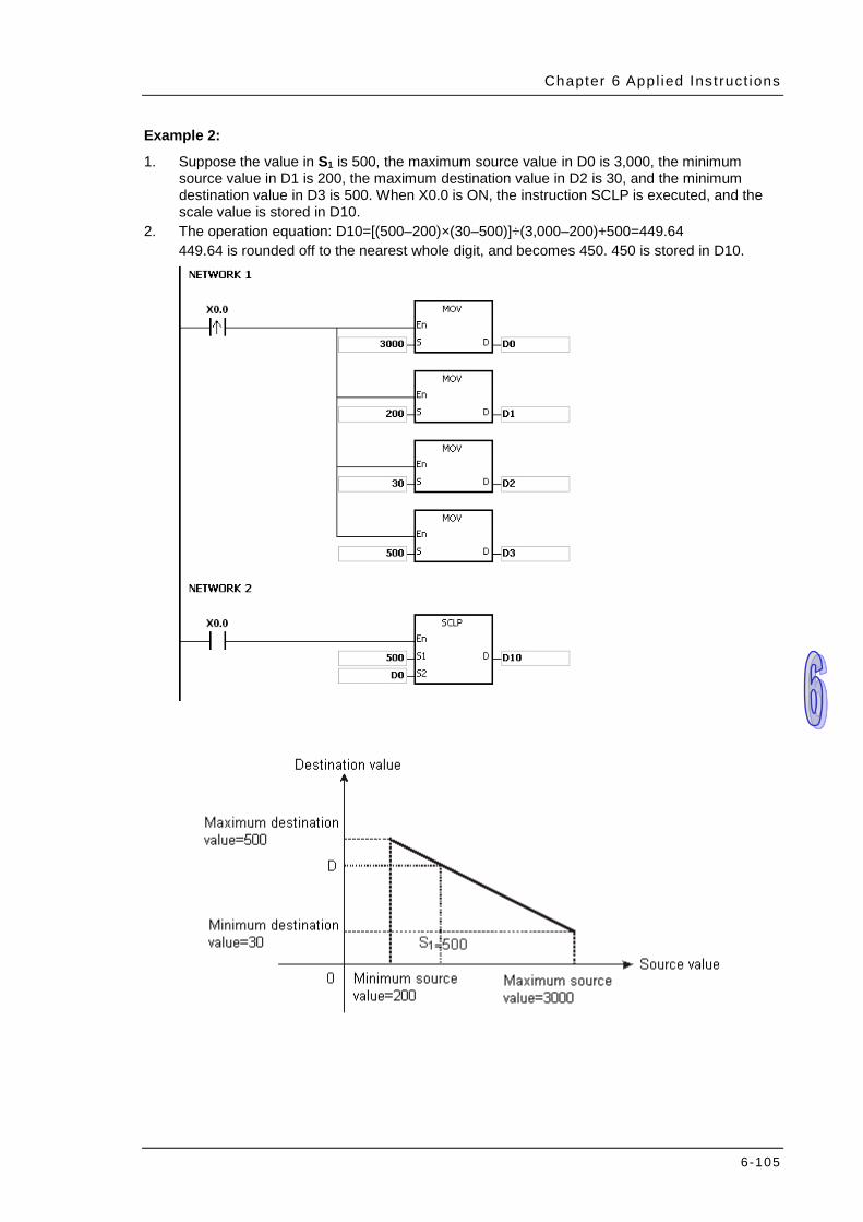
Chapter 6 Appl ied Inst ruct ions
6-105
Example 2:
1. Suppose the value in S1 is 500, the maximum source value in D0 is 3,000, the minimum source value in D1 is 200, the maximum destination value in D2 is 30, and the minimum destination value in D3 is 500. When X0.0 is ON, the instruction SCLP is executed, and the scale value is stored in D10.
2. The operation equation: D10=[(500–200)×(30–500)]÷(3,000–200)+500=449.64 449.64 is rounded off to the nearest whole digit, and becomes 450. 450 is stored in D10.

AH500 Programming Manual
6-106
Example 3:
1. Suppose the value in S1 is 500.0, the maximum source value in D0 is 3000.0, the minimum source value in D2 is 200.0, the maximum destination value in D4 is 500.0, and the minimum destination value in D6 is 30.0. When X0.0 is ON, SM685 is set to ON, the instruction DSCLP is executed, and the scale value is stored in D10.
2. The operation equation: D10=[(500.0–200.0)×(500.0–30.0)]÷(3000.0–200.0)+30.0=80.35 80.35 is rounded off to the nearest whole digit, and becomes 80.0. 80.0 is stored in D10.

Chapter 6 Appl ied Inst ruct ions
6-107
Additional remark:
1. The value in S1 which is used in the 16-bit instruction should be within the range between the minimum source value and the maximum source value, i.e. between -32,768 and 32,767. If the value exceeds the boundary value, the boundary value is used in the operation.
2. The integer in S1 which is used in the 32-bit instruction should be within the range between the minimum source value and the maximum source value, i.e. between -2,147,483,648 and 2,147,483,647. If the integer exceeds the boundary value, the boundary value is used in the operation.
3. The floating-point number in S1 which is used in the 32-bit instruction should be within the range between the minimum source value and the maximum source value, i.e. within the range of floating-point numbers. If the floating-point number exceeds the boundary value, the boundary value is used in the operation.
4. When users use the instruction, they have to notice that the maximum source value should be larger than the minimum source value. However, the maximum destination value is not necessarily larger than the minimum destination value.
5. When the maximum source value is the same as the minimum source value, the instruction will not be executed and it will be seen as an operation error; SM0 will be ON and the error code in SR0 is 16#2012.
6. If the operand S2 used during the execution of the 16-bit instruction is declared in ISPSoft, the data type will be ARRAY [4] of WORD.
7. If the operand S2 used during the execution of the 32-bit instruction is declared in ISPSoft, the data type will be ARRAY [4] of DWORD.

AH500 Programming Manual
6-108
API Instruction code Operand Function
0218 D LINE P S, n, D Converting a column of data into a line of data
Device X Y M S T C HC D L SM SR E PR K 16# “$” DF
S n D
Pulse instruction 16-bit instruction
(7 steps) 32-bit instruction
(7 steps) AH500 AH500 AH500
Symbol:
S : Data source Word/Double word
n : Number of bits Word/Double word
D : Data destination Word/Double word
Explanation:
1. The operand S used in the 16-bit instruction occupies sixteen 16-bit registers, i.e. S~S+15. 2. The operand S used in the 32-bit instruction occupies thirty-two 32-bit registers, i.e. S~S+31. 3. The operand n indicates that the value of the nth bit in every piece of data in the operand S is
retrieved. Besides, the operand n used in the 16-bit instruction should be within the range between 0 and 15, and the operand n used in the 32-bit instruction should be within the range between 0 and 31.
4. The operand n used in the 16-bit instruction indicates that the values of the nth bits in S~S+15 are retrieved, and the values of the nth bits are stored in the operand D in order.
5. The operand n used in the 32-bit instruction indicates that the values of the nth bits in S~S+31 are retrieved, and the values of the nth bits are stored in the operand D in order.
6. Only the 32-bit instructions can use the 32-bit counter. 7. Take the 16-bit instruction for example.
.
.
.
...... ..
101
10
0
0 1 0 1 10
.
.
.
.
.
.
.
.
.
b15 b0S
S+1S+2
S+13S+14S+15 b15 b0
D
N
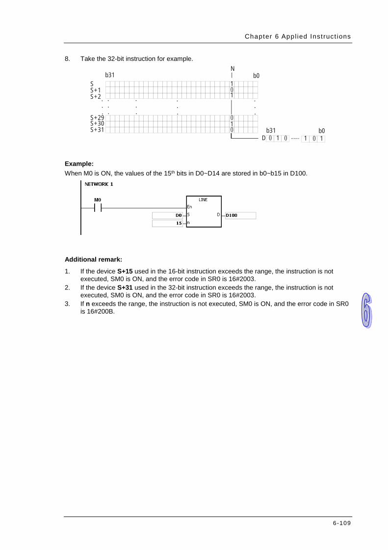
Chapter 6 Appl ied Inst ruct ions
6-109
8. Take the 32-bit instruction for example.
.
.
.
.. ... .0 1 0 1 10
.
.
.
.
.
.
.
.
.
b31 b0SS+1S+2
S+29S+30S+31 b31 b0
D
N
.
.
.
11
1
0
0
0
Example: When M0 is ON, the values of the 15th bits in D0~D14 are stored in b0~b15 in D100.
Additional remark:
1. If the device S+15 used in the 16-bit instruction exceeds the range, the instruction is not executed, SM0 is ON, and the error code in SR0 is 16#2003.
2. If the device S+31 used in the 32-bit instruction exceeds the range, the instruction is not executed, SM0 is ON, and the error code in SR0 is 16#2003.
3. If n exceeds the range, the instruction is not executed, SM0 is ON, and the error code in SR0 is 16#200B.
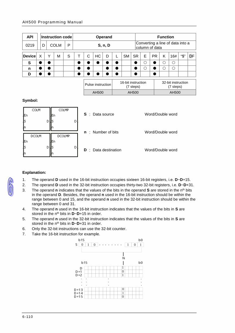
AH500 Programming Manual
6-110
API Instruction code Operand Function
0219 D COLM P S, n, D Converting a line of data into a column of data
Device X Y M S T C HC D L SM SR E PR K 16# “$” DF
S n D
Pulse instruction 16-bit instruction
(7 steps) 32-bit instruction
(7 steps) AH500 AH500 AH500
Symbol:
S : Data source Word/Double word
n : Number of bits Word/Double word
D : Data destination Word/Double word
Explanation:
1. The operand D used in the 16-bit instruction occupies sixteen 16-bit registers, i.e. D~D+15. 2. The operand D used in the 32-bit instruction occupies thirty-two 32-bit registers, i.e. D~D+31. 3. The operand n indicates that the values of the bits in the operand S are stored in the nth bits
in the operand D. Besides, the operand n used in the 16-bit instruction should be within the range between 0 and 15, and the operand n used in the 32-bit instruction should be within the range between 0 and 31.
4. The operand n used in the 16-bit instruction indicates that the values of the bits in S are stored in the nth bits in D~D+15 in order.
5. The operand n used in the 32-bit instruction indicates that the values of the bits in S are stored in the nth bits in D~D+31 in order.
6. Only the 32-bit instructions can use the 32-bit counter. 7. Take the 16-bit instruction for example.
...... ..0 1 0 1 10
.
.
.
101
10
0
.
.
.
.
.
.
.
.
.
b15 b0S
DD+1D+2
D+13D+14D+15
Nb0b15
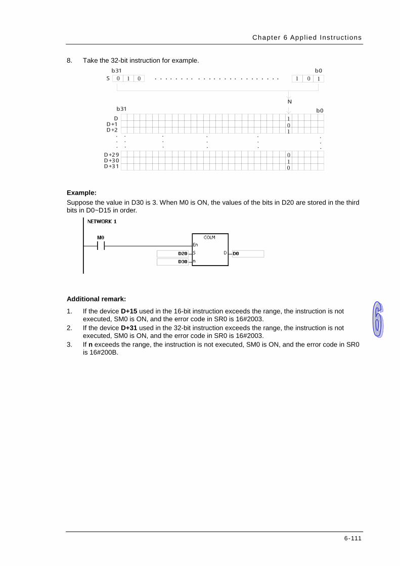
Chapter 6 Appl ied Inst ruct ions
6-111
8. Take the 32-bit instruction for example.
...... ..0 1 0 1 10
.
.
.
101
10
0
.
.
.
.
.
.
.
.
.
b31 b0S
DD+1D+2
D+29D+30D+31
Nb0b31
.
.
.
...... .. ...... ..
.
.
.
Example: Suppose the value in D30 is 3. When M0 is ON, the values of the bits in D20 are stored in the third bits in D0~D15 in order.
Additional remark:
1. If the device D+15 used in the 16-bit instruction exceeds the range, the instruction is not executed, SM0 is ON, and the error code in SR0 is 16#2003.
2. If the device D+31 used in the 32-bit instruction exceeds the range, the instruction is not executed, SM0 is ON, and the error code in SR0 is 16#2003.
3. If n exceeds the range, the instruction is not executed, SM0 is ON, and the error code in SR0 is 16#200B.
AH500 Programming Manual
6-112
6.4 Data Transfer Instructions
6.4.1 List of Data Transfer Instructions
API Instruction code Pulse instruction Function Step 16-bit 32-bit 64-bit
0300 MOV DMOV – Transferring the data 5
0301 – – DFMOV Transferring the 64-bit floating-point number 5-6
0302 $MOV – – Transferring the string 5-11 0303 CML DCML – Inverting the data 5 0304 BMOV – – Transferring all data 7
0305 NMOV DNMOV – Transferring the data to several devices 7
0306 XCH DXCH – Exchanging the data 5 0307 BXCH – – Exchanging all data 7
0308 SWAP DSWAP – Exchange the high byte with the low byte 3
0309 SMOV – – Transferring the digits 11 0310 MOVB – – Transferring several bits 7
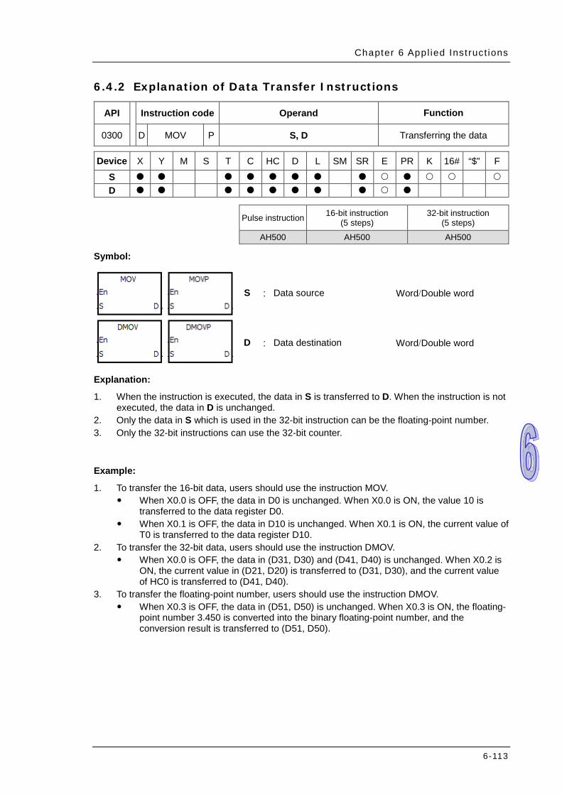
Chapter 6 Appl ied Inst ruct ions
6-113
6.4.2 Explanation of Data Transfer Instructions
API Instruction code Operand Function
0300 D MOV P S, D Transferring the data
Device X Y M S T C HC D L SM SR E PR K 16# “$” F
S D
Pulse instruction 16-bit instruction
(5 steps) 32-bit instruction
(5 steps) AH500 AH500 AH500
Symbol:
S : Data source Word/Double word
D : Data destination Word/Double word
Explanation:
1. When the instruction is executed, the data in S is transferred to D. When the instruction is not executed, the data in D is unchanged.
2. Only the data in S which is used in the 32-bit instruction can be the floating-point number. 3. Only the 32-bit instructions can use the 32-bit counter.
Example:
1. To transfer the 16-bit data, users should use the instruction MOV. When X0.0 is OFF, the data in D0 is unchanged. When X0.0 is ON, the value 10 is
transferred to the data register D0. When X0.1 is OFF, the data in D10 is unchanged. When X0.1 is ON, the current value of
T0 is transferred to the data register D10. 2. To transfer the 32-bit data, users should use the instruction DMOV.
When X0.0 is OFF, the data in (D31, D30) and (D41, D40) is unchanged. When X0.2 is ON, the current value in (D21, D20) is transferred to (D31, D30), and the current value of HC0 is transferred to (D41, D40).
3. To transfer the floating-point number, users should use the instruction DMOV. When X0.3 is OFF, the data in (D51, D50) is unchanged. When X0.3 is ON, the floating-
point number 3.450 is converted into the binary floating-point number, and the conversion result is transferred to (D51, D50).

AH500 Programming Manual
6-114

Chapter 6 Appl ied Inst ruct ions
6-115
API Instruction code Operand Function
0301 D FMOV P S, D Transferring the 64-bit floating-point number
Device X Y M S T C HC D L SM SR E PR K 16# “$” DF
S D
Pulse instruction 32-bit instruction 64-bit instruction
(5-6 steps) AH500 - AH500
Symbol:
S : Data source Long word
D : Data destination Double word/Long word
Explanation:
1. When the instruction is executed, the data in S is transferred to D. When the instruction is not executed, the data in D is unchanged.
2. Only the 64-bit instructions are supported. 3. The instrucitons DFMOV and DFMOVP are double-precision data transfer instructions.
Example:
When M0 is ON, the values in D0~D3 are transferred to D4~D7.
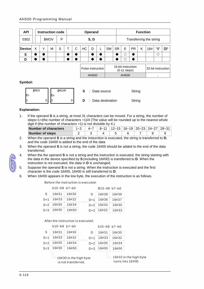
AH500 Programming Manual
6-116
API Instruction code Operand Function
0302 $MOV P S, D Transferring the string
Device X Y M S T C HC D L SM SR E PR K 16# “$” DF
S D
Pulse instruction 16-bit instruction
(5-11 steps) 32-bit instruction
AH500 AH500 -
Symbol:
S : Data source String
D : Data destination String
Explanation:
1. If the operand S is a string, at most 31 characters can be moved. For a string, the number of steps=1+(the number of characters +1)/4 (The value will be rounded up to the nearest whole digit if (the number of characters +1) is not divisible by 4.). Number of characters 1~3 4~7 8~11 12~15 16~19 20~23 24~27 28~31 Number of steps 2 3 4 5 6 7 8 9
2. When the operand S is a string and the insturction is executed, the string is transferred to D, and the code 16#00 is added to the end of the data
3. When the operand S is not a string, the code 16#00 should be added to the end of the data transferred.
4. When the the operand S is not a string and the instruction is executed, the string starting with the data in the device specified by S (including 16#00) is transferred to D. When the instruction is not executed, the data in D is unchanged.
5. Suppose the operand S is not a string. When the instruction is executed and the first character is the code 16#00, 16#00 is still transferred to D.
6. When 16#00 appears in the low byte, the execution of the instruction is as follows.
b7~b0b15~b8
SS+1S+2S+3
16#3016#3116#3216#3316#3416#3516#0016#30
b7~b0B15~b8
DD+1D+2D+3
16#3916#3816#3716#3616#3516#3416#3316#32
b7~b0b15~b8
SS+1S+2S+3
16#3016#3116#3216#3316#3416#3516#0016#30
b7~b0b15~b8
DD+1D+2D+3
16#3016#3116#3216#3316#3416#3516#0016#00
Before the instruction is executed:
After the instruction is executed:
16#32 in the high byte turns into 16#00.
16#30 in the high byte is not transferred.

Chapter 6 Appl ied Inst ruct ions
6-117
7. When 16#00 appears in the high byte, the execution of the instruction is as follows.
Before the instruction is executed:
After the instruction is executed:
b7~b0b15~b8
SS+1S+2S+3
16#3016#3116#3216#3316#3416#00
16#3616#37
b7~b0b15~b8
DD+1D+2D+3
16#3916#3816#3716#36
16#3516#34
16#3316#32
b7~b0b15~b8
SS+1S+2S+3
16#3016#3116#3216#3316#3416#0016#3616#37
b7~b0b15~b8
DD+1D+2D+3
16#3016#3116#3216#3316#3416#0016#3316#32
8. When S overlaps D and the device number of S is less than the device number of D, the
transfer of the data to D starts form the ending code 16#00.
Before the instruction is executed:
After the instruction is executed:
b7~b0b15~b8
D0 D1 D2 D3
16#3016#3116#3216#3316#3416#35
16#0016#30
b7~b0b15~b8
D1 D2 D3 D4
16#3216#3316#3416#3516#0016#30
16#3716#38
b7~b0b15~b8
D0 D1 D2 D3
16#3016#3116#3216#3316#3416#35
16#0016#30
b7~b0b15~b8
D1 D2 D3 D4
16#3016#3116#3216#3316#3416#35
16#0016#00
Example 1:
Suppose the operand S is the even string “1234”. When the conditional contact X0.0 is enabled, the data in D0~D3 is as follows.
The operand S:
String ‘1’ ‘2’ ‘3’ ‘4’
Hexadecimal value 16#31 16#32 16#33 16#34

AH500 Programming Manual
6-118
After the instruction is executed, the data in the operand D is as follows. Device High byte Low byte Note
D0 16#32 16#31 ‘1’=16#31; ‘2’=16#32 D1 16#34 16#33 ‘3’=16#33; ‘4’=16#34
D2 16#00 16#00 The ending code 16#00 is in the low byte. 16#00 is automatically added in the high byte.
D3 Unchanged Unchanged
Example 2:
Suppose the operand S is the odd string “12345”. When the conditional contact X0.0 is enabled, the data in D0~D3 is as follows.
The operand S:
String ‘1’ ‘2’ ‘3’ ‘4’ ‘5’ Hexadecimal value 16#31 16#32 16#33 16#34 16#35
After the instruction is executed, the data in the operand D is as follows. Device High byte Low byte Note
D0 16#32 16#31 ‘1’=16#31; ‘2’=16#32 D1 16#34 16#33 ‘3’=16#33; ‘4’=16#34 D2 16#00 16#35 The ending code 16#00 is in the high byte. D3 Unchanged Unchanged
Example 3:
When the operand S is not a string and the ending code 16#00 appears in the low byte, the execution of the instruction is as follows.
The operand S:
Device High byte Low byte Note D100 16#31 16#30 ‘1’=16#31; ‘0’=16#30 D101 16#33 16#32 ‘3’=16#33; ‘2’=16#32 D102 16#35 16#34 ‘5’=16#35; ‘4’=16#34 D103 16#30 16#00 ‘0’=16#30; 16#00 is the ending code.
After the instruction is executed, the data in the operand D is as follows. Device High byte Low byte Note
D0 16#31 16#30 ‘1’=16#31; ‘0’=16#30 D1 16#33 16#32 ‘3’=16#33; ‘2’=16#32 D2 16#35 16#34 ‘5’=16#35; ‘4’=16#34
D3 16#00 16#00 The ending code 16#00 is in the low byte. 16#00 is automatically added in the high byte.
D4 Unchanged Unchanged
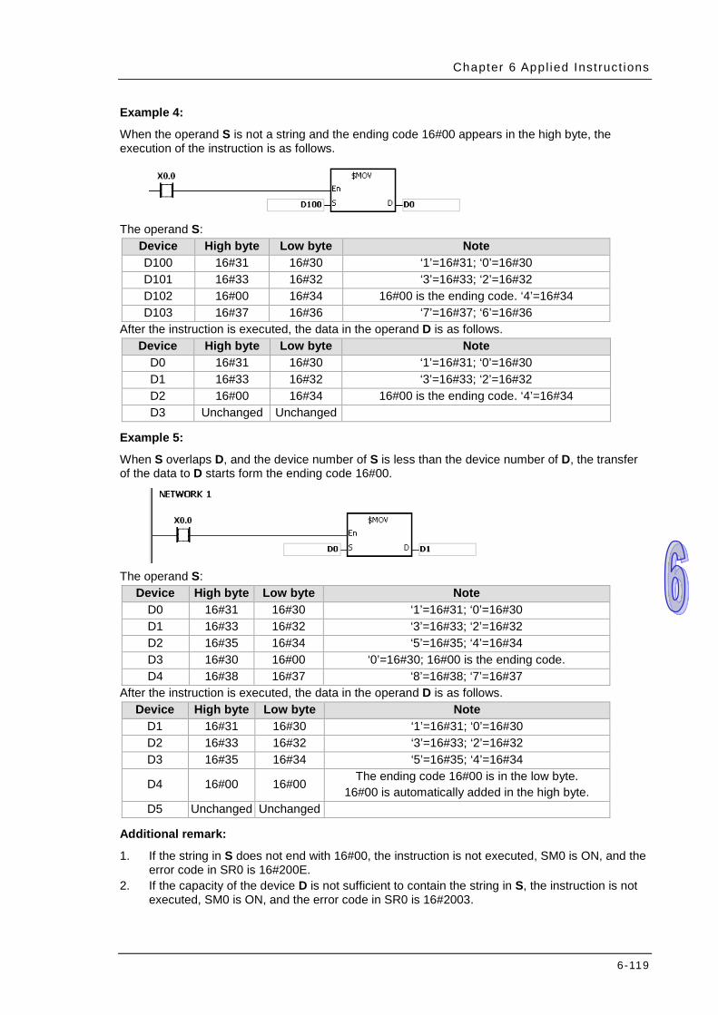
Chapter 6 Appl ied Inst ruct ions
6-119
Example 4:
When the operand S is not a string and the ending code 16#00 appears in the high byte, the execution of the instruction is as follows.
The operand S:
Device High byte Low byte Note D100 16#31 16#30 ‘1’=16#31; ‘0’=16#30 D101 16#33 16#32 ‘3’=16#33; ‘2’=16#32 D102 16#00 16#34 16#00 is the ending code. ‘4’=16#34 D103 16#37 16#36 ‘7’=16#37; ‘6’=16#36
After the instruction is executed, the data in the operand D is as follows. Device High byte Low byte Note
D0 16#31 16#30 ‘1’=16#31; ‘0’=16#30 D1 16#33 16#32 ‘3’=16#33; ‘2’=16#32 D2 16#00 16#34 16#00 is the ending code. ‘4’=16#34 D3 Unchanged Unchanged
Example 5:
When S overlaps D, and the device number of S is less than the device number of D, the transfer of the data to D starts form the ending code 16#00.
The operand S:
Device High byte Low byte Note D0 16#31 16#30 ‘1’=16#31; ‘0’=16#30 D1 16#33 16#32 ‘3’=16#33; ‘2’=16#32 D2 16#35 16#34 ‘5’=16#35; ‘4’=16#34 D3 16#30 16#00 ‘0’=16#30; 16#00 is the ending code. D4 16#38 16#37 ‘8’=16#38; ‘7’=16#37
After the instruction is executed, the data in the operand D is as follows. Device High byte Low byte Note
D1 16#31 16#30 ‘1’=16#31; ‘0’=16#30 D2 16#33 16#32 ‘3’=16#33; ‘2’=16#32 D3 16#35 16#34 ‘5’=16#35; ‘4’=16#34
D4 16#00 16#00 The ending code 16#00 is in the low byte. 16#00 is automatically added in the high byte.
D5 Unchanged Unchanged
Additional remark:
1. If the string in S does not end with 16#00, the instruction is not executed, SM0 is ON, and the error code in SR0 is 16#200E.
2. If the capacity of the device D is not sufficient to contain the string in S, the instruction is not executed, SM0 is ON, and the error code in SR0 is 16#2003.

AH500 Programming Manual
6-120
API Instruction code Operand Function
0303 D CML P S, D Inverting the data
Device X Y M S T C HC D L SM SR E PR K 16# “$” DF
S D
Pulse instruction 16-bit instruction
(5 steps) 32-bit instruction
(5 steps)
AH500 AH500 AH500
Symbol:
S : Data source Word/Double word
D : Data destination Word/Double word
Explanation:
1. The instruction is used to invert all bits in S, i.e. 0 becomes 1, and 1 becomes 0. The inversion result is stored in D. If the data in S is the constant, the constant will be converted into the binary value.
2. Only the 32-bit instructions can use the 32-bit counter.
Example 1:
When X0.0 is ON, all bit in D1 are inverted, and the conversion result is stored in Y0.0~Y0.15.
D1 1 0 1 0 1 0 1 0 1 0 1 0 1 0 1 0Sign bi t (0: P os it ive s ign; 1: Negative si gn)
0 1 0 1
Inversi on resul t
b 0b 1b 2b 3b 15
0 1 0 1 0 1 0 1 0 1 0 1Y0

Chapter 6 Appl ied Inst ruct ions
6-121
Example 2:
The circuits below can be represented by means of the instruction CML.
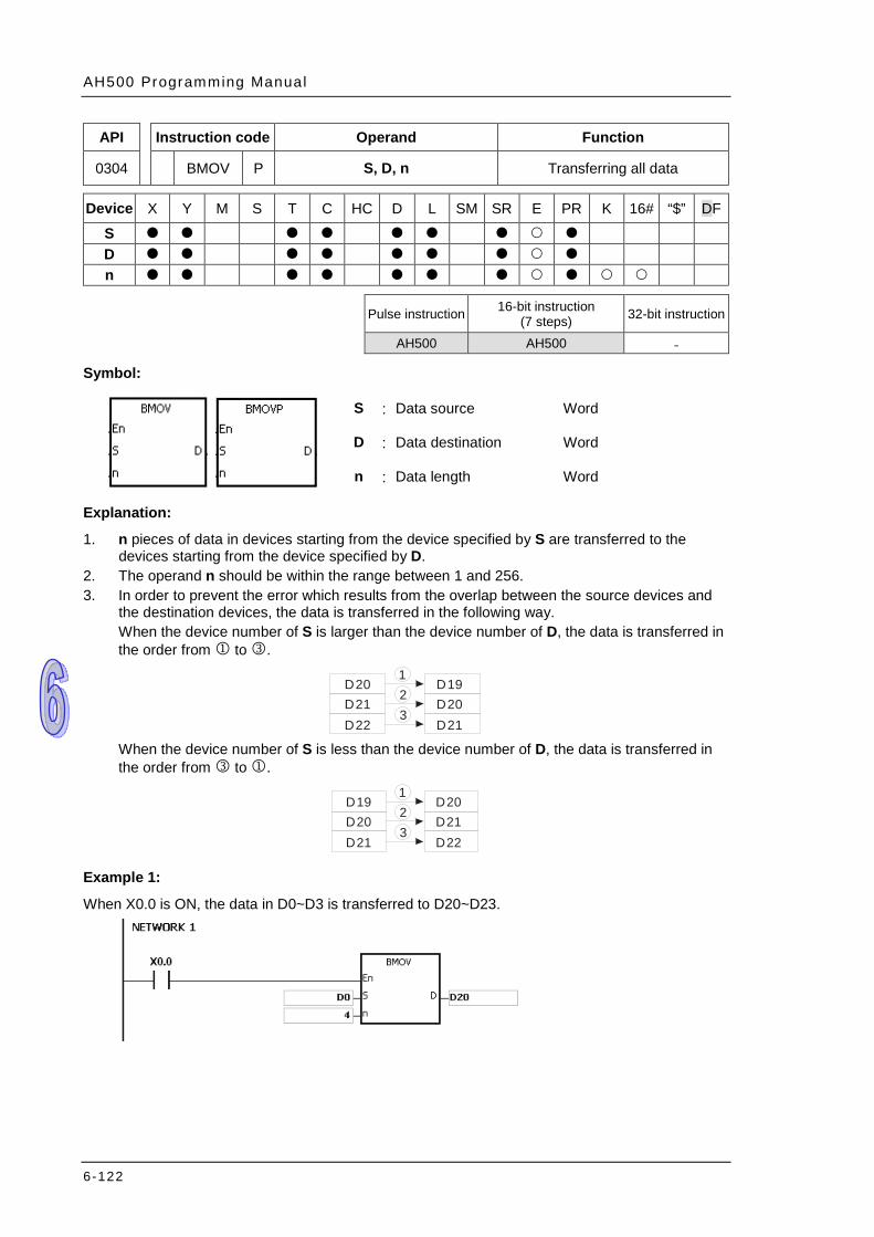
AH500 Programming Manual
6-122
API Instruction code Operand Function
0304 BMOV P S, D, n Transferring all data
Device X Y M S T C HC D L SM SR E PR K 16# “$” DF
S D n
Pulse instruction 16-bit instruction
(7 steps) 32-bit instruction
AH500 AH500 -
Symbol:
S : Data source Word
D : Data destination Word
n : Data length Word
Explanation:
1. n pieces of data in devices starting from the device specified by S are transferred to the devices starting from the device specified by D.
2. The operand n should be within the range between 1 and 256. 3. In order to prevent the error which results from the overlap between the source devices and
the destination devices, the data is transferred in the following way. When the device number of S is larger than the device number of D, the data is transferred in the order from to .
D19D20D21
D20D21D22
21
3
When the device number of S is less than the device number of D, the data is transferred in the order from to .
D20D21D22
D19D20D21
21
3
Example 1:
When X0.0 is ON, the data in D0~D3 is transferred to D20~D23.

Chapter 6 Appl ied Inst ruct ions
6-123
D0D1D2D3
D20D21D22D23
N=4
Example 2:
In order to prevent the error which results from the overlap between the source devices and the destination devices, the data is transferred in the following way. 1. When the device number of S is larger than the device number of D, the data is transferred in
the order from to .
D19D20D21
D20D21D22
21
3
2. When the device number of S is less than the device number of D, the data is transferred in the order from to .
D11
D13
D10D11D12
1
32
D12
Additional remark:
1. If D+n-1 exceeds the device range, the instruction is not executed, SM0 is ON, and the error code in SR0 is 16#2003.
2. If S+n-1 exceeds the device range, the instruction is not executed, SM0 is ON, and the error code in SR0 is 16#2003.
3. If n is larger than 256, or if n is less than 1, the instruction is not executed, SM0 is ON, and the error code in SR0 is 16#200B.
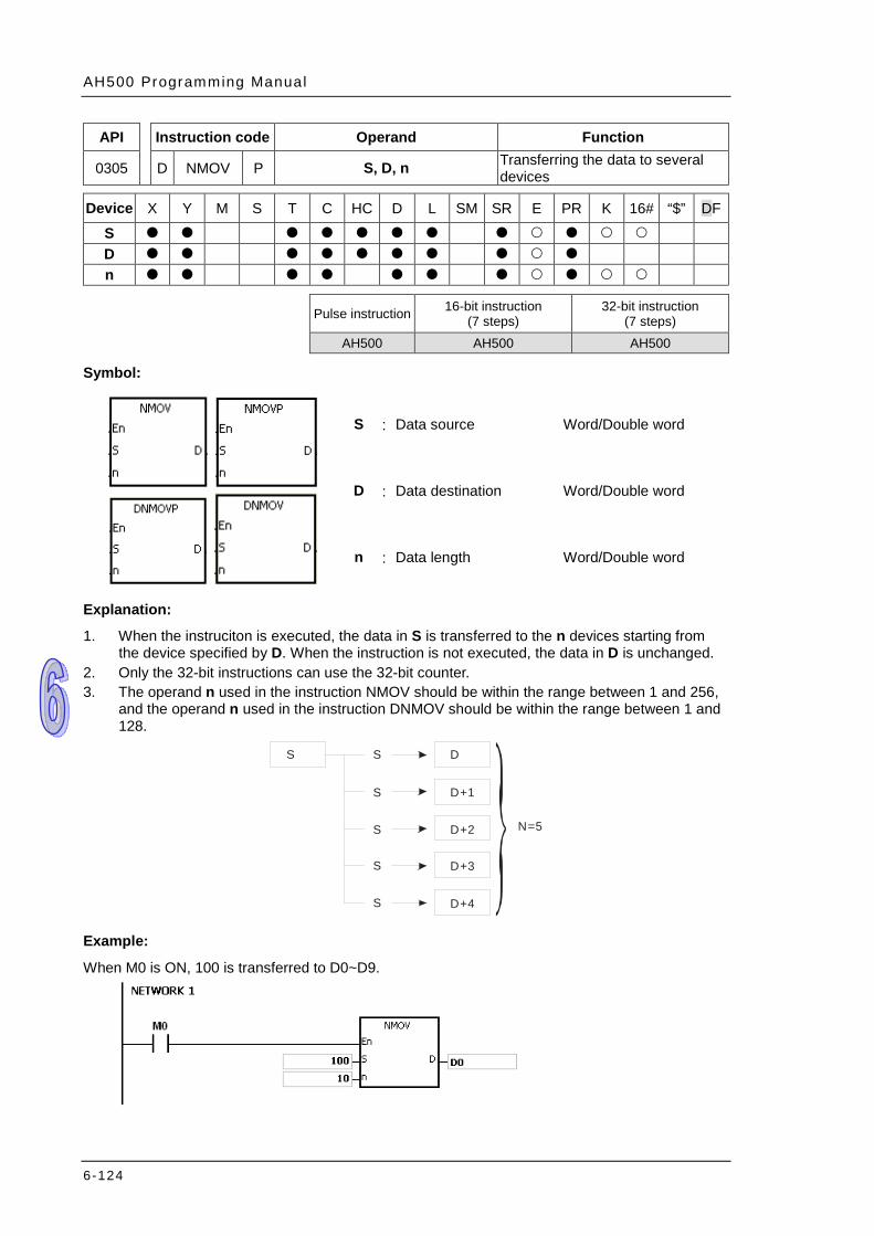
AH500 Programming Manual
6-124
API Instruction code Operand Function
0305 D NMOV P S, D, n Transferring the data to several devices
Device X Y M S T C HC D L SM SR E PR K 16# “$” DF
S D n
Pulse instruction 16-bit instruction
(7 steps) 32-bit instruction
(7 steps) AH500 AH500 AH500
Symbol:
S : Data source Word/Double word
D : Data destination Word/Double word
n : Data length Word/Double word
Explanation:
1. When the instruciton is executed, the data in S is transferred to the n devices starting from the device specified by D. When the instruction is not executed, the data in D is unchanged.
2. Only the 32-bit instructions can use the 32-bit counter. 3. The operand n used in the instruction NMOV should be within the range between 1 and 256,
and the operand n used in the instruction DNMOV should be within the range between 1 and 128.
S D
D+1
D+2
D+3
D+4
S
S
S
S
S
N=5
Example:
When M0 is ON, 100 is transferred to D0~D9.

Chapter 6 Appl ied Inst ruct ions
6-125
Additional remark:
1. If D~D+n-1 exceed the device range, the instruction is not executed, SM0 is ON, and the error code in SR0 is 16#2003.
2. If the operand n used in the 16-bit instruciton is larger than 256 or less than 1, the instruction is not executed, SM0 is ON, and the error code in SR0 is 16#200B.
3. If the operand n used in the 32-bit instruciton is larger than 128 or less than 1, the instruction is not executed, SM0 is ON, and the error code in SR0 is 16#200B.
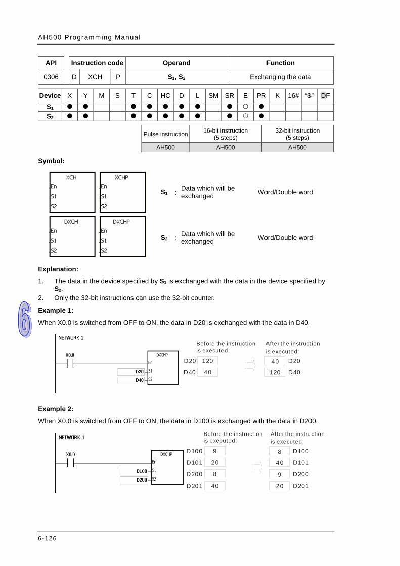
AH500 Programming Manual
6-126
API Instruction code Operand Function
0306 D XCH P S1, S2 Exchanging the data
Device X Y M S T C HC D L SM SR E PR K 16# “$” DF
S1 S2
Pulse instruction 16-bit instruction
(5 steps) 32-bit instruction
(5 steps) AH500 AH500 AH500
Symbol:
S1 : Data which will be exchanged Word/Double word
S2 : Data which will be exchanged Word/Double word
Explanation:
1. The data in the device specified by S1 is exchanged with the data in the device specified by S2.
2. Only the 32-bit instructions can use the 32-bit counter.
Example 1:
When X0.0 is switched from OFF to ON, the data in D20 is exchanged with the data in D40.
Example 2:
When X0.0 is switched from OFF to ON, the data in D100 is exchanged with the data in D200.
9
20
Before the instruction is executed:
After the instruction is executed:
8
40
D100
D101
8
40
9
20
D200
D201
D100
D101
D200
D201
D40
D20 120
40
Before the instruction is executed:
After the instruction is executed:
40
120
D20
D40
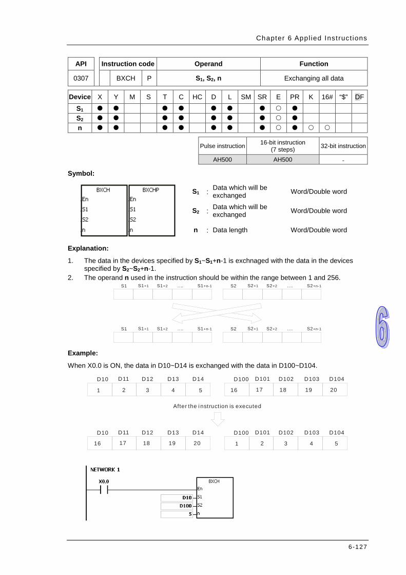
Chapter 6 Appl ied Inst ruct ions
6-127
API Instruction code Operand Function
0307 BXCH P S1, S2, n Exchanging all data
Device X Y M S T C HC D L SM SR E PR K 16# “$” DF
S1 S2 n
Pulse instruction 16-bit instruction
(7 steps) 32-bit instruction
AH500 AH500 -
Symbol:
S1 : Data which will be exchanged Word/Double word
S2 : Data which will be exchanged Word/Double word
n : Data length Word/Double word
Explanation:
1. The data in the devices specified by S1~S1+n-1 is exchnaged with the data in the devices specified by S2~S2+n-1.
2. The operand n used in the instruction should be within the range between 1 and 256. S1 S1+1 S1+2 .... S1+n-1
S1 S1+1 S1+2 .... S1+n-1
S2 S2+1 S2+2 .... S2+n-1
S2 S2+1 S2+2 .... S2+n-1
Example:
When X0.0 is ON, the data in D10~D14 is exchanged with the data in D100~D104.
D10 D11 D12 D13 D14
D10 D11 D12 D13 D14
D100 D101 D102 D103 D104
D100 D101 D102 D103 D104
1 2 3 4 5 16 17 18 19 20
16 17 18 19 20 1 2 3 4 5
After the i nstruction is executed
AH500 Programming Manual
6-128
Additional remark:
1. If S1+n-1 exceeds the device range, the instruction is not executed, SM0 is ON, and the error code in SR0 is 16#2003.
2. If S2+n-1 exceeds the device range, the instruction is not executed, SM0 is ON, and the error code in SR0 is 16#2003.
3. If the operand n used in the instruciton is larger than 256 or less than 1, the instruction is not executed, SM0 is ON, and the error code in SR0 is 16#200B.

Chapter 6 Appl ied Inst ruct ions
6-129
API Instruction code Operand Function
0308 D SWAP P S Exchange the high byte with the low byte
Device X Y M S T C HC D L SM SR E PR K 16# “$” DF
S
Pulse instruction 16-bit instruction (3 steps)
32-bit instruction (3 steps)
AH500 AH500 AH500
Symbol:
S : Data source Word/Double word
Explanation:
1. When the 16-bit instruction is executed, the data in the low byte in S is exchanged with the data in the high byte in S.
2. When the 32-bit instruction is executed, the data in the low byte of the high word in S is exchanged with the data in the high byte of the high word in S, and the data in the low byte of the low word in S is exchanged with the data in the high byte of the low word in S.
3. Only the 32-bit instructions can use the 32-bit counter.
Example 1:
When X0.0 is ON, the data in the low byte in D0 is exchanged with the data in the high byte in D0.
High byte Low byte
D0
Example 2:
When X0.0 is ON, the data in the low byte in D11 is exchanged with the data in the high byte in D11, and the data in the low byte in D10 is exchanged with the data in the high byte in D10.
High byte Low byte
D11
High byte Low byte
D10
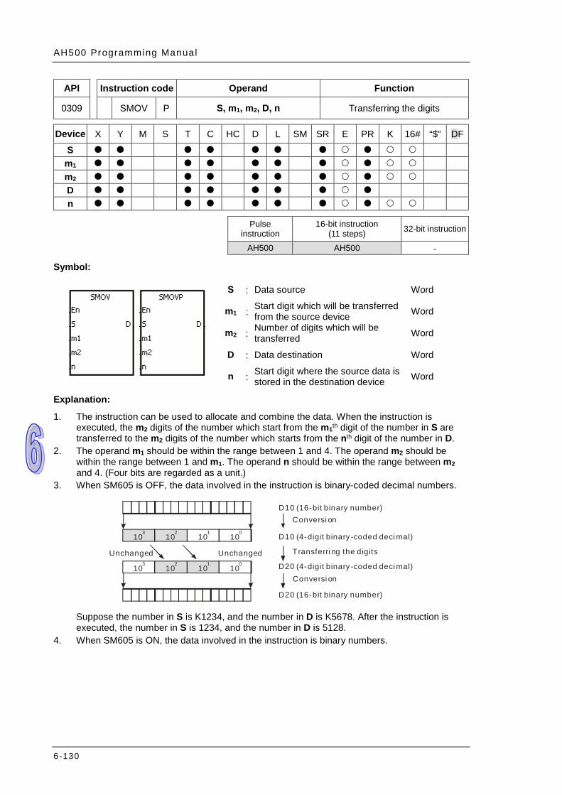
AH500 Programming Manual
6-130
API Instruction code Operand Function
0309 SMOV P S, m1, m2, D, n Transferring the digits
Device X Y M S T C HC D L SM SR E PR K 16# “$” DF
S m1 m2 D n
Pulse
instruction 16-bit instruction
(11 steps) 32-bit instruction
AH500 AH500 -
Symbol:
S : Data source Word
m1 : Start digit which will be transferred from the source device Word
m2 : Number of digits which will be transferred Word
D : Data destination Word
n : Start digit where the source data is stored in the destination device Word
Explanation:
1. The instruction can be used to allocate and combine the data. When the instruction is executed, the m2 digits of the number which start from the m1th digit of the number in S are transferred to the m2 digits of the number which starts from the nth digit of the number in D.
2. The operand m1 should be within the range between 1 and 4. The operand m2 should be within the range between 1 and m1. The operand n should be within the range between m2 and 4. (Four bits are regarded as a unit.)
3. When SM605 is OFF, the data involved in the instruction is binary-coded decimal numbers.
Suppose the number in S is K1234, and the number in D is K5678. After the instruction is executed, the number in S is 1234, and the number in D is 5128.
4. When SM605 is ON, the data involved in the instruction is binary numbers.
103
102
101
100
103
102
101
100
UnchangedUnchanged
Conversi on
Transferri ng the digits
Conversi on
D10 (16-bit binary number)
D10 (4-digit binary -coded deci mal)
D20 ( )16-bit binary number
D20 ( )4-digit binary -coded deci mal
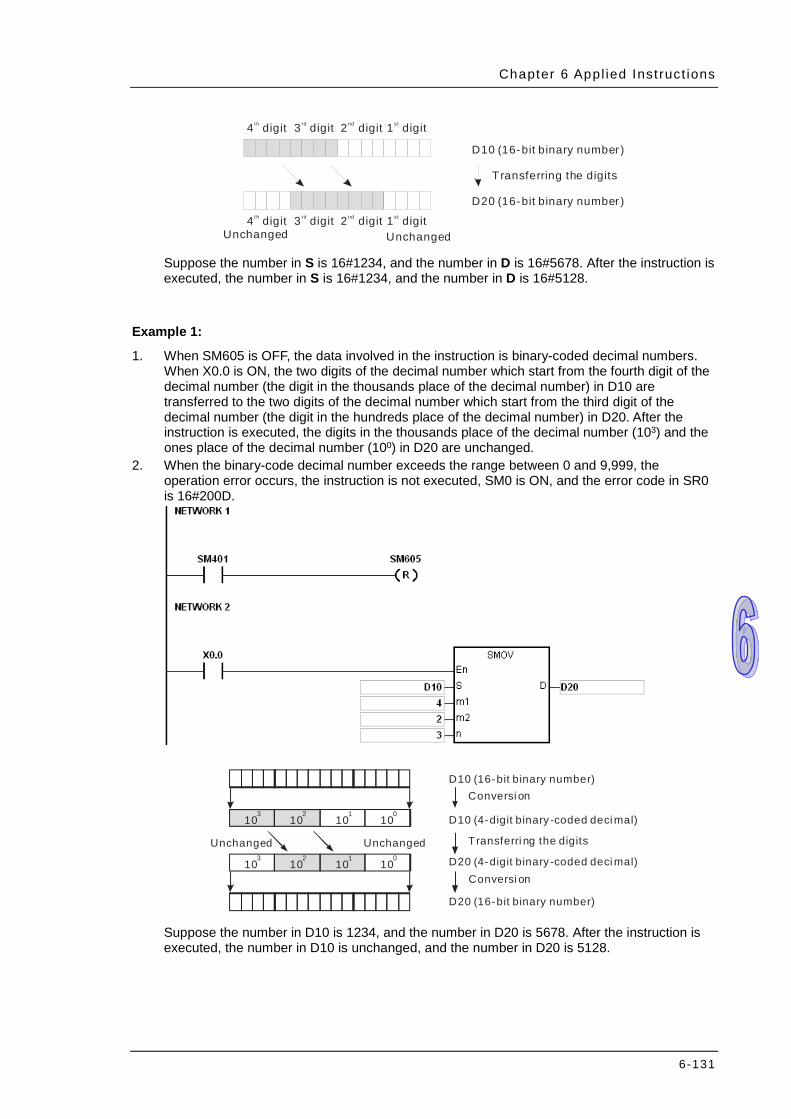
Chapter 6 Appl ied Inst ruct ions
6-131
Unchanged
Transferring the digits
D10 ( )16-bit binary number
4 digitth 3 digitrd 2 digitnd 1 digitst
4 digitth 3 digitrd 2 digitnd 1 digitst
Unchanged
D20 ( )16-bit binary number
Suppose the number in S is 16#1234, and the number in D is 16#5678. After the instruction is executed, the number in S is 16#1234, and the number in D is 16#5128.
Example 1:
1. When SM605 is OFF, the data involved in the instruction is binary-coded decimal numbers. When X0.0 is ON, the two digits of the decimal number which start from the fourth digit of the decimal number (the digit in the thousands place of the decimal number) in D10 are transferred to the two digits of the decimal number which start from the third digit of the decimal number (the digit in the hundreds place of the decimal number) in D20. After the instruction is executed, the digits in the thousands place of the decimal number (103) and the ones place of the decimal number (100) in D20 are unchanged.
2. When the binary-code decimal number exceeds the range between 0 and 9,999, the operation error occurs, the instruction is not executed, SM0 is ON, and the error code in SR0 is 16#200D.
103
102
101
100
103
102
101
100
UnchangedUnchanged
Conversi on
Transferri ng the digits
Conversi on
D10 (16-bit binary number)
D10 (4-digit binary -coded deci mal)
D20 ( )16-bit binary number
D20 ( )4-digit binary -coded deci mal
Suppose the number in D10 is 1234, and the number in D20 is 5678. After the instruction is executed, the number in D10 is unchanged, and the number in D20 is 5128.
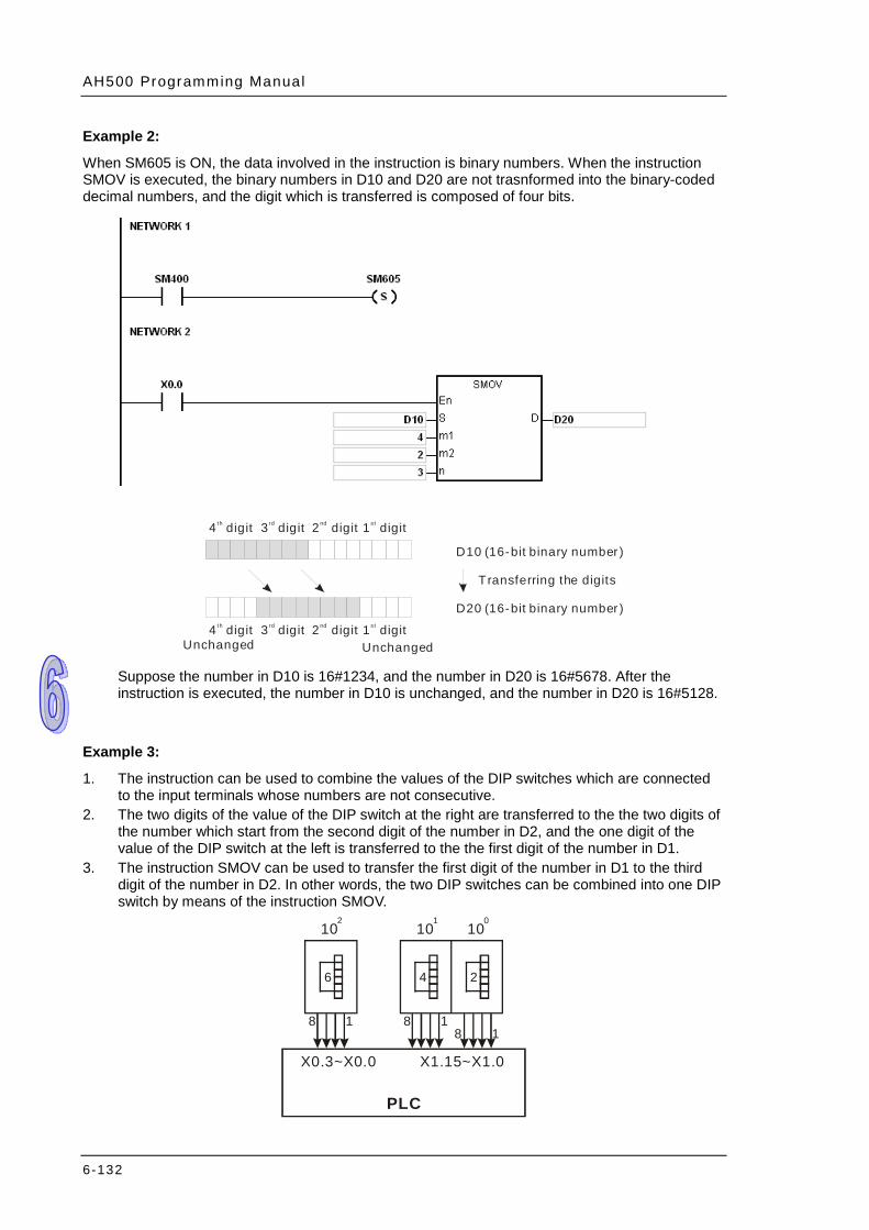
AH500 Programming Manual
6-132
Example 2:
When SM605 is ON, the data involved in the instruction is binary numbers. When the instruction SMOV is executed, the binary numbers in D10 and D20 are not trasnformed into the binary-coded decimal numbers, and the digit which is transferred is composed of four bits.
Unchanged
Transferring the digits
D10 ( )16-bit binary number
4 digitth 3 digitrd 2 digitnd 1 digitst
4 digitth 3 digitrd 2 digitnd 1 digitst
Unchanged
D20 ( )16-bit binary number
Suppose the number in D10 is 16#1234, and the number in D20 is 16#5678. After the instruction is executed, the number in D10 is unchanged, and the number in D20 is 16#5128.
Example 3:
1. The instruction can be used to combine the values of the DIP switches which are connected to the input terminals whose numbers are not consecutive.
2. The two digits of the value of the DIP switch at the right are transferred to the the two digits of the number which start from the second digit of the number in D2, and the one digit of the value of the DIP switch at the left is transferred to the the first digit of the number in D1.
3. The instruction SMOV can be used to transfer the first digit of the number in D1 to the third digit of the number in D2. In other words, the two DIP switches can be combined into one DIP switch by means of the instruction SMOV.
X0.3~X0.0 X1.15~X1.0
PLC
6 4 2
8 1 8 18 1
102
101
100
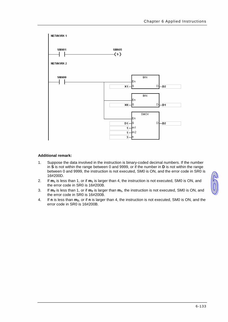
Chapter 6 Appl ied Inst ruct ions
6-133
Additional remark:
1. Suppose the data involved in the instruction is binary-coded decimal numbers. If the number in S is not within the range between 0 and 9999, or if the number in D is not within the range between 0 and 9999, the instruction is not executed, SM0 is ON, and the error code in SR0 is 16#200D.
2. If m1 is less than 1, or if m1 is larger than 4, the instruction is not executed, SM0 is ON, and the error code in SR0 is 16#200B.
3. If m2 is less than 1, or if m2 is larger than m1, the instruction is not executed, SM0 is ON, and the error code in SR0 is 16#200B.
4. If n is less than m2, or if n is larger than 4, the instruction is not executed, SM0 is ON, and the error code in SR0 is 16#200B.
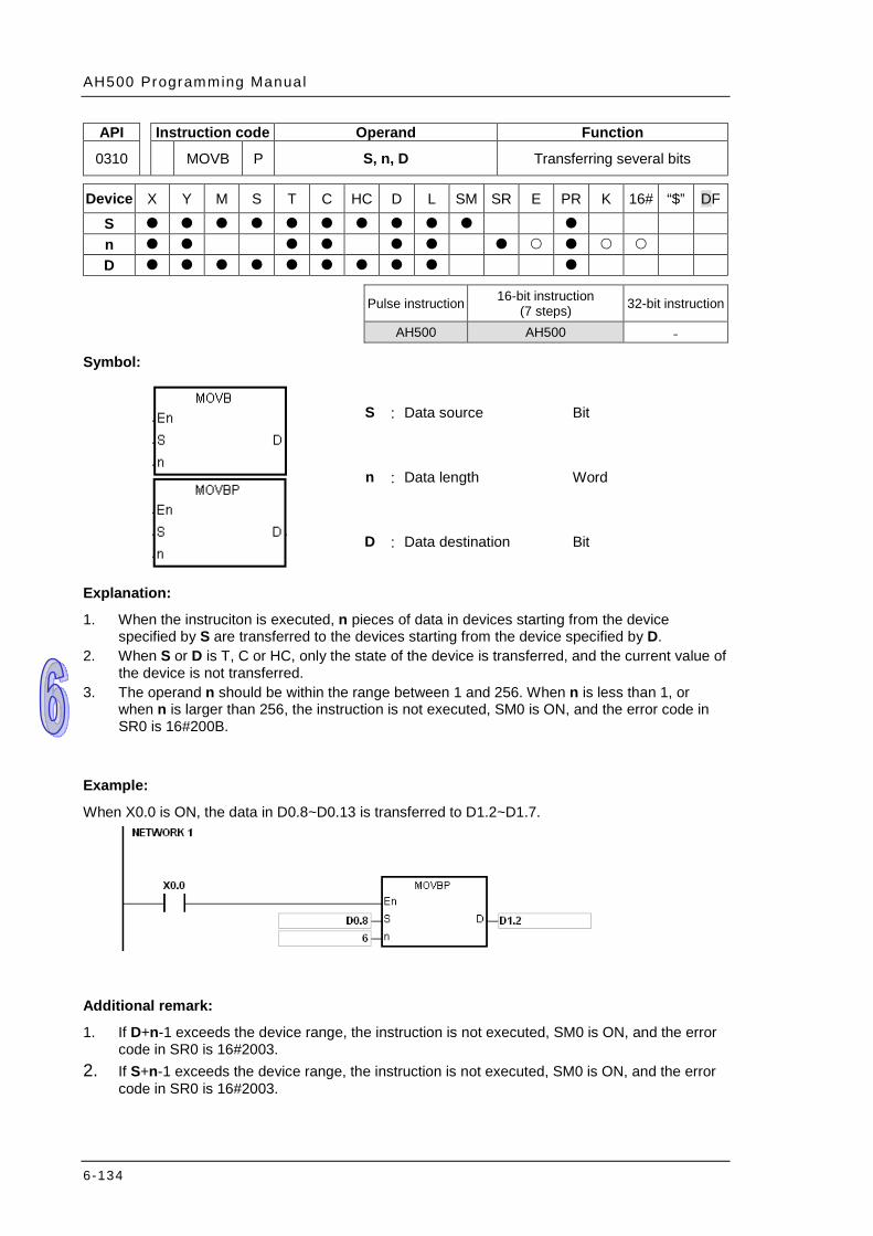
AH500 Programming Manual
6-134
API Instruction code Operand Function
0310 MOVB P S, n, D Transferring several bits
Device X Y M S T C HC D L SM SR E PR K 16# “$” DF
S n D
Pulse instruction 16-bit instruction
(7 steps) 32-bit instruction
AH500 AH500 -
Symbol:
S : Data source Bit
n : Data length Word
D : Data destination Bit
Explanation:
1. When the instruciton is executed, n pieces of data in devices starting from the device specified by S are transferred to the devices starting from the device specified by D.
2. When S or D is T, C or HC, only the state of the device is transferred, and the current value of the device is not transferred.
3. The operand n should be within the range between 1 and 256. When n is less than 1, or when n is larger than 256, the instruction is not executed, SM0 is ON, and the error code in SR0 is 16#200B.
Example:
When X0.0 is ON, the data in D0.8~D0.13 is transferred to D1.2~D1.7.
Additional remark:
1. If D+n-1 exceeds the device range, the instruction is not executed, SM0 is ON, and the error code in SR0 is 16#2003.
2. If S+n-1 exceeds the device range, the instruction is not executed, SM0 is ON, and the error code in SR0 is 16#2003.
Chapter 6 Appl ied Inst ruct ions
6-135
6.5 Jump Instructions
6.5.1 List of Jump Instructions
API Instruction code Pulse instruction Function Step 16-bit 32-bit
0400 CJ – Conditional jump 3 0401 JMP – – Unconditional jump 3 0402 GOEND – – Jumping to the end of the program 1
AH500 Programming Manual
6-136
6.5.2 Explanation of Jump Instructions
API Instruction code Operand Function
0400 CJ P S Conditional jump
Device X Y M S T C HC D L SM SR E PR K 16# “$” DF
S
Pulse instruction 16-bit instruction (3 steps) 32-bit instruction
AH500 AH500 -
Symbol:
S : Jump destination
Explanation:
1. When some part of the program in the PLC does not need to be executed, users can use CJ or CJP to shorten the scan time. Besides, when a dual output is used, users also can use CJ or CJP.
2. If the program specified by the label is prior to the instruction CJ, the watchdog timer error will occur, and the PLC will stop running. Please use the instruction carefully.
3. The instruction CJ can specify the same label repeatedly. 4. When the instruction is executed, the actions of the devices are as follows.
The state of Y, the state of M, and the state of S remain the same as those before the execution of the jump.
The timer stops counting. The general applied instructions are not executed.
Example 1:
1. When X0.0 is ON, the execution of the program jumps from address 0 to address N (LABEL1:).
2. When X0.0 is OFF, the execution of the program starts from address 0, and the instruction CJ is not executed.
Chapter 6 Appl ied Inst ruct ions
6-137
Example 2:
1. The instruction CJ between the instruction MC and the instruction MCR can be used in the five conditions below. (a) The execution of the program jumps from the part of the program outside one MC/MCR
loop to the part of the program outside another MC/MCR loop. (b) The execution of the program jumps from the part of the program outside the MC/MCR
loop to the part of the program inside the MC/MCR loop. (c) The execution of the program jumps from the part of the program inside the MC/MCR
loop to the part of the program inside the MC/MCR loop. (d) The execution of the program jumps from the part of the program inside the MC/MCR
loop to the part of the program outside the MC/MCR loop. (e) The execution of the program jumps from the part of the program inside one the
MC/MCR loop to the part of the program inside another the MC/MCR loop. 2. When the instruction MC is executed, the previous state of the switch contact is put onto the
top of the stack inside the PLC. The stack is controlled by the PLC, and can not be changed by users. When the instruction MCR is executed, the previous state of the switch contact is popped from the top of the stack. Under the conditions listed in (b), (d), and (e) above, the number of times the items are pushed onto the stack may be different from the number of times the items are popped from the stack. When this situation occurs, at most 32 items can be pushed onto the stack, and the items can be popped form the stack until the stack is empty. Therefore, when CJ or CJP is used with MC and MCR, users have to be careful of the pushing of the item onto the stack and the popping of the item from the stack.
AH500 Programming Manual
6-138
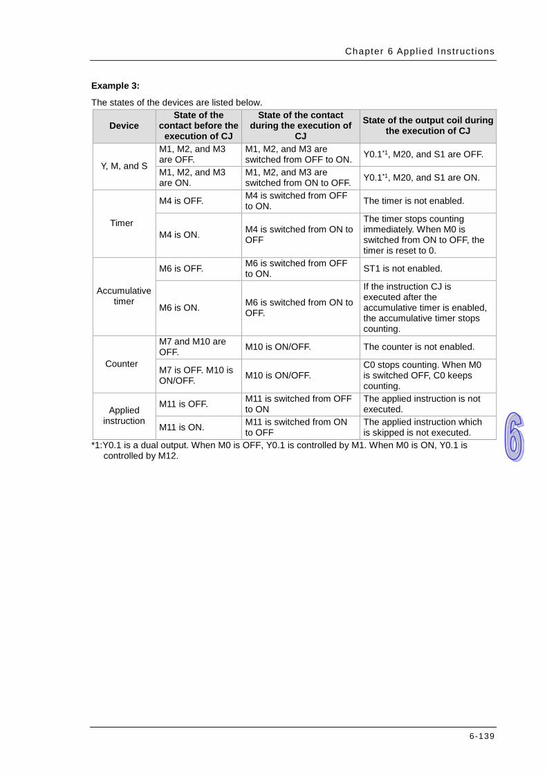
Chapter 6 Appl ied Inst ruct ions
6-139
Example 3:
The states of the devices are listed below.
Device State of the
contact before the execution of CJ
State of the contact during the execution of
CJ State of the output coil during
the execution of CJ
Y, M, and S
M1, M2, and M3 are OFF.
M1, M2, and M3 are switched from OFF to ON. Y0.1*1, M20, and S1 are OFF.
M1, M2, and M3 are ON.
M1, M2, and M3 are switched from ON to OFF. Y0.1*1, M20, and S1 are ON.
Timer
M4 is OFF. M4 is switched from OFF to ON. The timer is not enabled.
M4 is ON. M4 is switched from ON to OFF
The timer stops counting immediately. When M0 is switched from ON to OFF, the timer is reset to 0.
Accumulative timer
M6 is OFF. M6 is switched from OFF to ON. ST1 is not enabled.
M6 is ON. M6 is switched from ON to OFF.
If the instruction CJ is executed after the accumulative timer is enabled, the accumulative timer stops counting.
Counter
M7 and M10 are OFF. M10 is ON/OFF. The counter is not enabled.
M7 is OFF. M10 is ON/OFF. M10 is ON/OFF.
C0 stops counting. When M0 is switched OFF, C0 keeps counting.
Applied instruction
M11 is OFF. M11 is switched from OFF to ON
The applied instruction is not executed.
M11 is ON. M11 is switched from ON to OFF
The applied instruction which is skipped is not executed.
*1:Y0.1 is a dual output. When M0 is OFF, Y0.1 is controlled by M1. When M0 is ON, Y0.1 is controlled by M12.
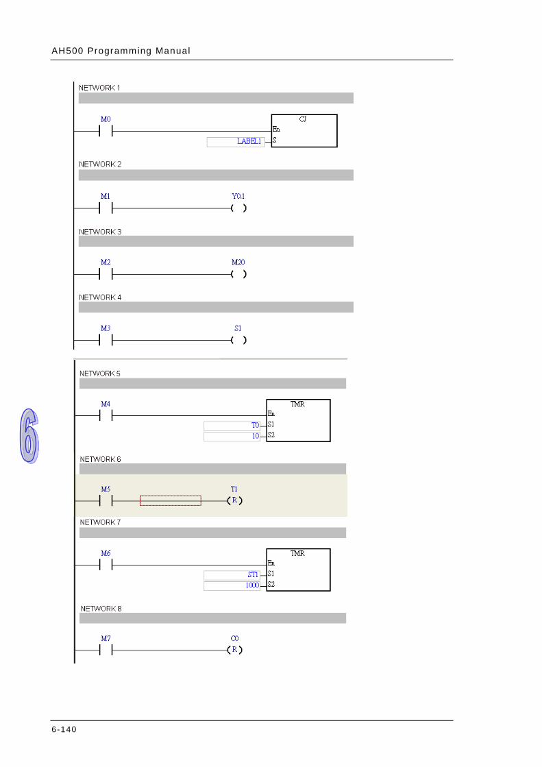
AH500 Programming Manual
6-140
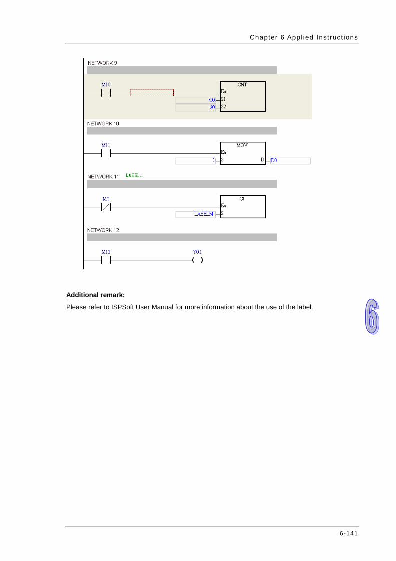
Chapter 6 Appl ied Inst ruct ions
6-141
Additional remark:
Please refer to ISPSoft User Manual for more information about the use of the label.
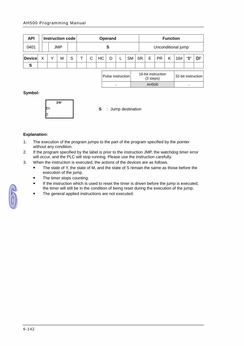
AH500 Programming Manual
6-142
API Instruction code Operand Function
0401 JMP S Unconditional jump
Device X Y M S T C HC D L SM SR E PR K 16# “$” DF
S
Pulse instruction 16-bit instruction (3 steps) 32-bit instruction
- AH500 -
Symbol:
S : Jump destination
Explanation:
1. The execution of the program jumps to the part of the program specified by the pointer without any condition.
2. If the program specified by the label is prior to the instruction JMP, the watchdog timer error will occur, and the PLC will stop running. Please use the instruction carefully.
3. When the instruction is executed, the actions of the devices are as follows. The state of Y, the state of M, and the state of S remain the same as those before the
execution of the jump. The timer stops counting. If the instruction which is used to reset the timer is driven before the jump is executed,
the timer will still be in the condition of being reset during the execution of the jump. The general applied instructions are not executed.
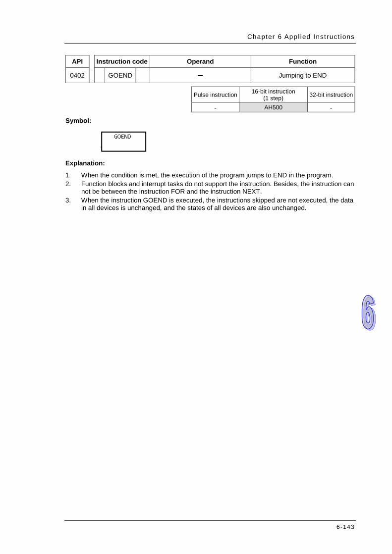
Chapter 6 Appl ied Inst ruct ions
6-143
API Instruction code Operand Function
0402 GOEND ─ Jumping to END
Pulse instruction 16-bit instruction
(1 step) 32-bit instruction
- AH500 -
Symbol:
Explanation:
1. When the condition is met, the execution of the program jumps to END in the program. 2. Function blocks and interrupt tasks do not support the instruction. Besides, the instruction can
not be between the instruction FOR and the instruction NEXT. 3. When the instruction GOEND is executed, the instructions skipped are not executed, the data
in all devices is unchanged, and the states of all devices are also unchanged.
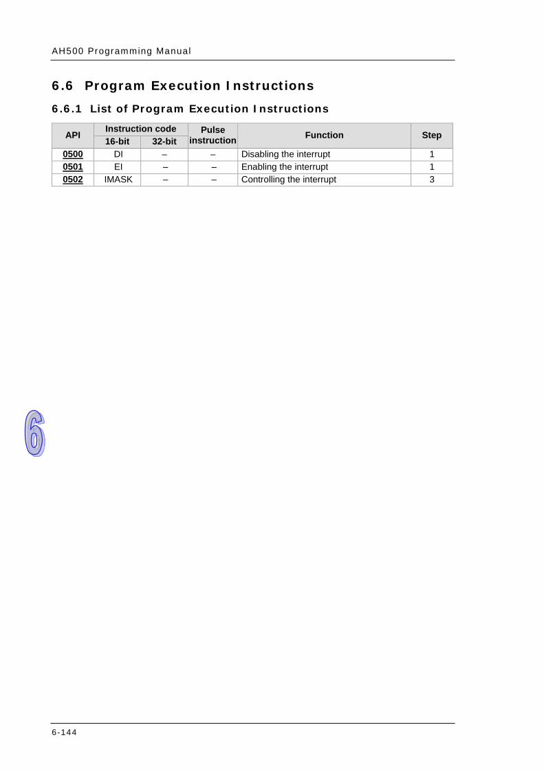
AH500 Programming Manual
6-144
6.6 Program Execution Instructions 6.6.1 List of Program Execution Instructions
API Instruction code Pulse instruction Function Step 16-bit 32-bit
0500 DI – – Disabling the interrupt 1 0501 EI – – Enabling the interrupt 1 0502 IMASK – – Controlling the interrupt 3
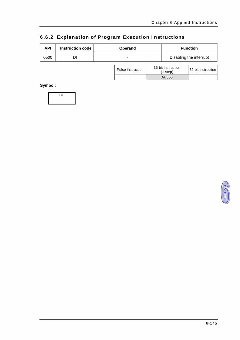
Chapter 6 Appl ied Inst ruct ions
6-145
6.6.2 Explanation of Program Execution Instructions
API Instruction code Operand Function
0500 DI - Disabling the interrupt
Pulse instruction 16-bit instruction
(1 step) 32-bit instruction
- AH500 -
Symbol:

AH500 Programming Manual
6-146
API Instruction code Operand Function
0501 EI - Enabling the interrupt
Pulse instruction 16-bit instruction
(1 step) 32-bit instruction
- AH500 -
Symbol:
Explanation:
1. The use of the instruction EI indicates that the interrupt task is allowed to be used in the program. (Please refer to section 6.6 in AH500 Operation Manual for more information about task I0~task I255.)
2. The interrupt task is allowed to be used between the instruction EI and the instruction DI in the program. When there is no part of the program in which the interrupt is disabled, users can choose not to use the instruction DI.
3. During the execution of one interrupt task, other interrupts generated will not be executed, but will be memorized. Not until the execution of the present interrupt task is complete will the next interrupt task be executed.
4. When several interrupts occur, the interrupt task which should be executed first has higher priority. When several interrupts occur simultaneously, the interrupt task whose pointer number is smaller is executed first.
5. When the interrupt task occurring between DI and EI can not be executed immediately, the interrupt request is memorized once, and the interrupt task is executed in the part of the program in which the execution of the interrupt task is allowed.
6. When the immediate I/O signal is required in the execution of the interrupt task, users can use the instruction REF in the program to refresh the state of the I/O.
Example:
If the PLC runs and the part of the program Cyclic_0 between the instruction EI and the instruction DI is scanned, the interrupt task is executed when it is enabled. When the execution of the interrupt task is complete, the main program is executed.
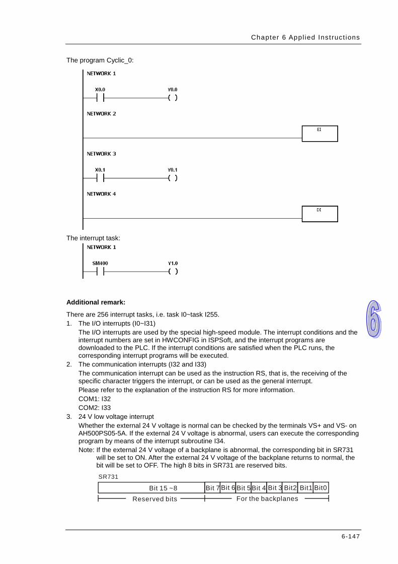
Chapter 6 Appl ied Inst ruct ions
6-147
The program Cyclic_0:
The interrupt task:
Additional remark:
There are 256 interrupt tasks, i.e. task I0~task I255. 1. The I/O interrupts (I0~I31)
The I/O interrupts are used by the special high-speed module. The interrupt conditions and the interrupt numbers are set in HWCONFIG in ISPSoft, and the interrupt programs are downloaded to the PLC. If the interrupt conditions are satisfied when the PLC runs, the corresponding interrupt programs will be executed.
2. The communication interrupts (I32 and I33) The communication interrupt can be used as the instruction RS, that is, the receiving of the specific character triggers the interrupt, or can be used as the general interrupt. Please refer to the explanation of the instruction RS for more information. COM1: I32 COM2: I33
3. 24 V low voltage interrupt Whether the external 24 V voltage is normal can be checked by the terminals VS+ and VS- on AH500PS05-5A. If the external 24 V voltage is abnormal, users can execute the corresponding program by means of the interrupt subroutine I34. Note: If the external 24 V voltage of a backplane is abnormal, the corresponding bit in SR731
will be set to ON. After the external 24 V voltage of the backplane returns to normal, the bit will be set to OFF. The high 8 bits in SR731 are reserved bits.
Bit0Bit1Bit2Bit 3Bit 4Bit 5Bit 6Bit 7Bit 15 ~8
SR731
Reserved bits For the backplanes

AH500 Programming Manual
6-148
For example: (a) If the external 24 V voltage of the local main backplane is abnormal, bit 0 in SR731 will be
set to ON. (b) If the external 24 V voltage of the first local extension backplane is abnormal, bit 1 in
SR731 will be set to ON. 4. The external interrupts (I40~I251)
If a peripheral device, e.g. a special I/O module, sends an interrupt request, the PLC will execute the specific interrupt task.
5. The timed interrupts (I252~I255) Timed interrupt 0 (I252): The default value is 100 milliseconds (1~1000 milliseconds). Timed interrupt 1 (I253): The default value is 40 milliseconds (1~1000 milliseconds). Timed interrupt 2 (I254): The default value is 20 milliseconds (1~1000 milliseconds). Timed interrupt 3 (I255): The default value is 10 milliseconds (1~1000 milliseconds). The timed interrupt task is executed every specific period of time. For example, the timed interrupt task is executed every 10 milliseconds. The priority order is a follows.
Interrupt number Description Priority order I0 I/O interrupt 0 1 I1 I/O interrupt 1 2 I2 I/O interrupt 2 3 I3 I/O interrupt 3 4 I4 I/O interrupt 4 5 I5 I/O interrupt 5 6 I6 I/O interrupt 6 7 I7 I/O interrupt 7 8 I8 I/O interrupt 8 9 I9 I/O interrupt 9 10 I10 I/O interrupt 10 11 I11 I/O interrupt 11 12 I12 I/O interrupt 12 13 I13 I/O interrupt 13 14 I14 I/O interrupt 14 15 I15 I/O interrupt 15 16 I16 I/O interrupt 16 17 I17 I/O interrupt 17 18 I18 I/O interrupt 18 19 I19 I/O interrupt 19 20 I20 I/O interrupt 20 21 I21 I/O interrupt 21 22 I22 I/O interrupt 22 23 I23 I/O interrupt 23 24 I24 I/O interrupt 24 25 I25 I/O interrupt 25 26 I26 I/O interrupt 26 27 I27 I/O interrupt 27 28 I28 I/O interrupt 28 29 I29 I/O interrupt 29 30 I30 I/O interrupt 30 31 I31 I/O interrupt 31 32 I32 Communication interrupt 33
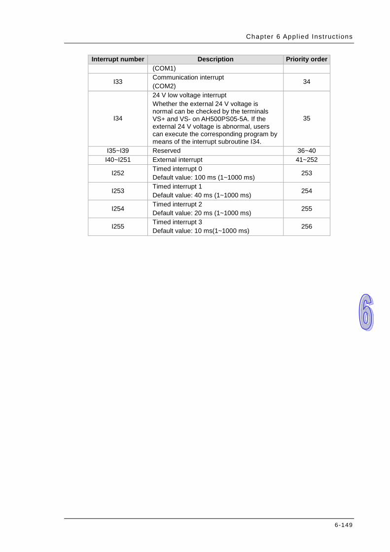
Chapter 6 Appl ied Inst ruct ions
6-149
Interrupt number Description Priority order (COM1)
I33 Communication interrupt (COM2) 34
I34
24 V low voltage interrupt Whether the external 24 V voltage is normal can be checked by the terminals VS+ and VS- on AH500PS05-5A. If the external 24 V voltage is abnormal, users can execute the corresponding program by means of the interrupt subroutine I34.
35
I35~I39 Reserved 36~40 I40~I251 External interrupt 41~252
I252 Timed interrupt 0 Default value: 100 ms (1~1000 ms) 253
I253 Timed interrupt 1 Default value: 40 ms (1~1000 ms) 254
I254 Timed interrupt 2 Default value: 20 ms (1~1000 ms) 255
I255 Timed interrupt 3 Default value: 10 ms(1~1000 ms) 256

AH500 Programming Manual
6-150
API Instruction code Operand Function
0502 IMASK S Controlling the interrupt
Device X Y M S T C HC D L SM SR E PR K 16# “$” DF
S
Pulse instruction 16-bit instruction (3 steps) 32-bit instruction
- AH500 -
Symbol:
S : Data source Word
Explanation:
1. The values of the bits in S~S+15 determine whether the interrupts are enabled or disabled. When the value of the bit is 1 and the instruction EI is executed, the corresponding interrupt is executed. When the value of the bit is 0, the corresponding interrupt can not be executed.
2. When the instruction is executed, the values in S~S+15 are transferred to SR623~SR638. 3. When the instruction is not executed, the values of the bits in SR623~SR638 determine
whether the interrupts are enabled or disabled.
I0I1I2I3I4I5I6I7I8I9I10I11I12I13I14I15
I16I17I18I19I20I21I22I23I24I25I26I27I28I29I30I31
I32I33I34I35I36I37I38I39I40I41I42I43I44I45I46I47
I48I49I50I51I52I53I54I55I56I57I58I59I60I61I62I63
I64I65I66I67I68I69I70I71I72I73I74I75I76I77I78I79
I80I81I82I83I84I85I87I88I89I90I91I92I93I94I95 I86
I96I97I98I99I100I101I103I104I105I106I107I108I109I110I111 I102 I96I97I98I99I100I101I103I104I105I106I107I108I109I110I111
I114I115I116I117I119I120I121I122I123I124I125I126I127 I118 I112I113
I130I131I132I133I135I136I137I138I139I140I141I142I143 I134 I128I129
I146I147I148I149I151I152I153I154I155I156I157I158I159 I150 I144I145
I162I163I164I165I167I168I169I170I172I173I174I175 I166 I160I161
I179I180I181I182I184I185I186I187I188I189I190I191 I183 I176I178
I195I196I197I198I200I201I202I203I204I205I206I207 I199 I192I194
I211I212I213I214I216I217I218I219I220I221I222I223 I215 I209I210
I227I228I229I230I232I233I234I235I236I237I238I239 I231 I225I226
I243I244I245I246I248I249I250I251I252I253I254I255 I247 I241I242S +15
I171
I177
I193
I208
I224
I240
S +14
S +13
S +12
S +11
S +10
S +9
S +8
S +7
S +6
S +5
S +4
S +3
S +2
S +1
S

Chapter 6 Appl ied Inst ruct ions
6-151
Additional remark:
If S~S+15 exceed the device range, the instruction is not executed, SM0 is ON, and the error code in SR0 is 16#2003.
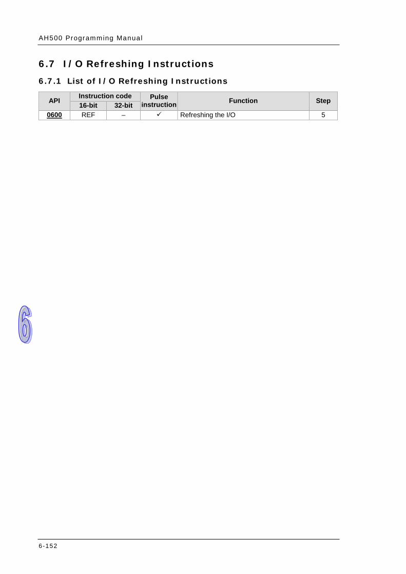
AH500 Programming Manual
6-152
6.7 I/O Refreshing Instructions 6.7.1 List of I/O Refreshing Instructions
API Instruction code Pulse instruction Function Step 16-bit 32-bit
0600 REF – Refreshing the I/O 5
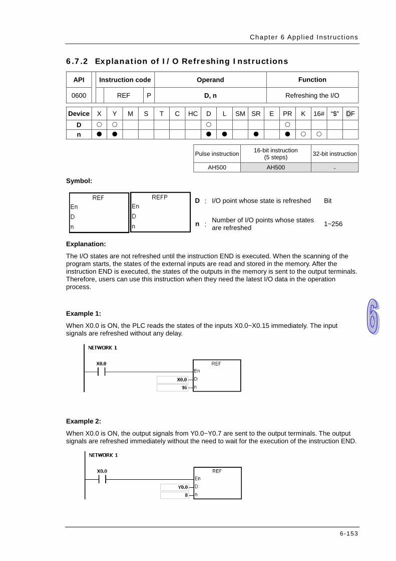
Chapter 6 Appl ied Inst ruct ions
6-153
6.7.2 Explanation of I/O Refreshing Instructions
API Instruction code Operand Function
0600 REF P D, n Refreshing the I/O
Device X Y M S T C HC D L SM SR E PR K 16# “$” DF
D n
Pulse instruction 16-bit instruction
(5 steps) 32-bit instruction
AH500 AH500 -
Symbol:
D : I/O point whose state is refreshed Bit
n : Number of I/O points whose states are refreshed 1~256
Explanation:
The I/O states are not refreshed until the instruction END is executed. When the scanning of the program starts, the states of the external inputs are read and stored in the memory. After the instruction END is executed, the states of the outputs in the memory is sent to the output terminals. Therefore, users can use this instruction when they need the latest I/O data in the operation process.
Example 1:
When X0.0 is ON, the PLC reads the states of the inputs X0.0~X0.15 immediately. The input signals are refreshed without any delay.
Example 2:
When X0.0 is ON, the output signals from Y0.0~Y0.7 are sent to the output terminals. The output signals are refreshed immediately without the need to wait for the execution of the instruction END.

AH500 Programming Manual
6-154
Additional remark:
1. If D+n-1 exceeds the device range, the instruction is not executed, SM0 is ON, and the error code in SR0 is 16#2003.
2. If n is larger than 256, or if n is less than 1, the instruction is not executed, SM0 is ON, and the error code in SR0 is 16#200B.
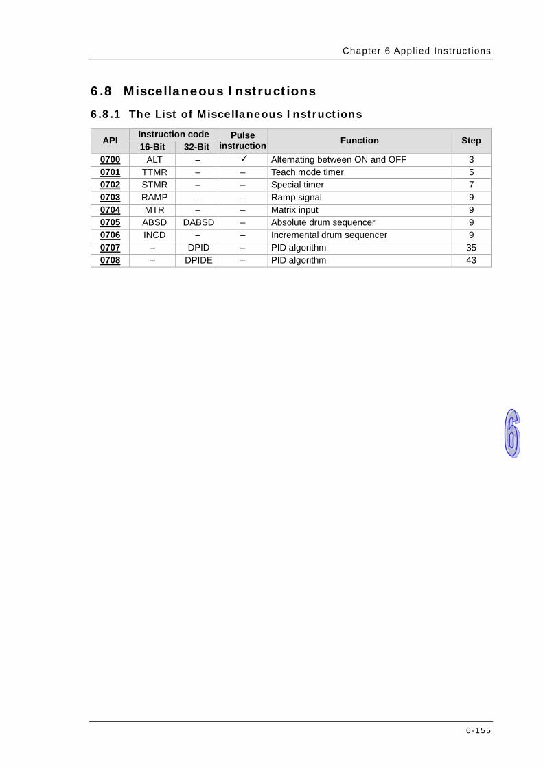
Chapter 6 Appl ied Inst ruct ions
6-155
6.8 Miscellaneous Instructions 6.8.1 The List of Miscellaneous Instructions
API Instruction code Pulse instruction Function Step 16-Bit 32-Bit
0700 ALT – Alternating between ON and OFF 3 0701 TTMR – – Teach mode timer 5 0702 STMR – – Special timer 7 0703 RAMP – – Ramp signal 9 0704 MTR – – Matrix input 9 0705 ABSD DABSD – Absolute drum sequencer 9 0706 INCD – – Incremental drum sequencer 9 0707 – DPID – PID algorithm 35 0708 – DPIDE – PID algorithm 43

AH500 Programming Manual
6-156
6.8.2 Explanation of Miscellaneous Instructions
API Instruction code Operand Function
0700 ALT P D Alternating between ON and OFF
Device X Y M S T C HC D L SM SR E PR K 16# “$” DF
D
Pulse instruction 16-Bit instruction (3 steps) 32-Bit instruction
AH500 AH500 -
Symbol:
D : Destination device Bit
Explanation:
1. When the instruction ALT is executed, the state of the device specified by D alternate between ON and OFF.
2. Generally, the pulse instruction ALTP is used.
Example 1:
When X0.0 is switched from OFF to ON for the first time, Y0.0 is ON. When X0.0 is switched from OFF to ON for the second time, Y0.0 is OFF.
Example 2:
In the beginning, M0 is OFF. Therefore, Y0.0 is ON, and Y0.1 is OFF. When X0.0 is switched from OFF to ON for the first time, M0 is ON. Therefore, Y0.1 is ON, and Y0.0 is OFF. When X0.0 is switched from OFF to ON for the second time, M0 is OFF. Therefore, Y0.0 is ON, and Y0.1 is OFF.
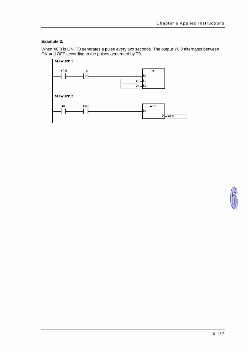
Chapter 6 Appl ied Inst ruct ions
6-157
Example 3:
When X0.0 is ON, T0 generates a pulse every two seconds. The output Y0.0 alternates between ON and OFF according to the pulses generated by T0.

AH500 Programming Manual
6-158
API Instruction code Operand Function
0701 TTMR D, n Teach mode timer
Device X Y M S T C HC D L SM SR E PR K 16# “$” DF
D n
Pulse instruction 16-Bit instruction
(5 steps) 32-Bit instruction
- AH500 -
Symbol:
D : Device in which the time is stored Word
n : Multiplier Word
Explanation:
1. A second is taken as the timing unit. The time for which the button switch has been turned ON is multiplied by n, and the product is stored in D. D+1 is for system use only. When the instruction is executed, the value in D+1 can not be altered. Otherwise, the time will be counted incorrectly.
2. When the conditional contact is ON, D is reset to 0. 3. Setting the multiplier: When n is 0, D takes a second as the timing unit. When n is 1, the time
for which the button switch has been turned ON is multiplied by 10, and D takes 100 milliseconds as the timing unit. When n is 2, the time for which the button switch has been turned ON is multiplied by 100, and D takes 10 milliseconds as the timing unit.
n D K0 (unit: 1 second) 1×T
K1 (unit: 100 milliseconds) 10×T K2 (unit: 10 milliseonds) 100×T
4. When the on-line editing is used, please reset the conditional contact to initialize the instruction.
5. The operand n should be within the range between 0 and 2.
Example 1:
1. The time for which the button switch X0.0 has been turned ON is multiplied by n, and the product is stored in D0.
2. When X0.0 is switched OFF, the value in D0 is unchanged.
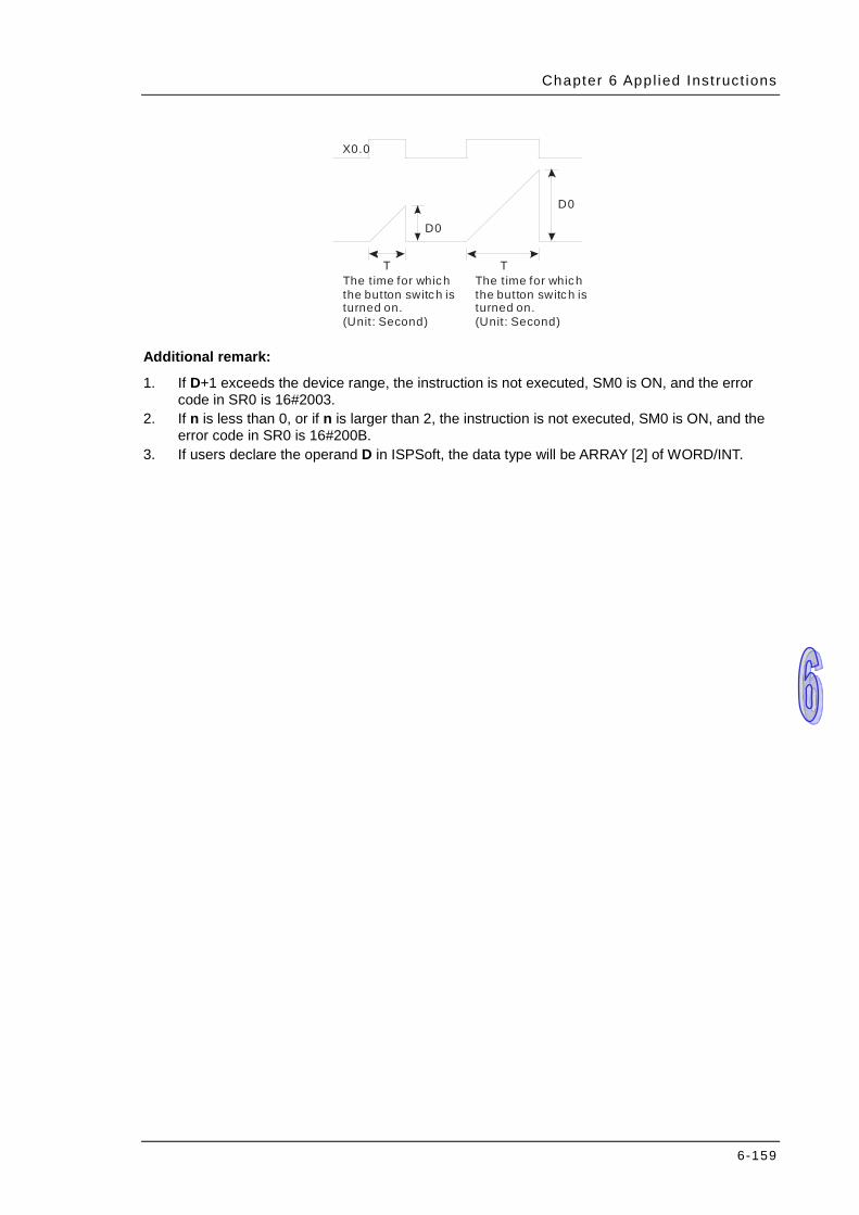
Chapter 6 Appl ied Inst ruct ions
6-159
X0.0
D0
D0
T TThe time for which the button switch is turned on. (Unit: Second)
The t ime for which the button switch is turned on. (Unit: Second)
Additional remark:
1. If D+1 exceeds the device range, the instruction is not executed, SM0 is ON, and the error code in SR0 is 16#2003.
2. If n is less than 0, or if n is larger than 2, the instruction is not executed, SM0 is ON, and the error code in SR0 is 16#200B.
3. If users declare the operand D in ISPSoft, the data type will be ARRAY [2] of WORD/INT.

AH500 Programming Manual
6-160
API Instruction code Operand Function
0702 STMR S, m, D Special timer
Device X Y M S T C HC D L SM SR E PR K 16# “$” DF
S m D
Pulse instruction 16-Bit instruction
(7 steps) 32-Bit instruction
- AH500 -
Symbol:
S : Timer number T0~T2047
m : Setting value of the timer Word
D : Output device Bit
Explanation:
1. The instruction STMR is used to generate the off-delay relay, the one-shot circuit, and the flashing circuit.
2. The timer specified by the instruction TMR takes 100 milliseconds as the timing unit. 3. The timer specified by the instruction STMR can not be used repeatedly. 4. D occupies four consecutive devices. 5. Before the instruction is executed, please reset D~D+3. 6. When the conditional contact is not enabled and the value of the device meets one of the two
conditions mentioned below, D, D+1, and D+3 are ON for m seconds before they are switched OFF. When the conditional contact is not enabled and the value of the device does not meet either of the two conditions mentioned below, D~D+3 keep OFF. The value of the timer is less than or equal to m, D is ON, and D+1 is OFF. The value of the timer is less than m, D +2 is OFF, and D, D+1, and D+3 are ON.
7. When the on-line editing is used, please reset the conditional contact to initialize the instruction.
8. The operand m should be within the range between 1 and 32767.
Example:
1. When X0.0 is ON, the instruction STMR specifies the timer T0, and the setting value of T0 is five seconds.
2. Y0.0 is the off-delay contact. When X0.0 is switched from OFF to ON, Y0.0 is ON. Five minutes after X0.0 is switched from ON to OFF, Y0.0 is OFF.
3. When X0.0 is switched from ON to OFF, Y0.0 is ON for five seconds. 4. When X0.0 is switched from OFF to ON, Y0.2 is ON for five seconds. 5. Five seconds after X0.0 is switched from OFF to ON, Y0.3 is ON. Five seconds after X0.0 is
switched from ON to OFF, Y0.3 is OFF.
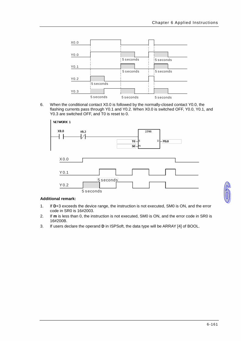
Chapter 6 Appl ied Inst ruct ions
6-161
X0.0
Y0.0
Y0.1
Y0.2
Y0.3
5 seconds 5 seconds
5 seconds 5 seconds
5 seconds
5 seconds 5 seconds 5 seconds 6. When the conditional contact X0.0 is followed by the normally-closed contact Y0.0, the
flashing currents pass through Y0.1 and Y0.2. When X0.0 is switched OFF, Y0.0, Y0.1, and Y0.3 are switched OFF, and T0 is reset to 0.
X 0.0
Y 0.1
Y 0.25 seconds
5 seconds
Additional remark:
1. If D+3 exceeds the device range, the instruction is not executed, SM0 is ON, and the error code in SR0 is 16#2003.
2. If m is less than 0, the instruction is not executed, SM0 is ON, and the error code in SR0 is 16#200B.
3. If users declare the operand D in ISPSoft, the data type will be ARRAY [4] of BOOL.
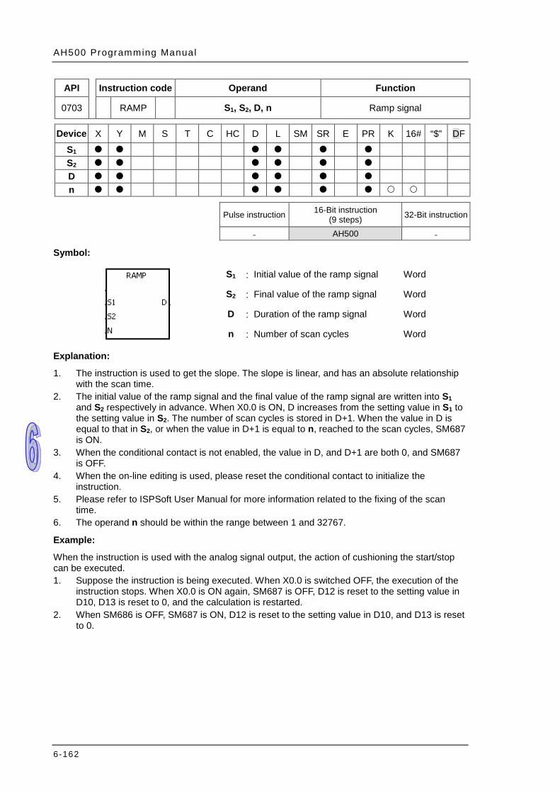
AH500 Programming Manual
6-162
API Instruction code Operand Function
0703 RAMP S1, S2, D, n Ramp signal
Device X Y M S T C HC D L SM SR E PR K 16# “$” DF
S1 S2 D n
Pulse instruction 16-Bit instruction
(9 steps) 32-Bit instruction
- AH500 -
Symbol:
S1 : Initial value of the ramp signal Word
S2 : Final value of the ramp signal Word
D : Duration of the ramp signal Word
n : Number of scan cycles Word
Explanation:
1. The instruction is used to get the slope. The slope is linear, and has an absolute relationship with the scan time.
2. The initial value of the ramp signal and the final value of the ramp signal are written into S1 and S2 respectively in advance. When X0.0 is ON, D increases from the setting value in S1 to the setting value in S2. The number of scan cycles is stored in D+1. When the value in D is equal to that in S2, or when the value in D+1 is equal to n, reached to the scan cycles, SM687 is ON.
3. When the conditional contact is not enabled, the value in D, and D+1 are both 0, and SM687 is OFF.
4. When the on-line editing is used, please reset the conditional contact to initialize the instruction.
5. Please refer to ISPSoft User Manual for more information related to the fixing of the scan time.
6. The operand n should be within the range between 1 and 32767.
Example:
When the instruction is used with the analog signal output, the action of cushioning the start/stop can be executed. 1. Suppose the instruction is being executed. When X0.0 is switched OFF, the execution of the
instruction stops. When X0.0 is ON again, SM687 is OFF, D12 is reset to the setting value in D10, D13 is reset to 0, and the calculation is restarted.
2. When SM686 is OFF, SM687 is ON, D12 is reset to the setting value in D10, and D13 is reset to 0.
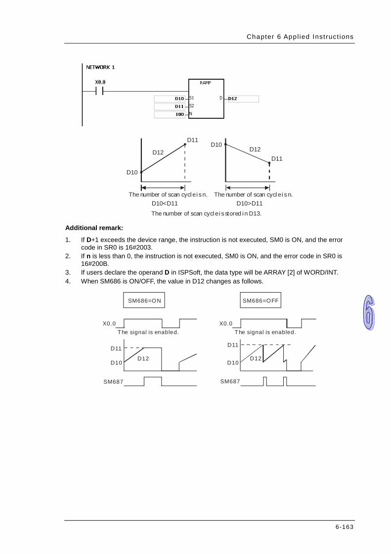
Chapter 6 Appl ied Inst ruct ions
6-163
D10
D12
D11
D11D12
D10
D10<D11 D10>D11 The number of scan cycl e i s n.
The number of scan cycl e i s stored i n D13.
The number of scan cycl e i s n.
Additional remark:
1. If D+1 exceeds the device range, the instruction is not executed, SM0 is ON, and the error code in SR0 is 16#2003.
2. If n is less than 0, the instruction is not executed, SM0 is ON, and the error code in SR0 is 16#200B.
3. If users declare the operand D in ISPSoft, the data type will be ARRAY [2] of WORD/INT. 4. When SM686 is ON/OFF, the value in D12 changes as follows.
X0.0
D11
D10D12
The signal is enabled.
SM686=ON
X0.0
D11
D10D12
SM686=OFF
SM687 SM687
The signal is enabled.
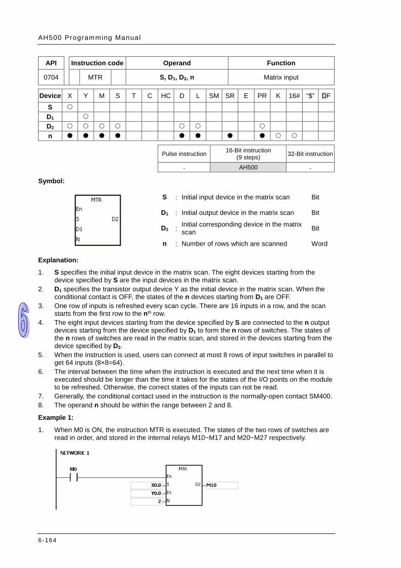
AH500 Programming Manual
6-164
API Instruction code Operand Function
0704 MTR S, D1, D2, n Matrix input
Device X Y M S T C HC D L SM SR E PR K 16# “$” DF
S D1 D2 n
Pulse instruction 16-Bit instruction
(9 steps) 32-Bit instruction
- AH500 -
Symbol:
S : Initial input device in the matrix scan Bit
D1 : Initial output device in the matrix scan Bit
D2 : Initial corresponding device in the matrix scan Bit
n : Number of rows which are scanned Word
Explanation:
1. S specifies the initial input device in the matrix scan. The eight devices starting from the device specified by S are the input devices in the matrix scan.
2. D1 specifies the transistor output device Y as the initial device in the matrix scan. When the conditional contact is OFF, the states of the n devices starting from D1 are OFF.
3. One row of inputs is refreshed every scan cycle. There are 16 inputs in a row, and the scan starts from the first row to the nth row.
4. The eight input devices starting from the device specified by S are connected to the n output devices starting from the device specified by D1 to form the n rows of switches. The states of the n rows of switches are read in the matrix scan, and stored in the devices starting from the device specified by D2.
5. When the instruction is used, users can connect at most 8 rows of input switches in parallel to get 64 inputs (8×8=64).
6. The interval between the time when the instruction is executed and the next time when it is executed should be longer than the time it takes for the states of the I/O points on the module to be refreshed. Otherwise, the correct states of the inputs can not be read.
7. Generally, the conditional contact used in the instruction is the normally-open contact SM400. 8. The operand n should be within the range between 2 and 8.
Example 1:
1. When M0 is ON, the instruction MTR is executed. The states of the two rows of switches are read in order, and stored in the internal relays M10~M17 and M20~M27 respectively.
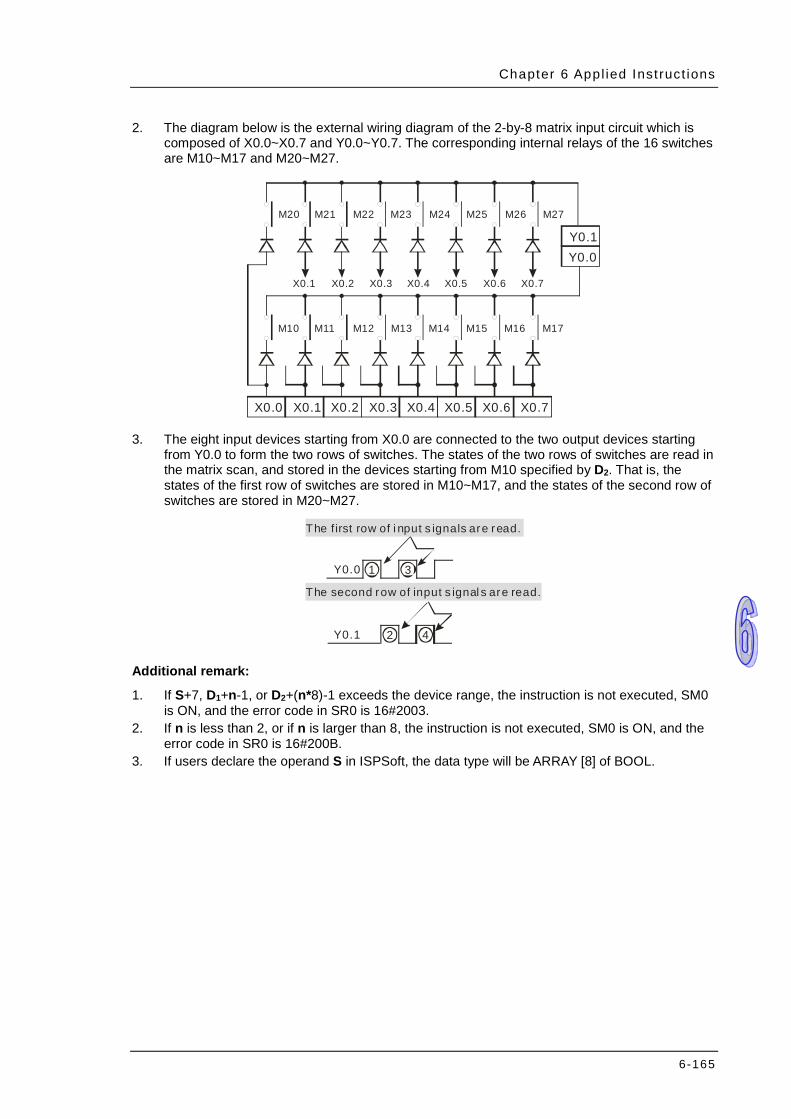
Chapter 6 Appl ied Inst ruct ions
6-165
2. The diagram below is the external wiring diagram of the 2-by-8 matrix input circuit which is composed of X0.0~X0.7 and Y0.0~Y0.7. The corresponding internal relays of the 16 switches are M10~M17 and M20~M27.
X0.0 X0.1 X0.2 X0.3 X0.4 X0.5 X0.7X0.6
Y0.0Y0.1
M10
X0.1
M20
M11 M12 M13 M14 M15 M16 M17
X0.2 X0.3 X0.4 X0.5 X0.6 X0.7
M21 M22 M23 M24 M25 M26 M27
3. The eight input devices starting from X0.0 are connected to the two output devices starting from Y0.0 to form the two rows of switches. The states of the two rows of switches are read in the matrix scan, and stored in the devices starting from M10 specified by D2. That is, the states of the first row of switches are stored in M10~M17, and the states of the second row of switches are stored in M20~M27.
2 4Y0.1
Y0.0
The first row of i nput s ignals are read.
1 3
The second row of input s ignal s are read.
Additional remark:
1. If S+7, D1+n-1, or D2+(n*8)-1 exceeds the device range, the instruction is not executed, SM0 is ON, and the error code in SR0 is 16#2003.
2. If n is less than 2, or if n is larger than 8, the instruction is not executed, SM0 is ON, and the error code in SR0 is 16#200B.
3. If users declare the operand S in ISPSoft, the data type will be ARRAY [8] of BOOL.

AH500 Programming Manual
6-166
API Instruction code Operand Function
0705 D ABSD S1, S2, D, n Absolute drum sequencer
Device X Y M S T C HC D L SM SR E PR K 16# “$” DF
S1 S2 D n
Pulse instruction 16-Bit instruction
(9 steps) 32-Bit instruction
(9 steps) - AH500 AH500
Symbol:
S1 : Initial device in the comparison Word/Double word
S2 : Comparison value Word/Double word
D : Comparison result Bit
n : Number of comparison groups Word
Explanation:
1. The instruction ABSD is used to generate multiple pulses corresponding to the current values of the counter.
2. Only the instruction DABSD can use the 32-Bit counter. 3. When the instruction ABSD is used, n should be within the range between 1 and 256. When
the instruction DABSD is used, n should be within the range between 1 and 128.
Example 1:
1. Before the instruction ABSD is executed, the instruction MOV is used to write the setting values in D100~D107. The values in the even devices are minimum values, and the values in the odd devices are maximum values.
2. When X0.0 is ON, the current value of the counter C10 is compared with the maximum values and the minimum values in D100~D107, and the comparison results are stored in M10~M13.
3. When X0.0 is OFF, the original states of M10~M13 are unchanged.
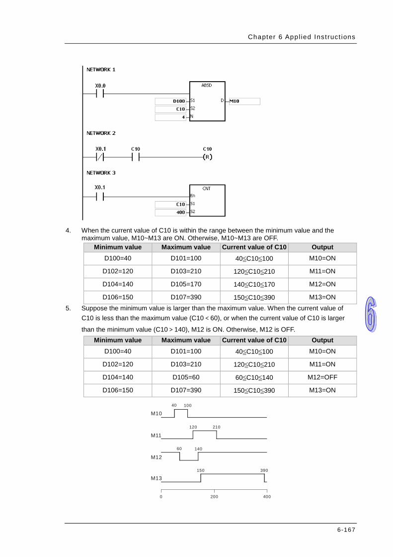
Chapter 6 Appl ied Inst ruct ions
6-167
4. When the current value of C10 is within the range between the minimum value and the
maximum value, M10~M13 are ON. Otherwise, M10~M13 are OFF. Minimum value Maximum value Current value of C10 Output
D100=40 D101=100 40≦C10≦100 M10=ON
D102=120 D103=210 120≦C10≦210 M11=ON
D104=140 D105=170 140≦C10≦170 M12=ON
D106=150 D107=390 150≦C10≦390 M13=ON 5. Suppose the minimum value is larger than the maximum value. When the current value of
C10 is less than the maximum value (C10<60), or when the current value of C10 is larger
than the minimum value (C10>140), M12 is ON. Otherwise, M12 is OFF. Minimum value Maximum value Current value of C10 Output
D100=40 D101=100 40≦C10≦100 M10=ON
D102=120 D103=210 120≦C10≦210 M11=ON
D104=140 D105=60 60≦C10≦140 M12=OFF
D106=150 D107=390 150≦C10≦390 M13=ON
4002000
40 100
120 210
60 140
150 390
M10
M11
M12
M13
AH500 Programming Manual
6-168
Additional remark:
1. If S+2*n-1 used in the instruction ABSD exceeds the device range, the instruction is not executed, SM0 is ON, and the error code in SR0 is 16#2003.
2. If S+4*n-1 used in the instruction DABSD exceeds the device range, the instruction is not executed, SM0 is ON, and the error code in SR0 is 16#2003.
3. If D+n-1 used in the instruction ABSD exceeds the device range, the instruction is not executed, SM0 is ON, and the error code in SR0 is 16#2003.
4. If D+2*n-1 used in the instruction DABSD exceeds the device range, the instruction is not executed, SM0 is ON, and the error code in SR0 is 16#2003.
5. If n used in the instruction ABSD is less than 1 or larger than 256, the instruction is not executed, SM0 is ON, and the error code in SR0 is 16#200B.
6. If n used in the instruction DABSD is less than 1 or larger than 128, the instruction is not executed, SM0 is ON, and the error code in SR0 is 16#200B.
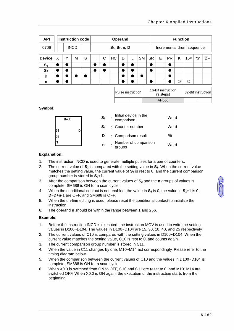
Chapter 6 Appl ied Inst ruct ions
6-169
API Instruction code Operand Function
0706 INCD S1, S2, n, D Incremental drum sequencer
Device X Y M S T C HC D L SM SR E PR K 16# “$” DF
S1 S2 D n
Pulse instruction 16-Bit instruction
(9 steps) 32-Bit instruction
- AH500 -
Symbol:
S1 : Initial device in the comparison Word
S2 : Counter number Word
D : Comparison result Bit
n : Number of comparison groups Word
Explanation:
1. The instruction INCD is used to generate multiple pulses for a pair of counters. 2. The current value of S2 is compared with the setting value in S1. When the current value
matches the setting value, the current value of S2 is rest to 0, and the current comparison group number is stored in S2+1.
3. After the comparison between the current values of S2 and the n groups of values is complete, SM688 is ON for a scan cycle.
4. When the conditional contact is not enabled, the value in S2 is 0, the value in S2+1 is 0, D~D+n-1 are OFF, and SM688 is OFF.
5. When the on-line editing is used, please reset the conditional contact to initialize the instruction.
6. The operand n should be within the range between 1 and 256.
Example:
1. Before the instruction INCD is executed, the instruction MOV is used to write the setting values in D100~D104. The values in D100~D104 are 15, 30, 10, 40, and 25 respectively.
2. The current values of C10 is compared with the setting values in D100~D104. When the current value matches the setting value, C10 is rest to 0, and counts again.
3. The current comparison group number is stored in C11. 4. When the value in C11 changes by one, M10~M14 act correspondingly. Please refer to the
timing diagram below. 5. When the comparison between the current values of C10 and the values in D100~D104 is
complete, SM688 is ON for a scan cycle. 6. When X0.0 is switched from ON to OFF, C10 and C11 are reset to 0, and M10~M14 are
switched OFF. When X0.0 is ON again, the execution of the instruction starts from the beginning.

AH500 Programming Manual
6-170
X0.0
M10
M12
M11
M13
M14
15 10 15 153030
4025
1110 0 02 3 4
C10
C11
Current value
SM688
Current value
Additional remark:
1. If S2+1 exceeds the device range, the instruction is not executed, SM0 is ON, and the error code in SR0 is 16#2003.
2. If S1+n-1 exceeds the device range, the instruction is not executed, SM0 is ON, and the error code in SR0 is 16#2003.
3. If D+n-1 exceeds the device range, the instruction is not executed, SM0 is ON, and the error code in SR0 is 16#2003.
4. If n is less than 1, or if n is larger than 256, the instruction is not executed, SM0 is ON, and the error code in SR0 is 16#200B.
5. If users declare the operand S2 in ISPSoft, the data type will be ARRAY [2] of WORD/INT.

Chapter 6 Appl ied Inst ruct ions
6-171
API Instruction code Operand Function
0707 D PID
PID_RUN, SV, PV, PID_MODE, PID_MAN, MOUT_AUTO,
CYCLE, Kp, Ki, Kd, PID_DIR, ERR_DBW, MV_MAX, MV_MIN,
MOUT, I_MV, MV
PID algorithm
Device X Y M S T C HC D L SM SR E PR K 16# “$” DF
PID_RUN SV PV
PID_MODE PID_MAN
MOUT_AUTO CYCLE
Kp Ki Kd
PID_DIR ERR_DBW MV_MAX MV_MIN MOUT I_MV MV
Pulse instruction 16-Bit instruction 32-Bit instruction
(35 steps) - - AH500
Symbol:
PID_RUN : Enabling the PID algorithm Bit
SV : Target value (SV) Double word
PV : Process value (PV) Double word
PID_MODE : PID control mode Double word
PID_MAN : PID A/M mode (PID_MAN) Bit
MOUT_AUTO : MOUT_AUTO Bit
CYCLE : Sampling time (CYCLE) Double word
Kp : Proportional gain (Kp) Double word
Ki : Integral gain (Ki) Double word
Kd : Derivative gain (Kd) Double word
PID_DIR : PID forward/reverse direction (PID_DIR) Bit
AH500 Programming Manual
6-172
ERR_DBW : Range within which the error value is count as 0 (ERR_DBW)
Double word
MV_MAX : Maximum output value (MV_MAX) Double word
MV_MIN : Minimum output value (MV_MIN) Double word
MOUT : Manual output value (MOUT) Double word
I_MV : Accumulated integral value (I_MV) Double word
MV : Output value (MV) Double word
Explanation:
1. The instruction is used to implement the PID algorithm. After the sampling time is reached, the PID algorithm is implemented. PID stands for Proportional, Integral, Derivative. The PID control is widely applied to mechanical equipments, pneumatic equipments, and electronic equipments.
2. The setting of the parameters is as follows. Device number
Data type Function Setting range Description
PID_RUN BOOL Enabling the PID algorithm
True: The PID algorithm is implemented. False: The output value (MV) is
reset to 0, and the PID algorithm is not implemented.
SV REAL SV
Range of single- precision floating- point numbers
Target value
PV REAL PV
Range of single- precision floating- point numbers
Process value
PID_MODE Double word/DINT PID control mode
0: Automatic control When PID_MAN is switched from ON to OFF, the output value (MV) then is involved in the automatic algorithm.
1: The parameters are tuned automatically for the temperature control. When the tuning of the parameters is complete, the device is automatically set to 0, and is filled in with appropriate parameters KP, KI, and KD.
2: Automatic control When PID_MAN is switched
Chapter 6 Appl ied Inst ruct ions
6-173
Device number
Data type Function Setting range Description
from ON to OFF, the MV involved in the internal algorithm is involved in the automatic algorithm. If the setting value exceeds the range, it will be counts as 0.
PID_MAN BOOL PID A/M mode
True: Manual The MV is output according to the MOUT, but it is still within the range between the MV_MIN and the MV_MAX. When PID_MODE is set to 1, the setting is ineffective.
False: Automatic The MV is output according to the PID algorithm, and the output value is within the range between MV_MIN and MV_MAX.
MOUT_AUTO BOOL MOUT automatic change mode
True: Automatic The MOUT varies with the MV.
False: Normal The MOUT deos not vary with the MV.
Cycle Double word/DINT Sampling time (TS) 1~2,000
(unit: 10ms)
When the instruction is scanned, the PID algorithm is implmented according to the sampling time, and the MV is refreshed. If TS is less than 1, it will be count as 1. If TS is larger than 2000, it will be count as 2000. When the instruction PID is used in the interval interrupt task, the sampling time is the same as the interval

AH500 Programming Manual
6-174
Device number
Data type Function Setting range Description
between the timed interrupt tasks.
Kp REAL Proportional gain (Kp)
Range of positive single- precision floating- point numbers
It is the magnified proportional value of the error between the SV and the PV. If the magnified proportional value of the error is less than 0, the Kp will be count as 0.
Ki REAL Integral gain (Ki)
Range of positive single- precision floating- point numbers
It is the integral gain (Ki). If the integral gain is less than 0, the Ki will be count as 0.
Kd REAL Derivative gain (Kd)
Range of positive single- precision floating- point numbers
It is the derivative gain (Kd). If the derivative gain is less than 0, the Kd will be count as 0.
PID_DIR BOOL PID forward/reverse direction
True: Reverse action (E=SV-PV)
False: Forward action (E=PV-SV)
ERR_DBW REAL Range within which the error value is count as 0
Range of single- precision floating- point numbers
The error value (E) is the difference between the SV and the PV. When the setting value is 0, the function is not enabled. For example, the E within the range between -5 and 5 will be count as 0 if the setting value is 5 or -5.
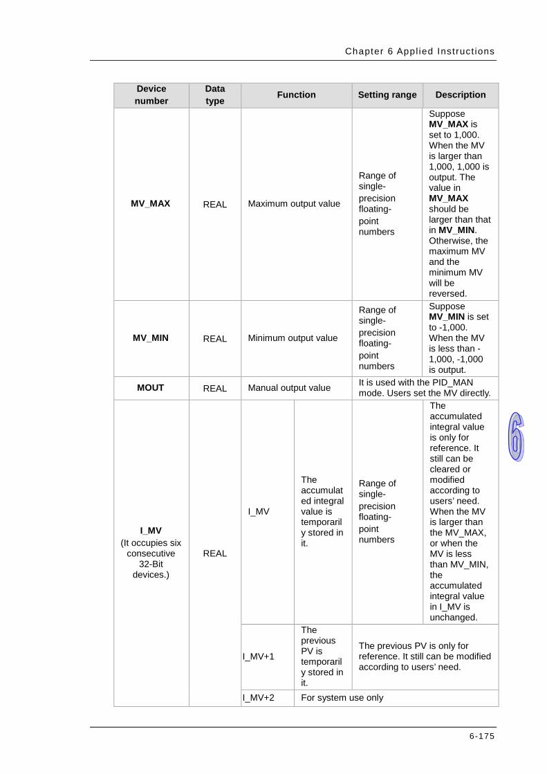
Chapter 6 Appl ied Inst ruct ions
6-175
Device number
Data type Function Setting range Description
MV_MAX REAL Maximum output value
Range of single- precision floating- point numbers
Suppose MV_MAX is set to 1,000. When the MV is larger than 1,000, 1,000 is output. The value in MV_MAX should be larger than that in MV_MIN. Otherwise, the maximum MV and the minimum MV will be reversed.
MV_MIN REAL Minimum output value
Range of single- precision floating- point numbers
Suppose MV_MIN is set to -1,000. When the MV is less than -1,000, -1,000 is output.
MOUT REAL Manual output value It is used with the PID_MAN mode. Users set the MV directly.
I_MV (It occupies six
consecutive 32-Bit
devices.)
REAL
I_MV
The accumulated integral value is temporarily stored in it.
Range of single- precision floating- point numbers
The accumulated integral value is only for reference. It still can be cleared or modified according to users’ need. When the MV is larger than the MV_MAX, or when the MV is less than MV_MIN, the accumulated integral value in I_MV is unchanged.
I_MV+1
The previous PV is temporarily stored in it.
The previous PV is only for reference. It still can be modified according to users’ need.
I_MV+2 For system use only

AH500 Programming Manual
6-176
Device number
Data type Function Setting range Description
~ I_MV+5
MV REAL MV The MV is withing the range between the MV_MIN and the MV_MAX.
Example:
1. Before the instruction PID is executed, the setting of the parameters should be complete. 2. When X0.0 is ON, the instruction is executed. When M1 is ON, the PID algorithm is
implemented. When M1 is OFF, the MV is 0, and the MV is stored in D200. When X0.0 is switched OFF, the instruction is not executed, and the previous data is unchanged.
Additional remark:
1. The instruction can be used several times, but the registers specified by I_MV~I_MV+5 can not be the same.
2. I_MV occupies 12 registers. I_MV used in the instruction PID in the above example occupies D122~D133.
3. The instruction PID only can be used in the cyclic task and the interval interrupt task. When the instruction PID is used in the interval interrupt task, the sampling time is the same as the interval between the timed interrupt tasks.
4. When the instruction is scanned, the PID algorithm is implmented according to the sampling time, and the MV is refreshed. When the instruction is used in the interrupt task, the sampling time is the same as the interval between the timed interrupt tasks. The PID algorithm is implemented according to the interval between the timed interrupt tasks.
5. Before the PID algorithm is implemented, the process value used in the instruction PID has to be a stable value. When users need the input value in the module to implement the PID algorithm, they have to notice the time it takes for the analog input to be converted into the digital input.
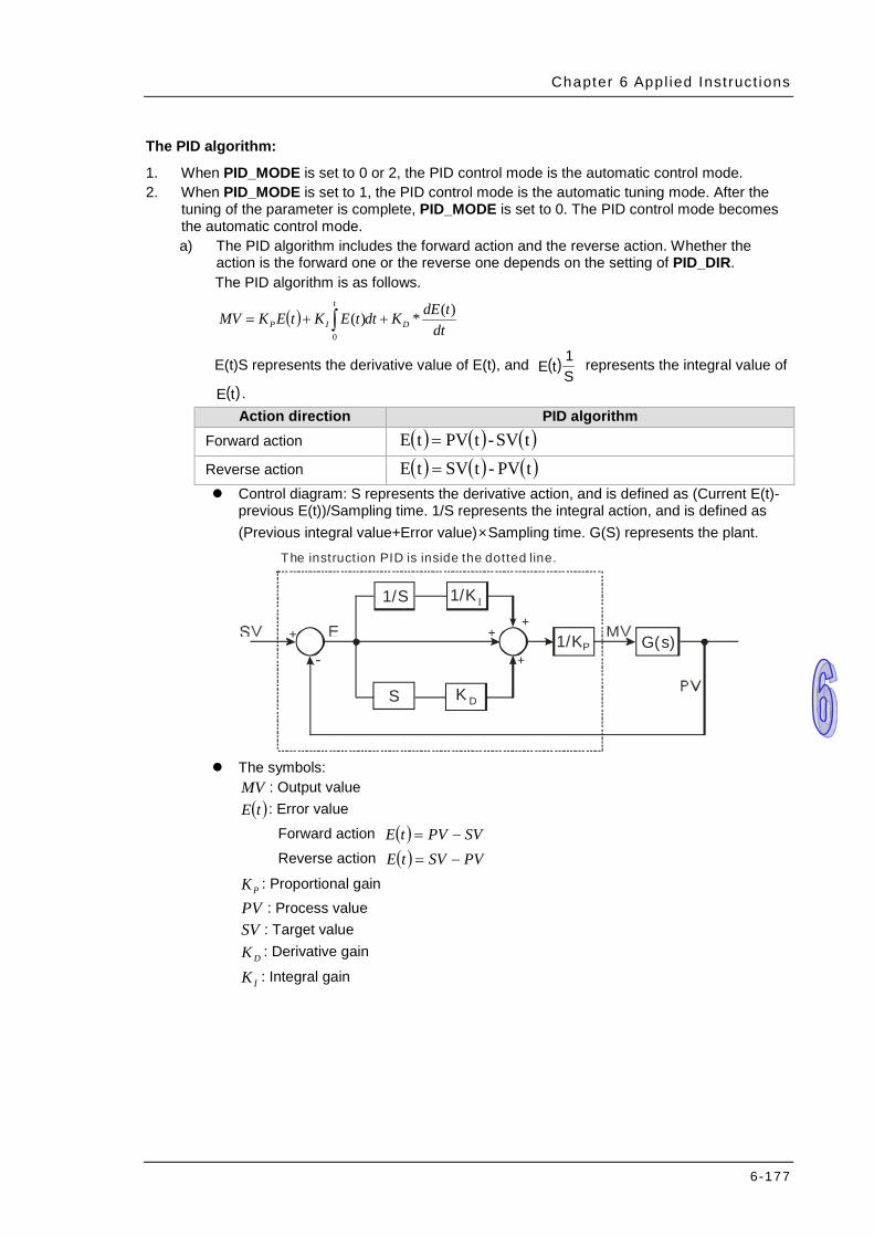
Chapter 6 Appl ied Inst ruct ions
6-177
The PID algorithm:
1. When PID_MODE is set to 0 or 2, the PID control mode is the automatic control mode. 2. When PID_MODE is set to 1, the PID control mode is the automatic tuning mode. After the
tuning of the parameter is complete, PID_MODE is set to 0. The PID control mode becomes the automatic control mode. a) The PID algorithm includes the forward action and the reverse action. Whether the
action is the forward one or the reverse one depends on the setting of PID_DIR. The PID algorithm is as follows.
( )dt
tdEKdttEKtEKMV D
t
IP)(*)(
0
++= ∫
E(t)S represents the derivative value of E(t), and ( )S1
tE represents the integral value of
( )tE . Action direction PID algorithm
Forward action ( ) ( ) ( )tSV-tPVtE =
Reverse action ( ) ( ) ( )tPV-tSVtE = Control diagram: S represents the derivative action, and is defined as (Current E(t)-
previous E(t))/Sampling time. 1/S represents the integral action, and is defined as (Previous integral value+Error value)×Sampling time. G(S) represents the plant.
G(s)
S
1/S 1/K I
K D
+ ++
-
The instruction PID is inside the dotted line.
P+
1/K
The symbols:
MV : Output value ( )tE : Error value
Forward action ( ) SVPVtE −= Reverse action ( ) PVSVtE −=
PK : Proportional gain PV : Process value SV : Target value
DK : Derivative gain
IK : Integral gain
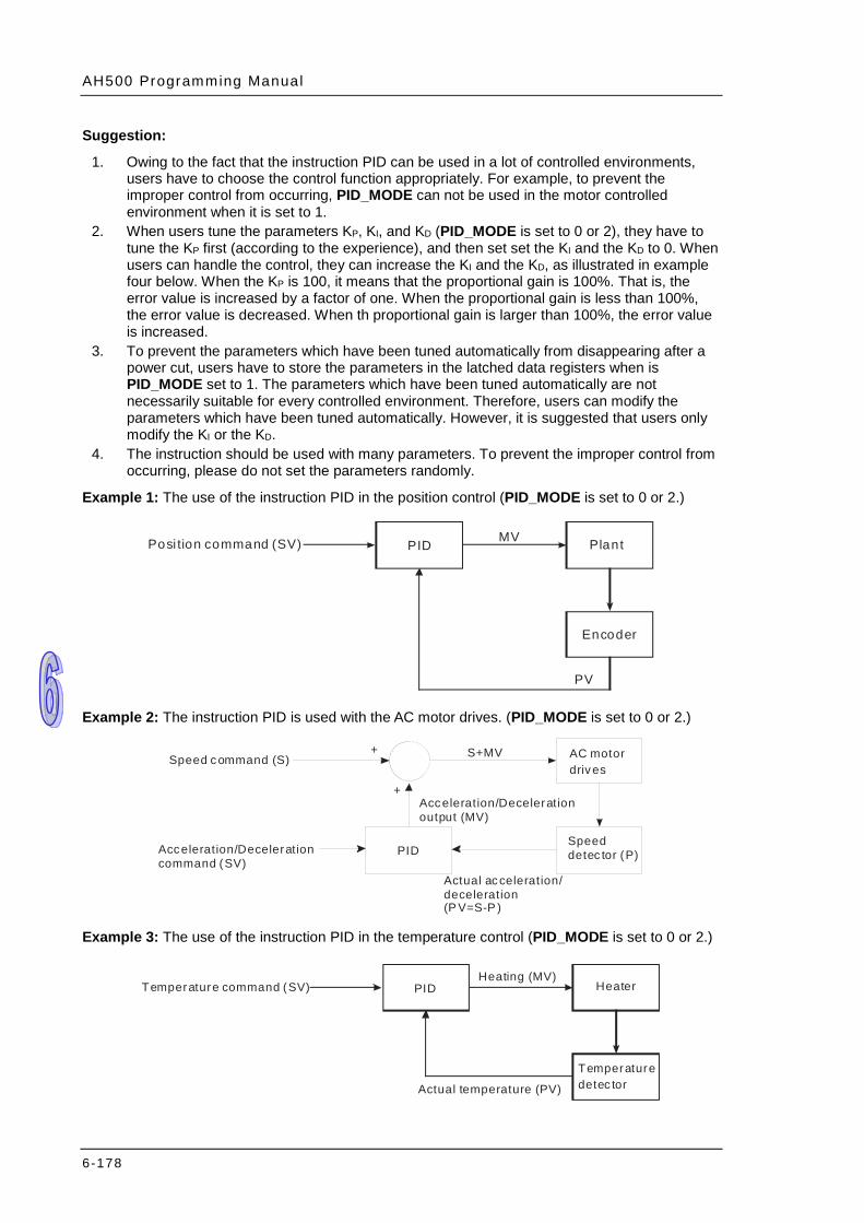
AH500 Programming Manual
6-178
Suggestion:
1. Owing to the fact that the instruction PID can be used in a lot of controlled environments, users have to choose the control function appropriately. For example, to prevent the improper control from occurring, PID_MODE can not be used in the motor controlled environment when it is set to 1.
2. When users tune the parameters KP, KI, and KD (PID_MODE is set to 0 or 2), they have to tune the KP first (according to the experience), and then set set the KI and the KD to 0. When users can handle the control, they can increase the KI and the KD, as illustrated in example four below. When the KP is 100, it means that the proportional gain is 100%. That is, the error value is increased by a factor of one. When the proportional gain is less than 100%, the error value is decreased. When th proportional gain is larger than 100%, the error value is increased.
3. To prevent the parameters which have been tuned automatically from disappearing after a power cut, users have to store the parameters in the latched data registers when is PID_MODE set to 1. The parameters which have been tuned automatically are not necessarily suitable for every controlled environment. Therefore, users can modify the parameters which have been tuned automatically. However, it is suggested that users only modify the KI or the KD.
4. The instruction should be used with many parameters. To prevent the improper control from occurring, please do not set the parameters randomly.
Example 1: The use of the instruction PID in the position control (PID_MODE is set to 0 or 2.)
Posi tion command (SV) PID MV Plant
Encoder
PV Example 2: The instruction PID is used with the AC motor drives. (PID_MODE is set to 0 or 2.)
Speed command (S)
PID
S+MV AC motor drives
Speed detec tor (P)
+
+
Acceleration/Deceleration command (SV)
Acceleration/Deceleration output (MV)
Actual acceleration/deceleration(P V=S-P )
Example 3: The use of the instruction PID in the temperature control (PID_MODE is set to 0 or 2.)
Temperature command (SV) PIDHeating (MV)
Heater
Actual temperature (PV)Temperature detec tor
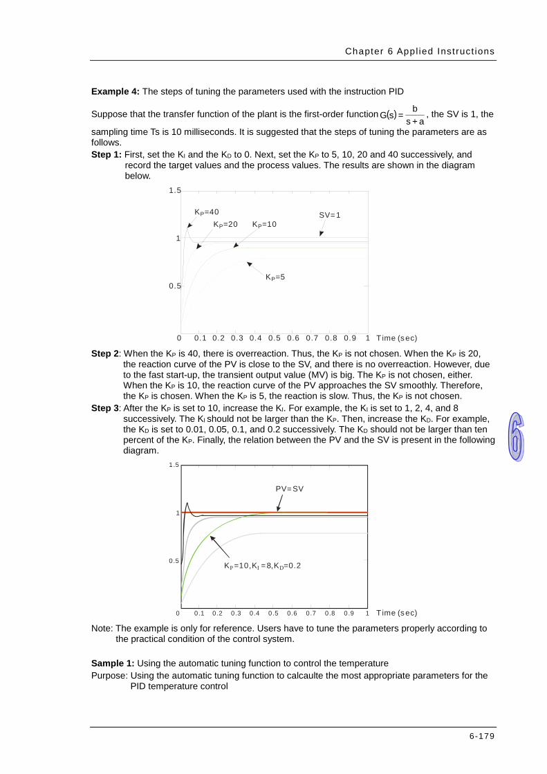
Chapter 6 Appl ied Inst ruct ions
6-179
Example 4: The steps of tuning the parameters used with the instruction PID
Suppose that the transfer function of the plant is the first-order function ( )a+s
b=sG , the SV is 1, the
sampling time Ts is 10 milliseconds. It is suggested that the steps of tuning the parameters are as follows. Step 1: First, set the KI and the KD to 0. Next, set the KP to 5, 10, 20 and 40 successively, and
record the target values and the process values. The results are shown in the diagram below.
1.5
1
0.5
0 0.1 0.2 0.3 0.4 0.5 0.6 0.7 0.8 0.9 1 Time (sec)
K =40P
K =20P K =10P
SV= 1
K =5P
Step 2: When the KP is 40, there is overreaction. Thus, the KP is not chosen. When the KP is 20,
the reaction curve of the PV is close to the SV, and there is no overreaction. However, due to the fast start-up, the transient output value (MV) is big. The KP is not chosen, either. When the KP is 10, the reaction curve of the PV approaches the SV smoothly. Therefore, the KP is chosen. When the KP is 5, the reaction is slow. Thus, the KP is not chosen.
Step 3: After the KP is set to 10, increase the KI. For example, the KI is set to 1, 2, 4, and 8 successively. The KI should not be larger than the KP. Then, increase the KD. For example, the KD is set to 0.01, 0.05, 0.1, and 0.2 successively. The KD should not be larger than ten percent of the KP. Finally, the relation between the PV and the SV is present in the following diagram.
1.5
1
0.5
0 0.1 0.2 0.3 0.4 0.5 0.6 0.7 0.8 0.9 1 Time (sec)
PV= SV
K =10,K = 8,K =0.2P I D
Note: The example is only for reference. Users have to tune the parameters properly according to
the practical condition of the control system. Sample 1: Using the automatic tuning function to control the temperature Purpose: Using the automatic tuning function to calcaulte the most appropriate parameters for the
PID temperature control
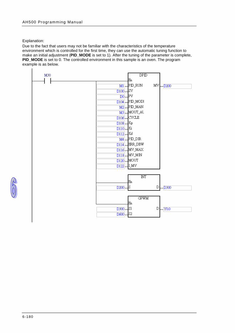
AH500 Programming Manual
6-180
Explanation: Due to the fact that users may not be familiar with the characteristics of the temperature environment which is controlled for the first time, they can use the automatic tuning function to make an initial adjustment (PID_MODE is set to 1). After the tuning of the parameter is complete, PID_MODE is set to 0. The controlled environment in this sample is an oven. The program example is as below.
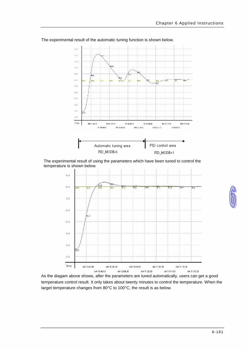
Chapter 6 Appl ied Inst ruct ions
6-181
The experimental result of the automatic tuning function is shown below.
The experimental result of using the parameters which have been tuned to control the temperature is shown below.
As the diagam above shows, after the parameters are tuned automatically, users can get a good temperature control result. It only takes about twenty minutes to control the temperature. When the target temperature changes from 80°C to 100°C, the result is as below.
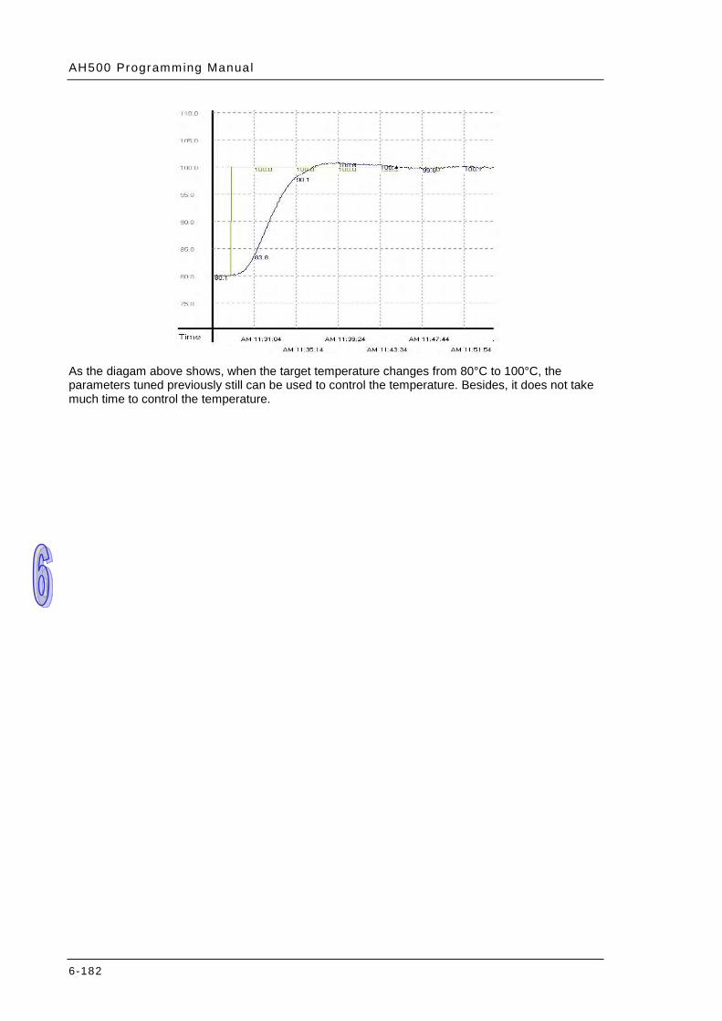
AH500 Programming Manual
6-182
As the diagam above shows, when the target temperature changes from 80°C to 100°C, the parameters tuned previously still can be used to control the temperature. Besides, it does not take much time to control the temperature.
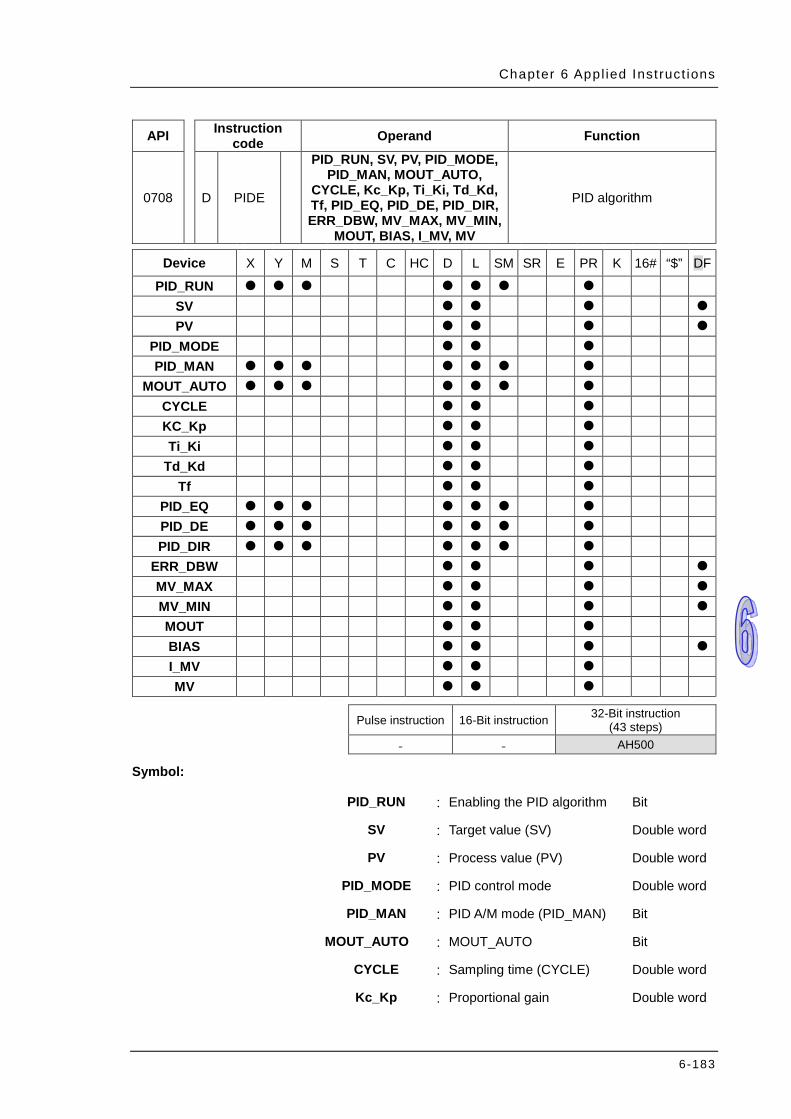
Chapter 6 Appl ied Inst ruct ions
6-183
API Instruction code Operand Function
0708 D PIDE
PID_RUN, SV, PV, PID_MODE, PID_MAN, MOUT_AUTO,
CYCLE, Kc_Kp, Ti_Ki, Td_Kd, Tf, PID_EQ, PID_DE, PID_DIR, ERR_DBW, MV_MAX, MV_MIN,
MOUT, BIAS, I_MV, MV
PID algorithm
Device X Y M S T C HC D L SM SR E PR K 16# “$” DF
PID_RUN SV PV
PID_MODE PID_MAN
MOUT_AUTO CYCLE KC_Kp Ti_Ki
Td_Kd Tf
PID_EQ PID_DE PID_DIR
ERR_DBW MV_MAX MV_MIN MOUT BIAS I_MV MV
Pulse instruction 16-Bit instruction 32-Bit instruction
(43 steps) - - AH500
Symbol:
PID_RUN : Enabling the PID algorithm Bit
SV : Target value (SV) Double word
PV : Process value (PV) Double word
PID_MODE : PID control mode Double word
PID_MAN : PID A/M mode (PID_MAN) Bit
MOUT_AUTO : MOUT_AUTO Bit
CYCLE : Sampling time (CYCLE) Double word
Kc_Kp : Proportional gain Double word
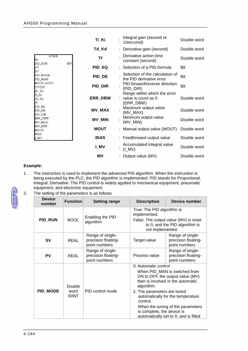
AH500 Programming Manual
6-184
Ti_Ki : Integral gain (second or 1/seccond) Double word
Td_Kd : Derivative gain (second) Double word
Tf : Derivative action time constant (second) Double word
PID_EQ : Selection of a PID formula Bit
PID_DE : Selection of the calculation of the PID derivative error Bit
PID_DIR : PID forward/reverse direction (PID_DIR) Bit
ERR_DBW : Range within which the error value is count as 0 (ERR_DBW)
Double word
MV_MAX : Maximum output value (MV_MAX) Double word
MV_MIN : Minimum output value (MV_MIN) Double word
MOUT : Manual output value (MOUT) Double word
BIAS : Feedforward output value Double word
I_MV : Accumulated integral value (I_MV) Double word
MV : Output value (MV) Double word
Example:
1. The instruction is used to implement the advanced PID algorithm. When the instruction is being executed by the PLC, the PID algorithm is implemented. PID stands for Proportional, Integral, Derivative. The PID control is widely applied to mechanical equipment, pneumatic equipment, and electronic equipment.
2. The setting of the parameters is as follows. Device number Function Setting range Description Device number
PID_RUN BOOL Enabling the PID algorithm
True: The PID algorithm is implemented. False: The output value (MV) is reset
to 0, and the PID algorithm is not implemented.
SV REAL Range of single-precision floating-point numbers
Target value Range of single-precision floating-point numbers
PV REAL Range of single-precision floating-point numbers
Process value Range of single-precision floating-point numbers
PID_MODE Double word /DINT
PID control mode
0: Automatic control When PID_MAN is switched from ON to OFF, the output value (MV) then is involved in the automatic algorithm.
1: The parameters are tuned automatically for the temperature control. When the tuning of the parameters is complete, the device is automatically set to 0, and is filled
Chapter 6 Appl ied Inst ruct ions
6-185
Device number Function Setting range Description Device number
in with appropriate parameters Kc_Kp, Ti_Ki, Td_Kd and Tf.
PID_MAN BOOL PID A/M mode
True: Manual The MV is output according to the MOUT, but it is still within the range between the MV_MIN and the MV_MAX. When PID_MODE is set to 1, the setting is ineffective.
False: Automatic The MV is output according to the PID algorithm, and the output value is within the range between MV_MIN and MV_MAX.
MOUT_AUTO BOOL MOUT automatic
change mode
True: Automatic The MOUT varies with the MV.
False: Normal The MOUT deos not vary with the MV.
CYCLE Double word/ DINT
Sampling time (TS) 1~40,000 (unit: ms)
When the instruction is scanned, the PID algorithm is implmented according to the sampling time, and the MV is refreshed. (PLC will not use the setting value to determine the time or to operate automatically. ) If TS is less than 1, it will be counted as 1. If TS is larger than 40,000, it will be counted as 40,000. When the instruction PID is used in the interval interrupt task, the sampling time is the same as the interval between the timed interrupt tasks.
Kc_Kp REAL
Proportional gain (Kc or Kp) (The selection of Kc or Kp depends on the setting of the parameter PID_EQ.)
Range of positive single precision floating-point values
It is a proportional gain. If a proportional gain is less than 0, Kc_Kp will be count as 0. If Kc_Kp is equal to
AH500 Programming Manual
6-186
Device number Function Setting range Description Device number
0 when the independent formula is used, the proportional control is not used.
Ti_Ki REAL
Integral gain (Ti or Ki) (The selection of Ti or Ki depends on the setting of the parameter PID_EQ.)
Range of positive single precision floating-point values (Unit: Ti=Second; Ki=1/second)
It is an integral gain. If an integral gain is less than 0, Ti_Ki will be count as 0. If Ti_Ki is equal to 0, the integral control is not used.
Td_Kd REAL
Derivative gain (Td or Kd) (The selection of Td or Kd depends on the setting of the parameter PID_EQ.)
Range of positive single precision floating-point values (Unit: Second)
It is a derivative gain. If a derivative gain is less than 0, Td_Kd will be count as 0. If Td_Kd is equal to 0, the derivative control is not used.
Tf REAL Derivative action time constant (Tf)
Range of positive single precision floating-point values (Unit: Second)
It the derivative action time constant. If the derivative action time constant is less than 0, Tf will be count as 0. If Tf is equal to 0, the derivative action time control is not used. (Derivative smoothing)
PID_EQ BOOL Selection of a PID formula
TRUE:Dependent Formula
FALSE:Independent Formula
PID_DE BOOL Selection of the calculation of the PID derivative error
True: Using the variations in the PV to calculate the control value of the derivative (Derivative of the PV) False: Using the variations in the error (E) to calculate the control value of the derivative (Derivative of the error)
PID_DIR BOOL PID forward/reverse direction
True: Reverse action (E=SV-PV) False: Forward action (E=PV-SV)
ERR_DBW REAL Range within which the error value is counted as 0
Range of single-precision floating-point numbers
An error (E) is equal to SV−PV or PV-SV. If the setting value is 0, the function will not be enabled, otherwise the CPU module will check whether the
Chapter 6 Appl ied Inst ruct ions
6-187
Device number Function Setting range Description Device number
present error is less than the absolute value of ERR_DBW, and check whether the present error meets the cross status condition. If the present error is less than the absolute value of ERR_DBW, and meets the cross status condition, the present error will be count as 0, and the PID algorithm will be implemented, otherwise the present error will be brought into the PID algorithm according to the normal processing.
MV_MAX REAL Maximum output value
Range of single-precision floating-point values
Example: After MV_MAX is set to 1,000, an MV will be 1,000 if it exceeds 1,000. MV_MAX has to be greater than MV_MIN, otherwise the maximum output value set and the minimum output value set will be interchanged.
MV_MIN REAL Minimum output value
Range of single-precision floating-point values
Example: After MV_MIN is set to - 1,000, an MV will be - 1,000 if it is less than than -1,000. MV_MIN has to be lessthan MV_MAX, otherwise the maximum output value set and the minimum output value set will be interchanged.
MOUT REAL Manual output value Range of single-precision
Mout and PID_MAN are
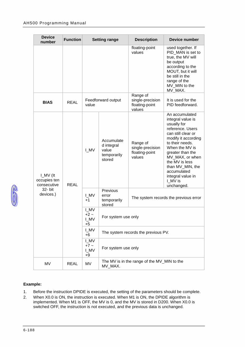
AH500 Programming Manual
6-188
Device number Function Setting range Description Device number
floating-point values
used together. If PID_MAN is set to true, the MV will be output according to the MOUT, but it will be still in the range of the MV_MIN to the MV_MAX.
BIAS REAL Feedforward output value
Range of single-precision floating-point values
It is used for the PID feedforward.
I_MV (It occupies ten consecutive
32- bit devices.)
REAL
I_MV
Accumulated integral value temporarily stored
Range of single-precision floating-point values
An accumulated integral value is usually for reference. Users can still clear or modify it according to their needs. When the MV is greater than the MV_MAX, or when the MV is less than MV_MIN, the accumulated integral value in I_MV is unchanged.
I_MV+1
Previous error temporarily stored
The system records the previous error
I_MV+2 ~ I_MV+5
For system use only
I_MV+6 The system records the previous PV.
I_MV+7 ~ I_MV+9
For system use only
MV REAL MV The MV is in the range of the MV_MIN to the MV_MAX.
Example:
1. Before the instruction DPIDE is executed, the setting of the parameters should be complete. 2. When X0.0 is ON, the instruction is executed. When M1 is ON, the DPIDE algorithm is
implemented. When M1 is OFF, the MV is 0, and the MV is stored in D200. When X0.0 is switched OFF, the instruction is not executed, and the previous data is unchanged.
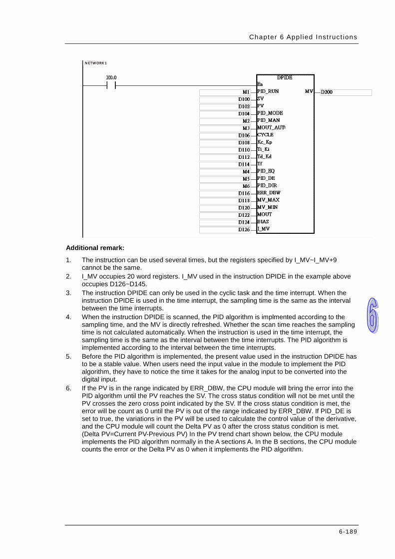
Chapter 6 Appl ied Inst ruct ions
6-189
N ETWORK 1
Additional remark:
1. The instruction can be used several times, but the registers specified by I_MV~I_MV+9 cannot be the same.
2. I_MV occupies 20 word registers. I_MV used in the instruction DPIDE in the example above occupies D126~D145.
3. The instruction DPIDE can only be used in the cyclic task and the time interrupt. When the instruction DPIDE is used in the time interrupt, the sampling time is the same as the interval between the time interrupts.
4. When the instruction DPIDE is scanned, the PID algorithm is implmented according to the sampling time, and the MV is directly refreshed. Whether the scan time reaches the sampling time is not calculated automatically. When the instruction is used in the time interrupt, the sampling time is the same as the interval between the time interrupts. The PID algorithm is implemented according to the interval between the time interrupts.
5. Before the PID algorithm is implemented, the present value used in the instruction DPIDE has to be a stable value. When users need the input value in the module to implement the PID algorithm, they have to notice the time it takes for the analog input to be converted into the digital input.
6. If the PV is in the range indicated by ERR_DBW, the CPU module will bring the error into the PID algorithm until the PV reaches the SV. The cross status condition will not be met until the PV crosses the zero cross point indicated by the SV. If the cross status condition is met, the error will be count as 0 until the PV is out of the range indicated by ERR_DBW. If PID_DE is set to true, the variations in the PV will be used to calculate the control value of the derivative, and the CPU module will count the Delta PV as 0 after the cross status condition is met. (Delta PV=Current PV-Previous PV) In the PV trend chart shown below, the CPU module implements the PID algorithm normally in the A sections A. In the B sections, the CPU module counts the error or the Delta PV as 0 when it implements the PID algorithm.
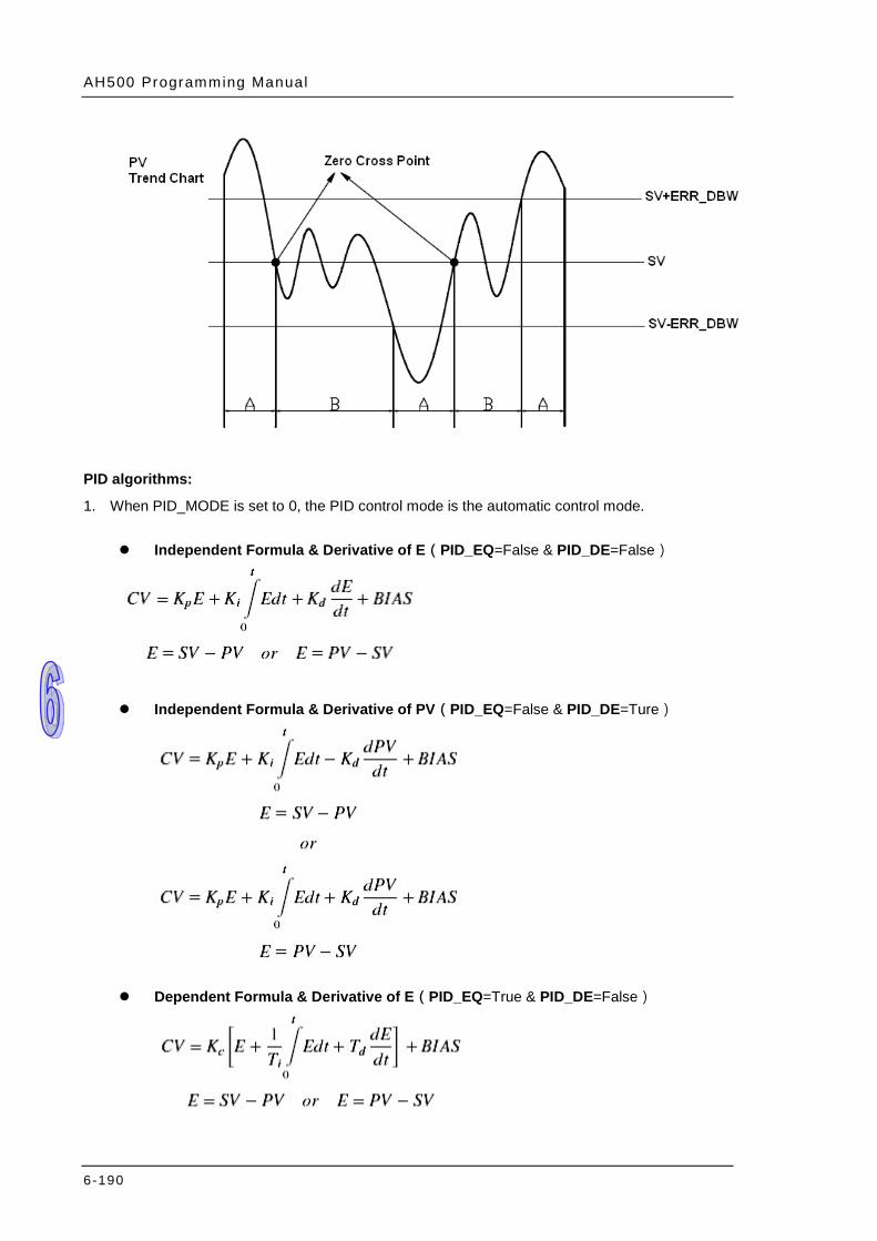
AH500 Programming Manual
6-190
PID algorithms:
1. When PID_MODE is set to 0, the PID control mode is the automatic control mode. Independent Formula & Derivative of E(PID_EQ=False & PID_DE=False)
Independent Formula & Derivative of PV(PID_EQ=False & PID_DE=Ture)
Dependent Formula & Derivative of E(PID_EQ=True & PID_DE=False)
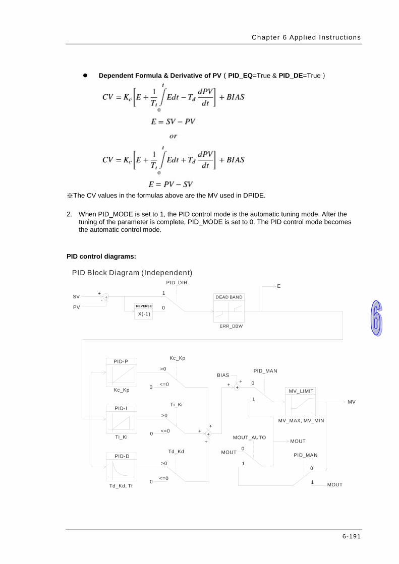
Chapter 6 Appl ied Inst ruct ions
6-191
Dependent Formula & Derivative of PV(PID_EQ=True & PID_DE=True)
※The CV values in the formulas above are the MV used in DPIDE. 2. When PID_MODE is set to 1, the PID control mode is the automatic tuning mode. After the
tuning of the parameter is complete, PID_MODE is set to 0. The PID control mode becomes the automatic control mode.
PID control diagrams:
PID Block Diagram (Independent)
SV
PV
+- +
REVERSE
X(-1)
PID_DIRE
DEAD BAND
ERR_DBW
0
1
PID-P
Kc_Kp
Kc_Kp
>0
<=00
PID-I
Ti_Ki
Ti_Ki
>0
<=00
0
>0
<=0
PID-D
Td_Kd, Tf
Td_Kd
BIASPID_MAN
0
1
0
1
MOUT
MOUT_AUTOMOUT
PID_MAN
0
1 MOUT
MV
MV_LIMIT
MV_MAX, MV_MIN
++ +
+
++
+
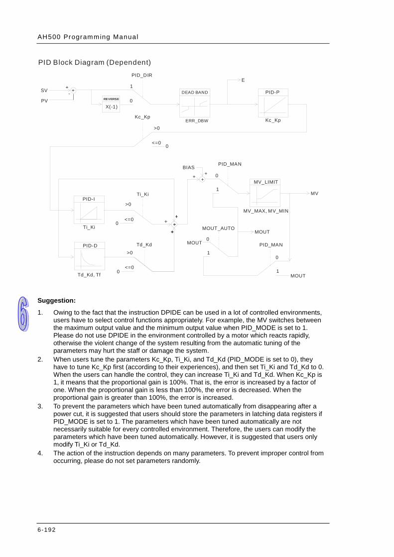
AH500 Programming Manual
6-192
PID Block Diagram (Dependent)
SV
PV
+- + PID-P
Kc_Kp
REVERSE
X(-1)
PID_DIR
0
1E
DEAD BAND
ERR_DBW
PID-I
Ti_Ki
Kc_Kp
>0
<=00
Ti_Ki
>0
<=00
PID-D
Td_Kd, Tf 0
>0
<=0
Td_Kd
BIASPID_MAN
++ +
MV
MV_LIMIT
MV_MAX, MV_MIN
MOUT_AUTOMOUT
MOUT PID_MAN
MOUT
0
1
0
1
0
1
Suggestion:
1. Owing to the fact that the instruction DPIDE can be used in a lot of controlled environments, users have to select control functions appropriately. For example, the MV switches between the maximum output value and the minimum output value when PID_MODE is set to 1. Please do not use DPIDE in the environment controlled by a motor which reacts rapidly, otherwise the violent change of the system resulting from the automatic tuning of the parameters may hurt the staff or damage the system.
2. When users tune the parameters Kc_Kp, Ti_Ki, and Td_Kd (PID_MODE is set to 0), they have to tune Kc_Kp first (according to their experiences), and then set Ti_Ki and Td_Kd to 0. When the users can handle the control, they can increase Ti_Ki and Td_Kd. When Kc_Kp is 1, it means that the proportional gain is 100%. That is, the error is increased by a factor of one. When the proportional gain is less than 100%, the error is decreased. When the proportional gain is greater than 100%, the error is increased.
3. To prevent the parameters which have been tuned automatically from disappearing after a power cut, it is suggested that users should store the parameters in latching data registers if PID_MODE is set to 1. The parameters which have been tuned automatically are not necessarily suitable for every controlled environment. Therefore, the users can modify the parameters which have been tuned automatically. However, it is suggested that users only modify Ti_Ki or Td_Kd.
4. The action of the instruction depends on many parameters. To prevent improper control from occurring, please do not set parameters randomly.
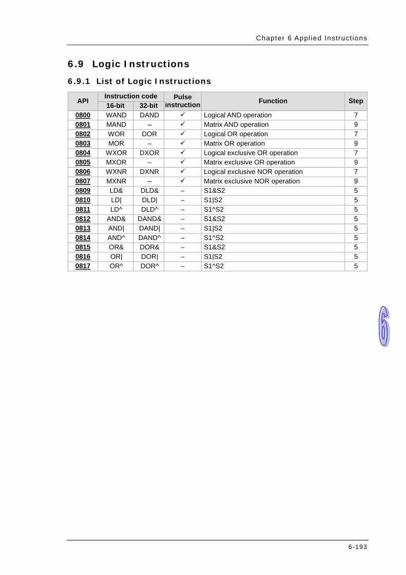
Chapter 6 Appl ied Instruc t ions
6-193
6.9 Logic Instructions
6.9.1 List of Logic Instructions
API Instruction code Pulse instruction Function Step 16-bit 32-bit
0800 WAND DAND Logical AND operation 7 0801 MAND – Matrix AND operation 9 0802 WOR DOR Logical OR operation 7 0803 MOR – Matrix OR operation 9 0804 WXOR DXOR Logical exclusive OR operation 7 0805 MXOR – Matrix exclusive OR operation 9 0806 WXNR DXNR Logical exclusive NOR operation 7 0807 MXNR – Matrix exclusive NOR operation 9 0809 LD& DLD& – S1&S2 5 0810 LD| DLD| – S1|S2 5 0811 LD^ DLD^ – S1^S2 5 0812 AND& DAND& – S1&S2 5 0813 AND| DAND| – S1|S2 5 0814 AND^ DAND^ – S1^S2 5 0815 OR& DOR& – S1&S2 5 0816 OR| DOR| – S1|S2 5 0817 OR^ DOR^ – S1^S2 5
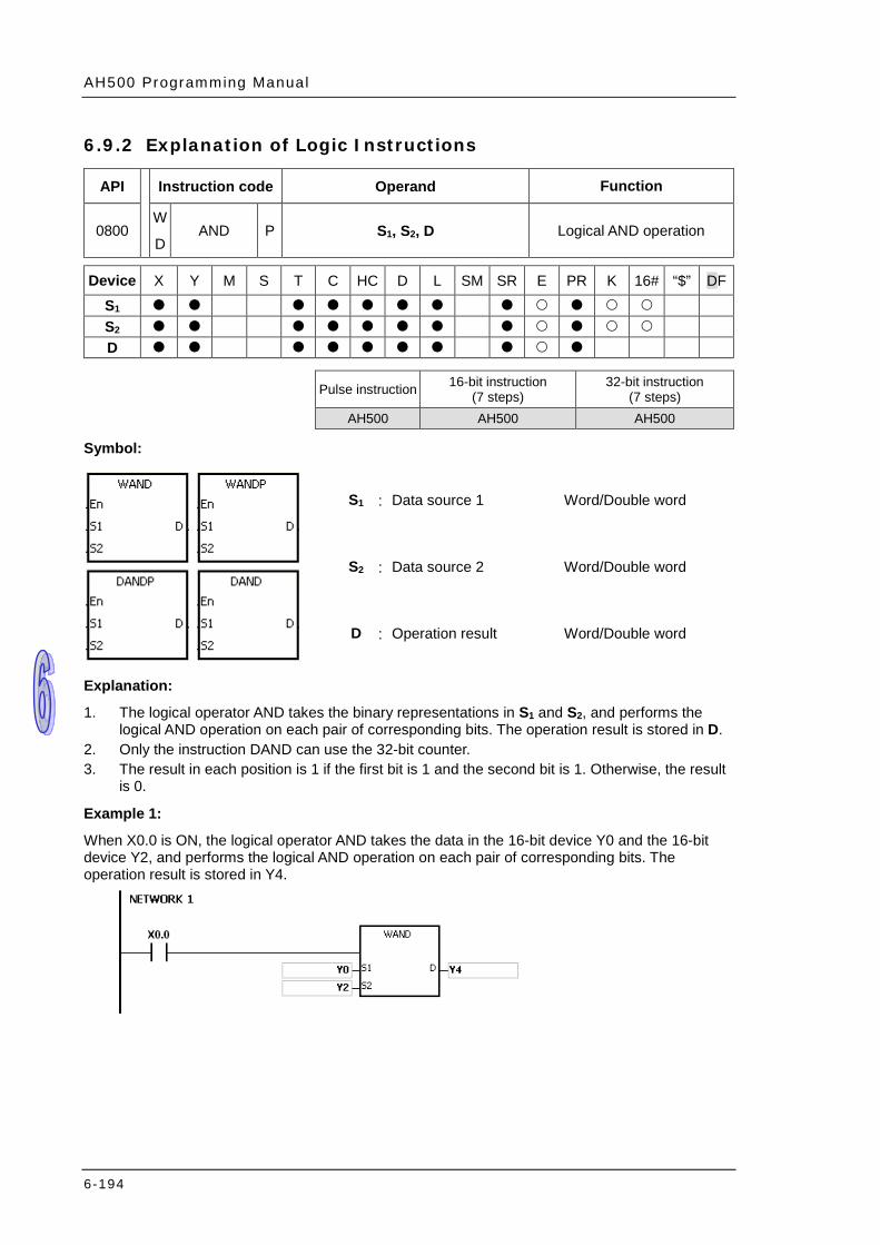
AH500 Programming Manual
6-194
6.9.2 Explanation of Logic Instructions
API Instruction code Operand Function
0800 W
D AND P S1, S2, D Logical AND operation
Device X Y M S T C HC D L SM SR E PR K 16# “$” DF
S1 S2 D
Pulse instruction 16-bit instruction
(7 steps) 32-bit instruction
(7 steps) AH500 AH500 AH500
Symbol:
S1 : Data source 1 Word/Double word
S2 : Data source 2 Word/Double word
D : Operation result Word/Double word
Explanation:
1. The logical operator AND takes the binary representations in S1 and S2, and performs the logical AND operation on each pair of corresponding bits. The operation result is stored in D.
2. Only the instruction DAND can use the 32-bit counter. 3. The result in each position is 1 if the first bit is 1 and the second bit is 1. Otherwise, the result
is 0.
Example 1:
When X0.0 is ON, the logical operator AND takes the data in the 16-bit device Y0 and the 16-bit device Y2, and performs the logical AND operation on each pair of corresponding bits. The operation result is stored in Y4.

Chapter 6 Appl ied Instruc t ions
6-195
Example 2:
When X0.0 is ON, the logical operator AND takes the data in the 32-bit device (Y11, Y10) and the 32-bit device (Y21, Y20), and performs the logical AND operation on each pair of corresponding bits. The operation result is stored in (Y41, Y40).
DAND
b15 b0b31Before the instruction is executed
After the instructionis executed
S 1
S 2
D
Y11 Y10
Y21 Y20
Y41 Y40
1 1 1 1 1 1 1 1 0 0 0 0 1 1 1 1
0 0 0
0 0 0 0 0 0 0 0 0
1 1 1 1 1
111 0 0 0 0
0 00 00 000
1 1 1
11111
1111 11 1 1 11 1 1
0 0 0 0 0 0 0 0 0 0 0
0 00 00 00 00 00 00
0 00 0
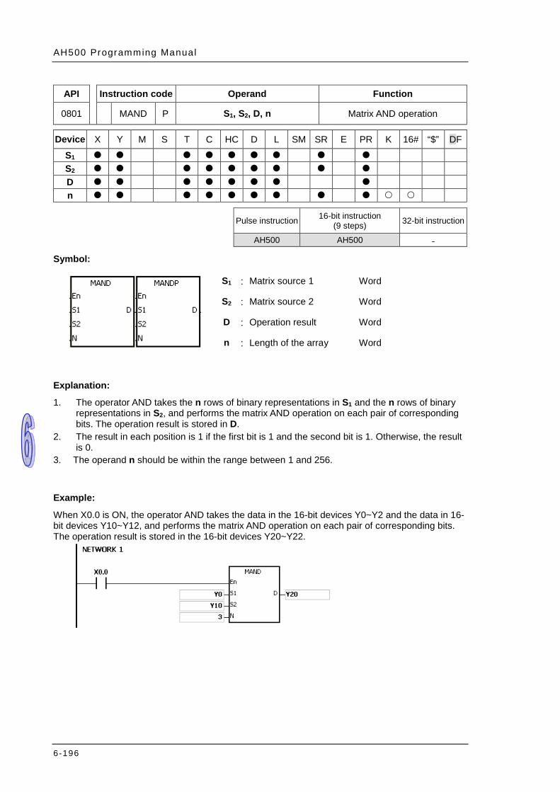
AH500 Programming Manual
6-196
API Instruction code Operand Function
0801 MAND P S1, S2, D, n Matrix AND operation
Device X Y M S T C HC D L SM SR E PR K 16# “$” DF
S1 S2 D n
Pulse instruction 16-bit instruction
(9 steps) 32-bit instruction
AH500 AH500 -
Symbol:
S1 : Matrix source 1 Word
S2 : Matrix source 2 Word
D : Operation result Word
n : Length of the array Word
Explanation:
1. The operator AND takes the n rows of binary representations in S1 and the n rows of binary representations in S2, and performs the matrix AND operation on each pair of corresponding bits. The operation result is stored in D.
2. The result in each position is 1 if the first bit is 1 and the second bit is 1. Otherwise, the result is 0.
3. The operand n should be within the range between 1 and 256.
Example:
When X0.0 is ON, the operator AND takes the data in the 16-bit devices Y0~Y2 and the data in 16-bit devices Y10~Y12, and performs the matrix AND operation on each pair of corresponding bits. The operation result is stored in the 16-bit devices Y20~Y22.
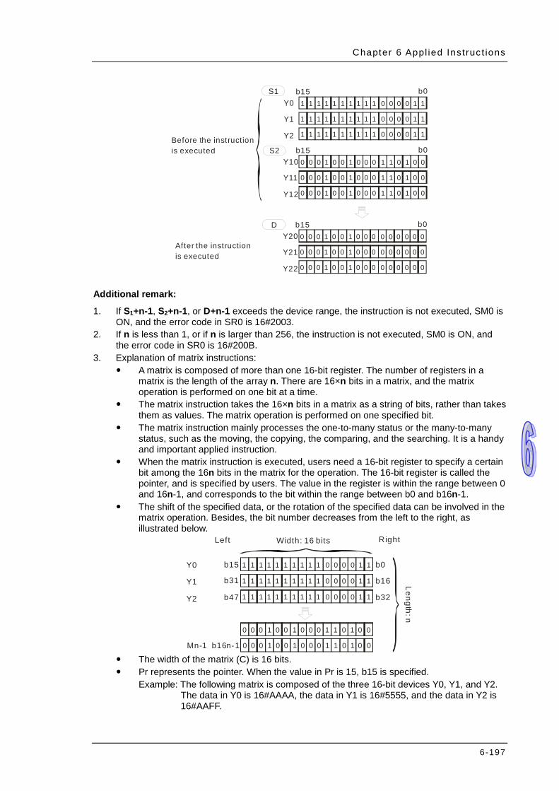
Chapter 6 Appl ied Instruc t ions
6-197
Before the instruction is executed
After the instructionis executed
1 1 1 1 1 1 1 1 1 1 0 0 0 0 1 1
1 1 1 1 1 1 1 1 1 1 0 0 0 0 1 1
b0b15Y0
Y1
Y2 1 1 1 1 1 1 1 1 1 1 0 0 0 0 1 1
Y10
Y11
Y12
0 0 0 1 0 0 1 0 0 0 1 1 0 1 0 0
0 0 0 1 0 0 1 0 0 0 1 1 0 1 0 0
b0b15
0 0 0 1 0 0 1 0 0 0 1 1 0 1 0 0
S1
S2
Y20
Y21
Y22
0 0 0 1 0 0 1 0 0 0 0 0 0 0 0 0
0 0 0 1 0 0 1 0 0 0 0 0 0 0 0 0
b0b15
0 0 0 1 0 0 1 0 0 0 0 0 0 0 0 0
D
Additional remark:
1. If S1+n-1, S2+n-1, or D+n-1 exceeds the device range, the instruction is not executed, SM0 is ON, and the error code in SR0 is 16#2003.
2. If n is less than 1, or if n is larger than 256, the instruction is not executed, SM0 is ON, and the error code in SR0 is 16#200B.
3. Explanation of matrix instructions: A matrix is composed of more than one 16-bit register. The number of registers in a
matrix is the length of the array n. There are 16×n bits in a matrix, and the matrix operation is performed on one bit at a time.
The matrix instruction takes the 16×n bits in a matrix as a string of bits, rather than takes them as values. The matrix operation is performed on one specified bit.
The matrix instruction mainly processes the one-to-many status or the many-to-many status, such as the moving, the copying, the comparing, and the searching. It is a handy and important applied instruction.
When the matrix instruction is executed, users need a 16-bit register to specify a certain bit among the 16n bits in the matrix for the operation. The 16-bit register is called the pointer, and is specified by users. The value in the register is within the range between 0 and 16n-1, and corresponds to the bit within the range between b0 and b16n-1.
The shift of the specified data, or the rotation of the specified data can be involved in the matrix operation. Besides, the bit number decreases from the left to the right, as illustrated below.
1 1 1 1 1 1 1 1 1 1 0 0 0 0 1 1
1 1 1 1 1 1 1 1 1 1 0 0 0 0 1 1
1 1 0 10 0 0 0 0 00 0 1 1 0 0
1 1 0 10 0 0 0 0 00 0 1 1 0 0
b0
b16
b32
b31
b15
b47
Width: 16 bitsLeft Right
Length: n
Y0
Y1
Y2
Mn-1 b16n-1
1 1 1 1 1 1 1 1 1 1 0 0 0 0 1 1
The width of the matrix (C) is 16 bits. Pr represents the pointer. When the value in Pr is 15, b15 is specified.
Example: The following matrix is composed of the three 16-bit devices Y0, Y1, and Y2. The data in Y0 is 16#AAAA, the data in Y1 is 16#5555, and the data in Y2 is 16#AAFF.

AH500 Programming Manual
6-198
C15 C14 C13 C12 C11 C10 C9 C8 C7 C6 C5 C4 C3 C2 C1 C0 1 0 1 0 1 0 1 0 1 0 1 0 1 0 1 0 Y0 0 1 0 1 0 1 0 1 0 1 0 1 0 1 0 1 Y1 1 0 1 0 1 0 1 0 1 1 1 1 1 1 1 1 Y2
Example: The following matrix is composed of the three 16-bit devices X 0, X 1, and X 2. The data in X 0 is 16#37, the data in X 1 is 16#68, and the data in X 2 is 16#45.
C15 C14 C13 C12 C11 C10 C9 C8 C7 C6 C5 C4 C3 C2 C1 C0 0 0 0 0 0 0 0 0 0 0 1 1 0 1 1 1 X0 0 0 0 0 0 0 0 0 0 1 1 0 1 0 0 0 X1 0 0 0 0 0 0 0 0 0 1 0 0 0 1 0 1 X2
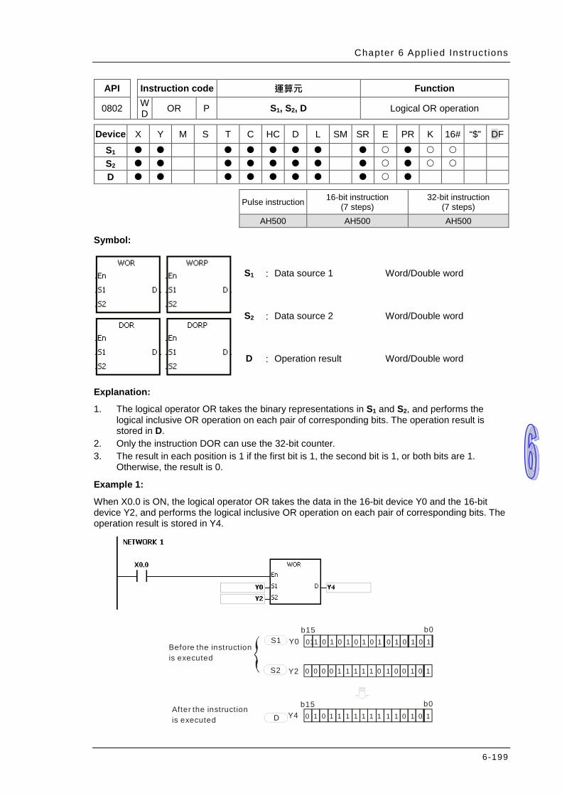
Chapter 6 Appl ied Instruc t ions
6-199
API Instruction code 運算元 Function
0802 W D OR P S1, S2, D Logical OR operation
Device X Y M S T C HC D L SM SR E PR K 16# “$” DF
S1 S2 D
Pulse instruction 16-bit instruction
(7 steps) 32-bit instruction
(7 steps) AH500 AH500 AH500
Symbol:
S1 : Data source 1 Word/Double word
S2 : Data source 2 Word/Double word
D : Operation result Word/Double word
Explanation:
1. The logical operator OR takes the binary representations in S1 and S2, and performs the logical inclusive OR operation on each pair of corresponding bits. The operation result is stored in D.
2. Only the instruction DOR can use the 32-bit counter. 3. The result in each position is 1 if the first bit is 1, the second bit is 1, or both bits are 1.
Otherwise, the result is 0.
Example 1:
When X0.0 is ON, the logical operator OR takes the data in the 16-bit device Y0 and the 16-bit device Y2, and performs the logical inclusive OR operation on each pair of corresponding bits. The operation result is stored in Y4.
Before the instruction is executed
After the instructionis executed
011 0 1 0 1 0 1 0 1 0 1 0 1 0 1
0 0 0 0 1 1 1 1 1 0 1 0 0 1 0 1
b0b15Y0
Y2
S1
S2
Y4 0 1 0 1 1 1 1 1 1 1 1 1 0 1 0 1
b0b15
D
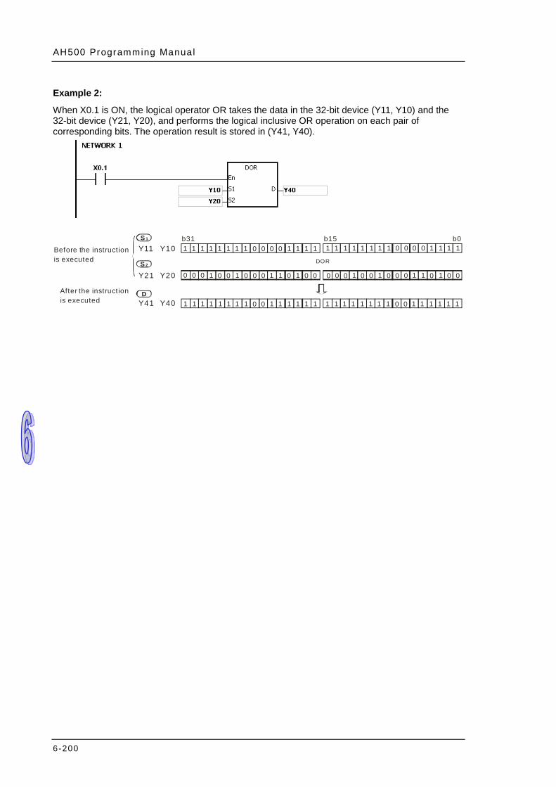
AH500 Programming Manual
6-200
Example 2:
When X0.1 is ON, the logical operator OR takes the data in the 32-bit device (Y11, Y10) and the 32-bit device (Y21, Y20), and performs the logical inclusive OR operation on each pair of corresponding bits. The operation result is stored in (Y41, Y40).
Before the instruction is executed
After the instructionis executed
DOR
b15 b0b31S 1
S 2
D
Y11 Y10
Y21 Y20
Y41 Y40
1 1 1 1 1 1 1 1 0 0 0 0 1 1 1 1
0 0 0
0 0
1 1 1 1 1
111
0 00 00 000 11111
1111 11 1 1 11 1 1
0 0 0 0 0 0 0 0 0 0 0
0 00 0
1 1 1 1 1 1 11 1 11 1111 1 1 1 1 1 11 1 110 0

Chapter 6 Appl ied Instruc t ions
6-201
API Instruction code Operand Function
0803 MOR P S1, S2, D, n Matrix OR operation
Device X Y M S T C HC D L SM SR E PR K 16# “$” DF
S1 S2 D n
Pulse instruction 16-bit instruction
(9 steps) 32-bit instruction
AH500 AH500 -
Symbol:
S1 : Matrix source 1 Word
S2 : Matrix source 2 Word
D : Operation result Word
n : Length of the array Word
Explanation:
1. The operator OR takes the n rows of binary representations in S1 and the n rows of binary representations in S2, and performs the matrix OR operation on each pair of corresponding bits. The operation result is stored in D.
2. The result in each position is 1 if the first bit is 1, the second bit is 1, or both bits are 1. Otherwise, the result is 0.
3. The operand n should be within the range between 1 and 256.
Example:
When X0.0 is ON, the operator OR takes the data in the 16-bit devices Y0~Y2 and the data in 16-bit devices Y10~Y12, and performs the matrix OR operation on each pair of corresponding bits. The operation result is stored in the 16-bit devices Y20~Y22.
Before the instruc tionis executed
After the instruc tionis executed
0 1 0 1 0 1 0 1 0 1 0 1 0 1 0 1
0 1 0 1 0 1 0 1 0 1 0 1 0 1 0 1
b0b15Y0
Y1
Y2 0 1 0 1 0 1 0 1 0 1 0 1 0 1 0 1
Y10
Y11
Y12
0 0 0 1 0 1 1 1 1 0 1 0 0 1 0 1
0 0 0 1 0 1 1 1 1 0 1 0 0 1 0 1
b0b15
0 0 0 1 0 0 1 1 1 0 1 0 0 1 0 1
S1
S2Y20
Y21
Y22
0 1 0 1 1 1 1 1 1 1 1 1 0 1 0 1
0 1 0 1 1 1 1 1 1 1 1 1 0 1 0 1
b0b15
0 1 0 1 1 1 1 1 1 1 1 1 0 1 0 1
D
MOR

AH500 Programming Manual
6-202
Additional remark:
1. If S1+n-1, S2+n-1, or D+n-1 exceeds the device range, the instruction is not executed, SM0 is ON, and the error code in SR0 is 16#2003.
2. If n is less than 1, or if n is larger than 256, the instruction is not executed, SM0 is ON, and the error code in SR0 is 16#200B.
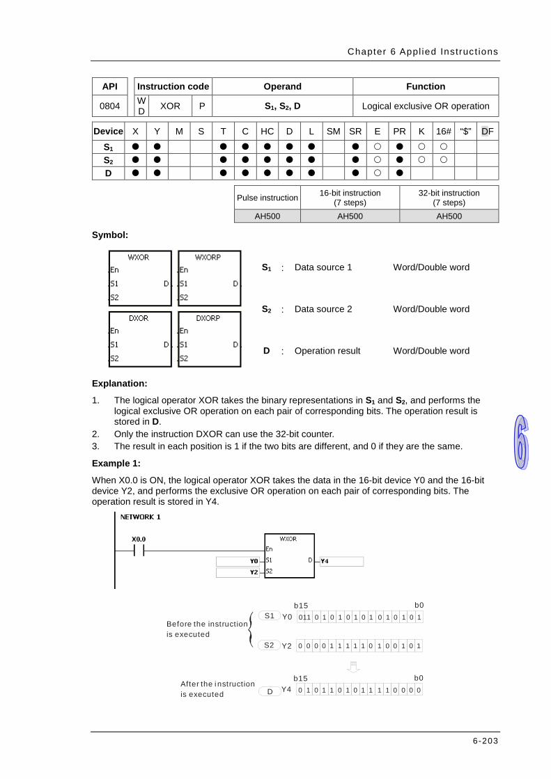
Chapter 6 Appl ied Instruc t ions
6-203
API Instruction code Operand Function
0804 W D XOR P S1, S2, D Logical exclusive OR operation
Device X Y M S T C HC D L SM SR E PR K 16# “$” DF
S1 S2 D
Pulse instruction 16-bit instruction
(7 steps) 32-bit instruction
(7 steps) AH500 AH500 AH500
Symbol:
S1 : Data source 1 Word/Double word
S2 : Data source 2 Word/Double word
D : Operation result Word/Double word
Explanation:
1. The logical operator XOR takes the binary representations in S1 and S2, and performs the logical exclusive OR operation on each pair of corresponding bits. The operation result is stored in D.
2. Only the instruction DXOR can use the 32-bit counter. 3. The result in each position is 1 if the two bits are different, and 0 if they are the same.
Example 1:
When X0.0 is ON, the logical operator XOR takes the data in the 16-bit device Y0 and the 16-bit device Y2, and performs the exclusive OR operation on each pair of corresponding bits. The operation result is stored in Y4.
Before the instructionis executed
After the i nstructionis executed
011 0 1 0 1 0 1 0 1 0 1 0 1 0 1
0 0 0 0 1 1 1 1 1 0 1 0 0 1 0 1
b0b15Y0
Y2
S1
S2
Y4 0 1 0 1 1 0 1 0 1 1 1 1 0 0 0 0
b0b15
D
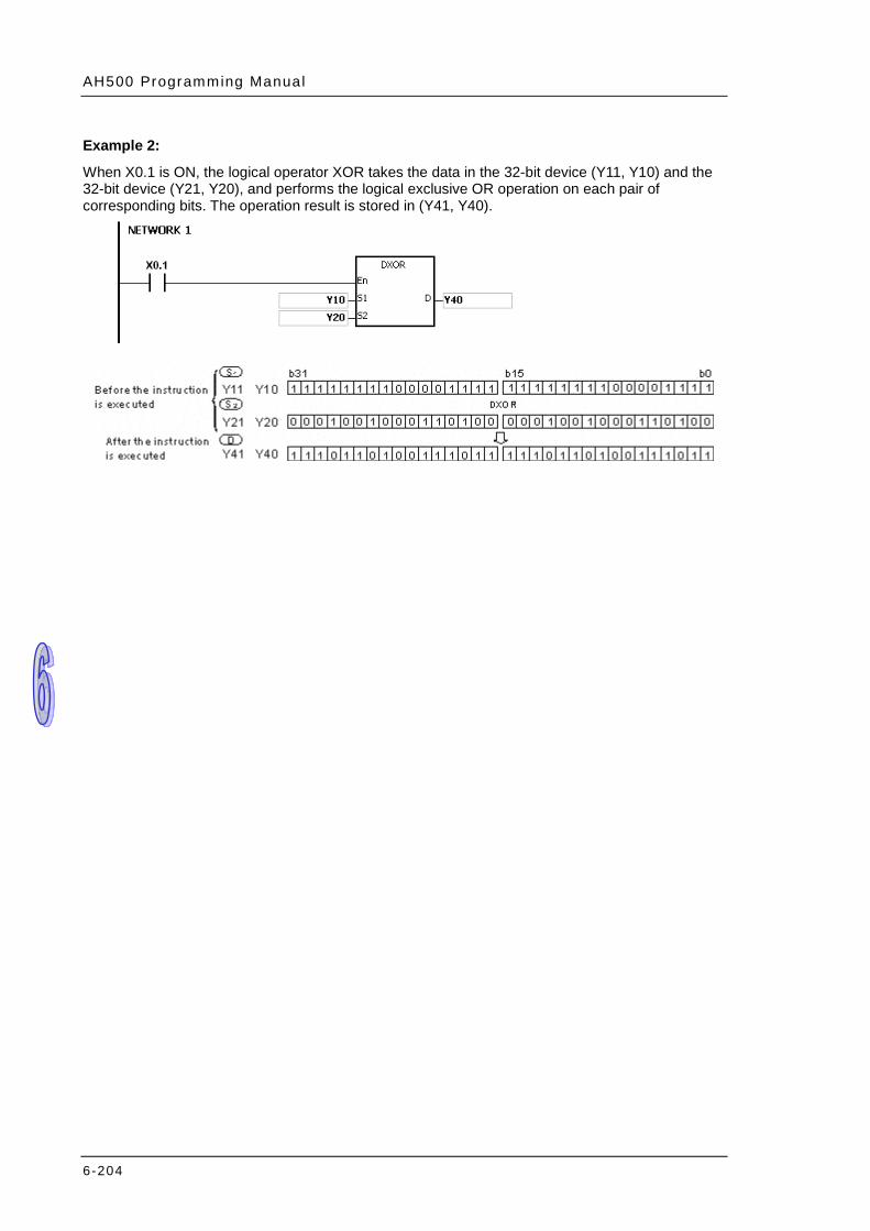
AH500 Programming Manual
6-204
Example 2:
When X0.1 is ON, the logical operator XOR takes the data in the 32-bit device (Y11, Y10) and the 32-bit device (Y21, Y20), and performs the logical exclusive OR operation on each pair of corresponding bits. The operation result is stored in (Y41, Y40).
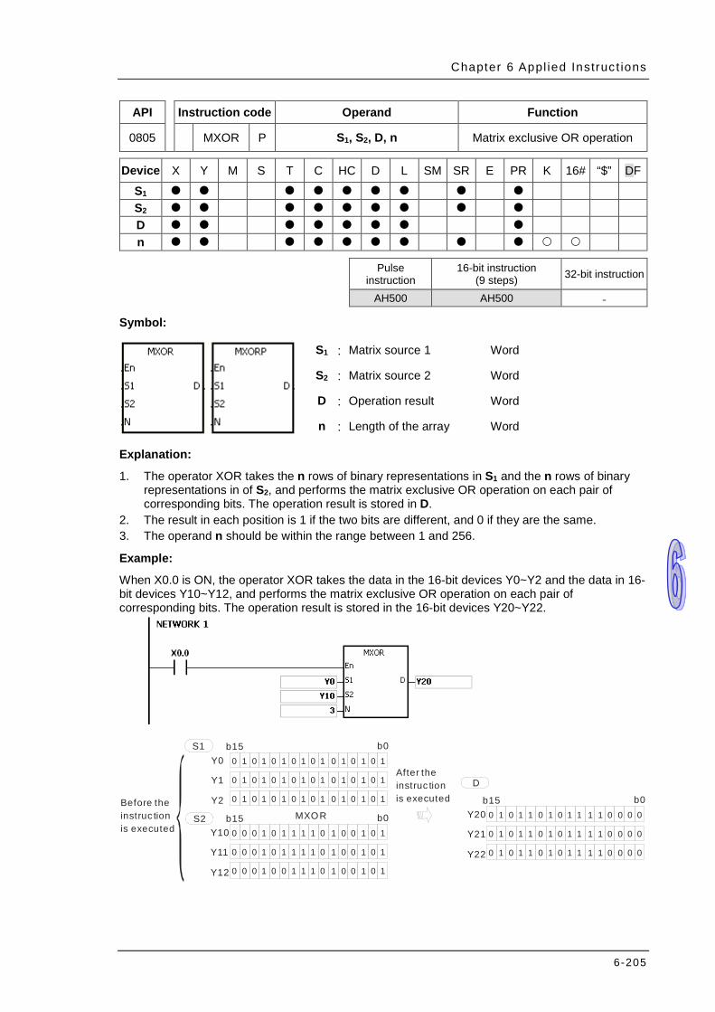
Chapter 6 Appl ied Instruc t ions
6-205
API Instruction code Operand Function
0805 MXOR P S1, S2, D, n Matrix exclusive OR operation
Device X Y M S T C HC D L SM SR E PR K 16# “$” DF
S1 S2 D n
Pulse
instruction 16-bit instruction
(9 steps) 32-bit instruction
AH500 AH500 -
Symbol:
S1 : Matrix source 1 Word
S2 : Matrix source 2 Word
D : Operation result Word
n : Length of the array Word
Explanation:
1. The operator XOR takes the n rows of binary representations in S1 and the n rows of binary representations in of S2, and performs the matrix exclusive OR operation on each pair of corresponding bits. The operation result is stored in D.
2. The result in each position is 1 if the two bits are different, and 0 if they are the same. 3. The operand n should be within the range between 1 and 256.
Example:
When X0.0 is ON, the operator XOR takes the data in the 16-bit devices Y0~Y2 and the data in 16-bit devices Y10~Y12, and performs the matrix exclusive OR operation on each pair of corresponding bits. The operation result is stored in the 16-bit devices Y20~Y22.
Before the instruc tionis executed
After the instruc tionis executed
0 1 0 1 0 1 0 1 0 1 0 1 0 1 0 1
0 1 0 1 0 1 0 1 0 1 0 1 0 1 0 1
b0b15Y0
Y1
Y2 0 1 0 1 0 1 0 1 0 1 0 1 0 1 0 1
Y10
Y11
Y12
0 0 0 1 0 1 1 1 1 0 1 0 0 1 0 1
0 0 0 1 0 1 1 1 1 0 1 0 0 1 0 1
b0b15
0 0 0 1 0 0 1 1 1 0 1 0 0 1 0 1
S1
S2 Y20
Y21
Y22
0 1 0 1 1 0 1 0 1 1 1 1 0 0 0 0
0 1 0 1 1 0 1 0 1 1 1 1 0 0 0 0
b0b15
0 1 0 1 1 0 1 0 1 1 1 1 0 0 0 0
D
MXOR

AH500 Programming Manual
6-206
Additional remark:
1. If S1+n-1, S2+n-1, or D+n-1 exceeds the device range, the instruction is not executed, SM0 is ON, and the error code in SR0 is 16#2003.
2. If n is less than 1, or if n is larger than 256, the instruction is not executed, SM0 is ON, and the error code in SR0 is 16#200B.
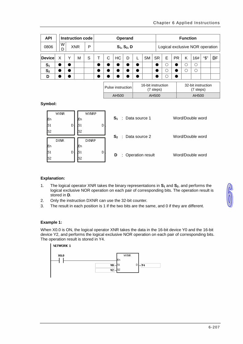
Chapter 6 Appl ied Instruc t ions
6-207
API Instruction code Operand Function
0806 W D XNR P S1, S2, D Logical exclusive NOR operation
Device X Y M S T C HC D L SM SR E PR K 16# “$” DF
S1 S2 D
Pulse instruction 16-bit instruction
(7 steps) 32-bit instruction
(7 steps) AH500 AH500 AH500
Symbol:
S1 : Data source 1 Word/Double word
S2 : Data source 2 Word/Double word
D : Operation result Word/Double word
Explanation:
1. The logical operator XNR takes the binary representations in S1 and S2, and performs the logical exclusive NOR operation on each pair of corresponding bits. The operation result is stored in D.
2. Only the instruction DXNR can use the 32-bit counter. 3. The result in each position is 1 if the two bits are the same, and 0 if they are different.
Example 1:
When X0.0 is ON, the logical operator XNR takes the data in the 16-bit device Y0 and the 16-bit device Y2, and performs the logical exclusive NOR operation on each pair of corresponding bits. The operation result is stored in Y4.
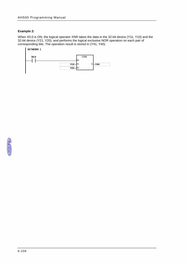
AH500 Programming Manual
6-208
Example 2:
When X0.0 is ON, the logical operator XNR takes the data in the 32-bit device (Y11, Y10) and the 32-bit device (Y21, Y20), and performs the logical exclusive NOR operation on each pair of corresponding bits. The operation result is stored in (Y41, Y40).

Chapter 6 Appl ied Instruc t ions
6-209
API Instruction code Operand Function
0807 MXNR P S1, S2, D, n Matrix exclusive NOR operation
Device X Y M S T C HC D L SM SR E PR K 16# “$” DF
S1 S2 D n
Pulse instruction 16-bit instruction
(9 steps) 32-bit instruction
AH500 AH500 -
Symbol:
S1 : Matrix source 1 Word
S2 : Matrix source 2 Word
D : Operation result Word
n : Length of the array Word
Explanation:
1. The operator XNR takes the n rows of binary representations in S1 and the n rows binary representations in of S2, and performs the matrix exclusive NOR operation on each pair of corresponding bits. The operation result is stored in D.
2. The result in each position is 1 if the two bits are the same, and 0 if they are different. 3. The operand n should be within the range between 1 and 256.
Example:
When X0.0 is ON, the operator XNR takes the data in the 16-bit devices Y0~Y2 and the data in 16-bit devices Y10~Y12, and performs the matrix exclusive NOR operation on each pair of corresponding bits. The operation result is stored in the 16-bit devices Y20~Y22.
Before the instruc ti onis executed
After the instruc ti onis executed
0 1 0 1 0 1 0 1 0 1 0 1 0 1 0 1
0 1 0 1 0 1 0 1 0 1 0 1 0 1 0 1
b0b15Y0
Y1
Y2 0 1 0 1 0 1 0 1 0 1 0 1 0 1 0 1
Y10
Y11
Y12
0 0 0 1 0 1 1 1 1 0 1 0 0 1 0 1
0 0 0 1 0 1 1 1 1 0 1 0 0 1 0 1
b0b15
0 0 0 1 0 0 1 1 1 0 1 0 0 1 0 1
S1
S2 Y20
Y21
Y22
1 0 1 0 0 1 0 1 0 0 0 0 1 1 1 1
1 0 1 0 0 1 0 1 0 0 0 0 1 1 1 1
b0b15
1 0 1 0 0 1 0 1 0 0 0 0 1 1 1 1
D
MXNR

AH500 Programming Manual
6-210
Additional remark:
1. If S1+n-1, S2+n-1, or D+n-1 exceeds the device range, the instruction is not executed, SM0 is ON, and the error code in SR0 is 16#2003.
2. If n is less than 1, or if n is larger than 256, the instruction is not executed, SM0 is ON, and the error code in SR0 is 16#200B.
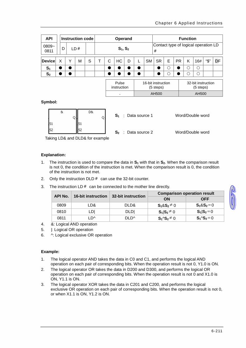
Chapter 6 Appl ied Instruc t ions
6-211
API Instruction code Operand Function
0809~ 0811 D LD# S1, S2
Contact type of logical operation LD#
Device X Y M S T C HC D L SM SR E PR K 16# “$” DF
S1 S2
Pulse
instruction 16-bit instruction
(5 steps) 32-bit instruction
(5 steps)
- AH500 AH500
Symbol:
Taking LD& and DLD& for example
S1 : Data source 1 Word/Double word
S2 : Data source 2 Word/Double word
Explanation:
1. The instruction is used to compare the data in S1 with that in S2. When the comparison result is not 0, the condition of the instruction is met. When the comparison result is 0, the condition of the instruction is not met.
2. Only the instruction DLD# can use the 32-bit counter.
3. The instruction LD# can be connected to the mother line directly.
API No. 16-bit instruction 32-bit instruction Comparison operation result ON OFF
0809 LD& DLD& S1&S2 0 S1&S2 0 0810 LD| DLD| S1|S2 0 S1|S2 0 0811 LD^ DLD^ S1^S2 0 S1^S2 0
4. &: Logical AND operation 5. |: Logical OR operation 6. ^: Logical exclusive OR operation
Example:
1. The logical operator AND takes the data in C0 and C1, and performs the logical AND operation on each pair of corresponding bits. When the operation result is not 0, Y1.0 is ON.
2. The logical operator OR takes the data in D200 and D300, and performs the logical OR operation on each pair of corresponding bits. When the operation result is not 0 and X1.0 is ON, Y1.1 is ON.
3. The logical operator XOR takes the data in C201 and C200, and performs the logical exclusive OR operation on each pair of corresponding bits. When the operation result is not 0, or when X1.1 is ON, Y1.2 is ON.
≠ =≠ =≠ =
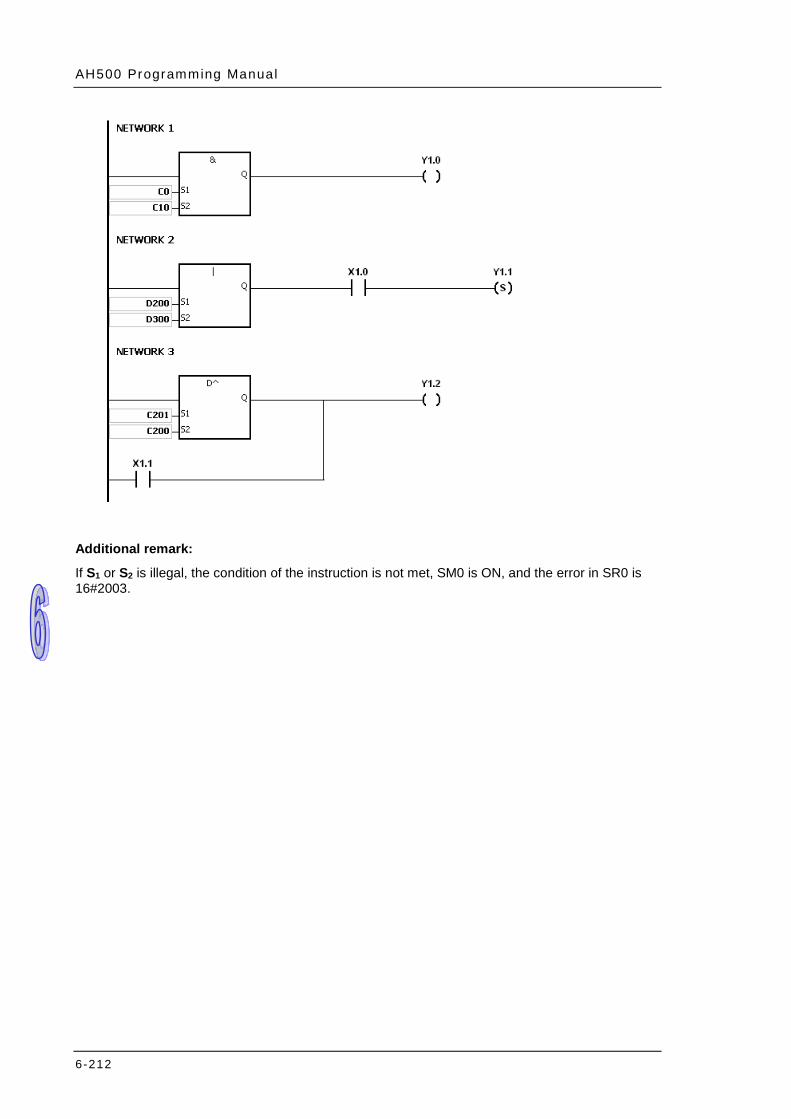
AH500 Programming Manual
6-212
Additional remark:
If S1 or S2 is illegal, the condition of the instruction is not met, SM0 is ON, and the error in SR0 is 16#2003.
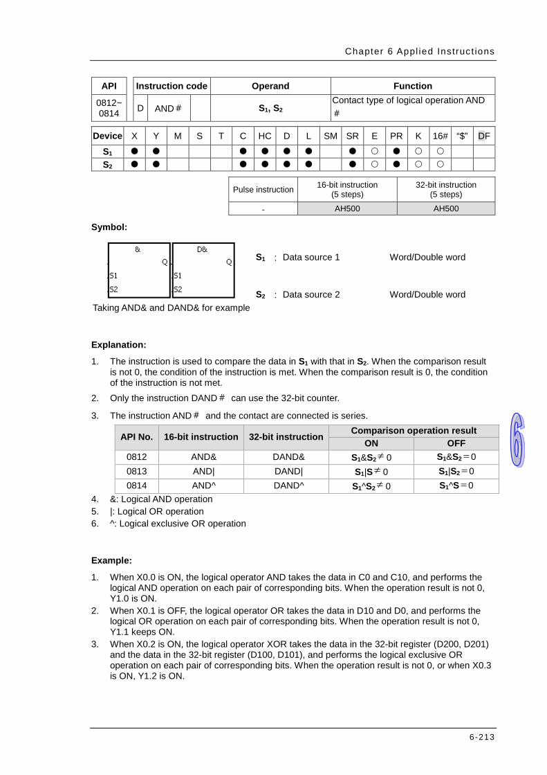
Chapter 6 Appl ied Instruc t ions
6-213
API Instruction code Operand Function
0812~ 0814 D AND# S1, S2
Contact type of logical operation AND#
Device X Y M S T C HC D L SM SR E PR K 16# “$” DF
S1 S2
Pulse instruction 16-bit instruction
(5 steps) 32-bit instruction
(5 steps)
- AH500 AH500
Symbol:
Taking AND& and DAND& for example
S1 : Data source 1 Word/Double word
S2 : Data source 2 Word/Double word
Explanation:
1. The instruction is used to compare the data in S1 with that in S2. When the comparison result is not 0, the condition of the instruction is met. When the comparison result is 0, the condition of the instruction is not met.
2. Only the instruction DAND# can use the 32-bit counter.
3. The instruction AND# and the contact are connected is series.
API No. 16-bit instruction 32-bit instruction Comparison operation result ON OFF
0812 AND& DAND& S1&S2 0 S1&S2 0 0813 AND| DAND| S1|S 0 S1|S2 0 0814 AND^ DAND^ S1^S2 0 S1^S 0
4. &: Logical AND operation 5. |: Logical OR operation 6. ^: Logical exclusive OR operation
Example:
1. When X0.0 is ON, the logical operator AND takes the data in C0 and C10, and performs the logical AND operation on each pair of corresponding bits. When the operation result is not 0, Y1.0 is ON.
2. When X0.1 is OFF, the logical operator OR takes the data in D10 and D0, and performs the logical OR operation on each pair of corresponding bits. When the operation result is not 0, Y1.1 keeps ON.
3. When X0.2 is ON, the logical operator XOR takes the data in the 32-bit register (D200, D201) and the data in the 32-bit register (D100, D101), and performs the logical exclusive OR operation on each pair of corresponding bits. When the operation result is not 0, or when X0.3 is ON, Y1.2 is ON.
≠ =≠ =≠ =
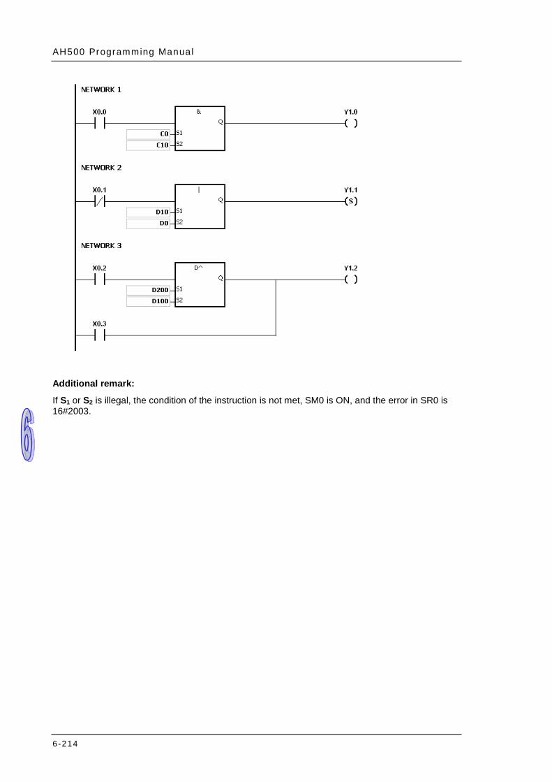
AH500 Programming Manual
6-214
Additional remark:
If S1 or S2 is illegal, the condition of the instruction is not met, SM0 is ON, and the error in SR0 is 16#2003.

Chapter 6 Appl ied Instruc t ions
6-215
API Instruction code Operand Function 0815~ 0817 D OR# S1, S2 Contact type of logical operation OR#
Device X Y M S T C HC D L SM SR E PR K 16# “$” DF
S1 S2
Pulse
instruction 16-bit instruction
(5 steps) 32-bit instruction
(5 steps) - AH500 AH500
Symbol:
Taking OR& and DOR& for example
S1 : Data source 1 Word/Double word
S2 : Data source 2 Word/Double word
Explanation:
1. The instruction is used to compare the data in S1 with that in S2. When the comparison result is not 0, the condition of the instruction is met. When the comparison result is 0, the condition of the instruction is not met.
2. Only the instruction DOR# can use the 32-bit counter.
3. The instruction OR# and the contact are connected in parallel.
API No. 16-bit instruction 32-bit instruction Comparison operation result ON OFF
0815 OR& DOR& S1&S2 0 S1&S2 0 0816 OR| DOR| S1|S2 0 S1|S2 0 0817 OR^ DOR^ S1^S2 0 S1^S2 0
4. &: Logical AND operation 5. |: Logical OR operation 6. ^: Logical exclusive OR operation
Example:
1. When X0.1 is ON, Y0.0 is ON. Besides, when the logical operator AND performs the logical AND operation on each pair of corresponding bits in C0 and C10 and the operation result is not 0, Y0.0 is ON.
2. When X0.2 and X0.3 are ON, Y0.1 is ON. When the logical operator OR performs the logical OR operation on each pair of corresponding bits in the 32-bit register (D10, D11) and the 32-bit register (D20, D21) and the operation result is not 0, Y0.1 is ON. Besides, when the logical operator XOR performs the logical exclusive OR operation on each pair of corresponding bits in the 32-bit counter HC0 and the 32-bit register (D200, D201) and the operation result is not 0, Y0.1 is ON.
≠ =≠ =≠ =
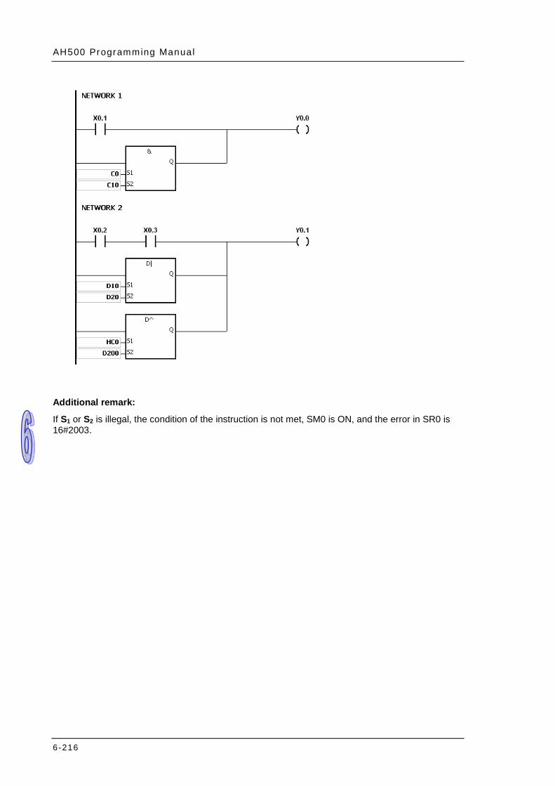
AH500 Programming Manual
6-216
Additional remark:
If S1 or S2 is illegal, the condition of the instruction is not met, SM0 is ON, and the error in SR0 is 16#2003.

Chapter 6 Appl ied Inst ruct ions
6-217
6.10 Rotation Instructions 6.10.1 List of Rotation Instructions
API Instruction code Pulse instruction Function Step 16-bit 32-bit
0900 ROR DROR Rotating to the right 5 0901 RCR DRCR Rotating to the right with the carry flag 5 0902 ROL DROL Rotating to the left 5 0903 RCL DRCL Rotating to the left with the carry flag 5 0904 MBR – Rotating the matrix bits 7
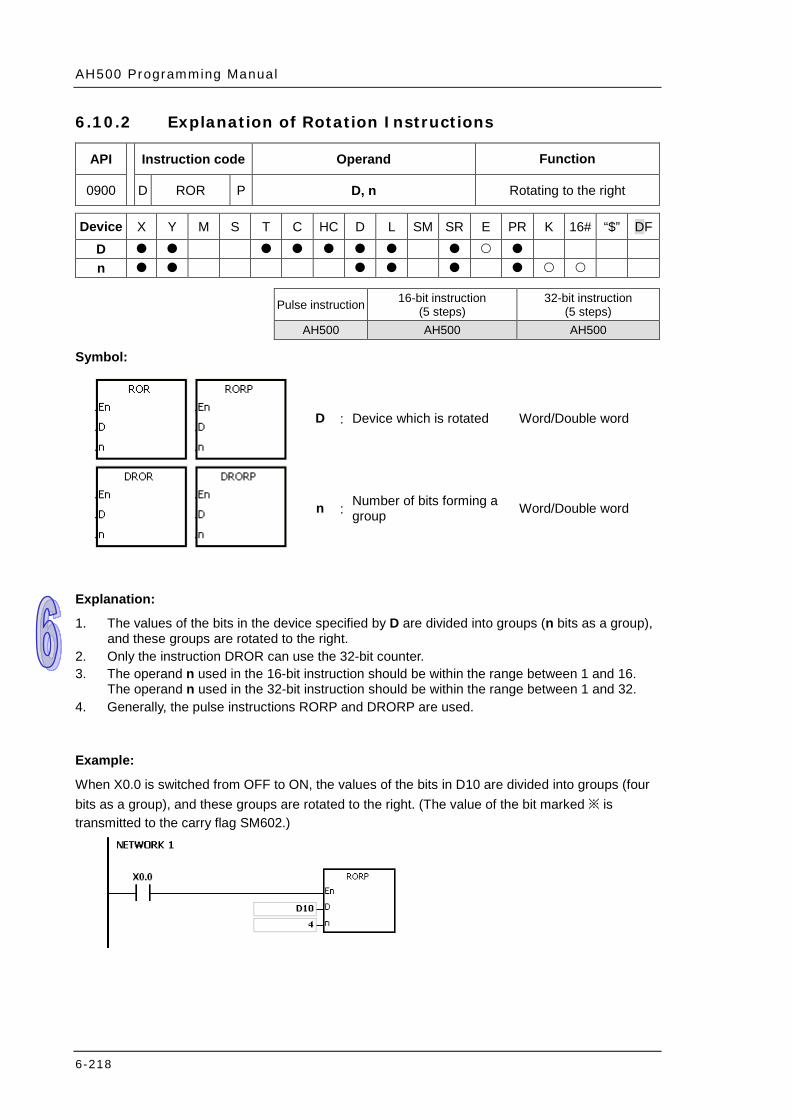
AH500 Programming Manual
6-218
6.10.2 Explanation of Rotation Instructions
API Instruction code Operand Function
0900 D ROR P D, n Rotating to the right
Device X Y M S T C HC D L SM SR E PR K 16# “$” DF
D n
Pulse instruction 16-bit instruction
(5 steps) 32-bit instruction
(5 steps) AH500 AH500 AH500
Symbol:
D : Device which is rotated Word/Double word
n : Number of bits forming a group Word/Double word
Explanation:
1. The values of the bits in the device specified by D are divided into groups (n bits as a group), and these groups are rotated to the right.
2. Only the instruction DROR can use the 32-bit counter. 3. The operand n used in the 16-bit instruction should be within the range between 1 and 16.
The operand n used in the 32-bit instruction should be within the range between 1 and 32. 4. Generally, the pulse instructions RORP and DRORP are used.
Example:
When X0.0 is switched from OFF to ON, the values of the bits in D10 are divided into groups (four bits as a group), and these groups are rotated to the right. (The value of the bit marked ※ is transmitted to the carry flag SM602.)
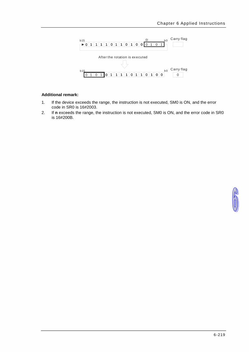
Chapter 6 Appl ied Inst ruct ions
6-219
0 1 1 1 1 0 1 1 0 1 0 0 0 1 0 1
0 1 0 1
0 1 1 1 1 0 1 1 0 1 0 0
0 1 1 1 1 0 1 1 0 1 0 00 1 1 1 1 0 1 1 0 1 0 0
※ Carry f lag
Carry f lag0
b0b15
b0b15
After the rotation is executed
Additional remark:
1. If the device exceeds the range, the instruction is not executed, SM0 is ON, and the error code in SR0 is 16#2003.
2. If n exceeds the range, the instruction is not executed, SM0 is ON, and the error code in SR0 is 16#200B.
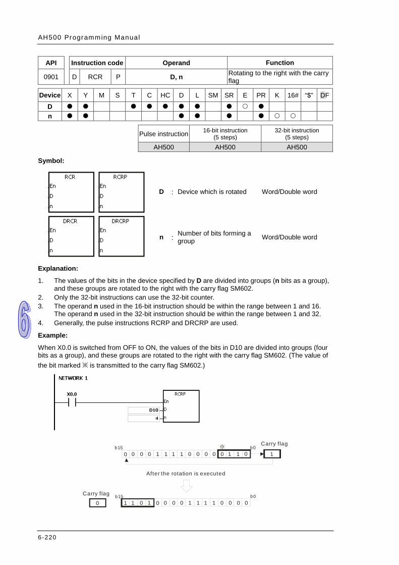
AH500 Programming Manual
6-220
API Instruction code Operand Function
0901 D RCR P D, n Rotating to the right with the carry flag
Device X Y M S T C HC D L SM SR E PR K 16# “$” DF
D n
Pulse instruction 16-bit instruction
(5 steps) 32-bit instruction
(5 steps)
AH500 AH500 AH500
Symbol:
D : Device which is rotated Word/Double word
n : Number of bits forming a group Word/Double word
Explanation:
1. The values of the bits in the device specified by D are divided into groups (n bits as a group), and these groups are rotated to the right with the carry flag SM602.
2. Only the 32-bit instructions can use the 32-bit counter. 3. The operand n used in the 16-bit instruction should be within the range between 1 and 16.
The operand n used in the 32-bit instruction should be within the range between 1 and 32. 4. Generally, the pulse instructions RCRP and DRCRP are used.
Example:
When X0.0 is switched from OFF to ON, the values of the bits in D10 are divided into groups (four bits as a group), and these groups are rotated to the right with the carry flag SM602. (The value of the bit marked ※ is transmitted to the carry flag SM602.)
Carry f lag
Carry f lag
After the rotation is executed
0 0 0 0 1 1 1 1 0 0 0 0 0 1 1 0
1 1 0 1
※
0
b0b15
b0b15
1
0 0 0 0 1 1 1 1 0 0 0 0

Chapter 6 Appl ied Inst ruct ions
6-221
Additional remark:
1. If the device exceeds the range, the instruction is not executed, SM0 is ON, and the error code in SR0 is 16#2003.
2. If n exceeds the range, the instruction is not executed, SM0 is ON, and the error code in SR0 is 16#200B.

AH500 Programming Manual
6-222
API Instruction code Operand Function
0902 D ROL P D, n Rotating to the left
Device X Y M S T C HC D L SM SR E PR K 16# “$” DF
D n
Pulse instruction 16-bit instruction
(5 steps) 32-bit instruction
(5 steps)
AH500 AH500 AH500
Symbol:
D : Device which is rotated Word/Double word
n : Number of bits forming a group Word/Double word
Explanation:
1. The values of the bits in the device specified by D are divided into groups (n bits as a group), and these groups are rotated to the left.
2. Only the 32-bit instructions can use the 32-bit counter. 3. The operand n used in the 16-bit instruction should be within the range between 1 and 16.
The operand n used in the 32-bit instruction should be within the range between 1 and 32. 4. Generally, the pulse instructions ROLP and DROLP are used.
Example:
When X0.0 is switched from OFF to ON, the values of the bits in D10 are divided into groups (four bits as a group), and these groups are rotated to the left. (The value of the bit marked ※ is transmitted to the carry flag SM602.)
Carry f lag
Carry f lag
After the rotation is executed
1 1 1 1 1 1 1 1 0 0 0 0 0 0 0 0
1 1 1 1
※
1
b0b15
b0b150 0 0 0 0 0 0 0 1 1 1 1

Chapter 6 Appl ied Inst ruct ions
6-223
Additional remark:
1. If the device exceeds the range, the instruction is not executed, SM0 is ON, and the error code in SR0 is 16#2003.
2. If n exceeds the range, the instruction is not executed, SM0 is ON, and the error code in SR0 is 16#200B.
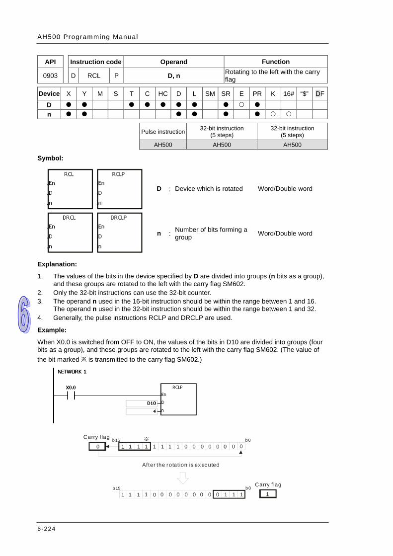
AH500 Programming Manual
6-224
API Instruction code Operand Function
0903 D RCL P D, n Rotating to the left with the carry flag
Device X Y M S T C HC D L SM SR E PR K 16# “$” DF
D n
Pulse instruction 32-bit instruction
(5 steps) 32-bit instruction
(5 steps)
AH500 AH500 AH500
Symbol:
D : Device which is rotated Word/Double word
n : Number of bits forming a group Word/Double word
Explanation:
1. The values of the bits in the device specified by D are divided into groups (n bits as a group), and these groups are rotated to the left with the carry flag SM602.
2. Only the 32-bit instructions can use the 32-bit counter. 3. The operand n used in the 16-bit instruction should be within the range between 1 and 16.
The operand n used in the 32-bit instruction should be within the range between 1 and 32. 4. Generally, the pulse instructions RCLP and DRCLP are used.
Example:
When X0.0 is switched from OFF to ON, the values of the bits in D10 are divided into groups (four bits as a group), and these groups are rotated to the left with the carry flag SM602. (The value of the bit marked ※ is transmitted to the carry flag SM602.)
Carry f lag
Carry f lag
After the rotation is executed
1 1 1 1 1 1 1 1 0 0 0 0 0 0 0 0
1 1 1 1
※
1
b0b15
b0b150 0 0 0 0 0 0 0 0 1 1 1
0

Chapter 6 Appl ied Inst ruct ions
6-225
Additional remark:
1. If the device exceeds the range, the instruction is not executed, SM0 is ON, and the error code in SR0 is 16#2003.
2. If n exceeds the range, the instruction is not executed, SM0 is ON, and the error code in SR0 is 16#200B.
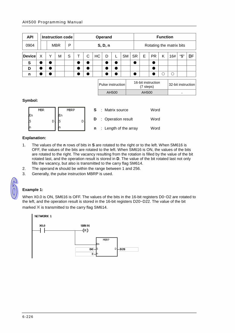
AH500 Programming Manual
6-226
API Instruction code Operand Function
0904 MBR P S, D, n Rotating the matrix bits
Device X Y M S T C HC D L SM SR E PR K 16# “$” DF
S D n
Pulse instruction 16-bit instruction
(7 steps) 32-bit instruction
AH500 AH500 -
Symbol:
S : Matrix source Word
D : Operation result Word
n : Length of the array Word
Explanation:
1. The values of the n rows of bits in S are rotated to the right or to the left. When SM616 is OFF, the values of the bits are rotated to the left. When SM616 is ON, the values of the bits are rotated to the right. The vacancy resulting from the rotation is filled by the value of the bit rotated last, and the operation result is stored in D. The value of the bit rotated last not only fills the vacancy, but also is transmitted to the carry flag SM614.
2. The operand n should be within the range between 1 and 256. 3. Generally, the pulse instruction MBRP is used.
Example 1:
When X0.0 is ON, SM616 is OFF. The values of the bits in the 16-bit registers D0~D2 are rotated to the left, and the operation result is stored in the 16-bit registers D20~D22. The value of the bit marked ※ is transmitted to the carry flag SM614.
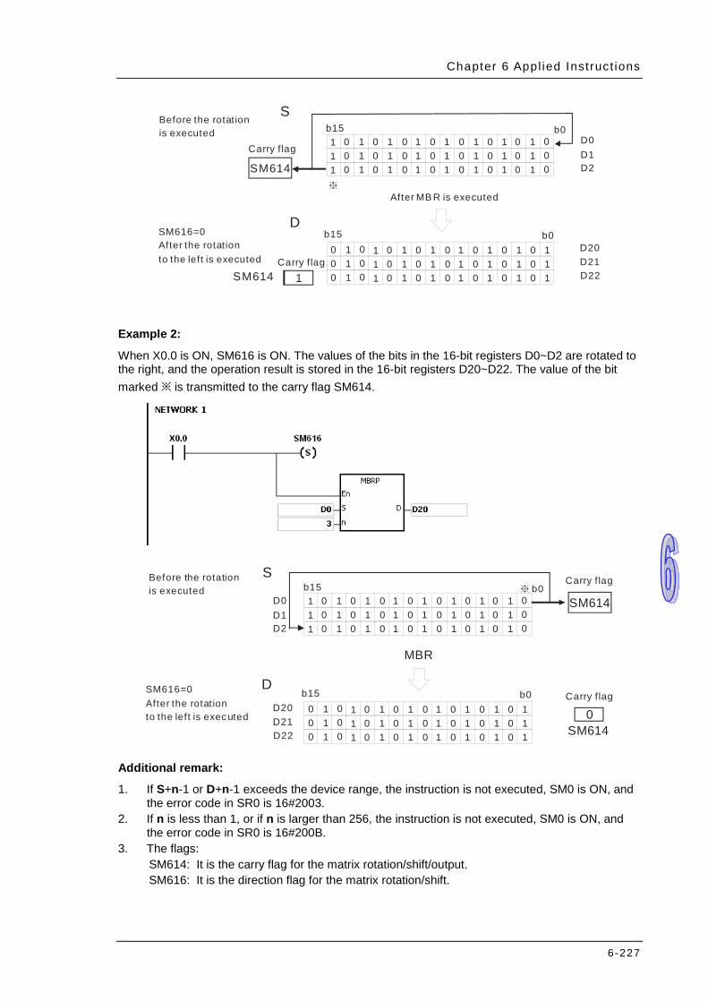
Chapter 6 Appl ied Inst ruct ions
6-227
1 0 1 0 1 0 1 0 1 0 1 0 1 0 1 0
Carry f lag1
b0b15
After MB R is executed
1 0 1 0 1 0 1 0 1 0 1 0 1 0 1 01 0 1 0 1 0 1 0 1 0 1 0 1 0 1 0
D0D1D2
D20D21D22
1 0 1 0 1 0 1 0 1 0 1 0 11 0 1 0 1 0 1 0 1 0 1 0 11 0 1 0 1 0 1 0 1 0 1 0 1
0 1 00 1 00 1 0
※
Carry f lag
SM614
SM614
Before the rotation is executed
SM616=0After the rotationto the left is executed
D
S
b0b15
Example 2:
When X0.0 is ON, SM616 is ON. The values of the bits in the 16-bit registers D0~D2 are rotated to the right, and the operation result is stored in the 16-bit registers D20~D22. The value of the bit marked ※ is transmitted to the carry flag SM614.
Carry f lag
Carry f lag
Before the rotation is executed
SM616=0After the rotationto the left is executed
D
1 0 1 0 1 0 1 0 1 0 1 0 1 0 1 0
0
b0b15
MBR
1 0 1 0 1 0 1 0 1 0 1 0 1 0 1 01 0 1 0 1 0 1 0 1 0 1 0 1 0 1 0
D0D1D2
D20D21D22
1 0 1 0 1 0 1 0 1 0 1 0 11 0 1 0 1 0 1 0 1 0 1 0 11 0 1 0 1 0 1 0 1 0 1 0 1
0 1 00 1 00 1 0
※
SM614
SM614
S
b0b15
Additional remark:
1. If S+n-1 or D+n-1 exceeds the device range, the instruction is not executed, SM0 is ON, and the error code in SR0 is 16#2003.
2. If n is less than 1, or if n is larger than 256, the instruction is not executed, SM0 is ON, and the error code in SR0 is 16#200B.
3. The flags: SM614: It is the carry flag for the matrix rotation/shift/output. SM616: It is the direction flag for the matrix rotation/shift.
AH500 Programming Manual
6-228
6.11 Timer and Counter Instructions 6.11.1 List of Timer and Counter Instructions
API Instruction code Pulse instruction Function Step 16-bit 32-bit
1000 RST – – Resetting the contact or clearing the register 3
1001 TMR – – 16-bit timer 5 1002 TMRH – – 16-bit timer 5 1003 CNT – – 16-bit counter 5 1004 – DCNT – 32-bit counter 5
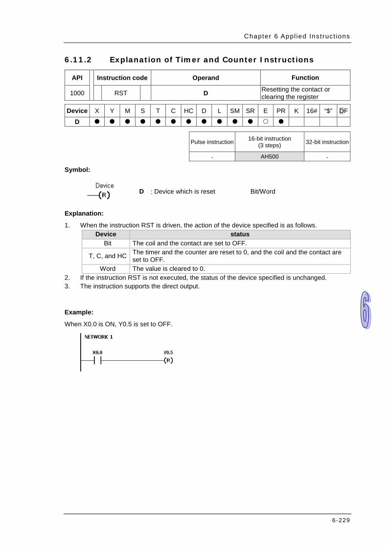
Chapter 6 Appl ied Instruc t ions
6-229
6.11.2 Explanation of Timer and Counter Instructions
API Instruction code Operand Function
1000 RST D Resetting the contact or clearing the register
Device X Y M S T C HC D L SM SR E PR K 16# “$” DF
D
Pulse instruction 16-bit instruction (3 steps) 32-bit instruction
- AH500 -
Symbol:
D : Device which is reset Bit/Word
Explanation:
1. When the instruction RST is driven, the action of the device specified is as follows. Device status
Bit The coil and the contact are set to OFF.
T, C, and HC The timer and the counter are reset to 0, and the coil and the contact are set to OFF.
Word The value is cleared to 0. 2. If the instruction RST is not executed, the status of the device specified is unchanged. 3. The instruction supports the direct output.
Example:
When X0.0 is ON, Y0.5 is set to OFF.
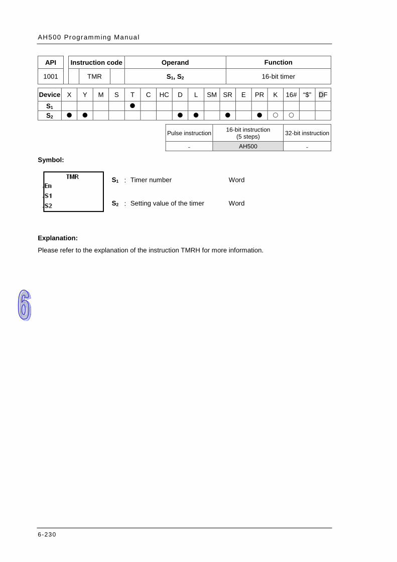
AH500 Programming Manual
6-230
API Instruction code Operand Function
1001 TMR S1, S2 16-bit timer
Device X Y M S T C HC D L SM SR E PR K 16# “$” DF
S1 S2
Pulse instruction 16-bit instruction
(5 steps) 32-bit instruction
- AH500 -
Symbol:
S1 : Timer number Word
S2 : Setting value of the timer Word
Explanation:
Please refer to the explanation of the instruction TMRH for more information.
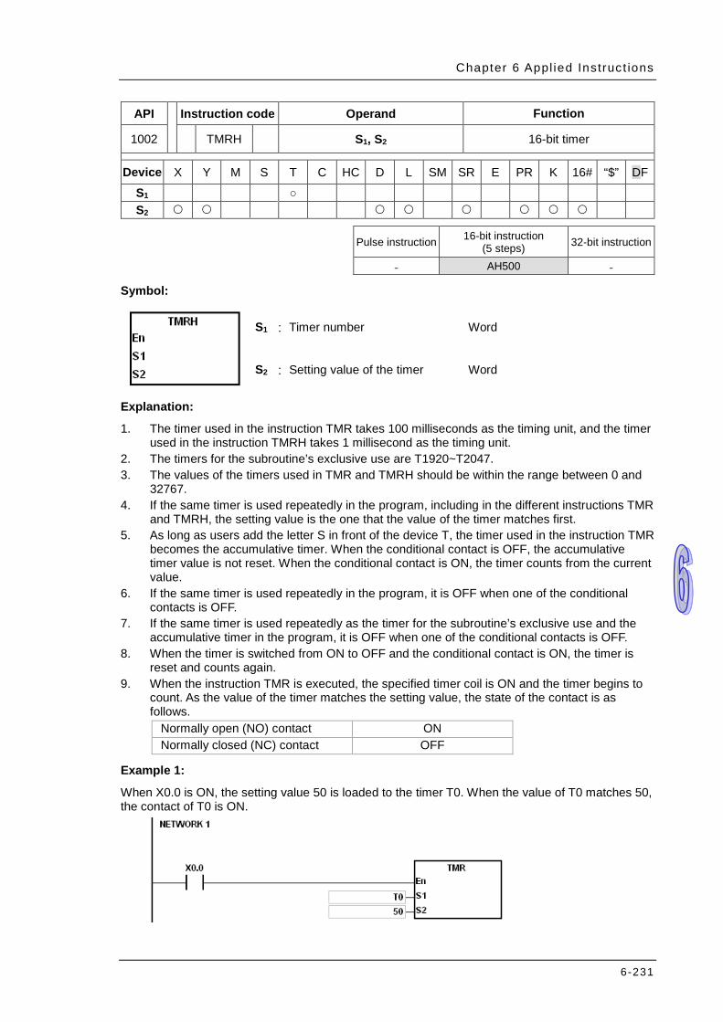
Chapter 6 Appl ied Instruc t ions
6-231
API Instruction code Operand Function
1002 TMRH S1, S2 16-bit timer
Device X Y M S T C HC D L SM SR E PR K 16# “$” DF
S1 ○ S2
Pulse instruction 16-bit instruction
(5 steps) 32-bit instruction
- AH500 -
Symbol:
S1 : Timer number Word
S2 : Setting value of the timer Word
Explanation:
1. The timer used in the instruction TMR takes 100 milliseconds as the timing unit, and the timer used in the instruction TMRH takes 1 millisecond as the timing unit.
2. The timers for the subroutine’s exclusive use are T1920~T2047. 3. The values of the timers used in TMR and TMRH should be within the range between 0 and
32767. 4. If the same timer is used repeatedly in the program, including in the different instructions TMR
and TMRH, the setting value is the one that the value of the timer matches first. 5. As long as users add the letter S in front of the device T, the timer used in the instruction TMR
becomes the accumulative timer. When the conditional contact is OFF, the accumulative timer value is not reset. When the conditional contact is ON, the timer counts from the current value.
6. If the same timer is used repeatedly in the program, it is OFF when one of the conditional contacts is OFF.
7. If the same timer is used repeatedly as the timer for the subroutine’s exclusive use and the accumulative timer in the program, it is OFF when one of the conditional contacts is OFF.
8. When the timer is switched from ON to OFF and the conditional contact is ON, the timer is reset and counts again.
9. When the instruction TMR is executed, the specified timer coil is ON and the timer begins to count. As the value of the timer matches the setting value, the state of the contact is as follows.
Normally open (NO) contact ON Normally closed (NC) contact OFF
Example 1:
When X0.0 is ON, the setting value 50 is loaded to the timer T0. When the value of T0 matches 50, the contact of T0 is ON.
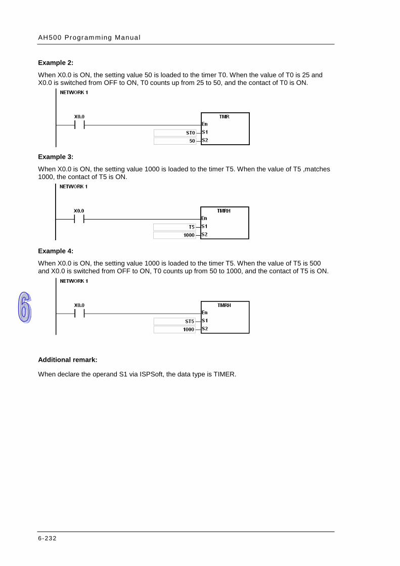
AH500 Programming Manual
6-232
Example 2:
When X0.0 is ON, the setting value 50 is loaded to the timer T0. When the value of T0 is 25 and X0.0 is switched from OFF to ON, T0 counts up from 25 to 50, and the contact of T0 is ON.
Example 3:
When X0.0 is ON, the setting value 1000 is loaded to the timer T5. When the value of T5 ,matches 1000, the contact of T5 is ON.
Example 4:
When X0.0 is ON, the setting value 1000 is loaded to the timer T5. When the value of T5 is 500 and X0.0 is switched from OFF to ON, T0 counts up from 50 to 1000, and the contact of T5 is ON.
Additional remark:
When declare the operand S1 via ISPSoft, the data type is TIMER.
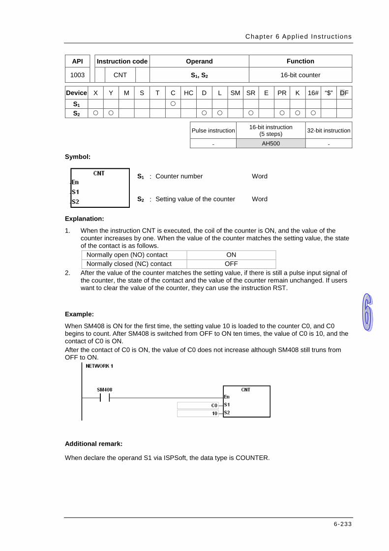
Chapter 6 Appl ied Instruc t ions
6-233
API Instruction code Operand Function
1003 CNT S1, S2 16-bit counter
Device X Y M S T C HC D L SM SR E PR K 16# “$” DF
S1 S2
Pulse instruction 16-bit instruction
(5 steps) 32-bit instruction
- AH500 -
Symbol:
S1 : Counter number Word
S2 : Setting value of the counter Word
Explanation:
1. When the instruction CNT is executed, the coil of the counter is ON, and the value of the counter increases by one. When the value of the counter matches the setting value, the state of the contact is as follows.
Normally open (NO) contact ON Normally closed (NC) contact OFF
2. After the value of the counter matches the setting value, if there is still a pulse input signal of the counter, the state of the contact and the value of the counter remain unchanged. If users want to clear the value of the counter, they can use the instruction RST.
Example:
When SM408 is ON for the first time, the setting value 10 is loaded to the counter C0, and C0 begins to count. After SM408 is switched from OFF to ON ten times, the value of C0 is 10, and the contact of C0 is ON. After the contact of C0 is ON, the value of C0 does not increase although SM408 still truns from OFF to ON.
Additional remark:
When declare the operand S1 via ISPSoft, the data type is COUNTER.
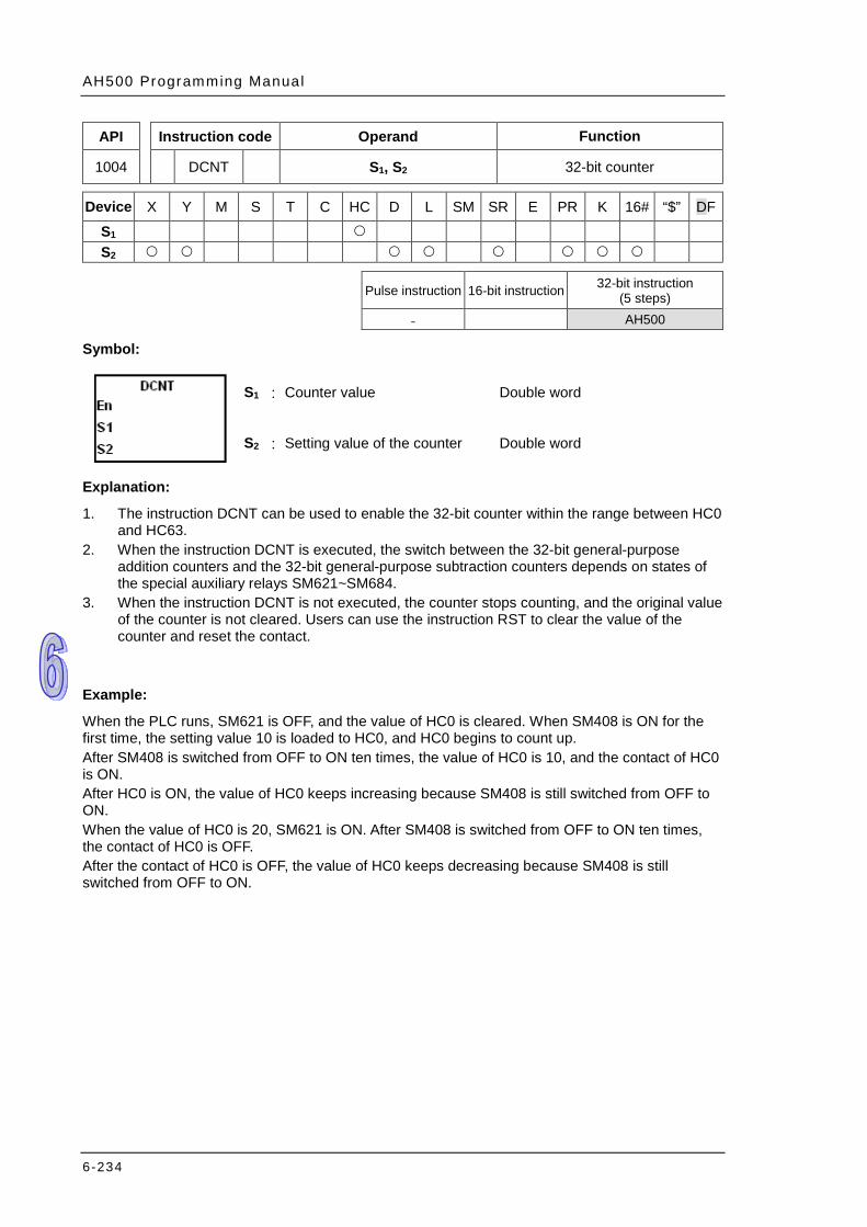
AH500 Programming Manual
6-234
API Instruction code Operand Function
1004 DCNT S1, S2 32-bit counter
Device X Y M S T C HC D L SM SR E PR K 16# “$” DF
S1 S2
Pulse instruction 16-bit instruction 32-bit instruction
(5 steps)
- AH500
Symbol:
S1 : Counter value Double word
S2 : Setting value of the counter Double word
Explanation:
1. The instruction DCNT can be used to enable the 32-bit counter within the range between HC0 and HC63.
2. When the instruction DCNT is executed, the switch between the 32-bit general-purpose addition counters and the 32-bit general-purpose subtraction counters depends on states of the special auxiliary relays SM621~SM684.
3. When the instruction DCNT is not executed, the counter stops counting, and the original value of the counter is not cleared. Users can use the instruction RST to clear the value of the counter and reset the contact.
Example:
When the PLC runs, SM621 is OFF, and the value of HC0 is cleared. When SM408 is ON for the first time, the setting value 10 is loaded to HC0, and HC0 begins to count up. After SM408 is switched from OFF to ON ten times, the value of HC0 is 10, and the contact of HC0 is ON. After HC0 is ON, the value of HC0 keeps increasing because SM408 is still switched from OFF to ON. When the value of HC0 is 20, SM621 is ON. After SM408 is switched from OFF to ON ten times, the contact of HC0 is OFF. After the contact of HC0 is OFF, the value of HC0 keeps decreasing because SM408 is still switched from OFF to ON.
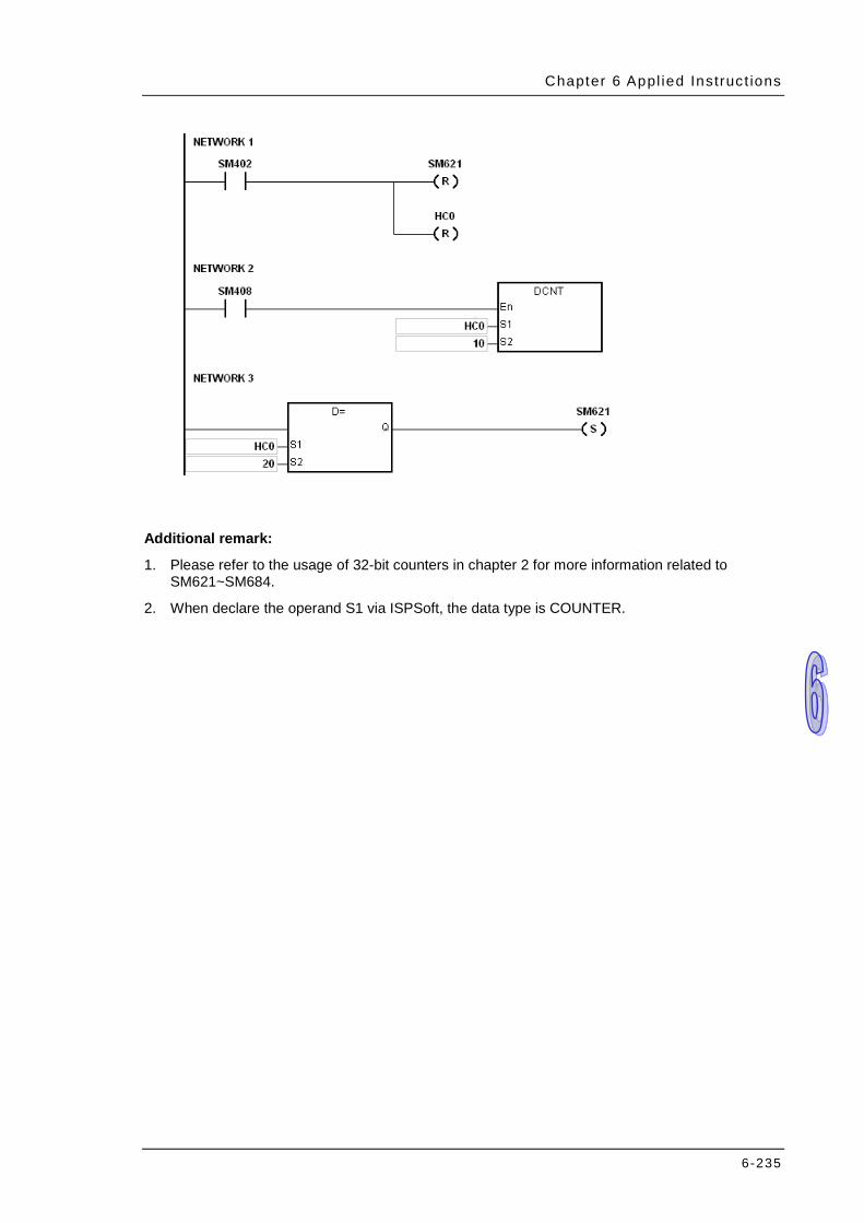
Chapter 6 Appl ied Instruc t ions
6-235
Additional remark:
1. Please refer to the usage of 32-bit counters in chapter 2 for more information related to SM621~SM684.
2. When declare the operand S1 via ISPSoft, the data type is COUNTER.

AH500 Programming Manual
6-236
6.12 Shift Instructions
6.12.1 The List of Shift Instructions
API Instruction code Pulse instruction Function Step 16-bit 32-bit
1100 SFTR – Shifting the states of the devices to the right 9 1101 SFTL – Shifting the states of the devices to the left 9
1102 WSFR – Shifting the data in the word devices to the right 9
1103 WSFL – Shifting the data in the word devices to the left 9
1104 SFWR – Shifting the data and writing it into the word device 7
1105 SFRD – Shifting the data and reading it from the word device 7
1106 SFPO – Reading the latest data from the data list 5 1107 SFDEL – Deleting the data from the data list 7 1108 SFINS – Inserting the data into the data list 7 1109 MBS – Shifting the matrix bits 7
1110 SFR – Shifting the values of the bits in the 16-bit registers by n bits to the right 5
1111 SFL – Shifting the values of the bits in the 16-bit registers by n bits to the left 5
1112 BSFR – Shifting the states of the n bit devices by one bit to the right 5
1113 BSFL – Shifting the states of the n bit devices by one bit to the left 5
1114 NSFR – Shifting n registers to the right 5 1115 NSFL – Shifting n registers to the left 5
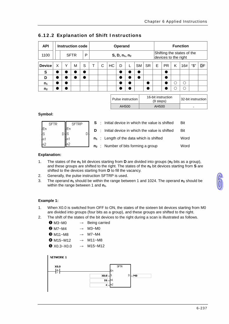
Chapter 6 Appl ied Inst ruct ions
6-237
6.12.2 Explanation of Shift Instructions
API Instruction code Operand Function
1100 SFTR P S, D, n1, n2 Shifting the states of the devices to the right
Device X Y M S T C HC D L SM SR E PR K 16# “$” DF
S D n1 n2
Pulse instruction 16-bit instruction
(9 steps) 32-bit instruction
AH500 AH500 -
Symbol:
S : Initial device in which the value is shifted Bit
D : Initial device in which the value is shifted Bit
n1 : Length of the data which is shifted Word
n2 : Number of bits forming a group Word
Explanation:
1. The states of the n1 bit devices starting from D are divided into groups (n2 bits as a group), and these groups are shifted to the right. The states of the n2 bit devices starting from S are shifted to the devices starting from D to fill the vacancy.
2. Generally, the pulse instruction SFTRP is used. 3. The operand n1 should be within the range between 1 and 1024. The operand n2 should be
within the range between 1 and n1.
Example 1:
1. When X0.0 is switched from OFF to ON, the states of the sixteen bit devices starting from M0 are divided into groups (four bits as a group), and these groups are shifted to the right.
2. The shift of the states of the bit devices to the right during a scan is illustrated as follows. M3~M0 → Being carried M7~M4 → M3~M0 M11~M8 → M7~M4 M15~M12 → M11~M8 X0.3~X0.0 → M15~M12

AH500 Programming Manual
6-238
X0.3 X0.2 X0.1 X0.0
M15 M14 M13 M12 M11 M10 M9 M8 M7 M6
34
5
Four bits as a group are shifted to the r ight.
M5 M4 M3 M2 M1 M0
12
Example 2: 1. When X0.0 is switched from OFF to ON, the states of the sixteen bit devices starting from M0
are divided into groups (five bits as a group), and these groups are shifted to the right. 2. The shift of the states of the bit devices to the right during a scan is illustrated as follows.
M0 → Being carried M5 → M0 M10~M6 → M5~M1 M15~M11 → M10~M6 X0.4~X0.0 → M15~M11
X0.3 X0.2 X0.1 X0.0
M15 M14 M13 M12 M11 M10 M9 M8 M7 M6
3
5
Five bits as a group is shifted to the right.
M5 M4 M3 M2 M1 M0
12
X0.4
4 Additional remark:
1. If S+n2-1 or D+n1-1 exceeds the device range, the instruction is not executed, SM0 is ON, and the error code in SR0 is 16#2003.
2. If n1 is less than 1, or if n1 is larger than 1024, the instruction is not executed, SM0 is ON, and the error code in SR0 is 16#200B.
3. If n2 is less than 1, or if n2 is larger than n1, the instruction is not executed, SM0 is ON, and the error code in SR0 is 16#200B.
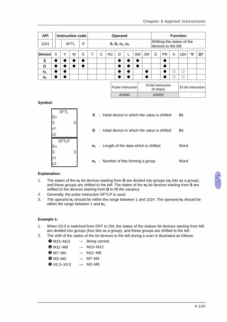
Chapter 6 Appl ied Inst ruct ions
6-239
API Instruction code Operand Function
1101 SFTL P S, D, n1, n2 Shifting the states of the devices to the left
Device X Y M S T C HC D L SM SR E PR K 16# “$” DF
S D n1 n2
Pulse instruction 16-bit instruction
(9 steps) 32-bit instruction
AH500 AH500 -
Symbol:
S : Initial device in which the value is shifted Bit
D : Initial device in which the value is shifted Bit
n1 : Length of the data which is shifted Word
n2 : Number of bits forming a group Word
Explanation:
1. The states of the n1 bit devices starting from D are divided into groups (n2 bits as a group), and these groups are shifted to the left. The states of the n2 bit devices starting from S are shifted to the devices starting from D to fill the vacancy.
2. Generally, the pulse instruction SFTLP is used. 3. The operand n1 should be within the range between 1 and 1024. The operand n2 should be
within the range between 1 and n1.
Example 1:
1. When X0.0 is switched from OFF to ON, the states of the sixteen bit devices starting from M0 are divided into groups (four bits as a group), and these groups are shifted to the left.
2. The shift of the states of the bit devices to the left during a scan is illustrated as follows. M15~M12 → Being carried M11~M8 → M15~M12 M7~M4 → M11~M8 M3~M0 → M7~M4 X0.3~X0.0 → M3~M0
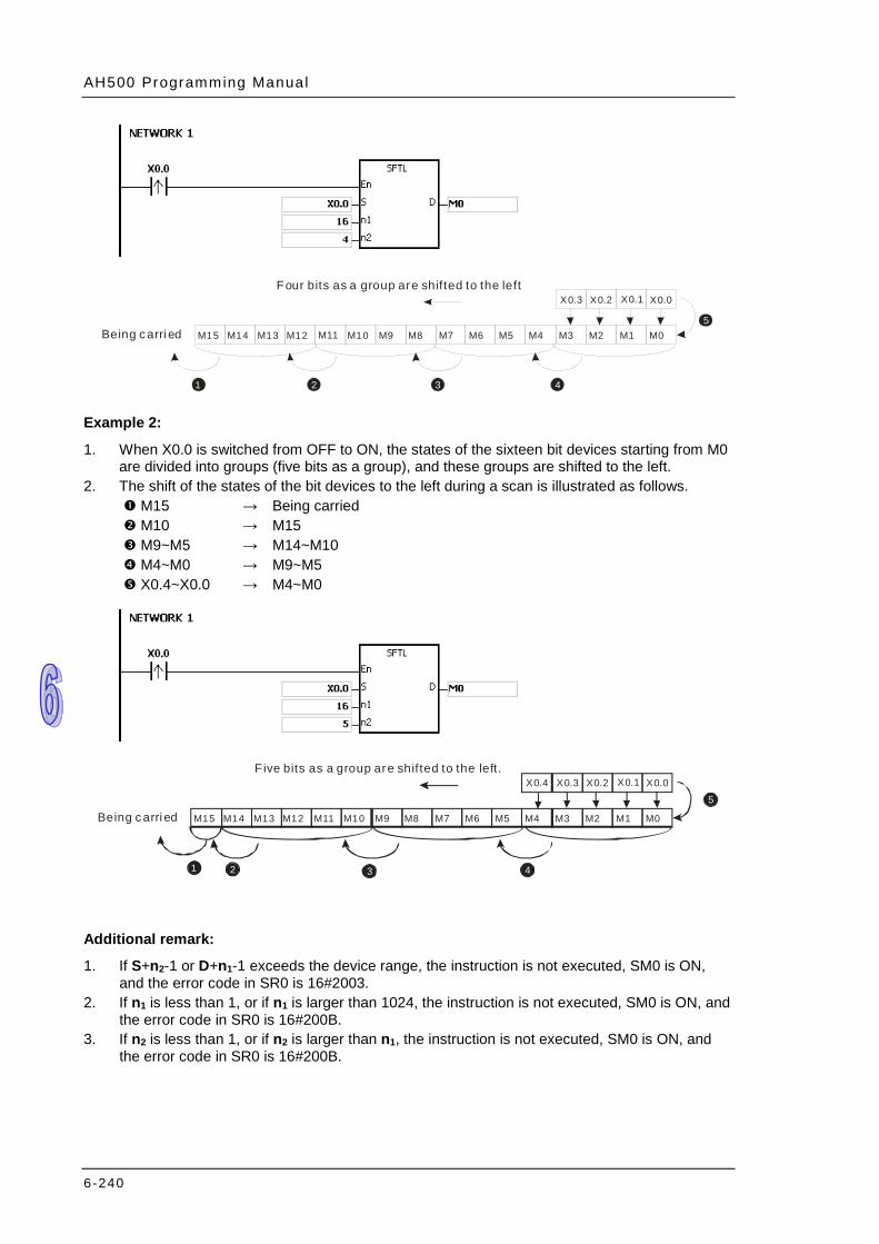
AH500 Programming Manual
6-240
1 2 3
Four bits as a group are shifted to the left
Being carri ed M15 M14 M13 M12 M11 M10 M9 M8 M7
X0.3 X0.2 X0.1 X0.0
4
5M6 M5 M4 M3 M2 M1 M0
Example 2: 1. When X0.0 is switched from OFF to ON, the states of the sixteen bit devices starting from M0
are divided into groups (five bits as a group), and these groups are shifted to the left. 2. The shift of the states of the bit devices to the left during a scan is illustrated as follows.
M15 → Being carried M10 → M15 M9~M5 → M14~M10 M4~M0 → M9~M5 X0.4~X0.0 → M4~M0
1 2 3
F ive bits as a group are shifted to the left.
Being carri ed M15 M14 M13 M12 M11 M10 M9 M8 M7
X0.3 X0.2 X0.1 X0.0
4
M6 M5 M4 M3 M2 M1 M0
5X0.4
Additional remark:
1. If S+n2-1 or D+n1-1 exceeds the device range, the instruction is not executed, SM0 is ON, and the error code in SR0 is 16#2003.
2. If n1 is less than 1, or if n1 is larger than 1024, the instruction is not executed, SM0 is ON, and the error code in SR0 is 16#200B.
3. If n2 is less than 1, or if n2 is larger than n1, the instruction is not executed, SM0 is ON, and the error code in SR0 is 16#200B.

Chapter 6 Appl ied Inst ruct ions
6-241
API Instruction code Operand Function
1102 WSFR P S, D, n1, n2 Shifting the data in the word devices to the right
Device X Y M S T C HC D L SM SR E PR K 16# “$” DF
S D n1 n2
Pulse instruction 16-bit instruction
(9 steps) 32-bit instruction
AH500 AH500 -
Symbol:
S : Initial device in which the value is shifted Word
D : Initial device in which the value is shifted Word
n1 : Length of the data which is shifted Word
n2 : Number of bits forming a group Word
Explanation:
1. The data in the n1 word devices starting from D is divided into groups (n2 words as a group), and these groups are shifted to the right. The data in the n2 word devices starting from S are shifted to the devices starting from D to fill the vacancy.
2. Generally, the pulse instruction WSFRP is used. 3. The operand n1 should be within the range between 1 and 512. The operand n2 should be
within the range between 1 and n1.
Example 1:
1. When X0.0 is switched from OFF to ON, the data in the sixteen word devices starting from D20 is divided into groups (four words as a group), and these groups are shifted to the right.
2. The shift of the data in the word devices to the right during a scan is illustrated as follows. D23~D20 → Being carried D27~D24 → D23~D20 D31~D28 → D27~D24 D35~D32 → D31~D28 D13~D10 → D35~D32

AH500 Programming Manual
6-242
D13 D12 D11 D10
D35 D34 D33 D32 D31 D30 D29 D28 D27
34
5
Four regi sters as a group are shifted to the r ight.
D26 D25 D24 D23 D22 D21 D20
12
Being carri ed
Example 2: 1. When X0.0 is switched from OFF to ON, the data in the sixteen word devices starting from
D20 is divided into groups (five words as a group), and these groups are shifted to the right. 2. The shift of the data in the word devices to the right during a scan is illustrated as follows.
D20 → Being carried D25 → D20 D30~D26 → D25~D21 D35~D31 → D30~D26 D14~D10 → D35~D31
D14 D13 D12 D11
D35 D34 D33 D32 D31 D30 D29 D28 D27
34
5
Five regi sters as a group are shifter to the right.
D26 D25 D24 D23 D22 D21 D20
12
Being carri ed
D10
Additional remark: 1. If S+n2-1 or D+n1-1 exceeds the device range, the instruction is not executed, SM0 is ON,
and the error code in SR0 is 16#2003. 2. If n1 is less than 1, or if n1 is larger than 512, the instruction is not executed, SM0 is ON, and
the error code in SR0 is 16#200B. 3. If n2 is less than 1, or if n2 is larger than n1, the instruction is not executed, SM0 is ON, and
the error code in SR0 is 16#200B.
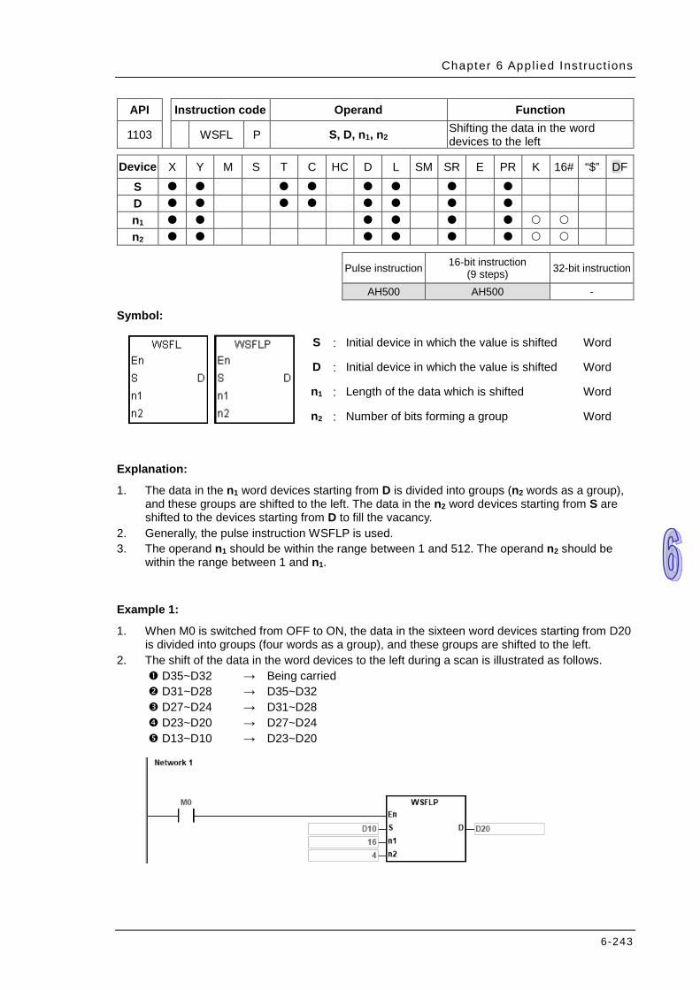
Chapter 6 Appl ied Inst ruct ions
6-243
API Instruction code Operand Function
1103 WSFL P S, D, n1, n2 Shifting the data in the word devices to the left
Device X Y M S T C HC D L SM SR E PR K 16# “$” DF
S D n1 n2
Pulse instruction 16-bit instruction
(9 steps) 32-bit instruction
AH500 AH500 -
Symbol:
S : Initial device in which the value is shifted Word
D : Initial device in which the value is shifted Word
n1 : Length of the data which is shifted Word
n2 : Number of bits forming a group Word
Explanation:
1. The data in the n1 word devices starting from D is divided into groups (n2 words as a group), and these groups are shifted to the left. The data in the n2 word devices starting from S are shifted to the devices starting from D to fill the vacancy.
2. Generally, the pulse instruction WSFLP is used. 3. The operand n1 should be within the range between 1 and 512. The operand n2 should be
within the range between 1 and n1.
Example 1:
1. When M0 is switched from OFF to ON, the data in the sixteen word devices starting from D20 is divided into groups (four words as a group), and these groups are shifted to the left.
2. The shift of the data in the word devices to the left during a scan is illustrated as follows. D35~D32 → Being carried D31~D28 → D35~D32 D27~D24 → D31~D28 D23~D20 → D27~D24 D13~D10 → D23~D20
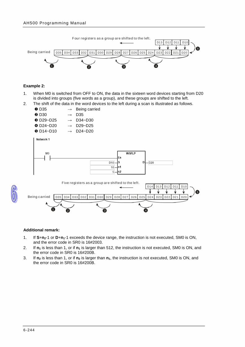
AH500 Programming Manual
6-244
D35 D34 D33 D32 D31 D30 D29 D28 D27
4
5
Four regi sters as a group are shifted to the l eft.
3
D13 D12 D11 D10
D26 D25 D24 D23 D22 D21 D20
21
Being carri ed
Example 2: 1. When M0 is switched from OFF to ON, the data in the sixteen word devices starting from D20
is divided into groups (five words as a group), and these groups are shifted to the left. 2. The shift of the data in the word devices to the left during a scan is illustrated as follows.
D35 → Being carried D30 → D35 D29~D25 → D34~D30 D24~D20 → D29~D25 D14~D10 → D24~D20
D14 D13 D12 D11
D35 D34 D33 D32 D31 D30 D29 D28 D27
3 4
5
Five regi sters as a group are shifted to the left.
D26 D25 D24 D23 D22 D21 D20
1 2
Being carri ed
D10
Additional remark:
1. If S+n2-1 or D+n1-1 exceeds the device range, the instruction is not executed, SM0 is ON, and the error code in SR0 is 16#2003.
2. If n1 is less than 1, or if n1 is larger than 512, the instruction is not executed, SM0 is ON, and the error code in SR0 is 16#200B.
3. If n2 is less than 1, or if n2 is larger than n1, the instruction is not executed, SM0 is ON, and the error code in SR0 is 16#200B.
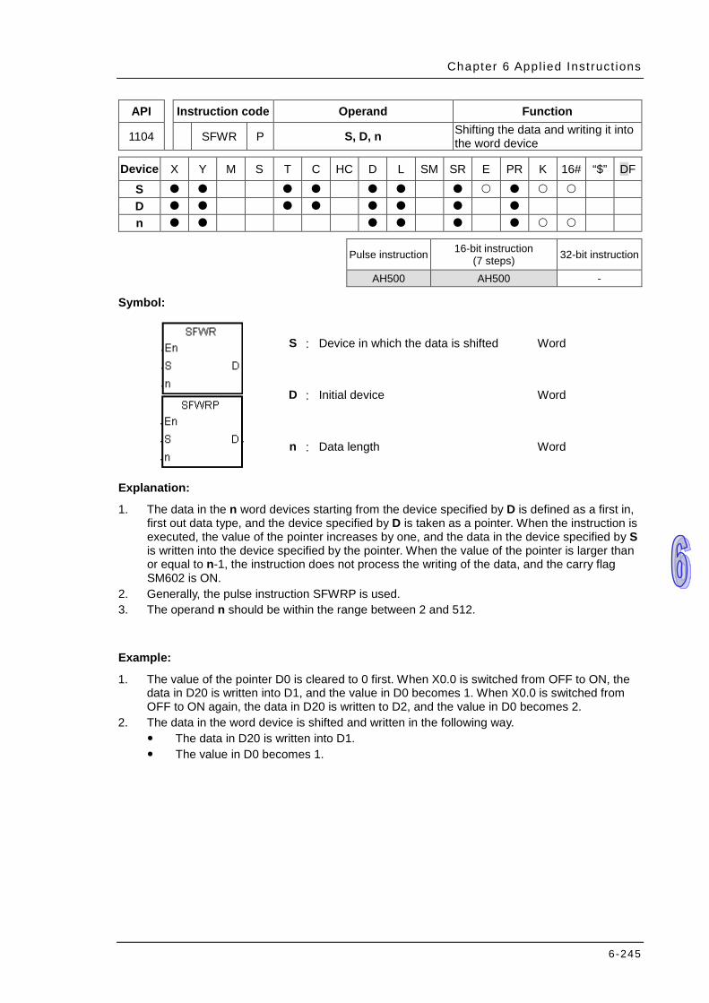
Chapter 6 Appl ied Inst ruct ions
6-245
API Instruction code Operand Function
1104 SFWR P S, D, n Shifting the data and writing it into the word device
Device X Y M S T C HC D L SM SR E PR K 16# “$” DF
S D n
Pulse instruction 16-bit instruction
(7 steps) 32-bit instruction
AH500 AH500 -
Symbol:
S : Device in which the data is shifted Word
D : Initial device Word
n : Data length Word
Explanation:
1. The data in the n word devices starting from the device specified by D is defined as a first in, first out data type, and the device specified by D is taken as a pointer. When the instruction is executed, the value of the pointer increases by one, and the data in the device specified by S is written into the device specified by the pointer. When the value of the pointer is larger than or equal to n-1, the instruction does not process the writing of the data, and the carry flag SM602 is ON.
2. Generally, the pulse instruction SFWRP is used. 3. The operand n should be within the range between 2 and 512.
Example:
1. The value of the pointer D0 is cleared to 0 first. When X0.0 is switched from OFF to ON, the data in D20 is written into D1, and the value in D0 becomes 1. When X0.0 is switched from OFF to ON again, the data in D20 is written to D2, and the value in D0 becomes 2.
2. The data in the word device is shifted and written in the following way. The data in D20 is written into D1. The value in D0 becomes 1.
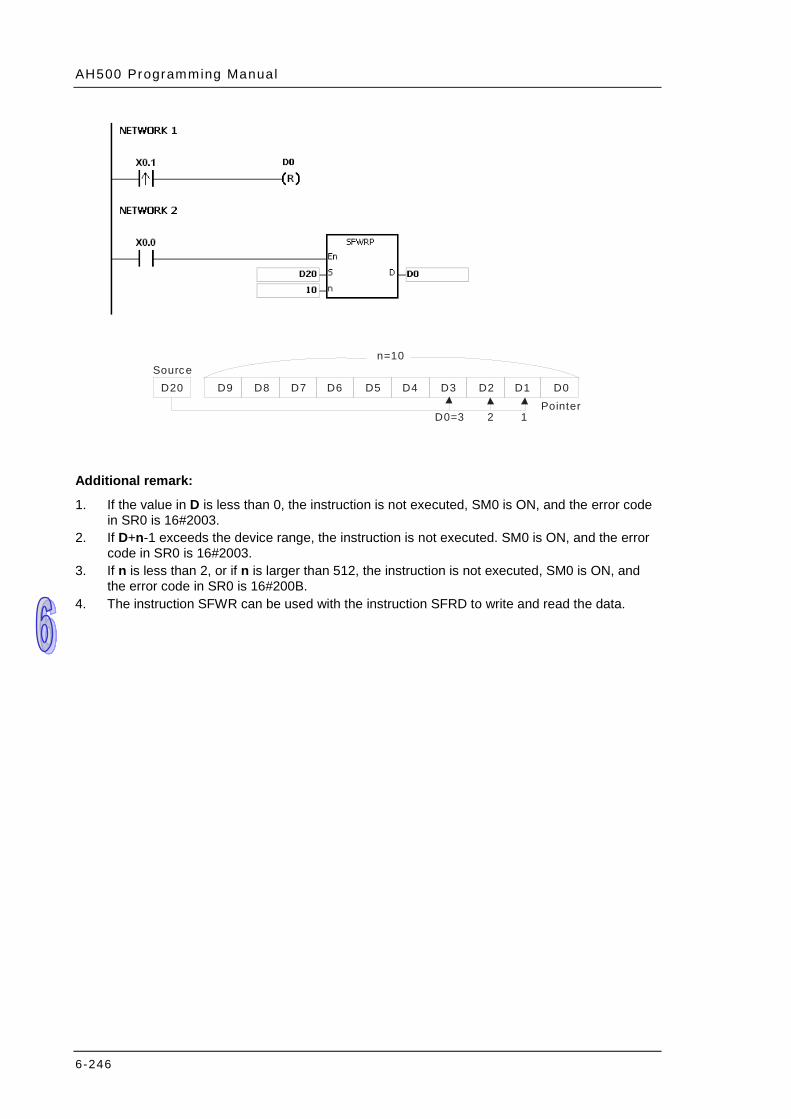
AH500 Programming Manual
6-246
D20 D9 D8 D7 D6 D5 D4 D3 D2 D1 D0
n=10
PointerD0=3 2 1
Source
Additional remark:
1. If the value in D is less than 0, the instruction is not executed, SM0 is ON, and the error code in SR0 is 16#2003.
2. If D+n-1 exceeds the device range, the instruction is not executed. SM0 is ON, and the error code in SR0 is 16#2003.
3. If n is less than 2, or if n is larger than 512, the instruction is not executed, SM0 is ON, and the error code in SR0 is 16#200B.
4. The instruction SFWR can be used with the instruction SFRD to write and read the data.
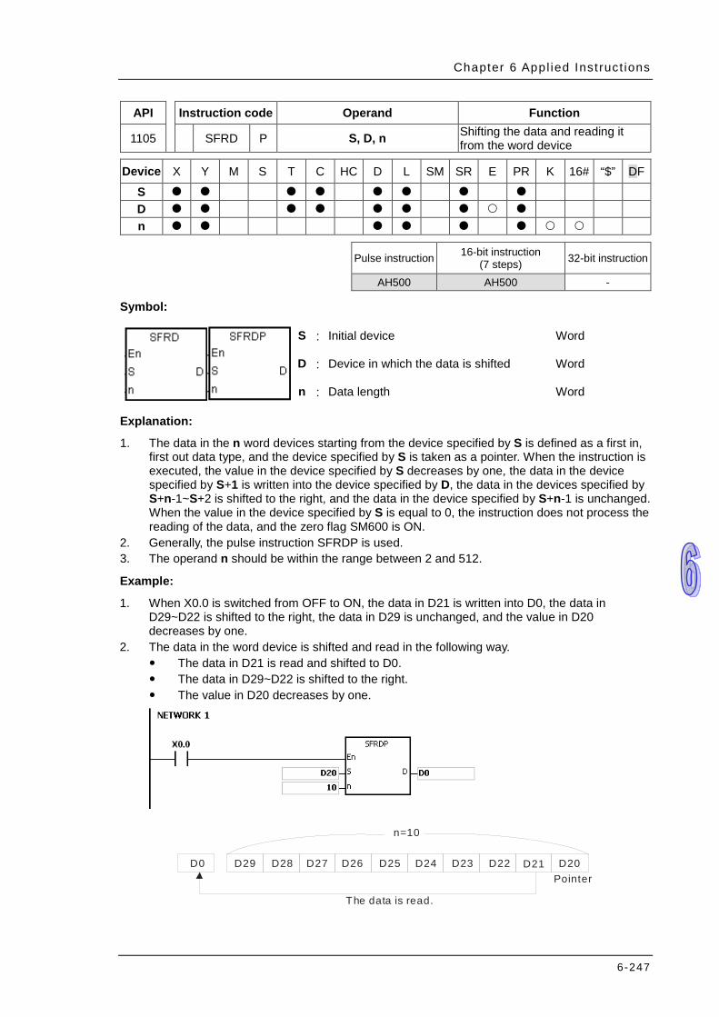
Chapter 6 Appl ied Inst ruct ions
6-247
API Instruction code Operand Function
1105 SFRD P S, D, n Shifting the data and reading it from the word device
Device X Y M S T C HC D L SM SR E PR K 16# “$” DF
S D n
Pulse instruction 16-bit instruction
(7 steps) 32-bit instruction
AH500 AH500 -
Symbol:
S : Initial device Word
D : Device in which the data is shifted Word
n : Data length Word
Explanation:
1. The data in the n word devices starting from the device specified by S is defined as a first in, first out data type, and the device specified by S is taken as a pointer. When the instruction is executed, the value in the device specified by S decreases by one, the data in the device specified by S+1 is written into the device specified by D, the data in the devices specified by S+n-1~S+2 is shifted to the right, and the data in the device specified by S+n-1 is unchanged. When the value in the device specified by S is equal to 0, the instruction does not process the reading of the data, and the zero flag SM600 is ON.
2. Generally, the pulse instruction SFRDP is used. 3. The operand n should be within the range between 2 and 512.
Example:
1. When X0.0 is switched from OFF to ON, the data in D21 is written into D0, the data in D29~D22 is shifted to the right, the data in D29 is unchanged, and the value in D20 decreases by one.
2. The data in the word device is shifted and read in the following way. The data in D21 is read and shifted to D0. The data in D29~D22 is shifted to the right. The value in D20 decreases by one.
D0 D29 D28 D27 D26 D25 D24 D23 D22 D21 D20
n=10
The data is read.
Pointer
AH500 Programming Manual
6-248
Additional remark:
1. If the value in S is less than 0, the instruction is not executed, SM0 is ON, and the error code in SR0 is 16#2003.
2. If S+n-1 exceeds the device range, the instruction is not executed, SM0 is ON, and the error code in SR0 is 16#2003.
3. If n is less than 2, or if n is larger than 512, the instruction is not executed, SM0 is ON, and the error code in SR0 is 16#200B.
4. The instruction SFWR can be used with the instruction SFRD to write and read the data.

Chapter 6 Appl ied Inst ruct ions
6-249
API Instruction code Operand Function
1106 SFPO P S, D Reading the latest data from the data list
Device X Y M S T C HC D L SM SR E PR K 16# “$” DF
S D
Pulse instruction 16-bit instruction
(5 steps) 32-bit instruction
AH500 AH500 -
Symbol:
S : Initial device Word
D : Device in which the data is stored Word
Explanation:
1. The device specified by S is taken as a pointer. When the instruction is executed, the data in the device specified by the value of the pointer is written into the device specified by D and cleared to 0, and the value in the device specified by S decreases by one. When the value in the device specified by S is equal to 0, the instruction does not process the reading of the data, and the zero flag SM600 is ON.
2. Generally, the pulse instruction SFPOP is used.
Example:
When X0.0 is ON, the data in the device specified by the value in D0 is written into D10. After the data is shifted, the data in the device specified by the value in D0 is cleared to 0, and the value in D0 increases by one.
D10 D9 D8 D7 D6 D5 D4 D3 D2 D1 D0
Pointer1000 7
SD
The data is read.
D10 D9 D8 D7 D6 D5 D4 D3 D2 D1 D01000 6
Pointer0

AH500 Programming Manual
6-250
Additional remark:
1. If the value in S is less than 0, the instruction is not executed, SM0 is ON, and the error code in SR0 is 16#2003.
2. If S+(The value in S) exceeds the device range, the instruction is not executed, SM0 is ON, and the error code in SR0 is 16#2003.
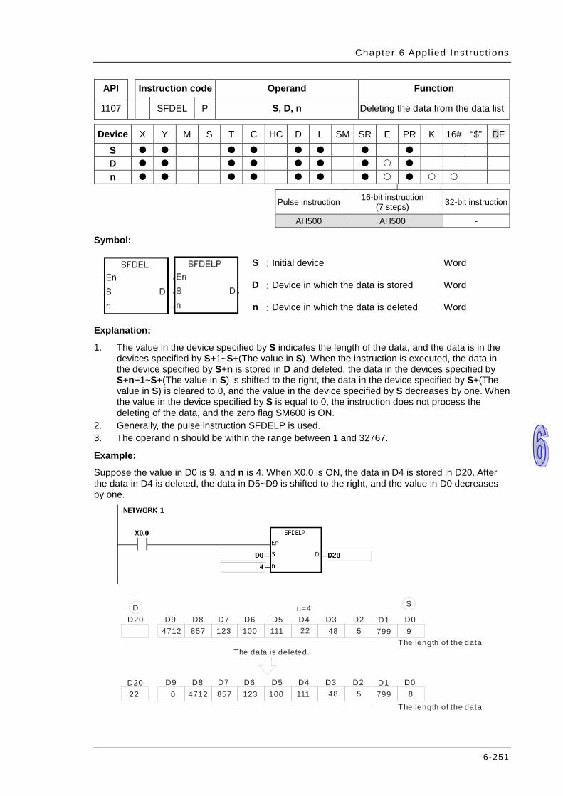
Chapter 6 Appl ied Inst ruct ions
6-251
API Instruction code Operand Function
1107 SFDEL P S, D, n Deleting the data from the data list
Device X Y M S T C HC D L SM SR E PR K 16# “$” DF
S D n
Pulse instruction 16-bit instruction
(7 steps) 32-bit instruction
AH500 AH500 -
Symbol:
S : Initial device Word
D : Device in which the data is stored Word
n : Device in which the data is deleted Word
Explanation:
1. The value in the device specified by S indicates the length of the data, and the data is in the devices specified by S+1~S+(The value in S). When the instruction is executed, the data in the device specified by S+n is stored in D and deleted, the data in the devices specified by S+n+1~S+(The value in S) is shifted to the right, the data in the device specified by S+(The value in S) is cleared to 0, and the value in the device specified by S decreases by one. When the value in the device specified by S is equal to 0, the instruction does not process the deleting of the data, and the zero flag SM600 is ON.
2. Generally, the pulse instruction SFDELP is used. 3. The operand n should be within the range between 1 and 32767.
Example:
Suppose the value in D0 is 9, and n is 4. When X0.0 is ON, the data in D4 is stored in D20. After the data in D4 is deleted, the data in D5~D9 is shifted to the right, and the value in D0 decreases by one.
D20 D9 D8 D7 D6 D5 D4 D3 D2 D1 D0
The length of the data9
SD
The data is deleted.
D20 D8 D7 D6 D5 D4 D3 D2 D1 D022 8
4712 857 123 100 111 22 48 5 799
4712 857 123 100 111 48 5 799
n=4
D90
The length of the data
AH500 Programming Manual
6-252
Additional remark:
1. If the value in S is less than 0, the instruction is not executed, SM0 is ON, and the error code in SR0 is 16#2003.
2. If S+n exceeds the device range, the instruction is not executed, SM0 is ON, and the error code in SR0 is 16#2003.
3. If S+(The value in S) exceeds the device range, the instruction is not executed, SM0 is ON, and the error code in SR0 is 16#2003.
4. If n is larger than the value in S, the instruction is not executed, SM0 is ON, and the error code in SR0 is 16#200B.
5. If n is less than 0, the instruction is not executed, SM0 is ON, and the error code in SR0 is 16#200B.

Chapter 6 Appl ied Inst ruct ions
6-253
API Instruction code Operand Function
1108 SFINS P S, D, n Inserting the data into the data list
Device X Y M S T C HC D L SM SR E PR K 16# “$” DF
S D n
Pulse instruction 16-bit instruction
(7 steps) 32-bit instruction
AH500 AH500 -
Symbol:
S : Initial device Word
D : Data which is inserted Word
n : Device into which the data is inserted Word
Explanation:
1. The value in the device specified by S indicates the length of the data, and the data is in the devices specified by S+1~S+(The value in S). When the instruction is executed, the data in D is inserted into S+n, the original data in the devices specified by S+n~S+(The value in S) is shifted to the left, and the value in the device specified by S increases by one. When the value in the device specified by S is equal to 32767, the instruction does not process the writing of the data, the value in the device specified by S does not increase, and the carry flag SM602 is ON.
2. Generally, the pulse instruction SFINSP is used. 3. The operand n should be within the range between 1 and 32767.
Example:
Suppose the value in D0 is 8, and n is 4. When X0.0 is ON, the data in D200 is inserted into D4, the original data in D4~D8 is shifted to D5~D9, and the value in D0 increases by one.
D200 D9 D8 D7 D6 D5 D4 D3 D2 D1 D09
SD
The data is inserted.
D200 D8 D7 D6 D5 D4 D3 D2 D1 D022 8
The length of the data
4712 857 123 100 111 22 48 5 799
4712 857 123 100 111 48 5 799
n=4
22The length of the data
AH500 Programming Manual
6-254
Additional remark:
1. If the value in S is less than 0, the instruction is not executed, SM0 is ON, and the error code in SR0 is 16#2003.
2. If S+n exceeds the device range, the instruction is not executed, SM0 is ON, and the error code in SR0 is 16#2003
3. If S+(The value in S)+1 exceeds the device range, the instruction is not executed, SM0 is ON, and the error code in SR0 is 16#2003.
4. If n is larger than the value in S, the instruction is not executed, SM0 is ON, and the error code in SR0 is 16#200B.
5. If n is less than 0, the instruction is not executed, SM0 is ON, and the error code in SR0 is 16#200B.

Chapter 6 Appl ied Inst ruct ions
6-255
API Instruction code Operand Function
1109 MBS P S, D, n Shifting the matrix bits
Device X Y M S T C HC D L SM SR E PR K 16# “$” DF
S D n
Pulse instruction 16-bit instruction
(7 steps) 32-bit instruction
AH500 AH500 -
Symbol:
S : Matrix source Word
D : Operation result Word
n : Length of the array Word
Explanation:
1. The values of the n rows of bits in S are shifted to the right or to the left. When SM616 is OFF, the values of the bits are shifted to the left. When SM616 is ON, the values of the bits are shifted to the right. The vacancy resulting from the shift is filled by the state of the borrow flag SM615, the value of the bit shifted last is transmitted to the carry flag SM614, and the operation result is stored in D.
2. The operand n should be within the range between 1 and 256. 3. Generally, the pulse instruction MBSP is used.
Example 1:
When X0.0 is ON, SM616 is OFF. The values of the bits are shifted to the left. Suppose SM615 is OFF. After the values of the bits in the 16-bit registers D0~D2 are shifted to the left, the operation result is stored in the 16-bit registers D20~D22, and SM614 is ON.
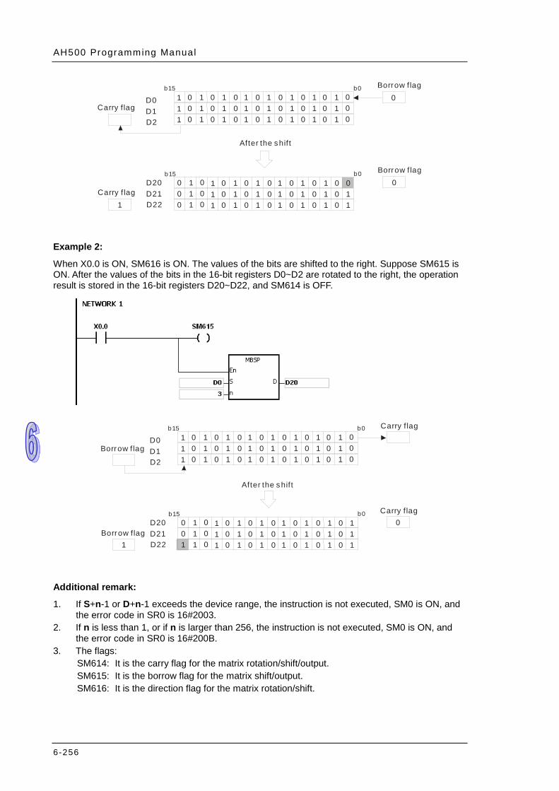
AH500 Programming Manual
6-256
1 0 1 0 1 0 1 0 1 0 1 0 1 0 1 0
Borrow flag0
b0b15
b0b15
After the shift
1 0 1 0 1 0 1 0 1 0 1 0 1 0 1 01 0 1 0 1 0 1 0 1 0 1 0 1 0 1 0
D0D1D2
D20D21D22
1 0 1 0 1 0 1 0 1 0 1 0 01 0 1 0 1 0 1 0 1 0 1 0 11 0 1 0 1 0 1 0 1 0 1 0 1
0 1 00 1 00 1 0
Borrow flag
Carry f lag1
Carry f lag0
Example 2:
When X0.0 is ON, SM616 is ON. The values of the bits are shifted to the right. Suppose SM615 is ON. After the values of the bits in the 16-bit registers D0~D2 are rotated to the right, the operation result is stored in the 16-bit registers D20~D22, and SM614 is OFF.
After the shift
Borrow flag
Borrow flag
Carry f lag
Carry f lag1 0 1 0 1 0 1 0 1 0 1 0 1 0 1 0
0
b0b15
b0b15
1 0 1 0 1 0 1 0 1 0 1 0 1 0 1 01 0 1 0 1 0 1 0 1 0 1 0 1 0 1 0
D0D1D2
D20D21D22
1 0 1 0 1 0 1 0 1 0 1 0 11 0 1 0 1 0 1 0 1 0 1 0 11 0 1 0 1 0 1 0 1 0 1 0 1
0 1 00 1 01 1 01
Additional remark:
1. If S+n-1 or D+n-1 exceeds the device range, the instruction is not executed, SM0 is ON, and the error code in SR0 is 16#2003.
2. If n is less than 1, or if n is larger than 256, the instruction is not executed, SM0 is ON, and the error code in SR0 is 16#200B.
3. The flags: SM614: It is the carry flag for the matrix rotation/shift/output. SM615: It is the borrow flag for the matrix shift/output. SM616: It is the direction flag for the matrix rotation/shift.
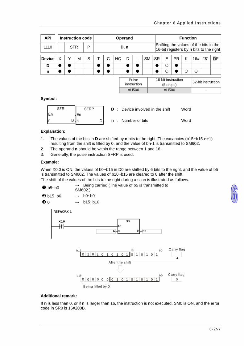
Chapter 6 Appl ied Inst ruct ions
6-257
API Instruction code Operand Function
1110 SFR P D, n Shifting the values of the bits in the 16-bit registers by n bits to the right
Device X Y M S T C HC D L SM SR E PR K 16# “$” DF
D n
Pulse
instruction 16-bit instruction
(5 steps) 32-bit instruction
AH500 AH500 -
Symbol:
D : Device involved in the shift Word
n : Number of bits Word
Explanation:
1. The values of the bits in D are shifted by n bits to the right. The vacancies (b15~b15-n+1) resulting from the shift is filled by 0, and the value of bn-1 is transmitted to SM602.
2. The operand n should be within the range between 1 and 16. 3. Generally, the pulse instruction SFRP is used.
Example:
When X0.0 is ON, the values of b0~b15 in D0 are shifted by 6 bits to the right, and the value of b5 is transmitted to SM602. The values of b10~b15 are cleared to 0 after the shift. The shift of the values of the bits to the right during a scan is illustrated as follows.
b5~b0 → Being carried (The value of b5 is transmitted to SM602.)
b15~b6 → b9~b0 0 → b15~b10
After the shift
Carry f lag
Carry f lag0
b0b15
b0b150 0 0 0 1 0 1 0 1 0 1 0 10 0 0
1 0 1 0 1 0 1 0 1 0 1 0 10 1 0※
Being f il led by 0 Additional remark:
If n is less than 0, or if n is larger than 16, the instruction is not executed, SM0 is ON, and the error code in SR0 is 16#200B.
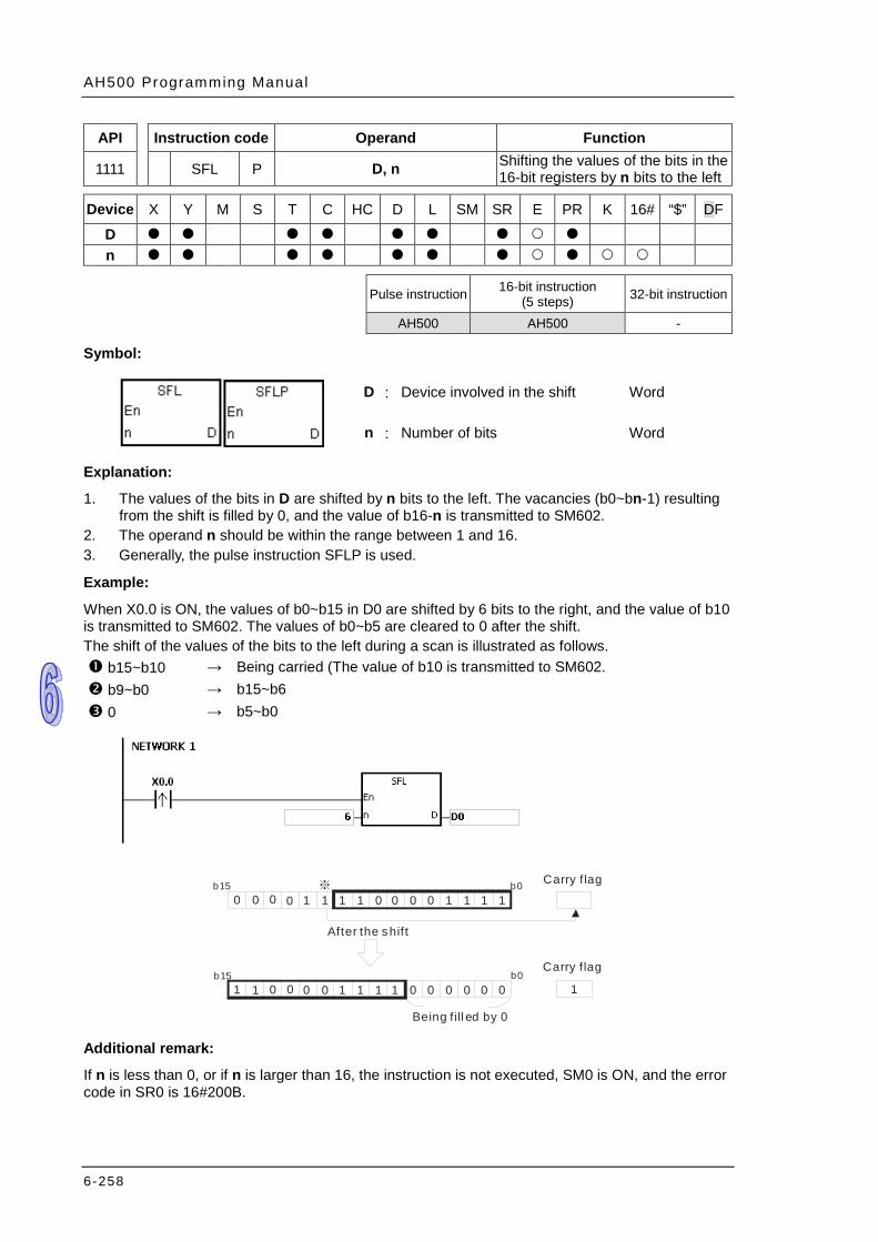
AH500 Programming Manual
6-258
API Instruction code Operand Function
1111 SFL P D, n Shifting the values of the bits in the 16-bit registers by n bits to the left
Device X Y M S T C HC D L SM SR E PR K 16# “$” DF
D n
Pulse instruction 16-bit instruction
(5 steps) 32-bit instruction
AH500 AH500 -
Symbol:
D : Device involved in the shift Word
n : Number of bits Word
Explanation:
1. The values of the bits in D are shifted by n bits to the left. The vacancies (b0~bn-1) resulting from the shift is filled by 0, and the value of b16-n is transmitted to SM602.
2. The operand n should be within the range between 1 and 16. 3. Generally, the pulse instruction SFLP is used.
Example:
When X0.0 is ON, the values of b0~b15 in D0 are shifted by 6 bits to the right, and the value of b10 is transmitted to SM602. The values of b0~b5 are cleared to 0 after the shift. The shift of the values of the bits to the left during a scan is illustrated as follows. b15~b10 → Being carried (The value of b10 is transmitted to SM602. b9~b0 → b15~b6 0 → b5~b0
After the shift
Carry f lag
Carry f lag
Being f ill ed by 0
1
b0b15
b0b150 0 0 1 1 1 1 0 0 0 0 0 01 1 0
0 1 1 1 1 0 0 0 0 1 1 1 10 0 0※
Additional remark:
If n is less than 0, or if n is larger than 16, the instruction is not executed, SM0 is ON, and the error code in SR0 is 16#200B.
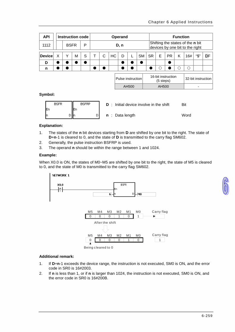
Chapter 6 Appl ied Inst ruct ions
6-259
API Instruction code Operand Function
1112 BSFR P D, n Shifting the states of the n bit devices by one bit to the right
Device X Y M S T C HC D L SM SR E PR K 16# “$” DF
D n
Pulse instruction 16-bit instruction
(5 steps) 32-bit instruction
AH500 AH500 -
Symbol:
D : Initial device involve in the shift Bit
n : Data length Word
Explanation:
1. The states of the n bit devices starting from D are shifted by one bit to the right. The state of D+n-1 is cleared to 0, and the state of D is transmitted to the carry flag SM602.
2. Generally, the pulse instruction BSFRP is used. 3. The operand n should be within the range between 1 and 1024.
Example:
When X0.0 is ON, the states of M0~M5 are shifted by one bit to the right, the state of M5 is cleared to 0, and the state of M0 is transmitted to the carry flag SM602.
After the shift
Carry f lag
Carry f lag1
M0M1M2M3M4M5
M0M1M2M3M4M5
101000
010000
Being c leared to 0 Additional remark:
1. If D+n-1 exceeds the device range, the instruction is not executed, SM0 is ON, and the error code in SR0 is 16#2003.
2. If n is less than 1, or if n is larger than 1024, the instruction is not executed, SM0 is ON, and the error code in SR0 is 16#200B.
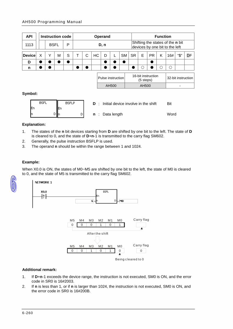
AH500 Programming Manual
6-260
API Instruction code Operand Function
1113 BSFL P D, n Shifting the states of the n bit devices by one bit to the left
Device X Y M S T C HC D L SM SR E PR K 16# “$” DF
D n
Pulse instruction 16-bit instruction
(5 steps) 32-bit instruction
AH500 AH500 -
Symbol:
D : Initial device involve in the shift Bit
n : Data length Word
Explanation:
1. The states of the n bit devices starting from D are shifted by one bit to the left. The state of D is cleared to 0, and the state of D+n-1 is transmitted to the carry flag SM602.
2. Generally, the pulse instruction BSFLP is used. 3. The operand n should be within the range between 1 and 1024.
Example:
When X0.0 is ON, the states of M0~M5 are shifted by one bit to the left, the state of M0 is cleared to 0, and the state of M5 is transmitted to the carry flag SM602.
After the shift
Carry f lag
Carry f lag
Being c leared to 0
0
M0M1M2M3M4M5
M0M1M2M3M4M5
101000
010100
Additional remark:
1. If D+n-1 exceeds the device range, the instruction is not executed, SM0 is ON, and the error code in SR0 is 16#2003.
2. If n is less than 1, or if n is larger than 1024, the instruction is not executed, SM0 is ON, and the error code in SR0 is 16#200B.
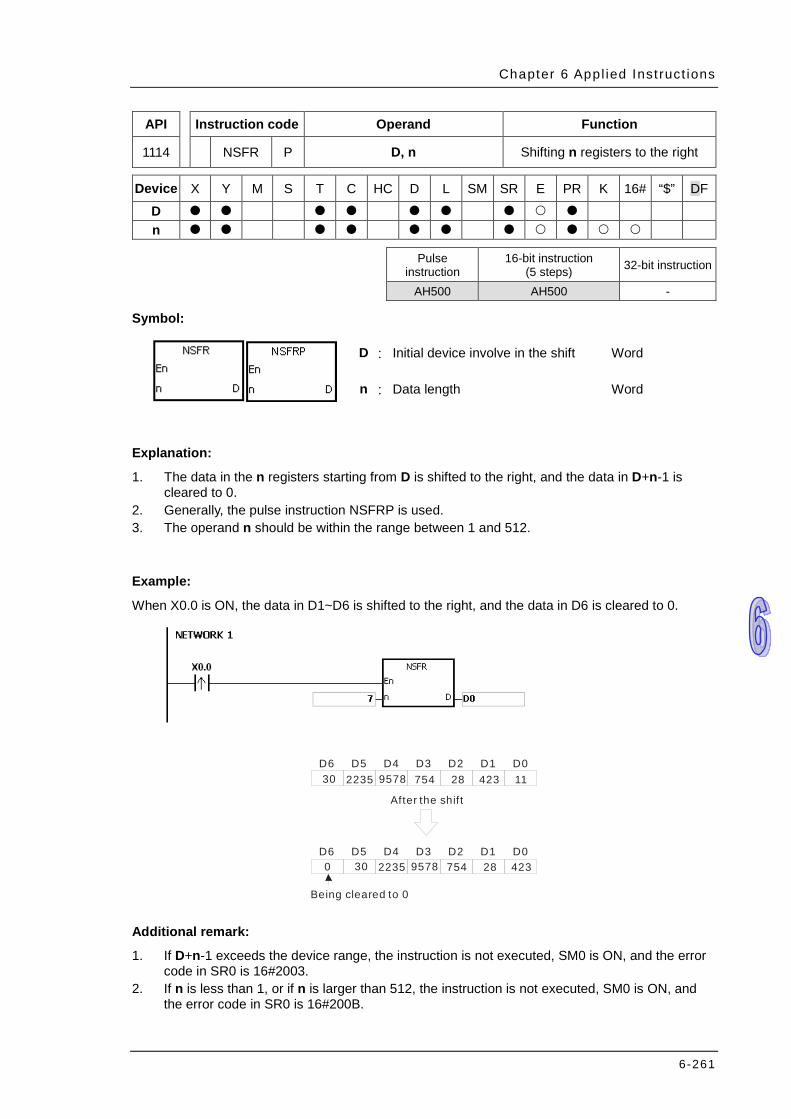
Chapter 6 Appl ied Inst ruct ions
6-261
API Instruction code Operand Function
1114 NSFR P D, n Shifting n registers to the right
Device X Y M S T C HC D L SM SR E PR K 16# “$” DF
D n
Pulse
instruction 16-bit instruction
(5 steps) 32-bit instruction
AH500 AH500 -
Symbol:
D : Initial device involve in the shift Word
n : Data length Word
Explanation:
1. The data in the n registers starting from D is shifted to the right, and the data in D+n-1 is cleared to 0.
2. Generally, the pulse instruction NSFRP is used. 3. The operand n should be within the range between 1 and 512.
Example:
When X0.0 is ON, the data in D1~D6 is shifted to the right, and the data in D6 is cleared to 0.
After the shift
Being cleared to 0
D0D1D2D3D4D5
D0D1D2D3D4D5
114232875495782235
0
30D6
D6423287549578223530
Additional remark:
1. If D+n-1 exceeds the device range, the instruction is not executed, SM0 is ON, and the error code in SR0 is 16#2003.
2. If n is less than 1, or if n is larger than 512, the instruction is not executed, SM0 is ON, and the error code in SR0 is 16#200B.
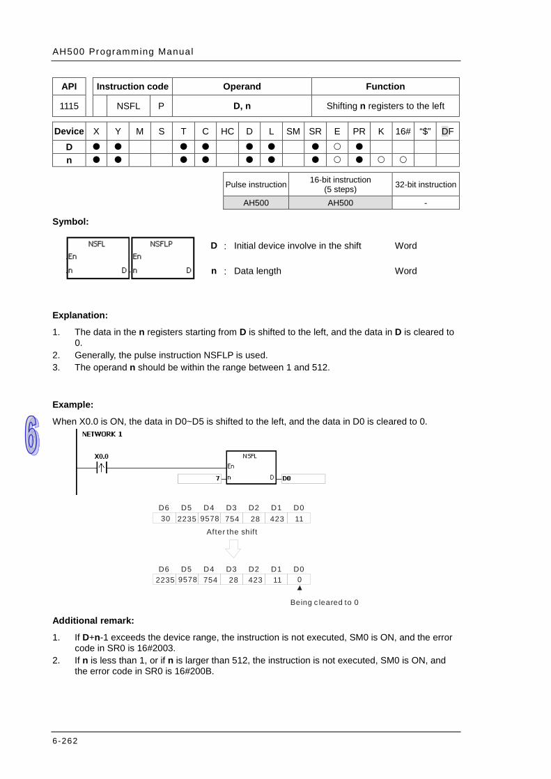
AH500 Programming Manual
6-262
API Instruction code Operand Function
1115 NSFL P D, n Shifting n registers to the left
Device X Y M S T C HC D L SM SR E PR K 16# “$” DF
D n
Pulse instruction 16-bit instruction
(5 steps) 32-bit instruction
AH500 AH500 -
Symbol:
D : Initial device involve in the shift Word
n : Data length Word
Explanation:
1. The data in the n registers starting from D is shifted to the left, and the data in D is cleared to 0.
2. Generally, the pulse instruction NSFLP is used. 3. The operand n should be within the range between 1 and 512.
Example:
When X0.0 is ON, the data in D0~D5 is shifted to the left, and the data in D0 is cleared to 0.
After the shift
Being c leared to 0
D0D1D2D3D4D5
D0D1D2D3D4D5
11423287549578223530D6
D6114232875495782235 0
Additional remark:
1. If D+n-1 exceeds the device range, the instruction is not executed, SM0 is ON, and the error code in SR0 is 16#2003.
2. If n is less than 1, or if n is larger than 512, the instruction is not executed, SM0 is ON, and the error code in SR0 is 16#200B.

Chapter 6 Appl ied Inst ruct ions
6-263
6.13 Data Processing Instructions 6.13.1 List of Data Processing Instructions
API Instruction code Pulse instruction Function Step 16-bit 32-bit
1200 SER DSER Searching the data 9 1201 SUM DSUM Number of bits whose states are ON 5 1202 DECO – Decoder 7 1203 ENCO – Encoder 7 1204 SEGD – Seven-segment decoding 5 1205 SORT DSORT – Sorting the data 11 1206 ZRST – Resetting the zone 5 1207 BON DBON Checking the state of the bit 7 1208 MEAN DMEAN Mean 7 1209 CCD – Sum check 7 1210 ABS DABS Absolute value 3 1211 MINV – Inverting the matrix bits 7 1212 MBRD – Reading the matrix bit 7 1213 MBWR – Writing the matrix bit 7 1214 MBC – Counting the bits with the value 0 or 1 7 1215 DIS – Disuniting the 16-bit data 7 1216 UNI – Uniting the 16-bit data 7 1217 WSUM DWSUM Getting the sum 7 1218 BSET – Setting the bit in the word device to ON 5 1219 BRST – Resetting the bit in the word device 5 1220 BKRST – Resetting the specified zone 5 1221 LIMIT DLIMIT Confining the value within the bounds 9 1222 BAND DBAND Deadband control 9 1223 ZONE DZONE Controlling the zone 9
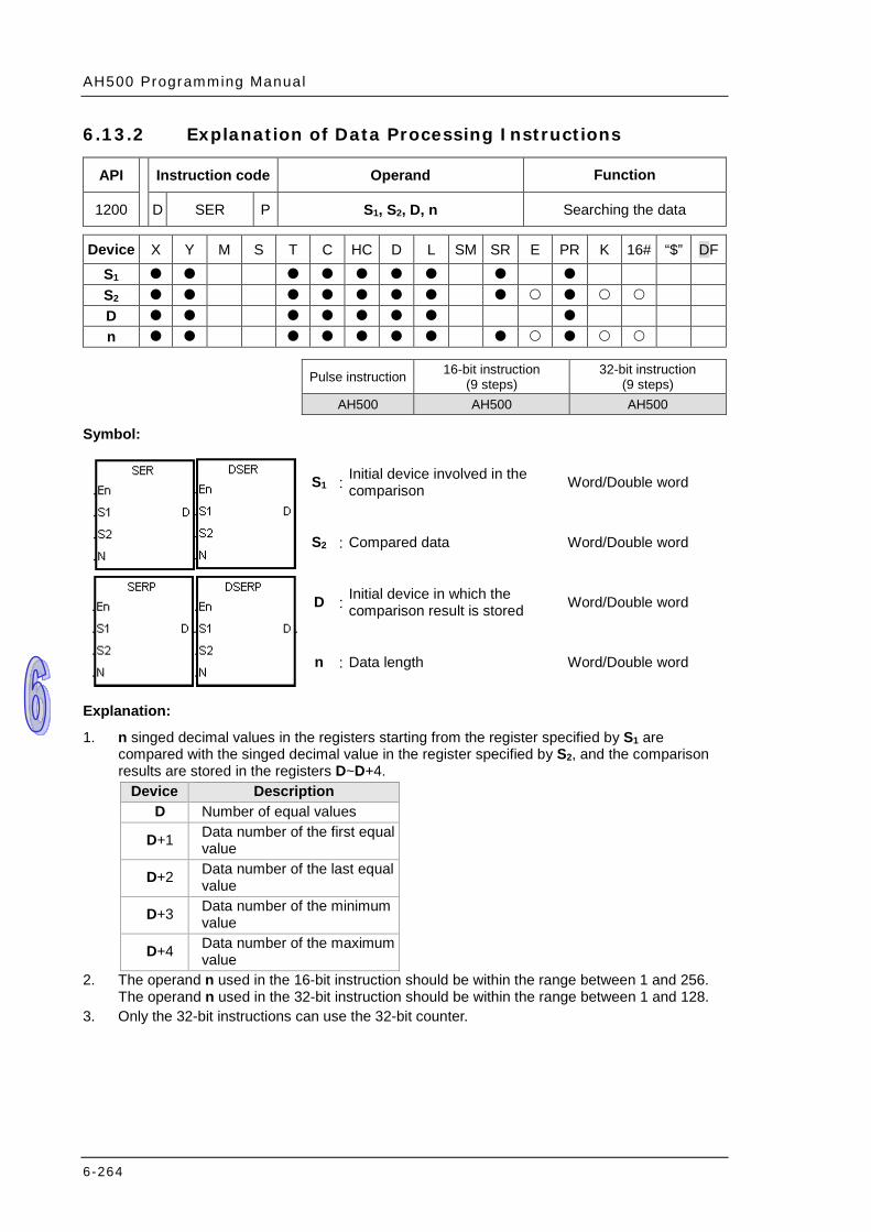
AH500 Programming Manual
6-264
6.13.2 Explanation of Data Processing Instructions
API Instruction code Operand Function
1200 D SER P S1, S2, D, n Searching the data
Device X Y M S T C HC D L SM SR E PR K 16# “$” DF
S1 S2 D n
Pulse instruction 16-bit instruction
(9 steps) 32-bit instruction
(9 steps) AH500 AH500 AH500
Symbol:
S1 : Initial device involved in the comparison Word/Double word
S2 : Compared data Word/Double word
D : Initial device in which the comparison result is stored Word/Double word
n : Data length Word/Double word
Explanation:
1. n singed decimal values in the registers starting from the register specified by S1 are compared with the singed decimal value in the register specified by S2, and the comparison results are stored in the registers D~D+4.
Device Description D Number of equal values
D+1 Data number of the first equal value
D+2 Data number of the last equal value
D+3 Data number of the minimum value
D+4 Data number of the maximum value
2. The operand n used in the 16-bit instruction should be within the range between 1 and 256. The operand n used in the 32-bit instruction should be within the range between 1 and 128.
3. Only the 32-bit instructions can use the 32-bit counter.
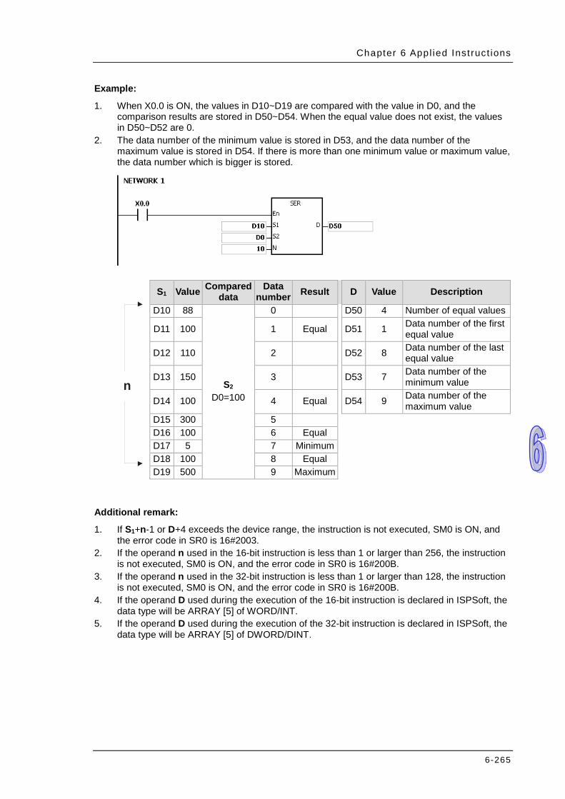
Chapter 6 Appl ied Inst ruct ions
6-265
Example:
1. When X0.0 is ON, the values in D10~D19 are compared with the value in D0, and the comparison results are stored in D50~D54. When the equal value does not exist, the values in D50~D52 are 0.
2. The data number of the minimum value is stored in D53, and the data number of the maximum value is stored in D54. If there is more than one minimum value or maximum value, the data number which is bigger is stored.
n
S1 Value Compared data
Data number Result D Value Description
D10 88
S2 D0=100
0 D50 4 Number of equal values
D11 100 1 Equal D51 1 Data number of the first equal value
D12 110 2 D52 8 Data number of the last equal value
D13 150 3 D53 7 Data number of the minimum value
D14 100 4 Equal D54 9 Data number of the maximum value
D15 300 5 D16 100 6 Equal D17 5 7 Minimum D18 100 8 Equal D19 500 9 Maximum
Additional remark:
1. If S1+n-1 or D+4 exceeds the device range, the instruction is not executed, SM0 is ON, and the error code in SR0 is 16#2003.
2. If the operand n used in the 16-bit instruction is less than 1 or larger than 256, the instruction is not executed, SM0 is ON, and the error code in SR0 is 16#200B.
3. If the operand n used in the 32-bit instruction is less than 1 or larger than 128, the instruction is not executed, SM0 is ON, and the error code in SR0 is 16#200B.
4. If the operand D used during the execution of the 16-bit instruction is declared in ISPSoft, the data type will be ARRAY [5] of WORD/INT.
5. If the operand D used during the execution of the 32-bit instruction is declared in ISPSoft, the data type will be ARRAY [5] of DWORD/DINT.
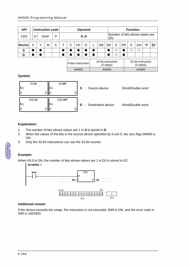
AH500 Programming Manual
6-266
API Instruction code Operand Function
1201 D SUM P S, D Number of bits whose states are ON
Device X Y M S T C HC D L SM SR E PR K 16# “$” DF
S D
Pulse instruction 16-bit instruction
(5 steps) 32-bit instruction
(5 steps) AH500 AH500 AH500
Symbol:
S : Source device Word/Double word
D : Destination device Word/Double word
Explanation:
1. The number of bits whose values are 1 in S is stored in D. 2. When the values of the bits in the source device specified by S are 0, the zero flag SM600 is
ON. 3. Only the 32-bit instructions can use the 32-bit counter.
Example:
When X0.0 is ON, the number of bits whose values are 1 in D0 is stored in D2.
0 0 0 1 0 0 1 0 0 0 0 0 0 1 0 0
b0b15
D0 D23
Additional remark:
If the device exceeds the range, the instruction is not executed, SM0 is ON, and the error code in SR0 is 16#2003.

Chapter 6 Appl ied Inst ruct ions
6-267
API Instruction code Operand Function
1202 DECO P S, D, n Decoder
Device X Y M S T C HC D L SM SR E PR K 16# “$” DF
S D n
Pulse instruction 16-bit instruction
(7 steps) 32-bit instruction
AH500 AH500 -
Symbol:
S : Source device Bit/Word
D : Device in which the decoded values are stored Bit/Word
n : Number of bits whose values are decoded Word
Explanation:
1. The values of the lower n bits in the source device specified by S are decoded as the values of the lower 2n bits in D.
2. When D is a bit device, n is within the range between 1 and 8. When n is 8, the values of the 8 bits is decoded as the values of the 256 bits. (Please note that the devices in which the decoded values are stored can not be used repeatedly.)
3. When D is a word device, n is within the range between 1 and 4. When n is 4, the values of the 4 bits is decoded as the values of the 16 bits.
4. Generally, the pulse instruction DECOP is used.
Example 1:
1. When Y0.0 is switched from OFF to ON, the instruction DECO decodes the values of the 3 bits in X0.0~X0.2 as the values of the 8 bits in M100~M107.
2. After the values of the 3 bits in X0.0~X0.2 are added up, the value 3 is gotten. The third bit in M10~M1007, that is, the bit in M103, is set to 1.
3. After the instruction DECO is executed and Y0.0 is switched OFF, the values of the 8 bits in M100~M107 are unchanged.
X0.2 X0.1
M107 M106 M105 M104 M103 M102 M101 M100
0 1 1
10 0 0 0 0 0 037 6 5 4 2 1 0
4 12
3
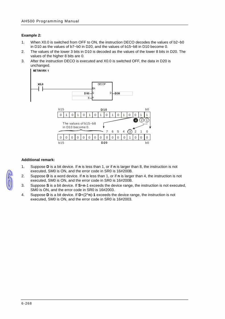
AH500 Programming Manual
6-268
Example 2:
1. When X0.0 is switched from OFF to ON, the instruction DECO decodes the values of b2~b0 in D10 as the values of b7~b0 in D20, and the values of b15~b8 in D10 become 0.
2. The values of the lower 3 bits in D10 is decoded as the values of the lower 8 bits in D20. The values of the higher 8 bits are 0.
3. After the instruction DECO is executed and X0.0 is switched OFF, the data in D20 is unchanged.
0 0 0 0 0 0 0 01 1 1 1 1 1 1 1
0 0 0 0 0 0 0 0 0 0 0 0 0 0 01
4 2 1
3
b15 b0
The values of b15~b8 in D10 become 0.
b15 b0
D10
D20
7 6 5 4 2 1 0
Additional remark:
1. Suppose D is a bit device. If n is less than 1, or if n is larger than 8, the instruction is not executed, SM0 is ON, and the error code in SR0 is 16#200B.
2. Suppose D is a word device. If n is less than 1, or if n is larger than 4, the instruction is not executed, SM0 is ON, and the error code in SR0 is 16#200B.
3. Suppose S is a bit device. If S+n-1 exceeds the device range, the instruction is not executed, SM0 is ON, and the error code in SR0 is 16#2003.
4. Suppose D is a bit device. If D+(2^n)-1 exceeds the device range, the instruction is not executed, SM0 is ON, and the error code in SR0 is 16#2003.
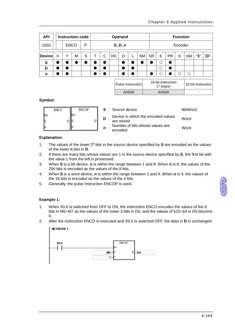
Chapter 6 Appl ied Inst ruct ions
6-269
API Instruction code Operand Function
1203 ENCO P S, D, n Encoder
Device X Y M S T C HC D L SM SR E PR K 16# “$” DF
S D n
Pulse instruction 16-bit instruction
(7 steps) 32-bit instruction
AH500 AH500 -
Symbol:
S : Source device Bit/Word
D : Device in which the encoded values are stored Word
n : Number of bits whose values are encoded Word
Explanation:
1. The values of the lower 2n bits in the source device specified by S are encoded as the values of the lower n bits in D.
2. If there are many bits whose values are 1 in the source device specified by S, the first bit with the value 1 from the left is processed.
3. When S is a bit device, n is within the range between 1 and 8. When n is 8, the values of the 256 bits is encoded as the values of the 8 bits.
4. When S is a word device, n is within the range between 1 and 4. When n is 4, the values of the 16 bits is encoded as the values of the 4 bits.
5. Generally, the pulse instruction ENCOP is used.
Example 1:
1. When X0.0 is switched from OFF to ON, the instruction ENCO encodes the values of the 8 bits in M0~M7 as the values of the lower 3 bits in D0, and the values of b15~b3 in D0 become 0.
2. After the instruction ENCO is executed and X0.0 is switched OFF, the data in D is unchanged.
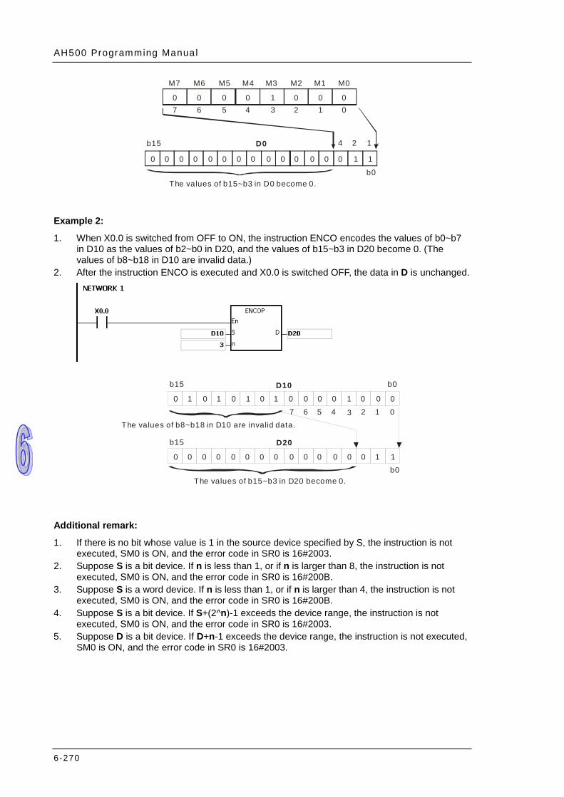
AH500 Programming Manual
6-270
b15
The values of b15~b3 in D0 become 0.b0
D0 4 2 1
0 0 0 0 1 0 0 07 6 5 4 3 2 1 0
M7 M6 M5 M4 M3 M2 M1 M0
0 0 0 0 0 0 0 0 0 0 0 0 0 1 10
Example 2:
1. When X0.0 is switched from OFF to ON, the instruction ENCO encodes the values of b0~b7 in D10 as the values of b2~b0 in D20, and the values of b15~b3 in D20 become 0. (The values of b8~b18 in D10 are invalid data.)
2. After the instruction ENCO is executed and X0.0 is switched OFF, the data in D is unchanged.
0 0 0 0 0 0 01 1 1 1 1
0 0 0 0 0 0 0 0 0 0 0 0 0 1
3
b15 b0
The values of b8~b18 in D10 are invalid data.
b15
b0
D10
D20
7 6 5 4 2 1 0
The values of b15~b3 in D20 become 0.
10
0 0 0 0
Additional remark:
1. If there is no bit whose value is 1 in the source device specified by S, the instruction is not executed, SM0 is ON, and the error code in SR0 is 16#2003.
2. Suppose S is a bit device. If n is less than 1, or if n is larger than 8, the instruction is not executed, SM0 is ON, and the error code in SR0 is 16#200B.
3. Suppose S is a word device. If n is less than 1, or if n is larger than 4, the instruction is not executed, SM0 is ON, and the error code in SR0 is 16#200B.
4. Suppose S is a bit device. If S+(2^n)-1 exceeds the device range, the instruction is not executed, SM0 is ON, and the error code in SR0 is 16#2003.
5. Suppose D is a bit device. If D+n-1 exceeds the device range, the instruction is not executed, SM0 is ON, and the error code in SR0 is 16#2003.
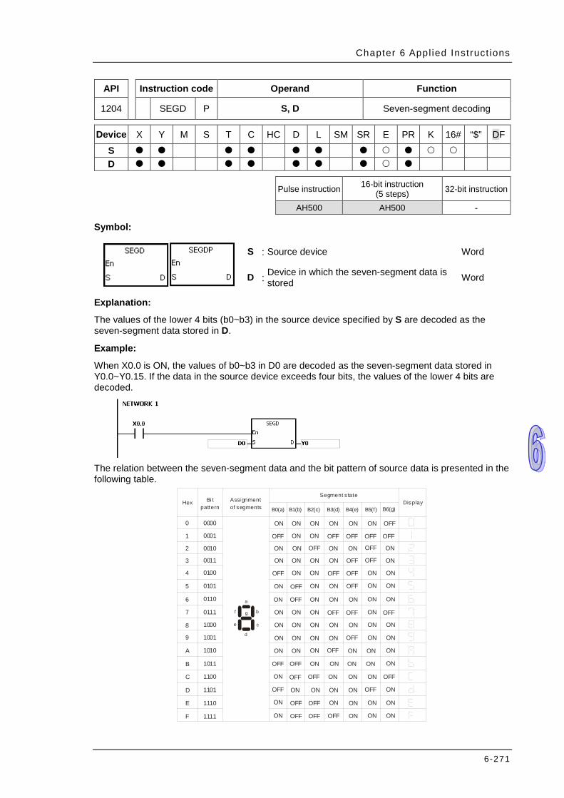
Chapter 6 Appl ied Inst ruct ions
6-271
API Instruction code Operand Function
1204 SEGD P S, D Seven-segment decoding
Device X Y M S T C HC D L SM SR E PR K 16# “$” DF
S D
Pulse instruction 16-bit instruction
(5 steps) 32-bit instruction
AH500 AH500 -
Symbol:
S : Source device Word
D : Device in which the seven-segment data is stored Word
Explanation:
The values of the lower 4 bits (b0~b3) in the source device specified by S are decoded as the seven-segment data stored in D.
Example:
When X0.0 is ON, the values of b0~b3 in D0 are decoded as the seven-segment data stored in Y0.0~Y0.15. If the data in the source device exceeds four bits, the values of the lower 4 bits are decoded.
The relation between the seven-segment data and the bit pattern of source data is presented in the following table.
Hex Bi t pattern
Assi gnment of segments
Segment s tateDisplay
0
1
2
3
4
5
6
7
8
9
A
B
C
D
E
F 1111
1110
1101
1100
1011
1010
1001
1000
0111
0110
0101
0100
0011
0010
0001
0000 ON
B0(a) B1(b) B2(c) B3(d) B4(e) B5(f) B6(g)
OFFON ON ON ON ON
OFFOFFOFFOFF OFFON ON
ON ON ON ONOFF OFF ON
ON ON ON ON ONOFFOFF
OFFOFF OFFON ON ON ON
ON OFF ON ON OFF ON ON
OFF ON ON ON ON ON
ON ON ON OFFOFF OFF
ON ON ON ON ON ON ON
ON ON ON ON ON ONOFF
ON ON
OFF OFF ON ON ON
OFF ONON
ON OFF ON
OFF OFF ON ON ON ON
OFF OFF OFF
a
c
b
d
e
f g
ON
ON
ONON ONON OFF
ON ON
ON OFF ON OFF
OFF ON ON ON
ON ON ON
ON
ON
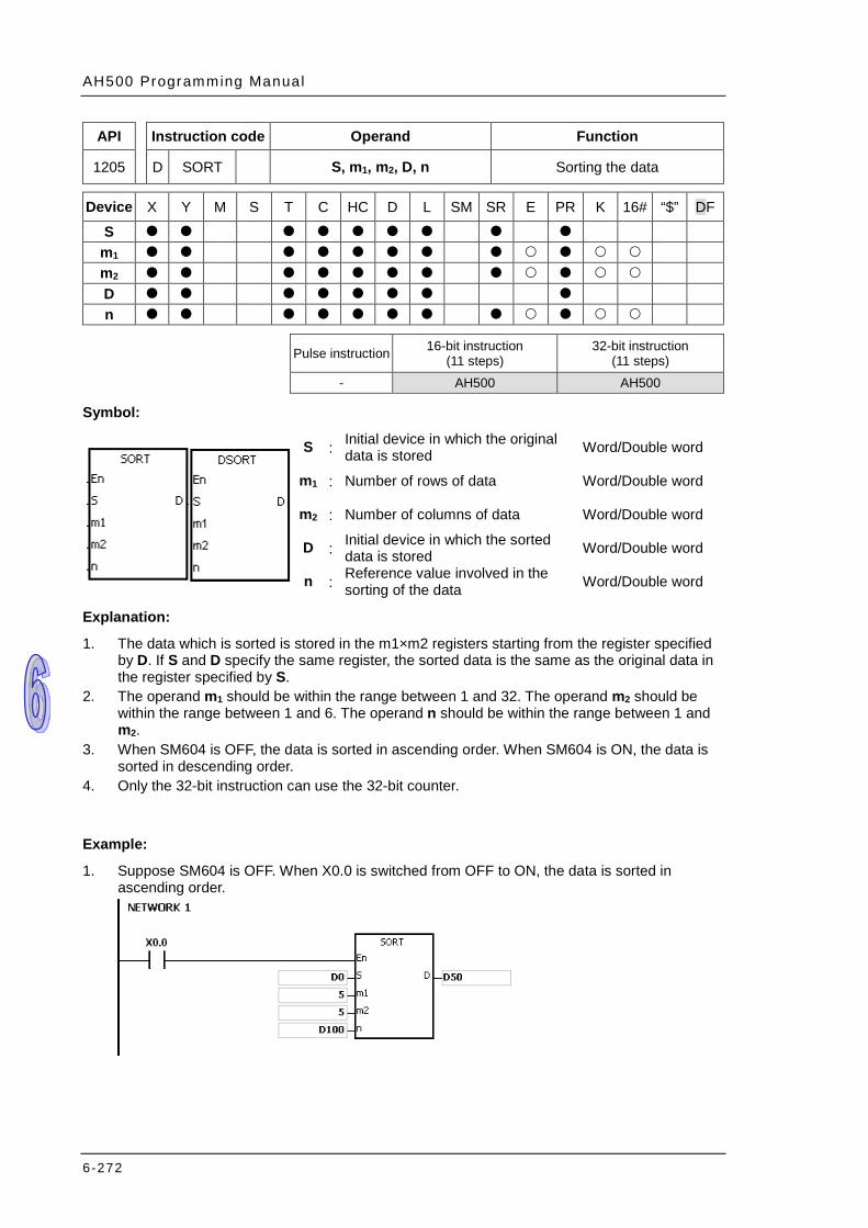
AH500 Programming Manual
6-272
API Instruction code Operand Function
1205 D SORT S, m1, m2, D, n Sorting the data
Device X Y M S T C HC D L SM SR E PR K 16# “$” DF
S m1 m2 D n
Pulse instruction 16-bit instruction
(11 steps) 32-bit instruction
(11 steps) - AH500 AH500
Symbol:
S : Initial device in which the original data is stored Word/Double word
m1 : Number of rows of data Word/Double word
m2 : Number of columns of data Word/Double word
D : Initial device in which the sorted data is stored Word/Double word
n : Reference value involved in the sorting of the data Word/Double word
Explanation:
1. The data which is sorted is stored in the m1×m2 registers starting from the register specified by D. If S and D specify the same register, the sorted data is the same as the original data in the register specified by S.
2. The operand m1 should be within the range between 1 and 32. The operand m2 should be within the range between 1 and 6. The operand n should be within the range between 1 and m2.
3. When SM604 is OFF, the data is sorted in ascending order. When SM604 is ON, the data is sorted in descending order.
4. Only the 32-bit instruction can use the 32-bit counter.
Example:
1. Suppose SM604 is OFF. When X0.0 is switched from OFF to ON, the data is sorted in ascending order.

Chapter 6 Appl ied Inst ruct ions
6-273
2. The data which will be sorted is shown below.
m2 columns of data Column
Column
Row
1 2 3 4 5 Student number Chinese English Math Physics
m1 row
s of data
1 (D0) 1 (D5) 90 (D10) 75 (D15) 66 (D20) 79
2 (D1) 2 (D6) 55 (D11) 65 (D16) 54 (D21) 63
3 (D2) 3 (D7) 80 (D12) 98 (D17) 89 (D22) 90
4 (D3) 4 (D8) 70 (D13) 60 (D18) 99 (D23) 50
5 (D4) 5 (D9) 95 (D14) 79 (D19) 75 (D24) 69
3. When the value in D100 is 3, the data is sorted as follows.
m2 columns of data
Column
Column
Row
1 2 3 4 5 Student number Chinese English Math Physics
m1 row
s of data
1 (D50) 4 (D55) 70 (D60) 60 (D65) 99 (D70) 50
2 (D51) 2 (D56) 55 (D61) 65 (D66) 54 (D71) 63
3 (D52) 1 (D57) 90 (D62) 75 (D67) 66 (D72) 79
4 (D53) 5 (D58) 95 (D63) 79 (D68) 75 (D73) 69
5 (D54) 3 (D59) 80 (D64) 98 (D69) 89 (D74) 90

AH500 Programming Manual
6-274
4. When the value in D100 is 5, the data is sorted as follows.
m2 columns of data Column
Column
Row
1 2 3 4 5 Student number Chinese English Math Physics
m1 row
s of data
1 (D50) 4 (D55) 70 (D60) 60 (D65) 99 (D70) 50
2 (D51) 2 (D56) 55 (D61) 65 (D66) 54 (D71) 63
3 (D52) 5 (D57) 95 (D62) 79 (D67) 75 (D72) 69
4 (D53) 1 (D58) 90 (D63) 75 (D68) 66 (D73) 79
5 (D54) 3 (D59) 80 (D64) 98 (D69) 89 (D74) 90
Additional remark:
1. If the device exceeds the range, the instruction is not executed, SM0 is ON, and the error code in SR0 is 16#2003.
2. If m1, m2, or n exceeds the range, the instruction is not executed, SM0 is ON, and the error code in SR0 is 16#200B.
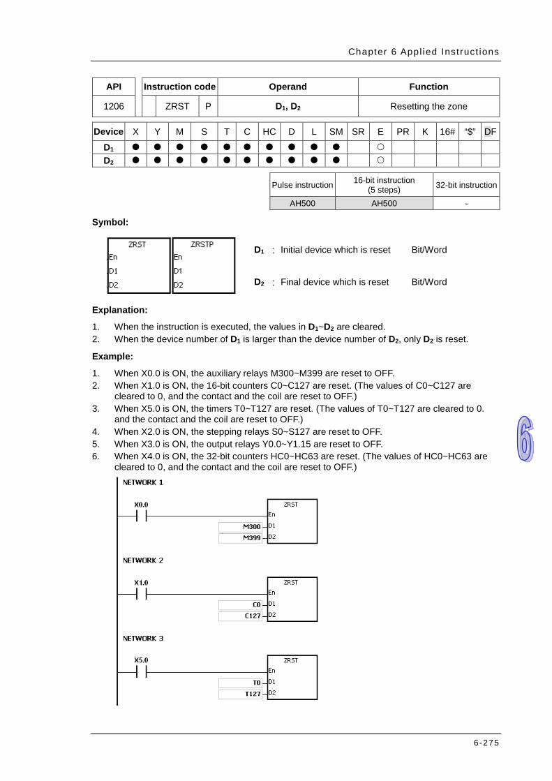
Chapter 6 Appl ied Inst ruct ions
6-275
API Instruction code Operand Function
1206 ZRST P D1, D2 Resetting the zone
Device X Y M S T C HC D L SM SR E PR K 16# “$” DF
D1 D2
Pulse instruction 16-bit instruction
(5 steps) 32-bit instruction
AH500 AH500 -
Symbol:
D1 : Initial device which is reset Bit/Word
D2 : Final device which is reset Bit/Word
Explanation:
1. When the instruction is executed, the values in D1~D2 are cleared. 2. When the device number of D1 is larger than the device number of D2, only D2 is reset.
Example:
1. When X0.0 is ON, the auxiliary relays M300~M399 are reset to OFF. 2. When X1.0 is ON, the 16-bit counters C0~C127 are reset. (The values of C0~C127 are
cleared to 0, and the contact and the coil are reset to OFF.) 3. When X5.0 is ON, the timers T0~T127 are reset. (The values of T0~T127 are cleared to 0.
and the contact and the coil are reset to OFF.) 4. When X2.0 is ON, the stepping relays S0~S127 are reset to OFF. 5. When X3.0 is ON, the output relays Y0.0~Y1.15 are reset to OFF. 6. When X4.0 is ON, the 32-bit counters HC0~HC63 are reset. (The values of HC0~HC63 are
cleared to 0, and the contact and the coil are reset to OFF.)
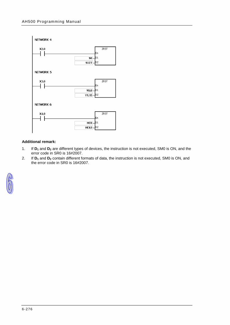
AH500 Programming Manual
6-276
Additional remark:
1. If D1 and D2 are different types of devices, the instruction is not executed, SM0 is ON, and the error code in SR0 is 16#2007.
2. If D1 and D2 contain different formats of data, the instruction is not executed, SM0 is ON, and the error code in SR0 is 16#2007.

Chapter 6 Appl ied Inst ruct ions
6-277
API Instruction code Operand Function
1207 D BON P S, D, n Checking the state of the bit
Device X Y M S T C HC D L SM SR E PR K 16# “$” DF
S D n
Pulse instruction 16-bit instruction
(7 steps) 32-bit instruction
(7 steps) AH500 AH500 AH500
Symbol:
S : Source device Word/Double word
D : Device in which the check result is stored Bit
n : Bit whose state is judged Word/Double word
Explanation:
1. The state of the nth bit in S is checked, and the result is stored in D. 2. The operand n used in the 16-bit instruction should be within the range between 0 and 15,
and the operand n used in the 32-bit instruction should be within the range between 0 and 31. 3. Only the 32-bit instructions can use the 32-bit counter.
Example:
1. When X0.0 is ON, Y0.1 is ON if the value of the 15th bit in D0 is 1. When X0.0 is ON, Y0.1 is OFF if the value of the 15th bit in D0 is 0.
2. When X0.0 is switched OFF, the state of Y0.1 remains the same as before X0.0 turned OFF.
0 0 0 1 0 0 1 0 0 0 0 0 0 1 0 0
b0b15
D0
1 0 0 1 0 0 1 0 0 0 0 0 0 1 0 0
b0b15
D0
Y0.1=OFF
Y0.1=ON
Additional remark: If n exceeds the range, the instruction is not executed, SM0 is ON, and the error code in SR0 is 16#200B.
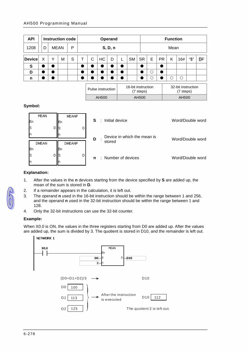
AH500 Programming Manual
6-278
API Instruction code Operand Function
1208 D MEAN P S, D, n Mean
Device X Y M S T C HC D L SM SR E PR K 16# “$” DF
S D n
Pulse instruction 16-bit instruction
(7 steps) 32-bit instruction
(7 steps) AH500 AH500 AH500
Symbol:
S : Initial device Word/Double word
D : Device in which the mean is stored Word/Double word
n : Number of devices Word/Double word
Explanation:
1. After the values in the n devices starting from the device specified by S are added up, the mean of the sum is stored in D.
2. If a remainder appears in the calculation, it is left out. 3. The operand n used in the 16-bit instruction should be within the range between 1 and 256,
and the operand n used in the 32-bit instruction should be within the range between 1 and 128.
4. Only the 32-bit instructions can use the 32-bit counter.
Example:
When X0.0 is ON, the values in the three registers starting from D0 are added up. After the values are added up, the sum is divided by 3. The quotient is stored in D10, and the remainder is left out.
D0
D1
D2
D10
112
100
113
125
(D0+D1+D2)/3
D10After the instruction is executed
The quotient 2 is left out.
Chapter 6 Appl ied Inst ruct ions
6-279
Additional remark:
1. If the operand n used in the 16-bit instruction is less than 1 or larger than 256, the instruction is not executed, SM0 is ON, and the error code in SR0 is 16#200B.
2. If the operand n used in the 32-bit instruction is less than 1 or larger than 128, the instruction is not executed, SM0 is ON, and the error code in SR0 is 16#200B.
3. If S+n-1 exceeds the device range, the instruction is not executed, SM0 is ON, and the error code in SR0 is 16#2003.
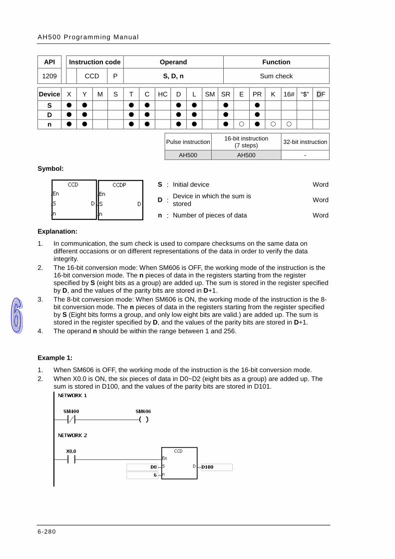
AH500 Programming Manual
6-280
API Instruction code Operand Function
1209 CCD P S, D, n Sum check
Device X Y M S T C HC D L SM SR E PR K 16# “$” DF
S D n
Pulse instruction 16-bit instruction
(7 steps) 32-bit instruction
AH500 AH500 -
Symbol:
S : Initial device Word
D : Device in which the sum is stored Word
n : Number of pieces of data Word
Explanation:
1. In communication, the sum check is used to compare checksums on the same data on different occasions or on different representations of the data in order to verify the data integrity.
2. The 16-bit conversion mode: When SM606 is OFF, the working mode of the instruction is the 16-bit conversion mode. The n pieces of data in the registers starting from the register specified by S (eight bits as a group) are added up. The sum is stored in the register specified by D, and the values of the parity bits are stored in D+1.
3. The 8-bit conversion mode: When SM606 is ON, the working mode of the instruction is the 8-bit conversion mode. The n pieces of data in the registers starting from the register specified by S (Eight bits forms a group, and only low eight bits are valid.) are added up. The sum is stored in the register specified by D, and the values of the parity bits are stored in D+1.
4. The operand n should be within the range between 1 and 256.
Example 1:
1. When SM606 is OFF, the working mode of the instruction is the 16-bit conversion mode. 2. When X0.0 is ON, the six pieces of data in D0~D2 (eight bits as a group) are added up. The
sum is stored in D100, and the values of the parity bits are stored in D101.
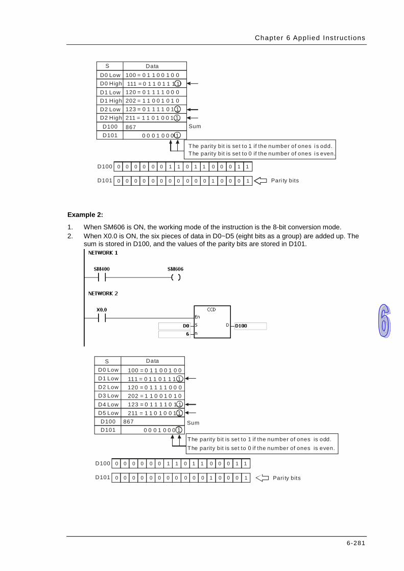
Chapter 6 Appl ied Inst ruct ions
6-281
D100
D101
0 0 0 0 0 0 0 0 001 1 1 1 1 1
0 0 0 0 0 0 0 0 0 0 0 00 1 10
S DataD0 LowD0 HighD1 LowD1 HighD2 LowD2 HighD100D101
100 = 0 1 1 0 0 1 0 0 111 = 0 1 1 0 1 1 1 1120 = 0 1 1 1 1 0 0 0202 = 1 1 0 0 1 0 1 0123 = 0 1 1 1 1 0 1 1211 = 1 1 0 1 0 0 1 1
0 0 0 1 0 0 0 1
The parity bit is set to 1 if the number of ones i s odd.The parity bit is set to 0 if the number of ones i s even.
867 Sum
Pari ty bits
Example 2:
1. When SM606 is ON, the working mode of the instruction is the 8-bit conversion mode. 2. When X0.0 is ON, the six pieces of data in D0~D5 (eight bits as a group) are added up. The
sum is stored in D100, and the values of the parity bits are stored in D101.
Data
The parity bit is set to 1 if the number of ones is odd.The parity bit is set to 0 if the number of ones is even.
Sum
Pari ty bits
D100
D101
0 0 0 0 0 0 0 0 001 1 1 1 1 1
0 0 0 0 0 0 0 0 0 0 0 00 1 10
SD0 LowD1 LowD2 LowD3 LowD4 LowD5 LowD100D101
100 = 0 1 1 0 0 1 0 0 111 = 0 1 1 0 1 1 1 1 120 = 0 1 1 1 1 0 0 0 202 = 1 1 0 0 1 0 1 0 123 = 0 1 1 1 1 0 1 1 211 = 1 1 0 1 0 0 1 1
0 0 0 1 0 0 0 1 867

AH500 Programming Manual
6-282
Additional remark:
1. Suppose SM606 is ON. If S+n-1 exceeds the device range, the instruction is not executed, SM0 is ON, and the error code in SR0 is 16#2003.
2. Suppose SM606 is OFF. If S+n/2-1 exceeds the device range, the instruction is not executed, SM0 is ON, and the error code in SR0 is 16#2003.
3. If n is less than 1, or if n is larger than 256, the instruction is not executed, SM0 is ON, and the error code in SR0 is 16#200B.
4. If users declare the operand D in ISPSoft, the data type will be ARRAY [2] of WORD/INT.

Chapter 6 Appl ied Inst ruct ions
6-283
API Instruction code Operand Function
1210 D ABS P D Absolute value
Device X Y M S T C HC D L SM SR E PR K 16# “$” DF
D
Pulse instruction 16-bit instruction (3 steps)
32-bit instruction (3 steps)
AH500 AH500 AH500
Symbol:
D : Device involved in the getting of the absolute value Word/Double word
Explanation:
1. When the instruction ABS is executed, the absolute value of the value in the device specified by D is gotten.
2. Generally, the pulse instruction ABSP is used. 3. Only the 32-bit instructions can use the 32-bit counter.
Example:
Suppose the value in D0 before the execution of the instruction is -1234. When X0.0 is switched from OFF to ON, the absolute value of -1234 in D0 is gotten. That is, the value in D0 becomes 1234 after the instruction is executed.

AH500 Programming Manual
6-284
API Instruction code Operand Function
1211 MINV P S, D, n Inverting the matrix bits
Device X Y M S T C HC D L SM SR E PR K 16# “$” DF
S D n
Pulse instruction 16-bit instruction
(7 steps) 32-bit instruction
AH500 AH500 -
Symbol:
S : Matrix source Word
D : Operation result Word
n : Length of the array Word
Explanation:
1. The bits in the n devices starting from the device specified by S are inverted, and the inversion result is stored in D.
2. The operand n should be within the range between 1 and 256.
Example:
When X0.0 is ON, the bits in the three 16-bit registers D0~D2 are inverted, and the inversion result is stored in the 16-bit registers D20~D22.
0 1 0 1 0 1 0 1 0 1 0 1 0 1 0 1
b0b15
0 1 0 1 0 1 0 1 0 1 0 1 0 1 0 1
0 1 0 1 0 1 0 1 0 1 0 1 0 1 0 1
0 1 0 1 0 1 0 1 0 1 0 1 0 1 01
b0b15
0 1 0 1 0 1 0 1 0 1 0 1 0 1 01
0 1 0 1 0 1 0 1 0 1 0 1 0 1 01
D0D1D2
D20D21D22
After the i nstruction is executed
Additional remark:
1. If S+n-1 or D+n-1 exceeds the device range, the instruction is not execute, SM0 is ON, and the error code in SR0 is 16#2003.
2. If n is less than 1, or if n is larger than 256, the instruction is not executed, SM0 is ON, and the error code in SR0 is 16#200B.
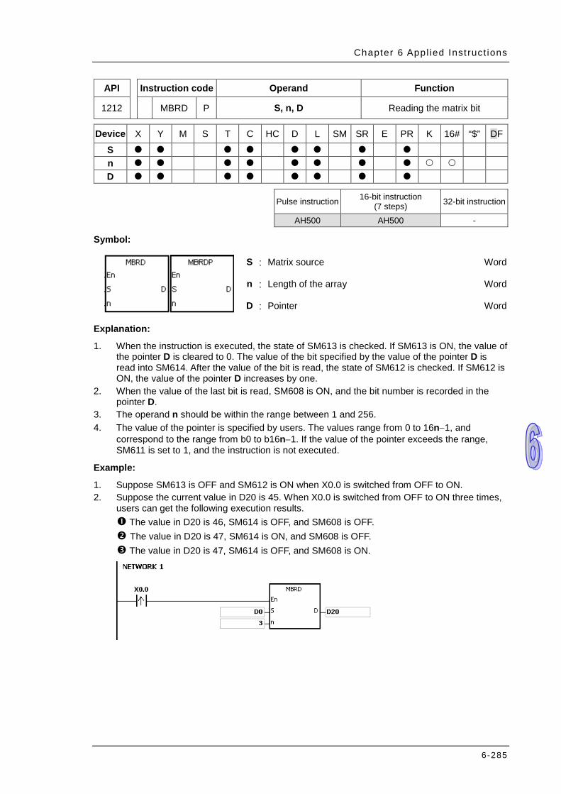
Chapter 6 Appl ied Inst ruct ions
6-285
API Instruction code Operand Function
1212 MBRD P S, n, D Reading the matrix bit
Device X Y M S T C HC D L SM SR E PR K 16# “$” DF
S n D
Pulse instruction 16-bit instruction
(7 steps) 32-bit instruction
AH500 AH500 -
Symbol:
S : Matrix source Word
n : Length of the array Word
D : Pointer Word
Explanation:
1. When the instruction is executed, the state of SM613 is checked. If SM613 is ON, the value of the pointer D is cleared to 0. The value of the bit specified by the value of the pointer D is read into SM614. After the value of the bit is read, the state of SM612 is checked. If SM612 is ON, the value of the pointer D increases by one.
2. When the value of the last bit is read, SM608 is ON, and the bit number is recorded in the pointer D.
3. The operand n should be within the range between 1 and 256. 4. The value of the pointer is specified by users. The values range from 0 to 16n−1, and
correspond to the range from b0 to b16n−1. If the value of the pointer exceeds the range, SM611 is set to 1, and the instruction is not executed.
Example:
1. Suppose SM613 is OFF and SM612 is ON when X0.0 is switched from OFF to ON. 2. Suppose the current value in D20 is 45. When X0.0 is switched from OFF to ON three times,
users can get the following execution results. The value in D20 is 46, SM614 is OFF, and SM608 is OFF. The value in D20 is 47, SM614 is ON, and SM608 is OFF. The value in D20 is 47, SM614 is OFF, and SM608 is ON.
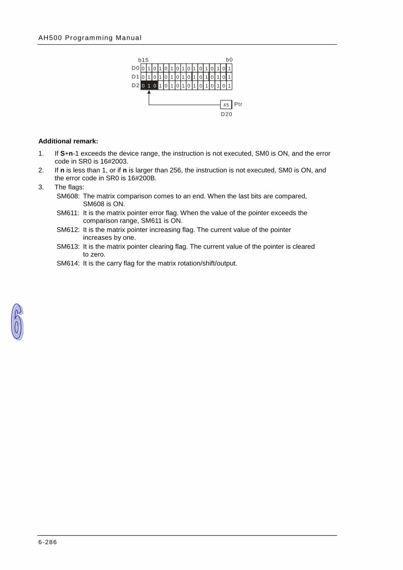
AH500 Programming Manual
6-286
0 1 0 1 0 1 0 1 0 1 0 1 0 1 0 1
b0b15
0 1 0 1 0 1 0 1 0 1 0 1 0 1 0 1
0 1 0 1 0 1 0 1 0 1 0 1 0 1 0 1
D0D1D2
45
D20
Ptr
Additional remark:
1. If S+n-1 exceeds the device range, the instruction is not executed, SM0 is ON, and the error code in SR0 is 16#2003.
2. If n is less than 1, or if n is larger than 256, the instruction is not executed, SM0 is ON, and the error code in SR0 is 16#200B.
3. The flags: SM608: The matrix comparison comes to an end. When the last bits are compared,
SM608 is ON. SM611: It is the matrix pointer error flag. When the value of the pointer exceeds the
comparison range, SM611 is ON. SM612: It is the matrix pointer increasing flag. The current value of the pointer
increases by one. SM613: It is the matrix pointer clearing flag. The current value of the pointer is cleared
to zero. SM614: It is the carry flag for the matrix rotation/shift/output.

Chapter 6 Appl ied Inst ruct ions
6-287
API Instruction code Operand Function
1213 MBWR P S, n, D Writing the matrix bit
Device X Y M S T C HC D L SM SR E PR K 16# “$” DF
S n D
Pulse instruction 16-bit instruction
(7 steps) 32-bit instruction
AH500 AH500 -
Symbol:
S : Matrix source Word
n : Length of the array Word
D : Pointer Word
Explanation:
1. When the instruction is executed, the state of SM613 is checked. If SM613 is ON, the value of the pointer D is cleared to 0. The state of SM615 is written into the bit specified by the value of the pointer D. After the state of SM615 is written into the bit, the state of SM612 is checked. If SM612 is ON, the value in the pointer D increases by one.
2. When the state of SM615 is written into the last bit, SM608 is ON, and the bit number is recorded in the pointer D. If value of the pointer D exceeds the range, SM611 is ON.
3. The operand n should be within the range between 1 and 256. 4. The value of the pointer is specified by users. The values range from 0 to 16n−1, and
correspond to the range from b0 to b16n−1. If the value of the pointer exceeds the range, SM611 is set to 1, and the instruction is not executed.
Example:
1. Suppose SM613 is OFF and SM612 is ON when X0.0 is switched from OFF to ON. 2. Suppose the current value in D20 is 45. When X0.0 is switched from OFF to ON one time,
users can get the execution result shown below. When the value in D20 is 45, SM615 is OFF, and SM608 is OFF.
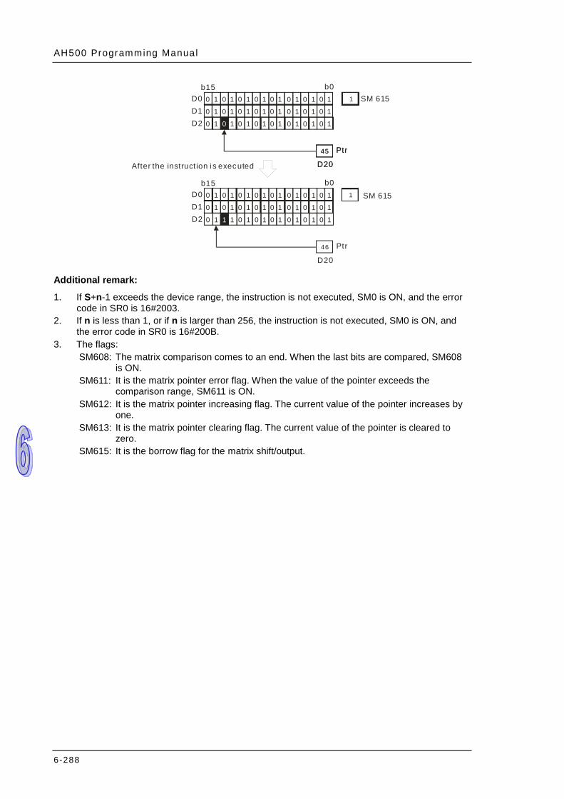
AH500 Programming Manual
6-288
After the instruction i s executed
0 1 0 1 0 1 0 1 0 1 0 1 0 1 0 1
b0b15
0 1 0 1 0 1 0 1 0 1 0 1 0 1 0 1
0 1 0 1 0 1 0 1 0 1 0 1 0 1 0 1
D0D1D2
45
D20
Ptr
0 1 0 1 0 1 0 1 0 1 0 1 0 1 0 1
b0b15
0 1 0 1 0 1 0 1 0 1 0 1 0 1 0 1
0 1 1 1 0 1 0 1 0 1 0 1 0 1 0 1
D0D1D2
46
D20
Ptr
45
D20
Ptr
1 SM 615
1 SM 615
Additional remark:
1. If S+n-1 exceeds the device range, the instruction is not executed, SM0 is ON, and the error code in SR0 is 16#2003.
2. If n is less than 1, or if n is larger than 256, the instruction is not executed, SM0 is ON, and the error code in SR0 is 16#200B.
3. The flags: SM608: The matrix comparison comes to an end. When the last bits are compared, SM608
is ON. SM611: It is the matrix pointer error flag. When the value of the pointer exceeds the
comparison range, SM611 is ON. SM612: It is the matrix pointer increasing flag. The current value of the pointer increases by
one. SM613: It is the matrix pointer clearing flag. The current value of the pointer is cleared to
zero. SM615: It is the borrow flag for the matrix shift/output.
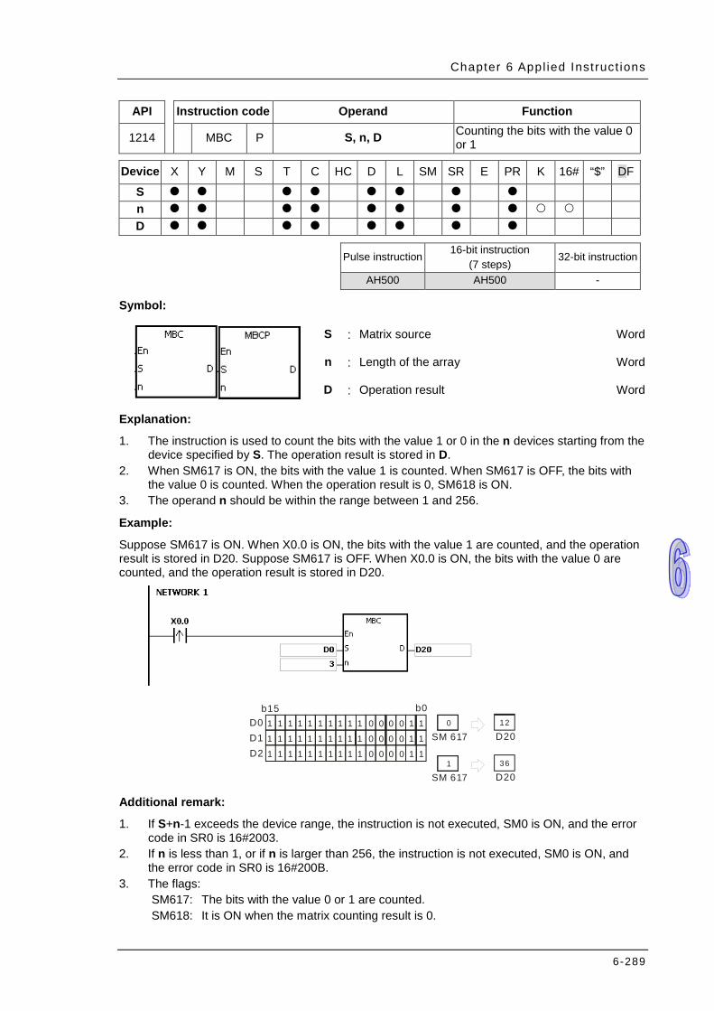
Chapter 6 Appl ied Inst ruct ions
6-289
API Instruction code Operand Function
1214 MBC P S, n, D Counting the bits with the value 0 or 1
Device X Y M S T C HC D L SM SR E PR K 16# “$” DF
S n D
Pulse instruction 16-bit instruction
(7 steps) 32-bit instruction
AH500 AH500 -
Symbol:
S : Matrix source Word
n : Length of the array Word
D : Operation result Word
Explanation:
1. The instruction is used to count the bits with the value 1 or 0 in the n devices starting from the device specified by S. The operation result is stored in D.
2. When SM617 is ON, the bits with the value 1 is counted. When SM617 is OFF, the bits with the value 0 is counted. When the operation result is 0, SM618 is ON.
3. The operand n should be within the range between 1 and 256.
Example:
Suppose SM617 is ON. When X0.0 is ON, the bits with the value 1 are counted, and the operation result is stored in D20. Suppose SM617 is OFF. When X0.0 is ON, the bits with the value 0 are counted, and the operation result is stored in D20.
1 1 1 1 1 1 1 1 1 1 0 0 0 0 1 1
b0b15
1 1 1 1 1 1 1 1 1 1 0 0 0 0 1 1
1 1 1 1 1 1 1 1 1 1 0 0 0 0 1 1
D0D1D2
D20120
SM 617
D20361
SM 617 Additional remark:
1. If S+n-1 exceeds the device range, the instruction is not executed, SM0 is ON, and the error code in SR0 is 16#2003.
2. If n is less than 1, or if n is larger than 256, the instruction is not executed, SM0 is ON, and the error code in SR0 is 16#200B.
3. The flags: SM617: The bits with the value 0 or 1 are counted. SM618: It is ON when the matrix counting result is 0.
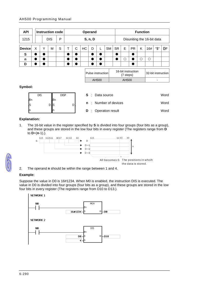
AH500 Programming Manual
6-290
API Instruction code Operand Function
1215 DIS P S, n, D Disuniting the 16-bit data
Device X Y M S T C HC D L SM SR E PR K 16# “$” DF
S n D
Pulse instruction 16-bit instruction
(7 steps) 32-bit instruction
AH500 AH500 -
Symbol:
S : Data source Word
n : Number of devices Word
D : Operation result Word
Explanation:
1. The 16-bit value in the register specified by S is divided into four groups (four bits as a group), and these groups are stored in the low four bits in every register (The registers range from D to D+(n-1).).
S D
+1
b3 b0b7 b4b11 b8b15 b12 b3 b0b15 b4
nD+2D
+3D
All becomes 0. The posit ions i n whcih
the data is stored. 2. The operand n should be within the range between 1 and 4.
Example:
Suppose the value in D0 is 16#1234. When M0 is enabled, the instruction DIS is executed. The value in D0 is divided into four groups (four bits as a group), and these groups are stored in the low four bits in every register (The registers range from D10 to D13.).
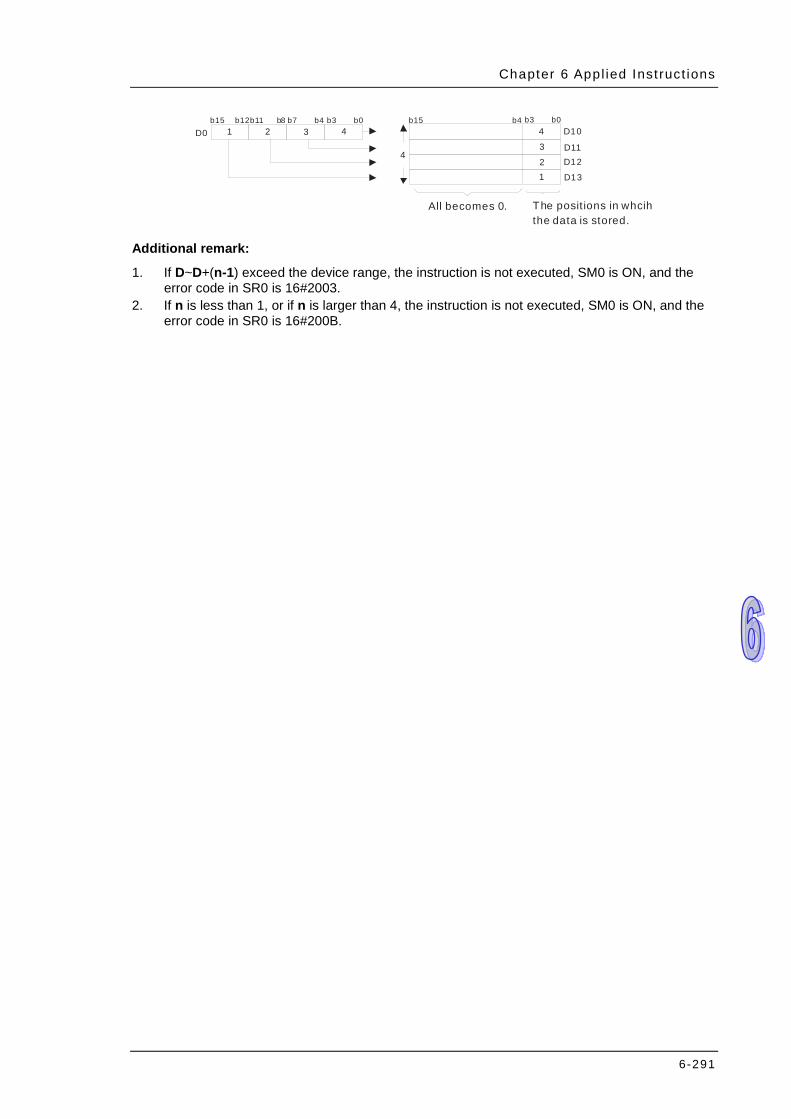
Chapter 6 Appl ied Inst ruct ions
6-291
All becomes 0. The posit ions in whcih the data is stored.
b3 b0b7 b4b11 b8b15 b12 b3 b0b15 b4
4
D0 1 2 3 4 D10
D11D12
D1312
3
4
Additional remark:
1. If D~D+(n-1) exceed the device range, the instruction is not executed, SM0 is ON, and the error code in SR0 is 16#2003.
2. If n is less than 1, or if n is larger than 4, the instruction is not executed, SM0 is ON, and the error code in SR0 is 16#200B.

AH500 Programming Manual
6-292
API Instruction code Operand Function
1216 UNI P S, n, D Uniting the 16-bit data
Device X Y M S T C HC D L SM SR E PR K 16# “$” DF
S n D
Pulse instruction 16-bit instruction
(7 steps) 32-bit instruction
AH500 AH500 -
Symbol:
S : Data source Word
n : Data length Word
D : Operation result Word
Explanation:
1. The 16-bit values in the registers specified by S~S+(n-1) are divided into groups (four bits as a group), and every group which is composed of b0~b3 is stored in the register specified by D.
S
+1
b3 b0b15 b4
S +2
S
+3
S
Being i gnored The data which
is stored
Db3 b0b7 b4b11 b8b15 b12
2. The operand n should be within the range between 1 and 4.
Example:
Suppose the values in D0~D3 are 16#1234, 16#5678, 16#8765, and 16#4321 respectively. When M0 is enabled, the instruction UNI is executed. The values in D0~D3 are divided into groups (four bits as a group), and every group which is composed of b0~b3 is stored in D10.
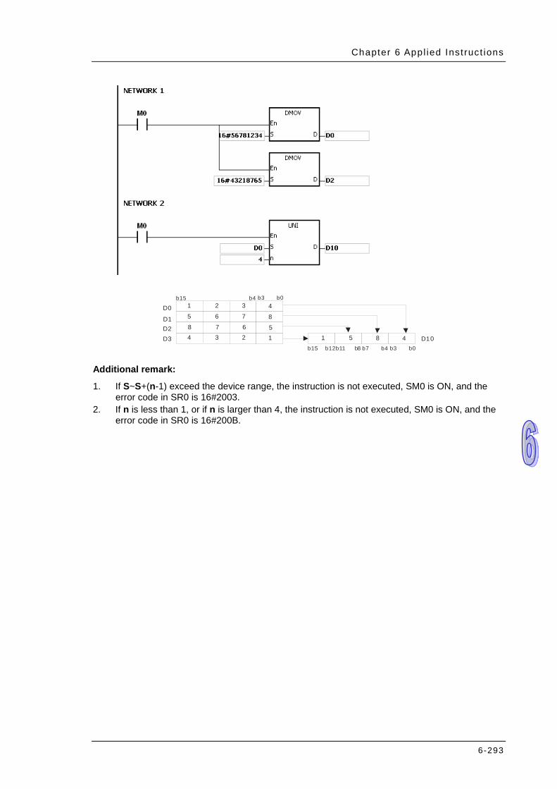
Chapter 6 Appl ied Inst ruct ions
6-293
D0b3 b0b15 b4
D1D2
D10b3 b0b7 b4b11 b8b15 b12
1 2 3 45 6 7 88 7 6 54 3 2 1 1 5 8 4D3
Additional remark:
1. If S~S+(n-1) exceed the device range, the instruction is not executed, SM0 is ON, and the error code in SR0 is 16#2003.
2. If n is less than 1, or if n is larger than 4, the instruction is not executed, SM0 is ON, and the error code in SR0 is 16#200B.
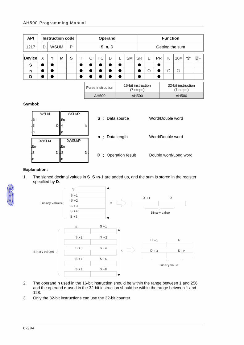
AH500 Programming Manual
6-294
API Instruction code Operand Function
1217 D WSUM P S, n, D Getting the sum
Device X Y M S T C HC D L SM SR E PR K 16# “$” DF
S n D
Pulse instruction 16-bit instruction
(7 steps) 32-bit instruction
(7 steps) AH500 AH500 AH500
Symbol:
S : Data source Word/Double word
n : Data length Word/Double word
D : Operation result Double word/Long word
Explanation:
1. The signed decimal values in S~S+n-1 are added up, and the sum is stored in the register specified by D.
S
+1S+2S
+3S
D
+4S
+5S
n
Binary valuesD+1
Binary value
Binary values
Binary value
S +1S
+2S+3SD
+4S+5Sn
D+1
+6S+7S
+8S+9S
D D+3 +2
2. The operand n used in the 16-bit instruction should be within the range between 1 and 256,
and the operand n used in the 32-bit instruction should be within the range between 1 and 128.
3. Only the 32-bit instructions can use the 32-bit counter.
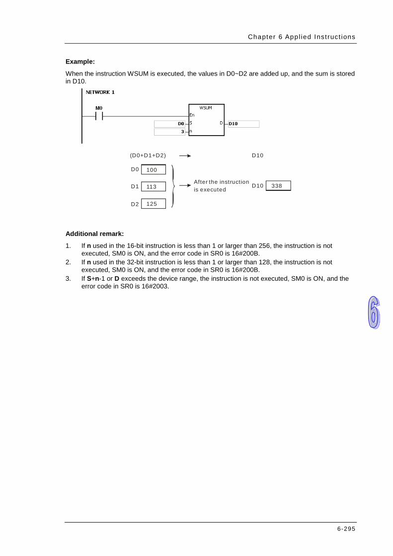
Chapter 6 Appl ied Inst ruct ions
6-295
Example:
When the instruction WSUM is executed, the values in D0~D2 are added up, and the sum is stored in D10.
D0
D1
D2
D10
338
100
113
125
(D0+D1+D2)
D10After the instruction is executed
Additional remark:
1. If n used in the 16-bit instruction is less than 1 or larger than 256, the instruction is not executed, SM0 is ON, and the error code in SR0 is 16#200B.
2. If n used in the 32-bit instruction is less than 1 or larger than 128, the instruction is not executed, SM0 is ON, and the error code in SR0 is 16#200B.
3. If S+n-1 or D exceeds the device range, the instruction is not executed, SM0 is ON, and the error code in SR0 is 16#2003.
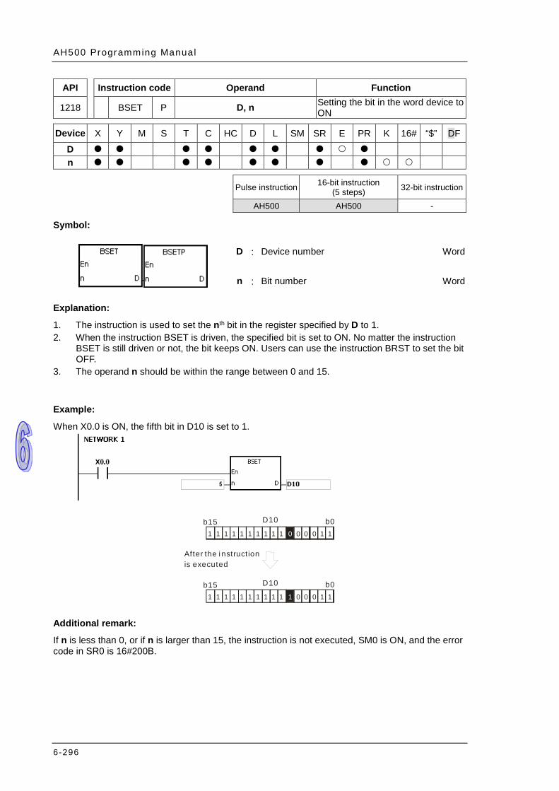
AH500 Programming Manual
6-296
API Instruction code Operand Function
1218 BSET P D, n Setting the bit in the word device to ON
Device X Y M S T C HC D L SM SR E PR K 16# “$” DF
D n
Pulse instruction 16-bit instruction
(5 steps) 32-bit instruction
AH500 AH500 -
Symbol:
D : Device number Word
n : Bit number Word
Explanation:
1. The instruction is used to set the nth bit in the register specified by D to 1. 2. When the instruction BSET is driven, the specified bit is set to ON. No matter the instruction
BSET is still driven or not, the bit keeps ON. Users can use the instruction BRST to set the bit OFF.
3. The operand n should be within the range between 0 and 15.
Example:
When X0.0 is ON, the fifth bit in D10 is set to 1.
After the i nstruction is executed
1 1 1 1 1 1 1 1 1 1 0 0 0 0 1 1
b0b15 D10
1 1 1 1 1 1 1 1 1 1 1 0 0 0 1 1
b0b15 D10
Additional remark:
If n is less than 0, or if n is larger than 15, the instruction is not executed, SM0 is ON, and the error code in SR0 is 16#200B.
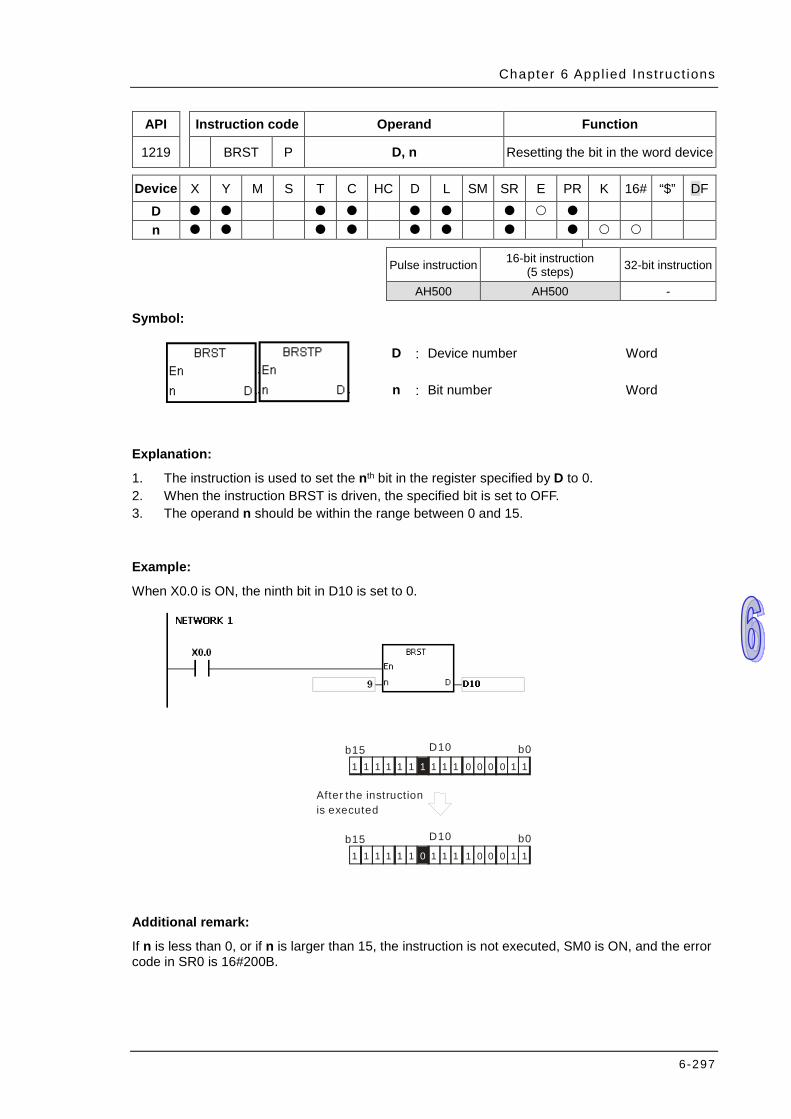
Chapter 6 Appl ied Inst ruct ions
6-297
API Instruction code Operand Function
1219 BRST P D, n Resetting the bit in the word device
Device X Y M S T C HC D L SM SR E PR K 16# “$” DF
D n
Pulse instruction 16-bit instruction
(5 steps) 32-bit instruction
AH500 AH500 -
Symbol:
D : Device number Word
n : Bit number Word
Explanation:
1. The instruction is used to set the nth bit in the register specified by D to 0. 2. When the instruction BRST is driven, the specified bit is set to OFF. 3. The operand n should be within the range between 0 and 15.
Example:
When X0.0 is ON, the ninth bit in D10 is set to 0.
After the instruction is executed
1 1 1 1 1 1 1 1 1 1 0 0 0 0 1 1
b0b15 D10
1 1 1 1 1 1 0 1 1 1 1 0 0 0 1 1
b0b15 D10
Additional remark:
If n is less than 0, or if n is larger than 15, the instruction is not executed, SM0 is ON, and the error code in SR0 is 16#200B.
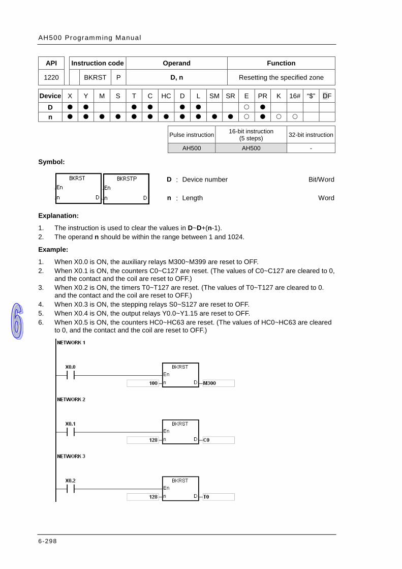
AH500 Programming Manual
6-298
API Instruction code Operand Function
1220 BKRST P D, n Resetting the specified zone
Device X Y M S T C HC D L SM SR E PR K 16# “$” DF
D n
Pulse instruction 16-bit instruction
(5 steps) 32-bit instruction
AH500 AH500 -
Symbol:
D : Device number Bit/Word
n : Length Word
Explanation:
1. The instruction is used to clear the values in D~D+(n-1). 2. The operand n should be within the range between 1 and 1024.
Example:
1. When X0.0 is ON, the auxiliary relays M300~M399 are reset to OFF. 2. When X0.1 is ON, the counters C0~C127 are reset. (The values of C0~C127 are cleared to 0,
and the contact and the coil are reset to OFF.) 3. When X0.2 is ON, the timers T0~T127 are reset. (The values of T0~T127 are cleared to 0.
and the contact and the coil are reset to OFF.) 4. When X0.3 is ON, the stepping relays S0~S127 are reset to OFF. 5. When X0.4 is ON, the output relays Y0.0~Y1.15 are reset to OFF. 6. When X0.5 is ON, the counters HC0~HC63 are reset. (The values of HC0~HC63 are cleared
to 0, and the contact and the coil are reset to OFF.)
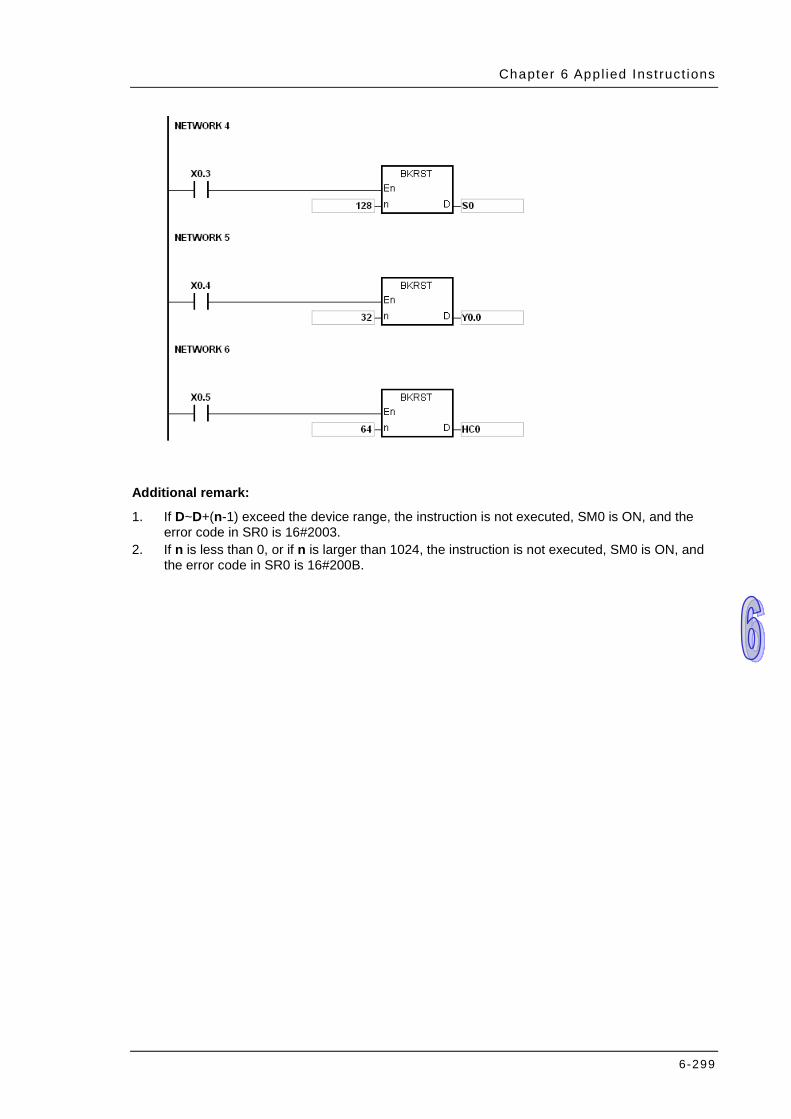
Chapter 6 Appl ied Inst ruct ions
6-299
Additional remark:
1. If D~D+(n-1) exceed the device range, the instruction is not executed, SM0 is ON, and the error code in SR0 is 16#2003.
2. If n is less than 0, or if n is larger than 1024, the instruction is not executed, SM0 is ON, and the error code in SR0 is 16#200B.
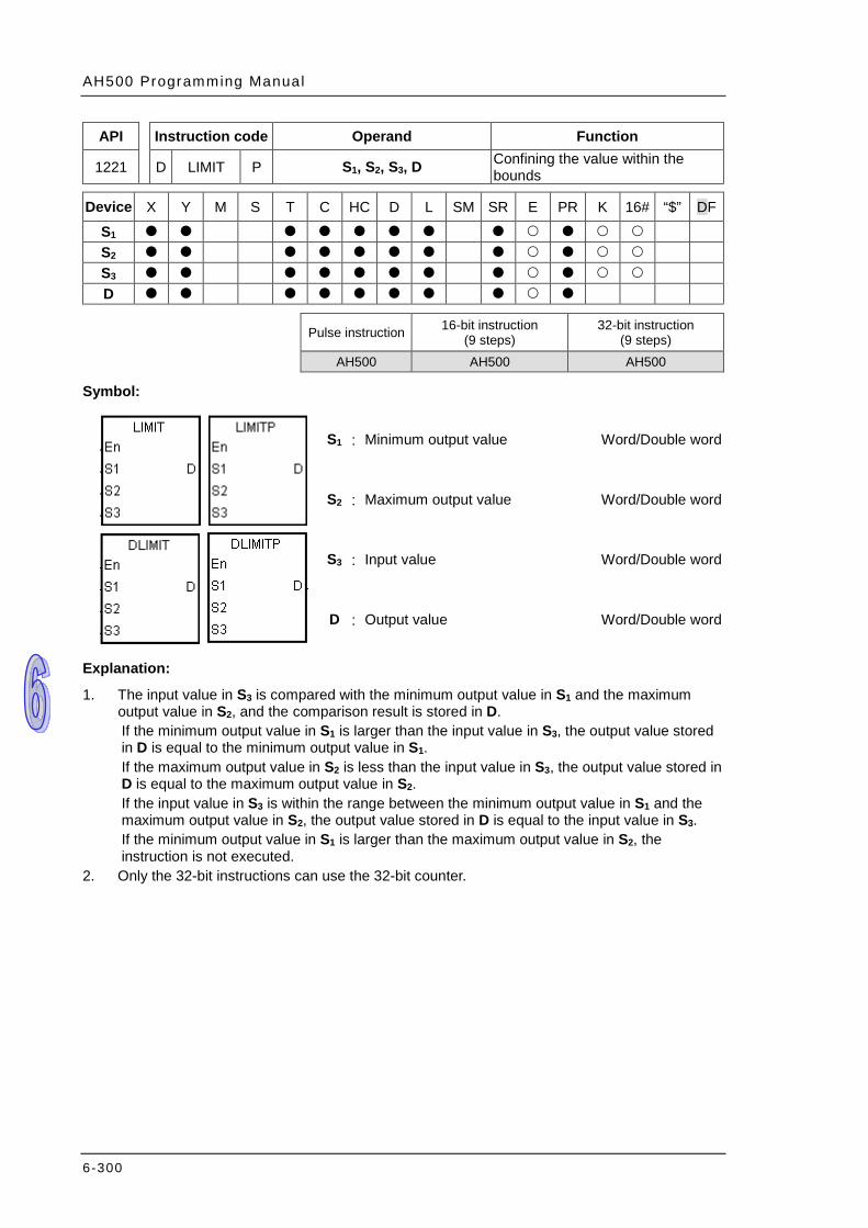
AH500 Programming Manual
6-300
API Instruction code Operand Function
1221 D LIMIT P S1, S2, S3, D Confining the value within the bounds
Device X Y M S T C HC D L SM SR E PR K 16# “$” DF
S1 S2 S3 D
Pulse instruction 16-bit instruction
(9 steps) 32-bit instruction
(9 steps) AH500 AH500 AH500
Symbol:
S1 : Minimum output value Word/Double word
S2 : Maximum output value Word/Double word
S3 : Input value Word/Double word
D : Output value Word/Double word
Explanation:
1. The input value in S3 is compared with the minimum output value in S1 and the maximum output value in S2, and the comparison result is stored in D. If the minimum output value in S1 is larger than the input value in S3, the output value stored in D is equal to the minimum output value in S1. If the maximum output value in S2 is less than the input value in S3, the output value stored in D is equal to the maximum output value in S2. If the input value in S3 is within the range between the minimum output value in S1 and the maximum output value in S2, the output value stored in D is equal to the input value in S3. If the minimum output value in S1 is larger than the maximum output value in S2, the instruction is not executed.
2. Only the 32-bit instructions can use the 32-bit counter.
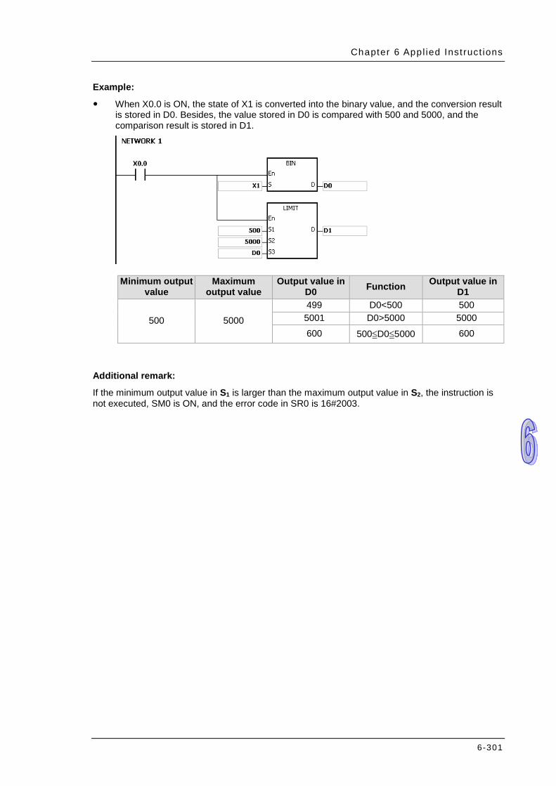
Chapter 6 Appl ied Inst ruct ions
6-301
Example:
When X0.0 is ON, the state of X1 is converted into the binary value, and the conversion result is stored in D0. Besides, the value stored in D0 is compared with 500 and 5000, and the comparison result is stored in D1.
Minimum output value
Maximum output value
Output value in D0 Function Output value in
D1
500 5000 499 D0<500 500 5001 D0>5000 5000 600 500≦D0≦5000 600
Additional remark:
If the minimum output value in S1 is larger than the maximum output value in S2, the instruction is not executed, SM0 is ON, and the error code in SR0 is 16#2003.
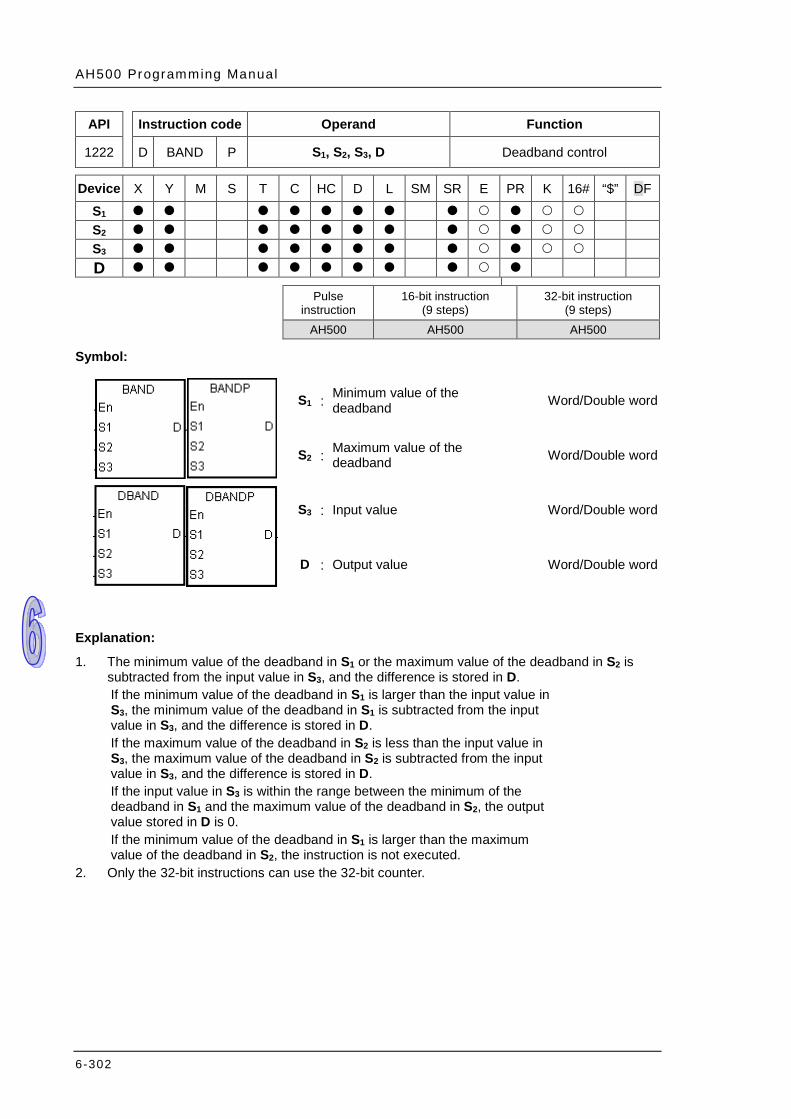
AH500 Programming Manual
6-302
API Instruction code Operand Function
1222 D BAND P S1, S2, S3, D Deadband control
Device X Y M S T C HC D L SM SR E PR K 16# “$” DF
S1 S2 S3 D
Pulse
instruction 16-bit instruction
(9 steps) 32-bit instruction
(9 steps) AH500 AH500 AH500
Symbol:
S1 : Minimum value of the deadband Word/Double word
S2 : Maximum value of the deadband Word/Double word
S3 : Input value Word/Double word
D : Output value Word/Double word
Explanation:
1. The minimum value of the deadband in S1 or the maximum value of the deadband in S2 is subtracted from the input value in S3, and the difference is stored in D. If the minimum value of the deadband in S1 is larger than the input value in S3, the minimum value of the deadband in S1 is subtracted from the input value in S3, and the difference is stored in D. If the maximum value of the deadband in S2 is less than the input value in S3, the maximum value of the deadband in S2 is subtracted from the input value in S3, and the difference is stored in D. If the input value in S3 is within the range between the minimum of the deadband in S1 and the maximum value of the deadband in S2, the output value stored in D is 0. If the minimum value of the deadband in S1 is larger than the maximum value of the deadband in S2, the instruction is not executed.
2. Only the 32-bit instructions can use the 32-bit counter.
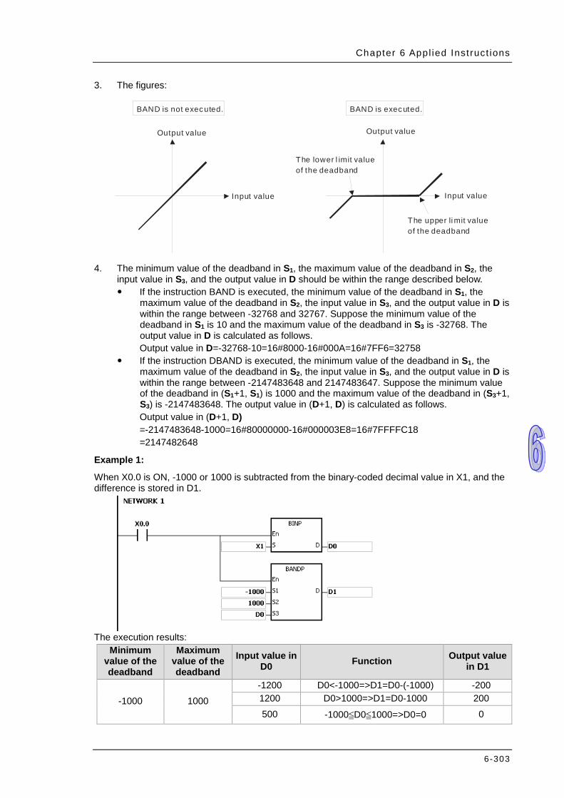
Chapter 6 Appl ied Inst ruct ions
6-303
3. The figures:
Output value
Input value
Output value
Input value
The lower l imit value of the deadband
The upper li mit value of the deadband
BAND is executed.BAND is not executed.
4. The minimum value of the deadband in S1, the maximum value of the deadband in S2, the
input value in S3, and the output value in D should be within the range described below. If the instruction BAND is executed, the minimum value of the deadband in S1, the
maximum value of the deadband in S2, the input value in S3, and the output value in D is within the range between -32768 and 32767. Suppose the minimum value of the deadband in S1 is 10 and the maximum value of the deadband in S3 is -32768. The output value in D is calculated as follows. Output value in D=-32768-10=16#8000-16#000A=16#7FF6=32758
If the instruction DBAND is executed, the minimum value of the deadband in S1, the maximum value of the deadband in S2, the input value in S3, and the output value in D is within the range between -2147483648 and 2147483647. Suppose the minimum value of the deadband in (S1+1, S1) is 1000 and the maximum value of the deadband in (S3+1, S3) is -2147483648. The output value in (D+1, D) is calculated as follows. Output value in (D+1, D) =-2147483648-1000=16#80000000-16#000003E8=16#7FFFFC18 =2147482648
Example 1:
When X0.0 is ON, -1000 or 1000 is subtracted from the binary-coded decimal value in X1, and the difference is stored in D1.
The execution results:
Minimum value of the deadband
Maximum value of the deadband
Input value in D0 Function Output value
in D1
-1000 1000 -1200 D0<-1000=>D1=D0-(-1000) -200 1200 D0>1000=>D1=D0-1000 200 500 -1000≦D0≦1000=>D0=0 0

AH500 Programming Manual
6-304
Example 2:
When X0.0 is ON, -10000 or 10000 is subtracted from the binary-coded decimal value in (X2, X1), and the difference is stored in (D11, D10).
The execution results:
Minimum value of the deadband
Maximum value of the deadband
Input value in (D1, D0) Function Output value in
(D11, D10)
-10000 10000
-12000 (D1, D0)<-10000 =>(D11,D10) =(D1, D0)-(-10000)
-2000
12000 (D1, D0)>10000 =>(D11, D10) =(D1, D0)-10000
2000
5000 -10000≦(D1, D0)≦10000 =>(D1, D0)=0
0
Additional remark:
If the minimum value of the deadband in S1 is larger than the maximum value of the deadband in S2, the instruction is not executed, SM0 is ON, and the error code in SR0 is 16#2003.
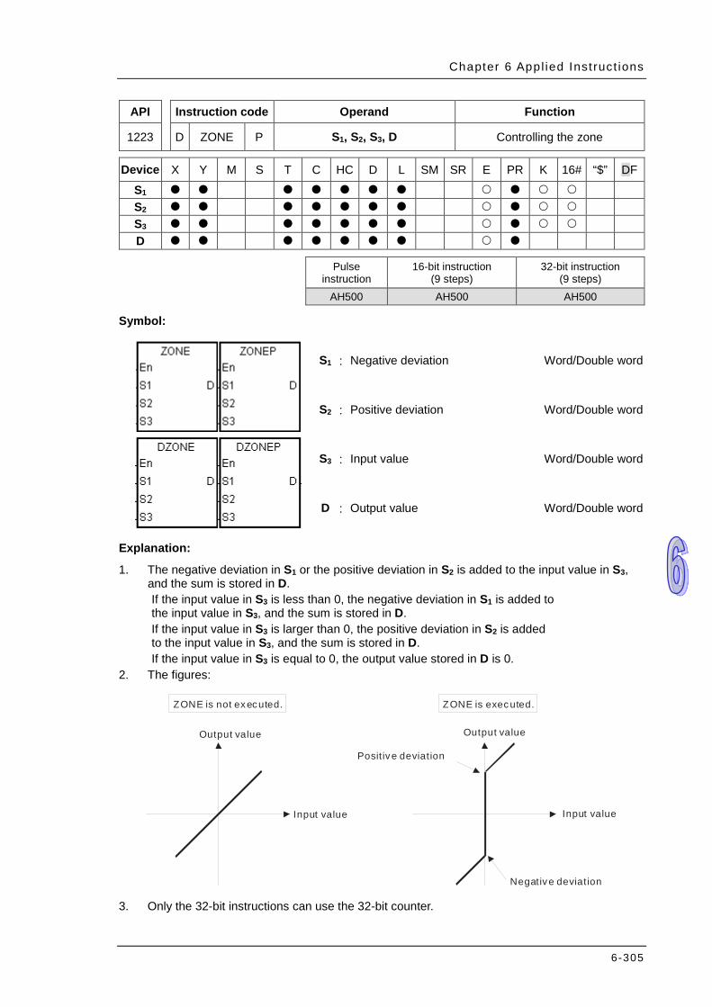
Chapter 6 Appl ied Inst ruct ions
6-305
API Instruction code Operand Function
1223 D ZONE P S1, S2, S3, D Controlling the zone
Device X Y M S T C HC D L SM SR E PR K 16# “$” DF
S1 S2 S3 D
Pulse
instruction 16-bit instruction
(9 steps) 32-bit instruction
(9 steps) AH500 AH500 AH500
Symbol:
S1 : Negative deviation Word/Double word
S2 : Positive deviation Word/Double word
S3 : Input value Word/Double word
D : Output value Word/Double word
Explanation:
1. The negative deviation in S1 or the positive deviation in S2 is added to the input value in S3, and the sum is stored in D. If the input value in S3 is less than 0, the negative deviation in S1 is added to the input value in S3, and the sum is stored in D. If the input value in S3 is larger than 0, the positive deviation in S2 is added to the input value in S3, and the sum is stored in D. If the input value in S3 is equal to 0, the output value stored in D is 0.
2. The figures:
Output value
Input value
Output value
Input value
Negative deviation
Posit ive deviation
ZONE is executed.ZONE is not executed.
3. Only the 32-bit instructions can use the 32-bit counter.
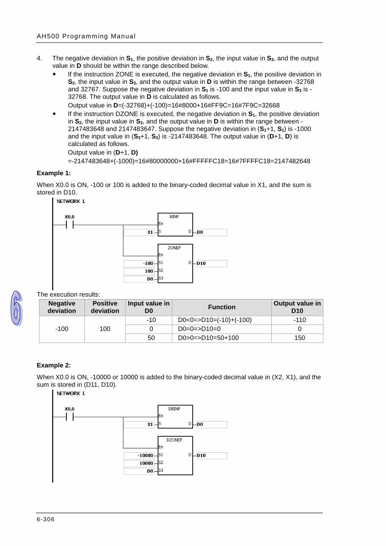
AH500 Programming Manual
6-306
4. The negative deviation in S1, the positive deviation in S2, the input value in S3, and the output value in D should be within the range described below. If the instruction ZONE is executed, the negative deviation in S1, the positive deviation in
S2, the input value in S3, and the output value in D is within the range between -32768 and 32767. Suppose the negative deviation in S1 is -100 and the input value in S3 is -32768. The output value in D is calculated as follows. Output value in D=(-32768)+(-100)=16#8000+16#FF9C=16#7F9C=32668
If the instruction DZONE is executed, the negative deviation in S1, the positive deviation in S2, the input value in S3, and the output value in D is within the range between -2147483648 and 2147483647. Suppose the negative deviation in (S1+1, S1) is -1000 and the input value in (S3+1, S3) is -2147483648. The output value in (D+1, D) is calculated as follows. Output value in (D+1, D) =-2147483648+(-1000)=16#80000000+16#FFFFFC18=16#7FFFFC18=2147482648
Example 1:
When X0.0 is ON, -100 or 100 is added to the binary-coded decimal value in X1, and the sum is stored in D10.
The execution results:
Negative deviation
Positive deviation
Input value in D0 Function Output value in
D10
-100 100 -10 D0<0=>D10=(-10)+(-100) -110 0 D0=0=>D10=0 0
50 D0>0=>D10=50+100 150
Example 2:
When X0.0 is ON, -10000 or 10000 is added to the binary-coded decimal value in (X2, X1), and the sum is stored in (D11, D10).
Chapter 6 Appl ied Inst ruct ions
6-307
Negative deviation
Positive deviation
Input value in (D1, D0) Function Output value in
(D11, D10)
-10000 10000
-10 (D1, D0)<0 =>(D11, D10) =(-10)+(-10000)
-10010
0 (D1, D0)=0 =>(D11, D10)=0 0
50 (D1, D0)>0 =>(D11, D10)=50+10000 10050

AH500 Programming Manual
6-308
6.14 Structure Creation Instructions
6.14.1 List of Structure Creation Instructions
API Instruction code Pulse instruction Function Step 16-bit 32-bit
1300 FOR – – Start of the nested loop 3 1301 NEXT – – End of the nested loop 1 1302 BREAK – Terminating the FOR-NEXT loop 5
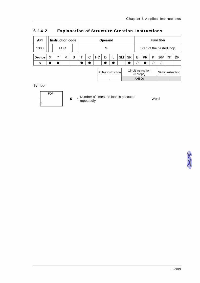
Chapter 6 Appl ied Inst ruct ions
6-309
6.14.2 Explanation of Structure Creation Instructions
API Instruction code Operand Function
1300 FOR S Start of the nested loop
Device X Y M S T C HC D L SM SR E PR K 16# “$” DF
S
Pulse instruction 16-bit instruction (3 steps) 32-bit instruction
- AH500 -
Symbol:
S : Number of times the loop is executed repeatedly Word
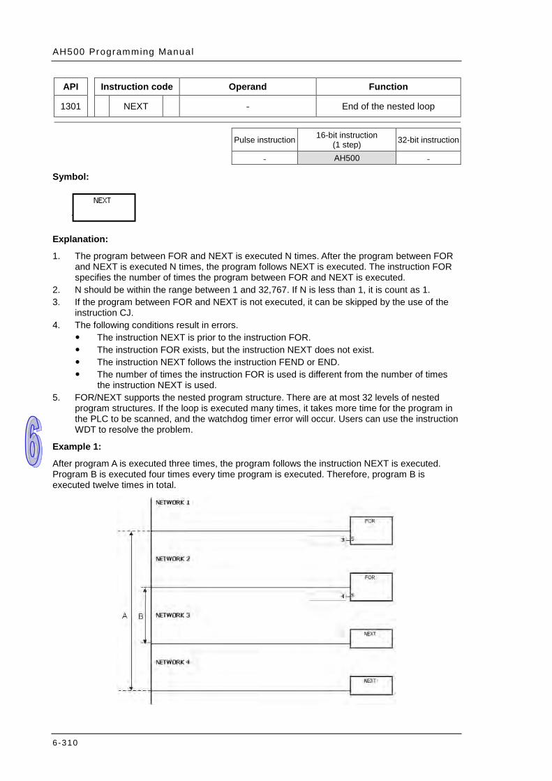
AH500 Programming Manual
6-310
API Instruction code Operand Function
1301 NEXT - End of the nested loop
Pulse instruction 16-bit instruction
(1 step) 32-bit instruction
- AH500 -
Symbol:
Explanation:
1. The program between FOR and NEXT is executed N times. After the program between FOR and NEXT is executed N times, the program follows NEXT is executed. The instruction FOR specifies the number of times the program between FOR and NEXT is executed.
2. N should be within the range between 1 and 32,767. If N is less than 1, it is count as 1. 3. If the program between FOR and NEXT is not executed, it can be skipped by the use of the
instruction CJ. 4. The following conditions result in errors.
The instruction NEXT is prior to the instruction FOR. The instruction FOR exists, but the instruction NEXT does not exist. The instruction NEXT follows the instruction FEND or END. The number of times the instruction FOR is used is different from the number of times
the instruction NEXT is used. 5. FOR/NEXT supports the nested program structure. There are at most 32 levels of nested
program structures. If the loop is executed many times, it takes more time for the program in the PLC to be scanned, and the watchdog timer error will occur. Users can use the instruction WDT to resolve the problem.
Example 1:
After program A is executed three times, the program follows the instruction NEXT is executed. Program B is executed four times every time program is executed. Therefore, program B is executed twelve times in total.
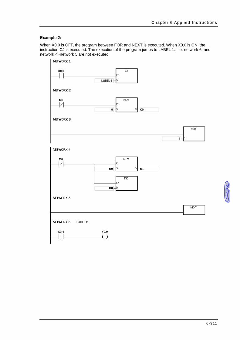
Chapter 6 Appl ied Inst ruct ions
6-311
Example 2:
When X0.0 is OFF, the program between FOR and NEXT is executed. When X0.0 is ON, the instruction CJ is executed. The execution of the program jumps to LABEL 1:, i.e. network 6, and network 4~network 5 are not executed.

AH500 Programming Manual
6-312
Example 3:
If the program between FOR and NEXT is not executed, it can be skipped by the use of the instruction CJ. When X0.1 in network 8 is ON, the instruction CJ is executed. The execution of the program jumps to LABEL 1:, i.e. network 12, and network 9~network 11 are not executed.
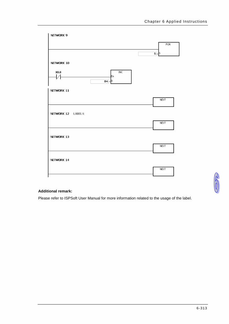
Chapter 6 Appl ied Inst ruct ions
6-313
Additional remark:
Please refer to ISPSoft User Manual for more information related to the usage of the label.

AH500 Programming Manual
6-314
API Instruction code Operand Function
1302 BREAK P D, P Terminating the FOR-NEXT loop
Device X Y M S T C HC D L SM SR E PR K 16# “$” DF
D P
Pulse instruction 16-bit instruction
(3 steps) 32-bit instruction
AH500 AH500 -
Symbol:
D : Device in which the remaining number of times the loop can be executed is stored
Word
P : Pointer Pointer
Explanation:
1. The instruction BREAK is used to terminate the FOR/NEXT loop. The remaining number of times the FOR/NEXT loop can be repeated is stored in D, and the execution of the program jumps to the part of program specified by the pointer
2. When the instruction BREAK is executed, the remaining number of times the FOR/NEXT loop can be repeated is stored in D, including this time the instruction BREAK is executed.
Example:
When the FOR/NEXT loop is executed, 1 is added to the value in D0. When the value in D0 is equal to 30, the FOR/NEXT loop is terminated, and the remaining number of times the FOR/NEXT loop can be repeated, i.e. 71, is stored in D10. The execution of the program jumps to LABEL 1:, i.e. network 6, and 1 is added to the value in D2.
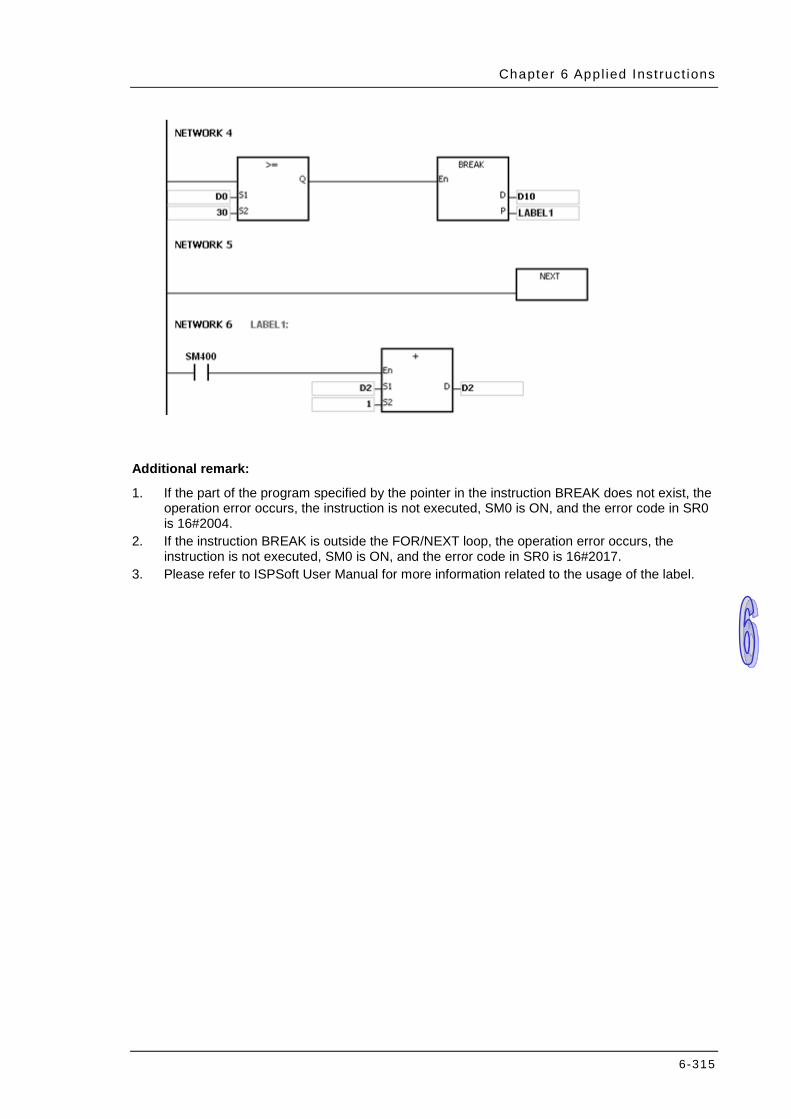
Chapter 6 Appl ied Inst ruct ions
6-315
Additional remark:
1. If the part of the program specified by the pointer in the instruction BREAK does not exist, the operation error occurs, the instruction is not executed, SM0 is ON, and the error code in SR0 is 16#2004.
2. If the instruction BREAK is outside the FOR/NEXT loop, the operation error occurs, the instruction is not executed, SM0 is ON, and the error code in SR0 is 16#2017.
3. Please refer to ISPSoft User Manual for more information related to the usage of the label.
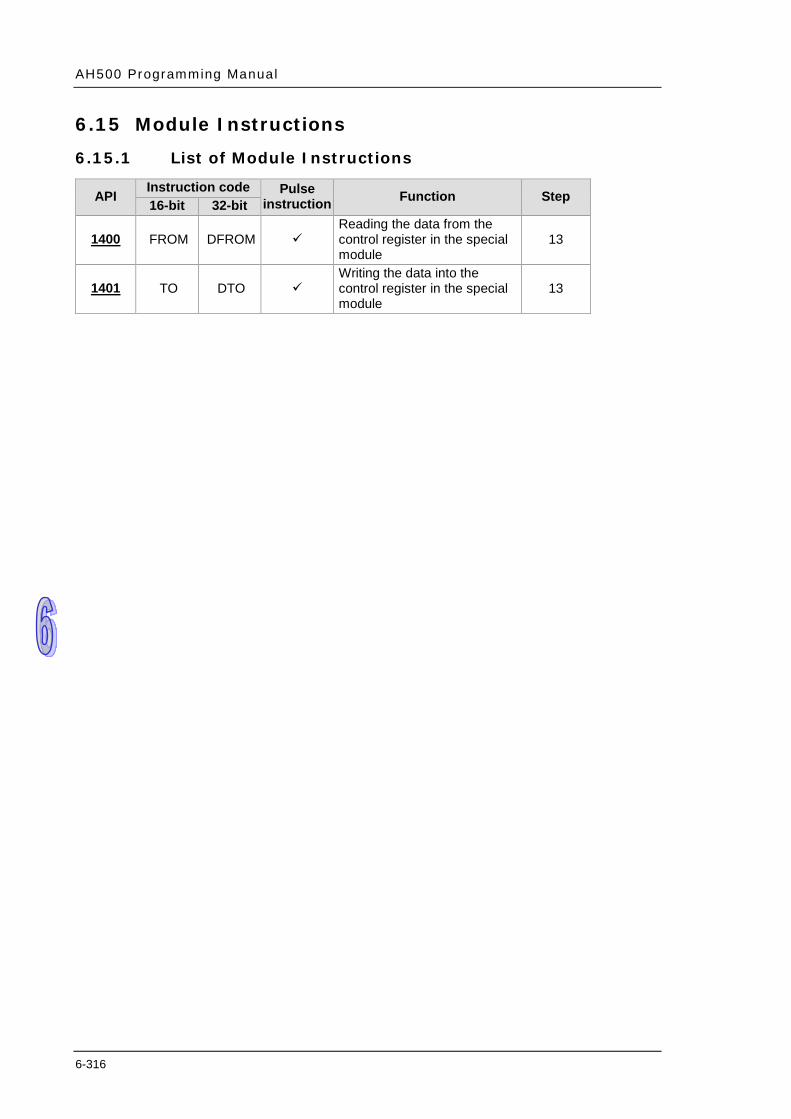
AH500 Programming Manual
6-316
6.15 Module Instructions
6.15.1 List of Module Instructions
API Instruction code Pulse instruction Function Step 16-bit 32-bit
1400 FROM DFROM Reading the data from the control register in the special module
13
1401 TO DTO Writing the data into the control register in the special module
13
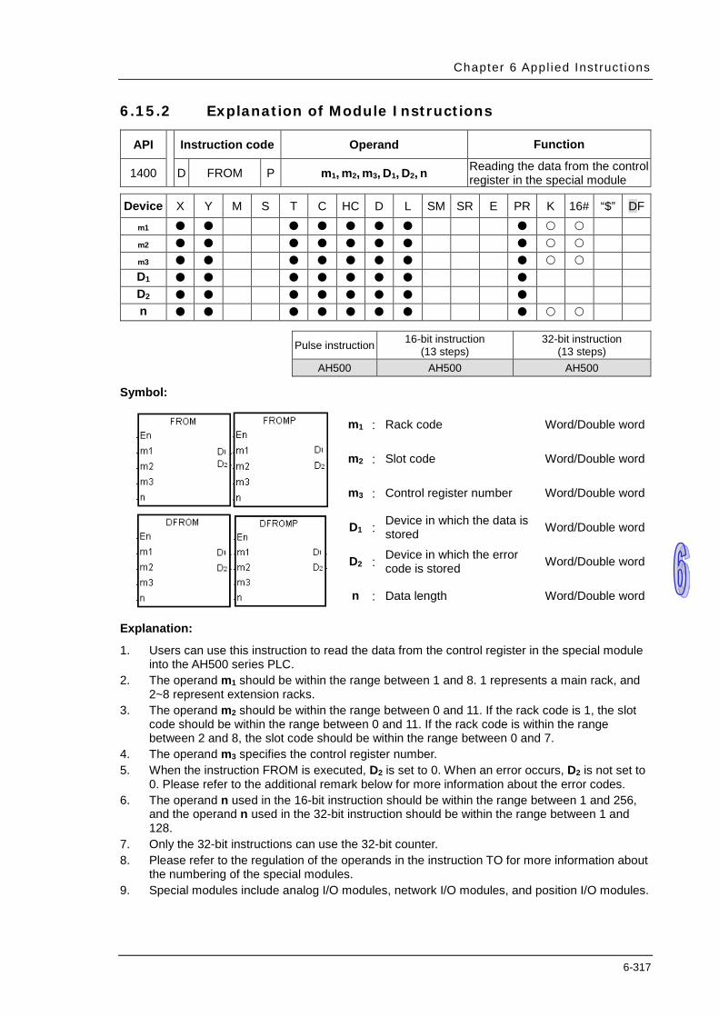
Chapter 6 Appl ied Inst ruct ions
6-317
6.15.2 Explanation of Module Instructions
API Instruction code Operand Function
1400 D FROM P m1, m2, m3, D1, D2, n Reading the data from the control register in the special module
Device X Y M S T C HC D L SM SR E PR K 16# “$” DF
m1
m2 m3 D1 D2 n
Pulse instruction 16-bit instruction
(13 steps) 32-bit instruction
(13 steps) AH500 AH500 AH500
Symbol:
m1 : Rack code Word/Double word
m2 : Slot code Word/Double word
m3 : Control register number Word/Double word
D1 : Device in which the data is stored Word/Double word
D2 : Device in which the error code is stored Word/Double word
n : Data length Word/Double word
Explanation:
1. Users can use this instruction to read the data from the control register in the special module into the AH500 series PLC.
2. The operand m1 should be within the range between 1 and 8. 1 represents a main rack, and 2~8 represent extension racks.
3. The operand m2 should be within the range between 0 and 11. If the rack code is 1, the slot code should be within the range between 0 and 11. If the rack code is within the range between 2 and 8, the slot code should be within the range between 0 and 7.
4. The operand m3 specifies the control register number. 5. When the instruction FROM is executed, D2 is set to 0. When an error occurs, D2 is not set to
0. Please refer to the additional remark below for more information about the error codes. 6. The operand n used in the 16-bit instruction should be within the range between 1 and 256,
and the operand n used in the 32-bit instruction should be within the range between 1 and 128.
7. Only the 32-bit instructions can use the 32-bit counter. 8. Please refer to the regulation of the operands in the instruction TO for more information about
the numbering of the special modules. 9. Special modules include analog I/O modules, network I/O modules, and position I/O modules.
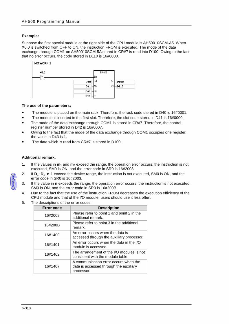
AH500 Programming Manual
6-318
Example:
Suppose the first special module at the right side of the CPU module is AH50010SCM-A5. When X0.0 is switched from OFF to ON, the instruction FROM is executed. The mode of the data exchange through COM1 on AH50010SCM-5A stored in CR#7 is read into D100. Owing to the fact that no error occurs, the code stored in D110 is 16#0000.
The use of the parameters:
The module is placed on the main rack. Therefore, the rack code stored in D40 is 16#0001. The module is inserted in the first slot. Therefore, the slot code stored in D41 is 16#0000. The mode of the data exchange through COM1 is stored in CR#7. Therefore, the control
register number stored in D42 is 16#0007. Owing to the fact that the mode of the data exchange through COM1 occupies one register,
the value in D43 is 1. The data which is read from CR#7 is stored in D100.
Additional remark:
1. If the values in m1 and m2 exceed the range, the operation error occurs, the instruction is not executed, SM0 is ON, and the error code in SR0 is 16#2003.
2. If D1~D1+n-1 exceed the device range, the instruction is not executed, SM0 is ON, and the error code in SR0 is 16#2003.
3. If the value in n exceeds the range, the operation error occurs, the instruction is not executed, SM0 is ON, and the error code in SR0 is 16#200B.
4. Due to the fact that the use of the instruction FROM decreases the execution efficiency of the CPU module and that of the I/O module, users should use it less often.
5. The descriptions of the error codes: Error code Description
16#2003 Please refer to point 1 and point 2 in the additional remark.
16#200B Please refer to point 3 in the additional remark.
16#1400 An error occurs when the data is accessed through the auxiliary processor.
16#1401 An error occurs when the data in the I/O module is accessed.
16#1402 The arrangement of the I/O modules is not consistent with the module table.
16#1407 A communication error occurs when the data is accessed through the auxiliary processor.

Chapter 6 Appl ied Inst ruct ions
6-319
API Instruction code Operand Function
1401 D TO P m1, m2, m3, S, D, n Writing the data into the control register in the special module
Device
X Y M S T C HC D L SM SR E PR K 16# “$” DF m1 m2
m3 S D n
Pulse instruction 16-bit instruction
(13 steps) 32-bit instruction
(13 steps)
AH500 AH500 AH500
Symbol:
m1 : Rack code Word/Double word
m2 : Slot code Word/Double word
m3 : Control register number Word/Double word
S : Data which is written into the control register Word/Double word
D : Device in which the error code is stored Word/Double word
n : Data length Word/Double word
Explanation:
1. Users can use this instruction to write the data in the AH500 series PLC into the control register in the special module.
2. The operand m1 should be within the range between 1 and 8. 1 represents a main rack, and 2~8 represent extension racks.
3. The operand m2 should be within the range between 0 and 11. If the rack code is 1, the slot code should be within the range between 0 and 11. If the rack code is within the range between 2 and 8, the slot code should be within the range between 0 and 7.
4. The operand m3 specifies the control register number. 5. When the instruction TO is executed, D is set to 0. When an error occurs, D is not set to 0.
Please refer to the additional remark below for more information about the error codes. 6. The operand n used in the 16-bit instruction should be within the range between 1 and 256,
and the operand n used in the 32-bit instruction should be within the range between 1 and 128.
7. Only the 32-bit instructions can use the 32-bit counter. 8. Special modules include analog I/O modules, network I/O modules, and position I/O modules. 9. When S is a decimal value or a hexadecimal value, n decimal values or n hexadecimal values
are transmitted to the I/O module. Suppose S is 16#0001 and n is 3. Three 16#0001s are transmitted to the I/O module.

AH500 Programming Manual
6-320
10. When using the redundancy system, AHCPU560-EN2, it is suggested to use API2901, RCS instruction along with this instruction to write the data into the control register in the special module. Or after the system is switched over, the module parameters may not be consistent. You can use RCS instruction to read the PLC ID to see if there is a switchover. If there is a switchover, you can use RCS instruction to set the system ID and redundant system data to ensure the parameters of the redundancy system are correct.
Example:
Suppose the first special module at the right side of the CPU module is AH50010SCM-A5. When X1.1 is switched from OFF to ON, the instruction TO is executed. The mode of the data exchange through COM1 on AH50010SCM-5A stored in CR#7 changes from being disabled to being enabled. Owing to the fact that no error occurs, the code stored in D110 is 16#0000.
The use of the parameters:
The module is placed on the main rack. Therefore, the rack code stored in D40 is 16#0001. The module is inserted in the first slot. Therefore, the slot code stored in D41 is 16#0000. The mode of the data exchange through COM1 is stored in CR#7. Therefore, the control
register number stored in D42 is 16#0007. Owing to the fact that the mode of the data exchange through COM1 occupies one register,
the value in D2 is 1. The data which is written into CR#7 is stored in D100. Therefore, the value in D100 is
16#0002.
The regulation of the operands in the instruction:
The operand m1 specifies the rack code. It should be within the range between 1 and 8. 1 represents a main rack, and 2~8 represent extension racks.
The operand m2 specifies the slot code. It should be within the range between 0 and 11. If the rack code is 1, the slot code should be within the range between 0 and 11. If the rack code is within the range between 2 and 8, the slot code should be within the range between 0 and 7.
The operand m3 specifies the control register number. The 16-bit memories built in the special modules are called the control registers. The control register numbers are decimal numbers #0~#N, and the number of control registers varies with the module. The operating conditions of the special module and the setting values are stored in the control registers.
At most 68 special modules can be placed on the rack, and they do not occupy inputs/outputs.
If the instruction FROM/TO is used, one control register is taken as a unit for the reading/writing of the data. If the instruction DFROM/DTO is used, two control registers are taken as a unit for the reading/writing of the data.
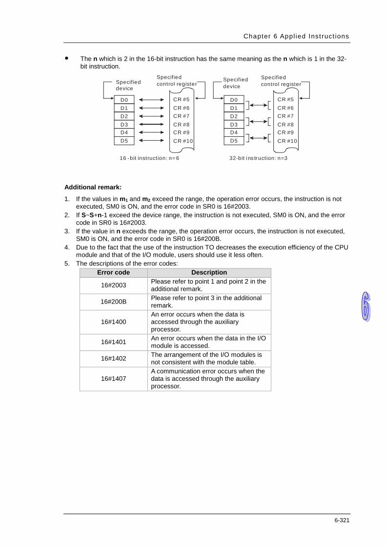
Chapter 6 Appl ied Inst ruct ions
6-321
The n which is 2 in the 16-bit instruction has the same meaning as the n which is 1 in the 32-bit instruction.
D0D1D2D3D4D5
CR #5CR #6CR #7CR #8CR #9CR #10
16 -bit instruction: n= 6
Specif ieddevice
Specif iedcontrol register
D0D1D2D3D4D5
CR #5CR #6CR #7CR #8CR #9CR #10
32-bit i ns truction: n=3
Specif ied device
Specif iedcontrol register
Additional remark:
1. If the values in m1 and m2 exceed the range, the operation error occurs, the instruction is not executed, SM0 is ON, and the error code in SR0 is 16#2003.
2. If S~S+n-1 exceed the device range, the instruction is not executed, SM0 is ON, and the error code in SR0 is 16#2003.
3. If the value in n exceeds the range, the operation error occurs, the instruction is not executed, SM0 is ON, and the error code in SR0 is 16#200B.
4. Due to the fact that the use of the instruction TO decreases the execution efficiency of the CPU module and that of the I/O module, users should use it less often.
5. The descriptions of the error codes: Error code Description
16#2003 Please refer to point 1 and point 2 in the additional remark.
16#200B Please refer to point 3 in the additional remark.
16#1400 An error occurs when the data is accessed through the auxiliary processor.
16#1401 An error occurs when the data in the I/O module is accessed.
16#1402 The arrangement of the I/O modules is not consistent with the module table.
16#1407 A communication error occurs when the data is accessed through the auxiliary processor.
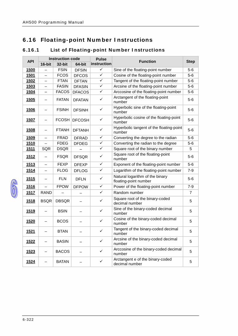
AH500 Programming Manual
6-322
6.16 Floating-point Number Instructions
6.16.1 List of Floating-point Number Instructions
API Instruction code Pulse instruction Function Step 16-bit 32-bit 64-bit
1500 – FSIN DFSIN Sine of the floating-point number 5-6 1501 – FCOS DFCOS Cosine of the floating-point number 5-6 1502 – FTAN DFTAN Tangent of the floating-point number 5-6 1503 – FASIN DFASIN Arcsine of the floating-point number 5-6 1504 – FACOS DFACOS Arccosine of the floating-point number 5-6
1505 – FATAN DFATAN Arctangent of the floating-point number 5-6
1506 – FSINH DFSINH Hyperbolic sine of the floating-point number 5-6
1507 – FCOSH DFCOSH Hyperbolic cosine of the floating-point number 5-6
1508 – FTANH DFTANH Hyperbolic tangent of the floating-point number 5-6
1509 – FRAD DFRAD Converting the degree to the radian 5-6 1510 – FDEG DFDEG Converting the radian to the degree 5-6 1511 SQR DSQR – Square root of the binary number 5
1512 – FSQR DFSQR Square root of the floating-point number 5-6
1513 – FEXP DFEXP Exponent of the floating-point number 5-6 1514 – FLOG DFLOG Logarithm of the floating-point number 7-9
1515 – FLN DFLN Natural logarithm of the binary floating-point number 5-6
1516 – FPOW DFPOW Power of the floating-point number 7-9 1517 RAND – – Random number 7
1518 BSQR DBSQR – Square root of the binary-coded decimal number 5
1519 – BSIN – Sine of the binary-coded decimal number 5
1520 – BCOS – Cosine of the binary-coded decimal number 5
1521 – BTAN – Tangent of the binary-coded decimal number 5
1522 – BASIN – Arcsine of the binary-coded decimal number 5
1523 – BACOS – Arccosine of the binary-coded decimal number 5
1524 – BATAN – Arctangent e of the binary-coded decimal number 5
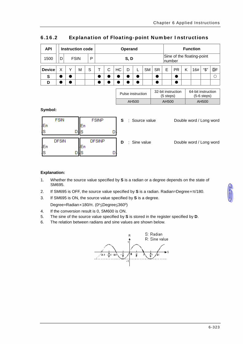
Chapter 6 Appl ied Inst ruct ions
6-323
6.16.2 Explanation of Floating-point Number Instructions
API Instruction code Operand Function
1500 D FSIN P S, D Sine of the floating-point number
Device X Y M S T C HC D L SM SR E PR K 16# “$” DF
S D
Pulse instruction 32-bit instruction
(5 steps) 64-bit instruction
(5-6 steps) AH500 AH500 AH500
Symbol:
S : Source value Double word / Long word
D : Sine value Double word / Long word
Explanation:
1. Whether the source value specified by S is a radian or a degree depends on the state of SM695.
2. If SM695 is OFF, the source value specified by S is a radian. Radian=Degree×π/180. 3. If SM695 is ON, the source value specified by S is a degree.
Degree=Radian×180/π. (0o≦Degree≦3600) 4. If the conversion result is 0, SM600 is ON. 5. The sine of the source value specified by S is stored in the register specified by D. 6. The relation between radians and sine values are shown below.
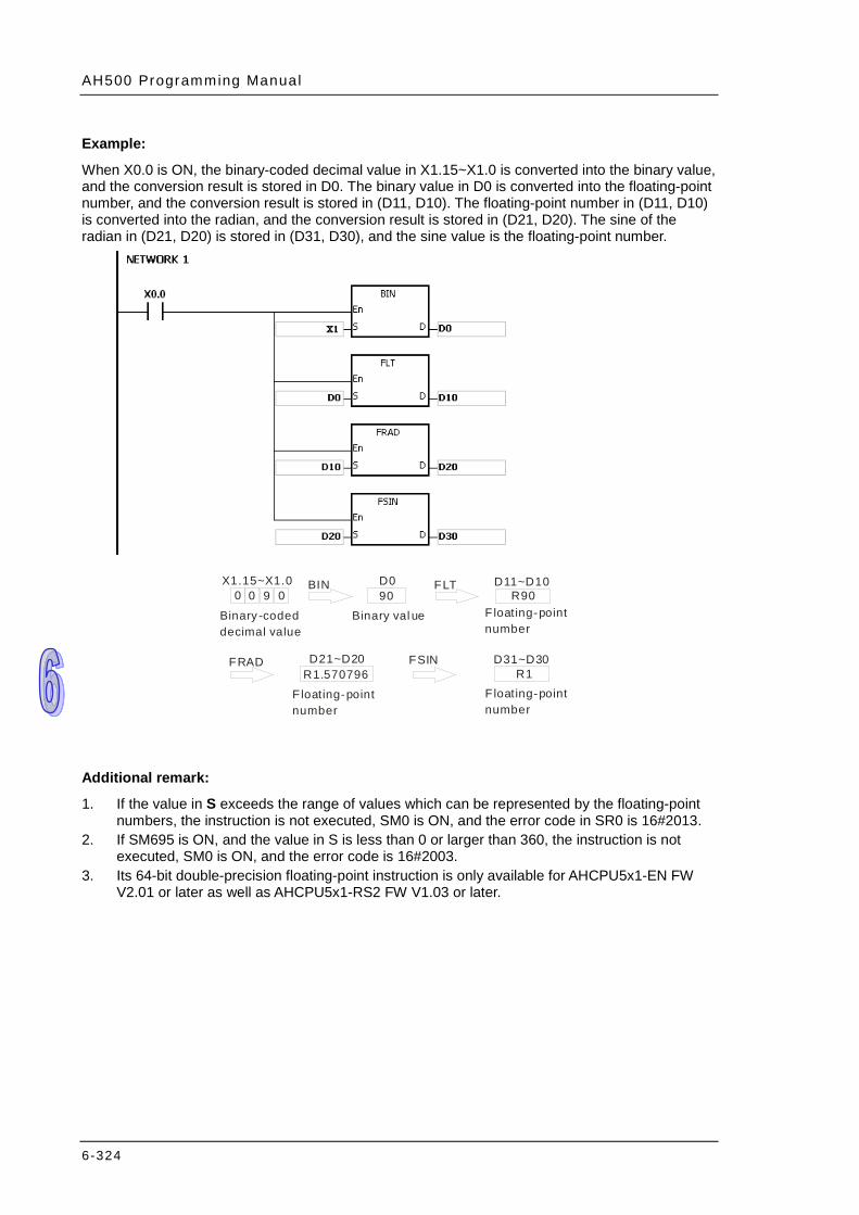
AH500 Programming Manual
6-324
Example:
When X0.0 is ON, the binary-coded decimal value in X1.15~X1.0 is converted into the binary value, and the conversion result is stored in D0. The binary value in D0 is converted into the floating-point number, and the conversion result is stored in (D11, D10). The floating-point number in (D11, D10) is converted into the radian, and the conversion result is stored in (D21, D20). The sine of the radian in (D21, D20) is stored in (D31, D30), and the sine value is the floating-point number.
BIN
Binary val ue
FLT
Floating-point number
Binary -coded decimal value
FRAD FSIN
R90900 0 09
R1.570796
X1.15~X1.0 D0 D11~D10
D21~D20R1
D31~D30
Floating-point number
F loating-point number
Additional remark:
1. If the value in S exceeds the range of values which can be represented by the floating-point numbers, the instruction is not executed, SM0 is ON, and the error code in SR0 is 16#2013.
2. If SM695 is ON, and the value in S is less than 0 or larger than 360, the instruction is not executed, SM0 is ON, and the error code is 16#2003.
3. Its 64-bit double-precision floating-point instruction is only available for AHCPU5x1-EN FW V2.01 or later as well as AHCPU5x1-RS2 FW V1.03 or later.

Chapter 6 Appl ied Inst ruct ions
6-325
API Instruction code Operand Function
1501 D FCOS P S, D Cosine of the floating-point number
Device X Y M S T C HC D L SM SR E PR K 16# “$” DF
S D
Pulse instruction 32-bit instruction
(5 steps) 64-bit instruction
(5-6 steps) AH500 AH500 AH500
Symbol:
S : Source value Double word / Long word
D : Cosine value Double word / Long word
Explanation:
1. Whether the source value specified by S is a radian or a degree depends on the state of SM695.
2. If SM695 is OFF, the source value specified by S is a radian. Radian=Degree×π/180. 3. If SM695 is ON, the source value specified by S is a degree.
Degree=Radian×180/π. (0o≦Degree≦3600) 4. If the conversion result is 0, SM600 is ON. 5. The cosine of the source value specified by S is stored in the register specified by D. 6. The relation between radians and cosine values are shown below.
Example:
When X0.0 is ON, the binary-coded decimal value in X1.15~X1.0 is converted into the binary value, and the conversion result is stored in D0. The binary value in D0 is converted into the floating-point number, and the conversion result is stored in (D11, D10). The floating-point number in (D11, D10) is converted into the radian, and the conversion result is stored in (D21, D20). The cosine of the radian in (D21, D20) is stored in (D31, D30), and the cosine value is the floating-point number.

AH500 Programming Manual
6-326
BIN
Binary value
FLT
Floating-point number
Binary -coded decimal value
FRAD
Floating-point number
F loating-point number
FCOS
R3603600 3 06
R6.283185
X1.15~X1.0 D0 D11~D10
D21~D20R1
D31~D30
Additional remark:
1. If the value in S exceeds the range of values which can be represented by the floating-point numbers, the instruction is not executed, SM0 is ON, and the error code in SR0 is 16#2013.
2. If SM695 is ON, and the value in S is less than 0 or larger than 360, the instruction is not executed, SM0 is ON, and the error code is 16#2003.
3. Its 64-bit double-precision floating-point instruction is only available for AHCPU5x1-EN FW V2.01 or later as well as AHCPU5x1-RS2 FW V1.03 or later.
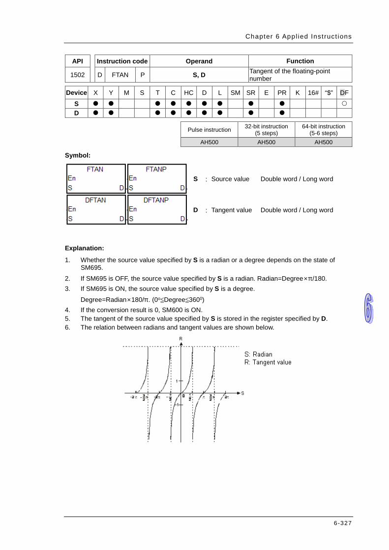
Chapter 6 Appl ied Inst ruct ions
6-327
API Instruction code Operand Function
1502 D FTAN P S, D Tangent of the floating-point number
Device X Y M S T C HC D L SM SR E PR K 16# “$” DF
S D
Pulse instruction 32-bit instruction
(5 steps) 64-bit instruction
(5-6 steps) AH500 AH500 AH500
Symbol:
S : Source value Double word / Long word
D : Tangent value Double word / Long word
Explanation:
1. Whether the source value specified by S is a radian or a degree depends on the state of SM695.
2. If SM695 is OFF, the source value specified by S is a radian. Radian=Degree×π/180. 3. If SM695 is ON, the source value specified by S is a degree.
Degree=Radian×180/π. (0o≦Degree≦3600) 4. If the conversion result is 0, SM600 is ON. 5. The tangent of the source value specified by S is stored in the register specified by D. 6. The relation between radians and tangent values are shown below.

AH500 Programming Manual
6-328
Example:
When X0.0 is ON, the binary-coded decimal value in X1.15~X1.0 is converted into the binary value, and the conversion result is stored in D0. The binary value in D0 is converted into the floating-point number, and the conversion result is stored in (D11, D10). The floating-point number in (D11, D10) is converted into the radian, and the conversion result is stored in (D21, D20). The tangent of the radian in (D21, D20) is stored in (D31, D30), and the tangent value is the floating-point number.
BIN
Binary val ue
FLT
Floating-point number
Binary -coded decimal value
FRAD
Floating-point number
F loating-point number
FTAN
R56450 0 54
R0.785398
X1.15~X1.0 D0 D11~D10
D21~D20R1
D31~D30
Additional remark:
1. If the value in S exceeds the range of values which can be represented by the floating-point numbers, the instruction is not executed, SM0 is ON, and the error code in SR0 is 16#2013.
2. If SM695 is ON, and the value in S is less than 0 or larger than 360, the instruction is not executed, SM0 is ON, and the error code is 16#2003.
3. Its 64-bit double-precision floating-point instruction is only available for AHCPU5x1-EN FW V2.01 or later as well as AHCPU5x1-RS2 FW V1.03 or later.

Chapter 6 Appl ied Inst ruct ions
6-329
API Instruction code Operand Function
1503 D FASIN P S, D Arcsine of the floating-point number
Device X Y M S T C HC D L SM SR E PR K 16# “$” DF
S D
Pulse instruction 32-bit instruction
(5 steps) 64-bit instruction
(5-6 steps) AH500 AH500 AH500
Symbol:
S : Source value Double word / Long word
D : Arcsine value Double word / Long word
Explanation:
1. Arcsine value=sin-1 The relation between sine values and arcsine values are shown below.
2. If the conversion result is 0, SM600 is ON.
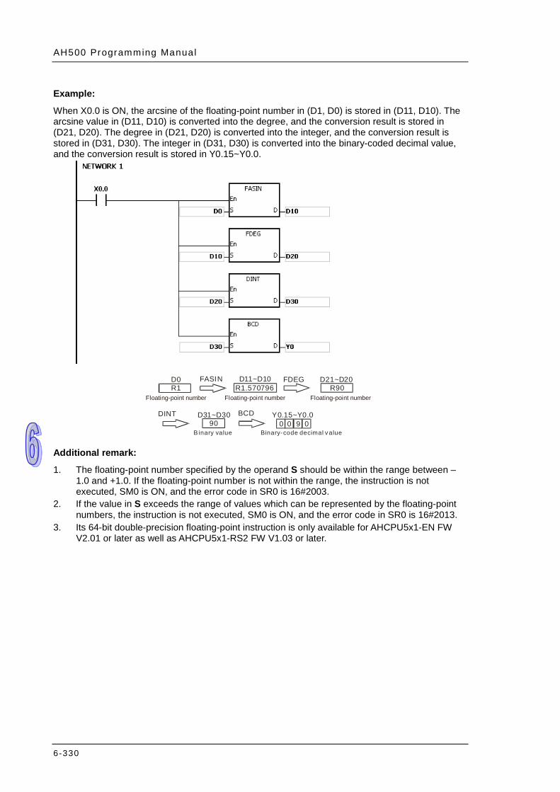
AH500 Programming Manual
6-330
Example:
When X0.0 is ON, the arcsine of the floating-point number in (D1, D0) is stored in (D11, D10). The arcsine value in (D11, D10) is converted into the degree, and the conversion result is stored in (D21, D20). The degree in (D21, D20) is converted into the integer, and the conversion result is stored in (D31, D30). The integer in (D31, D30) is converted into the binary-coded decimal value, and the conversion result is stored in Y0.15~Y0.0.
FDEG
0 0 09Y0.15~Y0.0
90
R90D21~D20
R1D0
R1.570796D11~D10FASIN
D31~D30DINT BCD
B inary value Binary-code decimal value
Floating-point numberFloating-point numberFloating-point number
Additional remark:
1. The floating-point number specified by the operand S should be within the range between –1.0 and +1.0. If the floating-point number is not within the range, the instruction is not executed, SM0 is ON, and the error code in SR0 is 16#2003.
2. If the value in S exceeds the range of values which can be represented by the floating-point numbers, the instruction is not executed, SM0 is ON, and the error code in SR0 is 16#2013.
3. Its 64-bit double-precision floating-point instruction is only available for AHCPU5x1-EN FW V2.01 or later as well as AHCPU5x1-RS2 FW V1.03 or later.
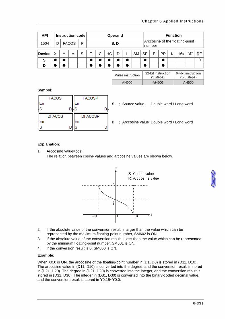
Chapter 6 Appl ied Inst ruct ions
6-331
API Instruction code Operand Function
1504 D FACOS P S, D Arccosine of the floating-point number
Device X Y M S T C HC D L SM SR E PR K 16# “$” DF
S D
Pulse instruction 32-bit instruction
(5 steps) 64-bit instruction
(5-6 steps) AH500 AH500 AH500
Symbol:
S : Source value Double word / Long word
D : Arccosine value Double word / Long word
Explanation:
1. Arccosine value=cos-1 The relation between cosine values and arccosine values are shown below.
2. If the absolute value of the conversion result is larger than the value which can be
represented by the maximum floating-point number, SM602 is ON. 3. If the absolute value of the conversion result is less than the value which can be represented
by the minimum floating-point number, SM601 is ON. 4. If the conversion result is 0, SM600 is ON.
Example:
When X0.0 is ON, the arccosine of the floating-point number in (D1, D0) is stored in (D11, D10). The arccosine value in (D11, D10) is converted into the degree, and the conversion result is stored in (D21, D20). The degree in (D21, D20) is converted into the integer, and the conversion result is stored in (D31, D30). The integer in (D31, D30) is converted into the binary-coded decimal value, and the conversion result is stored in Y0.15~Y0.0.
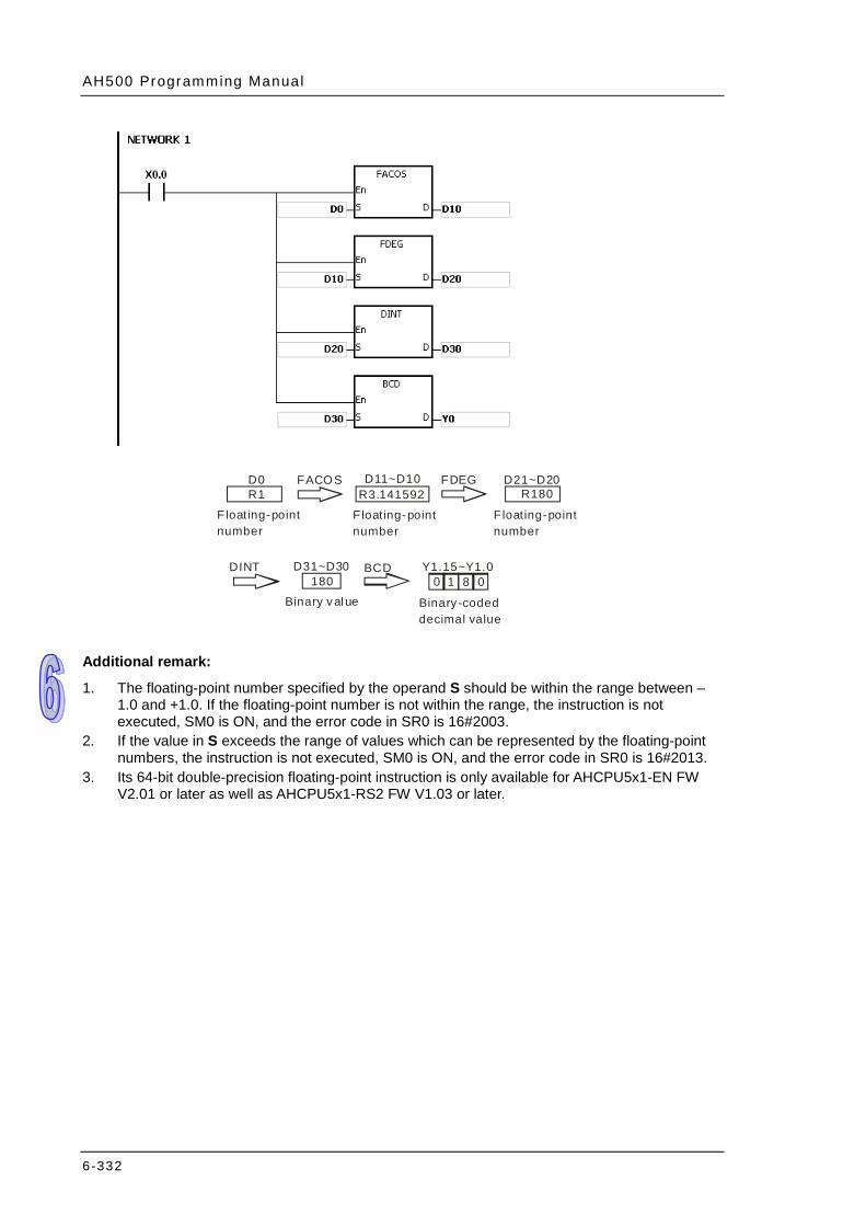
AH500 Programming Manual
6-332
Binary val ue
Floating-point number
Binary -coded decimal value
Floating-point number
F loating-point number
BCDDINT
FDEG
0 1 08Y1.15~Y1.0
180
R180D21~D20
R1D0
R3.141592D11~D10FACOS
D31~D30
Additional remark:
1. The floating-point number specified by the operand S should be within the range between –1.0 and +1.0. If the floating-point number is not within the range, the instruction is not executed, SM0 is ON, and the error code in SR0 is 16#2003.
2. If the value in S exceeds the range of values which can be represented by the floating-point numbers, the instruction is not executed, SM0 is ON, and the error code in SR0 is 16#2013.
3. Its 64-bit double-precision floating-point instruction is only available for AHCPU5x1-EN FW V2.01 or later as well as AHCPU5x1-RS2 FW V1.03 or later.
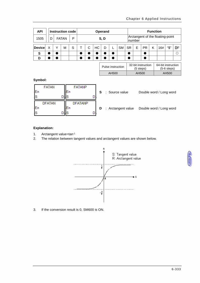
Chapter 6 Appl ied Inst ruct ions
6-333
API Instruction code Operand Function
1505 D FATAN P S, D Arctangent of the floating-point number
Device X Y M S T C HC D L SM SR E PR K 16# “$” DF
S D
Pulse instruction 32-bit instruction
(5 steps) 64-bit instruction
(5-6 steps) AH500 AH500 AH500
Symbol:
S : Source value Double word / Long word
D : Arctangent value Double word / Long word
Explanation:
1. Arctangent value=tan-1 2. The relation between tangent values and arctangent values are shown below.
3. If the conversion result is 0, SM600 is ON.
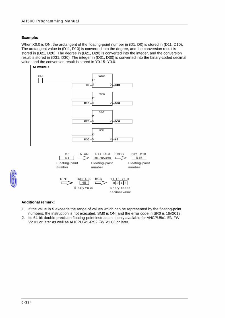
AH500 Programming Manual
6-334
Example:
When X0.0 is ON, the arctangent of the floating-point number in (D1, D0) is stored in (D11, D10). The arctangent value in (D11, D10) is converted into the degree, and the conversion result is stored in (D21, D20). The degree in (D21, D20) is converted into the integer, and the conversion result is stored in (D31, D30). The integer in (D31, D30) is converted into the binary-coded decimal value, and the conversion result is stored in Y0.15~Y0.0.
Binary val ue
Floating-point number
Binary -coded decimal value
Floating-point number
F loating-point number
BCDDINT
FDEG
0 0 54Y1.15~Y1.0
45
R45D21~D20
R1D0
R0.785398D11~D10FATAN
D31~D30
Additional remark:
1. If the value in S exceeds the range of values which can be represented by the floating-point numbers, the instruction is not executed, SM0 is ON, and the error code in SR0 is 16#2013.
2. Its 64-bit double-precision floating-point instruction is only available for AHCPU5x1-EN FW V2.01 or later as well as AHCPU5x1-RS2 FW V1.03 or later.
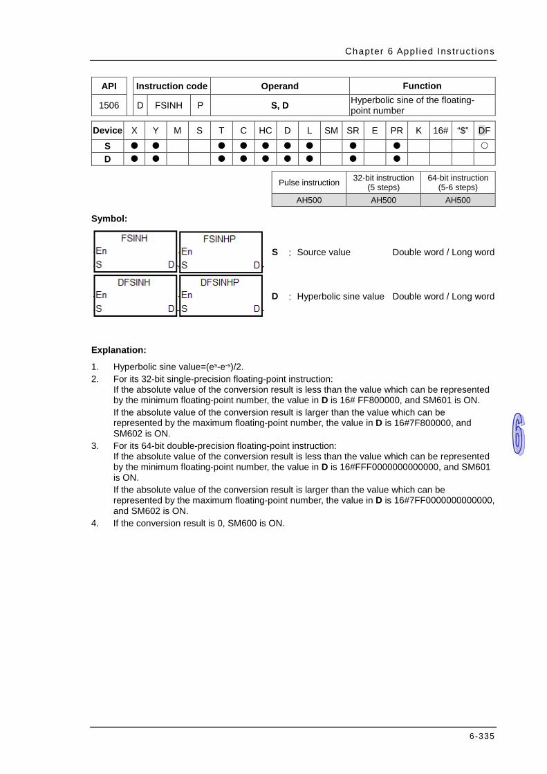
Chapter 6 Appl ied Inst ruct ions
6-335
API Instruction code Operand Function
1506 D FSINH P S, D Hyperbolic sine of the floating-point number
Device X Y M S T C HC D L SM SR E PR K 16# “$” DF
S D
Pulse instruction 32-bit instruction
(5 steps) 64-bit instruction
(5-6 steps) AH500 AH500 AH500
Symbol:
S : Source value Double word / Long word
D : Hyperbolic sine value Double word / Long word
Explanation:
1. Hyperbolic sine value=(es-e-s)/2. 2. For its 32-bit single-precision floating-point instruction:
If the absolute value of the conversion result is less than the value which can be represented by the minimum floating-point number, the value in D is 16# FF800000, and SM601 is ON. If the absolute value of the conversion result is larger than the value which can be represented by the maximum floating-point number, the value in D is 16#7F800000, and SM602 is ON.
3. For its 64-bit double-precision floating-point instruction: If the absolute value of the conversion result is less than the value which can be represented by the minimum floating-point number, the value in D is 16#FFF0000000000000, and SM601 is ON. If the absolute value of the conversion result is larger than the value which can be represented by the maximum floating-point number, the value in D is 16#7FF0000000000000, and SM602 is ON.
4. If the conversion result is 0, SM600 is ON.
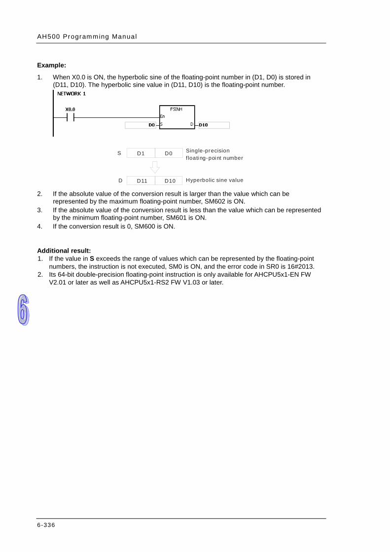
AH500 Programming Manual
6-336
Example:
1. When X0.0 is ON, the hyperbolic sine of the floating-point number in (D1, D0) is stored in (D11, D10). The hyperbolic sine value in (D11, D10) is the floating-point number.
D1 D0
D11 D10
Single-precision f loati ng-poi nt number
Hyperbolic sine value
S
D 2. If the absolute value of the conversion result is larger than the value which can be
represented by the maximum floating-point number, SM602 is ON. 3. If the absolute value of the conversion result is less than the value which can be represented
by the minimum floating-point number, SM601 is ON. 4. If the conversion result is 0, SM600 is ON.
Additional result: 1. If the value in S exceeds the range of values which can be represented by the floating-point
numbers, the instruction is not executed, SM0 is ON, and the error code in SR0 is 16#2013. 2. Its 64-bit double-precision floating-point instruction is only available for AHCPU5x1-EN FW
V2.01 or later as well as AHCPU5x1-RS2 FW V1.03 or later.
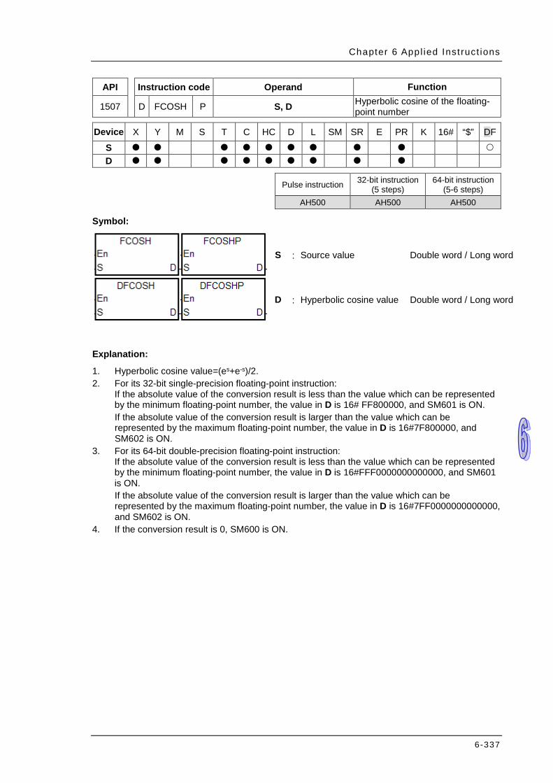
Chapter 6 Appl ied Inst ruct ions
6-337
API Instruction code Operand Function
1507 D FCOSH P S, D Hyperbolic cosine of the floating-point number
Device X Y M S T C HC D L SM SR E PR K 16# “$” DF
S D
Pulse instruction 32-bit instruction
(5 steps) 64-bit instruction
(5-6 steps) AH500 AH500 AH500
Symbol:
S : Source value Double word / Long word
D : Hyperbolic cosine value Double word / Long word
Explanation:
1. Hyperbolic cosine value=(es+e-s)/2. 2. For its 32-bit single-precision floating-point instruction:
If the absolute value of the conversion result is less than the value which can be represented by the minimum floating-point number, the value in D is 16# FF800000, and SM601 is ON. If the absolute value of the conversion result is larger than the value which can be represented by the maximum floating-point number, the value in D is 16#7F800000, and SM602 is ON.
3. For its 64-bit double-precision floating-point instruction: If the absolute value of the conversion result is less than the value which can be represented by the minimum floating-point number, the value in D is 16#FFF0000000000000, and SM601 is ON. If the absolute value of the conversion result is larger than the value which can be represented by the maximum floating-point number, the value in D is 16#7FF0000000000000, and SM602 is ON.
4. If the conversion result is 0, SM600 is ON.
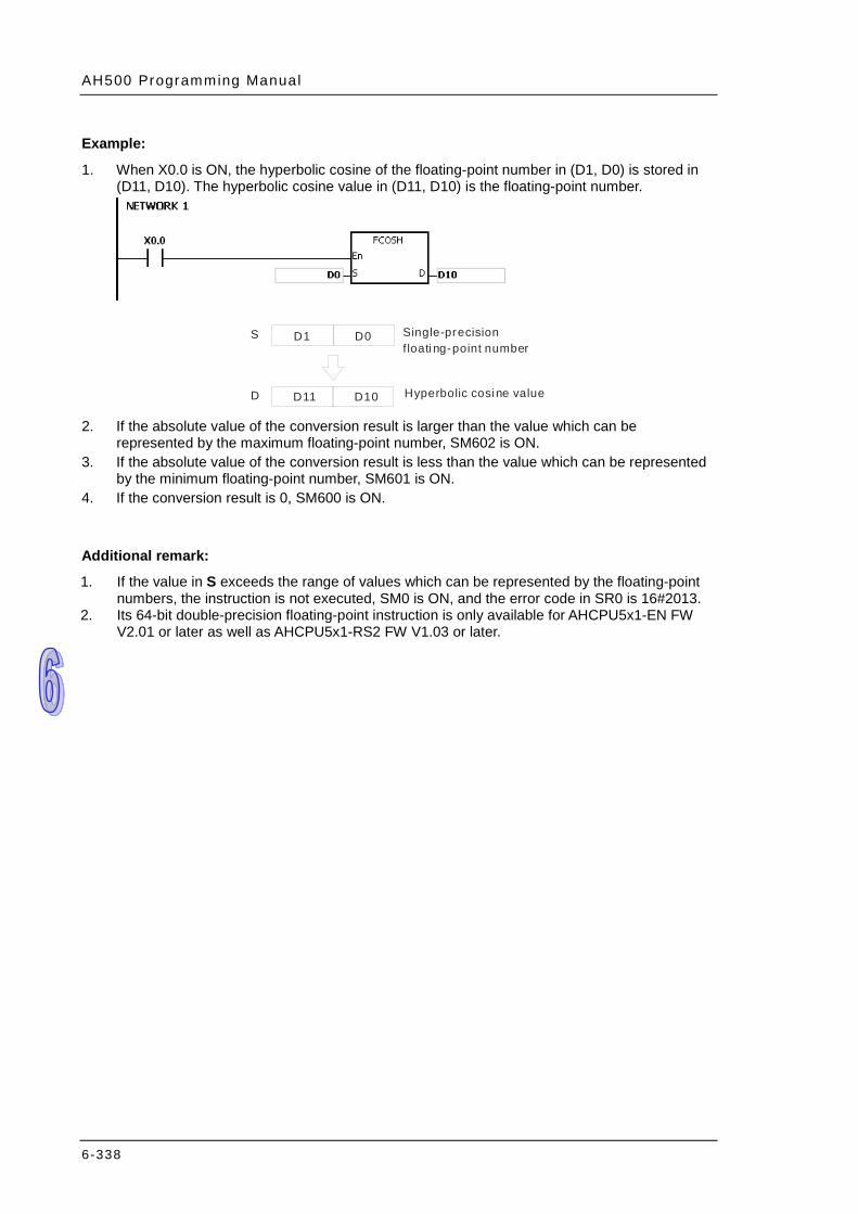
AH500 Programming Manual
6-338
Example:
1. When X0.0 is ON, the hyperbolic cosine of the floating-point number in (D1, D0) is stored in (D11, D10). The hyperbolic cosine value in (D11, D10) is the floating-point number.
Single-precision f loati ng-point number
Hyperbolic cosi ne value
D1 D0
D11 D10
S
D 2. If the absolute value of the conversion result is larger than the value which can be
represented by the maximum floating-point number, SM602 is ON. 3. If the absolute value of the conversion result is less than the value which can be represented
by the minimum floating-point number, SM601 is ON. 4. If the conversion result is 0, SM600 is ON.
Additional remark:
1. If the value in S exceeds the range of values which can be represented by the floating-point numbers, the instruction is not executed, SM0 is ON, and the error code in SR0 is 16#2013.
2. Its 64-bit double-precision floating-point instruction is only available for AHCPU5x1-EN FW V2.01 or later as well as AHCPU5x1-RS2 FW V1.03 or later.

Chapter 6 Appl ied Inst ruct ions
6-339
API Instruction code Operand Function
1508 D FTANH P S, D Hyperbolic tangent of the floating-point number
Device X Y M S T C HC D L SM SR E PR K 16# “$” DF
S D
Pulse instruction 32-bit instruction
(5 steps) 64-bit instruction
(5-6 steps) AH500 AH500 AH500
Symbol:
S : Source value Double word / Long word
D : Hyperbolic tangent value Double word / Long word
Explanation:
1. Hyperbolic tangent value=(es-e-s)/(es+e-s). 2. If the conversion result is 0, SM600 is ON.
Example:
1. When X0.0 is ON, the hyperbolic tangent of the floating-point number in (D1, D0) is stored in (D11, D10). The hyperbolic tangent value in (D11, D10) is the floating-point number.
Single-precision f loati ng-point number
Hyperbolic tangent value
D1 D0
D11 D10
S
D 2. If the conversion result is 0, SM600 is ON.
Additional remark:
1. If the value in S exceeds the range of values which can be represented by the floating-point numbers, the instruction is not executed, SM0 is ON, and the error code in SR0 is 16#2013.
2. Its 64-bit double-precision floating-point instruction is only available for AHCPU5x1-EN FW V2.01 or later as well as AHCPU5x1-RS2 FW V1.03 or later.
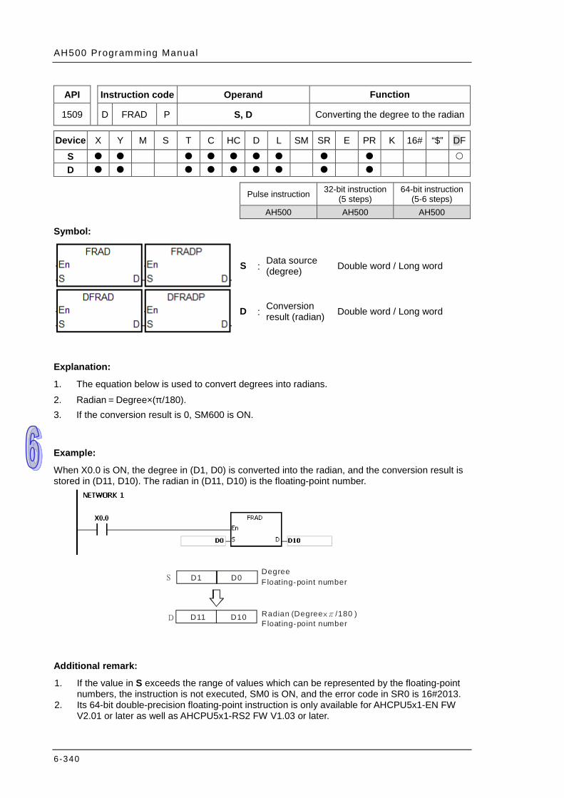
AH500 Programming Manual
6-340
API Instruction code Operand Function
1509 D FRAD P S, D Converting the degree to the radian
Device X Y M S T C HC D L SM SR E PR K 16# “$” DF
S D
Pulse instruction 32-bit instruction
(5 steps) 64-bit instruction
(5-6 steps) AH500 AH500 AH500
Symbol:
S : Data source (degree) Double word / Long word
D : Conversion result (radian) Double word / Long word
Explanation:
1. The equation below is used to convert degrees into radians. 2. Radian=Degree×(π/180). 3. If the conversion result is 0, SM600 is ON.
Example:
When X0.0 is ON, the degree in (D1, D0) is converted into the radian, and the conversion result is stored in (D11, D10). The radian in (D11, D10) is the floating-point number.
D1 D0
D11 D10
DegreeFloating-point number
Radian (Degree /180 )×π
Floating-point number
S
D
Additional remark:
1. If the value in S exceeds the range of values which can be represented by the floating-point numbers, the instruction is not executed, SM0 is ON, and the error code in SR0 is 16#2013.
2. Its 64-bit double-precision floating-point instruction is only available for AHCPU5x1-EN FW V2.01 or later as well as AHCPU5x1-RS2 FW V1.03 or later.
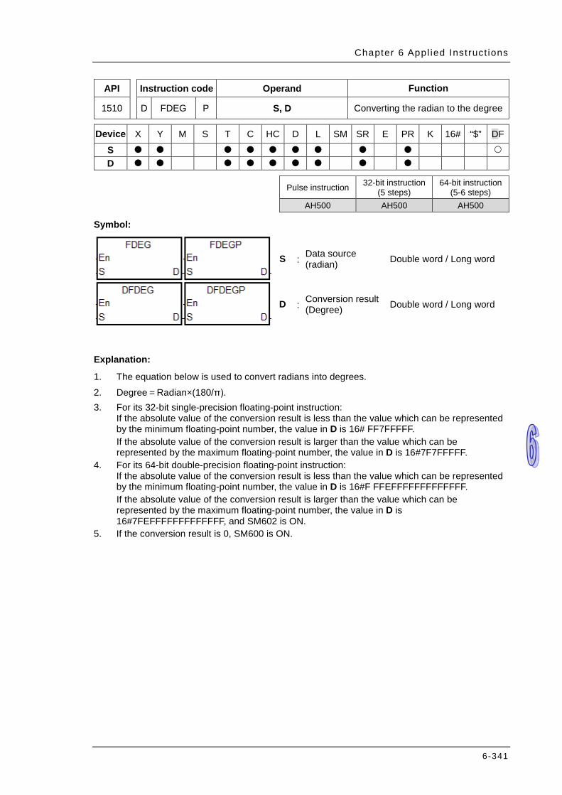
Chapter 6 Appl ied Inst ruct ions
6-341
API Instruction code Operand Function
1510 D FDEG P S, D Converting the radian to the degree
Device X Y M S T C HC D L SM SR E PR K 16# “$” DF
S D
Pulse instruction 32-bit instruction
(5 steps) 64-bit instruction
(5-6 steps) AH500 AH500 AH500
Symbol:
S : Data source (radian) Double word / Long word
D : Conversion result (Degree) Double word / Long word
Explanation:
1. The equation below is used to convert radians into degrees. 2. Degree=Radian×(180/π). 3. For its 32-bit single-precision floating-point instruction:
If the absolute value of the conversion result is less than the value which can be represented by the minimum floating-point number, the value in D is 16# FF7FFFFF. If the absolute value of the conversion result is larger than the value which can be represented by the maximum floating-point number, the value in D is 16#7F7FFFFF.
4. For its 64-bit double-precision floating-point instruction: If the absolute value of the conversion result is less than the value which can be represented by the minimum floating-point number, the value in D is 16#F FFEFFFFFFFFFFFFF. If the absolute value of the conversion result is larger than the value which can be represented by the maximum floating-point number, the value in D is 16#7FEFFFFFFFFFFFFF, and SM602 is ON.
5. If the conversion result is 0, SM600 is ON.

AH500 Programming Manual
6-342
Example:
When X0.0 is ON, the radian in (D1, D0) is converted into the degree, and the conversion result is stored in (D11, D10). The degree in (D11, D10) is the floating-point number.
RadianFl oating-point numberD1 D0
D11 D10 Degree (Radian / )×180 π
Fl oating-point number
S
D
Additional remark:
1. If the value in S exceeds the range of values which can be represented by the floating-point numbers, the instruction is not executed, SM0 is ON, and the error code in SR0 is 16#2013.
2. Its 64-bit double-precision floating-point instruction is only available for AHCPU5x1-EN FW V2.01 or later as well as AHCPU5x1-RS2 FW V1.03 or later.

Chapter 6 Appl ied Inst ruct ions
6-343
API Instruction code Operand Function
1511 D SQR P S, D Square root of the binary number
Device X Y M S T C HC D L SM SR E PR K 16# “$” DF
S D
Pulse instruction 16-bit instruction
(5 steps) 32-bit instruction
(5 steps)
AH500 AH500 AH500
Symbol:
S : Source value Word/Double word
D : Device in which the result is stored Word/Double word
Explanation:
1. The square root of the value in the device specified by S is calculated, and the result is stored in the device specified by D.
2. The operation result stored in D is an integer. If the floating-point number is rounded down to the nearest whole digit, SM601 is ON.
3. If the operation result stored in D is 0, SM600 is ON.
Example:
When X0.0 is ON, the square root of the value in D0 is calculated, and the result is stored in D10.
Additional remark:
1. The value in the device specified by S only can be a positive value. If the value in the device specified by S is a negative value, the operation error occurs, the instruction is not executed, SM0 is ON, and the error code in SR0 is 16#2003.

AH500 Programming Manual
6-344
API Instruction code Operand Function
1512 D FSQR P S, D Square root of the floating-point number
Device X Y M S T C HC D L SM SR E PR K 16# “$” DF
S D
Pulse instruction 32-bit instruction
(5 steps) 64-bit instruction
(5-6 steps) AH500 AH500 AH500
Symbol:
S : Source value Double word / Long word
D : Device in which the result is stored Double word / Long word
Explanation:
1. The square root of the floating-point number in the register specified by S is calculated, and the result is stored in the register specified by D.
2. If the operation result stored in D is 0, SM600 is ON.
Example 1:
When X0.0 is ON, the square root of the floating-point number in (D1, D0) is calculated, and the result is stored in (D11, D10).
Additional remark:
1. The value in the device specified by S only can be a positive value. If the value in the device specified by S is a negative value, the operation error occurs, the instruction is not executed, SM0 is ON, and the error code in SR0 is 16#2003.
2. Its 64-bit double-precision floating-point instruction is only available for AHCPU5x1-EN FW V2.01 or later as well as AHCPU5x1-RS2 FW V1.03 or later.
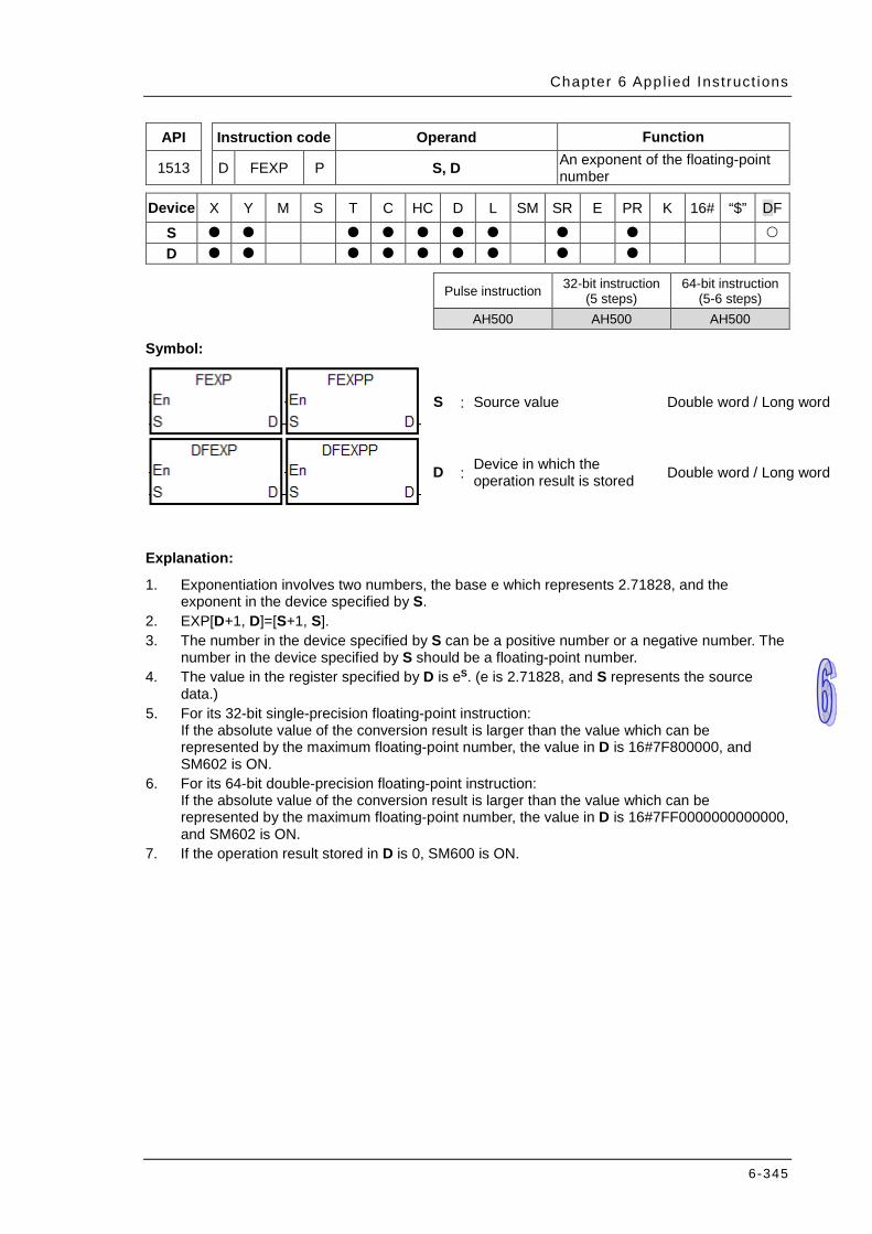
Chapter 6 Appl ied Inst ruct ions
6-345
API Instruction code Operand Function
1513 D FEXP P S, D An exponent of the floating-point number
Device X Y M S T C HC D L SM SR E PR K 16# “$” DF
S D
Pulse instruction 32-bit instruction
(5 steps) 64-bit instruction
(5-6 steps) AH500 AH500 AH500
Symbol:
S : Source value Double word / Long word
D : Device in which the operation result is stored Double word / Long word
Explanation:
1. Exponentiation involves two numbers, the base e which represents 2.71828, and the exponent in the device specified by S.
2. EXP[D+1, D]=[S+1, S]. 3. The number in the device specified by S can be a positive number or a negative number. The
number in the device specified by S should be a floating-point number. 4. The value in the register specified by D is eS. (e is 2.71828, and S represents the source
data.) 5. For its 32-bit single-precision floating-point instruction:
If the absolute value of the conversion result is larger than the value which can be represented by the maximum floating-point number, the value in D is 16#7F800000, and SM602 is ON.
6. For its 64-bit double-precision floating-point instruction: If the absolute value of the conversion result is larger than the value which can be represented by the maximum floating-point number, the value in D is 16#7FF0000000000000, and SM602 is ON.
7. If the operation result stored in D is 0, SM600 is ON.
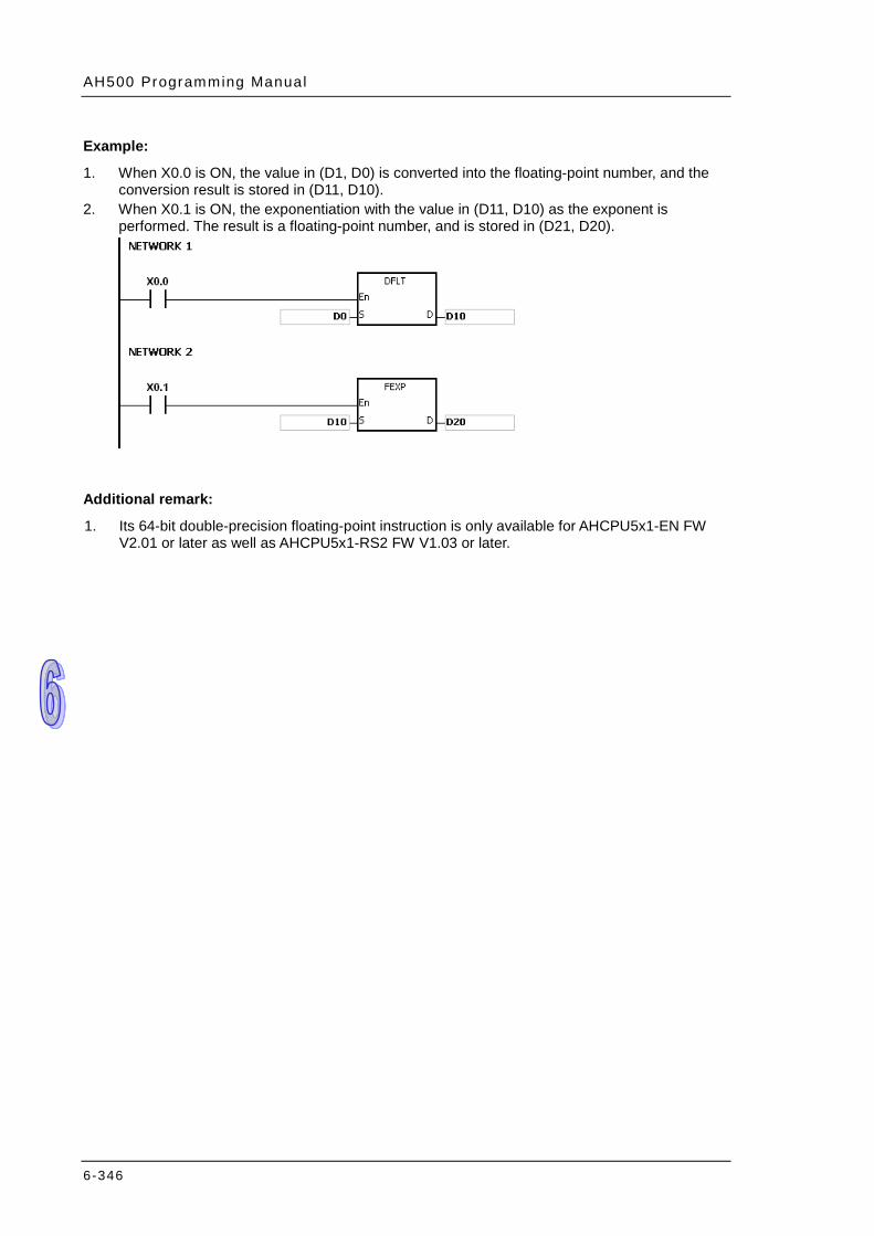
AH500 Programming Manual
6-346
Example:
1. When X0.0 is ON, the value in (D1, D0) is converted into the floating-point number, and the conversion result is stored in (D11, D10).
2. When X0.1 is ON, the exponentiation with the value in (D11, D10) as the exponent is performed. The result is a floating-point number, and is stored in (D21, D20).
Additional remark:
1. Its 64-bit double-precision floating-point instruction is only available for AHCPU5x1-EN FW V2.01 or later as well as AHCPU5x1-RS2 FW V1.03 or later.
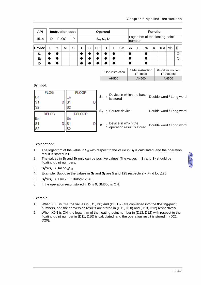
Chapter 6 Appl ied Inst ruct ions
6-347
API Instruction code Operand Function
1514 D FLOG P S1, S2, D Logarithm of the floating-point number
Device X Y M S T C HC D L SM SR E PR K 16# “$” DF
S1 S2 D
Pulse instruction 32-bit instruction
(7 steps) 64-bit instruction
(7-9 steps) AH500 AH500 AH500
Symbol:
S1 : Device in which the base is stored Double word / Long word
S2 : Source device Double word / Long word
D : Device in which the operation result is stored Double word / Long word
Explanation:
1. The logarithm of the value in S2 with respect to the value in S1 is calculated, and the operation result is stored in D.
2. The values in S1 and S2 only can be positive values. The values in S1 and S2 should be floating-point numbers.
3. S1D=S2.→D=LogS1S2. 4. Example: Suppose the values in S1 and S2 are 5 and 125 respectively. Find log5125. 5. S1D=S2.→5D=125.→D=log5125=3. 6. If the operation result stored in D is 0, SM600 is ON.
Example:
1. When X0.0 is ON, the values in (D1, D0) and (D3, D2) are converted into the floating-point numbers, and the conversion results are stored in (D11, D10) and (D13, D12) respectively.
2. When X0.1 is ON, the logarithm of the floating-point number in (D13, D12) with respect to the floating-point number in (D11, D10) is calculated, and the operation result is stored in (D21, D20).
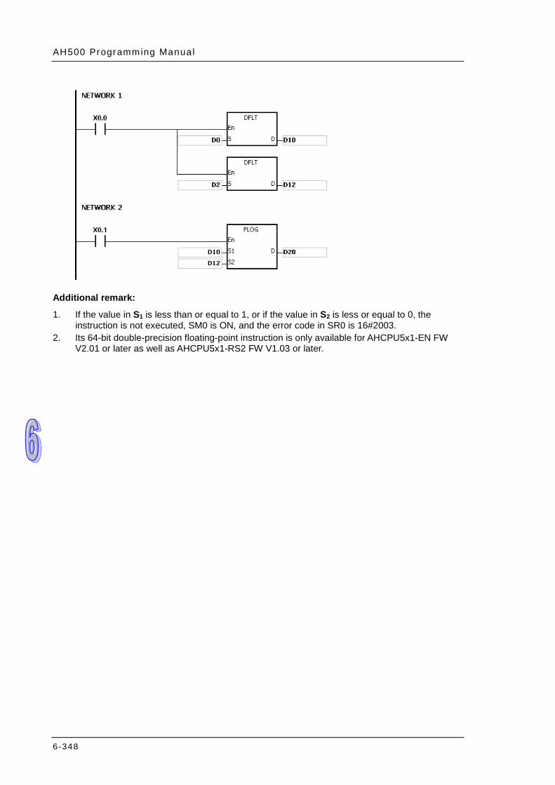
AH500 Programming Manual
6-348
Additional remark:
1. If the value in S1 is less than or equal to 1, or if the value in S2 is less or equal to 0, the instruction is not executed, SM0 is ON, and the error code in SR0 is 16#2003.
2. Its 64-bit double-precision floating-point instruction is only available for AHCPU5x1-EN FW V2.01 or later as well as AHCPU5x1-RS2 FW V1.03 or later.
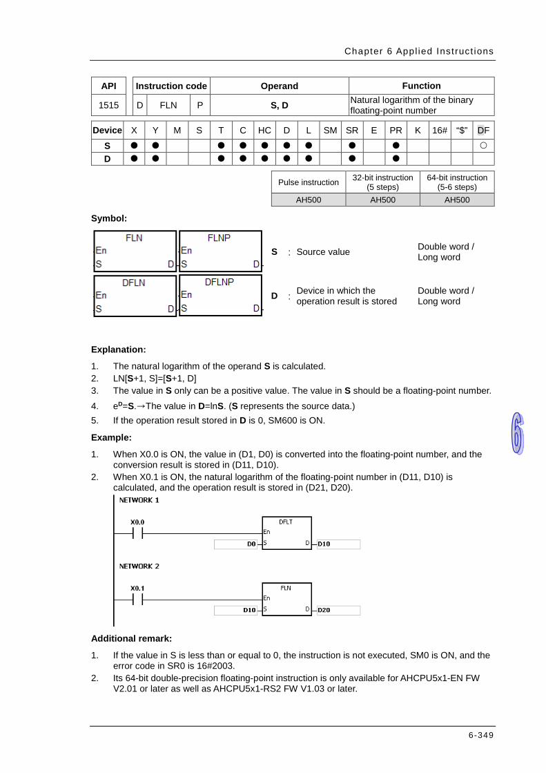
Chapter 6 Appl ied Inst ruct ions
6-349
API Instruction code Operand Function
1515 D FLN P S, D Natural logarithm of the binary floating-point number
Device X Y M S T C HC D L SM SR E PR K 16# “$” DF
S D
Pulse instruction 32-bit instruction
(5 steps) 64-bit instruction
(5-6 steps) AH500 AH500 AH500
Symbol:
S : Source value Double word / Long word
D : Device in which the operation result is stored
Double word / Long word
Explanation:
1. The natural logarithm of the operand S is calculated. 2. LN[S+1, S]=[S+1, D] 3. The value in S only can be a positive value. The value in S should be a floating-point number. 4. eD=S.→The value in D=lnS. (S represents the source data.) 5. If the operation result stored in D is 0, SM600 is ON.
Example:
1. When X0.0 is ON, the value in (D1, D0) is converted into the floating-point number, and the conversion result is stored in (D11, D10).
2. When X0.1 is ON, the natural logarithm of the floating-point number in (D11, D10) is calculated, and the operation result is stored in (D21, D20).
Additional remark:
1. If the value in S is less than or equal to 0, the instruction is not executed, SM0 is ON, and the error code in SR0 is 16#2003.
2. Its 64-bit double-precision floating-point instruction is only available for AHCPU5x1-EN FW V2.01 or later as well as AHCPU5x1-RS2 FW V1.03 or later.

AH500 Programming Manual
6-350
API Instruction code Operand Function
1516 D FPOW P S1, S2, D A power of the floating-point number
Device X Y M S T C HC D L SM SR E PR K 16# “$” DF
S1 S2 D
Pulse instruction 32-bit instruction (7 steps)
64-bit instruction (7-9 steps)
AH500 AH500 AH500
Symbol:
S1 : Device in which the base is stored
Double word / Long word
S2 : Device in which the power is stored
Double word / Long word
D : Device in which the operation result is stored
Double word / Long word
Explanation:
1. The floating-point number in S1 is raised to the power of the value in S2, and the operation result is stored in D.
2. D=POW[S1+1, S1][S2+1, S2] 3. The value in S1 only can be a positive value, whereas the value in S2 can be a positive value
or a negative value. The values in S1 and S2 should be floating-point numbers. 4. S1S2=D
Suppose the values in S1 and S2 are 5 and 3 respectively. D=53=125. 5. For its 32-bit single-precision floating-point instruction:
If the absolute value of the conversion result is less than the value which can be represented by the minimum floating-point number, the value in D is 16#7 FF7FFFFF. If the absolute value of the conversion result is large than the value which can be represented by the maximum floating-point number, the value in D is 16#7F7FFFFF.
5. For its 64-bit double-precision floating-point instruction: If the absolute value of the conversion result is less than the value which can be represented by the minimum floating-point number, the value in D is 16#FFEFFFFFFFFFFFFF If the absolute value of the conversion result is large than the value which can be represented by the maximum floating-point number, the value in D is D=16#7FEFFFFFFFFFFFFF.
6. If the operation result stored in D is 0, SM600 is ON.
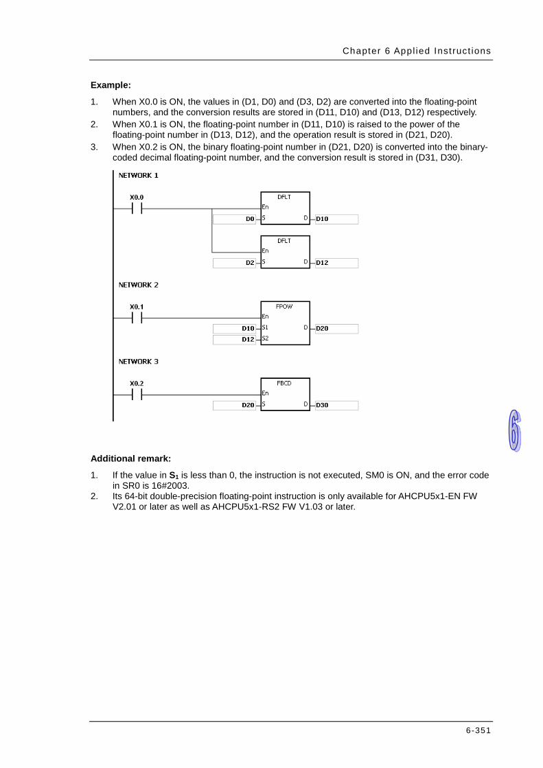
Chapter 6 Appl ied Inst ruct ions
6-351
Example:
1. When X0.0 is ON, the values in (D1, D0) and (D3, D2) are converted into the floating-point numbers, and the conversion results are stored in (D11, D10) and (D13, D12) respectively.
2. When X0.1 is ON, the floating-point number in (D11, D10) is raised to the power of the floating-point number in (D13, D12), and the operation result is stored in (D21, D20).
3. When X0.2 is ON, the binary floating-point number in (D21, D20) is converted into the binary-coded decimal floating-point number, and the conversion result is stored in (D31, D30).
Additional remark:
1. If the value in S1 is less than 0, the instruction is not executed, SM0 is ON, and the error code in SR0 is 16#2003.
2. Its 64-bit double-precision floating-point instruction is only available for AHCPU5x1-EN FW V2.01 or later as well as AHCPU5x1-RS2 FW V1.03 or later.
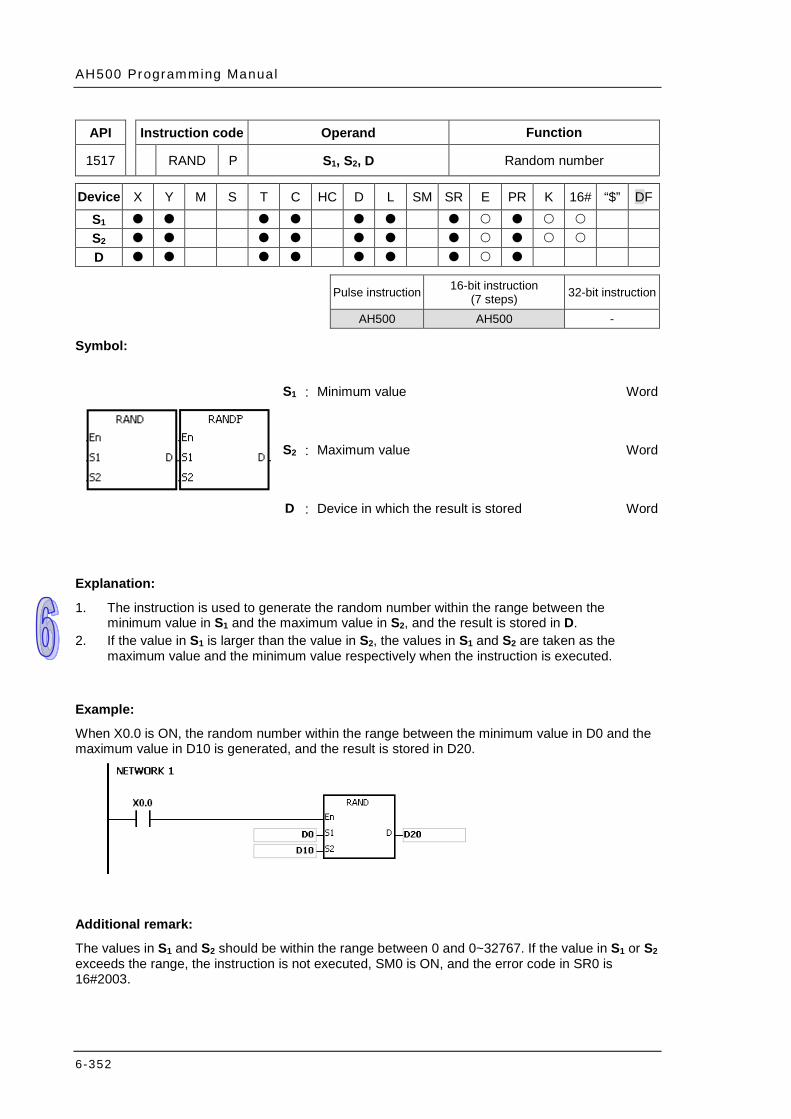
AH500 Programming Manual
6-352
API Instruction code Operand Function
1517 RAND P S1, S2, D Random number
Device X Y M S T C HC D L SM SR E PR K 16# “$” DF
S1 S2 D
Pulse instruction 16-bit instruction (7 steps) 32-bit instruction
AH500 AH500 -
Symbol:
S1 : Minimum value Word
S2 : Maximum value Word
D : Device in which the result is stored Word
Explanation:
1. The instruction is used to generate the random number within the range between the minimum value in S1 and the maximum value in S2, and the result is stored in D.
2. If the value in S1 is larger than the value in S2, the values in S1 and S2 are taken as the maximum value and the minimum value respectively when the instruction is executed.
Example:
When X0.0 is ON, the random number within the range between the minimum value in D0 and the maximum value in D10 is generated, and the result is stored in D20.
Additional remark:
The values in S1 and S2 should be within the range between 0 and 0~32767. If the value in S1 or S2 exceeds the range, the instruction is not executed, SM0 is ON, and the error code in SR0 is 16#2003.
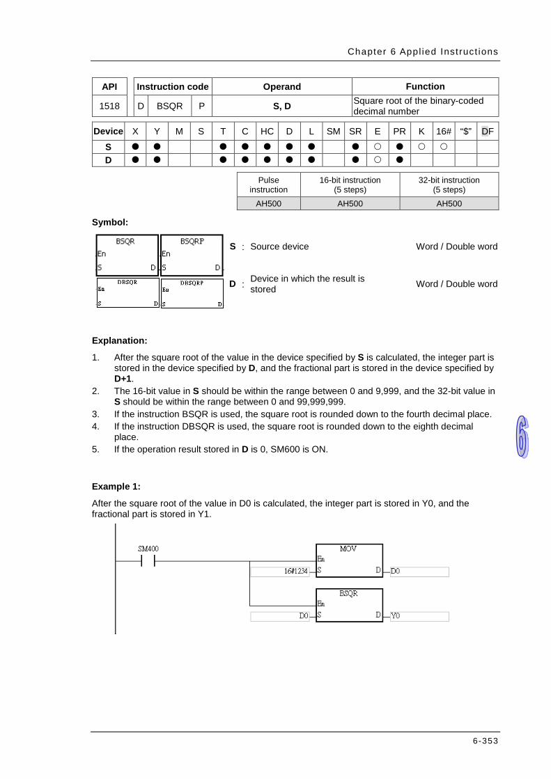
Chapter 6 Appl ied Inst ruct ions
6-353
API Instruction code Operand Function
1518 D BSQR P S, D Square root of the binary-coded decimal number
Device X Y M S T C HC D L SM SR E PR K 16# “$” DF
S D
Pulse
instruction 16-bit instruction
(5 steps) 32-bit instruction
(5 steps)
AH500 AH500 AH500
Symbol:
S : Source device Word / Double word
D : Device in which the result is stored Word / Double word
Explanation:
1. After the square root of the value in the device specified by S is calculated, the integer part is stored in the device specified by D, and the fractional part is stored in the device specified by D+1.
2. The 16-bit value in S should be within the range between 0 and 9,999, and the 32-bit value in S should be within the range between 0 and 99,999,999.
3. If the instruction BSQR is used, the square root is rounded down to the fourth decimal place. 4. If the instruction DBSQR is used, the square root is rounded down to the eighth decimal
place. 5. If the operation result stored in D is 0, SM600 is ON.
Example 1:
After the square root of the value in D0 is calculated, the integer part is stored in Y0, and the fractional part is stored in Y1.

AH500 Programming Manual
6-354
16#12341
Binary -coded decimal value
1 2 43D0MOV Y0
Y1
2 BSQRInteger part
Fractional part1 2 38
0 530Binary -coded decimal value
Binary -coded decimal value
Example 2:
After the square root of the value in D0 is calculated, the integer part is stored in Y0, and the fractional part is stored in Y1.
Additional remark: 1. If the value in S is not a binary-coded decimal value (The binary-coded decimal value is
represented by the hexadecimal number, but one of digits is not within the range between 0 and 9.), the operation error occurs, SM0 is ON, and the error code in SR0 is 16#200D.
2. If the operand D used during the execution of the 16-bit instruction is declared in ISPSoft, the data type will be ARRAY [2] of WORD/INT.
3. If the operand D used during the execution of the 32-bit instruction is declared in ISPSoft, the data type will be ARRAY [2] of DWORD/DINT.

Chapter 6 Appl ied Inst ruct ions
6-355
API Instruction code Operand Function
1519 BSIN P S, D Sine of the binary-coded decimal number
Device X Y M S T C HC D L SM SR E PR K 16# “$” DF
S D
Pulse instruction 16-bit instruction (5 steps) 32-bit instruction
AH500 AH500 -
Symbol:
S : Source value Word
D : Result Word
Explanation:
1. The source value specified by S is a degree, and the instruction is used to get the sine of the source value specified by S. After the sine value is gotten, the sign is stored in D, the integer part is stored in D+1, and the fractional part is stored in D+2.
2. The range of degrees: 0°≦Degree<360° 3. The operation result is rounded off to the fifth decimal place. 4. If the conversion result is 0, SM600 is ON.
Example:
The instruction is used to get the sine of the value in D0. After the sine value is gotten, the sign is stored in D10, the integer part is stored in D11, and the fractional part is stored in D12.
Binary -coded decimal value
Binary -coded decimal value
Binary -coded decimal value
0 0 06 0 0 00
0 0 00
D0
8 6 06
D11
D12
BSIN D10
Binary -coded decimal value

AH500 Programming Manual
6-356
Additional remark:
1. If the value in S is not a binary-coded decimal value (The binary-coded decimal value is represented by the hexadecimal number, but one of digits is not within the range between 0 and 9.), the operation error occurs, SM0 is ON, and the error code in SR0 is 16#200D.
2. If the value in S is not within the range between 0° and 360°, the operation error occurs, SM0 is ON, and the error code in SR0 is 16#2003.
3. If users declare the operand D in ISPSoft, the data type will be ARRAY [3] of WORD/INT.
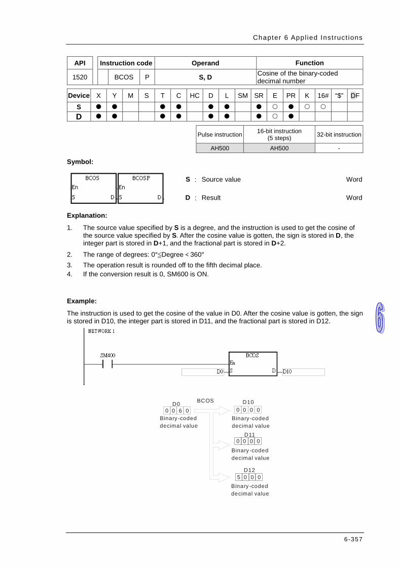
Chapter 6 Appl ied Inst ruct ions
6-357
API Instruction code Operand Function
1520 BCOS P S, D Cosine of the binary-coded decimal number
Device X Y M S T C HC D L SM SR E PR K 16# “$” DF
S D
Pulse instruction 16-bit instruction (5 steps) 32-bit instruction
AH500 AH500 -
Symbol:
S : Source value Word
D : Result Word
Explanation:
1. The source value specified by S is a degree, and the instruction is used to get the cosine of the source value specified by S. After the cosine value is gotten, the sign is stored in D, the integer part is stored in D+1, and the fractional part is stored in D+2.
2. The range of degrees: 0°≦Degree<360° 3. The operation result is rounded off to the fifth decimal place. 4. If the conversion result is 0, SM600 is ON.
Example:
The instruction is used to get the cosine of the value in D0. After the cosine value is gotten, the sign is stored in D10, the integer part is stored in D11, and the fractional part is stored in D12.
Binary -coded decimal value
Binary -coded decimal value
Binary -coded decimal value
0 0 06 0 0 00
0 0 00
D0
D11
BCOS D10
Binary -coded decimal value
5 0 00D12
AH500 Programming Manual
6-358
Additional remark:
1. If the value in S is not a binary-coded decimal value (The binary-coded decimal value is represented by the hexadecimal number, but one of digits is not within the range between 0 and 9.), the operation error occurs, SM0 is ON, and the error code in SR0 is 16#200D.
2. If the value in S is not within the range between 0° and 360°, the operation error occurs, SM0 is ON, and the error code in SR0 is 16#2003.
3. If users declare the operand D in ISPSoft, the data type will be ARRAY [3] of WORD/INT.
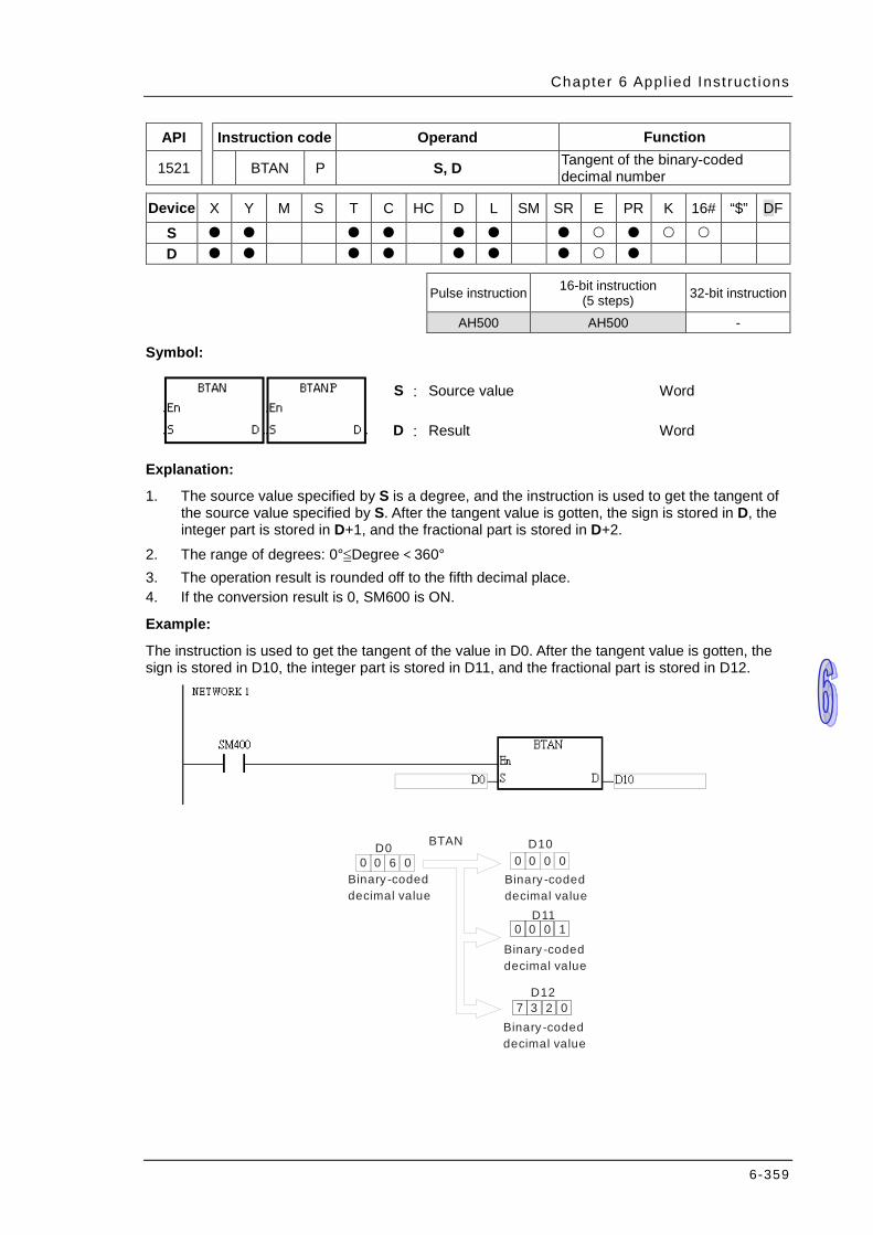
Chapter 6 Appl ied Inst ruct ions
6-359
API Instruction code Operand Function
1521 BTAN P S, D Tangent of the binary-coded decimal number
Device X Y M S T C HC D L SM SR E PR K 16# “$” DF
S D
Pulse instruction 16-bit instruction
(5 steps) 32-bit instruction
AH500 AH500 -
Symbol:
S : Source value Word
D : Result Word
Explanation:
1. The source value specified by S is a degree, and the instruction is used to get the tangent of the source value specified by S. After the tangent value is gotten, the sign is stored in D, the integer part is stored in D+1, and the fractional part is stored in D+2.
2. The range of degrees: 0°≦Degree<360° 3. The operation result is rounded off to the fifth decimal place. 4. If the conversion result is 0, SM600 is ON.
Example:
The instruction is used to get the tangent of the value in D0. After the tangent value is gotten, the sign is stored in D10, the integer part is stored in D11, and the fractional part is stored in D12.
Binary -coded decimal value
Binary -coded decimal value
Binary -coded decimal value
0 0 06 0 0 00
0 0 10
D0
D11
BTAN D10
Binary -coded decimal value
7 3 02D12
AH500 Programming Manual
6-360
Additional remark:
1. If the value in S is not a binary-coded decimal value (The binary-coded decimal value is represented by the hexadecimal number, but one of digits is not within the range between 0 and 9.), the operation error occurs, SM0 is ON, and the error code in SR0 is 16#200D.
2. If the value in S is not within the range between 0° and 360°, the operation error occurs, SM0 is ON, and the error code in SR0 is 16#2003.
3. If the value in S is equal to 90° or 270°, the operation error occurs, SM0 is ON, and the error code in SR0 is 16#2003.
4. If users declare the operand D in ISPSoft, the data type will be ARRAY [3] of WORD/INT.

Chapter 6 Appl ied Inst ruct ions
6-361
API Instruction code Operand Function
1522 BASIN P S, D Arcsine of the binary-coded decimal number
Device X Y M S T C HC D L SM SR E PR K 16# “$” DF
S D
Pulse instruction 16-bit instruction
(5 steps) 32-bit instruction
AH500 AH500 -
Symbol:
S : Source value Word
D : Arcsine value Word
Explanation:
1. The source value specified by S is a binary-coded decimal value, and the instruction is used to get the arcsine of the source value specified by S. The operation result (the degree) is stored in D.
2. The value in S represents the sign, i.e. 0 represents the positive sign, and 1 represents the negative sign. The integer part is stored in S+1, and the fractional part is stored in S+2.
3. The operation result is rounded off to the nearest whole digit. 4. The operation result is a binary-coded decimal value (the degree) wiithin the range between
0° and 90°, or within the range between 270° and 360°.
Example:
The value in D0 represents the sign, the integer part is stored in D1, and the fractional part is stored in D2. After the instruction BASIN is executed, the arcsine value is rounded off to the nearest whole digit, and the result is stored in D10.
Binary -coded decimal value
Binary -coded decimal value
Binary -coded decimal value
Binary -coded decimal value
0 0 00
0 0 00
8 6 06
D0
D1
D2
BASIN
0 0 06D10

AH500 Programming Manual
6-362
Additional remark:
1. Take 0.5 for example. When it is entered, users need to enter 0, 0, and 16#5000 into S, S+1, S+2 respectively.
2. If the value in S is not a binary-coded decimal value (The binary-coded decimal value is represented by the hexadecimal number, but one of digits is not within the range between 0 and 9.), the operation error occurs, SM0 is ON, and the error code in SR0 is 16#200D.
3. The value specified by the operand S should be within the range between –1.0 and +1.0. If the value specified by the operand S is not within the range, the instruction is not executed, SM0 is ON, and the error code in SR0 is 16#2003.
4. If users declare the operand S in ISPSoft, the data type will be ARRAY [3] of WORD/IN.
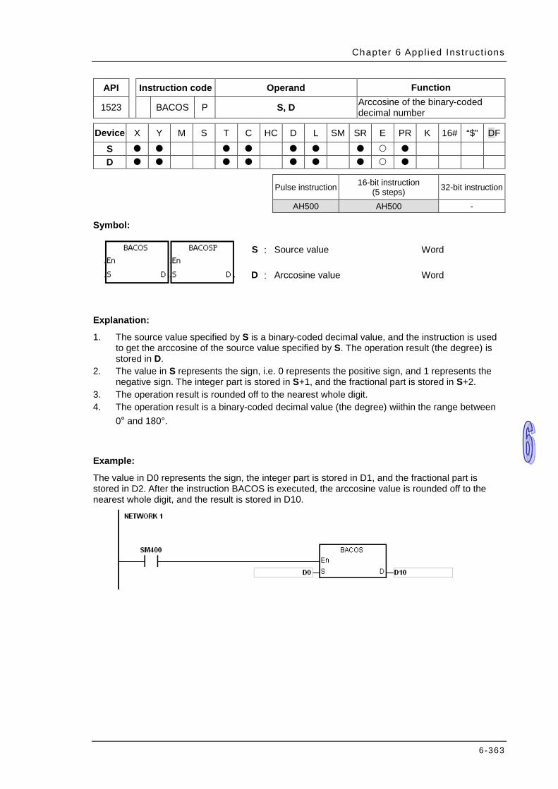
Chapter 6 Appl ied Inst ruct ions
6-363
API Instruction code Operand Function
1523 BACOS P S, D Arccosine of the binary-coded decimal number
Device X Y M S T C HC D L SM SR E PR K 16# “$” DF
S D
Pulse instruction 16-bit instruction
(5 steps) 32-bit instruction
AH500 AH500 -
Symbol:
S : Source value Word
D : Arccosine value Word
Explanation:
1. The source value specified by S is a binary-coded decimal value, and the instruction is used to get the arccosine of the source value specified by S. The operation result (the degree) is stored in D.
2. The value in S represents the sign, i.e. 0 represents the positive sign, and 1 represents the negative sign. The integer part is stored in S+1, and the fractional part is stored in S+2.
3. The operation result is rounded off to the nearest whole digit. 4. The operation result is a binary-coded decimal value (the degree) wiithin the range between
0° and 180°.
Example:
The value in D0 represents the sign, the integer part is stored in D1, and the fractional part is stored in D2. After the instruction BACOS is executed, the arccosine value is rounded off to the nearest whole digit, and the result is stored in D10.
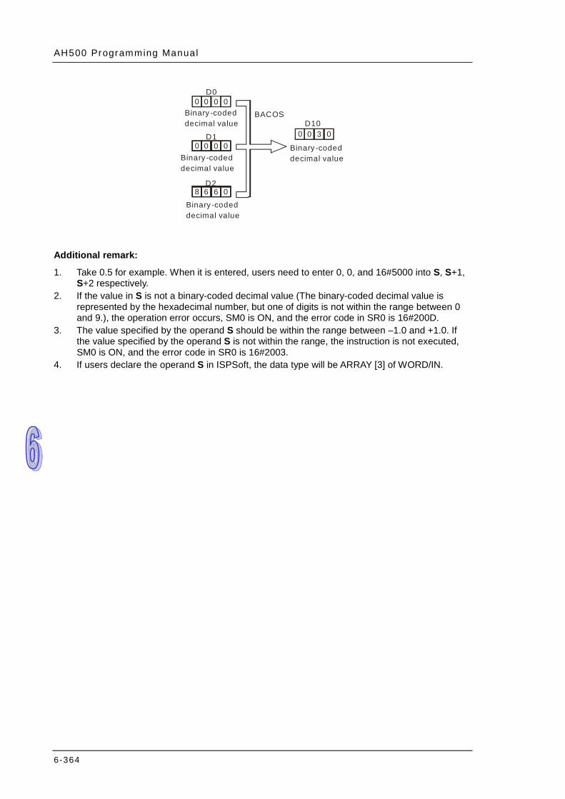
AH500 Programming Manual
6-364
Binary -coded decimal value
Binary -coded decimal value
Binary -coded decimal value
Binary -coded decimal value
0 0 00
0 0 00
8 6 06
D0
D1
D2
BACOS
0 0 03D10
Additional remark:
1. Take 0.5 for example. When it is entered, users need to enter 0, 0, and 16#5000 into S, S+1, S+2 respectively.
2. If the value in S is not a binary-coded decimal value (The binary-coded decimal value is represented by the hexadecimal number, but one of digits is not within the range between 0 and 9.), the operation error occurs, SM0 is ON, and the error code in SR0 is 16#200D.
3. The value specified by the operand S should be within the range between –1.0 and +1.0. If the value specified by the operand S is not within the range, the instruction is not executed, SM0 is ON, and the error code in SR0 is 16#2003.
4. If users declare the operand S in ISPSoft, the data type will be ARRAY [3] of WORD/IN.
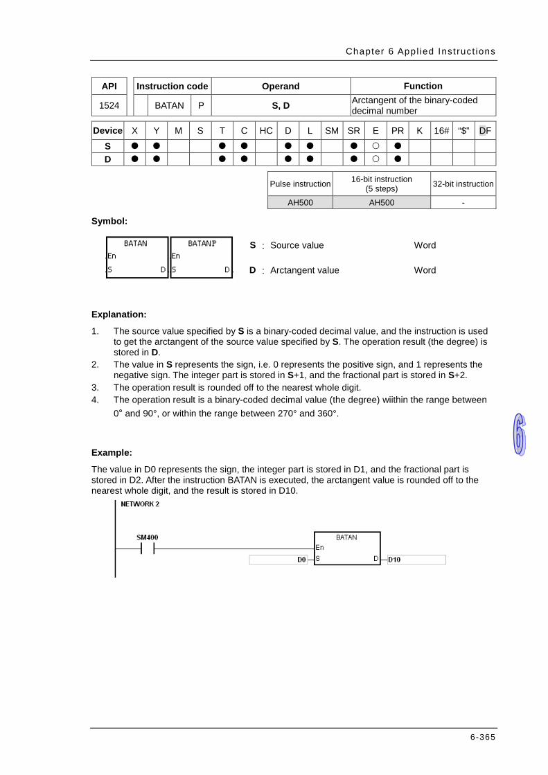
Chapter 6 Appl ied Inst ruct ions
6-365
API Instruction code Operand Function
1524 BATAN P S, D Arctangent of the binary-coded decimal number
Device X Y M S T C HC D L SM SR E PR K 16# “$” DF
S D
Pulse instruction 16-bit instruction
(5 steps) 32-bit instruction
AH500 AH500 -
Symbol:
S : Source value Word
D : Arctangent value Word
Explanation:
1. The source value specified by S is a binary-coded decimal value, and the instruction is used to get the arctangent of the source value specified by S. The operation result (the degree) is stored in D.
2. The value in S represents the sign, i.e. 0 represents the positive sign, and 1 represents the negative sign. The integer part is stored in S+1, and the fractional part is stored in S+2.
3. The operation result is rounded off to the nearest whole digit. 4. The operation result is a binary-coded decimal value (the degree) wiithin the range between
0° and 90°, or within the range between 270° and 360°.
Example:
The value in D0 represents the sign, the integer part is stored in D1, and the fractional part is stored in D2. After the instruction BATAN is executed, the arctangent value is rounded off to the nearest whole digit, and the result is stored in D10.
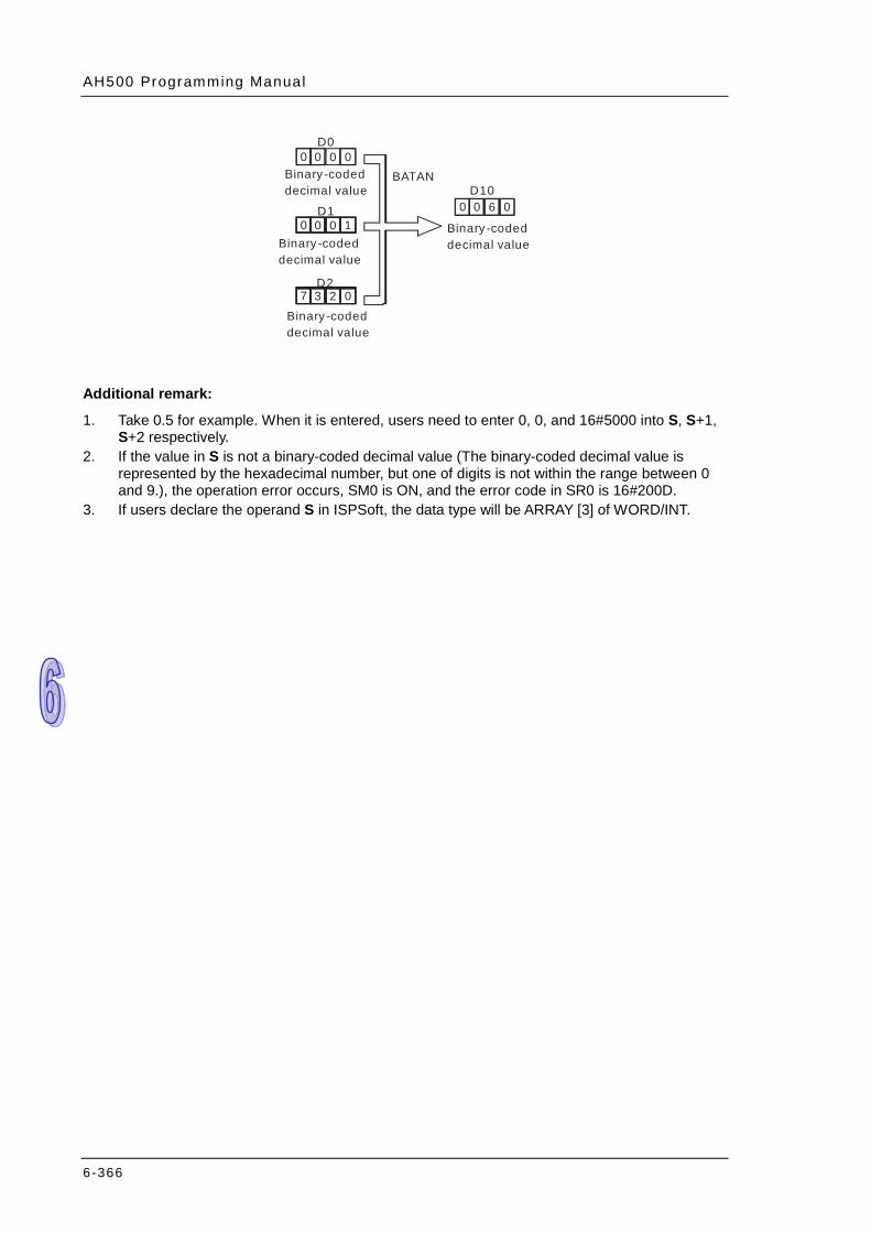
AH500 Programming Manual
6-366
Binary -coded decimal value
Binary -coded decimal value
Binary -coded decimal value
Binary -coded decimal value
0 0 00
0 0 10
7 3 02
D0
D1
D2
BATAN
0 0 06D10
Additional remark:
1. Take 0.5 for example. When it is entered, users need to enter 0, 0, and 16#5000 into S, S+1, S+2 respectively.
2. If the value in S is not a binary-coded decimal value (The binary-coded decimal value is represented by the hexadecimal number, but one of digits is not within the range between 0 and 9.), the operation error occurs, SM0 is ON, and the error code in SR0 is 16#200D.
3. If users declare the operand S in ISPSoft, the data type will be ARRAY [3] of WORD/INT.
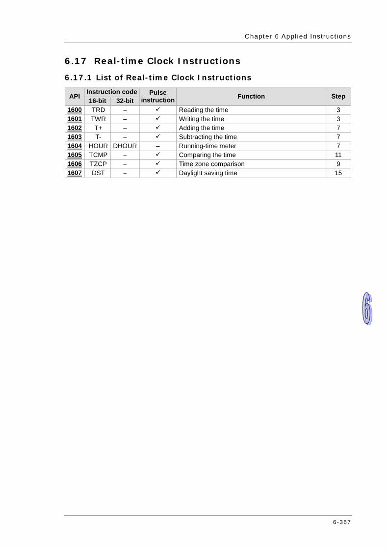
Chapter 6 Appl ied Instruc t ions
6-367
6.17 Real-time Clock Instructions 6.17.1 List of Real-time Clock Instructions
API Instruction code Pulse instruction Function Step 16-bit 32-bit
1600 TRD – Reading the time 3 1601 TWR – Writing the time 3 1602 T+ – Adding the time 7 1603 T- – Subtracting the time 7 1604 HOUR DHOUR – Running-time meter 7 1605 TCMP – Comparing the time 11 1606 TZCP – Time zone comparison 9 1607 DST – Daylight saving time 15
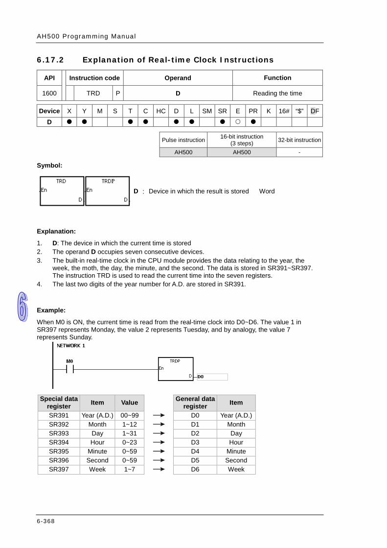
AH500 Programming Manual
6-368
6.17.2 Explanation of Real-time Clock Instructions
API Instruction code Operand Function
1600 TRD P D Reading the time
Device X Y M S T C HC D L SM SR E PR K 16# “$” DF
D
Pulse instruction 16-bit instruction (3 steps) 32-bit instruction
AH500 AH500 -
Symbol:
D : Device in which the result is stored Word
Explanation:
1. D: The device in which the current time is stored 2. The operand D occupies seven consecutive devices. 3. The built-in real-time clock in the CPU module provides the data relating to the year, the
week, the moth, the day, the minute, and the second. The data is stored in SR391~SR397. The instruction TRD is used to read the current time into the seven registers.
4. The last two digits of the year number for A.D. are stored in SR391.
Example:
When M0 is ON, the current time is read from the real-time clock into D0~D6. The value 1 in SR397 represents Monday, the value 2 represents Tuesday, and by analogy, the value 7 represents Sunday.
Special data
register Item Value General data register Item
SR391 Year (A.D.) 00~99 D0 Year (A.D.) SR392 Month 1~12 D1 Month SR393 Day 1~31 D2 Day SR394 Hour 0~23 D3 Hour SR395 Minute 0~59 D4 Minute SR396 Second 0~59 D5 Second SR397 Week 1~7 D6 Week

Chapter 6 Appl ied Instruc t ions
6-369
Additional remark:
1. If D+6 exceeds the device range, the instruction is not executed, SM0 is ON, and the error code in SR0 is 16#2003.
2. When SM220 is ON, the real-time clock is calibrated within ±30 seconds. If the value of the second in the real-time clock is within the range between 0 and 29, the value of the second is cleared to zero. If the value of the second in the real-time clock is within the range between 30 and 59, the value of the minute increases by one, and the value of the second is cleared to zero.
3. If users declare the operand D in ISPSoft, the data type will be ARRAY [7] of WORD/INT.
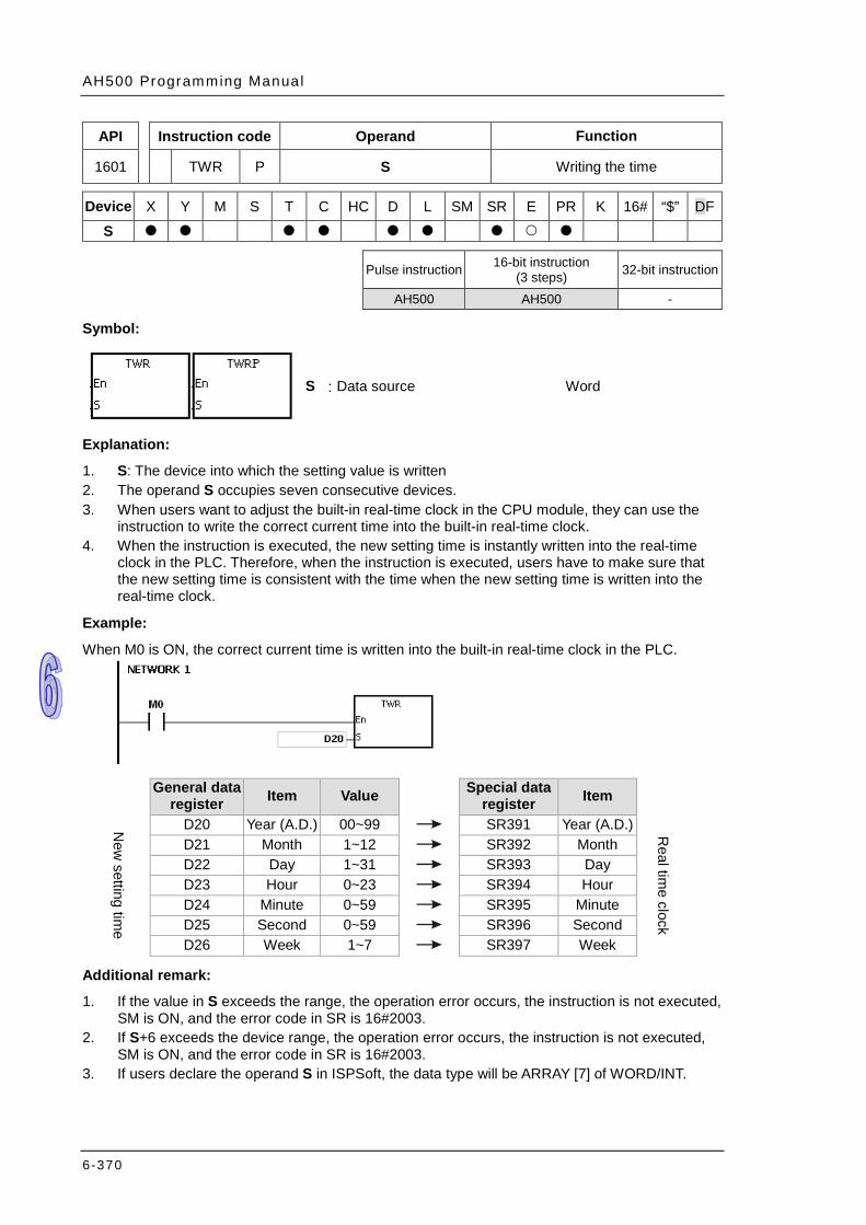
AH500 Programming Manual
6-370
API Instruction code Operand Function
1601 TWR P S Writing the time
Device X Y M S T C HC D L SM SR E PR K 16# “$” DF
S Pulse instruction 16-bit instruction
(3 steps) 32-bit instruction
AH500 AH500 -
Symbol:
S : Data source Word
Explanation:
1. S: The device into which the setting value is written 2. The operand S occupies seven consecutive devices. 3. When users want to adjust the built-in real-time clock in the CPU module, they can use the
instruction to write the correct current time into the built-in real-time clock. 4. When the instruction is executed, the new setting time is instantly written into the real-time
clock in the PLC. Therefore, when the instruction is executed, users have to make sure that the new setting time is consistent with the time when the new setting time is written into the real-time clock.
Example:
When M0 is ON, the correct current time is written into the built-in real-time clock in the PLC.
General data register Item Value Special data
register Item
New
setting time
D20 Year (A.D.) 00~99 SR391 Year (A.D.) Real tim
e clock
D21 Month 1~12 SR392 Month D22 Day 1~31 SR393 Day D23 Hour 0~23 SR394 Hour D24 Minute 0~59 SR395 Minute D25 Second 0~59 SR396 Second D26 Week 1~7 SR397 Week
Additional remark:
1. If the value in S exceeds the range, the operation error occurs, the instruction is not executed, SM is ON, and the error code in SR is 16#2003.
2. If S+6 exceeds the device range, the operation error occurs, the instruction is not executed, SM is ON, and the error code in SR is 16#2003.
3. If users declare the operand S in ISPSoft, the data type will be ARRAY [7] of WORD/INT.
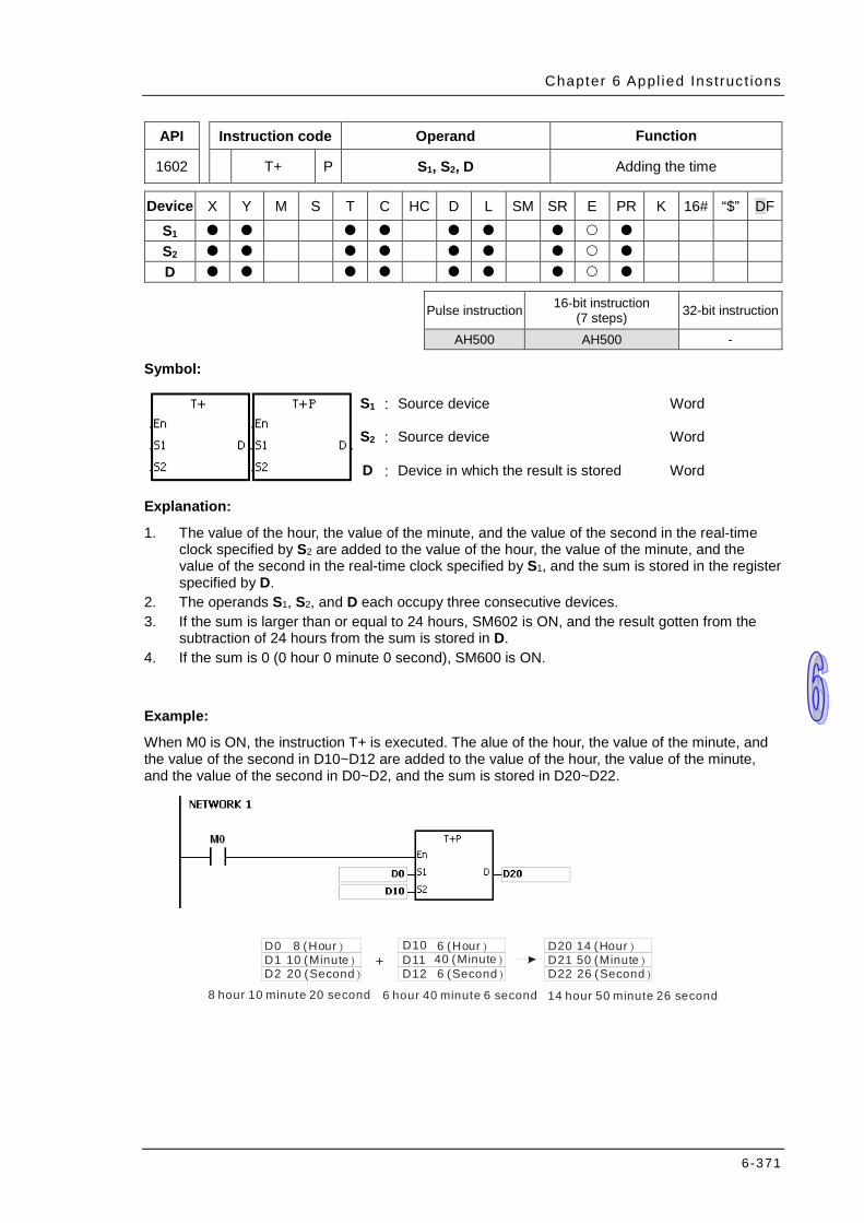
Chapter 6 Appl ied Instruc t ions
6-371
API Instruction code Operand Function
1602 T+ P S1, S2, D Adding the time
Device X Y M S T C HC D L SM SR E PR K 16# “$” DF
S1 S2 D
Pulse instruction 16-bit instruction
(7 steps) 32-bit instruction
AH500 AH500 -
Symbol:
S1 : Source device Word
S2 : Source device Word
D : Device in which the result is stored Word
Explanation:
1. The value of the hour, the value of the minute, and the value of the second in the real-time clock specified by S2 are added to the value of the hour, the value of the minute, and the value of the second in the real-time clock specified by S1, and the sum is stored in the register specified by D.
2. The operands S1, S2, and D each occupy three consecutive devices. 3. If the sum is larger than or equal to 24 hours, SM602 is ON, and the result gotten from the
subtraction of 24 hours from the sum is stored in D. 4. If the sum is 0 (0 hour 0 minute 0 second), SM600 is ON.
Example:
When M0 is ON, the instruction T+ is executed. The alue of the hour, the value of the minute, and the value of the second in D10~D12 are added to the value of the hour, the value of the minute, and the value of the second in D0~D2, and the sum is stored in D20~D22.
+D0D1D2
8 (Hour)10 (Minute)20 (Second)
D11D12
6 ( )Hour40 ( )Minute6 ( )Second
D20D21D22
14 ( )Hour50 ( )Minute26 ( )Second
8 hour 10 minute 20 second 6 hour 40 minute 6 second 14 hour 50 minute 26 second
D10
AH500 Programming Manual
6-372
Additional remark:
1. If the value in S1 or S2 exceeds the range, the operation error occurs, the instruction is not executed, SM0 is ON, and the error code in SR0 is 16#2003.
2. If S1+2, S2+2, or D+2 exceeds the device range, the operation error occurs, the instruction is not executed, SM0 is ON, and the error code in SR0 is 16#2003.
3. If users declare the operand S1 in ISPSoft, the data type will be ARRAY [3] of WORD/INT. 4. If users declare the operand S2 in ISPSoft, the data type will be ARRAY [3] of WORD/IN. 5. If users declare the operand D in ISPSoft, the data type will be ARRAY [3] of WORD/INT.

Chapter 6 Appl ied Instruc t ions
6-373
API Instruction code Operand Function
1603 T- P S1, S2, D Subtracting the time
Device X Y M S T C HC D L SM SR E PR K 16# “$” DF
S1 S2 D
Pulse instruction 16-bit instruction
(7 steps) 32-bit instruction
AH500 AH500 -
Symbol:
S1 : Source device Word
S2 : Source device Word
D : Device in which the result is stored Word
Explanation:
1. The value of the hour, the value of the minute, and the value of the second in the real-time clock specified by S2 are subtracted from the value of the hour, the value of the minute, and the value of the second in the real-time clock specified by S1, and the difference is stored in the register specified by D.
2. The operands S1, S2, and D all occupy three consecutive devices. 3. If the difference is a negative, SM601 is ON, and the result gotten from the addition of 24
hours to the difference is stored in D. 4. If the difference is 0 (0 hour 0 minute 0 second), SM600 is ON.
Example:
1. When M0 is ON, the instruction T- is executed. The value of the hour, the value of the minute, and the value of the second in D10~D12 are subtracted from the value of the hour, the value of the minute, and the value of the second in D0~D2, and the difference is stored in D20~D22.
D0D1D2
20 (Hour)20 (Minute)5 (Second)
D11D12
14 ( )Hour30 ( )Minute8 ( )Second
D20D21D22
5 ( )Hour49 ( )Minute57 ( )Second
20 hour 20 minute 50 second 14 hour 30 minute 8 second 5 hour 49 minute 57 second
D10-
2. If the difference is a negative, SM601 is ON.
5 (Hour)20 (Minute)30 (Second)
19 ( )Hour11 ( )Minute15 ( )Second
10 ( )Hour9 ( )Minute15 ( )Second
5 hour 20 minute 30 second 19 hour 11 mi nute 15 second 10 hour 9 minute 15 second
-

AH500 Programming Manual
6-374
Additional remark:
1. If the value in S1 or S2 exceeds the range, the operation error occurs, the instruction is not executed, SM0 is ON, and the error code in SR0 is 16#2003.
2. If S1+2, S2+2, or D+2 exceeds the device range, the operation error occurs, the instruction is not executed, SM0 is ON, and the error code in SR0 is 16#2003.
3. If users declare the operand S1 in ISPSoft, the data type will be ARRAY [3] of WORD/INT. 4. If users declare the operand S2 in ISPSoft, the data type will be ARRAY [3] of WORD/INT. 5. If users declare the operand D in ISPSoft, the data type will be ARRAY [3] of WORD/INT.
Chapter 6 Appl ied Instruc t ions
6-375
API Instruction code Operand Function
1604 D HOUR S, D1, D2 Running-time meter
Device X Y M S T C HC D L SM SR E PR K 16# “$” DF
S D1 D2
Pulse instruction 16-bit instruction
(7 steps) 32-bit instruction
(7 steps)
- AH500 AH500
Symbol:
S : Time after which the output device is ON Word/Double word
D1 : Current time Word/Double word
D2 : Output device Bit
Explanation:
1. S: The time after which the output device is ON (Unit: Hour) D1: The current time (Unit: Hour) D2: The output device
2. S: The time after which the output device is ON (Unit: Hour) The operand S used in the 16-bit instruction should be within the range between 1 and
32,767. The operand S used in the 32-bit instruction should be within the range between 1 and 2,147,483,647.
3. The instruction HOUR: D1: The current time (Unit: Hour)
The value in D1 should be within the range between 0 and 32,767. D1+1: The current time which is less than one hour (Unit: Second)
The value in D1+1 should be within the range between 0 and 3,599. D1+2 is for system use only. The value in it can not be altered when the instruction is executed. Otherwise, an error will occur. When the current time is 32,767 hour 3,599 second, the timer stops counting. After the values in D1 and D1+1 are cleared to 0, the timer starts to count again.
4. The instruction DHOUR: (D1+1, D1): The current time (Unit: Hour)
The value in (D1+1, D1) should be within the range between 0 and 2,147,483,647. D1+2: The current time which is less than one hour (Unit: Second)
The value in D1+1 should be within the range between 0 and 3,599. D1+3 is for system use only. The value in it can not be altered when the instruction is executed. Otherwise, an error will occur. When the current time is 2,147,483,647 hour 3,599 second, the timer stops counting. After the values in D1, D1+1, and D1+2 are cleared to 0, the timer starts to count again.

AH500 Programming Manual
6-376
5. When the time for which the input contact has been ON reaches the setting time, the ouput device is ON. When the time for which the input contact has been ON does not reach the setting time, the ouput device is not ON. This function allows users to manage the running time of the machine and the maintenance.
6. After the output device is ON, the timer countinues to count. 7. When the on-line editing is used, please reset the conditional contact to initialize the
instruction.
Example 1:
The 16-bit instruction HOUR: When X0.0 is ON, the timer starts to count. When the time for which X0.0 has been ON reaches 100 hours, Y0.0 is ON. The current time is recorded in D0, and the current time which is less than one hour is recorded in D1. D2 is for system use. The value in it can not be altered. Otherwise, an error will occur.
Example 2:
The 32-bit instruction DHOUR: When X0.0 is ON, the timer starts to count. When the time for which X0.0 has been ON reaches 4000 hours, Y0.0 is ON. The current time is recorded in (D1, D0), and the current time which is less than one hour is recorded in D2. D3 is for system use. The value in it can not be altered. Otherwise, an error will occur.
Additional remark:
1. When S is less than or equal to 0, the instruction is not executed, and the state of the output device is unchanged.
2. If the value in D1 used in the instruction HOUR is less than 0, the state of the output device is unchanged.
3. If D1+2 used in the instruction HOUR exceeds the device range, the operation error occurs, the instruction is not executed, SM0 is ON, and the error code in SR0 is 16#2003.
4. If the value in (D1+1, D1) used in the instruction DHOUR is less than 0, the state of the output device is unchanged.
5. If D1+3 used in the instruction DHOUR exceeds the device range, the operation error occurs, the instruction is not executed, SM0 is ON, and the error code in SR0 is 16#2003.
6. If the operand D1 used during the execution of the 16-bit instruction is declared in ISPSoft, the data type will be ARRAY [3] of WORD/INT.
7. If the operand D1 used during the execution of the 32-bit instruction is declared in ISPSoft, the data type will be ARRAY [2] of DWORD/DINT.
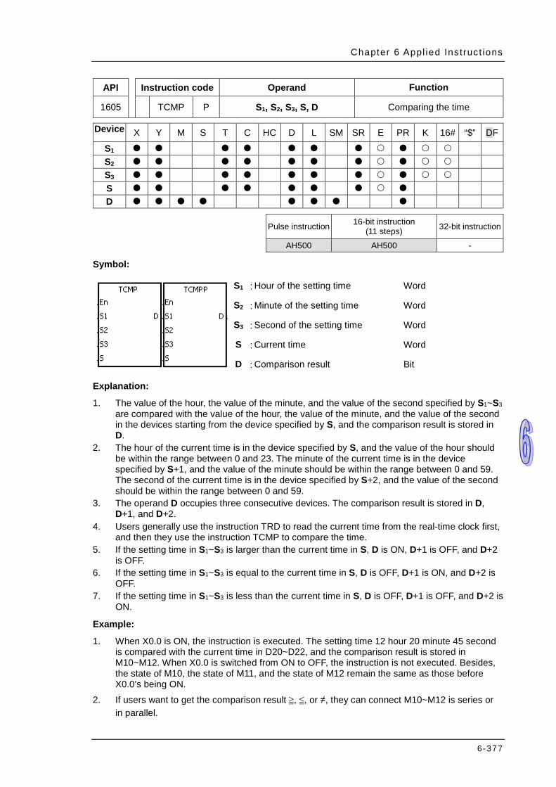
Chapter 6 Appl ied Instruc t ions
6-377
API Instruction code Operand Function
1605 TCMP P S1, S2, S3, S, D Comparing the time
Device X Y M S T C HC D L SM SR E PR K 16# “$” DF S1 S2 S3 S D
Pulse instruction 16-bit instruction
(11 steps) 32-bit instruction
AH500 AH500 -
Symbol:
S1 : Hour of the setting time Word
S2 : Minute of the setting time Word
S3 : Second of the setting time Word
S : Current time Word
D : Comparison result Bit
Explanation:
1. The value of the hour, the value of the minute, and the value of the second specified by S1~S3 are compared with the value of the hour, the value of the minute, and the value of the second in the devices starting from the device specified by S, and the comparison result is stored in D.
2. The hour of the current time is in the device specified by S, and the value of the hour should be within the range between 0 and 23. The minute of the current time is in the device specified by S+1, and the value of the minute should be within the range between 0 and 59. The second of the current time is in the device specified by S+2, and the value of the second should be within the range between 0 and 59.
3. The operand D occupies three consecutive devices. The comparison result is stored in D, D+1, and D+2.
4. Users generally use the instruction TRD to read the current time from the real-time clock first, and then they use the instruction TCMP to compare the time.
5. If the setting time in S1~S3 is larger than the current time in S, D is ON, D+1 is OFF, and D+2 is OFF.
6. If the setting time in S1~S3 is equal to the current time in S, D is OFF, D+1 is ON, and D+2 is OFF.
7. If the setting time in S1~S3 is less than the current time in S, D is OFF, D+1 is OFF, and D+2 is ON.
Example:
1. When X0.0 is ON, the instruction is executed. The setting time 12 hour 20 minute 45 second is compared with the current time in D20~D22, and the comparison result is stored in M10~M12. When X0.0 is switched from ON to OFF, the instruction is not executed. Besides, the state of M10, the state of M11, and the state of M12 remain the same as those before X0.0’s being ON.
2. If users want to get the comparison result ≧, ≦, or ≠, they can connect M10~M12 is series or in parallel.

AH500 Programming Manual
6-378
Additional remark:
1. If S+2 exceeds the device range, the instruction is not executed, SM0 is ON, and the error code in SR0 is 16#2003.
2. If D+2 exceeds the device range, the instruction is not executed, SM0 is ON, and the error code in SR0 is 16#2003.
3. If the value in S exceeds the range, the operation error occurs, the instruction is not executed, SM0 is ON, and the error code in SR0 is 16#2003.
4. If the values in S1~S3 exceed the range, the operation error occurs, the instruction is not executed, SM0 is ON, and the error code in SR0 is 16#2003.
5. If users declare the operand D in ISPSoft, the data type will be ARRAY [3] of BOOL.
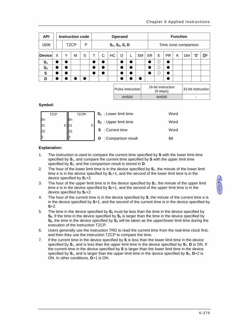
Chapter 6 Appl ied Instruc t ions
6-379
API Instruction code Operand Function
1606 TZCP P S1, S2, S, D Time zone comparison
Device X Y M S T C HC D L SM SR E PR K 16# “$” DF
S1 S2 S D
Pulse instruction 16-bit instruction (9 steps) 32-bit instruction
AH500 AH500 -
Symbol:
S1 : Lower limit time Word
S2 : Upper limit time Word
S : Current time Word
D : Comparison result Bit
Explanation:
1. The instruction is used to compare the current time specified by S with the lower limit time specified by S1, and compare the current time specified by S with the upper limit time specified by S2, and the comparison result is stored in D.
2. The hour of the lower limit time is in the device specified by S1, the minute of the lower limit time e is in the device specified by S1+1, and the second of the lower limit time is in the device specified by S1+2.
3. The hour of the upper limit time is in the device specified by S2, the minute of the upper limit time e is in the device specified by S2+1, and the second of the upper limit time is in the device specified by S2+2.
4. The hour of the current time is in the device specified by S, the minute of the current time e is in the device specified by S+1, and the second of the current time is in the device specified by S+2.
5. The time in the device specified by S1 must be less than the time in the device specified by S2. If the time in the device specified by S1 is larger than the time in the device specified by S2, the time in the device specified by S1 will be taken as the upper/lower limit time during the execution of the instruction TZCP.
6. Users generally use the instruction TRD to read the current time from the real-time clock first, and then they use the instruction TZCP to compare the time.
7. If the current time in the device specified by S is less than the lower limit time in the device specified by S1, and is less than the upper limit time in the device specified by S2, D is ON. If the current time in the device specified by S is larger than the lower limit time in the device specified by S1, and is larger than the upper limit time in the device specified by S2, D+2 is ON. In other conditions, D+1 is ON.

AH500 Programming Manual
6-380
Example:
When X0.0 is ON, the instruction TZCP is executed. M10, M11, or M12 is ON. When X0.0 is OFF, the instruction TZCP is not executed, the state of M10, the state of M11, and the state of M12 remain the same as those before X0.0’s being ON.
Additional remark:
1. If S1+2, S2+2, S+2, or D+2 exceeds the device range, the instruction is not executed, SM0 is ON, and the error code in SR0 is 16#2003.
2. If the values in S1, S2, and S exceed the range, the operation error occurs, the instruction is not executed, SM0 is ON, and the error code in SR0 is 16#2003
3. If users declare the operand S1 in ISPSoft, the data type will be ARRAY [3] of WORD/INT. 4. If users declare the operand S2 in ISPSoft, the data type will be ARRAY [3] of WORD/INT. 5. If users declare the operand S in ISPSoft, the data type will be ARRAY [3] of WORD/INT. 6. If users declare the operand D in ISPSoft, the data type will be ARRAY [3] of WORD/INT.
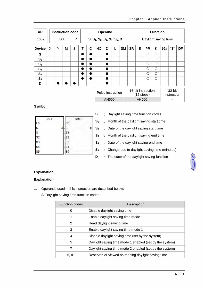
Chapter 6 Appl ied Instruc t ions
6-381
API Instruction code Operand Function
1607 DST P S, S1, S2, S3, S4, S5, D Daylight saving time
Device X Y M S T C HC D L SM SR E PR K 16# “$” DF
S S1 S2 S3 S4 S5 D
Pulse instruction 16-bit instruction (15 steps)
32-bit instruction
AH500 AH500 -
Symbol:
S : Daylight saving time function codes
S1 : Month of the daylight saving start time
S2 : Date of the daylight saving start time
S3 : Month of the daylight saving end time
S4 : Date of the daylight saving end time
S5 : Change due to daylight saving time (minutes)
D : The state of the daylight saving function
Explanation:
Explanation
1. Operands used in this instruction are described below:
S: Daylight saving time function codes
Function codes Description
0 Disable daylight saving time
1 Enable daylight saving time mode 1
2 Read daylight saving time
3 Enable daylight saving time mode 1
4 Disable daylight saving time (set by the system)
5 Daylight saving time mode 1 enabled (set by the system)
7 Daylight saving time mode 2 enabled (set by the system)
6, 8~ Reserved or viewed as reading daylight saving time
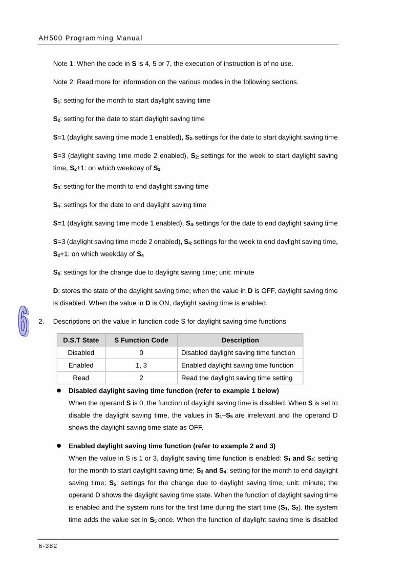
AH500 Programming Manual
6-382
Note 1: When the code in S is 4, 5 or 7, the execution of instruction is of no use.
Note 2: Read more for information on the various modes in the following sections.
S1: setting for the month to start daylight saving time
S2: setting for the date to start daylight saving time
S=1 (daylight saving time mode 1 enabled), S2: settings for the date to start daylight saving time
S=3 (daylight saving time mode 2 enabled), S2: settings for the week to start daylight saving
time, S2+1: on which weekday of S2
S3: setting for the month to end daylight saving time
S4: settings for the date to end daylight saving time
S=1 (daylight saving time mode 1 enabled), S4: settings for the date to end daylight saving time
S=3 (daylight saving time mode 2 enabled), S4: settings for the week to end daylight saving time,
S2+1: on which weekday of S4
S5: settings for the change due to daylight saving time; unit: minute
D: stores the state of the daylight saving time; when the value in D is OFF, daylight saving time
is disabled. When the value in D is ON, daylight saving time is enabled.
2. Descriptions on the value in function code S for daylight saving time functions
D.S.T State S Function Code Description
Disabled 0 Disabled daylight saving time function
Enabled 1, 3 Enabled daylight saving time function
Read 2 Read the daylight saving time setting
Disabled daylight saving time function (refer to example 1 below)
When the operand S is 0, the function of daylight saving time is disabled. When S is set to
disable the daylight saving time, the values in S1–S5 are irrelevant and the operand D
shows the daylight saving time state as OFF.
Enabled daylight saving time function (refer to example 2 and 3)
When the value in S is 1 or 3, daylight saving time function is enabled: S1 and S2: setting
for the month to start daylight saving time; S3 and S4: setting for the month to end daylight
saving time; S5: settings for the change due to daylight saving time; unit: minute; the
operand D shows the daylight saving time state. When the function of daylight saving time
is enabled and the system runs for the first time during the start time (S1, S2), the system
time adds the value set in S5 once. When the function of daylight saving time is disabled
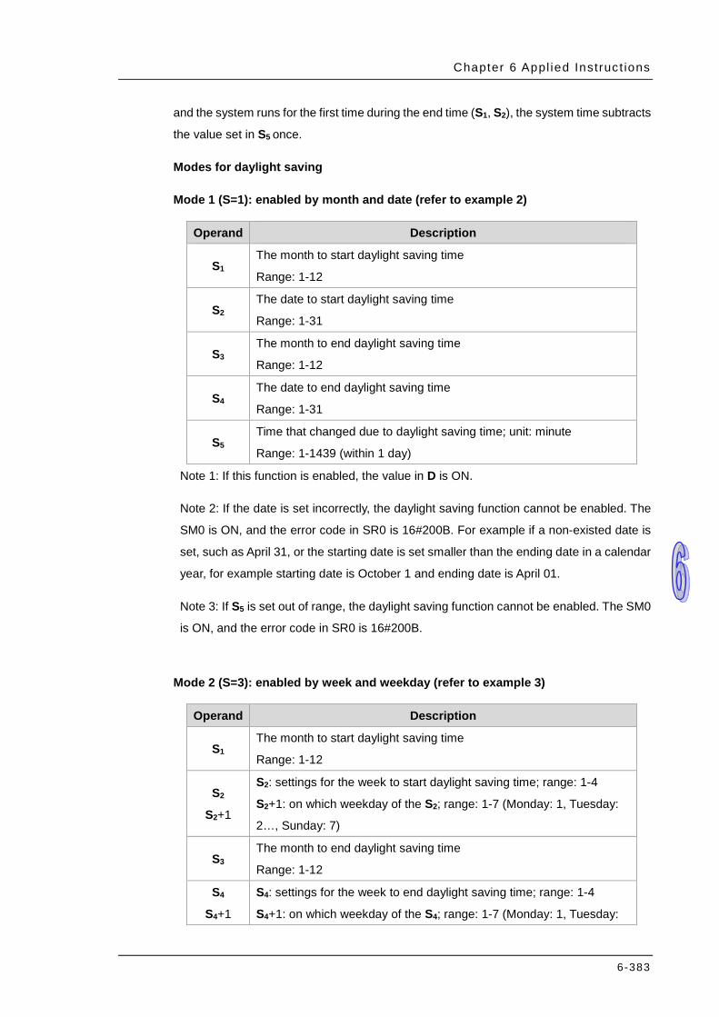
Chapter 6 Appl ied Instruc t ions
6-383
and the system runs for the first time during the end time (S1, S2), the system time subtracts
the value set in S5 once.
Modes for daylight saving
Mode 1 (S=1): enabled by month and date (refer to example 2)
Operand Description
S1 The month to start daylight saving time
Range: 1-12
S2 The date to start daylight saving time
Range: 1-31
S3 The month to end daylight saving time
Range: 1-12
S4 The date to end daylight saving time
Range: 1-31
S5 Time that changed due to daylight saving time; unit: minute
Range: 1-1439 (within 1 day)
Note 1: If this function is enabled, the value in D is ON.
Note 2: If the date is set incorrectly, the daylight saving function cannot be enabled. The
SM0 is ON, and the error code in SR0 is 16#200B. For example if a non-existed date is
set, such as April 31, or the starting date is set smaller than the ending date in a calendar
year, for example starting date is October 1 and ending date is April 01.
Note 3: If S5 is set out of range, the daylight saving function cannot be enabled. The SM0
is ON, and the error code in SR0 is 16#200B.
Mode 2 (S=3): enabled by week and weekday (refer to example 3)
Operand Description
S1 The month to start daylight saving time
Range: 1-12
S2
S2+1
S2: settings for the week to start daylight saving time; range: 1-4
S2+1: on which weekday of the S2; range: 1-7 (Monday: 1, Tuesday:
2…, Sunday: 7)
S3 The month to end daylight saving time
Range: 1-12
S4
S4+1
S4: settings for the week to end daylight saving time; range: 1-4
S4+1: on which weekday of the S4; range: 1-7 (Monday: 1, Tuesday:
AH500 Programming Manual
6-384
2…, Sunday: 7)
S5 Time that changed due to daylight saving time; unit: minute
Range: 1-1439 (within 1 day)
Note 1: If this function is enabled, the value in D is ON.
Note 2: The setting range for S2 and S4 is 1— 4 or -1— -4. The value -1 indicates the last
week of the month and -2 indicates the last 2nd week. If the value in S2 is -2 and S2+1 is
7, it indicates the last 2 Sunday of the month. If the date is set incorrectly, the daylight
saving function cannot be enabled. The SM0 is ON, and the error code in SR0 is
16#200B.
Note 3: If the value in S2+1 / S4+1 is out of range, the default setting value is 7,
indicating Sunday.
Note 4: If S5 is set out of range, the daylight saving function cannot be enabled. The
SM0 is ON, and the error code in SR0 is 16#200B.
Note 5: If the device for operand S2 and S4 is K or 16#, the values are not saved, the
SM0 is ON, and the error code in SR0 is 16#2003.
Read the daylight saving time function (refer to example 1-3)
When the operand S is 2, the function of daylight saving time is being read. S1 and S2: setting
for the month to start daylight saving time; S3 and S4: setting for the month to end daylight
saving time; S5: settings for the change due to daylight saving time; unit: minute. When S is set
to read the state of the daylight saving function and the output state of D is ON, the PLC saves
the setting values in the operands S1–S5. The device is set to D while S is set to read. If the
device is set to K or 16#, the values are not saved, the SM0 is ON, and the error code in SR0
is 16#2003.
Adds 4 to the function codes in S, after the daylight saving state is read. For example, after the
daylight saving state is read, the function codes 0, 1, 3 become 4, 5 and 7.
When the DST state is OFF, the operand and descriptions are shown below.
Operand Description
S Function code is 4, indicating the DST state is OFF.
S1- S5 Invalid operand
D DST state is OFF.

Chapter 6 Appl ied Instruc t ions
6-385
When the DST state is ON and in mode 1, the operand and descriptions are shown below.
Operand Description
S Function code is 5, indicating the DST state is ON and in mode 1.
S1 The month to start daylight saving time
S2 The date to start daylight saving time
S3 The month to end daylight saving time
S4 The date to end daylight saving time
S5 Time that changed due to daylight saving time; unit: minute
D The DST state is ON (enabled).
When the DST state is ON and in mode 2, the operand and descriptions are shown below.
Operand Description
S Function code is 7, indicating the DST state is ON and in mode 2.
S1 The month to start daylight saving time
S2
S2+1
S2: settings for the week to start daylight saving time
S2+1: on which weekday of the S2
S3 The month to end daylight saving time
S4
S4+1
S4: settings for the week to end daylight saving time
S4+1: on which weekday of the S4
S5 Time that changed due to daylight saving time; unit: minute
Operand The DST state is ON (enabled).
3. This instruction is to enable / disable the daylight saving time function. Whether the contact is
normally open or close will not affect the daylight saving time setting. (refer to example 2 for
more details on how to switch the contact M0 OFF=>ON) You can reset the daylight saving
time by executing the instruction again. There is no need to disable and then enable this function
to reset the daylight saving time.
4. When setting the daylight saving time to start on April 1st and to end on September 1st, and the
duration is 60 minutes; the real-time clock goes like below.
Daylight saving time function
disabled
Daylight saving time function
enabled
1st March, 3 o’clock 1st March, 3 o’clock
31st March, 3 o’clock 31st March, 3 o’clock
1st April, 3 o’clock 1st April, 4 o’clock
1st May, 3 o’clock 1st May, 4 o’clock
1st June, 3 o’clock 1st June, 4 o’clock
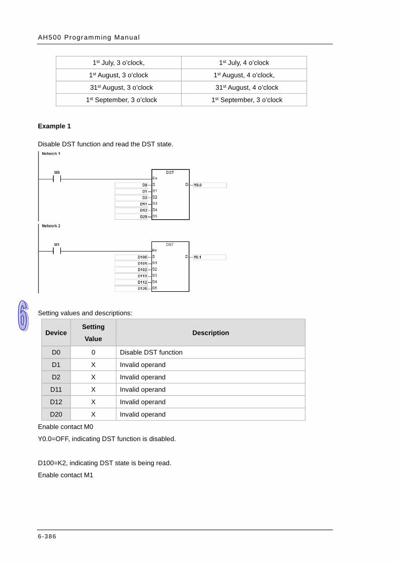
AH500 Programming Manual
6-386
1st July, 3 o’clock, 1st July, 4 o’clock
1st August, 3 o’clock 1st August, 4 o’clock,
31st August, 3 o’clock 31st August, 4 o’clock
1st September, 3 o’clock 1st September, 3 o’clock
Example 1
Disable DST function and read the DST state.
Setting values and descriptions:
Device Setting
Value Description
D0 0 Disable DST function
D1 X Invalid operand
D2 X Invalid operand
D11 X Invalid operand
D12 X Invalid operand
D20 X Invalid operand
Enable contact M0
Y0.0=OFF, indicating DST function is disabled.
D100=K2, indicating DST state is being read.
Enable contact M1
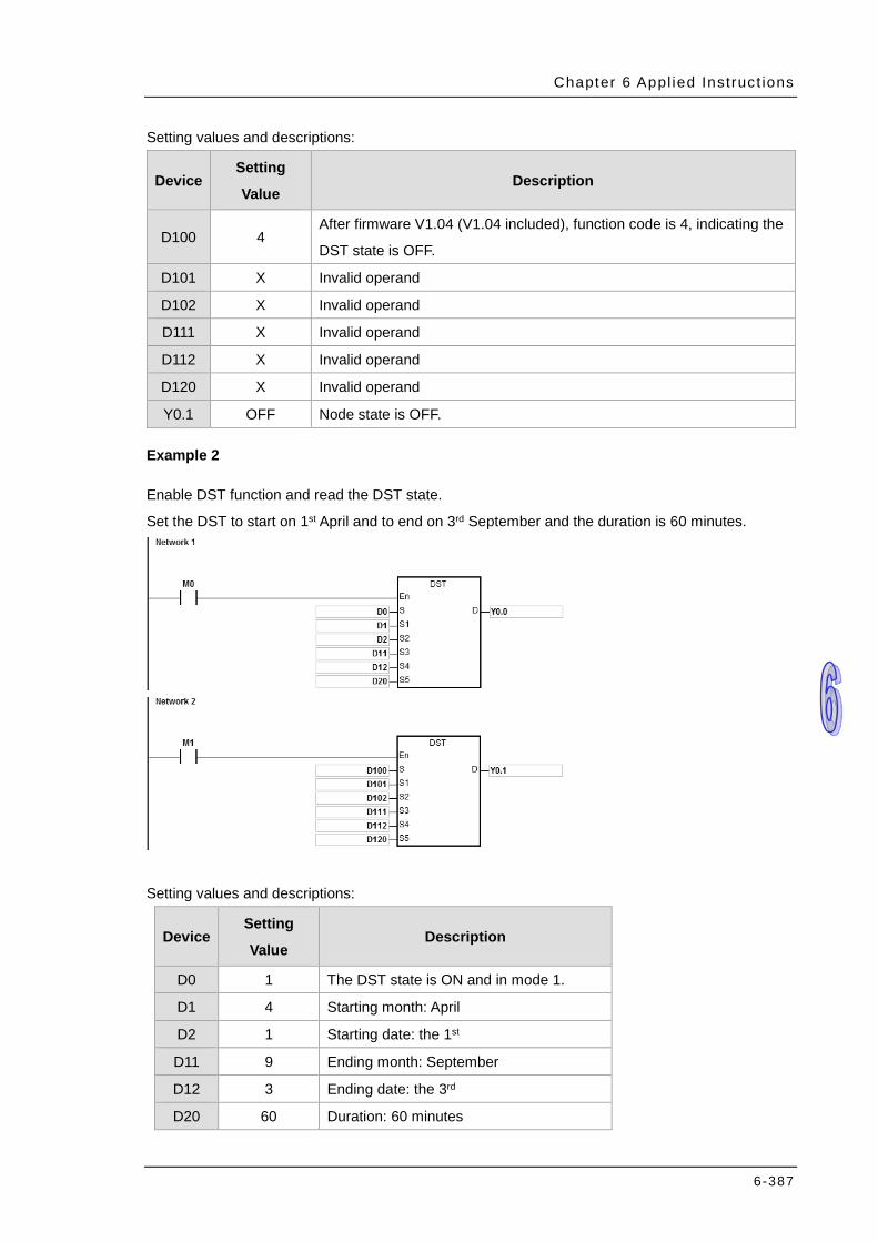
Chapter 6 Appl ied Instruc t ions
6-387
Setting values and descriptions:
Example 2
Enable DST function and read the DST state.
Set the DST to start on 1st April and to end on 3rd September and the duration is 60 minutes.
Setting values and descriptions:
Device Setting
Value Description
D0 1 The DST state is ON and in mode 1.
D1 4 Starting month: April
D2 1 Starting date: the 1st
D11 9 Ending month: September
D12 3 Ending date: the 3rd
D20 60 Duration: 60 minutes
Device Setting
Value Description
D100 4 After firmware V1.04 (V1.04 included), function code is 4, indicating the
DST state is OFF.
D101 X Invalid operand
D102 X Invalid operand
D111 X Invalid operand
D112 X Invalid operand
D120 X Invalid operand
Y0.1 OFF Node state is OFF.
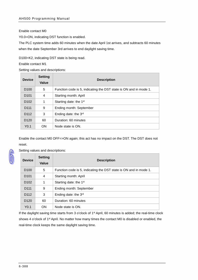
AH500 Programming Manual
6-388
Enable contact M0
Y0.0=ON, indicating DST function is enabled.
The PLC system time adds 60 minutes when the date April 1st arrives, and subtracts 60 minutes
when the date September 3rd arrives to end daylight saving time.
D100=K2, indicating DST state is being read.
Enable contact M1
Setting values and descriptions:
Device Setting
Value Description
D100 5 Function code is 5, indicating the DST state is ON and in mode 1.
D101 4 Starting month: April
D102 1 Starting date: the 1st
D111 9 Ending month: September
D112 3 Ending date: the 3rd
D120 60 Duration: 60 minutes
Y0.1 ON Node state is ON.
Enable the contact M0 OFF=>ON again; this act has no impact on the DST. The DST does not
reset.
Setting values and descriptions:
Device Setting
Value Description
D100 5 Function code is 5, indicating the DST state is ON and in mode 1.
D101 4 Starting month: April
D102 1 Starting date: the 1st
D111 9 Ending month: September
D112 3 Ending date: the 3rd
D120 60 Duration: 60 minutes
Y0.1 ON Node state is ON.
If the daylight saving time starts from 3 o’clock of 1st April, 60 minutes is added; the real-time clock
shows 4 o’clock of 1st April. No matter how many times the contact M0 is disabled or enabled, the
real-time clock keeps the same daylight saving time.
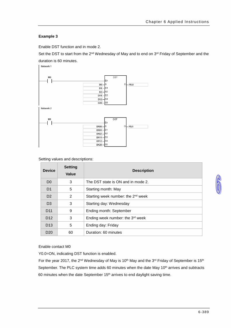
Chapter 6 Appl ied Instruc t ions
6-389
Example 3
Enable DST function and in mode 2.
Set the DST to start from the 2nd Wednesday of May and to end on 3rd Friday of September and the
duration is 60 minutes.
Setting values and descriptions:
Device Setting
Value Description
D0 3 The DST state is ON and in mode 2.
D1 5 Starting month: May
D2 2 Starting week number: the 2nd week
D3 3 Starting day: Wednesday
D11 9 Ending month: September
D12 3 Ending week number: the 3rd week
D13 5 Ending day: Friday
D20 60 Duration: 60 minutes
Enable contact M0
Y0.0=ON, indicating DST function is enabled.
For the year 2017, the 2nd Wednesday of May is 10th May and the 3rd Friday of September is 15th
September. The PLC system time adds 60 minutes when the date May 10th arrives and subtracts
60 minutes when the date September 15th arrives to end daylight saving time.

AH500 Programming Manual
6-390
D100=K2, indicating DST state is being read.
Enable contact M1
Setting values and descriptions:
Device Setting
Value Description
D100 7 Function code is 4, indicating the DST state is ON and in mode 2.
D101 5 Starting month: May
D102 2 Starting week number: the 2nd week
D103 3 Starting day: Wednesday
D111 9 Ending month: September
D112 3 Ending week number: the 3rd week
D113 5 Ending day: Friday
D120 60 Duration: 60 minutes
Y0.1 ON Node state is ON.
Additional remark:
DST instruction is available for the followings:
AHCPU5X1-EN V2.01 or later
AHCPU5X1-RS2 V1.03 or later
AHCPU560-EN2 V1.10 or later
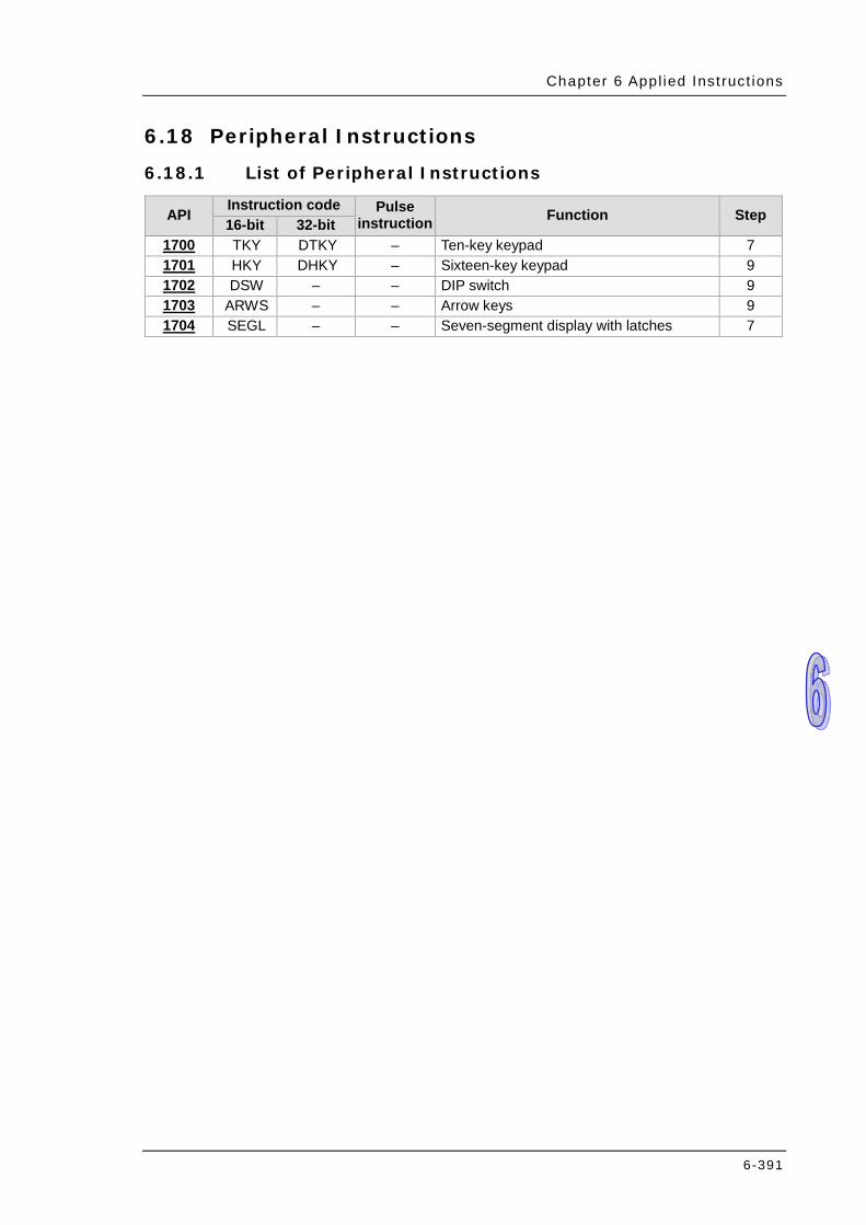
Chapter 6 Appl ied Inst ruct ions
6-391
6.18 Peripheral Instructions
6.18.1 List of Peripheral Instructions
API Instruction code Pulse instruction Function Step 16-bit 32-bit
1700 TKY DTKY – Ten-key keypad 7 1701 HKY DHKY – Sixteen-key keypad 9 1702 DSW – – DIP switch 9 1703 ARWS – – Arrow keys 9 1704 SEGL – – Seven-segment display with latches 7
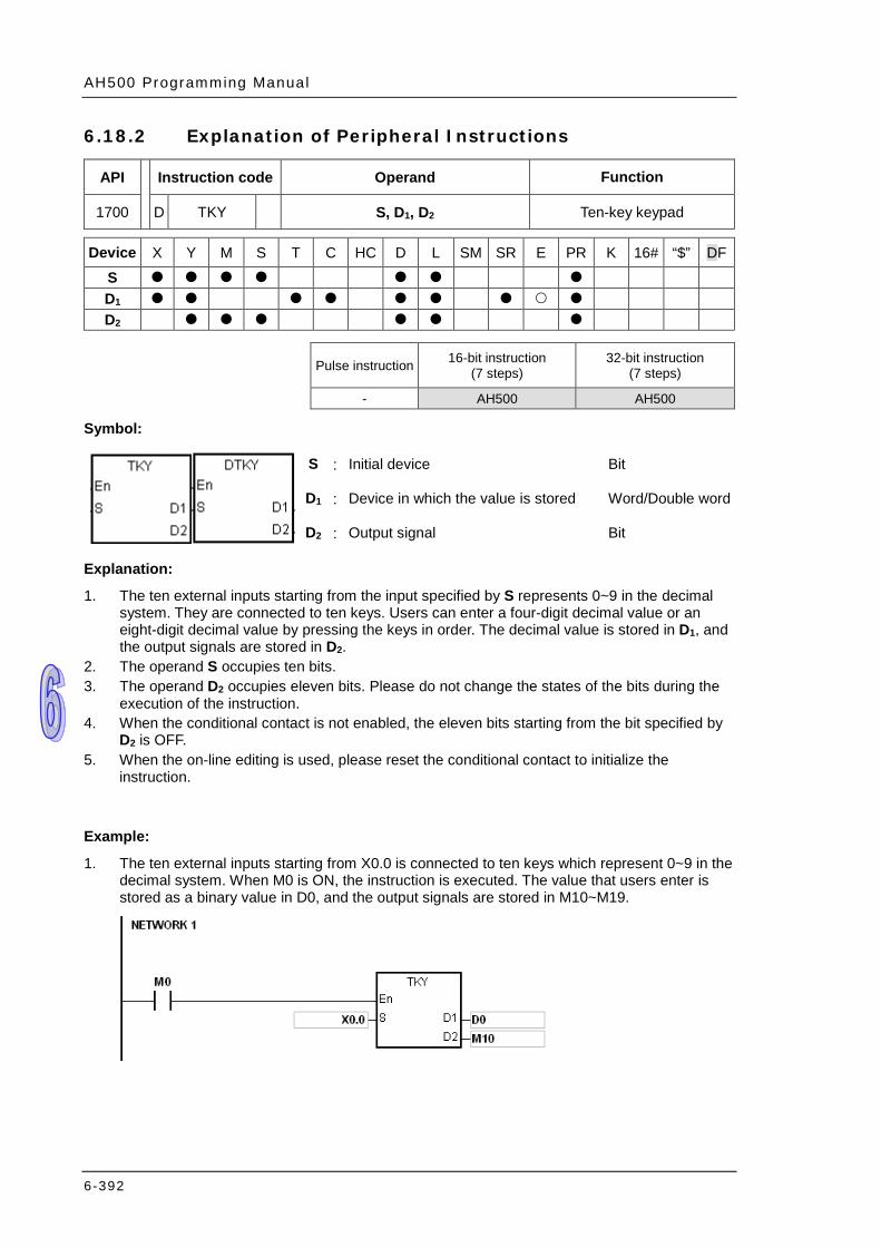
AH500 Programming Manual
6-392
6.18.2 Explanation of Peripheral Instructions
API Instruction code Operand Function
1700 D TKY S, D1, D2 Ten-key keypad
Device X Y M S T C HC D L SM SR E PR K 16# “$” DF
S D1 D2
Pulse instruction 16-bit instruction
(7 steps) 32-bit instruction
(7 steps)
- AH500 AH500
Symbol:
S : Initial device Bit
D1 : Device in which the value is stored Word/Double word
D2 : Output signal Bit
Explanation:
1. The ten external inputs starting from the input specified by S represents 0~9 in the decimal system. They are connected to ten keys. Users can enter a four-digit decimal value or an eight-digit decimal value by pressing the keys in order. The decimal value is stored in D1, and the output signals are stored in D2.
2. The operand S occupies ten bits. 3. The operand D2 occupies eleven bits. Please do not change the states of the bits during the
execution of the instruction. 4. When the conditional contact is not enabled, the eleven bits starting from the bit specified by
D2 is OFF. 5. When the on-line editing is used, please reset the conditional contact to initialize the
instruction.
Example:
1. The ten external inputs starting from X0.0 is connected to ten keys which represent 0~9 in the decimal system. When M0 is ON, the instruction is executed. The value that users enter is stored as a binary value in D0, and the output signals are stored in M10~M19.
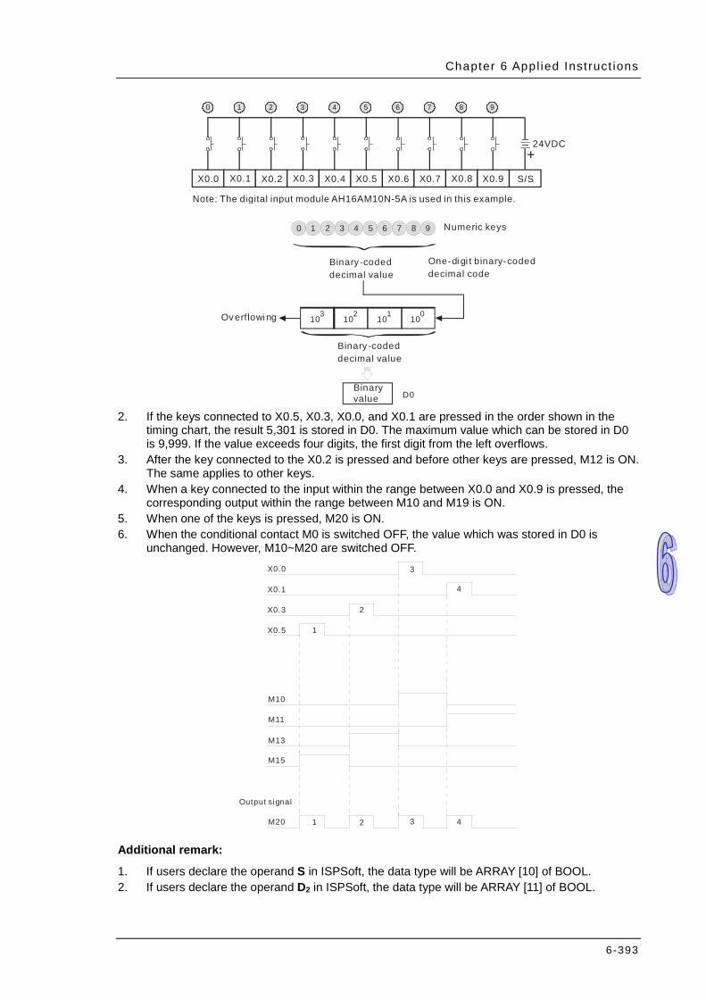
Chapter 6 Appl ied Inst ruct ions
6-393
0 1 2 3 4 5 6 7 8 9
Binary -coded decimal value
Binary value
Binary -coded decimal value
One-di gi t binary-codeddecimal code
D0
103
102
101
100
Numeric keys
Overflowi ng
2. If the keys connected to X0.5, X0.3, X0.0, and X0.1 are pressed in the order shown in the
timing chart, the result 5,301 is stored in D0. The maximum value which can be stored in D0 is 9,999. If the value exceeds four digits, the first digit from the left overflows.
3. After the key connected to the X0.2 is pressed and before other keys are pressed, M12 is ON. The same applies to other keys.
4. When a key connected to the input within the range between X0.0 and X0.9 is pressed, the corresponding output within the range between M10 and M19 is ON.
5. When one of the keys is pressed, M20 is ON. 6. When the conditional contact M0 is switched OFF, the value which was stored in D0 is
unchanged. However, M10~M20 are switched OFF. X0.0
X0.1
X0.3
X0.5 1
2
3
4
1 2 3 4
M10
M11
M13
M15
M20
Output si gnal
Additional remark:
1. If users declare the operand S in ISPSoft, the data type will be ARRAY [10] of BOOL. 2. If users declare the operand D2 in ISPSoft, the data type will be ARRAY [11] of BOOL.
0 1 32 4 5 6 7 8 9
X0.3X0.2X0.1X0.0 S/SX0.6X0.5X0.4 X0.8X0.7 X0.9
24VDC
Note: The digital input module AH16AM10N-5A is used in this example.
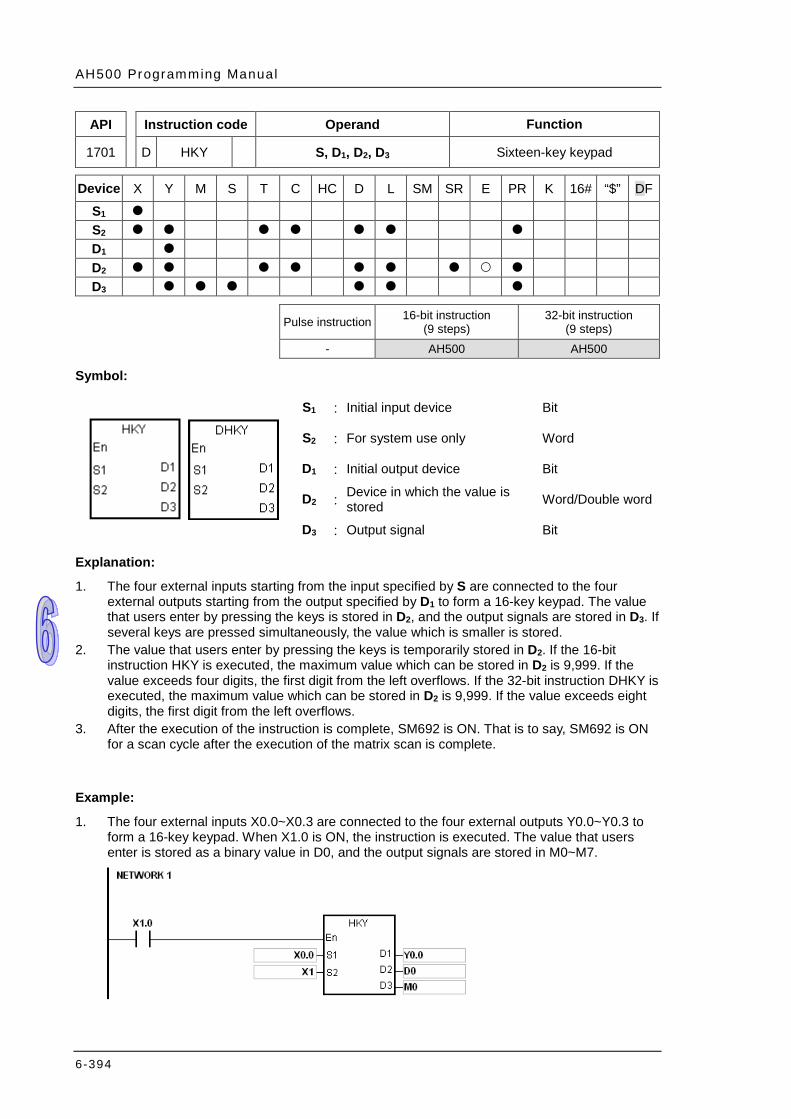
AH500 Programming Manual
6-394
API Instruction code Operand Function
1701 D HKY S, D1, D2, D3 Sixteen-key keypad
Device X Y M S T C HC D L SM SR E PR K 16# “$” DF
S1 S2 D1 D2 D3
Pulse instruction 16-bit instruction
(9 steps) 32-bit instruction
(9 steps)
- AH500 AH500
Symbol:
S1 : Initial input device Bit
S2 : For system use only Word
D1 : Initial output device Bit
D2 : Device in which the value is stored Word/Double word
D3 : Output signal Bit
Explanation:
1. The four external inputs starting from the input specified by S are connected to the four external outputs starting from the output specified by D1 to form a 16-key keypad. The value that users enter by pressing the keys is stored in D2, and the output signals are stored in D3. If several keys are pressed simultaneously, the value which is smaller is stored.
2. The value that users enter by pressing the keys is temporarily stored in D2. If the 16-bit instruction HKY is executed, the maximum value which can be stored in D2 is 9,999. If the value exceeds four digits, the first digit from the left overflows. If the 32-bit instruction DHKY is executed, the maximum value which can be stored in D2 is 9,999. If the value exceeds eight digits, the first digit from the left overflows.
3. After the execution of the instruction is complete, SM692 is ON. That is to say, SM692 is ON for a scan cycle after the execution of the matrix scan is complete.
Example:
1. The four external inputs X0.0~X0.3 are connected to the four external outputs Y0.0~Y0.3 to form a 16-key keypad. When X1.0 is ON, the instruction is executed. The value that users enter is stored as a binary value in D0, and the output signals are stored in M0~M7.
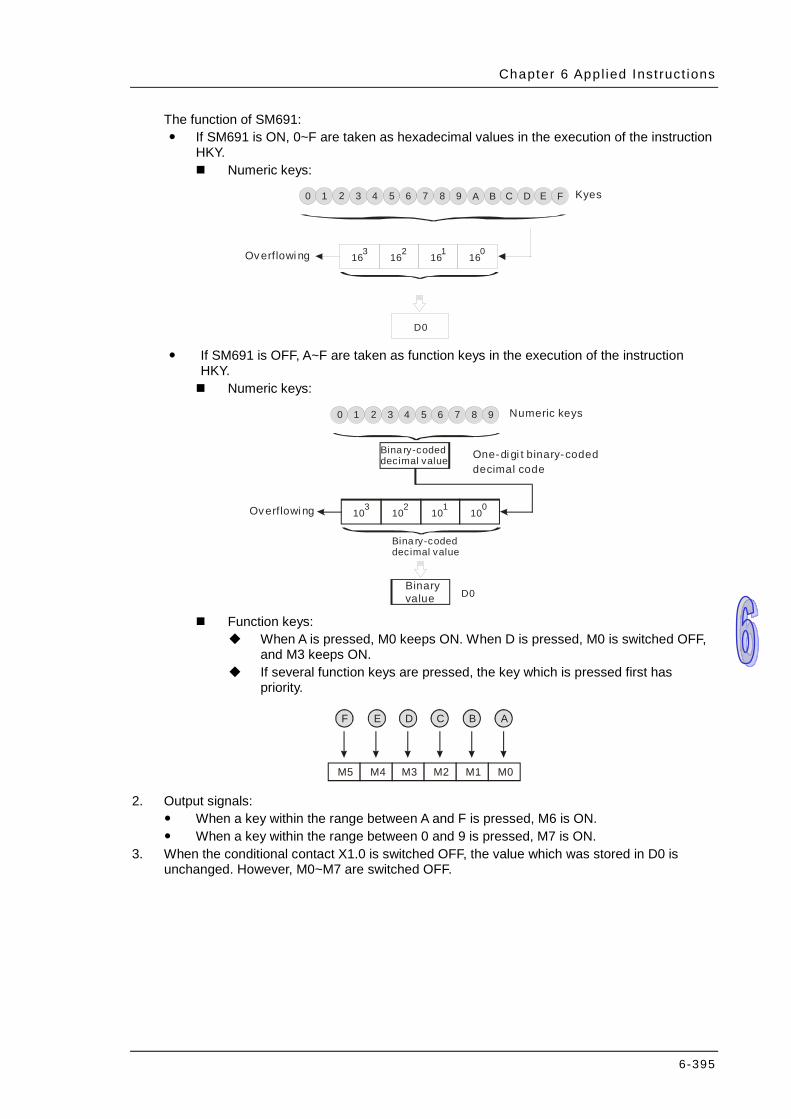
Chapter 6 Appl ied Inst ruct ions
6-395
The function of SM691: If SM691 is ON, 0~F are taken as hexadecimal values in the execution of the instruction
HKY. Numeric keys:
0 1 2 3 4 5 6 7 8 9
D0
3 2 1 0
Kyes
Overflowi ng
A B C D E F
16 16 16 16
If SM691 is OFF, A~F are taken as function keys in the execution of the instruction
HKY. Numeric keys:
0 1 2 3 4 5 6 7 8 9
Bina ry-codeddecimal value
Binary value
Bina ry-coded decimal value
One-di gi t binary-coded decimal code
D0
103
102
101
100
Numeric keys
Overflowi ng
Function keys:
When A is pressed, M0 keeps ON. When D is pressed, M0 is switched OFF, and M3 keeps ON.
If several function keys are pressed, the key which is pressed first has priority.
F E D C B A
M2M3M4M5 M0M1 2. Output signals:
When a key within the range between A and F is pressed, M6 is ON. When a key within the range between 0 and 9 is pressed, M7 is ON.
3. When the conditional contact X1.0 is switched OFF, the value which was stored in D0 is unchanged. However, M0~M7 are switched OFF.
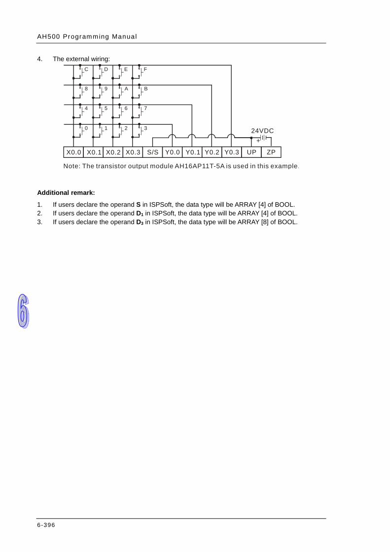
AH500 Programming Manual
6-396
4. The external wiring:
Additional remark:
1. If users declare the operand S in ISPSoft, the data type will be ARRAY [4] of BOOL. 2. If users declare the operand D1 in ISPSoft, the data type will be ARRAY [4] of BOOL. 3. If users declare the operand D3 in ISPSoft, the data type will be ARRAY [8] of BOOL.
X0.3X0.2X0.1X0.0 S/S
C D E F
8 9 A B
4 5 6 7
0 1 2 3
Note: The transistor output module is used in this example. AH16AP11T-5A
Y0.3Y0.2Y0.1Y0.0 UP ZP
24VDC+
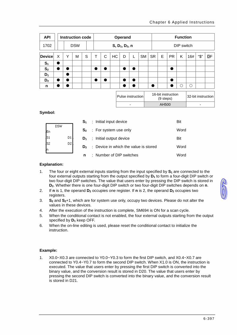
Chapter 6 Appl ied Inst ruct ions
6-397
API Instruction code Operand Function
1702 DSW S, D1, D2, n DIP switch
Device X Y M S T C HC D L SM SR E PR K 16# “$” DF
S1 S2 D1 D2 n
Pulse instruction 16-bit instruction
(9 steps) 32-bit instruction
- AH500 -
Symbol:
S1 : Initial input device Bit
S2 : For system use only Word
D1 : Initial output device Bit
D2 : Device in which the value is stored Word
n : Number of DIP switches Word
Explanation:
1. The four or eight external inputs starting from the input specified by S1 are connected to the four external outputs starting from the output specified by D1 to form a four-digit DIP switch or two four-digit DIP switches. The value that users enter by pressing the DIP switch is stored in D2. Whether there is one four-digit DIP switch or two four-digit DIP switches depends on n.
2. If n is 1, the operand D2 occupies one register. If n is 2, the operand D2 occupies two registers.
3. S2 and S2+1, which are for system use only, occupy two devices. Please do not alter the values in these devices.
4. After the execution of the instruction is complete, SM694 is ON for a scan cycle. 5. When the conditional contact is not enabled, the four external outputs starting from the output
specified by D1 keep OFF. 6. When the on-line editing is used, please reset the conditional contact to initialize the
instruction.
Example:
1. X0.0~X0.3 are connected to Y0.0~Y0.3 to form the first DIP switch, and X0.4~X0.7 are connected to Y0.4~Y0.7 to form the second DIP switch. When X1.0 is ON, the instruction is executed. The value that users enter by pressing the first DIP switch is converted into the binary value, and the conversion result is stored in D20. The value that users enter by pressing the second DIP switch is converted into the binary value, and the conversion result is stored in D21.
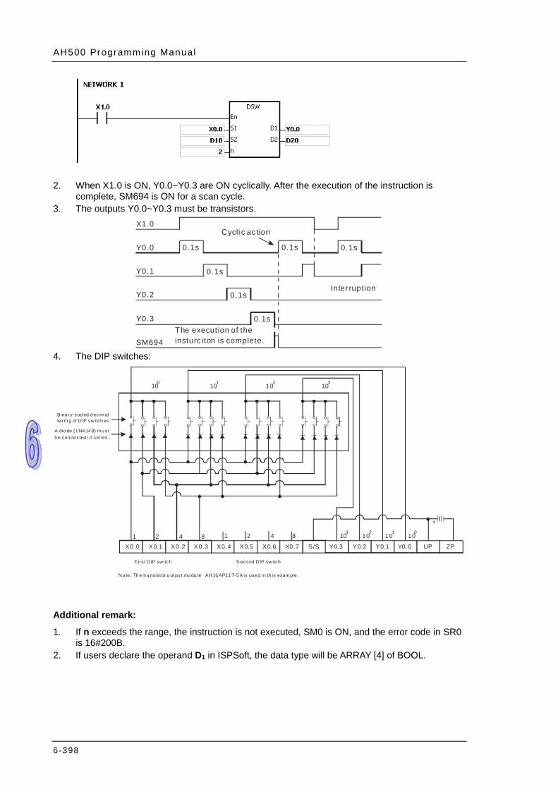
AH500 Programming Manual
6-398
2. When X1.0 is ON, Y0.0~Y0.3 are ON cyclically. After the execution of the instruction is complete, SM694 is ON for a scan cycle.
3. The outputs Y0.0~Y0.3 must be transistors. X1.0
Y0.0
Y0.1
Y0.2
Y0.3
SM694The execution of the insturc iton is complete.
0.1s
0.1s
0.1s
0.1s
0.1s 0.1s
Cycli c ac tion
Inter ruption
4. The DIP switches:
UPX0.0 X0.1 X0.2 X0.3 X0. 4 X0.5 X0.6 Y0.31 2 4 8 1 2 4 8 10 10 10 103 2 1 0
100 101 102 103
X0.7 Y0.2 Y0.0Y0.1 ZPS/S
+
A dio de (1 N4 14 8) m u st b e con ne cted i n ser ies .
Bina ry cod ed d ecim al-wir in g of D IP sw itch es
No te : Th e tra nsist or o ut pu t mo du le AH16 AP11 T-5 A is use d in th is exam ple .
First D IP sw itch S eco nd DIP swtich
Additional remark:
1. If n exceeds the range, the instruction is not executed, SM0 is ON, and the error code in SR0 is 16#200B.
2. If users declare the operand D1 in ISPSoft, the data type will be ARRAY [4] of BOOL.

Chapter 6 Appl ied Inst ruct ions
6-399
API Instruction code Operand Function
1703 ARWS S, D1, D2, n Arrow keys
Device X Y M S T C HC D L SM SR E PR K 16# “$” DF
S1 S2 D1 D2 n
Pulse instruction 16-bit instruction
(9 steps) 32-bit instruction
- AH500 -
Symbol:
S1 : Initial input device Bit
S2 : For system use only Word
D1 : Device in which the setting value is stored Word
D2 : Initial output device Bit
n : Positive/Negative logic Word
Explanation:
1. If the instruction is executed, S1 is defined as the down arrow, S1+1 is defined as the up arrow, S1+2 is defined as the right arrow, and S1+3 is defined as the left arrow. The setting value is stored in D1, and it should be within the range between 0 and 9,999.
2. The operand S1 occupies four consecutive bit devices. 3. S2 is for system use only. Please do not alter the value in it. 4. The operand D2 occupies eight consecutive bit devices. 5. When the conditional contact is not enabled, the eight bit devices starting from the bit device
specified by D2 keep OFF. 6. The operand n should be within the range between 0 and 3. Please refer to the additional
remark on the instruction SEGL for more information. 7. When the on-line editing is used, please reset the conditional contact to initialize the
instruction.
Example:
1. If the instruction is executed, X0.0 is defined as the down arrow, X0.1 is defined as the up arrow, X0.2 is defined as the right arrow, and X0.3 is defined as the left arrow. The setting value is stored in D20, and it should be within the range between 0 and 9,999.
2. When X1.0 is ON, the digit in the place 103 is selected. If the left arrow is pressed, the places are selected in sequence (103→100→101→102→103→100).
3. If the right arrow is pressed, the places are selected in sequence (103→102→101→100→103→102). The LED indicators with the corresponding places are connected to Y0.4~Y0.7. When the digits in the places are selected in sequence, the LED indicators are ON in sequence.
4. If the up arrow is pressed, the digit in the place selected changes (0→1→2→…8→9→0→1). If the down arrow is pressed, the digit in the place selected changes (0→9→8→…1→0→9). The new digit is shown on seven-segment display.
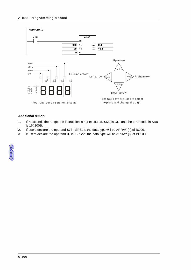
AH500 Programming Manual
6-400
1248
10 10 10 103 2 1 0
Y0.0Y0.1Y0.2Y0.3
Y0.7Y0.6Y0.5Y0.4
LED indicators
Four -digit seven-segment display
X0.1
X0.0
X0.2X0.3
Up arrow
Down arrow
Left arrow Right arrow
The four keys are used to selectthe place and change the digit
Additional remark:
1. If n exceeds the range, the instruction is not executed, SM0 is ON, and the error code in SR0 is 16#200B.
2. If users declare the operand S1 in ISPSoft, the data type will be ARRAY [4] of BOOL. 3. If users declare the operand D2 in ISPSoft, the data type will be ARRAY [8] of BOOLL.
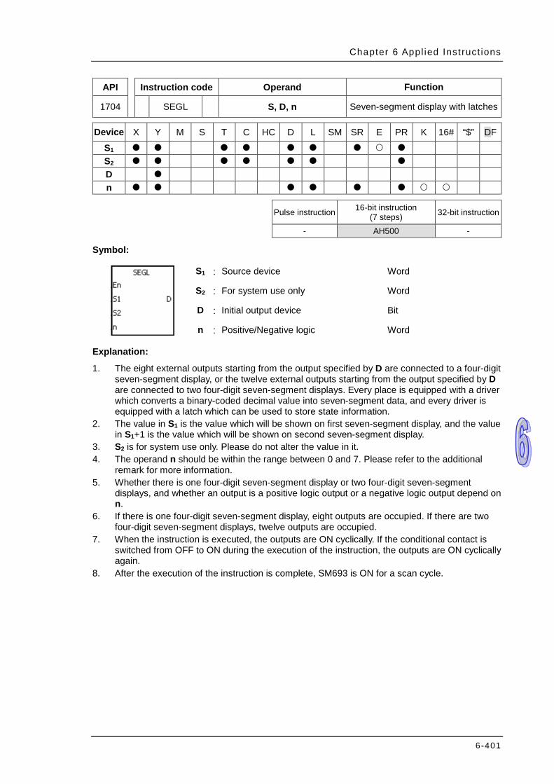
Chapter 6 Appl ied Inst ruct ions
6-401
API Instruction code Operand Function
1704 SEGL S, D, n Seven-segment display with latches
Device X Y M S T C HC D L SM SR E PR K 16# “$” DF
S1 S2 D n
Pulse instruction 16-bit instruction (7 steps) 32-bit instruction
- AH500 -
Symbol:
S1 : Source device Word
S2 : For system use only Word
D : Initial output device Bit
n : Positive/Negative logic Word
Explanation:
1. The eight external outputs starting from the output specified by D are connected to a four-digit seven-segment display, or the twelve external outputs starting from the output specified by D are connected to two four-digit seven-segment displays. Every place is equipped with a driver which converts a binary-coded decimal value into seven-segment data, and every driver is equipped with a latch which can be used to store state information.
2. The value in S1 is the value which will be shown on first seven-segment display, and the value in S1+1 is the value which will be shown on second seven-segment display.
3. S2 is for system use only. Please do not alter the value in it. 4. The operand n should be within the range between 0 and 7. Please refer to the additional
remark for more information. 5. Whether there is one four-digit seven-segment display or two four-digit seven-segment
displays, and whether an output is a positive logic output or a negative logic output depend on n.
6. If there is one four-digit seven-segment display, eight outputs are occupied. If there are two four-digit seven-segment displays, twelve outputs are occupied.
7. When the instruction is executed, the outputs are ON cyclically. If the conditional contact is switched from OFF to ON during the execution of the instruction, the outputs are ON cyclically again.
8. After the execution of the instruction is complete, SM693 is ON for a scan cycle.
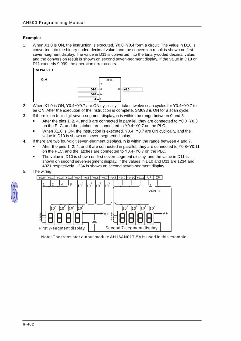
AH500 Programming Manual
6-402
Example:
1. When X1.0 is ON, the instruction is executed. Y0.0~Y0.4 form a circuit. The value in D10 is converted into the binary-coded decimal value, and the conversion result is shown on first seven-segment display. The value in D11 is converted into the binary-coded decimal value, and the conversion result is shown on second seven-segment display. If the value in D10 or D11 exceeds 9,999, the operation error occurs.
2. When X1.0 is ON, Y0.4~Y0.7 are ON cyclically. It takes twelve scan cycles for Y0.4~Y0.7 to
be ON. After the execution of the instruction is complete, SM693 is ON for a scan cycle. 3. If there is on four-digit seven-segment display, n is within the range between 0 and 3.
After the pins 1, 2, 4, and 8 are connected in parallel, they are connected to Y0.0~Y0.3 on the PLC, and the latches are connected to Y0.4~Y0.7 on the PLC.
When X1.0 is ON, the instruction is executed. Y0.4~Y0.7 are ON cyclically, and the value in D10 is shown on seven-segment display.
4. If there are two four-digit seven-segment displays, n is within the range between 4 and 7. After the pins 1, 2, 4, and 8 are connected in parallel, they are connected to Y0.8~Y0.11
on the PLC, and the latches are connected to Y0.4~Y0.7 on the PLC. The value in D10 is shown on first seven-segment display, and the value in D11 is
shown on second seven-segment display. If the values in D10 and D11 are 1234 and 4321 respectively, 1234 is shown on second seven-segment display.
5. The wiring:
Y0.0 Y0.1 Y0.2 Y0.3 Y0.4 Y0.5 Y0.6 Y0.7 Y0.8 Y0.9 Y0.10 Y0.11
1 2 4 8 100
101
102
103
103
102
101
100
V+10
310
210
110
0
V+1248
1248
UP ZP
24VDC
+
Note: The transistor output module AH16AN01T-5A is used in this example.
First 7-segment display Second 7-segment display

Chapter 6 Appl ied Inst ruct ions
6-403
Additional remark:
1. Whether an output is a positive output or a negative output, and whether there is one four-digit seven-segment display or two four-digit seven-segment displays depend on n.
2. The outputs on the PLC should be NPN transistors whose collectors are open collectors. Besides, an output has to connect a pull-up resistor to the DC power supply (less than 30 V DC). Therefore, when an output is ON, a signal of low potential is output.
The negative logic:
Binary-coded decimal value
Output (Binary-coded decimal code)
Signal
b3 b2 b1 b0 8 4 2 1 A B C D 0 0 0 0 0 0 0 0 1 1 1 1 0 0 0 1 0 0 0 1 1 1 1 0 0 0 1 0 0 0 1 0 1 1 0 1 0 0 1 1 0 0 1 1 1 1 0 0 0 1 0 0 0 1 0 0 1 0 1 1 0 1 0 1 0 1 0 1 1 0 1 0 0 1 1 0 0 1 1 0 1 0 0 1 0 1 1 1 0 1 1 1 1 0 0 0 1 0 0 0 1 0 0 0 0 1 1 1 1 0 0 1 1 0 0 1 0 1 1 0
The positive logic:
Binary-coded decimal value
Output (Binary-coded decimal code)
Signal
b3 b2 b1 b0 8 4 2 1 A B C D 0 0 0 0 1 1 1 1 0 0 0 0 0 0 0 1 1 1 1 0 0 0 0 1 0 0 1 0 1 1 0 1 0 0 1 0 0 0 1 1 1 1 0 0 0 0 1 1 0 1 0 0 1 0 1 1 0 1 0 0 0 1 0 1 1 0 1 0 0 1 0 1 0 1 1 0 1 0 0 1 0 1 1 0 0 1 1 1 1 0 0 0 0 1 1 1 1 0 0 0 0 1 1 1 1 0 0 0 1 0 0 1 0 1 1 0 1 0 0 1
The latch: Positive logic Negative logic
Latch Signal Latch Signal 1 0 0 1
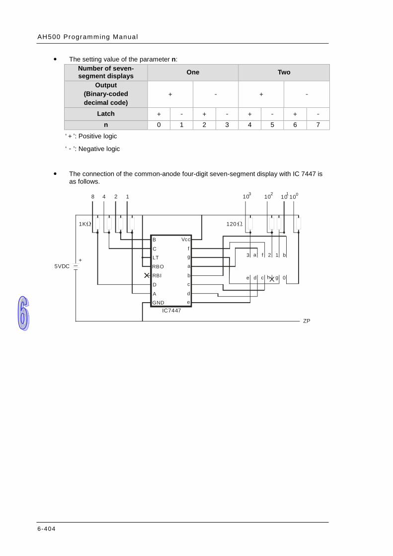
AH500 Programming Manual
6-404
The setting value of the parameter n: Number of seven-segment displays One Two
Output (Binary-coded decimal code)
+ - + -
Latch + - + - + - + - n 0 1 2 3 4 5 6 7
‘+’: Positive logic
‘-’: Negative logic
The connection of the common-anode four-digit seven-segment display with IC 7447 is as follows.
Vcc
f
GNDA
b
a
c
de
g
B
C
D
RBIRBOLT a b
c g
f
e d h 0
123
5VDC
120
1001011021 3
1K
10248
ZP
IC7447
+
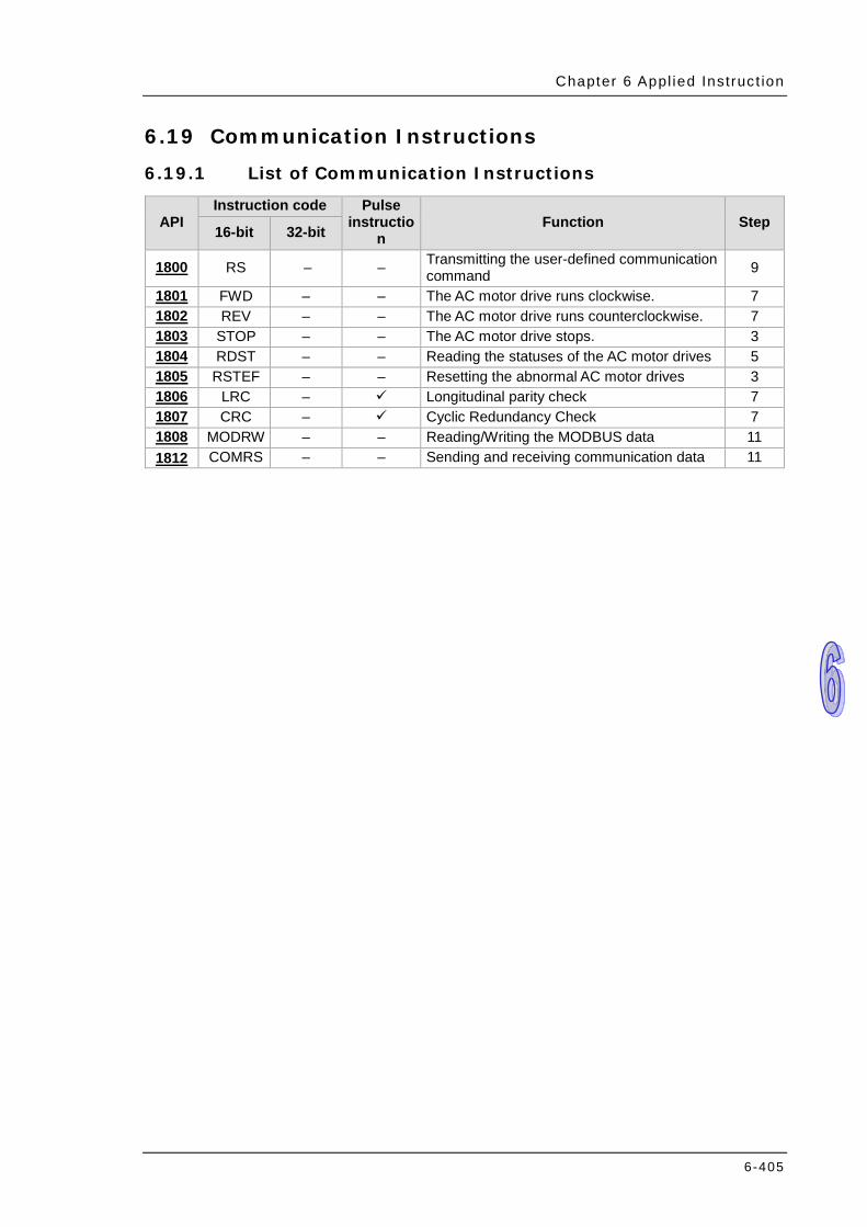
Chapter 6 Appl ied Instruc t ion
6-405
6.19 Communication Instructions
6.19.1 List of Communication Instructions
API Instruction code Pulse
instruction
Function Step 16-bit 32-bit
1800 RS – – Transmitting the user-defined communication command 9
1801 FWD – – The AC motor drive runs clockwise. 7 1802 REV – – The AC motor drive runs counterclockwise. 7 1803 STOP – – The AC motor drive stops. 3 1804 RDST – – Reading the statuses of the AC motor drives 5 1805 RSTEF – – Resetting the abnormal AC motor drives 3 1806 LRC – Longitudinal parity check 7 1807 CRC – Cyclic Redundancy Check 7 1808 MODRW – – Reading/Writing the MODBUS data 11 1812 COMRS – – Sending and receiving communication data 11
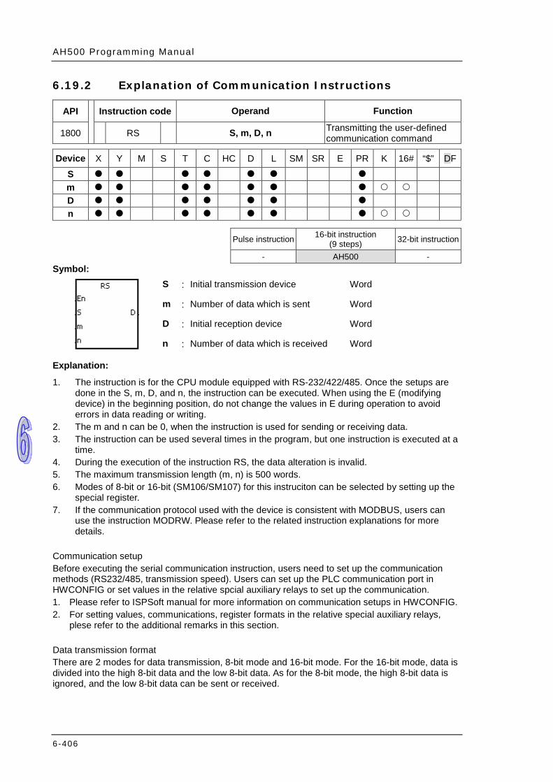
AH500 Programming Manual
6-406
6.19.2 Explanation of Communication Instructions
API Instruction code Operand Function
1800 RS S, m, D, n Transmitting the user-defined communication command
Device X Y M S T C HC D L SM SR E PR K 16# “$” DF
S m D n
Pulse instruction 16-bit instruction
(9 steps) 32-bit instruction
- AH500 - Symbol:
S : Initial transmission device Word
m : Number of data which is sent Word
D : Initial reception device Word
n : Number of data which is received Word
Explanation:
1. The instruction is for the CPU module equipped with RS-232/422/485. Once the setups are done in the S, m, D, and n, the instruction can be executed. When using the E (modifying device) in the beginning position, do not change the values in E during operation to avoid errors in data reading or writing.
2. The m and n can be 0, when the instruction is used for sending or receiving data. 3. The instruction can be used several times in the program, but one instruction is executed at a
time. 4. During the execution of the instruction RS, the data alteration is invalid. 5. The maximum transmission length (m, n) is 500 words. 6. Modes of 8-bit or 16-bit (SM106/SM107) for this instruciton can be selected by setting up the
special register. 7. If the communication protocol used with the device is consistent with MODBUS, users can
use the instruction MODRW. Please refer to the related instruction explanations for more details.
Communication setup Before executing the serial communication instruction, users need to set up the communication methods (RS232/485, transmission speed). Users can set up the PLC communication port in HWCONFIG or set values in the relative spcial auxiliary relays to set up the communication. 1. Please refer to ISPSoft manual for more information on communication setups in HWCONFIG. 2. For setting values, communications, register formats in the relative special auxiliary relays,
plese refer to the additional remarks in this section. Data transmission format There are 2 modes for data transmission, 8-bit mode and 16-bit mode. For the 16-bit mode, data is divided into the high 8-bit data and the low 8-bit data. As for the 8-bit mode, the high 8-bit data is ignored, and the low 8-bit data can be sent or received.
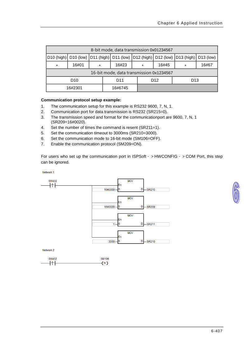
Chapter 6 Appl ied Instruc t ion
6-407
8-bit mode, data transmission 0x01234567
D10 (high) D10 (low) D11 (high) D11 (low) D12 (high) D12 (low) D13 (high) D13 (low)
* 16#01 * 16#23 * 16#45 * 16#67
16-bit mode, data transmission 0x1234567
D10 D11 D12 D13
16#2301 16#6745 Communication protocol setup example: 1. The communication setup for this example is RS232 9600, 7, N, 1. 2. Communication port for data transmission is RS232 (SR215=0). 3. The transmission speed and format for the communicationport are 9600, 7, N, 1
(SR209=16#0020). 4. Set the number of times the command is resent (SR211=1). 5. Set the communication timeout to 3000ms (SR210=3000). 6. Set the communication mode to 16-bit mode (SM106=OFF). 7. Enable the communication protocol (SM209=ON). For users who set up the communication port in ISPSoft->HWCONFIG->COM Port, this step can be ignored.

AH500 Programming Manual
6-408
Example: 1. Users can set up the PLC communication port in HWCONFIG or set values in the relative spcial
auxiliary relays to set up the communication (as the example stated). 2. Write the data which will be sent into the registers starting from D10, and then set SM96 to
ON. 3. When X0.1 and X0.3 are ON, the instruction RS is executed. The data in the n registers
starting from D10 is sent. After the sending of the data is complete, SM96 is reset to OFF automatically. (Please do not use the instruction RST to reset SM96.) If there is data which needs to be received, the data is stored in the registers starting from D100.
4. After the receiving of the data is complete, SM100 is ON. Besides, SM100 has to be reset to OFF after the data which has been received is processed. Please do not execute the instruction RST continuously.
5. If the command which the PLC receives includes a special character (SR621), I32 will be triggered. The value in D30 will increase by one.
The interrupt task (I32):
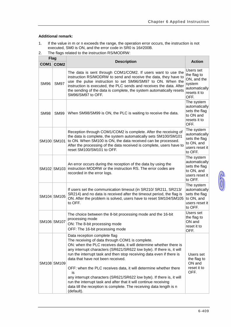
Chapter 6 Appl ied Instruc t ion
6-409
Additional remark:
1. If the value in m or n exceeds the range, the operation error occurs, the instruction is not executed, SM0 is ON, and the error code in SR0 is 16#200B.
2. The flags related to the instruction RS/MODRW: Flag
Description Action COM1 COM2
SM96 SM97
The data is sent through COM1/COM2. If users want to use the instruction RS/MODRW to send and receive the data, they have to use the pulse instruction to set SM96/SM97 to ON. When the instruction is executed, the PLC sends and receives the data. After the sending of the data is complete, the system automatically resets SM96/SM97 to OFF.
Users set the flag to ON, and the system automatically resets it to OFF.
SM98 SM99 When SM98/SM99 is ON, the PLC is waiting to receive the data.
The system automatically sets the flag to ON and resets it to OFF.
SM100 SM101
Reception through COM1/COM2 is complete. After the receiving of the data is complete, the system automatically sets SM100/SM101 to ON. When SM100 is ON, the data received can be processed. After the processing of the data received is complete, users have to reset SM100/SM101 to OFF.
The system automatically sets the flag to ON, and users reset it to OFF.
SM102 SM103 An error occurs during the reception of the data by using the instruction MODRW or the instruction RS. The error codes are recorded in the error logs.
The system automatically sets the flag to ON, and users reset it to OFF.
SM104 SM105
If users set the communication timeout (in SR210/ SR211, SR213/ SR214) and no data is received after the timeout period, the flag is ON. After the problem is solved, users have to reset SM104/SM105 to OFF.
The system automatically sets the flag to ON, and users reset it to OFF.
SM106 SM107
The choice between the 8-bit processing mode and the 16-bit processing mode ON: The 8-bit processing mode OFF: The 16-bit processing mode
Users set the flag to ON and reset it to OFF.
SM108 SM109
Data reception complete flag The receiving of data through COM1 is complete. ON: when the PLC receives data, it will determine whether there is any interrupt characters (SR621/SR622 low byte). If there is, it will run the interrupt task and then stop receiving data even if there is data that have not been received. OFF: when the PLC receives data, it will determine whether there
is any interrupt characters (SR621/SR622 low byte). If there is, it will run the interrupt task and after that it will continue receiving data till the reception is complete. The receiving data length is n (default).
Users set the flag to ON and reset it to OFF.
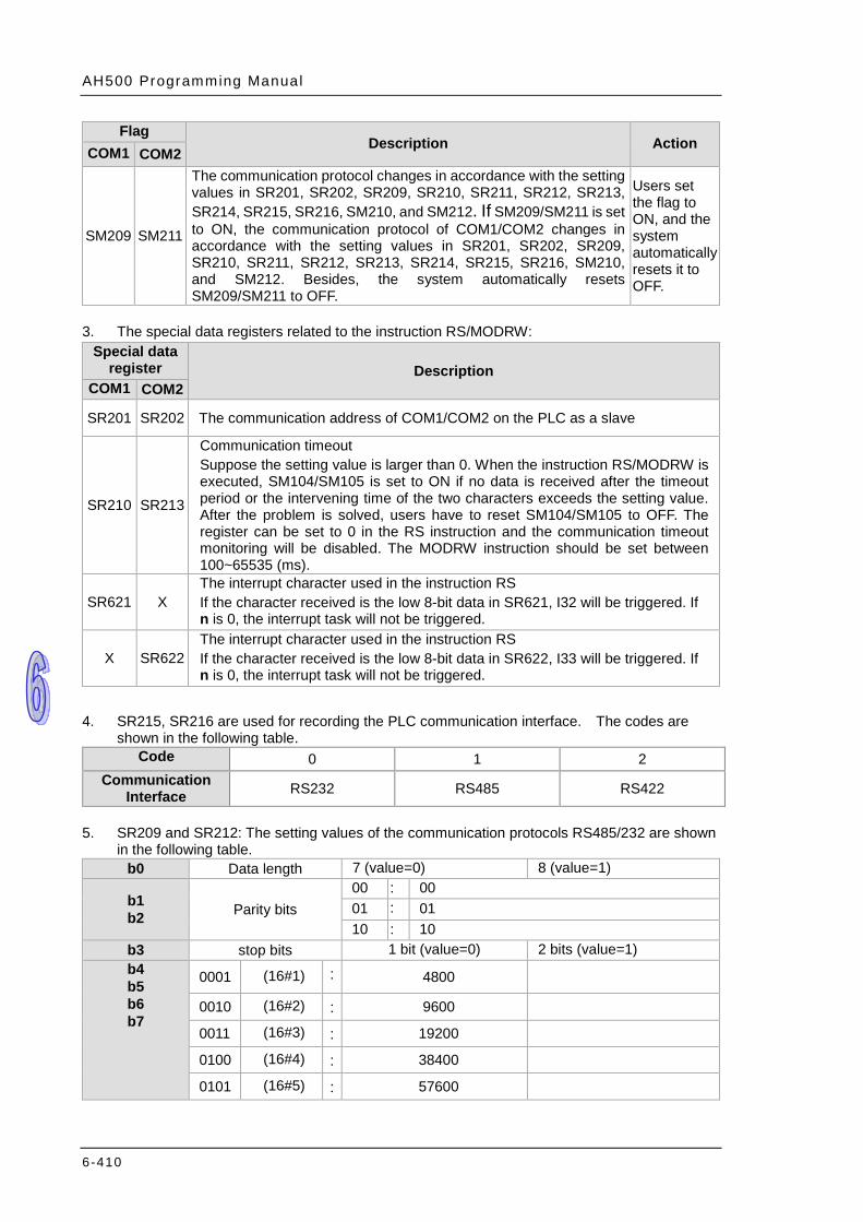
AH500 Programming Manual
6-410
Flag Description Action COM1 COM2
SM209 SM211
The communication protocol changes in accordance with the setting values in SR201, SR202, SR209, SR210, SR211, SR212, SR213, SR214, SR215, SR216, SM210, and SM212. If SM209/SM211 is set to ON, the communication protocol of COM1/COM2 changes in accordance with the setting values in SR201, SR202, SR209, SR210, SR211, SR212, SR213, SR214, SR215, SR216, SM210, and SM212. Besides, the system automatically resets SM209/SM211 to OFF.
Users set the flag to ON, and the system automatically resets it to OFF.
3. The special data registers related to the instruction RS/MODRW:
Special data register Description
COM1 COM2
SR201 SR202 The communication address of COM1/COM2 on the PLC as a slave
SR210 SR213
Communication timeout Suppose the setting value is larger than 0. When the instruction RS/MODRW is executed, SM104/SM105 is set to ON if no data is received after the timeout period or the intervening time of the two characters exceeds the setting value. After the problem is solved, users have to reset SM104/SM105 to OFF. The register can be set to 0 in the RS instruction and the communication timeout monitoring will be disabled. The MODRW instruction should be set between 100~65535 (ms).
SR621 X The interrupt character used in the instruction RS If the character received is the low 8-bit data in SR621, I32 will be triggered. If n is 0, the interrupt task will not be triggered.
X SR622 The interrupt character used in the instruction RS If the character received is the low 8-bit data in SR622, I33 will be triggered. If n is 0, the interrupt task will not be triggered.
4. SR215, SR216 are used for recording the PLC communication interface. The codes are
shown in the following table. Code 0 1 2
Communication Interface RS232 RS485 RS422
5. SR209 and SR212: The setting values of the communication protocols RS485/232 are shown
in the following table. b0 Data length 7 (value=0) 8 (value=1)
b1 b2 Parity bits
00 : 00 01 : 01 10 : 10
b3 stop bits 1 bit (value=0) 2 bits (value=1) b4 b5 b6 b7
0001 (16#1) : 4800
0010 (16#2) : 9600
0011 (16#3) : 19200
0100 (16#4) : 38400
0101 (16#5) : 57600

Chapter 6 Appl ied Instruc t ion
6-411
0110 (16#6) : 115200
0111 (16#7) : 230400 RS-232 does not support the baud rate.
1000 (16#8) : 460800 RS-232 does not support the baud rate.
1001 (16#9) : 921600 RS-232 does not support the baud rate.
b8~b15 Undefined (reserved) 6. The data transmission speed is as follows.
Baud rate (bps) RTU timeout timer (ms) Baud rate (bps) RTU timeout timer (ms) 4800 9 115200 1 9600 5 230400 1
19200 3 460800 1 38400 2 921600 1 57600 1

AH500 Programming Manual
6-412
API Instruction code Operand Function
1801 FWD S1, S2, n The AC motor drive runs clockwise.
Device X Y M S T C HC D L SM SR E PR K 16# “$” DF
S1 S2 n
Pulse instruction 16-bit instruction
(7 steps) 32-bit instruction
- AH500 -
Symbol:
S1 : Unit address Word
S2 : Operation frequency of the AC motor drives Word
n : Mode Word
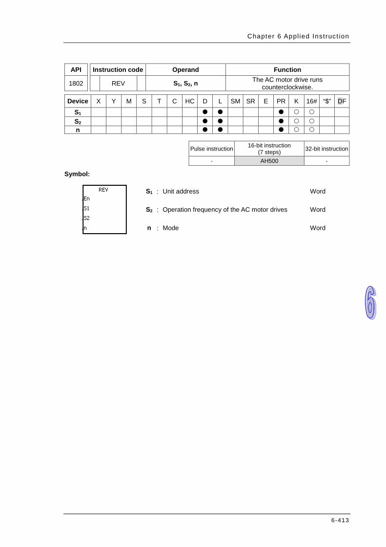
Chapter 6 Appl ied Instruc t ion
6-413
API Instruction code Operand Function
1802 REV S1, S2, n The AC motor drive runs counterclockwise.
Device X Y M S T C HC D L SM SR E PR K 16# “$” DF
S1 S2 n
Pulse instruction 16-bit instruction
(7 steps) 32-bit instruction
- AH500 -
Symbol:
S1 : Unit address Word
S2 : Operation frequency of the AC motor drives Word
n : Mode Word
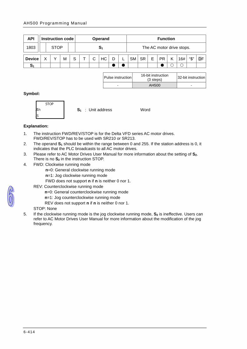
AH500 Programming Manual
6-414
API Instruction code Operand Function
1803 STOP S1 The AC motor drive stops.
Device X Y M S T C HC D L SM SR E PR K 16# “$” DF
S1
Pulse instruction 16-bit instruction (3 steps) 32-bit instruction
- AH500 -
Symbol:
S1 : Unit address Word
Explanation:
1. The instruction FWD/REV/STOP is for the Delta VFD series AC motor drives. FWD/REV/STOP has to be used with SR210 or SR213.
2. The operand S1 should be within the range between 0 and 255. If the station address is 0, it indicates that the PLC broadcasts to all AC motor drives.
3. Please refer to AC Motor Drives User Manual for more information about the setting of S2. There is no S2 in the instruction STOP.
4. FWD: Clockwise running mode n=0: General clockwise running mode n=1: Jog clockwise running mode FWD does not support n if n is neither 0 nor 1.
REV: Counterclockwise running mode n=0: General counterclockwise running mode n=1: Jog counterclockwise running mode REV does not support n if n is neither 0 nor 1.
STOP: None 5. If the clockwise running mode is the jog clockwise running mode, S2 is ineffective. Users can
refer to AC Motor Drives User Manual for more information about the modification of the jog frequency.
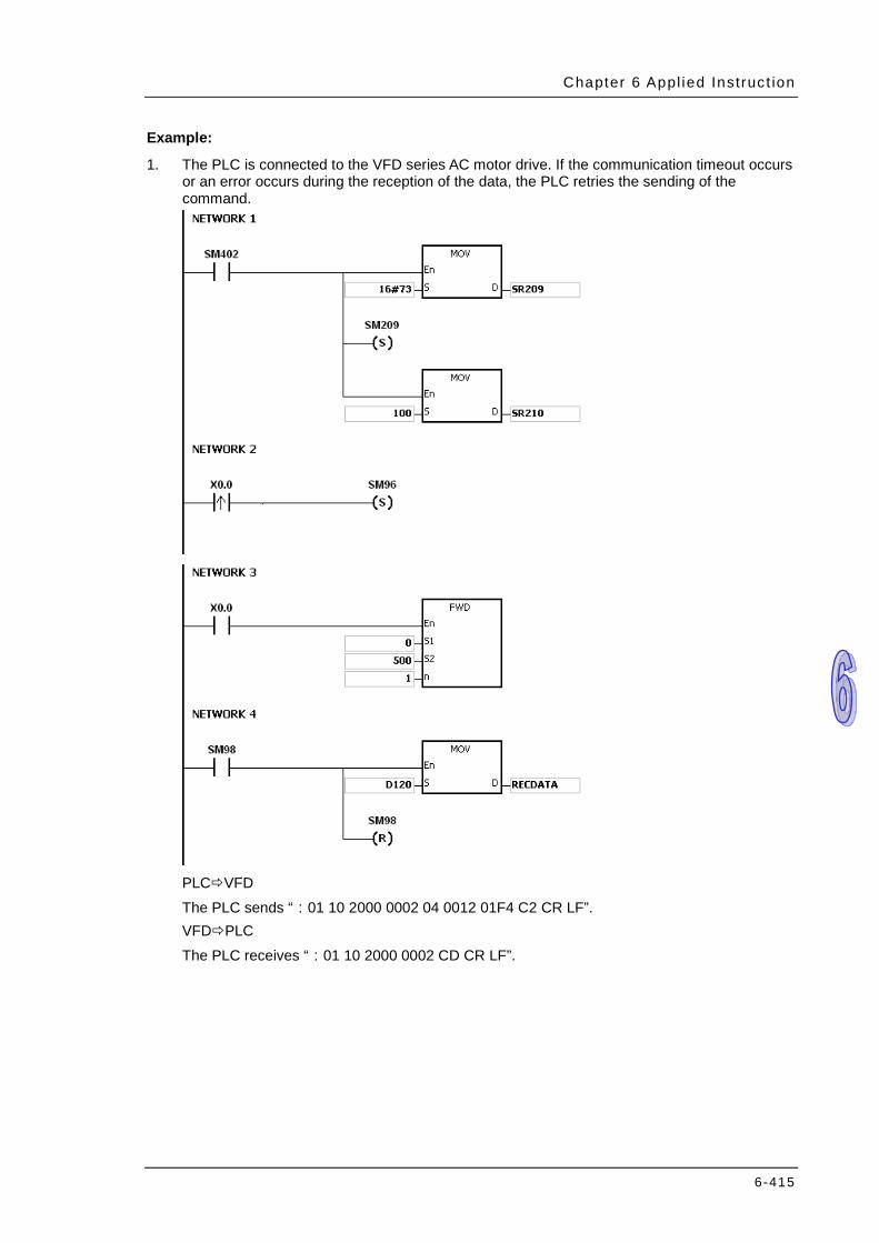
Chapter 6 Appl ied Instruc t ion
6-415
Example:
1. The PLC is connected to the VFD series AC motor drive. If the communication timeout occurs or an error occurs during the reception of the data, the PLC retries the sending of the command.
PLCVFD The PLC sends “:01 10 2000 0002 04 0012 01F4 C2 CR LF”. VFDPLC The PLC receives “:01 10 2000 0002 CD CR LF”.
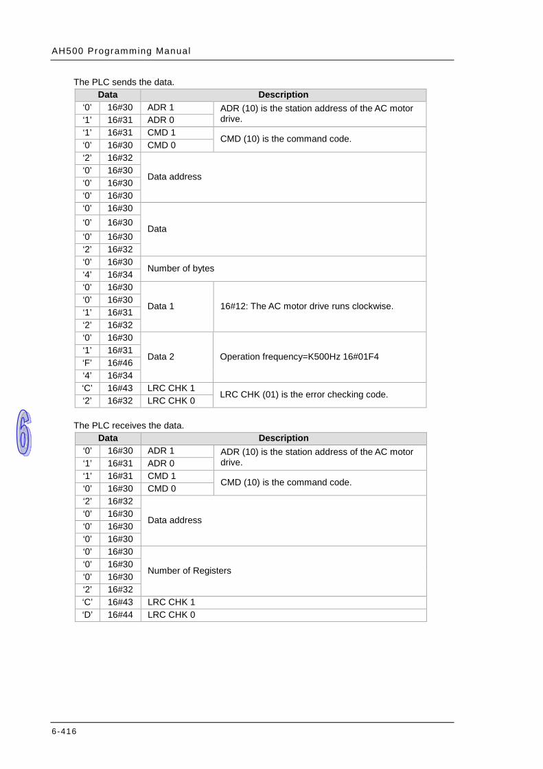
AH500 Programming Manual
6-416
The PLC sends the data. Data Description
‘0’ 16#30 ADR 1 ADR (10) is the station address of the AC motor drive. ‘1’ 16#31 ADR 0
‘1’ 16#31 CMD 1 CMD (10) is the command code.
‘0’ 16#30 CMD 0 ‘2’ 16#32
Data address ‘0’ 16#30 ‘0’ 16#30 ‘0’ 16#30 ‘0’ 16#30
Data ‘0’ 16#30 ‘0’ 16#30 ‘2’ 16#32 ‘0’ 16#30
Number of bytes ‘4’ 16#34 ‘0’ 16#30
Data 1 16#12: The AC motor drive runs clockwise. ‘0’ 16#30 ‘1’ 16#31 ‘2’ 16#32 ‘0’ 16#30
Data 2 Operation frequency=K500Hz 16#01F4 ‘1’ 16#31 ‘F’ 16#46 ‘4’ 16#34 ‘C’ 16#43 LRC CHK 1
LRC CHK (01) is the error checking code. ‘2’ 16#32 LRC CHK 0
The PLC receives the data.
Data Description ‘0’ 16#30 ADR 1 ADR (10) is the station address of the AC motor
drive. ‘1’ 16#31 ADR 0 ‘1’ 16#31 CMD 1
CMD (10) is the command code. ‘0’ 16#30 CMD 0 ‘2’ 16#32
Data address ‘0’ 16#30 ‘0’ 16#30 ‘0’ 16#30 ‘0’ 16#30
Number of Registers ‘0’ 16#30 ‘0’ 16#30 ‘2’ 16#32 ‘C’ 16#43 LRC CHK 1 ‘D’ 16#44 LRC CHK 0
Chapter 6 Appl ied Instruc t ion
6-417
Additional remark:
1. Please refer to the additional remark on the instruction RS for more information about the related flags and the special registers.
2. The instructions FWD, REV, STOP, RDST, and RSTEF can be used several times in the program, but one instruction is executed at a time.
3. If the value in S1 exceeds the range, the instruction is not executed, SM0 is ON, and the error code in SR0 is 16#2003.
4. If n exceeds the range, the instruction is not executed, SM0 is ON, and the error code in SR0 is 16#200B.
5. The instructions FWD, REV, STOP, RDST, and RSTEF are consistent with the MODBUS communication format.
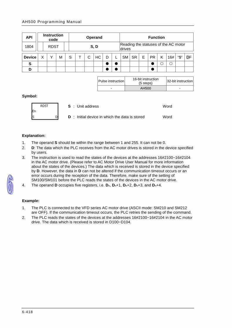
AH500 Programming Manual
6-418
API Instruction code Operand Function
1804 RDST S, D Reading the statuses of the AC motor drives
Device X Y M S T C HC D L SM SR E PR K 16# “$” DF
S D
Pulse instruction 16-bit instruction
(5 steps) 32-bit instruction
- AH500 -
Symbol:
S : Unit address Word
D : Initial device in which the data is stored Word
Explanation:
1. The operand S should be within the range between 1 and 255. It can not be 0. 2. D: The data which the PLC receives from the AC motor drives is stored in the device specified
by users. 3. The instruction is used to read the states of the devices at the addresses 16#2100~16#2104
in the AC motor drive. (Please refer to AC Motor Drive User Manual for more information about the states of the devices.) The data which is received is stored in the device specified by D. However, the data in D can not be altered if the communication timeout occurs or an error occurs during the reception of the data. Therefore, make sure of the setting of SM100/SM101 before the PLC reads the states of the devices in the AC motor drive.
4. The operand D occupies five registers, i.e. Dn, Dn+1, Dn+2, Dn+3, and Dn+4.
Example:
1. The PLC is connected to the VFD series AC motor drive (ASCII mode: SM210 and SM212 are OFF). If the communication timeout occurs, the PLC retries the sending of the command.
2. The PLC reads the states of the devices at the addresses 16#2100~16#2104 in the AC motor drive. The data which is received is stored in D100~D104.
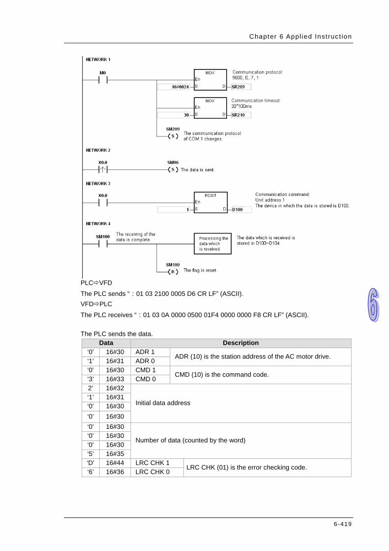
Chapter 6 Appl ied Instruc t ion
6-419
PLCVFD The PLC sends “:01 03 2100 0005 D6 CR LF” (ASCII). VFDPLC The PLC receives “:01 03 0A 0000 0500 01F4 0000 0000 F8 CR LF” (ASCII). The PLC sends the data.
Data Description ‘0’ 16#30 ADR 1
ADR (10) is the station address of the AC motor drive. ‘1’ 16#31 ADR 0 ‘0’ 16#30 CMD 1
CMD (10) is the command code. ‘3’ 16#33 CMD 0 2’ 16#32
Initial data address ‘1’ 16#31 ‘0’ 16#30 ‘0’ 16#30 ‘0’ 16#30
Number of data (counted by the word) ‘0’ 16#30 ‘0’ 16#30 ‘5’ 16#35 ‘D’ 16#44 LRC CHK 1
LRC CHK (01) is the error checking code. ‘6’ 16#36 LRC CHK 0
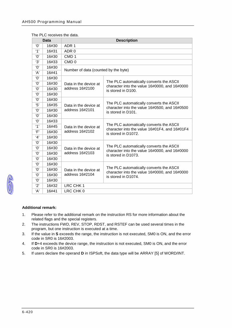
AH500 Programming Manual
6-420
The PLC receives the data. Data Description
‘0’ 16#30 ADR 1 ‘1’ 16#31 ADR 0 ‘0’ 16#30 CMD 1 ‘3’ 16#33 CMD 0 ‘0’ 16#30
Number of data (counted by the byte) ‘A’ 16#41 ‘0’ 16#30
Data in the device at address 16#2100
The PLC automatically converts the ASCII character into the value 16#0000, and 16#0000 is stored in D100.
‘0’ 16#30 ‘0’ 16#30 ‘0’ 16#30 ‘0’ 16#30
Data in the device at address 16#2101
The PLC automatically converts the ASCII character into the value 16#0500, and 16#0500 is stored in D101.
‘5’ 16#35 ‘0’ 16#30 ‘0’ 16#30 ‘0’ 16#33
Data in the device at address 16#2102
The PLC automatically converts the ASCII character into the value 16#01F4, and 16#01F4 is stored in D1072.
‘1’ 16#45 ‘F’ 16#30 ‘4’ 16#30 ‘0’ 16#30
Data in the device at address 16#2103
The PLC automatically converts the ASCII character into the value 16#0000, and 16#0000 is stored in D1073.
‘0’ 16#30 ‘0’ 16#30 ‘0’ 16#30 ‘0’ 16#30
Data in the device at address 16#2104
The PLC automatically converts the ASCII character into the value 16#0000, and 16#0000 is stored in D1074.
‘0’ 16#30 ‘0’ 16#30 ‘0’ 16#30 ‘2’ 16#32 LRC CHK 1 ‘A’ 16#41 LRC CHK 0
Additional remark:
1. Please refer to the additional remark on the instruction RS for more information about the related flags and the special registers.
2. The instructions FWD, REV, STOP, RDST, and RSTEF can be used several times in the program, but one instruction is executed at a time.
3. If the value in S exceeds the range, the instruction is not executed, SM0 is ON, and the error code in SR0 is 16#2003.
4. If D+4 exceeds the device range, the instruction is not executed, SM0 is ON, and the error code in SR0 is 16#2003.
5. If users declare the operand D in ISPSoft, the data type will be ARRAY [5] of WORD/INT.
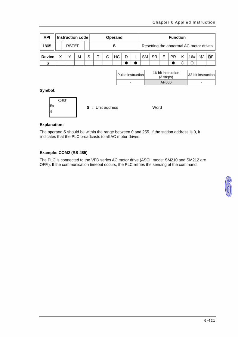
Chapter 6 Appl ied Instruc t ion
6-421
API Instruction code Operand Function
1805 RSTEF S Resetting the abnormal AC motor drives
Device X Y M S T C HC D L SM SR E PR K 16# “$” DF
S
Pulse instruction 16-bit instruction (3 steps) 32-bit instruction
- AH500 -
Symbol:
S : Unit address Word
Explanation:
The operand S should be within the range between 0 and 255. If the station address is 0, it indicates that the PLC broadcasts to all AC motor drives.
Example: COM2 (RS-485)
The PLC is connected to the VFD series AC motor drive (ASCII mode: SM210 and SM212 are OFF.). If the communication timeout occurs, the PLC retries the sending of the command.
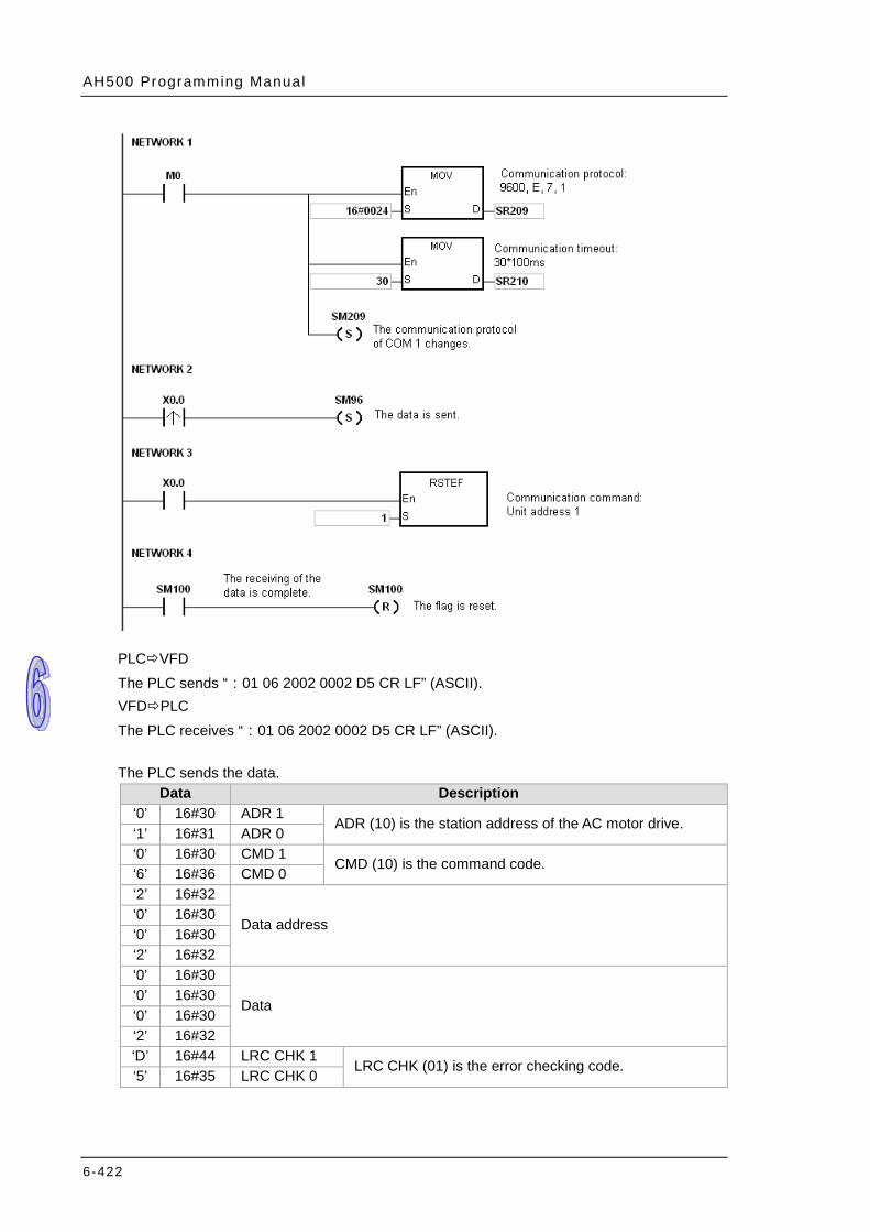
AH500 Programming Manual
6-422
PLCVFD The PLC sends “:01 06 2002 0002 D5 CR LF” (ASCII). VFDPLC The PLC receives “:01 06 2002 0002 D5 CR LF” (ASCII). The PLC sends the data.
Data Description ‘0’ 16#30 ADR 1
ADR (10) is the station address of the AC motor drive. ‘1’ 16#31 ADR 0 ‘0’ 16#30 CMD 1
CMD (10) is the command code. ‘6’ 16#36 CMD 0 ‘2’ 16#32
Data address ‘0’ 16#30 ‘0’ 16#30 ‘2’ 16#32 ‘0’ 16#30
Data ‘0’ 16#30 ‘0’ 16#30 ‘2’ 16#32 ‘D’ 16#44 LRC CHK 1
LRC CHK (01) is the error checking code. ‘5’ 16#35 LRC CHK 0
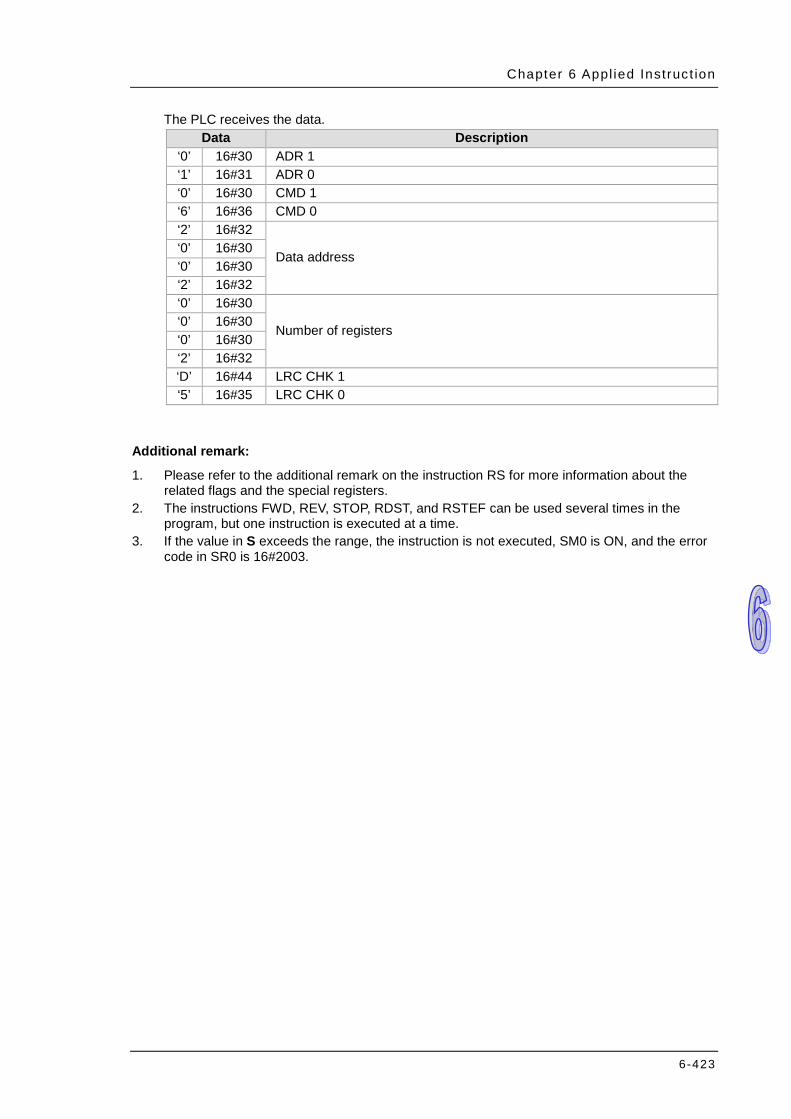
Chapter 6 Appl ied Instruc t ion
6-423
The PLC receives the data. Data Description
‘0’ 16#30 ADR 1 ‘1’ 16#31 ADR 0 ‘0’ 16#30 CMD 1 ‘6’ 16#36 CMD 0 ‘2’ 16#32
Data address ‘0’ 16#30 ‘0’ 16#30 ‘2’ 16#32 ‘0’ 16#30
Number of registers ‘0’ 16#30 ‘0’ 16#30 ‘2’ 16#32 ‘D’ 16#44 LRC CHK 1 ‘5’ 16#35 LRC CHK 0
Additional remark:
1. Please refer to the additional remark on the instruction RS for more information about the related flags and the special registers.
2. The instructions FWD, REV, STOP, RDST, and RSTEF can be used several times in the program, but one instruction is executed at a time.
3. If the value in S exceeds the range, the instruction is not executed, SM0 is ON, and the error code in SR0 is 16#2003.

AH500 Programming Manual
6-424
API Instruction code Operand Function
1806 LRC S, n, D Longitudinal parity check
Device X Y M S T C HC D L SM SR E PR K 16# “$” DF
S n D
Pulse instruction 16-bit instruction
(7 steps) 32-bit instruction
- AH500 -
Symbol:
S : Initial device to which the LRC is applied Word
n : Number of bytes Word
D : Initial device in which the operation result is stored Word
Explanation:
1. Please refer to the additional remark on the instruction LRC for more information about the LRC check code.
2. The operand n should be an even number, and should be within the range between 1 and 1000. If n is not within the range, the operation error occurs, the instruction is not executed, SM0 and SM1 are ON, and the error code in SR0 is 16#200B.
3. The 16-bit conversion mode: When SM606 is OFF, the hexadecimal data in the device specified by S is divided into the high 8-bit data and the low 8-bit data. The LRC is applied to every byte, and the operation result is stored in the high 8-bit and the low 8-bit in the device specified by D. The number of bytes depends on n.
4. The 8-bit conversion mode: When SM606 is ON, the hexadecimal data in the device specified by S is divided into the high 8-bit data (invalid data) and the low 8-bit data. The LRC is applied to every byte, and the operation result is stored in the low 8-bit in the two registers. The number of bytes depends on n. (The values of the high 8 bits in the two registers are 0.)
Example:
1. The PLC is connected to the VFD-S series AC motor drive (ASCII mode: SM210 is OFF; 8-bit mode: SM606 is ON.). The PLC sends the command, and reads the data in the six devices at the addresses starting from 16#2101 in the VFD-S series AC motor drive. PLCVFD-S The PLC sends “:01 03 2101 0006 D4 CR LF”.
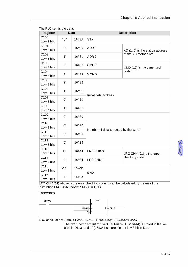
Chapter 6 Appl ied Instruc t ion
6-425
The PLC sends the data. Register Data Description
D100 Low 8 bits ‘:’ 16#3A STX
D101 Low 8 bits ‘0’ 16#30 ADR 1
AD (1, 0) is the station address of the AC motor drive. D102
Low 8 bits ‘1’ 16#31 ADR 0
D103 Low 8 bits ‘0’ 16#30 CMD 1
CMD (10) is the command code. D104
Low 8 bits ‘3’ 16#33 CMD 0
D105 Low 8 bits ‘2’ 16#32
Initial data address
D106 Low 8 bits ‘1’ 16#31
D107 Low 8 bits ‘0’ 16#30
D108 Low 8 bits ‘1’ 16#31
D109 Low 8 bits ‘0’ 16#30
Number of data (counted by the word)
D110 Low 8 bits ‘0’ 16#30
D111 Low 8 bits ‘0’ 16#30
D112 Low 8 bits ‘6’ 16#36
D113 Low 8 bits ‘D’ 16#44 LRC CHK 0
LRC CHK (01) is the error checking code. D114
Low 8 bits ‘4’ 16#34 LRC CHK 1
D115 Low 8 bits CR 16#0D
END D116 Low 8 bits LF 16#0A
LRC CHK (01) above is the error checking code. It can be calculated by means of the instruction LRC. (8-bit mode: SM606 is ON.)
LRC check code: 16#01+16#03+16#21+16#01+16#00+16#06=16#2C
The two’s complement of 16#2C is 16#D4. ‘D’ (16#44) is stored in the low 8-bit in D113, and ‘4’ (16#34) is stored in the low 8-bit in D114.

AH500 Programming Manual
6-426
Additional remark:
1. The format of the communication data in the ASCII mode: STX ‘:’ The start-of-text character is ‘:’ (16#3A). Address Hi ‘ 0 ’ Communication address:
The 8-bit address is composed of two ASCII codes. Address Lo ‘ 1 ’ Function Hi ‘ 0 ’ Function code:
The 8-bit function code is composed of two ASCII codes. Function Lo ‘ 3 ’
DATA (n-1) ……. DATA 0
‘ 2 ’
Data: The n×8-bit data is composed of 2n ASCII codes.
‘ 1 ’ ‘ 0 ’ ‘ 2 ’ ‘ 0 ’ ‘ 0 ’ ‘ 0 ’ ‘ 2 ’
LRC CHK Hi ‘ D ’ LRC check code: The 8-bit check code is composed of two ASCII codes. LRC CHK Lo ‘ 7 ’
END Hi CR End-of-text character: END Hi=CR(16#0D),END Lo=LF(16#0A) END Lo LF
2. LRC check code: The values starting from the communication address to the data are added up. The two’s complement of the sum gotten is the LRC check code. Example: 16#01+16#03+16#21+16#02+16#00+16#02=16#29 The two’s complement of 16#29 is 16#D7.
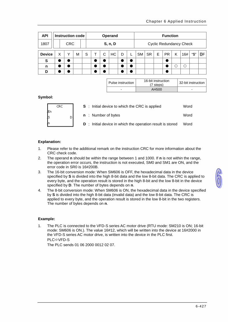
Chapter 6 Appl ied Instruc t ion
6-427
API Instruction code Operand Function
1807 CRC S, n, D Cyclic Redundancy Check
Device X Y M S T C HC D L SM SR E PR K 16# “$” DF
S n D
Pulse instruction 16-bit instruction
(7 steps) 32-bit instruction
- AH500 -
Symbol:
S : Initial device to which the CRC is applied Word
n : Number of bytes Word
D : Initial device in which the operation result is stored Word
Explanation:
1. Please refer to the additional remark on the instruction CRC for more information about the CRC check code.
2. The operand n should be within the range between 1 and 1000. If n is not within the range, the operation error occurs, the instruction is not executed, SM0 and SM1 are ON, and the error code in SR0 is 16#200B.
3. The 16-bit conversion mode: When SM606 is OFF, the hexadecimal data in the device specified by S is divided into the high 8-bit data and the low 8-bit data. The CRC is applied to every byte, and the operation result is stored in the high 8-bit and the low 8-bit in the device specified by D. The number of bytes depends on n.
4. The 8-bit conversion mode: When SM606 is ON, the hexadecimal data in the device specified by S is divided into the high 8-bit data (invalid data) and the low 8-bit data. The CRC is applied to every byte, and the operation result is stored in the low 8-bit in the two registers. The number of bytes depends on n.
Example:
1. The PLC is connected to the VFD-S series AC motor drive (RTU mode: SM210 is ON; 16-bit mode: SM606 is ON.). The value 16#12, which will be written into the device at 16#2000 in the VFD-S series AC motor drive, is written into the device in the PLC first. PLCVFD-S The PLC sends 01 06 2000 0012 02 07.
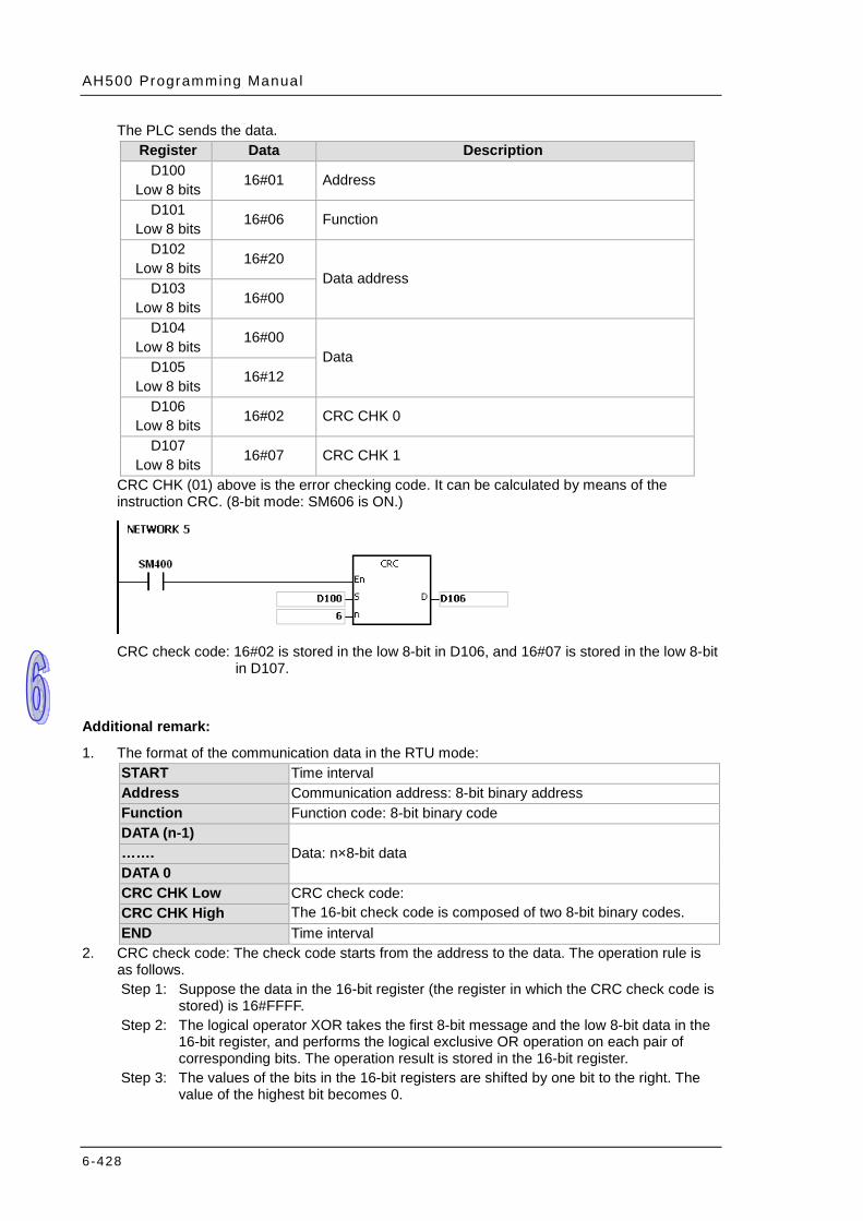
AH500 Programming Manual
6-428
The PLC sends the data. Register Data Description
D100 Low 8 bits 16#01 Address
D101 Low 8 bits 16#06 Function
D102 Low 8 bits 16#20
Data address D103
Low 8 bits 16#00
D104 Low 8 bits 16#00
Data D105
Low 8 bits 16#12
D106 Low 8 bits 16#02 CRC CHK 0
D107 Low 8 bits 16#07 CRC CHK 1
CRC CHK (01) above is the error checking code. It can be calculated by means of the instruction CRC. (8-bit mode: SM606 is ON.)
CRC check code: 16#02 is stored in the low 8-bit in D106, and 16#07 is stored in the low 8-bit
in D107.
Additional remark:
1. The format of the communication data in the RTU mode: START Time interval Address Communication address: 8-bit binary address Function Function code: 8-bit binary code DATA (n-1)
Data: n×8-bit data ……. DATA 0 CRC CHK Low CRC check code:
The 16-bit check code is composed of two 8-bit binary codes. CRC CHK High END Time interval
2. CRC check code: The check code starts from the address to the data. The operation rule is as follows. Step 1: Suppose the data in the 16-bit register (the register in which the CRC check code is
stored) is 16#FFFF. Step 2: The logical operator XOR takes the first 8-bit message and the low 8-bit data in the
16-bit register, and performs the logical exclusive OR operation on each pair of corresponding bits. The operation result is stored in the 16-bit register.
Step 3: The values of the bits in the 16-bit registers are shifted by one bit to the right. The value of the highest bit becomes 0.
Chapter 6 Appl ied Instruc t ion
6-429
Step 4: If the value of the right-most bit which is shifted to the right is 0, the data gotten from step 3 is stored in the 16-bit register. Otherwise, the logical operator XOR takes 16#A001 and the data in the 16-bit register, and performs the logical exclusive OR operation on each pair of corresponding bits. The operation result is stored in the 16-bit register.
Step 5: Repeat step 3 and step 4, and perform the operation on the 8-bit message. Step 6: Repeat step 2~step 5, and get the next 8-bit message. Perform the operations on all
messages. The final result in the 16-bit register is the CRC check code. Notice that the low 8-bit data in the 16-bit register is interchanged with the high 8-bit data in the 16-bit register before the CRC check code is put into the check code of the message
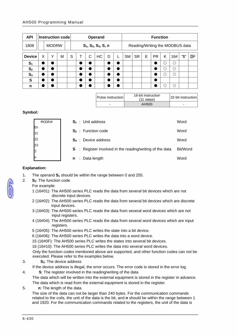
AH500 Programming Manual
6-430
API Instruction code Operand Function
1808 MODRW S1, S2, S3, S, n Reading/Writing the MODBUS data
Device X Y M S T C HC D L SM SR E PR K 16# “$” DF
S1 S2 S3 S n
Pulse instruction 16-bit instruction
(11 steps) 32-bit instruction
- AH500 -
Symbol:
S1 : Unit address Word
S2 : Function code Word
S3 : Device address Word
S : Register involved in the reading/writing of the data Bit/Word
n : Data length Word
Explanation:
1. The operand S1 should be within the range between 0 and 255. 2. S2: The function code
For example: 1 (16#01): The AH500 series PLC reads the data from several bit devices which are not
discrete input devices. 2 (16#02): The AH500 series PLC reads the data from several bit devices which are discrete
input devices. 3 (16#03): The AH500 series PLC reads the data from several word devices which are not
input registers. 4 (16#04): The AH500 series PLC reads the data from several word devices which are input
registers. 5 (16#05): The AH500 series PLC writes the state into a bit device. 6 (16#06): The AH500 series PLC writes the data into a word device. 15 (16#0F): The AH500 series PLC writes the states into several bit devices. 16 (16#10): The AH500 series PLC writes the data into several word devices. Only the function codes mentioned above are supported, and other function codes can not be executed. Please refer to the examples below.
3. S3: The device address If the device address is illegal, the error occurs. The error code is stored in the error log.
4. S: The register involved in the reading/writing of the data The data which will be written into the external equipment is stored in the register in advance. The data which is read from the external equipment is stored in the register.
5. n: The length of the data The size of the data can not be larger than 240 bytes. For the communication commands related to the coils, the unit of the data is the bit, and n should be within the range between 1 and 1920. For the communication commands related to the registers, the unit of the data is
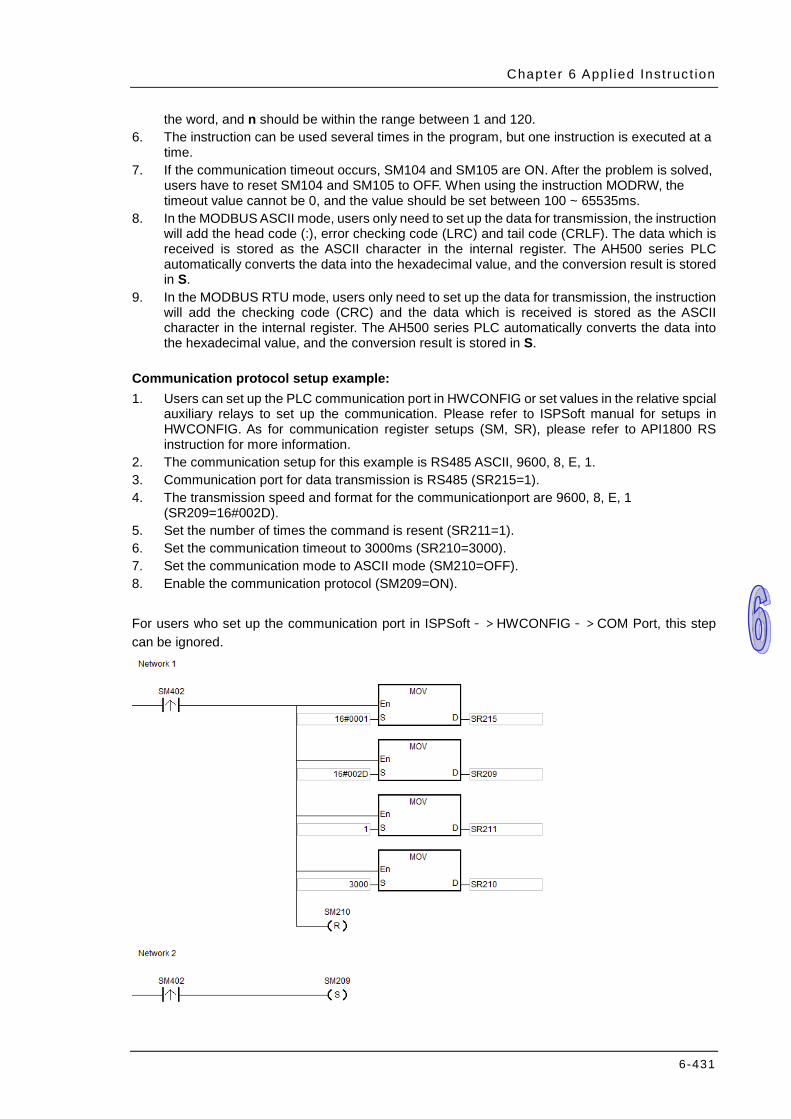
Chapter 6 Appl ied Instruc t ion
6-431
the word, and n should be within the range between 1 and 120. 6. The instruction can be used several times in the program, but one instruction is executed at a
time. 7. If the communication timeout occurs, SM104 and SM105 are ON. After the problem is solved,
users have to reset SM104 and SM105 to OFF. When using the instruction MODRW, the timeout value cannot be 0, and the value should be set between 100 ~ 65535ms.
8. In the MODBUS ASCII mode, users only need to set up the data for transmission, the instruction will add the head code (:), error checking code (LRC) and tail code (CRLF). The data which is received is stored as the ASCII character in the internal register. The AH500 series PLC automatically converts the data into the hexadecimal value, and the conversion result is stored in S.
9. In the MODBUS RTU mode, users only need to set up the data for transmission, the instruction will add the checking code (CRC) and the data which is received is stored as the ASCII character in the internal register. The AH500 series PLC automatically converts the data into the hexadecimal value, and the conversion result is stored in S.
Communication protocol setup example: 1. Users can set up the PLC communication port in HWCONFIG or set values in the relative spcial
auxiliary relays to set up the communication. Please refer to ISPSoft manual for setups in HWCONFIG. As for communication register setups (SM, SR), please refer to API1800 RS instruction for more information.
2. The communication setup for this example is RS485 ASCII, 9600, 8, E, 1. 3. Communication port for data transmission is RS485 (SR215=1). 4. The transmission speed and format for the communicationport are 9600, 8, E, 1
(SR209=16#002D). 5. Set the number of times the command is resent (SR211=1). 6. Set the communication timeout to 3000ms (SR210=3000). 7. Set the communication mode to ASCII mode (SM210=OFF). 8. Enable the communication protocol (SM209=ON). For users who set up the communication port in ISPSoft->HWCONFIG->COM Port, this step can be ignored.

AH500 Programming Manual
6-432
Example 1:
1. Function code 01 (16#01): The AH500 series PLC reads the data from several bit devices which are not discrete input devices. (16 peiece of data is read in this example.)
2. AH500 series is connected to the DVP-ES2 series PLC. ASCII Mode: The AH500 series PLC is connected to the DVP-ES2series PLC. When SM96 and X0.0 are on, the AH500 series PLC sends and receives the Y0~Y15 (Y0 address is 16#0500) commands from DVP-ES2.
3. The data which the AH500 series PLC receives from the DVP-ES2 series PLC is stored in D10.0~D10.15.
4. After the reception of data is complete, it will check the data format of what have been sent from the DVP-ES2 series PLC. If the format is correct, SM100 will be ON, and if not, SM102 will be ON.
Example 2:
1. Function code 03 (16#03): The AH500 series PLC reads the data from several bit devices which are not discrete input devices. (8 peiece of data is read in this example.)
2. AH500 series is connected to the DVP-ES2 series PLC. ASCII Mode: The AH500 series PLC is connected to the DVP-ES2series PLC. When SM96 and X0.0 are on, the AH500 series PLC sends and receives the D20~D27 (D20 address is 16#1020) commands from DVP-ES2.
3. The data which the AH500 series PLC receives from the DVP-ES2 series PLC is stored in D10~D17.
4. After the reception of data is complete, it will check the data format of what have been sent from the DVP-ES2 series PLC. If the format is correct, SM100 will be ON, and if not, SM102 will be ON.
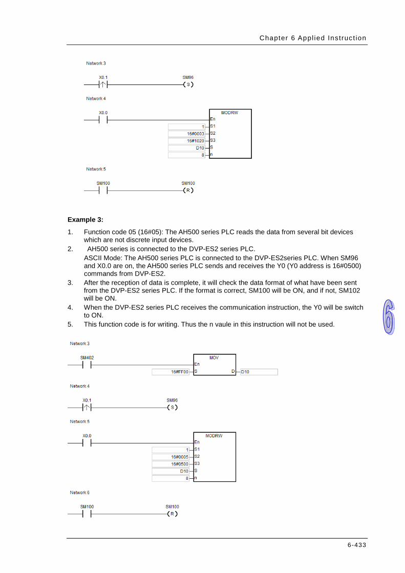
Chapter 6 Appl ied Instruc t ion
6-433
Example 3:
1. Function code 05 (16#05): The AH500 series PLC reads the data from several bit devices which are not discrete input devices.
2. AH500 series is connected to the DVP-ES2 series PLC. ASCII Mode: The AH500 series PLC is connected to the DVP-ES2series PLC. When SM96 and X0.0 are on, the AH500 series PLC sends and receives the Y0 (Y0 address is 16#0500) commands from DVP-ES2.
3. After the reception of data is complete, it will check the data format of what have been sent from the DVP-ES2 series PLC. If the format is correct, SM100 will be ON, and if not, SM102 will be ON.
4. When the DVP-ES2 series PLC receives the communication instruction, the Y0 will be switch to ON.
5. This function code is for writing. Thus the n vaule in this instruction will not be used.
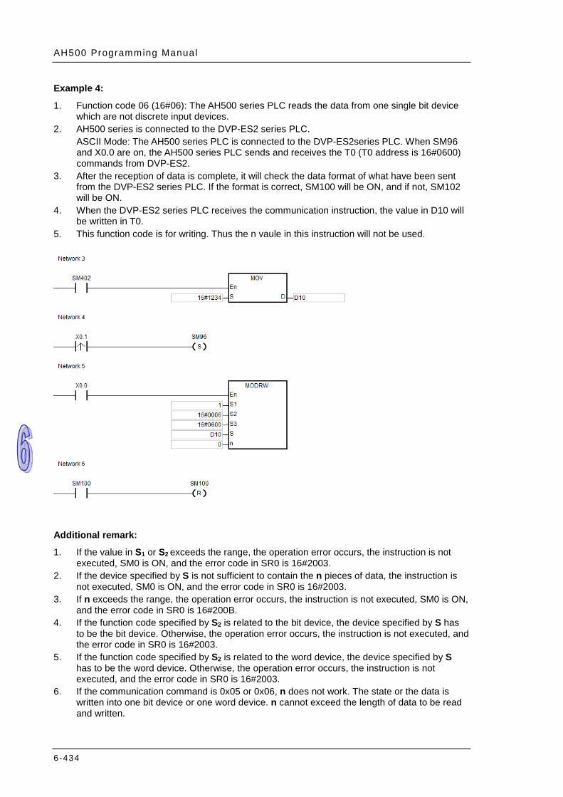
AH500 Programming Manual
6-434
Example 4:
1. Function code 06 (16#06): The AH500 series PLC reads the data from one single bit device which are not discrete input devices.
2. AH500 series is connected to the DVP-ES2 series PLC. ASCII Mode: The AH500 series PLC is connected to the DVP-ES2series PLC. When SM96 and X0.0 are on, the AH500 series PLC sends and receives the T0 (T0 address is 16#0600) commands from DVP-ES2.
3. After the reception of data is complete, it will check the data format of what have been sent from the DVP-ES2 series PLC. If the format is correct, SM100 will be ON, and if not, SM102 will be ON.
4. When the DVP-ES2 series PLC receives the communication instruction, the value in D10 will be written in T0.
5. This function code is for writing. Thus the n vaule in this instruction will not be used.
Additional remark:
1. If the value in S1 or S2 exceeds the range, the operation error occurs, the instruction is not executed, SM0 is ON, and the error code in SR0 is 16#2003.
2. If the device specified by S is not sufficient to contain the n pieces of data, the instruction is not executed, SM0 is ON, and the error code in SR0 is 16#2003.
3. If n exceeds the range, the operation error occurs, the instruction is not executed, SM0 is ON, and the error code in SR0 is 16#200B.
4. If the function code specified by S2 is related to the bit device, the device specified by S has to be the bit device. Otherwise, the operation error occurs, the instruction is not executed, and the error code in SR0 is 16#2003.
5. If the function code specified by S2 is related to the word device, the device specified by S has to be the word device. Otherwise, the operation error occurs, the instruction is not executed, and the error code in SR0 is 16#2003.
6. If the communication command is 0x05 or 0x06, n does not work. The state or the data is written into one bit device or one word device. n cannot exceed the length of data to be read and written.
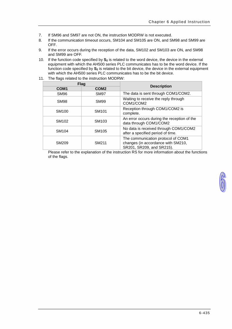
Chapter 6 Appl ied Instruc t ion
6-435
7. If SM96 and SM97 are not ON, the instruction MODRW is not executed. 8. If the communication timeout occurs, SM104 and SM105 are ON, and SM98 and SM99 are
OFF. 9. If the error occurs during the reception of the data, SM102 and SM103 are ON, and SM98
and SM99 are OFF. 10. If the function code specified by S2 is related to the word device, the device in the external
equipment with which the AH500 series PLC communicates has to be the word device. If the function code specified by S2 is related to the bit device, the device in the external equipment with which the AH500 series PLC communicates has to be the bit device.
11. The flags related to the instruction MODRW: Flag Description COM1 COM2
SM96 SM97 The data is sent through COM1/COM2.
SM98 SM99 Waiting to receive the reply through COM1/COM2
SM100 SM101 Reception through COM1/COM2 is complete.
SM102 SM103 An error occurs during the reception of the data through COM1/COM2
SM104 SM105 No data is received through COM1/COM2 after a specified period of time.
SM209 SM211 The communication protocol of COM1 changes (in accordance with SM210, SR201, SR209, and SR215).
Please refer to the explanation of the instruction RS for more information about the functions of the flags.
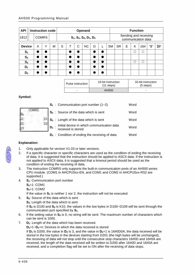
AH500 Programming Manual
6-436
API Instruction code Operand Function
1812 COMRS S1, S2, S3, D1, D2 Sending and receiving communication data
Device X Y M S T C HC D L SM SR E K 16# “$” DF
S1 S2
S3 D1
D2
Pulse instruction 16-bit instruction (11 steps)
32-bit instruction (5 steps)
- AH500 -
Symbol:
S1 : Communication port number (1~2) Word
S2 : Source of the data which is sent Word
S3 : Length of the data which is sent Word
D1 : Initial device in which communication data received is stored Word
D2 : Condition of ending the receiving of data Word
Explanation:
1. Only applicable for version V1.03 or later versions. 2. If a specific character or specific characters are used as the condition of ending the receiving
of data, it is suggested that the instruction should be applied to ASCII data. If the instruction is not applied to ASCII data, it is suggested that a timeout period should be used as the condition of ending the receiving of data.
3. The instruction COMRS only supports the built-in communication ports of an AH500 series CPU module. (COM1 in AHCPU5xx-EN, and COM1 and COM2 in AHCPU5xx-RS2 are supported.)
4. S1: Communication port number S1=1: COM1 S1=1: COM2 If the value in S1 is neither 1 nor 2, the instruction will not be executed.
5. S2: Source of the data which is sent S3: Length of the data which is sent If S2 is D100 and S3 is K10, the values in the low bytes in D100~D109 will be sent through the communication port specified by S1.
6. If the setting value in S3 is 0, no string will be sent. The maximum number of characters which can be sent is 1000.
7. D1: Length of the data which has been received. D1+1~D1+n: Devices in which the data received is stored If D1 is D200, the value in D2 is 3, and the value in D2+1 is 16#0D0A, the data received will be stored in the low bytes in the devices starting from D201 (the high bytes will be unchanged), the receiving of data will not stop until the consecutive stop characters 16#0D and 16#0A are received, the length of the data received will be written to D200 after 16#0D and 16#0A are received, and a completion flag will be set to ON after the receiving of data stops.
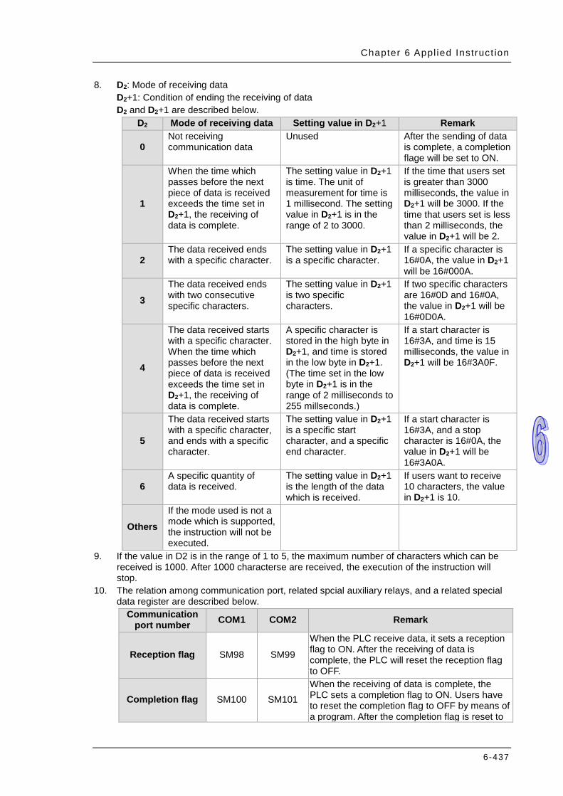
Chapter 6 Appl ied Instruc t ion
6-437
8. D2: Mode of receiving data D2+1: Condition of ending the receiving of data D2 and D2+1 are described below.
D2 Mode of receiving data Setting value in D2+1 Remark
0 Not receiving communication data
Unused After the sending of data is complete, a completion flage will be set to ON.
1
When the time which passes before the next piece of data is received exceeds the time set in D2+1, the receiving of data is complete.
The setting value in D2+1 is time. The unit of measurement for time is 1 millisecond. The setting value in D2+1 is in the range of 2 to 3000.
If the time that users set is greater than 3000 milliseconds, the value in D2+1 will be 3000. If the time that users set is less than 2 milliseconds, the value in D2+1 will be 2.
2 The data received ends with a specific character.
The setting value in D2+1 is a specific character.
If a specific character is 16#0A, the value in D2+1 will be 16#000A.
3 The data received ends with two consecutive specific characters.
The setting value in D2+1 is two specific characters.
If two specific characters are 16#0D and 16#0A, the value in D2+1 will be 16#0D0A.
4
The data received starts with a specific character. When the time which passes before the next piece of data is received exceeds the time set in D2+1, the receiving of data is complete.
A specific character is stored in the high byte in D2+1, and time is stored in the low byte in D2+1. (The time set in the low byte in D2+1 is in the range of 2 milliseconds to 255 millseconds.)
If a start character is 16#3A, and time is 15 milliseconds, the value in D2+1 will be 16#3A0F.
5
The data received starts with a specific character, and ends with a specific character.
The setting value in D2+1 is a specific start character, and a specific end character.
If a start character is 16#3A, and a stop character is 16#0A, the value in D2+1 will be 16#3A0A.
6 A specific quantity of data is received.
The setting value in D2+1 is the length of the data which is received.
If users want to receive 10 characters, the value in D2+1 is 10.
Others If the mode used is not a mode which is supported, the instruction will not be executed.
9. If the value in D2 is in the range of 1 to 5, the maximum number of characters which can be received is 1000. After 1000 characterse are received, the execution of the instruction will stop.
10. The relation among communication port, related spcial auxiliary relays, and a related special data register are described below.
Communication port number COM1 COM2 Remark
Reception flag SM98 SM99
When the PLC receive data, it sets a reception flag to ON. After the receiving of data is complete, the PLC will reset the reception flag to OFF.
Completion flag SM100 SM101 When the receiving of data is complete, the PLC sets a completion flag to ON. Users have to reset the completion flag to OFF by means of a program. After the completion flag is reset to
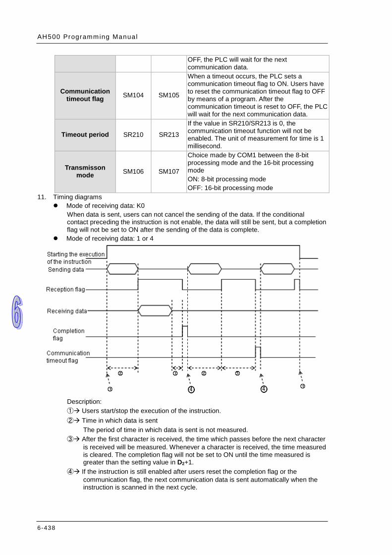
AH500 Programming Manual
6-438
OFF, the PLC will wait for the next communication data.
Communication timeout flag SM104 SM105
When a timeout occurs, the PLC sets a communication timeout flag to ON. Users have to reset the communication timeout flag to OFF by means of a program. After the communication timeout is reset to OFF, the PLC will wait for the next communication data.
Timeout period SR210 SR213
If the value in SR210/SR213 is 0, the communication timeout function will not be enabled. The unit of measurement for time is 1 millisecond.
Transmisson mode SM106 SM107
Choice made by COM1 between the 8-bit processing mode and the 16-bit processing mode ON: 8-bit processing mode OFF: 16-bit processing mode
11. Timing diagrams Mode of receiving data: K0
When data is sent, users can not cancel the sending of the data. If the conditional contact preceding the instruction is not enable, the data will still be sent, but a completion flag will not be set to ON after the sending of the data is complete.
Mode of receiving data: 1 or 4
Description: ① Users start/stop the execution of the instruction. ② Time in which data is sent
The period of time in which data is sent is not measured. ③ After the first character is received, the time which passes before the next character
is received will be measured. Whenever a character is received, the time measured is cleared. The completion flag will not be set to ON until the time measured is greater than the setting value in D2+1.
④ If the instruction is still enabled after users reset the completion flag or the communication flag, the next communication data is sent automatically when the instruction is scanned in the next cycle.
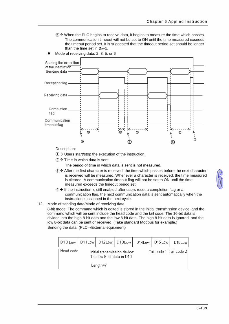
Chapter 6 Appl ied Instruc t ion
6-439
⑤ When the PLC begins to receive data, it begins to measure the time which passes. The communication timeout will not be set to ON until the time measured exceeds the timeout period set. It is suggested that the timeout period set should be longer than the time set in D2+1.
Mode of receiving data: 2, 3, 5, or 6
Description: ① Users start/stop the execution of the instruction. ② Time in which data is sent
The period of time in which data is sent is not measured. ③ After the first character is received, the time which passes before the next character
is received will be measured. Whenever a character is received, the time measured is cleared. A communication timeout flag will not be set to ON until the time measured exceeds the timeout period set.
④ If the instruction is still enabled after users reset a completion flag or a communication flag, the next communication data is sent automatically when the instruction is scanned in the next cycle.
12. Mode of sending data/Mode of receiving data 8-bit mode: The command which is edited is stored in the initial transmission device, and the command which will be sent include the head code and the tail code. The 16-bit data is divided into the high 8-bit data and the low 8-bit data. The high 8-bit data is ignored, and the low 8-bit data can be sent or received. (Take standard Modbus for example.) Sending the data: (PLC→External equipment)
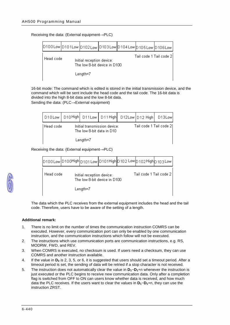
AH500 Programming Manual
6-440
Receiving the data: (External equipment→PLC)
16-bit mode: The command which is edited is stored in the initial transmission device, and the command which will be sent include the head code and the tail code. The 16-bit data is divided into the high 8-bit data and the low 8-bit data. Sending the data: (PLC→External equipment)
Receiving the data: (External equipment→PLC)
The data which the PLC receives from the external equipment includes the head and the tail code. Therefore, users have to be aware of the setting of a length.
Additional remark:
1. There is no limit on the number of times the communication instruction COMRS can be executed. However, every communication port can only be enabled by one communication instruction, and the communication instructions which follow will not be executed.
2. The instructions which use communication ports are communication instructions, e.g. RS, MODRW, FWD, and REV.
3. When COMRS is executed, no checksum is used. If users need a checksum, they can use COMRS and another instruction available.
4. If the value in D2 is 2, 3, 5, or 6, it is suggested that users should set a timeout period. After a timeout period is set, the sending of data will be retried if a stop character is not received.
5. The instruction does not automatically clear the value in D1~D1+n whenever the instruction is just executed or the PLC begins to receive new communication data. Only after a completion flag is switched from OFF to ON can users know whether data is received, and how much data the PLC receives. If the users want to clear the values in D1~D1+n, they can use the instruction ZRST.
Chapter 6 Appl ied Instruc t ion
6-441
6. If the value in S1 is neither 1 nor 2, the instruction will not be executed, SM0 will be ON, and the error code in SR0 will be 16#2003.
7. If the number of devices starting from S2 is not equal to the value in S3, the instruction will not be executed, SM0 will be ON, and the error code in SR0 will be 16#2003.
8. If the value in D2 is not in the range of 0 to 6, the instruction will not be executed, SM0 will be ON, and the error code in SR0 will be 16#2003.
9. If the value in D2 is 6, and the number of devices starting from D1 is not equal to the value in D2+1, the instruction will not be executed, SM0 will be ON, and the error code in SR0 will be 16#2003.
10. If the value in S2 is in the range of 1 to 5, and the quantity of data received is greater than the number of devices starting from D1, the data which can not be stored will be ignored.
11. If a completion flag is ON, the PLC will stop receiving data. If a communication port receives data when a completion flag is ON, the data will not be received.
12. If the setting value in S3 is less than 0 or greater than 1000, the instruction will not be executed, SM0 will be ON, and the error code in SR0 will be 16#2003.
AH500 Programming Manual
6-442
6.20 Other Instructions
6.20.1 List of Other Instructions
API Instruction code Pulse instruction Function Step 16-bit 32-bit
1900 WDT – Watchdog timer 1 1901 DELAY – Delaying the execution of the program 3 1902 GPWM – – General pulse width modulation 7 1903 TIMCHK – – Checking time 7 1904 EPUSH – Storing the contents of the index registers 3 1905 EPOP – Reading the data into the index registers 3
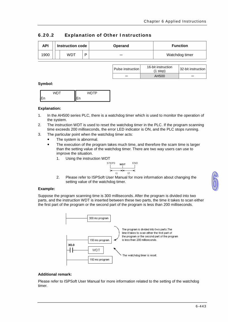
Chapter 6 Appl ied Inst ruct ions
6-443
6.20.2 Explanation of Other Instructions
API Instruction code Operand Function
1900 WDT P ─ Watchdog timer
Pulse instruction 16-bit instruction
(1 step) 32-bit instruction
─ AH500 ─
Symbol:
Explanation:
1. In the AH500 series PLC, there is a watchdog timer which is used to monitor the operation of the system.
2. The instruction WDT is used to reset the watchdog timer in the PLC. If the program scanning time exceeds 200 milliseconds, the error LED indicator is ON, and the PLC stops running.
3. The particular point when the watchdog timer acts: The system is abnormal. The execution of the program takes much time, and therefore the scam time is larger
than the setting value of the watchdog timer. There are two way users can use to improve the situation. 1. Using the instruction WDT
t1 t2
STEP0 ENDWDT
2. Please refer to ISPSoft User Manual for more information about changing the
setting value of the watchdog timer.
Example:
Suppose the program scanning time is 300 milliseconds. After the program is divided into two parts, and the instruction WDT is inserted between these two parts, the time it takes to scan either the first part of the program or the second part of the program is less than 200 milliseconds.
Additional remark:
Please refer to ISPSoft User Manual for more information related to the setting of the watchdog timer.

AH500 Programming Manual
6-444
API Instruction code Operand Function
1901 DELAY P S Delaying the execution of the program
Device X Y M S T C HC D L SM SR E PR K 16# “$” DF
S Pulse instruction 16-bit instruction
(3 steps) 32-bit instruction
AH500 AH500 ─
Symbol:
S : Delay Word
Explanation:
After the instruction DELAY is executed, the execution of the program following the DELAY is delayed for a period of time specified by users. The unit of S is 0.1 milliseconds.
Example:
When X0.0 is ON, the instruction DELAY is executed. The execution of the program following DELAY is delayed for two milliseconds. That is, Y0.0 is ON and the states of Y0.0~Y0.15 are refreshed two milliseconds after the instruction DELAY is executed.
Output Y0.0
T=2ms
Input X0.0
Additional remark:
1. If S I less than 0, there is no delay. 2. If S is larger than 1000, the instruction is not executed, SM0 is ON, and the error code in SR0
is 16#2003. 3. Users can adjust the delay according to the practical condition. 4. The delay will increase due to the communication or other influences.
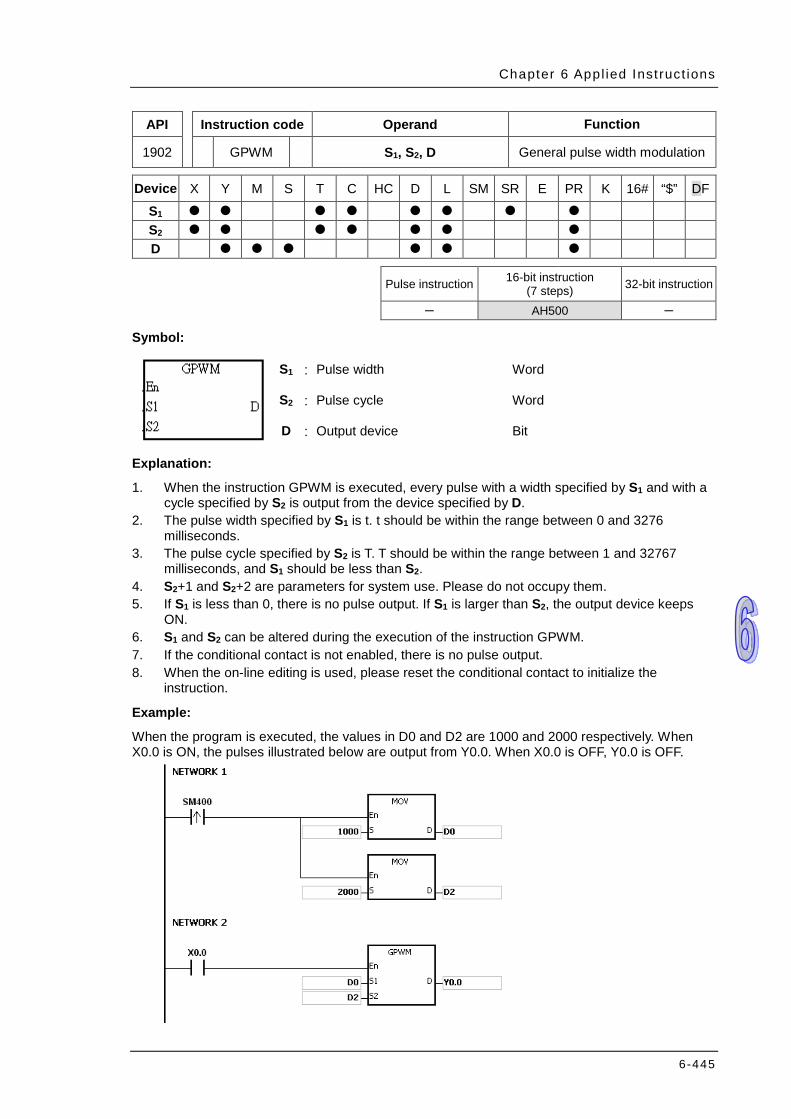
Chapter 6 Appl ied Inst ruct ions
6-445
API Instruction code Operand Function
1902 GPWM S1, S2, D General pulse width modulation
Device X Y M S T C HC D L SM SR E PR K 16# “$” DF
S1 S2 D
Pulse instruction 16-bit instruction
(7 steps) 32-bit instruction
─ AH500 ─
Symbol:
S1 : Pulse width Word
S2 : Pulse cycle Word
D : Output device Bit
Explanation:
1. When the instruction GPWM is executed, every pulse with a width specified by S1 and with a cycle specified by S2 is output from the device specified by D.
2. The pulse width specified by S1 is t. t should be within the range between 0 and 3276 milliseconds.
3. The pulse cycle specified by S2 is T. T should be within the range between 1 and 32767 milliseconds, and S1 should be less than S2.
4. S2+1 and S2+2 are parameters for system use. Please do not occupy them. 5. If S1 is less than 0, there is no pulse output. If S1 is larger than S2, the output device keeps
ON. 6. S1 and S2 can be altered during the execution of the instruction GPWM. 7. If the conditional contact is not enabled, there is no pulse output. 8. When the on-line editing is used, please reset the conditional contact to initialize the
instruction.
Example:
When the program is executed, the values in D0 and D2 are 1000 and 2000 respectively. When X0.0 is ON, the pulses illustrated below are output from Y0.0. When X0.0 is OFF, Y0.0 is OFF.
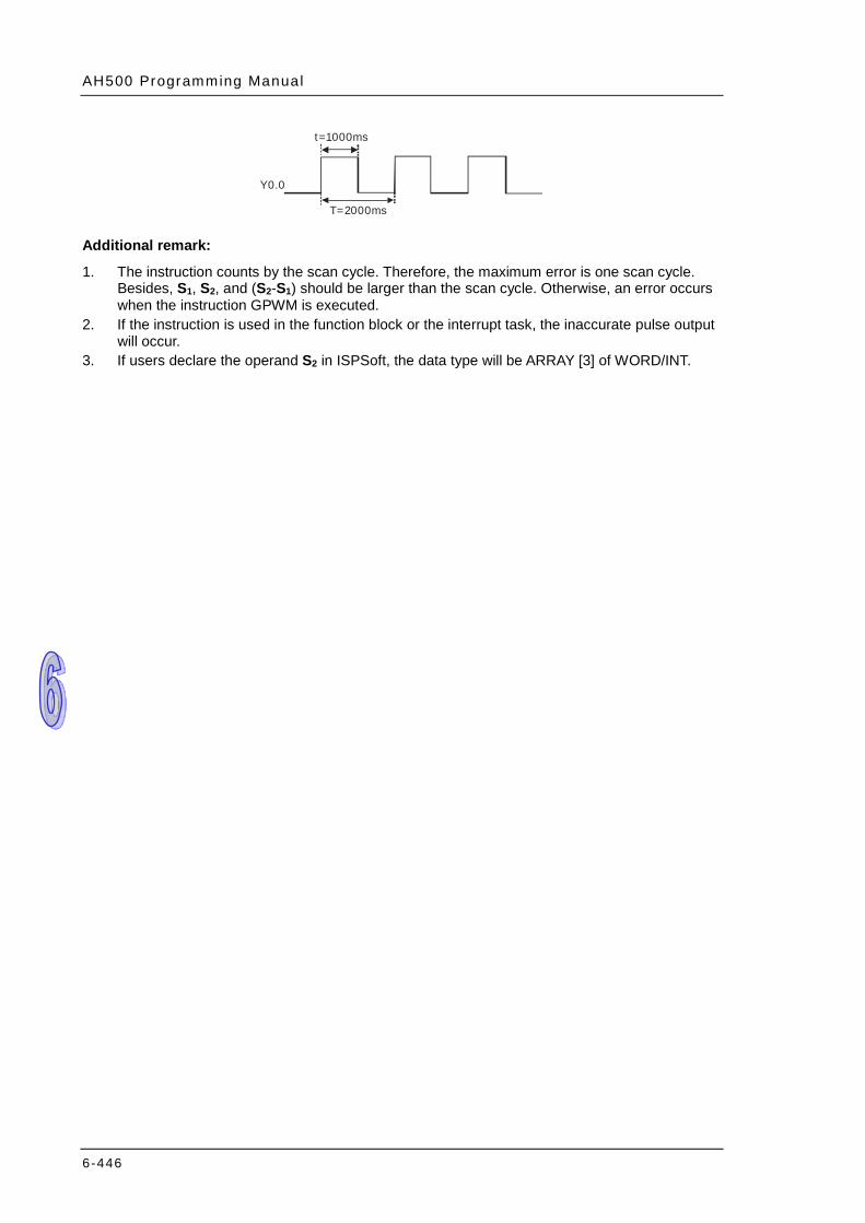
AH500 Programming Manual
6-446
t=1000ms
T=2000ms
Y0.0
Additional remark:
1. The instruction counts by the scan cycle. Therefore, the maximum error is one scan cycle. Besides, S1, S2, and (S2-S1) should be larger than the scan cycle. Otherwise, an error occurs when the instruction GPWM is executed.
2. If the instruction is used in the function block or the interrupt task, the inaccurate pulse output will occur.
3. If users declare the operand S2 in ISPSoft, the data type will be ARRAY [3] of WORD/INT.
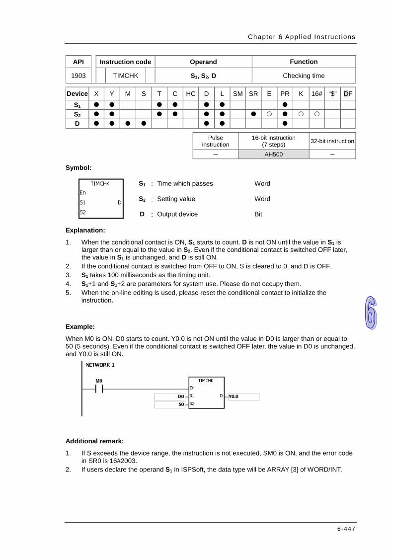
Chapter 6 Appl ied Inst ruct ions
6-447
API Instruction code Operand Function
1903 TIMCHK S1, S2, D Checking time
Device X Y M S T C HC D L SM SR E PR K 16# “$” DF
S1 S2 D
Pulse
instruction 16-bit instruction
(7 steps) 32-bit instruction
─ AH500 ─
Symbol:
S1 : Time which passes Word
S2 : Setting value Word
D : Output device Bit
Explanation:
1. When the conditional contact is ON, S1 starts to count. D is not ON until the value in S1 is larger than or equal to the value in S2. Even if the conditional contact is switched OFF later, the value in S1 is unchanged, and D is still ON.
2. If the conditional contact is switched from OFF to ON, S is cleared to 0, and D is OFF. 3. S1 takes 100 milliseconds as the timing unit. 4. S1+1 and S1+2 are parameters for system use. Please do not occupy them. 5. When the on-line editing is used, please reset the conditional contact to initialize the
instruction.
Example:
When M0 is ON, D0 starts to count. Y0.0 is not ON until the value in D0 is larger than or equal to 50 (5 seconds). Even if the conditional contact is switched OFF later, the value in D0 is unchanged, and Y0.0 is still ON.
Additional remark:
1. If S exceeds the device range, the instruction is not executed, SM0 is ON, and the error code in SR0 is 16#2003.
2. If users declare the operand S1 in ISPSoft, the data type will be ARRAY [3] of WORD/INT.
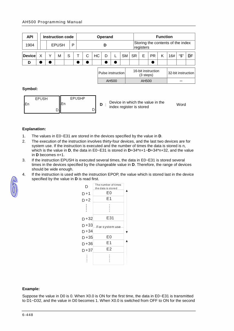
AH500 Programming Manual
6-448
API Instruction code Operand Function
1904 EPUSH P D Storing the contents of the index registers
Device X Y M S T C HC D L SM SR E PR K 16# “$” DF
D Pulse instruction 16-bit instruction
(3 steps) 32-bit instruction
AH500 AH500 ─
Symbol:
D : Device in which the value in the index register is stored Word
Explanation:
1. The values in E0~E31 are stored in the devices specified by the value in D. 2. The execution of the instruction involves thirty-four devices, and the last two devices are for
system use. If the instruction is executed and the number of times the data is stored is n, which is the value in D, the data in E0~E31 is stored in D+34*n+1~D+34*n+32, and the value in D becomes n+1.
3. If the instruction EPUSH is executed several times, the data in E0~E31 is stored several times in the devices specified by the changeable value in D. Therefore, the range of devices should be wide enough.
4. If the instruction is used with the instruction EPOP, the value which is stored last in the device specified by the value in D is read first.
Example:
Suppose the value in D0 is 0. When X0.0 is ON for the first time, the data in E0~E31 is transmitted to D1~D32, and the value in D0 becomes 1. When X0.0 is switched from OFF to ON for the second
The number of times the data is stored
E0E1
E31
......
+1D
DD +2
D +32
E0E1
......
+36DD +37
+35D
D +33D +34
............
......
E2
For system use
Chapter 6 Appl ied Inst ruct ions
6-449
time, the data in E0~E31 is transmitted to D35~D66, and the value in D0 becomes 2. When X0.0 is switched from OFF to ON for the nth time, the data in E0~E31 is transmitted to D+(the value in D0)*34+1~D+(the value in D0)*34+32.
Additional remark:
1. If the value in D is less than 0, the instruction is not executed, SM0 is ON, and the error code in SR0 is 16#2003.
2. If D+((the value in D)+1)*34-1 exceeds the device range, the instruction is not executed, SM0 is ON, and the error code in SR0 is 16#2003.
AH500 Programming Manual
6-450
API Instruction code Operand Function
1905 EPOP P D Reading the data into the index registers
Device X Y M S T C HC D L SM SR E PR K 16# “$” DF
D Pulse instruction 16-bit instruction
(3 steps) 32-bit instruction
AH500 AH500 ─
Symbol:
D : Device from which the value is read Word
Explanation:
1. The values in the devices specified by the value in D are read into E0~E31, and the value in D decreases by one.
2. The execution of the instruction involves thirty-four devices, and the last two devices are for system use. If the instruction is executed and the number of times the data is stored is n, which is the value in D, the data in D+34*(n-1)+1~D+34*(n-1)+32 is read into E0~E31, and the value in D becomes n-1.
3. The value which is stored last in the device specified by the value in D is read first. The number of times the data is stored
E0E1
E31
......
+1D
DD +2
D +32
E0E1
......
+36DD +37
+35D
D +33D +34
............
......
E2
For system use

Chapter 6 Appl ied Inst ruct ions
6-451
Example:
When X0.0 is ON, the value in D0 is set to 0, and the values in E0~E31 are transmitted to D1~D32. After the execution of FB0 is complete, the values in D1~D32 are read into D1~D32.
Additional remark:
1. If the value in D is less than or equal to 0, the instruction is not executed, SM0 is ON, and the error code in SR0 is 16#2003.
2. If D+(the value in D)*34-1 exceeds the device range, the instruction is not executed, SM0 is ON, and the error code in SR0 is 16#2003.
AH500 Programming Manual
6-452
6.21 String Processing Instructions
6.21.1 List of String Processing Instructions
API Instruction code Pulse instruction Function Step 16-bit 32-bit 64-bit
2100 BINDA DBINDA – Converting the singed decimal number into the ASCII code 5
2101 BINHA DBINHA – Converting the binary hexadecimal number into the hexadecimal ASCII code
5
2102 BCDDA DBCDDA – Converting the binary-coded decimal number into the ASCII code
5
2103 DABIN DDABIN – Converting the signed decimal ASCII code into the signed decimal binary number
5-11
2104 HABIN DHABIN – Converting the hexadecimal ASCII code into the hexadecimal binary number
5-11
2105 DABCD DDABCD – Converting the ASCII code into the binary-coded decimal number 5-11
2106 $LEN – – Calculating the length of the string 5-11
2107 $STR $DSTR – Converting the binary number into the string 7
2108 $VAL $DVAL – Converting the string into the binary number 7-13
2109 $FSTR – – Converting the floating-point number into the string 7-8
2110 $FVAL – – Converting the string into the floating-point number 5-11
2111 $RIGHT – – The retrieve of the characters in the string begins from the right. 7-13
2112 $LEFT – – The retrieve of the characters in the string begins from the left. 7-13
2113 $MIDR – – Retrieving a part of the string 7-13 2114 $MIDW – – Replacing a part of the string 7-13 2115 $SER – – Searching the string 9-21
2116 $RPLC – – Replacing the characters in the string 11-17
2117 $DEL – – Deleting the characters in the string 9 2118 $CLR – – Clearing the string 3 2119 $INS – – Inserting the string 9-15
2120 – FMOD – Converting the floating-point number into the binary-coded decimal floating-point number
7-8
2121 FREXP – – Converting the Binary-coded decimal floating-point number into the floating-point number
7
Chapter 6 Appl ied Inst ruct ions
6-453
6.21.2 Explanation of String Processing Instructions
API Instruction code Operand Function
2100 D BINDA P S, D Converting the singed decimal number into the ASCII code
Device X Y M S T C HC D L SM SR E PR K 16# “$” DF
S D
Pulse instruction 16-bit instruction
(5 steps) 32-bit instruction
(5 steps) AH500 AH500 AH500
Symbol:
S : Source value Word/Double word
D : Device in which the conversion result is stored Word
Explanation:
1. The signed decimal binary number in S is converted into the ASCII code, and the conversion result is stored in D.
2. The instruction supports SM690, which controls the ending character. 3. The value in S used in the 16-bit instruction should be within the range between -32768 and
32767, and should be a six-digit binary number. The operand D occupies four word devices. The data is converted as follows.
b15 b0 S
16-bit bi nary number
b15 b0 b7 b8
D
D
D
D
+1
+2
+3
ASCII code in the hundreds place
ASCII code in the ten thousands place
ASCII code in the thousands place
Sign (±)
ASCII code in the units pl ace
ASCII code in the tens place
Ending character (16#00 or unchanged)
If SM690 is OFF, 16#0000 is stored in D+3. If SM690 is ON, the value in D+3 is unchanged. Besides, if the value in S is a positive value, the sign character in D is 16#20. If the value in S is a negative value, the sign character in D is 16#2D. For example, if the value in S is -12345 and SM690 is OFF, the conversion result is as follows.
b15 b0 S
b15 b0 b7 b816#31(1)
16#0000
D
D
D D
+1+2+3
16#33(3)
16#35(5)
16#32(2)
16#34(4)
16#2D(-)
-12345
16-bit binary number 4. The value in S used in the 32-bit instruction should be within the range between -2147483648
and 2147483647, and should be an eleven-digit binary number. The operand D occupies six word devices. The data is converted as follows.

AH500 Programming Manual
6-454
S
b15 b0 b7 b8
D
D
D
D
+1
+2
+3
High 16 bi ts Low 16 bits
D +4
D +5
32-bit bi nary number
Ending character (16#00 or 16#20)
ASCII code in the units pl ace
ASCII code in the tens place
ASCII code in the thousands place
ASCII code in the hundreds place
ASCII code in the ten thousands place
ASCII code in the hundred thousands place
ASCII code in the mill ions place
ASCII code in the hundred mil lions place
ASCII code in the billi ons place
ASCII code in the ten mill ions place
Sign (±)
If SM690 is OFF, 16#0000 is stored in the high 8 bits in D+5. If SM690 is ON, 16#20 is stored in the high 8 bits in D+5. Besides, if the value in S is a positive value, the sign character in D is 16#20. If the value in S is a negative value, the sign character in D is 16#2D. For example, if the value in S is -12345678, the conversion result is as follows.
S
b15 b0 b7 b8
16#33( 3)
D
D
D D
+1+2+316#35( 5)
16#37( 7) 16#36( 6)
16#38( 8)
16#34( 4)-1234 5678
S +1
16#20( )
16#31( 1)
16#32( 2)
16#2D(-)
16#20( )
D D
+4+516#00或 6#20132-bit binary number
5. Take the 32-bit binary number -12345678 in S for example. The digit in the hundred millions
place of the number and the digit in the billions place of the number are 0. When the instruction is executed, 16#20 is stored in the low 8 bits in D+1 and the high 8 bits in D.
S
b15 b0 b7 b8
16#33( 3)
D
D
D D
+1+2+316#35( 5)
16#37( 7) 16#36( 6)
16#38( 8)
16#34( 4)-1234 5678
S +1
16#20( )
16#31( 1)
16#32( 2)
16#2D(-)
16#20( )
D D
+4+5
00123 45678Becoming 16#20
Signifi cant digits16#20 is stored.
16#00或 6#20132-bit binary number
Example 1:
Suppose the value in L0 is 5126 and SM690 is OFF. When the PLC runs, the values in D0, D1, D2, and D3 are 16#2020, 16#3135, 16#3135, and 16#0000 respectively.

Chapter 6 Appl ied Inst ruct ions
6-455
b15 b0 b7 b8
5126L0
BIN
16#20( ) 16#20( )16#31(1) 16#35(5)16#36(6) 16#32(2)
16#00 Example 2:
Suppose the value in L10 is -3842563 and SM690 is OFF. When the PLC runs, the values in D0, D1, D2, D3, D4, and D5 are 16#202D, 16#2020, 16#3833, 16#3234, 16#3635, and 16#0033 respectively.
L10
BIN
b15 b0 b7 b8
16#38(8)16#32(2)16#36(6) 16#35(5)
16#33(3)
16#34(4)-384 2563
L11
16#20( )16#20()
16#33(3)
16#2D(-)16#20( )
16#00 Additional remark:
1. If D+3 used in the 16-bit instruction exceeds the device range, SM0 is ON, and the error code in SR0 is 16#2003.
2. If D+5 used in the 32-bit instruction exceeds the device range, SM0 is ON, and the error code in SR0 is 16#2003.
3. If the operand D used during the execution of the 16-bit instruction is declared in ISPSoft, the data type will be ARRAY [4] of WORD/INT.
4. If the operand D used during the execution of the 32-bit instruction is declared in ISPSoft, the data type will be ARRAY [6] of WORD/INT.
AH500 Programming Manual
6-456
API Instruction code Operand Function
2101 D BINHA P S, D Converting the binary hexadecimal number into the hexadecimal ASCII code
Device X Y M S T C HC D L SM SR E PR K 16# “$” DF
S D
Pulse instruction 16-bit instruction
(5 steps) 32-bit instruction
(5 steps)
AH500 AH500 AH500
Symbol:
S : Source value Word/Double word
D : Device in which the conversion result is stored Word
Explanation:
1. The hexadecimal binary number in S is converted into the ASCII code, and the conversion result is stored in D.
2. The instruction supports SM690, which controls the ending character. 3. The value in S used in the 16-bit instruction should be within the range between 16#0000 and
16#FFFF, and should be a four-digit binary number. The operand D occupies three word devices. The data is converted as follows.
b15 b0
b15 b0 b7 b8
S D D
D
+1
+216-bit binary numberEnding character (16#0000 or unchanged)
F irst ASCII code Second ASCII code
Thi rd AS CII code Four th ASCII code
If SM690 is OFF, 16#0000 is stored in D+2. If SM690 is ON, the value in D+2 is unchanged. For example, if the value in S is 16#02A6 and SM690 is OFF, the conversion result is as follows.
b15 b0
b15 b0 b7 b8
16#0000
S 16#02A 616#32(2) 16#30(0)
16#36(6) 16#41(A)
4. The value in S used in the 32-bit instruction should be within the range between
16#00000000 and 16#FFFFFFFF, and should be an eight-digit binary number. The operand D occupies five word devices. The data is converted as follows.
S
b15 b0 b7 b8
16#32(2)
16#0000
D
D D D
+1+2+316#45(E) 16#35(5)
03AC 625E
S +1
16#33(3)16#43(C)
16#36(6)
16#30(0)16#41(A)
D+4
Chapter 6 Appl ied Inst ruct ions
6-457
If SM690 is OFF, 16#0000 is stored in D+4. If SM690 is ON, the value in D+4 is unchanged. For example, if the value in S is 16#03AC625E and SM690 is OFF, the conversion result is as follows.
S
b15 b0 b7 b8
16#32( 2)
16#0000
D
D
D D
+1+2+316#45( E) 16#36( 6)
03AC 625E
S +116#33( 3)
16#43( C)
16#36( 6)
16#30( 0)
16#41( A)
D +4
Example 1:
Suppose the value in L0 is 16#9C06 and SM690 is OFF. When PLC runs, the values in D0, D1, and D2, are 16#2020, 16#3135, 16#3135, and 16#0000 respectively.
b15 b0 b7 b8
16#0000
16#9C0616#43(C) 16#39(9)
16#36(6) 16#30(0) L0 D0
D1 D2
Example 2:
Suppose the value in L10 is 16#7B3C581F and SM690 is OFF. When the PLC runs, the values in D0, D1, D2, D3, and D4 are 16#4237, 16#4333, 16#3835, 16#4631, and 16#0000 respectively.
b15 b0 b7 b8
16#38(8)
16#000016#46(F) 16#31(1)
7B3C 581F
16#42(B)16#43(C)
16#35(5)
16#37(7)16#33(3) L10 L11
D0 D1 D2 D3 D4
AH500 Programming Manual
6-458
Additional remark:
1. If D+2 used in the 16-bit instruction exceeds the device range, SM0 is ON, and the error code in SR0 is 16#2003.
2. If D+4 used in the 32-bit instruction exceeds the device range, SM0 is ON, and the error code in SR0 is 16#2003.
3. If the operand D used during the execution of the 16-bit instruction is declared in ISPSoft, the data type will be ARRAY [3] of WORD/INT.
4. If the operand D used during the execution of the 32-bit instruction is declared in ISPSoft, the data type will be ARRAY [5] of WORD/INT.
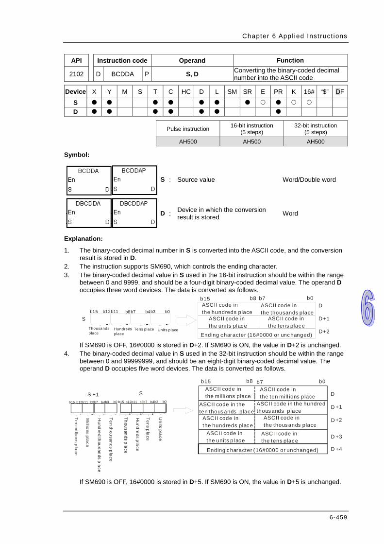
Chapter 6 Appl ied Inst ruct ions
6-459
API Instruction code Operand Function
2102 D BCDDA P S, D Converting the binary-coded decimal number into the ASCII code
Device X Y M S T C HC D L SM SR E PR K 16# “$” DF
S D
Pulse instruction 16-bit instruction
(5 steps) 32-bit instruction
(5 steps)
AH500 AH500 AH500
Symbol:
S : Source value Word/Double word
D : Device in which the conversion result is stored Word
Explanation:
1. The binary-coded decimal number in S is converted into the ASCII code, and the conversion result is stored in D.
2. The instruction supports SM690, which controls the ending character. 3. The binary-coded decimal value in S used in the 16-bit instruction should be within the range
between 0 and 9999, and should be a four-digit binary-coded decimal value. The operand D occupies three word devices. The data is converted as follows.
b15 b0
SThousands place
b15 b0 b7 b8 D
D
D
+1
+2Hundredsplace
Tens place Units place
b3 b4 b7 b8 b11 b12ASCII code in the hundreds place
ASCII code in the thousands place
ASCII code in the tens place
ASCII code in the units pl ace
Ending character (16#0000 or unchanged) If SM690 is OFF, 16#0000 is stored in D+2. If SM690 is ON, the value in D+2 is unchanged.
4. The binary-coded decimal value in S used in the 32-bit instruction should be within the range between 0 and 99999999, and should be an eight-digit binary-coded decimal value. The operand D occupies five word devices. The data is converted as follows.
Ending character (16#0000 or unchanged)
S
b15 b0 b7 b8
D
D
D
D
+1
+2
+3
D +4
b15 b12 b11 b8 b7 b4 b3 b0 b15 b12 b11 b8 b7 b4 b3 b0
S +1
Units place
Tens place
Hundreds place
Thousands place
Hundred thousands place
Ten thousands place
Millions place
Ten millions place
ASCII code in the units pl ace
ASCII code in the tens place
ASCII code in the hundreds pl ace
ASCII code in the thousands place
ASCII code in the ten thousands place
ASCII code in the hundred thousands place
ASCII code in the milli ons place
ASCII code in the ten mill ions place
If SM690 is OFF, 16#0000 is stored in D+5. If SM690 is ON, the value in D+5 is unchanged.
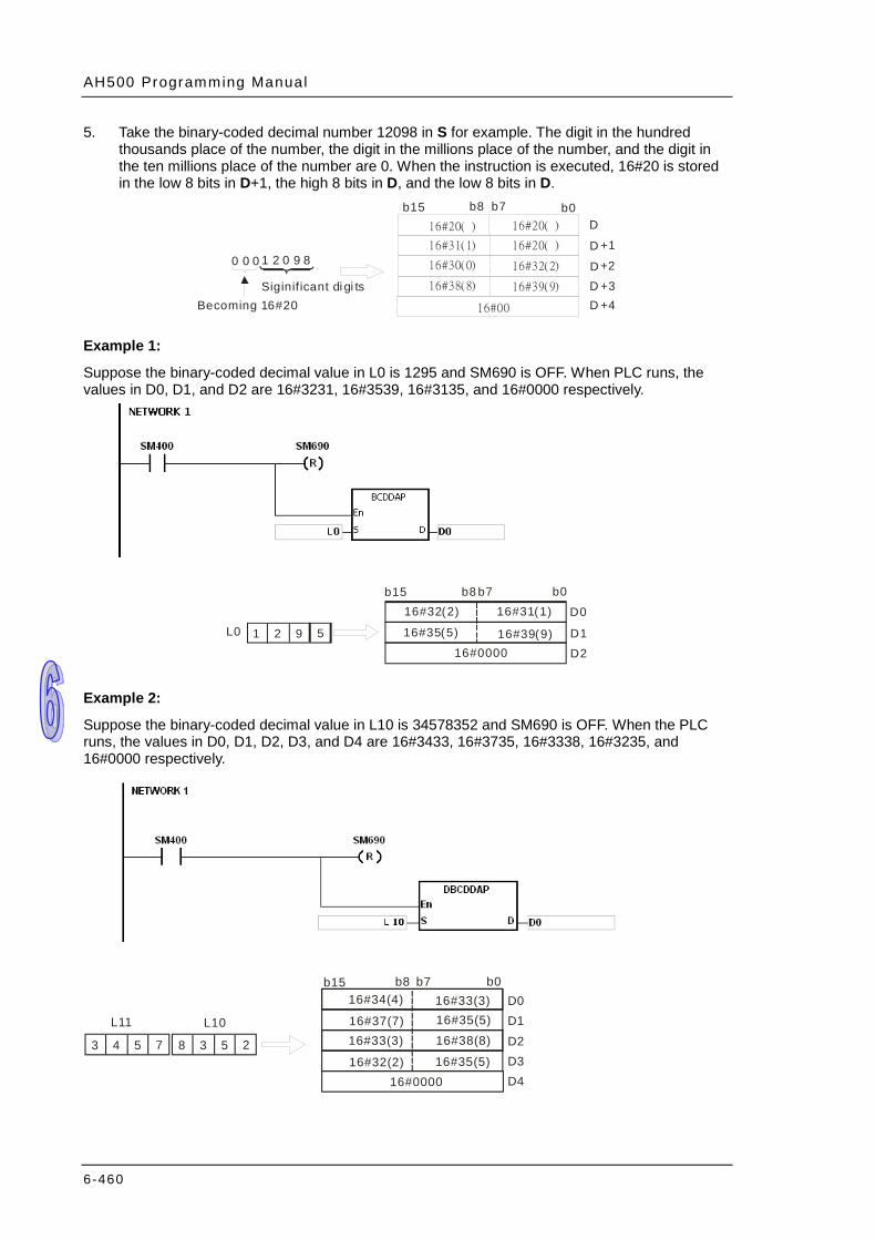
AH500 Programming Manual
6-460
5. Take the binary-coded decimal number 12098 in S for example. The digit in the hundred thousands place of the number, the digit in the millions place of the number, and the digit in the ten millions place of the number are 0. When the instruction is executed, 16#20 is stored in the low 8 bits in D+1, the high 8 bits in D, and the low 8 bits in D.
b15 b0 b7 b8 D
D
D D
+1+2+3
D +416#00
0 0 0 1 2 0 9 8
Becoming 16#20Siginif icant di gi ts
16#20( )
16#31( 1)
16#30( 0)
16#38( 8)
16#20( )
16#20( )
16#32( 2)
16#39( 9)
Example 1:
Suppose the binary-coded decimal value in L0 is 1295 and SM690 is OFF. When PLC runs, the values in D0, D1, and D2 are 16#3231, 16#3539, 16#3135, and 16#0000 respectively.
b15 b0 b7 b8
16#0000
16#32(2) 16#31(1)
16#35(5) 16#39(9) L0 D0
D1 D2
1 2 9 5
Example 2:
Suppose the binary-coded decimal value in L10 is 34578352 and SM690 is OFF. When the PLC runs, the values in D0, D1, D2, D3, and D4 are 16#3433, 16#3735, 16#3338, 16#3235, and 16#0000 respectively.
b15 b0 b7 b8
16#33(3)
16#000016#32(2) 16#35(5)
16#34(4)16#37(7)
16#38(8)
16#33(3)16#35(5) L10 L11
D0 D1 D2 D3 D4
8 3 5 2 3 4 5 7
Chapter 6 Appl ied Inst ruct ions
6-461
Additional remark:
1. If the value in S used in the 16-bit instruction is not within the range between 0 and 9999, the instruction is not executed, SM0 is ON, and the error code in SR0 is 16#200D. (The binary-coded decimal value is represented by the hexadecimal number, but one of digits is not within the range between 0 and 9.)
2. If the value in S used in the 32-bit instruction is not within the range between 0 and 99999999, the instruction is not executed, SM0 is ON, and the error code in SR0 is 16#200D. (The binary-coded decimal value is represented by the hexadecimal number, but one of digits is not within the range between 0 and 9.)
3. If D+2 used in the 16-bit instruction exceeds the device range, SM0 is ON, and the error code in SR0 is 16#2003.
4. If D+4 used in the 32-bit instruction exceeds the device range, SM0 is ON, and the error code in SR0 is 16#2003.
5. If the operand D used during the execution of the 16-bit instruction is declared in ISPSoft, the data type will be ARRAY [3] of WORD/INT.
6. If the operand D used during the execution of the 32-bit instruction is declared in ISPSoft, the data type will be ARRAY [5] of WORD/INT.

AH500 Programming Manual
6-462
API Instruction code Operand Function
2103 D DABIN P S, D Converting the signed decimal ASCII code into the signed decimal binary number
Device
X Y M S T C HC D L SM SR E PR K 16# “$” DF S D
Pulse instruction 16-bit instruction (5-11 steps)
32-bit instruction (5-11 steps)
AH500 AH500 AH500
Symbol:
S : Source value Word
D : Device in which the conversion result is stored
Word/Double word
Explanation:
1. The signed decimal ASCII code in S is converted into the signed decimal binary number, and the conversion result is stored in D.
2. The operand S used in the 16-bit instruction occupies three word devices, and the decimal ASCII code in S should be within the range between -32768 and 32767. If S is a string, the string should be within the range between “-32768” and “32767”.
b15 b0 b7 b8
SS+1S+2
b15 b0 D
16-bit bi nary numberASCII code in the units pl ace
ASCII code in the tens place
ASCII code in the hundreds place
ASCII code in the thousands place
ASCII code in the ten thousands place Sign
3. If S used in the 16-bit instruction is a string and the number of characters contained in the
string is less than 6, the characters which the string lacks are regarded as 0. The first character is a sign character. If the first character is “ ” (a space), the sign is a positive sign. If the first character is “-”, the sign is a negative sign. Take the string “1234” for example.
b15 b0 b7 b8
"3"
" "(Ignored) "4"
S
S+1S+2
b15 b0 D
"1" " "(Space)"2" 12340
16-bit binary number 4. The operand S used in the 32-bit instruction occupies six word devices, and the decimal
ASCII code in S should be within the range between -2147483648 and 2147483647. If S is a string, the string should be within the range between “-2147483648” and “2147483647”.
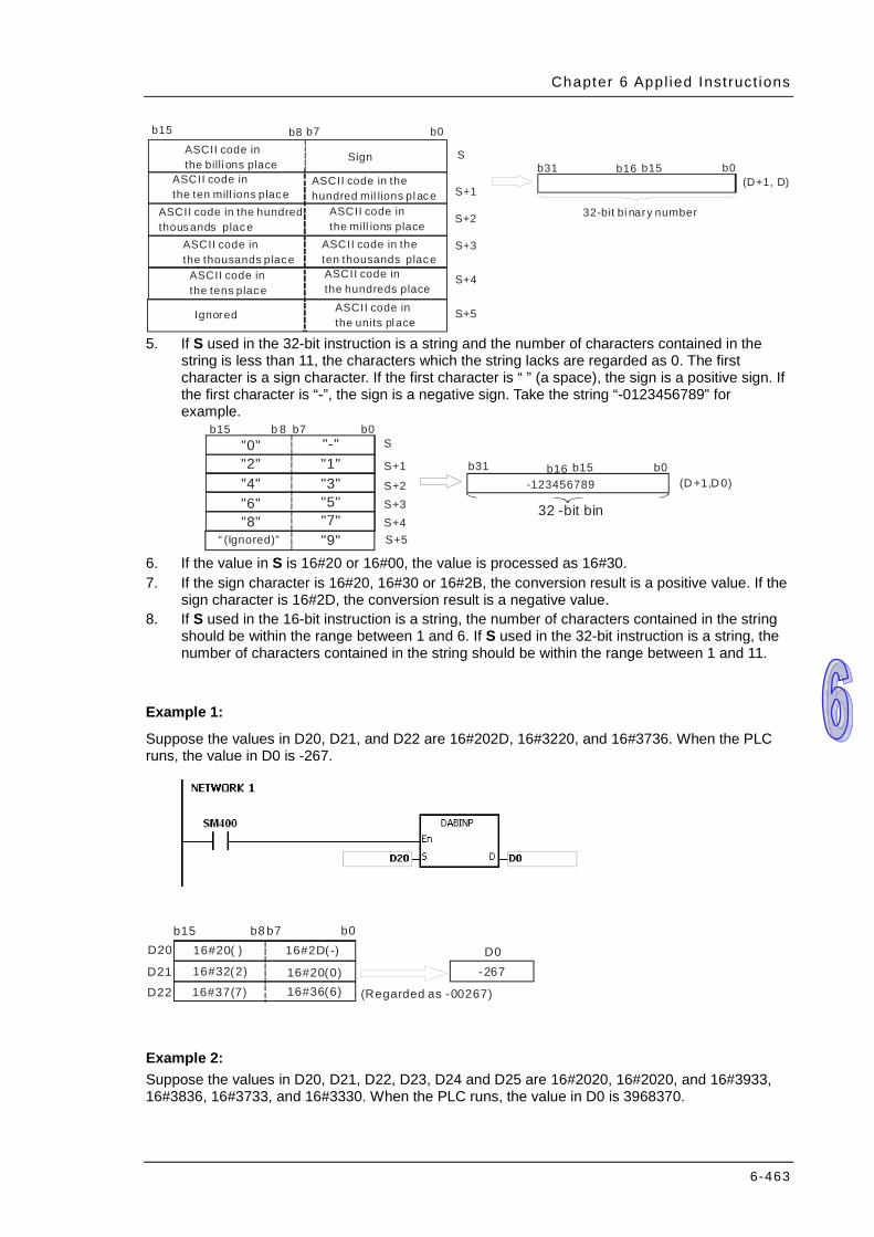
Chapter 6 Appl ied Inst ruct ions
6-463
b0
S
S+1
S+2
S+3
S+4
b15 b0 b31 b16(D+1, D)
S+5
32-bit bi nary number
ASCII code in the units pl ace
ASCII code in the tens place
ASCII code in the hundreds place
ASCII code in the thousands place
ASCII code in the ten thousands place
ASCII code in the hundred thousands place
ASCII code in the mill ions place
ASCII code in the ten mill ions place
ASCII code in the hundred mil lions pl ace
ASCII code in the billi ons place Sign
Ignored
b7 b8 b15
5. If S used in the 32-bit instruction is a string and the number of characters contained in the
string is less than 11, the characters which the string lacks are regarded as 0. The first character is a sign character. If the first character is “ ” (a space), the sign is a positive sign. If the first character is “-”, the sign is a negative sign. Take the string “-0123456789” for example.
b15 b0 b7 b 8
"5""7""9"
"6""8"
S+1
S+2S+3
"4""2"
“ (Ignored)”S+4
b15 b0
32 -bit bin
(D +1,D 0)"1"
"0" "-"
S+5
S
b31 b16-123456789"3"
6. If the value in S is 16#20 or 16#00, the value is processed as 16#30. 7. If the sign character is 16#20, 16#30 or 16#2B, the conversion result is a positive value. If the
sign character is 16#2D, the conversion result is a negative value. 8. If S used in the 16-bit instruction is a string, the number of characters contained in the string
should be within the range between 1 and 6. If S used in the 32-bit instruction is a string, the number of characters contained in the string should be within the range between 1 and 11.
Example 1:
Suppose the values in D20, D21, and D22 are 16#202D, 16#3220, and 16#3736. When the PLC runs, the value in D0 is -267.
b15 b0 b7 b8
37(7)16#
16#20( ) 16#2D(-)
16#36(6)16#20(0)
D0 -26716#32(2)
D20
D21
D22 (Regarded as -00267)
Example 2: Suppose the values in D20, D21, D22, D23, D24 and D25 are 16#2020, 16#2020, and 16#3933, 16#3836, 16#3733, and 16#3330. When the PLC runs, the value in D0 is 3968370.
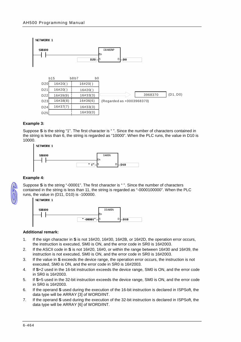
AH500 Programming Manual
6-464
b15 b0 b7 b8
39(9)16#
16#20( ) 16#20( )
16#33(3)16#20( )
(D1, D0) 396837016#20( )
D20
D21
D22(Regarded as +0003968370)16#38(8) 16#36(6)
16#30(0)16#33(3)16#37(7)
D23
D24
D25
Example 3:
Suppose S is the string “1”. The first character is “ ”. Since the number of characters contained in the string is less than 6, the string is regarded as “10000”. When the PLC runs, the value in D10 is 10000.
Example 4:
Suppose S is the string “-00001”. The first character is “ ”. Since the number of characters contained in the string is less than 11, the string is regarded as “-0000100000”. When the PLC runs, the value in (D11, D10) is -100000.
Additional remark:
1. If the sign character in S is not 16#20, 16#30, 16#2B, or 16#2D, the operation error occurs, the instruction is executed, SM0 is ON, and the error code in SR0 is 16#2003.
2. If the ASCII code in S is not 16#20, 16#0, or within the range between 16#30 and 16#39, the instruction is not executed, SM0 is ON, and the error code in SR0 is 16#2003.
3. If the value in S exceeds the device range, the operation error occurs, the instruction is not executed, SM0 is ON, and the error code in SR0 is 16#2003.
4. If S+2 used in the 16-bit instruction exceeds the device range, SM0 is ON, and the error code in SR0 is 16#2003.
5. If S+5 used in the 32-bit instruction exceeds the device range, SM0 is ON, and the error code in SR0 is 16#2003.
6. If the operand S used during the execution of the 16-bit instruction is declared in ISPSoft, the data type will be ARRAY [3] of WORD/INT.
7. If the operand S used during the execution of the 32-bit instruction is declared in ISPSoft, the data type will be ARRAY [6] of WORD/INT.

Chapter 6 Appl ied Inst ruct ions
6-465
API Instruction code Operand Function
2104 D HABIN P S, D Converting the hexadecimal ASCII code into the hexadecimal binary number
Device X Y M S T C HC D L SM SR E PR K 16# “$” DF
S D
Pulse instruction 16-bit instruction
(5-11 steps) 32-bit instruction
(5-11 steps)
AH500 AH500 AH500
Symbol:
S : Source value Word
D : Device in which the conversion result is stored
Word/Double word
Explanation:
1. The hexadecimal ASCII code in S is converted into the hexadecimal binary number, and the conversion result is stored in D.
2. The operand S used in the 16-bit instruction occupies two word devices, and the hexadecimal ASCII code in S should be within the range between 0000 and FFFF. If S is a string, the string should be within the range between “0” and “FFFF”.
b15 b0 b7 b8 S
S +1
b15 b0 D
16-bit binary numberFirst ASCII code Second A SCII code
Thi rd AS CII code Four th ASCII code
If the ASCII code in S~S+1 is 5A8D, the conversion result is as follows.
b15 b0 b7 b8 S
S +1
b15 b0 D
16#41(A) 35(5)16#16#44(D) 38(8)16#
5A8D16#
3. The operand S used in the 32-bit instruction occupies four word devices, and the hexadecimal
ASCII code in S should be within the range between 00000000 and FFFFFFFF. If S is a string, the string should be within the range between “0” and “FFFFFFFF”.
b15 b0 b7 b8 S
S +1
S
S +3
+2
D +1 D
First ASCII code Second ASCII code
Thi rd AS CII code Four th ASCII code
Fifth ASCII code Six th ASCII code
Seventh AS CII code Eighth AS CII code
32-bit binary number
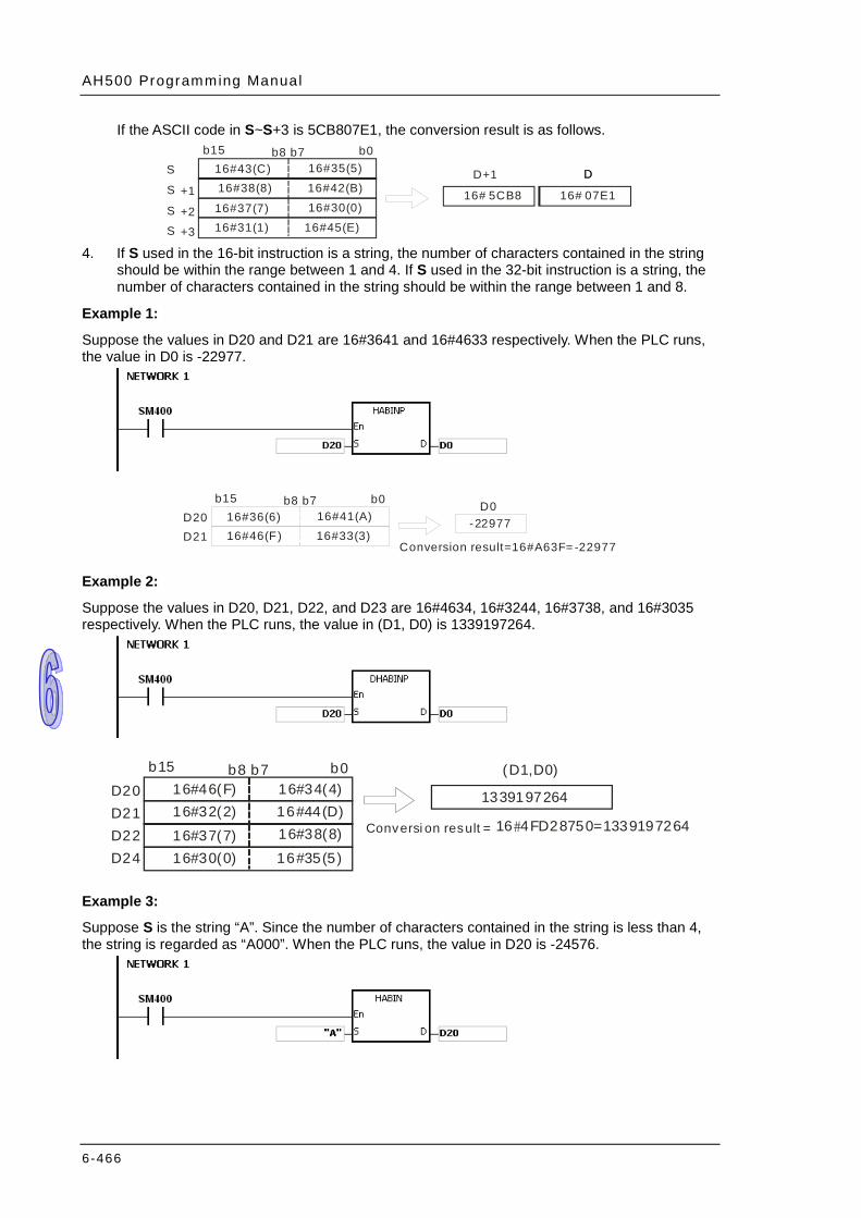
AH500 Programming Manual
6-466
If the ASCII code in S~S+3 is 5CB807E1, the conversion result is as follows. b15 b0 b7 b8
S
S +1
16#43(C) 35(5) 16# 38(8) 16# 42(B) 16# 16# 5CB8 16#37(7) 30(0) 16# 16#31(1) 16#45(E)
S +2 S +3
16# 07E1
D+1 D D
4. If S used in the 16-bit instruction is a string, the number of characters contained in the string
should be within the range between 1 and 4. If S used in the 32-bit instruction is a string, the number of characters contained in the string should be within the range between 1 and 8.
Example 1:
Suppose the values in D20 and D21 are 16#3641 and 16#4633 respectively. When the PLC runs, the value in D0 is -22977.
b15 b0 b7 b8 16#36(6) 41(A)16# 46(F)16# 33(3)16#
Conversion result= A63F= -2297716#
D20 D21
D0 -22977
Example 2:
Suppose the values in D20, D21, D22, and D23 are 16#4634, 16#3244, 16#3738, and 16#3035 respectively. When the PLC runs, the value in (D1, D0) is 1339197264.
b15 b0 b7 b8 16#46(F) 16#34(4) 16#32(2) 16#44(D)
Conversi on result = #16 =13391972644FD28750
D20 D21
(D1,D0)
1339197264
16#37(7) 16#38(8) 16#30(0) 16#35(5)
D22 D24
Example 3:
Suppose S is the string “A”. Since the number of characters contained in the string is less than 4, the string is regarded as “A000”. When the PLC runs, the value in D20 is -24576.

Chapter 6 Appl ied Inst ruct ions
6-467
Example 4:
Suppose S is the string “0000000A”. When the PLC runs, the value in (D21, D20) is 10.
Additional remark:
1. If the ASCII code in S is not within the range between 16#30 and 16#39, or within the range between 16#41 and 16#46, the instruction is not executed, SM0 is ON, and the error code in SR0 is 16#2003.
2. If the operand S used during the execution of the 16-bit instruction is declared in ISPSoft, the data type will be ARRAY [2] of WORD/INT.
3. If the operand S used during the execution of the 32-bit instruction is declared in ISPSoft, the data type will be ARRAY [4] of WORD/INT.

AH500 Programming Manual
6-468
API Instruction code Operand Function
2105 D DABCD P S, D Converting the ASCII code into the binary-coded decimal number
Device X Y M S T C HC D L SM SR E PR K 16# “$” DF
S D
Pulse instruction 16-bit instruction
(5-11 steps) 32-bit instruction
(5-11 steps)
AH500 AH500 AH500
Symbol:
S : Source value Word/Double word
D : Device in which the conversion result is stored
Word/Double word
Explanation:
1. The ASCII code in S is converted into the binary-coded decimal number, and the conversion result is stored in D.
2. The operand S used in the 16-bit instruction occupies two word devices, and the ASCII code in S should be within the range between 0000 and 9999. If S is a string, the string should be within the range between “0” and “9999”.
b15 b0 b15 b0 b7 b8
S
S+1
b3 b4 b7 b8 b11 b12
D
ASCII code in the units pl ace
ASCII code in the tens place
ASCII code in the hundreds place
ASCII code in the thousands place
Units place
Tens place
Hundreds place
Thousands place If the ASCII code in S~S+1 is 8765, the conversion result is as follows.
b15 b0 b15 b0 b7 b8
S
S+ 1
b3 b4 b7 b8 b11 b12 16#37(7) 16#38(8)
16#35(5) 16#36(6) 5 6 7 8 D
3. The operand S used in the 32-bit instruction occupies four word devices, and the ASCII code
in S should be within the range between 0000000 and 99999999. If S is a string, the string should be within the range between “0” and “99999999”.

Chapter 6 Appl ied Inst ruct ions
6-469
b15 b0 b7 b8
S
S+1
D+1
S+2
S+3
D b15 b12 b11 b8 b7 b4 b3 b0 b15 b12 b11 b8 b7 b4 b3 b0
ASCII code in the units pl ace
ASCII code in the tens place
ASCII code in the hundreds place
ASCII code in the thousands place
ASCII code in the ten thousands place
ASCII code in the hundred thousands place
ASCII code in the milli ons place
ASCII code in the ten mill ions place
Units place
Tens place
Hundreds place
Thousands place
Hundred thousands place
Ten thousands place
Millions place
Ten millions place
If the ASCII code in S~S+3 is 87654321, the conversion result is as follows.
b15 b0 b7 b8 S
S+1
D+1
S+2
S+3
8
D b15 b12 b11 b8 b7 b4 b3 b0 b15 b12 b11 b8 b7 b4 b3 b0 16#37(7) 16#38(8)
16#36(6) 16#35(5)
16#34(4) 16#33(3) 16#32(2) 16#31(1)
7 6 5 4 3 2 1
4. If the value in S is 16#20 or 16#00, the value is processed as 16#30. 5. If S used in the 16-bit instruction is a string, the number of characters contained in the string
should be within the range between 1 and 4. If S used in the 32-bit instruction is a string, the number of characters contained in the string should be within the range between 1 and 8.
Example 1:
Suppose the values in D20 and D21 are 16#3420 and 16#3439 respectively. When the PLC runs, the value in Y0 is 16#494.
b15 b0 b15 b0 b7 b8
b3 b4 b7 b8 b11 b12 16#34(4) 16#20( )
16#34(4) 16#39(9) 4 9 4 D20
D21 Y0
Example 2:
Suppose the values in D20, D21, D22, and D23 are 16#3738, 16#3536, 16#3334, and 16#3132 respectively. When the PLC runs, the value in (D11, D10) is 16#87654321.
b15 b0 b7 b8
8 b15 b12 b11 b8 b7 b4 b3 b0 b15 b12 b11 b8 b7 b4 b3 b0
16#37(7) 38(8)16#
36(6)16# 35(5)16#
34(4)16# 33(3)16# 32(2)16# 31(1)16#
7 6 5 4 3 2 1
D20 D21 D22
D11 D10
D23
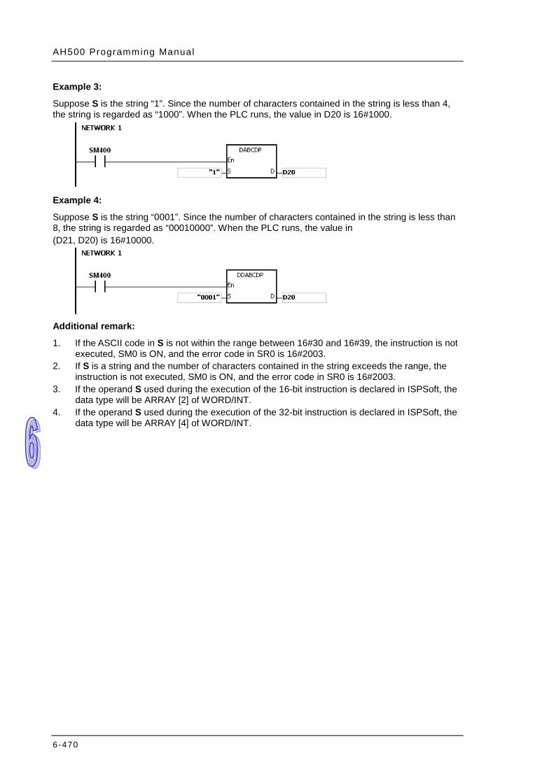
AH500 Programming Manual
6-470
Example 3:
Suppose S is the string “1”. Since the number of characters contained in the string is less than 4, the string is regarded as “1000”. When the PLC runs, the value in D20 is 16#1000.
Example 4:
Suppose S is the string “0001”. Since the number of characters contained in the string is less than 8, the string is regarded as “00010000”. When the PLC runs, the value in (D21, D20) is 16#10000.
Additional remark:
1. If the ASCII code in S is not within the range between 16#30 and 16#39, the instruction is not executed, SM0 is ON, and the error code in SR0 is 16#2003.
2. If S is a string and the number of characters contained in the string exceeds the range, the instruction is not executed, SM0 is ON, and the error code in SR0 is 16#2003.
3. If the operand S used during the execution of the 16-bit instruction is declared in ISPSoft, the data type will be ARRAY [2] of WORD/INT.
4. If the operand S used during the execution of the 32-bit instruction is declared in ISPSoft, the data type will be ARRAY [4] of WORD/INT.
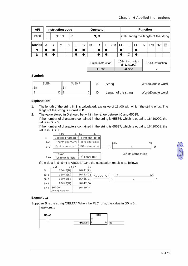
Chapter 6 Appl ied Inst ruct ions
6-471
API Instruction code Operand Function
2106 $LEN P S, D Calculating the length of the string
Device X Y M S T C HC D L SM SR E PR K 16# “$” DF
S D
Pulse instruction 16-bit instruction
(5-11 steps) 32-bit instruction
AH500 AH500 -
Symbol:
S : String Word/Double word
D : Length of the string Word/Double word
Explanation:
1. The length of the string in S is calculated, exclusive of 16#00 with which the string ends. The length of the string is stored in D.
2. The value stored in D should be within the range between 0 and 65535. If the number of characters contained in the string is 65536, which is equal to 16#10000, the value in D is 0. If the number of characters contained in the string is 65537, which is equal to 16#10001, the value in D is 0.
b15 b0 b7 b8First character S
S+1 b15 b0 D
Length of the string
Second characterThi rd characterFour th characterF ifth characterSix th character
n charac terth 16#00( )End ind characte r
S+2
S+n
n
If the data in S~S+4 is ABCDEFGHI, the calculation result is as follows.
b15 b0 b7 b8 S
S+1 b15 b0 D
16#00( )Ending character
S+2
S+4 S+3
16#41(A)16#42(B)16#43(C)16#44(D)16#45(E)16#46(F)16#47(G)16#48(H)16#49( I)
ABCDEFGHI 9
Example 1:
Suppose S is the string “DELTA”. When the PLC runs, the value in D0 is 5.

AH500 Programming Manual
6-472
Example 2:
Suppose the data in D0~D2 is as follows. When the PLC runs, the value in L0 is 5. D0 16#45 (E) 16#44 (D) D1 16#54 (T) 16#4C (L) D2 16#00 (Ending character) 16#41 (A)
Additional remark:
If the string does not end with 16#00, the instruction is not executed, SM0 is ON, and the error code in SR0 is 16#200E.

Chapter 6 Appl ied Inst ruct ions
6-473
API Instruction code Operand Function
2107 D $STR P S1, S2, D Converting the binary number into the string
Device X Y M S T C HC D L SM SR E PR K 16# “$” DF
S1 S2 D
Pulse instruction 16-bit instruction
(7 steps) 32-bit instruction
(7 steps)
AH500 AH500 AH500
Symbol:
S1 : Initial device in which the number of characters is stored
Word/Double word
S2 : Value which is converted Word/Double word
D : Initial device in which the conversion result is stored Word
Explanation:
1. A decimal point is added to the value in S2, the value in S1+1 indicates the number of decimal places, and the value in S1 indicates the number of characters. The conversion result is stored in D.
2. $STR: The value in S1 should be within the range between 2 and 8. The value in S1+1 should be within the range between 0 and 5, and should be less than or equal to the value in S1 minus 3. The value in S2 should be within the range between -32768 and 32767.
b15 b0 b7 b8
16#00 ( )Ending charac ter
Number of characters
S1+1 Number of dec imal pl aces
Binary number
.
Sign
D+1
D+2 D+3 D+4
Automati cally stored at the end of the s tr ing
S1
S2
DSign F irst ASCII codeSecond ASCII codeThi rd A SCII codeFour th ASCII codeFifth ASCII code
Six th ASCII codeSeventh AS CII code
Suppose the number of characters is 5, the number of decimal places is 1, and the value is -123. The conversion result is as follows.
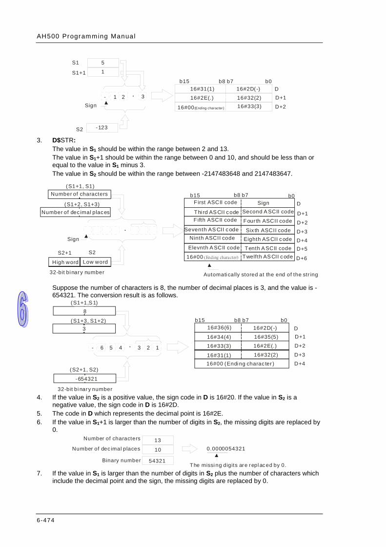
AH500 Programming Manual
6-474
b15 b0 b7 b8
16#00 ( )Ending character
S1+1
. D+1 D+2
16#31(1)
5 1
-123
- 1 2 3
32(2)16# 16#2E(.) 33(3)16#
S2
16#2D(-) D
S1
Sign
3. D$STR:
The value in S1 should be within the range between 2 and 13. The value in S1+1 should be within the range between 0 and 10, and should be less than or equal to the value in S1 minus 3. The value in S2 should be within the range between -2147483648 and 2147483647.
b15 b0 b7 b8 (S1+1, S1)
.
D+1 D+2 D+3
(S1+2, S1+3) D
Number of characters
Number of dec imal places
Sign
First ASCII code Sign Second A SCII codeThi rd AS CII codeFour th ASCII codeFifth ASCII code
Six th ASCII codeSeventh AS CII code
Eighth AS CII codeNinth ASCII code
32-bit bi nary number
D+4Tenth A SCII code D+5
S2+1
High word Low word
S2 16#00 ( )Ending chara cter Twelfth AS CII code D+6
Elevnth A SCII code
Automati cally stored at the end of the str ing
Suppose the number of characters is 8, the number of decimal places is 3, and the value is -654321. The conversion result is as follows.
b15 b0 b7 b8
(S1+1,S 1)
.
D+1 D+2 D+3 D+4
(S1+3, S1+2)
(S2+1, S2)
8
3
-654321
- 6 5 4 2 3 1
2D( -)16# 16#36(6)
35(5)16# 16#34(4) 2E(.)16# 16#33(3) 32(2)16# 16#31(1)
D
32-bit bi nary number
16#00 ( )Endi ng charac ter
4. If the value in S2 is a positive value, the sign code in D is 16#20. If the value in S2 is a
negative value, the sign code in D is 16#2D. 5. The code in D which represents the decimal point is 16#2E. 6. If the value in S1+1 is larger than the number of digits in S2, the missing digits are replaced by
0.
Binary number
13
10
54321
0.0000054321
The missi ng digits are repl aced by 0.
Number of characters
Number of dec imal places
7. If the value in S1 is larger than the number of digits in S2 plus the number of characters which
include the decimal point and the sign, the missing digits are replaced by 0.
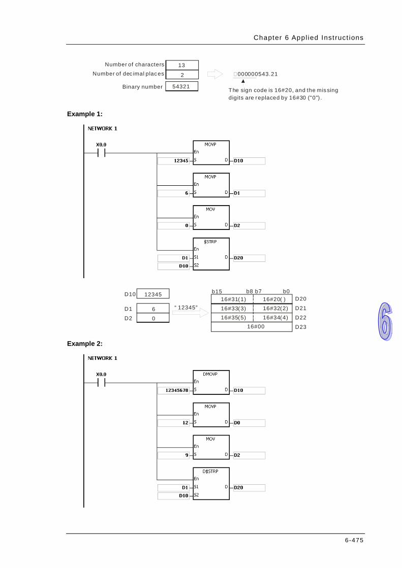
Chapter 6 Appl ied Inst ruct ions
6-475
13
2
54321
�000000543.21
The sign code is 16#20, and the missing digits are replaced by 16#30 ("0") .
Number of charactersNumber of dec imal places
Binary number
Example 1:
b15 b0 b7 b8
0016#
16#20( )16#31(1)16#32(2)16#33(3)16#34(4)16#35(5)
D10 12345
D1 6 D2 0
D20 D21 D22 D23
“ 12345”
Example 2:

AH500 Programming Manual
6-476
b15 b0 b7 b8
16#00
16#33(3)16#34(4)16#35(5)16#36(6)16#37(7)16#38(8)
(D11, D10)
(D1, D0)
(D2, D3)
D20 D21 D22 D23
12345678
12
9
16#20( )16#30(0)16#2E(.)16#30(0)16#31(1)16#32(2)
D24 D25 D26
“ 0.012345678”
Additional remark:
1. If the value in S1 exceeds the range, the instruction is not executed, SM0 is ON, and the error code in SR0 is 16#2003.
2. If the value in S1+1 exceeds the range, the instruction is not executed, SM0 is ON, and the error code in SR0 is 16#2003.
3. The value in S1+1 should be less than or equal to the value in S1 minus 3. Otherwise, the instruction is not executed, SM0 is ON, and the error code in SR0 is 16#2003.
4. If the value in S1 is less than the number of digits in S2 plus the number of characters which include the decimal point and the sign, the instruction is not executed, SM0 is ON, and the error code in SR0 is 16#2003.
5. If the operand S1 used during the execution of the 16-bit instruction is declared in ISPSoft, the data type will be ARRAY [2] of WORD/INT.
6. If the operand S1 used during the execution of the 32-bit instruction is declared in ISPSoft, the data type will be ARRAY [2] of DWORD/DINT.
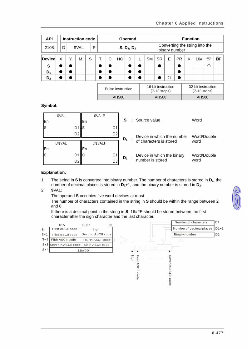
Chapter 6 Appl ied Inst ruct ions
6-477
API Instruction code Operand Function
2108 D $VAL P S, D1, D2 Converting the string into the binary number
Device X Y M S T C HC D L SM SR E PR K 16# “$” DF
S D1 D2
Pulse instruction 16-bit instruction
(7-13 steps) 32-bit instruction
(7-13 steps)
AH500 AH500 AH500
Symbol:
S : Source value Word
D1 : Device in which the number of characters is stored
Word/Double word
D2 : Device in which the binary number is stored
Word/Double word
Explanation:
1. The string in S is converted into binary number. The number of characters is stored in D1, the number of decimal places is stored in D1+1, and the binary number is stored in D2.
2. $VAL: The operand S occupies five word devices at most. The number of characters contained in the string in S should be within the range between 2 and 8. If there is a decimal point in the string in S, 16#2E should be stored between the first character after the sign character and the last character.
b15 b0 b7 b8
16#00
S+ 1 S+ 2S+3
S+ 4
D1+1
.
... .... .... .... .... .
D1
D2 S
Seventh AS CII code
Second ASCII code
Six th ASCII codeFifth ASCII codeThi rd A SCII code
Four th ASCII code
First ASCII code Sign
Seventh A
SC
II code
First A
SC
II codeS
ign
Number of characters
Number of dec imal pl aces
Binary number
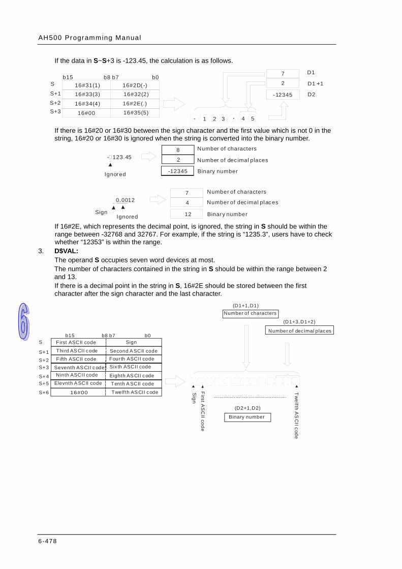
AH500 Programming Manual
6-478
If the data in S~S+3 is -123.45, the calculation is as follows.
b15 b0 b7 b8
0016#
S+1 S+2 S+3
D1 +1
.
2D( -)16# 16#31(1) 32(2)16# 33(3)16#
34(4)16# 35(5)16# 2E(.)16#
- 1
2
3 4 5
7
-12345
2
D1
D2
S
If there is 16#20 or 16#30 between the sign character and the first value which is not 0 in the string, 16#20 or 16#30 is ignored when the string is converted into the binary number.
8
2
-12345
- 123.45�
Ignored
Number of characters
Number of dec imal places
Binary number
7
4
12
0.0012
IgnoredSign
Number of characters
Number of dec imal pl aces
Binary number
If 16#2E, which represents the decimal point, is ignored, the string in S should be within the range between -32768 and 32767. For example, if the string is “1235.3”, users have to check whether “12353” is within the range.
3. D$VAL: The operand S occupies seven word devices at most. The number of characters contained in the string in S should be within the range between 2 and 13. If there is a decimal point in the string in S, 16#2E should be stored between the first character after the sign character and the last character.
(D1+1,D1)
... .... .... .... .... ..... .... .... .... .... ..... .... .
(D2+1,D2)
(D1+3,D1+2)
S
S+ 1 S+ 2 S+ 3
S+ 4 S+ 5
S+ 6
b15 b0 b7 b8
16#00
Sign F irst ASCII codeSecond A SCII codeThi rd AS CII codeFour th ASCII codeFifth ASCII codeSix th ASCII codeSeventh AS CII codeEighth AS CII codeNinth ASCII code
Tenth A SCII codeElevnth A SCII code
Twelfth AS CII code Sign
First A
SC
II code
Tw
elfth AS
CII code
Binary number
Number of characters
Number of dec imal places
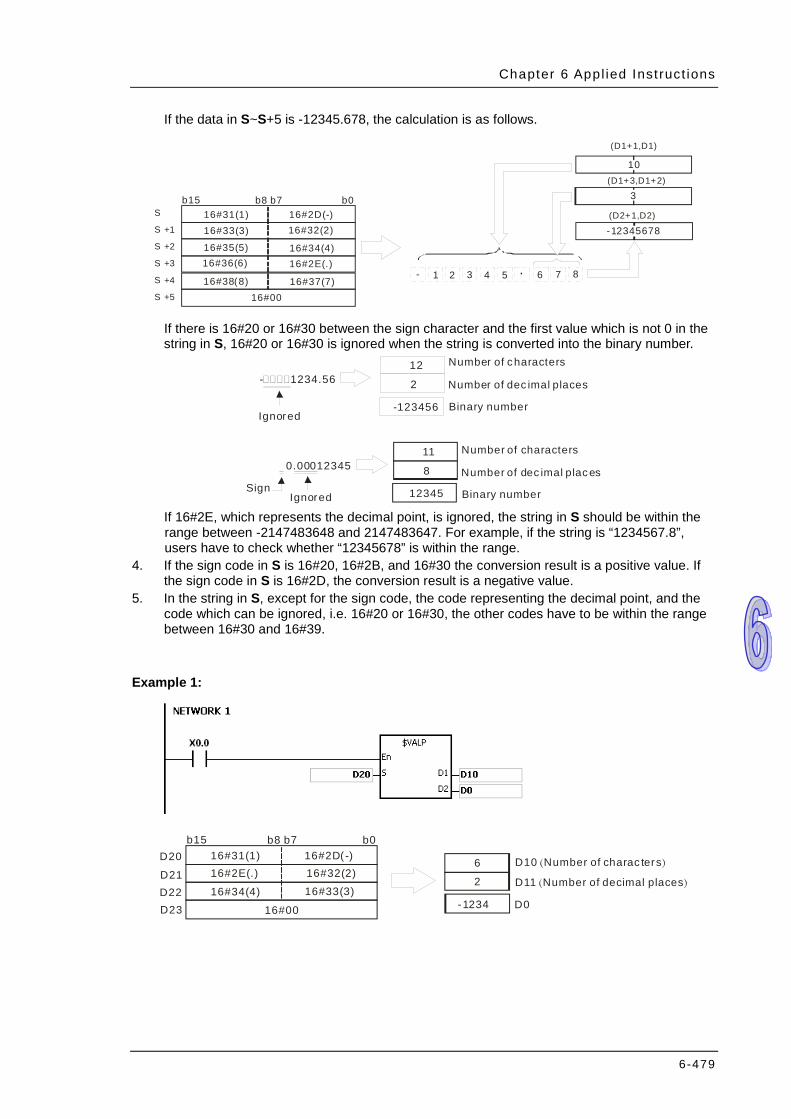
Chapter 6 Appl ied Inst ruct ions
6-479
If the data in S~S+5 is -12345.678, the calculation is as follows.
b15 b0 b7 b8
0016#
S
+1 S
+2 S
+3 S
4
(D1+1,D1)
2D(-)16# 16#31(1) 32(2)16# 33(3)16#
35(5)16# (4)16#34 2E(.)16#
- 1 3 5 36(6)16#
16#38(8) 37(7)16# +4 S
+5 S
. 6 7 8 2
10
3
(D2+1,D2)
(D1+3,D1+2)
-12345678
If there is 16#20 or 16#30 between the sign character and the first value which is not 0 in the string in S, 16#20 or 16#30 is ignored when the string is converted into the binary number.
12
2
-123456
- 1234.56����
Ignored
Number of characters
Number of dec imal places
Binary number
11
8
12345
0.00012345
Ignored
Number of characters
Number of dec imal places
Binary numberSign
If 16#2E, which represents the decimal point, is ignored, the string in S should be within the range between -2147483648 and 2147483647. For example, if the string is “1234567.8”, users have to check whether “12345678” is within the range.
4. If the sign code in S is 16#20, 16#2B, and 16#30 the conversion result is a positive value. If the sign code in S is 16#2D, the conversion result is a negative value.
5. In the string in S, except for the sign code, the code representing the decimal point, and the code which can be ignored, i.e. 16#20 or 16#30, the other codes have to be within the range between 16#30 and 16#39.
Example 1:
b15 b0 b7 b8
0016#
D20 2D( -)16# 16#31(1) 32(2)16# 2E(.)16#
34(4)16# 33(3)16# 2
6
-1234
D21 D22 D23
D10 ( )Number of charac ters
D11 ( )Number of decimal places
D0
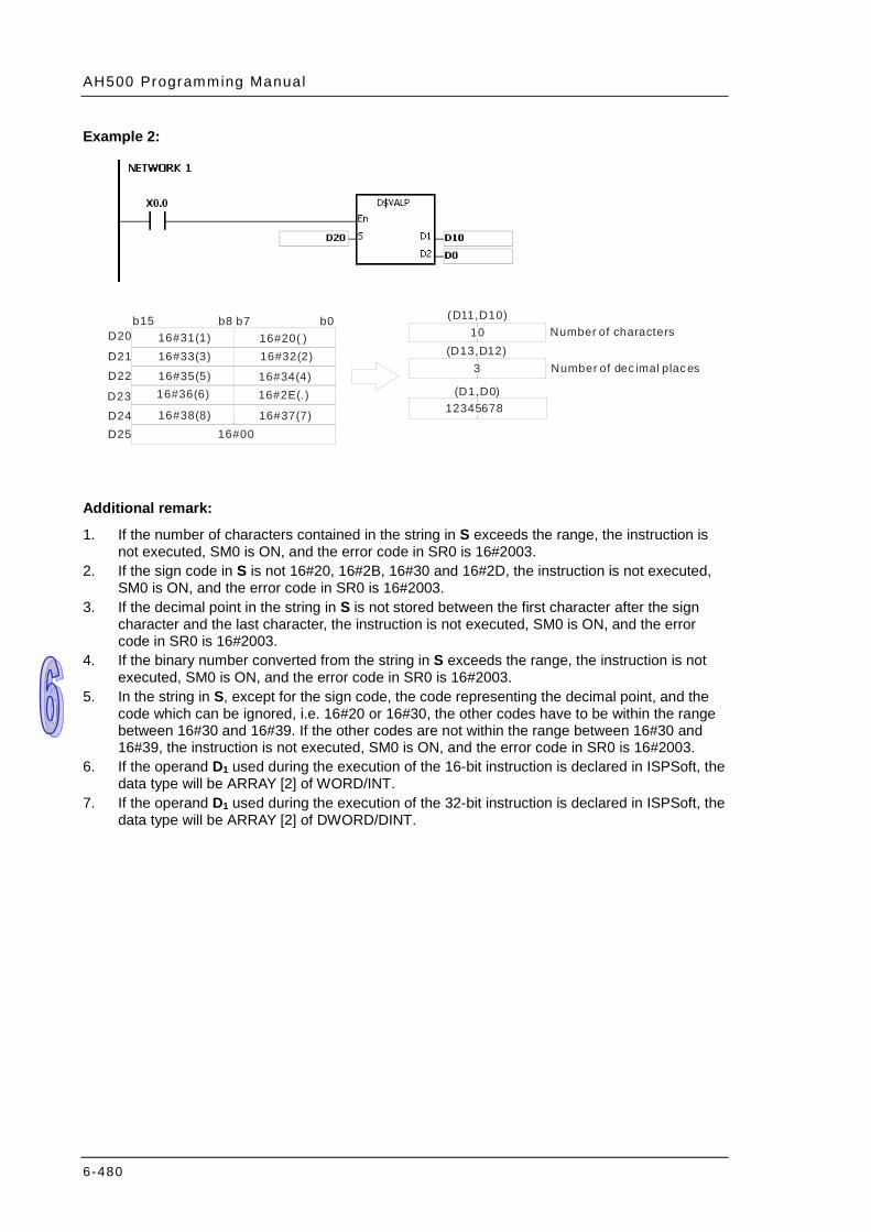
AH500 Programming Manual
6-480
Example 2:
b15 b0 b7 b8
16#00
D21 16#20( ) 16#31(1) 16#32(2) 16#33(3)
16#35(5) 16#34(4) 16#2E(.) 16#36(6)
16#38(8) 16#37(7)
10
3
12345678
D20
D22
D23 D24 D25
(D11,D10)
(D13,D12)
(D1,D0)
Number of characters
Number of dec imal places
Additional remark:
1. If the number of characters contained in the string in S exceeds the range, the instruction is not executed, SM0 is ON, and the error code in SR0 is 16#2003.
2. If the sign code in S is not 16#20, 16#2B, 16#30 and 16#2D, the instruction is not executed, SM0 is ON, and the error code in SR0 is 16#2003.
3. If the decimal point in the string in S is not stored between the first character after the sign character and the last character, the instruction is not executed, SM0 is ON, and the error code in SR0 is 16#2003.
4. If the binary number converted from the string in S exceeds the range, the instruction is not executed, SM0 is ON, and the error code in SR0 is 16#2003.
5. In the string in S, except for the sign code, the code representing the decimal point, and the code which can be ignored, i.e. 16#20 or 16#30, the other codes have to be within the range between 16#30 and 16#39. If the other codes are not within the range between 16#30 and 16#39, the instruction is not executed, SM0 is ON, and the error code in SR0 is 16#2003.
6. If the operand D1 used during the execution of the 16-bit instruction is declared in ISPSoft, the data type will be ARRAY [2] of WORD/INT.
7. If the operand D1 used during the execution of the 32-bit instruction is declared in ISPSoft, the data type will be ARRAY [2] of DWORD/DINT.

Chapter 6 Appl ied Inst ruct ions
6-481
API Instruction code Operand Function
2109 $FSTR P S1, S2, D Converting the floating-point number into the string
Device X Y M S T C HC D L SM SR E PR K 16# “$” DF
S1 S2 D
Pulse instruction 16-bit instruction
(7-8 steps) 32-bit instruction
AH500 AH500 -
Symbol:
S1 : Source value Double word
S2 : Initial device in which the format is stored Word
D : Initial device in which the conversion result is stored Word
Explanation:
1. The floating-point number in S1 is converted into the string in accordance with the setting of S2, and the conversion result is stored in D.
2. The conversion result varies with the setting of S2. 3. The value in S2+1 should be within the range between 2 and 24.
0: Decimal format1: Exponential
S2
S2 +1
S2 +2
Number of characters
Number of dec imal places 4. Decimal format
b15 b0 b7 b8 D
+1 D
+2 D
+3 D
+4 D
Decimal poi nt (.)
S2
Numbe r of ch aracters
Decimal fo ra mt
Number of decimal p laces +2S2
+1S2
.
Floating-poi nt number
(S1+1, S1)
Four th ASCII code
Sign F irst ASCII code
Second ASCII codeThi rd AS CII code
Fifth ASCII codeSix th ASCII code 16#00 ( )Ending charac ter
Automati cally stored at the end of the s tr ing
Sign
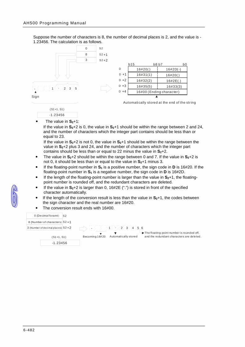
AH500 Programming Manual
6-482
Suppose the number of characters is 8, the number of decimal places is 2, and the value is -1.23456. The calculation is as follows.
b15 b0 b7 b8 D
+1 D
+2 D
+3 D
+4 D
S2
+2S2
+1S2
.
(S1+1, S1)
0
8
3
-1.23456
- 1 2 3 5
2D( -)16# 16#20( )
20( )16# 31(1)16#
16#2E(.) 32(2)16#
33(3)16# 35(5)16#
SignAutomati cally stored at the end of the str ing
16#00 ( )Ending charac ter
The value in S2+1:
If the value in S2+2 is 0, the value in S2+1 should be within the range between 2 and 24, and the number of characters which the integer part contains should be less than or equal to 23. If the value in S2+2 is not 0, the value in S2+1 should be within the range between the value in S2+2 plus 3 and 24, and the number of characters which the integer part contains should be less than or equal to 22 minus the value in S2+2.
The value in S2+2 should be within the range between 0 and 7. If the value in S2+2 is not 0, it should be less than or equal to the value in S2+1 minus 3.
If the floating-point number in S1 is a positive number, the sign code in D is 16#20. If the floating-point number in S1 is a negative number, the sign code in D is 16#2D.
If the length of the floating-point number is larger than the value in S2+1, the floating-point number is rounded off, and the redundant characters are deleted.
If the value in S2+2 is larger than 0, 16#2E (“.”) is stored in front of the specified character automatically.
If the length of the conversion result is less than the value in S2+1, the codes between the sign character and the real number are 16#20.
The conversion result ends with 16#00.
S2
+2S2
+1S2
.
(S1+1, S1)
0 (Decimal foramt)
8 (Number of characters)
3 (Number of deci mal places)
-1.23456
- 1 2 3 4 5 6The floating-point number is rounded off, and the redundant characters are de leted.Automatical ly storedBecoming 16#20

Chapter 6 Appl ied Inst ruct ions
6-483
5. Exponential format
b15 b0 b7 b8
16#00
D
D+1
D+2
D+3
D+4
Sign(Integer)
Decimal poi nt (.)
S2
Numbe r of cha racters
Expon ential format
Numbe r of decim al places +2S2
+1S2
E
Floating-point number
(S1+1, S1)
.
D+5
16#45(E)
D+6
Sign (Integer)
Sign (Exponent)
F irst ASCII codeSecond A SCII code
Thi rd AS CII codeFour th ASCII codeFifth ASCII codeSix th ASCII code
First ASCII codeSecond A SCII code
Automati cally stored at the end of the stri ng
Sign (Exponent)
Suppose the number of characters is 12, the number of decimal places is 4, and the value is -12.34567. The calculation is as follows.
b15 b0 b7 b8
16#00
D
+1 D
+2 D
+3 D
+4 D
S2
+2S2
+1S2
E
(S1+1,S1)
.
+5 D
+6 D
1 12 4
- 1 2 3 4 6 + 0 1
-12.34567
2D( -)16# 31(1)16# 32(2)16# 34(4)16#
45(E)16# 30(0)16#
16#20( )
16#2E(.)
16#33(3) 16#35(5)
16#2B(+) 16#31(1)Sign(
Integer)
Sign (Exponent)
Automati cally stored at the end of the str ing
The value in S2+1:
If the value in S2+2 is 0, the value in S2+1 should be within the range between 6 and 24. If the value in S2+2 is not 0, the value in S2+1 should be within the range between the value in S2+2 plus 7 and 24.
The value in S2+2 should be within the range between 0 and 7. If the value in S2+2 is not 0, it should be less than or equal to the value in S2+1 minus 7.
If the floating-point number in S1 is a positive number, the sign code in D is 16#20. If the floating-point number in S1 is a negative number, the sign code in D is 16#2D.
The integer part contains one character. To fulfill the number of characters, the codes between the sign code and the integer part are 16#20.
If the value in S2+2 is larger than 0, 16#2E (“.”) is stored in front of the specified character automatically.
If the exponent is a positive number, the sign code in D is 16#2B. If the exponent is a negative number, the sign code in D is 16#2D.
The exponent part contains two characters. If there is only one character, the other character is “0” (16#30).
The conversion result ends with 16#00.
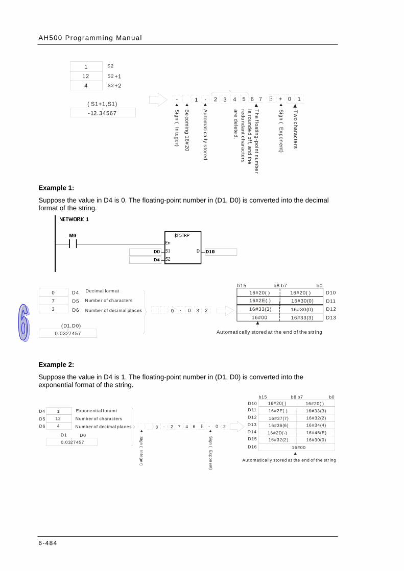
AH500 Programming Manual
6-484
Sign (Integer)
S2
+2S2
+1S2
E( S1+1,S1)
Sign (Exponent)
.
1 12 4
- 1 2 3 4 5 + 0 1
-12.34567Tw
o characters
Becoming 16#20
6 7
The floating-point number
is rounded off, and the redundant characters are deleted.
Automatically stored
Example 1:
Suppose the value in D4 is 0. The floating-point number in (D1, D0) is converted into the decimal format of the string.
Decimal fo rm at
Numbe r of ch aracters
Numbe r of decimal places
Automati cally stored at the end of the s tr ing
D4
.
0 7 3 0 0 2 3
0.0327457
D5
D6
(D1,D0)
b15 b0 b7 b8
0016#
20( )16# 16#20( ) 30(0)16# 2E(.)16#
16#30(0) 33(3)16#
33(3)16#
D10
D11 D12
D13
Example 2:
Suppose the value in D4 is 1. The floating-point number in (D1, D0) is converted into the exponential format of the string.
b15 b0 b7 b8
0016#
D11 D12 D13 D14
D6 D5
E
D1
.
D15
D16
1 12 4 3 2 7 4 6 - 0 2
0.0327457
20( )16# 33(3)16# 32(2)16# 34(4)16#
45(E)16# 30(0)16#
16#20( )
2E(.)16#
37(7)16# 36(6)16#
2D( -)16# 32(2)16#
D4
D0
D10
Sign (Integer)
Sign (Exponent)
Exponential foramt
Number of characters
Number of dec imal places
Automati cally stored at the end of the str ing
Chapter 6 Appl ied Inst ruct ions
6-485
Additional remark:
1. If the value in S1 exceeds the range of values which can be represented by the floating-point numbers, the instruction is not executed, SM0 is ON, and the error code in SR0 is 16#2013.
2. If the value in S2 is neither 0 nor 1, the instruction is not executed, SM0 is ON, and the error code in SR0 is 16#2003.
3. If the value in S2+1 exceeds the range below, the instruction is not executed, SM0 is ON, and the error code in SR0 is 16#2003. The decimal format:
If the value in S2+2 is 0, the value in S2+1 should be within the range between 2 and 24, and the number of characters which the integer part contains should be less than or equal to 23. If the value in S2+2 is not 0, the value in S2+1 should be within the range between the value in S2+2 plus 3 and 24, and the number of characters which the integer part contains should be less than or equal to 22 minus the value in S2+2
The exponential format: If the value in S2+2 is 0, the value in S2+1 should be within the range between 6 and 24. If the value in S2+2 is not 0, the value in S2+1 should be within the range between the value in S2+2 plus 7 and 24.
4. If the value in S2+2 exceeds the range below, the instruction is not executed, SM0 is ON, and the error code in SR0 is 16#2003. The decimal format:
The value in S2+2 should be within the range between 0 and 7. Besides, it should be less than or equal to the value in S2+1 minus 3.
The exponential format: The value in S2+2 should be within the range between 0 and 7. Besides, it should be less than or equal to the value in S2+1 minus 7.
5. If users declare the operand S2 in ISPSoft, the data type will be ARRAY [3] of WORD/INT.

AH500 Programming Manual
6-486
API Instruction code Operand Function
2110 $FVAL P S, D Converting the string into the floating-point number
Device X Y M S T C HC D L SM SR E PR K 16# “$” DF
S D
Pulse instruction 16-bit instruction
(5-11 steps) 32-bit instruction
AH500 AH500 -
Symbol:
S : Source value Word
D : Device in which the conversion result is stored Double word
Explanation:
1. The string in S is converted into the floating-point number, and the conversion result is stored in D.
The end of the s tr ing
F loating-point number
Sign F irst ASCII codeSecond A SCII codeThi rd AS CII codeFour th ASCII codeFifth ASCII codeSix th ASCII codeSeventh AS CII code
b15 b0 b7 b8
16#00
S
+1 S
+2 S
+3 S
+4 S
(D+1, D)
.. .. . .
+. .. S
.... . . . . .. . .
2. The string in S can be the decimal format of the string or the exponential format of the string.
The decimal format: b15 b0 b7 b8
16#31H(1) 2D(-)16# 30(0)16# 2E(.)16# 38(8)16# 37(7)16#
16#00 31(1)16#
. - 1 0 7 8 1 2
32(2)16#
HBF89FFD4 (D+1, D)
S
S +1
S +2
S +3
S +4
Floating-point number -1.07812
The exponential format:
b15 b0 b7 b816#20( ) 2D(-)16#16#2E(.) 31(1)16# 32(2)16# 33(3)16#
16#00
30(0)16#
. - 1 3 2 0 1
31(1)16# 16#D044B 5D1
(D+1, D)
S
S +1
S +2
S +3
S +4
S +5 S +6
2B(+ )16# 45(E)16#
31(1)16# 30(0)16#
E + 1 0
-1.3201E +10 Floating-poi nt number
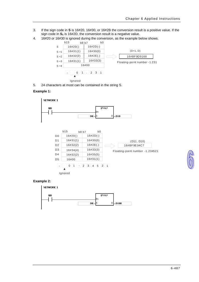
Chapter 6 Appl ied Inst ruct ions
6-487
3. If the sign code in S is 16#20, 16#30, or 16#2B the conversion result is a positive value. If the sign code in S1 is 16#2D, the conversion result is a negative value.
4. 16#20 or 16#30 is ignored during the conversion, as the example below shows. b15 b0 b7 b8
16#20( ) 2D(-)16# 31(1)16# 16#30(0) 32(2)16# 16#2E(.)
16#00 33(3)16#
. - 0 2 3 1
31(1)16# 16#BF9D9168
(D+1, D) S
S +1
S +2
S +3
S +4
1
-1.231Floating-poi nt number
Ignored 5. 24 characters at most can be contained in the string S.
Example 1:
Ignored
b15 b0 b7 b816#20( ) 2D(-)16# 31(1)16# 30(0)16#
D0 D1 (D11, D10)
32(2)16# 2E(.)16#
16#00
33(3)16# D2 D3
- 0 . 2 3 4
34(4)16#
16#BF9E 04C7
35(5)16# 32(2)16#16#31(1)
1 5 2 1
D4
D5
-1.234521 Floating-poi nt number
Example 2:
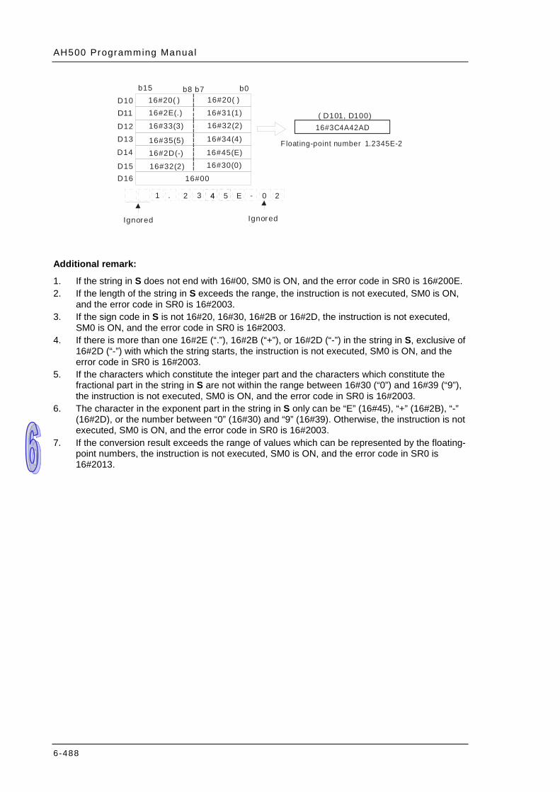
AH500 Programming Manual
6-488
Ignored
b15 b0 b7 b816#20( ) 20( )16# 2E(.)16# 31(1)16#
D10 D11 ( D101, D100)
33(3)16# 32(2)16#
16#32(2)
34(4)16# D12 D13
1 2 3 4
35(5)16#16#3C4A42AD
45(E)16# 2D(-)16#16#30(0)
. E - 2
D14
D1516#00 D16
0 4 5
Floating-point number 1.2345E-2
Ignored
Additional remark:
1. If the string in S does not end with 16#00, SM0 is ON, and the error code in SR0 is 16#200E. 2. If the length of the string in S exceeds the range, the instruction is not executed, SM0 is ON,
and the error code in SR0 is 16#2003. 3. If the sign code in S is not 16#20, 16#30, 16#2B or 16#2D, the instruction is not executed,
SM0 is ON, and the error code in SR0 is 16#2003. 4. If there is more than one 16#2E (“.”), 16#2B (“+”), or 16#2D (“-”) in the string in S, exclusive of
16#2D (“-”) with which the string starts, the instruction is not executed, SM0 is ON, and the error code in SR0 is 16#2003.
5. If the characters which constitute the integer part and the characters which constitute the fractional part in the string in S are not within the range between 16#30 (“0”) and 16#39 (“9”), the instruction is not executed, SM0 is ON, and the error code in SR0 is 16#2003.
6. The character in the exponent part in the string in S only can be “E” (16#45), “+” (16#2B), “-” (16#2D), or the number between “0” (16#30) and “9” (16#39). Otherwise, the instruction is not executed, SM0 is ON, and the error code in SR0 is 16#2003.
7. If the conversion result exceeds the range of values which can be represented by the floating-point numbers, the instruction is not executed, SM0 is ON, and the error code in SR0 is 16#2013.
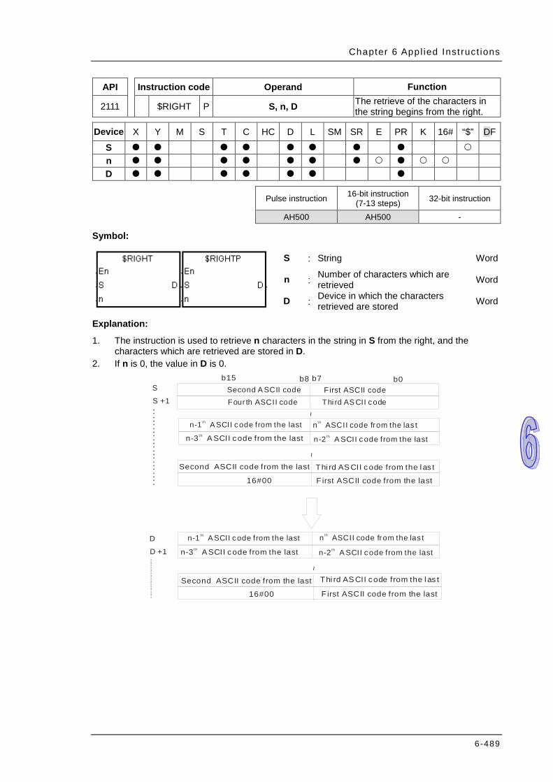
Chapter 6 Appl ied Inst ruct ions
6-489
API Instruction code Operand Function
2111 $RIGHT P S, n, D The retrieve of the characters in the string begins from the right.
Device X Y M S T C HC D L SM SR E PR K 16# “$” DF
S n D
Pulse instruction 16-bit instruction
(7-13 steps) 32-bit instruction
AH500 AH500 -
Symbol:
S : String Word
n : Number of characters which are retrieved Word
D : Device in which the characters retrieved are stored Word
Explanation:
1. The instruction is used to retrieve n characters in the string in S from the right, and the characters which are retrieved are stored in D.
2. If n is 0, the value in D is 0. b15 b0 b7 b8
16#00
S
+1 S
Second ASCII code from the last
F irst ASCII code from the last
.....................
~ ~
Thi rd AS CII code from the l as t
n-2 A SCII code from the lastthn-3 A SCII code from the lastth
16#00
~
D
+1 D.....................First ASCII codeSecond A SCII codeThi rd AS CII codeFour th ASCII code
n-1 A SCII code from the lastth n ASCII code from the las tth
n-1 A SCII code from the lastth n ASCII code from the las tth
n-2 A SCII code from the lastthn-3 A SCII code from the lastth
Thi rd AS CII code from the l as t
F irst ASCII code from the lastSecond ASCII code from the last
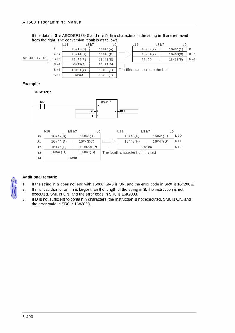
AH500 Programming Manual
6-490
If the data in S is ABCDEF12345 and n is 5, five characters in the string in S are retrieved from the right. The conversion result is as follows.
b15 b0 b7 b8
0016#
S
+1 S
+2 S
+3 S
16#41(A) 16#42(B) 43(C)16# 44(D)16#
46(F)16# 45(E)16# 31(1)16# 32(2)16#
34(4)16# 33(3)16# +4 S
+5 S 35(5)16#
b15 b0 b7 b8 D
+1 D
+2 D
16#31(1) 32(2)16# 33(3)16# 34(4)16#
16#00 35(5)16#
The fif th charac ter from the last
ABCDE F12345
Example:
b15 b0 b7 b8
0016#
16#41(A) 16#42(B)16#43(C) 44(D)16#
46(F)16# 45(E)16#16#47(G)16#48(H)
b15 b0 b7 b816#45(E) 46(F)16# 47(G)16# 48(H)16#
The fourth charac ter from the last
0016#
D0 D1
D2
D3 D4
D10 D11
D12
Additional remark:
1. If the string in S does not end with 16#00, SM0 is ON, and the error code in SR0 is 16#200E. 2. If n is less than 0, or if n is larger than the length of the string in S, the instruction is not
executed, SM0 is ON, and the error code in SR0 is 16#2003. 3. If D is not sufficient to contain n characters, the instruction is not executed, SM0 is ON, and
the error code in SR0 is 16#2003.
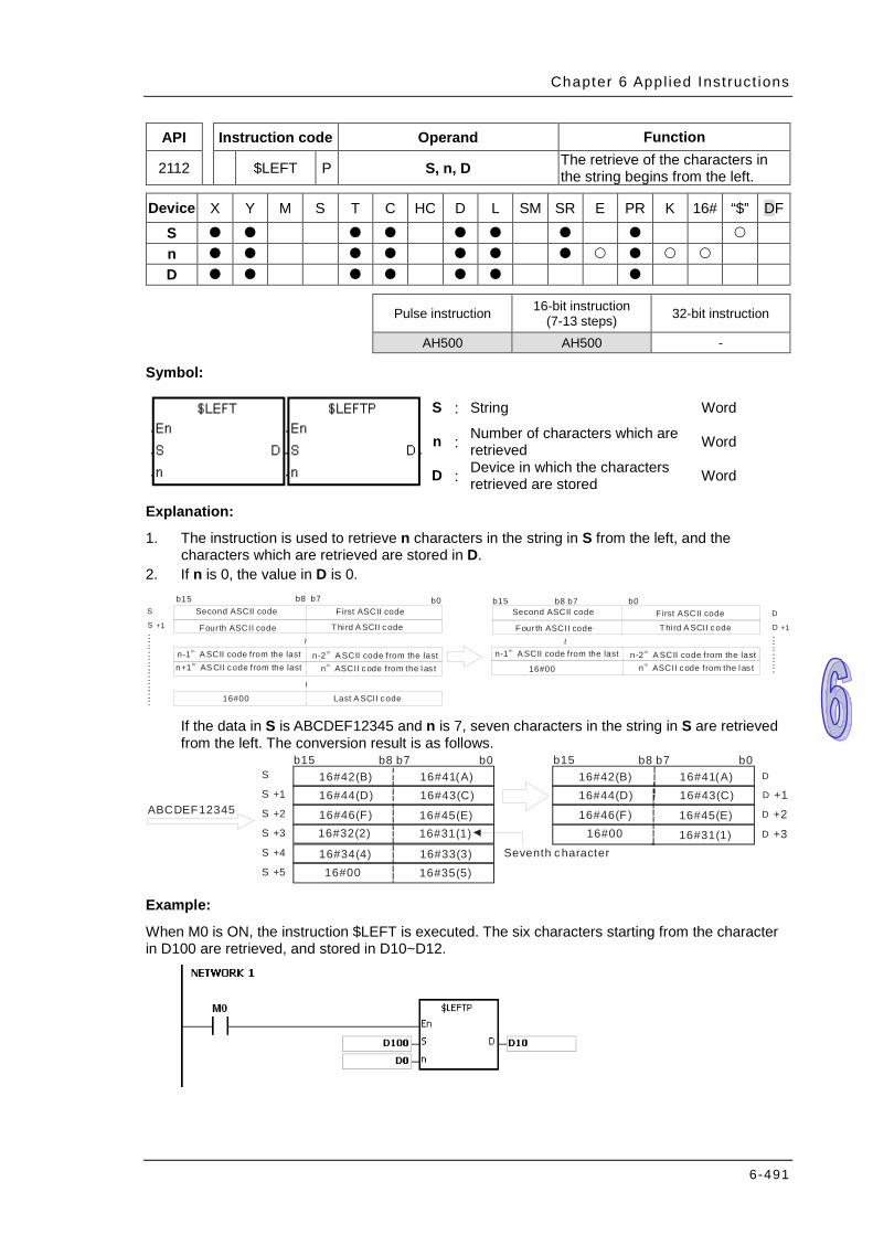
Chapter 6 Appl ied Inst ruct ions
6-491
API Instruction code Operand Function
2112 $LEFT P S, n, D The retrieve of the characters in the string begins from the left.
Device X Y M S T C HC D L SM SR E PR K 16# “$” DF
S n D
Pulse instruction 16-bit instruction
(7-13 steps) 32-bit instruction
AH500 AH500 -
Symbol:
S : String Word
n : Number of characters which are retrieved Word
D : Device in which the characters retrieved are stored Word
Explanation:
1. The instruction is used to retrieve n characters in the string in S from the left, and the characters which are retrieved are stored in D.
2. If n is 0, the value in D is 0. b15 b0 b7 b8
16#00
S
+1 S.....................
~ ~
D
+1 D...........
b15 b0 b7 b8
~
First ASCII codeSecond ASCII code
Thi rd A SCII codeFour th ASCII code
First ASCII codeSecond ASCII code
Thi rd A SCII codeFour th ASCII code
Last A SCII code
n ASCII code from the l as tth
n-2 A SCII code from the lastthn-1 A SCII code from the lastth
n+1 AS CII code from the lastth n ASCII code from the l as tth
n-2 A SCII code from the lastthn-1 A SCII code from the lastth
16#00
If the data in S is ABCDEF12345 and n is 7, seven characters in the string in S are retrieved from the left. The conversion result is as follows.
b15 b0 b7 b8
0016#
S
+1 S
+2 S
+3 S
16#41(A) 16#42(B) 43(C)16# 44(D)16#
46(F)16# 45(E)16# 31(1)16# 32(2)16#
34(4)16# 33(3)16# +4 S
+5 S 35(5)16#
b15 b0 b7 b8 D
+1 D
+2 D
16#41(A) 42(B)16# 43(C)16# 44(D)16#
46(F)16# 45(E)16#
Seventh character
ABCDEF12345
+3 D 31(1)16# 0016#
Example:
When M0 is ON, the instruction $LEFT is executed. The six characters starting from the character in D100 are retrieved, and stored in D10~D12.
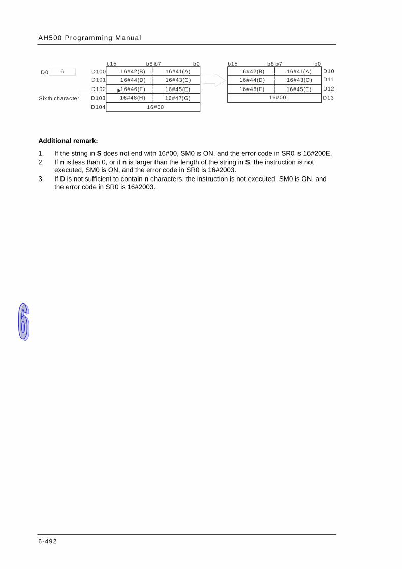
AH500 Programming Manual
6-492
b15 b0 b7 b8
0016#
16#41(A) 16#42(B) 43(C)16# 44(D)16#
46(F)16# 45(E)16#16#47(G) 48(H)16#
b15 b0 b7 b816#41(A) 42(B)16# 43(C)16# 44(D)16#
46(F)16# 45(E)16# Six th charac ter 0016#
D100 D101
D102 D103 D104
D10 D11
D12 D13
6 D0
Additional remark:
1. If the string in S does not end with 16#00, SM0 is ON, and the error code in SR0 is 16#200E. 2. If n is less than 0, or if n is larger than the length of the string in S, the instruction is not
executed, SM0 is ON, and the error code in SR0 is 16#2003. 3. If D is not sufficient to contain n characters, the instruction is not executed, SM0 is ON, and
the error code in SR0 is 16#2003.
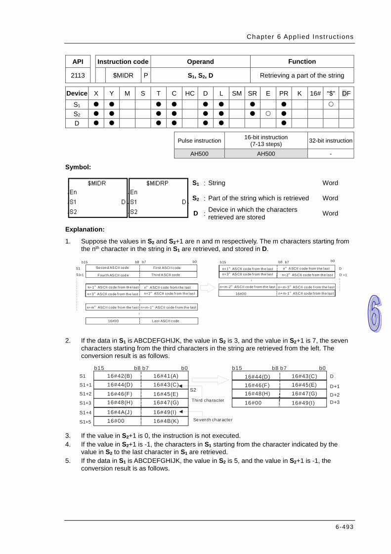
Chapter 6 Appl ied Inst ruct ions
6-493
API Instruction code Operand Function
2113 $MIDR P S1, S2, D Retrieving a part of the string
Device X Y M S T C HC D L SM SR E PR K 16# “$” DF
S1 S2 D
Pulse instruction 16-bit instruction
(7-13 steps) 32-bit instruction
AH500 AH500 -
Symbol:
S1 : String Word
S2 : Part of the string which is retrieved Word
D : Device in which the characters retrieved are stored Word
Explanation:
1. Suppose the values in S2 and S2+1 are n and m respectively. The m characters starting from the nth character in the string in S1 are retrieved, and stored in D.
b15 b0 b7 b8
16#0 0
~ ~
D
+1 D
...........
b15 b0 b7 b8
~
First ASCI I codeSe con d ASCII co de
Third ASCII co deFourth ASCII cod e
Last ASCI I code
n ASCII code from the lastthn+1 ASCII co de f rom th e lastth
n+m-1 ASCII co de f rom th e lastth
n+m-3 ASCII co de f rom the lastthn+m-2 ASCII co de f rom th e lastth
16#0 0
S1
+1 S1
.....................
n+2 ASCII co de f rom th e lastthn+3 ASCII co de f rom th e lastth
n+m ASCI I code fro m the lastth n+m-1 ASCII co de f rom th e lastth
~
n+1 ASCII co de f rom th e lastth n ASCII code from the lastth
n+3 ASCII co de f rom th e lastthn+2 ASCII co de f rom th e lastth
2. If the data in S1 is ABCDEFGHIJK, the value in S2 is 3, and the value in S2+1 is 7, the seven characters starting from the third characters in the string are retrieved from the left. The conversion result is as follows.
b15 b0 b7 b8
0016#
S1 16#41(A) 16#42(B) 43(C)16# 44(D)16#
46(F)16# 45(E)16# 47(G)16# 48(H)16#
4A(J )16# 49(I)16# 4B(K)16#
b15 b0 b7 b8 D
16#45(E) 46(F)16# 47(G)16# 48(H)16#
49(I)16# Thi rd character 0016#
+1 S1
+2 S1
+3 S1
+4 S1
+5 S1
S2
Seventh character
43(C)16# 44(D)16#
D+3
D+1
D+2
3. If the value in S2+1 is 0, the instruction is not executed. 4. If the value in S2+1 is -1, the characters in S1 starting from the character indicated by the
value in S2 to the last character in S1 are retrieved. 5. If the data in S1 is ABCDEFGHIJK, the value in S2 is 5, and the value in S2+1 is -1, the
conversion result is as follows.
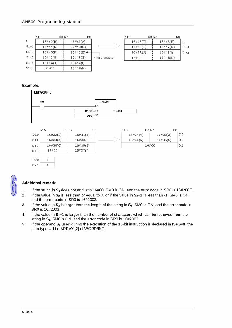
AH500 Programming Manual
6-494
b15 b0 b7 b8
0016#
S1 16#41(A) 16#42(B) 43(C)16# 44(D)16#
46(F)16# 45(E)16# 47(G)16# 48(H)16#
4A(J )16# 49(I)16# 4B(K)16#
b15 b0 b7 b8 D
+1 D
+2 D
16#45(E) 46(F)16# 47(G)16# 48(H)16#
49(I)16# Fifth character
4A(J )16#
+1 S1
+2 S1
+3 S1
+4 S1
+5 S1
0016# 4B(K)16#
Example:
b15 b0 b7 b8
0016#
16#31(1) 16#32(2) 33(3)16# 34(4)16#
16#36(6) 35(5)16# 37(7)16#
b15 b0 b7 b8 D0 D1
16#33(3) 34(4)16# 35(5)16# 36(6)16#
0016#
3 4
D2
D10 D11
D12 D13
D20 D21
Additional remark:
1. If the string in S1 does not end with 16#00, SM0 is ON, and the error code in SR0 is 16#200E. 2. If the value in S2 is less than or equal to 0, or if the value in S2+1 is less than -1, SM0 is ON,
and the error code in SR0 is 16#2003. 3. If the value in S2 is larger than the length of the string in S1, SM0 is ON, and the error code in
SR0 is 16#2003. 4. If the value in S2+1 is larger than the number of characters which can be retrieved from the
string in S1, SM0 is ON, and the error code in SR0 is 16#2003. 5. If the operand S2 used during the execution of the 16-bit instruction is declared in ISPSoft, the
data type will be ARRAY [2] of WORD/INT.
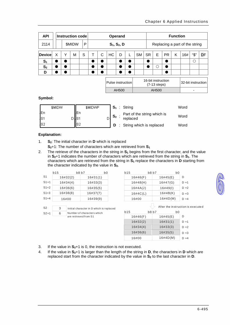
Chapter 6 Appl ied Inst ruct ions
6-495
API Instruction code Operand Function
2114 $MIDW P S1, S2, D Replacing a part of the string
Device X Y M S T C HC D L SM SR E PR K 16# “$” DF
S1 S2 D
Pulse instruction 16-bit instruction
(7-13 steps) 32-bit instruction
AH500 AH500 -
Symbol:
S1 : String Word
S2 : Part of the string which is replaced Word
D : String which is replaced Word
Explanation:
1. S2: The initial character in D which is replaced S2+1: The number of characters which are retrieved from S1
2. The retrieve of the characters in the string in S1 begins from the first character, and the value in S2+1 indicates the number of characters which are retrieved from the string in S1. The characters which are retrieved from the string in S1 replace the characters in D starting from the character indicated by the value in S2.
b15 b0 b7 b8
0016#
S1 16#31(1) 16#32(2) 33(3)16# 34(4)16#
36(6)16# 35(5)16# 37(7)16# 38(8)16#
39(9)16#
b15 b0 b7 b8 D
+1 D
+2 D
16#45(E) 46(F)16# 47(G)16# 48(H)16#
49(I)16# 4A(J )16#
+1 S1
+2 S1
+3 S1
+4 S1
S2
+1 S2
3 6
4C(L)16# 4B(K)16# +3 D
0016# 4D(M)16# +4 D
b15 b0 b7 b8 D
+1 D
+2 D
16#45(E) 46(F)16#
+3 D
0016# 4D(M)16# +4 D
In itial character in D which is rep lacedNumber of characters which are re trieved from S1
16#31(1) 32(2)16# 33(3)16# 34(4)16#
36(6)16# 35(5)16#
Af ter the in st ruct ion is execute d
3. If the value in S2+1 is 0, the instruction is not executed. 4. If the value in S2+1 is larger than the length of the string in D, the characters in D which are
replaced start from the character indicated by the value in S2 to the last character in D.
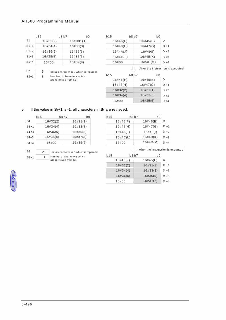
AH500 Programming Manual
6-496
b15 b0 b7 b8
0016#
S1 16#H31(1) 16#32(2) 33(3)16# 34(4)16#
36(6)16# 35(5)16# 37(7)16# 38(8)16#
39(9)16#
b15 b0 b7 b8 D
+1 D
+2 D
16#45(E) 46(F)16# 47(G)16# 48(H)16#
49(I)16# 4A(J )16#
+1 S1
+2 S1
+3 S1
+4 S1
S2
+1 S2
5 8
4C(L)16# 4B(K)16# +3 D
0016# 4D(M)16# +4 D
b15 b0 b7 b8 D
+1 D
+2 D
16#45(E) 46(F)16#
+3 D
0016# +4 D
47(G)16# 48(H)16#
16#31(1) 32(2)16# 33(3)16#
35(5)16#
34(4)16#
Af ter the in st ruct ion is execute dIn itial character in D which is rep lacedNumber of characters which are re trieved from S1
5. If the value in S2+1 is -1, all characters in S1 are retrieved.
b15 b0 b7 b8
0016#
S1 16#31(1) 16#32(2) 33(3)16# 34(4)16#
36(6)16# 35(5)16# 37(3)16# 38(8)16#
39(9)16#
b15 b0 b7 b8 D
+1 D
+2 D
16#45(E) 46(F)16# 47(G)16# 48(H)16#
49(I)16# 4A(J )16#
+1 S2
+2 S1
+3 S1
+4 S1
S2 2 -1
4C(L)16# 4B(K)16# +3 D
0016# 4D(M)16# +4 D
b15 b0 b7 b8 D
+1 D
+2 D
16#45(E) 46(F)16#
+3 D
0016# +4 D
16#31(1) 32(2)16# 33(3)16# 34(4)16#
36(6)16# 35(5)16# 37(7)16#
+1 S1
Af ter the in st ruct ion is execute dIn itial character in D which is rep lacedNumber of characters which are re trieved from S1
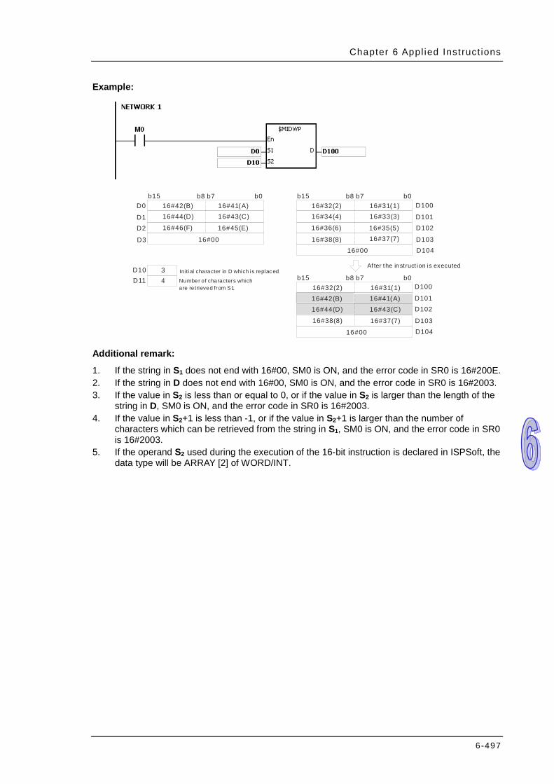
Chapter 6 Appl ied Inst ruct ions
6-497
Example:
b15 b0 b7 b8
0016#
D0
D1 D2
16#41(A) 16#42(B) 43(C)16# 44(D)16#
46(F)16# 45(E)16#
D3
b15 b0 b7 b816#31(1) 32(2)16# 33(3)16# 34(4)16#
35(5)16# 36(6)16#
D11 3 4
38(8)16# 37(7)16#
0016#
b15 b0 b7 b8
0016#
16#31(1) 32(2)16#
38(8)16# 37(7)16#
D10
D100
D101 D102
D103 D104
D100
D101 D102
D103 D104
16#41(A) 42(B)16# 43(C)16# 44(D)16#
Af ter the in st ruct ion is executedIn itial character in D which is replac edNumber of characters which are re trieved from S1
Additional remark:
1. If the string in S1 does not end with 16#00, SM0 is ON, and the error code in SR0 is 16#200E. 2. If the string in D does not end with 16#00, SM0 is ON, and the error code in SR0 is 16#2003. 3. If the value in S2 is less than or equal to 0, or if the value in S2 is larger than the length of the
string in D, SM0 is ON, and the error code in SR0 is 16#2003. 4. If the value in S2+1 is less than -1, or if the value in S2+1 is larger than the number of
characters which can be retrieved from the string in S1, SM0 is ON, and the error code in SR0 is 16#2003.
5. If the operand S2 used during the execution of the 16-bit instruction is declared in ISPSoft, the data type will be ARRAY [2] of WORD/INT.
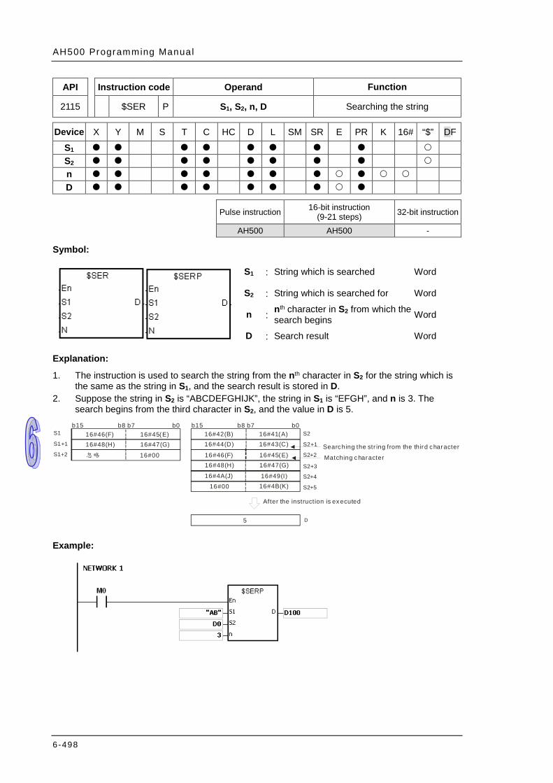
AH500 Programming Manual
6-498
API Instruction code Operand Function
2115 $SER P S1, S2, n, D Searching the string
Device X Y M S T C HC D L SM SR E PR K 16# “$” DF
S1 S2 n D
Pulse instruction 16-bit instruction (9-21 steps) 32-bit instruction
AH500 AH500 -
Symbol:
S1 : String which is searched Word
S2 : String which is searched for Word
n : nth character in S2 from which the
search begins Word
D : Search result Word
Explanation:
1. The instruction is used to search the string from the nth character in S2 for the string which is the same as the string in S1, and the search result is stored in D.
2. Suppose the string in S2 is “ABCDEFGHIJK”, the string in S1 is “EFGH”, and n is 3. The search begins from the third character in S2, and the value in D is 5.
b15 b0 b7 b8 S1 16#45(E) 16#46(F)
47(G)16# 48(H)16# +1 S1
+2 S1 0016#
b15 b0 b7 b8 S2
16#45(E) 46(F)16# 47(G)16# 48(H)16#
49(I)16# 4A(J)16# 4B(K)16#
D
After the instruction is executed
+1 S2
+2 S2
+3 S2
+4 S2
16#41(A) 42(B)16# 43(C)16# 44(D)16#
5
+5 S2 0016#
Searching the str ing from the third characterMatching character 忽略
Example:
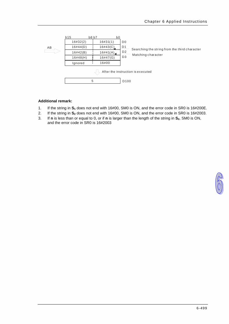
Chapter 6 Appl ied Inst ruct ions
6-499
b15 b0 b7 b8
16#41(A) 42(B)16# 47(G)16# 48(H)16#
16#31(1) 16#32(2) 43(C)16# 44(D)16#
5
0016#
AB
D0 D1 D2 D3
D100
Ignored
Searching the str ing from the thi rd characterMatching character
After the instruction is executed
Additional remark:
1. If the string in S1 does not end with 16#00, SM0 is ON, and the error code in SR0 is 16#200E. 2. If the string in S2 does not end with 16#00, SM0 is ON, and the error code in SR0 is 16#2003. 3. If n is less than or equal to 0, or if n is larger than the length of the string in S2, SM0 is ON,
and the error code in SR0 is 16#2003
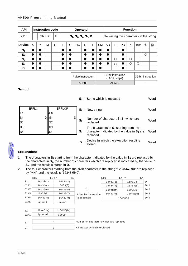
AH500 Programming Manual
6-500
API Instruction code Operand Function
2116 $RPLC P S1, S2, S3, S4, D Replacing the characters in the string
Device X Y M S T C HC D L SM SR E PR K 16# “$” DF
S1 S2 S3 S4 D
Pulse instruction 16-bit instruction
(11-17 steps) 32-bit instruction
AH500 AH500 -
Symbol:
S1 : String which is replaced Word
S2 : New string Word
S3 : Number of characters in S1 which are replaced Word
S4 : The characters in S1 starting from the character indicated by the value in S4 are replaced.
Word
D : Device in which the execution result is stored Word
Explanation:
1. The characters in S1 starting from the character indicated by the value in S4 are replaced by the characters in S2, the number of characters which are replaced is indicated by the value in S3, and the result is stored in D.
2. The four characters starting from the sixth character in the string “1234567890” are replaced by “MN”, and the result is “12345MN0”.
After the instruction is executed
b15 b0 b7 b8
0016#
S1+1 S1+2 S1+3
16#31(1) 16#32(2)16#33(3) 34(4)16#
36(6)16# 35(5)16# 37(7)16# 38(8)16#
39(9)16# S1+4
b15 b0 b7 b8
0016#
16#4D(M) 4E(N)16#
S1+5 30(0)16#
4
6
16#31(1) 32(2)16# 33(3)16# 34(4)16#
4D(M)16# 35(5)16# 4E(N)16# 30(0)16#
000016#
Character which i s replaced
Number of characters which are replaced
S1
S2 S2+1
S3
S4
D+1 D+2 D+3
D+4
D
Ignored
Ignored
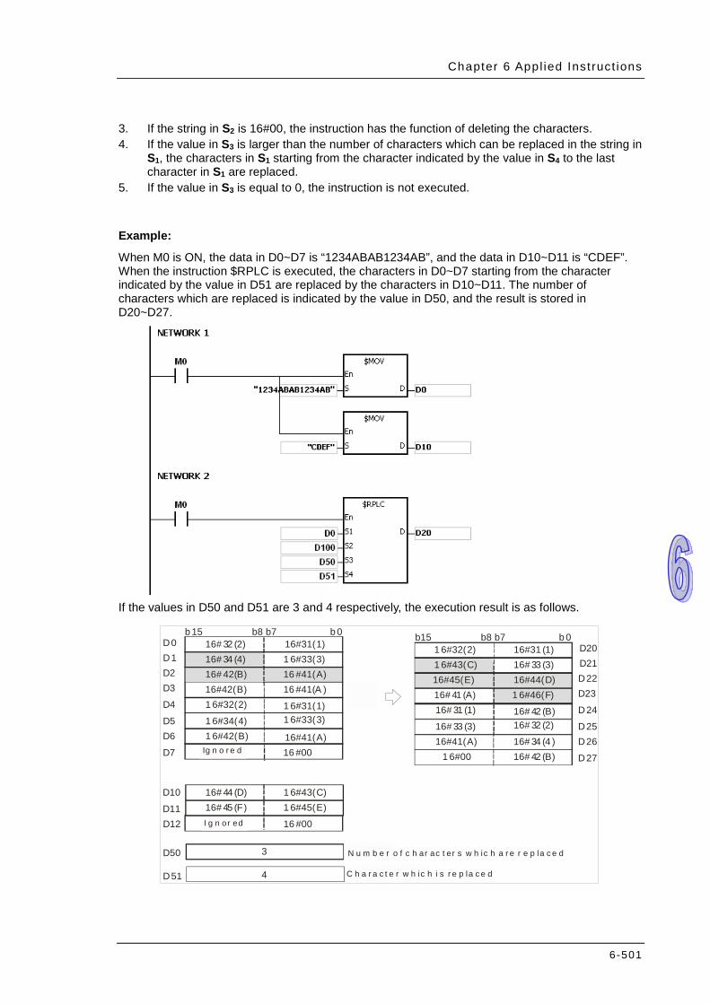
Chapter 6 Appl ied Inst ruct ions
6-501
3. If the string in S2 is 16#00, the instruction has the function of deleting the characters. 4. If the value in S3 is larger than the number of characters which can be replaced in the string in
S1, the characters in S1 starting from the character indicated by the value in S4 to the last character in S1 are replaced.
5. If the value in S3 is equal to 0, the instruction is not executed.
Example:
When M0 is ON, the data in D0~D7 is “1234ABAB1234AB”, and the data in D10~D11 is “CDEF”. When the instruction $RPLC is executed, the characters in D0~D7 starting from the character indicated by the value in D51 are replaced by the characters in D10~D11. The number of characters which are replaced is indicated by the value in D50, and the result is stored in D20~D27.
If the values in D50 and D51 are 3 and 4 respectively, the execution result is as follows.
Af te r the in st ruct io nis execu ted.
b 15 b 0b7b8
001 6#
D1D2D3
16#31(1)16# 32 (2)33(3)1 6#34 (4)16#
42(B)16# 41(A)16 #41(A )16 #42(B)16#
31(1)1 6#D4
b15 b 0b7b8
執行後
43(C)1 6#44 (D)16#
D5
32(2)1 6#
3
4 開始取代的位置
取代數量
33(3)1 6#34(4)1 6#42(B)1 6# 41(A)16#
D50
D51
D0
45(E)1 6#45 (F)16#
D6
D7
D21D22D23
D24
D25
D20
D26
D27
16#31 (1)32(2)1 6#33 (3)16#43(C)1 6#
16#45(E) 44(D)16#46(F)1 6#41 (A)16#
42 (B)16#31 (1)16#32 (2)16#33 (3)16#
41(A)16# 34 (4 )16#42 (B)16#
D10
D11
16 #00忽略
D12 16 #00忽略I g n or ed
Ig n o r e d
C h a r a c t e r w h ic h i s r e p la c e d
N u m b e r o f c h ar ac t er s w h ic h a r e r e p la c e d
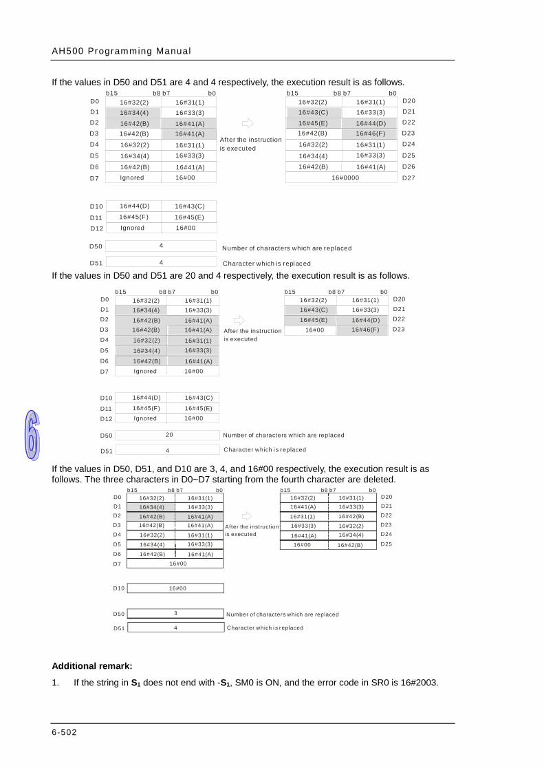
AH500 Programming Manual
6-502
If the values in D50 and D51 are 4 and 4 respectively, the execution result is as follows. b15 b0 b7 b8
000016#
D1 D2
D3
16#31(1) 16#32(2) 33(3)16# 34(4)16#
42(B)16# 41(A)16# 41(A)16# 42(B)16#
31(1)16# D4
b15 b0 b7 b8
43(C)16# 44(D)16#
D5 32(2)16#
4
4
33(3)16# 34(4)16#
42(B)16# 41(A)16#
D50
D51
D0
45(E)16# 45(F)16#
D6
D7
D21 D22
D23
D24
D25
D20
D26
D27
16#31(1) 32(2)16# 33(3)16# 43(C)16#
45(E)16# 44(D)16# 46(F)16# 42(B)16#
(1)16#31 (2)16#32 33(3)16# 34(4)16#
42(B)16# (A)16#41
D10
D11
16#00 Ignored
D12 16#00 Ignored
After the instruction is executed
Character which is repl aced
Number of characters which are replaced
If the values in D50 and D51 are 20 and 4 respectively, the execution result is as follows.
b15 b0 b7 b8
D1 D2
D3
16#31(1) 16#32(2) 33(3)16# 34(4)16#
42(B)16# 41(A)16# 41(A)16# 42(B)16#
31(1)16# D4
b15 b0 b7 b8
43(C)16# 44(D)16#
D5 32(2)16#
20
4
33(3)16# 34(4)16#
42(B)16# 41(A)16#
D50
D51
D0
45(E)16# 45(F)16#
D6
D7
D21 D22
D23
D2016#31(1) 32(2)16# 33(3)16# 43(C)16#
45(E)16# 44(D)16# 46(F)16#
D10
D11
0016#
0016#
Ignored
D12 0016# Ignored
After the instruction is executed
Character which i s replaced
Number of characters which are replaced
If the values in D50, D51, and D10 are 3, 4, and 16#00 respectively, the execution result is as follows. The three characters in D0~D7 starting from the fourth character are deleted.
b15 b0 b7 b8
0016#
D1 D2
D3
16#31(1) 16#32(2) 33(3)16# 34(4)16#
42(B)16# 41(A)16# 41(A)16# 42(B)16#
31(1)16# D4
b15 b0 b7 b8
D5
32(2)16#
3
4
33(3)16# 34(4)16#
42(B)16# 41(A)16#
D50
D51
D0
D6
D7
D21 D22
D23
D24
D25
D2016#31(1) 32(2)16# 33(3)16# 41(A)16#
42(B)16# 31(1)16#
32(2)16# 33(3)16# 34(4)16# 41(A)16#
16#42(B)
D10
0016#
0016#
After the instruction is executed
Character which i s replaced
Number of characters which are replaced
Additional remark:
1. If the string in S1 does not end with -S1, SM0 is ON, and the error code in SR0 is 16#2003.
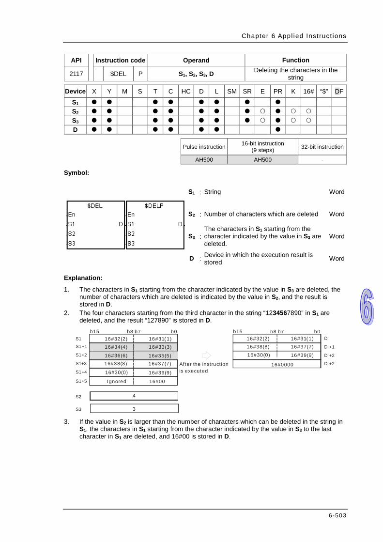
Chapter 6 Appl ied Inst ruct ions
6-503
API Instruction code Operand Function
2117 $DEL P S1, S2, S3, D Deleting the characters in the string
Device X Y M S T C HC D L SM SR E PR K 16# “$” DF
S1 S2 S3 D
Pulse instruction 16-bit instruction (9 steps) 32-bit instruction
AH500 AH500 -
Symbol:
S1 : String Word
S2 : Number of characters which are deleted Word
S3 : The characters in S1 starting from the character indicated by the value in S3 are deleted.
Word
D : Device in which the execution result is stored Word
Explanation:
1. The characters in S1 starting from the character indicated by the value in S3 are deleted, the number of characters which are deleted is indicated by the value in S2, and the result is stored in D.
2. The four characters starting from the third character in the string “1234567890” in S1 are deleted, and the result “127890” is stored in D.
b15 b0 b7 b8
0016#
S1 16#31(1) 16#32(2) 33(3)16# 34(4)16#
36(6)16# 35(5)16# 37(7)16# 38(8)16#
39(9)16#
b15 b0 b7 b8 D
+1 D
+2 D
+1 S1
+2 S1
+3 S1
+4 S1
S2
S3
+5 S1
30(0)16#
4
3
16#31(1) 32(2)16# 37(7)16# 38(8)16#
+2 D 000016#
39(9)16# 30(0)16#
Ignored
After the instruction is executed
3. If the value in S2 is larger than the number of characters which can be deleted in the string in
S1, the characters in S1 starting from the character indicated by the value in S3 to the last character in S1 are deleted, and 16#00 is stored in D.
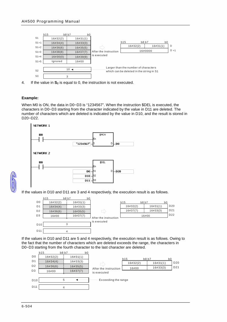
AH500 Programming Manual
6-504
b15 b0 b7 b8
0016#
S1 16#31(1) 16#32(2) 33(3)16# 34(4)16#
36(6)16# 35(5)16# 37(7)16# 38(8)16#
39(9)16#
b15 b0 b7 b8 D
+1 D
+1 S1
+2 S1
+3 S1
+4 S1
S2
S3
+5 S1
30(0)16#
10
3
16#31(1) 32(2)16#
000016#
Larger than the number of charac ters which can be deleted i n the str ing in S1
Ignored
After the instruction is executed
4. If the value in S2 is equal to 0, the instruction is not executed.
Example:
When M0 is ON, the data in D0~D3 is “1234567”. When the instruction $DEL is executed, the characters in D0~D3 starting from the character indicated by the value in D11 are deleted. The number of characters which are deleted is indicated by the value in D10, and the result is stored in D20~D22.
If the values in D10 and D11 are 3 and 4 respectively, the execution result is as follows.
b15 b0 b7 b8
0016#
D1 D2 D3
16#31(1) 16#32(2) 33(3)16# 34(4)16#
36(6)16# 35(5)16# 37(7)16#
b15 b0 b7 b8
3
4
16#31(1) 32(2)16# 33(3)16# 37(7)16#
0016#
D0
D11
D10
D21 D22
D20
After the instruction is executed
If the values in D10 and D11 are 5 and 4 respectively, the execution result is as follows. Owing to the fact that the number of characters which are deleted exceeds the range, the characters in D0~D3 starting from the fourth character to the last character are deleted.
b15 b0 b7 b8
0016#
D1 D2 D3
16#31(1) 16#32(2) 33(3)16# 34(4)16#
36(6)16# 35(5)16# 37(7)16#
b15 b0 b7 b8
5
4
16#31(1) 32(2)16# 33(3)16# 0016#
D0
D11
D10
D21 D20
Exceeding the range
After the instruction is executed
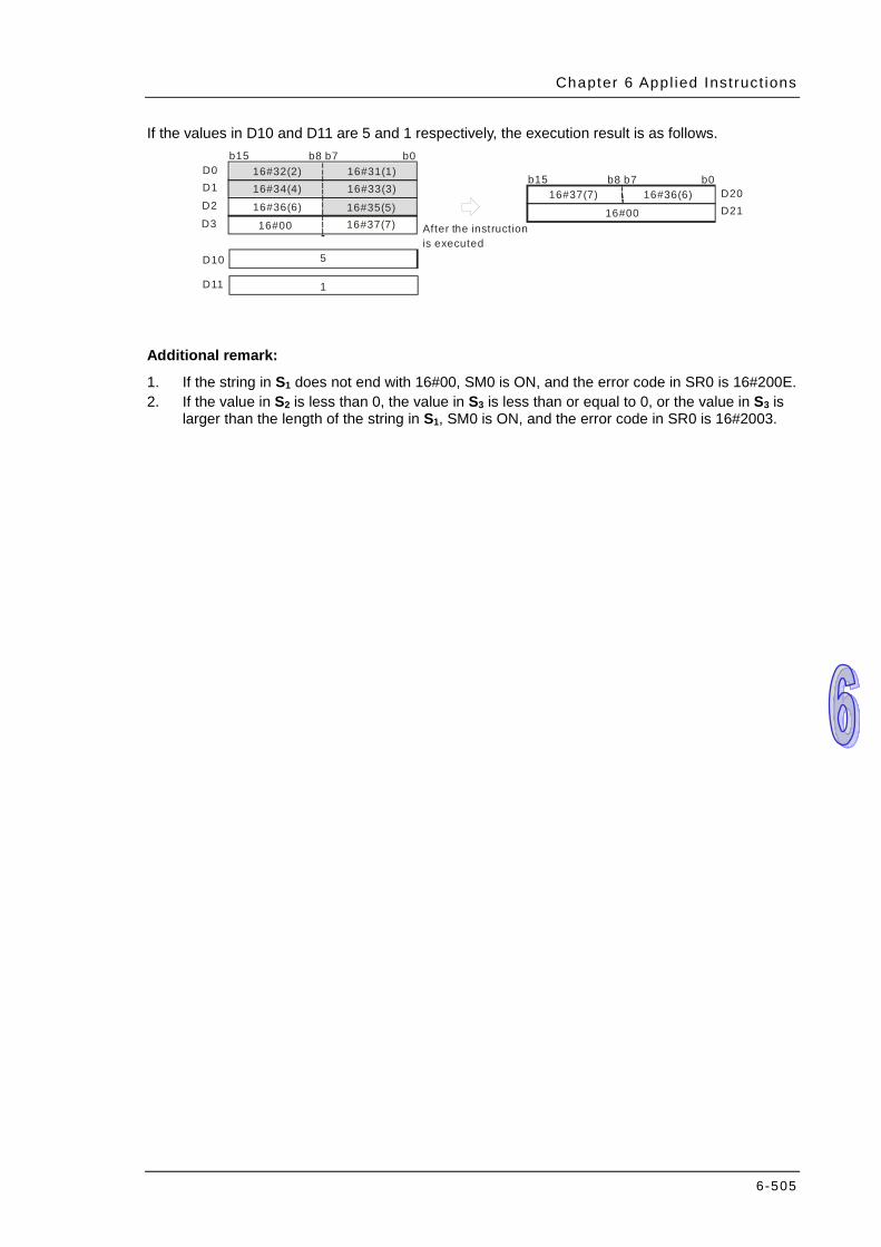
Chapter 6 Appl ied Inst ruct ions
6-505
If the values in D10 and D11 are 5 and 1 respectively, the execution result is as follows. b15 b0 b7 b8
0016#
D1 D2 D3
16#31(1) 16#32(2) 33(3)16# 34(4)16#
36(6)16# 35(5)16# 37(7)16#
b15 b0 b7 b8
5
1
16#36(6) 37(7)16#
0016#
D0
D11
D10
D21 D20
After the instruction is executed
Additional remark:
1. If the string in S1 does not end with 16#00, SM0 is ON, and the error code in SR0 is 16#200E. 2. If the value in S2 is less than 0, the value in S3 is less than or equal to 0, or the value in S3 is
larger than the length of the string in S1, SM0 is ON, and the error code in SR0 is 16#2003.

AH500 Programming Manual
6-506
API Instruction code Operand Function
2118 $CLR P S Clearing the string
Device X Y M S T C HC D L SM SR E PR K 16# “$” DF
S Pulse instruction 16-bit instruction
(3 steps) 32-bit instruction
AH500 AH500 -
Symbol:
S : String which is cleared Word
Explanation:
1. The string in S is cleared.
b15 b0 b7 b8
0016#
S
+1 S
+2 S
+3 S
2D(-)16# 16#31(1) 32(2)16# 33(3)16#
34(4)16# 35(5)16# 2E(.)16# 36(6)16#
38(8)16# 37(7)16# +4 S
+5 S 000016#
S
+1 S
+2 S
+3 S
000016#
+4 S
+5 S
000016# 000016# 000016#
000016# After the instruction is executed
Example:
The string in D0 is cleared, as illustrated below.
b15 b0 b7 b8
0016#
D1 D2 D3
16#31(1) 16#32(2) 33(3)16# 34(4)16#
36(6)16# 35(5)16# 37(7)16#
D0
000016#
D1 D2 D3
D0
000016#
000016# 000016#
After the instruction is executed
Additional remark:
1. If the string in S does not end with 16#00, SM0 is ON, and the error code in SR0 is 16#200E.

Chapter 6 Appl ied Inst ruct ions
6-507
API Instruction code Operand Function
2119 $INS P S1, S2, S3, D Inserting the string
Device X Y M S T C HC D L SM SR E PR K 16# “$” DF
S1 S2 S3 D
Pulse instruction 16-bit instruction (9-15 steps) 32-bit instruction
AH500 AH500 -
Symbol:
S1 : String Word
S2 : String which is inserted Word
S3 : The string is inserted into S1 after the character indicated by the value in S3. Word
D : Device in which the execution result is stored Word
Explanation:
1. The string in S2 is inserted into the string in S1 after the character indicated by the value in S3, and the result is stored in D.
2. If the string in either S1 or S2 is a null string, the other string which is not a null string is stored in D.
3. If the strings in S1 and S2 are null strings, 16#0000 is stored in D. b15 b0 b7 b8
0016#
16#31(1) 16#32(2) 33(3)16# 34(4)16#
36(6)16# 35(5)16# 37(7)16# 38(8)16#
39(9)16#
b15 b0 b7 b8
0016#
4D(M)16# 4E(N)16#
S1
+1 S1
+2 S1
+3 S1
+4 S1
S2
+1 S2 S2
S3
+5 S1
30(0)16#
6
16#31(1) 32(2)16# 33(3)16# 34(4)16#
36(6)16# 35(5)16# 4D(M)16# 4E(N)16#
0016#
37(7)16# 38(8)16#
39(9)16# 30(0)16#
D
+1 D
+2 D
+3 D
+4 D
+5 D
+6 D D
After the instruction is executed

AH500 Programming Manual
6-508
Example:
When M0 is ON, the data in D0~D3 is “1234567”, and the data in D10 is “AB”. When the instruction $INS is executed, “AB” is inserted into the string in D0~D3 after the character indicated by the value in D30. The result is stored in D20~D24.
If the value in D30 is 1, the execution result is as follows.
b15 b0 b7 b8
D1 D2
D3
b15 b0 b7 b8
D30
D0
D21 D22
D23
D24
D20
D10
D11
0016#
16#31(1) 16#32(2) 33(3)16# 34(4)16#
36(6)16# 35(5)16# 37(7)16#
0016#
41(A)16# 42(B)16#
1
16#31(1) 41(A)16# 42(B)16# 32(2)16#
34(4)16# 33(3)16# 35(5)16# 36(6)16#
0016# 37(7)16#
Ignored
After the instruction is executed
If the value in D30 is 0, the execution result is as follows.
b15 b0 b7 b8
D1 D2 D3
b15 b0 b7 b8
D30
D0 D21 D22 D23 D24
D20
D10 D11
16#00
16#31(1) 16#32(2) 16#33(3) 16#34(4)
16#36(6) 16#35(5) 16#37(7)
Af terexecution
16#00 16#41(A) 16#42(B)
0
16 #41(A) 16#42(B) 16 #31(1) 16#32(2 )
16#34(4) 16 #33(3) 16 #35(5) 16# 36(6)
16#00 16 #37(7)
I gnored
Additional remark:
1. If the string in S1 does not end with 16#00, SM0 is ON, and the error code in SR0 is 16#200E. 2. If the string in S2 does not end with 16#00, SM0 is ON, and the error code in SR0 is 16#200E. 3. If the value in S3 is less than 0, or if the value in S3 is larger than the length of the string in S1,
SM0 is ON, and the error code in SR0 is 16#2003.
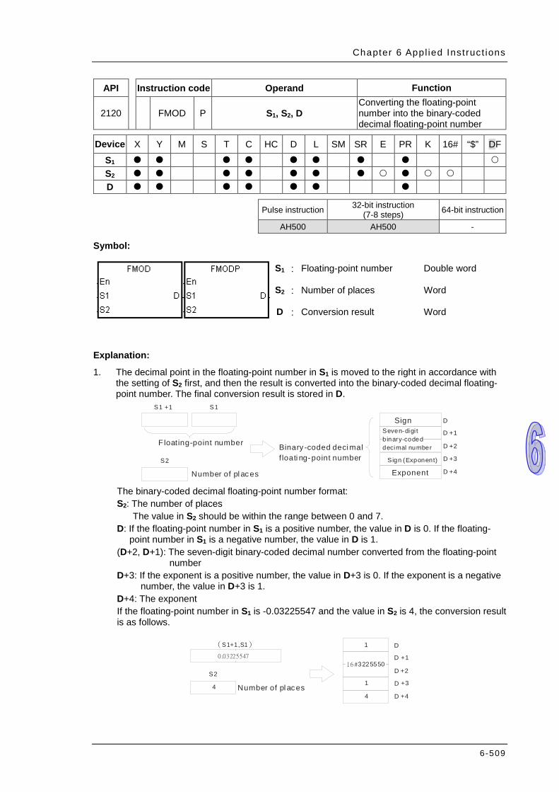
Chapter 6 Appl ied Inst ruct ions
6-509
API Instruction code Operand Function
2120 FMOD P S1, S2, D Converting the floating-point number into the binary-coded decimal floating-point number
Device X Y M S T C HC D L SM SR E PR K 16# “$” DF
S1 S2 D
Pulse instruction 32-bit instruction (7-8 steps) 64-bit instruction
AH500 AH500 -
Symbol:
S1 : Floating-point number Double word
S2 : Number of places Word
D : Conversion result Word
Explanation:
1. The decimal point in the floating-point number in S1 is moved to the right in accordance with the setting of S2 first, and then the result is converted into the binary-coded decimal floating-point number. The final conversion result is stored in D.
S1
Floating-point number
Number of pl aces
S1
S2
D
D
D
D
D
+1
+2
+1
+3
+4
SignSeven-digi t b inary-codeddecimal number
Sign (Exponent)
Exponent
Binary -coded deci mal f loati ng-point number
The binary-coded decimal floating-point number format: S2: The number of places
The value in S2 should be within the range between 0 and 7. D: If the floating-point number in S1 is a positive number, the value in D is 0. If the floating-
point number in S1 is a negative number, the value in D is 1. (D+2, D+1): The seven-digit binary-coded decimal number converted from the floating-point
number D+3: If the exponent is a positive number, the value in D+3 is 0. If the exponent is a negative
number, the value in D+3 is 1. D+4: The exponent If the floating-point number in S1 is -0.03225547 and the value in S2 is 4, the conversion result is as follows.
( )S1+1,S1
S2
D
D
D
D
D
+1
+2
+3
+4
0.03225547
4
1
16 #3225550
1
4Number of pl aces
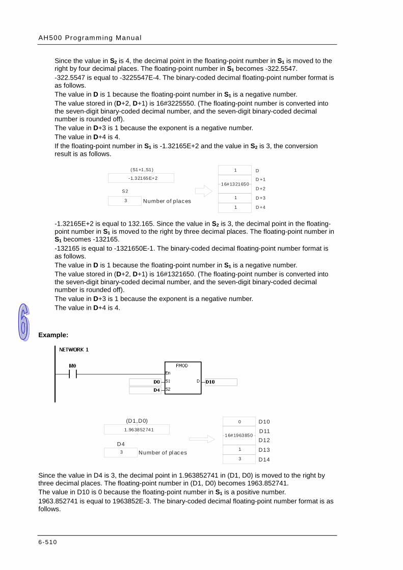
AH500 Programming Manual
6-510
Since the value in S2 is 4, the decimal point in the floating-point number in S1 is moved to the right by four decimal places. The floating-point number in S1 becomes -322.5547. -322.5547 is equal to -3225547E-4. The binary-coded decimal floating-point number format is as follows. The value in D is 1 because the floating-point number in S1 is a negative number. The value stored in (D+2, D+1) is 16#3225550. (The floating-point number is converted into the seven-digit binary-coded decimal number, and the seven-digit binary-coded decimal number is rounded off). The value in D+3 is 1 because the exponent is a negative number. The value in D+4 is 4. If the floating-point number in S1 is -1.32165E+2 and the value in S2 is 3, the conversion result is as follows.
(S1+1,S1)
S2
D
D
D
D
D
+1
+2
+3
+4
-1.32165E+2
3
1
16#1321650
1
1Number of places
-1.32165E+2 is equal to 132.165. Since the value in S2 is 3, the decimal point in the floating-point number in S1 is moved to the right by three decimal places. The floating-point number in S1 becomes -132165. -132165 is equal to -1321650E-1. The binary-coded decimal floating-point number format is as follows. The value in D is 1 because the floating-point number in S1 is a negative number. The value stored in (D+2, D+1) is 16#1321650. (The floating-point number is converted into the seven-digit binary-coded decimal number, and the seven-digit binary-coded decimal number is rounded off). The value in D+3 is 1 because the exponent is a negative number. The value in D+4 is 4.
Example:
(D1,D0)1.963852741
3
0
16#1963850
1
3
D4
D10
D11D12
D13
D14Number of pl aces
Since the value in D4 is 3, the decimal point in 1.963852741 in (D1, D0) is moved to the right by three decimal places. The floating-point number in (D1, D0) becomes 1963.852741. The value in D10 is 0 because the floating-point number in S1 is a positive number. 1963.852741 is equal to 1963852E-3. The binary-coded decimal floating-point number format is as follows.
Chapter 6 Appl ied Inst ruct ions
6-511
The value stored in (D12, D11) is 16#1963850. (The floating-point number is converted into the seven-digit binary-coded decimal number, and the seven-digit binary-coded decimal number is rounded off). The value in D13 is 1 because the exponent is a negative number. The value in D14 is 3.
Additional remark:
1. If the value in S1 exceeds the range of values which can be represented by the floating-point numbers, the instruction is not executed, SM0 is ON, and the error code in SR0 is 16#2013.
2. If the value in S2 exceeds the range, the instruction is not executed, SM0 is ON, and the error code in SR0 is 16#2003.
3. If the operand D used during the execution of the 32-bit instruction is declared in ISPSoft, the data type will be ARRAY [5] of WORD/INT.
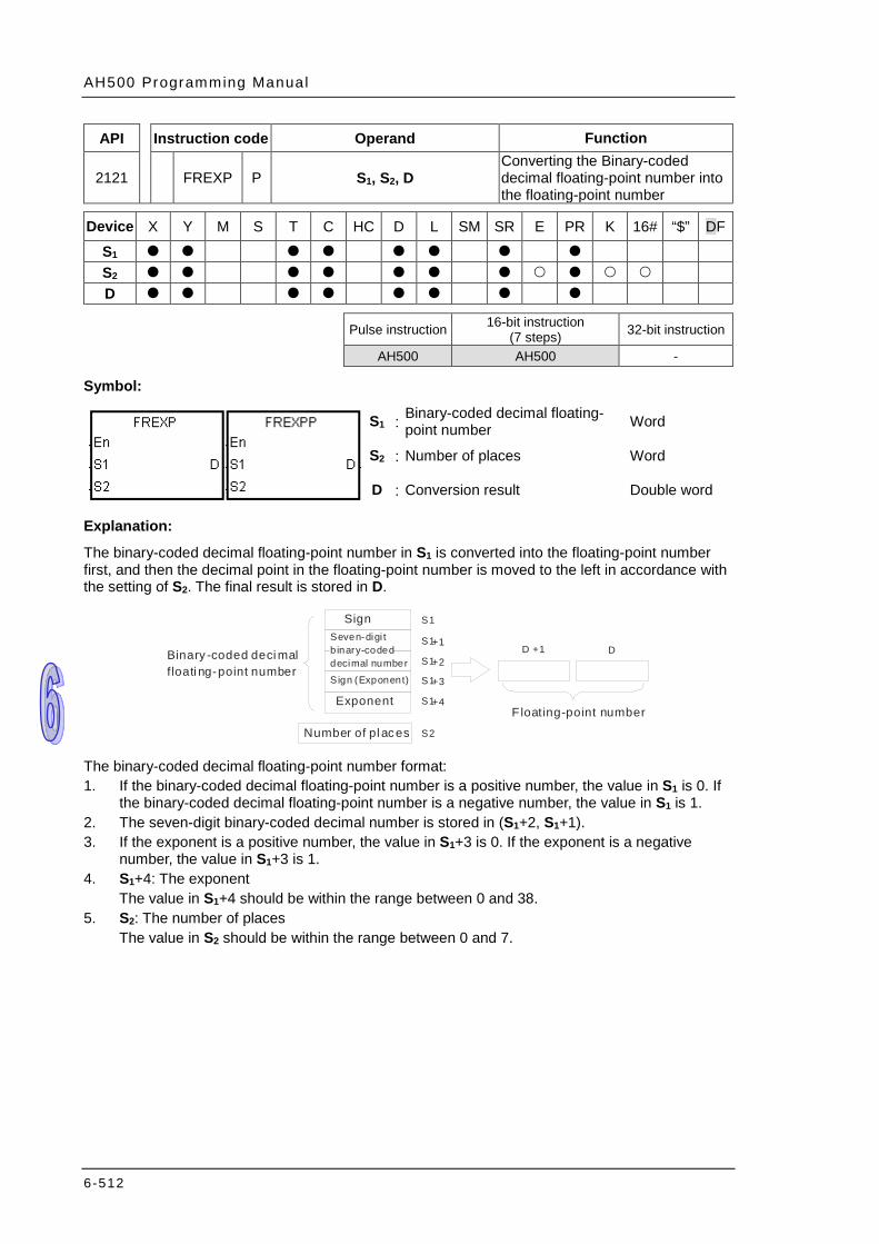
AH500 Programming Manual
6-512
API Instruction code Operand Function
2121 FREXP P S1, S2, D Converting the Binary-coded decimal floating-point number into the floating-point number
Device X Y M S T C HC D L SM SR E PR K 16# “$” DF
S1 S2 D
Pulse instruction 16-bit instruction (7 steps) 32-bit instruction
AH500 AH500 -
Symbol:
S1 : Binary-coded decimal floating-point number Word
S2 : Number of places Word
D : Conversion result Double word
Explanation:
The binary-coded decimal floating-point number in S1 is converted into the floating-point number first, and then the decimal point in the floating-point number is moved to the left in accordance with the setting of S2. The final result is stored in D.
D
D+1S1
+1
+2
+3
+4
S1
S1
S1
S1
S2
Binary -coded deci mal f loati ng-point number
SignSeven-digi t b inary-codeddecimal numberSign (Exponent)
Exponent
Number of pl acesFloating-point number
The binary-coded decimal floating-point number format: 1. If the binary-coded decimal floating-point number is a positive number, the value in S1 is 0. If
the binary-coded decimal floating-point number is a negative number, the value in S1 is 1. 2. The seven-digit binary-coded decimal number is stored in (S1+2, S1+1). 3. If the exponent is a positive number, the value in S1+3 is 0. If the exponent is a negative
number, the value in S1+3 is 1. 4. S1+4: The exponent
The value in S1+4 should be within the range between 0 and 38. 5. S2: The number of places
The value in S2 should be within the range between 0 and 7.
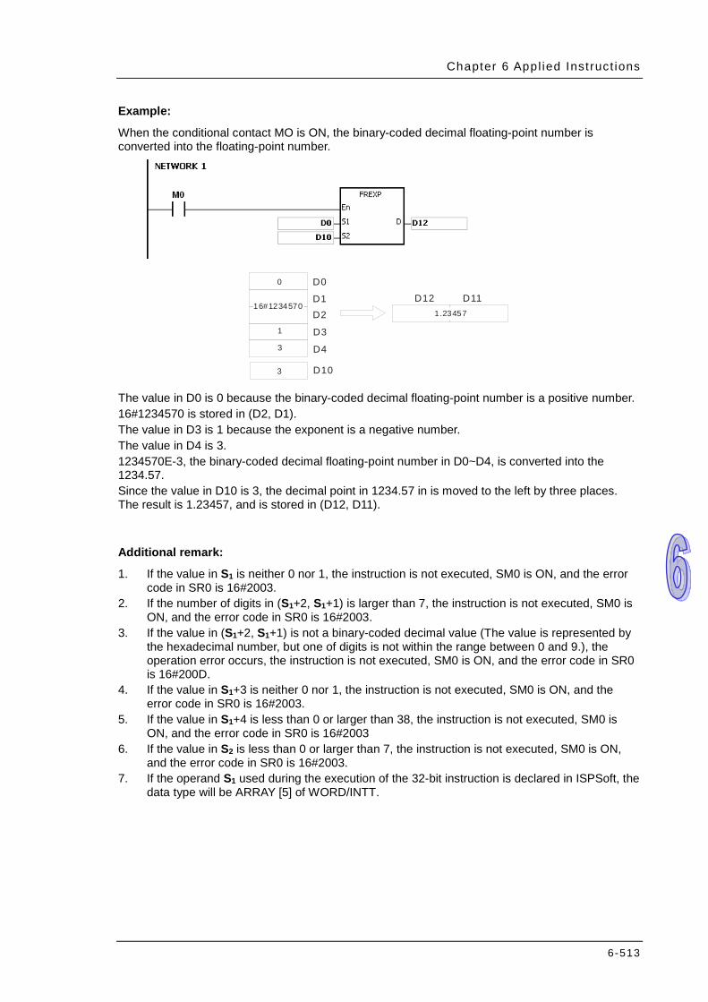
Chapter 6 Appl ied Inst ruct ions
6-513
Example:
When the conditional contact MO is ON, the binary-coded decimal floating-point number is converted into the floating-point number.
D121.23457
3
0
16#1234570
1
3
D11
D10
D0
D1D2
D3
D4
The value in D0 is 0 because the binary-coded decimal floating-point number is a positive number. 16#1234570 is stored in (D2, D1). The value in D3 is 1 because the exponent is a negative number. The value in D4 is 3. 1234570E-3, the binary-coded decimal floating-point number in D0~D4, is converted into the 1234.57. Since the value in D10 is 3, the decimal point in 1234.57 in is moved to the left by three places. The result is 1.23457, and is stored in (D12, D11).
Additional remark:
1. If the value in S1 is neither 0 nor 1, the instruction is not executed, SM0 is ON, and the error code in SR0 is 16#2003.
2. If the number of digits in (S1+2, S1+1) is larger than 7, the instruction is not executed, SM0 is ON, and the error code in SR0 is 16#2003.
3. If the value in (S1+2, S1+1) is not a binary-coded decimal value (The value is represented by the hexadecimal number, but one of digits is not within the range between 0 and 9.), the operation error occurs, the instruction is not executed, SM0 is ON, and the error code in SR0 is 16#200D.
4. If the value in S1+3 is neither 0 nor 1, the instruction is not executed, SM0 is ON, and the error code in SR0 is 16#2003.
5. If the value in S1+4 is less than 0 or larger than 38, the instruction is not executed, SM0 is ON, and the error code in SR0 is 16#2003
6. If the value in S2 is less than 0 or larger than 7, the instruction is not executed, SM0 is ON, and the error code in SR0 is 16#2003.
7. If the operand S1 used during the execution of the 32-bit instruction is declared in ISPSoft, the data type will be ARRAY [5] of WORD/INTT.
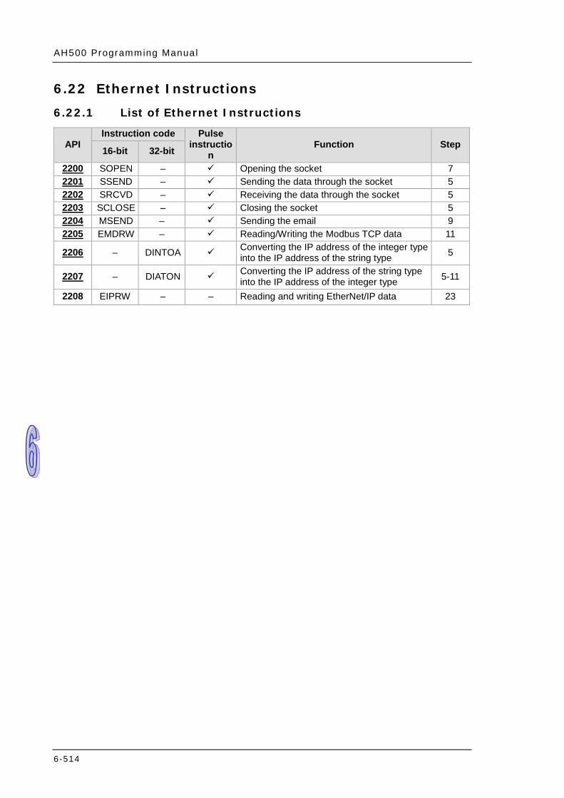
AH500 Programming Manual
6-514
6.22 Ethernet Instructions
6.22.1 List of Ethernet Instructions
API Instruction code Pulse
instruction
Function Step 16-bit 32-bit
2200 SOPEN – Opening the socket 7 2201 SSEND – Sending the data through the socket 5 2202 SRCVD – Receiving the data through the socket 5 2203 SCLOSE – Closing the socket 5 2204 MSEND – Sending the email 9 2205 EMDRW – Reading/Writing the Modbus TCP data 11
2206 – DINTOA Converting the IP address of the integer type into the IP address of the string type 5
2207 – DIATON Converting the IP address of the string type into the IP address of the integer type 5-11
2208 EIPRW – – Reading and writing EtherNet/IP data 23
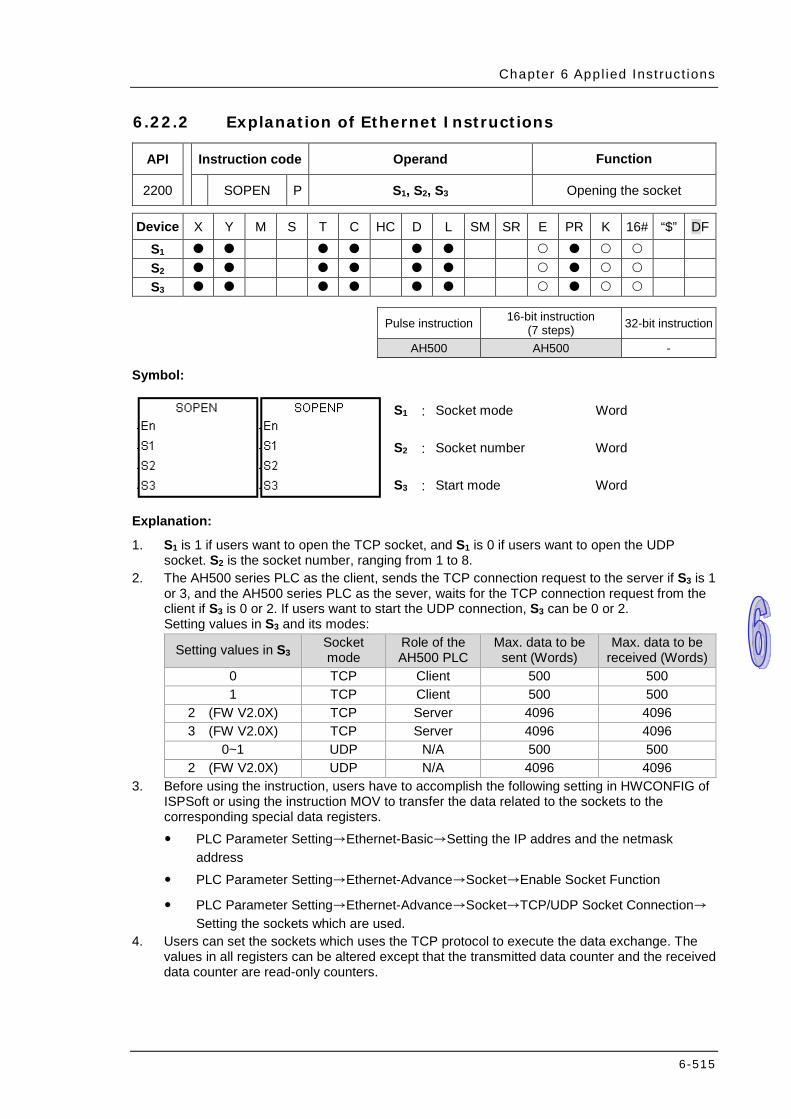
Chapter 6 Appl ied Inst ruct ions
6-515
6.22.2 Explanation of Ethernet Instructions
API Instruction code Operand Function
2200 SOPEN P S1, S2, S3 Opening the socket
Device X Y M S T C HC D L SM SR E PR K 16# “$” DF
S1 S2 S3
Pulse instruction 16-bit instruction
(7 steps) 32-bit instruction
AH500 AH500 -
Symbol:
S1 : Socket mode Word
S2 : Socket number Word
S3 : Start mode Word
Explanation:
1. S1 is 1 if users want to open the TCP socket, and S1 is 0 if users want to open the UDP socket. S2 is the socket number, ranging from 1 to 8.
2. The AH500 series PLC as the client, sends the TCP connection request to the server if S3 is 1 or 3, and the AH500 series PLC as the sever, waits for the TCP connection request from the client if S3 is 0 or 2. If users want to start the UDP connection, S3 can be 0 or 2. Setting values in S3 and its modes:
Setting values in S3 Socket mode
Role of the AH500 PLC
Max. data to be sent (Words)
Max. data to be received (Words)
0 TCP Client 500 500 1 TCP Client 500 500
2 (FW V2.0X) TCP Server 4096 4096 3 (FW V2.0X) TCP Server 4096 4096
0~1 UDP N/A 500 500 2 (FW V2.0X) UDP N/A 4096 4096
3. Before using the instruction, users have to accomplish the following setting in HWCONFIG of ISPSoft or using the instruction MOV to transfer the data related to the sockets to the corresponding special data registers. PLC Parameter Setting→Ethernet-Basic→Setting the IP addres and the netmask
address PLC Parameter Setting→Ethernet-Advance→Socket→Enable Socket Function
PLC Parameter Setting→Ethernet-Advance→Socket→TCP/UDP Socket Connection→Setting the sockets which are used.
4. Users can set the sockets which uses the TCP protocol to execute the data exchange. The values in all registers can be altered except that the transmitted data counter and the received data counter are read-only counters.
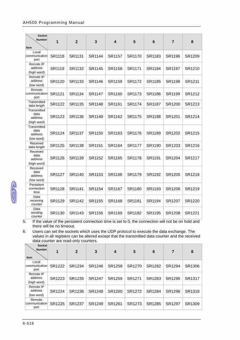
AH500 Programming Manual
6-516
Socket Number
Item
1 2 3 4 5 6 7 8
Local communication
port SR1118 SR1131 SR1144 SR1157 SR1170 SR1183 SR1196 SR1209
Remote IP address
(high word) SR1119 SR1132 SR1145 SR1158 SR1171 SR1184 SR1197 SR1210
Remote IP address
(low word) SR1120 SR1133 SR1146 SR1159 SR1172 SR1185 SR1198 SR1211
Remote communication
port SR1121 SR1134 SR1147 SR1160 SR1173 SR1186 SR1199 SR1212
Transmitted data length SR1122 SR1135 SR1148 SR1161 SR1174 SR1187 SR1200 SR1213 Transmitted
data address
(high word) SR1123 SR1136 SR1149 SR1162 SR1175 SR1188 SR1201 SR1214
Transmitted data
address (low word)
SR1124 SR1137 SR1150 SR1163 SR1176 SR1189 SR1202 SR1215
Received data length SR1125 SR1138 SR1151 SR1164 SR1177 SR1190 SR1203 SR1216 Received
data address
(high word) SR1126 SR1139 SR1152 SR1165 SR1178 SR1191 SR1204 SR1217
Received data
address (low word)
SR1127 SR1140 SR1153 SR1166 SR1179 SR1192 SR1205 SR1218
Persistent connection
time SR1128 SR1141 SR1154 SR1167 SR1180 SR1193 SR1206 SR1219
Data receiving counter
SR1129 SR1142 SR1155 SR1168 SR1181 SR1194 SR1207 SR1220
Data sending counter
SR1130 SR1143 SR1156 SR1169 SR1182 SR1195 SR1208 SR1221
5. If the value of the persistent connection time is set to 0, the connection will not be on hold and there will be no timeout.
6. Users can set the sockets which uses the UDP protocol to execute the data exchange. The values in all registers can be altered except that the transmitted data counter and the received data counter are read-only counters.
Socket Number
Item
1 2 3 4 5 6 7 8
Local communication
port SR1222 SR1234 SR1246 SR1258 SR1270 SR1282 SR1294 SR1306
Remote IP address
(high word) SR1223 SR1235 SR1247 SR1259 SR1271 SR1283 SR1295 SR1317
Remote IP address
(low word) SR1224 SR1236 SR1248 SR1260 SR1272 SR1284 SR1296 SR1318
Remote communication
port SR1225 SR1237 SR1249 SR1261 SR1273 SR1285 SR1297 SR1309

Chapter 6 Appl ied Inst ruct ions
6-517
Socket Number
Item
1 2 3 4 5 6 7 8
Transmitted data length SR1226 SR1238 SR1250 SR1262 SR1274 SR1286 SR1298 SR1310 Transmitted data address (high word)
SR1227 SR1239 SR1251 SR1263 SR1275 SR1287 SR1299 SR1311
Transmitted data address
(low word) SR1228 SR1240 SR1252 SR1264 SR1276 SR1288 SR1300 SR1312
Received data length SR1229 SR1241 SR1253 SR1265 SR1277 SR1289 SR1301 SR1313
Received data address
(high word) SR1230 SR1242 SR1254 SR1266 SR1278 SR1290 SR1302 SR1314
Received data address
(low word) SR1231 SR1243 SR1255 SR1267 SR1279 SR1291 SR1303 SR1315
Data receiving counter
SR1232 SR1244 SR1256 SR1268 SR1280 SR1292 SR1304 SR1316
Data sending counter
SR1233 SR1245 SR1257 SR1269 SR1281 SR1293 SR1305 SR1317
7. When the TCP socket is opened, the remote IP address and the communication ports can be set as follows.
Remote IP address
Local communication
port
Remote communication
port Description
0.0.0.0 0 0 Illegal
0.0.0.0 Not equal to 0 0
Only applied to the server 1. The connection request from the same
local communication port is accepted. 2. The packet sent from any device is
received through the local communication port.
0.0.0.0 0 Not equal to 0 Illegal Specific
IP address
0 0 Illegal
Specific IP
address Not equal to 0 0
Only applied to the server 1. The packet is received from the specific
IP address through the local communication port.
Specific IP
address 0 Not equal to 0
Only applied to the client 1. The system will specify an unused
communication port as the local communication port.
2. The data is sent to the specific IP address through the remote communication port.

AH500 Programming Manual
6-518
Remote IP address
Local communication
port
Remote communication
port Description
Specific IP
address Not equal to 0 Not equal to 0
1. The connection requests from the local communication port, the remote communication port, and the specific IP address are received.
2. The data is sent to the specific IP address through the remote communication port.
3. The packet is received from the specific IP address through the local communication port.
8. If the TCP socket is opened, and no error occurs after the instruction is executed, the PLC is connected to the remote device, and the flag related to the connection’s being started is ON. If the connection is successful, the flag related to the connection’s being successful is ON, and the flag related to the connection’s being started is OFF. If an error occurs, the error flag is ON.
TCP socket number
Being starting the connection
Successful connection Error flag
1 SM1273 SM1270 SM1277 2 SM1281 SM1278 SM1285 3 SM1289 SM1286 SM1293 4 SM1297 SM1294 SM1301 5 SM1305 SM1302 SM1309 6 SM1313 SM1310 SM1317 7 SM1321 SM1318 SM1325 8 SM1329 SM1326 SM1333
9. If the UDP socket is opened, and no error occurs after the instruction is executed, the flag related to the connection’s having been started is ON. If an error occurs, the error flag is ON.
UDP socket number Having started the connection Error flag 1 SM1334 SM1338 2 SM1339 SM1343 3 SM1344 SM1348 4 SM1349 SM1353 5 SM1354 SM1358 6 SM1359 SM1363 7 SM1364 SM1368 8 SM1369 SM1373
10. Generally, the pulse instruction SOPENP is used.
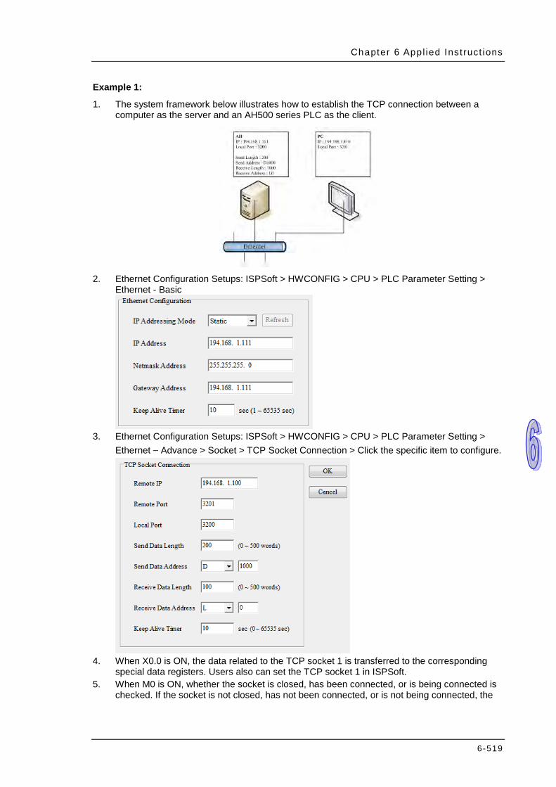
Chapter 6 Appl ied Inst ruct ions
6-519
Example 1:
1. The system framework below illustrates how to establish the TCP connection between a computer as the server and an AH500 series PLC as the client.
2. Ethernet Configuration Setups: ISPSoft > HWCONFIG > CPU > PLC Parameter Setting >
Ethernet - Basic
3. Ethernet Configuration Setups: ISPSoft > HWCONFIG > CPU > PLC Parameter Setting >
Ethernet – Advance > Socket > TCP Socket Connection > Click the specific item to configure.
4. When X0.0 is ON, the data related to the TCP socket 1 is transferred to the corresponding
special data registers. Users also can set the TCP socket 1 in ISPSoft. 5. When M0 is ON, whether the socket is closed, has been connected, or is being connected is
checked. If the socket is not closed, has not been connected, or is not being connected, the

AH500 Programming Manual
6-520
connection procedure is performed. After the socket has been connected, M0 will is switched OFF and M1 will be ON.
6. When M1 is ON, whether the socket has been connected and no data is being sent is checked. If the socket has been connected, and no data is being sent, the data will be sent. If the socket has not been connected, the instruction is not executed. After the sending of the data is complete, M1 will be switched OFF and M2 will be ON.
7. When M2 is ON, whether the socket has been connected and no data is being received is checked. If the socket has been connected, and no data is being received, the data will be received. If the socket has not been connected, the instruction is not executed. After the sending of the data is complete, M2 will be switched OFF and M3 will be ON.
8. When M3 is ON, whether the socket has been connected is checked. If the socket has been connected, the connection will be closed. If the socket has not been connected, the instruction is not executed. After the connection is closed, M3 will be switched OFF.
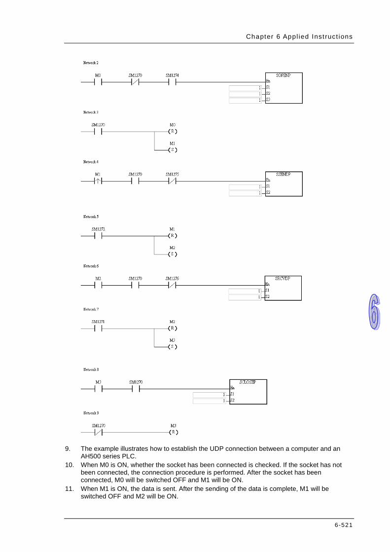
Chapter 6 Appl ied Inst ruct ions
6-521
9. The example illustrates how to establish the UDP connection between a computer and an
AH500 series PLC. 10. When M0 is ON, whether the socket has been connected is checked. If the socket has not
been connected, the connection procedure is performed. After the socket has been connected, M0 will be switched OFF and M1 will be ON.
11. When M1 is ON, the data is sent. After the sending of the data is complete, M1 will be switched OFF and M2 will be ON.
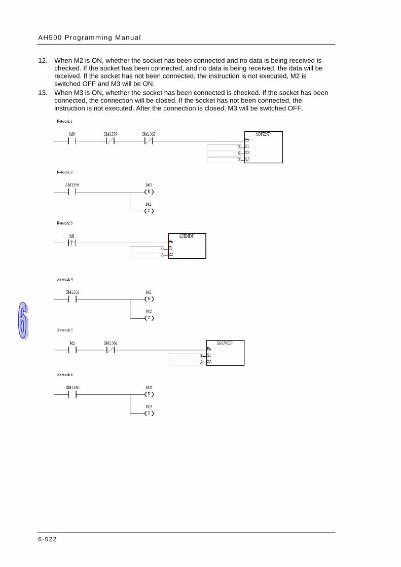
AH500 Programming Manual
6-522
12. When M2 is ON, whether the socket has been connected and no data is being received is checked. If the socket has been connected, and no data is being received, the data will be received. If the socket has not been connected, the instruction is not executed, M2 is switched OFF and M3 will be ON.
13. When M3 is ON, whether the socket has been connected is checked. If the socket has been connected, the connection will be closed. If the socket has not been connected, the instruction is not executed. After the connection is closed, M3 will be switched OFF.
Chapter 6 Appl ied Inst ruct ions
6-523
Additional remark:
If both Client and Server are AH Series PLCs and the timeout time for both Client and Server is set
identically. When a timeout occurs on the Server, the connection will be stopped and thus no error
flag will be shown on the Client. But if a timeout occurs on the Client first, an error flag shows up
and then the connection is stopped.
Error codes for the TCP connection:
Error Code Description Error Flag
16#2003 The value in S1, S2, or S3 exceeds the range, the instruction is not
executed. SM0/SM5
16#600A Failed to establish a TCP connection. SM1090
16#600C The socket has been used. SM1109
16#600D The RJ45 port is NOT connected. SM1100
16#6200 The remote socket IP address of the TCP connection is illegal. Note 1
16#6201 The local socket of TCP connection is illegal. Note 1 16#6202 The remote socket of TCP connection is illegal. Note 1 16#6214 The connection to the remote socket was denied. Note 1 16#6217 The current socket is opened. Note 1 16#621A The current socket is closed. Note 1
Note 1:
SM1277: The error flag of TCP Socket 1
SM1285:The error flag of TCP Socket 2
~
SM1325:The error flag of TCP Socket 7
SM1333:The error flag of TCP Socket 8
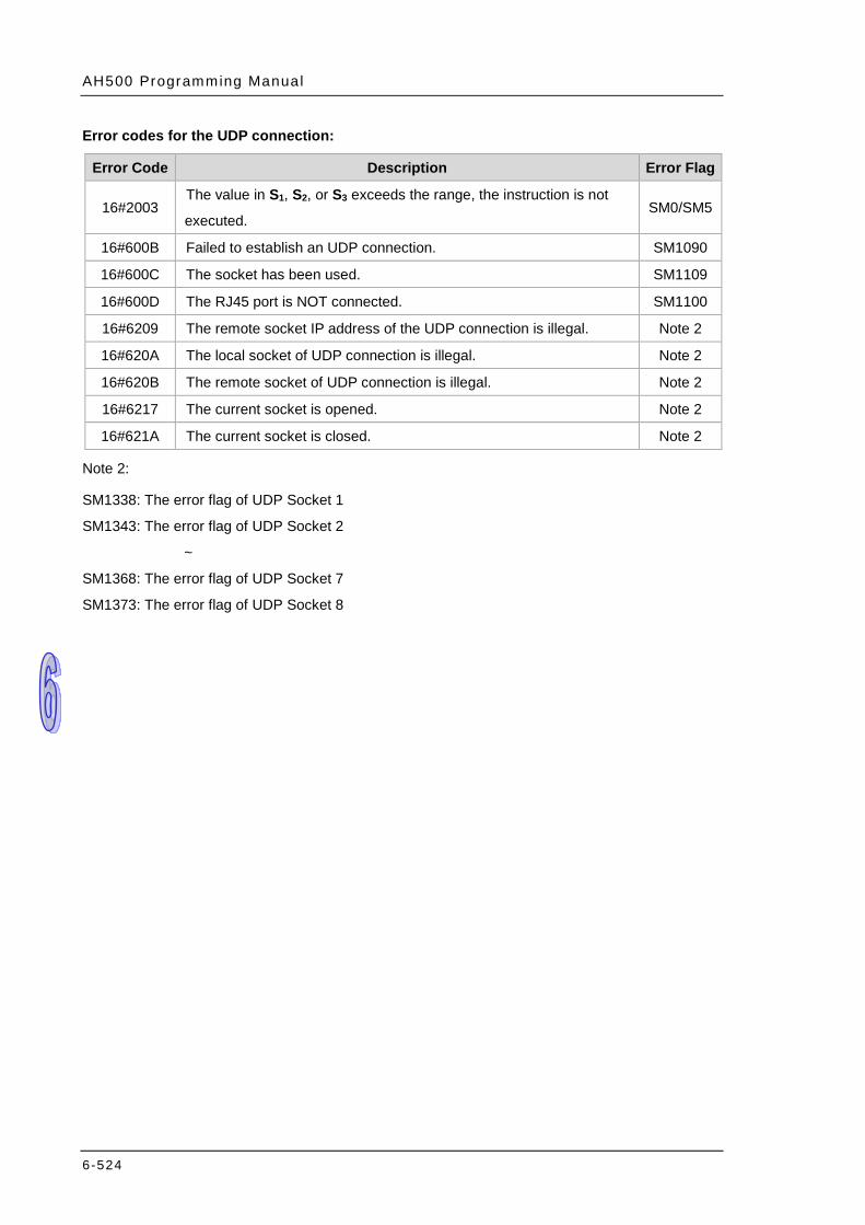
AH500 Programming Manual
6-524
Error codes for the UDP connection:
Error Code Description Error Flag
16#2003 The value in S1, S2, or S3 exceeds the range, the instruction is not
executed. SM0/SM5
16#600B Failed to establish an UDP connection. SM1090
16#600C The socket has been used. SM1109
16#600D The RJ45 port is NOT connected. SM1100
16#6209 The remote socket IP address of the UDP connection is illegal. Note 2
16#620A The local socket of UDP connection is illegal. Note 2 16#620B The remote socket of UDP connection is illegal. Note 2 16#6217 The current socket is opened. Note 2 16#621A The current socket is closed. Note 2
Note 2:
SM1338: The error flag of UDP Socket 1
SM1343: The error flag of UDP Socket 2
~
SM1368: The error flag of UDP Socket 7
SM1373: The error flag of UDP Socket 8
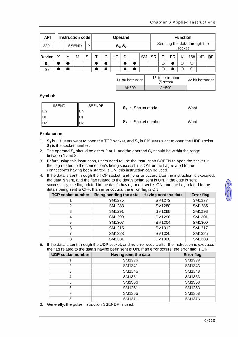
Chapter 6 Appl ied Inst ruct ions
6-525
API Instruction code Operand Function
2201 SSEND P S1, S2 Sending the data through the socket
Device X Y M S T C HC D L SM SR E PR K 16# “$” DF
S1 S2
Pulse instruction 16-bit instruction
(5 steps) 32-bit instruction
AH500 AH500 -
Symbol:
S1 : Socket mode Word
S2 : Socket number Word
Explanation:
1. S1 is 1 if users want to open the TCP socket, and S1 is 0 if users want to open the UDP socket. S2 is the socket number.
2. The operand S1 should be either 0 or 1, and the operand S2 should be within the range between 1 and 8.
3. Before using this instruction, users need to use the instruction SOPEN to open the socket. If the flag related to the connection’s being successful is ON, or the flag related to the connection’s having been started is ON, this instruction can be used.
4. If the data is sent through the TCP socket, and no error occurs after the instruction is executed, the data is sent, and the flag related to the data’s being sent is ON. If the data is sent successfully, the flag related to the data’s having been sent is ON, and the flag related to the data’s being sent is OFF. If an error occurs, the error flag is ON.
TCP socket number Being sending the data Having sent the data Error flag 1 SM1275 SM1272 SM1277 2 SM1283 SM1280 SM1285 3 SM1291 SM1288 SM1293 4 SM1299 SM1296 SM1301 5 SM1307 SM1304 SM1309 6 SM1315 SM1312 SM1317 7 SM1323 SM1320 SM1325 8 SM1331 SM1328 SM1333
5. If the data is sent through the UDP socket, and no error occurs after the instruction is executed, the flag related to the data’s having been sent is ON. If an error occurs, the error flag is ON.
UDP socket number Having sent the data Error flag 1 SM1336 SM1338 2 SM1341 SM1343 3 SM1346 SM1348 4 SM1351 SM1353 5 SM1356 SM1358 6 SM1361 SM1363 7 SM1366 SM1368 8 SM1371 SM1373
6. Generally, the pulse instruction SSENDP is used.

AH500 Programming Manual
6-526
7. While using this instruction, if the transmission length is an odd number, use the following flag to set up.
Socket number Flags for
sending an odd number of characters (TCP socket)
Flags for sending an odd number of characters (UDP socket)
1 SM1375 SM1383 2 SM1376 SM1384 3 SM1377 SM1385 4 SM1378 SM1386 5 SM1379 SM1387 6 SM1380 SM1388 7 SM1381 SM1389 8 SM1382 SM1390
Explanation:
1. Refer to the execution of SOPEN instruction for relative setups and examples for the transmission length with 4 Words.
2. Using the flags for sending an odd number of characters will take 1 byte and thus the actual transmission will be 7 Bytes. For transmission without using the flags for sending an odd number of characters, the actual transmission will be 8 Bytes.
Data transmission address
D0 D1 D2 D3
High Byte Low Byte High Byte Low Byte High Byte Low Bytes High Byte Low Byte
16#01 16#02 16#03 16#04 16#05 16#06 16#07 16#08
Actual data transmission (The flag for sending an odd number of characters is OFF.)
0102 0304 0506 0708
Actual data transmission (The flag for sending an odd number of characters is ON.)
0102 0304 0506 07
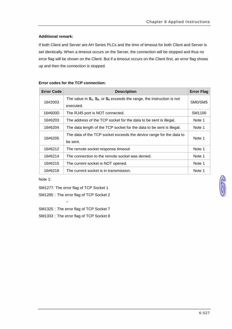
Chapter 6 Appl ied Inst ruct ions
6-527
Additional remark:
If both Client and Server are AH Series PLCs and the time of timeout for both Client and Server is
set identically. When a timeout occurs on the Server, the connection will be stopped and thus no
error flag will be shown on the Client. But if a timeout occurs on the Client first, an error flag shows
up and then the connection is stopped.
Error codes for the TCP connection:
Error Code Description Error Flag
16#2003 The value in S1, S2, or S3 exceeds the range, the instruction is not
executed. SM0/SM5
16#600D The RJ45 port is NOT connected. SM1100
16#6203 The address of the TCP socket for the data to be sent is illegal. Note 1 16#6204 The data length of the TCP socket for the data to be sent is illegal. Note 1
16#6205 The data of the TCP socket exceeds the device range for the data to
be sent. Note 1
16#6212 The remote socket response timeout Note 1 16#6214 The connection to the remote socket was denied. Note 1 16#6215 The current socket is NOT opened. Note 1
16#6218 The current socket is in transmission. Note 1
Note 1:
SM1277: The error flag of TCP Socket 1
SM1285:The error flag of TCP Socket 2
~
SM1325:The error flag of TCP Socket 7
SM1333:The error flag of TCP Socket 8
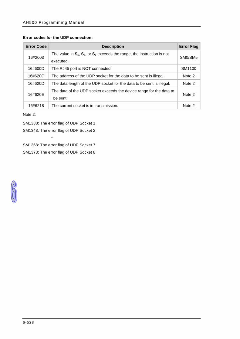
AH500 Programming Manual
6-528
Error codes for the UDP connection:
Error Code Description Error Flag
16#2003 The value in S1, S2, or S3 exceeds the range, the instruction is not
executed. SM0/SM5
16#600D The RJ45 port is NOT connected. SM1100
16#620C The address of the UDP socket for the data to be sent is illegal. Note 2
16#620D The data length of the UDP socket for the data to be sent is illegal. Note 2
16#620E The data of the UDP socket exceeds the device range for the data to
be sent. Note 2
16#6218 The current socket is in transmission. Note 2
Note 2:
SM1338: The error flag of UDP Socket 1
SM1343: The error flag of UDP Socket 2
~
SM1368: The error flag of UDP Socket 7
SM1373: The error flag of UDP Socket 8
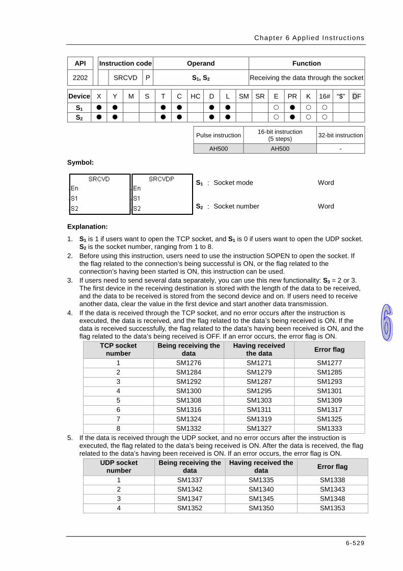
Chapter 6 Appl ied Inst ruct ions
6-529
API Instruction code Operand Function
2202 SRCVD P S1, S2 Receiving the data through the socket
Device X Y M S T C HC D L SM SR E PR K 16# “$” DF
S1 S2
Pulse instruction 16-bit instruction
(5 steps) 32-bit instruction
AH500 AH500 -
Symbol:
S1 : Socket mode Word
S2 : Socket number Word
Explanation:
1. S1 is 1 if users want to open the TCP socket, and S1 is 0 if users want to open the UDP socket. S2 is the socket number, ranging from 1 to 8.
2. Before using this instruction, users need to use the instruction SOPEN to open the socket. If the flag related to the connection’s being successful is ON, or the flag related to the connection’s having been started is ON, this instruction can be used.
3. If users need to send several data separately, you can use this new functionality: S3 = 2 or 3. The first device in the receiving destination is stored with the length of the data to be received, and the data to be received is stored from the second device and on. If users need to receive another data, clear the value in the first device and start another data transmission.
4. If the data is received through the TCP socket, and no error occurs after the instruction is executed, the data is received, and the flag related to the data’s being received is ON. If the data is received successfully, the flag related to the data’s having been received is ON, and the flag related to the data’s being received is OFF. If an error occurs, the error flag is ON.
TCP socket number
Being receiving the data
Having received the data Error flag
1 SM1276 SM1271 SM1277 2 SM1284 SM1279 SM1285 3 SM1292 SM1287 SM1293 4 SM1300 SM1295 SM1301 5 SM1308 SM1303 SM1309 6 SM1316 SM1311 SM1317 7 SM1324 SM1319 SM1325 8 SM1332 SM1327 SM1333
5. If the data is received through the UDP socket, and no error occurs after the instruction is executed, the flag related to the data’s being received is ON. After the data is received, the flag related to the data’s having been received is ON. If an error occurs, the error flag is ON.
UDP socket number
Being receiving the data
Having received the data Error flag
1 SM1337 SM1335 SM1338 2 SM1342 SM1340 SM1343 3 SM1347 SM1345 SM1348 4 SM1352 SM1350 SM1353
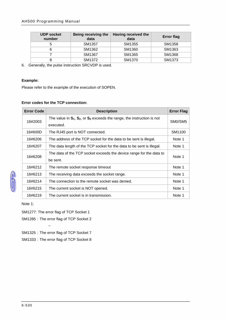
AH500 Programming Manual
6-530
UDP socket number
Being receiving the data
Having received the data Error flag
5 SM1357 SM1355 SM1358 6 SM1362 SM1360 SM1363 7 SM1367 SM1365 SM1368 8 SM1372 SM1370 SM1373
6. Generally, the pulse instruction SRCVDP is used.
Example:
Please refer to the example of the execution of SOPEN.
Error codes for the TCP connection:
Error Code Description Error Flag
16#2003 The value in S1, S2, or S3 exceeds the range, the instruction is not
executed. SM0/SM5
16#600D The RJ45 port is NOT connected. SM1100
16#6206 The address of the TCP socket for the data to be sent is illegal. Note 1 16#6207 The data length of the TCP socket for the data to be sent is illegal. Note 1
16#6208 The data of the TCP socket exceeds the device range for the data to
be sent. Note 1
16#6212 The remote socket response timeout Note 1 16#6213 The receiving data exceeds the socket range. Note 1
16#6214 The connection to the remote socket was denied. Note 1 16#6215 The current socket is NOT opened. Note 1
16#6219 The current socket is in transmission. Note 1
Note 1:
SM1277: The error flag of TCP Socket 1
SM1285:The error flag of TCP Socket 2
~
SM1325:The error flag of TCP Socket 7
SM1333:The error flag of TCP Socket 8
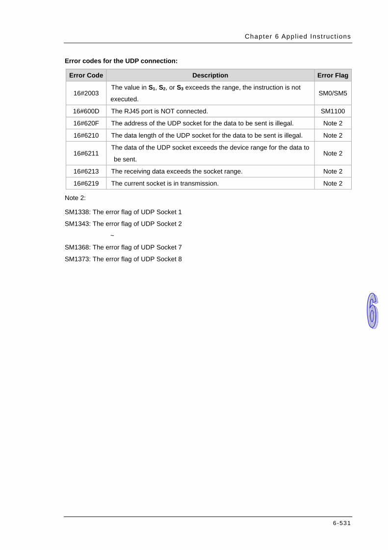
Chapter 6 Appl ied Inst ruct ions
6-531
Error codes for the UDP connection:
Error Code Description Error Flag
16#2003 The value in S1, S2, or S3 exceeds the range, the instruction is not
executed. SM0/SM5
16#600D The RJ45 port is NOT connected. SM1100
16#620F The address of the UDP socket for the data to be sent is illegal. Note 2
16#6210 The data length of the UDP socket for the data to be sent is illegal. Note 2
16#6211 The data of the UDP socket exceeds the device range for the data to
be sent. Note 2
16#6213 The receiving data exceeds the socket range. Note 2
16#6219 The current socket is in transmission. Note 2
Note 2:
SM1338: The error flag of UDP Socket 1
SM1343: The error flag of UDP Socket 2
~
SM1368: The error flag of UDP Socket 7
SM1373: The error flag of UDP Socket 8
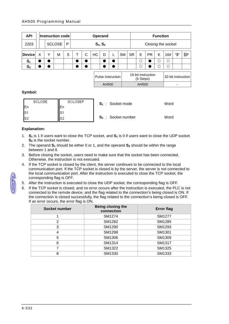
AH500 Programming Manual
6-532
API Instruction code Operand Function
2203 SCLOSE P S1, S2 Closing the socket
Device X Y M S T C HC D L SM SR E PR K 16# “$” DF
S1 S2
Pulse instruction 16-bit instruction
(5 Steps) 32-bit instruction
AH500 AH500 -
Symbol:
S1 : Socket mode Word
S2 : Socket number Word
Explanation:
1. S1 is 1 if users want to close the TCP socket, and S1 is 0 if users want to close the UDP socket. S2 is the socket number.
2. The operand S1 should be either 0 or 1, and the operand S2 should be within the range between 1 and 8.
3. Before closing the socket, users need to make sure that the socket has been connected. Otherwise, the instruction is not executed.
4. If the TCP socket is closed by the client, the server continues to be connected to the local communication port. If the TCP socket is closed is by the server, the server is not connected to the local communication port. After the instruction is executed to close the TCP socket, the corresponding flag is OFF.
5. After the instruction is executed to close the UDP socket, the corresponding flag is OFF. 6. If the TCP socket is closed, and no error occurs after the instruction is executed, the PLC is not
connected to the remote device, and the flag related to the connection’s being closed is ON. If the connection is closed successfully, the flag related to the connection’s being closed is OFF. If an error occurs, the error flag is ON.
Socket number Being closing the connection Error flag
1 SM1274 SM1277 2 SM1282 SM1285 3 SM1290 SM1293 4 SM1298 SM1301 5 SM1306 SM1309 6 SM1314 SM1317 7 SM1322 SM1325 8 SM1330 SM1333

Chapter 6 Appl ied Inst ruct ions
6-533
7. If the UDP socket is close, and no error occurs after the instruction is executed, the flag related to the connection’s having been started is OFF. If an error occurs, the error flag is ON.
Socket number Error flag 1 SM1338 2 SM1343 3 SM1348 4 SM1353 5 SM1358 6 SM1363 7 SM1368 8 SM1373
8. Generally, the pulse instruction SCLOSEP is used.
Example:
Please refer to the example of the execution of SOPEN.
Additional remark:
Error codes for the TCP connection:
Error Code Description Error Flag
16#2003 The value in S1, S2, or S3 exceeds the range, the instruction is not
executed. SM0/SM5
16#600D The RJ45 port is NOT connected. SM1100
16#6212 The remote socket response timeout Note 1 16#6214 The connection to the remote socket was denied. Note 1 16#621A The current socket is closed. Note 1
Note 1:
SM1277: The error flag of TCP Socket 1
SM1285:The error flag of TCP Socket 2
~
SM1325:The error flag of TCP Socket 7
SM1333:The error flag of TCP Socket 8
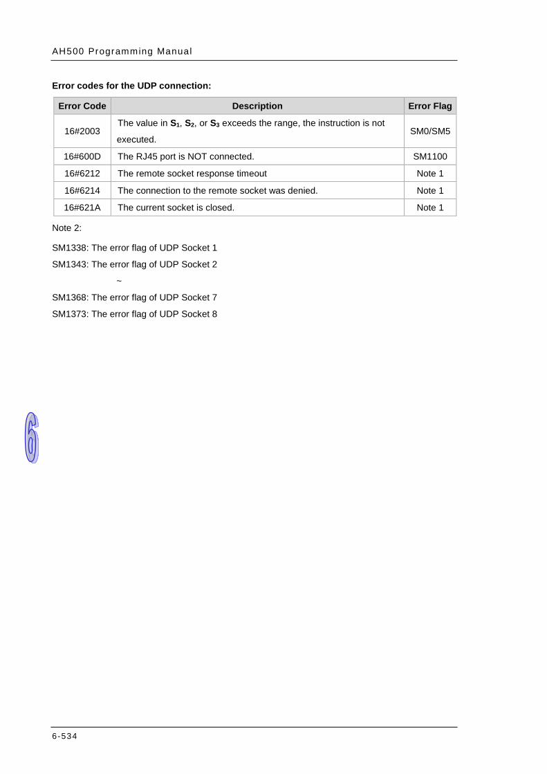
AH500 Programming Manual
6-534
Error codes for the UDP connection:
Error Code Description Error Flag
16#2003 The value in S1, S2, or S3 exceeds the range, the instruction is not
executed. SM0/SM5
16#600D The RJ45 port is NOT connected. SM1100
16#6212 The remote socket response timeout Note 1 16#6214 The connection to the remote socket was denied. Note 1 16#621A The current socket is closed. Note 1
Note 2:
SM1338: The error flag of UDP Socket 1
SM1343: The error flag of UDP Socket 2
~
SM1368: The error flag of UDP Socket 7
SM1373: The error flag of UDP Socket 8
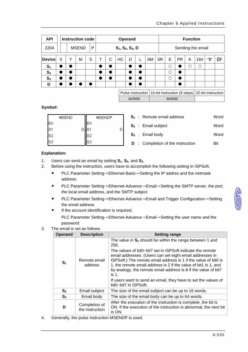
Chapter 6 Appl ied Inst ruct ions
6-535
API Instruction code Operand Function
2204 MSEND P S1, S2, S3, D Sending the email
Device X Y M S T C HC D L SM SR E PR K 16# “$” DF
S1 S2 S3 D
Pulse instruction 16-bit instruction (9 steps) 32-bit instruction AH500 AH500 -
Symbol:
S1 : Remote email address Word
S2 : Email subject Word
S3 : Email body Word
D : Completion of the instruction Bit
Explanation:
1. Users can send an email by setting S1, S2, and S3. 2. Before using the instruction, users have to accomplish the following setting in ISPSoft.
PLC Parameter Setting→Ethernet-Basic→Setting the IP addres and the netmask address
PLC Parameter Setting→Ethernet-Advance→Email→Setting the SMTP server, the port, the local email address, and the SMTP subject
PLC Parameter Setting→Ethernet-Advance→Email and Trigger Configuration→Setting the email address
If the account identification is required, PLC Parameter Setting→Ethernet-Advance→Email→Setting the user name and the password
3. The email is set as follows. Operand Description Setting range
S1 Remote email address
The value in S1 should be within the range between 1 and 256. The values of bit0~bit7 set in ISPSoft indicate the remote email addresses. (Users can set eight email addresses in ISPSoft.) The remote email address is 1 if the value of bit0 is 1, the remote email address is 2 if the value of bit1 is 1, and by analogy, the remote email address is 8 if the value of bit7 is 1. If users want to send an email, they have to set the values of bit0~bit7 in ISPSoft.
S2 Email subject The size of the email subject can be up to 16 words. S3 Email body The size of the email body can be up to 64 words.
D Completion of the instruction
After the execution of the instruction is complete, the bit is ON. If the execution of the instruction is abnormal, the next bit is ON.
4. Generally, the pulse instruction MSENDP is used.
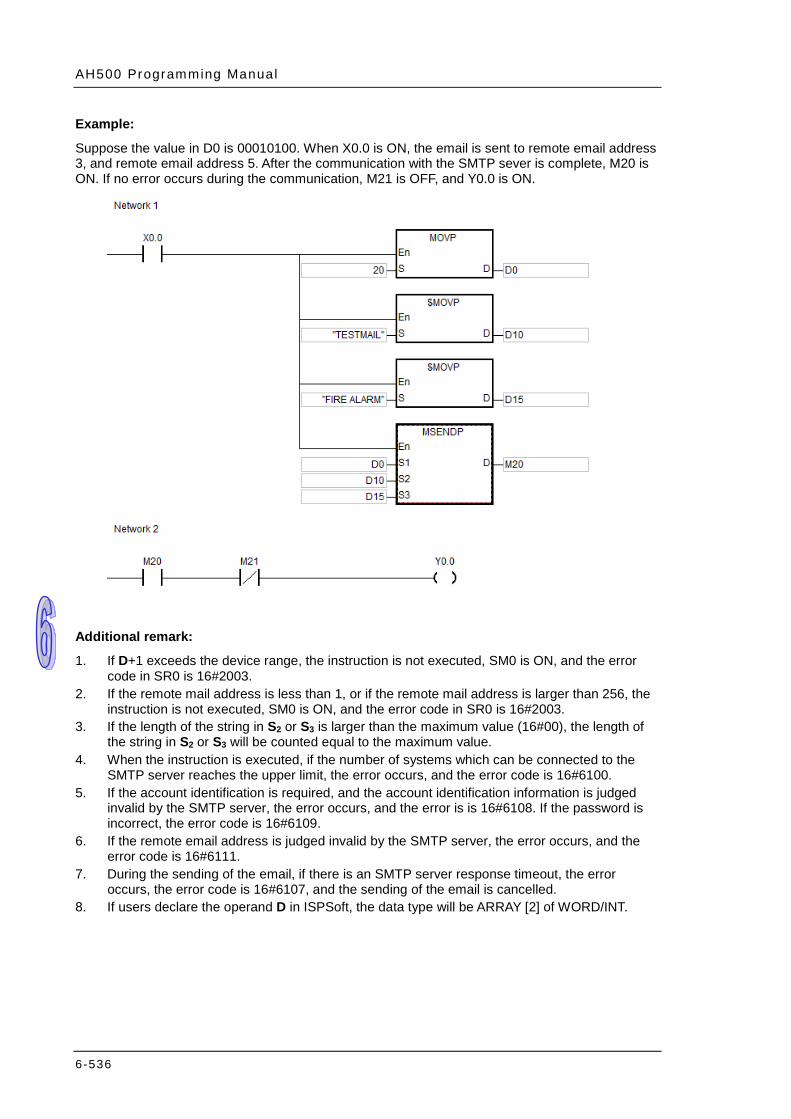
AH500 Programming Manual
6-536
Example:
Suppose the value in D0 is 00010100. When X0.0 is ON, the email is sent to remote email address 3, and remote email address 5. After the communication with the SMTP sever is complete, M20 is ON. If no error occurs during the communication, M21 is OFF, and Y0.0 is ON.
Additional remark:
1. If D+1 exceeds the device range, the instruction is not executed, SM0 is ON, and the error code in SR0 is 16#2003.
2. If the remote mail address is less than 1, or if the remote mail address is larger than 256, the instruction is not executed, SM0 is ON, and the error code in SR0 is 16#2003.
3. If the length of the string in S2 or S3 is larger than the maximum value (16#00), the length of the string in S2 or S3 will be counted equal to the maximum value.
4. When the instruction is executed, if the number of systems which can be connected to the SMTP server reaches the upper limit, the error occurs, and the error code is 16#6100.
5. If the account identification is required, and the account identification information is judged invalid by the SMTP server, the error occurs, and the error is is 16#6108. If the password is incorrect, the error code is 16#6109.
6. If the remote email address is judged invalid by the SMTP server, the error occurs, and the error code is 16#6111.
7. During the sending of the email, if there is an SMTP server response timeout, the error occurs, the error code is 16#6107, and the sending of the email is cancelled.
8. If users declare the operand D in ISPSoft, the data type will be ARRAY [2] of WORD/INT.
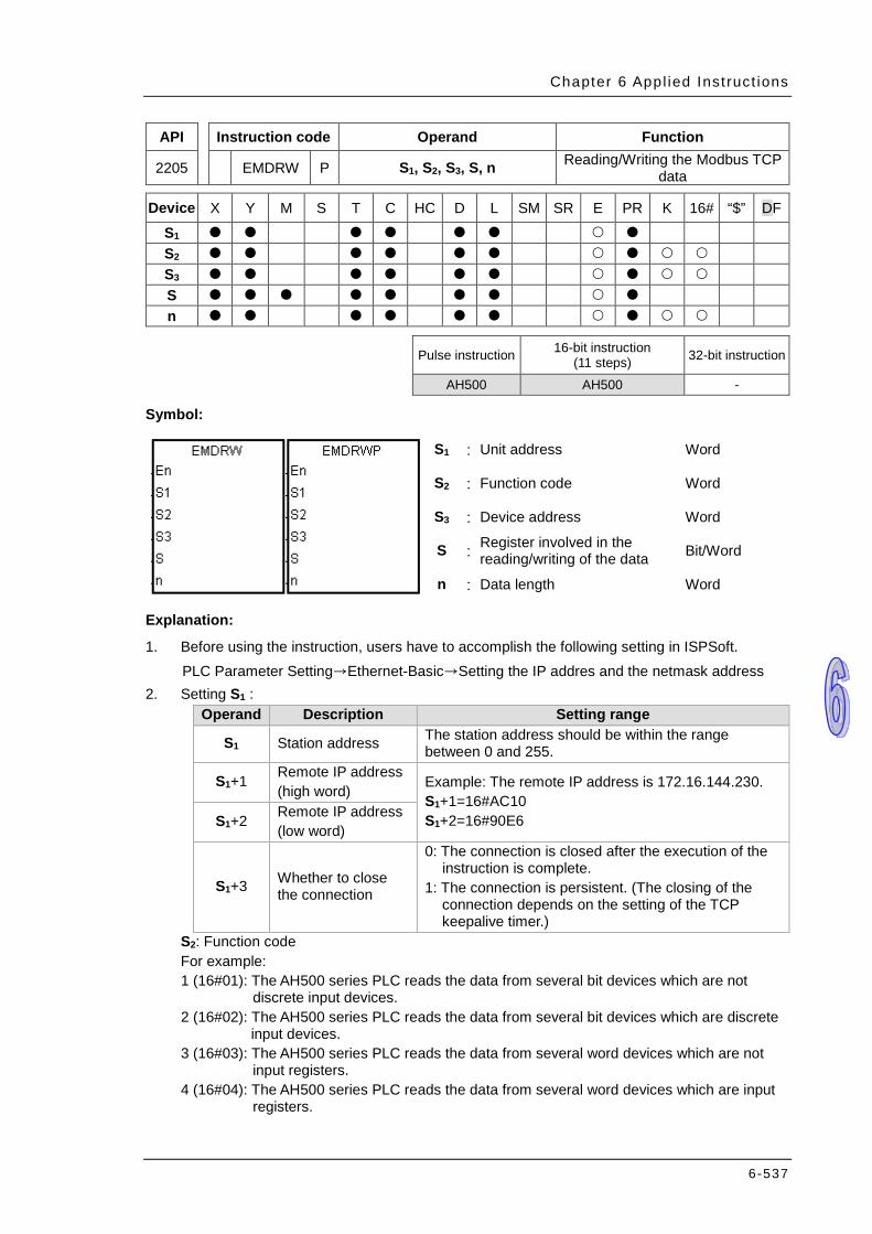
Chapter 6 Appl ied Inst ruct ions
6-537
API Instruction code Operand Function
2205 EMDRW P S1, S2, S3, S, n Reading/Writing the Modbus TCP data
Device X Y M S T C HC D L SM SR E PR K 16# “$” DF
S1 S2 S3 S n
Pulse instruction 16-bit instruction
(11 steps) 32-bit instruction
AH500 AH500 -
Symbol:
S1 : Unit address Word
S2 : Function code Word
S3 : Device address Word
S : Register involved in the reading/writing of the data Bit/Word
n : Data length Word
Explanation:
1. Before using the instruction, users have to accomplish the following setting in ISPSoft. PLC Parameter Setting→Ethernet-Basic→Setting the IP addres and the netmask address 2. Setting S1 :
Operand Description Setting range
S1 Station address The station address should be within the range between 0 and 255.
S1+1 Remote IP address (high word) Example: The remote IP address is 172.16.144.230.
S1+1=16#AC10 S1+2=16#90E6 S1+2 Remote IP address
(low word)
S1+3 Whether to close the connection
0: The connection is closed after the execution of the instruction is complete.
1: The connection is persistent. (The closing of the connection depends on the setting of the TCP keepalive timer.)
S2: Function code For example: 1 (16#01): The AH500 series PLC reads the data from several bit devices which are not
discrete input devices. 2 (16#02): The AH500 series PLC reads the data from several bit devices which are discrete
input devices. 3 (16#03): The AH500 series PLC reads the data from several word devices which are not
input registers. 4 (16#04): The AH500 series PLC reads the data from several word devices which are input
registers.
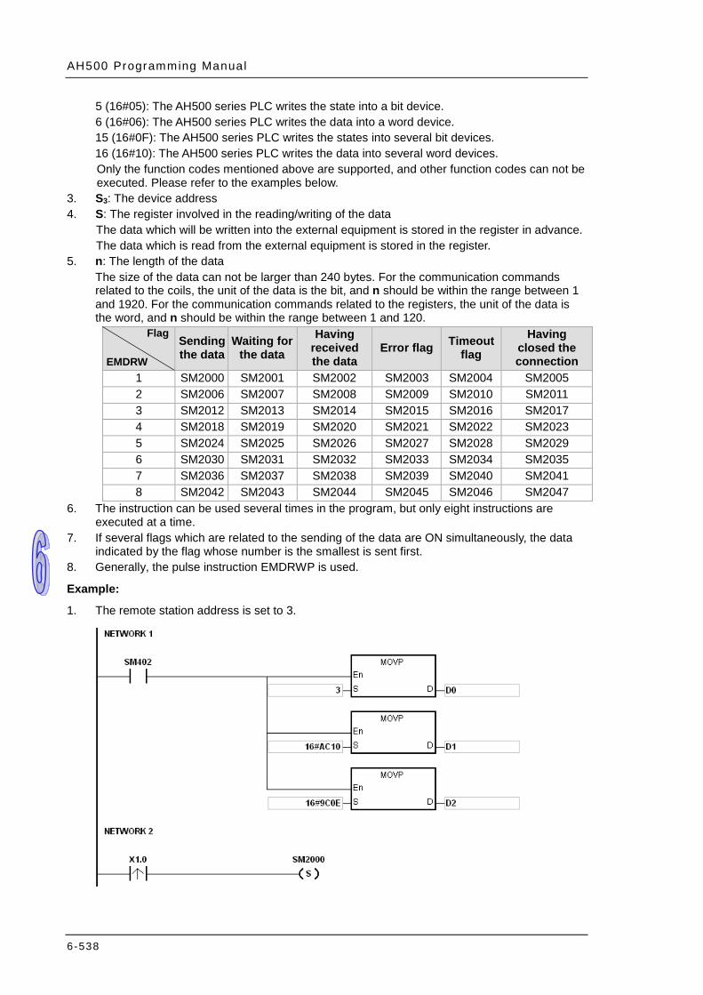
AH500 Programming Manual
6-538
5 (16#05): The AH500 series PLC writes the state into a bit device. 6 (16#06): The AH500 series PLC writes the data into a word device. 15 (16#0F): The AH500 series PLC writes the states into several bit devices. 16 (16#10): The AH500 series PLC writes the data into several word devices. Only the function codes mentioned above are supported, and other function codes can not be executed. Please refer to the examples below.
3. S3: The device address 4. S: The register involved in the reading/writing of the data
The data which will be written into the external equipment is stored in the register in advance. The data which is read from the external equipment is stored in the register.
5. n: The length of the data The size of the data can not be larger than 240 bytes. For the communication commands related to the coils, the unit of the data is the bit, and n should be within the range between 1 and 1920. For the communication commands related to the registers, the unit of the data is the word, and n should be within the range between 1 and 120.
Flag
EMDRW Sending the data
Waiting for the data
Having received the data
Error flag Timeout flag
Having closed the connection
1 SM2000 SM2001 SM2002 SM2003 SM2004 SM2005 2 SM2006 SM2007 SM2008 SM2009 SM2010 SM2011 3 SM2012 SM2013 SM2014 SM2015 SM2016 SM2017 4 SM2018 SM2019 SM2020 SM2021 SM2022 SM2023 5 SM2024 SM2025 SM2026 SM2027 SM2028 SM2029 6 SM2030 SM2031 SM2032 SM2033 SM2034 SM2035 7 SM2036 SM2037 SM2038 SM2039 SM2040 SM2041 8 SM2042 SM2043 SM2044 SM2045 SM2046 SM2047
6. The instruction can be used several times in the program, but only eight instructions are executed at a time.
7. If several flags which are related to the sending of the data are ON simultaneously, the data indicated by the flag whose number is the smallest is sent first.
8. Generally, the pulse instruction EMDRWP is used.
Example:
1. The remote station address is set to 3.
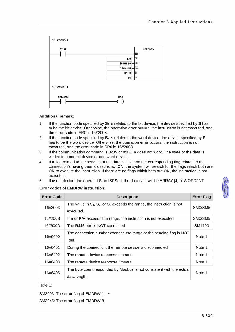
Chapter 6 Appl ied Inst ruct ions
6-539
Additional remark:
1. If the function code specified by S2 is related to the bit device, the device specified by S has to be the bit device. Otherwise, the operation error occurs, the instruction is not executed, and the error code in SR0 is 16#2003.
2. If the function code specified by S2 is related to the word device, the device specified by S has to be the word device. Otherwise, the operation error occurs, the instruction is not executed, and the error code in SR0 is 16#2003.
3. If the communication command is 0x05 or 0x06, n does not work. The state or the data is written into one bit device or one word device.
4. If a flag related to the sending of the data is ON, and the corresponding flag related to the connection’s having been closed is not ON, the system will search for the flags which both are ON to execute the instruction. If there are no flags which both are ON, the instruction is not executed.
5. If users declare the operand S1 in ISPSoft, the data type will be ARRAY [4] of WORD/INT.
Error codes of EMDRW instruction:
Error Code Description Error Flag
16#2003 The value in S1, S2, or S3 exceeds the range, the instruction is not
executed. SM0/SM5
16#200B If n or K/H exceeds the range, the instruction is not executed. SM0/SM5
16#600D The RJ45 port is NOT connected. SM1100
16#6400 The connection number exceeds the range or the sending flag is NOT
set. Note 1
16#6401 During the connection, the remote device is disconnected. Note 1 16#6402 The remote device response timeout Note 1 16#6403 The remote device response timeout Note 1
16#6405 The byte count responded by Modbus is not consistent with the actual
data length. Note 1
Note 1:
SM2003: The error flag of EMDRW 1 ~
SM2045: The error flag of EMDRW 8
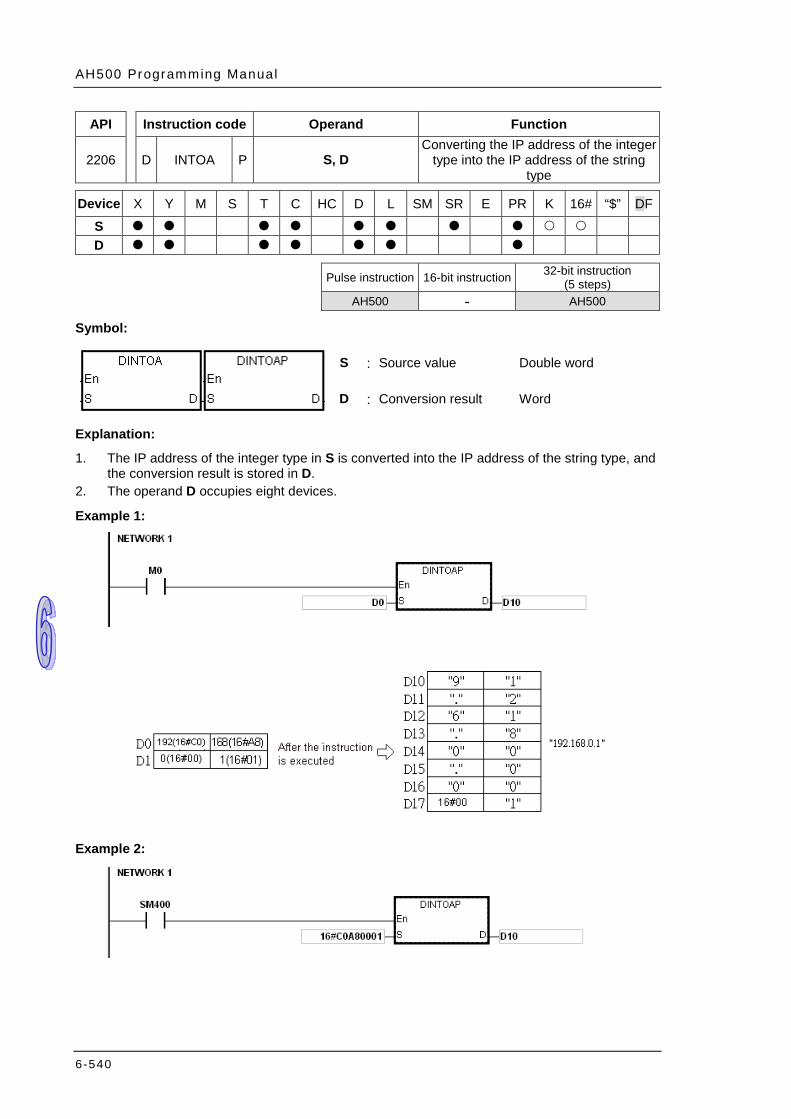
AH500 Programming Manual
6-540
API Instruction code Operand Function
2206 D INTOA P S, D Converting the IP address of the integer
type into the IP address of the string type
Device X Y M S T C HC D L SM SR E PR K 16# “$” DF
S D
Pulse instruction 16-bit instruction 32-bit instruction
(5 steps) AH500 - AH500
Symbol:
S : Source value Double word
D : Conversion result Word
Explanation:
1. The IP address of the integer type in S is converted into the IP address of the string type, and the conversion result is stored in D.
2. The operand D occupies eight devices.
Example 1:
Example 2:

Chapter 6 Appl ied Inst ruct ions
6-541
Additional remark:
If users declare the operand D in ISPSoft, the data type will be ARRAY [8] of WORD/INT.
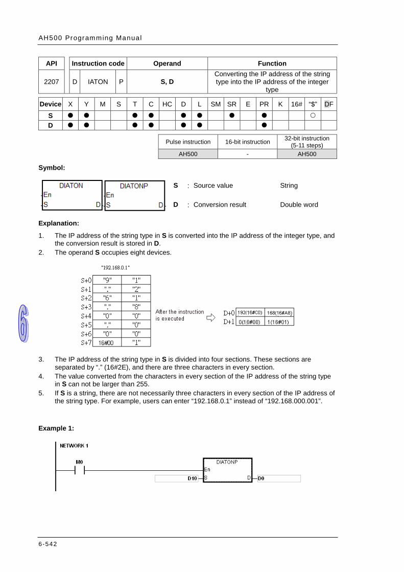
AH500 Programming Manual
6-542
API Instruction code Operand Function
2207 D IATON P S, D Converting the IP address of the string type into the IP address of the integer
type
Device X Y M S T C HC D L SM SR E PR K 16# “$” DF S D
Pulse instruction 16-bit instruction 32-bit instruction
(5-11 steps) AH500 - AH500
Symbol:
S : Source value String
D : Conversion result Double word
Explanation:
1. The IP address of the string type in S is converted into the IP address of the integer type, and the conversion result is stored in D.
2. The operand S occupies eight devices.
3. The IP address of the string type in S is divided into four sections. These sections are
separated by “.” (16#2E), and there are three characters in every section. 4. The value converted from the characters in every section of the IP address of the string type
in S can not be larger than 255. 5. If S is a string, there are not necessarily three characters in every section of the IP address of
the string type. For example, users can enter “192.168.0.1” instead of “192.168.000.001”.
Example 1:
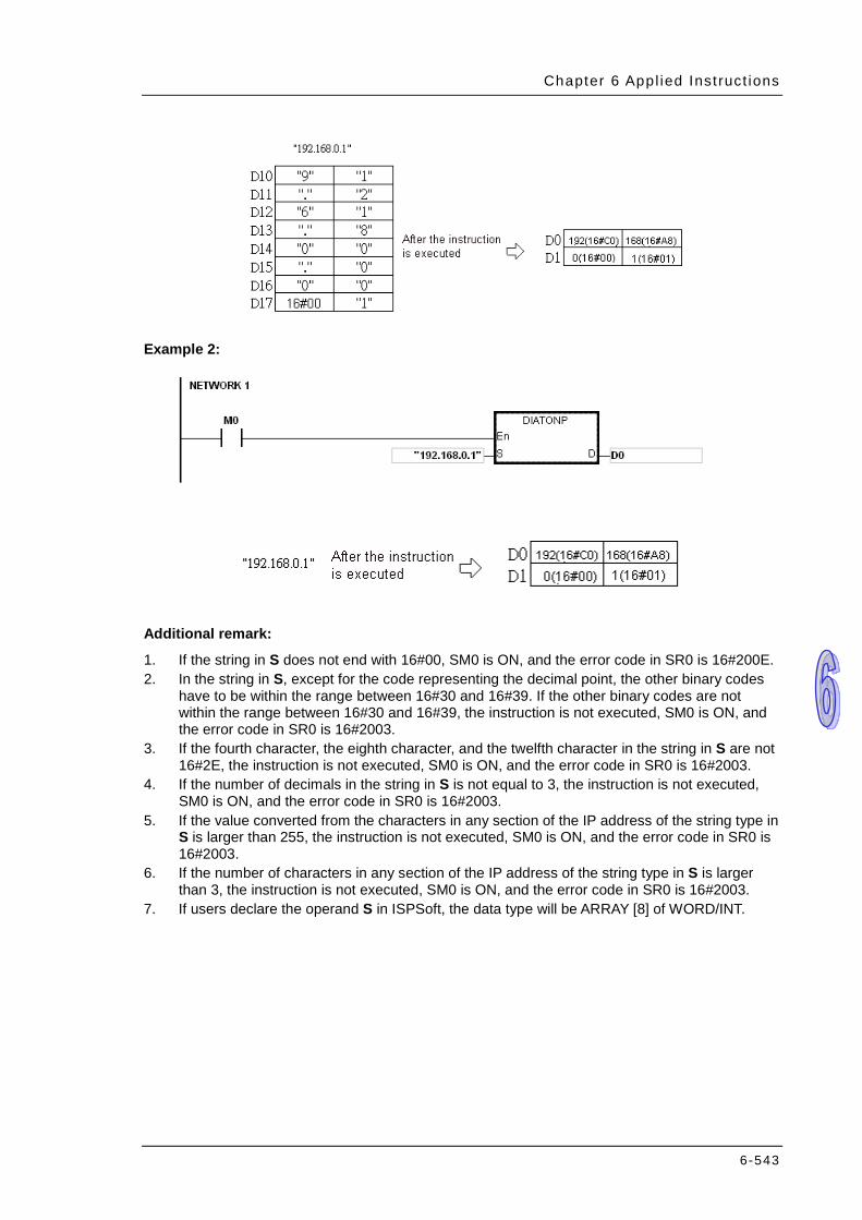
Chapter 6 Appl ied Inst ruct ions
6-543
Example 2:
Additional remark:
1. If the string in S does not end with 16#00, SM0 is ON, and the error code in SR0 is 16#200E. 2. In the string in S, except for the code representing the decimal point, the other binary codes
have to be within the range between 16#30 and 16#39. If the other binary codes are not within the range between 16#30 and 16#39, the instruction is not executed, SM0 is ON, and the error code in SR0 is 16#2003.
3. If the fourth character, the eighth character, and the twelfth character in the string in S are not 16#2E, the instruction is not executed, SM0 is ON, and the error code in SR0 is 16#2003.
4. If the number of decimals in the string in S is not equal to 3, the instruction is not executed, SM0 is ON, and the error code in SR0 is 16#2003.
5. If the value converted from the characters in any section of the IP address of the string type in S is larger than 255, the instruction is not executed, SM0 is ON, and the error code in SR0 is 16#2003.
6. If the number of characters in any section of the IP address of the string type in S is larger than 3, the instruction is not executed, SM0 is ON, and the error code in SR0 is 16#2003.
7. If users declare the operand S in ISPSoft, the data type will be ARRAY [8] of WORD/INT.

AH500 Programming Manual
6-544
API Instruction code Operand Function
2208 EIPRW S1~S7, n, S, D1, D2 Reading and writing EtherNet/IP data
Device X Y M S T C HC D L SM SR E PR K 16# “$” DF
S1 S2 S3 S4 S5 S6 S7 n S D1 D2
Pulse instruction 16-bit instruction (23 steps)
32-bit instruction
- AH500 - Symbol
S1 : IP address Word[2]
S2 : Connection mode Word
S3 : Function code (Service code) Word
S4 : Class ID Word
S5 : Instance ID Word
S6 : Attribute ID switch Bit
S7 : Attribute ID Word
n : Length of read and write data Word
S : Register for the read/write data Word[n]
D1 : Communication status Word
D2 : Error code Word[2]

Chapter 6 Appl ied Inst ruct ions
6-545
Explanation:
1. This instruction reads and writes EtherNet/IP data. The following table lists the names and
explanations of S1–S7, n, S and D1–D2.
Operand Name Description
S1 IP address
The first two sections of the IP address occupy the first
word and the remaining two sections of the IP address
occupy the second word. For example, if the IP address
is 192.168.1.5, S1=16#C0A8 and S1+1=16#0105.
S2 Connection mode
0: UCMM, no CIP connection
1: Connected then close CIP connection
2: Connected then keep CIP connection
S3 Function code
(Service code)
Range: 16#0000–00FF. If the function code exceeds the
range, the instruction is not executed. Refer to the
service codes of the to be connected device for more
details.
S4 Class ID Refer to the Class ID of the to be connected device for
more details.
S5 Instance ID Refer to the Instance ID of the to be connected device for
more details.
S6 Attribute ID switch ON: Enable;
OFF: Disable, and S7 is not used.
S7 Attribute ID Refer to the Attribute ID of the to be connected device for
more details.
n Length of read and
write data
Size of the data to be written or read;
unit: byte; maximum: 200 bytes
S Register for the
read/write data
Source register for the sent data or where the received
data is stored; unit: word
D1 Communication
status
0:Communication not triggered
1:Communication in process
2:Communication completed without errors
3:Communication error
4:Error in parameter settings
D2 Error code D2: Major error code
D2+1: extended error code
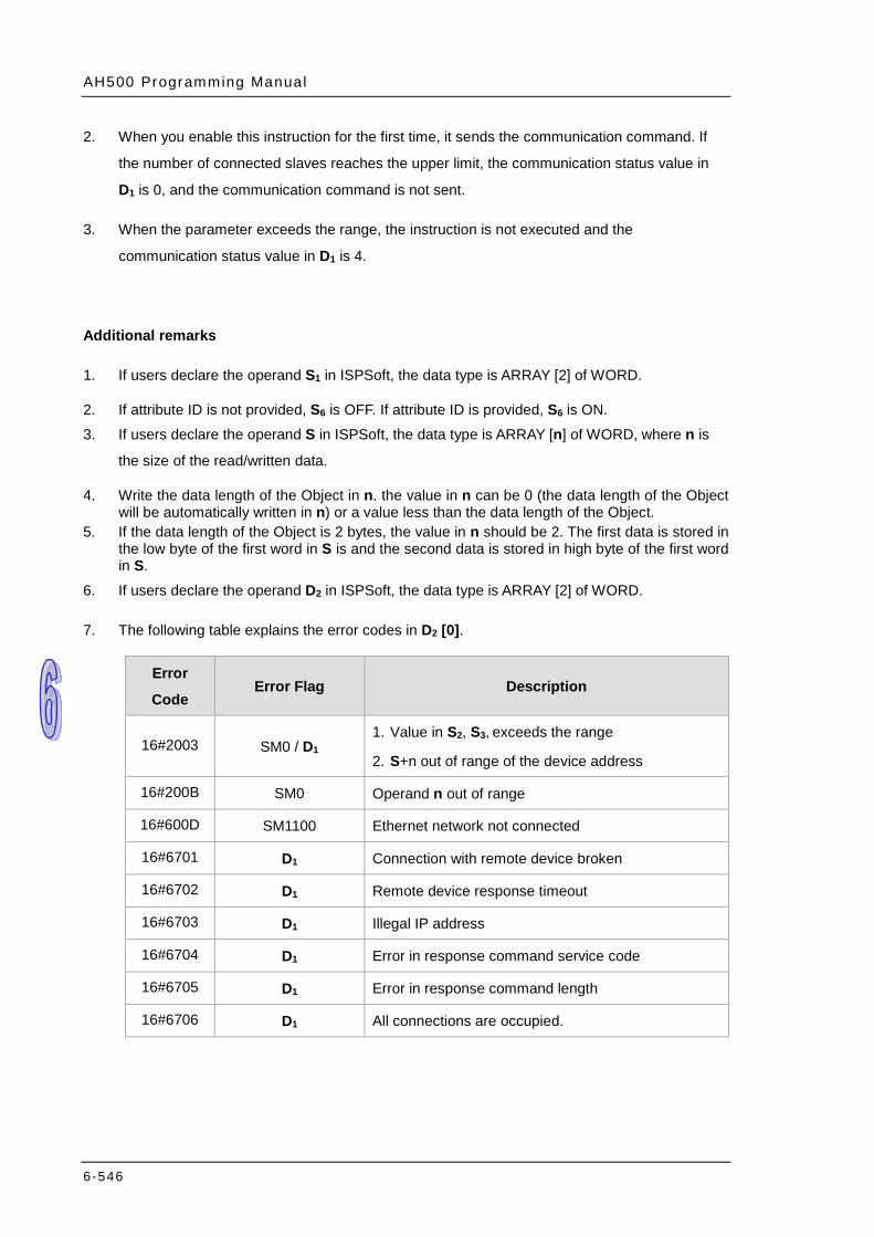
AH500 Programming Manual
6-546
2. When you enable this instruction for the first time, it sends the communication command. If
the number of connected slaves reaches the upper limit, the communication status value in
D1 is 0, and the communication command is not sent.
3. When the parameter exceeds the range, the instruction is not executed and the
communication status value in D1 is 4.
Additional remarks
1. If users declare the operand S1 in ISPSoft, the data type is ARRAY [2] of WORD.
2. If attribute ID is not provided, S6 is OFF. If attribute ID is provided, S6 is ON. 3. If users declare the operand S in ISPSoft, the data type is ARRAY [n] of WORD, where n is
the size of the read/written data.
4. Write the data length of the Object in n. the value in n can be 0 (the data length of the Object will be automatically written in n) or a value less than the data length of the Object.
5. If the data length of the Object is 2 bytes, the value in n should be 2. The first data is stored in the low byte of the first word in S is and the second data is stored in high byte of the first word in S.
6. If users declare the operand D2 in ISPSoft, the data type is ARRAY [2] of WORD.
7. The following table explains the error codes in D2 [0].
Error
Code Error Flag Description
16#2003 SM0 / D1 1. Value in S2, S3, exceeds the range
2. S+n out of range of the device address
16#200B SM0 Operand n out of range
16#600D SM1100 Ethernet network not connected
16#6701 D1 Connection with remote device broken
16#6702 D1 Remote device response timeout
16#6703 D1 Illegal IP address
16#6704 D1 Error in response command service code
16#6705 D1 Error in response command length
16#6706 D1 All connections are occupied.

Chapter 6 Appl ied Inst ruct ions
6-547
8. The following table explains the error codes in D2 [0].
Status
Code Description What to Do
16#00 Connection
successful
16#01 Connection error Ensure the EDS file of the slave is correct.
16#02 Connected devices
unavailable
1. Ensure the number of devices connected to the
master does not exceed the limit.
2. Ensure the number of devices connected to the
slave does not exceed the limit.
3. The instruction is triggered repeatedly. Wait till
the execution of the instruction is complete
before starting another instruction.
16#03 Error in parameter Ensure the read/written data in S is correct.
16#04 Path error Ensure the settings are correct for Class ID (S4),
Instance ID (S5), and Attribute ID (S7).
16#05 Destination path
does not exist
Ensure the settings are correct for Class ID (S4),
Instance ID (S5), and Attribute ID (S7).
16#07 Connection broken
1. Ensure the Ethernet port of the slave device is
connected properly.
2. Ensure the keep alive timer setting is correct for
the slave device.
16#08 Service code not
supported Ensure the function code (S3) is correct.
16#09 Invalid attribute value Ensure both the data source (S) and their contents
are correct.
16#0A Error in attribute list
Ensure the slave device object attribute allows PLC
to perform the Get_Attribute_List and
Set_Attribute_List functions.
16#0B Transmission
conflicts Ensure the service setting is repeated.
16#0C Object status
conflicts Ensure the Owner IO connection is established.

AH500 Programming Manual
6-548
Status
Code Description What to Do
16#0D Object existed
Ensure the slave supports the defined object. The
service does not need to execute if the defined
object is supported.
16#0E Attribute not writable Ensure the object attribute supports the write function.
16#0F No privilege to
perform service code
Ensure the slave device is allowed to perform the
service code.
16#10
Device cannot
currently perform
service
Ensure the Owner IO connection is established.
16#11 Size of response
data too large
Ensure the length of data in the object attribute does
not exceed the limit (100 words).
16#12
Data access
sequence error when
tag is accessed
Ensure the data length and the data type are correct.
16#13 Transmitted data too
short Ensure the length (n) of read/written data is correct.
16#14 Attribute value
unsupported
Ensure the Attribute ID switch (S6) and Attribute ID
(S7) are correct.
16#15 Transmitted data are
too long Ensure the read/written data length (n) is correct.
16#16 Object does not exist Ensure the Class ID (S4) is correct.
16#17
Data access
sequence error when
tag is accessed
1. Ensure the Ethernet network connection is
correct.
2. Ensure no packets are lost in the Ethernet
communication.
16#18 Attribute value not
saved Ensure no error state on the slave device occurred.
16#19 Attribute value
storage error
Ensure no hardware error on the slave device
occurred.
16#1A
Router error: length
of request packet
exceeds limit
Ensure the read/written data length (n) does not
exceed the limit of the router.
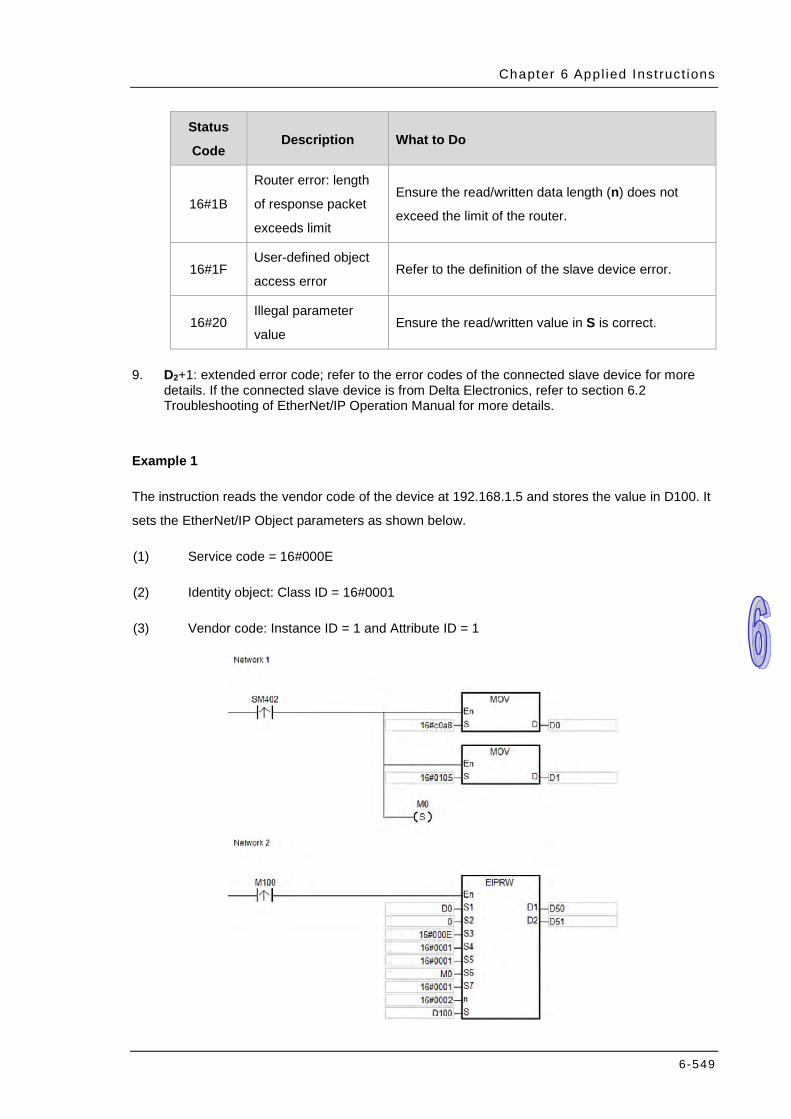
Chapter 6 Appl ied Inst ruct ions
6-549
Status
Code Description What to Do
16#1B
Router error: length
of response packet
exceeds limit
Ensure the read/written data length (n) does not
exceed the limit of the router.
16#1F User-defined object
access error Refer to the definition of the slave device error.
16#20 Illegal parameter
value Ensure the read/written value in S is correct.
9. D2+1: extended error code; refer to the error codes of the connected slave device for more
details. If the connected slave device is from Delta Electronics, refer to section 6.2 Troubleshooting of EtherNet/IP Operation Manual for more details.
Example 1
The instruction reads the vendor code of the device at 192.168.1.5 and stores the value in D100. It
sets the EtherNet/IP Object parameters as shown below.
(1) Service code = 16#000E
(2) Identity object: Class ID = 16#0001
(3) Vendor code: Instance ID = 1 and Attribute ID = 1
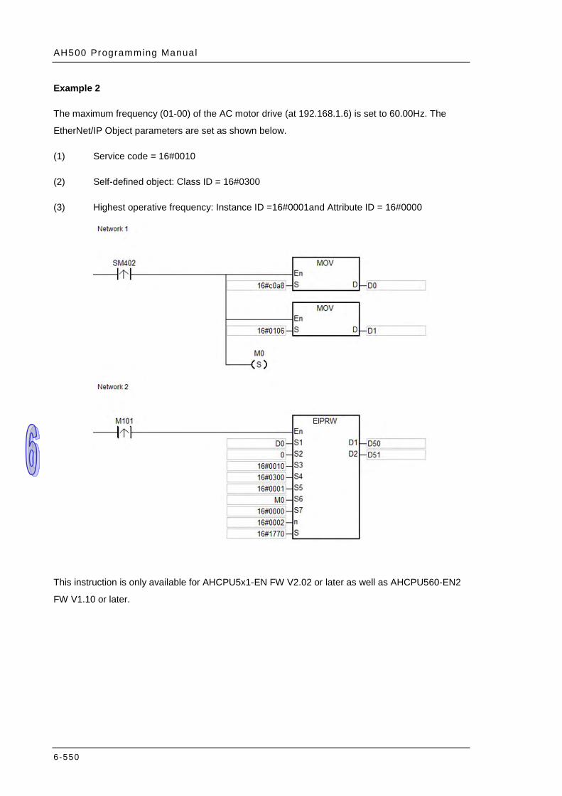
AH500 Programming Manual
6-550
Example 2
The maximum frequency (01-00) of the AC motor drive (at 192.168.1.6) is set to 60.00Hz. The
EtherNet/IP Object parameters are set as shown below.
(1) Service code = 16#0010
(2) Self-defined object: Class ID = 16#0300
(3) Highest operative frequency: Instance ID =16#0001and Attribute ID = 16#0000
This instruction is only available for AHCPU5x1-EN FW V2.02 or later as well as AHCPU560-EN2
FW V1.10 or later.
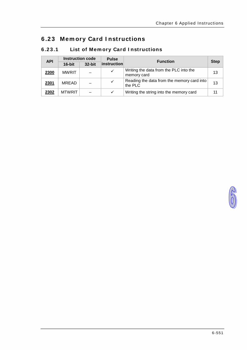
Chapter 6 Appl ied Inst ruct ions
6-551
6.23 Memory Card Instructions
6.23.1 List of Memory Card Instructions
API Instruction code Pulse instruction Function Step 16-bit 32-bit
2300 MWRIT – Writing the data from the PLC into the memory card 13
2301 MREAD – Reading the data from the memory card into the PLC 13
2302 MTWRIT – Writing the string into the memory card 11
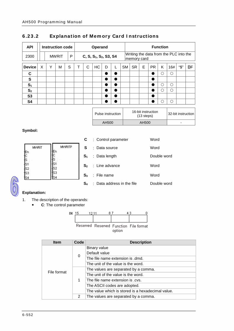
AH500 Programming Manual
6-552
6.23.2 Explanation of Memory Card Instructions
API Instruction code Operand Function
2300 MWRIT P C, S, S1, S2, S3, S4 Writing the data from the PLC into the memory card
Device X Y M S T C HC D L SM SR E PR K 16# “$” DF
C S S1 S2 S3 S4
Pulse instruction 16-bit instruction
(13 steps) 32-bit instruction
AH500 AH500 -
Symbol:
C : Control parameter Word
S : Data source Word
S1 : Data length Double word
S2 : Line advance Word
S3 : File name Word
S4 : Data address in the file Double word
Explanation:
1. The description of the operands: C: The control parameter
Item Code Description
File format
0
Binary value Default value The file name extension is .dmd. The unit of the value is the word.
1
The values are separated by a comma. The unit of the value is the word. The file name extension is .cvs. The ASCII codes are adopted. The value which is stored is a hexadecimal value.
2 The values are separated by a comma.
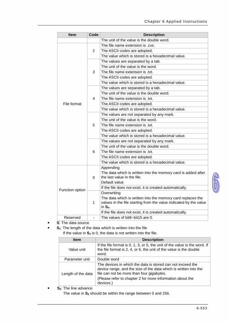
Chapter 6 Appl ied Inst ruct ions
6-553
Item Code Description The unit of the value is the double word.
File format
2 The file name extension is .cvs. The ASCII codes are adopted. The value which is stored is a hexadecimal value.
3
The values are separated by a tab. The unit of the value is the word. The file name extension is .txt. The ASCII codes are adopted. The value which is stored is a hexadecimal value.
4
The values are separated by a tab. The unit of the value is the double word. The file name extension is .txt. The ASCII codes are adopted. The value which is stored is a hexadecimal value.
5
The values are not separated by any mark. The unit of the value is the word. The file name extension is .txt. The ASCII codes are adopted. The value which is stored is a hexadecimal value.
6
The values are not separated by any mark. The unit of the value is the double word. The file name extension is .txt. The ASCII codes are adopted. The value which is stored is a hexadecimal value.
Function option
0
Appending The data which is written into the memory card is added after the last value in the file. Default value If the file does not exist, it is created automatically.
1
Overwriting The data which is written into the memory card replaces the values in the file starting from the value indicated by the value in S4. If the file does not exist, it is created automatically.
Reserved - The values of bit8~bit15 are 0. S: The data source S1: The length of the data which is written into the file
If the value in S1 is 0, the data is not written into the file.
Item Description
Value unit If the file format is 0, 1, 3, or 5, the unit of the value is the word. If the file format is 2, 4, or 6, the unit of the value is the double word.
Parameter unit Double word
Length of the data
The devices in which the data is stored can not exceed the device range, and the size of the data which is written into the file can not be more than four gigabytes. (Please refer to chapter 2 for more information about the devices.)
S2: The line advance The value in S2 should be within the range between 0 and 256.
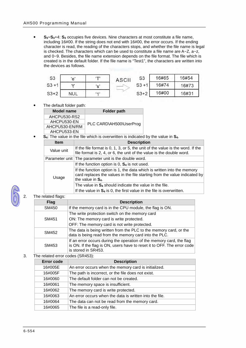
AH500 Programming Manual
6-554
S3~S3+4: S3 occupies five devices. Nine characters at most constitute a file name, including 16#00. If the string does not end with 16#00, the error occurs. If the ending character is read, the reading of the characters stops, and whether the file name is legal is checked. The characters which can be used to constitute a file name are A~Z, a~z, and 0~9. Besides, the file name extension depends on the file format. The file which is created is in the default folder. If the file name is “Test1”, the characters are written into the devices as follows.
The default folder path:
Model name Folder path AHCPU530-RS2
PLC CARD\AH500\UserProg AHCPU530-EN AHCPU530-EN/RM
AHCPU533-EN S4: The value in the file which is overwritten is indicated by the value in S4.
Item Description
Value unit If the file format is 0, 1, 3, or 5, the unit of the value is the word. If the file format is 2, 4, or 6, the unit of the value is the double word.
Parameter unit The parameter unit is the double word.
Usage
If the function option is 0, S4 is not used. If the function option is 1, the data which is written into the memory card replaces the values in the file starting from the value indicated by the value in S4. The value in S4 should indicate the value in the file. If the value in S4 is 0, the first value in the file is overwritten.
2. The related flags: Flag Description
SM450 If the memory card is in the CPU module, the flag is ON.
SM451 The write protection switch on the memory card ON: The memory card is write protected. OFF: The memory card is not write protected.
SM452 The data is being written from the PLC to the memory card, or the data is being read from the memory card into the PLC.
SM453 If an error occurs during the operation of the memory card, the flag is ON. If the flag is ON, users have to reset it to OFF. The error code is stored in SR453.
3. The related error codes (SR453): Error code Description 16#005E An error occurs when the memory card is initialized. 16#005F The path is incorrect, or the file does not exist. 16#0060 The default folder can not be created. 16#0061 The memory space is insufficient. 16#0062 The memory card is write protected. 16#0063 An error occurs when the data is written into the file. 16#0064 The data can not be read from the memory card. 16#0065 The file is a read-only file.
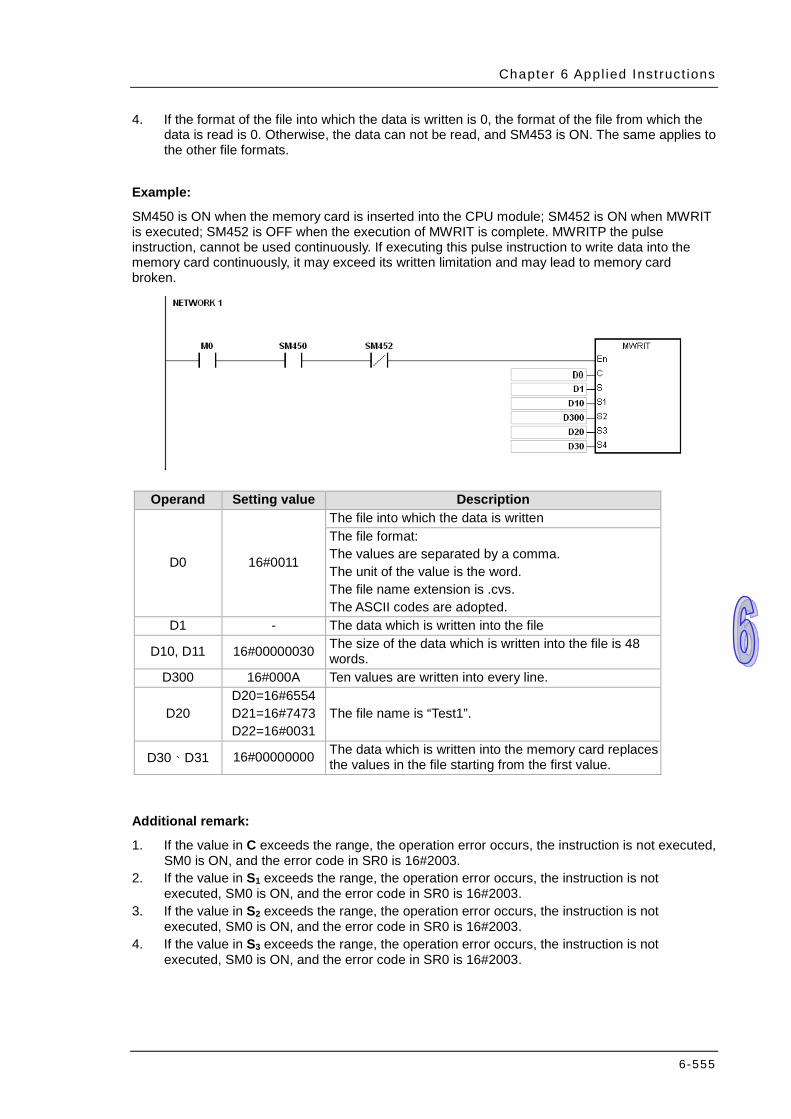
Chapter 6 Appl ied Inst ruct ions
6-555
4. If the format of the file into which the data is written is 0, the format of the file from which the data is read is 0. Otherwise, the data can not be read, and SM453 is ON. The same applies to the other file formats.
Example:
SM450 is ON when the memory card is inserted into the CPU module; SM452 is ON when MWRIT is executed; SM452 is OFF when the execution of MWRIT is complete. MWRITP the pulse instruction, cannot be used continuously. If executing this pulse instruction to write data into the memory card continuously, it may exceed its written limitation and may lead to memory card broken.
Operand Setting value Description
D0 16#0011
The file into which the data is written The file format: The values are separated by a comma. The unit of the value is the word. The file name extension is .cvs. The ASCII codes are adopted.
D1 - The data which is written into the file
D10, D11 16#00000030 The size of the data which is written into the file is 48 words.
D300 16#000A Ten values are written into every line.
D20 D20=16#6554 D21=16#7473 D22=16#0031
The file name is “Test1”.
D30、D31 16#00000000 The data which is written into the memory card replaces the values in the file starting from the first value.
Additional remark:
1. If the value in C exceeds the range, the operation error occurs, the instruction is not executed, SM0 is ON, and the error code in SR0 is 16#2003.
2. If the value in S1 exceeds the range, the operation error occurs, the instruction is not executed, SM0 is ON, and the error code in SR0 is 16#2003.
3. If the value in S2 exceeds the range, the operation error occurs, the instruction is not executed, SM0 is ON, and the error code in SR0 is 16#2003.
4. If the value in S3 exceeds the range, the operation error occurs, the instruction is not executed, SM0 is ON, and the error code in SR0 is 16#2003.
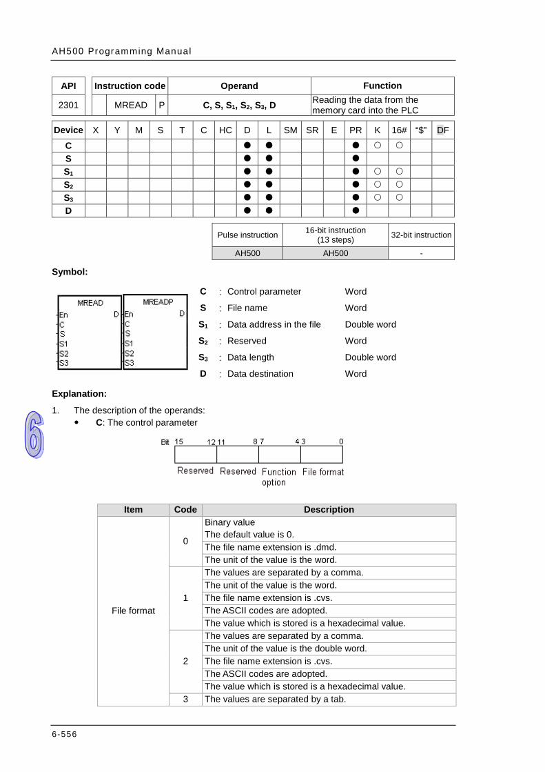
AH500 Programming Manual
6-556
API Instruction code Operand Function
2301 MREAD P C, S, S1, S2, S3, D Reading the data from the memory card into the PLC
Device X Y M S T C HC D L SM SR E PR K 16# “$” DF
C S S1 S2 S3 D
Pulse instruction 16-bit instruction
(13 steps) 32-bit instruction
AH500 AH500 -
Symbol:
C : Control parameter Word
S : File name Word
S1 : Data address in the file Double word
S2 : Reserved Word
S3 : Data length Double word
D : Data destination Word
Explanation:
1. The description of the operands: C: The control parameter
Item Code Description
File format
0
Binary value The default value is 0. The file name extension is .dmd. The unit of the value is the word.
1
The values are separated by a comma. The unit of the value is the word. The file name extension is .cvs. The ASCII codes are adopted. The value which is stored is a hexadecimal value.
2
The values are separated by a comma. The unit of the value is the double word. The file name extension is .cvs. The ASCII codes are adopted. The value which is stored is a hexadecimal value.
3 The values are separated by a tab.
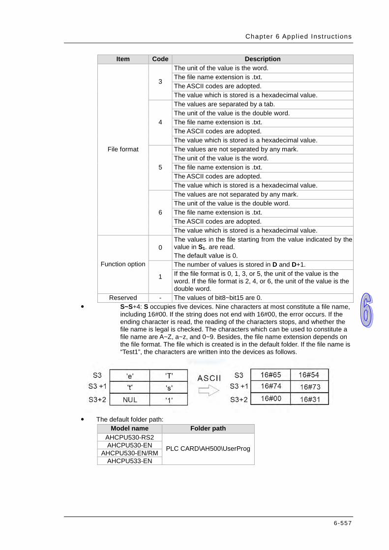
Chapter 6 Appl ied Inst ruct ions
6-557
Item Code Description
File format
3
The unit of the value is the word. The file name extension is .txt. The ASCII codes are adopted. The value which is stored is a hexadecimal value.
4
The values are separated by a tab. The unit of the value is the double word. The file name extension is .txt. The ASCII codes are adopted. The value which is stored is a hexadecimal value.
5
The values are not separated by any mark. The unit of the value is the word. The file name extension is .txt. The ASCII codes are adopted. The value which is stored is a hexadecimal value.
6
The values are not separated by any mark. The unit of the value is the double word. The file name extension is .txt. The ASCII codes are adopted. The value which is stored is a hexadecimal value.
Function option
0 The values in the file starting from the value indicated by the value in S1. are read. The default value is 0.
1
The number of values is stored in D and D+1. If the file format is 0, 1, 3, or 5, the unit of the value is the word. If the file format is 2, 4, or 6, the unit of the value is the double word.
Reserved - The values of bit8~bit15 are 0. S~S+4: S occupies five devices. Nine characters at most constitute a file name,
including 16#00. If the string does not end with 16#00, the error occurs. If the ending character is read, the reading of the characters stops, and whether the file name is legal is checked. The characters which can be used to constitute a file name are A~Z, a~z, and 0~9. Besides, the file name extension depends on the file format. The file which is created is in the default folder. If the file name is “Test1”, the characters are written into the devices as follows.
The default folder path:
Model name Folder path AHCPU530-RS2
PLC CARD\AH500\UserProg AHCPU530-EN AHCPU530-EN/RM
AHCPU533-EN
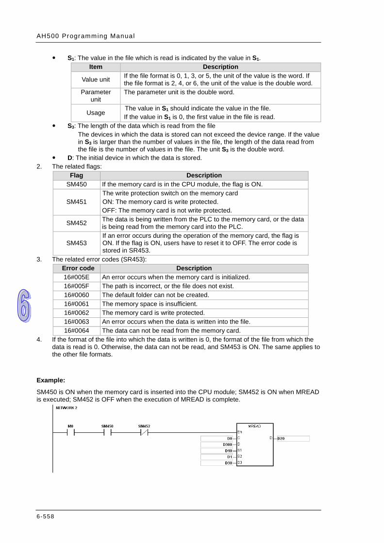
AH500 Programming Manual
6-558
S1: The value in the file which is read is indicated by the value in S1. Item Description
Value unit If the file format is 0, 1, 3, or 5, the unit of the value is the word. If the file format is 2, 4, or 6, the unit of the value is the double word.
Parameter unit
The parameter unit is the double word.
Usage The value in S1 should indicate the value in the file. If the value in S1 is 0, the first value in the file is read.
S3: The length of the data which is read from the file The devices in which the data is stored can not exceed the device range. If the value in S3 is larger than the number of values in the file, the length of the data read from the file is the number of values in the file. The unit S3 is the double word.
D: The initial device in which the data is stored. 2. The related flags:
Flag Description SM450 If the memory card is in the CPU module, the flag is ON.
SM451 The write protection switch on the memory card ON: The memory card is write protected. OFF: The memory card is not write protected.
SM452 The data is being written from the PLC to the memory card, or the data is being read from the memory card into the PLC.
SM453 If an error occurs during the operation of the memory card, the flag is ON. If the flag is ON, users have to reset it to OFF. The error code is stored in SR453.
3. The related error codes (SR453): Error code Description 16#005E An error occurs when the memory card is initialized. 16#005F The path is incorrect, or the file does not exist. 16#0060 The default folder can not be created. 16#0061 The memory space is insufficient. 16#0062 The memory card is write protected. 16#0063 An error occurs when the data is written into the file. 16#0064 The data can not be read from the memory card.
4. If the format of the file into which the data is written is 0, the format of the file from which the data is read is 0. Otherwise, the data can not be read, and SM453 is ON. The same applies to the other file formats.
Example:
SM450 is ON when the memory card is inserted into the CPU module; SM452 is ON when MREAD is executed; SM452 is OFF when the execution of MREAD is complete.
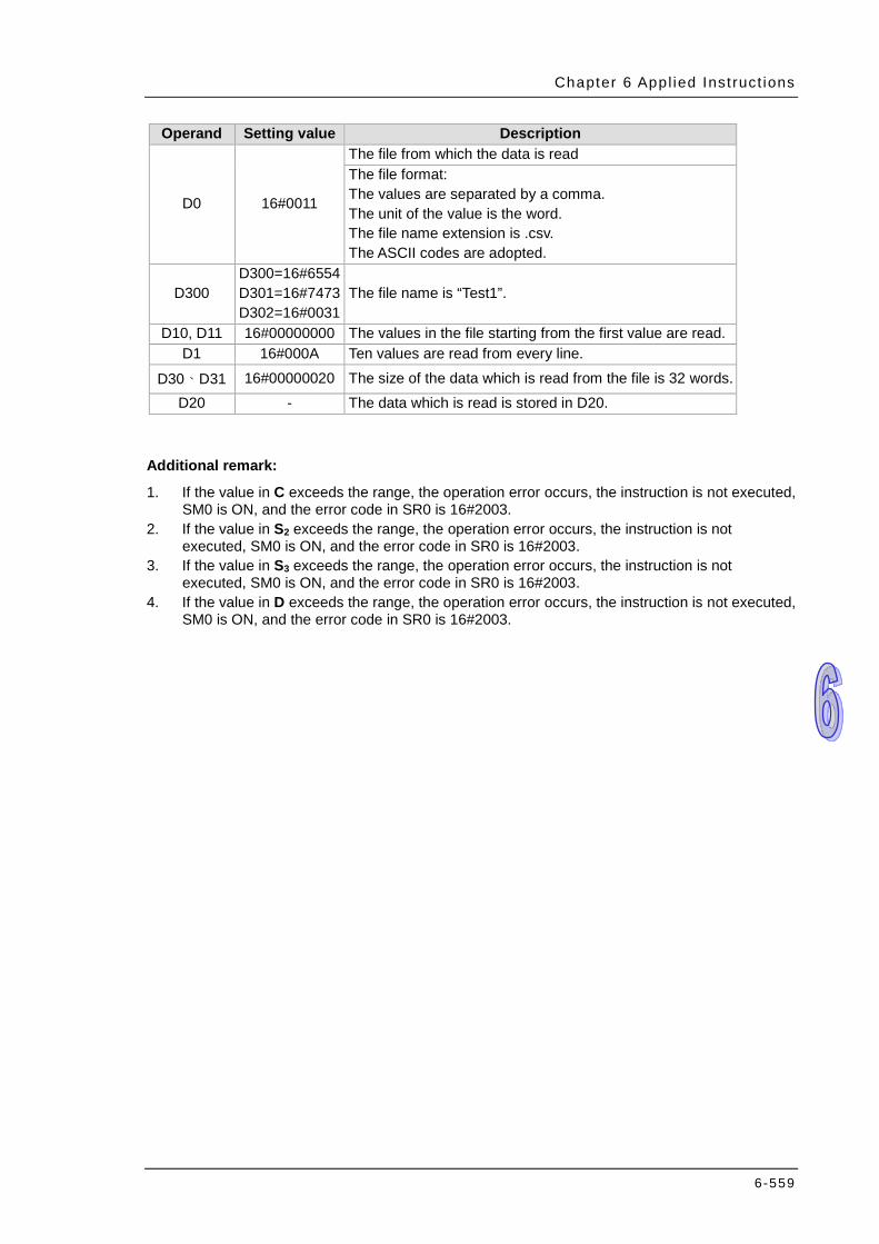
Chapter 6 Appl ied Inst ruct ions
6-559
Operand Setting value Description
D0 16#0011
The file from which the data is read The file format: The values are separated by a comma. The unit of the value is the word. The file name extension is .csv. The ASCII codes are adopted.
D300 D300=16#6554 D301=16#7473 D302=16#0031
The file name is “Test1”.
D10, D11 16#00000000 The values in the file starting from the first value are read. D1 16#000A Ten values are read from every line.
D30、D31 16#00000020 The size of the data which is read from the file is 32 words. D20 - The data which is read is stored in D20.
Additional remark:
1. If the value in C exceeds the range, the operation error occurs, the instruction is not executed, SM0 is ON, and the error code in SR0 is 16#2003.
2. If the value in S2 exceeds the range, the operation error occurs, the instruction is not executed, SM0 is ON, and the error code in SR0 is 16#2003.
3. If the value in S3 exceeds the range, the operation error occurs, the instruction is not executed, SM0 is ON, and the error code in SR0 is 16#2003.
4. If the value in D exceeds the range, the operation error occurs, the instruction is not executed, SM0 is ON, and the error code in SR0 is 16#2003.
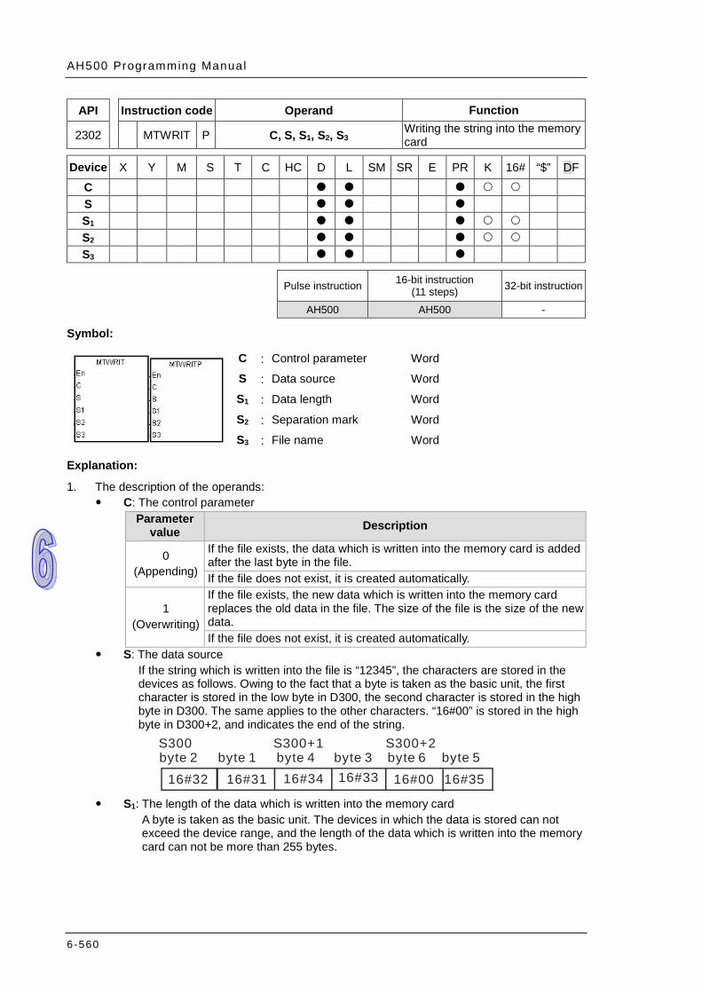
AH500 Programming Manual
6-560
API Instruction code Operand Function
2302 MTWRIT P C, S, S1, S2, S3 Writing the string into the memory card
Device X Y M S T C HC D L SM SR E PR K 16# “$” DF
C S S1 S2 S3
Pulse instruction 16-bit instruction
(11 steps) 32-bit instruction
AH500 AH500 -
Symbol:
C : Control parameter Word
S : Data source Word
S1 : Data length Word
S2 : Separation mark Word
S3 : File name Word
Explanation:
1. The description of the operands: C: The control parameter
Parameter value Description
0 (Appending)
If the file exists, the data which is written into the memory card is added after the last byte in the file. If the file does not exist, it is created automatically.
1 (Overwriting)
If the file exists, the new data which is written into the memory card replaces the old data in the file. The size of the file is the size of the new data. If the file does not exist, it is created automatically.
S: The data source If the string which is written into the file is “12345”, the characters are stored in the devices as follows. Owing to the fact that a byte is taken as the basic unit, the first character is stored in the low byte in D300, the second character is stored in the high byte in D300. The same applies to the other characters. “16#00” is stored in the high byte in D300+2, and indicates the end of the string.
16#32 byte 2
16#31 16#34 16#33 16#00 16#35
S300 byte 1 byte 4 byte 3 byte 6 byte 5
S300+1 S300+2
S1: The length of the data which is written into the memory card
A byte is taken as the basic unit. The devices in which the data is stored can not exceed the device range, and the length of the data which is written into the memory card can not be more than 255 bytes.
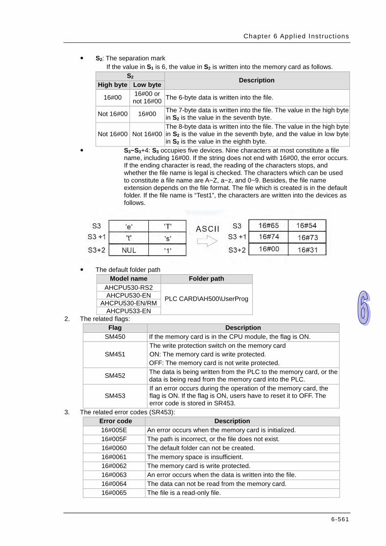
Chapter 6 Appl ied Inst ruct ions
6-561
S2: The separation mark If the value in S1 is 6, the value in S2 is written into the memory card as follows.
S2 Description High byte Low byte
16#00 16#00 or not 16#00 The 6-byte data is written into the file.
Not 16#00 16#00 The 7-byte data is written into the file. The value in the high byte in S2 is the value in the seventh byte.
Not 16#00 Not 16#00 The 8-byte data is written into the file. The value in the high byte in S2 is the value in the seventh byte, and the value in low byte in S2 is the value in the eighth byte.
S3~S3+4: S3 occupies five devices. Nine characters at most constitute a file name, including 16#00. If the string does not end with 16#00, the error occurs. If the ending character is read, the reading of the characters stops, and whether the file name is legal is checked. The characters which can be used to constitute a file name are A~Z, a~z, and 0~9. Besides, the file name extension depends on the file format. The file which is created is in the default folder. If the file name is “Test1”, the characters are written into the devices as follows.
The default folder path
Model name Folder path AHCPU530-RS2
PLC CARD\AH500\UserProg AHCPU530-EN AHCPU530-EN/RM
AHCPU533-EN 2. The related flags:
Flag Description SM450 If the memory card is in the CPU module, the flag is ON.
SM451 The write protection switch on the memory card ON: The memory card is write protected. OFF: The memory card is not write protected.
SM452 The data is being written from the PLC to the memory card, or the data is being read from the memory card into the PLC.
SM453 If an error occurs during the operation of the memory card, the flag is ON. If the flag is ON, users have to reset it to OFF. The error code is stored in SR453.
3. The related error codes (SR453): Error code Description 16#005E An error occurs when the memory card is initialized. 16#005F The path is incorrect, or the file does not exist. 16#0060 The default folder can not be created. 16#0061 The memory space is insufficient. 16#0062 The memory card is write protected. 16#0063 An error occurs when the data is written into the file. 16#0064 The data can not be read from the memory card. 16#0065 The file is a read-only file.

AH500 Programming Manual
6-562
Example:
SM450 is ON when the memory card is inserted into the CPU module; SM452 is ON when MTWRIT is executed; SM452 is OFF when the execution of MTWRIT is complete.
Operand Setting value Description
D0 16#0001
The file into which the data is written The file format: The unit of the character is the byte. The file name extension is .txt. The ASCII codes are adopted. The data in D300 is written into the file.
D300 - The data which is written into the file
D10 16#000A The size of the string which is written into the file is 32 bytes.
D1 16#0A00 After the data is written into the file, the separation mark is added after the last byte in the file.
D30 D30=16#6554 D31=16#7473 D32=16#0031
The file name is “Test1”.
Additional remark:
1. If the value in C exceeds the range, the operation error occurs, the instruction is not executed, SM0 is ON, and the error code in SR0 is 16#2003.
2. If the value in S1 exceeds the range, the operation error occurs, the instruction is not executed, SM0 is ON, and the error code in SR0 is 16#2003.
3. If the value in S3 exceeds the range, the operation error occurs, the instruction is not executed, SM0 is ON, and the error code in SR0 is 16#2003.

Chapter 6 Appl ied Inst ruct ions
6-563
6.24 Task Control Instructions
6.24.1 List of Task Control Instructions
API Instruction code Pulse instruction Function Step 16-bit 32-bit
2400 TKON – Enabling the cyclic task 3 2401 TKOFF – Disabling the cyclic task 3
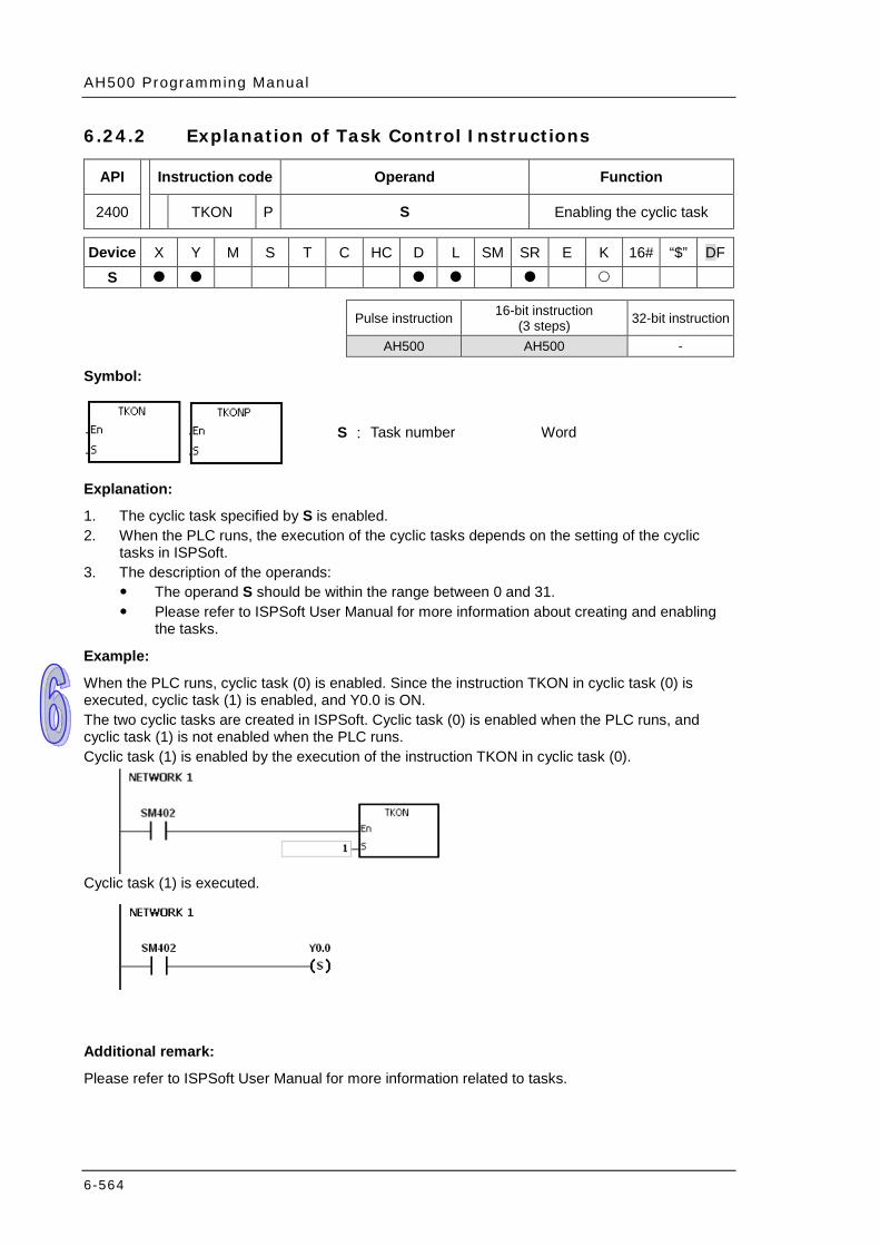
AH500 Programming Manual
6-564
6.24.2 Explanation of Task Control Instructions
API Instruction code Operand Function
2400 TKON P S Enabling the cyclic task
Device X Y M S T C HC D L SM SR E K 16# “$” DF
S
Pulse instruction 16-bit instruction (3 steps) 32-bit instruction
AH500 AH500 -
Symbol:
S : Task number Word
Explanation:
1. The cyclic task specified by S is enabled. 2. When the PLC runs, the execution of the cyclic tasks depends on the setting of the cyclic
tasks in ISPSoft. 3. The description of the operands:
The operand S should be within the range between 0 and 31. Please refer to ISPSoft User Manual for more information about creating and enabling
the tasks.
Example:
When the PLC runs, cyclic task (0) is enabled. Since the instruction TKON in cyclic task (0) is executed, cyclic task (1) is enabled, and Y0.0 is ON. The two cyclic tasks are created in ISPSoft. Cyclic task (0) is enabled when the PLC runs, and cyclic task (1) is not enabled when the PLC runs. Cyclic task (1) is enabled by the execution of the instruction TKON in cyclic task (0).
Cyclic task (1) is executed.
Additional remark:
Please refer to ISPSoft User Manual for more information related to tasks.

Chapter 6 Appl ied Inst ruct ions
6-565
API Instruction code Operand Function
2401 TKOFF P S Disabling the cyclic task
Device X Y M S T C HC D L SM SR E K 16# “$” DF
S Pulse instruction 16-bit instruction
(3 steps) 32-bit instruction
AH500 AH500 -
Symbol:
S : Task number Word
Explanation:
1. The cyclic task specified by S is disabled. 2. When the PLC runs, the execution of the cyclic tasks depends on the setting of the cyclic
tasks in ISPSoft. 3. The description of the operands:
The operand S should be within the range between 0 and 31. Please refer to ISPSoft User Manual for more information about creating and enabling
the tasks.
Example:
When the PLC runs, cyclic task (0) and cyclic task (1) are enabled. Since the instruction TKOOFF in cyclic task (0) is executed, cyclic task (1) is disabled, and Y0.0 is OFF. The two cyclic tasks are created in ISPSoft. Cyclic task (0) and cyclic task (1) are enabled when the PLC runs, and cyclic task (1) is disabled when the instruction TKOFF in cyclic task (0) is executed. Cyclic task (1) is disabled by the execution of the instruction TKOFF in cyclic task (0).
Cyclic task (1) is not executed.
Additional remark:
Please refer to ISPSoft User Manual for more information related to tasks.
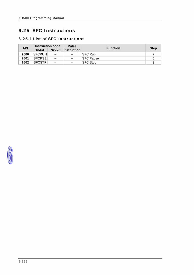
AH500 Programming Manual
6-566
6.25 SFC Instructions
6.25.1 List of SFC Instructions
API Instruction code Pulse instruction Function Step 16-bit 32-bit
2500 SFCRUN – – SFC Run 7 2501 SFCPSE – – SFC Pause 5 2502 SFCSTP – – SFC Stop 3
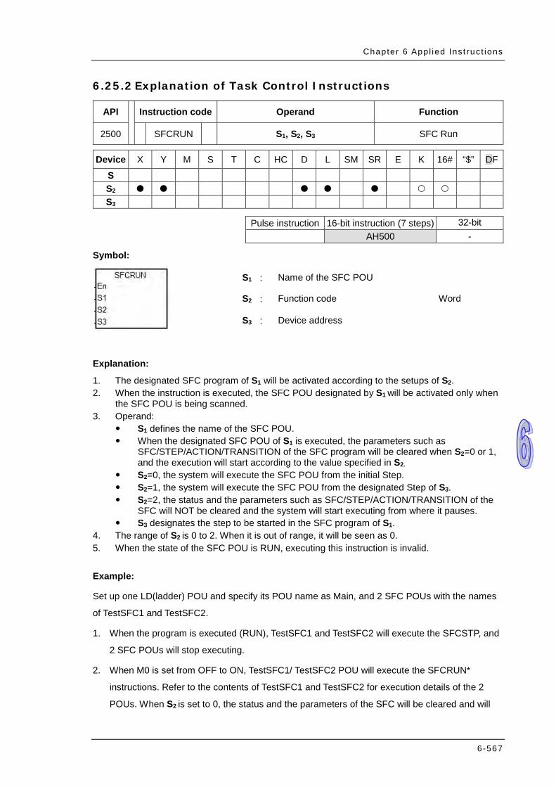
Chapter 6 Appl ied Ins t ruct ions
6-567
6.25.2 Explanation of Task Control Instructions
API Instruction code Operand Function
2500 SFCRUN S1, S2, S3 SFC Run
Device X Y M S T C HC D L SM SR E K 16# “$” DF
S S2 S3
Pulse instruction 16-bit instruction (7 steps) 32-bit
AH500 -
Symbol:
S1 : Name of the SFC POU
S2 : Function code Word
S3 : Device address
Explanation:
1. The designated SFC program of S1 will be activated according to the setups of S2. 2. When the instruction is executed, the SFC POU designated by S1 will be activated only when
the SFC POU is being scanned. 3. Operand:
S1 defines the name of the SFC POU. When the designated SFC POU of S1 is executed, the parameters such as
SFC/STEP/ACTION/TRANSITION of the SFC program will be cleared when S2=0 or 1, and the execution will start according to the value specified in S2.
S2=0, the system will execute the SFC POU from the initial Step. S2=1, the system will execute the SFC POU from the designated Step of S3. S2=2, the status and the parameters such as SFC/STEP/ACTION/TRANSITION of the
SFC will NOT be cleared and the system will start executing from where it pauses. S3 designates the step to be started in the SFC program of S1.
4. The range of S2 is 0 to 2. When it is out of range, it will be seen as 0. 5. When the state of the SFC POU is RUN, executing this instruction is invalid.
Example:
Set up one LD(ladder) POU and specify its POU name as Main, and 2 SFC POUs with the names
of TestSFC1 and TestSFC2.
1. When the program is executed (RUN), TestSFC1 and TestSFC2 will execute the SFCSTP, and
2 SFC POUs will stop executing.
2. When M0 is set from OFF to ON, TestSFC1/ TestSFC2 POU will execute the SFCRUN*
instructions. Refer to the contents of TestSFC1 and TestSFC2 for execution details of the 2
POUs. When S2 is set to 0, the status and the parameters of the SFC will be cleared and will
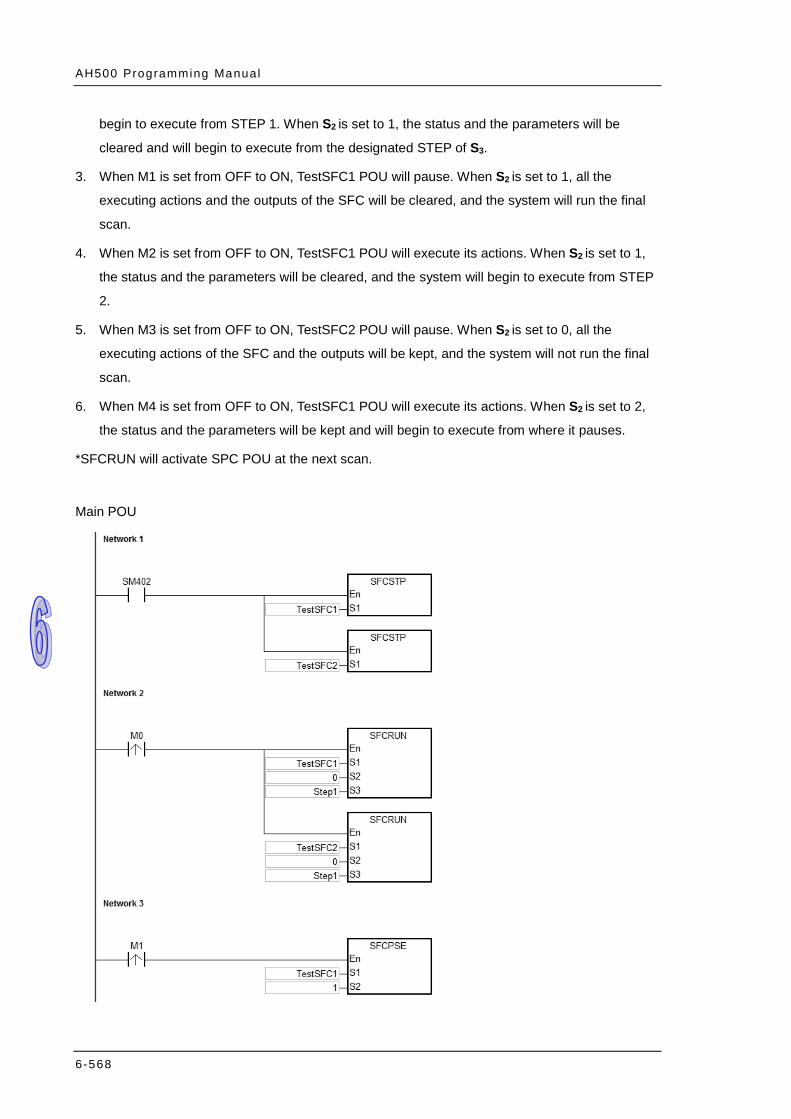
AH500 Programming Manual
6-568
begin to execute from STEP 1. When S2 is set to 1, the status and the parameters will be
cleared and will begin to execute from the designated STEP of S3.
3. When M1 is set from OFF to ON, TestSFC1 POU will pause. When S2 is set to 1, all the
executing actions and the outputs of the SFC will be cleared, and the system will run the final
scan.
4. When M2 is set from OFF to ON, TestSFC1 POU will execute its actions. When S2 is set to 1,
the status and the parameters will be cleared, and the system will begin to execute from STEP
2.
5. When M3 is set from OFF to ON, TestSFC2 POU will pause. When S2 is set to 0, all the
executing actions of the SFC and the outputs will be kept, and the system will not run the final
scan.
6. When M4 is set from OFF to ON, TestSFC1 POU will execute its actions. When S2 is set to 2,
the status and the parameters will be kept and will begin to execute from where it pauses.
*SFCRUN will activate SPC POU at the next scan.
Main POU
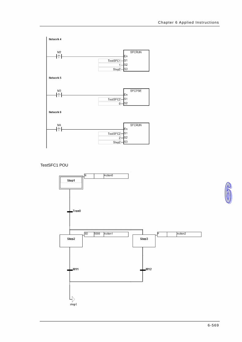
Chapter 6 Appl ied Ins t ruct ions
6-569
TestSFC1 POU

AH500 Programming Manual
6-570
TestSFC2 POU
Additional Remark:
Please refer to ISPSoft User Manual for more information related to SFC.
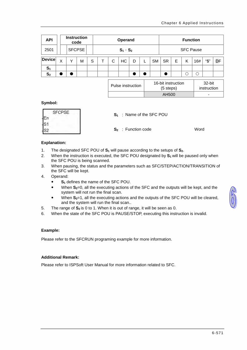
Chapter 6 Appl ied Ins t ruct ions
6-571
API Instruction code Operand Function
2501 SFCPSE S1,S2 SFC Pause
Device X Y M S T C HC D L SM SR E K 16# “$” DF S1 S2
Pulse instruction 16-bit instruction (5 steps)
32-bit instruction
AH500 -
Symbol:
S1 : Name of the SFC POU
S2 : Function code Word
Explanation:
1. The designated SFC POU of S1 will pause according to the setups of S2. 2. When the instruction is executed, the SFC POU designated by S1 will be paused only when
the SFC POU is being scanned. 3. When pausing, the status and the parameters such as SFC/STEP/ACTION/TRANSITION of
the SFC will be kept. 4. Operand:
S1 defines the name of the SFC POU. When S2=0, all the executing actions of the SFC and the outputs will be kept, and the
system will not run the final scan. When S2=1, all the executing actions and the outputs of the SFC POU will be cleared,
and the system will run the final scan.. 5. The range of S2 is 0 to 1. When it is out of range, it will be seen as 0. 6. When the state of the SFC POU is PAUSE/STOP, executing this instruction is invalid.
Example:
Please refer to the SFCRUN programing example for more information.
Additional Remark:
Please refer to ISPSoft User Manual for more information related to SFC.
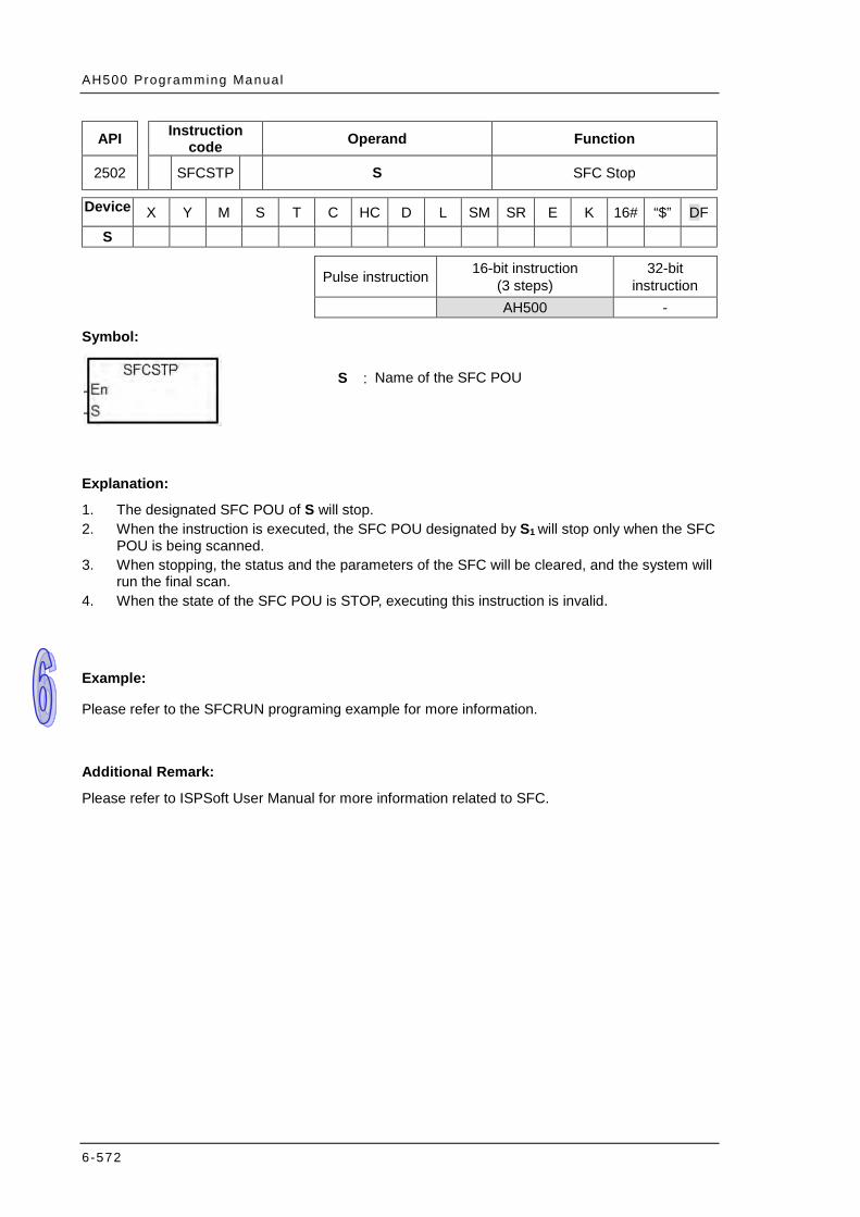
AH500 Programming Manual
6-572
API Instruction code Operand Function
2502 SFCSTP S SFC Stop
Device X Y M S T C HC D L SM SR E K 16# “$” DF S
Pulse instruction 16-bit instruction (3 steps)
32-bit instruction
AH500 -
Symbol:
S : Name of the SFC POU
Explanation:
1. The designated SFC POU of S will stop. 2. When the instruction is executed, the SFC POU designated by S1 will stop only when the SFC
POU is being scanned. 3. When stopping, the status and the parameters of the SFC will be cleared, and the system will
run the final scan. 4. When the state of the SFC POU is STOP, executing this instruction is invalid.
Example:
Please refer to the SFCRUN programing example for more information.
Additional Remark:
Please refer to ISPSoft User Manual for more information related to SFC.
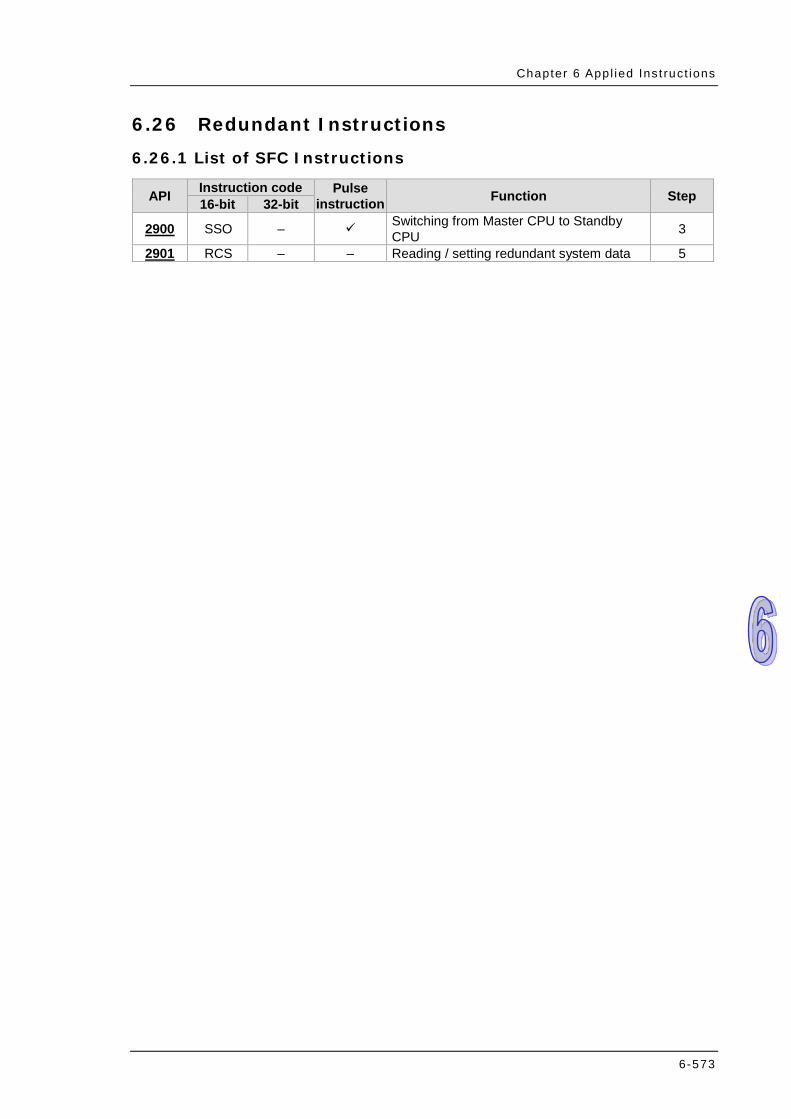
Chapter 6 Appl ied Ins t ruct ions
6-573
6.26 Redundant Instructions
6.26.1 List of SFC Instructions
API Instruction code Pulse instruction Function Step 16-bit 32-bit
2900 SSO – Switching from Master CPU to Standby CPU 3
2901 RCS – – Reading / setting redundant system data 5
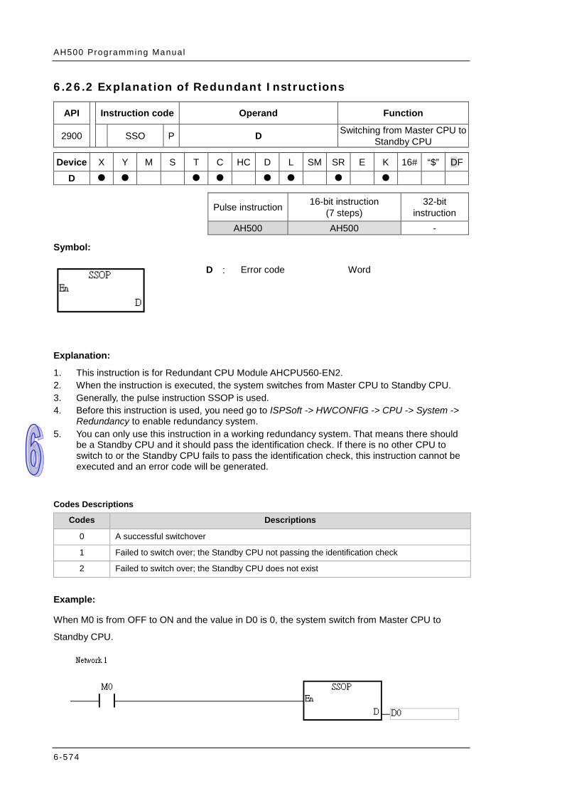
AH500 Programming Manual
6-574
6.26.2 Explanation of Redundant Instructions
API Instruction code Operand Function
2900 SSO P D Switching from Master CPU to Standby CPU
Device X Y M S T C HC D L SM SR E K 16# “$” DF
D
Pulse instruction 16-bit instruction (7 steps)
32-bit instruction
AH500 AH500 -
Symbol:
D : Error code Word
Explanation:
1. This instruction is for Redundant CPU Module AHCPU560-EN2. 2. When the instruction is executed, the system switches from Master CPU to Standby CPU. 3. Generally, the pulse instruction SSOP is used. 4. Before this instruction is used, you need go to ISPSoft -> HWCONFIG -> CPU -> System ->
Redundancy to enable redundancy system. 5. You can only use this instruction in a working redundancy system. That means there should
be a Standby CPU and it should pass the identification check. If there is no other CPU to switch to or the Standby CPU fails to pass the identification check, this instruction cannot be executed and an error code will be generated.
Codes Descriptions
Codes Descriptions
0 A successful switchover
1 Failed to switch over; the Standby CPU not passing the identification check
2 Failed to switch over; the Standby CPU does not exist
Example:
When M0 is from OFF to ON and the value in D0 is 0, the system switch from Master CPU to
Standby CPU.
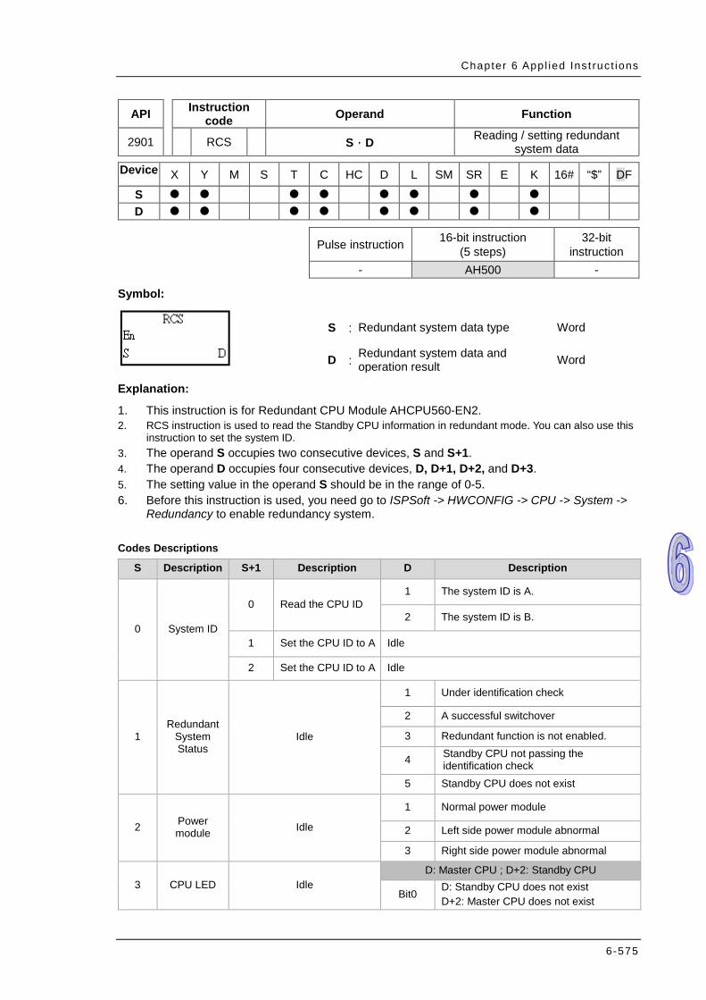
Chapter 6 Appl ied Ins t ruct ions
6-575
API Instruction code Operand Function
2901 RCS S,D Reading / setting redundant system data
Device X Y M S T C HC D L SM SR E K 16# “$” DF S D
Pulse instruction 16-bit instruction (5 steps)
32-bit instruction
- AH500 -
Symbol:
S : Redundant system data type Word
D : Redundant system data and operation result Word
Explanation:
1. This instruction is for Redundant CPU Module AHCPU560-EN2. 2. RCS instruction is used to read the Standby CPU information in redundant mode. You can also use this
instruction to set the system ID. 3. The operand S occupies two consecutive devices, S and S+1. 4. The operand D occupies four consecutive devices, D, D+1, D+2, and D+3. 5. The setting value in the operand S should be in the range of 0-5. 6. Before this instruction is used, you need go to ISPSoft -> HWCONFIG -> CPU -> System ->
Redundancy to enable redundancy system.
Codes Descriptions
S Description S+1 Description D Description
0 System ID
0 Read the CPU ID 1 The system ID is A.
2 The system ID is B.
1 Set the CPU ID to A Idle
2 Set the CPU ID to A Idle
1 Redundant
System Status
Idle
1 Under identification check
2 A successful switchover
3 Redundant function is not enabled.
4 Standby CPU not passing the identification check
5 Standby CPU does not exist
2 Power module Idle
1 Normal power module
2 Left side power module abnormal
3 Right side power module abnormal
3 CPU LED Idle D: Master CPU ; D+2: Standby CPU
Bit0 D: Standby CPU does not exist D+2: Master CPU does not exist
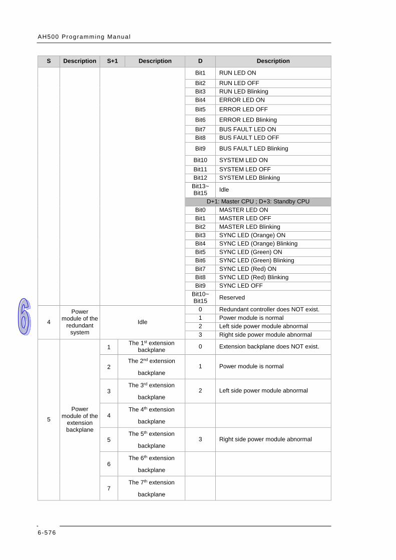
AH500 Programming Manual
6-576
S Description S+1 Description D Description
Bit1 RUN LED ON
Bit2 RUN LED OFF Bit3 RUN LED Blinking Bit4 ERROR LED ON Bit5 ERROR LED OFF
Bit6 ERROR LED Blinking Bit7 BUS FAULT LED ON Bit8 BUS FAULT LED OFF
Bit9 BUS FAULT LED Blinking
Bit10 SYSTEM LED ON Bit11 SYSTEM LED OFF Bit12 SYSTEM LED Blinking
Bit13~ Bit15 Idle
D+1: Master CPU ; D+3: Standby CPU Bit0 MASTER LED ON Bit1 MASTER LED OFF Bit2 MASTER LED Blinking Bit3 SYNC LED (Orange) ON Bit4 SYNC LED (Orange) Blinking Bit5 SYNC LED (Green) ON Bit6 SYNC LED (Green) Blinking Bit7 SYNC LED (Red) ON Bit8 SYNC LED (Red) Blinking Bit9 SYNC LED OFF
Bit10~ Bit15 Reserved
4
Power module of the
redundant system
Idle
0 Redundant controller does NOT exist. 1 Power module is normal 2 Left side power module abnormal 3 Right side power module abnormal
5
Power module of the
extension backplane
1 The 1st extension backplane 0 Extension backplane does NOT exist.
2 The 2nd extension
backplane 1 Power module is normal
3 The 3rd extension
backplane 2 Left side power module abnormal
4 The 4th extension
backplane
5 The 5th extension
backplane 3 Right side power module abnormal
6 The 6th extension
backplane
7 The 7th extension
backplane
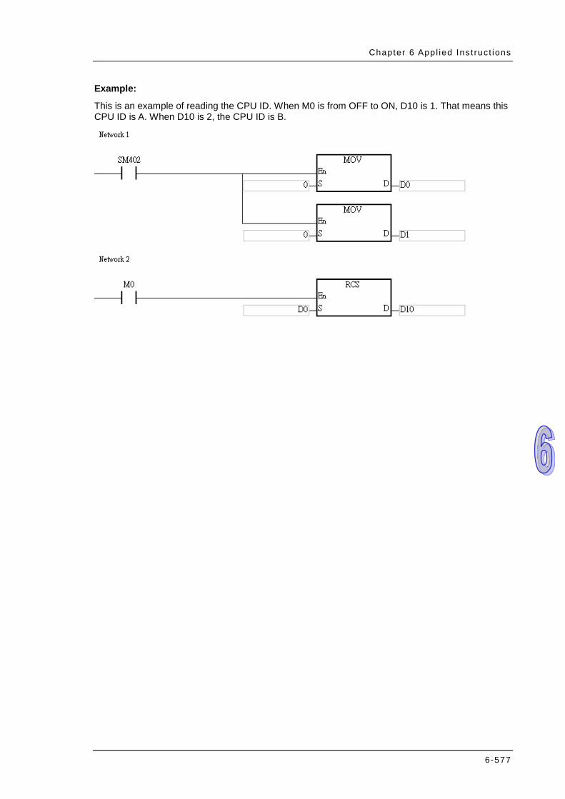
Chapter 6 Appl ied Ins t ruct ions
6-577
Example:
This is an example of reading the CPU ID. When M0 is from OFF to ON, D10 is 1. That means this CPU ID is A. When D10 is 2, the CPU ID is B.

AH500 Programming Manual
6-578
MEMO
7-1
Chapter 7 Error Codes
Table of Contents 7.1 Error Codes and LED Indicators ........................................... 7-2
7.1.1 CPU Modules ................................................................ 7-3 7.1.2 Analog I/O Modules and Temperature Measurement Modules .. .................................................................................7-26 7.1.3 AH02HC-5A/AH04HC-5A ...............................................7-28 7.1.4 AH05PM-5A / AH10PM-5A / AH15PM-5A .........................7-29 7.1.5 AH20MC-5A ................................................................7-30 7.1.6 AH10EN-5A / AH-15EN-5A ............................................7-31 7.1.7 AH10SCM-5A / AH15SCM-5A ........................................7-31 7.1.8 AH10DNET-5A .............................................................7-31 7.1.9 AH10PFBM-5A .............................................................7-32 7.1.10 AH10PFBS-5A ...........................................................7-33 7.1.11 AH10COPM-5A ..........................................................7-33
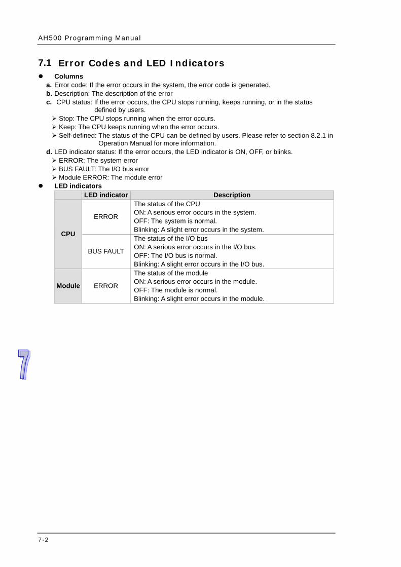
AH500 Programming Manual
7-2
7.1 Error Codes and LED Indicators Columns
a. Error code: If the error occurs in the system, the error code is generated. b. Description: The description of the error c. CPU status: If the error occurs, the CPU stops running, keeps running, or in the status
defined by users. Stop: The CPU stops running when the error occurs. Keep: The CPU keeps running when the error occurs. Self-defined: The status of the CPU can be defined by users. Please refer to section 8.2.1 in
Operation Manual for more information. d. LED indicator status: If the error occurs, the LED indicator is ON, OFF, or blinks. ERROR: The system error BUS FAULT: The I/O bus error Module ERROR: The module error
LED indicators
LED indicator Description
CPU
ERROR
The status of the CPU ON: A serious error occurs in the system. OFF: The system is normal. Blinking: A slight error occurs in the system.
BUS FAULT
The status of the I/O bus ON: A serious error occurs in the I/O bus. OFF: The I/O bus is normal. Blinking: A slight error occurs in the I/O bus.
Module ERROR
The status of the module ON: A serious error occurs in the module. OFF: The module is normal. Blinking: A slight error occurs in the module.
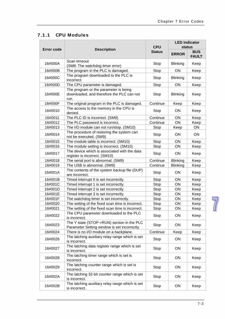
Chapter 7 Error Codes
7-3
7.1.1 CPU Modules
Error code Description CPU Status
LED indicator status
ERROR BUS FAULT
16#000A Scan timeout (SM8: The watchdog timer error) Stop Blinking Keep
16#000B The program in the PLC is damaged. Stop ON Keep
16#000C The program downloaded to the PLC is incorrect. Stop Blinking Keep
16#000D The CPU parameter is damaged. Stop ON Keep
16#000E The program or the parameter is being downloaded, and therefore the PLC can not run.
Stop Blinking Keep
16#000F The original program in the PLC is damaged. Continue Keep Keep
16#0010 The access to the memory in the CPU is denied. Stop ON Keep
16#0011 The PLC ID is incorrect. (SM9) Continue ON Keep 16#0012 The PLC password is incorrect. Continue ON Keep 16#0013 The I/O module can not run/stop. (SM10) Stop Keep ON
16#0014 The procedure of restoring the system can not be executed. (SM9) Stop ON ON
16#0015 The module table is incorrect. (SM10) Stop ON Keep 16#0016 The module setting is incorrect. (SM10) Stop ON Keep
16#0017 The device which is associated with the data register is incorrect. (SM10) Stop ON Keep
16#0018 The serial port is abnormal. (SM9) Continue Blinking Keep 16#0019 The USB is abnormal. (SM9) Continue Blinking Keep
16#001A The contents of the system backup file (DUP) are incorrect. Stop ON Keep
16#001B Timed interrupt 0 is set incorrectly. Stop ON Keep 16#001C Timed interrupt 1 is set incorrectly. Stop ON Keep 16#001D Timed interrupt 2 is set incorrectly. Stop ON Keep 16#001E Timed interrupt 3 is set incorrectly. Stop ON Keep 16#001F The watchdog timer is set incorrectly. Stop ON Keep 16#0020 The setting of the fixed scan time is incorrect. Stop ON Keep 16#0021 The setting of the fixed scan time is incorrect. Stop ON Keep
16#0022 The CPU parameter downloaded to the PLC is incorrect. Stop ON Keep
16#0023 The Y state (STOP->RUN) section in the PLC Parameter Setting window is set incorrectly. Stop ON Keep
16#0024 There is no I/O module on a backplane. Continue Keep Keep
16#0026 The latching auxiliary relay range which is set is incorrect. Stop ON Keep
16#0027 The latching data register range which is set is incorrect. Stop ON Keep
16#0028 The latching timer range which is set is incorrect. Stop ON Keep
16#0029 The latching counter range which is set is incorrect. Stop ON Keep
16#002A The latching 32-bit counter range which is set is incorrect. Stop ON Keep
16#002B The latching auxiliary relay range which is set is incorrect. Stop ON Keep
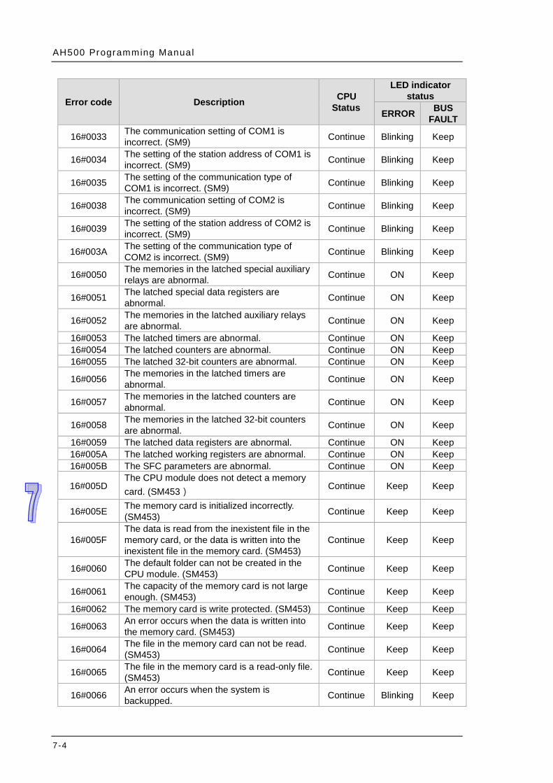
AH500 Programming Manual
7-4
Error code Description CPU Status
LED indicator status
ERROR BUS FAULT
16#0033 The communication setting of COM1 is incorrect. (SM9) Continue Blinking Keep
16#0034 The setting of the station address of COM1 is incorrect. (SM9) Continue Blinking Keep
16#0035 The setting of the communication type of COM1 is incorrect. (SM9) Continue Blinking Keep
16#0038 The communication setting of COM2 is incorrect. (SM9) Continue Blinking Keep
16#0039 The setting of the station address of COM2 is incorrect. (SM9) Continue Blinking Keep
16#003A The setting of the communication type of COM2 is incorrect. (SM9) Continue Blinking Keep
16#0050 The memories in the latched special auxiliary relays are abnormal. Continue ON Keep
16#0051 The latched special data registers are abnormal. Continue ON Keep
16#0052 The memories in the latched auxiliary relays are abnormal. Continue ON Keep
16#0053 The latched timers are abnormal. Continue ON Keep 16#0054 The latched counters are abnormal. Continue ON Keep 16#0055 The latched 32-bit counters are abnormal. Continue ON Keep
16#0056 The memories in the latched timers are abnormal. Continue ON Keep
16#0057 The memories in the latched counters are abnormal. Continue ON Keep
16#0058 The memories in the latched 32-bit counters are abnormal. Continue ON Keep
16#0059 The latched data registers are abnormal. Continue ON Keep 16#005A The latched working registers are abnormal. Continue ON Keep 16#005B The SFC parameters are abnormal. Continue ON Keep
16#005D The CPU module does not detect a memory card. (SM453) Continue Keep Keep
16#005E The memory card is initialized incorrectly. (SM453) Continue Keep Keep
16#005F The data is read from the inexistent file in the memory card, or the data is written into the inexistent file in the memory card. (SM453)
Continue Keep Keep
16#0060 The default folder can not be created in the CPU module. (SM453) Continue Keep Keep
16#0061 The capacity of the memory card is not large enough. (SM453) Continue Keep Keep
16#0062 The memory card is write protected. (SM453) Continue Keep Keep
16#0063 An error occurs when the data is written into the memory card. (SM453) Continue Keep Keep
16#0064 The file in the memory card can not be read. (SM453) Continue Keep Keep
16#0065 The file in the memory card is a read-only file. (SM453) Continue Keep Keep
16#0066 An error occurs when the system is backupped. Continue Blinking Keep
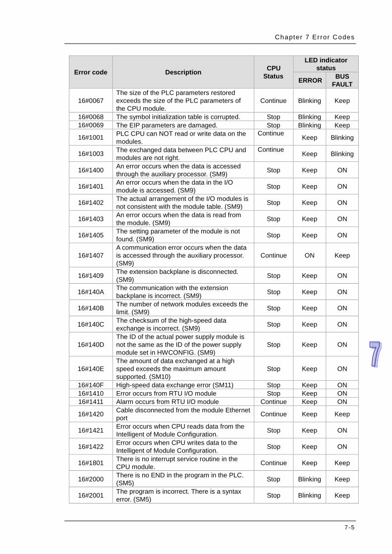
Chapter 7 Error Codes
7-5
Error code Description CPU Status
LED indicator status
ERROR BUS FAULT
16#0067 The size of the PLC parameters restored exceeds the size of the PLC parameters of the CPU module.
Continue Blinking Keep
16#0068 The symbol initialization table is corrupted. Stop Blinking Keep 16#0069 The EIP parameters are damaged. Stop Blinking Keep
16#1001 PLC CPU can NOT read or write data on the modules.
Continue Keep Blinking
16#1003 The exchanged data between PLC CPU and modules are not right.
Continue Keep Blinking
16#1400 An error occurs when the data is accessed through the auxiliary processor. (SM9) Stop Keep ON
16#1401 An error occurs when the data in the I/O module is accessed. (SM9) Stop Keep ON
16#1402 The actual arrangement of the I/O modules is not consistent with the module table. (SM9) Stop Keep ON
16#1403 An error occurs when the data is read from the module. (SM9) Stop Keep ON
16#1405 The setting parameter of the module is not found. (SM9) Stop Keep ON
16#1407 A communication error occurs when the data is accessed through the auxiliary processor. (SM9)
Continue ON Keep
16#1409 The extension backplane is disconnected. (SM9) Stop Keep ON
16#140A The communication with the extension backplane is incorrect. (SM9) Stop Keep ON
16#140B The number of network modules exceeds the limit. (SM9) Stop Keep ON
16#140C The checksum of the high-speed data exchange is incorrect. (SM9) Stop Keep ON
16#140D The ID of the actual power supply module is not the same as the ID of the power supply module set in HWCONFIG. (SM9)
Stop Keep ON
16#140E The amount of data exchanged at a high speed exceeds the maximum amount supported. (SM10)
Stop Keep ON
16#140F High-speed data exchange error (SM11) Stop Keep ON 16#1410 Error occurs from RTU I/O module Stop Keep ON 16#1411 Alarm occurs from RTU I/O module Continue Keep ON
16#1420 Cable disconnected from the module Ethernet port Continue Keep Keep
16#1421 Error occurs when CPU reads data from the Intelligent of Module Configuration. Stop Keep ON
16#1422 Error occurs when CPU writes data to the Intelligent of Module Configuration. Stop Keep ON
16#1801 There is no interrupt service routine in the CPU module. Continue Keep Keep
16#2000 There is no END in the program in the PLC. (SM5) Stop Blinking Keep
16#2001 The program is incorrect. There is a syntax error. (SM5) Stop Blinking Keep

AH500 Programming Manual
7-6
Error code Description CPU Status
LED indicator status
ERROR BUS FAULT
16#2002 GOEND is used incorrectly. (SM5) Stop Blinking Keep
16#2003 The devices used in the program exceed the range. (SM0/SM5) Self-defined Blinking Keep
16#2004 The part of the program specified by the label used in CJ/JMP is incorrect, or the label is used repeatedly. (SM0/SM5)
Stop Blinking Keep
16#2005
The N value used in MC is not the same as the corresponding N value used in MCR, or the number of N values used in MC is not the same as the number of N values used in MCR. (SM5)
Stop Blinking Keep
16#2006 The N values used in MC do not start from 0, or the N values used in MC are not continuous. (SM5)
Stop Blinking Keep
16#2007 The operands used in ZRST are not used properly. (SM5) Stop Blinking Keep
16#200A Invalid instruction (SM5) Stop Blinking Keep
16#200B The operand n or the other constant operands exceed the range. (SM0/SM5) Self-defined Blinking Keep
16#200C The operands overlap. (SM0/SM5) Self-defined Blinking Keep
16#200D An error occurs when the binary number is converted into the binary-coded decimal number. (SM0/SM5)
Self-defined Blinking Keep
16#200E The string does not end with 0x00. (SM0/SM5) Self-defined Blinking Keep
16#200F The instruction does not support the modification by an index register. (SM5) Stop Blinking Keep
16#2010
1. The instruction does not support the device. 2. Encoding error 3. The instruction is a 16-bit instruction, but
the constant operand is a 32-bit code. (SM5)
Stop Blinking Keep
16#2011 The number of operands is incorrect. (SM5) Stop Blinking Keep 16#2012 Incorrect division operation (SM0/SM5). Self-defined Blinking Keep
16#2013 The value exceeds the range of values which can be represented by the floating-point numbers. (SM0/SM5)
Self-defined Blinking Keep
16#2014 The task designated by TKON/YKOFF is incorrect, or exceeds the range. (SM5) Stop Blinking Keep
16#2015 There are more than 32 levels of nested program structures supported by CALL. (SM0)
Self-defined Blinking Keep
16#2016 There are more than 32 levels of nested program structures supported by FOR/NEXT. (SM0/SM5)
Self-defined Blinking Keep
16#2017 The number of times FOR is used is different from the number of times NEXT is used. (SM5)
Stop Blinking Keep
Chapter 7 Error Codes
7-7
Error code Description CPU Status
LED indicator status
ERROR BUS FAULT
16#2018 There is a label after FEND, but there is no SRET. There is SRET, but there is no label. (SM5)
Stop Blinking Keep
16#2019 The interrupt task is not after FEND. (SM5) Stop Blinking Keep 16#201A IRET/SRET is not after FEND. (SM5) Stop Blinking Keep
16#201B
There is an interrupt task, but there is no IRET. There is IRET, but there is not interrupt task. (SM5)
Stop Blinking Keep
16#201C End is not at the end of the program. (SM5) Stop Blinking Keep 16#201D There is CALL, but there is no MAR. (SM5) Stop Blinking Keep
16#201E The function code used in MODRW is incorrect. (SM102/SM103) Self-defined Blinking Keep
16#201F The length of the data set in MODRW is incorrect. (SM102/SM103) Self-defined Blinking Keep
16#2020 The communication command received by using MODRW is incorrect. (SM102/SM103) Self-defined Blinking Keep
16#2021 The checksum of the command received is incorrect. (SM102/SM103) Self-defined Blinking Keep
16#2022 The format of the command used in MODRW does not conform to the ASCII format. (SM102/SM103)
Self-defined Blinking Keep
16#2023 There is a communication timeout when MODRW is executed. (SM120/SM103) Self-defined Blinking Keep
16#2024 The setting value of the communication timeout is invalid. (SM120/SM103) Self-defined Blinking Keep
16#2025 There is a communication timeout when RS is executed. (SM120/SM103) Self-defined Blinking Keep
16#2026 The interrupt number used in RS is incorrect. (SM102/104) Self-defined OFF Keep
16#2027 The execution of FWD is abnormal. (SM102/103) Self-defined Blinking Keep
16#2028 The execution of REV is abnormal. (SM102/103) Self-defined Blinking Keep
16#2029 The execution of STOP is abnormal. (SM102/103) Self-defined Blinking Keep
16#202A The execution of SRDT is abnormal. (SM102/103) Self-defined Blinking Keep
16#202B The execution of RSTEF is abnormal. (SM102/103) Self-defined Blinking Keep
16#202C I/O interrupt service routine 0 does not exist. Stop Blinking Keep 16#202D I/O interrupt service routine 1 does not exist. Stop Blinking Keep 16#202E I/O interrupt service routine 2 does not exist. Stop Blinking Keep 16#202F I/O interrupt service routine 3 does not exist. Stop Blinking Keep 16#2030 I/O interrupt service routine 4 does not exist. Stop Blinking Keep 16#2031 I/O interrupt service routine 5 does not exist. Stop Blinking Keep 16#2032 I/O interrupt service routine 6 does not exist. Stop Blinking Keep 16#2033 I/O interrupt service routine 7 does not exist. Stop Blinking Keep 16#2034 I/O interrupt service routine 8 does not exist. Stop Blinking Keep 16#2035 I/O interrupt service routine 9 does not exist. Stop Blinking Keep 16#2036 I/O interrupt service routine 10 does not exist. Stop Blinking Keep

AH500 Programming Manual
7-8
Error code Description CPU Status
LED indicator status
ERROR BUS FAULT
16#2037 I/O interrupt service routine 11 does not exist. Stop Blinking Keep 16#2038 I/O interrupt service routine 12 does not exist. Stop Blinking Keep 16#2039 I/O interrupt service routine 13 does not exist. Stop Blinking Keep 16#203A I/O interrupt service routine 14 does not exist. Stop Blinking Keep 16#203B I/O interrupt service routine 15 does not exist. Stop Blinking Keep 16#203C I/O interrupt service routine 16 does not exist. Stop Blinking Keep 16#203D I/O interrupt service routine 17 does not exist. Stop Blinking Keep 16#203E I/O interrupt service routine 18 does not exist. Stop Blinking Keep 16#203F I/O interrupt service routine 19 does not exist. Stop Blinking Keep 16#2040 I/O interrupt service routine 20 does not exist. Stop Blinking Keep 16#2041 I/O interrupt service routine 21 does not exist. Stop Blinking Keep 16#2042 I/O interrupt service routine 22 does not exist. Stop Blinking Keep 16#2043 I/O interrupt service routine 23 does not exist. Stop Blinking Keep 16#2044 I/O interrupt service routine 24 does not exist. Stop Blinking Keep 16#2045 I/O interrupt service routine 25 does not exist. Stop Blinking Keep 16#2046 I/O interrupt service routine 26 does not exist. Stop Blinking Keep 16#2047 I/O interrupt service routine 27 does not exist. Stop Blinking Keep 16#2048 I/O interrupt service routine 28 does not exist. Stop Blinking Keep 16#2049 I/O interrupt service routine 29 does not exist. Stop Blinking Keep 16#204A I/O interrupt service routine 30 does not exist. Stop Blinking Keep 16#204B I/O interrupt service routine 31 does not exist. Stop Blinking Keep 16#2054
| 16#2127
External interrupt service routine 40~251 does not exist. Stop Blinking Keep
16#2128 An action in a sequential function chart is incorrectly assigned qualifiers related to time. (SM0/SM1)
Self-defined Blinking Keep
16#2129 The modifier R is assigned to an action in a sequential function chart incorrectly. (SM0/SM1)
Self-defined Blinking Keep
16#212A MC/MCR instructions cannot be used in interrupts or subroutines. (SM5) Self-defined Blinking Keep
16#6000 Ethernet connection error (SM1106) Continue Blinking Keep 16#6001 Illegal IP address (SM1107) Continue Blinking Keep 16#6002 Illegal netmask address (SM1107) Continue Blinking Keep 16#6003 Illegal gateway mask (SM1107) Continue Blinking Keep
16#6004 The IP address filter is set incorrectly. (SM1108) Continue Blinking Keep
16#6006 The static ARP table is set incorrectly. (SM1108) Continue Blinking Keep
16#6007 The NTP client service is set incorrectly. (SM1380) Continue Blinking Keep
16#6008 Illegal network number (SM1107) Continue Blinking Keep 16#6009 Illegal node number (SM1107) Continue Blinking Keep 16#600A TCP connection failure (SM1090) Continue Keep Keep 16#600B UDP connection failure (SM1091) Continue Keep Keep 16#600C The socket has been used. (SM1109) Continue Keep Keep 16#600D The RJ45 port is not connected. (SM1100) Continue Keep Keep
16#600E An RJ45 port on AH10EN-5A is not connected to a network cable. Continue Keep Keep
Chapter 7 Error Codes
7-9
Error code Description CPU Status
LED indicator status
ERROR BUS FAULT
16#600F Maximum Modbus TCP connection number has been reached. (SM1089) Continue Blinking Keep
16#6010 BOOTP IP setting error (SM1107) Continue Keep Keep 16#6011 BOOTP Gateway setting error (SM1107) Continue Keep Keep 16#6012 IP address conflict (SM1107) Continue Blinking Keep 16#6013 DNS address setting error (SM1107) 16#6100 The email connection is busy. (SM1113) Continue Keep Keep
16#6101 The trigger in the email is set incorrectly. (SM1112) Continue Blinking Keep
16#6102 The interval of sending the email is set incorrectly. (SM1112) Continue Blinking Keep
16#6103 The device containing the data specified as the attachment exceeds the device range. (SM1112)
Continue Blinking Keep
16#6104 The attachment in the email does not exist. (SM1113) Continue Keep Keep
16#6105 The attachment in the email is oversized. (SM1113) Continue Keep Keep
16#6106 The SMTP server address is incorrect. (SM1112) Continue Blinking Keep
16#6107 There is an SMTP server response timeout. (SM1113) Continue Keep Keep
16#6108 SMTP authentication error (SM1112) Continue Blinking Keep
16#6110 The SMTP server needs to be authenticated. (SM1112) Continue Blinking Keep
16#6111 The specified email address does not exist. (SM1112) Continue Blinking Keep
16#6200 The remote IP address set in the TCP socket function is illegal. (SM1196) Continue Blinking Keep
16#6201 The local communication port set in the TCP socket function is illegal. Continue Keep Keep
16#6202 The remote communication port set in the TCP socket function is illegal. Continue Keep Keep
16#6203 The device from which the data is sent in the TCP socket function is illegal. Continue Keep Keep
16#6204 The transmitted data length set in the TCP socket function is illegal. Continue Keep Keep
16#6205 The data which is sent through the TCP socket exceeds the device range. Continue Keep Keep
16#6206 The device which receives the data in the TCP socket function is illegal. Continue Keep Keep
16#6207 The received data length set in the TCP socket function is illegal. Continue Keep Keep
16#6208 The data which is received through the TCP socket exceeds the device range. Continue Keep Keep
16#6209 The remote IP address set in the UDP socket function is illegal. (SM1196) Continue Blinking Keep
16#620A The local communication port set in the UDP socket function is illegal. Continue Keep Keep
16#620B The remote communication port set in the UDP socket function is illegal. Continue Keep Keep

AH500 Programming Manual
7-10
Error code Description CPU Status
LED indicator status
ERROR BUS FAULT
16#620C The device from which the data is sent in the UDP socket function is illegal. Continue Keep Keep
16#620D The transmitted data length set in the UDP socket function is illegal. Continue Keep Keep
16#620E The data which is sent through the UDP socket exceeds the device range. Continue Keep Keep
16#620F The device which receives the data in the UDP socket function is illegal. Continue Keep Keep
16#6210 The received data length set in the UDP socket function is illegal. Continue Keep Keep
16#6211 The data which is received through the UDP socket exceeds the device range. Continue Keep Keep
16#6212 There is no response from the remote device after the timeout period. (Socket) Continue Keep Keep
16#6213 The data received exceeds the limit. (Socket) Continue Keep Keep
16#6214 The remote device refuses the connection. (Socket) Continue Keep Keep
16#6215 The socket is not opened. Continue Keep Keep 16#6217 The socket is opened. Continue Keep Keep 16#6218 The data is being sent through the socket. Continue Keep Keep
16#6219 The data is being received through the socket. Continue Keep Keep
16#621A The socket is being closed. Continue Keep Keep
16#6300 Only auxiliary relays, data registers, and link registers can be used in the Ether Link. Continue Blinking Keep
16#6301 The device used in the Ether Link exceeds the device range. Continue Blinking Keep
16#6302 The length of the data exchanged in the Ether Link exceeds the limit. Continue Blinking Keep
16#6303 The remote device in the Ether Link aborts the connection. Continue Keep Keep
16#6304 The connection in the Ether Link is busy. Continue Keep Keep
16#6305 The node used in the communication command is different from the local node. Continue Blinking Keep
16#6309 The remote device in the Ether Link does not respond after the timeout period. Continue Keep Keep
16#630A The module ID or the setting of the module is different from the setting in the Ether Link. Continue Blinking Keep
16#630B The setting of the netmask address for the CPU or the module is different from the setting in the Ether Link.
Continue Blinking Keep
16#6400
The number of connections reaches the upper limit, or the flag which is related to the sending of the data is not set to ON. (EMDRW)
Continue Keep Keep
16#6401 The remote device aborts the connection. (EMDRW) Continue Keep Keep
16#6402 There is no response from the remote device after the timeout period. (EMDRW) Continue Keep Keep
16#6403 The remote IP address used is illegal. (EMDRW) Continue Keep Keep

Chapter 7 Error Codes
7-11
Error code Description CPU Status
LED indicator status
ERROR BUS FAULT
16#6404 The function code received is not supported. (EMDRW) Continue Keep Keep
16#6405 The number of data which will be received is not consistent with the actual length of the data. (EMDRW)
Continue Keep Keep
16#6500 An error occurs when a data exchange function is initialized. (SM699) Continue Blinking OFF
16#6501 A remote device does not respond after a timeout. (SM828-SM955) Continue OFF OFF
16#6502 The packet with which a remote device replies is incorrect. (SM828-SM955) Continue OFF OFF
16#6700 An error occurs when a Modbus TCP data exchange is initialized. Continue Keep Keep
16#6701 Modbus TCP data exchange timeout Continue Keep Keep
16#6702 The data received by means of a Modbus TCP data exchange is incorrect. Continue Keep Keep
16#7002 The CPU module does not support the function. Continue Keep Keep
16#7203 Invalid access code Continue Keep Keep 16#7401 Function code error Continue Keep Keep
16#7402 The size of a packet exceeds the maximum data length. Continue Keep Keep
16#7404 Packet format error Continue Keep Keep 16#7405 The number of bytes is incorrect. Continue Keep Keep 16#7406 Checksum error Continue Keep Keep
16#7407 There are non-ASCII characters in a command. Continue Keep Keep
16#7408 The PLC is running. Continue Keep Keep
16#740A Data is being written to the memory in the PLC or data fails to be written to the memory in the PLC.
Continue Keep Keep
16#740B The CPU module is being reset, or the values in the laching devices are being cleared. Continue Keep Keep
16#740C The backplane number in a communication command is incorrect. Continue Keep Keep
16#740D The slot number in a communication command is incorrect. Continue Keep Keep
16#740E An error occurs when the the data in the memory in the PLC is cleared. Continue Keep Keep
16#740F Communication timeout Continue Keep Keep
16#7410 The function code in a reply command is incorrect. Continue Keep Keep
16#7412 Owing to the fact that SW1 is ON, data can not be downloaded to the CPU module. Continue Keep Keep
16#757D The remaining number of PLC password guesses is 0. Continue Keep Keep
16#757E The PLC password entered is incorrect. Continue Keep Keep
16#8105 The program downloaded to the CPU module is incorrect. The syntax downloaded is incorrect.
Continue Keep Keep

AH500 Programming Manual
7-12
Error code Description CPU Status
LED indicator status
ERROR BUS FAULT
16#8106 The program downloaded is incorrect. The length of the machine code exceeds the limit. Continue Keep Keep
16#8107 The program downloaded is incorrect. The length of the source code exceeds the limit. Continue Keep Keep
16#8230 A CPU parameter downloaded is incorrect. The IP address is illegal. Continue Keep Keep
16#8231 A CPU parameter downloaded is incorrect. The netmask address is illegal. Continue Keep Keep
16#8232 A CPU parameter downloaded is incorrect. The gateway address is illegal. Continue Keep Keep
16#8233 A CPU parameter downloaded is incorrect. The IP address filter is set incorrectly. Continue Keep Keep
16#8235 A CPU parameter downloaded is incorrect. The static ARP table is set incorrectly. Continue Keep Keep
16#8236 A CPU parameter downloaded is incorrect. The NTP client service is set incorrectly. Continue Keep Keep
16#8239 A CPU parameter downloaded is incorrect. The email sending function is set incorrectly. Continue Keep Keep
16#823A A CPU parameter downloaded is incorrect. The condition for the sending of an email is set incorrectly.
Continue Keep Keep
16#823B A CPU parameter downloaded is incorrect. A TCP socket is set incorrectly. Continue Keep Keep
16#823C A CPU parameter downloaded is incorrect. A UDP socket is set incorrectly. Continue Keep Keep
16#823E A CPU parameter downloaded is incorrect. The eeb function is set incorrectly. Continue Keep Keep
16#8240 A CPU parameter downloaded is incorrect. The data exchange by means of Ethernet is set incorrectly
Continue Keep Keep
16#8241 The setting of a DNS server is incorrect. Continue Keep Keep 16#8522 A module configuration is being scanned. Continue Keep Keep 16#853B An I/O module is not configured. Continue Keep Keep 16#853C An I/O module does not exist. Continue Keep Keep 16#854B An I/O module is not configured. Continue Keep Keep 16#854C An I/O module does not exist. Continue Keep Keep
16#8572 The checksum of the module configuration table is incorrect. Continue Keep Keep
16#8576 The checksum of the module parameter setting is incorrect. Continue Keep Keep
16#857A The checksum of the module parameter mapping table is incorrect. Continue Keep Keep
16#85E1 An I/O interrupt number is incorrect. Continue Keep Keep 16#85E2 An I/O interrupt service routine does not exist. Continue Keep Keep 16#860F System restoration error Continue Blinking Blinking
16#8611 No memory card exists, or the memory card format is incorrect. Continue Keep Keep
16#8612 An error occurs when data is accessed from the memory card, or the memory card is in read-only mode.
Continue Keep Keep

Chapter 7 Error Codes
7-13
Error code Description CPU Status
LED indicator status
ERROR BUS FAULT
16#9A01 The setting of the data exchange for slave 1 in the PLC Link / COM1 MODBUS is incorrect. (SM1590)
Continue Keep Keep
16#9A02 The setting of the data exchange for slave 2 in the PLC Link / COM1 MODBUS is incorrect. (SM1590)
Continue Keep Keep
16#9A03 The setting of the data exchange for slave 3 in the PLC Link / COM1 MODBUS is incorrect. (SM1590)
Continue Keep Keep
16#9A04 The setting of the data exchange for slave 4 in the PLC Link / COM1 MODBUS is incorrect. (SM1590)
Continue Keep Keep
16#9A05 The setting of the data exchange for slave 5 in the PLC Link / COM1 MODBUS is incorrect. (SM1590)
Continue Keep Keep
16#9A06 The setting of the data exchange for slave 6 in the PLC Link / COM1 MODBUS is incorrect. (SM1590)
Continue Keep Keep
16#9A07 The setting of the data exchange for slave 7 in the PLC Link / COM1 MODBUS is incorrect. (SM1590)
Continue Keep Keep
16#9A08 The setting of the data exchange for slave 8 in the PLC Link / COM1 MODBUS is incorrect. (SM1590)
Continue Keep Keep
16#9A09 The setting of the data exchange for slave 9 in the PLC Link / COM1 MODBUS is incorrect. (SM1590)
Continue Keep Keep
16#9A0A The setting of the data exchange for slave 10 in the PLC Link / COM1 MODBUS is incorrect. (SM1590)
Continue Keep Keep
16#9A0B The setting of the data exchange for slave 11 in the PLC Link / COM1 MODBUS is incorrect. (SM1590)
Continue Keep Keep
16#9A0C The setting of the data exchange for slave 12 in the PLC Link / COM1 MODBUS is incorrect. (SM1590)
Continue Keep Keep
16#9A0D The setting of the data exchange for slave 13 in the PLC Link / COM1 MODBUS is incorrect. (SM1590)
Continue Keep Keep
16#9A0E The setting of the data exchange for slave 14 in the PLC Link / COM1 MODBUS is incorrect. (SM1590)
Continue Keep Keep
16#9A0F The setting of the data exchange for slave 15 in the PLC Link / COM1 MODBUS is incorrect. (SM1590)
Continue Keep Keep
16#9A10 The setting of the data exchange for slave 16 in the PLC Link / COM1 MODBUS is incorrect. (SM1590)
Continue Keep Keep
16#9A11 The setting of the data exchange for slave 17 in the PLC Link / COM1 MODBUS is incorrect. (SM1590)
Continue Keep Keep
AH500 Programming Manual
7-14
Error code Description CPU Status
LED indicator status
ERROR BUS FAULT
16#9A12 The setting of the data exchange for slave 18 in the PLC Link / COM1 MODBUS is incorrect. (SM1590)
Continue Keep Keep
16#9A13 The setting of the data exchange for slave 19 in the PLC Link / COM1 MODBUS is incorrect. (SM1590)
Continue Keep Keep
16#9A14 The setting of the data exchange for slave 20 in the PLC Link / COM1 MODBUS is incorrect. (SM1590)
Continue Keep Keep
16#9A15 The setting of the data exchange for slave 21 in the PLC Link / COM1 MODBUS is incorrect. (SM1590)
Continue Keep Keep
16#9A16 The setting of the data exchange for slave 22 in the PLC Link / COM1 MODBUS is incorrect. (SM1590)
Continue Keep Keep
16#9A17 The setting of the data exchange for slave 23 in the PLC Link / COM1 MODBUS is incorrect. (SM1590)
Continue Keep Keep
16#9A18 The setting of the data exchange for slave 24 in the PLC Link / COM1 MODBUS is incorrect. (SM1590)
Continue Keep Keep
16#9A19 The setting of the data exchange for slave 25 in the PLC Link / COM1 MODBUS is incorrect. (SM1590)
Continue Keep Keep
16#9A1A The setting of the data exchange for slave 26 in the PLC Link / COM1 MODBUS is incorrect. (SM1590)
Continue Keep Keep
16#9A1B The setting of the data exchange for slave 27 in the PLC Link / COM1 MODBUS is incorrect. (SM1590)
Continue Keep Keep
16#9A1C The setting of the data exchange for slave 28 in the PLC Link / COM1 MODBUS is incorrect. (SM1590)
Continue Keep Keep
16#9A1D The setting of the data exchange for slave 29 in the PLC Link / COM1 MODBUS is incorrect. (SM1590)
Continue Keep Keep
16#9A1E The setting of the data exchange for slave 30 in the PLC Link / COM1 MODBUS is incorrect. (SM1590)
Continue Keep Keep
16#9A1F The setting of the data exchange for slave 31 in the PLC Link / COM1 MODBUS is incorrect. (SM1590)
Continue Keep Keep
16#9A20 The setting of the data exchange for slave 32 in the PLC Link / COM1 MODBUS is incorrect. (SM1590)
Continue Keep Keep
16#9A21 An error occurs when the master communicates with slave 1 in the PLC Link / COM1 MODBUS. (SM SM1591)
Continue Keep Keep
16#9A22 An error occurs when the master communicates with slave 2 in the PLC Link / COM1 MODBUS. (SM SM1591)
Continue Keep Keep
Chapter 7 Error Codes
7-15
Error code Description CPU Status
LED indicator status
ERROR BUS FAULT
16#9A23 An error occurs when the master communicates with slave 3 in the PLC Link / COM1 MODBUS. (SM SM1591)
Continue Keep Keep
16#9A24 An error occurs when the master communicates with slave 4 in the PLC Link / COM1 MODBUS. (SM SM1591)
Continue Keep Keep
16#9A25 An error occurs when the master communicates with slave 5 in the PLC Link / COM1 MODBUS. (SM1591)
Continue Keep Keep
16#9A26 An error occurs when the master communicates with slave 6 in the PLC Link / COM1 MODBUS. (SM1591)
Continue Keep Keep
16#9A27 An error occurs when the master communicates with slave 7 in the PLC Link / COM1 MODBUS. (SM1591)
Continue Keep Keep
16#9A28 An error occurs when the master communicates with slave 8 in the PLC Link / COM1 MODBUS. (SM1591)
Continue Keep Keep
16#9A29 An error occurs when the master communicates with slave 9 in the PLC Link / COM1 MODBUS. (SM1591)
Continue Keep Keep
16#9A2A An error occurs when the master communicates with slave 10 in the PLC Link / COM1 MODBUS. (SM1591)
Continue Keep Keep
16#9A2B An error occurs when the master communicates with slave 11 in the PLC Link / COM1 MODBUS. (SM1591)
Continue Keep Keep
16#9A2C An error occurs when the master communicates with slave 12 in the PLC Link / COM1 MODBUS. (SM1591)
Continue Keep Keep
16#9A2D An error occurs when the master communicates with slave 13 in the PLC Link / COM1 MODBUS. (SM1591)
Continue Keep Keep
16#9A2E An error occurs when the master communicates with slave 14 in the PLC Link / COM1 MODBUS. (SM1591)
Continue Keep Keep
16#9A2F An error occurs when the master communicates with slave 15 in the PLC Link / COM1 MODBUS. (SM1591)
Continue Keep Keep
16#9A30 An error occurs when the master communicates with slave 16 in the PLC Link / COM1 MODBUS. (SM1591)
Continue Keep Keep
16#9A31 An error occurs when the master communicates with slave 17 in the PLC Link / COM1 MODBUS. (SM1591)
Continue Keep Keep
16#9A32 An error occurs when the master communicates with slave 18 in the PLC Link / COM1 MODBUS. (SM1591)
Continue Keep Keep
16#9A33 An error occurs when the master communicates with slave 19 in the PLC Link / COM1 MODBUS. (SM1591)
Continue Keep Keep
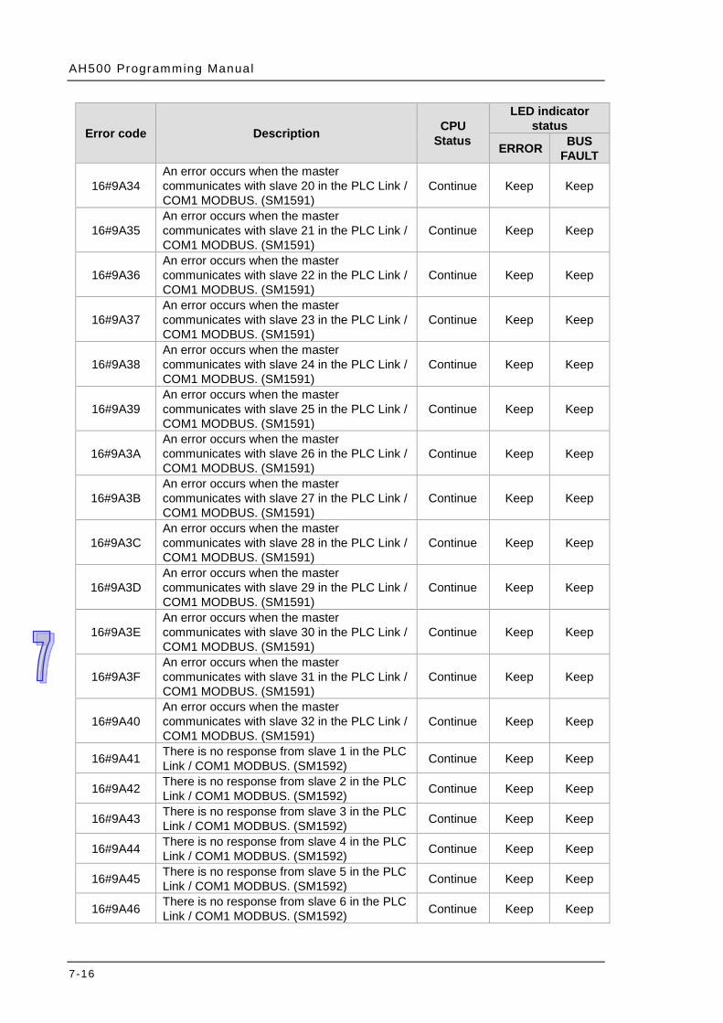
AH500 Programming Manual
7-16
Error code Description CPU Status
LED indicator status
ERROR BUS FAULT
16#9A34 An error occurs when the master communicates with slave 20 in the PLC Link / COM1 MODBUS. (SM1591)
Continue Keep Keep
16#9A35 An error occurs when the master communicates with slave 21 in the PLC Link / COM1 MODBUS. (SM1591)
Continue Keep Keep
16#9A36 An error occurs when the master communicates with slave 22 in the PLC Link / COM1 MODBUS. (SM1591)
Continue Keep Keep
16#9A37 An error occurs when the master communicates with slave 23 in the PLC Link / COM1 MODBUS. (SM1591)
Continue Keep Keep
16#9A38 An error occurs when the master communicates with slave 24 in the PLC Link / COM1 MODBUS. (SM1591)
Continue Keep Keep
16#9A39 An error occurs when the master communicates with slave 25 in the PLC Link / COM1 MODBUS. (SM1591)
Continue Keep Keep
16#9A3A An error occurs when the master communicates with slave 26 in the PLC Link / COM1 MODBUS. (SM1591)
Continue Keep Keep
16#9A3B An error occurs when the master communicates with slave 27 in the PLC Link / COM1 MODBUS. (SM1591)
Continue Keep Keep
16#9A3C An error occurs when the master communicates with slave 28 in the PLC Link / COM1 MODBUS. (SM1591)
Continue Keep Keep
16#9A3D An error occurs when the master communicates with slave 29 in the PLC Link / COM1 MODBUS. (SM1591)
Continue Keep Keep
16#9A3E An error occurs when the master communicates with slave 30 in the PLC Link / COM1 MODBUS. (SM1591)
Continue Keep Keep
16#9A3F An error occurs when the master communicates with slave 31 in the PLC Link / COM1 MODBUS. (SM1591)
Continue Keep Keep
16#9A40 An error occurs when the master communicates with slave 32 in the PLC Link / COM1 MODBUS. (SM1591)
Continue Keep Keep
16#9A41 There is no response from slave 1 in the PLC Link / COM1 MODBUS. (SM1592) Continue Keep Keep
16#9A42 There is no response from slave 2 in the PLC Link / COM1 MODBUS. (SM1592) Continue Keep Keep
16#9A43 There is no response from slave 3 in the PLC Link / COM1 MODBUS. (SM1592) Continue Keep Keep
16#9A44 There is no response from slave 4 in the PLC Link / COM1 MODBUS. (SM1592) Continue Keep Keep
16#9A45 There is no response from slave 5 in the PLC Link / COM1 MODBUS. (SM1592) Continue Keep Keep
16#9A46 There is no response from slave 6 in the PLC Link / COM1 MODBUS. (SM1592) Continue Keep Keep
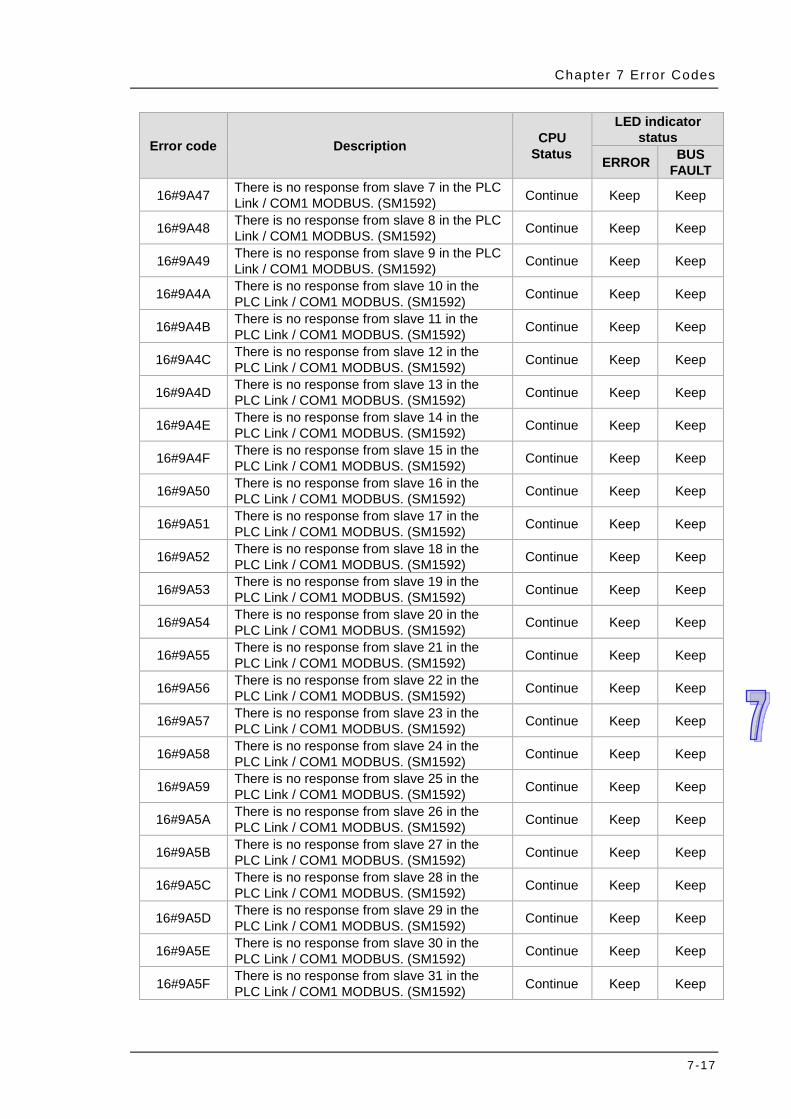
Chapter 7 Error Codes
7-17
Error code Description CPU Status
LED indicator status
ERROR BUS FAULT
16#9A47 There is no response from slave 7 in the PLC Link / COM1 MODBUS. (SM1592) Continue Keep Keep
16#9A48 There is no response from slave 8 in the PLC Link / COM1 MODBUS. (SM1592) Continue Keep Keep
16#9A49 There is no response from slave 9 in the PLC Link / COM1 MODBUS. (SM1592) Continue Keep Keep
16#9A4A There is no response from slave 10 in the PLC Link / COM1 MODBUS. (SM1592) Continue Keep Keep
16#9A4B There is no response from slave 11 in the PLC Link / COM1 MODBUS. (SM1592) Continue Keep Keep
16#9A4C There is no response from slave 12 in the PLC Link / COM1 MODBUS. (SM1592) Continue Keep Keep
16#9A4D There is no response from slave 13 in the PLC Link / COM1 MODBUS. (SM1592) Continue Keep Keep
16#9A4E There is no response from slave 14 in the PLC Link / COM1 MODBUS. (SM1592) Continue Keep Keep
16#9A4F There is no response from slave 15 in the PLC Link / COM1 MODBUS. (SM1592) Continue Keep Keep
16#9A50 There is no response from slave 16 in the PLC Link / COM1 MODBUS. (SM1592) Continue Keep Keep
16#9A51 There is no response from slave 17 in the PLC Link / COM1 MODBUS. (SM1592) Continue Keep Keep
16#9A52 There is no response from slave 18 in the PLC Link / COM1 MODBUS. (SM1592) Continue Keep Keep
16#9A53 There is no response from slave 19 in the PLC Link / COM1 MODBUS. (SM1592) Continue Keep Keep
16#9A54 There is no response from slave 20 in the PLC Link / COM1 MODBUS. (SM1592) Continue Keep Keep
16#9A55 There is no response from slave 21 in the PLC Link / COM1 MODBUS. (SM1592) Continue Keep Keep
16#9A56 There is no response from slave 22 in the PLC Link / COM1 MODBUS. (SM1592) Continue Keep Keep
16#9A57 There is no response from slave 23 in the PLC Link / COM1 MODBUS. (SM1592) Continue Keep Keep
16#9A58 There is no response from slave 24 in the PLC Link / COM1 MODBUS. (SM1592) Continue Keep Keep
16#9A59 There is no response from slave 25 in the PLC Link / COM1 MODBUS. (SM1592) Continue Keep Keep
16#9A5A There is no response from slave 26 in the PLC Link / COM1 MODBUS. (SM1592) Continue Keep Keep
16#9A5B There is no response from slave 27 in the PLC Link / COM1 MODBUS. (SM1592) Continue Keep Keep
16#9A5C There is no response from slave 28 in the PLC Link / COM1 MODBUS. (SM1592) Continue Keep Keep
16#9A5D There is no response from slave 29 in the PLC Link / COM1 MODBUS. (SM1592) Continue Keep Keep
16#9A5E There is no response from slave 30 in the PLC Link / COM1 MODBUS. (SM1592) Continue Keep Keep
16#9A5F There is no response from slave 31 in the PLC Link / COM1 MODBUS. (SM1592) Continue Keep Keep
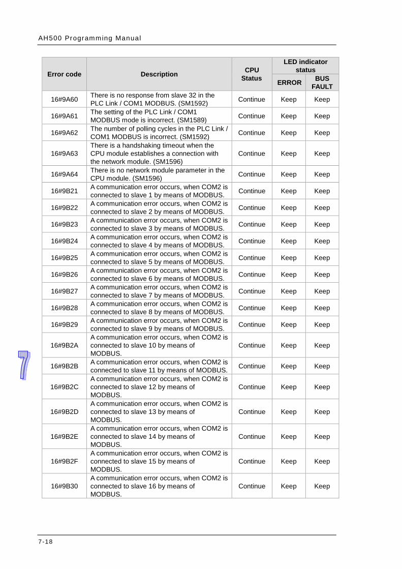
AH500 Programming Manual
7-18
Error code Description CPU Status
LED indicator status
ERROR BUS FAULT
16#9A60 There is no response from slave 32 in the PLC Link / COM1 MODBUS. (SM1592) Continue Keep Keep
16#9A61 The setting of the PLC Link / COM1 MODBUS mode is incorrect. (SM1589) Continue Keep Keep
16#9A62 The number of polling cycles in the PLC Link / COM1 MODBUS is incorrect. (SM1592) Continue Keep Keep
16#9A63 There is a handshaking timeout when the CPU module establishes a connection with the network module. (SM1596)
Continue Keep Keep
16#9A64 There is no network module parameter in the CPU module. (SM1596) Continue Keep Keep
16#9B21 A communication error occurs, when COM2 is connected to slave 1 by means of MODBUS. Continue Keep Keep
16#9B22 A communication error occurs, when COM2 is connected to slave 2 by means of MODBUS. Continue Keep Keep
16#9B23 A communication error occurs, when COM2 is connected to slave 3 by means of MODBUS. Continue Keep Keep
16#9B24 A communication error occurs, when COM2 is connected to slave 4 by means of MODBUS. Continue Keep Keep
16#9B25 A communication error occurs, when COM2 is connected to slave 5 by means of MODBUS. Continue Keep Keep
16#9B26 A communication error occurs, when COM2 is connected to slave 6 by means of MODBUS. Continue Keep Keep
16#9B27 A communication error occurs, when COM2 is connected to slave 7 by means of MODBUS. Continue Keep Keep
16#9B28 A communication error occurs, when COM2 is connected to slave 8 by means of MODBUS. Continue Keep Keep
16#9B29 A communication error occurs, when COM2 is connected to slave 9 by means of MODBUS. Continue Keep Keep
16#9B2A A communication error occurs, when COM2 is connected to slave 10 by means of MODBUS.
Continue Keep Keep
16#9B2B A communication error occurs, when COM2 is connected to slave 11 by means of MODBUS. Continue Keep Keep
16#9B2C A communication error occurs, when COM2 is connected to slave 12 by means of MODBUS.
Continue Keep Keep
16#9B2D A communication error occurs, when COM2 is connected to slave 13 by means of MODBUS.
Continue Keep Keep
16#9B2E A communication error occurs, when COM2 is connected to slave 14 by means of MODBUS.
Continue Keep Keep
16#9B2F A communication error occurs, when COM2 is connected to slave 15 by means of MODBUS.
Continue Keep Keep
16#9B30 A communication error occurs, when COM2 is connected to slave 16 by means of MODBUS.
Continue Keep Keep
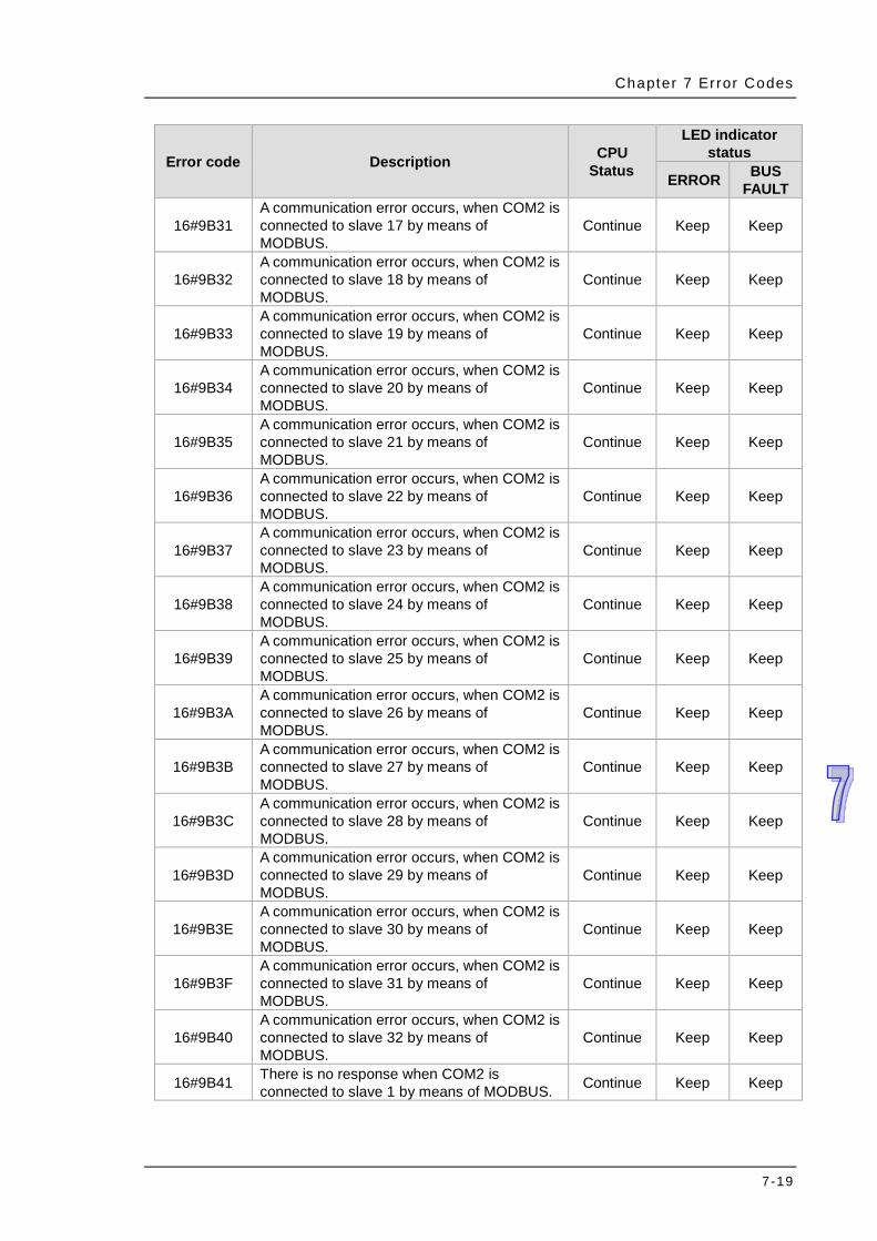
Chapter 7 Error Codes
7-19
Error code Description CPU Status
LED indicator status
ERROR BUS FAULT
16#9B31 A communication error occurs, when COM2 is connected to slave 17 by means of MODBUS.
Continue Keep Keep
16#9B32 A communication error occurs, when COM2 is connected to slave 18 by means of MODBUS.
Continue Keep Keep
16#9B33 A communication error occurs, when COM2 is connected to slave 19 by means of MODBUS.
Continue Keep Keep
16#9B34 A communication error occurs, when COM2 is connected to slave 20 by means of MODBUS.
Continue Keep Keep
16#9B35 A communication error occurs, when COM2 is connected to slave 21 by means of MODBUS.
Continue Keep Keep
16#9B36 A communication error occurs, when COM2 is connected to slave 22 by means of MODBUS.
Continue Keep Keep
16#9B37 A communication error occurs, when COM2 is connected to slave 23 by means of MODBUS.
Continue Keep Keep
16#9B38 A communication error occurs, when COM2 is connected to slave 24 by means of MODBUS.
Continue Keep Keep
16#9B39 A communication error occurs, when COM2 is connected to slave 25 by means of MODBUS.
Continue Keep Keep
16#9B3A A communication error occurs, when COM2 is connected to slave 26 by means of MODBUS.
Continue Keep Keep
16#9B3B A communication error occurs, when COM2 is connected to slave 27 by means of MODBUS.
Continue Keep Keep
16#9B3C A communication error occurs, when COM2 is connected to slave 28 by means of MODBUS.
Continue Keep Keep
16#9B3D A communication error occurs, when COM2 is connected to slave 29 by means of MODBUS.
Continue Keep Keep
16#9B3E A communication error occurs, when COM2 is connected to slave 30 by means of MODBUS.
Continue Keep Keep
16#9B3F A communication error occurs, when COM2 is connected to slave 31 by means of MODBUS.
Continue Keep Keep
16#9B40 A communication error occurs, when COM2 is connected to slave 32 by means of MODBUS.
Continue Keep Keep
16#9B41 There is no response when COM2 is connected to slave 1 by means of MODBUS. Continue Keep Keep
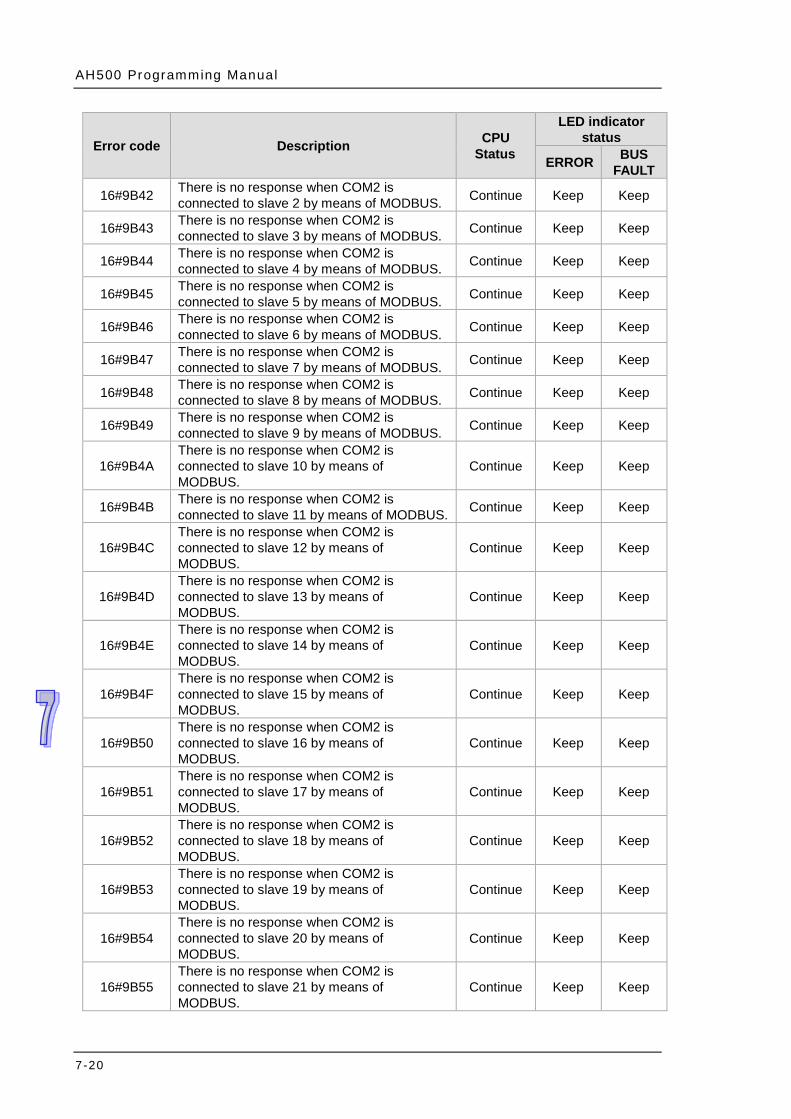
AH500 Programming Manual
7-20
Error code Description CPU Status
LED indicator status
ERROR BUS FAULT
16#9B42 There is no response when COM2 is connected to slave 2 by means of MODBUS. Continue Keep Keep
16#9B43 There is no response when COM2 is connected to slave 3 by means of MODBUS. Continue Keep Keep
16#9B44 There is no response when COM2 is connected to slave 4 by means of MODBUS. Continue Keep Keep
16#9B45 There is no response when COM2 is connected to slave 5 by means of MODBUS. Continue Keep Keep
16#9B46 There is no response when COM2 is connected to slave 6 by means of MODBUS. Continue Keep Keep
16#9B47 There is no response when COM2 is connected to slave 7 by means of MODBUS. Continue Keep Keep
16#9B48 There is no response when COM2 is connected to slave 8 by means of MODBUS. Continue Keep Keep
16#9B49 There is no response when COM2 is connected to slave 9 by means of MODBUS. Continue Keep Keep
16#9B4A There is no response when COM2 is connected to slave 10 by means of MODBUS.
Continue Keep Keep
16#9B4B There is no response when COM2 is connected to slave 11 by means of MODBUS. Continue Keep Keep
16#9B4C There is no response when COM2 is connected to slave 12 by means of MODBUS.
Continue Keep Keep
16#9B4D There is no response when COM2 is connected to slave 13 by means of MODBUS.
Continue Keep Keep
16#9B4E There is no response when COM2 is connected to slave 14 by means of MODBUS.
Continue Keep Keep
16#9B4F There is no response when COM2 is connected to slave 15 by means of MODBUS.
Continue Keep Keep
16#9B50 There is no response when COM2 is connected to slave 16 by means of MODBUS.
Continue Keep Keep
16#9B51 There is no response when COM2 is connected to slave 17 by means of MODBUS.
Continue Keep Keep
16#9B52 There is no response when COM2 is connected to slave 18 by means of MODBUS.
Continue Keep Keep
16#9B53 There is no response when COM2 is connected to slave 19 by means of MODBUS.
Continue Keep Keep
16#9B54 There is no response when COM2 is connected to slave 20 by means of MODBUS.
Continue Keep Keep
16#9B55 There is no response when COM2 is connected to slave 21 by means of MODBUS.
Continue Keep Keep
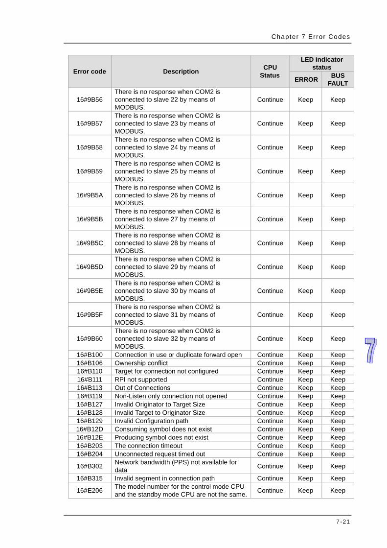
Chapter 7 Error Codes
7-21
Error code Description CPU Status
LED indicator status
ERROR BUS FAULT
16#9B56 There is no response when COM2 is connected to slave 22 by means of MODBUS.
Continue Keep Keep
16#9B57 There is no response when COM2 is connected to slave 23 by means of MODBUS.
Continue Keep Keep
16#9B58 There is no response when COM2 is connected to slave 24 by means of MODBUS.
Continue Keep Keep
16#9B59 There is no response when COM2 is connected to slave 25 by means of MODBUS.
Continue Keep Keep
16#9B5A There is no response when COM2 is connected to slave 26 by means of MODBUS.
Continue Keep Keep
16#9B5B There is no response when COM2 is connected to slave 27 by means of MODBUS.
Continue Keep Keep
16#9B5C There is no response when COM2 is connected to slave 28 by means of MODBUS.
Continue Keep Keep
16#9B5D There is no response when COM2 is connected to slave 29 by means of MODBUS.
Continue Keep Keep
16#9B5E There is no response when COM2 is connected to slave 30 by means of MODBUS.
Continue Keep Keep
16#9B5F There is no response when COM2 is connected to slave 31 by means of MODBUS.
Continue Keep Keep
16#9B60 There is no response when COM2 is connected to slave 32 by means of MODBUS.
Continue Keep Keep
16#B100 Connection in use or duplicate forward open Continue Keep Keep 16#B106 Ownership conflict Continue Keep Keep 16#B110 Target for connection not configured Continue Keep Keep 16#B111 RPI not supported Continue Keep Keep 16#B113 Out of Connections Continue Keep Keep 16#B119 Non-Listen only connection not opened Continue Keep Keep 16#B127 Invalid Originator to Target Size Continue Keep Keep 16#B128 Invalid Target to Originator Size Continue Keep Keep 16#B129 Invalid Configuration path Continue Keep Keep 16#B12D Consuming symbol does not exist Continue Keep Keep 16#B12E Producing symbol does not exist Continue Keep Keep 16#B203 The connection timeout Continue Keep Keep 16#B204 Unconnected request timed out Continue Keep Keep
16#B302 Network bandwidth (PPS) not available for data Continue Keep Keep
16#B315 Invalid segment in connection path Continue Keep Keep
16#E206 The model number for the control mode CPU and the standby mode CPU are not the same. Continue Keep Keep
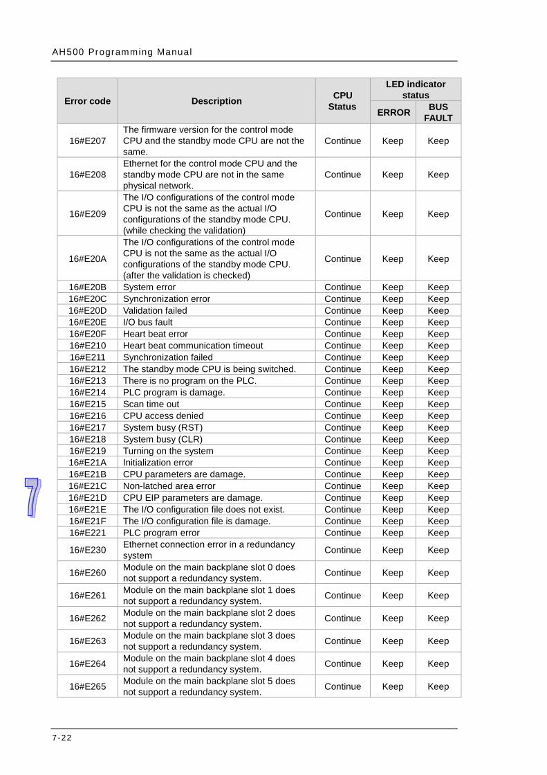
AH500 Programming Manual
7-22
Error code Description CPU Status
LED indicator status
ERROR BUS FAULT
16#E207 The firmware version for the control mode CPU and the standby mode CPU are not the same.
Continue Keep Keep
16#E208 Ethernet for the control mode CPU and the standby mode CPU are not in the same physical network.
Continue Keep Keep
16#E209
The I/O configurations of the control mode CPU is not the same as the actual I/O configurations of the standby mode CPU. (while checking the validation)
Continue Keep Keep
16#E20A
The I/O configurations of the control mode CPU is not the same as the actual I/O configurations of the standby mode CPU. (after the validation is checked)
Continue Keep Keep
16#E20B System error Continue Keep Keep 16#E20C Synchronization error Continue Keep Keep 16#E20D Validation failed Continue Keep Keep 16#E20E I/O bus fault Continue Keep Keep 16#E20F Heart beat error Continue Keep Keep 16#E210 Heart beat communication timeout Continue Keep Keep 16#E211 Synchronization failed Continue Keep Keep 16#E212 The standby mode CPU is being switched. Continue Keep Keep 16#E213 There is no program on the PLC. Continue Keep Keep 16#E214 PLC program is damage. Continue Keep Keep 16#E215 Scan time out Continue Keep Keep 16#E216 CPU access denied Continue Keep Keep 16#E217 System busy (RST) Continue Keep Keep 16#E218 System busy (CLR) Continue Keep Keep 16#E219 Turning on the system Continue Keep Keep 16#E21A Initialization error Continue Keep Keep 16#E21B CPU parameters are damage. Continue Keep Keep 16#E21C Non-latched area error Continue Keep Keep 16#E21D CPU EIP parameters are damage. Continue Keep Keep 16#E21E The I/O configuration file does not exist. Continue Keep Keep 16#E21F The I/O configuration file is damage. Continue Keep Keep 16#E221 PLC program error Continue Keep Keep
16#E230 Ethernet connection error in a redundancy system Continue Keep Keep
16#E260 Module on the main backplane slot 0 does not support a redundancy system. Continue Keep Keep
16#E261 Module on the main backplane slot 1 does not support a redundancy system. Continue Keep Keep
16#E262 Module on the main backplane slot 2 does not support a redundancy system. Continue Keep Keep
16#E263 Module on the main backplane slot 3 does not support a redundancy system. Continue Keep Keep
16#E264 Module on the main backplane slot 4 does not support a redundancy system. Continue Keep Keep
16#E265 Module on the main backplane slot 5 does not support a redundancy system. Continue Keep Keep
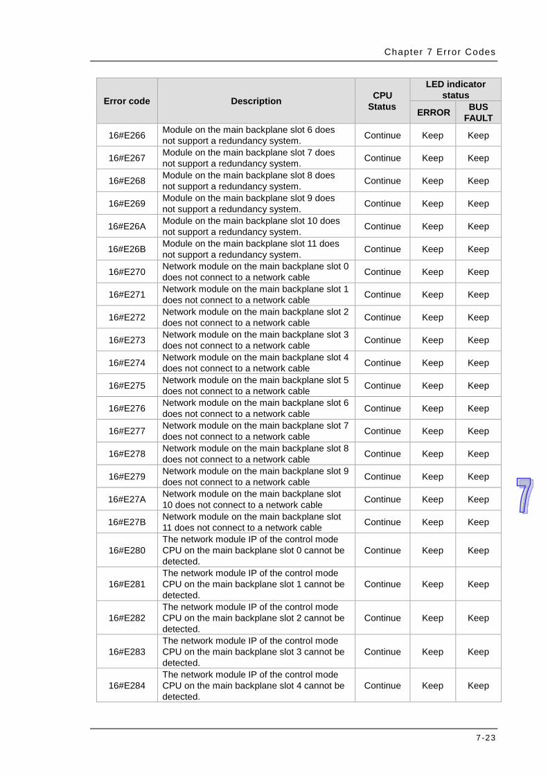
Chapter 7 Error Codes
7-23
Error code Description CPU Status
LED indicator status
ERROR BUS FAULT
16#E266 Module on the main backplane slot 6 does not support a redundancy system. Continue Keep Keep
16#E267 Module on the main backplane slot 7 does not support a redundancy system. Continue Keep Keep
16#E268 Module on the main backplane slot 8 does not support a redundancy system. Continue Keep Keep
16#E269 Module on the main backplane slot 9 does not support a redundancy system. Continue Keep Keep
16#E26A Module on the main backplane slot 10 does not support a redundancy system. Continue Keep Keep
16#E26B Module on the main backplane slot 11 does not support a redundancy system. Continue Keep Keep
16#E270 Network module on the main backplane slot 0 does not connect to a network cable Continue Keep Keep
16#E271 Network module on the main backplane slot 1 does not connect to a network cable Continue Keep Keep
16#E272 Network module on the main backplane slot 2 does not connect to a network cable Continue Keep Keep
16#E273 Network module on the main backplane slot 3 does not connect to a network cable Continue Keep Keep
16#E274 Network module on the main backplane slot 4 does not connect to a network cable Continue Keep Keep
16#E275 Network module on the main backplane slot 5 does not connect to a network cable Continue Keep Keep
16#E276 Network module on the main backplane slot 6 does not connect to a network cable Continue Keep Keep
16#E277 Network module on the main backplane slot 7 does not connect to a network cable Continue Keep Keep
16#E278 Network module on the main backplane slot 8 does not connect to a network cable Continue Keep Keep
16#E279 Network module on the main backplane slot 9 does not connect to a network cable Continue Keep Keep
16#E27A Network module on the main backplane slot 10 does not connect to a network cable Continue Keep Keep
16#E27B Network module on the main backplane slot 11 does not connect to a network cable Continue Keep Keep
16#E280 The network module IP of the control mode CPU on the main backplane slot 0 cannot be detected.
Continue Keep Keep
16#E281 The network module IP of the control mode CPU on the main backplane slot 1 cannot be detected.
Continue Keep Keep
16#E282 The network module IP of the control mode CPU on the main backplane slot 2 cannot be detected.
Continue Keep Keep
16#E283 The network module IP of the control mode CPU on the main backplane slot 3 cannot be detected.
Continue Keep Keep
16#E284 The network module IP of the control mode CPU on the main backplane slot 4 cannot be detected.
Continue Keep Keep
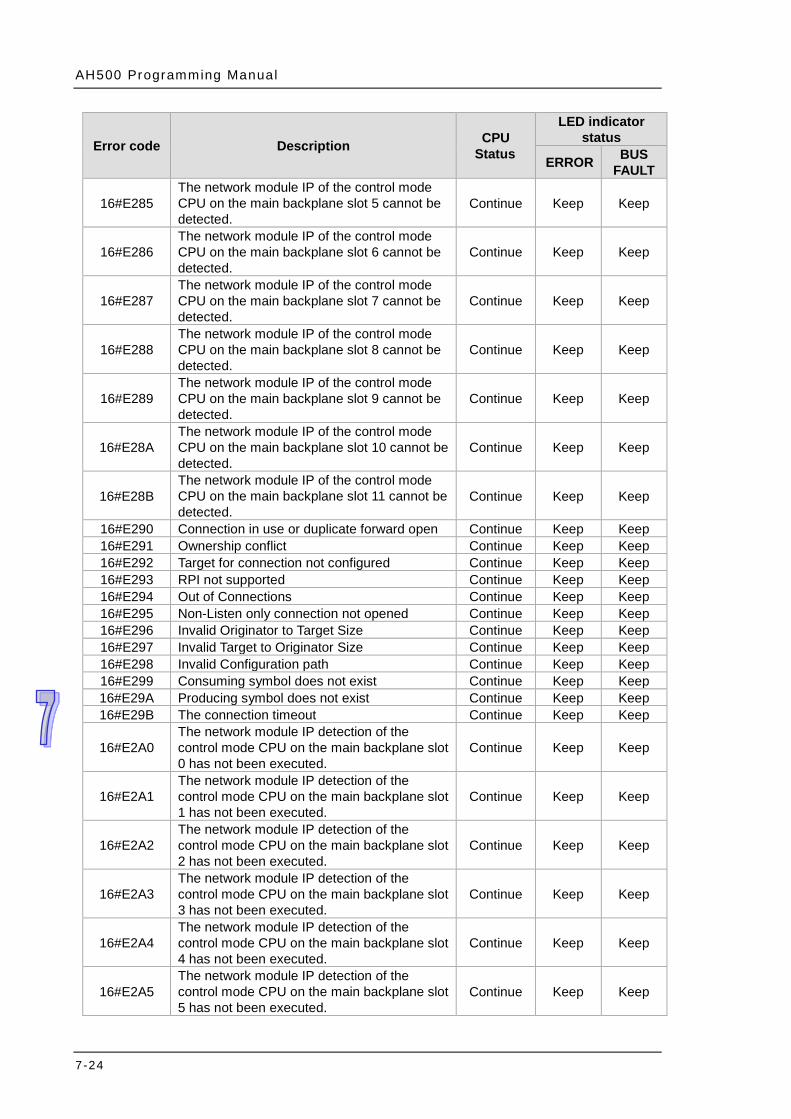
AH500 Programming Manual
7-24
Error code Description CPU Status
LED indicator status
ERROR BUS FAULT
16#E285 The network module IP of the control mode CPU on the main backplane slot 5 cannot be detected.
Continue Keep Keep
16#E286 The network module IP of the control mode CPU on the main backplane slot 6 cannot be detected.
Continue Keep Keep
16#E287 The network module IP of the control mode CPU on the main backplane slot 7 cannot be detected.
Continue Keep Keep
16#E288 The network module IP of the control mode CPU on the main backplane slot 8 cannot be detected.
Continue Keep Keep
16#E289 The network module IP of the control mode CPU on the main backplane slot 9 cannot be detected.
Continue Keep Keep
16#E28A The network module IP of the control mode CPU on the main backplane slot 10 cannot be detected.
Continue Keep Keep
16#E28B The network module IP of the control mode CPU on the main backplane slot 11 cannot be detected.
Continue Keep Keep
16#E290 Connection in use or duplicate forward open Continue Keep Keep 16#E291 Ownership conflict Continue Keep Keep 16#E292 Target for connection not configured Continue Keep Keep 16#E293 RPI not supported Continue Keep Keep 16#E294 Out of Connections Continue Keep Keep 16#E295 Non-Listen only connection not opened Continue Keep Keep 16#E296 Invalid Originator to Target Size Continue Keep Keep 16#E297 Invalid Target to Originator Size Continue Keep Keep 16#E298 Invalid Configuration path Continue Keep Keep 16#E299 Consuming symbol does not exist Continue Keep Keep 16#E29A Producing symbol does not exist Continue Keep Keep 16#E29B The connection timeout Continue Keep Keep
16#E2A0 The network module IP detection of the control mode CPU on the main backplane slot 0 has not been executed.
Continue Keep Keep
16#E2A1 The network module IP detection of the control mode CPU on the main backplane slot 1 has not been executed.
Continue Keep Keep
16#E2A2 The network module IP detection of the control mode CPU on the main backplane slot 2 has not been executed.
Continue Keep Keep
16#E2A3 The network module IP detection of the control mode CPU on the main backplane slot 3 has not been executed.
Continue Keep Keep
16#E2A4 The network module IP detection of the control mode CPU on the main backplane slot 4 has not been executed.
Continue Keep Keep
16#E2A5 The network module IP detection of the control mode CPU on the main backplane slot 5 has not been executed.
Continue Keep Keep

Chapter 7 Error Codes
7-25
Error code Description CPU Status
LED indicator status
ERROR BUS FAULT
16#E2A6 The network module IP detection of the control mode CPU on the main backplane slot 6 has not been executed.
Continue Keep Keep
16#E2A7 The network module IP detection of the control mode CPU on the main backplane slot 7 has not been executed.
Continue Keep Keep
16#E2A8 The network module IP detection of the control mode CPU on the main backplane slot 8 has not been executed.
Continue Keep Keep
16#E2A9 The network module IP detection of the control mode CPU on the main backplane slot 9 has not been executed.
Continue Keep Keep
16#E2AA The network module IP detection of the control mode CPU on the main backplane slot 10 has not been executed.
Continue Keep Keep
16#E2AB The network module IP detection of the control mode CPU on the main backplane slot 11 has not been executed.
Continue Keep Keep

AH500 Programming Manual
7-26
7.1.2 Analog I/O Modules and Temperature Measurement Modules
Error code Description
LED indicator status CPU Module BUS
FAULT ERROR
16#A000 The signal received by channel 0 exceeds the range of inputs which can be received by the hardware. Blinking
16#A001 The signal received by channel 1 exceeds the range of inputs which can be received by the hardware. Blinking
16#A002 The signal received by channel 2 exceeds the range of inputs which can be received by the hardware. Blinking
16#A003 The signal received by channel 3 exceeds the range of inputs which can be received by the hardware. Blinking
16#A004 The signal received by channel 4 exceeds the range of inputs which can be received by the hardware. Blinking
16#A005 The signal received by channel 5 exceeds the range of inputs which can be received by the hardware. Blinking
16#A006 The signal received by channel 6 exceeds the range of inputs which can be received by the hardware. Blinking
16#A007 The signal received by channel 7 exceeds the range of inputs which can be received by the hardware. Blinking
16#A400 The signal received by channel 0 exceeds the range of inputs which can be received by the hardware. ON
16#A401 The signal received by channel 1 exceeds the range of inputs which can be received by the hardware. ON
16#A402 The signal received by channel 2 exceeds the range of inputs which can be received by the hardware. ON
16#A403 The signal received by channel 3 exceeds the range of inputs which can be received by the hardware. ON
16#A404 The signal received by channel 4 exceeds the range of inputs which can be received by the hardware. ON
16#A405 The signal received by channel 5 exceeds the range of inputs which can be received by the hardware. ON
16#A406 The signal received by channel 6 exceeds the range of inputs which can be received by the hardware. ON
16#A407 The signal received by channel 7 exceeds the range of inputs which can be received by the hardware. ON
16#A600 Hardware failure ON 16#A601 The external voltage is abnormal. ON
16#A602 Internal error The CJC is abnormal. ON
16#A603 Internal error The factory correction is abnormal. ON
16#A800 The signal received by channel 0 exceeds the range of inputs which can be received by the hardware. OFF
16#A801 The signal received by channel 1 exceeds the range of inputs which can be received by the hardware. OFF
16#A802 The signal received by channel 2 exceeds the range of inputs which can be received by the hardware. OFF
16#A803 The signal received by channel 3 exceeds the range of inputs which can be received by the hardware. OFF
16#A804 The signal received by channel 4 exceeds the range of inputs which can be received by the hardware. OFF
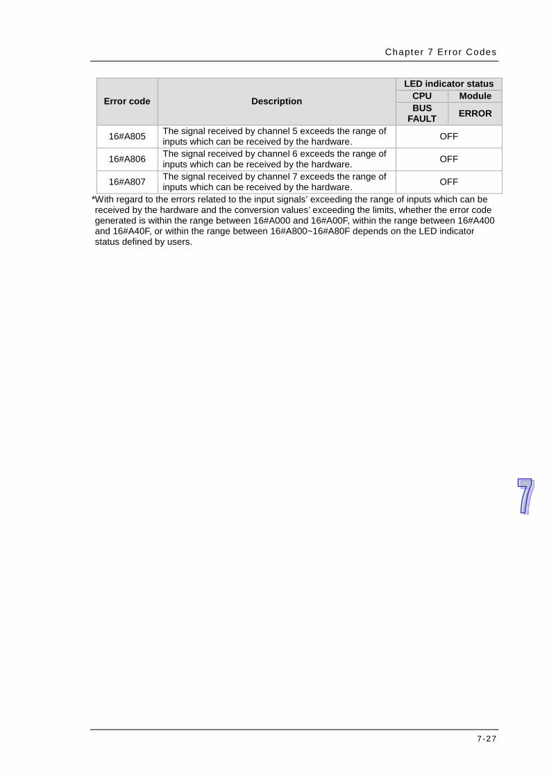
Chapter 7 Error Codes
7-27
Error code Description
LED indicator status CPU Module BUS
FAULT ERROR
16#A805 The signal received by channel 5 exceeds the range of inputs which can be received by the hardware. OFF
16#A806 The signal received by channel 6 exceeds the range of inputs which can be received by the hardware. OFF
16#A807 The signal received by channel 7 exceeds the range of inputs which can be received by the hardware. OFF
*With regard to the errors related to the input signals’ exceeding the range of inputs which can be received by the hardware and the conversion values’ exceeding the limits, whether the error code generated is within the range between 16#A000 and 16#A00F, within the range between 16#A400 and 16#A40F, or within the range between 16#A800~16#A80F depends on the LED indicator status defined by users.
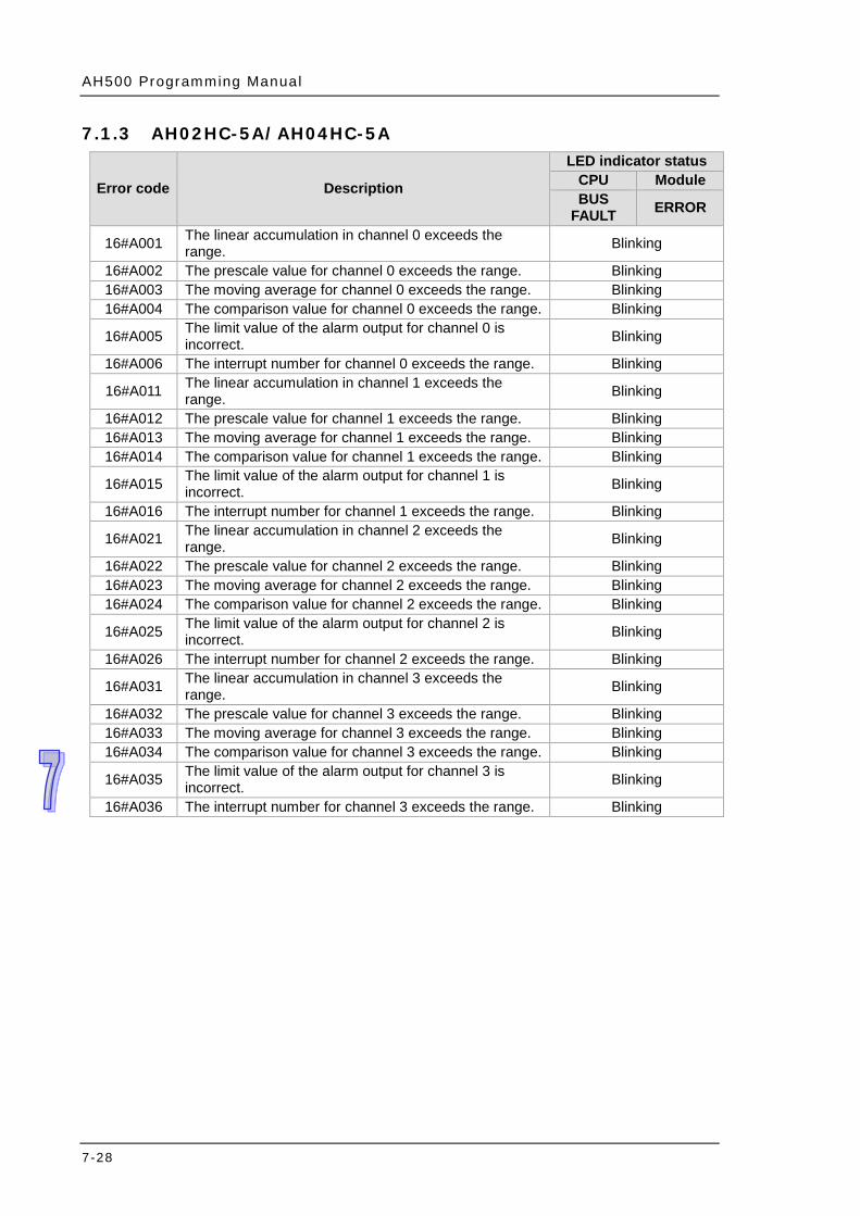
AH500 Programming Manual
7-28
7.1.3 AH02HC-5A/AH04HC-5A
Error code Description
LED indicator status CPU Module BUS
FAULT ERROR
16#A001 The linear accumulation in channel 0 exceeds the range. Blinking
16#A002 The prescale value for channel 0 exceeds the range. Blinking 16#A003 The moving average for channel 0 exceeds the range. Blinking 16#A004 The comparison value for channel 0 exceeds the range. Blinking
16#A005 The limit value of the alarm output for channel 0 is incorrect. Blinking
16#A006 The interrupt number for channel 0 exceeds the range. Blinking
16#A011 The linear accumulation in channel 1 exceeds the range. Blinking
16#A012 The prescale value for channel 1 exceeds the range. Blinking 16#A013 The moving average for channel 1 exceeds the range. Blinking 16#A014 The comparison value for channel 1 exceeds the range. Blinking
16#A015 The limit value of the alarm output for channel 1 is incorrect. Blinking
16#A016 The interrupt number for channel 1 exceeds the range. Blinking
16#A021 The linear accumulation in channel 2 exceeds the range. Blinking
16#A022 The prescale value for channel 2 exceeds the range. Blinking 16#A023 The moving average for channel 2 exceeds the range. Blinking 16#A024 The comparison value for channel 2 exceeds the range. Blinking
16#A025 The limit value of the alarm output for channel 2 is incorrect. Blinking
16#A026 The interrupt number for channel 2 exceeds the range. Blinking
16#A031 The linear accumulation in channel 3 exceeds the range. Blinking
16#A032 The prescale value for channel 3 exceeds the range. Blinking 16#A033 The moving average for channel 3 exceeds the range. Blinking 16#A034 The comparison value for channel 3 exceeds the range. Blinking
16#A035 The limit value of the alarm output for channel 3 is incorrect. Blinking
16#A036 The interrupt number for channel 3 exceeds the range. Blinking

Chapter 7 Error Codes
7-29
7.1.4 AH05PM-5A / AH10PM-5A / AH15PM-5A
Error code Description
LED indicator status CPU Module BUS
FAULT Error
16#A002 The subroutine has no data. Blinking 16#A003 CJ, CJN, and JMP have no matching pointers. Blinking 16#A004 There is a subroutine pointer in the main program. Blinking 16#A005 Lack of the subroutine Blinking 16#A006 The pointer is used repeatedly in the same program. Blinking 16#A007 The subroutine pointer is used repeatedly. Blinking
16#A008 The pointer used in JMP is used repeatedly in different subroutines. Blinking
16#A009 The pointer used in JMP is the same as the pointer used in CALL. Blinking
16#A00B Target position (I) of the single speed is incorrect. Blinking
16#A00C Target position (II) of the single-axis motion is incorrect. Blinking
16#A00D The setting of speed (I) of the single-axis motion is incorrect. Blinking
16#A00E The setting of speed (II) of the single-axis motion is incorrect. Blinking
16#A00F The setting of the speed (VRT) of returning to zero is incorrect. Blinking
16#A010 The setting of the deceleration (VCR) of returning to zero is incorrect. Blinking
16#A011 The setting of the JOG speed is incorrect. Blinking
16#A012 The positive pulses generated by the single-axis clockwise motion are inhibited. Blinking
16#A013 The negative pulses generated by the single-axis counterclockwise motion are inhibited. Blinking
16#A014 The limit switch is reached. Blinking 16#A015 The device which is used exceeds the device range. Blinking
16#A017 An error occurs when the device is modified by a 16-bit index register/32-bit index register. Blinking
16#A018 The conversion into the floating-point number is incorrect. Blinking
16#A019 The conversion into the binary-coded decimal number is incorrect. Blinking
16#A01A Incorrect division operation (The divisor is 0.) Blinking 16#A01B General program error Blinking 16#A01C LD/LDI has been used more than nine times. Blinking 16#A01D There is more than one level of nested program
structure supported by RPT/RPE. Blinking 16#A01E SRET is used between RPT and RPE. Blinking 16#A01F There is no M102 in the main program, or there is no
M2 in the motion program. Blinking
16#A020 The wrong instruction is used, or the device used exceeds the range. Blinking
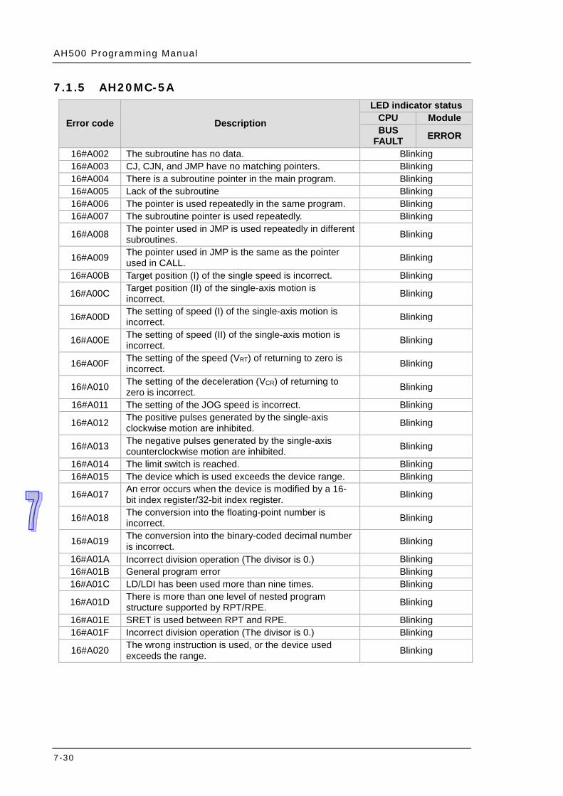
AH500 Programming Manual
7-30
7.1.5 AH20MC-5A
Error code Description
LED indicator status CPU Module BUS
FAULT ERROR
16#A002 The subroutine has no data. Blinking 16#A003 CJ, CJN, and JMP have no matching pointers. Blinking 16#A004 There is a subroutine pointer in the main program. Blinking 16#A005 Lack of the subroutine Blinking 16#A006 The pointer is used repeatedly in the same program. Blinking 16#A007 The subroutine pointer is used repeatedly. Blinking 16#A008 The pointer used in JMP is used repeatedly in different
subroutines. Blinking
16#A009 The pointer used in JMP is the same as the pointer used in CALL. Blinking
16#A00B Target position (I) of the single speed is incorrect. Blinking 16#A00C Target position (II) of the single-axis motion is
incorrect. Blinking
16#A00D The setting of speed (I) of the single-axis motion is incorrect. Blinking
16#A00E The setting of speed (II) of the single-axis motion is incorrect. Blinking
16#A00F The setting of the speed (VRT) of returning to zero is incorrect. Blinking
16#A010 The setting of the deceleration (VCR) of returning to zero is incorrect. Blinking
16#A011 The setting of the JOG speed is incorrect. Blinking 16#A012 The positive pulses generated by the single-axis
clockwise motion are inhibited. Blinking
16#A013 The negative pulses generated by the single-axis counterclockwise motion are inhibited. Blinking
16#A014 The limit switch is reached. Blinking 16#A015 The device which is used exceeds the device range. Blinking 16#A017 An error occurs when the device is modified by a 16-
bit index register/32-bit index register. Blinking
16#A018 The conversion into the floating-point number is incorrect. Blinking
16#A019 The conversion into the binary-coded decimal number is incorrect. Blinking
16#A01A Incorrect division operation (The divisor is 0.) Blinking 16#A01B General program error Blinking 16#A01C LD/LDI has been used more than nine times. Blinking 16#A01D There is more than one level of nested program
structure supported by RPT/RPE. Blinking 16#A01E SRET is used between RPT and RPE. Blinking 16#A01F Incorrect division operation (The divisor is 0.) Blinking 16#A020 The wrong instruction is used, or the device used
exceeds the range. Blinking
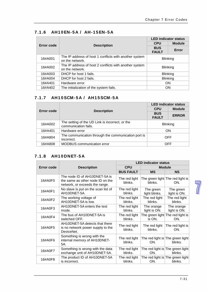
Chapter 7 Error Codes
7-31
7.1.6 AH10EN-5A / AH-15EN-5A
Error code Description
LED indicator status CPU Module BUS
FAULT Error
16#A001 The IP address of host 1 conflicts with another system on the network. Blinking
16#A002 The IP address of host 2 conflicts with another system on the network. Blinking
16#A003 DHCP for host 1 fails. Blinking 16#A004 DHCP for host 2 fails. Blinking 16#A401 Hardware error ON 16#A402 The initialization of the system fails. ON
7.1.7 AH10SCM-5A / AH15SCM-5A
Error code Description
LED indicator status CPU Module BUS
FAULT ERROR
16#A002 The setting of the UD Link is incorrect, or the communication fails. Blinking
16#A401 Hardware error ON
16#A804 The communication through the communication port is incorrect. OFF
16#A808 MODBUS communication error OFF
7.1.8 AH10DNET-5A
Error code Description LED indicator status
CPU Module BUS FAULT MS NS
16#A0F0 The node ID of AH10DNET-5A is the same as other node ID on the network, or exceeds the range.
The red light blinks.
The green light blinks.
The red light is ON.
16#A0F1 No slave is put on the scan list of AH10DNET-5A.
The red light blinks.
The green light blinks.
The green light is ON.
16#A0F2 The working voltage of AH10DNET-5A is low.
The red light blinks.
The red light blinks.
The red light blinks.
16#A0F3 AH10DNET-5A enters the test mode.
The red light blinks.
The orange light is ON.
The orange light is ON.
16#A0F4 The bus of AH10DNET-5A is switched OFF.
The red light blinks.
The green light is ON.
The red light is ON.
16#A0F5 AH10DNET-5A detects that there is no network power supply to the DeviceNet.
The red light blinks.
The red light blinks.
The red light is ON.
16#A0F6 Something is wrong with the internal memory of AH10DNET-5A.
The red light blinks.
The red light is ON.
The green light blinks.
16#A0F7 Something is wrong with the data exchange unit of AH10DNET-5A.
The red light blinks.
The red light is ON.
The green light blinks.
16#A0F8 The product ID of AH10DNET-5A is incorrect.
The red light blinks.
The red light is ON.
The green light blinks.
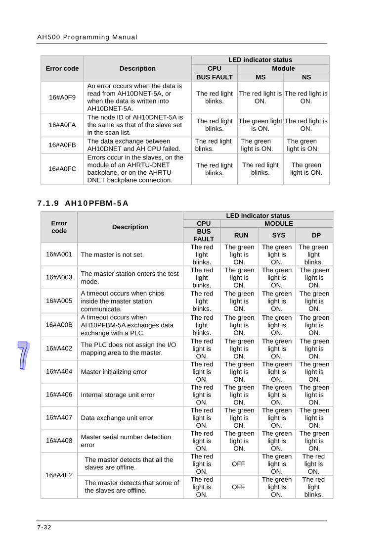
AH500 Programming Manual
7-32
Error code Description LED indicator status
CPU Module BUS FAULT MS NS
16#A0F9
An error occurs when the data is read from AH10DNET-5A, or when the data is written into AH10DNET-5A.
The red light blinks.
The red light is ON.
The red light is ON.
16#A0FA The node ID of AH10DNET-5A is the same as that of the slave set in the scan list.
The red light blinks.
The green light is ON.
The red light is ON.
16#A0FB The data exchange between AH10DNET and AH CPU failed.
The red light blinks.
The green light is ON.
The green light is ON.
16#A0FC
Errors occur in the slaves, on the module of an AHRTU-DNET backplane, or on the AHRTU-DNET backplane connection.
The red light blinks.
The red light blinks.
The green light is ON.
7.1.9 AH10PFBM-5A
Error code Description
LED indicator status CPU MODULE BUS
FAULT RUN SYS DP
16#A001 The master is not set. The red
light blinks.
The green light is ON.
The green light is ON.
The green light
blinks.
16#A003 The master station enters the test mode.
The red light
blinks.
The green light is ON.
The green light is ON.
The green light is ON.
16#A005 A timeout occurs when chips inside the master station communicate.
The red light
blinks.
The green light is ON.
The green light is ON.
The green light is ON.
16#A00B A timeout occurs when AH10PFBM-5A exchanges data exchange with a PLC.
The red light
blinks.
The green light is ON.
The green light is ON.
The green light is ON.
16#A402 The PLC does not assign the I/O mapping area to the master.
The red light is ON.
The green light is ON.
The green light is ON.
The green light is ON.
16#A404 Master initializing error The red light is ON.
The green light is ON.
The green light is ON.
The green light is ON.
16#A406 Internal storage unit error The red light is ON.
The green light is ON.
The green light is ON.
The green light is ON.
16#A407 Data exchange unit error The red light is ON.
The green light is ON.
The green light is ON.
The green light is ON.
16#A408 Master serial number detection error
The red light is ON.
The green light is ON.
The green light is ON.
The green light is ON.
16#A4E2
The master detects that all the slaves are offline.
The red light is ON.
OFF The green
light is ON.
The red light is ON.
The master detects that some of the slaves are offline.
The red light is ON.
OFF The green
light is ON.
The red light
blinks.
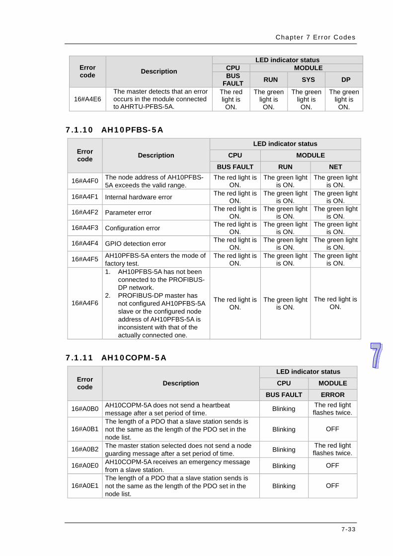
Chapter 7 Error Codes
7-33
Error code Description
LED indicator status CPU MODULE BUS
FAULT RUN SYS DP
16#A4E6 The master detects that an error occurs in the module connected to AHRTU-PFBS-5A.
The red light is ON.
The green light is ON.
The green light is ON.
The green light is ON.
7.1.10 AH10PFBS-5A
Error code Description
LED indicator status CPU MODULE
BUS FAULT RUN NET
16#A4F0 The node address of AH10PFBS-5A exceeds the valid range.
The red light is ON.
The green light is ON.
The green light is ON.
16#A4F1 Internal hardware error The red light is ON.
The green light is ON.
The green light is ON.
16#A4F2 Parameter error The red light is ON.
The green light is ON.
The green light is ON.
16#A4F3 Configuration error The red light is ON.
The green light is ON.
The green light is ON.
16#A4F4 GPIO detection error The red light is ON.
The green light is ON.
The green light is ON.
16#A4F5 AH10PFBS-5A enters the mode of factory test.
The red light is ON.
The green light is ON.
The green light is ON.
16#A4F6
1. AH10PFBS-5A has not been connected to the PROFIBUS-DP network.
2. PROFIBUS-DP master has not configured AH10PFBS-5A slave or the configured node address of AH10PFBS-5A is inconsistent with that of the actually connected one.
The red light is ON.
The green light is ON.
The red light is ON.
7.1.11 AH10COPM-5A
Error code Description
LED indicator status
CPU MODULE
BUS FAULT ERROR
16#A0B0 AH10COPM-5A does not send a heartbeat message after a set period of time. Blinking The red light
flashes twice.
16#A0B1 The length of a PDO that a slave station sends is not the same as the length of the PDO set in the node list.
Blinking OFF
16#A0B2 The master station selected does not send a node guarding message after a set period of time. Blinking The red light
flashes twice.
16#A0E0 AH10COPM-5A receives an emergency message from a slave station. Blinking OFF
16#A0E1 The length of a PDO that a slave station sends is not the same as the length of the PDO set in the node list.
Blinking OFF

AH500 Programming Manual
7-34
Error code Description
LED indicator status
CPU MODULE
BUS FAULT ERROR
16#A0E2 AH10COPM-5A does not receive a PDO from a slave station. Blinking OFF
16#A0E3 An automatic SDO is not downloaded successfully. Blinking OFF 16#A0E4 A PDO parameter is not set successfully. Blinking OFF 16#A0E5 A key parameter is set incorrectly. Blinking OFF
16#A0E6 The actual network configuration is not the same as the network configuration set. Blinking OFF
16#A0E7 The control of the errors in a slave station is not sent after a set period of time. Blinking The red light
flashes twice.
16#A0E8 The master station address is the same as a slave station address. Blinking OFF
16#A0F1 No slave station is added to the node list in CANopen builder. Blinking OFF
16#A0F3 An error occurs in AH10COPM-5A. Blinking OFF
16#A0F4 The bus used is off. Blinking The red light is ON.
16#A0F5 The node address of AH10COPM-5A is set incorrectly. Blinking OFF
16#A0F6 Internal error: An error occurs in the manufacturing process in the factory. Blinking OFF
16#A0F7 Internal error: GPIO error Blinking OFF 16#A0F8 Hardware error Blinking OFF 16#A0F9 Low voltage Blinking OFF 16#A0FA An error occurs in the firmware of AH10COPM-5A. Blinking OFF
16#A0FB The transmission registers in AH10COPM-5A are full. Blinking OFF
16#A0FC The reception registers in AH10COPM-5A are full. Blinking OFF

Chapter 7 Error Codes
7-35
MEMO