Agilent 8702D Lightwave Component Analyzer Reference
312
Agilent 8702D Lightwave Component Analyzer Reference
-
Upload
khangminh22 -
Category
Documents
-
view
1 -
download
0
Transcript of Agilent 8702D Lightwave Component Analyzer Reference

Agilent 8702D LightwaveComponent AnalyzerReference

ii
© Copyright Agilent Technologies 2000All Rights Reserved. Repro-duction, adaptation, or trans-lation without prior written permission is prohibited, except as allowed under copy-right laws.
Agilent Part No. 08702-90054Printed in USAApril 2000
Agilent Technologies Lightwave Division1400 Fountaingrove ParkwaySanta Rosa, CA 95403-1799, USA(707) 577-1400
Notice.The information contained in this document is subject to change without notice. Com-panies, names, and data used in examples herein are ficti-tious unless otherwise noted. Agilent Technologies makes no warranty of any kind with regard to this material, includ-ing but not limited to, the implied warranties of mer-chantability and fitness for a particular purpose. Agilent Technologies shall not be lia-ble for errors contained herein or for incidental or conse-quential damages in connec-tion with the furnishing, performance, or use of this material.
Restricted Rights Legend.Use, duplication, or disclo-sure by the U.S. Government is subject to restrictions as set forth in subparagraph (c) (1) (ii) of the Rights in Technical Data and Computer Software clause at DFARS 252.227-7013 for DOD agencies, and sub-paragraphs (c) (1) and (c) (2) of the Commercial Computer Software Restricted Rights clause at FAR 52.227-19 for other agencies.
Warranty.This Agilent Technologies instrument product is war-ranted against defects in
material and workmanship for a period of one year from date of shipment. During the war-ranty period, Agilent Technol-ogies will, at its option, either repair or replace products which prove to be defective. For warranty service or repair, this product must be returned to a service facility desig-nated by Agilent Technolo-gies. Buyer shall prepay shipping charges to Agilent Technologies and Agilent Technologies shall pay ship-ping charges to return the product to Buyer. However, Buyer shall pay all shipping charges, duties, and taxes for products returned to Agilent Technologies from another country.
Agilent Technologies war-rants that its software and firmware designated by Agi-lent Technologies for use with an instrument will execute its programming instructions when properly installed on that instrument. Agilent Tech-nologies does not warrant that the operation of the instru-ment, or software, or firmware will be uninterrupted or error-free.
Limitation of Warranty.The foregoing warranty shall not apply to defects resulting from improper or inadequate maintenance by Buyer, Buyer-supplied software or interfac-ing, unauthorized modifica-tion or misuse, operation outside of the environmental specifications for the product, or improper site preparation or maintenance.
No other warranty is expressed or implied. Agilent Technologies specifically dis-claims the implied warranties of merchantability and fitness for a particular purpose.
Exclusive Remedies.The remedies provided herein are buyer's sole and exclusive remedies. Agilent Technolo-
gies shall not be liable for any direct, indirect, special, inci-dental, or consequential dam-ages, whether based on contract, tort, or any other legal theory.
Safety Symbols.CAUTION
The caution sign denotes a hazard. It calls attention to a procedure which, if not cor-rectly performed or adhered to, could result in damage to or destruction of the product. Do not proceed beyond a cau-tion sign until the indicated conditions are fully under-stood and met.
WARNING
The warning sign denotes a hazard. It calls attention to a procedure which, if not cor-rectly performed or adhered to, could result in injury or loss of life. Do not proceed beyond a warning sign until the indicated conditions are fully understood and met.
The instruction man-ual symbol. The prod-uct is marked with this warning symbol when it is necessary for the user to refer to the instructions in the manual.
The laser radiation symbol. This warning symbol is marked on products which have a laser output.
The AC symbol is used to indicate the required nature of the line module input power.
| The ON symbols are used to mark the posi-tions of the instrument power line switch.
The OFF symbols are used to mark the positions of the instru-ment power line switch.
The CE mark is a reg-istered trademark of the European Commu-nity.
The CSA mark is a reg-istered trademark of the Canadian Stan-dards Association.
The C-Tick mark is a registered trademark of the Australian Spec-trum Management Agency.
This text denotes the instrument is an Industrial Scientific and Medical Group 1 Class A product.
Typographical Conven-
tions.
The following conventions are used in this book:
Key type for keys or text located on the keyboard or instrument.
Softkey type for key names that are displayed on the instru-ment’s screen.
Display type for words or characters displayed on the computer’s screen or instru-ment’s display.
User type for words or charac-ters that you type or enter.
Emphasis type for words or characters that emphasize some point or that are used as place holders for text that you type.
ISM1-A

Contents
1 Menu Maps
2 Reference
Instrument Options 2-3Available Accessories 2-5Power Cords 2-10Front Panel Features 2-12Analyzer Display 2-14Rear Panel Features and Connectors 2-16Reference Documents 2-19Location of Softkeys 2-21Connectors, Adjustments, and Display Annotation 2-39Preset Conditions 2-42Power-on Conditions 2-50
3 Error Messages
Error Messages in Alphabetical Order 3-3Error Messages in Numerical Order 3-27
4 Specifications and Regulatory Information
Instrument Specifications 4-3Instrument Specifications (Option 011) 4-10Instrument General Characteristics 4-18Environmental Characteristics 4-22System E/E Characteristics 4-24System O/E Characteristics 4-53System E/O Characteristics 4-67System O/O Characteristics 4-81Lightwave Receiver Measurement Repeatability 4-91GPIB Interface 4-93Regulatory Information 4-94
5 Concepts
How the Agilent 8702D Works 5-2How the Agilent 8702D Processes Data 5-5Using the Response Functions 5-11What is Measurement Calibration? 5-17
Contents-1

Contents
Understanding and Using Time Domain 5-71Instrument Preset State and Memory Allocation 5-100
Contents-2

1
Menu Maps

Menu MapsMenu Maps
Menu Maps
The menu maps that are in this chapter graphically represent the softkey menus. Maps for each softkey menu are shown in alphabetical order.
AVG menu map
A V G
A V E R A G I N GF A C T O R
A V E R A G I N Go n O F F
S M O O T H I N GA P E R T U R E
S M O O T H I N Go n O F F
I F B W[ ]
A V E R A G I N GR E S T A R T
A V GM E N U
1-2

Menu MapsMenu Maps
CAL menu map, 1 of 2
1-3

Menu MapsMenu Maps
CAL menu map, 2 of 2
1-4

Menu MapsMenu Maps
COPY menu map
1-5

Menu MapsMenu Maps
DISPLAY menu map
FORMAT menu map
1-6

Menu MapsMenu Maps
LOCAL menu map
1-7

Menu MapsMenu Maps
MARKER menu map
1-8

Menu MapsMenu Maps
MARKER FCTN menu map
1-9

Menu MapsMenu Maps
MEAS menu map, standard and option 011 with test set
MEAS menu map, option 011, no test set
1-10

Menu MapsMenu Maps
MENU menu map
PRESET menu map
1-11

Menu MapsMenu Maps
SAVE/RECALL menu map
1-12

Menu MapsMenu Maps
SCALE REF menu map
1-13

Menu MapsMenu Maps
SEQ menu map
1-14

Menu MapsMenu Maps
SYSTEM menu map
1-15


2
Instrument Options 2-3Available Accessories 2-5
Calibration Kits 2-5Verification Kit 2-5Test Port Return Cables 2-6Adapter Kits 2-6Transistor Test Fixtures 2-7System Accessories Available 2-8Power Cords 2-10
Front Panel Features 2-12Analyzer Display 2-14Rear Panel Features and Connectors 2-16Reference Documents 2-19
General Measurement and Calibration Techniques 2-19Fixtures and Non-coaxial Measurements 2-19On-Wafer Measurements 2-20
Location of Softkeys 2-21Connectors, Adjustments, and Display Annotation 2-39Preset Conditions 2-42Power-on Conditions 2-50
Reference

ReferenceReference
Reference
This chapter is a dictionary reference table of front and rear-panel connectors, front-panel keys (hardkeys), softkeys, and display annotations. With the exception of a few front-panel keys, softkeys control all instrument functions.
This chapter is designed for quick access of information. For example, during operation you may find a softkey or hardkey whose function is unfamiliar to you. Note the key name, find the key in this chapter, and note the applicable function. Some keys will have more than one function. Keys that begin with a symbol are listed at the front of the table.
2-2

ReferenceInstrument Options
Instrument Options
Option 1D5 High Stability Frequency Reference. Option 1D5 offers ±0.05 ppm tempera-ture stability from 0 to 60°C (referenced to 25°C).
Option 002 Harmonic Mode. Provides measurement of second or third harmonics of the test device’s fundamental output signal. Frequency and power sweep are sup-ported in this mode. Harmonic frequencies can be measured up to the maxi-mum frequency of the receiver. However, the fundamental frequency may not be lower than 16 MHz.
Option 006 Extends the maximum source and receiver frequency of the analyzer to 6 GHz.
Option 011 Receiver Configuration. Option 011 allows front panel access to the R, A, and B samplers and receivers. The transfer switch, couplers, and bias tees have been removed. Therefore, external accessories are required to make most measurements.
Option 075 75Ω Impedance. Option 075 offers 75 ohm impedance bridges with type-N test port connectors.
Option 110 Deletes Time Domain. This option removes the time domain capability, which displays the time domain response of a network by computing the inverse Fourier transform of the frequency domain response. It shows the response of a test device as a function of time and distance. Displaying the reflection coef-ficient of a network versus time determines the magnitude and location of each discontinuity. Displaying the transmission coefficient of a network versus time determines the characteristics of individual transmission paths. Time domain operation retains all accuracy inherent with the correction that is active in the frequency domain. The time domain capability is useful for the design and characterization of such devices as SAW filters, SAW delay lines, RF cables, and RF antennas.
2-3

ReferenceInstrument Options
Option 1CM Rack Mount Flange Kit Without Handles. Option 1CM is a rack mount kit con-taining a pair of flanges and the necessary hardware to mount the instrument, with handles detached, in an equipment rack with 482.6 mm (19 inches) hori-zontal spacing.
Option 1CP Rack Mount Flange Kit With Handles. Option 1CP is a rack mount kit contain-ing a pair of flanges and the necessary hardware to mount the instrument with handles attached in an equipment rack with 482.6 mm (19 inches) spacing.
2-4
ReferenceAvailable Accessories
Available Accessories
Calibration Kits
The following calibration kits contain prevision standards and required adapt-ers of the indicated connector type. The standards (known devices) facilitate measurement calibration, also called vector error correction. Refer to the data sheet and ordering guide for additional information. Part numbers for the standards are in their manuals.
• Agilent 85031B 7 mm Calibration Kit
• Agilent 85032B 50 Ohm Type-N Calibration Kit
• Agilent 85033D 3.5 mm Calibration Kit
• Agilent 85036B 75 Ohm Type-N Calibration Kit
• Agilent 85039A 75 Ohm Type-F Calibration Kit
Verification Kit
Accurate operation of the analyzer system can be verified by measuring known devices other than the standards used in calibration, and comparing the results with recorded data.
Agilent 85029B 7 mm Verification Kit
This kit contains traceable precision 7 mm devices used to confirm the sys-tem’s error-corrected measurement uncertainty performance. Also included is verification data on a 3.5 inch disk, together with a hard-copy listing. A system verification procedure is provided with this kit and is also located in the Agilent 8702D Installation Guide.
2-5

ReferenceAvailable Accessories
Test Port Return Cables
The following RF cables are used to connect a two-port device between the test ports. These cables provide shielding for high dynamic range measure-ments.
Agilent 11857D 7 mm Test Port Return Cable Set
This set consists of a pair of test port return cables that can be used in mea-surements of 7 mm devices. They can also be used with connectors other than 7 mm, by using the appropriate precision adapters.
Agilent 11857B 75 Ohm Type-N Test Port Return Cable Set
This set consists of test port return cables for use with the Agilent 8702D Option 075.
Adapter Kits
Agilent 11852B 50 to 75 Ohm Minimum Loss Pad
This device converts impedance from 50 ohms to 75 ohms or from 75 ohms to 50 ohms. It is used to provide a low SWR impedance match between a 75 ohm device under test and the Agilent 8702D analyzer (without Option 075) or between the 50Ω lightwave source and receiver and the Agilent 8702D Option 075.
Agilent 11853A 50 Ohm Type-N Adapter Kit
Agilent 11854A 50 Ohm BNC Adapter Kit
Agilent 11855A 75 Ohm Type-N Adapter Kit
Agilent 11856A 75 Ohm BNC Adapter Kit
These adapter kits contain the connection hardware required for making mea-surements on devices of the indicated connector type.
2-6

ReferenceAvailable Accessories
Transistor Test Fixtures
The following Agilent Technologies transistor test fixture is compatible with the Agilent 8702D. Additional test fixtures for transistors and other devices are available from Inter-Continental Microwave. To order their catalog, request Agilent Technologies literature number 5091–4254E, or contact Inter–Continental Microwave as follows:
1515 Wyatt Drive Santa Clara, CA 95054-1524 (tel) 408 727-1596 (fax) 408 727-0105
Agilent 11608A Option 003 Transistor Fixture
This fixture is designed to be user-milled to hold stripline transistors for S-parameter measurements. Option 003 is pre-milled for 0.205 inch diameter disk packages, such as the HP1 HPAC-200.
1. HP and Hewlett-Packard are registered trademarks of Hewlett-Packard Company.
2-7

ReferenceAvailable Accessories
System Accessories Available
System Cabinet The Agilent 85043D system cabinet is designed to rack mount the analyzer in a system configuration. The 132 cm (52 in) system cabinet includes a book-case, a drawer, and a convenient work surface.
Plotters and
Printers
The analyzer is capable of plotting or printing displayed measurement results directly (without the use of an external computer) to a compatible peripheral. The analyzer supports GPIB, serial, and parallel peripherals. Most Hewlett-Packard desktop printers and plotters are compatible with the analyzer. Some common compatible peripherals are listed here (some are no longer available for purchase, but are listed here for your reference).
These plotters are compatible:
• HP 7440A ColorPro Eight-Pen Color Graphics Plotter • HP 7470A Two-Pen Graphics Plotter • HP 7475A Six-Pen Graphics Plotter • HP 7550A/B High-Speed Eight-Pen Graphics Plotter
These printers are compatible:
• HP DeskJet 1200C (can also be used to plot) • HP DeskJet 500 • HP C2170A, DeskJet 520 • HP DeskJet 500C • HP DeskJet 540 • HP DeskJet 550C • HP DeskJet 560C • HP DeskJet 600, 660C, 682C, 690C, 850C, 870C, 1600C• All LaserJets (LaserJet III and above can also be used to plot) • HP C2621A DeskJet Portable InkJet • PaintJet 3630A PaintJet Color Graphics Printer • Epson printers which are compatible with the Epson ESC/P2 printer control
language, such as the LQ570, are also supported by the analyzer. Older Epson printers, however, such as the FX-80, will not work with the analyzer.
Mass Storage The analyzer has the capability of storing instrument states directly to its internal memory, to an internal disk, or to an external disk. The internal 3.5 inch floppy disk can be initialized in both LIF and DOS formats and is capa-ble of reading and writing data in both formats. Using the internal disk drive is
2-8

ReferenceAvailable Accessories
the preferred method, but all the capability of previous generation analyzers, to use external disk drives, still exists with the Agilent 8702D. Most external disks using CS80 protocol are compatible.
The analyzer does not support the LIF-HFS (hierarchy file system) directory format.
C A U T I O N Do not use the older single-sided disks in the analyzer’s internal drive.
GPIB Cables A GPIB cable is required for interfacing the analyzer with a plotter, printer, external disk drive, or computer. The cables available are:
• HP 10833A GPIB Cable, 1.0 m (3.3 ft.) • HP 10833B GPIB Cable, 2.0 m (6.6 ft.) • HP 10833D GPIB Cable, 0.5 m (1.6 ft.)
Interface Cables
• HP C2951A Centronics (Parallel) Interface Cable, 3.0 m (9.9 ft.) • HP C2913A RS-232C Interface Cable, 1.2 m (3.9 ft.) • HP 24542G Serial Interface Cable, 3 m (9.9 ft.) • HP C2950A Parallel Interface Cable, 2 m (6 ft.)
Keyboards A keyboard can be connected to the analyzer for data input, such as titling files. The HP C1405B Option ABA keyboard, with the HP part number C1405-60015 adapter, is suitable for this purpose. Or, the analyzer is designed to accept most PC-AT-compatible keyboards with a standard DIN connector. Keyboards with a mini-DIN connector are compatible with the HP part num-ber C1405-60015 adapter.
External Monitors The analyzer can drive both its internal display and an external monitor simul-taneously. One compatible color monitor is the HP 35741A/B. (It is no longer available for purchase, but is listed here for your reference.)
External Monitor Requirements:
• 60 Hz vertical refresh rate • 25.5 kHz horizontal refresh rate • RGB with synchronization on green • 75 ohm video input impedance • video amplitude 1 V p-p (0.7 V= white, 0 V= black, –0.3 V= synchronization)
2-9

ReferencePower Cords
Power Cords
Plug TypeCable Part No.
Plug DescriptionLength (in/cm)
Color Country
250V 8120-1351
8120-1703
Straight *BS1363A
90°
90/228
90/228
Gray
Mint Gray
United Kingdom, Cyprus, Nigeria, Zimbabwe, Singapore
250V 8120-1369
8120-0696
Straight *NZSS198/ASC
90°
79/200
87/221
Gray
Mint Gray
Australia, New Zealand
250V 8120-1689
8120-1692
8120-2857p
Straight *CEE7-Y11
90°
Straight (Shielded)
79/200
79/200
79/200
Mint Gray
Mint Gray
Coco Brown
East and West Europe, Saudi Arabia, So. Africa, India (unpolarized in many nations)
125V 8120-1378
8120-1521
8120-1992
Straight *NEMA5-15P
90°
Straight (Medical) UL544
90/228
90/228
96/244
Jade Gray
Jade Gray
Black
United States, Canada, Mexico, Philippines, Taiwan
250V 8120-2104
8120-2296
Straight *SEV1011
1959-24507
Type 12 90°
79/200
79/200
Mint Gray
Mint Gray
Switzerland
220V 8120-2956
8120-2957
Straight *DHCK107
90°
79/200
79/200
Mint Gray
Mint Gray
Denmark
* Part number shown for plug is the industry identifier for the plug only. Number shown for cable is the Agilent Technologies part number for the complete cable including the plug.
2-10

ReferencePower Cords
250V 8120-4211
8120-4600
Straight SABS164
90°
79/200
79/200
Jade Gray Republic of South Africa
India
100V 8120-4753
8120-4754
Straight MITI
90°
90/230
90/230
Dark Gray Japan
Plug Type Cable Part No.
Plug Description Length (in/cm)
Color Country
* Part number shown for plug is the industry identifier for the plug only. Number shown for cable is the Agilent Technologies part number for the complete cable including the plug.
2-11

ReferenceFront Panel Features
Front Panel Features
Figure 2-1. Agilent 8702D Front Panel
1 LINE switch. This switch controls ac power to the analyzer. 1 is on, 0 is off.
2 Display. This shows the measurement data traces, measurement annotation, and softkey labels. The display is divided into specific information areas, illustrated in Figure 2-2.
3 Softkeys. These keys provide access to menus that are shown on the display.
4 STIMULUS function block. The keys in this block allow you to control the analyzer source’s frequency, power, and other stimulus functions.
5 RESPONSE function block. The keys in this block allow you to control the measurement and display functions of the active display channel.
6 ACTIVE CHANNEL keys. The analyzer has two independent display channels.
2-12

ReferenceFront Panel Features
These keys allow you to select the active channel. Then any function you enter applies to this active channel.
7 The ENTRY block. This block includes the knob, the step (⇑, ⇓) keys, and the number pad. These allow you to enter numerical data and control the markers.
8 INSTRUMENT STATE function block. These keys allow you to control channel-independent system functions such as the following:
• copying, save/recall, and GPIB controller mode • limit testing • external source mode • tuned receiver mode • frequency offset mode • test sequence function • harmonic measurements (Option 002) • time domain transform (Option 010)
GPIB STATUS indicators are also included in this block.
9 PRESET key. This key returns the instrument to either a known factory preset state, or a user preset state that can be defined.
10 PORT 1 and PORT 2. These ports output a signal from the source and receive input signals from a device under test. PORT 1 allows you to measure S12 and S11. PORT 2 allows you to measure S21 and S22.
11 PROBE POWER connector. This connector (fused inside the instrument) supplies power to an active probe for in-circuit measurements of ac circuits.
12 R CHANNEL connectors. These connectors allow you to apply an input signal to the analyzer’s R channel, for frequency offset mode.
13 Disk drive. This 3.5 inch drive allows you to store and recall instrument states and measurement results for later analysis.
2-13

ReferenceAnalyzer Display
Analyzer Display
Figure 2-2. Analyzer Display (Single Channel, Cartesian Format)
The analyzer display shows various measurement information:
• the grid where the analyzer plots the measurement data. • the currently selected measurement parameters. • the measurement data traces.
1 Stimulus Start Value. This value could be any one of the following:
• the start frequency of the source in frequency domain measurements. • the start time in CW mode (0 seconds) or time domain measurements. • the lower power value in power sweep.
When the stimulus is in center/span mode, the center stimulus value is shown in this space.
2-14

ReferenceAnalyzer Display
2 Stimulus Stop Value. This value could be any one of the following:
• the stop frequency of the source in frequency domain measurements. • the stop time in time domain measurements or CW sweeps. • the upper limit of a power sweep.
When the stimulus is in center/span mode, the span is shown in this space. The stimulus values can be blanked.
3 Status Notations. This area shows the current status of various functions for the active channel.
4 Active Entry Area. This displays the active function and its current value.
5 Message Area. This displays prompts or error messages.
6 Title. This is a descriptive alpha-numeric string title that you define and enter through an attached keyboard.
7 Active Channel. This is the number of the current active channel, selected with the ACTIVE CHANNEL keys. If dual channel is on with an overlaid display, both channel 1 and channel 2 appear in this area.
8 Measured Input(s). This shows the S-parameter, input, or ratio of inputs currently measured, as selected using the MEAS key. Also indicated in this area is the current display memory status.
9 Format. This is the display format that you selected using the FORMAT key.
10 Scale/Div. This is the scale that you selected using the SCALE/REF key, in units appropriate to the current measurement.
11 Reference Level. This value is the reference line in Cartesian formats or the outer circle in polar formats, whichever you selected using the SCALE/REF key. The reference level is also indicated by a small triangle adjacent to the graticule, at the left for channel 1 and at the right for channel 2.
12 Marker Values. These are the values of the active marker, in units appropriate to the current measurement.
13 Marker Stats, Bandwidth. These are statistical marker values that the analyzer calculates when you access the menus with the MKR FCTN key.
14 Softkey Labels. These menu labels redefine the function of the softkeys that are located to the right of the analyzer display.
15 Pass/Fail. During limit testing, the result will be annunciated as “PASS” if the limits are not exceeded, and “FAIL” if any points exceed the limits.
2-15

ReferenceRear Panel Features and Connectors
Rear Panel Features and Connectors
Figure 2-3. Agilent 8702D Rear Panel
1 Serial number plate.
2 External Monitor. Red, green, and blue video output connectors provide analog red, green, and blue video signals which you can use to drive an external monitor such as the HP 3571A/B or monochrome monitor such as the HP 35731A/B. You can use other analog multi-sync monitors if they are compatible with the analyzer’s 25.5 kHz scan rate and video levels: 1 V p-p, 0.7 V=white, 0 V=black, –0.3 V sync, sync on green.
3 GPIB connector. This allows you to connect the analyzer to an external controller, compatible peripherals, and other instruments for an automated system.
4 PARALLEL connector. This connector allows the analyzer to output to a peripheral with a parallel input. Also included, is a general purpose input/output (GPIO) bus that can control eight output bits and read five input bits through test sequencing.
2-16

ReferenceRear Panel Features and Connectors
5 RS-232 connector. This connector allows the analyzer to output to a peripheral with an RS-232 (serial) input.
6 KEYBOARD input (DIN) connector. This connector allows you to connect an external keyboard. This provides a more convenient means to enter a title for storage files, as well as substitute for the analyzer’s front panel keyboard. The keyboard must be connected to the analyzer before the power is switched on.
7 Power cord receptacle, with fuse.
8 Line voltage selector switch.
9 10 MHZ REFERENCE ADJUST. (Option 1D5)
10 10 MHZ PRECISION REFERENCE OUTPUT. (Option 1D5)
11 EXTERNAL REFERENCE INPUT connector. This allows for a frequency reference signal input that can phaselock the analyzer to an external frequency standard for increased frequency accuracy.
12 AUXILIARY INPUT connector. This allows for a dc or ac voltage input from an external signal source, such as a detector or function generator, which you can then measure, using the S-parameter menu.
13 EXTERNAL AM connector. This allows for an external analog signal input that is applied to the ALC circuitry of the analyzer’s source. This input analog signal amplitude modulates the RF output signal.
14 EXTERNAL TRIGGER connector. This allows connection of an external negative-going TTL-compatible signal that will trigger a measurement sweep. The trigger can be set to external through softkey functions.
15 TEST SEQUENCE. Outputs a TTL signal that can be programmed in a test sequence to be high or low, or pulse (10 µseconds) high or low at the end of a sweep for robotic part handler interface.
16 LIMIT TEST. Outputs a TTL signal of the limit test results as follows:
• Pass: TTL high • Fail: TTL low
17 BIAS INPUTS AND FUSES. These connector bias devices connected to port 1 and port 2. The fuses (1 A, 125 V) protect the port 1 and port 2 bias lines.
18 TEST SET INTERCONNECT. This allows you to connect an Agilent 8702D Option 011 analyzer to an Agilent 85046A/B or 85047A S-parameter test set using the interconnect cable supplied with the test set. The S-parameter test set is then fully controlled by the analyzer.
2-17

ReferenceRear Panel Features and Connectors
Figure 2-4. Rear Panel Connectors
2-18

ReferenceReference Documents
Reference Documents
Hewlett-Packard Company, Simplify Your Amplifier and Mixer Testing, HP publication number 5956-4363
Hewlett-Packard Company, RF and Microwave Device Test for the ’90s -
Seminar Papers, HP publication number 5091-8804E
Hewlett-Packard Company, Testing Amplifiers and Active Devices with the
HP 8720 Network Analyzer, Product Note 8720-1, HP publication number 5091-1942E
Hewlett-Packard Company, Mixer Measurements using the HP 8753 Net-
work Analyzer, Product Note 8753-2A, HP publication number 5952-2771
General Measurement and Calibration Techniques
Blacka, Robert J., TDR Gated Measurements of Stripline Terminations, Reprint from Microwave Product Digest, HP publication number 5952-0359, March/April 1989
Montgomery, David, Borrowing RF Techniques for Digital Design, Reprint from Computer Design, HP publication number 5952-9335, May 1982
Rytting, Doug, Advances in Microwave Error Correction Techniques, Hewlett-Packard RF and Microwave Measurement Symposium paper, HP pub-lication number 5954-8378, June 1987
Rytting, Doug, Improved RF Hardware and Calibration Methods for Net-
work Analyzers Hewlett-Packard RF and Microwave Measurement Sympo-sium paper, 1991
Fixtures and Non-coaxial Measurements
Hewlett-Packard Company, Applying the HP 8510 TRL Calibration for Non-
Coaxial Measurements, Product Note 8510-8A, HP publication number 5091-3645E, February 1992
2-19

ReferenceReference Documents
Hewlett-Packard Company, Measuring Chip Capacitors with the HP 8520C
Network Analyzers and Inter-Continental Microwave Test Fixtures, Prod-uct Note 8510-17, HP publication number 5091-5674E, September 1992
Hewlett-Packard Company, In-Fixture Microstrip Device Measurement
Using TRL* Calibration, Product Note 8720-2, HP publication number 5091-1943E, August 1991
Hewlett-Packard Company, Calibration and Modeling Using the HP 83040
Modular Microcircuit Package, Product Note 83040-2, HP publication num-ber 5952-1907, May 1990
“Test Fixtures and Calibration Standards,“ Inter-Continental Microwave Prod-uct Catalog, HP publication number 5091-4254E
Curran, Jim, Network Analysis of Fixtured Devices, Hewlett-Packard RF and Microwave Measurement Symposium paper, HP publication number 5954-8346, September 1986
Curran, Jim, TRL Calibration for Non-Coaxial Measurements, Hewlett-Packard Semiconductor Test Symposium paper
Elmore, Glenn and Louis Salz, “Quality Microwave Measurement of Packaged Active Devices,” Hewlett-Packard Journal, February 1987, Measurement
Techniques for Fixtured Devices, HP 8510/8720 News, HP publication num-ber 5952-2766, June 1990
On-Wafer Measurements
Hewlett-Packard Company, On-Wafer Measurements Using the HP 8510
Network Analyzer and Cascade Microtech Wafer Probes, Product Note 8510-6, HP publication number 5954-1579
Barr, J.T., T. Burcham, A.C. Davidson, E.W. Strid, Advancements in On-
Wafer Probing Calibration Techniques, Hewlett-Packard RF and Microwave Measurement Symposium paper, 1991
Lautzenhiser, S., A. Davidson, D. Jones, Improve Accuracy of On-Wafer Tests
Via LRM Calibration, Reprinting from Microwaves and RF, HP publication number 5952-1286, January 1990, On-Wafer Calibration: Practical Consid-
erations, HP 8510/8720 News, HP publication number 5091-6837, February 1993
2-20

ReferenceLocation of Softkeys
Location of Softkeys
Table 2-1. Location of Softkeys (1 of 18)
Softkey Menu Location
∆ MODE MENU Front-panel access key: MARKER ∆ MODE OFF Front-panel access key: MARKER ∆ REF= 1 Front-panel access key: MARKER ∆ REF= 2 Front-panel access key: MARKER ∆ REF= 3 Front-panel access key: MARKER ∆ REF= 4 Front-panel access key: MARKER ∆ REF= 5 Front-panel access key: MARKER ∆ REF= ∆ FIXED MKR Front-panel access key: MARKER 1/S Front-panel access key: MEAS 2.4 mm Front-panel access key: CAL
2.92* Front-panel access key: CAL
2.92 mm Front-panel access key: CAL
3.5mmC Front-panel access key: CAL 3.5mmD Front-panel access key: CAL 7 mm Front-panel access key: CAL
A Front-panel access key: MEAS A/B Front-panel access key: MEAS A/R Front-panel access key: MEAS ACTIVE ENTRY Front-panel access key: DISPLAY ACTIVE MKR MAGNITUDE Front-panel access key: DISPLAY ADD Front-panel access key: CAL and MENU
ADDRESS: 8702 Front-panel access key: LOCAL ADDRESS: CONTROLLER Front-panel access key: LOCAL ADDRESS: DISK Front-panel access key: LOCAL ADDRESS: DISK Front-panel access key: SAVE/RECALL ADDRESS: P MTR/HPIB Front-panel access key: LOCAL ADJUST DISPLAY Front-panel access key: DISPLAY ALIAS SPAN on OFF Front-panel access key: SYSTEM
2-21

ReferenceLocation of Softkeys
ALL OFF Front-panel access key: MARKER ALL SEGS SWEEP Front-panel access key: MENU ALTERNATE A AND B Front-panel access key: CAL AMPLITUDE Front-panel access key: SYSTEM AMPLITUDE OFFSET Front-panel access key: SYSTEM ANALOG IN Aux Input Front-panel access key: MEAS ARBITRARY IMPEDANCE Front-panel access key: CAL ASCII Front-panel access key: SAVE/RECALL ASSERT SRQ Front-panel access key: SEQ AUTO-FEED ON off Front-panel access key: COPY AUTO SCALE Front-panel access key: SCALE REF AVERAGING FACTOR Front-panel access key: AVG AVERAGING on OFF Front-panel access key: AVG AVERAGING RESTART Front-panel access key: AVG B Front-panel access key: MEAS B/R Front-panel access key: MEAS BACKGROUND INTENSITY Front-panel access key: DISPLAY BACKSPACE Front-panel access key: CAL
BANDPASS Front-panel access key: SYSTEM BEEP DONE ON off Front-panel access key: DISPLAY BEEP FAIL on OFF Front-panel access key: SYSTEM BEEP WARN on OFF Front-panel access key: DISPLAY BLANK DISPLAY Front-panel access key: DISPLAY
BRIGHTNESS Front-panel access key: DISPLAY C0 Front-panel access key: CAL C1 Front-panel access key: CAL C2 Front-panel access key: CAL C3 Front-panel access key: CAL CAL FACTOR Front-panel access key: CAL CAL FACTOR SENSOR A Front-panel access key: CAL CAL FACTOR SENSOR B Front-panel access key: CAL CAL KITS & STDS Front-panel access key: CAL CAL KIT: 2.4 mm Front-panel access key: CAL
CAL KIT: 2.92* Front-panel access key: CAL
CAL KIT: 2.92 mm Front-panel access key: CAL
CAL KIT: 3.5mmC Front-panel access key: CAL
Table 2-1. Location of Softkeys (2 of 18)
Softkey Menu Location
2-22

ReferenceLocation of Softkeys
CAL KIT: 3.5mmD Front-panel access key: CAL CAL KIT: 7mm Front-panel access key: CAL CAL KIT: N 50Ω Front-panel access key: CAL CAL KIT: N 75Ω Front-panel access key: CAL CAL KIT: TRL 3.5 mm Front-panel access key: CAL
CALIBRATE MENU Front-panel access key: CAL CALIBRATE: NONE Front-panel access key: CAL CAL Z0 LINE Z0 Front-panel access key: CAL
CENTER Front-panel access key: MENU CENTER Front-panel access key: SYSTEM CH1 DATA [ ] Front-panel access key: COPY CH1 DATA LIMIT LN Front-panel access key: DISPLAY CH1 MEM Front-panel access key: DISPLAY CH1 MEM [ ] Front-panel access key: COPY CH2 DATA [ ] Front-panel access key: COPY CH2 DATA LIMIT LN Front-panel access key: DISPLAY CH2 MEM [ ] Front-panel access key: COPY CH2 MEM REF LINE Front-panel access key: DISPLAY CHAN POWER [COUPLED] Front-panel access key: MENU CHAN POWER [UNCOUPLED] Front-panel access key: MENU CHOP A AND B Front-panel access key: CAL CLEAR BIT Front-panel access key: SEQ CLEAR LIST Front-panel access key: CAL and MENU
CLEAR SEQUENCE Front-panel access key: SEQ COAX Front-panel access key: CAL COAXIAL DELAY Front-panel access key: SCALE REF
COLOR Front-panel access key: DISPLAY COMPONENT ANALYZER Front-panel access key: SYSTEM
CONFIGURE EXT DISK Front-panel access key: SAVE/RECALL CONTINUE SEQUENCE Front-panel access key: SEQ CONTINUOUS Front-panel access key: MENU and MARKER FCTN
CONVERSION [ ] Front-panel access key: MEAS CONVERSION OFF Front-panel access key: MEAS
CORRECTION on OFF Front-panel access key: CAL COUPLED Front-panel access key: MARKER FCTN
COUPLED CH ON off Front-panel access key: MENU
Table 2-1. Location of Softkeys (3 of 18)
Softkey Menu Location
2-23

ReferenceLocation of Softkeys
CW FREQ Front-panel access key: MENU CW TIME Front-panel access key: MENU D2/D1 TO D2 on OFF Front-panel access key: DISPLAY DATA AND MEMORY Front-panel access key: DISPLAY DATA ARRAY on off Front-panel access key: SAVE/RECALL DATA/MEM Front-panel access key: DISPLAY DATA – MEM Front-panel access key: DISPLAY
DATA → MEMORY Front-panel access key: DISPLAY
DATA ONLY on off Front-panel access key: SAVE/RECALL DECISION MAKING Front-panel access key: SEQ DECR LOOP COUNTER Front-panel access key: SEQ DEFAULT COLORS Front-panel access key: DISPLAY DEFAULT PLOT SETUP Front-panel access key: COPY DEFAULT PRNT SETUP Front-panel access key: COPY DEFAULT RCVR COEFF Front-panel access key: CAL
DEFAULT SRC COEFF Front-panel access key: CAL
DEFAULT STANDARDS Front-panel access key: CAL
DEFINE DISK-SAVE Front-panel access key: SAVE/RECALL DEFINE PLOT Front-panel access key: COPY DEFINE PRINT Front-panel access key: COPY DEFINE STANDARD Front-panel access key: CAL DELAY Front-panel access key: FORMAT DELAY/THRU Front-panel access key: CAL DELETE Front-panel access key: CAL, MENU and SYSTEM
DELETE ALL FILES Front-panel access key: SAVE/RECALL
DELETE FILE Front-panel access key: SAVE/RECALL DELTA LIMITS Front-panel access key: SYSTEM DEMOD: OFF Front-panel access key: SYSTEM DIRECTORY SIZE (LIF) Front-panel access key: SAVE/RECALL DISCRETE Front-panel access key: MARKER FCTN
DISK Front-panel access key: LOCAL
DISK UNIT NUMBER Front-panel access key: SAVE/RECALL DISPLAY: DATA Front-panel access key: DISPLAY DISP MKRS ON off Front-panel access key: MARKER FCTN
DO BOTH FWD + REV Front-panel access key: CAL
DONE 1-PORT CAL Front-panel access key: CAL
Table 2-1. Location of Softkeys (4 of 18)
Softkey Menu Location
2-24

ReferenceLocation of Softkeys
DONE 2-PORT CAL Front-panel access key: CAL DONE LINE/MATCH Front-panel access key: CAL
DONE RESPONSE Front-panel access key: CAL DONE RESP ISOL’N CAL Front-panel access key: CAL DONE SEQ MODIFY Front-panel access key: SEQ DONE TRL/LRM Front-panel access key: CAL
DO SEQUENCE Front-panel access key: SEQ
DOS Front-panel access key: SAVE/RECALL
DOWN CONVERTER Front-panel access key: SYSTEM DUAL CHAN on OFF Front-panel access key: DISPLAY DUPLICATE SEQUENCE Front-panel access key: SEQ EACH SWEEP Front-panel access key: CAL EDIT Front-panel access key: CAL, MENU and SYSTEM
EDIT LIMIT LINE Front-panel access key: SYSTEM EDIT LIST Front-panel access key: MENU ELECTRICAL DELAY Front-panel access key: SCALE REF EMIT BEEP Front-panel access key: SEQ END OF LABEL Front-panel access key: DISPLAY END SWEEP HIGH PULSE Front-panel access key: SEQ END SWEEP LOW PULSE Front-panel access key: SEQ ENTER RCVR COEFF MENU Front-panel access key: CAL
ENTER SRC COEFF MENU Front-panel access key: CAL
ERASE TITLE Front-panel access key: CAL ERASE TITLE Front-panel access key: DISPLAY ERASE TITLE Front-panel access key: SAVE/RECALL EXT SOURCE AUTO Front-panel access key: SYSTEM EXT SOURCE MANUAL Front-panel access key: SYSTEM EXT TRIG ON POINT Front-panel access key: MENU EXT TRIG ON SWEEP Front-panel access key: MENU EXTENSION INPUT A Front-panel access key: CAL EXTENSION INPUT B Front-panel access key: CAL EXTENSION PORT 1 Front-panel access key: CAL EXTENSION PORT 2 Front-panel access key: CAL EXTENSIONS on OFF Front-panel access key: CAL EXTERNAL DISK Front-panel access key: SAVE/RECALL FACTORY Front-panel access key: PRESET
Table 2-1. Location of Softkeys (5 of 18)
Softkey Menu Location
2-25

ReferenceLocation of Softkeys
FILENAME FILE0 Front-panel access key: SAVE/RECALL FILE UTILITIES Front-panel access key: SAVE/RECALL
FIXED Front-panel access key: CAL FIXED MKR AUX VALUE Front-panel access key: MARKER FIXED MKR POSITION Front-panel access key: MARKER FIXED MKR STIMULUS Front-panel access key: MARKER FIXED MKR VALUE Front-panel access key: MARKER FLAT LINE Front-panel access key: SYSTEM FORM FEED Front-panel access key: DISPLAY FORMAT ARY on off Front-panel access key: SAVE/RECALL FORMAT DISK Front-panel access key: SAVE/RECALL FORMAT: DOS Front-panel access key: SAVE/RECALL FORMAT EXT DISK Front-panel access key: SAVE/RECALL FORMAT INT DISK Front-panel access key: SAVE/RECALL FORMAT INT MEMORY Front-panel access key: SAVE/RECALL FORMAT: LIF Front-panel access key: SAVE/RECALL
FORWARD: Front-panel access key: CAL
FREQ OFFS MENU Front-panel access key: SYSTEM FREQ OFFS on OFF Front-panel access key: SYSTEM FREQUENCY Front-panel access key: CAL FREQUENCY BLANK Front-panel access key: DISPLAY FREQUENCY: CW Front-panel access key: SYSTEM FREQUENCY: SWEEP Front-panel access key: SYSTEM FULL 2-PORT Front-panel access key: CAL FULL PAGE Front-panel access key: COPY FWD ISOL’N ISOL’N STD Front-panel access key: CAL FWD MATCH Front-panel access key: CAL FWD MATCH THRU Front-panel access key: CAL FWD TRANS Front-panel access key: CAL FWD TRANS THRU Front-panel access key: CAL G+jB MKR Front-panel access key: MARKER FCTN
GATE: CENTER Front-panel access key: SYSTEM GATE on OFF Front-panel access key: SYSTEM GATE SHAPE Front-panel access key: SYSTEM GATE SHAPE MAXIMUM Front-panel access key: SYSTEM GATE SHAPE MINIMUM Front-panel access key: SYSTEM
Table 2-1. Location of Softkeys (6 of 18)
Softkey Menu Location
2-26

ReferenceLocation of Softkeys
GATE SHAPE NORMAL Front-panel access key: SYSTEM GATE SHAPE WIDE Front-panel access key: SYSTEM
GATE: SPAN Front-panel access key: SYSTEM GATE: START Front-panel access key: SYSTEM GATE: STOP Front-panel access key: SYSTEM GOSUB SEQUENCE Front-panel access key: SEQ GRAPHICS on off Front-panel access key: SAVE/RECALL GRATICULE [ ] Front-panel access key: COPY GRATICULE TEXT Front-panel access key: DISPLAY GUIDED SETUP Front-panel access key: PRESET and SYSTEM
HARMONIC MEAS Front-panel access key: SYSTEM HARMONIC OFF Front-panel access key: SYSTEM HARMONIC SECOND Front-panel access key: SYSTEM HARMONIC THIRD Front-panel access key: SYSTEM HOLD Front-panel access key: MENU HP-IB DIAG on OFF Front-panel access key: LOCAL I/O FWD Front-panel access key: SEQ
I/O REV Front-panel access key: SEQ
IF BIT H Front-panel access key: SEQ
IF BIT L Front-panel access key: SEQ
IF BW [ ] Front-panel access key: AVG and SYSTEM
IF LIMIT TEST FAIL Front-panel access key: SEQ IF LIMIT TEST PASS Front-panel access key: SEQ IF LOOP COUNTER=0 Front-panel access key: SEQ IF LOOP COUNTER < > 0 Front-panel access key: SEQ
IMAGINARY Front-panel access key: FORMAT INCR LOOP COUNTER Front-panel access key: SEQ INDEX of REFRACTION Front-panel access key: CAL and SYSTEM INPUT PORT CAL Front-panel access key: CAL
INPUT PORTS Front-panel access key: MEAS INSTRUMENT MODE Front-panel access key: SYSTEM INTENSITY Front-panel access key: DISPLAY INTERNAL DISK Front-panel access key: SAVE/RECALL INTERNAL MEMORY Front-panel access key: SAVE/RECALL INTERPOL on OFF Front-panel access key: CAL I/O REV Front-panel access key: SEQ
Table 2-1. Location of Softkeys (7 of 18)
Softkey Menu Location
2-27
ReferenceLocation of Softkeys
I/S Front-panel access key: MEAS
ISOLATION Front-panel access key: CAL ISOLATION DONE Front-panel access key: CAL ISOL’N STD Front-panel access key: CAL ISTATE CONTENTS Front-panel access key: SAVE/RECALL KIT DONE (MODIFIED) Front-panel access key: CAL LABEL CLASS Front-panel access key: CAL LABEL CLASS DONE Front-panel access key: CAL LABEL KIT Front-panel access key: CAL LABEL STD Front-panel access key: CAL LEFT LOWER Front-panel access key: COPY LEFT UPPER Front-panel access key: COPY LIF Front-panel access key: SAVE/RECALL
LIGHTWAVE PARAMETERS Front-panel access key: MEAS
LIMIT LINE OFFSETS Front-panel access key: SYSTEM LIMIT LINE on OFF Front-panel access key: SYSTEM LIMIT MENU Front-panel access key: SYSTEM LIMIT TEST on OFF Front-panel access key: SYSTEM LIMIT TEST RESULT Front-panel access key: DISPLAY LIMIT TYPE Front-panel access key: SYSTEM LINE/MATCH Front-panel access key: CAL
LIN FREQ Front-panel access key: MENU LIN MAG Front-panel access key: FORMAT LIN MKR Front-panel access key: MARKER FCTN
LINE/MATCH Front-panel access key: CAL
LINE Z0: Front-panel access key: CAL
LINE TYPE DATA Front-panel access key: COPY LINE TYPE MEMORY Front-panel access key: COPY LIST Front-panel access key: COPY LIST FREQ Front-panel access key: MENU
LIST VALUES Front-panel access key: COPY
LN/MATCH 1 LOAD Front-panel access key: CAL
LN/MATCH 2 LOAD Front-panel access key: CAL
LO CONTROL on OFF Front-panel access key: SYSTEM LO MENU Front-panel access key: SYSTEM LO SOURCE ADDRESS Front-panel access key: SYSTEM
Table 2-1. Location of Softkeys (8 of 18)
Softkey Menu Location
2-28

ReferenceLocation of Softkeys
LOAD Front-panel access key: CAL LOAD RCVR DISK MENU Front-panel access key: CAL
LOAD SEQ FROM DISK Front-panel access key: SEQ LOAD SRC DISK MENU Front-panel access key: CAL
LOG FREQ Front-panel access key: MENU LOG MAG Front-panel access key: FORMAT LOG MKR Front-panel access key: MARKER FCTN
LOOP COUNTER Front-panel access key: DISPLAY and SEQ
LOSS Front-panel access key: CAL LOSS/SENSR LISTS Front-panel access key: CAL LOWER LIMIT Front-panel access key: SYSTEM LOW PASS IMPULSE Front-panel access key: SYSTEM LOW PASS STEP Front-panel access key: SYSTEM MANUAL TRG ON POINT Front-panel access key: MENU
MARKER → AMP. OFS. Front-panel access key: SYSTEM
MARKER → CENTER Front-panel access key: MARKER FCTN
MARKER → CW Front-panel access key: SEQ
MARKER → DELAY Front-panel access key: MARKER FCTN
MARKER → MIDDLE Front-panel access key: SYSTEM
MARKER → REFERENCE Front-panel access key: MARKER FCTN and SCALE REF
MARKER → SPAN Front-panel access key: MARKER FCTN
MARKER → START Front-panel access key: MARKER FCTN
MARKER → STIMULUS Front-panel access key: SYSTEM
MARKER → STOP Front-panel access key: MARKER FCTN
MARKER 1, 2, 3, 4, and 5 Front-panel access key: MARKER MARKER MODE MENU Front-panel access key: MARKER FCTN
MARKERS: CONTINUOUS Front-panel access key: MARKER FCTN
MARKERS: COUPLED Front-panel access key: MARKER FCTN
MARKERS: DISCRETE Front-panel access key: MARKER FCTN
MARKERS: UNCOUPLED Front-panel access key: MARKER FCTN
MAX Front-panel access key: MARKER FCTN MAXIMUM FREQUENCY Front-panel access key: CAL MEASURE RESTART Front-panel access key: MENU MEMORY Front-panel access key: DISPLAY MIDDLE VALUE Front-panel access key: SYSTEM
Table 2-1. Location of Softkeys (9 of 18)
Softkey Menu Location
2-29

ReferenceLocation of Softkeys
MIN Front-panel access key: MARKER FCTN MINIMUM FREQUENCY Front-panel access key: CAL MKR SEARCH [ ] Front-panel access key: MARKER FCTN MKR ZERO Front-panel access key: MARKER MODIFY [ ] Front-panel access key: CAL MODIFY COLORS Front-panel access key: DISPLAY MODIFY STANDARDS Front-panel access key: CAL
MODIFY THRU/RCVR Front-panel access key: CAL
N 50Ω Front-panel access key: CAL N 75Ω Front-panel access key: CAL NEW SEQ/MODIFY SEQ Front-panel access key: SEQ NEWLINE Front-panel access key: DISPLAY NUMBER OF GROUPS Front-panel access key: MENU NUMBER of POINTS Front-panel access key: SYSTEM
NUMBER OF POINTS Front-panel access key: MENU NUMBER OF READINGS Front-panel access key: CAL OFFSET DELAY Front-panel access key: CAL OFFSET LOSS Front-panel access key: CAL OFFSET Z0 Front-panel access key: CAL OMIT ISOLATION Front-panel access key: CAL ONE-PATH 2-PORT Front-panel access key: CAL ONE SWEEP Front-panel access key: CAL OP PARMS (MKRS etc.) Front-panel access key: COPY
OPEN Front-panel access key: CAL OPTICAL STANDARDS Front-panel access key: CAL
P MTR/HPIB TO TITLE Front-panel access key: SEQ PAGE Front-panel access key: COPY
PARALLEL Front-panel access key: LOCAL PARALLEL [ ] Front-panel access key: LOCAL PARALLEL OUT ALL Front-panel access key: SEQ PARALL IN BIT NUMBER Front-panel access key: SEQ PARALL IN IF BIT H Front-panel access key: SEQ PARALL IN IF BIT L Front-panel access key: SEQ PAUSE Front-panel access key: SEQ PEN NUM DATA Front-panel access key: COPY PEN NUM GRATICULE Front-panel access key: COPY
Table 2-1. Location of Softkeys (10 of 18)
Softkey Menu Location
2-30

ReferenceLocation of Softkeys
PEN NUM MARKER Front-panel access key: COPY PEN NUM MEMORY Front-panel access key: COPY PEN NUM TEXT Front-panel access key: COPY PERIPHERAL HPIB ADDR Front-panel access key: SEQ PHASE Front-panel access key: FORMAT and SYSTEM
PHASE OFFSET Front-panel access key: SCALE REF PLOT Front-panel access key: COPY and SYSTEM
PLOT DATA ON off Front-panel access key: COPY PLOT GRAT ON off Front-panel access key: COPY PLOT MEM ON off Front-panel access key: COPY PLOT MKR ON off Front-panel access key: COPY PLOT SPEED [ ] Front-panel access key: COPY PLOT TEXT ON off Front-panel access key: COPY PLOTTER BAUD RATE Front-panel access key: LOCAL PLOTTER FORM FEED Front-panel access key: COPY PLOTTER PORT Front-panel access key: LOCAL PLTR PORT HPIB Front-panel access key: LOCAL PLTR TYPE [ ] Front-panel access key: LOCAL POLAR Front-panel access key: FORMAT POLAR MKR MENU Front-panel access key: MARKER FCTN
PORT EXTENSIONS Front-panel access key: CAL PORT POWER [COUPLED] Front-panel access key: MENU PORT POWER [UNCOUPLED] Front-panel access key: MENU POWER Front-panel access key: MENU and SYSTEM
POWER: FIXED Front-panel access key: SYSTEM POWER LOSS Front-panel access key: CAL POWER MTR: [ ] Front-panel access key: LOCAL POWER RANGES Front-panel access key: MENU POWER: SWEEP Front-panel access key: MENU and SYSTEM
PRESET: FACTORY Front-panel access key: PRESET PRESET: USER Front-panel access key: PRESET PRINT: COLOR Front-panel access key: COPY PRINT COLORS Front-panel access key: COPY PRINT: MONOCHROME Front-panel access key: COPY PRINT ALL MONOCHROME Front-panel access key: COPY
PRINT MONOCHROME Front-panel access key: COPY and SYSTEM
Table 2-1. Location of Softkeys (11 of 18)
Softkey Menu Location
2-31

ReferenceLocation of Softkeys
PRINT SEQUENCE Front-panel access key: SEQ PRINTER BAUD RATE Front-panel access key: LOCAL PRINTER FORM FEED Front-panel access key: COPY PRINTER PORT Front-panel access key: LOCAL PRm = display annotation Power range is in manual mode. PRNTR PORT HPIB Front-panel access key: LOCAL PRNTR TYPE [ ] Front-panel access key: LOCAL PWR LOSS on OFF Front-panel access key: CAL PWR RANGE AUTO man Front-panel access key: MENU PWRMTR CAL [ ] Front-panel access key: CAL PWRMTR CAL OFF Front-panel access key: CAL R Front-panel access key: MEAS R+jX MKR Front-panel access key: MARKER FCTN
RANGE 0 –15 TO +10 Front-panel access key: MENU RANGE 1 –25 TO 0 Front-panel access key: MENU RANGE 2 –35 TO –10 Front-panel access key: MENU RANGE 3 –45 TO –20 Front-panel access key: MENU RANGE 4 –55 TO –30 Front-panel access key: MENU RANGE 5 –65 TO –40 Front-panel access key: MENU RANGE 6 –75 TO –50 Front-panel access key: MENU RANGE 7 –85 TO –60 Front-panel access key: MENU RAW ARRAY on off Front-panel access key: SAVE/RECALL Re/Im MKR Front-panel access key: MARKER FCTN
REAL Front-panel access key: FORMAT RECALL COLORS Front-panel access key: DISPLAY RECALL KEYS MENU Front-panel access key: SAVE/RECALL
RECALL KEYS on OFF Front-panel access key: SAVE/RECALL RECALL REG1 – 7 Front-panel access key: SAVE/RECALL RECALL STATE Front-panel access key: SAVE/RECALL RECEIVER STANDARDS Front-panel access key: CAL
REFERENCE POSITION Front-panel access key: SCALE REF REFERENCE VALUE Front-panel access key: SCALE REF Refl: E S11 FWD Front-panel access key: MEAS Refl: E S22 (B/R) Front-panel access key: MEAS
Refl: E S22 REV Front-panel access key: MEAS
Refl: O (PORT 1→2) Front-panel access key: MEAS
Table 2-1. Location of Softkeys (12 of 18)
Softkey Menu Location
2-32

ReferenceLocation of Softkeys
REFLECT Front-panel access key: CAL
REFLECT’N Front-panel access key: CAL RENAME FILE Front-panel access key: SAVE/RECALL
RE-SAVE STATE Front-panel access key: SAVE/RECALL RESET COLOR Front-panel access key: DISPLAY RESPONSE Front-panel access key: CAL RESPONSE & ISOL’N Front-panel access key: CAL RESPONSE & MATCH Front-panel access key: CAL RESTORE DISPLAY Front-panel access key: COPY
RESUME CAL SEQUENCE Front-panel access key: CAL REV ISOL’N ISOL’N STD Front-panel access key: CAL REV MATCH Front-panel access key: CAL REV MATCH THRU Front-panel access key: CAL REV TRANS Front-panel access key: CAL REV TRANS THRU Front-panel access key: CAL REVERSE: Front-panel access key: CAL
RF > LO Front-panel access key: SYSTEM RF < LO Front-panel access key: SYSTEM RIGHT LOWER Front-panel access key: COPY RIGHT UPPER Front-panel access key: COPY ROUND SECONDS Front-panel access key: SYSTEM S11 1-PORT Front-panel access key: CAL S11 REFL OPEN Front-panel access key: CAL
S11A Front-panel access key: CAL
S11B Front-panel access key: CAL
S11C Front-panel access key: CAL
S22 1-PORT Front-panel access key: CAL S22 REFL OPEN Front-panel access key: CAL
S22A Front-panel access key: CAL
S22B Front-panel access key: CAL
S22C Front-panel access key: CAL
SAVE/RECALL MENU Front-panel access key: SAVE/RECALL
SAVE COLORS Front-panel access key: DISPLAY SAVE RCVR COEFF Front-panel access key: CAL
SAVE SRC COEFF Front-panel access key: CAL
SAVE STANDARDS Front-panel access key: CAL
Table 2-1. Location of Softkeys (13 of 18)
Softkey Menu Location
2-33

ReferenceLocation of Softkeys
SAVE STATE Front-panel access key: SAVE/RECALL
SAVE USER KIT Front-panel access key: CAL SAVE USING BINARY Front-panel access key: SAVE/RECALL SCALE/DIV Front-panel access key: SCALE REF SCALE PLOT [ ] Front-panel access key: COPY SEARCH LEFT Front-panel access key: MARKER FCTN SEARCH: MAX Front-panel access key: MARKER FCTN SEARCH: MIN Front-panel access key: MARKER FCTN SEARCH: OFF Front-panel access key: MARKER FCTN SEARCH RIGHT Front-panel access key: MARKER FCTN SECOND Front-panel access key: SYSTEM SEGMENT Front-panel access key: CAL, MENU and SYSTEM
SEGMENT: CENTER Front-panel access key: MENU SEGMENT: SPAN Front-panel access key: MENU SEGMENT: START Front-panel access key: MENU SEGMENT: STOP Front-panel access key: MENU SEL QUAD [ ] Front-panel access key: COPY
SELECT CAL KEY Front-panel access key: CAL
SELECT CAL KIT Front-panel access key: CAL
SELECT DISK Front-panel access key: SAVE/RECALL
SELECT LETTER Front-panel access key: CAL, DISPLAY and SAVE/RECALL
SEQUENCE 1 SEQ1 Front-panel access key: SEQ SEQUENCE 2 SEQ2 Front-panel access key: SEQ SEQUENCE 3 SEQ3 Front-panel access key: SEQ SEQUENCE 4 SEQ4 Front-panel access key: SEQ SEQUENCE 5 SEQ5 Front-panel access key: SEQ SEQUENCE 6 SEQ6 Front-panel access key: SEQ SERIAL Front-panel access key: LOCAL
SERVICE MENU Front-panel access key: SYSTEM SET ADDRESSES Front-panel access key: LOCAL SET BIT Front-panel access key: SEQ SET CLOCK Front-panel access key: SYSTEM SET DAY Front-panel access key: SYSTEM SET FREQ LOW PASS Front-panel access key: SYSTEM SET HOUR Front-panel access key: SYSTEM SET MINUTES Front-panel access key: SYSTEM
Table 2-1. Location of Softkeys (14 of 18)
Softkey Menu Location
2-34

ReferenceLocation of Softkeys
SET MONTH Front-panel access key: SYSTEM SET REF Front-panel access key: CAL
SET YEAR Front-panel access key: SYSTEM SET Z0 Front-panel access key: CAL SHORT Front-panel access key: CAL SHOW MENUS Front-panel access key: SEQ
SINGLE Front-panel access key: MENU SINGLE POINT Front-panel access key: SYSTEM SINGLE SEG SWEEP Front-panel access key: MENU SLIDING OFFSET Front-panel access key: CAL SLOPE Front-panel access key: MENU SLOPE ON off Front-panel access key: MENU SLOPING LINE Front-panel access key: SYSTEM SMITH CHART Front-panel access key: FORMAT SMITH MKR MENU Front-panel access key: MARKER FCTN
SMOOTHING APERTURE Front-panel access key: AVG SMOOTHING on OFF Front-panel access key: AVG SOURCE PWR ON off Front-panel access key: MENU SOURCE STANDARDS Front-panel access key: CAL
SPAN Front-panel access key: MENU SPAN Front-panel access key: SYSTEM S PARAMETERS Front-panel access key: MEAS SPECIAL FUNCTIONS Front-panel access key: SEQ SPECIFY CLASS Front-panel access key: CAL SPECIFY CLASS DONE Front-panel access key: CAL
SPECIFY GATE Front-panel access key: SYSTEM SPECIFY OFFSET Front-panel access key: CAL SPECIFY TRL THRU Front-panel access key: CAL
SPLIT DISP ON off Front-panel access key: DISPLAY SP MKRS ON off Front-panel access key: MARKER FCTN
STANDARDS DONE Front-panel access key: CAL START Front-panel access key: MENU
START FREQUENCY Front-panel access key: SYSTEM
STATS on OFF Front-panel access key: MARKER FCTN STD DONE (DEFINED) Front-panel access key: CAL STD OFFSET DONE Front-panel access key: CAL
Table 2-1. Location of Softkeys (15 of 18)
Softkey Menu Location
2-35
ReferenceLocation of Softkeys
STD TYPE:LOAD Front-panel access key: CAL STD TYPE: OPEN Front-panel access key: CAL
STD TYPE: SHORT Front-panel access key: CAL
STEP SIZE Front-panel access key: MENU STIMULUS VALUE Front-panel access key: SYSTEM STIMULUS OFFSET Front-panel access key: SYSTEM STOP Front-panel access key: MENU
STOP FREQUENCY Front-panel access key: SYSTEM
STORE SEQ TO DISK Front-panel access key: SEQ SWEEP TIME [ ] Front-panel access key: MENU and SYSTEM
SWEEP TYPE MENU Front-panel access key: MENU SWR Front-panel access key: FORMAT SYSTEM CONTROLLER Front-panel access key: LOCAL SYSTEM Z0 Front-panel access key: CAL
TAKE CAL SWEEP Front-panel access key: CAL TALKER/LISTENER Front-panel access key: LOCAL TARGET Front-panel access key: MARKER FCTN TERMINAL IMPEDANCE Front-panel access key: CAL TESTPORT 1 2 Front-panel access key: MEAS TESTSET I/O FWD Front-panel access key: SEQ
TESTSET I/O REV Front-panel access key: SEQ
TESTSET SW CONT hld Front-panel access key: CAL TEXT Front-panel access key: DISPLAY TEXT [ ] Front-panel access key: COPY THIRD Front-panel access key: SYSTEM THRU Front-panel access key: CAL THRU THRU Front-panel access key: CAL TIME STAMP ON off Front-panel access key: SYSTEM TINT Front-panel access key: DISPLAY TITLE Front-panel access key: DISPLAY TITLE SEQUENCE Front-panel access key: SEQ TITLE TO MEMORY Front-panel access key: SEQ TITLE TO P MTR/HPIB Front-panel access key: SEQ TITLE TO PERIPHERAL Front-panel access key: SEQ TITLE TO PRNTR/HPIB Front-panel access key: SEQ TRACKING on OFF Front-panel access key: MARKER FCTN
Table 2-1. Location of Softkeys (16 of 18)
Softkey Menu Location
2-36

ReferenceLocation of Softkeys
Trans: E/E S11 (A/R) Front-panel access key: MEAS
Trans: E/E S12 REV Front-panel access key: MEAS
Trans: E/E S21 (B/R) Front-panel access key: MEAS
Trans: E/E S21 FWD Front-panel access key: MEAS
Trans: E/O (PORT 1→2) Front-panel access key: MEAS
Trans: O/E (PORT 1→2) Front-panel access key: MEAS
Trans: O/O (PORT 1→2) Front-panel access key: MEAS
TRANSFORM MENU Front-panel access key: SYSTEM TRANSFORM on OFF Front-panel access key: SYSTEM TRANSFORM PARAMETERS Front-panel access key: SYSTEM
TRANSFORM SPAN Front-panel access key: SYSTEM
TRANSMISSION Front-panel access key: CAL TRIGGER MENU Front-panel access key: MENU TRIGGER: TRIG OFF Front-panel access key: MENU TRL/LRM OPTION Front-panel access key: CAL
TRL*/LRM* 2-PORT Front-panel access key: CAL TRL 3.5 mm Front-panel access key: CAL
TRL LINE OR MATCH Front-panel access key: CAL
TRL REFLECT Front-panel access key: CAL
TTL I/O Front-panel access key: SEQ TTL OUT Front-panel access key: SEQ
TTL OUT HIGH Front-panel access key: SEQ TTL OUT LOW Front-panel access key: SEQ TUNED RECEIVER Front-panel access key: SYSTEM UNCOUPLED Front-panel access key: MARKER FCTN
UP CONVERTER Front-panel access key: SYSTEM UPPER LIMIT Front-panel access key: SYSTEM USE MEMORY on OFF Front-panel access key: SYSTEM USE PASS CONTROL Front-panel access key: LOCAL USER Front-panel access key: PRESET USER KIT Front-panel access key: CAL USE SENSOR A / B Front-panel access key: CAL VELOCITY FACTOR Front-panel access key: CAL VIEW MEASURE Front-panel access key: SYSTEM VOLUME NUMBER Front-panel access key: LOCAL VOLUME NUMBER Front-panel access key: SAVE/RECALL
Table 2-1. Location of Softkeys (17 of 18)
Softkey Menu Location
2-37

ReferenceLocation of Softkeys
WAIT X Front-panel access key: SEQ WARNING Front-panel access key: DISPLAY WARNING [ ] Front-panel access key: COPY WAVEGUIDE Front-panel access key: CAL WAVEGUIDE DELAY Front-panel access key: SCALE REF
WIDE Front-panel access key: SYSTEM WIDTH VALUE Front-panel access key: MARKER FCTN WIDTHS on OFF Front-panel access key: MARKER FCTN WINDOW Front-panel access key: SYSTEM WINDOW: MAXIMUM Front-panel access key: SYSTEM WINDOW: MINIMUM Front-panel access key: SYSTEM WINDOW: NORMAL Front-panel access key: SYSTEM XMIT CNTRL [ ] Front-panel access key: LOCAL Y: Refl Front-panel access key: MEAS Y: Trans Front-panel access key: MEAS Z: Refl Front-panel access key: MEAS Z: Trans Front-panel access key: MEAS
Table 2-1. Location of Softkeys (18 of 18)
Softkey Menu Location
2-38
ReferenceConnectors, Adjustments, and Display Annotation
Connectors, Adjustments, and Display Annotation
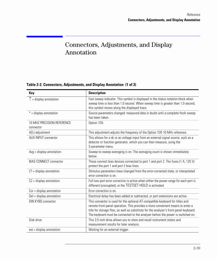
Table 2-2. Connectors, Adjustments, and Display Annotation (1 of 3)
Key Description
↑ = display annotation Fast sweep indicator. This symbol is displayed in the status notation block when sweep time is less than 1.0 second. When sweep time is greater than 1.0 second, this symbol moves along the displayed trace.
* = display annotation Source parameters changed: measured data in doubt until a complete fresh sweep has been taken.
10 MHZ PRECISION REFERENCE connector
Option 1D5
ADJ adjustment This adjustment adjusts the frequency of the Option 1D5 10 MHz reference.AUX INPUT connector This allows for a dc or ac voltage input from an external signal source, such as a
detector or function generator, which you can then measure, using the S-parameter menu.
Avg = display annotation Sweep-to-sweep averaging is on. The averaging count is shown immediately below.
BIAS CONNECT connector These connect bias devices connected to port 1 and port 2. The fuses (1 A, 125 V) protect the port 1 and port 2 bias lines.
C? = display annotation Stimulus parameters have changed from the error-corrected state, or interpolated error correction is on.
C2 = display annotation Full two-port error-correction is active when either the power range for each port is different (uncoupled), or the TESTSET HOLD is activated.
Cor = display annotation Error correction is on. Del = display annotation Electrical delay has been added or subtracted, or port extensions are active. DIN KYBD connector This connector is used for the optional AT-compatible keyboard for titles and
remote front-panel operation. This provides a more convenient means to enter a title for storage files, as well as substitute for the analyzer’s front panel keyboard. The keyboard must be connected to the analyzer before the power is switched on.
Disk drive This 3.5 inch drive allows you to store and recall instrument states and measurement results for later analysis.
ext = display annotation Waiting for an external trigger.
2-39

ReferenceConnectors, Adjustments, and Display Annotation
EXT AM connector This allows for an external analog signal input that is applied to the ALC circuitry of the analyzer’s source. This input analog signal amplitude modulates the RF output signal.
EXT MON connector RED, GREEN, and BLUE video output connectors provide analog red, green, and blue video signals which you can use to drive an external monitor, such as the HP 3571A/B, or monochrome monitor, such as the HP 35731A/B. You can use other analog multi-sync monitors if they are compatible with the analyzer’s 25.5 kHz scan rate and video levels: 1 V p-p, 0.7 V=white, 0 V=black, –0.3 V sync, sync on green.
EXT REF connector This allows for a frequency reference signal input that can phaselock the analyzer to an external frequency standard for increased frequency accuracy.
EXT TRIG connector This allows connection of an external negative-going TTL-compatible signal that will trigger a measurement sweep. The trigger can be set to external through softkey functions.
Gat = display annotation Gating is on. H=2 = display annotation Harmonic mode is on, and the second harmonic is being measured. (Harmonics
Option 002 only.) H=3 = display annotation Harmonic mode is on, and the third harmonic is being measured. (Harmonics
Option 002 only.) Hld = display annotation Hold sweep. HP-IB connector This connector allows communication with compatible devices including external
controllers, printers, plotters, disk drives, and power meters.LIMIT TEST connector Outputs a TTL signal of the limit test results. A TTL high state indicates a ‘pass’
condition. A TTL low state indicates a “fail” condition.LINE key This switch controls ac power to the analyzer. 1 is on, 0 is off. Refer to Table 2-5,
“Power-on Conditions (versus Preset),” on page 2-50, for more information.man = display annotation Waiting for manual trigger. Of? = display annotation Frequency offset mode error, the IF frequency is not within 10 MHz of expected
frequency. LO inaccuracy is the most likely cause. Ofs = display annotation Frequency offset mode is on. P? = display annotation Source power is unleveled at start or stop of sweep. PØ = display annotation Source power has been automatically set to minimum, due to receiver overload. PARALLEL PORT connector This connector is used with parallel (or Centronics interface) peripherals such as
printers and plotters. It can also be used as a general purpose I/O port, with control provided by test sequencing functions.
PC = display annotation Power meter calibration is on. PC? = display annotation The analyzer’s source could not be set to the desired level, following a power
meter calibration.
Table 2-2. Connectors, Adjustments, and Display Annotation (2 of 3)
Key Description
2-40

ReferenceConnectors, Adjustments, and Display Annotation
PORT 1 and PORT 2 connectors These ports output a signal from the source and receive input signals from a device under test. PORT 1 allows you to measure S12 and S11. PORT 2 allows you to measure S21 and S22.
PRESET key This key returns the instrument to either a known factory preset state, or a user preset state that can be defined. Refer to “Preset Conditions” on page 2-42 for more information.
PRm = display annotation Power range is in manual mode. PROBE POWER connector This connector (fused inside the instrument) supplies power to an active probe for
in-circuit measurements of ac circuits.R CHANNEL connectors These connectors allow you to apply an input signal to the analyzer’s R channel, for
frequency offset mode.RS-232 connector This connector allows the analyzer to output to a peripheral with an RS-232 (serial)
input. This includes printers and plotters.Smo = display annotation Trace smoothing is on. TEST SEQ connector This connector outputs a TTL signal which can be programmed by the user in a test
sequence to be high or low. By default, this output provides an end-of-sweep TTL signal. (For use with part handlers).
TEST SET I/O INTERCONNECT connector This allows you to connect an Agilent 8702D Option 011 analyzer to an Agilent 85046A/B or 85047A S-parameter test set using the interconnect cable supplied with the test set. The S-parameter test set is then fully controlled by the analyzer.
tsH = display annotation Indicates that the test set hold mode is engage. That is, a mode of operation is selected which would cause repeated switching of the step attenuator. This hold mode may be overridden.
Table 2-2. Connectors, Adjustments, and Display Annotation (3 of 3)
Key Description
2-41

ReferencePreset Conditions
Preset Conditions
When the PRESET key is pressed, the analyzer reverts to a known state called the factory preset state. This state is defined in Table 2-4 on page 2-44. There are subtle differences between the preset state and the power-up state. These differences are documented in Table 2-5 on page 2-50. If power to battery-protected memory is lost, the analyzer will have certain parameters set to default settings.
When line power is cycled, or the PRESET key pressed, the analyzer performs a self-test routine. Upon successful completion of that routine, the instrument state is set to the conditions shown in Table 2-4 on page 2-44. The same condi-tions are true following a “PRES;” or “RST;” command over GPIB, although the self-test routines are not executed.
You also can configure an instrument state and define it as your user preset state:
a Set the instrument state to your desired preset conditions.
b Save the state (SAVE/RECALL menu).
c Rename that register to “UPRESET”.
d Press PRESET, PRESET: USER.
The PRESET key is now toggled to the USER selection and your defined instru-ment state will be recalled each time you press PRESET and when you turn power on. You can toggle back to the factory preset instrument state by press-ing PRESET and selecting FACTORY.
NOTE
When you send a preset over GPIB, you will always get the factory preset. You can, how-ever, activate the user-defined preset over GPIB by recalling the register in which it is stored.
2-42

ReferencePreset Conditions
Table 2-3. Preset Display Formats
Format ScaleReference
Position Value
Log Magnitude (dB) 10.0 5.0 0.0Phase (degree) 90.0 5.0 0.0Group Delay (ns) 10.0 5.0 0.0Smith Chart 1.00 – 1.0Polar 1.00 – 1.0Linear Magnitude 0.1 0.0 0.0Real 0.2 5.0 0.0Imaginary 0.2 5.0 0.0SWR 1.00 0.0 1.0
2-43

ReferencePreset Conditions
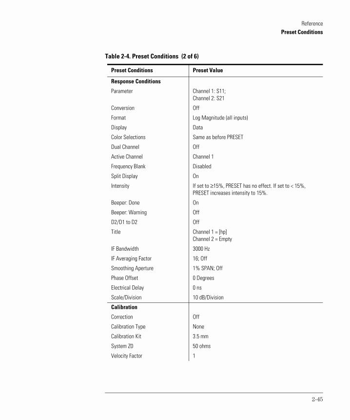
Table 2-4. Preset Conditions (1 of 6)
Preset Conditions Preset Value
Analyzer Mode
Analyzer Mode Component Analyzer Mode
Frequency Offset Off
Operation Offset Value 0
Harmonic Operation Off
Stimulus Conditions
Sweep Type Linear Frequency
Display Mode Start/Stop
Trigger Type Continuous
External Trigger Off
Sweep Time 100 ms, Auto Mode
Start Frequency 300 kHz
Frequency Span (std.) 2999.97 MHz
Frequency Span (Opt. 006) 5999.97 MHz
Start Time 0
Time Span 100 ms
CW Frequency 1000 MHz
Source Power 0 dBm
Power Slope 0 dB/GHz; Off
Start Power –15.0 dBm
Power Span 25 dB
Coupled Power On
Source Power On
Coupled Channels On
Coupled Port Power On
Power Range Auto; Range 0
Number of Points 201
Frequency List
Frequency List Empty
Edit Mode Start/Stop, Number of Points
2-44
ReferencePreset Conditions
Response Conditions
Parameter Channel 1: S11; Channel 2: S21
Conversion Off
Format Log Magnitude (all inputs)
Display Data
Color Selections Same as before PRESET
Dual Channel Off
Active Channel Channel 1
Frequency Blank Disabled
Split Display On
Intensity If set to ≥15%, PRESET has no effect. If set to < 15%, PRESET increases intensity to 15%.
Beeper: Done On
Beeper: Warning Off
D2/D1 to D2 Off
Title Channel 1 = [hp]Channel 2 = Empty
IF Bandwidth 3000 Hz
IF Averaging Factor 16; Off
Smoothing Aperture 1% SPAN; Off
Phase Offset 0 Degrees
Electrical Delay 0 ns
Scale/Division 10 dB/Division
Calibration
Correction Off
Calibration Type None
Calibration Kit 3.5 mm
System Z0 50 ohms
Velocity Factor 1
Table 2-4. Preset Conditions (2 of 6)
Preset Conditions Preset Value
2-45

ReferencePreset Conditions
ExtensionsPort 1Port 2Input AInput B
Off0 s0 s0 s0 s
Chop A and B On
Power Meter CalibrationNumber of ReadingsPower Loss CorrectionSensor A/B
Off1OffA
Interpolated Error Correction Off
Markers (coupled)
Markers 1, 2, 3, 4, 5 1 GHz; All Markers Off
Last Active Marker 1
Reference Marker None
Marker Mode Continuous
Display Markers On
Delta Marker Mode Off
Coupling On
Marker Search Off
Marker Target Value –3 dB
Marker Width Value –3 dB; Off
Marker Tracking Off
Marker Stimulus Offset 0 Hz
Marker Value Offset 0 dB
Marker Aux Offset (Phase) 0 Degrees
Marker Statistics Off
Polar Marker Lin Mkr
Smith Marker R + jX Mkr
Limit Lines
Limit Lines Off
Limit Testing Off
Limit List Empty
Table 2-4. Preset Conditions (3 of 6)
Preset Conditions Preset Value
2-46

ReferencePreset Conditions
Edit Mode Upper/Lower Limits
Stimulus Offset 0 Hz
Amplitude Offset 0 dB
Limit Type Sloping Line
Beep Fail Off
Time Domain
Transform Off
Transform Type Bandpass
Start Transform –20 nanoseconds
Transform Span 40 nanoseconds
Gating Off
Gate Shape Normal
Gate Start –10 nanoseconds
Gate Span 20 nanoseconds
Demodulation Off
Window Normal
Use Memory Off
System Parameters
HP-IB Addresses Last Active State
HP-IB Mode Last Active State
Focus Last Active State
Clock Time Stamp On
Preset: Factory/User Last Selected State
Copy Configuration
Parallel Port Last Active State
Plotter Type Last Active State
Plotter Port Last Active State
Plotter Baud Rate Last Active State
Plotter Handshake Last Active State
HP-IB Address Last Active State
Printer Type Last Active State
Table 2-4. Preset Conditions (4 of 6)
Preset Conditions Preset Value
2-47

ReferencePreset Conditions
Printer Port Last Active State
Printer Baud Rate Last Active State
Printer Handshake Last Active State
Printer HP-IB Address Last Active State
Disk Save Configuration (Define Store)
Data Array Off
Raw Data Array Off
Formatted Data Array Off
Graphics Off
Data Only Off
Directory Size Defaulta
Save Binary Binary
Select Disk Internal Memory
Disk Format LIF
Sequencingb
Loop Counter 0
TTL OUT High
Service Modes
HP-IB Diagnostic Off
Source Phase Lock Loop On
Sampler Correction On
Spur Avoidance On
Aux Input Resolution Low
Analog Bus Mode 11 (Aux Input)
Plot
Plot Data On
Plot Memory On
Plot Graticule On
Plot Text On
Plot Marker On
Table 2-4. Preset Conditions (5 of 6)
Preset Conditions Preset Value
2-48

ReferencePreset Conditions
Autofeed On
Plot Quadrant Full Page
Scale Plot Full
Plot Speed Fast
Pen Number:Ch1 DataCh2 DataCh1 MemoryCh2 MemoryCh1 GraticuleCh2 GraticuleCh1 TextCh2 TextCh1 MarkerCh2 Marker
2356117777
Line Type:Ch1 DataCh2 DataCh1 MemoryCh2 Memory
7777
Printer Mode Last Active State
Auto-Feed On
Printer ColorsCh1 DataCh1 MemCh2 DataCh2 MemGraticuleWarningText
MagentaGreenBlueRedCyanBlackBlack
a. The directory size is calculated as 0.013% of the floppy disk size (which is approximately 256) or 0.005%of the hard disk size.
b. Pressing PRESET turns off sequencing modify (edit) mode and stops any running sequence.
Table 2-4. Preset Conditions (6 of 6)
Preset Conditions Preset Value
2-49

ReferencePower-on Conditions
Power-on Conditions
Table 2-5. Power-on Conditions (versus Preset)
HP-IB MODE Talker/listener.SAVE REGISTERS Power meter calibration data and calibration data not
associated with an instrument state are cleared.COLOR DISPLAY Default color values.INTENSITY Factory stored values. The factory values can be changed by
running the appropriate service routine. Refer to the Agilent 8753D Service Guide.
SEQUENCES Sequence 1 through 5 are erased.DISK DIRECTORY Cleared.
2-50

3
Error Messages in Alphabetical Order 3-3Error Messages in Numerical Order 3-27
Error Messages

Error MessagesError Messages
Error Messages
This chapter contains the information to help you interpret any error mes-sages that may be displayed on the Agilent 8702D or transmitted by the instrument over GPIB.
Some messages described in this chapter are for information only and do not indicate an error condition. These messages are not numbered and so they will not appear in the numerical listing.
3-2

Error MessagesError Messages in Alphabetical Order
Error Messages in Alphabetical Order
ABORTING COPY OUTPUT
Information Message
This message is displayed briefly if you have pressed LOCAL to abort a copy operation. If the message is not subsequently replaced by error message num-ber 25, PRINT ABORTED, the copy device may be hung. Press LOCAL once more to exit the abort process and verify the status of the copy device. At this point, the copy device will probably have an error condition which must be fixed. (For example: out of paper or paper jam.)
ADDITIONAL STANDARDS NEEDED TO COVER SPANError Number 68
Error correction for the selected calibration class cannot be computed until you have measured all the necessary standards to cover the current frequency span.
ADDRESSED TO TALK WITH NOTHING TO SAY
Error Number 31
You have sent a read command to the analyzer (such as ENTER 716) without first requesting data with an appropriate output command (such as OUTP-DATA). The analyzer has no data in the output queue to satisfy the request.
ALL REGISTERS HAVE BEEN USED
Error Number 200
You have used all of the available registers; you can store no more instrument states even though you may still have sufficient memory. There are 31 regis-ters available, plus the present instrument state.
ASCII: MISSING ’BEGIN’ STATEMENT
Error Number 193
The citifile you just downloaded over the GPIB or via disk was not properly organized. The analyzer is unable to read the “BEGIN” statement.
3-3

Error MessagesError Messages in Alphabetical Order
ASCII: MISSING ’CITIFILE’ STATEMENT
Error Number 194
The citifile you just downloaded over the GPIB or via disk was not properly organized. The analyzer is unable to read the “CITIFILE” statement.
ASCII: MISSING ’DATA’ STATEMENT
Error Number 195
The citifile you just downloaded over the GPIB or via disk was not properly organized. The analyzer is unable to read the “DATA” statement.
ASCII: MISSING ’VAR’ STATEMENT
Error Number 196
The citifile you just downloaded over the GPIB or via disk was not properly organized. The analyzer is unable to read the “VAR” statement.
AVERAGING INVALID ON NON-RATIO MEASURE
Error Number 13
You cannot use sweep-to-sweep averaging in single-input measurements. Sweep-sweep averaging is valid only for ratioed measurements (A/R, B/R, A/B, and S-parameters). You can use noise reduction techniques, such as narrower IF bandwidth, for single input measurements.
BAD FREQ FOR HARMONIC OR FREQ OFFSET
Error Number 181
You turned on time domain or recalled a calibration that resulted in start and stop frequencies that are beyond the allowable limits.
BATTERY FAILED. STATE MEMORY CLEARED
Error Number 183
The battery protection of the battery-operated memory has failed. The mem-ory has been cleared. Refer to the Agilent 8753D Service Guide for battery replacement instructions.
BATTERY LOW! STORE SAVE REGS TO DISK
Error Number 184
The battery protection of the memory is in danger of failing. If this occurs, all of the instrument state registers stored in memory will be lost. Save these states to a disk and refer to the Agilent 8702D User’s Guide for battery replacement instructions.
3-4

Error MessagesError Messages in Alphabetical Order
BLOCK INPUT ERROR
Error Number 34
The analyzer did not receive a complete data transmission. This is usually caused by an interruption of the bus transaction. Clear by pressing the LOCAL key or aborting the I/O process at the controller.
BLOCK INPUT LENGTH ERROR
Error Number 35
The length of the header received by the analyzer did not agree with the size of the internal array block. Refer to the Agilent 8702D Programmer’s Guide for instructions on using analyzer input commands.
CALIBRATION ABORTED
Error Number 74
You have changed the active channel during a calibration so the calibration in progress was terminated. Make sure the appropriate channel is active and restart the calibration.
CALIBRATION REQUIRED
Error Number 63
A calibration set could not be found that matched the current stimulus state or measurement parameter. You will have to perform a new calibration.
CANNOT FORMAT DOS DISKS ON THIS DRIVE
Error Number 185
You have attempted to initialize a floppy disk to DOS format on an external disk drive that does not support writing to all 80 tracks of the double density (gray) and high density disks (usually black). The older single-sided disks (blue) had only 66 tracks and some disk drives were limited to accessing that number of tracks. To format the disk, either choose another external disk drive or use the analyzer’s internal disk drive.
CANNOT MODIFY FACTORY PRESET
Error Number 199
You have attempted to rename, delete, or otherwise alter the factory preset state. The factory preset state is permanently stored in memory and cannot be altered. If your intent was to create a user preset state, you must create a new instrument state, save it, and then rename it to “UPRESET”.
3-5

Error MessagesError Messages in Alphabetical Order
CANNOT READ/WRITE HFS FILE SYSTEM
Error Number 203
The disk is being accessed by the analyzer and is found to contain an HFS (hierarchical file system). The analyzer does not support HFS.
CAN’T CHANGE-ANOTHER CONTROLLER ON BUS
Error Number 37
You must remove the active controller from the bus or the controller must relinquish the bus before the analyzer can assume the system controller mode.
CAN’T STORE/LOAD SEQUENCE, INSUFFICIENT MEMORY
Error Number 127
Your sequence transfer to or from a disk could not be completed due to insuf-ficient memory.
CH1 (CH2) TARGET VALUE NOT FOUND
Error Number 159
Your target value for the marker search function does not exist on the current data trace.
CONTINUOUS SWITCHING NOT ALLOWED
Error Number 10
Your current measurement requires the power range to switch between chan-nel 1 and channel 2. To protect the attenuator from undue mechanical wear, it will not be switched continuously. The “tsH” (test set hold) indicator in the left margin of the display indicates that the inactive channel has been put in the sweep hold mode.
COPY: device not responding; copy aborted
Error Number 170
The printer or plotter is not accepting data. Verify the cable connections, GPIB addresses, and otherwise ensure that the copy device is ready.
COPY OUTPUT COMPLETED
Information Message
The analyzer has completed outputting data to the printer or plotter. The ana-lyzer can now accept another copy command.
3-6

Error MessagesError Messages in Alphabetical Order
CORRECTION AND DOMAIN RESET
Error Number 65
When you change the frequency range, sweep type, or number of points, error-correction is switched off and the time domain transform is recalculated, without error-correction. You can either correct the frequency range, sweep type, or number of points to match the calibration, or perform a new calibra-tion. Then perform a new time domain transform.
CORRECTION CONSTANTS NOT STORED
Error Number 3
A store operation to the EEPROM was not successful. You must change the position of the jumper on the A9 CPU assembly.
CORRECTION TURNED OFF
Error Number 66
Critical parameters in your current instrument state do not match the param-eters for the calibration set, therefore correction has been turned off. The crit-ical instrument state parameters are sweep type, start frequency, frequency span, and number of points.
CURRENT PARAMETER NOT IN CAL SET
Error Number 64
Correction is not valid for your selected measurement parameter. Either change the measurement parameters or perform a new calibration.
D2/D1 INVALID WITH SINGLE CHANNEL
Error Number 130
You can only make a D2/D1 measurement if both channels are on.
D2/D1 INVALID. CH1 CH2 NUM PTS DIFFERENT
Error Number 152
You can only make a D2/D1 measurement if both channels have the same num-ber of points.
DEADLOCK
Error Number 111
A fatal firmware error occurred before instrument preset completed. Call your local Agilent Technologies service office.
3-7

Error MessagesError Messages in Alphabetical Order
DEMODULATION NOT VALID
Error Number 17
Demodulation is only valid for the CW time mode.
DEVICE: not on, not connect, wrong addrs
Error Number 119
The device at the selected address cannot be accessed by the analyzer. Verify that the device is switched on, and check the GPIB connection between the analyzer and the device. Ensure that the device address recognized by the analyzer matches the GPIB address set on the device itself.
DIRECTORY FULL
Error Number 188
There is no room left in the directory to add files. Either delete files or get a new disk.
DISK HARDWARE PROBLEM
Error Number 39
The disk drive is not responding correctly. Refer to the disk drive operating manual.
DISK IS WRITE PROTECTED
Error Number 48
The store operation cannot write to a write-protected disk. Slide the write-protect tab over the write-protect opening in order to write data on the disk.
DISK MEDIUM NOT INITIALIZED
Error Number 40
You must initialize the disk before it can be used.
DISK MESSAGE LENGTH ERROR
Error Number 190
The analyzer and the external disk drive aren’t communicating properly. Check the GPIB connection and then try substituting another disk drive to iso-late the problem instrument.
3-8

Error MessagesError Messages in Alphabetical Order
DISK: not on, not connected, wrong addrs
Error Number 38
The disk cannot be accessed by the analyzer. Verify power to the disk drive, and check the GPIB connection between the analyzer and the disk drive. Ensure that the disk drive address recognized by the analyzer matches the GPIB address set on the disk drive itself.
DISK READ/WRITE ERROR
Error Number 189
There may be a problem with your disk. Try a new floppy disk. If a new floppy disk does not eliminate the error, suspect hardware problems.
DISK WEAR - REPLACE DISK SOON
Error Number 49
Cumulative use of the disk is approaching the maximum. Copy files as neces-sary using an external controller. If no controller is available, load instrument states from the old disk and store them to a newly initialized disk using the save/recall features of the analyzer. Discard the old disk.
DOMAIN RESET
Error Number 67
Time domain calculations were reset due to a change in the frequency range, sweep type, or number of points. Perform a new time domain transform on the new state.
DOS NAME LIMITED TO 8 CHARS + 3 CHAR EXTENSION
Error Number 180
A DOS file name must meet the following criteria:
• minimum of 1 character • first character must be alpha; the remainder must be alphanumeric or
underscore • format is filename.ext
• maximum of 8 characters in the filename • maximum of 3 characters in the extension field • a dot separates the filename from the extension field (the dot is not part of
the name on the disk)
3-9

Error MessagesError Messages in Alphabetical Order
DUPLICATING TO THIS SEQUENCE NOT ALLOWED
Error Number 125
A sequence cannot be duplicated to itself.
EXCEEDED 7 STANDARDS PER CLASS
Error Number 72
When modifying calibration kits, you can define a maximum of seven stan-dards for any class.
EXTERNAL SOURCE MODE REQUIRES CW TIME
Error Number 148
An external source can only be phase locked and measured in the CW time sweep mode.
EXT SOURCE NOT READY FOR TRIGGER
Error Number 191
There is a hardware problem with the external source. Verify the connections between the analyzer and the external source. If the connections are correct, refer to the source operating manual.
EXT SRC: NOT ON/CONNECTED OR WRONG ADDR
Error Number 162
The analyzer is unable to communicate with the external source. Check the connections and the GPIB address on the source.
FILE NOT COMPATIBLE WITH INSTRUMENT
Information Message
You cannot recall user graphics that had been saved on an earlier model of analyzer with a monochrome display. These files cannot be used with the Agilent 8702D.
FILE NOT FOUND
Error Number 192
The requested file was not found on the current disk medium.
3-10

Error MessagesError Messages in Alphabetical Order
FILE NOT FOUND OR WRONG TYPE
Error Number 197
During a resave operation, either the file was not found or the type of file was not an instrument state file.
FIRST CHARACTER MUST BE A LETTER
Error Number 42
The first character of a disk file title or an internal save register title must be an alpha character.
FORMAT NOT VALID FOR MEASUREMENT
Error Number 75
Conversion measurements (Z or Y reflection and transmission) are not valid with Smith chart and SWR formats.
FORMATTING DATA
Information Message
The list information is being processed for a list data output to a copy device and stored in the copy spool buffer. During this time, the analyzer’s resources are dedicated to this task (which takes less than a few seconds.)
FREQ OFFSET ONLY VALID IN COMPONENT ANALYZER MODE
Error Number 140
You can only make frequency offset measurements in the component analyzer mode.
FUNCTION NOT VALID
Error Number 14
The function you requested is incompatible with the current instrument state.
FUNCTION NOT VALID DURING MOD SEQUENCE
Error Number 131
You cannot perform sequencing operations while a sequence is being modi-fied.
3-11

Error MessagesError Messages in Alphabetical Order
FUNCTION NOT VALID FOR INTERNAL MEMORY
Error Number 201
The function you selected only works with disk files.
FUNCTION ONLY VALID DURING MOD SEQUENCE
Error Number 164
You can only use the GOSUB SEQUENCE capability when you are building a sequence. Attempting to use this softkey at any other time returns an error message and no action is taken.
HPIB COPY IN PROGRESS, ABORT WITH LOCAL
Error Number 169
A GPIB copy was already in progress when you requested the GPIB for another function. To abort the first copy, press LOCAL, otherwise the GPIB is unavailable until the first copy is completed.
ILLEGAL UNIT OR VOLUME NUMBER
Error Number 46
The disk unit or volume number set in the analyzer is not valid. Refer to the disk drive operating manual.
INIT DISK removes all data from disk
Information Message
Continuing with the initialize operation will destroy any data currently on the disk.
INITIALIZATION FAILED
Error Number 47
The disk initialization failed, probably because the disk is damaged.
INSTRUMENT STATE MEMORY CLEARED
Error Number 56
All instrument state registers have been cleared from memory along with any saved calibration data, memory traces, and calibration kit definitions. Addi-tionally, all user-settable selections, (such as GPIB addresses) are set to their defaults.
3-12

Error MessagesError Messages in Alphabetical Order
INSUFFICIENT MEMORY
Error Number 51
Your last front panel or GPIB request could not be implemented due to insuffi-cient memory space. In some cases, this is a fatal error from which you can escape only by presetting the instrument.
INSUFFICIENT MEMORY FOR PRINT/PLOT
Error Number 168
There is not enough memory available for the print or plot function. Increase the available memory by changing or eliminating a memory-intensive opera-tion such as reducing the number of points in the sweep.
INSUFFICIENT MEMORY, PWR MTR CAL OFF
Error Number 154
There is not enough memory space for the power meter calibration array. Increase the available memory by clearing one or more save/recall registers, or by reducing the number of points.
INVALID CAL DATA FILEError Number 142
The calibration file you are attempting to read does not contain valid data.
INVALID KEY
Error Number 2
You pressed an undefined softkey.
LIST MODE OFF: INVALID WITH LO FREQ
Error Number 182
List mode has been turned off in the frequency offset mode because it is incompatible with your selected LO frequency.
LIST TABLE EMPTY
Error Number 9
The frequency list is empty. To implement list frequency mode, add segments to the list table.
3-13

Error MessagesError Messages in Alphabetical Order
LOAD RECEIVER CAL DATA FROM DISK FILEError Number 134
You are attempting to measure a receiver cal standard that has not been defined. Define by loading cal data from the appropriate file.
LOAD SOURCE CAL DATA FROM DISK FILEError Number 135
You are attempting to measure a source cal standard that has not been defined. Define by loading cal data from the appropriate file.
LOG SWEEP REQUIRES 2 OCTAVE MINIMUM SPAN
Error Number 150
A logarithmic sweep is only valid if the stop frequency is greater than four times the start frequency. For frequency spans of less than two octaves, the sweep type automatically reverts to linear sweep.
LOW PASS: FREQ LIMITS CHANGED
Information Message
The frequency domain data points must be harmonically related from dc to the stop frequency. That is, stop = n × start, where n = number of points. If this condition is not true when a low pass mode (step or impulse) is selected and transform is turned on, the analyzer resets the start and stop frequencies. The stop frequency is set close to the entered stop frequency, and the start frequency is set equal to stop/n.
MEMORY FOR CURRENT SEQUENCE IS FULL
Error Number 132
All the memory in the sequence you are modifying is filled with instrument commands.
MORE SLIDES NEEDED
Error Number 71
When you use a sliding load (in a user-defined calibration kit), you must set at least three slide positions to complete the calibration.
NO CALIBRATION CURRENTLY IN PROGRESS
Error Number 69
The RESUME CAL SEQUENCE softkey is not valid unless a calibration is already in progress. Start a new calibration.
3-14

Error MessagesError Messages in Alphabetical Order
NO DISK MEDIUM IN DRIVE
Error Number 41
You have no disk in the current disk unit. Insert a disk, or check the disk unit number stored in the analyzer.
NO FAIL FOUND
Service Error Number 114
The self-diagnose function of the instrument operates on an internal test fail-ure. At this time, no failure has been detected.
NO FILE(S) FOUND ON DISK
Error Number 45
No files of the type created by an analyzer store operation were found on the disk. If you requested a specific file title, that file was not found on the disk.
NO IF FOUND: CHECK R INPUT LEVEL
Error Number 5
The first IF signal was not detected during pre-tune. Check the front panel R channel jumper. If there is no visible problem with the jumper, refer to the Agilent 8753D Service Guide for troubleshooting.
NO LIMIT LINES DISPLAYED
Error Number 144
You can turn limit lines on but they cannot be displayed on polar or Smith chart display formats.
NO MARKER DELTA -SPAN NOT SET
Error Number 15
You must turn the delta marker mode on, with at least two markers displayed, in order to use the MARKER → SPAN softkey function.
NO MEMORY AVAILABLE FOR INTERPOLATION
Error Number 123
You cannot perform interpolated error correction due to insufficient memory.
NO MEMORY AVAILABLE FOR SEQUENCING
Error Number 126
You cannot modify the sequence due to insufficient memory.
3-15

Error MessagesError Messages in Alphabetical Order
NO PHASE LOCK: CHECK R INPUT LEVEL
Error Number 7
The first IF signal was detected at pre-tune, but phase lock could not be acquired. Refer to the Agilent 8753D Service Guide for troubleshooting.
NO SPACE FOR NEW CAL. CLEAR REGISTERS
Error Number 70
You cannot store a calibration set due to insufficient memory. You can free more memory by clearing a saved instrument state from an internal register (which may also delete an associated calibration set, if all the instrument states using the calibration kit have been deleted.) You can store the saved instrument state and calibration set to a disk before clearing them. After delet-ing the instrument states, press PRESET to run the memory packer.
NOT ALLOWED DURING POWER METER CAL
Error Number 198
When the analyzer is performing a power meter calibration, the GPIB bus is unavailable for other functions such as printing or plotting.
NOT ENOUGH SPACE ON DISK FOR STORE
Error Number 44
The store operation will overflow the available disk space. Insert a new disk or purge files to create free disk space.
NOT VALID FOR CURRENT PARAMETERError Number 143
You are attempting a response and match calibration on a parameter other than E/O or O/E.
NO VALID MEMORY TRACE
Error Number 54
If you are going to display or otherwise use a memory trace, you must first store a data trace to memory.
NO VALID STATE IN REGISTER
Error Number 55
You have requested the analyzer, over GPIB (or by sequencing), to load an instrument state from an empty internal register.
3-16
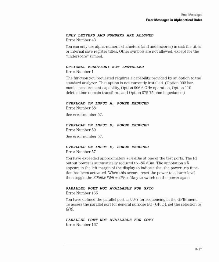
Error MessagesError Messages in Alphabetical Order
ONLY LETTERS AND NUMBERS ARE ALLOWED
Error Number 43
You can only use alpha-numeric characters (and underscores) in disk file titles or internal save register titles. Other symbols are not allowed, except for the “underscore” symbol.
OPTIONAL FUNCTION; NOT INSTALLED
Error Number 1
The function you requested requires a capability provided by an option to the standard analyzer. That option is not currently installed. (Option 002 har-monic measurement capability, Option 006 6 GHz operation, Option 110 deletes time domain transform, and Option 075 75 ohm impedance.)
OVERLOAD ON INPUT A, POWER REDUCED
Error Number 58
See error number 57.
OVERLOAD ON INPUT B, POWER REDUCED
Error Number 59
See error number 57.
OVERLOAD ON INPUT R, POWER REDUCED
Error Number 57
You have exceeded approximately +14 dBm at one of the test ports. The RF output power is automatically reduced to –85 dBm. The annotation P⇓ appears in the left margin of the display to indicate that the power trip func-tion has been activated. When this occurs, reset the power to a lower level, then toggle the SOURCE PWR on OFF softkey to switch on the power again.
PARALLEL PORT NOT AVAILABLE FOR GPIO
Error Number 165
You have defined the parallel port as COPY for sequencing in the GPIB menu. To access the parallel port for general purpose I/O (GPIO), set the selection to GPIO.
PARALLEL PORT NOT AVAILABLE FOR COPY
Error Number 167
3-17

Error MessagesError Messages in Alphabetical Order
You have defined the parallel port as general purpose I/O (GPIO) for sequenc-ing. The definition was made under the LOCAL key menus. To access the paral-lel port for copy, set the selection to PARALLEL [COPY].
PHASE LOCK CAL FAILED
Error Number 4
An internal phase lock calibration routine is automatically executed at power-on, preset, and any time a loss of phase lock is detected. This message indi-cates that phase lock calibration was initiated and the first IF detected, but a problem prevented the calibration from completing successfully. Refer to the Agilent 8753D Service Guide and execute pre-tune correction test 48.
This message may appear if you connect a mixer between the RF output and R input before turning on frequency offset mode. Ignore it: it will go away when you turn on frequency offset. This message may also appear if you turn on fre-quency offset mode before you define the offset.
PHASE LOCK LOST
Error Number 8
Phase lock was acquired but then lost. Refer to the Agilent 8753D Service
Guide for troubleshooting information.
PLOT ABORTED
Error Number 27
When you press the LOCAL key, the analyzer aborts the plot in progress.
PLOTTER: not on, not connect, wrong addrs
Error Number 26
The plotter does not respond to control. Verify power to the plotter, and check the GPIB connection between the analyzer and the plotter. Ensure that the plotter address recognized by the analyzer matches the GPIB address set on the plotter itself.
PLOTTER NOT READY-PINCH WHEELS UP
Error Number 28
The plotter pinch wheels clamp the paper in place. If you raise the pinch wheels, the plotter indicates a “not ready” status on the bus.
3-18

Error MessagesError Messages in Alphabetical Order
POSSIBLE FALSE LOCK
Error Number 6
Phase lock has been achieved, but the source may be phase locked to the wrong harmonic of the synthesizer. Perform the source pre-tune correction routine documented in the “Adjustments and Correction Constants” chapter in the Agilent 8753D Service Guide.
POWER UNLEVELEDError Number 179
There is either a hardware failure in the source or you have attempted to set the power level too high. Check to see if the power level you set is within spec-ifications. If it is, refer to the Agilent 8753D Service Guide for troubleshoot-ing. You will only receive this message over the GPIB. On the analyzer, P? is displayed.
POW MET INVALID
Error Number 116
The power meter indicates an out-of-range condition. Check the test setup.
POW MET NOT SETTLED
Error Number 118
Sequential power meter readings are not consistent. Verify that the equipment is set up correctly. If so, preset the instrument and restart the operation.
POW MET: not on, not connected, wrong addrs
Error Number 117
The power meter cannot be accessed by the analyzer. Verify that the power meter address and model number set in the analyzer match the address and model number of the actual power meter.
POWER SUPPLY HOT!
Error Number 21
The temperature sensors on the A8 post-regulator assembly have detected an over-temperature condition. The power supplies regulated on the post-regula-tor have been shut down.
POWER SUPPLY SHUT DOWN!
Error Number 22
3-19

Error MessagesError Messages in Alphabetical Order
One or more supplies on the A8 post-regulator assembly have been shut down due to an over-current, over-voltage, or under-voltage condition.
PRESS [MENU], SELECT CW (IF) FREQ, THEN SWEPT LO
Error Number 161
When you are sweeping the RF and LO, the IF must be fixed.
PRINT ABORTED
Error Number 25
When you press the LOCAL key, the analyzer aborts output to the printer.
print color not supported with EPSON
Error Number 178
You have defined the printer type as EPSON-P2. Color print is not supported with this printer. The print will abort.
PRINTER: busy
Error Number 176
The parallel port printer is not accepting data.
PRINTER: error
Error Number 175
The parallel port printer is malfunctioning. The analyzer cannot complete the copy function.
PRINTER: not connected
Error Number 173
There is no printer connected to the parallel port.
PRINTER: not handshaking
Error Number 177
The printer at the parallel port is not responding.
PRINTER: not on line
Error Number 172
The printer at the parallel port is not set on line.
3-20

Error MessagesError Messages in Alphabetical Order
PRINTER: not on, not connected, wrong addrs
Error Number 24
The printer does not respond to control. Verify power to the printer, and check the GPIB connection between the analyzer and the printer. Ensure that the printer address recognized by the analyzer matches the GPIB address set on the printer itself.
PRINTER: paper error
Error Number 171
There is a paper-related problem with the parallel port printer such as a paper jam or out-of-paper condition.
PRINTER: power off
Error Number 174
The power to the printer at the parallel port is off.
PRINT/PLOT IN PROGRESS, ABORT WITH LOCAL
Error Number 166
If a print or plot is in progress and you attempt a second print or plot, this message is displayed and the second attempt is ignored. To abort a print or plot in progress, press LOCAL.
PROBE POWER SHUT DOWN!
Error Number 23
The analyzer biasing supplies to the Agilent 85024A external probe are shut down due to excessive current. Troubleshoot the probe, and refer to the power supply troubleshooting section of the Agilent 8753D Service Guide.
PROCESSING DISPLAY LIST
Information Message
The display information is being processed for a screen print to a copy device and stored in the copy spool buffer. During this time, the analyzer’s resources are dedicated to this task (which takes less than a few seconds.)
REQUESTED DATA NOT CURRENTLY AVAILABLE
Error Number 30
The analyzer does not currently contain the data you have requested. For example, this condition occurs when you request error term arrays and no cal-ibration is active.
3-21

Error MessagesError Messages in Alphabetical Order
SAVE FAILED. INSUFFICIENT MEMORY
Error Number 151
You cannot store an instrument state in an internal register due to insufficient memory. Increase the available memory by clearing one or more save/recall registers and pressing PRESET, or by storing files to a disk.
SELECTED SEQUENCE IS EMPTY
Error Number 124
The sequence you attempted to run does not contain instrument commands.
SELF TEST #n FAILED
Service Error Number 112
Internal test #n has failed. Several internal test routines are executed at instrument preset. The analyzer reports the first failure detected. Refer to the Agilent 8753D Service Guide for troubleshooting information on internal tests and the self-diagnose feature.
SEQUENCE ABORTED
Error Number 157
The sequence running was stopped prematurely when you pressed the LOCAL key.
SEQUENCE MAY HAVE CHANGED, CAN’T CONTINUE
Error Number 153
When you pause a sequence, you cannot continue it if you have modified it. You must start the sequence again.
SLIDES ABORTED (MEMORY REALLOCATION)
Error Number 73
You cannot perform sliding load measurements due to insufficient memory. Reduce memory usage by clearing save/recall registers, then repeat the sliding load measurements.
SOURCE PARAMETERS CHANGED
Error Number 61
Some of the stimulus parameters of the instrument state have been changed, because you have turned correction on. A calibration set for the current mea-surement parameter was found and activated. The instrument state was updated to match the stimulus parameters of the calibration state.
3-22

Error MessagesError Messages in Alphabetical Order
This message also appears when you have turned on harmonic mode or fre-quency offset and the present frequency range cannot be used with one of these modes.
SOURCE POWER TRIPPED, RESET UNDER POWER MENU
Information Message
You have exceeded the maximum power level at one of the inputs and power has been automatically reduced. The annotation P⇓ indicates that power trip has been activated. When this occurs, reset the power and then press MENU, POWER, SOURCE PWR on OFF, to switch on the power. This message follows error numbers 57, 58, and 59.
STARTING COPY SPOOLER
Information Message
The analyzer is beginning to output data from the spool buffer to the copy device. The analyzer resumes normal operation; the data is being output to the copy device in the background.
STOP/CW FREQ + OFFSET MUST BE < 3 GHz
Error Number 141
The output frequency of the mixer cannot violate the minimum/maximum fre-quency of the analyzer.
SWEEP MODE CHANGED TO CW TIME SWEEP
Error Number 187
If you select external source auto or manual instrument mode and you do not also select CW mode, the analyzer is automatically switched to CW.
SWEEP TIME INCREASED
Error Number 11
You have made instrument changes that cause the analyzer sweep time to be automatically increased. Some parameter changes that cause an increase in sweep time are narrower IF bandwidth, an increase in the number of points, and a change in sweep type.
SWEEP TIME TOO FAST
Error Number 12
The fractional-N and digital IF circuits have lost synchronization. Refer to the Agilent 8753D Service Guide for troubleshooting information.
3-23

Error MessagesError Messages in Alphabetical Order
SWEEP TRIGGER SET TO HOLD
Information Message
The instrument is in a hold state and is no longer sweeping.
SWEEP TYPE CHANGED TO LINEAR SWEEP
Error Number 145
If you have the frequency list mode active when you change the instrument mode to harmonic measurements, and the list frequencies do not fall in the allowable frequency range of these modes, the list mode automatically is turned off.
SYNTAX ERROR
Error Number 33
You have improperly formatted a GPIB command. Refer to the Agilent 8702D
Programmer’s Guide for proper command syntax.
SYST CTRL OR PASS CTRL IN LOCAL MENU
Error Number 36
The analyzer is in talker/listener mode. In this mode, the analyzer cannot con-trol a peripheral device on the bus. Use the local menu to change to system controller or pass control mode.
TEST ABORTED
Error Number 113
You have prematurely stopped a service test.
THIS LIST FREQ INVALID IN HARM/3 GHZ RNG
Error Number 133
You have set frequencies in the list that are outside of the allowable frequency range for harmonic measurements, or are greater than 3 GHz on instruments without Option 006. Reduce the frequency range of the list.
TOO MANY NESTED SEQUENCES. SEQ ABORTED
Error Number 164
You can only nest sequences to a maximum level of six. The sequence will abort if you nest more than six.
3-24

Error MessagesError Messages in Alphabetical Order
TOO MANY SEGMENTS OR POINTS
Error Number 50
You can have a maximum of 30 segments or 1632 points in frequency list mode. In power meter calibrations, you can have a maximum of 12 segments for power sensor cal factors and power loss functions.
TRANSFORM, GATE NOT ALLOWED
Error Number 16
You can perform a time domain transformation only in linear and CW sweep types.
TROUBLE! CHECK SETUP AND START OVER
Service Error Number 115
Your equipment setup for the adjustment procedure in progress is not correct. Check the setup diagram and instructions in the Agilent 8753D Service
Guide. Start the procedure again.
WAITING FOR CLEAN SWEEP
Information Message
In single sweep mode, the instrument ensures that all changes to the instru-ment state, if any, have been implemented before taking the sweep. The com-mand that you have initiated is being processed and will not be complete until the new sweep is completed. An asterisk * is displayed in the left margin of the CRT until a complete fresh sweep has been taken.
WAITING FOR DISK
Information Message
This message is displayed between the start and finish of a read or write oper-ation to a disk.
WAITING FOR HP-IB CONTROL
Information Message
You have instructed the analyzer to use pass control (USEPASC). When you send the analyzer an instruction that requires active controller mode, the ana-lyzer requests control of the bus and simultaneously displays this message. If the message remains, the system controller is not relinquishing the bus.
3-25

Error MessagesError Messages in Alphabetical Order
WRITE ATTEMPTED WITHOUT SELECTING INPUT TYPE
Error Number 32
You have sent the data header “#A” to the analyzer with no preceding input command (such as INPUDATA). The instrument recognized the header but did not know what type of data to receive. Refer to the Agilent 8702D Pro-
grammer’s Guide for command syntax information.
WRONG DISK FORMAT, INITIALIZE DISK
Error Number 77
You have attempted to store, load, or read file titles, but your disk format does not conform to the Logical Interchange Format (LIF). You must initialize the disk before reading or writing to it.
3-26

Error MessagesError Messages in Numerical Order
Error Messages in Numerical Order
Table 3-1. Numerical Listing of Error Messages (1 of 7)
Error Number Error
1 OPTIONAL FUNCTION; NOT INSTALLED
2 INVALID KEY
3 CORRECTION CONSTANTS NOT STORED
4 PHASE LOCK CAL FAILED
5 NO IF FOUND: CHECK R INPUT LEVEL
6 POSSIBLE FALSE LOCK
7 NO PHASE LOCK: CHECK R INPUT LEVEL
8 PHASE LOCK LOST
9 LIST TABLE EMPTY
10 CONTINUOUS SWITCHING NOT ALLOWED
11 SWEEP TIME INCREASED
12 SWEEP TIME TOO FAST
13 AVERAGING INVALID ON NON-RATIO MEASURE
14 FUNCTION NOT VALID
15 NO MARKER DELTA - SPAN NOT SET
16 TRANSFORM, GATE NOT ALLOWED
17 DEMODULATION NOT VALID
18 not used
3-27

Error MessagesError Messages in Numerical Order
19 LIST TABLE EMPTY: occurs if user selects LIST sweep type but there is no list frequency table
20 AIR FLOW RESTRICTED: CHECK FAN FILTER
21 POWER SUPPLY HOT!
22 POWER SUPPLY SHUT DOWN!
23 PROBE POWER SHUT DOWN!
24 PRINTER: not on, not connect, wrong addrs
25 PRINT ABORTED
26 PLOTTER: not on, not connect, wrong addrs
27 PLOT ABORTED
28 PLOTTER NOT READY-PINCH WHEELS UP
30 REQUESTED DATA NOT CURRENTLY AVAILABLE
31 ADDRESSED TO TALK WITH NOTHING TO SAY
32 WRITE ATTEMPTED WITHOUT SELECTING INPUT TYPE
33 SYNTAX ERROR
34 BLOCK INPUT ERROR
35 BLOCK INPUT LENGTH ERROR
36 SYST CTRL OR PASS CTRL IN LOCAL MENU
37 CAN’T CHANGE-ANOTHER CONTROLLER ON BUS
38 DISK: not on, not connected, wrong addrs
39 DISK HARDWARE PROBLEM
40 DISK MEDIUM NOT INITIALIZED
41 NO DISK MEDIUM IN DRIVE
42 FIRST CHARACTER MUST BE A LETTER
43 ONLY LETTERS AND NUMBERS ARE ALLOWED
Table 3-1. Numerical Listing of Error Messages (2 of 7)
Error Number Error
3-28

Error MessagesError Messages in Numerical Order
44 NOT ENOUGH SPACE ON DISK FOR STORE
45 NO FILE(S) FOUND ON DISK
46 ILLEGAL UNIT OR VOLUME NUMBER
47 INITIALIZATION FAILED
48 DISK IS WRITE PROTECTED
49 DISK WEAR-REPLACE DISK SOON
50 TOO MANY SEGMENTS OR POINTS
51 INSUFFICIENT MEMORY
52 not used
54 NO VALID MEMORY TRACE
55 NO VALID STATE IN REGISTER
56 INSTRUMENT STATE MEMORY CLEARED
57 OVERLOAD ON INPUT R, POWER REDUCED
58 OVERLOAD ON INPUT A, POWER REDUCED
59 OVERLOAD ON INPUT B, POWER REDUCED
61 SOURCE PARAMETERS CHANGED
63 CALIBRATION REQUIRED
64 CURRENT PARAMETER NOT IN CAL SET
65 CORRECTION AND DOMAIN RESET
66 CORRECTION TURNED OFF
67 DOMAIN RESET
68 ADDITIONAL STANDARDS NEEDED TO COVER SPAN
69 NO CALIBRATION CURRENTLY IN PROGRESS
70 NO SPACE FOR NEW CAL CLEAR REGISTERS
Table 3-1. Numerical Listing of Error Messages (3 of 7)
Error Number Error
3-29

Error MessagesError Messages in Numerical Order
71 MORE SLIDES NEEDED
72 EXCEEDED 7 STANDARDS PER CLASS
73 SLIDES ABORTED (MEMORY REALLOCATION)
74 CALIBRATION ABORTED
75 FORMAT NOT VALID FOR MEASUREMENT
77 WRONG DISK FORMAT, INITIALIZE DISK
111 DEADLOCK
112 SELF TEST #n FAILED
113 TEST ABORTED
114 NO FAIL FOUND
115 TROUBLE! CHECK SETUP AND START OVER
116 POW MET INVALID
117 POW MET: not on, not connected, wrong addrs
118 POW MET NOT SETTLED
119 DEVICE: not on, not connect, wrong addrs
123 NO MEMORY AVAILABLE FOR INTERPOLATION
124 SELECTED SEQUENCE IS EMPTY
125 DUPLICATING TO THIS SEQUENCE NOT ALLOWED
126 NO MEMORY AVAILABLE FOR SEQUENCING
127 CAN’T STORE/LOAD SEQUENCE, INSUFFICIENT MEMORY
130 D2/D1 INVALID WITH SINGLE CHANNEL
131 FUNCTION NOT VALID DURING MOD SEQUENCE
132 MEMORY FOR CURRENT SEQUENCE IS FULL
133 THIS LIST FREQ INVALID IN HARM/3 GHZ RNG
Table 3-1. Numerical Listing of Error Messages (4 of 7)
Error Number Error
3-30

Error MessagesError Messages in Numerical Order
134 LOAD RECEIVER CAL DATA FROM DISK FILE
135 LOAD SOURCE CAL DATA FROM DISK FILE
140 FREQ OFFSET ONLY VALID IN COMPONENT ANALYZER MODE
141 STOP/CW FREQ + OFFSET MUST BE <3 GHz
142 INVALID CAL DATA FILE
143 NOT VALID FOR CURRENT PARAMETER
144 NO LIMIT LINES DISPLAYED
145 SWEEP TYPE CHANGED TO LINEAR SWEEP
148 EXTERNAL SOURCE MODE REQUIRES CW TIME
150 LOG SWEEP REQUIRES 2 OCTAVE MINIMUM SPAN
151 SAVE FAILED INSUFFICIENT MEMORY
152 D2/D1 INVALID CH1 CH2 NUM PTS DIFFERENT
153 SEQUENCE MAY HAVE CHANGED, CAN’T CONTINUE
154 INSUFFICIENT MEMORY, PWR MTR CAL OFF
157 SEQUENCE ABORTED
159 CH1 (CH2) TARGET VALUE NOT FOUND
161 PRESS [MENU], SELECT CW (IF) FREQ, THEN SWEPT LO
162 EXT SRC: NOT ON/CONNECTED OR WRONG ADDR
163 FUNCTION ONLY VALID DURING MOD SEQUENCE
164 TOO MANY NESTED SEQUENCES
165 PARALLEL PORT NOT AVAILABLE FOR GPIO
166 PRINT/PLOT IN PROGRESS, ABORT WITH LOCAL
167 PARALLEL PORT NOT AVAILABLE FOR COPY
168 INSUFFICIENT MEMORY FOR PRINT/PLOT
Table 3-1. Numerical Listing of Error Messages (5 of 7)
Error Number Error
3-31

Error MessagesError Messages in Numerical Order
169 HPIB COPY IN PROGRESS, ABORT WITH LOCAL
170 COPY:device not responding; copy aborted
171 PRINTER: paper error
172 PRINTER: not on line
173 PRINTER: not connected
174 PRINTER: power off
175 PRINTER: error
176 PRINTER: busy
177 PRINTER: not handshaking
178 print color not supported with EPSON
179 POWER UNLEVELED
180 DOS NAME LIMITED TO 8 CHARS + 3 CHAR EXTENSION
181 BAD FREQ FOR HARMONIC OR FREQ OFFSET
182 LIST MODE OFF: INVALID WITH LO FREQ
183 BATTERY FAILED. STATE MEMORY CLEARED
184 BATTERY LOW! STORE SAVE REGS TO DISK
185 CANNOT FORMAT DOS DISKS ON THIS DRIVE
187 SWEEP MODE CHANGED TO CW TIME SWEEP
188 DIRECTORY FULL
189 DISK READ/WRITE ERROR
190 DISK MESSAGE LENGTH ERROR
191 EXT SOURCE NOT READY FOR TRIGGER
192 FILE NOT FOUND
193 ASCII: MISSING ’BEGIN’ statement
Table 3-1. Numerical Listing of Error Messages (6 of 7)
Error Number Error
3-32

Error MessagesError Messages in Numerical Order
194 ASCII: MISSING ’CITIFILE’ statement
195 ASCII: MISSING ’DATA’ statement
196 ASCII: MISSING ’VAR’ statement
197 FILE NOT FOUND OR WRONG TYPE
198 NOT ALLOWED DURING POWER METER CAL
199 CANNOT MODIFY FACTORY PRESET
200 ALL REGISTERS HAVE BEEN USED
201 FUNCTION NOT VALID FOR INTERNAL MEMORY
Table 3-1. Numerical Listing of Error Messages (7 of 7)
Error Number Error
3-33

4Instrument Specifications 4-3Instrument Specifications (Option 011) 4-10Instrument General Characteristics 4-18Environmental Characteristics 4-22System E/E Characteristics 4-24
Agilent 8702D (50Ω) with 7 mm Test Ports 4-24Agilent 8702D (50Ω) with Type-N Test Ports 4-28Agilent 8702D (50Ω) with 3.5 mm Test Ports 4-31Agilent 8702D (75Ω) with Type-N Test Ports 4-34Agilent 8702D (75Ω) with Type-F Test Ports 4-38
Agilent 8702D (75Ω) using Agilent 85039A F-F Test Ports 4-41Agilent 8702D (75Ω) using Agilent 85039A M-M Test Ports 4-44Agilent 8702D (75Ω) using Agilent 85039A M-F Test Ports 4-47
System O/E Characteristics 4-533 GHz and 6 GHz 50Ω System Configuration 4-543 GHz and 6 GHz 50Ω System Configuration for Agilent 8702D Option 011 and Agilent 11889A RF Interface Kit 4-593 GHz and 6 GHz 75Ω System Configuration 4-65
System E/O Characteristics 4-673 GHz and 6 GHz 50Ω System Configuration 4-683 GHz and 6 GHz 50Ω System Configuration for Agilent 8702D Option 011 and Agilent 11889A RF Interface Kit 4-733 GHz and 6 GHz 75Ω System Configuration 4-79
System O/O Characteristics 4-813 GHz and 6 GHz 50Ω System Configuration 4-823 GHz and 6 GHz 50Ω System Configuration for Agilent 8702D Option 011 and Agilent 11889A RF Interface Kit 4-86
Lightwave Receiver Measurement Repeatability 4-91GPIB Interface 4-93Regulatory Information 4-94
Specifications and Regulatory Information

Specifications and Regulatory InformationSpecifications and Regulatory Information
Specifications and Regulatory Information
This chapter lists specification and characteristics of the instrument. The dis-tinction between these terms is described as follows:
• Specifications describe warranted performance over the temperature range 0°C to +55°C and relative humidity <95% (unless otherwise noted). All speci-fications apply after the instrument’s temperature has been stabilized after one hour of continuous operation.
• Characteristics provide useful information by giving functional, but nonwar-ranted, performance parameters. Characteristics are printed in italics.
Calibration Cycle
This instrument requires periodic verification of performance. The instrument should have a complete verification of specifications at least once every two years.
4-2

Specifications and Regulatory InformationInstrument Specifications
Instrument Specifications
The specifications, listed in Table 4-1 on page 4-4, range from those guaran-teed by Agilent Technologies, to those typical of most Agilent 8702D instru-ments, but not guaranteed.
Codes in the far right column of the table reference a specification definition, listed below. These definitions are intended to clarify the extent to which Agi-lent Technologies supports the specified performance of the Agilent 8702D.
S-1 This performance parameter is verifiable using performance tests documented in the service manual.
S-2 Due to limitations on available industry standards, the guaranteed performance of the instrument cannot be verified outside the factory. Field procedures can verify performance with a confidence prescribed by available standards.
S-3 These specifications are generally digital functions or are mathematically derived from tested specifications, and can therefore be verified by functional pass/fail testing.
T Typical, but non-warranted, performance characteristics intended to provide information useful in applying the instrument. Typical characteristics are representative of most instruments, though not necessarily tested in each unit. Not field tested.
4-3

Specifications and Regulatory InformationInstrument Specifications
Table 4-1. Agilent 8702D Instrument Specifications and Characteristics (1 of 6)
Description Specification or Characteristic Code
TEST PORT OUTPUTSFrequency CharacteristicsRange
StandardOption 006
30 kHz to 3 GHz30 kHz to 6 GHz
S-1S-1
Accuracy (at 25°C ±5°C) ±10 ppm
Stability
0° to 55°Cper year
±7.5 ppm±3 ppm
TT
Resolution 1 Hz S-3Output Power CharacteristicsRange –85 to +10 dBm S-1Resolution 0.05 dB S-3Level Accuracy (at 0 dBm output level)(at 25°C ±5°C)a
±1.0 dB S-1b
Linearity (at 25°C ±5°C)a
–15 to +5 dBm+5 to +10 dBm
±0.2 dB (relative to 0 dBm output level)±0.5 dB (relative to 0 dBm output level)
S-1S-1
Impedance 50 ohms >16 dB return loss to 3 GHz>14 dB return loss to 6 GHz
TT
Spectral Purity Characteristics2nd Harmonic (16 MHz to 3 GHz)
at +10 dBm output levelat 0 dBm output levelat –10 dBm output level
<–25 dBc<–40 dBc<–50 dBc
S-1b
TT
3rd Harmonic (16 MHz to 2 GHz)at +10 dBm output levelat 0 dBm output levelat –10 dBm output level
<–25 dBc<–40 dBc<–50 dBc
S-1b
TT
Non-Harmonic Spurious Signals Mixer Relatedat +10 dBm output levelat –10 dBm output level
<–30 dBc<–55 dBc
TT
TEST PORT INPUTSCharacteristicsFrequency Range
StandardOption 006
30 kHz to 3 GHz30 kHz to 6 GHz
S-1S-1
4-4

Specifications and Regulatory InformationInstrument Specifications
Impedance 50 ohms nominal30 kHz to 50 kHz50 kHz to 300 kHz300 kHz to 1.3 GHz1.3 GHz to 3 GHz3 GHz to 6 GHz
≥10 dB return loss≥18 dB return loss≥18 dB return loss≥16 dB return loss≥14 dB return loss
TTS-1S-1S-1
Maximum Input Level +10 dBm S-1Damage Level +26 dBm or >35 Vdc TAverage Noise Level
50 kHz to 3 GHz3 kHz IF bandwidth10 Hz IF bandwidth
–82 dBm–102 dBm–110 dBm
S-1b
S-1b
T
3 GHz to 6 GHz3 kHz IF bandwidth10 Hz IF bandwidth
–77 dBm–97 dBm–105 dBm
S-1b
S-1b
T
Frequency Response (25 ±5°C)300 kHz to 3 GHz3 GHz to 6 GHz
±1 dB±2 dB
S-1b
S-1b
Internally Generated Harmonics (Option 002)2nd Harmonic
at +8 dBm input levelat +0 dBm input levelat –15 dBm input level
<–15 dBc<–30 dBc <–45 dBc
S-1b
TT
3rd Harmonicat +8 dBm input levelat +0 dBm input levelat –15 dBm input level
<–30 dBc<–50 dBc<–50 dBc
S-1b
TT
Harmonic Measurement Accuracy (25 ±5°C)16 MHz to 3 GHz3 GHz to 6 GHzc
±1 dB±3 dB
S-1S-1
Harmonic Measurement Dynamic Range(with output at –10 dBm and input at <–15 dBm)
–40 dBc T
R CHANNEL INPUT
Frequency Offset Operationd,e
Frequency Rangec 300 kHz to 6 GHz S-1
R Channel Input Requirements 0 to –35 dBm, to 3 GHz S-1
Table 4-1. Agilent 8702D Instrument Specifications and Characteristics (2 of 6)
Description Specification or Characteristic Code
4-5

Specifications and Regulatory InformationInstrument Specifications
(required for phase-locked operation) 0 to –30 dBm, 3 GHz to 6 GHz S-1LO Spectral Purity and Accuracy
Maximum Spurious InputResidual FMFrequency Accuracy
<–25 dBc<20 kHz–1 to +1 MHz of nominal frequency
TTT
Accuracy (see Magnitude Characteristics and Phase Characteristics)
External Source Modee,f (CW Time sweep only)
Frequency Rangec 300 kHz to 6 GHz S-1
R Input RequirementsPower LevelSpectral Purity
Maximum Spurious InputResidual FM
0 to –25 dBm
<–30 dBc<20 kHz
T
TT
Setting TimeAutoManual
500 ms50 ms
TT
Frequency Readout Accuracy (auto) 0.1% TInput Frequency Margin
ManualAuto
≤50 MHz>50 MHz
–0.5 to 5 MHz
±5 MHz of nominal CW frequency±10% of nominal CW frequency
T
TT
Accuracy (see Magnitude Characteristics and Phase Characteristics)f
INPUT GENERALMagnitude CharacteristicsDisplay Resolution 0.01 dB/division S-3
Markerg Resolution 0.001 dB S-3
Dynamic Rangeh
30 kHz to 300 kHz30 kHz to 50 kHz300 kHz to 16 MHz300 kHz to 1.3 GHz1.3 GHz to 3 GHz3 GHz to 6 GHz
100 dB90 dB100 dB (std), 105 dB (option 075)110 dB (std), 105 dB (option 075)110 dB (std), 105 dB (option 075)105 dB
TTS-1S-1S-1S-1
Dynamic Accuracy (10 Hz BW, inputs Test Port 1 and Test Port 2; R to –35 dBm) (see graph)
S-1
Table 4-1. Agilent 8702D Instrument Specifications and Characteristics (3 of 6)
Description Specification or Characteristic Code
4-6

Specifications and Regulatory InformationInstrument Specifications
Dynamic Accuracy (Magnitude)
Trace Noisei
30 kHz to 3 GHz3 GHz to 6 GHz
<0.006 dB rms<0.010 dB rms
S-1S-1
Reference LevelRangeResolution
±500 dB0.001 dB
S-3S-3
Stability30 kHz to 3 GHz3 GHz to 6 GHz
0.02 dB/°C0.04 dB/°C
TT
Phase CharacteristicsRange ±180° S-3
Display Resolution 0.01°/division S-3
Marker Resolutiong 0.01° S-3
Dynamic Accuracy (10 Hz BW, inputs Test Port 1 and Test Port 2; R to –35 dBm) (see graph)
S-1
Table 4-1. Agilent 8702D Instrument Specifications and Characteristics (4 of 6)
Description Specification or Characteristic Code
4-7

Specifications and Regulatory InformationInstrument Specifications
Dynamic Accuracy (Phase)
Trace Noise (+5 dBm into Test Port, ratio measurement)30 kHz to 3 GHz3 GHz to 6 GHz
<0.038° rms<0.070° rms
S-1S-1
Reference LevelRangeResolution
±500°0.01°
S-3S-3
Stability30 kHz to 3 GHz3 GHz to 6 GHz
0.05°/degree C0.20°/degree C
TT
Polar Characteristics (Ratio Measurement)Range 10 x 10–12 up to 1000 units full scale S-3
Reference range of ±500 units S-3Group Delay CharacteristicsGroup delay is computed by measuring the phase change within a specified frequency step (determined by the frequency span and the number of points per sweep).Aperture (selectable) (frequency span)/(number of points – 1) S-3Maximum Aperture 20% of frequency span S-3Range 1/2 x (1/minimum aperture) S-3
(The maximum delay is limited to measuring no more than 180° of phase change within the minimum aperture.)Accuracy (see graph) S-3
Table 4-1. Agilent 8702D Instrument Specifications and Characteristics (5 of 6)
Description Specification or Characteristic Code
4-8

Specifications and Regulatory InformationInstrument Specifications
The following graph shows group delay accuracy with 7 mm full 2-port calibration and a 10 Hz IF bandwidth. Insertion loss is assumed to be <2 dB and electrical length to be ten meters.
Group Delay Accuracy vs. Aperture
In general, the following formula can be used to determine the accuracy, in seconds, of specific group delay measurement:
±[0.003 x Phase Accuracy (deg)]/Aperture (Hz)
Depending on the aperture and device length, the phase accuracy used is either incremental phase accuracy or worst case phase accuracy.
a. Typical 30 kHz to 300 kHz and typical from 2 to 3 GHz for Option 075.b. Explicitly tested as part of an on-site verification performed by Agilent Technologies.c. Operation from 3 GHz to 6 GHz requires Option 006.d. The Agilent 8702D RF source characteristics in this mode are dependent on the stability of the external LO source. The RF source tracks
the LO to maintain a stable IF signal at the R channel receiver input. Degradation in accuracy is negligible with an Agilent 8642A/B orAgilent 8656B RF signal generator as the LO source.
e. Refer to the Agilent 8702D descriptions and options in this manual for a functional description.f. Measurement accuracy is dependent on the stability of the input signal.g. Marker resolution for magnitude, phase, and delay is dependent upon the value measured; resolution is limited to 5 digits.h. The specifications described apply to transmission measurements using 10 Hz IF BW and full 2-port correction. Dynamic range is limited
by the maximum test port power and the receiver’s noise floor.i. CW sweep, +5 dBm into Test Port, ratio measurement, 3 kHz BW.
Table 4-1. Agilent 8702D Instrument Specifications and Characteristics (6 of 6)
Description Specification or Characteristic Code
4-9

Specifications and Regulatory InformationInstrument Specifications (Option 011)
Instrument Specifications (Option 011)
The specifications, listed in Table 4-2 on page 4-11, range from those guaran-teed by Agilent Technologies, to those typical of most Agilent 8702D Option 011 instruments, but not guaranteed.
Codes in the far right column of the table reference a specification definition, listed below. These definitions are intended to clarify the extent to which Agi-lent Technologies supports the specified performance of the Agilent 8702D Option 011.
S-1 This performance parameter is verifiable using performance tests documented in the service manual.
S-2 Due to limitations on available industry standards, the guaranteed performance of the instrument cannot be verified outside the factory. Field procedures can verify performance with a confidence prescribed by available standards.
S-3 These specifications are generally digital functions or are mathematically derived from tested specifications, and can therefore be verified by functional pass/fail testing.
T Typical, but non-warranted, performance characteristics intended to provide information useful in applying the instrument. Typical characteristics are representative of most instruments, though not necessarily tested in each unit. Not field tested.
4-10

Specifications and Regulatory InformationInstrument Specifications (Option 011)
Table 4-2. Agilent 8702D Option 011 Specifications and Characteristics (1 of 7)
Description Specification or Characteristic Code
SOURCEFrequency CharacteristicsRange
Without Option 006With Option 006
300 kHz to 3 GHz30 kHz to 6 GHz
S-1a
S-1a
Accuracy (at 25°C ±5°C) ±10 ppm
Stability
0° to 55°Cper year
±7.5 ppm±3 ppm
TT
Resolution 1 Hz S-3Output Power CharacteristicsRange
Without Option 006With Option 006
–5 to +20 dBm–5 to +18 dBm
S-1a
S-1a
Resolution 0.05 dB S-3Level Accuracy (at +10 dBm output level)(at 25°C ±5°C)b
±1.0 dB S-1a
Linearity (at 25°C ±5°C)b
–5 to +15 dBmc
+15 to +20 dBmd
±0.25 dB (relative to +10 dBm output level)±0.5 dB (relative to +10 dBm output level)
S-1S-1
Impedance 50 ohms nominalSpectral Purity Characteristics(with 0 to –10 dBm into R input)2nd Harmonic (16 MHz to 3 GHz)
at +20 dBm output levelat +10 dBm output levelat 0 dBm output level
<–25 dBc<–40 dBc<–50 dBc
S-1a
TT
3rd Harmonic (16 MHz to 2 GHz)at +20 dBm output levelat +10 dBm output levelat 0 dBm output level
<–25 dBc<–40 dBc<–50 dBc
S-1a
TT
Non-Harmonic Spurious Signals Mixer Relatedat +20 dBm output levelat 0 dBm output level
<–30 dBc<–55 dBc
TT
Phase Noise(10 kHz offset from fundamental in 1 Hz bandwidth)
4-11

Specifications and Regulatory InformationInstrument Specifications (Option 011)
f<135 MHzf≥135 MHz
–90 dBc[–90 + 20log(f/135 MHz)]dBc
S-1S-1
RECEIVERCharacteristicsFrequency Range
Without Option 006With Option 006
300 kHz to 3 GHz30 kHz to 6 GHz
S-1a
S-1a
Impedance 50 ohms nominal30 kHz to 50 kHz50 kHz to 2 MHz2 MHz to 1.3 GHz1.3 GHz to 3 GHz3 GHz to 6 GHz
≥10 dB return loss≥18 dB return loss≥23 dB return loss≥20 dB return loss≥8 dB return loss
TTS-1S-1T
Dynamic Range (10 Hz IF bandwidth)A, B
30 kHz to 50 kHz50 kHz to 300 kHz300 kHz to 3 GHze
3 GHz to 6 GHz
90 dB100 dB110 dB105 dB
TTS-1S-1
R30 kHz to 300 kHz300 kHz to 3 GHz3 GHz to 6 GHz
30 dB35 dB30 dB
TS-1S-1
Maximum Input Level 0 dBm S-1Damage Level +20 dBm or >25 Vdc TAverage Noise Level
50 kHz to 3 GHz3 kHz IF bandwidth10 Hz IF bandwidth
–90 dBm–110 dBm–120 dBm
S-1S-1T
3 GHz to 6 GHz3 kHz IF bandwidth10 Hz IF bandwidth
–85 dBm–105 dBm–115 dBm
S-1S-1T
Minimum R Level(required for source operation)
300 kHz to 3 GHz3 GHz to 6 GHz
–35 dBm–30 dBm
S-1S-1
Input Crosstalk (10 Hz IF bandwidth)
Table 4-2. Agilent 8702D Option 011 Specifications and Characteristics (2 of 7)
Description Specification or Characteristic Code
4-12

Specifications and Regulatory InformationInstrument Specifications (Option 011)
300 kHz to 1 GHz1 GHz to 3 GHz3 GHz to 4.5 GHz4.5 GHz to 6 GHz
–100 dB–90 dB–82 dB–75 dB
S-1S-1S-1S-1
Internally Generated Harmonics (Option 002)2nd Harmonic
at 0 dBm input levelat –10 dBm input levelat –30 dBm input level
<–15 dBc<–35 dBc <–45 dBc
S-1a
TT
3rd Harmonicat 0 dBm input levelat –10 dBm input levelat –30 dBm input level
<–30 dBc<–50 dBc<–50 dBc
S-1a
TT
Harmonic Measurement Accuracy (25 ±5°C)16 MHz to 3 GHz3 GHz to 6 GHz
±1 dB±3 dB
S-1S-1
Harmonic Measurement Dynamic Range(with output at 0 dBm and receiver at <–30 dBm) –40 dBc T
R CHANNEL INPUT
Frequency Offset Operationf g
Frequency Range 300 kHz to 6 GHz S-1R Channel Input Requirements 0 to –35 dBm, to 3 GHz S-1(required for phase-locked operation) 0 to –30 dBm, 3 GHz to 6 GHz S-1LO Spectral Purity and Accuracy
Maximum Spurious InputResidual FMFrequency Accuracy
<–25 dBc<20 kHz–1 to +1 MHz of nominal frequency
TTT
Accuracy (see Magnitude Characteristics and Phase Characteristics)
External Source Mode f,h (CW Time sweep only)Frequency Range 300 kHz to 6 GHz S-1R Input Requirements
Power LevelSpectral Purity
Maximum Spurious InputResidual FM
0 to –25 dBm
<–30 dBc<20 kHz
S-1
TT
Setting Time
Table 4-2. Agilent 8702D Option 011 Specifications and Characteristics (3 of 7)
Description Specification or Characteristic Code
4-13

Specifications and Regulatory InformationInstrument Specifications (Option 011)
AutoManual
500 ms50 ms
TT
Frequency Readout Accuracy (auto) 0.1% TInput Frequency Margin
ManualAuto
≤50 MHz>50 MHz
–0.5 to 5 MHz
±5 MHz of nominal CW frequency±10% of nominal CW frequency
T
TT
Accuracy (see Magnitude Characteristics and Phase Characteristics)h
RECEIVER GENERALMagnitude CharacteristicsDisplay Resolution 0.001 dB/division S-3
Markeri Resolution 0.001 dB S-3
Dynamic Accuracy (10 Hz BW, inputs A, B; R to –35 dBm) (see graph) S-1Dynamic Accuracy (Magnitude)
Frequency Response (25 ±5°C, A, B, R, –10 dBm input)300 kHz to 3 GHz3 GHz to 6 GHz
±1 dB±2 dB
S-1S-1
Table 4-2. Agilent 8702D Option 011 Specifications and Characteristics (4 of 7)
Description Specification or Characteristic Code
4-14

Specifications and Regulatory InformationInstrument Specifications (Option 011)
Ratio Accuracy (A/R, B/R, A/B)(25°C ±5°C, with –10 dBm on all inputs)
300 kHz to 3 GHz3 GHz to 6 GHz
±0.5 dB±2.0 dB
TT
Trace Noisej
30 kHz to 3 GHz3 GHz to 6 GHz
<0.006 dB rms<0.010 dB rms
S-1S-1
Reference LevelRangeResolution
±500 dB0.001 dB
S-3S-3
Stability30 kHz to 3 GHz3 GHz to 6 GHz
0.02 dB/°C0.04 dB/°C
TT
Phase Characteristics(A/R, B/R, A/B)Range ±180° S-3
Display Resolution 0.01°/division S-3
Marker Resolutioni 0.01° S-3
Dynamic Accuracy (10 Hz BW, inputs A/R, B/R, A/B; R to –35 dBm) (see graph) S-1
Table 4-2. Agilent 8702D Option 011 Specifications and Characteristics (5 of 7)
Description Specification or Characteristic Code
4-15

Specifications and Regulatory InformationInstrument Specifications (Option 011)
Dynamic Accuracy (Phase)
Frequency Response (deviation from linear)(with –10 dBm into inputs, 25°C ±5°C)
300 kHz to 3 GHz3 GHz to 6 GHz
±3°±10°
S-1S-1
Trace Noisej
30 kHz to 3 GHz3 GHz to 6 GHz
<0.038° rms<0.070° rms
S-1S-1
Reference LevelRangeResolution
±500°0.01°
S-3S-3
Stability30 kHz to 3 GHz3 GHz to 6 GHz
0.05°/degree C0.20°/degree C
TT
Polar Characteristics (Ratio Measurement)Range 10 x 10–12 up to 1000 units full scale S-3
Reference range of ±500 units S-3Group Delay Characteristics
Table 4-2. Agilent 8702D Option 011 Specifications and Characteristics (6 of 7)
Description Specification or Characteristic Code
4-16

Specifications and Regulatory InformationInstrument Specifications (Option 011)
Group delay is computed by measuring the phase change within a specified frequency step (determined by the frequency span and the number of points per sweep).Aperture (selectable) (frequency span)/(number of points – 1) S-3Maximum Aperture 20% of frequency span S-3Range 1/2 x (1/minimum aperture) S-3
(The maximum delay is limited to measuring no more than 180° of phase change within the minimum aperture.)Accuracy (see graph) S-3The following graph shows group delay accuracy with an Agilent 85047A test set with 7 mm full 2-port calibration and a 10 Hz IF bandwidth. Insertion loss is assumed to be <2 dB and electrical length to be ten meters.
Group Delay Accuracy vs. Aperture
In general, the following formula can be used to determine the accuracy, in seconds, of specific group delay measurement:
±[0.003 x Phase Accuracy (deg)]/Aperture (Hz)
Depending on the aperture and device length, the phase accuracy used is either incremental phase accuracy or worst case phase accuracy.
a. Explicitly tested as part of an on-site verification performed by Agilent Technologies.b. Typical 30 kHz to 300 kHz.c. –5 to +13 dBm for Option 006.d. +13 to +18 dBm for Option 006.e. 100 dB, 300 kHz to 16 MHz, due to fixed spurs.f. The Agilent 8702D Option 011 RF source characteristics in this mode are dependent on the stability of the external LO source. The RF
source tracks the LO to maintain a stable IF signal at the R channel receiver input. Degradation in accuracy is negligible with anAgilent 8642A/B or Agilent 8568B RF signal generator as the LO source.
g. Refer to the Agilent 8702D Option 011 descriptions and options for a functional description.h. Measurement accuracy is dependent on the stability of the input signal.i. Marker resolution for magnitude, phase, and delay is dependent upon the value measured; resolution is limited to 5 digits.j. CW sweep, –10 dBm into receiver, ratio measurement, 3 kHz BW.
Table 4-2. Agilent 8702D Option 011 Specifications and Characteristics (7 of 7)
Description Specification or Characteristic Code
4-17

Specifications and Regulatory InformationInstrument General Characteristics
Instrument General Characteristics
Table 4-3. Typical Measurement Times
Typical Time for Completion (ms)
Number of Points
51 201 401 1601
Measurement
Uncorrected
1-port cala
2-port calb
125
125
245
200
200
510
300
300
855
900
900
2940
Time Domain Conversionc 80 350 740 1790
GPIB Data Transferd
Binary (Internal)
IEEE754 floating point format
32 bit
64 bit
ASCII
20
25
40
140
35
85
115
510
55
150
220
1000
205
590
840
3960
a. S11 1-port calibration, with a 3 kHz IF bandwidth. Includes system retrace time, but does not include bandswitch time. Time domain gatingis assumed off.
b. S21
measurement with full 2-port calibration, using a 3 kHz IF bandwidth. Includes system retrace time and RF switching time, but does notinclude bandswitch time. Time domain gating is assumed off.
c. Option 110 only, gating on.d. Measured with HP 9000 series 300 computer.
4-18

Specifications and Regulatory InformationInstrument General Characteristics
Table 4-4. Connector Characteristics (1 of 3)
Connector Characteristic
AUX INPUT Connector
Input Voltage Limits –10 V to +10 V
BIAS CONNECT Connector
Maximum Voltage +30 Vdc
Maximum Current (no degradation in RF specifications)
±200 mA
Maximum Current ±1 A
EXT AM Connector
±1 volt into a 5 kΩ resistor, 1 kHz maximum, resulting in approximately 8 dB/volt amplitude modulation.
EXT MON Connector
The R, G, and B connectors drive external monitors with these characteristics:
Color model R, G, B with synch on green
Impedance 75 ohm
Voltage 1 V p-p (0.7 V = white; 0 V = black; –0.3 V = synch)
EXT REF INPUT Connector
Frequency 1, 2, 5, and 10 MHz (±200 Hz at 10 MHz)
Level –10 dBm to +20 dBm, typical
Impedance 50 ohms
LIMIT TEST Connector
This connector outputs a TTL signal of the limit test results. Pass: TTL high; Fail: TTL low.
Logic TTL
PORT 1 and PORT 2 Connectors
Connector Type 7 mm precision
Impedance 50 ohm (nominal)
4-19

Specifications and Regulatory InformationInstrument General Characteristics
Connector Conductor Depth 0.000 to 0.003 in.
A, B, R, RF OUT Connectors (Option 011)
Connector Type Type-N, female
Impedance 50 Ω (nominal)
Connector Center Pin Protrusion 0.201 to 0.207 in.
Probe Power Connectors
+15 V ±2% 400 mA (combined load for both probe connections).
–12.6 V ±5.5% 300 mA (combined load for both probe connections).
TEST SEQ Connector
This connector outputs a TTL signal which can be programmed by the user in a test sequence to be high or low. By default, this output provides an end-of-sweep TTL signal. (For use with part handlers.)
Logic TTL
DIN Keyboard
This connector is used for the optional AT-compatible keyboard for titles and remote front-panel operation.
GPIB
This connector allows communication with compatible devices including external controllers, printers, plotters, disk drives, and power meters.
Option 1D5 10 MHz Frequency Reference
Frequency 10.0000 MHz
Frequency Stability (0°C to 55°C) ±0.05 ppm
Daily Aging Rate (after 30 days) ≤3 X 10⁻⁹/day
Yearly Aging Rate 0.5 ppm/year
Output 0 dBm minimum
Nominal Output Impedance 50 Ω
Table 4-4. Connector Characteristics (2 of 3)
Connector Characteristic
4-20

Specifications and Regulatory InformationInstrument General Characteristics
Parallel Port
This connector is used with parallel (or Centronics interface) peripherals, such as printers and plotters. It can also be used as a general purpose I/O port, with control provided by test sequencing functions.
RS-232
This connector is used with serial peripherals, such as printers and plotters.
EXT TRIG Connector
Triggers on a negative TTL transition or contact closure to ground.
External Trigger Circuit
Table 4-5. Internal Memory Data Retention Time with 3 V, 1.2 Ah Battery
Temperature Retention Time
70°C 250 days (0.68 year)
40°C 1244 days (3.4 years)
25°C 11904 days (32.6 years) typical
Table 4-4. Connector Characteristics (3 of 3)
Connector Characteristic
4-21

Specifications and Regulatory InformationEnvironmental Characteristics
Environmental Characteristics
Table 4-6. Operating Characteristics
Use IndoorPower 280 VA maximumVoltage nominal: 115 VAC / 230 VAC
range 115 VAC: 90–132 Vrange 230 VAC: 198–264 V
Frequency nominal: 50 Hz / 60 Hzrange: 48-66 Hz
Operating ConditionsOperating temperature:Error-correction temperature range:Humidity:Altitude:
0° to 55°C±1°C of calibration temperature5% to 95% at 40°C (non-condensing)0 to 4500 meters (15,000 feet)
Non-Operating Storage ConditionsTemperature range:Humidity:Altitude:
–40°C to +70°C0 to 90% relative at +65°C (non-condensing)0 to 15,240 meters (50,000 feet)
Weight Net: 34 kg (75 lb)Shipping: 37 kg (82 lb)
Dimensions (H x W x D) 222 x 425 x 508 mm (8.75 x 16.75 x 20.0 in)These dimensions exclude front and rear panel protrusions.
4-22

Specifications and Regulatory InformationEnvironmental Characteristics
Dimensions of the instrument
4-23

Specifications and Regulatory InformationSystem E/E Characteristics
System E/E Characteristics
The characteristics listed in this section apply to Agilent 8702D instruments with specific options, calibration kits, and cables.
Agilent 8702D (50Ω) with 7 mm Test Ports
The system hardware includes the following:
Options: . . . . . . . . . . . . . . . . . . . . . . . . . . . . . . . . . . . . . . . . . . . . . . . . . . . . 006 Calibration kit: . . . . . . . . . . . . . . . . . . . . . . . . . . . . . . . . . . . . . .Agilent 85031B Cables: . . . . . . . . . . . . . . . . . . . . . . . . . . . . . . . . . . . . . . . . . . . .Agilent 11857D
MEASUREMENT PORT CHARACTERISTICS (CORRECTED)a
for Agilent 8702D (50Ω) with 7 mm Test Ports
Frequency Range
30 kHz to300 kHzb
300 kHz to1.3 GHz
1.3 GHz to3 GHz
3 GHz to6 GHz
Directivity 55 dB 55 dB 51 dB 46 dB
Source Match 55 dB 51 dB 49 dB 43 dB
Load Match 55 dB 55 dB 51 dB 46 dB
Reflection Tracking ±0.001 dB ±0.001 dB ±0.005 dB ±0.020 dB
Transmission Tracking ±0.008 dB ±0.006 dB ±0.009 dB ±0.021 dB
a. These characteristics apply for an environmental temperature of 25 ±5°C, with less than 1°C deviationfrom the calibration temperature.
b. Typical Performance
4-24

Specifications and Regulatory InformationSystem E/E Characteristics
MEASUREMENT PORT CHARACTERISTICS (UNCORRECTED)a
for Agilent 8702D (50Ω) with 7 mm Test Ports
Frequency Range
30 kHz to300 kHzb
300 kHz to1.3 GHz
1.3 GHz to3 GHz
3 GHz to6 GHz
Directivity 20 dBc 35 dB 30 dB 25 dB
Source Match 18 dBd 16 dB 16 dB 14 dB
Load Match 20 dBd 18 dB 16 dB 14 dB
Reflection Tracking ±2.0 dB ±1.5 dB ±1.5 dB ±2.5 dB
Transmission Tracking ±2.0 dB ±1.5 dB ±1.5 dB ±2.5 dB
Crosstalk 90 dB 100 dB 100 dB 90 dB
a. Applies at 25 ±5°Cb. Typical Performancec. 10 dB, 30 kHz to 50 kHzd. 15 dB, 30 kHz to 50 kHz
4-25

Specifications and Regulatory InformationSystem E/E Characteristics
Transmission Measurement Uncertainties
4-26

Specifications and Regulatory InformationSystem E/E Characteristics
Reflection Measurement Uncertainties
4-27

Specifications and Regulatory InformationSystem E/E Characteristics
Agilent 8702D (50Ω) with Type-N Test Ports
The system hardware includes the following:
Options: . . . . . . . . . . . . . . . . . . . . . . . . . . . . . . . . . . . . . . . . . . . . . . . . . . . . 006 Calibration kit: . . . . . . . . . . . . . . . . . . . . . . . . . . . . . . . . . . . . Agilent 85032B/ECables: . . . . . . . . . . . . . . . . . . . . . . . . . . . . . . . . . . . . . . . . . . . .Agilent 11851B
MEASUREMENT PORT CHARACTERISTICS (CORRECTED)a
for Agilent 8702D (50Ω) with Type-N Test Ports
Frequency Range
30 kHz to300 kHzb
300 kHz to1.3 GHz
1.3 GHz to3 GHz
3 GHz to6 GHz
Directivity 50 dB 50 dB 47 dB 40 dB
Source Match 49 dB 42 dB 36 dB 31 dB
Load Match 50 dB 50 dB 47 dB 40 dB
Reflection Tracking ±0.005 dB ±0.009 dB ±0.019 dB ±0.070 dB
Transmission Tracking ±0.014 dB ±0.013 dB ±0.026 dB ±0.065 dB
a. Applies at 25 ±5°C b. Typical Performance
4-28

Specifications and Regulatory InformationSystem E/E Characteristics
Transmission Measurement Uncertainties
4-29

Specifications and Regulatory InformationSystem E/E Characteristics
Reflection Measurement Uncertainties
4-30

Specifications and Regulatory InformationSystem E/E Characteristics
Agilent 8702D (50Ω) with 3.5 mm Test Ports
The system hardware includes the following:
Options: . . . . . . . . . . . . . . . . . . . . . . . . . . . . . . . . . . . . . . . . . . . . . . . . . . . . . 006 Calibration kit: . . . . . . . . . . . . . . . . . . . . . . . . . . . . . . . . . . . . . Agilent 85033DCables: . . . . . . . . . . . . . . . . . . . . . . . . . . . . . . . . . . . . . . . . . . . . Agilent 11857D
MEASUREMENT PORT CHARACTERISTICS (CORRECTED)a
for Agilent 8702D (50Ω) with 3.5 mm Test Ports
Frequency Range
30 kHz to300 kHzb
300 kHz to1.3 GHz
1.3 GHz to3 GHz
3 GHz to6 GHz
Directivity 49 dB 46 dB 44 dB 38 dB
Source Match 49 dB 44 dB 41 dB 37 dB
Load Match 49 dB 46 dB 44 dB 38 dB
Reflection Tracking ±0.010 dB ±0.005 dB ±0.007 dB ±0.009 dB
Transmission Tracking ±0.016 dB ±0.014 dB ±0.022 dB ±0.048 dB
a. Applies at 25 ±5°C b. Typical Performance
4-31

Specifications and Regulatory InformationSystem E/E Characteristics
Transmission Measurement Uncertainties
4-32

Specifications and Regulatory InformationSystem E/E Characteristics
Reflection Measurement Uncertainties
4-33

Specifications and Regulatory InformationSystem E/E Characteristics
Agilent 8702D (75Ω) with Type-N Test Ports
The system hardware includes the following:
Options: . . . . . . . . . . . . . . . . . . . . . . . . . . . . . . . . . . . . . . . . . . . . . . . . . . . . 075 Calibration kit: . . . . . . . . . . . . . . . . . . . . . . . . . . . . . . . . . . . . . .Agilent 85036B Cables: . . . . . . . . . . . . . . . . . . . . . . . . . . . . . . . . . . . . . . . . . . . .Agilent 11857B
MEASUREMENT PORT CHARACTERISTICS (CORRECTED)a
for Agilent 8702D (75Ω) with Type-N Test Ports
Frequency Range
30 kHz to300 kHzb
300 kHz to1.3 GHz
1.3 GHz to3 GHz
Directivity 48 dB 48 dB 43 dB
Source Match 47 dB 41 dB 35 dB
Load Match 48 dB 48 dB 43 dB
Reflection Tracking ±0.004 dB ±0.010 dB ±0.019 dB
Transmission Tracking ±0.018 dB ±0.015 dB ±0.033 dB
a. Applies at 25 ±5°Cb. Typical Performance
4-34

Specifications and Regulatory InformationSystem E/E Characteristics
MEASUREMENT PORT CHARACTERISTICS (UNCORRECTED)a
for Agilent 8702D (75Ω) with Type-N Test Ports
Frequency Range
30 kHz to300 kHzb
300 kHz to1.3 GHz
1.3 GHz to3 GHz
Directivity 34 dB 35 dB 30 dB
Source Match 10 dB 16 dB 16 dB
Load Match 14 dB 18 dB 16 dB
Reflection Tracking ±2.0 dB ±1.5 dB ±1.5 dB
Transmission Tracking ±2.0 dB ±1.5 dB ±1.5 dB
Crosstalk 100 dB 100 dB 100 dB
a. Applies at 25 ±5°Cb. Typical Performance
4-35

Specifications and Regulatory InformationSystem E/E Characteristics
Transmission Measurement Uncertainties
4-36

Specifications and Regulatory InformationSystem E/E Characteristics
Reflection Measurement Uncertainties
4-37

Specifications and Regulatory InformationSystem E/E Characteristics
Agilent 8702D (75Ω) with Type-F Test Ports
The system hardware includes the following:
Options: . . . . . . . . . . . . . . . . . . . . . . . . . . . . . . . . . . . . . . . . . . . . . . . . . . . . 075 Calibration kit: . . . . . . . . . . . . . . . . . . . . . . . . . . . . . . . . . . . . . .Agilent 85039ACables: . . . . . . . . . . . . . . . . . . . . . . . . . . . . . . . . . . . . . . . . . . . .Agilent 11857B
MEASUREMENT PORT CHARACTERISTICS (CORRECTED)a
for Agilent 8702D (75Ω) with Type-F Test Ports
Frequency Range
30 kHz to300 kHzb
300 kHz to1.3 GHz
1.3 GHz to3 GHz
Directivity 38 dB 38 dB 32 dB
Source Match 36 dB 36 dB 30 dB
Load Match 38 dB 38 dB 32 dB
Reflection Tracking ±0.0080 dB ±0.0080 dB ±0.0320 dB
Transmission Tracking ±0.0618 dB ±0.0346 dB ±0.0778 dB
a. Applies at 25 ±5°C b. Typical Performance
4-38

Specifications and Regulatory InformationSystem E/E Characteristics
Transmission Measurement Uncertainties
4-39

Specifications and Regulatory InformationSystem E/E Characteristics
Reflection Measurement Uncertainties
4-40

Specifications and Regulatory InformationSystem E/E Characteristics
Agilent 8702D (75Ω) using Agilent 85039A F-F Test Ports
MEASUREMENT PORT CHARACTERISTICS (CORRECTED)a
for Agilent 8702D (75Ω) using Agilent 85039A F-F Test Ports
a. Applies at 25 ±5°C
Frequency Range
30 kHz to300 kHzb
b. Typical Performance
300 kHz to1.3 GHz
1.3 GHz to3 GHz
Directivity 38 dB 38 dB 32 dB
Source Match 36 dB 36 dB 30 dB
Load Match 29.8 dB 29.8 dB 26 dB
Reflection Tracking ±0.0080 dB ±0.0080 dB ±0.0320 dB
Transmission Tracking ±0.1161 dB ±0.0619 dB ±0.1118 dB
4-41

Specifications and Regulatory InformationSystem E/E Characteristics
Transmission Measurement Uncertainties
4-42

Specifications and Regulatory InformationSystem E/E Characteristics
Reflection Measurement Uncertainties
4-43

Specifications and Regulatory InformationSystem E/E Characteristics
Agilent 8702D (75Ω) using Agilent 85039A M-M Test Ports
MEASUREMENT PORT CHARACTERISTICS (CORRECTED)a
for Agilent 8702D (75Ω) using Agilent 85039A M-M Test Ports
a. Applies at 25 ±5°C
Frequency Range
30 kHz to300 kHzb
b. Typical Performance
300 kHz to1.3 GHz
1.3 GHz to3 GHz
Directivity 29.8 dB 29.8 dB 26 dB
Source Match 29 dB 29 dB 25 dB
Load Match 38 dB 38 dB 32 dB
Reflection Tracking ±0.0425 dB ±0.0354 dB ±0.0728 dB
Transmission Tracking ±0.0961 dB ±0.0563 dB ±0.1106 dB
4-44

Specifications and Regulatory InformationSystem E/E Characteristics
Transmission Measurement Uncertainties
4-45
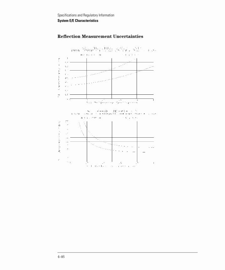
Specifications and Regulatory InformationSystem E/E Characteristics
Reflection Measurement Uncertainties
4-46

Specifications and Regulatory InformationSystem E/E Characteristics
Agilent 8702D (75Ω) using Agilent 85039A M-F Test Ports
MEASUREMENT PORT CHARACTERISTICS (CORRECTED)a
for Agilent 8702D (75Ω) using Agilent 85039A M-F Test Ports
a. Applies at 25 ±5°C
Frequency Range
30 kHz to300 kHzb
b. Typical Performance
300 kHz to1.3 GHz
1.3 GHz to3 GHz
Directivity 29.8 dB 29.8 dB 26 dB
Source Match 29 dB 29 dB 25 dB
Load Match 29.8 dB 29.8 dB 26 dB
Reflection Tracking ±0.0425 dB ±0.0354 dB ±0.0728 dB
Transmission Tracking ±0.1502 dB ±0.0836 dB ±0.1445 dB
4-47

Specifications and Regulatory InformationSystem E/E Characteristics
Transmission Measurement Uncertainties
4-48

Specifications and Regulatory InformationSystem E/E Characteristics
Reflection Measurement Uncertainties
4-49

Specifications and Regulatory InformationSystem Characteristics
System Characteristics
What you’ll find in this section
System O/E Characteristics 4-533 GHz and 6 GHz 50Ω System Configuration 4-543 GHz and 6 GHz 50Ω System Configuration for Agilent 8702D Option 011 and Agilent 11889A RF Interface Kit 4-593 GHz and 6 GHz 75Ω System Configuration 4-65
System E/O Characteristics 4-673 GHz and 6 GHz 50Ω System Configuration 4-683 GHz and 6 GHz 50Ω System Configuration for Agilent 8702D Option 011 and Agilent 11889A RF Interface Kit 4-733 GHz and 6 GHz 75Ω System Configuration 4-79
System O/O Characteristics 4-813 GHz and 6 GHz 50Ω System Configuration 4-823 GHz and 6 GHz 50Ω System Configuration for Agilent 8702D Option 011 and Agilent 11889A RF Interface Kit 4-86
Lightwave Receiver Measurement Repeatability 4-91
Typical System Performance (measurement uncertainty)
These are a set of curves, or plots, that describe the measurement accuracy characteristics of the lightwave component analyzer system under certain conditions. These curves can be used to assign a value of uncertainty (±3 sigma dB value) to your measurements based upon the RF modulation frequency, device under test return loss, or other device under test parame-ters. In addition, several other plots are shown to further describe measure-ment repeatability and the Agilent Technologies lightwave source (laser) reflection sensitivity.
The following curves and descriptions apply to 3 GHz and 6 GHz (Option 006) systems at 1300 nm and 1550 nm for mostly single-mode fiber devices. Some curves have been included for 850 nm multi-mode fiber devices. Refer to the measurement type listed in the contents, then to the specific plot configura-tion and its assumptions or conditions. The plot can then be used to determine the uncertainty characteristic of your device measurement.
All curves are based upon measurements using an Agilent 8702D system as shown for each configuration below. The assumptions (conditions) given with each plot describe the type of calibration required, the RF input power level, and the device under test insertion or return loss.
4-50

Specifications and Regulatory InformationSystem Characteristics
Definitions Input power
This is the RF modulation power (dBm) delivered to the lightwave source’s electrical input. An Agilent 8702D delivers +10 dBm input power when +10 dBm is selected on the analyzer’s RF power menu. After transmission path attenuation, an Agilent 8702D Option 011 will deliver +14 dBm input power when +20 dBm is selected on the analyzer’s RF power menu.
Return loss
This is the amount of signal power reflecting off or returning from a device, compared to the incident signal. Return loss is expressed as a linear reflection coefficient (rho) or a dB value. Because the analyzer display is often logarith-mic, return loss (RL) is expressed in dB. The return loss of your device under test can be measured by making an optical reflection measurement, explained in the Agilent 8702D User’s Guide. For example, a 3.5% Fresnel reflection is –14.6 dB where:
RL = –10 log Reflected Power/Incident PowerRL = –10 log 3.5%/100%RL = –10 log 0.035RL = –14.6 dB
Insertion loss
This is the amount of signal power (dB) dissipated in a device, compared to the incident signal inserted into the device. The loss is usually due to the attenuation of the device as the signal passes through it. For example, if a 10 dBm signal is injected into a device under test and 7 dBm is measured as its output, then insertion loss is 3 dB.
Reflection sensitivity
This is a measure of the lightwave source’s sensitivity to reflected light enter-ing the laser cavity.
4-51

Specifications and Regulatory InformationSystem Characteristics
Typical Example How to determine your flatness measurement uncertainty
Suppose you were measuring the responsivity of a 1550 nm receiver and wanted to know the flatness accuracy from 300 kHz to 3 GHz. You would per-form a response & match calibration for an O/E device (explained in the Agilent 8702D User’s Guide). You would then measure the receiver to deter-mine the response (in dB) at some frequency between 300 kHz and 3 GHz. You would refer to the O/E transmission measurement plot, Figure 4-2 on page 4-55. Using the plot, you would locate the measured O/E responsivity (in dB) on the trace that represents the source and receiver pair used to calibrate the measurement (Agilent 83411C). In this example, the receiver’s responsiv-ity is –10 dB at 3 GHz. Assuming that the receiver electrical port return loss is 14 dBe, optical port return loss is 30 dBo, and the RF input power to the light-wave source (Agilent 83403C) is +10 dBm, the curve shows that at –10 dB measured responsivity, the flatness uncertainty is ±.35 dB. Therefore, if the 3 GHz modulation point value showed –10 dB on the display of the analyzer, the measurement would have a total flatness uncertainty window of –10.35 dB to –9. 65 dB. The flatness uncertainty window in A/W would be 0.30 A/W to 0.33 A/W for a measured value of 0.32 A/W. (This uncertainty number does not consider optical connector loss uncertainty. A typical absolute uncertainty value can be calculated by adding ±0.76 dBe to the –10.35 dB to –9.65 dB flat-ness uncertainty window in this example.)
4-52

Specifications and Regulatory InformationSystem O/E Characteristics
System O/E Characteristics
Measurements of O/E devices with optical inputs and electrical outputs have a total value of uncertainty that includes various individual uncertainties. The total relative measurement uncertainty (dB) is shown plotted against the device under test responsivity (dB). These graphs refer to the relative flatness of modulation bandwidth measurements.
Included in the total relative uncertainty value (shown by the plots) are the following individual contributing uncertainties:
• Drift with temperature (23 ±3°C)• Dynamic accuracy• Reflection sensitivity• Wavelength accuracy• Factory test (characterization) system• Electrical mismatches or reflections between:
RF source/lightwave source RF inputRF receiver/lightwave receiver RF output
• Optical mismatches or reflections between:lightwave source/lightwave receiverlightwave source/device under test
Absolute magnitude uncertainty includes additional error contributors, the greatest of which is optical connector loss uncertainty. A typical absolute un-certainty value for a specific data point can be calculated by adding ±0.76 dB to the value found on the uncertainty graphs.
The responsivity of an O/E device can be read off the display in dB or linear for any given frequency. The Agilent 8702D User’s Guide describes how to con-vert the dB value to its corresponding amps/watt responsivity value in the example for measuring an O/E converter where,
Responsivity R (dB) = 20 log10 [R (a/w) / 1 (a/w)]
4-53

Specifications and Regulatory InformationSystem O/E Characteristics
3 GHz and 6 GHz 50Ω System Configuration
The following plots are based on an Agilent 8702D system consisting of the following:
• Agilent 8702D (standard) for 300 kHz to 3 GHz modulation bandwidth, or
Agilent 8702D Option 006 (6 GHz frequency extension) for 3 GHz to 6 GHz modulation bandwidth
• Agilent 8340XX SMF Lightwave Source• Agilent 8341XX Lightwave Receiver• Agilent 11886A Interconnect Cable Kit (HMS-10)• Agilent 11857D 50Ω 7 mm Test Port Return Cables• Agilent 85033D 3.5 mm Calibration Kit
Assumptions or Conditions
• Receiver response & match calibration using disk data for the Agilent 8341XX selected
• Device under test optical input return loss = 30 dBo• Device under test electrical output return loss = 14 dBe• RF input power to the lightwave source = +10 dBm
Figure 4-1. Slope Responsivity Uncertainty vs. O/E Responsivity 300 kHz to 3 GHz (characteristic)
Uncertainty (dB)
0.1
1
10
-70-60-50-40-30-20-100102030O/E Responsivity (dB)
300 kHz to 3 GHz
HP 83402C & HP 83411C HP 83402C & HP83410C HP 83402C & HP 83411D
4-54

Specifications and Regulatory InformationSystem O/E Characteristics
Figure 4-2. Slope Responsivity Uncertainty vs. O/E Responsivity 300 kHz to 3 GHz (characteristic)
Figure 4-3. Slope Responsivity Uncertainty vs. O/E Responsivity 3 GHz to 6 GHz (characteristic)
Uncertainty (dB)
0.1
1
10
-70-60-50-40-30-20-100102030O/E Responsivity (dB)
300 kHz to 3 GHz
HP 83403C & HP 83411C HP 83403C & HP83410C HP 83403C & HP 83411D
Uncertainty (dB)
0.1
1
10
-70-60-50-40-30-20-100102030O/E Responsivity (dB)
3 GHz to 6 GHz
HP 83402C & HP 83411C HP 83402C & HP 83411D
4-55

Specifications and Regulatory InformationSystem O/E Characteristics
Figure 4-4. Slope Responsivity Uncertainty vs. O/E Responsivity 3 GHz to 6 GHz (characteristic)
Uncertainty (dB)
0.1
1
10
-70-60-50-40-30-20-100102030O/E Responsivity (dB)
3 GHz to 6 GHz
HP 83403C & HP 83411C HP 83403C & HP 83411D
4-56

Specifications and Regulatory InformationSystem O/E Characteristics
The following plot is based on an Agilent 8702D system for 850 nm measure-ments consisting of the following:
• Agilent 8702D (standard) for 300 kHz to 3 GHz modulation bandwidth• User-selected 850 nm source with the following characteristics:
Electrical input return loss = 14 dBeOptical output return loss = 34 dBoResponsivity = –26 dBe
• Agilent 83412B 850 nm Lightwave Receiver• Agilent 11887A Interconnect Cable Kit (HMS-10)• Agilent 11857D 50Ω 7 mm Test Port Return Cables• Agilent 85033D Calibration Kit
Assumptions or Conditions
• Receiver response & match calibration using disk data for the Agilent 83412B• Device under test optical input return loss = 30 dBo• Device under test electrical output return loss = 14 dBe• RF input power to the lightwave source = +10 dBm
Figure 4-5. Slope Responsivity Uncertainty vs. O/E Responsivity 300 kHz to 3 GHz (characteristic)
Uncertainty (dB)
0.1
1
10
-80-70-60-50-40-30-20-100102030O/E Responsivity (dB)
300 kHz to 3 GHz
User selected 850 nm source & HP 83412B
4-57

Specifications and Regulatory InformationSystem O/E Characteristics
The two curves in the following plot show the uncertainty in a measurement of deviation from linear phase response after the average group delay has been removed for 3 GHz and 6 GHz measurements. Locate the device under test’s responsivity in dB along the X axis. For modulation frequencies between 300 kHz and 3 GHz, read the uncertainty value off the Y axis that corresponds to the 3 GHz curve. For modulation frequencies between 3 GHz and 6 GHz, read the uncertainty value corresponding to the 6 GHz curve.
Assumptions or Conditions
• Receiver response & match calibration using disk data for the Agilent 8341XX selected
• Device under test optical input return loss = 30 dBo• Device under test electrical output return loss = 14 dBe• RF input power to the lightwave source = +10 dBm
Figure 4-6. Deviation from Linear Phase vs. O/E Responsivity (characteristic)
Uncertainty (deg)
1
10
100
-70-60-50-40-30-20-1001020304050
O/E Responsivity (dB)
3 GHz System 6 GHz System
4-58

Specifications and Regulatory InformationSystem O/E Characteristics
3 GHz and 6 GHz 50Ω System Configuration for Agilent 8702D Option 011 and Agilent 11889A RF Inter-face Kit
The following plots are based on an Agilent 8702D Option 011 system consist-ing of the following:
• Agilent 8702D Option 011 for 300 kHz to 3 GHz modulation bandwidth, or
Agilent 8702D Option 011, 006 (6 GHz Frequency Extension) for 3 GHz to 6 GHz modulation bandwidth
• Agilent 8340XX SMF Lightwave Source• Agilent 8341XX Lightwave Receiver• Agilent 11886A Interconnect Cable Kit (HMS-10)• Agilent 11889A RF Interface Kit
Assumptions or Conditions
• Receiver response calibration using disk data for the Agilent 8341XX selected• Device under test optical input return loss = 30 dBo• Device under test electrical output return loss = 14 dBe• RF input power to the lightwave source = +10 dBm
4-59

Specifications and Regulatory InformationSystem O/E Characteristics
Figure 4-7. Slope Responsivity Uncertainty vs. O/E Responsivity 300 kHz to 3 GHz (characteristic)
Uncertainty (dB)
0.1
1
10
-70-60-50-40-30-20-100102030O/E Responsivity (dB)
300 kHz to 3 GHz
HP 83402C & HP 83411C HP 83402C & HP83410C HP 83402C & HP 83411D
4-60

Specifications and Regulatory InformationSystem O/E Characteristics
Figure 4-8. Slope Responsivity Uncertainty vs. O/E Responsivity 300 kHz to 3 GHz (characteristic)
Figure 4-9. Slope Responsivity Uncertainty vs. O/E Responsivity 3 GHz to 6 GHz (characteristic)
Uncertainty (dB)
0.1
1
10
-70-60-50-40-30-20-100102030O/E Responsivity (dB)
300 kHz to 3 GHz
HP 83403C & HP 83411C HP 83403C & HP83410C HP 83403C & HP 83411D
Uncertainty (dB)
0.1
1
10
-70-60-50-40-30-20-100102030O/E Responsivity (dB)
3 GHz to 6 GHz
HP 83402C & HP 83411C / HP 83402C & HP 83411D
4-61
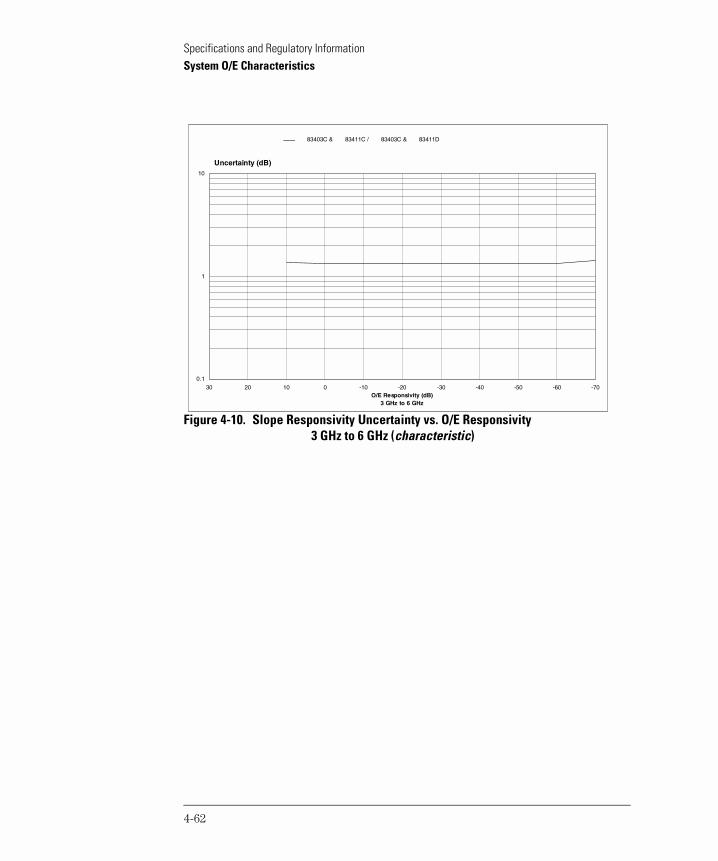
Specifications and Regulatory InformationSystem O/E Characteristics
Figure 4-10. Slope Responsivity Uncertainty vs. O/E Responsivity 3 GHz to 6 GHz (characteristic)
Uncertainty (dB)
0.1
1
10
-70-60-50-40-30-20-100102030O/E Responsivity (dB)
3 GHz to 6 GHz
HP 83403C & HP 83411C / HP 83403C & HP 83411D
4-62

Specifications and Regulatory InformationSystem O/E Characteristics
The following plot is based on an Agilent 8702D Option 011 system for 850 nm measurements consisting of the following:
• Agilent 8702D Option 011 for 300 kHz to 3 GHz modulation bandwidth• User-selected 850 nm source with the following characteristics:
Electrical input return loss = 14 dBeOptical output return loss = 34 dBoResponsivity = –26 dBe
• Agilent 83412B 850 nm Lightwave Receiver• Agilent 11887A Interconnect Cable Kit (HMS-10)• Agilent 11889A RF Interface Kit
Assumptions or Conditions
• Receiver response calibration using disk data for the Agilent 83412B• Device under test optical input return loss = 30 dBo• Device under test electrical output return loss = 14 dBe• RF input power to the lightwave source = +10 dBm
Figure 4-11. Slope Responsivity Uncertainty vs. O/E Responsivity 300 kHz to 3 GHz (characteristic)
Uncertainty (dB)
0.1
1
10
-80-70-60-50-40-30-20-100102030O/E Responsivity (dB)
300 kHz to 3 GHz
User selected 850 nm source & HP 83412B
4-63

Specifications and Regulatory InformationSystem O/E Characteristics
The two curves in the following plot show the uncertainty in a measurement of deviation from linear phase response after the average group delay has been removed for 3 GHz and 6 GHz measurements. Locate the device under test’s responsivity in dB along the X axis. For modulation frequencies between 300 kHz and 3 GHz, read the uncertainty value off the Y axis that corresponds to the 3 GHz curve. For modulation frequencies between 3 GHz and 6 GHz read the uncertainty value corresponding to the 6 GHz curve.
Assumptions or Conditions
• Receiver response & match calibration using disk data for the Agilent 8341XX selected
• Device under test optical input return loss = 30 dBo• Device under test electrical output return loss = 14 dBe• RF input power to the lightwave source = +10 dBm
Figure 4-12. Deviation from Linear Phase vs. O/E Responsivity (characteristic)
Uncertainty (deg)
1
10
100
-70-60-50-40-30-20-10010203040
O/E Responsivity (dB)
User selected 850 nm source & HP 83412B 3 GHz System 6 GHz System
4-64

Specifications and Regulatory InformationSystem O/E Characteristics
3 GHz and 6 GHz 75Ω System Configuration
The following plots are based on an Agilent 8702D Option 075 system consist-ing of the following:
• Agilent 8702D Option 075 for 300 kHz to 2 GHz modulation bandwidth• Agilent 8340XX SMF Lightwave Source• Agilent 8341XX Lightwave Receiver• Agilent 11886A Interconnect Cable Kit (HMS-10)• Agilent 11857B 75Ω Type-N Test Port Cables• Agilent 11852B Option 004 50Ω to 75Ω Minimum Loss Pad (2)• Agilent Part Number 1250-1750, Type-N to 3.5 mm (m) adapters (2)• Agilent 85036B 75Ω Type-N Calibration Kit
Assumptions or Conditions
• Receiver response & match calibration using disk data for the Agilent 83411C• Device under test optical input return loss = 30 dBo• Device under test electrical output return loss = 14 dBe• RF input power to the lightwave source = +10 dBm
Figure 4-13. Slope Responsivity Uncertainty vs. O/E Responsivity 300 kHz to 2 GHz (characteristic)
Uncertainty (dB)
0.1
1
10
-70-60-50-40-30-20-100102030405075 Ω O/E Responsivity (dB)
300 kHz to 2 GHz
HP 83402C/3C & HP 83411C
4-65

Specifications and Regulatory InformationSystem O/E Characteristics
The curve in the following plot shows the uncertainty in a measurement of deviation from linear phase response, after the average group delay has been removed, for measurements made at modulation frequencies at and below 2 GHz. Locate the device under test’s responsivity in dB along the X axis. Read the uncertainty value off the Y axis that corresponds to that point on the curve.
Assumptions or Conditions
• Receiver response & match calibration using disk data for the Agilent 83411C• Device under test optical input return loss = 30 dBo• Device under test electrical output return loss = 14 dBe• RF input power to the lightwave source = +10 dBm
Figure 4-14. Deviation from Linear Phase vs. O/E Responsivity (characteristic)
Uncertainty (deg)
1
10
100
-70-60-50-40-30-20-100102030405075 Ω O/E Responsivity (dB)
300 kHz to 2 GHz
HP 83402/3C & HP 83411C
4-66

Specifications and Regulatory InformationSystem E/O Characteristics
System E/O Characteristics
Measurements of E/O devices with electrical inputs and optical outputs have a total value of uncertainty that includes various individual uncertainties. The total relative measurement uncertainty (dB) is shown plotted against the device under test responsivity (dB). These graphs refer to the relative flatness of modulation bandwidth measurements.
Included in the total relative uncertainty value (shown by the plots) are the following individual contributing uncertainties:
• Drift with temperature (23 ±3°C)• Dynamic accuracy• Reflection sensitivity• Wavelength accuracy• Factory test (characterization) system• Electrical mismatches or reflections between:
RF source/lightwave source RF inputRF receiver/lightwave receiver RF output
• Optical mismatches or reflections between:lightwave source/lightwave receiverdevice under test/ lightwave receiver
Absolute magnitude uncertainty includes additional error contributors, the greatest of which is optical connector loss uncertainty. An absolute uncertainty value for a specific data point can be calculated by adding ±0.76 dB to the value found on the uncertainty graphs.
The responsivity of an E/O device can be read off the display in dB or linear for any given frequency. The Agilent 8702D User’s Guide describes how to con-vert the dB value to its corresponding watts/amp responsivity value in the example for measuring an E/O converter where,
Responsivity R (dB) = 20 log10
[R (w/a) / 1 (w/a)]
4-67

Specifications and Regulatory InformationSystem E/O Characteristics
3 GHz and 6 GHz 50Ω System Configuration
The following plots are based on an Agilent 8702D system consisting of the following:
• Agilent 8702D (standard) for 300 kHz to 3 GHz modulation bandwidth, or Agilent 8702D Option 006 (6 GHz Frequency Extension) for 3 GHz to 6 GHz modulation bandwidth
• Agilent 8340XX SMF Lightwave Source• Agilent 8341XX Lightwave Receiver• Agilent 11886A Interconnect Cable Kit (HMS-10)• Agilent 11857D 50Ω 7 mm Test Port Return Cables• Agilent 85033D 3.5 mm Calibration Kit
Assumptions or Conditions
• Source response & match calibration using disk data for the Agilent 8340XX selected
• Device under test electrical input return loss = 14 dBe• Device under test optical output return loss = 30 dBo• RF input power to the device under test = +10 dBm
Figure 4-15. Slope Responsivity Uncertainty vs. E/O Responsivity 300 kHz to 3 GHz (characteristic)
Uncertainty (dB)
0.1
1
10
-130-120-110-100-90-80-70-60-50-40-30-20-10E/O Responsivity (dB)
300 kHz to 3 GHz
HP 83402C & HP 83411C HP 83402C & HP 83410C HP 83402C & HP 83411D
4-68

Specifications and Regulatory InformationSystem E/O Characteristics
Figure 4-16. Slope Responsivity Uncertainty vs. E/O Responsivity 300 kHz to 3 GHz (characteristic)
Figure 4-17. Slope Responsivity Uncertainty vs. E/O Responsivity 3 GHz to 6 GHz (characteristic)
Uncertainty (dB)
0.1
1
10
-130-120-110-100-90-80-70-60-50-40-30-20-10E/O Responsivity (dB)
300 kHz to 3 GHz
HP 83403C & HP 83411C HP 83403C & HP 83410C HP 83403C & HP 83411D
Uncertainty (dB)
0.1
1
10
-130-120-110-100-90-80-70-60-50-40-30-20-10E/O Responsivity (dB)
3 GHz to 6 GHz
HP 83402C & HP 83411C HP 83402C & HP 83411D
4-69

Specifications and Regulatory InformationSystem E/O Characteristics
Figure 4-18. Slope Responsivity Uncertainty vs. E/O Responsivity 3 GHz to 6 GHz (characteristic)
Uncertainty (dB)
0.1
1
10
-130-120-110-100-90-80-70-60-50-40-30-20-10E/O Responsivity (dB)
3 GHz to 6 GHz
HP 83403C & HP 83411C HP 83403C & HP 83411D
4-70

Specifications and Regulatory InformationSystem E/O Characteristics
The following plot is based on an Agilent 8702D system for 850 nm measure-ments consisting of the following:
• Agilent 8702D (standard) for 300 kHz to 3 GHz modulation bandwidth• Agilent 83412B 850 nm Lightwave Receiver• Agilent 11887A Interconnect Cable Kit (HMS-10)• Agilent 11857D 50Ω 7 mm Test Port Return Cables• Agilent 85033D Calibration Kit
Assumptions or Conditions
• Source response & match calibration using the thru-receiver technique and disk data for the Agilent 83412B
• Device under test electrical input return loss = 14 dBe• Device under test optical output return loss = 34 dBo• Device under test responsivity = –26 dBe • RF input power to the device under test = +10 dBm
Figure 4-19. Slope Responsivity Uncertainty vs. E/O Responsivity 300 kHz to 3 GHz (characteristic)
Uncertainty (dB)
0.1
1
10
-130-120-110-100-90-80-70-60-50-40-30-20E/O Responsivity (dB)
300 kHz to 3 GHz
User selected 850 nm source & HP 83412B
4-71

Specifications and Regulatory InformationSystem E/O Characteristics
The two curves in the following plot show the uncertainty in a measurement of deviation from linear phase response after the average group delay has been removed for 3 GHz and 6 GHz measurements. Locate the device under test’s responsivity in dB along the X axis. For modulation frequencies between 300 kHz and 3 GHz, read the uncertainty value off the Y axis that corresponds to the 3 GHz curve. For modulation frequencies between 3 GHz and 6 GHz read the uncertainty value corresponding to the 6 GHz curve.
Assumptions or Conditions
• Source response & match calibration using disk data for the Agilent 8340XX selected
• Device under test electrical input return loss = 14 dBe• Device under test optical output return loss = 34 dBo• Device under test responsivity = –26 dBe • RF input power to the device under test = +10 dBm
Figure 4-20. Deviation from Linear Phase vs. E/O Responsivity (characteristic)
Uncertainty (deg)
1
10
100
-120-110-100-90-80-70-60-50-40-30-20-10
E/O Responsivity (dB)
3 GHz System 6 GHz System
4-72

Specifications and Regulatory InformationSystem E/O Characteristics
3 GHz and 6 GHz 50Ω System Configuration for Agilent 8702D Option 011 and Agilent 11889A RF Inter-face Kit
The following plots are based on an Agilent 8702D Option 011 system consist-ing of the following:
• Agilent 8702D Option 011 for 300 kHz to 3 GHz modulation bandwidth, or Agilent 8702D Option 001, 006 (6 GHz Frequency Extension) for 3 GHz to 6 GHz modulation bandwidth
• Agilent 8340XX SMF Lightwave Source• Agilent 8341XX Lightwave Receiver• Agilent 11886A Interconnect Cable Kit (HMS-10)• Agilent 11889A RF Interface Kit
Assumptions or Conditions
• Source response calibration using disk data for the Agilent 8340XX selected• Device under test electrical input return loss = 14 dBe• Device under test optical output return loss = 30 dBo• RF input power to the device under test = +14 dBm
4-73

Specifications and Regulatory InformationSystem E/O Characteristics
Figure 4-21. Slope Responsivity Uncertainty vs. E/O Responsivity 300 kHz to 3 GHz (characteristic)
Uncertainty (dB)
0.1
1
10
-130-120-110-100-90-80-70-60-50-40-30-20-10E/O Responsivity (dB)
300 kHz to 3 GHz
HP 83402C & HP 83411C HP 83402C & HP 83410C HP 83402C & HP 83411D
4-74

Specifications and Regulatory InformationSystem E/O Characteristics
Figure 4-22. Slope Responsivity Uncertainty vs. E/O Responsivity 300 kHz to 3 GHz (characteristic)
Figure 4-23. Slope Responsivity Uncertainty vs. E/O Responsivity 3 GHz to 6 GHz (characteristic)
Uncertainty (dB)
0.1
1
10
-130-120-110-100-90-80-70-60-50-40-30-20-10E/O Responsivity (dB)
300 kHz to 3 GHz
HP 83403C & HP 83411C HP 83403C & HP 83410C HP 83403C & HP 83411D
Uncertainty (dB)
0.1
1
10
-130-120-110-100-90-80-70-60-50-40-30-20-10E/O Responsivity (dB)
3 GHz to 6 GHz
HP 83402C & HP 83411C HP 83402C & HP 83411D
4-75
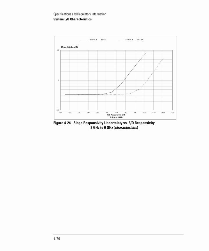
Specifications and Regulatory InformationSystem E/O Characteristics
Figure 4-24. Slope Responsivity Uncertainty vs. E/O Responsivity 3 GHz to 6 GHz (characteristic)
Uncertainty (dB)
0.1
1
10
-130-120-110-100-90-80-70-60-50-40-30-20-10E/O Responsivity (dB)
3 GHz to 6 GHz
HP 83403C & HP 83411C HP 83403C & HP 83411D
4-76
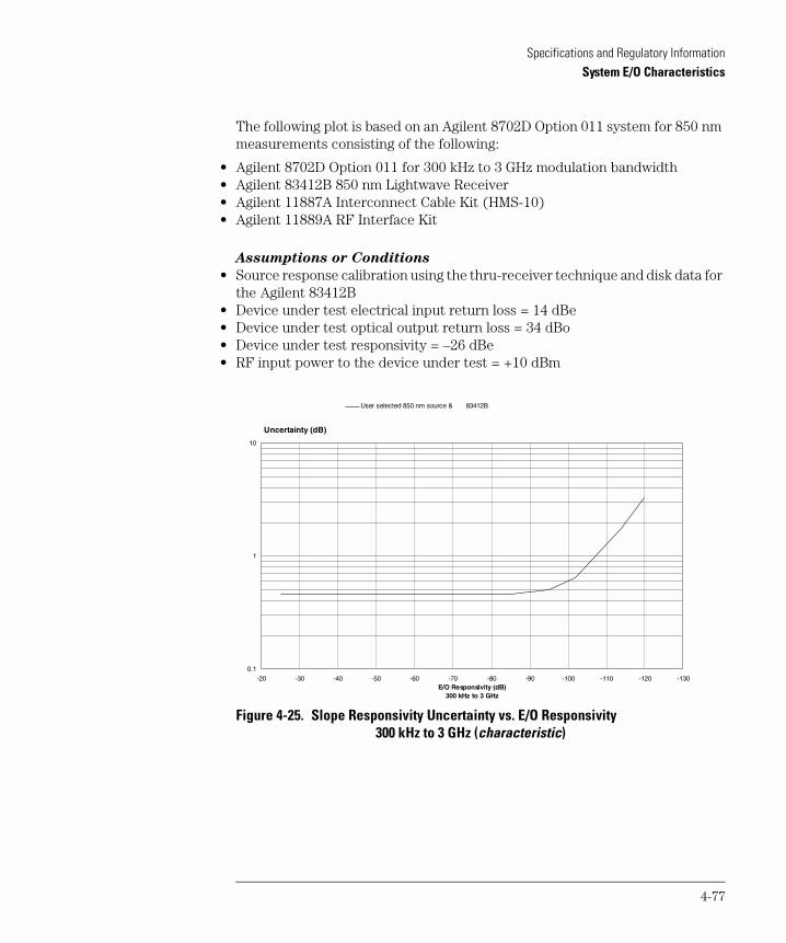
Specifications and Regulatory InformationSystem E/O Characteristics
The following plot is based on an Agilent 8702D Option 011 system for 850 nm measurements consisting of the following:
• Agilent 8702D Option 011 for 300 kHz to 3 GHz modulation bandwidth• Agilent 83412B 850 nm Lightwave Receiver• Agilent 11887A Interconnect Cable Kit (HMS-10)• Agilent 11889A RF Interface Kit
Assumptions or Conditions
• Source response calibration using the thru-receiver technique and disk data for the Agilent 83412B
• Device under test electrical input return loss = 14 dBe• Device under test optical output return loss = 34 dBo• Device under test responsivity = –26 dBe • RF input power to the device under test = +10 dBm
Figure 4-25. Slope Responsivity Uncertainty vs. E/O Responsivity 300 kHz to 3 GHz (characteristic)
Uncertainty (dB)
0.1
1
10
-130-120-110-100-90-80-70-60-50-40-30-20E/O Responsivity (dB)
300 kHz to 3 GHz
User selected 850 nm source & HP 83412B
4-77

Specifications and Regulatory InformationSystem E/O Characteristics
The two curves in the following plot show the uncertainty in a measurement of deviation from linear phase response after the average group delay has been removed for 3 GHz and 6 GHz measurements. Locate the device under test’s responsivity in dB along the X axis. For modulation frequencies between 300 kHz and 3 GHz, read the uncertainty value off the Y axis that corresponds to the 3 GHz curve. For modulation frequencies between 3 GHz and 6 GHz read the uncertainty value corresponding to the 6 GHz curve.
Assumptions or Conditions
• Source response calibration using disk data for the Agilent 8340XX selected • Device under test electrical input return loss = 14 dBe• Device under test optical output return loss = 30 dBo• RF input power to the device under test = +14 dBm
Figure 4-26. Deviation from Linear Phase vs. E/O Responsivity (characteristic)
Uncertainty (deg)
1
10
100
-120-110-100-90-80-70-60-50-40-30-20-10
E/O Responsivity (dB)
3 GHz System 6 GHz System
4-78

Specifications and Regulatory InformationSystem E/O Characteristics
3 GHz and 6 GHz 75Ω System Configuration
The following plots are based on an Agilent 8702D Option 075 system consist-ing of the following:
• Agilent 8702D Option 075 for 300 kHz to 2 GHz modulation bandwidth• Agilent 8340XX SMF Lightwave Source• Agilent 8341XX Lightwave Receiver• Agilent 11886A Interconnect Cable Kit (HMS-10)• Agilent 11857B 75Ω Type-N Test Port Cables• Agilent 11852B Option 004 50Ω to 75Ω Minimum Loss Pad (2)• Agilent Part Number 1250-1750, Type-N to 3.5 mm (m) adapters (2)• Agilent 85036B 75Ω Type-N Calibration Kit
Assumptions or Conditions
• Source response & match calibration using disk data for the Agilent 83402C or Agilent 83403C
• Device under test electrical input return loss = 14 dBe• Device under test optical output return loss = 30 dBo• RF input power to the device under test = +10 dBm
Figure 4-27. Slope Responsivity Uncertainty vs. E/O Responsivity 300 kHz to 2 GHz (characteristic)
Uncertainty (dB)
0.1
1
10
-100-90-80-70-60-50-40-30-20-1075 Ω E/O Responsivity (dB)
300 kHz to 2 GHz
HP 83402C & HP 83411C / HP 83403C & HP 83411C
4-79

Specifications and Regulatory InformationSystem E/O Characteristics
The curve in the following plot shows the uncertainty in a measurement of deviation from linear phase response after the average group delay has been removed for measurements made at modulation frequencies at and below 2 GHz. Locate the device under test’s responsivity in dB along the X axis. Read the uncertainty value off the Y axis that corresponds to that point on the curve.
Assumptions or Conditions
• Source response & match calibration using disk data for the Agilent 83402C or Agilent 83403C
• Device under test electrical input return loss = 14 dBe• Device under test optical output return loss = 30 dBo• RF input power to the device under test = +10 dBm
Figure 4-28. Deviation from Linear Phase vs. O/E Responsivity (characteristic)
Uncertainty (deg)
1
10
100
-110-100-90-80-70-60-50-40-30-20-10
300 kHz to 2 GHz
HP 83402C/3C & HP 83411C
75 Ω E/O Responsivity (dB)
4-80

Specifications and Regulatory InformationSystem O/O Characteristics
System O/O Characteristics
Measurements of O/O devices with optical inputs and optical outputs have a total value of uncertainty that includes various individual uncertainties. The total relative measurement uncertainty (dB) is shown plotted against the device under test insertion loss (dB). These graphs refer to the relative flat-ness of modulation bandwidth measurements.
Included in the total relative uncertainty value (shown by the plots) are the following individual contributing uncertainties:
• Drift with temperature (23 ±3°C)• Dynamic accuracy• Reflection sensitivity• Wavelength accuracy• Factory test (characterization) system• Optical mismatches or reflections between:
lightwave source/lightwave receiverlightwave source/device under testdevice under test/ lightwave receiver
4-81

Specifications and Regulatory InformationSystem O/O Characteristics
3 GHz and 6 GHz 50Ω System Configuration
The following plots are based on an Agilent 8702D system consisting of the following:
• Agilent 8702D (standard) for 300 kHz to 3 GHz modulation bandwidth, or Agilent 8702D Option 006 (6 GHz Frequency Extension) for 3 GHz to 6 GHz modulation bandwidth
• Agilent 8340XX SMF Lightwave Source• Agilent 8341XX Lightwave Receiver• Agilent 11886A Interconnect Cable Kit (HMS-10)• Agilent 11857D 50Ω 7 mm Test Port Return Cables• Agilent Part Number 85052-60004, 7 mm to 3.5 mm (m) adapters (2)
Assumptions or Conditions
• O/O thru calibration on Agilent 8702D• Device under test optical input return loss = 30 dBo• Device under test optical output return loss = 30 dBo• RF input power to the lightwave source = +10 dBm
Figure 4-29. Relative Transmission Coefficient Uncertainty vs. O/O Transmission Coefficient 300 kHz to 3 GHz (characteristic)
Uncertainty (dB)
0.1
1
10
-60-50-40-30-20-100Transmission coefficient (dB)
300 kHz to 3 GHz
HP 83402C & HP 83411C HP 83402C & HP 83410C HP 83402C & HP 83411D
4-82

Specifications and Regulatory InformationSystem O/O Characteristics
Figure 4-30. Relative Transmission Coefficient Uncertainty vs. O/O Transmission Coefficient 300 kHz to 3 GHz (characteristic)
Figure 4-31. Relative Transmission Coefficient vs. O/O Transmission Coefficient 3 GHz to 6 GHz (characteristic)
Uncertainty (dB)
0.1
1
10
-60-50-40-30-20-100Transmission coefficient (dB)
300 kHz to 3 GHz
HP 83403C & HP 83411C HP 83403C & HP 83410C HP 83403C & HP 83411D
Uncertainty (dB)
0.1
1
10
-50-45-40-35-30-25-20-15-10-50Transmission coefficient (dB)
3 GHz to 6 GHz
HP 83402C & HP 83411C HP 83402C & HP 83411D
4-83

Specifications and Regulatory InformationSystem O/O Characteristics
Figure 4-32. Relative Transmission Coefficient Uncertainty vs. O/O Transmission Coefficient 3 GHz to 6 GHz (characteristic)
Uncertainty (dB)
0.1
1
10
-50-45-40-35-30-25-20-15-10-50Transmission coefficient (dB)
3 GHz to 6 GHz
HP 83403C & HP 83411C HP 83403C & HP 83411D
4-84

Specifications and Regulatory InformationSystem O/O Characteristics
The two curves in the following plot show the uncertainty in a measurement of deviation from linear phase response after the average group delay has been removed for 3 GHz and 6 GHz measurements. Locate the device under test’s transmission coefficient in dB along the X axis. For modulation frequencies between 300 kHz and 3 GHz, read the uncertainty value off the Y axis that cor-responds to the 3 GHz curve. For modulation frequencies between 3 GHz and 6 GHz, read the uncertainty value corresponding to the 6 GHz curve.
Assumptions or Conditions
• O/O thru calibration on Agilent 8702D• Device under test optical input return loss = 30 dBo• Device under test optical output return loss = 30 dBo• RF input power to the lightwave source = +10 dBm
Figure 4-33. Deviation from Linear Phase vs. O/O Transmission Coefficient (characteristic)
Uncertainty (deg)
1
10
100
-40-30-20-100
Transmission coefficient (dB)
3 GHz System 6 GHz System
4-85

Specifications and Regulatory InformationSystem O/O Characteristics
3 GHz and 6 GHz 50Ω System Configuration for Agilent 8702D Option 011 and Agilent 11889A RF Inter-face Kit
The following plots are based on an Agilent 8702D Option 011 system consist-ing of the following:
• Agilent 8702D Option 011 for 300 kHz to 3 GHz modulation bandwidth, or Agilent 8702D Option 001, 006 (6 GHz Frequency Extension) for 3 GHz to 6 GHz modulation bandwidth
• Agilent 8340XX SMF Lightwave Source• Agilent 8341XX Lightwave Receiver• Agilent 11886A Interconnect Cable Kit (HMS-10)• Agilent 11889A RF Interface Kit
Assumptions or Conditions
• O/O thru calibration on Agilent 8702D Option 011• Device under test optical input return loss = 30 dBo• Device under test optical output return loss = 30 dBo• RF input power to the lightwave source = +14 dBm
4-86

Specifications and Regulatory InformationSystem O/O Characteristics
Figure 4-34. Relative Transmission Coefficient Uncertainty vs. O/O Transmission Coefficient 300 kHz to 3 GHz (characteristic)
Uncertainty (dB)
0.1
1
10
-60-50-40-30-20-100Transmission coefficient (dB)
300 kHz to 3 GHz
HP 83402C & HP 83411C HP 83402C & HP 83410C HP 83402C & HP 83411D
4-87

Specifications and Regulatory InformationSystem O/O Characteristics
Figure 4-35. Relative Transmission Coefficient Uncertainty vs. O/O Transmission Coefficient 300 kHz to 3 GHz (characteristic)
Figure 4-36. Relative Transmission Coefficient vs. O/O Transmission Coefficient 3 GHz to 6 GHz (characteristic)
Uncertainty (dB)
0.1
1
10
-60-50-40-30-20-100Transmission coefficient (dB)
300 kHz to 3 GHz
HP 83403C & HP 83411C HP 83403C & HP 83410C HP 83403C & HP 83411D
Uncertainty (dB)
0.1
1
10
-50-45-40-35-30-25-20-15-10-50Transmission coefficient (dB)
3 GHz to 6 GHz
HP 83402C & HP 83411C HP 83402C & HP 83411D
4-88

Specifications and Regulatory InformationSystem O/O Characteristics
Figure 4-37. Relative Transmission Coefficient Uncertainty vs. O/O Transmission Coefficient 3 GHz to 6 GHz (characteristic)
Uncertainty (dB)
0.1
1
10
-50-45-40-35-30-25-20-15-10-50Transmission coefficient (dB)
3 GHz to 6 GHz
HP 83403C & HP 83411C HP 83403C & HP 83411D
4-89

Specifications and Regulatory InformationSystem O/O Characteristics
The two curves in the following plot show the uncertainty in a measurement of deviation from linear phase response after the average group delay has been removed for 3 GHz and 6 GHz measurements. Locate the device under test’s transmission coefficient in dB along the X axis. For modulation frequencies between 300 kHz and 3 GHz, read the uncertainty value off the Y axis that cor-responds to the 3 GHz curve. For modulation frequencies between 3 GHz and 6 GHz, read the uncertainty value corresponding to the 6 GHz curve.
Assumptions or Conditions
• O/O thru calibration on Agilent 8702D Option 011• Device under test optical input return loss = 30 dBo• Device under test optical output return loss = 30 dBo• RF input power to the lightwave source = +14 dBm
Figure 4-38. Deviation from Linear Phase vs. O/O Transmission Coefficient (characteristic)
Uncertainty (deg)
1
10
100
-40-30-20-100
Transmission coefficient (dB)
3 GHz System 6 GHz System
4-90

Specifications and Regulatory InformationLightwave Receiver Measurement Repeatability
Lightwave Receiver Measurement Repeatability
This plot shows the system’s ability to accurately repeat measurements of the same O/E device.
A system consisting of an Agilent 8702D Option 006 (6 GHz Frequency Exten-sion), Agilent 83403C 1550 nm Lightwave Source, and Agilent 83411C Light-wave Receiver was used to make measurements on a different Agilent 83411C Lightwave Receiver. The three traces in the following plot represent three measurements of the same Agilent 83411C (device under test) made on three completely different Agilent 8702D systems. A receiver response & match cal-ibration was performed on each of the three systems using three different Agilent 83411Cs and their calibration data disks.
The following measurement conditions existed for all three measurements:
• 401 data points• modulation frequency = 300 kHz to 6 GHz• +10 dBm RF output power• IF bandwidth = 30 Hz• no averaging• ambient temperature
The plot shows about 0.1 dBe (worst case) repeatability error.
4-91

Specifications and Regulatory InformationLightwave Receiver Measurement Repeatability
Figure 4-39. Agilent 8702D System Repeatability of O/E Measurement (characteristic)
HP 8702D System Repeatability of O/E Measurement (characteristic)
-6.2
-6.0
-5.8
-5.6
-5.4
-5.2
-5.0
-4.8
-4.6
-4.4
0 1 2 3 4 5 6
Frequency (GHz)
dB
e
Series1
Series2
Series3
4-92

Specifications and Regulatory InformationGPIB Interface
GPIB Interface
GPIB interface operates according to IEEE 488-1978 and IEC 625 standards and IEEE 728-1982 recommended practices.
Transfer Formats
Binary (internal 48-bit floating point complex format)
ASCII
32/64 bit IEEE 754 Floating Point Format
Interface Function Codes
SH1, AH1, T6, TE0, L4, LEO, SR1, RL1, PP0, DC1, DT1, C1, C2, C3, C10, E2
4-93
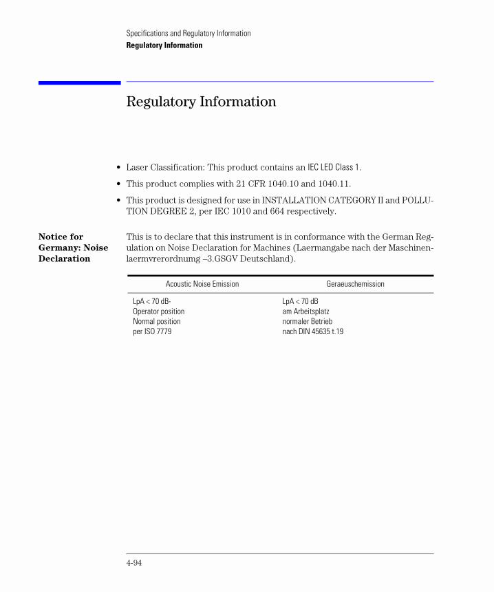
Specifications and Regulatory InformationRegulatory Information
Regulatory Information
• Laser Classification: This product contains an IEC LED Class 1.
• This product complies with 21 CFR 1040.10 and 1040.11.
• This product is designed for use in INSTALLATION CATEGORY II and POLLU-TION DEGREE 2, per IEC 1010 and 664 respectively.
Notice for
Germany: Noise
Declaration
This is to declare that this instrument is in conformance with the German Reg-ulation on Noise Declaration for Machines (Laermangabe nach der Maschinen-laermvrerordnumg –3.GSGV Deutschland).
Acoustic Noise Emission Geraeuschemission
LpA < 70 dB-Operator positionNormal positionper ISO 7779
LpA < 70 dBam Arbeitsplatznormaler Betriebnach DIN 45635 t.19
4-94

Specifications and Regulatory InformationRegulatory Information
4-95


5
How the Agilent 8702D Works 5-2The built-in synthesized source 5-3The built-in test set 5-4The receiver block 5-4Required peripheral equipment 5-4
How the Agilent 8702D Processes Data 5-5Processing details 5-7
Using the Response Functions 5-11Understanding S-parameters 5-12Selecting the measurement 5-15
What is Measurement Calibration? 5-17What is accuracy enhancement? 5-18What causes measurement errors? 5-19Characterizing microwave systematic errors 5-24Correcting for measurement errors 5-38How effective is accuracy enhancement? 5-39Ensuring a valid calibration 5-41The calibration standards 5-43Modifying calibration kits 5-47TRL*/LRM* calibration 5-61Power meter calibration 5-64
Understanding and Using Time Domain 5-71Time domain bandpass 5-74Time domain low pass 5-77Time domain concepts 5-85Transforming CW time measurements into the frequency domain 5-94
Instrument Preset State and Memory Allocation 5-99Types of memory and data storage 5-99Conserving memory 5-105Using saved calibration sets 5-105
Concepts

ConceptsHow the Agilent 8702D Works
How the Agilent 8702D Works
Component analyzers measure the reflection and transmission characteristics of devices and networks. A component analyzer test system consists of the fol-lowing:
• source • signal-separation devices • receiver • display
The analyzer applies a signal that is transmitted through the test device, or re-flected from its input, and then compares it with the incident signal generated by the swept RF source. The signals are then applied to a receiver for measure-ment, signal processing, and display.
The Agilent 8702D integrates a high resolution synthesized RF source, test set, and a dual channel three-input receiver to measure and display magni-tude, phase, and group delay of transmitted and reflected power. Agilent 8702D options are explained in Chapter 2, “Reference”.
5-2

ConceptsHow the Agilent 8702D Works
Figure 5-1 is a simplified block diagram of the analyzer system. A detailed block diagram of the analyzer is provided in the Agilent 8753D Network Ana-
lyzer Service Guide, together with a theory of system operation.
Figure 5-1. Simplified Block Diagram of the Analyzer System
The built-in synthesized source
The analyzer’s built-in synthesized source produces a swept RF signal in the range of 300 kHz to 3.0 GHz. The Agilent 8702D Option 006 is able to generate signals up to 6 GHz. The RF output power is leveled by an internal ALC (auto-matic leveling control) circuit. To achieve frequency accuracy and phase mea-suring capability, the analyzer is phaselocked to a highly stable crystal oscillator. For this purpose, a portion of the transmitted signal is routed to the R channel input of the receiver, where it is sampled by the phase detection loop and fed back to the source.
The source step
attenuator
The step attenuator, contained in the source, is used to adjust the power level to the test device, without changing the level of the incident power in the ref-erence path.
5-3

ConceptsHow the Agilent 8702D Works
The built-in test set
The Agilent 8702D features a built-in test set that provides connections to the test device, as well as to the signal-separation devices. The signal separation devices are needed to separate the incident signal from the transmitted and reflected signals. The incident signal is applied to the R channel input through a jumper cable on the front panel. Meanwhile, the transmitted and reflected signals are internally routed from the test port couplers to the inputs of the A and B sampler/mixers in the receiver. Port 1 is connected to the A input and port 2 is connected to the B input.
The test set contains the hardware required to make simultaneous transmis-sion and reflection measurements in both the forward and reverse directions. An RF path switch in the built-in test set allows reverse measurements to be made without changing the connections to the test device.
The receiver block
The receiver block contains three sampler/mixers for the R, A, and B inputs. The signals are sampled, and mixed to produce a 4 kHz IF (intermediate fre-quency). A multiplexer sequentially directs each of the three signals to the ADC (analog-to-digital converter), where it is converted from an analog to a digital signal to be measured and processed for viewing on the display. Both amplitude and phase information are measured simultaneously, regardless of what is displayed on the analyzer.
The
microprocessor
A microprocessor takes the raw data and performs all the required error cor-rection, trace math, formatting, scaling, averaging, and marker operations, according to the instructions from the front panel or over GPIB. The format-ted data is then displayed. The data processing sequence is described in “How the Agilent 8702D Processes Data” on page 5-5.
Required peripheral equipment
Measurements will require calibration standards for vector accuracy enhance-ment, and cables for interconnections. Model numbers and details of compati-ble power splitters, calibration kits, and cables are provided in Chapter 2, “Reference”.
5-4

ConceptsHow the Agilent 8702D Processes Data
How the Agilent 8702D Processes Data
The analyzer’s receiver converts the R, A, and B input signals into useful mea-surement information. This conversion occurs in two main steps:
• The swept high frequency input signals are translated to fixed low frequency IF signals, using analog sampling or mixing techniques. (Refer to the Agilent 8753D Network Analyzer Service Guide for more details on the the-ory of operation.)
• The IF signals are converted into digital data by an analog-to-digital converter (ADC). From this point on, all further signal processing is performed mathe-matically by the analyzer microprocessors.
The following section describes the sequence of math operations and the resulting data arrays as the information flows from the ADC to the display. It provide a good foundation for understanding most of the response functions, and the order in which they are performed.
5-5

ConceptsHow the Agilent 8702D Processes Data
Figure 5-2 is a data processing flow diagram that represents the flow of numerical data from IF detection to display. The data passes through several math operations, denoted in the figure by single line boxes. Most of these operations can be selected and controlled with the front-panel response block function keys. (Refer to “Using the Response Functions” on page 5-11 for more information.) The data is also stored in arrays along the way, denoted by double line boxes. These arrays are places in the flow path where data is accessible, usually via GPIB.
Figure 5-2. Data Processing Flow Diagram
While only a single flow path is shown, two identical paths are available, corre-sponding to channel 1 and channel 2. When the channels are uncoupled, each channel is processed and controlled independently.
Data point definition
A “data point”, or “point”, is a single piece of data representing a measurement at a single stimulus value. Most data processing operations are performed point-by-point; some involving more than one point.
5-6

ConceptsHow the Agilent 8702D Processes Data
Sweep definition
A “sweep” is a series of consecutive data point measurements, taken over a sequence of stimulus values. A few data processing operations require that a full sweep of data be available. The number of points per sweep can be defined by the user. The units of the stimulus values (such as power, frequency, and time) can change, depending on the sweep mode, although this does not generally affect the data processing path.
Processing details
ADC The ADC (analog-to-digital converter) converts the R, A, and B inputs (already down-converted to a fixed low frequency IF) into digital words. (The AUX INPUT connector on the rear panel is a fourth input.) The ADC switches rapidly between these inputs, so they are converted nearly simultaneously.
IF detection This occurs in the digital filter, which performs the discrete Fourier transform (DFT) on the digital words. The samples are converted into complex number pairs (real plus imaginary, R+jX). The complex numbers represent both the magnitude and phase of the IF signal. If the AUX INPUT is selected, the imagi-nary part of the pair is set to zero. The DFT filter shape can be altered by changing the IF bandwidth, which is a highly effective technique for noise reduction.
Ratio calculations These are performed if the selected measurement is a ratio of two inputs (for example, A/R or B/R). This is a complex divide operation. If the selected mea-surement is absolute (A or B), no operation is performed. The R, A, and B val-ues are also split into channel data at this point.
Sampler/IF
correction
The next digital processing technique used is sampler/IF correction. This pro-cess digitally corrects for frequency response errors (both magnitude and phase, primarily sampler rolloff) in the analog down-conversion path.
Sweep-to-sweep
averaging
This is another noise reduction technique. This calculation involves taking the complex exponential average of several consecutive sweeps. This technique cannot be used with single-input measurements.
Raw data arrays These store the results of all the preceding data processing operations. (Up to this point, all processing is performed real-time with the sweep by the IF pro-cessor. The remaining operations are not necessarily synchronized with the
5-7

ConceptsHow the Agilent 8702D Processes Data
sweep, and are performed by the main processor.) When full 2-port error cor-rection is on, the raw arrays contain all four S-parameter measurements required for accuracy enhancement. When the channels are uncoupled (cou-pled channels off), there may be as many as eight raw arrays. These arrays are directly accessible via GPIB. Notice that the numbers here are still complex pairs.
Vector error
correction
(accuracy
enhancement)
Error correction is performed next, if a measurement calibration has been performed and correction is activated. Error correction removes repeatable systematic errors (stored in the error coefficient arrays) from the raw arrays. This can vary from simple vector normalization to full 12-term error correc-tion.
The error coefficient arrays themselves are created during a measurement cal-ibration using data from the raw arrays. These are subsequently used when-ever correction is on, and are accessible via GPIB.
The results of error correction are stored in the data arrays as complex num-ber pairs. These arrays are accessible via GPIB.
If the data-to-memory operation is performed, the data arrays are copied into the memory arrays.
Trace math
operation
This selects either the data array, memory array, or both to continue flowing through the data processing path. In addition, the complex ratio of the two (data/memory) or the difference (data–memory) can also be selected. If mem-ory is displayed, the data from the memory arrays goes through exactly the same data processing flow path as the data from the data arrays.
Gating This is a digital filtering operation associated with time domain transforma-tion. Its purpose is to mathematically remove unwanted responses isolated in time. In the time domain, this can be viewed as a time-selective bandpass or bandstop filter. (If both data and memory are displayed, gating is applied to the memory trace only if gating was on when data was stored into memory.)
The delay block This involves adding or subtracting phase in proportion to frequency. This is equivalent to “line-stretching” or artificially moving the measurement refer-ence plane.
Conversion
transforms
This transforms the measured S-parameter data to the equivalent complex impedance (Z) or admittance (Y) values, or to inverse S-parameters (1/S).
5-8

ConceptsHow the Agilent 8702D Processes Data
Windowing This is a digital filtering operation that prepares (enhances) the frequency domain data for transformation to time domain.
Time domain
transform
This converts frequency domain information into the time domain when trans-form is on. The results resemble time domain reflectometry (TDR) or impulse-response measurements. The transform uses the chirp-Z inverse fast Fourier transform (FFT) algorithm to accomplish the conversion. The windowing operation, if enabled, is performed on the frequency domain data just before the transform. (A special transform mode is available to “demodulate” CW sweep data, with time as the stimulus parameter, and display spectral informa-tion with frequency as the stimulus parameter.)
Formatting This converts the complex number pairs into a scalar representation for dis-play, according to the selected format. This includes group delay calculations. These formats are often easier to interpret than the complex number repre-sentation. (Polar and Smith chart formats are not affected by the scalar for-matting.) Notice that after formatting, it is impossible to recover the complex data.
Smoothing This is another noise reduction technique, that smooths noise on the trace. The primary application of smoothing is to set the aperture for group delay measurements.
When smoothing is on, each point in a sweep is replaced by the moving aver-age value of several adjacent (formatted) points. The number of points included depends on the smoothing aperture, which can be selected by the user. The effect is similar to video filtering. If data and memory are displayed, smoothing is performed on the memory trace only if smoothing was on when data was stored into memory.
Format arrays The results, so far, are stored in the format arrays. Notice that the marker val-ues and marker functions are all derived from the format arrays. Limit testing is also performed on the formatted data. The format arrays are accessible via GPIB.
Offset and scale These operations prepare the formatted data for display. This is where the ref-erence line position, reference line value, and scale calculations are per-formed, as appropriate to the format.
5-9

ConceptsHow the Agilent 8702D Processes Data
Display memory The display memory stores the display image for presentation on the analyzer. The information stored includes graticules, annotation, and softkey labels. If user display graphics are written, these are also stored in display memory. When hardcopy records are made, the information sent to the plotter or printer is taken from display memory.
Finally, the display memory data is sent to the analyzer’s display. The display is updated frequently and asynchronously with the data processing operations.
5-10

ConceptsUsing the Response Functions
Using the Response Functions
Figure 5-3. Response Function Block
The response function block keys are used to define and control the following functions of the active channel.
• measurement parameters • data format • display functions • noise reduction alternatives • calibration functions • display markers
The current values for the major response functions of the active channel are displayed in specific locations along the top of the display. In addition, certain functions accessed through the keys in this block are annotated in the status notations area at the left side of the display. An illustration of the analyzer’s dis-play, showing the locations of these information labels, is provided in Chapter 2, “Reference”.
5-11

ConceptsUsing the Response Functions
Understanding S-parameters
S-parameters (scattering parameters) are a convention used to characterize the way a device modifies signal flow. A brief explanation of the S-parameters of a two-port device is provided here. For additional details, refer to Agilent
Technologies Application Notes A/N 95-1 and A/N 154.
S-parameters are always a ratio of two complex (magnitude and phase) quan-tities. S-parameter notation identifies these quantities using the numbering convention:
S out in
where the first number (out) refers to the test-device port where the signal is emerging and the second number (in) is the test-device port where the signal is incident. For example, the S-parameter S
21 identifies the measurement as
the complex ratio of the signal emerging at the test device’s port 2 to the sig-nal incident at the test device’s port 1.
5-12

ConceptsUsing the Response Functions
Figure 5-4 is a representation of the S-parameters of a two-port device, together with an equivalent flowgraph. In the illustration, “a” represents the signal entering the device and “b” represents the signal emerging. Note that ‘'a” and “b” are not related to the A and B input ports on the analyzer.
Figure 5-4. S-Parameters of a Two-Port Device
5-13

ConceptsUsing the Response Functions
S-parameters are exactly equivalent to the more common description terms shown in Table 5-1, requiring only that the measurements be taken with all test device ports properly terminated.
Table 5-1. S-Parameter Descriptions
S-Parameter Definition Test Set Description Direction
S11 Input reflection coefficient FWD
S21 Forward gain FWD
S12 Reverse gain REV
S22 Output reflection coefficient REV
b1
a1
----- a2 0=
b2
a1
----- a2 0=
b1
a2
----- a1 0=
b2
a2
----- a1 0=
5-14

ConceptsUsing the Response Functions
Selecting the measurement
The MEAS key leads to a series of softkey menus used to select the parameters or inputs that define the type of measurement being performed.
S-parameter menu The S-parameter menu is used to define the input ports and test set direction for S-parameter measurements. The analyzer automatically switches the direction of the measurement according to the selections made in this menu. Therefore, all four S-parameters can be measured with a single connection. The S-parameter being measured is labeled at the top left corner of the dis-play.
Input ports menu This menu is used to define the input ports for power ratio measurements, or a single input for magnitude only measurements of absolute power. Single inputs cannot be used for phase or group delay measurements, or any mea-surements with averaging activated.
Conversion menu This menu converts the measured reflection or transmission data to the equiv-alent complex impedance (Z) or admittance (Y) values. This is not the same as a two-port Y or Z parameter conversion, as only the measured parameter is used in the equations. Two simple one-port conversions are available, depend-ing on the measurement configuration.
An S11
or S22
trace measured as reflection can be converted to equivalent par-
allel impedance or admittance using the model and equations shown in Figure 5-5.
Figure 5-5. Reflection Impedance and Admittance Conversions
5-15

ConceptsUsing the Response Functions
In a transmission measurement, the data can be converted to its equivalent series impedance or admittance using the model and equations shown in Figure 5-6.
Figure 5-6. Transmission Impedance and Admittance Conversions
Avoid the use of Smith chart, SWR, and delay formats for display of Z and Y conversions, as these formats are not easily interpreted.
5-16

ConceptsWhat is Measurement Calibration?
What is Measurement Calibration?
Measurement calibration is an accuracy enhancement procedure that effec-tively removes the system errors that cause uncertainty in measuring a test device. It measures known standard devices, and uses the results of these measurements to characterize the system.
This section discusses the following topics:
• definition of accuracy enhancement
• causes of measurement errors
• characterization of microwave systematic errors
• correcting for measurement errors
• effectiveness of accuracy enhancement
• ensuring a valid calibration
• calibration standards
• modifying calibration kits
• calibrating for non-insertable devices
• TRL*/LRM* calibration
• power meter calibration
5-17

ConceptsWhat is Measurement Calibration?
What is accuracy enhancement?
A perfect measurement system would have infinite dynamic range, isolation, and directivity characteristics, no impedance mismatches in any part of the test setup, and flat frequency response. In any high frequency measurement there are measurement errors associated with the system that contribute uncertainty to the results. Parts of the measurement setup, such as intercon-necting cables and signal-separation devices (as well as the analyzer itself), all introduce variations in magnitude and phase that can mask the actual perfor-mance of the test device. Vector accuracy enhancement, also known as mea-surement calibration or error correction, provides the means to simulate a nearly perfect measurement system.
For example, crosstalk due to the channel isolation characteristics of the ana-lyzer can contribute an error equal to the transmission signal of a high-loss test device. For reflection measurements, the primary limitation of dynamic range is the directivity of the test setup. The measurement system cannot dis-tinguish the true value of the signal reflected by the test device from the signal arriving at the receiver input due to leakage in the system. For both transmis-sion and reflection measurements, impedance mismatches within the test setup cause measurement uncertainties that appear as ripples superimposed on the measured data.
Measurement calibration simulates a perfect analyzer system. It measures the magnitude and phase responses of known standard devices, and compares the measurement with actual device data. It uses the results to characterize the system and effectively remove the system errors from the measurement data of a test device, using vector math capabilities internal to the analyzer.
When you use measurement calibration, the dynamic range and accuracy of the measurement are limited only by system noise and stability, connector repeatability, and the accuracy to which the characteristics of the calibration standards are known.
5-18

ConceptsWhat is Measurement Calibration?
What causes measurement errors?
Analysis measurement errors can be separated into systematic, random, and drift errors.
Correctable systematic errors are the repeatable errors that the system can measure. These are errors due to mismatch and leakage in the test setup, iso-lation between the reference and test signal paths, and system frequency response.
The system cannot measure and correct for the non-repeatable random and drift errors. These errors affect both reflection and transmission measure-ments. Random errors are measurement variations due to noise and connector repeatability. Drift errors include frequency drift, temperature drift, and other physical changes in the test setup between calibration and measurement.
The resulting measurement is the vector sum of the test device response plus all error terms. The precise effect of each error term depends upon its magni-tude and phase relationship to the actual test device response.
In most high frequency measurements the systematic errors are the most sig-nificant source of measurement uncertainty. Since each of these errors can be characterized, their effects can be effectively removed to obtain a corrected value for the test device response. For the purpose of vector accuracy enhancement these uncertainties are quantified as directivity, source match, load match, isolation (crosstalk), and frequency response (tracking). Each of these systematic errors is described in this section.
Random and drift errors cannot be precisely quantified, so they must be treated as producing a cumulative uncertainty in the measured data.
5-19

ConceptsWhat is Measurement Calibration?
Directivity Normally a device that can separate the reverse from the forward-traveling waves (a directional bridge or coupler) is used to detect the signal reflected from the test device. Ideally the coupler would completely separate the inci-dent and reflected signals, and only the reflected signal would appear at the coupled output, as illustrated in Figure 5-7a.
Figure 5-7. Directivity
However, an actual coupler is not perfect, as illustrated in Figure 5-7b. A small amount of the incident signal appears at the coupled output due to leakage, as well as reflection from the termination in the coupled arm. Also, reflections from the coupler output connector appear at the coupled output, adding uncertainty to the signal reflected from the device. The figure of merit, for how well a coupler separates forward and reverse waves, is directivity. The greater the directivity of the device, the better the signal separation. System directivity is the vector sum of all leakage signals appearing at the analyzer receiver input. The error contributed by directivity is independent of the char-acteristics of the test device and it usually produces the major ambiguity in measurements of low reflection devices.
5-20

ConceptsWhat is Measurement Calibration?
Source match Source match is defined as the vector sum of signals appearing at the analyzer receiver input, due to the impedance mismatch at the test device looking back into the source, as well as to adapter and cable mismatches and losses. In a reflection measurement, the source match error signal is caused by some of the reflected signal from the test device being reflected from the source back toward the test device and re-reflected from the test device (Figure 5-8). In a transmission measurement, the source match error signal is caused by reflec-tion from the test device that is re-reflected from the source. Source match is most often given in terms of return loss in dB, the larger the number, the smaller the error.
Figure 5-8. Source Match
The error contributed by source match is dependent on the relationship between the actual input impedance of the test device and the equivalent match of the source. It is a factor in both transmission and reflection measure-ments. Source match is a particular problem in measurements where there is a large impedance mismatch at the measurement plane.
5-21

ConceptsWhat is Measurement Calibration?
Load match Load match error results from an imperfect match at the output of the test device. It is caused by impedance mismatches between the test device output port and port 2 of the measurement system. As shown in Figure 5-9, some of the transmitted signal is reflected from port 2 back to the test device. A por-tion of this wave may be re-reflected to port 2, or part may be transmitted through the device in the reverse direction to appear at port 1. If the test device has low insertion loss (for example, a transmission line), the signal reflected from port 2 and re-reflected from the source causes a significant error because the test device does not attenuate the signal significantly on each reflection. Load match is usually given in terms of return loss in dB, the larger the number, the smaller the error.
Figure 5-9. Load Match
The error contributed by load match is dependent on the relationship between the actual output impedance of the test device and the effective match of the return port (port 2). It is a factor in all transmission measurements and in reflection measurements of two-port devices. Load match and source match are usually ignored when the test device insertion loss is greater than about 6 dB, because the error signal is greatly attenuated each time it passes through the test device. However, load match effects produce major transmis-sion measurement errors for a test device with a highly reflective output port.
5-22

ConceptsWhat is Measurement Calibration?
Isolation
(crosstalk)
Leakage of energy between analyzer signal paths contributes to error in a transmission measurement, much like directivity does in a reflection measure-ment. Isolation is the vector sum of signals appearing at the analyzer samplers, due to crosstalk between the reference and test signal paths. This includes signal leakage within the test set and in both the RF and IF sections of the receiver.
The error contributed by isolation depends on the characteristics of the test device. Isolation is a factor in high-loss transmission measurements. However, analyzer system isolation is more than sufficient for most measurements, and correction for it may be unnecessary.
For measuring devices with high dynamic range, accuracy enhancement can provide improvements in isolation that are limited only by the noise floor. Gen-erally, the isolation falls below the noise floor. Therefore, when performing an isolation calibration, you should use a noise reduction function such as averag-ing or reduce the IF bandwidth.
Frequency
response
(tracking)
This is the vector sum of all test setup variations in which magnitude and phase change as a function of frequency. This includes variations contributed by signal-separation devices, test cables, and adapters, and variations between the reference and test signal paths. This error is a factor in both transmission and reflection measurements.
For further explanation of systematic error terms and the way they are com-bined and represented graphically in error models, refer to “Characterizing microwave systematic errors” on page 5-24.
5-23

ConceptsWhat is Measurement Calibration?
Characterizing microwave systematic errors
One-port error
model
In a measurement of the reflection coefficient (magnitude and phase) of a test device, the measured data differs from the actual, no matter how carefully the measurement is made. Directivity, source match, and reflection signal path frequency response (tracking) are the major sources of error (refer to Figure 5-10).
Figure 5-10. Sources of Error in a Reflection Measurement
5-24

ConceptsWhat is Measurement Calibration?
To characterize the errors, the reflection coefficient is measured by first sepa-rating the incident signal (I) from the reflected signal (R), then taking the ratio of the two values (refer to Figure 5-11). Ideally, (R) consists only of the signal reflected by the test device (S
11A).
Figure 5-11. Reflection Coefficient
5-25

ConceptsWhat is Measurement Calibration?
However, all of the incident signal does not always reach the unknown (refer to Figure 5-12). Some of (I) may appear at the measurement system input due to leakage through the test set or through a signal separation device. Also, some of (I) may be reflected by imperfect adapters between a signal separa-tion device and the measurement plane. The vector sum of the leakage and the miscellaneous reflections is the effective directivity, E
DF. Understandably,
the measurement is distorted when the directivity signal combines vectorally with the actual reflected signal from the unknown, S
11A.
Figure 5-12. Effective Directivity EDF
5-26

ConceptsWhat is Measurement Calibration?
Since the measurement system test port is never exactly the characteristic impedance (50 ohms or 75 ohms), some of the reflected signal bounces off the test port, or other impedance transitions further down the line, and back to the unknown, adding to the original incident signal (I). This effect causes the magnitude and phase of the incident signal to vary as a function of S
11A and
frequency. Leveling the source to produce a constant incident signal (I) reduces this error, but since the source cannot be exactly leveled at the test device input, leveling cannot eliminate all power variations. This re-reflection effect and the resultant incident power variation are caused by the source match error, E
SF (refer to Figure 5-13).
Figure 5-13. Source Match ESF
5-27

ConceptsWhat is Measurement Calibration?
Frequency response (tracking) error is caused by variations in magnitude and phase flatness versus frequency between the test and reference signal paths. These are due mainly to imperfectly matched samplers and differences in length and loss between the incident and test signal paths. The vector sum of these variations is the reflection signal path tracking error, E
RF (refer to
Figure 5-14).
Figure 5-14. Reflection Tracking ERF
5-28

ConceptsWhat is Measurement Calibration?
These three errors are mathematically related to the actual data, S11
A, and
measured data, S11
M, by the following equation:
S11M
= EDF
+ [(S11A
ERF
) / (1 – ESF
S11A
)]
If the value of these three “E” errors and the measured test device response were known for each frequency, the above equation could be solved for S
11A to
obtain the actual test device response. Because each of these errors changes with frequency, their values must be known at each test frequency. These val-ues are found by measuring the system at the measurement plane using three independent standards whose S
11A is known at all frequencies.
The first standard applied is a “perfect load,” which makes S11
A= 0 and essen-
tially measures directivity (refer to Figure 5-15). “Perfect load” implies a reflectionless termination at the measurement plane. All incident energy is absorbed. With S
11A = 0, the equation can be solved for E
DF, the directivity
term. In practice, of course, the “perfect load” is difficult to achieve, although very good broadband loads are available in the Agilent 8702D-compatible cali-bration kits.
Figure 5-15. “Perfect Load” Termination
5-29

ConceptsWhat is Measurement Calibration?
Since the measured value for directivity is the vector sum of the actual direc-tivity plus the actual reflection coefficient of the “perfect load,” any reflection from the termination represents an error. System effective directivity becomes the actual reflection coefficient of the “perfect load” (refer to Figure 5-16). In general, any termination having a return loss value greater than the uncorrected system directivity reduces reflection measurement uncertainty.
Figure 5-16. Measured Effective Directivity
Next, a short circuit termination, whose response is known to a very high degree, is used to establish another condition (refer to Figure 5-17).
Figure 5-17. Short Circuit Termination
5-30

ConceptsWhat is Measurement Calibration?
The open circuit gives the third independent condition. In order to accurately model the phase variation with frequency due to radiation from the open con-nector, a specially designed shielded open circuit is used for this step. (The open circuit capacitance is different with each connector type.) Now the val-ues for E
DF directivity, E
SF source match, and E
RF reflection frequency
response are computed and stored (refer to Figure 5-18).
Figure 5-18. Open Circuit Termination
Now the unknown is measured to obtain a value for the measured response, S
11M, at each frequency (refer to Figure 5-19).
Figure 5-19. Measured S11
This is the one-port error model equation solved for S11
A. Since the three
errors and S11
M are now known for each test frequency, S11
A can be computed
as follows:
5-31

ConceptsWhat is Measurement Calibration?
S11A
= S11M
– EDF
/ [ESF
(S11M
– EDF
) + ERF
]
For reflection measurements on two-port devices, the same technique can be applied, but the test device output port must be terminated in the system characteristic impedance. This termination should have as low a reflection coefficient as the load used to determine directivity. The additional reflection error caused by an improper termination at the test device’s output port is not incorporated into the one-port error model.
Two-port error
model
The error model for measurement of the transmission coefficients (magnitude and phase) of a two-port device is derived in a similar manner. The potential sources of error are frequency response (tracking), source match, load match, and isolation (refer to Figure 5-20). These errors are effectively removed using the full two-port error model.
Figure 5-20. Major Sources of Error
5-32

ConceptsWhat is Measurement Calibration?
The transmission coefficient is measured by taking the ratio of the incident signal (I) and the transmitted signal (T) (refer to Figure 5-21). Ideally, (I) consists only of power delivered by the source, and (T) consists only of power emerging at the test device output.
Figure 5-21. Transmission Coefficient
5-33

ConceptsWhat is Measurement Calibration?
As in the reflection model, source match can cause the incident signal to vary as a function of test device S
11A. Also, since the test setup transmission return
port is never exactly the characteristic impedance, some of the transmitted signal is reflected from the test set port 2, and from other mismatches between the test device output and the receiver input, to return to the test device. A portion of this signal may be re-reflected at port 2, thus affecting S
21M, or part may be transmitted through the device in the reverse direction to
appear at port 1, thus affecting S11
M. This error term, which causes the magni-
tude and phase of the transmitted signal to vary as a function of S22
A, is called
load match, ELF
(refer to Figure 5-22).
Figure 5-22. Load Match ELF
The measured value, S21
M, consists of signal components that vary as a func-
tion of the relationship between ESF
and S11
A, as well as ELF
and S22
A, so the
input and output reflection coefficients of the test device must be measured and stored for use in the S
21A error correction computation. Thus, the test
setup is calibrated as described above for reflection to establish the directivity, E
DF , source match, E
SF , and reflection frequency response, E
RF , terms for the
reflection measurements.
Now that a calibrated port is available for reflection measurements, the thru is connected and load match, E
LF , is determined by measuring the reflection
coefficient of the thru connection.
5-34
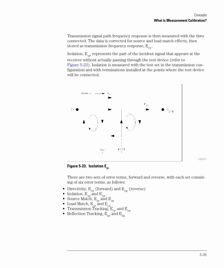
ConceptsWhat is Measurement Calibration?
Transmission signal path frequency response is then measured with the thru connected. The data is corrected for source and load match effects, then stored as transmission frequency response, E
TF .
Isolation, EXF
, represents the part of the incident signal that appears at the
receiver without actually passing through the test device (refer to Figure 5-23). Isolation is measured with the test set in the transmission con-figuration and with terminations installed at the points where the test device will be connected.
Figure 5-23. Isolation EXF
There are two sets of error terms, forward and reverse, with each set consist-ing of six error terms, as follows:
• Directivity, EDF
(forward) and EDR
(reverse) • Isolation, E
XF and E
XR
• Source Match, ESF
and ESR
• Load Match, E
LF and E
LR
• Transmission Tracking, ETF
and ETR
• Reflection Tracking, E
RF and E
RR
5-35

ConceptsWhat is Measurement Calibration?
The Agilent 8702D’s built-in S-parameter test set can measure both the for-ward and reverse characteristics of the test device without the need to manu-ally remove and physically reverse the device. The full two-port error model illustrated in Figure 5-24 effectively removes both the forward and reverse er-ror terms for transmission and reflection measurements.
Figure 5-24. Full Two-Port Error Model
Figure 5-25 shows the full two-port error model equations for all four S-parameters of a two-port device. Note that the mathematics for this compre-hensive model use all forward and reverse error terms and measured values. Thus, to perform full error correction for any one parameter, all four S-param-eters must be measured.
Applications of these error models are provided in the calibration procedures described in the Agilent 8702D User’s Guide.
5-36

ConceptsWhat is Measurement Calibration?
Figure 5-25. Full Two-Port Error Model Equations
5-37

ConceptsWhat is Measurement Calibration?
In addition to the errors removed by accuracy enhancement, other systematic errors exist due to limitations of dynamic accuracy, test set switch repeatabil-ity, and test cable stability. These, combined with random errors, also contrib-ute to total system measurement uncertainty. Therefore, after accuracy enhancement procedures are performed, residual measurement uncertainties remain.
Correcting for measurement errors
The CAL key leads to a series of menus that implement the accuracy enhance-ment concepts described in this section. Accuracy enhancement (error cor-rection) is performed as a calibration step before measurement of a test device.
There are twelve different error terms for a two-port measurement that can be corrected by accuracy enhancement in the analyzer. These are directivity, source match, load match, isolation, reflection tracking, and transmission tracking, each in both the forward and reverse direction. The analyzer has sev-eral different measurement calibration routines to characterize one or more of the systematic error terms and remove their effects from the measured data. The procedures range from a simple frequency response calibration to a full two-port calibration that effectively removes all twelve error terms.
Response
calibration
The response calibration provides a normalization of the test setup for reflec-tion or transmission measurements. This calibration procedure may be ade-quate for measurement of well matched low-loss devices. This is the simplest error correction to perform, and should be used when extreme measurement accuracy is not required.
Response and
isolation
calibration
The response and isolation calibration provides a normalization for frequency response and crosstalk errors in transmission measurements, or frequency response and directivity errors in reflection measurements. This procedure may be adequate for measurement of well matched high-loss devices.
S11
and S22
one-
port calibration
The S11
and S22
one-port calibration procedures provide directivity, source
match, and frequency response vector error correction for reflection measure-ments. These procedures provide high accuracy reflection measurements of one-port devices or properly terminated two-port devices.
5-38

ConceptsWhat is Measurement Calibration?
Full two-port
calibration
The full two-port calibration provides directivity, source match, load match, isolation, and frequency response vector error correction, in both forward and reverse directions, for transmission and reflection measurements of two-port devices. This calibration provides the best magnitude and phase measurement accuracy for both transmission and reflection measurements of two-port devices, and requires an S-parameter test set.
One-path two-port
calibration
The one-path two-port calibration provides directivity, source match, load match, isolation, and frequency response vector error correction in one direc-tion. It is used for high accuracy transmission and reflection measurements. You must use a full 2-port measurement calibration and put the analyzer in the test set hold mode to use this feature. You can access the test set hold mode by pressing, CAL, MORE, TESTSET SW HLD.
How effective is accuracy enhancement?
The uncorrected performance of the analyzer is sufficient for many measure-ments. However, the vector accuracy enhancement procedures, described in the Agilent 8702D User’s Guide, will provide a much higher level of accuracy. Figure 5-26 through Figure 5-28 illustrate the improvements that can be made in measurement accuracy by using a more complete calibration routine. Figure 5-26a shows a measurement in log magnitude format with a response calibration only. Figure 5-26b shows the improvement in the same measure-ment using an S
11 one-port calibration. Figure 5-27a shows the measurement
on a Smith chart with response calibration only, and Figure 5-27b shows the same measurement with an S
11 one-port calibration.
5-39

ConceptsWhat is Measurement Calibration?
Figure 5-26. Response versus S11
1-Port Calibration on Log Magnitude Format
Figure 5-27. Response versus S11
1-Port Calibration on Smith Chart
5-40

ConceptsWhat is Measurement Calibration?
Figure 5-28 shows the response of a low-loss device in a log magnitude format, using a response calibration in Figure 5-28a and a full two-port calibration in Figure 5-28b.
Figure 5-28. Response versus Full Two-Port Calibration
Ensuring a valid calibration
Unless interpolated error correction is on, measurement calibrations are valid only for a specific stimulus state, which must be set before calibration is begun. The stimulus state consists of the selected frequency range, number of points, sweep time, temperature, output power, and sweep type. Changing the frequency range, number of points, or sweep type with correction on invali-dates the calibration and turns it off. Changing the sweep time or output power changes the status notation Cor, at the left of the screen, to C?, to indi-cate that the calibration is in question. If correction is turned off or in question after the stimulus changes are made, pressing CORRECTION ON recalls the origi-nal stimulus state for the current calibration.
Interpolated error
correction
The interpolated error correction feature allows you to select a subset of the frequency range or a different number of points without recalibration. Inter-polation is activated by a softkey. When interpolation is on, the system errors for the newly selected frequencies are calculated from the system errors of the original calibration.
System performance is unspecified when using interpolated error correction. The quality of the interpolated error correction is dependent on the amount of phase shift and the amplitude change between measurement points. If phase
5-41

ConceptsWhat is Measurement Calibration?
shift is no greater than 180° per approximately 5 measurement points, inter-polated error correction offers a great improvement over uncorrected mea-surements. The accuracy of interpolated error correction improves as the phase shift and amplitude change between adjacent points decrease. When you use the analyzer in linear frequency sweep, perform the original calibra-tion with at least 67 points per 1 GHz of frequency span for greatest accuracy with interpolated error correction.
Interpolated error correction functions in three sweep modes: linear fre-quency, power sweep, and CW time.
If there is a valid correction array for a linear frequency sweep, this may be interpolated to provide correction at the CW frequency used in power sweep or CW time modes. This correction is part of the interpolated error correction feature and is not specified.
Channel coupling Up to two sets of measurement calibration data can be defined for each instru-ment state, one for each channel. If the two channels are stimulus coupled and the input ports are the same for both channels, they share the same calibra-tion data. If the two channel inputs are different, they can have different cali-bration data. If the two channels are stimulus uncoupled, the measurement calibration applies to only one channel.
Measurement
parameters
Calibration procedures are parameter-specific, rather than channel-specific. When a parameter is selected, the instrument checks the available calibration data, and uses the data found for that parameter. For example, if a transmis-sion response calibration is performed for B/R, and an S
11 1-port calibration for
A/R, the analyzer retains both calibration sets and corrects whichever parame-ter is displayed. Once a calibration has been performed for a specific parame-ter or input, measurements of that parameter remain calibrated in either channel, as long as stimulus values are coupled. In the response and response and isolation calibrations, the parameter must be selected before calibration: other correction procedures select parameters automatically. Changing chan-nels during a calibration procedure invalidates the part of the procedure already performed.
Device
measurements
In calibration procedures that require measurement of several different devices, for example a short, an open, and a load, the order in which the devices are measured is not critical. Any standard can be remeasured, until the DONE key is pressed. The change in trace during measurement of a stan-dard is normal.
5-42

ConceptsWhat is Measurement Calibration?
Response and response and isolation calibrations require measurement of only one standard device. If more than one device is measured, only the data for the last device is retained.
Omitting isolation
calibration
Isolation calibration can be omitted for most measurements, except where wide dynamic range is a consideration. Use the following guidelines. When the measurement requires a dynamic range of:
• 80 dB: Omit isolation calibration for most measurements.
• 80 to 100 dB: Isolation calibration is recommended with approximately 0 dBm into the R input. If an isolation calibration is used, averaging should be turned on with an averaging factor of 16 for the isolation calibration, and four for the measurement after calibration.
• 100 dB: Averaging should be turned on with an averaging factor of 16, both for the isolation calibration and for the measurement after calibration.
Restarting a
calibration
If you interrupt a calibration to go to another menu, you can continue the cali-bration by pressing the RESUME CAL SEQUENCE softkey in the correction menu.
Saving calibration
data
You should save the calibration data, either in the internal non-volatile mem-ory or on a disk. If you do not save it, it will be lost if you select another cali-bration procedure for the same channel, or if you change stimulus values. Instrument preset, power on, and instrument state recall will also clear the calibration data.
The calibration standards
During measurement calibration, the analyzer measures actual, well-defined standards and mathematically compares the results with ideal “models” of those standards. The differences are separated into error terms which are later removed during error correction. Most of the differences are due to sys-tematic errors, repeatable errors introduced by the analyzer, test set, and cables, which are correctable.
The standard devices required for system calibration are available in compati-ble calibration kits with different connector types. Each kit contains at least one short circuit, one open circuit, and two impedance-matched loads. In kits that require adapters for interface to the test set ports, the adapters are phase-matched for calibration prior to measurement of non-insertable and
5-43

ConceptsWhat is Measurement Calibration?
non-reversible devices. Other standard devices can be used by specifying their characteristics in a user-defined kit, as described in “Modifying calibration kits” on page 5-47.
The accuracy improvement of the correction is limited by the quality of the standard devices, and by the connection techniques used. For maximum accu-racy, use a torque wrench for final connections.
Frequency
response of
calibration
standards
In order for the response of a reference standard to show as a dot on the dis-play, it must have no phase shift with respect to frequency. Standards that exhibit such “perfect” response are the following:
• 7 mm short (with no offset)• type-N male short (with no offset)
There are two reasons why other types of reference standards show phase shift after calibration:
• The reference plane of the standard is electrically offset from the mating plane of the test port. Such devices exhibit the properties of a small length of trans-mission line, including a certain amount of phase shift.
• The standard is an open termination, which by definition exhibits a certain amount of fringe capacitance (and therefore phase shift). Open terminations which are offset from the mating plane will exhibit a phase shift due to the off-set in addition to the phase shift caused by the fringe capacitance.
The most important point to remember is that these properties will not affect your measurements. The analyzer compensates for them during measure-ment. Figure 5-29 on page 5-46 shows sample displays of various calibration standards after calibration.
Electrical Offset
Some standards have reference planes that are electrically offset from the mating plane of the test port. These devices will show a phase shift with respect to frequency. Table 5-2 on page 5-45 shows which reference devices exhibit an electrical offset phase shift. The amount of phase shift can be calcu-lated with the formula:
φ = (360 x f x l)/c
where:
f = frequency l = electrical length of the offset c = speed of light (3 x 10⁸ meters/second)
5-44

ConceptsWhat is Measurement Calibration?
Fringe capacitance
All open circuit terminations exhibit a phase shift over frequency due to fringe capacitance. Offset open circuits have increased phase shift because the offset acts as a small length of transmission line. Refer to Table 5-2.
Table 5-2. Calibration Standard Types and Expected Phase Shift
Test Port Connector Type
Standard Type Expected Phase Shift
7 mm
Type N male
Short 180°
3.5 mm male
3.5 mm female
Type N female
Offset Short 180°+ (360 × f × l)/c
7 mm
Type N male
Open 0°+ φcapacitance
3.5 mm male
3.5 mm female
Type N female
Offset Open 0°+ φcapacitance
+ (360 × f × l)/c
Open 0°+ φcapacitance
+ (360 x f x l)/c
5-45

ConceptsWhat is Measurement Calibration?
Figure 5-29. Typical Responses of Calibration Standards after Calibration
5-46

ConceptsWhat is Measurement Calibration?
Specifying
calibration kits
In addition to the menus for the different calibration procedures, the CAL key provides access to a series of menus used to specify the characteristics of cali-bration standards. Several default calibration kits with different connector types have predefined standards and are valid for most applications. The numerical definitions for most Agilent Technologies calibration kits can be ref-erenced in the calibration kit operating and service manuals, or can be viewed on the analyzer. The standard definitions can also be modified to any set of standards used.
Modifying calibration kits
Modifying calibration kits is necessary only if unusual standards (such as in TRL*) are used or the very highest accuracy is required. Unless a calibration kit model is provided with the calibration devices used, a solid understanding of error correction and the system error model are absolutely essential to making modifications.
To improve your understanding of modifying calibration kits, you should read Application Note 8510-5A, Agilent Technologies part number 5956-4352, before attempting to modify calibration standard definitions. Although the application note is written for the Agilent 8510 family of network analyzers, it also applies to the Agilent 8702D.
Several situations exist that may require a user-defined calibration kit:
• A calibration is required for a connector interface different from the four de-fault calibration kits. (Examples: SMA, TNC, or waveguide.)
• A calibration with standards (or combinations of standards) that are different from the default calibration kits is required. (Example: Using three offset shorts instead of open, short, and load to perform a 1-port calibration.)
• The built-in standard models for default calibration kits can be improved or re-fined. Remember that the more closely the model describes the actual perfor-mance of the standard, the better the calibration. (Example: The 7 mm load is determined to be 50.4 ohms instead of 50.0 ohms.)
5-47
ConceptsWhat is Measurement Calibration?
Definitions The following are definitions of terms:
• A “standard” is a specific, well-defined, physical device used to determine sys-tematic errors.
• A standard “type” is one of five basic types that define the form or structure of the model to be used with that standard (for example, short or load).
• Standard “coefficients” are numerical characteristics of the standards used in the model selected.
• A standard “class” is a grouping of one or more standards that determines which standards are used in a particular calibration procedure.
Procedure The following steps are used to modify or define a user kit:
1 To modify a cal kit, first select the predefined kit to be modified. This is not necessary for defining a new cal kit.
2 Define the standards. For each standard, define which “type” of standard it is and its electrical characteristics.
3 Specify the class where the standard is to be assigned.
4 Store the modified cal kit.
Refer to “Using the front panel to examine or modify calibration constants” on page 5-58 for detailed instructions.
5-48

ConceptsWhat is Measurement Calibration?
Modify calibration
kit menu
This menu is accessed from the CAL key. This leads, in turn, to additional series of menus associated with modifying cal kits.
DEFINE STANDARD makes the standard number the active function, and brings up the define standard menus. The standard number (1 to 8) is an arbitrary reference number used to reference standards while specifying a class. The standard numbers for the predefined calibration kits are as follows:
SPECIFY CLASS leads to the specify class menu. After the standards are modified, use this key to specify a class to consist of certain standards.
LABEL CLASS leads to the label class menu, to give the class a meaningful label for future reference.
LABEL KIT leads to a menu for constructing a label for the user-modified cal kit. If a label is supplied, it will appear as one of the five softkey choices in the select cal kit menu. The approach is similar to defining a display title, except that the kit label is limited to ten characters.
KIT DONE terminates the cal kit modification process, after all standards are defined and all classes are specified. Be sure to save the kit with the SAVE USER KIT softkey, if it is to be used later.
1 short
2 open
3 broadband load
4 thru
5 sliding load
6 lowband load
7 short
8 open
5-49

ConceptsWhat is Measurement Calibration?
Define standard
menus
Standard definition is the process of mathematically modeling the electrical characteristics (delay, attenuation, and impedance) of each calibration stan-dard. These electrical characteristics (coefficients) can be mathematically derived from the physical dimensions and material of each calibration stan-dard, or from its actual measured response. The parameters of the standards can be listed in Table 5-3.
Each standard must be identified as one of five “types”: open, short, load, delay/thru, or arbitrary impedance.
After a standard number is entered, selection of the standard type will present one of five menus for entering the electrical characteristics (model coeffi-cients) corresponding to that standard type. These menus are tailored to the current type, so that only characteristics applicable to the standard type can be modified.
Any standard type can be further defined with offsets in delay, loss, and stan-dard impedance; assigned minimum or maximum frequencies over which the standard applies; and defined as coax or waveguide. Press the SPECIFY OFFSET key, and refer to the specify offset menu.
Table 5-3. Standard Definitions
System Z0a =
_____________________________________Disk File Name: __________________________________
Calibration Kit Label: _______________________________
Standardb
C0 x 10–15F
C1 x 10–27F/Hz
C2 x 10–36
F/Hz2
C3 x 10–45
F/Hz3
Fixedc or Sliding
Termd Imped Ω
Offset Freq (GHz)Coax or WG
StdLabelNo. Type Delay s
Z0
ΩLossΩ/s
Min Max
12345678
a. Ensure system Z0 of analyzer is set to this value.b. Open, short, load, delay/thru, or arbitrary impedance.c. Load or arbitrary impedance only.d. Arbitrary impedance only, device terminating impedance.
5-50

ConceptsWhat is Measurement Calibration?
A distinct label can be defined and assigned to each standard, so that the ana-lyzer can prompt the user with explicit standard labels during calibration (for example, “SHORT”). Press the LABEL STD softkey. The function is similar to defining a display title, except that the label is limited to ten characters.
After each standard is defined, including offsets, press STD DONE (DEFINED) to terminate the standard definition.
OPEN defines the standard type as an open, used for calibrating reflection mea-surements. Opens are assigned a terminal impedance of infinite ohms, but delay and loss offsets may still be added. Pressing this key also brings up a menu for defining the open, including its capacitance.
As a reflection standard, an open termination offers the advantage of broad-band frequency coverage. At microwave frequencies, however, an open rarely has perfect reflection characteristics because fringing (capacitance) effects cause phase shift that varies with frequency. This can be observed in measur-ing an open termination after calibration, when an arc in the lower right cir-cumference of the Smith chart indicates capacitive reactance. These effects are impossible to eliminate, but the calibration kit models include the open termination capacitance at all frequencies for compatible calibration kits. The capacitance model is a cubic polynomial, as a function of frequency, where the polynomial coefficients are user-definable. The capacitance model equation is:
C = (C0) + (C1 × F) + (C2 × F2) + (C3 × F
3)
where: F is the measurement frequency
5-51

ConceptsWhat is Measurement Calibration?
The terms in the equation are defined with the specify open menu as follows:
C0 used to enter the C0 term, which is the constant term of the cubic polynomial and is scaled by 10–15 Farads.
C1 used to enter the C1 term, expressed in F/Hz (Farads/Hz) and scaled by 10–27.
C2 used to enter the C2 term, expressed in F/Hz2 and scaled by 10–36.
C3 used to enter the C3 term, expressed in F/Hz3 and scaled by 10–45.
SHORT defines the standard type as a short, for calibrating reflection measurements. Shorts are assigned a terminal impedance of 0 ohms, but delay and loss offsets may still be added.
LOAD defines the standard type as a load (termination). Loads are assigned a terminal impedance equal to the system characteristic impedance Z0, but delay and loss offsets may still be added. If the load impedance is not Z0, use the arbitrary impedance standard definition.
FIXED defines the load as a fixed (not sliding) load.
SLIDING defines the load as a sliding load. When such a load is measured during calibration, the analyzer will prompt for several load positions, and calculate the ideal load value from it.
DELAY/THRU defines the standard type as a transmission line of specified length, for calibrating transmission measurements.
ARBITRARY IMPEDANCE defines the standard type to be a load, but with an arbitrary
impedance (different from system Z0).
TERMINAL IMPEDANCE used to specify the (arbitrary) impedance of the standard,
in ohms.
FIXED defines the load as a fixed (not sliding) load.
SLIDING defines the load as a sliding load. When such a load is measured during calibration, the analyzer will prompt for several load positions, and calculate the ideal load value from it.
5-52

ConceptsWhat is Measurement Calibration?
Specify offset
menu
The specify offset menu allows additional specifications for a user-defined standard. Features specified in this menu are common to all five types of stan-dards.
Offsets may be specified with any standard type. This means defining a uni-form length of transmission line to exist between the standard being defined and the actual measurement plane. (Example: a waveguide short circuit ter-minator, offset by a short length of waveguide.) For reflection standards, the offset is assumed to be between the measurement plane and the standard (one-way only). For transmission standards, the offset is assumed to exist between the two reference planes (in effect, the offset is the thru). Three characteristics of the offset can be defined: its delay (length), loss, and imped-ance.
In addition, the frequency range over which a particular standard is valid can be defined with a minimum and maximum frequency. This is particularly important for a waveguide standard, since its behavior changes rapidly beyond its cutoff frequency. Note that several band-limited standards can together be defined as the same “class” (see specify class menu). Then, if a measurement calibration is performed over a frequency range exceeding a single standard, additional standards can be used for each portion of the range.
Lastly, the standard must be defined as either coaxial or waveguide. If it is waveguide, dispersion effects are calculated automatically and included in the standard model.
OFFSET DELAY used to specify the one-way electrical delay from the measurement (reference) plane to the standard, in seconds (s). (In a transmission standard, offset delay is the delay from plane to plane.) Delay can be calculated from the precise physical length of the offset, the permittivity constant of the medium, and the speed of light.
In coax, group delay is considered constant. In waveguide, however, group delay is dispersive, that is, it changes significantly as a function of frequency. Hence, for a waveguide standard, offset delay must be defined at an infinitely high frequency.
OFFSET LOSS used to specify energy loss, due to skin effect, along a one-way length of coax offset. The value of loss is entered as ohms/nanosecond (or Giga ohms/second) at 1 GHz. (Such losses are negligible in waveguide, so enter 0 as the loss offset.)
OFFSET Z0 used to specify the characteristic impedance of the coax
5-53
ConceptsWhat is Measurement Calibration?
offset. (Note: This is not the impedance of the standard itself.) (For waveguide, the offset impedance is always assigned a value equal to the system Z0.)
MINIMUM FREQUENCY used to define the lowest frequency at which the standard
can be used during measurement calibration. In waveguide, this must be the lower cutoff frequency of the standard, so that the analyzer can calculate dispersive effects correctly (refer to OFFSET DELAY above).
MAXIMUM FREQUENCY used to define the highest frequency at which the standard
can be used during measurement calibration. In waveguide, this is normally the upper cutoff frequency of the standard.
COAX defines the standard (and the offset) as coaxial. This causes the analyzer to assume linear phase response in any offsets.
WAVEGUIDE defines the standard (and the offset) as rectangular waveguide. This causes the analyzer to assume a dispersive delay (refer to OFFSET DELAY above).
Label standard
menu
This menu is used to label (reference) individual standards during the menu-driven measurement calibration sequence. The labels are user-definable using a character set shown on the display that includes letters, numbers, and some symbols, and they may be up to ten characters long. The analyzer will prompt you to connect standards using these labels, so they should be meaningful to you, and distinct for each standard.
By convention, when sexed connector standards are labeled male (m) or female (f), the designation refers to the test port connector sex, not the con-nector sex of the standard.
Specify class
menus
Once a standard is specified, it must be assigned to a standard “class”. This is a group of from one to seven standards that is required to calibrate for a single error term. The standards within a single class are assigned to locations A through G as listed in Table 5-4. A class often consists of a single standard, but may be composed of more than one standard if band-limited standards are used. (Example: All default calibration kits for the analyzer have a single load standard per class, since all are broadband in nature. However, if there were two load standards - a fixed load for low frequencies, and a sliding load for high frequencies - then that class would have two standards.)
5-54

ConceptsWhat is Measurement Calibration?
The number of standard classes required depends on the type of calibration being performed, and is identical to the number of error terms corrected. (Examples: A response cal requires only one class, and the standards for that class may include an open, or short, or thru. A 1-port cal requires three classes. A full 2-port cal requires 10 classes, not including two for isolation.) The number of standards that can be assigned to a given class may vary from none (class not used) to one (simplest class) to seven. When a certain class of standards is required during calibration, the analyzer will display the labels for all the standards in that class (except when the class consists of a single stan-dard). This does not, however, mean that all standards in a class must be mea-sured during calibration. Unless band-limited standards are used, only a single standard per class is required. Note that it is often simpler to keep the number of standards per class to the bare minimum needed (often one) to avoid con-fusion during calibration.
Standards are assigned to a class simply by entering the standard’s reference number (established while defining a standard) under a particular class.
Each class can be given a user-definable label as described under the Label Class Menus.
Table 5-4. Standard Class Assignments
Calibration Kit Label: ______________________________________________________________
Disk File Name: __________________________________________________________________
Class A B C D E F G Standard Class Label
S11
A
S11
B
S11
C
S22
A
S22
B
S22
C
Forward Transmission Reverse Transmission Forward Match Reverse Match Response Response and Isolation
5-55
ConceptsWhat is Measurement Calibration?
S11A RE SW MTCH used to enter the standard numbers for the first class required for an S
11 1-port calibration. (For default cal kits,
this is the open.)
S11B LN FW MTCH used to enter the standard numbers for the second class required for an S
11 1-port calibration. (For default cal kits,
this is the short.)
S11C LN FW TRAN used to enter the standard numbers for the third class required for an S
11 1-port calibration. (For default kits, this
is the load.)
S22A RE RV MTCH used to enter the standard numbers for the first class required for an S
22 1-port calibration. (For default cal kits,
this is the open.)
S22B LN RV MTCH used to enter the standard numbers for the second class required for an S
22 1-port calibration. (For default cal kits,
this is the short.)
S22C LN RV TRAN used to enter the standard numbers for the third class required for an S
22 1-port calibration. (For default kits, this
is the load.)
Pressing the MORE softkey leads to the following softkeys:
FWD TRANS used to enter the standard numbers for the forward transmission thru calibration. (For default kits, this is the thru.)
REV TRANS used to enter the standard numbers for the reverse transmission (thru) calibration. (For default kits, this is the thru.)
FWD MATCH used to enter the standard numbers for the forward match (thru) calibration. (For default kits, this is the thru.)
REV MATCH used to enter the standard numbers for the reverse match (thru) calibration. (For default kits, this is the thru.)
RESPONSE used to enter the standard numbers for a response calibration. This calibration corrects for frequency response in either reflection or transmission measurements, depending on the parameter being measured when a calibration is performed. (For default kits, the standard is either the open or short for reflection measurements, or the thru for transmission measurements.)
5-56

ConceptsWhat is Measurement Calibration?
RESPONSE & ISOL’N used to enter the standard numbers for a response & isolation calibration. This calibration corrects for frequency response and directivity in reflection measurements, or frequency response and isolation in transmission measurements.
Pressing the MORE softkey leads to the following softkeys:
TRL THRU used to enter the standard numbers for a TRL thru calibration.
TRL REFLECT used to enter the standard numbers for a TRL reflection calibration.
TRL LINE OR MATCH used to enter the standard numbers for a TRL line or match calibration.
Label class menus The label class menus are used to define meaningful labels for the calibration classes. These then become softkey labels during a measurement calibration. Labels can be up to ten characters long.
Label kit menu After a new calibration kit has been defined, be sure to specify a label for it. Choose a label that describes the connector type of the calibration devices. This label will then appear in the CAL KIT softkey label in the correction menu and the MODIFY label in the select cal kit menu. It will be saved with calibration sets.
This menu is accessed with the LABEL KIT softkey in the modify cal kit menu, and is identical to the label class menu and the label standard menu described above. It allows definition of a label up to eight characters long.
Verify
performance
Once a measurement calibration has been generated with a user-defined cali-bration kit, its performance should be checked before making device measure-ments. To check the accuracy that can be obtained using the new calibration kit, a device with a well-defined frequency response (preferably unlike any of the standards used) should be measured. The verification device must not be one of the calibration standards: measurement of one of these standards is merely a measure of repeatability.
To achieve more complete verification of a particular measurement calibra-tion, accurately known verification standards with a diverse magnitude and phase response should be used. NIST traceable or Agilent Technologies stan-dards are recommended to achieve verifiable measurement accuracy.
5-57

ConceptsWhat is Measurement Calibration?
Using the front panel to examine or modify calibration constants
Calibration constants can be loaded into the analyzer’s user-defined kit via front panel entry. Follow the procedure below to enter, modify, or examine standard definitions on the Agilent 8702D analyzer.
1 Press CAL, CAL KIT & STDS, SELECT CAL KIT, MORE. If necessary, press MORE to select the desired calibration kit.
2 Select the softkey that corresponds to the kit you want to modify or examine.
3 Press RETURN, MODIFY CAL KIT.
4 Press DEFINE STANDARD and use the front panel entry keys to enter the number of the standard you want to examine or modify. For example, to select a short press: 1, x1.
5 Press the underlined softkey. If you selected a short in the previous step, SHORT should be the underlined softkey.
6 This step applies only to the open. Go to the next step if you selected any other standard.
Press C0. Observe the value on the analyzer screen. To change the value, use the entry keys on the front panel. Repeat this step for C1, C2, and C3.
7 This step applies only to the load. Go to the next step if you selected any other standard.
Ensure that the correct load type is underlined: FIXED or SLIDING.
8 Press SPECIFY OFFSET.
9 Press OFFSET DELAY and observe the value on the analyzer screen. To change the value, use the entry keys on the front panel. Repeat this step for the softkeys
NOTE
The published specifications for the Agilent 8702D analyzer system include accuracy enhancement with compatible calibration kits. Measurement calibrations made with user-defined or modified calibration kits are not subject to the Agilent 8702D specifica-tions, although a procedure similar to the system verification procedure may be used.
5-58

ConceptsWhat is Measurement Calibration?
listed below:
• OFFSET LOSS • OFFSET Z0 • MINIMUM FREQUENCY • MAXIMUM FREQUENCY
10 Ensure that the correct transmission line is underlined: COAX or WAVEGUIDE.
11 Press STD OFFSET DONE, STD DONE (DEFINED).
12 Repeat Step 4 through Step 11 for the remaining standards.
Saving the
modified
calibration
constants
If you made modifications to any of the standard definitions, follow the remaining steps in this procedure to assign a kit label and store them in the non-volatile memory. The new set of standard definitions will be available under USER KIT until they are overwritten by another kit or become modified and saved.
13 Press LABEL KIT, ERASE TITLE. Use the front panel knob to move the pointer to a character and press SELECT LETTER.
14 Press DONE, KIT DONE (DEFINED).
15 To save the standard definitions in the user-defined kit, press SAVE USER KIT.
5-59

ConceptsWhat is Measurement Calibration?
Calibrating for non-insertable devices
A test device having the same sex connector on both the input and output cannot be connected directly into a transmission test configuration. There-fore, the device is considered to be non-insertable, and the following calibra-tion method must be performed.
Figure 5-30. Calibrating for Non-Insertable Devices
With this method, you use two precision matched adapters which are “equal.” To be equal, the adapters must have the same match, Z
0, insertion loss, and
electrical delay.
To use this method, refer to Figure 5-30 and perform the following steps:
1 Perform a transmission calibration using the first adapter.
2 Remove adapter A, and place adapter B on port 2. Adapter B becomes the effective test port.
3 Perform a reflection cal.
4 Measure the test device with adapter B in place.
The errors remaining after calibration with this method are equal to the differ-ences between the two adapters that are used.
5-60

ConceptsWhat is Measurement Calibration?
TRL*/LRM* calibration
The Agilent 8702D analyzer has the capability for making calibrations using the “TRL” (thru-reflect-line) method. This method is convenient in that cali-bration standards can be fabricated for a specific measurement environment, for example, a transistor test fixture or microstrip. This convenience allows for accurate measurements of chip packages, MMIC’s, RFIC’s, beam-lead devices, and so on.
For coaxial, waveguide and other environments where high-quality impedance standards are readily available, the traditional short, open, load, thru (SOLT) method still provides the most accurate results since all of the significant sys-tematic errors are reduced. This method is implemented in the Agilent 8702D in the form of the S
11 1-port, S
22 1-port, and full 2-port calibration selections.
In all measurement environments, the user must provide calibration standards for the desired calibration to be performed. The advantage of TRL is that only three standards need to be characterized as opposed to 4 in the traditional open, short, load, and thru full 2-port calibrations. Further, the requirements for characterizing the T, R, and L standards are less stringent and these stan-dards are more easily fabricated.
Notice that the letters TRL, LRL, LRM are often interchanged depending the standards used. For example, “LRL” indicates that two lines and a reflect stan-dard are used; “TRM” indicates that a thru, reflection and match standards are used. All of these refer to the same basic method.
The TRL*/LRM* calibration used in the Agilent 8702D relies on the character-istic impedance of simple transmission lines rather than on a set of discrete impedance standards. Since transmission lines are relatively easy to fabricate (in a microstrip, for example), the impedance of these lines can be deter-mined from the physical dimensions and substrate’s dielectric constant. For a fixture, TRL* can eliminate the effects of the fixture’s loss and length, but does not completely remove the effects due to the mismatch of the fixture. (This is in contrast to the “pure” TRL technique used by the Agilent 8510 microwave network analyzers; see Product Note 8510-8A, literature number 5091-3645E. The Agilent 8510 hardware includes measurements made by an additional reference measurement port to completely correct for source and load match errors. Also, refer to Product Note 8720-2, literature number 5091-1943E for more detail on TRL* as implemented on the Agilent 8720C, which is basically the same as the Agilent 8702D implementation.)
5-61

ConceptsWhat is Measurement Calibration?
Because the technique relies on the characteristic impedance of transmission lines, the mathematically equivalent method LRM* (for line-reflect-match) may be substituted for TRL*. Since a well matched termination is, in essence, an infinitely long transmission line, it is well suited for low (RF) frequency cal-ibrations. Achieving a long line standard for low frequencies is oftentimes physically unrealizable, as will be demonstrated below.
Fabricating and
defining
calibration
standards for
TRL*/LRM*
When calibrating an analyzer, the actual calibration standards must have known physical characteristics. For the reflect standard, these characteristics include the offset in electrical delay (seconds) and the loss (ohms/second of delay). The characteristic impedance, OFFSET Z0, is not used in the calculations in that it is determined by the line standard. The reflection coefficient magni-tude should optimally be 1.0, but need not be known since the same reflect standard must be applied to both ports.
The thru standard may be a zero-length or known length of transmission line. The value of length must be converted to electrical delay, just like that done for the reflect standard. The loss term must also be specified.
The line standard must meet specific frequency related criteria, in conjunc-tion with the length used by the thru standard. In particular, the insertion phase of the line must not be the same as the thru. The optimal line length is 1/4 wavelength (90 degrees) relative to a zero length thru at the center fre-quency of interest, and between 20 and 160 degrees of phase difference over the frequency range of interest.
If two lines are used (LRL), the difference in electrical length of the two lines should meet these optimal conditions. Measurement uncertainty will increase significantly when the insertion phase nears zero an integer multiple of 180 degrees, and it not recommended.
For a transmission media that exhibits linear phase over the frequency range of interest, the following expression can be used to determine a suitable line length of one-quarter wavelength at the center frequency (which equals the sum of the start frequency and stop frequency divided by 2):
Electrical length (cm) = (LINE – zero length THRU)
Electrical length (cm) = (5000 × VF) ÷ [f1 (MHz) + f2 (MHz)]
let:
NOTE:
These phase values can be ±N ¥ 180 degrees where N is an integer.
5-62

ConceptsWhat is Measurement Calibration?
f1 = 1000 MHz
f2 = 2000 MHz
VF = Velocity Factor = 1 (for this example)
Thus, the length to initially check is 5 cm
Next, use the following to verify the insertion phase at f1 and f2:
Phase (degrees) = (360 × f × l) ÷ v
where:
f = frequency
l = length of line
v = velocity = speed of light × velocity factor
which can be reduced to the following using frequencies in MHz and length in centimeters:
Phase (degrees) approx = 0.012 × f (MHz) × l (cm) ÷ VF
So for an air line (velocity factor approximately 1) at 1000 MHz, the insertion phase is 60 degrees for a 5 cm line; it is 120 degrees at 2000 MHz. This line would be a suitable line standard.
For microstrip and other fabricated standards, the velocity factor is signifi-cant. In those cases, the phase calculation must be divided by that factor. For example, if the dielectric constant for a substrate is 10, and the corresponding “effective” dielectric constant for microstrip is 6.5, then the “effective” veloc-ity factor equals 0.39 (1 ÷ square root of 6.5).
Using the example frequencies and equation 1, the initial length to test is 1.95 cm. This length provides an insertion phase at 1000 MHz of 60 degrees; at 2000 MHz, 120 degrees (the insertion phase should be the same as the air line because the velocity factor was accounted for when using equation 1).
Another reason for showing this example is to point out the potential problem in calibrating at low frequencies using TRL*. For example, one-quarter wave-length (in vacuum) at 50 MHz is:
Length = 7500 × VF ÷ fc
where:
fc = center frequency
Length= 7500 ÷ 50 MHz = 150 cm or 1.5 m
5-63

ConceptsWhat is Measurement Calibration?
Such a line standard would not only be difficult to fabricate, but its long term stability and usability would be questionable as well.
Thus at lower frequencies and/or broadband measurements, fabrication of a “match” or termination may be deemed more practical. Since a termination is, in essence, an infinitely long transmission line, it fits the TRL model mathe-matically, and is sometimes referred to as a “TRM” calibration.
For information on how to modify calibration constants for TRL*/LRM*, and how to perform a TRM* calibration, refer to the Agilent 8702D User’s Guide.
Power meter calibration
An GPIB-compatible power meter can monitor and correct RF source power to achieve leveled power at the test port. To correct the power going to the test device, power meter calibration samples the power at each measurement point across the frequency band of interest. It then constructs a correction data table which the instrument uses to correct the power output of the inter-nal source. The correction table may be saved in an instrument state register with the SAVE key.
The correction table may be updated on each sweep (in a leveling application) or during an initial single sweep. In the sample-and-sweep mode the power meter is not needed for subsequent sweeps. The correction table may be read or modified through GPIB.
Primary
applications
• When you are testing a system with significant frequency response errors. For example, a coupler with significant roll-off, or a long cable with a significant amount of loss.
• When you are measuring devices that are very sensitive to actual input power for proper operation.
• When you require a reference for receiver power calibration.
Calibrated power
level
By setting the analyzer calibrated power to the desired value at the power meter, this power level will be maintained at that port during the entire sweep. First set the source power so that the power at the test device is approxi-mately correct. This reduces residual power errors when only one reading is taken. When power meter calibration is on, the annotation PC is displayed.
5-64

ConceptsWhat is Measurement Calibration?
This indicates that the source power is being changed during the sweep. Cali-brated power level becomes the active entry if any of the following softkeys are pressed:
PWRMTR CAL [OFF] EACH SWEEP ONE SWEEP POWER (if power meter cal is on)
Regardless of the measurement application, the analyzer’s source can only sup-ply corrected power within the selected power range. If power outside this range is requested, the annotation will change to PC?.
Compatible sweep
types
Power meter calibration may be used in linear, log, list, CW, and power sweep modes. In power sweep, the power at each point is the true power at the power meter, not the power at the analyzer’s source output.
Loss of power
meter calibration
data
The power meter calibration data will be lost by committing any of the follow-ing actions:
Turning power off
Turning off the instrument erases the power meter calibration table.
Changing sweep type
If the sweep type is changed (linear, log, list, CW, power) while power meter calibration is on, the calibration data will be lost. However, calibration data is retained if you change the sweep type while power meter calibration is off.
Changing frequency
Power meter calibration data will also be lost if the frequency is changed in log or list mode, but it is retained in linear sweep mode.
Pressing PRESET.
Presetting the instrument will erase power meter calibration data. If the instrument state has been saved in a register using the SAVE/RECALL key, you may recall the instrument state and the data will be restored. Saving the instrument state will not protect the data if the instrument is turned off.
Interpolation in
power meter
calibration
If the frequency is changed in linear sweep, or the start/stop power is changed in power sweep, then the calibration data is interpolated for the new range.
5-65

ConceptsWhat is Measurement Calibration?
If calibration power is changed in any of the sweep types, the data array is increased or decreased to reflect the new power level. Some accuracy is lost when this occurs.
Power meter calibration modes of operation
Continuous
sample mode
You can set the analyzer to update the correction table at each sweep (as in a leveling application), using the continuous sample mode. In this mode, the analyzer checks the power level at every frequency point each time it sweeps. You can also have more than one sample/correction iteration at each fre-quency point.
While using the continuous sample mode, the power meter must remain con-nected as shown in Figure 5-31. A power splitter or directional coupler sam-ples the actual power going to the test device and is measured by the power meter. The power meter measurement provides the information necessary to update the correction table via GPIB.
Figure 5-31. Test Setup for Continuous Sample Mode
Continuous correction slows the sweep speed considerably, especially when low power levels are being measured by the power meter. It may take up to 10 seconds per point if the power level is less than –20 dBm. For faster opera-
5-66

ConceptsWhat is Measurement Calibration?
tion, you can use the sample-and-sweep mode. If you use a directional coupler, you must enter the attenuation of the coupled arm with respect to the through arm using the POWER LOSS softkey.
Sample-and-sweep
mode
You can use the sample-and-sweep mode to correct the analyzer output power and update the power meter calibration data table during the initial measure-ment sweep. In this mode of operation, the analyzer does not require the power meter for subsequent sweeps. You may use a power splitter or direc-tional coupler, or simply connect the power sensor directly to the analyzer to measure the power for the initial sweep prior to connecting and measuring the test device (refer to Figure 5-32).
Figure 5-32. Test Setup for Sample-and-Sweep Mode
The speed of the calibration will be slow while power meter readings are taken (refer to Table 5-5, “Typical Speed and Accuracy,” on page 5-69). However, once the sample sweep is finished, subsequent sweeps are power-corrected using the data table, and sweep speed increases significantly. Once the initial sweep is taken, sample-and-sweep correction is much faster than continuous sample correction.
If the calibrated power level is changed after the initial measurement sweep is done, the entire correction table is increased or decreased by that amount and the annotation PCo appears on the display. The resulting power will no longer be as accurate as the original calibration.
5-67

ConceptsWhat is Measurement Calibration?
Power loss
correction list
If a directional coupler or power splitter is used to sample the RF power out-put of the analyzer, the RF signal going to the power meter may be different than that going to the test device. A directional coupler will attenuate the RF signal by its specified coupling factor. The difference in attenuation between the through arm and the coupled arm (coupling factor) must be entered using the loss/sensor list menu. Non-linearities in either the directional coupler or power splitter can be corrected in the same way.
Power loss information is entered in much the same way as limit line parame-ters. Up to 12 segments may be entered, each with a different attenuation value. The entered data will not be lost if the instrument’s power is cycled.
Power sensor
calibration factor
list
Two power sensor calibration data lists can be created in the analyzer. The first list is primarily intended to maintain data for power sensors being used with standard 3 GHz analyzers. For Option 006 (6 GHz) analyzers, however, a second lists must be used to cover the frequency range. No single power sen-sor covers the entire frequency range of 300 kHz to 6 GHz, therefore the cali-bration data for two different power sensors must be available. The entered data will not be lost if the instrument’s power is cycled.
Speed and
accuracy
The speed and accuracy of a power meter calibration vary depending on the test setup and the measurement parameters. When the number of readings = 1, accuracy is improved if you set the source power such that it is approximately correct at the measurement port. Power meter calibration should then be turned on.
Table 5-5 shows typical sweep speed and power accuracy. The times given apply only to the test setup for continuous correction or for the first sweep of sample-and-sweep correction.
The typical values given in Table 5-5 were derived under the following condi-tions:
Test equipment used
• Agilent 8702D component analyzer • Agilent 436A power meter • Agilent 8482A power sensor
5-68

ConceptsWhat is Measurement Calibration?
Stimulus parameters
The time required to perform a power meter calibration depends on the source power and number of points tested. The parameters used to derive the typical values in Table 5-5 are as follows:
• number of points: 51, 100 kHz to 3 GHz
• test port power: equal to calibration power
Sweep time is linearly proportional to the number of points measured. For example, a sweep taking 49 seconds at 51 points will take approximately 98 seconds if 101 points are measured.
Notes on accuracy
The accuracy values in Table 5-5 were derived by combining the accuracy of the power meter and linearity of the analyzer’s internal source, as well as the mismatch uncertainty associated with the test set and the power sensor.
Power meter calibration measures the source power output (at the measure-ment port) at a single stimulus point, and compares it to the calibrated power you selected. If the two values are different, power meter calibration changes the source output power by the difference. This process is repeated at every stimulus point. The accuracy of the result depends on the amount of correc-tion required. If the selected number of readings = 1, the final measurement
Table 5-5. Typical Speed and Accuracy
Power Desired at Test Port (dBm)
Number of Readings
Sweep Time (seconds)a
a. Sweep speed applies to every sweep in continuous correction mode, and to the first sweep insample-and-sweep mode. Subsequent sweeps in sample-and-sweep mode will be muchfaster.
Typical Accuracy (dB)
+5
1
2
3
49
94
136
±0.2
±0.1
±0.1
–15
1
2
3
49
95
138
±0.2
±0.2
±0.1
–25
1
2
3
56
98
147
±0.4
±0.3
±0.25
5-69

ConceptsWhat is Measurement Calibration?
accuracy is significantly affected by a large power change. However, if the selected number of readings is >1, the power change on the second or third reading is much smaller: thus accuracy is much better.
The following methods can be used to perform power meter calibration. If the selected number of readings is >1, then it makes little difference which method is used. However, if number of readings = 1, then the first method pro-vides better accuracy. The values in Table 5-5 were derived using the second (worst case) method.
• Set source power approximately correct at the measurement port, then acti-vate power meter calibration. This method can significantly increase the accu-racy of the measurement when the selected number of readings = 1. Smaller accuracy improvements occur with a higher number of readings. Remember that mismatch errors affect accuracy as well.
• Activate power meter calibration independent of the source’s current power setting. There may be a large difference between the current power level and the desired calibrated power level. Power meter calibration will automatically adjust the power at the measurement port to match the desired calibrated pow-er level. However, a large change in power affects accuracy, especially if the number of readings = 1.
NOTE
Power meter correction applies to one port only; the other port is not corrected.
5-70

ConceptsUnderstanding and Using Time Domain
Understanding and Using Time Domain
The analyzer can transform frequency domain data to the time domain or time domain data to the frequency domain.
In normal operation, the analyzer measures the characteristics of a test device as a function of frequency. Using a mathematical technique (the inverse Fou-rier transform), the analyzer transforms frequency domain information into the time domain, with time as the horizontal display axis. Response values (measured on the vertical axis) now appear separated in time or distance, pro-viding valuable insight into the behavior of the test device beyond simple fre-quency characteristics.
The transform used by the analyzer resembles time domain reflectometry (TDR) measurements. TDR measurements, however, are made by launching an impulse or step into the test device and observing the response in time with a receiver similar to an oscilloscope. In contrast, the analyzer makes swept fre-quency response measurements, and mathematically transforms the data into a TDR-like display.
The analyzer has three frequency-to-time transform modes:
• Time domain bandpass mode is designed to measure band-limited devices and is the easiest mode to use. This mode simulates the time domain response to an impulse input.
• Time domain low pass step mode simulates the time domain response to a step input. As in a traditional TDR measurement, the distance to the discontinuity in the test device, and the type of discontinuity (resistive, capacitive, induc-tive) can be determined.
• Time domain low pass impulse mode simulates the time domain response to an impulse input (like the bandpass mode). Both low pass modes yield better time domain resolution for a given frequency span than does the bandpass mode. In addition, using the low pass modes you can determine the type of discontinuity. However, these modes have certain limitations that are defined in “Time do-main low pass” on page 5-77.
5-71

ConceptsUnderstanding and Using Time Domain
The analyzer has one time-to-frequency transform mode:
• Forward transform mode transforms CW signals measured over time into the frequency domain, to measure the spectral content of a signal. This mode is known as the CW time mode.
In addition to these transform modes, this section discusses special transform concepts such as masking, windowing, and gating.
General theory
The relationship between the frequency domain response and the time domain response of the analyzer is defined by the Fourier transform. Because of this transform, it is possible to measure, in the frequency domain, the response of a linear test device and mathematically calculate the inverse Fou-rier transform of the data to find the time domain response. The analyzer’s internal computer makes this calculation using the chirp-Z Fourier transform technique. The resulting measurement is the fully error-corrected time domain reflection or transmission response of the test device, displayed in near real-time.
Figure 5-33 illustrates the frequency and time domain reflection responses of a test device. The frequency domain reflection measurement is the composite of all the signals reflected by the discontinuities present in the test device over the measured frequency range.
NOTE
In this section, all points of reflection are referred to as discontinuities.
5-72

ConceptsUnderstanding and Using Time Domain
Figure 5-33. Device Frequency Domain and Time Domain Reflection Responses
The time domain measurement shows the effect of each discontinuity as a function of time (or distance), and shows that the test device response con-sists of three separate impedance changes. The second discontinuity has a reflection coefficient magnitude of 0.035 (or, 3.5% of the incident signal is reflected). Marker 1 on the time domain trace shows the elapsed time to the discontinuity and back to the reference plane (where the calibration stan-dards are connected): 18.2 nanoseconds. The distance shown (5.45 meters) is based on the assumption that the signal travels at the speed of light. The sig-nal travels slower than the speed of light in most media (for example, coax cables). This slower velocity (relative to light) can be compensated for by adjusting the analyzer relative velocity factor. This procedure is described in “Time domain bandpass” on page 5-74.
5-73

ConceptsUnderstanding and Using Time Domain
Time domain bandpass
This mode is called bandpass because it works with band-limited devices. Tra-ditional TDR requires that the test device be able to operate down to dc. Using bandpass mode, there are no restrictions on the measurement frequency range. Bandpass mode characterizes the test device impulse response.
Adjusting the
relative velocity
factor
A marker provides both the time (x2) and the electrical length (x2) to a dis-continuity. To determine the physical length, rather than the electrical length, change the velocity factor to that of the medium under test:
1 Press CAL, MORE, VELOCITY FACTOR.
2 Enter a velocity factor between 0 and 1.0 (1.0 corresponds to the speed of light in a vacuum). Most cables have a velocity factor of 0.66 (polyethylene dielectrics) or 0.70 (teflon dielectrics).
Reflection
measurements
using bandpass
mode
The bandpass mode can transform reflection measurements to the time domain. Figure 5-34a shows a typical frequency response reflection measure-ment of two sections of cable. Figure 5-34b shows the same two sections of cable in the time domain using the bandpass mode.
NOTE
To cause the markers to read the actual one-way distance to a discontinuity, rather than the two-way distance, enter one-half the actual velocity factor.
5-74

ConceptsUnderstanding and Using Time Domain
Figure 5-34. A Reflection Measurement of Two Cables
The ripples in reflection coefficient versus frequency in the frequency domain measurement are caused by the reflections at each connector “beating” against each other.
One at a time, loosen the connectors at each end of the cable and observe the response in both the frequency domain and the time domain. The frequency domain ripples increase as each connector is loosened, corresponding to a larger reflection adding in and out of phase with the other reflections. The time domain responses increase as you loosen the connector that corresponds to each response.
Interpreting the bandpass reflection response horizontal axis
In bandpass reflection measurements, the horizontal axis represents the time it takes for an impulse launched at the test port to reach a discontinuity and return to the test port (the two-way travel time). In Figure 5-34, each connec-tor is a discontinuity.
5-75
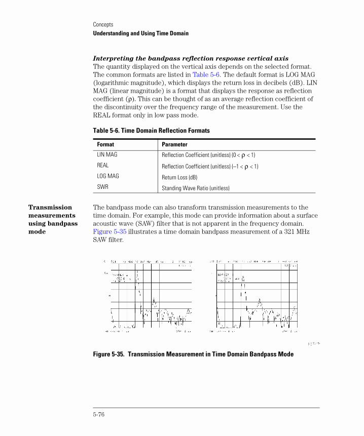
ConceptsUnderstanding and Using Time Domain
Interpreting the bandpass reflection response vertical axis
The quantity displayed on the vertical axis depends on the selected format. The common formats are listed in Table 5-6. The default format is LOG MAG (logarithmic magnitude), which displays the return loss in decibels (dB). LIN MAG (linear magnitude) is a format that displays the response as reflection coefficient (ρ). This can be thought of as an average reflection coefficient of the discontinuity over the frequency range of the measurement. Use the REAL format only in low pass mode.
Transmission
measurements
using bandpass
mode
The bandpass mode can also transform transmission measurements to the time domain. For example, this mode can provide information about a surface acoustic wave (SAW) filter that is not apparent in the frequency domain. Figure 5-35 illustrates a time domain bandpass measurement of a 321 MHz SAW filter.
Figure 5-35. Transmission Measurement in Time Domain Bandpass Mode
Table 5-6. Time Domain Reflection Formats
Format Parameter
LIN MAG
REAL
LOG MAG
SWR
Reflection Coefficient (unitless) (0 < ρ < 1)
Reflection Coefficient (unitless) (–1 < ρ < 1)
Return Loss (dB)
Standing Wave Ratio (unitless)
5-76

ConceptsUnderstanding and Using Time Domain
Interpreting the bandpass transmission response horizontal axis
In time domain transmission measurements, the horizontal axis is displayed in units of time. The time axis indicates the propagation delay through the device. Note that in time domain transmission measurements, the value dis-played is the actual delay (not x2). The marker provides the propagation delay in both time and distance.
Marker 2 in Figure 5-35a indicates the main path response through the test device, which has a propagation delay of 655.6 ns, or about 196.5 meters in electrical length. Marker 4 in Figure 5-35b indicates the triple-travel path response at 1.91 µs, or about 573.5 meters. The response at marker 1 (at 0 seconds) is an RF feedthru leakage path. In addition to the triple travel path response, there are several other multi-path responses through the test device, which are inherent in the design of a SAW filter.
Interpreting the bandpass transmission response vertical axis In the log magnitude format, the vertical axis displays the transmission loss or gain in dB; in the linear magnitude format it displays the transmission coeffi-cient (τ). Think of this as an average of the transmission response over the measurement frequency range.
Time domain low pass
This mode is used to simulate a traditional time domain reflectometry (TDR) measurement. It provides information to determine the type of discontinuity (resistive, capacitive, or inductive) that is present. Low pass provides the best resolution for a given bandwidth in the frequency domain. It may be used to give either the step or impulse response of the test device.
The low pass mode is less general-purpose than the bandpass mode because it places strict limitations on the measurement frequency range. The low pass mode requires that the frequency domain data points are harmonically related from dc to the stop frequency. That is, stop = n x start, where n = number of points. For example, with a start frequency of 300 kHz and 101 points, the stop frequency would be 30.3 MHz. Since the analyzer frequency range starts at 300 kHz, the dc frequency response is extrapolated from the lower fre-quency data. The requirement to pass dc is the same limitation that exists for traditional TDR.
5-77

ConceptsUnderstanding and Using Time Domain
Setting frequency
range for time
domain low pass
Before a low pass measurement is made, the measurement frequency range must meet the (stop = n x start) requirement described above. The SET FREQ LOW PASS softkey performs this function automatically: the stop frequency is set close to the entered stop frequency, and the start frequency is set equal to stop/n.
If the low end of the measurement frequency range is critical, it is best to cal-culate approximate values for the start and stop frequencies before pressing SET FREQ LOW PASS and calibrating. This avoids distortion of the measurement results. To see an example, select the preset values of 201 points and a 300 kHz to 3 GHz frequency range. Now press SET FREQ LOW PASS and observe the change in frequency values. The stop frequency changes to 2.999 GHz, and the start frequency changes to 14.925 MHz. This would cause a distortion of measurement results for frequencies from 300 kHz to 14.925 MHz.
Minimum allowable stop frequencies
The lowest analyzer measurement frequency is 30 kHz, therefore for each value of n there is a minimum allowable stop frequency that can be used. That is, the minimum stop frequency = n x 30 kHz. Table 5-7 lists the minimum frequency range that can be used for each value of n for low pass time domain measurements.
NOTE
If the start and stop frequencies do not conform to the low pass requirement before a low pass mode (step or impulse) is selected and transform is turned on, the analyzer resets the start and stop frequencies. If error correction is on when the frequency range is changed, this turns it off.
5-78

ConceptsUnderstanding and Using Time Domain
Reflection
measurements in
time domain low
pass
Figure 5-36 shows the time domain response of an unterminated cable in both the low-pass step and low-pass impulse modes.
Figure 5-36. Time Domain Low Pass Measurements of an Unterminated Cable
Table 5-7. Minimum Frequency Ranges for Time Domain Low Pass
Number of Points Minimum Frequency Range
3
11
26
51
101
201
401
801
1601
30 kHz to 0.09 MHz
30 kHz to 0.33 MHz
30 kHz to 0.78 MHz
30 kHz to 1.53 MHz
30 kHz to 3.03 MHz
30 kHz to 6.03 MHz
30 kHz to 12.03 MHz
30 kHz to 24.03 MHz
30 kHz to 48.03 MHz
5-79

ConceptsUnderstanding and Using Time Domain
Interpreting the low pass response horizontal axis
The low pass measurement horizontal axis is the two-way travel time to the discontinuity (as in the bandpass mode). The marker displays both the two-way time and the electrical length along the trace. To determine the actual physical length, enter the appropriate velocity factor as described in “Time domain bandpass” on page 5-74.
Interpreting the low pass response vertical axis
The vertical axis depends on the chosen format. In the low pass mode, the fre-quency domain data is taken at harmonically related frequencies and extrapo-lated to dc. Because this results in the inverse Fourier transform having only a real part (the imaginary part is zero), the most useful low pass step mode for-mat in this application is the real format. It displays the response in reflection coefficient units. This mode is similar to the traditional TDR response, which displays the reflected signal in a real format (volts) versus time (or distance) on the horizontal axis.
The real format can also be used in the low pass impulse mode, but for the best dynamic range for simultaneously viewing large and small discontinuities, use the log magnitude format.
Fault location
measurements
using low pass
As described, the low pass mode can simulate the TDR response of the test device. This response contains information useful in determining the type of discontinuity present.
Figure 5-37 illustrates the low pass responses of known discontinuities. Each circuit element was simulated to show the corresponding low pass time domain S
11 response waveform. The low pass mode gives the test device
response either to a step or to an impulse stimulus. Mathematically, the low pass impulse stimulus is the derivative of the step stimulus.
5-80

ConceptsUnderstanding and Using Time Domain
Figure 5-37. Simulated Low Pass Step and Impulse Response Waveforms (Real Format)
Figure 5-38 shows example cables with discontinuities (faults) using the low pass step mode with the real format.
5-81

ConceptsUnderstanding and Using Time Domain
Figure 5-38. Low Pass Step Measurements of Common Cable Faults (Real Format)
Transmission
measurements in
time domain low
pass
Measuring small signal transient response using low pass step
Use the low pass mode to analyze the test device’s small signal transient response. The transmission response of a device to a step input is often mea-sured at lower frequencies, using a function generator (to provide the step to the test device) and a sampling oscilloscope (to analyze the test device output response). The low pass step mode extends the frequency range of this type of measurement to 3 GHz (6 GHz with an analyzer Option 006).
The step input shown in Figure 5-39 is the inverse Fourier transform of the frequency domain response of a thru measured at calibration. The step rise time is proportional to the highest frequency in the frequency domain sweep; the higher the frequency, the faster the rise time. The frequency sweep in Figure 5-39 is from 10 MHz to 1 GHz.
5-82
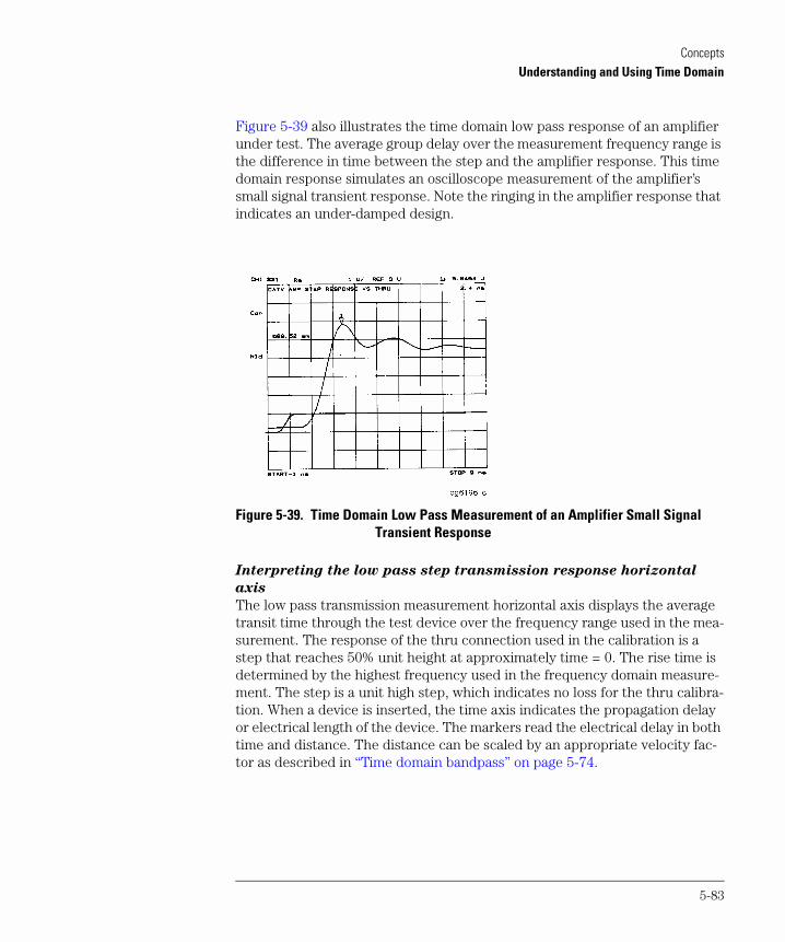
ConceptsUnderstanding and Using Time Domain
Figure 5-39 also illustrates the time domain low pass response of an amplifier under test. The average group delay over the measurement frequency range is the difference in time between the step and the amplifier response. This time domain response simulates an oscilloscope measurement of the amplifier’s small signal transient response. Note the ringing in the amplifier response that indicates an under-damped design.
Figure 5-39. Time Domain Low Pass Measurement of an Amplifier Small Signal Transient Response
Interpreting the low pass step transmission response horizontal
axis
The low pass transmission measurement horizontal axis displays the average transit time through the test device over the frequency range used in the mea-surement. The response of the thru connection used in the calibration is a step that reaches 50% unit height at approximately time = 0. The rise time is determined by the highest frequency used in the frequency domain measure-ment. The step is a unit high step, which indicates no loss for the thru calibra-tion. When a device is inserted, the time axis indicates the propagation delay or electrical length of the device. The markers read the electrical delay in both time and distance. The distance can be scaled by an appropriate velocity fac-tor as described in “Time domain bandpass” on page 5-74.
5-83

ConceptsUnderstanding and Using Time Domain
Interpreting the low pass step transmission response vertical axis
In the real format, the vertical axis displays the transmission response in real units (for example, volts). For the amplifier example in Figure 5-39, if the amplifier input is a step of 1 volt, the output, 2.4 nanoseconds after the step (indicated by marker 1), is 5.84 volts.
In the log magnitude format, the amplifier gain is the steady state value dis-played after the initial transients die out.
Measuring separate transmission paths through the test device
using low pass impulse mode
The low pass impulse mode can be used to identify different transmission paths through a test device that has a response at frequencies down to dc (or at least has a predictable response, above the noise floor, below 30 kHz). For example, use the low pass impulse mode to measure the relative transmission times through a multi-path device such as a power divider. Another example is to measure the pulse dispersion through a broadband transmission line, such as a fiber optic cable.
Both examples are illustrated in Figure 5-40. The horizontal and vertical axes can be interpreted as already described in this section under “Time domain bandpass” on page 5-74.
Figure 5-40. Transmission Measurements Using Low Pass Impulse Mode
5-84

ConceptsUnderstanding and Using Time Domain
Time domain concepts
Masking Masking occurs when a discontinuity (fault) closest to the reference plane affects the response of each subsequent discontinuity. This happens because the energy reflected from the first discontinuity never reaches subsequent discontinuities. For example, if a transmission line has two discontinuities that each reflect 50% of the incident voltage, the time domain response (real for-mat) shows the correct reflection coefficient for the first discontinuity (ρ=0.50). However, the second discontinuity appears as a 25% reflection (ρ=0.25) because only half the incident voltage reached the second disconti-nuity.
As an example of masking due to line loss, consider the time domain response of a 3 dB attenuator and a short circuit. The impulse response (log magnitude format) of the short circuit alone is a return loss of 0 dB, as shown in Figure 5-41a.
When the short circuit is placed at the end of the 3 dB attenuator, the return loss is –6 dB, as shown in Figure 5-41b. This value actually represents the for-ward and return path loss through the attenuator, and illustrates how a lossy network can affect the responses that follow it.
NOTE
This example assumes a loss-less transmission line. Real transmission lines, with non-zero loss, attenuate signals as a function of the distance from the reference plane.
5-85

ConceptsUnderstanding and Using Time Domain
Figure 5-41. Masking Example
Windowing The analyzer provides a windowing feature that makes time domain measure-ments more useful for isolating and identifying individual responses. Window-ing is needed because of the abrupt transitions in a frequency domain measurement at the start and stop frequencies. The band limiting of a fre-quency domain response causes overshoot and ringing in the time domain response, and causes a non-windowed impulse stimulus to have a sin(kt)/kt shape, where: k = π/frequency span and t = time (refer to Figure 5-42). This has two effects that limit the usefulness of the time domain measurement:
Finite impulse width (or rise time)
Finite impulse width limits the ability to resolve between two closely spaced responses. The effects of the finite impulse width cannot be improved without increasing the frequency span of the measurement (refer to Table 5-8).
Sidelobes
The impulse sidelobes limit the dynamic range of the time domain measure-ment by hiding low-level responses within the sidelobes of higher level responses. The effects of sidelobes can be improved by windowing (refer to Table 5-8).
5-86
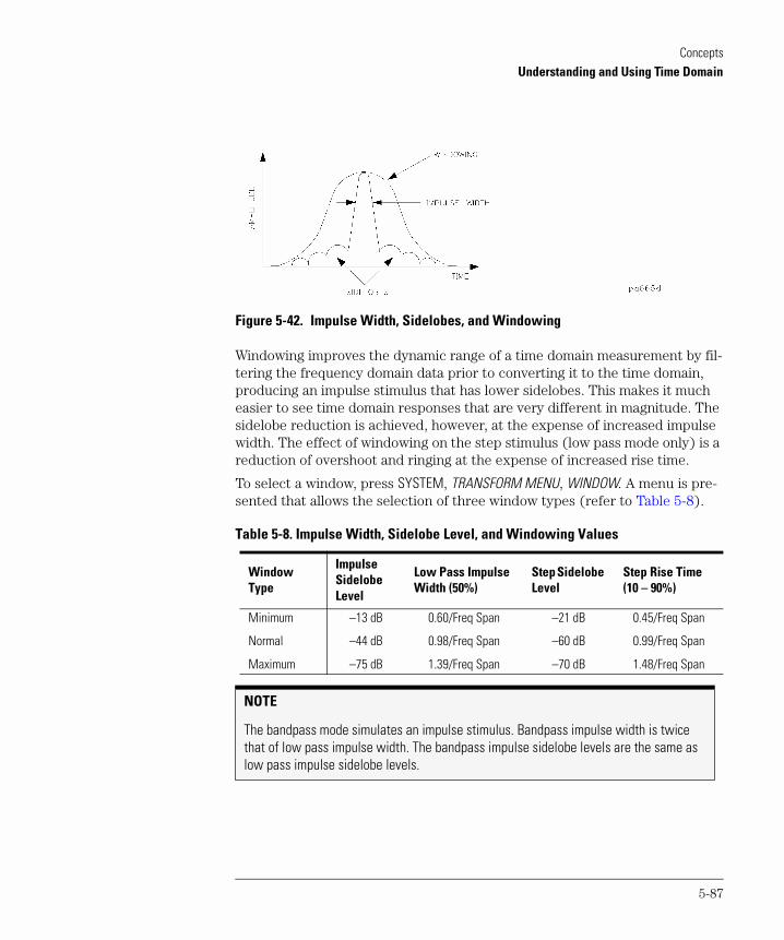
ConceptsUnderstanding and Using Time Domain
Figure 5-42. Impulse Width, Sidelobes, and Windowing
Windowing improves the dynamic range of a time domain measurement by fil-tering the frequency domain data prior to converting it to the time domain, producing an impulse stimulus that has lower sidelobes. This makes it much easier to see time domain responses that are very different in magnitude. The sidelobe reduction is achieved, however, at the expense of increased impulse width. The effect of windowing on the step stimulus (low pass mode only) is a reduction of overshoot and ringing at the expense of increased rise time.
To select a window, press SYSTEM, TRANSFORM MENU, WINDOW. A menu is pre-sented that allows the selection of three window types (refer to Table 5-8).
Table 5-8. Impulse Width, Sidelobe Level, and Windowing Values
Window Type
Impulse Sidelobe Level
Low Pass Impulse Width (50%)
Step Sidelobe Level
Step Rise Time (10 – 90%)
Minimum
Normal
Maximum
–13 dB
–44 dB
–75 dB
0.60/Freq Span
0.98/Freq Span
1.39/Freq Span
–21 dB
–60 dB
–70 dB
0.45/Freq Span
0.99/Freq Span
1.48/Freq Span
NOTE
The bandpass mode simulates an impulse stimulus. Bandpass impulse width is twice that of low pass impulse width. The bandpass impulse sidelobe levels are the same as low pass impulse sidelobe levels.
5-87

ConceptsUnderstanding and Using Time Domain
Choose one of the three window shapes listed in Table 5-8. Or you can use the knob to select any windowing pulse width (or rise time for a step stimulus) between the softkey values. The time domain stimulus sidelobe levels depend only on the window selected.
MINIMUM is essentially no window. Consequently, it gives the highest sidelobes.
NORMAL (the preset mode) gives reduced sidelobes and is the mode most often used.
MAXIMUM window gives the minimum sidelobes, providing the greatest dynamic range.
USE MEMORY on OFF remembers a user-specified window pulse width (or step
rise time) different from the standard window values.
A window is activated only for viewing a time domain response, and does not affect a displayed frequency domain response. Figure 5-43 shows the typical effects of windowing on the time domain response of a short circuit reflection measurement.
Figure 5-43. The Effects of Windowing on the Time Domain Responses of a Short Circuit
5-88

ConceptsUnderstanding and Using Time Domain
Range In the time domain, range is defined as the length in time that a measurement can be made without encountering a repetition of the response, called alias-ing. A time domain response repeats at regular intervals because the fre-quency domain data is taken at discrete frequency points, rather than continuously over the frequency band.
Measurement range is equal to 1/∆F (∆F is the spacing between frequency data points).
Measurement range = (number of points – 1)/frequency span (Hz).
Example:
Measurement = 201 points1 MHz to 2.001 GHz
Range = 1/∆F or (number of points – 1)/frequency span = 1/(10 x 106) or (201 – 1)/(2 x 109) = 100 x 10–9 seconds
Electrical length = range x the speed of light (3 x 10⁸ m/s) = (100 x 10–9 s) x (3 x 10⁸ m/s) = 30 meters
In this example, the range is 100 ns, or 30 meters electrical length. To prevent the time domain responses from overlapping, the test device must be 30 meters or less in electrical length for a transmission measurement (15 meters for a re-flection measurement). The analyzer limits the stop time to prevent the display of aliased responses.
To increase the time domain measurement range, first increase the number of points, but remember that as the number of points increases, the sweep speed decreases. Decreasing the frequency span also increases range, but reduces resolution.
Resolution Two different resolution terms are used in the time domain:
• Response resolution• Range resolution
Response resolution
Time domain response resolution is defined as the ability to resolve two closely-spaced responses, or a measure of how close two responses can be to each other and still be distinguished from each other. For responses of equal amplitude, the response resolution is equal to the 50% (–6 dB) impulse width. It is inversely proportional to the measurement frequency span, and is also a function of the window used in the transform. The approximate formulas for calculating the 50% impulse width are given in Table 5-8 on page 5-87. For example, using the formula for the bandpass mode with a normal windowing function for a 1 MHz to 3.001 GHz measurement (3 GHz span):
5-89

ConceptsUnderstanding and Using Time Domain
50% calculated impulse width = 0.98 x (1/3 GHz) x 2 = 0.65 nanoseconds
Electrical length (in air) = (0.65 x 10⁻⁹ s) x (30 x 109 cm/s) = 19.6 centimeters
With this measurement, two equal responses can be distinguished when they are separated by at least 19.6 centimeters. In a 6 GHz measurement with an Op-tion 006 analyzer, two equal responses can be distinguished when they are sep-arated by at least 9.8 cm. Using the low pass mode (the low pass frequencies are slightly different) with a minimum windowing function, you can distinguish two equal responses that are about 5 centimeters or more apart.
For reflection measurements, which measure the two-way time to the response, divide the response resolution by 2. Using the example above, you can distinguish two faults of equal magnitude provided they are 2.5 centime-ters (electrical length) or more apart.
For example, a cable with a teflon dielectric (0.7 relative velocity factor), mea-sured under the conditions stated above, has a fault location measurement response resolution of 1.7 centimeters. This is the maximum fault location response resolution. Factors such as reduced frequency span, greater fre-quency domain data windowing, and a large discontinuity shadowing the response of a smaller discontinuity, all act to degrade the effective response resolution.
NOTE
Remember, to determine the physical length, enter the relative velocity factor of the transmission medium under test.
5-90

ConceptsUnderstanding and Using Time Domain
Figure 5-44 illustrates the effects of response resolution. The solid line shows the actual reflection measurement of two approximately equal discontinuities (the input and output of an SMA barrel). The dashed line shows the approxi-mate effect of each discontinuity, if they could be measured separately.
Figure 5-44. Response Resolution
While increasing the frequency span increases the response resolution, keep the following points in mind:
• The time domain response noise floor is directly related to the frequency do-main data noise floor. Because of this, if the frequency domain data points are taken at or below the measurement noise floor, the time domain measurement noise floor is degraded.
• The time domain measurement is an average of the response over the frequen-cy range of the measurement. If the frequency domain data is measured out-of-band, the time domain measurement is also the out-of-band response.
You may (with these limitations in mind) choose to use a frequency span that is wider than the test device bandwidth to achieve better resolution.
Range resolution
Time domain range resolution is defined as the ability to locate a single response in time. If only one response is present, range resolution is a mea-sure of how closely you can pinpoint the peak of that response. The range res-olution is equal to the digital resolution of the display, which is the time domain span divided by the number of points on the display. To get the maxi-
5-91

ConceptsUnderstanding and Using Time Domain
mum range resolution, center the response on the display and reduce the time domain span. The range resolution is always much finer than the response res-olution (refer to Figure 5-45).
Figure 5-45. Range Resolution of a Single Discontinuity
The Transform Parameter feature can be used to view the current values of the range, response resolution and range resolution by pressing SYSTEM, TRANSFORM MENU, TRANSFORM PARAMETERS.
Gating Gating provides the flexibility of selectively removing time domain responses. The remaining time domain responses can then be transformed back to the frequency domain. For reflection (or fault location) measurements, use this feature to remove the effects of unwanted discontinuities in the time domain. You can then view the frequency response of the remaining discontinuities. In a transmission measurement, you can remove the effects of multiple transmis-sion paths.
Figure 5-46a shows the frequency response of an electrical airline and termi-nation. Figure 5-46b shows the response in the time domain. The discontinu-ity on the left is due to the input connector. The discontinuity on the right is due to the termination. We want to remove the effect of the connector so that we can see the frequency response of just the airline and termination. Figure 5-46c shows the gate applied to the connector discontinuity. Figure 5-46d shows the frequency response of the airline and termination, with the connector “gated out.”
5-92

ConceptsUnderstanding and Using Time Domain
Figure 5-46. Sequence of Steps in Gating Operation
Setting the gate
Think of a gate as a bandpass filter in the time domain (refer to Figure 5-47). When the gate is on, responses outside the gate are mathematically removed from the time domain trace. Enter the gate position as a start and stop time (not frequency) or as a center and span time. The start and stop times are the bandpass filter –6 dB cutoff times. Gates can have a negative span, in which case the responses inside the gate are mathematically removed. The gate’s start and stop flags define the region where gating is on.
Figure 5-47. Gate Shape
5-93
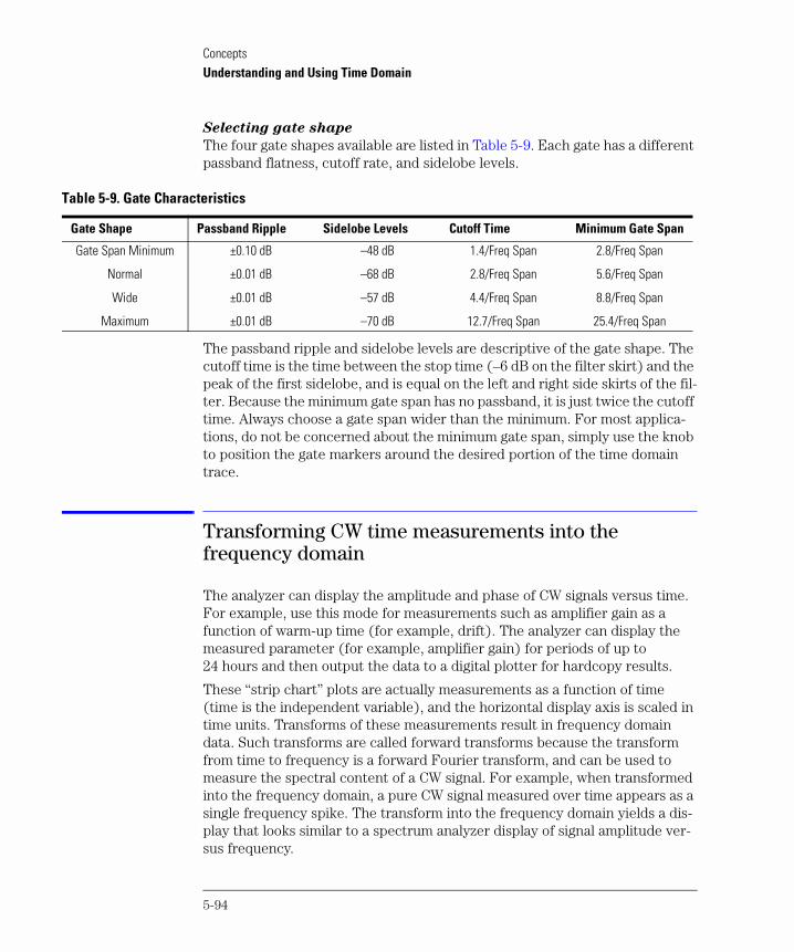
ConceptsUnderstanding and Using Time Domain
Selecting gate shape
The four gate shapes available are listed in Table 5-9. Each gate has a different passband flatness, cutoff rate, and sidelobe levels.
The passband ripple and sidelobe levels are descriptive of the gate shape. The cutoff time is the time between the stop time (–6 dB on the filter skirt) and the peak of the first sidelobe, and is equal on the left and right side skirts of the fil-ter. Because the minimum gate span has no passband, it is just twice the cutoff time. Always choose a gate span wider than the minimum. For most applica-tions, do not be concerned about the minimum gate span, simply use the knob to position the gate markers around the desired portion of the time domain trace.
Transforming CW time measurements into the frequency domain
The analyzer can display the amplitude and phase of CW signals versus time. For example, use this mode for measurements such as amplifier gain as a function of warm-up time (for example, drift). The analyzer can display the measured parameter (for example, amplifier gain) for periods of up to 24 hours and then output the data to a digital plotter for hardcopy results.
These “strip chart” plots are actually measurements as a function of time (time is the independent variable), and the horizontal display axis is scaled in time units. Transforms of these measurements result in frequency domain data. Such transforms are called forward transforms because the transform from time to frequency is a forward Fourier transform, and can be used to measure the spectral content of a CW signal. For example, when transformed into the frequency domain, a pure CW signal measured over time appears as a single frequency spike. The transform into the frequency domain yields a dis-play that looks similar to a spectrum analyzer display of signal amplitude ver-sus frequency.
Table 5-9. Gate Characteristics
Gate Shape Passband Ripple Sidelobe Levels Cutoff Time Minimum Gate Span
Gate Span Minimum
Normal
Wide
Maximum
±0.10 dB
±0.01 dB
±0.01 dB
±0.01 dB
–48 dB
–68 dB
–57 dB
–70 dB
1.4/Freq Span
2.8/Freq Span
4.4/Freq Span
12.7/Freq Span
2.8/Freq Span
5.6/Freq Span
8.8/Freq Span
25.4/Freq Span
5-94

ConceptsUnderstanding and Using Time Domain
Forward
transform
measurements
This is an example of a measurement using the Fourier transform in the for-ward direction, from the time domain to the frequency domain (refer to Figure 5-48).
Figure 5-48. Amplifier Gain Measurement
Interpreting the forward transform vertical axis
With the log magnitude format selected, the vertical axis displays dB. This for-mat simulates a spectrum analyzer display of power versus frequency.
Interpreting the forward transform horizontal axis
In a frequency domain transform of a CW time measurement, the horizontal axis is measured in units of frequency. The center frequency is the offset of the CW frequency. For example, with a center frequency of 0 Hz, the CW fre-quency (250 MHz in the example) is in the center of the display. If the center frequency entered is a positive value, the CW frequency shifts to the right half of the display; a negative value shifts it to the left half of the display. The span value entered with the transform on is the total frequency span shown on the display. (Alternatively, the frequency display values can be entered as start and stop.)
5-95

ConceptsUnderstanding and Using Time Domain
Demodulating the results of the forward transform
The forward transform can separate the effects of the CW frequency modula-tion amplitude and phase components. For example, if a test device modulates the transmission response (S
21) with a 500 Hz AM signal, you can see the
effects of that modulation as shown in Figure 5-49. To simulate this effect, apply a 500 Hz sine wave to the analyzer rear panel EXT AM input.
Figure 5-49. Combined Effects of Amplitude and Phase Modulation
Using the demodulation capabilities of the analyzer, it is possible to view the amplitude or the phase component of the modulation separately. The window menu includes the following softkeys to control the demodulation feature:
DEMOD: OFF This is the normal preset state, in which both the amplitude and phase components of any test device modulation appear on the display.
AMPLITUDE displays only the amplitude modulation, as illustrated in Figure 5-50a.
PHASE displays only the phase modulation, as shown in Figure 5-50b.
5-96
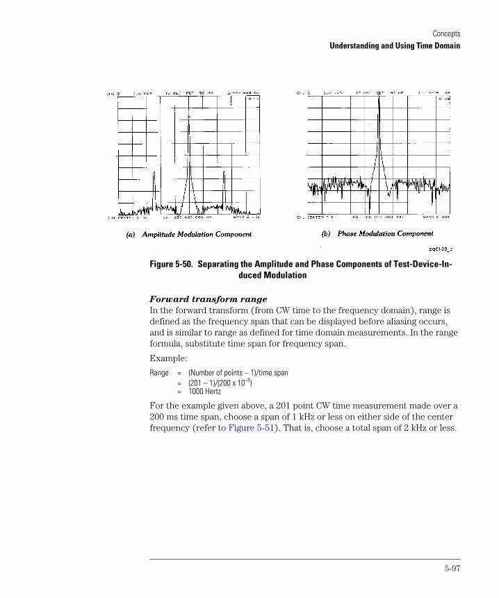
ConceptsUnderstanding and Using Time Domain
Figure 5-50. Separating the Amplitude and Phase Components of Test-Device-In-duced Modulation
Forward transform range
In the forward transform (from CW time to the frequency domain), range is defined as the frequency span that can be displayed before aliasing occurs, and is similar to range as defined for time domain measurements. In the range formula, substitute time span for frequency span.
Example:
Range = (Number of points – 1)/time span = (201 – 1)/(200 x 10–3) = 1000 Hertz
For the example given above, a 201 point CW time measurement made over a 200 ms time span, choose a span of 1 kHz or less on either side of the center frequency (refer to Figure 5-51). That is, choose a total span of 2 kHz or less.
5-97

ConceptsUnderstanding and Using Time Domain
Figure 5-51. Range of a Forward Transform Measurement
To increase the frequency domain measurement range, increase the span. The maximum range is inversely proportional to the sweep time, therefore it may be necessary to increase the number of points or decrease the sweep time. Because increasing the number of points increases the auto sweep time, the maximum range is 2 kHz on either side of the selected CW time measurement center frequency (4 kHz total span). To display a total frequency span of 4 kHz, enter the span as 4000 Hz.
5-98

ConceptsInstrument Preset State and Memory Allocation
Instrument Preset State and Memory Allocation
The analyzer is capable of saving complete instrument states for later retrieval. It can store these instrument states into the internal memory, to the internal disk, or to an external disk. This section describes these capabilities in the following sections:
• instrument state definition • memory allocation • internal and external data storage • description of analyzer state after preset
Types of memory and data storage
The analyzer utilizes two types of memory and can also utilize the internal disk drive or be connected to an external disk drive:
Volatile Memory This is dynamic read/write memory, of approximately 2 Mbytes, that contains all of the parameters that make up the current instrument state. An instru-ment state consists of all the stimulus and response parameters that set up the analyzer to make a specific measurement.
Some data that you may think is part of the instrument state (such as calibra-tion data and memory traces) are actually stored in battery-protected mem-ory. Refer to “Battery-Protected Memory” to read more about the differences.
Volatile memory is cleared upon a power cycle of the instrument and, except as noted, upon instrument preset.
Battery-Protected
Memory
This is read/write memory that is protected by a battery to provide storage of data when line power to the instrument is turned off. With this battery protec-tion, data can be retained in memory for approximately 250 days at 70°C and for approximately 10 years at 25°C (typically.)
Battery-protected memory consists of a block of user-allocated memory and a block of fixed memory.
5-99

ConceptsInstrument Preset State and Memory Allocation
The user-allocated memory is available for you to save the following data:
• instrument states • measurement calibration data • power meter calibration data • user calibration kit definitions • memory traces • user preset
C A U T I O N Even though calibration data is stored in battery-protected memory, if the associated instrument state is not saved, you will not be able to retrieve the calibration data after a power cycle.
The fixed memory is used to store the following data (you cannot change where this data is stored and it does not affect your memory availability for storing user-allocated data):
• GPIB addresses • copy configuration (printer and plotter type, port, baud rate, handshake) • power meter type (Agilent 436/438) • display colors • sequence titles • sixth sequence • power sensor calibration factors and loss tables • user-defined calibration kits • system Z0 • factory preset • GPIB configuration • display intensity default
The maximum number of instrument states, calibrations, and memory traces that can reside in battery-protected memory at any one time is limited to 31 instrument states, 128 calibrations (4 per instrument state, including the present instrument state), and 64 memory traces (2 per instrument state, in-cluding the present instrument state).
In addition, the number of instrument states and associated calibrations and memory traces are limited by the available memory. To display the amount of unused memory on the analyzer, press SAVE/RECALL. (Be sure you have selected INTERNAL MEMORY as your disk type.) In the upper righthand portion of the display, the value displayed as Bytes free: is the unused battery-protected memory. When you save to the internal memory, you will see the number of bytes free decrease. When you delete files, the number of bytes free increases. There is a maximum of 512 kbytes available.
5-100

ConceptsInstrument Preset State and Memory Allocation
If you have deleted registers since the last time the instrument was preset, the bytes available for you to use may be less than the actual “bytes free” that is displayed. Deleting registers to increase the available memory will work in cases where the registers being deleted and the registers needing to be added are of the same standard size (such as instrument states not having calibra-tions associated with them). In certain other cases, however, you may have to press PRESET after deleting registers so that the “bytes free” value equals the available memory value. During a preset, the analyzer runs a memory packer that defragments the free memory into one contiguous block.
Table 5-10 on page 5-102 shows the memory requirements of calibration arrays and memory trace arrays to help you approximate memory require-ments. For example, add the following memory requirements:
• a full 2-port calibration with 801 points (58 k) • the memory trace array (4.9 k) • the instrument state (3 k)
The total memory requirement is 65.9 kbytes. There is sufficient memory to store 7 calibrations of this type. However, the same calibration performed with 1601 points and 2 channels uncoupled would require 252 kbytes:
• a full 2-port calibration with 1601 points, two channels, uncoupled (230 k) • the memory trace array (19 k) • the instrument state (3 k)
Only two of these calibrations could reside in memory before the available memory would be depleted.
5-101

ConceptsInstrument Preset State and Memory Allocation
The analyzer attempts to allocate memory at the start of a calibration. If insuf-ficient memory is available, an error message is displayed. It is possible that the memory might be fragmented due to the sequence of saving and deleting states of various sizes. Another alternative would be to store the current state to disk and then press PRESET. The analyzer runs a memory packer which might regain some previously inaccessible memory. If memory is still inade-quate, delete an instrument state and restart the calibration.
Storing Data to
Disk
You can use the internal disk drive or connect an external disk drive for stor-age of instrument states, calibration data, measurement data, and plot files. (Refer to Agilent 8702D User’s Guide, for more information on saving mea-surement data and plot files.)
Table 5-10. Memory Requirements of Calibration and Memory Trace Arrays
Variable Data Length (Bytes)
Approximate Totals (Bytes)
401 pts 801 pts 1601 pts
1 chan 1 chan 2 chan
Calibration Arrays
Response
Response and Isolation
1-Port
E/O Response & Match
O/E Response & Match
2-Port
Interpolated Cal
N × 6 + 52
N × 6 × 2 + 52
N × 6 × 3 + 52
N × 6 × 6+ 52
N × 6 × 10 + 52
N × 6 × 12 + 52
Same as above in addition to regular cal
2.5 k
5 k
7 k
14 k
24 k
29 k
5 k
10 k
14 k
28 k
47 k
58 k
10 k
19 k
29 k
56 k
94 k
115 k
19 k
38 k
58 k
113 k
188 k
230 k
Power Meter Cala
a. This variable is allocated once per active channel.
(Nb x 2 x number of channelsc) + 208
b. The number of points that were set at the time the cal was turned on.c. If the channels are coupled, this number is always 1. If the channels are uncoupled, this number refers to
the number of channels that have power meter cal on.
1 k 1.8 k 3.4 k 6.6 k
Measurement Data
Memory Trace Arraya N x 6 + 52 2.5 k 4.9 k 9.7 k 19 k
Instrument Stated
d. This value may change with different firmware revisions.
3 k 3 k 3 k 3 k
5-102

ConceptsInstrument Preset State and Memory Allocation
The analyzer displays one file name per stored instrument state when you list the disk directory. In reality, several files are actually stored to the disk when you store the instrument state. Thus, when the disk directory is accessed from a remote system controller, the directory will show several files associated with a particular saved state. The maximum number of files that you can store on a disk depends on the directory size. You can define the directory size when you format a disk. Refer to “Preset Conditions” on page 2-42 for the default directory size for floppy disks and hard disks.
The maximum number of instrument states and calibrations that can reside on a disk is limited by the available disk space. To see the available disk space dis-played on the analyzer, press SAVE RECALL. (Be sure you have selected either INTERNAL DISK or EXTERNAL DISK depending on your disk type.) In the upper righthand portion of the display, the value displayed as Bytes free: is the available disk space. If your disk is formatted in LIF, this value is the largest contiguous block of disk space. Since the analyzer is reporting the largest con-tiguous block of disk space, you may or may not see the bytes free number change when you delete files. If your disk is formatted in DOS, the number reported as bytes free is the total available disk space. That number is updated whenever you save to or delete files from the disk.
A disk file created by the analyzer appends a suffix to the file name. The suffix consists of one or two characters: the first character is the file type and the second is a data index. (Refer to Table 5-11 on page 5-104 for the definitions of each suffix character.)
5-103

ConceptsInstrument Preset State and Memory Allocation
If correction is on at the time of an external store, the calibration set is stored to disk. (Note that inactive calibrations are not stored to disk.) When an instrument state is loaded into the analyzer from disk, the stimulus and response parameters are restored first. If correction is on for the loaded state, the analyzer will load a calibration set from disk that carries the same title as the one stored for the instrument state.
Table 5-11. Suffix Character Definitions
Char 1 Definition Char 2 Definition
I Instrument StateG Graphics 1
0
Display Graphics
Graphics IndexD Error Corrected Data 1
2
Channel 1
Channel 2R Raw Data 1 to 4
5 to 8
Channel 1, raw arrays 1 to 4
Channel 2, raw arrays 5 to 8F Formatted Data 1
2
Channel 1
Channel 2C Cal K
R
S
Cal Kit
Lightwave Receiver Cal Data
Lightwave Source Cal Data1 Cal Data, Channel 1 0
1 to 9
A
B
C
Stimulus State
Coefficients 1 to 9
Coefficient 10
Coefficient 11
Coefficient 122 Cal Data, Channel 2 0 to C same as Channel 1M Memory Trace Data 1
2
Channel 1
Channel 2
5-104

ConceptsInstrument Preset State and Memory Allocation
Conserving memory
If you are concerned about conserving memory, either internal memory or external disk space, some of the most memory-intensive operations include:
• two-port error correction • interpolated error correction • 1601 measurement points • using time domain • saving data arrays and graphics with the instrument state
Using saved calibration sets
When you are saving to internal memory, calibration sets are linked to the instrument state and measurement parameter for which the calibration was done. Therefore, a saved calibration can be used for multiple instrument states as long as the measurement parameter, frequency range, and number of points are the same. A full 2-port calibration is valid for any S-parameter mea-surement with the same frequency range and number of points. When an instrument state is deleted from memory, the associated calibration set is also deleted if it is unused by any other state.
The following hints will help you avoid potential problems:
• If a measurement is saved with calibration and interpolated calibration on, it will be restored with interpolated calibration on.
• A calibration stored from one instrument and recalled by a different one will be invalid. To ensure maximum accuracy, always recalibrate in these circumstanc-es.
• No record is kept in memory of the temperature when a calibration set was stored. Instrument characteristics change as a function of temperature, and a calibration stored at one temperature may be inaccurate if recalled and used at a different temperature.
5-105

ConceptsInstrument Preset State and Memory Allocation
Table 5-12. Results of Power Loss to Non-Volatile Memory
GPIB ADDRESSES are set to the following defaults:Agilent 8702D 16USER DISPLAY 17PLOTTER 5PRINTER 1POWER METER 13DISK 0DISK UNIT NUMBER 0DISK VOLUME NUMBER 0
POWER METER TYPE is set to Agilent 438A/437INTERNAL REGISTER TITLESa are set to defaults: REG1 through REG32.
a. Only applies to GPIB operation.
EXTERNAL REGISTER TITLESa (store files) are set to defaults: FILE1 through FILE5.PRINT TYPE is set to default: MONOCHROMEPRINTING/PLOTTING SETUPS are set to the following defaults:
PARALLEL PORT COPYPLOTTER TYPE PLOTTERPLOTTER PLOT SERIALPLOTTER BAUD RATE 9600PLOTTER HANDSHAKE Xon-XoffPRINTER TYPE DESKJETPRINTER PORT PARALLELPRINTER BAUD RATE 19200PRINTER HANDSHAKE Xon-Xoff
5-106

Index
Aaccessories, 2-5, 2-8accuracy enhancement
concepts, 5-17–5-70effectiveness of, 5-39what is, 5-18
adapter kits, 2-6ADC, 5-7ADJ adjustment, 2-39admittance conversion, 5-15–5-16alphabetical listing of keys, 2-21–2-38, 2-39–??analog-to-digital converter, 5-7analyzer display features, 2-14attenuator, 5-3AUX INPUT connector, 2-39averaging, sweep-to-sweep, 5-7AVG menu map, 1-2Avg status notation, 2-39
Bbandpass mode
fault location measurements, 5-81reflection measurements, 5-74transmission measurements, 5-76
battery backup for memory, 5-100BIAS CONNECT connector, 2-39built-in test set, 5-4
CC? status notation, 2-39C2 = status notation, 2-39cabinet, 2-8cables
GPIB, 2-9interface, 2-9test port return, 2-6
CAL menu map, 1-3calibrated power level for power meter, 5-64calibration
channel coupling, 5-42concepts, 5-17–5-70cycle, 4-2data lost, 5-101device measurements, 5-42for non-insertable devices, 5-60in memory, 5-100
interpolated, 5-106interpolated error correction, 5-41measurement parameters, 5-42modifying kits, 5-47omitting isolation, 5-43power meter, 5-64response & match, 4-52restarting, 5-43saving data, 5-43sets, using, 5-106specifying kits, 5-47standard devices, 5-43temperature, 5-106TRL*/LRM*, 5-61using on multiple analyzers, 5-106validity of, 5-41verify performance of, 5-57
calibration arrays memory requirements,5-102
calibration constants, viewing/modifying, 5-58calibration kit, 2-5
class assignments, 5-54definitions, 5-48modify menu, 5-49standard definitions, 5-50terminology, 5-48
calibration standardsdefining, 5-62fabricating, 5-62frequency response of, 5-44fringe capacitance, 5-45types, 5-45
channel coupling calibration, 5-42characteristics
connector, 4-19E/E, 4-24–4-49E/O, 4-67–4-80environmental, 4-22error-corrected, 4-24–4-49general, 4-18measurement port, 4-24–4-47O/E, 4-53–4-66O/O, 4-81–4-90operating, 4-22Option 011, 4-10–4-17standard instrument, 4-3–4-9
classification, laser, 4-94CMOS memory, 5-100
Index-1

Index
coefficient, linear reflection, 4-51concepts
accuracy enhancement, 5-17–5-70calibration, 5-17–5-70data processing, 5-5error correction, 5-17–5-70frequency domain, 5-71–5-99measurement calibration, 5-17–5-70response function, 5-11system overview, 5-2time domain, 5-71–5-99
connector10 MHZ PRECISION REFERENCE, 2-39AUX INPUT, 2-39BIAS CONNECT, 2-39characteristics, 4-19DIN KYBD, 2-39EXT AM, 2-40EXT MON, 2-40EXT REF, 2-40EXT TRIG, 2-40for external monitor, 2-16, 2-40for GPIB, 2-16, 2-40LIMIT TEST, 2-40parallel port, 2-40probe power, 2-41R channel, 2-13, 2-41RS-232, 2-41test device, 5-4TEST SEQ, 2-41TEST SET I/O INTERCONNECT, 2-41
constants, calibration, 5-58continuous sample mode, 5-66conversion
menu, 5-15reflection impedance/admittance, 5-15transform, 5-8transmission impedance/admittance, 5-16
COPY menu map, 1-5Cor status notation, 2-39crosstalk, 5-23CW time-to-frequency domain, 5-95
Ddata point, definition, 5-6data processing, 5-4, 5-5
flow diagram, 5-6
data retention time, internal memory, 4-21data storage, types of, 5-100declaration of conformity, 4-95define standard menu, 5-50defining calibration standards, 5-62Del status notation, 2-39delay block, 5-8device measurements calibration, 5-42dictionary reference, 2-2dimensions of instrument, 4-22DIN KYBD connector, 2-39directivity, 5-20directory size, 5-104disk
external, 5-103internal, 5-103storing data, 5-103
displayfeatures, 2-14formats, preset, 2-43memory, 5-10
DISPLAY menu map, 1-6documents, reference, 2-19DOS format, 2-8dynamic range, 4-4
EE/E characteristics, 4-24–4-49E/O characteristics, 4-67–4-80electrical offset standards, 5-44engaging hold mode, 2-41environmental characteristics, 4-22error correction
concepts, 5-17, 5-70full two-port calibration, 5-39one-path two-port calibration, 5-39one-port, 5-38raw data, 5-4response and isolation, 5-38response calibration, 5-38
error messagesalphabetically listed, 3-3numerically listed, 3-27
error modelone-port, 5-24two-port, 5-32
EXT AM connector, 2-40
Index-2

Index
EXT MON connector, 2-16, 2-40EXT REF connector, 2-40ext status notation, 2-39EXT TRIG connector, 2-40external disk, 5-103external monitor connector, 2-16, 2-40
Ffault location measurements
using low pass mode, 5-81file names, 5-104flatness measurement uncertainty, 4-52format arrays, 5-9FORMAT menu map, 1-6formatting data, 5-9forward transform, 5-96
demodulating the results, 5-97range, 5-98
frequency domainconcepts, 5-71–5-99transform from CW time, 5-95
frequency response, 5-23of calibration standards, 5-44
frequency-to-time domain, 5-71Fresnel reflection, 4-51fringe capacitance, 5-45front panel features, 2-12full two-port calibration error correction, 5-39
GGat status notation, 2-40gating, 5-8
time domain, 5-93general characteristics, 4-18GPIB
cables, 2-9connector, 2-40interface, 4-93
HH=2 status notation, 2-40H=3 status notation, 2-40Hld status notation, 2-40hold mode engaged, 2-41humidity, 4-2
IIF detection, 5-7impedance conversion, 2-6initializing
DOS, 2-8LIF, 2-8
input ports menu, 5-15input power, 4-51insertion loss, 4-51instrument
dimensions, 4-22options, 2-3specifications and characteristics, 4-3–4-9
instrument statein memory, 5-100memory requirements, 5-102
interfacecables, 2-9GPIB, 4-93
internal memory data retention time, 4-21interpolated
calibration, 5-106error correction, 5-41
interpolation, power meter calibration, 5-65isolation, 5-23
calibration, 5-43
Kkey menu maps, 1-2–1-15keyboards, 2-9keycap listing, 2-21–2-38, 2-39–??
Llabel class menu, 5-57label kit menu, 5-57label standard menu, 5-54laser classification, 4-94LIF format, 2-8LIMIT TEST connector, 2-40LINE key, 2-40linear reflection coefficient, 4-51line-power
cables, 2-10listing of keys, 2-21–2-38, 2-39–??load match, 5-22LOCAL menu map, 1-7
Index-3

Index
loss of data, power meter calibration, 5-65low pass mode
reflection measurements, 5-79setting frequency range, 5-78transmission measurements, 5-82
Mman status notation, 2-40MARKER FCTN menu map, 1-9MARKER menu map, 1-8masking, time domain, 5-85mass storage, 2-8MEAS menu map, 1-10measurement
calibration concepts, 5-17–5-70parameters calibration, 5-42port characteristics, 4-24–4-47repeatability, 4-91selecting, 5-15times, typical, 4-18
measurement errorscauses of, 5-19correcting for, 5-38crosstalk, 5-23directivity, 5-20frequency response, 5-23isolation, 5-23load match, 5-22source match, 5-21tracking, 5-23
measurement uncertainty, flatness, 4-52memory
battery backup, 5-100CMOS, 5-100conserving, 5-106display, 5-10external disk, 5-103internal disk, 5-103non-volatile, 5-100requirements, 5-102saving data, 5-100types of, 5-100volatile, 5-100
memory trace arraysmemory requirements, 5-102
memory-intensive operations, 5-106menu maps, 1-2–1-15
MENU menu map, 1-11microprocessor, 5-4minimum loss pad, 2-6modes of operation, power meter calibration,
5-66modifying
calibration kit menu, 5-49calibration kits, 5-47
monitor, 2-9connector, 2-16, 2-40
multiplexer, 5-4
Nnoise declaration, 4-94non-insertable devices
calibrating for, 5-60non-volatile memory, 5-100
OO/E characteristics, 4-53–4-66O/O characteristics, 4-81–4-90Of? status notation, 2-40offset, 5-9Ofs status notation, 2-40omitting isolation calibration, 5-43one-path/two-port error correction, 5-39one-port
error correction, 5-38error model, 5-24
operating characteristics, 4-22operation, of the analyzer, 5-2Option 011
specifications and characteristics, 4-10–4-17options, instrument, 2-3overview of the system, 5-2
PP? status notation, 2-40, 3-19P0 status notation, 2-40PARALLEL PORT connector, 2-40PC status notation, 2-40PC? status notation, 2-40peripheral equipment, required, 5-4phase shift, 5-45plotters, 2-8
Index-4

Index
power level, calibrating, 5-64power loss correction list, 5-68power meter calibration, 5-64
accuracy, 5-68applications, 5-64compatible sweep types, 5-65continuous sample mode, 5-66interpolation, 5-65loss of data, 5-65modes of operation, 5-66power loss correction list, 5-68power sensor calibration data, 5-68sample-and-sweep mode, 5-67speed, 5-68stimulus parameters, 5-69
power sensor calibration factor list, 5-68preset display formats, 2-43PRESET key, 2-41PRESET menu map, 1-11primary applications, power meter calibration,
5-64printers, 2-8Prm status notation, 2-32, 2-41PROBE POWER connector, 2-41processing data, 5-4
RR channel connector, 2-13, 2-41rack mount cabinet, 2-8range, time domain, 5-89ratio calculations, 5-7raw data
arrays, 5-7error correction, 5-4
rear panel features, 2-16receiver block, 5-4receiver measurement repeatability, 4-91reference documents, 2-19reflection
impedance conversion, 5-15sensitivity, 4-51
reflection measurementsusing bandpass mode, 5-74using low pass mode, 5-79
regulatory information, 4-94relative velocity factor, adjusting of, 5-74repeatability, measurement, 4-91
required peripheral equipment, 5-4resolution, time domain, 5-90response & match calibration, 4-52response calibration error correction, 5-38response function, 5-11response/isolation calibration error correction,
5-38restarting a calibration, 5-43return loss, 4-51RS-232 connector, 2-41
Ssample-and-sweep mode, 5-67sampler/IF correction, 5-7sampler/mixer, receiver block, 5-4SAVE/RECALL menu map, 1-12saving calibration data, 5-43scale, 5-9SCALE REF menu map, 1-13selecting the measurement, 5-15sensitivity, reflection, 4-51SEQ menu map, 1-14signal power, 4-51signal separation devices, 5-4Smo status notation, 2-41smoothing, 5-9softkey listing, 2-21–2-38, 2-39–??softkey menu maps, 1-2–1-15source, 5-3source match, 5-21S-parameter menu, 5-15S-parameters, 5-12specifications
definition of terms, 4-2Option 011, 4-10–4-17standard instrument, 4-3–4-9
specify class menu, 5-54specify offset menu, 5-53specifying calibration kits, 5-47speed/accuracy, power meter calibration, 5-68standard types, calibration, 5-45standards, calibration, 5-43start values possible, 2-14step attenuator, 5-3stimulus
start value, 2-14stop value, 2-15
Index-5

Index
stimulus parameters, power meter calibration,5-69
stop values possible, 2-15storing
data, methods of, 5-100to external disk, 2-8to internal disk, 2-8to internal memory, 2-8
sweepdefinition, 5-7types, power meter calibration, 5-65
synthesized source, 5-3system
accessories, 2-8cabinet, 2-8overview, 5-2performance, 4-50
SYSTEM menu map, 1-15systematic errors
characterizing, 5-24
Ttemperature range, 4-2test device connection, 5-4test fixtures, transistors, 2-7TEST SEQ connector, 2-41TEST SET I/O INTERCONNECT, 2-41test set, built-in, 5-4time domain
bandpass, 5-74bandpass mode, 5-71concepts, 5-71–5-99gating, 5-93general theory, 5-72low pass, 5-71–5-82masking, 5-85range, 5-89reflection bandpass mode, 5-74relative velocity factor, 5-74resolution, 5-90transform, 5-9transmission bandpass mode, 5-76windowing, 5-86
time-to-frequency domain, 5-72trace math operation, 5-8tracking, 5-23transform
CW time-to-frequency domain, 5-95forward measurements, 5-96frequency-to-time domain, 5-71time-to-frequency domain, 5-72
transform modestime domain bandpass, 5-71time domain low pass impulse, 5-71time domain low pass step, 5-71
transistor test fixtures, 2-7transmission impedance conversion, 5-16transmission measurements
using bandpass mode, 5-76using low pass mode, 5-82
TRL*/LRM* calibration, 5-61tsH display annotation, 2-41two-port error
correction, 5-39model, 5-32
typical measurement times, 4-18typical system performance, 4-50
Vvector error correction, 5-8verification kits, 2-5verifying calibration performance, 5-57volatile memory, 5-100
Wweight, 4-22windowing, 5-9
time domain, 5-86
Index-6