
ADO300-48S05 - Micro-Semiconductor.com
42
Rev.12.13.17_#1.0 ADO300-48S05 Page 1 Datasheet ADO300-48S05 300 Watts Eighth-brick Converter Total Power: 300 Watts Input Voltage: 36 to 75 Vdc # of Outputs: Single Special Features • Delivers up to 60A output current • Ultra-high efficiency 95.2% at half load • Startup Pre-bias • Input range: 36V ~ 75V • Excellent thermal performance • Power Good (PG) feature • No minimum load requirement • RoHS 6 compliant • Remote control function (negative logic with Secondary Remote On/Off control optional) • Remote output sense • Trim from 4V to 5.7V • PMBus Rev.1.2 Compliance • Input under voltage lockout • Input over voltage lockout • Output over current protection • Output over voltage protection • Over temperature protection • Industry standard eighth-brick pin-out outline • Open frame and with baseplate optional • Pin length option: 3.8mm Safety • IEC/EN/UL/CSA 62368 • CE Mark • UL/TUV • Materials meet UL94, V-0 • EN55032 Class A with external filter Product Description The ADO300-48S05 is a new generation single output digital control DC/DC converter with standard eighth-brick outline and pin configuration, as well as baseplate and PMBus option. It delivers up to 60A output current with 5V output voltage. Above 95.2% ultra-high efficiency and excellent thermal performance make it an ideal choice to supply power in telecom and data com. It can work under -40 O C ~ +85 O C with air cooling. PMBus optional interface is also provided for a flexible digital control. Applications • Telecom • Datacom
-
Upload
khangminh22 -
Category
Documents
-
view
0 -
download
0
Transcript of ADO300-48S05 - Micro-Semiconductor.com

Rev.12.13.17_#1.0
ADO300-48S05
Page 1
Datasheet
ADO300-48S05
300 Watts
Eighth-brick Converter
Total Power: 300 Watts
Input Voltage: 36 to 75 Vdc
# of Outputs: Single
Special Features• Delivers up to 60A output current
• Ultra-high efficiency 95.2% at half load
• Startup Pre-bias
• Input range: 36V ~ 75V
• Excellent thermal performance
• Power Good (PG) feature
• No minimum load requirement
• RoHS 6 compliant
• Remote control function (negative logic with
Secondary Remote On/Off control optional)
• Remote output sense
• Trim from 4V to 5.7V
• PMBus Rev.1.2 Compliance
• Input under voltage lockout
• Input over voltage lockout
• Output over current protection
• Output over voltage protection
• Over temperature protection
• Industry standard eighth-brick pin-out outline
• Open frame and with baseplate optional
• Pin length option: 3.8mm
Safety• IEC/EN/UL/CSA 62368
• CE Mark
• UL/TUV
• Materials meet UL94, V-0
• EN55032 Class A with external filter
Product DescriptionThe ADO300-48S05 is a new generation single output digital control DC/DC
converter with standard eighth-brick outline and pin configuration, as well as
baseplate and PMBus option. It delivers up to 60A output current with 5V
output voltage. Above 95.2% ultra-high efficiency and excellent thermal
performance make it an ideal choice to supply power in telecom and data
com. It can work under -40OC ~ +85OC with air cooling. PMBus optional
interface is also provided for a flexible digital control.
Applications• Telecom
• Datacom

Technical Reference Note
Rev.12.13.17_#1.0
ADO300-48S05
Page 2
Datasheet
Artesyn Embedded Technologies
Ordering information
Options
Positive enable optional
Pin length optional
PMBus optional
StandardOutput Voltage
StructureRemote ON/OFF
LogicRoHS Status
PMBusInterface
ADO300-48S05-6L 5Vdc Open frame Negative R6 Don’t support
ADO300-48S05-6LI 5Vdc Open frame Negative R6 Support
ADO300-48S05B-6L 5Vdc Baseplated Negative R6 Don’t support
ADO300-48S05B-6LI 5Vdc Baseplated Negative R6 Support
ADO300-48S05PB-6L 5Vdc Baseplated Positive R6 Don’t support
ADO300 - 48 S 05 - 6 L I
① ② ③ ④ ⑤ ⑥ ⑦ ⑧ ⑨
① Model seriesADO: high efficiency digital control eighth brick series
300: output current: 60A
② Input voltage 48: 36V ~ 75V input range, rated input voltage 48V
③ Output number S: single output
④ Rated output voltage 05: 5V output
⑤ Remote ON/OFF logic Default: negative; P: positive logic
⑥ Baseplate B: with baseplate; default: open frame
⑦ Pin length
4: 4.8mm±0.25mm
6: 3.8mm ± 0.25mm
8: 2.8mm±0.25mm
Default: 5.8mm±0.25mm
⑧ RoHS status Y: Rohs, R5; L: RoHS, R6
⑨ PMBus interface I: available; default: don’t support
Model Numbers

Technical Reference Note
Rev.12.13.17_#1.0
ADO300-48S05
Page 3
Datasheet
Artesyn Embedded Technologies
Table 1. Absolute Maximum Ratings:
Parameter Model Symbol Min Typ Max Unit
Input Voltage
Operating-Continuous
Non-operating 100msAll VIN,DC
-
-
-
-
80
100
Vdc
Vdc
Maximum Output Power All PO,max - - 300 W
Isolation Voltage1
Input to output
Isolation Resistance
All
All
-
10
-
-
1500
-
Vdc
Mohm
Ambient Operating Temperature All TA -40 - 85 OC
Storage Temperature All TSTG -55 - 125 OC
Voltage at Remote ON/OFF Pin All -0.3 - 15 Vdc
Logic Pin Voltage (to Sig_Gnd or Vo-),
such as Trim/C1, C2, Addr0, Addr1, Clock,
Data or SMBAlert
All - - 3.3 Vdc
Humidity (non-condensing)
Operating
Non-operating
All
All
-
-
-
-
95
95
%
%
Note 1 - Basic insulation, pollution degree 2, 1mA for 60s, slew rate of 1500V/10s.
Absolute Maximum Ratings
Stress in excess of those listed in the “Absolute Maximum Ratings” may cause permanent damage to the power supply.
These are stress ratings only and functional operation of the unit is not implied at these or any other conditions above
those given in the operational sections of this TRN. Exposure to any absolute maximum rated condition for extended
periods may adversely affect the power supply’s reliability.
Electrical Specifications
Technical Reference Note
Rev.12.13.17_#1.0
ADO300-48S05
Page 4
Datasheet
Artesyn Embedded Technologies
Input Specifications
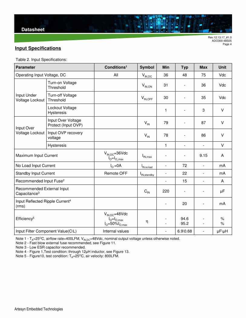
Table 2. Input Specifications:
Parameter Conditions1 Symbol Min Typ Max Unit
Operating Input Voltage, DC All VIN,DC 36 48 75 Vdc
Input Under
Voltage Lockout
Turn-on Voltage
ThresholdVIN,ON 31 - 36 Vdc
Turn-off Voltage
ThresholdVIN,OFF 30 - 35 Vdc
Lockout Voltage
Hysteresis1 - 3 V
Input Over
Voltage Lockout
Input Over Voltage
Protect (Input OVP)VIN 79 - 87 V
Input OVP recovery
voltageVIN 78 - 86 V
Hysteresis 1 - - V
Maximum Input CurrentVIN,DC=36Vdc
IO=IO,max
IIN,max - - 9.15 A
No Load Input Current IO =0A IIN,no load - 72 - mA
Standby Input Current Remote OFF IIN,standby - 22 - mA
Recommended Input Fuse2 - 15 - A
Recommended External Input
Capacitance3 CIN 220 - - µF
Input Reflected Ripple Current4
(rms)- 20 - mA
Efficiency5
VIN,DC=48Vdc
IO=IO,max
IO=50%IO,max
η-
-
94.6
95.2
-
-
%
%
Input Filter Component Value(C\L) Internal values - 6.9\0.68 - µF\µH
Note 1 - TA=25OC, airflow rate=400LFM, VIN,DC=48Vdc, nominal output voltage unless otherwise noted.Note 2 - Fast blow external fuse recommended, see Figure 11.Note 3 - Low ESR capacitor recommended.Note 4 - Figure 1,Test condition: through 12µH inductor, see Figure 13.Note 5 - Figure10, test condition: TA=25OC, air velocity: 800LFM.
Technical Reference Note
Rev.12.13.17_#1.0
ADO300-48S05
Page 5
Datasheet
Artesyn Embedded Technologies
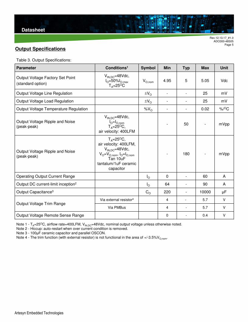
Output Specifications
Table 3. Output Specifications:
Parameter Conditions1 Symbol Min Typ Max Unit
Output Voltage Factory Set Point
(standard option)
VIN,DC=48Vdc,
IO=50%IO,max
TA=25OC
VO,nom 4.95 5 5.05 Vdc
Output Voltage Line Regulation ±VO - - 25 mV
Output Voltage Load Regulation ±VO - - 25 mV
Output Voltage Temperature Regulation %VO - - 0.02 %/OC
Output Voltage Ripple and Noise
(peak-peak)
VIN,DC=48Vdc,
IO=IO,nom
TA=25OC,
air velocity: 400LFM
- 50 - mVpp
Output Voltage Ripple and Noise
(peak-peak)
TA=25OC,
air velocity: 400LFM,
VIN,DC=48Vdc,
VO=VO,nom, IO=IO,nom
Tan 10uF
tantalum/1uF ceramic
capacitor
- 180 - mVpp
Operating Output Current Range IO 0 - 60 A
Output DC current-limit inception2 IO 64 - 90 A
Output Capacitance3 CO 220 - 10000 µF
Output Voltage Trim RangeVia external resistor4 4 - 5.7 V
Via PMBus 4 - 5.7 V
Output Voltage Remote Sense Range 0 - 0.4 V
Note 1 - TA=25OC, airflow rate=400LFM, VIN,DC=48Vdc, nominal output voltage unless otherwise noted.Note 2 - Hiccup: auto-restart when over current condition is removed.Note 3 - 100µF ceramic capacitor and parallel OSCON.Note 4 - The trim function (with external resistor) is not functional in the area of +/-3.5%VO,nom.
Technical Reference Note
Rev.12.13.17_#1.0
ADO300-48S05
Page 6
Datasheet
Artesyn Embedded Technologies
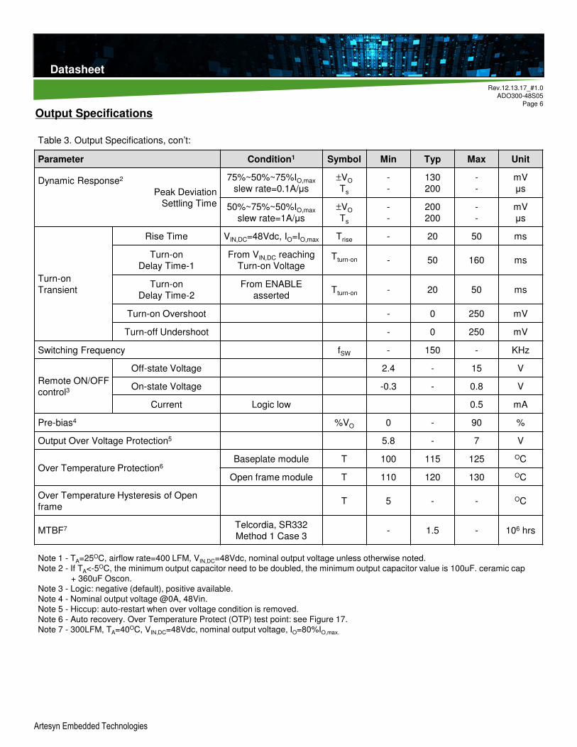
Table 3. Output Specifications, con’t:
Parameter Condition1 Symbol Min Typ Max Unit
Dynamic Response2
Peak Deviation
Settling Time
75%~50%~75%IO,max
slew rate=0.1A/µs
±VO
Ts
-
-
130
200
-
-
mV
µs
50%~75%~50%IO,max
slew rate=1A/µs
±VO
Ts
-
-
200
200
-
-
mV
µs
Turn-on
Transient
Rise Time VIN,DC=48Vdc, IO=IO,max Trise - 20 50 ms
Turn-on
Delay Time-1
From VIN,DC reaching
Turn-on VoltageTturn-on - 50 160 ms
Turn-on
Delay Time-2
From ENABLE
assertedTturn-on - 20 50 ms
Turn-on Overshoot - 0 250 mV
Turn-off Undershoot - 0 250 mV
Switching Frequency fSW - 150 - KHz
Remote ON/OFF
control3
Off-state Voltage 2.4 - 15 V
On-state Voltage -0.3 - 0.8 V
Current Logic low 0.5 mA
Pre-bias4 %VO 0 - 90 %
Output Over Voltage Protection5 5.8 - 7 V
Over Temperature Protection6Baseplate module T 100 115 125 OC
Open frame module T 110 120 130 OC
Over Temperature Hysteresis of Open
frame T 5 - - OC
MTBF7 Telcordia, SR332
Method 1 Case 3- 1.5 - 106 hrs
Note 1 - TA=25OC, airflow rate=400 LFM, VIN,DC=48Vdc, nominal output voltage unless otherwise noted.Note 2 - If TA<-5OC, the minimum output capacitor need to be doubled, the minimum output capacitor value is 100uF. ceramic cap
+ 360uF Oscon.Note 3 - Logic: negative (default), positive available.Note 4 - Nominal output voltage @0A, 48Vin.Note 5 - Hiccup: auto-restart when over voltage condition is removed.Note 6 - Auto recovery. Over Temperature Protect (OTP) test point: see Figure 17.Note 7 - 300LFM, TA=40OC, VIN,DC=48Vdc, nominal output voltage, IO=80%IO,max.
Output Specifications

Technical Reference Note
Rev.12.13.17_#1.0
ADO300-48S05
Page 7
Datasheet
Artesyn Embedded Technologies
Table 4. Digital Interface Specifications:
Parameter Condition1 Symbol Min Typ Max Unit
Input High Voltage
(Clock,Data,C2,SMBAlert)2.2 - 3.3 V
Input Low Voltage
(Clock,Data,C2,SMBAlert)0 - 0.8 V
Input High Level Current
((Clock,Data,C2,SMBAlert)-1 - 1 mA
Output High Voltage
(Clock,Data,C2,SMBAlert)IO=4mA 2.4 - - V
Output Low Voltage
(Clock,Data,C2,SMBAlert) IO=-4mA - - 0.3 V
Output Current Reading Accuracy30A<IO≤60A -8 1.4 8 %
1A<IO≤30A -4 - 4 A
Output Current Reading Resolution 0.19 0.5 A
Output Voltage Reading Accuracy -2 1 2 %
Output Voltage Reading Resolution - 0.25 0.5 mV
Input Voltage Reading Accuracy -4 - 4 %
Input Voltage Reading Resolution - 0.2 1 V
Temperature Reading Accuracy TA>0OC -5 - 5 OC
Temperature Reading Resolution TA>0OC - 0.25 1 OC
Table 5. Configurable Control Pins:
Pin Designation/FunctionConfiguration
Trim/C1 C2
On/Off Power Good Via PMBus
Trim Power Good Factory Default
Trim On/Off Via PMBus
Note 1 - TA=25OC, airflow rate=400LFM, VIN,DC=48Vdc, nominal output voltage unless otherwise noted.
Configurable Control Pins
The module contains two configurable control pins, Trim/C1 and C2, referenced to the module secondary Sig_Gnd. See
section Mechanical Outlines for pin locations. The following Table 5 lists the default factory configurations for the functions
assigned to these pins. Additional configurations can be accomplished via the PMBus command, what’s more, there is a
feature description for each function in Table 5.
Digital Interface Specifications
Technical Reference Note
Rev.12.13.17_#1.0
ADO300-48S05
Page 8
Datasheet
Artesyn Embedded Technologies
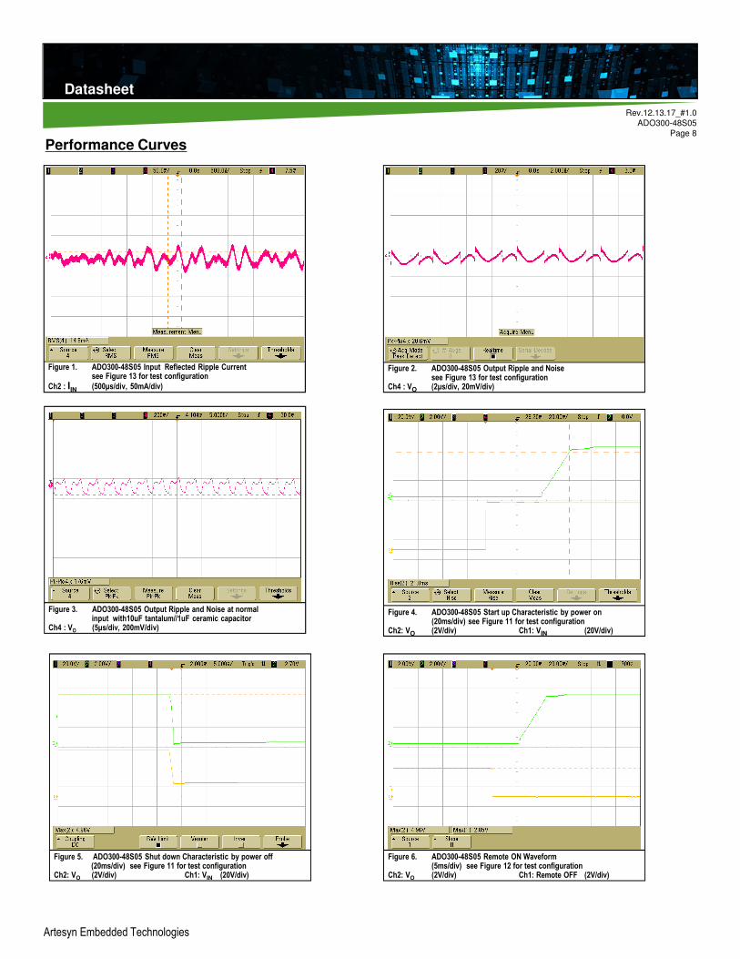
Figure 1. ADO300-48S05 Input Reflected Ripple Current see Figure 13 for test configuration
Ch2 : IIN (500µs/div, 50mA/div)
Figure 2. ADO300-48S05 Output Ripple and Noise see Figure 13 for test configuration
Ch4 : VO (2µs/div, 20mV/div)
Figure 4. ADO300-48S05 Start up Characteristic by power on (20ms/div) see Figure 11 for test configuration
Ch2: VO (2V/div) Ch1: VIN (20V/div)
Figure 6. ADO300-48S05 Remote ON Waveform (5ms/div) see Figure 12 for test configuration
Ch2: VO (2V/div) Ch1: Remote OFF (2V/div)
Figure 5. ADO300-48S05 Shut down Characteristic by power off(20ms/div) see Figure 11 for test configuration
Ch2: VO (2V/div) Ch1: VIN (20V/div)
Performance Curves
Figure 3. ADO300-48S05 Output Ripple and Noise at normal input with10uF tantalum//1uF ceramic capacitor
Ch4 : VO (5µs/div, 200mV/div)

Technical Reference Note
Rev.12.13.17_#1.0
ADO300-48S05
Page 9
Datasheet
Artesyn Embedded Technologies
Figure 8. ADO300-48S05 Transient Response 25% load step (50%~75%~50%) and 0.1A/µs slew rate (2ms/div) see Figure 16 for test configuration
Ch4: Vo (50mV/div) Ch3: Io (20A/div)
Figure 9. ADO300-48S05 Transient Response 25% load step (50%~75%~50%) and 1A/µs slew rate (2ms/div) see Figure 16 for test configuration
Ch4: Vo (100mV/div) Ch3: Io (20A/div)Figure 10. ADO300-48S05 Efficiency Curves @25OC, VO=5V, 800LFMLoading: IO=10% increment to 60A
Performance Curves
Figure 7. ADO300-48S05 Remote OFF Waveform (5ms/div) see Figure 12 for test configuration
Ch2: VO (2V/div) Ch1: Remote OFF (2V/div)
84
86
88
90
92
94
96
98
6 12 18 24 30 36 42 48 54 60
Eff
ien
cy (
%)
Output current (A)
36V 48V 75V
Technical Reference Note
Rev.12.13.17_#1.0
ADO300-48S05
Page 10
Datasheet
Artesyn Embedded Technologies
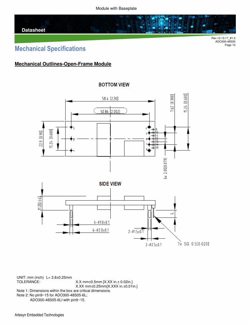
UNIT: mm (inch) L= 3.8±0.25mmTOLERANCE: X.X mm±0.5mm [X.XX in.± 0.02in.]
X.XX mm±0.25mm[X.XXX in.±0.01in.]Note 1: Dimensions within the box are critical dimensions.Note 2: No pin9~15 for ADO300-48S05-6L;
ADO300-48S05-6LI with pin9~15.
Mechanical Specifications
Mechanical Outlines-Open-Frame Module
Module with Baseplate

Technical Reference Note
Rev.12.13.17_#1.0
ADO300-48S05
Page 11
Datasheet
Artesyn Embedded Technologies
Device Code Suffix Length (mm)
-4 4.8±0.25
-6 3.8±0.25
-8 2.8±0.25
None 5.8±0.25
UNIT: mm (inch) L= 3.8±0.25mmTOLERANCE: X.X mm±0.5mm [X.XX in.± 0.02in.]
X.XX mm±0.25mm[X.XXX in.±0.01in.]Note 1: Dimensions within the box are critical dimensions.Note 2: No pin9~15 for ADO300-48S05B-6L and ADO300-48S05PB-6L;
ADO300-48S05B-6LI with pin9~15.
Mechanical Outlines-Module with Baseplate
Pin Length Option

Technical Reference Note
Rev.12.13.17_#1.0
ADO300-48S05
Page 12
Datasheet
Artesyn Embedded Technologies
Pin No. Name Function Optional
1 Vin+ Positive input voltage NA
2 Remote ON/OFF Remote control NA
3 Vin- Negative input voltage NA
4 Vo- Negative output voltage NA
5 S- Remote sense negative Yes
6 Trim/C1 Voltage adjustment Yes
7 S+ Remote sense positive Yes
8 Vo+ Positive output voltage NA
9 C2
Digital Yes
10 Sig_Gnd
11 Data
12 SMBAlert
13 Clock
14 Addr1
15 Addr0
Pin Designations
Technical Reference Note
Rev.12.13.17_#1.0
ADO300-48S05
Page 13
Datasheet
Artesyn Embedded Technologies
Environmental Specifications
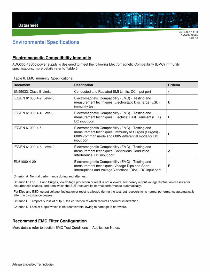
Electromagnetic Compatibility Immunity
ADO300-48S05 power supply is designed to meet the following Electromagnetic Compatibility (EMC) immunity
specifications, more details refer to Table 6.
Recommend EMC Filter Configuration
More details refer to section EMC Test Conditions in Application Notes.
Table 6. EMC immunity Specifications:
Document Description Criteria
EN55032, Class B Limits Conducted and Radiated EMI Limits, DC input port /
IEC/EN 61000-4-2, Level 3 Electromagnetic Compatibility (EMC) - Testing and
measurement techniques: Electrostatic Discharge (ESD)
immunity test
B
IEC/EN 61000-4-4, Level3 Electromagnetic Compatibility (EMC) - Testing and
measurement techniques: Electrical Fast Transient (EFT).
DC input port.
B
IEC/EN 61000-4-5 Electromagnetic Compatibility (EMC) - Testing and
measurement techniques: Immunity to Surges (Surges) -
600V common mode and 600V differential mode for DC
input port
B
IEC/EN 61000-4-6, Level 2 Electromagnetic Compatibility (EMC) - Testing and
measurement techniques: Continuous Conducted
Interference. DC input port
A
EN61000-4-29 Electromagnetic Compatibility (EMC) - Testing and
measurement techniques: Voltage Dips and Short
Interruptions and Voltage Variations (Dips). DC input port
B
Criterion A: Normal performance during and after test.
Criterion B: For EFT and Surges, low-voltage protection or reset is not allowed. Temporary output voltage fluctuation ceases after disturbances ceases, and from which the EUT recovers its normal performance automatically.
For Dips and ESD, output voltage fluctuation or reset is allowed during the test, but recovers to its normal performance automatically after the disturbance ceases.
Criterion C: Temporary loss of output, the correction of which requires operator intervention.
Criterion D: Loss of output which is not recoverable, owing to damage to hardware.
Technical Reference Note
Rev.12.13.17_#1.0
ADO300-48S05
Page 14
Datasheet
Artesyn Embedded Technologies
Safety Certifications
The ADO300-48S05 power supply is intended for inclusion in other equipment and the installer must ensure that it is in
compliance with all the requirements of the end application. This product is only for inclusion by professional installers
within other equipment and must not be operated as a stand alone product.
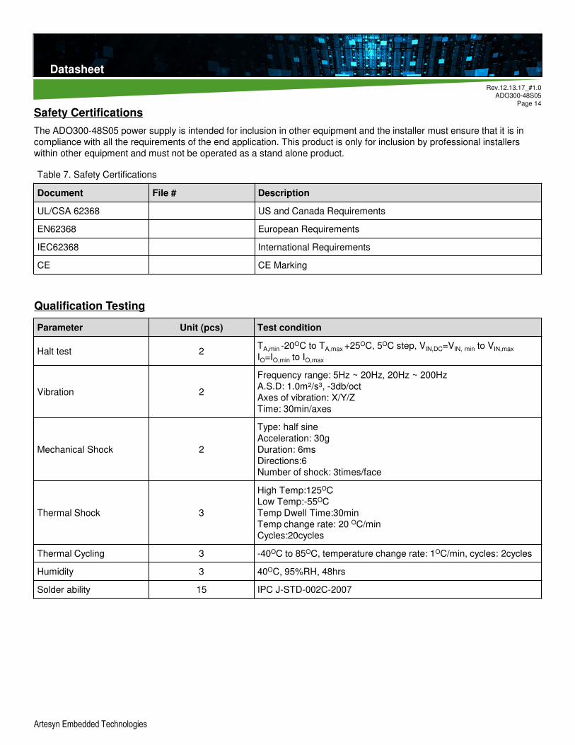
Table 7. Safety Certifications
Document File # Description
UL/CSA 62368 US and Canada Requirements
EN62368 European Requirements
IEC62368 International Requirements
CE CE Marking
Qualification Testing
Parameter Unit (pcs) Test condition
Halt test 2TA,min -20OC to TA,max +25OC, 5OC step, VIN,DC=VIN, min to VIN,max
IO=IO,min to IO,max
Vibration 2
Frequency range: 5Hz ~ 20Hz, 20Hz ~ 200Hz
A.S.D: 1.0m2/s3, -3db/oct
Axes of vibration: X/Y/Z
Time: 30min/axes
Mechanical Shock 2
Type: half sine
Acceleration: 30g
Duration: 6ms
Directions:6
Number of shock: 3times/face
Thermal Shock 3
High Temp:125OC
Low Temp:-55OC
Temp Dwell Time:30min
Temp change rate: 20 OC/min
Cycles:20cycles
Thermal Cycling 3 -40OC to 85OC, temperature change rate: 1OC/min, cycles: 2cycles
Humidity 3 40OC, 95%RH, 48hrs
Solder ability 15 IPC J-STD-002C-2007
Technical Reference Note
Rev.12.13.17_#1.0
ADO300-48S05
Page 15
Datasheet
Artesyn Embedded Technologies
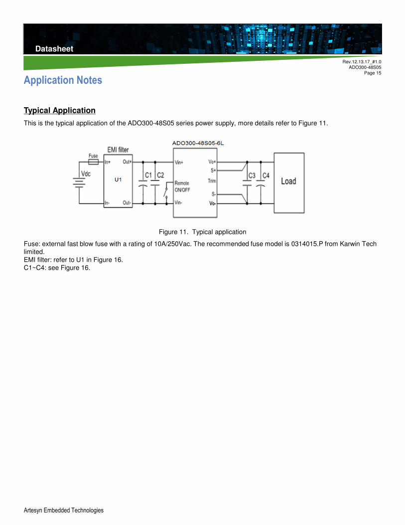
Application Notes
Typical Application
This is the typical application of the ADO300-48S05 series power supply, more details refer to Figure 11.
Figure 11. Typical application
Fuse: external fast blow fuse with a rating of 10A/250Vac. The recommended fuse model is 0314015.P from Karwin Tech
limited.
EMI filter: refer to U1 in Figure 16.
C1~C4: see Figure 16.

Technical Reference Note
Rev.12.13.17_#1.0
ADO300-48S05
Page 16
Datasheet
Artesyn Embedded Technologies
Remote ON/OFF
Standard negative remote ON/OFF logic is available in ADO300-48S05(B)-6L(I). The logic is CMOS and TTL compatible.
Remote ON/OFF (ENABLE) can be controlled by an external switch between the on/off terminal and the Vin- terminal.
The switch can be an open collector or open drain.
The voltage between pin Remote ON/OFF and pin Vin- must not exceed the range listed in Table 3 to ensure proper
operation. The external Remote ON/OFF circuit is highly recommended as shown in Figure 12.
For the negative logic, if the remote ON/OFF (ENABLE) feature is not used, please maintain the ENABLE pin to Vin-.
Secondary Remote On/Off
The module contains an additional secondary remote on/off control, via either the Trim/C1 or C2 pin, reference to the
output Sig_Gnd pin. And such pin can be reconfigured as secondary remote on/off pin by the PMBus interface including
either negative or positive logic. Negative logic turns the module on during a logic low and off during a logic high. Positive
logic turns the module on during a logic high and off during a logic low. The secondary remote on/off can be controlled by
an external switch between Trim/C1 or C2 and output Sig_Gnd pin. The switch can be an open collector or open drain,
more details refer to Figure 12.
If not using the secondary remote on/off control, the pin may be left N/C.
Isolated remote ON/OFF circuit non-isolated remote ON/OFF circuit
Figure 12. Remote ON/OFF external diagram
Remote sense
If the load is far from the unit, connect S+ and S- to the terminal of the load respectively to compensate the voltage drop on
the transmission line, When using remote sense and trim, the output current should be decreased accordingly so as not to
exceed the maximum output power. If the sense compensate function is not necessary, connect S+ to Vo+ and S- to Vo-
directly.
Power Good
The module provides a Power Good ((PG) ,C2 Pin) feature, to indicate that the output voltage is within the normal output
voltage range of the power module. The PG signal will be de-asserted to a low state if any condition such as over
temperature, over current, Input Under Voltage Lockout (UVLO), output voltage protect (OVP), startup with diode
emulation mode or loss of regulation occurs that would result in the output voltage going below the normal voltage range
value.
The Power Good signal, provided on pin C2, is implemented with an open-drain node, pulled up via a 10kΩ resistor to
3.3V internally. For Positive Logic PG (default), the PG signal is high level, when PG is asserted.
If not using the Power Good feature, the pin may be left N/C.
Technical Reference Note
Rev.12.13.17_#1.0
ADO300-48S05
Page 17
Datasheet
Artesyn Embedded Technologies
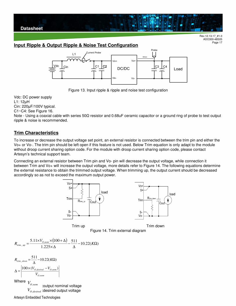
Input Ripple & Output Ripple & Noise Test Configuration
Figure 13. Input ripple & ripple and noise test configuration
Vdc: DC power supply
L1: 12µH
Cin: 220µF/100V typical.
C1~C4: See Figure 16.
Note - Using a coaxial cable with series 50Ω resistor and 0.68uF ceramic capacitor or a ground ring of probe to test output
ripple & noise is recommended.
Trim Characteristics
To increase or decrease the output voltage set point, an external resistor is connected between the trim pin and either the
Vo+ or Vo-. The trim pin should be left open if this feature is not used. Below Trim equation is only adapt to the module
without droop current sharing option code. For the module with droop current sharing option code, please contact
Artesyn’s technical support team.
Connecting an external resistor between Trim pin and Vo- pin will decrease the output voltage, while connection it
between Trim and Vo+ will increase the output voltage, more details refer to Figure 14. The following equations determine
the external resistance to obtain the trimmed output voltage. When trimming up, the output current should be decreased
accordingly so as not to exceed the maximum output power.
Trim up Trim down
Figure 14. Trim external diagram
( ))(22.10
511
225.1
10011.5 ,
_ Ω−∆
−∆×
∆+××= K
VR
nomO
uptrim
)(22.10511
_ Ω−∆
= KR downtrim
Where
:output nominal voltage
:desired output voltage
nomO
nomOdesiredO
V
VV
,
,, )(100 −×=∆
desiredOV ,
nomOV ,

Technical Reference Note
Rev.12.13.17_#1.0
ADO300-48S05
Page 18
Datasheet
Artesyn Embedded Technologies
145
)57.5(100)(100
,
,,=
−×=
−×=∆
nomO
desiredOnomO
V
VV
0408.2)225.1(, ×+= trimdesiredO VV
( ) ( ))(12.12322.10
14
511
14225.1
14100511.522.10
511
225.1
100511.5_ Ω=−−
×
+××=−−
×
+××= KR uptrim
For example, to get the desired output voltage,5.7V, so equates 5.7V.
So, the external resistor is 123.12KΩ. The output voltage can also be trimmed by potential applied at the Trim pin.
EMC Test Conditions
Figure 16. EMC Test Conditions
C1: 330µF/100V electrolytic capacitor, P/N: UPM2A331MPD (Nichicon) or equivalent caps
C2: 0.1µF/100V/X7R capacitor
C3: 100uF/10V/X7S ceramic capacitor
C4: 1000µF/16V electrolytic capacitor, P/N: OSCON or POSCAP
U1: Input EMC filter
U2: Module to test, ADO300-48S05
CX1, CX2, CX3, CX4, CX5: 1µF/100V/X7R capacitor
Cy1, Cy2, Cy3, Cy4: 0.88µF/630V/X7R, Y capacitor
L1, L2: 473µH, common mode inductor
Fuse: External fast blow fuse with a rating of 15A/250Vac. The recommended fuse model is 0314015.P from Karwin
Tech limited.
Where : the voltage of trim pin.trimV
desiredoV ,
4.5
4.7
4.9
5.1
5.3
5.5
5.7
5.9
32 35 38 41 44 47 50 53 56 59 62 65 68 71 74 77
Half load
Fig15. Trimming up the output voltage
When trimming up the output voltage, the
minimum input voltage should be increased as
shown in figure 15.
Technical Reference Note
Rev.12.13.17_#1.0
ADO300-48S05
Page 19
Datasheet
Artesyn Embedded Technologies
Top view for open frame module
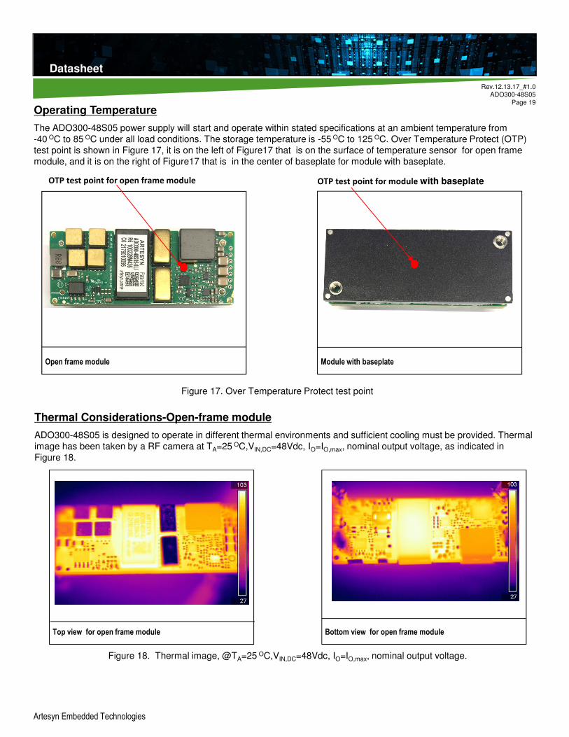
Operating Temperature
The ADO300-48S05 power supply will start and operate within stated specifications at an ambient temperature from
-40 OC to 85 OC under all load conditions. The storage temperature is -55 OC to 125 OC. Over Temperature Protect (OTP)
test point is shown in Figure 17, it is on the left of Figure17 that is on the surface of temperature sensor for open frame
module, and it is on the right of Figure17 that is in the center of baseplate for module with baseplate.
Figure 18. Thermal image, @TA=25 OC,VIN,DC=48Vdc, IO=IO,max, nominal output voltage.
Figure 17. Over Temperature Protect test point
Open frame module
OTP test point for open frame module
Module with baseplate
OTP test point for module with baseplate
Bottom view for open frame module
Thermal Considerations-Open-frame module
ADO300-48S05 is designed to operate in different thermal environments and sufficient cooling must be provided. Thermal
image has been taken by a RF camera at TA=25 OC,VIN,DC=48Vdc, IO=IO,max, nominal output voltage, as indicated in
Figure 18.

Technical Reference Note
Rev.12.13.17_#1.0
ADO300-48S05
Page 20
Datasheet
Artesyn Embedded Technologies
Figure 19 Temperature test point for open frame module
OTP test point for open frame
module
Test point A
Table 8. Temperature limit of the test point
Test Point Temperature Limit (OC)
Test point A 129
OTP test point for open frame module 115
Figure 20. Thermal derating data for open frame module @48Vin, airflow from Vin- to Vin+
(OC)
Proper cooling can be verified by measuring the temperature at these test points as shown in Figure 19. The number of
test points may vary with different thermal design and topology. The temperature above the limit values in Table 8 are not
allowed. For a typical application, There is the thermal derating data of output current vs. ambient air temperature at
different air velocity @48Vin for open frame module.
(A)
25
30
35
40
45
50
55
60
25 30 35 40 45 50 55 60 65 70 75 80 85 90
100LFM 200LFM 400LFM 600LFM
Technical Reference Note
Rev.12.13.17_#1.0
ADO300-48S05
Page 21
Datasheet
Artesyn Embedded Technologies
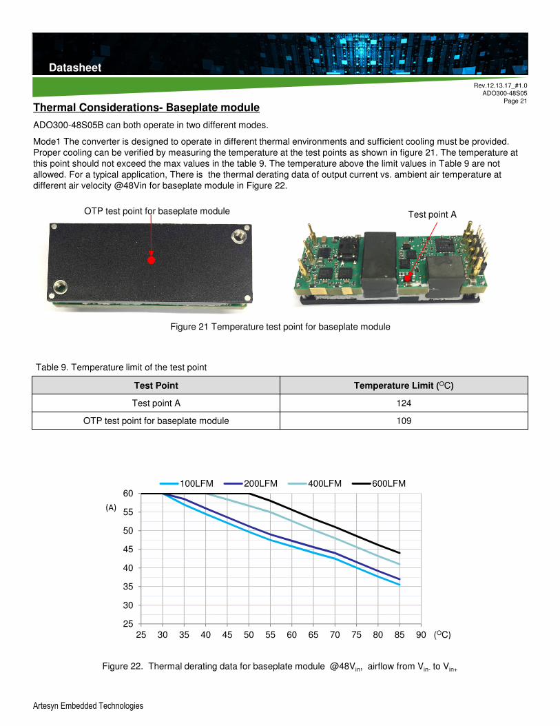
Figure 22. Thermal derating data for baseplate module @48Vin, airflow from Vin- to Vin+
Figure 21 Temperature test point for baseplate module
Table 9. Temperature limit of the test point
Test Point Temperature Limit (OC)
Test point A 124
OTP test point for baseplate module 109
OTP test point for baseplate module
Thermal Considerations- Baseplate module
ADO300-48S05B can both operate in two different modes.
Mode1 The converter is designed to operate in different thermal environments and sufficient cooling must be provided.
Proper cooling can be verified by measuring the temperature at the test points as shown in figure 21. The temperature at
this point should not exceed the max values in the table 9. The temperature above the limit values in Table 9 are not
allowed. For a typical application, There is the thermal derating data of output current vs. ambient air temperature at
different air velocity @48Vin for baseplate module in Figure 22.
Test point A
(A)
(OC)
25
30
35
40
45
50
55
60
25 30 35 40 45 50 55 60 65 70 75 80 85 90
100LFM 200LFM 400LFM 600LFM
Technical Reference Note
Rev.12.13.17_#1.0
ADO300-48S05
Page 22
Datasheet
Artesyn Embedded Technologies
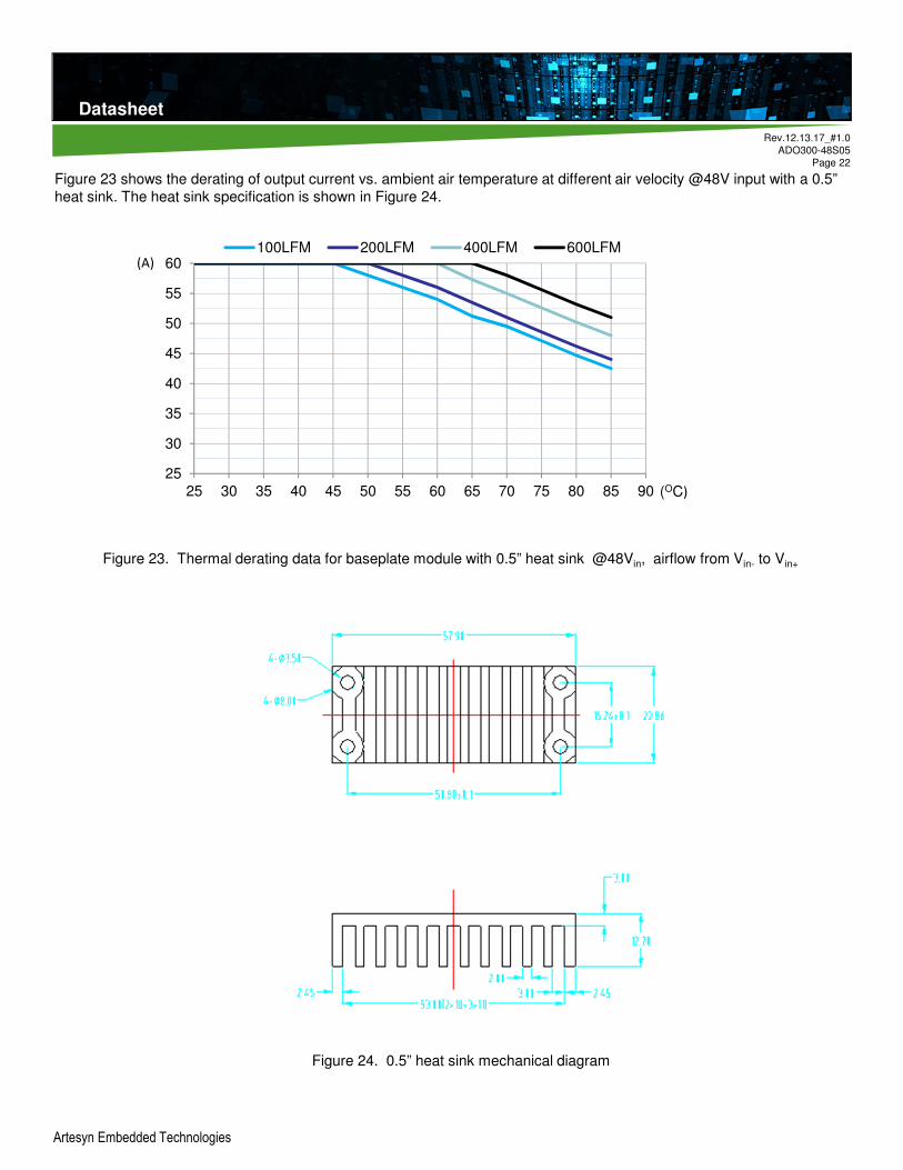
Figure 23 shows the derating of output current vs. ambient air temperature at different air velocity @48V input with a 0.5”
heat sink. The heat sink specification is shown in Figure 24.
Figure 24. 0.5” heat sink mechanical diagram
Figure 23. Thermal derating data for baseplate module with 0.5” heat sink @48Vin, airflow from Vin- to Vin+
(A)
(OC)
25
30
35
40
45
50
55
60
25 30 35 40 45 50 55 60 65 70 75 80 85 90
100LFM 200LFM 400LFM 600LFM

Technical Reference Note
Rev.12.13.17_#1.0
ADO300-48S05
Page 23
Datasheet
Artesyn Embedded Technologies
Mode2 The converter can operate in a enclosed environment without forced air convection. Cooling of the converter is
achieved mainly by conduction from the baseplate to a heat sink. Hot spot temperature measured point is shown in figure
25. The temperature at this point should not exceed the max values in the table 10. The temperature above the limit values
Table 10 are not allowed. For a typical application, figure 26 shows the derating of output current vs. baseplate
temperature, provided ambient temperature is kept below the max values 85OC.
Figure 25. Temperature test point on base plate
Figure 26. The derating of output current vs. baseplate temperature for baseplate module in a enclosed environment
without forced air convection
30
35
40
45
50
55
60
40 45 50 55 60 65 70 75 80 85 90 95 100
48V
Table 10. Temperature limit of the test point
Test Point Temperature Limit (OC)
Test point A 124
(OC)
(A)
Technical Reference Note
Rev.12.13.17_#1.0
ADO300-48S05
Page 24
Datasheet
Artesyn Embedded Technologies
PMBus Communication
PMBus Communication Descriptions
The module has a digital PMBus interface to allow the module to be monitored, controlled and configured by the system.
The module supports 4 PMBus signal lines, Data, Clock, SMBAlert (optional), Control (C2 pin, optional), and 2 Address
lines Addr0 and Addr1. More detail PMBus information can be found in the PMBus Power Management Protocol
Specification, Part I and part II, revision 1.2; which is shown in http://pmbus.org. Both 100kHz and 400kHz bus speeds are
supported by the module. Connection for the PMBus interface should be following the High Power DC specifications given
in section 3.1.3 in the SMBus specification V2.0 or the Low Power DC specifications in section 3.1.2. The complete SMBus
specification is shown in http://smbus.org.
The module supports the Packet Error Checking (PEC) protocol. It can check the PEC byte provided by the PMBus
master, and include a PEC byte in all message responses to the master.
The module contains a data flash used to store configuration settings, which will not be programmed into the device data
flash automatically. The STORE_DEFAULT_ALL command must be used to commit the current settings are transfer from
RAM to data flash as device defaults.
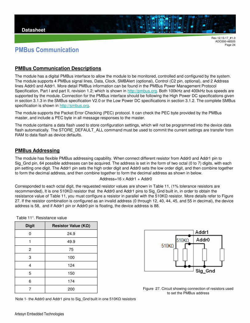
PMBus Addressing
The module has flexible PMBus addressing capability. When connect different resistor from Addr0 and Addr1 pin to
Sig_Gnd pin, 64 possible addresses can be acquired. The address is set in the form of two octal (0 to 7) digits, with each
pin setting one digit. The Addr1 pin sets the high order digit and Addr0 sets the low order digit, and then combine together
to form the decimal address, and then combine together to form the decimal address as shown in below.
Address=16 X Addr1 + Addr0
Corresponded to each octal digit, the requested resistor values are shown in Table 11, (1% tolerance resistors are
recommended), It is one 510KΩ resistor that the Addr0 and Addr1 pins to Sig_Gnd built in, in order to obtain the
resistance value of Table 11, you must configure a resistor in parallel with the 510KΩ resistor. More details refer to Figure
27. If the resistor combination is configured as an invalid address (0 through 12, 40, 44, 45, and 55 in decimal), the device
address is 58, and if Addr1 pin or Addr0 pin is floating, the device address is 88.
Table 111. Resistance value
Digit Resistor Value (KΩ)
0 24.9
1 49.9
2 75
3 100
4 124
5 150
6 174
7 200 Figure 27. Circuit showing connection of resistors used to set the PMBus address
Note 1- the Addr0 and Addr1 pins to Sig_Gnd built in one 510KΩ resistors

Technical Reference Note
Rev.12.13.17_#1.0
ADO300-48S05
Page 25
Datasheet
Artesyn Embedded Technologies
PMBus Data Format
The module receives and report date in LINEAR format. The Exponent of the data words is fixed at a reasonable value for
the command; altering the exponent is not supported. DIRECT format is not supported by the module.
For commands that set or report any voltage thresholds related to the output voltage, the module supports the linear data
format consisting of a two byte value with a 16-bit, unsigned mantissa, and a fixed exponent of -9. The format of the two
data bytes is shown below:
The equation can be written as:
Vo=Mantissa x 2-9
For example, considering set Vo to 3.3V by VOUT_COMMAND, the read/write data can be calculated refer to below
process:
1. Mantissa =Vo/2-9= 3.3/2-9=1689.6;
2. Converter the calculated Mantissa to hexadecimal 0x699.
For commands that set or report all other thresholds, including input voltages, output current, temperature, time and
frequency, the supported linear data format is a two byte value with: an 11 bit, two’s complement mantissa , and a 5 bit,
two’s complement exponent (scaling factor).The format of the two data bytes is shown as in below.
The equation can be written as:
Value=Mantissa x 2exponent
For example, considering set the turn on threshold of input under voltage lockout to 33V by VIN_ON command; the
read/write data can be calculated refer to below process:
1. Get the exponent of VIN,ON, 0; whose binary is 00000
2. Mantissa =VIN,ON/20=33/20=33;
3. Converter the calculated Mantissa to hexadecimal 21, then converter to binary 00000100001;
4. Combine the exponent and the mantissa, 00000 and 0000000000100001;
5. Converter binary 0000000000100001 to hexadecimal 0021.
The detail exponent and resolution of main parameter is to be decided later.

Technical Reference Note
Rev.12.13.17_#1.0
ADO300-48S05
Page 26
Datasheet
Artesyn Embedded Technologies
PMBus Enabled On/Off
The module can also be turned on and off via the PMBus interface. The OPERATION command is used to actually turn
the module on and off via the PMBus. Bit [7] in the OPERATION command data byte enables the module, with the
following functions:
0: Output is disabled
1. Output is enabled
PMBus Adjustable Input Under voltage Lockout
The module allows adjustment of the input under voltage lockout and hysteresis. The command VIN_ON allows setting the
input voltage turn on threshold, while the VIN_OFF command sets the input voltage turn off threshold. For both the
VIN_ON and VIN_OFF commands, possible values range from 30.000 to 36.000V in 0.1V steps. VIN_ON must be 1.5V
greater than VIN_OFF. The data associated with VIN_ON and VIN_OFF can be stored to non-volatile memory using the
STORE_DEFAULT_ALL command.
PMBus Adjustable Soft Start Delay and Rise Time
The soft start delay and rise time can be adjusted in the module via PMBus. The TON_DELAY command sets the delay
time in ms, and allows choosing delay times between 30ms and 160ms, with resolution of 0.1ms. The TON_RISE
command sets the rise time in ms, and allows choosing soft start times between 10ms and 50ms, with resolution of 0.1ms.
When setting TON_RISE, make sure that the charging current for output capacitors can be delivered by the module in
addition to any load current to avoid nuisance tripping of the over current protection circuitry during startup. The data
associated with TON_RISE and TON_DELAY can be stored to non-volatile memory using the STORE_DEFAULT_ALL
command.
Output Voltage Adjustment Using the PMBus
The ADO300-48S05-6LI module output voltage set point is adjusted using the VOUT_COMMAND. The output voltage
setting uses the Linear data format, with the 16 bits of the VOUT_COMMAND formatted as an unsigned mantissa, and a
fixed exponent of -9 (decimal) (read from VOUT_MODE).
VOUT = Mantissa x 2-9
The range limits for VOUT_COMMAND are 4V to 5.7V, and the resolution is 1.171mV. The data associated with
VOUT_COMMAND can be stored to non-volatile memory using the STORE_DEFAULT_ALL command.
Output Voltage Margining Using the PMBus
The ADO300-48S05-6LI module can also have its output voltage margined via PMBus commands. The command
VOUT_MARGIN_HIGH sets the margin high voltage, while the command VOUT_MARGIN_LOW sets the margin low
voltage. Both the VOUT_MARGIN_HIGH and VOUT_MARGIN_LOW commands use the “Linear” mode with the exponent
fixed at –9 (decimal). The data associated with VOUT_MARGIN_HIGH and VOUT_MARGIN_LOW can be stored to non-
volatile memory using the STORE_DEFAULT_ALL command. The module is commanded to go to the margined high or
low voltages using the OPERATION command. Bits [5:2] are used to enable margining as follows:
00XX: Margin Off
0110: Margin Low (Act on Fault)
1010: Margin High (Act on Fault)

Technical Reference Note
Rev.12.13.17_#1.0
ADO300-48S05
Page 27
Datasheet
Artesyn Embedded Technologies
Measuring Input Voltage Using the PMBus
The module can provide input voltage information using the READ_VIN command. During module manufacture, offset and
gain correction values are written into the non-volatile memory of the module to null errors in the tolerance and A/D
conversion of Vin. The command MFR_VIN_READ_CAL_GAIN can be used to read the gain correction - two bytes
consisting of an unsigned 16 bit number. The corrected input voltage reading is then given by:
Measuring Output Current Using the PMBus
The module measures output current by using the output filter inductor winding resistance as a current sense element. The
module can provide output current information using the READ_IOUT command. The command returns two bytes of data
in the linear format. The upper five bits [7:3] of the high data byte form the two’s complement representation of the
exponent. The remaining 11 bits are used for two’s complement representation of the mantissa, with the 11th bit fixed at
zero since only positive numbers are valid.
During module manufacture, offset and gain correction values are written into the non-volatile memory of the module to
null errors in the tolerance and A/D conversion of IOUT. The command MFR_IOUT_CAL_OFFSET can be used to read
the offset - two bytes consisting of a five-bit exponent (fixed at -4) and an 11-bit mantissa in two’s complement format. The
resolution is 0.19A. The command MFR_IOUT_CAL_GAIN can be used to read the gain correction - two bytes consisting
of a unsigned 16 bit number. The resolution of this correction factor 0.000122.
The READ_IOUT command provides module average output current information. This command only supports positive
current sourced from the module. If the converter is sinking current a reading of 0 is provided.
Note that the current reading provided by the module is measured in the room temperature.
Measuring the Temperature using the PMBus
The module can provide temperature information using the READ_TEMPERATURE_1 command. The command returns
two bytes of data in the linear format. The upper five bits [7:3] of the high data byte form the two’s complement
representation of the exponent. The remaining 11 bits are used for two’s complement representation of the mantissa.
Note that the module’s temperature sensor is located close to the module hot spot TH1 (see Thermal Considerations).and
is subjected to temperatures higher than the ambient air temperature near the module. The temperature reading will be
highly influenced by module load and airflow conditions.
Reading the Status of the Module using the PMBus
The module supports a number of status information commands implemented in PMBus. However, not all features are
supported in these commands. An X in the FLAG cell indicates the bit is not supported.
Technical Reference Note
Rev.12.13.17_#1.0
ADO300-48S05
Page 28
Datasheet
Artesyn Embedded Technologies
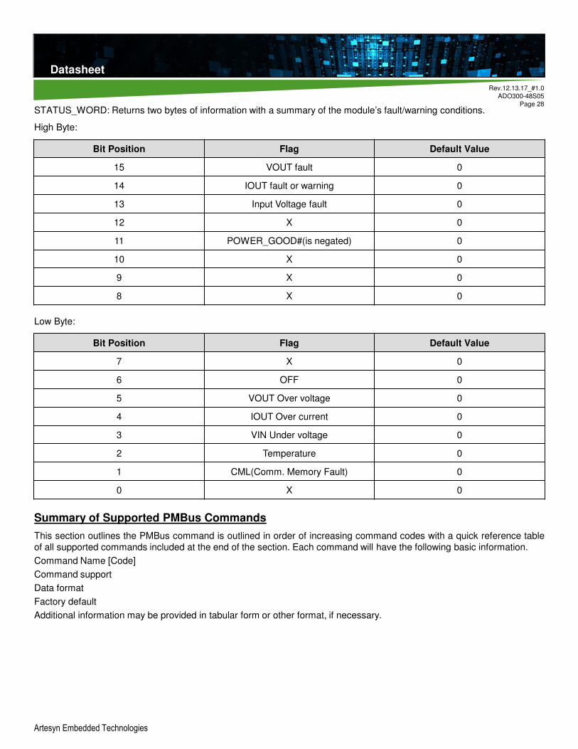
STATUS_WORD: Returns two bytes of information with a summary of the module’s fault/warning conditions.
High Byte:
Low Byte:
Summary of Supported PMBus Commands
This section outlines the PMBus command is outlined in order of increasing command codes with a quick reference table
of all supported commands included at the end of the section. Each command will have the following basic information.
Command Name [Code]
Command support
Data format
Factory default
Additional information may be provided in tabular form or other format, if necessary.
Bit Position Flag Default Value
15 VOUT fault 0
14 IOUT fault or warning 0
13 Input Voltage fault 0
12 X 0
11 POWER_GOOD#(is negated) 0
10 X 0
9 X 0
8 X 0
Bit Position Flag Default Value
7 X 0
6 OFF 0
5 VOUT Over voltage 0
4 IOUT Over current 0
3 VIN Under voltage 0
2 Temperature 0
1 CML(Comm. Memory Fault) 0
0 X 0

Technical Reference Note
Rev.12.13.17_#1.0
ADO300-48S05
Page 29
Datasheet
Artesyn Embedded Technologies
OPERATION [0x01]
Command support: On/Off Immediate and Margins (Act on Fault). Soft off with sequencing not supported and Margins
(Ignore Fault) not supported. Therefore bits 6, 3, 2, 1 and 0 set as read only at factory defaults.
ON_OFF_CONFIG [0x02]
Command support: Bit 1 polarity will be set based upon module code [0=Negative on/off logic, 1=positive on/off logic to
allow customer system to know hardware on/off logic.
CLEAR_FAULTS [0x03]
Command support: All functionality.
STORE_DEFAULT_ALL[0x11]
Command support: All functionality – Stores operating parameters to E2prom memory.
RESTORE_DEFAULT_ALL[0x12]
Command support: All functionality – Restores operating parameters from E2prom memory.
VOUT_MODE[0x20]
Command support: Supported. Factory default: 0x14 – indicates linear mode with exp = -9.
Format 8 bit unsigned (bit field)
Bit Position 7 6 5 4 3 2 1 0
Access r/w r r/w r/w r r r r
Function ON/OFF Vout Command N/A N/A
Default Value 1 0 0 0 1 0 0 0
Format 8 bit unsigned (bit field)
Bit Position 7 6 5 4 3 2 1 0
Access r r r r r r r/w r
Function (reserved) Bit4 pu Bit3 cmd Bit2 cpr Bit1 pol Bit0 cpa
Default Value 0 0 0 1 1 1 0 1
Format 8 bit unsigned (bit field)
Bit Position 7 6 5 4 3 2 1 0
Access r r r r r r r r
Function Mode(linear) 2’s complement exponent
Default Value 0 0 0 1 0 1 0 0
Technical Reference Note
Rev.12.13.17_#1.0
ADO300-48S05
Page 30
Datasheet
Artesyn Embedded Technologies
VOUT_COMMAND [0x21]
Data format: 16 bit unsigned mantissa (implied exponent per VOUT_MODE)
Factory default: 5.00V (5.00 / 2-9 → 2560 = 0xA00)
Range limits (max/min): 6.0V/4.0V
Units: volt
Command support: Supported, except when Trim function is selected via MFR_C1_C2_ARA_CONFIG [0xE0].
VOUT_MARGIN_HIGH [0x25]
Range limits (max/min): 6.0V/4.0V
Units: volt
Command support: read/write support, full functionality except “Ignore faults”.
Note: Range cross-check - value must be greater than VOUT_MARGIN_LOW value.
VOUT_MARGIN_LOW [0x26]
Range limits (max/min): 6.0/4.0
Units: volt
Command support: read/write support, full functionality except “Ignore faults”.
Note: Range cross-check - value must be less than VOUT_MARGIN_HIGH value.
VIN_ON [0x35]
Range limits (max/min): 36/32
Units: volt
Command support: All functionalityNote: Special interlock checks between VIN_ON and VIN_OFF maintain a hysteresis gap and do not allow the OFF level to be higherthan and ON level.
VIN_OFF [0x36]
Range limits (max/min): 35/31
Units: volt
Command support: All functionalityNote: Special interlock checks between VIN_ON and VIN_OFF maintain a hysteresis gap and do not allow the OFF level to be higherthan and ON level.
IOUT_CAL_GAIN[0x38]
Data format: IOUT linear format
Command support: support for IOUT GAIN calibration (factor in flash), lockout per MFR_DEVICE_TYPE
IOUT_CAL_OFFSET[0x39]
Data format: IOUT linear format
Command support: support for IOUT offset calibration (factor in flash), lockout per MFR_DEVICE_TYPE

Technical Reference Note
Rev.12.13.17_#1.0
ADO300-48S05
Page 31
Datasheet
Artesyn Embedded Technologies
VOUT_OV_FAULT_LIMIT [0x40]
Range limits (max/min): 7.0/5.0 (See note 2)
Units: volt
Command support: All functionalityNote1: Range cross- check – value must be greater than VOUT_COMMAND value.Note2: The maximum OV Fault Limit equals the output set point plus 2V, up to 7V. This is an automatic module protection feature thatwill override a user-set fault limit if the user limit is set too high.
VOUT_OV_FAULT_RESPONSE [0x41]
Command support:
Response settings (bits RSP0:1) – only a setting of 10, unit shuts down and responds according to the retry settings
below, is supported.
Retry settings (bits RS0:2) – only settings of 000 (unit does not attempt to restart on fault) and 111 unit continuously
restarts (normal startup) while fault is present until commanded off, bias power is removed or another fault condition
causes the unit to shutdown.
Delay time setting (bits 0-2) – only DT0:2 = 0 (no delay) supported.
Default Settings: The default settings for the VOUT_OV_FAULT_RESPONSE command are;
The unit shuts down in response to a VOUT over voltage condition.
The unit will continuously restart (normal startup) while the VOUT over voltage condition is present until it is commanded
off, bias power is removed or another fault condition causes the unit to shutdown.
The shutdown delay is set to 0 delay cycles.
IOUT_OC_FAULT_LIMIT [0x46]
Range limits (max/min): 80/64
Units: amp
Command support: All functionalityNote: Range cross-check – value must be greater than IOUT_OC_WARN_LIMIT value.
Format 8 bit unsigned (bit field)
Bit Position 7 6 5 4 3 2 1 0
Access r r r/w r/w r/w r r r
Function RSP[1] RSP[0] RS[2] RS[1] RS[0] DT[2] DT[1] DT[0]
Default Value 1 0 1 1 1 0 0 0
Technical Reference Note
Rev.12.13.17_#1.0
ADO300-48S05
Page 32
Datasheet
Artesyn Embedded Technologies
IOUT_OC_FAULT_RESPONSE [0x47]
Command support:
Response settings (bits RSP0:1) – only settings of 11, unit shuts down and responds according to the retry settings below,
is supported.
Retry settings (bits RS0:2) – only settings of 000 (unit does not attempt to restart on fault) and 111 unit continuously
restarts (normal startup) while fault is present until commanded off, bias power is removed or another fault condition
causes the unit to shut down.
Delay time setting (bits 0-2) – only DT0:2 = 0 (no delay) supported.
Default Settings: The default settings for the IOUT_OC_FAULT_RESPONSE command are;
The unit shuts down in response to an IOUT over current condition.
The unit will continuously restart (normal startup) while the IOUT over current condition is present until it is commanded
off, bias power is removed or another fault condition causes the unit to shut down.
The shutdown delay is set to 0 delay cycles.
IOUT_OC_WARN_LIMIT [0x4A]
Range limits (max/min): 80/64
Units: amp
Command support: read/write support, functionality completeNote: Range cross-check – value must be less than IOUT_OC_FAULT_LIMIT value.
OT_FAULT_LIMIT [0x4F]
Range limits (max/min): 125/110
Units: degrees C.
Command support: All functionalityNote: Range cross-check – value must be greater than OT_WARN_LIMIT value.
Format 8 bit unsigned (bit field)
Bit Position 7 6 5 4 3 2 1 0
Access r r r/w r/w r/w r r r
Function RSP[1] RSP[0] RS[2] RS[1] RS[0] DT[2] DT[1] DT[0]
Default Value 1 1 1 1 1 0 0 0

Technical Reference Note
Rev.12.13.17_#1.0
ADO300-48S05
Page 33
Datasheet
Artesyn Embedded Technologies
OT_FAULT_RESPONSE [0x50]
Command support:
Response settings (bits RSP0:1) – only setting of 10, unit shuts down and responds according to the retry settings below.
Retry settings (bits RS0:2) – only settings of 000 (unit does not attempt to restart on fault) and 111 unit continuously
restarts (normal startup) while fault is present until commanded off, bias power is removed or another fault condition
causes the unit to shutdown.
Delay time setting (bits 0-2) – only DT0:2 = 0 (no delay) supported.
Default Settings: The default settings for the OT_FAULT_RESPONSE command are;
The unit shuts down in response to an over-temperature condition.
The unit will continuously restart (normal startup) while the over-temperature condition is present until it is commanded off,
bias power is removed or another fault condition causes the unit to shut down.
The shutdown delay is set to 0 delay cycles.
OT_WARN_LIMIT [0x51]
Range limits (max/min): 125/100
Units: degrees C.
Command support: All functionalityNote: Range cross-check – value must be less than OT_FAULT_LIMIT value.
VIN_OV_FAULT_LIMIT [0x55]
Range limits (max/min): 87/79
Units: volt
Command support: All functionality
VIN_OV_FAULT_RESPONSE [0x56]
Default Settings: The default settings for the VIN_OV_FAULT_RESPONSE command are;
The unit shuts down in response to a VIN over voltage condition.
The unit will continuously prepares to restart (normal startup) while the VIN over voltage condition is present until it is
commanded off, bias power is removed, the VIN over voltage condition is removed, or another fault condition causes the
unit to shut down.
The shutdown delay is set to 0 delay cycles.
Format 8 bit unsigned (bit field)
Bit Position 7 6 5 4 3 2 1 0
Access r r r/w r/w r/w r r r
Function RSP[1] RSP[0] RS[2] RS[1] RS[0] DT[2] DT[1] DT[0]
Default Value 1 0 1 1 1 0 0 0

Technical Reference Note
Rev.12.13.17_#1.0
ADO300-48S05
Page 34
Datasheet
Artesyn Embedded Technologies
POWER_GOOD_ON [0x5E]
Range limits (max/min): 5.5/3.0
Units: volt
Command support: full supportNote: Range cross-check – value must be greater than POWER_GOOD_OFF value by 0.8V.
POWER_GOOD_OFF [0x5F]
Range limits (max/min): 5.5/3.0
Units: volt
Command support: full supportNote: Range cross-check – value must be less than POWER_GOOD_ON value by 0.8V.
STATUS_WORD [0x79]
Command support: full implementation for supported functions (note: Fans, MFR_SPECIFIC, Unknown not supported)
Note1: Not supported
Format 8 bit unsigned (bit field)
Bit Position 7 6 5 4 3 2 1 0
Access r r r/w r/w r/w r r r
Function RSP[1] RSP[0] RS[2] RS[1] RS[0] DT[2] DT[1] DT[0]
Default Value 1 1 0 0 0 0 0 0
Format 8 bit unsigned (bit field)
Bit Position 15 14 13 12 11 10 9 8
Access r r r r r r r r
Function VOUT I/POUT INPUT MFR_SPEC#PWR_GO
ODFAN1 OTHER1 UNKNOWN1
Format 8 bit unsigned (bit field)
Bit Position 7 6 5 4 3 2 1 0
Access r r r r r r r r
Function BUSY1 OUTPUT_OFF
VOUT_OV_FAULT
IOUT_OC_FAULT
VIN_UV_FAULT
TEMP CMLNONE OF ABOVE1
Technical Reference Note
Rev.12.13.17_#1.0
ADO300-48S05
Page 35
Datasheet
Artesyn Embedded Technologies
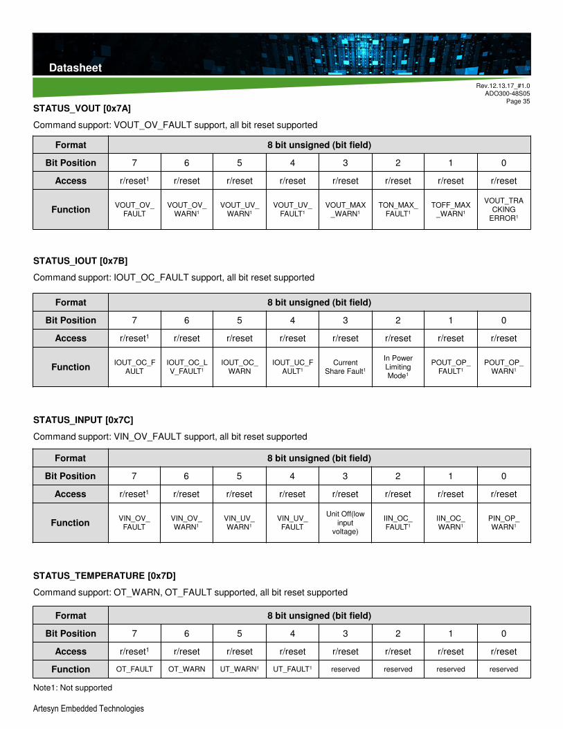
STATUS_VOUT [0x7A]
Command support: VOUT_OV_FAULT support, all bit reset supported
STATUS_IOUT [0x7B]
Command support: IOUT_OC_FAULT support, all bit reset supported
STATUS_INPUT [0x7C]
Command support: VIN_OV_FAULT support, all bit reset supported
STATUS_TEMPERATURE [0x7D]
Command support: OT_WARN, OT_FAULT supported, all bit reset supported
Note1: Not supported
Format 8 bit unsigned (bit field)
Bit Position 7 6 5 4 3 2 1 0
Access r/reset1 r/reset r/reset r/reset r/reset r/reset r/reset r/reset
FunctionVOUT_OV_
FAULTVOUT_OV_
WARN1
VOUT_UV_WARN1
VOUT_UV_FAULT1
VOUT_MAX_WARN1
TON_MAX_FAULT1
TOFF_MAX_WARN1
VOUT_TRACKING
ERROR1
Format 8 bit unsigned (bit field)
Bit Position 7 6 5 4 3 2 1 0
Access r/reset1 r/reset r/reset r/reset r/reset r/reset r/reset r/reset
FunctionIOUT_OC_F
AULTIOUT_OC_LV_FAULT1
IOUT_OC_WARN
IOUT_UC_FAULT1
Current Share Fault1
In Power Limiting Mode1
POUT_OP_FAULT1
POUT_OP_WARN1
Format 8 bit unsigned (bit field)
Bit Position 7 6 5 4 3 2 1 0
Access r/reset1 r/reset r/reset r/reset r/reset r/reset r/reset r/reset
FunctionVIN_OV_
FAULTVIN_OV_WARN1
VIN_UV_WARN1
VIN_UV_FAULT
Unit Off(low input
voltage)
IIN_OC_FAULT1
IIN_OC_WARN1
PIN_OP_WARN1
Format 8 bit unsigned (bit field)
Bit Position 7 6 5 4 3 2 1 0
Access r/reset1 r/reset r/reset r/reset r/reset r/reset r/reset r/reset
Function OT_FAULT OT_WARN UT_WARN1 UT_FAULT1 reserved reserved reserved reserved

Technical Reference Note
Rev.12.13.17_#1.0
ADO300-48S05
Page 36
Datasheet
Artesyn Embedded Technologies
READ_VIN [0x88]
Command support: full support
READ_VOUT [0x8B]
Command support: full support
READ_IOUT [0x8C]
Command support: full support
READ_TEMPERATURE_1 [0x8D]
Range cross-check - value must be greater than VOUT_MARGIN_LOW value.
Command support: full support
MFR_VOUT_READ_CAL_GAIN [0xD1]
Command support: support for VOUT gain calibration (factor in flash), lockout per MFR_DEVICE_TYPE
MFR_VOUT_READ_CAL_OFFSET [0xD2]
Command support: support for VOUT offset calibration (factor in flash), lockout per MFR_DEVICE_TYPE
MFR_VIN_READ_CAL_GAIN [0xDD]
Factory default:194
Range limits (max/min): 210/180
Command support: support for VIN gain calibration (factor in flash), lockout per MFR_DEVICE_TYPE
MFR_VIN_READ_CAL_OFFSET [0xDE]
Range limits (max/min): 200/0
Units: N/A
Command support: support for VIN offset calibration (factor in flash), lockout per MFR_DEVICE_TYPE
MFR_FW_REV [0x9B]
Range limits (max/min): 0 - 0xff (0.00 – 15.15)
Units: N/A
Command support: full read support

Technical Reference Note
Rev.12.13.17_#1.0
ADO300-48S05
Page 37
Datasheet
Artesyn Embedded Technologies
MFR_C1_C2_ARA_CONFIG [0xE0]
Command support: Full support.
Command MFR_C1_C2_ARA_CONFIG
Format 8 bit unsigned (bit field)
Bit Position 7 6 5 4 3 2 1 0
Access r r r r/w r/w r/w r/w r/w
Function Reserved ARA Assignment Table
Default Value 0 0 0 0 0 0 0 0
Assignment Table:
Bit Description Value Meaning
7:5 Reserved 000 Reserved
4 ARA
0ARA not functional, module remains at resistor
programmed address when SMBLAERT is asserted
1ARA functional, module responds to ARA only, when
SMBLAERT is asserted
3:0 PIN Configuration
0000T/C1 pin: ON/OFF (Secondary)
C2 pin: POWER_GOOD
0001T/C1 pin: TRIM
C2 pin: POWER_GOOD
0010T/C1 pin: TRIM
C2 pin: ON/OFF (Secondary)

Technical Reference Note
Rev.12.13.17_#1.0
ADO300-48S05
Page 38
Datasheet
Artesyn Embedded Technologies
MFR_ C2_LOGIC [0xE1]
Command support: full support (bits 0 and 1) as follows:
MFR_PGOOD_POLARITY [0xE6]
Command support: full support (bit 0) as follows:
Bit 0:
0 = Negative PGOOD logic (module PGOOD asserted when pin is LO, PGOOD de-asserted when pin is HI)
1 = Positive PGOOD logic (module PGOOD de-asserted when pin is LO, PGOOD asserted when pin is HI)
MFR_MODULE_DATE_LOC_SN [0xF0]
Command support: read/write support for 12 byte block, lockout per MFR_DEVICE_TYPE
Command MFR_C2_ARA_LOGIC
Format 8 bit unsigned (bit field)
Bit Position 7 6 5 4 3 2 1 0
Access r r r r r r r/w r/w
Function Reserved On/Off(primary & secondary) combination logic
Default Value 0 0 0 0 0 0 0 0
Bit Description Value Meaning
7:2 Reserved 000000 Reserved
1ON/OFF
Configuration
0Secondary side on/off pin state, when mapped to either T/C1
or C2, is ignored
1 AND – Primary and Secondary side on/off
0Secondary Side
ON/OFF Logic
0 Negative Logic (Low Enable: Input < 0.8V wrt Vout(-)
1 Positive Logic (High Enable: Input > 2.2V wrt Vout(-)
Command MFR_PGOOD_POLARITY
Format 8 bit unsigned (bit field)
Bit Position 7 6 5 4 3 2 1 0
Access r r r r r r r r/w
Function Reserved logic
Default Value 0 0 0 0 0 0 0 1

Technical Reference Note
Rev.12.13.17_#1.0
ADO300-48S05
Page 39
Datasheet
Artesyn Embedded Technologies
PMBus Command List
The main PMBus commands described in the PMBus 1.2 specification are supported by the module. Partial PMBus
commands are fully supported; Partial PMBus commands have difference with the definition in PMBus 1.2
specification. The details about all the supported PMBus commands are to be decided later.
PMBUS CMDCMD
CODEDATA
BYTESDATA FORMAT
DATAUNITS
TRANSFER TYPE DEFAULT VALUE
OPERATION 0x01 1 Bit field N/A R/W byte 0x80
CLEAR_FAULTS 0x03 0 N/A N/A Send byte none
STORE_DEFAULT_ALL 0x11 0 N/A N/A Send byte none
RESTORE_DEFAULT_ALL 0x12 0 N/A N/A Send byte none
VOUT_MODE 0x20 1 mode + exp N/A Send byte 0x17
VOUT_COMMAND 0x21 2 VOUT linear Volts R/W word 5.00V
VOUT_MARGIN_HIGH 0x25 2 VOUT linear Volts R/W word 5.70V
VOUT_MARGIN_LOW 0x26 2 VOUT linear Volts R/W word 4.00V
VIN_ON 0x35 2 VIN linear V R/W word 34.000V
VIN_OFFIOUT_CAL_GAINIOUT_CAL_OFFSET
0x360x380x39
222
VIN linearIOUT linearIOUT linear
VN/AN/A
R/W wordR/W wordR/W word
32.000V1000401
VOUT_OV_FAULT_LIMIT 0x40 2 VOUT linear V R/W word 7.000V
VOUT_OV_FAULT_RESPONSE 0x41 1 Bit field N/A Read byte 0xB8
IOUT_OC_FAULT_LIMIT 0x46 2 IOUT linear Amps R/W word 75.000A
IOUT_OC_FAULT_RESPONSE 0x47 1 Bit field N/A Read byte 0xF8
IOUT_OC_WARN_LIMIT 0x4A 2 IOUT linear Amps R/W word 70.000A
OT_FAULT_LIMIT 0x4F 2 TEMP linear Deg. C R/W word 120C
OT_FAULT_RESPONSE 0x50 1 Bit field N/A Read byte 0xB8
OT_WARN_LIMIT 0x51 2 TEMP linear Deg. C R/W word 110C
VIN_OV_FAULT_LIMIT 0x55 2 VIN linear v R/W word 85V
VIN_OV_FAULT_RESPONSE 0x56 1 Bit field N/A Read byte 0xC0
POWER_GOOD_ON 0x5E 2 VOUT linear v R/W word 4.200V
POWER_GOOD_OFF 0x5F 2 VOUT linear v R/W word 3.500V
TON_DELAY 0x60 2 Time linear msec R/W word 40ms
TON_RISE 0x61 2 Time linear msec R/W word 20ms
STATUS_WORD 0x79 2 Bit field N/A Read word N/A
STATUS_VOUT 0x7A 1 Bit field N/A Read byte N/A
STATUS_IOUT 0x7B 1 Bit field N/A Read byte N/A
STATUS_INPUT 0x7C 1 Bit field N/A Read byte N/A
STATUS_TEMPERATURE 0x7D 1 Bit field N/A Read byte N/A
READ_VIN 0x88 2 VIN linear v Read word N/A
READ_VOUT 0x8B 2 VOUT linear v Read word N/A
READ_IOUT 0x8C 2 IOUT linear Amps Read word N/A
READ_TEMP1 0x8D 2 TEMP linear Deg. C Read word N/A
PMBUS_REVISION 0x98 1 Bit Field N/A Read byte 1.2
MFR_FW_REVMFR_VOUT_READ_CAL_GAINMFR_VOUT_READ_CAL_OFFSET
0x9B0xD10xD2
122
8 bit unsignedU 16bitU 16bit
N/AN/AN/A
R/W wordR/W wordR/W word
AAMSMS
MFR_VIN_READ_CAL_GAIN 0xDD 2 U 16 bit N/A R/W word MS
MFR_VIN_READ_CAL_OFF 0xDE 2 VIN linear N/A R/W word MS
MFR_C1_C2_ARA_CONFIG 0xE0 1 Bit field N/A R/W byte 0x01
MFR_ C2_LOGIC 0xE1 1 Bit field N/A R/W byte 0x01
MFR_PGOOD _POLARITY 0xE6 1 Bit field N/A R/W byte 0x01
MFR_MOD_DATE_LOC_SN 0xF0 12 8 bit char N/A R/W block China. SZ
MS=Module specific

Technical Reference Note
Rev.12.13.17_#1.0
ADO300-48S05
Page 40
Datasheet
Artesyn Embedded Technologies
Soldering
The product ADO300-48S05-6L and ADO300-48S05-6LI are intended for standard manual or wave soldering or reflow
soldering.
The product ADO300-48S05B-6L/ ADO300-48S05PB-6L/ ADO300-48S05B-6LI are intended for standard manual or wave
soldering.
When wave soldering is used, the temperature on pins is specified to maximum 255OC for maximum 7s.
When manual soldering is used, the iron temperature should be maintained at 300OC ~ 380OC and applied to the converter
pins for less than 10s. Longer exposure can cause internal damage to the converter.
When reflow soldering is used, device must be qualified for Pb-Free reflow soldering process without any electrical or
mechanical property degradation. The Pb-Free process parameters are as follows:
•Max. sustain temperature:
•245OC (J-STD-020C Table 4-2: Packaging Thickness≥2.5mm/ Volume > 2000mm3),
•Peak temperature over 245OC is not suggested due to the potential reliability risk of components under
continuous high-temperature.
•Min. sustain duration above 217OC: 90s
•Min. sustain duration above 180OC: 150s
•Max. heat up rate: 3OC /s
•Max. cool down rate: 4OC /s
•In compliance with JEDEC J-STD-020C spec for 2 times reflow requirement.
The device module will comply with J-STD-020 Rev. C (Moisture/Reflow Sensitivity Classification for Non-hermetic Solid
State Surface Mount Devices) for both Pb-free solder profiles and MSL classification procedures.
Cleaning of solder joint can be performed with cleaning solvent IPA or simulative.
.
Application Notes

Technical Reference Note
Rev.12.13.17_#1.0
ADO300-48S05
Page 41
Datasheet
Artesyn Embedded Technologies
PartsHazardous Substances
Pb Hg Cd Cr6+ PBB PBDE
ADO300-48S05-6L x x x x x x
ADO300-48S05-6LI x x x x x x
ADO300-48S05B-6L x x x x x x
ADO300-48S05B-6LI x x x x x x
ADO300-48S05PB-6L x x x x x x
х: Means the content of the hazardous substances in all the average quality materials of the part is within the limits
specified in SJ/T-11363-2006
√: Means the content of the hazardous substances in at least one of the average quality materials of the part is outside
the limits specified in SJ/T11363-2006
Artesyn Embedded Technologies has been committed to the design and manufacturing of environment-friendly
products. It will reduce and eventually eliminate the hazardous substances in the products through unremitting efforts in
research. However, limited by the current technical level, the following parts still contain hazardous substances due to
the lack of reliable substitute or mature solution:
1. Solders (including high-temperature solder in parts) contain plumbum.
2. Glass of electric parts contains plumbum.
3. Copper alloy of pins contains plumbum
Hazardous Substances Announcement (RoHS of China)

Technical Reference Note
Rev.12.13.17_#1.0
ADO300-48S05
Page 42
Datasheet
For more information: www.artesyn.com/power
For support: [email protected]
Issue Date Description Originators
1.0 12.13.2017 First Issue Kim Hou
Record of Revision and Changes