User Manual AIMB-224 - Micro-Semiconductor.com
102
User Manual AIMB-224 AIMB-224 Mobile AMD R-series Qual Core/Dual Core Mini-ITX with VGA/LVDS/Display Port,6COM and Dual LAN
-
Upload
khangminh22 -
Category
Documents
-
view
2 -
download
0
Transcript of User Manual AIMB-224 - Micro-Semiconductor.com

User Manual
AIMB-224
AIMB-224 Mobile AMD R-series Qual Core/Dual Core Mini-ITX with VGA/LVDS/Display Port,6COM and Dual LAN

CopyrightThe documentation and the software included with this product are copyrighted 2012by Advantech Co., Ltd. All rights are reserved. Advantech Co., Ltd. reserves the rightto make improvements in the products described in this manual at any time withoutnotice. No part of this manual may be reproduced, copied, translated or transmittedin any form or by any means without the prior written permission of Advantech Co.,Ltd. Information provided in this manual is intended to be accurate and reliable. How-ever, Advantech Co., Ltd. assumes no responsibility for its use, nor for any infringe-ments of the rights of third parties, which may result from its use.
AcknowledgementsAWARD is a trademark of Phoenix Technologies Ltd.
IBM and PC are trademarks of International Business Machines Corporation.
Intel® Atom™ N455/D525 is trademark of Intel CorporationWinBond is a trademark of Winbond Corporation.
All other product names or trademarks are properties of their respective owners.
Part No. 2006022400 Edition 1
Printed in Taiwan July 2013
AIMB-223 User Manual ii

A Message to the Customer
Advantech Customer Services
Each and every Advantech product is built to the most exacting specifications toensure reliable performance in the harsh and demanding conditions typical of indus-trial environments. Whether your new Advantech equipment is destined for the labo-ratory or the factory floor, you can be assured that your product will provide thereliability and ease of operation for which the name Advantech has come to beknown.
Your satisfaction is our primary concern. Here is a guide to Advantech’s customerservices. To ensure you get the full benefit of our services, please follow the instruc-tions below carefully.
Technical Support
We want you to get the maximum performance from your products. So if you run intotechnical difficulties, we are here to help. For the most frequently asked questions,you can easily find answers in your product documentation. These answers are nor-mally a lot more detailed than the ones we can give over the phone.
So please consult this manual first. If you still cannot find the answer, gather all theinformation or questions that apply to your problem, and with the product close athand, call your dealer. Our dealers are well trained and ready to give you the supportyou need to get the most from your Advantech products. In fact, most problemsreported are minor and are able to be easily solved over the phone.
In addition, free technical support is available from Advantech engineers every busi-ness day. We are always ready to give advice on application requirements or specificinformation on the installation and operation of any of our products.
iii AIMB-223 User Manual

Declaration of Conformity
FCC Class B
This device complies with the requirements in part 15 of the FCC rules:
Operation is subject to the following two conditions:
This device may not cause harmful interference This device must accept any interference received, including interference that
may cause undesired operation.This equipment has been tested and found to comply with the limits for a Class B dig-ital device, pursuant to Part 15 of the FCC Rules. These limits are designed to pro-vide reasonable protection against harmful interference when the equipment isoperated in a commercial environment. This equipment generates, uses, and canradiate radio frequency energy and, if not installed and used in accordance with theinstruction manual, may cause harmful interference to radio communications. Opera-tion of this device in a residential area is likely to cause harmful interference in whichcase the user will be required to correct the interference at his/her own expense. Theuser is advised that any equipment changes or modifications not expressly approvedby the party responsible for compliance would void the compliance to FCC regula-tions and therefore, the user's authority to operate the equipment.
CPU Compatibility Test
Test Purpose
The purpose of this test is to evaluate and ensure the CPU compatibility of the DUT.
Test Data
Caution! There is a danger of a new battery exploding if it is incorrectly installed. Do not attempt to recharge, force open, or heat the battery. Replace the battery only with the same or equivalent type recommended by the man-ufacturer. Discard used batteries according to the manufacturer's instructions.
Test Item Description
ResultCPU Family
sSpec.Core Stepping
Power Vcore FSBMfg. Tech
HTL2 cache
L3 cache
Package Type
AMD R-464L 2.3G
35W2x2MB
None722-pinMicro-PGA
PASS
AMD R-460H 1.9G
35W2x2MB
None722-pinMicro-PGA
PASS
AMD R-272F 2.7G
35W 1MB None722-pinMicro-PGA
PASS
AMD R-268D 2.5G
35W 1MB None722-pinMicro-PGA
PASS
AIMB-223 User Manual iv
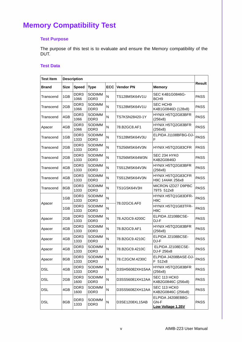
Memory Compatibility Test
Test Purpose
The purpose of this test is to evaluate and ensure the Memory compatibility of theDUT.
Test Data
Test Item DescriptionResult
Brand Size Speed Type ECC Vendor PN Memory
Transcend 1GBDDR3 1066
SODIMM DDR3
N TS128MSK64V1USEC K4B1G0846G-BCH9
PASS
Transcend 2GBDDR3 1066
SODIMM DDR3
N TS128MSK64V1USEC HCH9 K4B1G0846D (128x8)
PASS
Transcend 4GBDDR3 1066
SODIMM DDR3
N TS7KSN28420-1YHYNIX H5TQ2G83BFR (256x8)
PASS
Apacer 4GBDDR3 1066
SODIMM DDR3
N 78.B2GC8.AF1HYNIX H5TQ2G83BFR (256x8)
PASS
Transcend 1GBDDR3 1333
SODIMM DDR3
N TS128MSK64V3UELPIDA J1108BFBG-DJ-F
PASS
Transcend 2GBDDR3 1333
SODIMM DDR3
N TS256MSK64V3N HYNIX H5TQ2G83CFR PASS
Transcend 2GBDDR3 1333
SODIMM DDR3
N TS256MSK64W3N SEC 234 HYK0 K4B2G0846D
PASS
Transcend 4GBDDR3 1333
SODIMM DDR3
N TS512MSK64V3NHYNIX H5TQ2G83BFR (256x8)
PASS
Transcend 4GBDDR3 1333
SODIMM DDR3
N TS512MSK64V3NHYNIX H5TQ2G83CFR H9C 144AK 256x8
PASS
Transcend 8GBDDR3 1333
SODIMM DDR3
N TS1GSK64V3HMICRON IZD27 D9PBC 79T5 512x8
PASS
Apacer1GB
DDR3 1333
SODIMM DDR3
N78.02GC6.AF0
HYNIX H5TQ1G83DFR-H9C
PASS
1GBDDR3 1333
SODIMM DDR3
NHYNIX H5TQ1G83TFR-H9C
PASS
Apacer 2GBDDR3 1333
SODIMM DDR3
N 78.A2GC9.4200CELPIDA J2108BCSE-DJ-F
PASS
Apacer 4GBDDR3 1333
SODIMM DDR3
N 78.B2GC9.AF1HYNIX H5TQ2G83BFR (256x8)
PASS
Apacer 4GBDDR3 1333
SODIMM DDR3
N 78.B2GC9.4210CELPIDA J2108BCSE-DJ-F
PASS
Apacer 4GBDDR3 1333
SODIMM DDR3
N 78.B2GC9.4210C ELPIDA J2108ECSE-DJ-F 256x8
PASS
Apacer 8GBDDR3 1333
SODIMM DDR3
N 78.C2GCM.4230CELPIDA J4208BASE-DJ-F 512x8
PASS
DSL 4GBDDR3 1333
SODIMM DDR3
N D3SH56082XH15AAHYNIX H5TQ2G83BFR (256x8)
PASS
DSL 2GBDDR3 1600
SODIMM DDR3
N D3SS56081XH12AASEC 113 HCK0 K4B2G0846C (256x8)
PASS
DSL 4GBDDR3 1600
SODIMM DDR3
N D3SS56082XH12AASEC 113 HCK0 K4B2G0846C (256x8)
PASS
DSL 8GBDDR3 1333
SODIMM DDR3
N D3SE1208XL15ABELPIDA J4208EBBG-GN-FLow Voltage 1.35V
PASS
v AIMB-223 User Manual

Ordering Information
DSL 8GBDDR3 1600
SODIMM DDR3
N D3SE1208XL12AAELPIDA J4208EBBG-GN-FLow Voltage 1.35V
PASS
Apacer 2GBDDR3 1600
SODIMM DDR3
N 78.A2GCJ.AF00C HYNIX H5TQ2G83CFR (256x8)
PASS
Apacer 4GBDDR3 1600
SODIMM DDR3
N 78.B2GCJ.AF10CHYNIX H5TQ2G83CFR (256x8)
PASS
Apacer 4GBDDR3 1600
SODIMM DDR3
N 78.B2GCR.AF10CHYNIX H5TC2G83EFRLow Voltage 1.35V
PASS
Apacer 4GBDDR3 1600
SODIMM DDR3
N 78.B2GCZ.AT00CMICRON 2QE22 D9QBJLow Voltage 1.35V
PASS
Apacer 8GBDDR3 1600
SODIMM DDR3
N 78.C2GCZ.AT30CMICRON 2REI7 D9QBJLow Voltage 1.35V
PASS
Transcend 2GBDDR3 1600
SODIMM DDR3
N TS256MSK64V6N MICRON IVM77 D9PFJ PASS
Transcend 4GBDDR3 1600
SODIMM DDR3
N TS512MSK64V6NMICRON 2DM77 D9PFJ 256x8
PASS
Transcend 4GBDDR3 1600
SODIMM DDR3
N TS512MSK64W6HSEC 231 HYK0 K4B4G0846BLow Voltage 1.35V
PASS
Transcend 4GBDDR3 1600
SODIMM DDR3
N TS512MSK64N6N MICRON IRM72 D9PFJ PASS
Transcend 8GBDDR3 1600
SODIMM DDR3
N TS1GSK64V6HMICRON IZD27 D9PBC 79T5 512x8
PASS
Transcend 8GBDDR3 1600
SODIMM DDR3
N TS1GSK64W6HSEC 231 HYK0 K4B4G0846BLow Voltage 1.35V
PASS
ATP 8GBDDR3 1600
SODIMM DDR3
N AW24M64F8BLK0SSEC 140 HYK0 K4B4G0846B 512x8
PASS
Part Number Chipset GbE COM Display
AIMB-224G2-00A1E A75 2 6 VGA/DP/DP/LVDS
AIMB-223 User Manual vi

Product Warranty (2 years)Advantech warrants to you, the original purchaser, that each of its products will befree from defects in materials and workmanship for two years from the date of pur-chase.
This warranty does not apply to any products which have been repaired or altered bypersons other than repair personnel authorized by Advantech, or which have beensubject to misuse, abuse, accident or improper installation. Advantech assumes noliability under the terms of this warranty as a consequence of such events.
Because of Advantech’s high quality-control standards and rigorous testing, most ofour customers never need to use our repair service. If an Advantech product is defec-tive, it will be repaired or replaced at no charge during the warranty period. For out-of-warranty repairs, you will be billed according to the cost of replacement materials,service time and freight. Please consult your dealer for more details.
If you think you have a defective product, follow these steps:
1. Collect all the information about the problem encountered. (For example, CPU speed, Advantech products used, other hardware and software used, etc.) Note anything abnormal and list any onscreen messages you get when the problem occurs.
2. Call your dealer and describe the problem. Please have your manual, product, and any helpful information readily available.
3. If your product is diagnosed as defective, obtain an RMA (return merchandise authorization) number from your dealer. This allows us to process your return more quickly.
4. Carefully pack the defective product, a fully-completed Repair and Replacement Order Card and a photocopy proof of purchase date (such as your sales receipt) in a shippable container. A product returned without proof of the purchase date is not eligible for warranty service.
5. Write the RMA number visibly on the outside of the package and ship it prepaid to your dealer.
vii AIMB-223 User Manual

Initial InspectionBefore you begin installing your motherboard, please make sure that the followingmaterials have been shipped:
AIMB-224 AMD R-series mini-ITX motherboard 2 x SATA HDD cable 2 x SATA Power cable 1 x Serial port cable(1 to 4) 1 x I/O port bracket 1 x Startup manual 1 x Driver CD 1 x Warranty card 1 x CPU cooler
If any of these items are missing or damaged, contact your distributor or sales repre-sentative immediately. We have carefully inspected the AIMB-224 mechanically andelectrically before shipment. It should be free of marks and scratches and in perfectworking order upon receipt. As you unpack the AIMB-224, check it for signs of ship-ping damage. (For example, damaged box, scratches, dents, etc.) If it is damaged orit fails to meet the specifications, notify our service department or your local salesrepresentative immediately. Also notify the carrier. Retain the shipping carton andpacking material for inspection by the carrier. After inspection, we will make arrange-ments to repair or replace the unit.
AIMB-223 User Manual viii
Contents
Chapter 1 General Information ............................11.1 Introduction ............................................................................................... 21.2 Features .................................................................................................... 21.3 Specifications ............................................................................................ 3
1.3.1 Processor System......................................................................... 31.3.2 Expansion Slot .............................................................................. 31.3.3 Memory ......................................................................................... 31.3.4 Graphic Interface .......................................................................... 31.3.5 Ethernet Interface ......................................................................... 31.3.6 SATA Interface.............................................................................. 31.3.7 EIDE.............................................................................................. 31.3.8 Rear I/O ........................................................................................ 41.3.9 Internal Connector ........................................................................ 41.3.10 Watchdog Timer............................................................................ 41.3.11 Power Requirement ...................................................................... 41.3.12 Environment.................................................................................. 41.3.13 Physical Characteristics................................................................ 4
1.4 Jumpers and Connectors .......................................................................... 5Table 1.1: Connectors List........................................................... 5Table 1.2: DCIN1......................................................................... 6Table 1.3: KBMS1 ....................................................................... 6Table 1.4: .................................................................................... 6Table 1.5: DUAL_DP1 ................................................................. 7Table 1.6: COM1 ......................................................................... 8Table 1.7: COM2 ......................................................................... 8Table 1.8: VGA1.......................................................................... 8Table 1.9: LAN1USB01 ............................................................... 9Table 1.10:LAN2USB23 ............................................................. 10Table 1.11:AUDIO1 .................................................................... 10Table 1.12:JAMP1 ...................................................................... 11Table 1.13:FPAUDIO: Front panel audio connector................... 11Table 1.14:SPDIF_OUT1 ........................................................... 11Table 1.15:SPI1.......................................................................... 11Table 1.16:SATA1 ...................................................................... 12Table 1.17:SATA2 ...................................................................... 12Table 1.18:SATA3 ...................................................................... 12Table 1.19:SATA_PWR2............................................................ 12Table 1.20:SATA_PWR1............................................................ 12Table 1.22:BAT1......................................................................... 13Table 1.23:COM3-6 .................................................................... 13Table 1.21:JCMOS1 ................................................................... 13Table 1.24:MINI_CARD1............................................................ 14Table 1.25:JWDT1+JOBS1 ........................................................ 15Table 1.26:JFP3 ......................................................................... 15Table 1.27:JFP1+JFP2............................................................... 16Table 1.28:JLVDS3 .................................................................... 16Table 1.29:JLVDS4 .................................................................... 16Table 1.30:VCON2 ..................................................................... 16Table 1.31:LVDS2 ...................................................................... 17Table 1.32:KBMS2 ..................................................................... 18Table 1.33:ATX_5V1 .................................................................. 18Table 1.34:ATX12V1 .................................................................. 18Table 1.35:PSON1 ..................................................................... 18Table 1.36:CPUFAN1................................................................. 18
ix AIMB-223 User Manual
Table 1.37:DIO_CN1.................................................................. 19Table 1.38:JSETCOM3 .............................................................. 19Table 1.39:COM Port 3 ~ 6 ........................................................ 19Table 1.40:SPI_CN1 .................................................................. 20Table 1.41:USB45 ...................................................................... 20Table 1.42:USB67 ...................................................................... 21Table 1.43:JVBR: BL CONTROLLER FROM SIO ..................... 21Table 1.44: INV2 ......................................................................... 21Table 1.45:EDP1 ........................................................................ 21Table 1.46:JSETCOM6 .............................................................. 22Table 1.47:SYSFAN1 ................................................................. 22Table 1.48:MINI_PCIE2 ............................................................. 23Table 1.49:USB89 ...................................................................... 24Table 1.50:DOM_PWR1............................................................. 24Table 1.51:DDR_PWR1 ............................................................. 24
1.5 Board layout: Jumper and Connector Locations..................................... 25Figure 1.1 Jumper and Connector Location .............................. 25Figure 1.2 I/O Connectors ......................................................... 26
1.6 AIMB-224 Board Diagram....................................................................... 26Figure 1.3 AIMB-224 Board Diagram ........................................ 26
1.7 Safety Precautions.................................................................................. 271.8 Jumper Settings ...................................................................................... 28
1.8.1 How to Set Jumpers ................................................................... 281.8.2 CMOS Clear (CMOS1) ............................................................... 28
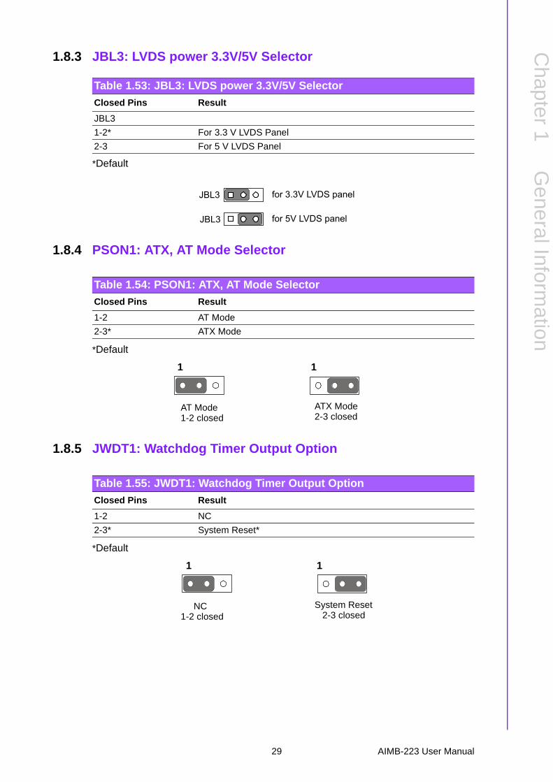
Table 1.52:CMOS1..................................................................... 281.8.3 JBL3: LVDS power 3.3V/5V Selector ......................................... 29
Table 1.53:JBL3: LVDS power 3.3V/5V Selector ....................... 291.8.4 PSON1: ATX, AT Mode Selector................................................ 29
Table 1.54:PSON1: ATX, AT Mode Selector ............................. 291.8.5 JWDT1: Watchdog Timer Output Option .................................... 29
Table 1.55:JWDT1: Watchdog Timer Output Option.................. 291.9 System Memory ...................................................................................... 30
1.10 Memory Installation Procedures ............................................................. 30
Chapter 2 Connecting Peripherals.................... 312.1 Introduction ............................................................................................. 322.2 USB Ports (LAN1_USB01/LAN2_USB23/USB45/USB67) ..................... 32
Table 2.1: LAN LED Indicator.................................................... 322.3 VGA Connector (VGA1).......................................................................... 332.4 Serial Ports (COM3~6)............................................................................ 342.5 CPU Fan Connector (CPU_FAN1) ......................................................... 352.6 System FAN Connector (SYSFAN1) ...................................................... 352.7 Front Panel Connectors (JFP1+JFP2+JFP3) ......................................... 36
2.7.1 ATX soft power switch ((JFP1+JFP2/ PWR_SW)) ..................... 362.7.2 Reset (JFP1+JFP2/ RESET) ...................................................... 362.7.3 HDD LED (JFP1+JFP2/ HDDLED)............................................. 362.7.4 External speaker (JFP1+JFP2/ SPEAKER) ............................... 362.7.5 Power LED and keyboard lock connector (JFP1 / PWR_LED &
KEY LOCK)................................................................................. 37Table 2.2: ATX power supply LED status (No support for AT pow-
er) ............................................................................. 372.8 Line In, Line Out, Mic In Connector (AUDIO1)........................................ 372.9 Serial ATA Interface (SATA1~3) ............................................................. 38
2.10 PCI Express x8 ....................................................................................... 382.11 ATX 12V Power Connector (CN19) ........................................................ 392.12 SPI Flash connector(CN4) ...................................................................... 392.13 LCD Inverter Connector (JBL1) .............................................................. 402.14 LVDS Connector (LVDS1) ...................................................................... 41
AIMB-223 User Manual x

2.15 General purpose I/O Connector (GPIO1)................................................ 41
Chapter 3 BIOS Operation..................................433.1 Introduction ............................................................................................. 443.2 BIOS Setup ............................................................................................. 44
3.2.1 Main Menu .................................................................................. 453.2.2 Advanced BIOS Features ........................................................... 463.2.3 Chipset........................................................................................ 523.2.4 Boot............................................................................................. 563.2.5 Security ....................................................................................... 573.2.6 Save & Exit ................................................................................. 58
Chapter 4 Software Introduction & Service ......594.1 Introduction ............................................................................................. 604.2 Value-Added Software Services ............................................................. 60
4.2.1 Software API ............................................................................... 604.2.2 Software Utility ............................................................................ 62
Chapter 5 Chipset Software Installation Utility 635.1 Before You Begin .................................................................................... 645.2 Introduction ............................................................................................. 645.3 Windows XP Driver Setup....................................................................... 65
Chapter 6 VGA Setup..........................................676.1 Introduction ............................................................................................. 686.2 Windows 7/XP......................................................................................... 68
Chapter 7 LAN Configuration.............................697.1 Introduction ............................................................................................. 707.2 Features .................................................................................................. 707.3 Installation ............................................................................................... 707.4 Windows 7/XP Driver Setup.................................................................... 71
Appendix A Programming the Watchdog Timer..73A.1 Programming the Watchdog Timer ......................................................... 74
A.1.1 Watchdog Timer Overview.......................................................... 74A.1.2 Programming the Watchdog Timer ............................................. 74
Table A.1: Watchdog Timer Registers ....................................... 76A.1.3 Example Program ....................................................................... 77
Appendix B I/O Pin Assignments..........................81B.1 USB Header (USB56, USB78)................................................................ 82
Table B.1: USB Header (USB56)............................................... 82B.2 VGA Connector (VGA1) .......................................................................... 82
Table B.2: VGA Connector (VGA1) ........................................... 82B.3 RS-232 Interface (COM3/4/5/6) .............................................................. 83
Table B.3: RS-232 Interface (COM3~COM6) ............................ 83
xi AIMB-223 User Manual

B.4 CN4: SPI Fresh Card Pin Connector ...................................................... 84Table B.4: CN4: SPI Fresh Card Pin Connector........................ 84
B.5 CPU Fan Power Connector (CPU_FAN1) .............................................. 84Table B.5: CPU Fan Power Connector (CPU_FAN1)................ 84
B.6 System Fan Power Connector (SYS_FAN1) .......................................... 84Table B.6: System Fan Power Connector (SYS_FAN1)............ 84
B.7 Power LED & Keyboard Lock Connector (JFP3) .................................... 85Table B.7: Power LED & Keyboard Lock Connector (JFP3) ..... 85
B.8 Power switch/HDD LED/SMBus/Speaker (JFP1+JFP2)......................... 85Table B.8: Power Switch/HDD LED/SMBus/Speaker
(JFP1+JFP2) ............................................................ 85B.9 USB/LAN ports (LAN1_USB12/LAN2_USB34) ...................................... 86
Table B.9: USB Port .................................................................. 86Table B.10:Ethernet 10/100 Mbps RJ-45 Port............................ 86
B.10 Line In, Line Out, Mic In Connector (AUDIO1)........................................ 86B.11 Serial ATA0/1 (SATA 1/2/3/4) ................................................................. 86
Table B.11:Serial ATA 0/1 (SATA 1/2/3/4) ................................. 86B.12 AT/ATX Mode (PSON1).......................................................................... 87
Table B.12:AT/ATX Mode (PSON1) ........................................... 87B.13 GPIO Pin Header (GPIO1)...................................................................... 87
Table B.13:GPIO Pin Header (GPIO1) ....................................... 87B.14 LVDS Connector: LVDS1........................................................................ 87
Table B.14:LVDS1 Connector .................................................... 88B.15 LVDS Power Jumper (JBL3)................................................................... 88
Table B.15:LVDS Power Jumper................................................ 88B.16 LVDS Inverter (JBL1).............................................................................. 89
Table B.16:LVDS Power Jumper................................................ 89B.17 ATX 12 V connector (ATX12V_1) ........................................................... 89
Table B.17:ATX 12 V connector (ATX12V_1) ............................ 89
AIMB-223 User Manual xii

Chapter 1
1 General Information
1.1 IntroductionThe AIMB-224 board comes with high connectivity and a variety of expansion options
including: a PCI expansion x16 slot, six serial ports, 3 SATA III 600 MB/s connectors,two USB3.0 ports and eight USB 2.0 ports. Thriple display output is supported withseveral output interface options: VGA, two Display port, and LVDS (LVDS supports3.3V, 5V, and 12V for large sized panels). AIMB-224 also comes with dual PCIExpress based Gigabit (Realtek 8111E) Ethernet ports delivering up to 1000Mbps ofbandwidth for network-intensive applications. AIMB-224 has designed in bothATX12V and DC IN power to provide a low total cost solution. All this connectivity ispacked into a space-saving, power-efficient, and cost-effective Mini-ITX form factor.
With the graphics engine integrated onto the processor chip, these two-chip solutionsprovide enhanced graphics performance compared to previous AMD platforms. Theintegrated graphics controller includes AMD’s first Fusion architecture acceleratedprocessing unit which can also support dual channel 24-bit LVDS for large sized pan-els.
1.2 Features Rich I/O connectivity: 6 serial ports, 8 USB 2.0, 2USB3.0, 3SATA 2.0, Dual
GbE LAN Standard Mini-ITX form factor with industrial feature: The AIMB-224 is a full-
featured Mini-ITX motherboard with balanced expendability and performance Wide selection of storage devices: SATA HDD, CFast, SATA DOM, mSATA
customers benefit from the flexibility of using the most suitable storage device for larger capacity
Optimized integrated graphic solution: With AMD ATI Radeon HD7000 series, Support DirectX 11, UVD3.
AIMB-223 User Manual 2

Chapter 1
GeneralInform
ation
1.3 Specifications
1.3.1 Processor System CPU: AMD R-series processor, support Quad core CPU up to 2.3GHz and Dual
core CPU up to 2.7GHz Max. Speed: Quad Core 2.3GHz / Dual Core 2.5GHz (TDP 35W) L2 Cache: 512 KB Chipset: AMD R-series + A75 BIOS: AMI 16 Mbit SPI
1.3.2 Expansion Slot Mini-PCIe: 2 PCIe: PCIe x8
1.3.3 Memory Technology: Dual channel DDR3 1333/1600MHz Max. Capacity: 16 GB Socket: 2 x 204 pin SODIMM
1.3.4 Graphic Interface Controller: ATI Radeon HD7000 series, support DirectX 11, UVD3 VRAM: TBD VGA: Supports up to 2560 x 1536 @ 32bpp LVDS: Supports 24-bit dual channel and up to 1920 x 1200 DP: 1920x1200@60Hz Dual Display: Supports dual display of any two display device (CRT, LVDS,
Display port) Triple Display: Support triple display as below configuration. CRT+LVDS+DP
or DP+DP+LVDS
1.3.5 Ethernet Interface Interface: 10/100/1000 Mbps Controller: GbE: Realtek RTL8111E Connector: RJ-45 x 2
1.3.6 SATA Interface Max Data Transfer Rate: 600 MB/s Channel: 3
1.3.7 EIDE Mode: None Channel: None
3 AIMB-223 User Manual
1.3.8 Rear I/O VGA: 1 DP: 2 Ethernet: 2 USB: 4 (2USB2.0 & 2USB3.0) Audio: 3 (Mic-in, Line-out, Line-in) Serial: 1 (RS-232) DC jack: 1 (2.5 mm) PS2 KB/MS: 1
1.3.9 Internal Connector LVDS & Inverter: 1 USB: 4 (USB 2.0 compliant) Serial: 5(4RS-2322. 1RS[-422/485 suport, COM3 rs-232/422/485 selection by
jumper seelection; COM6 support 5V/12V) IDE: None SATA: 3 Parallel: None GPIO: 8-bit Mini PCIE slot: 2miniPCIE slot, F/S support mSATA; H/S support wifi-module
only.
1.3.10 Watchdog Timer Output: System reset Interval: Programmable 1 ~ 255 sec/min
1.3.11 Power Requirement Typical:
– Single Voltage 12V DC input by 1x External DC phone Jack or 1x Internal 2x2-pin Power Connector;
– AT/ATX Supported by Jumper– Max power consumption:47.57W (4G DDR3 RAM)
1.3.12 Environment Temperature:
– 0 ~ 60° C (32 ~ 140° F), Operating– -40 ~ 85° C (-40 ~ 185° F), Non-operating
1.3.13 Physical Characteristics Dimensions: 170 mm x 170 mm (6.69" x 6.69")
AIMB-223 User Manual 4

Chapter 1
GeneralInform
ation
1.4 Jumpers and ConnectorsConnectors on the AIMB-224 motherboard link it to external devices such as harddisk drives and a keyboard. In addition, the board has a number of jumpers used toconfigure your system for your application.
The tables below list the function of each of the board jumpers and connectors. Latersections in this chapter give instructions on setting jumpers. Chapter 2 gives instruc-tions for connecting external devices to your motherboard.
Table 1.1: Connectors List
Label Function
FPAUD1 Front Panel audio connector
AUDIO1 Audio connector
CMOS1 CMOS clear ( Default 1-2 )
DIMM1_A1/B1 Memory connector channel
COM3-6 Serial port: 3RS232/1RS-232-422/485
COM2 Serial port: RS-232
CPU_FAN1 CPU FAN connector(3-pin)
DIO_CN1 GPIO Header
DCIN1 DC IN
ATX12V1 ATX 12V connector
ATX_5V1 PS_ON , 5VSB
LVDS2 LVDS connector (Internal)
INV2 LVDS Inverter Power
JVBR2LVDS Brightness control selector for Analog or Digital (Default 1-2, Analog)
JLVDS3 LVDS voltage jumper (default 1-2, 3.3V)
JLVDS4 LVDS 12V voltage jumper
VCON2 LVDS JEIDA/VESA jumper selection
JFP1+JFP2 Power switch/HDD LED/SMBus/speaker
JFP3 Power LED and Keyboard lock
JSETCOM6 COM6 RS-232/422/485 Jumper setting
JSETCOM3 COM3 5V/12V Jumper setting
PCIEX8_1 PCI Express X8 slot
KBMS1 PS/2 Keyboard and Mouse external connector
KBMS2 PS/2 Keyboard and Mouse internal connector
LAN1_USB01 LAN1 / USB port 1, 2
LAN2_USB23 LAN2 / USB port 3, 4
MINI_PCIE1/2 Mini PCI express connector
PSON1 AT(1-2) / ATX(2-3) ( Default 2-3 )
SATA1 Serial ATA data connector 1
SATA2 Serial ATA data connector 2
SATA3 Serial ATA data connector 3
SATA_PWR1 SATA POWER
SATA_PWR2 SATA POWER
DOM_PWR DOM POWER
SPI1 SPI connector
SPI_CN1 SPI flash update connector.
SPDIF_OUT1 Digital Audio connector
5 AIMB-223 User Manual

SYS_FAN1 System FAN connector(3-pin)
USB456789 USB port 4,5, 6,7,8,9 (on board)
DUAL_DP1 Two Display port connector
VGA1 VGA connector
COM1 COM PORT CONNECTOR
JOBS1+JWDT1 OBS Alarm and Watchdog Reset
BAT1 Battery holder
Table 1.2: DCIN1
PIN SIGNAL
1 +12V
2 GND
Table 1.3: KBMS1 Table 1.4:
PIN SIGNAL
1 KB_DATA
2 MS_DATA
3 GND
4 +PS2VCC
5 KB_CLK
6 MS_CLK
Table 1.1: Connectors List
AIMB-223 User Manual 6
Chapter 1
GeneralInform
ation
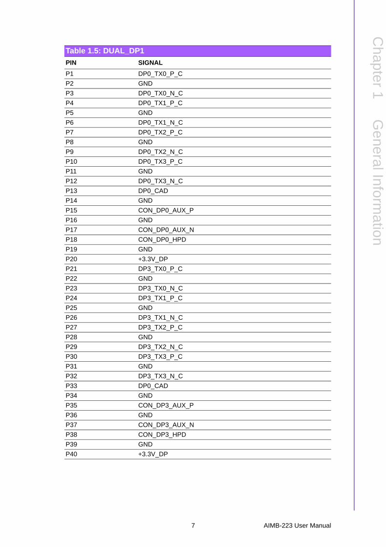
Table 1.5: DUAL_DP1
PIN SIGNAL
P1 DP0_TX0_P_C
P2 GND
P3 DP0_TX0_N_C
P4 DP0_TX1_P_C
P5 GND
P6 DP0_TX1_N_C
P7 DP0_TX2_P_C
P8 GND
P9 DP0_TX2_N_C
P10 DP0_TX3_P_C
P11 GND
P12 DP0_TX3_N_C
P13 DP0_CAD
P14 GND
P15 CON_DP0_AUX_P
P16 GND
P17 CON_DP0_AUX_N
P18 CON_DP0_HPD
P19 GND
P20 +3.3V_DP
P21 DP3_TX0_P_C
P22 GND
P23 DP3_TX0_N_C
P24 DP3_TX1_P_C
P25 GND
P26 DP3_TX1_N_C
P27 DP3_TX2_P_C
P28 GND
P29 DP3_TX2_N_C
P30 DP3_TX3_P_C
P31 GND
P32 DP3_TX3_N_C
P33 DP0_CAD
P34 GND
P35 CON_DP3_AUX_P
P36 GND
P37 CON_DP3_AUX_N
P38 CON_DP3_HPD
P39 GND
P40 +3.3V_DP
7 AIMB-223 User Manual
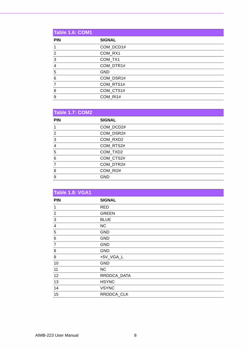
Table 1.6: COM1
PIN SIGNAL
1 COM_DCD1#
2 COM_RX1
3 COM_TX1
4 COM_DTR1#
5 GND
6 COM_DSR1#
7 COM_RTS1#
8 COM_CTS1#
9 COM_RI1#
Table 1.7: COM2
PIN SIGNAL
1 COM_DCD2#
2 COM_DSR2#
3 COM_RXD2
4 COM_RTS2#
5 COM_TXD2
6 COM_CTS2#
7 COM_DTR2#
8 COM_RI2#
9 GND
Table 1.8: VGA1
PIN SIGNAL
1 RED
2 GREEN
3 BLUE
4 NC
5 GND
6 GND
7 GND
8 GND
9 +5V_VGA_L
10 GND
11 NC
12 RRDDCA_DATA
13 HSYNC
14 VSYNC
15 RRDDCA_CLK
AIMB-223 User Manual 8
Chapter 1
GeneralInform
ation
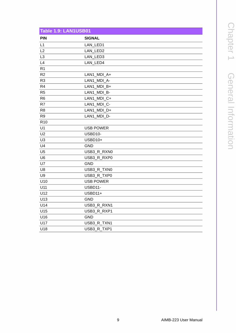
Table 1.9: LAN1USB01
PIN SIGNAL
L1 LAN_LED1
L2 LAN_LED2
L3 LAN_LED3
L4 LAN_LED4
R1
R2 LAN1_MDI_A+
R3 LAN1_MDI_A-
R4 LAN1_MDI_B+
R5 LAN1_MDI_B-
R6 LAN1_MDI_C+
R7 LAN1_MDI_C-
R8 LAN1_MDI_D+
R9 LAN1_MDI_D-
R10
U1 USB POWER
U2 USBD10-
U3 USBD10+
U4 GND
U5 USB3_R_RXN0
U6 USB3_R_RXP0
U7 GND
U8 USB3_R_TXN0
U9 USB3_R_TXP0
U10 USB POWER
U11 USBD11-
U12 USBD11+
U13 GND
U14 USB3_R_RXN1
U15 USB3_R_RXP1
U16 GND
U17 USB3_R_TXN1
U18 USB3_R_TXP1
9 AIMB-223 User Manual
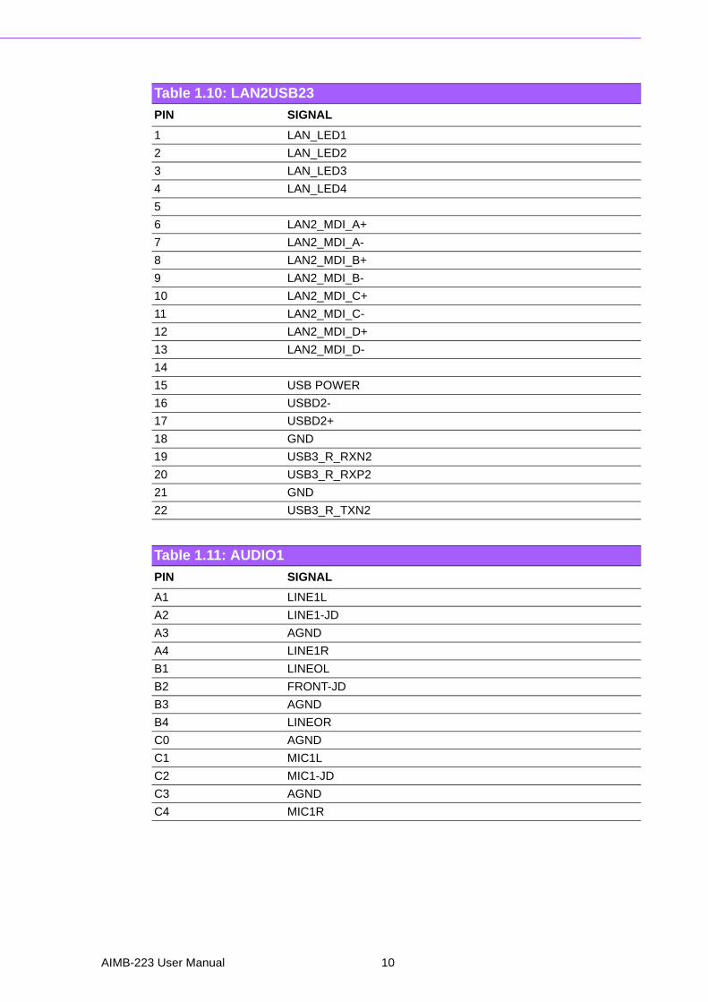
Table 1.10: LAN2USB23
PIN SIGNAL
1 LAN_LED1
2 LAN_LED2
3 LAN_LED3
4 LAN_LED4
5
6 LAN2_MDI_A+
7 LAN2_MDI_A-
8 LAN2_MDI_B+
9 LAN2_MDI_B-
10 LAN2_MDI_C+
11 LAN2_MDI_C-
12 LAN2_MDI_D+
13 LAN2_MDI_D-
14
15 USB POWER
16 USBD2-
17 USBD2+
18 GND
19 USB3_R_RXN2
20 USB3_R_RXP2
21 GND
22 USB3_R_TXN2
Table 1.11: AUDIO1
PIN SIGNAL
A1 LINE1L
A2 LINE1-JD
A3 AGND
A4 LINE1R
B1 LINEOL
B2 FRONT-JD
B3 AGND
B4 LINEOR
C0 AGND
C1 MIC1L
C2 MIC1-JD
C3 AGND
C4 MIC1R
AIMB-223 User Manual 10

Chapter 1
GeneralInform
ation
Table 1.12: JAMP1
PIN SIGNAL
1 AMP_L-
2 AMP_L+
3 AMP_R-
4 AMP_R+
Table 1.13: FPAUDIO: Front panel audio connector
PIN SIGNAL
1 MIC2L
2 AGND
3 MIC2R
4 A_FP_PRES#
5 LINE2R
6 MIC2-JD
7 SENSEB
8 NC
9 LINE2L
10 LINE2-JD
Table 1.14: SPDIF_OUT1
PIN SIGNAL
1 +5VA_CODEC
3 SPDIF_O
4 GND
Table 1.15: SPI1
PIN SIGNAL
1 SPI_CS#
2 SPI_DATAIN
3 SPI_WP0#
4 GND
5 SPI_MOSI
6 SPI_CLK
7 SPI_HOLD0#
8 +V3.3M_SPI
11 AIMB-223 User Manual

Table 1.16: SATA1
PIN SIGNAL
1 GND
2 SATA_C_TX0_P
3 SATA_C_TX0_N
4 GND
5 SATA_C_RX0_N
6 SATA_C_RX0_P
7 GND
Table 1.17: SATA2
PIN SIGNAL
1 GND
2 SATA_C_TX1_P
3 SATA_C_TX1_N
4 GND
5 SATA_C_RX1_N
6 SATA_C_RX1_P
7 GND
Table 1.18: SATA3
PIN SIGNAL
1 GND
2 SATA_C_TX2_P
3 SATA_C_TX2_N
4 GND
5 SATA_C_RX2_N
6 SATA_C_RX2_P
7 GND
Table 1.19: SATA_PWR2
PIN SIGNAL
1 +5V
2 GND
3 GND
4 +12V
Table 1.20: SATA_PWR1
PIN SIGNAL
1 +5V
2 GND
3 GND
4 +12V
AIMB-223 User Manual 12
Chapter 1
GeneralInform
ation
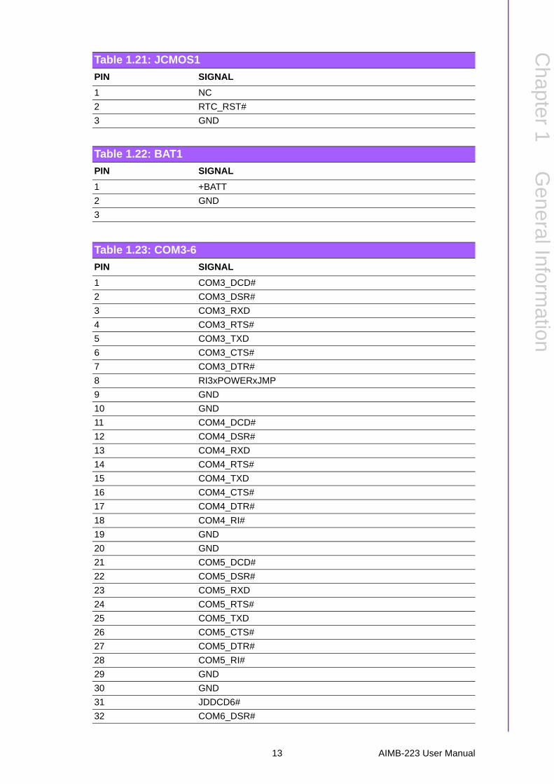
Table 1.21: JCMOS1
PIN SIGNAL
1 NC
2 RTC_RST#
3 GND
Table 1.22: BAT1
PIN SIGNAL
1 +BATT
2 GND
3
Table 1.23: COM3-6
PIN SIGNAL
1 COM3_DCD#
2 COM3_DSR#
3 COM3_RXD
4 COM3_RTS#
5 COM3_TXD
6 COM3_CTS#
7 COM3_DTR#
8 RI3xPOWERxJMP
9 GND
10 GND
11 COM4_DCD#
12 COM4_DSR#
13 COM4_RXD
14 COM4_RTS#
15 COM4_TXD
16 COM4_CTS#
17 COM4_DTR#
18 COM4_RI#
19 GND
20 GND
21 COM5_DCD#
22 COM5_DSR#
23 COM5_RXD
24 COM5_RTS#
25 COM5_TXD
26 COM5_CTS#
27 COM5_DTR#
28 COM5_RI#
29 GND
30 GND
31 JDDCD6#
32 COM6_DSR#
13 AIMB-223 User Manual

33 JRRXD6
34 COM6_RTS#
35 JTTXD6
36 COM6_CTS#
37 JDDTR6#
38 COM6_RI#
39 GND
40 GND
Table 1.24: MINI_CARD1
PIN SIGNAL
1 WAKE#
2 +V3.3_PIN43
3 NC
4 GND
5 NC
6 +1P5V
7 CKREQ_MINICARD#
8 NC
9 GND
10 NC
11 CLK_MINICARD#
12 NC
13 CLK_MINICARD
14 NC
15 GND
16 NC
17 NC
18 GND
19 NC
20 PEMCxWDISBN
21 MSATA_PCIE_DET#
22 PCIE_RST#
23 MPCIE_MSATA_RX-
24 +V3.3_PIN51
25 MPCIE_MSATA_RX+
26 GND
27 GND
28 +1P5V
29 GND
30 SMB_CLK_RESUME
31 MPCIE_MSATA_TX-
32 SMB_DAT_RESUME
33 MPCIE_MSATA_TX+
34 GND
35 GND
Table 1.23: COM3-6
AIMB-223 User Manual 14

Chapter 1
GeneralInform
ation
36 USBP7-
37 GND
38 USBP7+
39 +V3.3_PIN43
40 GND
41 +V3.3_PIN43
42 PEMCxLWANN
43 PCIE1.1#_1.0MSATA_SEL
44 PEMCxLLANN
45 NC
46 PEMCxLPANN
47 NC
48 +1P5V
49 NC
50 GND
51 MSATA#_PCIE_SEL
52 +V3.3_PIN43
Table 1.25: JWDT1+JOBS1
PIN SIGNAL
1 NC
2 SIO_WG#
3 FRP_RST#
4 SIO_BEEP
5 ERR_BEEP
Table 1.26: JFP3
PIN SIGNAL
1 PWLED+
2 NC
3 GND
4 #KEYLOCK
5 GND
Table 1.24: MINI_CARD1
15 AIMB-223 User Manual

Table 1.27: JFP1+JFP2
PIN SIGNAL
1 +5V
2 HDLED+
3 FRP_PANSWIN#
4 SPK_CN17P2
5 HDD_LED-
6 GND(R1160:100OHM)
7 SPK_CN17P4
8 SMBDATA_R
9 FRP_RST#
10 SPK_CN17P3
11 SMBCLK_R
12 GND
Table 1.28: JLVDS3
PIN SIGNAL
1 +12V
2 VDDSAFE_IN
Table 1.29: JLVDS4
PIN SIGNAL
1 +3P3V
2 VDDSAFE_IN
3 +5V
Table 1.30: VCON2
PIN SIGNAL
1 +3P3V
2 VCON
3 GND
AIMB-223 User Manual 16

Chapter 1
GeneralInform
ation
Table 1.31: LVDS2
PIN SIGNAL
1 VDDSAFE
2 VDDSAFE
3 GND
4 GND
5 VDDSAFE
6 VDDSAFE
7 LVDS_L0_N
8 LVDS_U0_N
9 LVDS_L0_P
10 LVDS_U0_P
11 GND
12 GND
13 LVDS_L1_N
14 LVDS_U1_N
15 LVDS_L1_P
16 LVDS_U1_P
17 GND
18 GND
19 LVDS_L2_N
20 LVDS_U2_N
21 LVDS_L2_P
22 LVDS_U2_P
23 GND
24 GND
25 LVDS_CLKL_N
26 LVDS_CLKU_N
27 LVDS_CLKL_P
28 LVDS_CLKU_P
29 GND
30 GND
31 LVDS_CH7511_DDC_CLK
32 LVDS_CH7511_DDC_DATA
33 GND
34 GND
35 LVDS_L3_N
36 LVDS_U3_N
37 LVDS_L3_P
38 LVDS_U3_P
39 N22140709
40 VCON
17 AIMB-223 User Manual

Table 1.32: KBMS2
PIN SIGNAL
1 O_KB_CLK_L
2 O_KB_DATA_L
3 O_MS_DATA_L
4 GND
5 +PS2VCC
6 O_MS_CLK_L
Table 1.33: ATX_5V1
PIN SIGNAL
1 +5VSB_IN
2 GND
3 PS_ON#
Table 1.34: ATX12V1
PIN SIGNAL
1 +12V
2 GND
3 +12V
4 GND
5
Table 1.35: PSON1
PIN SIGNAL
1 FRP_PANSWIN#_AT
2 FRP_PANSWIN#
3 NC
Table 1.36: CPUFAN1
PIN SIGNAL
1 GND
2 CPU_SFAN_PWR
3 CPU_SFAN_D
AIMB-223 User Manual 18

Chapter 1
GeneralInform
ation
Table 1.37: DIO_CN1
PIN SIGNAL
1 SIO_GPIO0
2 SIO_GPIO4
3 SIO_GPIO1
4 SIO_GPIO5
5 SIO_GPIO2
6 SIO_GPIO6
7 SIO_GPIO3
8 SIO_GPIO7
9 +5VSB
10 GND
Table 1.38: JSETCOM3
PIN SIGNAL
1 +12V
2 RI6xPOWERxJMP
3 COM6_RI#
4 RI6xPOWERxJMP
5 +5V
6 RI6xPOWERxJMP
Table 1.39: COM Port 3 ~ 6
PIN SIGNAL
1 COM3_DCD#
2 COM3_DSR#
3 COM3_RXD
4 COM3_RTS#
5 COM3_TXD
6 COM3_CTS#
7 COM3_DTR#
8 RI3xPOWERxJMP
9 GND
10 GND
11 COM4_DCD#
12 COM4_DSR#
13 COM4_RXD
14 COM4_RTS#
15 COM4_TXD
16 COM4_CTS#
17 COM4_DTR#
18 COM4_RI#
19 GND
20 GND
21 COM5_DCD#
19 AIMB-223 User Manual
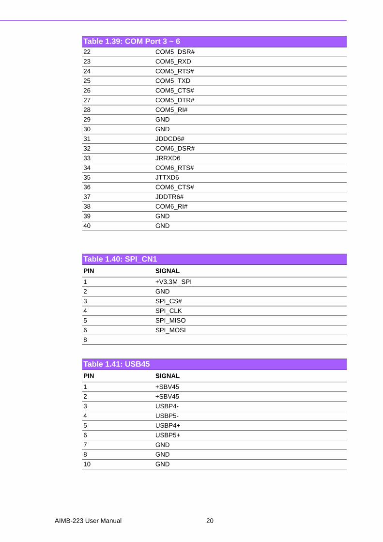
22 COM5_DSR#
23 COM5_RXD
24 COM5_RTS#
25 COM5_TXD
26 COM5_CTS#
27 COM5_DTR#
28 COM5_RI#
29 GND
30 GND
31 JDDCD6#
32 COM6_DSR#
33 JRRXD6
34 COM6_RTS#
35 JTTXD6
36 COM6_CTS#
37 JDDTR6#
38 COM6_RI#
39 GND
40 GND
Table 1.40: SPI_CN1
PIN SIGNAL
1 +V3.3M_SPI
2 GND
3 SPI_CS#
4 SPI_CLK
5 SPI_MISO
6 SPI_MOSI
8
Table 1.41: USB45
PIN SIGNAL
1 +SBV45
2 +SBV45
3 USBP4-
4 USBP5-
5 USBP4+
6 USBP5+
7 GND
8 GND
10 GND
Table 1.39: COM Port 3 ~ 6
AIMB-223 User Manual 20

Chapter 1
GeneralInform
ation
Table 1.42: USB67
PIN SIGNAL
1 +SBV67
2 +SBV67
3 USBP6-
4 USBP7-
5 USBP6+
6 USBP7+
7 GND
8 GND
10 GND
Table 1.43: JVBR: BL CONTROLLER FROM SIO
PIN SIGNAL
1 BL_CLT1
2 GND
3 NC
Table 1.44: INV2
PIN SIGNAL
1 +V12SA1
2 GND
3 BL_EN1
4 BL_CLT1
5 INV1_P5V1
Table 1.45: EDP1
PIN SIGNAL
1 GND
2 GND
3 EDP0N
4 EDP3N
5 EDP0P
6 EDP3P
7 GND
8 NC
9 EDP1N
10 GND
11 EDP1P
12 EAUXN
13 GND
14 EAUXP
15 EDP2N
16 GND
21 AIMB-223 User Manual
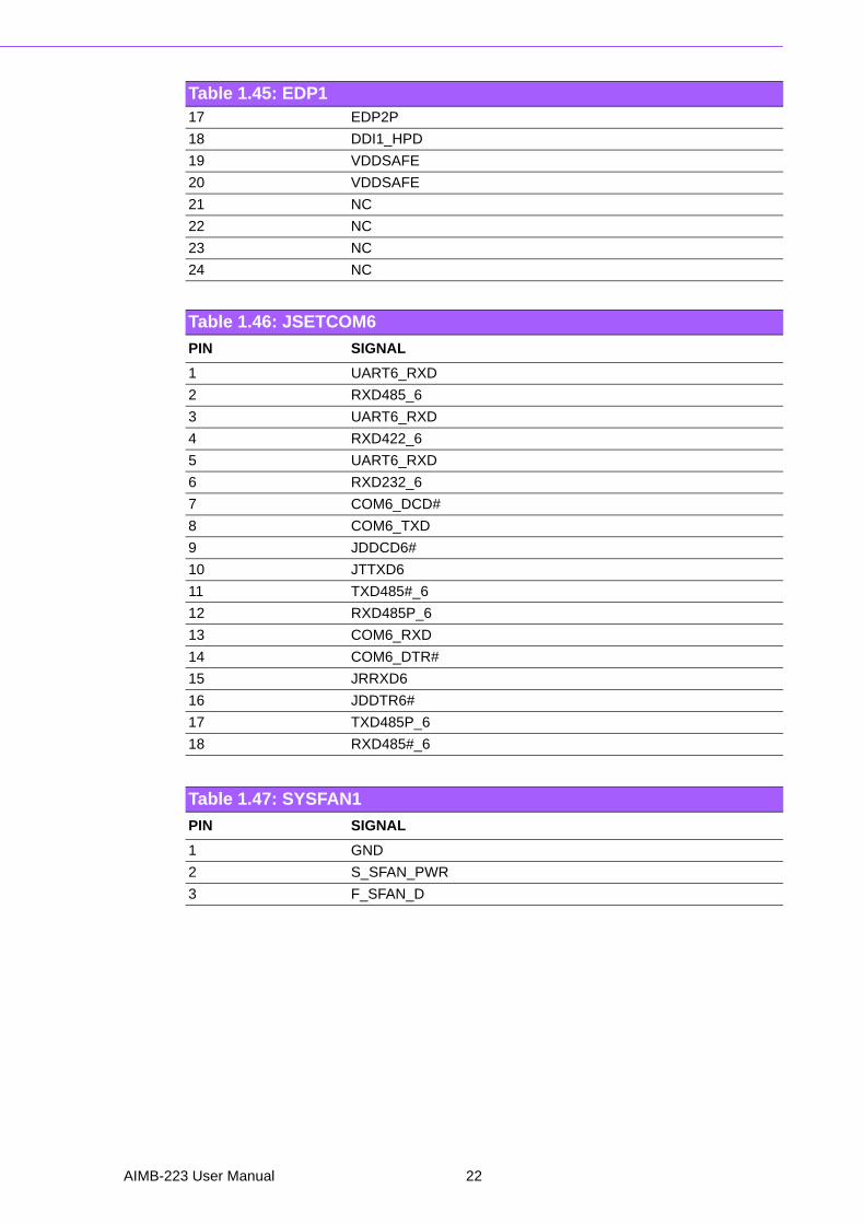
17 EDP2P
18 DDI1_HPD
19 VDDSAFE
20 VDDSAFE
21 NC
22 NC
23 NC
24 NC
Table 1.46: JSETCOM6
PIN SIGNAL
1 UART6_RXD
2 RXD485_6
3 UART6_RXD
4 RXD422_6
5 UART6_RXD
6 RXD232_6
7 COM6_DCD#
8 COM6_TXD
9 JDDCD6#
10 JTTXD6
11 TXD485#_6
12 RXD485P_6
13 COM6_RXD
14 COM6_DTR#
15 JRRXD6
16 JDDTR6#
17 TXD485P_6
18 RXD485#_6
Table 1.47: SYSFAN1
PIN SIGNAL
1 GND
2 S_SFAN_PWR
3 F_SFAN_D
Table 1.45: EDP1
AIMB-223 User Manual 22
Chapter 1
GeneralInform
ation
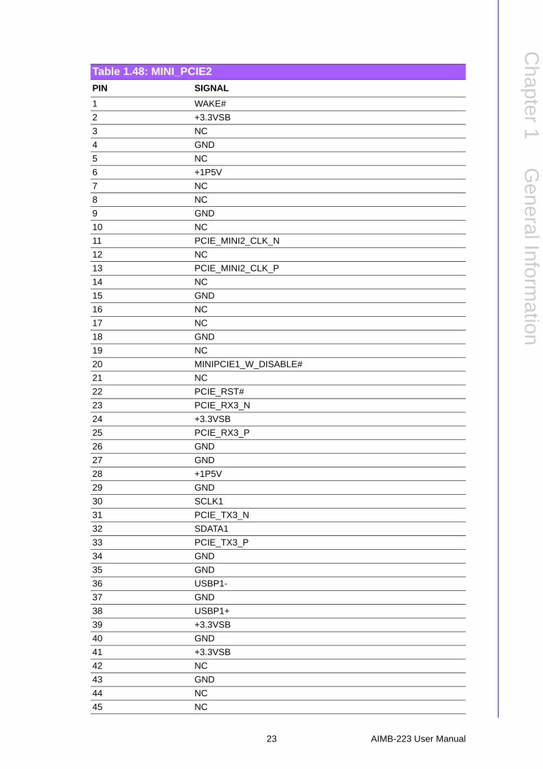
Table 1.48: MINI_PCIE2
PIN SIGNAL
1 WAKE#
2 +3.3VSB
3 NC
4 GND
5 NC
6 +1P5V
7 NC
8 NC
9 GND
10 NC
11 PCIE_MINI2_CLK_N
12 NC
13 PCIE_MINI2_CLK_P
14 NC
15 GND
16 NC
17 NC
18 GND
19 NC
20 MINIPCIE1_W_DISABLE#
21 NC
22 PCIE_RST#
23 PCIE_RX3_N
24 +3.3VSB
25 PCIE_RX3_P
26 GND
27 GND
28 +1P5V
29 GND
30 SCLK1
31 PCIE_TX3_N
32 SDATA1
33 PCIE_TX3_P
34 GND
35 GND
36 USBP1-
37 GND
38 USBP1+
39 +3.3VSB
40 GND
41 +3.3VSB
42 NC
43 GND
44 NC
45 NC
23 AIMB-223 User Manual

46 NC
47 NC
48 +1P5V
49 NC
50 GND
51 NC
52 +3.3VSB
Table 1.49: USB89
PIN SIGNAL
1 +SBV89
2 +SBV89
3 USBP8-
4 USBP9-
5 USBP8+
6 USBP9+
7 GND
8 GND
10 GND
Table 1.50: DOM_PWR1
PIN SIGNAL
1 GND
2 DOM_PWR
3 5V
Table 1.51: DDR_PWR1
PIN SIGNAL
1 PU 3.3V
2 SELECT 1.35V or 1.5V
3 PD GND
Table 1.48: MINI_PCIE2
AIMB-223 User Manual 24

Chapter 1
GeneralInform
ation
1.5 Board layout: Jumper and Connector Locations
Figure 1.1 Jumper and Connector Location
MINI_PCIE1SATA_PWR
CPUFAN1
SATA_PWR2
KBMS2
ATX12V1
COM2SATA2SATA3
USB89DOM_PWR1SATA1
USB45USB67
SPI1BAT1INV2SPDIF_OUTJCMOS1
FPAUDIO1JAMP1
SYSFAN1DDR_PWR1
JWDT1+JOBS1
JFP3JFP1+JFP2
PSON1DIO_CN1 JESTCOM6
DIMM_B1
DIMM_A1ATX5V1
COM3-6
JSETCOM3
SPI_CN1
JVBR2JLVDS4
VCON2JLVDS3
EDP1
LVDS2
DCIN1 KBMS1 DUAL_DP1 COM1 VGA LANUSB01 LANUSB23AUDIO1
MINI_PCIE2
25 AIMB-223 User Manual
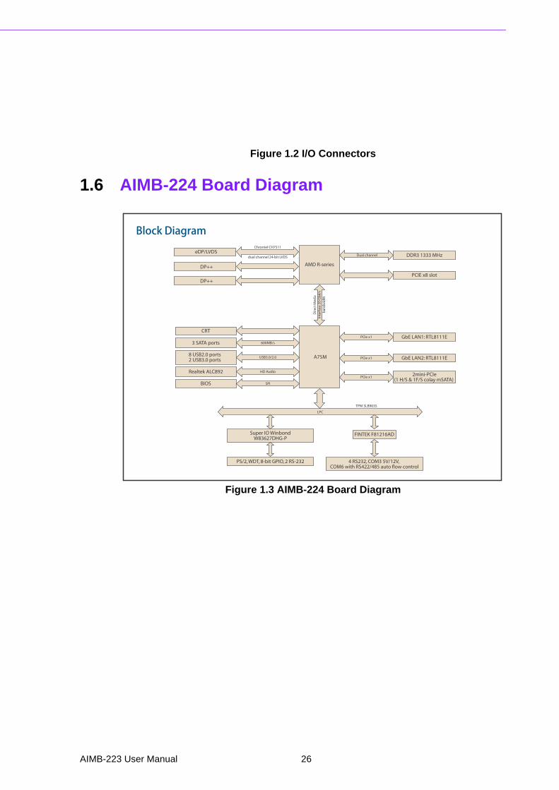
Figure 1.2 I/O Connectors
1.6 AIMB-224 Board Diagram
Figure 1.3 AIMB-224 Board Diagram
Block Diagram
A75M
FINTEK F81216AD
4 RS232, COM3 5V/12V, COM6 with RS422/485 auto flow control
LPC
TPM SLB9635
Super IO WinbondW83627DHG-P
PS/2, WDT, 8-bit GPIO, 2 RS-232
AMD R-series
DDR3 1333 MHzDual channel
PCIE x8 slot
Dire
ct M
edia
Inte
rfac
e 20
-Gb
it/s
ban
dwid
th
CRT
BIOS
Chrontel CH7511
dual channel 24-bit LVDSeDP/LVDS
DP++
DP++
3 SATA ports
8 USB2.0 ports2 USB3.0 ports
Realtek ALC892
600MB/s
USB3.0/2.0
HD Audio
SPI
GbE LAN1: RTL8111E
GbE LAN2: RTL8111E
PCIe x1
PCIe x1
PCIe x12mini-PCIe
(1 H/S & 1F/S colay mSATA)
AIMB-223 User Manual 26

Chapter 1
GeneralInform
ation
1.7 Safety Precautions
Warning! Always completely disconnect the power cord from chassis whenever you work with the hardware. Do not make connections while the power is on. Sensitive electronic components can be damaged by sudden power surges. Only experienced electronics personnel should open the PC chassis.
Caution! Always ground yourself to remove any static charge before touching the motherboard. Modern electronic devices are very sensitive to electro-static discharges. As a safety precaution, use a grounding wrist strap at all times. Place all electronic components on a static-dissipative surface or in a static-shielded bag when they are not in the chassis.
Caution! The computer is provided with a battery-powered real-time clock circuit. There is a danger of explosion if battery is incorrectly replaced. Replace only with same or equivalent type recommended by the manufacturer. Discard used batteries according to manufacturer's instructions.
Caution! There is a danger of a new battery exploding if it is incorrectly installed. Do not attempt to recharge, force open, or heat the battery. Replace the battery only with the same or equivalent type recommended by the man-ufacturer. Discard used batteries according to the manufacturer’s instructions.
27 AIMB-223 User Manual

1.8 Jumper SettingsThis section provides instructions on how to configure your motherboard by settingthe jumpers. It also includes the motherboards's default settings and your options foreach jumper.
1.8.1 How to Set JumpersYou can configure your motherboard to match the needs of your application by set-ting the jumpers. A jumper is a metal bridge that closes an electrical circuit. It consistsof two metal pins and a small metal clip (often protected by a plastic cover) that slidesover the pins to connect them. To “close” (or turn ON) a jumper, you connect the pinswith the clip. To “open” (or turn OFF) a jumper, you remove the clip. Sometimes ajumper consists of a set of three pins, labeled 1, 2, and 3. In this case you connecteither pins 1 and 2, or 2 and 3. A pair of needle-nose pliers may be useful when set-ting jumpers.
1.8.2 CMOS Clear (CMOS1)The AIMB-224 motherboard contains a jumper that can erase CMOS data and resetthe system BIOS information. Normally this jumper should be set with pins 1-2closed. If you want to reset the CMOS data, set J1 to 2-3 closed for just a few sec-onds, and then move the jumper back to 1-2 closed. This procedure will reset theCMOS to its default setting.
* Default
Table 1.52: CMOS1
Function Jumper Setting
*Keep CMOS data
Clear CMOS data
1-2 closed
2-3 closed
AIMB-223 User Manual 28
Chapter 1
GeneralInform
ation
1.8.3 JBL3: LVDS power 3.3V/5V Selector
*Default
1.8.4 PSON1: ATX, AT Mode Selector
*Default
1 1
1.8.5 JWDT1: Watchdog Timer Output Option
*Default
1 1
Table 1.53: JBL3: LVDS power 3.3V/5V Selector
Closed Pins Result
JBL3
1-2* For 3.3 V LVDS Panel
2-3 For 5 V LVDS Panel
for 3.3V LVDS panelJBL3
JBL3 for 5V LVDS panel
Table 1.54: PSON1: ATX, AT Mode Selector
Closed Pins Result
1-2 AT Mode
2-3* ATX Mode
AT Mode1-2 closed
ATX Mode2-3 closed
Table 1.55: JWDT1: Watchdog Timer Output Option
Closed Pins Result
1-2 NC
2-3* System Reset*
NC1-2 closed
System Reset 2-3 closed
29 AIMB-223 User Manual

1.9 System MemoryThe AIMB-224 has two sockets for a 204-pin SODIMM.
This socket can use 1.35V or 1.5 V unbuffered double-data-rate three synchronousDRAM(DDR3 SDRAM). DRAM is available in capacities of 1 GB/2GB/4GB and 8GB.The socket can be filled in any combination with DIMMs of any size, giving a totalmemory size between 2MB to 16GB. AIMB-224 does not support ECC (error check-ing and correction) memory.
1.10 Memory Installation ProceduresTo install SODIMMs, first make sure the handle of the SODIMM socket are in the“open” position, i.e., the handles lean outward. Slowly slide the SODIMM modulealong the plastic guides on both ends of the socket. Then press the SODIMM modulewell down into the socket, until you hear a click when the two handles have automat-ically locked the memory module into the correct position of the SODIMM socket. Toremove the memory module, just push both handles outward, and the memory mod-ule will be ejected by the mechanism.
AIMB-223 User Manual 30

Chapter 2
2 Connecting Peripherals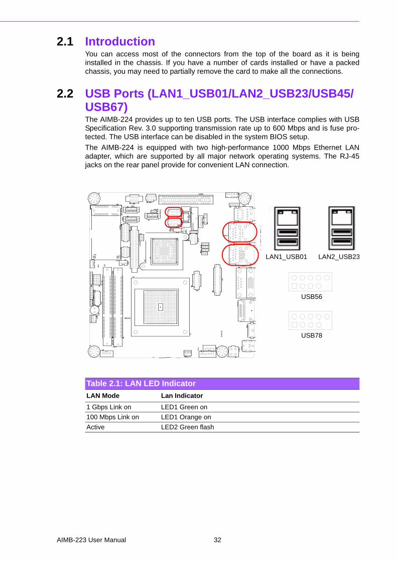
2.1 IntroductionYou can access most of the connectors from the top of the board as it is beinginstalled in the chassis. If you have a number of cards installed or have a packedchassis, you may need to partially remove the card to make all the connections.
2.2 USB Ports (LAN1_USB01/LAN2_USB23/USB45/USB67)The AIMB-224 provides up to ten USB ports. The USB interface complies with USBSpecification Rev. 3.0 supporting transmission rate up to 600 Mbps and is fuse pro-tected. The USB interface can be disabled in the system BIOS setup.
The AIMB-224 is equipped with two high-performance 1000 Mbps Ethernet LANadapter, which are supported by all major network operating systems. The RJ-45jacks on the rear panel provide for convenient LAN connection.
USB56
USB78
Table 2.1: LAN LED Indicator
LAN Mode Lan Indicator
1 Gbps Link on LED1 Green on
100 Mbps Link on LED1 Orange on
Active LED2 Green flash
LAN2_USB34 LAN1_USB12LAN1_USB01 LAN2_USB23
AIMB-223 User Manual 32
Chapter 2
Connecting
Peripherals
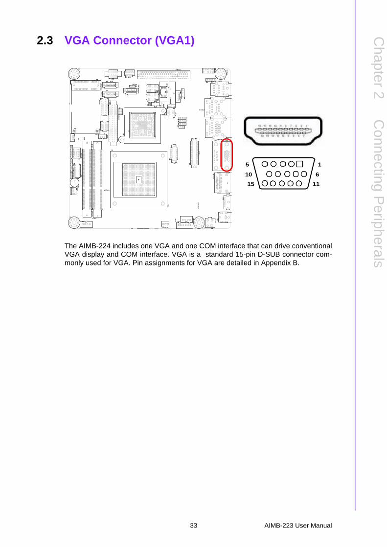
2.3 VGA Connector (VGA1)
The AIMB-224 includes one VGA and one COM interface that can drive conventionalVGA display and COM interface. VGA is a standard 15-pin D-SUB connector com-monly used for VGA. Pin assignments for VGA are detailed in Appendix B.
5
15
1
11
10 6
33 AIMB-223 User Manual

2.4 Serial Ports (COM3~6)
AIMB-224 supports six serial ports. 1 of RS-232 - COM1, COM2, COM3, COM4,COM5 and COM6. These ports can connect to serial devices, such as a mouse or aprinter, or to a communications network.
The IRQ and address ranges for both ports are fixed. However, if you want to disablethe port or change these parameters later, you can do this in the system BIOS setup.
COM12
AIMB-223 User Manual 34
Chapter 2
Connecting
Peripherals
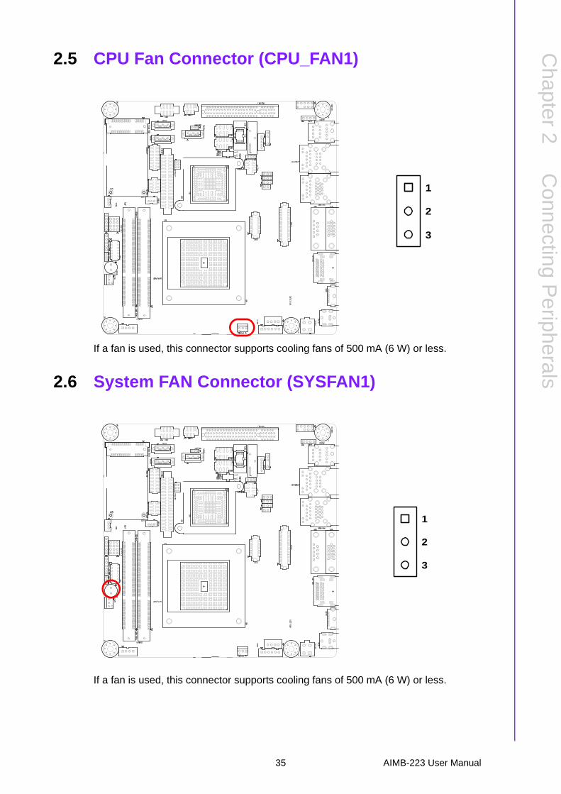
2.5 CPU Fan Connector (CPU_FAN1)
If a fan is used, this connector supports cooling fans of 500 mA (6 W) or less.
2.6 System FAN Connector (SYSFAN1)
If a fan is used, this connector supports cooling fans of 500 mA (6 W) or less.
1
2
3
1
2
3
35 AIMB-223 User Manual

2.7 Front Panel Connectors (JFP1+JFP2+JFP3)There are several external switches to monitor and control the AIMB-224.
2.7.1 ATX soft power switch ((JFP1+JFP2/ PWR_SW))If your computer case is equipped with an ATX power supply, you should connect thepower on/off button on your computer case to ((JFP1+JFP2/ PWR_SW)), for conve-nient power on and off.
2.7.2 Reset (JFP1+JFP2/ RESET)Many computer cases offer the convenience of a reset button. Connect the wire forthe reset button.
2.7.3 HDD LED (JFP1+JFP2/ HDDLED)You can connect an LED to connector (JFP2/HDDLED) to indicate when the HDD isactive.
2.7.4 External speaker (JFP1+JFP2/ SPEAKER)((JFP1+JFP2/ SPEAKER)) is a 4-pin connector for an external speaker. If there is noexternal speaker, the AIMB-224 provides an onboard buzzer as an alternative. Toenable the buzzer, set pins 7-10 as closed.
3 6 9 122 5 8 111 4 7 101 2 3 4 5
JFP1 & JFP2
JFP3
AIMB-223 User Manual 36

Chapter 2
Connecting
Peripherals
2.7.5 Power LED and keyboard lock connector (JFP1 / PWR_LED &KEY LOCK)(JFP1 / PWR_LED & KEY LOCK) is a 5-pin connector for the power on LED and KeyLock function. Refer to Appendix B for detailed information on the pin assignments.The Power LED cable should be connected to pin 1-3. The key lock button cable
should be connected to pin 4-5. There are 3 modes for the power supply connection.The first is “ATX power mode”; the system turns on/off by a momentary power button.The second is “AT Power Mode”; the system turns on/off via the power supply switch.The third is another “AT Power Mode” which makes use of the front panel powerswitch. The power LED status is indicated in the following table:
2.8 Line In, Line Out, Mic In Connector (AUDIO1)
Table 2.2: ATX power supply LED status (No support for AT power)
Power mode
LED (ATX Power Mode)(On/off by momentary button)
LED (AT power Mode) (On/off by switching power supply)
LED (AT power Mode) (On/off by front panel switch)
PSON1 (on back plane) jumper setting
pins 2-3 closed pins 1-2 closedConnect pins 1 & 2 to panel switch via cable
System On On On On
System Suspend Fast flashes Fast flashes Fast flashes
System Off Slow flashes Off Off
Line Out
Mic In
Line In
37 AIMB-223 User Manual

2.9 Serial ATA Interface (SATA1~3)
AIMB-224 features a high performance Serial ATA interface (up to 600 MB/s) whicheases cabling to hard drives with long, thin cables.
2.10 PCI Express x8
AIMB-224 provides 1x PCI express x8 slot.
AIMB-223 User Manual 38
Chapter 2
Connecting
Peripherals
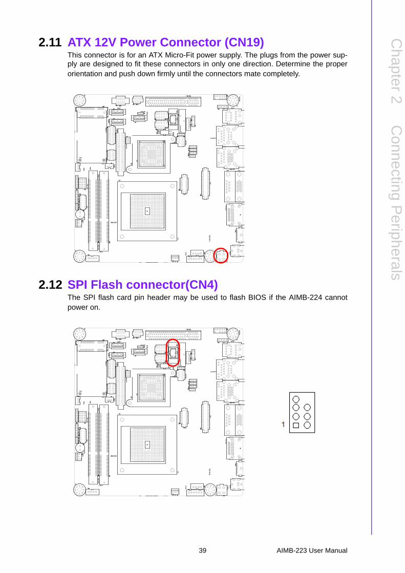
2.11 ATX 12V Power Connector (CN19)This connector is for an ATX Micro-Fit power supply. The plugs from the power sup-ply are designed to fit these connectors in only one direction. Determine the properorientation and push down firmly until the connectors mate completely.
2.12 SPI Flash connector(CN4)The SPI flash card pin header may be used to flash BIOS if the AIMB-224 cannotpower on.
39 AIMB-223 User Manual
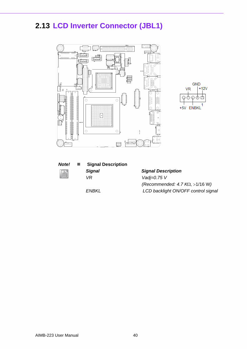
2.13 LCD Inverter Connector (JBL1)
Note! Signal Description
Signal Signal Description
VR Vadj=0.75 V
(Recommended: 4.7 K, 1/16 W)
ENBKL LCD backlight ON/OFF control signal
AIMB-223 User Manual 40

Chapter 2
Connecting
Peripherals
2.14 LVDS Connector (LVDS1)
2.15 General purpose I/O Connector (GPIO1)
41 AIMB-223 User Manual

AIMB-223 User Manual 42

Chapter 3
3 BIOS Operation
3.1 IntroductionAMI BIOS has been integrated into many motherboards, and has been very popularfor over a decade. People sometimes refer to the AMI BIOS setup menu as BIOS,BIOS setup or CMOS setup.
With the AMI BIOS Setup program, you can modify BIOS settings and control thespecial features of your computer. The Setup program uses a number of menus formaking changes and turning special features on or off. This chapter describes thebasic navigation of the AIMB-224 setup screens.
3.2 BIOS SetupThe AIMB-224 Series system has AMI BIOS built in, with a CMOS SETUP utility thatallows users to configure required settings or to activate certain system features.
The CMOS SETUP saves the configuration in the CMOS RAM of the motherboard.When the power is turned off, the battery on the board supplies the necessary powerto preserve the CMOS RAM.
When the power is turned on, press the <Del> button during the BIOS POST (Power-On Self Test) to access the CMOS SETUP screen.
Control Keys
< ↑ >< ↓ >< ← >< → > Move to select item
<Enter> Select Item
<Esc>Main Menu - Quit and not save changes into CMOSSub Menu - Exit current page and return to Main Menu
<Page Up/+> Increase the numeric value or make changes
<Page Down/-> Decrease the numeric value or make changes
<F1> General help, for Setup Sub Menu
<F2> Item Help
<F5> Load Previous Values
<F7> Load Setup Defaults
<F10> Save all CMOS changes
AIMB-223 User Manual 44
Chapter 3
BIO
S O
peration
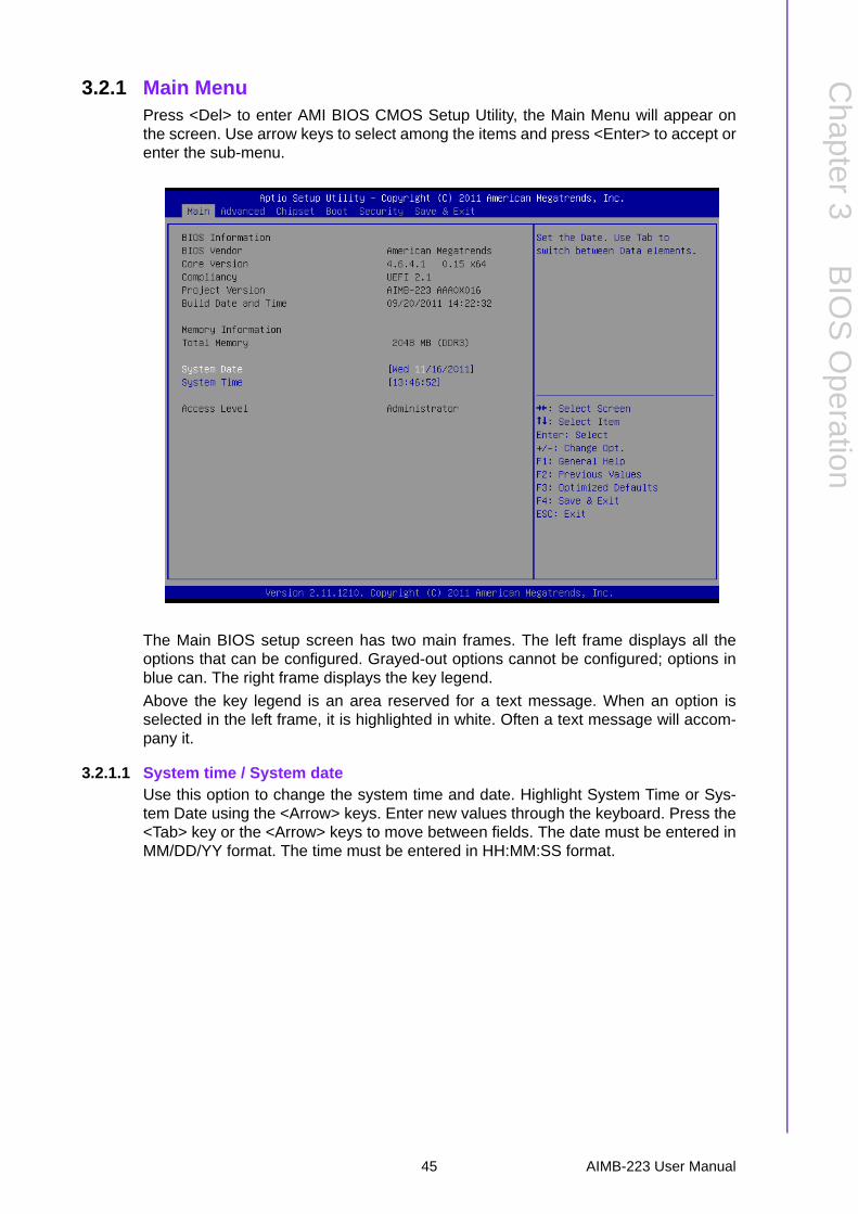
3.2.1 Main MenuPress <Del> to enter AMI BIOS CMOS Setup Utility, the Main Menu will appear onthe screen. Use arrow keys to select among the items and press <Enter> to accept orenter the sub-menu.
The Main BIOS setup screen has two main frames. The left frame displays all theoptions that can be configured. Grayed-out options cannot be configured; options inblue can. The right frame displays the key legend.
Above the key legend is an area reserved for a text message. When an option isselected in the left frame, it is highlighted in white. Often a text message will accom-pany it.
3.2.1.1 System time / System dateUse this option to change the system time and date. Highlight System Time or Sys-tem Date using the <Arrow> keys. Enter new values through the keyboard. Press the<Tab> key or the <Arrow> keys to move between fields. The date must be entered inMM/DD/YY format. The time must be entered in HH:MM:SS format.
45 AIMB-223 User Manual
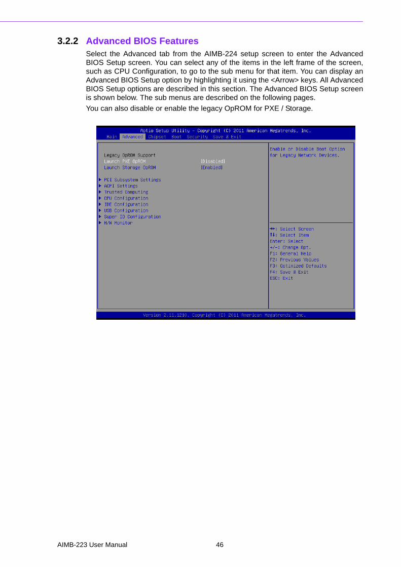
3.2.2 Advanced BIOS FeaturesSelect the Advanced tab from the AIMB-224 setup screen to enter the AdvancedBIOS Setup screen. You can select any of the items in the left frame of the screen,such as CPU Configuration, to go to the sub menu for that item. You can display anAdvanced BIOS Setup option by highlighting it using the <Arrow> keys. All AdvancedBIOS Setup options are described in this section. The Advanced BIOS Setup screenis shown below. The sub menus are described on the following pages.
You can also disable or enable the legacy OpROM for PXE / Storage.
AIMB-223 User Manual 46

Chapter 3
BIO
S O
peration
3.2.2.1 PCI Subsystem settings
3.2.2.2 ACPI Setting
ACPI Sleep StateSelect the ACPI state used for system suspend.
S3 Report Video Enable or disable video repost.
47 AIMB-223 User Manual

Resume on LAN1Enables or disables GbE LAN1 wake up from S5 function.
Resume on LAN2Enables or disables GbE LAN2 wake up from S5 function.
Resume on RTC AlarmDisable/Enable RTC wake event.
3.2.2.3 Trusted Computing
TPM SUPPORTDisable/Enable TPM function.
AIMB-223 User Manual 48
Chapter 3
BIO
S O
peration
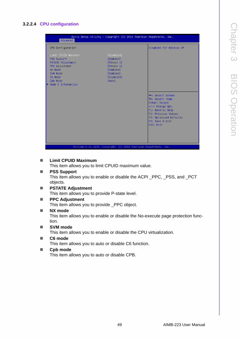
3.2.2.4 CPU configuration
Limit CPUID MaximumThis item allows you to limit CPUID maximum value.
PSS SupportThis item allows you to enable or disable the ACPI _PPC, _PSS, and _PCT objects.
PSTATE AdjustmentThis item allows you to provide P-state level.
PPC AdjustmentThis item allows you to provide _PPC object.
NX modeThis item allows you to enable or disable the No-execute page protection func-tion.
SVM modeThis item allows you to enable or disable the CPU virtualization.
C6 modeThis item allows you to auto or disable C6 function.
Cpb modeThis item allows you to auto or disable CPB.
49 AIMB-223 User Manual

3.2.2.5 IDE configuration
IDE ConfigurationDisplay SATA Port0 / SATA Port1 / SATA Port2 / SATA Port3 information.
3.2.2.6 USB configuration
AIMB-223 User Manual 50
Chapter 3
BIO
S O
peration
Legacy USB supportEnables support for legacy USB. Auto option disables legacy support if no USB devices are connected.
EHCI Hand-offThis is a workaround for OS without EHCI hand-off support. The EHCI owner-ship change should claim by EHCI driver.
USB transfer time-outTime-out value for control, bulk, and interrupt transfers.
Device reset time-outUSB mass storage device starts unit command time-out.
Device power-up delayMaximum time the device will take before it properly report itself to the host con-troller.
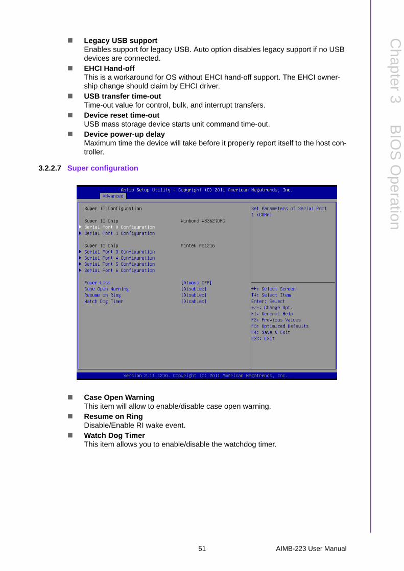
3.2.2.7 Super configuration
Case Open WarningThis item will allow to enable/disable case open warning.
Resume on RingDisable/Enable RI wake event.
Watch Dog TimerThis item allows you to enable/disable the watchdog timer.
51 AIMB-223 User Manual

3.2.2.8 H/W monitor
Smart Fan FunctionThis item allows you to enable/disable CPU cooler smart function.
3.2.3 Chipset
AIMB-223 User Manual 52

Chapter 3
BIO
S O
peration
North Bridge ConfigurationDetail of North Bridge items.
Display Configuration SelectDetails of display items.
South Bridge ConfigurationDetails of South bridge items.
3.2.3.1 North Bridge Configuration
Memory ConfigurationDetails of Bank Interleaving, IOMMU Mode, and Memory Clock items.
Node 0 InformationDetails of memory information.
53 AIMB-223 User Manual

3.2.3.2 Display Configuration
LVDSThis item allows you to enable or disable LVDS function.
HDMIThis item allows you to enable or disable HDMI function.
* LVDS setting of customized define, please refer to the document on CD-ROM:
"Chrontel EEPROM Adjust SOP
AIMB-223 User Manual 54

Chapter 3
BIO
S O
peration
3.2.3.3 SB Configuration
SB SATA ConfigurationOptions for SATA configuration.
SB USB ConfigurationOptions for USB configuration.
SB GPP port ConfigurationOptions for SB GPP port configuration.
SB HD Azalia ConfigurationOptions for SB azalia.
55 AIMB-223 User Manual

3.2.4 Boot
Setup Prompt TimeoutThis item allows you to change number of seconds to wait for setup activation key.
Bootup NumLock StateSelect the Power-on state for Numlock.
Quiet Boot If this option is set to Disabled, the BIOS display normal POST messages. If Enabled, an OEM Logo is shown instead of POST messages.
Fast BootThis item allows BIOS to skip certain tests while booting. This will decrease the time needed to boot the system.
GateA20 Active This item allows you to select Upon Request or Always.
Option ROM Messages Sets display mode for option ROM.
Interrupt 19 Capture This item allows option ROMs to trap interrupt 19.
Boot Option PrioritiesSet the system boot order.
AIMB-223 User Manual 56

Chapter 3
BIO
S O
peration
3.2.5 Security
Select Security Setup from the AIMB-224 Setup main BIOS setup menu. All SecuritySetup options, such as password protection and virus protection are described in thissection. To access the sub menu for the following items, select the item andpress<Enter>: Change Administrator / User Password.
57 AIMB-223 User Manual

3.2.6 Save & Exit
Save Changes and ExitThis item allows you to exit system setup after saving changes.
Discard Changes and ExitThis item allows you to exit system setup without saving any changes.
Save Changes and ResetThis item allows you to reset the system after saving the changes.
Discard Changes and ResetThis item allows you to rest system setup without saving any changes.
Save ChangesThis item allows you to save changes done so far to any of the options.
Discard ChangesThis item allows you to discard changes done so far to any of the options.
Restore DefaultsThis item allows you to restore/load default values for all the options.
Save as User DefaultsThis item allows you to save the changes done so far as user defaults.
Restore User DefaultsThis item allows you to restore the user defaults to all the options.
Boot Override Boot device select can override your boot priority.
AIMB-223 User Manual 58

Chapter 4
4 Software Introduction & Service
4.1 IntroductionThe mission of Advantech Embedded Software Services is to "Enhance quality of lifewith Advantech platforms and Microsoft® Windows® embedded technology." Weenable Windows® Embedded software products on Advantech platforms to moreeffectively support the embedded computing community. Customers are freed fromthe hassle of dealing with multiple vendors (hardware suppliers, system integrators,embedded OS distributors) for projects. Our goal is to make Windows® EmbeddedSoftware solutions easily and widely available to the embedded computing commu-nity.
4.2 Value-Added Software ServicesSoftware API: An interface that defines the ways by which an application programmay request services from libraries and/or operating systems. Provides not only theunderlying drivers required but also a rich set of user-friendly, intelligent and inte-grated interfaces, which speeds development, enhances security and offers add-onvalue for Advantech platforms. It plays the role of catalyst between developer andsolution, and makes Advantech embedded platforms easier and simpler to adopt andoperate with customer applications.
4.2.1 Software API
4.2.1.1 Control
GPIOGeneral Purpose Input/Output is a flexible parallel interface that allows a variety of custom connections. Allows users to monitor the level of signal input or set the output status to switch on/off the device. Our API also provide Programmable GPIO, which allows developers to dynamically set the GPIO input or output status.
SMBusSMBus is the System Management Bus defined by Intel Cor-poration in 1995. It is used in personal computers and serv-ers for low-speed system management communications. The SMBus API allows a developer to interface a embedded sys-tem environment and transfer serial messages using the SMBus protocols, allowing multiple simultaneous device control.
AIMB-223 User Manual 60

Chapter 4
Softw
areIntroduction
&S
ervice
4.2.1.2 Display
4.2.1.3 Monitor
4.2.1.4 Power Saving
Brightness ControlThe Brightness Control API allows a developer to access embedded devices and easily control brightness.
BacklightThe Backlight API allows a developer to control the backlight (screen) on/off in embedded devices.
WatchdogA watchdog timer (WDT) is a device that performs a specific operation after a certain period of time if something goes wrong and the system does not recover on its own. A watch-dog timer can be programmed to perform a warm boot (restarting the system) after a certain number of seconds.
Hardware MonitorThe Hardware Monitor (HWM) API is a system health super-vision API that inspects certain condition indexes, such as fan speed, temperature and voltage.
CPU SpeedMakes use of Intel SpeedStep technology to save power con-sumption. The system will automatically adjust the CPU speed depending on the system loading.
System ThrottlingRefers to a series of methods for reducing power consump-tion in computers by lowering the clock frequency. This API allows the user to adjust the clock from 87.5% to 12.5%.
61 AIMB-223 User Manual
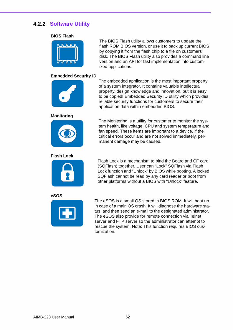
4.2.2 Software Utility
BIOS FlashThe BIOS Flash utility allows customers to update the flash ROM BIOS version, or use it to back up current BIOS by copying it from the flash chip to a file on customers’ disk. The BIOS Flash utility also provides a command line version and an API for fast implementation into custom-ized applications.
Embedded Security IDThe embedded application is the most important property of a system integrator. It contains valuable intellectual property, design knowledge and innovation, but it is easy to be copied! Embedded Security ID utility which provides reliable security functions for customers to secure their application data within embedded BIOS.
MonitoringThe Monitoring is a utility for customer to monitor the sys-tem health, like voltage, CPU and system temperature and fan speed. These items are important to a device, if the critical errors occur and are not solved immediately, per-manent damage may be caused.
Flash LockFlash Lock is a mechanism to bind the Board and CF card (SQFlash) together. User can “Lock” SQFlash via Flash Lock function and “Unlock” by BIOS while booting. A locked SQFlash cannot be read by any card reader or boot from other platforms without a BIOS with “Unlock” feature.
eSOSThe eSOS is a small OS stored in BIOS ROM. It will boot up in case of a main OS crash. It will diagnose the hardware sta-tus, and then send an e-mail to the designated administrator. The eSOS also provide for remote connection via Telnet server and FTP server so the administrator can attempt to rescue the system. Note: This function requires BIOS cus-tomization.
AIMB-223 User Manual 62
Chapter 5
5 Chipset Software Installation Utility
5.1 Before You BeginTo facilitate the installation of the enhanced display drivers and utility software, readthe instructions in this chapter carefully. The drivers for the AIMB-224 are located onthe software installation CD. The driver in the folder of the driver CD will guide andlink you to the utilities and drivers under a Windows system. Updates are providedvia Service Packs from Microsoft*.
Before you begin, it is important to note that most display drivers need to have therelevant software application already installed in the system prior to installing theenhanced display drivers. In addition, many of the installation procedures assumethat you are familiar with both the relevant software applications and operating sys-tem commands. Review the relevant operating system commands and the pertinentsections of your application software’s user manual before performing the installa-tion.
5.2 IntroductionThe AMD Chipset Software Installation (CSI) utility installs the Windows INF files thatoutline to the operating system how the chipset components will be configured. Thisis needed for the proper functioning of the following features:
Core PCI PnP services IDE Ultra ATA 100/66/33 and Serial ATA interface support USB 1.1/2.0 support (USB 2.0 driver needs to be installed separately for Win98) Identification of AMD chipset components in the Device Manager Integrates superior video features. These include filtered sealing of 720 pixel
DVD content, and MPEG-2 motion compensation for software DVD
Note! The files on the software installation CD are compressed. Do not attempt to install the drivers by copying the files manually. You must use the supplied SETUP program to install the drivers.
Note! This utility is used for the following versions of Windows, and it has to be installed before installing all the other drivers:
Windows 7 Windows XP
AIMB-223 User Manual 64
Chapter 5
ChipsetS
oftware
Installation Utility
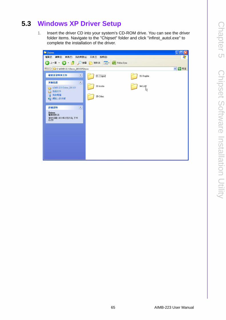
5.3 Windows XP Driver Setup1. Insert the driver CD into your system's CD-ROM drive. You can see the driver
folder items. Navigate to the "Chipset" folder and click "infinst_autol.exe" to complete the installation of the driver.
65 AIMB-223 User Manual

AIMB-223 User Manual 66

Chapter 6
6 VGA Setup
6.1 IntroductionTo benefit from the AMD G-series T56N/T40E/T44R integrated graphics controller,you need to install the graphic driver.
6.2 Windows 7/XP
Insert the driver CD into your system's CD-ROM drive. You can see the driver foldersitems. Navigate to the "Graphic" folder and click "setup.exe" to complete the installa-tion of the drivers for Windows 7, Windows Vista, Windows XP.
Note! Before installing this driver, make sure the CSI utility has been installed in your system. See Chapter 5 for information on installing the CSI utility.
AIMB-223 User Manual 68

Chapter 7
7 LAN Configuration
7.1 IntroductionThe AIMB-224 has dual Gigabit Ethernet LANs via dedicated PCI Express x1 lanes(Realtek RTL8111D for LAN1&2) that offer bandwidth of up to 500 MB/sec, eliminat-ing the bottleneck of network data flow and incorporating Gigabit Ethernet at 1000Mbps.
7.2 Features Integrated 10/100/1000 Mbps transceiver 10/100/1000 Mbps triple-speed MAC High-speed RISC core with 24-KB cache On-chip voltage regulation Wake-on-LAN (WOL) support PCI Express X1 host interface
7.3 Installation
The AIMB-224’s Realtek RTL8111D (LAN1&LAN2) Gigabit integrated controllerssupport all major network operating systems. However, the installation procedurevaries from system to system. Please find and use the section that provides thedriver setup procedure for the operating system you are using.
Note! Before installing the LAN drivers, make sure the CSI utility has been installed on your system. See Chapter 5 for information on installing the CSI utility.
AIMB-223 User Manual 70
Chapter 7
LAN
Configuration
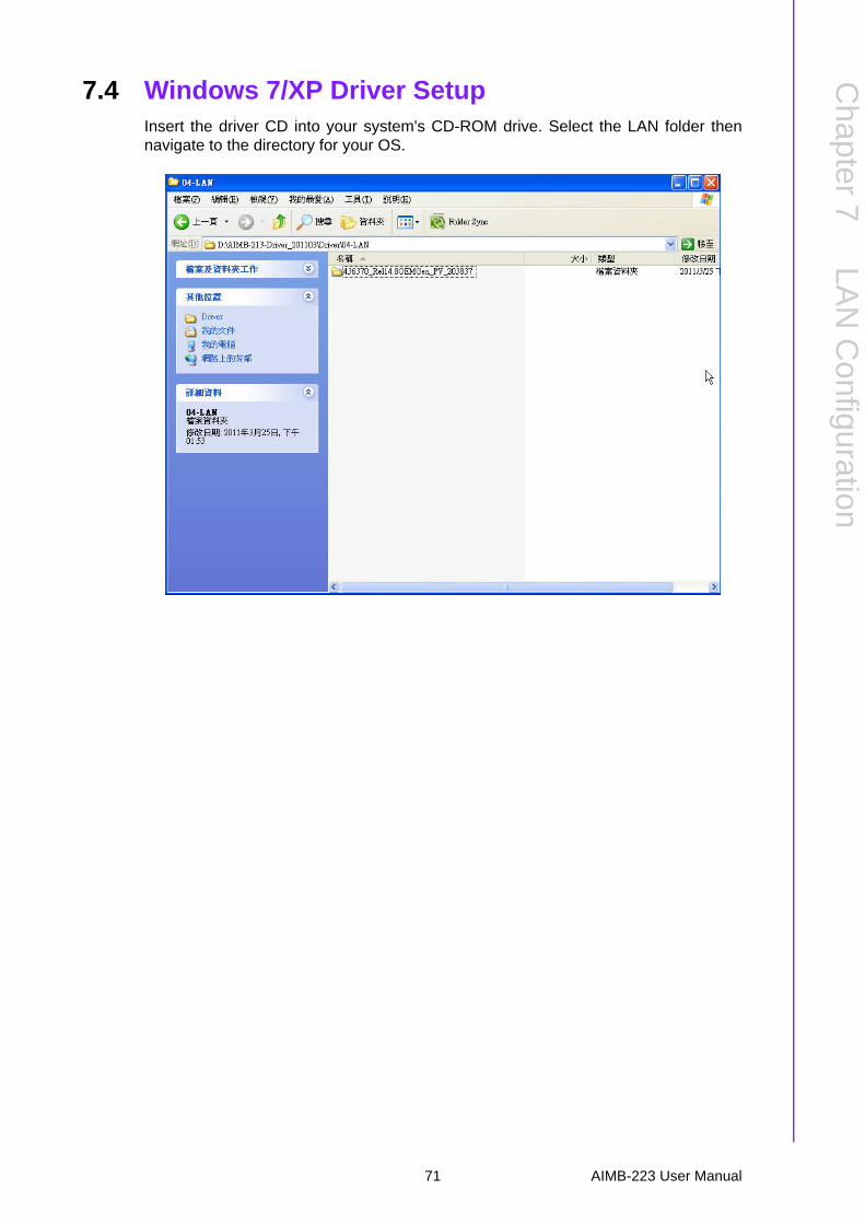
7.4 Windows 7/XP Driver Setup Insert the driver CD into your system's CD-ROM drive. Select the LAN folder thennavigate to the directory for your OS.
71 AIMB-223 User Manual

AIMB-223 User Manual 72

Appendix A
A Programming the Watchdog Timer
A.1 Programming the Watchdog TimerThe AIMB-224's watchdog timer can be used to monitor system software operationand take corrective action if the software fails to function within the programmedperiod. This section describes the operation of the watchdog timer and how to pro-gram it.
A.1.1 Watchdog Timer OverviewThe watchdog timer is built into the super I/O controller W83627DHG-P. It providesthe following user-programmable functions:
Can be enabled and disabled by user program Timer can be set from 1 to 255 seconds or 1 to 255 minutes Generates an interrupt or resets signal if the software fails to reset the timer
before time-out
A.1.2 Programming the Watchdog TimerThe I/O port address of the watchdog timer is 2E (hex) and 2F (hex). 2E (hex) is theaddress port. 2F (hex) is the data port. You must first assign the address of registerby writing an address value into address port 2E (hex), then write/read data to/fromthe assigned register through data port 2F (hex).
AIMB-223 User Manual 74

Appendix A
Program
ming
theW
atchdogT
imer
Unlock
Select register of watchdog timer
Enable the function ofthe watchdog timer
Use the function of
Lock W83627DHG-P
the watchdog timer
W83627DHG-P
75 AIMB-223 User Manual
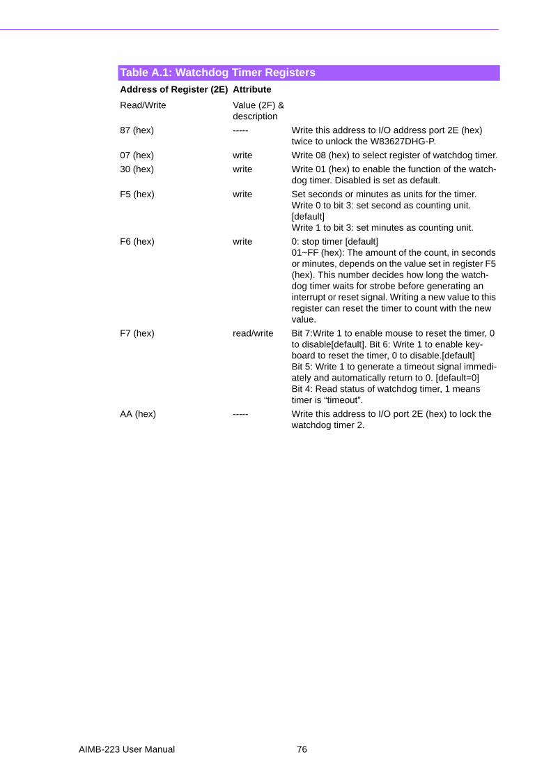
Table A.1: Watchdog Timer Registers
Address of Register (2E) Attribute
Read/Write Value (2F) &description
87 (hex) ----- Write this address to I/O address port 2E (hex) twice to unlock the W83627DHG-P.
07 (hex) write Write 08 (hex) to select register of watchdog timer.
30 (hex) write Write 01 (hex) to enable the function of the watch-dog timer. Disabled is set as default.
F5 (hex) write Set seconds or minutes as units for the timer.Write 0 to bit 3: set second as counting unit. [default]Write 1 to bit 3: set minutes as counting unit.
F6 (hex) write 0: stop timer [default]01~FF (hex): The amount of the count, in seconds or minutes, depends on the value set in register F5 (hex). This number decides how long the watch-dog timer waits for strobe before generating an interrupt or reset signal. Writing a new value to this register can reset the timer to count with the new value.
F7 (hex) read/write Bit 7:Write 1 to enable mouse to reset the timer, 0 to disable[default]. Bit 6: Write 1 to enable key-board to reset the timer, 0 to disable.[default] Bit 5: Write 1 to generate a timeout signal immedi-ately and automatically return to 0. [default=0]Bit 4: Read status of watchdog timer, 1 means timer is “timeout”.
AA (hex) ----- Write this address to I/O port 2E (hex) to lock the watchdog timer 2.
AIMB-223 User Manual 76

Appendix A
Program
ming
theW
atchdogT
imer
A.1.3 Example Program1. Enable watchdog timer and set 10 sec. as timeout interval;-----------------------------------------------------------
Mov dx,2eh ; Unlock W83627DHG-P
Mov al,87h
Out dx,al
Out dx,al
;-----------------------------------------------------------
Mov al,07h ; Select registers of watchdog timer
Out dx,al
Inc dx
Mov al,08h
Out dx,al
;-----------------------------------------------------------
Dec dx ; Enable the function of watchdog timer
Mov al,30h
Out dx,al
Inc dx
Mov al,01h
Out dx,al
;-----------------------------------------------------------
Dec dx ; Set second as counting unit
Mov al,0f5h
Out dx,al
Inc dx
In al,dx
And al,not 08h
Out dx,al
;-----------------------------------------------------------
Dec dx ; Set timeout interval as 10 seconds and start counting
Mov al,0f6h
Out dx,al
Inc dx
Mov al,10
Out dx,al
;-----------------------------------------------------------
Dec dx ; Lock W83627DHG-P
Mov al,0aah
Out dx,al
2. Enable watchdog timer and set 5 minutes as timeout interval;-----------------------------------------------------------
Mov dx,2eh ; Unlock W83627DHG-P
Mov al,87h
Out dx,al
Out dx,al
77 AIMB-223 User Manual

;-----------------------------------------------------------
Mov al,07h ; Select registers of watchdog timer
Out dx,al
Inc dx
Mov al,08h
Out dx,al
;-----------------------------------------------------------
Dec dx ; Enable the function of watchdog timer
Mov al,30h
Out dx,al
Inc dx
Mov al,01h
Out dx,al
;-----------------------------------------------------------
Dec dx ; Set minute as counting unit
Mov al,0f5h
Out dx,al
Inc dx
In al,dx
Or al,08h
Out dx,al
;-----------------------------------------------------------
Dec dx ; Set timeout interval as 5 minutes and start counting
Mov al,0f6h
Out dx,al
Inc dx
Mov al,5
Out dx,al
;-----------------------------------------------------------
Dec dx ; Lock W83627DHG-P
Mov al,0aah
Out dx,al
3. Enable watchdog timer to be reset by mouse;-----------------------------------------------------------
Mov dx,2eh ; Unlock W83627DHG-P
Mov al,87h
Out dx,al
Out dx,al
;-----------------------------------------------------------
Mov al,07h ; Select registers of watchdog timer
Out dx,al
Inc dx
Mov al,08h
Out dx,al
;-----------------------------------------------------------
AIMB-223 User Manual 78

Appendix A
Program
ming
theW
atchdogT
imer
Dec dx ; Enable the function of watchdog timer
Mov al,30h
Out dx,al
Inc dx
Mov al,01h
Out dx,al
;-----------------------------------------------------------
Dec dx ; Enable watchdog timer to be reset by mouse
Mov al,0f7h
Out dx,al
Inc dx
In al,dx
Or al,80h
Out dx,al
;-----------------------------------------------------------
Dec dx ; Lock W83627DHG-P
Mov al,0aah
Out dx,al
4. Enable watchdog timer to be reset by keyboard;-----------------------------------------------------------
Mov dx,2eh ; Unlock W83627DHG-P
Mov al,87h
Out dx,al
Out dx,al
;-----------------------------------------------------------
Mov al,07h ; Select registers of watchdog timer
Out dx,al
Inc dx
Mov al,08h
Out dx,al
;-----------------------------------------------------------
Dec dx ; Enable the function of watchdog timer
Mov al,30h
Out dx,al
Inc dx
Mov al,01h
Out dx,al
;-----------------------------------------------------------
Dec dx ; Enable watchdog timer to be strobed reset by keyboard
Mov al,0f7h
Out dx,al
Inc dx
In al,dx
Or al,40h
Out dx,al
79 AIMB-223 User Manual

;-----------------------------------------------------------
Dec dx ; Lock W83627DHG-P
Mov al,0aah
Out dx,al
5. Generate a time-out signal without timer counting;-----------------------------------------------------------
Mov dx,2eh ; Unlock W83627DHG-P
Mov al,87h
Out dx,al
Out dx,al
;-----------------------------------------------------------
Mov al,07h ; Select registers of watchdog timer
Out dx,al
Inc dx
Mov al,08h
Out dx,al
;-----------------------------------------------------------
Dec dx ; Enable the function of watchdog timer
Mov al,30h
Out dx,al
Inc dx
Mov al,01h
Out dx,al
;-----------------------------------------------------------
Dec dx ; Generate a time-out signal
Mov al,0f7h
Out dx,al ;Write 1 to bit 5 of F7 register
Inc dx
In al,dx
Or al,20h
Out dx,al
;-----------------------------------------------------------
Dec dx ; Lock W83627DHG-P
Mov al,0aah
Out dx,al
AIMB-223 User Manual 80

Appendix B
B I/O Pin Assignments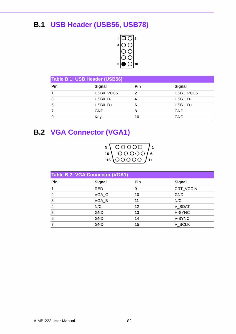
B.1 USB Header (USB56, USB78)
B.2 VGA Connector (VGA1)
Table B.1: USB Header (USB56)
Pin Signal Pin Signal
1 USB0_VCC5 2 USB1_VCC5
3 USB0_D- 4 USB1_D-
5 USB0_D+ 6 USB1_D+
7 GND 8 GND
9 Key 10 GND
Table B.2: VGA Connector (VGA1)
Pin Signal Pin Signal
1 RED 9 CRT_VCCIN
2 VGA_G 10 GND
3 VGA_B 11 N/C
4 N/C 12 V_SDAT
5 GND 13 H-SYNC
6 GND 14 V-SYNC
7 GND 15 V_SCLK
5
15
1
11
10 6
AIMB-223 User Manual 82

Appendix B
I/O P
inA
ssignments
B.3 RS-232 Interface (COM3/4/5/6)
Table B.3: RS-232 Interface (COM3~COM6)
Pin Signal Pin Signal
1 DCD_3 2 DSR_3
3 RXD_3 4 RTS_3
5 TXD_3 6 CTS_3
7 DTR_3 8 RRI_3
9 GND_3 10 GND_3
11 DCD_4 12 DSR_4
13 RXD_4 14 RTS_4
15 TXD_4 16 CTS_4
17 DTR_4 18 RRI_4
19 GND_4 20 GND_4
21 DCD_5 22 DSR_5
23 RXD_5 24 RTS_5
25 TXD_5 26 CTS_5
27 DTR_5 28 RRI_5
29 GND_5 30 GND_5
31 DCD_6 32 DSR_6
33 RXD_6 34 RTS_6
35 TXD_6 36 CTS_6
37 DTR_6 38 RRI_6
39 GND_6 40 GND_6
83 AIMB-223 User Manual

B.4 CN4: SPI Fresh Card Pin Connector
B.5 CPU Fan Power Connector (CPU_FAN1)
B.6 System Fan Power Connector (SYS_FAN1)
Table B.4: CN4: SPI Fresh Card Pin Connector
Pin Signal Pin Signal
1 +F1_3V 2 GND
3 F1_SPI_CS#_Q 4 F1_SPI_CLK_Q
5 F1_SPI_MISO_Q 6 F1_SPI_MOSI_Q
7 NC 8 NC
1 2
87
Table B.5: CPU Fan Power Connector (CPU_FAN1)
Pin Signal
1 GND
2 +12 V
3 DETECT
1
2
3
Table B.6: System Fan Power Connector (SYS_FAN1)
Pin Signal
1 GND
2 +12VPWM
3 Sensor
1
2
3
AIMB-223 User Manual 84
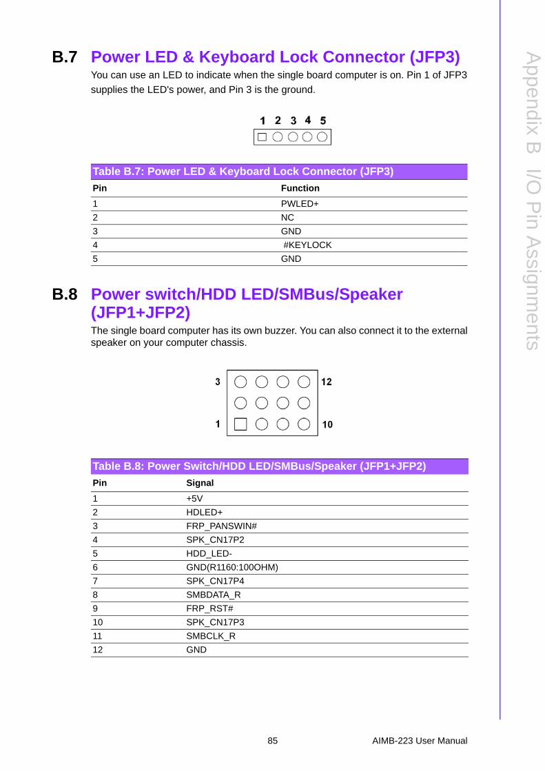
Appendix B
I/O P
inA
ssignments
B.7 Power LED & Keyboard Lock Connector (JFP3)You can use an LED to indicate when the single board computer is on. Pin 1 of JFP3
supplies the LED's power, and Pin 3 is the ground.
B.8 Power switch/HDD LED/SMBus/Speaker (JFP1+JFP2)The single board computer has its own buzzer. You can also connect it to the externalspeaker on your computer chassis.
Table B.7: Power LED & Keyboard Lock Connector (JFP3)
Pin Function
1 PWLED+
2 NC
3 GND
4 #KEYLOCK
5 GND
Table B.8: Power Switch/HDD LED/SMBus/Speaker (JFP1+JFP2)
Pin Signal
1 +5V
2 HDLED+
3 FRP_PANSWIN#
4 SPK_CN17P2
5 HDD_LED-
6 GND(R1160:100OHM)
7 SPK_CN17P4
8 SMBDATA_R
9 FRP_RST#
10 SPK_CN17P3
11 SMBCLK_R
12 GND
85 AIMB-223 User Manual

B.9 USB/LAN ports (LAN1_USB12/LAN2_USB34)
B.10 Line In, Line Out, Mic In Connector (AUDIO1)
B.11 Serial ATA0/1 (SATA 1/2/3/4)
Table B.9: USB Port
Pin Signal Pin Signal
1 VCC 3 Data0+
2 Data0- 4 GND
Table B.10: Ethernet 10/100 Mbps RJ-45 Port
Pin Signal Pin Signal
1 XMT+ 5 N/C
2 XMT- 6 RCV-
3 RCV+ 7 N/C
4 N/C 8 N/C
Line Out
Mic In
Line In
Table B.11: Serial ATA 0/1 (SATA 1/2/3/4)
Pin Signal Pin Signal
1 GND 2 SATA_0TX+
3 SATA_0TX- 4 GND
5 SATA_0RX- 6 SATA_0RX+
7 GND 8
AIMB-223 User Manual 86

Appendix B
I/O P
inA
ssignments
B.12 AT/ATX Mode (PSON1)
B.13 GPIO Pin Header (GPIO1)
B.14 LVDS Connector: LVDS1
Table B.12: AT/ATX Mode (PSON1)
Pin Signal Pin Signal
1 VCCATX 2 VCCATX
3 GND
Table B.13: GPIO Pin Header (GPIO1)
Pin Signal Pin Signal
1 GPIO0 2 GPIO4
3 GPIO1 4 GPIO5
5 GPIO2 6 GPIO6
7 GPIO3 8 GPIO7
9 +5V 10 GND
NCNC
NCNC
NCNC
NCNC
OD3-OD3+
87 AIMB-223 User Manual

B.15 LVDS Power Jumper (JBL3)
* default setting
Table B.14: LVDS1 Connector
Pin Signal Pin Signal
1 VDDSAFE_1 2 VDDSAFE_2
3 GND_1 4 GND_7
5 VDDSAFE_3 6 VDDSAFE_4
7 OD0- 8 NC
9 OD0+ 10 NC
11 GND_2 12 GND_8
13 OD1- 14 NC
15 OD1+ 16 NC
17 GND_3 18 GND_9
19 OD2- 20 NC
21 OD2+ 22 NC
23 GND_4 24 GND_10
25 OCK- 26 NC
27 OCK+ 28 NC
29 GND_3 30 GND_11
31 DDC_CLK 32 DDC_DAT
33 GND_6 34 GND_12
35 OD3- 36 NC
37 OD3+ 38 NC
39 HPLG 40 VCON
Table B.15: LVDS Power Jumper
Pin Signal
1 VCC3
2 VCC_LCD
3 VCC
for 3.3V LVDS panelJBL3
JBL3 for 5V LVDS panel
AIMB-223 User Manual 88

Appendix B
I/O P
inA
ssignments
B.16 LVDS Inverter (JBL1)
B.17 ATX 12 V connector (ATX12V_1)
Table B.16: LVDS Power Jumper
Pin Signal
1 +12V2 GND
3 BL_EN
4 BL_CLT
5 +5V
Table B.17: ATX 12 V connector (ATX12V_1)
Pin Signal Pin Signal
1 GND 2 GND
3 +12V 4 +12V
89 AIMB-223 User Manual

www.advantech.comPlease verify specifications before quoting. This guide is intended for referencepurposes only.All product specifications are subject to change without notice.No part of this publication may be reproduced in any form or by any means,electronic, photocopying, recording or otherwise, without prior written permis-sion of the publisher.All brand and product names are trademarks or registered trademarks of theirrespective companies.© Advantech Co., Ltd. 2013


![Christian v Cooper [2020] QSC 224 - Document Control](https://static.fdokumen.com/doc/165x107/633af2e84d44dea89a02b478/christian-v-cooper-2020-qsc-224-document-control.jpg)