
Advanced passive micro-optical elements
116
-
Upload
khangminh22 -
Category
Documents
-
view
1 -
download
0
Transcript of Advanced passive micro-optical elements


Institut de microtechnique
Advanced passive micro-optical elements
Thèse
Présentée à la Faculté des Sciences pour obtenir le gradede docteur ès sciences par
Patrick Ru�eux
Neuchâtel, Avril 2008

Thèse de l'université de Neuchâtel
Date de soutenance : le 9 Janvier 2008
Rapporteurs :
Prof. Dr. H.-P Herzig (Directeur de thèse)Dr. T. ScharfDr. R. VölkelProf. Dr. H.P. Zappe
Mots clés: micro-optique, birefringence, cristaux liquides,polariseurs, microlentilles achromatiques, réseaux de mi-crolentilles, homogénéiseur de faisceau, e�et de moiré, agran-dissement par e�et de moiré, a�cheurs, di�useurs, micro-lentilles concaves.
Keywords : micro-optics, birefringence, liquid cristals,polarizer, achromatic microlenses, microlens arrays, beamhomogenizers, moiré, moiré magni�er, displays, di�users,concave microlenses.


Abstract
Micro-optical elements are optical elements having size or details in the range ofthe micrometer scale. The emergency of such elements is strongly linked to thedevelopment made in the fabrication techniques during the nineties to followthe still actual trend of miniaturization. From this time it has been convenientto separate micro-optical element having refractive or re�ective optical designfrom those ones having strictly di�ractive design. In the present thesis we arein between this two �elds and from conventional refractive optical elements,di�erent features of physical optics like di�raction, polarization or interferencee�ects are added. We start by adding the birefringent property of liquid crystalpolymers (LCP) to microlenses. The interest to employ LCP is linked to the factthat bulky birefringent structures of various shapes can easily be obtained byembossing. Moreover the choice of the optical axis of this material can be chosenby boundary conditions imposed by the di�erent surfaces embedding the liquidcrystal. Using this material a micro-optical device allowing the increase of thee�ciency of conventional polarizer has been designed, simulated and realized.We continue by studying the in�uence of the aperture size on the positionof the peak irradiance of microlenses. This di�ractive e�ect of the aperturelimitation is known as the focal shift which tends to decrease the real focallength obtained from paraxial geometric optics. In the frame of this thesis, wepursue the investigation and show that this e�ect could be advantageously usedto obtain achromatic microlenses. In the frame of beam shaping applicationswe realized di�users with very narrow angular distribution. These di�usersallow high energy throughputs and homogeneity distribution for highly coherentsources employed in conventional Fly's eye condensers. The consequences ofcoherent sources used in such beam shaper are discused in detail and rules aregiven to employ our di�users in such systems. To �nish, we developed andcharacterized a new method to fabricate concave microlenses with di�ractionlimited property and applied them in the realization of optical di�users.

Contents
1 Introduction 1
2 Fabrication methods and simulation tools 3
2.1 Fabrication processes . . . . . . . . . . . . . . . . . . . . . . . 32.1.1 Photolithography . . . . . . . . . . . . . . . . . . . . . 3
2.1.1.1 Microlens array fabrication . . . . . . . . . . . 62.1.2 Replication techniques . . . . . . . . . . . . . . . . . . . 72.1.3 Dry etching . . . . . . . . . . . . . . . . . . . . . . . . 9
2.2 Simulation tools. . . . . . . . . . . . . . . . . . . . . . . . . . . 112.2.1 Ray-Tracing . . . . . . . . . . . . . . . . . . . . . . . . 112.2.2 Polarization ray tracing . . . . . . . . . . . . . . . . . . 112.2.3 Simulation of optical �elds . . . . . . . . . . . . . . . . 14
3 Birefringent polarizer 17
3.1 Introduction . . . . . . . . . . . . . . . . . . . . . . . . . . . . 173.2 Operation principle . . . . . . . . . . . . . . . . . . . . . . . . 173.3 Simulations . . . . . . . . . . . . . . . . . . . . . . . . . . . . 193.4 Experimental results . . . . . . . . . . . . . . . . . . . . . . . 233.5 Un-collimated sources . . . . . . . . . . . . . . . . . . . . . . . 273.6 Head to head con�guration . . . . . . . . . . . . . . . . . . . . 303.7 Conclusion . . . . . . . . . . . . . . . . . . . . . . . . . . . . . 33
4 Moiré magni�er 35
4.1 Introduction . . . . . . . . . . . . . . . . . . . . . . . . . . . . 354.2 Moiré phenomenon . . . . . . . . . . . . . . . . . . . . . . . . 354.3 Moiré magni�er . . . . . . . . . . . . . . . . . . . . . . . . . . 354.4 Design considerations . . . . . . . . . . . . . . . . . . . . . . . 374.5 Image quality . . . . . . . . . . . . . . . . . . . . . . . . . . . 39
4.5.1 Image formation . . . . . . . . . . . . . . . . . . . . . . 394.5.2 Parallax and orientation . . . . . . . . . . . . . . . . . . 44
4.6 Encoding . . . . . . . . . . . . . . . . . . . . . . . . . . . . . . 49
i

ii CONTENTS
4.7 Conclusion . . . . . . . . . . . . . . . . . . . . . . . . . . . . 50
5 Achromatic microlenses 51
5.1 Introduction . . . . . . . . . . . . . . . . . . . . . . . . . . . . 515.2 Basic considerations . . . . . . . . . . . . . . . . . . . . . . . 525.3 Plano-convex refractive microlens . . . . . . . . . . . . . . . . 525.4 Refractive and di�ractive regime . . . . . . . . . . . . . . . . . 545.5 Achromaticity . . . . . . . . . . . . . . . . . . . . . . . . . . . 565.6 Conclusion . . . . . . . . . . . . . . . . . . . . . . . . . . . . . 58
6 Di�users for optimized illuminations 61
6.1 Introduction . . . . . . . . . . . . . . . . . . . . . . . . . . . . 616.2 Microlens beam homogenizers . . . . . . . . . . . . . . . . . . 626.3 Design considerations . . . . . . . . . . . . . . . . . . . . . . . 636.4 Beam requirements . . . . . . . . . . . . . . . . . . . . . . . . 656.5 Di�raction e�ects . . . . . . . . . . . . . . . . . . . . . . . . . 666.6 Coherent illumination . . . . . . . . . . . . . . . . . . . . . . . 676.7 Di�users . . . . . . . . . . . . . . . . . . . . . . . . . . . . . . 726.8 Beam Homogenizer with di�user . . . . . . . . . . . . . . . . . 756.9 Advanced considerations on homogeneity . . . . . . . . . . . . 786.10 Conclusions . . . . . . . . . . . . . . . . . . . . . . . . . . . . 79
7 Concave microlenses 81
7.1 Introduction . . . . . . . . . . . . . . . . . . . . . . . . . . . . 817.2 Basic principle . . . . . . . . . . . . . . . . . . . . . . . . . . . 817.3 Methodology . . . . . . . . . . . . . . . . . . . . . . . . . . . . 827.4 Quality measurements . . . . . . . . . . . . . . . . . . . . . . . 847.5 Experimental results . . . . . . . . . . . . . . . . . . . . . . . 857.6 Concave microlens di�users . . . . . . . . . . . . . . . . . . . . 907.7 Conclusion . . . . . . . . . . . . . . . . . . . . . . . . . . . . . 92
8 Conclusion 93

Chapter 1
Introduction
In the nineties following the trend of miniaturization several technologies havebeen developed to shrink the size of refractive and re�ective optical elements[1]. In parallel di�ractive optics has emerged from holography. Several stud-ies of optical elements combining the advantages of refractive (low dispersion)and di�ractive properties (arbitrary beam shape) have been done. They con-sist in hybrid elements having both refractive and di�ractive features. As anexample a grating structure can be associated to the surface of a microlens toreduce its chromatic aberration [2]. Basically all these optical elements have arelatively large size and are made in isotropic media. This consideration intro-duces to the �eld of �advanced micro-optics� where di�erent features of physicaloptics like di�raction, polarization or interference e�ects are added to basicmicro-optical elements. It includes birefringent microlens arrays, di�users ob-tained from designed microstructures for coherent beam shaping applications,achromatic microlenses with limited apertures and designed radius of curvature(ROC) [3] or microlenses with annular phase or amplitude steps [4]. All theseelements have refractive designs compared to strictly di�ractive objects such asdi�ractive optical elements DOE [5, 6] but their behaviors also imply di�rac-tion, polarization and interference e�ects. The arrival of liquid crystal polymers[7] (LCP) on the market gave the possibility to obtain bire�ngent micro-opticalelements of various shapes. Associated to di�erent fabrication techniques, bire-fringent micro-optical elements having di�erent orientations of their optical axisare nowadays feasible [8]. This property can be added to conventional refrac-tive, di�ractive or hybrid elements. Another trend is to combine micro-opticalelements in systems in the purpose of achieving speci�c functions. We realizedsuch a system by combining birefringent microlens arrays with index matchinglayers and patterned twisted nematic liquid crystal cell. While the actual trendin optics research is more focused on nanooptics [9] i.e. optical devices with
1

2 CHAPTER 1. INTRODUCTION
nano-scale structures, a still strong interest exist for refractive and di�ractiveoptical microstructures. Most parts of the various research topics presentedhere have been done during projects with di�erent industrial partners that wit-ness the still high value of applied micro-optics. The fabrication techniquesused in the frame of this work are presented in chapter two. The third chap-ter concerns the development and realization of a micro-optical polarizer basedon birefringent optical elements. The forth chapter explores image quality ofmoiré magni�ers. The �fth chapter talks about the design of microlenses wheredi�ractive e�ects can advantageously reduce or eliminate chromatic aberrations.Chapter six summarizes the development followed by the realization of narrowdispersion angle di�users for beam shaping applications. Chapter seven de-scribes a new fabrication method allowing the realization of di�raction limitedconcave microlenses and the generation of high quality di�users.

Chapter 2
Fabrication methods andsimulation tools
2.1 Fabrication processes
An important part of the present work has been done in the cleanroom of theoptics group at the Institute of Microtechnology of Neuchatel with the help ofseveral fabrication techniques. This chapter summarizes the di�erent employedmethods.
2.1.1 Photolithography
Firstly developed for manufacturing of microelectronics at a very large scale inte-gration (VLSI), photolithography is nowadays commonly used to fabricate, at awafer level, micro-optical elements from binary gratings to multi-level di�ractiveoptical elements (DOE) or microlenses. The principle is to pattern a photosen-sitive material (photoresist) that can be transferred by dry etching techniquesinto optical substrates such as silicon or quartz. Two types of photoresist (PR)are commonly distinguished, positive or negative PR. Positive photoresists areresins synthesized from phenol and formaldehyde with addition of a photo initia-tor which increases their alkaline solubility by three orders of magnitude whenexposed to UV light. The patterning of the photoresist is made by mean ofa mask. The structures are printed in chromium or steal oxide and re�ect orabsorb the photon �ux. This variation of solubility when exposed or not to UVlight, allows transferring a pattern into the thickness of the photoresist layer.The exposed parts are removed using appropriate solvents called developers.A 2D pattern with binary pro�le is obtained. The di�erent steps involved inthe photolithography process are illustrated through the �rst four points of themicrolens array fabrication described in Fig. 2.1. Firstly the PR is deposited
3

4 CHAPTER 2. FABRICATION METHODS AND SIMULATION TOOLS
Figure 2.1: Process Flow of microlens arrays fabrication steps. (1) Pouring andspinning of photoresist PR on the wafer; (2) Bake at 80°C to remove solvents;(3) UV exposure steps through a pattern mask in chromium; (4) Developmentstep of the PR. All the illuminated parts are removed (positive PR); (5) Meltingof the cylinders at 150°C for 1hour to obtain microlenses; (6) Additional dryetching step to transfer the PR into the wafer.
over the whole wafer by spin coating. The spinning process consists to rotate asubstrate at various speed rates over a certain period of time while deposing PRon its surface. By reaching equilibrium between centrifugal force and solventevaporation a homogeneous layer of accurate thickness is obtained. Figure 2.2illustrates the obtained thickness for AZ9260 photoresist versus speed rotationof the substrate. Because PR are very sensitive to ambient conditions and espe-cially to the humidity rate, which should be set around 50%, all spinning curvesmust be calibrated for each machine type and cleanroom. In this operation, theviscosity partially due to the presence of solvent (55 to 85 % Vol.) is an impor-tant parameter [10]. Addition of solvent is often used to decrease the viscosityof the PR to allow deposition of thinner layer when using spinning machines.Then a typical cure at 80° for 1h is necessary to remove the remaining solventstill present inside the material. The cure parameters such as the number oftemperature steps and time, depend on the thickness of the deposited PR layeras described later in the microlens array fabrication. This solvent has to beremoved to avoid bubble formation and dark erosion (development rate of un-exposed PR) in the development step. Then the photoresist is exposed using

2.1. FABRICATION PROCESSES 5
Figure 2.2: Typical example of thickness layer versus spinning speed for pureAZ9260 photoresist (CMI-EPFL). The �tted curve is described by 0.31 · x2 −3.89 · x + 17.45 where x is the spin speed.
Table 2.1: Example of typical exposure times for di�erent thickness of the pho-toresist (AZ9260, h and i lines) layer using a mask aligner MA150 (CMI-EPFL)
a mask aligner which allows an accurate positioning of the mask to the wafer.To reduce di�raction e�ects at the edge of the �ne structured patterns contactmode can be used in which the mask and the wafer are pressed together. Thetypical achievable resolution is around 1 µm. The PR is exposed to UV light.The sensitivity of PR is commonly de�ned for three spectral lines found in thetypical Hg light sources of mask aligner, i-line at 365 nm, h-line at 405 nm andg-line at 436 nm. To ensure perfect results, a calibration has to be done depend-ing on the type of photoresist and the thickness of the layer. As an example,typical exposure times for di�erent thicknesses of PR layers are given in Table2.1 . To �nally obtain the structures, the PR is developed in a bath of dedicateddeveloper during 1 to 3 min. The wafer is then cleaned in de-ionized water anddried with N2 jet.

6 CHAPTER 2. FABRICATION METHODS AND SIMULATION TOOLS
Figure 2.3: Schematic illustration of the pillar and microlens parameters. Theheight of the pillars hp before melting at 150°C is correlated to the height ofthe microlens hL. The diameter Ø stays the same for the pillars and for themicrolens of radius of curvature ROC. The maximum achievable microlens di-ameter is �xed by the contact angle α.
2.1.1.1 Microlens array fabrication
In the fabrication process of microlens arrays, a 1 to 4 volume dilution of PR isused to spin a 500 nm base layer in order to set the adhesion conditions. Becauseof the presence of solvent, the base layer is left 1 hour at ambient temperature toremove the main part. A second layer of the desired thickness is deposited usingthe same method. Because of the more important thickness several cures areperformed to remove the solvent. Typically for 20 microns thickness: the curingtime is 1h at 50°, 1h at 60°, 1h at 70° and 1h at 80°C. Using a mask containinground holes in the chromium layer, the PR is exposed as discussed before underUV light and developed. At this stage only cylinders are fabricated. To obtainmicrolenses a next cure at 150°C is performed for half an hour. By melting ofthe resist and because of cohesive forces, a lens like shape is obtained [11, 12].The di�erent parameters such as the cylinders height hc and the lens height hL
are shown in Fig. 2.3. This shape strongly depends on the adhesion boundariesconditions of the second PR layer on the base layer and the cohesive forces ofthe PR. Because of solvent evaporation and thermal cross linking of the materialduring the cure, the volume of the corresponding lens is lower than the volumeof the initial cylinder. The lens height hL is correlated to the height of thecylinders hc by [13]
hc ≤hL
2+
h3L
6r2 , (2.1)
where r is the radius of the lens aperture. Equation 2.1 can be rewritten in theform hc = γ ·hp with γ in the range between 1.3 to 1.7, meaning that the heightof the microlenses is higher than the height of the initial pillars. The contactangle α seen on Fig. 2.3 depends on the surface energy, the resist volume andthe diameter of the lens base during the melting step. While di�raction e�ectslimit the minimum diameter of the microlenses Ø, the upper limit is �xed by the

2.1. FABRICATION PROCESSES 7
height of the pillars and the contact angle α. A minimum contact angle in theorder of 10° is achieved for melting PR on a resist base layer corresponding to aratio hL
Ø≈ 1
23 . Below this ratio the lens pro�le is deformed. For higher values of
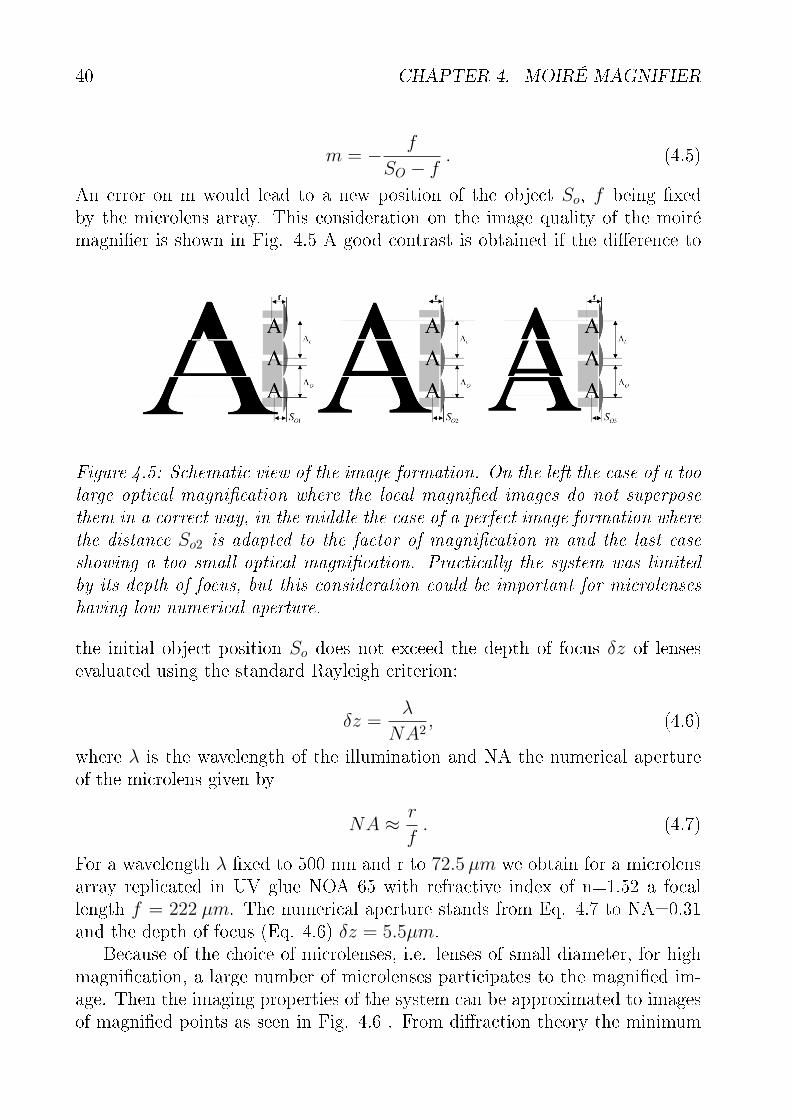
the ratio similar shape problems appear, but re�ow microlenses of hL
Ø> 1
2 havealready been fabricated. The best microlenses are realized with a ratio in therange between hL
Ø≈ 1
12 and hL
Ø≈ 1
15 .
2.1.2 Replication techniques
Although photolithography is the dominant technology, even for large micronscale features, it is not always the best or the only option for all applications. It
Figure 2.4: Process �ow of the replication technique used; (1) Fabrication ofa master; (2) Pouring of the liquid PDMS over the master; (3) Cure at 50°Cfor 12 hours to polymerize the PDMS. (4) De-molding operation and release ofthe master; (5) Deposition of UV glue on a substrate; (6) UV exposure ∼ 9min at 350 nm to polymerize the UV adhesive; (7) De-molding operation andrealization of a micro-optical element in solid UV glue.
is not an inexpensive technology and di�culties arise for patterning non planarsurfaces although it becomes possible with spraycoater. In addition it providesalmost no control over the chemistry of the surface and hence is not very �exi-ble in generating patterns of speci�c chemical functionalities on surfaces ( e.g.,for anchorage-dependant tissue culture or combinatorial chemistry). Moreover it

8 CHAPTER 2. FABRICATION METHODS AND SIMULATION TOOLS
can only generate 2D microstructures and is directly applicable only to a limitedset of photosensitive materials ( photoresists) [14]. As an alternative, severalmicro fabrication techniques on polymers have been created especially in massproduction of micro-optical elements with extended functionalities. Methodssuch as micro injection molding [15] or embossing techniques have been devel-oped. In the �eld of embossing methods, two approaches can be distinguished[14]. Soft lithography techniques, using elastomer molds, such as replica molding(REM) solvent assisted micro-molding (SAMIM), micro-molding in capillaries(MIMIC), microcontact printing and microtransfert molding (µTM) and rigidimprint techniques such as nanocontact imprint (NCM), step and �ash imprintlithography (S-FIL) and nanoimprint lithography (NIL) [16, 17]. In the frameof this work a general UV embossing technique (i. e. embossing of UV curablepolymer) with an elastomer mold was used. Fig. 2.4 shows the di�erent stepsinvolved in this process. As described in the previous section the fabrication
Figure 2.5: Corresponding shrinkage of Sylgard 184 PDMS versus curing con-ditions. The measurements were performed on a 4 inches round mold with athickness of 1.2 mm [18].
of microlens arrays by photolithography and re�ow process is a three step pro-cess. To simplify the manufacture of prototypes, a mold of the PR master isfabricated using standard Sylgard 184 PolyDiMethylSiloxane (PDMS) materialfrom DowCorning. The material is composed out of two elements, a base anda hardener. The two components are blend together with a weight ratio of 1part of hardener to 10 part of base [19]. After mixing, the air and solvents areremoved with an additional step in a vacuum chamber at 5 mbar. The liquidis then applied directly on the master preliminary placed in an adapted con-tainer. 50 ml are enough to produce a 4 inches square mold with about 5 mmthickness. The PDMS is then polymerized in an oven 12 hours at 50°C. Faster

2.1. FABRICATION PROCESSES 9
cure, 1 hour at 100°C, is also possible but with a corresponding shrinkage of themold of about 2 % (Fig. 2.5). Replicas are simply made by applying the PDMSmold over a drop of optical UV glue [Norland Optical Adhesive (NOA)] andpolymerized 9 minutes in a standard UV box with approximately 2mW
cm2 in thewavelength range between 350 to 400 nm. Replicated nanostructures smallerthan 300 nm can be achieved but an aspect ratio of the structures in the rangebetween 0,2-2 must be observed to avoid their collapsing [14].
2.1.3 Dry etching
To obtain microlens arrays in silicon or fused silica substrates an additional stepfrom the re�ow process described previously in the photolithography section hasto be done. This step is performed using a Reactive Ion etching with InductedCoupled Plasma (RIE-ICP) machine from STS (Surface Technology Systems).In a reactor, plasma conditions are generated for di�erent mixtures of gases bymeans of electrodes supplied by a RF generator at 13.56 MHz with an adapta-tive power between 200-1000 W. The substrate being etched is biased to inducedirectional ion bombardment and produce anisotropic etch characteristics. Theions generated in the plasma are con�ned on the wafer and generated at lowpressure (2-5 mtorr) by an additional coil driven separately by an identical RFpower supply. The presence of the coil allows to increase etching rates and direc-tional etching by increasing the ion to neutral particles ratio and reducing ionsto neutral particles collisions [20]. All the di�erent mentioned parts of the ma-chine are illustrated in Fig. 2.6. . More recent improvements have been realized
Figure 2.6: Illustration of the Multiplex-ICP system. Image source from [25].
in the etching of silicon using Deep Reactive Ion Etching (DRIE) technology.

10 CHAPTER 2. FABRICATION METHODS AND SIMULATION TOOLS
This allows very high selectivity by repeating etching steps and formation ofsidewalls passivation layers used as protective layers during the sputtering etch-ing steps (Bosch process) [21]. Similar improvements have been realized onsilicon oxide using continuous polymer layer deposition to increase the etchingcapability of the oxide with anisotropic etch [22]. Mainly based on �uorinechemistry, several types of gazes can be used CF4,, C2F6, CHF3, C3F8, C4F8[23] and etching of a wide range of materials are possible (Silicon SI, quartzQZ, Aluminum AL...)[24]. In the present work C3F8 and SF6 were used toetch respectively fused silica and silicon substrates, while heavy Ar moleculeswere added as a general surface cleaner for both materials ( sputtering e�ect,low selectivity). In the purpose of changing the selectivity of etching betweenPR and the material of the substrate O2 and CH4 are added as an acceleratorand an inhibitor of PR etching. The depth of the transferred structures canbe adjusted by modifying the ratio between the di�erent gases. Several othersparameters such as plasma pressure, �ux of the gases and powers of the coiland platen can be changed. During the etching process two main e�ects occur .
Figure 2.7: Scheme of the basic mechanisms occurring during dry etching pro-cess. (1) Physical etching i.e. sputtering etching, highly anisotropic and lowselectivity. (2) Chemical etching, isotropic and high selectivity. (3) Both,anisotropic pro�le, good selectivity.
As described in Fig. 2.7 an isotropic chemical etching of the material happensas well as an anisotropic physical sputtering occur. By adjusting separatelythe pressure inside the chamber the weight of one e�ect to the other can beemphasized. While low pressures tend to strengthen the e�ect of sputtering,higher pressures increase the e�ect of chemical etching mechanisms as seen inFig. 2.7 [24]. In the applied processes, the pressures were typically set between2-5 mtorr. Because optical elements were fabricated we focused our attentionto good surface roughness and obtain etching rates of 400 nm/min in PR with
selectivity S =PRetching rate
QZetching rateof 0.65 for quartz (QZ) wafers coated with AZ9260
PR while 600nm/min in PR with selectivity between 0.56 to 1.14 were obtainedfor SI wafers. More information can be found on general etching mechanisms ofSi and SiO2 in �uorocarbon ICP plasmas in [20, 23].

2.2. SIMULATION TOOLS. 11
2.2 Simulation tools.
2.2.1 Ray-Tracing
With the arrival of computers in the sixties and with the Fourier series expan-sion of the di�erent sine and cosine functions, e�cient simulations of opticalsystem by looking at the propagation of rays, according to the laws of geomet-rical optics, became possible. Two principle of ray-tracing approaches can bedistinguished, sequential and non-sequential ray-tracing. The sequential ray-tracing has been developed to analyze optical aberrations in imaging system.The propagation of the optical rays through the di�erent optical interfaces ofthe system is calculated using the law of refraction and re�ection. It performs asequential propagation from the source through the di�erent optical interfacesup to the image plane. The non-sequential ray-tracing has been developed tooptimize design light sources or imaging instruments where internal re�ections,stray-light and di�usion by the roughness of surfaces are important. It takesinto account transmitted as well as re�ected rays and includes geometrical op-tics for scattering. The main goal is the calculation of spatial or directionaldistribution of the power, such as the �ux φ, the irradiance E and the radianceL [26].
2.2.2 Polarization ray tracing
Because micro-optics combines small to very small optical structures but spreadover a large surfaces of several square millimeters, accurate simulations can bedi�cult especially in time consumption. It is therefore convenient to separatethe di�erent optical phenomena that physically appear and retain only the mostsigni�cant ones. The main optical e�ects we had to deal with in simulationswere di�raction, polarization management and coherence. In the case of bire-fringent refractive microstructures presented in the next chapter, we used TracePro software from Lambda research which is able to deal with polarization andray splitting. No di�raction and coherence e�ects have been retained. As anexample we simulate the case of a �nite bundle of normal rays incident on abirefringent prism illustrated in Fig. 2.8. The output rays are collected on adetector screen at two di�erent positions ((1) and (2)). The results on the inten-sity distribution and the degree of polarization are shown in Fig. 2.9 for position(1) and in Fig. 2.10 for position (2). Because simulations are performed usingincoming natural light, the two orthogonal components (transverse electric (TE)and transverse magnetic (TM)) generated by the system cannot be recombinedin an interferometric way [27]. Consequently two rays Re and Ro having dif-ferent Optical Path Di�erence (OPD) do not interfere and their superposition

12 CHAPTER 2. FABRICATION METHODS AND SIMULATION TOOLS
gives, as it was the case for the input light, unpolarized light.
Figure 2.8: Illustration of a typical polarization management experiment per-formed with Trace Pro software from Lambda Reaserch. A birefringent prismis illuminated with collimated unpolarized light. At the output face of the prismdouble refraction occurs. TE and TM components travel with di�erent direc-tions of propagation.
Figure 2.9: Intensity and polarization distribution at the detector plane placedin position (1) in the experiment described in Fig. 2.8. The right image showsthe intensity distribution of the two beams while the left image shows the polar-ization distribution (state and degree) in the same plane.
The simulation of the polarization state is then simply de�ned by the addi-tion of the stokes vector parameters
SS =∑
S
Si =∑
S
S0S1S2S3
i
, (2.2)

2.2. SIMULATION TOOLS. 13
Figure 2.10: Intensity and polarization distribution at the detector plane placedin position (2) in the experiment described in Fig. 2.8. The right image showsthe intensity distribution of the superposition of the two beams while the leftimage shows the polarization distribution in the same plane. The intensitydistribution increases at the superposition of the two beams while the degree ofpolarization decreases in the same area.
where the index S corresponds to the sampling area in the target plan and i tothe rays. In the case of a plane wave, S0, S1, S2, S3 are Stokes vector parameterslinked to the amplitude polarization components Ax and Ay and their relativephase di�erence δ and is given by,
S0S1S2S3
=
⟨A2
x + A2y
⟩⟨A2
x − A2y
⟩〈2AxAy cos (δ)〉〈2AxAy sin (δ)〉
. (2.3)
The degree of polarization is then de�ned by
p =
√S2
1 + S22 + S2
3
S0. (2.4)
In the case of rays the intensity is replaced by the amount of power or �ux.For instance, the addition of a ray TE polarized with an associated �ux P1represented by a Stokes vector, [P1 P1 0 0] and a second ray TM polarized, [P2-P2 0 0] will give [(P1 + P2) (P1 − P2) 0 0] corresponding to a partially polarized
ray p =∣∣∣P1−P2
P1+P2
∣∣∣ with �ux P1 + P2. The local intensity will be de�ned by the
ratio between the �ux and the sampling area S. This can be seen in Fig. 2.10where the degree of polarization drops down to nearly zero at the intersection ofthe two beams because of the superposition of the two orthogonal components.The sign of the parameter S1 gives the orientation of the linear polarization. Toensure di�erent cases of the resulting degree of polarization at the intersectionof the two beams, the light source was set to have randomly distributed rays

14 CHAPTER 2. FABRICATION METHODS AND SIMULATION TOOLS
at its surface. The degree of polarization is now dependent on the numberof rays striking the local sampling area S. More complete interpretations andexplanations on Stokes vectors and associated Mueller matrix can be found in[28].
2.2.3 Simulation of optical �elds
In the case of micro-optical elements, the di�raction of the light becomes impor-tant and has to be taken into account in the simulations. This is specially thecase in the understanding of the light propagation through microlenses with�nite apertures which are studied in details in the chapter 5. Several rig-
Figure 2.11: Comparison between simulated (upper image) and measured (bot-tom pictures) intensity distribution of the focal region of a microlens of Ø =250 µm, ROC= 864 µm and Strehl ratio of 96.
orous methods like FDTD (Finite Di�erential Time Domain), FMM (FourierModal Method) have been developed nowadays to understand the propagationof electromagnetic waves through optical objects. Nevertheless these accuratemethods are not appropriate for wide optical geometries such as microlenses ofseveral hundred of microns, mainly because of their somehow too high preci-sion (not necessary) and their time consuming. To overcome these di�cultieswe choose the FRED simulation software from Photons Engineering combin-ing scalar di�raction theory and easy implementations of complex geometriesof several millimeters with coherent illuminations. The aim of this paragraphis to validate this approach through comparison with 2D measurements of theintensity distribution of a microlens of Ø = 250 µm with a Radius of curva-ture (ROC) equal to 864 µm performed using a Mach-Zehnder interferometer.This is illustrated in Fig. 2.11 where the position of the peak irradiance is thesame in both cases with a slight di�erence of only 2-3 microns. The shape ofthe intensity distribution is well comparable with the presence of the di�erentside lobes. The measured image is the combination of three scans over 100 µmwith di�erent intensity of the laser source to avoid saturation of the CCD cam-era. This explains the general higher contrast measured in the side lobes. A

2.2. SIMULATION TOOLS. 15
comparison of the position of the peak irradiance position through a circularaperture has been done with the resolution of the Rayleigh Sommerfeld integraland FRED software in chapter 5.

16 CHAPTER 2. FABRICATION METHODS AND SIMULATION TOOLS

Chapter 3
Birefringent polarizer
3.1 Introduction
The appearance of polymerizable liquid crystal mesogens (LCP) has openednew opportunities for manufacturing of birefringent components and devices,often composed of expensive and bulky materials such as calcite or quartz [29].Replication of micro-optical components is standard but not known for bire-fringent organic materials until now [30]. Combining di�erent methods such assoft (or UV) embossing with alignment of liquid crystals on nanostructures andindex matching, elements of various shapes and devices with increased function-alities can be produced [31]. The purpose of the proposed device is to convertincoming natural light into nearly linearly polarized light with e�ciency over50 %. Compared to conventional polarization management devices developedfor LCD projector [32, 33] we avoid expensive components such as polarizingbeamsplitters. Moreover the wafer based fabrication process strongly reducesthe obstruction to a thickness of only few millimeters.
3.2 Operation principle
The principle of the present device is based on splitting natural light into its po-larization components and modifying one component with a polarization rotatorto get one polarization state at the output. Neither absorption nor re�ection isused. With the help of birefringent lenses, incoming natural light can be splitinto its two linear polarization components with two di�erent focal points [34].Embedding the lens in an index matching environment allows focalizing one po-larization only, leaving the other una�ected. If we consider only the polarizationcomponent which is not focalized by the system and we rotate it by 90° all thislight will be transformed into a polarization state perpendicular to its origin.
17

18 CHAPTER 3. BIREFRINGENT POLARIZER
This light has now the same polarization state as the focalized second polariza-tion component. Only one polarization state will therefore be transmitted. Thesystem becomes a polarizer with very high e�ciency and without loss due toabsorption. This operation principle is shown in details in Fig. 3.1. Because one
Figure 3.1: Operation principle, on the top lens of the picture, the incoming lightis split by the microlens, TE polarization is focused on the twisted nematic (TN)cell and converted into TM polarization while TM component is not focused andconverted into TE polarization. The bottom lens shows the same system but witha switched zone in the TN cell located at the focal point, resulting in a whole TEpolarization at the output of the TN cell. Note that if the TN cell is switchedthe polarization is maintained.
of the polarization components is focalized and the other is not, the beam char-acteristics will be changed. To achromatically rotate in the visible wavelengthrange the polarization a twisted nematic (TN) cell is well suited. The choice ofrotating the unfocalized component comes from the angular sensitivity of theTN cell [29] which could be important for angles higher than 20° or a numericalaperture of the microlens NA > 0.34. Because the micro-optical polarizer (MP)converts incoming natural light into polarized light it is not possible to use itas conventional dichroic (absorption of one polarization component) polarizers.The behavior of the MP is described in Fig. 3.2 for di�erent case of polarizationof the input light and compared to a conventional polarizer. In the �rst case(A), the input light IIN is unpolarized and only half the intensity is convertedinto a linearly polarization state IOUT by the polarizer. In the case of the MP

3.3. SIMULATIONS 19
Figure 3.2: Illustration of the behaviors of a perfect dichroic polarizer (top part)compared to the case of a perfect micro-optical polarizer MP (bottom part) underdi�erent illumination conditions. The arrow in the polarizer and the MP givestheir optical axis orientation.
all the intensity is converted. In the second case (B) the input light is linearlypolarized and parallel to the devices. Both let pass the light. In the third case(C), the polarization of the input light is orthogonal to the optical axis of thedevices. No light passes trough the polarizer while all the light is converted bythe MP. (D) Crossed polarizer and MP con�gurations. The unpolarized inputlight is totally absorbed by the second polarizer while all the converted intensityis rotated by the MP. We have realized such a micro-optical polarizer (MP) withan array of birefringent microlenses and a patterned twisted nematic (TN) cellas a polarization rotator.
3.3 Simulations
We studied a system with an array of cylindrical microlenses of 150 µm widthand about 25 µm height. All the elements constituting the MP are illustratedin Fig. 3.3. The incident natural light reached the microlenses array from theleft and due to the index matching between the ordinary refractive index (no)and the refractive index n of the matrix material, only one component of thepolarization is focused on the twisted nematic cell. The focal length of themicrolens for the focalized component is given by
f =ROC
ne − n, (3.1)
where ROC is the radius of curvature of the microlens, ne the extraordinaryindex of the birefringent material and n the index of refraction of the matrix

20 CHAPTER 3. BIREFRINGENT POLARIZER
material. The TN cell has striped electrodes, visible as black zone in Fig. 3.3.
Figure 3.3: Illustration of the complete device. All the elements are representedwith their e�ective thickness. The whole system is less than 2 mm thick.
If the TN cell is switched, these zones will become homeotropic (meaning thatthe orientation of the molecules will be set normal to the substrate) and thecell forms a grating of twisted and non-twisted areas. Light passing throughswitched areas is only slightly a�ected and in the ideal case no change of the stateof polarization will be observed. The non-switched areas rotate the polarizationby 90°. Simulations have been performed with commercial optical ray tracingsoftware (Trace Pro Expert) that allows simulating polarization optics includingcrystal optics. One problem for the simulation is the twisted nematic cell. Inthe present case with restricted angular range, we have chosen a very simplemodel. The polarization rotation behavior of the TN cell was simulated by a halfwave plate positioned at 45° with respect to the orientation of the cylindricalmicrolens array. The corresponding Mueller matrix has been used instead ofmore complex, but more accurate methods, such those ones described in [35]which take ray splitting and local interferences phenomenon into account. Letus calculate the e�ciency for our model system. In the ideal case all the lightof the polarization component that is focused is left unchanged. The otherpolarization component traverses the system parallel and is rotated, except forthe areas, where the TN cell is switched. In the switched zones the polarizationis not changed and will remain in the undesired state. The amount of this lossL1 is given by the ratio of the portion of light that is not rotated and the totalincident light i.e. by the ratio of the area of the switchable zones and the totalarea. It follows for a cylindrical lens grating with a given pitch of ΛLenses and a

3.3. SIMULATIONS 21
width of the commuted area of WTN to
L1 =1
2· WTN
ΛLenses. (3.2)
The factor ½ appears in the calculation because only one polarization componentshows that type of loss. Taking a pitch of ΛLenses = 150 µm and a width of thecommuted area of WTN = 20 µm this leads to the following rate L1 = 6.5 %.To this loss we also have to add the part of the light passing through the spacebetween two lenses WGap and not being a�ected by the system
L2 =1
2· WGap
ΛLenses. (3.3)
For manufacturing reasons this space WGap is �xed to 5 µm leading to a lossof L2 = 1.6 % for cylindrical lenses. So the maximum theoretical polarizatione�ciency Pe without Fresnel re�ection losses is given by
Pe = 1− (L1 + L2) , (3.4)
which gives Pe = 91.9 %. These di�erent losses and the parameters involved inthe calculations are shown in details in Fig. 3.4.
Figure 3.4: Illustration of the di�erent losses present in the system and raytracing interpretation of the polarization state at the output of the micro-opticalpolarizer. S corresponds to the sampling area (collecting the rays) retained inthe calculation of the polarization state and the intensity distribution.
Another limitation of the system is its high angular sensitivity, since onecomponent of the polarization must be precisely focalized on the switchableTN area. Figure 3.5 illustrates the case of perfectly collimated incoming lightstriking the device with normal incidence.

22 CHAPTER 3. BIREFRINGENT POLARIZER
Figure 3.5: Resulting intensity distribution and polarization state for perfectlycollimated light at normal incidence. The linear polarization state of the beamis almost homogenous, but the degree of polarization drop down in its centerbecause of the presence of unconverted rays as explained in Fig. 3.4.
Figure 3.6: Resulting intensity distribution and polarization state for perfectlycollimated light at 4° of incidence. The focalized polarization does no morepass through the switched area of the TN cell. The polarization map shows theresulting inhomogeneous polarization distribution.
The bottom left picture shows the resulting intensity distribution. The

3.4. EXPERIMENTAL RESULTS 23
white area of higher intensity inside the beam spot is due to the focus of onepolarization component and shows the new spatial distribution of the outputlight. In Fig. 3.6, the incoming light is slightly deviated and strikes the microlens
Figure 3.7: Simulated polarization e�ciency Pe as a function of the angle ofincidence of collimated input light for a system with microlens diameter Ø =145 µm, pitch = 150 µm, hlens = 25 µm and a width of the commuted TN areaof 20 µm. Pe is de�ned as the ratio of the output intensity I2 and input intensityI0.
at an angle of 4°, the focused polarization misses the switched area of the TN cell,the polarization state is no more improved as shown in the bottom right picture.The use of cylindrical microlenses can eliminate this dependency in one axis butthe problem remains in the other direction. Taking an additional polarizer atthe output, the transmission is a measure of the polarization e�ciency Pe of themicro-optical polarizer. The simulated transmission as a function of the angle ofincidence is shown in Fig. 3.7. After few degrees of inclination the focal pointsof the focused polarization components do not hit the switched areas of the TNcell anymore and the e�ciency drops down and rises again when neighboredswitchable areas are found at about 15°. The polarization e�ciency drops evenbelow 50% since one polarization does not reach anymore the switched areasand the other component continues to pass through them.
3.4 Experimental results
As described earlier, the presented micro-optical polarizer is composed of twoliquid crystal cells. One cell contains the birefringent microlenses between two

24 CHAPTER 3. BIREFRINGENT POLARIZER
glass plates and immersed in index matching �uid. The other is a twisted ne-matic cell with structured electrodes. The birefringent microlens array is madeby a replication process with a silicon stamp, printing the structures into a liquidcrystal polymer (LCP) which is afterwards polymerized. The parallel alignmentof the LCP in the nematic phase is obtained by boundary conditions imposedby rubbed polyimide coating on one side and nanostructures relief (fabricatedby laser beam interference [36, 37]) of the silicon stamp on the other side. Afterannealing and polymerization of the LC with ultraviolet light (UV) the stamp isremoved and a thin layer of index matching UV glue is deposed over the array.The cell is completed by another glass plate and an additional UV curing stepto polymerize the UV glue. A very robust temperature insensitive birefringentmicrolens array is formed. Finally, a TN cell with structured grating electrodesis glued on the lens array respecting the narrow alignment tolerances of align-ing the microlens array to the switchable grating structures. To realize thebirefringent microlenses, conventional cylindrical microlenses of 150 µm pitchspaced by 5 µm were used. They were fabricated in photoresist using the re�owtechnique described in the introduction. By means of laser beam interference agrating of 400 nm pitch with 80 nm depth is recorded on the microlenses withan additional step of lithography. This master is used for stamp fabrication inPDMS silicone material. The liquid crystal polymers are heated to 100° C toevaporate the remaining solvent and avoid bubbles formation during fabricationsteps. One drop of LCP is put on a glass plate with a rubbed polyimide layerand the stamp is applied directly over it. After 15 min on the hot plate, a pres-sure of 1 bar is applied on the stamp. The system is hold at 80° C in an ovenfor at least 1 hour to align the LCP molecules. As LCP, RM 257 from MERCKwith a birefringence of about ∆n = 0.14 (no= 1.54; ne= 1.68) was used.
Figure 3.8: SEM Pictures of free standing birefringent microlenses, detail ofthe alignment grating parallel and orthogonal. (Scales, 10 µm and 60 µm)
The polymerization of the LCP is done under UV exposure for 9 minutesin a standard UV curing chamber (Intensity of 2mW
cm2 in the wavelength range

3.4. EXPERIMENTAL RESULTS 25
between 350 to 400 nm). Fig. 3.8 shows two types of free standing birefrin-gent microlenses in LCP. The grating written on the stamp used to mold themicrolenses in the LCP is clearly visible. In Fig. 3.9 we can see, the di�erentelements constituting the micro-optical polarizer, �rstly the birefringent mi-crolenses, the focal line at the position of the TN cell and the output light. Thepictures have been taken at di�erent positions (1,2,3) in the complete system.Figure 3.10 shows the device in the three possible states. Firstly the device is
Figure 3.9: Pictures of the realized prototype taken at di�erent distances insidethe system showing the microlenses, the focal line and the output light.
Figure 3.10: Pictures of the realized device in the three possible states underunpolarized collimated white light. Picture (1) the electrodes are switched o�,picture (2) switched on, picture (3) black position and TN electrodes switchedon.
under collimated but unpolarized illumination. Picture (1) corresponds to theinitial state where no voltage is applied on the TN electrodes. This features thebasic condition where no change occurs in the illumination except on its spatialdistribution. The second image (2) illustrates the device in bright position, i.

26 CHAPTER 3. BIREFRINGENT POLARIZER
e. the optical axis of the analyzer stands parallel to the optical axis of the MPand the TN cell is commuted. The light is completely focused on the switchedareas of the TN cell and passed without any change of polarization. A gen-eral increasing of the brightness of the picture taken under identical conditionsshows the performance of the device. In black position (3), i. e. the optical axisof the analyzer is perpendicular to the optical axis of the device, several stripesappear because of the better contrast as well as a general decreasing of thebrightness of the picture. These broader white stripes are the result of discli-nation lines at the border of the switched zones in the TN cell and because thewrong polarization component passes there without being rotated. The thinnerlines correspond to the space between lenses. To measure the performance ofthe device, the output intensity for a combination of the micro-optical polarizerand a conventional sheet polarizer was measured under natural light using amicroscope. To ensure a good collimation of the input light diaphragms have
Figure 3.11: Illustration of the con�guration used in the measurements of thepolarization e�ciency Pe of the micro-optical polarizer MP. In the �rst part ofthe measure, the intensity I1 is detected without the MP but through a conven-tional dichroic polarizer (A), In the second part the MP is placed in front ofthe analyzer and the intensity I2 is detected (B). The intensity directly at theoutput of the MP I0′ is not measured because of its not well de�ned polarizationstate.
been used. To allow comparisons with the simulated polarization e�ciency Pe,we assume 50% e�ciency (Pe = 0.5) for the analyzer, representing the case ofa perfect dichroic polarizer as simulated in the previous section
Pemeasured=
I2 − I1
2 · I1+ 0.5. (3.5)

3.5. UN-COLLIMATED SOURCES 27
I2 corresponds to the intensity measured with the micro-optical polarizer and I1without MP as described in Fig 3.11. Results are shown in Fig. 3.12 for anglesof incidence in a range between 0° and 18°. The displacement of the second
Figure 3.12: Measured and simulated polarization e�ciency as a function of theangle of incidence for a system with microlens diameter Ø = 145 µm, pitch =150 µm, hlens = 25 µm and a width of the commuted TN area WTN of 20 µm.
peak of the e�ciency measurements may come from a bad position of the gluedTN cell which is thicker than the focal length of the microlenses. At normalincidence, the presence of the device before the analyzer leads to a measuredtransmission increased by 34 %. The general smoothing of the curve probablycomes from the fact that no di�ractive e�ects have been taken into account insimulations. In real measurements the width of the focal point is enlarged bydi�raction of the input white light and by the divergence of the source.
3.5 Un-collimated sources
As mentioned in the upper paragraph the realized system is well suited forhighly collimated sources and not appropriate for diverging light sources. Nev-ertheless by adapting some design parameters it is possible to strongly increasethe e�ciency for that type of illumination. All the sources are assumed to haveconstant radiance over an angular range between ±αmax de�ned through theirF-Number given for any lens by
F# =f
2r≈ 1
2NA, (3.6)

28 CHAPTER 3. BIREFRINGENT POLARIZER
Figure 3.13: Schematic illustration of the design optimization; (a) Total inter-nal re�ection (TIR); (b) Spherical aberration, the focused polarization reachesno more the TN area; (c) Focused ray; (d) O� axis ray still focused; (e) TIR ofan o� axis ray. ROC and WTN are parameters to optimize. Fresnel re�ectionsare not illustrated.
with f as the focal length, r the radius of the lens aperture. The numericalaperture NA is de�ned by the half angle αmax with
αmax = arctan
(1
2F#
). (3.7)
As seen in Fig. 3.13, two parameters can be optimized, �rstly the focal lengthof the microlenses through their ROC and secondly the width of the TN cell.The position of the TN cell is �xed to the focus of the microlenses. Taking intoaccount all the di�erent Fresnel losses occurring at the lens interface for o� axisrays in a 3D geometry of the system, the calculated transmission is then plottedas function of the F-number of the light source for simulations of microlenseswith di�erent radius of curvature (ROC) (see Fig. 3.14) and for di�erent widthof the commuted areas in the TN cell (see Fig. 3.15). The main parameter toadjust, in purpose of avoiding losses when rays strike the device with a certainangle, is the focal length. This is checked in simulations by reducing the ROCin Fig. 3.14. It has to be noticed that the position of the TN cell is �xed to thecorresponding focal length of the microlenses. Nevertheless a limit is found whenaberrations and total internal re�ections appear in the microlenses, the higheste�ciency is achieved with ROC = 0.091 mm. For large F-Number sources, thewidth of the commuted areas of the TN cell can be enlarged to ensure a bettere�ciency of the system, as shown in Fig. 3.15 because the focusing ability ofthe microlenses is strongly reduced by the angular dispersion at the entrance ofthe system. In other words, this means that for collimated rays the e�ciencywill drop down following
3.5. UN-COLLIMATED SOURCES 29
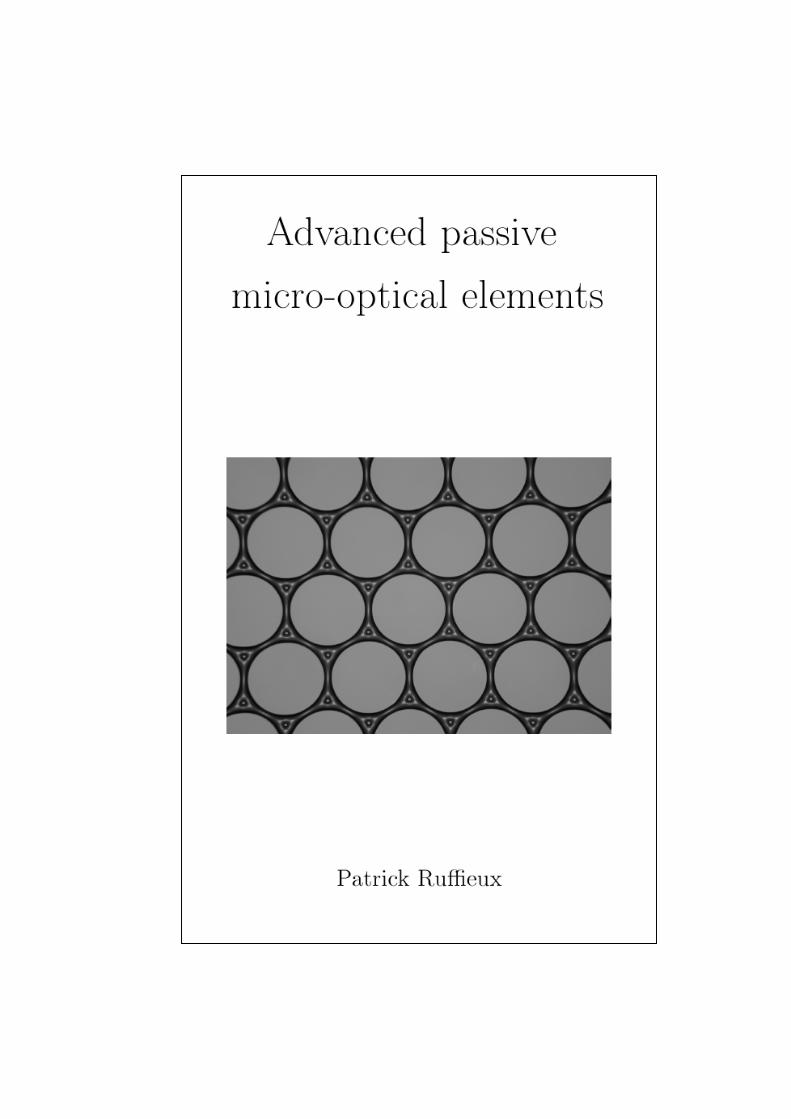
Figure 3.14: Simulated polarization e�ciency for sources with di�erent F-numbers and various ROC of the microlenses. The microlens array periodis ΛLenses = 150 µm, the gap of Wgap = 5 µm and the TN switched areaWTN Cell = 20 µm.
Figure 3.15: Simulated e�ciency for three sources with di�erent F-numbersin function of the width of the commuted zones in the TN cell. The ROC ofmicrolenses is 0.09 mm, the microlens period ΛLenses = 150 µm and the gapWgap = 5 µm.
Eq. 3.2, but will increase for o� axis rays. As an example an increasing of10% of the overall e�ciency is simulated for by changing the TN width from20 µm to 70 µm for a source with a F-Number, F# = 4 (diverging angle αmax

30 CHAPTER 3. BIREFRINGENT POLARIZER
de�ned by Eq. 3.7, αmax = 7.1 ) as seen in Fig. 3.15. Appling this consider-ations it is possible to maximize the system by adjusting the two parameters(Wth, ROC) for each speci�c source.
3.6 Head to head con�guration
A strong improvement in the design of the present device can be obtained byadding a second birefringent microlens array with an orthogonal orientationof the optical axis. Based on the identical principle described in the previousparagraph, the second array of microlenses focuses the second polarization com-ponent in the plan of the TN cell. This new concept is illustrated in detail in
Figure 3.16: Illustration of the Head to Head con�guration. The optical axisof the two birefringent microlens arrays are set orthogonal. Both polarizationsare focalized. A complete separation of each polarization is performed, with adirect possibility of increasing the width of the TN areas to half the pitch of themicrolens arrays.
Fig. 3.16 . In this case, the maximum theoretical polarization e�ciency Pe isde�ned simply by the ratio of the amount of non focused light and focused light,i.e. by two times the half ratio of the gap between microlenses Wgap over themicrolens array period ΛLenses :
Pe = 1− Wgap
ΛLenses. (3.8)
Equation 3.8 leads to an e�ciency Pe = 96.7% for a period ΛLenses = 150 µmand a gap of Wgap = 5 µm. A complete separation of both polarization compo-nents is then achieved.

3.6. HEAD TO HEAD CONFIGURATION 31
Figure 3.17: Simulated and measured polarization e�ciency versus the angle ofincidence of collimated light for one microlens array and Head to Head con�g-urations systems with microlens diameter Ø = 145 µm, pitch = 150 µm, hlens= 25 µm and a width of the commuted TN area of 20 µm.
The main implication is a possible widening of the TN commuted area tohalf the pitch of the microlens array without adding losses to the �rst polar-ization component. A lower angular sensitive micro-optical polarizer is thenrealized. The same consideration described previously on the optimization ofthe ROC applies. Using the soft embossing technique discussed previously forthe fabrication of the birefringent microlens arrays, an unswitchable pattern TNcell in LC polymers with half the pitch of the microlens array has been realized.The height of the cell is 10 µm. The measured polarization e�ciency of the de-vice has been performed under white light illumination using diaphragms (F#∼7) and the mercury lamp of the microscope as an unpolarized light source.The results are shown in Fig. 3.17. The general smoothing of the measuredcurves may similarly be explained by the di�raction of the white light and bythe divergence of the source which widespread the focus point. In Fig. 3.18the e�ect of the two birefringent microlens arrays is shown through three pic-tures. On the right the analyzer is positioned parallel to the microlens arrayand only one focalized polarization is visible. In the center picture the analyzeris rotated by 90° and the second focalized polarization is now visible. In thelast picture the analyzer is removed and both focalized polarizations are visible.Using standard linear photodiode, an average gain of 45% (Pe = 72, 5%) on thetransmitted intensity has been measured with a contrast de�ned as the ratiobetween maximum transmitted intensity and minimum transmitted intensitythrough the device and the polarizer of reference

32 CHAPTER 3. BIREFRINGENT POLARIZER
Figure 3.18: Pictures of focalization of one polarization component (1), of theorthogonal component (2) and both (3).
c =Imax
Imin(3.9)
of 3.64. For these measurements a prototype has been realized working on a
Figure 3.19: Pictures of head to head device illuminated with collimated whitelight seen through orthogonal polarizer (A) and parallel polarizer (B)and super-imposed picture of the whole cell seen between crossed polarizers.
large area of several millimeters and allowing macroscopic view of its e�ciency.By restricting the angular distribution of the source using two diaphragms of2 mm separated by a distance of 130 mm (F# ∼33) pictures of the devicehave been taken with parallel and orthogonal orientation of the analyzer to seethe realized contrast. These two pictures are shown on the right hand side ofFig. 3.19 while on the left hand side a picture of the whole device betweencrossed polarizer can be seen. The case of intensity transmission with only thepolarizer of reference is not pertinent since the light distribution at the outputof the device is no more collimated. Note that the beam can be collimated byaddition of another lens array with half the pitch of the �rst arrays. Lossesdue to the degree of coherence of the source (interferences, di�raction) are notdiscussed in this paper.

3.7. CONCLUSION 33
3.7 Conclusion
It has been demonstrated that polarizing micro-optical elements allow creatingnew non-conventional optical elements. Integrated in systems, special functionslike a micro-optical polarizer can be realized. The speci�c interest lays in thepossibility to produce devices with wafer technology. We realized a prototypewith miniaturized optical components that is only 2 mm thick. The gain inthe polarization e�ciency is over 45% for collimated white light. Strong im-provements could be realized using AR coating on both sides, by increasing thehomogeneity of the alignment of the Liquid crystal molecules and by increasingthe TN cell height [27]. Aspheric microlenses could be used to increase theacceptance angle. Moreover a third microlens array could be added to the headto head con�guration to improve the collimation of the light at the output ofthe system.

34 CHAPTER 3. BIREFRINGENT POLARIZER

Chapter 4
Moiré magni�er
4.1 Introduction
This chapter concerns an interesting visual application of microlens arrays. Us-ing a repetitive pattern of a scale down image and a microlens array, a magni-�cation of this image can be displayed. The magni�cation and the orientationof the image can be chosen by simply rotate the microlens array. This propertyallows interesting design application in thin and �at devices. To ensure a strongintegration of the overall system, we focus our analyze to high resolution moirémagni�ers using microlens arrays having heights of only few tens of microns anddiameters between 150− 360 µm. From the equations developed in [38] we givea method to design moiré magni�ers and explore their image quality throughfabricated samples.
4.2 Moiré phenomenon
The moiré phenomenon is a well known phenomenon which occurs when repet-itive structures are superposed or viewed against each other. It consists of anew pattern of alternating dark and bright areas which is clearly observed atthe superposition, although it does not appear in any of the original structures[39]. This e�ect is mainly used in metrology since it allows weak deformationsto be easily detected [40, 41].
4.3 Moiré magni�er
The principle of a moiré magni�er is to use a �rst object made up by the periodictwo-dimensional repetition of a certain image and its interaction with a matrixof microlenses of slightly di�erent period. The �gure created at the time of
35

36 CHAPTER 4. MOIRÉ MAGNIFIER
the superposition of the two elements is a magni�ed image of the repetitivestructure visualized through the microlenses.
Figure 4.1: Illustration of the di�erent elements constituting the moiré magni-�er. On the left the object array, in the middle the microlens array and on theright the magni�ed image obtained when superposing both elements.
Figure 4.1 shows the di�erent elements constituting the moiré magni�erand the resulting magni�ed image. Each lens carries out a magni�ed imageof a di�erent part (white area) of the object as seen in Fig. 4.2. When thesampling of the di�erent parts of the pattern is adapted, all the images formedby the matrix of microlenses combine themselves in a contiguous way to formthe complete image of the magni�ed pattern. Since an image formation occurs,two distinguished cases are possible depending on the position of the objectcompared to the focal length of the microlenses. A virtual magni�ed imageappears when the object position So is lower than the focal length f of themicrolens i.e. So < f and a real but inverted image appears for So > f . Thedi�erent elements required for a moiré magni�er are illustrated in Fig. 4.1. Themoiré magni�er e�ect imposes dimensions in the same order for the array andthe magni�ed image. In the idea of displaying a magni�ed image of the object,no advantage is then obtained since the pattern could directly be written on thesurface at disposition. Nevertheless a moiré magni�er is an innovative way tomagnify and demagnify a �xed image with an overall thickness of the resultingdevice of only few millimeters. Only a simple rotation of the microlens array overthe repeated pattern is required (see section 4.5.2) [38]. This allows interestingvisual applications in thin and �at systems. Others interesting applications arefound in security systems for o�cial documents [42]. The high quality resolutionrequired for the repeated pattern do not allow being easily copied and di�erent

4.4. DESIGN CONSIDERATIONS 37
Figure 4.2: Geometrical construction of the moiré magni�er e�ect. Each mag-ni�ed part of the object "A" (white areas) combine themselves in a contiguousway to form the complete magni�ed image. The object "A" is sketched out ofplan for understanding purpose. It should be parallel to the plan of the microlensarray. f is the focal length, ΛL is the pitch of the microlens array, ΛO the pitchof the object array and Sothe object position. The illustrated case correspondsto the case of a virtual image where So < f .
encoding of the information could be realized. A well known application ofmoiré magni�er concern a peculiar case known as Gabor superlens which usestwo arrays of microlenses instead of one repetitive image and one microlensarray. This system has been well studied in [43] and applications are commonlyfound in photocopier and facsimile machines [44].
4.4 Design considerations
The moiré magni�cation e�ect appears for elements with close pitches [38]. Thepitch of the object array can be assimilated as a �rst approximation to the pitchof the microlens array. Then to avoid crosstalk between objects, the maximumsurface available to write the initial image corresponds to the lens aperture,which de�nes the unit cell of the pattern. As an example a common microlensarray with a diameter of microlenses of ØL imposes the image to be scale downto the dimension d = ØL resulting in a high quality printing (24000 dpi). Thenext important parameter is the wished size of the magni�ed image D. Bothdimensions d and D are connected through the pitches of their arrays by themagni�cation factor m [38]

38 CHAPTER 4. MOIRÉ MAGNIFIER
m =D
d=
ΛL
4Λ, (4.1)
where ΛL is the pitch of the microlens array, ΛO the pitch of the object array.In the case where several images are encoded in the same array (for instancethe letters �A� and �B� in Fig. 4.3), Eq. 4.1 is rewritten in the form
m =ΛL
ΛL −N · Λo, (4.2)
where N = n + 1 and n equals to the number of added images. The pitch ofthe object array is always de�ned by the periodic distance between two imagesindependently of their type. On other words, it represents cases of object arrayswith pitches divided by N or a number of objects per pitch equal to N. In thepresent case the object size �lls up the lens diameter, i. e. n=0, and N=1. Allthe di�erent geometrical parameters are shown in Fig. 4.3. A scaling factor F
Figure 4.3: Schematic view of the moiré design parameters. f corresponds thefocal length of the microlenses, ΛL to the pitch of the microlens array, ΛO tothe pitch of the object array and So to the object position. D corresponds to thesize of the magni�ed image while d is the size of the repeated object.
between ΛL and ΛO is de�ned by
F =ΛO
ΛL, (4.3)

4.5. IMAGE QUALITY 39
which becomes with Eq. 4.1
F =m− 1
m· 1
N. (4.4)
For the microlens array de�ned above and for a �nal size D = 2 cm, we get fromEq. 4.1, m = 137.9 and from Eq. 4.4, F = 0.9927. With conventional designmask software (Expert), arrays of the image with a pitch scaled down by F arerealized.
4.5 Image quality
4.5.1 Image formation
A main concern is the image quality. As mentioned previously in the designconsideration the pitch of the microlens array is taken to be higher than thepitch of the object array which is scaled down by F. This choice can be explain bythe wish of the best image quality. Each microlens forms a local magni�ed imageof the object. If the pitch of the microlens array is smaller than the pitch of theobject array, we get an inverted magni�ed image as seen in Fig. 4.4 . The reason
Figure 4.4: Schematic view of the image formation for the case of pitch of themicrolens ΛL smaller than the pitch of the object array ΛO. This drawbackis strongly reduced when the number of microlenses participating to the imageformation increases as seen on the right part of the �gure. The illustrated casecorresponds to a virtual magni�ed image where So < f .
is that the di�erent partial images are aligned in the wrong order. If only a fewlenses contribute to the imaging, then the quality of the generated image is bad(Fig.4.4 left). If many lenses contribute, the general quality improves (Fig.4.4right). In the case of an imaging system, the magni�cation m is determined bythe object distance So and the focal length f (Newton's equations):
40 CHAPTER 4. MOIRÉ MAGNIFIER
m = − f
SO − f. (4.5)
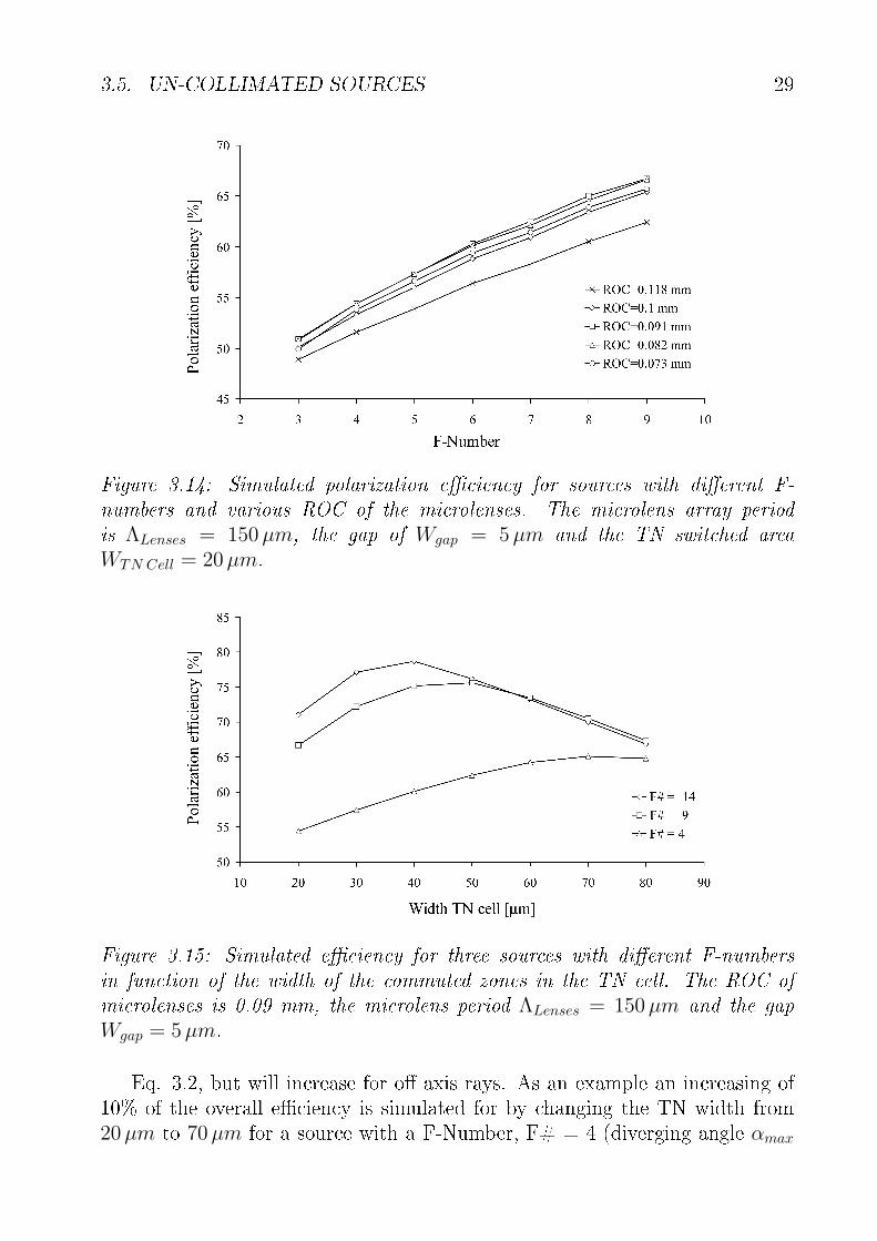
An error on m would lead to a new position of the object So, f being �xedby the microlens array. This consideration on the image quality of the moirémagni�er is shown in Fig. 4.5 A good contrast is obtained if the di�erence to
Figure 4.5: Schematic view of the image formation. On the left the case of a toolarge optical magni�cation where the local magni�ed images do not superposethem in a correct way, in the middle the case of a perfect image formation wherethe distance So2 is adapted to the factor of magni�cation m and the last caseshowing a too small optical magni�cation. Practically the system was limitedby its depth of focus, but this consideration could be important for microlenseshaving low numerical aperture.
the initial object position So does not exceed the depth of focus δz of lensesevaluated using the standard Rayleigh criterion:
δz =λ
NA2 , (4.6)
where λ is the wavelength of the illumination and NA the numerical apertureof the microlens given by
NA ≈ r
f. (4.7)
For a wavelength λ �xed to 500 nm and r to 72.5 µm we obtain for a microlensarray replicated in UV glue NOA 65 with refractive index of n=1.52 a focallength f = 222 µm. The numerical aperture stands from Eq. 4.7 to NA=0.31and the depth of focus (Eq. 4.6) δz = 5.5µm.
Because of the choice of microlenses, i.e. lenses of small diameter, for highmagni�cation, a large number of microlenses participates to the magni�ed im-age. Then the imaging properties of the system can be approximated to imagesof magni�ed points as seen in Fig. 4.6 . From di�raction theory the minimum

4.5. IMAGE QUALITY 41
Figure 4.6: Schematic view of the image formation for the case of a very highmagni�cation m, where the pitch of the microlens ΛL very close to the pitch ofthe object array ΛO. The sampling s of the object corresponds to the portionof the object which has to be magni�ed by the microlens to complete the moiréimage formation. If the sampling s is smaller than the resolving power of themicrolens no more details are added to the resulting magni�ed image and thesystem can be considered as a point imager.
distance between two points being solved by a lens is given by
ØAD ≈ 1.22 · λ
NA. (4.8)
Taking the same parameters as before we �nd ØAD = 2 µm. The sampling scorresponding to the part of the object which has to be magni�ed by a singlelens and is given by
s = ΛL − (ΛL · F ) =ΛL
m. (4.9)
For the system under consideration (m = 137.9) we �nd a sampling s = 1.08 µm.This value is inferior than the resolving power of the microlens. In that case, ahigh magni�cation is achieved but no more information is added to the magni�edimage (since m = 75 in our example). It also means that the formed image ateach microlens is an Airy function of diameter: m · ØAD. This interpretationexplains the strong magni�cation that can be achieved with only low alterationsin the quality of the magni�ed image because each microlenses does no morecarry out spectral information but only local intensity (image of black or whiteparts). Moreover, the higher the magni�cation, the larger is the number ofmicrolenses participating to the magni�ed image. Therefore, the local defectsare contained on small zones compare to the whole magni�ed image.

42 CHAPTER 4. MOIRÉ MAGNIFIER
A typical defect is about the precision of the pitch of the two arrays. FromEq. 4.1 one sees that a weak variation of the relative step of one of the arraysleads to a di�erent magni�cation m. By writing the derivative of Eq. 4.4 one�nds,
δF
δm=
1
m2 ·1
N. (4.10)
Taking the local di�erence and N=1, we get
∆m = m2 ·∆F . (4.11)
Considering that only neglectible changes on the image dimensions occur, thevariations on the �nal dimensions of the magni�ed image become,
∆D = ∆m · d . (4.12)
It follows from Eqs. 4.11 and 4.12 that a higher magni�cation factor m yields toa higher sensitivity of the ratio F between both pitches. Taking our last exampleand choosing a local error of 4F = ±0.001 we �nd 4m = ±19. This drives to4D = ±2.757 mm, which corresponds to 13,7 % of the �nal size D. This e�ecthas to be taken into consideration when designing a system to ensure the rightmagni�cation in presence of variations on positions and sizes that occur duringthe fabrication of the di�erent elements. It is also an important result whenusing microlens arrays made by soft embossing techniques where variation ofpitches are often present due to local variations on the hardness of the mold orin the applied pressure. This error on the factor of magni�cation m also leads toa new distance between the lenses and the object as discussed before. It formsat the place where the pitch is deformed, a local blurring e�ect. Because themagni�ed image results from magni�cation of local parts of the di�erent localimages, an overall averaging of all contributions is made. It explains why thesystem easily supports local defects that can occur during the printing of theobject array. With pictures of realized samples, the discussed key points on theimage quality can be evaluated. It has to be noticed that only cases of virtualimages allowing a high magni�cation have been tested. Focusing is then noteasy to achieve with a camera because the erect image is located behind themicrolens array. Firstly the increase of the sensitivity of local pitch deformationsare illustrated through the three pictures in Fig. 4.7 showing two magni�cationfactors for microlenses replicated in UV glue and accurate reference sample inquartz. The quality of the printing of the array is also a way to increase thegeneral quality of the magni�ed image.

4.5. IMAGE QUALITY 43
Figure 4.7: Pictures of local deformation of the pitch on the microlens arrayfor two magni�cations m ≈ 21 (left) and m ≈ 60 (middle). The strength of thedeformations on the visual e�ect depends on the magni�cation factor m. Theright picture has been taken with the master of the microlens array where nodeformations are present m ≈ 46
Figure 4.8: Pictures taken with a microscope of high resolution printing on plas-tic sheet on the left and patterned chromium on glass (photolithography mask)on the right. Several local defects are visible on the high resolution printingon plastic. Nevertheless by averaging of the di�erent contributions of the mi-crolenses high magni�cation with high image quality can be achieved as seen inFig. 4.10.
Figure 4.9: High resolution moiré magni�er, the left picture shows results forhigh resolution printing on plastic and at right a chromium pattern on glass (m≈ 35). The pitch of the microlens array is ΛL = 250 µm and the ROC = 0.315mm.

44 CHAPTER 4. MOIRÉ MAGNIFIER
This is illustrated in Fig. 4.8 with two pictures of printed numbers 28 on aplastic sheet and a high resolution patterned chromium on glass. The resultsusing this two objects are seen in Fig. 4.9. The case of a high magni�cationover the resolution limit of the microlens is shown in Fig. 4.10
Figure 4.10: Picture of a highly magni�ed image m ≈ 95 from high resolutionprinting on plastic. The width of the number in the object array is 106 µm. Ex-cept a slight distortion visible on the bottom left part of the number, the pictureshows that high image quality can be achieved even for high magni�cation.
4.5.2 Parallax and orientation
The system also shows a strong parallax [45] leading to a stereoscopic visionwhich is sometimes disturbing when the object and the microlens arrays arenot parallel. This 3D impression cannot be transmitted in pictures of realizedsystems. This impression can be decreased by employing microlenses with highnumerical aperture or by reducing the factor of magni�cation. From Fig. 4.11we can de�ne the di�erence of the position seen by the two eyes looking at thesame microlens
d4 = 2 · f · sin(arctan
( e
h
)), (4.13)
where e corresponds to the half distance between the eyes and set to 4 cm. Theparameter h is the distance between the observer and the plan of the microlensarray and set to 25 cm. Then for a displacement x of the observer looking atthe same microlens a scan over the distance d3 occurs. Again from Fig. 4.11 weobtain the following formula:
d3 = f ·[sin
(e + x
h
)− sin
(arctan
( e
h
))]. (4.14)
Using values de�ned above for the e and h parameters and values determinedpreviously in our example, we found for a displacement x = 4 cm, d3 = 0.067mm.

4.5. IMAGE QUALITY 45
Figure 4.11: Interpretation of the parallax e�ect which occurs for microlenseswith small numerical apertures. The distance e corresponds to half the distancebetween the eyes of an observer and is set to 4 cm. The observing distance h isset to 25 cm. The distances d1 and d4 correspond respectively to the parallax ofthe system and d2 and d3 to the scanning that occurs for a move over a distancex of the observer at two di�erent locations on the microlens array.
This corresponds almost to the radius of the microlens. This explains the needto write the whole object and not only the sampled part s shown previously inFig. 4.6 behind each microlens to avoid losses in the �eld of view when movingthe head or the sample. This could be reduce by using microlenses with highernumerical apertures as mentioned previously, but harder to realized with thesame optical quality (see introduction). Then encoding of several local imagescould be performed as well as a magni�cation of the objects which could containmore details but which should again be restricted to the scanned surface de�nedby the desired �eld of view.
This parallax leads to another disturbing behavior of the image which ap-pears to travel in the same direction than the movement of the observer whenmicrolens array and array of objects are parallel. This is no more the case fora rotation of the microlens array. The explanation is found by seeing Fig. 4.12and especially the left part of the �gure where a horizontal displacement of thesampling points (small circles) leads to a vertical displacement in the samplingof the object because of their local rotation. The same explanation is valid forstereoscopic vision, because the two images seen by the eyes are no the ones

46 CHAPTER 4. MOIRÉ MAGNIFIER
that should be seen to obtain a real 3D impression. By the fact that the dis-placement on the array of objects when moving the head does not depend onthe magni�cation factor m, Eq. 4.14, the speed ratio of this movement for twomagni�ed images m1 and m2 with a same microlens array can be expressed asthe ratio of their magni�cation factors v1
v2= m1
m2.
The moiré magni�er is an interesting way to magnify and demagnify a �xedimage simply by rotating one array to the other. This does not only drive to amagni�cation demagni�cation of the object but also to a rotation of the image.To simplify and follow the explanations above for high magni�cation moiré, thesystem can be seen as a sampling device. When rotating the microlens arraywith an angle θ with respect to the object array, the sampled points move todi�erent locations (small circles on Fig. 4.12) on the object array. The newcon�guration can be interpreted as a new moiré con�guration with pitch Λ
′
O
along the axis of the lens array with a local rotation of the objects from thecenter of each microlens (�xed points present in the real con�guration). Bygeometrical analysis in Fig. 4.13, the local rotation angle of the image ϕ isgiven by
ϕ =π
2− θ − arctan (β) , (4.15)
with the angle β given by
arctan (β) =ΛL � cos (θ)− ΛO
ΛL � sin (θ)(4.16)
and the magni�cation factor m by
m =1
1−(
ΛL−dΛL
) , (4.17)
with the distance d,
d =
√(ΛL � sin (θ))2 + (ΛL � cos (θ)− ΛO)2 . (4.18)

4.5. IMAGE QUALITY 47
Figure 4.12: Interpretation of the local rotation of the magni�ed images thatoccurs during a rotation of one of the components. The system is reduced to asampling system where the small circles correspond to the area of the object im-aged by each microlens. The new con�guration (after rotation of the microlensarray (left)) can be interpreted as a new moiré con�guration (right) with a pitchΛ
′
O along the axis of the lens array with a local rotation of the objects from thecenter of each microlens. The angle θ de�nes the rotation of the microlensarray and the angle ϕ, the local rotation of the objects.
Figure 4.13: Detail of Fig. 4.12 showing the various parameters allowing cal-culation of the local rotation of the magni�ed image.
The calculated and measured magni�cation m and the rotation angle of theimage are plotted in Fig. 4.14

48 CHAPTER 4. MOIRÉ MAGNIFIER
Figure 4.14: Graph of calculated and measured curves for the magni�cationfactor m and the local angle of rotation ϕ.
. Figure 4.15 shows the pictures of the occurring rotation of the magni�edimage. A good agreement is found between measurements and calculations. A
Figure 4.15: Pictures of the rotation of the magni�ed image (28) that occursfor a rotation angle θ of the microlens array. The pitch of the microlens arrayΛL is 250 µm .
similar interpretation of the image quality described previously in Fig. 4.6 forthe case of a pitch of the microlens array smaller than the pitch of the objectarray can be done because the object array is not rotated in reality and themagni�ed and rotated image is the reconstruction of local unrotated images.

4.6. ENCODING 49
The last parameter, that must be taken into account are the intrinsic lensaberrations which are mostly responsible for the general contrast of the magni-�ed image.
4.6 Encoding
Since one pattern can be strongly magni�ed m > 90 as shown previously in Fig.4.10 with help of good elements several patterns can be encoded on the area atdisposal. If the size of the �nal magni�ed image takes the whole display a slightmove of half the pitch of the object array for an example of 4 encoded imagesis enough to display another number. This would be the case in Fig. 4.16 if the�eld of view is restricted to the number 23 for instance. A horizontal move ofhalf the pitch of the object array would display the number 14. Nevertheless thishas to be restricted to a microlens array with high numerical aperture to reduceparallax e�ect and avoid unwished display of the surrounding encoded objects.Since moiré conditions i.e., moiré magni�cation occurs only for closed pitches(Eq. 4.1), after a rotation of only few degrees the magni�cation of the imagedecreases and the image is no more visible (Fig. 4.14 and 4.15). By additionseveral images can be encoded on the same array. Figure 4.17 illustrates picturesof a realized prototype showing the words �Best of IMT� for rotation of 20°, 40°and 60° of the object array. Because of non imaging but still present samplingof parts of the undesired images by the microlens array, the background seemsnoisy and reduces the overall contrast of the magni�ed image.
Figure 4.16: High resolution moiré magni�er of a chromium on glass mask (m≈ 35). The pitch of the microlens array is ΛL = 250 µm and the ROC = 0.315mm. If the �eld of view is restricted to the number 23 (middle), a horizontalmove of half the pitch of the object array set to ΛO = 247 µm on the left woulddisplay the number 14 (left).

50 CHAPTER 4. MOIRÉ MAGNIFIER
Figure 4.17: Pictures of magni�ed images of three objects encoded on the samearray, m ≈ 55.2. The pitch of the microlens array is ΛL = 250 µm. To displaythe information, the microlens array is rotated by 20° between each picture. Thedesign of the object array is shown on the right.
4.7 Conclusion
Based on equations developed in [38] a design method for moiré magni�er isgiven. The di�erent critical parameters on the image quality are discussed indetail and several illustrations of realized samples of highly integrated moirémagni�ers are shown. The encoding of several images is limited because of theparallax which allows the observer to see the images which should be hidden.Nevertheless after a rotation of few degrees, the image is no more visible (dueto the decrease of the magni�cation). This allows encoding of several images.Because of the symmetry present in the 2D periodical arrangement of the lensesseveral moiré condition are retrieved (every 60° for hexagonal arrays). Theangular range is then limited by the symmetry of the array. An idea wouldbe to destroy the symmetry by building a non periodical microlens array witha corresponding scaled down non periodical object array. Taking a reasonableangular range∼20° to display and remove the image, 18 images could be encodedon a complete rotation of 360°. Contrast problems would still be a problem asseen in Fig. 4.17. This idea could nevertheless be used in security systems whereonly one position and one dedicated microlens array could be used to read oneencoded image.

Chapter 5
Achromatic microlenses
5.1 Introduction
The refractive index of any transparent material is function of the wavelength.Therefore, a lens made in one single material shows di�erent positions of focusat each wavelength. The di�erence in position of these focal points is known asthe longitudinal primary chromatic aberration [46]. To correct this aberration,achromatic lenses are usually manufactured using two lenses of di�erent materialhaving di�erent Abbe numbers combined to form a doublet or even triplet [46].This method uses the di�erent dispersion curves of the materials to obtain, attwo well separated wavelengths, the same focal length with small variationsfor the other wavelengths in between. By their small dimensions microlensescan have low Fresnel number and then exhibit strong di�ractive e�ects on theposition and the shape of their focal point as it has been extensively studied inliterature (focal shift [47, 48, 49]). We show here that for such lenses a rangefor the radius of curvature (ROC) can be found where microlenses show anachromatic behavior. Firstly we focus our study on the position of the peakirradiance (Zp) for di�erent microlenses diameters as function of ROC. Thefocal length is increased by increasing the ROC. However at a certain valuefor ROC, the focal length cannot be further increased. The limit is �xed bythe position of the peak irradiance of the light di�racted by an aperture equalto the lens diameter. Secondly we study the position of the peak irradianceat di�erent wavelengths. We observe two phenomena in�uencing Zp. One isthe focal shift due to di�raction and the second is the chromatic aberrationdue to the material dispersion. Because these two phenomena have opposingin�uence on Zp, a choice for the ROC can be found where Zp is the same attwo wavelengths. This property could be used to design achromatic lenses inone single material.
51

52 CHAPTER 5. ACHROMATIC MICROLENSES
5.2 Basic considerations
The focal length of a plano-convex refractive lens is derived from the radius ofcurvature ROC and the refractive index n of the lens material .
fE =ROC
(n− 1). (5.1)
The refractive index is a function of the wavelength, whereas n (λ2) < n (λ1)for λ2 > λ1 .The longitudinal primary chromatic aberration, corresponds to achromatic shift of the focal length, fE (λ2) > fE (λ1) for λ2 > λ1, [46]. TheFresnel number FN of a lens with a lens diameter Ø = 2 · ρ is de�ned by
FN =ρ2
λfE. (5.2)
For large Fresnel numbers FN >> 1, geometric optics is well suitable to derivethe focal length of a microlens. For low Fresnel numbers, the focal length isshifted towards the lens due to the in�uence of the di�raction at the lens stop.A Gaussian beam decomposition algorithm [50] is used for the comprehensiveanalysis of the refractive and di�ractive properties of the microlenses.
5.3 Plano-convex refractive microlens
A plane wave with constant intensity pro�le illuminates a plano-convex refrac-tive microlens as shown in Fig. 5.1. An aperture blocks the light outside themicrolens. As an example, a microlens with diameter Ø=635 µm, ROC = 2.03
Figure 5.1: Model of a plano-convex microlens illuminated by a plane wave.
mm, made of fused silica with n (633 nm) = 1.456 has been chosen. Fromparaxial geometric optics, the focal length f is = 4.45 mm. The Fresnel numberof the lens is FN = 35.7. As shown in Fig. 5.2, di�raction analysis [50] predicts

5.3. PLANO-CONVEX REFRACTIVE MICROLENS 53
a position of the peak irradiance Zp at 4.36 mm. The di�erence between theposition of the peak irradiance Zp derived from di�raction theory and the focallength obtained from geometrical optics is de�ned as focal shift δ [51]:
δ = ZP − fE. (5.3)
In the example of a microlens with a Fresnel number FN = 35.7. A focalshift of δ = -0.09 mm, corresponding to 2% mismatch is observed. This showsa good agreement between geometrical optics and di�raction theory for mi-crolenses with large Fresnel numbers. Fig. 5.3 shows the intensity distribution
Figure 5.2: Intensity (a.u.) distribution behind a microlens of Ø = 635 µm ,ROC = 2.03 mm, illuminated by a plane wave at 633 nm. The lens stands inthe x,y plan while z corresponds to the propagating axis.
Figure 5.3: Intensity (a.u.) distribution behind a microlens of Ø = 635 µm andROC = 25.2 mm illuminated by a plane wave at 633 nm. The lens stands inthe x,y plan while z corresponds to the propagating axis.
of a microlens with a Fresnel number FN = 6.29. A focal shift of δ= -6.23mm, corresponding to 11% mismatch is observed. Fig. 5.4 shows the intensitydistribution of a microlens with a Fresnel number FN = 0.3. A focal shift ofδ = -416.86 mm, corresponding to 75% mismatch is observed. Fig. 5.5 shows

54 CHAPTER 5. ACHROMATIC MICROLENSES
Figure 5.4: Intensity (a.u.) distribution behind a microlens of Ø = 635 µm ,ROC = 252 mm, illuminated by a plane wave at 633 nm. The lens stands inthe x,y plan while z corresponds to the propagating axis.
the intensity distribution behind a pinhole with same diameter. A pinhole withno refractive power corresponds to a microlens with ROC = ∞. The observed
Figure 5.5: Intensity (a.u.) distribution behind an aperture of Ø = 635 µmilluminated by a plane wave at 633 nm. The lens stands in the x,y plan while zcorresponds to the propagating axis.
peak irradiance position Zp = 162.93 mm is the maximum obtainable focus spotposition for a microlens of Ø=635 µm diameter.
5.4 Refractive and di�ractive regime
These phenomena are now analyzed for di�erent microlens diameters illumi-nated by a plane wave at 633 nm. Fig. 5.6 shows Zp as a function of ROCfor di�erent microlens diameters. For low ROC (typically ROC < 1 mm forØ= 635µm microlens) the peak irradiance corresponds to the focal length ob-tained by Eq. 5.3. For increasing values of ROC, the peak irradiance convergesto a maximum value Zp max illustrated by vertical dash lines in Fig. 5.6. Thisvalue corresponds to the peak irradiance position obtained for a pinhole withno optical power, i.e. ROC =∞. To check the validity of the present approach,

5.4. REFRACTIVE AND DIFFRACTIVE REGIME 55
Figure 5.6: ROC [mm] versus position of peak irradiance for six diameters ofmicrolenses illuminated by a plane wave at 633nm.
the values of Zp max obtained by the Gaussian beam decomposition algorithmare now compared to the values derived from the Rayleigh-Sommerfeld integral.The scalar �eld U(r,z ) at the point P is given by [52],
U (r, z) =1
λi
ˆΣ
A0 (r0)exp (ikR)
Rcos (θ) dS, (5.4)
(4) where Σ is the surface limited by the aperture in z0 = 0. For a plane wavedi�racted at the circular aperture and propagating along the optical axis wehave A0 (r0) = A0and R =
√z2 + r2
0 with r0 = |r0| . Furthermore, for paraxialapproximation we assume that cos (θ) ≈ 1. Substituting these relations intoEq. 5.4 and introducing polar co-ordinates yields to
U (r = 0, z) =A0
iλ
ˆ 2π
ϕ=0
ˆ ρ0
r0=0
exp(ik√
z2 + r20
)√
z2 + r20
r0dr0dϕ, (5.5)
where ρ0 is the radius of the limiting aperture at z0 = 0. Integrating Eq. 5.5and approximating the square root in the phase by the �rst two terms of theTaylor series yields to
I (r = 0, z) =
(2A0 sin
(kρ2
0
4z
))2
, (5.6)
describing the intensity distribution along the optical axis. The maximum in-tensity is found by setting the derivative of Eq. 5.6 equal to zero,
dI (r = 0, z)
dz= −A0ρ
20 sin
(kρ2
0
2z
)1
z2 = 0, (5.7)

56 CHAPTER 5. ACHROMATIC MICROLENSES
which implies that kρ20
2z = π. The position of peak irradiance of an apertureobtained by the Rayleigh-Sommerfeld integral is
Zp =ρ2
0
λ. (5.8)
The peak irradiance positions Zp of pinholes with diameters obtained fromRayleigh-Sommerfeld, are shown as dashed lines in Fig. 5.6. The Gaussianbeam decomposition algorithm corresponds well to the Rayleigh-Sommerfeldapproach.
5.5 Achromaticity
As described in the previous section microlenses exhibit a refractive regimefollowing the linear law predicted by classical optics and a di�ractive regimewhere the peak irradiance converges to a maximum value. As shown in Fig. 5.7,both e�ects are related to the wavelength . In the di�ractive regime, the peakirradiance Zp is strongly dominated by the focal shift introduced by di�ractionat the aperture and converges to a maximum value proportional to the inverseof the wavelength, see Eq. 5.8. In the refractive domain, the peak irradiance
Figure 5.7: ROC versus position of peak irradiance Zp for microlenses of Ø =635 µm illuminated by a plane wave at two di�erent wavelengths.
Zp respectively the focal length is inversely proportional to the refractive indexn (λ). The dispersion curve of a material approximated by the Cauchy Formula[46],
n = C0 +C1
λ2 +C2
λ4 , (5.9)

5.5. ACHROMATICITY 57
leads to a decreasing refractive index for increasing wavelengths. In the refrac-tive regime, the position of the peak irradiance (Zp) is equal to the focal lengthgiven by Eq. 5.1. Fig. 5.7 shows the peak irradiance position function of ROCat di�erent wavelengths . The longitudinal primary chromatic aberration is thedi�erence of the peak irradiance positions for di�erent wavelengths, expressedalong the optical axis [46]. In classical optics, an achromatic lens is designed tohave the same focal length for two well-separated wavelengths, i.e. δλ = 0. In
Figure 5.8: ROC versus position of peak irradiance Zp for a microlens ofØ = 635 µm , illuminated by a plane wave at �ve di�erent wavelengths.The crossings between two curves corresponding to achromatic microlenses areshown with circles.
Fig. 5.8, we observe that for each pair of wavelengths the di�erent graphs arecrossing in one point. From the UV to the IR a value for ROC is found wherethe longitudinal chromatic aberrations are zero for two di�erent wavelengths.For our example of a microlens with diameter , the peak radiance at 248 nmand 1550 nm are equal Zp(248 nm) = Zp(1550 nm) = 21.7mm for ROC = 10.8mm, Fig. 5.7. Similar to classical achromats an achromatic microlens doesnot show an achromatic behavior over the full wavelength range in-between λ1and λ2. The variation of achromats inside the range between these two designwavelengths is usually called secondary color aberration [46]. In classical opticsthe design of achromatic lenses can be made for any desired Zp. In the presentcase, chromatic aberrations are directly related to the diameter and the ROCas these are the only free parameters. For a �xed diameter of microlenses, theappearance of di�raction e�ect, used for chromatic aberration corrections, de-pends on the ROC as seen in Fig. 5.6. This implies for each design one positionof the peak irradiance. To investigate an achromatic design for a microlens we�x a diameter. Then to allow comparisons a wavelength of reference �xing Zp isrequired. It is now possible to plot the relative variations of this Zp against the

58 CHAPTER 5. ACHROMATIC MICROLENSES
Figure 5.9: Relative variations on Zp calibrated at 550 nm for �ve microlensesof Ø = 635 µm for �ve ROC, illuminated by a plane wave at di�erent wave-lengths.
wavelength of a de�ned spectrum. For example, Fig. 5.9 shows the variations asfunction of the wavelength of Zp expressed in percent of the Zp calibrated at 550nm. This is done for di�erent ROC while for each lens Zp at 550 nm is taken tonormalize. The e�ect of di�raction appears when ROC increases. Correction ofchromatic aberrations is possible for curve shapes that show a maximum in thedesired wavelengths region. It would seem that small curvature (large radius ofcurvature) of the plot at the maximum would lead to small chromatic aberrationin Fig. 5.9. Curves for ROC = 20.2 mm (FN = 4), 12.6 mm (FN = 6) and 10.1mm (FN = 8) in Fig. 5.9 show a maximum. Note, that the FN are calculatedat 550 nm. The maximum shifts to shorter wavelengths for increasing ROC.The microlens with a ROC �xed to 10.1 mm shows less than 1 0�00 variationon Zp from 530 nm to 690 nm. For comparison the microlens with ROC=2 mmis not in�uenced by di�raction e�ects and shows more than 8 0�00 variationson Zp inside the same range. For this wavelengths range we see from Fig. 5.9that the lens with ROC=10.1 mm represents an optimum design for a lens ofdiameter. The position of the peak irradiance is 21.5 mm.
5.6 Conclusion
It is well known from geometric optics that increasing the focal length of anylens leads to increase its ROC. This is the case for lenses having large values ofFN >>1. By comparison, microlenses by their small diameters impose smallvalue for ROC and then short focal length. When designing a microlens withlarge ROC, di�raction at the lens aperture may severely dominate the optical

5.6. CONCLUSION 59
properties of the microlens and limit the range of the e�ective focal length. Theupper limit of the focal length is determined by the di�raction pattern of apinhole with equal diameter. Moreover refraction and di�raction have opposingin�uence on the position of the peak irradiance when changing the wavelengthof illumination. Di�raction at the lens stop can be used to correct chromaticaberration introduced from the dispersion of the lens material. For microlenseswith low Fresnel numbers (FN<10), achromatic designs can be realized in onesingle material.

60 CHAPTER 5. ACHROMATIC MICROLENSES

Chapter 6
Di�users for optimizedilluminations
6.1 Introduction
Pro�les of laser beam are not homogeneous (i.e. uniform intensity distribu-tion). As commonly described in literature they result of the combination ofone or several transversal modes such as the superposition of Hermite-Gaussiantypes intensity distribution [53]. Nowadays micromachining manufacture re-quires highly homogenous beam pro�les. Microlenses can successfully be ap-
Figure 6.1: Typical homogenized microscope illumination described in the be-
ginning of the 21th century. The picture shows two microlens arrays LA1 andLA2 and a Fourier lens nowadays found in Fly's eye condenser for laser beamhomogenizing. The object is placed in the homogenized plane of illuminationand an additional �eld lens redirect the intensity to the microscope objectiveand the observer.
plied to homogenize light sources. Especially in the case of incoherent light
61

62 CHAPTER 6. DIFFUSERS FOR OPTIMIZED ILLUMINATIONS
sources such as LEDs where arrays of microlenses can o�er a space invariant so-lution with various aperture shapes. Nevertheless in the case of highly coherentsources they produce very contrasted di�raction pattern. One solution consistto modify spatially and temporally (at the time scale of the application) thiscoherence by introducing a rotating di�user inside the optical path. To ensurea high energy throughput these di�users should have a very narrow angular dis-persion. In this chapter we present such micro-optical di�users that have beendeveloped to ful�ll this condition.
The use of microlenses to homogenize light sources is not new. Since morethan 100 years Fly's Eye Condensers are used to homogenize light emitting froma light bulb in order to e�ciently illuminate extended object �elds in the objectplane of the microscope. This is shown in Fig. 6.1 by a drawing of a typicalhomogenized microscope illumination where two microlens arrays and a Fourierlens are found [54]. Similar homogenizers with microlens arrays are used todayfor homogenizing of a wide variety of modern light emitters from line-narrowedExcimer Lasers, laser diodes to high power LEDs. It is hence important tostudy their characteristics with coherent illumination.
6.2 Microlens beam homogenizers
Two main types of microlens Beam Homogenizers have to be distinguished: theNon-Imaging illustrated in Fig. 6.2 and the Imaging microlens Homogenizerillustrated in Fig. 6.3. Both types use either cross cylindrical or square mi-crolens arrays to divide the incident beam into beamlets. These beamlets arethen passed through a lens FL to be overlapped at the homogenization planeFP located in the back focal plane of the lens FL. The lens FL causes parallelbundles of rays to converge in the homogenization plane FP and is thereforecalled a Fourier lens. It carries out a two-dimensional Fourier transformation.The intensity pattern in the homogenization plane is related to the spatial fre-quency spectra generated by the microlens array(s) entering the Fourier lens.The decision whether to use a Non-Imaging or Imaging Homogenizer dependsvery much on the light source and the desired application. Following Dickey's[55] suggestion the Fresnel number FN should be used as a general guideline.The Fresnel number FN of a microlens beam homogenizer is de�ned as
FN ≈ PLA ·DFT
4 · λ · fFL, (6.1)
whereas PLA is the pitch of the microlens array, DFT is the dimension of the�at-top intensity pro�le in the homogenization plane FP, fFL is the focal lengthof the Fourier lens FL and λ is the wavelength.

6.3. DESIGN CONSIDERATIONS 63
Figure 6.2: Illustration of the non-imaging beam homogenizer. In this con�g-uration a single microlens array LA1 divides the input beam of diameter ØIN
into several beamlets recombined in the homogenization plane FP by a lens FL.The width DFT of the �at top pro�le intensity will depend on the pitch of themicrolens array PLA, the focal length of the microlenses fLA and the focal lengthof the lens FL fFL. The distance s is a free parameter.
Non-imaging homogenizers often show dominant di�raction e�ects due toFresnel di�raction at the microlens array. The Fresnel di�raction is related tothe Fresnel number FN. Higher Fresnel numbers give sharper edges and smallervariations of the �at-top pro�le. In practice, non-imaging homogenizers shouldhave Fresnel numbers FN > 10, better FN > 100, to obtain a good uniformity.Non-imaging homogenizers are well suited for large area illumination, as the�at-top dimension DFT is proportional to the Fresnel number FN. For smallFresnel numbers FN < 10 or high uniformity �at-top requirements, the ImagingHomogenizer is the preferred solution.
6.3 Design considerations
The size of the obtained �at top obtained with a non-imaging beam homogenizeris given by [55]
DFTNI=
PLA · fFL
fLA, (6.2)
proportional to the pitch PLA of the microlens array and the focal length ofthe Fourier lens fFL , but inversely proportional to the focal length of themicrolens array fLA. The imaging homogenizer uses the �rst microlens arrayLA1 to divide the incident beam into multiple beamlets. The second microlens

64 CHAPTER 6. DIFFUSERS FOR OPTIMIZED ILLUMINATIONS
Figure 6.3: Illustration of the imaging beam homogenizer. In this con�gurationa second microlens array is added to the non-imaging con�guration (Fig. 6.2)and creates with the help of the lens FL an array of objectives that superimposesimages of the beamlets in the �rst array LA1onto the homogenization plane FP.The size of the �at top can be adjusted by modifying the distance between thetwo arrays a12. The distance s is a free parameter.
array LA2, in combination with the lens FL, acts as an array of objective lensesthat superimposes the images of each of the beamlets in the �rst array onto thehomogenization plane FP. The size of the �at-top now depends on the separationa12 of the two microlens arrays where fLA1 < a12 < fLA1 + fLA2
DFTI= PLA1
fFL
fLA1 · fLA2[(fLA1 + fLA2)− a12] . (6.3)
This allows variations of the �at-top dimensions by shifting the position of thesecond microlens array. However, care must be taken not to damage the secondmicrolens array by focusing high-power laser beams into the lens material orto generate crosstalk by over�lling the lens apertures of the second microlensarray. The divergence (half angle) after the homogenized plane is given by
tan (θ) <1
2
(ØIN + DFTI− 2PLA)
fFL, (6.4)
if DFTI> PLA and by the approximation
tan (θ) ≈ 1
2
(ØIN + DFTI)
fFL, (6.5)
when DFTI< PLA . Usually, imaging homogenizers consist of two similar
microlens arrays with identical lens pitches.

6.4. BEAM REQUIREMENTS 65
Figure 6.4: Superimposition of magni�ed images of channels apertures. Theshape of the output intensity in FP corresponds to the shape of the microlensapertures. The width DFT of the �at top pro�le intensity will depend on thepitch of the microlens array PLA.
Square-type lens apertures generate a square �at top or top hat intensity dis-tribution in the Fourier plane. Circular or hexagonal microlenses will generatea circular respectively hexagonal �at-top Fig. 6.4.
6.4 Beam requirements
For standard laser beams, the overlay of some 3 by 3 microlenses is usually suf-�cient to achieve a good �at top uniformity. Consequently, the beam diameter
IN constrains the maximum microlens pitch PLA1≤ IN
3 . Typical homogenizersuse 5 x 5 to 7 x 7 microlenses. For space invariant features a larger numberof microlenses is required. For imaging homogenizers the diameter of the indi-vidual beamlets at the second microlens array LA2 must be smaller than thelens pitch to avoid an over�lling of the lens aperture and the loss of light. Fora collimated laser beam, the separation of the two microlens arrays is givenby fLA1 < a12 < fLA1 + fLA2. For laser beams with a signi�cant beam diver-gence the diameter of the beamlets at the second microlens array scales with thebeam divergence. The maximum allowed beam divergence for a given microlenshomogenizer is
tan (θ) ≤ PLA/ (2 · fLA1) , (6.6)
for a = fLA1. For high-power laser beams, a focusing into the material ofthe second microlens array or the spherical lens must be avoided. As it willbe discussed later on, an additional di�user might be used to properly �ll theaperture of the second microlens array.

66 CHAPTER 6. DIFFUSERS FOR OPTIMIZED ILLUMINATIONS
6.5 Di�raction e�ects
For small microlens apertures with a long focal length, i.e. for microlens beamhomogenizers with a Fresnel Number FN < 10, the �at top pro�le might bedistorted by di�raction at the lens apertures. This e�ect is shown in Fig. 6.5where two simulations of the intensity distribution in FP for one illuminatedmicrolens channel having di�erent Fresnel numbers. Thus for small laser beamsa beam expander is usually the better solution than using microlens arrays witha very small lens pitch. Microlens arrays are periodic structures, where the pitch
Figure 6.5: Simulations of one microlens channel intensity distribution in theFourier Plan for two beam homogenizers with microlenses of di�erent FresnelNumbers: A) PLA= 1 mm, FN = 272; B) PLA= 0.3 mm, FN = 37 (FL =80 mm). In the bottom simulation, the di�raction e�ect is enhanced and amodulation of the �at top intensity appears.
PLA corresponds to a grating period. Each microlens array will behave like adi�raction grating and will generate di�raction orders with a period ΛFP
ΛFP =fFL · λPLA
, (6.7)
in the homogenization plane FP. fFL corresponds to the focal length of theFourier lens and λ to the wavelength. This becomes a real drawback for coherentillumination. This behavior is illustrated in Fig. 6.6 for a beam homogenizerused with coherent light. The �at top intensity pattern is distorted by an arrayof spots with a minimum diameter δxmin given by di�raction at the Fourier lens:
δxmin = 1.22 · 2 · fFL · λØBeam
, (6.8)

6.6. COHERENT ILLUMINATION 67
Figure 6.6: Typical di�raction pattern observed in FP for coherent light source(Laser diode Linos DS 670). The homogenization is clearly destroyed by anarray of local intensity spots.
whereas ØBeam is the diameter of beam.
6.6 Coherent illumination
To fully understand di�ractive and interference e�ects happening in microlensbeam homogenizers for coherent illumination, it is convenient to analyze thesystem using Fourier optics theory. It follows that the intensity pattern of thehomogenized beam by a non-imaging beam homogenizer is modulated by thesuperposition of two e�ects [56]. First, the beam is modulated by di�raction atthe microlenses edges. Second, an amplitude modulation appears due to inter-ference caused by the overlapping of beams from individual microlenses. Thecomplex 1D transmittance function of the lens array is given by the followingexpression [57]
TLA =
[((e−j
k(y′2)2�fLA
)· rect
(y′
PLA/2
))⊗ comb
(y′
PLA
)](6.9)
·circ(
y′
N0PLA/2
),
with pLA is the pitch of the microlens array, fLA the focal length of the mi-crolenses, N0 the number of microlenses and the wavenumber k = 2·π
λ de�nedat the wavelength λ. The �rst term corresponds to the phase factor introducedby the microlens, the second to the square lens aperture and the comb functionto a train of Dirac functions spaced by PLA representing the array. The last

68 CHAPTER 6. DIFFUSERS FOR OPTIMIZED ILLUMINATIONS
circ function to the �nite circular aperture of the input beam limiting . Theoutput �eld in the target plane is given by the Fourier transform performed bythe Fourier lens of the input �eld UIN transmitted through the microlens arrayof transmittance TLA
UFP = FT FL {UIN · TLA} , (6.10)
which can be developed in the form
UFP ∝(UIN ⊗ TLA
), (6.11)
where UIN and TLA represent the Fourier transform by the Fourier lens FTFL ofthe input �eld and the microlens array complex transmittance. From Eq. 6.10,TLA takes the form
TLA =
[(FTFL
(e−j
k(y′2)2�fLA
)⊗ sinc
(PLA
2
1
λ · fFL· y))
· comb
(PLA
λ · fFL· y)](6.12)
⊗Airy
(N0PLA
2
1
λ · fFL· y)
.
If we look in detail Eq. 6.12, the two �rst terms correspond to the Fresneldi�raction from the microlenses and the third term to interferences. The forthterm correspond to di�raction e�ects from the beam size. Neglecting the �eldsize we see from Eq. 6.11 that the �eld is the result of the convolution between
the angular spectrum of the input �eld and a modulated comb function(TLA
)with period λ · fFL/PLA. The shape of each intensity spot is a function ofthe angular spectrum of the input �eld. So when modifying the plane wavespectrum of the source with a di�user, modi�cations on the intensity in theFourier plan FP will occur.
In the case of the imaging system with two microlens arrays, we follow theideas given in [58] and used the propagation of the plane wave spectrum of theinput �eld. The method is well suited because it allows a complete separation ofthe e�ects of the array and of single microlens channels. To fully understand thisapproach it is convenient to start again with the case of the non-imaging beamhomogenizer with a single microlens array. Firstly using an monochromaticinput �eld of the form
Uin = a (α) · exp (iky′ sin (α) + φ (α)) , (6.13)

6.6. COHERENT ILLUMINATION 69
where α is the angle of propagation of the plane wave and the amplitude a (α) =1 and φ (α) = 0 is the phase shift. The resulting �eld in the focal plane ofthe Fourier lens FP for a non imaging beam homogenizer can be expressed,neglecting the �nite aperture of the Fourier lens FL, by
UFP (α) = FTFL
{|Uin (α)| · exp (iky′ sin (α)) ·
N0∑l=−N0
δ (y′ − lPLA) · ULens (y′)
},
(6.14)
where∑N0
l=−N0δ (y′ − lPLA) · ULens (y′) represents the transmission function of
the microlens array with ULens = eik2fl
y′2· rect
(y′
PLA
). This expression can be
developed using linearity and shifting properties of Fourier analysis in the form
UFP (α; y) =
[δ (y − fFL · sin (α))⊗ FTFL
{N0∑
l=−N0
δ (y′ − lPLA)
}](6.15)
· [δ (y − fFL · sin (α))⊗ FTFL {|Uin (α)| · ULens (y′)}] .
It can be rewritten into the simpli�ed form
UFP (α; y) = SN0(α; y) · UFPChanel
, (6.16)
where
SN0(α; y) =
∣∣∣∣sin (N0πPLA (y − fFL sin (α)) /λfFL)
sin (πPLA (y − fFL sin (α)) /λfFL)
∣∣∣∣ ,corresponds to the analytical expression of the Fourier transform of the array
transmittance Uarray = comb(
1PLA
)· rect
(1
N0PLA
)shifted by fFL sin (α) giving
the di�raction e�ects of the array containing N0 microlenses with peaks sepa-rated by ΛFP given by Eq.6.7 and position depending on the plane wave angleα as illustrated schematically in Fig. 6.7.

70 CHAPTER 6. DIFFUSERS FOR OPTIMIZED ILLUMINATIONS
Figure 6.7: Schematic illustration of the interpretation of the plane wave spec-trum applied to beam homogenizer. The beam homogenizer can be seen in-dependently of the type (imaging or non-imaging) as an array of transmissionchannels. The intensity distribution will be a function of the array transmissionfunction SN0
responsible of the peaks intensity multiplied by the transmissionfunction of a channel UFPchannel
.
The second term UFPChanelcorresponds to the propagation onto FP of the
input wave through one microlens channel. A general broadening of the �at topcan't be avoid because of the position which depend on α for both functions SN0
and UFPChanel. The overall expression of the transmitted �eld through an imaging
beam homogenizer with two microlens arrays can be similarly described by thepropagation of the input wave in one channel onto FP multiplied by the arrayfunction SN0
. The channel can be considered with one or two microlenses asillustrated in Fig. 6.8. By applying the approximation to the distance betweenthe arrays a12 = fLA and propagating the �eld from LA1 to LA2 using theFresnel approximation of the Fresnel-Kirchho� di�raction Integral [58] one gets
UFP (α; y) ∝ SN0(α; y) · [sinc
(PLA
λ · fFL
)⊗ (6.17)(
|UIN (α)| exp (ikfL/fFLy sin (α)) rect
((fL
fFL
)(y
PLA
)))],

6.6. COHERENT ILLUMINATION 71
Figure 6.8: Schematic illustration of the di�erent parameters involved in theplane wave spectrum approach of the Non-Imaging (A) and Imaging (B) beamhomogenizer. UIN (α)corresponds to one plane wave component of the input�eld. LA1 and LA2 are microlens arrays. FL is the Fourier lens with a focallength fFL. PLA is the pitch of the microlens array and N0 is the number ofretained microlenses. To evaluate the transmission of a channel in the caseof the imaging beam homogenizer, the �eld at the entrance of one microlens ispropagated over the focal length of the microlenses fLA.
where the term in the brackets after the array function SN0corresponds to
the channel transmission function UFPChanelof the imaging con�guration. The
resulting intensity for a monochromatic source λ is the modulus of the coherentsum of the di�erent plane waves contributions
IFP ∝∣∣∣∣ˆ αmax
αmin
UFP (α) dα
∣∣∣∣2 . (6.18)
Because of the term SN0present in both cases of non-imaging and imaging beam

72 CHAPTER 6. DIFFUSERS FOR OPTIMIZED ILLUMINATIONS
homogenizers and depending on α, the modi�cation of the angular spectrum ofthe source is a way to reduce the localization of theses spots and smooth thegeneral di�raction pattern. The imaging con�guration is also less sensitive tobroadening e�ects of the �at top pro�le since its UFPChanel
is not linked to α. Forcoherent cw-lasers, the spatial modulation of the observed pattern can locallyreach more than 100%. A rotating di�user plate is the appropriated mean tohomogenize the intensity of the �at top pro�le. Placing the di�user at thefocus of the beam, e.g., by using a beam expander in front of the homogenizer,changes the plane wave spectrum of the illumination by creating a new extendedlight source, whereas the size of the source is equal to the spot diameter on therotating di�user. Unfortunately rotating di�users do not work for pulsed laserslike Nd:YAG with picosecond laser pulses. Di�erent measures, such as stair casebeam splitters [59] are applied or chirped microlens arrays [60].
6.7 Di�users
Conventionally di�users are obtained by mechanical methods, such as sand-blasting, which increase statistically the surface roughness of a glass plate.
Figure 6.9: SEM pictures of a ground glass di�user (1), E di�user (2), HTdi�user (3).
These cheap di�users have the main drawback of di�using light in a verybroad angular spectrum because of their sharp and �ne details producing localdi�raction of the input light. This behavior implies often losses of light when

6.7. DIFFUSERS 73
employed in an optical setup. To �ght this drawback we have developed twoother types of di�users, respectively called SMO E and SMO HT followed bythe value of their diverging angle (e.g. SMO E 1.3°). SMO stands for Süssmicro-optics. For con�dential reasons no details about their fabrication arementionned. Both di�users obtained have smoother di�using surfaces as shownin Fig. 6.9. The HT type di�user is composed of several coincident concave
Figure 6.10: Scheme of the goniometer setup used to measure the radiationproperties of the di�users. The di�user is static and illuminated by a HeNelaser and the light is collected by the scan of a photodiode over the angle θ.
Figure 6.11: Measured angular distribution curves for several di�user typeshowing the di�erent cut-o� angles and the strong zero order transmission ofthe ground glass di�user.
areas reducing substantially the thin and sharp edges present in the �rst pro�le.Consequently the Full Width at Half Maximum (FWHM) angular dispersionof these di�users is reduced. The di�using properties are analyzed using a

74 CHAPTER 6. DIFFUSERS FOR OPTIMIZED ILLUMINATIONS
conventional goniometer setup as shown in Fig. 6.10. The di�user is lightenedwith a HeNe laser and the output is collected by mean of a photodiode. Resultson the angular distribution are shown in Fig. 6.11.
Figure 6.12: Measured angular distribution curves for di�users E and HT withdi�erent depths of microstructures.
Figure 6.13: Surface pro�le of SMO HT 0.2° di�user performed with a MachZehnder interferometer. The average depth of the microstructures lies around1.5 µm and the width is about 60 µm.
An averaging of the di�user properties is performed because of the largeilluminated area Øbeam ∼ 2mm compared to the size of the microstructures

6.8. BEAM HOMOGENIZER WITH DIFFUSER 75
having usually several microns. All the curves have been normalized. Startingwith one surface pro�le, di�users with various angular dispersion propertieshave been realized by adjusting the depth of microstructures from few hundrednanometers to several microns. Measurements of such di�users with variousmicrostructure depths are shown in Fig. 6.12. The typical surface of a SMO HT0.2° di�user is shown in detail in Fig. 6.13 where the 3D pro�le is analyzed usinga Mach Zehnder interferometer. It exhibits typical microstructures with concaveshapes. For example the microstructures selected in Fig. 6.13 have diametersof about Ø = 60 µm with depths of 1.5 µm corresponding to a focal length fl ∼−600 µm. The possibility to modify the depth of the microstructures allowsfabrication of adapted di�users to a speci�c design of a beam homogenizer.
6.8 Beam Homogenizer with di�user
To ensure �exibility the di�user is placed between the two lenses of the beamexpander as shown in Fig. 6.14. This allows a tuning of the homogeneity bychanging the position e of the di�user. The illuminated area of the di�userwill then vary with its position, while the average size of the microstructuresremains the same.
Figure 6.14: Scheme of beam homogenizer with telescope and di�user. The dif-fuser is placed between the two lenses of the telescope spaced by d1. By changingthe position e of the di�user modi�cations on the spatial intensity distributionin FP can be achieved. The position and the angular distribution of the di�userhave to be adapted to avoid crosstalks between microlenses on the second arrayLA2 (dashed lines).
It implies that when looking at the system over a certain period of time,for instance the integration time of the CCD camera used to record the �at topintensity, the di�user can be seen as a new incoherent source of diameter ØSD

76 CHAPTER 6. DIFFUSERS FOR OPTIMIZED ILLUMINATIONS
ØSD = (e− d1) � tan (arcsin (NA)) . (6.19)
The distance e corresponds to space left between the two lenses of the telescopeand d1 to the position of the di�user. NA is the numerical aperture of thetelescope lenses. The radiance of the source will be modi�ed by the di�usingproperties of the di�user as illustrated in Fig. 6.15. This interpretation has beencon�rmed in experiments when placing the di�user directly at the focal point ofthe telescope and by displacing it closer to the last lens. One sees in Fig. 6.16the increasing diameter of the spot of the di�raction pattern for two positionsof the di�user. It is easy to understand that the overall homogeneity that canbe obtained by this way cannot be perfect since the square arrangement of themicrolenses exclude a complete �lling of the �at top area with a circular widespreading of the local spots (due to the rotation of the di�user). The variationsof homogeneity H was calculated as the root mean square (RMS) value of thespatial intensity deviation from the mean intensity on the �at top area using
Figure 6.15: Interpretation of the in�uence of the di�user as a �new source� ofdiameter ØDS. The diameter and the radiance of the �new source� is spatiallymodi�ed by changing the position e of the di�user inside the telescope.
H [%] =σ
〈I (x, y)〉, (6.20)
where 〈I (x, y)〉is the spatial average value on the whole �at top area and σ isthe RMS value of the intensity variation on the same surface and is de�ned by
σ =
√⟨I (x, y)2 − 〈I (x, y)〉2
⟩. (6.21)
Commercial de�nition of the homogeneity follows ISO 13654 norm. While aspatial variation of homogeneity H of more than 100 % is observed for the rawintensity pattern in Fig. 6.17, the same value drops down to H=16 % using

6.8. BEAM HOMOGENIZER WITH DIFFUSER 77
a SMO HT 0.2° (HWHM) di�user. Compared to a conventional ground glassdi�user the variation of homogeneity H is more than two times inferior for acollected power that is 2.8 times superior.
Figure 6.16: Experimental observation of the spatial intensity distribution inFP for two di�erent positions of the rotating di�user. A circular enlargementof the spots intensity is observed and a better homogeneity is achieved.
Figure 6.17: Intensity measurements in FP for a beam homogenizer with mi-crolens arrays of 300 microns pitch and FN=37 at 670 nm. (1) Output intensitywithout di�user. The spatial variation of the homogeneity H reaches more than100%. (2) The addition of a rotating HT 0,2° di�user reduced this variation Hto 16 %, (3) The same experiment with a rotating ground glass di�user (com-mercial product). The value H is around 33 % for 2.8 less collected power.

78 CHAPTER 6. DIFFUSERS FOR OPTIMIZED ILLUMINATIONS
6.9 Advanced considerations on homogeneity
Placing a rotating di�user in the telescope is not the only technique to increasethe homogeneity. The defocus of the telescope is also another way to improvethe homogeneity by changing the divergence of the light source. Defocus of thetarget plan compared to the Fourier lens is also a third possibility as we cansee Fig. 6.18. It has to be noticed that microlens arrays are periodical elementsand when illuminated with coherent �elds they produce periodic patterns in thefar �eld.
Figure 6.18: Simulation of the intensity distribution around FP for a beamhomogenizer with microlens arrays of 300 microns pitch and FN=37 illuminatedby a plane wave with Gaussian intensity distribution at 670 nm. The presenceof spots are spatially localized. A defocus of the homogenization plan FP canhelp to increase the homogeneity.
This is de�nitely true for planes at de�ned distances known as Talbot planes[61, 62]. This Talbot planes are easily seen in Fig. 6.18. If the target plan isout of focus for example from the Fourier lens, the system is no more focusedon a plan of periodical pattern and the overall homogeneity is increased. Bycombining the di�erent ways of increasing the homogeneity, signi�cant resultshave be recorded. As an example 5 % of variation of homogeneity H has beenobtained with SUSS SMO HT 0.2° as shown in Fig. 6.19 .

6.10. CONCLUSIONS 79
Figure 6.19: Picture of a �at top intensity distribution with only 5 % of vari-ation of homogeneity H. This result has been obtained for a beam homogenizerwith microlens arrays of 300 microns pitch and Fresnel Number FN = 37 illu-minated at 670 nm through a rotating SMO HT 0.2° di�user. The focal lengthof the Fourier lens FL = 80 mm.
6.10 Conclusions
Two types of di�users dedicated to beam shaping applications with various dif-fusing properties have been realized and will be commercially available. It hasbeen demonstrated that employed in conventional Fly'eye condenser they allowvery high reduction of the overall contrasted pattern of coherent illumination.Using a laser diode at 670 nm and square microlens arrays we reduce the vari-ations of homogeneity by a factor 2 compared to a conventional ground glassdi�user. Only 5 % of variations on the homogeneity has been measured. More-over this type of di�users with narrow angular dispersion allows high energythroughput. The measured collected power was almost 3 times superior com-pared to a conventional ground glass di�user. The possibility to adapt the depthof the microstructures (i.e. their di�using properties) ensure a high �exibilityfor various beam shaping applications.

80 CHAPTER 6. DIFFUSERS FOR OPTIMIZED ILLUMINATIONS

Chapter 7
Concave microlenses
7.1 Introduction
In this chapter we described a new method allowing the creation of concavemicrolens arrays. While most of the fabrication methods to generate concavemicrolenses in photoresist are based on control of the exposure threshold ordistribution [63, 64], we developed a two step photolithography process. Wewere able to fabricate concave microlens arrays with lens diameters between30 to 230 µm and di�raction limited properties. For the development of thefabrication process, the simplicity of the method was a key point to respect. Wetried to avoid additional etching or lift o� steps.
Based on this fabrication principle, we fabricated di�users by generatingpatterns of random locations and sizes of concave resist structures.
7.2 Basic principle
The fabrication principle consists in a two step process shown in Fig. 7.1. Aphotolithography step is done on a photoresist (PR) layer to create cylindricalholes. A melting step is performed on the obtained structures to harden themand allow continuous edge shapes formation. The melted structures are next�lled by a second spinning step of resist. After a bake to remove the solvents,concave shapes are generated. Because of the complex geometry of the meltedholes, several trials where performed to �nd the appropriated spin speeds andresist concentrations. We found that because of the non planar surface presentduring the second spinning step, the spin speed has to be slowed down to allowhomogenous deposition of the PR. The spin speed is then no longer linked tothe �nal thickness of the PR layer but rather to the quantity of PR �lling theholes.
81

82 CHAPTER 7. CONCAVE MICROLENSES
Figure 7.1: Process �ow. The �rst step shows a crossed section view of cylin-drical holes resulting from a conventional photolithography process (spinning ofphotoresist AZ4562, UV exposure through a mask with holes and development).During the second step the holes are melted at 150°C for half an hour. In thethird step the holes are �lled with AZ1518 PR during a second spinning step.To �nish the PR is dried in an oven at 80°C for 30 minutes. The concavepro�le obtained by the surface tension is then modi�ed by the solvent removedin the �nal cure.
7.3 Methodology
A mask containing hole arrays of various diameters has been designed. Hexag-onal and square packed holes with diameters in a range between 30 to 240 µmspaced by 10 µm were designed. Three additional zones were �lled with ran-domly generated pattern of various hole diameters in the purpose of testing theidea of concave microlens di�users. The goal is to �ll these holes, once trans-ferred by photolithography, in a PR layer. As a starting point the thickness ofthis �rst layer on the glass wafers was �xed to 17 microns. To allow spinning ofa second layer of PR it is necessary to melt the �rst layer of PR to make it lesssensitive to the solvent dilution. This is performed half an hour in an oven at150°C. The melting of the �rst layer is illustrated in Fig. 7.2 with two picturesof unmelted and melted holes. During melting some re�ow of the PR from thethin regions between holes to wider zones occurs [65]. The main consequence isa lower wall ((A) in Fig. 7.2) between two holes meaning a lower depth of themelted holes . To avoid this drawback a less re�ow sensitive PR (AZ4562) has
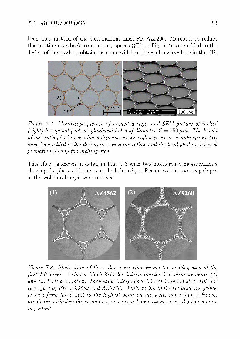
7.3. METHODOLOGY 83
been used instead of the conventional thick PR AZ9260. Moreover to reducethis melting drawback, some empty spaces ((B) on Fig. 7.2) were added to thedesign of the mask to obtain the same width of the walls everywhere in the PR.
Figure 7.2: Microscope picture of unmelted (left) and SEM picture of melted(right) hexagonal packed cylindrical holes of diameter Ø = 150 µm. The heightof the walls (A) between holes depends on the re�ow process. Empty spaces (B)have been added to the design to reduce the re�ow and the local photoresist peakformation during the melting step.
This e�ect is shown in detail in Fig. 7.3 with two interference measurementsshowing the phase di�erences on the holes edges. Because of the too steep slopesof the walls no fringes were resolved.
Figure 7.3: Illustration of the re�ow occurring during the melting step of the�rst PR layer. Using a Mach-Zehnder interferometer two measurements (1)and (2) have been taken. They show interference fringes in the melted walls fortwo types of PR, AZ4562 and AZ9260. While in the �rst case only one fringeis seen from the lowest to the highest point on the walls more than 3 fringesare distinguished in the second case meaning deformations around 3 times moreimportant.

84 CHAPTER 7. CONCAVE MICROLENSES
Nevertheless variations on the wall pro�le are clearly distinguished. Thise�ect is clearly minimized when employing AZ4562 PR instead of AZ9260 PR.In the �rst case only slight deformations of the walls appear visible as dark andlight grey modulations. In the second case several black fringes are observablemeaning stronger deformations. The amplitudes of these deformations dependon the array geometry. As an example, height di�erences between the lowestand the highest part of the wall in Fig. 7.3 were 3.8 µm in the AZ9260 and 3times less around 1.3 µm for the AZ4562.
The holes are then �lled by a second step of spinning. To avoid inhomoge-neous deposition of the second layer, some PR is poured on all the wafer beforespinning occurs. Because of the presence of structures before spinning, the spinspeed is not anymore correlated to the �nal layer thickness as mentioned inchapter 1. In this case it seems correlated to the amount of PR left in the�lled holes. After �lling, the wafers are dried in an oven at 80°C for 30 minutesto remove solvents. At this stage concave shapes are obtained depending onthe boundary conditions imposed by the melted hole, the surface tension of thechosen PR and the amount of solvent removed during the drying step.
7.4 Quality measurements
To get values on their quality, all the microlenses where measured using a Mach-Zehnder interferometer [66, 67, 68] allowing the calculation of the correspondingStrehl ratio. The Strehl ratio or normalized intensity i (P ) is de�ned as
i (P ) =I (P )
I∗, (7.1)
where I (P ) corresponds to the intensity in the point P (focal point) and I∗tothe intensity which would be obtained without aberrations[69]. The Marechal'scriterion applies that Strehl ratio higher than 80 % are considered for di�rac-tion limited microlenses [70]. More in detail, the validity of the approach comesfrom the fact that, as a �rst approximation, the half-width of the di�ractionAiry pattern introduced by the circular lens aperture in the focal region doesnot change with the presence of small aberrations. But energy from the cen-tral lobe is redistributed in the di�erent side lobes. So the calculation of theratio between the amount of energy in the central lobe without aberrations andwith aberrations becomes a way to get an idea on the quality of the microlens.When the aberrations are su�ciently small, the Strehl ratio is expressed by thefollowing equation:

7.5. EXPERIMENTAL RESULTS 85
i (P ) ∼ 1− 4 · π2
λ2 ·
[˜{W (x, y)}2 dxdy
A−{˜
{W (x, y)} dxdy
A
}2]
, (7.2)
where W (x, y) corresponds to the wavefront aberration, A the surface ofthe exit pupil of the optical system. The term in brackets can be recognized asthe variance of W (x, y). So the Strehl tolerance level (0.8) is reached when the
variance is λ197
2or when the RMS deformations of the wavefront is about λ
14 . Toget an idea on the maximal allowed deformation of the wavefront we considerthe case of primary spherical abberation that can be written in polar coordinates(ρ, φ), W (ρ, φ) = α1 · ρ4. One �nds from Eq.7.1 that the maximum deviationof the wavefront α1 = ±0.24 · λ. This correspond to the Rayleigh quarter-wavelength rule which says that the optical system is substantially perfect ifwavefronts can be included between two concentric spherical surfaces λ
4 apart.As an example if we take a concave microlens in photoresist with a diameter ofØ=50 µm with a depth h = 5.05 µm (NA of 0.2). The corresponding opticalpath length, for a refraction index di�erence of ∆n ∼ 0.5, is equal to 4λ. Themaximum acceptable deformation stands to 0.25·λ
4·λ = 116 . The fabrication error
should be less than 6.2 % for this microlens depth. More details on quanti�cationof wavefront aberrations can be found in reference [69].
7.5 Experimental results
The maximum diameters of the di�raction limited concave microlenses thathave been realized as a function of the spin speed of the second layer of PRare shown in Fig. 7.4. It is seen that di�raction limited concave microlensarrays could be produced for diameters in a range between 30 to 230 µm. Theminimum achievable diameter was arbitrary de�ned when only one fringe (i.e.depth around 1.2 µm) could be solved or because of inhomogeneity coming fromthe too important �lling of the holes. For diameters over 150 µm the holes arealmost �lled, resulting in an nearly �at pro�le. The numerical aperture (NA) isthen lower than 0.02. A degree of freedom on the numerical aperture is possibleby changing the spin speed and/or the dilution of the PR as seen in Fig. 7.5and Fig. 7.6. As an example square packed concave microlens arrays of pitchbetween 70 to 80 µm with a gap of 10 µm having NA from 0.07 to 0.14 havebeen realized (grey zone in Fig. 7.6). The di�erences observed in the resultspresented in Fig. 7.4, Fig. 7.5 and Fig. 7.6 between square and hexagonalpacked microlens arrays could come from boundary conditions imposed by the

86 CHAPTER 7. CONCAVE MICROLENSES
geometry of the melted holes and from the thin layer of PR deposits at thesurface which quickly dries because of the volatile solvents contained inside it.
Figure 7.4: Results of the fabrication of concave microlens arrays. The curvesshow the maximum diameters of di�raction limited microlenses that could beobtained when varying the spin speed of the second layer of AZ1518. Overthis limit, the Strehl ratio of the concave microlenses drops down to valueslower than 80%. The minimum diameters were arbitrary de�ned when only onefringe could be solved on the interference measurements or when homogeneityproblems happened. Square (quad) and hexagonal (hexa) packed arrays havebeen considered.
The in�uence on the resulting meniscus shape of these boundary conditionsis shown in Fig. 7.7. The �gure shows RMS deformations from a sphere oc-curring for increasing diameters after deposition of the second layer (AZ15184:1 270 rounds per minute (rpm)). For diameters lower than 80 µm no sig-ni�cant deformations are visible (Strehl ratio ∼96 %). For diameters between80 µm and 100 µm deformations are clearly visible as well as their di�erentlocations for hexagonal and square packed arrays. In this experiment squarepacked microlens arrays are less sensitive. For diameters Ø>100 µm the holesare not enough �lled and after drying both (square and hexagonal packed) mi-crolenses exhibit similar deformations. Fig. 7.8 shows the pro�le formation ofthe concave shape in measurements performed on a constant microlens diameterØ=50 µm and for di�erent spin speed experiments. Because of the non verticalwalls surrounding the meniscus, the radius of curvature (ROC) of the realizedmicrolenses changes depending on the �lling rate of the melted holes. An impor-tant question is the homogeneity of the obtained results. For spin speeds higher

7.5. EXPERIMENTAL RESULTS 87
Figure 7.5: Numerical aperture (NA) as function of the microlens diameters(hexagonal packed arrangement) for various spin speed experiments. As anexample, in the grey zone corresponding to microlenses with diameters between70 to 80 microns, NA between 0.07 to 0.14 have been realized by changing thespin speed and/or the dilution of the PR.
than 2000 rpm some shadow e�ects of the structures, mainly coming from thegrid between the microlens arrays, are observable.
Figure 7.6: Numerical aperture (NA) function of the microlens diameters(square packed arrangement) for various spin speed experiments.

88 CHAPTER 7. CONCAVE MICROLENSES
Figure 7.7: 2D pro�le deformations from a sphere for increasing microlensdiameters between 60 to 110 microns. The arrangement of the array is clearlyseen in the deformations which occur at the four cardinals points for squarepacked array and at both sides of the three axis of symmetry for hexagonalpacked microlens arrays. The �rst layer is 17 µm of AZ4562 and the secondlayer of diluted (4:1) AZ1518 was spincoated at 360 rpm
Figure 7.8: Pro�le measurements of concave microlenses with Ø = 50 µm(white area) obtained at 3 di�erent spin speeds of pure AZ1518. The verti-cal positions are set arbitrary. The anchoring point (i.e., the in�ection point ofthe pro�le of the microlens ) of the meniscus will depend on the �lling of theholes. As it can be seen, the distances (d1, d2 , d3) between the top part of thepro�le and the starting slope (angle α1, α2, α3) of the meniscus decrease. At830 rpm the meniscus starts within the hole and deformations appears on theedges as shown previously in Fig. 7.7.

7.5. EXPERIMENTAL RESULTS 89
For lower spin speeds the results are quite homogenous even if the testedwafers contained various structures in heights and sizes. For this reason noinvestigations have been done to evaluate all parameters. Nevertheless it is pos-sible, as shown in Fig. 7.9, to realized homogenous arrays of several microlenses.The typical defects encountered during the fabrication process are illustrated inFig. 7.10.
Figure 7.9: Large scale interference picture (left) and SEM picture (right) ofrespectively 40 µm pitch and 60 µm pitch concave microlens array showing thehomogeneity of the realized samples.
It consists in trapped air bubbles, dust particles, cracks in the second layeras well as local adhesion problems of the �rst layers.
Figure 7.10: Pictures of typical defects encounter during the fabrication process.(1) Shadow e�ect of the structures during spinning of the second layer of PRfor spin speed higher than 2000 rpm.(2) Local deformation due to local weakadhesion of the �rst layer. (3) Dust particles. (4) Trapped bubbles. (5) Edgebeads formation of PR at very low spin speed of the second layer (< 400 rpm).(6)Cracks in the second spun layer.

90 CHAPTER 7. CONCAVE MICROLENSES
At very low spin speeds it is necessary to remove the PR at the edge of thewafer during spinning to ensure homogenous distribution of the second layer.The reproducibility of the experiment is closely linked to the quality of the pho-tolithography of the �rst layer. Once the thickness, the quality of the exposureand the quality of the development of the photoresist is kept constant, variationsof less than 10 % were observed on the focal length of the di�raction limitedmicrolenses. The temperature as well as the dilution rate of the photoresist usedto �ll the holes are also important parameters which have to be well quanti�ed.
7.6 Concave microlens di�users
Based on experiments with the SMO HT di�users that are composed of concavestructures, three types of design have been developed. They consist in randomlydistributed (in positions and sizes) holes over an area of 1 square cm. The
Figure 7.11: Illustration of the three patterns of randomly distributed holes. Thediameters of the holes were contained in ranges between 100 to 300 µm (RCL4), 70 to 160 µm (RCL 5) and to 160 to 500 µm (RCL 6) .
designs are illustrated in Fig. 7.11. On the left part of the �gure, the range ofdiameters was contained between 100 to 300 µm (RCL 4) while in the design onthe middle, they were restricted to 70 to 160 µm (RCL 5) and to 160 to 500 µm(RCL 6) in the last pattern. Using a Mach-Zehnder interferometer, the pro�le ofthree realized di�users are shown in Fig. 7.12. The typical depth of the resultingstructures lies at 15 microns. To avoid a strong zero order transmission of thedi�users the main part of the holes must be �lled and form concave shapes.Because of the large hole diameters (designed to ensure low di�using angles),only very low spin speed ful�ll this condition. For this reason only di�usersfrom spin speed experiments allowing formation of concave microlenses close tothe speci�c range of hole diameters have been considered.

7.6. CONCAVE MICROLENS DIFFUSERS 91
Figure 7.12: 2D pro�les of three realized di�users. Because of the re�ow oc-curring during the melting step of the �rst layer the zones between concavemicrolenses are no more �at (white and grey areas) and strongly reduced zeroorder transmission. The �rst layer is set to 17 microns and the second layer ofpure AZ1518 has been spincoated at 200 rpm.
Figure 7.13: Measured angular distribution curves of concave microlens dif-fusers. AZ1518 pure 200 rpm RCL 4 and RCL5 show very nice smooth disper-sion while no zero order transmission is observable.
Their di�using properties have been analyzed using the goniometric setupillustrated in chapter 6 and shown in Fig. 7.13. While most of the measureddi�users only scatter around 10% of the light intensity with a strong zero ordertransmission, two di�users (AZ1518 pure 200 rpm RCL 4 and RCL5) show asmooth distribution of the transmitted light. The large cut-o� angle around 4°could be reduced by a dry etching step with adapted selectivity.

92 CHAPTER 7. CONCAVE MICROLENSES
7.7 Conclusion
A new method allowing the fabrication of di�raction limited concave microlensarrays has been demonstrated. Moreover by adjusting the processing parametersof the PR a control on the numerical aperture NA is possible. Once fabricatedand transferred in a fused silica wafer to ensure �at areas between microlenses,they could be used as a mold for fabrication of high quality convex microlenses.Moreover because of the unexposed second layer of PR, nanostructures couldbe written at the surface using interference recording.
The fabrication process of concave microlenses has been successfully appliedto the realization of di�users. The idea behind is the increase of the �exibility onthe design of fused silica di�users compare to conventional statistical methodssuch as sandblasting techniques or wet chemical etching. Using dry etching onfused silica wafers several di�users with interesting di�using properties couldbe realized. Some trials with others PR with di�erent surface tension would bea way to explore the �exibility of this fabrication method. It would probablypermit to increase the range of possible NA.

Chapter 8
Conclusion
This thesis illustrates various applications of microlenses. From several birefrin-gent ones built in arrays and combined with an index matching layer a micro-optical polarizer has been realized in chapter 3. Its e�ciency has been simulatedand measured on fabricated samples. The possibility to shape birefringent ma-terials allows formation of micro-optical elements that can be combined to formsystems. This micro-optical polarizer is an example of such systems and themeasured e�ciency over 72 % gives validity to this approach. Various appli-cations of microlens arrays are possible. For design applications some moirémagni�ers with high image quality have been realized in chapter 4. Becauseof their small diameters the Fresnel number of the microlenses can easily reachvery low values FN<10 and di�raction e�ects begins to be preponderant. Astudy of their implications on the maximum focal length that can be obtainedfor microlenses has been done in chapter 5. As well as the possibility to choosea design that allows the same position of the peak irradiance at two di�erentwavelengths. Comparison between results obtained in the FRED optical soft-ware and the Rayleigh-Sommerfeld equations has been performed. With therecent opportunity to easily obtain microlens arrays of very high quality, sev-eral applications in beam shaping application are found. The typical case of�y'eyes condensers is developed in chapter 6. This microlens beam shapers arewell adapted to uncoherent light emitters such as LEDs. But when used withhighly coherent sources they produced very contrasted patterns. A solutionconsists to add a rotating di�user in the optical path after the light source andbefore the beam shaper. To ensure a high energy throughput compare to com-mercial ground glass di�users, several designs of low angular distribution downto 0.2° (FWHM) di�users have been realized. Basic rules to use them are given.A deacrese of the spatial variations of the homogeneity down to only 5 % hasbeen measured. Compared to a ground glass di�user they reduce the inhomo-geneity by a factor 2 while they allow a power collection 2.8 times higher. In
93

94 CHAPTER 8. CONCLUSION
chapter 7, a new method to fabricate concave microlens arrays with di�ractionlimited features is described for diameters between 30 to 230 µm. An applica-tion is shown through the realization of di�users from statistical distribution insize and location of concave shapes. Goniometric measurements show no zeroorder transmission.

Acknowledgements
I would like to thank in my french English:Prof. Dr. René Dändliker, who hired me at IMT.Prof. Dr. Hans-Peter Herzig, my thesis director, for his valuable remarks
during the correction of my thesis manuscript.Dr. Toralf Scharf, my supervisor who allowed me to stay longer than I
thought and fully helped me to realize this thesis.Dr. Reinhard Völkel, who was my expert, gave me so much work to do for
yesterday and introduced me to the �eld of beam shaping and di�users.Prof. Dr. Hans Zappe, from the University of Freiburg (D), for accepting
to read my thesis and be my expert.The University of Neuchatel and the "Commission pour la Technologie et
l'Innovation" (CTI), for �nancially supporting my research.All the industrial partners involved in the di�erent projects and especially
the company SUSS MicroOptics.Dr. Gerben Boer, my ancient high school colleague, who thought of me when
he was looking for someone to make Wollaston cells in liquid crystal polymersand introduced me to the world of birefringent micro- optics and spectrometers.
Dr. Olivier Ripoll, with whom I shared my o�ce and who introduced me todi�raction and to (the) incomprehensible philosophical implications of quantummechanics.
Irène Philipoussis, who did not only share my o�ce but also life di�cultiesand joys with always in the silent background a strange salsa song from someobscure South American guy. She helped me a lot in the fabrication of concavemicrolenses.
Dr. Iwan Märki, who helped me to stay �t by joining me at the swimmingpool and for the numerous interesting scienti�c discussions we had on photoniccrystals.
Dr. Sylvain Jaquet, who also helped me to stay �t by joining me at theswimming pool and encouraged me to swim the head under water level (notideal for breathing) and also for the numerous interesting scienti�c discussionson OLED and Bragg re�ectors we had.
Sylvain Herminjard, for his perpetual good mood and his so personal style.
95

96 CHAPTER 8. CONCLUSION
Vincent Paeder, an inhabitant of Le Landeron (thus, a nice guy ;)) who alsocame swimming, for his interesting explanations about optical theory, methods,validity, matrices, and so on.
Pierre-Yves Baroni, a colleague biker and companion in the clean room whorecorded many gratings for me.
Dr. Oliver Scherler, a true biker (all weathers) with delicious co�ee in hiso�ce.
Dr. Wataru Nakagawa, for his delicious chocolate and his phosphorescentAmerican junk food.
Dr. Piero Tortora, for his sympathetic birthdays with guitar concerts, thesoccer matches we played together and for his SNOM introduction.
Dr. Emiliano Descrovi, for our nice talks on polarization distributions andfor his dog that sometimes scared me in the hallway late in the evening.
Marcel Groccia and Martial Racine, for the few bike tours I tried to do withthem, sweating and praying that they would su�er from their old ages. Noway...
Felix Schädelin, for his help in the preparation of the exercises for students.Dr. Kenneth Weible and Dr. Pascal Pernet, for their valuable advice on
making the RIE machine work.All the SUSS MicroOptics team.Mary-Claude Gauteaub and Joëlle Banjac, for helping me with parcels.Sandrine Pi�aretti, for helping me with incredibly complicated administra-
tive tasks.Mme Stocker and Mme De Carvalho, for helping me avoid �nancial disasters
at IMT.Dr. Christophe Weiteneder, for his introduction to the �eld of holography.Dr. Christian Bohley, for his artistic views on the scienti�c work.Dr. Carsten Rockstuhl, for helping me using the FMM in Matlab.Dr. Guido Niederer, for introducing me to the behavior of gratings.Dr. Martin Salt, who introduced me to the English humor.Dr. Omar Manzardo, for his precious advice on lifestyle.Reto Tscharner, for his help with the �re security system and about all
things that create vacuum, especially pumps.Cédric Bucher, for his help with �nding Reto.Dr. Andrea Crottini, Dr. Lorenzo Sirigu, Hicham Farah, Roland Bitterli,
Tristan Sfez, Dr. Luciana Vaccaro, Dr. Marcella Giovannini, Jean-Luc Coulot.Jean Luc Kumin, for teaching me how to repair a motorbike and how it was
when you rode a famous Triumph Bonneville.Patrick Hostettler, for his sympathetic mood and for all the various discus-
sions we had.

97
All the people from the other groups at IMT, who shared co�ee the morning,lunch or some cigarettes that I may have smoked during my time here.
My clos friends, with whom I can share other aspects of my personality andwho helped me �nd a good balance between work and leisure...
My family, my father, my mother and my two brothers, who were and areso important to me.
My wife Perrine for all... and more...My son Esteban, whose interest in grabbing things and understanding the
world surrounding him always captivated me and made me remeber the funda-mentals of science...

98 CHAPTER 8. CONCLUSION
Bibliography
[1] Micro-optics Elements, systems and applications, edited by H.P. Herzig,Taylor and Francis (1997)
[2] T. Stone and N. George, Hybrid di�ractive-refractive lenses and achromats,Appl. Opt. 27, 2960- (1988)
[3] P. Ru�eux, T. Scharf, H. P. Herzig, R. Völkel, and K. J. Weible, On thechromatic aberration of microlenses, Opt. Express 14, 4687-4694 (2006)
[4] V.Paeder, T. Scharf, P. Ru�eux, H.P. Herzig, R. Voelkel, K.J. Weible,Microlenses with amplitude and phase masks, JEOS, Vol 2, pp. 07005-1-07005-6 (2007)
[5] G. J. Swanson, W. B. Veldkamp, Di�ractive optical elements for use ininfrared systems, Opt. Eng. 28, 605-608 (1989)
[6] H. P. Herzig, M. T. Gale, H.W. Lehmann, R. Morf, Di�ractive components:Computed generated elements. In Ph. Lalanne, P. Chavel (eds) Perspectivesfor Parallel Interconnects, pp 71-107, Berlin, Springer (1993)
[7] A.M. Donald, A.H. Windle, Liquid Crystalline Polymers, Cambridge Uni-versity press (1992)
[8] G. Boer, P. Ru�eux, T. Scharf, P. Seitz, R. Dändliker, Compact Liquid-Crystal-Polymer Fourier-Transform Spectrometer, Appl. Opt. 43, 2201-2208 (2004)
[9] L. Novotny, B. Hecht, Principles of Nano-Optics ,Cambridge Univ. Press,Cambridge, UK ( 2006)
[10] C.Koch, T.J. Rinke, Lithography, theory and application of photoresists,developers, solvents and etchants, Ed. Microchemicals (2006)
[11] Z. D. Popovic, R. A. Sprague, G. A. Neville-Connell, Technique for mono-lithic fabrication of microlens arrays, Appl. Opt. 27, 1281- (1988)
99

100 BIBLIOGRAPHY
[12] D. Daly, R. F. Stevens, M. C. Hutley, and N. Davies, The manufactureof microlenses by melting photoresist, J. Meas. Sci. Technol. 1, 759-766(1990).
[13] P.Nussbaum, R. Volkel, H.P. Herzig, M. Eisner, S Haselbeck, Design, fabri-cation and testing of microlens arrays for sensors and microsystems, PureAppl. Opt. 6, 617-636 (1997)
[14] Y. Xia,G. M. Whitesides, Soft lithography, Annu. Rev. Matter. Sci. 28,153-84 (1998)
[15] M. Heckele, W. K. Schomburg, Review on micro molding of thermoplasticpolymers, J. Micromech. Microeng. 14, R1-R14 (2004)
[16] S.Y. Chou, P.R. Krauss, P J. Renstrom, Nanoimprint lithography, J.Vac.Sci. Technol. B 14 (6), 4129-4133 (1996)
[17] J.P. Rolland, E. C. Hagberg, G M. Denison, K. R. Carter, J. M. De Si-mone, High-Resolution Soft lithography: Enabling Materials for Nanotech-nologies, Angew. Chem. Int. Ed. 43, 5796-5799 (2004)
[18] S. W. Lee, S.S. Lee, Shrinkage ratio of PDMS and its alignment methodfor the wafer level process, Microsyst Technol 14, 205-208 (2008)
[19] Information about high technology silicone material, Sylgard 184 datasheet,Dow Corning corporation (1991)
[20] G. S. Oehrlein, J. F. Rembetski, Plasma-based dry etching techniques inthe silicon integrated circuit technology, IBM J. Res. Develop. Vol 36 No.2 (1992)
[21] C. Chang, Y. F. Wang, Y. Kanamori, J. J. Shih, Y. Kawai, C. K. Lee,K. C. Wu, M. Esashi, Etching submicrometer trenches by using the boschprocess and its application to the fabrication of antire�ection structures, J.Micromech. Microeng. 15, 580-585 (2005)
[22] LA Donohue and al., Developments in Si and SiO2 Etching for MEMS-Based Optical Applications, proceeding of SPIE, Vol. 5347, pp 44-53 (2003)
[23] F. Gaboriau, G. Cartry, M-C. Peignon, Ch.Cardinaud, Etching mecha-nisms of Si and SiO2in �uorocarbon ICP plasmas: analysis of the plasmaby mass spectrometry, Langnuir probe and optical emission spectroscopy,J. Phys. D:Appl. Phys. 39, 1830-1845 (2006)

BIBLIOGRAPHY 101
[24] M. Madou, Fundamentals of microfabrication, CRC press (1997)
[25] S.A. McAuley, H. Ashraf, L. Atabo, A. Chambers, S. Hall, J. Hopkins, Sil-icon micromachining using a high-density plasma source, J. Phys. D:Appl.Phys. 34, 2769-2774 (2001)
[26] J.M. Teijido, Conception and design of illumination light pipes, Thesis atthe university of Neuchatel (2000)
[27] T. Scharf, Polarized Light in Liquid Crystals and Polymers, Wiley & Sons,( 2006)
[28] S. Huard, Polarisation de la lumière, Masson (1994)
[29] C. Gu, P. Yeh, Optics of Liquid Crystal Displays, Wiley, New York, (1999)
[30] 4. D.J. Broer, Reation of Supramolecular thin �lm architectures with liquid-crystalline networks, Mol Cryst Liq Cryst 261, 513-523 (1995)
[31] N. Nieuborg, A. Kirk, B. Morlion, H. Thienpont, I. Veretennico�,Polarization-selective di�ractive optical elements with an index-matchinggap material, Appl. Optics. 36, 4681-4685 (1997)
[32] W. C. Yip, H. C. Huang, H. S. Kwok, E�cient polarization converter forprojection displays, Appl. Optics. 36, 6453-6457 (1997)
[33] C.W. McLaughlin, Progress in projection and large-area displays, Proc.IEEE, Vol: 90, no. 4, (2002).
[34] T. Scharf, Static birefringent microlenses, Optics and Lasers in Engineering43, 317-327 (2005)
[35] G. Boer, Toralf Scharf, Polarization Ray Tracing in Twisted Liquid CrystalSystems, Mol. Cryst Liq.Cryst., Vol. 375, pp. 301-311 (2002)
[36] M. C. Hutley, Interference (holographic) di�raction gratings, Jounal ofPhysics E, Vol 9 (1976)
[37] E. G. Loewen, E. Popov, Di�raction gratings and applications, MarcelDekker Inc, New York (1997)
[38] H. Kamal, R. Völkel, J. Alda, Properties of moiré magni�ers, Opt. Eng.37 (11) 3007-3014 (1998)

102 BIBLIOGRAPHY
[39] I. Amidror, The Theory of the Moiré Phenomenon, Kluwer Academic Pub-lishers, Dordrecht (2000)
[40] C. A. Walker, A historical review of moiré interferometry, Exp. Mech. 34,281-99 (1994)
[41] Y. Yamamoto, Y. Morimoto, M. Fujigaki, Two-directional phase-shiftingmoiré interferometry and its application to thermal deformation measure-ment of an electronic device, Meas. Sci. Technol. 18, 561-566 (2007)
[42] I. Amidror, A new print-based security strategy for the protection of valu-able documents and products using moiré intensity pro�les, Proceedings ofSPIE Vol. 4677 (2002)
[43] C.Hembd-Sölner, R.F. Stevens, M.C. Hutley, Imaging properties of theGabor superlens, J. Opt. A: Pure Appl. Opt. 1, 94-102 (1999)
[44] R. H. Anderson, Close-up imaging of documents and displays with lensarrays, Appl. Opt. 18, 477-84 (1979)
[45] M.C. Hutley, R. Hunt, R.F. Stevens, P. Savandert, The moiré magnifer,Pure Appl. Opt. 3, 133-142 (1994)
[46] D. Malacara, Z. Malacara, Handbook of lens design, Dekker, New-York,(1994).
[47] Y.Li, E. Wolf, Focal shifts in di�racted converging spherical waves, Opt.Commun. 39, 211 (1981).
[48] Y. Li, H. Platzer, An experimental investigation of di�raction patterns inlow Fresnel-Number focusing systems, Optica Acta 30, 1621- (1983).
[49] W. Wang, A.T. Friberg, E. Wolf, Structure of focused �elds in systems withlarge Fresnel numbers, J Opt. Soc. Am. A. 12, 1947- (1995)
[50] Arnaud, J, Representation of Gaussian beams by complex rays, AppliedOptics 24, 538- (1985).
[51] Urs Vokinger, René Dändliker, Peter Blattner, Hans Peter Herzig, Uncon-ventional treatment of focal shift, Opt. Commun. 157, 218-224 (1998)
[52] J.W. Goodman, Introduction to Fourier Optics, 2nd edn., MacGraw-Hill,New York, Chap. 4, 63-69, (1968)
[53] B.E.A. Saleh, M.C. Teich, Fundamentals of photonics, Wiley (1991)

BIBLIOGRAPHY 103
[54] N. Schröder. Bauelemente der Optik. Hanser Verlag (1992)
[55] F.M. Dickey, S.C. Hoswade, D.L. Shealy. Laser Beam Shaping Applications.Taylor & Francis, ISBN 0-8247-5941 (2000)
[56] C. Kopp, L. Ravel, P. Meyrueis E�cient beamshaper homogenizer designcombining di�ractive optical elements microlens array and random phaseplate. J. Opt. A: Opt. 1, 398-403 (1999)
[57] Handbook of optical systems: Vol. 2. Physical Image Formation, Edited byH. Gross, Wiley, Weinheim (2005)
[58] A. Buttner, U. D. Zeitner, Wave optical analysis of light-emitting diodebeam shaping using microlens arrays, Opt. Eng. 41 (10), 2393-2401 (2002)
[59] L.Erdmann, M. Burkhardt, R.Brunner Coherence management for mi-crolens laser beam homogenizers. Proc. SPIE Vol.4775 (2002)
[60] F. Wippermann, Uwe-D. Zeitner, P.Dannberg, A. Bräuer,S. Sinzinger,Beam homogenizers based on chirped microlens array, Opt. Express 15,6218-6231 (2007)
[61] K. Patorski, The self-imaging phenomenon and its applications, Progr.Opt. XXVII, 3108 (1989)
[62] B. Besold, N. Lindlein Practical limitations of Talbot imaging with mi-crolens arrays. Pure Appl. Opt. 6, 691-698 (1997)
[63] Sung-Il Chang and Jun-Bo Yoon, Shape-controlled, high �ll-factor mi-crolens arrays fabricated by 3D di�user lithography and plastic replicationmethod, Opt. Express 12, 6366-6371 (2004)
[64] X. Dong, C. Du, S. Li, C. Wang, Y. Fu, Control approach for form accuracyof microlenses with continuous relief, Opt. Express 13, 1353-1360 (2005)
[65] A. Schilling, R. Merz, CH. Ossmann, H.P. Herzig, Surface pro�les of re�owmicrolenses under the in�uence of surface tension and gravity, Opt. Eng39, 2171-2176 (2000)
[66] D.J. Daly, M.C. Hutley, R.F. Stevens, �Mach-Zehnder interferometer formeasuring microlenses�, Proc. SPIE Vol. 2340, 258-263 (1994)
[67] H.Sickinger, J. Schwinder, B. Manzke, �Fiber based Mach-Zehnder interfer-ometer for measuring wave aberrations of microlenses�, Optik 110, 239-243(1999)

104 BIBLIOGRAPHY
[68] S. Reichelt, H. Zappe, �Combined Twyman-Green and Mach-Zender inter-ferometer for microlens testing�, Appl. Opt. 44, 5786-5792 (2005)
[69] M. Born and E. Wolf, Principles of optics, 7th ed., Cambridge universitypress (1999)
[70] W. T. Welford, Aberrations of optical systems, Adam Hilger Ltd, Bristoland Boston (1986)