Mesh puppetry: cascading optimization of mesh deformation with inverse kinematics

INTERNATIONAL JOURNAL OF CIRCUIT THEORY AND APPLICATIONSInt. J. Circ. Theor. Appl. 2009; 37:793–810Published online 20 June 2008 in Wiley InterScience (www.interscience.wiley.com). DOI: 10.1002/cta.493
A mixed-mode KHN-biquad using DVCC and grounded passiveelements suitable for direct cascading
Shahram Minaei1,∗,† and Muhammed A. Ibrahim2
1Department of Electronics and Communication Engineering, Dogus University, Acibadem,
Kadikoy 34722, Istanbul, Turkey2Department of Electrical Engineering, College of Engineering, University of Salahaddin, Erbil, Iraq
SUMMARY
In this paper a mixed-mode (input and output signals can be current or voltage) Kerwin–Huelsman–Newcomb (KHN) biquad with low/high input impedance and high/low output impedance depending onthe type of the corresponding signal (current/voltage) is presented. The circuit is constructed using threedifferential voltage current conveyors (DVCCs), two grounded capacitors and three grounded resistors.The circuit simultaneously provides bandpass (BP), highpass (HP) and lowpass (LP) responses when theoutput is current and notch, BP and LP responses when the output is voltage. The notch and allpassresponses can be obtained by connecting appropriate output currents directly without using additionalactive elements. Because of the low input and high output impedance of the circuit for current signalsand the high input and low output impedance for voltage signals, it can be used in cascade for realizinghigher-order filters. SPICE simulation results are given to verify the theoretical analysis. Copyright q2008 John Wiley & Sons, Ltd.
Received 15 January 2007; Revised 22 March 2008; Accepted 24 March 2008
KEY WORDS: DVCC; mixed-mode filter; KHN-biquad; CMOS
1. INTRODUCTION
Many second-order filters constructed using different active elements and a minimum or near-minimum number of external passive components have been reported in [1–6]. Simplicity, however,does not come without a price. Drawbacks such as wide component spreads, awkward tuningcapabilities and high sensitivity to component variations, particularly to the gain of the filter,generally limit filters to the quality factor of Q�10. The filter performance and versatility can be
∗Correspondence to: Shahram Minaei, Department of Electronics and Communication Engineering, Dogus University,Acibadem, Kadikoy 34722, Istanbul, Turkey.
†E-mail: [email protected]
Copyright q 2008 John Wiley & Sons, Ltd.

794 S. MINAEI AND M. A. IBRAHIM
improved using additional active and passive components. For example, state-variable (SV)-typefilters are more convenient to tune and less sensitive to passive component variations.
The SV filter, also known as the KHN filter for inventors Kerwin–Huelsman–Newcomb biquad,or KHN-biquad [7], uses two integrators and a summing amplifier to provide second-order lowpass(LP), bandpass (BP) and highpass (HP) responses simultaneously. Based on the active elementsused in the integrator and summer circuits, several KHN-biquads have been presented in [8–13],some of which operate in voltage mode (VM) (both input and output as voltage) [8, 9, 11–13].On the other hand, it is well known that mathematical operations such as adding, subtracting ormultiplying signals represented by currents are simpler to perform than when they are representedby voltages [14]. Therefore, some current mode (CM) (both input and output as current) KHN-biquads have also been presented [10, 12, 13]. However, the circuits given in [10, 12] have threeinputs and one output; therefore, one cannot obtain all the filter responses simultaneously. It isknown that a useful feature of many biquads is that the LP, HP, BP and/or notch outputs aresimultaneously available at various nodes in the circuit. These additional outputs can be used insome systems that employ more than one filter function [15]. In addition, the circuit reportedin [10] employs six resistors, of which two are floating. Although the number of resistors used inthe circuit reported in [12] is decreased, it employs five active elements. The KHN circuit givenin [13] employs four active elements and it does not produce the allpass (AP) filter responsedirectly without using additional active elements. Recently, using three differential voltage currentconveyors (DVCCs) [16] a CM KHN-biquad has been reported [17]. The reported circuit providesBP, HP and LP responses simultaneously while the notch and AP responses can be obtained byconnecting appropriate output currents directly without additional stages. However, it suffers fromhigh input impedance due to the resistor connected to its input. A Tow–Thomas filter that usesonly two dual-X current conveyor (DXCCII), as active element, has been given in [18]. Besidesthe circuit operates only in CM, it provides simultaneously only the BP and LP filter functions.Another KHN-biquad has been reported based on using dual-X differential difference currentconveyor (DXDDCC) [19]. Although it employs only two active elements with two electronicresistors and two capacitors, it operates only in VM. Despite the circuit given in [20] uses onlytwo operational floating current conveyors as active elements and provides all the filter functions,it suffers from operating only in VM and using floating resistors, which is undesirable in integratedcircuit (IC) implementation. Moreover, the output voltages in the circuit of [20] are not taken fromlow-impedance nodes, which is undesired when cascade connections are needed.
A few mixed-mode filter circuits have been reported in [21–24]. The circuit given in [21]employs four active elements and two capacitors, but it cannot realize AP functions. The circuitsgiven in [22, 23] use many active and passive elements. Although the circuit given in [24] usesonly three active and seven passive elements, it is not suitable for realizing some of the filterfunctions by direct cascading.
It should be mentioned that other types of filters such as square-root domain wave filters [25],continuous-time OTA-C filters [26] and Tow–Thomas bi-quadratic filters [27] can also be foundin the literature.
In this paper, we propose a new mixed-mode KHN-biquad circuit, which employs three DVCCsas active elements together with two grounded capacitors and three grounded resistors. The currentconveyor exploits a circuit topology that emphasizes CM operation, which is inherently muchfaster than VM operation because it is less prone to the effect of stray node capacitances. Theproposed filter can be driven by a voltage or current source and gives outputs in current or voltagesimultaneously. Therefore, filter transfer functions in CM, VM, transimpedance mode (TIM) (i.e.
Copyright q 2008 John Wiley & Sons, Ltd. Int. J. Circ. Theor. Appl. 2009; 37:793–810DOI: 10.1002/cta

A MIXED-MODE KHN-BIQUAD USING DVCC 795
input as current and output as voltage) and transadmittance mode (TAM) (i.e. input as voltage andoutput as current) are possible to be obtained. The HP, BP and LP filter responses are obtainedsimultaneously when the output signal is current. In addition, the BP, LP and notch filter responsesare obtained simultaneously for VM operation. In addition, the notch and AP functions can berealized by connecting proper output currents without using additional active elements. All thepassive elements are grounded, which is important in IC implementation. Because of the low inputand high output impedances of the proposed circuit for current signals and the high input andlow output impedances for voltage signals it can be used in cascade for realizing higher-orderfilters.
2. PROPOSED MIXED-MODE KHN-BIQUAD
The DVCC, whose electrical symbol is shown in Figure 1, is a five-terminal network with terminalcharacteristics described by⎡
⎢⎢⎢⎢⎢⎢⎢⎣
VX
IY1
IY2
IZ1
IZ2
⎤⎥⎥⎥⎥⎥⎥⎥⎦
=
⎡⎢⎢⎢⎢⎢⎢⎢⎣
0 1 −1 0 0
0 0 0 0 0
0 0 0 0 0
1 0 0 0 0
−1 0 0 0 0
⎤⎥⎥⎥⎥⎥⎥⎥⎦
⎡⎢⎢⎢⎢⎢⎢⎢⎣
IX
VY1
VY2
VZ1
VZ2
⎤⎥⎥⎥⎥⎥⎥⎥⎦
(1)
It should be noted that using a single DVCC and grounded passive elements it is easy toconstruct basic current processing blocks such as amplifier, integrator, differentiator, summer andsubtractor [17].
The block diagram for realizing a mixed-mode biquad is shown in Figure 2. It consists of twointegrators and a summer. Using DVCCs as active elements for signal processing the proposedmixed-mode filter is shown in Figure 3. The input current of the circuit is applied to the X -terminalof the first DVCC that has low impedance, while all of the output currents are taken through theZ -terminals of the conveyors that have high impedances. The input voltage of the circuit is appliedto the Y2-terminal of the first DVCC that has high impedance, while all of the output voltages aretaken through the X -terminals of the conveyors that have low impedances. Therefore, the circuitis suitable for cascading in all of the operation modes.
VX
Y1
DVCCY2
X
Z1
Z2
VY1IY1
VY2IY2
IX
IZ1VZ1
VZ2
IZ2
Figure 1. Electrical symbol of DVCC.
Copyright q 2008 John Wiley & Sons, Ltd. Int. J. Circ. Theor. Appl. 2009; 37:793–810DOI: 10.1002/cta

796 S. MINAEI AND M. A. IBRAHIM
OUTHP -OUTBP OUTLP
1
-OUTBP
-OUTLP
IN1/s
-1 1 -11/s
1
Figure 2. The signal processing block diagram of implementing mixed-mode KHN-biquad.
Y1DVCC(1)
Y2X
Z1
Z2
Y1
DVCC(2)
Y2X
Z1
Z2
Y1DVCC(3)
Y2X
Z1
Z2
R1R2 R3
C1 C2
IBP
ILP
IHP
Iin
Vin
VBPVLPVNH
V-V
MR
MR
V-V
MR
MR
V-V
MR
MR
Figure 3. The proposed mixed-mode KHN-biquad.
Routine analysis of the circuit of Figure 3 yields the following filter transfer functions:(a) For CM operation, set Vin=0; then,
IHPIin
= s2
s2+ 1
R1C1s+ 1
R2R3C1C2
(2a)
IBPIin
= −1
R2C1s
s2+ 1
R1C1s+ 1
R2R3C1C2
(2b)
ILPIin
=1
R2R3C1C2
s2+ 1
R1C1s+ 1
R2R3C1C2
(2c)
In addition, a notch response can be obtained by interconnection of the relevant output currents asINH= ILP+ IHP without using additional active elements. Moreover, for R1= R2, an AP functioncan be obtained by connecting HP, LP and BP responses as IAP= ILP+ IBP+ IHP.
Copyright q 2008 John Wiley & Sons, Ltd. Int. J. Circ. Theor. Appl. 2009; 37:793–810DOI: 10.1002/cta

A MIXED-MODE KHN-BIQUAD USING DVCC 797
(b) For VM operation, set Iin=0; then,
VNHVin
= −1
R2R3C1C2+s2
s2+ 1
R1C1s+ 1
R2R3C1C2
(3a)
VBPVin
=1
R1C1s
s2+ 1
R1C1s+ 1
R2R3C1C2
(3b)
VLPVin
=1
R1R2C1C2
s2+ 1
R1C1s+ 1
R2R3C1C2
(3c)
The analytical steps for deriving Equations (2a)–(2c) and (3a)–(3c) are given in Appendix A.(c) For TAM operation, set Iin=0; then,
IHPVin
=1
R1s2
s2+ 1
R1C1s+ 1
R2R3C1C2
(4a)
IBPVin
= −1
R1R2C1s
s2+ 1
R1C1s+ 1
R2R3C1C2
(4b)
ILPVin
=1
R1R2R3C1C2
s2+ 1
R1C1s+ 1
R2R3C1C2
(4c)
In addition, a notch response can be obtained with interconnection of the relevant output currents asINH= ILP+ IHP without using additional active elements. Moreover, for R1= R2, an AP functioncan be obtained by connecting HP, LP and BP responses as IAP= ILP+ IBP+ IHP.
(d) For TIM operation, set Vin=0; then,
VBPIin
=1
C1s
s2+ 1
R1C1s+ 1
R2R3C1C2
(5a)
VLPIin
=1
R2C1C2
s2+ 1
R1C1s+ 1
R2R3C1C2
(5b)
Copyright q 2008 John Wiley & Sons, Ltd. Int. J. Circ. Theor. Appl. 2009; 37:793–810DOI: 10.1002/cta

798 S. MINAEI AND M. A. IBRAHIM
Y2
VBB
VSS
VDD
X Z14M3M2M1M
M5 M6
M7 M8
M9 M10 M11 M12
Y1 Z2
M15
M18
M13
M16
M14
M17
Figure 4. The CMOS implementation of DVCC [16].
Table I. Transistor aspect ratios of the DVCC circuit shown in Figure 4.
Transistor W (�m) L (�m)
M1, M2, M3, M4 1.4 0.7M5, M6 5.6 0.7M7, M8, M13, M14, M15 14 0.7M9, M10 20.3 0.7M11, M12, M16, M17, M18 58.1 0.7
The natural angular frequency �0, the quality factor Q and the parameter �0/Q of the filter canbe found as
�0=√
1
R2R3C1C2, Q= R1
√C1
R2R3C2,
�0
Q= 1
R1C1(6)
It should be noted that the parameters Q and �0/Q can be adjusted by changing the resistor R1without disturbing the parameter �0.
Sensitivity analysis of the filter parameters shows that
S�0R2
= S�0R3
= S�0C1
= S�0C2
=− 12
SQR1= 1, SQR2
= SQR3= SQC2
=−SQC1=− 1
2
S�0/QR1
= S�0/QC1
=−1
which are all no more than unity in magnitude.As shown in Figure 3, each resistor Ri (i=1,2,3) is realized by two MOS resistors (MRi1 and
MRi2) that can be adjusted with their corresponding control voltages VCi and −VCi . According
Copyright q 2008 John Wiley & Sons, Ltd. Int. J. Circ. Theor. Appl. 2009; 37:793–810DOI: 10.1002/cta

A MIXED-MODE KHN-BIQUAD USING DVCC 799
Table II. The 0.35�m TSMC CMOS model parameters.
.MODEL CMOSN NMOS (LEVEL=3+TOX=7.9E−9 NSUB=1E17 GAMMA=0.5827871+PHI=0.7 VTO=0.5445549 DELTA=0+UO=436.256147 ETA=0 THETA=0.1749684+KP=2.055786E−4 VMAX=8.309444E4 KAPPA=0.2574081+RSH=0.0559398 NFS=1E12 TPG=1+XJ=3E−7 LD=3.162278E−11 WD=7.046724E−8+CGDO=2.82E−10 CGSO=2.82E−10 CGBO=1E−10+CJ=1E−3 PB=0.9758533 MJ=0.3448504+CJSW=3.777852E−10 MJSW=0.3508721)
.MODEL CMOSP PMOS (LEVEL=3+TOX=7.9E−9 NSUB=1E17 GAMMA=0.4083894+PHI=0.7 VTO=−0.7140674 DELTA=0+UO=212.2319801 ETA=9.999762E−4 THETA=0.2020774+KP=6.733755E−5 VMAX=1.181551E5 KAPPA=1.5+RSH=30.0712458 NFS=1E12 TPG=−1+XJ=2E−7 LD=5.000001E−13 WD=1.249872E−7+CGDO=3.09E−10 CGSO=3.09E−10 CGBO=1E−10+CJ=1.419508E−3 PB=0.8152753 MJ=0.5+CJSW=4.813504E−10 MJSW=0.5)
Figure 5. The magnitude response of the LP filter for different valuesof control voltages VC =VC1=VC2=VC3.
to the following equation [28]:
Ri = L
2�CoxW (VCi −VT)(7)
where L is the channel length of a MOS transistor, W is the channel width of the MOS transistor, �is the effective carrier mobility, Cox is the gate oxide capacitance of the MOS transistor per unitarea and VT is the threshold voltage of the MOS transistor.
Copyright q 2008 John Wiley & Sons, Ltd. Int. J. Circ. Theor. Appl. 2009; 37:793–810DOI: 10.1002/cta

800 S. MINAEI AND M. A. IBRAHIM
Figure 6. The phase response of the LP filter for different values of control voltages VC =VC1=VC2=VC3.
Figure 7. The magnitude response of the BP filter for different valuesof control voltages VC =VC1=VC2=VC3.
3. TRACKING ERROR ANALYSIS
Taking the DVCC non-idealities into consideration, the port relations in Equations (1) can beexpressed as
VX =�1VY1−�2VY2, IZ1=�1 IX and IZ2=−�2 IX (8)
where � j =1−�vj and � j =1−�ij for j =1,2. Here �vj and �ij (|�vj|, |�ij|�1) represent voltage andcurrent tracking errors of the DVCC, respectively. Denoting �1i , �2i , �1i and �2i (i=1,2,3) asmentioned parameters associated with the i th DVCC and reanalyzing the filter circuit yield the
Copyright q 2008 John Wiley & Sons, Ltd. Int. J. Circ. Theor. Appl. 2009; 37:793–810DOI: 10.1002/cta

A MIXED-MODE KHN-BIQUAD USING DVCC 801
Figure 8. The phase response of the BP filter for different values of control voltages VC =VC1=VC2=VC3.
Figure 9. BP responses with different Q values obtained by selectingdifferent VC1 values when VC2=VC3=1.5V.
following modified transfer functions:(a) For CM operation (Vin=0)
IHPIin
= �21s2
s2+ �11�11�22R1C1
s+ �11�12�23�13�22R2R3C1C2
(9a)
IBPIin
= −�11�22�22R2C1
s
s2+ �11�11�22R1C1
s+ �11�12�23�13�22R2R3C1C2
(9b)
Copyright q 2008 John Wiley & Sons, Ltd. Int. J. Circ. Theor. Appl. 2009; 37:793–810DOI: 10.1002/cta

802 S. MINAEI AND M. A. IBRAHIM
Figure 10. The magnitude response of the HP filter for different valuesof control voltages VC =VC1=VC2=VC3.
ILPIin
=�11�12�13�13�22
R2R3C1C2
s2+ �11�11�22R1C1
s+ �11�12�23�13�22R2R3C1C2
(9c)
(b) For VM operation (Iin=0)
VNHVin
= −�11�12�23�21�13�22
R2R3C1C2+�21s
2
s2+ �11�11�22R1C1
s+ �11�12�23�13�22R2R3C1C2
(10a)
VBPVin
=�11�21�22R1C1
s
s2+ �11�11�22R1C1
s+ �11�12�23�13�22R2R3C1C2
(10b)
VLPVin
=�11�12�13�21�22
R1R2C1C2
s2+ �11�11�22R1C1
s+ �11�12�23�13�22R2R3C1C2
(10c)
(c) For TAM operation (Iin=0)
IHPVin
=�21�21R1
s2
s2+ �11�11�22R1C1
s+ �11�12�23�13�22R2R3C1C2
(11a)
Copyright q 2008 John Wiley & Sons, Ltd. Int. J. Circ. Theor. Appl. 2009; 37:793–810DOI: 10.1002/cta

A MIXED-MODE KHN-BIQUAD USING DVCC 803
Figure 11. The phase response of the HP filter for different valuesof control voltages VC =VC1=VC2=VC3.
Figure 12. The magnitude response of the notch filter for differentvalues of control voltages VC =VC1=VC2=VC3.
IBPVin
= −�11�22�21�22
R1R2C1s
s2+ �11�11�22R1C1
s+ �11�12�23�13�22R2R3C1C2
(11b)
ILPVin
=�11�12�13�13�21�22
R1R2R3C1C2
s2+ �11�11�22R1C1
s+ �11�12�23�13�22R2R3C1C2
(11c)
Copyright q 2008 John Wiley & Sons, Ltd. Int. J. Circ. Theor. Appl. 2009; 37:793–810DOI: 10.1002/cta

804 S. MINAEI AND M. A. IBRAHIM
Figure 13. The phase response of the notch filter for different valuesof control voltages VC =VC1=VC2=VC3.
Figure 14. The magnitude response of the AP filter for different valuesof control voltages VC =VC1=VC2=VC3.
(d) For TIM operation (Vin=0)
VBPIin
=�11�22C1
s
s2+ �11�11�22R1C1
s+ �11�12�23�13�22R2R3C1C2
(12a)
VLPIin
=�11�12�13�22
R2C1C2
s2+ �11�11�22R1C1
s+ �11�12�23�13�22R2R3C1C2
(12b)
Copyright q 2008 John Wiley & Sons, Ltd. Int. J. Circ. Theor. Appl. 2009; 37:793–810DOI: 10.1002/cta
A MIXED-MODE KHN-BIQUAD USING DVCC 805
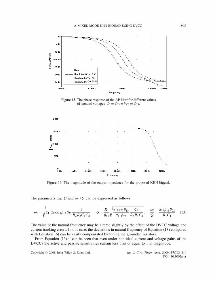
Figure 15. The phase response of the AP filter for different valuesof control voltages VC =VC1=VC2=VC3.
Figure 16. The magnitude of the output impedance for the proposed KHN-biquad.
The parameters �0, Q and �0/Q can be expressed as follows:
�0=√
�11�12�23�13�221
R2R3C1C2, Q= R1
�11
√�12�23�13�11�22
C1
R3R4C2,
�0
Q= �11�11�22
R1C1(13)
The value of the natural frequency may be altered slightly by the effect of the DVCC voltage andcurrent tracking errors. In this case, the deviations in natural frequency of Equation (13) comparedwith Equation (6) can be easily compensated by tuning the grounded resistors.
From Equation (13) it can be seen that even under non-ideal current and voltage gains of theDVCCs the active and passive sensitivities remain less than or equal to 1 in magnitude.
Copyright q 2008 John Wiley & Sons, Ltd. Int. J. Circ. Theor. Appl. 2009; 37:793–810DOI: 10.1002/cta

806 S. MINAEI AND M. A. IBRAHIM
Figure 17. The magnitude of the input impedance for the proposed KHN-biquad.
Figure 18. The input and output waveforms of the BP filter for an 80�A(peak-to-peak) sinusoidal input current at 16MHz.
4. SIMULATION RESULTS
The proposed KHN-biquad filter operated in CM has been simulated using SPICE program toverify the given theoretical analysis. The DVCCs have been simulated using the CMOS structure ofFigure 4 [16]. The aspect ratios of the CMOS transistors of the DVCC are given in Table I. Table IIillustrates TSMC 0.35�m CMOS process model parameters used for the SPICE simulations. Thesupply voltages and capacitor values are selected as VDD=−VSS=1.5V and C2=2C1=2pF,respectively. The electronic resistors of the circuit are simulated using MOS transistors with anaspect ratio of W/L=0.7/0.7�m. Different control voltages of VC =1.5, 1 and 0.75V for theelectronic resistor circuit result in resistor values of 7, 10.76 and 19.13k�, respectively. Selectingequal resistors of R1= R2= R3 with different values of 7, 10.76 and 19.13k� results in filterresponses with a quality factor of Q=0.707 and natural frequencies of f0∼=16, 10.45 and 5.9MHz,
Copyright q 2008 John Wiley & Sons, Ltd. Int. J. Circ. Theor. Appl. 2009; 37:793–810DOI: 10.1002/cta

A MIXED-MODE KHN-BIQUAD USING DVCC 807
respectively. In addition, selecting R2= R3=7k� and different values for R1 as 7, 10.76 and19.13k�, BP filter responses with different Q values of 0.707, 1.08 and 1.93 are obtained,respectively. All of the magnitude and phase responses of the LP, BP, HP, notch and AP responsesare shown in Figures 5–15.
The frequency response of the output terminal impedance for the proposed KHN circuit isshown in Figure 16. From Figure 16 the output impedance is found to be 162k�‖0.042pF. Thus,the parasitic capacitance of the circuit has a small value that can be neglected in our frequencyrange of interest. The frequency response of the input impedance for the proposed filter is shownin Figure 17. It can be seen that the circuit has a low input impedance (229� resistance in serieswith 85.75�H inductance), which makes it suitable for cascading.
To test the time-domain response of the filter, the simulation has been repeated for a sinusoidalinput signal with an amplitude of 80�A peak to peak at f0=16MHz. Figure 18 shows the inputand output signals of the BP filter (in CM operation). The total harmonic distortion of the outputsignal is found to be 1.3%. The proposed filter has a total power dissipation of 5.76mW.
5. CONCLUSIONS
In this paper, a mixed-mode KHN-biquad circuit has been presented. The filter employs threeDVCCs, two capacitors and three resistors. The circuit enjoys the following advantages:
1. Providing BP, HP and LP filter functions simultaneously for current outputs, and providingnotch, BP and LP filter functions for VM operation.
2. Realizing the notch and AP functions by connecting appropriate output currents directlywithout using additional active elements.
3. Low input and high output impedance for current signals and high input and low outputimpedance for voltage signals, which are important for cascade connections.
4. Use of only grounded passive elements, which is attractive in IC implementation.5. Control of the quality factor Q without disturbing the parameter �0 of the filter.6. Low active and passive sensitivities.
APPENDIX A
Applying Kirchoff’s current law at the X -terminal of DVCC-1 in Figure 3 and using the character-istic matrix given in Equation (1), we can obtain the transfer functions given in Equations (2a)–(2c)and (3a)–(3c) as follows:
(a) Setting Vin=0 :
IHP− Iin+ ILP+ VBPR1
=0 (A1)
VBP=−(
− IHPsC1
)= IHP
sC1(A2)
Copyright q 2008 John Wiley & Sons, Ltd. Int. J. Circ. Theor. Appl. 2009; 37:793–810DOI: 10.1002/cta

808 S. MINAEI AND M. A. IBRAHIM
IBP = −VBPR2
=− IHPsC1R2
(A3)
ILP = VLPR3
=− IBPsC2R3
= IHPs2C1C2R2R3
(A4)
By substituting Equations (A2) and (A4) into Equation (A1), we obtain
IHPIin
= s2
s2+ 1
R1C1s+ 1
R2R3C1C2
(A5)
which is the HP transfer function given in Equation (2a). In addition, by substituting Equation (A5)into Equations (A3) and (A4), we obtain the other transfer functions given in Equations (2b) and(2c), respectively.
(b) Setting Iin=0:
IHP+ VBP−VinR1
+ ILP=0 (A6)
Using Equations (A3) and (A4) we can re-write Equation (A6) as
sC1VBP+ VBP−VinR1
+ VBPsC2R2R3
=0 (A7)
The above equation yields the transfer function given in Equation (3b), which is
VBPVin
=1
R1C1s
s2+ 1
R1C1s+ 1
R2R3C1C2
(A8)
According to the characteristic equation given in Equation (1) the voltage at the X -terminal ofDVCC-1 is
VNH=VBP−Vin (A9)
Using Equation (A8) we can re-write Equation (A9) as
VNH=Vin
⎛⎜⎜⎝
1
R1C1s
s2+ 1
R1C1s+ 1
R2R3C1C2
−1
⎞⎟⎟⎠ (A10)
The above equation yields the transfer function given in Equation (3a), which is
VNHVin
=−1
R2R3C1C2+s2
s2+ 1
R1C1s+ 1
R2R3C1C2
(A11)
Copyright q 2008 John Wiley & Sons, Ltd. Int. J. Circ. Theor. Appl. 2009; 37:793–810DOI: 10.1002/cta

A MIXED-MODE KHN-BIQUAD USING DVCC 809
Finally, using Equations (A3) and (A4) in Equation (A8) we obtain the transfer function given inEquation (3c), which is
VLPVin
=1
R1R2C1C2
s2+ 1
R1C1s+ 1
R2R3C1C2
(A12)
In the same manner we can obtain the other transfer functions given in Equations (4a)–(4c) and(5a)–(5b).
REFERENCES
1. Horng JW, Tsai CC, Lee MH. Novel universal voltage-mode biquad filter with three inputs and one output usingonly two current conveyors. International Journal of Electronics 1996; 80:543–546.
2. Ozoguz S, Toker A, Cicekoglu O. High output impedance current-mode multifunction filter with minimumnumber of active and reduced number of passive elements. Electronics Letters 1998; 34(19):1807–1809.
3. Toker A, Ozoguz S, Cicekoglu O. A new current-mode multifunction filter with minimum components using dual-output current conveyors. IEICE Transactions on Fundamentals of Electronics, Communications and ComputerSciences Letter 2000; E83-A(11):2382–2384.
4. Cicekoglu O. Current-mode biquad with a minimum number of passive elements. IEEE Transactions on Circuitsand Systems—II: Analog and Digital Signal Processing 2001; 48(2):221–222.
5. Cam U, Cicekoglu O, Toker A, Kuntman H. Current-mode high output impedance multifunction filters employingminimum number of FTFNs. Analog Integrated Circuits and Signal Processing 2001; 28:299–307.
6. Toker A, Cicekoglu O, Ozcan S, Kuntman H. High output impedance transadmittance type continuous timemultifunction filter with minimum active elements. International Journal of Electronics 2001; 88:1085–1091.
7. Kerwin W, Huelsman L, Newcomb R. State variable synthesis for insensitive integrated circuit transfer functions.IEEE Journal of Solid-State Circuits 1967; SC-2:87–92.
8. Soliman AM. Kerwin–Huelsman–Newcomb circuit using current conveyors. Electronics Letters 1994; 30:2019–2020.
9. Senani R, Singh VK. KHN-equivalent biquad using current conveyors. Electronics Letters 1995; 31:626–628.10. Toker A, Ozoguz S, Acar C. Current-mode KHN-equivalent biquad using CDBAs. Electronics Letters 1999;
35:1682–1683.11. Khaled NS, Soliman AM. Voltage mode Kerwin–Huelsman–Newcomb circuit using CDBAs. Frequenz 2000;
54:90–93.12. Altuntas E, Toker A. Realization of voltage and current mode KHN biquads using CCCIIs. AEU International
Journal of Electronics and Communications 2002; 56:45–49.13. Soliman AM. Current conveyor filters: classification and review. Microelectronics Journal 1998; 29:133–149.14. Roberts GW, Sedra AS. All current-mode frequency selective circuits. Electronics Letters 1989; 25:759–761.15. Sun Y. Design of High Frequency Integrated Analogue Filters. The Institute of Electrical Engineering, London,
U.K., 2002.16. Elwan HO, Soliman AM. Novel CMOS differential voltage current conveyor and its applications. IEE
Proceedings—Circuits, Devices and Systems 1997; 144:195–200.17. Ibrahim MA, Minaei S, Kuntman H. A 22MHz current-mode KHN-biquad using differential voltage current
conveyor and grounded passive elements. AEU International Journal of Electronics and Communications 2005;59:311–318.
18. Zeki A, Toker A. The dual-X current conveyor (DXCCII): a new active device for tunable continuous time filters.International Journal of Electronics 2002; 89(12):913–923.
19. Yamacli S, Kuntman H. A new circuit building block: dual-X differential difference current conveyor (DXDDCC).Proceedings of NEU-CEE 2004: Second International Symposium on Electrical, Electronics and ComputerEngineering and Exhibition, TRNC, Nicosia, 11–13 March 2004; 144–149.
20. Ghallab YH, Badawy W, Abou El-Ela M, El-Said MH. The operational floating current conveyor and itsapplications. Journal of Circuits, Systems and Computers 2006; 15(3):352–371.
Copyright q 2008 John Wiley & Sons, Ltd. Int. J. Circ. Theor. Appl. 2009; 37:793–810DOI: 10.1002/cta

810 S. MINAEI AND M. A. IBRAHIM
21. Abulma’atti MA. A novel mixed mode current-controlled current-conveyor-based filter. Active and PassiveElectronic Components 2003; 26:185–191.
22. Abulma’atti MA, Bentrica A, Al-Shahrani SM. A novel mixed-mode current-conveyor-based filter. InternationalJournal of Electronics 2004; 91:191–197.
23. Singh VK, Singh AK, Bhaskar DR, Senani R. Novel mixed-mode universal biquad configuration. IEICE ElectronicsExpress 2005; 2:548–553.
24. Pandey N, Paul SK, Bahattacharyya A, Jain SB. A new mixed mode biquad using reduced number of active andpassive elements. IEICE Electronics Express 2006; 3:115–121.
25. Psychalinos C. Square-root domain wave filters. International Journal of Circuit Theory and Applications 2007;35(2):131–148.
26. Koziel S, Ramachandran A, Szczepanski S, Sanchez-Sinencio E. A general framework for evaluating nonlinearity,noise and dynamic range in continuous-time OTA-C filters for computer-aided design and optimization.International Journal of Circuit Theory and Applications 2007; 35(4):405–425.
27. Soliman AM. Voltage mode and current mode Tow–Thomas bi-quadratic filters using inverting CCII. InternationalJournal of Circuit Theory and Applications 2007; 35(4):463–467.
28. Wang Z. 2-MOSFET transistors with extremely low distortion for output reaching supply voltage. ElectronicsLetters 1990; 26:951–952.
Copyright q 2008 John Wiley & Sons, Ltd. Int. J. Circ. Theor. Appl. 2009; 37:793–810DOI: 10.1002/cta
Copyright © 2022 FDOKUMEN


![Towards a phonetically grounded diachronic phonology of Basque [Thesis]](https://static.fdokumen.com/doc/165x107/63226867078ed8e56c0a658e/towards-a-phonetically-grounded-diachronic-phonology-of-basque-thesis.jpg)