Inorganic Chemistry I (CH331) Solid state Chemistry II Solid ...
Upload
independentCategory
view
6download
0
IEEE TRANSACTIONS ON INDUSTRY APPLICATIONS, VOL. 29, NO. 5, SEPTEMBEWOCTOBER 1993 969
A Solid-state High-Performance Reactive-Power Compensator
Luis MorBn, Member, IEEE, Phoivos D. Ziogas, Fellow, IEEE, and Geza Joos, Senior Member, IEEE
Abstract-A high-performance reactive-power compensator is presented and analyzed in this paper. The var compensator consists of a three-phase current-regulated pulse width modulated voltage-source inverter connected to a self-controlled dc bus. Reactive-power compensation is achieved by forcing the inverter output current to follow a reactive sinusoidal reference waveform at a constant switching frequency. The main advantages of this scheme are that it reduces the stresses on the switching devices (as compared with other current regulated techniques), and it has a fast response time, which allows almost instantaneous reactive current control, and low harmonic distortion in the line currents. In particular, this paper discusses the proposed scheme in terms of principles of operation, power and control system design, and the analysis under transient operating conditions. Simulated results obtained with the Spice simulating package for steady-state and transient operating conditions are presented and validated on an experimental unit.
1. INTRODUCTION N recent years there has been a substantial increase in the I demand for controllable reactive-power sources which can
regulate and stabilize transmission and distribution lines and can compensate for large intermittent lagging loads. Moreover, with the continuous proliferation of nonlinear types of load, the requirements for power compensation are becoming more rigorous. These requirements involve precise and continuous reactive-power control with fast response times, avoidance of harmonic line current generation, and avoidance of resonance created by peripheral low frequency current sources. In order to satisfy the above criteria solid-state var compensators using force-commutated converters have been developed and are gradually being accepted by the static converter industry and by the users of electric power [l].
A number of recent papers discuss various static var com- pensator topologies based on force-commutated voltage-source inverters [2]-[4]. In particular, the authors have previously proposed a scheme that uses a power circuit topology similar to the one given in Fig. 1, consisting of a filter reactor on the line side and a self-controlled dc bus [5]. The modulation index is controlled directly by the var calculator. The scheme allows the use of optimized PWM patterns for harmonic rejection
Paper IPCSD 92-43, approved by the Industrial Power Converter Committee of the IEEE Industry Applications Society for presentation at the 1990 IEEE Applied Power Electronics Conference and Exposition, Los Angeles, CA, March 12-16. Manuscript released for publication November 16, 1992.
L. Morin is with the Departamento de Ingenieria Elktrica, Universidad de Concepcih, Concepcih, Chile.
P. D. Ziogas and G. Joos are with the Department of Electrical & Computer Engineering, Montreal, Canada H3G 1M8.
IEEE Log Number 9212098.
Fig. 1. The high-performance solid-state reactive-power compensator configuration.
and is suitable for slowly varying var demand applications. An alternative topology that requires no var sensing is proposed in [6]. The reactor is placed on the ac supply line. The modulation index is fixed and the capacitor voltage is controlled so that the inverter output voltage matches in magnitude the line voltage. This ensures nearly unity power factor without the need for var sensing. Capacitor voltage control is achieved through phase- shifting of the inverter voltage with respect to the line voltage. Despite its simplicity, this load angle control schemes does not allow very fast response to be achieved, particularly at high power ratings [6].
The scheme proposed in this paper addresses the problem of dynamic response limitations of the above compensators by making use of instantaneous inverter line current control. The power circuit topology, given in Fig. 1, is that of a synchronous var compensator [5]. A var calculator and var control loop are required. The scheme provides both leading and lagging power factor compensation, depending upon the phase angle of the inverter controlled current. The features and advantages of the proposed var compensator can be summarized as follows:
1) It uses a current control scheme which allows leading or lagging reactive-power compensation, and a very fast response.
2) Current control is achieved at a constant switching frequency, which yields a more uniform switching pat- tern than hysteresis current control [7]. This results in a reduction of the line current harmonics and lower stresses on the semiconductor devices.
3 ) Instantaneous overcurrent protection is provided, thereby increasing the system reliability.
0093-9994/93$03.00 0 1993 IEEE

-
970
M A I N S
IEEE TRANSACTIONS ON INDUSTRY APPLICATIONS, VOL. 29, NO. 5, SEFTEMBEWOCTOBER 1993
PHH VDLTAOE-SOURCE IPNERTER ,
VOLTABE CONTROL U N I T CURRENT CONTROL U N I T
Fig. 2. Block diagram of the reactive-power compensator control system.
The treatment presented in this paper includes the principles of operation, the design of the reactive-power control loop, the design of the power converter, and the analysis of the transient performance of the system for dynamic var compensation. Finally, simulated results obtained with the PSpice simulation package are verified experimentally on a 1.5 kVA prototype unit.
11. PRINCIPLES OF OPERATION
The operating principles of the high-performance var com- pensator proposed in this paper are described with the help of the control system block diagram shown in Fig. 2. The control system consists of a current control unit, a dc bus voltage control circuit, and a gating signal generator. A brief functional description of each of these units is given in the next three subsections.
A. Current Control Unit
The current control unit forces the line current of the inverter to follow a sinusoidal reference waveform which is phase shifted by almost 90" (leading or lagging) with respect to the corresponding phase-to-neutral line voltage [7]. Any amount of reactive power can be supplied or absorbed by controlling the amplitude and the sign of the inverter current reference waveform. Amplitude control results in modulation index control of the inverter output voltage.
B. Voltage Control Unit
The dc voltage control unit maintains the voltage across the dc capacitor equal to a constant reference voltage. Keeping the dc voltage constant simplifies the voltage control scheme, but it increases the switching stresses, especially for lagging var compensation which requires a low modulation index. The
higher stresses occur because narrow pulses are generated in the gating circuit. However, this problem can be overcome by using two reference signals. For leading var compensation the reference voltage is equal to a maximum value, Kefmax, while for lagging var compensation the reference voltage is changed to a minimum value, Vrefmin. By using two different voltages across the dc capacitor, the need for narrow switching pulses (low modulation index) is reduced. Thus, a switching pattern composed of wider pulses and having a modulation index close to one is used in all cases and the resulting switching stresses are lower.
The voltage across the dc capacitor is controlled by adjust- ing the small amount of real power absorbed by the inverter. The real power required by the inverter is controlled by phase shifting the reference current waveform by plus or minus a degrees with respect to the 90" (leading or lagging) steady- state operating point. The real power absorbed by the inverter is given by
where V,, is the fundamental component of the inverter phase- to-neutral output voltage, Il is the fundamental component of the inverter line current, and a is the phase shift between V,, and I l .
C. Gating Signal Generator
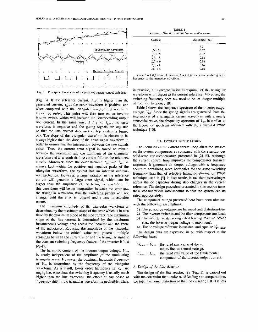
A constant switching frequency is achieved by comparing the current error signal with a triangular carrier waveform [81-[10]. The purpose of introducing the triangular waveform is to stabilize the inverter switching frequency, forcing it to be constant and equal to the frequency of the triangular waveform. In the proposed technique, the current error is forced to remain within a window defined by the ampli- tude of the triangular waveform, assuming intersections exist
MORAN et al.: A SOLID-STATE HIGH-PERFORMANCE REACTIVE POWER COMPENSATOR
Order k Amplitude (pu)
Triangular Waveform i
(Fig. 3). If the reference current, Irefr is higher than the generated current, I,,,, the error waveform is positive, and when compared with the triangular waveform, it results in a positive pulse. This pulse will then turn on an inverter bottom switch, which will increase the corresponding output line current. In the same way, if Iref < Igen, the error waveform is negative and the gating signals are adjusted so that the line current decreases (a top switch is turned on). The slope of the triangular waveform is chosen to be always higher than the slope of the error signal waveform in order to ensure that the intersection between the two signals exists. Thus, the current error signal is forced to remain between the maximum and the minimum of the triangular waveform and as a result the line current follows the reference closely. Moreover, since the error between Iref and I,,, is always kept within the positive and negative peaks of the triangular waveform, the system has an inherent overcur- rent protection. However, a large variation in the reference current will generate a large error signal, which can be higher than the amplitude of the triangular waveform. In this case there will be no intersection between the error and the triangular waveform, thus the switching pattern will not change, until the error is reduced and a new intersection occurs.
The minimum amplitude of the triangular waveform is determined by the maximum slope of the error which is in turn fixed by the maximum slope of the line current. The maximum slope of the line current is determined by the maximum instantaneous voltage drop across the inductor and the value of the inductance. Reducing the amplitude of the triangular waveform below the critical value will generate multiple crossings between the current error and the triangular signals: the constant switching frequency feature of the inverter is lost [81-[91.
The harmonic content of the inverter output voltage, V,,, is nearly independent of the amplitude of the modulating triangular wave. However, the dominant harmonic frequency of V,, is determined by the frequency of the triangular waveform. As a result, lower order harmonics in V,, are negligible. Also since the switching frequency is usually much higher than the line frequency, the effect of any phase or
~
97 1
TABLE I FREQUENCY SPECTRUM OF THE VOLTAGE WAVEFORM
1 f t - 2 f t + 2 2ft - b 2 f t + b 3 f t - 4 3 f t + 4
1 .o 0.32 0.32 0.18 0.18 0.16 0.16
where b = 1 if fr is an odd number, b = 2 if fr is an even number, fr is the frequency of the triangular waveform.
in practice, no synchronization is required of the triangular waveform with respect to the current reference. Moreover, the switching frequency does not need to be an integer multiple of the line frequency [9].
Table I shows the frequency spectrum of the inverter output voltage, V,,. Since the gating signals are generated from the intersection of a triangular carrier waveform with a nearly sinusoidal wave, the frequency spectrum of V,, is similar to the frequency spectrum obtained with the sinusoidal PWM technique [lo].
111. POWER CIRCUIT DESIGN
The inclusion of the current control loop alters the stresses on the system components as compared with the synchronous solid-state var compensators presented in [2]-[5]. Although the current control loop improves the compensator transient response, it generates an output voltage with a frequency spectrum containing more harmonics for the same switching frequency than that of selective harmonic elimination PWM technique used in [5]. It also results in transient overvoltages across the dc capacitor during step changes in the current reference. The design procedure presented in this section takes these considerations into account so that the system can be rated appropriately.
The component ratings presented here have been obtained with the following assumptions:
1) The ac source voltages are balanced and distortion-free. 2) The inverter switches and the filter components are ideal. 3) The inverter is delivering rated leading reactive power
4) The dc voltage reference is constant and equal to Vrefmax. The design data are expressed in pu with respect to the
(i.e., the inverter output voltage is maximum).
following base:
Vbase = Van, the rated rms value of the ac mains line to neutral voltage.
Ibase = Ial, the rated rms value of the fundamental component of the inverter output current.
A. Design of the Line Reactor
The design of the line reactor, X I (Fig. l), is carried out with the constraint that, under rated leading var compensation, - -
frequency drift in the triangular waveform is negligible. Thus, the total harmonic distortion of the line current (THD;) is less

-
912
¶ n - x
2
1.8
1.6
1.4
1.2
1
E.E
e.6
8.4
8.2
IEEE TRANSACTTONS ON INDUSTRY APPLICATIONS, VOL. 29, NO. 5 , SEPTEMBEWOCTOBER 1993
Switching € r q u e n c y (pul
Fig. 4. Design values for the synchronous link reactor.
than 5%. Also, it is assumed that the dc voltage is ripple-free and the modulation index is one.
The large harmonic distortion of the inverter output voltage, Vao, requires an increased value of X1 in order to keep the line current distortion below 5%. However, a large value of X I reduces the range of compensation. This problem can be overcome by increasing the inverter switching frequency. Fig. 4 shows the reactor value for different switching frequencies. The design value of X I obtained from Fig. 4 insures a THDi below 5%. The value of X1 is calculated from the following equation
where vdc is the dc voltage, Vaok is the peak value of the kth inverter output voltage harmonic component, and k is the order of the harmonic component. Using the selective harmonic elimination PWM technique, XI can be reduced by almost 50% compared with the values given in Fig. 4.
B. Design of the DC Capacitor
Under steady-state operating conditions the dc voltage con- trol loop keeps the dc voltage constant. However, transient changes in the reactive-power command signal, which results in changes in the inverter line current amplitude generate voltage fluctuations across the dc capacitor. The amplitude of these voltage fluctuations can be controlled effectively with an appropriate choice of dc capacitor value.
An overvoltage is created when the inverter line currents are forced to reduce their amplitude, or when they are forced to change from a 90" leading to a 90" lagging phase-shift. On the other hand, an undervoltage is generated when the line currents are forced to increase their amplitude or when they are forced to change from a 90" lagging to 90' leading phase-shift. These dc voltage fluctuations are created because, transiently, the dc capacitor supplies (or absorbs) the extra power absorbed (or supplied) by the load and X I , and results in a current being drawn by or supplied to the dc capacitor. The amplitude of the
TABLE I1 DESIGN DATA FOR THE DC CAPACITOR (PU)
1.7 3.82 1.59
resulting capacitor voltage fluctuation depends on the instant at which the transient occurs and on the amount of change in the line current amplitude. The maximum overvoltage is generated when one of the line currents is forced to change from 1 pu leading to 1 pu lagging. The maximum overvoltage value is given by
where
(3)
V,,,, vd,
2,
0/w
is the maximum voltage across the dc capacitor is the steady-state dc voltage is the instantaneous capacitor current are the limits of integration.
Since the dc current is obtained from the product of the inverter line currents with the respective switching functions [5] , the mean value of the dc current that generates the maximum overvoltage can be estimated by
where Ol/w and 02/w are the limits of integration (90" and 120") and Iline is the peak value of the inverter ac line current. From (3)
Equation (5 ) gives the value of the dc capacitor, C, that will maintain the dc voltage fluctuation below AV pu.
Table I1 summarizes the capacitor design data in pu with respect to the ac base values already defined. The design data have been evaluated considering X I = 0.35 pu, vdc = 2.7 pu, and AV& = 0.1 pu.
IV. CONTROL CIRCUIT DESIGN
The design procedure for the current and voltage loops is based on the respective time response requirements. Since the transient response of the var compensator is determined by the current control loop, this loop has to be fast enough to force the current to follow the current reference waveform closely. On the other hand, the time response of the dc voltage control need not to be fast and is selected to be at least 10 times slower than the current loop time response, in order not to interfere with the operation of the current loop. Thus, these loops can be designed as two independent systems.

M O R h et al.: A SOLID-STATE HIGH-PERFORMANCE REACTIVE POWER COMPENSATOR 973
Km
The block diagram of the voltage control system.
I
Fig. 5.
A. Voltage Control Loop
The dc voltage control loop is achieved by adjusting the small amount of real power absorbed by the inverter. This power is controlled by phase-shifting the inverter line current around the + or - 90" operating point. It should be noted that this corresponds to phase-shifting the inverter output voltage with respect to the corresponding ac source voltage. This approach is similar to the S control method presented in [6].
The block diagram of the closed loop voltage control system is shown in Fig. 5. At low frequencies, the voltage loop has the characteristics of a first order system and its transfer function can be approximated by
AV A, A6 $ + l
G ( s ) = - = -
where A6 is the variation of the phase-shift angle between the inverter output voltage and the corresponding ac source volt- age, A, is the compensator open loop gain (Ao = 3Xlvdc),
and W b is the open loop break frequency [6]. Using standard design approach, a PI controller is used, which has the following functions:
1) The integral term I , with a transfer function k i / s , is required to obtain the steady-state accuracy, since the loop has a finite dc gain resulting from the losses.
2) The proportional term P, of gain I C p , allows the required bandwidth to be achieved.
The transfer function of the PI controller is given by
(7)
with w, = k i / k p . The break frequency wc is made equal to the open loop break frequency Wb. The closed loop transfer function of the voltage control system is
where K d is the gain of the volts to angle a conversion and K, is the gain of the voltage feedback transducer (Fig. 5). The closed loop break frequency, Wbc, is equal to
wbc = K,KdkiAo. (9)
From (9)
and from (7)
Fig. 6. The PI controller.
The practical implementation of the PI controller is shown in Fig. 6. The transfer function is given by
From (7) and (12)

914 IEEE TRANSACTIONS ON INDUSTRY APPLICATIONS, VOL. 29, NO. 5, SEF'TEMBERIOCTOBER 1993
: - :
-EOv~-.-.-------+.-...------+----------f.........--t.....----.+~.---------
(C)
Fig. 8. Simulated current and voltage waveforms for steady-state operating conditions and lagging var compensation. (a) Inverter line current I, and corresponding phase to neutral voltage Van. (b) Inverter output voltage Vabo. (c) Inverter dc bus current I d c .
4485 4815 52% 5Ems 60ms 64m5 6815
Time
B. Current Control Loop A PI controller is selected for the current control loop,
since it can achieve zero steady-state error in tracking the reference current signal. Simulated results have shown that a fast transient response is obtained by keeping the proportional gain (IC,) equal to one and the time constant associated with the integrator (ICi/ICp) equal to the period of the triangular waveform. From Fig. 6
R2 1 IC - - = l a n d I C . - - = f t - R1 ' - RIG'
where f t is the frequency of the triangular waveform
C. Gating Signal Generator
The switching patterns are generated on a per leg basis from the intersection between the current error signal and the trian- gular waveform. The minimum value for the amplitude of the triangular waveform can be readily found from the maximum instantaneous voltage drop across the reactor, XI(X1 = WLI), and the value of L1. The maximum slope of the inductor current is
(15) Van + 0.5Vdc
L1 x =
where Van is the peak value of the ac source phase-to-neutral
reov+ . . . .
ov
-savi _____._._ + _ _ _ _ _ _ _ 1.+ _ _ _ _ _ _ _ _ _ * _ _ _ _ _ _ _ _ _ + _ _ _ _ _ _ _ _ _ + _________i_________ *
(f)
4Ems 50ms 52as 54m5 568s 5ems 60ms 6211s
T 2 e
Fig. 9. Simulated current and voltage waveforms for transient operating conditions (step change from 1 pu leading to 1 pu lagging). (a) Inverter line current I,, with the phase to neutral voltage Van. (b) Inverter line current I b , with the phase to neutral voltage Vin. (c) Inverter line current I,, with the phase to neutral voltage Vcn. (d) Inverter line to line voltage Vabo. (e) Inverter dc bus voltage Vdc. (f) Inverter dc bus currentla,.
the minimum peak amplitude of the triangular waveform corresponding to this slope of the current is given by
x 4 f+
A ' --. min - voltage and V& is the steady-state dc voltage. Therefore,

MORAN et al.: A SOLID-STATE HIGH-PERFORMANCE REACTIVE POWER COMPENSATOR 975
r-------------- 1
I . . . . . I ' I I'
I
Fig. 10. Experimental current and voltage waveforms for steady-state operating conditions and leading var compensation. (a) Inverter line current I, and corresponding phase to neutral voltage Van (5 Ndiv , 20 V/div, 2 mddiv). (b) Inverter output voltage Vabo (50 V/div, 2 mddiv). (c) Inverter dc bus current I& (5 Ndiv , 2 mddiv). (d) Inverter dc bus voltage V d , (50 V/div, 2 mddiv).
V. DESIGN EXAMPLE
To illustrate and facilitate the use of the theoretical results obtained in the previous sections, the following example is given.
A. Power Circuit
following specifications: The high-performance solid-state var compensator has the
Van ac supply (ms) 120 v S compensator output apparent power 12 kVA fac mains frequency 60 Hz.
From these data the following base values per phase are defined as:
1 pu voltage v = 120 v 1 pu apparent power S = 4 kVA 1 pu current I = 33.33 A 1 pu impedance Z = 3.6 R 1 pu frequency f = 60 Hz.
Therefore, using the design data and equations obtained in Sections I11 and IV, the specifications of the var compensators power components are given by:
1) Synchronous reactor Switching frequency = 2.16 kHz (36 pu) XI = 1.26 fl L1 = 3.342 mH S L ~ = 1.4 kVA
2) DC capacitor X , = 6.12 R Vd, = 505 V
C = 433p F Scdc = 6.4 kVA
3 ) Semiconductors peak current = 47 A rms current = 16.7 A peak reverse blocking voltage = 505 V.
B. Control Circuit
1) Voltage control loop The required closed loop break frequency, Wbc, is chosen to be 10 Hz. Also the compensator control parameters

916
2)
are known to be equal to
A, = 1740 rads K, = 0.01 Kd = 0.03 wc = 3 Hz.
From (10)
20T I C . - = 120 - 0.01 x 0.03 x 1740
IEEE TRANSACTIONS ON INDUSTRY APPLICATIONS, VOL. 29, NO. 5 , SEPTEMBEWOCTOBER 1993
and from (11)
120 IC - - = 6.4. '- 67r Current control loop The switching frequency is obtained from the choice of the line reactor, X I . Also the switching frequency, which is the frequency of the triangular waveform, determines the current loop controller. From (14) the gains of the PI controller are found to be
ki = 13572 rads and kp = 1.
The minimum amplitude of the triangular waveform is obtained from (15) and (16). From (1 5 )
170 + 0.5 x 458 3.342 x 10-lo
A = = 119.39 WS
and from (16)
A . -- 119390 = 13.28 A or 0.416 pu. 4 x 2160 min -
VI. SIMULATED RESULTS
The performance of the current controlled synchronous var compensator, as specified in Section V, was simulated using a standard electronic circuit simulation package (PSpice) [ 111. The system performance was obtained for steady-state and transient operating conditions.
A. Steady-state Simulated Waveforms
Figs. 7 and 8 show the simulated current and voltage waveforms for leading and lagging var compensation. These figures indicate that only leading and lagging reactive power is produced by the inverter. Also, from these figures it is apparent that the inverter line currents have low THD. Resulting THD values agree with the specified THD limits. The inverter line-to-line output voltage for leading and lagging var compen- sation are shown in Figs. 7(b) and 8(b). In this case, lagging var compensation was obtained by reducing the modulation index of the inverter output voltage (i.e., the reference dc voltage was kept constant). Figs. 7(c) and 8(c) show the current flowing through the dc capacitor for leading and lagging var compensation. The voltage across the dc capacitor for leading var compensation is shown in Fig. 7(d).
t 1 1
(b)
Fig. 1 1. Experimental current and voltage waveforms for transient operating conditions (step change in the current reference from 0.1 pu to 0.75 pu). (a) Inverter line current I,, with the phase to neutral source voltage Va,(5 Ndiv, 20 V/div, 5 ms/div). (b) Inverter dc bus voltage vdc and inverter line current I, (10 Ndiv, 50 V/div, 5 ms/div).
B. Simulated Transient Response
The transient performance of the proposed var compensator was tested by applying a step change in the current reference signals while keeping the reference signal of the dc voltage constant. The step change is applied when the current reference of phase A is at its maximum value. Fig. 9 shows simulated results for the case in which the inverter line current (phase A) is forced to change from 1 pu leading to 1 pu lagging. In particular Fig. 9(a)-(c) display the line currents of the inverter with the respective phase to neutral source voltages. These figures confirm that the compensator time response is very fast (- 0.3 ms). The inverter line-to-line output voltage is shown in Fig. 9(d). Fig. 9(e) displays the voltage across the dc capacitor at the instant the transient occurs. Fig. 9(e) illustrates that the overvoltage generated across the dc capacitor is below 10% of vdc. This result proves the validity of the dc capacitor design criteria. Finally, Fig. 9(f) shows the dc capacitor current. It is noted that there is a net flow of dc current in the capacitor at the instant the step change occurs.

MORAN et al.: A SOLID-STATE HIGH-PERFORMANCE REACTIVE POWER COMPENSATOR 917
MAG
I
c i
Fig. 12. Experimental current and voltage waveforms for transient operating conditions (step change in the current reference from 0.75 pu to 1.0 pu). (a) Inverter line current I,, with the phase to neutral source voltage Van (5 Ndiv, 20 V/div, 5 msldiv). (b) Inverter dc bus voltage Vdc and inverter line current I, (10 Ndiv, 50 V/div, 5 ms/div).
VII. EXPERIMENTAL RESULTS
In order to confirm the feasibility and performance of the proposed var compensator, a 1.5 kVA prototype was built in the laboratory and tested under steady-state and transient operating conditions. Fig. 10 indicates the steady- state operation for leading var compensation. The steady-state performance is very similar to that obtained by simulation (Fig. 7). The speed of response of the current control loop was examined by applying a step change in the magnitude of the current reference. Figs. 11 and 12 show the transient behavior of the system for a 25% decrease and a 25% increase in the current reference respectively. The proposed scheme provides almost instantaneous current response to reference step changes (see Fig. 9 for comparison). The experimental results are therefore in close agreement with the simulated performance.
VIII. CONCLUSION In this paper, a high-performance solid-state reactive-power
compensator has been presented and analyzed. The proposed
system uses inverter line current regulation. It is designed for applications that require leading or lagging reactive-power compensation with fast current response (below half a cycle of the ac supply). The reactive current is generated with a constant inverter switching frequency. The design consider- ations and procedures for the power and the control circuit have been presented and discussed. Finally, steady-state and transient simulated results were verified experimentally and confirm the feasibility of the proposed scheme.
REFERENCES
E. Wanner, R. Mathys, and M. Hausler, “Compensation Systems for Industry,” Brown Boveri Review, vol. 70, pp. 330-340, Sept./Oct. 1983. L. Gyugyi, “Reactive Power Generation and Control by Thyristor Circuits,” IEEE Trans. Ind. Applicat., vol. IA-15, no. 5, pp. 521-532, SeptJOct. 1979. Y. Sumi, Y. Harumoto, T. Hasegawa, M. Yano, K. Ikeda, and T. Matsura, “New Static Var Control Using Force-Commutated Inverters,” IEEE Trans. PAS, vol. PAS-100, no. 9, pp. 4216-4223, Sept. 1981. C. Edwards, K. E. Mattern, E. J. Stacey, P. R. Nannery, and J. Gu- bernick, “Advanced Static Var Generator Employing GTO Thyristors,” IEEE Trans. Power Delivery, vol. 3, no. 4, pp. 1622-1627, Oct. 1988. L. Morin, P. D. Ziogas, and G. Joos, “Analysis and Design of a Three- Phase Synchronous Solid-state Var Compensator,” IEEE Trans. Ind. Applicat., vol. IA-25, no. 4, pp. 598-608, JulyIAug. 1989. G. Joos, L. Morin, and P. D. Ziogas, “Performance Analysis of a PWM Inverter Var Compensator,” in Trans. Power Electron., vol. 6, no. 3, pp. 380-391, July 1991. B. T. Ooi, J. C. Salmon, J. W. Dixon, and A. B. Kulkami, “A Three- phase Controlled Current PWM Inverter with Leading Power Factor,” IEEE Trans. Ind. Applicat., vol. IA-23, no. 1, pp. 78-84, Jan./Feb. 1987. M. Kazerani, P. D. Ziogas, and G. Joos, “A Novel Active Current Wave- shaping Technique for Solid-state Input Power Factor Conditioners,” IEEE Trans. Ind. Electron., vol. 38, no. 1, pp. 72-78, Feb. 1991. G. Joos, P. D. Ziogas, and D. Vincenti, “A Model Reference Adaptive PWM Technique,” in Con$ Rec. IEEE-PESC 1989, pp. 1057-1064. D. Brod and D. Novotni, “Current Control VSI-PWM Inverters,” IEEE Trans, Industry Applicat., vol. IA-21, no. 4, pp. 562-570, May/June 1985. “PSpice,” Microsim Corporation, 23 175 La Cadena Drive, Laguna Hills, CA, 1987.
’ $
Luis Moran (S’78-M’gl) received the degree in electrical engineering from the University of Con- cepci6n. Chile, and the Ph.D. degree from Concor- dia University, Montreal, Canada, in 1982 and 1990, respectively.
He is currently an Assistant Professor in the De- partment of Electrical Engineering at the University of Concepci6n. Chile. His research interests are in the areas of static var compensators, ac drives, and power distribution systems.
Phoivos D. Ziogas (SM’89-F’91) received the B.Sc, M.Sc., and the Ph.D. from the University of Toronto, Toronto, Canada, in 1973, 1974, and 1978 respec- tively.
From 1978 to 1992 he was with the Department of Electrical and Computer Engineering of Concordia University, Montreal, Canada, where he was en- gaged in teaching and research in the area of power converters. He had also participated as a consultant in several industrial projects.

918 IEEE TRANSACTIONS ON INDUSTRY APPLICATIONS, VOL. 29, NO. 5, SEPTEMBEWOCTOBER 1993
Gem Joos (M’79-SM’89) received the M.Eng. and the Ph.D. degrees from McGill University, Montreal, Canada, in 1974 and 1987, respectively.
Since 1988, he has been with the Department of Electrical and Computer Engineering at Concordia University, Montreal, Canada. His research interests are in rotating machines, power converters, and electrical drives. From 1975 to 1978, he was with Brown Boveri and from 1978 to 1988 with the Ecole de Technologie Superieure, University of Quebec.
Copyright © 2022 FDOKUMEN