
A review on highly ordered, vertically oriented TiO 2 nanotube arrays: Fabrication, material...
65
Solar Energy Materials & Solar Cells 90 (2006) 2011–2075 Review A review on highly ordered, vertically oriented TiO 2 nanotube arrays: Fabrication, material properties, and solar energy applications Gopal K. Mor, Oomman K. Varghese, Maggie Paulose, Karthik Shankar, Craig A. Grimes Department of Electrical Engineering, and Materials Research Institute, 217 Materials Research Laboratory, The Pennsylvania State University, University Park, PA 16802, USA Received 27 February 2006; received in revised form 12 April 2006; accepted 25 April 2006 Abstract We review the fabrication, properties, and solar energy applications of highly ordered TiO 2 nanotube arrays made by anodic oxidation of titanium in fluoride-based electrolytes. The material architecture has proven to be of great interest for use in water photoelectrolysis, photocatalysis, heterojunction solar cells, and gas sensing. We examine the ability to fabricate nanotube arrays of different shape (cylindrical, tapered), pore size, length, and wall thickness by varying anodization parameters including electrolyte concentration, pH, voltage, and bath temperature, with fabrication and crystallization variables discussed in reference to a nanotube array growth model. We review efforts to lower the band gap of the titania nanotubes by anionic doping. Measured optical properties are compared with computational electromagnetic simulations obtained using finite difference time domain (FDTD). The article concludes by examining various practical applications of the remarkable material architecture, including its use for water photoelectrolysis, and in heterojucntion dye-sensitized solar cells. r 2006 Elsevier B.V. All rights reserved. Keywords: Nanotube; TiO 2 ; Titania; Array; Photoelectrolysis; Water photolysis; Hydrogen; Dye-sensitized solar cell; Heterojunction; Sensor ARTICLE IN PRESS www.elsevier.com/locate/solmat 0927-0248/$ - see front matter r 2006 Elsevier B.V. All rights reserved. doi:10.1016/j.solmat.2006.04.007 Corresponding author. Tel.: +1 8148659142; fax: +1 8148656780. E-mail address: [email protected] (C.A. Grimes).
Transcript of A review on highly ordered, vertically oriented TiO 2 nanotube arrays: Fabrication, material...

ARTICLE IN PRESS
Solar Energy Materials & Solar Cells 90 (2006) 2011–2075
0927-0248/$ -
doi:10.1016/j
�CorrespoE-mail ad
www.elsevier.com/locate/solmat
Review
A review on highly ordered, vertically oriented TiO2
nanotube arrays: Fabrication, material properties,and solar energy applications
Gopal K. Mor, Oomman K. Varghese, Maggie Paulose,Karthik Shankar, Craig A. Grimes�
Department of Electrical Engineering, and Materials Research Institute, 217 Materials Research Laboratory,
The Pennsylvania State University, University Park, PA 16802, USA
Received 27 February 2006; received in revised form 12 April 2006; accepted 25 April 2006
Abstract
We review the fabrication, properties, and solar energy applications of highly ordered TiO2
nanotube arrays made by anodic oxidation of titanium in fluoride-based electrolytes. The material
architecture has proven to be of great interest for use in water photoelectrolysis, photocatalysis,
heterojunction solar cells, and gas sensing. We examine the ability to fabricate nanotube arrays of
different shape (cylindrical, tapered), pore size, length, and wall thickness by varying anodization
parameters including electrolyte concentration, pH, voltage, and bath temperature, with fabrication
and crystallization variables discussed in reference to a nanotube array growth model. We review
efforts to lower the band gap of the titania nanotubes by anionic doping. Measured optical properties
are compared with computational electromagnetic simulations obtained using finite difference time
domain (FDTD). The article concludes by examining various practical applications of the
remarkable material architecture, including its use for water photoelectrolysis, and in heterojucntion
dye-sensitized solar cells.
r 2006 Elsevier B.V. All rights reserved.
Keywords: Nanotube; TiO2; Titania; Array; Photoelectrolysis; Water photolysis; Hydrogen; Dye-sensitized solar
cell; Heterojunction; Sensor
see front matter r 2006 Elsevier B.V. All rights reserved.
.solmat.2006.04.007
nding author. Tel.: +18148659142; fax: +18148656780.
dress: [email protected] (C.A. Grimes).

ARTICLE IN PRESSG.K. Mor et al. / Solar Energy Materials & Solar Cells 90 (2006) 2011–20752012
Contents
1. Introduction . . . . . . . . . . . . . . . . . . . . . . . . . . . . . . . . . . . . . . . . . . . . . . . . . . . . . . 2012
2. Fabrication of titania nanotube arrays by anodization . . . . . . . . . . . . . . . . . . . . . . . . 2014
2.1. Using HF-based electrolyte . . . . . . . . . . . . . . . . . . . . . . . . . . . . . . . . . . . . . . . 2015
2.2. Tapered conical shape nanotubes. . . . . . . . . . . . . . . . . . . . . . . . . . . . . . . . . . . 2016
2.3. Wall thickness variation . . . . . . . . . . . . . . . . . . . . . . . . . . . . . . . . . . . . . . . . . 2017
2.4. Addition of boric acid to HF electrolyte. . . . . . . . . . . . . . . . . . . . . . . . . . . . . . 2017
2.5. KF-based aqueous electrolyte . . . . . . . . . . . . . . . . . . . . . . . . . . . . . . . . . . . . . 2020
2.6. Fabrication of transparent TiO2 nanotube arrays . . . . . . . . . . . . . . . . . . . . . . . 2021
2.7. Mechanistic model of nanotube array formation . . . . . . . . . . . . . . . . . . . . . . . . 2026
3. Doped titania nanotubes . . . . . . . . . . . . . . . . . . . . . . . . . . . . . . . . . . . . . . . . . . . . . 2029
3.1. Flame-annealed nanotubes . . . . . . . . . . . . . . . . . . . . . . . . . . . . . . . . . . . . . . . 2029
3.2. Dopant introduction via modification of anodization bath chemistry . . . . . . . . . 2029
3.3. CdS-coated nanotubes . . . . . . . . . . . . . . . . . . . . . . . . . . . . . . . . . . . . . . . . . . 2033
4. Material properties . . . . . . . . . . . . . . . . . . . . . . . . . . . . . . . . . . . . . . . . . . . . . . . . . 2034
4.1. Structural and elemental characterization . . . . . . . . . . . . . . . . . . . . . . . . . . . . . 2034
4.2. Characterization of doped titania nanotubes. . . . . . . . . . . . . . . . . . . . . . . . . . . 2038
4.2.1. Flame-annealed samples . . . . . . . . . . . . . . . . . . . . . . . . . . . . . . . . . . . 2038
4.2.2. Nitrogen-doped titania . . . . . . . . . . . . . . . . . . . . . . . . . . . . . . . . . . . . 2039
4.2.3. Organic bath . . . . . . . . . . . . . . . . . . . . . . . . . . . . . . . . . . . . . . . . . . . 2041
4.2.4. CdS-coated nanotubes . . . . . . . . . . . . . . . . . . . . . . . . . . . . . . . . . . . . 2041
5. Optical properties of titania nanotube arrays . . . . . . . . . . . . . . . . . . . . . . . . . . . . . . . 2042
5.1. FDTD simulation of light propagation in nanotube arrays . . . . . . . . . . . . . . . . 2042
5.2. Measured optical properties . . . . . . . . . . . . . . . . . . . . . . . . . . . . . . . . . . . . . . 2045
6. Applications of titania nanotube arrays . . . . . . . . . . . . . . . . . . . . . . . . . . . . . . . . . . . 2051
6.1. Photoelectrochemical and water photolysis properties . . . . . . . . . . . . . . . . . . . . 2051
6.2. Application to DSSCs . . . . . . . . . . . . . . . . . . . . . . . . . . . . . . . . . . . . . . . . . . 2058
6.2.1. Transparent nanotube arrays on FTO-coated glass . . . . . . . . . . . . . . . . 2058
6.2.2. Back-side illuminated foil-based DSSCs . . . . . . . . . . . . . . . . . . . . . . . . 2060
6.2.3. Voltage decay measurements . . . . . . . . . . . . . . . . . . . . . . . . . . . . . . . . 2062
6.3. Hydrogen sensing. . . . . . . . . . . . . . . . . . . . . . . . . . . . . . . . . . . . . . . . . . . . . . 2063
6.4. Self-cleaning sensors . . . . . . . . . . . . . . . . . . . . . . . . . . . . . . . . . . . . . . . . . . . . 2067
7. Conclusions. . . . . . . . . . . . . . . . . . . . . . . . . . . . . . . . . . . . . . . . . . . . . . . . . . . . . . . 2068
Acknowledgments . . . . . . . . . . . . . . . . . . . . . . . . . . . . . . . . . . . . . . . . . . . . . . . . . . . . . 2070
References . . . . . . . . . . . . . . . . . . . . . . . . . . . . . . . . . . . . . . . . . . . . . . . . . . . . . . . . . . . 2070
1. Introduction
Nanotubes are of great interest due to their high surface-to-volume ratios and size-dependent properties. The discovery of carbon nanotubes [1] with their variety ofinteresting properties have stimulated the quest for the synthesis of nanotubular structuresof other substances and chemical compounds. Several recent studies have indicated thattitania nanotubes have improved properties compared to any other form of titania forapplication in photocatalysis [2,3], sensing [4–7], photoelectrolysis [8–10], and photo-voltaics [11–14]. Titania nanotubes, and nanotube arrays, have been produced by a varietyof methods including deposition into a nanoporous alumina template [15–18], sol–geltranscription using organo-gelators as templates [19,20], seeded growth [21], andhydrothermal processes [22–24]. However, of these nanotube fabrication routes, the

ARTICLE IN PRESSG.K. Mor et al. / Solar Energy Materials & Solar Cells 90 (2006) 2011–2075 2013
architecture demonstrating by far the most remarkable properties are highly orderednanotube arrays made by anodization of titanium in fluoride-based baths [25–31] thedimensions of which can be precisely controlled. Uniform titania nanotube arrays ofvarious pore sizes (22–110 nm), lengths (200–6000 nm), and wall thicknesses (7–34 nm) areeasily grown by tailoring electrochemical conditions. A variety of reports in the literature[6–10,13,14] give evidence of the unique properties this material architecture possesses,making it of considerable scientific interest as well as practical importance.
In 1991, Zwilling and co-workers [32] reported the porous surface of titania filmselectrochemically formed in fluorinated electrolyte by titanium anodization. A decade laterGrimes and co-workers [25] first reported formation of uniform titania nanotube arraysvia anodic oxidation of titanium in an hydrofluoric (HF) electrolyte. Varying pH andelectrolyte concentration, this same research group achieved a 6.4 mm long nanotube arrayusing a fluoride solution of pH 5.5 [27]. Recently, Schmuki and co-workers [29,30] alsoreported the formation of long nanotubes during anodization of titanium in neutralfluoride solutions.
The efficient utilization of solar energy is one of the major goals of modern science andengineering, of particular importance with reference to global warming and fossil fueldepletion [33–35]. Of the materials being developed for photoelectrolysis applications,titania remains the most promising because of its high efficiency, low cost, chemicalinertness, and photostability [36–38]. However, the widespread technological use of titaniais impaired by its wide band gap (3.2 eV), which requires ultraviolet (UV) irradiation forphotocatalytic activation. Because UV light accounts for only a small fraction (8%) ofthe sun’s energy compared to visible light (45%), any shift in the optical response oftitania from the UV towards full spectrum light will have a positive impact on thephotocatalytic and photoelectrochemical utility of the material. Historically, doping ofthe titania has been the approach taken for band-gap engineering the material. Whenemploying dopants to change the optical response of a material it is desirable to maintainthe integrity of the host material crystal structure while changing its electronic structure.The crystal structure of the material is directly related to the ratio of cation and anionsize in the crystal lattice. It appears to be relatively easier to replace Ti4+ in titania withany cation than to substitute O2� with any other anion due to the difference in thecharge states and ionic radii. Doping of various transition metal cations has beenintensively attempted [39–46]. Except for a few cases [44,45], the photoactivity of thecation-doped titania have shown a noticeable diminution due to an enhancement of therecombination mechanism of the photoexcited electron–hole pairs and/or higher thermalinstability [46]. Recently, some groups have demonstrated the substitution of a nonmetalatom such as nitrogen [47–51] and fluorine [52–54] for oxygen. However, insertionaldoping should be considered as a possibility where inherent lattice strain in nanometer-sized material provides an opportunity to dope titania to larger extent. In this report, wereview the possibility of titania nanotube doping during the anodization process byvariation of electrolyte composition and post-fabrication flame annealing of crystallizednanotubes.
Within this Review we consider application of the highly ordered nanotube arrays todye-sensitized solar cells (DSSCs), a relatively low-cost solar cell technology that hasachieved overall light-to-electricity conversion efficiencies of over 10.6% [55–56]. Theelectron-collecting layer in a DSSC is typically a 10 mm thick nanoparticulate film, with athree-dimensional network of interconnected 15–20 nm sized nanoparticles [57]. The

ARTICLE IN PRESSG.K. Mor et al. / Solar Energy Materials & Solar Cells 90 (2006) 2011–20752014
slow percolation of electrons through a random polycrystalline network and the poorabsorption of low-energy photons by available dyes are two of the major factors limitingfurther improvement in the photoconversion efficiencies achievable using nanocrystallineDSSCs [58]. The arrangement of the highly ordered titania nanotube array perpendicularto the surface permits facile charge transfer along the length of the nanotubes from thesolution to the conductive substrate, thereby reducing the losses incurred by charge-hopping across the nanoparticle grain boundaries [59]. Easier access to the nanotubearray surface, as well as better control of the interface makes this morphology desirablefor DSSCs [57–60]. The enhancement in the electronic transport also allows for improvedlight harvesting as thicker films can be used to increase the optical density, thus improvingthe absorption of low-energy photons in the red and infrared without losing theadditionally harvested charge carriers to recombination [58]. Several nanotubulararchitectures have been investigated for potential enhancement of electron percolationpathways and light conversion as well as improved ion diffusion at the semiconductor–electrolyte interface. We review recent application of these highly ordered nanotube arrays(front-side illumination geometry for transparent nanotubes and back-side illuminationgeometry for titania nanotube array on foil) as the working electrode in liquid junctionDSSCs.Another promising solar energy related application of the TiO2 nanotube arrays is in
water photoelectrolysis. Fujishima and Honda reported water photolysis on titaniasemiconductor electrodes in 1972 [61]; since then titania has been widely investigated as aphotoelectrode material. The photoanode material architecture is crucial in determiningthe performance of a photoelectrochemical cell. The geometry of the titania nanotubearrays, grown vertically from a substrate, appears ideal for water photolysis allowing facilehigh surface area electrolyte percolation and efficient charge transfer. The objective now isto shift the band gap so the material responds more fully to full spectrum light whilemaintaining the excellent charge transfer properties and chemical stability properties. Afinal application of the titania nanotube array architecture that we consider herein ishydrogen gas sensing. We consider the topic relevant to the discussion as it can be arguedthat the hydrogen economy is substantially affected, if not predicated, upon being able toprecisely quantify hydrogen gas levels in a complex environment.
2. Fabrication of titania nanotube arrays by anodization
Fabrication of titania nanotube arrays via anodic oxidation of titanium foil in afluoride-based solution were first reported in 2001 by Grimes and co-workers [25]. Furtherstudies focused on precise control and extension of the nanotube morphology [26], lengthand pore size [27], and wall thickness [62]. Electrolyte composition plays a critical, and asof yet essentially unexplored role in determining the resultant nanotube arraynanoarchitecture and, potentially, its chemical composition. Electrolyte composition,and its pH, determines both the rate of nanotube array formation, as well as the rate atwhich the resultant oxide is dissolved. In all cases, a fluoride ion containing electrolyte isneeded for nanotube array formation. In an effort to shift the band gap of the titaniananotube arrays so that they more fully respond to full spectrum light various dopingstrategies have been pursued [28,63,64] including the use of an organic anodization bath,and incorporation of anionic species during the anodization process.

ARTICLE IN PRESSG.K. Mor et al. / Solar Energy Materials & Solar Cells 90 (2006) 2011–2075 2015
2.1. Using HF-based electrolyte
Anodization of titanium foils and thin films are conducted using a two-electrodeelectrochemical cell with a platinum foil as cathode at a constant potential [65], see Fig. 1.Anodization experiments are commonly conducted with magnetic agitation of theelectrolyte which reduces the thickness of the double layer at the metal/electrolyteinterface, and ensures uniform local current density and temperature over the Ti electrodesurface [65]. Foils were anodized at different anodizing voltages, 3, 5, 10 and 20V, in0.5wt% HF aqueous solution at room temperature [25]. At low anodizing voltage, themorphology of the porous film is similar to that of porous (sponge-like) alumina [66], witha typical pore size of 15–30 nm. As the voltage is increased, the surface becomes particulatein nature. As the voltage is further increased to 10V, the particulate appearance is lost,with discrete, hollow, cylindrical tube-like features appearing. Nanotube samples preparedusing 10, 14 and 20V anodization voltages have, respectively, inner diameters of 22 nmwith standard deviation SD ¼ 5 nm, 53 nm (SD ¼ 10 nm) and 76 nm (SD ¼ 15 nm); wallthickness 13 nm (SD ¼ 2 nm), 17 nm (SD ¼ 5 nm) and 27 nm (SD ¼ 6 nm); and lengths200, 260 and 400 nm. The titanium samples were anodized for 45min, resulting in uniformnanotube arrays grown atop the supporting titanium metal foils, with an electricallyinsulating barrier layer separating the nanotubes from the conducting titanium foil; thethickness of the barrier layer is approximately equal to the pore radius. The nanotubestructure is lost at anodizing voltages greater than 23V, with a sponge-like randomlyporous structure being realized. During anodization the color of the titanium oxide layernormally changed from purple to blue, light green, and then finally light red.
The addition of acetic acid to the 0.5% HF electrolyte in a 1:7 ratio results in moremechanically robust nanotubes without changing in their shape and size [5,67]. On usingan anodization voltage of 10V, resulting nanotubes have an inner pore diameter of 22 nm
Fig. 1. Illustrative drawing of a three-electrode electrochemical cell in which the Ti samples are anodized.
Fabrication variables include temperature, voltage, pH and electrolyte composition.

ARTICLE IN PRESSG.K. Mor et al. / Solar Energy Materials & Solar Cells 90 (2006) 2011–20752016
and wall thickness of about 13.5 nm. The as-prepared 20V samples were found to have alength of �400 nm and a barrier layer thickness of �50 nm. The Average pore diameter ascalculated from the FE-SEM images to be 76 nm (SD�15 nm) and wall thickness 27 nm(SD�6 nm). The tubes were having an external diameter of 131 nm (SD�16 nm).
2.2. Tapered conical shape nanotubes
In 0.5% HF solution (pH ¼ 1.0), nanotubes of well-defined shape, with length anddiameter proportional to the anodization voltage, are obtained for voltages between 10and 23V. Keeping the anodization voltage constant throughout the experiment results instraight, pipe-like nanotubes. Altering the shape of the nanotubes can be used to tailortheir optical absorption properties. In order to achieve tapered, conical-shaped nanotubesthe anodization voltage was ramped up from 10 to 23V at rates from 0.43 to 2.6V/min toobtain a continuous increase in pore size from nanotube top to bottom [26]. Two sets ofsamples were prepared: Set-1 by increasing the voltage linearly from 10 to 23V and thenholding the voltage constant at 23V so as to keep the total anodization time constant at40min. Set-2 by anodizing the samples initially at 10V for 20min before starting a voltageramp of either 0.5 or 1.0 V/min, and then keeping the sample at a constant 23V for 2min(total anodization time 35min for the 1.0V/min ramp, and 47min for the 0.5V/min ramp);Fig. 2 shows FE-SEM images of the resulting tapered nanotubes. Fig. 2a shows nanotubesresulting from a 0.43V/min anodization voltage ramp of 30min, followed by a constant23V anodization for 10min. Fig. 2b shows the nanotubes fabricated by anodizing thesample for 20min at 10V followed by ramping the voltage at the rate of 1.0V/min, andfinally holding the voltage at 23V for 2min. For comparison the image of a straightnanotube prepared using a constant 23V anodization is shown in Fig. 2c. The images areillustrative of the ability to fabricate tapered nanotubes of titania by linearly varying theanodization voltage.
Fig. 2. FE-SEM cross-sectional views of tapered nanotubes obtained: (a) By ramping the anodization voltage
from 10 to 23V over a 30min period, 0.43V/min, then holding the voltage at 23V for 10min. (b) By initially
anodizing the sample at 10V for 20min then increasing the voltage at 1.0V/min to 23V, and finally kept at 23V
for 2min. (c) Straight nanotubes obtained by applying a constant 23V for 45min. Here, d denotes diameter of
apex, and D diameter of cone base.

ARTICLE IN PRESSG.K. Mor et al. / Solar Energy Materials & Solar Cells 90 (2006) 2011–2075 2017
In all cases the average outer-diameter of the tube base is E166 nm, which is nearlyequal to that of a tube fabricated by applying a constant 23V anodization voltage; it isdifficult to determine the inner-diameter of the tube bottom as that requires tube cleavageprecisely down its middle. The average inner-diameters of the tapered end of the tubes inSet-1 are approximately 70, 80, 85, and 100 nm for, respectively, sweep rates of 0.43, 0.65,0.87 and 2.6V/min. The average inner-diameter of the tube from Set-2 are approximately36 and 42 nm for the 0.5 and 1.0V/min ramps, respectively. In the latter case, a sweep-rategreater than 1.0V/min led to collapse of the nanotubes. Tapered nanotubes could not beachieved when sweeping the anodization voltage from 23 to 10V, at different rates,followed by a constant 10V anodization for a total anodization time of 40min.Irrespective of the sweep rates, the resulting tubes were straight with a constant 22 nminner diameter and 200 nm length, dimensions equal to those achieved for a constant 10Vanodization.
2.3. Wall thickness variation
In the growth of nanotubes via anodic oxidation of titanium, chemical dissolution andelectrochemical etching process are two crucial factors in the growth of nanotubes.Varying the electrolyte bath temperature can change the rate of both etching process [62].
Nanotube arrays were grown by potentiostatic anodization of titanium foil at 10V in anelectrolyte of acetic acid+0.5% HF mixed in 1:7 ratio, kept at four different electrolytebath temperatures, 5, 25, 35 and 50 1C [62]. Fig. 3 shows FE-SEM images of themorphology of titania nanotubes fabricated by anodization at 10V at (a) 5 1C and (b)50 1C. The pore diameter is essentially the same (22 nm) for the 10V anodized titaniananotube arrays fabricated at these different temperatures, whereas the wall thicknesschanges by a approximately a factor of four and the tube-length changes by approximatelya factor of two. The wall thickness increases with decreasing anodization temperature from9nm at 50 1C to 34 nm at 5 1C. As the wall thickness increases with decreasing anodizationtemperature the voids in the interpore areas fill; as the tubes become more interconnectedthe discrete tube-like structure approaches a nanoporous structure in appearance. Thelength of the nanotubes increases with decreasing anodization bath temperature from120 nm at 50 1C to 224 nm at 5 1C. Table 1 shows the variation in 10V nanotube arraywall-thickness and tube-length as a function of anodization temperature. FE-SEM imagesof titania nanotubes fabricated by anodization at 20V at (a) 5 1C and (b) 25 1C, withresulting inner pore diameters of 76 nm showed that the nanotube wall thickness increasesfrom 17 nm at 25 1C to 27 nm at 5 1C, confirming the trend of increasing nanotube wall-thickness as a consequence of lower anodization temperature [62].
2.4. Addition of boric acid to HF electrolyte
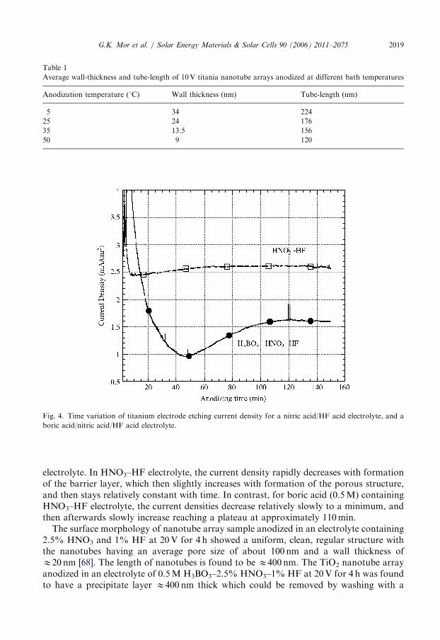
During anodization of titanium foil in a 2.5% HNO3+1% HF water solutionelectrolyte, with or without addition of boric acid, the applied anodic potential wasinitially ramped from 0 to 20V at a rate of 6V/min; the anodization potential was thenheld constant at 20V for 4 h [68]. The voltage ramp was used because initial application ofa 20V anodization potential resulted in high current densities not allowing the formationof an oxide coating due to dielectric breakdown. Fig. 4 shows the current density, as afunction of anodizing time, after the potential has reached 20V, for both types of

ARTICLE IN PRESS
Fig. 3. FE-SEM images of 10V nanotube arrays anodized at: (a) 5 1C with an average wall thickness of 34 nm,
and (b) 50 1C with an average wall thickness of 9 nm. The pore size is E22 nm for all samples.
G.K. Mor et al. / Solar Energy Materials & Solar Cells 90 (2006) 2011–20752018
ARTICLE IN PRESS
Table 1
Average wall-thickness and tube-length of 10V titania nanotube arrays anodized at different bath temperatures
Anodization temperature (1C) Wall thickness (nm) Tube-length (nm)
5 34 224
25 24 176
35 13.5 156
50 9 120
Fig. 4. Time variation of titanium electrode etching current density for a nitric acid/HF acid electrolyte, and a
boric acid/nitric acid/HF acid electrolyte.
G.K. Mor et al. / Solar Energy Materials & Solar Cells 90 (2006) 2011–2075 2019
electrolyte. In HNO3–HF electrolyte, the current density rapidly decreases with formationof the barrier layer, which then slightly increases with formation of the porous structure,and then stays relatively constant with time. In contrast, for boric acid (0.5M) containingHNO3–HF electrolyte, the current densities decrease relatively slowly to a minimum, andthen afterwards slowly increase reaching a plateau at approximately 110min.
The surface morphology of nanotube array sample anodized in an electrolyte containing2.5% HNO3 and 1% HF at 20V for 4 h showed a uniform, clean, regular structure withthe nanotubes having an average pore size of about 100 nm and a wall thickness ofE20 nm [68]. The length of nanotubes is found to be E400 nm. The TiO2 nanotube arrayanodized in an electrolyte of 0.5M H3BO3–2.5% HNO3–1% HF at 20V for 4 h was foundto have a precipitate layer E400 nm thick which could be removed by washing with a

ARTICLE IN PRESSG.K. Mor et al. / Solar Energy Materials & Solar Cells 90 (2006) 2011–20752020
dilute HF solution. In these samples, there is a greater degree of pore irregularity, withsizes ranging from 10 to 120 nm. The average wall thickness of the nanotubes is 20 nm, andnanotube length is about 560 nm.
2.5. KF-based aqueous electrolyte
Nanotube arrays several microns in length have been fabricated using KF (or NaF withequivalent results) electrolytes of variable pH [27], a summary of which is presented inTable 2. With respect to Table 2, prior to KF addition the desired pH was obtained byadding NaOH, sulfuric acid (pH 1–2), sodium hydrogen sulfate, or citric acid (pH 2.5–7.5).The F� concentration was held fixed at 0.1mol/L. In 0.1mol/L F� and 1mol/L H2SO4
medium, the potential window for nanotube formation is 10–25V (Samples 01–08).Outside of this potential range no nanotubes were formed (Samples 01 and 08). In Sample01 (at 5V), the electrochemical etch rate was relatively slow due to lower applied potentialand only a few pits can be seen on the sample surface. In Sample 08 (at 30V), the
Table 2
Electrolyte pH and composition, anodization conditions, and size of the resulting nanotubes
No. Electrolytea pHb V (V) t (h) D (nm) L (mm) Qc
F� SO42� PO4
3� Cit
01 0.1 1.0 — — o1 5 1 1072 — No NT
02 0.1 1.0 — — o1 10 1 4075 0.2870.02 NT
03 0.1 1.0 — — o1 15 1 8079 — NT
04 0.1 1.0 — — o1 20 1 100711 0.4870.03 NT
05 0.1 1.0 — — o1 25 1 110712 0.5670.04 NT
06 0.1 1.0 — — o1 30 1 — — No NT
07 0.1 1.0 — — o1 20 6.5 100711 0.4370.03 NT
08 0.1 2.0 — — o1 20 1 100711 0.4570.03 NT
09 0.1 1.0 — 0.2 1.3 10 20 3075 0.3270.03 NT
10 0.1 1.0 — 0.2 2.8 10 20 3075 0.5970.05 NT
11 0.1 1.0 — 0.2 2.8 15 20 5075 1.0070.05 NT
12 0.1 1.0 — 0.2 2.8 25 20 115710 1.5070.04 NT
13 0.1 1.0 — 0.2 3.8 10 20 3075 0.8070.06 NT
14 0.1 1.0 — 0.2 3.8 10 60 3075 1.8070.06 NT
15 0.1 1.0 — 0.2 3.8 10 90 3075 2.3070.08 NT
16 0.1 1.0 — 0.2 4.5 10 20 3075 1.0570.04 NT
17 0.1 1.0 — 0.2 4.5 25 20 11575 4.4070.10 NT
18 0.1 1.0 — 0.2 5.0 10 20 3075 1.4070.06 NT
19 0.1 1.0 — 0.2 5.0 25 20 11575 6.0070.40 NT
20 0.1 1.0 0.1 0.2 6.4 10 24 — — No NT
21 — 2.0 — — o1 10 24 — — No NT
Cit: citrate; t: time; D: inner diameter of nanotube; L: length of nanotube.
SO42� is from addition of H2SO4 or NaHSO4; PO4
3� is addition of potassium hydrogen phosphate K2HP3O4; Cit
denotes citric acid from its salt, HO(CO2Na)(CH2CO2Na)2 � 2H2O.aElectrolyte components are in mol/L.bpHo1 represents a 1.0 or 2.0mol/L H2SO4 medium.cQuality Q of resulting nanotubes. NT: nanotubes uniformly across substrate. No NT: no nanotubes or partly
developed nanotube/porous structures.

ARTICLE IN PRESSG.K. Mor et al. / Solar Energy Materials & Solar Cells 90 (2006) 2011–2075 2021
electrochemical etch is much faster which prevents nanotube formation; a highly disturbedporous structure was obtained in this case [27]. The nanotube pore size was found to beproportional to the potential applied (Samples 02–05) and independent of the anodizationtime (Samples 04–07) and the electrolyte concentration (Samples 04 and 08). Increasing thepotential from 10 to 25V increased the diameter of the resulting nanotubes from 40 to110 nm. No significant difference was observed in the pore size for anodization times of 1 h(Sample 04) and 6.5 h (Sample 07) or for electrolyte concentrations 1mol/L H2SO4
(Sample 04) and 2mol/L H2SO4 (Sample 08).Electrolyte pH affects both the behavior of the electrochemical etch, and chemical
dissolution owing to the hydrolysis of titanium ions. With increasing pH the hydrolysiscontent increases, which slows the rate of chemical dissolution. As shown in Fig. 5(Samples 10, 13 fabricated at 10V; Samples 12, 17 fabricated at 25V) and Table 2, longernanotubes can be formed in higher pH solutions that remain acidic. For a potential of25V, with pH increasing from strong acidity (Sample 05, pHo1) to weak acidity (Sample17, pH 4.5), nanotube length increased from 0.56 to 4.4 mm; for 10V, the length increasedfrom 0.28 mm (Sample 2, pHo1) to 1.4 mm (Sample 18, pH 5.0). For a particular pH, thelength increases with applied potential (Samples 10–12 and 16–17). When the potentialincreased from 10 to 25V, the length increased from 0.59 to 1.5 mm for pH ¼ 2.8 and from1.05 to 4.4 mm for pH ¼ 4.5. At a particular pH, the pore size of the nanotubes was foundto be increasing with anodization potential as shown in the inset of Fig. 5 (Samples 10, 11,12). However, the pore size was independent of the pH at a particular potential.
In strongly acidic solutions (pHo1), increasing the anodization time does not increasethe nanotube length as shown by Samples 04 and 07. In weak acid electrolytes thenanotube length is time dependent as shown by Samples 13–15 (Fig. 5; Samples 13, 15). Asanodization time increases from 23 to 90 h the nanotube length increase from 0.8 to 2.3 mm.On increasing pH values the hydrolysis content increases, resulting in a significant amountof hydrous titanic oxide precipitated on the nanotube surface. Our studies showed that thebest pH range for formation of relatively longer nanotubes is between pH 3 and 5; lowerpH forms shorter but clean nanotubes, while higher pH values result in longer tubes thatsuffer from unwanted precipitates. Alkaline solutions are not favorable for the self-organized nanotube formation. In the case of Sample 19 (Table 2), where the anodizationwas done in pH 6.4 with 0.1mol/L PO4
3�, no nanotubes but a layer of dense hydroustitania salts were found. Stronger acidity is required for nanotube formation in thepresence of phosphate, owing to the formation of undissolvable titanic phosphates. Nonanotube array formation has been achieved without F�, even in 2mol/L H2SO4 solution(Sample 20).
2.6. Fabrication of transparent TiO2 nanotube arrays
Micro-miniaturization of nanotube array based electronic devices is a challengingprospect when based upon the thick-film Ti foils due to their relative mechanicalinstability. Therefore methods have been developed for fabrication of the highly orderedtitania nanotube arrays from Ti thin films atop a substrate compatible with photo-lithographic processing. The resulting transparent nanotube array structure, illustrated inFig. 6, is promising for applications such as anti-reflection coatings, DSSCs, and hydrogensensors. Crucial to the success of fabricating thin film TiO2 nanotube array devices isdeposition of a high-quality Ti film suitable for transformation into a nanotube array film

ARTICLE IN PRESS
Fig. 5. Lateral view of the nanotubes formed in different pH solutions (pH41). The anodization conditions for
each sample are listed in Table 2. Inset to Samples 10 and 12 show variation of pore size with anodization
potential for a pH 2.8 electrolyte.
G.K. Mor et al. / Solar Energy Materials & Solar Cells 90 (2006) 2011–20752022
[69]. The quality of a deposited film and its adhesion to the substrate appear to be inter-related functions of film thickness and substrate temperature during deposition. Filmsdeposited at room temperature using rf sputtering were found to have poor substrate

ARTICLE IN PRESS
Fig. 6. The key stages in fabrication of a transparent TiO2 nanotube array film: (top) Sputter deposition of a high-
quality Ti thin film; (middle) anodization of resulting film, and (bottom) heat treatment to oxidize remaining
metallic islands.
G.K. Mor et al. / Solar Energy Materials & Solar Cells 90 (2006) 2011–2075 2023
adhesion, peeling off when immersed in the electrolyte. Adhesion was not a problem forfilms deposited at either 250 or 500 1C. Films deposited by rf sputtering at a temperatureabout 250 1C were granular in nature and did not yield well-defined tubular structures.However, in the case of films sputtered at 500 1C, the Ti film structure is highly dense withtight packing of particles; ordered nanotube arrays were formed on these films uponanodization [69].
Anodization of single-layer titanium films was not successful as the metal layer incontact with the electrolyte surface was rapidly etched away, thus breaking electricalcontact with the submerged portion of the film undergoing anodization before nanotubescould be formed. It appears that the non-uniform electric field distribution at themetal–air–electrolyte interface enhances the rate of chemical etching relative to the field-assisted oxidation of the metal. Therefore, a bilayer-film scheme was adopted for thin filmdeposition and anodization. The first layer, of required thickness, was deposited over theentire substrate; a second layer of at least 400 nm thickness was deposited atop the firstlayer over half the substrate area. Anodization to form the nanotube arrays wassuccessfully accomplished by keeping the single layer region completely immersed in theelectrolyte, while having the double-layer region in contact with the electrolyte surface.The higher thickness of the film in contact with the electrolyte surface ensured thesustained anodization of the submerged single layer region to the desired specifications.
A minimum (single) layer thickness is required for the formation of a fully developednanotube array structure. Fig. 7 shows the typical anodization behavior of a 400 nm Tithin film (deposited by rf sputtering at 500 1C) anodized at 10V in an HF-based electrolyte.For an anodization potential of 10V, this thickness was determined as E400 nm; althoughany thickness higher than this can be used, this is optimum for eliminating any residualmetal underneath the nanotubes. For a fixed HF concentration, the dimensions of the tube

ARTICLE IN PRESS
Fig. 7. Anodization behavior of a 400 nm Ti thin film (deposited by rf sputtering at 500 1C) anodized at 10V in
HF-based electrolyte (acetic acid and 0.5 vol% HF mixed in ratio of 1:7) at room temperature. Inset shows a
typical current density vs. time response observed for a titanium foil (with one face protected with polymer
coating) anodized at the same potential and electrolyte.
G.K. Mor et al. / Solar Energy Materials & Solar Cells 90 (2006) 2011–20752024
vary with respect to voltage; for a fixed anodization potential, the dimensions vary withrespect to electrolyte HF concentration. The anodization-potential range over whichnanotube arrays could be formed from the thin films depended upon the concentration ofHF in the electrolyte. For example, at a concentration of 0.5% HF nanotubes were formedin a potential range of 10–15V. Below 10V, a porous structure is obtained, while above15V the resulting structure appeared sponge-like. The anodization voltage window forsuccessfully achieving the nanotube arrays is 6–10V for 0.25% HF concentration, and10–18V for 1% HF concentration.With reference to the anodization behavior (400 nm Ti thin film anodized at 10V in an
HF-based electrolyte) seen in Fig. 7 within a few seconds, E25 s, after application of thevoltage, the measured current density reduced from 415mA/cm2 to a local-minimum of1.25mA/cm2 (point P1 on the plot), with the field-assisted oxidation of the Ti metal surfacereducing the current. The structure of the film at point P1 of Fig. 7 is shown in Fig. 8a; asevident from the figure fine pits or cracks form on the oxide surface and act as porenucleation sites. These pits and cracks arise due to the chemical and field-assisteddissolution of the oxide at local points of high energy. The reduced oxide layer thickness atthese points results in a current increase; Fig. 8b corresponds to point P2 on the plot wherethe crack/pit density has reached saturation as evidenced by the current maximum. Beyondthis point the current gradually drops due to a corresponding increase in porous structuredepth. A porous structure is clearly seen in Fig. 8c, corresponding to point P3, with porediameters of �20 nm. Fig. 8d, point P4, shows the transition between a porous structureand the nanotubular structure. Fig. 8e, point P5, shows the resulting nanotube array withpore diameters of 20–30 nm. Nanotube array length increases to point P4 (E360 s), as

ARTICLE IN PRESS
Fig. 8. FE-SEM images of samples taken at points P1, P2, P3, P4, and P5 as noted in Fig. 7.
G.K. Mor et al. / Solar Energy Materials & Solar Cells 90 (2006) 2011–2075 2025
evident from the decrease in the current. Between P4 and P5 the nanotube array lengthremains essentially constant.
As the anodization proceeds the metal below the oxide barrier layer is progressivelyconsumed. Beyond a certain stage the metal layer becomes thin or discontinuous enough tocreate highly resistive electrical current pathways. Hence beyond P5 (Fig. 7) the current

ARTICLE IN PRESSG.K. Mor et al. / Solar Energy Materials & Solar Cells 90 (2006) 2011–20752026
drastically reduces, finally dropping to zero as the metal film becomes completelydiscontinuous. We make note that only a small dip in current can be seen at P5 as thesample was taken out of the anodization bath at this point. Keeping the sample inside theanodization bath beyond point P5 destroys the nanotube structure due to its chemicaldissolution in HF electrolyte. Real time observation of the current enabled us to removesamples from the anodization bath as soon as the dip in the current plateau region, justbeyond P5, was observed. SEM images of samples kept beyond point P5 showed that thenanotube layer was severely damaged or completely eliminated. Thus, strict processcontrol is necessary to obtain intact nanotube arrays without an underlying metal layer.However, if there is a need to keep a continuous metal layer underneath the nanotubes thesamples should be removed from the anodization bath at a point between P4 and P5. Closemonitoring of the electric current response during potentiostatic anodization helpsdetermine the optimum anodization parameters and serves as a process control tool.The inset of Fig. 7 shows a typical current vs. time plot obtained during anodization
(same conditions as thin film) of a 250 mm thick Ti foil with one face protected with apolymer coating. It can be seen that the current-time behavior is no different from that ofthe thin films. We note that if both sides of the foil are exposed to anodization the currentbehavior will be significantly different from that seen in Fig. 7. In this case, the changes inthe current after the initial dip cannot be discerned due to the anodization processprogressing at different levels on both sides of the sample. It was noticed in both thin filmsand metal foils (Fig. 7) that current shows periodical fluctuations of a small magnitudebetween point P2 and P5; similar fluctuations were observed by others [29,70]. Macak andco-workers suggest predicted that the current transients causing inhomogeneities on tubewall are due to pH bursts at the pore tip, which can be suppressed by decreasing thediffusion constant in the electrolyte. They reported a smoothing of the nanotube walls byanodizing titanium in glycerol-based electrolyte containing 0.5wt% NH4F [30].In strongly acidic solutions (pHo1) both the nanotube growth rate and dissolution rate
are increased, therefore increasing the anodization time does not increase the nanotubelength. In short nanotube (obtained at 10V), time required to form nanotube is about6min. Further increasing the time for anodization result into more uniform nanotubularstructure both in shape and size with not much change in the length of nanotubes.Increasing pH decreases the chemical dissolution rate, and apparently prolongs the timeneeded to reach equilibrium between the rate of nanotube growth and the dissolution rate;in weak acid electrolytes, therefore the nanotube length is appearing to be time dependent.In such solution, even without having a protective covering on one side of foil, we stillobserved the same pattern in current vs. time plot as shown in Fig. 7. Only variation is interm of difference in current density between P1 and P2, and time between P1 and P4 [71].However, anodization has to be continued upto point P4 for obtaining a completenanotubular structure in titania. In KF-based solution with pH 5.0 and anodizationvoltage 25V, the time required to reach point P4 is 17 h and the resulting length ofnanotubes is 6.0 mm70.4 mm [71].
2.7. Mechanistic model of nanotube array formation
The key processes responsible for anodic formation of nanoporous alumina [72–79] andtitania [80–83] appear to be the same, and are fundamental to the formation of straighttitania nanotubes. The key processes are: (1) Oxide growth at the surface of the metal

ARTICLE IN PRESSG.K. Mor et al. / Solar Energy Materials & Solar Cells 90 (2006) 2011–2075 2027
occurs due to interaction of the metal with O2� or OH� ions [73]. After the formation of aninitial oxide layer, these anions migrate through the oxide layer reaching the metal/oxideinterface where they react with the metal. (2) Metal ion (Ti4+) migration from the metal atthe metal/oxide interface; Ti4+ cations will be ejected from the metal/oxide interface underapplication of an electric field that move towards the oxide/electrolyte interface. (3) Field-assisted dissolution of the oxide at the oxide/electrolyte interface [73,74]. Due to theapplied electric field the Ti–O bond undergoes polarization and is weakened promotingdissolution of the metal cations. Ti4+ cations dissolve into the electrolyte, and the free O2�
anions migrate towards the metal/oxide interface, see process (1), to interact with the metal[84,85]. (4) Chemical dissolution of the metal, or oxide, by the acidic electrolyte also takesplace during anodization. Chemical dissolution of titania in the HF electrolyte plays a keyrole in the formation of nanotubes rather than a nanoporous structure.
To help understand the process of nanotube formation, FE-SEM images of the surfaceof the samples anodized at 20V for different durations were taken and analyzed [26]. Asthe anodization process begins the initial oxide layer [85], formed due to interaction of thesurface Ti4+ ions with oxygen ions (O2�) in the electrolyte, is seen uniformly across thesurface. The overall reactions for anodic oxidation of titanium can be represented as
2H2O! O2 þ 4eþ 4Hþ (1)
TiþO2! TiO2 (2)
In the initial stages of the anodization process field-assisted dissolution dominates chemicaldissolution due to the relatively large electric field across the thin oxide layer [84]. Smallpits formed due to the localized dissolution of the oxide, represented by the followingreaction, act as pore forming centers:
TiO2 þ 6F� þ 4Hþ ! TiF2�6 þ 2H2O (3)
Then, these pits convert into bigger pores and the pore density increases. After that, thepores spread uniformly over the surface. The pore growth occurs due to the inwardmovement of the oxide layer at the pore bottom (barrier layer) due to processes (1)–(3)[85,86]. The Ti4+ ions migrating from the metal to the oxide/electrolyte interface dissolvein the HF electrolyte [73,84,85]. The rate of oxide growth at the metal/oxide interface andthe rate of oxide dissolution at the pore-bottom/electrolyte interface ultimately becomeequal, thereafter the thickness of the barrier layer remains unchanged although it movesfurther into the metal making the pore deeper. Close examination of FE-SEM images showthe formation of small pits in the inter-pore regions which eventually leads to pore-separation and tube formation. The thickness of the tubular structure ceases to increasewhen the chemical dissolution rate of the oxide at the mouth of the tube (top surface)becomes equal to the rate of inward movement of the metal/oxide boundary at the base ofthe tube. Higher anodization voltages increase the oxidation and field-assisted dissolutionhence a greater nanotube layer thickness can be achieved before equilibrating with thechemical dissolution.
With the onset of anodization, a thin layer of oxide forms on the titanium surface(Fig. 9a). Small pits originate in this oxide layer due to the localized dissolution of theoxide (Fig. 9b) making the barrier layer at the bottom of the pits relatively thin which, inturn, increases the electric field intensity across the remaining barrier layer resulting infurther pore growth (Fig. 9c). The pore entrance is not affected by electric field-assisted

ARTICLE IN PRESS
Fig. 9. Schematic diagram of the evolution of a nanotube array at constant anodization voltage: (a) oxide layer
formation, (b) pit formation on the oxide layer, (c) growth of the pit into scallop shaped pores, (d) metallic part
between the pores undergoes oxidation and field assisted dissolution, and (e) fully developed nanotube array with
a corresponding top view.
G.K. Mor et al. / Solar Energy Materials & Solar Cells 90 (2006) 2011–20752028
dissolution and hence remains relatively narrow, while the electric field distribution in thecurved bottom surface of the pore causes pore widening, as well as deepening of thepore. The result is a pore with a scallop shape [82,87]. As the Ti–O bond energy is high(323 kJ/mol), in the case of titania it is reasonable to assume that only pores having thinwalls can be formed due to the relatively low ion mobility and relatively high chemicalsolubility of the oxide in the electrolyte, hence un-anodized metallic portions can initiallyexist between the pores. As the pores become deeper the electric field in these protrudedmetallic regions increases enhancing the field-assisted oxide growth and oxide dissolu-tion, hence simultaneously with the pores well-defined inter-pore voids start forming, seeFig. 9d. Thereafter, both voids and tubes grow in equilibrium. The nanotube lengthincreases until the electrochemical etch rate equals the chemical dissolution rate of the topsurface of the nanotubes. After this point is reached the nanotube length will beindependent of the anodization duration, as determined for a given electrolyteconcentration and anodization potential.This chemical dissolution, the key for the self-organized formation of the nanotube
arrays, reduces the thickness of the oxide layer (barrier layer) keeping the electrochemicaletching (field-assisted oxidation and dissolution) process active. No nanotubes can beformed if the chemical dissolution is too high or too low. The electrochemical etch ratedepends on anodization potential as well as concentration of electrolytes. If theelectrochemical etch proceeds faster than the chemical dissolution the thickness of the

ARTICLE IN PRESSG.K. Mor et al. / Solar Energy Materials & Solar Cells 90 (2006) 2011–2075 2029
barrier layer increases, which in turn reduces the electrochemical etching process to the ratedetermined by chemical dissolution. The chemical dissolution rate is determined by theF� concentration and solution pH (reaction 3). With increasing F� and H+ concentrationschemical dissolution increases. Recent investigations have shown that only in a certainF� concentration range can nanotube arrays be achieved; from 0.05 to 0.3mol/L in acidicsolution. The anodic potential at which nanotubes are formed is related to theF� concentration, with higher potentials requiring electrolytes of higher F� concentration.
3. Doped titania nanotubes
3.1. Flame-annealed nanotubes
Annealing titanium metal foils and titanium oxide films in a hydrocarbon flame formscarbon-doped titania with a significantly enhanced full spectrum photoresponse. Onannealing Ti metal foils in a natural gas flame at 850 1C Khan and co-workers found thediffuse reflectance spectra of these samples to be significantly broadened [88]; in addition toa shift in the primary absorption threshold from 414 to 440 nm, a second opticalabsorption threshold appeared at 535 nm, which was used to extract a band gap of 2.32 eV.However, on flame annealing their samples using a propane/butane–oxygen mixture,Augustynski and coworkers described a shift of the spectral photoresponse into the visibleregion up to 425 nm but their samples did not exhibit a secondary band edge [89].
The effect of flame annealing on two different nanotube array geometries has beeninvestigated. The first geometry consisted of nanotubes with an average pore size of 22 nm,an average wall thickness close to 20 nm and a length of �200 nm (10V, acetic acid+0.5%HF solution) annealed at 450 1C in oxygen ambient for 6 h for crystallization. The secondgeometry investigated was nanotubes synthesized by anodic oxidation of titanium foils inan electrolyte containing potassium fluoride (0.1M), tetrabutylammonium hydroxide(0.05M), trisodium citrate (0.2M) and sodium hydrogen using a potential of 25V, over a17-h anodization. The pH of the electrolyte, adjusted by adding sodium hydrogen sulfate,was 4.5 for the duration of the process. The samples were then annealed at 600 1C in anoxygen atmosphere for 6 h, with a resulting pore size of 100 nm, a wall thickness ofE20 nm and a length of 4.4 mm.
Flame annealing of the nanotube array samples was performed in air after thecrystallinity-inducing annealing step by exposing them to the reductive region of a propaneburner for 3min. The temperature of the titania surface while exposed to propane flamewas found to be 1020725 1C. The duration of the flame anneal was kept brief to preservethe nanotubular structure, which is destroyed upon prolonged exposure to temperatures inexcess of 650 1C due to thermal oxidation of the underlying titanium foil. The sharpcontrast in the morphology of the nanotubes with and without the flame anneal is depictedin Fig. 10.
3.2. Dopant introduction via modification of anodization bath chemistry
Recently band-gap engineering of TiO2 by anionic doping has been receiving attention.Asahi and co-workers [49] performed densities of states (DOSs) calculations on the effectof substitutional doping and identified nitrogen as the most effective dopant due to itscomparable ionic radius and because its p-states contributed to band gap narrowing by

ARTICLE IN PRESS
Fig. 10. FE-SEM images of KF electrolyte anodized nanotube arrays anodized at 25V: (a) before, and (b) after
flame annealing.
G.K. Mor et al. / Solar Energy Materials & Solar Cells 90 (2006) 2011–20752030

ARTICLE IN PRESSG.K. Mor et al. / Solar Energy Materials & Solar Cells 90 (2006) 2011–2075 2031
mixing with the p-states of oxygen [50]. However, Lee et al. [90] contradicted thisassessment in their report, where their density functional calculations indicate that whilenitrogen doping produces isolated N 2p states above the valence band maximum of TiO2,the mixing of N with O 2p states is too weak to result in appreciable band-narrowing.There has recently been a surge of interest in this area documenting different experimentalapproaches towards nitrogen doping of titania [91–93]. The possibility exists forelectrochemical incorporation of anionic dopants, specifically nitrogen, during theanodization process [64]. Various organic solvents have been used in the anodicfabrication of macroporous silicon and aluminum oxide [94–97]. It has been shown thatorganic solvents essentially suppress the electrochemical oxidation of silicon in comparisonto an aqueous electrolyte [94,95], and that an organic solvent can act as mild oxidizingreactant for silicon [98]. As previously reported in the anodic fabrication of nanoporousalumina using a neutral organic electrolyte [99], it was hypothesized that a significantamount of organic material could be incorporated into anodic TiO2 films by using organicelectrolytes. Such in situ chemical doping of the TiO2-nanotube arrays might prove usefulin band-gap engineering of the resulting material.
Fig. 11 shows a typical potentiostatic current density–time plot for a titanium electrodein 1:1 DMSO and ethanol solvent containing 4% HF at 20V (vs. Pt). The current densitydecreases during the first hour of anodization, indicating formation of a barrier layer onthe titanium surface. Several peaks in the current density–time curve can be observed overthe 70 h period. The change in current density indicates changes in the titania film growthrate, structure, and anodic area. FE-SEM images of a resulting sample taken directly fromthe anodization bath are shown in Fig. 12 at varying degrees of magnification. Theinhomogeneous cracked surface with cylindrical nanotubes clumped together can beclearly observed. It is believed that the cracks are the result of surface stress originating
Fig. 11. Typical potentiostatic (20V) current–time response for a titanium foil electrode in DSMO and ethanol
mixture solution (1:1) containing 4% HF at room temperature.

ARTICLE IN PRESS
Fig. 12. FE-SEM images of titanium foil sample anodized in DSMO and ethanol mixture solution (1:1)
containing 4% HF at +20V (vs. Pt) for 70 h at room temperature. Surface is shown at three levels of
magnification.
G.K. Mor et al. / Solar Energy Materials & Solar Cells 90 (2006) 2011–20752032
during formation of the oxide films. Such cracks are not apparent in films fabricated byanodization of Ti in aqueous electrolytes, possibly due to the rapid oxide formation. It wasalso noted that the well-organized nanotube array structure can only be formed over aperiod of approximately 48 h in a 1:1 DMSO and ethanol electrolyte.FE-SEM images of a sample identical to that in Fig. 12 that has been washed in dilute
HF prior to imaging is shown in Fig. 13. The surface coating partially obscuring thenanotube tops seen in Fig. 12, that also acts to clump the nanotubes together, has beenremoved. The obtained nanotubes have a pore size diameter of approximately 60 nm and awall thickness of 40 nm. The average height of the nanotubes is approximately 2.3 mm, witha variation of approximately 0.3 mm. The diameter of the resulting nanotubes at 10V in 1:1DMSO and ethanol containing 4% HF is E24 nm. Compared with the nanotube arraysfabricated in aqueous electrolytes, nanotube arrays fabricated in the organic electrolytesare relatively fragile; the individual nanotubes of the array can be separated by sonicationin dilute HF. The evolution in surface morphology was studied as a function ofanodization time in the same electrolyte composition and voltage [23]. It was found that noself-organized pore or tubular structures are formed in the initial 24 h anodization. After48 h a well-ordered nanotube array structure is formed. With the 72 h anodization the

ARTICLE IN PRESS
Fig. 13. FE-SEM images of sample shown in Fig. 12 after washed in dilute HF.
G.K. Mor et al. / Solar Energy Materials & Solar Cells 90 (2006) 2011–2075 2033
nanotubes clump, or lean together, presenting crack-like features readily apparent in thesurface.
3.3. CdS-coated nanotubes
Other efforts concerned with shifting of the TiO2 band gap have focused onphotoelectrode sensitization through combination with narrow-band gap semiconductorfilms [100]. Such sandwich electrodes may be advantageous as electron injection may beoptimized through confinement effects, and a sensitizer, a 1.5 eV edge absorber, is wellapproximated by a narrow band gap semiconductor material [101]. Since the conductionband of bulk CdS is ca. 0.5V more negative than that of TiO2, this coupling of thesemiconductors should have a beneficial role in improving charge separation. TiO2
nanotube electrodes were prepared at 20V in a HF and acetic acid solution [100]. Theseamorphous samples were then crystallized at 480 1C for 6 h in oxygen gas ambient. A CdSfilm was then deposited upon the crystallized TiO2 nanotube array by cathodic reduction,using a conventional three-electrode system comprising an Ag/AgCl reference electrodeand Cd counter electrode [87]. A mixed solution of saturated elemental sulfur in benzene

ARTICLE IN PRESS
Fig. 14. Top surface FE-SEM view of: (a) TiO2 nanotube array electrode, and (b) CdS–TiO2 nanotube array
electrode after CdS electrodeposition at �0.5V for 30min.
G.K. Mor et al. / Solar Energy Materials & Solar Cells 90 (2006) 2011–20752034
with 0.6M CdCl2 in dimethyl sulfoxide (DMSO) was used as the electrolyte. The solutionwas bubbled with flowing N2 for 30min prior to electro-deposition in order to remove O2
and any moisture within the solution. The cathodic potential was kept constant at �0.5Vfor different deposition times. After electrodeposition the samples were thoroughly rinsedwith acetone, methanol and D.I. water. The prepared CdS–TiO2 electrodes were annealedat 350 and 400 1C for 1 h in a N2 atmosphere to investigate the influence of annealing ontheir photoelectrochemical response. It was suggested that when a cathodic potential isapplied to the TiO2 nanotube electrode, it will reduce sulfur to S2� on the electrode surface,while the applied electric field induces Cd2+ to migrate towards the electrode hence underproper conditions CdS will form at the electrode surface [102]. Fig. 14a shows anillustrative FE-SEM image, top surface view, of a TiO2 nanotube array upon which just afew CdS nanoparticles,E20 nm diameter, have been deposited (�0.5V for 5min). Fig. 14bshows the topology after a 30min (�0.5V) electrodeposition of the CdS nanoparticles.
4. Material properties
4.1. Structural and elemental characterization
The properties of titania depend on the crystallinity and isomorph type. Anatase phaseis preferred in charge separation devices such as DSSCs, while rutile is used predominatelyin gas sensors and as dielectric layers. Rutile has minimum free energy in comparison toother titania polymorphs hence given the necessary activation energy all other polymorphsincluding anatase transform into rutile through first-order phase transformation.However, the temperature at which metastable anatase to stable rutile transformationtakes place depends upon several factors, including impurities present in the anatase,primary particle size, texture and strain in the structure. Hence, porosity and/or surfacearea reduction occur due to the sintering effects associated with nucleation-growth type ofphase transformations [103–105].

ARTICLE IN PRESSG.K. Mor et al. / Solar Energy Materials & Solar Cells 90 (2006) 2011–2075 2035
As-anodized titania nanotubes are amorphous, and crystallized by a high-temperatureanneal. GAXRD patterns of a 20V HF electrolyte sample annealed at differenttemperatures in dry oxygen ambient are shown in Fig. 15 [106]. In the diffractionpatterns, the anatase phase starts appearing at a temperature of 280 1C. As the 250 1Cannealed sample was amorphous (only reflections from titanium support can be seen), it isclear that the sample was crystallized in anatase phase at a temperature between 250 and280 1C. At a temperature near 430 1C rutile phase appears in the X-ray diffraction pattern.Beyond this temperature, the rutile (1 1 0) peak grows whereas the anatase (1 0 1) peakdiminishes. Complete transformation to rutile occurs in the temperature range 620–680 1C.It can also be seen from Fig. 15 that the reflection from the titanium support is gettingreduced at temperatures between 430 and 580 1C and they fully vanish at around 680 1C.This shows that the oxidation followed by crystallization of titanium support takes place atthese temperatures. With respect to variation of the size of the anatase and rutilecrystallites with temperature, it was found that the anatase grain size initially increases
Fig. 15. Glancing angle X-ray diffraction patterns of the nanotube array samples annealed at temperatures
ranging from 230 to 880 1C in dry oxygen ambient for 3 h. A, R, and T represent anatase, rutile, and titanium,
respectively.

ARTICLE IN PRESSG.K. Mor et al. / Solar Energy Materials & Solar Cells 90 (2006) 2011–20752036
with temperature but between �480 and 580 1C the grain size decreases to increase againafter 580 1C. At the same time the grain size of rutile progressively increases withtemperature after its nucleation. At 430 1C a rutile fraction of 31% compared to anatasewas formed. It increased to 75% at 480 1C and further to 92% at 580 1C on annealingfor 3 h.The evolution of the surface morphology as a result of high-temperature annealing has
also been studied. For nanotube arrays atop Ti foil, the structure of the 20V sample wasfound to be stable till around 580 1C (for 10V sample, it is about 500 1C). No discerniblechange in the pore diameter or wall thickness was observed even after annealing for 3 h atthis temperature. It was observed that at temperatures in the range 550–580 1C dependingon the sample, small protrusions come out through the porous structure. Above thistemperature the tubular structure completely collapsed leaving dense rutile crystallites.HR-TEM images of the wall and contact points of crystallized nanotubes indicate that thecrystallites the wall have a length of �35 nm and a width of around �12 nm. Differentregions of the walls were examined using HR-TEM and all crystallites were found to beanatase from Fourier transform analysis. On comparing energy dispersive X-ray spectra(EDS) of the as-deposited and the one fired at 580 1C in oxygen ambient, it was shown thatthe relative intensity of oxygen peak with respect to titanium Ka peak increased onannealing in presence of oxygen which is an indication of the improvement in thestoichiometry of the sample.The as-anodized titania films fabricated from a Ti thin film deposited on glass, taken out
of the anodization bath at P5 of Fig. 7, having an extremely thin discontinuous metal layerunderneath the nanotubes, were annealed at 260, 280 and 500 1C for 6 h in dry oxygenambient. Their GAXRD patterns showed only one exception, the absence of rutile phasein the thin film samples annealed at 500 1C [69]. This result is in striking contrast to thatfound with nanotube arrays formed from Ti thick-film foils, where an earlier study notedthat rutile phase appears at 430 1C and both rutile and anatase co-exist till around 620 1C(shown in earlier section). However, we find that thin film samples with a continuousmetal layer underneath the nanotubes behave in a way similar to that of the foil samples,with both rutile and anatase phases co-existing at 480 1C. These results support thehypothesis that rutile grows at the interface between the barrier layer and titanium metalwhere the metal is thermally oxidized. The constraints imposed by the nanotube wallsmake it difficult for the anatase crystals situated there to undergo phase transformationto rutile.The X-ray patterns of nanotube array samples obtained in H3BO3–HNO3–HF and
HNO3–HF baths, annealed at 550 1C for 6 h with a heating and cooling rate of 1 1C/min inoxygen ambient, are similar to ones observed for nanotubes formed in the HF electrolyte[68]. After annealing, the phase-structure of the architecture can be viewed as an anatasenanotube array atop a rutile barrier layer. In comparison, a TiO2 film made by 550 1Cthermal annealing is primarily rutile phase with traces of anatase phase. The normalizedreference intensity ratio (RIR) method was used to estimate the weight fraction of anatase,rutile, and titanium in the resulting samples [107]. The calculated RIR result of theH3BO3–HNO3–HF prepared sample is anatase 33.6%, rutile 58.7%, and titanium 7.7%.The calculated RIR result of the HNO3–HF prepared sample is anatase 1.7%, rutile66.5%, and titanium 31.7%. Considering a similar X-ray sampling depth for both samples,the higher weight percentage of titanium in the HNO3–HF anodized sample indicates athinner barrier layer, and shorter nanotube array length. Consequently, the thinner barrier

ARTICLE IN PRESSG.K. Mor et al. / Solar Energy Materials & Solar Cells 90 (2006) 2011–2075 2037
layer gives rise to a lower-measured anatase weight percentage for the sample obtained inHNO3–HF.
A XPS scan for the HNO3–HF sample, after 550 1C annealing, indicated the elements Ti(23.0%), O (64.3%), N (1.0%), F (0.5%), and C (8.0%). For the H3BO3–HNO3–HFelectrolyte sample, 550 1C annealed, a scan point out Ti (27.4%), O (65.3%), N (0.3%), F(0.8%), and C (4.7%). Both carbon and some of the oxygen can be viewed as surfacecontamination, while the small amounts of N and F originate from the electrolytes used forsample preparation. XPS analysis of the H3BO3–HNO3–HF sample before annealingspecifies Ti (26.9%), O (60.2%), N (1.7%), F (6.6%), and C (4.5%). Chemical stateanalysis indicates the sample is comprised of Ti4+ bonded with oxygen (TiO2),contaminated with N, F and C compounds; no boron was detected in the samples. TheO1s spectra of the samples (in boric acid bath) showed a single peak at 530.8 eV. However,in the HNO3–HF sample there is an indication of a second peak at 532 eV, revealing thepresence of two forms of oxygen [68]. The Ti2p3/2 peak has a binding energy of 459.0 eVfor both samples, indicating Ti present in the samples is in the form of TiO2. For thesemeasurements the sampling depth of the X-rays is 8 nm, thus the Ti substrate cannot bedetected. The position of 2p3/2 peak of Ti in the form of TiO2 was in consistent with theformation of a crystalline TiO2 [108,109].
GAXRD patterns of the long (several micron) nanotube array samples fabricated usingKF (or NaF, the two acids result in equivalent architectures) based electrolytes annealed atdifferent temperatures up to 700 1C are shown in Fig. 16 [10,27]. It can be seen that thenanotubes maintain the amorphous behavior on annealing at 230 1C. The crystallizationoccurs in anatase phase at a temperature near 280 1C. It may be noted that crystallizationof the samples prepared using HF electrolyte without any additives also showed the samecrystallization temperature [106]. Apparently, electrolyte concentration or pH has no
Fig. 16. Glancing angle X-ray diffraction patterns of a 6.0mm long nanotube array as a function of annealing
temperature (oxygen ambient).
ARTICLE IN PRESS
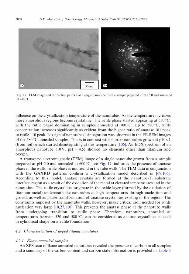
Fig. 17. TEM image and diffraction pattern of a single nanotube from a sample prepared at pH 5.0 and annealed
at 600 1C.
G.K. Mor et al. / Solar Energy Materials & Solar Cells 90 (2006) 2011–20752038
influence on the crystallization temperature of the nanotubes. As the temperature increasesmore amorphous regions become crystalline. The rutile phase started appearing at 530 1C,with the rutile phase dominating in samples annealed at 700 1C. Up to 580 1C, rutileconcentration increases significantly as evident from the higher ratio of anatase 101 peakto rutile 110 peak. No sign of nanotube disintegration was observed in the FE-SEM imagesof the 580 1C annealed samples. This is in contrast with shorter nanotubes grown at pHo1(from foil) which started disintegrating at this temperature [106]. An EDX spectrum of anamorphous nanotube (10V, pH ¼ 4.5) showed no elements other than titanium andoxygen.A transverse electromagnetic (TEM) image of a single nanotube grown from a sample
prepared at pH 5.0 and annealed at 600 1C, see Fig. 17, indicates the presence of anatasephase in the walls; rutile phase is not found in the tube walls. The TEM data in conjunctionwith the GAXRD patterns confirm a crystallization model described in [69,106].According to this model, anatase crystals are formed at the nanotube-Ti substrateinterface region as a result of the oxidation of the metal at elevated temperatures and in thenanotubes. The rutile crystallites originate in the oxide layer (formed by the oxidation oftitanium metal) underneath the nanotubes at high temperatures through nucleation andgrowth as well as phase transformation of anatase crystallites existing in the region. Theconstraints imposed by the nanotube walls, however, make critical radii needed for rutilenucleation very large [10,27,110]. This prevents the anatase phase at the nanotube wallsfrom undergoing transition to rutile phase. Therefore, nanotubes, annealed attemperatures between 530 and 580 1C, can be considered as anatase crystallites stackedin cylindrical shape on a rutile foundation.
4.2. Characterization of doped titania nanotubes
4.2.1. Flame-annealed samples
An XPS scan of flame annealed nanotubes revealed the presence of carbon in all samplesand a summary of the carbon content and carbon state information is provided in Table 3

ARTICLE IN PRESS
Table 3
Carbon content and chemical state information (from XPS)
Sample Depth (nm) Total C (at%) C–C C–O COO
Short NT 0 0.7 — — —
100 0.3 — — —
Flame annealed short NT 0 3.3 2.5 0.4 0.5
100 2.8 1.9 0.6 0.3
Flame annealed long NT 0 5.6 3.9 0.8 0.9
100 5.2 3.8 0.9 0.6
Long NT 0 3.5 2.3 0.5 0.7
100 3.0 1.9 0.6 0.5
Flame annealed Ti foil 0 4.0 2.7 0.6 0.7
100 3.8 2.5 0.7 0.5
G.K. Mor et al. / Solar Energy Materials & Solar Cells 90 (2006) 2011–2075 2039
[111]. Fluorine was present in all samples, at surface concentration of nearly 2 at%,decreasing to about 0.2 at% in the interior. The presence of both sodium and fluorine aredirectly related to the chemistry of the anodizing baths. Based on the analysis of the C1speak, incorporated carbon was present in C–C (285.3 eV), CO (286.5 eV), COO (289.0 eV)and C–N bonds. The Ti–C signal at 281.9 eV was not observed. The carbon content of theshort nanotubes, which is initially quite small, becomes appreciable upon flame annealing.A significant amount of carbon (�3%) is present in the long KF nanotube samples evenprior to flame annealing, which is attributed to the presence of a large number of organicions such as citrate and tetrabutylammonium in the anodizing bath. In long nanotubes,flame annealing introduces additional carbon into a structure where carbon preexists inappreciable quantities. Hence, flame-annealed long nanotubes have the highest carboncontent (45%) of the samples studied.
4.2.2. Nitrogen-doped titania
Titanium foils were potentiostatically anodized at 25V in an electrolyte of pH 3.5containing 0.4M ammonium nitrate NH4NO3 and 0.07M HF acid; with reference toFig. 18, Sample A was removed after 17 s of anodization, while Sample B was anodized for240 s. Sample C was anodized for 6 h at 20V in an electrolyte of pH 3.5 containing 2.5MNH4NO3 and 0.07M HF. Such anodization chemistry restricts the electrolytic ions tonitrogen and fluorine bearing species, allowing control of the possible elements that canbe incorporated into the anodic titania films. The potential and pH regimes chosen weresuch as to facilitate nanotube array formation. The maximum current at the onset ofthe anodization was limited by the compliance of the power supply used to performthe anodization. In the first 25 s, after application of the voltage, the measured currentdensity reduced from 4120mA/cm2 to a local-minimum between 15 and 25mA/cm2,with the field-assisted oxidation of the Ti metal surface reducing the current. In thepotential range under consideration, this behavior is typical for the anodization ofTi in fluoride ion containing acidic electrolytes; however, the magnitude of the anodizationcurrents is much greater. The larger anodization currents are attributed to the stronger

ARTICLE IN PRESS
Fig. 18. N 1s XPS spectra for samples A–C (pedigree described in text) with respective nitrogen-doping levels [x].
G.K. Mor et al. / Solar Energy Materials & Solar Cells 90 (2006) 2011–20752040
oxidizing and etching action of the nitrate ion containing electrolyte. High-resolutionN 1s XPS spectra of Samples A (x ¼ 0:23), B (x ¼ 0:09) and C (x ¼ 0:02) is shown inFig. 18. XPS data confirms that all the incorporated nitrogen is substitutional on theoxygen site. The nitrogen peak at 396.8 eV was observed and assigned to atomic b-N,indicating a chemically bound N� state [112,113]. Fluorine was present in the amorphousas-anodized samples, with the final concentration of incorporated F� sensitive to theannealing conditions. Annealing processes (in air) lasting longer than 6 h at tempera-tures above 600 1C resulted in fluorine atoms being completely resubstituted by oxygen.The depth profile of a 250 nm thick film with a surface nitrogen concentration x ¼ 0:05(the sample was anodized at 20V for 120 s in a pH 4.5 electrolyte containing0.4M ammonium nitrate and 0.07M HF acid then annealed per the other samples)indicated that the doping of nitrogen is inhomogeneous with the maximum nitrogen beingincorporated close to the surface then linearly decreasing with increasing depth inside thefilm.The precise reactions involving the decomposition of ammonium ions and nitrate ions at
the anodic surface to form N-doped titania are currently unclear, and the subject ofongoing studies. However, the anodization of aluminum in nitric acid has been studiedpreviously and is known to be relatively complex [114]. A study of the interaction ofaluminum with nitrate ions in thin oxide films formed in nitrate ion containing electrolytesindicated that the adsorption of nitrate ions on the oxidized surface of aluminium wasfollowed by their reduction inside the oxide film [115]. Parhutik and co-workers [116]reported the incorporation of electrolyte anions in the anodic film formed by anodizationof Al in HNO3 solution. Furthermore, it was reported that the anion concentration, in thegrowing oxide, reaches a maximum value at the moment when intensive pore growth startsand the oxide is thin, i.e. when the anodizing time is very brief [114,116] and the surfacetopology strongly dependent upon the applied forming conditions. Similar behavior was

ARTICLE IN PRESS
Table 4
XPS results of titanium etched in fluorinated 1:1 DSMO and ethanol at 20V for 48 h, one of the samples annealed
at 550 1C for 6 h
Atomic Con. (%) Ti O F N C S
Nanotubes 23.9 53.4 13.7 0.9 6.8 1.1
Annealed nanotubes 26.6 64.3 1.6 0.5 5.8 1.2
G.K. Mor et al. / Solar Energy Materials & Solar Cells 90 (2006) 2011–2075 2041
observed for Ti anodization, with maximum nitrogen incorporation occurring in a filmanodized for a mere 17 s (Sample A). Thus, a trade-off exists between the morphology andthe level of nitrogen doping. Shorter anodization periods result in higher concentrations ofincorporated nitrogen, whereas longer anodization periods are required for evolution ofthe nanotube array architecture.
4.2.3. Organic bath
XPS was used to determine the elemental composition of the nanotube array samplesfabricated in an organic anodization bath, with results summarized in Table 4. Thenanotube array samples are predominately titanium and oxygen, with traces of fluorineand sulfur due to solvent incorporation in the anodic films. It was believed that surfacecontamination is the likely source for the nitrogen and carbon found in the samples.Chemical state analysis for titanium indicates the sample is Ti4+ bonded with oxygen(TiO2). Compared with samples fabricated in aqueous electrolytes [27], the atomicconcentration of fluorine (13%) is considerably increased using the organic electrolyte.However the fluorine concentration is dramatically reduced in the annealed samples, to1.6%; GAXRD gives no indication of TiOxFy or TiOxSy in the samples. Hence while theresults of XPS and XRD indicate a considerable amount of solvent is trapped in theamorphous anodic films, the trapped elements such as F, C, and S do not enter the rutile oranatase lattice.
4.2.4. CdS-coated nanotubes
In the GAXRD pattern of CdS coated (short, HF fabricated) TiO2 nanotube arrayannealed at 350 1C for 1 h, Chen and co-workers [87] observed a prominent TiO2 Braggpeak along with weak Bragg reflections at 2y values of 26.55, 30.75, 44.04, 52.16, 54.67,corresponding to the (1 1 1), (2 0 0), (2 2 0), (3 1 1), and (2 2 2) Bragg reflections of cubicCdS, respectively. The general scan spectrum of XPS of CdS–TiO2 electrodes showedsharp peaks for Ti, O, Cd, S, and also C. The Cd 3d core level XPS spectrum has twopeaks at 405.3 eV (3 d5/2) and 411.9 eV (3 d3/2), in good agreement with published values[117]. The S 2p core level spectrum indicated that there are two chemically distinct speciesin the spectrum. The peak at 161.9 eV is for sulfide, the structure occurs because of asplit between 2p3/2 and 2p1/2 ; the split is near 1.18 eV and the area ratio is 2:1, inexcellent agreement with published values of the S 2p signal for CdS [29]. Measuredatomic concentrations of the as-prepared samples suggested that when the sulfate/Oratio is 1, the sulfide/Cd ratio is 0.86; this means that the CdS nanoparticles obtainedare slightly Cd rich, which is expected for CdS under normal synthesis conditions[118].

ARTICLE IN PRESSG.K. Mor et al. / Solar Energy Materials & Solar Cells 90 (2006) 2011–20752042
5. Optical properties of titania nanotube arrays
5.1. FDTD simulation of light propagation in nanotube arrays
The titania nanotube arrays can be grown over a wide range of pore diameters, wallthicknesses, lengths, and chemical composition with each topology showing different lightabsorption and photocatalytic properties leading to different values of photoconversionefficiency [8,9]. It became evident that knowledge of the light-absorbing behavior of thevarious nanotube array geometries prior to sample fabrication would be desirable.Therefore, the computation electromagnetic technique finite difference time domain (FDTD)[119] was used to simulate the light-absorbing properties of the nanotube arrays as afunction of feature size [120]. The simulations were performed for titania nanotube arrayfilms with no metal layer underneath the nanotubes (transparent, Type-I) and also for thenanotubes grown on titanium foil (opaque, Type-II), see Fig. 19. Note that in the formercase, Type-I, the glass substrates were not included in the simulations and hence thenanotube film can be considered self-standing. The FDTD space was terminated with anabsorbing boundary condition (ABC) made of a uniaxial perfect matching layer [121] toeliminate field reflection from the computational boundaries. The Type-II (Fig. 19b) modelcontains a perfect electrical conductor layer at the bottom of the nanotube array to representthe titanium layer. Therefore, in the case of Type-I, transmittance and in the case of Type-II,reflectance are used to determine the absorbance of light by the nanotube array. In allsimulations reported to date the distance between two adjacent tubes was taken as 10nm.The validity of the FDTD simulations were established by comparison of the calculated andexperimentally measured transmittance of a Type-I film of different porosity, see Fig. 20.Fig. 21 shows the propagation of a TEM wave through a titania nanotube array on
Ti foil (Type-II). For illustration purposes, a derivative Gaussian wave [119] (centerfrequency ¼ 8� 1014Hz, bandwidth ¼ 2� 1014Hz) is used as the excitation source. Thetube length, pore diameter, wall thickness, and barrier layer thickness are, respectively,1000, 100, 20, and 100 nm. Fig. 21a shows the wave originating from the source andmoving towards the nanotubes. When the wave front hits the top surface of the nanotubearray, Fig. 21b, most of the incident energy is transmitted into the nanotubes with anegligible portion reflecting back. The reflected wave can be seen in Figs. 21b–c as a fainthorizontal line on the top of the nanotubes. The wave dissipates as it travels through thenanotube array to reach the barrier layer, Fig. 21c. Figs. 21d–f show the wave reflectingback from the conducting Ti layer at the bottom of the nanotube array. Note that thereflected wave contains multiple wave fronts as the derivative Gaussian pulse containsradiation over a wide frequency range; the individual frequencies travel at differentvelocities through the barrier layer and nanotube array due to the frequency-dependentvariation in the titania permittivity. The measured absorbance spectrum of a titaniananotube array (length—200 nm, pore size—22 nm, wall thickness—13 nm and barrierlayer thickness—100 nm) was compared with the simulated results [120]. Both curves werefound similar except that the absorption edge of measured spectra is shifted slightly to thehigher wavelength region compared to the simulated spectra. This is due to the fact thatthe barrier layer has rutile crystallites and the nanotube walls consist of anatase crystallites.The band gap of the rutile is lower (3.0 eV) compared to the anatase (3.2 eV). The rutilephase at the barrier layer leads to the shifting of the absorption edge to higher wavelength,a property not taken into account by the FDTD simulations.

ARTICLE IN PRESS
Fig. 19. Geometry of two-dimensional FDTD models used for determining the propagation of a tranverse
electromagnetic wave through: (a) A self-standing titania nanotube array film (Type-I), (b) titania nanotube array
film on titanium substrates (Type-II).
G.K. Mor et al. / Solar Energy Materials & Solar Cells 90 (2006) 2011–2075 2043

ARTICLE IN PRESS
Fig. 20. Measured and FDTD calculated transmittance of a Type-I film made using different anodization
voltages. The 10V sample is 200 nm long, the length of the 20V sample is 360 nm.
G.K. Mor et al. / Solar Energy Materials & Solar Cells 90 (2006) 2011–20752044
With respect to the applied properties of Type-II samples, it should be noted that toinduce crystallinity the nanotube array samples are annealed at elevated temperatures in anoxygen environment. The diffusion of oxygen into Ti foil is consistent with the Fick’ssecond law, hence a gradient in the oxide composition exists from the top of the barrierlayer to the Ti metal [125]. Consequently there is a gradient in the complex permittivityspectrum of the oxide layer underneath the nanotubes and hence light is bent before it isreflected back from the metal. This gradient was considered during the simulation processby linearly increasing the permittivity values of the barrier layer so the permittivity at thebottom of barrier layer is 10 times larger than the top. Hence when light is reflected backfrom the metal it is more readily absorbed, therefore the intensity of the reflected light isvery low, on a unit length basis, compared to that of the transmitted wave in Type-Isamples. As a result, a clear difference in the absorbance can be seen between the Type-IIsamples (Fig. 22) and the Type-I samples (Fig. 23) [120]. The increased light absorption inType-II samples makes them more suitable for water photolysis experiments, while theType-I films are better suited for application in solar cells.The transmittance of light through self-standing titania nanotube array films (Type-I)
are calculated as a function of tube length while keeping wall thickness, pore diameter, andbarrier layer thickness constant. Fig. 24 plots the transmittance of the film as a function ofexcitation wavelength and tube length for nanotubes of length 200 nm, diameter 22 nm andbarrier layer thickness 100 nm. The transmittance reaches a value over 95% at wavelengthsgreater than 380 nm. The spacing between the interference patterns, created by theinteraction of the transmitted wave and the wave reflected back from the top of thenanotubes, reduces with increasing nanotube length [122–124]. In the region below about330 nm the absorption is so high that the nanotube length has little influence. Here the lightis completely absorbed by the nanotubes within a path length of a few tens of nanometers.Above this wavelength region the transmitted fields depend on the nanotube length. It wasfound that for a given nanotube length, wall thickness and barrier layer thickness, the

ARTICLE IN PRESS
Fig. 21. Propagation of light through nanotube array at (a) 4.67 femtoseconds (fs), (b) 9.34 fs, (c) 11.68 fs,
(d) 14.01 fs, (e) 16.35 fs, and (f) 17.51 fs. The variation in field strength is represented by the different shades of
gray.
G.K. Mor et al. / Solar Energy Materials & Solar Cells 90 (2006) 2011–2075 2045
transmittance increases slightly with the increasing pore size. With the increase in porositythe air column volume increases and the solid material volume decreases, yielding reducedeffective refractive indices.
5.2. Measured optical properties
The transmittance spectrum of a titania nanotube array film (transparent) on glass isshown in Fig. 25. The optical behavior of the TiO2 nanotube arrays is quite similar to thatreported for mesostructured titanium dioxide [126–128]. The difference in the envelope-magnitude encompassing the interference fringe maxima and minima is relatively small

ARTICLE IN PRESS
Fig. 22. Absorbance of titania nanotube films as a function of tube length for arrays grown on Ti foil (Type-II);
the inner diameter of the tube is 20 nm, wall thickness 10 nm, and barrier layer thickness 100 nm.
Fig. 23. (a) Absorbance of titania nanotube array films as a function of tube length (Type-I; the inner diameter of
the tube was 20 nm, wall thickness 10 nm, and barrier thickness 100 nm).
G.K. Mor et al. / Solar Energy Materials & Solar Cells 90 (2006) 2011–20752046
compared to that observed in titania films deposited by rf sputtering, e-beam and sol–gelmethods [129–131].The absorbance (or optical density) of the films were estimated from the transmittance
‘T’ using the relation: A ¼ �logðTÞ. Here we assumed that all the incident light is eithertransmitted or absorbed, reflection or scattering being negligible. The Napierianabsorption coefficient of the sample was calculated using Lamberts law, a ¼ 2:303ðA=dÞ,

ARTICLE IN PRESS
Fig. 24. Transmittance of titania nanotube array films as a function of tube length (Type-I; the inner diameter of
the tube was 20 nm, wall thickness 10 nm, and barrier thickness 100 nm).
Fig. 25. Transmittance spectra of glass (Corning 2947) substrate, and 450 1C annealed 400nm thick nanotube
array film atop the same glass (Corning 2947).
G.K. Mor et al. / Solar Energy Materials & Solar Cells 90 (2006) 2011–2075 2047
where ‘d’ is the thickness of film, which can be determined using the relation:
d ¼l1l2
2 l2nðl1Þ � l1nðl2Þ½ �, (4)
where l1 and l2 are the wavelengths corresponding to the two adjacent maxima or minimaand n(l1) and n(l2) are the refractive indices at l1 and l2, respectively. The refractive

ARTICLE IN PRESS
Fig. 26. Refractive index variation of 450 1C annealed nanotubular titania film, and for comparison a glass
(Corning 2947) substrate, in the range 380–1050nm. The TiO2 film has an average refractive index in the visible
range of 1.66.
G.K. Mor et al. / Solar Energy Materials & Solar Cells 90 (2006) 2011–20752048
indices of the titania nanotube film were calculated using the transmittance spectrum in therange 380–1100 nm employing Manifacier’s envelope method [132]:
nðlÞ ¼
ffiffiffiffiffiffiffiffiffiffiffiffiffiffiffiffiffiffiffiffiffiffiffiffiffiffiffiffiffiffiffiffiffiffiffiffiffiffiffiffiffiffiffiffiffiS þ
ffiffiffiffiffiffiffiffiffiffiffiffiffiffiffiffiffiffiffiffiffiffiffiffiffiffiffiffiffiffiffiS2 � n2
0ðlÞn2SðlÞ
qr, (5)
S ¼1
2½n2
0ðlÞ þ n2SðlÞ� þ 2n0nS
TmaxðlÞ � TminðlÞTmaxðlÞ � TminðlÞ
, (6)
where n0 and nS are the refractive indices of air and film, respectively, Tmax is the maximumenvelope, and Tmin is the minimum envelope. From the transmittance spectrum, therefractive index of glass is calculated as a function of wavelength using the relation
nSðlÞ ¼1
TSðlÞþ
ffiffiffiffiffiffiffiffiffiffiffiffiffiffiffiffiffiffiffiffi1
T2SðlÞ� 1
s. (7)
where TS is the transmittance of glass.Fig. 26 shows the refractive index of the thin film titania nanotubes, and for comparison
the glass substrate, calculated using Eqs. (5) and (6). The optical behavior of the TiO2
nanotube arrays is quite similar to that reported for mesostructured titanium dioxide [131].The average refractive index of the nanotube array (450 1C annealed) was found to be 1.66in the visible range, 380–800 nm. The thickness, as calculated by inserting the values ofrefractive indices and the wavelength corresponding to two consecutive maximum orminimum (Fig. 26) in Eq. (4), was found to be 340 nm. This agrees with the value of 300 nmfor the total thickness of the nanotube array including the barrier layer, determined fromSEM images.

ARTICLE IN PRESSG.K. Mor et al. / Solar Energy Materials & Solar Cells 90 (2006) 2011–2075 2049
The porosity of the nanotube array architecture was determined from the relation [133]
Porosityð%Þ ¼ 1�n2 � 1
n2d � 1
� �� 100, (8)
where n ( ¼ 1.66) and nd ( ¼ 2.5) are the refractive indices of the nanotube structure(annealed at 450 1C) and nonporous anatase films, respectively. The porosity of thenanotube structure was calculated as 66.5%, which is close to the calculated value of 67%for nanotube arrays grown on titanium foil using a 10V anodization potential [4]. The lowrefractive index is due to the high porosity of the nanotube architectures, with nanotubediameters much less than the wavelength of light in the visible range, which reduces thelight reflection from the surface of the array.
The absorption coefficient a and the band gap Eg are related through [134]
ðahnÞs ¼ hn� Eg, (9)
where n is the frequency, h is Plank’s constant, and s ¼ 0:5 for indirect band gap material.The Tauc plot,
ffiffiffiffiffiffiffiahnp
vs: hn, obtained after substituting the value of a in this equation isshown in Fig. 27. The optical band gap, obtained by dropping a line from the maximumslope of the curve to the x-axis, is 3.34 eV. It may be noted that XRD results showed onlyanatase phase in the transparent titania nanotube array film. The reported band gap valueof anatase phase in bulk is 3.2 eV [135]. A slight blue shift in the value might be due to aquantization effect in the nanotubular film where the wall thickness is about 12 nm.A band tail to 2.4 eV is observed. The degree of lattice distortion is likely to be relativelyhigher for nanotube array films, thus causing aggregation of vacancies acting as trap statesalong the seams of nanotube walls leading to a lower band-to-band transition energy.
As seen from the structural studies, nanotube array films that retain a metal layerunderneath have anatase phase residing in the nanotube walls and rutile phase in thebarrier layer. The absorbance spectra of these opaque films were compared with those of
Fig. 27.ffiffiffiffiffiffiffiffiffia_op
vs: _o plot of a 450 1C annealed nanotube array film. An indirect band gap of 3.34 eV and band
tailing up to 2.4 eV is observed in the film.

ARTICLE IN PRESS
Fig. 28. Diffuse reflectance spectra of thin film (with a significant Ti metal layer underneath) and bulk metal
samples. Both film and foil samples were prepared in the same electrolyte and annealed in the identical conditions.
Only as-anodized (indicated as amorphous) and 480 1C annealed samples are shown.
G.K. Mor et al. / Solar Energy Materials & Solar Cells 90 (2006) 2011–20752050
nanotubes grown on metal foils (both annealed at 480 1C) in the wavelength range320–800 nm, as shown in Fig. 28. Although there is no significant difference between thebehavior of thin films and foil samples, the shift in the absorption edge towards higherwavelengths on annealing the samples is evident from this figure. The presence of rutilephase, which has a band gap of �3.0 eV, makes the absorption edge close to 400 nm [135].The UV–Vis spectra of the electrochemically nitrogen and fluorine-doped TiO2 thin
films revealed that fluorine incorporation resulted in no discernable change in opticalabsorption, whereas N-doping exhibited slightly higher optical absorption in thewavelength range from 400 to 510 nm [64]. The optical absorption is a function of bothfilm thickness and nitrogen concentration. The film with the highest nitrogen concentra-tion, see Fig. 18, Sample A with x ¼ 0:23, is also the thinnest film owing to the fact that itwas anodized for only 17 s. However all N-doped films exhibited a shift in the primaryabsorption threshold with the magnitude of this shift increasing with the concentration ofincorporated nitrogen.Normalized visible reflectance spectra of a plain TiO2-nanotube array electrode, as well
as CdS-modified TiO2 nanotube array electrodes are shown in Fig. 29. The reflectanceonset was determined by linear extrapolation from the inflection point of the curve towardthe baseline. The CdS coating on nanotube array has red-shifted the absorption edge intothe visible region, with the absorption tail extending to 500 nm; the band gap calculatedfrom this reflectance edge is about 2.53 eV. After annealing (N2, 350 1C, 1 h) its absorptionbehavior has further red-shifted, with the reflectance tail extending to 515 nm, a calculatededge band gap of 2.41 eV, a typical band gap value for bulk CdS. The absorption edgecorresponds to a nanoparticle size of approximately 10 to 20 nm [136,137]. With annealingthe CdS particles aggregate, causing the spectrum to red-shift, a behavior previouslyattributed to the formation of valence-band tail states [138].

ARTICLE IN PRESS
Fig. 29. Normalized visible reflectance spectra of CdS–TiO2 nanotube array electrodes: (a) TiO2 nanotube array
electrode. (b) As fabricated 20min �0.5V electro-deposited CdS modified TiO2 nanotube array electrode. (c)
Electrode of (b) after annealing at 350 1C for 60min in N2.
G.K. Mor et al. / Solar Energy Materials & Solar Cells 90 (2006) 2011–2075 2051
6. Applications of titania nanotube arrays
6.1. Photoelectrochemical and water photolysis properties
Fig. 30 is an illustrative drawing of the experimental setup for water photoelectrolysismeasurements with the nanotube arrays used as the photoanodes from which oxygen isevolved. The I–V characteristics of the titania nanotube array electrodes, photocurrentdensity vs. potential, measured in 1M KOH electrolyte as a function of anodization bathtemperature under UV (320–400 nm, 100mW/cm2) illumination are shown in Fig. 31. Thesamples were fabricated using a HF electrolyte. At 1.5V the photocurrent density of the5 1C anodized sample is more than three times the value for the sample anodized at 50 1C.The lower anodization temperature also increases the slope of the photocurrent—potentialcharacteristic. On seeing the photoresponse of a 10V 5 1C anodized sample tomonochromatic 337 nm 2.7mW/cm2 illumination, it was found that at high anodicpolarization, greater than 1V, the quantum efficiency is larger than 90%.
The photoconversion efficiency of light energy to chemical energy in presence of anexternal applied potential is calculated using the following expression [88,126]:
%Z ¼ ½ðTotal power output� electrical power outputÞ=light power� � 100
¼ jp½ðE0rev � jEappjÞ=I0� � 100. ð10Þ
Eapp ¼ Emeas � Eaoc where the total power output is jpE0rev and the electrical power input is
jp|Eapp|, jp is the photocurrent density in mA/cm2. E0rev is the standard reversible potential
which is 1.23V NHE�1. Emeas is the electrode potential (vs. Ag/AgCl) of the workingelectrode at which photocurrent was measured under illumination of light and Eaoc is the

ARTICLE IN PRESS
Fig. 30. Illustrative drawing of experimental setup for hydrogen generation by water photoelectrolysis.
Fig. 31. Variation of photocurrent density (in 1M KOH solution) vs. measured potential vs. Ag/AgCl for 10V
samples anodized at four anodization bath temperatures, 5, 25, 35 and 50 1C. The samples were measured under
320–400nm 100mW/cm2 illumination.
G.K. Mor et al. / Solar Energy Materials & Solar Cells 90 (2006) 2011–20752052
electrode potential (vs. Ag/AgCl) of the same working electrode at open-circuit conditionunder same illumination and in the same electrolyte solution. I0 is the intensity of incidentlight in mW/cm2.The titania nanotube array architecture results in a large effective surface area in close
proximity with the electrolyte thus enabling diffusive transport of photogenerated holes tooxidizable species in the electrolyte. Separation of photogenerated charges is assisted byaction of the depletion region electric field [139,140]. Minority carriers generated within a‘retrieval’ length from the material surface, that is a distance from the surface equal to the

ARTICLE IN PRESSG.K. Mor et al. / Solar Energy Materials & Solar Cells 90 (2006) 2011–2075 2053
sum of the depletion layer width and the diffusion length, escape recombination and reachthe electrolyte [141]. The relevant structure sizes of the titania nanotube arrays, i.e. half thewall thickness, are all smaller than 20 nm which is less than the retrieval length ofcrystalline titania [142], hence bulk recombination is greatly reduced and the quantumyield enhanced [142]. Due to light scattering within a porous structure incident photons aremore effectively absorbed than on a flat electrode [143]. However while bulkrecombination is reduced by the nanotube architecture, photogenerated minority carrierscan be trapped by surface states [142,144]. The photoconversion efficiency as a function ofpotential for the different photoanodes is shown in Fig. 32. A maximum conversionefficiency of 6.8% is obtained for nanotubes anodized at 5 1C. For this sample, gaschromatographic analysis verified that the volume ratio of the evolved hydrogen andoxygen was 2:1, which confirmed water splitting. With the nanotube array photoanodesheld at constant voltage bias, determined by the peak position in the photoconversionefficiency curve with respect to the Ag/AgCl electrode, during 1800 s of exposure, 48 mmolof hydrogen gas was generated. Normalizing this rate to time and incident power we find ahydrogen generation rate of 960 mmol/hW, or 24mL/hW. Oxygen bubbles evolving fromthe nanotube array photoanode do not remain on the on the sample, hence the outputremains stable with time irrespective of the duration of hydrogen production.
Under UV (320–400 nm, 100mW/cm2) illumination a maximum photoconversionefficiency of 7.9% was obtained for nanotube arrays anodized in boric acid containedelectrolyte [68], with a hydrogen generation rate of 42mL/hW. Under full spectrumillumination (AM 1.5, 100mW/cm2), a photoconversion efficiency of 0.45% was obtained.The enhanced photoresponse of the boric acid anodized sample is not due solely to amodified nanotube array structure since the maximum nanotube array length achieved isabout 600 nm. It is possible boron, which is difficult to identify by XPS, remains inside thetitania matrix and affects its charge transfer properties.
Fig. 32. Photoconversion efficiency under 320–400nm 100mW/cm2 illumination as a function of measured
potential [vs. Ag/AgCl] for 10V samples anodized at four temperatures, i.e. 5, 25, 35 and 50 1C.

ARTICLE IN PRESS
Fig. 33. (a) Photocurrent generated from 6 mm long nanotube arrays (in 1M KOH solution) with respect to
annealing temperature, and (b) the corresponding photoconversion efficiencies.
G.K. Mor et al. / Solar Energy Materials & Solar Cells 90 (2006) 2011–20752054
Fig. 33a shows the I–V characteristics of 6 mm nanotube arrays (on foil) annealed atdifferent temperatures under UV (320–400 nm) illumination with an intensity 100mW/cm2
on the surface; the dark current in all cases is approximately 10�7–10�6A. Thephotocurrent increases with increasing annealing temperature to 675 1C, after which itreduces with samples annealed at 700 1C showing a low photocurrent (�10–4A) due todisruption of the nanotube array architecture. The corresponding light energy to chemicalenergy conversion (photoconversion) efficiencies are shown in Fig. 33b. The highestefficiency of about 12.25% was obtained for samples annealed in the range 580–620 1C.The increase in photocurrent and efficiency are due to the increased crystallinity of thenanotube-walls, with the reduction of the amorphous regions and grain boundaries in turn

ARTICLE IN PRESSG.K. Mor et al. / Solar Energy Materials & Solar Cells 90 (2006) 2011–2075 2055
reducing the number of charge carrier recombination centers. However, at temperaturesnear 675 1C the densification of the bottom part of the nanotubes starts isolating theundestroyed nanotubes from the metal electrode reducing the number of charge carriersreaching the electrode.
The effect of nanotube array length on the photoresponse, with all samples annealed at530 1C was also studied; both photocurrent magnitude and photoconversion efficiency areseen to increase with length [10]; a length-efficiency saturation point has yet to be reached.On exposing a 6 mm nanotube array samples annealed at 600 1C to individual wavelengthsof 337 nm (3.1mW/cm2) and 365 nm (89mW/cm2), the quantum efficiency was calculatedas 81% and 80%, respectively. The high quantum efficiency clearly indicates that theincident light is effectively utilized by the nanotube arrays for charge carrier generation.For a 6 mm nanotube array annealed at 600 1C, the hydrogen evolution rate is about76mL/hW which, to the best of our knowledge, is higher than any reported hydrogengeneration rate for any oxide material system by photoelectrolysis.
Fig. 34 shows the I–V characteristics under AM 1.5 full-spectrum illumination of 6 mmlong nanotube arrays annealed at different temperatures. The photocurrent increases withincreasing annealing temperature to approximately 620 1C, after which it reduces withsamples annealed at 700 1C showing a low photocurrent (�10–4A). The highest AM 1.5full-spectrum efficiency of about 0.6% was obtained for samples annealed in the range580–620 1C. For a 6 mm nanotube array annealed at 600 1C, the hydrogen generation rate is1.75mL/Wh.
We note the unique, highly ordered titania nanotube array structure enables theconductive electrolyte to permeate the entire internal and external surfaces, hence there is aconstant electrostatic potential along the length of the tubes. Therefore, long-rangeelectron transport is dominated by diffusion rather than drift. In this case, for a nanotubearray of length d, the diffusion driving force is nearly constant and approximately equal to2kBT/d [145]. The nanotube array architecture, with a wall thickness of 20 nm, ensures that
Fig. 34. Full-spectrum (AM 1.5) photocurrent generated from 6mm long nanotube arrays with respect to
annealing temperature.

ARTICLE IN PRESSG.K. Mor et al. / Solar Energy Materials & Solar Cells 90 (2006) 2011–20752056
the holes are never generated far from the semiconductor–electrolyte interface.Furthermore, since the wall thickness is much less than the minority carrier diffusionlength Lp � 100 nm in TiO2 [146], charge carrier separation takes place efficiently.The increased crystallinity of the samples annealed at elevated temperatures reduces the
number of grain boundaries, improves connectivity between grains and eliminates anyamorphous regions that provide defects acting as carrier recombination centers. The widthof the anatase crystallites in the walls is restricted by the wall thickness, approximately20 nm. The potential drop within the wall can be represented as
Df0 ¼ kTr20=6eL2D, (11)
where r0 is half the width of the wall, T is the temperature, and LD is the Debye lengthgiven by
LD ¼ e0ekT=2e2ND
� �1=2, (12)
where ND is the number of ionized donors per cm3 [147]. This potential drop across thewall thickness may not be enough to separate the photogenerated electrons and holes,however due to the nanoscale dimensions of the walls the holes can reach the surfacethrough diffusion, which takes place on a scale of picoseconds [147–149]. Minority carriersgenerated within a ‘retrieval’ length from the material surface, that is a distance from thesurface equal to the sum of the depletion layer width and the diffusion length, escaperecombination and reach the electrolyte [150]. The relevant dimensional features of thetitania nanotube arrays, i.e. half the wall thickness, are all smaller than 10 nm which is lessthan the retrieval length of crystalline titania [151], hence bulk recombination is greatlyreduced and the quantum yield enhanced [146,151–153]. It is noted that J. van de Lagemaat
et al. observed a substantial enhancement of the quantum yield in SiC made nano-porous by anodic etching in HF solution [150]. Furthermore, charge carriers near theelectrolyte–nanotube interface region are readily accessible to the electrolyte species due tooverlapping wave functions [147].The short-circuit photocurrent density (320–400 nm illumination, 100mW/cm2) of the
sample anodized in 1:1 DMSO and ethanol containing 4% HF solution, Fig. 35 curve (a),is more than six times the value for the sample obtained in a 1% HF aqueous solutionshown in Fig. 35 curve (b). Furthermore, the slope of the photocurrent–potential curve issignificantly enhanced in the organic electrolyte sample. The enhanced photoresponse ofthe sample anodized in DMSO and ethanol may be due to the distinct tube structure.Nanotube arrays obtained in a 1% HF acid aqueous solution are approximately 500 nm inlength [25], which is much shorter than the nanotubes obtained in the organic electrolyte.A maximum UV photoconversion efficiency of 10.7% is obtained for nanotubes anodizedin the DMSO containing organic electrolyte. The photoresponse of the TiO2 nanotubearray photoanodes under full spectrum AM 1.5 illumination is shown in Fig. 36. Theshort-circuit full-spectrum photocurrent density (i.e. 1.08mA/cm2) of the sample anodizedin 1:1 DMSO and ethanol is found to be about four times the value for the sampleprepared in aqueous solution [28].The I–V characteristics of CdS-sensitized TiO2 nanotube electrodes are presented in
Fig. 37 for an illumination intensity of 1 sun (AM 1.5, 100mW/cm2, light of wavelengthbelow 400 nm was filtered). The measurements were done in 1.0M Na2S electrolytesolution, an efficient hole scavenger for CdS in which the electrodes are stable. For the as-

ARTICLE IN PRESS
Fig. 35. Photocurrent density vs. applied potential in 1M KOH solution under UV (320–400nm) illumination
(96mW/cm2). Anodic samples prepared as: (a) Titanium foil anodized at 20V for 70 h in DSMO and ethanol
mixture solution (1:1) containing 4% HF. (b) H2O–HF electrolyte at 20V for 1 h. Both samples were annealed at
550 1C for 6 h in oxygen atmosphere prior to testing. Dark current for each sample is shown in (c).
Fig. 36. Variation of full-spectrum AM 1.5 100mW/cm2 photocurrent density vs. potential in 1M KOH solution.
Anodic samples prepared as: (a) Titanium foil anodized at 20V for 70 h in DSMO and ethanol mixture solution
(1:1) containing 4% HF. (b) H2O–HF electrolyte at 20V for 1 h. Both samples were annealed at 550 1C for 6 h in
oxygen atmosphere prior to testing. Dark current for each sample is shown in (c).
G.K. Mor et al. / Solar Energy Materials & Solar Cells 90 (2006) 2011–2075 2057

ARTICLE IN PRESS
Fig. 37. Photocurrent vs. voltage in 1M Na2S under AM 1.5 (1 sun), 100mW/cm2 illumination: (a): bare TiO2
nanotube electrode. (b) As-prepared electrodeposited CdS film (�0.5V, 30min.) upon TiO2 nanotube array
electrode. (c) CdS (�0.5V, 30min )–TiO2 electrode after annealing at 350 1C in N2 for 60min. (d) CdS (�0.5V,
30min )–TiO2 electrode after annealing at 400 1C in N2 for 60min.
G.K. Mor et al. / Solar Energy Materials & Solar Cells 90 (2006) 2011–20752058
prepared CdS–TiO2 electrode, photocurrent onset occurs at �1.30V vs. Ag/AgCl, a�0.60V negative shift compared to the plain TiO2 nanotube array electrode. Incomparison to the plain TiO2 nanotube array electrode, addition of the CdS filmincreased the photocurrent from 0.16 to 0.55mA/cm2 [101,136]. The photocurrentresponse is sensitive to the annealing temperature, as discernable in Fig. 37. Thesample annealed at 350 1C, trace (c), reaches E1.42mA/cm2; the 400 1C annealedsample, trace (d), reaches E2.51mA/cm2, respectively, 9 and 16 times higher thanthat of bare TiO2 nanotube array electrode of trace (a). The I–V curves of these samplesgradually lose their well-defined photocurrent saturation as the annealing temperatureincreases. Higher-temperature annealing may result in pore blockage due to sintering ofthe CdS nanoparticles, reducing the area accessible to the hole scavenging electrolytesolution.
6.2. Application to DSSCs
6.2.1. Transparent nanotube arrays on FTO-coated glass
Fig. 38 illustrates the DSSC geometry in cross-section. A 400 nm thick titanium films,sputtered deposited on fluorine-doped tin oxide (FTO) coated glass, were anodized at aconstant potential of 10V in an electrolyte of 0.5% HF+acetic acid mixed in a 7:1 ratiothen crystallized by a 450 1C anneal in oxygen for 3 h. Prior to their use, the annealedsamples were placed in a 0.2M TiCl4 solution for 60min at room temperature withinairtight bottles, then rinsed in ethanol and annealed in air at 450 1C for 30min. Thenanotube samples were then immersed overnight in 0.3mM ethanolic solution of N719(commercially available ruthenium based dye RuL2(NCS)2: 2 TBA, from Solaronix Inc.).

ARTICLE IN PRESS
Fig. 38. Integration of transparent nanotube array architecture into front-side illuminated dye solar cell structure.
G.K. Mor et al. / Solar Energy Materials & Solar Cells 90 (2006) 2011–2075 2059
The electrolyte contained 0.5M LiI, 0.05M I2, 0.6M N-methylbenzimidazole, 0.10Mguanidinium thiocyanate, 0.5M tert-butylpyridine in methoxypropionitrile (MPN). Aconductive glass slide sputter-coated with 25 nm of Pt was used at the counter electrode inthe fabricated DSSCs. Electrodes spacing was ensured by the use of Suryln spacers(Solaronix Inc.). Electrolyte was introduced into the clamped electrodes by capillaryaction.
Photocurrent (I) and photovoltage (V) of the resulting solar cells were measured for sizesranging from 0.2 to 0.8 cm2. The AM-1.5 (150W Oriel Solar Simulator) I–V characteristicsof an illustrative 0.25 cm2 device is shown in Fig. 39 [13]. At 100% sun 3600 nm thicknanotube array DSSCs exhibit a Jsc of 10.3mA/cm2, a Voc of 0.84V and a fill factor (ff) of0.54, with an overall conversion efficiency of 4.7%.
Several aspects of these experimental results are worthy of consideration. The first is thephotocurrent magnitude, 10.3mA/cm2 under 1.5AM illumination for a DSSC having a3600 nm long nanotube array negative electrode. The relatively short nanotube arrayresults in considerably less photoabsorption than, for example, the current DSSC standardof a 10 mm thick layer of TiO2 nanoparticles. We note the fabrication of highly orderednanotube arrays 26.071 mm in length from Ti foil, and suggest the possibility offabricating highly efficient dye solar cells by increasing the length of the nanotube array onthe negative electrode as the amount of the absorbed dye appears to be the limiting factor.A second key factor that impacts photoconversion efficiency is uniform dye absorptionwithin the pores of the nanotube arrays. The nanotube array geometry has only oneentrance, or exit, makes the prospect of pore filling by a liquid more challenging since theair may be trapped. A third factor for improvement is the ff, in our work 0.54, which is

ARTICLE IN PRESS
12
10
8
6
4
2
00 0.2 0.4 0.6 0.8
Potential (V)
Phot
ocur
rent
(m
A/c
m2 )
Fig. 39. Photocurrent–photovoltage characteristics of transparent nanotube array DSSC, using N719 dye, under
AM 1.5 illumination.
G.K. Mor et al. / Solar Energy Materials & Solar Cells 90 (2006) 2011–20752060
reduced with increasing series resistance. The series resistance will be increased, and henceff reduced, with increasing barrier layer thickness, and poor contact between the barrierlayer and FTO substrate. The barrier layer thickness can be reduced using a step-wisereduction in the anodization voltage [26], followed as needed by an acid rinse to furtherthin the barrier layer. Adhesion between the barrier layer and FTO substrate is a functionof initial Ti film quality, in turn dependent upon deposition parameters. Finally, we notethat the resistance of the FTO substrate increases at least one order of magnitude with theoxygen annealing step needed to crystallize the nanotube array. Modification of thisannealing step should facilitate retention of the FTO-conducting properties thus increasingthe ff. We believe these processing issues to be tractable, and will result in a significantimprovement in the photoconversion efficiency.
6.2.2. Back-side illuminated foil-based DSSCs
Highly ordered TiO2 nanotube arrays (length of nanotube �6 mm, pore sizes �110 nmand wall thicknesses �20 nm) were grown by anodic oxidation of titanium in KF-basedelectrolyte (25V, pH 5.0) and then crystallized by subsequent anneal in oxygen ambient at580 1C for 6 h. Unlike nanocrystalline electrodes where the interconnectedness of the poresensures an escape route for trapped air, the nanotube array geometry consists of nanotubessealed at one end by the underlying barrier layer. This raises the concern that air trappedinside the nanotube may not pass out of the tube due to surface tension of the electrolyte.The nanotube samples were immersed overnight in 0.3mM solutions of N-719 inacetonitrile. The electrolyte contained 0.5M LiI, 0.05M I2, 0.6M N-methylbenzimidazole,0.10 guanidinium thiocyanate, 0.5M tert-butylpyridine in methoxypropionitrile (MPN). Aconductive glass slide sputter coated with 1.3 nm of DC sputtered Pt was used at thecounter electrode in the fabricated cells. The electrodes were spaced and sealed by 25 mmthick sheets of SX1170 hot melt film. The electrolyte was introduced with the help of twoholes in the sealed film by capillary action, after which the holes were sealed using SX1170film from Solaronix. Fig. 40 is an illustrative drawing of the nanotube array back-sideilluminated DSSC structure.

ARTICLE IN PRESS
Fig. 40. Schematic diagram of back-side illuminated nanotube array (on foil) dye solar cell.
G.K. Mor et al. / Solar Energy Materials & Solar Cells 90 (2006) 2011–2075 2061
The photocurrent (I)—photovoltage (V) performance of an illustrative acetonitrile N719infiltrated device, 0.4 cm2 active surface area, under simulated sunlight at AM-1.5(100mW/cm2) is shown in Fig. 41 [14]. The TiCl4-treated nanotube array DSSC, infiltratedwith N719 in acetonitrile, exhibits a Jsc of 15mA/cm2, a Voc value of 0.842V and a ff of0.43 to produce an overall conversion efficiency of 5.44%. Maximum power of 5.44mW/cm2 is delivered at � Imax ¼ 10:4mA=cm2 and Vmax ¼ 0:53V. Clearly the device suffersfrom a low ff, which we believe is largely due to a relatively thick barrier layer. Theannealing step used to crystallize the nanotube arrays can significantly increase the barrierlayer thickness up to, approximately, 1 mm [4]; reducing the barrier layer thickness is afocus of current research. Compared with the use of acetonitrile, using ethanol to infiltratethe N-719 resulted in a decrease of short-circuit current density and open-circuit voltage byabout 25%. This is directly attributed to the wetting interactions of uncoated TiO2
nanotubes and nanotubes coated with dye with the respective solvents resulting indifferential adsorption of dye molecules [154]. When acetonitrile is used as the dye solventto infiltrate TiO2 the coverage of the resulting self-assembled dye monolayer is greater,hence producing a larger photogenerated charge and a higher open-circuit voltage.
From dye-desorption measurements, the surface coverage of dye in the back-sideilluminated 6 mm long nanotube samples was determined to be 50 nanomol/cm2. The lightharvesting efficiency (LHE) is a measure of the fraction of light absorbed by the dye-sensitized photoelectrode and is calculated as [55]
LHE ¼ 1� 10�Gs. (13)
G is the number of moles of sensitizer per square centimeter of projected surface area of thefilm and equals 5� 10�8mol cm�2. s is the absorption cross-section in units of cm2/mol. At535 nm, the absorption maximum of the N719 dye, the dye has an absorption cross-sections equal to 1.42� 107 cm2mol�1. This results in a LHE at 535 nm of 80%, and 56% at thewavelength of half-maximum height [55].

ARTICLE IN PRESS
Fig. 41. Current–voltage characteristics of back-side illuminated 6.0 mm TiO2 nanotube array solar cell under
1 sun AM 1.5 illumination when sensitized by a 0.3mM solution of N-719 dye in acetonitrile. The active surface
area is 0.4 cm2.
G.K. Mor et al. / Solar Energy Materials & Solar Cells 90 (2006) 2011–20752062
6.2.3. Voltage decay measurements
Following the technique of Zaban and co-workers [155] open-circuit voltage Voc decaymeasurements were performed to determine the electron lifetimes of the transparent andfoil nanotube array DSSCs. When the AM-1.5 illumination on a DSSC at open circuit isinterrupted the excess electrons are removed due to recombination, with the photovoltagedecay rate directly related to the electron lifetime by the expression:
tn ¼�kBT
e
dVoc
dt
� ��1. (14)
The thermal energy is given by kBT, e is the positive elementary charge, and dVoc/dt is thederivative of the open-circuit voltage transient. Appropriate use of Eq. (14) assumes thatthe recombination occurs only with the electrolyte. The Voc transient was recorded duringrelaxation from an illuminated quasi-equilibrium state to the dark equilibrium for theback- and front-side illuminated DSSCs; this data, and for comparison the response timedata for TiO2 nanoparticles (front-side illuminated) from Refs. [155,156], are shown inFig. 42. In comparison to reported open-circuit photovoltage decay measurements ofnanoparticulate TiO2-based DSSCs [155,156] the nanotube arrays exhibit superiorrecombination characteristics.The longer lifetimes seen in the nanotube array films indicate relatively fewer
recombination centers. If the recombination rate is non-linear, its dependence on thefree electron concentration maybe expressed as R ¼ �krn
b where kr is the recombinationrate constant and n is the free electron concentration [157]. The effective recombinationorder b, given by 1þ dtn=dt where tn is the electron lifetime, has been found to be nearlyconstant and is hence a convenient way to describe the lifetime dependence in DSSCs[155,156]. Recombination parameter b, 1þ dtn=dt of the nanotube array samples, is

ARTICLE IN PRESS
Fig. 42. Electron lifetimes determined by open-circuit photovoltage decay measurements for front- and back-side
illuminated TiO2 nanotube array DSSCs, as well as response times for TiO2 nanoparticle DSSC replotted from
Refs. [155,156].
G.K. Mor et al. / Solar Energy Materials & Solar Cells 90 (2006) 2011–2075 2063
constant at about 1.2 vs. 1.3–1.6 as reported for the nanoparticulate DSSCs, indicating asmaller open-circuit voltage dependence of the electron recombination rate in the nanotubearrays.
The data of Fig. 42 indicates that back-side illuminated nanotube arrays resting atop aTi thick film have charge transfer properties superior to their FTO-connected counter-parts. We believe this difference in charge transfer properties is due to differences in theback contacts, TiO2 to FTO vs. TiO2 to Ti, and in architecture differences with the longertubes having larger pore diameters and wall thicknesses.
6.3. Hydrogen sensing
Hydrogen sensors can be viewed as one of many enabling steps on the path to ahydrogen economy thus are of great scientific and practical importance [6,7,158–178]. Thedemand for a highly sensitive, selective and stable hydrogen sensor has increased in recentyears due mainly to the continued and growing importance of hydrogen in fuel cellapplications [179], as well as the chemical, semiconductor, food processing and petroleumindustries. Various types of sensor technologies [180] such as Schottky junction [181–184],fiber optic [185–187], catalytic [188–190], electrochemical [191–194], field effect transistor(FET) [195–197], oxide semiconductor [198–200], and combinations of these, are beingdeveloped. Oxide semiconductor technology is relatively simple and hence involves lowercosts. However, the need of elevated temperatures for operation of oxide semiconductorsensors has historically been a significant factor limiting their utility, especially thoseinvolving explosive gases such as hydrogen. Only a few efforts employing metal oxidesemiconductors for room temperature hydrogen sensing can be found in the literature[201–205]. The interaction of a gas with a metal oxide semiconductor is primarily a surface

ARTICLE IN PRESSG.K. Mor et al. / Solar Energy Materials & Solar Cells 90 (2006) 2011–20752064
phenomenon, therefore nanoporous metal oxides [206–209] offer the advantage ofproviding large sensing surface areas.Several studies have shown that the highly ordered nanotube arrays demonstrate
remarkable changes in electrical resistance in the presence of hydrogen gas at room, as wellas elevated, temperatures [4–7,67,178] with the hydrogen sensitivity more prominent forsmaller diameter and thin-walled nanotubes. Fig. 43 shows the variation in resistance of ashort (E250 nm in length) 22 nm diameter nanotube sample at room temperature when thehydrogen concentration is cycled in discrete ppm steps. It is clear from Fig. 43 that thenanotubes respond without hysteresis, with sensor resistance decreasing to a few tens ofohms on exposure to 1000 ppm hydrogen.The typical response of a titania nanotube array sample (10V, KF bath, pH 4.0) of 1 mm
length on switching the ambient atmosphere between air and 1000 ppm hydrogen innitrogen is shown in Fig. 44. On exposure to hydrogen a rapid reduction in resistance fromseveral hundred giga-Ohms to a few Ohms is observed; there is no indication ofmeasurement hysteresis. Sensitivity S is not greatly influenced by nanotube length; for the10V samples a sensitivity shift of 7 orders to 8.7 orders is found with an increase in lengthfrom 380 nm to 1 mm. It was found that 6 mm long samples (25V, pH 5.0) showed lesssensitivity, with significantly longer response/recovery times due to the time required forhydrogen to diffuse inside the long pores. The sensitivity of the nanotube arrays is in starkcontrast to the hydrogen sensitivity of a crystalline TiO2 film made by thermal oxidation ofa Ti film which demonstrates, to 1000 ppm hydrogen at room temperature, a resistancevariation of approximately 400%.It behooves us to consider how hydrogen interacts with the titania-nanotube
architecture, a material which is essentially all surface and no bulk, to achieve suchremarkable changes in electrical resistance. At room temperature there is little reduction ofthe surface or bulk oxide [168,169], while the fast response and recovery without hysteresis(Fig. 44) rules out a significant contribution from diffusion of hydrogen into the titanialattice [170]. Oxygen in air may be chemisorbed in the form of O2
� on the nanotube surface
Fig. 43. Electrical resistance of 22 nm diameter 360 nm long TiO2 nanotube array when exposed to different
hydrogen concentrations at room temperature. The nanotube response is completely reversible without hysteresis
or drift.

ARTICLE IN PRESS
Fig. 44. Room temperature resistance variation of a 1.0 mm long nanotube array sample prepared in a pH 4.0
electrolyte using 10V (30 nm pore diameter), annealed at 480 1C, alternately exposed to air and 1000 ppm
hydrogen in nitrogen.
G.K. Mor et al. / Solar Energy Materials & Solar Cells 90 (2006) 2011–2075 2065
by trapping electrons from its conduction band leading to an enhanced base resistance[171,172]. Hydrogen can remove this chemisorbed oxygen thus reducing the resistance[173]. To understand the role of chemisorbed oxygen, we initially passed air through thetest chamber, then nitrogen, then a hydrogen–nitrogen mixture, and finally nitrogen. It wasobserved that nitrogen reduced the 1000 ppm hydrogen sensitivity to approximately sixorders of magnitude while only slightly reducing the base resistance, and greatly extendedthe needed recovery time. The high sensitivity in the absence of oxygen indicates that directchemisorption of hydrogen on the nanotubes is the dominant mechanism leading to thetremendous reduction in resistance of the titania nanotubes, while the presence of oxygenfacilitates removal of the chemisorbed hydrogen. Platinum, used the electrical contactmaterial, is known to be a catalyst that activates hydrogen by adsorbing and dissociatinghydrogen molecules which are then spilled over to the semiconducting material forchemisorption [174,175]. Replacing the platinum electrodes with gold reduced the1000 ppm sensitivity of the nanotube sample (10V, pH 4.0) to E5 orders of magnitudewith a considerably slower response time. While it is evident that the platinum electrodesfacilitate the high sensitivity by providing spilt-over hydrogen for chemisorption, it is notthe only cause of observed nanotube response.
Hydrogen activation appears to occur on the walls of the undoped nanotubes at highlyactive surface states provided by nanoscale surface defects. The dissociated hydrogenspecies form OH groups with the surface oxygen accompanied by electron transfer to thetitania conduction band and formation of an electron-rich region within the nanotubewalls. To ensure that the nanotube samples were undoped, samples annealed at 480 1Cwere studied using XPS (Kratos Analytical Axis Ultra). In addition to the Ti and O peaks

ARTICLE IN PRESSG.K. Mor et al. / Solar Energy Materials & Solar Cells 90 (2006) 2011–20752066
the XPS spectra showed a weak carbon (C 1s) peak. Depth profiling showed carbon waspresent inside the sample at low concentrations. The carbon peak is believed to come fromadventitious carbon or hydroxyl and carboxyl groups. Our studies do not show any effectof C on the hydrogen sensitivity. Fig. 45 shows the response of the nanotubes of 1 mmlength and 30 nm pore diameter to 1000 ppm hydrogen in humid ambients. In humidconditions physisorption of water molecules takes place on a layer of initially chemisorbedOH radicals at the nanotube surface which reduces the base resistance of the nanotubes inair [176]. The adsorbed water molecules block the active sites where hydrogenchemisorption occurs, thus reducing sensitivity. Fig. 45 also shows the response of thenanotube sample to 1000 ppm carbon monoxide and 1000 ppm methane; although bothgases are strongly reducing, the sensitivity to these gases is negligible.We believe that the crystallized nanoscale walls and inter-tubular connecting points play
critical roles in determining the remarkable hydrogen sensitivities of the titania nanotubearrays. The adsorption of oxygen in air takes place on either side of the nanotube wallscreating an electron depletion region. The width of the space charge layer L is given byL ¼ LD [2 eV/kT]1/2, where LD ¼ ½e0ekT=2e2ND�
1=2 is the Debye length, eV is the barrierheight, kT is the thermal energy and ND the ionized donor density. In metal oxides thespace charge layer extends to a few tens of nanometers [177]. If the nanotube wall half-thickness t=2 is significantly greater than the width of the space charge region, as shown inFig. 46a, oxygen removal by hydrogen and subsequent hydrogen chemisorption will havelittle effect on device resistance hence high sensitivity cannot be expected. In contrast whent/2 is comparable to or less than the space charge region the shift in the electrical resistanceon exposure to hydrogen can be very high (Fig. 46b, c), with a flat-band condition existingwhen the wall thickness is less than the width of the space charge region. The nanotubesample showing the highest sensitivity had a wall thickness of E13 nm, corresponding to
Fig. 45. Hydrogen sensitivity (1000ppm) of a 1.0 mm long 10V nanotube array sample prepared in a pH 4.0
electrolyte as a function of relative humidity. The sensitivity of the sample to carbon monoxide and methane in
dry ambient is also shown.

ARTICLE IN PRESS
Fig. 46. The influence of nanotube wall thickness on band bending due to oxygen chemisorption: (a) when
nanotube wall half-thickness (t/2) is much greater than the space charge layer, (b) when comparable, and (c) when
t/2 is less than the width of the space charge region. (d) Schematic illustration of nanotubes, top view, and the
tube-to-tube connecting points corresponding to case shown in (a).
G.K. Mor et al. / Solar Energy Materials & Solar Cells 90 (2006) 2011–2075 2067
the geometry of Fig. 46b. The small wall thickness may result in the overlap of neighboringspace charge regions, thus the entire volume of the inter-tubular region may experience lowresistivity. The inter-wall connecting points also appear to play a significant role inenabling the ultra-high hydrogen sensitivity. The oxygen adsorption and its removal byhydrogen atoms as well as chemisorption of hydrogen at these constricted points, Fig. 46d,regulates the current passing from nanotube to nanotube.
In summary, our studies on the interaction of titania nanotube arrays with hydrogenreveal an unprecedented gas-dependent shift in electrical resistance. The synergetic effect ofplatinum electrodes, highly active nano-scale surface states that activate oxygen andhydrogen for chemisorption, tremendous surface area, nano-sized walls and inter-tubularconnecting points is believed responsible for the remarkable behavior. Extension of thematerial architecture to other metal oxides should enable dramatically improved broad-spectrum gas sensing materials.
6.4. Self-cleaning sensors
Combination of the hydrogen gas sensing properties and photocatalytic properties of theTiO2 nanotube arrays gives rise to the interesting application of self-cleaning sensors; thatis sensors able to use the ambient light to recover from detrimental contamination. Whilerarely considered in the literature [210,211], a fundamental problem with chemical sensoruse is that the sensors get contaminated, or poisoned, with use limiting their lifetime.Furthermore, typically the more sensitive the sensor the more susceptible it is tocontamination. In addition to the gas mixtures of interest, that the user seeks to detect, realworld operation results in sensors being exposed to various organic vapors, carbon smokeand soot, and volatile organic compounds that will contaminate a sensor surface degradingits sensitivity and limiting its useful lifetime. The titania nanotube room temperaturehydrogen gas sensor is able to self-clean with exposure to UV light, fully recoveringinitial properties after being contaminated by either motor oil and/or stearic acid [67]; the

ARTICLE IN PRESS
Fig. 47. Resistance vs. time before, during and after sensor contamination with motor; sensor sensitivity is
recovered with UV exposure [67]. The plot shows that the sensor, comprised of a nanotube array 200 nm long,
regains the original hydrogen sensitivity with nearly three-order variation in resistance upon cleaning of
contaminants.
G.K. Mor et al. / Solar Energy Materials & Solar Cells 90 (2006) 2011–20752068
room-temperature sensor response to hydrogen is fully reversible. The self-cleaningproperties are demonstrated by observing the sensor base resistance, and the resistancechange upon exposure to a 1000 ppm hydrogen atmosphere, before and after contamina-tion with exposure of the sensor to a 270mW/cm2 UV light of mixed (365 nm, 254 nm)wavelength.Fig. 47 shows an illustrative resistance vs. time plot demonstrating the self-cleaning
capabilities of the sensor, with all measurements done at room temperature and a gas flowrate of 1000 sccm. The sensor is comprised of an array of 22 nm inner-diameter titaniananotubes 200 nm in length, fabricated by anodizing a Ti foil in an HF solution,subsequently annealed at 500 1C for 6 h in an oxygen atmosphere, and then coated with adiscontinuous 12 nm (average) palladium layer. The sample chamber is initially flushedwith compressed air until the sensor resistance stabilizes; a 2500 ppm mixture of hydrogenand nitrogen is then passed through the test chamber until the resistance stabilizes. The testgas is then switched to air, followed by hydrogen concentrations of 1000 and 500 ppm. Theclean sensor is then contaminated with a thin, estimated at a few hundred micron, layer ofmotor oil applied by dropper. As seen in Fig. 47, after contamination the sensor resistancestays essentially constant demonstrating negligible response to hydrogen. Yet afterexposing the sensor to UV light for 6650 s (E2 h) we find the titania sensor regains itsinitial baseline resistance and hydrogen gas sensitivity [67].
7. Conclusions
In this work we have reviewed the fabrication, properties, and selected applications ofhighly ordered titania nanotube arrays made by anodization of a titanium foil or thin film.Relatively short nanotube arrays, with a pore size from 22 to 76 nm and length from 200 to400 nm, are achieved with anodization voltages ranging from 10 to 23V in combination

ARTICLE IN PRESSG.K. Mor et al. / Solar Energy Materials & Solar Cells 90 (2006) 2011–2075 2069
with an HF electrolyte concentration of 0.25–1.0wt%. Importantly, it was found that theaddition of acetic acid to the anodization electrolyte transformed the nanotubes fromsomething quite fragile, prone to breaking during handling, to something mechanicallyrobust. A tapered conical shape appeared in the nanotubes (0.5 wt% HF solution) whenthe anodization voltage was linearly varied from 10 to 23V. The nanotube wall thicknesscould be varied through the anodization bath temperature, with wall thickness increasingfrom 9 nm at 50 1C to 34 nm at 5 1C. On varying the pH of KF-based electrolyte(containing citrate acid and NaHSO4 solution) from 1 to 5.5, the length of nanotubes(anodized at 25V) were increased from 0.56 to 6.4 mm, respectively.
In an effort to dope the titania nanotubes, thereby shifting their band gap, carbon wasincorporated by exposing the samples to a propane flame. Nitrogen was introduced asNO3� anion from solution during the growth of titania nanotubular structure while
anodization in NH4NO3 and HF electrolyte. Fluorine of upto 13% was found after doinganodization in 4.0wt% HF in 1:1 DMSO and ethanol solvent. Also the titania nanotubeshave been successfully sensitized with CdS nanoparticles, a low band gap material, withoutblocking the nanotube pores.
In combination with FE-SEM images taken at different stages of anodization amechanism of titania nanotube array formation was put forth. The whole process wasunderstood with respect to the observation of current density vs. time during potentiostaticanodization in fluoride-based solution. For complete growth of nanotubular structure, aminimum duration required is the time to reach point P4 (see Fig. 7). In HF-based solution(pH�1), the time duration to reach P4 was in minutes, while hours are required for KF-based solutions (pH from 3 to 5).
For crystallization the as-anodized amorphous nanotubes are typically annealed in anoxygen ambient, at elevated temperatures, for several hours. The temperature at whichsamples crystallized without disturbance of the nanotubular structure is found to be afunction of the nanotube length, e.g., for short nanotubes it is 480 1C, and 580 1C fornanotubes of several microns length. The nanotube walls remain anatase irrespective ofannealing temperature provided the nanotubular structure remains intact, whereas themetal–nanotube region starts transforming anatase to rutile at 430 1C irrespective of thenanotube length.
Experimental results have been coupled with FDTD simulations to investigate thenanotube array light absorbing properties as a function of pore size and length for both thetransparent and opaque nanotube array samples. The simulation results correlate well withexperimental data, and offer a method by which architecture dimensions and materialproperties can be rapidly investigated. Flame annealing of ‘short’ nanotubes, a fewhundred nm long, was found to significantly enhance full spectrum absorption with abroad absorption maximum centered at 520 nm N-doped nanotubes exhibited slightlyhigher optical absorption from 400 to 510 nm, an effect which decreases as the thickness ofanodized film increases. The band gap of surface-sensitized nanotubes with CdSnanoparticles was about 2.41 eV.
In application to water photolysis, using short nanotubes and UV illumination 22 nmdiameter nanotubes (500 1C annealed, 300 nm long) with 10 nm palladium layer gave thebest efficiency, i.e. 4.8%. Compared to thin walled (9 nm) nanotubes, nanotube ofapproximately the same length with 34 nm thick walls (fabricated using a bath temperatureof �5 1C) showed a maximum photocoversion efficiency of 6.8%. Nanotubes prepared in aboric acid bath gave a UV photoconversion efficiency of 7.8%. The highest efficiency of

ARTICLE IN PRESSG.K. Mor et al. / Solar Energy Materials & Solar Cells 90 (2006) 2011–20752070
about 12.25% was obtained with a 6 mm long nanotube array (320–400 nm illumination)annealed at 580 1C, Fig. 33b, with a hydrogen evolution rate of 76mL/hW which, to thebest of our knowledge, is higher than any reported hydrogen generation rate for any oxidematerial system by photoelectrolysis. Of the doped nanotubes, those fabricated in anorganic electrolyte (2.5 mm length) rich in fluorine anions showed the best photoconversionefficiency of 0.84% under full-spectrum illumination (AM 1.5, 100mW/cm2) and 10.7%under UV illumination.With respect to application in DSSCs, a TiCl4-treated 360 nm thick transparent
nanotube array on FTO glass (front-side illumination), infiltrated with N-719 inacetonitrile, exhibited an overall conversion efficiency of 2.9% (see Fig. 39). Thisphotoconversion efficiency is remarkable considering the minute length of the nanotubearrays serving as the negative electrode. The opaque nanotube array (length�6 mm) ontitanium foil (back-side illumination) showed an overall conversion efficiency of 5.44%(see Fig. 41). As demonstrated in Fig. 42, electron lifetimes within the nanotube arrayDSSCs are an order of magnitude greater than those comprised of nanoparticles.In application of the nanotube array architecture for room temperature hydrogen
sensing nanotubes of 1 mm length prepared in KF electrolyte (pH�4.0, 10V) exhibited aresistance change of 8.7 orders to 1000 ppm hydrogen; this represents the largest knownsensitivity of any material, to any gas, at any temperature.In summary, although only a few years have passed since their discovery [25], the
photolysis, charge transport, photocatalytic, and gas-sensing properties of the describedhighly ordered titania nanotube arrays are nothing short of remarkable. As such, webelieve the material architecture warrants extended and in-depth study, comparable to theefforts that have been spent investigating the properties of carbon nanotubes. Certainly,the work has only just begun in exploring the science and engineering applications of thisremarkable material platform.
Acknowledgments
The authors gratefully acknowledge partial support of this work by the National ScienceFoundation under Grant no. CTS-0518269 (gas sensors), and the Department of Energyunder Grant no. DE-FG02-06ER15772 (water photolysis).
References
[1] S. Iijima, Nature 354 (1991) 56.
[2] M. Adachi, Y. Murata, M. Harada, Y. Yoshikawa, Chem. Lett. 29 (2000) 942.
[3] S.Z. Chu, S. Inoue, K. Wada, D. Li, H. Haneda, S. Awatsu, J. Phys. Chem. B 107 (2003) 6586.
[4] O.K. Varghese, D. Gong, M. Paulose, K.G. Ong, E.C. Dickey, C.A. Grimes, Adv. Mater. 15 (2003) 624.
[5] G.K. Mor, M.A. Carvalho, O.K. Varghese, M.V. Pishko, C.A. Grimes, J. Mater. Res. 19 (2004) 628.
[6] O.K. Varghese, G.K. Mor, C.A. Grimes, M. Paulose, N. Mukherjee, J. Nanosci. Nanotechnol. 4 (2004) 733.
[7] M. Paulose, O.K. Varghese, G.K. Mor, C.A. Grimes, K.G. Ong, Nanotechnology 17 (2006) 398.
[8] G.K. Mor, K. Shankar, O.K. Varghese, C.A. Grimes, J. Mater. Res. 19 (2004) 2989.
[9] G.K. Mor, K. Shankar, M. Paulose, O.K. Varghese, C.A. Grimes, Nano Lett. 5 (2005) 191.
[10] O.K. Varghese., M. Paulose, K. Shankar, G.K. Mor, C.A. Grimes, J. Nanosci. Nanotechnol. 5 (2005) 1158.
[11] S. Uchida, R. Chiba, M. Tomiha, N. Masaki, M. Shirai, Electrochemistry 70 (2002) 418.
[12] M. Adachi, Y. Murata, I. Okada, Y. Yoshikawa, J. Electrochem. Soc. 150 (2003) G488.
[13] G.K. Mor, K. Shankar, M. Paulose, O.K. Varghese, C.A. Grimes, Nano Lett. 6 (2006) 215.
[14] M. Paulose, K. Shankar, O.K. Varghese, G.K. Mor, B. Hardin, C.A. Grimes, Nanotechnology 17 (2006) 1.

ARTICLE IN PRESSG.K. Mor et al. / Solar Energy Materials & Solar Cells 90 (2006) 2011–2075 2071
[15] P. Hoyer, Langmuir 12 (1996) 1411.
[16] B.B. Lakshmi, P.K. Dorhout, C.R. Martin, Chem. Mater. 9 (1997) 857.
[17] H. Imai, Y. Takei, K. Shimizu, M. Matsuda, H. Hirashima, J. Mater. Chem. 9 (1999) 2971.
[18] A. Michailowski, D. AlMawlwai, G.S. Cheng, M. Moskovits, Chem. Phys. Lett. 349 (2001) 1.
[19] J.H. Jung, H. Kobayashi, K.J.C. van Bommel, S. Shinkai, T. Shimizu, Chem. Mater. 14 (2002) 1445.
[20] S. Kobayashi, N. Hamasaki, M. Suzuki, M. Kimura, H. Shirai, K. Hanabusa, J. Am. Chem. Soc. 124 (2002)
6550.
[21] Z.R.R. Tian, J.A. Voigt, J. Liu, B. McKenzie, H.F. Xu, J. Am. Chem. Soc. 125 (2003) 12384.
[22] T. Kasuga, M. Hiramatsu, A. Hoson, T. Sekino, K. Niihara, Langmuir 14 (1998) 3160.
[23] Q. Chen, W.Z. Zhou, G.H. Du, L.H. Peng, Adv. Mater. 14 (2002) 1208.
[24] B.D. Yao, Y.F. Chan, X.Y. Zhang, W.F. Zhang, Z.Y. Yang, N. Wang, Appl. Phys. Lett. 82 (2003)
281.
[25] D. Gong, C.A. Grimes, O.K. Varghese, W. Hu, R.S. Singh, Z. Chen, E.C. Dickey, J. Mater. Res. 16 (2001)
3331.
[26] G.K. Mor, O.K. Varghese, M. Paulose, N. Mukherjee, C.A. Grimes, J. Mater. Res. 18 (2003) 2588.
[27] Q. Cai, M. Paulose, O.K. Varghese, C.A. Grimes, J. Mater. Res. 20 (2005) 230.
[28] C. Ruan, M. Paulose, O.K. Varghese, G.K. Mor, C.A. Grimes, J. Phys. Chem. B 109 (2005) 15754.
[29] J.M. Macak, H. Tsuchiya, P. Schmuki, Angew. Chem. Int. Ed. 44 (2005) 2100.
[30] M. Macak, H. Tsuchiya, L. Taveira, S. Aldabergerova, P. Schmuki, Angew. Chem. Int. Ed. 44 (2005) 7463.
[31] X. Quan, S. Yang, X. Ruan, H. Zhao, Electrode Environ. Sci. Technol. 39 (2005) 3770.
[32] V. Zwilling, M. Aucouturier, E. Darque-Ceretti, Electrochim. Acta 45 (1991) 921.
[33] M.K. Hubbert, Science 109 (1949) 103.
[34] D.S. Ollis, H. Al-Ekabi, Photocatalytic Purification and Treatment of Water and Air, Elsevier, Amsterdam,
1993.
[35] S. Licht, B. Wang, S. Mukerji, T. Soga, M. Umeno, H. Tributsch, J. Phys. Chem. B 104 (2000) 8920.
[36] N. Serpone, E. Pelizzetti, Photocatalysis: Fundamentals and Applications, Wiley, New York, 1989.
[37] M. Schiavello, H. Dordrecht, Photoelectrochemistry, Photocatalysis, and Photoreactors: Fundamentals and
Developments, Kluwer Academic Publishers, Boston, MA, 1985.
[38] A.L. Linsebigler, G. Lu, J.T. Yates, Chem. Rev. 95 (1995) 735.
[39] A. Xu, J. Zhu, Y. Gao, H. Liu, Chem. Res. Chin. Univ. 17 (2001) 281.
[40] C. Wang, D.W. Bahnemann, J.K. Dohrmann, Chem. Commun. 16 (2000) 1539.
[41] Y. Wang, Y. Hao, H. Cheng, H. Ma, B. Xu, W. Li, S. Cai, J. Mater. Sci. 34 (1999) 2773.
[42] F. Coloma, F. Marquez, C.H. Rochester, J.A. Anderson, Phys. Chem. Chem. Phys. 2 (2000) 5320.
[43] T. Umebayashi, T. Yamaki, H. Itoh, K. Asai, J. Phys. Chem. Solids 63 (2002) 1909.
[44] H. Yamashita, Y. Ichihashi, M. Takeuchi, S. Kishiguchi, M. Anpo, J. Synchrotr. Radiat. 6 (1999) 451.
[45] K.E. Karakitsou, X.E. Verykios, J. Phys. Chem. 97 (1993) 1184.
[46] W. Choi, A. Termin, M.R. Hoffmann, J. Phys. Chem. 98 (1994) 13669.
[47] D.H. Lee, Y.S. Cho, W.I. Yi, T.S. Kim, J.K. Lee, H.J. Jung, Appl. Phys. Lett. 66 (1995) 815.
[48] N.C. Saha, H.G. Tompkins, J. Appl. Phys. 72 (1992) 3072.
[49] R. Asahi, T. Morikawa, T. Ohwaki, K. Aoki, Y. Taga, Science 293 (2001) 269.
[50] T. Morikawa, R. Asahi, T. Ohwaki, K. Aoki, Y. Taga, J. Appl. Phys. Lett. 40 (2001) L561.
[51] H. Irie, Y. Wanatabe, K. Hashimoto, J. Phys. Chem. B 107 (2003) 5483.
[52] S.N. Subbarao, Y.H. Yun, R. Kershaw, K. Dwinghta, A. Wold, Inorg. Chem. 18 (1979) 488.
[53] A. Hattori, M. Yamamoto, H. Tada, S. Ito, Chem. Lett. 27 (1998) 707.
[54] T. Yamaki, T. Sumita, S. Yamamoto, J. Mater. Sci. Lett. 21 (2002) 33.
[55] M.K. Nazeeruddin, A. Kay, I. Rodicio, R. Humphrybaker, E. Muller, P. Liska, N. Vlachopoulos,
M. Gratzel, J. Am. Chem. Soc. 115 (1993) 6382.
[56] B. O’Regan, M. Gratzel, Nature 353 (1991) 737.
[57] M. Gratzel, J. Photochem. Photobiol. A 168 (2004) 235.
[58] M. Law, L.E. Greene, J.C. Johnson, R. Saykally, P.D. Yang, Nat. Mater. 4 (2005) 455.
[59] R. Tenne, C.N.R. Rao, Philos. Trans. R. Soc. A 362 (2004) 2099.
[60] M. Adachi, Y. Murata, I. Okada, S. Yoshikawa, J. Electrochem. Soc. 150 (2003) G488.
[61] A. Fujishima, M. Honda, Nature 238 (1972) 37.
[62] G.K. Mor, K. Shankar, M. Paulose, O.K. Varghese, C.A. Grimes, Nano Lett. 5 (2005) 191.
[63] K. Shankar, M. Paulose, G.K. Mor, O.K. Varghese, C.A. Grimes, J. Phys. D: Appl. Phys. 38 (2005)
3543.

ARTICLE IN PRESSG.K. Mor et al. / Solar Energy Materials & Solar Cells 90 (2006) 2011–20752072
[64] K. Shankar, K.C. Tep, G.K. Mor, C.A. Grimes, An electrochemical strategy to incorporate nitrogen in
nanostructured TiO2 thin films: modification of bandgap and photoelectrochemical properties, J. Phys. D 39
(2006) in press.
[65] G. Patermarakis, K. Moussoutzanis, J. Electrochem. Soc. 142 (1995) 737.
[66] G.E. Thompson, R.C. Furneaux, G.C. Wood, J.A. Richardson, J.S. Goode, Nature 272 (1978) 433.
[67] G.K. Mor, O.K. Varghese, M. Paulose, C.A. Grimes, Sensor Lett. 1 (2003) 42.
[68] C. Ruan, M. Paulose, O.K. Varghese, C.A. Grimes, Sol. Energy Mater. Sol. Cells 90 (2006) 1283–1295.
[69] G.K. Mor, O.K. Varghese, M. Paulose, C.A. Grimes, Adv. Funct. Mater. 15 (2005) 1291.
[70] R. Beranek, H. Hildebrand, P. Schmuki, Electrochem. Solid-State Lett. 6 (2003) B12.
[71] M. Paulose, G.K. Mor, O.K. Varghese, K. Shankar, C.A. Grimes, J. Photochem. Photobiol. A 178 (2006) 8.
[72] G. Patermarakis, H.S. Karayannis, Electrochim. Acta 40 (1995) 2647.
[73] V.P. Parkhutik, V.I. Shershulsky, J. Phys. D: Appl. Phys. 25 (1992) 1258.
[74] D.D. Macdonald, J. Electrochem. Soc. 140 (1993) L27.
[75] J.W. Diggle, T.C. Downie, C.W. Goulding, Electrochim. Acta 15 (1970) 1079.
[76] G.C. Wood, J.P. O’Sullivan, Electrochim. Acta 15 (1970) 1865.
[77] G. Patermarakis, P. Lenas, G. Papayiannis, Electrochim. Acta 36 (1991) 709.
[78] A.P. Li, F. Muller, A. Birner, K. Nielsch, U. Gosele, J. Appl. Phys. 84 (1998) 6023.
[79] O. Jessensky, F. Muller, U. Gosele, Appl. Phys. Lett. 72 (1998) 1173.
[80] V. Zwilling, E. Darque-Ceretti, A. Boutry-Forveille, D. David, M.Y. Perrin, M. Aucouturier, Surf.
Interface Anal. 27 (1991) 629.
[81] J.-L. Delplancke, R. Winand, Electrochim. Acta 33 (1988) 1551.
[82] Young-Taeg Sul, C.B. Johansson, Y. Jeong, T. Albrektsson, Med. Eng. Phys. 23 (2001) 329.
[83] B.J. Hwang, J.R. Hwang, J. Appl. Electrochem. 23 (1993) 1056.
[84] J. Siejka, C. Ortega, J. Electrochem. Soc.: Solid State Sci. Technol. 124 (1977) 883.
[85] G.E. Thompson, Thin Solid Films 297 (1997) 192.
[86] A. Pakes, G.E. Thompson, P. Skeldon, P.C. Morgan, Corros. Sci. 45 (2003) 1275.
[87] S. Chen, M. Paulose, C. Ruan, G.K. Mor, O.K. Varghese, D. Kouzoudis, C.A. Grimes, J. Photochem.
Photobiol. 177 (2006) 177.
[88] S.U.M. Khan, M. Al-Shahry, W.B. Ingler, Science 297 (2002) 2243.
[89] K. Noworyta, J. Augustynski, Electrochem. Solid State Lett. 7 (2004) E31.
[90] J.Y. Lee, J. Park, J.H. Cho, Appl. Phys. Lett. 87 (2005) 11904.
[91] X.B. Chen, Y.B. Lou, A.C.S. Samia, C. Burda, J.L. Gole, Adv. Funct. Mater. 15 (2005) 41.
[92] P.G. Wu, C.H. Ma, J.K. Shang, Appl. Phys. A-Mater. Sci. Process. 81 (2005) 1411.
[93] Y. Suda, H. Kawasaki, T. Ueda, T. Ohshima, Thin Solid Films 475 (2005) 337.
[94] E.K. Propst, P.A. Kohl, J. Electrochem. Soc. 141 (1994) 1006.
[95] M. Christophersen, J. Carstensen, H. Foll, Phys. State. Sol. A 182 (2000) 103.
[96] M. Christophersen, J. Carstensen, K. Voigt, H. Foll, Phys. State. Sol. A 197 (2003) 34.
[97] E.A. Ponomarev, C. Levy-Clement, Electrochem. Solid State Lett. 1 (1998) 42.
[98] H. Foll, M. Christophersen, J. Carstensen, G. Hasse, Mater. Sci. Eng. R 39 (2002) 93.
[99] Y. Liu, R.S. Alwitt, K. Shimizu, J. Electrochem. Soc. 147 (2000) 1382.
[100] H. Gerischer, M. Lubke, J. Electroanal. Chem. 204 (1986) 225.
[101] R. Vogel, P. Hoyer, H. Weller, J. Phys. Chem. 98 (1994) 3183.
[102] R.K. Pandey, S.N. Sahu, S. Chandra, Handbook of Semiconductor Electrodeposition, Marcel Decker,
New York, 1996.
[103] O.J. Whittemore, J.J. Sipe, Powder Technol. 9 (1974) 159.
[104] K.-N.P. Kumar, K. Keizer, A.J. Burggraaf, J. Mater. Chem. 3 (1993) 1141.
[105] K.-N.P. Kumar, K. Keizer, A.J. Burggraaf, T. Okubo, H. Nagamoto, J. Mater. Chem. 3 (1993)
1151.
[106] O.K. Varghese, D.W. Gong, M. Paulose, C.A. Grimes, E.C. Dickey, J. Mater. Res. 18 (2003) 156.
[107] B.D. Cullity, S.R. Stock, Elements of X-ray Diffraction, third ed., Prentice-Hall, Englewood Cliffs, NJ,
2001.
[108] N.C. Saha, H.C. Tomkins, J. Appl. Phys. 72 (1992) 3072.
[109] C.E.B. Marino, P.A.P. Nascente, S.R. Biaggio, R.C. Rocha-Filho, N. Bocchi, Thin Solid Films 468 (2004)
109.
[110] K.-N.P. Kumar, K. Keizer, A.J. Burggraaf, T. Okubo, H. Nagamoto, J. Mater. Chem. 3 (1993) 1151.
[111] Y. Choi, T. Umebayashi, S. Yamamoto, S. Tanaka, J. Mater. Sci. Lett. 22 (2003) 1209.

ARTICLE IN PRESSG.K. Mor et al. / Solar Energy Materials & Solar Cells 90 (2006) 2011–2075 2073
[112] A.R. Chourasia, D.R. Chopra, in: G.E. McGuire, C.E. Bryson (Eds.), X-Ray Photoelectron Study of TiN,
1992.
[113] A.R. Chourasia, D.R. Chopra, Thin Solid Films 266 (1995) 298.
[114] N.M. Yakovleva, L. Anicai, A.N. Yakovlev, L. Dima, E.Y. Khanina, M. Buda, E.A. Chupakhina, Thin
Solid Films 416 (2002) 16.
[115] J. Augustynski, H. Berthou, J. Painot, Chem. Phys. Lett. 44 (1976) 221.
[116] V.P. Parhutik, I.E. Makushok, E. Kudriavtsev, V.A. Sokol, A.N. Khodan, Russian J. Electrochem. 23
(1987) 1538.
[117] M. Kundu, A.A. Khosravi, S.K. Kulkarni, J. Mater. Sci. 32 (1997) 245.
[118] M. Savelli, J. Bougnot, in: B.O. Seraphim (Ed.), Topics in Applied Physics, vol. 31, Solar Energy
Conversion, Springer, Berlin, 1979.
[119] A. Taflove, Computational Electrodynamics: The Finite-Difference Time-Domain Method, Artech House
Inc., Boston, 1995.
[120] K.G. Ong, O.K. Varghese, G.K. Mor, C.A. Grimes, J. Nanosci. Nanotechnol. 5 (2005) 1.
[121] J.A. Roden, S.D. Gedney, Microwave Opt. Technol. Lett. 14 (1997) 71.
[122] N. Negishi, K. Takeuchi, T. Ibusuki, Science 33 (1998) 5789.
[123] F.M. Amanulla, M.S. Al-Mobarak, A.M. Al-Dhafiri, K.M. Al-Shibani, Mater. Chem. Phys. 59 (1999) 247.
[124] P. Yang, K.N. Liou, M.I. Mishchenko, B-Cai Gao, Appl. Opt. 39 (2000) 3727.
[125] T.N. Wittberg, J.D. Wolf, R.G. Keil, P.S. Wang, J. Vac. Sci. Technol. A 1 (1983) 475.
[126] G.K. Mor, K. Shankar, O.K. Varghese, C.A. Grimes, J. Mater. Res. 19 (2004) 2989.
[127] S. Zheng, L. Gao, Q. Zhang, J. Sun, J. Solid State Chem. 162 (2001) 138.
[128] R. Vogel, P. Meredith, I. Kartini, M. Harvey, J.D. Riches, A. Bishop, N. Heckenberg, M. Trau,
H.R. Dunlop, Chem. Phys. Chem. 4 (2003) 595.
[129] F.M. Liu, T.M. Wang, Appl. Surf. Sci. 195 (2002) 284.
[130] S.H. Oh, D.J. Kim, S.H. Hahn, E.J. Kim, Mater. Lett. 57 (2003) 4151.
[131] T. Asanuma, T. Matsutani, C. Liu, T. Mihara, M. Kiuchi, J. Appl. Phys. 95 (2004) 6011.
[132] J.C. Manifacier, J. Gasiot, J.P. Fillard, J. Phys. E 9 (1976) 1002.
[133] R. Vogel, P. Meredith, I. Kartini, M. Harvey, J.D. Riches, A. Bishop, N. Heckenberg, M. Trau,
H.R. Dunlop, Chem. Phys. Chem. 4 (2003) 595.
[134] B.E. Yoldas, P.W. Partlow, Thin Solid Films 129 (1985) 1.
[135] J. Tauc, Mater. Res. Bull. 5 (1970) 721.
[136] P.A. Sant, P.V. Kamat, Phys. Chem. Chem. Phys. 4 (2002) 198.
[137] A. Henglein, Chem. Rev. 98 (1989) 1861.
[138] J. Kokai, A.E. Rakhshani, J. Phys. D: Appl. Phys. 37 (2004) 1970.
[139] J.P.H. Sukamto, C.S. Mcmillan, W. Smyrl, Electrochim. Acta 38 (1993) 15.
[140] J.P.H. Sukamto, W.H. Smyrl, C.S. Mcmillan, M.R. Kozlowski, J. Electrochem. Soc. 139 (1992) 1033.
[141] J. Van de Lagemaat, M. Plakman, D. Vanmaekelbergh, J.J. Kelly, Appl. Phys. Lett. 69 (1996) 2246.
[142] W.H. Lubberhuizen, D. Vanmaekelbergh, E. Van Faassen, J. Porous Mater. 7 (2000) 147.
[143] F.I. Marin, M.A. Hamstra, D. Vanmaekelbergh, J. Electrochem. Soc. 143 (1996) 1137.
[144] M. Gratzel, Nature 414 (2001) 338.
[145] D. Vanmaekelbergh, P.E. de Jongh, J. Phys. Chem. B 103 (1999) 747.
[146] A. Hamnett, Faraday Discussions of the Chemical Society 70 (1980) 127.
[147] A. Hagfeldt, M. Gratzel, Chem. Rev. 95 (1995) 49.
[148] J.P.H. Sukamto, C.S. Mcmillan, W. Smyrl, Electrochim. Acta 38 (1993) 15.
[149] J.P.H. Sukamto, W.H. Smyrl, C.S. Mcmillan, M.R. Kozlowski, J. Electrochem. Soc. 139 (1992) 1033.
[150] J. Van de Lagemaat, M. Plakman, D. Vanmaekelbergh, J.J. Kelly, Appl. Phys. Lett. 69 (1996) 2246.
[151] W.H. Lubberhuizen, D. Vanmaekelbergh, E. Van Faassen, J. Porous Mater. 7 (2000) 147.
[152] N. Kopidakis, K. Benkstein, J. van de Lagemaat, A.J. Frank, J. Phys. Chem. B 107 (2003) 11307.
[153] K.D. Benkstein, N. Kopidakis, J. van de Lagemaat, A.J. Frank, J. Phys. Chem. B 107 (2003) 7759.
[154] E. Balaur, J.M. Macak, H. Tsuchiya, P. Schmuki, J. Mater. Chem. 15 (2005) 4488.
[155] A. Zaban, M. Greenshtein, J. Bisquert, Chem. Phys. Chem. 4 (2003) 859.
[156] F. Fabregat-Santiago, J. Garcia-Canadas, E. Palomares, J.N. Clifford, S.A. Haque, J.R. Durrant,
G. Garcia-Belmonte, J. Bisquert, J. Appl. Phys. 96 (2004) 6903.
[157] D. Niinobe, Y. Makari, T. Kitamura, Y. Wada, S. Yanagida, J. Phys. Chem. B 109 (2005) 17892.
[158] V.A. Chaudhary, I.S. Mulla, K. Vijayamohanan, Sens. Actuator B 55 (1999) 154.
[159] S. Basu, A. Dutta, Mater. Chem. Phys. 47 (1997) 93.

ARTICLE IN PRESSG.K. Mor et al. / Solar Energy Materials & Solar Cells 90 (2006) 2011–20752074
[160] H. Nakagawa, N. Yamamoto, S. Okazaki, T. Chinzei, S. Asakura, Sens. Actuators B 93 (2003) 468.
[161] A. Zuttel, Ch. Nutzendadel, G. Schmid, Ch. Emmenegger, P. Sudan, L. Schlapbach, Appl. Surf. Sci. 162
(2000) 571.
[162] H.B. Michaelson, J. Appl. Phys. 48 (1977) 4729.
[163] V.E. Henrich, P.A. Cox, The Surface Science of Metal Oxides, Cambridge University Press, New York,
1994.
[164] W. Huang, R. Zhai, X. Bao, Appl. Surf. Sci. 158 (2000) 287.
[165] H. Kobayashi, K. Kishimoto, Y. Nakato, Surf. Sci. 306 (1994) 393.
[166] U. Roland, T. Braunschweig, F. Roessner, J. Mol. Catal. 127 (1997) 61.
[167] G.K. Mor, O.K. Varghese, M. Paulose, K.G. Ong, C.A. Grimes, Thin Solid Films 496 (2006) 42.
[168] D. Eder, R. Kramer, Phys. Chem. Chem. Phys. 5 (2003) 1314.
[169] R.M. Walton, D.J. Dwyer, J.W. Schwand, J.L. Gland, Appl. Surf. Sci. 125 (1998) 187.
[170] L.D. Birkefeld, A.M. Azad, S.A. Akbar, J. Amer. Ceram. Soc. 75 (1992) 2964.
[171] M.J. Madou, S.R. Morrison, Chemical Sensing with Solid State Devices, Academic Press, New York, 1989.
[172] C.C. Wang, S.A. Akbar, M.J. Madou, J. Electroceramics 2 (1998) 273.
[173] J.B. Bates, J.C. Wang, R.A. Perkins, Phys. Rev. B 19 (1979) 4130.
[174] U. Roland, R. Salzer, J. Chem. Soc. Faraday Trans. 91 (1995) 1091.
[175] U. Roland, T. Braunschweig, F. Roessner, J. Mol. Catal. A 127 (1997) 61.
[176] T. Morimoto, M. Nagao, F. Tokuda, J. Phys. Chem. 73 (1969) 243.
[177] H. Ogawa, M. Nishikawa, A. Abe, J. Appl. Phys. 53 (1982) 4448.
[178] C.A. Grimes, K.G. Ong, O.K. Varghese, X. Yang, G.K. Mor, M. Paulose, C. Ruan, E.C. Dickey,
M.V. Pishko, J.W. Kendig, A.J. Mason, Sensors 3 (2003) 69.
[179] P. Hoffman, Tomorrow’s Energy: Hydrogen, Fuel Cells, and the Prospects for a Cleaner Planet,
Cambridge, MA, 2001.
[180] C. Chtristofides, A. Mandelis, J. Appl. Phys. 68 (1990) R1.
[181] P.F. Ruths, S. Askok, S.J. Fonash, J.M. Ruths, IEEE Trans. Electron. Dev. 28 (1981) 1003.
[182] J. Schalwig, G. Muller, U. Karrer, M. Eickhoff, O. Ambacher, M. Stutzmann, L. Gorgens, G. Dollinger,
Appl. Phys. Lett. 80 (2002) 1222.
[183] S. Roy, C. Jacob, C. Lang, S. Basu, J. Electrochem. Soc. 150 (2003) H135.
[184] S.-Y. Cheng, Mater. Chem. Phys. 78 (2002) 525.
[185] M.A. Butler, J. Electrochem. Soc. 138 (1991) L46.
[186] S. Sekimoto, H. Nakagawa, S. Okazaki, K. Fukuda, S. Asakura, T. Shigemori, S. Takahashi, Sens.
Actuators B 66 (2000) 142.
[187] B. Sutapun, M. Tabib-Azar, A. Kazemi, Sens. Actuators B 60 (1999) 27.
[188] M. Matsumiya, W. Shin, N. Izu, N. Murayama, Sens. Actuators B 93 (2003) 309.
[189] V.R. Katti, A.K. Debnath, S.C. Gadkari, S.K. Gupta, V.C. Sahni, Sens. Actuators B 84 (2002) 219.
[190] R.X. Luo, L.H. Chen, A.F. Chen, C.C. Liu, Sci. China Ser. A 34 (1991) 1500.
[191] N. Maffei, A.K. Kuriakose, Sens. Actuators B 56 (1999) 243.
[192] K. Katahira, H. Matsumoto, H. Iwahara, K. Koide, T. Iwamoto, Sens. Actuators B 73 (2001) 130.
[193] G. Lu, N. Miura, N. Yamazoe, Sens. Actuators B 35 (1996) 130.
[194] N. Miura, T. Harada, Y. Shimizu, N. Yamazoe, Sens. Actuators B 1 (1990) 125.
[195] I. Lundstrom, S. Shivaraman, C.S. Svensson, L. Lundkvist, Appl. Phys. Lett. 26 (1975) 55.
[196] N. Miura, T. Harada, N. Yoshida, Y. Shimizu, N. Yamazoe, Sens. Actuators B 25 (1995) 499.
[197] S. Fomenko, S. Gumenjuk, B. Podlepetsky, V. Chuvashov, G. Safronkin, Sens. Actuators B 10 (1992) 7.
[198] O.K. Varghese, D. Gong, M. Paulose, K.G. Ong, E.C. Dickey, C.A. Grimes, Adv. Mater. 15 (2003)
624.
[199] T. Hyodo, N. Nishida, Y. Shimizu, M. Egashira, Sens. Actuators B 83 (2002) 209.
[200] V.A. Chaudhary, I.S. Mulla, K. Vijayamohanan, Sens. Actuators B 55 (1999) 154.
[201] S.J. Fonash, Z. Li, M.J. O’Leary, J. Appl. Phys. 58 (1985) 4415.
[202] C.V.G. Reddy, S.V. Manorama, J. Electrochem. Soc. 147 (2000) 390.
[203] S. Basu, A. Dutta, Sens. Actuators B 22 (1994) 83.
[204] H. Nakagawa, N. Yamamoto, S. Okazaki, T. Chinzei, S. Asakura, Sens. Actuators B 93 (2003) 468.
[205] N. Yamamoto, S. Tonomura, T. Matsuoka, H. Tsubomura, Surf. Sci. 92 (1980) 400.
[206] Y. Shimizu, N. Kuwano, T. Hyodo, M. Egashira, Sens. Actuators B 83 (2002) 195.
[207] M.C. Carotta, M. Ferroni, D. Gnani, V. Guidi, M. Merli, G. Martinelli, M.C. Casale, M. Notaro, Sens.
Actuators B 58 (1999) 310.

ARTICLE IN PRESSG.K. Mor et al. / Solar Energy Materials & Solar Cells 90 (2006) 2011–2075 2075
[208] C.C. Koch (Ed.), Nanostructured Materials: Processing, Properties and Applications, Noyes Publications,
New York, USA, 2002.
[209] H.-M. Lin, C.-H. Keng, C.-Y. Tung, NanoStruct. Mater. 9 (1997) 747.
[210] D.E. Williams, G.S. Henshaw, K.F.E. Pratt, Faraday Trans. 91 (1995) 3307.
[211] D.E. Williams, K.F.E. Pratt, Faraday Trans. 91 (1995) 1961.