A RAIL-TO-RAIL HIGH SPEED CLASS-AB CMOS BUFFER WITH LOW POWER AND ENHANCED SLEW RATE
12
International Journal of VLSI design & Communication Systems (VLSICS) Vol.4, No.3, June 2013 DOI : 10.5121/vlsic.2013.4308 79 A RAIL-TO-RAIL HIGH SPEED CLASS-AB CMOS BUFFER WITH LOW POWER AND ENHANCED SLEW RATE Sadhana Sharma 1 , Abhay Vidyarthi 2 and Shyam Akashe 3 1 Research Scholar of ITM University, Gwalior, India [email protected] 2 Associate Professor, Dept. of ECE, ITM University, Gwalior, India [email protected] 3 Associate Professor, Dept. of ECE, ITM University, Gwalior, India [email protected] ABSTRACT A rail-to-rail class-AB CMOS buffer is proposed in this paper to drive large capacitive loads. A new technique is used to reduce the leakage power of class-AB CMOS buffer circuits without affecting dynamic power dissipation .The name of applied technique is LECTOR, which gives the high speed buffer with the reduced low power dissipation (1.05%) and reduced area (2.8%). The proposed buffer is simulated at 45nm CMOS technology and the circuit is operated at 3V supply with cadence software. This analog circuit is performed with extremely low leakage current as well as high current driving capability for the large input voltages. The proposed paper is achieved very high speed with very low propagation delay range i.e.(292×10-12). So the delay of the circuit is reduced to 10%. The settling time of this circuit is reduced by 24% (in ns) at 3V square wave input. The measured quiescent current is 41μA. KEYWORDS CMOS buffer, Class-AB, Rail-to-rail, Quiescent current, Lector technique. 1. INTRODUCTION In the electronics industries CMOS based integrated circuits are used at very large scale .Today CMOS technology has been scaled down to nanometer region. The demand of CMOS transistors is increasing day by day for high speed, low cost and the low power consumption. In the CMOS technology, large capacitive loads are used many times. Buffer circuits are mostly used to run the large capacitive load at high speed. Here rail to rail class-AB CMOS buffer is presented to drive the large capacitive loads. Presented paper has the enhanced slew rate with the low power dissipation. This paper is based on the new leakage current technique i.e. LECTOR [1]. The tapered buffer has been presented to get the high speed that contains the capacitive load with 5v supply [2]. Here tapered buffer is fixed between the logic/registers and large capacitive loads. A low dropout linear regulator (LDOs) is also designed which dissipates the low static power and the transient response of this circuit is also good without transient overshoot when driving large
-
Upload
independent -
Category
Documents
-
view
3 -
download
0
Transcript of A RAIL-TO-RAIL HIGH SPEED CLASS-AB CMOS BUFFER WITH LOW POWER AND ENHANCED SLEW RATE
International Journal of VLSI design & Communication Systems (VLSICS) Vol.4, No.3, June 2013
DOI : 10.5121/vlsic.2013.4308 79
A RAIL-TO-RAIL HIGH SPEED CLASS-AB CMOS
BUFFER WITH LOW POWER AND ENHANCED
SLEW RATE
Sadhana Sharma1, Abhay Vidyarthi2 and Shyam Akashe3
1Research Scholar of ITM University, Gwalior, India [email protected]
2Associate Professor, Dept. of ECE, ITM University, Gwalior, India [email protected]
3Associate Professor, Dept. of ECE, ITM University, Gwalior, India [email protected]
ABSTRACT
A rail-to-rail class-AB CMOS buffer is proposed in this paper to drive large capacitive loads. A new
technique is used to reduce the leakage power of class-AB CMOS buffer circuits without affecting dynamic
power dissipation .The name of applied technique is LECTOR, which gives the high speed buffer with the
reduced low power dissipation (1.05%) and reduced area (2.8%). The proposed buffer is simulated at
45nm CMOS technology and the circuit is operated at 3V supply with cadence software. This analog circuit
is performed with extremely low leakage current as well as high current driving capability for the large
input voltages. The proposed paper is achieved very high speed with very low propagation delay range
i.e.(292×10-12). So the delay of the circuit is reduced to 10%. The settling time of this circuit is reduced by
24% (in ns) at 3V square wave input. The measured quiescent current is 41µA.
KEYWORDS
CMOS buffer, Class-AB, Rail-to-rail, Quiescent current, Lector technique.
1. INTRODUCTION
In the electronics industries CMOS based integrated circuits are used at very large scale .Today CMOS technology has been scaled down to nanometer region. The demand of CMOS transistors is increasing day by day for high speed, low cost and the low power consumption. In the CMOS technology, large capacitive loads are used many times. Buffer circuits are mostly used to run the large capacitive load at high speed. Here rail to rail class-AB CMOS buffer is presented to drive the large capacitive loads. Presented paper has the enhanced slew rate with the low power dissipation. This paper is based on the new leakage current technique i.e. LECTOR [1]. The tapered buffer has been presented to get the high speed that contains the capacitive load with 5v supply [2]. Here tapered buffer is fixed between the logic/registers and large capacitive loads. A low dropout linear regulator (LDOs) is also designed which dissipates the low static power and the transient response of this circuit is also good without transient overshoot when driving large

International Journal of VLSI design & Communication Systems (VLSICS) Vol.4, No.3, June 2013
80
capacitive loads [3].This paper was realized by a new current efficient analog driver for CMOS LDO. To improve the transient response, the concept of the LDO with the current boosting buffer was presented [4] , [5].In [6] A high driving capability CMOS buffer amplifier for TFT-LCD source drivers is performed which contains a pair of auxiliary driving transistors. It contains the comparators with the basic differential amplifiers to reduce the power dissipation. A compact low-power rail-to-rail buffer is performed for large size LCD applications .It performs the high slew rate by applying the push- pull output buffer with two complementary type input amplifiers give a dual-path push-pull operation of the output buffer. An auxiliary biasing network is used to control the output quiescent current without increase the power dissipation [7]-[9].The new circuit technique is proposed to get a rail-to-rail CMOS analogue buffer with class-AB function which gives an approach with low power dissipation and high driving capability. The basic fundamental of this paper is based on the [10]. The operation of this circuit depends upon the transconductance amplifier connected in negative feedback as shown in figure 1(a) and (b).This scheme is used to driving capability. The analog buffer is implemented by the transconductance amplifier gm with negative feedback. In Fig.1 (a), consists the ro and CL represent the output resistance of the gm circuit and the load capacitor, respectively. Fig.(b) contains the settling time which is exist between to and ts ,so the gm circuit should be able to consist the high output current driving capability to quickly charge (or discharge). When settling time to ≤ t ≥ ts, then output voltage Vo should follow the input voltage Vin. Now to reduce the power consumption , to drive the large capacitive load, to reduce the leakage current and to further reduce the settling time the Lector technique is performed. This technique reduces the settling time by reducing the propagation delay. The paper consist an adaptive circuit which has four simple current mirrors and the pair of leakage control transistors, forming an attractive circuit for- low power applications. The basic idea of this paper begins from the next section, Conditions for rail- to- rail input swing is given in the next section. Section 3 consists the low power dissipation scheme for the buffer circuit Section 4 explains the new high speed buffer with low power. Section 5 is giving the simulation results of the circuit. And Section 6 is giving the conclusion of the proposed paper. .
Vin
V
to ts
Vin
Vout
t
( b)
Fig.1 (a) Transconductance amplifier-based voltage follower and (b) Output
settling time with slewing.
Vout
ro CL
(a)
gm
+
-

International Journal of VLSI design & Communication Systems (VLSICS) Vol.4, No.3, June 2013
81
2. CLASS-AB RAIL-TO-RAIL BUFFER
Class-AB rail-to-rail buffer contains some common features are explained in the following sub-
sections.
2.1 Rail-to-Rail input swing
To achieve the rail-to-rail swing, an NMOS pair and an PMOS pair added in parallel configuration [11].The CMR voltage range of the n-channel pair is written as;
���� ≥ ��� + ��� + ��� (1)
Where ��� and ��� are the gate-source voltage and drain-source voltage respectively. Similarly,
the CMR of p-channel pair is written as;
���� ≤ � + ��� + ��� (2)
To get rail-to-rail input range, one or both pair should be in “active mode”, which requires
���� ��� ≥ ���� ��� (3)
Put the equation (1) and (2) in equation (3)
� − ��� ≥ ��� + ��� + ��� + ��� ≥ 2��� (4)
Here equation (4) shows that ��� of NMOS and PMOS are same, and then the value of applied voltage should be higher than twice of the threshold voltage ��� of the applied technology.
2.2 Class-AB Buffer
Class-AB buffer is mostly used to reduce the tradeoff between speed characteristics and power dissipation. The function of class-AB buffer is also called the adaptive biasing [12]. Adaptive biasing is useful to improve the slew rate performance. To achieve this phenomenon we need high quiescent current so, that power -consumption will also increase. To remove this contradiction Lector technique is applied. In class-AB operation, each device operates the same way as in class-B over half the waveform, but on the same side it also conducts a small amount on the other half. As per result the region where both devices simultaneously are nearly off (the dead zone) is reduced. According to the result when the waveform from the two devices are combined, the crossover greatly minimized or eliminated altogether .The exact choice of quiescent current, the standing current across both devices when there is no signal, then it make a large difference at the level of distortion (and to the risk of thermal run away, that may damage the devices) often the bias voltage applied to set this quiescent current has to be adjusted with the temperature of the output transistor.
International Journal of VLSI design & Communication Systems (VLSICS) Vol.4, No.3, June 2013
82
2.3 Power dissipation of circuit
The maximum power allowed to dissipate in a circuit is defined as,
P� = ������� ��� ��
(5)
Where P� is the power dissipation, T"#$%& is the maximum junction temperature [13]. T% is
ambient temperature. Ɵja is the thermal resistance; depends on parameters such as die size,
package size and package material. The smaller will be the die size and package, the higher θ"% is
becomes then the power dissipation will be reduced .Total power dissipation in a device can be calculated as
P� = P( + P) (6)
P� is the quiescent power dissipated in a circuit with no load connected at the output. P) is the power dissipated in the circuit with a load connected at the output, this power cannot be dissipated by the load. P� = supply current × total supply voltage with no load.
P) =output current × voltage difference between supply voltage and output voltage of
the same supply.
2. PROPOSED LOW POWER DISSIPATION SCHEME FOR CMOS BUFFER
We have seen that the buffer’s circuit affected by the power dissipation. The power dissipation is an important consideration in the CMOS VLSI design circuits. High power consumption leads to reduction in the battery life-, in the case of battery-powers applications and in reliability, packaging and cooling costs. The main sources of power dissipation are: (a) capacitive power dissipation. (b) Short circuit currents. (c) Leakage currents. In CMOS technology leakage power occurs due to the sub-threshold; which is the reverse current flowing through the off transistor. The feature size and the channel length of transistor are reducing day by day, because the technology is also scaled down. Due to decrement in the channel length we get the increment of the leakage power in the total dissipated power. To minimize the increment of the leakage current we are applying the LECTOR technique, which is based on the leakage control transistor. LECTOR technique is based on the stacking of transistor, which is existing between supply voltage and ground. LECTOR provides two leakage control transistors, a P-type and an N-type. In this technique PMOS is added with pull up network and an NMOS is added with the pull down network. Here the gate terminal of each leakage control transistor (LCT) is connected with the other, where one of the LCTs is always exist in the cutoff region of operation, by help of this phenomenon an additional resistance is provided which decreases the sub-threshold leakage current. Fig. (2) Shows the leakage current of the buffer circuit which is achieved after the simulation of the circuit at cadence software. By help of this technique we have achieved the reduced leakage current i.e.118.4µa and the propagation delay is reduced to picorange i.e.292.1×10-12.The graph between the supply voltage and achieved leakage power is shown in fig. (3).

International Journal of VLSI design & Communication Systems (VLSICS) Vol.4, No.3, June 2013
83
Fig. (2) Shows the simulated leakage current of the circuit.
Fig.(3) shows the achieved leakage power with supply voltage.
0
10
20
30
40
50
60
70
3v 2.5 2v 1.5v
LEAKAGE POWER(μw)
supply voltage
Lea
ka
ge
po
we
r(μ
W)

International Journal of VLSI design & Communication Systems (VLSICS) Vol.4, No.3, June 2013
84
As shown in fig. (4), the charging capability of the paper is improved by this paper. Achieved settling time is also improved in this paper. The settling time can be defined as the time required for the output signal reaching within .2% of the output voltage. The simulated settling time is
41.12×10⁻⁹s. As shown in fig. (4), the R+,-%|/0and R+1-%|/0 are as the channel resistances of the
output transistor and the auxiliary driving transistor respectively. Then output response can be written as,
�23� = �4 + -�5 − �40 61 − 89 � :;< => (7)
Where �4 and �5 are the initial and final values of the output voltage respectively, and
?� = -@A,Bǁ@A1B0 × EF (8)
GHIJK� L�M�N
= -HO HP0:;
8Q �; :;R S (9)
3. NEW HIGH SPEED BUFFER WITH LOW POWER
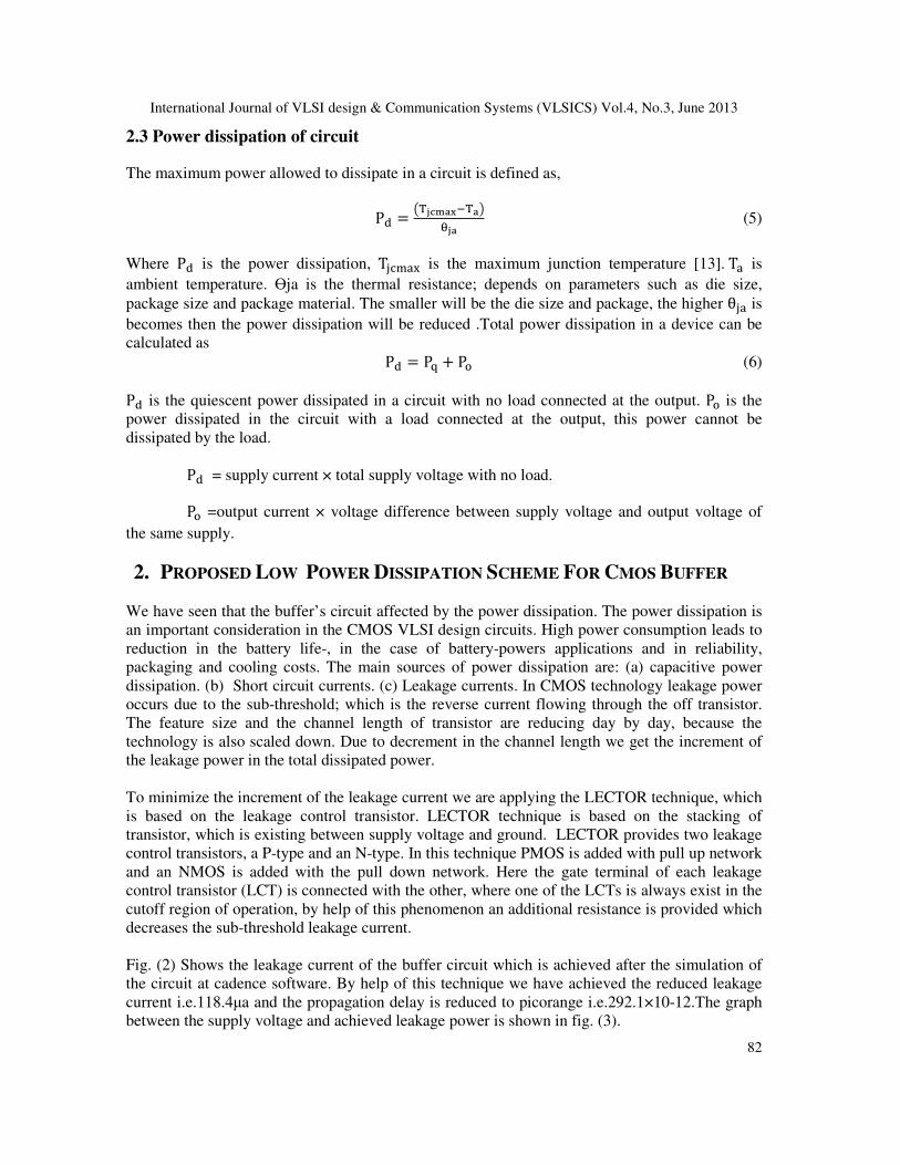
Fig.(4) shows the proposed class-AB rail-to-rail high speed buffer with low power dissipation. This circuit is divided into two parts: The upper part of the circuit consist transistors Mc1a-c3a with adaptive biasing and added with the transistors M1a-8a. The lower part of the circuit consist the transistors Mc1b-c3b with adaptive biasing and added with M1b-8b. Total stages of the circuit perform as a class-AB amplifier. The level shifters M4a-5a and M4b-5b are used to provide the negative feedback, which extend the input common mode range [13]. The main aim of the negative feedback loop is the low impedances at the source terminals of transistors M2a-2b. This function gives the result in the form of the gate-source voltages of M2a (Vgs2a) and M2b (Vgs2b) are kept nearly constant. This functionality is used to show the class-AB behavior. The inserted transistors M3a-3b are also used to increase the input range, so the gate source voltages of M3a-3b are same as M2a-2b, which gives the same current behavior controlled by VUV.Transistors M3a-3b performs the function as the constant controlled sources, which stabilize the DC current of the transistors M7a-7b. The previous paper contains the drawback of power dissipation. Transistors M8a-8b is inserted between M7a-7b, these transistors remove the drawback of power dissipation. Function of these transistors is explained in the previous section. The technique is applied on transistors M8a-8b, which is known as LECTOR technique.
International Journal of VLSI design & Communication Systems (VLSICS) Vol.4, No.3, June 2013
85
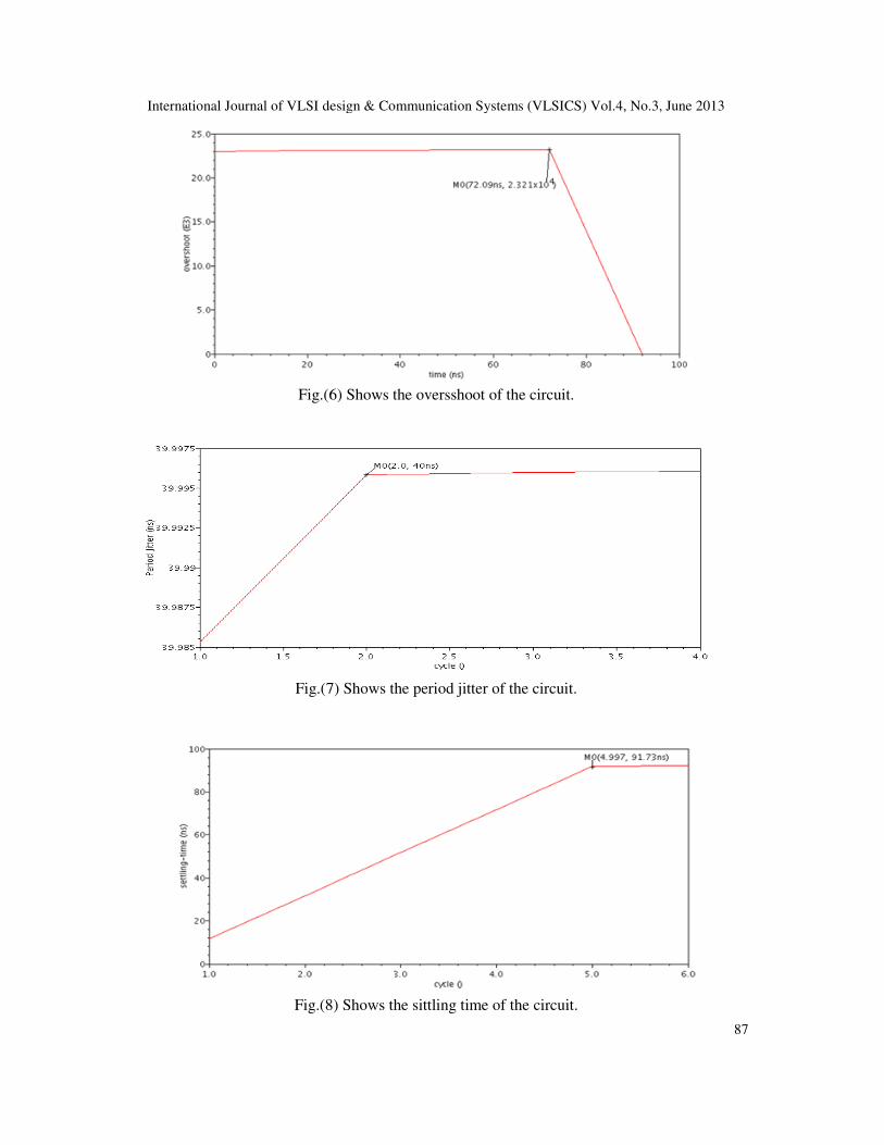
4. SIMULATED RESULTS
Using 45nm CMOS technology we designed a new buffer as shown in fig. (4), which is simulated at 3V supply voltage by help of the cadence tool. Fig.(4) contains the transistors that all have the same sizing. Bias current IB is fixed at 10µA in buffer circuit. It contains the 1pF capacitor, fixed at the output side. Table 1 shows the simulated results giving the overall performance. Fig.(5) shows the frequency jitter waveform which is showing the rising function of buffer circuit. Fig.(6) shows the overshoot of the output waveform. Fig.(7) shows the period jitter Fig.(8) Shows the settling time of the circuit, which shows the high speed of the circuit. Fig.(9) shows the power plot of the output waveform. and fig.(10)shows the input output waveform of the buffer circuit.
��� �23�
M1a
Fig.4. Proposed class-AB rail-to-rail high speed buffer with low power.
M2a
M3a
M4a
M5a
Mc3
Mc2 Mc1
M6a
M7a
IB
I
M8a
M8b
Md1b Md2
Md3b
M1M2 M3b
M4
M5
M6b
M7b
IB
IB
1pF

International Journal of VLSI design & Communication Systems (VLSICS) Vol.4, No.3, June 2013
86
TABLE-1
SIMULATION RESULTS OF BUFFER
Parameter Simulated Results
Process technology 45nm
Power supply 3v
Transistor count 22
Settling time (ns) 91.07×10⁻⁹
Overshoot (m3) 23.21×10³
Rise time (ps) 139×10-12
Slew rate ( W XY< ) 90
Period jitter 40×10-9
Phase noise 1.227
Total quiescent current(µA) 41.25×10⁻⁶
Propagation delay(ps) 292.1×10⁻¹²
Fig.(5) Shows the frequency jitter of the circuit
International Journal of VLSI design & Communication Systems (VLSICS) Vol.4, No.3, June 2013
Fig.(6)
Fig.(7) Shows the period jitter of the circuit.
Fig.(8) Shows the sittling time of the circuit.
International Journal of VLSI design & Communication Systems (VLSICS) Vol.4, No.3, June 2013
Fig.(6) Shows the oversshoot of the circuit.
Fig.(7) Shows the period jitter of the circuit.
Fig.(8) Shows the sittling time of the circuit.
International Journal of VLSI design & Communication Systems (VLSICS) Vol.4, No.3, June 2013
87

International Journal of VLSI design & Communication Systems (VLSICS) Vol.4, No.3, June 2013
88
Fig.(9) Shows the power plot of the circuit.
Fig.(10) Shows the input-output waveform
5. CONCLUSION
A new design scheme for CMOS class-AB buffer using the LECTOR technique is proposed. By help of this technique reduced leakage current is achieved. Applying the LECTOR technique with the adaptive biasing into the buffer helped us to get the propagation delay in the range of Pico- seconds i.e.292.1×10-12, from here we can concluded that the speed of this buffer is very high. The settling time of proposed circuit is also reduced to the range of nanoseconds. This technique is also capable to enhance the slew rate, the achieved slew rate is 90(v µs< ).The designed buffers
is applicable in systems requiring the efficient operation with very low quiescent power consumption.

International Journal of VLSI design & Communication Systems (VLSICS) Vol.4, No.3, June 2013
89
REFERENCES
[1] U. Supriya, K. Ramana Rao, “Design of Low Power CMOS Circuits using Leakage Control
Transistor and Multi-Threshold CMOS Techniques.” International Journal. Computer Technology and Applications, vol.3 (4), 1496-1500, 2012.
[2] Brain S. Cherkauer and Eby G. Friedman, “A Unified Design Methodology for CMOS Tapered
Buffers”, IEEE Transactions on very large scale integration systems, vol.3, no.1, March 1995. [3] Hoi Lee, Philip K.T. Mok and Ka Nang Leung, “Design of Low Power Analog Drivers Based on
Slew rate Enhancement circuits for CMOS Low-Dropout Regulators.” IEEE Transactions on circuits and systems-II: Express Briefs, vol.52, no.9, 2010.
[4] Ka Nang Leung and Yuen Sum Ng, “A CMOS Low Dropout Regulator with a momentarily current-
Boosting voltage Buffer”, IEEE Transactions on circuits and systems-I: Regular paper, vol.57, no.9, 2010.
[5] Massimo Aloito , Gaetano Palumbo, “Power Aware Design of Nanometer MCML Tapered Buffer.”
IEEE Transactions on circuits and systems-II: Express Briefs, vol.55 no.1, 2008. [6] Zhi-Ming Lin and Hsin-Chi Lai, “A High Driving Capability CMOS Buffer Amplifier for TFF LCD
Source Driver.” Engineering Letters, 15:2, EL_15_2_22.Advance online publication:17, 2007. [7] David Marino , Gaetano Palumbo, and Salvatore Pennnis, “Low-Power Dual active Class-AB Buffer
Amplifier with Self Biasing Network for LCD Column Drivers.” IEEE Transaction 978-1-4244-5309-2/10/$26.00.2010
[8] D.J.R Cristaldi, S.Pennis, F.Pulvirenti, “Liquid Crystal Display Drivers: Techniques and
circuits.”Springer 2009 [9] J.-H.Wang, J.-C.Qui, H.-Y.Zheng, C.-H.Tsai, C.-Y.Wang, C.-C.Lee, C,-T Chang , “A High Compact
Low Power Slew rate Rail- to-Rail Class-AB Buffer Amplifier for LCD Driver ICs.” Proc, EDSSC ’07, app. 397-400, 2007.
[10] Merih Yeldiz and shahram Minaei and Emre Arslan, “High-slew rate low Quiscent current Rail-to-
Rail CMOS Buffer Amplifier for Flat Panel Displays.” Journal of circuits, systems and computers vol.20, no.7 (2001)
[11] Chutham Sawigun, Andreas Demothenous, Xiao Liu, and wouter A. Serdijen, “A Compact Rail-to-
Rail Class-AB CMOS Buffer with Slew-rate Enhancement.”IEEE Transactions on circuits and systems –II: Express briefs, vol.59, no.8, 2012.
[12] G.Ferri,G.-C.Cardarilli and M.Re , “Rail-to-Rail adaptive Biased low-power op-Amp.”Microelectronics journal 32(2001) 265-272.
[13] amu Hu and Mohammad Sawan, “A Low Power 800mv Rail-to-Rail Class-AB Operational
amplifier.” IEEE CCECE 2003-CCGEI 2003 ,Monted, May/mai 2003. [14] B.Dilip, P.Surya Prasad and R.S.G. Bhavani, “Leakage Power Reduction in CMOS Circuits Using
Leakage Control Transistor Technique in Nanoscale Technology.” International Journal of Electrnics Signals and Systems (IJESS) ISSN: 2231-5969, vol.2 ISS-1, 2012.

International Journal of VLSI design & Communication Systems (VLSICS) Vol.4, No.3, June 2013
[15] Antonio Lopez Martin, Jose Maria Algueta Miiguel, Lucia Acosta, Jaime RamirezRamon Gonzalez Carvajal, “Design of TwoApproach.” ETRI Journal, vol.33, no.3, 2011.
[16] Tzung-Je Lee, Tieh-Yen Chang Chua
µm 3.3-V CMOS technology” IEEE Tranno.4, 2009.
[17] Shih-Lun Chen, Ming-Dou Ker, “An Output Buffer for 3.3
CMOS Process.” IEEE Transaction on circuit and systems
Authors Sadhana Sharma was born in Gwalior (India) on 20 may 1987. She has completed Bachelor of Engineering from Rajiv Gandhi Technical University, Bhopal.She is pursuing M. Tech (VLSI Design) From ITM University, Gwalior.Her research interests are in VLSI Design, Low power, VLSI Signal processing and FPGA Design. Abhay Vidyarthi was born in Gwalior on 30 november 1979. He has completed Master of Engineering in C.C.N . from Rajiv Gandhi technical University, Bhopal.His research areas of interest are Signal Processing and Communication, Cognitive radio, Sensor networks.He presented papers on Role of Communication And Technology In Infrastructure Development on 24thCollege, Gwalior. And in National Conference on Wireless Communication on 5thEngineering College, Gwalior. S. Akashe was born on 22nd May 1976. This author received his M.Tech from ITM, Gwalior, Madhya Pradesh, India in the year 2006. The author is Thapar University, Patiala on the topic of Low Power Memory Cell Design. The author’s major fields of study are low power VLSI Design, VLSI signal processing, FPGA Design and Communication System. He is working as Associate Professor indepartment of ITM University, Gwalior, India. His important research publications are “Implementation of Technology Scaling on Leakage Reduction Techniques using cadence tools with 45 nm technology,” IEEE, 2011; “High Density and Low Leakage Current Based 5T SRAM Cell Using 45 nrn Technology,” IEEE, 2011; “Multi Vt 7T SRAM Cell for high speed application At 45 Nm Technology,” IEEE, 2011
International Journal of VLSI design & Communication Systems (VLSICS) Vol.4, No.3, June 2013
Antonio Lopez Martin, Jose Maria Algueta Miiguel, Lucia Acosta, Jaime Ramirezn Gonzalez Carvajal, “Design of Two-Stage Class-AB CMOS Buffers: A Systematic
Approach.” ETRI Journal, vol.33, no.3, 2011.
Yen Chang Chua-Chin Wang, “Wide-Range 5.0/3.3/ 1.8V I/OBuffer using 0.35 V CMOS technology” IEEE Transaction on circuit and systems-i: regular papers, vol.56,
Dou Ker, “An Output Buffer for 3.3-V Application in a 0.13CMOS Process.” IEEE Transaction on circuit and systems-II: Express Briefs, vol. 54, no.
Sadhana Sharma was born in Gwalior (India) on 20 may 1987. She has completed Bachelor of Engineering from Rajiv Gandhi Technical University, Bhopal.She is pursuing M. Tech (VLSI Design) From ITM University, Gwalior.Her research
rests are in VLSI Design, Low power, VLSI Signal processing and FPGA Design.
Abhay Vidyarthi was born in Gwalior on 30 november 1979. He has completed Master of Engineering in C.C.N . from Rajiv Gandhi technical University, Bhopal.His research areas of interest are Signal Processing and Communication, Cognitive radio, Sensor networks.He presented papers on Role of Communication And Technology In Infrastructure Development on 24th-25th Apr. 2007 at N.R.I.-I.T.M., Engineering
nd in National Conference on Wireless Communication on 5th-6th Apr 2008 at G.E.C.
S. Akashe was born on 22nd May 1976. This author received his M.Tech from ITM, Gwalior, Madhya Pradesh, India in the year 2006. The author is pursuing Ph.D from Thapar University, Patiala on the topic of Low Power Memory Cell Design. The author’s major fields of study are low power VLSI Design, VLSI signal processing, FPGA Design and Communication System. He is working as Associate Professor in Electronics and Instrumentation Engineering department of ITM University, Gwalior, India. His important research publications are “Implementation of Technology Scaling on Leakage Reduction Techniques using cadence tools with 45 nm
“High Density and Low Leakage Current Based 5T SRAM Cell Using 45 nrn Technology,” IEEE, 2011; “Multi Vt 7T SRAM Cell for high speed application At 45 Nm Technology,”
International Journal of VLSI design & Communication Systems (VLSICS) Vol.4, No.3, June 2013
90
Antonio Lopez Martin, Jose Maria Algueta Miiguel, Lucia Acosta, Jaime Ramirez-Angulo and AB CMOS Buffers: A Systematic
Range 5.0/3.3/ 1.8V I/OBuffer using 0.35 i: regular papers, vol.56,
V Application in a 0.13-µm 1/ 2. 5-V II: Express Briefs, vol. 54, no. 1, 2007.
“Implementation of Technology Scaling on Leakage Reduction Techniques using cadence tools with 45 nm “High Density and Low Leakage Current Based 5T SRAM Cell Using 45 nrn
Technology,” IEEE, 2011; “Multi Vt 7T SRAM Cell for high speed application At 45 Nm Technology,”