
A process-tolerant cache architecture for improved yield in nanoscale technologies
12
IEEE TRANSACTIONS ON VERY LARGE SCALE INTEGRATION (VLSI) SYSTEMS, VOL. 13, NO. 1, JANUARY 2005 27 A Process-Tolerant Cache Architecture for Improved Yield in Nanoscale Technologies Amit Agarwal, Student Member, IEEE, Bipul C. Paul, Member, IEEE, Hamid Mahmoodi, Student Member, IEEE, Animesh Datta, Student Member, IEEE, and Kaushik Roy, Fellow, IEEE Abstract—Process parameter variations are expected to be significantly high in a sub-50-nm technology regime, which can severely affect the yield, unless very conservative design tech- niques are employed. The parameter variations are random in nature and are expected to be more pronounced in minimum geometry transistors commonly used in memories such as SRAM. Consequently, a large number of cells in a memory are expected to be faulty due to variations in different process parameters. In this paper, we analyze the impact of process variation on the different failure mechanisms in SRAM cells. We also propose a process-tolerant cache architecture suitable for high-performance memory. This technique dynamically detects and replaces faulty cells by dynamically resizing the cache. It surpasses all the con- temporary fault tolerant schemes such as row/column redundancy and error-correcting code (ECC) in handling failures due to process variation. Experimental results on a 64-K direct map L1 cache show that the proposed technique can achieve 94% yield compared to its original 33% yield (standard cache) in a 45-nm predictive technology under mV. Index Terms—Process-tolerant cache, resizing, SRAM failures, yield. I. INTRODUCTION S CALING of CMOS devices has provided remarkable improvement in performance of electronic circuits in the last two decades. However, as silicon industry is moving toward the end of the technology roadmap, controlling the variation in device parameters during fabrication is becoming a great challenge. The variations in process parameter such as the channel length, width, oxide thickness, and placement of dopants in a channel result in a large variation in threshold voltage [1]. Among them, the random placement of dopants is more of a concern [2] because it is independent of transistor spatial locations and causes threshold voltage mismatch be- tween the transistors, which are close to each other (intra-die variation). These atomic-level intrinsic fluctuations cannot be eliminated by external control of the manufacturing process and are expected to severely affect the minimum-geometry transistors commonly used in area-constrained circuits such as SRAM cells. Manuscript received September 22, 2003; revised April 28, 2004. This work was supported by the Defense Advanced Research Projects Agency (DARPA), MARCO, GSRC, SRC, and by Intel and IBM. The authors are with the School of Electrical and Computer Engi- neering, Purdue University, West Lafayette, IN 47907-1285 USA (e-mail: [email protected]; [email protected]; [email protected]; [email protected]; [email protected]). Digital Object Identifier 10.1109/TVLSI.2004.840407 A major part of any electronic system is the memory sub- system. State-of-the-art microprocessor designs devote a large fraction of the chip area to memory structures, e.g., multiple levels of instruction and data caches, translation look-aside buffers, and prediction tables. For instance, 30% of Alpha 21 264 and 60% of StrongARM are devoted to cache and memory structures [3]. Since memory is one of the biggest blocks of any system, it is more prone to faults under process variation. A failure in memory cell can occur due to 1) an increase in cell access time and 2) unstable read/write opera- tion [4]. The mismatch in device parameters will increase the probability of these failures. Hence, a proper failure analysis is necessary to understand the impact of process variation on different fault mechanisms. Conventionally redundant rows/columns [5], [6] are used to replace faulty rows/columns, to improve yield in memories. These redundancy techniques either have performance over- head or have limitations on the number of faulty rows/columns it can handle, due to resource limitation and design complexity. In particular, the failures due to random dopant effect are ran- domly distributed across the dies, resulting in a large number of faulty rows/columns. Recovery from such defects cannot be handled by row/column redundancy. We will show that, with the drastic increase in parameter variation, redundancy alone will not result in good yield. Moreover, the number and the location of failures due to process variation changes depending on operating condition (e.g., supply voltage and frequency), which cannot be handled by any static technique such as row/column redundancy. Error correcting code (ECC) [7], [8] employed in existing design to correct transient faults (soft error), can also be used to correct failures due to process variation. However, ECC can correct only a single-error, and hence, will not be sufficient in tolerating a number of failures due to process variation. In this paper, we analyze the effect of process variation on dif- ferent failure mechanisms in SRAM cell. Based on this analysis we estimate the expected yield of a 64-K L1 cache in BPTM 45-nm technology [9]. We propose a process-tolerant cache ar- chitecture suitable for high-performance memories, to detect and replace faulty cells by adaptively resizing the cache. This architecture assumes that the cache is equipped with an on- line built-in-self-test (BIST) [10], [11] to detect faulty cells due to process variation. The proposed scheme then downsizes the cache by forcing the column MUX to select a nonfaulty block in the same row if the accessed block is faulty. This architecture has a high-fault tolerant capability compared to contemporary fault 1063-8210/$20.00 © 2005 IEEE
-
Upload
independent -
Category
Documents
-
view
1 -
download
0
Transcript of A process-tolerant cache architecture for improved yield in nanoscale technologies
IEEE TRANSACTIONS ON VERY LARGE SCALE INTEGRATION (VLSI) SYSTEMS, VOL. 13, NO. 1, JANUARY 2005 27
A Process-Tolerant Cache Architecture for ImprovedYield in Nanoscale Technologies
Amit Agarwal, Student Member, IEEE, Bipul C. Paul, Member, IEEE, Hamid Mahmoodi, Student Member, IEEE,Animesh Datta, Student Member, IEEE, and Kaushik Roy, Fellow, IEEE
Abstract—Process parameter variations are expected to besignificantly high in a sub-50-nm technology regime, which canseverely affect the yield, unless very conservative design tech-niques are employed. The parameter variations are random innature and are expected to be more pronounced in minimumgeometry transistors commonly used in memories such as SRAM.Consequently, a large number of cells in a memory are expectedto be faulty due to variations in different process parameters.In this paper, we analyze the impact of process variation on thedifferent failure mechanisms in SRAM cells. We also propose aprocess-tolerant cache architecture suitable for high-performancememory. This technique dynamically detects and replaces faultycells by dynamically resizing the cache. It surpasses all the con-temporary fault tolerant schemes such as row/column redundancyand error-correcting code (ECC) in handling failures due toprocess variation. Experimental results on a 64-K direct map L1cache show that the proposed technique can achieve 94% yieldcompared to its original 33% yield (standard cache) in a 45-nmpredictive technology under inter = intra = 30 mV.
Index Terms—Process-tolerant cache, resizing, SRAM failures,yield.
I. INTRODUCTION
SCALING of CMOS devices has provided remarkableimprovement in performance of electronic circuits in
the last two decades. However, as silicon industry is movingtoward the end of the technology roadmap, controlling thevariation in device parameters during fabrication is becominga great challenge. The variations in process parameter suchas the channel length, width, oxide thickness, and placementof dopants in a channel result in a large variation in thresholdvoltage [1]. Among them, the random placement of dopants ismore of a concern [2] because it is independent of transistorspatial locations and causes threshold voltage mismatch be-tween the transistors, which are close to each other (intra-dievariation). These atomic-level intrinsic fluctuations cannot beeliminated by external control of the manufacturing processand are expected to severely affect the minimum-geometrytransistors commonly used in area-constrained circuits such asSRAM cells.
Manuscript received September 22, 2003; revised April 28, 2004. This workwas supported by the Defense Advanced Research Projects Agency (DARPA),MARCO, GSRC, SRC, and by Intel and IBM.
The authors are with the School of Electrical and Computer Engi-neering, Purdue University, West Lafayette, IN 47907-1285 USA (e-mail:[email protected]; [email protected]; [email protected];[email protected]; [email protected]).
Digital Object Identifier 10.1109/TVLSI.2004.840407
A major part of any electronic system is the memory sub-system. State-of-the-art microprocessor designs devote a largefraction of the chip area to memory structures, e.g., multiplelevels of instruction and data caches, translation look-asidebuffers, and prediction tables. For instance, 30% of Alpha21 264 and 60% of StrongARM are devoted to cache andmemory structures [3]. Since memory is one of the biggestblocks of any system, it is more prone to faults under processvariation. A failure in memory cell can occur due to 1) anincrease in cell access time and 2) unstable read/write opera-tion [4]. The mismatch in device parameters will increase theprobability of these failures. Hence, a proper failure analysisis necessary to understand the impact of process variation ondifferent fault mechanisms.
Conventionally redundant rows/columns [5], [6] are used toreplace faulty rows/columns, to improve yield in memories.These redundancy techniques either have performance over-head or have limitations on the number of faulty rows/columnsit can handle, due to resource limitation and design complexity.In particular, the failures due to random dopant effect are ran-domly distributed across the dies, resulting in a large numberof faulty rows/columns. Recovery from such defects cannotbe handled by row/column redundancy. We will show that,with the drastic increase in parameter variation, redundancyalone will not result in good yield. Moreover, the numberand the location of failures due to process variation changesdepending on operating condition (e.g., supply voltage andfrequency), which cannot be handled by any static techniquesuch as row/column redundancy. Error correcting code (ECC)[7], [8] employed in existing design to correct transient faults(soft error), can also be used to correct failures due to processvariation. However, ECC can correct only a single-error, andhence, will not be sufficient in tolerating a number of failuresdue to process variation.
In this paper, we analyze the effect of process variation on dif-ferent failure mechanisms in SRAM cell. Based on this analysiswe estimate the expected yield of a 64-K L1 cache in BPTM45-nm technology [9]. We propose a process-tolerant cache ar-chitecture suitable for high-performance memories, to detectand replace faulty cells by adaptively resizing the cache. Thisarchitecture assumes that the cache is equipped with an on-line built-in-self-test (BIST) [10], [11] to detect faulty cells dueto process variation. The proposed scheme then downsizes thecache by forcing the column MUX to select a nonfaulty block inthe same row if the accessed block is faulty. This architecture hasa high-fault tolerant capability compared to contemporary fault
1063-8210/$20.00 © 2005 IEEE

28 IEEE TRANSACTIONS ON VERY LARGE SCALE INTEGRATION (VLSI) SYSTEMS, VOL. 13, NO. 1, JANUARY 2005
tolerant techniques, with minimum energy overhead and doesnot impose any cache access time penalty. This scheme mapsthe whole memory address space into the resized cache in sucha way that resizing is transparent to the processor. Hence, theprocessor accesses the resized cache with the same address asin a conventional architecture. We evaluate the performance ofthis architecture both analytically and experimentally. We alsocompared our technique with conventional fault tolerant tech-niques such as redundancy and ECC.
The rest of the paper is organized as follows. In Section IIwe analyze different failure mechanisms in an SRAM cell dueto process variation. Section III explains the basic cache archi-tecture. In Section IV, we explain the proposed process-tolerantcache architecture and describe the implementation of differentcircuit blocks required by this scheme. Section V presents theanalysis and combines it with experimental results to comparethe fault tolerant capability and resulting yield of the proposedscheme with ECC and redundancy. In Section VI we draw ourconclusions.
II. FAILURE ANALYSIS OF SRAM CELL DUE TO
PROCESS VARIATION
A failure in a SRAM cell can occur due to 1) an increase inthe access time of the cell (access time failure) and 2) destructiveread (read failure) and/or unsuccessful write (write failure). Ina die, failures are principally caused by the mismatch in the de-vice parameters (length, width, and transistor threshold voltage)of different transistors (intra-die) in the cell. Such device mis-match modifies the strength of the different transistors resultingin different failure events. The primary source of device mis-match is the intrinsic fluctuation of the of different transistorsdue to random dopant effect [2]. Hence, in this paper we haveconsidered the variation as the major source of intra-die vari-ation while analyzing the failure probabilities. One should notethat the effect of other parameter variation can be translated intothe effective variation in threshold voltage.
A. Access Time Failure (AF)
The cell access time is defined as the timerequired to produce a prespecified (say, )voltage difference between two bit-lines (bit-differential). Fora cell storing '` and '` (Fig. 1), bitline BR willdischarge through transistors AXR and NR during the readoperation. Hence, is a strong function of of AXRand NR. Therefore, any variation in of these transistorschanges and will cause an access time failure if it isgreater than the maximum tolerable limit .
B. Read Stability Failure (RF)
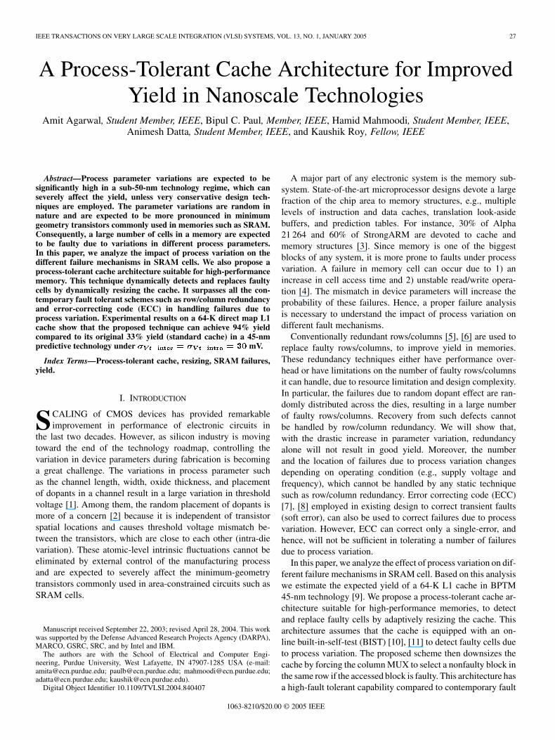
During the read operation, (Fig. 1) increases due to thevoltage divider action of AXR and NR to a positive value
. If is higher than the trip point of the inverterPL-NL then the cell flips [Fig. 2(a)] resulting in aread failure. depends on the of AXR and NR, while
is a function of the of PL and NL. Intrinsic variationin of these transistors can change both andleading to a read failure.
Fig. 1. Schematic of an SRAM cell.
C. Write Stability Failure
While writing a ‘0’ to a cell storing ‘1’, the node (Fig. 1)gets discharged through BL to a low value determinedby the voltage division between the PL and AXL. If can notbe reduced below the trip point of the inverter PR-NR ,within the time when word-line is high , then a writefailure occurs [Fig. 2(b)]. Variation in of PL, AXL, PR, andNR can cause a write failure.
It should also be noted that the failure mechanisms describedabove are functions of supply voltage and frequency of opera-tion, and hence, the failure map of a cache will change if theoperation conditions are altered.
D. Probability of Failure
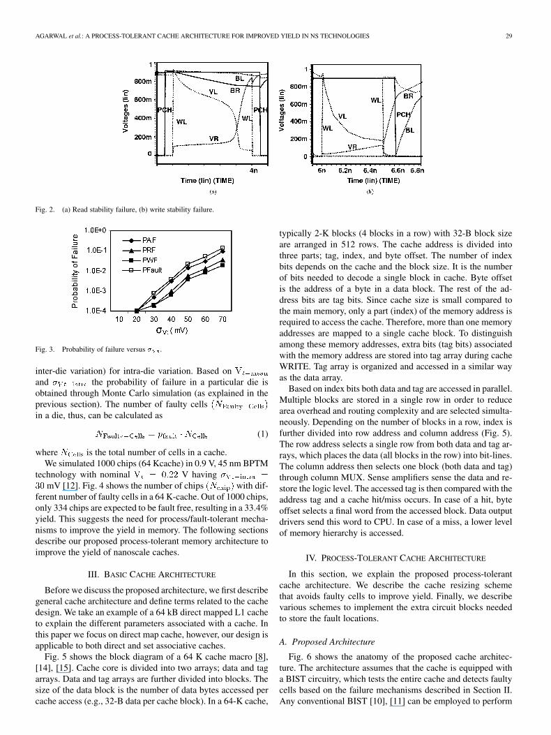
Intrinsic variation in nanoscale technology is random innature. Hence, in order to analyze the probability of failure, thethreshold voltage of all six transistors in a cell are consideredas six independent random variables and assumed to have aGaussian distribution. The standard deviation of thevariation depends on the manufacturing process, doping profile,and the transistor size. Fig. 3 shows the result of Monte Carlosimulations for the probability of different failure mechanisms,using the BPTM 45-nm technology, for different . Theprobability of a failure is calculated as the ratio of the numberof occurrence of a particular failure to the total number ofexperiments. It can be seen from the figure that the proba-bility of all three-failure mechanisms increases considerablywith process variation , however, it is mostly dominatedby access time failures. In 45-nm technology, where isexpected to be 30 mV [12], effective probability of failure
can be as high as (Fig. 3).This indicates that there will be a large number of faulty cells innanoscale SRAMs under process variation, affecting the yield.
E. Yield Analysis of a 64 K-Cache Under Process Variation
In order to analyze the yield of a cache under process vari-ation, we considered both inter-die and intra-die variation.Intra-die variations are the variations in device parameterswithin a single chip, which means different devices at differentlocations on a single die may have different device features.Inter-chip variations, on the other hand, are the variations thatoccur from one die to the other, from wafer to wafer, and fromwafer lot to wafer lot. We first model inter-die variation ofas a Gaussian distribution [13] and use the probability densityfunction (pdf) of this distribution as the mean of intra-die vari-ation. Hence, different dies will have different (due to
AGARWAL et al.: A PROCESS-TOLERANT CACHE ARCHITECTURE FOR IMPROVED YIELD IN NS TECHNOLOGIES 29
Fig. 2. (a) Read stability failure, (b) write stability failure.
Fig. 3. Probability of failure versus � .
inter-die variation) for intra-die variation. Based onand the probability of failure in a particular die isobtained through Monte Carlo simulation (as explained in theprevious section). The number of faulty cellsin a die, thus, can be calculated as
(1)
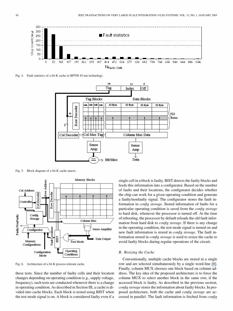
where is the total number of cells in a cache.We simulated 1000 chips (64 Kcache) in 0.9 V, 45 nm BPTM
technology with nominal V havingmV [12]. Fig. 4 shows the number of chips with dif-
ferent number of faulty cells in a 64 K-cache. Out of 1000 chips,only 334 chips are expected to be fault free, resulting in a 33.4%yield. This suggests the need for process/fault-tolerant mecha-nisms to improve the yield in memory. The following sectionsdescribe our proposed process-tolerant memory architecture toimprove the yield of nanoscale caches.
III. BASIC CACHE ARCHITECTURE
Before we discuss the proposed architecture, we first describegeneral cache architecture and define terms related to the cachedesign. We take an example of a 64 kB direct mapped L1 cacheto explain the different parameters associated with a cache. Inthis paper we focus on direct map cache, however, our design isapplicable to both direct and set associative caches.
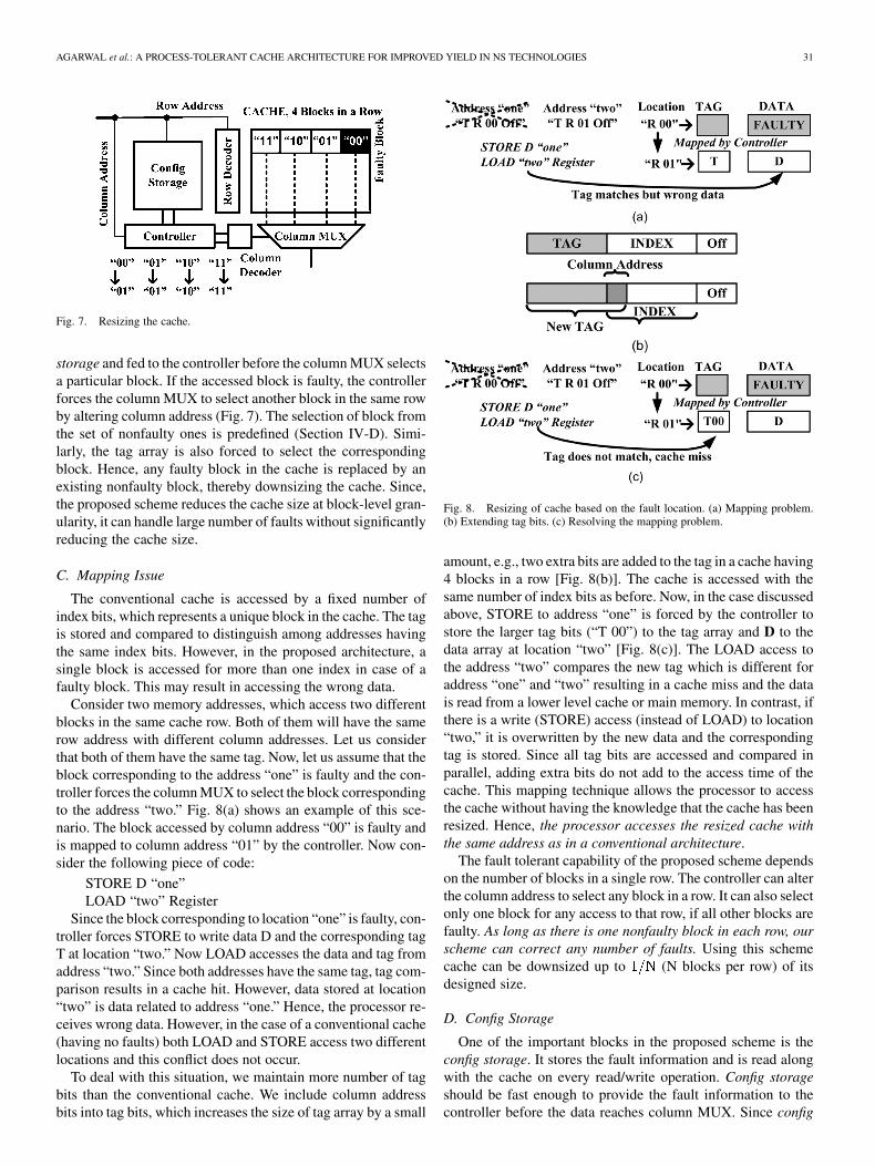
Fig. 5 shows the block diagram of a 64 K cache macro [8],[14], [15]. Cache core is divided into two arrays; data and tagarrays. Data and tag arrays are further divided into blocks. Thesize of the data block is the number of data bytes accessed percache access (e.g., 32-B data per cache block). In a 64-K cache,
typically 2-K blocks (4 blocks in a row) with 32-B block sizeare arranged in 512 rows. The cache address is divided intothree parts; tag, index, and byte offset. The number of indexbits depends on the cache and the block size. It is the numberof bits needed to decode a single block in cache. Byte offsetis the address of a byte in a data block. The rest of the ad-dress bits are tag bits. Since cache size is small compared tothe main memory, only a part (index) of the memory address isrequired to access the cache. Therefore, more than one memoryaddresses are mapped to a single cache block. To distinguishamong these memory addresses, extra bits (tag bits) associatedwith the memory address are stored into tag array during cacheWRITE. Tag array is organized and accessed in a similar wayas the data array.
Based on index bits both data and tag are accessed in parallel.Multiple blocks are stored in a single row in order to reducearea overhead and routing complexity and are selected simulta-neously. Depending on the number of blocks in a row, index isfurther divided into row address and column address (Fig. 5).The row address selects a single row from both data and tag ar-rays, which places the data (all blocks in the row) into bit-lines.The column address then selects one block (both data and tag)through column MUX. Sense amplifiers sense the data and re-store the logic level. The accessed tag is then compared with theaddress tag and a cache hit/miss occurs. In case of a hit, byteoffset selects a final word from the accessed block. Data outputdrivers send this word to CPU. In case of a miss, a lower levelof memory hierarchy is accessed.
IV. PROCESS-TOLERANT CACHE ARCHITECTURE
In this section, we explain the proposed process-tolerantcache architecture. We describe the cache resizing schemethat avoids faulty cells to improve yield. Finally, we describevarious schemes to implement the extra circuit blocks neededto store the fault locations.
A. Proposed Architecture
Fig. 6 shows the anatomy of the proposed cache architec-ture. The architecture assumes that the cache is equipped witha BIST circuitry, which tests the entire cache and detects faultycells based on the failure mechanisms described in Section II.Any conventional BIST [10], [11] can be employed to perform
30 IEEE TRANSACTIONS ON VERY LARGE SCALE INTEGRATION (VLSI) SYSTEMS, VOL. 13, NO. 1, JANUARY 2005
Fig. 4. Fault statistics of a 64-K cache in BPTM 45-nm technology.
Fig. 5. Block diagram of a 64-K cache macro.
Fig. 6. Architecture of a 64-K process-tolerant cache.
these tests. Since the number of faulty cells and their locationchanges depending on operating condition (e.g., supply voltage,frequency), such tests are conducted whenever there is a changein operating condition. As described in Section III, a cache is di-vided into cache blocks. Each block is tested using BIST whenthe test mode signal is on. A block is considered faulty even if a
single cell in a block is faulty. BIST detects the faulty blocks andfeeds this information into a configurator. Based on the numberof faults and their locations, the configurator decides whetherthe chip can work for a given operating condition and generatea faulty/nonfaulty signal. The configurator stores the fault in-formation in config storage. Stored information of faults for aparticular operating condition is saved from the config storageto hard disk, whenever the processor is turned off. At the timeof rebooting, the processor by default reloads the old fault infor-mation from hard disk to config storage. If there is any changein the operating condition, the test mode signal is turned on andnew fault information is stored in config storage. The fault in-formation stored in config storage is used to resize the cache toavoid faulty blocks during regular operations of the circuit.
B. Resizing the Cache
Conventionally, multiple cache blocks are stored in a singlerow and are selected simultaneously by a single word-line [8].Finally, column MUX chooses one block based on column ad-dress. The key idea of the proposed architecture is to force thecolumn MUX to select another block in the same row, if theaccessed block is faulty. As described in the previous section,config storage stores the information about faulty blocks. In pro-posed architecture, both the cache and config storage are ac-cessed in parallel. The fault information is fetched from config
AGARWAL et al.: A PROCESS-TOLERANT CACHE ARCHITECTURE FOR IMPROVED YIELD IN NS TECHNOLOGIES 31
Fig. 7. Resizing the cache.
storage and fed to the controller before the column MUX selectsa particular block. If the accessed block is faulty, the controllerforces the column MUX to select another block in the same rowby altering column address (Fig. 7). The selection of block fromthe set of nonfaulty ones is predefined (Section IV-D). Simi-larly, the tag array is also forced to select the correspondingblock. Hence, any faulty block in the cache is replaced by anexisting nonfaulty block, thereby downsizing the cache. Since,the proposed scheme reduces the cache size at block-level gran-ularity, it can handle large number of faults without significantlyreducing the cache size.
C. Mapping Issue
The conventional cache is accessed by a fixed number ofindex bits, which represents a unique block in the cache. The tagis stored and compared to distinguish among addresses havingthe same index bits. However, in the proposed architecture, asingle block is accessed for more than one index in case of afaulty block. This may result in accessing the wrong data.
Consider two memory addresses, which access two differentblocks in the same cache row. Both of them will have the samerow address with different column addresses. Let us considerthat both of them have the same tag. Now, let us assume that theblock corresponding to the address “one” is faulty and the con-troller forces the column MUX to select the block correspondingto the address “two.” Fig. 8(a) shows an example of this sce-nario. The block accessed by column address “00” is faulty andis mapped to column address “01” by the controller. Now con-sider the following piece of code:
STORE D “one”LOAD “two” Register
Since the block corresponding to location “one” is faulty, con-troller forces STORE to write data D and the corresponding tagT at location “two.” Now LOAD accesses the data and tag fromaddress “two.” Since both addresses have the same tag, tag com-parison results in a cache hit. However, data stored at location“two” is data related to address “one.” Hence, the processor re-ceives wrong data. However, in the case of a conventional cache(having no faults) both LOAD and STORE access two differentlocations and this conflict does not occur.
To deal with this situation, we maintain more number of tagbits than the conventional cache. We include column addressbits into tag bits, which increases the size of tag array by a small
Fig. 8. Resizing of cache based on the fault location. (a) Mapping problem.(b) Extending tag bits. (c) Resolving the mapping problem.
amount, e.g., two extra bits are added to the tag in a cache having4 blocks in a row [Fig. 8(b)]. The cache is accessed with thesame number of index bits as before. Now, in the case discussedabove, STORE to address “one” is forced by the controller tostore the larger tag bits (“T 00”) to the tag array and D to thedata array at location “two” [Fig. 8(c)]. The LOAD access tothe address “two” compares the new tag which is different foraddress “one” and “two” resulting in a cache miss and the datais read from a lower level cache or main memory. In contrast, ifthere is a write (STORE) access (instead of LOAD) to location“two,” it is overwritten by the new data and the correspondingtag is stored. Since all tag bits are accessed and compared inparallel, adding extra bits do not add to the access time of thecache. This mapping technique allows the processor to accessthe cache without having the knowledge that the cache has beenresized. Hence, the processor accesses the resized cache withthe same address as in a conventional architecture.
The fault tolerant capability of the proposed scheme dependson the number of blocks in a single row. The controller can alterthe column address to select any block in a row. It can also selectonly one block for any access to that row, if all other blocks arefaulty. As long as there is one nonfaulty block in each row, ourscheme can correct any number of faults. Using this schemecache can be downsized up to (N blocks per row) of itsdesigned size.
D. Config Storage
One of the important blocks in the proposed scheme is theconfig storage. It stores the fault information and is read alongwith the cache on every read/write operation. Config storageshould be fast enough to provide the fault information to thecontroller before the data reaches column MUX. Since config

32 IEEE TRANSACTIONS ON VERY LARGE SCALE INTEGRATION (VLSI) SYSTEMS, VOL. 13, NO. 1, JANUARY 2005
Fig. 9. Config Storage. (a) CAM, an example to store 100 faults, (b) OBI.
storage is accessed every cache access, energy consumed inconfig storage should also be negligible compared to the energyconsumed in the cache. At the same time, the config storageshould be large enough to cover most of the faults to achievehigh-fault tolerant capability. Based on theses constraints, twotypes of config storage are implemented:
1) content addressable memory (CAM) implementation;2) one-bit implementation (OBI).
The following section explains each scheme in detail and dis-cusses pros and cons associated with each.
1) CAM Implementation: In this design, fault locations(index bits) are stored into a CAM [16]. The fault locationsare written into the CAM at the time of testing. The size ofCAM depends on the maximum number of faults that canbe tolerated. The size can be decided based on the averagenumber of expected faulty blocks due to the process variationin a cache for a particular technology. Along with the locationof each faulty block, CAM also stores the column addressof a nonfaulty block. This nonfaulty block is determined bythe configurator at the time of testing, and the faulty block ismapped to this block whenever accessed.
CAM is accessed in parallel with the cache using the indexbits of the memory address. These index bits are compared withall the fault locations stored in the CAM. Since all the storedlocations are compared in parallel, these comparisons are fast.Each comparison generates their local match signals [Fig. 9(a)].These local signals are combined together using a domino OR togenerate the final match signal. The controller uses this signal todecide whether to change the present column address. If there isa match, only one among all local match signals will be “1.” Thecorresponding column address stored in the CAM is then sentto the controller through a MUX. The controller then replacesthe column address by the one read from the CAM.
The energy overhead associated with the CAM depends onwhether a match occurs or not. Since, the number of faultyblocks is expected to be small, the most common case is ano-match. To reduce the energy overhead, the CAM is designedusing XNOR and dynamic AND gates that switches only if thereis a match, resulting in less power consumption in case of ano-match.
TABLE ICOMPARISON OF ENERGY AND PERFORMANCE BETWEEN DIFFERENT
CONFIG STORAGE
To evaluate this scheme, a 64-KB cache is designed usingthe TSMC 0.25- technology. This cache has 2-K blocks with32-B block size, arranged in 512 rows. Table I shows the energyand the delay from the row decoder to column MUX in a 64-kBcache. Table I also shows the energy overhead and the delay as-sociated with CAM, designed to store 100–200 fault locations,respectively. It can be observed that energy overhead is negli-gible (2%–4%) compared to the dynamic energy per cache ac-cess. The time required to access the CAM is also much smallerthan the row address to the MUX delay of the cache. This en-sures that the appropriate column address arrives before datareaches column MUX and, hence, the latency to access the cacheremains the same as a conventional cache. The energy over-head and delay depends on the size of the CAM. Hence, onehas to consider the fault tolerance versus energy dissipation/areatrade-off. For example, using a 100 entry CAM, one can tolerateup to 5% faulty blocks with only 0.25% area overhead in a 64-Kcache.
2) OBI: In this design style, one bit per cache block is main-tained in a small memory (OBI) to store the fault information.The bit is “1” if the corresponding block in the cache is fauty;otherwise, it is “0.” These bits are determined at the time oftesting and stored in OBI by the configurator. Architecture ofOBI is exactly the same as cache [Fig. 9(b)]. A block size ofOBI is equal to the number of blocks in a cache row. Therefore,each block in OBI stores the fault information of all the blocksin a cache row.
AGARWAL et al.: A PROCESS-TOLERANT CACHE ARCHITECTURE FOR IMPROVED YIELD IN NS TECHNOLOGIES 33
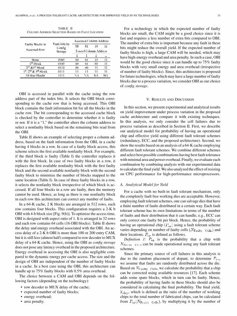
TABLE IICOLUMN ADDRESS SELECTION BASED ON FAULT LOCATION
OBI is accessed in parallel with the cache using the rowaddress part of the index bits. It selects the OBI block corre-sponding to the cache row that is being accessed. This OBIblock contains the fault information bit for all the blocks in thecache row. The bit corresponding to the accessed cache blockis checked by the controller to determine whether it is faultyor not. If it is a “1,” the controller alters the column address toselect a nonfaulty block based on the remaining bits read fromthe OBI.
Table II shows an example of selecting proper a column ad-dress, based on the fault information from the OBI, in a cachehaving 4 blocks in a row. In case of a faulty block access, thisscheme selects the first available nonfaulty block. For example,if the third block is faulty (Table I) the controller replaces itwith the first block. In case of two faulty blocks in a row, itreplaces the first available nonfaulty block with the first faultyblock and the second available nonfaulty block with the secondfaulty block to minimize the number of blocks mapped to thesame location (Table I). In case of three faulty blocks in a row,it selects the nonfaulty block irrespective of which block is ac-cessed. If all four blocks in a row are faulty, then the memorycannot be used. Hence, as long as there is one nonfaulty blockin each row this architecture can correct any number of faults.
In a 64-K cache, 2 K blocks are arranged in 512 rows, eachrow contains four blocks. This configuration requires a 2-K bOBI with 4-b block size [Fig. 9(b)]. To optimize the access time,OBI is designed with aspect ratio of 1. It is arranged in 32 rowsand each row contains 64 cells (16 OBI blocks). Table II showsthe delay and energy overhead associated with the OBI. An ac-cess delay of a 2-K b OBI is more than 100 or 200 entry CAM,but it is still less (almost half) compared to row decoder to MUXdelay of a 64-K cache. Hence, using the OBI as config storagedoes not pose any latency overhead in the proposed architecture.Energy overhead in accessing the OBI is also negligible com-pared to the dynamic energy per cache access. The size and thedesign of OBI are independent of the number of faulty blocksin a cache. In a best case using the OBI, this architecture canhandle up to 75% faulty blocks with 0.5% area overhead.
The choice between a CAM and OBI depends on the fol-lowing factors (depending on the technology):
• row decoder to MUX delay of the cache;• expected number of faulty blocks;• energy overhead;• area penalty.
For a technology in which the expected number of faultyblocks are small, the CAM might be a good choice since it isfast and requires a less number of extra bits compared to OBI.The number of extra bits is important because any fault in thesebits might reduce the overall yield. If the expected number offaulty blocks is high, a large CAM will be needed, which mayhave high-energy overhead and area penalty. In such a case, OBIwould be the good choice since it can handle up to 75% faultyblocks with very small energy and area overhead (irrespectiveof number of faulty blocks). Since, this architecture is proposedfor future technologies, which may have a large number of faultyblocks due to a process variation, we consider OBI as our choiceof config storage.
V. RESULTS AND DISCUSSION
In this section, we present experimental and analytical resultson yield improvement under process variation in the proposedcache architecture and compare it with existing techniques.In this analysis, we only consider the cell failures due toprocess variation as described in Section II. First, we describeour analytical model for probability of having an operationalchip and effective yield using different fault tolerant schemes(redundancy, ECC, and the proposed architecture). Second, weshow the results based on an analysis of a 64-K cache employingdifferent fault tolerant schemes. We combine different schemesand select best possible combinations having best fault tolerancewith minimal area and power overhead. Finally, we evaluate eachcombination by combining analysis with our experimental datato calculate the final yield. We also analyzed the effect of resizingon CPU performance for high-performance microprocessors.
A. Analytical Model for Yield
For a cache with no built-in fault tolerant mechanism, onlythe completely fault free working dies are acceptable. However,employing fault tolerant schemes, one can salvage dies that havea finite number of faults distributed in a certain way. Each faulttolerant scheme has its own limitations in terms of the numberof faults and their distribution that it can handle, e.g., ECC canonly correct one faulty bit per block. Hence, the probability ofhaving an operational chip using a fault tolerant schemevaries depending on number of faulty cells andtheir locations. is defined as follows.
Definition 1: is the probability that a chip withcan be made operational using any fault tolerant
schemes.Since the primary source of cell failures in this analysis is
due to the random placement of dopant, to determine ,we assume that faults are randomly distributed across the die.Based on , we calculate the probability that a chipcan be corrected using available resources [17]. Each schemeadds some spare blocks, which in turn can be faulty. Hence,the probability of having faults in these blocks should also beconsidered in calculating the final probability. The final yield,
, which is defined as the ratio of the number of workingchips to the total number of fabricated chips, can be calculatedfrom , by multiplying it by the number of

34 IEEE TRANSACTIONS ON VERY LARGE SCALE INTEGRATION (VLSI) SYSTEMS, VOL. 13, NO. 1, JANUARY 2005
chips with and summing over all possiblein our simulation
(2)
However, adding a spare block increases the chip area andreduces the number of chips that fits into the wafer area. Con-sequently, a better measure for evaluating the benefit of eachscheme is effective yield, defined as
(3)
In our analysis, we have ignored the area overhead associatedwith extra control circuitry, fuses, and routing. We only considerthe area overhead due to extra storage space. To describe ourmodel, we assume a cache having M rows. Each row contains Ncache blocks and the size of each block is B bits.are randomly distributed inside the memory. To simplify our de-scription we only consider data array in our analysis and ignorethe tag array. However, our final results do include tag array inthe analysis. Considering tag array requires a simple extensionof the model described below by either adding the number oftag bits into block size (for the proposed architecture) or con-sidering the tag as a separate block (for ECC and redundancy).
1) Redundancy: Redundancy schemes replace faultyrows/columns with redundant rows/columns. For simplifyingour expressions, we represent both row and column redundancyin terms of redundant rows. with redundancy is defined asthe probability that the number of faulty rows in a chip is lessthan or equal to the number of redundant rows. Let us assumethat there are R redundant rows. Hence, for a good chip, among
rows, at most R rows can be faulty.Definition 2: is the probability that exactly out of
rows are faulty.To calculate the we first calculate the probability of
having a faulty row. A row ( bits) is considered faulty if ithas at least one faulty bit. Since faults are randomly distributedwith the fault probability, , which depends on(1), probability of having one row faulty is given by
(4)
and thus
(5)
Hence, the probability of having an operational chip is
(6)
(7)
Here, is given by (2) and is the probabilitythat rows are faulty among rows.
2) ECC: It has been shown that ECC with more than onefault correction capability cannot be implemented in memories
TABLE IIICONFIGURATION OF A 64-K CACHE WITH DIFFERENT FAULT-TOLERANT
SCHEMES
due to the high area and delay penalty associated with it [18]. Weassume that cache maintains numberof ECC bits per cache block and can correct only one fault ina block, where B is the number of bits in each block. withECC is defined as the probability that every block in a cache hasat most one faulty bit. There are blocks in the cache.Hence, the probability of having an operational chip using ECCis given by
(8)
(9)
3) Proposed Architecture: Using OBI as config storage, theproposed scheme can correct any number of faults as long asat least one block in every row is nonfaulty. with resizingis defined as the probability that each row has at least one non-faulty block and config storage is fault free. A block is consid-ered faulty even if only one bit in that block is faulty. The prob-ability of a block to be faulty is given by
(10)
Hence, the probability of having a row that can be corrected(i.e., there is at least one nonfaulty block in a row having Nblocks), is given by
(11)
and the probability that all M rows can be corrected is
(12)
There are blocks in the cache and hence, the size ofthe OBI is bits. Therefore, the probability that OBI isfault free is given by
(13)
and thus
(14)
(15)

AGARWAL et al.: A PROCESS-TOLERANT CACHE ARCHITECTURE FOR IMPROVED YIELD IN NS TECHNOLOGIES 35
Fig. 10. Probability of salvaging a chip versus fault probability for a 64-K cache. (a) Proposed architecture, ECC, and redundancy. (b) Proposed architecture withredundancy in OBI. (c) Proposed architecture with redundancy in cache. (d) ECC with redundancy.
B. Yield Using Different Schemes for a 64-K Cache
Table III shows the configuration of a 64-K cache with threedifferent fault tolerant schemes. Fig. 10 shows the versus
by employing different fault tolerant schemes. Itcan be observed from Fig. 10(a) that our proposed techniqueis more efficient in correcting faults compared to ECC or re-dundancy. It can correct 66% chips having 105 faulty cells,while ECC can only correct 6%, and it is impossible to correctany using row/column redundancy. The effective yield is cal-culated using (3). is obtained from the experimental re-sults on the failure analysis described in Section II (
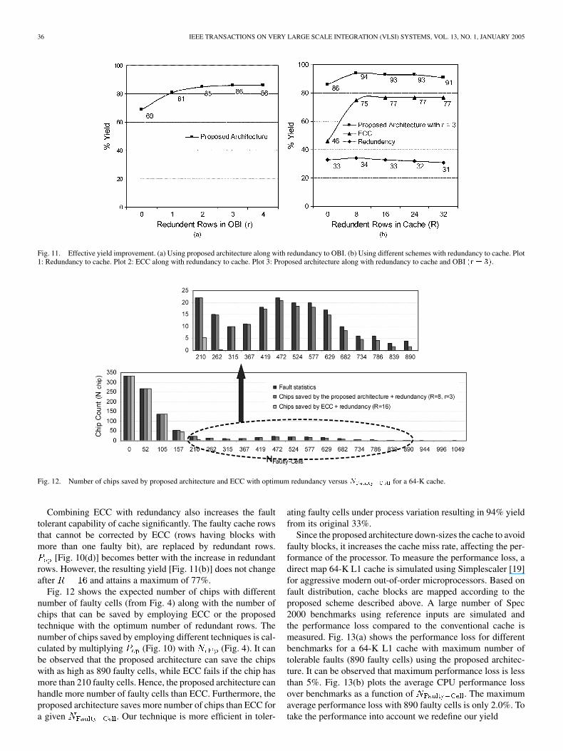
mV, nm BPTM, Fig. 2). The effective yieldis plotted in Fig. 11. Without the use of ECC or resizing, usingredundant rows only, results in maximum yield of 34% (for
), which is close to nominal yield [Fig. 11(b)]. Increasingthe number of redundant rows/columns does not improve yieldbecause the improvement in yield is masked by area overhead.Fig. 11(b) shows that ECC, without any additional redundancy
, results in 46% yield. However, it is smaller comparedto the yield using the proposed technique, which is around 69%[Fig. 11(a)].
can further be improved by adding an optimum numberof redundant row/column along with ECC or the proposed
architecture. Yield of cache using the proposed scheme is astrong function of the probability that the config storage is notfaulty. This is because each and every bit of config storageneeds to be nonfaulty to ensure proper operation. Hence, toincrease this probability, redundant rows (r) are added to OBIwith a small increase in the area. The probability of a nonfaultyOBI is calculated in a similar way as cache using redundancy(Section V-A1). is determined using (14). Fig. 10(b) showsthe effect of adding redundant rows to OBI on . Addingredundant OBI rows greatly improves . The resulting yieldchanges from 69% to a maximum of 86% [Fig. 11(a)]. It canbe observed that increasing r above 3 has little effect on[Fig. 10(b)] and does not change the effective yield [Fig. 11(a)].Hence, is optimum for resizing with redundancy in OBI.
To improve the yield further redundant rows (R) are addedto the cache along with the redundancy in OBI . Thefaulty cache rows, which cannot be corrected by the proposedscheme (rows having all 4 blocks faulty), are replaced by re-dundant rows. The resulting is plotted in Fig. 10(c). It canbe observed that optimum number of redundant rows for thegiven fault distribution is 8 and effective yield goes up to 94%[Fig. 11(b)]. A further increase in the yield using more redun-dant rows is masked by the defects in redundant rows themselvesand the area overhead.
36 IEEE TRANSACTIONS ON VERY LARGE SCALE INTEGRATION (VLSI) SYSTEMS, VOL. 13, NO. 1, JANUARY 2005
Fig. 11. Effective yield improvement. (a) Using proposed architecture along with redundancy to OBI. (b) Using different schemes with redundancy to cache. Plot1: Redundancy to cache. Plot 2: ECC along with redundancy to cache. Plot 3: Proposed architecture along with redundancy to cache and OBI (r = 3).
Fig. 12. Number of chips saved by proposed architecture and ECC with optimum redundancy versus N for a 64-K cache.
Combining ECC with redundancy also increases the faulttolerant capability of cache significantly. The faulty cache rowsthat cannot be corrected by ECC (rows having blocks withmore than one faulty bit), are replaced by redundant rows.
[Fig. 10(d)] becomes better with the increase in redundantrows. However, the resulting yield [Fig. 11(b)] does not changeafter and attains a maximum of 77%.
Fig. 12 shows the expected number of chips with differentnumber of faulty cells (from Fig. 4) along with the number ofchips that can be saved by employing ECC or the proposedtechnique with the optimum number of redundant rows. Thenumber of chips saved by employing different techniques is cal-culated by multiplying (Fig. 10) with (Fig. 4). It canbe observed that the proposed architecture can save the chipswith as high as 890 faulty cells, while ECC fails if the chip hasmore than 210 faulty cells. Hence, the proposed architecture canhandle more number of faulty cells than ECC. Furthermore, theproposed architecture saves more number of chips than ECC fora given . Our technique is more efficient in toler-
ating faulty cells under process variation resulting in 94% yieldfrom its original 33%.
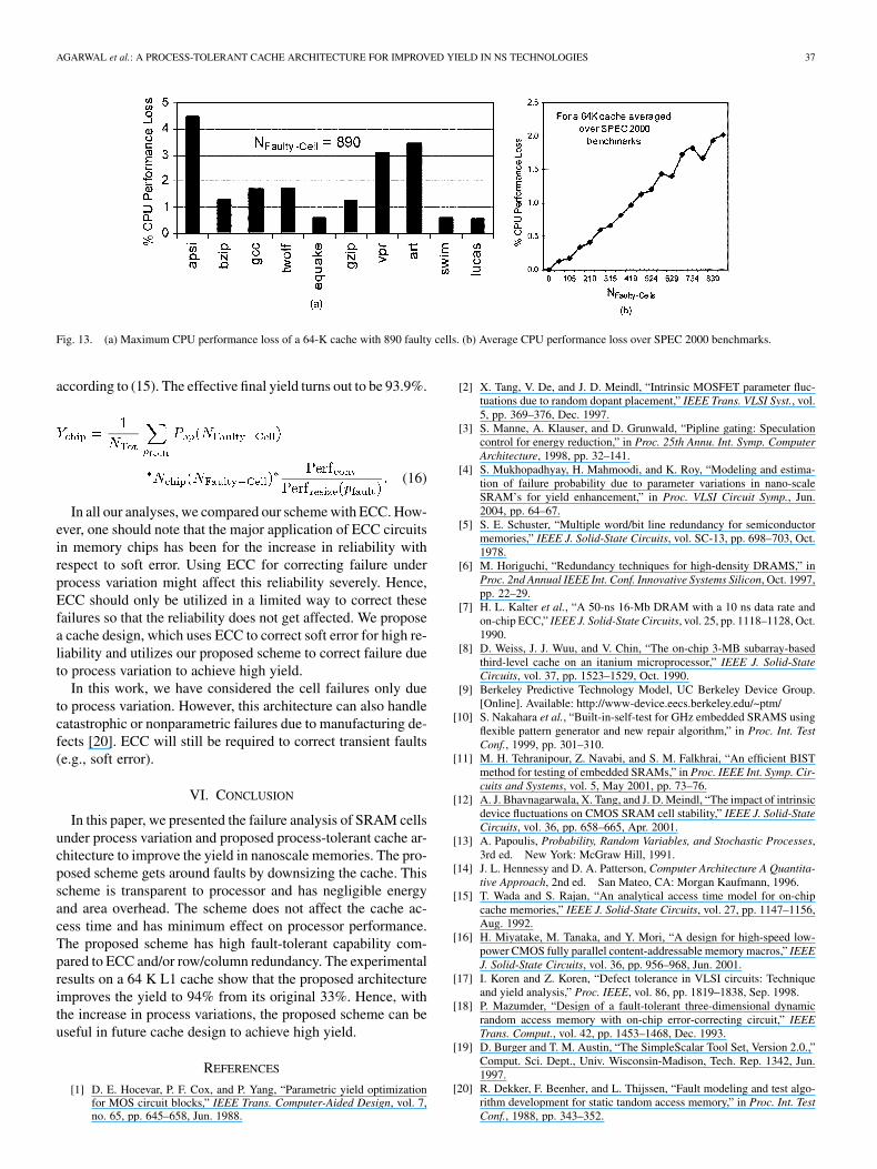
Since the proposed architecture down-sizes the cache to avoidfaulty blocks, it increases the cache miss rate, affecting the per-formance of the processor. To measure the performance loss, adirect map 64-K L1 cache is simulated using Simplescaler [19]for aggressive modern out-of-order microprocessors. Based onfault distribution, cache blocks are mapped according to theproposed scheme described above. A large number of Spec2000 benchmarks using reference inputs are simulated andthe performance loss compared to the conventional cache ismeasured. Fig. 13(a) shows the performance loss for differentbenchmarks for a 64-K L1 cache with maximum number oftolerable faults (890 faulty cells) using the proposed architec-ture. It can be observed that maximum performance loss is lessthan 5%. Fig. 13(b) plots the average CPU performance lossover benchmarks as a function of . The maximumaverage performance loss with 890 faulty cells is only 2.0%. Totake the performance into account we redefine our yield
AGARWAL et al.: A PROCESS-TOLERANT CACHE ARCHITECTURE FOR IMPROVED YIELD IN NS TECHNOLOGIES 37
Fig. 13. (a) Maximum CPU performance loss of a 64-K cache with 890 faulty cells. (b) Average CPU performance loss over SPEC 2000 benchmarks.
according to (15). The effective final yield turns out to be 93.9%.
(16)
In all our analyses, we compared our scheme with ECC. How-ever, one should note that the major application of ECC circuitsin memory chips has been for the increase in reliability withrespect to soft error. Using ECC for correcting failure underprocess variation might affect this reliability severely. Hence,ECC should only be utilized in a limited way to correct thesefailures so that the reliability does not get affected. We proposea cache design, which uses ECC to correct soft error for high re-liability and utilizes our proposed scheme to correct failure dueto process variation to achieve high yield.
In this work, we have considered the cell failures only dueto process variation. However, this architecture can also handlecatastrophic or nonparametric failures due to manufacturing de-fects [20]. ECC will still be required to correct transient faults(e.g., soft error).
VI. CONCLUSION
In this paper, we presented the failure analysis of SRAM cellsunder process variation and proposed process-tolerant cache ar-chitecture to improve the yield in nanoscale memories. The pro-posed scheme gets around faults by downsizing the cache. Thisscheme is transparent to processor and has negligible energyand area overhead. The scheme does not affect the cache ac-cess time and has minimum effect on processor performance.The proposed scheme has high fault-tolerant capability com-pared to ECC and/or row/column redundancy. The experimentalresults on a 64 K L1 cache show that the proposed architectureimproves the yield to 94% from its original 33%. Hence, withthe increase in process variations, the proposed scheme can beuseful in future cache design to achieve high yield.
REFERENCES
[1] D. E. Hocevar, P. F. Cox, and P. Yang, “Parametric yield optimizationfor MOS circuit blocks,” IEEE Trans. Computer-Aided Design, vol. 7,no. 65, pp. 645–658, Jun. 1988.
[2] X. Tang, V. De, and J. D. Meindl, “Intrinsic MOSFET parameter fluc-tuations due to random dopant placement,” IEEE Trans. VLSI Syst., vol.5, pp. 369–376, Dec. 1997.
[3] S. Manne, A. Klauser, and D. Grunwald, “Pipline gating: Speculationcontrol for energy reduction,” in Proc. 25th Annu. Int. Symp. ComputerArchitecture, 1998, pp. 32–141.
[4] S. Mukhopadhyay, H. Mahmoodi, and K. Roy, “Modeling and estima-tion of failure probability due to parameter variations in nano-scaleSRAM’s for yield enhancement,” in Proc. VLSI Circuit Symp., Jun.2004, pp. 64–67.
[5] S. E. Schuster, “Multiple word/bit line redundancy for semiconductormemories,” IEEE J. Solid-State Circuits, vol. SC-13, pp. 698–703, Oct.1978.
[6] M. Horiguchi, “Redundancy techniques for high-density DRAMS,” inProc. 2nd Annual IEEE Int. Conf. Innovative Systems Silicon, Oct. 1997,pp. 22–29.
[7] H. L. Kalter et al., “A 50-ns 16-Mb DRAM with a 10 ns data rate andon-chip ECC,” IEEE J. Solid-State Circuits, vol. 25, pp. 1118–1128, Oct.1990.
[8] D. Weiss, J. J. Wuu, and V. Chin, “The on-chip 3-MB subarray-basedthird-level cache on an itanium microprocessor,” IEEE J. Solid-StateCircuits, vol. 37, pp. 1523–1529, Oct. 1990.
[9] Berkeley Predictive Technology Model, UC Berkeley Device Group.[Online]. Available: http://www-device.eecs.berkeley.edu/~ptm/
[10] S. Nakahara et al., “Built-in-self-test for GHz embedded SRAMS usingflexible pattern generator and new repair algorithm,” in Proc. Int. TestConf., 1999, pp. 301–310.
[11] M. H. Tehranipour, Z. Navabi, and S. M. Falkhrai, “An efficient BISTmethod for testing of embedded SRAMs,” in Proc. IEEE Int. Symp. Cir-cuits and Systems, vol. 5, May 2001, pp. 73–76.
[12] A. J. Bhavnagarwala, X. Tang, and J. D. Meindl, “The impact of intrinsicdevice fluctuations on CMOS SRAM cell stability,” IEEE J. Solid-StateCircuits, vol. 36, pp. 658–665, Apr. 2001.
[13] A. Papoulis, Probability, Random Variables, and Stochastic Processes,3rd ed. New York: McGraw Hill, 1991.
[14] J. L. Hennessy and D. A. Patterson, Computer Architecture A Quantita-tive Approach, 2nd ed. San Mateo, CA: Morgan Kaufmann, 1996.
[15] T. Wada and S. Rajan, “An analytical access time model for on-chipcache memories,” IEEE J. Solid-State Circuits, vol. 27, pp. 1147–1156,Aug. 1992.
[16] H. Miyatake, M. Tanaka, and Y. Mori, “A design for high-speed low-power CMOS fully parallel content-addressable memory macros,” IEEEJ. Solid-State Circuits, vol. 36, pp. 956–968, Jun. 2001.
[17] I. Koren and Z. Koren, “Defect tolerance in VLSI circuits: Techniqueand yield analysis,” Proc. IEEE, vol. 86, pp. 1819–1838, Sep. 1998.
[18] P. Mazumder, “Design of a fault-tolerant three-dimensional dynamicrandom access memory with on-chip error-correcting circuit,” IEEETrans. Comput., vol. 42, pp. 1453–1468, Dec. 1993.
[19] D. Burger and T. M. Austin, “The SimpleScalar Tool Set, Version 2.0.,”Comput. Sci. Dept., Univ. Wisconsin-Madison, Tech. Rep. 1342, Jun.1997.
[20] R. Dekker, F. Beenher, and L. Thijssen, “Fault modeling and test algo-rithm development for static tandom access memory,” in Proc. Int. TestConf., 1988, pp. 343–352.
38 IEEE TRANSACTIONS ON VERY LARGE SCALE INTEGRATION (VLSI) SYSTEMS, VOL. 13, NO. 1, JANUARY 2005
Amit Agarwal (S’04) was born in Ghazipur, India.He received the B.Tech. degree in electrical engi-neering from the Indian Institute of Technology,Kanpur, India, in 2000, the M.S. in electricaland computer engineering from Purdue University,Lafayette, IN, in 2001, where he is currently workingtoward the Ph.D. degree in electrical and computerengineering.
In summer 2001, he was a summer Intern withSGI Microprocessor Design Center, Boston , MA,where he was involved with signal integrity. In
fall 2003, He was with Intel circuit research lab, Hillsboro working on highperformance, leakage tolerant, and low leakage register file design. His researchinterests include low-power, high-performance, process tolerant cache andregister file design, low-power integrated device, circuits, and architecturedesign and reconfigurable architecture design with unreliable components foryield improvement.
Mr. Agarwal received the certificate of academic excellence for the years1996–1997, 1997–1998, and 1998–1999. He received a fellowship from PurdueUniversity for the year 2000–2001. In 2004–2005, he received the Intel Ph.D.fellowship at Purdue University.
Bipul C. Paul (M’01) received the B.Tech. andM.Tech. degrees in radiophysics and electronics,from the University of Calcutta, Calcutta, India, andthe Ph.D. degree from Indian Institute of Science(IISc) Bangladore, India, where he received the bestthesis of the year award in 1999.
He was with Alliance Semiconductor, India, Pvt.Ltd., where he worked on synchronous DRAMdesign. He is currently a Post-Doctoral Fellow,with the Department of Electrical and ComputerEngineering, Purdue University, West Lafayette, IN.
His present research interests include low-power electronic design of nanoscalecircuits under process variation (using both bulk and SOI devices), testing, andnoise analysis. He is also working on the device and circuit optimization forultra-low power subthreshold operation.
Hamid Mahmoodi (S’00) received the B.S. degreein electrical engineering from Iran University of Sci-ence and Technology, Tehran, Iran, in 1998 and theM.S. degree in electrical engineering from the Uni-versity of Tehran, Tehran, Iran, in 2000, and is cur-rently working toward the Ph.D. degree in electricalengineering at Purdue University, West Lafayette, IN.
His research interests include low-power, robust,and high-performance circuit design for nanoscaledbulk CMOS and SOI technologies.
Animesh Datta (S’03) received the B.Tech. degree inelectrical engineering from Indian Institute of Tech-nology, Kharagpur, in 2001, and is currently workingtoward the Ph.D. degree at Purdue University, WestLafayette, IN.
From 2001 to 2002, he worked as a GraduateResearch Consultant in the Advanced VLSI DesignLab., IIT Kharagpur, India. His research emphasis ison the process variation tolerant low-power architec-ture to achieve good performance. He also works onsizing algorithms for scaled technology to achieve
fault tolerant design.
Kaushik Roy (M’83–SM’95–F’02) received theB.Tech. degree in electronics and electrical com-munications engineering from the Indian Instituteof Technology, Kharagpur, India, and Ph.D. de-gree from the electrical and computer engineeringdepartment of the University of Illinois at Ur-bana-Champaign in 1990.
He was with the Semiconductor Process andDesign Center of Texas Instruments, Dallas, wherehe worked on FPGA architecture development andlow-power circuit design. He joined the electrical
and computer engineering faculty at Purdue University, West Lafayette, IN, in1993, where he is currently a Professor. His research interests include VLSIdesign/CAD with particular emphasis in low-power electronics for portablecomputing and wireless communications, VLSI testing and verification, andreconfigurable computing. Dr. Roy has published more than 300 papers inrefereed journals and conferences, holds seven patents, and is a co-author oftwo books, Low Power CMOS VLSI: Circuit Design (New York: Wiley, 2000)and Low Voltage, Low Power VLSI Subsystems (New York: McGraw-Hill,2005).
Dr. Roy received the National Science Foundation Career DevelopmentAward in 1995, the IBM faculty partnership award, ATT/Lucent FoundationAward, Best Paper Awards at the 1997 International Test Conference, IEEE2000 International Symposium on Quality of IC Design, 2003 IEEE LatinAmerican Test Workshop, and is currently a Purdue University Faculty ScholarProfessor. He is on the Technical Advisory Board of Zenasis, Inc., and is aResearch Visionary Board Member of Motorola Labs since 2002. He has beenon the editorial board of IEEE DESIGN AND TEST, IEEE TRANSACTIONS ON
CIRCUITS AND SYSTEMS, and IEEE TRANSACTIONS ON VERY LARGE SCALE
INTEGRATION (VLSI) SYSTEMS. He was Guest Editor for the 1994 Special Issueon Low-Power VLSI in IEEE DESIGN AND TEST, and the June 2000 Issue ofIEEE TRANSACTIONS ON VLSI SYSTEMS, and the July 2002 IEE ProceedingsComputers and Digital Techniques.