
A neuromorphic implementation of multiple spike-timing synaptic plasticity rules for large-scale...
17
ORIGINAL RESEARCH published: 20 May 2015 doi: 10.3389/fnins.2015.00180 Frontiers in Neuroscience | www.frontiersin.org 1 May 2015 | Volume 9 | Article 180 Edited by: Elisabetta Chicca, University of Bielefeld, Germany Reviewed by: Johannes Schemmel, University of Heidelberg, Germany Michael Pfeiffer, University of Zurich and ETH Zurich, Switzerland Francesco Tenore, Johns Hopkins University Applied Physics Laboratory, USA *Correspondence: Runchun M. Wang, The MARCS Institute, University of Western Sydney, Room 109, Building XB, Kingswood Campus, Sydney, NSW 2747, Australia [email protected] Specialty section: This article was submitted to Neuromorphic Engineering, a section of the journal Frontiers in Neuroscience Received: 21 October 2014 Accepted: 06 May 2015 Published: 20 May 2015 Citation: Wang RM, Hamilton TJ, Tapson JC and van Schaik A (2015) A neuromorphic implementation of multiple spike-timing synaptic plasticity rules for large-scale neural networks. Front. Neurosci. 9:180. doi: 10.3389/fnins.2015.00180 A neuromorphic implementation of multiple spike-timing synaptic plasticity rules for large-scale neural networks Runchun M. Wang*, Tara J. Hamilton, Jonathan C. Tapson and André van Schaik The MARCS Institute, University of Western Sydney, Sydney, NSW, Australia We present a neuromorphic implementation of multiple synaptic plasticity learning rules, which include both Spike Timing Dependent Plasticity (STDP) and Spike Timing Dependent Delay Plasticity (STDDP). We present a fully digital implementation as well as a mixed-signal implementation, both of which use a novel dynamic-assignment time-multiplexing approach and support up to 2 26 (64M) synaptic plasticity elements. Rather than implementing dedicated synapses for particular types of synaptic plasticity, we implemented a more generic synaptic plasticity adaptor array that is separate from the neurons in the neural network. Each adaptor performs synaptic plasticity according to the arrival times of the pre- and post-synaptic spikes assigned to it, and sends out a weighted or delayed pre-synaptic spike to the post-synaptic neuron in the neural network. This strategy provides great flexibility for building complex large-scale neural networks, as a neural network can be configured for multiple synaptic plasticity rules without changing its structure. We validate the proposed neuromorphic implementations with measurement results and illustrate that the circuits are capable of performing both STDP and STDDP. We argue that it is practical to scale the work presented here up to 2 36 (64G) synaptic adaptors on a current high-end FPGA platform. Keywords: mixed-signal implementation, synaptic plasticity, STDP, STDDP, analog VLSI, time-multiplexing, dynamic-assigning, neuromorphic engineering Introduction Plastic synapses, i.e., synapses that can adapt their gain according to one or more adaptation rules, are extremely important in neural systems, as it is generally accepted that learning in the brain arises from synaptic modifications. The Spike Timing Dependent Plasticity (STDP) algorithm (Gerstner et al., 1996; Magee, 1997; Markram et al., 1997; Bi and Poo, 1998), which is one of the adaptation rules observed in biology, modulates the weight of a synapse based on the relative timing between the pre-synaptic spike and the post-synaptic spike. Besides weight adaptation, some observations suggest that the propagation delays of neural spikes, as they are transmitted from one neuron to another, may be adaptive (Stanford, 1987). Axonal delays are an important feature that seems to play a key role in the formation of neuronal groups and memory (Izhikevich, 2006). In our previous work (Wang et al., 2011b, 2012), a delay adaptation algorithm, Spike Timing Dependent Delay Plasticity (STDDP), inspired by STDP was developed to fine-tune delays that had been programmed into the network. We recently showed that the time delays of neural spike propagation
-
Upload
westernsydney -
Category
Documents
-
view
3 -
download
0
Transcript of A neuromorphic implementation of multiple spike-timing synaptic plasticity rules for large-scale...
ORIGINAL RESEARCHpublished: 20 May 2015
doi: 10.3389/fnins.2015.00180
Frontiers in Neuroscience | www.frontiersin.org 1 May 2015 | Volume 9 | Article 180
Edited by:
Elisabetta Chicca,
University of Bielefeld, Germany
Reviewed by:
Johannes Schemmel,
University of Heidelberg, Germany
Michael Pfeiffer,
University of Zurich and ETH Zurich,
Switzerland
Francesco Tenore,
Johns Hopkins University Applied
Physics Laboratory, USA
*Correspondence:
Runchun M. Wang,
The MARCS Institute, University of
Western Sydney, Room 109, Building
XB, Kingswood Campus, Sydney,
NSW 2747, Australia
Specialty section:
This article was submitted to
Neuromorphic Engineering,
a section of the journal
Frontiers in Neuroscience
Received: 21 October 2014
Accepted: 06 May 2015
Published: 20 May 2015
Citation:
Wang RM, Hamilton TJ, Tapson JC
and van Schaik A (2015) A
neuromorphic implementation of
multiple spike-timing synaptic
plasticity rules for large-scale neural
networks. Front. Neurosci. 9:180.
doi: 10.3389/fnins.2015.00180
A neuromorphic implementation ofmultiple spike-timing synapticplasticity rules for large-scale neuralnetworksRunchun M. Wang*, Tara J. Hamilton, Jonathan C. Tapson and André van Schaik
The MARCS Institute, University of Western Sydney, Sydney, NSW, Australia
We present a neuromorphic implementation of multiple synaptic plasticity learning
rules, which include both Spike Timing Dependent Plasticity (STDP) and Spike Timing
Dependent Delay Plasticity (STDDP). We present a fully digital implementation as well
as a mixed-signal implementation, both of which use a novel dynamic-assignment
time-multiplexing approach and support up to 226 (64M) synaptic plasticity elements.
Rather than implementing dedicated synapses for particular types of synaptic plasticity,
we implemented amore generic synaptic plasticity adaptor array that is separate from the
neurons in the neural network. Each adaptor performs synaptic plasticity according to the
arrival times of the pre- and post-synaptic spikes assigned to it, and sends out a weighted
or delayed pre-synaptic spike to the post-synaptic neuron in the neural network. This
strategy provides great flexibility for building complex large-scale neural networks, as a
neural network can be configured for multiple synaptic plasticity rules without changing its
structure. We validate the proposed neuromorphic implementations with measurement
results and illustrate that the circuits are capable of performing both STDP and STDDP.
We argue that it is practical to scale the work presented here up to 236 (64G) synaptic
adaptors on a current high-end FPGA platform.
Keywords: mixed-signal implementation, synaptic plasticity, STDP, STDDP, analog VLSI, time-multiplexing,
dynamic-assigning, neuromorphic engineering
Introduction
Plastic synapses, i.e., synapses that can adapt their gain according to one or more adaptation rules,are extremely important in neural systems, as it is generally accepted that learning in the brain arisesfrom synaptic modifications. The Spike Timing Dependent Plasticity (STDP) algorithm (Gerstneret al., 1996; Magee, 1997; Markram et al., 1997; Bi and Poo, 1998), which is one of the adaptationrules observed in biology, modulates the weight of a synapse based on the relative timing betweenthe pre-synaptic spike and the post-synaptic spike. Besides weight adaptation, some observationssuggest that the propagation delays of neural spikes, as they are transmitted from one neuron toanother, may be adaptive (Stanford, 1987). Axonal delays are an important feature that seemsto play a key role in the formation of neuronal groups and memory (Izhikevich, 2006). In ourprevious work (Wang et al., 2011b, 2012), a delay adaptation algorithm, Spike Timing DependentDelay Plasticity (STDDP), inspired by STDP was developed to fine-tune delays that had beenprogrammed into the network.We recently showed that the time delays of neural spike propagation

Wang et al. Neuromorphic implementation of synaptic-plasticity rules
in the rat somatosensory cortex can be modified bysuprathreshold synaptic processes such as STDP (Buskilaet al., 2013). This suggests that it is likely that synaptic weightsand the propagation delays are adapted simultaneously.
The main goal of this work is to develop a design frameworkthat is capable of implementing neural networks with maximumsize, using simplified biological models. To allow for futureimplementations that interface with the real world, these neuralnetworks should be running in real time. While detailedsimulations of small networks of neurons are one way of studyingneural systems, such small networks are not able to capture allthe complexity and dynamics of a large scale neural network withnon-linear properties, such as a model of neocortex, as pointedout by Johansson and Lansner (2007). In the work reportedhere, we have therefore focussed on attaining maximum networksize.
As synaptic plasticity has not yet been fully characterizedand models of synaptic plasticity remain in flux (Brennerand Sejnowski, 2011; Sejnowski, 2012), dedicated hardwareimplementations that have been hardwired to one particular typeof plasticity rule will not be able to adapt to likely future changesin plasticity models. Thus, the design framework we present herewill be capable of including various substantial neural networks,each of which may be designed to solve a particular task.
In this paper, we will focus on exploring hardware friendlyimplementations rather than comparing our learning ruleswith the vast, well established complex algorithms used incomputational neuroscience. As a result of our hardware focus,mathematical analysis of the long-term behavior of the plasticityrules in benchmark networks and quantifying the effects of ourlearning rules on the synaptic weight, which are commonly usedin computational modeling papers, are out of the scope of thispaper and will therefore not be addressed.
Simulating neural networks on computers has been successfulin informing the computational neuroscience community onpromising learning strategies, network configurations and neuralmodels for many decades. This approach, however, does not scalevery well, slowing down considerably for large networks withlarge numbers of variables. For instance, the Blue Gene rack, atwo-million-dollar, 2048-processor supercomputer, takes 1 h and20min to simulate 1 s of neural activity in 8 million integrate-and-fire neurons (Izhikevich, 2003) connected by 4 billion staticsynapses (Wittie and Memelli, 2010). For smaller scale networks,Graphic Processing Units (GPUs) can perform certain types ofsimulations tens of times faster than a PC (Shi et al., 2015). GPUsstill perform numeric simulations, however, and, depending onthe complexity of the network, it can take hours to simulate 1 sof activity in a tiny piece of cortex (Izhikevich and Edelman,2008). Along with general hardware solutions, there have beena number of more dedicated hardware solutions (Pfeil et al.,2012, 2013; Painkras et al., 2013). A good example of a dedicatedsolution that implements numeric simulation of neurons is theSpiNNaker project (Galluppi et al., 2012). In SpiNNaker, ARMprocessors run software neuron models. Their most recent workshows that the SpiNNaker cores are capable of implementing96,000 synapses (7500 synapses per core) for STDP in real time(Galluppi et al., 2014).
An alternative approach is to use the analog VLSI (aVLSI)circuits, which avoid any need to discretise differential equationsof neuronal dynamics. These implementations will also addstochasticity to the system through electronic noise and devicemismatch, resulting in more realistic simulations of biologicalneural networks. The basic STDP learning rule, which is a pairedpulse protocol (Gerstner et al., 1996), has been successfullyimplemented using aVLSI circuits (Bofill-i-petit and Murray,2004; Indiveri et al., 2006; Häfliger, 2007; Koickal et al., 2007).More variants of the STDP algorithm have been proposed byBrader et al. (2007a) and Graupner and Brunel (2012). Thesealgorithms capture more of the synaptic dynamics but still followthe principle that themodification of the synaptic weight dependson the relative timing of individual pre- and post-synaptic spikes.Many aVLSI implementations of these algorithms have beenproposed (Chicca et al., 2003; Mitra et al., 2009; Giulioni et al.,2012). Similarly, aVLSI circuits have also been used to implementthe STDDP learning rule (Wang et al., 2011a,b, 2012, 2013a).This aVLSI approach is useful for studying the dynamics of smalland densely interconnected networks, but less so for the study oflarge and sparsely connected networks, such as complex modelsof various areas of cortex. The aVLSI implementations all useddedicated synapses for a specific type of synaptic plasticity andthe number of plastic synapses integrated on single chip is usuallyfewer than tens of thousands. This significantly limits the size ofthe network these approaches can implement.
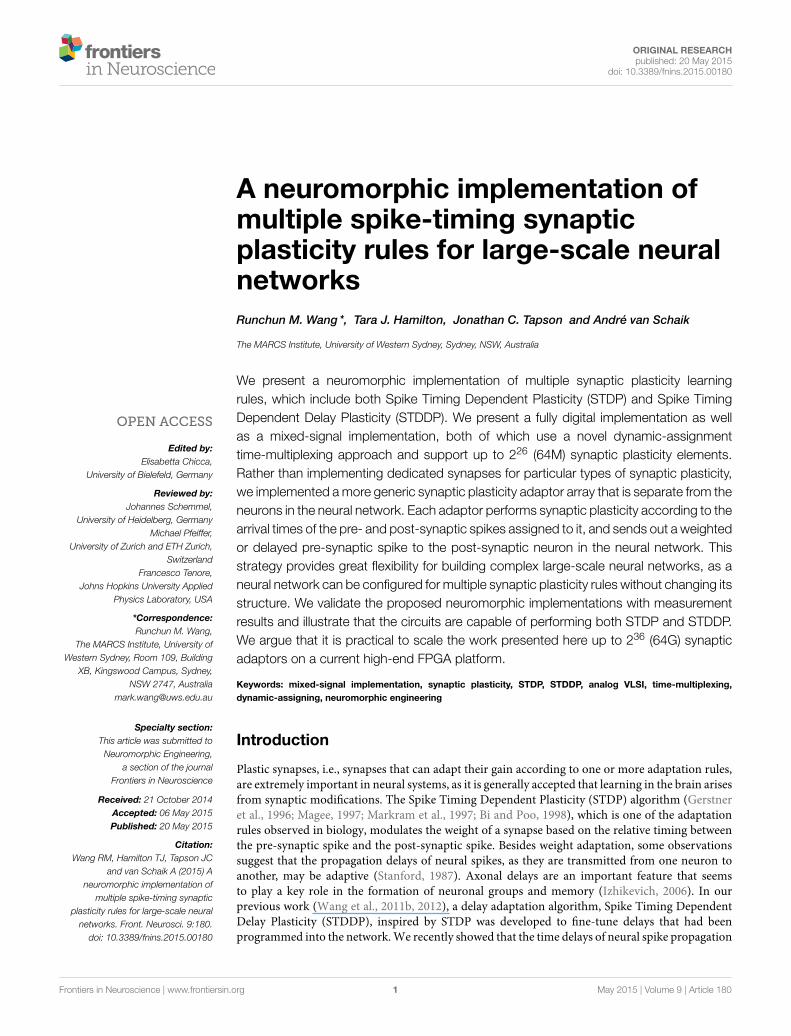
We chose to implement a synaptic plasticity adaptor arraythat is separate from the neurons (see Figure 1). In this scheme,the address of the pre-synaptic spike from the pre-synapticneuron will have already been remapped to the address of thepost-synaptic neuron by the router shown in Figure 1. Foreach synapse, which remains part of the neuron, a synapticadaptor will be connected to it when it needs to apply a certainsynaptic plasticity rule. The synaptic adaptor will carry out theweight/delay adaptation by updating weight/delay values that arestored in digital memory. For each incoming pre-synaptic spike,the adaptor will send a weighted/delayed pre-synaptic spike tothe post-synaptic neuron in the neuron array.
This strategy provides great flexibility, as a hardware neuralnetwork can be configured to performmultiple synaptic plasticityrules without needing to change its own structure, simplyby connecting the synapses to the appropriate modules inthe synaptic plasticity adaptor array. This structure was firstproposed by Vogelstein and his colleagues in the IFAT project(Vogelstein et al., 2007). However, they didn’t implementsynaptic plasticity in that work although they did discussthe implementation of STDP with this structure. It seemsthat this flexibility will generate a communication overhead.The communication between neurons and adaptors has thesame overhead as the communication between neurons andother neurons in a network without a separate adaptor array.Thus, the additional overhead stems from the communicationfrom the adaptor array to each of the synapses. This willbe discussed in more detail in the next section. The majordisadvantage of our approach is that it is incapable of modelingthe ion channels in the biological synapses. Compared to theaVLSI approach, our approach is less useful for studying the
Frontiers in Neuroscience | www.frontiersin.org 2 May 2015 | Volume 9 | Article 180
Wang et al. Neuromorphic implementation of synaptic-plasticity rules
FIGURE 1 | The synaptic plasticity adaptor array that is separate
from the neurons. For each synapse, which remains part of the
neuron, a synaptic adaptor will be connected to it when it needs to
apply a certain synaptic plasticity rule. The synaptic adaptor will carry
out the weight/delay adaptation by updating weight/delay values. For
each incoming pre-synaptic spike, the adaptor will send a
weighted/delayed pre-synaptic spike to the post-synaptic neuron in the
neuron array.
dynamics of the networks that require high degrees of biologicalrealism. Furthermore, our approach is less power efficientcompared to the aVLSI implementations. This is because ourimplementation has to employ configurable but power hungrydevices, such as FPGAs/MCUs, to achieve its flexibility. AnalogVLSI implementations, in contrast, especially those operatingin weak inversion (Liu et al., 2002), are capable of achieving asignificantly low power consumption.
We have previously presented a compact reconfigurablemixed-signal implementation of a synaptic plasticity adaptor thatis capable of performing both STDP and STDDP (Wang et al.,2014a). Here, we present its follow-up work that uses a novelapproach to scale up the numbers of synaptic plasticity adaptorsup by 128 (27) times more without increasing the hardware costsignificantly.While the design of the router and the neuron arraysare out of the scope of this paper and will not be presented.
Materials and Methods
Learning RulesSpike Timing Dependent PlasticityThe STDP algorithm modulates the weight of a synapse basedon the relative timing of the pre- and post-synaptic spikes. Theweight of a synapse will be increased if a pre-synaptic spikearrives several milliseconds before the post-synaptic spike fires.
Conversely, the weight will be decreased in the case that thepost-synaptic spike fires earlier than the arrival of a pre-synapticspike by several milliseconds. The amount and direction ofmodification of the weight are determined by the time betweenthe arrival of the pre- and post-synaptic spike.
To obtain this time difference, we need to know when thepre- and post-synaptic spike arrives. This is implemented byintroducing a time window generator, which is composed of a4-bit counter, it will be reset by either spike and increased byone bit at each time step, e.g., 1ms until it reaches its maximumvalue 0 × F. The time at which the alternative spike arrives isrepresented by the value of the counter. We also define that thetime window is “active” before it reaches its maximum value. Aswe assume that the adaption will not be carried out if the pre-and post- synaptic spikes arrive simultaneously, only one timewindow generator will be needed.
In the original STDP learning rule (Gerstner et al., 1996), theamount of synaptic modification is summarized by the followingequations:
1w =
{
A+ exp (1t/τ+), if 1t < 0−A−exp (1t/τ−), if 1t ≥ 0
(1)
where 1w is the modification of the synaptic weight, 1tis the time difference between the arrival time of the pre-
Frontiers in Neuroscience | www.frontiersin.org 3 May 2015 | Volume 9 | Article 180

Wang et al. Neuromorphic implementation of synaptic-plasticity rules
FIGURE 2 | The STDP modification function. 1t is the time difference
between the arrival time of the pre- and post-synaptic spike. The blue
line represents synaptic modification 1w, which is linearly proportional 1t. The
red line represents the synaptic modification 1w, which is a fixed step. The
dashed line represents the range of pre-to-post-synaptic interspike intervals
over which synaptic modification is performed.
and post-synaptic spike. The maximum amounts of synapticmodification 1w are determined by two positive parameters:A+ and A−. The ranges of pre-to-post-synaptic interspikeintervals over which synaptic modifications are performedare determined by the parameters τ+ and τ−. The authorsin Song et al. (2000) concluded that this function providesa reasonable approximation of the dependence of synapticmodification on spike timing observed experimentally. However,it is a computationally intensive function since it requiresexponentiation and division operations, both of which wouldoccupy a large silicon area.
To reduce the required silicon area, in our system, we haveimplemented two simplifiedmodification rules. The first one is tochange the weight proportionally to the calculated time difference(see the blue line in Figure 2) and is summarized by the followingequations:
1w =
{
A+ + 1t, if Tactive = 1 and 1t < 0−A− + 1t, if Tactive = 1 and 1t > 0
(2)
where 1w is the modification of the synaptic weight, 1t is thetime difference between the arrival time of the pre- and post-synaptic spike. Tactive is a Boolean value that indicates the timewindow generator is active (see the dashed line in Figure 2). Inthis system, the synaptic weight is an unsigned integer, whichranges from 0 to 15. A+ and A− are both set to 16 here. Thesecond one is to change the value of the weight by a fixed value(see the red line in Figure 2) and is summarized by the followingequations:
1w =
{
+ step, if Tactive = 1 and 1t< 0− step, if Tactive = 1 and 1t > 0
(3)
where step is the fixed value and is set to 1 here. No weightmodification will be performed if the pre- and post-synaptic
FIGURE 3 | Illustration of Delay adaptation. (A) Delay increment; (B) Delay
decrement. The axonal delay presents the delay between the firing time of the
pre-synaptic neuron (the green one) and arrival time of the pre-synaptic spike
(the red one) at the post-synaptic neuron. 1t represents the time difference
between the pre- and post-synaptic spike (the blue spike) to and from the
post-synaptic neuron.
spikes arrive simultaneously. The efficacy of these two simplifiedlearning rules will be presented in Section Performance of STDP.
Spike Timing Dependent Delay PlasticityTwo examples of the adaptation of axonal delays are shown inFigure 3, an increment of the delay (Figure 3A) and a decrementof the delay (Figure 3B). After the pre-synaptic neuron firesthere is an axonal delay before the delayed pre-synaptic spikeis sent to the post-synaptic neuron. If the post-synaptic spike,which is from the post-synaptic neuron, is not simultaneouswith the delayed pre-synaptic spike, we may adapt the axonaldelay by increasing or decreasing it by a small amount. Thisprocedure is repeated until the delayed pre-synaptic spike occurssimultaneously with the post-synaptic spike.
Since this learning rule also needs to obtain the time differencebetween the pre- and post-synaptic spikes, we will use the sametime window generator as described above, to generate the axonaldelay. In this case, however, the time window generator will bestarted by the pre-synaptic spike (the green spike in Figure 3).Moreover, the duration of the generated time window will bemodulated according to the axonal delay. The modification ofthe axonal delay will only be performed by the post-synapticspike: when the post-synaptic spike arrives, if the time windowis active, then there is a decrease the axonal delay and vice versa.The modification of the axonal delay 1d is summarized by thefollowing equations:
1d =
{
− step, if Tactive = 1+ step, if Tactive = 0
(4)
where step is a fixed value and is set to 1 here. Modifying theaxonal delay by a single step is one of the three strategies, whichwere proposed and proved to be functional in our previouswork (Wang et al., 2013b). No delay modification will beperformed if the delayed pre-synaptic spike and post-synapticarrive simultaneously. In this system, the axonal delay is also anunsigned integer, which ranges from 0 to 15.
Design ChoiceTo implement multiple synaptic plasticity rules for large scalespiking neural networks, the design choice we made were basedon the following principles:
Frontiers in Neuroscience | www.frontiersin.org 4 May 2015 | Volume 9 | Article 180
Wang et al. Neuromorphic implementation of synaptic-plasticity rules
Time-multiplexingIn digital implementations of spiking neural networks, a singlephysical neuron can be time-multiplexed to simulate manyvirtual neurons, since digital hardware neurons can operatemuch faster than biological neurons. Each virtual neuron onlyneeds to be updated every millisecond or so, as a millisecondtime resolution is generally acceptable for neural simulations.Digital implementations of neurons using this time-multiplexingapproach have been described in Cassidy and Andreou (2008);Cassidy et al. (2011); Wang et al. (2013b, 2014c). In theimplementation presented here, we are time-multiplexing boththe synaptic adaptors and the neurons.
Dynamic-assignmentIt is not necessary to implement all neurons physically on siliconas based on the physiological metabolic cost of neural activity, ithas been concluded that fewer than 1% of neurons are active inthe brain at any moment (Lennie, 2003). A larger address spacecan be mapped onto a smaller number of physical componentsthrough dynamically assigning these components. Based on thisprinciple, we have presented a dynamically-assigned digital andanalog neuron array in Wang et al. (2013b) and Wang et al.(2014d), respectively. In these two systems, 4096 (4 k) neuronswere achieved with only tens of neurons implemented physicallyon silicon. Here we also use this approach for both the neuronsand the synaptic adaptors.
Mixed-signalThis implementation style can combine some of theadvantages of both analog and digital implementations.Analog implementations can realize biological behaviorsof neurons in a very efficient manner, whereas digitalimplementations can provide the re-configurability neededfor rapid prototyping of spiking neural networks. As a result,mixed-signal implementations offer an attractive solutionfor implementing neural networks and many designs havebeen proposed for such systems (Goldberg et al., 2001; Gaoand Hammerstrom, 2007; Mirhassani et al., 2007; Vogelsteinet al., 2007; Harkin et al., 2008, 2009; Schemmel et al., 2008;Saighi et al., 2010; Yu and Cauwenberghs, 2010; Zaveri andHammerstrom, 2011; Minkovich et al., 2012).
StandardizationTo enable multiplexing building blocks, such as neurons,synapses, and axons, in a neuromorphic system, these circuitsmust be designed as standardized building blocks with astandard protocol for communication with programmabledevices. Specifically for use in time-multiplexed neural systems,we have developed a synchronous Address Event Representation(AER) protocol, which uses a collision-free serial processingscheme with a single active signal and an address (Wang et al.,2013b). This synchronous scheme eliminates the overhead of anarbiter in the standard AER protocol.
For the maximum utilization of a fixed sized aVLSI chip, itis best to reduce the on-chip routing as much as possible as therouting can be carried out off-chip by FPGAs or microprocessorswith more flexibility and extensibility. As the on-chip topology of
the aVLSI circuits is generally fixed after fabrication, it is betterto implement the whole system in an FPGA for prototyping andoptimization before fabricating the aVLSI chips.
Pulse width ModulationFor the systems that are sensitive to high communicationsoverheads, e.g., aVLSI chips with limited number of pads, weadopted a pulse width modulation scheme, to minimize thecommunication bandwidth. In this scheme the durations of thespikes are modulated according to the synaptic weights, and thesynapses in the neuron array are sensitive to the durations of thespikes (e.g., Wang et al., 2014b). It should be noted, however,that we could easily reconfigure the system to send out synapticweights directly to the neurons in systems that are not sensitiveto high communications overheads, e.g., FPGA designs.
VersatilityTo efficiently implement synaptic plasticity in large-scale spikingneural networks with different learning rules, the building blockshould be capable of being configured for multiple synapticplasticity rules, such as STDP and STDDP. When the synapticplasticity adaptor is configured as the STDP adaptor, it performsSTDP by receiving pre- and post-synaptic spikes from the pre-and post-synaptic neuron respectively. Its output, a weighted pre-synaptic spike generated using pulse width modulation, is sent tothe synapse of the post-synaptic neuron for generating a post-synaptic current (PSC). When the synaptic plasticity adaptor isconfigured as an STDDP adaptor, it receives the same signals, butits output is a pre-synaptic spike that has been delayed accordingto the stored delay value for this neuron-to-neuron connection.
ArchitectureFigure 4 shows the topology of the proposed mixed-signalsynaptic plasticity adaptor array. It consists of an adaptor arrayon an FPGA and a time window generator array, which couldbe either a fully digital implementation on the same FPGA, oran analog implementation on a custom designed aVLSI chip,or both, as shown. All blocks use time multiplexing and aredynamically assigned using an FPGA to control the assignment.
Based on the physiological metabolic cost of neural activity,it has been concluded that fewer than 1% of neurons are activein the brain at any moment (Lennie, 2003). The anatomicalstudies of neocortex presented in Scannell et al. (1995) showedthat cortical neurons are not randomly wired together. Instead,cortical neurons are typically organized into local clusterscalled minicolumns, which are then grouped into modulescalled hypercolumns (Hubel and Wiesel, 1974; Amirikian andGeorgopoulos, 2003). The connections of the minicolumnsare highly localized so that connectivity between two nearby(less than 25–50µm apart) pyramidal neurons is high and theconnectivity between two neurons drops sharply with distance(Holmgren et al., 2003). Based on the experimental data inTsunoda et al. (2001) and Johansson and Lansner (2007)concluded that at most a few percent of the hypercolumns andhence only about 0.01% of the minicolumns and neurons are activein a functional sense (integrating and firing) at any moment inthe cortex. They also concluded that only 0.01% of the synapses
Frontiers in Neuroscience | www.frontiersin.org 5 May 2015 | Volume 9 | Article 180

Wang et al. Neuromorphic implementation of synaptic-plasticity rules
FIGURE 4 | Topology of the mixed-signal synaptic plasticity
module array. The controller receives pre- and post-synaptic spikes
from the neuron array and assigns them to the corresponding TM
adaptors according to their addresses. The global counter processes
each TM adaptor sequentially. We use the Master RAM to store all the
weight/delay values, while the TM STDP/STDDP adaptor array has a
Local cache that stores the values of the DA adaptors that are being
processed. The time window generator array generates the time
windows that will be used by the TM adaptors for performing the
learning rules.
in our brains are active (transmitting signals) on average at anymoment. Hence, in principle, one hardware synapse could bedynamically reassigned to 104 virtual synapses on average. Sucha hardware synapse will be referred to as a physical synapse andthe synapse to be simulated will be referred to as a dynamically-assigned (DA) synapse. If a DA synapse cannot be simulated in asingle time step, the physical synapse needs to be assigned to thatDA synapse for a longer time and the number of DA synapses asingle physical synapse can simulate will go down proportionally.
On an FPGA running at 200MHz, we can time-multiplex asingle physical synapse to simulate 1ms/5 ns = 200,000 time-multiplexed (TM) synapses, each one updated every millisecond.Therefore, theoretically, a TM synapse array with 200,000 TMsynapses can be dynamically assigned for 200,000 × 104 = 2 ×
109 DA synapses, if these synapses can be simulated in a single 5ns clock cycle and if only 0.01% of the synapses are active at anytime step.
Since we chose to implement a synaptic plasticity adaptorarray that is separate from the neurons, we will apply thesetwo approaches to the adaptors. To be able to deal with highersynaptic activity rates, and because powers of two are preferableto optimize memory use for storing variables, such as weightsand delays, we chose to dynamically assign one TM adaptor for8192 (8 k) DA adaptors. Themaximum active rate of the synapsesthat this system can support is therefore 1/8 k≈ 0.012%. The TMadaptor array itself is configured to simulate 8 k TM adaptors,allowing it to support 8 k × 8 k = 64M synapses. Each TM
adaptor can use up to 25 clock cycles to complete its processing tomaintain an update rate of 1 kHz (the corresponding time step isabout 1ms). The time window generator array is also configuredto have 8 k identical time window generators, each time windowbeing assigned to one TM adaptor.
The dynamically-assigned adaptor array consists of three sub-blocks: a controller, a TM STDP/STDDP adaptor array anda Master RAM. A single physically implemented dynamically-assigned adaptor array is capable of representing up to 64M DAadaptors, thus the hardware cost of the DA adaptors is negligible.The physical constraint for this approach is data storage. On-chip SRAM (on an FPGA) will be highly limited in size (generallyless than tens of MBs), while the use of off-chip memory will belimited by the communications bandwidth. It is difficult, but notimpossible, to use off-chip memory with the time-multiplexingapproach, as new values need to be available from memory everytime slot to provide real-time simulation.
Since we are aiming for themaximumnetwork size, we need toensure that the system is able to utilize off-chip memory. Inspiredby the cache structure used in state-of-the-art CPUs, we use theMaster RAM to store all the weight/delay values, while the TMadaptor array has a Local cache that stores the values of theDA adaptors that are being processed. The accessing (read/write)of the Master RAM will only be performed when needed. Thismeans that new values are no longer required to be availablefrom memory every time slot. Hence this cache structure greatlyreduces the bandwidth requirement to use external memory.
Frontiers in Neuroscience | www.frontiersin.org 6 May 2015 | Volume 9 | Article 180

Wang et al. Neuromorphic implementation of synaptic-plasticity rules
We will present the details of this cache structure following apresentation on the management the incoming spikes. It shouldbe noted, however, that using off-chip memory requires flowcontrol for the memory interface, which results in a morecomplex system architecture. Thus, for the work reported here,we use only on-chip memory, thus simplifying the systemarchitecture. We will discuss the usage of off-chip memory inmore detail in Section Discussion.
The controller receives pre- and post-synaptic spikes fromthe neuron array (see Figure 4) and assigns them to thecorresponding TM adaptors according to their addresses. In ourprevious work (Wang et al., 2013b, 2014d) that also implementedthe dynamic-assignment algorithm, the controller needs to checkwhether there is already a neuron assigned to the incoming spikeor not. This method has a high usage of slice LUTs, which isthe bottleneck for large-scale FPGA designs. This is because thatmethod requires an address register array and a timer array,both of which are running in parallel and hence have to beimplemented with slice LUTs.
To avoid this problem, we chose instead to use a directmapping method that assigns one fixed TM adaptor as the targetadaptor for the incoming spike irrespective of whether the TMadaptor has been assigned or not. The incoming spike’s AERaddress is a 26-bit address (along with a single active line). Weonly store the most significant 13 bits out of 26 bits into a DAaddress RAM (a dual port RAM with a size of 8 k × 13 bits),while the other 13 bits determine where, i.e., in which positionof the DA address RAM, the 13 bits will be stored.
To decouple writing new events (pre- and post-synapticspikes) from reading out from current events, we use a FIFO
and an aligner (a dual port RAM with a size of 8 k × 1 bit thatcorresponds to 8 k TM adaptors). For pre- and post-synapticspikes, the size of the FIFO is 16 × 26 bit and 16 × 13 bitrespectively. The work presented in Cassidy et al. (2011) used twobanks of dual port RAM to implement a ping-pong buffer. Thisrequires much more RAM than our solution.
Figure 5 shows the timing diagram for the controller for onetime slot. Assuming the PRE_FIFO is empty at T0, when a newpre-synaptic spike arrives (its active line is high) at T2, its 26-bit AER address will be written into PRE_FIFO. The controllerwill then read the PRE_FIFO by asserting fifo_rd at T3 (since thePRE_FIFO is not empty anymore) and read data (fifo_rddata)will be ready at T4 (one clock cycle latency). To indicate that aspike has arrived (for that TM adaptor), at T4, the controller willwrite 0 × 1 into the PRE_aligner to the position determined bythe least significant 13 bits of the fifo_rddata.
At T4, the controller will also use the least significant 13 bitsof fifo_rddata to retrieve the stored address (from the DA addressRAM), which will be ready at T6 (two clock cycles latency). Ifthis retrieved address does not match the most significant 13 bitsof the delayed fifo_rddata (the red one), this indicates that thetarget DA adaptor is not the one that has been assigned before.Hence the value (in the Local cache) of the TM adaptor needs tobe updated with the value of the target DA adaptor. Therefore, atT6, the controller will read the Master RAM by asserting a readenable signal (M_rden) with a read address M_rdaddr, which isthe fifo_rddata signal delayed. For the same reason, at T6, thecontroller will also update the DA address RAM with the addressof this newly arrived pre-synaptic spike: the most significant13 bits of the delayed fifo_rddata (the least significant 13 bits
FIGURE 5 | The controller’s timing diagram of one time slot. A
pre-synaptic spike arrives at the controller at T2 and it will be written into the
PRE_FIFO. The controller will read the PRE_FIFO at T3 and the read data
(fifo_rddata) will be ready at T4. To indicate that a spike has arrived (for that
TM adaptor), at T4, controller will write 0× 1 into the PRE_aligner to the
position determined by the least significant 13 bits of the fifo_rddata. The
controller will also use the least significant 13 bits of fifo_rddata to retrieve the
stored address (from the DA address RAM), which will be ready at T6. At T6,
the controller will read the Master RAM by asserting a read enable signal
(M_rden) with a read address M_rdaddr, which is the fifo_rddata signal
delayed (the red one). At T12, the output from the Master RAM M_rddata will
be ready and the Local cache will be updated by asserting L_wren.
Frontiers in Neuroscience | www.frontiersin.org 7 May 2015 | Volume 9 | Article 180

Wang et al. Neuromorphic implementation of synaptic-plasticity rules
determines the position to write). The output from the MasterRAMM_rddata will be ready 6 clock cycles later (we will explainwhy this latency is needed Section TM STDP Adaptor Array) andthe Local cache will be updated by asserting L_wren.
To read out the aligned pre-synaptic spike (Pre_aligned), ateach time slot, the controller will read out the TM adaptor ofthat time slot, from the PRE_aligner at T1. The Pre_alignedwill be ready at T3 where the corresponding TM adaptor willacknowledge it, after which it will be cleared. To avoid thecollision that can happen when the PRE_FIFO and the controllerboth try to write the PRE_aligner (at the same location, althoughthis case will not happen frequently) at T3, we set it so thatthe PRE_FIFO cannot be read (fifo_rd cannot be asserted) atT0. This is indeed the reason to introduce the FIFO since inthis way all operations are fully pipelined and can be performedon every clock. To keep consistent with this pipeline, in eachtime slot, the controller will read out the DA_addr (no clearoperation needed) for the TM adaptor of that time slot fromthe DA address RAM at T1. When the TM adaptor generatesa weighted/delayed pre-synaptic spike, the controller will sendthis spike to the post-synaptic neuron with a 26-bit AER address,which is a combination of the DA_addr and the value of theglobal counter.
The timing for post-synaptic spike is aligned using a verysimilar scheme to that described above for the pre-synaptic spike,however, its address will not be stored in the DA address RAM.This is due to the fact that only the weighted/delayed pre-synapticspike will be sent to the post-synaptic neuron (see Figure 1) andhence only the address of the pre-synaptic spike needs be storedand only the pre-synaptic spike will retrieve the weight/delayvalue from the Master RAM.
This method significantly reduces the usage of the Slice LUTsand hence makes it practical to apply the dynamic-assignmentapproach to an adaptor array with 8 k neurons. The hardwarecost of the FIFO and the aligner is very small and they areboth efficiently implemented with on-chip distributed SRAM. Itdoes need a DA address RAM, which needs to be implementedwith on-chip block SRAM, but storing only 13 bits significantlyreduces the size of the addressmemory. Anothermajor advantageof this method is its flexibility, e.g., with a 26-bit AER address,input spikes can arrive at any time and be handled. This meansmultiple different types of neuron arrays can be connected to oneadaptor array. Moreover, it suffers little from the large latenciesin the spikes, that can be of the order of hundreds microseconds,due to routing. Excessive latency due to routing is quite commonin large-scale neural networks. Similarly, the communicationoverhead between the neuron array and the adaptor array willbarely affect the performance of the system.
A collision will happen when multiple input spikes, that targetdifferent DA adaptors, while at the same time need the sameTM adaptor, arrive within one time step. In this case, only thelast arriving spike will be sent to its target adaptor, and theones that arrived previously will be simply discarded. Anothercollision will happen when the most significant 13 bits of theaddress of an incoming post-synaptic spike do not match theDA_addr of the target TM adaptor. In this case the 13 bitsof the address of the post-synaptic spike will still be sent to
that TM adaptor for performing adaptation and might causewrong weight/delay modifications. These two possible collisionscenarios are drawbacks of our approach, and do affect small anddensely interconnected neural networks with high activity rates.These scenarios, however, are not serious problems for large-scaleneural networks, the connections of which are highly localized,while the activity rate is low. For instance if we are modelinghypercolumns in human cortex, the experimental data shows thatonly a few hypercolumns in the human cortex are active for anygiven task.
For practical applications, within a short period, the TMadaptors should only be assigned for one certain task. Whenthat task ends, they will be released and can then be used byother tasks. For example, one hypercolumn could use all the8K TM plastic synapses for learning patterns, which mightlast for hundreds of milliseconds. After the patterns have beenlearned (stored in the Master RAM), another hypercolumn couldthen use these 8K TM adaptors for learning patterns. It is ofcourse possible that a synapse in another hypercolumn becomesactive more or less spontaneously. These spontaneously activatedsynapses, however, would be uniformly distributed all over theneural network and are thus unlikely to make up a large fractionof the group of synapses in the hyper column that is currentlylearning patterns. Hence, these spontaneously activated synapseswill not have a significant effect on the learning being performed.We will validate the dynamic-assignment scheme in SectionValidation of the Dynamic-assignment Scheme. The maximummemory update speed, which is indeed the maximum firing rateof the neurons, that our system supports is 200Mhz/25= 8MHz(much higher than biological neurons).
Time Window Generator ArrayThe time window generator array has been successfullyimplemented on a custom designed aVLSI chip, andindependently also on the same FPGA as the dynamically-assigned adaptor array. The digital implementation usedtime-multiplexing to achieve 8 k TM time window generators.However, this fully digital implementation needs block SRAM,as the internal state of each generator needs to be stored inmemory in between updates. This memory demand is thereal bottleneck of the time-multiplexing approach (Mooreet al., 2012). Nevertheless, this fully digital solution will bequite suitable for the applications when aVLSI is not available.On the other hand, an aVLSI circuit can implement a timewindow generator very efficiently, as long as high precision isnot required. Using the aVLSI time window generator circuitreduces memory usage and the memory saved can be used forstoring more synaptic weight and delay values, allowing forlarger networks. Furthermore, the analog time window generatorwill add stochasticity to the weight and delay adaptation throughelectronic noise and device mismatch, which will provide morerealistic simulations of biological neural networks.
Analog Time Window Generator ArrayWe provide a brief review of the analog time window generator,which has been presented in depth in Wang et al. (2014a).Figure 6A shows the schematic of the analog time window
Frontiers in Neuroscience | www.frontiersin.org 8 May 2015 | Volume 9 | Article 180

Wang et al. Neuromorphic implementation of synaptic-plasticity rules
FIGURE 6 | aVLSI time window generator. (A) Schematic; (B) Layout; (C)
Layout of the array. It is placed in a two-dimensional array and when a time
window generator is selected, the voltage at node Vcmp will pull the output
signal of this neuron Vactive either up to Vdd (active, Vcmp is low) or down to
ground (inactive, Vcmp is high) via an inverter (I1) and a serial switch (M4–M5).
generator, comprising a ramp generator circuit (blue) and anAER hand-shaking circuit for our synchronous AER (red). It isplaced in a two-dimensional array and therefore requires rowand column select signals (Row_sel_n and Col_sel_n), which areboth low when the ramp generator has been selected. Whena time window generator is selected, the voltage at node Vcmp
will pull the output signal of this neuron Vactive either up toVdd (active, Vcmp is low) or down to ground (inactive, Vcmp ishigh) via an inverter (I1) and a serial switch (M4–M5). Whenthis time window generator is not selected (M4 and M5 areOFF), Vactive will be driven by another other time windowgenerator in the array. Each time window generator is linked toits corresponding TM adaptor and will be processed sequentially,
with each generator selected for one time slot. To use theasynchronous aVLSI circuits with the FPGA, synchronizationwith its clock domain is needed. Since the output signal Vactive
is a 1-bit signal, we use the general method that uses two seriallyconnected flip-flops to sample the input (Weste and Harris,2005).
This circuit was implemented in the IBM 130 nm technology.For the maximum utilization of silicon area, one time windowgenerator should share as many resources as possible withits neighboring ones. Based on this principle, all the pMOStransistors are located in the right side and all the nMOStransistors are located at the left side (see the dashed red rectanglein Figure 6B) so that they can share their bulk connections witheach other. All the input/output signals and the bias currents areplaced vertically so that they can be merged to a bus across thearray without any extra wiring cost. The effective size of a timewindow generator in the array is∼50µm2 achieving a density of20,000 cells/mm2. As a proof of concept, we have placed 180 ofthe proposed aVLSI time window generators on the bottom rightcorner of a test chip, as shown by the red rectangles in Figure 6C
(Wang et al., 2014b).
Digital Time Window Generator ArrayThe digital time window generator has the exact same function asthe aVLSI time window generator. The global counter processeseach TM time window generator sequentially. In each timeslot, the controller will read the value of the TM time windowgenerator from the Timer RAM. A counter will be incrementedby one at each clock cycle when the digital input spike fromthe time-multiplexed adaptor is active (high), so that its countincreases proportional to the spike width. When there is no inputspike, the count will decrease by one each time slot, until itreaches zero, indicating the end of the time window.
Slightly different to the aVLSI time window generator, theoutput of the digital time window generator contains not onlyan active line, to indicate whether the time window is finished ornot, but also the actual value of the counter. In aVLSI it would bedifficult to read out the actual value of the Vramp (see Figure 6A)in an efficient manner. In a digital implementation this value isdirectly accessible to the DA adaptor array and could be used toperform more complex plasticity rules.
TM Adaptor ArrayTM STDP Adaptor ArrayWhen implementing the TM adaptor array for STDP, asignificant reduction in memory usage was achieved by storinga bistable weight in the Master RAM. This is based on the workby Brader et al. (2007b), which shows that from a theoreticalperspective, having only two stable states for synaptic weightsdoes not degrade the performance of associative networks, ifthe transitions between the stable states are stochastic. Fornetworks with large numbers of neurons, each with largenumbers of synapses, the assumptions that synaptic weights willbe discretized to two stable values on long time-scales is nottoo severe, and is supported by biological evidence (Bliss andCollingridge, 1993; Petersen et al., 1998).
Frontiers in Neuroscience | www.frontiersin.org 9 May 2015 | Volume 9 | Article 180
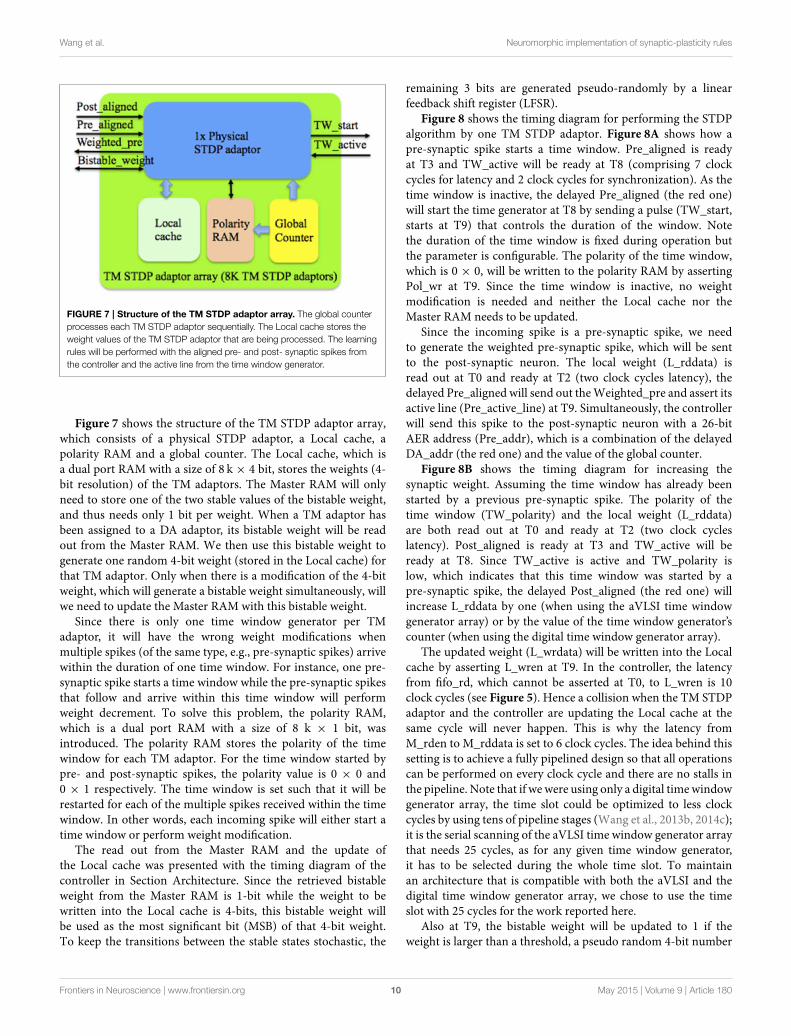
Wang et al. Neuromorphic implementation of synaptic-plasticity rules
FIGURE 7 | Structure of the TM STDP adaptor array. The global counter
processes each TM STDP adaptor sequentially. The Local cache stores the
weight values of the TM STDP adaptor that are being processed. The learning
rules will be performed with the aligned pre- and post- synaptic spikes from
the controller and the active line from the time window generator.
Figure 7 shows the structure of the TM STDP adaptor array,which consists of a physical STDP adaptor, a Local cache, apolarity RAM and a global counter. The Local cache, which isa dual port RAM with a size of 8 k × 4 bit, stores the weights (4-bit resolution) of the TM adaptors. The Master RAM will onlyneed to store one of the two stable values of the bistable weight,and thus needs only 1 bit per weight. When a TM adaptor hasbeen assigned to a DA adaptor, its bistable weight will be readout from the Master RAM. We then use this bistable weight togenerate one random 4-bit weight (stored in the Local cache) forthat TM adaptor. Only when there is a modification of the 4-bitweight, which will generate a bistable weight simultaneously, willwe need to update the Master RAM with this bistable weight.
Since there is only one time window generator per TMadaptor, it will have the wrong weight modifications whenmultiple spikes (of the same type, e.g., pre-synaptic spikes) arrivewithin the duration of one time window. For instance, one pre-synaptic spike starts a time window while the pre-synaptic spikesthat follow and arrive within this time window will performweight decrement. To solve this problem, the polarity RAM,which is a dual port RAM with a size of 8 k × 1 bit, wasintroduced. The polarity RAM stores the polarity of the timewindow for each TM adaptor. For the time window started bypre- and post-synaptic spikes, the polarity value is 0 × 0 and0 × 1 respectively. The time window is set such that it will berestarted for each of the multiple spikes received within the timewindow. In other words, each incoming spike will either start atime window or perform weight modification.
The read out from the Master RAM and the update ofthe Local cache was presented with the timing diagram of thecontroller in Section Architecture. Since the retrieved bistableweight from the Master RAM is 1-bit while the weight to bewritten into the Local cache is 4-bits, this bistable weight willbe used as the most significant bit (MSB) of that 4-bit weight.To keep the transitions between the stable states stochastic, the
remaining 3 bits are generated pseudo-randomly by a linearfeedback shift register (LFSR).
Figure 8 shows the timing diagram for performing the STDPalgorithm by one TM STDP adaptor. Figure 8A shows how apre-synaptic spike starts a time window. Pre_aligned is readyat T3 and TW_active will be ready at T8 (comprising 7 clockcycles for latency and 2 clock cycles for synchronization). As thetime window is inactive, the delayed Pre_aligned (the red one)will start the time generator at T8 by sending a pulse (TW_start,starts at T9) that controls the duration of the window. Notethe duration of the time window is fixed during operation butthe parameter is configurable. The polarity of the time window,which is 0 × 0, will be written to the polarity RAM by assertingPol_wr at T9. Since the time window is inactive, no weightmodification is needed and neither the Local cache nor theMaster RAM needs to be updated.
Since the incoming spike is a pre-synaptic spike, we needto generate the weighted pre-synaptic spike, which will be sentto the post-synaptic neuron. The local weight (L_rddata) isread out at T0 and ready at T2 (two clock cycles latency), thedelayed Pre_aligned will send out theWeighted_pre and assert itsactive line (Pre_active_line) at T9. Simultaneously, the controllerwill send this spike to the post-synaptic neuron with a 26-bitAER address (Pre_addr), which is a combination of the delayedDA_addr (the red one) and the value of the global counter.
Figure 8B shows the timing diagram for increasing thesynaptic weight. Assuming the time window has already beenstarted by a previous pre-synaptic spike. The polarity of thetime window (TW_polarity) and the local weight (L_rddata)are both read out at T0 and ready at T2 (two clock cycleslatency). Post_aligned is ready at T3 and TW_active will beready at T8. Since TW_active is active and TW_polarity islow, which indicates that this time window was started by apre-synaptic spike, the delayed Post_aligned (the red one) willincrease L_rddata by one (when using the aVLSI time windowgenerator array) or by the value of the time window generator’scounter (when using the digital time window generator array).
The updated weight (L_wrdata) will be written into the Localcache by asserting L_wren at T9. In the controller, the latencyfrom fifo_rd, which cannot be asserted at T0, to L_wren is 10clock cycles (see Figure 5). Hence a collision when the TM STDPadaptor and the controller are updating the Local cache at thesame cycle will never happen. This is why the latency fromM_rden to M_rddata is set to 6 clock cycles. The idea behind thissetting is to achieve a fully pipelined design so that all operationscan be performed on every clock cycle and there are no stalls inthe pipeline. Note that if we were using only a digital timewindowgenerator array, the time slot could be optimized to less clockcycles by using tens of pipeline stages (Wang et al., 2013b, 2014c);it is the serial scanning of the aVLSI time window generator arraythat needs 25 cycles, as for any given time window generator,it has to be selected during the whole time slot. To maintainan architecture that is compatible with both the aVLSI and thedigital time window generator array, we chose to use the timeslot with 25 cycles for the work reported here.
Also at T9, the bistable weight will be updated to 1 if theweight is larger than a threshold, a pseudo random 4-bit number
Frontiers in Neuroscience | www.frontiersin.org 10 May 2015 | Volume 9 | Article 180

Wang et al. Neuromorphic implementation of synaptic-plasticity rules
FIGURE 8 | TM STDP adaptor’s timing diagram of one time slot. (A)
Starting a time window. Pre_aligned is ready at T3 and TW_active will be
ready at T8. As the time window is inactive, the delayed Pre_aligned (the red
one) will start the time generator at T8 by sending a pulse (TW_start, starts at
T9); (B) Increasing weight. The polarity of the time window (TW_polarity) and
the local weight (L_rddata) are both read out at T0 and ready at T2.
Post_aligned is ready at T3 and TW_active will be ready at T8. The delayed
Post_aligned (the red one) will increase L_rddata.
between 4 and 11 that is updated every time slot. Otherwise,the bistable weight will be updated to 0. The updated bistableweight will be written into the Master RAM by asserting M_wrenat T9.
TM STDDP Adaptor ArrayThe TM STDDP adaptor array operates in the same scheme(with the same pipeline stages) as the TM STDP adaptor array.From the controller’s point of view, they are identical. Thismeans that they are interchangeable, which was a deliberatedesign decision. Figure 9 shows the structure of the TM STDDPadaptor array, which consists of a physical STDDP adaptor, aLocal cache, an active RAM and a global counter. The Localcache, which is a dual port RAM with a size of 8 k × 4 bit,stores the 4-bit delay values of TM adaptors. The Master RAMstores the 4-bit delay values too. When a TM adaptor hasbeen assigned to a DA adaptor, the delay of the latter will
be read out from the Master RAM and then stored in theLocal cache as the delay of that TM adaptor. When there is amodification of the delay the Master RAM is updated with thenew delay.
Since the TM STDDP adaptor array pipeline is the same as theone presented for STDP earlier, the timing diagram is exactly thesame as the ones presented in Figure 8 (replacing “weight” with“delay”) with the following additional changes:
1. Only the pre-synaptic spike can start the time windowgenerator by sending it a spike with a duration proportionalto the retrieved axonal delay.
2. The delayed pre-synaptic spike should be generated at thefalling edge of the active line (from 0 × 1 to 0 × 0), whichindicates the end of the axonal delay. Since this is a timemultiplexing system, each TM adaptor will only know thevalue of the active line in the current time slot. To solve thisproblem, we introduced the active RAM, which is a dual port
Frontiers in Neuroscience | www.frontiersin.org 11 May 2015 | Volume 9 | Article 180

Wang et al. Neuromorphic implementation of synaptic-plasticity rules
FIGURE 9 | Structure of the TM STDDP adaptor array. The global counter
processes each TM STDDP adaptor sequentially. The Local cache stores the
axonal delay values of the TM STDDP adaptor that are being processed. The
learning rules will be performed with the aligned pre- and post- synaptic spikes
from the controller and the active line from the time window generator.
RAM with a size of 8 k × 1 bit, to store the value of the activeline in the current time slot.While the retrieved value from theactive RAM represents the previous value. The delayed pre-synaptic spike will be generated if the active line is low andthe active line retrieved from the active RAM is high. For thisreason, the actual axonal delay will be from 1 to 16ms whilethe value of the delay stored is from 0×0 to 0× F. The signalsof the polarity RAM (see Figure 8) are replaced by those ofthe active RAM. The weight of this spike will be a fixed butconfigurable value.
3. Only the post-synaptic spike can change the delay. Noadaptation will be performed if the falling edge of the activeline has been detected at T8 since this means the delay hasbeen perfectly tuned and a delayed pre-synaptic spike will begenerated at T9.
UtilizationThe digital parts of the proposed array were developed usingthe standard ASIC design flow and therefore can be easilyimplemented with state-of-the-art manufacturing technologies.A bottom-up design flow was adopted in which we designedand verified each module separately. Once the module levelverification was complete, all the modules were integratedtogether for chip-level verification. As a proof of concept, weimplemented the proposed system on a Virtex6 XC6VLX240TFPGA, which is hosted on the XilinxML605 board.Table 1 showsthe utilization of hardware resources on the FPGA. Note thatthis is the utilization for the dynamically-assigned STDP/STDDPadaptor array (without theMaster RAM), the digital timewindowgenerator array, and the interface circuit for the aVLSI timewindow generator. As Table 1 shows, the proposed system usesonly a small fraction (<1%) of the hardware resources. Limitedby the size of the on-chip SRAM, for STDP and STDDP, we haveimplemented 1800 × 8 k = 14.4M and 450 × 8 k = 3.6M DAadaptors respectively. This is a proof of concept and in the futurewe will implement the Master RAM with off-chip memory, thusleveraging the design of the cache structure introduced.
TABLE 1 | Device utilization Xilinx Virtex6 XC6VLX240T.
Resource STDP STDDP Total available
Occupied slices 558(1.4%) 545(1.4%) 37,680
Slice FF’s 398(0.1%) 399(0.1%) 301,440
Slice LUTs 1430(0.9%) 1422(0.9%) 152,720
LUTs as logic 578(0.3%) 568(0.3%) 152,720
LUTs as RAM 827(1.4%) 827(1.4%) 58,400
36 k RAM 5(1.2%) 5(1.2%) 416
Results
For testing purposes, a PCB was developed as a daughter boardto contain the aVLSI chip and was connected to the FPGA.The FPGA is controlled by a PC via a JTAG interface and theanalog bias inputs of the aVLSI chip are controlled by externalprogrammable bias voltages.
Performance of STDPWe have tested the performance of the dynamically-assignedSTDP adaptor array by performing a balanced excitationexperiment, based on the experiment run by Song et al. (2000).Song et al. (2000) have shown that competitive Hebbian learning(Hebb, 1949) can be performed through STDP. The competition(induced by STDP) between the synapses can establish a bimodaldistribution of the synaptic weights: either toward zero (weak) orthe maximum (strong) values.
Using Digital Time Window Generator ArrayIn this experiment, a single post-synaptic neuron is driven by1024 TM synaptic adaptors, the TM addresses of which arefrom 0 × 0 to 0 × 3 FF. Their DA addresses are all thesame: 0 × 0. That post-synaptic neuron has a single post-synaptic current generator that can generate both excitatory andinhibitory post-synaptic currents (EPSC and IPSC) modulatedby the weights of the spikes arriving from different adaptors(Wang et al., 2014c). As the post-synaptic currents sumlinearly in our model, only a PSC generator is needed ineach neuron. Each adaptor was driven by an independentPoisson pre-synaptic spike train with the same average rate.We have tested the system with two firing rates: 10 and 20Hz,whereas the firing rate of the post-synaptic neuron was 15 and40Hz respectively. The adaptors start with a uniform positiveweight distribution. The size of the time window was fixed at16ms.
After 1.25 s of simulation, the distribution of synaptic weightsconverges to a steady-state condition with bimodal distributionof strong and weak weights (see Figure 10). Additionally,although our learning rule is considerably simplified whencompared to that presented in Song et al. (2000), our systemis capable of producing the same result: for low input rates,more synaptic adaptors approach the upper limit, and forhigh input rates, more are pushed toward zero (Song et al.,2000).
Frontiers in Neuroscience | www.frontiersin.org 12 May 2015 | Volume 9 | Article 180

Wang et al. Neuromorphic implementation of synaptic-plasticity rules
FIGURE 10 | Balanced excitation experiment with digital time window
generator array. (A) Weight distribution after 1.25 s of STDP for an input rate
of 10Hz. The bimodal distribution of strong and weak weights is apparent; (B)
Scatter plot of the final weight distribution; (C,D) Same as (A,B), but for an
input rate of 20Hz. Now more weights are weak than strong.
Using aVLSI Time Window Generator ArrayWe ran the experiment with 128 aVLSI time window generators(this is due to the fact that we have only 180 aVLSI time windowgenerators and powers of two are preferable in digital design)
FIGURE 11 | Balanced excitation experiment with aVLSI time window
generator array. (A) Weight distribution after 1.25 s of STDP for an input rate
of 10Hz. The bimodal distribution of strong and weak weights is apparent; (B)
Same as (A), but for an input rate of 20Hz. Now more weights are weak than
strong.
with all the settings the same as with the digital time windowgenerator. After 1.25 s of simulation, despite the adaptor usinga fixed adaptation step (set to 1 here), the distribution of synapticweights converges to a steady-state condition with a bimodaldistribution of strong and weak weights (see Figure 11). It is alsocapable of producing the result: the higher the input rates, themore the synaptic weight will be pushed toward zero.
Validation of the Dynamic-assignment SchemeThe previous two experiments have shown that the balancedexcitation experiment works for a system with 128 TM STDPadaptors. To validate the dynamic-assignment scheme, weconducted an experiment for 16 runs with an input rate of 20Hzand 128 digital time window generators. For each run, these 128TM STDP adaptors were assigned a DA address in the range from0×0000 to 0×1 E00 with a step of 0×200. After each run, we readout the weights of these 128 adaptors (from the FPGA) and thenstarted another run with the next DA address. In other words, wekept using the same 128 TM STDP adaptors for all the 16 runs byusing the dynamic-assignment scheme. Note, this experiment isonly a proof-of-concept and we can dynamically assign the TMadaptors for all those 8 k DA addresses (0 × 0 to 0 × 1 FFF) aslong as the constraint of the active rate is not violated.
For each run, the distribution of synaptic weights convergesto a steady-state condition with a bimodal distribution of strongand weak weights. Figure 12 shows the average distributionof synaptic weights across all 16 runs. We first obtained thedistribution of synaptic weights for each run and then averagedthem. Since the input rate is 20Hz, more synaptic weights
Frontiers in Neuroscience | www.frontiersin.org 13 May 2015 | Volume 9 | Article 180

Wang et al. Neuromorphic implementation of synaptic-plasticity rules
FIGURE 12 | Balanced excitation experiments using the
dynamic-assignment scheme. One TM STDP adaptor array (with 128 TM
STDP adaptors) was dynamically assigned for 16 DA STDP adaptor arrays.
The averaged weight distribution after 1.25 s of STDP for an input rate of
20Hz. Note these data are averaged across all 16 runs. The bimodal
distribution of strong and weak weights is apparent and more weights are
weak than strong. Error bars are standard deviations of 16 runs.
were pushed toward zero, which matches the results presentedin Figures 10C, 11B. For each run, the dynamic-assignmentscheme has achieved a similar bimodal distribution of synapticweights as the standard deviation of the results indicates. Thedynamic-assignment scheme is therefore proved to be capable ofperforming what was designed to do: reusing hardware resources.
Performance of STDDPWe have tested the performance of the dynamically-assignedSTDDP adaptor array by performing a polychronizationexperiment. The term polychronization is used to indicate thatseveral neurons can fire asynchronously but after travelingalong axons with specific delays, their spikes will arrive at apost-synaptic neuron simultaneously, causing it to fire in turn(Izhikevich, 2006). Neural networks based on this principle arereferred to as “polychronous” neural networks and are capableof storing and recalling quite complicated spatio-temporalpatterns. In Wang et al. (2014d), we have concluded that themost important requirement of a hardware implementation ofa polychronous network is to provide a strong time-lockedrelationship. This is indeed the motivation for us to develop theSTDDP learning rule, which will fine-tune the axonal delays tothe desired delay values.
Using Digital Time Window Generator ArrayIn this experiment, we used 128 adaptors and a paired-pulseprotocol: a single pair of pre- and post-synaptic spikes wassent to each of the adaptors periodically (every 32 time steps).During each period, each adaptor will receive one and onlyone pre-synaptic spike, the arrival time of which is randomizedbetween time step 1 and 15. Additionally, during each period,each adaptor will receive one and only one post-synaptic spike,the arrival time is set to be time step 16. These spike pairs remainthe same in each period. All the axonal delays are initializedto be zero. In each period, for each adaptor, a delay adaptation
FIGURE 13 | Polychronization experiment with digital time window
generator array. (A) Delay distribution after 15 times of STDDP; (B). Scatter
plot of the final delay distribution.
will be performed if the axonal delay has not been tuned to thedesired delay. Hence, theoretically, after 15 times of STDDP, allthe delayed pre-synaptic spikes from these 128 adaptors will firesimultaneously (each at its own time slot) at time step 16.
This theoretical behavior was confirmed via measurementson the FPGA. Since plotting 128 delayed pre-synaptic spike thatfire at the same time is meaningless, we chose instead to showthe delay distribution after 15 times of STDDP and the scatterplot of the final delay distribution (see Figure 13). It might benoticed that the final delays are not uniformly distributed, whichindicated that more pre-synaptic spikes arrive at the early part ofthat period than the ones arrive at the later part. The system hasperformed the polychronization experiment successfully since allthe axonal delays have been fine-tuned to the desired values,which are the time differences between pre- and post-synapticspikes.
Using aVLSI Time Window Generator ArrayThe digital timewindow generator can generate any given desiredsize of the time window (from 1 to 15ms, in a time-step of 1ms).But due to process variation and device mismatch, it is impossibleto tune all the aVLSI time window generators with such accuracy.To compare the performance with its digital counterpart, wetested the system with all the settings the same as with the digitaltime window generator conducting 10 test runs for statistical
Frontiers in Neuroscience | www.frontiersin.org 14 May 2015 | Volume 9 | Article 180
Wang et al. Neuromorphic implementation of synaptic-plasticity rules
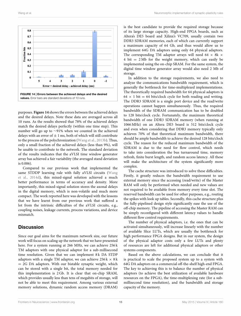
FIGURE 14 | Errors between the achieved delays and the desired
values. Error bars are standard deviations of 10 runs.
purposes. Figure 14 shows the errors between the achieved delaysand the desired delays. Note these data are averaged across all10 runs. As the results showed that 78% of the achieved delaysmatch the desired delays perfectly (within one time step). Thisnumber will go up to ∼91% when we counted in the achieveddelays with an error of± 1ms, both of which will still contributeto the process of the polychronization (Wang et al., 2013b). Thus,only a small fraction of the achieved delays (less than 9%), willbe unable to contribute to the network. The standard deviationof the results indicates that the aVLSI time window generatorarray has achieved a fair variability (the averaged stand deviationis 0.006).
Compared to our previous work that implemented thesame STDDP learning rule with fully aVLSI circuits (Wanget al., 2014d), this mixed-signal solution achieved a muchbetter performance in terms of accuracy and density. Moreimportantly, this mixed-signal solution stores the axonal delaysin the digital memory, which is non-volatile and much morecompact. The work reported here was developed with the lessonsthat we have learnt from our previous work that suffered alot from the intrinsic difficulties of the aVLSI circuits, e.g.,coupling noises, leakage currents, process variations, and devicemismatch.
Discussion
Since our goal aims for the maximum network size, our futurework will focus on scaling up the network that we have presentedhere. For a system running at 266 MHz, we can achieve 256 kTM adaptors with one physical adaptor for a sub-millisecondtime resolution. Given that we can implement 8 k DA STDPadaptors with a single TM adaptor, we can achieve 256 k × 8 k= 2G DA adaptors. With our bistable synaptic weight, whichcan be stored with a single bit, the total memory needed forthis implementation is 2Gb. It is clear that on-chip SRAM,which provides usually less than tens of megabits of storage, willnot be able to meet this requirement. Among various externalmemory solutions, dynamic random access memory (DRAM)
is the best candidate to provide the required storage becauseof its large storage capacity. High-end FPGA boards, such asAltera’s DE5 board and Xilinx’s VC709, usually contain twoDDR3 SDRAM memories, each of which can currently supporta maximum capacity of 64 Gb, and thus would allow us toimplement 64G DA adaptors using only 64 physical adaptors.The corresponding TM adaptor arrays will need 64 × 8k ×
4 bit = 2Mb for the weight memory, which can easily beimplemented using the on-chip SRAM. For the same system, thedigital time window generator array would also need 2 Mb ofstorage.
In addition to the storage requirements, we also need toanalyze the communications bandwidth requirement, which isgenerally the bottleneck for time-multiplexed implementations.The theoretically required bandwidth for 64 physical adaptors is64 × 1 bit = 64 bits/clock cycle for both reading and writing.The DDR3 SDRAM is a single port device and the read/writeoperations cannot happen simultaneously. Thus, the requiredbandwidth of the SDRAM communication has to be doubledto 128 bits/clock cycle. Fortunately, the maximum theoreticalbandwidth of one DDR3 SDRAM memory (when running at1066MHz) on an Altera DE5 board is 512 bits/clock cycleand even when considering that DDR3 memory typically onlyachieves 70% of that theoretical maximum bandwidth, thereshould be ample bandwidth to achieve the desired 128 bits/clockcycle. The reason for the reduced maximum bandwidth of theSDRAM is due to the need for flow control, which needsto take into consideration the bus turnaround time, memoryrefresh, finite burst length, and random access latency. All thesewill make the architecture of the system significantly morecomplex.
The cache structure was introduced to solve these difficulties.Firstly, it greatly reduces the bandwidth requirement to useexternal memory since the accessing (read/write) of the MasterRAM will only be performed when needed and new values arenot required to be available from memory every time slot. Thereserved bandwidth can be used for other purposes, e.g., routingthe spikes with look up tables. Secondly, this cache structure plusthe fully-pipelined design style significantly ease the use of theoff-chip memory. The pipeline of accessing the Master RAM canbe simply reconfigured with different latency values to handledifferent flow control requirements.
The number of physical adaptors, i.e. the ones that can beactivated simultaneously, will increase linearly with the numberof available Slice LUTs, which are usually the bottleneck forhigh performance FPGA designs. But in our system, the designof the physical adaptor costs only a few LUTs and plentyof resources are left for additional physical adaptors or othersystems components.
Based on the above calculations, we can conclude that itis practical to scale the proposed system up to a system with64G DA adaptors on a commercial off-the-shelf high-end FPGA.The key to achieving this is to balance the number of physicaladaptors (to achieve the best utilization of available hardwareresources on the FPGA), the time-multiplexing rate (for a sub-millisecond time resolution), and the bandwidth and storagecapacity of the memory.
Frontiers in Neuroscience | www.frontiersin.org 15 May 2015 | Volume 9 | Article 180

Wang et al. Neuromorphic implementation of synaptic-plasticity rules
Our aVLSI implementation is nowhere near as scalable asthe digital implementation, since it can only be scaled upby implementing more physical copies of the aVLSI module.However, the introduction of the dynamic-assigning approachallows 8 k DA analog time window generators to be achievedwith only a single physical time window generator. Above all, themotivation to develop the aVLSI implementation in the proposedsystem is for enhancement of the simulations.
Acknowledgments
This work has been supported by the Australian ResearchCouncil Grant DP140103001. The support by the Xilinx andAltera university program is gratefully acknowledged. This workwas inspired by the Capo Caccia Cognitive NeuromorphicEngineering Workshop 2014 and Telluride Neuromorphicworkshop 2014.
References
Amirikian, B., and Georgopoulos, A. P. (2003). Modular organization of
directionally tuned cells in the motor cortex: is there a short-range order?
Proc. Natl. Acad. Sci. U.S.A. 100, 12474–12479. doi: 10.1073/pnas.20377
19100
Bi, G. Q., and Poo, M. M. (1998). Synaptic modifications in cultured hippocampal
neurons: dependence on spike timing, synaptic strength, and postsynaptic cell
type. J. Neurosci. 18, 10464–10472.
Bliss, T. V., and Collingridge, G. L. (1993). A synaptic model of memory: long-
term potentiation in the hippocampus. Nature 361, 31–39. doi: 10.1038/36
1031a0
Bofill-i-petit, A., and Murray, A. F. (2004). Synchrony detection and amplification
by silicon neurons with STDP synapses. IEEE Trans. Neural Netw. 15,
1296–1304. doi: 10.1109/TNN.2004.832842
Brader, J. M., Senn,W., and Fusi, S. (2007a). Learning real-world stimuli in a neural
network with spike-driven synaptic dynamics. Neural Comput. 19, 2881–2912.
doi: 10.1162/neco.2007.19.11.2881
Brader, J. M., Senn,W., and Fusi, S. (2007b). Learning real-world stimuli in a neural
network with spike-driven synaptic dynamics. Neural Comput. 19, 2881–2912.
doi: 10.1162/neco.2007.19.11.2881
Brenner, S., and Sejnowski, T. J. (2011). Understanding the human brain. Science
334, 567. doi: 10.1126/science.1215674
Buskila, Y., Morley, J. W., Tapson, J., and van Schaik, A. (2013). The adaptation of
spike backpropagation delays in cortical neurons. Front. Cell. Neurosci. 7:192.
doi: 10.3389/fncel.2013.00192
Cassidy, A., and Andreou, A. G. (2008). “Dynamical digital silicon neurons,”
in 2008 IEEE Biomedical Circuits and Systems Conference, (Baltimore, MD),
289–292.
Cassidy, A., Andreou, A. G., and Georgiou, J. (2011). “Design of a one million
neuron single FPGA neuromorphic system for real-time multimodal scene
analysis,” in 2011 45th Annual Conference on Information Sciences and
Systems, (Baltimore, MD), 1–6.
Chicca, E., Badoni, D., Dante, V., D’Andreagiovanni, M., Salina, G., Carota, L.,
et al. (2003). AVLSI recurrent network of integrate-and-fire neurons connected
by plastic synapses with long-term memory. IEEE Trans. Neural Netw. 14,
1297–1307. doi: 10.1109/TNN.2003.816367
Galluppi, F., Davies, S., Furber, S., Stewart, T., and Eliasmith, C. (2012). “Real time
on-chip implementation of dynamical systems with spiking neurons,” in The
2012 International Joint Conference on Neural Networks (IJCNN) (Brisbane,
QLD: IEEE), 1–8.
Galluppi, F., Lagorce, X., Stromatias, E., Pfeiffer, M., Luis, A., Furber, S., et al.
(2014). A framework for plasticity implementation on the SpiNNaker neural
architecture. Front. Neurosci. 8:429. doi: 10.3389/fnins.2014.00429
Gao, C., and Hammerstrom, D. (2007). Cortical models onto CMOL and CMOS—
architectures and performance/price. IEEE Trans. Circ. Syst. I 54, 2502–2515.
doi: 10.1109/TCSI.2007.907830
Gerstner, W., Kempter, R., Van Hemmen, J. L., andWagner, H. (1996). A neuronal
learning rule for sub-millisecond temporal coding. Nature 383, 76–81. doi:
10.1038/383076a0
Giulioni, M., Camilleri, P., Dante, M. M., Braun, J., and Del Giudice, P. (2012).
Robust working memory in an asynchronously spiking neural network realized
with neuromorphic VLSI. Front. Neurosci. 5:149. doi: 10.3389/fnins.2012.
00149
Goldberg, D., Cauwenberghs, G., and Andreou, A. (2001). Probabilistic synaptic
weighting in a reconfigurable network of VLSI integrate-and-fire neurons.
Neural Netw. 14, 781–793. doi: 10.1016/S0893-6080(01)00057-0
Graupner, M., and Brunel, N. (2012). Calcium-based plasticity model explains
sensitivity of synaptic changes to spike pattern, rate, and dendritic location.
Proc. Natl. Acad. Sci 109, 3991–3996. doi: 10.1073/pnas.1109359109
Häfliger, P. (2007). Adaptive WTA with an analog VLSI neuromorphic learning
chip. IEEE Trans. Neural Netw. 18, 551–572. doi: 10.1109/TNN.2006.884676
Harkin, J., Morgan, F., Hall, S., Dudek, P., Dowrick, T., and McDaid, L. (2008).
“Reconfigurable platforms and the challenges for large-scale implementations
of spiking neural networks,” in 2008 International Conference on Field
Programmable Logic and Applications (Heidelberg: IEEE), 483–486.
Harkin, J., Morgan, F., McDaid, L., Hall, S., McGinley, B., and Cawley, S. (2009).
A reconfigurable and biologically inspired paradigm for computation using
network-on-chip and spiking neural networks. Int. J. Reconf. Comp. 2009, 1–13.
doi: 10.1155/2009/908740
Hebb, D. (1949). The Organization of Behavior. Journal of Applied Behavior
Analysis. New York, NY: Wiley & Sons.
Holmgren, C., Harkany, T., Svennenfors, B., and Zilberter, Y. (2003). Pyramidal cell
communication within local networks in layer 2/3 of rat neocortex. J. Physiol.
(Lond). 551, 139–153. doi: 10.1113/jphysiol.2003.044784
Hubel, D. H., and Wiesel, T. N. (1974). Uniformity of monkey striate cortex:
a parallel relationship between field size, scatter, and magnification factor.
J. Comp. Neurol. 158, 295–305. doi: 10.1002/cne.901580305
Indiveri, G., Chicca, E., and Douglas, R. (2006). A VLSI array of low-power spiking
neurons and bistable synapses with spike-timing dependent plasticity. IEEE
Trans. Neural Netw. 17, 211–221. doi: 10.1109/TNN.2005.860850
Izhikevich, E. M. (2003). Simple model of spiking neurons. IEEE Trans. Neural
Netw. 14, 1569–1572. doi: 10.1109/TNN.2003.820440
Izhikevich, E. M. (2006). Polychronization: computation with spikes. Neural
Comput. 18, 245–282. doi: 10.1162/089976606775093882
Izhikevich, E. M., and Edelman, G. M. (2008). Large-scale model of mammalian
thalamocortical systems. Proc. Natl. Acad. Sci. U.S.A. 105, 3593–3598. doi:
10.1073/pnas.0712231105
Johansson, C., and Lansner, A. (2007). Towards cortex sized artificial neural
systems. Neural Netw. 20, 48–61. doi: 10.1016/j.neunet.2006.05.029
Koickal, T. J., Hamilton, A., Tan, S. L., Covington, J. A., Gardner, J. W., and
Pearce, T. C. (2007). Analog VLSI circuit implementation of an adaptive
neuromorphic olfaction chip. IEEE Trans. Circ. Syst. I 54, 60–73. doi:
10.1109/TCSI.2006.888677
Lennie, P. (2003). The cost of cortical computation. Curr. Biol. 13, 493–497. doi:
10.1016/S
Liu, S., Kramer, J., Indiveri, G., Delbrück, T., and Douglas, R. (2002). Analog VLSI:
Circuits and Principles. Cambridge, MA: MIT Press.
Magee, J. C. (1997). A synaptically controlled, associative signal for
hebbian plasticity in hippocampal neurons. Science 275, 209–213. doi:
10.1126/science.275.5297.209
Markram, H., Lübke, J., Frotscher, M., and Sakmann, B. (1997). Regulation of
synaptic efficacy by coincidence of postsynaptic APs and EPSPs. Science (NY)
275, 213–215. doi: 10.1126/science.275.5297.213
Minkovich, K., Srinivasa, N., Cruz-Albrecht, J. M., Cho, Y., and Nogin, A. (2012).
Programming time-multiplexed reconfigurable hardware using a scalable
neuromorphic compiler. IEEE Trans. Neural Netw. Learn. Syst. 23, 889–901.
doi: 10.1109/TNNLS.2012.2191795
Frontiers in Neuroscience | www.frontiersin.org 16 May 2015 | Volume 9 | Article 180

Wang et al. Neuromorphic implementation of synaptic-plasticity rules
Mirhassani, M., Ahmadi, M., and Miller, W. C. (2007). A feed-forward
time-multiplexed neural network with mixed-signal neuron–synapse arrays.
Microelectron. Eng. 84, 300–307. doi: 10.1016/j.mee.2006.02.014
Mitra, S., Fusi, S., and Indiveri, G. (2009). Real-time classification of complex
patterns using spike-based learning in neuromorphic VLSI. IEEE Trans.
Biomed. Circ. Syst. 3, 32–42. doi: 10.1109/TBCAS.2008.2005781
Moore, S. W., Fox, P. J., Marsh, S. J. T., Markettosa, T., and Mujumdar, A. (2012).
“Bluehive—a field-programable custom computing machine for extreme-scale
real-time neural network simulation,” in 20th IEEE International Symposium
on Field-Programmable Custom Computing Machines. (IEEE), 133–140. doi:
10.1109/FCCM.2012.32
Painkras, E., Plana, L. A., Garside, J., Temple, S., Galluppi, F., Patterson, C.,
et al. (2013). SpiNNaker: a 1-W 18-core system-on-chip for massively-parallel
neural network simulation. IEEE J. Solid State Circ. 48, 1943–1953. doi:
10.1109/JSSC.2013.2259038
Petersen, C. C. H., Malenka, R. C., Nicoll, R. A., and Hopfield, J. J. (1998). All-or-
none potentiation at CA3-CA1 synapses. Proc. Natl. Acad. Sci. 95, 4732–4737.
doi: 10.1073/pnas.95.8.4732
Pfeil, T., Grübl, A., Jeltsch, S., Müller, E., Müller, P., Petrovici, M., et al. (2013). Six
networks on a universal neuromorphic computing substrate. Front. Neurosci.
7:11. doi: 10.3389/fnins.2013.00011
Pfeil, T., Potjans, T. C., Schrader, S., Potjans, W., Schemmel, J., Diesmann, M., et al.
(2012). Is a 4-bit synaptic weight resolution enough?—constraints on enabling
spike-timing dependent plasticity in neuromorphic hardware. Front. Neurosci.
6:90. doi: 10.3389/fnins.2012.00090
Saighi, S., Levi, T., Belhadj, B., Malot, O., and Tomas, J. (2010). “Hardware
system for biologically realistic, plastic, and real-time spiking neural network
simulations,” in The 2010 International Joint Conference on Neural Networks
(IJCNN), (Barcelona), 1–7.
Scannell, J. W., Blakemore, C., and Young, M. P. (1995). Analysis of connectivity
in the cat cerebral cortex. J. Neurosci. 15, 1463–1483.
Schemmel, J., Fieres, J., and Meier, K. (2008). “Wafer-scale integration of analog
neural networks,” in 2008 IEEE International Joint Conference on Neural
Networks (IEEE World Congress on Computational Intelligence), (Hong Kong),
431–438.
Sejnowski, T. J. (2012). Are we merely the sum of our neurons? New Scientist 213,
46. doi: 10.1016/S0262-4079(12)60317-0
Shi, Y., Veidenbaum, A. V., Nicolau, A., and Xu, X. (2015). Large-scale neural
circuit mapping data analysis accelerated with the graphical processing
unit (GPU). J. Neurosci. Methods 239, 1–10. doi: 10.1016/j.jneumeth.2014.
09.022
Song, S., Miller, K. D., and Abbott, L. F. (2000). Competitive Hebbian learning
through spike-timing-dependent synaptic plasticity. Nat. Neurosci. 3, 919–926.
doi: 10.1038/78829
Stanford, L. R. (1987). Conduction velocity variations minimize conduction time
differences among retinal ganglion cell axons. Science (NY), 238, 358–360.
Tsunoda, K., Yamane, Y., Nishizaki, M., and Tanifuji, M. (2001). Complex objects
are represented in macaque inferotemporal cortex by the combination of
feature columns. Nat. Neurosci. 4, 832–838. doi: 10.1038/90547
Vogelstein, R. J., Mallik, U., Vogelstein, J. T., and Cauwenberghs, G.
(2007). Dynamically reconfigurable silicon array of spiking neurons with
conductance-based synapses. IEEE Trans. Neural Netw. 18, 253–265. doi:
10.1109/TNN.2006.883007
Wang, R., Cohen, G., Hamilton, T. J., Tapson, J., and Schaik, A. V. (2013a). “An
improved aVLSI axon with programmable delay using spike timing dependent
delay plasticity,” in 2013 IEEE International Symposium of Circuits and Systems
(ISCAS) (Beijing: IEEE), 2–5.
Wang, R., Cohen, G., Stiefel, K. M., Hamilton, T. J., Tapson, J., and van Schaik,
A. (2013b). An FPGA implementation of a polychronous spiking neural
network with delay adaptation. Front. Neurosci. 7:14. doi: 10.3389/fnins.2013.
00014
Wang, R., Hamilton, T. J., Tapson, J., and van Schaik, A. (2014a). “A compact
reconfigurable mixed-signal implementation of synaptic plasticity in spiking
neurons,” in 2014 IEEE International Symposium on Circuits and Systems
(ISCAS) (Melbourne, VIC: IEEE), 862–865.
Wang, R., Hamilton, T. J., Tapson, J., and van Schaik, A. (2014b). “A generalised
conductance-based silicon neuron for large-scale spiking neural networks,” in
2014 IEEE International Symposium on Circuits and Systems (ISCAS) (IEEE),
1564–1567.
Wang, R., Hamilton, T. J., Tapson, J., and van Schaik, A. (2014c). “An FPGA
design framework for large-scale spiking neural networks,” in 2014 IEEE
International Symposium on Circuits and Systems (ISCAS) (Melboune: IEEE),
457–460.
Wang, R., Jin, C., McEwan, A., and van Schaik, A. (2011a). A programmable axonal
propagation delay circuit for time-delay spiking neural networks. 2011 IEEE
International Symposium of Circuits and Systems (ISCAS), (Rio de Janeiro),
869–872.
Wang, R. M., Hamilton, T. J., Tapson, J. C., and van Schaik, A. (2014d). A mixed-
signal implementation of a polychronous spiking neural network with delay
adaptation. Front. Neurosci. 8:51. doi: 10.3389/fnins.2014.00051
Wang, R., Tapson, J., Hamilton, T. J., and van Schaik, A. (2011b). “An analogue
VLSI implementation of polychronous spiking neural networks,” in 2011
Seventh International Conference on Intelligent Sensors, Sensor Networks and
Information Processing (Adelaide, SA: IEEE), 97–102.
Wang, R., Tapson, J., Hamilton, T. J., and van Schaik, A. (2012). “An aVLSI
programmable axonal delay circuit with spike timing dependent delay
adaptation,” in 2012 IEEE International Symposium on Circuits and Systems
(Seoul: IEEE), 2413–2416.
Weste, N., and Harris, D. (2005). CMOS VLSI Design?: a Circuits and Systems
Perspective. Energy Policy, 3rd Edn., Vol. 24. Boston, MA: Addison-Wesley.
Wittie, L., Memelli, H. (2010). “Billion neuron memory models in slender Blue
Genes,” in Program 208.30/MMM21, 2010 Neuroscience Meeting Planner (San
Diego, CA: Society for Neuroscience), 1.
Yu, T., and Cauwenberghs, G. (2010). “Log-domain time-multiplexed realization
of dynamical conductance-based synapses,” in Proceedings of 2010 IEEE
International Symposium on Circuits and Systems, (Paris), 2558–2561.
Zaveri, M. S., and Hammerstrom, D. (2011). Performance/price estimates for
cortex-scale hardware: a design space exploration. Neural Netw. 24, 291–304.
doi: 10.1016/j.neunet.2010.12.003
Conflict of Interest Statement: The authors declare that the research was
conducted in the absence of any commercial or financial relationships that could
be construed as a potential conflict of interest.
Copyright © 2015 Wang, Hamilton, Tapson and van Schaik. This is an open-access
article distributed under the terms of the Creative Commons Attribution License (CC
BY). The use, distribution or reproduction in other forums is permitted, provided the
original author(s) or licensor are credited and that the original publication in this
journal is cited, in accordance with accepted academic practice. No use, distribution
or reproduction is permitted which does not comply with these terms.
Frontiers in Neuroscience | www.frontiersin.org 17 May 2015 | Volume 9 | Article 180