A Low-Power High-Speed Comparator for Precise Applications
12
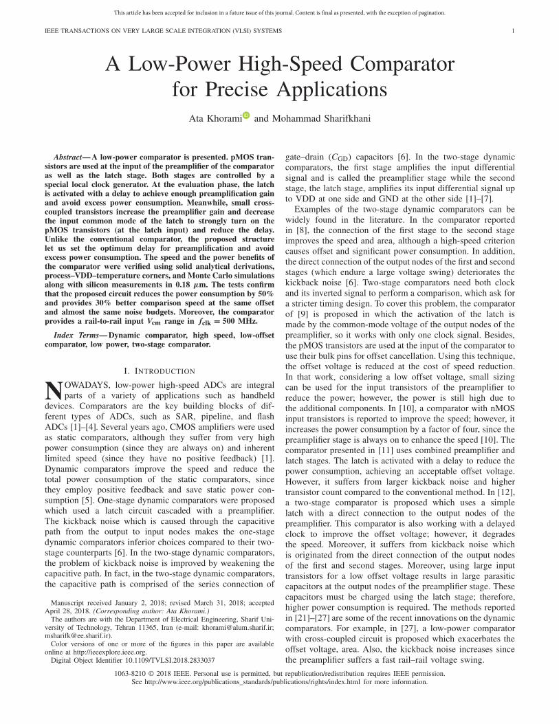
This article has been accepted for inclusion in a future issue of this journal. Content is final as presented, with the exception of pagination. IEEE TRANSACTIONS ON VERY LARGE SCALE INTEGRATION (VLSI) SYSTEMS 1 A Low-Power High-Speed Comparator for Precise Applications Ata Khorami and Mohammad Sharifkhani Abstract—A low-power comparator is presented. pMOS tran- sistors are used at the input of the preamplifier of the comparator as well as the latch stage. Both stages are controlled by a special local clock generator. At the evaluation phase, the latch is activated with a delay to achieve enough preamplification gain and avoid excess power consumption. Meanwhile, small cross- coupled transistors increase the preamplifier gain and decrease the input common mode of the latch to strongly turn on the pMOS transistors (at the latch input) and reduce the delay. Unlike the conventional comparator, the proposed structure let us set the optimum delay for preamplification and avoid excess power consumption. The speed and the power benefits of the comparator were verified using solid analytical derivations, process–VDD–temperature corners, and Monte Carlo simulations along with silicon measurements in 0.18 μm. The tests confirm that the proposed circuit reduces the power consumption by 50% and provides 30% better comparison speed at the same offset and almost the same noise budgets. Moreover, the comparator provides a rail-to-rail input V cm range in f clk = 500 MHz. Index Terms— Dynamic comparator, high speed, low-offset comparator, low power, two-stage comparator. I. I NTRODUCTION N OWADAYS, low-power high-speed ADCs are integral parts of a variety of applications such as handheld devices. Comparators are the key building blocks of dif- ferent types of ADCs, such as SAR, pipeline, and flash ADCs [1]–[4]. Several years ago, CMOS amplifiers were used as static comparators, although they suffer from very high power consumption (since they are always on) and inherent limited speed (since they have no positive feedback) [1]. Dynamic comparators improve the speed and reduce the total power consumption of the static comparators, since they employ positive feedback and save static power con- sumption [5]. One-stage dynamic comparators were proposed which used a latch circuit cascaded with a preamplifier. The kickback noise which is caused through the capacitive path from the output to input nodes makes the one-stage dynamic comparators inferior choices compared to their two- stage counterparts [6]. In the two-stage dynamic comparators, the problem of kickback noise is improved by weakening the capacitive path. In fact, in the two-stage dynamic comparators, the capacitive path is comprised of the series connection of Manuscript received January 2, 2018; revised March 31, 2018; accepted April 28, 2018. (Corresponding author: Ata Khorami.) The authors are with the Department of Electrical Engineering, Sharif Uni- versity of Technology, Tehran 11365, Iran (e-mail: [email protected]; [email protected]). Color versions of one or more of the figures in this paper are available online at http://ieeexplore.ieee.org. Digital Object Identifier 10.1109/TVLSI.2018.2833037 gate–drain (C GD ) capacitors [6]. In the two-stage dynamic comparators, the first stage amplifies the input differential signal and is called the preamplifier stage while the second stage, the latch stage, amplifies its input differential signal up to VDD at one side and GND at the other side [1]–[7]. Examples of the two-stage dynamic comparators can be widely found in the literature. In the comparator reported in [8], the connection of the first stage to the second stage improves the speed and area, although a high-speed criterion causes offset and significant power consumption. In addition, the direct connection of the output nodes of the first and second stages (which endure a large voltage swing) deteriorates the kickback noise [6]. Two-stage comparators need both clock and its inverted signal to perform a comparison, which ask for a stricter timing design. To cover this problem, the comparator of [9] is proposed in which the activation of the latch is made by the common-mode voltage of the output nodes of the preamplifier, so it works with only one clock signal. Besides, the pMOS transistors are used at the input of the comparator to use their bulk pins for offset cancellation. Using this technique, the offset voltage is reduced at the cost of speed reduction. In that work, considering a low offset voltage, small sizing can be used for the input transistors of the preamplifier to reduce the power; however, the power is still high due to the additional components. In [10], a comparator with nMOS input transistors is reported to improve the speed; however, it increases the power consumption by a factor of four, since the preamplifier stage is always on to enhance the speed [10]. The comparator presented in [11] uses combined preamplifier and latch stages. The latch is activated with a delay to reduce the power consumption, achieving an acceptable offset voltage. However, it suffers from larger kickback noise and higher transistor count compared to the conventional method. In [12], a two-stage comparator is proposed which uses a simple latch with a direct connection to the output nodes of the preamplifier. This comparator is also working with a delayed clock to improve the offset voltage; however, it degrades the speed. Moreover, it suffers from kickback noise which is originated from the direct connection of the output nodes of the first and second stages. Moreover, using large input transistors for a low offset voltage results in large parasitic capacitors at the output nodes of the preamplifier stage. These capacitors must be charged using the latch stage; therefore, higher power consumption is required. The methods reported in [21]–[27] are some of the recent innovations on the dynamic comparators. For example, in [27], a low-power comparator with cross-coupled circuit is proposed which exacerbates the offset voltage, area. Also, the kickback noise increases since the preamplifier suffers a fast rail–rail voltage swing. 1063-8210 © 2018 IEEE. Personal use is permitted, but republication/redistribution requires IEEE permission. See http://www.ieee.org/publications_standards/publications/rights/index.html for more information.
-
Upload
khangminh22 -
Category
Documents
-
view
0 -
download
0
Transcript of A Low-Power High-Speed Comparator for Precise Applications
This article has been accepted for inclusion in a future issue of this journal. Content is final as presented, with the exception of pagination.
IEEE TRANSACTIONS ON VERY LARGE SCALE INTEGRATION (VLSI) SYSTEMS 1
A Low-Power High-Speed Comparatorfor Precise Applications
Ata Khorami and Mohammad Sharifkhani
Abstract— A low-power comparator is presented. pMOS tran-sistors are used at the input of the preamplifier of the comparatoras well as the latch stage. Both stages are controlled by aspecial local clock generator. At the evaluation phase, the latchis activated with a delay to achieve enough preamplification gainand avoid excess power consumption. Meanwhile, small cross-coupled transistors increase the preamplifier gain and decreasethe input common mode of the latch to strongly turn on thepMOS transistors (at the latch input) and reduce the delay.Unlike the conventional comparator, the proposed structurelet us set the optimum delay for preamplification and avoidexcess power consumption. The speed and the power benefits ofthe comparator were verified using solid analytical derivations,process–VDD–temperature corners, and Monte Carlo simulationsalong with silicon measurements in 0.18 µm. The tests confirmthat the proposed circuit reduces the power consumption by 50%and provides 30% better comparison speed at the same offsetand almost the same noise budgets. Moreover, the comparatorprovides a rail-to-rail input Vcm range in fclk = 500 MHz.
Index Terms— Dynamic comparator, high speed, low-offsetcomparator, low power, two-stage comparator.
I. INTRODUCTION
NOWADAYS, low-power high-speed ADCs are integralparts of a variety of applications such as handheld
devices. Comparators are the key building blocks of dif-ferent types of ADCs, such as SAR, pipeline, and flashADCs [1]–[4]. Several years ago, CMOS amplifiers were usedas static comparators, although they suffer from very highpower consumption (since they are always on) and inherentlimited speed (since they have no positive feedback) [1].Dynamic comparators improve the speed and reduce thetotal power consumption of the static comparators, sincethey employ positive feedback and save static power con-sumption [5]. One-stage dynamic comparators were proposedwhich used a latch circuit cascaded with a preamplifier.The kickback noise which is caused through the capacitivepath from the output to input nodes makes the one-stagedynamic comparators inferior choices compared to their two-stage counterparts [6]. In the two-stage dynamic comparators,the problem of kickback noise is improved by weakening thecapacitive path. In fact, in the two-stage dynamic comparators,the capacitive path is comprised of the series connection of
Manuscript received January 2, 2018; revised March 31, 2018; acceptedApril 28, 2018. (Corresponding author: Ata Khorami.)
The authors are with the Department of Electrical Engineering, Sharif Uni-versity of Technology, Tehran 11365, Iran (e-mail: [email protected];[email protected]).
Color versions of one or more of the figures in this paper are availableonline at http://ieeexplore.ieee.org.
Digital Object Identifier 10.1109/TVLSI.2018.2833037
gate–drain (CGD) capacitors [6]. In the two-stage dynamiccomparators, the first stage amplifies the input differentialsignal and is called the preamplifier stage while the secondstage, the latch stage, amplifies its input differential signal upto VDD at one side and GND at the other side [1]–[7].
Examples of the two-stage dynamic comparators can bewidely found in the literature. In the comparator reportedin [8], the connection of the first stage to the second stageimproves the speed and area, although a high-speed criterioncauses offset and significant power consumption. In addition,the direct connection of the output nodes of the first and secondstages (which endure a large voltage swing) deteriorates thekickback noise [6]. Two-stage comparators need both clockand its inverted signal to perform a comparison, which ask fora stricter timing design. To cover this problem, the comparatorof [9] is proposed in which the activation of the latch ismade by the common-mode voltage of the output nodes of thepreamplifier, so it works with only one clock signal. Besides,the pMOS transistors are used at the input of the comparator touse their bulk pins for offset cancellation. Using this technique,the offset voltage is reduced at the cost of speed reduction.In that work, considering a low offset voltage, small sizingcan be used for the input transistors of the preamplifier toreduce the power; however, the power is still high due tothe additional components. In [10], a comparator with nMOSinput transistors is reported to improve the speed; however, itincreases the power consumption by a factor of four, since thepreamplifier stage is always on to enhance the speed [10]. Thecomparator presented in [11] uses combined preamplifier andlatch stages. The latch is activated with a delay to reduce thepower consumption, achieving an acceptable offset voltage.However, it suffers from larger kickback noise and highertransistor count compared to the conventional method. In [12],a two-stage comparator is proposed which uses a simplelatch with a direct connection to the output nodes of thepreamplifier. This comparator is also working with a delayedclock to improve the offset voltage; however, it degradesthe speed. Moreover, it suffers from kickback noise whichis originated from the direct connection of the output nodesof the first and second stages. Moreover, using large inputtransistors for a low offset voltage results in large parasiticcapacitors at the output nodes of the preamplifier stage. Thesecapacitors must be charged using the latch stage; therefore,higher power consumption is required. The methods reportedin [21]–[27] are some of the recent innovations on the dynamiccomparators. For example, in [27], a low-power comparatorwith cross-coupled circuit is proposed which exacerbates theoffset voltage, area. Also, the kickback noise increases sincethe preamplifier suffers a fast rail–rail voltage swing.
1063-8210 © 2018 IEEE. Personal use is permitted, but republication/redistribution requires IEEE permission.See http://www.ieee.org/publications_standards/publications/rights/index.html for more information.
This article has been accepted for inclusion in a future issue of this journal. Content is final as presented, with the exception of pagination.
2 IEEE TRANSACTIONS ON VERY LARGE SCALE INTEGRATION (VLSI) SYSTEMS
In all mentioned research, the offset voltage or power con-sumption is improved using two methods which are describedintuitively as follows. First, bulk-tuned calibration is used tohave a lower offset voltage which results in smaller transistorsand lower power, however, the calibration procedure takestime and increases complexity and area. Second, delayedcomparators with larger input transistor sizing is used whichsometimes increases the power consumption (for a low offsetvoltage) and reduces the speed of the comparator.
In this paper, a special controller (local clock generator)for the comparator and pMOS latch with pMOS pream-plifier (latch and preamplifier with input pMOS transistors)are presented to achieve low-power and high-speed benefits.It is shown that the proposed comparator reduces the powerconsumption by half while increasing the speed. Moreover,it operates at large input common-mode voltages close toVDD, although pMOS transistors are used at the input ofthe comparator. As another benefit, the preamplification delaycan be set to its optimum value to have a better comparisonspeed and reduce excess power consumption. However, in theconventional and other comparators, this delay is fixed to avalue which is far from its optimum point. As a result, theproposed comparator is a good candidate for precise low-power high-speed applications.
This paper is organized as follows. Section II presents theconventional and proposed circuits. In Section III, the analyt-ical derivations of the speed and the offset voltage are pre-sented. Section IV discusses the noise behavior. In Section V,the controller behavior is verified using corner simulations.Section VI elaborates the simulations and compares differentstructures, and then in Section VII, silicon measurements arepresented. Section VIII provides the conclusion.
II. DYNAMIC COMPARATORS
A. Conventional Comparator
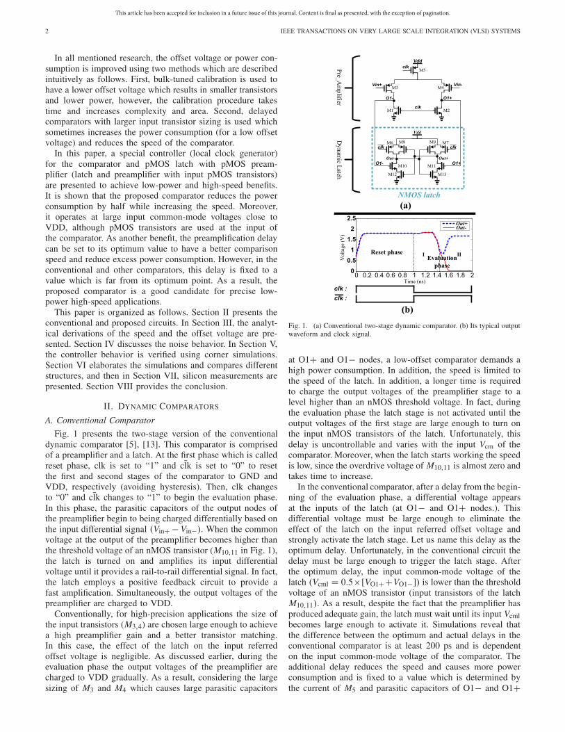
Fig. 1 presents the two-stage version of the conventionaldynamic comparator [5], [13]. This comparator is comprisedof a preamplifier and a latch. At the first phase which is calledreset phase, clk is set to “1” and ¯clk is set to “0” to resetthe first and second stages of the comparator to GND andVDD, respectively (avoiding hysteresis). Then, clk changesto “0” and ¯clk changes to “1” to begin the evaluation phase.In this phase, the parasitic capacitors of the output nodes ofthe preamplifier begin to being charged differentially based onthe input differential signal (Vin+ − Vin−). When the commonvoltage at the output of the preamplifier becomes higher thanthe threshold voltage of an nMOS transistor (M10,11 in Fig. 1),the latch is turned on and amplifies its input differentialvoltage until it provides a rail-to-rail differential signal. In fact,the latch employs a positive feedback circuit to provide afast amplification. Simultaneously, the output voltages of thepreamplifier are charged to VDD.
Conventionally, for high-precision applications the size ofthe input transistors (M3,4) are chosen large enough to achievea high preamplifier gain and a better transistor matching.In this case, the effect of the latch on the input referredoffset voltage is negligible. As discussed earlier, during theevaluation phase the output voltages of the preamplifier arecharged to VDD gradually. As a result, considering the largesizing of M3 and M4 which causes large parasitic capacitors
Fig. 1. (a) Conventional two-stage dynamic comparator. (b) Its typical outputwaveform and clock signal.
at O1+ and O1− nodes, a low-offset comparator demands ahigh power consumption. In addition, the speed is limited tothe speed of the latch. In addition, a longer time is requiredto charge the output voltages of the preamplifier stage to alevel higher than an nMOS threshold voltage. In fact, duringthe evaluation phase the latch stage is not activated until theoutput voltages of the first stage are large enough to turn onthe input nMOS transistors of the latch. Unfortunately, thisdelay is uncontrollable and varies with the input Vcm of thecomparator. Moreover, when the latch starts working the speedis low, since the overdrive voltage of M10,11 is almost zero andtakes time to increase.
In the conventional comparator, after a delay from the begin-ning of the evaluation phase, a differential voltage appearsat the inputs of the latch (at O1− and O1+ nodes.). Thisdifferential voltage must be large enough to eliminate theeffect of the latch on the input referred offset voltage andstrongly activate the latch stage. Let us name this delay as theoptimum delay. Unfortunately, in the conventional circuit thedelay must be large enough to trigger the latch stage. Afterthe optimum delay, the input common-mode voltage of thelatch (Vcml = 0.5×[VO1++VO1−]) is lower than the thresholdvoltage of an nMOS transistor (input transistors of the latchM10,11). As a result, despite the fact that the preamplifier hasproduced adequate gain, the latch must wait until its input Vcmlbecomes large enough to activate it. Simulations reveal thatthe difference between the optimum and actual delays in theconventional comparator is at least 200 ps and is dependenton the input common-mode voltage of the comparator. Theadditional delay reduces the speed and causes more powerconsumption and is fixed to a value which is determined bythe current of M5 and parasitic capacitors of O1− and O1+

This article has been accepted for inclusion in a future issue of this journal. Content is final as presented, with the exception of pagination.
KHORAMI AND SHARIFKHANI: LOW-POWER HIGH-SPEED COMPARATOR FOR PRECISE APPLICATIONS 3
Fig. 2. (a) Proposed two-stage dynamic. (b) Its typical output waveform andclock signal.
nodes. Also, the latch starts to work weakly with a smalloverdrive voltage (which further cause speed reduction). Thecurrent of M5 is determined by the power consumption andspeed criteria. The parasitic capacitors at O1+ and O1− aremostly the parasitic capacitors of M3,4 which are determinedby the offset criterion. Consequently, the delay of latch stageactivation is controlled by other parameters, such as offsetor power, and is far away from the optimum value. With anefficient design methodology, this problem may be alleviated;however, this fundamental problem still exists.
The proposed comparator eliminates the problem inherentlyand efficiently makes it possible to have the optimum delay inthe two-stage dynamic comparators. Therefore, it reduces thepower consumption and improves the speed.
B. Proposed ComparatorThe proposed comparator is shown in Fig. 2. In contrast to
the conventional comparator, a pMOS latch (a latch with inputpMOS transistors) is used in the latch which is activated witha predetermined delay during the evaluation phase [tamp, asshown in Fig. 2(b)]. This delay is supposed to be the optimumdelay. At the reset phase, the clk, clkb1, and clkb2 hold a logic“1” to discharge the output voltages of both preamplifier and
latch to GND. At the evaluation phase, first the clk and clkb1are toggled to logic “0” to start preamplification (charging theparasitic capacitors of O1+ and O1− nodes differentially).During this phase, the cross-coupled circuit increases thedifferential voltage (Vidl = [VO1+−VO1−]) slowly (since M4,5are mostly in subthreshold region) and reduces the common-mode voltage (Vcml = 0.5 × [VO1+ + VO1−]) to provide astrong drive for the input pMOS latch stage. Increasing Vidl(means larger preamplifier gain) further eliminates the effect ofthe latch on the input referred offset voltage. Also, larger Vidlresults in a smaller latch delay. Decreasing Vcml enhances thespeed of the comparator, since pMOS transistors are used atthe input of the latch (M13,14). Finally, clkb2 is toggled to logic“0” to activate the latch. Simultaneously, clkb1 is changed tologic “1” to turn off the current source of the preamplifierin order to avoid excess power consumption. Amplificationof Vid is kept going during this phase because the cross-coupled circuit is still working independently of the currentsource (M8). Meanwhile, Vcml is kept reducing by M3−5.
The control signals are implemented using a local clockgenerator as shown in Fig. 2(b), which consumes a smallamount of power. The black inverter is designed carefullyto adjust the delay. Instructively, the proposed comparator isrobust against overlapped control signals, since overlappedsignals only slightly affect the power consumption and haveno effect on the precision.
In the proposed circuit, the delay of the evaluation-phase islong enough to achieve the minimum required preamplificationgain for a given speed and latch offset elimination. Thanksto the cross-coupled circuit (M3−5), during the first step ofthe evaluation phase, the differential voltage at O1+ andO1-nodes increases; however, the common-mode voltage ofthose nodes is kept low. Therefore, for a sufficient evaluation-phase delay, tamp, Vcml (= 0.5 × [VO1+ + VO1−]) is pulleddown to activate the pMOS latch strongly. Also, the larger Vidlboosts the latching process (speed). Consequently, the delayof the comparator will be small and almost flat over a widerange of the input Vcm. Transition of clkb1 to logic “1” limitsthe power consumption of the preamplifier which is the mainpart of the total power consumption. In the meanwhile, thecross-coupled circuit continues preamplification at no cost ofpower consumption.
As another benefit, the delay time from beginning of theevaluation phase to beginning of the latching process is simplycontrollable and can be tuned at its optimum value. However,in the conventional comparator, delay is inevitably fixed to therequired time to charge the output parasitic capacitors of thepreamplifier to the level of an nMOS voltage threshold.
The proposed structure can also be implemented usingnMOS transistors, i.e., latch and preamplifier with input nMOStransistors. This will result in a higher speed because of theinherent superiority of nMOS transistors over pMOS ones.The size of M4,5 is chosen large enough to keep the outputcommon-mode voltage of the preamplifier small enough andincrease the preamplifier differential gain.
In this paragraph, the core concept of the proposed com-parator is briefly described. In the conventional comparator,if the preamplifier and the latch work in different time slots,the power consumption is improved. To do this efficiently, oneway is to change the structure of the conventional comparator
This article has been accepted for inclusion in a future issue of this journal. Content is final as presented, with the exception of pagination.
4 IEEE TRANSACTIONS ON VERY LARGE SCALE INTEGRATION (VLSI) SYSTEMS
from “pMOS preamp|| nMOS latch” to “pMOS preamp||pMOS latch” (or “nMOS preamp|| nMOS latch” for a betterspeed). In fact, the type of both the input transistors ofthe preamplifier and latch must be the same in contrast togeneral structure of the dynamic comparators [1]–[22]. Theproposed pMOS–pMOS (nMOS–nMOS) structure requires aspecial clocking pattern to work correctly and efficiently. Wedevelop a low-power small-area delay-line-based controllerwhich in addition to controlling the comparator, it makes thecomparator robust against process–VDD–temperature (PVT)variations since the delay of the controller and the delayof the comparator components varies in the same directionin different PVT corners. The preamplification delay can beset to achieve the optimum delay and this delay is almostoptimum in all PVT corners. In the achieved structure, Fig.1 without the cross-coupled circuit, the optimum delay couldnot be realized since a larger preamplification time reduces theVGS voltage of the following input pMOS transistors of thelatch (worsening the speed and power). Therefore, a circuitwhich reduces the input common-mode voltage of the pMOSlatch is needed while (at least) it keeps the differential gainuntouched. The cross-coupled circuit can do this. The sizeof the transistors is much smaller than the size of the inputtransistors of the preamplifier (about 7–10 times). Therefore,the power, area, and offset contribution of the cross-coupledcircuit is negligible. The cross-coupled circuit increases thedifferential voltage mainly when the preamplifier is turned offand enhances the speed; however, its main purpose is to reducethe input common-mode voltage of the latch.
III. ANALYTICAL DERIVATIONS
A. Delay
In this part, the speed of the proposed comparator iscalculated. Also, it is proven analytically why the proposedcomparator improves the speed. The comparison delay of theproposed comparator Tcomp is a summation of two parts. Thefirst one is tamp as shown in Fig. 2(b) and is determined bythe designer. The second part tlatch (II and III in Fig. 2) is thetime that a latch needs to reach the full swing at output whichdepends on the input signals and transistors sizing both of thelatch stage. The latch delay is defined as follows based on theanalytical calculations presented in [14]:
tlatch = τinv × ln
�VDD − GND
Vidl
�(1)
in which τinv = CL/(GMpMOS + GMnMOS) and Vidl is the inputdifferential signal of the latch. As shown in Appendix I, (1) canbe modified as follows to predict the delay more precisely:
tlatch = τinv × ln
�VDD − GND
Vidl
�+ Klatch
(VDD−V cml − Vthp)2
(2)
where Vcml and Vidl are the input common-mode and differen-tial voltages of the latch (Vcml = 0.5×[VO1+ + VO1−], Vidl =VO1+ − VO1−) coming from the preamplifier stage. Klatchis a constant depending on M13,14 sizing and technologyparameters. Equation (2) verifies that a higher Vidl or a lowerVcml results in a lower delay, since a higher Vidl reduces thefirst term and a lower Vcml reduces the second term. In the
following parts, it is shown that higher Vidl and lower Vcmlare achieved in the proposed comparator.
In the proposed circuit, the differential and common modesof VO1+ and VO1− are dependent on the input common-mode voltage (Vcm) of the comparator. For example, a largeinput Vcm reduces the current of M6,7 resulting a lowerVcml because of a lower charging current. To calculate thedelay, Vidl and Vcml should be calculated based on the inputdifferential voltage, common-mode voltage, and the circuitparameters. The input common-mode voltage and differentialvoltage of the comparator are defined as follows:⎧⎨
⎩Vcm = Vin+ + Vin−
2Vid = Vin+ − Vin−.
(3)
Based on the value of Vcm, three different scenarios of thedelay take place. First, for low values of Vcm, M6−8 work inthe saturation region and the current of M8 is partly controlledby Vcm because of the channel length modulation of M8.Second, for large values of Vcm close to VDD, M6,7 workin the subthreshold region and M8 works in the deep trioderegion. Third, Vcm has a level between the two previous bound-aries, M6,7 work at the edge of saturation or subthresholdregion, and M8 works at the edge of triode or deep trioderegion. It is noteworthy that in all scenarios, M6,7 do notwork in the triode region (Linear region), since the nMOScross-coupled transistors (M4,5), keep the output voltages(VO1+, VO1−) well below the voltage threshold of a pMOStransistor.
Based on Appendix II, the cross-coupled circuit is modeledwith two dependent current sources as shown in Fig. 3(a).M3 works in the deep triode region and M4,5 work in thesubthreshold region. At the first scenario, the current of M6,7is �
I1 = k1(Vp − Vin+ − Vth)2
I2 = k2(Vp − Vin− − Vth)2 (4)
where ki = 0.5μCox(W/L)i and Vp is the drain voltage of M8as shown in Fig. 3(b). By subtracting the previous equations,the differential current �I is calculated as follows:
�I = I2 − I1 = kVid(2Vp − Vin+ − Vin− − 2Vth)
�I = 2kVid(Vp − Vcm − Vth), Vid = Vin+ − Vin−. (5)
KCL equations at node O1+ and O− yields in the followingset of equalities:⎧⎪⎪⎨
⎪⎪⎩VO1+ = (I1 − αVO1−) × tamp
C
VO1− = (I2 − αVO1+) × tamp
C.
(6)
By solving this linear set of equations, VO1+ and VO1− atthe end of tamp are calculated as the following equations:⎧⎪⎪⎪⎪⎪⎪⎪⎪⎪⎨
⎪⎪⎪⎪⎪⎪⎪⎪⎪⎩
VO1+ =
I1 − α I2tampC
× tamp
C
1 − α2
tampC
2
VO1− =
I2 − α I1tampC
× tamp
C
1 − α2
tampC
2 .
(7)

This article has been accepted for inclusion in a future issue of this journal. Content is final as presented, with the exception of pagination.
KHORAMI AND SHARIFKHANI: LOW-POWER HIGH-SPEED COMPARATOR FOR PRECISE APPLICATIONS 5
Fig. 3. (a) Equivalent circuit of the cross-coupled part. (b) Simplified circuitdiagram of the preamplifier.
Consequently, Vidl and Vcml are calculated in the followingequation to be used in the delay equation, i.e., (2)⎧⎪⎪⎪⎪⎪⎪⎨⎪⎪⎪⎪⎪⎪⎩
Vcml = VO1+ + VO1−2
= I× tampC
1 + α
tampC
, I = I1 + I2
Vidl = VO1+ − VO1− = �I× tampC
1 − α
tampC
, �I = I2 − I1.
(8)
Let us assume that in the conventional comparator a pMOSlatch (similar to Fig. 2) is used (to make an apple-to-applecomparison). It is noteworthy that the equivalent equations forsuch a comparator are as follows; in fact, there is no α termin the denominator:⎧⎪⎪⎪⎨
⎪⎪⎪⎩Vcml = VO1+ + VO1−
2= I × tamp
C
1 + 0= I× tamp
C
1
Vidl = VO1+ − VO1− = �I × tampC
1 − 0= �I × tamp
C
1
(9)
Compared to the proposed comparator, in that comparator,when the latch is activated, the value of Vcml is higher and thevalue of Vidl is lower, so the delay is worse than the proposedcomparator.
In the conventional comparator, nMOS latch is used(Fig. 1) so the latch is gradually turned on (which meansmore delay). In fact, when the latch is turned on, the overdrivevoltage of the input nMOS transistors [M10,11 Fig. 1(a)] is lowthat exacerbates the delay.
As discussed earlier, in the proposed comparator thanks tothe cross-coupled circuit [α term in (8)], a higher Vidl and alower Vcml are achieved. Therefore, considering (2), the speedis improved. The amount of improvement is considerable,since both terms in (2) are reduced. As another reason forthe speed improvement, in the proposed comparator, the latchstarts its function strongly because of the large overdrive volt-age for M13,14 in Fig. 2 [Vcml ∼ 0 �⇒ Vod ∼ (VDD − Vthp)].However, in the conventional comparator, at the beginning ofthe latching process Vod ∼ 0.
At the second and third scenarios, the same procedure isused to calculate the delay. The equations will be tedious inthis part; therefore, the results are presented in Appendix III.
Fig. 4. (a) Delay of the proposed comparator versus input Vcm. (b) Delayof the proposed comparator versus input Vid.
In order to verify the derivations, a sample of the proposedcomparator is designed in 0.18-μm CMOS technology toachieve a typical offset voltage of 2 mV. Then, the com-parator delay is approximated using the delay derivationspresented in (2), (3), and Appendix III. Fig. 4 presentsthe schematic simulation results along with the analyticalderivations for all scenarios. To calculate the analytical results,first Vidl and Vcml are determined by the proposed equations[e.g., (8)], then equation (2) is used. In Fig. 4(a), the delayof the comparator with respect to the input Vcm is presented.Fig. 4(a) confirms the analytical derivations that predict thedelay precisely. At the boundaries, the error between simu-lation results and analytical derivations is growing becausethe working region of M6,7,8 changes smoothly in additionto α variations and increasing the effect of channel lengthmodulation of M6,7. Fig. 4(b) shows the delay versus Vidconsidering Vcm = 1.1 V.
B. Offset Voltage
The offset voltage is dependent on Vcm, since the workingregion of the transistors changes and the nonideal effects suchas channel length modulation alters the effect of mismatch ofeach component on the differential gain. The offset voltageof the comparator is calculated analytically for Vcm less thanVDD/2, where M6,7,8 work in the saturation region and thechannel length modulation of M6,7 is negligible. In order topropose a closed-form equation, we neglect the effect of thelatch on the offset voltage (which is satisfied in a good design).As discussed earlier, in a good design the sizing of the inputtransistors (M6,7) for high-resolution applications are chosenlarge enough to eliminate the effect of the latch stage on theinput referred offset voltage.
Technically, the input referred dynamic offset is the inputdifferential voltage (Vin+−Vin−) that establishes equal voltageat the O1+ and O1− nodes at the end of the preamplificationphase (tamp). The current of M6,7 [Fig. 3(b)] and the differencebetween them are calculated as follows by taking into account

This article has been accepted for inclusion in a future issue of this journal. Content is final as presented, with the exception of pagination.
6 IEEE TRANSACTIONS ON VERY LARGE SCALE INTEGRATION (VLSI) SYSTEMS
Fig. 5. Schematic and analytical simulation results of offset voltageversus Vcm.
the effect of mismatch:�I1 = k(Vp − Vin+ − Vth)
2
I2 = (k + �k)(Vp − Vin− − Vth − �Vth)2 (10)
�I = (I2− I1)=2k(Vin+−Vin−−�Vth)(Vp−Vth−Vcm−�Vth)
+�k(Vp − Vin− − Vth − �Vth)2
⇒ �I ∼= Vos(gm − 2k�Vth) − gm�Vth
+�k(Vp − Vth − �Vth + 0.5 × Vos − Vcm).2 (11)
Employing KCL at O1+ and O1− nodes yields the followingequations for VO1+ and VO1−:⎧⎪⎪⎪⎪⎪⎪⎪⎪⎨
⎪⎪⎪⎪⎪⎪⎪⎪⎩
VO1+ =
I1 − α I2
tampC
tampC
1 − α (α+�α)
tampC
2
VO1− =
I2−(α+�α)I1
tampC
tampC
1 − α (α+�α)
tampC
2 .
(12)
Based on the definition of the offset voltage, if an inputdifferential voltage as large as Vos is applied to the comparator,VO1+ will be equal to VO1− after the amplification time (tamp).Therefore, by solving the equation VO1+ = VO1− and substi-tuting (11), the offset voltage is calculated in (13), shown atthe bottom of this page.
Fig. 5 presents the simulation results of the offsetvoltage for the proposed comparator. In Fig. 5, the offsetvoltage versus Vcm is shown considering 1 k-points SpectreMonte Carlo simulations (using 0.18-μm technology) and100 k-points MATLAB Monte Carlo simulations using (13).
IV. NOISE
In two-stage dynamic comparators, the offset voltage andsimilarly the input referred noise is mainly dominated bythe preamplifier stage. Using the proposed technique, bothinput nMOS and input pMOS preamplifiers can be used;their structures are similar to the conventional counterparts
TABLE I
PARAMETERS OF THE CONTROLLER IN DIFFERENT CORNERS
[neglecting the cross-coupled circuit Fig. 3(a)]. As a result, weexpect an almost equal input referred noise. In the proposedcomparator, the cross-coupled circuit increases both the noiseand the preamplification gain. On the other hand, the cross-coupled circuit keeps the output voltages of the preamplifierstage low so it keeps the preamplifier input transistors inthe saturation region. This is in contrast to the conventionalcomparator where the input transistors go to the triode regionduring preamplification exacerbating the input noise (gain↓⇒ Vnoise-in ↑). Assuming all above, the first effect increasesthe input noise while the second one reduces the input noise.Therefore, totally, it is expected that the input noise of the pro-posed comparator will be almost the same as the conventionalcomparator. In Section VI, multiple transient noise simulationsprove this inspection.
V. DELAY-LINE-BASED CONTROLLER
Fig. 2(b) presents the controller and the voltage waveforms.The circuit was designed to produce 150-ps delay for theproposed comparator. The circuit consumes about 20 μwwhich is negligible compared to the total power consumption.To be sure about the behavior of this circuit, different PVTcorners was considered. Table 1 presents the results. As can beseen, the power consumption remains acceptable for differentcorners compared to the total power consumption of about210 μW. Naturally, the delay varies in different corners whichis favorable for the comparator, since it is consistent withthe delay variations of the comparator (which is toward thesame direction in different corners). In fact, the proposedcontroller employs an inherent self-adjusting mechanism. The10 k-points Monte Carlo simulations reveal that the σ of tampvariations due to transistors mismatch is 5 ps, which is only3% of the total 150-ps delay. The PVT and Monte Carlo sim-ulations confirm the validity and efficiency of the controller.
VOS = [gm�Vth + �k(Vp − Vth − �Vth)2 + 2Vcm�k(Vp − Vth − �Vth)
2 − V 2cm]
(gm − 2k�Vth + �k(Vp − Vth − �Vth)2 − Vcm)
+−�α
2
tampC
I
(gm − 2k�Vth + �k�Vp − Vth − �Vth
2 − Vcm)
1 + �α + �α
2
tampC
(13)
This article has been accepted for inclusion in a future issue of this journal. Content is final as presented, with the exception of pagination.
KHORAMI AND SHARIFKHANI: LOW-POWER HIGH-SPEED COMPARATOR FOR PRECISE APPLICATIONS 7
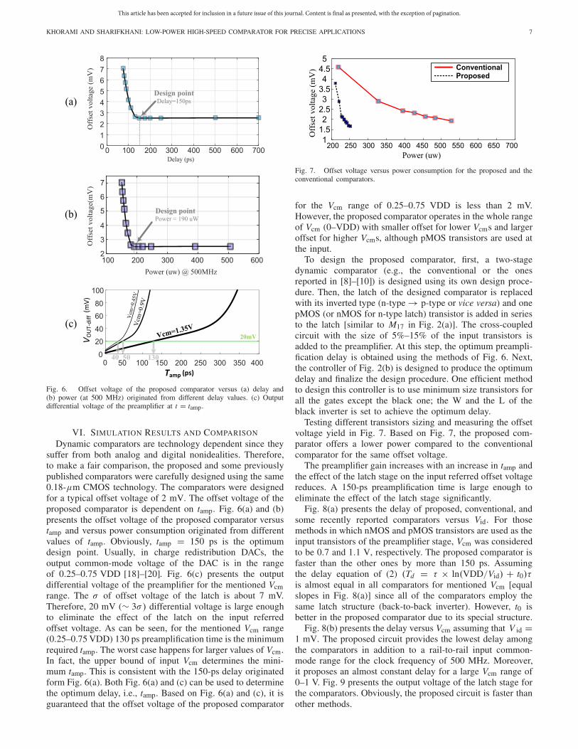
Fig. 6. Offset voltage of the proposed comparator versus (a) delay and(b) power (at 500 MHz) originated from different delay values. (c) Outputdifferential voltage of the preamplifier at t = tamp.
VI. SIMULATION RESULTS AND COMPARISON
Dynamic comparators are technology dependent since theysuffer from both analog and digital nonidealities. Therefore,to make a fair comparison, the proposed and some previouslypublished comparators were carefully designed using the same0.18-μm CMOS technology. The comparators were designedfor a typical offset voltage of 2 mV. The offset voltage of theproposed comparator is dependent on tamp. Fig. 6(a) and (b)presents the offset voltage of the proposed comparator versustamp and versus power consumption originated from differentvalues of tamp. Obviously, tamp = 150 ps is the optimumdesign point. Usually, in charge redistribution DACs, theoutput common-mode voltage of the DAC is in the rangeof 0.25–0.75 VDD [18]–[20]. Fig. 6(c) presents the outputdifferential voltage of the preamplifier for the mentioned Vcmrange. The σ of offset voltage of the latch is about 7 mV.Therefore, 20 mV (∼ 3σ) differential voltage is large enoughto eliminate the effect of the latch on the input referredoffset voltage. As can be seen, for the mentioned Vcm range(0.25–0.75 VDD) 130 ps preamplification time is the minimumrequired tamp. The worst case happens for larger values of Vcm.In fact, the upper bound of input Vcm determines the mini-mum tamp. This is consistent with the 150-ps delay originatedform Fig. 6(a). Both Fig. 6(a) and (c) can be used to determinethe optimum delay, i.e., tamp. Based on Fig. 6(a) and (c), it isguaranteed that the offset voltage of the proposed comparator
Fig. 7. Offset voltage versus power consumption for the proposed and theconventional comparators.
for the Vcm range of 0.25–0.75 VDD is less than 2 mV.However, the proposed comparator operates in the whole rangeof Vcm (0–VDD) with smaller offset for lower Vcms and largeroffset for higher Vcms, although pMOS transistors are used atthe input.
To design the proposed comparator, first, a two-stagedynamic comparator (e.g., the conventional or the onesreported in [8]–[10]) is designed using its own design proce-dure. Then, the latch of the designed comparator is replacedwith its inverted type (n-type → p-type or vice versa) and onepMOS (or nMOS for n-type latch) transistor is added in seriesto the latch [similar to M17 in Fig. 2(a)]. The cross-coupledcircuit with the size of 5%–15% of the input transistors isadded to the preamplifier. At this step, the optimum preampli-fication delay is obtained using the methods of Fig. 6. Next,the controller of Fig. 2(b) is designed to produce the optimumdelay and finalize the design procedure. One efficient methodto design this controller is to use minimum size transistors forall the gates except the black one; the W and the L of theblack inverter is set to achieve the optimum delay.
Testing different transistors sizing and measuring the offsetvoltage yield in Fig. 7. Based on Fig. 7, the proposed com-parator offers a lower power compared to the conventionalcomparator for the same offset voltage.
The preamplifier gain increases with an increase in tamp andthe effect of the latch stage on the input referred offset voltagereduces. A 150-ps preamplification time is large enough toeliminate the effect of the latch stage significantly.
Fig. 8(a) presents the delay of proposed, conventional, andsome recently reported comparators versus Vid. For thosemethods in which nMOS and pMOS transistors are used as theinput transistors of the preamplifier stage, Vcm was consideredto be 0.7 and 1.1 V, respectively. The proposed comparator isfaster than the other ones by more than 150 ps. Assumingthe delay equation of (2) (Td = τ × ln(VDD/Vid) + t0)τis almost equal in all comparators for mentioned Vcm [equalslopes in Fig. 8(a)] since all of the comparators employ thesame latch structure (back-to-back inverter). However, t0 isbetter in the proposed comparator due to its special structure.
Fig. 8(b) presents the delay versus Vcm assuming that V id =1 mV. The proposed circuit provides the lowest delay amongthe comparators in addition to a rail-to-rail input common-mode range for the clock frequency of 500 MHz. Moreover,it proposes an almost constant delay for a large Vcm range of0–1 V. Fig. 9 presents the output voltage of the latch stage forthe comparators. Obviously, the proposed circuit is faster thanother methods.

This article has been accepted for inclusion in a future issue of this journal. Content is final as presented, with the exception of pagination.
8 IEEE TRANSACTIONS ON VERY LARGE SCALE INTEGRATION (VLSI) SYSTEMS
Fig. 8. (a) Delay versus Vid considering Vcm = 0.7, 1.1 for nMOS input andpMOS input comparators. (b) Delay versus Vcm considering Vid = 1 mV.
Fig. 9. Output waveforms of the proposed, conventional, and some othercomparators.
Fig. 10(a) presents the power consumption versus Vcm atthe clock frequency of 500 MHz. The output voltage swingof the preamplifier at the end of tamp is larger for a lowerinput Vcm; as a result, the power consumption is higher for alower Vcm Neglecting the power consumption of the latch, thetotal power consumption is calculated as
Power = 1
T
� T =Tclk/2
0v(t) · i(t)dt + Platch
= 1
T
� tamp
0VDD · (I1+ I2)dt+ Platch ∼= tamp
TVDD× IM8.
(14)
Tclk/2 is replaced with tamp, since only during tamp the pream-plifier draws power from the supply voltage. By increasingtamp, the power consumption increases linearly. Fig. 10(b)presents the power consumption versus delay for Vcm = 1.1 V.The conventional power level is fixed, since in the conventionalcomparator, the preamplification delay is fixed to Tclk/2.As expected, in the proposed comparator, the power consump-tion has a linear relationship with tamp. In the sample designed
Fig. 10. (a) Power consumption of comparators versus input Vcm. (b) Powerconsumption of the proposed comparator versus tamp, Vcm = 1.1 V.
TABLE II
COMPARISON BETWEEN THE COMPARATORS BASED ON THEAUTHOR SIMULATIONS (σoffset = 2 mV)
comparator, tamp is chosen 150 ps which offers very low powerconsumption while it is large enough to eliminate the effectof the latch stage on the offset voltage. If the delay is chosen600 ps, the power of the proposed comparator is the same asthat in the conventional one. Thus, here, the difference betweenthe actual and ideal delay is about 450 ps. In the conventionalcomparator, for about 450 ps, time and preamplifier power arewasted.
Table II compares the proposed and some comparatorswhich are designed using the same technology (0.18 μm) andoffset voltage (∼2 mV). The maximum frequency is calculatedusing Fig. 8, and the power consumption is the average powerover the input Vcm range of each comparator. The proposedcomparator presents a higher speed and a higher input Vcmrange with lower power consumption. The area overhead isnegligible. The last row of Table II presents the input noise ofthe comparators. As discussed in the noise section, the inputreferred noise of the proposed comparator is almost the sameas the other ones. The dynamic noise is negligible compared tothe offset voltage. Totally, the proposed comparator is a goodcandidate for low-power high-speed high-resolution ADCs.
A. Corner Simulations
In order to confirm the benefits of the proposed comparator,the designed comparator was tested under different process

This article has been accepted for inclusion in a future issue of this journal. Content is final as presented, with the exception of pagination.
KHORAMI AND SHARIFKHANI: LOW-POWER HIGH-SPEED COMPARATOR FOR PRECISE APPLICATIONS 9
TABLE III
PARAMETERS OF THE COMPARATOR IN DIFFERENT CORNERSCONSIDERING THE IDEAL AND PROPOSED
CONTROLLERS (Vcm = Vref /2)
(ss, tt, and ff), voltage (1.6, 1.8, and 2 V), and temperature(0°, 27°, and 70 °C) corners (PVT corners). Table III presentsthe results for 27 different corners (33 = 27). In each cell ofTable III, the top numbers represent the results considering anideal controller (fixed 150-ps delay), while the down numberis for the proposed controller [Fig. 2(b)]. As can be seen, theoffset voltage remains about 2 mV in different corners, sincethe proposed controller somehow self-adjust the comparator.In fact, whenever the delay is low (e.g., VDD = 2 V, ffin 0 °C) the delay-line-based controller is fast forcing thecomparator to work correctly. On the contrary, if the delayis high (e.g., VDD = 1.6 V, ss in 70 °C) the delay-line-basedcontroller is slow letting the comparator work correctly. As aresult, the delay-line-based controller serves the comparator asa self-adjusting clock generator. The delay naturally reducesor increases in different corners. The power consumption forthe case of the proposed controller (the down numbers) variesonly with VDD variations. In fact, in different process andtemperature corners the power consumption almost remainsconstant. In the case of an ideal controller, however, thepower changes significantly (due to the current variation ofthe preamplifier and a fix tamp).
Consequently, the simulation results in different PVT cor-ners prove the efficiency of the proposed comparator andthe delay-line-based controller. Moreover, Table III showsthat employing the proposed delay-line-based controller ismore efficient than using a fixed-delay (process-independent)controller.
VII. MEASUREMENT
In order to verify the low-power benefit of the proposedcomparator, the sample comparator (discussed in Section VI)
Fig. 11. (a) Symmetric layout of the proposed comparator. (b) Differentlayers of the layout. (c) Die micrograph.
TABLE IV
COMPARISON BETWEEN THE PROPOSED AND OTHER COMPARATORS
was fabricated using CMOS 0.18-μm technology. Fig. 11(a)shows the layout of the circuit. In order to avoid the staticoffset voltage caused by the load capacitors mismatch, thecircuit was laid out in a fully symmetric fashion. In Fig. 11(a),all transistors are labeled with their name as depicted in Fig. 2.Fig. 11(b) presents the wiring of the layers. Fig. 11(c) depictsthe die micrograph. To calculate the power consumptionaccurately, 66 comparators were fabricated. Fig. 12(a) presentsthe power consumption versus input Vcm. The average powerconsumption is less than 250 μW for 500-MHz clockfrequency. In Fig. 12(a), power consumption versus inputfrequency is presented. The proposed comparators offer a

This article has been accepted for inclusion in a future issue of this journal. Content is final as presented, with the exception of pagination.
10 IEEE TRANSACTIONS ON VERY LARGE SCALE INTEGRATION (VLSI) SYSTEMS
Fig. 12. (a) Power versus input Vcm. (b) Power versus clock frequency.(c) Delay versus input Vcm.
low power consumption in different frequencies. Fig. 12(c)presents the delay versus input Vcm. The delay is less than500 ps for the whole range of Vcm. Table IV presents thecomparison between the proposed and other comparators.The proposed comparator offers a low power behavior witha low offset voltage while having an input Vcm range of0–VDD. This feature enables the comparator to be used fol-lowed by low-power components with a rail-to-rail output Vcmrange such as the ultralow-power capacitive DACs reportedin [16] and [17].
VIII. CONCLUSION
In the proposed comparator, pMOS latch and pMOS pream-plifier in addition to a small cross-coupled circuit are usedwith a special clocking pattern to adjust the preamplifier gain.The clocking pattern provides enough preamplifier gain; sincepMOS transistors are used at the input of the latch, andthe cross-coupled circuit is employed to keep the common-mode voltage of the preamplifier outputs at a low level.As a result, the speed of the comparator is increased andis constantly high for a wide input Vcm range [Fig. 12(c)].Deactivating the preamplifier after the optimum delay reducesthe power consumption significantly. Therefore, the proposed
Fig. 13. (a) Typical output waveform of the pMOS latch. (b) Simplifiedcircuit diagram of the latch right after beginning the latching process.
circuit is a low-offset low-power high-speed comparator whichworks at a wide input common-mode voltage range. Analyticalmodeling, PVT corner, and post layout simulations alongwith silicon measurements prove the benefits of the proposedcomparator.
APPENDIX I
Fig. 13(a) presents a typical output waveform of a pMOSlatch. As shown in Fig. 13(a), the delay of the latch canbe divided into two parts. First, the voltage of the outputnodes is charged from Gnd to Vthn with almost the same rateconsidering a small differential voltage at the input (since Vidlat the output of the preamplifier is small). Then the nMOStransistors are turned on and the back-to-back inverter startsto lock based on its input differential signal. Equation (1)presents an approximation of the second delay. The first delayis calculated as follows. When the latch is in a comparatorcircuit, the signal at the both outputs of the preamplifier isassumed to be Vcml neglecting the differential voltage. In thiscase, when the latch is activated M15−17 are deeply triode,M9−12 are OFF and M13,14 work in the saturated region.Therefore, the equivalent circuit of Fig. 13(b) is obtained. Ifa capacitor is charged using a dc current source, the voltageof the capacitor is calculated as follows:
Vc(t) = I
Ct (15)
T1 = C
I× �V = C
k13,14�VDD − Vcml − Vthp
2 × Vthn.
(16)
T2 is a constant delay and is referred to as the regenerationtime of the back-to-back inverter.
APPENDIX II
Considering Fig. 3(a), the gate of M3is connected to VDDand the common-mode voltage of O1+ and O1− nodes duringcomparison are typically less than 0.4 V for different values ofinput Vcm of the comparator. Therefore, M3 is deeply triode
This article has been accepted for inclusion in a future issue of this journal. Content is final as presented, with the exception of pagination.
KHORAMI AND SHARIFKHANI: LOW-POWER HIGH-SPEED COMPARATOR FOR PRECISE APPLICATIONS 11
and the voltage of the source pins of M4,5 is almost GND.M4,5 works in the subthreshold region. Then, we have
I+ = ID0e
VO1−−Vth
ηVT
�1 − e
−V O1+VT
�
×e
−V O1+VT
< 0.1 for VO1+> 50 mV (17)
→ I+ ∼= ID0e
VO1−+Vth
ηVT
= ID0e
VthηVT
e
VO1−ηVT
= I �
D0e
VO1−ηVT
= I �D0
�1 + VO1−
ηVT
�(18)
→ I+ ∼= I �D0
�1+ VO1−
ηVT
�= I �
D0 + VO1−ηVT
= I0 + I0
ηVTVO1−.
(19)
For I− on the other side of the comparator, we have the samederivations
I− ∼= I �D0
�1 + VO1+
ηVT
�= I �
D0 + VO1+ηVT
= I0 + I0
ηVTVO1+.
(20)
I0 has a common-mode effect in lowering VO1+ and VO1−;therefore, it has no effect on the input differential voltage ofthe latch (Vidl). On the other hand, the effect of I0 on theinput common-mode voltage of the latch (Vcml) is negligiblecompared to (I0/ηVT )VO1+, since (1/ηVT ) ∼= 32 (for typicalparameters in room temperature). Moreover, the current com-ing from the input pMOS transistors of the preamplifier stagedominates I0. Consequently, I− and I+ are approximated by
⎧⎪⎪⎨⎪⎪⎩
I+ ∼= I0
ηVTVO1− = αVO1−
I− ∼= I0
ηVTVO1+ = αVO1+.
(21)
APPENDIX III
At the second scenario, M6,7 are in the subthreshold regionand M8 is completely triode. Therefore, Vp is almost VDD andthe current of M6,7 is calculated as follows for the subthresholdregion, considering a first-order approximation of the effect ofdrain–source voltage (1 − e(−VDS/VT ) = (VDS/VT )) [15]:
⎧⎪⎪⎪⎪⎪⎪⎪⎪⎪⎪⎪⎪⎪⎪⎨⎪⎪⎪⎪⎪⎪⎪⎪⎪⎪⎪⎪⎪⎪⎩
I1 = I0e
VDD−Vin+
ηVT
�1
VT[VDD−VO1+]
�
= I0
VTe
VDD−Vin+
ηVT
(VDD−VO1+)
I2 = I0e
VDD−Vin−
ηVT
�1
VT[VDD−VO1−]
�
= I0
VTe
VDD−Vin−
ηVT
(VDD−VO1−) .
(22)
Equation (22) is simplified to⎧⎪⎪⎨⎪⎪⎩
I1 = A1 (VDD−VO1+) , A1 = I0
VTe
VDD−Vin+
ηVT
I2 = A2 (VDD−VO1−) , A2 = I0
VTe
VDD−Vin−
ηVT
.
(23)
O1+ and O1− nodes are being charged with I1 and I2 thenthe following equations hold:⎧⎪⎪⎨⎪⎪⎩
I1 = CdVO1+
dt+ αVO1−
I2 = CdVO1−
dt+ αVO1+
⇒
⎧⎪⎪⎨⎪⎪⎩
CdVO1+
dt+ αVO1− = A1VDD−A1VO1+
CdVO1−
dt+ αVO1+ = A2VDD−A2VO1−.
(24)
The solution of the above set of linear differential equationsfor t ≥ 0 is⎧⎪⎪⎪⎪⎪⎪⎨⎪⎪⎪⎪⎪⎪⎩
VO1+ (t)
= m2,1
C2m4
�−1 + cosh (m1t) − C
m1sinh
�m1t
C
��m3− m5,1
m2,1
��
VO1+(t)
= m2,2
C2m4
�−1 + cosh(m1t)− C
m1sinh
�m1t
C
��m3− m5,2
m2,2
��
(25)
where m1−4 coefficients are defined as follows:⎧⎪⎪⎪⎪⎪⎪⎪⎪⎪⎪⎪⎨⎪⎪⎪⎪⎪⎪⎪⎪⎪⎪⎪⎩
m1 = 1
C
�1
4(A1 − A2)
2 + a2
m2,1 = A2C2×VDD(A1 − α)
m2,2 = A1C2×VDD(A2 − α)
m3 = 1
2C(A1 + A2)
m4 = α2 − A1 A2
(26)
m5,1, and m5,2 are defined as follows:�
m5,1 = C × VDD�−A2
2α + A1 A22 − A1 A2α + A1α
2
m5,2 = C × VDD�−A2
1α + A2 A21 − A2 A1α + A2α
2 .
(27)
As excepted, VO1+(0+) = VO1−(0+) = 0, since the followingequations hold:const × (−1+ cosh(0+)−const× sinh(0+))
= const × (−1 + 1) = const × 0 = 0. (28)
Equation (25) derivations are evaluated at t = tamp, then VO1+and VO1− are used in the following equation to predict thedelay using (2):
⎧⎨⎩
Vcml = VO1+(tamp) + VO1−(tamp)
2Vidl = VO1+(tamp) − VO1−(tamp).
(29)
At the third scenario, M6,7 working region is between satu-ration and subthreshold region and M8 almost operates in thetriode region. Vp is highly dependent on Vcm and the channellength modulation effect of M6,7 becomes important. Theanalytical calculations of this scenario lead to an extensive,yet straightforward derivations which is beyond the length of

This article has been accepted for inclusion in a future issue of this journal. Content is final as presented, with the exception of pagination.
12 IEEE TRANSACTIONS ON VERY LARGE SCALE INTEGRATION (VLSI) SYSTEMS
this paper. Therefore, just the results are reported⎧⎪⎪⎪⎪⎪⎪⎪⎪⎪⎪⎪⎪⎪⎪⎪⎨⎪⎪⎪⎪⎪⎪⎪⎪⎪⎪⎪⎪⎪⎪⎪⎩
Vcml = VO1+ + VO1−2
=B
2A 1
VTD−αD − Aα
tampC
2+B (A+D)
tampC
2
��A
1
VT
2D−α2
� tampC
2+ 1VT
(A+D)
tampC
+1
�
Vidl =VO1+ − VO1−
=B (A − D)
tampC
α
tampC
+ 1
�
A
1VT
2D − α2
� tampC
2+ 1VT
(A + D)
tampC
+ 1
(30)
where A, B , and D are defined as⎧⎪⎪⎪⎪⎨⎪⎪⎪⎪⎩
A = I0e
VDD−Vin+
ηVT
B = 1
VT× VDD
D = I0e
VDD−Vin−
ηVT
(31)
REFERENCES
[1] B. Razavi and B. A. Wooley, “Design techniques for high-speed, high-resolution comparators,” IEEE J. Solid-State Circuits, vol. 27, no. 12,pp. 1916–1926, Dec. 1992.
[2] H.-K. Hong et al., “A 2.6b/cycle-architecture-based 10b 1 JGS/s15.4 mW 4×-time-interleaved SAR ADC with a multistep hardware-retirement technique,” in IEEE Int. Solid-State Circuits Conf. (ISSCC)Tech. Dig. Papers, Feb. 2015, pp. 1–3.
[3] K. Ragab, L. Chen, A. Sanyal, and N. Sun, “Digital backgroundcalibration for pipelined ADCs based on comparator decision timequantization,” IEEE Trans. Circuits Syst. II, Exp. Briefs, vol. 62, no. 5,pp. 456–460, May 2015.
[4] A. Khorami and M. Sharifkhani, “High-speed low-power comparator foranalog to digital converters,” AEU—Int. J. Electron. Commun., vol. 70,no. 7, pp. 886–894, 2016.
[5] T. B. Cho and P. R. Gray, “A 10 b, 20 Msample/s, 35 mW pipeline A/Dconverter,” IEEE J. Solid-State Circuits, vol. 30, no. 3, pp. 166–172,Mar. 1995.
[6] P. M. Figueiredo and J. C. Vital, “Kickback noise reduction techniquesfor CMOS latched comparators,” IEEE Trans. Circuits Syst. II, Exp.Briefs, vol. 53, no. 7, pp. 541–545, Jul. 2006.
[7] A. Khorami and M. Sharifkhani, “Low-power technique fordynamic comparators,” Electron. Lett., vol. 52, no. 7, pp. 509–511,Apr. 2016.
[8] M. Abbas, Y. Furukawa, S. Komatsu, J. Y. Takahiro, and K. Asada,“Clocked comparator for high-speed applications in 65nm technology,”in Proc. IEEE Asian Solid State Circuits Conf. (A-SSCC), Nov. 2010,pp. 1–4.
[9] J. Lu and J. Holleman, “A low-power high-precision compara-tor with time-domain bulk-tuned offset cancellation,” IEEE Trans.Circuits Syst. I, Reg. Papers, vol. 60, no. 5, pp. 1158–1167,May 2013.
[10] S. D’Amico, G. Cocciolo, A. Spagnolo, M. De Matteis, andA. Baschirotto, “A 7.65-mW 5-bit 90-nm 1-Gs/s folded interpolatedADC without calibration,” IEEE Trans. Instrum. Meas., vol. 63, no. 2,pp. 295–303, Feb. 2014.
[11] J. Gao, G. Li, and Q. Li, “High-speed low-power common-modeinsensitive dynamic comparator,” Electron. Lett., vol. 51, no. 2,pp. 134–136, Jan. 2015.
[12] M. Hassanpourghadi, M. Zamani, and M. Sharifkhani, “A low-powerlow-offset dynamic comparator for analog to digital converters,” Micro-electron. J., vol. 45, no. 2, pp. 256–262, 2014.
[13] M. Miyahara, Y. Asada, D. Paik, and A. Matsuzawa, “A low-noise self-calibrating dynamic comparator for high-speed ADCs,” inProc. IEEE Asian Solid-State Circuits Conf. (A-SSCC), Nov. 2008,pp. 269–272.
[14] A. Nikoozadeh and B. Murmann, “An analysis of latch comparator offsetdue to load capacitor mismatch,” IEEE Trans. Circuits Syst. II, Exp.Briefs, vol. 53, no. 12, pp. 1398–1402, Dec. 2006.
[15] T. C. Carusone, D. Johns, and K. Martin, Analog Integrated CircuitDesign. Hoboken, NJ, USA: Wiley, 2008.
[16] A. Khorami and M. Sharifkhani, “Zero-power mismatch-independentdigital to analog converter,” AEU—Int. J. Electron. Commun., vol. 69,no. 11, pp. 1599–1605, 2015.
[17] C.-C. Liu, S.-J. Chang, G.-Y. Huang, and Y.-Z. Lin, “A 10-bit50-MS/s SAR ADC with a monotonic capacitor switching procedure,”IEEE J. Solid-State Circuits, vol. 45, no. 4, pp. 731–740, Apr. 2010.
[18] B. Yazdani, A. Khorami, and M. Sharifkhani, “Low-power bottom-plate sampling capacitor-splitting DAC for SAR ADCs,” Electron. Lett.,vol. 52, no. 11, pp. 913–915, May 2016.
[19] C. Yuan and Y. Lam, “Low-energy and area-efficient tri-level switchingscheme for SAR ADC,” Electron. Lett., vol. 48, no. 9, pp. 482–483,Apr. 2012.
[20] B. Yazdani, A. Khorami, and M. Sharifkhani, “Low power DAC withsingle capacitor sampling method for SAR ADCs,” Electron. Lett.,vol. 52, no. 14, pp. 1209–1210, Jul. 2016.
[21] B. Razavi, “The StrongARM latch [A circuit for all seasons],”IEEE Solid-State Circuits Mag., vol. 7, no. 2, pp. 12–17, 2015,doi: 10.1109/MSSC.2015.2418155.
[22] D. Xu, S. Xu, and G. Chen, “High-speed low-power and low-powersupply voltage dynamic comparator,” Electron. Lett., vol. 51, no. 23,pp. 1914–1916, Nov. 2015.
[23] A. Khorami, M. B. Dastjerdi, and A. F. Ahmadi, “A low-power high-speed comparator for analog to digital converters,”in Proc. IEEE Int. Symp. Circuits Syst. (ISCAS), May 2016,pp. 2010–2013.
[24] S. Babayan-Mashhadi and R. Lotfi, “Analysis and design of alow-voltage low-power double-tail comparator,” IEEE Trans. VeryLarge Scale Integr. (VLSI) Syst., vol. 22, no. 2, pp. 343–352,Feb. 2014.
[25] A. Khorami and M. Sharifkhani, “Excess power elimination in high-resolution dynamic comparators,” Microelectron. J., vol. 64, pp. 45–52,Jun. 2017.
[26] M. Ahmadi and W. Namgoong, “Comparator power minimizationanalysis for SAR ADC using multiple comparators,” IEEE Trans.Circuits Syst. I, Fundam. Theory Appl., vol. 62, no. 10, pp. 2369–2379,Oct. 2015.
[27] A. Rabiei, A. Najafizadeh, A. Khalafi, and S. M. Ahmadi, “A new ultralow power high speed dynamic comparator,” in Proc. IEEE 23rd IranianConf. Elect. Eng. (ICEE), May 2015, pp. 1266–1270.
Ata Khorami received the M.S. degree from SharifUniversity of Technology, Tehran, Iran, in 2014,where he is currently working toward the Ph.D.degree.
In 2012, he joined the AICDL Research Group,Sharif University of Technology, where he is cur-rently involved in analog-to-digital converters, com-parators, adiabatic circuits, and pad-less devices.In 2016, he joined an IC Design Company, Tehran,where he is also involved in mixed-mode circuitssuch as analog modules of digital processors. His
current research interests include the design of integrated circuits andadvanced software/CAD tools.
Mohammad Sharifkhani received the B.Sc. andM.A.Sc. degrees in electrical and computer engineer-ing from the University of Tehran, Tehran, Iran, in1998 and 2000, respectively, and the Ph.D. degreefrom the University of Waterloo, Waterloo, ON,Canada, in 2006.
He was a Postdoctoral Research Fellow at theUniversity of Waterloo in 2007. He is currently anAssociate Professor at the Department of Electri-cal Engineering, Sharif University of Technology,Tehran. His current research interests include low-
power SRAM circuits and architectures, data converters, and video processing.