A low cost Time of Arrival Lightning Detection ... - Blitzortung.org
75
Blitzortung.org - A low cost Time of Arrival Lightning Detection and Lightning Location Network Egon Wanke * September 12, 2011 This document will continually change due to further developments and improvements. Please send your remarks to mailto:[email protected]. Most of the receiving sta- tions are currently operating in Europe, but we are emphatically interested to extend our activities to other continents. Please contact us, if you are interested to start the activity in you region. Blitzortung.org is the first free an non-commercial low-cost lightning detection and lightning location network of the world. The data provided by Blitzortung.org is only used for private and entertainment purposes. Blitzortung.org is not an official infor- mation service for lightning data. A commercial use of data from Blitzortung.org is strongly prohibited, even by the users that send data to our server. Publishing this document or excerpts of this document on websites not under our control is unwanted. * D¨ usseldorf, Germany 1
-
Upload
khangminh22 -
Category
Documents
-
view
1 -
download
0
Transcript of A low cost Time of Arrival Lightning Detection ... - Blitzortung.org

Blitzortung.org - A low cost Time of Arrival Lightning
Detection and Lightning Location Network
Egon Wanke∗
September 12, 2011
This document will continually change due to further developments and improvements.
Please send your remarks to mailto:[email protected]. Most of the receiving sta-
tions are currently operating in Europe, but we are emphatically interested to extend our
activities to other continents. Please contact us, if you are interested to start the activity
in you region.
Blitzortung.org is the first free an non-commercial low-cost lightning detection and
lightning location network of the world. The data provided by Blitzortung.org is only
used for private and entertainment purposes. Blitzortung.org is not an official infor-
mation service for lightning data. A commercial use of data from Blitzortung.org is
strongly prohibited, even by the users that send data to our server.
Publishing this document or excerpts of this document on websites not under our control
is unwanted.
∗Dusseldorf, Germany
1
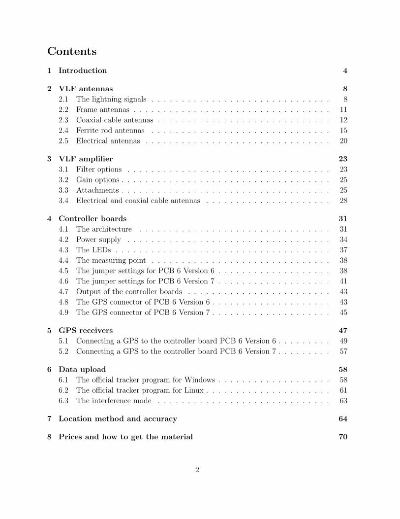
Contents
1 Introduction 4
2 VLF antennas 8
2.1 The lightning signals . . . . . . . . . . . . . . . . . . . . . . . . . . . . . . 8
2.2 Frame antennas . . . . . . . . . . . . . . . . . . . . . . . . . . . . . . . . . 11
2.3 Coaxial cable antennas . . . . . . . . . . . . . . . . . . . . . . . . . . . . . 12
2.4 Ferrite rod antennas . . . . . . . . . . . . . . . . . . . . . . . . . . . . . . 15
2.5 Electrical antennas . . . . . . . . . . . . . . . . . . . . . . . . . . . . . . . 20
3 VLF amplifier 23
3.1 Filter options . . . . . . . . . . . . . . . . . . . . . . . . . . . . . . . . . . 23
3.2 Gain options . . . . . . . . . . . . . . . . . . . . . . . . . . . . . . . . . . . 25
3.3 Attachments . . . . . . . . . . . . . . . . . . . . . . . . . . . . . . . . . . . 25
3.4 Electrical and coaxial cable antennas . . . . . . . . . . . . . . . . . . . . . 28
4 Controller boards 31
4.1 The architecture . . . . . . . . . . . . . . . . . . . . . . . . . . . . . . . . 31
4.2 Power supply . . . . . . . . . . . . . . . . . . . . . . . . . . . . . . . . . . 34
4.3 The LEDs . . . . . . . . . . . . . . . . . . . . . . . . . . . . . . . . . . . . 37
4.4 The measuring point . . . . . . . . . . . . . . . . . . . . . . . . . . . . . . 38
4.5 The jumper settings for PCB 6 Version 6 . . . . . . . . . . . . . . . . . . . 38
4.6 The jumper settings for PCB 6 Version 7 . . . . . . . . . . . . . . . . . . . 41
4.7 Output of the controller boards . . . . . . . . . . . . . . . . . . . . . . . . 43
4.8 The GPS connector of PCB 6 Version 6 . . . . . . . . . . . . . . . . . . . . 43
4.9 The GPS connector of PCB 6 Version 7 . . . . . . . . . . . . . . . . . . . . 45
5 GPS receivers 47
5.1 Connecting a GPS to the controller board PCB 6 Version 6 . . . . . . . . . 49
5.2 Connecting a GPS to the controller board PCB 6 Version 7 . . . . . . . . . 57
6 Data upload 58
6.1 The official tracker program for Windows . . . . . . . . . . . . . . . . . . . 58
6.2 The official tracker program for Linux . . . . . . . . . . . . . . . . . . . . . 61
6.3 The interference mode . . . . . . . . . . . . . . . . . . . . . . . . . . . . . 63
7 Location method and accuracy 64
8 Prices and how to get the material 70
2

9 Acknowledgement 74
3

1 Introduction
How lightning initially forms is still a matter of debate [BSL09]. Scientists have studied root
causes ranging from atmospheric perturbations (wind, humidity, friction, and atmospheric
pressure) to the impact of solar wind and accumulation of charged solar particles. Ice
inside a cloud is thought to be a key element in lightning development, and may cause a
forcible separation of positive and negative charges within the cloud, thus assisting in the
formation of lightning. It was not obvious, that lightning deals with electricity, since the
electric current does not flow through the air. This, on June 10th 1752, Benjamin Franklin
flies a kite during a thunderstorm and collects a charge in a Leyden jar when the kite is
struck by lightning, enabling him to demonstrate the electrical nature of lightning. He also
invented the lightning rod, used to protect buildings and ships.
0 °C
10 km
+20 °C
−30 °C
++ +++
+ +++ +
++
−−
−−
−−− − −
−
+
−−−−
−
+++
++
−+
−− −
++
−
+
Cloud to Ground Lightning
Cloud to Cloud
Electromagnetic
Lighning
Wave
Receiver
+ ++ ++ +
+ ++
−− − −
−+ −
−
++ −−
+−
++
1752Benjamin Franklin
Figure 1: How lightning forms
A lightning discharge emits radio frequency energy over a wide range of frequencies.
When high currents occur in previously ionized channels during cloud-to-ground flashes, the
most powerful emissions occur in the VLF range. VLF (very low frequency) refers to radio
frequencies in the range of 3 kHz to 30 kHz. An essential advantage of low frequencies
in contrast to higher frequencies is the property that these signals are propagated over
thousands of kilometers by reflections from the ionosphere and the ground. In general, a
lightning discharge generates several short duration pulses running between a storm cloud
and the ground, or between or within storm clouds. The current flow generates an electric
field parallel to the current flow, and a corresponding magnetic field perpendicular to the
electric field.
The lightning location network Blitzortung.org consists of several VLF lightning re-
4

Figure 2: Some lightning discharges in the atmosphere, c©Bernd Marz
ceiver sites and one central processing server for each larger region. The receiver sites
transmit their data in short time intervals over the Internet to our server. Every data sen-
tence contains the precise time of arrival of the received lightning strike impulse (”sferic”)
and the geographic position of the receiver site. With this information from all receiver
sites the exact positions of the discharges are computed. The sferic positions are made
available in raw format to all users that transmit their data to our server. The users can
use the raw data for all non-commercial purposes. The lightning activities of the last two
hours are displayed at Blitzortung.org on several public maps recomputed every minute.
Blitzortung.org is a community of receiver site operators who transmit their data to
a central server, programmers who develop and/or implement algorithms for the location or
visualization of sferic positions, and people who assist anyway to keep the system running.
There is no restriction on membership. There is no fee and no contract. All people who
keep the network in operation are volunteers. If a receiver site stops pooling its data, the
server stops providing the access to the archive of sferic positions for the corresponding
user.
The aim of the project is to accomplish a low budget lightning location network based
on a high number of receiver sites spaced close to each other, typically separated by 50 km -
250 km. The hardware you need to participate to the network consists of an antenna, Ferrite
or loop, a VLF amplifier, our controller board, a GPS receiver providing an 1PPS (one-
pulse-per-second) signal, and a personal computer permanently connected to the Internet.
You can get the PCBs, the A/D-converter, and the programmed micro-controller from
us. To participants not from Germany we sometimes also send complete kits as shown in
Figure 4 and 5. We do not send completely assembled kits. We do not have the time to
5

Figure 3: A lightning map of Europe from Blitzortung.org
assemble the kits for you. You either can assemble the kits by yourself or should look for
somebody who can assemble the kits for you.
Note that it is not possible to compute positions or at least accurate directions with
the data from one station. We need the data of several stations (at least four stations)
to compute strike positions. There is currently no software that enables you to set up
a connection with other sites like the LR software of Frank Kooimann for the direction
finding system. The computation of strike positions is currently only done by one of our
computing servers.
The next sections will explain how you can setup an own receiver for lightning dis-
charges.
6

Figure 4: The amplifier kits PCB 5 Version 6 and the controller board kit PCB 6 Version 6
Figure 5: The amplifier kits PCB 5 Version 7 and the controller board kit PCB 6 Version 7
7

2 VLF antennas
2.1 The lightning signals
Waves with a frequency between 3 kHz and 30 kHz have a length between 100 km and
10 km. A suitable antenna for these frequencies is a small loop antenna with size of
less than 1/10000 of the wavelength in circumference. Small loops are also called magnetic
loops, because they are more sensitive to the magnetic component of the electromagnetic
wave, and less sensitive to near electric field noises when properly shielded. If the loop is
small with respect to the wavelength, the current around the antenna is nearly completely
in phase. Therefore, waves approaching in the plane of the loop will cancel, and waves in
the axis perpendicular to the plane of the loop will be strongest. This property changes if
the loop becomes larger.
Figure 6: Two orthogonal crossed VLF loop antennas, 8 turns, diagonal size 1 m connected
to amplifier PCB 3 Version 2.
The electric field of the radio waves emitted by cloud-to-ground lightning discharges is
mainly oriented vertically, and thus the magnetic field is oriented horizontally. To cover
all directions (all-around 360 degree) it is advisable to use more than one loop. A suitable
solution can be obtained by two orthogonal crossed loops as they are used for a direction
finding system.
8

Figure 7: A spectrogram of the signal received by a 35 cm ferrite rod antenna. The
signal was recorded by a Creative Professional E-MU 0202 sound card with a sampling
frequency of 192 kHz. The spectrogram is made by Spectrum Lab. Vertical lines shows
radio transmissions for special purpose, and do not affect our reception.
The electromagnetic signals of lightning discharges are not waves of a fixed frequency.
The signals have more or less the form of an impulse and thus emits waves over a wide
range of frequencies. Every of these impulses is unique and looks different. To measure
the time of arrival of a lightning discharge, we need a wide-band receiving system, and not
a tuned system. The antenna should be large to get a high voltage caused by the change
of the electromagnetic field. If the loop consists of more than one winding, the wire placed
side by side forms a capacitance.
However, the unavoidable own resonance frequency of a loop should be as high as
possible such that we can easily suppress these frequencies by a low-pass filter. Please
avoid any additional tuning capacitor. Figure 8 shows to the left a signal received by
two equal sized untuned loops antennas. These loops have no additional tuning capacitor.
The resonance frequency of the antenna is approximately at 1000 kHz (= 1 MHz). The
used amplifier reduces frequencies of 1000 kHz by -72 dB (=4000 times). To the right
of Figure 7, Loop B is connected to a parallel tuning capacitor of 1 µF. Now, the tuned
9

frequency is the antenna is approximately 10 kHz. Since lightning impulses often contain
a lot of energy at 10 kHz, the tuned loop antenna only outputs unusable uniform waves
of 10 kHz. This shows that it is very important to use a pure loop without any parallel
capacitor.
Figure 8: To the left, a signal received by two loop antennas without tuning capacitors,
to the right, antenna B is tuned to approximately 10 kHz. This signal can not be used for
time measurement.
10

2.2 Frame antennas
It is easy to set up a frame antenna for VLF frequencies by yourself. Useful construction
manual can also be found at the Internet. Two example at
http://members.inode.at/576265/LightningRadarSystem.zip
written by Gerald Ihninger and
http://users.edpnet.be/DanielV37/Detecteur3/Antenna/Antenna.htm.
written by Daniel Verschueren. Both instruction manuals are made for the participants of
the lightning radar project http://www.lightningradar.net.
For a square frame antenna with a diagonal of 1 m and 8 turns of wire you need
• approximately 4 m of 20× 20 mm wooden coving,
• 2×25 m cable with a single conductor of area 1.5mm2 (this corresponds to a diameter
of 1.38 mm),
• 8 screw hooks,
• 3 screws/washer/wingnuts, and
• some cable ties.
The assembling takes about two hours. The price for the material is approximately 40 ein
a German home improvement store.
Figure 9: Assembling details for the frame antenna
A shielding of the E-field can significantly improve the signal to noise ratio, especially
in metropolitan areas. This can improve the detection rate of lightning discharges. As we
only want the magnetic part of the signal (H-field), any Electric field (E-field) is unwanted.
The shielding of a loop antenna can be realized for example by wires in a copper tube. It
is important that the tube is not closed. It can either be separated at the top or at the
bottom. If it is separated at the bottom, then only one end of the copper tube has to be
connected with the ground of the amplifier.
11

Figure 10: c©Daniel Verschueren
2.3 Coaxial cable antennas
A cheep loop antenna can easily be constructed using coaxial cable. You can use an
arbitrary impedance, but the 75 Ohm version are very cheap to get. With 20 Meter
coaxial cable you can form a loop with 3 turns and a diameter of 180 cm. The shield
has to be broken in the middle. Keep 20 cm cable for the connection at both ends. Such
a construction will create a loop with an induction of approximately 60 µH and a self-
resonance at 2 MHz.
12

Figure 11: A coax antenna, c©Richo Andersen
Cut off the plastic sheath, remove the wire grid,
put the separated plastic sheath back, and cover the area by a flexible hose.
c©Richo Andersen
Figure 12: Cutting the wire grid in the middle of the coaxial antenna
13

Figure 13: Connecting a coax antenna, c©Richo Andersen and Bernhard Kilimann
14

2.4 Ferrite rod antennas
The size of the antenna can extremely be reduced by using ferrite rods, but a ferrite rod
antenna needs a higher number of turns to get the same voltage compared with the larger
loop antenna. That is, a corresponding ferrite rod antenna has a lower resonance frequency
than the larger loop antenna. This is one reason why the loop antennas are more adequate
than small ferrite rod antennas. The resonance frequency of the ferrite rod antenna for
wide-band VLF reception should not fall below 100 kHz. Suitable ferrite rod antennas can
be obtained from http://www.sfericsempfang.de.
Figure 14: Two 20 cm ferrite rod antennas mounted on a PVC board connected to amplifier
PCB 5 Version 1, and two 20 cm ferrite shielded rod antennas mounted on a PVC board
connected to amplifier PCB 5 Version 6
Please do not twist the connection cable of the ferrite rod antennas. This creates a
capacity and leads to a lower self resonance.
It is not necessary to align the two antennas to north/south and west/east. The anten-
nas only have to be placed horizontally, because the magnetic field of radio waves emitted
by cloud-to-ground lightning discharges is mainly oriented horizontally. If you are using
ferrite rod antennas, you have to strip the insulation of the copper enameled wires, be-
fore the blank copper wires can be soldered to the amplifier board. The wires definitively
have to be soldered to the board. It is not possible to tighten such thin wires sufficiently
good with the screws of the terminal block. If you are using the ferrite rod antennas of
http://www.sfericsempfang.de, then one of the two copper enameled wire ends has a
knot. Connect these wires with the positive inputs of your amplifier and the other wire
with the negative input of the amplifier. If you are using PCB 5.1, PCB 5.2, or PCB 5.3
15

Figure 15: Shielding a ferrite rod antenna with ribbon cable
Figure 16: A 35 cm ferrite rod antenna in my hands and two 20 cm ferrite rod antennas
mounted on a PVC board connected to amplifier PCB 5 Version 7
the knots should be connected to pin 1 and 4. If you are using PCB 5.4 or PCB 5.5 the
knots should be connected to pin 1 and 3.
It is not easy to wind ferrite rod antennas by yourself. The quality of a ferrite rod
16

Figure 17: A quite location far away from VLF noises
antenna depends on the used material for the rods and on the type of the coil. A large range
of rods can be found at http://www.amidon.de. High quality rods can be obtained much
cheaper by http://www.sfericsempfang.de. Coil placement and the length of windings
on the rods, bars, plates and tubes affect the effective permeability of the antenna. Greatest
inductance will be obtained when the winding is centered on the rod rather than placed
at either end. The best ”Q” will be obtained when the winding covers the entire length
of the rod. The spacing between the turns has also a significant effect on the ”Q”. The
best values for the ”Q” are obtained when the coil turns are spaced one wire diameter
apart, with a winding covering the entire rod. This would not increase the inductance
to much. Note that we have to design a ferrite rod antenna with a high ”Q” but a low
inductance, such that we do not get low resonance frequencies with small capacities. We
do not recommend to wind ferrite rod antennas by yourself.
17

Figure 18: A 20 cm ferrite rod antenna with an inductance of 22.5 mH and a ”Q” of 125
and a 30 cm ferrite rod antenna with an inductance of 13.4 mH and a ”Q” of 156
18

Ferrite rod antennas can also be made waterproof, as the image presentations at Figure
19 and 20 show.
Figure 19: A guidance for building an outdoor ferrite rod antenna, c©Florian Bamberg
19
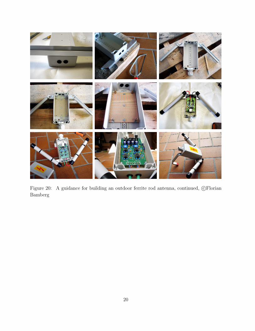
Figure 20: A guidance for building an outdoor ferrite rod antenna, continued, c©Florian
Bamberg
20

2.5 Electrical antennas
It is also possible to use an electrical antenna, i.e., an antenna sensitive to the electric
component of the electromagnetic wave. As already mentioned above, the electric field
of the radio waves emitted by cloud-to-ground lightning discharges is mainly oriented
vertically. That is, in the simplest case, the electrical antenna is a vertical wire directly
connected to one channel of the amplifier. Note that it is important that the wire is
directly connected to the input of the amplifier. If you use our amplifier PCB 5 Version 5,
connect it to the hot input at capacitors C7-A or C7-B, i.e., to the eye number 1 or 3 of the
terminal block, and connect the other two inputs to ground. Do not use coaxial connection
cables. This could generate a phase shift which leads to an inaccurate time measurement.
Figure 21 shows an example of a simple electrical antenna consisting of 1 meter cable. The
amplification of the second channel should be switched off. You can, for example, remove
the operational amplifiers.
Figure 21: A wire of 1 meter length used as an electrical antenna connected to amplifier
PCB 5 Version 1
The advantages of an electrical antenna are the following. 1.) Since it receives signals
from all horizontal directions, we need only one antenna instead of two antennas. 2.) The
21

Figure 22: A signal of a lightning discharge received by an electrical antenna (above) and
by a ferrite rod antenna (below)
received signals are very clean and free of any resonances frequencies. Figure 22 shows a
signal of a lightning discharge received by an electrical antenna (above) and received by a
ferrite rod antenna (below). However, the resonance frequencies of the ferrite rod antennas
can easily be eliminated by a digital post-processing, see figure 23. 3.) It is possible to
determine the polarity of the lightning discharge, if the lightning discharge was not to far
away. 4.) It is easy to construct for a very low price. However, an electrical antenna has
also some disadvantages. 1.) It is very sensitive to field electric noises. 2.) It has to be
placed outside or at least on an attic, and thus, conditions for lightning protection have to
be respected.
Figure 23: The original signal to the left and the Fourier transformed, filtered, and then
re-transformed signal to the right
When using an electrical antenna, the ground of the amplifier and thus also the ground
of the controller board should be connected to a large expanse of metal such as a safety
hand rail around a roof. Note that the ground of the boards should never be connected to
the ground wire of the electrical supply system. Usually some grounding is already given
if the serial 9-ways Sub-D plug is connected to the PC. A grounding is not necessary for
22

ferrite rod antennas.
When using an electrical antenna, it is reasonable to connect on of the inputs of the
VLF amplifier to ground and the other input to the antenna. It is also reasonable to
shortcut the input by a 1 MΩ resistor to avoid electrostatic charges. Both can by our
amplifier PCB 6 Version 7 with jumpers, see also Section 3.4.
Figure 24: The setting for using an electrical antenna
23
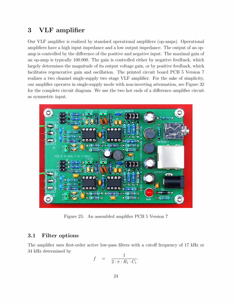
3 VLF amplifier
Our VLF amplifier is realized by standard operational amplifiers (op-amps). Operational
amplifiers have a high input impedance and a low output impedance. The output of an op-
amp is controlled by the difference of the positive and negative input. The maximal gain of
an op-amp is typically 100.000. The gain is controlled either by negative feedback, which
largely determines the magnitude of its output voltage gain, or by positive feedback, which
facilitates regenerative gain and oscillation. The printed circuit board PCB 5 Version 7
realizes a two channel single-supply two stage VLF amplifier. For the sake of simplicity,
our amplifier operates in single-supply mode with non-inverting attenuation, see Figure 32
for the complete circuit diagram. We use the two hot ends of a difference amplifier circuit
as symmetric input.
Figure 25: An assembled amplifier PCB 5 Version 7
3.1 Filter options
The amplifier uses first-order active low-pass filters with a cutoff frequency of 17 kHz or
34 kHz determined by
f =1
2 · π ·R1 · C1
.
24
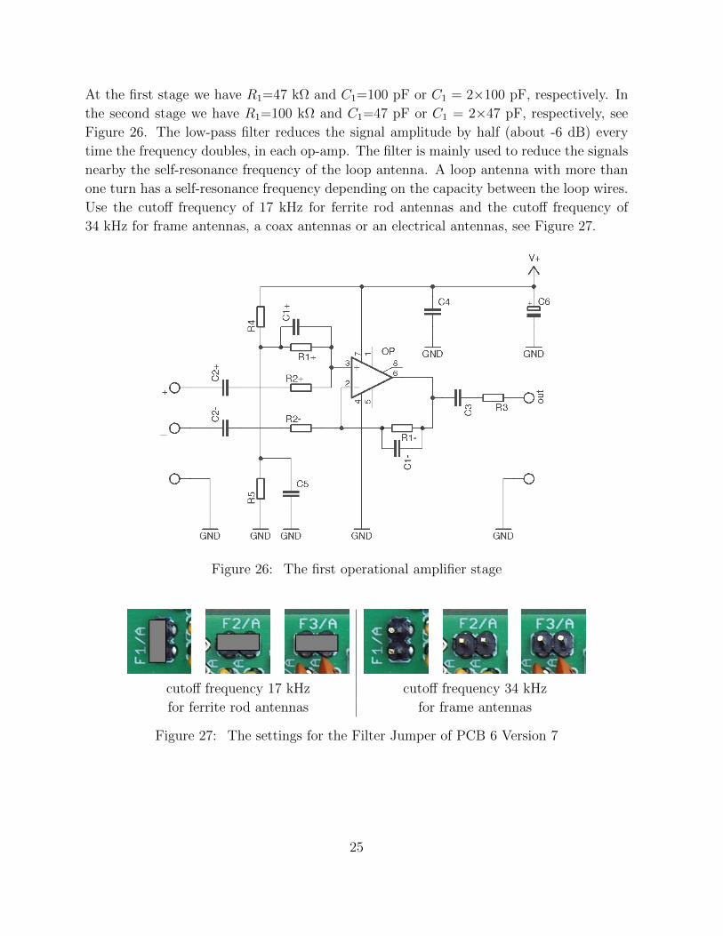
At the first stage we have R1=47 kΩ and C1=100 pF or C1 = 2×100 pF, respectively. In
the second stage we have R1=100 kΩ and C1=47 pF or C1 = 2×47 pF, respectively, see
Figure 26. The low-pass filter reduces the signal amplitude by half (about -6 dB) every
time the frequency doubles, in each op-amp. The filter is mainly used to reduce the signals
nearby the self-resonance frequency of the loop antenna. A loop antenna with more than
one turn has a self-resonance frequency depending on the capacity between the loop wires.
Use the cutoff frequency of 17 kHz for ferrite rod antennas and the cutoff frequency of
34 kHz for frame antennas, a coax antennas or an electrical antennas, see Figure 27.
Figure 26: The first operational amplifier stage
cutoff frequency 17 kHz cutoff frequency 34 kHz
for ferrite rod antennas for frame antennas
Figure 27: The settings for the Filter Jumper of PCB 6 Version 7
25

3.2 Gain options
The gain of the amplifier is determined by the voltage divider R1/R2 and can be computed
by 1 + R1
R2. The gain of the first stage is approximately 48. The gain of the second stage
can be set by the Gain-Jumpers. There are 15 possible combinations to connect the four
resistors R16, R17, R18, and R19 in parallel. However, the most interesting stages for
the gain are those shown in Figure 28. The gain increases every stage by a factor of
approximately 1.6.
gain 170 gain 111 gain 70
gain 43 gain 28 gain 18 gain 11
Figure 28: The settings for the Gain Jumpers of PCB 6 Version 7
3.3 Attachments
The DC jack can be used for power supply with positive polarization at the center. The
power of the amplifier can also be supplied by the controller board and vice versa. The
voltage should not fall under 6 Volt and should not exceed 15 Volt. The normal operation
is 12 Volt. The series resistance R1 to the power control LED can be adjusted to the
supplied voltage. For 12 Volt and a standard LED a series resistor between 330 and 4.7 K
is adequate. We prefer 1 K for R1. You can also use a switching power supply, if you place
it far away from the antennas.
The 3.5 mm jack socket can be used to connect a stereo headphone. This provides
an easy and affective way to detect interfering devices and thus to find the best place for
an undisturbed operation. Note that the headphone has to be unplugged during normal
operation.
26

Figure 29: The layout of the VLF amplifier PCB 5 Version 7
27
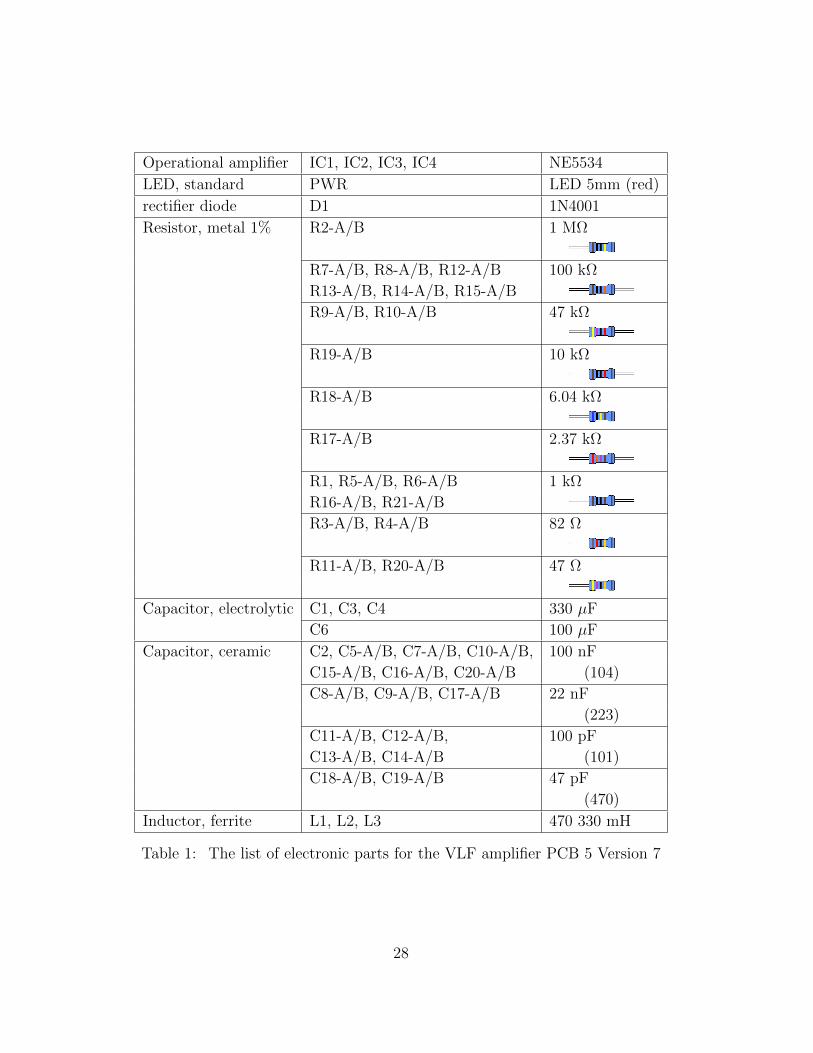
Operational amplifier IC1, IC2, IC3, IC4 NE5534
LED, standard PWR LED 5mm (red)
rectifier diode D1 1N4001
Resistor, metal 1% R2-A/B 1 MΩ
R7-A/B, R8-A/B, R12-A/B 100 kΩ
R13-A/B, R14-A/B, R15-A/B
R9-A/B, R10-A/B 47 kΩ
R19-A/B 10 kΩ
R18-A/B 6.04 kΩ
R17-A/B 2.37 kΩ
R1, R5-A/B, R6-A/B 1 kΩ
R16-A/B, R21-A/B
R3-A/B, R4-A/B 82 Ω
R11-A/B, R20-A/B 47 Ω
Capacitor, electrolytic C1, C3, C4 330 µF
C6 100 µF
Capacitor, ceramic C2, C5-A/B, C7-A/B, C10-A/B, 100 nF
C15-A/B, C16-A/B, C20-A/B (104)
C8-A/B, C9-A/B, C17-A/B 22 nF
(223)
C11-A/B, C12-A/B, 100 pF
C13-A/B, C14-A/B (101)
C18-A/B, C19-A/B 47 pF
(470)
Inductor, ferrite L1, L2, L3 470 330 mH
Table 1: The list of electronic parts for the VLF amplifier PCB 5 Version 7
28

We modify the amplifier circuit from time to time to improve its quality for our special
application and to reduce the price. If you want to use your own amplifier, please send us
first the circuit diagram. It is very important that you do not include delaying parts like
inductions in the signal ways. The part list of amplifier is PCB 5 Version 7 is shown in
Table 1, the PCB layout is shown in Figure 29, and the complete circuit diagram is shown
in Figure 32.
The output voltage of the amplifier should be between −2.5 Volt and +2.5 Volt. These
are the reference voltages of the analog digital converter at the controller board. In most
cases, the board is used under the following circumstance: 12 V power supply, two un-
shielded square loop antennas (diagonal size 1 m) with 8 turns (wire 1.5 mm2) connected
to the input, or two unshielded ferrite rod antennas. In this cases, you can set the Gain
Jumper to a gain of 70. If you still have to much interferences, you should reduce the
amplification to a gain of 43 or 28. A much more effective way to reduce interferences is a
shielding of your loop or ferrite rod antenna. If you use shielded antennas, then you can
increase the amplification to a gain of 111 or 170. If the resonance frequency of your home
made loop antenna is accidentally tuned at a long wave radio station you can use a parallel
resistor of approximately 20 kΩ.
3.4 Electrical and coaxial cable antennas
When using a coaxial cable antenna, you can add the 82 Ω terminating resistors by the
I-Jumper as shown in Figure 30 to the right. This can additionally reduce interferences
and make the signal more smooth.
open set negative input set both inputs
to ground with resistors to ground
Figure 30: The settings for the I-Jumpers of PCB 5 Version 7
29
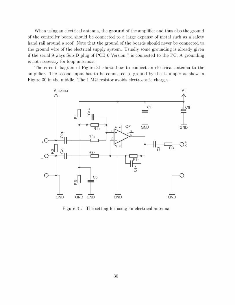
When using an electrical antenna, the ground of the amplifier and thus also the ground
of the controller board should be connected to a large expanse of metal such as a safety
hand rail around a roof. Note that the ground of the boards should never be connected to
the ground wire of the electrical supply system. Usually some grounding is already given
if the serial 9-ways Sub-D plug of PCB 6 Version 7 is connected to the PC. A grounding
is not necessary for loop antennas.
The circuit diagram of Figure 31 shows how to connect an electrical antenna to the
amplifier. The second input has to be connected to ground by the I-Jumper as show in
Figure 30 in the middle. The 1 MΩ resistor avoids electrostatic charges.
Figure 31: The setting for using an electrical antenna
30

Figure 32: The circuit diagram of the amplifier board PCB 5 Version 7
31

4 Controller boards
4.1 The architecture
The heart of the controller boards is an Atmel 8-bit AVR micro controller ATmega644
running with a clock frequency of 19.660800 MHz1. The boards also contain two separate
10-bit analog-to-digital converters AD7813 operating in high speed mode, i.e., not powered
down between conversions. In this mode of operation, the converters are capable to provide
a throughput of up to 400 ksps= 400.000 samples per second. A quad comparator LM339
activates the analog-to-digital conversion, if the input signal exceed a threshold of ±0.417
Volt. Unfortunately, the ATmega644 is not able to process and store the data as fast as
provided. Therefore, we use only 8-bit conversions with a throughput of approximately
350 ksps. This is quite sufficient for our purposes.
Figure 33: An assembled controller board PCB 6 Version 6
1The PCS 6 Version 6 board still has the labeling 20 MHz. We use 19.660800 MHz to reduce the
baud rate error at the serial interface. The board needs different Firmware versions for the different clock
frequencies.
32
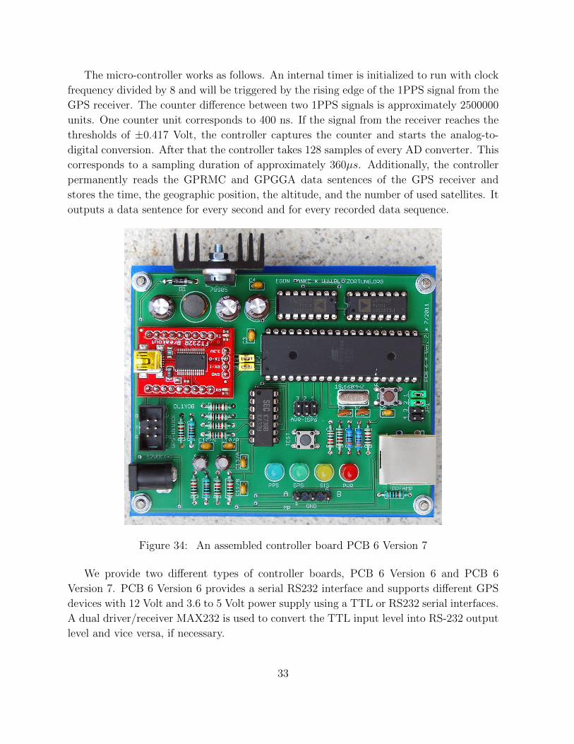
The micro-controller works as follows. An internal timer is initialized to run with clock
frequency divided by 8 and will be triggered by the rising edge of the 1PPS signal from the
GPS receiver. The counter difference between two 1PPS signals is approximately 2500000
units. One counter unit corresponds to 400 ns. If the signal from the receiver reaches the
thresholds of ±0.417 Volt, the controller captures the counter and starts the analog-to-
digital conversion. After that the controller takes 128 samples of every AD converter. This
corresponds to a sampling duration of approximately 360µs. Additionally, the controller
permanently reads the GPRMC and GPGGA data sentences of the GPS receiver and
stores the time, the geographic position, the altitude, and the number of used satellites. It
outputs a data sentence for every second and for every recorded data sequence.
Figure 34: An assembled controller board PCB 6 Version 7
We provide two different types of controller boards, PCB 6 Version 6 and PCB 6
Version 7. PCB 6 Version 6 provides a serial RS232 interface and supports different GPS
devices with 12 Volt and 3.6 to 5 Volt power supply using a TTL or RS232 serial interfaces.
A dual driver/receiver MAX232 is used to convert the TTL input level into RS-232 output
level and vice versa, if necessary.
33

PCB 6 Version 7 uses an USB to serial Breakout Board from http://www.sparcfun.
com with a FT232RL. It supports only GPS modules with 5 Volt power supply and a serial
TTL interface. The PCB 6 Version 7 board is designed to operate preferable with the EM-
406A GPS module. It has additionally a 6-pin header for an AVR in-system programmer
interface (ISP interface). This interface can be used to reprogram the controller.
Resistor, metal 1% R1, R3, R4, R6, R8, R9, 10 kΩ
R10, R11, R12, R13, R14
R5, R7 2 kΩ
R2 1 kΩ
R15, R16 330 Ω
Capacitor, electrolytic C1, C2 330 µF
radial, pitch 2.5 mm C5 100 µF
C9, C11, C14, C15, C16, C17 4.7 µF
Capacitor, ceramic, C3, C4, C6, C10 100 nF
pitch 2.5 mm C12, C13-A, C13-B (104)
C7, C8 15 pF
Inductor, ferrite L1 330 µH
rectifier diode D1, D2, D3, D4 1N4001
LED, standard PWR LED LED 5 mm (red)
SIG LED LED 5 mm (yellow)
GPS LED LED 5 mm (green)
PPS LED LED 5 mm (blue)
Quartz crystal Q1 19.660800 MHz
Voltage regulator IC1 µ78S05
Comparator IC2 LM339
Driver/receiver IC3 MAX232
Analog-to-digital converter IC4, IC5 AD7813
Micro controller IC6 ATmega644 20PU
Table 2: The electronic part list for the controller board PCB 6 Version 6
34

Resistor, metal 1% R2, R3, R4/N+P, R6, R7, 10 kΩ
R8/N+P, R9/N+P, R10
R5/N+P 2 kΩ
R1 1 kΩ
R11, R12 330 Ω
Capacitor, electrolytic C1, C2, C5 330 µF
C9/N+P 4.7 µF
Capacitor, ceramic, C3, C4, C6, C10/N+P 100 nF
pitch 2.5 mm C11/A+B (104)
C7, C8 15 pF
Inductor, ferrite L1 330 µH
rectifier diode D1 1N4001
LED, standard PWR LED LED 5 mm (red)
SIG LED LED 5 mm (yellow)
GPS LED LED 5 mm (green)
PPS LED LED 5 mm (blue)
Quartz crystal Q1 19.660800 MHz
Voltage regulator IC1 µ78S05
Comparator IC2 LM339
Analog-to-digital converter IC3, IC4 AD7813
USB-to-serial breakout board IC5 SparcFun BOB-00718
Micro controller IC6 ATmega644 20PU
Table 3: The electronic part list for the controller board PCB 6 Version 7
4.2 Power supply
The amplifier and the controller board can be connected by a 1-to-1 cat cable via the RJ45
jacks. We prefer a shielded Cat 5 cable. This connection also allows you to use the same
power supply for both boards.
The DC jack can be used for separate power supply with positive polarization at the
center. The voltage should not fall under 10 Volt and should not exceed 15 Volt. The
normal operation is 12 Volt.
35

Figure 35: The circuit diagram of the controller board PCB 6 Version 6
36

Figure 36: The circuit diagram of the controller board PCB 6 Version 7
37

4.3 The LEDs
Figure 37: The LEDs of the controller board
When power supply is connected to the board, then the following will happen.
• The (red) PWR LED will light and the other three LEDs will blink four times one
after the other. This just indicates that the controller is running.
• The (green) GPS LED starts blinking if the controller recognizes a GPRMC data
sentence from the GPS. If the (green) GPS LED remains off, then in most cases
the baud rate of the GPS differs from the baud rate of the controller. To find the
right baud rate, change the setting of the baud rate jumper (Jumper JP4 at PCB 6
Version 6 and Jumper JP1 at PCB 6 Version 7) and push the reset switch. If the GPS
device is on track, that is, if the GPRMC data sentence contains status “A”’ and
not status “V”, the green GPS LED will light permanently. This is usually already
the case when the GPS device receives at least one satellite. If the green GPS LED
remains blinking, you should move the GPS to a more adequate place on a window
or on a place with a view to the sky.
• The (blue) 1PPS LED will blink every time the GPS provides a 1PPS signal. This
will be every second. The (blue) 1PPS LED usually starts blinking immediately after
the green LED lights permanently.
• The (yellow) SIG LED will flash every time the controller outputs a data sentence
containing strike signal information.
The LED series resistors R2, R14, R15, and R16 for the Version 6 board and R1, R10,
R11, and R12 for the Version 7 board need to be adjusted corresponding to the illuminating
power of the used LEDs. For standard LEDs, the series resistor R2(R1) for the red LED
should be 1 kΩ, the series resistor R14(R10) for the blue LED should be 10 kΩ, and the
series resistors R15(R11) and R15(R12) for the yellow and green LED should be 330 Ω.
38

4.4 The measuring point
Figure 38: The Measuring Point MP1 of the controller boards Version 6 and Version 7
The measuring point MP1 provides at Pin 1 and Pin 5 the two signals from the amplifier.
Channel A at Pin 1 and Channel B at Pin 5. Pin 3 of MP1 is connected to the ground
of the board. These pins can be used to control the amplifier output with an oscilloscope
or other measuring instruments. You should not use instruments with low impedance,
because this could reduce the signal strength.
4.5 The jumper settings for PCB 6 Version 6
The jumpers at PCB 6 Version 6 have the following meanings.
1. Jumper JP1 performs several different tasks.
normal operation output of GPS to output of board
Figure 39: Setting for Jumper JP1 of PCB 6 Version 6
The first two columns of JP1 from the right numbered 1 and 2 are used to bypass
the serial connection to/from the controller. The setting shown in Figure 39 to the
left connects the output of the GPS device with the input of the controller and the
output of the controller with the output of the board. This is the normal operation.
The setting to the right separates the controller from the serial stream. It connects
the output of the GPS device with the output of the board. This setting allows you
to monitor the output of the GPS device at the serial interface of the board.
Columns 6 to 10 of JP1 are used to switch between TTL and RS232 level on the
serial interface of the board and the GPS device.
The remaining three columns of JP1 numbered 3 to 5 are used to select the positive
voltage at pin 1 of the GPS connector, if Jumper JP3 is set to pass this voltage to
39

Sub-D output RS232 Sub-D output TTL
Sub-D input = GPS in Sub-D input RS232 → GPS input TTL
GPS output TTL GPS output RS232
Figure 40: Setting for Jumper JP1 of PCB 6 Version 6
+2.9 Volt +5.0 Volt
+4.3 Volt +3.6 Volt
Figure 41: GPS voltage setting at Jumper JP1 of PCB 6 Version 6
Pin 1. The voltage can be set to +5 Volt or approximately +4,3 Volt, +3,6 Volt or
+2.9 Volt caused by a voltage drop of approximately 0.7 Volt by every of the three
40

diodes.
2. Jumper JP2 allows you to connect Pin 1 of the GPS connector with GND or +5/+4.3/
+3.6/+2.9 Volt depending on the setting of Jumper JP1, see Figure 42 to the left.
JP3 allows you to connect +12 Volt to Pin 9 of the serial 9-ways Sub-D connector,
see Figure 42 to the right. This allows you to power the PCBs via pin 9 of the serial
connector.
Set Pin 1 of the GPS connector to Set Pin 9 of the serial connector to
open + GND open +12Volt
Figure 42: The settings for Jumper JP2 and JP3 of PCB 6 Version 6
3. Jumper JP4 of PCB 6 Version 6 serves two functions. First, it allows you to change
the baud rate of the board between 4800, 9600, 19200, and 38400 baud, 8 bit, 1 stop
bit, no parity, see Figure 43, and second, it can be used to switch between different
output formats, see see Figure 44.
4800 baud 9600 baud 19200 baud 38400 baud
Figure 43: Setting of Jumper JP4 of PCB 6 Version 6
If this Jumper is set to ”both channels”, then the controller will output 64 values of
both channels. In the setting ”channel A” and ”channel B”, the controller will output
128 values of channel A or channel B, respectively. In the setting ”best channel”,
the controller will output 128 values of the channel that receives the strongest signal.
The decision will be made separately for each signal.
41

both channels channel A channel B best channel
Figure 44: Setting for Jumper JP4 of PCB 6 Version 6
4.6 The jumper settings for PCB 6 Version 7
Jumper JP1 of PCB 6 Version 7 serves the same two functions as PCB 5 Version 7. First,
it allows you to change the baud rate of the board between 4800, 9600, 19200, and 38400
baud, 8 bit, 1 stop bit, no parity, see Figure 45, and second, it can be used to switch
between different output formats, see see Figure 46.
4800 baud 9600 baud 19200 baud 38400 baud
Figure 45: Setting of Jumper JP1 of PCB 6 Version 7
If this Jumper is set to ”both channels”, then the controller will output 64 values of
both channels. In the setting ”channel A” and ”channel B”, the controller will output 128
values of channel A or channel B, respectively. In the setting ”best channel”, the controller
will output 128 values of the channel that receives the strongest signal. The decision will
be made separately for each signal.
42

both channels channel A channel B best channel
Figure 46: Setting for Jumper JP1 of PCB 6 Version 7
Jumper JP2 can be used to bypass the serial connection to/from the controller. The
setting shown in Figure 47 to the left connects the output of the GPS device with the input
of the controller and the output of the controller with the output of the board. This is the
normal operation. The setting to the right separates the controller from the serial stream.
It connects the output of the GPS device with the output of the board. This setting allows
you to monitor the output of the GPS device at the serial interface of the board2.
normal operation output of GPS to output of board
Figure 47: Setting for Jumper JP2 of PCB 6 Version 7
dual output, both channels mono output, best channel
Figure 48: The different outputs
2Unfortunately, the USB controller board 6 Version 7 has a layout error which do not allow to reroute
the output of the GPS device to the output of the board by turning the yellow jumpers. This is corrected
in Version 7b.
43
4.7 Output of the controller boards
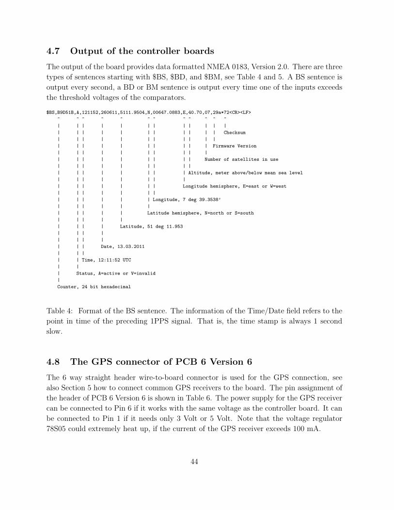
The output of the board provides data formatted NMEA 0183, Version 2.0. There are three
types of sentences starting with $BS, $BD, and $BM, see Table 4 and 5. A BS sentence is
output every second, a BD or BM sentence is output every time one of the inputs exceeds
the threshold voltages of the comparators.
$BS,B9D51B,A,121152,260611,5111.9504,N,00647.0883,E,40.70,07,29a*72<CR><LF>
^ ^ ^ ^ ^ ^ ^ ^ ^ ^ ^ ^
| | | | | | | | | | | |
| | | | | | | | | | | Checksum
| | | | | | | | | | |
| | | | | | | | | | Firmware Version
| | | | | | | | | |
| | | | | | | | | Number of satellites in use
| | | | | | | | |
| | | | | | | | Altitude, meter above/below mean sea level
| | | | | | | |
| | | | | | | Longitude hemisphere, E=east or W=west
| | | | | | |
| | | | | | Longitude, 7 deg 39.3538’
| | | | | |
| | | | | Latitude hemisphere, N=north or S=south
| | | | |
| | | | Latitude, 51 deg 11.953
| | | |
| | | |
| | | Date, 13.03.2011
| | |
| | Time, 12:11:52 UTC
| |
| Status, A=active or V=invalid
|
Counter, 24 bit hexadecimal
Table 4: Format of the BS sentence. The information of the Time/Date field refers to the
point in time of the preceding 1PPS signal. That is, the time stamp is always 1 second
slow.
4.8 The GPS connector of PCB 6 Version 6
The 6 way straight header wire-to-board connector is used for the GPS connection, see
also Section 5 how to connect common GPS receivers to the board. The pin assignment of
the header of PCB 6 Version 6 is shown in Table 6. The power supply for the GPS receiver
can be connected to Pin 6 if it works with the same voltage as the controller board. It can
be connected to Pin 1 if it needs only 3 Volt or 5 Volt. Note that the voltage regulator
78S05 could extremely heat up, if the current of the GPS receiver exceeds 100 mA.
44
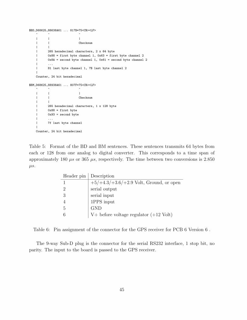
$BD,D68625,88638A61 ... 817B*75<CR><LF>
^ ^ ^
| | |
| | Checksum
| |
| 265 hexadecimal characters, 2 x 64 byte
| 0x88 = first byte channel 1, 0x63 = first byte channel 2
| 0x8A = second byte channel 1, 0x61 = second byte channel 2
| ...
| 81 last byte channel 1, 7B last byte channel 2
|
Counter, 24 bit hexadecimal
$BM,D68625,88938A61 ... 807F*75<CR><LF>
^ ^ ^
| | |
| | Checksum
| |
| 265 hexadecimal characters, 1 x 128 byte
| 0x88 = first byte
| 0x93 = second byte
| ...
| 7f last byte channel
|
Counter, 24 bit hexadecimal
Table 5: Format of the BD and BM sentences. These sentences transmits 64 bytes from
each or 128 from one analog to digital converter. This corresponds to a time span of
approximately 180 µs or 365 µs, respectively. The time between two conversions is 2.850
µs.
Header pin Description
1 +5/+4.3/+3.6/+2.9 Volt, Ground, or open
2 serial output
3 serial input
4 1PPS input
5 GND
6 V+ before voltage regulator (+12 Volt)
Table 6: Pin assignment of the connector for the GPS receiver for PCB 6 Version 6 .
The 9-way Sub-D plug is the connector for the serial RS232 interface, 1 stop bit, no
parity. The input to the board is passed to the GPS receiver.
45

4.9 The GPS connector of PCB 6 Version 7
The pin assignment of the header of PCB 6 Version 7 is shown in Table 7.
Header pin Description
1 ground
2 +5 Volt
3 serial output TTL
4 serial input TTL
5 ground
6 1PPS input
Table 7: Pin assignment of the connector for the GPS receiver for PCB 6 Version 7
46

Figure 49: The layout of the controller board PCB 6 Version 6
Figure 50: The layout of the controller board PCB 6 Version 7b
47

5 GPS receivers
The GPS devices we need for our lightning location system have to provide a one-pulse-
per-second (1PPS) signal with an accuracy of at least ±1µs, and a serial interface using
either RS232 or TTL level. The communication between the GPS device and the controller
board is carried out with 4800, 9200, 19200, or 38400 baud, 1 stop bit, and no parity. The
controller board reads the GPRMC and GPGGA sentences from the GPS device. These
sentences refer to the immediately preceding 1PPS output and look like shown in Table 8
and 9.
$GPRMC,191410,A,4735.5634,N,00739.3538,E,0.0,0.0,181102,0.4,E,A*19
^ ^ ^ ^ ^ ^ ^ ^ ^ ^ ^ ^ ^
| | | | | | | | | | | | |
| | | | | | | | | | | | Checksum
| | | | | | | | | | | |
| | | | | | | | | | | Mode
| | | | | | | | | | |
| | | | | | | | | | Hemisphere
| | | | | | | | | |
| | | | | | | | | Magnetic Variation
| | | | | | | | |
| | | | | | | | Date, 18.11.2002
| | | | | | | |
| | | | | | | Track angle in degrees True
| | | | | | |
| | | | | | Speed over the ground in knots
| | | | | |
| | | | | Longitude hemisphere, E or W
| | | | |
| | | | Longitude, 7 deg 39.3538’
| | | |
| | | Latitude hemisphere, N or S
| | |
| | Latitude, 47 deg 35.5634’
| |
| Status, A=active or V=invalid
|
Time, 19:14:10 UTC
Table 8: The GPRMC data sentence
During the last decade, there were several low cost stand-alone GPS devices available
providing a 1PPS signal, but unfortunately most of them are no longer produced by the
manufacturers. The GPS devices today are mainly integrated as auxiliary modules in
navigation systems, cellular phones, and other equipments. However, some of the good old
GPS mouses can sometimes be bought low priced at online auctions.
The GPS devices we have tested so far are the Garmin 35-HVS, the Garmin 16-HVS, the
Garmin 35-LVS, the AQTIME VP-200T, the Fortuna U2/PS2, and the EM-406A module.
If you do not already have one of these GPS devices but have to obtain one, then we advise
48

$GPGGA,191410,4735.5634,N,00739.3538,E,1,08,0.9,545.4,M,46.9,M,0,0*47
^ ^ ^ ^ ^ ^ ^ ^ ^ ^ ^ ^ ^ ^ ^
| | | | | | | | | | | | | | |
| | | | | | | | | | | | | | Checksum
| | | | | | | | | | | | | |
| | | | | | | | | | | | | DGPS station ID number
| | | | | | | | | | | | |
| | | | | | | | | | | | time in seconds since
| | | | | | | | | | | | last DGPS update
| | | | | | | | | | | |
| | | | | | | | | | | Meters
| | | | | | | | | | |
| | | | | | | | | | Height of geoid (mean sea
| | | | | | | | | | level) above WGS84 ellipsoid
| | | | | | | | | |
| | | | | | | | | Meters
| | | | | | | | |
| | | | | | | | Altitude, above mean sea level
| | | | | | | |
| | | | | | | Horizontal dilution
| | | | | | |
| | | | | | Number of satellites
| | | | | |
| | | | | Quality
| | | | |
| | | | Longitude hemisphere, E or W
| | | |
| | | Longitude, 7 deg 39.3538’
| | |
| | Latitude hemisphere, N or S
| |
| Latitude, 47 deg 35.5634’
|
Time, 19:14:10 UTC
Table 9: The GPGGA data sentence
to choose the EM-406A GPS module, because of the following reasons.
1. The EM-406A engine module is still in production and thus can be obtained from
several distributors.
2. The price for a new EM-406A engine module is on average less than 40 e.
3. It has an up-to-date sensitive SiRF Start III chipset and works also inside at a
window.
4. It has a serial TTL interface, which makes the RS232 to TTL conversion unnecessary.
This is very comfortable, especially when using the Version 7 USB controller board.
This board do not have any RS232 to TTL conversion.
49

Garmin 16 HVS AQTIME VP-200T Fortuna U2 PS2
Garmin 37 HVS/LVS EM-406A
Figure 51: Some GPS devices/modules providing a 1PPS signal
5.1 Connecting a GPS to the controller board PCB 6 Version 6
The Garmin 35-HVS and Garmin 16-HVS are designed to withstand rugged operating
conditions and are completely water resistant. They operate from a 6 Volt to 40 Volt
unregulated supply. These GPS devices can easily be supplied by the 12 Volt power of the
controller board. They include a receiver and antenna in the same housing with one cable
for the power supply and communications. The GPS antenna must have a clear view of
the sky. Generally these GPS antennas will not work indoors. They come with 5 meters of
cable ending either stripped and pre-tinned assembled for a flexible connection or with an
RJ45 connector attached to the cable end. Figure 52 shows how the wires of the Garmin
16/35 HVS have to be connected to the pins of the straight header at the controller board.
Jumper JP1 of PCB 6 Version 6 has to be set such that the RS232 serial input of
the controller board is routed to the RS232 input of the Garmin 16/35 HVS, the RS232
output of the Garmin 16/35 HVS is routed to the TTL input of the Controller, and the
TTL output of the controller is routed to the RS232 output of the controller board, see
Figure 52. Jumper JP2 has to be set such that the power on/off switch of the Garmin
16/35 HVS is connected to ground. The baud rate can be set to 19200 baud by Jumper
JP4. This is the maximum speed for these old Garmin GPS devices. The Garmin 17-HVS,
50

Color Description Header of PCB 6 Ver. 6
yellow power on/off switch 1
white serial input RS232 2
blue serial output RS232 3
grey 1PPS output 4
black power ground 5
red +12 Volt 6
Figure 52: A Garmin 16/35 HVS connected to the controller board PCB 6 Version 6 with
a transfer rate of 19200 baud
one of the more recent models, also accepts 38400 baud. The 1PPS signal is not output
by default. This feature has first to be set up by an initialization. Our tracker program
initializes the GPS device by sending the following strings.
$PGRMO,GPGGA,1*20
$PGRMO,GPGSA,0*35
$PGRMO,GPGSV,0*22
$PGRMO,GPRMC,1*3D
$PGRMO,GPVTG,0*25
$PGRMO,PGRMM,0*32
$PGRMO,PGRMT,0*2B
$PGRMO,PGRME,0*3A
$PGRMO,PGRMB,0*3D
$PGRMCE*0E
$PGRMC,,,,,,,,,,5,,2,4,*00
Table 10: Initialization strings for Garmin GPS devices
This initialization turns off the data sentences GPGSA, GPGSV, GPVTG, GPRMM,
GPRMT,GPRME, and PGRMB, turns on the GPRMC and GPGGA sentences for an
output by every second, set the baud rate to 19200 baud, and activates the 1PPS output
51
with a duration of 100 ms. The new baud rate and the 1PPS mode changes take effect
on the next power on cycle. That is, you have to power off and again power on the GPS
device. By default, the baud rate is set to 4800 baud.
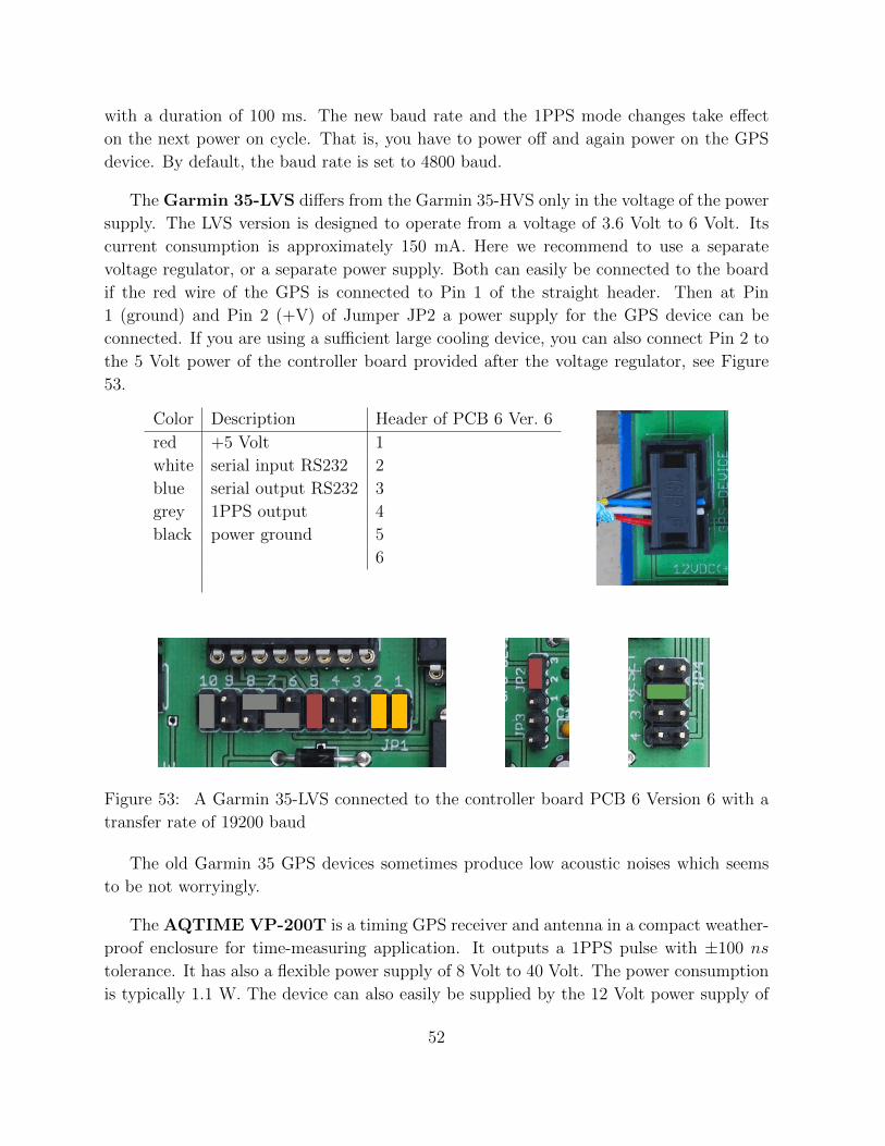
The Garmin 35-LVS differs from the Garmin 35-HVS only in the voltage of the power
supply. The LVS version is designed to operate from a voltage of 3.6 Volt to 6 Volt. Its
current consumption is approximately 150 mA. Here we recommend to use a separate
voltage regulator, or a separate power supply. Both can easily be connected to the board
if the red wire of the GPS is connected to Pin 1 of the straight header. Then at Pin
1 (ground) and Pin 2 (+V) of Jumper JP2 a power supply for the GPS device can be
connected. If you are using a sufficient large cooling device, you can also connect Pin 2 to
the 5 Volt power of the controller board provided after the voltage regulator, see Figure
53.
Color Description Header of PCB 6 Ver. 6
red +5 Volt 1
white serial input RS232 2
blue serial output RS232 3
grey 1PPS output 4
black power ground 5
6
Figure 53: A Garmin 35-LVS connected to the controller board PCB 6 Version 6 with a
transfer rate of 19200 baud
The old Garmin 35 GPS devices sometimes produce low acoustic noises which seems
to be not worryingly.
The AQTIME VP-200T is a timing GPS receiver and antenna in a compact weather-
proof enclosure for time-measuring application. It outputs a 1PPS pulse with ±100 ns
tolerance. It has also a flexible power supply of 8 Volt to 40 Volt. The power consumption
is typically 1.1 W. The device can also easily be supplied by the 12 Volt power supply of
52

the controller board. It comes with 5 meters of cable ending with a 9-ways Sub-D plug for
the serial interface, a DC plug for power supply, and a phono plug for the 1PPS signal.
The wires we need for the connection to the controller board have the following colors (if
the plugs are cut off) and can be connected to the pins of the straight header as shown in
Figure 54.
Color Description Header of PCB 6 Ver. 6
green serial input RS232 2
white serial output RS232 3
blue 1PPS output 4
black power ground 5
red +12 Volt 6
Figure 54: An AQTIME VP-200T connected to the controller board PCB 6 Version 6
with a transfer rate of 4800 baud
The AQTIME VP-200T provides the 1PPS signal with a duration of 100 ms by default.
The initialization by the tracker program switches off the data sentences GPGLL, GPGSA,
GPGSV, GPDTM, and PGZDA. The data sentences GPRMC and GPGGA are switched
on for an output of every second. Unfortunately, the AQTIME VP-200T only supports a
data transfer rate of 4800 baud.
$PFEC,GPint,GGA01,GLL00,GSA00,GSV00,RMC01,DTM00,VTG00,ZDA00*52
Table 11: Initialization strings for San Jose Navigation GPS devices
The Fortuna U2-PS/2 is a small GPS mouse using a SiRF-II chip-set. The body is
not completely water resistant, and thus not adequate for outdoor mounting. It comes with
2 meters of cable ending in a female 6-ways Mini-DIN plug. Although the GPS module
provides the 1PPS output with a duration of 100 ms, the signal is not connected to the
cable. This can be changed by a simple modification. Note that there are several versions
53

of the Fortuna U2. Some of them provide an USB interface (Fortuna U2-USB). These
receivers can not be used in connection with the controller board. Newer versions use a
SiRF-III chip-set but do not have a free wire which we can use to lead through the 1PPS
signal. We do not know whether the SiRF-III module used by the latest versions of the
Fortuna U2-PS/2 also provides the 1PPS output. If somebody has find out this, please
give us some feed back such that we can include this information here.
yellow wire
original position ofyellow wire
new position of
Figure 55: The modification of the old Fortuna U2/PS2 with the SiRF II module
To modify the Fortuna U2, we have to open die housing by taking out the two screws on
the backside. Then we can remove the cap and will find a soldered copper box, see Figure
55 to the left. The cap contains two slices that makes the base of the device magnetic, see
Figure 55 to the right. These two slices usually fall down when opening the housing. If
we open the copper box we will find the GPS module. We have to move the yellow wire
from Pin 2 to Pin 9, see Figure 55 in the middle. After that we can solder up the copper
box. An easy way to mount the cap with the two magnetic slices is the following. Attach
the cap on a metal board by the magnetic slices from inside. Then insert the module and
push the housing to the cap. After the modification the 6-way female Mini-DIN plug has
the pin assignment as shown at the top of Figure 56. Note that the information about the
pin assignment at the folder enclosed into the original package of the Fortuna U2 is wrong!
The initialization by the tracker program switches off the data sentences GPGLL,
GPGSA, GPGSV, GPMSS, GPDTM, and PGZDA. The data sentence GPRMC and
54

Color Description Mini-DIN Header of PCB 6 Ver. 6
orange serial input RS232 4 2
brown serial output RS232 2 3
yellow 1PPS output 1 4
black ground 3 5
red +5 Volt 6 1
Figure 56: The 6-ways female Mini-DIN connector from the front and its connection to
the header of PCB 6 Version 6
Figure 57: The Fortuna U2/PS2 connected to the controller board PCB 6 Version 6 with
a transfer rate of 4800 baud
GPGGA will be switched on for an output by every second. The communication speed of
the serial interface is 4800 baud by default, but the initialization can switch the commu-
nication speed up to 38400 baud.
$PSRF103,00,00,01,01*25
$PSRF103,01,00,00,01*25
$PSRF103,02,00,00,01*26
$PSRF103,03,00,00,01*27
$PSRF103,04,00,01,01*21
$PSRF103,05,00,00,01*21
$PSRF103,06,00,00,01*22
$PSRF103,08,00,00,01*2C
$PSRF100,1,38400,8,1,0*3D
Table 12: Initialization strings for SiRF GPS devices
The device operates with a voltage of 5 Volt, the current consumption is approximately
90 mA. If the temperature of the voltage regulator exceeds 40 degree, it should be mounted
on a larger cooling device. The GPS device can alternatively be supplied by a separate
voltage regulator or power supply, respectively, similar to the Garmin 35 LVS.
55

For connecting the GPS device with the controller board, you can either cut of the
Mini-DIN connector from the cable and connect the wires directly to the jack, or, if you
do not like this destructive solution, you can use an extension cable. Unfortunately, many
of these GPS mouses are some years old such that the internal backup battery is empty.
In these cases, the initialization, the selection of the data sentences and the baud rate of
19200, falls down to the default baud rate of of 4800 baud, whenever the power supply will
be interrupted.
The EM-406A is a GPS module using a SiRF-III chip-set. The sensitivity of this
device is very high (-159dBm). It can also be used at window side. Since the module has
no housing, it should be protected. Figure 58 shows two examples for an integration of
the module into the housings of other GPS devices. Note that the EM-406A module is not
the module inside the Navilock NL-303P. We have exchanged the original module with an
EM-406A module.
Figure 58: An EM-406A module embedded into the housing of a Fortuna U2/PS2, to the
left, and embedded into a housing of a Navilock NL-303P, to the right
Following the manufacturers’ specifications, it operates with a voltage of 4.5 Volt to 6.5
Volt and consumes approximately 44 mA, but the module also works fine with 3.6 Volt.
The module provides a very short 1PPS output with a duration of 1µs. The initialization
is the same as for the Fortuna U2 using the SiRF-II chip-set. A backup battery keeps all
the settings during a power down. The module also contains a LED indicator for GPS fix
or not fix. The default baud rate is 4800 baud. There is one main difference between the
EM-406A and all other GPS devices discussed in this section. The serial connection uses
TTL signal level (0V/2.85V) and not RS-232 signal level (+3V/-3V). In this case, we have
to change the jumper setting for the TTL/RS232 jumper as shown in Figure 60.
The EM-406A module comes with a 6-pin interface cable that can be used to connect a
longer connection cable. For our embedding of the EM-406A to the housing of a Navilock
NL-303P, the black wire connected to Pin 1 at the module connector was changed to Pin
6. The ground signal is then still available via pin 5 of the module connector.
56

Pin ← EM-406A module Header of PCB 6 Ver. 6 → Pin
1 ground 5
2 +5 Volt
4321
front
123456
6
top
5
1
3 serial input TTL 3
4 serial output TTL 2
5 ground
6 1PPS output 4
Figure 59: Pin assignment of the EM-406A module and its connection to the header of
PCB 6 Version 6
Figure 60: An EM-406A module connected to the controller board PCB 6 Version 6 using
5 Volt power supply and a transfer rate of 38400 baud
There are several further GPS devices that can be connected to the PCB 6 Version 6
board. For example, the Garmin 17-HVS can be handled in the same way as the Garmin
16-HVS. The RoyalTek RGM-2000 can be modified similar like the Fortuna U2.
Figure 61: An EM-406A module embedded in a plastic housing
57

5.2 Connecting a GPS to the controller board PCB 6 Version 7
The controller board PCB 6 Version 7 has no RS232 to TTL conversion ship. You can
only connect GPS modules with a serial TTL interface. The board is designed to work
preferably with the EM-406A GPS module. The pin assignment of the header is the same
as the pin assignment of the module, see Figure 62. Figure 63 shows a completely connected
controller board PCB 6 Version 7. Jumper JP2 defines a transfer rate of 38400 baud.
Pin ← EM-406A module Header of PCB 6 Ver. 7 → Pin
1 ground 1
2 +5 Volt
4321
front
123456
6
top
5
2
3 serial input TTL 3
4 serial output TTL 4
5 ground 5
6 1PPS output 6
Figure 62: Pin assignment of the EM-406A module and its connection to the header of
PCB 6 Version 7
Figure 63: A completely connected controller board PCB 6 Version 7
58

6 Data upload
The data upload is carried out by a tracker program. It reads and processes the data of
the controller board and sends the resulting lightning data to our computing server. We
provide two types of tracker programs, one for computers running a Linux operating system
and one for computers running a Windows operating system. The official tracker program
for Linux is written by Egon Wanke. We only provide the C++ source code of the Linux
tracker program. You have to compile the source code using any C++ compiler for your
Linux system. The official tracker program for Windows is written by Edmund Korffmann.
It consists of only one small executable file. You can download both tracker programs from
the ”Miscellaneous” page of the ”Services” menu of Blitzortung.org. However, you can
also use the other tracker programs written by some of the participants. Please do not
write and use own written tracker programs without to get in contact with us.
6.1 The official tracker program for Windows
In this section, we briefly explain how to work with the tracker program for Windows.
The current Version (at the time this text has been written) is ”WT 5.02”. The program
consists of one small (less than 250 K) executable file named ”serial tracker”. You
can store the tracker program in any directory, also on your desktop. It should run at
all Windows systems. If you are running an extraordinary Windows system, please get in
contact with us. The tracker program stores the used settings in a configuration file called
”Tracker.prefs” placed in the same directory.
First, connect the GPS device to the controller board and the controller board to your
computer. Disconnect the amplifier. We recommend to set the jumper of the controller
board to 38400 baud or at least 19200 baud, depending on the maximal speed your GPS
device supports. Then power on the controller board and start the tracker program. Select
the serial device, the baud rate, and the GPS type, as shown in Figure 64, and initialize the
GPS device. If you are using a Garmin GPS device then the initialization is not carried out
until the next power on. In this case, you have to disconnected and then again to connect
the power supply. Now the green LED should start blinking, and after a while it should
continuously light. If the green LED blinks, the controller board receives GPRMC sentences
with status ’V’ (= invalid), if it lights permanently, it receives GPRMC sentences with status
’A’ (= active). If the green LED is off, either the baud rate of the GPS does not match
the baud rate of the controller board, or something else fails. In this case, you can use
the port monitor to control the serial connection with the controller board, see Figure 66.
If you push the reset button of the controller board, then the micro-controller outputs its
firmware version. If the firmware version text string is not listed at the port monitor, then
the baud rate of the controller board does not match the baud rate selected at you PC for
59

the serial device. You can turn the yellow jumpers at the controller board by 90 degrees
to see the output of the GPS device at the port monitor3. If the green LED is blinking
and does not turn into a permanent light, then move the GPS device outside, or at least
to a window side.
Figure 64: The initialization of the serial connection and the GPS device
Next you should insert your username and password. The username is the one you got
from blitzortung.org. The password is the one you have chosen by yourself. The tracker
program will not accept the password you initially got from Blitzortung.org. You have
to select a new own password.
Activating the ”Auto” flag will cause the tracker to start up automatically after the PC
will restart. If the ”Minimize” flag is set the tracker program window will disappear from
3Unfortunately, the USB controller board 6 Version 7 has a layout error which do not allow to reroute
the output of the GPS device to the output of the board by turning the yellow jumpers. This is corrected
in Version 7b.
60

Figure 65: Inserting the password and user name
Figure 66: The port monitor
the desktop and move to you tool bar. The ”Logfile” flag activates log file output, and
the ”Adj. System Time” option allows to synchronize the local clock by the GPS time.
The ”Region” menu is used to distinguish between different computing servers for different
continents. At the time this document is written, there is only one region, Region 1, for
Europe. Different setting for the History window can also be chosen, see Figure 67.
61

Figure 67: Different settings for the history window
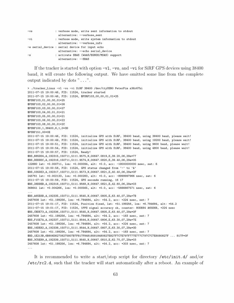
6.2 The official tracker program for Linux
The source code of the tracker program for Linux can be downloaded from the ”Miscel-
laneous” page of the ”Services” menu of Blitzortung.org. The file tracker_Linux.c
should be compiled by g++ -Wall -lm -o tracker_Linux tracker_Linux.c to the ex-
ecutable tracker_Linux. A short description of all options can be listed by starting the
tracker program with option ”-h”, see the following screen dump.
> g++ -Wall -lm -o tracker_Linux tracker_Linux.c
> ./tracker_Linux -h
./tracker_Linux: [-h] [-L] [-ll file] [-lo file] [-ls file] [-vl] [-vo] [-vs] [-vi] [-e serial_device] [-s]
gps_type baud_rate serial_device username password
gps_type : gps type (SANAV, Garmin, or SiRF (’-’ for no initialization))
baud_rate : baud rate (4800, 9600, 19200, or 38400)
serial_device : serial device (example: /dev/ttyS0)
username : username (example: PeterPim)
password : password (example: s36r67hi)
-h : print this help text
alternative: --help
-L : write log messages to the system message logger
altervative: --syslog
-ll file : write log messages to file
alternative: --log_log file
-lo file : write board output to file
alternative: --log_output file
-ls file : write sent information to file
alternative: --log_sent file
-vl : verbose mode, write log messages to stdout
alternative: --verbose_log
-vo : verbose mode, write board output to stdout
alternative: --verbose_output
62
-vs : verbose mode, write sent information to stdout
alternative: --verbose_sent
-vi : verbose mode, write system information to stdout
alternative: --verbose_info
-e serial_device : serial device for input echo
alternative: --echo serial_device
-s : activate SBAS (WAAS/EGNOS/MSAS) support
alternative: --SBAS
If the tracker is started with option -vl, -vo, and -vi for SiRF GPS devices using 38400
baud, it will create the following output. We have omitted some line from the complete
output indicated by dots ”...”.
> ./tracker_Linux -vl -vo -vi SiRF 38400 /dev/ttyUSB0 PeterPim s36r67hi
2011-07-15 19:00:46, PID: 11524, tracker started
2011-07-15 19:00:46, PID: 11524, $PSRF103,00,00,01,01*25
$PSRF103,01,00,00,01*25
$PSRF103,02,00,00,01*26
$PSRF103,03,00,00,01*27
$PSRF103,04,00,01,01*21
$PSRF103,05,00,00,01*21
$PSRF103,06,00,00,01*22
$PSRF103,08,00,00,01*2C
$PSRF100,1,38400,8,1,0*3D
$PSRF151,00*0E
2011-07-15 19:00:46, PID: 11524, initialize GPS with SiRF, 38400 baud, using 38400 baud, please wait!
2011-07-15 19:00:49, PID: 11524, initialize GPS with SiRF, 38400 baud, using 19200 baud, please wait!
2011-07-15 19:00:51, PID: 11524, initialize GPS with SiRF, 38400 baud, using 9600 baud, please wait!
2011-07-15 19:00:54, PID: 11524, initialize GPS with SiRF, 38400 baud, using 4800 baud, please wait!
2011-07-15 19:00:57, PID: 11524, Ready!
$BS,B85DD4,A,192315,150711,5111.9575,N,00647.0819,E,39.20,06,29a*77
$BS,DDDDDC,A,192316,150711,5111.9574,N,00647.0820,E,39.40,06,29a*05
122880 lat: +0.000711, lon: +0.000094, alt: +0.0, acc: -19000000000 nsec, sat: 6
2011-07-15 19:00:58, PID: 11524, GPS status changed from ’-’ to ’A’
$BS,035DE3,A,192317,150711,5111.9573,N,00647.0821,E,40.40,06,29a*0F
245761 lat: +0.002133, lon: +0.000283, alt: +0.0, acc: -8999997966 nsec, sat: 6
2011-07-15 19:00:59, PID: 11524, GPS seconds running, 16 17
$BS,28DDEB,A,192318,150711,5111.9568,N,00647.0821,E,42.60,06,29a*03
368641 lat: +0.004266, lon: +0.000565, alt: +0.0, acc: -5666667571 nsec, sat: 6
...
$BS,A65E6B,A,192335,150711,5111.9545,N,00647.0805,E,63.40,07,29a*7B
2457608 lat: +51.199256, lon: +6.784684, alt: +54.2, acc: +224 nsec, sat: 7
2011-07-15 19:01:17, PID: 11524, Position fixed, lat: +51.199256, lon: +6.784684, alt: +54.2
2011-07-15 19:01:17, PID: 11524, 1PPS signal accuracy ok, counter: 80DE64 A65E6B, +224 nsec
$BS,CBDE73,A,192336,150711,5111.9545,N,00647.0805,E,63.40,07,29a*0F
2457608 lat: +51.199256, lon: +6.784684, alt: +54.2, acc: -183 nsec, sat: 7
$BS,F15E7A,A,192337,150711,5111.9544,N,00647.0806,E,63.30,07,29a*7E
2457608 lat: +51.199256, lon: +6.784684, alt: +54.2, acc: +224 nsec, sat: 7
$BS,16DE82,A,192338,150711,5111.9544,N,00647.0807,E,63.30,07,29a*0D
2457608 lat: +51.199256, lon: +6.784684, alt: +54.2, acc: -183 nsec, sat: 7
$BD,1E213B,6B806D82708275807B7F817F848185818480827E827F7C7E797F777E777C797C7C7E8080827F ... 817F*0F
$BS,3C5E89,A,192339,150711,5111.9545,N,00647.0810,E,62.70,07,29a*03
2457608 lat: +51.199256, lon: +6.784684, alt: +54.2, acc: +203 nsec, sat: 7
...
It is recommended to write a start/stop script for directory /etc/init.d/ and/or
/etc/rc2.d, such that the tracker will start automatically after a reboot. An example of
63

such a start script for Debian and Ubuntu Linux distributions can also be found on the
”Miscellaneous” page.
The tracker program can easily be installed on a router running the OpenWrt ope-
rating system. This reduces the costs and additionally saves energy. OpenWrt is a Linux
distribution for embedded devices. A list of currently supported devices can be found here
http://wiki.openwrt.org/toh/start. You have to pay attention that the router has a
serial interface or an USB port, if you are using PCB 6 Version 7. We have tested the low
cost wireless router D-Link DIR-825 available in Germany for approximately 90 e. The
router can easily be configured as a client in a local network.
Figure 68: Controller board PCB 6 Version 7 connected to a D-Link DSR-825 router
running OpenWrt as a client bridge
6.3 The interference mode
The interference mode is used to reduce the amount of improper data send to the server.
The tracker program enters the interference mode if it receives for more than 10 seconds
every second at least one lightning data. If this happens, it is assumed that the major part
of the received signals are not lightning data but interferences. During the interference
mode, no further data are send to our server. The tracker program leaves the interference
mode immediately after it receives no data for at least one second.
64

7 Location method and accuracy
The TOA (time of arrival) lightning location technique is based on the computations
of hyperbolic curves. The emitted radio signal of a lightning discharge is traveling
through the air with the speed of light. This is approximately 300000 kilometers per
second, or equivalently, 300 meters per microsecond. Each received signal gets a time
stamp. Let tA(s) be the time stamp for signal s from station A. Time stamp tA(s) is
the Coordinated Universal Time (abbreviated UTC) in microseconds with an accuracy of
±1µs. The difference of two time stamps for the same signal received by two different
stations and the positions of these two stations define a hyperbolic curve. Let dA(p) be the
distance of a point p to station A in meter. Then the hyperbolic curve for signal s, is the
set of all positions p whose distance difference dA(p) − dB(p) in meter corresponds to the
time stamp difference tA(s) − tB(s) in microseconds converted by the speed of light into
meter. That is,
dA(p)− dB(p) = (tA(s)− tB(s)) · 300.
20184km Altitude GPS Satellites
18:00:02.142783 18:00:02.142723
60km = 200µs 42km = 140µs
−−
−
+
+−
− −
++
−
++
+−
−−
−−
−
+
+
++ ++
++
+
+
−−
Figure 69: The receiver to the left receives the lightning signal 60µs later than the receiver
to the right, because the lightning discharge is 18 kilometers more far away from the receiver
to the left than from the receiver to the right.
The source of the signal has to be somewhere on this hyperbolic curve. The intersection
point of three or more such hyperbolic curves defines the unique location of the source of
the radio signal, see Figure 70. The computed position is then be assumed to be the
location of the lightning discharge. At least 4 sites not on a line are needed to define
always a unique intersection point. With more than four receiving sstations reporting a
65

time stamp for the same signal there is some redundant information available to improve
the accuracy and to verify the performance.
Figure 70: Three hyperbolic curves defined by the three time differences tB(s) − tA(s),
tC(s) − tA(s), and tD(s) − tA(s) of four sites A, B, C, and D (the green squares). The
intersection of all three curves uniquely defines the location of the source of the radio signal
(the white dot). The curves have a width corresponding to a tolerance of ±5µs. That is,
the white area for signal s received by station A and B is the set of all points p for which
(tA(s)− tB(s)) · 300− 5 ≤ dA(p)− dB(p) ≤ (tA(s)− tB(s)) · 300 + 5.
A time difference of ±100 microseconds corresponds to a distance difference of ±30
kilometers. That is, if site A receives the same signal 100 microseconds earlier than site B,
the corresponding hyperbolic curve is defined by the set of all points that are 30 kilometers
near to site A than to site B. Assume the time stamps have an accuracy of ±1µs and
there are four sites arranged such that their positions define a square. If the signal source
is exactly in the middle of the square, then the deviation of the computed position to the
real source of the signal is greater than ±300m ·√
2 = 424m. It can be much greater if
the source of the signal is outside the square, see Figure 71. The argumentation of some
commercial providers that their system has an accuracy of ± 300 meters, because the time
stamp has an accuracy of ±1µs, is a naive fallacy.
The main challenge of a TOA lightning location system is to assign the received signal
a unique characteristic time stamp. This is not easy, because the outline of the signal
changes when it travels over long distances. One way to handle different signal forms,
is to compute a time of group arrival, see [DBR02]. However, if the time stamps are
66

2236
07 (2
2330
7) m
223607 (223307) m
111803 (112103) m
Site 1 Site 2100000 m
316228 (316528) m
282843 (283143) m
Deviation: 4318 m
111803 (111503) m
Deviation: 1878mDeviation: 671m
Figure 71: The deviations for an accuracy of ±1µs for different cut angles
not consistently assigned, the hyperbolic curves do not intersect in a common intersection
point. A collection of several nice papers about lightning detection can be found in [BSL09].
The computations at our server are carried out in two steps. In the first step a starting
point is computed using the method from [KS01] applied to the first 4 time stamps. After
that a numerical method is used to minimize the sum of all squared distances to the
hyperbolic curves. All our computations use spherical coordinates.
Figure 72, 73, and 74 show a comparison of the positions computed by blitzortung.org
and ”Blids” over Germany, Belgium, and Poland. Blids is a lightning information system
in Germany. Figure 75 shows the used color code for the age of the discharges.
References
[DBR02] R.L. Dowden and J.B. Brundell and C.J. Rodger. VLF lightning location by
time of group arrival (TOGA) at multiple sites. Journal of Atmospheric and
Solar-Terrestrial Physics, 64(7):817-830, 2002.
[KS01] W.J. Koshak and R.J. Solakiewicz. TOA Lightning Location Retrieval on Spheri-
cal and Oblate Spheroidal Earth Geometries. Journal of Atmospheric and Oceanic
Technology, 18(2):187-199, 2001.
[BSL09] H.D. Betz, U. Schumann, and P. Laroche (Eds.) Lightning: Principles, Instru-
ments and Applications. Springer Verlag, 2009.
67

Figure 72: A comparison of the positions computed by blitzortung.org (the white framed
colored squares) and Blids (the colored squares) in Germany
68

Figure 73: A comparison of the positions computed by blitzortung.org (the white framed
colored squares) and Blids (the colored squares) over Belgium, the Netherlands, and Lux-
embourg
69

Figure 74: A comparison of the positions computed by blitzortung.org (the white framed
colored squares) and Blids (the colored squares) over Poland
120 - 105 105 - 90 90 - 75 75 - 60 60 - 45 45 - 30 30 - 15 15 - 0
Figure 75: The Blids color code for the age of the lightning discharges in minutes
70

8 Prices and how to get the material
We only offer the two PCBs and the programed ATMega644 micro-controller. We do
not offer completely assembled kits. You have need to gather all the necessary parts by
yourself, but we will try to help you to find a vendor where you can buy all these parts in
your country. In exceptional cases, we deliver complete kits (not assembled) if the parts
are very difficult to get in certain countries. In this case, we sell everything at cost prices
without profit-making intentions. We only sell parts to persons who promise to take part
to the network. You will receive our bank account information and PayPal address on
request.
To get an overview of the costs for assembling such a system, we state here some
examples of prices. These are approximate prices of traders in Germany. Clearly, the
prices will differ from country to country, but a rough orientation seems to be always
interesting for an estimation of the total costs. Tables 13, 14 and Table 15 show the prices
for the parts of the complete kits for PCB 5 Version 7, PCB 6 Version 6 and PCB 6
Version 7 in Germany at the time this document was written.
The prices for shipping the kits from Germany are
7,00 e with DHL (max 5 kg) within Germany
17,00 e with DHL (max 5 kg) to European countries (European Union),
30,00 e with DHL (max 5 kg) to European countries (not EU)
35,00 e with DHL (max 5 kg) to USA/Canada, and
40,00 e with DHL (max 5 kg) to all over the world.
Additionally you need a GPS device providing a 1PPS output, for example, the EM-
406A module for approximately 40 e, and a VLF antenna, for example, a ferrite rod
or a loop antenna. Suitable ferrite rod antennas can be obtained from http://www.
sfericsempfang.de, order number SKS 200 BL (approximately 22 eeach).
Please remember: Blitzortung.org is a community of volunteers with noncommercial
interests. We spend our free time to buy the necessary parts here in Germany, pack them
into a parcel, and ship it to you. We do all this just as a favor, there is no extra charge.
Since we are no salesmen, we do not write invoices for the material and service (only on
occasional exception, if the users will try to get back the appropriate amount through
official channels).
If you want to build your own station, first write an email to the author of this document.
71

Part approximate Price
Semiconductors
4× NE5534 4× 0,40 e1× 1N4001, rectifier diode 1× 0,05 e1× LED, 5 mm, red 1× 0,10 e∑
1,75 e
Capacities
3× 330 µF, 16 V, electrolytic 8×11 mm, pitch 3.5 mm 3× 0,10 e1× 100 µF, 16 V, electrolytic 5×11 mm, pitch 2.5 mm 1× 0,10 e13× 100 nF, ceramic, pitch 2.5 mm 13× 0,10 e6× 22 nF, ceramic, pitch 2.5 mm 6× 0,10 e8× 100 pF, ceramic, pitch 2.5 mm 8× 0,10 e4× 47 pF, ceramic, pitch 2.5 mm 4× 0,10 e∑
3,50 e
Inductors
3× 330 µH, ferrite, pitch 5 mm 3× 0,50 e∑1,50 e
Resistors
2× 1 MΩ, metal 1% 2× 0,10 e12× 100 kΩ, metal 1% 12× 0,10 e4× 47 kΩ, metal 1% 4× 0,10 e2× 10 kΩ, metal 1% 2× 0,10 e2× 6.04 kΩ, metal 1% 2× 0,10 e2× 2.37 kΩ, metal 1% 2× 0,10 e9× 1 kΩ, metal 1% 9× 0,10 e4× 82 Ω, metal 1% 4× 0,10 e4× 47 Ω, metal 1% 4× 0,10 e∑
4,10 e
Further material
1× PCB 5 Version 7 1× 10,00 e1× RJ45 jack, 8 ways, shielded 1× 0,60 e1× DC jack, PCB, 2.1 mm 1× 0,20 e1× Jack socket, PCB, 3,5 mm 1× 0,25 e2× Terminal block, PCB, 3 way, pitch 5 mm 2× 0,30 e4× IC socket, 8 ways 4× 0,20 e1× Pin header, 14×40 pins 1× 0,25 e20× Jumper 20× 0,10 e1× Power Supply, 12 V, stabilized 1× 6,00 e∑
20,70 e
∑31,55 e
Table 13: Approximate prices of the parts for the amplifier kit PCB 5 Version 7 including
a power supply
72

Part approximate Price
Semiconductors
1× ATMega644-20PU 1× 6,50 e2× AD7813 2× 8,85 e1× LM339 1× 0,20 e1× MAX232 1× 0,45 e1× 78S05 1× 0,40 e4× 1N4001, rectifier diode 4× 0,05 e1× LED, 5 mm, red 1× 0,10 e1× LED, 5 mm, yellow 1× 0,10 e1× LED, 5 mm, green 1× 0,10 e1× LED, 5 mm, blue 1× 0,30 e∑
26,05 e
Capacities
2× 330 µF, 16 V, electrolytic 8×11 mm, pitch 3.5 mm 2× 0,10 e1× 100 µF, 16 V, electrolytic 5×11 mm, pitch 2.5 mm 1× 0,10 e6× 4.7 µF, 100 V, electrolytic 5×11 mm, pitch 2.5 mm 6× 0,10 e7× 100 nF, ceramic, pitch 2.5 mm 7× 0,10 e2× 15 pF, ceramic, pitch 2.5 mm 2× 0,10 e∑
1,80 e
Inductors
1× 330 µH, ferrite, pitch 5 mm 1× 0,50 e∑0,50 e
Resistors
11× 10 kΩ, metal 1% 10× 0,10 e2× 2 kΩ, metal 1% 2× 0,10 e1× 1 kΩ, metal 1% 2× 0,10 e2× 330 Ω, metal 1% 2× 0,10 e∑
1,60 e
Further material
1× PCB 6 Version 6 1× 10,00 e1× Crystal, 19,660800 MHz 1× 0,30 e1× RJ45 jack, 8 ways, shielded 1× 0,60 e1× DC jack, PCB, 2.1 mm 1× 0,20 e1× Straight Header Connector jack, 6 ways 1× 0,25 e5× Header Connector plug, 6 ways 5× 0,25 e1× Pin header, 1×40 pins 1× 0,25 e12× Jumper 12× 0,10 e2× Mini switch 2× 0,15 e1× Sub-D plug, PCB, 9 ways 1× 0,35 e1× Cooling device, TO220 1× 0,50 e1× IC socket, 40 ways 1× 0,65 e3× IC socket, 16 ways 3× 0,35 e1× IC socket, 14 ways 1× 0,30 e1× Connection cable, Sub-D, 9 ways 1× 2,00 e1× Network cable, RJ45/RJ45, 10 m, CAT5 1× 3,00 e1× 1 m ribbon cable for shielding ferrite rod antennas 1× 2,00 e∑
24,20 e
∑54,20 e
Table 14: Approximate prices of the parts for the controller board kit PCB 6 Version 6
including connection cables
73

Part approximate Price
Semiconductors
1× ATMega644-20PU 1× 6,50 e1× Breakout Board for FT232RL USB to Serial 1× 12,00 e2× AD7813 2× 8,85 e1× LM339 1× 0,20 e1× 78S05 1× 0,40 e1× 1N4001, rectifier diode 1× 0,05 e1× LED, 5 mm, red 1× 0,10 e1× LED, 5 mm, yellow 1× 0,10 e1× LED, 5 mm, green 1× 0,10 e1× LED, 5 mm, blue 1× 0,30 e∑
37,45 e
Capacities
3× 330 µF, 16 V, electrolytic 8×11 mm, pitch 3.5 mm 3× 0,10 e2× 4.7 µF, 100 V, electrolytic 5×11 mm, pitch 2.5 mm 2× 0,10 e7× 100 nF, ceramic, pitch 2.5 mm 7× 0,10 e2× 15 pF, ceramic, pitch 2.5 mm 2× 0,10 e∑
1,40 e
Inductors
1× 330 µH, ferrite, pitch 5 mm 1× 0,50 e∑0,50 e
Resistors
11× 10 kΩ, metal 1% 11× 0,10 e2× 2 kΩ, metal 1% 2× 0,10 e1× 1 kΩ, metal 1% 1× 0,10 e2× 330 Ω, metal 1% 2× 0,10 e∑
1,60 e
Further material
1× PCB 6 Version 7 1× 10,00 e1× Crystal, 19,660800 MHz 1× 0,30 e1× RJ45 jack, 8 ways, shielded 1× 0,60 e1× DC jack, PCB, 2.1 mm 1× 0,20 e1× Straight Header Connector jack, 6 ways 1× 0,25 e5× Header Connector plug, 6 ways 5× 0,25 e1× Pin header, 1×40 pins 1× 0,25 e6× Jumper 6× 0,10 e2× Mini switch 2× 0,15 e1× Cooling device, TO220 1× 0,50 e1× IC socket, 40 ways 1× 0,65 e2× IC socket, 16 ways 2× 0,35 e1× IC socket, 14 ways 1× 0,30 e1× Connection cable, A-/Mini-B-USB 1× 2,00 e1× Network cable, RJ45/RJ45, 10 m, CAT5 1× 3,00 e1× 1 m ribbon cable for shielding ferrite rod antennas 1× 2,00 e∑
22,90 e
∑63,85 e
Table 15: Approximate prices of the parts for the controller board kit PCB 6 Version 7
including connection cables
74

9 Acknowledgement
I would like to thank all the people who helped me to write this document, and especially
Richo Anderson for many helpful comments, suggestions and improvements.
75