A Layout-Aware Analysis of Networks-on-Chip and Traditional Interconnects for MPSoCs
14
IEEE TRANSACTIONS ON COMPUTER-AIDED DESIGN OF INTEGRATED CIRCUITS AND SYSTEMS, VOL. 26, NO. 3, MARCH 2007 421 A Layout-Aware Analysis of Networks-on-Chip and Traditional Interconnects for MPSoCs Federico Angiolini, Paolo Meloni, Member, IEEE, Salvatore M. Carta, Luigi Raffo, Member, IEEE, and Luca Benini, Fellow, IEEE Abstract—The ever-shrinking lithographic technologies avail- able to chip designers enable performance and functionality breakthroughs; yet, they bring new hard problems. For exam- ple, multiprocessor systems-on-chip featuring several processing elements can be conceived, but efficiently interconnecting them while keeping the design complexity manageable is a challenge. Traditional buses are easy to deploy, but cannot provide enough bandwidth for such complex systems. A departure from legacy architectures is therefore called for. One radical path is repre- sented by packet-switching networks-on-chip, whereas a more conservative approach interleaves bandwidth-rich components (e.g., crossbars) within the preexisting fabrics. This paper is aimed at analyzing the strengths and weaknesses of these alternative ap- proaches by performing a thorough analysis based on actual chip floorplans after the interconnection place&route stages and after a clock tree has been distributed across the layout. Performance, area, and power results will be discussed while keeping an eye on the scalability prospects in future technology nodes. Index Terms—Floorplan, interconnection systems, networks- on-chip (NoCs), power consumption, scalability, synthesis flow. I. I NTRODUCTION T HE INCREASINGLY dense integration of intellectual property (IP) cores in system-on-chip (SoC) designs re- quires corresponding advances in the performance of the inter- connection infrastructure. Traditionally, SoC fabrics have been implemented as simple shared buses; under the load of multiple high-speed processing elements, however, this architecture has rapidly become a bottleneck. Designers have been successfully tackling the issue by incrementally improving the bus para- digm. Approaches range from more advanced protocols [1], which keep the shared bus topology but add sophisticated fea- tures, like the support for multiple outstanding transactions, to new topological concepts [2]–[4], up to the extreme concept of a full crossbar interconnect. These alternatives exhibit varying levels of complexity, performance, and reusability. Manuscript received April 8, 2006; revised August 1, 2006. This work was supported in part by STMicroelectronics and in part by Semiconductor Research Corporation (SRC) under Contract 1188. This paper was recom- mended by Guest Editor D. Sciuto. F. Angiolini and L. Benini are with the Department of Electronics and Computer Science, University of Bologna, 40136 Bologna, Italy (e-mail: [email protected]; [email protected]). P. Meloni and L. Raffo are with the Department of Electrical and Elec- tronics Engineering, University of Cagliari, 09123 Cagliari, Italy (e-mail: [email protected]; [email protected]). S. M Carta is with the Department of Mathematics and Computer Science, University of Cagliari, 09123 Cagliari, Italy (e-mail: [email protected]). Digital Object Identifier 10.1109/TCAD.2006.888287 Fig. 1. General view of a NoC. Still, the scalability challenge is not over. A crossbar-based design guarantees maximum bandwidth, but large crossbars run into spaghetti wiring issues, which hinder the achievable frequency of operation and pose severe physical design prob- lems. Furthermore, large crossbars are expensive to imple- ment. Therefore, for big designs, hierarchical approaches are typically taken; IP cores are glued together by a mixture of buses, crossbars, bridges, decoders, and adapters. This choice keeps hardware cost at an acceptable level, but is difficult to design, validate, maintain, and extend; most importantly, it does not really provide a comprehensive answer to the scalability dilemma. In search of a proven solution to scalability worries, re- searchers turned to wide area networks to get inspiration. Networks-on-chip (NoCs) were the outcome [5], [6]. NoCs (Fig. 1) are the on-chip transposition of the packet-switched paradigm; as such, they feature some known properties, but mostly unexplored set of design tradeoffs. For example, in wide area networks, switches can leverage a whole dedicated chip and a large amount of buffer memory. Within a chip, a switch has to fit within fractions of square millimeters, and its power consumption should be some milliwatts at most. The most effective way to implement a switch while staying within those bounds has not been clearly determined yet. Similarly, wide area networks can afford processing latencies of hundreds of milliseconds without problems, whereas in a NoC, an excessive latency overhead for packetization and multihop routing could severely affect area, power, and latency metrics. Provided that designers can comply with such tight con- straints, NoCs feature many compelling properties. Should system requirements increase, more bandwidth can be eas- ily added to a network. Physical design is made easier by the possibility of optimizing wire utilization and enforcing strict wire segmentation. Designing complex interconnection systems becomes a more streamlined activity since a single 0278-0070/$25.00 © 2007 IEEE
-
Upload
independent -
Category
Documents
-
view
0 -
download
0
Transcript of A Layout-Aware Analysis of Networks-on-Chip and Traditional Interconnects for MPSoCs
IEEE TRANSACTIONS ON COMPUTER-AIDED DESIGN OF INTEGRATED CIRCUITS AND SYSTEMS, VOL. 26, NO. 3, MARCH 2007 421
A Layout-Aware Analysis of Networks-on-Chip andTraditional Interconnects for MPSoCs
Federico Angiolini, Paolo Meloni, Member, IEEE, Salvatore M. Carta,Luigi Raffo, Member, IEEE, and Luca Benini, Fellow, IEEE
Abstract—The ever-shrinking lithographic technologies avail-able to chip designers enable performance and functionalitybreakthroughs; yet, they bring new hard problems. For exam-ple, multiprocessor systems-on-chip featuring several processingelements can be conceived, but efficiently interconnecting themwhile keeping the design complexity manageable is a challenge.Traditional buses are easy to deploy, but cannot provide enoughbandwidth for such complex systems. A departure from legacyarchitectures is therefore called for. One radical path is repre-sented by packet-switching networks-on-chip, whereas a moreconservative approach interleaves bandwidth-rich components(e.g., crossbars) within the preexisting fabrics. This paper is aimedat analyzing the strengths and weaknesses of these alternative ap-proaches by performing a thorough analysis based on actual chipfloorplans after the interconnection place&route stages and aftera clock tree has been distributed across the layout. Performance,area, and power results will be discussed while keeping an eye onthe scalability prospects in future technology nodes.
Index Terms—Floorplan, interconnection systems, networks-on-chip (NoCs), power consumption, scalability, synthesis flow.
I. INTRODUCTION
THE INCREASINGLY dense integration of intellectualproperty (IP) cores in system-on-chip (SoC) designs re-
quires corresponding advances in the performance of the inter-connection infrastructure. Traditionally, SoC fabrics have beenimplemented as simple shared buses; under the load of multiplehigh-speed processing elements, however, this architecture hasrapidly become a bottleneck. Designers have been successfullytackling the issue by incrementally improving the bus para-digm. Approaches range from more advanced protocols [1],which keep the shared bus topology but add sophisticated fea-tures, like the support for multiple outstanding transactions, tonew topological concepts [2]–[4], up to the extreme concept ofa full crossbar interconnect. These alternatives exhibit varyinglevels of complexity, performance, and reusability.
Manuscript received April 8, 2006; revised August 1, 2006. This workwas supported in part by STMicroelectronics and in part by SemiconductorResearch Corporation (SRC) under Contract 1188. This paper was recom-mended by Guest Editor D. Sciuto.
F. Angiolini and L. Benini are with the Department of Electronics andComputer Science, University of Bologna, 40136 Bologna, Italy (e-mail:[email protected]; [email protected]).
P. Meloni and L. Raffo are with the Department of Electrical and Elec-tronics Engineering, University of Cagliari, 09123 Cagliari, Italy (e-mail:[email protected]; [email protected]).
S. M Carta is with the Department of Mathematics and Computer Science,University of Cagliari, 09123 Cagliari, Italy (e-mail: [email protected]).
Digital Object Identifier 10.1109/TCAD.2006.888287
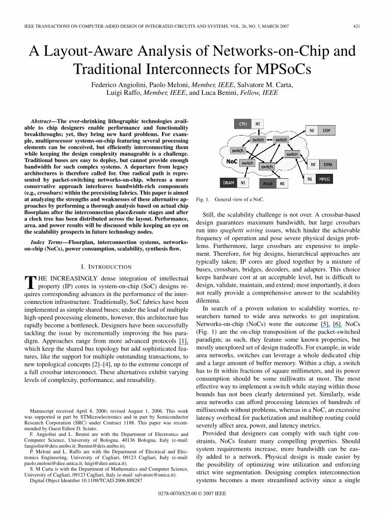
Fig. 1. General view of a NoC.
Still, the scalability challenge is not over. A crossbar-baseddesign guarantees maximum bandwidth, but large crossbarsrun into spaghetti wiring issues, which hinder the achievablefrequency of operation and pose severe physical design prob-lems. Furthermore, large crossbars are expensive to imple-ment. Therefore, for big designs, hierarchical approaches aretypically taken; IP cores are glued together by a mixture ofbuses, crossbars, bridges, decoders, and adapters. This choicekeeps hardware cost at an acceptable level, but is difficult todesign, validate, maintain, and extend; most importantly, it doesnot really provide a comprehensive answer to the scalabilitydilemma.
In search of a proven solution to scalability worries, re-searchers turned to wide area networks to get inspiration.Networks-on-chip (NoCs) were the outcome [5], [6]. NoCs(Fig. 1) are the on-chip transposition of the packet-switchedparadigm; as such, they feature some known properties, butmostly unexplored set of design tradeoffs. For example, in widearea networks, switches can leverage a whole dedicated chipand a large amount of buffer memory. Within a chip, a switchhas to fit within fractions of square millimeters, and its powerconsumption should be some milliwatts at most. The mosteffective way to implement a switch while staying within thosebounds has not been clearly determined yet. Similarly, widearea networks can afford processing latencies of hundreds ofmilliseconds without problems, whereas in a NoC, an excessivelatency overhead for packetization and multihop routing couldseverely affect area, power, and latency metrics.
Provided that designers can comply with such tight con-straints, NoCs feature many compelling properties. Shouldsystem requirements increase, more bandwidth can be eas-ily added to a network. Physical design is made easier bythe possibility of optimizing wire utilization and enforcingstrict wire segmentation. Designing complex interconnectionsystems becomes a more streamlined activity since a single
0278-0070/$25.00 © 2007 IEEE
422 IEEE TRANSACTIONS ON COMPUTER-AIDED DESIGN OF INTEGRATED CIRCUITS AND SYSTEMS, VOL. 26, NO. 3, MARCH 2007
homogeneous architecture must be deployed and validated.At the same time, very heterogeneous IP cores (in terms ofdata width, operating frequency, and transaction types) can beplugged to a NoC, given the proper network adapters. TheNoC itself can be shaped into arbitrary topologies to optimallymatch the communication needs of the cores; this is key tosimultaneously satisfying application requirements and costconstraints. Generally speaking, NoCs feature more degreesof freedom than alternative architectures, which is a definiteadvantage in the highly heterogeneous SoC market.
As can be seen, each design alternative for the interconnectfabric is very suitable for a subset of the SoC applicationspace but is limited in some other respect. Buses are cheapto manufacture but have a clear performance scalability issue.Crossbars have the highest possible performance for medium-sized designs; however, cost and wire routing issues also pre-vent scalability beyond a certain threshold. Hierarchical busesand mixed topologies not only struggle to provide the besttradeoff among performance and overheads in big designs butalso encounter a stumbling block in terms of complexity ofdesign and validation. NoCs offer virtually unlimited scalabilityand a high potential for customization, but their implementationoverhead has to be fully assessed first.
Abundant literature can be found describing communicationfabric architectures, including NoCs. However, the task of com-paring such diverse alternatives among each other is not easyand has received limited attention until now. For this reason, inthis paper, we will attempt such a comparison. We will comparethe performance of Advanced Microcontroller Bus Architecture(AMBA) Advanced High-performance Bus (AHB) [3], whichis a widespread shared bus design, against its multilayer (ML)extension, which includes a crossbar component, and against×pipes [7], [8], which is a NoC architecture that we builtin-house.
An endless number of design variables may affect the resultof such an analysis, and it is clearly not possible to tackle themall in this paper. Still, to make the comparative analysis mean-ingful, we believe that simulations alone, even if cycle accurate,do not suffice. First, area and power consumptions are equallycrucial efficiency metrics. Second, even if performance alonewere to be taken into account, the operating clock frequencymust be assessed first. This demands for a complete analysisframework including a path to synthesis.
Since interconnects, by their own nature, span across signifi-cant portions of the die, wiring congestion and wire propagationdelays are very difficult to estimate in advance. Therefore, theoverhead of crossbars and NoCs can only be fully understoodafter having laid out the architecture onto a chip floorplan. Theplacement&routing step is instrumental to a synthesis flow thatproperly investigates wiring loads. Similarly, the distributionof the clock signal to the cells in the design is a crucialpoint. It is well known that the clock tree can represent asignificant percentage of the power budget [9]–[11], whereasanother significant fraction is due to sequential logic. Therefore,the clock distribution tree and the clock-gating techniques areprime candidates for evaluation.
To take into account as many key effects as possible, weestablish a flow that takes our test platforms down to a
placed&routed layout. This flow allows us to derive frequency,area, and power figures. We use a 0.13-µm library for our study.
This paper is based on our previous research work [8],compared to which a major addition is the inclusion of a clocktree and clock-gating facilities. These two items have a largeimpact on power and timing results, as we will show in ouranalysis. Furthermore, the testing environment is extended withone extra NoC topology, which is an example of what can beachieved with automated design flows, and with one furtherreal-life functional benchmark.
The rest of this paper is structured as follows. Section IIdiscusses previous work in the area of on-chip interconnects,with emphasis on fabric synthesis. Section III presents somearchitectural examples of how interconnects can be designed,Section IV discusses the test topologies we choose for ouranalysis, and Section V introduces the applications we use forbenchmarking. In Section VI, we describe a full characteriza-tion flow for an on-chip interconnect, spanning from architec-tural description and cycle-accurate performance assessment tothe generation of a chip layout with fully placed&routed wiresand a clock tree. Section VII details the results we achievedfrom our simulations and syntheses. Finally, Section VIII sum-marizes the results of our work, and Section IX presents a briefoutlook onto our future research.
II. RELATED WORK
Large numbers of communication fabrics are described inprevious literature. Advanced RISC Machines (ARM) AMBA[3], including the latest AXI [12] packages, STMicroelectronicsSTBus [2], and Sonics MicroNetworks [1] are examples ofbuses and attempts to overcome the most classical shared busarchitecture by various means (e.g., multiple STBus channelscan be deployed, leading to crossbars).
NoCs have been suggested as a scalable communicationfabric [5], [6]. Research has focused on multiple design levels.From the architectural point of view, a complete scheme ispresented, for example, in [13], whereas specific topics aretackled in several works, e.g., flow control protocols [14],quality of service (QoS) provisions [15], [16], and asynchro-nous implementations [17]. A computer-aided design (CAD)tool for NoC instantiation and optimization can be found,for example, in [18].
The synthesis flow of NoCs has been explored by severalgroups. Layouts are presented in [19] and [20], a test chip isshown in [21], and an FPGA target is provided for [22]. Syn-thesis and layout results for the ×pipes library of componentblocks that we will leverage on are shown in [7] and [23].
As previously mentioned, one key topic that has not yet beenextensively covered is studying how NoCs compare to moretraditional interconnects. In [24], an analytical methodology isillustrated to compare NoCs of arbitrary topology (a sharedbus and a crossbar are provided as examples), also takinginto account area, frequency, and power metrics. However,some assumptions of this paper (such as the relative cost ofwiring versus logic) do not seem to be fully confirmed whenconsidering actual fabrics, as Section VII will show. In [25],a synthesis-aware flow is presented to characterize the Hermes
ANGIOLINI et al.: LAYOUT-AWARE ANALYSIS OF NoCs AND TRADITIONAL INTERCONNECTS FOR MPSoCs 423
NoC; processor interface (PI) bus is used as a benchmark forperformance metrics, but not for area and power analyses.Furthermore, PI bus is not representative of the current widelyused high-performance interconnects.
III. ARCHITECTURES FOR ON-CHIP
INTERCONNECTION FABRICS
A. AMBA Shared Bus
The AMBA 2.0 [3] interconnect is a well-established fabricarchitecture for SoC designs due to its efficiency despite themoderate silicon footprint. Therefore, we choose it as a refer-ence against which to compare the ×pipes NoC. The AMBAspecification dictates three different architectures with varyinglevels of complexity and performance; in this paper, we willrefer to AMBA AHB, which is the fastest of them.
AMBA traditionally leverages on a shared bus topology, andits communication protocol is kept simple to minimize areaoverhead (a single ongoing transaction at a time, no postedwrites, etc.). An AHB is composed of several IP blocks (AHBmasters and slaves), one central arbiter to manage resourceaccess, and some interconnection resources. A minimal amountof flip-flops is required in the architecture, which is typicallybufferless. The bus resources are owned by a single master at atime; if the targeted slave is forced to insert wait states beforeresponding, no other transaction can be initiated, neither by thecurrent bus owner nor by any other master. As a result, theutilization of bus bandwidth, which is already limited, mightbe poor.
AMBA AHB uses nonpipelined paths for communicationamong all masters and all slaves. Therefore, a key performanceassumption is that the propagation delay of the interconnectwires will be short. If that is the case, communication willincur the minimum possible latency. However, new technologynodes are leading to faster and faster logic, potentially resultingin faster clock periods, while wire propagation delays areproportionally increasing. If the whole fabric is constrained toslow operation by wire delay, this factor represents a limit tomaximum operating frequency.
B. ML AMBA
Due to increasing congestion and bandwidth demands inmodern SoCs, a crossbar component was added to the AMBAtoolkit, resulting in ML AMBA designs. To keep existingAMBA interfaces unchanged, the device is purely combina-tional and completely transparent to AMBA masters and slaves.The crossbar component behaves as a slave toward multipleAMBA AHBs (“layers”) and forwards requests to real AMBAslaves (e.g., memories). Multiple layers can simultaneouslyaccess the crossbar, provided they do not conflict on arbitrationfor the same transaction target.
Given its high-bandwidth topological nature and its combina-tional response times, this crossbar is clearly a best-case refer-ence block from an architectural point of view. However, fromthe perspective of a layout engineer, wire routing constraints insuch a block are very demanding. Therefore, an assessment ofthe achievable clock frequency and area is clearly essential.
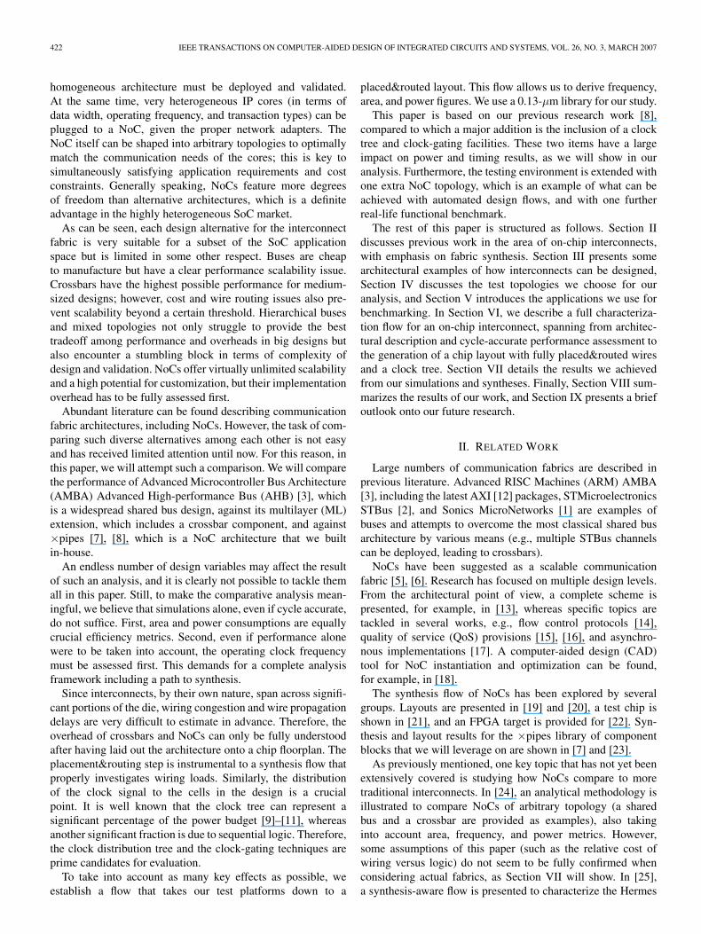
Fig. 2. ×pipes building blocks. (a) Switch. (b) NI. (c) Link.
C. ×pipes NoC
The ×pipes NoC [7], [23] is an example of a highly flexiblelibrary of component blocks (Fig. 2). The NoC is instantiatedby deploying a set of components in an arbitrary topology andby configuring them. The ×pipes library contains three maincomponents, namely: 1) switches; 2) network interfaces (NIs);and 3) links.
The backbone of the NoC is composed of switches, whosemain function is to route packets from sources to destina-tions. Arbitrary switch connectivity is possible, allowing forimplementation of any topology. Switches provide bufferingresources to lower congestion and improve performance; in×pipes, output buffering is chosen; i.e., first in–first outs(FIFOs) are present on each output port. Switches also handleflow control [14] issues (we use the ACK/NACK protocol inthis paper) and resolve conflicts among packets when theyoverlap in requesting access to the same physical links.
An NI is needed to connect each IP core to the NoC. NIs con-vert transaction requests/responses into packets, and vice versa.Packets are then split into a sequence of flow control units (flits)before transmission to decrease the physical wire parallelismrequirements. In ×pipes, two separate NIs are defined, namely;1) an initiator and 2) a target, which are associated to systemmasters and system slaves, respectively. A master/slave devicewill require an NI of each type to be attached to it. The interfaceamong IP cores and NIs is point-to-point as defined by theOpen Core Protocol (OCP) 2.0 [26] specification, guaranteeingmaximum reusability. NI lookup tables specify the path thatpackets will follow in the network to reach their destination(source routing). Two different clock signals can be attached toNIs: one to drive the NI front end (OCP interface) and the otherto drive the NI back end (×pipes interface). This arrangementallows the NoC to run at a fast clock although some or all of theattached IP cores are slower, which is crucial to keep transactionlatency low. Since each IP core can run at a different divider ofthe ×pipes frequency, mixed-clock platforms are possible.
Interblock links are a critical component of NoCs, giventhe technology trends for global wires. The problem of signalpropagation delay is, or will soon become, critical. For this
424 IEEE TRANSACTIONS ON COMPUTER-AIDED DESIGN OF INTEGRATED CIRCUITS AND SYSTEMS, VOL. 26, NO. 3, MARCH 2007
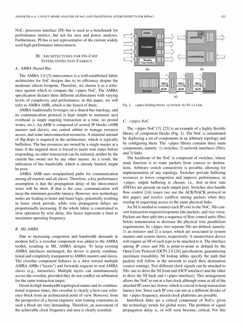
Fig. 3. Platforms under test. (a) Shared bus AMBA AHB. (b) ML AMBA AHB. (c) ×pipes mesh. (d) ×pipes custom topology. M: ARM7 masters;T: traffic generators; P: privately accessed slaves; S: shared slaves.
reason, ×pipes supports link pipelining [14], i.e., the inter-leaving of logical buffers along links. Proper flow controlprotocols are implemented in link transmitters and receivers(NIs and switches) to make the link latency transparent to thesurrounding logic. Therefore, the overall platform can run at afast clock frequency, without the longest wires being a globalspeed limiter.
IV. FABRICS UNDER TEST
Choosing a test environment to compare such different ar-chitectures as a NoC and a bus/crossbar is a difficult task sincecommunication fabrics can be heavily tuned to optimally fita target benchmark, but the resulting figures would not berepresentative of real-world performance under a different testload. For this reason, we do not attempt to fully optimize
our evaluation platforms, and we choose to present relativelyregular mappings, which should be suitable for multiple appli-cations. For the ×pipes NoC, we also include in our analysis anirregular topology, which is optimized by an in-house CAD tool[18], [27] to better match the target application. The topology isoptimized according to criteria of low area occupation and lowpower consumption and is built for deadlock freedom. We referthe interested reader to [27] for details on the topology mappingprocess. Comparing this topology against a regular one can givean idea of the potential benefits achievable by custom topologydesign.
We conceive four test platforms, namely: 1) an AMBA AHBshared bus; 2) an AMBA AHB ML system containing a cross-bar element; 3) a ×pipes mesh; and 4) a ×pipes custom topol-ogy (Fig. 3). All fabrics allow for attaching up to 30 IP cores,of which 15 masters and 15 slaves (typically memory banks).
ANGIOLINI et al.: LAYOUT-AWARE ANALYSIS OF NoCs AND TRADITIONAL INTERCONNECTS FOR MPSoCs 425
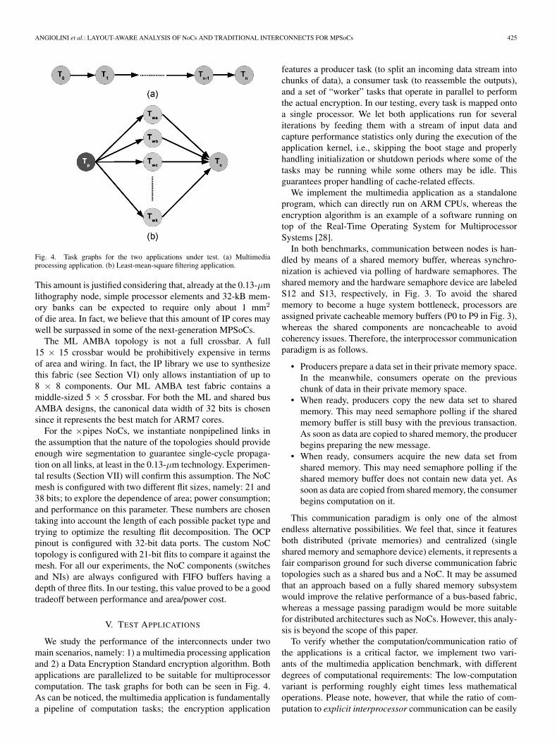
Fig. 4. Task graphs for the two applications under test. (a) Multimediaprocessing application. (b) Least-mean-square filtering application.
This amount is justified considering that, already at the 0.13-µmlithography node, simple processor elements and 32-kB mem-ory banks can be expected to require only about 1 mm2
of die area. In fact, we believe that this amount of IP cores maywell be surpassed in some of the next-generation MPSoCs.
The ML AMBA topology is not a full crossbar. A full15 × 15 crossbar would be prohibitively expensive in termsof area and wiring. In fact, the IP library we use to synthesizethis fabric (see Section VI) only allows instantiation of up to8 × 8 components. Our ML AMBA test fabric contains amiddle-sized 5 × 5 crossbar. For both the ML and shared busAMBA designs, the canonical data width of 32 bits is chosensince it represents the best match for ARM7 cores.
For the ×pipes NoCs, we instantiate nonpipelined links inthe assumption that the nature of the topologies should provideenough wire segmentation to guarantee single-cycle propaga-tion on all links, at least in the 0.13-µm technology. Experimen-tal results (Section VII) will confirm this assumption. The NoCmesh is configured with two different flit sizes, namely: 21 and38 bits; to explore the dependence of area; power consumption;and performance on this parameter. These numbers are chosentaking into account the length of each possible packet type andtrying to optimize the resulting flit decomposition. The OCPpinout is configured with 32-bit data ports. The custom NoCtopology is configured with 21-bit flits to compare it against themesh. For all our experiments, the NoC components (switchesand NIs) are always configured with FIFO buffers having adepth of three flits. In our testing, this value proved to be a goodtradeoff between performance and area/power cost.
V. TEST APPLICATIONS
We study the performance of the interconnects under twomain scenarios, namely: 1) a multimedia processing applicationand 2) a Data Encryption Standard encryption algorithm. Bothapplications are parallelized to be suitable for multiprocessorcomputation. The task graphs for both can be seen in Fig. 4.As can be noticed, the multimedia application is fundamentallya pipeline of computation tasks; the encryption application
features a producer task (to split an incoming data stream intochunks of data), a consumer task (to reassemble the outputs),and a set of “worker” tasks that operate in parallel to performthe actual encryption. In our testing, every task is mapped ontoa single processor. We let both applications run for severaliterations by feeding them with a stream of input data andcapture performance statistics only during the execution of theapplication kernel, i.e., skipping the boot stage and properlyhandling initialization or shutdown periods where some of thetasks may be running while some others may be idle. Thisguarantees proper handling of cache-related effects.
We implement the multimedia application as a standaloneprogram, which can directly run on ARM CPUs, whereas theencryption algorithm is an example of a software running ontop of the Real-Time Operating System for MultiprocessorSystems [28].
In both benchmarks, communication between nodes is han-dled by means of a shared memory buffer, whereas synchro-nization is achieved via polling of hardware semaphores. Theshared memory and the hardware semaphore device are labeledS12 and S13, respectively, in Fig. 3. To avoid the sharedmemory to become a huge system bottleneck, processors areassigned private cacheable memory buffers (P0 to P9 in Fig. 3),whereas the shared components are noncacheable to avoidcoherency issues. Therefore, the interprocessor communicationparadigm is as follows.
• Producers prepare a data set in their private memory space.In the meanwhile, consumers operate on the previouschunk of data in their private memory space.
• When ready, producers copy the new data set to sharedmemory. This may need semaphore polling if the sharedmemory buffer is still busy with the previous transaction.As soon as data are copied to shared memory, the producerbegins preparing the new message.
• When ready, consumers acquire the new data set fromshared memory. This may need semaphore polling if theshared memory buffer does not contain new data yet. Assoon as data are copied from shared memory, the consumerbegins computation on it.
This communication paradigm is only one of the almostendless alternative possibilities. We feel that, since it featuresboth distributed (private memories) and centralized (singleshared memory and semaphore device) elements, it represents afair comparison ground for such diverse communication fabrictopologies such as a shared bus and a NoC. It may be assumedthat an approach based on a fully shared memory subsystemwould improve the relative performance of a bus-based fabric,whereas a message passing paradigm would be more suitablefor distributed architectures such as NoCs. However, this analy-sis is beyond the scope of this paper.
To verify whether the computation/communication ratio ofthe applications is a critical factor, we implement two vari-ants of the multimedia application benchmark, with differentdegrees of computational requirements: The low-computationvariant is performing roughly eight times less mathematicaloperations. Please note, however, that while the ratio of com-putation to explicit interprocessor communication can be easily
426 IEEE TRANSACTIONS ON COMPUTER-AIDED DESIGN OF INTEGRATED CIRCUITS AND SYSTEMS, VOL. 26, NO. 3, MARCH 2007
tuned in this way, the ratio of computation to overall communi-cation requirements depends on several additional factors. Forexample, unless an ideal cache is available, changing the com-putation patterns also implicitly results in different bandwidthdemands (for cache refills and write backs). This will be furtherdiscussed in Section VII.
In the following, for the sake of brevity, we will call thebenchmarks multihigh (i.e., high-computation variant of themultimedia benchmark), multilow (i.e., low-computation vari-ant of the multimedia benchmark), and des.
Since real-life MPSoCs are not likely to only feature general-purpose processing cores, we also deploy traffic generators tomodel additional hardware IP blocks that may be present inthe platform. While this choice is not in any way supposedto model on-chip coprocessors in a general fashion, we feelthat it adds extra realism. Therefore, we include two differenttypes of traffic generation patterns, namely: 1) digital signalprocessor (DSP) like (streams of accesses to a memory bank)and 2) I/O controller like (a rotating pattern of accesses to-ward neighboring devices). DSP-like traffic generators are eachprogrammed to fetch 128 or 256 bits of data from one of theshared memory banks or devices (indicated with S in Fig. 3),compute for ten clock cycles, and repeat. I/O controller-liketraffic generators are instead programmed to query three shareddevices in a rotating pattern by reading 256 bits from each.We program the generators to issue functional traffic such asdata transactions for consistency reasons; adopting a lower levelapproach, such as the injection of packets in the NoC, wouldmake the comparison with AMBA very unintuitive.
VI. CHARACTERIZATION FLOW: FROM ARCHITECTURE
TO CHIP LAYOUT
To properly characterize the platforms mentioned inSection IV, both simulation and synthesis flows are needed. Theflows we adopt are described next.
A. Fabric Simulation
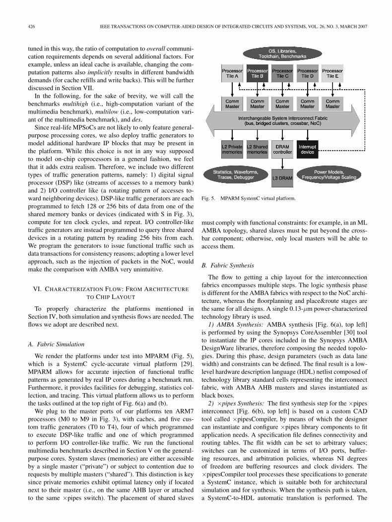
We render the platforms under test into MPARM (Fig. 5),which is a SystemC cycle-accurate virtual platform [29].MPARM allows for accurate injection of functional trafficpatterns as generated by real IP cores during a benchmark run.Furthermore, it provides facilities for debugging, statistics col-lection, and tracing. This virtual platform allows us to performthe tasks outlined at the top right of Fig. 6(a) and (b).
We plug to the master ports of our platforms ten ARM7processors (M0 to M9 in Fig. 3), with caches, and five cus-tom traffic generators (T0 to T4), four of which programmedto execute DSP-like traffic and one of which programmedto perform I/O controller-like traffic. We run the functionalmultimedia benchmarks described in Section V on the general-purpose cores. System slaves (memories) are either accessibleby a single master (“private”) or subject to contention due torequests by multiple masters (“shared”). This distinction is keysince private memories exhibit optimal latency only if locatednext to their master (i.e., on the same AHB layer or attachedto the same ×pipes switch). The placement of shared slaves
Fig. 5. MPARM SystemC virtual platform.
must comply with functional constraints: for example, in an MLAMBA topology, shared slaves must be put beyond the cross-bar component; otherwise, only local masters will be able toaccess them.
B. Fabric Synthesis
The flow to getting a chip layout for the interconnectionfabrics encompasses multiple steps. The logic synthesis phaseis different for the AMBA fabrics with respect to the NoC archi-tecture, whereas the floorplanning and place&route stages arethe same for all designs. A single 0.13-µm power-characterizedtechnology library is used.
1) AMBA Synthesis: AMBA synthesis [Fig. 6(a), top left]is performed by using the Synopsys CoreAssembler [30] toolto instantiate the IP cores included in the Synopsys AMBADesignWare libraries, therefore composing the needed topolo-gies. During this phase, design parameters (such as data lanewidth) and constraints can be defined. The final result is a low-level hardware description language (HDL) netlist composed oftechnology library standard cells representing the interconnectfabric, with AMBA AHB masters and slaves instantiated asblack boxes.
2) ×pipes Synthesis: The first synthesis step for the ×pipesinterconnect [Fig. 6(b), top left] is based on a custom CADtool called ×pipesCompiler, by means of which the designercan instantiate and configure ×pipes library components to fitapplication needs. A specification file defines connectivity androuting tables. The flit width can be set to arbitrary values;switches can be customized in terms of I/O ports, buffer-ing resources, and arbitration policies, whereas NI degreesof freedom are buffering resources and clock dividers. The×pipesCompiler tool processes these specifications to generatea SystemC instance, which is suitable both for architecturalsimulation and for synthesis. When the synthesis path is taken,a SystemC-to-HDL automatic translation is performed. The
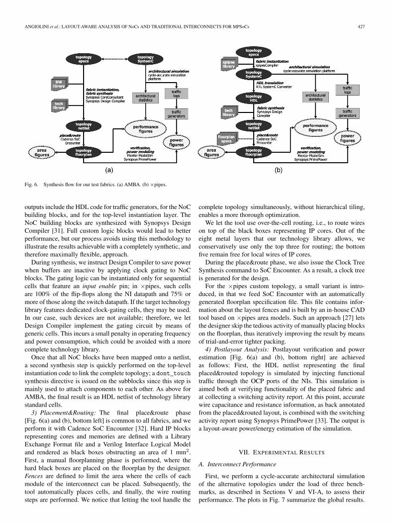
ANGIOLINI et al.: LAYOUT-AWARE ANALYSIS OF NoCs AND TRADITIONAL INTERCONNECTS FOR MPSoCs 427
Fig. 6. Synthesis flow for our test fabrics. (a) AMBA. (b) ×pipes.
outputs include the HDL code for traffic generators, for the NoCbuilding blocks, and for the top-level instantiation layer. TheNoC building blocks are synthesized with Synopsys DesignCompiler [31]. Full custom logic blocks would lead to betterperformance, but our process avoids using this methodology toillustrate the results achievable with a completely synthetic, andtherefore maximally flexible, approach.
During synthesis, we instruct Design Compiler to save powerwhen buffers are inactive by applying clock gating to NoCblocks. The gating logic can be instantiated only for sequentialcells that feature an input enable pin; in ×pipes, such cellsare 100% of the flip-flops along the NI datapath and 75% ormore of those along the switch datapath. If the target technologylibrary features dedicated clock-gating cells, they may be used.In our case, such devices are not available; therefore, we letDesign Compiler implement the gating circuit by means ofgeneric cells. This incurs a small penalty in operating frequencyand power consumption, which could be avoided with a morecomplete technology library.
Once that all NoC blocks have been mapped onto a netlist,a second synthesis step is quickly performed on the top-levelinstantiation code to link the complete topology; a dont_touchsynthesis directive is issued on the subblocks since this step ismainly used to attach components to each other. As above forAMBA, the final result is an HDL netlist of technology librarystandard cells.
3) Placement&Routing: The final place&route phase[Fig. 6(a) and (b), bottom left] is common to all fabrics, and weperform it with Cadence SoC Encounter [32]. Hard IP blocksrepresenting cores and memories are defined with a LibraryExchange Format file and a Verilog Interface Logical Modeland rendered as black boxes obstructing an area of 1 mm2.First, a manual floorplanning phase is performed, where thehard black boxes are placed on the floorplan by the designer.Fences are defined to limit the area where the cells of eachmodule of the interconnect can be placed. Subsequently, thetool automatically places cells, and finally, the wire routingsteps are performed. We notice that letting the tool handle the
complete topology simultaneously, without hierarchical tiling,enables a more thorough optimization.
We let the tool use over-the-cell routing, i.e., to route wireson top of the black boxes representing IP cores. Out of theeight metal layers that our technology library allows, weconservatively use only the top three for routing; the bottomfive remain free for local wires of IP cores.
During the place&route phase, we also issue the Clock TreeSynthesis command to SoC Encounter. As a result, a clock treeis generated for the design.
For the ×pipes custom topology, a small variant is intro-duced, in that we feed SoC Encounter with an automaticallygenerated floorplan specification file. This file contains infor-mation about the layout fences and is built by an in-house CADtool based on ×pipes area models. Such an approach [27] letsthe designer skip the tedious activity of manually placing blockson the floorplan, thus iteratively improving the result by meansof trial-and-error tighter packing.
4) Postlayout Analysis: Postlayout verification and powerestimation [Fig. 6(a) and (b), bottom right] are achievedas follows: First, the HDL netlist representing the finalplaced&routed topology is simulated by injecting functionaltraffic through the OCP ports of the NIs. This simulation isaimed both at verifying functionality of the placed fabric andat collecting a switching activity report. At this point, accuratewire capacitance and resistance information, as back annotatedfrom the placed&routed layout, is combined with the switchingactivity report using Synopsys PrimePower [33]. The output isa layout-aware power/energy estimation of the simulation.
VII. EXPERIMENTAL RESULTS
A. Interconnect Performance
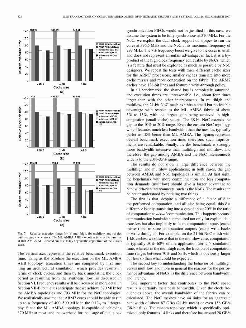
First, we perform a cycle-accurate architectural simulationof the alternative topologies under the load of three bench-marks, as described in Sections V and VI-A, to assess theirperformance. The plots in Fig. 7 summarize the global results.
428 IEEE TRANSACTIONS ON COMPUTER-AIDED DESIGN OF INTEGRATED CIRCUITS AND SYSTEMS, VOL. 26, NO. 3, MARCH 2007
Fig. 7. Relative execution times for (a) multihigh, (b) multilow, and (c) deswith varying cache sizes. The ML AMBA AHB execution time is the baselineat 100. AMBA AHB shared bus results lay beyond the upper limit of the Y -axisscale.
The vertical axis represents the relative benchmark executiontime, taking as the baseline the execution on the ML AMBAAHB topology. Execution times are computed by first run-ning an architectural simulation, which provides results interms of clock cycles, and then by back annotating the clockperiod as resulting from the synthesis flow, as discussed inSection VI. Frequency results will be discussed in more detail inSection VII-B, but let us anticipate that we achieve 370 MHz forthe AMBA topologies and 793 MHz for the NoC topologies.We realistically assume that ARM7 cores should be able to runup to a frequency of 400–500 MHz in the 0.13-µm lithogra-phy. Since the ML AMBA topology is capable of achieving370 MHz at most, and the overhead for the usage of dual clock
synchronization FIFOs would not be justified in this case, weassume the system to be fully synchronous at 370 MHz. For theNoC, we exploit the dual clock support of ×pipes to run thecores at 396.5 MHz and the NoC at its maximum frequency of793 MHz. The 7% frequency boost we give to the cores is smalland does not represent an unfair advantage; in fact, it is a by-product of the high clock frequency achievable by NoCs, whichis a feature that must be exploited as much as possible by NoCdesigners. We repeat the tests with three different cache sizesfor the ARM7 processors; smaller caches translate into morecache misses and more congestion on the fabric. The ARM7caches have 128-bit lines and feature a write-through policy.
In all benchmarks, the shared bus is completely saturated,and execution times are unreasonable, i.e., about four timeslarger than with the other interconnects. In multihigh andmultilow, the 21-bit NoC mesh exhibits a small but noticeableadvantage with respect to the ML AMBA fabric of about5% to 15%, with the largest gain being achieved in high-congestion (small cache) setups. The 38-bit NoC extends thegap to the 10% to 20% range. Even the custom NoC topology,which features much less bandwidth than the meshes, typicallyperforms 10% better than ML AMBA. The figures representoverall benchmark execution time; therefore, such improve-ments are remarkable. Finally, the des benchmark is stronglymore bandwidth intensive than multihigh and multilow, andtherefore, the gap among AMBA and the NoC interconnectswidens to the 20%–35% range.
The results do not show a large difference between themultihigh and multilow applications; in both cases, the gapbetween AMBA and NoC topologies is similar. At first sight,the benchmark with more communication and less computa-tion demands (multilow) should give a larger advantage tobandwidth-rich interconnects, such as the NoCs. The results canbe better understood by noticing two things.
The first is that, despite a difference of a factor of 8 inthe performed computation, and all else being equal, this 8×difference is only translating into a gap of about 20% in the ratioof computation to actual communication. This happens becausecommunication bandwidth is required not only for explicit datatransfers but also implicitly to fetch computation inputs (cachemisses) and to store computation outputs (cache write backsor write throughs). For example, on the 21-bit NoC mesh with1-kB caches, we observe that in the multilow case, computationis typically 50%–60% of the application kernel’s simulationtime, whereas in the multihigh case, the fraction of computationtime ranges between 70% and 85%, which is obviously largerbut less so than what could be expected.
The second key to understanding the behavior of multihighversus multilow, and more in general the reasons for the perfor-mance advantage of NoCs, is the difference between bandwidthand latency.
One important factor that contributes to the NoC speedresults is certainly their peak bandwidth. Given the clock fre-quencies above, the overall bandwidth of the fabrics can becalculated. The NoC meshes have 44 links for an aggregatebandwidth of about 87 GB/s (21-bit mesh) or even 158 GB/s(38-bit flits). The custom topology, which is specifically opti-mized, only features 14 links and therefore has around 28 GB/s
ANGIOLINI et al.: LAYOUT-AWARE ANALYSIS OF NoCs AND TRADITIONAL INTERCONNECTS FOR MPSoCs 429
of bandwidth. The ML AMBA topology can have at most fivepending transactions at a time; considering two sets of 32-bitdata wires (AMBA features dual data channels for reads andwrites), 32-bit address wires, and a dozen used control wires,the available bandwidth can be computed to be around 24 GB/s.
Therefore, the NoC meshes feature about 3.5 to 6.5 timesmore peak bandwidth than the ML AMBA topology. Thisseems to explain the performance gap. However, the NoCcustom topology still outperforms ML AMBA with only28 GB/s of peak bandwidth, which is a 15% margin.
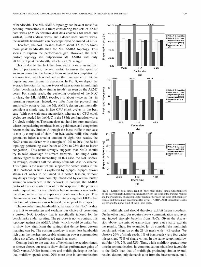
This is due to the fact that bandwidth is only an indirectclue of performance; the real metric to assess the speed ofan interconnect is the latency from request to completion ofa transaction, which is defined as the time needed to let therequesting core resume its execution. In Fig. 8, we depict theaverage latencies for various types of transactions in multihigh(other benchmarks show similar trends), as seen by the ARM7cores. For single reads, the packeting overhead of the NoCis clear; the ML AMBA topology is about twice as fast inreturning responses. Indeed, we infer from the protocol andempirically observe that the ML AMBA design can internallycomplete a single read in five CPU clock cycles in the bestcase (with one-wait-state memories), whereas ten CPU clockcycles are needed for the NoC in the 38-bit configuration with a2× clock multiplier. The same does not hold for burst transfers,where the packeting overhead is only paid once, and congestionbecomes the key limiter: Although the burst traffic in our caseis mostly composed of short four-beat cache refills (the trafficgenerators inject a smaller amount of eight-beat reads), theNoCs come out faster, with a margin of 10% to 20% (the 38-bittopology performing even better at 20% to 25% due to lowercongestion). This result strongly suggests that NoCs shouldtry to take advantage of stream transfers. The single writelatency figure is also interesting; in this case, the NoC shows,on average, less than half the latency of the ML AMBA scheme.This figure is the result of the support for posted writes in theOCP protocol, which is exploited by ×pipes. ×pipes allowsstreams of writes to be issued in a posted fashion, withoutany delays except those possibly introduced by eventual buffersaturation somewhere in the network. In contrast, the AMBAprotocol forces a master to wait for the response to the previouswrite request and for rearbitration before issuing a new write;therefore, write streams experience continuous hiccups. Thisphenomenon could be bypassed by interposing data FIFOs, butthis kind of optimizations is beyond the scope of this paper.
The overwhelming bandwidth advantage of the NoC meshesis a hint to overdesign and explains our choice of presentinga custom NoC topology that is specifically tailored for thebenchmarks under scrutiny. The purpose is not to contrast thistopology against the AMBA fabric, which would be unfair, butto show how significant the savings that derive from custommapping can be. The custom topology is much less bandwidthrich than the meshes, noticeably trimming power consumptionwhile not affecting fabric speed nearly as much.
Coming back to the analysis of benchmark execution times,as shown above, our results show similar performance gains ofNoCs versus AMBA in multilow and multihigh, despite the factthat multilow spends about 20% more time in communication
Fig. 8. Latency of (a) single read, (b) burst read, and (c) single write transferson the interconnects. Latency measured between the issue of the transfer requestand the availability of a response (for reads) or between the issue of the transferrequest and the request acceptance (for writes). AMBA AHB shared bus resultslay beyond the upper limit of the Y -axis scale.
than multihigh, and should therefore exhibit larger speedups.On the other hand, des requires heavy communication resourcesand indeed strongly benefits from NoCs. Given the discus-sion above, the mix of transaction types can clearly explainthe results. Thus, for example, let us consider the multihighbenchmark when run on the 21-bit mesh with 4-kB caches. Weobserve 26% of single reads, 1% of burst reads (very few cachemisses), and 73% of single writes. In the same setup, multilowexhibits 46%, 2%, and 52%. Thus, while multilow spends moretime in communication, its communication mix is less favorableto the NoCs than that of multihigh, producing similar overallresults. des not only demands a lot from the interconnect, but it
430 IEEE TRANSACTIONS ON COMPUTER-AIDED DESIGN OF INTEGRATED CIRCUITS AND SYSTEMS, VOL. 26, NO. 3, MARCH 2007
Fig. 9. Layouts of our test fabrics. (a) ML AMBA. (b) ×pipes meshes. (c) ×pipes custom.
is also a good match to NoC architectures; due to a much largerdata set and code segment, in the same setup, we notice that theratios are 16% (few single reads), 32% (many refills), and 52%,respectively.
Many factors can contribute to performance results, includ-ing caching schemes (as the plots show), functional bottlenecks(one slave is heavily accessed and slows down the wholesystem), localized congestion (the topology suffers from over-load at some location), traffic spikes over time (resources arenormally underutilized, but communication spikes occur, andwhen they occur, they are poorly handled). A discussion of allthese issues is beyond the scope of this paper. Overall, we thinkthat our results show a noticeable performance lead of NoCsover a wide range of transaction patterns.
B. Interconnect Area, Frequency of Operation, and Bandwidth
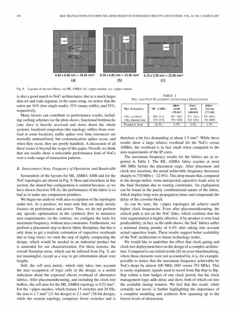
Screenshots of the layouts for ML AMBA AHB and for theNoC topologies are shown in Fig. 9. Here and elsewhere in thissection, the shared bus configuration is omitted because, as wehave shown (Section VII-A), the performance of the fabric is sobad as to make any comparison pointless.
We begin our analysis with area occupation of the topologiesunder test. As a premise, we must state that our study mostlyfocuses on performance and power. Thus, we do not performany specific optimization in the synthesis flow to minimizearea requirements; on the contrary, we configure the tools formaximum frequency, without area constraints. Furthermore, weperform a placement step to derive fabric floorplans, but this isonly done to get a realistic estimation of capacitive overheadsdue to long wires; we omit the step of tightly compacting thedesign, which would be needed in an industrial product butis unneeded for our characterization. For these reasons, theoverall floorplan areas, which can be inferred from Fig. 9, arenot meaningful, except as a way to get information about wirelengths.
Still, the cell area metric, which only takes into accountthe area occupation of logic cells in the design, is a usefulindication about the expected silicon overhead of alternativefabrics. After placement&routing, and including the clock treebuffers, the cell area for the ML AMBA topology is 0.52 mm2.For the ×pipes meshes, which feature 15 switches and 30 NIs,the area is 1.7 mm2 (21-bit design) to 2.1 mm2 (38-bit design),while the custom topology comprises fewer switches and is
TABLE IPRE- AND POST-PLACEMENT ACHIEVABLE FREQUENCIES
therefore a bit less demanding at about 1.5 mm2. While theseresults show a large relative overhead for the NoCs versusAMBA, the overhead is in fact small when compared to thearea requirements of the IP cores.
The maximum frequency results for the fabrics are as re-ported in Table I. The ML AMBA fabric reaches at most480 MHz before the placement stage. After placement andclock tree insertion, the actual achievable frequency decreasessharply to 370 MHz (−22.9%). This drop means that, comparedto the design netlist, some unexpected capacitive loads arise inthe final floorplan due to routing constraints. An explanationcan be found in the purely combinational nature of the fabric,which implies long-wire propagation times and compounds thedelay of the crossbar block.
As can be seen, the ×pipes topologies all achieve muchhigher clock frequencies. Even after placement&routing, thecritical path is not on the NoC links, which confirms that thewire segmentation is highly effective. A by-product is wire loadpredictability; in fact, as the table shows, the NoC fabrics suffera minimal timing penalty of 6.4% after taking into accountactual capacitive loads. These results suggest better scalabilityof the NoC architecture to future technology nodes.
We would like to underline the effect that clock gating andclock tree deployment have on the design of a complex architec-ture. Compared to our initial results [8] on cross-benchmarking,where these elements were not accounted for, it is, for example,possible to notice that the maximum frequency achievable byNoCs drops by almost 100 MHz (885 versus 793 MHz). Thisis easily explained; signals need to travel from flip-flop to flip-flop within a time budget of one clock period, but the clockmanagement logic adds delay and skew, both of which cut intothe available timing window. We feel that this result, whilecertainly not novel, is further highlighting the importance ofa complete modeling and synthesis flow spanning up to thelowest levels of abstraction.
ANGIOLINI et al.: LAYOUT-AWARE ANALYSIS OF NoCs AND TRADITIONAL INTERCONNECTS FOR MPSoCs 431
TABLE IIPOWER CONSUMPTION OF THE FABRICS
C. Interconnect Power and Energy
To attempt a power evaluation, we first monitor activityduring functional system simulations and log all source–targettransaction pairs. We then follow the flow outlined inSection VI-B4 by injecting traffic from master ports towardeach of the targets that are accessed in the functional simu-lation. Please note that, in this paper, our focus is on cross-benchmarking; therefore, we only analyze average power andenergy consumption figures under specific workloads. Researchis ongoing on how to best build flexible yet accurate powermodels for NoCs in general [34], [35] and for the ×pipesarchitecture in particular [36].
As shown by our initial analyses [8], sequential logic rep-resents by far the largest fraction of power consumption inthe ×pipes NoC, with flip-flops burning as much as 80% ofthe global power requirements (still excluding the clock treecontribution, which, as we will show, is also major). This iscontrary to some previous assumptions, where switching activ-ity on global wires is expected to be the dominant contributionto power dissipation (an example is in [37]). The balanceis expected to eventually shift in future technologies, but atthe 0.13-µm node, sequential elements seem to be the primecandidates for tuning. This observation leads us to attemptingto optimize the NoC by means of several strategies related tobuffering elements. First, the implementation of clock gatinglets us achieve about 30% power savings. Second, we keepbuffering resources to a minimum across the NoC by sizingNI and switch buffers to hold only three flits at a time. Third,we explore the flit width degree of freedom, which provesvery useful: moving from 38- to 21-bit flits reduces buffersize almost in half, cutting power by a significant amount(see below).
The power results that we achieve for the topologies at theirmaximum operating frequency are reported in Table II, whereasenergy results are reported in Table III. ×pipes figures are fordesigns with clock tree and clock gating, whereas in the caseof AMBA, we only insert a clock tree; given the low amountof sequential logic that AMBA contains (see Table II), clockgating would offer negligible benefits and unnecessarily adddesign flow complexity and frequency penalties.
It is interesting to note that, with the 0.13-µm technologylibrary we use, leakage power is present but almost negligible(less than 0.1%). This is also expected to change in futuretechnologies.
The ML AMBA crossbar is clearly the winner in termsof pure power consumption. The power consumption of theNoC meshes is 5.6–7.5 times higher. Keeping the flit widthof the NoC mesh low is, however, helpful, as power savingsof 25% can be noticed, with a much lower impact on overall
TABLE IIIENERGY CONSUMPTION OF THE FABRICS
performance (see Section VII-A). Due to clock gating, thefraction of power consumption due to sequential logic dropssignificantly, from an initial value of around 80% [8] to around35%. This drop is due to the compound effect of clock gating,which cuts the sequential power requirements by 30%, andof the clock tree insertion, which is implemented by meansof combinational cells, thus lowering the relative fraction ofsequential power. The custom NoC topology, due both to itslower switch count, is able to shave about 8% off the powerof the 21-bit mesh. When considering the power density ofthe interconnects, AMBA has an advantage of roughly a factorof 2; we mostly attribute this to the difference in clock speeds.
In terms of energy, the advantage of ML AMBA is lessclear. When considering the ratio among power consumptionand available bandwidth (milliwatts over gigabyte per secondor millijoules over gigabyte of injectable data), ML AMBA andthe NoC meshes look much closer. However, this figure is a bitmisleading; using all of the available bandwidth, the mesheswould indeed consume much more energy. Furthermore, thecustom NoC, which is designed around providing bandwidthonly where necessary but utilizing it efficiently, is unreasonablypenalized by this analysis. Therefore, we attempt to use a moremeaningful metric: power over benchmark execution time, i.e.,the energy required to complete a benchmark. Given the per-formance figures shown by our experiments, we conservativelyassume an execution time advantage as shown by multihighor multilow; in a des-like scenario, of course, the results ofNoCs would look better. Thus, we set an execution time gainof 10% for the 21-bit NoCs (mesh and custom) against the MLAMBA fabric and of 15% in the case of the 38-bit NoC mesh.Calculating the energy consumption over an execution time,which is 1 ms for the baseline ML AMBA case, we observethe results reported in the second row of Table III. To derive aneven more useful metric, however, the energy consumption ofthe whole system should be taken into account. To this effect,the power consumption of other parts of the system must bemodeled. This is a very difficult task, as it greatly depends onthe specific components at hand. We could very conservativelyassume a power consumption of only 1 W at 370 MHz forall of the 15 cores, caches, and memory blocks. Furthermore,we could assume a 370-MHz working frequency for the coresin the ML AMBA case and a 396.5-MHz frequency for theNoCs (Section VII-A). The overall power consumption of thesystems would therefore be 1.075 W for ML AMBA, 1.449 W
432 IEEE TRANSACTIONS ON COMPUTER-AIDED DESIGN OF INTEGRATED CIRCUITS AND SYSTEMS, VOL. 26, NO. 3, MARCH 2007
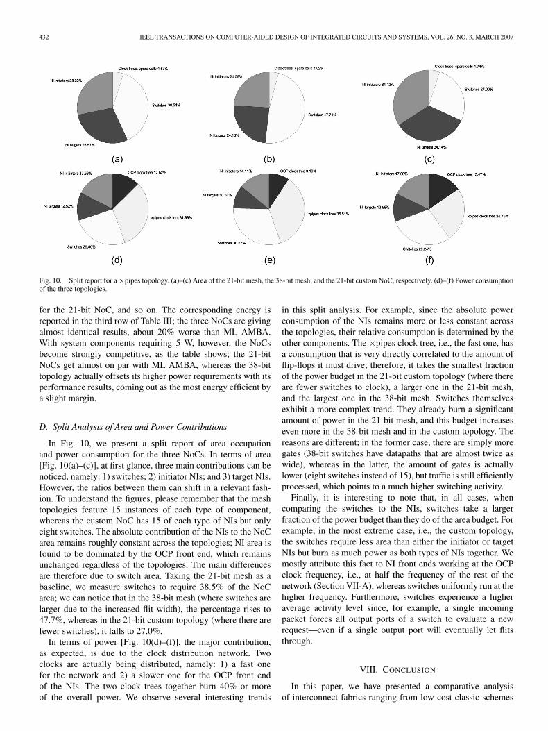
Fig. 10. Split report for a ×pipes topology. (a)–(c) Area of the 21-bit mesh, the 38-bit mesh, and the 21-bit custom NoC, respectively. (d)–(f) Power consumptionof the three topologies.
for the 21-bit NoC, and so on. The corresponding energy isreported in the third row of Table III; the three NoCs are givingalmost identical results, about 20% worse than ML AMBA.With system components requiring 5 W, however, the NoCsbecome strongly competitive, as the table shows; the 21-bitNoCs get almost on par with ML AMBA, whereas the 38-bittopology actually offsets its higher power requirements with itsperformance results, coming out as the most energy efficient bya slight margin.
D. Split Analysis of Area and Power Contributions
In Fig. 10, we present a split report of area occupationand power consumption for the three NoCs. In terms of area[Fig. 10(a)–(c)], at first glance, three main contributions can benoticed, namely: 1) switches; 2) initiator NIs; and 3) target NIs.However, the ratios between them can shift in a relevant fash-ion. To understand the figures, please remember that the meshtopologies feature 15 instances of each type of component,whereas the custom NoC has 15 of each type of NIs but onlyeight switches. The absolute contribution of the NIs to the NoCarea remains roughly constant across the topologies; NI area isfound to be dominated by the OCP front end, which remainsunchanged regardless of the topologies. The main differencesare therefore due to switch area. Taking the 21-bit mesh as abaseline, we measure switches to require 38.5% of the NoCarea; we can notice that in the 38-bit mesh (where switches arelarger due to the increased flit width), the percentage rises to47.7%, whereas in the 21-bit custom topology (where there arefewer switches), it falls to 27.0%.
In terms of power [Fig. 10(d)–(f)], the major contribution,as expected, is due to the clock distribution network. Twoclocks are actually being distributed, namely: 1) a fast onefor the network and 2) a slower one for the OCP front endof the NIs. The two clock trees together burn 40% or moreof the overall power. We observe several interesting trends
in this split analysis. For example, since the absolute powerconsumption of the NIs remains more or less constant acrossthe topologies, their relative consumption is determined by theother components. The ×pipes clock tree, i.e., the fast one, hasa consumption that is very directly correlated to the amount offlip-flops it must drive; therefore, it takes the smallest fractionof the power budget in the 21-bit custom topology (where thereare fewer switches to clock), a larger one in the 21-bit mesh,and the largest one in the 38-bit mesh. Switches themselvesexhibit a more complex trend. They already burn a significantamount of power in the 21-bit mesh, and this budget increaseseven more in the 38-bit mesh and in the custom topology. Thereasons are different; in the former case, there are simply moregates (38-bit switches have datapaths that are almost twice aswide), whereas in the latter, the amount of gates is actuallylower (eight switches instead of 15), but traffic is still efficientlyprocessed, which points to a much higher switching activity.
Finally, it is interesting to note that, in all cases, whencomparing the switches to the NIs, switches take a largerfraction of the power budget than they do of the area budget. Forexample, in the most extreme case, i.e., the custom topology,the switches require less area than either the initiator or targetNIs but burn as much power as both types of NIs together. Wemostly attribute this fact to NI front ends working at the OCPclock frequency, i.e., at half the frequency of the rest of thenetwork (Section VII-A), whereas switches uniformly run at thehigher frequency. Furthermore, switches experience a higheraverage activity level since, for example, a single incomingpacket forces all output ports of a switch to evaluate a newrequest—even if a single output port will eventually let flitsthrough.
VIII. CONCLUSION
In this paper, we have presented a comparative analysisof interconnect fabrics ranging from low-cost classic schemes
ANGIOLINI et al.: LAYOUT-AWARE ANALYSIS OF NoCs AND TRADITIONAL INTERCONNECTS FOR MPSoCs 433
to NoCs. While the traditional shared bus proves completelyunable to cope with the heavy load injected by 30 IP cores, theevolutionary ML AMBA design and the ×pipes NoC handle theload with different degrees of effectiveness and area and poweroverheads. The ML architecture is much more efficient in termsof area and power at the current technology node, but the NoC isfaster and promises better scalability and predictability in futurelithographic processes.
This paper sheds light on some questions that were pre-viously unanswered or only partially answered. For example,the NoC handles wiring delays and congestion much betterthan even a medium-sized 5 × 5 crossbar component, so wellso that most of its area and power overheads seems to beconcentrated in buffers—which is contrary to expectations insome previous literature, where wire switching activity wasexpected to be dominant. While this ratio should eventuallyshift in future technologies, we show that, in current processes,proper buffering optimizations are very useful. Clock gating,short FIFOs, and narrow flit widths are instrumental in keepingarea and power to reasonable levels.
We also show that custom NoC topology design, where aNoC is tailored to fit the target application, has noticeablepotential benefits. In this paper, we observe more than 10%savings in global area, 8% savings in power, and constantperformance. These savings are visible even despite beingmasked by large system-level overheads, such as the resourcesrequired by the clock tree and the cores themselves, and also bytopological considerations—in a system with 30 IP cores and30 NIs, the improvements that can be achieved by optimizationsof the network of switches alone have limited headroom. Whileit is not fair to compare a custom-designed NoC to a fairlygeneric ML AMBA topology, the superior customizability ofNoCs should be taken into account.
IX. FUTURE PERSPECTIVES
A. Technology Scaling
While this paper provides an assessment of design tradeoffsfor interconnects in the 0.13-µm technology, we feel that thereis plenty of research to be done to understand how to best scaleinterconnect fabrics into deeper submicrometer technologies.Some new challenges await designers, such as increasing wiredelay, increasing leakage power, increasing process variations,and increasing importance of inductive phenomena. While theanalysis we present in this paper provides hints, it is notclear whether even scalable architectures such as NoCs cansuccessfully tackle all of these issues in their present form. Wehope to be soon able to address some of these questions withadditional research.
Second, we are going to investigate asynchronous or glob-ally asynchronous–locally synchronous paradigms for NoCdesign. Asynchronous, or partially so, design styles may bethe only way to counter extreme process variation issues infuture technologies. Of course, asynchronous designs featurea very different set of tradeoffs compared to fully synchronouslogic, including better power efficiency but much more compleximplementation flows. Whether the advantages will outweighthe problems remains to be seen.
B. Architectural Analysis
At the same time, NoCs are still very young, and theirarchitecture has not been fully optimized yet. While bandwidthis obviously an essential indirect parameter, we show that atthe end of the day, the key to performance metrics is providingresponses with the lowest possible latency. We feel that thisfact might not have received enough attention in previous work.Burst transactions seem to be necessary to offset the packetingoverhead of NoCs and as much attention as possible should bedevoted to keeping latency low. Therefore, we plan on devisingschemes to optimize the latency of NoCs.
To further improve our understanding of performance bot-tlenecks in system interconnects, we are devoting major effortinto the development of additional simulation models of hard-ware components, such as DSPs or memory controllers. Suchmodels will allow us to study performance tradeoffs under alarger variety of traffic patterns. This analysis is planned asnear-future work.
ACKNOWLEDGMENT
The authors would like to thank S. Murali (StanfordUniversity, USA; EPFL, Switzerland), D. Bertozzi (Universityof Bologna, Italy; University of Ferrara, Italy), A. Pullini(University of Bologna), and K. Lee (KAIST, Korea), whosevaluable contributions were key to writing this paper.
REFERENCES
[1] D. Wingard, “Micronetwork-based integration for SoCs,” in Proc. 38thDAC, Jun. 2001, pp. 673–677.
[2] STMicroelectronics, The STBus Interconnect. [Online]. Available:www.st.com
[3] ARM Ltd., The Advanced Microcontroller Bus Architecture (AMBA)Homepage. [Online]. Available: www.arm.com/products/solutions/AMBAHomePage.html
[4] Sonics Inc., SonicsMX. [Online]. Available: www.sonicsinc.com/sonics/products/smx/
[5] L. Benini and G. De Micheli, “Networks on chips: A new SoC paradigm,”Computer, vol. 35, no. 1, pp. 70–78, Jan. 2002.
[6] W. J. Dally and B. Towles, “Route packets, not wires: On-chip inter-connection networks,” in Proc. 38th Des. Autom. Conf., Jun. 2001,pp. 684–689.
[7] F. Angiolini, P. Meloni, D. Bertozzi, L. Benini, S. Carta, and L. Raffo,“Networks on chips: A synthesis perspective,” in Proc. ParCo Conf.,2005, pp. 745–752.
[8] F. Angiolini, P. Meloni, S. Carta, L. Benini, and L. Raffo, “Contrasting aNoC and a traditional interconnect fabric with layout awareness,” in Proc.DATE Conf. and Exhib., 2006, pp. 124–129.
[9] R. Chen, N. Vijaykrishnan, and M. J. Irwin, “Clock power issuesin system-on-a-chip designs,” in Proc. IEEE Workshop VLSI, 1999,pp. 48–53.
[10] M. Donno, A. Ivaldi, L. Benini, and E. Macii, “Clock-tree poweroptimization based on RTL clock-gating,” in Proc. DAC, 2003,pp. 622–627.
[11] M. Taylor, W. Lee, S. Amarasinghe, and A. Agarwal, “Scalar op-erand networks,” IEEE Trans. Parallel Distrib. Syst., vol. 16, no. 2,pp. 145–162, Feb. 2005.
[12] ARM Ltd., PrimeXsys platforms. [Online]. Available: www.arm.com[13] F. Karim, A. Nguyen, S. Dey, and R. Rao, “On-chip communication
architecture for OC-768 network processors,” in Proc. DAC, 2001,pp. 678–683.
[14] A. Pullini, F. Angiolini, D. Bertozzi, and L. Benini, “Fault toleranceoverhead in network-on-chip flow control schemes,” in Proc. 18th Annu.Symp. Integr. Circuits and Syst. Des. (SBCCI), 2005, pp. 224–229.
[15] E. Bolotin, I. Cidon, R. Ginosar, and A. Kolodny, “QNoC: QoS architec-ture and design process for network on chip,” J. Systems Archit., vol. 50,no. 2/3, pp. 105–128, Feb. 2004.
434 IEEE TRANSACTIONS ON COMPUTER-AIDED DESIGN OF INTEGRATED CIRCUITS AND SYSTEMS, VOL. 26, NO. 3, MARCH 2007
[16] D. Wiklund and D. Liu, “SoCBUS: Switched network on chip for hardreal time embedded systems,” in Proc. IEEE IPDPS, 2003, p. 78.1.
[17] T. Bjerregaard and J. Sparsø, “Scheduling discipline for latency and band-width guarantees in asynchronous network-on-chip,” in Proc. 11th IEEEInt. Symp. ASYNC, 2005, pp. 34–43.
[18] D. Bertozzi, A. Jalabert, S. Murali, R. R. Tamhankar, S. Stergiou,L. Benini, and G. De Micheli, “NoC synthesis flow for customized domainspecific multiprocessor systems-on-chip,” IEEE Trans. Parallel Distrib.Syst., vol. 16, no. 2, pp. 113–129, Feb. 2005.
[19] A. Radulescu, J. Dielissen, K. Goossens, E. Rijpkema, and P. Wielage,“An efficient on-chip network interface offering guaranteed services,shared-memory abstraction, and flexible network configuration,” in Proc.IEEE DATE Conf., 2004, pp. 878–883.
[20] A. Andriahantenaina and A. Greiner, “Micro-network for SoC: Imple-mentation of a 32-port SPIN network,” in Proc. IEEE Des., Autom. andTest Eur. Conf. and Exhib., 2003, pp. 1128–1129.
[21] K. Lee, S.-J. Lee, S.-E. Kim, H.-M. Choi, D. Kim, S. Kim, M.-W. Lee,and H.-J. Yoo, “A 51 mW 1.6 GHz on-chip network for low-powerheterogeneous SoC platform,” in IEEE ISSC Dig. Tech. Papers, 2004,pp. 152–518.
[22] C. A. Zeferino and A. A. Susin, “SoCIN: A parametric and scalablenetwork-on-chip,” in Proc. 16th Symp. Integrated Circuits and Syst. Des.(SBCCI), 2003, pp. 34–43.
[23] S. Stergiou, F. Angiolini, S. Carta, L. Raffo, D. Bertozzi, andG. De Micheli, “×pipes Lite: A synthesis oriented design library fornetworks on chips,” in Proc. IEEE DATE Conf., 2005, pp. 1188–1193.
[24] J. Xu, W. Wolf, J. Henkel, and S. Chakradhar, “A methodology for design,modeling, and analysis of networks-on-chip,” in Proc. IEEE ISCAS, 2005,pp. 1778–1781.
[25] G. Sassatelli, S. Riso, L. Torres, M. Robert, and F. Moraes, “Packet-switching network-on-chip features exploration and characterization,”in Proc. Int. Conf. VLSI-SoC, 2005, pp. 403–408.
[26] Open Core Protocol Specification, Release 2.0. OCP-IP Association.[Online]. Available: www.ocpip.org
[27] L. Benini, “Application specific NoC design,” in Proc. DATE Conf., 2006,pp. 491–495.
[28] Real-Time Operating System for Multiprocessor Systems (RTEMS).[Online]. Available: www.rtems.com
[29] M. Loghi, F. Angiolini, D. Bertozzi, L. Benini, and R. Zafalon, “Analyzingon-chip communication in a MPSoC environment,” in Proc. IEEE DATEConf., 2004, pp. 752–757.
[30] Synopsys Inc., coreTools. [Online]. Available: www.synopsys.com[31] Synopsys Inc., Design Compiler. [Online]. Available: www.synopsys.com[32] Cadence Design Systems Inc., SoC Encounter. [Online]. Available:
www.cadence.com[33] Synopsys Inc., PrimePower. [Online]. Available: www.synopsys.com[34] H.-S. Wang, X. Zhu, L.-S. Peh, and S. Malik, “Orion: A power-
performance simulator for interconnection networks,” in Proc. 35th Annu.ACM/IEEE Int. Symp. Microarchitecture, 2002, pp. 294–305.
[35] J. Chan and S. Parameswaran, “NoCEE: Energy macro-model extractionmethodology for network on chip routers,” in Proc. IEEE/ACM ICCAD,2005, pp. 254–259.
[36] P. Meloni, S. Carta, R. Argiolas, L. Raffo, and F. Angiolini, “Area andpower modeling methodologies for networks-on-chip,” in Proc. Nano-NetConf., 2006, CD-ROM.
[37] T. Ahonen, D. A. Sigüenza-Tortosa, H. Bin, and J. Nurmi, “Topologyoptimization for application-specific networks-on-chip,” in Proc. 6th Int.Workshop SLIP, 2004, pp. 53–60.
Federico Angiolini received the M.S. degree(summa cum laude) in electrical engineering fromthe University of Bologna, Bologna, Italy, in 2003.He is currently working toward the Ph.D. degreein the Department of Electronics and ComputerScience, University of Bologna, where his researchis mostly focused on memory hierarchies, multi-processor embedded systems, networks-on-chip, andnanotechnologies.
Paolo Meloni (S’80–M’81) received the M.S.degree in electrical engineering from the Universityof Cagliari, Cagliari, Italy, in 2004. He is currentlyworking toward the Ph.D. degree in the Departmentof Electrical and Electronics Engineering, Universityof Cagliari, where his research is mostly focusedon advanced digital designs and development ofnetwork-on-chip architectures.
Salvatore M. Carta received the M.S. degree inelectronic engineering and the Ph.D. degree inelectronics and computer science from the Univer-sity of Cagliari, Cagliari, Italy, in 1997 and 2002,respectively.
Since 2005, he has been an Assistant Profes-sor with the Department of Mathematics and Com-puter Science, University of Cagliari. His researchinterests focus mainly on architectures, software,and tools for embedded and communication centriccomputing, with particular emphasis on languages,
architectures, and compilers for reconfigurable and parallel computing;networks-on-chip; operating systems for multiprocessor systems-on-chip; andlow-power real-time scheduling algorithms.
Luigi Raffo (M’97) received the M.S. and Ph.D.degrees in electronics and computer science fromthe University of Cagliari, Cagliari, Italy, in 1989and 1994, respectively.
In 1994, he joined the Department of Electricaland Electronics Engineering, University of Cagliari,as an Assistant Professor. Since 1998, he has beena Professor of digital system design, integrated sys-tems architectures, and microelectronics with thesame department. He has been a Project Manager ofmany local and international projects. His research
activity is mainly in the design of low-power analog and digital architec-tures/chips. He is the author of more than 50 international papers in this field.
Luca Benini (S’94–M’97–SM’04–F’07) receivedthe B.S. degree (summa cum laude) in electrical en-gineering from the University of Bologna, Bologna,Italy, in 1991 and the M.S. and Ph.D. degrees in elec-trical engineering from Stanford University, Stan-ford, CA, in 1994 and 1997, respectively.
He is currently an Associate Professor with theDepartment of Electronics and Computer Science,University of Bologna. He is also a Visiting Pro-fessor with Stanford University. His research inter-ests are in all aspects of computer-aided design of
digital circuits, with special emphasis on low-power applications, and in thedesign of portable systems. On these topics, he has published more than200 papers in international conference proceedings and journals and hascoauthored three books.
Dr. Benini is a member of the Technical Program Committee for severaltechnical conferences, including the Design Automation Conference, the Inter-national Symposium on Low Power Design, and the International Symposiumon Hardware–Software Codesign. He was the Program Chair of the 2005Design, Automation and Test in Europe Conference.