
A. Khitun, G. Liu, and A. A. Balandin Department of ... - arXiv
26
1 | Page 1 A. Khitun, G. Liu, and A. A. Balandin Department of Electrical and Computer Engineering, Bourns College of Engineering, University of California – Riverside, Riverside, CA 92521 USA Abstract — We propose an oscillatory neural network implemented with two- dimensional tantalum disulfide devices operating in the change density wave regime at room temperature. An elementary cell of the network consists of two 1T-TaS 2 devices connected in series. Such a cell has constant output and oscillatory states. All cells have the same bias voltage. There is constant current flowing through the cell in the constant output mode. The oscillations occur at a certain bias voltage due to the electrical-field driven metal-to-insulator transition owing to the changes in the charge density wave phase in the 1T-TaS 2 channel. Two 1T-TaS 2 devices oscillate out-of- phase where one of the devices is in the insulator phase while the other one is in the metallic state. The nearest-neighbor cells are coupled via graphene transistors. The cells are resistively coupled if the graphene transistor is in the On state while they are capacitively coupled if the transistor is in the Off state. The operation of the oscillatory neural network is simulated numerically for the 30×30 node network. The results of our numerical modeling show the formation of artificial vortexes and cellular-automata type data processing. The two-dimensional 1T-TaS 2 devices, utilized in the network, offer a unique combination of properties such as scalability, high operational frequency, fast synchronization speed, and radiation hardness, which makes them promising for both consumer electronic and defense applications. Index Terms—Charge density waves, two-dimensional materials, oscillatory network. Two-Dimensional Oscillatory Neural Network Based on Charge-Density-Wave Devices Operating at Room Temperature
-
Upload
khangminh22 -
Category
Documents
-
view
0 -
download
0
Transcript of A. Khitun, G. Liu, and A. A. Balandin Department of ... - arXiv

1 | P a g e
1
A. Khitun, G. Liu, and A. A. Balandin
Department of Electrical and Computer Engineering, Bourns College of
Engineering, University of California – Riverside, Riverside, CA 92521 USA
Abstract — We propose an oscillatory neural network implemented with two-
dimensional tantalum disulfide devices operating in the change density wave regime at
room temperature. An elementary cell of the network consists of two 1T-TaS2 devices
connected in series. Such a cell has constant output and oscillatory states. All cells
have the same bias voltage. There is constant current flowing through the cell in the
constant output mode. The oscillations occur at a certain bias voltage due to the
electrical-field driven metal-to-insulator transition owing to the changes in the charge
density wave phase in the 1T-TaS2 channel. Two 1T-TaS2 devices oscillate out-of-
phase where one of the devices is in the insulator phase while the other one is in the
metallic state. The nearest-neighbor cells are coupled via graphene transistors. The
cells are resistively coupled if the graphene transistor is in the On state while they are
capacitively coupled if the transistor is in the Off state. The operation of the oscillatory
neural network is simulated numerically for the 30×30 node network. The results of our
numerical modeling show the formation of artificial vortexes and cellular-automata type
data processing. The two-dimensional 1T-TaS2 devices, utilized in the network, offer a
unique combination of properties such as scalability, high operational frequency, fast
synchronization speed, and radiation hardness, which makes them promising for both
consumer electronic and defense applications.
Index Terms—Charge density waves, two-dimensional materials, oscillatory network.
Two-Dimensional Oscillatory Neural Network Based on Charge-Density-Wave
Devices Operating at Room Temperature

2 | P a g e
2
I. INTRODUCTION
resently, there is a strong motivation for development of a new generation of
information processing systems, which function on the principles of biological or
neuromorphic computing 1. Such systems would drastically increase the computing
efficiency in solving specific problems, particularly in image processing and pattern
recognition. The neuromorphic computer, unlike the von Neumann computer, does not
execute a list of commands, which constitute a program. Its major aim is not a general-
purpose computation but rather special task data processing via the collective dynamics
of the cells in the network 2. The concept of a cellular neural network (CNN) was first
formulated by Chua 3. CNN is a two (three or more) dimensional array of mainly
identical dynamical systems, called cells, which satisfy two properties: (i) most
interactions are local within a finite radius, and (ii) all state variables are signals of
continuous values. In subsequent works, the CNN paradigm evolved in many ways, and
its computing capabilities in image processing and pattern recognition have been
successfully demonstrated4-7. In recent years, the CNN concept attracted growing
interest as a promising architecture for future information processing systems
implemented with nanometer scale devices and structures 8. Potentially, CNN
comprising nano-cells will have a tremendous integration density, as well as specific
architecture features originating from the unique output characteristics. A
comprehensive review of nanoscale devices for the next generation computers is given
in 9.
Oscillatory neural network is one of the promising approaches for development of the
next generation computers. In such a network, an elementary cell comprises an
oscillator circuit. The cells are locally coupled and may share a common node. The
memorized and test patterns are encoded in the parameters of the oscillators. The
collective behavior of the coupled oscillators is utilized for pattern recognition. There is
a variety of nanoscale devices suitable for integration in an oscillatory network. An
example of the oscillatory network with the coupled spin-torque oscillators is described
in 10. In general, an oscillatory network has two modes of operation: (i) the fixed point
mode and (ii) the oscillatory mode. In the fixed point mode, the memories are stored as
the fixed points of the network dynamics, whereas in the oscillatory mode they are
P

3 | P a g e
3
encoded as the phase relations among individual oscillators.
In this work, we propose an oscillatory network based on two-dimensional (2D)
tantalum disulfide (TaS2) devices 11. Specifically, we used 1T polytype of TaS2, which
undergoes the transition from a normal metallic phase to the charge density wave
(CDW) phases at high temperature. The CDW state is a macroscopic quantum state
formed via a periodic modulation of the electronic charge density accompanied by a
periodic distortion of the atomic lattice in a quasi-1D or quasi-2D layered metallic crystal
12-15. Some materials reveal several CDW phases with different transition temperatures.
It is known that 1T-TaS2 transforms from a normal metallic phase to an incommensurate
CDW (IC-CDW) phase at 545 K, to a nearly commensurate CDW (NC-CDW) phase at
350 K and, finally, to a commensurate CDW (C-CDW) phase at 180 K 11. Each phase
transition is accompanied by a lattice reconstruction, which results in strong changes of
the electrical properties of the material. The transition between the phases can be
triggered by an applied voltage. We used 1T-TaS2 as the device channel material where
electrical current is switched by inducing transition between IC-CDW and NC-CDW
states 11. The integration of two 1T-TaS2 devices provides a simple, miniaturized,
voltage-controlled oscillator. A large number of 1T-TaS2 oscillators can be integrated in
a network, where the coupling between the oscillators can be controlled by graphene
transistors.
The rest of the paper is organized as follows. In the next Section II, we outline the
structure and fabrication of 1T-TaS2 - graphene devices, and present experimental
current-voltage (I-V) characteristics. In Section III, we describe the oscillatory neural
network and present results of the numerical simulations illustrating the operation and
collective behavior in the network. The experimental I-Vs are used as input data for our
numerical model. The discussion and conclusions are given in sections IV and V,
respectively.
II. DEVICE STRUCTURE AND CHARACTERISTICS OF 1T-TAS2 – BASED OSCILLATOR
Metal-insulator-transition (MIT) is the physical mechanism leading to the self-
sustained oscillation. The simplest oscillatory circuit consist of one MIT device and a
passive resistor as described in Ref. 16. In order to demonstrate self-sustained
4 | P a g e
4
oscillation in 1T-TaS2 – based circuit, we build a prototype consisting of the 1T-TaS2
channel connected in series with an off chip resistor, D-R configuration. The 1T-TaS2
channel experiences switching between electrically conducting (IC-CDW) and resistive
(NC-CDW) states as the voltage across the threshold value VTH. The 1T-TaS2 channel
is capped with hexagonal boron nitride (h-BN) layer, which serves as the protective
capping. The schematic of the oscillator device structure and an optical microscopy
image of a typical fabricated device are shown in Figs. 1(A) and 1(B), respectively.
We fabricated a number of prototype devices for the proof-of-concept demonstration
using mechanical exfoliation and transfer process. Briefly, the fabrication can be
summarized in the following steps. Thin 1T-TaS2 layer is exfoliated on SiO2/Si substrate
while BN thin layer is exfoliated from the bulk material onto the PDMS stamp. The
stamp is then used to align and transfer BN on top of 1T-TaS2 film [4-6]. In the proposed
devices the metal contacts to 1T-TaS2 are made in the edge contact configuration. The
oscillations are observed when applying DC bias to the D-R circuit. As the voltage
across 1T-TaS2 channel exceeds VTH, the oscillation occurs at the output port. The
current-voltage characteristics of 1T-TaS2 device and the oscillation waveform of the D-
R circuit are shown in Fig.2. Load resistance is 1kΩ, DC bias is 4.21V, the frequency is
2MHz.
III. DEVICE MODEL AND RESULTS OF THE NUMERICAL MODELING
We adopt the metal-insulator-transition (MIT) device model from Ref. 16. The model
has been validated with the experimental data. In the framework of this model, the
device has two resistance states RH and RL, where RH is the high resistance
corresponding to the insulator state, and RL is the low resistance corresponding to the
metallic state. The switching among the states is triggered by the voltage across the
device. There are two threshold voltages vh and vl corresponding to the transitions
between the metal and insulator phases. The resistance changes to a metallic (RL) state
as the voltage exceeds the higher threshold vh. The change to the insulating (RH) state
occurs when the voltage exceeds the lower threshold vl . The thresholds vh and vl are
not equal, i.e. there is hysteresis in the switching with vl < vh. Such a simple model
describes well the I-V characteristics of a VO2 MIT device 16.

5 | P a g e
5
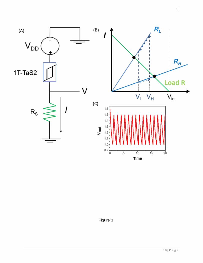
The simplest way of building an oscillator circuit is to combine MIT device (D) with a
resistor (R) in series as shown in Figure 3(A). The phase space of a single D-R
oscillator is shown in Figure 3(B). As in Ref. 16, we define conductance gdi=1/RH,
gdm=1/RL, gS=1/RS, where subscript d denotes a state dependent device conductance
and m/i denotes metallic/insulating state respectively, Rs correspond to the linear
resistor. Effective charging happens through gdm and whereas effective discharging
happens only through gs. The equation for the single D-R oscillator dynamics can be
described by the following set of piecewise linear differential equations written as 16:
ingdischvg
ingchvggvv
vc
S
Sdmdd
arg
arg)(
(1)
The D-R circuit produce oscillating output at certain combination of resistances RH,RL,
RS and bias voltage vdd, as explained in Figure 1(B). Lines with slopes RH and RL are
the regions of operation of the device in insulating and metallic states respectively. The
intersection of these lines with the load line due to the series resistance RS gives the
stable points of the system in the two states. In order to obtain self-sustained
oscillations, the stable points in each state should lie outside the region of operation, i.e.
outside the region defined by vertical lines passing through the transition points. In this
case, MIT device has phase transition before the circuit reaches the stable point. Figure
3(C) shows the results of numerical modeling illustrating the oscillating output of the D-
R oscillator. Hereafter, we depict all values in normalized units R0,I0, and V0 where
I0=V0/R0. In our numerical simulations, we use the following set of parameters vl =1 V0,
vh =2 V0, RH = 2.73 R0, RL = 0.67 R0, RS = 1 R0.
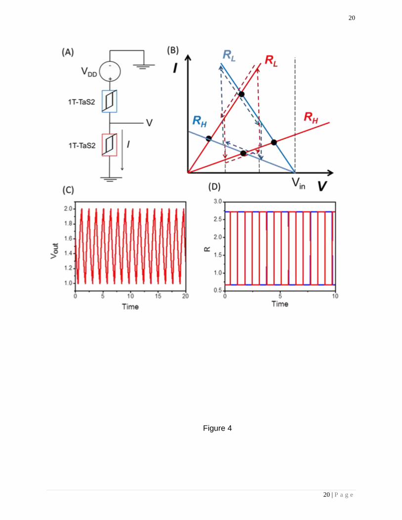
Following the same methodology, one can write the equation for D-D oscillator circuit
as shown in Fig 4(A):
ingdischvg
ingchgvv
vc
dM
dmdd
arg
arg)(
2
1
(2)
The only difference from the D-R case is that the effective charging happens through
g1dm and effective discharging through g2dm. The conditions leading to the self-sustained
oscillation are illustrated in Fig. 3(B). Due to the symmetry in I-V characteristics, two
MIT devices are biased in such a way, that the phase transition in each device occurs

6 | P a g e
6
before the system reaches one of the four stable points. In this scenario, as one of the
MIT devices changes its state from metallic to insulator, the second MIT device has
phase transfer from insulator to metal state, and vice versa. As a result, the system of
two MIT devices forms a complementary pair, where one of the devices is in high
resistance state, while the other is in low resistance state. Fig. 4(C) shows the results of
numerical modeling illustrating the switch between the resistance states for MIT devices
in D-D configuration. Compare to the R-D configuration, D-D circuit possesses a lower
leakage current similar to the well-established complementary metal oxide
semiconductor (CMOS).
There are different possible ways to oscillator coupling. There are two extreme cases
of purely resistive and purely capacitive coupling. In the case of purely resistive
coupling, two oscillators are tending to oscillate in phase. In contrast, purely capacitive
coupling makes the two oscillators to oscillate out of phase. The dynamics of purely
resistive and purely capacitive coupled D-D oscillators are described in details in Ref. 16.
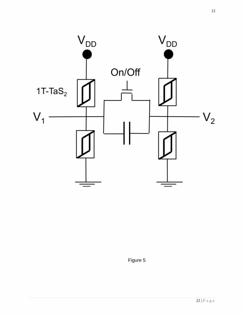
In this work, we propose the combination of MIT-based oscillators and a graphene
transistor as shown in Fig. 5. Two D-D circuits are coupled via resistance RC and
capacitance CC. The mutual capacitance Cc is fixed after the fabrication, while the
coupling resistance RC is controlled by the state of the graphene transistor (G-FET). In
the On state, the resistive coupling dominates forcing the two oscillators to oscillate in
phase. In the Off state, the capacitive coupling comes to the stage by introducing a π-
phase shift between the oscillators. It is important to note, that two capacitively coupled
D-D oscillators may occur in a meta-stable state (i.e. in-phase oscillation) till an external
perturbation will make the system to evolve towards the stable out-of-phase state. The
introduction of a transistor controlling the coupling between the MIT-based oscillators in
a network opens a number of intrigue possibilities for engineering special templates for
data processing. In the rest of this work, we show some examples of the proposed
approach
As a testbed, we consider a 30×30 template of identical D-D coupled oscillators (i.e.
as shown in Fig. 4). An elementary cell of the network is shown in Fig. 6, where a D-D
oscillator is connected to the four nearest-neighbor D-D oscillators. The position of the
cell in the network is defined by the two numbers Nx and Ny. The state of the cell is
7 | P a g e
7
assigned to the voltage V(NX,NY) as depicted in Fig.6(B). There are four junction
transistors connecting the central oscillators with the four neighbors. As in Fig.5, the
states of these transistors define the type of coupling (e.g. the On state of the transistor
corresponds to the inter-cell resistance of 0.1R0, the Off state corresponds to the inter-
cell resistance 10 R0). For instance, oscillator (NX,NY) can be capacitively coupled to the
oscillator (NX+1,NY) but resistively coupled to the other neighbors.
Let us consider a template with two regions consisting of capacitively and resistively
coupled oscillators. The capacitively coupled oscillators are located in the center of the
template (i.e. all oscillators around (15,15) with radius 7). All the oscillators outside this
region are resistively coupled. We assume all the oscillators to be biased with the same
voltage VDD=3V0. Such a network demonstrates an interesting dynamics, which is
illustrated by numerical modeling.
The color surface in Fig. 7 presents the results of numerical modeling. The color
surface shows the voltage map in the 2-D array of oscillators. Nx and Ny depict the
position of the oscillator in the network. The color depicts the voltage of the cell. The
resistively coupled oscillator oscillate in phase (i.e. the same voltage in every moment of
time), while the capacitively-coupled oscillators in the center oscillate out-of-phase. In
Fig. 8, we show the sequence of voltage maps calculated with the time interval of
0.05t0, where t0=R0C0, where C0 =0.01. This dynamics resembles a magnetic vortex,
where the position of magnetization is copied by the phase of oscillation. In contrast to
the steady-state magnetic vortexes, this artificial vortex in the sea of coupled oscillators
does not show any stead-state phase distribution. The phase difference between any
oscillator in the center and any oscillator out of the central region varies with time. This
phase evolution is defined by the set of electric characteristics as well as the geometry
of the capacitively-coupled region.
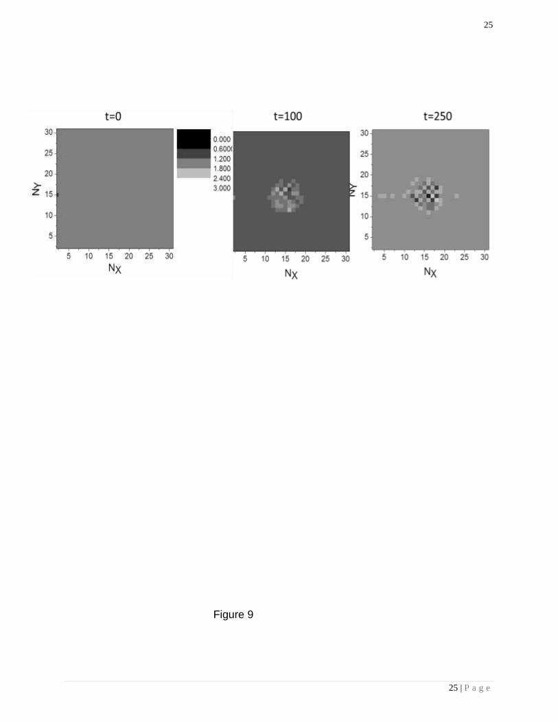
In Fig. 9, we present the results of numerical simulations showing signal propagation
through the network with partially capacitive and resistive-coupled oscillators. The initial
distribution of the cell voltages is shown in top left graph (i.e., t=0) . All of the cells
except one (2,15) are prepared in the meta-stable state oscillating in-phase regardless
of the coupling. The oscillator at (2,15) provides the input, which triggers the switch from
the metastable in phase to stable out-of-phase coupling for all capacitive coupled
8 | P a g e
8
oscillators. This switching is very well seen in the sequence of snapshots taken with
time interval depicted in t0. The propagation of the signal is associated with the
sequential change of the phase of oscillation for capacitive-coupled oscillators. For
instance, it shows the switch of the oscillation phase in the center circular region around
(Nx=15,Ny=15), with capacitevely coupled cells. As the signal propagates through the
template, one can see the phase ornament produced by the capacitively-coupled
oscillators.
It is interesting to note the similarity between the operation of the array of capacitively-
coupled oscillators and magnetic cellular automata 17. In both cases, the bulk of the
elementary cells are prepared in a metastable state. Signal propagation is resulted in
the cell relaxation. In magnetic cellular automata, the nearest-neighbor magnets tend to
be polarized in the opposite directions due to the dipole-dipole interaction. In the
network built of oscillators, the nearest-neighbor capacitively coupled oscillator trend to
oscillate out-of-phase. Potentially, the array of coupled oscillators can perform the same
basic logic operations such as MAJ and NOT gate as magnetic cellular automata18.
Finally, we present the results of numerical modeling showing the Game of Life in the
network of coupled 1T-TaS2 oscillators The Game of Life is a special version of cellular
automation invented by the J.H. Conway in 1970 19. It consists of a collection of cells
which may have two or more states (e.g. black and white). The cells change their states
according to the set of rules, which results in a system evolution mimicking living cell
birth, multiplication and death. Depending on the initial conditions, the cells may form
various patterns throughout the evolution. Game of Life offers an original way of
implementing complex Boolean operators in the space-time dynamics and presents a
testbed for artificial intelligence development.
IV. DISCUSSION
There are several technological advantages inherent to 1T-TaS2 – graphene devices
including scalability, high operation frequency, fast synchronization, voltage control of
operational frequency, flexibility, radiation hardness and room temperature operation.
It is well known that G-FETs show relatively low Ion/IOff ratio due to the absence of a
9 | P a g e
9
band gap, which is significantly narrows the perspectives of using G-FETs in
conventional digital logic 20 . In our proposed architecture, G-FETs are utilized for the
oscillatory circuits coupling, where the Ion/IOff ratio of 100 is sufficient for switching
between the resistive and capacitive regimes. At the same time, G-FETs can operate
at very high frequencies of hundreds of GHz 21, 22. The transitions between IC-CDW
and NC-CDW phases in 1T-TaS2 channel can reach frequencies of ~1 THz 23. These
considerations suggest that the frequency of operation of 1T-TaS2 – G-FET devices
can be increased substantially compared to the one demonstrated experimentally. In
the present experiments, the frequency is limited by the extrinsic RC time constants of
the probe station measurement apparatus. The intrinsic resistances and capacitances
can be reduced by scaling. It is important to note
that 1T-TaS2 – based oscillator circuits do not require any micro- or nano-inductor
components, which is one of the major issue for integrated magnetics 24. Additional
advantage of the selected material systems is that graphene and h-BN layers in the
device structure have extremely high thermal conductivity25, 26, and, as a result, act as
heat spreaders. Graphene is a very promising candidate for applications in flexible
electronics due to its high carrier mobility and mechanical flexibility 27. The
combination of graphene transistors with 2D 1T-TaS2 may pave a road towards the
new generation of flexible circuits. For some applications, e.g. deep-space probes,
radiation hardness is an important metric. The considered 1T-TaS2 – G-FETs are all-
metallic devices, which are less susceptible to radiation damage than semiconductors.
There have been a number of attempts to implement all-metallic switches and circuits,
ranging from metal dot single electron transistors, to metallic carbon nanotube
devices, and metallic nanowire transistors28-32. Our CDW devices belong to the same
class of devices that do not use semiconductor components. The results of our
numerical modeling show fast synchronization among the coupled oscillators. It takes
only a couple of cycles for the 1T-TaS2 – graphene device for transition from the in-
phase to the out-of-phase oscillatory states. This is another important benefit of the
proposed technology.
The presented data suggests that overall, the unique output characteristics of 1T-
10 | P a g e
10
TaS2 devices are of great potential for implementation in phase-based logic devices
using oscillatory nano-systems 33. Phase logic was invented by Eiichi Goto and John
von Neumann in the middle of the last century 34, 35. The key idea of this approach is to
exploit two (or more) distinct oscillating steady states for logical states representation.
The first phase-based logic devices were built more than sixty years ago primarily in
Japan and competed for some time with digital logic circuits. Later on, phase-based
logic devices left the stage due to the great success of transistors and integrated
circuits. Scalability and low operational speed are the two main disadvantages inherent
to von Neumann’s schemes. The need in large inductors and capacitors limits the size
of the oscillatory circuits. Also, periodic turn-on transients and delays in logic gates
make phase-based logic slower than transistorized level-based logic. The development
of nanometer systems together with the implementation of novel physical mechanisms
(e.g. spin torque oscillator 36) has led to the growing interest in phase-logic devices able
to overcome the limits of von Neumann’s schemes.
V. CONCLUSIONS
We presented a design of an oscillatory neural network based on integrated 1T-TaS2 –
graphene devices. The oscillations are driven by 1T-TaS2 channel switching between
two CDW states. Graphene FETs are used for coupling between the 1T-TaS2-based
oscillatory cells. . We illustrated the dynamics of the proposed network by numerical
modeling of a network comprising 3232 cells, where each cell consists of two 1T-TaS2
devices. The type of coupling (e.g. capacitive or resistive) between the nearest-
neighbor cells is controlled by the G-FETs. The results of numerical simulations reveal
potential of the proposed network for general and special task data processing. The
integrated 1T-TaS2 – graphene devices possess a unique combination of properties
such as scalability, high operational frequency, fast synchronization speed, radiation
hardness, which makes well suited for application in oscillatory networks.

11 | P a g e
11
ACKNOWLEDGMENT
This work was supported, in part, by the National Science Foundation (NSF) Emerging
Frontiers of Research Initiative (EFRI) 2-DARE project Novel Switching Phenomena in
Atomic MX2 Heterostructures for Multifunctional Applications (NSF 005400). The 1T-
TaSe2 crystals used for fabrication of the prototype devices were provided by Professor
Tina T. Salguero, University of Georgia.
12 | P a g e
12
Figure Captions
Figure 1. (A) Structure of 1T-TaS2 device. 1T-TaS2 thin film is fully covered with h-BN,
which acts as a protective layer against oxidation. (B) The optical image of a typical 1T-
TaS2 device.
Figure 2. (A) Current-voltage characteristics of 1T-TaS2 device at room temperature.
The CDW phase transition can be triggered by applying voltage beyond the threshold
level. (B) Oscillation waveform of a D-R circuit. The load resistance is 1kΩ, DC bias is
4.21V.
Figure 3. (A) Schematics of an oscillator circuit realized with a MIT device in series with
a resistor (D-R configuration). (B) Phase space of the device in a single (D-R) oscillator.
(C) Results of numerical modeling showing the output of the (D-R) oscillator.
Figure 4. (A) Schematics of relaxation oscillator circuit realized with two MIT devices
connected in series - (D-D) configuration. (B) Phase space of the D-D oscillator. (C)
Results of numerical modeling showing the output of the (D-D) oscillator. (D) Resistance
states of the 1T-TaS2 devices as a function of time. The devices are mostly in the
different resistance states (i.e. if one of the devices is in the high-resistance state, the
second one is in the low resistance state).
Figure 5. Schematics of two D-D coupled oscillators. The type of coupling is controlled
by the transistor. In the On state, the resistive coupling dominates forcing the two
oscillators to oscillate in phase. In the Off state, the capacitive coupling comes to the
stage by introducing a π-phase shift between the oscillators.
Figure 6. (A) Schematics of 2D network consisting of D-D coupled oscillators. (B)
Elementary cell of the network comprising nearest-neighbor coupled oscillators. The
coupling between the oscillators is controlled by the junction transistors

13 | P a g e
13
Figure 7. Results of numerical simulations. The color surface shows the voltage map in
the 2-D array of oscillators. Nx and Ny depict the position of the oscillator in the
network. The oscillators in the center of the network around Nx=15, Ny=15 with radius
7, are capacitively coupled. The rest of the oscillators are resistively coupled.
Figure 8. Results of numerical simulations showing the dynamics in the template with
capacitively- (center) and resistively- (out of the central region) coupled oscillators. The
graphs (A-E) are the snapshots of the network voltage map taken with the time step
0.05[RC].
Figure 9. Results of numerical modeling illustrating Cellular Automata-like network
operation. (A) The initial distribution of the cell voltages. All of the cells except one
(2,15) are prepared in the meta-stable state oscillating in-phase regardless of the
coupling. (B) and (C) signal propagation is associated with the switch of the oscillation
phase in the center circular region around (Nx=15,Ny=15).
Figure 10. Results of numerical simulations showing system evolution. (A) Starting
configurations. There is a group of capacitively-coupled oscillators in the left bottom
corner – cell alive. All other oscillators oscillate in-phase – dead cells. (B) System
evolves by driving more capacitively-coupled oscillators out of the metastable state. (C)
Culmination of living cell growth. As the living cells reach the top right corner, it triggers
the coupling switch for the oscillators in the left bottom corner. The oscillators become
resistively coupled. (D) The oscillators in the left bottom corner oscillate in-phase, which
symbolizes cell death.
14 | P a g e
14
REFERENCES
1. V. P. Shmerko and S. N. Yanushkevich, Journal of Computational and
Theoretical Nanoscience 7 (2), 303-324 (2010).
2. F. C. Hoppensteadt and E. M. Izhikevich, Physical Review Letters 82 (14),
2983-2986 (1999).
3. L. O. Chua and L. Yang, IEEE Transactions on Circuits & Systems 35 (10),
1257-1272 (1988).
4. T. Matsumoto, L. O. Chua and T. Yokohama, IEEE Transactions on Circuits &
Systems 37 (5), 638-640 (1990).
5. K. R. Krieg, L. O. Chua and L. Yang, presented at the 1990 IEEE International
Symposium on Circuits and Systems (Cat. No.90CH2868-8). IEEE. 1990,
pp.958-61 vol.2. New York, NY, USA. (unpublished).
6. T. Roska, T. Boros, P. Thiran and L. O. Chua, presented at the 1990 IEEE
International Workshop on Cellular Neural Networks and their Applications,
CNNA-90 (Cat. No.90TH0312-9). IEEE. 1990, pp.127-38. New York, NY, USA.
(unpublished).
7. P. L. Venetianer, F. Werblin, T. Roska and L. O. Chua, IEEE Transactions on
Circuits & Systems I-Fundamental Theory & Applications 42 (5), 278-284 (1995).
8. http://www.itrs.net/Links/2013ITRS/2013Chapters/2013ERD.pdf, 7-10 (2013).
9. D. E. Nikonov and I. A. Young, Proceedings of the IEEE 101 (12), 2498-2533
(2013).
10. G. Csaba, M. Pufall, D. E. Nikonov, G. I. Bourianoff, A. Horvath, T. Roska
and W. Porod, in 2012 13th International Workshop on Cellular Nanoscale
Networks and Their Applications, edited by F. Corinto and G. E. Pazienza (2012).
11. G. Liu, B. Debnath, T. R. Pope, T. T. Salguero, R. K. Lake and A. A.
Balandin, Nature Nanotechnology (2016).
12. G. Gruner, Reviews of Modern Physics 60 (4), 1129-1182 (1988).
13. T. L. Adelman, S. V. Zaitsevzotov and R. E. Thorne, Physical Review Letters
74 (26), 5264-5267 (1995).
14. S. V. Zaitsev-Zotov, Physics-Uspekhi 47 (6), 533-554 (2004).

15 | P a g e
15
15. D. E. Moncton, J. D. Axe and F. J. Disalvo, Physical Review Letters 34 (12),
734-737 (1975).
16. A. Parihar, N. Shukla, S. Datta and A. Raychowdhury, JOURNAL OF
APPLIED PHYSICS 117 (5) (2015).
17. R. P. Cowburn and M. E. Welland, Science 287 (5457), 1466-1468 (2000).
18. A. Imre, G. Csaba, L. Ji, A. Orlov, G. H. Bernstein and W. Porod, Science
311 (5758), 205-208 (2006).
19. M. Gardner, Sci. Amer. 223 (4), pp. 120-123 (1970).
20. P. Avouris, Nano Letters 10 (11), 4285-4294 (2010).
21. Y. M. Lin, A. Valdes-Garcia, S. J. Han, D. B. Farmer, I. Meric, Y. N. Sun, Y.
Q. Wu, C. Dimitrakopoulos, A. Grill, P. Avouris and K. A. Jenkins, Science 332
(6035), 1294-1297 (2011).
22. Y. Q. Wu, Y. M. Lin, A. A. Bol, K. A. Jenkins, F. N. Xia, D. B. Farmer, Y. Zhu
and P. Avouris, Nature 472 (7341), 74-78 (2011).
23. L. Perfetti, P. A. Loukakos, M. Lisowski, U. Bovensiepen, M. Wolf, H.
Berger, S. Biermann and A. Georges, New Journal of Physics 10 (2008).
24. C. O. Mathuna, N. N. Wang, S. Kulkarni and S. Roy, Ieee Transactions on
Power Electronics 27 (11), 4799-4816 (2012).
25. A. A. Balandin, Nature Materials 10 (8), 569-581 (2011).
26. I. Jo, M. T. Pettes, J. Kim, K. Watanabe, T. Taniguchi, Z. Yao and L. Shi,
Nano Letters 13 (2), 550-554 (2013).
27. W. J. Zhu, D. B. Farmer, K. A. Jenkins, B. Ek, S. Oida, X. S. Li, J.
Bucchignano, S. Dawes, E. A. Duch and P. Avouris, Applied Physics Letters 102
(23) (2013).
28. A. N. Korotkov, R. H. Chen and K. K. Likharev, JOURNAL OF APPLIED
PHYSICS 78 (4), 2520-2530 (1995).
29. V. A. Zhukov and V. G. Maslov, Russ. Microelectron. 42 (102), 102-112
(2013).
30. V. A. Krupenin, A. B. Zorin, M. N. Savvateev, D. E. Presnov and J.
Niemeyer, JOURNAL OF APPLIED PHYSICS 90 (5), 2411-2415 (2001).
16 | P a g e
16
31. Q. H. Liu, L. L. Yu, H. Li, R. Qin, Z. Jing, J. X. Zheng, Z. X. Gao and J. Lu,
Journal of Physical Chemistry C 115 (14), 6933-6938 (2011).
32. H. H. Cheng, C. N. Andrew and M. M. Alkaisi, Microelectronic Engineering
83 (4-9), 1749-1752 (2006).
33. W. Tianshi and J. Roychowdhury, PHLOGON: PHase-based LOGic using
Oscillatory Nano-systems. (2014).
34. E. G., Patent No. US Patent 2,948,818 (1960).
35. J. v. Neumann, Collected Works. Design of Computers,Theory of Automata
and Numerical Analysis. (Pergamon Press New York, 1963).
36. W. H. Rippard, M. R. Pufall, S. Kaka, T. J. Silva and S. E. Russek,
PHYSICAL REVIEW B 70 (10) (2004).

17 | P a g e
17
Figure 1

18 | P a g e
18
Figure 2
19 | P a g e
19
Figure 3
20 | P a g e
20
Figure 4
21 | P a g e
21
Figure 5

22 | P a g e
22
Figure 6

23 | P a g e
23
Figure 7

24 | P a g e
24
Figure 8
25 | P a g e
25
Figure 9

26 | P a g e
26
Figure 10