A Finite-Element Approach to Analyze the Thermal Effect of Defects on Silicon-Based PV Cells
8
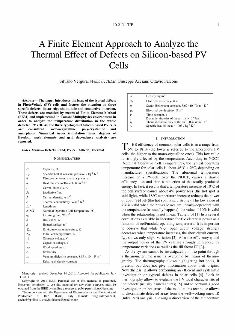
10-2131-TIE 1 Abstract— The paper introduces the issue of the typical defects in PhotoVoltaic (PV) cells and focuses the attention on three specific defects: linear edge shunt, hole and conductive intrusion. These defects are modeled by means of Finite Element Method (FEM) and implemented in Comsol Multiphysics environment in order to analyze the temperature distribution in the whole defected PV cell. All the three typologies of Silicon-based PV cells are considered: mono-crystalline, poly-crystalline and amorphous. Numerical issues (simulation times, degrees of freedom, mesh elements and grid dependence analysis) are reported. Index Terms— Defects, FEM, PV cell, Silicon, Thermal NOMENCLATURE C Capacity, pF Cp Specific heat at constant pressure, J kg -1 K -1 d Distance between capacitor plates, m h Heat transfer coefficient, W m -2 K -1 I Current intensity, A J0 Irradiative flux J Current density, A m -2 k Thermal conductivity, W m -1 K -1 L, l Length, m NOCT Nominal Operative Cell Temperature, °C q0 Incoming flux, W m -2 R Resistance, Ω A Heated surface, m 2 Τenv Environmental temperature, K Tinf Initial cell temperature, K V0 Constant voltage, V vc Capacitor voltage, V w0 Wind speed, m s -1 ε Emissivity ε 0 Vacuum dielectric constant, 8.85 × 10 -12 F m -1 εr Relative dielectric constant Manuscript received December 14 ,2010. Accepted for publication July 11, 2011. Copyright © 2011 IEEE. Personal use of this material is permitted. However, permission to use this material for any other purposes must be obtained from the IEEE by sending a request to [email protected]. The authors are with the Department of Electrotechnics and Electronics of Politecnico di Bari, BARI, Italy (e-mail: [email protected], [email protected], [email protected]). ρ Density, kg m -3 ρel Electrical resistivity, Ω m σ Stefan-Boltzmann constant, 5.67 *10 -8 W m -2 K -4 σel Electrical conductivity, S m -1 τ μ kf cf Time constant, s Dynamic viscosity of the air, 1.81×10 -5 Pa s Thermal conductivity of the air, 0,026 W m -1 K -1 Specific heat of the air, 1005 J kg -1 K -1 I. INTRODUCTION HE efficiency of common solar cells is in a range from 5% to 18 % (the lower is referred to the amorphous PV cells, the higher to the mono-crystalline ones). This low value is strongly affected by the temperature. According to NOCT (Nominal Operative Cell Temperature), the typical operating temperature for solar cells is about 46°C ± 2°C, depending on manufacturer specifications. The abnormal temperature increase of a PV-cell, over the NOCT, causes a drastic efficiency loss and then a reduction of the totally produced energy. In fact, it results that a temperature increase of 10°C of the cell surface causes about 4% power loss (the hot spot is said light), while 18°C temperature increase reduces the power of about 7÷10% (the hot spot is said strong). The low value of 7% is valid when the power losses are linearly-dependent with the temperature (as usually happens), the value of 10% is valid when the relationship is not linear; Table 3 of [1] lists several correlations available in literature for PV electrical power as a function of cell/module operating temperature. It is important to observe that while V OC (open circuit voltage) strongly decreases when temperature increases, the short circuit current, I SC , shows only slight variation [2]. Also the efficiency η and the output power of the PV cell are strongly influenced by temperature variations as well as the fill factor FF [3]. As the system cannot be investigated point-to-point through a thermometer, the issue is overcome by means of thermo- graphy. The thermography allows highlighting hot spots, if present, but does not give information about their origins. Nevertheless, it allows performing an efficient and systematic investigation on typical defects in solar cells [4]. Lock in thermography allows to evaluate the I-V local characteristic of the defects (usually named shunts) [5] and to perform a good investigation on hot areas of the module; this technique allows to discriminate defected areas from the well-working ones. IR (Infra Red) analysis, allowing a direct view of the temperature A Finite Element Approach to Analyze the Thermal Effect of Defects on Silicon-based PV Cells Silvano Vergura, Member, IEEE, Giuseppe Acciani, Ottavio Falcone T
Transcript of A Finite-Element Approach to Analyze the Thermal Effect of Defects on Silicon-Based PV Cells
10-2131-TIE 1
Abstract— The paper introduces the issue of the typical defects
in PhotoVoltaic (PV) cells and focuses the attention on three
specific defects: linear edge shunt, hole and conductive intrusion.
These defects are modeled by means of Finite Element Method
(FEM) and implemented in Comsol Multiphysics environment in
order to analyze the temperature distribution in the whole
defected PV cell. All the three typologies of Silicon-based PV cells
are considered: mono-crystalline, poly-crystalline and
amorphous. Numerical issues (simulation times, degrees of
freedom, mesh elements and grid dependence analysis) are
reported.
Index Terms— Defects, FEM, PV cell, Silicon, Thermal
NOMENCLATURE
C
Capacity, pF
Cp Specific heat at constant pressure, J kg-1 K-1
d Distance between capacitor plates, m
h Heat transfer coefficient, W m-2 K-1
I Current intensity, A
J0 Irradiative flux
J Current density, A m-2
k Thermal conductivity, W m-1 K-1
L, l Length, m
NOCT Nominal Operative Cell Temperature, °C
q0 Incoming flux, W m-2
R Resistance, Ω
A Heated surface, m2
Τenv Environmental temperature, K
Tinf Initial cell temperature, K
V0 Constant voltage, V
vc Capacitor voltage, V
w0 Wind speed, m s-1
ε Emissivity
ε0 Vacuum dielectric constant, 8.85 × 10⁻¹² F m-1
εr Relative dielectric constant
Manuscript received December 14 ,2010. Accepted for publication July
11, 2011.
Copyright © 2011 IEEE. Personal use of this material is permitted.
However, permission to use this material for any other purposes must be
obtained from the IEEE by sending a request to [email protected].
The authors are with the Department of Electrotechnics and Electronics of
Politecnico di Bari, BARI, Italy (e-mail: [email protected],
[email protected], [email protected]).
ρ Density, kg m-3
ρel Electrical resistivity, Ω m
σ Stefan-Boltzmann constant, 5.67 *10-8 W m-2 K-4
σel Electrical conductivity, S m-1
τ µ kf
cf
Time constant, s
Dynamic viscosity of the air, 1.81×10⁻⁵ Pa s
Thermal conductivity of the air, 0,026 W m-1 K-1
Specific heat of the air, 1005 J kg-1 K-1
I. INTRODUCTION
HE efficiency of common solar cells is in a range from
5% to 18 % (the lower is referred to the amorphous PV
cells, the higher to the mono-crystalline ones). This low value
is strongly affected by the temperature. According to NOCT
(Nominal Operative Cell Temperature), the typical operating
temperature for solar cells is about 46°C ± 2°C, depending on
manufacturer specifications. The abnormal temperature
increase of a PV-cell, over the NOCT, causes a drastic
efficiency loss and then a reduction of the totally produced
energy. In fact, it results that a temperature increase of 10°C of
the cell surface causes about 4% power loss (the hot spot is
said light), while 18°C temperature increase reduces the power
of about 7÷10% (the hot spot is said strong). The low value of
7% is valid when the power losses are linearly-dependent with
the temperature (as usually happens), the value of 10% is valid
when the relationship is not linear; Table 3 of [1] lists several
correlations available in literature for PV electrical power as a
function of cell/module operating temperature. It is important
to observe that while VOC (open circuit voltage) strongly
decreases when temperature increases, the short circuit current,
ISC, shows only slight variation [2]. Also the efficiency η and
the output power of the PV cell are strongly influenced by
temperature variations as well as the fill factor FF [3].
As the system cannot be investigated point-to-point through
a thermometer, the issue is overcome by means of thermo-
graphy. The thermography allows highlighting hot spots, if
present, but does not give information about their origins.
Nevertheless, it allows performing an efficient and systematic
investigation on typical defects in solar cells [4]. Lock in
thermography allows to evaluate the I-V local characteristic of
the defects (usually named shunts) [5] and to perform a good
investigation on hot areas of the module; this technique allows
to discriminate defected areas from the well-working ones. IR
(Infra Red) analysis, allowing a direct view of the temperature
A Finite Element Approach to Analyze the
Thermal Effect of Defects on Silicon-based PV
Cells
Silvano Vergura, Member, IEEE, Giuseppe Acciani, Ottavio Falcone
T
10-2131-TIE 2
distribution on PV cells and on the other PV system
components, may be considered as a valid diagnostic tool,
useful during the development, production and monitoring of
all PV system components [6].
The origin of the hot spots in PV cells is due to the defects,
some of them reported in [7]-[8]-[9]. Some authors have
modeled an electro-thermal PV module, but not for the aim to
study the defects [10]. Other authors have proposed thermal
model for photovoltaic panels under varying atmospheric
conditions [11].
The aim of the paper is to model three typologies of defects
by means of FEM and to simulate the thermal behavior of the
different PV cells. Until some years ago the FEM analysis was
not largely used because the most of the PCs was not able to
manage the high computational burden required by the FEM
analysis. Nowadays, instead, the PCs have highest
performances for both the processing and storage of the data.
For this reason, FEM analysis is now used in very different
fields and whenever detailed and accurate results are needed.
In fact FEM analysis is used for studying the electromagnetic
vibrations in electrical machine [12], the thermal effects in
power devices carrying large currents [13], the axial flux and
fault diagnoses in synchronous motors [14]-[15], and so on.
In this paper FEM will be used for analyzing the thermal
behavior of defected PV cells. Specifically, it will be studied
three defects occurring in the three different typologies of
Silicon-based PV cells: mono-crystalline (mono-Si), poly-
crystalline (poly-Si) and amorphous (a-Si).
Specific defects for mono-Si and poly-Si PV cells are
reported in [16]. This paper adds to the previous one the
theoretical basis of the thermal and electrical constraints, the
modeling and analysis for specific defects of a-Si cells and,
finally, a numerical analysis of the simulation results of all the
three typologies of PV cells. Specifically, linear edge shunt
and hole are typical defects of mono-Si and poly-Si cells; then
both of them will be modeled, implemented and simulated for
these specific typologies of Silicon cells. The defects will be
inserted into the 3-D model of well-operating PV cells [17],
even if the model of this paper is an upgraded version, because
the glass has been added and thermal insulation has been
imposed. On the other hand, conductive intrusion is typical
defect of a-Si cells. Also this defect will be modeled,
implemented and simulated for an a-Si cell. All the simulations
will be run in Comsol Multiphysics environment and
simulation times, grid dependence analysis and solvers will be
compared each other.
The paper is organized as follows: defects of PV cells and
IR analysis are presented in Sec. II, geometrics and physics of
PV cells are introduced in Sec. III, thermal and electrical
constraints are studied in Section IV, models and simulation
results are reported in Sec. V, conclusions end the paper.
II. CHARACTERISTIC DEFECTS AND THERMO-GRAPHY
IR analysis allows performing an efficient and systematic
investigation on the defects in solar cells [4]. A division of
typical defects in two categories is possible according to the I-
V characteristic: the shunt is defined resistive-like if it is
highlighted under forward bias as well as under reverse bias. If
the shunt compares only under forward bias it is defined
diode-like. From a physical point of view another
classification is possible. The shunts can be grouped in two
categories: material induced and process induced. The former
one comes from specific features of the substrate, the latter one
is related to the fabrication steps. In this paper the attention is
focused only on the second one, specifically linear edge shunt
and hole for mono-Si and poly-Si PV cells and conductive
intrusion for a-Si ones.
Let us introduce the three defects. Linear edge shunt comes
from a bad edge insulation of the solar cell; when this
incomplete insulation occurs, a low resistivity walk stats
between top and bottom electrodes of the cell. This low
resistivity walk acts like a short circuit on one side of the cell.
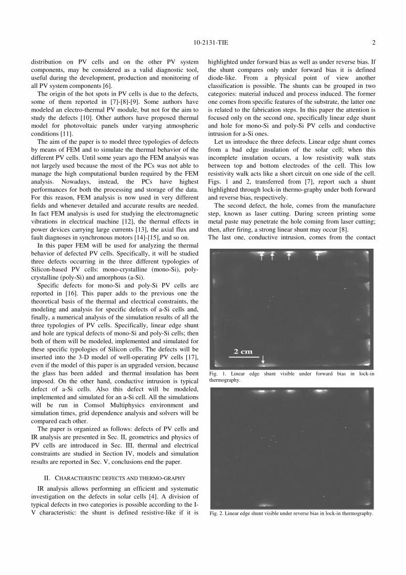
Figs. 1 and 2, transferred from [7], report such a shunt
highlighted through lock-in thermo-graphy under both forward
and reverse bias, respectively.
The second defect, the hole, comes from the manufacture
step, known as laser cutting. During screen printing some
metal paste may penetrate the hole coming from laser cutting;
then, after firing, a strong linear shunt may occur [8].
The last one, conductive intrusion, comes from the contact
Fig. 2. Linear edge shunt visible under reverse bias in lock-in thermography.
Fig. 1. Linear edge shunt visible under forward bias in lock-in
thermography.
10-2131-TIE 3
setup. The conductive material penetrating the structure may
lead to a direct contact of the different areas of the wafer. If
this direct contact stats between cell electrodes, these will be
short-circuited.
Other existing defects classified as process induced, but not
studied in this paper, are the following:
• entrapped air, which comes from mistakes that may occur
in the setting of the different parameters (temperature,
vacuum, operating time) that characterize the fabrication
step, known as rolling-mill process.
• non linear edge shunt, which can be interpreted as
recombination sites.
• Schottky-type which generates when the emitter
metallization is sintered and acts as a Schottky diode with
non-unity ideality factor.
• Scratches, which determine a p-n junction with a surface
with high density of recombination centers, if present at
the surface of solar cell across the emitter layer (this
shunt is non-linear).
• Aluminum particles, which can create a tunnel contact
between base and emitter generating a shunt.
III. GEOMETRICS AND PHYSICS
The photovoltaic cell is a three-dimensional-five-layer
structure obtained from the superposition of different materials
each one with specific thickness. Each layer has been carried
out with the characteristic thickness it has in real PV cell
structure. The model of a defect has to be inserted into the
model of a well-working PV cell. For this aim, the defects for
mono-Si and poly-Si cells have been inserted into the 3D
model described in [17] (upgraded by adding the glass), while
the well-working model of the a-Si cell is reported in the
following. The structure of the modeled a-Si cell has been
developed according to geometric dimensions of a real
amorphous PV cell: 12,5 cm length and an overall thickness of
about 340 µm.
The upper layer, glass, has been modeled with thickness of 4
mm; the top plate of the cell has been modeled with thickness
of 150 µm and as to be composed of silver; the lower layer,
bottom plate of the cell, has thickness of 100 µm; the thickness
of ITO (Indium Thin Oxide) layer is 85 µm. Finally for the
silicon layer a thickness of 5 µm has been set up.
As the model has to be analyzed by means of FEM based
software, the perfect overlap of the single layers is a critical
factor during Comsol’s mesh generation step. In fact an
incomplete overlapping of the layers may cause the presence
of empty spaces and an incomplete mesh error may occur. To
overcome this problem two utilities available in the Comsol
CAD interface, (Geometric Entities Union and Coerce to
solid) have been successfully used. In this way no problem
occurs during mesh generation.
To complete the model definition the physical features of
each layer have to be set up. The setting of these specific
features depends on the analysis to be run. The value of
thermal conductivity or specific heat has to be set for the
thermal analysis, while the value of the electrical conductivity
has to be imposed for the electrical one. Each metallization has
been modeled with Silver.
For studying the behavior of the defects, multiphysical
analysis has been run using two modules of Comsol (Heat
Transfer and AC/DC).
IV. THERMAL AND ELECTRICAL CONSTRAINTS
After defining the geometric and physic structure, it is
needed to set correctly the thermal parameters for analyzing
the thermal behavior of a PV cell. Table I summarizes the
values of thermal conductivity k, specific heat CP and density ρ
of each material constituting the 3 typologies of Silicon-based
PV cells.
Note that the parameters of the support oxide layer as well
as of the a-Si one are expressed by a temperature-dependent
equations, as reported in standard Comsol libraries.
TABLE I
THERMAL PARAMETERS VALUE
The problem is completely defined when correct constraints
on temperature and radiation have been imposed on domain
boundaries. A widening is necessary about boundary
conditions. Comsol environment allows choosing between two
different typologies of boundary conditions:
• Dirichlet’s condition: values of the solution on
boundaries must be fixed;
• Neuman’s condition: values of solution derivatives on
boundaries must be fixed.
When the Heat Transfer Module is used, boundary
conditions can be set up on temperature or on thermal flux. If a
temperature constraint is considered, the condition is:
0T=T (1)
It is clearly a Dirichlet’s condition. Instead, equation (2)
expresses the constraint on thermal flux and is a Neuman’s
condition:
tot-n q=q⋅ (2)
For the proposed model the Neuman’s condition has been
imposed and the mathematical model is the following:
4 4
0 env inf-n q=q +σε(T -T )+h(T -T)⋅ (3)
where the values of the parameters have to be set as follows
(according to NOCT specifications). The term q0, which
corresponds to the incoming flux, is set up equal to 800 W/m2,
Material k [W/(m*K)] ρ [kg/m3] Cp [J/(kg*K)]
Glass
Ag
mono-Si
poly-Si a-Si
ITO TiO2
χ(T) 429
163
34 α(T)
87 δ(T)
φ(T) 10,500
2,330
2,320 β(T)
7,120 ε(T)
ψ(T) 235
703
678 γ(T)
753 ζ(T)
10-2131-TIE 4
the second term is the radiative contribution to the total flux on
the cell while the third term is the convective contribution to
the total flux. The parameters in the second term are the
Stefan-Boltzmann constant σ and the emissivity ε whose
values are shown in the Table II; Tenv represents the
environment temperature.
TABLE II
EMISSIVITY VALUES
The third term depends by the heat transfer coefficient h and
the difference between the initial cell temperature, Tinf, and the
unknown temperature. The value of the initial temperature of
the cell has been set up equal to 293.15 K while the h value
has been computed equal to 11 W/m2K, as follows.
The heat transfer coefficient h is the factor that links the heat
swapped for convection between a solid and the fluid lapping
it and the difference between the temperatures of the solid and
the fluid, according to the well known Newton’s equation:
s 0Q=hA(T -T ) (4)
where Q is the total heat transfer, A is the heated surface area,
Ts the surface temperature and T0 the mean temperature of the
fluid. For the convection heat transfer to have a physical
meaning, there must be a temperature difference between the
heated surface and the moving fluid. According on convective
heat transfer theory, the value of the following dimensionless
numbers has to be computed in order to evaluate the correct
value of h:
0
e
ρ w LR =
µ
⋅ ⋅(Reynolds number) (5)
where ρ is the fluid density (1,204 kg/m3 for air at NOCT
conditions), w0 the fluid speed (1m/s for air in NOCT
conditions), L the length of the cell and the dynamic
viscosity of the air;
fu
h LN =
k
⋅ (Nusselt number) (6)
where kf is the thermal conductivity of the air and, finally,
f
fr
cP
k
µ ⋅= (Prandtle number) (7)
with cf specific heat of the air. With a length value of 12.5 cm
set up on the modeled PV cell, the value of Reynolds number
is 7890 and the flux is still laminar. Using the Nusselt relations
which applies for constant surface temperature and horizontal
flat surfaces (valid for laminar flow [18]) it results:
0.5 0.33Nu 0.664 Re Pr= ⋅ ⋅ (8)
The Nu value has been computed to be equal to 52.9. Using
this value in (6) the value of the heat transfer coefficient to be
set up on both surfaces of the implemented solar device is
equal to 11 W/m2K. This value agrees with the hypothesis of
air in natural convection incoming on the cell [19]. So the
thermal setting for the FEM-based analysis is complete.
Now, the implemented model has to be validated from the
electrical point of view considering a system including a
parallel RC circuit connected to the solar device: it
corresponds to simulate the cell acting as a current source.
This procedure has been used for all the three typologies of PV
cells. Through the CAD Module a resistor and a capacitor
have been modeled. The starting points for their modeling are
the well known equations (9) and (10) which link the value of
capacity and resistance to their geometrical and physical
features:
el
lR = ρ
S⋅ (9)
where ρel is the resistivity of the modeled material, l the length,
S the section.
0 r
SC = ε ε
d (10)
with ε0 vacuum dielectric constant, S the section, d the distance
between the two plates of the capacitor and finally εr the
relative dielectric constant whose value has been set equal to 6
(mica has been chosen as capacitor dielectric layer). The
values of resistance and capacity have been fixed as
R=1Ω, C=200 pF, then the time constant of the circuit is -10 -1
τ = RC = 2×10 [s ] . Other choices for the value of R and
C could be equally valid; in fact, as we are validating the
model from the electrical point of view, then each possible
operating point can be chosen. Obviously, even if the optimal
operating point is the Maximum Power Point (MPP),
nevertheless often the real operating point is different from
MPP (e.g., well functioning PV cells do not work in their
MPP, when connected in series with a defected one); in these
cases the PV cell works, but do not produce the maximum
energy.
This value has to be set up into the model available in
Comsol’s equation setting mask for AC/DC module:
( ) a∂ ∂ ∂ ∂ +∇⋅ − ∇ − + + + ⋅∇ =a
e t V t c V V V V f2 2
aV +d α γ β (11)
A suitable setting of the parameters in (11) has to be set to
obtain the correct Kirchhoff Voltage Low for RC circuits
Material ε
Ag
Si(mono)
Si(poly)
TiO2
0.01
0.85
0.85 0.9
10-2131-TIE 5
according to circuit theory. So the value of c, ea, α, β, γ will
be set up to zero, a to 1, da to the value of the time constant as
expressed in (10).
A boundary condition of incoming current flux has been
imposed on the cell surface directly connected to the RC
bipolar circuit. Equation (12) is the Neuman’s condition while
(13) reports the model used to compute the correct value for
the current density to be set in (12):
- n J=Jn
⋅ (12)
I=Jn
S⋅ (13)
Finally on the upper electrode a zero voltage condition has
been set while on the lower one a Dirichlet’s condition has
been imposed (equal to 0.6 V).
The simulation has been run in transient analysis and the
time parameters have been set up as follows:
• beginning t = 0
• final time t = 6τ
• simulation steps two orders lower than τ.
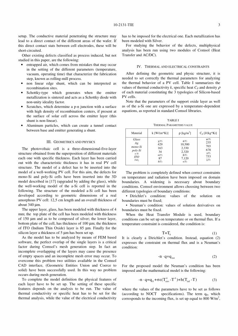
Fig. 3 allows verifying the capacitor voltage reaches the final value after 4-5 times the time constant value. Then, also the electrical validation is complete.
Fig. 3. Time domain voltage for the capacitor pins.
V. SIMULATIONS AND NUMERICAL RESULTS
This Section reports the results of the simulated defects and
some numerical aspects. Particularly,
• simulation results for linear edge shunts for both mono-
Si and poly-Si cases (Subsection A);
• simulation results for the hole defect for both mono-Si
and poly-Si cases (Subsection B);
• simulation results for conductive intrusion for a-Si case
(Subsection C);
• computational burden and grid dependence analysis
(Subsection D).
A. Linear edge shunt
It comes from a not correct electrical insulation of some
areas on the side of the cell. It can be considered as a short
circuit on one side of the device and it has been implemented
just as short-circuit. The linear edge shunt has been modeled
with a thin layer of conductive material connecting top and
bottom electrode of the cell. Its geometric dimension is 1 cm
length and 250 µm height. According to the theory it has to be
modeled as a low resistivity walk; so the value of conductivity
σel has been set to the 2× 10⁴ S/m value. Across the cell pins a
voltage of 0.6 V(as start condition) has been applied while the
conditions on domains, sub-domains and boundaries are those
explained in [17], coming from NOCT specifications. These
are the initial conditions (valid for t =0-) imposed in the
simulation settings. At the instant t = 0, the simulation run and
the currents flowing in the circuit and the voltages across the
pins vary as LKC and LKT, respectively. Fig. 4 reports the
simulation results for a mono-Si PV cell. As already said, this
model is upgraded with respect to that of [17], because the
superior glass has been added and the thermal insulation has
been imposed . It can be noted that the maximum value of the
temperature reaches about 53.9 °C while the minimum value is
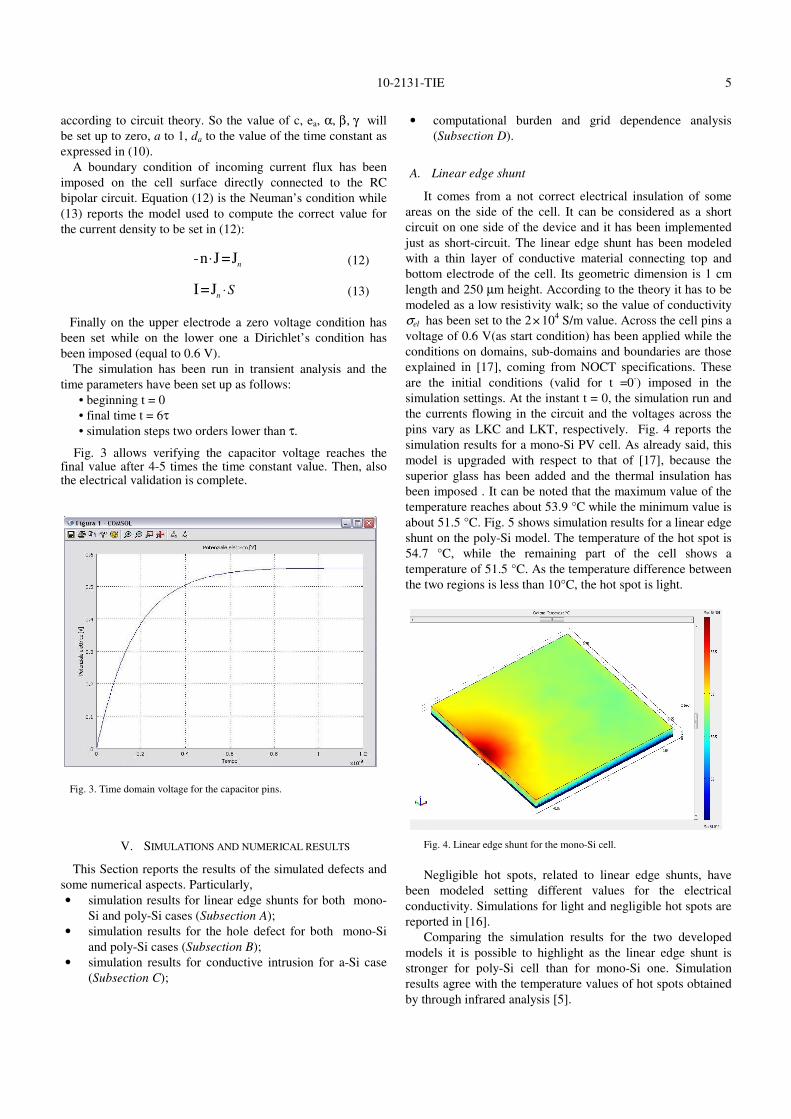
about 51.5 °C. Fig. 5 shows simulation results for a linear edge
shunt on the poly-Si model. The temperature of the hot spot is
54.7 °C, while the remaining part of the cell shows a
temperature of 51.5 °C. As the temperature difference between
the two regions is less than 10°C, the hot spot is light.
Fig. 4. Linear edge shunt for the mono-Si cell.
Negligible hot spots, related to linear edge shunts, have
been modeled setting different values for the electrical
conductivity. Simulations for light and negligible hot spots are
reported in [16].
Comparing the simulation results for the two developed
models it is possible to highlight as the linear edge shunt is
stronger for poly-Si cell than for mono-Si one. Simulation
results agree with the temperature values of hot spots obtained
by through infrared analysis [5].
10-2131-TIE 6
Fig. 5. Linear edge shunt on the poly-Si cell.
B. Hole
It has been considered the same model of the hole defect
for both mono-Si and poly-Si PV cells. A thin cylindrical
connection between top and bottom plats has been put into the
upgraded well-operating PV cell structure [17]. Hole defect
has been modeled as a 2 mm-diameter cylinder (Fig. 6)
constituted of metal paste. In this case the conductivity σel of
the low resistivity walk has been set to 103S/m. Electrical and
thermal conditions on domains, sub-domains and boundaries
have been set according to [17]. Fig. 7 diagrams the
temperature distribution for the defected cell. It is possible to
note that the value of the temperature of the area interested by
the shunt is about 52°C, i.e. 1,5°C higher than the temperature
of the remaining part of the cell. This result represents a light
hot spot.
Finally, Fig. 8 shows the temperature distribution on the
poly-Si cell affected by hole. In this case the hot spot
connected to the hole is negligible. In fact, the hot spot reaches
a temperature of about 53.2°C while the remaining cell shows
a temperature of 52°C.
Fig. 6. Model of hole defect.
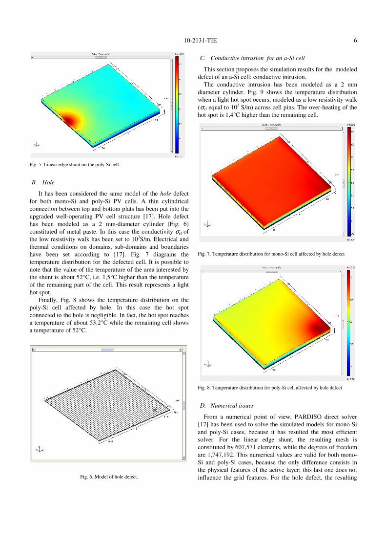
C. Conductive intrusion for an a-Si cell
This section proposes the simulation results for the modeled
defect of an a-Si cell: conductive intrusion.
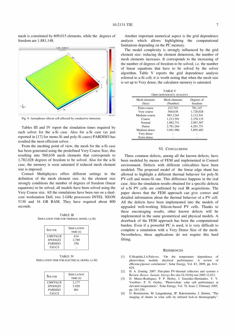
The conductive intrusion has been modeled as a 2 mm
diameter cylinder. Fig. 9 shows the temperature distribution
when a light hot spot occurs, modeled as a low resistivity walk
(σel equal to 103 S/m) across cell pins. The over-heating of the
hot spot is 1,4°C higher than the remaining cell.
Fig. 7. Temperature distribution for mono-Si cell affected by hole defect
Fig. 8. Temperature distribution for poly-Si cell affected by hole defect
D. Numerical issues
From a numerical point of view, PARDISO direct solver
[17] has been used to solve the simulated models for mono-Si
and poly-Si cases, because it has resulted the most efficient
solver. For the linear edge shunt, the resulting mesh is
constituted by 607,571 elements, while the degrees of freedom
are 1,747,192. This numerical values are valid for both mono-
Si and poly-Si cases, because the only difference consists in
the physical features of the active layer; this last one does not
influence the grid features. For the hole defect, the resulting
10-2131-TIE 7
mesh is constituted by 609,015 elements, while the degrees of
freedom are 1,881,148.
Fig. 9. Amorphous silicon cell affected by conductive intrusion.
Tables III and IV report the simulation times required by
each solver for the a-Si case. Also for a-Si case (as just
reported in [17] for mono-Si and poly-Si cases) PARDISO has
resulted the most efficient solver.
From the meshing point of view, the mesh for the a-Si case
has been generated using the predefined Very Coarse Size, this
resulting into 560,638 mesh elements that corresponds to
1,782,028 degrees of freedom to be solved. Also for the a-Si
case, the memory is soon saturated if reduced mesh element
size is imposed.
Comsol Multiphysics offers different settings in the
definition of the mesh element size. As the element size
strongly conditions the number of degrees of freedom (linear
equations) to be solved, all models have been solved using the
Very Coarse size. All the simulations have been run on a dual-
core workstation Dell, two 2-GHz processors INTEL XEON
5130 and 16 GB RAM. They have required about 800
seconds.
TABLE III
SIMULATION TIME FOR THERMAL MODEL (A-SI)
TABLE IV
SIMULATION TIME FOR ELECTRICAL MODEL (A-SI)
Another important numerical aspect is the grid dependence
analysis which allows highlighting the computational
limitations depending on the PC memory.
The model complexity is strongly influenced by the grid
element size: reducing the element dimension, the number of
mesh elements increases. It corresponds to the increasing of
the number of degrees of freedom to be solved, i.e. the number
of linear equations that have to be solved by the solver
algorithm. Table V reports the grid dependence analysis
referred to a-Si cell; it is worth noting that when the mesh size
is set up to Very dense, the calculator memory is saturated.
TABLE V
GRID DEPENDENCE ANALISYS
Mesh elements
(Size)
Mesh elements
(Number)
Degrees of
freedom
Extra coarse
Very coarse
Medium coarse
Coarse
Normal
Dense
Medium dense
Very dense
Extra dense
215,743
560,638
983,1244
1,213,591
1,982,751
2,781,264
3,941,986
-
-
781,147
1,728,028
2,112,541
2,378,135
2,987,587
4,281,751
5,895,482
-
-
VI. CONCLUSIONS
Three common defects, among all the known defects, have
been modeled by means of FEM and implemented in Comsol
environment. Defects with different criticalities have been
modeled. The proposed model of the linear edge shunt has
allowed to highlight a different thermal behavior for poly-Si
PV-cell and mono-Si one. This difference happens in the real
case. Also the simulation results obtained for a specific defecta
of a-Si PV cells are confirmed by real IR acquisitions. The
paper shows that the FEM approach can give correct and
detailed information about the thermal behavior of a PV cell.
All the defects have been implemented into the models of
upgraded well-working Silicon-based PV cells. Thanks to
these encouraging results, other known defects will be
implemented in the same geometrical and physical models. A
drawback of the FEM approach has been the computational
burden. Even if a powerful PC is used, it is very difficult to
complete a simulation with a Very Dense Size of the mesh.
Nevertheless, these applications do not require this hard
fitting.
REFERENCES
[1] E.Skoplaki,J.A.Palyvos, “On the temperature dependence of
photovoltaic module electrical performance: A review of
efficiency/power correlations”, Solar Energy, Vol. 83, 2009, pp. 614–
624.
[2] H. A. Zondag, 2007. Flat-plate PV-thermal collectors and systems a
Review, Renew. Sustain. Energy Rev.doi:10.1016/j.rser.2005.12.012.
[3] D. Menes-Rodrìguez, P. P. Horley, J. Gonzàlez-Hernàndez, Y. V.
Vorobiev, P. N. Gorley, “Photovoltaic solar cell performance at
elevated temperatures”, Solar Energy, Vol. 78, Issue 2, February 2005,
pp. 243-250.
[4] O. Breitenstein, M. Langenkamp, JP. Rakotoniaina, J. Zettner, “The
imaging of shunts in solar cells by infrared lock-in thermography”.
SOLVER SIMULATION
TIME (S)
UMFPACK
SPOOLES
PARDISO
TAUCS
2,177
5,920
801
-
SOLVER SIMULATION
TIME (S)
UMFPACK
SPOOLES
PARDISO
TAUCS
614
2,789
350
-
10-2131-TIE 8
Proceedings of the 17th European Photovoltaic Solar Energy
Conference, Munich, 2002, pp. 1499-1502.
[5] O. Breitenstein, JP. Rakotoniaina, M. H. Al Rifai, “Quantitative
evaluation of shunts in solar cells by lock-in thermography”, Progress
in photovoltaics research and application, 2003, vol. 11, pp. 515-526.
[6] L. King, J. A. Kratochvil, M. A. Quintana and T.J. McMahon,
“Application for infrared imaging equipment in Photovoltaic cell,
module, and system testing” Photovoltaic Specialists Conference,
2000, pp. 1487-1490.
[7] O. Breitenstein, JP Rakotoniaina, M. H. Al Rifai, M. Werner, “Shunt
type in crystalline solar cells”, Progress in photovoltaics research and
application, 2004, 12, pp. 529-538.
[8] O. Breitenstein, M. Langenkamp, O. Lang, A. Schirrmacher, “A.
Shunts due to laser scribing of solar cell evaluated by highly sensitive
lock-in thermography”, Solar Energy and Solar Cells, 2001, pp. 55-
62.
[9] JP. Rakotoniaina, S. Neve, M. Werner, O. Breitenstein, “Material
induced shunts in multicrystalline silicon solar cells”, Proceedings of
the Conference on PV in Europe, Rome, 2002, pp. 24-27.
[10] P. Maffezzoni, L. Codecasa, D. D’Amore, “Modeling and Simulation
of a Hybrid Photovoltaic Module Equipped With a Heat-Recovery
System”, IEEE Trans on INDUSTRIAL Electronics, November 2009,
Vol. 56, n. 11, pp. 4311-4318.
[11] S. Armstrong, W.G. Hurley, “A thermal model for photovoltaic panels
under varying atmospheric conditions”, Applied Thermal Engineering,
Vol. 30, 2010, pp. 1488-1495.
[12] D. Torregrossa, B. Fahimi, F. Peyraut, A. Miraoui, “Fast Computation
of Electromagnetic Vibrations in Electrical Machines via Field
Reconstruction Method and Knowledge of Mechanical Impulse
Response”, IEEE Trans on INDUSTRIAL Electronics, Vol. PP, Issue
99, 2011, DOI: 10.1109/TIE.2011.2143375.
[13] B. Cranganu-Cretu, A. Kertesz, J. Smajic, “Coupled Electromagnetic–
Thermal Effects of Stray Flux: Software Solution for Industrial
Applications”, IEEE Trans on INDUSTRIAL Electronics, January
2010, Vol. 57, issue. 1, pp. 14-21.
[14] F. Marignetti, V. Delli Colli, Y. Coia, “Design of Axial Flux PM
Synchronous Machines Through 3-D Coupled Electromagnetic
Thermal and Fluid-Dynamical Finite-Element Analysis”, IEEE Trans
on INDUSTRIAL Electronics, October 2008, Vol. 55, issue. 10, pp.
3591-3601.
[15] B.M. Ebrahimi, J. Faiz, M.J. Roshtkhari, “Static-, Dynamic-, and
Mixed-Eccentricity Fault Diagnoses in Permanent-Magnet
Synchronous Motors”, IEEE Trans on INDUSTRIAL Electronics,
November 2009 2010, Vol. 56, issue. 11, pp. 4727-4739.
[16] G. Acciani, O. Falcone, S. Vergura, “Typical Defects of PV-cells”,
ISIE 2010, July, 4-7, 2010, Bari, Italy, pp. 2745-2749.
[17] S. Vergura, G. Acciani, O. Falcone, “3-D PV-cell Model by means of
FEM”, IEEE-ICCEP, 35-40, Capri, Italy, 9th – 11th June 2009.
[18] E. Sartori, ”Convection coefficient equations for forced air flow over
flat surface”, Solar Energy, Vol. 80, Issue 9, September 2006, pp.
1063-1071.
[19] C. Lasance, C. Moffat, “Advances in high performance cooling for
electronics”, Electronics Cooling, November 2005, Vol. 11,Number 4.
Silvano Vergura received the MSc degree and the PhD
degree in Electrical Engineering from Politecnico di
Bari, Italy, in 1999 and 2003, respectively. From 2004
he is Assistant Professor in Politecnico di Bari, where
he is currently teaching Electrotechnics and Circuit
Simulation. His main research interests concern the
monitoring of renewable energy sources. He has devoted
particular attention to the energy performance analysis
of photovoltaic plants by means of statistical approach
and infrared analysis. Another research area concerns the modelling and
simulation of switching circuits. Co-simulation, homotopy methods and
topological techniques are the principal approaches utilized to study the
transient analysis of switching circuits. He is member of the reviewer board of
the International Journal of Computational Science and reviewer of IEEE-
Trans. on Circuits and Systems, IEEE-Trans. on Industrial Electronics and
other international journals and conferences. He is CEO of an academic Spin-
off of the Politecnico di Bari.
Giuseppe Acciani received the M.Sc. degree (summa
cum laude) in Electrical Engineering from the
University of Bari Italy in 1981. After graduation, he
had got a grant at a Computer Research Centre
(CSATA, Italy) attending to microprocessor interfacing.
In 1985 he joined the Electrical Engineering
Department of the Politecnico di Bari (Technical
University), Italy, as an Assistant Professor, where he is
currently an Associate Professor. At present he has in charge the following
courses: “Electric circuits”, “ Innovative Materials for Electrical Engineering”
and “Intelligent systems for industrial diagnostics”. His main research
interests concern the fields of photovoltaic plants monitoring and neural
networks, in particular unsupervised networks for clustering, and soft
computing for non destructive diagnostics by means of Ultrasonic waves and
Infrared techniques.
Ottavio Falcone was born in Policoro (Matera) in March
1979. He received his MSC degree in October 2008 at
the Politecnico di Bari debating a degree thesis
concerning the non destructive diagnostics of
photovoltaic modules. Since November 2008 until
December 2009 he was an assistant researcher inside the
team of electrotechnics at the department of
electrotechnics and electronics. His research activity has
been focused on the study of typical defects of different
typologies of PV cells and their modeling and analysis by means of finite
element method. Another research activity concerning the development of a
Matlab based software that allows pointing out defects on thermal images has
been carried out during the collaboration with the electrotechnics team until
April 2010. His main interest involve all aspects connected to renewable
energy plants, specifically photovoltaic plants. From January 2011 he works
as an inspector of commissioning of large grid connected PV plants.