a field programmable gate array based motion - Sabanci ...
99
A FIELD PROGRAMMABLE GATE ARRAY BASED MOTION CONTROL PLATFORM by OSMAN KOÇ Submitted to the Graduate School of Engineering and Natural Sciences in partial fulfillment of the requirements for the degree of Master of Science Sabanci University August 2010
-
Upload
khangminh22 -
Category
Documents
-
view
0 -
download
0
Transcript of a field programmable gate array based motion - Sabanci ...
A FIELD PROGRAMMABLE GATE ARRAY BASED MOTION CONTROL PLATFORM
by OSMAN KOÇ
Submitted to the Graduate School of Engineering and Natural Sciences in partial fulfillment of
the requirements for the degree of Master of Science
Sabanci University August 2010
A FIELD PROGRAMMABLE GATE ARRAY BASED MOTION
CONTROL PLATFORM
APPROVED BY:
Prof. Dr. Asif. ŞABANOVİÇ ………………………………….. (Thesis Advisor) Assoc. Prof. Dr. Mustafa ÜNEL ………………………………….. Assoc. Prof. Erkay SAVAŞ ………………………………….. Assoc. Prof. Dr. Albert LEVI ………………………………….. Assist. Prof. Dr. İlker HAMZAOĞLU ………………………………….. DATE OF APPROVAL: …………………………………..

© Osman KOÇ
2010
All Rights Reserved
A FIELD PROGRAMMABLE GATE ARRAY BASED MOTION CONTROL
PLATFORM
Osman KOÇ
Mechatronics Engineering, M.Sc. Thesis, 2010
Thesis Supervisor: Prof. Dr. Asif SABANOVIC
Keywords: Field programmable gate array, motion control platform, reconfigurable
hardware, hardware-software co-design
ABSTRACT
The expectations from motion control systems have been rising day by day. As
the system becomes more complex, conventional motion control systems can not
achieve to meet all the specifications with optimized results. This creates the need of re-
designing the control platform in order to meet the new specifications. Field
programmable gate arrays (FPGA) offer reconfigurable hardware, which would result in
overcoming this re-designing issue. The hardware structure of the system can be
reconfigured, even though the hardware is deployed. As the functionality is provided by
the hardware, the performance is enhanced. The dedicated hardware also improves the
power consumption. The board size also shrinks, as the discrete components can be
implemented in FPGA. The shrinkage of the board size also lowers the cost. As a trade-
off, FPGA programming is more complicated than software programming.
The aim of this thesis is to create a level of abstraction in order to diminish the
requirement of advanced hardware description language knowledge for implementing
motion control algorithms on FPGA’s. The hardware library is introduced which is
specifically implemented for motion control purposes. In order to have a thorough
motion control platform, other parts of the system like, user interface, kinematics
calculations and trajectory generation, have been implemented as a software library.
The control algorithms are tested, and the system is verified by experimenting on a
parallel mechanism.
i
ALANDA PROGRAMLANABİLİR KAPI DİZİLERİ TEMELLİ HARAKET
KONTROLÜ PLATFORMU
Osman KOÇ
Mekatronik Mühendisliği, Yüksek Lisans Tezi, 2010
Tez Danışmanı: Prof. Dr. Asif SABANOVIC
Anahtar Kelimeler: Alanda programlanabilir kapı dizileri, hareket control platformu,
yeniden ayarlanabilir donanım, donanım-yazılım ortak tasarımı
ÖZET
Hareket kontrol sistemlerine duyulan beklentiler her geçen gün artmaktadır.
Sistemler karmaşıklaştıkça, gelenekse hareket kontrol sistemleri tüm gereksinimleri en
iyi biçimde karşılayamıyor. Bu durum, kontrol platformunun yeni gereksinimleri tatmin
etmek için yeniden tasarlanmasını gerektiriyor. Alanda programlanabilir kapı dizileri,
sistem sahaya yerleştirilmiş olsa dahi, yeniden düzenlenebilir donanım özelliği sunuyor.
İşlevlerin donanım tarafından yapılıyor olması, performansı güçlendiriyor. Adanmış
donanım yapısı aynı zamanda enerji tüketimini de azaltıyor. Ayrık donanımların da,
alanda programlanabilir kapı dizilerinde uygulanması kart boyutunun azalmasına, bu da
kart fiyatının düşmesini sağlıyor. Bunlara karşın alanda programlanabilir kapı
dizilerinin programlanması, yazılım geliştirmekten daha karmaşık bir iştir.
Tezin amacı, alanda programlanabilir kapı dizileri kullanarak hareket kontrol
sistemi tasarımında, ileri donanım tanımlama dili bilgisi gereksinimini azaltmak için,
yeni bir soyutlaştırma seviyesi yaratmaktır. Uygulanan donanım kütüphanesi özellikle
hareket kontrolü sistemleri için tasarlanmıştır. Bütün bir hareket kontrol sistemi
yaratmak için, kullanıcı ara yüzü, kinematik hesaplamaları ve gezinge yaratımı gibi
kısımlar, yazılım tarafında uygulanmıştır. Yaratılan platform bir paralel mekanizma
üzerinde doğrulanmıştır.
ii

To my beloved ones..
iii

ACKNOWLEDGEMENTS
I can not show enough gratitude to my supervisor Prof. Dr. Asif Sabanoviç, for
the things he taught me, not only bounded by the technical information, but also about
various aspects, with never-ending patience, tranquilizing behavior and humor.
I am also very grateful to the members of my graduate committee; Assoc. Prof.
Mustafa Ünel, Assoc. Prof. Erkay Savaş, Assist. Prof. İlker Hamzaoğlu and Assoc. Prof.
Albert Levi for their interest in my work.
I would like to thank members of the Micro Systems Laboratories, especially
Ahmet Teoman Naskali, Emrah Deniz Kunt, and Merve Acer, whom makes the
graduate life bearable. I would also like to thank Islam S. M. Khalil, for his endless will
to work and help. I also wish to thank Utku Seven for being a great support and room
mate. Last but not least, I would like to thank Metin Yılmaz, for being such a good
friend, and his valuable suggestions and ideas in every aspect of life.
Finally, I wish to thank my family, for their understanding, and support. Without
them none of this would be possible.
I would like to acknowledge that my research is supported by the Ministry of
Industry’s San-Tez project 00183.STZ.2007-2.
iv
A FIELD PROGRAMMABLE GATE ARRAY BASED MOTION CONTROL
PLATFORM
TABLE OF CONTENTS
ABSTRACT i
ÖZET ii
ACKNOWLEDGEMENTS iv
TABLE OF CONTENT v
LIST OF FIGURES vii
LIST OF TABLES ix
1. INTRODUCTION 1
2. LITERATURE REVIEW 7
2.1.Commercial Products. . . . . . . . . . . . . . . . . . . . . . . . . . . . . . . . . . . . . 7
2.2.Relevant Research . . . . . . . . . . . . . . . . . . . . . . . . . . . . . . . . . . . . . . . 10
3.CONTROL LIBRARY IN VERILOG HDL 23
3.1.Floating Point Arithmetic Functions . . . . . . . . . . . . . . . . . . . . . . . . . 23
3.1.1.From Integer. . . . . . . . . . . . . . . . . . . . . . . . . . . . . . . . . . . . . . 25
3.1.2.To Integer. . . . . . . . . . . . . . . . . . . . . . . . . . . . . . . . . . . . . . . . 25
3.1.3.From IEEE754. . . . . . . . . . . . . . . . . . . . . . . . . . . . . . . . . . . . 26
3.1.4.To IEEE754. . . . . . . . . . . . . . . . . . . . . . . . . . . . . . . . . . . . . . 26
3.1.5.Adder/Subtractor . . . . . . . . . . . . . . . . . . . . . . . . . . . . . . . . . . 27
3.1.6.Multiplier. . . . . . . . . . . . . . . . . . . . . . . . . . . . . . . . . . . . . . . . 28
3.1.7.Division. . . . . . . . . . . . . . . . . . . . . . . . . . . . . . . . . . . . . . . . . 29
3.2.Floating Point Laplacian Functions. . . . . . . . . . . . . . . . . . . . . . . . . . 30
3.2.1.Derivative . . . . . . . . . . . . . . . . . . . . . . . . . . . . . . . . . . . . . . . 30
3.2.2.Low Pass Filter . . . . . . . . . . . . . . . . . . . . . . . . . . . . . . . . . . . 31
3.2.3.Real Derivative . . . . . . . . . . . . . . . . . . . . . . . . . . . . . . . . . . . 32
3.2.4.Integral. . . . . . . . . . . . . . . . . . . . . . . . . . . . . . . . . . . . . . . . . . 33
3.3.Temporal Blocks . . . . . . . . . . . . . . . . . . . . . . . . . . . . . . . . . . . . . . . . 35
3.3.1.Variable Delay. . . . . . . . . . . . . . . . . . . . . . . . . . . . . . . . . . . . 35
3.3.2.Synchronizer . . . . . . . . . . . . . . . . . . . . . . . . . . . . . . . . . . . . . 35
v
3.4.Advanced Blocks. . . . . . . . . . . . . . . . . . . . . . . . . . . . . . . . . . . . . . . . 36
3.4.1.PID Controller. . . . . . . . . . . . . . . . . . . . . . . . . . . . . . . . . . . . 36
3.4.2.Disturbance Observer . . . . . . . . . . . . . . . . . . . . . . . . . . . . . . 37
3.4.3.Motion Controller . . . . . . . . . . . . . . . . . . . . . . . . . . . . . . . . . 39
3.5.Physical Interface Blocks. . . . . . . . . . . . . . . . . . . . . . . . . . . . . . . . . . 41
3.5.1.Quadrature Encoder. . . . . . . . . . . . . . . . . . . . . . . . . . . . . . . . 41
3.5.2.Pulse Width Modulation Generators. . . . . . . . . . . . . . . . . . . 41
3.5.2.1.PWM Generator with Direction . . . . . . . . . . . . . . . . 42
3.5.2.2.PWM Generator with Bias . . . . . . . . . . . . . . . . . . . . 42
3.5.3.Step Generator. . . . . . . . . . . . . . . . . . . . . . . . . . . . . . . . . . . . 43
4.EXTERNAL HARDWARE DESIGNS 46
4.1.Mid-Power H-Bridge Circuit. . . . . . . . . . . . . . . . . . . . . . . . . . . . . . . 48
4.2.High Power H-Bridge Circuit . . . . . . . . . . . . . . . . . . . . . . . . . . . . . . 50
4.3.Mid-Power Stepper Driver Circuit. . . . . . . . . . . . . . . . . . . . . . . . . . . 52
4.4.High Power Stepper Driver Circuit . . . . . . . . . . . . . . . . . . . . . . . . . . 54
4.5.Digital to Analog Converter. . . . . . . . . . . . . . . . . . . . . . . . . . . . . . . . 55
5.COMMUNICATION 57
5.1.RS232. . . . . . . . . . . . . . . . . . . . . . . . . . . . . . . . . . . . . . . . . . . . . . . . . 57
5.2.Ethernet . . . . . . . . . . . . . . . . . . . . . . . . . . . . . . . . . . . . . . . . . . . . . . . 58
6.SOFTWARE LIBRARY 59
7.EXPERIMENTS 63
7.1.Motion Controller Comparison . . . . . . . . . . . . . . . . . . . . . . . . . . . . . 64
7.2.Pantograph . . . . . . . . . . . . . . . . . . . . . . . . . . . . . . . . . . . . . . . . . . . . . 68
8.CONCLUSION AND FUTURE WORK 71
BIBLIOGRAPHY 73
APPENDIX A 76
A.1.EFP Adder/Subtractor Unit. . . . . . . . . . . . . . . . . . . . . . . . . . . . . . . . 76
A.2.EFP Multiplication Unit . . . . . . . . . . . . . . . . . . . . . . . . . . . . . . . . . . 82
A.3.EFP Division Unit. . . . . . . . . . . . . . . . . . . . . . . . . . . . . . . . . . . . . . . 84
vi
LIST OF FIGURES
Figure
1.1: Digilent Xilinx Virtex II Pro development system. . . . . . . . . . . . . . 4
3.1: Block structure of from integer to EFP conversion unit. . . . . . . . . . 25
3.2: Block structure of from EFP to integer conversion unit. . . . . . . . . . 25
3.3: Block structure of from IEEE754standard to EFP conversion unit . 26
3.4: Block structure of from EFP to IEEE754 standard conversion unit. 26
3.5: Block structure of the adder/subtractor unit . . . . . . . . . . . . . . . . . . . 27
3.6: Block structure of the multiplier unit . . . . . . . . . . . . . . . . . . . . . . . . 28
3.7: Block structure of the division unit. . . . . . . . . . . . . . . . . . . . . . . . . . 29
3.8: Block structure of the time derivative unit.. . . . . . . . . . . . . . . . . . . . 31
3.9: Block structure of the low pass filter unit. . . . . . . . . . . . . . . . . . . . . 32
3.10: Block structure of the real derivative unit. . . . . . . . . . . . . . . . . . . . 33
3.11: Block structure of the time integral unit . . . . . . . . . . . . . . . . . . . . . 34
3.12: Block structure of the synchronizer unit. . . . . . . . . . . . . . . . . . . . . 35
3.13: Block structure of PID controller . . . . . . . . . . . . . . . . . . . . . . . . . . 37
3.14: Disturbance observer block structure . . . . . . . . . . . . . . . . . . . . . . . 39
3.15: Motion controller block structure . . . . . . . . . . . . . . . . . . . . . . . . . . 40
3.16: State sequences for the encoder block. . . . . . . . . . . . . . . . . . . . . . . 41
3.17: The structure of the PWM block with direction signals . . . . . . . . . 42
3.18: The structure of the PWM block with bias . . . . . . . . . . . . . . . . . . . 43
3.19: Cyclic states for full and half step sequences . . . . . . . . . . . . . . . . . 44
3.20: The block structure for the step generator block. . . . . . . . . . . . . . . 44
4.1: The H-Bridge topology. . . . . . . . . . . . . . . . . . . . . . . . . . . . . . . . . . . 46
4.2: The inside of the chip . . . . . . . . . . . . . . . . . . . . . . . . . . . . . . . . . . . . 48
4.3: Schematic and board views of the board. . . . . . . . . . . . . . . . . . . . . . 49
4.4: HIP4082 functional diagram . . . . . . . . . . . . . . . . . . . . . . . . . . . . . . . 50
4.5: The schematics and the board design . . . . . . . . . . . . . . . . . . . . . . . . 51
vii
4.6: ULN2803 block diagram. . . . . . . . . . . . . . . . . . . . . . . . . . . . . . . . . . 52
4.7: Darlington array based stepper motor driver schematic and board views 53
4.8: Schematics and board layout. . . . . . . . . . . . . . . . . . . . . . . . . . . . . . . 54
4.9: Schematics and board layout. . . . . . . . . . . . . . . . . . . . . . . . . . . . . . . 56
6.1: GUI . . . . . . . . . . . . . . . . . . . . . . . . . . . . . . . . . . . . . . . . . . . . . . . . . . 61
7.1: Step response of PID controller without external disturbance . . . . . 65
7.2: Step response of motion controller without external disturbance. . . 65
7.3: Step response of PID controller with external disturbance. . . . . . . . 66
7.4: Step response of motion controller without external disturbance. . . 66
7.5: 3-D image of the pantograph. . . . . . . . . . . . . . . . . . . . . . . . . . . . . . . 68
7.6: Trajectory versus position. . . . . . . . . . . . . . . . . . . . . . . . . . . . . . . . . 69
7.7: Pantograph setup photograph . . . . . . . . . . . . . . . . . . . . . . . . . . . . . . 70
viii
ix
LIST OF TABLES
Table
1.1: Platform capabilities . . . . . . . . . . . . . . . . . . . . . . . . . . . . . . . . . . . . . 5
3.1: Area consumption and speed information about the hardware library. 45
4.1: the truth table of H-Bridge. . . . . . . . . . . . . . . . . . . . . . . . . . . . . . . . . 47
4.2: the encoder interface pinout. . . . . . . . . . . . . . . . . . . . . . . . . . . . . . . . 56
6.1: Command list. . . . . . . . . . . . . . . . . . . . . . . . . . . . . . . . . . . . . . . . . . . 60
7.1: System specifications. . . . . . . . . . . . . . . . . . . . . . . . . . . . . . . . . . . . . 70
Chapter 1
1. INTRODUCTION
The motion control systems were first established by using mechanical systems,
which were very inefficient and unalterable. Then they were replaced by analog electronic
controllers which brought more flexibility and allowed to build up more complicated
systems. But in order to have even more flexibility and reproducibility, microprocessor or
DSP based digital controllers were evolved. These systems are still widely used in the
industry today. The motion control systems can be divided into five main parts, such as
user interface, reference generation, sensor interface, control, and actuator driving. User
interface is mainly used for monitoring the system, and adjusting the parameters if
permitted. The reference can be a predefined trajectory, or received from the user. Control
part consists of several different algorithms, which basically feeds the driving system with
respect to the system dynamics and the given reference. Sensor interface is mainly encoder
or Hall Effect sensors for motion control systems. Lastly the driving part depends on the
actuator and the drive circuitry. First two parts are usually implemented in a
microcontroller or a DSP, whereas the latter parts are conventionally implemented in
hardware by using off-the-shelf products.
As today’s multi degree-of-freedom (DOF) mechatronic systems require more
sophisticated control algorithms day by day, the precision, speed and concurrency concepts
gain more importance. This dictates the processing units of the controllers to have more
capabilities than before. The precision and speed of the control algorithm may not be so
difficult to accomplish, but implementation for a multi DOF system would create the need
for parallel processing.
1
Increasing the capabilities of the processors also leverages the increasing amount of
processing power per dollar. But having a more intelligent system with better control does
not always satisfy the customers’ demands. To reduce the costs, factories are forced to have
systems that can be quickly adapted to different environments.
Since last century, electronics have been improving and developing rapidly. After the
first integrated circuit was realized around late '80s, programmable read only memories
(PROM) and programmable logic devices (PLD) were born. These were the ancestors of
field programmable gate arrays (FPGA). The first FPGA was produced in 1985, by the co-
founders of Xilinx, Ross Freeman and Bernard Vonderschmitt.
Today we have several big companies in the market with years of experience. They
all have different technologies and device families, (Altera (SRAM, Flash), Actel
(Antifuse), Lattice (SRAM, Flash), QuickLogic (Antifuse), Xilinx (SRAM)) providing the
optimum solution for your specific application.
FPGA can be thought as a “sea of gates” which uses configurable switches for
interconnects. It can be programmed by the “hardware description languages” (HDL),
which results in having your algorithm implemented physically in the integrated circuit
(IC).
As the industry is migrating from software to hardware for developing functionalities,
new tools are being developed every day, in order to prevent companies and engineers to
spend resources to learn new languages and environments. Conventionally, FPGAs were
programmed by hardware description languages like Verilog or VHDL. But now with the
introduction of the new tools, some compilers for software languages like C or even
Matlab’s Simulink, are even capable of generating a hardware with the specified
functionality. But the generated hardwares are not optimized in terms of area and
performance manners.
The computer architectures have evolved in a way that forces the application to run in
a linear flow, whereas FPGAs fragment the application into independent and optimized
logic blocks, which are capable of even severe timings. This fragmentation issue is also an
application dependent issue. Some of the most popular examples are, vector calculations
and image processing.
2
Today, as a result of the improvements in shrinkage of the transistors allows
fabricators to embed FPGA, microprocessor and even digital signal processors (DSP) in the
same silicon die.
In comparison with application specific integrated circuits (ASIC), field
programmable gate arrays (FPGA) bring more flexibility to the design with reduced
production cost and lower implementation time. On the other hand FPGAs can not reach
the performance and power rating of an ASIC, but the differences are becoming negligible
at least for motion control purposes.
However, the microprocessors and DSPs are highly flexible as well. Also the
implementation time may be even lower than FPGAs’ due to easier programming. But the
microprocessors and DSPs can not work fully parallel as their nature. This may create
lower loop frequencies for multi DOF systems.
Apart from the performance advantages like preventing the pipeline stages in
processors, FPGAs also have better classifications in terms of power consumption. One of
today’s high-end FPGAs, Xilinx Virtex5, claims around 3 Watts of power consumption,
whereas Intel Core Extreme requires 60-70 Watts of power.
1.1.Problem Statement and Contribution of the Thesis
As the motion control systems require increasing performance each day, it should be
pointed out that the traditional systems like programmable logic controllers (PLCs) or PC-
based controllers, fail to meet these specifications. As a result, engineers have to resort to
design custom boards with custom logic circuits, which is an expensive and time
consuming process. Furthermore the resulting design is inflexible for different applications
and has limited ability to run variations in motion control algorithms.
This thesis proposes a new platform for motion control purposes. In order to have a
thorough system, all the major parts of an industrialized motion controller have been
implemented. These parts are namely, the control algorithm, physical interface, actuator
driving hardware, user interface and the reference generation.
3
The structure has been implemented in a hybrid manner. The control algorithm and
physical interfacing parts have been implemented as hardware in Verilog HDL by using the
Xilinx ISE tool. The blocks have been implemented as a library in order to enable the
reusability of these blocks for different applications. As the library includes the
fundamental functions of control theory, it allows the future users to setup even state-of-
the-art theories without the necessity of advanced hardware description language
knowledge. The library is implemented in floating point format in order to have a wider
range of numbers with high precision. The physical interface blocks of the control library
consist of encoder blocks, different types of pulse width modulation (PWM) generators and
step generator for stepper motors.
Different systems may use different types of actuators. In order to be able to control a
variety of actuators like, brushless and brushed DC motors, linear actuators or stepper
motors, external driver hardware are also designed to be used with the physical interface
blocks from the control library. The designed external hardwares can be found in mid and
high current versions.
The user interface has been developed in C#, and communicates over the Ethernet. A
grammar has been developed for interpreting the messages coming from the user interface.
For the conversion of the interpreted commands to the actuator reference, a software library
has been developed, consisting of the kinematics of the sample mechanism. The
development board used for the experiments is Digilent Inc. Xilinx University
ProgramVirtex II Pro [1]. The picture of the development board can be found below,
followed later by the capabilities and the peripherals of the board.
4
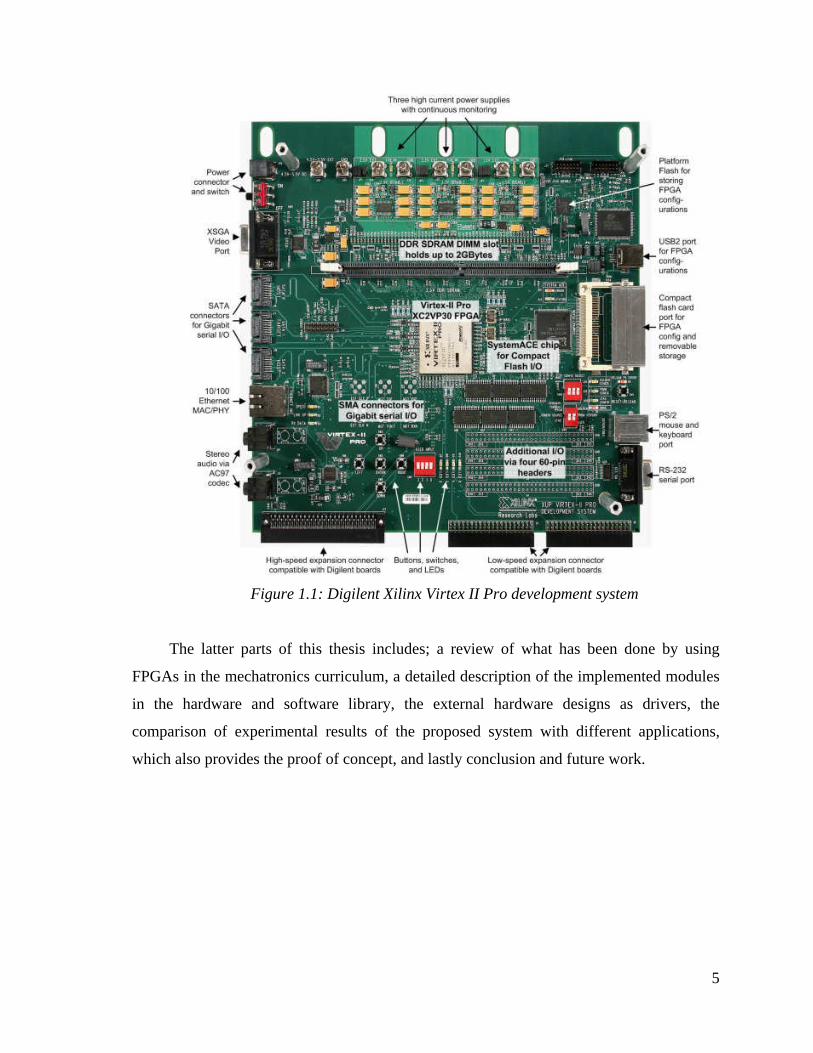
Figure 1.1: Digilent Xilinx Virtex II Pro development system
The latter parts of this thesis includes; a review of what has been done by using
FPGAs in the mechatronics curriculum, a detailed description of the implemented modules
in the hardware and software library, the external hardware designs as drivers, the
comparison of experimental results of the proposed system with different applications,
which also provides the proof of concept, and lastly conclusion and future work.
5

Table 1.1: Platform capabilities
6
Chapter 2
2. LITERATURE REVIEW
Hybrid controllers have been used for motion control systems due to the advantages
of different systems like DSP and FPGAs. But in DSP and FPGA based hybrid controller
systems, FPGA had a very little role, against their capabilities. As it was mentioned before,
a motion control system consists of several parts. With the increasing use of FPGAs in
motion control systems, there have been lots of research going on dealing with different
parts of this aspect. Some FPGA companies have been proposing FPGA based applications
to courage users to migrate to FPGA based systems.
2.1.Commercial Products
Altera suggests that FPGA based systems would be suitable for industrial distributed
systems [2]. Industrial Ethernet (IE) is used for complex motion control systems. But there
are several different standards (over 20) for industrial Ethernet, and this amount is still
increasing. This creates the need of flexibility for communication mediums. Common
solution is providing different daughter boards for different IE standards, or using an ASIC
with multi-standard support, but with new standards these also become obsolete. Therefore,
both solutions are expensive in the long term. Whereas FPGAs with Ethernet PHY
transceivers can provide support for configuring different IE standards. The system can be
7
reconfigured and updated with appropriate FPGA configuration and software files for a
new IE standard even if the system is already adopted in an environment.
Altera also suggests the use of FPGAs as motor controllers in smart home appliances
[3]. Some of the major concerns for smart home appliances are reconfigurability, power
consumption, reliability and cost. As it was mentioned before, FPGAs provide
reconfigurability even if the system is deployed in an environment.
One of the main reasons for the increase in power consumption is the time-harmonic
distortions. Increasing the PWM frequency lowers the time-harmonic distortions at the
output, and this can be optimized in an FPGA, according to the system or environment
where it is deployed. Decreasing the total-harmonic distortion at the output enables more
power saving, reducing in audible noise and increases system reliability. Having dedicated
hardware for control results the control loop to run at high frequencies (more than 100
kHz), which results better regulation, which also enables the system to detect failure
information.
FPGAs also bring cost advantages. The system-on-chip structure decreases the
complexity of the board, hence reducing the need for external integrated circuits, which
results in reducing the board area, board cost and increasing the reliability of the system.
While Altera creates some applications and with proves their concept with some
experiments, National Instruments (NI) introduces a thorough motion control platform,
which has an FPGA-processor hybrid structure [4]. With the newly introduced tools, which
provide visual programming and reconfigurability, these costs have been reduced.
National Instruments provide real time controllers, reconfigurable chassis and driver
modules, which are compatible with each other, and can be programmed by LabView
software.
National Instruments introduced a new platform for industrial applications, the
CompactRIO, a system consists of a real-time controller and a high-end FPGA, with
several connections for I/O modules with signal conditioning. The I/O connections are
compatible with industrial components, thus the amount of wiring and external interfaces
are reduced. The designed system has an H-Bridge driver module, which is capable of
interfacing a single-ended or differential encoder, current sensing, and direct connection to
8
fractional horsepower actuators. Transmitting these data to the user, the system also allows
custom control algorithm design.
The software provided with the NI’s system allows the user to reconfigure the real-
time controller and the FPGA. Programming the supervisory control, user can interface
I/O’s and enables the trajectory generator. This part usually runs in millisecond loops. The
trajectory generator generates the set points for the control loop with given tolerance. The
system is capable of running multi-axis systems, with preemptive scheduling and ,uses
double floating point arithmetic for calculations. It also provides various interpolation
techniques for trajectory generation, like linear, circular or spline. The control loop includes
position and velocity loop, using encoder and ADC’s. Drivers can be customized using the
full H-Bridge and the software. It also reads the current for loop or monitoring.
Equivalent to the aforementioned platform, Xilinx provides a distributed system as
reference design with Windows based Graphical User Interface, FPGA design which
consists of a soft CPU core with floating point unit, CAN Bus for communication between
the FPGA boards and a RS232 interface for communication with the host computer [5].
The software running in the soft CPU core takes the controller gains from the host and
calculates the control signal accordingly. It also takes the speed of the motor and sampling
rate. The GUI displays the current speed and driving voltage as well as the average and the
standard deviation of the speed and driving voltage calculated from the last 256 samples
received from the FPGA. The AC induction motor driver IP generates an interrupt for the
soft CPU core in every 10ms.
The host communication protocol packet format consists of a start and end of packet
byte, message id, number of data bytes and the data bytes. The start of packet byte is the
letter “t” in ASCII format, and the end of packet byte is carriage return. The message id
indicates which controller the message belongs to, number of bytes is self-explanatory, and
the data bytes are in single precision IEEE754 format for controller gains, and 32-bit
unsigned integer for speed/position and sampling rate. All the messages are acknowledged
back, if the transmission is successful in order to increase the systems reliability.
9
2.2.Relevant Research
The arithmetic functions determine the overall system performance, as they are the
most fundamental structure of the system. The whole system is built upon them. Therefore,
even a slight optimization in the arithmetic blocks may speed-up the overall system
drastically. Efficient implementation algorithms have been proposed [6], but the precision
was slightly decreased. In order to optimize these fundamental arithmetic blocks without
any decay in the precision of the calculations, Chun Hok Ho et al. proposed a hybrid
FPGA, which has coarse-grained units as well as fine-grained ones[7]. Some FPGAs
already have some coarse-grained elements, like DSP48 in Xilinx, which improves the
system in area and speed in certain cases.
The coarse-grained units are consisting of floating point adder/subtractor and floating
point multiplier as they have been considered to be more frequently used in algorithms than
floating point division or square root function blocks. The architecture also allows efficient
implementation of interconnections between these blocks, which can also communicate
with the fine-grained parts of the device. The coarse-grained blocks are in IEEE754 floating
point standard, with zero and sign flags. Therefore the coarse-grained blocks can be
considered as multiply-and-accumulate units, with control signals, status flags and bus
interfaces, with single or double floating point precision capabilities.
The architecture of the floating point FPGA (FPFPGA) is island based for the fine-
grained units and dedicated columns in between these islands for coarse-grained units. This
architecture also allows easy routing in the system. Therefore the system also requires a
specialized compiler and synthesizer, in order to work optimal.
The proposed architecture has not been realized on a prototype, but the performance
analysis has been done for several benchmarks, using the virtual embedded block (VEB)
method. The current area and delay model of a commercial FPGA chip has been taken, and
with the use of commercial CAD tools, the delay and are parameters of the proposed
system have been calculated. Results show that the proposed system can provide 25 times
of area reduction and 4 times frequency increase in average.
10
The arithmetic functions may be the most fundamentals blocks, but for nonlinear
calculations they are not enough. The concept of “Coordinate Rotation Digital Computer”
(CORDIC) was originally introduced by Volder J. in 1959 and later it was brought back to
light by J.S.Walther in 1971. It is an iterative algorithm, which is capable of doing
mathematical operations in linear, circular and hyperbolic coordinate systems, which only
use add and shift operations to compute trigonometric, exponential, logarithmic functions,
which require large chip area to implement in hardware. With the increasing use of FPGA
chips in scientific applications, trigonometric or logarithmic operations are needed with
floating point precision.
Jie Zhou et al. proposed a double precision floating point CORDIC unit, which can be
used as co-processors in FPGA-based systems [8]. The co-processor has the ability to
calculate sin/cosine, arctangent, exponential, logarithm, square-root functions in three
different coordinate systems which are; circular, linear and hyperbolic. The overall system
is implemented as a finite state machine, with 65 states. These states consist of three main
phases; argument reduction phase, CORDIC calculation phase and normalization phase.
The resulting intellectual property occupies %20 resources and has the maximum
clock frequency as 93MHz in StratixII FPGA, and occupies %10 resources and has the
maximum clock frequency of 173MHz in Virtex5 FPGA. The benchmarks results show
that the maximum error as 2-32 in sinh operation. A set of scientific functions were executed
on the co-processor and an AMD Athlon 2GHz processor. The results show that the co-
processor computes the same functions around 19.2 times faster than the processor. The
same tests have been made by using several co-processors in a parallel manner. The
conclusion of the second experiment reveals the speed-up as 49.3 on average. The obtained
results show that the co-processor can also be used for enhancing computers with scientific
purposes.
The aforementioned fundamental blocks have been optimized and implemented in
order to enable the realization of more complex systems on FPGA. The researches on
implementing motion control systems in FPGA can be classified by the control structures,
actuator driving methods, scale and modularity.
One of the major reasons to use FPGAs is, the resulting design realizes a physical
circuit, which validates the design for ASIC prototyping. An ASIC-PID design was
11
proposed in [9], by using the basic blocks; adder, multiplier and control logic. Since FPGAs
can only handle digital signals, the PID formula has been discretized by using the backward
Euler method as s-approximation. The system uses fixed point number format for
calculation. The resulting system uses three multiplication, and ten addition operations, and
allows the maximum clock frequency of 667MHz, whereas the PID algorithm implemented
as software in a DSP can work at 16MHz. The equivalency of the results validates the
functionality of the ASIC.
The ASIC-PID design was later optimized by Yuen Fong Chan et al. in [10]. The
design also discretized the PID functions by the backward Euler method. The necessary
blocks sum up to five multipliers, seven adder/subtractor and four delay blocks. The main
optimization was achieved by using the distributed arithmetic (DA) method.
The distributed arithmetic method is a bit-serial computation algorithm that performs
multiplication using an LUT-based scheme. DA based implementation of the PID
algorithm results in using four delays, four LUTs, four accumulators, and four adders. The
operands in the calculation are m-bit fixed point numbers; therefore the proposed algorithm
computes the output of the loop in m+1 clock cycles. The multiplier-based scheme has the
throughput of one clock cycle, but less efficient in terms of utilizing the FPGA. The DA
based scheme uses 20% of the area needed for multiplier based scheme. The DA based
scheme allows maximum clock frequency of 47MHz, but this is for calculating only one bit
of the result, whereas multiplier based scheme allows maximum clock frequency of 15MHz
for calculating the whole result. The results of the power consumption 765mW for
multiplier based scheme and 456mW for DA based scheme as it uses less hardware.
Stepper motors have been suitable for mechatronic systems as a result of the
precision, simplicity and the reliability that they provide. Urmila Meshram’s work [11] is a
great example of a thorough yet simple robot arm controller implemented on FPGA. The
serial mechanism with five unipolar stepper motors with 12 steps per revolution and a
gripper is controlled. The reference step signals are generated by the FPGA and the motors
are driven via the Darlington array (ULN2803) based driver circuitry. The FPGA is also
responsible of handling the user interface communication. RS232 is chosen as the
communication medium, and a 11-bit packet based protocol is developed for commanding
each motors and the gripper. The packet consists of two bits for each motor, interpreted as
12
45 degree rotations in each direction or brake for the motors, and a 1-bit signal interpreted
as grip or release command for the gripper.
Another FPGA based stepper motor implementation is done by Ngoc Quy Le. In his
work [12], open loop position control of the stepper motor by closed loop current control is
implemented. There are two main approaches that can be followed for the closed loop
current control for stepper motor driving. One approach would be adjusting the duty cycle
of the switching pulse by using a DAC and an analog comparator. The other method is to
sample the current with an ADC. With the first method, the comparator determines the
switching, resulting less responsibility for the processing unit, with less flexibility and
accuracy. With the second method, the parameter of the controller can be adjusted easily,
digital filters can be adopted and the accuracy can be increased by using more bits for fixed
point arithmetic.
The implementation has been made in FPGA in order to make ASIC manufacturing
easier. The FPGA has the ADC interface, PI controller and a PWM generator. The driver
hardware consists of a gate driver IC and 4 MOSFET’s with H-Bridge topology. The
commutation frequency of the driver hardware is 40 kHz; therefore the PWM frequency is
adjusted accordingly. The output of the ADC is signed 12-bit, with an input range of 1 and
-1 volts. The encoder of the stepper motor has the accuracy of 10000 pulses per revolution.
The resulting design consumes 21682 logic elements of the FPGA. The results show the
maximum position error of 45 pulses at 400 rpm.
In order to shorten the implementation time, yet not sacrificing from the performance,
hybrid controllers became popular. The study by Dayu Wang et al. shows the advantages of
using a DSP and FPGA hybrid controller for brushless DC motor based applications [13].
The introduced system uses DSP for user interface and speed loop calculation, while FPGA
is used for the current loop, PWM generation and speed calculations. These different
modules communicate via a dual port RAM used as shared memory. The Hall Effect
switches of the brushless DC motor are used to calculate the speed of the motor, and an
ADC (ADC10064) is used for measuring the current.
The FPGA calculates the speed by dividing time to number of rotations. All the
calculations have been done in fixed point. After the current loop reference is read from the
RAM, current control loop uses “PI” as the control method, discretized with backward
13
Euler method, and calculates the duty ratio for the PWM signal. A saturation limit is
applied to the output of the current controller for protection purposes. The FPGA also
generates a PWM signal at 10 kHz frequency. The speed reference is given by the user to
DSP, and depending on the speed of the motor at that instant, DSP calculates the
corresponding current amount and writes it to RAM. The results show that step response of
current and speed loops have very little error, around 0.02 A and 10 rpm respectively.
The advantages of superior power density, high performance fast and accurate motion
control makes the permanent magnet synchronous motors (PMSM) preferable for high
power automation systems. The main challenge for driving PMSM is the generation of
sinusoidal pulse width modulation (SPWM) signal. The experiments in [14], [15] and [16]
different methods for SPWM generation have been attempted.
In [14] and [15] analog signal comparison method have been used. Sinusoidal PWM
signal is generated by comparing a 50 Hz sine wave with a carrier triangular signal at a
higher frequency. The module determines the switching of the PWM according to the
crossing points of these signals. The main difference between these two methods is the first
one uses symmetrical triangular signal, the latter one uses negative-slope saw-tooth signal
as the carrier signal. Both experiments use n-channel power MOSFET based H-Bridge
topology as power stage. In order to protect the FPGA board, an isolation circuitry is
provided to interface the power stage. Also [15] provides optimization on [14] by
introducing a variable deadbeat timer, which is adjusted depending on the parameters of the
H-Bridge circuit, in order to prevent sudden short circuits and spikes due to switchings. It is
also shown that, additional LC filters improve the distortion at the output signal. To reduce
the total harmonic distortion in [16], the three-phase sinusoidal PWM values have been
calculated in a vector form. For the vector rotation calculations, an implemented CORDIC
algorithm is used. This method optimizes the overall board size, as it neglects the
requirements for external analog circuitry.
The system also has three closed loops for current, velocity and position. The position
loop is implemented on the embedded processor in the FPGA for flexibility purposes,
whereas the other two loops are designed using HDL. Two separate PI controller loops are
running for the current and velocity loops and the one for the current also has saturation,
and for the position controller sliding-mode variable structure control is used. The SMVSC
14
provides insensitivity to parameter variations, disturbance rejection and fast dynamic
response. The convergence parameter affects the speed and chattering, as a result it is
chosen to be decreasing in time. Obtained simulation results show that, the proposed
system can track step speed trajectories with 0.5 sec settling time, at 1500rpm, with an
800W PMSM.
FPGAs provide very high sampling rates, which creates a drastic difference between
the conventional controllers in high precision and high speed applications. Many
technologies require high-precision accuracy nowadays. As a result high-precision
positioning, multidimensional drive, miniaturization and light-weight are expected from
robotic mechanisms. Piezoelectric ceramic linear ultrasonic motors meet the size, weight,
speed and precision requirements of the nano-technological systems. However, the
mathematical models of these actuators are complex, and the motor parameters are time-
variant due to the changes in temperature and operating conditions. In addition, the control
characteristics of these actuators are highly nonlinear. Therefore, intelligent control
algorithms such as neural networks are suitable due to their ability to approximate the
nonlinear characteristics of the systems without using the mathematical models of the
system.
The experiment in [17] introduces Elman Neural Networks (ENN). ENN can be
considered as feed-forward neural networks with additional memory neurons. These
neurons provide high-precision approximation for high-order nonlinear systems, with fast
convergence.
To reduce the consumption of FPGA resources, instead of sigmoid function,
piecewise continuous function is used in the NN. In order to overcome the unknown
dynamics of the system, online learning speed is determined by the use of the adaptation
law.
The linear motion is detected with 1 micron precision and the control algorithm runs
at 732 Hz. Digital-to-analog converters are used to drive the hardware. The system
consumes 3256 logic cells of the FPGA. The calculations are done in 12-bit fixed point
format, which is used for values between 1 and -1.
Results show that with radial basis function based neural networks the errors for
sinusoidal and trapezoid references are 3.19 and 6.17 microns respectively, whereas with
15
ENN these numbers are reduced to 2.82 and 1.78 with nominal parameters. The
comparison results with varying parameters are 5.15 and 4.76 microns for RBF based NN
with sinusoidal and trapezoid references, and 3.23 and 1.08 microns for ENN with the same
references.
As the applications evolve from a single actuator to multi-DOF mechanisms, the
amount of tasks for the controller to handle are expanded. The main overheads that the
multi-DOF systems bring to the system are the kinematics of the mechanism and the
trajectory generation. In [18] the inverse kinematics calculation, position controller, speed
controller, PWM generator and encoder counter have been implemented inside the FPGA
for each actuator of the test mechanism. In order to optimize the resource consumption in
FPGA, the inverse kinematics has been implemented by using the finite state machine
method with 42 states, which results in throughput of 1MHz, whereas if it has been
implemented on the NiosII processor embedded in the FPGA, the throughput would have
been around 160Hz. To perform the inverse kinematics, the circuit needs 3 multipliers, 2
dividers, 2 adders, 1 square root function, 1 component for atan function, 1 component for
arcos function, 1 look-up-table for sin function and some comparator for atan2 function.
The sampling frequency of the position and speed loop is 762Hz and 1525Hz respectively.
Position control loop have been implemented with 4 states by using a P-controller, and the
speed loop has 12 states and uses PI-controller. The PWM generators run at 18 kHz. The
NiosII processor is used for serial communication based user interface.
The system is tested on a five-axis serial manipulator robotic arm. The obtained
results show that the response of the mechanism is less than 0.5 seconds, and the position
error on a circular trajectory is ±4 mm.
Another difficulty of controlling multi-DOF mechanisms is the compensation of
environmental disturbances. The experiment in [19] is implemented on a 6-DOF robot arm,
which belongs to the humanoid robot, ROBOKER. As linear PID based control systems do
not work efficiently with systems which have nonlinear characteristics or external
disturbances, adaptive and intelligent methods have been introduced to overcome this
problem. Another solution to this problem is nonlinear PID, which eliminates the nonlinear
characteristics of the motion by including some nonlinear functions to eliminate them.
16
A floating point arithmetic core is used to perform the algorithm combined with the
control logic. The design also has encoder and PWM modules as physical interfaces and
serial communication.
The controller has been tested on the 6-DOF arm of ROBOKER humanoid robot. The
results show maximum error around 0.1 radians with little chattering.
In order to improve the performance of the controller further, the same experiment
setup has been used with a Neural Network (NN) based controller in [20].
The system is implemented as a hybrid controller. The FPGA part has the PID
controllers, PWM generators, encoder modules and serial communication interface,
whereas the DSP part calculates the learning algorithm of the neural network. The reason
for this partition is that complex intelligent algorithms such as neural networks or fuzzy
logic, are hard to implement on FPGA, on the other hand, DSP and microcontrollers do not
have large number of IO’s. Therefore this hybrid system aims to grasp the beneficial parts
of both of the systems. The floating point DSP is implemented as an intellectual property
core on FPGA.
PD controller is used for position control of the system. To improve the accuracy,
neural network based compensation mechanism is added to the system. This method is also
known as feedback error learning scheme. Radial Basis Function based forward
propagation method is used with backward propagation. The results of the new experiment
show a maximum tracking error of 0.01 radians for the joints with 0.01 learning rate.
Haptic interfaces consist of human operator, haptic device and virtual environment.
In haptic interfaces, stability is a crucial concept as it creates the perception of the virtual
environment to the operator. The lack of it may cause distortions in the experience, harm
the hardware or even worse, create physical damage on the human operator. The fast
sampling rate and parallel processing capabilities of FPGA improves the system stability
which makes it suitable for such systems. To improve the stability of the haptic systems,
passivity observer and passivity controller implementations on FPGA is proposed in [21].
The encoder counter block, passivity observer, passivity controller and the
communication with the host computer can run simultaneously on FPGA. The host
computer renders the virtual environment, so the environment and the controller are
separated. If collusion is detected the host computer sends FPGA the reference force. For
17
the controller and observer, to eliminate the measurement noise, instead of current
measurement, the reference current is used in calculations. The output is generated in
FPGA by the PWM module which runs at 200 kHz, and sent to the Maxon motor driver
with current limit of 1.6A. The system is compared to a more sophisticated implementation
of passivity observer and passivity controller duo but in software.
The results show improvement in the response time with lower overshoot. The
amount of disturbance, while the device is in free run mode or touching the wall, was also
diminished.
The surgery robots, take the haptic idea even one step further where the doctor
operates on the master robot, and the slave robot acts on an affected area. The main
problem with surgery robots is the reflection of tactile sensation to the doctor. In order to
meet these requirements a teleoperation method called bilateral was developed. Many
controllers with different architectures have been proposed, like symmetric servo
architecture, force reflection architecture. The first method has large forces in the master
side, and the latter one has stability issues. Four-channel architecture is proposed [22],
which satisfies both stability and transparency. The architecture focuses on the control of
four variables of bidirectional position and force.
In tactile sensation, the sampling rate plays a major role in the system. Human
receptors are sensitive in 0-400Hz range. Reaction force estimation by using disturbance
observer provides wide bandwidth. The cut-off frequency is inversely proportional to the
sampling rate of the system. In PC-based systems the sampling period is not enough to
estimate all force that is in the human sensitivity frequency range.
The FPGA implementation achieved 10 microseconds sampling period. And in order
to enhance the accuracy, which is not enough with the conventional fixed-point arithmetic,
floating point arithmetic have been adapted to the system.
In the ideal case the stiffness of position control is infinite and the stiffness of the
force control is zero. As the stiffness of the position control is lowered, the robustness of
the system decreases. But the stiffness and the robustness of the system can be separated a
in a disturbance observer based acceleration control. Therefore position and force control
can be integrated on the dimension of acceleration. The common and differential modes for
18
acceleration are needed to calculate force and position respectively. For the differential
mode position controller, PD algorithm is implemented.
The disturbance force is applied on a driven actuator. It consists of the load force
such as friction and the difference between nominal and real parameters. Therefore,
disturbance observer increases the robustness of the system.
The only sensors in the system are the encoders; as a result the velocity is calculated
by taking the real-derivative of the position. As force sensor, strain gauges have been used,
but it decreases the stability of the system. As a result force estimation is being used for
force information. The experiment setup consists of linear actuators with very little friction,
allowing assuming that the force estimation only consists of external force.
The implementation has been done in FPGA, as a result of its parallel processing
capabilities. Linear actuators with linear encoders are used for the test setup, and DACs are
used to drive the actuators. Inside the FPGA, the counter calculates the positions by using
the encoder signals. The position values are then converted to floating point format. After
the conversion the acceleration references are calculated in the bilateral control module by
using the position inputs. The experimental data is stored in a SDRAM, and after the
operation it is send to the PC by serial communication. The DACs have 12-bit resolution
with ±10V output voltage range. The synthesis results show that the design allows a
maximum clock frequency of 6.25MHz. The experiments with different sampling
frequencies have been done in order to see the effect on control. As the sampling frequency
and the cut-off frequency of the low pass filter increases, the position tracking and the force
reflection is enhanced.
The setup board is revised and four FPGA have been implemented on the latest
custom board [23]. With the new design, the board accommodates a new bilateral control
system of two 7-DOF mechanisms, which are used for haptic endoscopic surgery. For the
PC side communication, PCI bus has been chosen instead of serial communication.
Besides these specific applications for specific actuators, mechanisms or concepts,
more general FPGA-based motion control platforms have also been introduced in [24] and
[25]. Both of the proposed systems are hybrid controllers, which consists of DSP and
FPGA.
19
The first proposed design offers closed current loop, closed position/velocity control
loop, incremental encoder, PWM module, fault/brake, velocity estimator, UART based host
communication, and Delta-Sigma based analog-to-digital conversion and necessary glue
logic. With the capabilities of FPGA chips, the sampling rate of the control loop can be
raised up to a new frequency range.
The host communication is implemented by integrating an UART module to the
FPGA. The Delta-Sigma analog-to-digital conversion is ran at 200MHz clock frequency
with 8-bit resolution, therefore resulting 8680 samples per second. The velocity estimator
uses third order Taylor expansion to determine the velocity. The current control loop is
implemented by using an IR2175 chip, which senses the current from an external shunt
resistor, and outputs a PWM signal which can be handled by the FPGA chip directly. With
200MHz clock, the PWM output of the IR2175 chip results around 11-bit resolution. The
current loop uses a PI based controller and runs at 120 kHz.
The proposed system uses an adaptive motion control algorithm, which can be
partitioned into two parts, linear and nonlinear. The linear part consists of a PD-like control
algorithm, whereas the nonlinear part deals with the dynamic compensations of the system.
The nonlinear part of the control algorithm requires complex calculations; therefore it is
implemented on a DSP chip. The linear part of the control algorithm is implemented on the
FPGA chip. The position signals are 32-bit fixed point, and the velocity and acceleration
signals are 18-bit fixed point numbers with 10-bit fractional part. The linear part of the
control algorithm runs on FPGA at 20 kHz.
The trajectory generation is done in two phases. First, DSP calculates the trajectory
and writes to the shared memory, then FPGA takes the steps from the memory and
interpolates into finer steps.
As an experimental setup, a SCARA mechanism has been chosen. The mechanism is
controlled by the same adaptive algorithm in order to eliminate the hardware independent
effects. Sample trajectories have been given to track at different speeds, which are 750 rpm
and 7500 rpm respectively. The results show that with the conventional controllers the
position tracking errors for the different speeds are 0.005 and 0.01 radians, where as the
error results for the FPGA-based control platform are 0.005 and 0.001 radians.
20
The latter proposed design consists of nine modules; velocity profile generator,
interpolation calculator, inverse kinematics calculator, PID controller, feedback counter,
pulse integrator, data converter, clock generator and external interface. The velocity profile
generator generates acceleration and deceleration characteristics for the motion. The
interpolation calculator provides a smoother motion without sharp jerks. The inverse
kinematics calculation can provide angular values for the rotary actuators from metric end-
effecter input. Trigonometric function values are stored in the lookup tables. The PID
controller can control position and velocity of the system. Feedback counter module is used
for encoders to track the position of the motor. The pulse integrator calculates the
integrated pulse during sampling. All the calculations in the system are done in fixed point
format. The values are multiplied with different powers of two in order to meet the required
accuracy for the calculations, and then shifted back to the fixed point format. The data
converter converts the output signal to driving signals for various types of servo drivers.
The clock generator provides several different clocks for the different parts of the system.
The external interface provides the communication with the host computer via serial cable.
The design is tested with a four-DOF SCARA mechanism. The positions of the
motors are stored in 32-bit registers and the PWM module has 12-bit resolution. The
maximum clock allowed by the system is 36MHz. The system accommodates 44,364
lookup tables of Xilinx XC2V6000-FF1152 FPGA, which has 6M system gates, 76,032
logic cells and 1104 IO pins. The system can drive four servo motors with the designed
drivers which has a DAC, amplifier and a level shifter. The motors of the mechanism are
brushless DC motors, with 4096 pulse per revolution encoders and 1:50 gear ratios. The
maximum measured error is about 0.6 degrees. With 100 kHz sampling frequency, the
power consumption of the overall system is 0.724W, whereas an equivalent system with
Texas Instruments DSP would consume around 1.5W with 20 kHz sampling rate.
21
Chapter 3
3. CONTROL LIBRARY IN VERILOG HDL
The main purpose of this library is to create a level of abstraction while using FPGAs
for control applications. This abstraction layer enables the end user to implement control
systems without having to know advanced HDL knowledge. As visual programming
languages are becoming more popular each day (Simulink, MaxMsp), the control library,
combined with Xilinx ISE, offers a similar structure. The main advantage of the library is
the shortening of the implementation time. Conceptually, higher the programming
language, lower the implementation time. But this also has the trade-off about decreasing
the performance and the precision of the overall system. In order to prevent this, the
arithmetic functions in the library are implemented compatible with IEEE754 single-
precision floating point number format. The subsequent sections will present the
implemented modules in detail, namely, From Integer to EFP, To Integer from EFP, From
IEEE754 to EFP, To IEEE754 from EFP, Adder/Subtractor, Multiplication, Division in
arithmetic; Derivative, Low Pass Filter, Real Derivative, Integral in Laplacian; Variable
Delay, Synchronizer in temporal; PID Controller, Disturbance Observer, Motion Controller
in advanced; and Quadrature encoder, PWM generators, Step generators in physical
interface sections.
22
3.1. Floating Point Arithmetic Functions
The decision of implementing the library in floating point has been taken in order to
have a standard number format, which is also becoming the de-facto standard for high
precision calculations. As it is the most popular and valid standard, the modules are
compatible with IEEE754 floating point number format. The single precision floating point
format consists of 32-bits and fragments the number into sign, exponent and mantissa parts.
These parts provide relative precision as the exponent and the mantissa are stored
separately. The format in bit representation is below.
There are several differences between the implementation and IEEE754 standard.
First difference is the implied bit. In order to increase the accuracy, IEEE754 standard has
an implied bit as the MSB of the mantissa. This feature also brings the need for handling
the denormalized bits. One other difference is the exponent bias. In the IEEE754 standard,
the exponent is biased for signed exponent calculation. In order to prevent complexity,
these features are not implemented in the modules. For compatibility purposes, two
converter blocks have been implemented for converting from and to the IEEE754 standard.
The implemented floating point format will be referred as “Easy Floating Point” (EFP)
format for disambiguation reasons. The tests with arbitrary inputs show equivalency with
the IEEE754 standard, except the loss of precision caused by the absence of the implied bit.
The Verilog HDL sources for the arithmetic units (excluding the converters), can be found
in Appendix A.
Another commonly used number format is fixed point signed integers. In order to
have only one number format in the system, two blocks for converting from and to integer
have been implemented as well.
23
3.1.1. From Integer to EFP
The block takes an integer, assigns the MSB of integer as the sign bit. If the integer is
negative, other bits are reversed with two’s complement method. The resulting number is
shifted left, until the MSB is one. When the shifting is finished, the number of shifts creates
the exponent, and the higher 23-bits create the mantissa of the resulting floating point
number.
Figure 3.1: Block structure of from integer to EFP conversion unit.
3.1.2. To Integer From EFP
The block takes a 32-bit floating point number in EFP format and precedes the
mantissa with a 31-bit number which consists of zeros. The resulting 54-bit number is
shifted corresponding to the exponent of the number, and complemented depending on the
sign bit.
Figure 3.2: Block structure of from EFP to integer conversion unit.
24
3.1.3. From IEEE754 to EFP
The block takes a 32-bit floating point number in IEEE754 standard. The exponent
bias is normalized and the implied bit is explicated. The module outputs the resulting
number, which is compatible with EFP format.
Figure 3.3: Block structure of from IEEE754standard to EFP conversion unit.
3.1.4. To IEEE754 From EFP
The block takes a 32-bit floating point number in EFP format and subtracts the
predefined bias from the exponent, and implies the MSB of the mantissa as 1. These
operations make the resulting number compatible with IEEE754 format.
Figure 3.4: Block structure of from EFP to IEEE754 standard conversion unit.
25
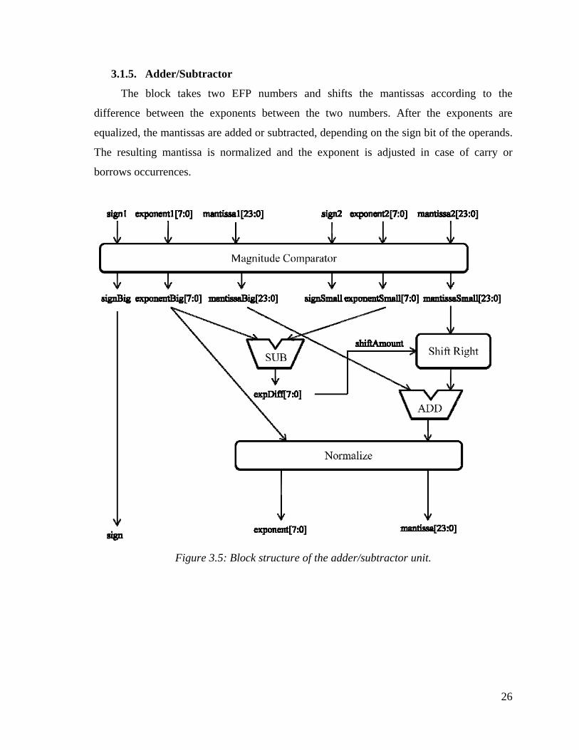
3.1.5. Adder/Subtractor
The block takes two EFP numbers and shifts the mantissas according to the
difference between the exponents between the two numbers. After the exponents are
equalized, the mantissas are added or subtracted, depending on the sign bit of the operands.
The resulting mantissa is normalized and the exponent is adjusted in case of carry or
borrows occurrences.
Figure 3.5: Block structure of the adder/subtractor unit.
26
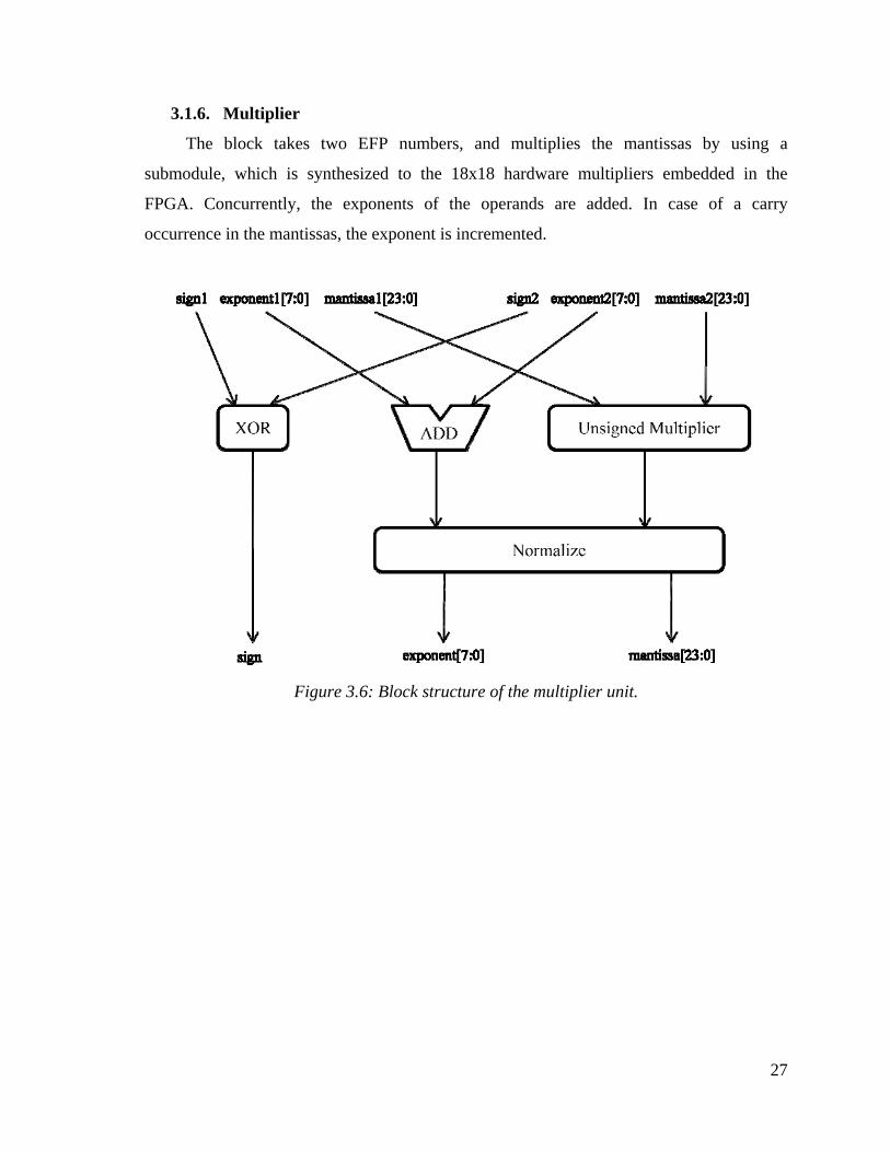
3.1.6. Multiplier
The block takes two EFP numbers, and multiplies the mantissas by using a
submodule, which is synthesized to the 18x18 hardware multipliers embedded in the
FPGA. Concurrently, the exponents of the operands are added. In case of a carry
occurrence in the mantissas, the exponent is incremented.
Figure 3.6: Block structure of the multiplier unit.
27
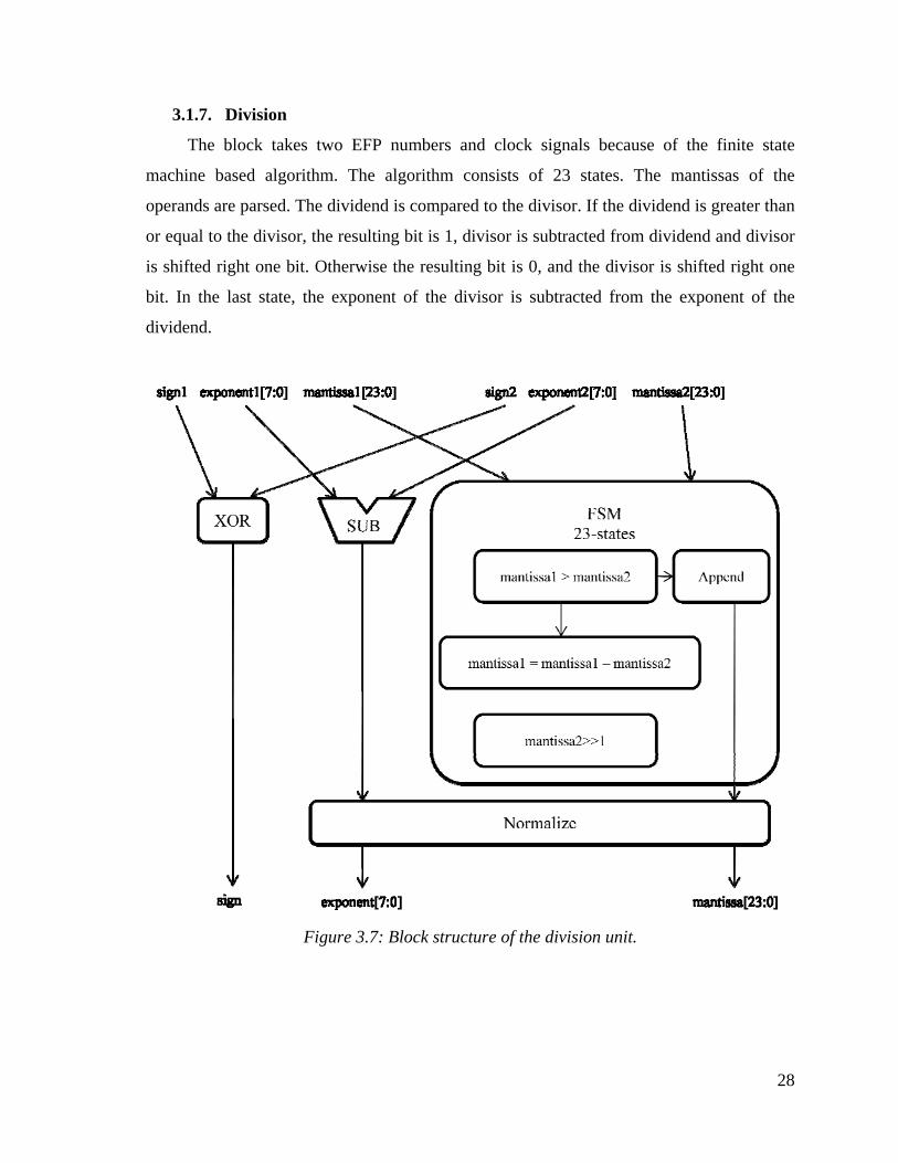
3.1.7. Division
The block takes two EFP numbers and clock signals because of the finite state
machine based algorithm. The algorithm consists of 23 states. The mantissas of the
operands are parsed. The dividend is compared to the divisor. If the dividend is greater than
or equal to the divisor, the resulting bit is 1, divisor is subtracted from dividend and divisor
is shifted right one bit. Otherwise the resulting bit is 0, and the divisor is shifted right one
bit. In the last state, the exponent of the divisor is subtracted from the exponent of the
dividend.
Figure 3.7: Block structure of the division unit.
28
3.2. Floating Point Laplacian Functions
The mathematical models or the functions that we use are continuous functions, as
they correspond to the physical structure. But in digital electronics, the system works in
steps or clock cycles. This brings the need for conversion between the Laplacian domain
and the digital domain. Several different discrete approximations of the continuous
functions have been proposed. Before going deeper into the implemented blocks, it would
be more appropriate to compare different types of approximations.
As studies show [26] newly introduced methods like, Al-Alaoui or implicit Adams
provide superior performance than the classical methods, as they are using different
weighted interpolations of the Euler and Tustin methods. Implicit Adams have been chosen
as the Laplace approximation method; as it provides smoother response than Euler or
Tustin, and easier to calculate than Al-Alaoui method.
29
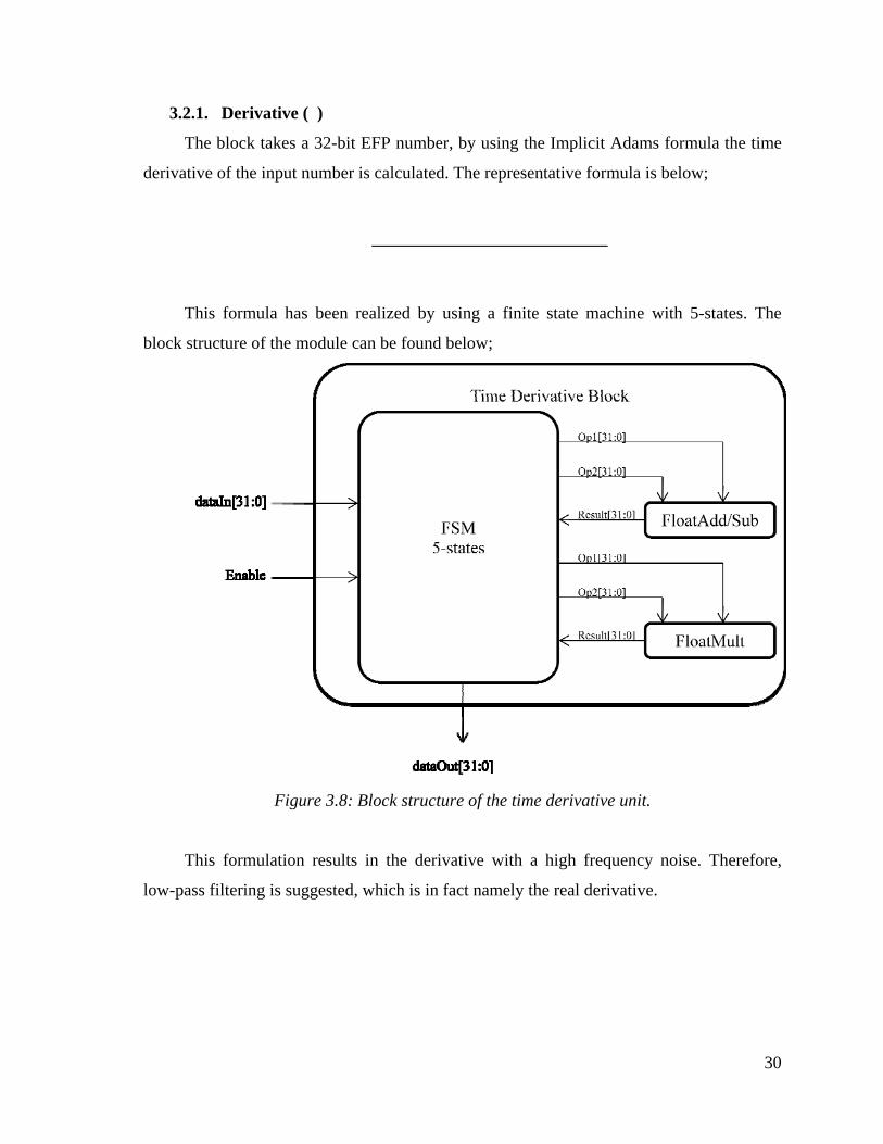
3.2.1. Derivative ( )
The block takes a 32-bit EFP number, by using the Implicit Adams formula the time
derivative of the input number is calculated. The representative formula is below;
This formula has been realized by using a finite state machine with 5-states. The
block structure of the module can be found below;
Figure 3.8: Block structure of the time derivative unit.
This formulation results in the derivative with a high frequency noise. Therefore,
low-pass filtering is suggested, which is in fact namely the real derivative.
30
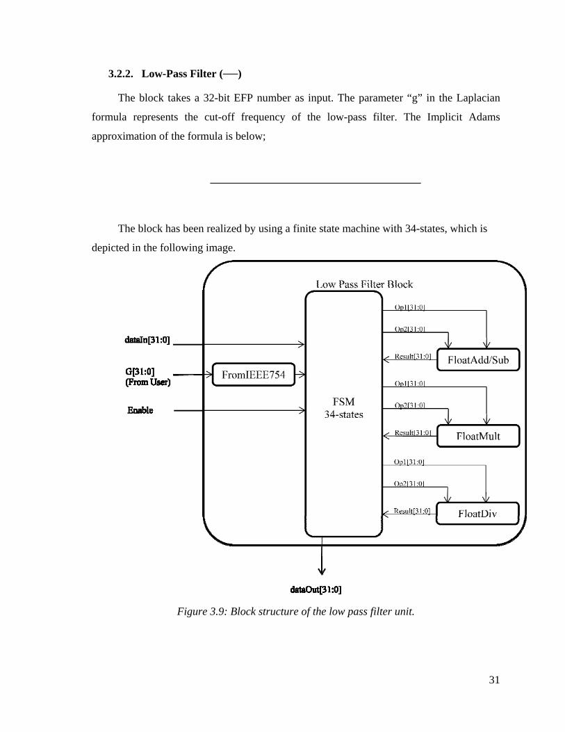
3.2.2. Low-Pass Filter ( )
The block takes a 32-bit EFP number as input. The parameter “g” in the Laplacian
formula represents the cut-off frequency of the low-pass filter. The Implicit Adams
approximation of the formula is below;
The block has been realized by using a finite state machine with 34-states, which is
depicted in the following image.
Figure 3.9: Block structure of the low pass filter unit.
31
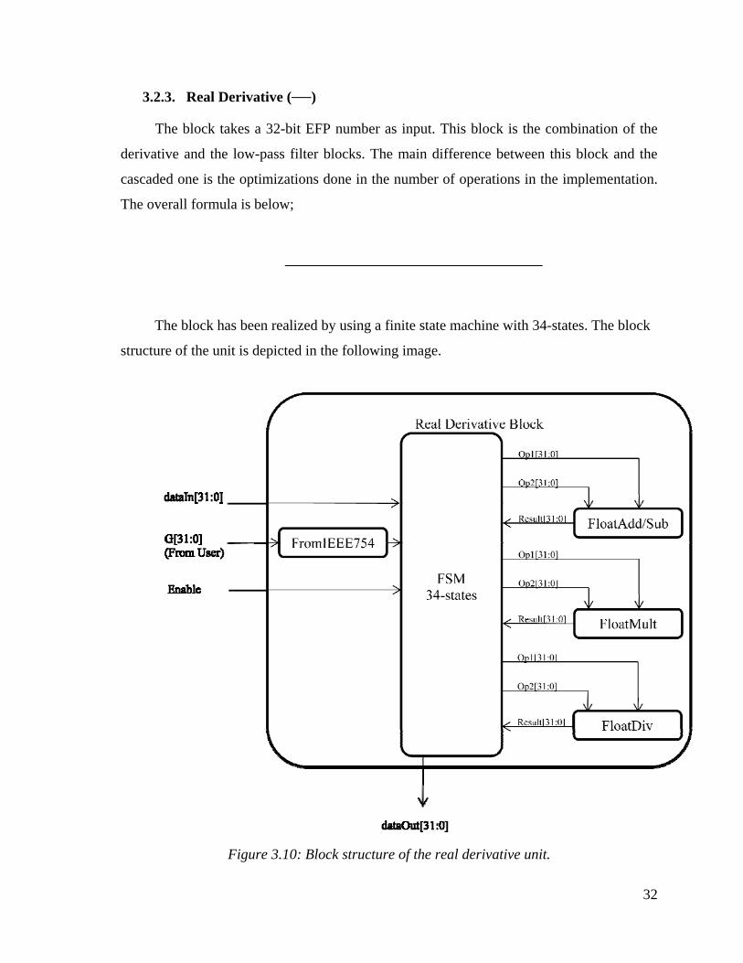
3.2.3. Real Derivative ( )
The block takes a 32-bit EFP number as input. This block is the combination of the
derivative and the low-pass filter blocks. The main difference between this block and the
cascaded one is the optimizations done in the number of operations in the implementation.
The overall formula is below;
The block has been realized by using a finite state machine with 34-states. The block
structure of the unit is depicted in the following image.
Figure 3.10: Block structure of the real derivative unit.
32
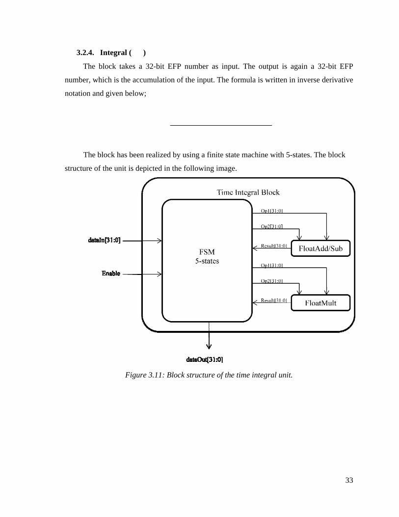
3.2.4. Integral ( )
The block takes a 32-bit EFP number as input. The output is again a 32-bit EFP
number, which is the accumulation of the input. The formula is written in inverse derivative
notation and given below;
The block has been realized by using a finite state machine with 5-states. The block
structure of the unit is depicted in the following image.
Figure 3.11: Block structure of the time integral unit.
33
3.3 Temporal Blocks
3.3.1 Variable Delay ( )
This block takes a 32-bit number in any format, and depending on the given delay
parameter, outputs the input after the delay.
3.3.2. Synchronizer
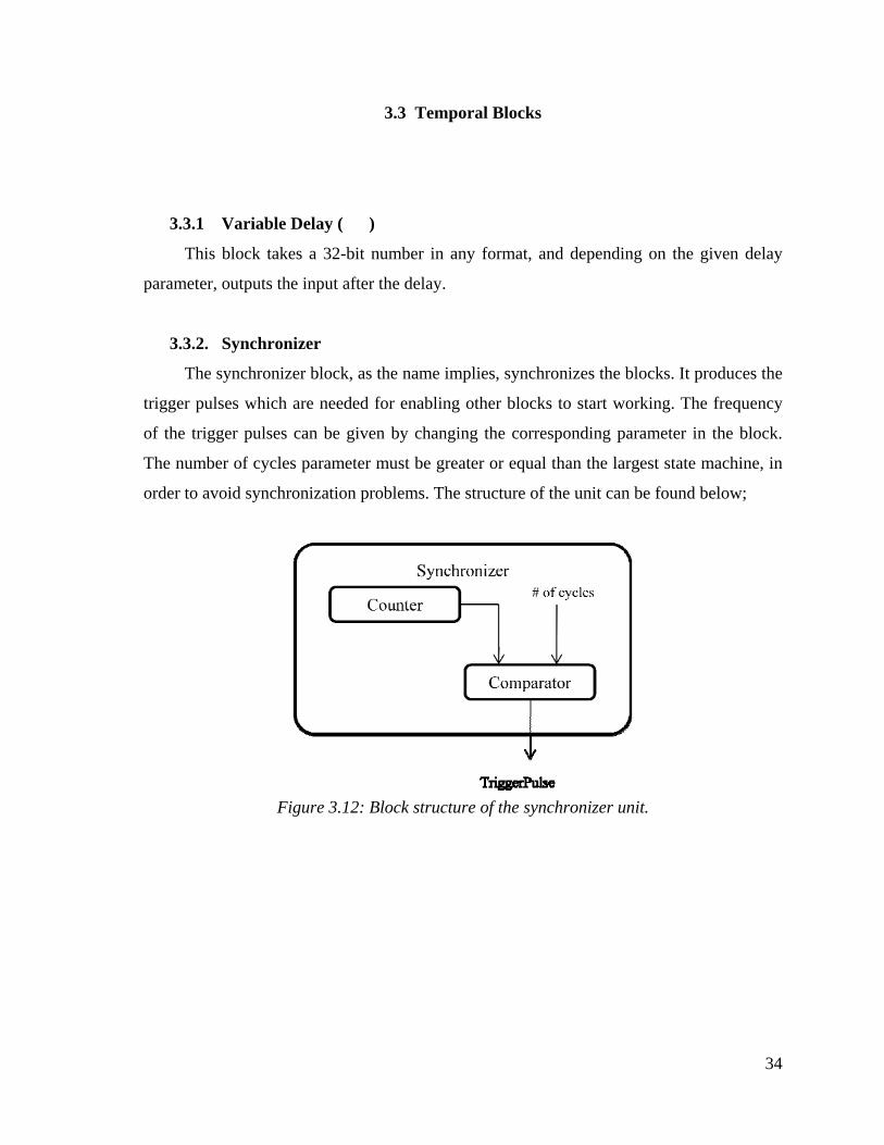
The synchronizer block, as the name implies, synchronizes the blocks. It produces the
trigger pulses which are needed for enabling other blocks to start working. The frequency
of the trigger pulses can be given by changing the corresponding parameter in the block.
The number of cycles parameter must be greater or equal than the largest state machine, in
order to avoid synchronization problems. The structure of the unit can be found below;
Figure 3.12: Block structure of the synchronizer unit.
34
3.4. Advanced Blocks
These blocks consist of the combination of previously discussed blocks. The frequent
use of these blocks makes them compulsory to implement. Due to the optimizations done in
the formula, these combined blocks are better in performance and area compared to the
cascaded implementations.
3.4.1. PID Controller
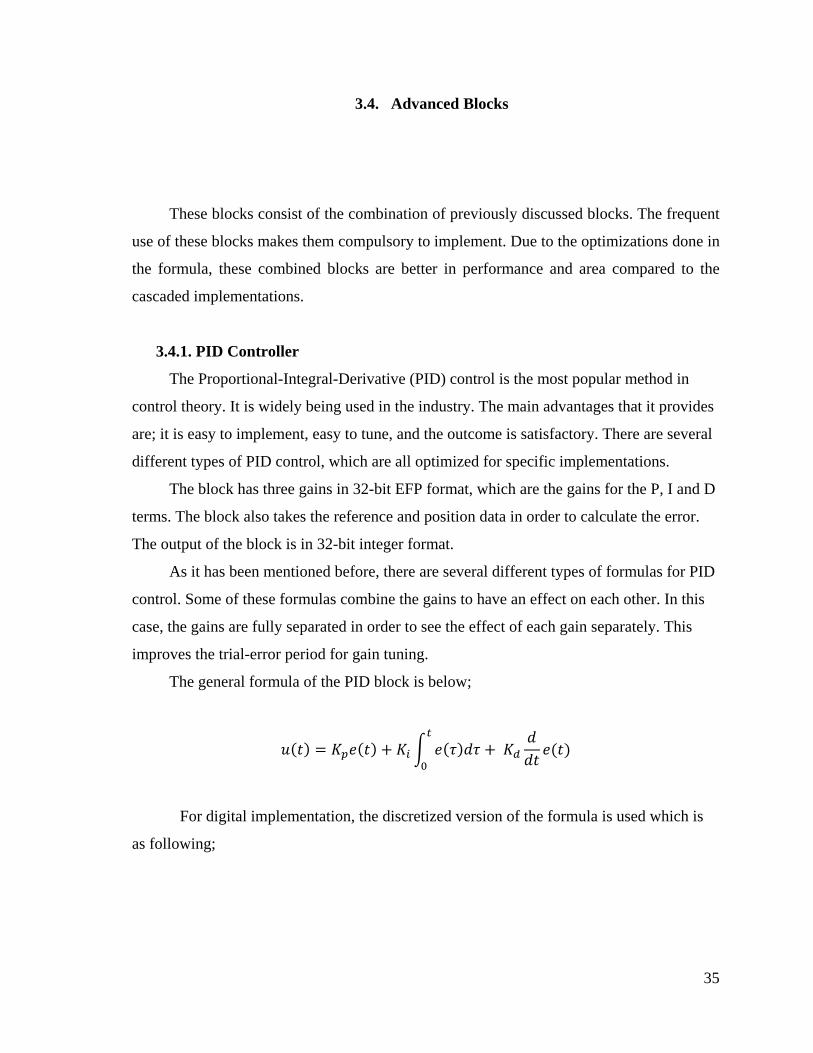
The Proportional-Integral-Derivative (PID) control is the most popular method in
control theory. It is widely being used in the industry. The main advantages that it provides
are; it is easy to implement, easy to tune, and the outcome is satisfactory. There are several
different types of PID control, which are all optimized for specific implementations.
The block has three gains in 32-bit EFP format, which are the gains for the P, I and D
terms. The block also takes the reference and position data in order to calculate the error.
The output of the block is in 32-bit integer format.
As it has been mentioned before, there are several different types of formulas for PID
control. Some of these formulas combine the gains to have an effect on each other. In this
case, the gains are fully separated in order to see the effect of each gain separately. This
improves the trial-error period for gain tuning.
The general formula of the PID block is below;
For digital implementation, the discretized version of the formula is used which is
as following;
35
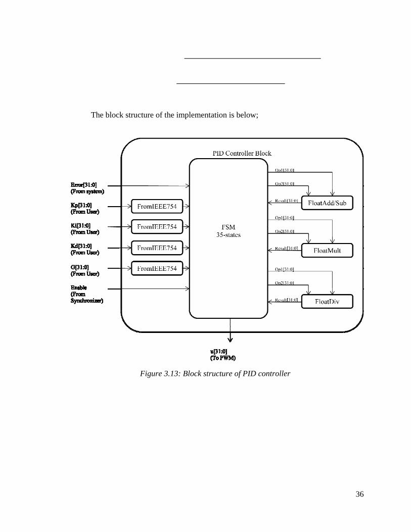
The block structure of the implementation is below;
Figure 3.13: Block structure of PID controller
36
3.4.2. Disturbance Observer
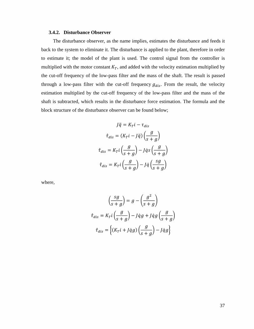
The disturbance observer, as the name implies, estimates the disturbance and feeds it
back to the system to eliminate it. The disturbance is applied to the plant, therefore in order
to estimate it; the model of the plant is used. The control signal from the controller is
multiplied with the motor constant , and added with the velocity estimation multiplied by
the cut-off frequency of the low-pass filter and the mass of the shaft. The result is passed
through a low-pass filter with the cut-off frequency . From the result, the velocity
estimation multiplied by the cut-off frequency of the low-pass filter and the mass of the
shaft is subtracted, which results in the disturbance force estimation. The formula and the
block structure of the disturbance observer can be found below;
where,
37
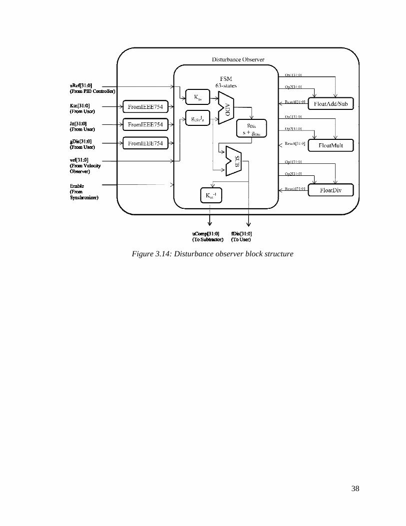
Figure 3.14: Disturbance observer block structure
38
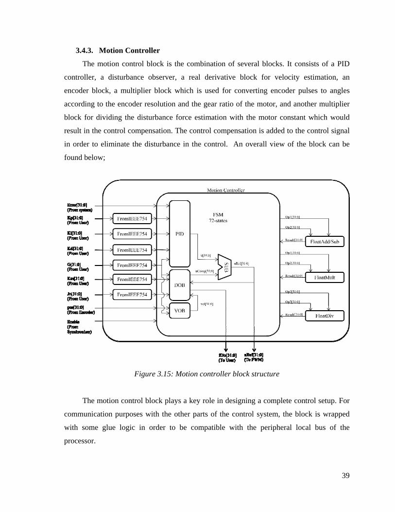
3.4.3. Motion Controller
The motion control block is the combination of several blocks. It consists of a PID
controller, a disturbance observer, a real derivative block for velocity estimation, an
encoder block, a multiplier block which is used for converting encoder pulses to angles
according to the encoder resolution and the gear ratio of the motor, and another multiplier
block for dividing the disturbance force estimation with the motor constant which would
result in the control compensation. The control compensation is added to the control signal
in order to eliminate the disturbance in the control. An overall view of the block can be
found below;
Figure 3.15: Motion controller block structure
The motion control block plays a key role in designing a complete control setup. For
communication purposes with the other parts of the control system, the block is wrapped
with some glue logic in order to be compatible with the peripheral local bus of the
processor.
39
3.5. Physical Interface Blocks
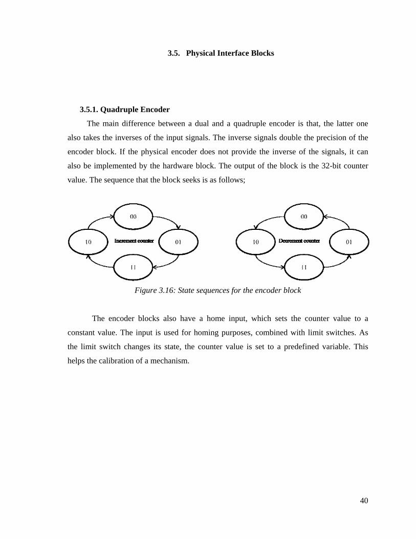
3.5.1. Quadruple Encoder
The main difference between a dual and a quadruple encoder is that, the latter one
also takes the inverses of the input signals. The inverse signals double the precision of the
encoder block. If the physical encoder does not provide the inverse of the signals, it can
also be implemented by the hardware block. The output of the block is the 32-bit counter
value. The sequence that the block seeks is as follows;
Figure 3.16: State sequences for the encoder block
The encoder blocks also have a home input, which sets the counter value to a
constant value. The input is used for homing purposes, combined with limit switches. As
the limit switch changes its state, the counter value is set to a predefined variable. This
helps the calibration of a mechanism.
40
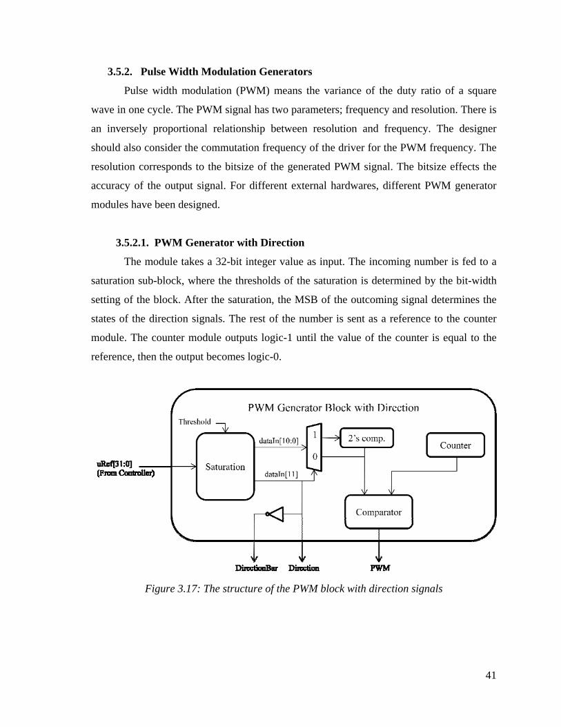
3.5.2. Pulse Width Modulation Generators
Pulse width modulation (PWM) means the variance of the duty ratio of a square
wave in one cycle. The PWM signal has two parameters; frequency and resolution. There is
an inversely proportional relationship between resolution and frequency. The designer
should also consider the commutation frequency of the driver for the PWM frequency. The
resolution corresponds to the bitsize of the generated PWM signal. The bitsize effects the
accuracy of the output signal. For different external hardwares, different PWM generator
modules have been designed.
3.5.2.1. PWM Generator with Direction
The module takes a 32-bit integer value as input. The incoming number is fed to a
saturation sub-block, where the thresholds of the saturation is determined by the bit-width
setting of the block. After the saturation, the MSB of the outcoming signal determines the
states of the direction signals. The rest of the number is sent as a reference to the counter
module. The counter module outputs logic-1 until the value of the counter is equal to the
reference, then the output becomes logic-0.
Figure 3.17: The structure of the PWM block with direction signals
41
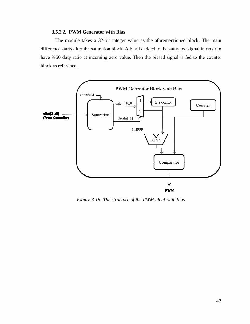
3.5.2.2. PWM Generator with Bias
The module takes a 32-bit integer value as the aforementioned block. The main
difference starts after the saturation block. A bias is added to the saturated signal in order to
have %50 duty ratio at incoming zero value. Then the biased signal is fed to the counter
block as reference.
Figure 3.18: The structure of the PWM block with bias
42
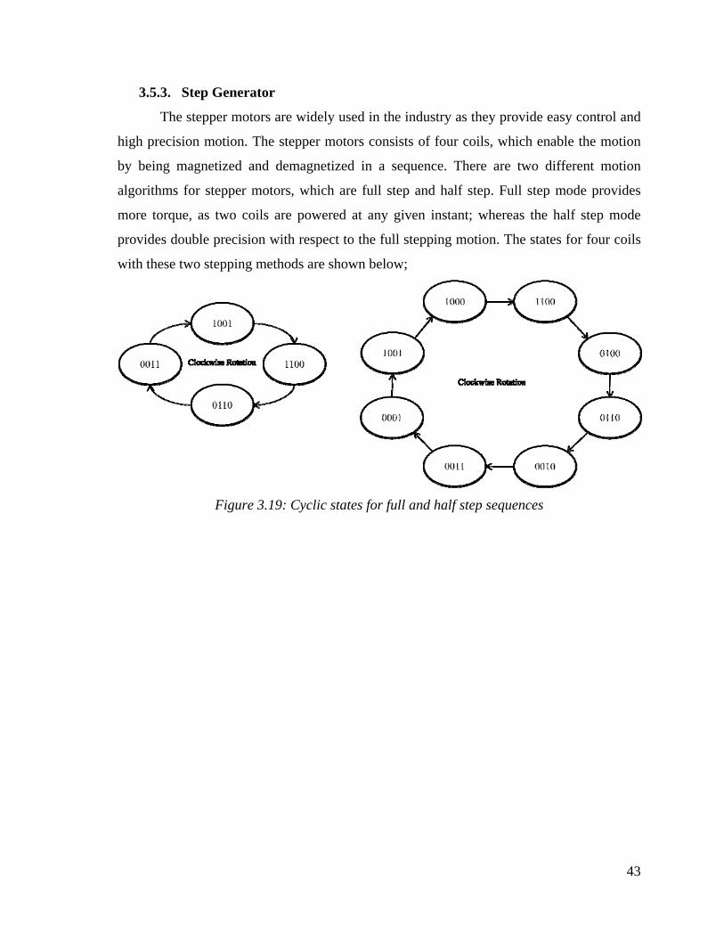
3.5.3. Step Generator
The stepper motors are widely used in the industry as they provide easy control and
high precision motion. The stepper motors consists of four coils, which enable the motion
by being magnetized and demagnetized in a sequence. There are two different motion
algorithms for stepper motors, which are full step and half step. Full step mode provides
more torque, as two coils are powered at any given instant; whereas the half step mode
provides double precision with respect to the full stepping motion. The states for four coils
with these two stepping methods are shown below;
Figure 3.19: Cyclic states for full and half step sequences
43
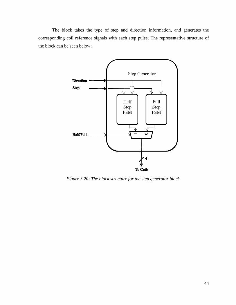
The block takes the type of step and direction information, and generates the
corresponding coil reference signals with each step pulse. The representative structure of
the block can be seen below;
Figure 3.20: The block structure for the step generator block.
44
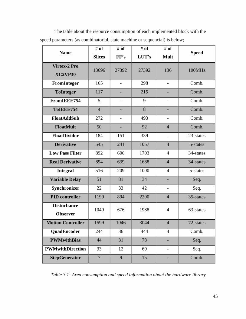
The table about the resource consumption of each implemented block with the
speed parameters (as combinatorial, state machine or sequencial) is below;
Name # of
Slices
# of
FF’s
# of
LUT’s
# of
Mult Speed
Virtex-2 Pro
XC2VP30 13696 27392 27392 136 100MHz
FromInteger 165 - 298 - Comb.
ToInteger 117 - 215 - Comb.
FromIEEE754 5 - 9 - Comb.
ToIEEE754 4 - 8 - Comb.
FloatAddSub 272 - 493 - Comb.
FloatMult 50 - 92 4 Comb.
FloatDividor 184 151 339 - 23-states
Derivative 545 241 1057 4 5-states
Low Pass Filter 892 606 1703 4 34-states
Real Derivative 894 639 1688 4 34-states
Integral 516 209 1000 4 5-states
Variable Delay 51 81 34 - Seq.
Synchronizer 22 33 42 - Seq.
PID controller 1199 894 2200 4 35-states
Disturbance
Observer 1040 676 1988 4 63-states
Motion Controller 1599 1046 3044 4 72-states
QuadEncoder 244 36 444 4 Comb.
PWMwithBias 44 31 78 - Seq.
PWMwithDirection 33 12 60 - Seq.
StepGenerator 7 9 15 - Comb.
Table 3.1: Area consumption and speed information about the hardware library.
45
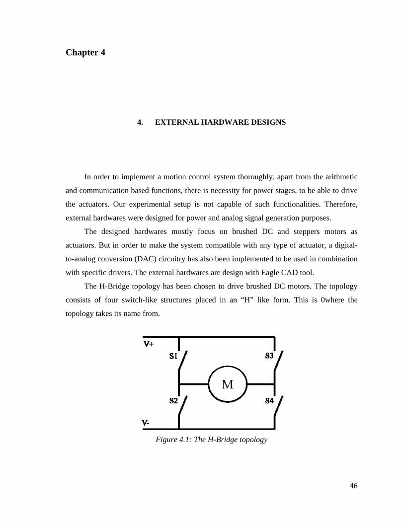
Chapter 4
4. EXTERNAL HARDWARE DESIGNS
In order to implement a motion control system thoroughly, apart from the arithmetic
and communication based functions, there is necessity for power stages, to be able to drive
the actuators. Our experimental setup is not capable of such functionalities. Therefore,
external hardwares were designed for power and analog signal generation purposes.
The designed hardwares mostly focus on brushed DC and steppers motors as
actuators. But in order to make the system compatible with any type of actuator, a digital-
to-analog conversion (DAC) circuitry has also been implemented to be used in combination
with specific drivers. The external hardwares are design with Eagle CAD tool.
The H-Bridge topology has been chosen to drive brushed DC motors. The topology
consists of four switch-like structures placed in an “H” like form. This is 0where the
topology takes its name from.
Figure 4.1: The H-Bridge topology
46

The topology is capable of driving a load in both directions. As the design dictates,
S1 and S2 switches should never be closed at the same time. This also applies for S3 and
S4. This condition would create consumption of high current, which would lead to
performance losses, increase in temperature and even harming the hardware. The truth table
for the topology is given below;
Table 4.1: the truth table of H-Bridge
The following are different H-Bridge based hardware designs, which can be used for
driving mid and high power loads.
47
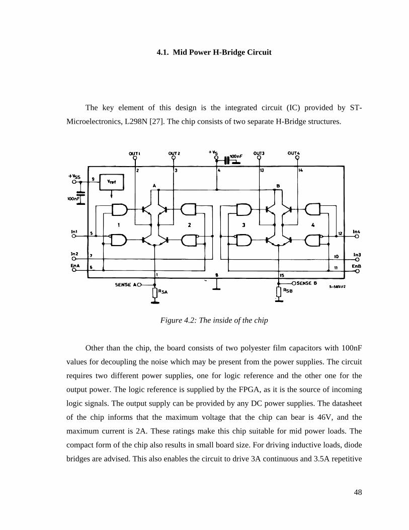
4.1. Mid Power H-Bridge Circuit
The key element of this design is the integrated circuit (IC) provided by ST-
Microelectronics, L298N [27]. The chip consists of two separate H-Bridge structures.
Figure 4.2: The inside of the chip
Other than the chip, the board consists of two polyester film capacitors with 100nF
values for decoupling the noise which may be present from the power supplies. The circuit
requires two different power supplies, one for logic reference and the other one for the
output power. The logic reference is supplied by the FPGA, as it is the source of incoming
logic signals. The output supply can be provided by any DC power supplies. The datasheet
of the chip informs that the maximum voltage that the chip can bear is 46V, and the
maximum current is 2A. These ratings make this chip suitable for mid power loads. The
compact form of the chip also results in small board size. For driving inductive loads, diode
bridges are advised. This also enables the circuit to drive 3A continuous and 3.5A repetitive
48
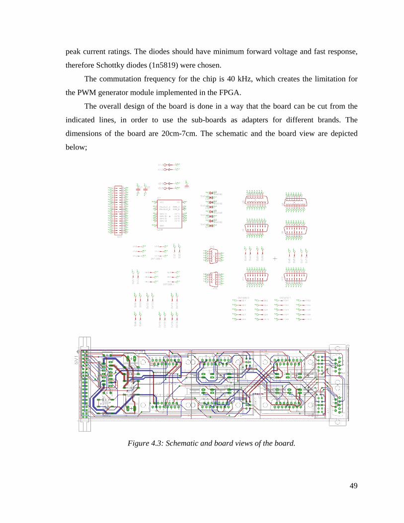
peak current ratings. The diodes should have minimum forward voltage and fast response,
therefore Schottky diodes (1n5819) were chosen.
The commutation frequency for the chip is 40 kHz, which creates the limitation for
the PWM generator module implemented in the FPGA.
The overall design of the board is done in a way that the board can be cut from the
indicated lines, in order to use the sub-boards as adapters for different brands. The
dimensions of the board are 20cm-7cm. The schematic and the board view are depicted
below;
Figure 4.3: Schematic and board views of the board.
49
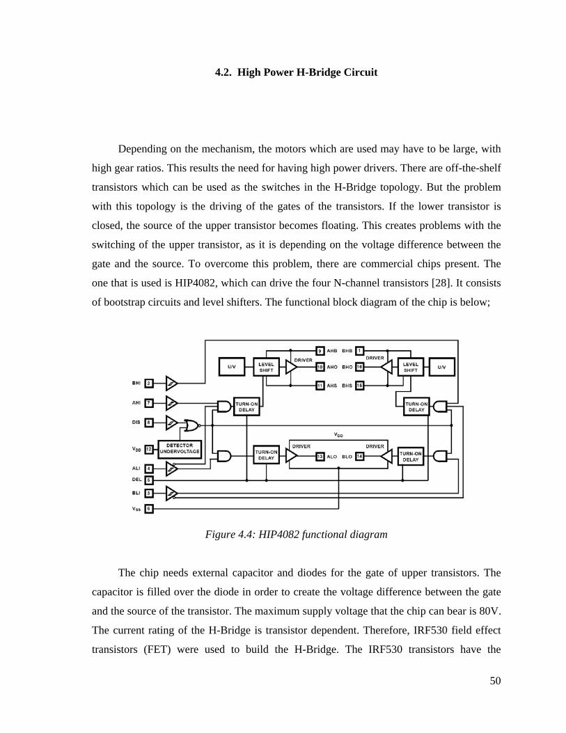
4.2. High Power H-Bridge Circuit
Depending on the mechanism, the motors which are used may have to be large, with
high gear ratios. This results the need for having high power drivers. There are off-the-shelf
transistors which can be used as the switches in the H-Bridge topology. But the problem
with this topology is the driving of the gates of the transistors. If the lower transistor is
closed, the source of the upper transistor becomes floating. This creates problems with the
switching of the upper transistor, as it is depending on the voltage difference between the
gate and the source. To overcome this problem, there are commercial chips present. The
one that is used is HIP4082, which can drive the four N-channel transistors [28]. It consists
of bootstrap circuits and level shifters. The functional block diagram of the chip is below;
Figure 4.4: HIP4082 functional diagram
The chip needs external capacitor and diodes for the gate of upper transistors. The
capacitor is filled over the diode in order to create the voltage difference between the gate
and the source of the transistor. The maximum supply voltage that the chip can bear is 80V.
The current rating of the H-Bridge is transistor dependent. Therefore, IRF530 field effect
transistors (FET) were used to build the H-Bridge. The IRF530 transistors have the
50
maximum voltage and current ratings as 100V and 16A respectively. In addition, the
switching on and off periods are around 12ns. These specifications make them suitable for
our purpose. For the protection purposes, a diode and a resistor are used for each transistor.
In order to eliminate the need to inverse the input, an inverter chip (7404) has also
been used for the input stage of the board. The dimensions of the resulting board are 14cm–
4cm. The schematics and the board design of the hardware can be found below;
Figure 4.5: The schematics and the board design.
Several stepper motor driver circuits can be found in the market. There are also chips
for generating the stepping pulses in full or half step. As the step generation part is
implemented in the FPGA, two different driver circuits have been designed for applications
with different power specifications.
51
4.3. Mid Power Stepper Driver Circuit
The ULN2803 chip consists of eight Darlington Array transistors [29]. The
Darlington Array is a cascaded topology, where a transistor is used to drive another
transistor. The block diagram of the ULN2803 chip can be found below;
Figure 4.6: ULN2803 block diagram
The inputs of the chip are compatible with the outputs of the FPGA, as they both
work at TTL level. And the output of the chip can be connected directly to the windings of
the stepper motor. As the stepper motors have four windings, this board can be used to
drive two stepper motors concurrently. The voltage and current ratings for the chip are 50V
and 500mA respectively. The diode bridges are necessary, as the windings of the stepper
motor are inductive loads. The size of the board is 6cm-4.5cm. The schematic and board
layout of the hardware can be found below;
52
Figure 4.7: Darlington array based stepper motor driver schematic and board views
53
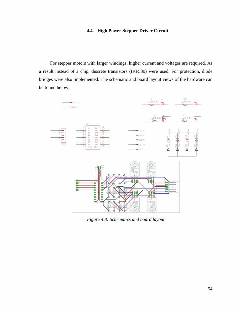
4.4. High Power Stepper Driver Circuit
For stepper motors with larger windings, higher current and voltages are required. As
a result instead of a chip, discrete transistors (IRF530) were used. For protection, diode
bridges were also implemented. The schematic and board layout views of the hardware can
be found below;
Figure 4.8: Schematics and board layout
54
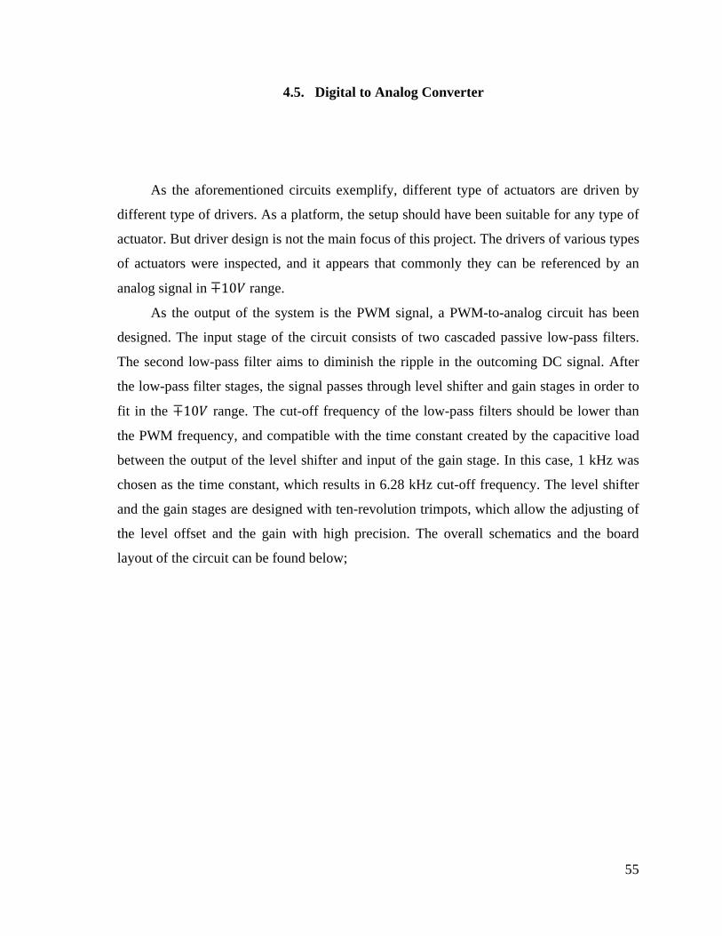
4.5. Digital to Analog Converter
As the aforementioned circuits exemplify, different type of actuators are driven by
different type of drivers. As a platform, the setup should have been suitable for any type of
actuator. But driver design is not the main focus of this project. The drivers of various types
of actuators were inspected, and it appears that commonly they can be referenced by an
analog signal in 10 range.
As the output of the system is the PWM signal, a PWM-to-analog circuit has been
designed. The input stage of the circuit consists of two cascaded passive low-pass filters.
The second low-pass filter aims to diminish the ripple in the outcoming DC signal. After
the low-pass filter stages, the signal passes through level shifter and gain stages in order to
fit in the 10 range. The cut-off frequency of the low-pass filters should be lower than
the PWM frequency, and compatible with the time constant created by the capacitive load
between the output of the level shifter and input of the gain stage. In this case, 1 kHz was
chosen as the time constant, which results in 6.28 kHz cut-off frequency. The level shifter
and the gain stages are designed with ten-revolution trimpots, which allow the adjusting of
the level offset and the gain with high precision. The overall schematics and the board
layout of the circuit can be found below;
55
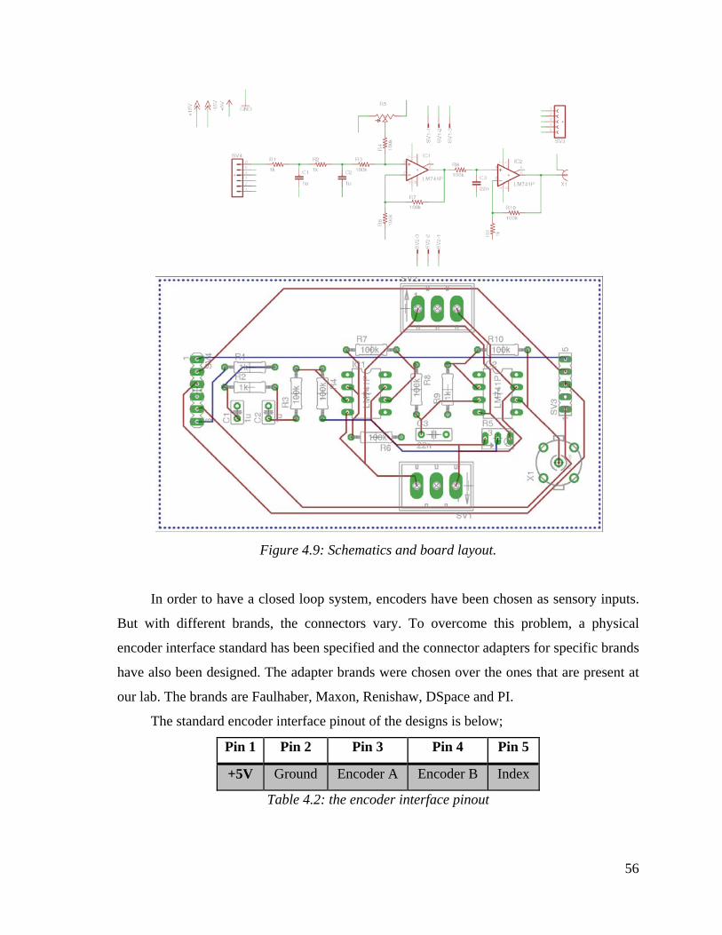
Figure 4.9: Schematics and board layout.
In order to have a closed loop system, encoders have been chosen as sensory inputs.
But with different brands, the connectors vary. To overcome this problem, a physical
encoder interface standard has been specified and the connector adapters for specific brands
have also been designed. The adapter brands were chosen over the ones that are present at
our lab. The brands are Faulhaber, Maxon, Renishaw, DSpace and PI.
The standard encoder interface pinout of the designs is below;
Pin 1 Pin 2 Pin 3 Pin 4 Pin 5
+5V Ground Encoder A Encoder B Index
Table 4.2: the encoder interface pinout
56
Chapter 5
5. COMMUNICATION
Communication is a major part of the system. In order to communicate with the
operator via user interface, or creating a distributed system, a highly reliable
communication medium is compulsory. Communication can be split into two parts; the
hardware which constitutes the physical medium, and the software protocol. There are lots
of different communication standards such as CAN, RS232, I2C, USB, PCI and Ethernet.
All of them have been used is several cases which have been aforementioned in the survey
part. As our experimental setup board has the required hardware for RS232 and Ethernet,
these have been implemented.
5.1. RS232
For RS232 communication, the board has MAX3388 chip on-board which is
connected to a female dsub9 connector. The chip provides the regulation in the voltage
values of the communication. The RS232 standard specifies the output voltages between
-5V and -15V to be interpreted as logic-1 and between +5V and +15V as logic-0. These
voltage levels ensure the transmission of the correct data despite very long cable length (50
feet). The chip also provides fully functional RS232 protocol, with the handshaking signals
like Data Set Ready, Clear to Send and Request to Send. Even though RS232 does not
57
provide very fast data rates, due to the low overhead that it brings to the system, it is widely
chosen as the communication medium.
5.2. Ethernet
The second communication medium which is implemented is Ethernet. There are
several different standards for Ethernet with different speeds. As it needs special hardware
infrastructure, the speed and the standard is dependent on the hardware. The LXT972A
chip on-board supports IEEE 802.3 standard with 10/100 Mb/s data rate. The chip provides
standard Media Independent Interface (MII) for easy attachment to 10/100 Media Access
Controllers (MAC). The full-duplex operation mode can be selected between auto-
negotiation, parallel detection or manual control. The physical layer transceiver (PHY) also
provides performs all functions of the physical coding sub-layer (PCS), the physical media
attachment (PMA) sub-layer, and the physical media dependent (PMD) sub-layer for 100
Mb/s connections. The chip reads three configuration pins on power up. If it is not forced to
any configuration, the device uses auto-negotiation / parallel detection to automatically
determine line operating conditions. If the PHY on the other end supports auto-negotiation,
the chip negotiates with fast link pulse (FLP) bursts. If the other end does not support auto-
negotiation, the chip automatically detects the rate of communication on the other side and
sets its operating mode accordingly. There are three LEDs on the board, providing status
information about the Ethernet link. If a link has been established, the LINK UP LED turns
on. If the links is has 100 Mb/s rate, the SPEED LED also turns on. The RX_DATA LED
blinks when a new packet is received.
The board also includes a Dallas Semiconductor DS2401 Silicon Serial Number. This
provides a unique identity for each board. The chip includes a 64-bit ROM with a 48-bit
serial number, an 8-bit CRC, and an 8-bit device family code. The label on the board has
the registered Ethernet MAC address.
58
Chapter 6
6. SOFTWARE LIBRARY
The overall system does not only consist of hardware part, some elements of the
system have been implemented in software. The written software runs on the embedded
IBM PowerPC 405 processor inside the FPGA. The PowerPC exists as hardware inside the
FPGA; therefore it does not consume any of the resources present in FPGA, but it creates
convenience for some parts of the implementation.
The protocols for aforementioned communication mediums are handled inside the
processor. While RS232 communication is pretty straightforward in software, an external
open source library was necessary for the Ethernet. The library is called “Lightweight IP”,
which consists of several features, implemented on the internet protocol stack. The features
that the library enables are;
Internet Protocol including packet forwarding over multiple network interfaces
Internet Control Message Protocol for network maintenance and debugging
Internet Group Management Protocol for multicast traffic management
User Datagram Protocol including experimental UDP-lite extensions
Transmission Control Protocol with congestion control, RTT estimation and fast
recovery/fast retransmit
Specialized raw/native API for enhanced performance
Domain names resolver
Simple Network Management Protocol
Dynamic Host Configuration Protocol
AUTOIP Link-local address (for IPv4, conforms with RFC 3927)
59
Point-to-Point Protocol
Address Resolution Protocol for Ethernet
Mainly Transmission Control Protocol and User Datagram Protocol features are used
in the software. On top of this communication protocol layer, a command list has been
implemented by using parsers for the incoming messages. The command list and the
responses of the commands can be found in the table below;
Parameter1 Parameter2 Parameter3 Parameter4 Parameter5
setPID Address
(int)
Kp
(float)
Ki
(float)
Kd
(float)
G
(float)
getPID Address
(int)
Kp
(float)
Ki
(float)
Kd
(float)
G
(float)
setRef Address
(int)
Reference
(int)
getRef Address
(int)
Reference
(int)
getPosition Address
(int)
Position
(int)
enableRef Address
(int)
Enable
(bool)
setRegister Address
(int)
Value
(u.int)
getRegister Address
(int)
Value
(u.int)
Table 6.1: Command list
60
In order for these commands to affect the physical part of the system, a device driver
for the motion control block has been developed with the light of the command list. The
device driver enables to read the gains, reference and the position from the block, while
having the authority to override these parameters except the position. These parameters are
sent to the user via selected protocol, which achieves the semi-real time tracking of the
system.
The user communicates with the system over the graphical user interface (GUI),
implemented on the PC side of the system. GUI has been developed by using C#.A sample
screen shot of the GUI can be found below;
Figure 6.1: GUI
The inverse kinematics of the mechanism which will be controlled is implemented in
software also. The main reason for implementing the kinematics in the software is, the
overhead brought by implementing all the functions in hardware. Kinematics consists of
several different mathematical functions like trigonometry, logarithm, exponential and
polynomial functions. Some of the basic functions can be approximated with different
methods like Taylor expansion, but logarithm and exponential functions are more
complicated to approximate.
Each function in the software has been written in a library form. This enables the
future users to understand the code easier and minimizing the amount of code changes for
61
different implementations. All the codes have been written in C, and built by using Xilinx
Embedded Development Kit tool.
62
Chapter 7
7. EXPERIMENTS
In the hardware library section, two different controller blocks have been introduced.
In order to validate the functionality of these blocks, a fundamental experiment has been
made. In the following subsections, the controller comparison experiment will be
introduced, and later on, the controllers will be implemented on a parallel mechanism.
In the past decades, parallel mechanisms gained popularity over serial ones. The main
reason is the advantages they provide like, high stiffness, high accuracy and high payload-
to-weight ratio. In the recent years, many different parallel mechanism designs have been
proposed. However, the main disadvantage of the parallel mechanisms is the limited
workspace. Depending on the application, the limited workspace may not always be a
problem.
The Pantograph is chosen as an experimental setup, in order to have a valid proof of
the proposed platform. This mechanism also forms one of the subsections of the
“MicroFactory” project, developed in the MicroSystem Laboratory.
The setup creation process is done by first creating a top level module by using the
blocks from the library, by using Xilinx ISE tool and tested by using pre-defined
parameters.The physical interface blocks should be chosen depending on the driving
hardware and the actuator type. A custom controller can also be created if needed. After
the top level module is approved, the top level module is wrapped by the template provided
by Xilinx Embedded Development Kit (EDK) in order for the module to communicate with
the proessor over the peripheral local bus (PLB). The software registers are assigned to the
parameters of the module, and a sample code is generated for read/write operations for each
softaware register. After the peripherals are added to the processor, whole system is
63
synthesized to embed in the FPGA chip. Inside EDK, a software project is crated, and the
motion control library should be updated with the assigned addresses of the hardware
blocks. The kernel and the libraries provided by Xilinx can be selected from the software
structure settings. Other libraries can be easily added to the projects. The kernel provided
by Xilinx also enables multi-tasking by a selected scheme like Round-Robin, depending on
the priority table also in the software structure settings.
64
7.1. Motion Controller Comparison
The reason to build a structure for motion control is for high precision and high speed
control applications, where PID controller is good for up to a point. PID control also may
need very fine parameter tuning in several cases. The trial-and-error period consumes a lot
of time. There have been proposed methods for parameter tuning, like Zeigler-Nichols, but
unfortunately it only provides shallow tuning without considering the system dynamics.
The disturbance observer brings robustness to the system and very fine tuning is not
necessary for precise control. The error that the controller fails to handle, like overshoot or
steady-state error, are treated as disturbance and handled by the compensation of the
observer. In order to test and validate these blocks a simple setup has been constructed. The
setup consists of Maxon motors with graphite brushes [30]. As gears damp the actuators
and increases stability, in order to observe the differences explicitly, gearless motors have
been chosen. Two motors are connected by a belt from their shafts, where one motor is
controlled, and the other is supplied with a constant current in order to create disturbance.
The system takes the actuator reference directly from the user. The actuators are driven
with mid power H-Bridge driver circuits, and the position is obtained by using the
quadrature encoder block. The step response of the system with PID and motion
controllers with and without external disturbances can be found below;
The amplitude of the step references are 1000 pulses. The first experiment is done
while the controlled motor is running free. The PID controller results with a 10 pulse
overshoot, and a 2 pulse steady-state error, whereas the motion controller results 7 pulse
overshoot and no steady-state error. When we add disturbance to the system, the PID
controller results 15 pulse overshoot, and the system oscillates in steady state with an
amplitude of ±2 pulses, while the motion controller results 6 pulse overshoot with no
steady-state error.
In light of these obtained results, the motion controller block has been chosen as
control block for the parallel mechanism.
65
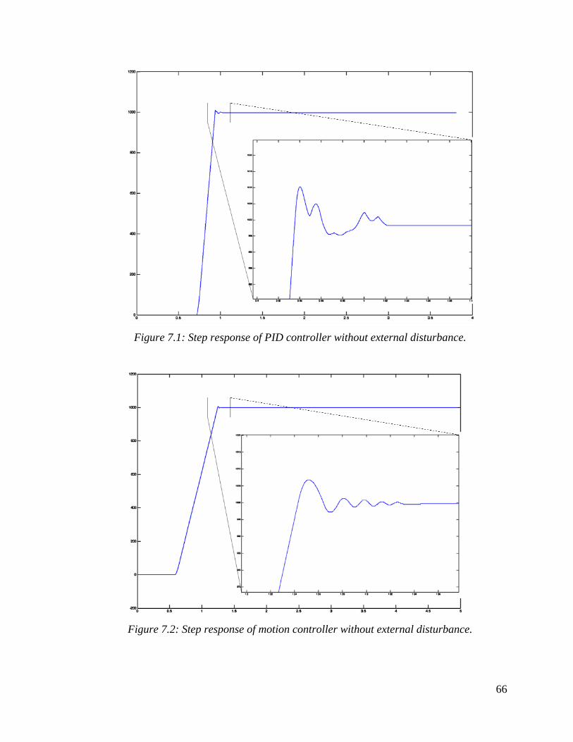
Figure 7.1: Step response of PID controller without external disturbance.
Figure 7.2: Step response of motion controller without external disturbance.
66
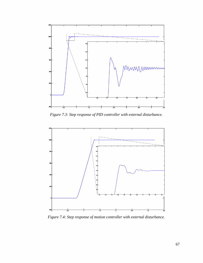
Figure 7.3: Step response of PID controller with external disturbance.
Figure 7.4: Step response of motion controller with external disturbance.
67
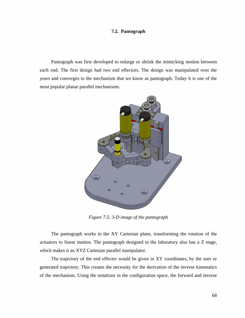
7.2. Pantograph
Pantograph was first developed to enlarge or shrink the mimicking motion between
each end. The first design had two end effectors. The design was manipulated over the
years and converges to the mechanism that we know as pantograph. Today it is one of the
most popular planar parallel mechanisms.
Figure 7.5: 3-D image of the pantograph
The pantograph works in the XY Cartesian plane, transforming the rotation of the
actuators to linear motion. The pantograph designed in the laboratory also has a Z stage,
which makes it an XYZ Cartesian parallel manipulator.
The trajectory of the end effecter would be given in XY coordinates, by the user or
generated trajectory. This creates the necessity for the derivation of the inverse kinematics
of the mechanism. Using the notations in the configuration space, the forward and inverse
68
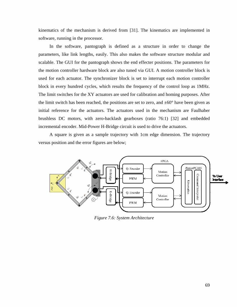
kinematics of the mechanism is derived from [31]. The kinematics are implemented in
software, running in the processor.
In the software, pantograph is defined as a structure in order to change the
parameters, like link lengths, easily. This also makes the software structure modular and
scalable. The GUI for the pantograph shows the end effecter positions. The parameters for
the motion controller hardware block are also tuned via GUI. A motion controller block is
used for each actuator. The synchronizer block is set to interrupt each motion controller
block in every hundred cycles, which results the frequency of the control loop as 1MHz.
The limit switches for the XY actuators are used for calibration and homing purposes. After
the limit switch has been reached, the positions are set to zero, and ±60° have been given as
initial reference for the actuators. The actuators used in the mechanism are Faulhaber
brushless DC motors, with zero-backlash gearboxes (ratio 76:1) [32] and embedded
incremental encoder. Mid-Power H-Bridge circuit is used to drive the actuators.
A square is given as a sample trajectory with 1cm edge dimension. The trajectory
versus position and the error figures are below;
Figure 7.6: System Architecture
69
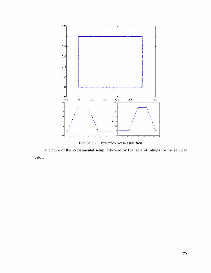
Figure 7.7: Trajectory versus position
A picture of the experimental setup, followed by the table of ratings for the setup is
below;
70
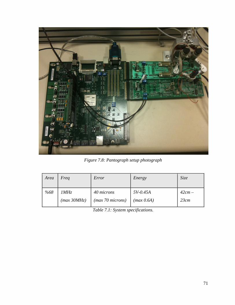
Figure 7.8: Pantograph setup photograph
Area Freq Error Energy Size
%68 1MHz
(max 30MHz)
40 microns
(max 70 microns)
5V-0.45A
(max 0.6A)
42cm –
23cm
Table 7.1: System specifications.
71
Chapter 8
8. CONCLUSION AND FUTURE WORK
The main aim of this thesis was to propose an alternative platform for motion control
purposes. The FPGA based motion control platform offers an easy-to-build system, due to
the given hardware and software libraries. The libraries also allow creating custom
functionalities without advanced hardware description language knowledge. The
experiments are done by using only the functionalities provided by the libraries, where the
results validate the platforms functionality. The functionalities are designed to cover the
fundamentals of motion control theory.
The proposed platform has some major advantages over other conventionally used
systems. The size and the cost of the system is less than most of the commercial products.
Setting up a system is fairly easy, due to the schematic based visual programming
environment. The performance is compatible with the other platforms for basic systems.
The major performance difference can be observed as the systems become more complex,
or require high sampling rates, and high frequency loops due to the physical hardware
structure of the system and parallel processing capabilities. The energy efficiency of the
system is higher than other similar platforms, as the system does not use any redundant
parts, and works at a lower clock frequency. One other major advantage of the proposed
system is, it is technology independent. The libraries can be synthesized and compiled for
different technologies, whereas current platforms require specific software versions, or
specific hardware.
One of the down sides of the system is the communication performance. As the
communication of the system depends on the physical layer chip, it supports 10/100 Mb/s
ethernet communication. With more upgraded boards it can also provide gigabit ethernet,
as well as other communication mediums such as PCI.
72
As future work, a custom FPGA board can be designed. In that case, the external
hardwares like the power stages, H-Bridges, and the DAC circuits can be embedded on
board, as well as higher performance communication mediums.
73
Bibliography
[1] Digilent - http://www.digilentinc.com/
[2] Altera, “Is Motion control technology moving from controllers to FPGAs?”, 2008
[3] Altera, “FPGAs Enable Energy-Efficient Motor Control in Next-Generation Smart
Home Appliances”, 2008
[4] National Instruments, “Creating Custom Motion Control and Drive electronics with
FPGA based system”, 2010
[5] Xilinx, “FPGA Motor Control Reference Design”, 2005
[6] M. K. Jaiswal, “Efficient Implementation of IEEE Double Precision Floating-Point
Multiplier on FPGA”, IEEE Region 10 Colloquium and the Third ICIIS, pp.226-230,
December 2008
[7] Chun Hok Ho, “Floating-Point FPGA: Architecture and Modeling”, IEEE Transactions
On Very Large Scale Integration (VLSI) Systems, vol. 17, no. 12, December 2009
[8] Jie Zhou, “Double Precision Hybrid-Mode Floating-Point FPGA CORDIC Co-
processor”, The 10th IEEE International Conference on High Performance Computing and
Communications, 2008
[9] N. Masmoudi, “Implementation of PID Controller on FPGA”, Laboratory of Computer
Science and Industrial Electronic of Sfax
[10] Y. F. Chan, “Design and Implementation of Modular FPGA-Based PID Controllers”,
IEEE Transactions on Industrial Electronics, vol. 54, no. 4, August 2007
[11] U. Meshram, “Robot Arm Controller Using FPGA”, Impact, 2009
[12] N. Q. Le, “An Open Loop Stepper Motor Driver Based on FPGA”, International
conference on Control, Automation and Systems, October 2007
[13] D. Wang, “Functional Design of FPGA in a Brushless DC Motor System Based on
FPGA and DSP”, IEEE Vehicle Power and Propulsion Conference, September 2008
74
[14] B. S. Kariyappa, “FPGA Based Speed Control of AC Servomotor Using Sinusoidal
PWM”, IJCSNS International Journal of Computer Science and Network Security, vol.8
no.10, October 2008
[15] A. M. Eltamaly, “FPGA Based Speed Control of Three-Phase Induction Motor Using
Stator Voltage Regulator”, Elmansoura University
[16] Y. Li, “Development of an FPGA-Based Servo Controller for PMSM Drives”, Proc.
IEEE International Conference on Automation and Logistics, August 2007
[17] F. J. Lin, “FPGA-Based Elman Neural Network Control System for Linear Ultrasonic
Motor”, IEEE Transactions on Ultrasonics, Ferroelectrics, and Frequency Control, vol. 56,
no. 1, January 2009
[18] Y. S. Kung, “FPGA-Implementation of Inverse Kinematics and Servo Controller for
Robot Manipulator”, Proc. IEEE International Conference on Robotics and Biomimetics,
December 2006
[19] J. S. Kim, “Hardware Implementation of Nonlinear PID Controller with FPGA Based
on Floating Point Operation for 6-DOF Manipulator Robot Arm”, International
Conference on Control, Automation and Systems, Oct. 2007
[20] J. S. Kim, “Hardware Implementation of a Neural Network Controller on FPGA for a
Humanoid Robot Arm”, Proc. IEEE/ASMEInternational Conference on Advanced
Intelligent Mechatronics, July 2008
[21] B. Han, “FPGA based Time Domain Passivity Observer and Passivity Controller”,
IEEE/ASME International Conference on Advanced Intelligent Mechatronics, July 2009
[22] E. Ishii, “Improvement of Performance in Bilateral Teleoperation by Using FPGA”,
AMC, 2006
[23] H. Tanaka., “Implementation of Bilateral Control System Based on Acceleration
Control Using FPGA for multi-DOF Haptic Endoscopic Surgery Robot”, IEEE
Transactions on Industrial Electronics, vol. 56, no. 3, March 2009
[24] X. Shao, “Development of an FPGA-Based Motion Control ASIC for Robotic
Manipulators”, Proc. 6th World Congress on Intelligent Control and Automation, June
2006
[25] J. U. Cho, “An FPGA-Based Multiple-Axis Motion Control Chip” IEEE Transactions
on Industrial Electronics, vol. 56, no. 3, March 2009
75
[26] R. S. Barbosa, “Time domain design of fractional differintegrators using least-
squares”, Signal Processing 86 , pp. 2567–2581, 2006
[27] http://www.st.com/stonline/books/pdf/docs/1773.pdf
[28] http://www.intersil.com/data/fn/fn3676.pdf
[29] http://www.st.com/stonline/products/literature/ds/1536/uln2803a.pdf
[30] http://www.maxonmotor.com/
[31] G. Campion, “The Pantograph Mk-II: A Haptic Instrument”, Proc. IROS 2005,
IEEE/RSJ Int. Conf. Intelligent Robots and Systems, pp. 723-728
[32] http://www.micromo.com/
76
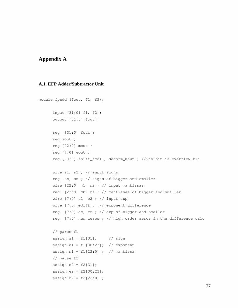
Appendix A
A.1. EFP Adder/Subtractor Unit
module fpadd (fout, f1, f2);
input [31:0] f1, f2 ;
output [31:0] fout ;
reg [31:0] fout ;
reg sout ;
reg [22:0] mout ;
reg [7:0] eout ;
reg [23:0] shift_small, denorm_mout ; //9th bit is overflow bit
wire s1, s2 ; // input signs
reg sb, ss ; // signs of bigger and smaller
wire [22:0] m1, m2 ; // input mantissas
reg [22:0] mb, ms ; // mantissas of bigger and smaller
wire [7:0] e1, e2 ; // input exp
wire [7:0] ediff ; // exponent difference
reg [7:0] eb, es ; // exp of bigger and smaller
reg [7:0] num_zeros ; // high order zeros in the difference calc
// parse f1
assign s1 = f1[31]; // sign
assign e1 = f1[30:23]; // exponent
assign m1 = f1[22:0] ; // mantissa
// parse f2
assign s2 = f2[31];
assign e2 = f2[30:23];
assign m2 = f2[22:0] ;
77
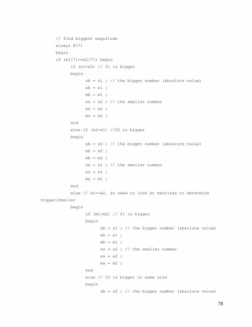
// find biggest magnitude
always @(*)
begin
if (e1[7]==e2[7]) begin
if (e1>e2) // f1 is bigger
begin
sb = s1 ; // the bigger number (absolute value)
eb = e1 ;
mb = m1 ;
ss = s2 ; // the smaller number
es = e2 ;
ms = m2 ;
end
else if (e2>e1) //f2 is bigger
begin
sb = s2 ; // the bigger number (absolute value)
eb = e2 ;
mb = m2 ;
ss = s1 ; // the smaller number
es = e1 ;
ms = m1 ;
end
else // e1==e2, so need to look at mantissa to determine
bigger/smaller
begin
if (m1>m2) // f1 is bigger
begin
sb = s1 ; // the bigger number (absolute value)
eb = e1 ;
mb = m1 ;
ss = s2 ; // the smaller number
es = e2 ;
ms = m2 ;
end
else // f2 is bigger or same size
begin
sb = s2 ; // the bigger number (absolute value)
78
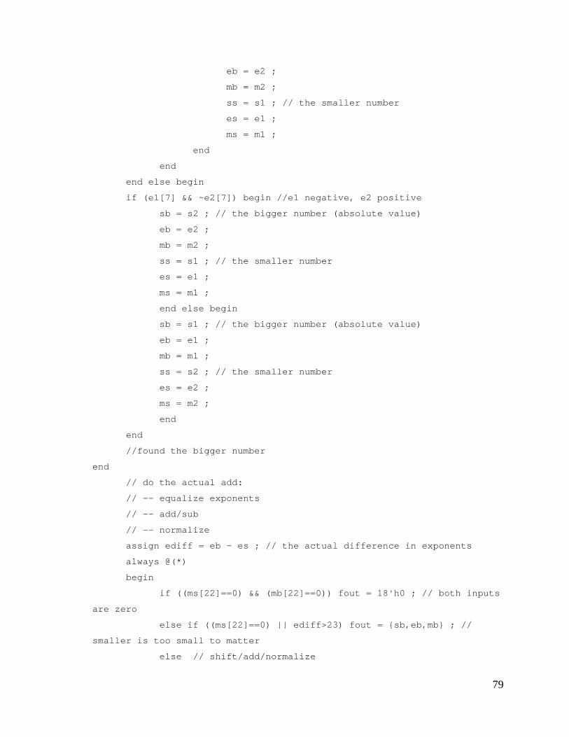
eb = e2 ;
mb = m2 ;
ss = s1 ; // the smaller number
es = e1 ;
ms = m1 ;
end
end
end else begin
if (e1[7] && ~e2[7]) begin //e1 negative, e2 positive
sb = s2 ; // the bigger number (absolute value)
eb = e2 ;
mb = m2 ;
ss = s1 ; // the smaller number
es = e1 ;
ms = m1 ;
end else begin
sb = s1 ; // the bigger number (absolute value)
eb = e1 ;
mb = m1 ;
ss = s2 ; // the smaller number
es = e2 ;
ms = m2 ;
end
end
//found the bigger number
end
// do the actual add:
// -- equalize exponents
// -- add/sub
// -- normalize
assign ediff = eb - es ; // the actual difference in exponents
always @(*)
begin
if ((ms[22]==0) && (mb[22]==0)) fout = 18'h0 ; // both inputs
are zero
else if ((ms[22]==0) || ediff>23) fout = {sb,eb,mb} ; //
smaller is too small to matter
else // shift/add/normalize
79
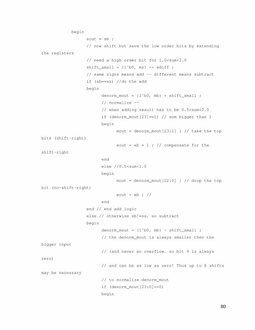
begin
sout = sb ;
// now shift but save the low order bits by extending
the registers
// need a high order bit for 1.0<sum<2.0
shift_small = {1'b0, ms} >> ediff ;
// same signs means add -- different means subtract
if (sb==ss) //do the add
begin
denorm_mout = {1'b0, mb} + shift_small ;
// normalize --
// when adding result has to be 0.5<sum<2.0
if (denorm_mout[23]==1) // sum bigger than 1
begin
mout = denorm_mout[23:1] ; // take the top
bits (shift-right)
eout = eb + 1 ; // compensate for the
shift-right
end
else //0.5<sum<1.0
begin
mout = denorm_mout[22:0] ; // drop the top
bit (no-shift-right)
eout = eb ; //
end
end // end add logic
else // otherwise sb!=ss, so subtract
begin
denorm_mout = {1'b0, mb} - shift_small ;
// the denorm_mout is always smaller then the
bigger input
// (and never an overflow, so bit 9 is always
zero)
// and can be as low as zero! Thus up to 8 shifts
may be necessary
// to normalize denorm_mout
if (denorm_mout[23:0]==0)
begin
80

mout = 9'b0 ;
eout = 8'b0 ;
end
else
begin
// detect leading zeros
casex (denorm_mout[22:0])
23'b1xxxxxxxxxxxxxxxxxxxxxx: num_zeros = 8'h00 ;
23'b01xxxxxxxxxxxxxxxxxxxxx: num_zeros = 8'h01 ;
23'b001xxxxxxxxxxxxxxxxxxxx: num_zeros = 8'h02 ;
23'b0001xxxxxxxxxxxxxxxxxxx: num_zeros = 8'h03 ;
23'b00001xxxxxxxxxxxxxxxxxx: num_zeros = 8'h04 ;
23'b000001xxxxxxxxxxxxxxxxx: num_zeros = 8'h05 ;
23'b0000001xxxxxxxxxxxxxxxx: num_zeros = 8'h06 ;
23'b00000001xxxxxxxxxxxxxxx: num_zeros = 8'h07 ;
23'b000000001xxxxxxxxxxxxxx: num_zeros = 8'h08 ;
23'b0000000001xxxxxxxxxxxxx: num_zeros = 8'h09 ;
23'b00000000001xxxxxxxxxxxx: num_zeros = 8'h0a ;
23'b000000000001xxxxxxxxxxx: num_zeros = 8'h0b ;
23'b0000000000001xxxxxxxxxx: num_zeros = 8'h0c ;
23'b00000000000001xxxxxxxxx: num_zeros = 8'h0d ;
23'b000000000000001xxxxxxxx: num_zeros = 8'h0e ;
23'b0000000000000001xxxxxxx: num_zeros = 8'h0f ;
23'b00000000000000001xxxxxx: num_zeros = 8'h10 ;
23'b000000000000000001xxxxx: num_zeros = 8'h11 ;
23'b0000000000000000001xxxx: num_zeros = 8'h12 ;
23'b00000000000000000001xxx: num_zeros = 8'h13 ;
23'b000000000000000000001xx: num_zeros = 8'h14 ;
23'b0000000000000000000001x: num_zeros = 8'h15 ;
23'b00000000000000000000001: num_zeros = 8'h16 ;
default: num_zeros = 8'd0 ;
endcase
// shift out leading zeros
// and adjust exponent
eout = eb - num_zeros ;
mout = denorm_mout[23:0] << num_zeros ;
end
81
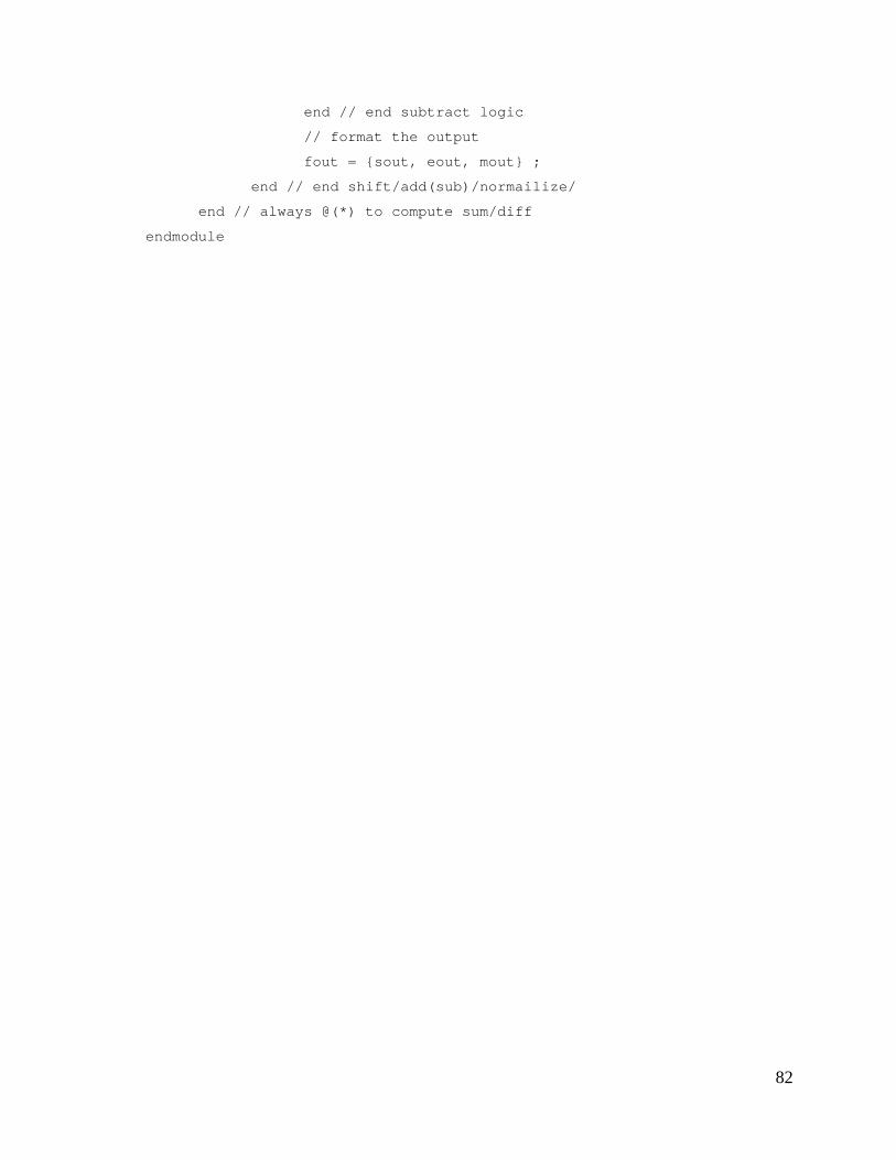
end // end subtract logic
// format the output
fout = {sout, eout, mout} ;
end // end shift/add(sub)/normailize/
end // always @(*) to compute sum/diff
endmodule
82
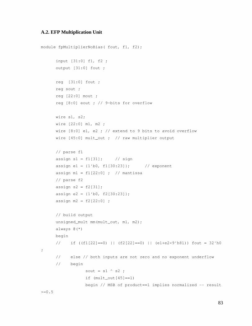
A.2. EFP Multiplication Unit
module fpMultiplierNoBias( fout, f1, f2);
input [31:0] f1, f2 ;
output [31:0] fout ;
reg [31:0] fout ;
reg sout ;
reg [22:0] mout ;
reg [8:0] eout ; // 9-bits for overflow
wire s1, s2;
wire [22:0] m1, m2 ;
wire [8:0] e1, e2 ; // extend to 9 bits to avoid overflow
wire [45:0] mult_out ; // raw multiplier output
// parse f1
assign s1 = f1[31]; // sign
assign e1 = {1'b0, f1[30:23]}; // exponent
assign m1 = f1[22:0] ; // mantissa
// parse f2
assign s2 = f2[31];
assign e2 = {1'b0, f2[30:23]};
assign m2 = f2[22:0] ;
// build output
unsigned_mult mm(mult_out, m1, m2);
always @(*)
begin
// if ((f1[22]==0) || (f2[22]==0) || (e1+e2<9'h81)) fout = 32'h0
;
// else // both inputs are not zero and no exponent underflow
// begin
sout = s1 ^ s2 ;
if (mult_out[45]==1)
begin // MSB of product==1 implies normalized -- result
>=0.5
83

eout = e1+e2; //no need to adjust eout
mout = mult_out[45:23] ;
end
else // MSB of product==0 implies result <0.5
begin
eout = e1+e2-1; //adjust eout
mout = mult_out[44:22] ;
end
fout = {sout, eout[7:0], mout} ;
// end // nonzero mult logic
end // always @(*)
endmodule
84
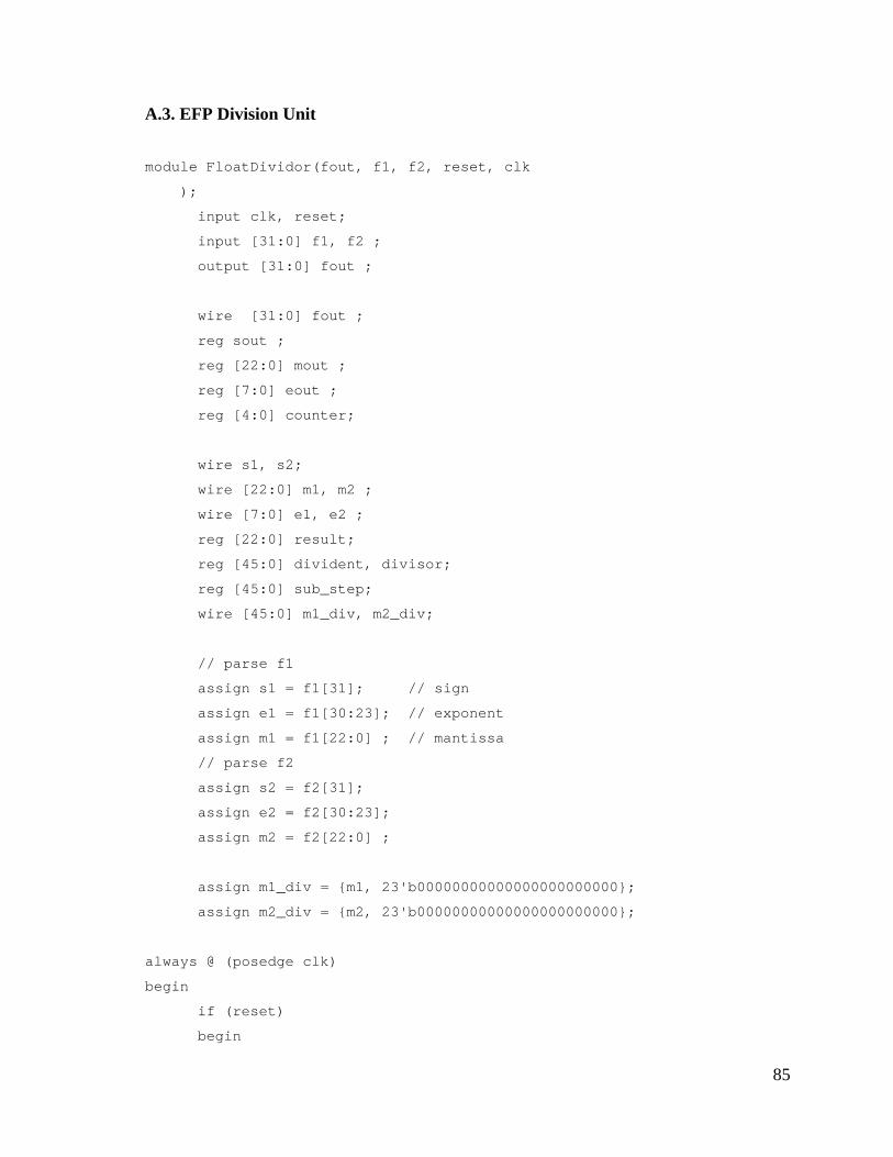
A.3. EFP Division Unit
module FloatDividor(fout, f1, f2, reset, clk
);
input clk, reset;
input [31:0] f1, f2 ;
output [31:0] fout ;
wire [31:0] fout ;
reg sout ;
reg [22:0] mout ;
reg [7:0] eout ;
reg [4:0] counter;
wire s1, s2;
wire [22:0] m1, m2 ;
wire [7:0] e1, e2 ;
reg [22:0] result;
reg [45:0] divident, divisor;
reg [45:0] sub_step;
wire [45:0] m1_div, m2_div;
// parse f1
assign s1 = f1[31]; // sign
assign e1 = f1[30:23]; // exponent
assign m1 = f1[22:0] ; // mantissa
// parse f2
assign s2 = f2[31];
assign e2 = f2[30:23];
assign m2 = f2[22:0] ;
assign m1_div = {m1, 23'b00000000000000000000000};
assign m2_div = {m2, 23'b00000000000000000000000};
always @ (posedge clk)
begin
if (reset)
begin
85
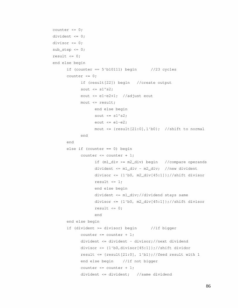
counter <= 0;
divident <= 0;
divisor <= 0;
sub_step <= 0;
result <= 0;
end else begin
if (counter == 5'b10111) begin //23 cycles
counter <= 0;
if (result[22]) begin //create output
sout <= s1^s2;
eout <= e1-e2+1; //adjust eout
mout <= result;
end else begin
sout <= s1^s2;
eout <= e1-e2;
mout <= {result[21:0],1'b0}; //shift to normal
end
end
else if (counter == 0) begin
counter <= counter + 1;
if (m1_div >= m2_div) begin //compare operands
divident <= m1_div - m2_div; //new divident
divisor <= {1'b0, m2_div[45:1]};//shift divisor
result <= 1;
end else begin
divident <= m1_div;//dividend stays same
divisor <= {1'b0, m2_div[45:1]};//shift divisor
result <= 0;
end
end else begin
if (divident >= divisor) begin //if bigger
counter <= counter + 1;
divident <= divident - divisor;//next dividend
divisor <= {1'b0,divisor[45:1]};//shift dividor
result <= {result[21:0], 1'b1};//feed result with 1
end else begin //if not bigger
counter <= counter + 1;
divident <= divident; //same dividend
86
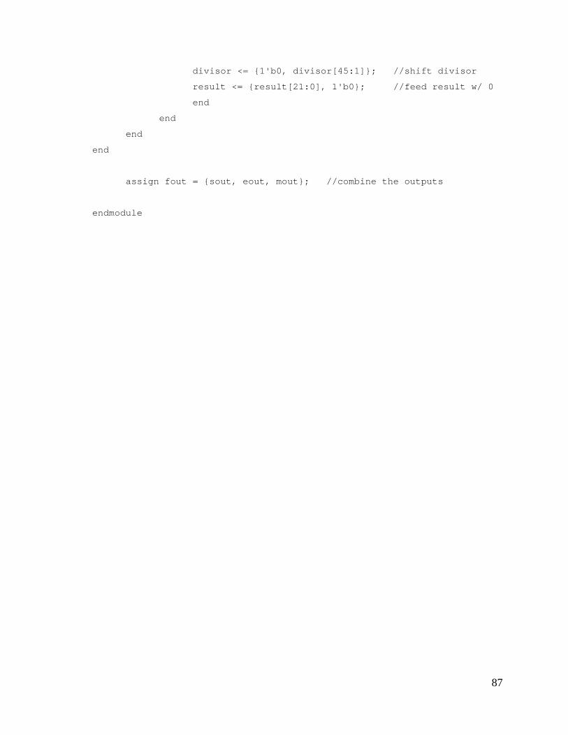
87
divisor <= {1'b0, divisor[45:1]}; //shift divisor
result <= {result[21:0], 1'b0}; //feed result w/ 0
end
end
end
end
assign fout = {sout, eout, mout}; //combine the outputs
endmodule