Locked In/Locked Out:Imprisoning Women in the Shrinking and Punitive Welfare State
Upload
khangminh22Category
view
4download
0
Vol. 32, No. 10 Journal of Semiconductors October 2011
A fast-locking all-digital delay-locked loop for phase/delay generation in an FPGA�
Chen Zhujia(陈柱佳)1; 2, Yang Haigang(杨海钢)1; �, Liu Fei(刘飞)1, and Wang Yu(王瑜)1; 2
1Institute of Electronics, Chinese Academy of Sciences, Beijing 100190, China2Graduate University of the Chinese Academy of Sciences, Beijing 100049, China
Abstract: A fast-locking all-digital delay-locked loop (ADDLL) is proposed for the DDR SDRAM controllerinterface in a field programmable gate array (FPGA). The ADDLL performs a 90ı phase-shift so that the datastrobe (DQS) can enlarge the data valid window in order to minimize skew. In order to further reduce the lockingtime and to prevent the harmonic locking problem, a time-to-digital converter (TDC) is proposed. A duty cyclecorrector (DCC) is also designed in the ADDLL to adjust the output duty cycle to 50%. The ADDLL, implementedin a commercial 0.13 �m CMOS process, occupies a total of 0.017 mm2 of active area. Measurement results showthat the ADDLL has an operating frequency range of 75 to 350 MHz and a total delay resolution of 15 ps. The timeinterval error (TIE) of the proposed circuit is 60.7 ps.
Key words: all digital DLL; DDR SDRAM controller; time-to-digital converter; duty cycle corrector; DCDL;FPGA
DOI: 10.1088/1674-4926/32/10/105009 EEACC: 2570
1. Introduction
Delay-locked loops (DLLs) are widely used as phaseshifters in clock de-skew buffers, multiphase clock generatorsand DRAM interfaces in high speed field programmable gatearrays (FPGAs). Compared with the phase-lock loop (PLL),a DLL has advantages of better jitter performance, stability,improved phase tracking ability and ease of designŒ1�. DigitalDLLs are a good alternative in applications such as phase shift-ing in the DRAM interfaces of FPGAs.
In double data rate (DDR) SDRAM controller designs,data transfers are based on the bidirectional data strobe (DQS)signal transmitted with the output data (DQ)Œ2�. Figure 1 showsthe timing budget in read operation. Ideally, both signals areedge aligned by a DDR SDRAM. However, due to PCB boardskew and pin-to-pin mismatch between the DQS and the DQ,skew exists between the DQS and DQ when they arrive at thecontroller, making the data valid window smaller. In order toenlarge the data valid window, the DQS needs to be delayed bya 90ı phase shift to the center of the data window. One way toimplement the phase shift is to use a buffer chain. The disad-vantages of this method are that the buffer chain cannot meeta wide input frequency range and its delay value varies withprocess, voltage and temperature (PVT) variations. Comparedwith this method, digital DLLs are preferred due to their fastlocking time and ease of migration over different processes inhigh speed DDR memory interface controllersŒ3�7�.
To tolerate wide variations of clock frequency and PVT, aDLL needs to be able to operate in a wide frequency range. Thehighest frequency of a DLL is decided by the delay of a singledelay unit and the lowest frequency is decided by the length ofthe delay line. All of the above demand that the delay line of aDLL has a high-bandwidth. To meet this requirement, conven-tional digital DLLsŒ9; 10� consume large numbers of delay units
and increase supply-induced jitter due to the longer delay line.Conventional digital DLLsŒ9� employ counters to adjust
the delay lines, which makes the locking time increase expo-nentially as the number of control bits increases. Thus a shortlocking time is required for the ADDLL to generate a phase-shifted clock signal when the controller switches from powerdown mode to active mode. A binary searching algorithm wasadopted in Refs. [11, 12] to reduce the locking time in propor-tion to the control bits, but the open-loop characteristic makesit hard to track PVT variations.
In this work, an improved all-digital DLL (ADDLL) is pro-posed. Compared with conventional digital DLLsŒ9; 10�, whichuse a single delay line, the digital control delay line (DCDL) ofthe proposed ADDLL is composed of a coarse delay unit and afine delay unit. The proposed ADDLL meets the short lockingtime requirement by utilizing a novel time-to-digital converter(TDC) to coarse lock the ADDLL by tuning the coarse delayunit in one clock cycle. The proposed structure achieves a shortlocking time and prevents the possibility of harmonic locking.
Fig. 1. DDR SDRAM Read operation timing budget.
* Project supported by the Major National Scientific Research Plan of China (No. 2011CB933202) and the National High Technology Re-search and Development Program of China (No. 2008AA010701).
� Corresponding author. Email: [email protected] 6 April 2011, revised manuscript received 11 May 2011 c 2011 Chinese Institute of Electronics
105009-1

J. Semicond. 2011, 32(10) Chen Zhujia et al.
Fig. 2. Architecture of the proposed ADDLL.
A duty-cycle correction (DCC) circuit is designed to adjust theduty cycle of the input clock signal close to 50%.
2. Architecture of the all digital DLL
Figure 2 shows the architecture of the proposed ADDLL.It is composed of a phase detector (PD), a bidirectional shiftregister (BSR), a TDC, a DCDL and a DCC. Like DLL-basedmulti-phase clock generators, the ADDLL has a multi-stagedelay line with the same digital control code to generate anequally spaced multi-phase clock outputŒ7�. In this design, fourduplicated delay cells are utilized in the DCDL to generate a90ı phase shift, each of which contains a coarse delay unit and afine delay unit. The delay cell in the DQS logic is the same as inthe DCDL. When the ADDLL is in the locked state, the delaytime of the DCDL is one clock cycle, which is averagely di-vided into quarters by the four delay cells. Then, the 90ı phaseshift of the DQS can be tuned by the delay component in theDQS logic.
The locking procedure of the ADDLL is divided into 3steps: coarse locking by TDC, fine locking by the PD and BSR,and state holding. Initially, the signal RESET N is low, whichresets control codes C[15:0] and F[19:0] to zero for minimumdelay. When RESET N goes to high, the ADDLL enters intothe locking procedure. At the beginning, the DCC takes 6 clockcycles to adjust the input clock duty cycle to near 50% andgenerate the output signal CLK REF fed into the DCDL andTDC. After the DCC finishes its adjustment, the ADDLL en-ters into the coarse tuning procedure. The PD and BSR are dis-abled in this period. The TDC estimates the input clock cycleby a multiple of the coarse delay value and generates the coarsedelay control code C[15:0] for the DCDL. The TDC completescoarse tuning in one clock period and then generates a controlsignal to enable the PD and BSR, and the ADDLL begins finetuning. After this step, the delay difference between the refer-ence phase and the output phase of the DCDL is less than a stepsize of the coarse delay unit.
After coarse locking, the DCDL will be fine tuned by theBSR. The PD compares the reference phase with the output
phase of the delay line and then generates an UP/DOWN sig-nal for the BSR. The state of the BSR is controlled by theUP/DOWN signal from the PD. The BSR generates a ther-mometer control code F[19:0], which helps to reduce ditheredswitching of the control code. The 4-stage duplicated delaycells in the DCDL generate 4 equally spaced signals: CLK90,CLK180, CLK270 and CLK360.When the output clock lags orleads the reference clock, the PD generates an UP or DOWNsignal for the BSR. When the phase difference is within thelock range of the lock detector, a LOCK signal is created bythe lock detector to turn the ADDLL into the hold state.
3. Circuit implementation
3.1. Digital control delay line (DCDL)
The DCDL is the most important part of an ADDLL de-sign, as it decides the operating frequency range, delay reso-lution and delay linearity of the ADDLL. The DCDL in thisdesign is divided into two parts to extend its tunable range andto reduce the locking time: a coarse delay unit and a fine delayunit. According to the requirements of the ADDLL, the delayline needs 4 duplicated delay cells to generate a 90ı phase shift.To track PVT variations, the minimum delay of each delay cellin a worst case scenario (slow, 1.35 V, 125 ıC) is supposedto be shorter than 1/4 of the input reference clock period, andlarger than 1/4 of the input reference clock period in the bestcase scenario (fast, 1.65 V, � 40 ıC).
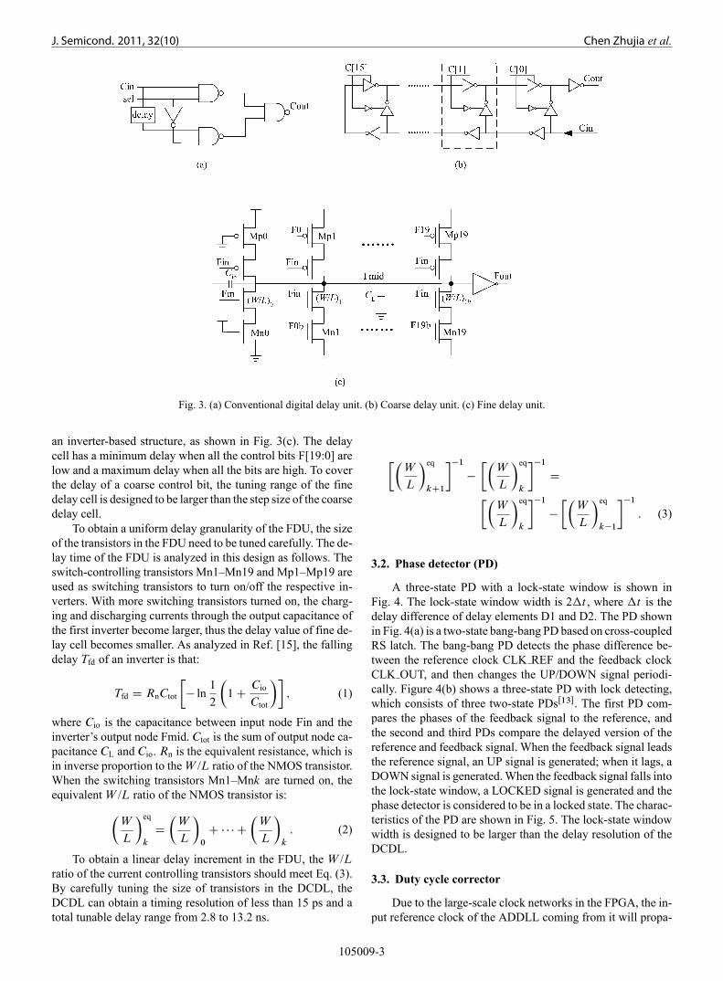
The conventional digital-controlled delay unit is shown inFig. 3(a). It has two different delays controlled by a multi-plexer. The tunable range can be increased by cascading thedelay units, but this also increases the intrinsic delay. So themaximum operating frequency is restricted by the large intrin-sic delay. The proposed CDU shown in Fig. 3(b) is a MUX-based structure mirror delay line. The length of the delay chaincan be unlimited and enables a wide range of frequencies anddelays. In this design, a 16-stage delay line is designed for thecoarse delay cell.
A fully digital fine delay cell is implemented by adopting
105009-2
J. Semicond. 2011, 32(10) Chen Zhujia et al.
Fig. 3. (a) Conventional digital delay unit. (b) Coarse delay unit. (c) Fine delay unit.
an inverter-based structure, as shown in Fig. 3(c). The delaycell has a minimum delay when all the control bits F[19:0] arelow and a maximum delay when all the bits are high. To coverthe delay of a coarse control bit, the tuning range of the finedelay cell is designed to be larger than the step size of the coarsedelay cell.
To obtain a uniform delay granularity of the FDU, the sizeof the transistors in the FDU need to be tuned carefully. The de-lay time of the FDU is analyzed in this design as follows. Theswitch-controlling transistors Mn1–Mn19 and Mp1–Mp19 areused as switching transistors to turn on/off the respective in-verters. With more switching transistors turned on, the charg-ing and discharging currents through the output capacitance ofthe first inverter become larger, thus the delay value of fine de-lay cell becomes smaller. As analyzed in Ref. [15], the fallingdelay Tfd of an inverter is that:
Tfd D RnCtot
�� ln
1
2
�1 C
Cio
Ctot
��; (1)
where Cio is the capacitance between input node Fin and theinverter’s output node Fmid. Ctot is the sum of output node ca-pacitance CL and Cio. Rn is the equivalent resistance, which isin inverse proportion to the W /L ratio of the NMOS transistor.When the switching transistors Mn1–Mnk are turned on, theequivalent W /L ratio of the NMOS transistor is:�
W
L
�eq
k
D
�W
L
�0
C � � � C
�W
L
�k
: (2)
To obtain a linear delay increment in the FDU, the W /Lratio of the current controlling transistors should meet Eq. (3).By carefully tuning the size of transistors in the DCDL, theDCDL can obtain a timing resolution of less than 15 ps and atotal tunable delay range from 2.8 to 13.2 ns.
��W
L
�eq
kC1
��1
�
��W
L
�eq
k
��1
D��W
L
�eq
k
��1
�
��W
L
�eq
k�1
��1
: (3)
3.2. Phase detector (PD)
A three-state PD with a lock-state window is shown inFig. 4. The lock-state window width is 2�t , where �t is thedelay difference of delay elements D1 and D2. The PD shownin Fig. 4(a) is a two-state bang-bang PD based on cross-coupledRS latch. The bang-bang PD detects the phase difference be-tween the reference clock CLK REF and the feedback clockCLK OUT, and then changes the UP/DOWN signal periodi-cally. Figure 4(b) shows a three-state PD with lock detecting,which consists of three two-state PDsŒ13�. The first PD com-pares the phases of the feedback signal to the reference, andthe second and third PDs compare the delayed version of thereference and feedback signal. When the feedback signal leadsthe reference signal, an UP signal is generated; when it lags, aDOWN signal is generated.When the feedback signal falls intothe lock-state window, a LOCKED signal is generated and thephase detector is considered to be in a locked state. The charac-teristics of the PD are shown in Fig. 5. The lock-state windowwidth is designed to be larger than the delay resolution of theDCDL.
3.3. Duty cycle corrector
Due to the large-scale clock networks in the FPGA, the in-put reference clock of the ADDLL coming from it will propa-
105009-3

J. Semicond. 2011, 32(10) Chen Zhujia et al.
Fig. 4. Phase detector.
Fig. 5. Simulated characteristics of the PD and lock detector.
gate a longway, which causes duty cycle degradation. Tomain-tain a 50% duty cycle, a duty cycle corrector (DCC) is embed-ded in the proposed ADDLL. As Figure 6(a) shows, the pro-posed DCC is composed of two edge detectors, a keeper, twodelay chains and a successive approximation register (SAR).The two delay chains have the same delay time and the samecontrol word DutyCode[5:0] generated by the SAR. The SARis utilized to reduce the adjustment time of the DCC. The ris-ing edge delay of Cout is a NAND’s constant delay, while thefalling edge delay is decided by the delay chain. As depictedin Fig. 6(b), tr is the rising edge delay, tf is the delay betweenthe rising edge of B and the falling edge of Cout, and tdelay isthe delay of the delay chain. Thus the output duty cycle is:
tduty D tdelay C tr � tf; (4)
when tr and tf are tuned to be the same, the output duty cycleis equal to tdelay. The DCC works as follows: the output clockCout is generated by the edge detectors, whose duty cycle istdelay. Cdelay is the output of the delay line. A D flip-flop isused as a phase comparator to compare the phase of Cdelay andCout. A 6-bit SAR is used in the circuit, which requires 6 clockcycles to finish the DCC adjustment, as depicted in Ref. [14].
The timing diagram of duty cycle detection is shown in
Fig. 6(c). Two cases are shown in this waveform. As shown inFig. 6(c), the duty cycle of Cout and the delay between Cdelayand Cout are both tdelay, thus the delay between the falling edgeof Cdelay and the rising edge of Cout is 2tdelay. When the dutycycle of Cout is under 50% (meaning that tdelay is less thanT /2),the input data of D flip-flop is always low and output Comp isset to a low value. However, over 50% of the duty cycle of Coutwill drive the output of Comp to high.
The DCC is adjusted by the delay time of the delay chain.Using amore precise delay chain could obtain a better DCC ad-justment resolution, but needs longer delay chain, whichmeansmore chip area, more power dissipation and a longer adjustingtime of the DCC. A tradeoff between resolution and area andpower dissipation needs to be considered.
3.4. Time-to-digital converter
Since a conventional digital DLL utilizes a sequentialsearch scheme to obtain the control words, the lock time de-pends on the length of the delay line, and is exponentially pro-portionate to the number of control bits. The proposed ADDLLadopts a novel time-to-digital converter (TDC) to reduce lock-ing time and to prevent the harmonic locking problem. The pro-posed TDC in the ADDLL shown in Fig. 7 comprises a pulsegenerator, a TDC delay chain and an encoder. The TDC delaychain is a rearrangement of the DCDL and it is composed of4 fine delay units and 15 TDC delay units. The 4 fine delayunits generate the intrinsic delay of the DCDL, and each TDCdelay unit contains 4 coarse delay cells. According to the trans-fer characteristic of the PD, the DCDL delay should meet thefollowing requirement in order to prevent false locking:
0:5TREF < TDCDL < 1:5TREF; (5)
where TREF is the period of reference clock and TDCDL is thedelay of the digital delay line. In a TDC, the period of the refer-ence clock is quantized by TDC delay unit and then convertedto a TDC control code to control the coarse delay of the DCDL.The TDC control code guarantees that the DCDL delay meetsEq. (5). The timing diagram of the proposed TDC is shown inFig. 8. The TDC works as follows: a PULSE START signalis generated by the pulse generator at the first rising edge ofthe effective clock. PULSE START then passes through TDC
105009-4

J. Semicond. 2011, 32(10) Chen Zhujia et al.
Fig. 6. (a) Duty cycle corrector. (b) Output duty cycle. (c) DCC timing diagram.
Fig. 7. Time-to-digital converter.
Fig. 8. Timing diagram of TDC.
delay chain and generates equally spaced signals TDC IN[N-1:0]. The delay spacing of the generated signals is the same asthe coarse delay step size of the DCDL. A PULSE END sig-nal generated at the second rising edge of the effective clock
Fig. 9. (a) Chip microphotograph and (b) layout of the proposed AD-DLL.
is used to sample TDC IN[N-1:0] and generates a control codeTDC CODE[N-1:0]. An encoder converts the TDC CODE[N-
105009-5
J. Semicond. 2011, 32(10) Chen Zhujia et al.
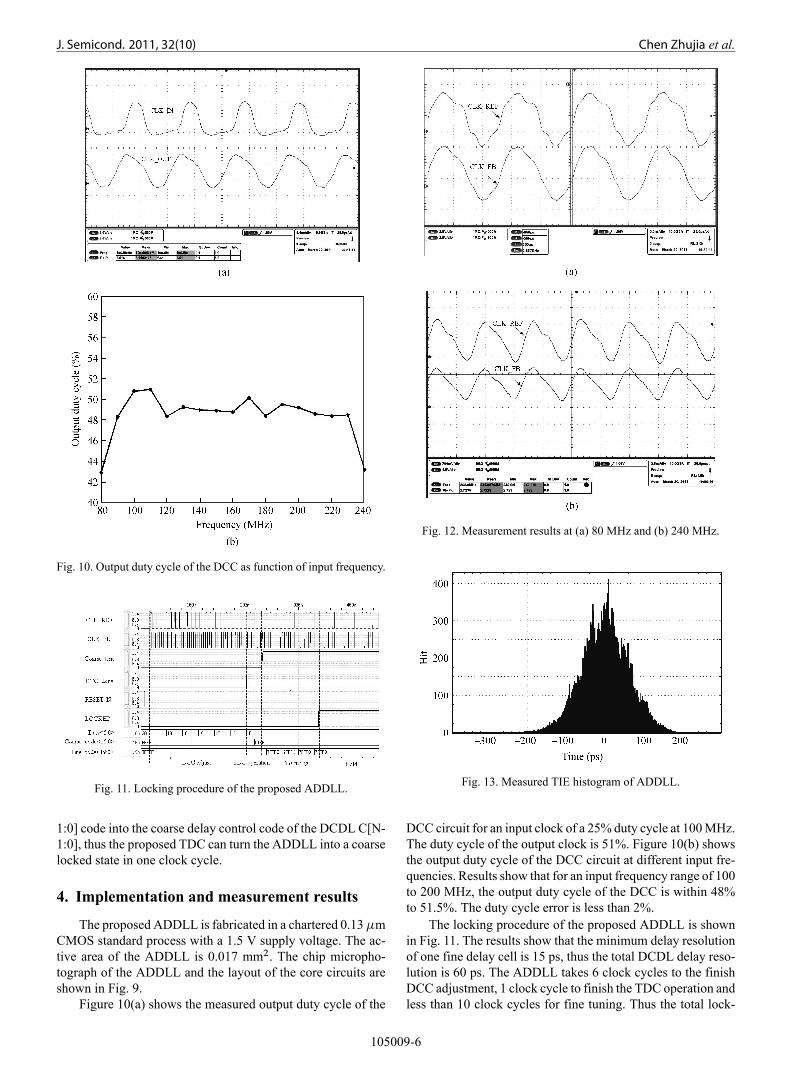
Fig. 10. Output duty cycle of the DCC as function of input frequency.
Fig. 11. Locking procedure of the proposed ADDLL.
1:0] code into the coarse delay control code of the DCDL C[N-1:0], thus the proposed TDC can turn the ADDLL into a coarselocked state in one clock cycle.
4. Implementation and measurement results
The proposed ADDLL is fabricated in a chartered 0.13�mCMOS standard process with a 1.5 V supply voltage. The ac-tive area of the ADDLL is 0.017 mm2. The chip micropho-tograph of the ADDLL and the layout of the core circuits areshown in Fig. 9.
Figure 10(a) shows the measured output duty cycle of the
Fig. 12. Measurement results at (a) 80 MHz and (b) 240 MHz.
Fig. 13. Measured TIE histogram of ADDLL.
DCC circuit for an input clock of a 25% duty cycle at 100MHz.The duty cycle of the output clock is 51%. Figure 10(b) showsthe output duty cycle of the DCC circuit at different input fre-quencies. Results show that for an input frequency range of 100to 200 MHz, the output duty cycle of the DCC is within 48%to 51.5%. The duty cycle error is less than 2%.
The locking procedure of the proposed ADDLL is shownin Fig. 11. The results show that the minimum delay resolutionof one fine delay cell is 15 ps, thus the total DCDL delay reso-lution is 60 ps. The ADDLL takes 6 clock cycles to the finishDCC adjustment, 1 clock cycle to finish the TDC operation andless than 10 clock cycles for fine tuning. Thus the total lock-
105009-6

J. Semicond. 2011, 32(10) Chen Zhujia et al.
Table 1. Performance comparison.Parameter Proposed Ref. [6]
(simulation)Ref. [7] Ref. [4] Ref. [5] Ref. [8]
Process 0.13 �mCMOS
0.13 �mCMOS
0.13 �mCMOS
0.13 �mCMOS
0.18 �mCMOS
0.13 �mCMOS
Supply voltage (V) 1.5 1.2 1.2 1.2 1.8 1.2Locking time(clock cycles)
< 17 13 N/A 40 80 42
Operation range(MHz)
75–350 200–400 100–200 333.5–800 510–1100 30–1000
Phase error(degree)
2.59 1.3 5.47 (7.6%) 2 N/A N/A
Power consumption(mW)
1.74 @240 MHz
5.5 @400 MHz
9 @200 MHz
19.2 @800 MHz
12 @800 MHz
1.5 @30 MHz
Delay resolution (ps) 15 4 1.4 10 5.9 10Active area (mm2) 0.017 0.026 0.207 0.074 0.023 0.02
Table 2. The measured performance summary of the proposed AD-DLL.
Parameter ValueOperating frequency range 75–350 MHzDelay resolution 15 psLocking time < 17 clock cyclesOutput duty cycle 48%–51.5%Power @ 240 MHz 1.74 mWInput duty cycle range 15%–80%Active area 0.1 � 0.17 mm2
Time interval error 60.7 ps
ing time of the ADDLL is less than 17 clock cycles. When theADDLL is in a locked state, the LOCKED signal is activatedto put the ADDLL into power down mode, which reduces thedithering phenomenon and power consumption of the ADDLL.
Figures 12(a) and 12(b) show the output clock signal whenthe proposed ADDLL is locked at 80 and 240 MHz, respec-tively. The measured signals in Figs. 12(a) and 12(b) are thereference clock and output clock signal, separately. Accordingto the measurement results, the proposed ADDLL can operateat a tuning range of 75 to 350 MHz.
Figure 13 shows the measured time-interval-error (TIE)histogram of the output signal when the ADDLL operates at240 MHz. The standard deviation of the TIE of the ADDLL is60.7 ps. The measured power consumption is 1.74 mW whenthe ADDLL is locked at 240-MHz clock input.
Table 1 lists comparison results with the state-of-the-artDLLs in DDR controller applications. The measured perfor-mance summary of the proposed ADDLL is listed in Table 2.The proposed ADDLL using a time-to-digital converter, short-ens the locking time to less than 17 clock cycles. The proposedADDLL also has the widest operating range and the lowestpower consumption compared with other DLL designs.
5. Conclusion
A fast-locking all-digital DLL has been proposed in thispaper. By using a novel structure TDC, the locking time of theADDLL can be reduced to less than 17 clock cycles. The BSR
helps to reduce dithering during switching of fine control code.The fabricated chip occupies 0.017mm2 active area in 0.13�mCMOS technology and consumes 1.74 mW from a 1.5 V sup-ply. The proposed ADDLL can be used in the interface of aDDR SDRAM controller for phase shifting.
References
[1] KimB,Weigandt T C, Gray P R. PLL/DLL system noise analysisfor low-jitter clock synthesis design. Proceedings of the Interna-tional Symposium on ISCAS, 1994, 4: 31
[2] JEDEC Standard, Double Data Rate (DDR) SDRAM specifica-tion, JESD79E, May 2005
[3] Yoshimura T, Nakase Y, Watanabe N, et al. A delay-locked loopand 90-degree phase shifter for 100 Mbps double data rate mem-ories. Symposium on VLSI Circuits Digest of Technical Papers,1998: 66
[4] Bae J H, Seo J H, Yeo H S, et al. An all-digital 90-degree phase-shift DLLwith loop embedded DCC for 1.6 Gbps DDR interface.CICC Dig Tech Papers, 2007: 373
[5] Oh K I, Kim L S, Park K I, et al. Low-jitter multi-phase digitalDLL with closest edge selection scheme for DDR memory inter-face. Electron Lett, 2008, 44(19): 1121
[6] Sheng D, Chung C C, Lee C Y. Fast-lock all-digital DLL anddigitally-controlled phase-shifter for DDR controller applica-tions. IECIE Electronics Express, 2010, 7(9): 634
[7] Chung C C, Chen P L, Lee C Y. An all-digital delay-locked loopfor DDR SDRAM controller applications. Symposium on VLSIDesign, Automation and Test, 2006: 1
[8] Wang L, Liu L, Chen H. An implementation of fast-locking andwide-range 11-bit reversible SARDLL. IEEE Trans Circuits SystII: Express Briefs, 2010, 57(6): 421
[9] Jeon Y J, Lee J H, Lee H C, et al. A 66–333-MHz 12-mWregister-controlled DLL with a single delay line and adaptive-duty-cycle clock dividers for production DDR SDRAMs. IEEE JSolid-State Circuits, 2004, 39(11): 2087
[10] Alvandpour A, Krishnamurthy R K, Eckerbert D, et al. A 3.5GHz 32 mW 150 nm multiphase clock generator for high-performance microprocessors. IEEE International Solid-StateCircuits Conference Digest of Technical Papers, 2003: 112
[11] Wang J S, Wang Y M, Chen C H, et al. An ultra-low-power fast-lock-in small-jitter all-digital DLL. IEEE International Solid-
105009-7
J. Semicond. 2011, 32(10) Chen Zhujia et al.State Circuits Conference Digest of Technical Papers, 2005: 422
[12] Yang R J, Liu S I. A 40–550MHz harmonic-free all-digital delay-locked loop using a variable SAR algorithm. IEEE J Solid-StateCircuits, 2007, 42(2): 361
[13] Dehng G K, Hsu J M, Yang C Y, et al. Clock-deskew buffer usinga SAR-controlled delay-locked loop. IEEE J Solid-State Circuits,
2000, 35(8):1128[14] Rossi A, Fucili G. Nonredundant successive approximation reg-
ister for A/D converters. Electron Lett, 1996, 32: 1055[15] Maymandi-Nejad M, Sachdev M. A digitally programmable de-
lay element: design and analysis. IEEE Trans VLSI Syst, 2003,11(5): 871
105009-8
Copyright © 2022 FDOKUMEN