A digital holographic microscope for complete characterization of microelectromechanical systems
11
INSTITUTE OF PHYSICS PUBLISHING MEASUREMENT SCIENCE AND TECHNOLOGY Meas. Sci. Technol. 15 (2004) 529–539 PII: S0957-0233(04)69469-0 A digital holographic microscope for complete characterization of microelectromechanical systems G Coppola 1,4 , P Ferraro 2 , M Iodice 1 , S De Nicola 3 , A Finizio 3 and S Grilli 2 1 Istituto per la Microelettronica e i Microsistemi del CNR, Via P Castellino, 111-80131, Napoli, Italy 2 Istituto Nazionale di Ottica Applicata—Sezione di Napoli, Via Campi Flegrei 34, 80078 Pozzuoli (Na), Italy 3 Istituto di Cibernetica del CNR, ‘E Caianiello’, Via Campi Flegrei 34, 80078 Pozzuoli (Na), Italy E-mail: [email protected] Received 23 September 2003, in final form 3 December 2003, accepted for publication 15 January 2004 Published 9 February 2004 Online at stacks.iop.org/MST/15/529 (DOI: 10.1088/0957-0233/15/3/005) Abstract Digital holographic microscopy (DHM) can be described as a non-invasive metrological tool for inspection and characterization of microelectromechanical structures (MEMS). DHM is a quick, non-contact and non-invasive technique that can offer a high resolution in both lateral and vertical directions. It has been employed for the characterization of the undesired out-of-plane deformations due to the residual stresses introduced by technological processes. The characterization of these deformations is helpful in studying and understanding the effect of residual stress on the deformation of a single microstructure. To that end, MEMS with different geometries and shapes, such as cantilever beams, bridges and membranes, have been characterized. Moreover, DHM has been applied efficiently to evaluate variations of the structure profile due to some external effects. As an example, the characterization of a cantilever subjected to a thermal process has been described. The results reported show that DHM is a useful non-invasive method for characterizing and developing reliable MEMS. Keywords: MEMS characterization, digital holography, 3D shape measurement, surface profiling (Some figures in this article are in colour only in the electronic version) 1. Introduction Microelectromechanical systems (MEMS) are the results of the integration of mechanical elements, sensors, actuators and electronics on a common silicon substrate through microfabrication technology. They range in size from the submicrometre level to the millimetre level, and there can be any number, from a few to millions, in a particular system. 4 Author to whom any correspondence should be addressed. Examples of MEMS device applications include inkjet-printer cartridges, accelerometers, miniature robots, microengines, locks, inertial sensors, microtransmissions, micromirrors, microactuators, optical scanners, fluid pumps, transducers and chemical, pressure and flow sensors. New applications are emerging as the existing technology is applied to the miniaturization and integration of conventional devices. Thus, MEMS promise to revolutionize nearly every product category by bringing together silicon-based microelectronics with micromachining technology, making possible the realization 0957-0233/04/030529+11$30.00 © 2004 IOP Publishing Ltd Printed in the UK 529
-
Upload
independent -
Category
Documents
-
view
0 -
download
0
Transcript of A digital holographic microscope for complete characterization of microelectromechanical systems
INSTITUTE OF PHYSICS PUBLISHING MEASUREMENT SCIENCE AND TECHNOLOGY
Meas. Sci. Technol. 15 (2004) 529–539 PII: S0957-0233(04)69469-0
A digital holographic microscope forcomplete characterization ofmicroelectromechanical systemsG Coppola1,4, P Ferraro2, M Iodice1, S De Nicola3, A Finizio3 andS Grilli2
1 Istituto per la Microelettronica e i Microsistemi del CNR, Via P Castellino, 111-80131,Napoli, Italy2 Istituto Nazionale di Ottica Applicata—Sezione di Napoli, Via Campi Flegrei 34,80078 Pozzuoli (Na), Italy3 Istituto di Cibernetica del CNR, ‘E Caianiello’, Via Campi Flegrei 34,80078 Pozzuoli (Na), Italy
E-mail: [email protected]
Received 23 September 2003, in final form 3 December 2003, accepted forpublication 15 January 2004Published 9 February 2004Online at stacks.iop.org/MST/15/529 (DOI: 10.1088/0957-0233/15/3/005)
AbstractDigital holographic microscopy (DHM) can be described as a non-invasivemetrological tool for inspection and characterization ofmicroelectromechanical structures (MEMS). DHM is a quick, non-contactand non-invasive technique that can offer a high resolution in both lateraland vertical directions. It has been employed for the characterization of theundesired out-of-plane deformations due to the residual stresses introducedby technological processes. The characterization of these deformations ishelpful in studying and understanding the effect of residual stress on thedeformation of a single microstructure. To that end, MEMS with differentgeometries and shapes, such as cantilever beams, bridges and membranes,have been characterized. Moreover, DHM has been applied efficiently toevaluate variations of the structure profile due to some external effects. Asan example, the characterization of a cantilever subjected to a thermalprocess has been described. The results reported show that DHM is a usefulnon-invasive method for characterizing and developing reliable MEMS.
Keywords: MEMS characterization, digital holography, 3D shapemeasurement, surface profiling
(Some figures in this article are in colour only in the electronic version)
1. Introduction
Microelectromechanical systems (MEMS) are the results ofthe integration of mechanical elements, sensors, actuatorsand electronics on a common silicon substrate throughmicrofabrication technology. They range in size from thesubmicrometre level to the millimetre level, and there can beany number, from a few to millions, in a particular system.
4 Author to whom any correspondence should be addressed.
Examples of MEMS device applications include inkjet-printercartridges, accelerometers, miniature robots, microengines,locks, inertial sensors, microtransmissions, micromirrors,microactuators, optical scanners, fluid pumps, transducersand chemical, pressure and flow sensors. New applicationsare emerging as the existing technology is applied to theminiaturization and integration of conventional devices. Thus,MEMS promise to revolutionize nearly every product categoryby bringing together silicon-based microelectronics withmicromachining technology, making possible the realization
0957-0233/04/030529+11$30.00 © 2004 IOP Publishing Ltd Printed in the UK 529
G Coppola et al
of complete systems-on-a-chip. In other words, MEMS is anenabling technology increasing the computational ability ofmicroelectronics with the perception and control capabilitiesof microsensors and microactuators.
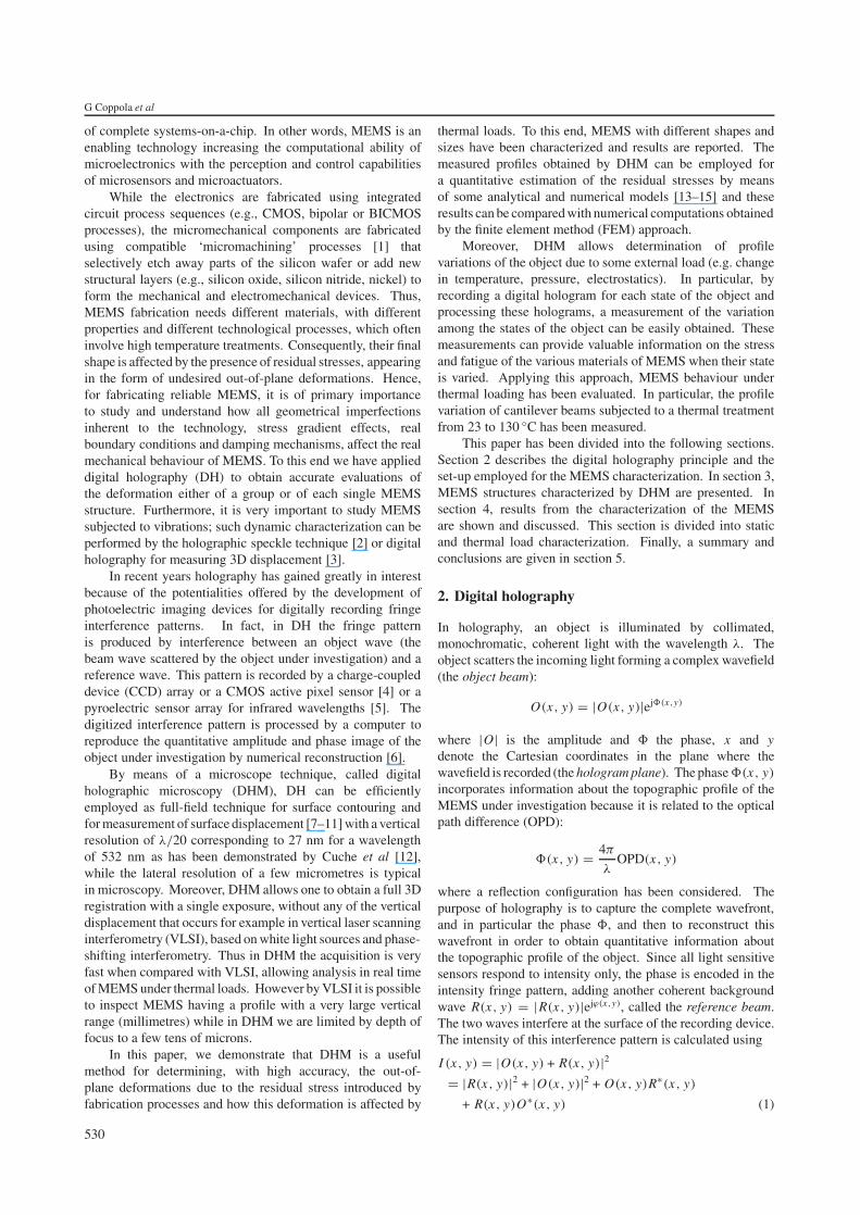
While the electronics are fabricated using integratedcircuit process sequences (e.g., CMOS, bipolar or BICMOSprocesses), the micromechanical components are fabricatedusing compatible ‘micromachining’ processes [1] thatselectively etch away parts of the silicon wafer or add newstructural layers (e.g., silicon oxide, silicon nitride, nickel) toform the mechanical and electromechanical devices. Thus,MEMS fabrication needs different materials, with differentproperties and different technological processes, which ofteninvolve high temperature treatments. Consequently, their finalshape is affected by the presence of residual stresses, appearingin the form of undesired out-of-plane deformations. Hence,for fabricating reliable MEMS, it is of primary importanceto study and understand how all geometrical imperfectionsinherent to the technology, stress gradient effects, realboundary conditions and damping mechanisms, affect the realmechanical behaviour of MEMS. To this end we have applieddigital holography (DH) to obtain accurate evaluations ofthe deformation either of a group or of each single MEMSstructure. Furthermore, it is very important to study MEMSsubjected to vibrations; such dynamic characterization can beperformed by the holographic speckle technique [2] or digitalholography for measuring 3D displacement [3].
In recent years holography has gained greatly in interestbecause of the potentialities offered by the development ofphotoelectric imaging devices for digitally recording fringeinterference patterns. In fact, in DH the fringe patternis produced by interference between an object wave (thebeam wave scattered by the object under investigation) and areference wave. This pattern is recorded by a charge-coupleddevice (CCD) array or a CMOS active pixel sensor [4] or apyroelectric sensor array for infrared wavelengths [5]. Thedigitized interference pattern is processed by a computer toreproduce the quantitative amplitude and phase image of theobject under investigation by numerical reconstruction [6].
By means of a microscope technique, called digitalholographic microscopy (DHM), DH can be efficientlyemployed as full-field technique for surface contouring andfor measurement of surface displacement [7–11] with a verticalresolution of λ/20 corresponding to 27 nm for a wavelengthof 532 nm as has been demonstrated by Cuche et al [12],while the lateral resolution of a few micrometres is typicalin microscopy. Moreover, DHM allows one to obtain a full 3Dregistration with a single exposure, without any of the verticaldisplacement that occurs for example in vertical laser scanninginterferometry (VLSI), based on white light sources and phase-shifting interferometry. Thus in DHM the acquisition is veryfast when compared with VLSI, allowing analysis in real timeof MEMS under thermal loads. However by VLSI it is possibleto inspect MEMS having a profile with a very large verticalrange (millimetres) while in DHM we are limited by depth offocus to a few tens of microns.
In this paper, we demonstrate that DHM is a usefulmethod for determining, with high accuracy, the out-of-plane deformations due to the residual stress introduced byfabrication processes and how this deformation is affected by
thermal loads. To this end, MEMS with different shapes andsizes have been characterized and results are reported. Themeasured profiles obtained by DHM can be employed fora quantitative estimation of the residual stresses by meansof some analytical and numerical models [13–15] and theseresults can be compared with numerical computations obtainedby the finite element method (FEM) approach.
Moreover, DHM allows determination of profilevariations of the object due to some external load (e.g. changein temperature, pressure, electrostatics). In particular, byrecording a digital hologram for each state of the object andprocessing these holograms, a measurement of the variationamong the states of the object can be easily obtained. Thesemeasurements can provide valuable information on the stressand fatigue of the various materials of MEMS when their stateis varied. Applying this approach, MEMS behaviour underthermal loading has been evaluated. In particular, the profilevariation of cantilever beams subjected to a thermal treatmentfrom 23 to 130 ◦C has been measured.
This paper has been divided into the following sections.Section 2 describes the digital holography principle and theset-up employed for the MEMS characterization. In section 3,MEMS structures characterized by DHM are presented. Insection 4, results from the characterization of the MEMSare shown and discussed. This section is divided into staticand thermal load characterization. Finally, a summary andconclusions are given in section 5.
2. Digital holography
In holography, an object is illuminated by collimated,monochromatic, coherent light with the wavelength λ. Theobject scatters the incoming light forming a complex wavefield(the object beam):
O(x, y) = |O(x, y)|ej�(x,y)
where |O| is the amplitude and � the phase, x and ydenote the Cartesian coordinates in the plane where thewavefield is recorded (the hologram plane). The phase �(x, y)
incorporates information about the topographic profile of theMEMS under investigation because it is related to the opticalpath difference (OPD):
�(x, y) = 4π
λOPD(x, y)
where a reflection configuration has been considered. Thepurpose of holography is to capture the complete wavefront,and in particular the phase �, and then to reconstruct thiswavefront in order to obtain quantitative information aboutthe topographic profile of the object. Since all light sensitivesensors respond to intensity only, the phase is encoded in theintensity fringe pattern, adding another coherent backgroundwave R(x, y) = |R(x, y)|ejϕ(x,y), called the reference beam.The two waves interfere at the surface of the recording device.The intensity of this interference pattern is calculated using
I (x, y) = |O(x, y) + R(x, y)|2= |R(x, y)|2 + |O(x, y)|2 + O(x, y)R∗(x, y)
+ R(x, y)O∗(x, y) (1)
530

A digital holographic microscope for complete characterization of MEMS
where ∗ denotes the conjugate complex. The hologram isproportional to this intensity: h(x, y) = α I (x, y). Forhologram reconstruction the amplitude h(x, y) has to bemultiplied by the complex amplitude of the reference wave:
R(x, y)h(x, y) = R(x, y)α|R(x, y)|2 + R(x, y)α|O(x, y)|2+ α|R(x, y)|2 O(x, y) + αR2(x, y)O∗(x, y).
The first term on the right-hand side of this equation is theattenuated reference wave; the second one is a spatially varying‘cloud’ surrounding the first term. These two terms constitutethe zeroth order of diffraction. The third term is, except fora constant factor, an exact replica of the original wavefrontand for this reason is called the virtual image. The last term isanother copy, the conjugate image, of the original object wave,but focused on the opposite side of the holographic plane (realimage).
In the reconstruction process, the hologram can be seenas like an amplitude transmittance that diffracts the referencewave. In other words the wavefront scattered by the objectunder investigation is obtained through the propagation ofR(x, y)h(x, y) from the holographic plane to the imageplane. If ξ , η denote the Cartesian coordinates in the objectplane, the reconstructed wavefront Q(ξ, η) in this plane ata distance d from the holographic plane is obtained byusing the Fresnel approximation of the Rayleigh–Sommerfelddiffraction formula [6], i.e.,
Q(ξ, η) = exp(j2πd
λ)
jλdexp
(jπ(ξ 2 + η2)
λd
)
×∫ ∫
h(x, y)R(x, y) exp
(jπ(x2 + y2)
λd
)
× exp
(−2jπ(xξ + yη)
λd
)dx dy
= exp(j2πd
λ)
jλdexp(jπλd(ν2 + µ2))
× FT
{h(x, y)R(x, y) exp
(jπ
λd(x2 + y2)
)}(2)
where ν = ξ/(dλ), µ = η/(dλ) and FT{· · ·} denotes thespatial Fourier transform.
Generally, in DH the recording device is a CCD array,i.e. a two-dimensional rectangular raster of N × M pixels,with pixel pitches x and y in the two directions. Thus,hologram patterns recorded by a CCD are nothing less than thedigitized version of the wavefields that impinge on the CCDsurface. Therefore, x and y are the sampling intervals inthe observation plane, and they define the resolution of thereconstructed images. Mathematically this two-dimensionalspatial sampling can be described using the following relation:
I (n x, m y) = I (x, y) rect
(x
N x,
y
M y
)
×N∑
n=1
M∑m=1
δ(x − n x, y − m y)
where δ(x, y) is the two-dimensional Dirac delta function,n and m are integers, (N x) × (M y) is the area ofthe digitized hologram, rect(x, y) is a function defined as aconstant amplitude value if the point with coordinates (x, y)is inside the digitized hologram and zero elsewhere. For a
M
M
BE
BS
BS
MO
LASER
Sample
CC
D
Figure 1. The experimental set-up for recording digital holograms;BS: beam splitter; M: mirror; MO: microscope objective; BE: beamexpander.
Figure 2. An SEM image of a group of cantilevers that experiencesan out-of-plane deformation.
perfect reconstruction of the object image, it is necessary thatthe sampling process satisfies the Shannon sampling theorem.In particular, to satisfy this theorem the distance between twocontiguous fringes of the interference pattern, described byequation (1), must be recorded by at least two pixels of theacquisition system.
Thus, in DH the hologram is spatially sampled and storedas a numerical array in a computer and, in the reconstructionprocess, the recorded intensity distribution of the hologramis numerically multiplied by the reference wavefield in thehologram plane. Then the diffracted field in the image plane isdetermined by a discretization of equation (2) to calculate theintensity and the phase distribution of the reconstructed realimage. Obviously, the spatial Fourier transform is replaced bya discrete Fourier transform, which can be easily calculated bythe fast Fourier transform (FFT) algorithm. That is,
Q(m, n) = exp(j2πd
λ)
jλdexp
(jπλd
N M
(n2
x2+
m2
y2
))
×N−1∑k=0
M−1∑l=0
h(k x, l y)R(k x, l y)
531
G Coppola et al
1000
900
800
700
600
500
400
300
200
100
200 400 600 800 1000 1200
350
300
250
200
150
100
50
0100
8060
4020
20 4060 80 100 120 140
[µm][µm]
Def
lect
ion
[µm
]
(a) (b)
(c) (d)
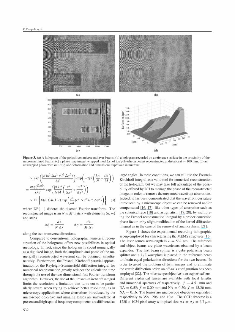
Figure 3. (a) A hologram of the polysilicon microcantilever beams; (b) a hologram recorded on a reference surface in the proximity of themicromachined beams; (c) a phase map image, wrapped mod 2π , of the polysilicon beams reconstructed at distance d = 100 mm; (d) anunwrapped phase with out-of-plane deformation and dimensions expressed in microns.
× exp(
jπ(k2 x2 + l2 y2)
λd
)exp
(−2jπ
(kn
N+
lm
M
))
= exp(j2πd
λ)
jλdexp
(jπλd
N M
(n2
x2+
m2
y2
))
× DF
{h(k, l)R(k, l) exp
(jπ
λd(k2 x2 + l2 y2)
)}(3)
where DF{· · ·} denotes the discrete Fourier transform. Thereconstructed image is an N × M matrix with elements (n, m)and steps
ξ = dλ
N xη = dλ
M y
along the two transverse directions.Compared to conventional holography, numerical recon-
struction of the holograms offers new possibilities in opticalmetrology. In fact, since the hologram is coded numericallyas a digitized image, both the amplitude and phase of the nu-merically reconstructed wavefront can be obtained, simulta-neously. Furthermore, the Fresnel–Kirchhoff paraxial approx-imation of the Rayleigh–Sommerfeld diffraction integral fornumerical reconstruction greatly reduces the calculation timethrough the use of the two-dimensional fast Fourier transformalgorithm. However, the use of the Fresnel–Kirchhoff integrallimits the resolution, a limitation that turns out to be partic-ularly severe when trying to achieve better resolution, as inmicroscopy applications where aberrations introduced by themicroscope objective and imaging lenses are unavoidable atpresent and high spatial frequency components are diffracted at
large angles. In these conditions, we can still use the Fresnel–Kirchhoff integral as a valid tool for numerical reconstructionof the hologram, but we may take full advantage of the possi-bility offered by DH to manage the phase of the reconstructedimage, in order to remove the unwanted wavefront aberrations.Indeed, it has been demonstrated that the wavefront curvatureintroduced by a microscope objective can be removed and/orcompensated [16, 17], like other types of aberration such asthe spherical type [18] and astigmatism [19, 20], by multiply-ing the Fresnel reconstruction integral by a proper correctionphase factor or by slight modification of the kernel diffractionintegral as in the case of the removal of anamorphism [21].
Figure 1 shows the experimental recording holographicset-up employed for characterizing the MEMS structures [16].The laser source wavelength is λ = 532 nm. The referenceand object beams are plane wavefronts obtained by a beamexpander. The first beam splitter is a cube polarizing beamsplitter and a λ/2 waveplate is placed in the reference beamto obtain equal polarization directions for the two beams. Inorder to avoid the problem of twin images and to eliminatethe zeroth diffraction order, an off-axis configuration has beenemployed [22]. The microscope objective is an aspherical lens.Different aspherical lenses are available with focal lengthsand numerical apertures of respectively: f = 4.51 mm andNA = 0.55; f = 8.00 mm and NA = 0.50; f = 15.36 mm,NA = 0.16. The lenses are microscope objectives equivalentrespectively to 35×, 20× and 10×. The CCD detector is a1280 × 1024 pixel array with pixel size x = y = 6.7 µm.
532
A digital holographic microscope for complete characterization of MEMS
50 40 30 20 1020
4060
80100
distance [µm]
distance [µm]
defo
rmat
ion
[µm
]
(a) (b)
(c)
6
4
2
0
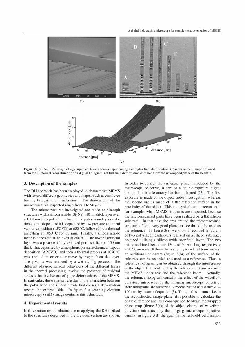
Figure 4. (a) An SEM image of a group of cantilever beams experiencing a complex final deformation; (b) a phase map image obtainedfrom the numerical reconstruction of a digital hologram; (c) full-field deformation obtained from the unwrapped phase of the beam A.
3. Description of the samples
The DH approach has been employed to characterize MEMSwith several different geometries and shapes, such as cantileverbeams, bridges and membranes. The dimensions of themicrostructures inspected range from 1 to 50 µm.
The microstructures investigated are made as bimorphstructures with a silicon nitride (Si3N4) 140 nm thick layer overa 1500 nm thick polysilicon layer. The polysilicon layer can bedoped or undoped and it is deposited by low pressure chemicalvapour deposition (LPCVD) at 680 ◦C, followed by a thermalannealing at 1050 ◦C for 30 min. Finally, a silicon nitridelayer is deposited in an oven at 800 ◦C. The lower sacrificiallayer was a p-vapox (fully oxidized porous silicon) 1150 nmthick film, deposited by atmospheric pressure chemical vapourdeposition (APCVD), and then a thermal process at 1050 ◦Cwas applied in order to remove hydrogen from the layer.The p-vapox was removed by a wet etching process. Thedifferent physicochemical behaviours of the different layersin the thermal processing involve the presence of residualstresses that involve out-of-plane deformations of the MEMS.In particular, these stresses are due to the interaction betweenthe polysilicon and silicon nitride that causes a deformationtoward the external side. In figure 2 a scanning electronmicroscopy (SEM) image confirms this behaviour.
4. Experimental results
In this section results obtained from applying the DH methodto the structures described in the previous section are shown.
In order to correct the curvature phase introduced by themicroscope objective, a sort of a double-exposure digitalholographic interferometry has been adopted [23]. The firstexposure is made of the object under investigation, whereasthe second one is made of a flat reference surface in theproximity of the object. This is a typical case, encountered,for example, when MEMS structures are inspected, becausethe micromachined parts have been realized on a flat siliconsubstrate. In that case the area around the micromachinedstructure offers a very good plane surface that can be used asthe reference. In figure 3(a) we show a recorded hologramof two polysilicon cantilevers realized on a silicon substrate,obtained utilizing a silicon oxide sacrificial layer. The twomicromachined beams are 130 and 60 µm long respectivelyand 20 µm wide. If the wafer is slightly translated transversely,an additional hologram (figure 3(b)) of the surface of thesubstrate can be recorded and used as a reference. Thus, areference hologram can be obtained through the interferenceof the object field scattered by the reference flat surface nearthe MEMS under test and the reference beam. Actually,the reference hologram contains the effect of the wavefrontcurvature introduced by the imaging microscope objective.Both holograms are numerically reconstructed at distance d =100 mm by means of equation (3). Thus, at this distance, i.e. inthe reconstructed image plane, it is possible to calculate thephase difference and, as a consequence, to obtain the wrappedphase map (figure 3(c)) of the object cleared of wavefrontcurvature introduced by the imaging microscope objective.Finally, in figure 3(d) the quantitative full-field deformation
533
G Coppola et al
0 20 40 60 80
prof
ile
[µm
]
prof
ile
[µm
]
0
1
2
3
4
5
6
Anchor point
x-axis [µm] y-axis [µm]100
0
0.5
1
1.5
2
2.5
3
3.5
0 10 20 30 40 50 60
(a) (b)
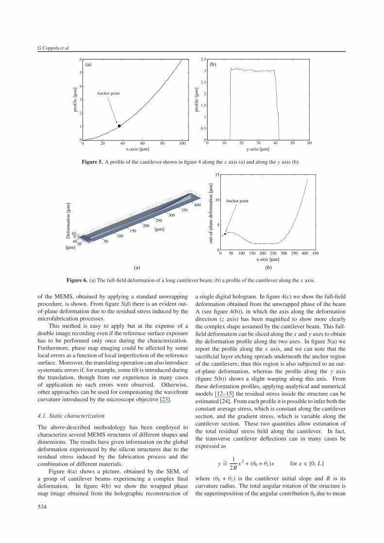
Figure 5. A profile of the cantilever shown in figure 4 along the x axis (a) and along the y axis (b).
15
10
5
00 50 100 150 200 250 300 350 400 450
x-axis [µm]
out-
of-p
lane
def
orm
atio
n [µ
m]
Anchor point
10040
2050
100150
200250
300350
400
[µm]
[µm]
Def
orm
atio
n [µ
m]
(b)(a)
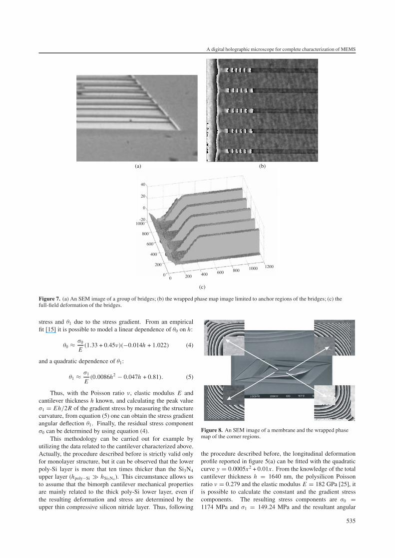
Figure 6. (a) The full-field deformation of a long cantilever beam; (b) a profile of the cantilever along the x axis.
of the MEMS, obtained by applying a standard unwrappingprocedure, is shown. From figure 3(d) there is an evident out-of-plane deformation due to the residual stress induced by themicrofabrication processes.
This method is easy to apply but at the expense of adouble image recording even if the reference surface exposurehas to be performed only once during the characterization.Furthermore, phase map imaging could be affected by somelocal errors as a function of local imperfection of the referencesurface. Moreover, the translating operation can also introducesystematic errors if, for example, some tilt is introduced duringthe translation, though from our experience in many casesof application no such errors were observed. Otherwise,other approaches can be used for compensating the wavefrontcurvature introduced by the microscope objective [23].
4.1. Static characterization
The above-described methodology has been employed tocharacterize several MEMS structures of different shapes anddimensions. The results have given information on the globaldeformation experienced by the silicon structures due to theresidual stress induced by the fabrication process and thecombination of different materials.
Figure 4(a) shows a picture, obtained by the SEM, ofa group of cantilever beams experiencing a complex finaldeformation. In figure 4(b) we show the wrapped phasemap image obtained from the holographic reconstruction of
a single digital hologram. In figure 4(c) we show the full-fielddeformation obtained from the unwrapped phase of the beamA (see figure 4(b)), in which the axis along the deformationdirection (z axis) has been magnified to show more clearlythe complex shape assumed by the cantilever beam. This full-field deformation can be sliced along the x and y axes to obtainthe deformation profile along the two axes. In figure 5(a) wereport the profile along the x axis, and we can note that thesacrificial layer etching spreads underneath the anchor regionof the cantilevers; thus this region is also subjected to an out-of-plane deformation, whereas the profile along the y axis(figure 5(b)) shows a slight warping along this axis. Fromthese deformation profiles, applying analytical and numericalmodels [12–15] the residual stress inside the structure can beestimated [24]. From each profile it is possible to infer both theconstant average stress, which is constant along the cantileversection, and the gradient stress, which is variable along thecantilever section. These two quantities allow estimation ofthe total residual stress field along the cantilever. In fact,the transverse cantilever deflections can in many cases beexpressed as
y ∼= 1
2Rx2 + (θ0 + θ1)x for x ∈ [0, L ]
where (θ0 + θ1) is the cantilever initial slope and R is itscurvature radius. The total angular rotation of the structure isthe superimposition of the angular contribution θ0 due to mean
534
A digital holographic microscope for complete characterization of MEMS
40
20
0
-201000
800
600
400
200
00 200 400 600 800 1000 1200
(a) (b)
(c)
Figure 7. (a) An SEM image of a group of bridges; (b) the wrapped phase map image limited to anchor regions of the bridges; (c) thefull-field deformation of the bridges.
stress and θ1 due to the stress gradient. From an empiricalfit [15] it is possible to model a linear dependence of θ0 on h:
θ0 ≈ σ0
E(1.33 + 0.45ν)(−0.014h + 1.022) (4)
and a quadratic dependence of θ1:
θ1 ≈ σ1
E(0.0086h2 − 0.047h + 0.81). (5)
Thus, with the Poisson ratio ν, elastic modulus E andcantilever thickness h known, and calculating the peak valueσ1 = Eh/2R of the gradient stress by measuring the structurecurvature, from equation (5) one can obtain the stress gradientangular deflection θ1. Finally, the residual stress componentσ0 can be determined by using equation (4).
This methodology can be carried out for example byutilizing the data related to the cantilever characterized above.Actually, the procedure described before is strictly valid onlyfor monolayer structure, but it can be observed that the lowerpoly-Si layer is more that ten times thicker than the Si3N4
upper layer (hpoly−Si � hSi3N4 ). This circumstance allows usto assume that the bimorph cantilever mechanical propertiesare mainly related to the thick poly-Si lower layer, even ifthe resulting deformation and stress are determined by theupper thin compressive silicon nitride layer. Thus, following
Figure 8. An SEM image of a membrane and the wrapped phasemap of the corner regions.
the procedure described before, the longitudinal deformationprofile reported in figure 5(a) can be fitted with the quadraticcurve y = 0.0005x2 + 0.01x . From the knowledge of the totalcantilever thickness h = 1640 nm, the polysilicon Poissonratio ν = 0.279 and the elastic modulus E = 182 GPa [25], itis possible to calculate the constant and the gradient stresscomponents. The resulting stress components are σ0 =1174 MPa and σ1 = 149.24 MPa and the resultant angular
535
G Coppola et al
250
200
150
100
50
50 100 150 200
pixel50 100 150 200
pixel
pixe
l
250
200
150
100
50
pixe
l
(a) (b)
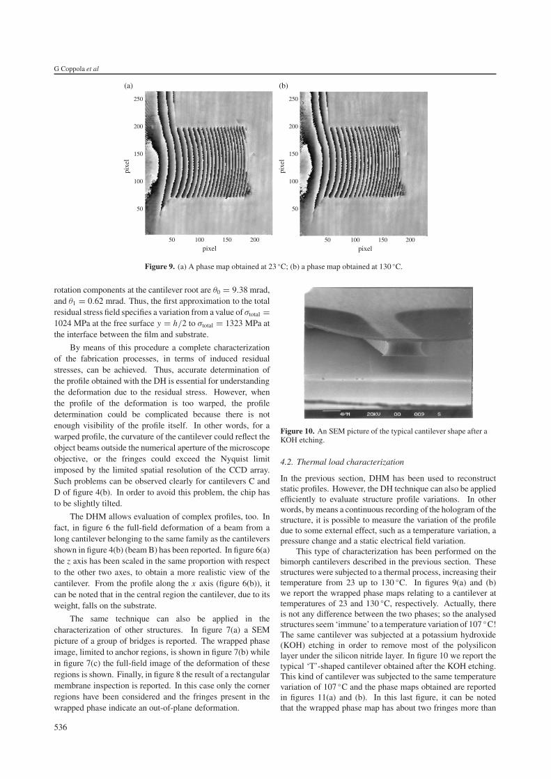
Figure 9. (a) A phase map obtained at 23 ◦C; (b) a phase map obtained at 130 ◦C.
rotation components at the cantilever root are θ0 = 9.38 mrad,and θ1 = 0.62 mrad. Thus, the first approximation to the totalresidual stress field specifies a variation from a value of σtotal =1024 MPa at the free surface y = h/2 to σtotal = 1323 MPa atthe interface between the film and substrate.
By means of this procedure a complete characterizationof the fabrication processes, in terms of induced residualstresses, can be achieved. Thus, accurate determination ofthe profile obtained with the DH is essential for understandingthe deformation due to the residual stress. However, whenthe profile of the deformation is too warped, the profiledetermination could be complicated because there is notenough visibility of the profile itself. In other words, for awarped profile, the curvature of the cantilever could reflect theobject beams outside the numerical aperture of the microscopeobjective, or the fringes could exceed the Nyquist limitimposed by the limited spatial resolution of the CCD array.Such problems can be observed clearly for cantilevers C andD of figure 4(b). In order to avoid this problem, the chip hasto be slightly tilted.
The DHM allows evaluation of complex profiles, too. Infact, in figure 6 the full-field deformation of a beam from along cantilever belonging to the same family as the cantileversshown in figure 4(b) (beam B) has been reported. In figure 6(a)the z axis has been scaled in the same proportion with respectto the other two axes, to obtain a more realistic view of thecantilever. From the profile along the x axis (figure 6(b)), itcan be noted that in the central region the cantilever, due to itsweight, falls on the substrate.
The same technique can also be applied in thecharacterization of other structures. In figure 7(a) a SEMpicture of a group of bridges is reported. The wrapped phaseimage, limited to anchor regions, is shown in figure 7(b) whilein figure 7(c) the full-field image of the deformation of theseregions is shown. Finally, in figure 8 the result of a rectangularmembrane inspection is reported. In this case only the cornerregions have been considered and the fringes present in thewrapped phase indicate an out-of-plane deformation.
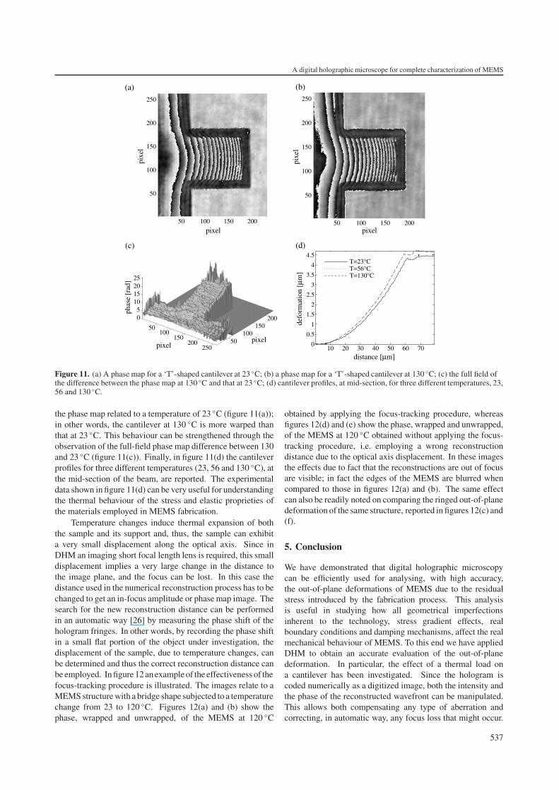
Figure 10. An SEM picture of the typical cantilever shape after aKOH etching.
4.2. Thermal load characterization
In the previous section, DHM has been used to reconstructstatic profiles. However, the DH technique can also be appliedefficiently to evaluate structure profile variations. In otherwords, by means a continuous recording of the hologram of thestructure, it is possible to measure the variation of the profiledue to some external effect, such as a temperature variation, apressure change and a static electrical field variation.
This type of characterization has been performed on thebimorph cantilevers described in the previous section. Thesestructures were subjected to a thermal process, increasing theirtemperature from 23 up to 130 ◦C. In figures 9(a) and (b)we report the wrapped phase maps relating to a cantilever attemperatures of 23 and 130 ◦C, respectively. Actually, thereis not any difference between the two phases; so the analysedstructures seem ‘immune’ to a temperature variation of 107 ◦C!The same cantilever was subjected at a potassium hydroxide(KOH) etching in order to remove most of the polysiliconlayer under the silicon nitride layer. In figure 10 we report thetypical ‘T’-shaped cantilever obtained after the KOH etching.This kind of cantilever was subjected to the same temperaturevariation of 107 ◦C and the phase maps obtained are reportedin figures 11(a) and (b). In this last figure, it can be notedthat the wrapped phase map has about two fringes more than
536
A digital holographic microscope for complete characterization of MEMS
250
200
150
100
50
50 100 150 200
pixel
pixelpixel
pixe
l
250
200
150
100
50
50 100 150 200pixel
pixe
l
2520151050
50100
150200
25050
100150
200
phas
e [r
ad]
4.5
4
3.5
3
2.5
2
1.5
1
0.5
010 20 30 40 50 60 70
distance [µm]
defo
rmat
ion
[µm
]
T=23°CT=56°CT=130°C
(a) (b)
(c) (d)
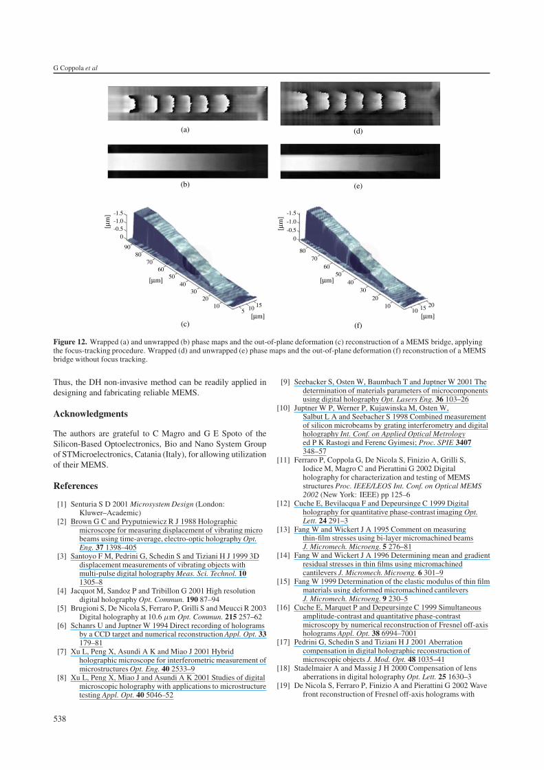
Figure 11. (a) A phase map for a ‘T’-shaped cantilever at 23 ◦C; (b) a phase map for a ‘T’-shaped cantilever at 130 ◦C; (c) the full field ofthe difference between the phase map at 130 ◦C and that at 23 ◦C; (d) cantilever profiles, at mid-section, for three different temperatures, 23,56 and 130 ◦C.
the phase map related to a temperature of 23 ◦C (figure 11(a));in other words, the cantilever at 130 ◦C is more warped thanthat at 23 ◦C. This behaviour can be strengthened through theobservation of the full-field phase map difference between 130and 23 ◦C (figure 11(c)). Finally, in figure 11(d) the cantileverprofiles for three different temperatures (23, 56 and 130 ◦C), atthe mid-section of the beam, are reported. The experimentaldata shown in figure 11(d) can be very useful for understandingthe thermal behaviour of the stress and elastic proprieties ofthe materials employed in MEMS fabrication.
Temperature changes induce thermal expansion of boththe sample and its support and, thus, the sample can exhibita very small displacement along the optical axis. Since inDHM an imaging short focal length lens is required, this smalldisplacement implies a very large change in the distance tothe image plane, and the focus can be lost. In this case thedistance used in the numerical reconstruction process has to bechanged to get an in-focus amplitude or phase map image. Thesearch for the new reconstruction distance can be performedin an automatic way [26] by measuring the phase shift of thehologram fringes. In other words, by recording the phase shiftin a small flat portion of the object under investigation, thedisplacement of the sample, due to temperature changes, canbe determined and thus the correct reconstruction distance canbe employed. In figure 12 an example of the effectiveness of thefocus-tracking procedure is illustrated. The images relate to aMEMS structure with a bridge shape subjected to a temperaturechange from 23 to 120 ◦C. Figures 12(a) and (b) show thephase, wrapped and unwrapped, of the MEMS at 120 ◦C
obtained by applying the focus-tracking procedure, whereasfigures 12(d) and (e) show the phase, wrapped and unwrapped,of the MEMS at 120 ◦C obtained without applying the focus-tracking procedure, i.e. employing a wrong reconstructiondistance due to the optical axis displacement. In these imagesthe effects due to fact that the reconstructions are out of focusare visible; in fact the edges of the MEMS are blurred whencompared to those in figures 12(a) and (b). The same effectcan also be readily noted on comparing the ringed out-of-planedeformation of the same structure, reported in figures 12(c) and(f).
5. Conclusion
We have demonstrated that digital holographic microscopycan be efficiently used for analysing, with high accuracy,the out-of-plane deformations of MEMS due to the residualstress introduced by the fabrication process. This analysisis useful in studying how all geometrical imperfectionsinherent to the technology, stress gradient effects, realboundary conditions and damping mechanisms, affect the realmechanical behaviour of MEMS. To this end we have appliedDHM to obtain an accurate evaluation of the out-of-planedeformation. In particular, the effect of a thermal load ona cantilever has been investigated. Since the hologram iscoded numerically as a digitized image, both the intensity andthe phase of the reconstructed wavefront can be manipulated.This allows both compensating any type of aberration andcorrecting, in automatic way, any focus loss that might occur.
537
G Coppola et al
-1.5-1.0-0.5
0
9080
7060
5040
3020
105 10 15
[µm]
[µm]
[µm
] -1.5
-1.0
-0.5
0
8070
6050
4030
2010
10 15 20
[µm]
[µm][µ
m]
(a) (d)
(b) (e)
(c) (f)
Figure 12. Wrapped (a) and unwrapped (b) phase maps and the out-of-plane deformation (c) reconstruction of a MEMS bridge, applyingthe focus-tracking procedure. Wrapped (d) and unwrapped (e) phase maps and the out-of-plane deformation (f) reconstruction of a MEMSbridge without focus tracking.
Thus, the DH non-invasive method can be readily applied indesigning and fabricating reliable MEMS.
Acknowledgments
The authors are grateful to C Magro and G E Spoto of theSilicon-Based Optoelectronics, Bio and Nano System Groupof STMicroelectronics, Catania (Italy), for allowing utilizationof their MEMS.
References
[1] Senturia S D 2001 Microsystem Design (London:Kluwer–Academic)
[2] Brown G C and Pryputniewicz R J 1988 Holographicmicroscope for measuring displacement of vibrating microbeams using time-average, electro-optic holography Opt.Eng. 37 1398–405
[3] Santoyo F M, Pedrini G, Schedin S and Tiziani H J 1999 3Ddisplacement measurements of vibrating objects withmulti-pulse digital holography Meas. Sci. Technol. 101305–8
[4] Jacquot M, Sandoz P and Tribillon G 2001 High resolutiondigital holography Opt. Commun. 190 87–94
[5] Brugioni S, De Nicola S, Ferraro P, Grilli S and Meucci R 2003Digital holography at 10.6 µm Opt. Commun. 215 257–62
[6] Schanrs U and Juptner W 1994 Direct recording of hologramsby a CCD target and numerical reconstruction Appl. Opt. 33179–81
[7] Xu L, Peng X, Asundi A K and Miao J 2001 Hybridholographic microscope for interferometric measurement ofmicrostructures Opt. Eng. 40 2533–9
[8] Xu L, Peng X, Miao J and Asundi A K 2001 Studies of digitalmicroscopic holography with applications to microstructuretesting Appl. Opt. 40 5046–52
[9] Seebacker S, Osten W, Baumbach T and Juptner W 2001 Thedetermination of materials parameters of microcomponentsusing digital holography Opt. Lasers Eng. 36 103–26
[10] Juptner W P, Werner P, Kujawinska M, Osten W,Salbut L A and Seebacher S 1998 Combined measurementof silicon microbeams by grating interferometry and digitalholography Int. Conf. on Applied Optical Metrologyed P K Rastogi and Ferenc Gyimesi; Proc. SPIE 3407348–57
[11] Ferraro P, Coppola G, De Nicola S, Finizio A, Grilli S,Iodice M, Magro C and Pierattini G 2002 Digitalholography for characterization and testing of MEMSstructures Proc. IEEE/LEOS Int. Conf. on Optical MEMS2002 (New York: IEEE) pp 125–6
[12] Cuche E, Bevilacqua F and Depeursinge C 1999 Digitalholography for quantitative phase-contrast imaging Opt.Lett. 24 291–3
[13] Fang W and Wickert J A 1995 Comment on measuringthin-film stresses using bi-layer micromachined beamsJ. Micromech. Microeng. 5 276–81
[14] Fang W and Wickert J A 1996 Determining mean and gradientresidual stresses in thin films using micromachinedcantilevers J. Micromech. Microeng. 6 301–9
[15] Fang W 1999 Determination of the elastic modulus of thin filmmaterials using deformed micromachined cantileversJ. Micromech. Microeng. 9 230–5
[16] Cuche E, Marquet P and Depeursinge C 1999 Simultaneousamplitude-contrast and quantitative phase-contrastmicroscopy by numerical reconstruction of Fresnel off-axisholograms Appl. Opt. 38 6994–7001
[17] Pedrini G, Schedin S and Tiziani H J 2001 Aberrationcompensation in digital holographic reconstruction ofmicroscopic objects J. Mod. Opt. 48 1035–41
[18] Stadelmaier A and Massig J H 2000 Compensation of lensaberrations in digital holography Opt. Lett. 25 1630–3
[19] De Nicola S, Ferraro P, Finizio A and Pierattini G 2002 Wavefront reconstruction of Fresnel off-axis holograms with
538

A digital holographic microscope for complete characterization of MEMS
compensation of aberrations by means of phase-shiftingdigital holography Opt. Lasers Eng. 37 331–40
[20] Grilli S, Ferraro P, De Nicola S, Finizio A, Pierattini G andMeucci R 2001 Whole optical wavefields reconstruction bydigital holography Opt. Express 9 294–302
[21] De Nicola S, Ferraro P, Finizio A and Pierattini G 2001Correct-image reconstruction in the presence of severeanamorphism by means of digital holography Opt. Lett. 26974–7
[22] Kreis T M and Juptner W P P 1997 Suppression of the dc termin digital holography Opt. Eng. 36 2357–60
[23] Ferraro P, De Nicola S, Finizio A, Coppola G, Grilli S,Magro C and Pierattini G 2003 Compensation of theinherent wave front curvature in digital holographic
coherent microscopy for quantitative phase-contrastimaging Appl. Opt. 42 1938–46
[24] Coppola G, De Nicola S, Ferraro P, Finizio A, Grilli S,Iodice M, Magro C and Pierattini G 2003 Evaluation ofresidual stress in MEMS structures by means digitalholography Proc. Speckle Metrology; Proc. SPIE 4933226–31
[25] Hess P 1996 Laser diagnostics of mechanical and elasticproperties of silicon and carbon films Appl. Surf. Sci. 106429–37
[26] Ferraro P, Coppola G, De Nicola S, Finizio A andPierattini G 2003 Digital holographic microscope withautomatic focus tracking by detecting sample displacementin real time Opt. Lett. 28 1257–9
539