A concurrent testing technique for digital circuits
11
1250 A Concurrent IEEE TRANSACTIONS ON COMPUTER-AIDED DESIGN. VOL. 7. NO 12. DECEMBER 1988 Testing Technique for Digital Circuits KEWAL K. SALUJA, MEMBER, IEEE, RAJIV SHARMA, AND CHARLES R. KIME, SENIOR MEMBER, IEEE Abstract-In this paper, we present a method of testing digital cir- cuits during normal operation. The resources used to perform on-line testing are those which are inserted to alleviate the off-line testing problem. The off-line testing resources are modified such that during system operation they can also observe the normal inputs and outputs of a combinational circuit under test. The normal inputs to the circuit under test are compared with test vectors in its test set. When a normal input matches a test vector, the circuit output for such an input is typ- ically compressed into a developing signature. When all of the test vec- tors in the test set have appeared as normal inputs, the signature is read and verified. With this method, the length of time required for all of the test vec- tors to appear, possibly in some order, among the normal inputs to the circuit under test is of considerable importance. We refer to this as the test latency and give analytical methods for its computation with ver- ification by simulation. We also describe a hardware structure for im- plementing the concurrent test method and identify a number of ap- proaches for reducing test latency. Zndex Terms-Concurrent testing, test latency, built-in-self-test, VLSI testing, testable design. I. INTRODUCTION ITH THE advent of VLSI, the complexity of digital circuits has been increasing at an exponential rate. Unfortunately, increased circuit complexity also compli- cates the testing problem. To ease testing, two new dis- ciplines have emerged, namely, design for testability (DFT) and built-in selj-test (BIST) [l]. Both these disci- plines require adding extra logic to alleviate the testing problem. In DFT environment, the extra logic is active during the test mode (off-line) operation of a logic circuit and such logic is idle during normal operation of the cir- cuit. BIST techniques, on the other hand, can be used either for on-line or for off-line testing. Structures used for on-line and off-line BIST are differ- ent. This is so because on-line BIST uses normally oc- curring data as inputs and employs redundancy techniques such as information redundancy, time redundancy, and hardware redundancy to do concurrent checking. Off-line BIST, on the other hand, uses stored and/or generated test Manuscript received February 15, 1988; revised July 12, 1988. This work was supported in part by the University of Wisconsin Graduate Re- search Committee and by the National Science Foundation under Grant MIP 8509194. The review of this paper was arranged by Associate Editor V. K. Aganval. This is an expanded version of the work originally presented at the IC- K. K. Saluja and C. R. Kime are with the Department of Electrical and Computer Engineering, University of Wisconsin at Madison, Madison, W1 53706. R. Sharma was with the University of Wisconsin at Madison, Madison, WI 53706. He is now with Gateway Design Automation Corporation, Low- ell, MA 01852. CAD-87. IEEE Log Number 8824032. vectors as inputs and employs compression and compari- son techniques for off-line testing. As a result, typical structures used by on-line BIST are checkers and dupli- cated or triplicated hardware with comparators [ 11, whereas the structures employed for off-line BIST include the linear feedback shift register (LFSR), built-in logic block observer (BILBO) [2], or binary counter [3], often with such features as scan paths [l]. During normal op- eration, the on-line BIST hardware is active, while only a portion of the off-line BIST hardware is active and the remainder is idle. Furthermore, even in the presence of on-line BIST techniques, it is often essential for digital circuits to have either DFT or off-line BIST features for production testing and field diagnostics. In this paper we propose ways of effectively utilizing the logic added for off-line BIST to perform testing of the circuit concurrently with its normal operation with little additional impact on the circuit performance. Concurrent testing as proposed here is achieved by observing the nor- mal inputs to the circuit and the responses of the circuit to these normal inputs. This technique of concurrent test- ing is called concurrent comparative built-in selj-test (C- BIST). The hardware structure used to implement C-BIST is known as a Concurrent comparative built-in self-test unit (CBU). A CBU is capable of generating test vectors and verifying responses during both off-line and on-line modes of operation of the circuit to be tested. The use of this technique has several advantages rela- tive to DFT and off-line BIST methods. First of all, it is possible in the production environment to run BIST tests concurrently with functional chip and system tests, thereby providing much more thorough testing in less time. Second, in the field environment, faults are detected fairly rapidly thereby reducing the potential corruption of data. Furthermore, added information is available on a continuing basis that is useful in locating faults and helps to reduce the number of diagnostic tests required. In ad- dition, the technique is useful in conjunction with on-line BIST to detect multiple faults in the production environ- ment and to provide guaranteed self-testing for self- checking in the field environment. In Section I1 we describe some of the existing off-line BIST methods which are relevant to C-BIST. Section I11 describes the C-BIST concept. Methods of computing test latency for CBU’s, an important measure for evaluating the C-BIST technique, are discussed in Section IV. The design of a hardware unit for concurrent testing is given in Section V. Finally, discussion and conclusions are given in Section VI. 0278-0070/88/1200-1250$01 .OO 0 1988 IEEE
-
Upload
independent -
Category
Documents
-
view
0 -
download
0
Transcript of A concurrent testing technique for digital circuits

1250
A Concurrent IEEE TRANSACTIONS ON COMPUTER-AIDED DESIGN. VOL. 7. NO 12. DECEMBER 1988
Testing Technique for Digital Circuits KEWAL K. SALUJA, MEMBER, IEEE, RAJIV SHARMA, AND CHARLES R . KIME, SENIOR MEMBER, IEEE
Abstract-In this paper, we present a method of testing digital cir- cuits during normal operation. The resources used to perform on-line testing are those which are inserted to alleviate the off-line testing problem. The off-line testing resources are modified such that during system operation they can also observe the normal inputs and outputs of a combinational circuit under test. The normal inputs to the circuit under test are compared with test vectors in its test set. When a normal input matches a test vector, the circuit output for such an input is typ- ically compressed into a developing signature. When all of the test vec- tors in the test set have appeared as normal inputs, the signature is read and verified.
With this method, the length of time required for all of the test vec- tors to appear, possibly in some order, among the normal inputs to the circuit under test is of considerable importance. We refer to this as the test latency and give analytical methods for its computation with ver- ification by simulation. We also describe a hardware structure for im- plementing the concurrent test method and identify a number of ap- proaches for reducing test latency.
Zndex Terms-Concurrent testing, test latency, built-in-self-test, VLSI testing, testable design.
I. INTRODUCTION ITH THE advent of VLSI, the complexity of digital circuits has been increasing at an exponential rate.
Unfortunately, increased circuit complexity also compli- cates the testing problem. To ease testing, two new dis- ciplines have emerged, namely, design for testability (DFT) and built-in selj-test (BIST) [l]. Both these disci- plines require adding extra logic to alleviate the testing problem. In DFT environment, the extra logic is active during the test mode (off-line) operation of a logic circuit and such logic is idle during normal operation of the cir- cuit. BIST techniques, on the other hand, can be used either for on-line or for off-line testing.
Structures used for on-line and off-line BIST are differ- ent. This is so because on-line BIST uses normally oc- curring data as inputs and employs redundancy techniques such as information redundancy, time redundancy, and hardware redundancy to do concurrent checking. Off-line BIST, on the other hand, uses stored and/or generated test
Manuscript received February 15, 1988; revised July 12, 1988. This work was supported in part by the University of Wisconsin Graduate Re- search Committee and by the National Science Foundation under Grant MIP 8509194. The review of this paper was arranged by Associate Editor V . K. Aganval.
This is an expanded version of the work originally presented at the IC-
K. K. Saluja and C. R. Kime are with the Department of Electrical and Computer Engineering, University of Wisconsin at Madison, Madison, W1 53706.
R. Sharma was with the University of Wisconsin at Madison, Madison, WI 53706. He is now with Gateway Design Automation Corporation, Low- ell, MA 01852.
CAD-87.
IEEE Log Number 8824032.
vectors as inputs and employs compression and compari- son techniques for off-line testing. As a result, typical structures used by on-line BIST are checkers and dupli- cated or triplicated hardware with comparators [ 11, whereas the structures employed for off-line BIST include the linear feedback shift register (LFSR), built-in logic block observer (BILBO) [ 2 ] , or binary counter [3], often with such features as scan paths [ l ] . During normal op- eration, the on-line BIST hardware is active, while only a portion of the off-line BIST hardware is active and the remainder is idle. Furthermore, even in the presence of on-line BIST techniques, it is often essential for digital circuits to have either DFT or off-line BIST features for production testing and field diagnostics.
In this paper we propose ways of effectively utilizing the logic added for off-line BIST to perform testing of the circuit concurrently with its normal operation with little additional impact on the circuit performance. Concurrent testing as proposed here is achieved by observing the nor- mal inputs to the circuit and the responses of the circuit to these normal inputs. This technique of concurrent test- ing is called concurrent comparative built-in selj-test (C- BIST). The hardware structure used to implement C-BIST is known as a Concurrent comparative built-in self-test unit (CBU). A CBU is capable of generating test vectors and verifying responses during both off-line and on-line modes of operation of the circuit to be tested.
The use of this technique has several advantages rela- tive to DFT and off-line BIST methods. First of all, it is possible in the production environment to run BIST tests concurrently with functional chip and system tests, thereby providing much more thorough testing in less time. Second, in the field environment, faults are detected fairly rapidly thereby reducing the potential corruption of data. Furthermore, added information is available on a continuing basis that is useful in locating faults and helps to reduce the number of diagnostic tests required. In ad- dition, the technique is useful in conjunction with on-line BIST to detect multiple faults in the production environ- ment and to provide guaranteed self-testing for self- checking in the field environment.
In Section I1 we describe some of the existing off-line BIST methods which are relevant to C-BIST. Section I11 describes the C-BIST concept. Methods of computing test latency for CBU’s, an important measure for evaluating the C-BIST technique, are discussed in Section IV. The design of a hardware unit for concurrent testing is given in Section V. Finally, discussion and conclusions are given in Section VI.
0278-0070/88/1200-1250$01 .OO 0 1988 IEEE

SALUJA et al . : TESTING TECHNIQUE FOR DIGITAL CIRCUITS
. . . I - - - - - - - - - - -
L - - - - _ -
, IdlepartofTG
1251
._ - - - - - I
- - - - - - - - I
11. EXISTING OFF-LINE BIST TECHNIQUES The conventional techniques for off-line testing make
use of test pattern generation and fault simulation algo- rithms to find a set of test vectors to detect the modeled faults in a circuit. These tests can be applied to the circuit either by an external tester or alternatively they can be stored on chip and applied during the test mode. The method of storing tests on chip and applying the test vec- tors during the test phase can be viewed as an off-line BIST technique. Various other off-line BIST techniques have been proposed in the literature, some of which are outlined below. The exhaustive testing [ 11 technique does not require a fault model and test generation. Also, it does not require that the test vectors be stored, because the test vectors can be generated by a test generator (TG) such as a counter or an LFSR with nonlinear circuitry added to include the all zero pattern. However, the method cannot be used for circuits with large numbers of inputs because the time for testing a circuit becomes large. To overcome this limitation, other techniques such as pseudoexhaustive testing [4], verification testing [5], and testing using ran- dom inputs [6] have been proposed.
To reduce the storage requirements for expected re- sponses, the signature analyzer [7] has been proposed as a response verijer (RV). Output responses can be com- pressed by using, for example, LFSR's or multiple input linear feedback shift registers (MISR's) as RV's while the test vectors are being applied. The final compressed re- sponse (known as a signature) is compared with the ex- pected response. Another technique, known as syndrome testing [3], tests the combinational circuit exhaustively while compressing the output. One of the features of this method, which signature methods lack, is that the com- pressed output is independent of the order in which the input test vectors are applied, although the compressor to compress the responses of a multi-output circuit can be rather complex. Further, the circuit under test (CUT) can be made to be syndrome testable, although at the expense of increasing the number of inputs to the circuit.
A structure which combines both the TG and the RV functions is the built-in logic block observer (BILBO) [2]. The BILBO and its variations can be used in different modes as an LFSR, an MISR or a part of a scan chain during the off-line test phase. This structure can be used in the pseudoexhaustive or exhaustive testing environ- ment.
A general organization of hardware for an off-line BIST environment is shown in Fig. l(a). Note that only the combinational logic is shown in the test path. If the circuit realizes a finite state machine then the feedback is tested in a separate test phase. Test logic and normal logic blocks contain the necessary hardware for the test as well as for the normal mode of operation. The normal logic parts of the test logic and normal logic blocks in Fig. l(a) typi- cally consist of latches. The test mode operation of the circuit is shown in Fig. l(b). During normal mode, parts of the test generator, TG, and the response verifier, RV, are idle as shown in Fig. l(c). Such a portion of the test
. . . I _ - - - - - _ _ - - - - - - I L----
IdlepartofRV
Test Nom$ Lo ic Logic And
Combinational
Logic
Test Lo 'c And N d L o g i c
1 - - I
Test Generator rr A Cucuit Under

1252 IEEE TRANSAC TIONS ON COMPUTER-AIDED DESIGN. VOL 7. NO. 12. DECEMBER 19x8
logic is called idle test logic. Clearly, the idle test logic, which was introduced to alleviate the off-line testing problem, performs no useful function during the normal system operation. On the other hand, if the idle test logic is sufficient to act as a TG or RV, then it can potentially be used for concurrent testing. It is this concept we first consider at some length in the next section. Note that to impart this power to the idle test logic it may be necessary to increase the amount of test hardware. The details of the hardware design for concurrent testing will be discussed in a later section.
111. C-BIST CONCEPT To illustrate the C-BIST concept, let us consider a BIST
scheme, in which the combinational part of a circuit with n inputs is tested exhaustively by using the circuit orga- nization shown in Fig. 2. In this organization, we assume that the TG and the RV stay idle during the normal mode of operation of the circuit. We have chosen this represen- tation for clarity of presentation. An actual organization may not employ multiplexers, or only parts of TG and RV may form idle test logic. We shall comment on these de- tails in later sections.
We modify the hardware associated with the idle test logic as shown in Fig. 3 . We have added an equality com- parator to compare the normal inputs to the CUT to the outputs of the TG. The structures shown within dotted lines form the CBU. The two modes of testing proceed as follows.
Test Mode: This is off-line testing mode. During this mode, the
multiplexer is set such that the tests generated by the TG are applied to the CUT and the responses are compressed using the RV. After the application of all tests, contents of the RV are used to determine the status of the CUT. In this configuration of the circuit, the equality comparator plays no role at all.
No rrna 1 Mode : This is the system operation mode and the testing of the
CUT proceeds concurrently with the normal operation of the system. In order for the RV to obtain a result identical to that for the test mode, it must process only those re- sponses that correspond to the test input vector set or test input sequence applied during the test mode. Thus the RV must be enabled only if a vector from a particular set or a vector at a particular point in a test sequence occurs. (The choice of a vector set versus a vector sequence de- pends on the type of RV employed.) The enabling of the RV is accomplished as follows. The TG produces, at its outputs, vectors from the test set or sequence for the CUT. During normal operation, the outputs of the TG are con- stantly compared, bit-by-bit, with the normal inputs to the CUT by the equality comparator. The particular output vector with which the normal inputs are compared is known as the active test vector. A signal HIT is generated if and only if the normal inputs to the CUT are the same as an active test vector of the TG. When a HIT is gener- ated, the RV is enabled to compress/record the normal
Normal Inputs s Mode Select (TesVNormal) i- Multiplexer
Combinational Logic
RV
Normal Outputs
Fig. 2 . An off-line BIST organization
Mode Select Normal Inputs (TesVSomal)
h E l C 1 A Comparator ' 1 Equality
Normal Outputs
Fig. 3 . Modified BIST organization.
outputs of the circuit. Also, the TG is advanced to the next state to produce the next vector only when a HIT occurs. It is possible to have multiple active test vectors; when the HIT signal is activated, the particular active test vector present is identified. When the TG has gone through the appropriate set of states, i.e., all test vectors in the set or sequence have been applied to the inputs of the CUT, then the contents of the RV are examined to determine the status of the CUT.
From the above conceptual explanation, it should be evident that the testing of the circuit can proceed concur- rently with the normal operation of the circuit.
IV. DETERMINATION OF TEST LATENCY An important evaluation measure for the performance
of the CBU's is the time required for test completion. Let T be the set of test vectors to completely test the CUT. Clearly the fault-free status of the CUT cannot be verified until all the test vectors from T have been applied to the

S A L U J A et al.: TESTING T E C H N I Q U E FOR DIGITAL CIRCUITS 1253
CUT. For the CBU discussed in the previous section (Fig- ure 3) , the status of the circuit cannot be determined until the TG has gone through all the required states. The ques- tion we need to address is the time required for the TG to go through all the states necessary to completely test the circuit.
Dejinition I : The test latency (TL) for a circuit is the time required for the TG to go through all states corre- sponding to the test vectors in the test set T.
Dejinition 2: Suppose that the TG is an exhaustive test pattern generator with n storage elements and it produces all possible 2" combinations as the test set T. Then the test latency of exhaustive testing (TLET) for a circuit is the time required for the TG to go through all possible 2" states.
Note that for exhaustive testing purposes the TG could be implemented as a counter or an LFSR with nonlinear circuitry added to include all-zero pattern. In such a case the state of the TG can be considered as the output of the TG. In what follows we will compute the values of TL and TLET. The following statement is the direct conse- quence of the above definitions.
In test mode, i.e., off-line testing, assuming that a test is applied every clock cycle,
TL = (TI - T,
TLET = 2" * T,
where I T 1 denotes the number of test vectors in the test set T, T, is the clock period, and n is the number of inputs to the CUT.
To compute TL or TLET during the normal mode of operation, we make two assumptions. These are (1) all input patterns are equally likely to occur during the nor- mal operation of the circuit and (2) the probability of oc- currence of any one pattern is independent of the occur- rence of any other pattern. We have resorted to these assumptions because in many practical circuits informa- tion about the occurrence of normal input patterns and their statistical dependence is not known a priori. These assumptions therefore provide a general method of com- puting TL for a circuit during normal operation. We must add, however, that if the statistics of normal input pat- terns are known, then it may be possible to design a test generator which would result in shorter test latency com- pared to that obtained by making the above assumptions. For example, if it is known a priori that the normal inputs occur in an ascending order as a count sequence, then TG realized as a counter will result in a short test latency. On the other hand, it may happen that some inputs may occur rather infrequently during normal system operation. In such a case the test latency may be longer. Problems as- sociated with the situation where some inputs never occur during normal operation are discussed in Section VI.
In the rest of this section we shall assume that the TG is used for exhaustive testing; therefore, our discussion will be confined to the computation of TLET. Further, we
will compute the value of TLET in terms of the number of clock cycles, assuming that one and only one input is applied to the CUT in any one clock cycle. It should be pointed out that very often it is not necessary to apply an exhaustive set of test patterns to test a circuit. A desired fault coverage can generally be obtained with a much shorter sequence of random test vectors. Therefore, this paper gives a rather pessimistic value of test latency for practical purposes. We observe that TLET in the normal mode of operation can only be determined in a "proba- bilistic sense" as defined below:
Dejinition 3: Concurrent test latency for exhaustive testing is the time it takes for the TG to go through all possible 2" states with a probability CY during the normal operation of the circuit. We shall denote it as C ( a ) .
In the above definitions C ( CY) denotes the time required to test the CUT exhaustively during normal system op- eration. Thus CY is the level of confidence we have that during the period C(a) the TG goes through 2" states. Clearly it is desirable that CY be close to 1. If VCcOL, denotes the actual number of states the TG has gone through (i.e., the actual number of tests applied to the CUT which were also perceived to be HITS by the TG) in time C ( a ) then
lim Vc(OL, + 2". O L - I
4. I . Computation of Latency Test latency can be computed either analytically by
using probability theory or through Monte Carlo simula- tion. In the next two subsections we discuss these meth- ods to compute test latency in greater detail.
4. I . I , Analytical Technique to Compute Test Latency: The TG is reset at the initiation of an on-line testing
phase. Let L be the number of cycles, since the last reset, during which the TG has been in on-line test mode. As explained earlier, during L cycles, whenever a normal in- put matches the active test vector of the TG, a HIT is said to occur. After every HIT, the TG advances to the next state producing the next active test vector. On the other hand if a normal input does not match the active test vec- tor of the TG, a MISS is said to occur and the TG does not change state after a MISS. Thus, every cycle can be viewed as an independent Bernoulli trial resulting in a HIT or a MISS. From the assumptions it is evident that the probability of a HIT, denoted b y p , is 1/2" and that of a MISS, denoted by q , is 1 - (1/2") . Also, these proba- bilities are independent of the active test vector and hence the state of the TG during any cycle.
Thus the sample space for our experiment consists of L independent Bernoulli trials with p = 1 / 2" and q = 1 - (1/2") = 1 - p . With respect to our objective, the test- ing will be complete if in L such trials we have at least 2" HIT's. Note, the fact that the active test vector of TG changes after a HIT does not affect the probability of HIT, although due to change in the active test vector, the def- inition of HIT changes. The probability of exactly k HIT's in L such trials is given by
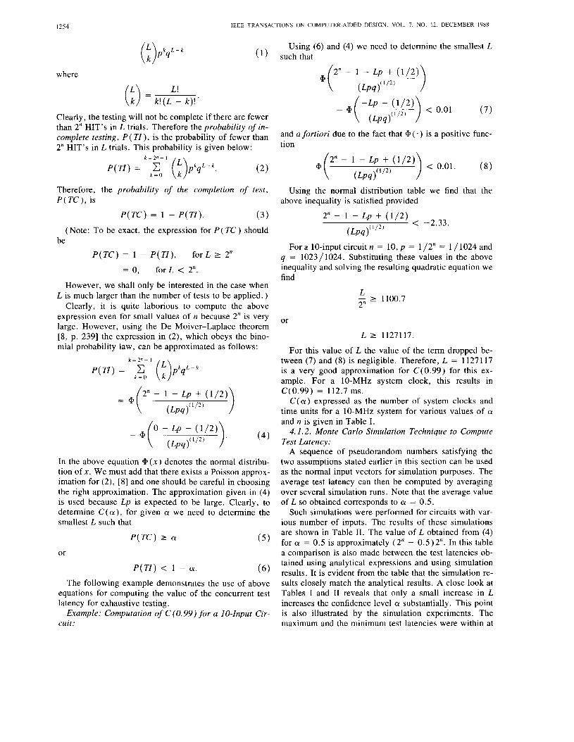
1254 IEEE TRANSACTIONS ON COMPUTER-AIDED DESIGN. VOL. 7 . NO. 12. DECEMBER 198X
( f i ) P k P \ ,
where
lL\ L!
Using (6 ) and (4) we need to determine the smallest L ( such that
2" - 1 - Lp + (1/2)
\ k j k ! ( L - k ) ! .
Clearly, the testing will not be complete if there are fewer than 2" HIT'S in L trials. Therefore the probability of in- complete testing, P ( T I ) , is the probability of fewer than and afortiori due to the fact that 9 ( * ) is a positive func- 2" HIT'S in L Gals. This probability is gLven below: tion
k = 2 " - I
P(TZ) = k = O c ( ; )pkyL- ' .
Therefore, the probability of the completion of test, P ( T C ) , is
P ( T C ) = 1 - P(TZ). (3)
(Note: To be exact, the expression for P ( T C ) should be
P ( T C ) = 1 - P(TZ), for L L 2"
= 0, for L < 2".
However, we shall only be interested in the case when L is much larger than the number of tests to be applied. )
Clearly, it is quite laborious to compute the above expression even for small values of n because 2" is very large. However, using the De Moiver-Laplace theorem [8, p. 2391 the expression in (2), which obeys the bino- mial probability law, can be approximated as follows:
k = 2 " - 1
P(TZ) = k = O c ( , ) p k q L P k
) 2" - 1 - Lp + (1 /2 ) = .(
( Lpq)'1/2'
In the above equation + ( x ) denotes the normal distribu- tion of x . We must add that there exists a Poisson approx- imation for (2), [8] and one should be careful in choosing the right approximation. The approximation given in (4) is used because Lp is expected to be large. Clearly, to determine C ( a ) , for given a we need to determine the smallest L such that
P ( T C ) L a ( 5 )
P(TZ) < 1 - a. ( 6 )
or
The following example demonstrates the use of above equations for computing the value of the concurrent test latency for exhaustive testing.
Example: Computation of C(0.99) for a IO-Input Cir- cuit:
< 0.01. ( 8 ) 2" - 1 - Lp + (1 /2)
(Lpq )( I /*)
Using the normal distribution table we find that the above inequality is satisfied provided
2" - 1 - Lp + (1 /2) < -2.33. (Lpq) ' l / 2 )
For a 10-input circuit n = 10, p = 1 /2" = 1 / 1024 and q = 1023/1024. Substituting these values in the above inequality and solving the resulting quadratic equation we find
L - > 1100.7 2" -
or
L 2 1127117.
For this value of L the value of the term dropped be- tween (7) and (8) is negligible. Therefore, L = 11271 17 is a very good approximation for C(0.99) for this ex- ample. For a 10-MHz system clock, this results in C(0.99) = 112.7 ms.
C ( a ) expressed as the number of system clocks and time units for a IO-MHz system for various values of a and n is given in Table I.
4.1.2. Monte Carlo Simulation Technique to Compute Test Latency:
A sequence of pseudorandom numbers satisfying the two assumptions stated earlier in this section can be used as the normal input vectors for simulation purposes. The average test latency can then be computed by averaging over several simulation runs. Note that the average value of L so obtained corresponds to a = 0.5.
Such simulations were performed for circuits with var- ious number of inputs. The results of these simulations are shown in Table 11. The value of L obtained from (4) for a = 0.5 is approximately (2" - 0.5)2". In this table a comparison is also made between the test latencies ob- tained using analytical expressions and using simulation results. It is evident from the table that the simulation re- sults closely match the analytical results. A close look at Tables I and I1 reveals that only a small increase in L increases the confidence level cy substantially. This point is also illustrated by the simulation experiments. The maximum and the minimum test latencies were within at

SALUJA et al . : TESTING T E C H N I Q U E FOR DIGITAL CIRCUITS
10
12
14
1255
I048064 1048975 0.09%
16775168 16778520 0.02%
268427264 268365880 0.02%
TABLE I C( a) FOR DIFFERENT VALUES O F n A N D 01
I 1 C(O.90) I C(0.95) I C(O.99) 1
n Number of Simulation Runs
10 10
12 I O
TABLE IV OPERATION TABLE FOR THE COOT
Latency (L) Latency (L) Latency (L) Maximum Deviauon (Maximum) (Minimum) (Average) from Average
1051053 1046472 1048975 0.24%
16784258 16773371 16778816 0.03%
TABLE I1 AVERAGE TEST LATENCY
Average Test Latency (L) Difference Between Analytical 1 I Analytical 1 Simulated I andSimulatedResults I
most 0.24 percent of the average test latencies for all sim- ulation runs, as shown in Table 111. In close agreement with theory, the test latencies arrived at through simula- tion are very close to the average test latencies given in Table 11. If shorter test latencies are required, then tech- niques for reducing test latency (discussed in [9]) can be employed.
v. HARDWARE FOR CONCURRENT TESTING In this section we shall discuss the design of a particular
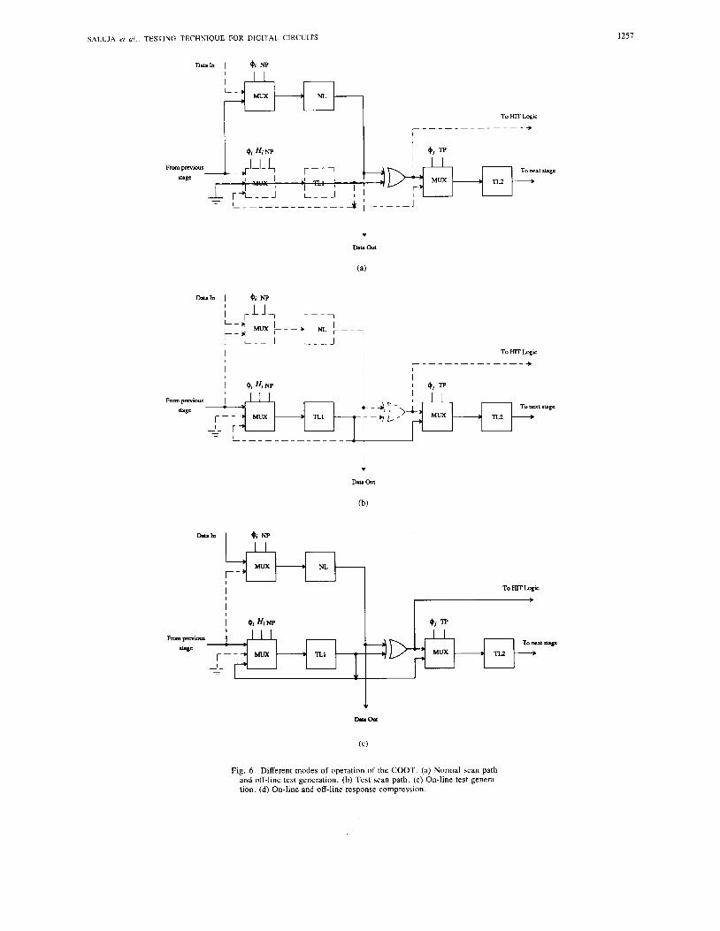
type of CBU, which we shall refer to as a concurrent and off-line observer and tester (COOT). The basic design philosophy is similar to that used in the design of a BILBO [2]. The COOT has six basic modes of operation. Fig. 4 gives a general design of the COOT. The four building blocks of the COOT are the COOT cell, the feedback function, the scan path multiplexer and the HIT-logic. The COOT is controlled by four independent control inputs NP, TP, SI and FH. The number of control inputs can, however, be reduced but we have chosen four indepen- dent control inputs for the clarity of presentation. Each COOT can operate in different modes. The feedback func- tion provides the linear function with a nonlinearity for the exhaustive TG operation. The scan path multiplexer is controlled by SI to open (SI = 1 ) or close (SI = 0) the feedback path. The HIT-logic is used to generate the signal Hi to indicate the HIT condition for on-line testing. The control input FH is required to force the HIT condi- tion for off-line response compression and scan modes. A design of the COOT cell is given in Fig. 5(a). In this figure, NL represents the normal system latch, TL1 and TL2 are test latches, and 4i and cpj are two nonoverlapping clocks. An implementation of the COOT cell in nMOS is given in Fig. 5(b). This implementation is a modification of the implementation given in [lo]. Latches NL and TL2
7 0 0
FH I Modeofomtion
Off-line RC 0 On-lineRC
are realized as dynamic latches while TL1 is realized as a static latch since it is required to hold the data for long duration in on-line test generation and on-line response compression modes. Table IV gives different modes of operations of the COOT for different values of the control inputs. The modes of the COOT are described next in detail.
We must add that not all designs will require existence of all modes mentioned in this paper. Thus it may be pos- sible to simplify the hardware given in this paper. But for the sake of generality we have chosen to treat the most complex case.
1 ) Normal Scan Path and Off-line Test Generation Modes (NP = 1, TP = 1 ) : In these modes all NL and TL2 latches form a shift register. A complete scan path for off-line scan is formed when SI = 1, whereas for SI = 0 the feedback path is completed and the COOT acts as an LFSR for off-line test generation. The configuration of the COOT cell for these two modes is shown in Fig. 6(a) by highlighting the configuration path. The normal scan path mode is used to test system latches as well as to read-out and initialize the COOT latches for test gen- eration and response compression modes for off-line test- ing.
2) Test Scan Path (NP = 0, TP = 0, SI = 1 , FH = 1 ) : In this mode all TL1 and TL2 latches form a scan path. The configuration of the COOT cell is shown in Fig- ure 6(b). This mode is used to read-out and initialize the test latches while the system is operating. This mode can also be used to test the test latches of the COOT.
3) On-Line Test Generation Mode (NP = 0, TP = 0, SI = 0, FH = 0): This mode is used for concurrent test- ing. Configuration of the COOT is shown in Fig. 6(c). The TLl latch holds the bit to be compared with the con- tent of NL latch. In case of a MISS the signal Hi = 0 and the state of the test latches does not change. When a HIT occurs, the signal Hi = 1, the test latches of the COOT form an LFSR and a new test vector is generated.
4) Off-Line and On-Line Response Compression Modes (NP = 0, TP = 1 , SI = 0): The control input FH is used to distinguish between these two modes. During off-line testing, the tests are applied to the CUT by the TG on every clock cycle, therefore the RC must compress all data. This is achieved by setting FH = 1 which in essence sets H, to 1 . In the on-line response compression mode, a response needs to be compressed provided the normal in- put corresponding to the response was a HIT. Therefore, in this mode the COOT compresses the response only if the COOT acting as an on-line test generator for the CUT

1256
* Dp.h mu W I n
4
IEEE TRANSACTIONS ON COMPUTER-AIDED DESIGN. VOL. 7, NO. 12, DECEMBER 1988
b H I T Logic -
SI N P T P H i
V 1 + - Mux- m c C l l -
I
Data Out
N P T p H i NP Tp Hi
.I V L - -
COOTcell 1 I - b lr,... _+
COOTCell 14
(b) Fig. 5. A design of the COOT cell. (a) Structure of the COOT cell. (b)
An NMOS realization of the COOT cell.
SALUJA et al.: TESTING TECHNIQUE FOR DIGITAL CIRCUITS
DI1.h
F m previous
I Qi NP
~
1257
To HlT Logic
+
D l u In
From previous
I Qi NP
I Qi Km
To HlT Logic
+ _ _ _ _ I
I
To next ruge
B TLZ +
I To HlT Logic
Fig. 6. Different modes of operation of the COOT. (a) Normal scan path and off-line test generation. (b) Test scan path. (c) On-line test genera- tion. (d) On-line and off-line response compression.

IEEE TRANSACTIONS ON COMPUTER-AIDED DESIGN. VOL. 7 , NO. 12, DECEMBER 1988 1258
To HIT Logic I
I I
mu out
(d)
Fig. 6 . (Continued)
produces a logic 1 on the line Hi. The configuration of the COOT cell for these modes is shown in Fig. 6(d).
A simplified view of the use of the COOT structures in the system operation is shown in Fig. 7. In such an or- ganization off-line testing of all combinational logic struc- tures can be completed in two phases. The method of test- ing is similar to the testing in a BILBO-oriented test organization [4]. All COOT’s are initialized using off-line scan mode before the testing begins. In phase 1 (phase 2) all even (odd) numbered CUT’s are tested. Alternative COOTS are configured for off-line test generation and off- line response compression. At the end of the testing all COOT’s are read out using off-line scan mode. The com- pressed responses (signatures) are compared to the ex- pected responses to determine the status of the CUT’s. The concurrent testing proceeds in the similar manner but while the system is operating. The COOT’s are initialized using the on-line scan mode. Notice that the COOT struc- ture is such that the on-line scan mode has no effect on the normal system latches. To test CUT ( i ), COOT ( i ) is used as on-line test generator and COOT ( i + 1 ) is used as on-line response compressor. COOT ( i ) compares the normal inputs to CUT ( i ) to its own content. If a normal input to CUT ( i ) is the same as the content of COOT ( i ), then it performs two functions: (1) it generates a HIT sig- nal Hi for COOT(i + 1) thereby requiring COOT(i + 1 ) to record the output of CUT ( i ) by generating the next signature state; (2) it goes into the LFSR configuration and at the end of the clock cycle its content becomes the next test pattern. Concurrent testing is complete when COOT ( i ) has gone through all states. A phase of testing
Fig. 7 . A simplified test environment for COOT’s
only the results of the comparison would need to be read out to determine the status of the circuit.
A real system may require more than two phases for completely testing a system as pointed out by Craig er al. [ 113 for off-line testing. The techniques proposed therein for scheduling the tests to reduce total testing time can be used for on-line testing using the COOT structures pro- posed in this paper. This will also require a design of the controller to completely and correctly carry out the on- line testing function.
is complete when all COOT’s in the TG mode have gone through all desired states. At this time all COOT’s are read out using test scan path mode. As mentioned earlier the test scan path mode can proceed without interrupting the system operation. The scanned out responses can be compared with the expected responses and the next phase of testing can start. It is also possible to compare the sig- natures internally without scanning them out in which case
VI. DISCUSSION AND CONCLUSIONS In this paper we have described a method of testing dig-
ital circuits while the system is operating. The resources we use to achieve this are essentially the same as used for off-line testing although depending on the design of off- line BIST, additional logic may be required. AS men- tioned earlier, in some situations shorter test latencies may
SALUJA ef al.: TESTING TECHNIQUE FOR DIGITAL CIRCUITS
be desirable. In such situations the following techniques discussed in [9] can be used.
(1) Circuit partitioning [4]. (2) Verification testing [ 5 ] . (3) Roving [12]. (4) Random pattern testing. ( 5 ) Stored tests. (6) Multiple hardware signature analysis. (7) Order independent signature analysis [3].
The underlying concept used in these techniques is that the test latency primarily depends upon two factors; (1) the size of the test set T and (2) the probability of a HIT for the inputs applied to the circuit under normal opera- tion. The first five techniques mentioned above reduce the test latency by reducing the number of states of the TG and the last two techniques do so by effectively increasing the probability of a HIT for the normal inputs.
The design of a test resource, proposed in this paper, is such that the resource can be initialized or its status can be read through scan path without interrupting the normal operation of the circuit. Thus the COOT design proposed in this paper can also be used to take a snapshot of the status of the circuit while the system is operating. We should also point out that with the design of the COOT not only the combinational circuit part of the system is tested during on-line testing, but the normal system latches are also tested [lo].
This discussion would be incomplete without a com- ment on the assumptions stated in the Section 111. We have assumed in this paper that all inputs to the circuit are equally probable. In a real circuit, not only may this as- sumption not hold, but some input combinations may never occur during normal operation of the circuit. There are two possible solutions to this problem: (1) we may employ test generators which generate only those test vec- tors which also occur as normal inputs to the circuit or (2) we may employ time-out indicators, which, if too much time has elapsed for an active test vector, halts the normal system operation and forces a test vector injection. This second method can also be used to reduce the test latency although at the expense of the system performance. An- other design of a concurrent tester and its application a:e studied in [13]. Sharma and Saluja [13] also investigate the use of the concurrent testing technique to: (1) detect and diagnose intermittent faults, (2) detect transient faults, (3) perform system diagnosis, (4) reduce maintenance, and ( 5 ) increase system availability.
Finally, the distinction between concurrent testing and self-checking [ l ] is an important one that has not been emphasized thus far. On-line testing as presented here is targeted at permanent faults whereas self-checking is tar- geted at both permanent and non-permanent (intermittent and transient) faults. Thus concurrent testing, proposed in this paper, without substantial verification of adequate coverage for non-permanent faults in a particular appli- cation is not a total replacement for self-checking. It does guarantee the self-testing property of self-checking , but
1259
typically does not provide the fault secure property for nonpermanent faults. Thus, additional hardware or soft- ware means are usually needed in combination with con- current testing to achieve traditional self-checking goals. It should be noted, however, that concurrent testing as proposed here can be used to guarantee that the appropri- ate input vectors have occurred, an issue which has been a problem with traditional self-testing. Thus the self-test- ing provided by concurrent testing is stronger than that provided by traditional self-checking designs.
ACKNOWLEDGMENT The authors are thankful to the referees for providing
many helpful and critical comments. The authors espe- cially thank referee 1 whose comments helped improve the presentation substantially.
REFERENCES [ l ] H. Fujiwara, Logic Testing and Design for Testability. Cambridge,
MA: MIT Press, 1985. [2] B. Koenemann, J . Mucha, and G. Zwiehoff, “Built-in logic block
observation techniques,” in Proc. 1979 Test Conf., pp. 37-41, Oct. 1979. I. Savir, “Syndrome testable design of combinational circuits,” IEEE Trans. Comput., vol. C-29, pp. 442-451, June 1980. E. J . McCluskey and S . Bozorgui-Nesbat, “Design for autonomous test,” IEEE Trans. Cornput., vol. C-30, pp, 866-875, Nov. 1981. E. J . McCluskey, “Verification testing-A pseudoexhaustive test technique,” IEEE Trans. Comput., vol. C-33, pp. 541-546, June 1984. J . Losq, “Referenceless random testing,” in Proc. 1nt. S y n p . on Fault-Tolerant Computing, pp. 108-1 13, June 1976. R. A. Frohwerk, “Signature analysis: A new digital field service method,” Hewlett-Packard J . , pp. 2-8, May 1977. E. Parzen, Modern Probability Theory and Its Applications. New York: Wiley, 1960. K. K. Saluja, R. Sharma, and C. R. Kime, “Concurrent comparative built-in testing of digital circuits,’’ Tech. Rep. ECE-87-11, Dep. of Elect. Comp. Eng., Univ. of Wisconsin, Aug. 1987. C. W. Lau and C. R. Kime, “An experimental study of built-in logic block observer (BILBO) designs,” Tech. Rep. ECE-86-10, Dep. of Elect. Comp. Eng., Univ. of Wisconsin, 1986. G. L. Craig, C . R. Kime, and K . K. Saluja, “Test scheduling and control for VLSI built-in self-test,” IEEE Trans. Comput., vol. 37, pp. 1099-1 109, Sept. 1988. M. A. Breuer and A. A. Ismaeel, “Roving emulation as a fault de- tection mechanism,” IEEE Trans. Cornput., vol. C-35, pp. 933-939, Nov. 1986. R. Sharma and K. K. Saluja, “An implementation and analysis of a concurrent BIST technique,” Int. Symp. on Fault-Tolerant Comput- ing, pp. 164-169 June 1988.
*
Kewal K. Saluja (S’70-M’73) received the B E degree in electncal engineenng from the Univer- sity of Roorkee, Roorkee, India, in 1967, and the M.S. and Ph.D. degrees from the University of Iowa, Iowa City, in 1972 and 1973, respectively
He is currently an Associate Professor in the Department of Electncal and Computer Engineer- ing at the University of Wisconsin-Madison, where he teaches logic design, computer architec- ture, microprocessor-based syqtems, VLSI de- sign, and testing. Previously he was at the Uni-
versity of Newcastle, NSW, Australia He has also held visiting and consulting positions at number of institutions such as the University of Southern California, University of Iowa, and Hiroshima University His research interests include design for testability, fault-tolerant computing, VLSI design and computer architecture.
1260 IEEE TRAKSACTIONS ON COMPUTER-AIDED DESIGP;. VOL 7. NO I ? . DECEMBtK I Y X X
Rajiv Sharma received the B E degree in elec Charles R. Kime (S’60-M’66-SM’79) received tronics and electrical communications from the the B S degree from the University of Iowa, Iowa Punjdb Engineerlng College. Chdndigdrh, India, City, in 1962, the M S degree from the Univer- In 1985, and the M S degree in electrical engi sity of Illinois, Urbana, in 1963, and the Ph D neering from the Michigan Technological Univer- degree from the University of Iowa in 1966, all in sity, Houghton, in 1986 electricdl engineering
He was uith Michigan Technological Univer- He joined the faculty of the University of Wis- sity, ds a Tedching Assistant trom 1985 to 1986, conw-Mddi\on in 1966 where he is currently d
and as d Research Assistant at the University of Protessor in the Department of Electricdl and Wisconsin-Mddison troin 1986 to 1988 He I \ cur- Computer Engineering He \pent the 1973-1974 rently working in the area ot computer-aided test acddemic yedr as a Visiting A\sociate Professor
products development with Gateway- Design Automation Corporation, Lowell, MA. His research interests include design for testability, VLSI design, fault tolerant computing, computer architecture. and design auto- mation.
in the Department of Electrical Engineering and Computer Sciences, Uni- versity of California, Berkeley. His current research and teaching interests are in testing and built-in test, VLSI systems design, fault-tolerant com- puting. computer architecture and logic design.
Dr. Kinie is a member of the Association for Computing Machinery, the American Society of Engineering Education. and Sigma Xi. He has served as an Associate Editor of the IEEE TRANSACTIONS ON COMPUTERS and as the General Chairman of the 1979 International Symposium on Fault-Tol- erant Computing.