A compact double-gate MOSFET model comprising quantum-mechanical and nonstatic effects
Upload
independentCategory
view
1download
0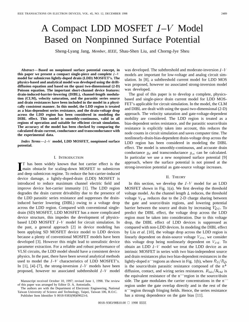
IEEE TRANSACTIONS ON ELECTRON DEVICES, VOL. 45, NO. 12, DECEMBER 1998 2489
A Compact LDD MOSFET – ModelBased on Nonpinned Surface Potential
Sheng-Lyang Jang,Member, IEEE, Shau-Shen Liu, and Chorng-Jye Sheu
Abstract—Based on nonpinned surface potential concept, inthis paper we present a compact single-piece and completeI–Vmodel for submicron lightly-doped drain (LDD) MOSFET’s. Thephysics-based and analytical model was developed using the drift-diffusion equation and based on the quasi two-dimensional (2-D)Poisson equation. The important short-channel device features:drain-induced-barrier-lowering (DIBL), channel-length modula-tion (CLM), velocity saturation, and the parasitic series sourceand drain resistances have been included in the model in a physi-cally consistent manner. In this model, the LDD region is treatedas a bias-dependent series resistance, and the drain-voltage dropacross the LDD region has been considered in modeling theDIBL effect. This model is smoothly-continuous, valid in allregions of operation and suitable for efficient circuit simulation.The accuracy of the model has been checked by comparing thecalculated drain current, conductance and transconductance withthe experimental data.
Index Terms—I–V model, LDD MOSFET, nonpinned surfacepotential.
I. INTRODUCTION
I T has been widely known that hot carrier effect is themain obstacle for scaling-down MOSFET to submicron
and deep submicron regime. To reduce the hot-carrier-induceddevice damage, a lightly-doped-drain (LDD) MOSFET isintroduced to reduce maximum channel electric field andimprove device hot-carrier immunity [1]. The LDD regiondegrades the drain current drivability due to the presence ofthe LDD parasitic series resistance and suppresses the drain-induced barrier lowering (DIBL) owing to a voltage dropacross the LDD region. Compared with conventional single-drain (SD) MOSFET, LDD MOSFET has a more complicateddevice structure, this impedes the development of physics-based LDD MOSFET – model for circuit simulation. Inthe past, a general approach [2] in device modeling hasbeen applying SD MOSFET device model to LDD devicesbecause a plenty of conventional MOSFET models have beendeveloped [3]. However this might lead to unrealistic deviceparameter extraction. For a reliable and robust performance ofVLSI circuits, the LDD model should have a consistent devicephysics. In the past, there have been several analytical methodsused to model the – characteristics of LDD MOSFET’s.In [1], [4]–[7], the strong-inversion – models have beenproposed, however no associated subthreshold– model
Manuscript received October 10, 1997; revised June 1, 1998. The reviewof this paper was arranged by Editor D. A. Antoniadis.
The authors are with the Department of Electronic Engineering, NationalTaiwan University of Science and Technology, Taipei, Taiwan 106, R.O.C.
Publisher Item Identifier S 0018-9383(98)09023-6.
was developed. The subthreshold and moderate-inversion–models are important for low-voltage and analog circuit sim-ulation. In [8], a subthreshold current model for LDD MOSwas proposed, however no associated strong-inversion modelwas developed.
The goal of this paper is to develop a complete, physics-based and single-piece drain current model for LDD MOS-FET’s applicable for circuit simulation. In the model, the CLMand DIBL are dealt with using the quasi two-dimensional (2-D)approach. The velocity saturation and gate-voltage-dependentmobility are considered. The LDD region is treated as abias-dependent series resistance, and the parasitic source/drainresistance is explicitly taken into account, this reduces thenode counts in circuit simulation and saves computer time. Thenonlinearly-drain-bias-dependent drain-voltage drop across theLDD region has been considered in modeling the DIBLeffect. The model is smoothly-continuous, and accurate drainconductance and transconductance can be calculated.In particular we use a new nonpinned surface potential [9]approach, where the surface potential is not pinned at thestrong-inversion potential as gate-source voltage increases.
II. THEORY
In this section, we develop the– model for an LDDMOSFET shown in Fig. 1(a). We first develop the thresholdvoltage model. As the channel lengthreduces, the thresholdvoltage reduces due to the 2-D charge sharing betweenthe gate and source/drain regions, and lowering potentialbarrier between the source and drain by increasing Topredict the DIBL effect, the voltage drop across the LDDregion must be taken into consideration. Due to this voltagedrop, the DIBL effect of LDD devices is suppressed ascompared with non-LDD devices. In modeling the DIBL effectby Liu et al. [10], the voltage drop across the LDD region islinearly dependent on drain-source voltage we considerthis voltage drop being nonlinearly dependent on Toobtain an LDD – model we treat the LDD device as anintrinsic MOSFET in series with two bias-independent sourceand drain resistances plus two bias-dependent resistances in thelightly-doped n regions as shown in Fig. 1(b), whereis the source/drain parasitic resistance composed of the ndiffusion, contact, and wiring series resistances. isthe equivalent resistance of the nregion in the source/drainside. The gate modulates the carrier concentrations in the nregion under the gate overlap directly and in the rest of then region through fringing fields. Hence, the series resistancehas a strong dependence on the gate bias [11].
0018–9383/98$10.00 1998 IEEE
2490 IEEE TRANSACTIONS ON ELECTRON DEVICES, VOL. 45, NO. 12, DECEMBER 1998
(a)
(b)
(c)
Fig. 1. (a) Cross section of an LDD MOSFET. (b) MOSFET equivalentcircuit. (c) Detailed LDD region.
A. Threshold Voltage Reduction
To analyze we divide the LDD device as shown inFig. 1(a) into two parts, the intrinsic channel and the LDDregion. The mathematic manipulation of the lightly-dopedsource (LDS) region is neglected for simplicity. In the intrinsicchannel region of 0 from the 2-D Poisson equationwe can get [12]
(1)
where is the inversion layer charge density. is the gate-oxide capacitance. is the gate-source voltage. is thepotential relative to the substrate contact. is the intrinsic-channel flat-band voltage. is the elementary charge. isthe permittivity of silicon. is the depletion layerthickness/depletion layer thickness at the threshold of surfaceinversion with zero bulk-source bias. is an experimentalfitting parameter [12]. is the substrate concentration.
Using the Taylor series expansion about atwe have
(2a)
where
(2b)
and
(2c)
is the threshold voltage reduction due to the longi-tudinal electric field. is where is thethermal voltage, is the intrinsic carrier density. is thesource-bulk voltage. is the threshold voltage of the longchannel device and can be phenomenologically modified as[13]
(3)
where accounts for the nonuniform substrate doping effecton the threshold voltage. In weak-inversion region, we assume
0, then from (2a) and (2c), we can get a quasi 2-Ddifferential equation
(4)
where and
The subthreshold ideality factor
is further modified in Appendix A to account for thesubthreshold swing roll-up as channel length reduces.
In the LDD region of from the 2-DPoisson equation we can get
(5a)
where
(5b)
is the potential. is the free electron density. is theaverage doping concentration of the nregion. is thejunction depth of n region [Fig. 1(c)]. is the depletiondepth of substrate. Integrating (5a) from the SiOSi interfacetoward the depletion layer edge, we get
(6)
where is the total free carrier density. The first term onthe left-hand of (6) can be written as
(7)
The second term on the left-hand of (6) can be approximatedby
(8)
where is a fitting constant. is the value of atderived in Appendix B. Combining (6)–(8)
JANG et al.: COMPACT LDD MOSFET – MODEL 2491
and using the Taylor series expansion atwe have
(9a)
where
(9b)
is derived in Appendix B. If is decreased, a point isreached where the top depletion region meets with that of then -substrate junction. Under this circumstance, from(9a) we can get the quasi-2D differential equation
(10)
whereis the surface potential
of the long buried-channel MOSFET. Equations (4) and (10)are subjected to the following boundary conditions:
(11)
where is the built-in potential of the LDD-substratejunction. is the longitudinal depletion length in the LDDregion, which can be analytically calculated and is given by(14a). is the saturation electric field. The voltage dropacross the region is neglected. Thesolution of the surface potential in the intrinsic channel is
(12a)
where
(12b)
and the solution of the surface potential in the LDD region ofbecomes
(13a)
where
(13b)
Using (12a) and (13a) and the boundary conditions in (11),we can obtain
(14a)
where
(14b)
The minimum surface potential at can befound by solving the equation 0. For afixed increases with decreasing channel length orincreasing drain voltage. To determine the threshold voltagereduction we assume that equals at
Since locates within the intrinsicchannel region, we can get
(15a)
where
(15b)
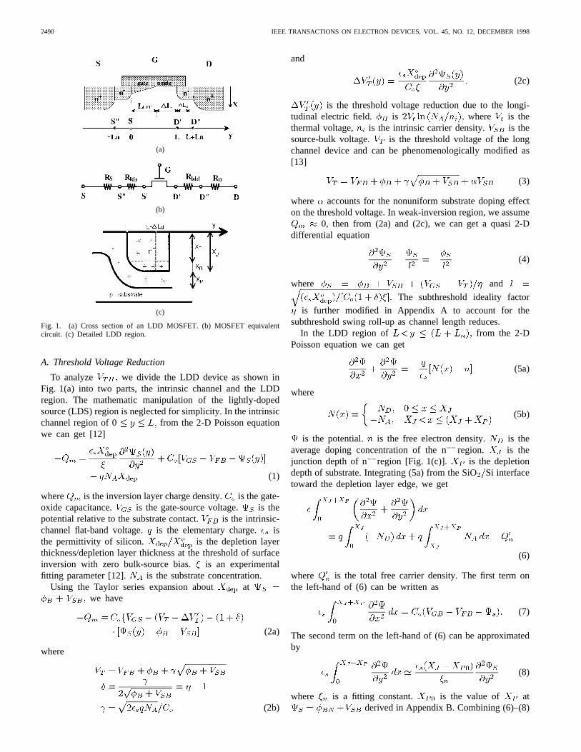
Fig. 2 shows the calculated and experimental [14] thresholdvoltage versus effective channel length as a function of
2492 IEEE TRANSACTIONS ON ELECTRON DEVICES, VOL. 45, NO. 12, DECEMBER 1998
Fig. 2. Experimental (symbols) and calculated (lines) threshold voltageversus effective channel length for an LDD device.
and The test device was fabricated by an 0.5-mtechnology with 110 A and 0.18 m. As can beseen, the proposed model correctly predicts the experimentalresults. The calculation also shows that the voltage drop acrossthe LDD region depends on nonlinearly.
B. Equivalent LDS and LDD Resistances
The LDD equivalent resistance is derived as follows. From(9a), we can get the drain current
(16)
where is the electrical channel width. For simplicity, weuse since the spatial variation of is smallin the linear region and we use the same bulk and surfacemobility. The drift velocity is given by
(17)
where is the effectivemobility. is the surface electric field. is a fitting constant,
is the low-field mobility and is given bySubstituting (17) for (16), integrating (16) from
to and usingand
yields
(18a)
where
(18b)
When can be approximated by wherethe velocity saturation effect is neglected [4]. Note under high-current operation the term cannot be neglected andcan be approximated as [4]
(19)
Combining the above two equations, can be obtained.
C. Triode – Model
We define
(20)
and
(21)
where After expanding (1)becomes
(22a)
where
(22b)
Considering the drift and diffusion current components, thedrain current is
(23a)
where is the channel width, and the drift velocity is givenby
(23b)
is a fitting constant.Integrating (23a) from the intrinsic source to the intrinsic
drain and using (22a) we can get
(24a)
where
(24b)
Considering a long-channel device operated in the weakinversion region and biased at small using (32a) and(24a) we can get the well-known subthreshold current
(24c)
JANG et al.: COMPACT LDD MOSFET – MODEL 2493
in the strong inversion condition (24a) reduces to the well-known strong-inversion drain current
(24d)
Hence (24a) is valid in all regions of operation.Using we
can obtain
(25a)
where
(25b)
The above derivation is based on the assumption that istreated as a constant evaluated at When a MOSFET isoperated in the triode mode, the channel electric field is small,this approximation simplifies the mathematical manipulationfor the drain current formula. In strong inversion region, from(22a) we can get the free charge density at 0
(25c)
D. Pentode Model
As increases, the velocity saturation occurs at the drainend channel, and the MOSFET can be divided into two parts[see Fig. 1(a)].
a) In the pre-saturation channel region near the sourcethe current can be due to
the drift or diffusion component depending on the valueof
b) In the post-saturation region the drift currentis dominant because the electric field is large, issmall, the diffusion current is negligible.
can not be regarded as a constant. The saturation draincurrent can be approximated by
(26)
Letting (24a) (26), we can get the saturation intrinsicchannel voltage The saturation extrinsic drain voltage
can be written as
(27a)
where is given by in (24a) by substituting in(24a) for To obtain we set the value of equalto to get the first-order approximation for that is
To ensure smooth transition of drain conductanceand transconductance between linear and saturation regionsand between subthreshold and strong-inversion we use thefollowing approximation to calculate
(27b)
we also use the following equation to replace inof to obtain a more accurate value of
(27c)
where is a fitting constant.In order to make a smooth transition for between linear
and saturation regions, an engineering approximation has beenused [15], [16]
(28)
where is a model fitting parameter. When is greaterthan the velocity saturation point moves toward thesource, the voltage difference is droppedacross the distance The effective channel length becomes
Using (1) and the boundary conditions [12], [16] wecan get
E. Complete – Model
To calculate the drain current in the previous sections, inthis section we will derive as a function of bias,since is a function of We also will derivein the pre-saturation channel region, where the electric fieldis smaller than in the post-saturation channel region. Theeffective gate-channel capacitance is given by [17]
(29a)
where
(29b)
2494 IEEE TRANSACTIONS ON ELECTRON DEVICES, VOL. 45, NO. 12, DECEMBER 1998
where is the channel-source electron quasi-Fermi poten-tial. is the 1-D bulk depletion capacitance. is thegate-channel voltage.
In weak-inversion region, we assume then from(1) we can get
(30)
Substituting (30) into (29b) yields
(31)
Next we assume that in the presaturation channel can beapproximated by to derive the drain current. Substituting(31) into (29a) and integrating (29a) with respect to gives
(32a)
and
(32b)
The above derivation involves a drastic approximation, whichmakes possibile the complete– model.
In strong inversion region, (32b) reduces to (25c). From(22a) and at 0 we can get
(33a)
Expanding (32b) in terms of Taylor’s series we can get
(33b)
where
(33c)
In weak inversion region is small; in strong inversionregion the second terms on the right-hand sides of (33a) and(33b) are equal, hence we can get
(33d)
Substituting (33d) in (25b), and and substitutingand respectively in and in (25b), we
can get the drain current equation in all regions of operation.
TABLE IFITTING PARAMETERS OF FIG. 3
Parameter Value UnitL 0.56 �m
Ln=XJ 0.2/0.25 �m/�mNA 2.2� 1016 cm�3
ND 1.0� 1018 cm�3
RS=RD 38/38 =
VFB �0.97 V�c 5.75� 1016 cm=s�0 665 cm2=V � s
� 0.13 V�1
�=�n 2.1/5.9
ATS=nm 3.0/1.0
The surface pontential at can be obtained from (33a).Combining (22b) and (33d) we can get
(34)
This equation indicates that the surface potential is not pinnedas increases. This surface potential can be used tocalculate the bulk charge [18].
III. RESULTS AND DISCUSSION
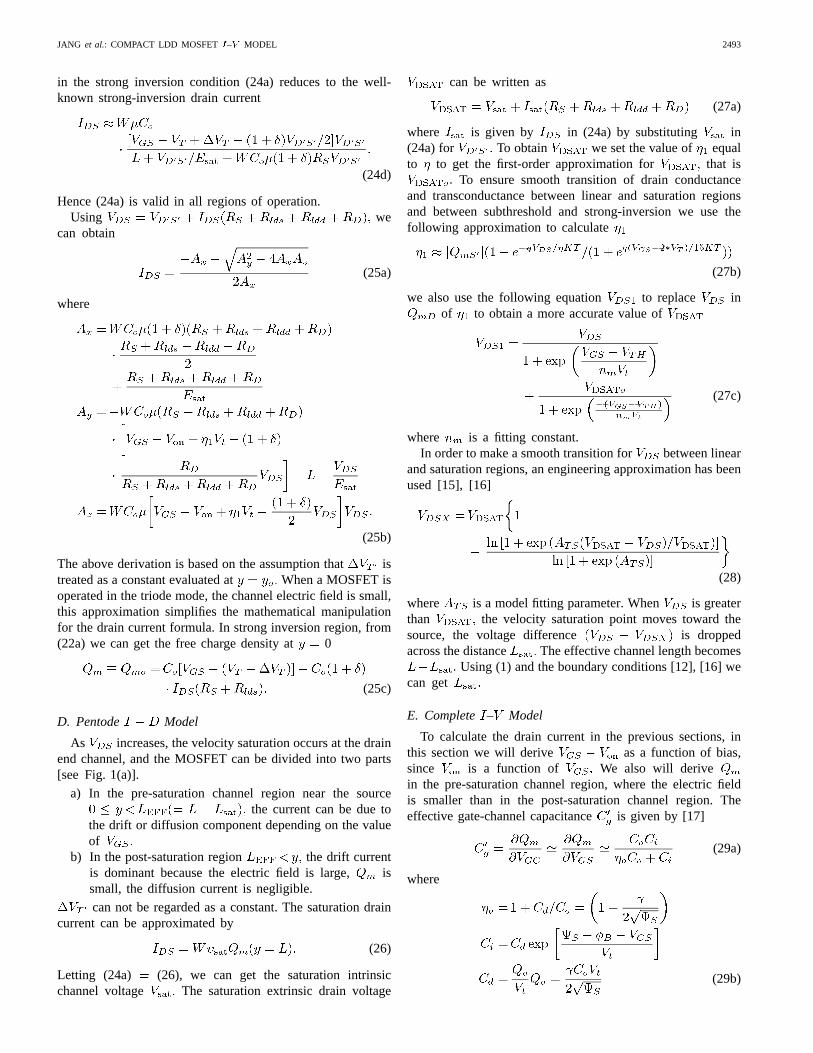
We verify our model with the experimental data.Figs. 3(a)–(d) show comparisons between the experimentaldata and the modeled results. The circles are the experimentaldata and the solid lines are the fitting results. All modeledresults and measurements were performed at0. A good agreement has been obtained by using only oneset of parameters tabulated in Table I. The tested device isan LDD MOSFET with a masked channel length of 0.72
and 22.725 m. The spacer is about 0.25m.The threshold voltage implantation was performed with adose of 1.14 10 cm The n regions were formedby implanting the phosphorus with an energy of 30 keVand a dose of 2 10 cm The source/drain n regionwere implanted with an energy of 40 keV and a dose of 4
10 cm Using the published methods [19], [20], theextracted effective channel length is 0.56m. As can be seenfrom these figures, the subthreshold current increases withincreasing drain bias due to the DIBL effect, and our modelquite accurately reproduces the experimental data over severaldecades of current variation. The measured and calculateddrain currents are smoothly continuous at the transitionbetween the linear and saturation regions. The calculated plotof versus also indicates a smooth transition as
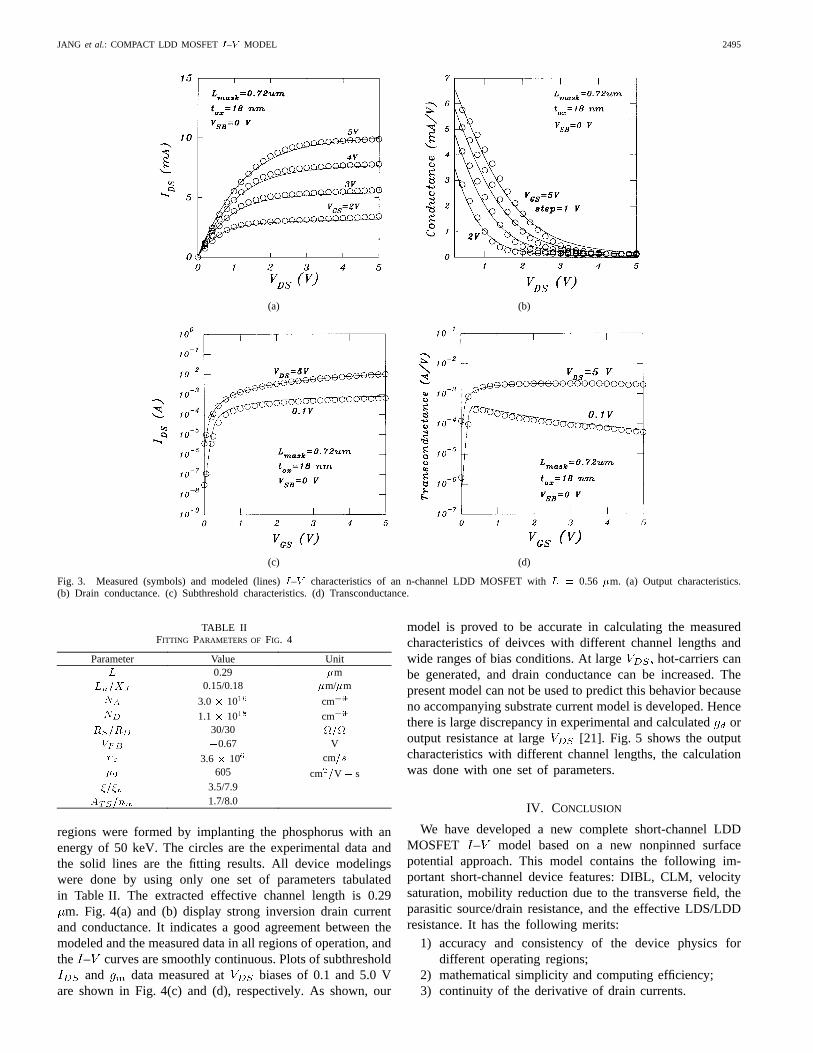
increases (not shown).Fig. 4(a)–(d) show comparisons between the experimental
data and the modeled results for an LDD MOSFET made byother process with a masked channel length of 0.4m, and
10 m. The spacer is about 0.1m. The thresholdvoltage adjustment was performed by implanting withan energy of 60 keV and a dose of 3.510 cm . The n
JANG et al.: COMPACT LDD MOSFET – MODEL 2495
(a) (b)
(c) (d)
Fig. 3. Measured (symbols) and modeled (lines)I–V characteristics of an n-channel LDD MOSFET withL = 0.56 �m. (a) Output characteristics.(b) Drain conductance. (c) Subthreshold characteristics. (d) Transconductance.
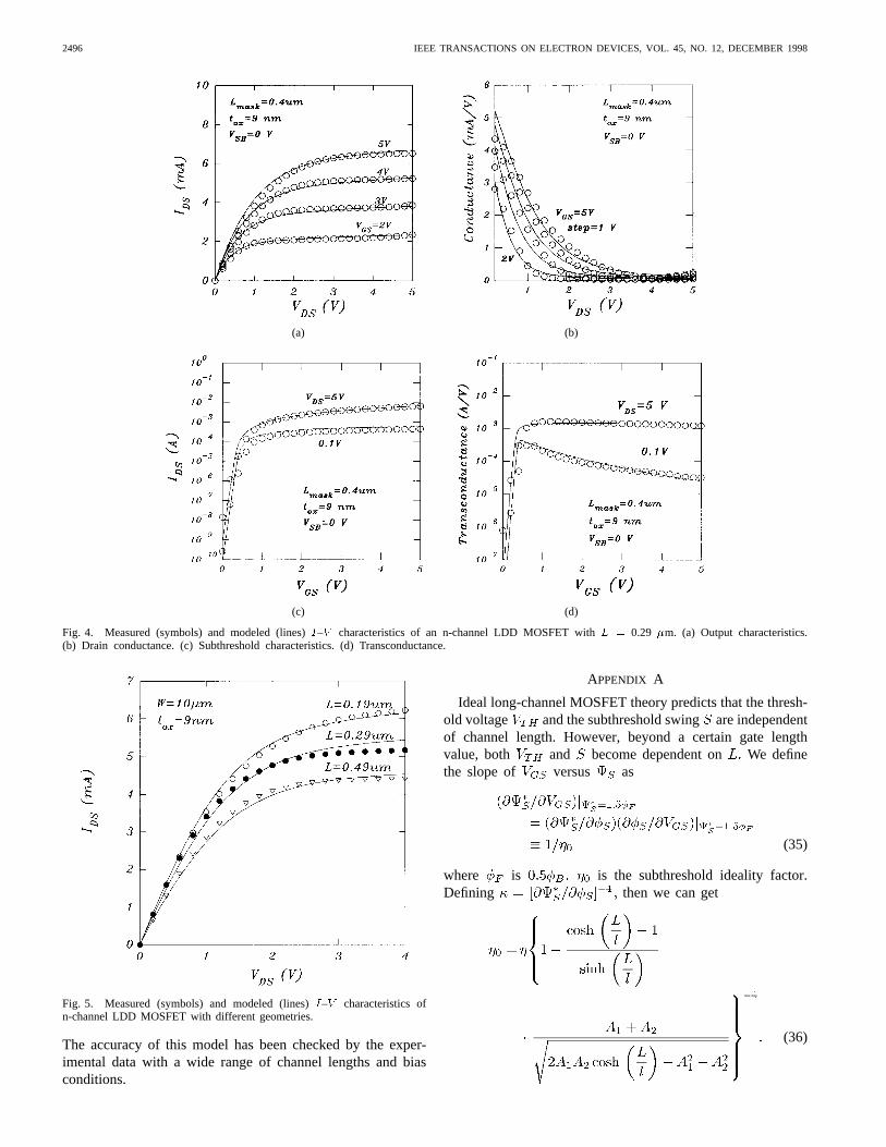
TABLE IIFITTING PARAMETERS OF FIG. 4
Parameter Value UnitL 0.29 �m
Ln=XJ 0.15/0.18 �m/�mNA 3.0� 1016 cm�3
ND 1.1� 1018 cm�3
RS=RD 30/30 =
VFB �0.67 V�c 3.6� 106 cm=s�0 605 cm2=V � s�=�n 3.5/7.9
ATS=nm 1.7/8.0
regions were formed by implanting the phosphorus with anenergy of 50 keV. The circles are the experimental data andthe solid lines are the fitting results. All device modelingswere done by using only one set of parameters tabulatedin Table II. The extracted effective channel length is 0.29
m. Fig. 4(a) and (b) display strong inversion drain currentand conductance. It indicates a good agreement between themodeled and the measured data in all regions of operation, andthe – curves are smoothly continuous. Plots of subthreshold
and data measured at biases of 0.1 and 5.0 Vare shown in Fig. 4(c) and (d), respectively. As shown, our
model is proved to be accurate in calculating the measuredcharacteristics of deivces with different channel lengths andwide ranges of bias conditions. At large hot-carriers canbe generated, and drain conductance can be increased. Thepresent model can not be used to predict this behavior becauseno accompanying substrate current model is developed. Hencethere is large discrepancy in experimental and calculatedoroutput resistance at large [21]. Fig. 5 shows the outputcharacteristics with different channel lengths, the calculationwas done with one set of parameters.
IV. CONCLUSION
We have developed a new complete short-channel LDDMOSFET – model based on a new nonpinned surfacepotential approach. This model contains the following im-portant short-channel device features: DIBL, CLM, velocitysaturation, mobility reduction due to the transverse field, theparasitic source/drain resistance, and the effective LDS/LDDresistance. It has the following merits:
1) accuracy and consistency of the device physics fordifferent operating regions;
2) mathematical simplicity and computing efficiency;3) continuity of the derivative of drain currents.
2496 IEEE TRANSACTIONS ON ELECTRON DEVICES, VOL. 45, NO. 12, DECEMBER 1998
(a) (b)
(c) (d)
Fig. 4. Measured (symbols) and modeled (lines)I–V characteristics of an n-channel LDD MOSFET withL = 0.29 �m. (a) Output characteristics.(b) Drain conductance. (c) Subthreshold characteristics. (d) Transconductance.
Fig. 5. Measured (symbols) and modeled (lines)I–V characteristics ofn-channel LDD MOSFET with different geometries.
The accuracy of this model has been checked by the exper-imental data with a wide range of channel lengths and biasconditions.
APPENDIX A
Ideal long-channel MOSFET theory predicts that the thresh-old voltage and the subthreshold swingare independentof channel length. However, beyond a certain gate lengthvalue, both and become dependent on We definethe slope of versus as
(35)
where is is the subthreshold ideality factor.Defining then we can get
(36)
JANG et al.: COMPACT LDD MOSFET – MODEL 2497
Here we let the value of in equal toand is the value of in (15) with replaced withby Since the slope of versus changes from
to as decreases, we phenomenologically model thebehavior as
(37)
where is a fitting parameter. Replacingin (33) withwe can get an accurate subthreshold swing as a function ofgate and drain biases and channel length.
APPENDIX B
From Fig. 1(c), the 1-D Poisson equation in the pinchoffmode can be solved and the result is
(38)
which gives
(39)
From (39), we can get
(40)
Using that the electric field must be continuous atwe can get
(41)
Putting (41) into (38), we can get
(42)
When we define andEquating (40) with (42), we can get
(43)
where
(44)
To solve the unknown pinchoff voltage the chargebalance requires
(45)
The potential balance equation is obtained by going throughthe gate terminal through the device to the substrate terminal
(46)
where is the work function difference between the gateconductor and region, is the voltage drop across gateoxide. We also have
(47)
Combining the above three equations, is derived when
REFERENCES
[1] M.-C. Hu, S.-L. Jang, and C.-G. Chyau, “A physical short-channelcurrent-voltage model for LDD MOSFET’s,”Jpn. J. Appl. Phys., vol.36, no. 6A, pp. 3448–3459, 1997.
[2] B. Lemaıtre, “An improved analytical LDD-MOSFET model for digitaland analog circuit simulation for all channel lengths down to deep-submicron,” inIEDM Tech. Dig., 1991, pp. 333–336.
[3] B. I nıguez and E. G. Mroreno, “A physical basedC1-continuous modelfor small-geometry MOSFET’s,”IEEE Trans. Electron Devices, vol. 42,no. 2, pp. 283–287, 1995.
[4] G.-S Huang and C.-Y. Wu, “An analyticI–V model for lightly dopeddrain (LDD) MOSFET devices,”IEEE Trans. Electron Devices, vol.ED-34, pp. 1311–1321, June 1987.
[5] , “An analytic saturation model for drain and substrate currentsof conventional and LDD MOSFET’s,”IEEE Trans. Electron Devices,vol. 37, pp. 1667–1677, July 1990.
[6] S. S.-S. Chung, T.-S. Lin, and Y.-G. Chen, “An efficient semi-empiricalmodel of theI � V characteristics for LDD MOSFET’s,”IEEE Trans.Electron Devices, vol. 36, pp. 1691–1702, Sept. 1990.
[7] F.-S. J. Lai and J. Y.-C. Sun, “An analytical one-dimensional model forlightly doped drain (LDD) MOSFET devices,”IEEE Trans. ElectronDevices, vol. 32, pp. 2803–2811, Dec. 1985.
[8] L.-M. Chua and P.-C. Liu, “Subthreshold current for submicron LDDMOS transistor,” inIEDM Tech. Dig., 1993, pp. 1044–1047.
[9] D.-H. Cho and S. M. Kang, “A new deep submicron compact physicalmodel for analog circuits” inProc. IEEE CICC, 1994, pp. 3.5.1–3.5.4.
[10] Z.-H. Liu, C. Hu, J.-H. Haung, T.-Y. Chan, M.-C. Jeng, P. K. Ko,and Y. C. Cheng, “Threshold voltage model for deep-submicometerMOSFET’s,” IEEE Trans. Electron Devices, vol. 40, pp. 86–94, Jan.1993.
[11] G. J. Hu, C. Chang, and Y. T. Chia, “Gate-voltage-dependent effectivechannel and series resistance of LDD MOSFET’s,”IEEE Trans. ElectronDevices, vol. ED-34, pp. 2469–2475, Dec. 1987.
[12] Y.-S. Chen, T.-H. Tang, and S.-L. Jang, “Modeling of hot-carrier-stressed characteristics of nMOSFET’s,”Solid-State Electron., vol. 38,no. 1, pp. 75–81, 1996.
[13] J. A. Power and W. A. Lane, “An enhanced SPICE MOSFET modelsuitable for analog application,”IEEE Trans. Computer-Aided Design,vol. 11, pp. 1418–1424, Nov. 1992.
[14] J.-J. Maa and C.-Y. Wu, “A new simplified threshold-voltage modelfor n-MOSFET’s with nonuniformly doped substrate and its applicationto MOSFET’s miniaturization,”IEEE Trans. Electron Devices, vol. 42,pp. 1487–1494, Aug. 1995.
[15] C. Hu, “Hot-electron effects in MOSFET’s,” inIEDM Tech. Dig., 1983,pp. 176–181.
[16] C. C. McAndrew, B. K. Bhattacharyya, and O. Wing, “A single-pieceC1-continuous MOSFET model including subthreshold conduction,”IEEE Electron Device Lett., vol. 12, pp. 565–567, Oct. 1991.
[17] Y. P. Tsividis, Operation and Modeling of the MOS Transistor. NewYork: McGraw-Hill, 1988.
2498 IEEE TRANSACTIONS ON ELECTRON DEVICES, VOL. 45, NO. 12, DECEMBER 1998
[18] N. D. Arora, R. Rios, and C.-L. Huang, “Modeling the polysilicon deple-tion effect and its impact on submicrometer CMOS circuit performance”IEEE Trans. Electron Devices, vol. 42, pp. 935–942, 1995.
[19] K. Takeuchi, N. Kasai, and K. Terada, “A new effective channel lengthdetermination method for LDD MOSFET’s,” inProc. IEEE Int. Conf.Microelectron. Test Structures, 1991, vol. 4, no. 1, pp. 215–220.
[20] K. Takeuchi, N. Kasai, T. Kunio, and K. Terada, “An effective chan-nel length determination method for LDD MOSFET’s,”IEEE Trans.Electron Devices, vol. 43, pp. 580–587, Apr. 1996.
[21] J. H. Huang, Z. H. Liu, M. C. Jeng, P. K. Ko, and C. Hu, “A physicalmodel for MOSFET output resistance,” inIEDM Tech. Dig., Dec. 1992,pp. 569–572.
Sheng-Lyang Jang (M’98) was born in Taiwan,R.O.C., in 1959. He received the B.S. degree fromNational Chiao-Tung University, Hsinchu, Taiwan,in 1981, the M.S. degree from National TaiwanUniversity, Taipei, in 1983, and the Ph.D. degreefrom the University of Florida, Gainesville, in 1989.
He joined the Noise Research Laboratory, Uni-versity of Florida, in 1986. In 1989, he joined theDepartment of Electronics Engineering, NationalTaiwan Institute of Technology, Taipei, and becamea Full Professor in 1993. He has published more
than 40 journal papers in the semiconductor field. His current research interestsinclude electrical noise, device modeling and characterization, and integratedcircuit design.
Shau-Shen Liu was born in Hsinchu, Taiwan, R.O.C., in 1970. He re-ceived the B.S. degree in electronic engineering from Feng-Chia University,Taichung, Taiwan, in 1992 and the Ph.D. degree in electronics engineeringfrom the National Taiwan University of Science and Technology, Taipei,Taiwan, in 1998.
Currently, he is with the Thin Film Technology Development Department,the Electronics Research and Service Organization/Industrial TechnologyResearch Institute, Hsinchu. His current research area has been in thecharacterization and simulation of hot-carrier effects in semiconductor devices.
Chorng-Jye Sheuwas born in Changhwa, Taiwan,R.O.C., in 1969. He received the M.S. degree inelectronics engineering from National Taiwan Uni-versity of Science and Technology, Taipei, in 1995and is currently pursuing the Ph.D. degree in theDepartment of Electronics Engineering.
His research area has been in submicron anddeep submicron surface/buried-channel MOS devicemodeling and characterization.
Copyright © 2022 FDOKUMEN