A 4 V Operation, Flexible Braille Display Using Organic ...
23
www.afm-journal.de FULL PAPER © 2011 WILEY-VCH Verlag GmbH & Co. KGaA, Weinheim 4019 www.MaterialsViews.com wileyonlinelibrary.com Adv. Funct. Mater. 2011, 21, 4019–4027 Kenjiro Fukuda, Tsuyoshi Sekitani, Ute Zschieschang, Hagen Klauk, Kazunori Kuribara, Tomoyuki Yokota, Takushi Sugino, Kinji Asaka, Masaaki Ikeda, Hirokazu Kuwabara, Tatsuya Yamamoto, Kazuo Takimiya, Takanori Fukushima, Takuzo Aida, Makoto Takamiya, Takayasu Sakurai, and Takao Someya* A 4 V Operation, Flexible Braille Display Using Organic Transistors, Carbon Nanotube Actuators, and Organic Static Random-Access Memory A sheet-type Braille display operating at 4 V has been successfully fabricated by integrating organic an static random-access memory (SRAM) array with carbon nanotube (CNT)-based actuators that are driven by organic thin-film transistors (control-TFTs). The on current of organic control-TFTs that drive CNT actuators exceeds 3 mA, the mobility exceeds 1 cm 2 V −1 s −1 , and the on/off ratio exceeds 10 5 at an operational voltage of 3 V. By adjusting the process time for the forma- tion of the aluminum oxide dielectrics, the threshold voltage of the organic TFTs can be systematically controlled. This technique leads to an improved static noise margin of the SRAM and enables its stable operation with a short pro- gramming time of 2 ms at a programming voltage of 2 V. As a demonstration of the operation of one actuator with one control-TFT and SRAM: the displacement of actuator exceeds 300 μm at an operation voltage of 4 V, which is large enough for a blind person to recognize the pop-up of braille dots. Integrating the SRAM array reduces the frame rate of a 12 dot × 12 dot display from 1/21.6 s to 1/2.9 s. DOI: 10.1002/adfm.201101050 Dr. K. Fukuda, [+] K. Kuribara, T. Yokota, T. Sakurai, Prof. T. Someya Department of Applied Physics The University of Tokyo 7-3-1 Hongo, Bunkyo-ku, Tokyo 113-8656, Japan E-mail: [email protected] Prof. T. Sekitani, Prof. T. Someya Department of Electrical and Electronic Engineering The University of Tokyo 7-3-1 Hongo, Bunkyo-ku, Tokyo 113-8656, Japan Dr. U. Zschieschang, Dr. H. Klauk Max Planck Institute for Solid State Research Heisenbergstr. 1, 70569 Stuttgart, Germany Dr. T. Sugino, Dr. K. Asaka Research Institute for Cell Engineering National Institute of Advanced Industrial Science and Technology (AIST) Midorigaoka 1-8-31, Ikeda, Osaka 563-8577, Japan Dr. M. Ikeda, Dr. H. Kuwabara Functional Chemicals R&D Laboratories Nippon Kayaku Co., Ltd. 3-26-8, Shimo, Kita-ku, Tokyo, 115-8588, Japan Dr. T. Yamamoto, Prof. K. Takimiya Department of Applied Chemistry Hiroshima University 1-4-1, Kagamiyama, Higashi-Hiroshima, Hiroshima, 739-8527, Japan Prof. T Fukushima Functional Soft Matter Engineering Laboratory Advanced Science Institute RIKEN, 2-1 Hirosawa,Wako, Saitama, 351-0198, Japan Prof. T. Aida Department of Chemistry and Biotechnology The University of Tokyo 7-3-1, Hongo, Bunkyo-ku, Tokyo, 113-8656, Japan Prof. M. Takamiya VLSI Design & Education Center The University of Tokyo 4-6-1, Komaba, Meguro-ku, Tokyo, 153-8505, Japan Prof. T. Sakurai Institute of Industrial Science The University of Tokyo 4-6-1, Komaba, Meguro-ku, Tokyo, 153-8505, Japan Prof. T. Someya Institute for Nano Quantum Information Electronics The University of Tokyo, 4-6-1, Komaba, Meguro-ku, Tokyo, 153-8505, Japan Prof. T. Someya Core Research for Evolutional Science and Technology Sanban-cho Bldg, 4F, 5, Sanban-cho Chiyoda-ku, Tokyo, 102-0075, Japan [+] Present address: Research Center for Organic Electronics, Yamagata University, 4-3-16, Jonan, Yonezawa, Yamagata, 992-8510, Japan 1. Introduction Large-area electronics are key technologies for realizing ambient electronics that are expected to support our safety and secu- rity of life. Organic semiconductors have attracted much attention because they can be processed on plastic substrates and by printing fabrication techniques at room temperature. These features allow large- area and flexible applications of organic semiconductors, including solar cells, [1] thin-film transistors (TFTs), [2] sensors, [3] or memory devices [4–10] Although large- area actuators are required for enhancing electrical functionalities of large-area electronics in combination with large- area sensors, only a few applications of
-
Upload
khangminh22 -
Category
Documents
-
view
1 -
download
0
Transcript of A 4 V Operation, Flexible Braille Display Using Organic ...
www.afm-journal.de
FULL P
APER
www.MaterialsViews.com
Kenjiro Fukuda , Tsuyoshi Sekitani , Ute Zschieschang , Hagen Klauk , Kazunori Kuribara , Tomoyuki Yokota , Takushi Sugino , Kinji Asaka , Masaaki Ikeda , Hirokazu Kuwabara , Tatsuya Yamamoto , Kazuo Takimiya , Takanori Fukushima , Takuzo Aida , Makoto Takamiya , Takayasu Sakurai , and Takao Someya *
A 4 V Operation, Flexible Braille Display Using Organic Transistors, Carbon Nanotube Actuators, and Organic Static Random-Access Memory
© 2011 WILEY-VCH Verlag GmbH & Co. KGaA, WeinheimAdv. Funct. Mater. 2011, 21, 4019–4027
A sheet-type Braille display operating at 4 V has been successfully fabricated by integrating organic an static random-access memory (SRAM) array with carbon nanotube (CNT)-based actuators that are driven by organic thin-fi lm transistors (control-TFTs). The on current of organic control-TFTs that drive CNT actuators exceeds 3 mA, the mobility exceeds 1 cm 2 V − 1 s − 1 , and the on/off ratio exceeds 10 5 at an operational voltage of 3 V. By adjusting the process time for the forma-tion of the aluminum oxide dielectrics, the threshold voltage of the organic TFTs can be systematically controlled. This technique leads to an improved static noise margin of the SRAM and enables its stable operation with a short pro-gramming time of 2 ms at a programming voltage of 2 V. As a demonstration of the operation of one actuator with one control-TFT and SRAM: the displacement of actuator exceeds 300 μ m at an operation voltage of 4 V, which is large enough for a blind person to recognize the pop-up of braille dots. Integrating the SRAM array reduces the frame rate of a 12 dot × 12 dot display from 1/21.6 s to 1/2.9 s.
DOI: 10.1002/adfm.201101050
Dr. K. Fukuda , [+] K. Kuribara , T. Yokota , T. Sakurai , Prof. T. Someya Department of Applied Physics The University of Tokyo7-3-1 Hongo, Bunkyo-ku, Tokyo 113-8656, Japan E-mail: [email protected] Prof. T. Sekitani , Prof. T. Someya Department of Electrical and Electronic Engineering The University of Tokyo7-3-1 Hongo, Bunkyo-ku, Tokyo 113-8656, Japan Dr. U. Zschieschang , Dr. H. Klauk Max Planck Institute for Solid State Research Heisenbergstr. 1, 70569 Stuttgart, Germany Dr. T. Sugino , Dr. K. Asaka Research Institute for Cell Engineering National Institute of Advanced Industrial Science and Technology (AIST) Midorigaoka 1-8-31, Ikeda, Osaka 563-8577, Japan Dr. M. Ikeda , Dr. H. Kuwabara Functional Chemicals R&D LaboratoriesNippon Kayaku Co., Ltd. 3-26-8, Shimo, Kita-ku, Tokyo, 115-8588, Japan Dr. T. Yamamoto , Prof. K. Takimiya Department of Applied Chemistry Hiroshima University1-4-1, Kagamiyama, Higashi-Hiroshima, Hiroshima, 739-8527, Japan
Prof. T Fukushima Functional Soft MatteAdvanced Science InsRIKEN, 2-1 Hirosawa, Prof. T. Aida Department of ChemiThe University of Toky7-3-1, Hongo, Bunkyo Prof. M. Takamiya VLSI Design & EducatThe University of Toky4-6-1, Komaba, Megur Prof. T. Sakurai Institute of Industrial The University of Toky4-6-1, Komaba, Megur Prof. T. Someya Institute for Nano QuThe University of Toky4-6-1, Komaba, Megur Prof. T. Someya Core Research for EvoSanban-cho Bldg, 4F, Chiyoda-ku, Tokyo, 10 [ + ] Present address: ResUniversity, 4-3-16, Jon
1. Introduction
Large-area electronics are key technologies for realizing ambient electronics that are expected to support our safety and secu-rity of life. Organic semiconductors have attracted much attention because they can be processed on plastic substrates and by printing fabrication techniques at room temperature. These features allow large-area and fl exible applications of organic semiconductors, including solar cells, [ 1 ] thin-fi lm transistors (TFTs), [ 2 ] sensors, [ 3 ] or memory devices [ 4–10 ] Although large-area actuators are required for enhancing electrical functionalities of large-area electronics in combination with large-area sensors, only a few applications of
4019wileyonlinelibrary.com
r Engineering Laboratory titute Wako, Saitama, 351-0198, Japan
stry and Biotechnology o -ku, Tokyo, 113-8656, Japan
ion Centero o-ku, Tokyo, 153-8505, Japan
Science o o-ku, Tokyo, 153-8505, Japan
antum Information Electronics o, o-ku, Tokyo, 153-8505, Japan
lutional Science and Technology 5, Sanban-cho 2-0075, Japan earch Center for Organic Electronics, Yamagata
an, Yonezawa, Yamagata, 992-8510, Japan
FULL
PAPER
4020
www.afm-journal.dewww.MaterialsViews.com
soft actuators have been reported, so far. [ 11 ] Our group has previously fabricated sheet-type Braille displays by integrating organic TFTs and soft polymer actuators. [ 12 ] However, these displays reported in the past required a large operation voltage; more than 40 V for driving polymer actuators using Au-plated Nafi on. An actuation time of more than 1 s is required for oper-ating one actuator and achieving displacements of more than 300 μ m, which is necessary to recognize whether the individual Braille dots are up or down. Furthermore, the most diffi cult obstacle for practical applications is the device instability in ambient conditions. In fact, the Nafi on actuators require suf-fi ciently moist conditions for the actuation, [ 13 ] while organic semiconductors are degraded by atmospheric components including O 2 or H 2 O [ 14 ]
Recently, air-stable actuators comprising carbon nanotubes (CNTs) dispersed in polymers have been reported by Fuku-shima et al., which exhibit large displacements (5 mm) and high-speed actuation a low operating voltages ( ≈ 3–4 V). [ 15 ]
The integration of organic TFTs with CNT-based actuators to realize low-operation, air-stable Braille displays faces three tech-nical challenges on material, process, and circuit engineering aspects. One is to decrease the operation voltages of organic TFTs for direct driving CNT-based actuators. A second one is to supply large source–drain currents of the order of milli-amperes from TFTs operating at 4 V, because CNT-based actua-tors require large currents for achieving large displacements. The third is to develop and integrate an organic static random-access memory (SRAM) array with actuators for driving all actuators at the same time, and then to increase the frame rate (that is, improve the refresh speed) of Braille displays.
Lowering the operation voltage of organic TFTs has been reported using novel gate dielectrics with a large capacitance per unit area. Among the approaches are the use of ultrathin insu-lating polymers, [ 16 , 17 ] self-assembled nanodielectrics, [ 18 , 19 ] high-dielectric constant (high- k ) metal oxide layers, [ 20 , 21 ] and electric double-layer capacitors. [ 22 ] Another approach is the use of a gate dielectric composed of a thin, plasma-grown aluminum oxide (AlO x ) layer in combination with an alkylphosphonic acid self-assembled monolayer (SAM), which has shown good perform-ance as well as suffi cient yield to allow the realization of organic large-scale integrated (LSI) circuits. [ 10 , 23–27 ]
In order to increase the frame rate of the Braille display, the organic memory is required. [ 28 ] In this application, the critical feature required for organic memories is not non-volatility or high density but a faster programming speed and low-voltage operation. When an organic SRAM matrix with a programming speed of 40 ms was integrated with a sheet-type Braille display, the frame rate of a 6 × 4 character (144 dots) Braille display was increased from 0.002 Hz to 0.6 Hz. [ 28 ] However, the opera-tion voltage of the organic SRAM in our previous demonstra-tion was 40 V or more, which is too large for practical appli-cations. [ 12 ] Thus, a signifi cant reduction in operating voltage is highly desirable for power-consumption and safety reasons.
However, simply applying organic TFTs with standard AlO x /SAM gate dielectrics to reduce the operation voltage of SRAM cells is not straightforward, because SRAM designs that uti-lize only p-channel transistors (as opposed to p-channel and n-channel transistors) require deterministic control of the threshold voltage of the transistors. The reason is that SRAM
© 2011 WILEY-VCH Verlag Gwileyonlinelibrary.com
cells are functional only if they utilize depletion-mode (“nor-mally-on”) transistors (e.g., p-channel transistors with a posi-tive threshold voltage) but not if the transistors are enhance-ment-mode (“normally-off”, such as p-channel transistors with negative threshold voltage). However, most of the previously reported organic TFTs with AlO x /SAM gate dielectric show enhancement-mode behavior, and practical methods to control the threshold voltage of low-voltage organic TFTs have only very recently been reported. [ 29 ]
In this paper, we fabricated a Braille sheet displays operating at 4 V by integrating organic TFT drivers, organic SRAMs, and CNT-based actuators. The displacement and the generating force of the CNT-based actuators can be controlled systemati-cally by changing the thickness of the electrodes. The combina-tion of oxygen-plasma-grown AlO x and n -tetradecylphosphonic acid SAMs was used for the gate dielectrics, while dinaphtho-[2,3-b:2 ′ ,3 ′ -f ]thieno[3,2-b]thiophene (DNTT) [ 30 , 31 ] was used as the organic semiconductor to realize air-stable, high-perform-ance p-channel organic TFTs. We found that the threshold voltage of the transistors depends on how long the aluminum gate electrodes are exposed to an oxygen plasma in order to form the AlO x layer, which - together with the alkylphosphonic acid SAM – forms the gate dielectric of the organic TFTs. We found that the threshold voltage can be changed systematically from –0.57 to + 0.10 V by extending the plasma time from 1 to 30 min. For manufacturing organic TFT drivers, a mobility of 1.0 cm 2 V − 1 s − 1 is achieved, the ON/OFF ratio exceeds 10 6 , and the on current is 4.9 mA at 3 V. For an organic SRAM the pro-gramming speed can be reduced to 1.5 ms at 2 V by reducing the channel length down to 20 μ m and using DNTT as p-type organic semiconductors. For operating actuator with organic control TFTs and SRAM, the time required to drive a displace-ment of more than 300 μ m was 2.9 s at –4.5 V, which is suffi -cient for applying this technology to Braille displays.
2. Results
2.1. Carbon Nanotube-Based Actuators
The Braille actuators consist of an electrolyte layer sandwiched between two CNT electrode layers, as shown in Figure 1 a. In this study, each CNT-based actuator can be operated selectively using the organic TFT matrix, as shown in Figure 1 a. The actuator sheet is integrated on the organic TFT matrix sheet (Figure 1 b).
A schematic representation of the manufacturing process is shown in the Supporting Information, Figure S1. For the CNT–based actuator, single-walled CNTs (purifi ed Hipco, Carbon Nanotechnologies Inc.), ionic liquid of 1-ethyl-3meth-ylimidazolium tetrafl uoroborate (EMIBF 4 , Fluka), and fl uoride-cohexafl uoropropylene (PVDF-HFP, Kynar Flex 2801, Arkema Chemicals Inc.) were used. N , N -dimethylacetamide (DMAc, 99.0%, Kishida Chem. Co.), 4-methyl-2-pentanone (MP, ≥ 99.5%, Sigma–Aldrich), and propylene carbonate anhydrous (PC, 99.7%, Sigma–Aldrich) were used as solvents.
The Braille actuators consist of an electrolyte layer sand-wiched between two CNT electrode layers. The electrode layers were prepared from a mixture of 50 mg single-walled carbon
mbH & Co. KGaA, Weinheim Adv. Funct. Mater. 2011, 21, 4019–4027

FULL P
APER
© 2011 WILEY-VCH Verlag GmbH & Co. KGaA, Weinheim 4021
www.afm-journal.dewww.MaterialsViews.com
wileyonlinelibrary.comAdv. Funct. Mater. 2011, 21, 4019–4027
Figure 1 . CNT-based actuators: a) Circuit diagrams of CNT-based actuators with organic TFTs operating at low voltages. b) Photograph of the CNT-based actuators operated by the organic TFTs. Each actuator is operated by the organic TFT cell below the actuator sheet. c) Cross-sectional scanning electron microscopy image of the CNT-based actuator. d) Displacement of the actuator as a function of time (Black: thickness of 109 μ m; blue: thick-ness of 265 μ m; red: thickness of 458 μ m). The size of the actuators is 1 mm × 4 mm. Operation voltage: ± 3.0 V. e) Displacement of the actuators as a function of total thickness (black: operation voltage of ± 2.0 V; blue: operation voltage of ± 2.5 V; red: operation voltage of ± 3.0 V). f) Time required to drive a displacement of more than 300 μ m as a function of total thickness of the actuators (blue: operation voltage of ± 2.5 V; red: operation voltage of ± 3.0 V). g) Generating force as a function of total thickness of the actuators (black: operation voltage of ± 2.0 V; blue: operation voltage of ± 2.5 V).
( )
Electrolyte Electrode
(d)
(b)
(a)
(c)
Electrode
TFT
TFT
active matrix
Actuator
0
200
400
600
800
1000
0 1 2 3 4 5 6 7 8
Dis
pla
ce
men
t (µ
m)
Time (sec)
V = 3 V 1 * 4 mm
Thickness:
109 µm
265 µm
458 µm
0
0.5
1
1.5
0 100 200 300 400 500
Ge
nera
tin
g f
orc
e [
gf]
V = 2.5 V
Thickness [µm]
V = 2.5 V
V = 2.0 V
(g)
0
200
400
600
800
0 100 200 300 400 500
Dis
pla
cem
en
t [µ
m]
V = 3.0 V
2.5 V
2.0 V
Thickness [µm]
(e)
0
0.2
0.4
0.6
0.8
1
0 100 200 300 400 500
Tim
e f
or
300
µm
[s]
V = 3.0 V
Thickness [µm]
V = 2.5 V
(f)
(d)

FULL
PAPER
402
www.afm-journal.dewww.MaterialsViews.com
nanotubes, 120 mg of the ionic liquid EMIBF 4 , and 80 mg PVDF-HFP dissolved in 9 ml DMAc. The mixture was stirred at room temperature for more than 3 d and then sonicated in an ultrasonic bath (36 kHz) for more than 24 h to gelatinize the mixture. 1.6 mL of the gelatinous mixture was then cast onto a Tefl on mold (dimensions of 2.5 cm × 2.5 cm) and the solvent was dried for 3 d at 80 ° C in a vacuum oven. The thickness of the electrodes changed from 50 to 200 μ m by changing the amount of gelatinous mixture to the molds.
The gel electrolyte layers were prepared from a mixture of 100 mg EMIBF 4 and 100 mg PVDF-HFP dissolved in 3 mL MP and 250 mg PC. The mixture was stirred at 65 ° C in a sand bath. 0.3 mL of the mixture were then cast onto an aluminum mold (2.5 cm × 2.5 cm) and dried for 3 d at 80 ° C in a vacuum oven. The thickness of the obtained electrolyte layer was approx-imately 15 μ m.
The three-layer actuator sandwich was fabricated by pressing two CNT electrode layers against an electrolyte fi lm at 70 ° C for 90 s. The total thicknesses of the actuators were approximately 100 μ m, 200 μ m, 400 μ m, respectively.
The cross-sectional image of the fabricated actuator was observed by the scanning electron microscopy (SEM; S-4800, Hitachi high-technologies), as shown in Figure 1 c and the Sup-porting Information, Figure S2. Using a thermocompression bonding process, the polymers in the three layers were con-nected accross the layers and, as a result, a very smooth inter-face was formed between electrode and electrolyte. This leads
2
Figure 2 . Schematics of fabricated organic transistors: a) Photograph of an organic TFT matrix sheet for operating the Braille display. b) Circuit diagram of one element of the Braille display. c) Schematic cross-section of the organic TFTs) with patterned aluminum gate electrodes, ultrathin aluminum oxide/SAM gate dielectrics, vacuum-deposited organic semiconductor layers (DNTTs), and vacuum-deposited Au source–drain contacts.
)b()a(
(c)
to large displacement of the actuator, because ions can easily be moved between electrode and electrolyte.
Figure 1 d shows the time-dependent dis-placement of a directly driven CNT-based actuator with a size of 1 mm × 4 mm. The black, blue, and red lines indicate actuators of 109, 265, and 458 μ m thickness, respec-tively. A square-wave signal with an ampli-tude of ± 3 V and a frequency of 0.1 Hz was applied to the actuator, and the bending motion of the actuator was continuously monitored using a laser displacement meter (KEYENCE, LE-4000) and an oscilloscope (Agilent, DSO6054A). There are signifi cant relations between the displacement or oper-ating speed and the thickness of the actu-ator. For example, thinner actuator results in a faster speed and larger displacement. Figure 1 e shows the displacement of the actuator as a function of the total thickness of the actuators. For the 109 μ m thick actu-ator, a large displacement of about 800 μ m was obtained at a voltage of ± 3 V. A dis-placement of 300 μ m is demanded for a blind person to recognize, so it is important to estimate the time required to produce a displacement of 300 μ m. From the displace-ment characteristics of the actuators, the time required to produce a displacement of 300 μ m was plotted as a function of thickness of the actuators in Figure 1 f. CNT actuator
© 2011 WILEY-VCH Verlag Gwileyonlinelibrary.com
with thickness of 109 μ m requires displacement time less than 0.1 s. We also measured the generating force of the same actu-ators, as shown in Figure 1 g. At the input voltage of ± 2.5 V, the generating force (gf) increased from 0.2 to 1.4 gf and the thickness of the actuator increased from 109 to 458 μ m. There is a trade-off between the two important characteristic dis-placement and generating force, and these results clearly indi-cate that these important characteristics can be systematically controlled to the demands of electronic applications.
2.2. Manufacture and Electrical Characteristics of Organic Transistors
A Braille display consists of three functional sheets: CNT-based actuators, organic TFTs for driving CNT actuators, and organic TFT-based SRAM. The sheets are laminated to one another using an anisotropic conductive sheet. Since all mate-rials, except from the metal electrodes, are made of organic materials, the entire system is very thin, lightweight, and mechanically fl exible ( Figure 2 a). To realize a 4 V Braille dis-play, the organic SRAM array was integrated with CNT-based actuators controlled by high-current organic TFTs, as shown in Figure 2 b.
Figure 2 c shows a schematic cross-section of a stand-alone organic transistor. First, a 20 nm thick aluminum gate elec-trode was thermally evaporated through a shadow mask onto
mbH & Co. KGaA, Weinheim Adv. Funct. Mater. 2011, 21, 4019–4027
FULL P
APER
www.afm-journal.dewww.MaterialsViews.com
a Si reference substrate and/or onto a fl exible plastic substrate (UPILEX 75S, Ube Industrial). The gate dielectric layer is com-posed of a thin layer of aluminum oxide (thickness: 4 nm) and a SAM of n -tetradecylphosphonic acid (thickness: 2 nm). The aluminum oxide fi lm was prepared by oxygen-plasma treat-ment of the Al gate electrodes and provides a high density of hydroxyl groups for adsorption of the self-assembling phos-phonic acid molecules. To control the threshold voltage of the TFTs, the duration of the oxygen plasma treatment performed to create the AlO x layer was controlled between 1 min and 30 min. The plasma power was 300 W. The SAM was prepared by immersing the substrate in a 2-propanol solution of n -tetra-decylphosphonic acid for 16 h at room temperature. [ 26 , 32 ] The substrates were then rinsed with pure 2-propanol and baked in an oven at 100 ° C for 10 min. The organic semiconductor DNTT was deposited in vacuum through a shadow mask to form a 30 nm thick patterned organic semiconductor layer on the gate dielectric. Finally, a 50 nm thick Au layer was evapo-rated through a shadow mask to form the source–drain con-tacts. All TFTs have a channel length of 20 μ m.
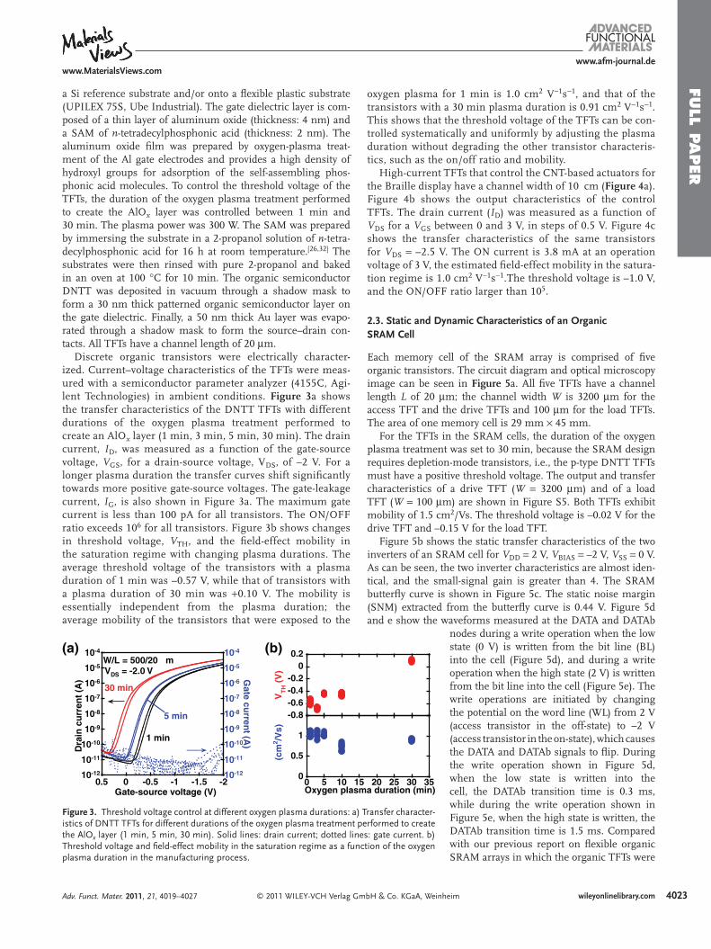
Discrete organic transistors were electrically character-ized. Current–voltage characteristics of the TFTs were meas-ured with a semiconductor parameter analyzer (4155C, Agi-lent Technologies) in ambient conditions. Figure 3 a shows the transfer characteristics of the DNTT TFTs with different durations of the oxygen plasma treatment performed to create an AlO x layer (1 min, 3 min, 5 min, 30 min). The drain current, I D , was measured as a function of the gate-source voltage, V GS , for a drain-source voltage, V DS , of –2 V. For a longer plasma duration the transfer curves shift signifi cantly towards more positive gate-source voltages. The gate-leakage current, I G , is also shown in Figure 3 a. The maximum gate current is less than 100 pA for all transistors. The ON/OFF ratio exceeds 10 6 for all transistors. Figure 3 b shows changes in threshold voltage, V TH , and the fi eld-effect mobility in the saturation regime with changing plasma durations. The average threshold voltage of the transistors with a plasma duration of 1 min was –0.57 V, while that of transistors with a plasma duration of 30 min was + 0.10 V. The mobility is essentially independent from the plasma duration; the average mobility of the transistors that were exposed to the
© 2011 WILEY-VCH Verlag GmAdv. Funct. Mater. 2011, 21, 4019–4027
Figure 3 . Threshold voltage control at different oxygen plasma durations: a) istics of DNTT TFTs for different durations of the oxygen plasma treatment pthe AlO x layer (1 min, 5 min, 30 min). Solid lines: drain current; dotted lineThreshold voltage and fi eld-effect mobility in the saturation regime as a funcplasma duration in the manufacturing process.
)b()a(
10-12
10-11
10-10
10-9
10-8
10-7
10-6
10-5
10-4
10-12
10-11
10-10
10-9
10-8
10-7
10-6
10-5
10-4
-2-1.5-1-0.500.5
Dra
in c
urr
en
t (A
) Gate
cu
rren
t (A)
Gate-source voltage (V)
VDS
= -2.0 V
W/L = 500/20 µm
30 min
5 min
1 min
-0.8
-0.6
-0.4
-0.2
0
0.2
VT
H (
V)
0
0.5
1
0 5 10 15
µ (c
m2/V
s)
Oxygen plasm
oxygen plasma for 1 min is 1.0 cm 2 V − 1 s − 1 , and that of the transistors with a 30 min plasma duration is 0.91 cm 2 V − 1 s − 1 . This shows that the threshold voltage of the TFTs can be con-trolled systematically and uniformly by adjusting the plasma duration without degrading the other transistor characteris-tics, such as the on/off ratio and mobility.
High-current TFTs that control the CNT-based actuators for the Braille display have a channel width of 10 cm ( Figure 4 a). Figure 4 b shows the output characteristics of the control TFTs. The drain current ( I D ) was measured as a function of V DS for a V GS between 0 and 3 V, in steps of 0.5 V. Figure 4 c shows the transfer characteristics of the same transistors for V DS = –2.5 V. The ON current is 3.8 mA at an operation voltage of 3 V, the estimated fi eld-effect mobility in the satura-tion regime is 1.0 cm 2 V − 1 s − 1 .The threshold voltage is –1.0 V, and the ON/OFF ratio larger than 10 5 .
2.3. Static and Dynamic Characteristics of an Organic SRAM Cell
Each memory cell of the SRAM array is comprised of fi ve organic transistors. The circuit diagram and optical microscopy image can be seen in Figure 5 a. All fi ve TFTs have a channel length L of 20 μ m; the channel width W is 3200 μ m for the access TFT and the drive TFTs and 100 μ m for the load TFTs. The area of one memory cell is 29 mm × 45 mm.
For the TFTs in the SRAM cells, the duration of the oxygen plasma treatment was set to 30 min, because the SRAM design requires depletion-mode transistors, i.e., the p-type DNTT TFTs must have a positive threshold voltage. The output and transfer characteristics of a drive TFT ( W = 3200 μ m) and of a load TFT ( W = 100 μ m) are shown in Figure S5. Both TFTs exhibit mobility of 1.5 cm 2 /Vs. The threshold voltage is –0.02 V for the drive TFT and –0.15 V for the load TFT.
Figure 5 b shows the static transfer characteristics of the two inverters of an SRAM cell for V DD = 2 V, V BIAS = –2 V, V SS = 0 V. As can be seen, the two inverter characteristics are almost iden-tical, and the small-signal gain is greater than 4. The SRAM butterfl y curve is shown in Figure 5 c. The static noise margin (SNM) extracted from the butterfl y curve is 0.44 V. Figure 5 d and e show the waveforms measured at the DATA and DATAb
bH & Co. KGaA, Wein
Transfer character-erformed to create s: gate current. b) tion of the oxygen
20 25 30 35a duration (min)
nodes during a write operation when the low state (0 V) is written from the bit line (BL) into the cell (Figure 5 d), and during a write operation when the high state (2 V) is written from the bit line into the cell (Figure 5 e). The write operations are initiated by changing the potential on the word line (WL) from 2 V (access transistor in the off-state) to –2 V (access transistor in the on-state), which causes the DATA and DATAb signals to fl ip. During the write operation shown in Figure 5 d, when the low state is written into the cell, the DATAb transition time is 0.3 ms, while during the write operation shown in Figure 5 e, when the high state is written, the DATAb transition time is 1.5 ms. Compared with our previous report on fl exible organic SRAM arrays in which the organic TFTs were
heim 4023wileyonlinelibrary.com

FULL
PAPER
4024
www.afm-journal.dewww.MaterialsViews.com
Figure 4 . Operation of the integrated Braille display: a) A picture of an organic transistor active matrix. b) Output characteristics of a high-current organic TFT employed to drive a Braille dot. c) Transfer characteristics of the corresponding TFT. The TFT has a channel-width/channel-length (W/L) ratio of 5000 and provides a maximum current of more than 3 mA at 3 V. The mobility at the saturation regime is 1.0 cm 2 V − 1 s − 1 , and the ON/OFF ratio exceeds 10 5 .
)c()b(10-2 10-2
W = 10 cm L = 20 µm-4
V 3 V
1 cm 1 mm
G
S
D
(a)
3 mm
10-9
10-8
10-7
10-6
10-5
10-4
10-3
10-9
10-8
10-7
10-6
10-5
10-4
10-3
-3-2.5-2-1.5-1-0.50
Dra
in c
urr
en
t (A
) Gate
cu
rren
t (A)
Gate-source voltage (V)
VDS
= -2.5 VW = 10 cm, L = 20 µm
-3.5
-3
-2.5
-2
-1.5
-1
-0.5
0-2-1.5-1-0.50
VDS
(V)
Dra
in c
urr
en
t(m
A)
VGS
= -3 V
-2 V
-2.5 V
-1.5 V
-1 V
fabricated using a thick polyimide gate dielectric and pentacene as the semiconductor, [ 28 ] the transition time of our new SRAM design based on low-voltage DNTT TFTs is 25 times faster.
2.4. Integrated Characteristics of One CNT-Based Actuator With Control TFTs, and Organic SRAM
One actuator with a size of 1 mm × 4 mm integrating with one TFTs driver and one TFTs SRAM was characterized. The displacement of the CNT-based actuator was also measured in air using a laser displacement meter and an oscilloscope. Figures 6 a and b show voltages measured at the DATAb node and actuator’s displacement as a function of time after the SRAM word line potential was changed from 3 V to –2 V. When voltages of the word line is changed from 3 to –2 V at t = 0, the DATAb signal is pulled from a large positive voltage (approxi-mately equal to V DD ) down to 0 V, which causes the control TFT to turn on, which in turn causes the actuator and the Braille dot to move upward. For the bias condition V DD = V PL = –4 V, a displacement of 300 μ m was measured, which is large enough for a blind person to recognize. The time required to produce a displacement of 300 μ m is 6 s at V DD = V PL = –4 V and 2.9 s at V DD = V PL = –4.5 V.
© 2011 WILEY-VCH Verlag Gmwileyonlinelibrary.com
The operating speed of the actuators is limited by the time required to charge and discharge the actuator electrodes. In order to obtain a faster response of the actuation, it is very important to increase the magnitude of the current fl ow from TFTs driver to actuators. Indeed, the operating speed of the actuators increases as the operating voltage of the TFTs driver is increased (Figure 6 b). Therefore, the use of DNTT as p-type semiconductors and large W / L ratio of the TFTs driver facili-tates the increase in the response time of the actuators.
3. Discussion
The DNTT TFTs exhibit very good air stability because of the large ionization potential of DNTT (5.4 eV). [ 30 , 31 , 33 ] Transfer characteristics as well as threshold voltage, mobility, and on/off ratio were essentially unchanged after the devices were exposed to ambient air for 170 days (Figure S4).
Not only the magnitude of the displacement, but also the dispersion of the displacement of the actuators is important to recognize correctly whether the individual dots are up or down. The SAM dielectrics can be formed quite uniform layers without any technical control, [ 23 ] so the dispersion of the TFTs using SAM as dielectrics will be very small. [ 23 ] Indeed, the
bH & Co. KGaA, Weinheim Adv. Funct. Mater. 2011, 21, 4019–4027

FULL P
APER
www.afm-journal.dewww.MaterialsViews.com
1.5
2-5
-4
3
ge (
V)
1.5
2
TA
(V
)
)c()b(
Drive TFT Access TFT(a)
1 µm
Load TFT
400 µm
Drain electrode
DNTT
Gate electrode
Source electrode
0
0.5
1
1.5
2
2.5
-1 0 1 2 3 4 5 6 7
Vo
lta
ge (
V)
Time (msec)
WL 2 to -2 V, BL = 2 V
DATA
DATA b0
0.5
1
1.5
2
2.5
-1 -0.5 0 0.5 1 1.5 2
Vo
ltag
e (
V)
Time (msec)
WL 2 to -2 V, BL = 0 V
DATA
DATA b
0
0.5
1
-3
-2
-1
00 0.5 1 1.5 2
Ou
tpu
t vo
lta
Input voltage (V)
Gain
VSS
= 0 V
VDD
= 2 V
VBIAS
= -2 V
0
0.5
1
0 0.5 1 1.5 2
DA
TA
b, D
AT
DATA, DATAb (V)
VSS
= 0 V
VDD
= 2 V
VBIAS
= -2 V
)e()d(
Figure 5 . Static and dynamic characteristics of an organic SRAM cell. a) Optical microscopy image of an organic SRAM cell. The minimum feature size is 20 μ m. b) Static transfer characteristics of the two inverters of an SRAM cell. c) Butterfl y curve of an SRAM cell. The static noise margin extracted from the curve is 0.44 V. d) Measured DATA and DATAb waveforms during a write operation with a low bit line (BL) signal (0 V). The programming time, taken as the time until DATAb reaches 90% of the target potential, is 0.3 ms. e) Measured DATA and DATAb waveforms during a write operation with a high bit line signal (2 V). The programming time, taken as the time until DATAb reaches 90% of the target potential, is 1.5 ms.
control TFTs showed large current and low leakage current even though the TFTs have quite large channel width and very thin gate dielectrics less than 10 nm. This result demonstrates the high insulation property and the high uniformity of the SAM dielectrics. Furthermore, it is reported that the TFTs using DNTT as organic semiconductors have high air stability, [ 31 ] so the present device can be operational in the air conditions for a long time.
© 2011 WILEY-VCH Verlag GmAdv. Funct. Mater. 2011, 21, 4019–4027
Previous works for organic and/or molecular memories were motivated for realizing cost-effective, high-density media mem-ories. For this reason, almost all organic memories reported thus far are non-volatile memories: e.g., organic ferroelec-tric random access memory (FeRAM), [ 4–7 ] resistance random access memory (ReRAM), [ 8 , 9 ] and charge trap memory. [ 10 ] In addition to intensive efforts toward cheap organic memories, another trend is attempting to fully utilize the unique features
bH & Co. KGaA, Weinheim 4025wileyonlinelibrary.com

FULL
PAPER
4026
www.afm-journal.dewww.MaterialsViews.com
Figure 6 . Operation of the integrated Braille display. a) Potential measured at the DATAb node as a function of time after the potential on the word line (WL) was changed from 3 to –2 V at t = 0, for three different supply voltages V DD . b) Displacement of the actuator as a function of time for three different supply voltages V DD and V PL of –3.5, –4, and –4.5 V. The actuator has an area of 1 mm × 4 mm. c) Photographs of the actuator with a white Braille dot in the two static states (up and down).
0
100
200
300
400
500
-2 0 2 4 6 8 10
Dis
pla
cem
en
t (µ
m)
Time (sec)
-3.5 V
-4 V
DATAb= V PL= -4.5 V
2.9 s
6.0 s
0
1
2
3
4
5
-2 0 2 4 6 8 10
Vo
ltag
e (
V)
Time (sec)
WL = 3 to -2 V, BL 3 V V
DD= 4.5 V
4 V
3.5 V
Down Up
)b()a(
(c)
DA
TA
b s
ign
al
(V)
400 µm
4 mm
of organic memories, such as mechanical fl exibility and the ease of fabrication over large areas. Examples of new applica-tions include sheet-type Braille displays and communication systems; both are possible by distributing organic memories over a large area. [ 6 , 11 , 12 , 28 ] In these applications, the critical fea-ture required for organic memories is not non-volatility or high density but a faster programming speed.
Commercial silicon-based SRAM usually employs a comple-mentary (CMOS) design, because complementary circuits have larger noise margins and lower power consumption than uni-polar (PMOS) circuits. However, in the case of organic SRAM, complementary designs have a number of problems associ-ated with the low fi eld-effect mobility and poor air stability of organic n-channel TFTs, [ 34 , 35 ] which is the reason why we chose to implement a PMOS, rather than a complementary, SRAM.
Compared with the previously reported organic SRAM, [ 28 ] we achieved simultaneous reductions in operation voltage (from 40 V to 2 V) and programming time (from 40 ms to 2 ms). These substantial improvements are due to the high capaci-tance of the gate dielectric based on oxygen-plasma-grown AlO x and a SAM of n-tetradecylphosphonic acid, and the large fi eld-effect mobility of the organic semiconductor DNTT. Indeed, the same combination of AlO x /SAM gate dielectric and DNTT has led to the realization of organic ring oscillators with a signal delay per stage of 37 μ s at 3 V. [ 31 ]
In addition to the high mobility, good uniformity, and good air stability of the organic TFTs, the systematic control of the threshold voltage, which was demonstrated in this study, was critical for the low-voltage SRAM design. The threshold-voltage control provided a good balance for the switching characteristics
© 2011 WILEY-VCH Verlag Gwileyonlinelibrary.com
of the inverters in the organic SRAM, so that a large static noise margin (SNM) of 0.44 was obtained at fairly low operating volt-ages without the necessity for a double-gate process. [ 28 , 36 ]
The main motivation for integrating each actuator of the Braille display with a memory cell is to reduce the time required to address a large number of Braille dots. If an individual Braille dot is controlled only by a transistor, then the time to produce a displacement of 300 μ m is 1.8 s at 4 V, as shown in Figure S6. For a display composed of 144 Braille dots (12 × 12 array), the time to change all Braille dots ( T all ) would thus be 21.6 s. When the SRAM array is added, T all is the sum of the time required to program all 144 cells of the SRAM array plus the time required to change one Braille dot. Therefore, T all is reduced to 2.91 s, because all 144 Braille dots are actuated simultaneously once the data are written into the SRAM array. Although the oper-ating speed for a single actuator controlled by a transistor and an SRAM cell is slightly slower than the operating speed for a single actuator controlled only by a transistor, the fast SRAM programming speed (1.5 ms) enables a fast response of the Braille dot array.
In principle, the Braille display may be realized using an alternative memory concept, such as charge-trap memory or dynamic random access memory (DRAM). The main drawback of organic charge-trap memories is that they usually require either a large programming voltage or a long programming time (e.g., 6 V and 1 s, as in reference 9). The main problem with organic DRAM is that the rate at which the charge leaks away from the capacitor would be higher than the maximum possible refresh rate. Therefore, organic SRAM is a unique solu-tion to achieve fast programming speeds and low programming
mbH & Co. KGaA, Weinheim Adv. Funct. Mater. 2011, 21, 4019–4027

FULL P
APER
www.afm-journal.dewww.MaterialsViews.com
voltages simultaneously. A typical drawback of SRAM is the relatively large area requirement, due to the large number of devices per memory cell. However, unlike in silicon technology, where real estate is very expensive, the integration density in fl exible large-area electronics applications is much smaller, so that the large area of SRAM is not really a drawback here.
Supporting Information Supporting Information is available from the Wiley Online Library or from the author.
Acknowledgements This study was partially supported by JST/CREST, NEDO, Special Coordination Funds for Promoting Science and Technology, and the Global COE Program on Physical Sciences Frontier, MEXT Japan.
Received: July 5, 2011Published online: September 19, 2011
[ 1 ] D. Gebeyehu , C. J. Brabec , F. Padinger , T. Fromherz , J. C. Hummelen , D. Badt , H. Schindler , N. S. Sariciftci , Synth. Met. , 2001 , 118 , 1 .
[ 2 ] B. Crone , A. Dodabalapur , Y.-Y. Lin , R. W. Filas , Z. Bao , A. LaDuca , R. Sarpeshkar , H. E. Katz , W. Li , Nature 2000 , 403 , 521 .
[ 3 ] T. Someya , Y. Kato , T. Sekitani , S. Iba , Y. Noguchi , Y. Murase , H. Kawaguchi , T. Sakurai , Proc. Natl. Acad. Sci. USA 2005 , 102 , 1 2321 .
[ 4 ] C. A. Nguyen , S. G. Mhaisalkar , J. Ma , P. S. Lee , Org. Electron. 2008 , 9 , 1087 .
[ 5 ] K. H. Lee , G. Lee , K. Lee , M. S. Oh , S. Im , Appl. Phys. Lett , 2009 , 94 , 093304 .
[ 6 ] T. Sekitani , K. Zaitsu , Y. Noguchi , K. Ishibe , M. Takamiya , T. Sakurai , T. Someya , IEEE Trans. Electron Devices 2009 , 56 , 1027 .
[ 7 ] K. Zaitsu , S. Lee , K. Ishibe , T. Sekitani , T. Someya , J. Appl. Phys. 2010 , 107 , 114506 .
[ 8 ] K. Asadi , D. M. de Leeuw , B. de Boer , P. W. M. Blom , Nat. Mater. 2008 , 7 , 547 .
[ 9 ] J. Ouyang , C. W. Chu , C. R. Szmanda , L. Mai , A. Yang , Nat. Mater. 2004 , 3 , 918 .
[ 10 ] T. Sekitani , T. Yokota , U. Zschieschang , H. Klauk , S. Bauer , K. Takeuchi , M. Takamiya , T. Sakurai , T. Someya , Science 2009 , 326 , 1516 .
[ 11 ] T. Sekitani , M. Takamiya , Y. Noguchi , S. Nakano , Y. Kato , T. Sakurai , T. Someya , Nat. Mater. 2007 , 6 , 413 .
© 2011 WILEY-VCH Verlag GAdv. Funct. Mater. 2011, 21, 4019–4027
[ 12 ] Y. Kato , T. Sekitani , M. Takamiya , M. Doi , K. Asaka , T. Sakurai , T. Someya , IEEE Trans. Electron Devices 2007 , 54 , 202 .
[ 13 ] N. Fujiwara , K. Asaka , Y. Nishimura , K. Oguro , E. Torikai , Chem. Mater. , 2000 , 12 , 1750 .
[ 14 ] K. Fukuda , T. Sekitani , T. Someya , Appl. Phys. Lett. 2009 , 95 , 023302 .
[ 15 ] K. Mukai , K. Asaka , T. Sugino , K. Kiyohara , I. Takeuchi , N. Terasawa , D. N. Futaba , K. Hata , T. Fukushima , T. Aida , Adv. Mater. 2009 , 21 , 1582 .
[ 16 ] S. Y. Yang , S. H. Kim , K. Shin , H. Jeon , C. E. Park , Appl. Phys. Lett. 2006 , 88 , 173507 .
[ 17 ] M. E. Roberts , S. C. B. Mannsfeld , N. Queraltó , C. Reese , J. Locklin , W. Knoll , Z. Bao , Proc. Natl. Acad. Sci. USA 2008 , 105 , 1 2134 .
[ 18 ] S. A. DiBenedetto , D. Frattarelli , M. A. Ratner , A. Facchetti , T. J. Marks , J. Am. Chem. Soc. 2008 , 130 , 7528 .
[ 19 ] M. H. Yoon , A. Facchetti , T. J. Marks , Proc. Natl. Acad. Sci. USA 2005 , 102 , 4678 .
[ 20 ] M. Kitamura , Y. Arakawa , Appl. Phys. Lett. 2007 , 91 , 053505 . [ 21 ] A. L. Deman , J. Tardy , Org. Electron. 2005 , 6 , 78 . [ 22 ] J. Ho Cho , J. Lee , Y. Xia , B. Kim , Y. He , M. J. Renn , T. P. Lodge ,
C. D. Frisbie , Nat. Mater. 2008 , 7 , 900 . [ 23 ] H. Klauk , U. Zschieschang , J. Pfl aum , M. Halik , Nature 2007 , 445 ,
745 . [ 24 ] T. Sekitani , Y. Noguchi , U. Zschieschang , H. Klauk , T. Someya , Proc
Natl. Acad. Sci. USA 2008 , 105 , 4976 . [ 25 ] K. Fukuda , T. Hamamoto , T. Yokota , T. Sekitani , U. Zschieschang ,
H. Klauk , T. Someya , Appl. Phys. Lett. 2009 , 95 , 203301 . [ 26 ] K. Fukuda , T. Yokota , K. Kuribara , T. Sekitani , U. Zschieschang ,
H. Klauk , T. Someya , Appl. Phys. Lett. 2010 , 96 , 053302 . [ 27 ] T. C. Huang , K. Fukuda , C. M. Lo , Y. H. Yeh , T. Sekitani , T. Someya ,
K. T. Cheng , IEEE Trans. Electron Devices 2011 , 58 , 141 . [ 28 ] M. Takamiya , T. Sekitani , Y. Kato , H. Kawaguchi , T. Someya ,
T. Sakurai , IEEE J. Solid-State Circuits 2007 , 42 , 93 . [ 29 ] U. Kraft , U. Zschieschang , F. Ante , D. Kälblein , C. Kamella ,
K. Amsharov , M. Jansen , K. Kern , E. Weber , H. Klauk , J. Mater. Chem. 2010 , 20 , 6416 .
[ 30 ] S. Haas , Y. Takahashi , K. Takimiya , T. Hasegawa , Appl. Phys. Lett. 2009 , 95 , 022111 .
[ 31 ] U. Zschieschang , T. Yamamoto , K. Takimiya , H. Kuwabara , M. Ikeda , T. Sekitani , T. Someya , H. Klauk , Adv. Mater. 2010 , 22 , 982 .
[ 32 ] Y. T. Tao , J. Am. Chem. Soc. 1993 , 115 , 4350 . [ 33 ] K. Takimiya , T. Yamamoto , H. Ebata , T. Izawa , Sci. Technol. Adv.
Mater. 2007 , 8 , 273 . [ 34 ] Z. Bao , A. J. Lovinger , J. Brown , J. Am. Chem. Soc. 1998 , 120 , 207 . [ 35 ] M. M. Ling , Z. Bao , Org. Electron. 2006 , 7 , 568 . [ 36 ] S. Iba , T. Sekitani , Y. Kato , T. Someya , H. Kawaguchi , M. Takamiya ,
T. Sakurai , S. Takagi , Appl. Phys. Lett. 2005 , 87 , 023509 .
mbH & Co. KGaA, Weinheim 4027wileyonlinelibrary.com

1
Supporting Information
A 4 V operation, flexible Braille display using organic transistors,
carbon nanotube actuators, and organic SRAM
Kenjiro Fukuda1§, Tsuyoshi Sekitani
2, Ute Zschieschang
3, Hagen Klauk
3, Kazunori
Kuribara1, Tomoyuki Yokota
1, Takushi Sugino
4, Kinji Asaka
4, Masaaki Ikeda
5, Hirokazu
Kuwabara5, Tatsuya Yamamoto
6, Kazuo Takimiya
6, Takanori Fukushima
7, Takuzo Aida
8,
Makoto Takamiya9, Takayasu Sakurai
10,
Takao Someya1,2,11,12*
1Department of Applied Physics, The University of Tokyo, 7-3-1 Hongo, Bunkyo-ku,
Tokyo 113-8656, Japan
2Department of Electrical and Electronic Engineering, The University of Tokyo, 7-3-1
Hongo, Bunkyo-ku, Tokyo 113-8656, Japan
3Max Planck Institute for Solid State Research, Heisenbergstr. 1, 70569 Stuttgart,
Germany
4Research Institute for Cell Engineering, National Institute of Advanced Industrial
Science and Technology (AIST), Midorigaoka 1-8-31, Ikeda, Osaka 563-8577, Japan
5Functional Chemicals R&D Laboratories, Nippon Kayaku Co., Ltd. 3-26-8, Shimo,
Kita-ku, Tokyo, 115-8588, Japan
6Department of Applied Chemistry, Hiroshima University, 1-4-1, Kagamiyama,

2
Higashi-Hiroshima,Hiroshima, 739-8527, Japan
7Functional Soft Matter Engineering Laboratory, Advanced Science Institute, RIKEN,
2-1 Hirosawa,Wako, Saitama, 351-0198, Japan
8Department of Chemistry and Biotechnology, The University of Tokyo, 7-3-1, Hongo,
Bunkyo-ku, Tokyo, 113-8656, Japan
9VLSI Design & Education Center, The University of Tokyo, 4-6-1, Komaba,
Meguro-ku, Tokyo, 153-8505, Japan
10Institute of Industrial Science, The University of Tokyo, 4-6-1, Komaba, Meguro-ku,
Tokyo, 153-8505, Japan
11Institute for Nano Quantum Information Electronics, The University of Tokyo, 4-6-1,
Komaba, Meguro-ku, Tokyo, 153-8505, Japan
12Core Research for Evolutional Science and Technology, Sanban-cho Bldg, 4F, 5,
Sanban-cho, Chiyoda-ku, Tokyo, 102-0075 Japan
§ Presently, Research Center for Organic Electronics, Yamagata University, 4-3-16,
Jonan, Yonezawa, Yamagata, 992-8510, Japan
Correspondence and requests for materials should be addressed to T.S. (Takao Someya),
Department of Electrical and Electronic Engineering, School of Engineering, the
University of Tokyo
7-3-1 Hongo, Bunkyo-ku, Tokyo 113-8656, JAPAN
Telephone: +81-3-5841-6756 Fax: +81-3-5841-6709

3
1. Carbon nanotube (CNT) based actuator (Fig. S1-S3)
1.1 Fabrication process (Fig. S1, S2)
The manufacturing process and pictures are shown in Fig. S1. Detailed explanations of
the process flow may be found in the main text. As shown in the figures, the CNTs and
polymers were uniformly dispersed in the solvents through the processes of stirring with
an ionic liquid. Fig. S2 shows a cross-sectional image taken using scanning electron
microscope (SEM, S4800, Hitachi high-technologies), where interfaces between
electrodes and electrolytes in the CNT based actuators can be seen. After the pressure
bonding process with heating at 70 °C, the polymer the polymers in the three layers
were connected over the layer though the CNTs did not penetrate from electrode to the
electrolyte.
1.2 Mechanical characteristics (Fig. S3)
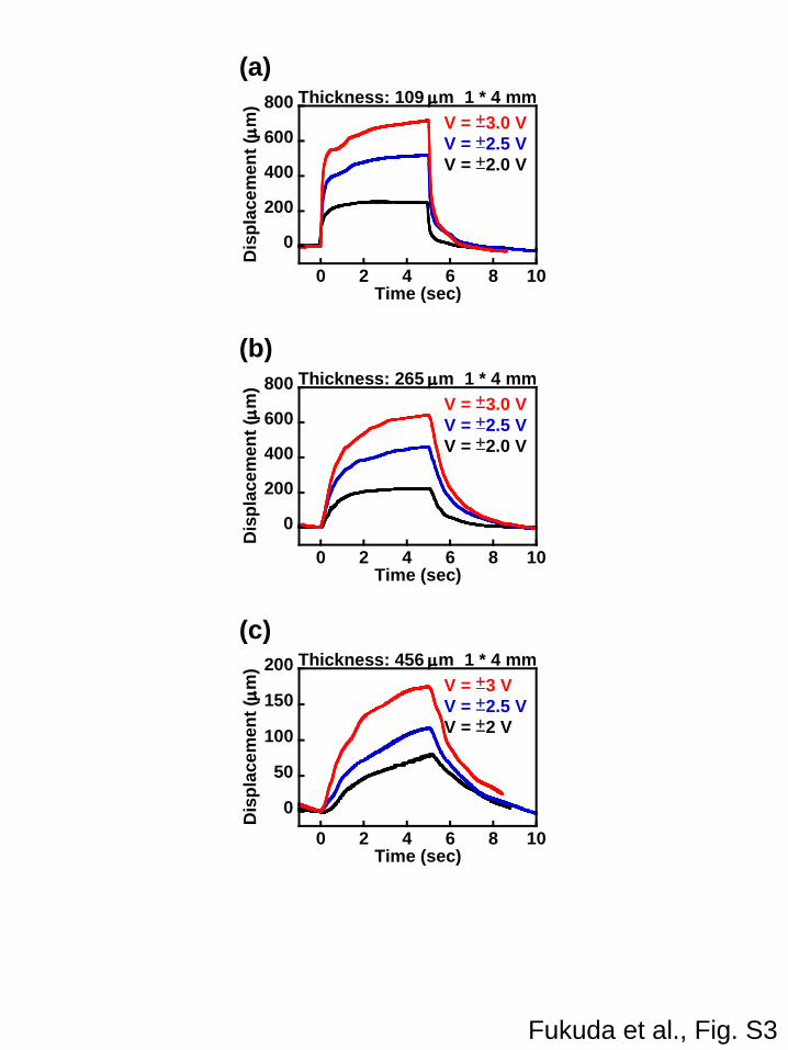
We measured displacements of the actuator using laser displacement meter (KEYENCE,
LE-4000) and an oscilloscope (Agilent, DSO6054A). Figure S3 shows the displacement
as a function of time. CNT actuators with different thicknesses of 109 µm, 265 µm, and
456 µm can be seen Figs.S3a, b, and c, respectively. The actuator size was 1 × 4 mm2.
The input voltage changed from ±2.0 V to ±3.0 V. For all actuators, the displacement
increased as increasing the input voltage from ±2.0 V to ±3.0 V. For the actuator whose
thickness was 109 µm, the displacement increased from 250 to 720 µm as increasing the

4
input voltage from ±2.0 V to ±3.0 V. These results indicate the displacement of the
actuator can be controlled by changing operational voltages and the thickness.
2. Air stability of DNTT TFTs (Fig. S4)
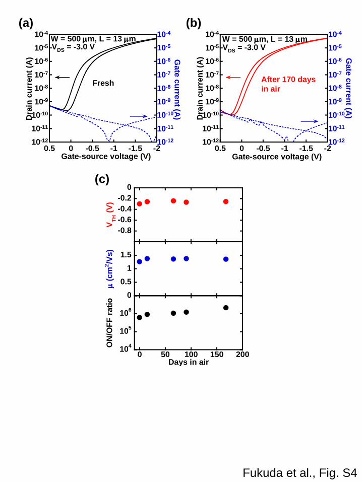
Figure S4a shows current–voltage characteristics of a DNTT TFT on a Si/SiO2 substrate
measured immediately after exposure to ambient air. The TFT exhibited a mobility of
1.3 cm2/Vs, a threshold voltage of –0.3 V, and an on/off current ratio of 10
5. Figure S4b
shows the characteristics of the same transistor measured after 6 months (170 days)
stored in ambient air; whose mobility is 1.4 cm2/Vs, threshold voltage is –0.26 V, and
on/off current ratio is 105. Figure S4c shows changes in threshold voltage, mobility, and
on/off ratio as time passed in air. The TFT characteristics are almost the same even after
170 days in air, which indicates the excellent air stability of the DNTT p-channel TFTs.
3. Electrical characteristics of organic SRAM (Fig. S5, S6)
3.1 Output characteristics of DNTT TFTs in an SRAM cell (Fig. S5)
The output characteristics of the drive and load TFTs in an SRAM cell are shown in
Figure S5a and b, respectively. These pictures can be seen in Fig. 5 in the main text. The
drain current ID was measured as a function of the drain-source voltage VDS for
gate-source voltages VGS between 0 to –2 V in steps of 0.5 V. We found a linear increase
in drain current ID at small VDS, which indicates that the contact resistance between the
DNTT semiconductor and the gold source/drain contacts is negligibly small.

5
3.2 Retention characteristic of the SRAM (Fig. S6)
A retention characteristic of the SRAM was measured in air. The measurement
procedure was as follows: First, a voltage of –2 V was applied to the word line (WL)
and then a voltage of -2 V or 0 V was applied to the bit line, to realize the Low state or
the High state in the SRAM cell. Second, the WL was connected to 0 V. Finally, the
supply voltage VDD was kept constant at –2 V, and the voltage at DATAb was monitored.
Figure S6 shows the of DATAb voltage over time. The stored information is stable for
about 500 sec.
4. Displacement of CNT-based actuators with control TFTs (Fig. S7)
Figure S7a shows the schematic of an actuator integrated with organic TFT that can
drive large channel currents. Figure S7b shows time-dependent displacement of the
actuator having a size of 1 × 4 mm2 when controlled by the TFT. A square-wave signal
with an amplitude of 2 V and a frequency of 0.1 Hz was applied to the drain contact of
the TFT, and the displacement of the actuator was measured as a function of time for
various TFT gate-source voltages (VGS; ranging from –2.5 V to –4 V). The maximum
displacement increases monotonically with increasing VGS, from 210 µm at VGS = –2.5
V to 450 µm at VGS = –4 V. The time required to produce a displacement of 300 µm is
1.8 sec at VGS = –4 V; under these bias conditions the current reaches a maximum of 3.9
mA.
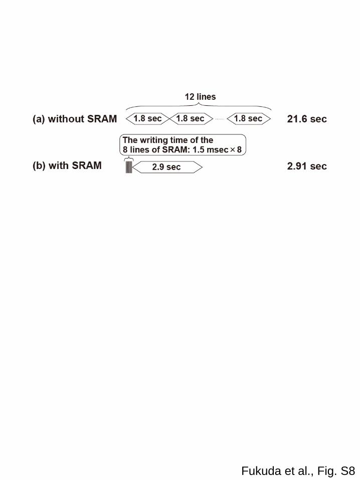
5. Minimum frame time of a Braille display with 12 rows and 12 column (Fig. S8)
Figure S6 summarizes estimated time required to address 144 Braille dots arranged in
12 rows and 12 columns with and without the assistance of an organic SRAM array.
6
Without the SRAM array the 12 rows must addressed sequentially, i.e. one after the
other. Addressing one row takes 1.8 sec (assuming a minimum displacement of 300 µm),
so the total time required to address all 12 rows with all 144 dots (i.e., the frame time) is
21.6 sec. When the Braille dot array is equipped with an SRAM array, all the data are
first programmed into the SRAM array and then all 144 Braille dots are addressed
simultaneously using the information stored in the SRAM array, so the frame time is
significantly shorter, only 2.91 sec. This clearly shows the significant benefit of
combining the Braille display with an SRAM array.

Carbon nanotube(CNT)50 mg
CNT disperasedgel
CNT disperasedgel
CNT electrode
Stirr for 3 days, at room temperature with DMAc 4 ml& Sonicate for 1 day
Add DMAc 5 ml, then Stirr for 1 days, at room temperature& Sonicate for 1 day
Casting on 20 mm by 20 mm moldDrying on hotplate, 50 C for 1 daythen Vacuum oven, 80 C for 3 days
Et MeN N
BF4
120 mg
Ionic liquid(EMI-BF4)
CH2 CF2
CF20.88 0.12
nCF
CF3
80 mg
Polymer(PVDF-HFP)
o
o
o
Gelatinousmixture
Electrolyte
CNT-based actuator
Et MeN N
BF4
100 mg
Ionic liquid(EMI-BF4)
CH2 CF2
CF20.88 0.12
nCF
CF3
100 mg
Polymer(PVDF-HFP)
Casting on 20 mm by 20 mm moldDrying on hotplate, 50 C for 1 daythen Vacuum oven, 80 C for 3 days
Press 90 N at 70 C for 90 sec,270 N at 70 C for 90 seco
o
Stirr for 1 day, at 70 C sandbathwith MP 3 ml and PC 0.25 g& Sonicate for 1 day
o
o
Fukuda et al., Fig. S1

Electrolyte Electrode
Fukuda et al., Fig. S2
0
50
100
150
200
0 2 4 6 8 10
Dis
pla
ce
men
t (
m)
Time (sec)
V = 3 V
V = 2.5 V
V = 2 V
1 * 4 mmThickness: 456 m
0
200
400
600
800
0 2 4 6 8 10
Dis
pla
ce
men
t (
m)
Time (sec)
V = 3.0 V
V = 2.5 V
V = 2.0 V
1 * 4 mmThickness: 265 m
0
200
400
600
800
0 2 4 6 8 10
Dis
pla
ce
men
t (
m)
Time (sec)
V = 3.0 V
V = 2.5 V
V = 2.0 V
1 * 4 mmThickness: 109 m
(a)
(b)
(c)
Fukuda et al., Fig. S3
10-12
10-11
10-10
10-9
10-8
10-7
10-6
10-5
10-4
10-12
10-11
10-10
10-9
10-8
10-7
10-6
10-5
10-4
-2-1.5-1-0.500.5
Dra
in c
urr
en
t (A
) Ga
te c
urre
nt (A
)
Gate-source voltage (V)
VDS = -3.0 VW = 500 m, L = 13 m
Fresh
10-12
10-11
10-10
10-9
10-8
10-7
10-6
10-5
10-4
10-12
10-11
10-10
10-9
10-8
10-7
10-6
10-5
10-4
-2-1.5-1-0.500.5
Dra
in c
urr
en
t (A
) Gate
cu
rren
t (A)
Gate-source voltage (V)
VDS = -3.0 VW = 500 m, L = 13 m
After 170 days
in air
0
0.5
1
1.5
(
cm
2/V
s)
-0.8
-0.6
-0.4
-0.2
0
VT
H (
V)
104
105
106
0 50 100 150 200
ON
/OF
F r
ati
o
Days in air
(a) (b)
(c)
Fukuda et al., Fig. S4

-200
-150
-100
-50
0-2-1.5-1-0.50
Drain-source voltage (V)
Dra
in c
urr
en
t (
A)
VGS = -2 V
-1 V
-1.5 V
-0.5 V
Drive TFT
W = 3200 m, L = 20 m
-5
-4
-3
-2
-1
0-2-1.5-1-0.50
Drain-source voltage (V)
Dra
in c
urr
en
t (
A)
VGS = -2 V
-1 V
-1.5 V
-0.5 V
Load TFTW = 100 m, L = 20 m
Fukuda et al., Fig. S5
(a)
(b)
10-12
10-10
10-8
10-6
10-4
10-2
10-12
10-10
10-8
10-6
10-4
10-2
-2-1.5-1-0.500.5
Dra
in c
urr
en
t (A
) Gate
cu
rren
t (A)
Gate-source voltage (V)
VDS = -2 VW/L = 3200/20 m
100/20 m
(c)

0
0.5
1
1.5
2
1 10 100 1000
DA
TA
b s
ign
al
(V)
Time (s)
BL = 0 V
BL = 2 V
Fukuda et al., Fig. S6

0
100
200
300
400
500
15 20 25 30 35
Dis
pla
cem
en
t (
m)
Time (sec)
VDS=-2~2 V
VGS = -2.5 V
-3 V-3.5 V-4 V
(b)
-4
-2
0
2
4
15 20 25 30 35
Cu
rren
t (m
A)
Time (sec)
VGS = -2.5 V
VDS = -2~2 V
-3 V-3.5 V
-4 V
(c)
Fukuda et al., Fig. S7
(a)
Fukuda et al., Fig. S8