SPFD5408B - Intelligent Display Solutions
84
ORISE Technology reserves the right to change this documentation without prior notice. Information provided by ORISE Technology is believed to be accurate and reliable. However, ORISE Technology makes no warranty for any errors which may appear in this document. Contact ORISE Technology to obtain the latest version of device specifications before placing your order. No responsibility is assumed by ORISE Technology for any infringement of patent or other rights of third parties which may result from its use. In addition, ORISE products are not authorized for use as critical components in life support devices/ systems or aviation devices/systems, where a malfunction or failure of the product may reasonably be expected to result in significant injury to the user, without the express written approval of ORISE. Preliminary DEC. 24, 2007 Version 0.4 S S P P F F D D 5 5 4 4 0 0 8 8 B B 720-channel 6-bit Source Driver with System-on-chip for Color Amorphous TFT-LCDs
-
Upload
khangminh22 -
Category
Documents
-
view
4 -
download
0
Transcript of SPFD5408B - Intelligent Display Solutions

ORISE Technology reserves the right to change this documentation without prior notice. Information provided by ORISE Technology is believed to be accurate and reliable. However, ORISE Technology makes no warranty for any errors which may appear in this document. Contact ORISE Technology to obtain the latest version of device specifications before placing your order. No responsibility is assumed by ORISE Technology for any infringement of patent or other rights of third parties which may result from its use. In addition, ORISE products are not authorized for use as critical components in life support devices/ systems or aviation devices/systems, where a malfunction or failure of the product may reasonably be expected to result in significant injury to the user, without the express written approval of ORISE.
PPrreelliimmiinnaarryy
DEC. 24, 2007
Version 0.4
SSPPFFDD55440088BB772200--cchhaannnneell 66--bbiitt SSoouurrccee DDrriivveerr wwiitthh SSyysstteemm--oonn--cchhiipp ffoorr CCoolloorr AAmmoorrpphhoouuss TTFFTT--LLCCDDss

PPrreelliimmiinnaarryy SPFD5408B
© ORISE Technology Co., Ltd. Proprietary & Confidential
2 DEC. 24, 2007Preliminary Version: 0.4
Table of Contents PAGE
1. GENERAL DESCRIPTION .......................................................................................................................................................................... 5 2. FEATURE .................................................................................................................................................................................................... 5 3. ORDERING INFORMATION........................................................................................................................................................................ 5 4. BLOCK DIAGRAM ...................................................................................................................................................................................... 6 5. SIGNAL DESCRIPTIONS............................................................................................................................................................................ 8 6. INSTRUCTIONS........................................................................................................................................................................................ 12
6.1. OUTLINE.............................................................................................................................................................................................. 12 6.2. INSTRUCTION....................................................................................................................................................................................... 13
6.2.1. Index Register (IR) ............................................................................................................................................................... 14 6.2.2. ID Read Register (SR) ......................................................................................................................................................... 14 6.2.3. Driver Output Control Register (R01h) ................................................................................................................................. 14 6.2.4. LCD Driving Waveform Control (R02h) ................................................................................................................................ 15 6.2.5. Entry Mode (R03h) ............................................................................................................................................................... 15 6.2.6. Scaling Control register (R04h) ............................................................................................................................................ 16 6.2.7. Display Control (R07h) ......................................................................................................................................................... 16 6.2.8. Display Control 2 (R08h) ...................................................................................................................................................... 17 6.2.9. Display Control 3 (R09h) ...................................................................................................................................................... 18 6.2.10. Frame Cycle Control (R0Ah) ................................................................................................................................................ 19 6.2.11. External Display Interface Control 1 (R0Ch) ........................................................................................................................ 20 6.2.12. Frame Maker Position (R0Dh).............................................................................................................................................. 21 6.2.13. External Display Interface Control 2 (R0Fh) ........................................................................................................................ 21 6.2.14. Power Control 1 (R10h)........................................................................................................................................................ 22 6.2.15. Power Control 2 (R11h)........................................................................................................................................................ 23 6.2.16. Power Control 3 (R12h)........................................................................................................................................................ 24 6.2.17. Power Control 4 (R13h)........................................................................................................................................................ 25 6.2.18. GRAM Address Set (Horizontal Address) (R20h)................................................................................................................. 26 6.2.19. GRAM Address Set (Vertical Address) (R21h)..................................................................................................................... 26 6.2.20. Write Data to GRAM (R22h)................................................................................................................................................. 27 6.2.21. Read Data Read from GRAM (R22h)................................................................................................................................... 30 6.2.22. NVM read data 1 (R28h) ...................................................................................................................................................... 30 6.2.23. NVM read data 2 (R29h) ...................................................................................................................................................... 30 6.2.24. NVM read data 3 (R2Ah)...................................................................................................................................................... 31 6.2.25. γ Control (R30h to R3Fh) ..................................................................................................................................................... 32 6.2.26. Window Horizontal RAM Address Start (R50h) .................................................................................................................... 32 6.2.27. Window Horizontal RAM Address End (R51h) ..................................................................................................................... 32 6.2.28. Window Vertical RAM Address Start (R52h) ........................................................................................................................ 33 6.2.29. Window Vertical RAM Address End (R53h) ......................................................................................................................... 33 6.2.30. Driver Output Control (R60h) ............................................................................................................................................... 33 6.2.31. Driver Output Control (R61h) ............................................................................................................................................... 35 6.2.32. Vertical Scroll Control (R6Ah)............................................................................................................................................... 35 6.2.33. Display Position – Partial Display 1 (R80h).......................................................................................................................... 35 6.2.34. RAM Address Start – Partial Display 1 (R81h) ..................................................................................................................... 35 6.2.35. RAM Address End – Partial Display 1 (R82h) ...................................................................................................................... 36

PPrreelliimmiinnaarryy SPFD5408B
© ORISE Technology Co., Ltd. Proprietary & Confidential
3 DEC. 24, 2007Preliminary Version: 0.4
6.2.36. Display Position – Partial Display 2 (R83h).......................................................................................................................... 36 6.2.37. RAM Address Start – Partial Display 2 (R84h) ..................................................................................................................... 36 6.2.38. RAM Address End – Partial Display 2 (R85h) ...................................................................................................................... 36 6.2.39. Panel Interface Control 1 (R90h).......................................................................................................................................... 36 6.2.40. Panel Interface Control 2 (R92h).......................................................................................................................................... 37 6.2.41. Panel Interface control 3 (R93h) .......................................................................................................................................... 38 6.2.42. Panel Interface control 4 (R95h) .......................................................................................................................................... 38 6.2.43. Panel Interface Control 5 (R97h).......................................................................................................................................... 40 6.2.44. Panel Interface Control 6 (R98h).......................................................................................................................................... 41 6.2.45. Calibration Control (RA4h) ................................................................................................................................................... 41
7. GRAM ........................................................................................................................................................................................................ 42 8. INTERFACES............................................................................................................................................................................................ 44
8.1. SYSTEM INTERFACE............................................................................................................................................................................. 44 8.1.1. 80-system 18-bit interface .................................................................................................................................................... 45 8.1.2. 80-system 16-bit interface .................................................................................................................................................... 45 8.1.3. 80-system 9-bit interface ...................................................................................................................................................... 45 8.1.4. 80-system 8-bit interface ...................................................................................................................................................... 45 8.1.5. Serial Peripheral interface (SPI)........................................................................................................................................... 46
8.2. VSYNC INTERFACE............................................................................................................................................................................. 47 8.3. EXTERNAL DISPLAY INTERFACE ............................................................................................................................................................ 48
8.3.1. 6-bit RGB interface............................................................................................................................................................... 49 8.3.2. 16-bit RGB interface............................................................................................................................................................. 50 8.3.3. 18-bit RGB interface............................................................................................................................................................. 50
8.4. SEQUENCE TO SET BETWEEN SYSTEM INTERFACE AND RGB INTERFACE:................................................................................................ 51 9. DISPLAY FEATURE FUNCTION: ..................................................................................................................................................................... 52
9.1. FMARK FUNCTION: ............................................................................................................................................................................. 52 9.2. SCAN MODE FUNCTION: ....................................................................................................................................................................... 53 9.3. SCALING FUNCTION:............................................................................................................................................................................. 54 9.4. PARTIAL DISPLAY FUNCTION: ................................................................................................................................................................ 56 9.5. GAMMA CORRECTION FUNCTIONS:........................................................................................................................................................ 58
10. POWER MANAGEMENT SYSTEM: .................................................................................................................................................................. 59 11. APPLICATION CIRCUITS:............................................................................................................................................................................... 62 12. INITIAL CODE:.............................................................................................................................................................................................. 63 13. POWER ON/OFF SEQUENCE......................................................................................................................................................................... 64
13.1. POWER ON/OFF SEQUENCE DIAGRAM.................................................................................................................................................. 64 13.2. DISPLAY ON/OFF SEQUENCE: .............................................................................................................................................................. 65 13.3. SEQUENCE TO EXIT SLEEP MODE: ......................................................................................................................................................... 66
14. ELECTRICAL CHARACTERISTICS:.................................................................................................................................................................. 67 14.1. ABSOLUTE MAXIMUM RATINGS: ............................................................................................................................................................ 67 14.2. DC CHARACTERISTICS......................................................................................................................................................................... 67 14.3. AC CHARACTERISTICS......................................................................................................................................................................... 68
14.3.1. Clock Characteristics............................................................................................................................................................ 68 14.3.2. 80-System Bus Interface Timing Characteristics (18-/ 16- bit interface).............................................................................. 68 14.3.3. Clock-synchronized Serial Interface Timing Characteristics ................................................................................................ 70 14.3.4. Reset Timing Characteristics (IOVCC=1.65~3.30V)............................................................................................................ 70

PPrreelliimmiinnaarryy SPFD5408B
© ORISE Technology Co., Ltd. Proprietary & Confidential
4 DEC. 24, 2007Preliminary Version: 0.4
14.3.5. RGB Interface Timing Characteristics.................................................................................................................................. 71 15. CHIP INFORMATION ................................................................................................................................................................................ 72
15.1. PAD ASSIGNMENT ............................................................................................................................................................................... 72 15.2. PAD DIMENSION.................................................................................................................................................................................. 72
15.2.1. Output Pads ......................................................................................................................................................................... 72 15.2.2. Input Pads ............................................................................................................................................................................ 72
15.3. BUMP CHARACTERISTICS ..................................................................................................................................................................... 73 15.4. PAD LOCATIONS.................................................................................................................................................................................. 74 15.5. ALIGNMENT MARK................................................................................................................................................................................ 82
16. DISCLAIMER............................................................................................................................................................................................. 83 17. REVISION HISTORY ................................................................................................................................................................................. 84

PPrreelliimmiinnaarryy SPFD5408B
© ORISE Technology Co., Ltd. Proprietary & Confidential
5 DEC. 24, 2007Preliminary Version: 0.4
720-CHANNEL DRIVER WITH SYSTEM-ON-CHIP (SOC) FOR COLOR AMORPHOUS TFT LCD
1. GENERAL DESCRIPTION
The SPFD5408B, a 262144-color System-on-Chip (SoC) driver
LSI designed for small and medium sizes of TFT LCD display, is
capable of supporting up to 240xRGBx320 in resolution which can
be achieved by the designated RAM for graphic data. The
720-channel source driver has true 6-bit resolution, which
generates 64 Gamma-corrected values by an internal D/A
converter.
The SPFD5408B is able to operate with low IO interface power
supply up to 1.65V and incorporate with several charge pumps to
generate various voltage levels that form an on-chip power
management system for gate driver and source driver.
The built-in timing controller in SPFD5408B can support several
interfaces for the diverse request of medium or small size portable
display. SPFD5408B provides system interfaces, which include
8-/9-/16-/18-bit parallel interfaces and serial interface (SPI), to
configure system. Not only can the system interfaces be used to
configure system, they can also access RAM at high speed for still
picture display. In addition, the SPFD5408B incorporates 6, 16,
and 18-bit RGB interfaces for picture movement display. The
SPFD5408B also supports a function to display eight colors and a
standby mode for power control consideration.
2. FEATURE One-chip solution for amorphous TFT-LCD.
Supports resolution up to 240xRGBx320, incorporating a
720-channel source driver and a 320-channel gate driver Outputs 64γ -corrected values using an internal true 6-bit
resolution D/A converter to achieve 262K colors
Built-in 172800 bytes internal RAM
Line Inversion AC drive / frame inversion AC drive
System interfaces
− High-speed interfaces to 8-, 9-, 16-, and 18-bit parallel ports
− Serial Peripheral Interface (SPI)
Interfaces for moving picture display
− 6-, 16-, and 18-bit RGB interfaces
Diverse RAM accessing for functional display
− Window address function to display at any area on the
screen via a moving picture display interface
− Window address function to limit the data rewriting area
and reduce data transfer
− Moving and still picture can display at the same time
− Vertical scrolling function
− Partial screen display
Power supply
− I/O interface supply voltage (IOVcc): 1.65 ~ 3.3 V
− Analog power supply voltage (Vci): 2.5 ~ 3.3 V
Resize function( x 1/2, x 1/4)
On-chip power management system
− Power saving mode (standby / 8-color mode, etc)
− Low power consumption structure for source driver.
Built-in Charge Pump circuits
− Source driver voltage level: DDVDH-GND=4.5V ~ 6V.
− Gate driver voltage level (VGH, VGL)
VGH = 10.0V ~20.0V
VGL = -4.5V ~ -13.5V
VGH – VGL < 28.0V
− Built-in internal oscillator and hardware reset
3. ORDERING INFORMATION
Product Number Package Type
SPFD5408B-C3 Chip Form with Gold Bump (thickness 400um)

PPrreelliimmiinnaarryy SPFD5408B
© ORISE Technology Co., Ltd. Proprietary & Confidential
6 DEC. 24, 2007Preliminary Version: 0.4
4. BLOCK DIAGRAM4.1. Block Function
RGBInterface
TimingSignal
Generator
DB[17:0]18
VSYNC
InternalClock
Generator
HSYNC Shift Register (240 bits)
Source Driver (720 channels)
S720S719S2S1
True 6-bit D/A Converter
Data Latch (240 x 3 x 6bits)
6 6 6 6
Level Shifter (720 x 6bits)
6 6 6 6
GraphicsRAM
172800bytes
18
GatePowerChargePump
VCI1
SystemInterface
WR*/SCLSDI
SDOIM[3:1],IM0/ID
CS*RS
RegulatorVREG1OUT
ENABLEDOTCLK
GateDriver
VCOM
GammaVoltage
Generator
VCOMHVCOMVCOML
G[320:1]
64
VCIOUT
VLOUT1/DDVDH
VLOUT2/VGH
VLOUT3/VGL
VLOUT4/VCL
C11P/N
C12P/N
C21P/N
C22P/NCLK
C13P/N

PPrreelliimmiinnaarryy SPFD5408B
© ORISE Technology Co., Ltd. Proprietary & Confidential
7 DEC. 24, 2007Preliminary Version: 0.4
4.2. System Interface
4.2.1. The SPFD5408B supports three high-speed system interfaces:
1. 80-system high-speed interfaces with 8-, 9-, 16-, 18-bit parallel
ports.
2. Serial Peripheral Interface (SPI).
The SPFD5408B has a 16-bit index register (IR) and two 18-bit
data registers, a write-data register (WDR) and a read-data
register (RDR). The IR register is used to store index information
from control registers. The WDR register is used to temporarily
store data to be written for register control and internal GRAM.
The RDR register is used to temporarily store data read from the
GRAM. When graphic data is written to the internal GRAM from
MCU/graphic engine, the data is first written to the WDR and then
automatically written to the internal GRAM in internal operation.
When graphic data read operation is executed, graphic data is
read via the RDR from the internal GRAM. Therefore, invalid data
is first read out to the data bus when the SPFD5408B executes
the 1st read operation. Thus, valid data can be read out after the
SPFD5408B executes the 2nd read operation.
4.2.2. External Display Interface
The SPFD5408B supports external RGB interface for picture
movement display.
The SPFD5408B allows switching between one of the external
display interfaces and the system interface via pin configuration so
that the optimum interface is selected for still / moving picture
displayed on the screen.
When the RGB interface is chosen, display operations are
synchronized with external supplied signals, VSYNC, HSYNC, and
DOTCLK. Moreover, valid display data (DB17-0) is written to
GRAM, which synchronized with signal (DE) enabling.
4.2.3. Address Counter (AC)
SPFD5408B features an Address Counter (AC) giving an address
to the internal GRAM. The address in the AC is automatically
updated plus or minus 1. The window address function enables
writing data only in the rectangular area arbitrarily set by users on
the GRAM.
4.2.4. Graphics RAM (GRAM)
SPFD5408B features a 172800-byte (240 x 320 x 18 / 8) Graphic
RAM (GRAM).
4.2.5. Grayscale Voltage Generating Circuit
SPFD5408B has true 6-bit resolution D/A converter, which
generates 64 Gamma-corrected values and cooperates with
OP-AMP structure to enhance display quality. The grayscale
voltage can be adjusted by grayscale data set in the γ-correction
register.
4.2.6. Timing Controller
SPFD5408B has a timing controller, which can generate a timing
signal for internal circuit operation such as gate output timing,
RAM accessing timing, etc.
4.2.7. Oscillator (OSC)
The SPFD5408B also features an internal oscillator to generate
RC oscillation with an internal resistor. In standby mode, RC
oscillation is halted to reduce power consumption.
4.2.8. Source Driver Circuit
SPFD5408B consists of a 720-output source driver circuit (S1 ~
S720). Data in the GRAM are latched when the 720th bit data is
input. The latched data controls the source driver and generates
a drive waveform.
4.2.9. Gate Driver Circuit
SPFD5408B consists of a 320-output gate driver circuit
(G1~G320). The gate driver circuit outputs gate driver signals at
either VGH or VGL level.
4.2.10. LCD Driving Power Supply Circuit
The LCD driving power supply circuit generates the voltage levels
DDVDH, VGH, VGL and VCOM for driving an LCD. All this
voltages can be adjusted by register setting.

PPrreelliimmiinnaarryy SPFD5408B
© ORISE Technology Co., Ltd. Proprietary & Confidential
8 DEC. 24, 2007Preliminary Version: 0.4
5. SIGNAL DESCRIPTIONS
Signal Pin No. I/O Connected
with Function
System Configuration Input Signal
IM3~1, IM0/ID 4 I GND/ IOVCC Select a mode to interface to an MPU. In serial interface operation, the IM0 pin is used to set the ID bit of device code.
IM3 IM2 IM1 IM0/I D Interface Mode DB Pin Colors
0 0 0 0 Setting disabled - -
0 0 0 1 Setting disabled - -
0 0 1 0 80-system 16-bit interface
DB17-10, DB8-1
262,144 see Note 1
0 0 1 1 80-system 8-bit interface DB17-10
262,144 see Note 2
0 1 0 *(ID) Clock
synchronous serial interface
- 65,536
0 1 1 0 Setting disabled - -
0 1 1 1 Setting disabled - -
1 0 0 0 Setting disabled - -
1 0 0 1 Setting disabled - -
1 0 1 0 80-system 18-bit interface DB17-0 262,144
1 0 1 1 80-system 9-bit interface DB17-9 262,144
1 1 0 0 Setting disabled - -
1 1 0 1 Setting disabled - -
1 1 1 0 Setting disabled - -
1 1 1 1 Setting disabled - - Notes: 1. 65,536 colors in one transfer mode
2. 65,536 colors in two transfers mode /RESET 1 I MPU or
external
RC circuit
RESET pin. This is an active low signal.
Interface input Signals
/CS 1 I MPU Chip select signal.
Low: the SPFD5408B is accessible
High: the SPFD5408B is not accessible
Must connect to the GND or IOVCC level when not used.
This pin has weak pull high/low resistors and can be modified to high / low by
metal layer change for customer’s request.
RS 1 I MPU Register select signal.
Low: Index register or internal status is selected.
High: Control register is selected.
Must connect to the GND or IOVCC level when not used.
This pin has weak pull high/low resistors and can be modified to high / low by
metal layer change for customer’s request.
(/WR) / (SCL) 1 I MPU (A) In 80-system interface mode, a write strobe signal can be input via this pin
and initializes a write operation when the signal is low.
(B) In SPI mode, served as a synchronizing clock signal.

PPrreelliimmiinnaarryy SPFD5408B
© ORISE Technology Co., Ltd. Proprietary & Confidential
9 DEC. 24, 2007Preliminary Version: 0.4
Signal Pin No. I/O Connected
with Function
This pin has weak pull high/low resistors and can be modified to high / low by
metal layer change for customer’s request.
/RD 1 I MPU In 80-system interface mode, a read strobe signal can be input via this pin and
initializes a read operation when the signal is low.
Must connect to the GND or IOVCC level when not in use.
This pin has weak pull high/low resistors and can be modified to high / low by
metal layer change for customer’s request.
SDI 1 I MPU Series Data is the input on the rising edge of the SCL signal in SPI mode.
Must connect to the GND or IOVCC level when not in use.
This pin has weak pull high/low resistors and can be modified to high / low by
metal layer change for customer’s request.
SDO 1 O MPU Series Data is the output on the rising edge of the SCL signal in SPI mode.
DB0-DB17 1 I/O MPU Served as an 18-bit parallel bi-directional data bus. Data bus pin assignment
corresponding to different modes are summarized in the table:
Mode Pin Assignment
8-bit system interface DB17-DB10
9-bit system interface DB17-DB9
16-bit system interface DB17-DB10, DB8-DB1
18-bit system interface DB17-DB0
6-bit External (RGB) interface DB17-DB12
16-bit External (RGB) interface DB17-13, DB11-DB1
18-bit External (RGB) interface DB17-DB0
Must connect to the GND or IOVCC level when not in use.
These pins have weak pull high/low resistors and can be modified to high / low
by metal layer change for customer’s request.
VSYNC 1 I MPU In external interface mode, served as a vertical synchronize signal input
Must connect to the IOVCC or GND level when not in use.
This pin has weak pull high/low resistors and can be modified to high / low by
metal layer change for customer’s request.
HSYNC 1 I MPU In external interface mode, served as a horizontal synchronized signal input
Must connect to the IOVCC or GND level when not used.
This pin has weak pull high/low resistors and can be modified to high / low by
metal layer change for customer’s request.
ENABLE 1 I MPU In external interface mode, polarity of ENABLE signal is synchronized with
valid graphic data input.
Low: Valid data on DB17-DB0
High: Invalid data on DB17-DB0
Moreover, setting EPL bit can change the polarity of the ENABLE signal.
Must connect to the GND or IOVCC level when not in use.
This pin has weak pull high/low resistors and can be modified to high / low by
metal layer change for customer’s request.
DOTCLK 1 I MPU In external interface mode, served as a dot clock signal.
When DPL = “0”: Input data on the rising edge of DOTCLK
When DPL = “1”: Input data on the falling edge of DOTCLK
It is fixed to the IOVCC level when not in use.

PPrreelliimmiinnaarryy SPFD5408B
© ORISE Technology Co., Ltd. Proprietary & Confidential
10 DEC. 24, 2007Preliminary Version: 0.4
Signal Pin No. I/O Connected
with Function
This pin has weak pull high/low resistors and can be modified to high / low by
metal layer change for customer’s request.
FMARK 1 O MPU Frame head pulse signal, which is used when writing data to the internal RAM.
Keep this pin open when not used.
Charge Pump and Power Supply Signal
C11P/N,
C12P/N
C13P/N
C21P/N,
C22P/N
12 - Step-up
capacitor
Connect boost capacitors for the internal DC/DC converter circuit to these
pins.
Leave the pins open when DC/DC converter circuits are not used.
VCI1 1 I/O Stabilizing capacitor Reference voltage of step-up circuit 1. Make sure the output voltage levels
from DDVDH, VGH, and VGL do not exceed the respective setting ranges.
DDVDH 1 I Stabilizing capacitor Power supply for the source driver liquid crystal drive unit and VCOM drive.
DDVDH = 4.5V ~ 6.0V
VGH 1 I Stabilizing capacitor Liquid crystal drive power supply.
VGL 1 I Stabilizing capacitor Liquid crystal drive power supply.
VCL 1 O Stabilizing
capacitor
VCOML drive power supply. Make sure to connect to stabilizing capacitor.
VCL = -1.9V ~ -3.0V
VPP2 I Power supply or
open
Power supply.
Source/Gate Driver and VCOM Signals
G1~G320 320 O LCD Output gate driver signals, which has the swing from VGH to VGL
S1~S720 720 O LCD Output source driver signals. The D/A converted 64-gray-scale analog voltage
is output.
VREG1 OUT 1 O Stabilizing
capacitor
Output voltage generated from the reference voltage (VCI or VCIR). The factor
is determined by instruction (VRH bits). VREG1OUT is used for (1) source
driver grayscale reference voltage, (2) VCOMH level reference voltage, and
(3) VCOM amplitude reference voltage. Connect to a stabilizing capacitor
when in use. VREG1OUT = 4.0V ~ (DDVDH – 0.5)V
VCOM 1 O TFT panel
common
electrode
Power supply to TFT panel’s common electrode. VCOM alternates between
VCOMH and VCOML. The alternating cycle is set by internal register. Also, the
VCOM output can be started and halted by register setting.
VCOMH 1 O Stabilizing
capacitor
The High level of VCOM amplitude. The output level can be adjusted by
electronic volume. Make sure to connect to stabilizing capacitor.
VCOML 1 O Stabilizing
capacitor
The Low level of VCOM amplitude. The output level can be adjusted by
instruction (VDV bits). VCOML = (VCL+0.5) V ~ 0V. Make sure to connect to
stabilizing capacitor.
VGS 1 I GND Reference level for the grayscale voltage generating circuit.
GND 1 - Power supply Internal logic GND: GND = 0V.
RGND 1 - Power supply
Internal RAM GND. RGND must be at the same electrical potential as GND. In
case of COG, connect to GND on the FPC to prevent noise.
VDDD 1 O Stabilizing
capacitor
Internal logic regulator output, which is used as the power supply to internal
logic. Connect a stabilizing capacitor.
IOVCC 1 - Power supply Power supply to the interface pins: RESET*, CS*, WR, RD*, RS, DB17-0,

PPrreelliimmiinnaarryy SPFD5408B
© ORISE Technology Co., Ltd. Proprietary & Confidential
11 DEC. 24, 2007Preliminary Version: 0.4
Signal Pin No. I/O Connected
with Function
VSYNC, HSYNC, DOTCLK, ENABLE. IOVCC = 1.65V ~ 3.3V. VCC ≥IOVCC.
In case of COG, connect to VCC on the FPC if IOVCC=VCC, to prevent noise.
AGND 1 - Power supply Analog GND (for logic regulator and liquid crystal power supply circuit): AGND
= 0V. In case of COG, connect to GND on the FPC to prevent noise.
VCI 1 I Power supply
Power supply to the liquid crystal power supply analog circuit. Connect to an
external power supply of 2.5V ~ 3.3V.
Misc. Signal
IOGNDDUM 3 I/O Open Test pins. Leave them open.
DUMMY1~15
DUMMY20~27
10 I/O Open Test pins. Leave them open.
TESTO2~16 37 I/O Open Test pins. Leave them open.
TEST1~3 2 I/O Open Test pins. Leave them open.
TS0~8 9 I/O Open Test pins. Leave them open

PPrreelliimmiinnaarryy SPFD5408B
© ORISE Technology Co., Ltd. Proprietary & Confidential
12 DEC. 24, 2007Preliminary Version: 0.4
6. INSTRUCTIONS 6.1. Outline
The SPFD5408B supports 18-bit data bus interface to access
command register to configure system. When the command
register accessing is desired, sending the command information to
specify which index register would be accessed and following the
data to that control register. Moreover, register accessing
operation should cooperate with RS, /WR, /RD signal for
SPFD5408B to recognize the control instruction. And command
instruction can be accomplished by using all system interfaces
(18-bit, 16-bit, 9-bit, 8-bit 80 system and SPI). The corresponding
pin assignment of different system interface are shown in Figure
6-1 to Figure 6-6
The instruction can be categorized into 8 groups. And the 8 groups
are:
1. Specify the index of register
2. Read a status
3. Display control
4. Power management Control
5. Graphics data processing
6. Set internal GRAM address
7. Transfer data to and from the internal GRAM 8. Internal grayscale γ-correction
DB17
DB16
DB15
DB14
DB13
DB12
DB11
DB10
DB9
DB8
DB7
DB6
DB5
DB4
DB3
DB2
DB1
DB0
CB15
CB14
CB13
CB12
CB11
CB10
CB9
CB8
CB6
CB5
CB4
CB3
CB2
CB1
CB0
CB7
80-system 18-bit interface
Figure 6-1
DB15
DB14
DB13
DB12
DB11
DB10
DB6
DB5
DB4
DB3
DB2
DB1
DB7
CB15
CB14
CB13
CB12
CB11
CB10
CB9
CB8
CB6
CB5
CB4
CB3
CB2
CB1
CB0
CB7
80-system 16-bit interface
DB8
DB17
DB16
Figure 6-2
DB17
DB16
DB15
DB14
DB13
DB12
DB11
DB10
DB9
CB15
CB14
CB13
CB12
CB11
CB10
CB9
CB8
CB6
CB5
CB4
CB3
CB2
CB1
CB0
CB7
80-system 9-bit interface
1st Transfer 2nd Transfer
DB17
DB16
DB15
DB14
DB13
DB12
DB11
DB10
DB9
Figure 6-3
CB15
CB14
CB13
CB12
CB11
CB10
CB9
CB8
CB6
CB5
CB4
CB3
CB2
CB1
CB0
CB7
DB16
DB15
DB14
DB13
DB12
DB11
DB10
DB17
80-system 8-bit interface
1st Transfer 2nd Transfer
DB16
DB15
DB14
DB13
DB12
DB11
DB10
DB17
Figure 6-4 Serial interface Data Format
CB15
CB14
CB13
CB12
CB11
CB10
CB9
CB8
CB6
CB5
CB4
CB3
CB2
CB1
CB0
CB7
D6
D5
D4
D3
D2
D1
D0
D7
D14
D13
D12
D11
D10
D9
D8
D15
1st Transfer 2nd Transfer
Figure 6-5
Serial interface Data Transfer Format Transfer end
242321 22201917 18161513 1412119 10875 6431 2
D0D2 D1D3D4D6 D5D7D8D10 D9D11D12D14 D13D15RWID RS01110
Device ID code RWRS
D0D2 D1D3D4D6 D5D7D8D10 D9D11D12D14 D13D15SDO(output)
SDI(input)
SCL(input)
CS(input)
Transfer Start
MSB LSB
Figure 6-6

PPrreelliimmiinnaarryy SPFD5408B
© ORISE Technology Co., Ltd. Proprietary & Confidential
13 DEC. 24, 2007Preliminary Version: 0.4
6.2. Instruction
Table 6-1 Instruction List Table Upper 8-bit Lower 8-bit Register
No Register
CB15 CB14 CB13 CB12 CB11 CB10 CB9 CB8 CB7 CB6 CB5 CB4 CB3 CB2 CB1 CB000h ID Read 0 1 0 1 0 1 0 0 0 0 0 0 1 0 0 0 01h Driver Output Control 0 0 0 0 0 SM
(0) 0 SS
(0) 0 0 0 0 0 0 0 0
02h LCD Drive Waveform Control
0 0 0 0 0 1 B/C (0)
0 0 0 0 0 0 0 0 0
03h Entry Mode TRIREG (0)
DFM (0)
0 BGR (0)
0 0 0 0 ORG(0)
0 I/D1 (1)
I/D0 (1)
AM (0)
0 0 0
04h Scaling Control 0 0 0 0 0 0 RCV1 (0)
RCV0 (0)
0 0 RCH1(0)
RCH0 (0)
0 0 RSZ1(0)
RSZ0(0)
07h Display Control (1) 0 0 PTDE1 (0)
PTDE0 (0)
0 0 0 BASEE (0)
0 0 0 DTE (0)
COL (0)
0 D1 (0)
0
08h Display Control (2) 0 0 0 0 FP3 (1)
FP2 (0)
FP1 (0)
FP0 (0)
0 0 0 0 BP3 (1)
BP2 (0)
BP1 (0)
BP0 (0)
09h Display Control (3) 0 0 0 0 0 PTS2 (0)
PTS1 (0)
PTS0 (0)
0 0 PTG1 (0)
PTG0 (0)
ISC3 (0)
ISC2(0)
ISC1(0)
ISC0(0)
0Ah Frame Cycle Control 0 0 0 0 0 0 0 0 0 0 0 0 FMARKOE (0)
FMI2 (0)
FMI1(0)
FMI0(0)
0Ch External Display interface control (1)
0 0 0 0 0 0 0 RM (0)
0 0 DM1 (0)
DM0 (0)
0 0 RIM1(0)
RIM0(0)
0Dh Frame Maker Position 0 0 0 0 0 0 0 FMP8 (0)
FMP7(0)
FMP6(0)
FMP5(0)
FMP4 (0)
FMP3 (0)
FMP2(0)
FMP1(0)
FMP0(0)
0Fh External Display interface control (2)
0 0 0 0 0 0 0 0 0 0 0 VSPL (0)
HSPL (0)
0 EPL (0)
DPL(0)
10h Power Control (1) 0 0 0 SAP (0)
0 BT2 (0)
BT1 (0)
BT0 (0)
APE (0)
0 AP1 (0)
AP0 (0)
0 DSTB (0)
SLP (0)
0
11h Power Control (2) 0 0 0 0 0 DC12 (0)
DC11 (0)
DC10 (0)
0 DC02 (0)
DC01 (0)
DC00 (0)
0 VC2 (0)
VC1 (0)
VC0 (0)
12h Power Control (3) 0 0 0 0 0 0 0 VCMR0 (0)
VREG1R(0)
0 0 0 VRH3 (0)
VRH2 (0)
VRH1 (0)
VRH0 (0)
13h Power Control (4) 0 0 0 VDV4 (0)
VDV3 (0)
VDV2 (0)
VDV1 (0)
VDV0 (0)
0 0 0 0 0 0 0 0
20h GRAM address Set Horizontal Address
0 0 0 0 0 0 0 0 AD7 (0)
AD6 (0)
AD5 (0)
AD4 (0)
AD3 (0)
AD2 (0)
AD1 (0)
AD0 (0)
21h GRAM address Set Vertical Address
0 0 0 0 0 0 0 AD16 (0)
AD15(0)
AD14 (0)
AD13 (0)
AD12 (0)
AD11 (0)
AD10 (0)
AD9 (0)
AD8 (0)
22h Write Data to GRAM Read Data from GRAM
28h NVM read data (1)
0 0 0 0 0 0 UID3 (0)
UID2(0)
UID1(0)
UID0(0)
29h NVM read data (2)
0 0 0 0 0 0 0 0 0 0 0 VCM14 (0)
VCM13 (0)
VCM12(0)
VCM11(0)
VCM10(0)
2Ah NVM read data (3) 0 0 0 0 0 0 0 0 VCMSEL(0)
0 0 VCM24 (0)
VCM23 (0)
VCM22(0)
VCM21(0)
VCM20(0)
30h γ Control (1) 0
0 0 V1RP4 V1RP3 V1RP2 V1RP1 V1RP0 0 0 0 V6RN4 V6RN3 V6RN2 V6RN1 V6RN0
31h γ Control (2) 0
0 V2RP5 V2RP4 V2RP3 V2RP2 V2RP1 V2RP0 0 0 V5RN5 V5RN4 V5RN3 V5RN2 V5RN1 V5RN0
32h γ Control (3) 0
0 V3RP5 V3RP4 V3RP3 V3RP2 V3RP1 V3RP0 0 0 V4RN5 V4RN4 V4RN3 V4RN2 V4RN1 V4RN0
33h γ Control (4) 0
0 V4RP5 V4RP4 V4RP3 V4RP2 V4RP1 V4RP0 0 0 V3RN5 V3RN4 V3RN3 V3RN2 V3RN1 V3RN0
34h γ Control (5) 0
0 V5RP5 V5RP4 V5RP3 V5RP2 V5RP1 V5RP0 0 0 V2RN5 V2RN4 V2RN3 V2RN2 V2RN1 V2RN0
35h γ Control (6) 0
0 0 V6RP4 V6RP3 V6RP2 V6RP1 V6RP0 0 0 0 V1RN4 V1RN3 V1RN2 V1RN1 V1RN0
36h γ Control (7) 0
0 0 V7RP4 V7RP3 V7RP2 V7RP1 V7RP0 0 0 0 V8RN4 V8RN3 V8RN2 V8RN1 V8RN0
37h γ Control (8) 0
0 0 V8RP4 V8RP3 V8RP2 V8RP1 V8RP0 0 0 0 V7RN4 V7RN3 V7RN2 V7RN1 V7RN0
38h γ Control (9) 0
0 0 0 V9RP3 V9RP2 V9RP1 V9RP0 0 0 0 0 V16RN3 V16RN2 V16RN1 V16RN0
39h γ Control (10) 0
0 0 0 V10RP3 V10RP2 V10RP1 V10RP0 0 0 0 0 V15RN3 V15RN2 V15RN1 V15RN0
3Ah γ Control (11) 0
0 0 0 V11RP3 V11RP2 V11RP1 V11RP0 0 0 0 0 V14RN3 V14RN2 V14RN1 V14RN0
3Bh γ Control (12) 0
0 0 0 V12RP3 V12RP2 V12RP1 V12RP0 0 0 0 0 V13RN3 V13RN2 V13RN1 V13RN0
3Ch γ Control (13) 0
0 0 0 V13RP3 V13RP2 V13RP1 V13RP0 0 0 0 0 V12RN3 V12RN2 V12RN1 V12RN0
3Dh γ Control (14) 0
0 0 0 V14RP3 V14RP2 V14RP1 V14RP0 0 0 0 0 V11RN3 V11RN2 V11RN1 V11RN0
3Eh γ Control (15) 0
0 0 0 V15RP3 V15RP2 V15RP1 V15RP0 0 0 0 0 V10RN3 V10RN2 V10RN1 V10RN0
3Fh γ Control (16) 0
0 0 0 V16RP3 V16RP2 V16RP1 V16RP0 0 0 0 0 V9RN3 V9RN2 V9RN1 V9RN0
50h Window Horizontal RAM Address Start
0 0 0 0 0 0 0 0 HSA7(0)
HSA6 (0)
HSA5 (0)
HSA4 (0)
HSA3 (0)
HSA2 (0)
HSA1 (0)
HSA0 (0)
51h Window Horizontal RAM Address End
0 0 0 0 0 0 0 0 HEA7(1)
HEA6 (1)
HEA5 (1)
HEA4 (0)
HEA3 (1)
HEA2 (1)
HEA1 (1)
HEA0 (1)
52h Window Vertical RAM Address Start
0 0 0 0 0 0 0 VSA8 (0)
VSA7(0)
VSA6 (0)
VSA5 (0)
VSA4 (0)
VSA3 (0)
VSA2 (0)
VSA1 (0)
VSA0 (0)
53h Window Vertical RAM Address End
0 0 0 0 0 0 0 VEA8 (1)
VEA7(0)
VEA6 (0)
VEA5 (1)
VEA4 (1)
VEA3 (1)
VEA2 (1)
VEA1 (1)
VEA0 (1)
60h Driver Output Control GS (0)
0 NL5 (0)
NL4 (0)
NL3 (0)
NL2 (0)
NL1 (0)
NL0 (0)
0 0 SCN5(0)
SCN4 (0)
SCN3 (0)
SCN2(0)
SCN1(0)
SCN0(0)

PPrreelliimmiinnaarryy SPFD5408B
© ORISE Technology Co., Ltd. Proprietary & Confidential
14 DEC. 24, 2007Preliminary Version: 0.4
61h Driver Output Control 0 0 0 0 0 0 0 0 0 0 0 0 0 NDL(0)
VLE (0)
REV(0)
6Ah Vertical Scroll Control 0 0 0 0 0 0 0 VL8 (0)
VL7 (0)
VL6 (0)
VL5 (0)
VL4 (0)
VL3 (0)
VL2 (0)
VL1 (0)
VL0(0)
80h Display Position - Partial Display 1
0 0 0 0 0 0 0 PTDP08(0)
PTDP07 (0)
PTDP06 (0)
PTDP05 (0)
PTDP04 (0)
PTDP03 (0)
PTDP02 (0)
PTDP01 (0)
PTDP00 (0)
81h RAM Address Start - Partial Display 1
0 0 0 0 0 0 0 PTSA08(0)
PTSA07 (0)
PTSA06 (0)
PTSA05 (0)
PTSA04 (0)
PTSA03 (0)
PTSA02 (0)
PTSA01 (0)
PTSA00 (0)
82h RAM Address End - Partial Display 1
0 0 0 0 0 0 0 PTEA08(0)
PTEA07 (0)
PTEA06 (0)
PTEA05 (0)
PTEA04 (0)
PTEA03 (0)
PTEA02 (0)
PTEA01 (0)
PTEA00 (0)
83h Display Position - Partial Display 2
0 0 0 0 0 0 0 PTDP18(0)
PTDP17 (0)
PTDP16 (0)
PTDP15 (0)
PTDP14 (0)
PTDP13 (0)
PTDP12 (0)
PTDP11 (0)
PTDP10 (0)
84h RAM Address Start - Partial Display 2
0 0 0 0 0 0 0 PTSA18(0)
PTSA17 (0)
PTSA16 (0)
PTSA15 (0)
PTSA14 (0)
PTSA13 (0)
PTSA12 (0)
PTSA11 (0)
PTSA10(0)
85h RAM Address End - Partial Display 2
0 0 0 0 0 0 0 PTEA18(0)
PTEA17 (0)
PTEA16 (0)
PTEA15 (0)
PTEA14 (0)
PTEA13 (0)
PTEA12 (0)
PTEA11 (0)
PTEA10 (0)
90h Panel interface Control 1
0 0 0 0 0 0 DIVI1 (0)
DIVI0 (0)
0 0 0 RTNI4 (1)
RTNI3 (0)
RTNI2(0)
RTNI1(0)
RTNI0(0)
92h Panel Interface Control 2
0 0 0 0 0 NOWI2(0)
NOWI1 (0)
NOWI0 (0)
0 0 0 0 0 0 0 0
93h Panel Interface Control 3
0 0 0 0 0 0 VEQW11(0)
VEQW10(0)
0 0 0 0 0 MCPI2(0)
MCPI1(0)
MCPI0(0)
95h Panel Interface Control 4
0 0 0 0 0 0 DIVE1 (0)
DIVE0 (0)
0 0 RTNE5(0)
RTNE4 (1)
RTNE3 (1)
RTNE2(1)
RTNE1(1)
RTNE0(0)
97h Panel Interface Control 5
0 0 0 0 NOWE3(0)
NOWE2(0)
NOWE1(0)
NOWE0(0)
0 0 0 0 0 0 0 0
98h Panel Interface Control 6
0 0 0 0 0 0 0 0 0 0 0 0 0 MCPE2(0)
MCPE1(0)
MCPE0(0)
A4h Calibration control 0 0 0 0 0 0 0 0 0 0 0 0 0 0 0 CALB(0)
The following are detailed explanations of instructions with illustrations of instruction bits (CB15-0) assigned to each interface.
6.2.1. Index Register (IR)
R/W RS CB15 CCB14 CB13 CB12 CB11 CB10 CB9 CB8 CB7 CB6 CB5 CB4 CB3 CB2 CB1 CB0
W 0 ∗ ∗ ∗ ∗ ∗ ∗ ∗ ∗ ID7 ID6 ID5 ID4 ID3 ID2 ID1 ID0
The index register specifies the index (R00h ~ RFFh) of a control register. The index range is from “000_0000” to “111_1111” in binary
format.
6.2.2. ID Read Register (SR)
R/W RS CB15 CB14 CB13 CB12 CB11 CB10 CB9 CB8 CB7 CB6 CB5 CB4 CB3 CB2 CB1 CB0
R 0 0 1 0 1 0 1 0 0 0 0 0 0 1 0 0 0
The IC code of SPFD5408B can be accessed by read operation. ‘5408H can be read out when read ID operation is executed.
6.2.3. Driver Output Control Register (R01h)
R/W RS CB15 CB14 CB13 CB12 CB11 CB10 CB9 CB8 CB7 CB6 CB5 CB4 CB3 CB2 CB1 CB0
W 1 0 0 0 0 0 SM 0 SS 0 0 0 0 0 0 0 0
SS: Shift direction of the source driver output selection.
When SS = “0”, source driver shift from S1 to S720.
When SS =“1”, source driver shift from S720 to S1.
Moreover, SS can cooperate with BGR for different color
filter configuration of LCD panel. The combination of SS
and BGR bit are summarized at Table 6-2.
Table 6-2
SS=0;BGR=0; S1 S2 S3 S718 S719 S720
SS=0;BGR=1; S1 S2 S3 S718 S719 S720
SS=1,BGR=0; S1 S2 S3 S718 S719 S720
SS=1,BGR=1; S1 S2 S3 S718 S719 S720
SM: Set the scan mode of the gate driver output. Moreover, SM
can cooperate with GS for different LCD panel gate line
layout. The combination of GS and SM bit are summarized at
Table 6-3.
Table 6-3
SM GS Shift Direction (begin,…..,end)
0 0 G1, G2, G3, G4…………G317, G318, G319, G320
0 1 G320, G319, G318, G317…………G4, G3, G2, G1
1 0 G1, G3, G5, …G317, G319, …G2, G4,... G318, G320
1 1 G320, G318, G316,..G4, G2, ..G319, G317,...G3, G1

PPrreelliimmiinnaarryy SPFD5408B
© ORISE Technology Co., Ltd. Proprietary & Confidential
15 DEC. 24, 2007Preliminary Version: 0.4
6.2.4. LCD Driving Waveform Control (R02h)
R/W RS CB15 CB14 CB13 CB12 CB11 CB10 CB9 CB8 CB7 CB6 CB5 CB4 CB3 CB2 CB1 CB0
W 1 0 0 0 0 0 1 B/C 0 0 0 0 0 0 0 0 0
B/C: This bit .is to set the Vcom toggle at frame rate format of N-line inversion format.
B/C=0: Frame inversion.
B/C=1: 1-line inversion.
6.2.5. Entry Mode (R03h)
R/W RS CB15 CB14 CB13 CB12 CB11 CB10 CB9 CB8 CB7 CB6 CB5 CB4 CB3 CB2 CB1 CB0
W 1 TRIR
EG
DFM 0 BGR 0 0 0 0 ORG 0 I/D1 I/D0 AM 0 0 0
Table 6-4
Operation
mode ORG AM I/D1 I/D0 Function
Mode 1 0 0 0 0 Replace horizontal data
Mode2 0 1 0 1 Replace vertical data
Mode3 1 0 1 0 Conditionally replace horizontal data
Mode4 1 1 1 1 Conditionally replace vertical data
AM: To set the update direction when writing data to GRAM.
If AM=1, data will write in vertical direction.
If AM=0, data will write in horizontal direction.
Moreover, if a fixed window GRAM accessing is desired, the
writing direction can be set by I/D1-0 and AM bits.
I/D1-0: To specify address counter increment /decrement
automatically function while GRAM is accessing. I/D[0]
indicates the increment or decrement in horizontal
direction. I/D[1] indicates the increment or decrement in
vertical direction.
I/D[0]=0: decrement in horizontal direction automatically
I/D[0]=1: increment in horizontal direction automatically
I/D[1]=0: decrement in vertical direction automatically
I/D[1]=1: increment in vertical direction automatically
ID[1-0] setting can cooperate with Am bit to set the data
updating direction.
ORG: SPFD5408B provides the option of start address definition
when window function is selected.
ORG=0: RAM address setting (R20h, R21h) should set to
the window start address, as normal operation case.
ORG=1: RAM address setting (R20h, R21h) should set to
(00000h) no matter where the window start address is. In
this case, the window start position is treated as (00000h),
regardless the physical location in GRAM.
BGR: To set the order of RGB dot location in GRAM.
BGR=0: same assignment of RGB allocation of DB17-0
BGR=1: inverse assignment of RGB allocation of DB17-0
DFM: In combination with TRIREG setting, sets the format to
develop 16-/8-bit data to 18-bit data when using either
16-bit or 8-bit bus interface. Make sure to set DFM=0
when not transferring data via 16-bit or 8-bit interface.
TRIREG: to set 1–3 time transfer mode for system interface. TRI
bit should cooperate with DFM to meet the specific
transfer mode.
For 8-bit data bus interface mode:
TRIREG=0: 2 time transfer mode for 16-bit GRAM data.
TRIREG=1: 3 time transfer mode for 18-bit GRAM data
For 16-bit data bus interface mode:
TRIREG=0: 1 time transfer mode for 16-bit GRAM data.
TRIREG=1: 2 time transfer mode for 18-bit GRAM data
Note: Set TRIREG=0, when using neither 8-bit nor 16-bit.

PPrreelliimmiinnaarryy SPFD5408B
© ORISE Technology Co., Ltd. Proprietary & Confidential
16 DEC. 24, 2007Preliminary Version: 0.4
6.2.6. Scaling Control register (R04h)
R/W RS CB15 CB14 CB13 CB12 CB11 CB10 CB9 CB8 CB7 CB6 CB5 CB4 CB3 CB2 CB1 CB0
W 1 0 0 0 0 0 0 RCV1 RCV0 0 0 RCH1 RCH0 0 0 RSZ1 RSZ0
RSZ [1:0]: SPFD5408B provides scaling factor to give the display more flexibility to show different picture size. For detail, refer to “Scaling
function”.
RSZ1 RSZ0 Scaling Factor
0 0 No Scaling
0 1 1/2 times
1 0 Setting Disable
1 1 1/4 times
RCH [1:0]: To set the surplus pixel number in horizontal direction when scaling mode is selected. When scaling mode is not selected, make
sure RCH[1:0]= “00”
RCH [1:0]: To set the surplus pixel number in Vertical direction when scaling mode is selected. When scaling mode is not selected, make
sure RCV[1:0]= “00”
6.2.7. Display Control (R07h)
R/W RS CB15 CB14 CB13 CB12 CB11 CB10 CB9 CB8 CB7 CB6 CB5 CB4 CB3 CB2 CB1 CB0
W 1 0 0 PTDE1PTDE0 0 0 0 BASEE 0 0 0 DTE COL 0 D1 0
D1-0: To set the internal operation, source driver output and
VCOM output function. When D1-0=00; SPFD5408B is
set to standby mode. The combination of D1 and AM bit is
summarized at Table 6-5.
Table 6-5
D1 BASEE Source, VCOM
output
Internal
Operation FLM
0 * GND Terminated OFF
0 Non-lit display Normal Operation ON
1 1 Normal display Normal Operation ON
COL: 8-color mode selection. When CL=1 SPFD5408B enter to
8-color mode. When CL=0, SPFD5408B is in normal
operation mode.
DTE: Specify the high/low level of gate driver output signal. The
meaning of DTE bit is summarized at Table 6-6.
Table 6-6
APE DTE Gate Output
0 VGL 1
1 VGH/VGL
RCH1 RCH0 Surplus pixel number in Horizontal direction
0 0 0 Pixel
0 1 1 Pixel
1 0 2 Pixels
1 1 3 Pixels
RCV1 RCV0 Surplus pixel number in Vertical direction
0 0 0 Pixel
0 1 1 Pixel
1 0 2 Pixels
1 1 3 Pixels

PPrreelliimmiinnaarryy SPFD5408B
© ORISE Technology Co., Ltd. Proprietary & Confidential
17 DEC. 24, 2007Preliminary Version: 0.4
BASEE: To enable Base image display
BASEE
0 (1) Non-lit display
(2) Partial image display
1 Base image is display on the LCD
PTDE1-0: To set the partial-display enables function.
PTDE [0]: “0” Partial image 1 display “Off”.
“1” Partial image 1 display “On”.
PTDE [1]: “0” Partial image 2 display “Off”.
“1” Partial image 2 display “On”.
6.2.8. Display Control 2 (R08h)
R/W RS CB15 CB14 CB13 CB12 CB11 CB10 CB9 CB8 CB7 CB6 CB5 CB4 CB3 CB2 CB1 CB0
W 1 0 0 0 0 FP3 FP2 FP1 FP0 0 0 0 0 BP3 BP2 BP1 BP0
FP3-0: Set the amount of blank period of front porch
BP3-0: Set the amount of blank period of back porch
Table 6-7 summarized the function of FP3-0/BP3-0 setting.
When setting this register, make sure that:
BP + FP ≤ 16 lines
FP ≥ 2 lines
BP ≥ 2 lines
In external display interface mode, a back porch (BP) period starts
on the falling edge of the VSYNC signal, followed by a display
operation period. After driving the number of lines set with NL bits,
a front porch period starts. After the front porch period, a blank
period continues until the next input of VSYNC signal. Be aware
that different interface mode, has different BP/ FP setting. Table
6-8 summarized the setting for each interface mode.
Table 6-7
FP3 FP2 FP1 FP0 Number of lines for the Front Porch
BP3 BP2 BP1 BP0 Number of lines for the Back Porch
0 0 0 0 Setting disabled
0 0 0 1 Setting disabled
0 0 1 0 2 lines
0 0 1 1 3 lines
0 1 0 0 4 lines
0 1 0 1 5 lines
0 1 1 0 6 lines
0 1 1 1 7 lines
1 0 0 0 8 lines
1 0 0 1 9 lines
1 0 1 0 10 lines
1 0 1 1 11 lines
1 1 0 0 12 lines
1 1 0 1 13 lines
1 1 1 0 14 lines
1 1 1 1 Setting disabled
Table 6-8
Operation of Internal clock BP ≥ 2 lines FP ≥ 2 lines FP +BP ≤ 16 lines
RGB interface BP ≥ 2 lines FP ≥ 2 lines FP +BP ≤ 16 lines
VSYNC interface BP ≥ 2 lines FP ≥ 2 lines FP +BP = 16 lines

PPrreelliimmiinnaarryy SPFD5408B
© ORISE Technology Co., Ltd. Proprietary & Confidential
18 DEC. 24, 2007Preliminary Version: 0.4
Figure 6-7 Front porch and back porch function diagram
6.2.9. Display Control 3 (R09h)
R/W RS CB15 CB14 CB13 CB12 CB11 CB10 CB9 CB8 CB7 CB6 CB5 CB4 CB3 CB2 CB1 CB0
W 1 0 0 0 0 0 PTS2 PTS1 PTS0 0 0 PTG1 PTG0 ISC3 ISC2 ISC1 ISC0
ISC3-0: To set the gate driver scan cycle in non-display area.
Table 6-9 summarized the function of ISC3-0 setting
Table 6-9
ISC3 ISC2 ISC1 ISC0 Scan cycle fFLM=60Hz
0 0 0 1 Setting disable
0 0 1 0 3frames 50 ms
0 0 1 1 5 frames 84 ms
0 1 0 0 7 frames 117 ms
0 1 0 1 9 frames 150 ms
0 1 1 0 11 frames 184 ms
0 1 1 1 13 frames 217 ms
1 0 0 0 15 frames 251 ms
1 0 0 1 19 frames 317 ms
1 0 1 0 21 frames 351 ms
1 0 1 1 23 frames 384 ms
1 1 0 0 25 frames 418 ms
1 1 0 1 27 frames 451 ms
1 1 1 0 29 frames 484 ms
1 1 1 1 31 frames 518 ms

PPrreelliimmiinnaarryy SPFD5408B
© ORISE Technology Co., Ltd. Proprietary & Confidential
19 DEC. 24, 2007Preliminary Version: 0.4
PTG1-0: To set the gate driver scan mode in non-display area. Table 6-10 summarized the function of PTG1-0 setting
Table 6-10
PTG1 PTG0 Gate outputs in non-
display area
Source outputs in non-
display area VCOM output
0 0 Normal scan Based on the PTS2-0 bits setting VCOMH/VCOML
0 1 Setting Disable
1 0 Interval scan Based on the PTS2-0 bits setting VCOMH/VCOML
1 1 Setting Disable
PTS2-0: To set the source driver output level in non-display area of partial display mode. Table 6-11 summarized the function of PTS2-0
setting.
Table 6-11
Source output in non-display area PTS2 PTS1 PTS0
+ polarity - polarity Operation amplifier in non-display area
0 0 0 V63 V0 V0-V63
0 0 1 Invalid setting Invalid setting -
0 1 0 GND GND V0-V63
0 1 1 High impedance High impedance V0-V63
1 0 0 V63 V0 V0, V63
1 0 1 Invalid setting Invalid setting -
1 1 0 GND GND V0, V63
1 1 1 High impedance High impedance V0, V63
6.2.10. Frame Cycle Control (R0Ah)
R/W RS CB15 CB14 CB13 CB12 CB11 CB10 CB9 CB8 CB7 CB6 CB5 CB4 CB3 CB2 CB1 CB0
W 1 0 0 0 0 0 0 0 0 0 0 0 0 FMAR
KOE FMI2 FMI1 FMI0
FMI [2:0]: SPFD5408 provide FMARK signal to prevent tearing effect. FMI [2:0] can set FMARK output interval.
FMI2 FMI1 FMI0 Output interval
0 0 0 1 frame
0 0 1 2 frames
0 1 1 4 frames
1 0 1 6 frames
Other Setting Setting Disable
FMARKOE: Initialized the output signal FMARK from FMARK pin.
FMARK=”0”: Output FMARK disable
FMARK=”1”. Output FMARK enables.

PPrreelliimmiinnaarryy SPFD5408B
© ORISE Technology Co., Ltd. Proprietary & Confidential
20 DEC. 24, 2007Preliminary Version: 0.4
6.2.11. External Display Interface Control 1 (R0Ch)
R/W RS CB15 CB14 CB13 CB12 CB11 CB10 CB9 CB8 CB7 CB6 CB5 CB4 CB3 CB2 CB1 CB0
W 1 0 0 0 0 0 0 0 RM 0 0 DM1 DM0 0 0 RIM1 RIM0
RIM1-0: To set the different transfer modes of RGB interface.
Table 6-12 summarized the function of RIM1-0 setting.
Table 6-12
RIM1 RIM0 RGB Interface Mode Colors Data Bus
0 0 18-bit RGB interface (one transfer/pixel) 262K DB 17-0
0 1 16-bit RGB interface (one transfer/pixel) 65K DB 17-13; DB 11-1
1 0 6-bit RGB interface (three transfers/pixel) 262K DB17-12
1 1 Setting disabled - -
DM1-0: To specify the display interface mode. DM1-0 Setting can
switch the display interface among system interface, RGB
interface and VSYNC interface.
Table 6-13 summarized the function of DM1-0 setting.
Table 6-13
DM1 DM0 Display Interface
0 0 Internal clock operation
0 1 RGB interface
1 0 VSYNC interface
1 1 Setting disabled
RM: Select the interface to access the SPFD5408B’s internal GRAM. Set RM to “1” when writing display data via the RGB interface. The
SPFD5408B allows for setting the RM bit not constrained by the mode used for the display operation. This means it is possible to
rewrite display data via a system interface by setting RM = “0” even while display operations are performed via the RGB interface.
Table 6-14Table 6-14 summarized the function of RM bit setting.
Table 6-14
RM Interface for RAM Access
0 System interface/VSYNC interface
1 RGB interface

PPrreelliimmiinnaarryy SPFD5408B
© ORISE Technology Co., Ltd. Proprietary & Confidential
21 DEC. 24, 2007Preliminary Version: 0.4
Table 6-15
Display State Operation Mode RAM Access (RM) Display Operation Mode (DM1-0)
Still pictures Internal clock
operation
System interface
(RM = 0)
Internal clock operation
(DM1-0 = 00)
Moving pictures RGB interface (1) RGB interface
(RM = 1)
RGB interface
(DM1-0 = 01)
Rewrite still picture area while
displaying moving pictures. RGB interface (2)
System interface
(RM = 0)
RGB interface
(DM1-0 = 01)
Moving pictures VSYNC interface System interface
(RM = 0)
VSYNC interface
(DM1-0 = 10) Note1: Instructions are set only via the system interface. Note2: The RGB-I/F and the VSYNC-I/F are not used simultaneously. Note3: Do not make changes to the RGB-I/F mode setting (RIM-0) while the RGB I/F is in operation. Note4: See the “External Display Interface” section for the flowcharts to follow when switching from one mode to another.
6.2.12. Frame Maker Position (R0Dh)
R/W RS CB15 CB14 CB13 CB12 CB11 CB10 CB9 CB8 CB7 CB6 CB5 CB4 CB3 CB2 CB1 CB0
W 1 0 0 0 0 0 0 0 FMP8 FMP7 FMP6 FMP5 FMP4 FMP3 FMP2 FMP1 FMP0
FMP 8-0: indicates the output position of frame cycle signal (frame maker) relation with back porch. When FMP[8:0] =9’h000, FMARK is
outputted at the start of back porch. When FMP[8:0] =9’h001, FMARK is outputted one line after the start of back porch.
FMP [8:0] RAM data write cycle
9’h000 immediate
9’h001 1 line
9’h002 2 line
~
9’h175 373 lines
9’h176 374 lines
9’h177 375 lines
6.2.13. External Display Interface Control 2 (R0Fh)
R/W RS CB15 CB14 CB13 CB12 CB11 CB10 CB9 CB8 CB7 CB6 CB5 CB4 CB3 CB2 CB1 CB0
W 1 0 0 0 0 0 0 0 0 0 0 0 VSPL HSPL 0 EPL DPL
EPL: The polarity of ENABLE signal selection in RGB interface
mode.
EPL = “0”: ENABLE: Low active
EPL = ”1”: ENABLE: High active
DPL: Select the data latch edge of the DOTCLK signal in RGB
interface mode.
DPL = ”0”: rising edge of the DOTCLK.
DPL =”1”: falling edge of the DOTCLK.
VSPL: The polarity of VSYNC signal selection in RGB interface
mode.
VSPL = ”0”: Low active.
VSPL = ”1”: High active.
HSPL: The polarity of HSYNC signal selection in RGB interface
mode.
HSPL = ”0”: Low active.
HSPL = ”1”: High active.

PPrreelliimmiinnaarryy SPFD5408B
© ORISE Technology Co., Ltd. Proprietary & Confidential
22 DEC. 24, 2007Preliminary Version: 0.4
6.2.14. Power Control 1 (R10h)
R/W RS CB15 CB14 CB13 CB12 CB11 CB10 CB9 CB8 CB7 CB6 CB5 CB4 CB3 CB2 CB1 CB0
W 1 0 0 0 SAP 0 BT2 BT1 BT0 APE 0 AP1 AP0 0 DSTB SLP 0
SLP: Sleep mode selection. When SLP =1, SPFD5408B set to
sleep mode. In sleep mode, all internal operations are
terminated except internal RC oscillation. Be sure that a
display off sequence should be executed before set SLP to
“1”. In sleep mode, no instruction can be accepted except
R11h, R13h, bit 3-0 of R12h and R10h (except SAP2-0). Set
STB=0 can exit sleep mode. Moreover, when exit from sleep
mode, data in GRAM and in instruction registers are keep the
same with these before set to SLP mode.
DSTB: Deep Standby mode selection. When DSTB =1, SPFD5408B
set to deep standby mode. In this mode, all internal
operations are terminated including internal RC oscillation.
Be sure that a display off sequence should be executed
before set DSTB to “1”. Set DSTB=0 can exit standby mode.
Be sure that start oscillation following by 10ms delay should
be executed before set DSTB to “0”. Moreover, when exit
from deep standby mode, data in GRAM and register might
be lost, reset and re-sending command and data into GRAM
is necessary.
AP1-0: Operational amplifier DC bias current adjustment. Set AP1-0
= “00” to stop operational amplifier and DC/DC charge
pump circuits to reduce current consumption during no
display period. Table 6-16 summarized the function of
AP1-0 setting
Table 6-16
AP1 AP0 Constant current in power supply circuit
Constant current in Gamma circuit
0 0 Halt Halt
0 1 0.5 0.62
1 0 0.75 0.71
1 1 1 1
APE: Enable bit for both liquid crystal power supply and gamma
voltage generation circuit.
APE=”0”, Halt liquid crystal power supply and gamma
voltage generation circuit
APE=”1”, Enable liquid crystal power supply and gamma
voltage generation circuit.
BT3-0: Set the voltage level of DDVDH, VGH, VGL and VCL.
Table 6-17 summarized the function of BT3-0 setting
BT2 BT1 BT0 DDVDH VGH VGL VCL Capacitor connection pins
0 0 0 VCI1 x 2
[x2]
DDVDH x 3
[VCI1 x 6]
-(VCI1+DDVDHx 2)
[VCI1x -5] -VCI1 C23 can be eliminated
0 0 1 VCI1 x 2
[x2]
DDVDH x 3
[VCI1 x 6]
-(DDVDHx 2)
[VCI1x -4] -VCI1
0 1 0 VCI1 x 2
[x2]
DDVDH x 3
[VCI1 x 6]
-(VCI1+DDVDH)
[VCI1x -3] -VCI1
0 1 1 VCI1 x 2
[x2]
DDVDH x 2 + VCI1
[VCI1 x 5]
-(VCI1+DDVDHx 2)
[VCI1x -5] -VCI1
1 0 0 VCI1 x 2
[x2]
DDVDH x 2 + VCI1
[VCI1 x 5]
-(DDVDHx 2)
[VCI1x -4] -VCI1
1 0 1 VCI1 x 2
[x2]
DDVDH x 2 + VCI1
[VCI1 x 5]
-(VCI1+DDVDH)
[VCI1x -3] -VCI1
1 1 0 VCI1 x 2
[x2]
DDVDH x 2
[VCI1 x 4]
-(DDVDHx 2)
[VCI1x -4] -VCI1 C23 can be eliminated
1 1 1 VCI1 x 2
[x2]
DDVDH x 2
[VCI1 x 4]
-(VCI1+DDVDH)
[VCI1x -3] -VCI1 C23 can be eliminated
SAP: Enable bit for gamma voltage generation circuit.
SAP=”0”, Halt gamma voltage generation circuit.
SAP=”1”, Enable gamma voltage generation circuit

PPrreelliimmiinnaarryy SPFD5408B
© ORISE Technology Co., Ltd. Proprietary & Confidential
23 DEC. 24, 2007Preliminary Version: 0.4
6.2.15. Power Control 2 (R11h)
R/W RS CB15 CB14 CB13 CB12 CB11 CB10 CB9 CB8 CB7 CB6 CB5 CB4 CB3 CB2 CB1 CB0
W 1 0 0 0 0 0 DC12 DC11 DC10 0 DC02 DC01 DC00 0 VC2 VC1 VC0
VC2-0: Set the voltage of VCIOUT. VCIOUT is generated by VCI.
Table 6-18 summarized the function of VC2-0 setting
Table 6-18
VC2 VC1 VC0 VCIOUT
0 0 0 0.94 x VCI
0 0 1 0.89 x VCI
0 1 0 Setting Disable
0 1 1 Setting Disable
1 0 0 0.76 x VCI
1 0 1 Setting Disable
1 1 0 Setting Disable
1 1 1 1.00 x VCI
DC02-00: Set DC/DC charge pump circuit 1 operating frequency.
Table 6-19 summarized the function of DC02-00 setting
Table 6-19
DC02 DC01 DC00 DC/DC charge pump circuit 1
frequency (fDCDC1)
0 0 0 Oscillation clock
0 0 1 Oscillation clock / 2
0 1 0 Oscillation clock / 4
0 1 1 Oscillation clock / 8
1 0 0 Oscillation clock / 16
1 0 1 Invalid Setting
1 1 0 Halt Step-up Circuit 1
1 1 1 Invalid Setting
DC12-10: Set DC/DC charge pump circuit 2 operating frequency.
Table 6-20 summarized the function of DC02-00 setting Note: Be aware that DC/DC charge pump 1 frequency ≥ DC/DC
charge pump 2 frequency
Table 6-20
DC12 DC11 DC10Step-up circuit 2
step-up frequency (fDCDC2)
0 0 0 Oscillation clock / 16
0 0 1 Oscillation clock / 32
0 1 0 Oscillation clock / 64
0 1 1 Oscillation clock / 128
1 0 0 Oscillation clock / 256
1 0 1 Setting disabled
1 1 0 Halt Step-up Circuit 2
1 1 1 Setting disabled Note: Be sure fDCDC1≥fDCDC2 when setting DC02-00, DC12-10.

PPrreelliimmiinnaarryy SPFD5408B
© ORISE Technology Co., Ltd. Proprietary & Confidential
24 DEC. 24, 2007Preliminary Version: 0.4
6.2.16. Power Control 3 (R12h)
R/W RS CB15 CB14 CB13 CB12 CB11 CB10 CB9 CB8 CB7 CB6 CB5 CB4 CB3 CB2 CB1 CB0
W 1 0 0 0 0 0 0 0 1 VRE
G1R0 0 0 VRH3 VRH2 VRH1 VRH0
VRH3-0: Set the voltage level of VCI. VCI is generated by VREG1OUT. Table 6-21 summarized the function of VRH3-0 setting
Table 6-21
VREG1OUT voltage VREG1OUT voltage VRH3 VRH2 VRH1 VRH0
VCI VCIR
VRH3 VRH2 VRH1 VRH0
VCI VCIR
0 0 0 0 Halt Halt 1 0 0 0 VCIx1.6 2.5Vx1.6
0 0 0 1 Halt Halt 1 0 0 1 VCIx1.65 2.5Vx1.65
0 0 1 0 Halt Halt 1 0 1 0 VCIx1.7 2.5Vx1.7
0 0 1 1 Halt Halt 1 0 1 1 VCIx1.75 2.5Vx1.75
0 1 0 0 Setting
disable
Setting
disable
1 1 0 0 VCIx1.8 2.5Vx1.8
0 1 0 1 Setting
disable
Setting
disable
1 1 0 1 VCIx1.85 2.5Vx1.85
0 1 1 0 Setting
disable
Setting
disable
1 1 1 0 VCIx1.9 2.5Vx1.9
0 1 1 1 Setting
disable
Setting
disable 1 1 1 1
Setting
disable
Setting
disable
VREG1R: Select reference voltage for VREG1OUT
VREG1R = “0” (default): VCI (External) as reference voltage for VREG1OUT.
VREG1R = ”1”: VCIR (internal) as reference voltage for VREG1OUT.

PPrreelliimmiinnaarryy SPFD5408B
© ORISE Technology Co., Ltd. Proprietary & Confidential
25 DEC. 24, 2007Preliminary Version: 0.4
6.2.17. Power Control 4 (R13h)
R/W RS CB15 CB14 CB13 CB12 CB11 CB10 CB9 CB8 CB7 CB6 CB5 CB4 CB3 CB2 CB1 CB0
W 1 0 0 0 VDV4 VDV3 VDV2 VDV1 VDV0 0 0 0 0 0 0 0 0
VDV4-0: Set the Vcom amplitude. Vcom amplitude is generated by VREG1OUT.
Table 6-22
VDV4 VDV3 VDV2 VDV1 VDV0 Vcom amplitude
0 0 0 0 0 VREG1OUT x 0.70
0 0 0 0 1 VREG1OUT x 0.72
0 0 0 1 0 VREG1OUT x 0.74
0 0 0 1 1 VREG1OUT x 0.76
0 0 1 0 0 VREG1OUT x 0.78
0 0 1 0 1 VREG1OUT x 0.80
0 0 1 1 0 VREG1OUT x 0.82
0 0 1 1 1 VREG1OUT x 0.84
0 1 0 0 0 VREG1OUT x 0.86
0 1 0 0 1 VREG1OUT x 0.88
0 1 0 1 0 VREG1OUT x 0.90
0 1 0 1 1 VREG1OUT x 0.92
0 1 1 0 0 VREG1OUT x 0.94
0 1 1 0 1 VREG1OUT x 0.96
0 1 1 1 0 VREG1OUT x 0.98
0 1 1 1 1 VREG1OUT x 1.00
1 0 0 0 0 VREG1OUT x 1.02
1 0 0 0 1 VREG1OUT x 1.04
1 0 0 1 0 VREG1OUT x 1.06
1 0 0 1 1 VREG1OUT x 1.08
1 0 1 0 0 VREG1OUT x 1.10
1 0 1 0 1 VREG1OUT x 1.12
1 0 1 1 0 VREG1OUT x 1.14
1 0 1 1 1 VREG1OUT x 1.16
1 1 0 0 0 VREG1OUT x 1.18
1 1 0 0 1 VREG1OUT x 1.20
1 1 0 1 0 VREG1OUT x 1.22
1 1 0 1 1 VREG1OUT x 1.24
1 1 1 0 0 Setting disable
1 1 1 0 1 Setting disable
1 1 1 1 0 Setting disable
1 1 1 1 1 Setting disable

PPrreelliimmiinnaarryy SPFD5408B
© ORISE Technology Co., Ltd. Proprietary & Confidential
26 DEC. 24, 2007Preliminary Version: 0.4
6.2.18. GRAM Address Set (Horizontal Address) (R20h)
R/W RS CB15 CB14 CB13 CB12 CB11 CB10 CB9 CB8 CB7 CB6 CB5 CB4 CB3 CB2 CB1 CB0
W 1 0 0 0 0 0 0 0 0 AD7 AD6 AD5 AD4 AD3 AD2 AD1 AD0
6.2.19. GRAM Address Set (Vertical Address) (R21h)
R/W RS CB15 CB14 CB13 CB12 CB11 CB10 CB9 CB8 CB7 CB6 CB5 CB4 CB3 CB2 CB1 CB0
W 1 0 0 0 0 0 0 0 AD16 AD15 AD14 AD13 AD12 AD11 AD10 AD9 AD8
AD16–0: To set the initial address counter for GRAM address.
Based on AM and I/D[1:0] setting, the address counter is
automatically increment or decrement while data are written
to the internal GRAM There is no need to updated AD16-0
every data transfer if AD16-0 was set in the beginning of
one frame graphic data. Be aware that address counter is
not automatically updated if reading data from the internal
GRAM instruction is executed. Moreover, the address
counter cannot be accessed when the SPFD5408B is in
standby mode.
Table 6-23Table 6-23 summarized the function of AD15-0 setting
Note1: The address AD16-0 should be set in the address counter every
frame on the falling edge of VSYNC if RGB interface mode is selected.
Note2: The address AD16-0 should be set when executing an instruction if system or VSYNC interface mode is selected.
Table 6-23
AD16–AD0 GRAM Setting
“00000”H – “000EF”H Bitmap data for G1
“00100”H – “001EF”H Bitmap data for G2
“00200”H – “002EF”H Bitmap data for G3
“00300”H – “003EF”H Bitmap data for G4
: :
“13600”H – “13CEF”H Bitmap data for G317
“13700”H – “13DEF”H Bitmap data for G318
“13800”H – “13EEF”H Bitmap data for G319
“13900”H – “13FEF”H Bitmap data for G320

PPrreelliimmiinnaarryy SPFD5408B
© ORISE Technology Co., Ltd. Proprietary & Confidential
27 DEC. 24, 2007Preliminary Version: 0.4
6.2.20. Write Data to GRAM (R22h)
R/W RS CB15 CB14 CB13 CB12 CB11 CB10 CB9 CB8 CB7 CB6 CB5 CB4 CB3 CB2 CB1 CB0
W 1 RAM write data (WD17-0) The DB17-0 pin assignment is different in different interface modes.
WD17-0: SPFD5408B supports 18 bits data format. However, if
only 16-bit (565format) is input to GRAM, SPFD5408B
will expand the 16 bit data into 18-bit format. Same case
when RGB interface is selected. Based on the graphic
data in GRAM, the grayscale voltage of source driver is
selected. Table 6-24 summarized the source driver
grayscale voltage output versus graphic data in GRAM.
Figure 6-8 ~ Figure 6-18 illustrates the pin assignment
among data bus (DB17-0), R22 (WD17-0) and GRAM.
Table 6-24
Data in GRAM Source Driver Grayscale Output
RGB Negative Positive
000000 V0 V63
000001 V1 V62
000010 V2 V61
000011 V3 V60
000100 V4 V59
000101 V5 V58
000110 V6 V57
000111 V7 V56
001000 V8 V55
001001 V9 V54
001010 V10 V53
001011 V11 V52
001100 V12 V51
001101 V13 V50
001110 V14 V49
001111 V15 V48
010000 V16 V47
010001 V17 V46
010010 V18 V45
010011 V19 V44
010100 V20 V43
010101 V21 V42
010110 V22 V41
010111 V23 V40
011000 V24 V39
011001 V25 V38
011010 V26 V37
011011 V27 V36
011100 V28 V35
Data in GRAM Source Driver Grayscale Output
RGB Negative Positive
011101 V29 V34
011110 V30 V33
011111 V31 V32
100000 V32 V31
100001 V33 V30
100010 V34 V29
100011 V35 V28
100100 V36 V27
100101 V37 V26
100110 V38 V25
100111 V39 V24
101000 V40 V23
101001 V41 V22
101010 V42 V21
101011 V43 V20
101100 V44 V19
101101 V45 V18
101110 V46 V17
101111 V47 V16
110000 V48 V15
110001 V49 V14
110010 V50 V13
110011 V51 V12
110100 V52 V11
110101 V53 V10
110110 V54 V9
110111 V55 V8
111000 V56 V7
111001 V57 V6
111010 V58 V5
111011 V59 V4
111100 V60 V3
111101 V61 V2
111110 V62 V1
111111 V63 V0

PPrreelliimmiinnaarryy SPFD5408B
© ORISE Technology Co., Ltd. Proprietary & Confidential
28 DEC. 24, 2007Preliminary Version: 0.4
Figure 6-8 18-bit interface (262,144 colors) TRIREG = x1, DFM=x.
Figure 6-9 16-bit interface (65,536 colors) TRIREG= 0 , DFM=x
Figure 6-10 16-bit interface (262,144 colors) TRIREG = 1, DFM = 0
Figure 6-11 16-bit interface (262,144 colors) TRIREG = 1, DFM = 1
Figure 6-12 9-bit interface (262,144 colors) TRIREG= 0 , DFM=x
Figure 6-13 8-bit interface (65,536 colors) TRIREG = 0, DFM=x
Figure 6-14 8-bit interface 262 colors) TRIREG = 1, DFM=0.
Figure 6-15 8-bit interface (262K colors) TRIREG = 1, DFM=1
Figure 6-16 18-bit RGB interface (262,144 colors)
Figure 6-17 16-bit RGB interface (65,563 colors)
Figure 6-18 6-bit RGB interface (262,144 colors)

PPrreelliimmiinnaarryy SPFD5408B
© ORISE Technology Co., Ltd. Proprietary & Confidential
29 DEC. 24, 2007Preliminary Version: 0.4
SPFD5408B supports external (RGB) interface. In RGB interface
mode, all graphic data are stored in GRAM. To meet the diverse
requirement of small size LCD panel, SPFD5408B also supports in
a fix window using RGB interface and outside the window still use
system interface.
In RGB interface mode, data writing to the internal RAM is
synchronized with DOTCLK during ENABLE = “Low”. Set ENABLE
“High” to terminate writing data to RAM. Wait for a write/read bus
cycle time. If accessing internal RAM using the RGB interface is
desired after accessing the RAM via the system interface. Figure
6-19 illustrates the timing diagram while RGB and system interface
are both use in the same time.
Figure 6-19

PPrreelliimmiinnaarryy SPFD5408B
© ORISE Technology Co., Ltd. Proprietary & Confidential
30 DEC. 24, 2007Preliminary Version: 0.4
6.2.21. Read Data Read from GRAM (R22h)
R/W RS CB15 CB14 CB13 CB12 CB11 CB10 CB9 CB8 CB7 CB6 CB5 CB4 CB3 CB2 CB1 CB0
R 1 RAM Read data (RD17-0) The DB17-0 pin assignment is different in different interface modes.
R22 also served as a register, which store the data read out from
GRAM. When data are read out from the GRAM is desired, first
sets the RAM address and executes first word read, and issues
second word read. When first word read instruction is issued,
Invalid data are sent to the data bus DB17-0. Valid data are sent to
the data bus as second word data is executed.
The LSBs of R and B dots cannot read out, when the 8 or 16-bit
interface is selected,
Note: This register is not available with the RGB interface. Figure
6-20 ~ Figure 6-23 illustrates the pin assignment among data bus
(DB17-0), R22 (RD17-0) and GRAM in read data instruction.
Figure 6-20 18-bit interface
Figure 6-21 16-bit interface
Figure 6-22 9-bit interface
Figure 6-23 8-bit interface / SPI
6.2.22. NVM read data 1 (R28h)
R/W RS CB15 CB14 CB13 CB12 CB11 CB10 CB9 CB8 CB7 CB6 CB5 CB4 CB3 CB2 CB1 CB0
W 1 0 0 0 0 0 0 0 0 0 0 0 0 UID3 UID2 UID1 UID0
6.2.23. NVM read data 2 (R29h)
R/W RS CB15 CB14 CB13 CB12 CB11 CB10 CB9 CB8 CB7 CB6 CB5 CB4 CB3 CB2 CB1 CB0
W 1 0 0 0 0 0 0 0 0 0 0 0 VCM
14
VCM
13
VCM
12
VCM
11
VCM
10

PPrreelliimmiinnaarryy SPFD5408B
© ORISE Technology Co., Ltd. Proprietary & Confidential
31 DEC. 24, 2007Preliminary Version: 0.4
6.2.24. NVM read data 3 (R2Ah)
R/W RS CB15 CB14 CB13 CB12 CB11 CB10 CB9 CB8 CB7 CB6 CB5 CB4 CB3 CB2 CB1 CB0
W 1 0 0 0 0 0 0 0 0 VCM
SEL0 0
VCM
24
VCM
23
VCM
22
VCM
21
VCM
20
UID[3:0]: SPFD5408B provides a 4-bit identification code UID[3:0] for user to use. UID[3:0] can be write / read from NVM. UID can be read
out via R28h when CALB(RA4h, CB0) is set to 1.
VCM1 [4:0]:These pins are to set the factor for generating
VCOMH when VCMSEL=”0”. Table 6-25 summarized the
factor of VERG1OUT
Table 6-25 VCM1[4:0] VCOMH voltage
5’h00 VREG1OUT x 0.69 5’h01 VREG1OUT x 0.70 5’h02 VREG1OUT x 0.71 5’h03 VREG1OUT x 0.72 5’h04 VREG1OUT x 0.73 5’h05 VREG1OUT x 0.74 5’h06 VREG1OUT x 0.75 5’h07 VREG1OUT x 0.76 5’h08 VREG1OUT x 0.77 5’h09 VREG1OUT x 0.78 5’h0A VREG1OUT x 0.79 5’h0B VREG1OUT x 0.80 5’h0C VREG1OUT x 0.81 5’h0D VREG1OUT x 0.82 5’h0E VREG1OUT x 0.83 5’h0F VREG1OUT x 0.84 5’h10 VREG1OUT x 0.85 5’h11 VREG1OUT x 0.86 5’h12 VREG1OUT x 0.87 5’h13 VREG1OUT x 0.88 5’h14 VREG1OUT x 0.89 5’h15 VREG1OUT x 0.90 5’h16 VREG1OUT x 0.91 5’h17 VREG1OUT x 0.92 5’h18 VREG1OUT x 0.93 5’h19 VREG1OUT x 0.94 5’h1A VREG1OUT x 0.95 5’h1B VREG1OUT x 0.96 5’h1C VREG1OUT x 0.97 5’h1D VREG1OUT x 0.98 5’h1E VREG1OUT x 0.99 5’h1F VREG1OUT x 1.00
VCM2 [4:0]: These pins are to set the factor for generating
VCOMH when VCMSEL=”1”. Table 6-26 summarized the
factor of VERG1OUT
Table 6-26 VCM2[4:0] VCOMH voltage
5’h00 VREG1OUT x 0.69 5’h01 VREG1OUT x 0.70 5’h02 VREG1OUT x 0.71 5’h03 VREG1OUT x 0.72 5’h04 VREG1OUT x 0.73 5’h05 VREG1OUT x 0.74 5’h06 VREG1OUT x 0.75 5’h07 VREG1OUT x 0.76 5’h08 VREG1OUT x 0.77 5’h09 VREG1OUT x 0.78 5’h0A VREG1OUT x 0.79 5’h0B VREG1OUT x 0.80 5’h0C VREG1OUT x 0.81 5’h0D VREG1OUT x 0.82 5’h0E VREG1OUT x 0.83 5’h0F VREG1OUT x 0.84 5’h10 VREG1OUT x 0.85 5’h11 VREG1OUT x 0.86 5’h12 VREG1OUT x 0.87 5’h13 VREG1OUT x 0.88 5’h14 VREG1OUT x 0.89 5’h15 VREG1OUT x 0.90 5’h16 VREG1OUT x 0.91 5’h17 VREG1OUT x 0.92 5’h18 VREG1OUT x 0.93 5’h19 VREG1OUT x 0.94 5’h1A VREG1OUT x 0.95 5’h1B VREG1OUT x 0.96 5’h1C VREG1OUT x 0.97 5’h1D VREG1OUT x 0.98 5’h1E VREG1OUT x 0.99 5’h1F VREG1OUT x 1.00
VCMSEL: VCMSEL is to select VCM1 or VCM2; When VCMSEL=”0”, VCM1 is selected while VCMSEL=”1”, VCM2 is selected.

PPrreelliimmiinnaarryy SPFD5408B
© ORISE Technology Co., Ltd. Proprietary & Confidential
32 DEC. 24, 2007Preliminary Version: 0.4
6.2.25. γ Control (R30h to R3Fh)
Table 6-27
R/W RS CB15 CB14 CB13 CB12 CB11 CB10 CB9 CB8 CB7 CB6 CB5 CB4 CB3 CB2 CB1 CB0
R30 W 1 0 0 0 V1RP4 V1RP3 V1RP2 V1RP1 V1RP00 0 0 V6RN4 V6RN3 V6RN2 V6RN1 V6RN0
R31 W 1 0 0 V2RP5 V2RP4 V2RP3 V2RP2 V2RP1 V2RP00 0 V5RN5 V5RN4 V5RN3 V5RN2 V5RN1 V5RN0
R32 W 1 0 0 V3RP5 V3RP4 V3RP3 V3RP2 V3RP1 V3RP00 0 V4RN5 V4RN4 V4RN3 V4RN2 V4RN1 V4RN0
R33 W 1 0 0 V4RP5 V4RP4 V4RP3 V4RP2 V4RP1 V4RP00 0 V3RN5 V3RN4 V3RN3 V3RN2 V3RN1 V3RN0
R34 W 1 0 0 V5RP5 V5RP4 V5RP3 V5RP2 V5RP1 V5RP00 0 V2RN5 V2RN4 V2RN3 V2RN2 V2RN1 V2RN0
R35 W 1 0 0 0 V6RP4 V6RP3 V6RP2 V6RP1 V6RP00 0 0 V1RN4 V1RN3 V1RN2 V1RN1 V1RN0
R36 W 1 0 0 0 V7RP4 V7RP3 V7RP2 V7RP1 V7RP00 0 0 V8RN4 V8RN3 V8RN2 V8RN1 V8RN0
R37 W 1 0 0 0 V8RP4 V8RP3 V8RP2 V8RP1 V8RP00 0 0 V7RN4 V7RN3 V7RN2 V7RN1 V7RN0
R38 W 1 0 0 0 0 V9RP3 V9RP2 V9RP1 V9RP00 0 0 0 V16RN3 V16RN2 V16RN1 V16RN0
R39 W 1 0 0 0 0 V10RP3 V10RP2 V10RP1 V10RP00 0 0 0 V15RN3 V15RN2 V15RN1 V15RN0
R3A W 1 0 0 0 0 V11RP3 V11RP2 V11RP1 V11RP00 0 0 0 V14RN3 V14RN2 V14RN1 V14RN0
R3B W 1 0 0 0 0 V12RP3 V12RP2 V12RP1 V12RP00 0 0 0 V13RN3 V13RN2 V13RN1 V13RN0
R3C W 1 0 0 0 0 V13RP3 V13RP2 V13RP1 V13RP00 0 0 0 V12RN3 V12RN2 V12RN1 V12RN0
R3D W 1 0 0 0 0 V14RP3 V14RP2 V14RP1 V14RP00 0 0 0 V11RN3 V11RN2 V11RN1 V11RN0
R3E W 1 0 0 0 0 V15RP3 V15RP2 V15RP1 V15RP00 0 0 0 V10RN3 V10RN2 V10RN1 V10RN0
R3F W 1 0 0 0 0 V16RP3 V16RP2 V16RP1 V16RP00 0 0 0 V9RN3 V9RN2 V9RN1 V9RN0
γ Control (R30h to R3Fh): SPFD5408B provides 16 gamma registers to fine tune gamma output voltage.
V1RP[4:0]: register for positive VSD0 fine tune adjustment.
V2RP[5:0]: register for positive VSD1 fine tune adjustment.
V3RP[5:0]: register for positive VSD2 fine tune adjustment.
V4RP[5:0]: register for positive VSD61 fine tune adjustment.
V5RP[5:0]: register for positive VSD62 fine tune adjustment.
V6RP[4:0]: register for positive VSD63 fine tune adjustment
V7RP[4:0]: register for positive VSD13 fine tune adjustment
V8RP[4:0]: register for positive VSD50 fine tune adjustment
V9RP[3:0]: register for positive VSD4 fine tune adjustment
V10RP[3:0]: register for positive VSD8 fine tune adjustment
V11RP[3:0]: register for positive VSD20 fine tune adjustment
V12RP[3:0]: register for positive VSD27 fine tune adjustment
V13RP[3:0]: register for positive VSD36 fine tune adjustment
V14RP[3:0]: register for positive VSD43 fine tune adjustment
V15RP[3:0]: register for positive VSD55 fine tune adjustment
V16RP[3:0]: register for positive VSD59 fine tune adjustment
V1RN[4:0]: register for negative VSD0 fine tune adjustment.
V2RN[5:0]: register for negative VSD1 fine tune adjustment.
V3RN[5:0]: register for negative VSD2 fine tune adjustment.
V4RN[5:0]: register for negative VSD61 fine tune adjustment.
V5RN[5:0]: register for negative VSD62 fine tune adjustment.
V6RN[4:0]: register for negative VSD63 fine tune adjustment
V7RN[4:0]: register for negative VSD13 fine tune adjustment
V8RN[4:0]: register for negative VSD50 fine tune adjustment
V9RN[3:0]: register for negative VSD4 fine tune adjustment
V10RN[3:0]: register for negative VSD8 fine tune adjustment
V11RN[3:0]: register for negative VSD20 fine tune adjustment
V12RN[3:0]: register for negative VSD27 fine tune adjustment
V13RN[3:0]: register for negative VSD36 fine tune adjustment
V14RN[3:0]: register for negative VSD43 fine tune adjustment
V15RN[3:0]: register for negative VSD55 fine tune adjustment
V16RN[3:0]: register for negative VSD59 fine tune adjustment
6.2.26. Window Horizontal RAM Address Start (R50h)
R/W RS CB15 CB14 CB13 CB12 CB11 CB10 CB9 CB8 CB7 CB6 CB5 CB4 CB3 CB2 CB1 CB0
W 1 0 0 0 0 0 0 0 0 HSA7 HSA6 HSA5 HSA4 HSA3 HSA2 HSA1 HSA0
6.2.27. Window Horizontal RAM Address End (R51h)
R/W RS CB15 CB14 CB13 CB12 CB11 CB10 CB9 CB8 CB7 CB6 CB5 CB4 CB3 CB2 CB1 CB0
W 1 0 0 0 0 0 0 0 0 HEA7 HEA6 HEA5 HEA4 HEA3 HEA2 HEA1 HEA0

PPrreelliimmiinnaarryy SPFD5408B
© ORISE Technology Co., Ltd. Proprietary & Confidential
33 DEC. 24, 2007Preliminary Version: 0.4
6.2.28. Window Vertical RAM Address Start (R52h)
R/W RS CB15 CB14 CB13 CB12 CB11 CB10 CB9 CB8 CB7 CB6 CB5 CB4 CB3 CB2 CB1 CB0
W 1 0 0 0 0 0 0 0 VSA8 VSA7 VSA6 VSA5 VSA4 VSA3 VSA2 VSA1 VSA0
6.2.29. Window Vertical RAM Address End (R53h)
R/W RS CB15 CB14 CB13 CB12 CB11 CB10 CB9 CB8 CB7 CB6 CB5 CB4 CB3 CB2 CB1 CB0
W 1 0 0 0 0 0 0 0 VEA8 VEA7 VEA6 VEA5 VEA4 VEA3 VEA2 VEA1 VEA0
HSA7-0/HEA7-0: SPFD5408B provides window access function.
Set HSA7-0 and HEA7-0 represent the start address and end
address of the window function in horizontal direction. To use
window-accessing function, HSA and HEA bits must be set before
starting RAM write operation. Be aware that “00”h ≤ HSA7-0<
HEA7-0 ≤ “EF”h and HEA-HSA>=”04h”.
VSA8-0/VEA8-0: SPFD5408B provides window access function.
Set VSA8-0 and VEA8-0 represent the start address and end
address of the window in vertical direction. To use
window-accessing function, VSA and VEA bits must be set before
starting RAM write operation. Be aware that “00”h ≤ VSA8-0<
VEA8-0 ≤ 9’h13F.
Figure 6-24 illustrates the window-accessing function using R44 and R45.
6.2.30. Driver Output Control (R60h)
R/W RS CB15 CB14 CB13 CB12 CB11 CB10 CB9 CB8 CB7 CB6 CB5 CB4 CB3 CB2 CB1 CB0
W 1 GS 0 NL5 NL4 NL3 NL2 NL1 NL0 0 0 SCN5 SCN4 SCN3 SCN2 SCN1 SCN0
SCN5-0: Set the SCN5-0 bits can specify the starting position of
the gate driver. The start position of gate driver is
determined by the combination of the setting of GS and
SM. Table 6-28 summarized the starting position for
each SCN5-0 setting.
Table 6-28 (when SM=0)
Scan Start Position (Gate line)
SCN5
SCN4
SCN3
SCN2
SCN1
SCN0
GS = “0” GS = “1”
0 0 0 0 0 0 G1 G320
0 0 0 0 0 1 G9 G312
0 0 0 0 1 0 G17 G304
0 0 0 0 1 1 G25 G296
0 0 0 1 0 0 G33 G288
0 0 0 1 0 1 G41 G280
0 0 0 1 1 0 G49 G272
0 0 0 1 1 1 G57 G264
0 0 1 0 0 0 G65 G256
0 0 1 0 0 1 G73 G248
Scan Start Position (Gate line)
SCN5
SCN4
SCN3
SCN2
SCN1
SCN0
GS = “0” GS = “1”
0 0 1 0 1 0 G81 G240
0 0 1 0 1 1 G89 G232
0 0 1 1 0 0 G97 G224
0 0 1 1 0 1 G105 G216
0 0 1 1 1 0 G113 G208
0 0 1 1 1 1 G121 G200
0 1 0 0 0 0 G129 G192
0 1 0 0 0 1 G137 G184
0 1 0 0 1 0 G145 G176
0 1 0 0 1 1 G153 G168
0 1 0 1 0 0 G161 G160
0 1 0 1 0 1 G169 G152
0 1 0 1 1 0 G177 G144
0 1 0 1 1 1 G185 G136
0 1 1 0 0 0 G193 G128
0 1 1 0 0 1 G201 G120
0 1 1 0 1 0 G209 G112

PPrreelliimmiinnaarryy SPFD5408B
© ORISE Technology Co., Ltd. Proprietary & Confidential
34 DEC. 24, 2007Preliminary Version: 0.4
Scan Start Position (Gate line)
SCN5
SCN4
SCN3
SCN2
SCN1
SCN0
GS = “0” GS = “1”
0 1 1 0 1 1 G217 G104
0 1 1 1 0 0 G225 G96
0 1 1 1 0 1 G233 G88
0 1 1 1 1 0 G241 G80
0 1 1 1 1 1 G249 G72
1 0 0 0 0 0 G257 G64
1 0 0 0 0 1 G265 G56
1 0 0 0 1 0 G273 G48
Scan Start Position (Gate line)
SCN5
SCN4
SCN3
SCN2
SCN1
SCN0
GS = “0” GS = “1”
1 0 0 0 1 1 G281 G40
1 0 0 1 0 0 G289 G32
1 0 0 1 0 1 G297 G24
1 0 0 1 1 0 G305 G16
1 0 0 1 1 1 G313 G8
1 0 1 0 0 0 Setting disable
Setting disable
1 1 1 1 1 1 Setting
NL5-0: Set the number of gate lines for different resolution of display panel. The combination of NL5-NL0 represents the gate line number
are summarized at Table 6-29.
Table 6-29
NL5 NL4 NL3 NL2 NL1 NL0 Display Size Lines Driven gate lines
0 0 0 0 0 0 Setting disabled Setting disabled Setting disabled
Setting disable
0 1 0 1 0 1 720 x 176 dots 176 G1 ~ G176
Setting disable
0 1 1 1 0 1 720 x 240 dots 240 G1 ~ G240
0 1 1 1 1 0 720 x 248 dots 248 G1 ~ G248
0 1 1 1 1 1 720 x 256 dots 256 G1 ~ G256
1 0 0 0 0 0 720 x 264 dots 264 G1 ~ G264
1 0 0 0 0 1 720 x 272 dots 272 G1 ~ G272
1 0 0 0 1 0 720 x 280 dots 280 G1 ~ G280
1 0 0 0 1 1 720 x 288 dots 288 G1 ~ G288
1 0 0 1 0 0 720 x 296 dots 296 G1 ~ G296
1 0 0 1 0 1 720 x 304 dots 304 G1 ~ G304
1 0 0 1 1 0 720 x 312 dots 312 G1 ~ G312
1 0 0 1 1 1 720 x 320 dots 320 G1 ~ G320
Setting disable
Note: Back porch and a front porch (set with BP/FP bits respectively) are inserted before/ after driving all gate lines,
GS: Shift direction of the gate driver output selection. When
GS=“0”, gate driver shift from G1 to G320. When GS = “1”, gate driver shift from G320 to G1.

PPrreelliimmiinnaarryy SPFD5408B
© ORISE Technology Co., Ltd. Proprietary & Confidential
35 DEC. 24, 2007Preliminary Version: 0.4
6.2.31. Driver Output Control (R61h)
R/W RS CB15 CB14 CB13 CB12 CB11 CB10 CB9 CB8 CB7 CB6 CB5 CB4 CB3 CB2 CB1 CB0
W 1 0 0 0 0 0 0 0 0 0 0 0 0 0 NDL VLE REV
REV: To set the grayscale corresponding to normally white or normally black LCD panel from same data input.
Table 6-30Table 6-30 summarized REV bit function.
Table 6-30
Source Driver Output REV
GRAM
data Positive Polarity Negative Polarity
0
18’h00000
18’h3FFFF
V63
V0
V0
V63
1 18’h00000
18’h3FFFF
V0
V63
V63
V0
VLE: SPFD5408B provides vertical scrolling function which can be
set by VLE bit.
VLE = “1”, vertical scrolling function enable. The amount of
scrolling line from the first line is determined by VL[8:0].
VLE = ”0”, normal display.
NDL: set the source diver output level in non-lit area..
NDL = “1”, .
NDL = ”0”, .
6.2.32. Vertical Scroll Control (R6Ah)
R/W RS CB15 CB14 CB13 CB12 CB11 CB10 CB9 CB8 CB7 CB6 CB5 CB4 CB3 CB2 CB1 CB0
W 1 0 0 0 0 0 0 0 VL8 VL7 VL6 VL5 VL4 VL3 VL2 VL1 VL0
VL8-0: SPFD5408B provides scrolling function. The start position for displaying the image is shifted vertically by the number of lines based
on the setting of the VL8-0 bits. Be aware that the vertical scrolling function is not available in the external (RGB) display interface
mode. Table 6-31 summarized the function of VL8-0 setting.
Table 6-31
VL8 VL7 VL6 VL5 VL4 VL3 VL2 VL1 VL0 Scrolling lines
0 0 0 0 0 0 0 0 0 0 line
0 0 0 0 0 0 0 0 1 1 line
0 0 0 0 0 0 0 1 0 2 lines
: : : : : : : : :
1 0 0 1 1 1 1 1 1 319 lines
1 0 1 0 0 0 0 0 0 320 lines Note: VL8-0 bits cannot set more than 320 lines.
6.2.33. Display Position – Partial Display 1 (R80h)
R/W RS CB15 CB14 CB13 CB12 CB11 CB10 CB9 CB8 CB7 CB6 CB5 CB4 CB3 CB2 CB1 CB0
W 1 0 0 0 0 0 0 0 PTD
P08
PTD
P07
PTD
P06
PTD
P05
PTD
P04
PTD
P03
PTD
P02
PTD
P01
PTD
P00
6.2.34. RAM Address Start – Partial Display 1 (R81h)
R/W RS CB15 CB14 CB13 CB12 CB11 CB10 CB9 CB8 CB7 CB6 CB5 CB4 CB3 CB2 CB1 CB0
W 1 0 0 0 0 0 0 0 PTS
A08
PTS
A07
PTS
A06
PTS
A05
PTS
A04
PTS
A03
PTS
A02
PTS
A01
PTS
A00

PPrreelliimmiinnaarryy SPFD5408B
© ORISE Technology Co., Ltd. Proprietary & Confidential
36 DEC. 24, 2007Preliminary Version: 0.4
6.2.35. RAM Address End – Partial Display 1 (R82h)
R/W RS CB15 CB14 CB13 CB12 CB11 CB10 CB9 CB8 CB7 CB6 CB5 CB4 CB3 CB2 CB1 CB0
W 1 0 0 0 0 0 0 0 PTE
A08
PTE
A07
PTE
A06
PTE
A05
PTE
A04
PTE
A03
PTE
A02
PTE
A01
PTE
A00
6.2.36. Display Position – Partial Display 2 (R83h)
R/W RS CB15 CB14 CB13 CB12 CB11 CB10 CB9 CB8 CB7 CB6 CB5 CB4 CB3 CB2 CB1 CB0
W 1 0 0 0 0 0 0 0 PTD
P18
PTD
P17
PTD
P16
PTD
P15
PTD
P14
PTD
P13
PTD
P12
PTD
P11
PTD
P10
6.2.37. RAM Address Start – Partial Display 2 (R84h)
R/W RS CB15 CB14 CB13 CB12 CB11 CB10 CB9 CB8 CB7 CB6 CB5 CB4 CB3 CB2 CB1 CB0
W 1 0 0 0 0 0 0 0 PTS
A18
PTS
A17
PTS
A16
PTS
A15
PTS
A14
PTS
A13
PTS
A12
PTS
A11
PTS
A10
6.2.38. RAM Address End – Partial Display 2 (R85h)
R/W RS CB15 CB14 CB13 CB12 CB11 CB10 CB9 CB8 CB7 CB6 CB5 CB4 CB3 CB2 CB1 CB0
W 1 0 0 0 0 0 0 0 PTE
A18
PTE
A17
PTE
A16
PTE
A15
PTE
A14
PTE
A13
PTE
A12
PTE
A11
PTE
A10
PTDP0[8:0]: Set the physical starting position of partial display 1 on the LCD panel
PTDP1[8:0]: Set the physical starting position of partial display 2 on the LCD panel
The partial display 1 and partial display 2 should not overlap with each other. And make sure the PTDP0[8:0] < PTDP1[8:0].
PTSA0[8:0]: Set the start line address of display RAM of partial display 1 which will be display according to PTDP0[8:0].
PTEA0[8:0]: Set the end line address of display RAM of partial display 1 which will be display according to PTDP0[8:0].
Make sure PTSA0<=PTEA0
PTSA1[8:0]: Set the start line address of display RAM of partial display2 which will be display according to PTDP1[8:0].
PTEA1[8:0]: Set the end line address of display RAM of partial display2 which will be display according to PTDP1[8:0]
Make sure PTSA1<=PTEA1
6.2.39. Panel Interface Control 1 (R90h)
R/W RS CB15 CB14 CB13 CB12 CB11 CB10 CB9 CB8 CB7 CB6 CB5 CB4 CB3 CB2 CB1 CB0
W 1 0 0 0 0 0 0 DIVI1 DIVI0 0 0 0 RTNI4 RTNI 3 RTNI 2 RTNI 1 RTNI 0
RTNI4-0: Set the clock cycle per line Table 6-32 summarized the function of RTNI4-0 setting.
Table 6-32
RTNI4 RTNI3 RTNI2 RTNI1 RTNI0 Clock Cycles per line
0 0 0 0 0 Setting disable
Setting disable
1 0 0 0 0 16 clocks
1 0 0 0 1 17 clocks
1 0 0 1 0 18 clocks

PPrreelliimmiinnaarryy SPFD5408B
© ORISE Technology Co., Ltd. Proprietary & Confidential
37 DEC. 24, 2007Preliminary Version: 0.4
RTNI4 RTNI3 RTNI2 RTNI1 RTNI0 Clock Cycles per line
1 0 0 1 1 19 clocks
1 0 1 0 0 20 clocks
1 0 1 0 1 21 clocks
1 0 1 1 0 22 clocks
1 0 1 1 1 23 clocks
1 1 0 0 0 24 clocks
1 1 0 0 1 25 clocks
1 1 0 1 0 26 clocks
1 1 0 1 1 27 clocks
1 1 1 0 0 28 clocks
1 1 1 0 1 29 clocks
1 1 1 1 0 30 clocks
1 1 1 1 1 31 clocks
DIVI1-0: To specified the division ratio of internal operation clock frequency. Set the RTN and DIVI bits to adjust frame frequency. Be aware
of that if the number of lines for driving liquid crystal is changed, the frame frequency must also be adjusted. Moreover, In RGB
interface mode, the DIVI1-0 bits are disabled. Table 6-33 summarized the function of DIVI1-0 setting.
Table 6-33
DIVI1 DIVI0 Division
Ratio
Internal Operation Clock
Frequency
0 0 1 fosc / 1
0 1 2 fosc / 2
1 0 4 fosc / 4
1 1 8 fosc / 8
fosc =Frequency of RC oscillation
Formula to calculate frame frequency
fosc: frequency of RC oscillation
Line: number of lines for driving liquid crystal (NL bits)
Division ratio: DIVI bits
Clock cycles per line: RTNI bits
FP: the number of lines for the front porch period
BP: the number of lines for the back porch period
6.2.40. Panel Interface Control 2 (R92h)
R/W RS CB15 CB14 CB13 CB12 CB11 CB10 CB9 CB8 CB7 CB6 CB5 CB4 CB3 CB2 CB1 CB0
W 1 0 0 0 0 0 NOWI2NOWI1NOWI0 0 0 0 0 0 0 0 0
NOWI [2:0]: Set the adjacent gate driver output non-overlap period. Table 6-34 summarized the function of NOWI2-0 setting.
Table 6-34
NOWI2 NOWI1
NOWI0
Gate output non-overlap period
Internal Operation (reference clock: internal oscillator)
0 0 0 0 clock
0 0 1 1 clocks
0 1 0 2 clocks
0 1 1 3 clocks
1 0 0 4 clocks
1 0 1 5 clocks
1 1 0 6 clocks
1 1 1 7 clocks

PPrreelliimmiinnaarryy SPFD5408B
© ORISE Technology Co., Ltd. Proprietary & Confidential
38 DEC. 24, 2007Preliminary Version: 0.4
6.2.41. Panel Interface control 3 (R93h)
R/W RS CB15 CB14 CB13 CB12 CB11 CB10 CB9 CB8 CB7 CB6 CB5 CB4 CB3 CB2 CB1 CB0
W 1 0 0 0 0 0 0 0 0 0 0 0 0 0 MCP
I2
MCP
I1
MCP
I0
MCPI[2:0]: Set source driver start output timing. The source driver output position is measure from internal reference point.
MCPI2 MCPI1 MCPI0 Source driver start output position
0 0 0 0 clock
0 0 1 1 clocks
0 1 0 2 clocks
0 1 1 3 clocks
1 0 0 4 clocks
1 0 1 5 clocks
1 1 0 6 clocks
1 1 1 7 clocks
6.2.42. Panel Interface control 4 (R95h)
R/W RS CB15 CB14 CB13 CB12 CB11 CB10 CB9 CB8 CB7 CB6 CB5 CB4 CB3 CB2 CB1 CB0
W 1 0 0 0 0 0 0 DIVE1 DIVE0 0 0 RTNE5RTNE4RTNE3RTNE2RTNE1RTNE0
RTNE5-0: Set the clock cycle per line Table 6-35 summarized the function of RTNE5-0 setting.
Table 6-35
RTNE5 RTNE4 RTNE3 RTNE2 RTNE1 RTNE0 Clock Cycles per line
0 0 0 0 0 0 Setting disable
Setting disable
0 1 0 0 0 0 16 clocks
0 1 0 0 0 1 17 clocks
0 1 0 0 1 0 18 clocks
0 1 0 0 1 1 19 clocks
0 1 0 1 0 0 20 clocks
0 1 0 1 0 1 21 clocks
0 1 0 1 1 0 22 clocks
0 1 0 1 1 1 23 clocks
0 1 1 0 0 0 24 clocks
0 1 1 0 0 1 25 clocks
0 1 1 0 1 0 26 clocks
0 1 1 0 1 1 27 clocks
0 1 1 1 0 0 28 clocks
0 1 1 1 0 1 29 clocks
0 1 1 1 1 0 30 clocks
0 1 1 1 1 1 31 clocks
1 1 0 0 0 0 32 clocks
1 1 0 0 0 1 33 clocks
1 1 0 0 1 0 34 clocks

PPrreelliimmiinnaarryy SPFD5408B
© ORISE Technology Co., Ltd. Proprietary & Confidential
39 DEC. 24, 2007Preliminary Version: 0.4
RTNE5 RTNE4 RTNE3 RTNE2 RTNE1 RTNE0 Clock Cycles per line
1 1 0 0 1 1 35 clocks
1 1 0 1 0 0 36 clocks
1 1 0 1 0 1 37 clocks
1 1 0 1 1 0 38 clocks
1 1 0 1 1 1 39 clocks
1 1 1 0 0 0 40 clocks
1 1 1 0 0 1 41 clocks
1 1 1 0 1 0 42 clocks
1 1 1 0 1 1 43 clocks
1 1 1 1 0 0 44 clocks
1 1 1 1 0 1 45 clocks
1 1 1 1 1 0 46 clocks
1 1 1 1 1 1 47 clocks
1 1 0 0 0 0 48 clocks
1 1 0 0 0 1 49 clocks
1 1 0 0 1 0 50 clocks
1 1 0 0 1 1 51 clocks
1 1 0 1 0 0 52 clocks
1 1 0 1 0 1 53 clocks
1 1 0 1 1 0 54 clocks
1 1 0 1 1 1 55 clocks
1 1 1 0 0 0 56 clocks
1 1 1 0 0 1 57 clocks
1 1 1 0 1 0 58 clocks
1 1 1 0 1 1 59 clocks
1 1 1 1 0 0 60 clocks
1 1 1 1 0 1 61 clocks
1 1 1 1 1 0 62 clocks
1 1 1 1 1 1 63 clocks

PPrreelliimmiinnaarryy SPFD5408B
© ORISE Technology Co., Ltd. Proprietary & Confidential
40 DEC. 24, 2007Preliminary Version: 0.4
DIVE1-0: To specified the division ratio of internal operation clock frequency. Set the RTNE and DIVE bits to adjust frame frequency. Be
aware of that if the number of lines for driving liquid crystal is changed, the frame frequency must also be adjusted. Moreover, In
RGB interface mode, the DIVE1-0 bits are disabled. Table 6-36 summarized the function of DIVE1-0 setting.
Table 6-36
DIVE1 DIVE0 Division
Ratio
Internal Operation Clock
Frequency
0 0 Setting disable
0 1 4 fosc / 4
1 0 8 fosc / 8
1 1 16 fosc / 16
fosc =Frequency of RC oscillation
6.2.43. Panel Interface Control 5 (R97h)
R/W RS CB15 CB14 CB13 CB12 CB11 CB10 CB9 CB8 CB7 CB6 CB5 CB4 CB3 CB2 CB1 CB0
W 1 0 0 0 0 NOW
E3
NOW
E2
NOW
E1
NOW
E0
0 0 0 0 0 0 0 0
NOWE [3:0]: Set the adjacent gate driver output non-overlap period in RGB interface. Table 6-37 summarized the function of NOWE3-0
setting.
Table 6-37
NOWE3 NOWE2 NOWE1
NOWE0
Gate output non-overlap period
Internal Operation (reference clock: internal oscillator)
0 0 0 0 0 clock
0 0 0 1 1 clocks
0 0 1 0 2 clocks
0 0 1 1 3 clocks
0 1 0 0 4 clocks
0 1 0 1 5 clocks
0 1 1 0 6 clocks
0 1 1 1 7 clocks
1 0 0 0 8 clocks
1 0 0 1 9 clocks
1 0 1 0 10 clocks
1 0 1 1 11 clocks
1 1 0 0 12 clocks
1 1 0 1 13 clocks
1 1 1 0 14 clocks
1 1 1 1 15 clocks

PPrreelliimmiinnaarryy SPFD5408B
© ORISE Technology Co., Ltd. Proprietary & Confidential
41 DEC. 24, 2007Preliminary Version: 0.4
6.2.44. Panel Interface Control 6 (R98h)
R/W RS CB15 CB14 CB13 CB12 CB11 CB10 CB9 CB8 CB7 CB6 CB5 CB4 CB3 CB2 CB1 CB0
W 1 0 0 0 0 0 0 0 0 0 0 0 0 0 MCP
E2
MCP
E1
MCP
E0
MCPE[2:0]: Set source driver start output timing in RGB interface. The source driver output position is measure from internal reference
point.
MCPE2 MCPE1 MCPE0 Source driver start output position
0 0 0 0 clock
0 0 1 1 clocks
0 1 0 2 clocks
0 1 1 3 clocks
1 0 0 4 clocks
1 0 1 5 clocks
1 1 0 6 clocks
1 1 1 7 clocks
6.2.45. Calibration Control (RA4h)
R/W RS CB15 CB14 CB13 CB12 CB11 CB10 CB9 CB8 CB7 CB6 CB5 CB4 CB3 CB2 CB1 CB0
W 1 0 0 0 0 0 0 0 0 0 0 0 0 0 0 0 CALB
CALB: .the enable bit for the read function of the NVM.
When CALB=”1”: Read function from NVM is enable.
When CALB=”0”: Read function from NVM is disable.

PPrreelliimmiinnaarryy SPFD5408B
© ORISE Technology Co., Ltd. Proprietary & Confidential
42 DEC. 24, 2007Preliminary Version: 0.4
7. GRAM
Table 7-1 GRAM address and display panel position (SS = “0”)
S/G pin S1
S2
S3
S4
S5
S6
S7
S8
S9
S10
S11
S12 ….
S709
S710
S711
S712
S713
S714
S715
S716
S717
S718
S719
S720
GS=0 GS=1 DB17-0 DB17-0 DB17-0 DB17-0 …. DB17-0 DB17-0 DB17-0 DB17-0
G1 G320 “00000"H “00001"H “00002"H "00003"H …. "000EC"H "000ED"H "000EE"H "000EF"H
G2 G319 "00100"H "00101"H "00102"H "00103"H …. "001EC"H "001ED"H "001EE"H "001EF"H
G3 G318 "00200"H "00201"H "00202"H "00203"H …. "002EC"H "002ED"H "002EE"H "002EF"H
G4 G317 "00300"H "00301"H "00302"H "00303"H …. "003EC"H "003ED"H "003EE"H "003EF"H
G5 G316 "00400"H "00401"H "00402"H "00403"H …. "004EC"H "004ED"H "004EE"H "004EF"H
G6 G315 "00500"H "00501"H "00502"H "00503"H …. "005EC"H "005ED"H "005EE"H "005EF"H
G7 G314 "00600"H "00601"H "00602"H "00603"H …. "006EC"H "06ED"H "06EE"H "06EF"H
G8 G313 "00700"H "00701"H "00702"H "00703"H …. “007EC"H “007ED"H “007EE"H “007EF"H
G9 G312 “00800"H “00801"H “00802"H “00803"H …. “008EC"H “008ED"H “008EE"H “008EF"H
G10 G311 “00900"H “00901"H “00902"H “00903"H …. “009EC"H “009ED"H “009EE"H “009EF"H
G11 G310 “00E00"H “00E01"H “00E02"H “00E03"H …. “00EEC"H “00EED"H “00EEE"H “00EEF"H
G12 G309 “00B00"H “00B01"H “00B02"H “00B03"H …. “00BEC"H “00BED"H “00BEE"H “00BEF"H
G13 G308 “00C00"H “00C01"H “00C02"H “00C03"H …. “00CEC"H “00CED"H “00CEE"H “00CEF"H
G14 G307 “00D00"H “00D01"H “00D02"H “00D03"H …. “00DEC"H “00DED"H “00DEE"H “00DEF"H
G15 G306 “00E00"H “00E01"H “00E02"H “00E03"H …. “00EEC"H “00EED"H “00EEE"H “00EEF"H
G16 G305 “00F00"H “00F01"H “00F02"H “00F03"H …. “00FEC"H “00FED"H “00FEE"H “00FEF"H
G17 G304 “01000"H “01001"H “01002"H “01003"H …. “010EC"H “010ED"H “010EE"H “010EF"H
G18 G303 “01100"H “01101"H “01102"H “01103"H …. “011EC"H “011ED"H “011EE"H “011EF"H
G19 G302 “01200"H “01201"H “01202"H “01203"H …. “012EC"H “012ED"H “012EE"H “012EF"H
G20 G301 “01300"H “01301"H “01302"H “01303"H …. “013EC"H “013ED"H “013EE"H “013EF"H
: : : : : : : : : :
: : : : : : : : : :
G313 G8 “13800"H “13801"H “13802"H “13803"H …. “138EC"H “138ED"H “138EE"H “138EF"H
G314 G7 “13900"H “13901"H “13902"H “13903"H …. “139EC"H “139ED"H “139EE"H “139EF"H
G315 G6 “13A00"H “13A01"H “13A02"H “13A03"H …. “13AEC"H “13AED"H “13AEE"H “13AEF"H
G316 G5 “13B00"H “13B01"H “13B02"H “13B03"H …. “13BEC"H “13BED"H “13BEE"H “13BEF"H
G317 G4 “13C00"H “13C01"H “13C02"H “13C03"H …. “13CEC"H “13CED"H “13CEE"H “13CEF"H
G318 G3 “13D00"H “13D01"H “13D02"H “13D03"H …. “13DEC"H “13DED"H “13DEE"H “13DEF"H
G319 G2 “13E00"H “13E01"H “13E02"H “13E03"H …. “13EEC"H “13EED"H “13EEE"H “13EEF"H
G320 G1 “13F00"H “13F01"H “13F02"H “13F03"H …. “13FEC"H “13FED"H “13FEE"H “13FEF"H

PPrreelliimmiinnaarryy SPFD5408B
© ORISE Technology Co., Ltd. Proprietary & Confidential
43 DEC. 24, 2007Preliminary Version: 0.4
Table 7-2 GRAM address and display panel position (SS = “1”)
S/G pin S1
S2
S3
S4
S5 …
S7
S8
S9
S10
S11
S12 ….
S709
S710
S711
S712
S713
S714
S715
S716
S717
S718
S719
S720
GS=0 GS=1 DB17-0 DB17-0 DB17-0 DB17-0 …. DB17-0 DB17-0 DB17-0 DB17-0
G1 G320 “000EF”H “000EE”H “000ED”H “000EC”H …. “00003”H “00002”H “00001”H “00000”H
G2 G319 “001EF”H “001EE”H “001ED”H “001EC”H …. “00103”H “00102”H “00101”H “00100”H
G3 G318 “002EF”H “002AE”H “002ED”H “002EC”H …. “00203”H “00202”H “00201”H “00200”H
G4 G317 “003EF”H “003EE”H “003ED”H “003EC”H …. “00303”H “00302”H “00301”H “00300”H
G5 G316 “004EF”H “004EE”H “004ED”H “004EC”H …. “00403”H “00402”H “00401”H “00400”H
G6 G315 “005EF”H “005EE”H “005ED”H “005EC”H …. “00503”H “00502”H “00501”H “00500”H
G7 G314 “006EF”H “006EE”H “006ED”H “006EC”H …. “00603”H “00602”H “00601”H “00600”H
G8 G313 “007EF”H “007EE”H “007ED”H “007EC”H …. “00703”H “00702”H “00701”H “00700”H
G9 G312 “008EF”H “008EE”H “008ED”H “008EC”H …. “00803”H “00802”H “00801”H “00800”H
G10 G311 “009EF”H “009EE”H “009ED”H “009EC”H …. “00903”H “00902”H “00901”H “00900”H
G11 G310 “00AEF”H “00AEE”H “00AED”H “00AEC”H …. “00E03”H “00A02”H “00A01”H “00A00”H
G12 G309 “00BEF”H “00BEE”H “00BED”H “00BEC”H …. “00B03”H “00B02”H “00B01”H “00B00”H
G13 G308 “00CEF”H “00CEE”H “00CED”H “00CEC”H …. “00C03”H “00C02”H “00C01”H “00C00”H
G14 G307 “00DEF”H “00DEE”H “00DED”H “00DEC”H …. “00D03”H “00D02”H “00D01”H “00D00”H
G15 G306 “00EEF”H “00EEE”H “00EED”H “00EEC”H …. “00E03”H “00E02”H “00E01”H “00E00”H
G16 G305 “00FEF”H “00FEE”H “00FED”H “00FEC”H …. “00F03”H “00F02”H “00F01”H “00F00”H
G17 G304 “010EF”H “010EE”H “010ED”H “010EC”H …. “01003”H “01002”H “01001”H “01000”H
G18 G303 “011EF”H “011EE”H “011ED”H “011EC”H …. “01103”H “01102”H “01101”H “01100”H
G19 G302 “012EF”H “012EE”H “012ED”H “012EC”H …. “01203”H “01202”H “01201”H “01200”H
G20 G301 “013EF”H “013EE”H “013ED”H “013EC”H …. “01303”H “01302”H “01301”H “01300”H
: : : : : : : : : :
: : : : : : : : : :
G233 G8 “E8EF”H “138EE”H “138ED”H “138EC”H …. “13803”H “13802”H “13801”H “13800”H
G234 G7 “139EF”H “139EE”H “139ED”H “139EC”H …. “13903”H “13902”H “13901”H “13900”H
G235 G6 “13AEF”H “13AEE”H “13AED”H “13AEC”H …. “13A03”H “13A02”H “13A01”H “13A00”H
G236 G5 “13BEF”H “13BEE”H “13BED”H “13BEC”H …. “13B03”H “13B02”H “13B01”H “13B00”H
G237 G4 “13CEF”H “13CEE”H “13CED”H “13CEC”H …. “13C03”H “13C02”H “13C01”H “13C00”H
G238 G3 “13DEF”H “13DEE”H “13DED”H “13DEC”H …. “13D03”H “13D02”H “13D01”H “13D00”H
G239 G2 “13EEF”H “13EEE”H “13EED”H “13EEC”H …. “13E03”H “13E02”H “13E01”H “13E00”H
G240 G1 “13FEF”H “13FEE”H “13FED”H “13FEC”H …. “13F03”H “13F02”H “13F01”H “13F00”H

PPrreelliimmiinnaarryy SPFD5408B
© ORISE Technology Co., Ltd. Proprietary & Confidential
44 DEC. 24, 2007Preliminary Version: 0.4
8. INTERFACES
The SPFD5408B provides different interfaces to meet the diverse
need of small/medium size LCD. Based on the application
requirement, there are three different display modes which are
most used in end product.
1. Still picture display
2. Moving picture display.
3. Re-writing still pictures while moving picture are display.
For above three different display requirements, SPFD5408B
provides different interfaces to meet the requirement.
1. System interface
2. External interface (RGB interface)
3. VSYNC interface
System interface is suitable for still picture display while RGB
interface and VSYNC interface are suitable for moving picture
display. Be aware that RGB or VSYNC interface still can used to
display still picture and system interface can also display moving
picture. Table 8-1 summarized different interfaces for different
display requirement.
Table 8-1
Operation Mode Display Mode RAM Access Setting (RM) Display Operation Mode (DM1-0)
System Still picture System interface
(RM = 0)
Internal operating clock
(DM1-0 = 00)
RGB interface (1) Moving picture RGB interface
(RM = 1)
RGB interface
(DM1-0 = 01)
RGB interface (2) Rewriting still pictures while
displaying moving pictures
System interface
(RM = 0)
RGB interface
(DM1-0 = 01)
VSYNC interface Moving pictures System interface
(RM = 0)
VSYNC interface
(DM1-0 = 10)
8.1. System Interface
The system interfaces of SPFD5408B can support 8-bit, 9-bit,
16-bit, 18-bit 80-system Interface and Serial Peripheral Interface
(SPI), which can be set by the IM3/2/1/0 pins. The system
interface can set instructions and access RAM. Table 8-2
summarized the interface corresponding to IM3-0 setting.
Table 8-2
IM3 IM2 IM1 IM0 MPU-Interface Mode DB Pin in use
0 0 0 0 Setting disabled -
0 0 0 1 Setting disabled -
0 0 1 0 80-system 16-bit interface DB17 to 10 and 8 to 1
0 0 1 1 80-system 8-bit interface DB17 to 10
0 1 0 * Serial peripheral interface (SPI) DB1 to 0
0 1 1 0 Setting disabled -
1 0 0 0 Setting disabled -
1 0 0 1 Setting disabled -
1 0 1 0 80-system 18-bit interface DB17 to 0
1 0 1 1 80-system 9-bit interface DB17 to 9
1 1 * * Setting disabled - -

PPrreelliimmiinnaarryy SPFD5408B
© ORISE Technology Co., Ltd. Proprietary & Confidential
45 DEC. 24, 2007Preliminary Version: 0.4
8.1.1. 80-system 18-bit interface
The instruction and GRAM accessing format of 80-system 18-bit
interface are shown in Figure 8-1 and Figure 8-2, respectively.
DB17
DB16
DB15
DB14
DB13
DB12
DB11
DB10
DB9
DB8
DB7
DB6
DB5
DB4
DB3
DB2
DB1
DB0
CB15
CB14
CB13
CB12
CB11
CB10
CB9
CB8
CB6
CB5
CB4
CB3
CB2
CB1
CB0
CB7
Instructions
Figure 8-1
DB17
DB16
DB15
DB14
DB13
DB12
DB11
DB10
DB9
DB8
DB7
DB6
DB5
DB4
DB3
DB2
DB1
DB0
R5
R4
R3
R2
R1
R0
G5
G4
G1
G0
B5
B4
B3
B2
B1
G2
GRAM access
G3
B0
Figure 8-2
8.1.2. 80-system 16-bit interface
The instruction and GRAM accessing format of 80-system 16-bit
interface are shown in Figure 8-3 and Figure 8-4, respectively.
DB17
DB16
DB15
DB14
DB13
DB12
DB11
DB10
DB8
DB7
DB6
DB5
DB4
DB3
DB2
DB1
CB15
CB14
CB13
CB12
CB11
CB10
CB9
CB8
CB6
CB5
CB4
CB3
CB2
CB1
CB0
CB7
Instruction
Figure 8-3
DB17
DB16
DB15
DB14
DB13
DB12
DB11
DB10
DB8
DB7
DB6
DB5
DB4
DB3
DB2
DB1
R5
R4
R3
R2
R1
R0
G5
G4
G1
G0
B5
B4
B3
B2
B1
G2
RAM Accessing TRI=0;
G3
B0
RAM Accessing TRI=1;DFM=0
DB17
DB16
DB15
DB14
DB13
DB12
DB11
DB10
DB7
DB6
DB5
DB4
DB3
DB2
DB1
R5
R4
R3
R2
R1
R0
G5
G4
G1
G0
B5
B4
B3
B2
G2
G3
DB8
B1
B0
DB17
DB16
1st Transfer2nd Transfer
RAM Accessing TRI=1;DFM1=1
DB17
DB16
DB15
DB14
DB13
DB12
DB11
DB10
DB7
DB6
DB5
DB4
DB3
DB2
DB1
R3
R2
R1
R0
G5
G4
G3
G2
B5
B4
B3
B2
B1
B0
G0
G1
DB8
R5
R4
DB2
DB1
1st Transfer 2nd Transfer
Figure 8-4
8.1.3. 80-system 9-bit interface
The instruction and GRAM accessing format of 80-system 9-bit
interface are shown in Figure 8-5 and Figure 8-6, respectively.
DB17
DB16
DB15
DB14
DB13
DB12
DB11
DB10
DB17
DB16
DB15
DB14
DB13
DB12
DB11
DB10
CB15
CB14
CB13
CB12
CB11
CB10
CB9
CB8
CB6
CB5
CB4
CB3
CB2
CB1
CB0
CB7
Instruction
DB9
DB9
Figure 8-5
RAM Accessing
1st Transfer 2nd Transfer
DB17
DB16
DB15
DB14
DB13
DB12
DB11
DB10
DB17
DB16
DB15
DB14
DB13
DB12
DB11
DB10
R5
R4
R3
R2
R1
R0
G5
G4
G1
G0
B5
B4
B3
B2
B1
G2
DB9
DB9
G3
B0
Figure 8-6
8.1.4. 80-system 8-bit interface
The instruction and GRAM accessing format of 80-system 8-bit
interface are shown in Figure 8-7 and Figure 8-8, respectively.
DB17
DB16
DB15
DB14
DB13
DB12
DB11
DB10
DB17
DB16
DB15
DB14
DB13
DB12
DB11
DB10
CB15
CB14
CB13
CB12
CB11
CB10
CB9
CB8
CB6
CB5
CB4
CB3
CB2
CB1
CB0
CB7
Instruction
1st Transfer 2nd Transfer
Figure 8-7
DB17
DB16
DB15
DB14
DB13
DB12
DB11
DB10
DB8
DB7
DB6
DB5
DB4
DB3
DB2
DB1
R5
R4
R3
R2
R1
R0
G5
G4
G1
G0
B5
B4
B3
B2
B1
G2
RAM Accessing TRI = 0;
G3
B0
RAM Accessing TRI=1, DFM = 0
1st Transfer
DB17
DB16
DB15
DB14
DB13
DB12
DB17
DB16
DB14
DB13
DB12
DB17
DB16
DB15
DB14
DB13
R5
R4
R3
R2
R1
R0
G5
G4
G1
G0
B5
B4
B3
B2
B1
G2
DB15
DB12
G3
B0
1st Transfer 2nd Transfer
3rd Transfer2nd Transfer
RAM Accessing TRI=1, DFM = 1
1st Transfer
DB17
DB16
DB15
DB14
DB13
DB12
DB17
DB16
DB14
DB13
DB12
DB17
DB16
DB15
DB14
DB13
R5
R4
R3
R2
R1
R0
G5
G4
G1
G0
B5
B4
B3
B2
B1
G2
DB15
DB12
G3
B0
3rd Transfer2nd Transfer
Figure 8-8

PPrreelliimmiinnaarryy SPFD5408B
© ORISE Technology Co., Ltd. Proprietary & Confidential
46 DEC. 24, 2007Preliminary Version: 0.4
8.1.5. Serial Peripheral interface (SPI)
The system interface of SPFD5408B also includes the Serial
Peripheral Interface (SPI). In SPI mode, /CS, SCL, SDI and SDO
are used to transfer data between MCU and SPFD5408B. IM0/ID
pin served as the ID pin. Figure 8-9 illustrates the detail timing
while using SPI. Be aware that the unused pins such as DB17-0
pins must be fixed at either IOVCC or GND level.
The instruction and GRAM accessing format of SPI interface are
shown in Figure 8-10 and Figure 8-11, respectively.
When read operation is desired In SPI mode, valid data are read
out as the SPFD5408B reads out the 6th byte data from the
internal GRAM. The RAM data transfer in SPI mode, in SPI mode
with status read are illustrated in Figure 8-12, , respectively.
Transfer end
242321 22201917 18161513 1412119 10875 6431 2
D0D2 D1D3D4D6 D5D7D8D10 D9D11D12D14 D13D15RWID RS01110
Device ID code RWRS
D0D2 D1D3D4D6 D5D7D8D10 D9D11D12D14 D13D15SDO(output)
SDI(input)
SCL(input)
CS(input)
Transfer Start
MSB LSB
Figure 8-9
Start Byte Format
Transferred bits S 1 2 3 4 5 6 7 8
Device ID code R/W Start byte format Transfer start
0 1 1 1 0 ID
RS
Note 1) ID bit is selected by setting the IM0/ID pin.
RS R/W Function
0 0 Set an index register
0 1 Read a status
1 0 Write an instruction or RAM data
1 1 Read an instruction or RAM data
D15
D14
D13
D12
D11
D10
D9
D8
D7
D6
D5
D4
D3
D2
D1
D0
CB15
CB14
CB13
CB12
CB11
CB10
CB9
CB8
CB6
CB5
CB4
CB3
CB2
CB1
CB0
CB7
Instruction
1st Transfer 2nd Transfer
Figure 8-10
D15
D14
D13
D12
D11
D10
D9
D8
D7
D6
D5
D4
D3
D2
D1
D0
R5
R4
R3
R2
R1
R0
G5
G4
G1
G0
B5
B4
B3
B2
B1
G2
RAM Accessing
G3
B0
1st Transfer 2nd Transfer
Figure 8-11
1 2 3 4 5 6 7 8 9 10 11 12 13 14 15 16 17 18 19 20 21 22 23 24
0 1 1 1 0 ID RS RW D15
D14
D13
D12
D11
D10
D9
D8
D7
D6
D5
D4
D3
D2
D1
D0
D15
D14
D13
D12
D11
D10
D9
D8
D7
D6
D5
D4
D3
D2
D1
D0
Device DataRS RW
MSB LSB
Set IR (index register), instruction, write RAM dataStart byte
Read instruction, RAM data
CSinput
SCLinput
SDIinput
SDOoutput
CSinput
SCLinput
SDIinput Start byte
Instructionupper 8 bits
InstructionLower 8 bits
Instructionupper 8 bits
InstructionLower 8 bits
Clock synchronization serial consecutive data transfer
Clock synchronization serial data transfer (basic mode)
CSinput
SCLinput
SDIinput
RAM resd data transfer
SDOoutput
1 2 3 4 5 6 7 8 9 10 11 12 13 14 15 16 17 18 19 20 21 22 23 24
CSinput
SCLinput
SDIinput
SDOoutput
Start byte
Register 1upper 8 bit
Register 1lower 8 bit
Status / register read transmission
Start byteRS=1
R/W=1
Start bytedummyread 1
dummyread 2
dummyread 3
dummyread 4
dummyread 5
RAM readupper byte
RAM readlower byte
start END
Figure 8-12

PPrreelliimmiinnaarryy SPFD5408B
© ORISE Technology Co., Ltd. Proprietary & Confidential
47 DEC. 24, 2007Preliminary Version: 0.4
8.2. VSYNC Interface The SPFD5408B also supports VSYNC interface for moving picture display, which is the system interface in synchronization with the frame-synchronizing signal (VSYNC). The VSYNC interface can display a moving picture without tremendous modification.
DM1-0 = “10” and RM = “0” can initialized VSYNC interface. In VSYNC interface mode, the internal display operation is synchronized with
the VSYNC signal. In VSYNC interface mode, the graphic data are stored in GRAM to minimize the data transfer to overwrite on the
moving picture GRAM area. Figure 8-13 illustrates moving picture data transfer through VSYNC interface.
In VSYNC mode, Internal operation is executed in synchronization with the internal clock generated from internal oscillators and VSYNC
input. Therefore the frame rate is determined by the frequency of VSYNC. SPFD5408B can access the internal RAM in high speed with
less power consumption in VSYNC interface mode while using high-speed write mode
Figure 8-13
In VSYNC interface mode, the formula for Internal clock frequency and frame rate is shown below:
Input clock frequency = FrameRate x (DisplayLines) + FrontPorch + BackPorch x 16 x variance
Due to the possible cause of variances while set the internal clock frequency; be sure to complete the display operation in one VSYNC
cycle.

PPrreelliimmiinnaarryy SPFD5408B
© ORISE Technology Co., Ltd. Proprietary & Confidential
48 DEC. 24, 2007Preliminary Version: 0.4
8.3. External Display Interface
SPFD5408B also includes external (RGB) interface for displaying moving picture. External interface can be set by RIM1-0 bit. Table 8-3
summarized the corresponding types of RGB interface with RIM1-0 setting.
Table 8-3
RIM1 RIM0 RGB Interface DB Pin
0 0 18-bit RGB interface DB17-0
0 1 16-bit RGB interface DB17-10, 8-1
1 0 6-bit RGB interface DB17-12
1 1 Setting disabled
RGB interface cab access SPFD5408B by VSYNC, HSYNC, ENABLE, DOTCLK and DB17-0 signals, where VSYNC is used for frame
synchronization; HSYNC is used for line synchronization and ENABLE is served as the valid data synchronized signals. The RGB interface
can be rewriting minimum necessary data to the GRAM area which need to be overwritten with use of window address function and
high-speed write mode. It is necessary for RGB interface to set front and back porch periods after and before a display period, respectively.
Figure 8-14 illustrates the general timing for RGB interface. There are some constrain while using RGB interface. The following
summarized the conditions
(a) Partial display/ scroll function / interlace and graphics operation function are not available for RGB interface
(b) In RGB interface VSYNC, HSYNC, and DOTCLK signals must be input through a display operation period.
(c) The setting of the NO1-0 bits, STD1-0 bits and EQ1-0 bits are based on DOTCLK in RGB interface mode. In 6-bit RGB interface mode,
it takes 3 DOTCLK inputs to transfer one pixel. Be aware data transfer in units of 3 DOTCLK inputs in 6-bit RGB interface mode is
necessary. Set the cycle of each signal in 6-bit interface mode (VSYNC, HSYNC ENABLE, DB17-0) to input 3x clock to complete data
transfer in units of pixels.
(d) In RGB interface mode, the front porch period continues until the next VSYNC input is detected after drawing one frame.
(e) In RGB interface mode, a GRAM address (DB17-0) is set in the address counter every frame on the falling edge of VSYNC.
Figure 8-14
RGB interface includes ENABLE signal served as valid data
synchronized signals. Moreover, the active level for ENABLE can
be set by EPL. The EPL bit inverts the polarity of ENABLE signal.
Table 8-4 summarized the setting of EPL and ENABLE active level
for GRAM accessing. Setting both EPL and ENABLE bits to
automatically update RAM address in the AC is necessary while
writing data to the GRAM.
Table 8-4
EPL ENABLE RAM Write RAM Address
0 0 Enabled Updated
0 1 Disenabled Retained
1 0 Disenabled Retained
1 1 Enabled Updated

PPrreelliimmiinnaarryy SPFD5408B
© ORISE Technology Co., Ltd. Proprietary & Confidential
49 DEC. 24, 2007Preliminary Version: 0.4
SPFD5408B can support 18-bit, 16-bit and 6-bit RGB interface. The detail timing diagram for 18-bit, 16-bit and 6-bit RGB interface are
shown in Figure 8-15 and Figure 8-16 respectively.
Figure 8-15
Figure 8-16
The RGB interface also has the window address function to transfer only minimum necessary data on the moving picture GRAM area,
which can lower the power consumption and still can use system interface to rewrite data in still picture RAM area while displaying a moving
picture. Setting RM = 0 while in RGB interface mode can make GRAM access through the system interface. When RGB interface accessing
GRAM is desired, wait for one read/write bus cycle following by RM = 1 setting.
Figure 8-17 illustrates the timing diagram when displaying a
moving picture through the RGB interface and rewriting data in the
still picture GRAM area through the system interface.
Figure 8-17
8.3.1. 6-bit RGB interface
RAM accessing format and data transmission synchronization of 6-bit RGB interface are shown in Figure 8-18 and Figure 8-19,
respectively.
Figure 8-18
Figure 8-19

PPrreelliimmiinnaarryy SPFD5408B
© ORISE Technology Co., Ltd. Proprietary & Confidential
50 DEC. 24, 2007Preliminary Version: 0.4
8.3.2. 16-bit RGB interface
RAM accessing format of 16-bit RGB interface are shown in
Figure 8-20.
Figure 8-20
8.3.3. 18-bit RGB interface
RAM accessing format of 18-bit RGB interface are shown in
Figure 8-21.
Figure 8-21

PPrreelliimmiinnaarryy SPFD5408B
© ORISE Technology Co., Ltd. Proprietary & Confidential
51 DEC. 24, 2007Preliminary Version: 0.4
8.4. Sequence to set between system interface and RGB interface:
HWM = 1 and AM = 0
RAM address set
Set DM1-0 = 01 and RM = 1for RGB interface
Set index register to R22h
Wait one frame period or more
Write data to RAM via RGB interface
Internal clock operation
Operation via RGB interface
Display operation insynchronization with internal clocks
*Instruction setting for the RGB interface operation is enebled from the next frame period.
Display operation insynchronization with VSYNC,HSYNC, and DOTCLK
Note: Input the RGB interface signals before setting the DM 1-0 and RM bits to the RGB interface operation .
RGB Interface (1) to Internal Clock Operation
RGB interface operation
Wait one frame period or more
Set internal clock operation mode* (DM1-0 = 00 and RM = 0)
Internal clock operation
Note: Continue RGB interface signals at least for one frame period after setting DM1-0, RM bits to internal clock operation.
Display operation insynchronization with VSYNC, HSYNC, and DOTCLK
*Instruction setting to the internal clock operation is enebled from the next frame period.
Display operation insynchronization with internal clocks
Internal Clock Operation to RGB Interface (1)
AM= 0

PPrreelliimmiinnaarryy SPFD5408B
© ORISE Technology Co., Ltd. Proprietary & Confidential
52 DEC. 24, 2007Preliminary Version: 0.4
9. Display Feature Function: 9.1. FMARK function:
SPFDF5408B provided FMARK function which output signal to alert host MCU via FMARK I/O pad so that LCD display can avoid flicker
effect. FMARK output position and interval can be set by FMP[8:0] and FMI[2:0], respectively.
Figure 9-1 illustrated the FMARK output position when FMP[8:0]=9’h008.
8 (9th line)9 (10th line)10 (11th line)
327 (320th line) AD[16:8]=9'h13F
Base imageNL=6'h27 Display area
Front porch
Back porch
Line address
RAM physical line address
FMARK output positionFMP = 9'h008
FMP=9'h008NL=6'h27 320th lineFP=4'h8BP=4'h8VL=8'h00
Figure 9-1 Example of FMARK signal.

PPrreelliimmiinnaarryy SPFD5408B
© ORISE Technology Co., Ltd. Proprietary & Confidential
53 DEC. 24, 2007Preliminary Version: 0.4
9.2. Scan Mode function:
SM GS Scan Direction
0 0
SPFD5408B
G1G3
G317G319
G2G4
G318G320
TFT panel
even-number
G1 to G
319
G2 to G
320
G1, G2, G3, G4,----------G317, G318, G319, G320
odd-number
Scan Order:
0 1
even-number
SPFD5408B
G1G3
G317G319
G2G4
G318G320
TFT panelG
319 to G1
G320 to G
2
G320, G319, G318, G317,-------G4, G3, G2, G1
odd-number
Scan Order:
1 0
G1, G3, G5,----G317,G319,G2, G4, G6,----G318, G320
even-number
SPFD5408B
G1
G319G2
G320
TFT panel
G1 to G
319
G2 to G
320
odd-number
Scan Order:
1 1
G320, G318, G316,-----G4, G2,G319, G317, G315,-----G3, G1Scan Order:
SPFD5408B
G1
G319G2
G320
TFT panel even-number
G319 to G
1
G320 to G
2
odd-number

PPrreelliimmiinnaarryy SPFD5408B
© ORISE Technology Co., Ltd. Proprietary & Confidential
54 DEC. 24, 2007Preliminary Version: 0.4
9.3. Scaling function:
SPFD5408 provides scaling function to resize the display area. The Scaling factor can be set via RSZ[1:0] (register R04h, CB [1:0]). Table
summarized the RSZ[1:0] function. The image after scaling can be displayed at the area set by (HSA, HEA, VSA, VFA).
Table 9-1 RSZ[1:0] Scaling Factor Actual resolution (original input data 240xRGbx320)
00 No scaling 240xRGBx320 01 1/2 scaling 120xRGBx160 10 Setting Disable - 11 1/4 scaling 60xRGBx80
Table 9-2 illustrated the data arrangement when scaling factor is 1/2, RSZ[1:0]=’”01”
1 2 3 4 5 6 7 8 1 A1 A2 A3 A4 A5 A6 A7 A82 B1 B2 B3 B4 B5 B6 B7 B83 C1 C2 C3 C4 C5 C6 C7 C84 D1 D2 D3 D4 D5 D6 D7 D85 E1 E2 E3 E4 E5 E6 E7 E86 F1 F2 F3 F4 F5 F6 F7 F87 G1 G2 G3 G4 G5 G6 G7 G88 H1 H1 H3 H4 H5 H6 H7 H8
1 2 3 4 1 A1 A3 A5 A7 2 C1 C3 C5 C7 3 E1 E3 E5 E7 4 G1 G3 G5 G7
Table 9-3 data arrangement
Figure 9-2 illustrated the example when scaling factor is 1/2, RSZ[1:0]=’”01”

PPrreelliimmiinnaarryy SPFD5408B
© ORISE Technology Co., Ltd. Proprietary & Confidential
55 DEC. 24, 2007Preliminary Version: 0.4
The flow chart to use scaling function:
Set (RSZ, RCH, RCV)
Set scaling image location
(HSA, HEA, VSA, VEA)
RAM Address Set
(AD16~0)
Write Data to RAM Via R22h

PPrreelliimmiinnaarryy SPFD5408B
© ORISE Technology Co., Ltd. Proprietary & Confidential
56 DEC. 24, 2007Preliminary Version: 0.4
9.4. Partial Display function:
SPFD5408B has partial display function feature which can provide only partial display for power saving purpose. Partial display function can
be accessed by setting BSEE=”0”,. Moreover, 2 partial display area (partial image 1/ partial image 2) can be initialized by set PTDE0=”1”
and PTDE1=”1”, respectively. The partial display area for partial image 1 and partial 2 can be set by PTSA0 / PTEA0 and PTSA1/ PTEA1,
respectively. Table 9-4 and Figure 9-3 summarized the full and partial display function.
Table 9-4 Partial display function summary table Case Function Setting
Display area setting Display Position
Full display BASEE=”1” PTDE0=”x” PTDE1=”x”
(BSA,BEA) -
Partial image1:0n Partial image2:Off
BASEE=”0” PTDE0=”1” PTDE1=”0”
(PTSA0,PTEA0) PTDP0
Partial image1:Off Partial image2:On
BASEE=”0” PTDE0=”0” PTDE1=”1”
(PTSA1,PTEA1) PTDP1
Partail image1:On Partial image2:On
BASEE=”0” PTDE0=”1” PTDE1=”1”
(PTSA0,PTEA0) (PTSA1,PTEA1)
PTDP0 & PTDP1
Figure 9-3 Partial display function diagram
Figure 9-4 indicated the case of NL[5:0] setting is < 6’h27 which active line is less than 320. Partial display image data can stored in not
active area.
Figure 9-5 indicated the partial display area start position. The partial display area and start position can be set by (PTSA0, PTEA0, PTSA1,
PTEA1) and (PTDP0, PTDP1), respectively.

PPrreelliimmiinnaarryy SPFD5408B
© ORISE Technology Co., Ltd. Proprietary & Confidential
57 DEC. 24, 2007Preliminary Version: 0.4
Display screen0 (1st line)1 (2nd line)2 (3rd line)
n-1
NL(n lines)
Partial displayBSA0=9'h000
NL
PTSA1
PTEA1
BEA=9'h13F
BASE imageRAM area
Partial image 1RAM area
Partial image 2RAM area
Display Data outputorder
LCD panelPhysical line address RAM line address
12345
NL
PTSD image 2Display area
PTSD image 1Display area
PTSA0
PTEA0
PTSA0
PTEA0
PTSA1
PTEA1
Figure 9-4 Example of NL[5:0] setting is < 6’h27 case
Figure 9-5 indicated the partial display area start position.

PPrreelliimmiinnaarryy SPFD5408B
© ORISE Technology Co., Ltd. Proprietary & Confidential
58 DEC. 24, 2007Preliminary Version: 0.4
9.5. Gamma Correction functions:
SPFD54508B adopt Gamma voltage generation circuit which can provide wider output voltage range to fit the different kind of liquid crystal
for Gamma curve from 1.0~2.5. The Gamma output voltage can be set by R30h~R3Fh.
V1RP[4:0]: register for positive VSD0 fine tune adjustment.
V2RP[5:0]: register for positive VSD1 fine tune adjustment.
V3RP[5:0]: register for positive VSD2 fine tune adjustment.
V4RP[5:0]: register for positive VSD61 fine tune adjustment.
V5RP[5:0]: register for positive VSD62 fine tune adjustment.
V6RP[4:0]: register for positive VSD63 fine tune adjustment
V7RP[4:0]: register for positive VSD13 fine tune adjustment
V8RP[4:0]: register for positive VSD50 fine tune adjustment
V9RP[3:0]: register for positive VSD4 fine tune adjustment
V10RP[3:0]: register for positive VSD8 fine tune adjustment
V11RP[3:0]: register for positive VSD20 fine tune adjustment
V12RP[3:0]: register for positive VSD27 fine tune adjustment
V13RP[3:0]: register for positive VSD36 fine tune adjustment
V14RP[3:0]: register for positive VSD43 fine tune adjustment
V15RP[3:0]: register for positive VSD55 fine tune adjustment
V16RP[3:0]: register for positive VSD59 fine tune adjustment
V1RN[4:0]: register for negative VSD0 fine tune adjustment.
V2RN[5:0]: register for negative VSD1 fine tune adjustment.
V3RN[5:0]: register for negative VSD2 fine tune adjustment.
V4RN[5:0]: register for negative VSD61 fine tune adjustment.
V5RN[5:0]: register for negative VSD62 fine tune adjustment.
V6RN[4:0]: register for negative VSD63 fine tune adjustment
V7RN[4:0]: register for negative VSD13 fine tune adjustment
V8RN[4:0]: register for negative VSD50 fine tune adjustment
V9RN[3:0]: register for negative VSD4 fine tune adjustment
V10RN[3:0]: register for negative VSD8 fine tune adjustment
V11RN[3:0]: register for negative VSD20 fine tune adjustment
V12RN[3:0]: register for negative VSD27 fine tune adjustment
V13RN[3:0]: register for negative VSD36 fine tune adjustment
V14RN[3:0]: register for negative VSD43 fine tune adjustment
V15RN[3:0]: register for negative VSD55 fine tune adjustment
V16RN[3:0]: register for negative VSD59 fine tune adjustment
Figure 9-6 illustrated 4 different Gamma Curve.
Gamma Curve
0.0
0.1
0.2
0.3
0.4
0.5
0.6
0.7
0.8
0.9
1.0
0.0 0.1 0.2 0.3 0.4 0.5 0.6 0.7 0.8 0.9 1.0X
Y
Gamma = 1.0Gamma = 2.5Gamma = 2.2Gamma = 1.8

PPrreelliimmiinnaarryy SPFD5408B
© ORISE Technology Co., Ltd. Proprietary & Confidential
59 DEC. 24, 2007Preliminary Version: 0.4
10. Power Management System: (a) VCI short VCI1:
SPFD5408B
Amplifier 1(VDHadjustment)
VcomHAdjustmentcircuit
Grayscalevoltagegeneratingcircuit
Vcomamplitudeadjustment
VcomLoutput AMP
Vci1
C11-
C11+
DDVDH
C12-
C12+
C21-
C21+
VCL
VGL
SeeNote 3
VGH
REGP
VREG1OUT
VGH
VGLG1-320
S1-720
VcomH
Vcom
VcomL
SeeNote 3
C22-
C22+
C13-
C13+
IOVCC
GND
VCI
AGND
Vci
VcomHoutput AMP
Sourcedriver
Gatedriver
VCIOUTAMP
VDDD

PPrreelliimmiinnaarryy SPFD5408B
© ORISE Technology Co., Ltd. Proprietary & Confidential
60 DEC. 24, 2007Preliminary Version: 0.4
(b) Separate VCI and VCI1:
SPFD5408B
Amplifier 1(VDHadjustment)
VcomHAdjustmentcircuit
Grayscalevoltagegeneratingcircuit
Vcomamplitudeadjustment
VcomLoutput AMP
Vci1
C11-
C11+
DDVDH
C12-
C12+
C21-
C21+
VCL
VGL
SeeNote 3
VGH
REGP
VREG1OUT
VGH
VGLG1-320
S1-720
VcomH
Vcom
VcomL
SeeNote 3
C22-
C22+
C13-
C13+
IOVCC
GND
VCI
AGND
VcomHoutput AMP
Sourcedriver
Gatedriver
VCIOUTAMP
VDDD

PPrreelliimmiinnaarryy SPFD5408B
© ORISE Technology Co., Ltd. Proprietary & Confidential
61 DEC. 24, 2007Preliminary Version: 0.4
VGH (+10 ~ +20V)
DDVDH (4.5~6V)
VREG1OUT (4.0 ~ (DDVDH-0.5)V)
VcomH (3.0~(DDVDH-0.5)V)
VcomL ((VCL+0.5) ~ 0V)
VCL (-1.9~ -3.0)V
BT
VREG1OUT
VRHVCM/VcomR
VDV
VC
VGL (-4.5 ~ - 13.5V)
Vci (2.5 ~ 3.3V)
IOVcc (1.65 ~ 3.3V)
GND (0V)
Vci1
BT

PPrreelliimmiinnaarryy SPFD5408B
© ORISE Technology Co., Ltd. Proprietary & Confidential
62 DEC. 24, 2007Preliminary Version: 0.4
11. Application circuits:
DB7
DB5DB4
DB2DB1
TESTO13
SDIRD
WR_SCLRS
TS8TS7
TS2
IOVCCIOVCC
IOVCCVDDDVDDDVDDD
VDDD
VDDD
S4S5
S2
S6S7
S3
DUMMY26DUMMY25
S1
IOVCCIOVCC
DUMMY2TS0TS1
TS4TS5
TESTO16FMARK
TESTO15TESTO14
CS
SDO
SPFD5408B
( Bum
p Up)
TESTO8
DB8
DB14
DB16
ENABLE
HSYNC
RESET
TESTO10
TESTO4
TESTO11
DB6
DB3
RESET
VSYNC
DB17
DB15
DB12DB11DB10DB9
TEST3TESTO12
IOVCC
GND
VCI
GNDGNDGNDVGSVGS
RGNDRGNDRGNDRGNDRGNDAGNDAGNDAGNDAGNDAGND
DUMMY4DUMMY5DUMMY6
VCOMVCOMVCOMVCOMVCOMVCOMVCOM
VCOMHVCOMHVCOMHVCOMHVCOMHVCOMHVCOMLVCOMLVCOML
VREG1OUTVREG1OUTVREG1OUT
DUMMY7
DUMMY9VCLVCLVCLVCLVCL
DDVDHDDVDHDDVDHDDVDHDDVDHDDVDH
VCI1VCI1VCI1VCIVCIVCIVCIVCIVCIVCIVCIVCIVCIVCIVCIVCIVCIVCIVCI
DUMMY10DUMMY11
C12NC12NC12NC12NC12NC12PC12PC12PC12PC12PC11NC11NC11NC11NC11NC11PC11PC11PC11PC11PVGLVGLVGLVGL
VGL
VGLVGLVGLGNDGNDGNDVGHVGHVGHVGHVGHVGH
DUMMY13C13NC13NC13NC13NC13PC13P
C21N
C13PC13PC21NC21N
C21NC21NC21NC21NC21PC21PC21PC21PC21PC21PC21PC22NC22NC22NC22NC22NC22NC22NC22PC22PC22PC22PC22PC22PC22P
DUMMY14DUMMY15
110
2015
2530
3540
45
50
55
60
65
70
7580
85
9095
100
105110
115120
125130
135140
145150
155160
165170
175180
185190
195200
205210
215220
225230
235240
243
S717S718S719S720
S716
G310
G318
DUMMY21DUMMY22
G6G4G2
G320G316
G314G312
G8
DUMMY20
S715S714
5
DUMMY8
VCOML
VCI
VGL
G315G317 G319DUMMY27
G313
G7G5 G3G1
G9
TS3
DB0
TESTO5TESTO6TESTO7
TESTO9
DUMMY1
TEST2
IOGNDDUMTEST1
VPP2TESTO2TESTO3
IM0_IDIM1IM2IM3
DOTCLK
DB13
TS6
VGL
DUMMY12
DB15
DB13
DB12
DB10DB9
DB7DB6DB5
SDOSDI
WR_SCL
DB0DB1DB2DB3DB4
DB8
ENABLE
DB14
DB11
RESET
VSYNCHSYNC
DOTCLK
DB17DB16
RD
GND
VCOMH
VCI1
VCI
C11N
C11P
VGL
GND
C21N
C21P
C22N
C22P
GND 1uFGND 1uF
GND 1uF
GND 1uF
GND 1uF
GND 1uF
GND 1uF1uF
1uF
GND 1uF
GND 1uF
GN
DV
CI
FPC
IM2
IM0/IDIM1
IM3
C12N
C12P
VGH
C13P
C13N
DDVDH
VCL
VREG1OUT
VCOML
VCOM
AGND
RGND
VGS
VDDD
IOVCC
RSCS
FMARK
1uF1uF
1uF
GND 1uF
GND 1uF
< 5ohm
< 5ohm
< 5ohm
< 5ohm
< 5ohm
< 5ohm
< 5ohm
< 5ohm
< 5ohm
< 5ohm
< 5ohm
< 5ohm
< 5ohm
< 5ohm
< 15ohm
< 10ohm
< 10ohm
< 10ohm
< 5ohm
< 5ohm
< 5ohm
< 5ohm
< 5ohm
< 5ohm
< 5ohm
VDDDVDDD
VDDDDUMMY3
VDDDVDDD
VDDD
GNDGNDGNDGND
< 5ohm
< 5ohm
< 100ohm
VPP2
< 100ohm< 100ohm< 100ohm
< 100ohm
< 100ohm
< 100ohm
< 100ohm< 100ohm
< 100ohm< 100ohm< 100ohm
< 100ohm
< 100ohm
< 100ohm
< 100ohm< 100ohm
< 100ohm
< 100ohm
< 100ohm
< 100ohm< 100ohm
< 100ohm
< 100ohm
< 100ohm
< 100ohm
< 100ohm
< 100ohm
< 100ohm
< 100ohm
< 100ohm
< 100ohm
< 100ohm
< 100ohm
< 15ohm

PPrreelliimmiinnaarryy SPFD5408B
© ORISE Technology Co., Ltd. Proprietary & Confidential
63 DEC. 24, 2007Preliminary Version: 0.4
12. Initial Code: Step Register Address Register Value Note
1 R00h TBD 2 R01h TBD 3 R02h TBD 4 R03h TBD 5 R04h TBD 6 R08h TBD 7 R09h TBD 8 R0Ah TBD 9 R0Ch TBD
10 R0Dh TBD 11 R0Fh TBD 12 R07h TBD 13 R10h TBD 14 R11h TBD 15 R17h TBD 16 R12h TBD 17 R13h TBD 18 R29h TBD 19 R2Ah TBD 20 R50h TBD 21 R51h TBD 22 R52h TBD 23 R53h TBD 24 R60h TBD 25 R61h TBD 26 R6Ah TBD 27 R80h TBD 28 R81h TBD 29 R82h TBD 30 R83h TBD 31 R84h TBD 32 R85h TBD 33 R90h TBD 34 R92h TBD 35 R93h TBD 36 R95h TBD 37 R97h TBD 38 R98h TBD 39 R07h TBD
Note: This initial code is not including Gamma setting. Please contact Orise Technology for desired Gamma setting.

PPrreelliimmiinnaarryy SPFD5408B
© ORISE Technology Co., Ltd. Proprietary & Confidential
64 DEC. 24, 2007Preliminary Version: 0.4
13. Power On/Off Sequence 13.1. Power On/Off Sequence Diagram
Power supply (Vcc, Vci, IOVcc) ON
VciIOVccVcc
Vcc IOVcc Vcior Vcc, IOVcc, Vci simultaneously
Power supply OFF settingDET=0, D1=0 Power ON reset
2ms or more
Transfer synchronizationRS=0, DB=16’h0000RS=0, DB=16’h0000RS=0, DB=16’h0000RS=0, DB=16’h0000
Initial instruction settingUser setting (1)NL, BP, FP, GammaSetting, others
LCDPower supply ONsequence
Power supply user settingR10h: APE=1, AP,BT, SAP=1R11h: VC, DC0, DC1R12h: VRH, VCMR=1R13h: VDVR29h: VCM1
Other mode setting instructionPower supplyStartup time(8 frames x 1/OSC)
Display ON sequence
Normal display DTE=1, D1=1
Display OFF sequence
Power supply user settingR10h: AP=2’h0, SAP=0
Power supply Halt settingR10h: APE = 0
Power supply (Vcc, Vci, IOVcc) OFF
VciIOVcc
Vcc
Vci IOVcc Vccor Vcc, IOVcc, Vci simultaneously
LCDPower supply OFFsequence
1frame or more
2frame or more

PPrreelliimmiinnaarryy SPFD5408B
© ORISE Technology Co., Ltd. Proprietary & Confidential
65 DEC. 24, 2007Preliminary Version: 0.4
13.2. Display On/Off Sequence:
Display ON sequence
LCD Power supplyON Sequence *Note1
Display ONR07h: 16’h0112
(BASEE=1, DTE=1, D1=1)
Display ON
*Note1: See power supply ON/OFF setting sequence
Display OFF sequence
Display OFFR07h: 16’h0000
(BASEE=0, DTE=0, D1=0)
Display OFF
LCD Power supplyOFF Sequence *Note1

PPrreelliimmiinnaarryy SPFD5408B
© ORISE Technology Co., Ltd. Proprietary & Confidential
66 DEC. 24, 2007Preliminary Version: 0.4
13.3. Sequence to exit sleep mode:

PPrreelliimmiinnaarryy SPFD5408B
© ORISE Technology Co., Ltd. Proprietary & Confidential
67 DEC. 24, 2007Preliminary Version: 0.4
14. Electrical Characteristics: 14.1. Absolute Maximum Ratings:
Table 14-1
Item Symbol Unit Value Note
Power Supply Voltage1 VCC,IOVCC V -0.3 ~+4.6
Power Supply Voltage 2 VCI – AGND V -0.3 ~+4.6
Power Supply Voltage 3 DDVDH – AGND V -0.3 ~+6.5
Power Supply Voltage4 AGND – VCL V -0.3 ~+4.6
Power Supply Voltage 5 DDVDH – VCL V -0.3 ~+9.0
Power Supply Voltage7 AGND – VGL V -0.3 ~+14.0
Power Supply Voltage 8 VGH– VGL V -0.3 ~+30.0
Input Voltage Vt V -0.3 ~IOVCC + 0.3
Operating Temperature Topr ℃ -40 ~+85
Storage Temperature Tstg ℃ -55 ~+110
14.2. DC Characteristics
Table 14-2 VCC= 2.50V~3.30V,IOVCC=1.65V~ 3.30V,Ta=-40℃~+85℃
Item Symbol Unit Test Condition Min. Typ. Max. Note
Input High level voltage VIH V IOVCC=1.65V~3.30V 0.8xIOVCC - IOVCC
Input Low level voltage VIL V IOVCC=1.65V~3.30V -0.3 - 0.2xIOVCC
Output ”High” level voltage 1 (DB0-17) VOH V IOVCC=1.65V~3.30V,
IOH=-0.1mA
0.8xIOVCC - -
Output ”Low” level voltage 1 (DB0-17) VOL V IOVCC=1.65V~3.30V,
IOL=0.1mA - - 0.2xIOVCC
I/O leak current ILI µA Vin=0~IOVCC -1 - 1
Current Consumption Normal operation mode
(262k-colors, display operation)
IOP1 µA
fosc= tdb kHz (320line drive), IOVCC=VCC=3.00V fFLM= tbd Hz Ta=25℃ RAM data: 18’h000000
- TBD -
Current Consumption 8-color mode, 64-line, partial
display operation Iop2 µA
fosc= tbd kHz (64-line, partial display), IOVCC=VCC=3.00V,fFLM= tbd Hz Ta=25℃ RAM data: 18h’000000
- TBD -
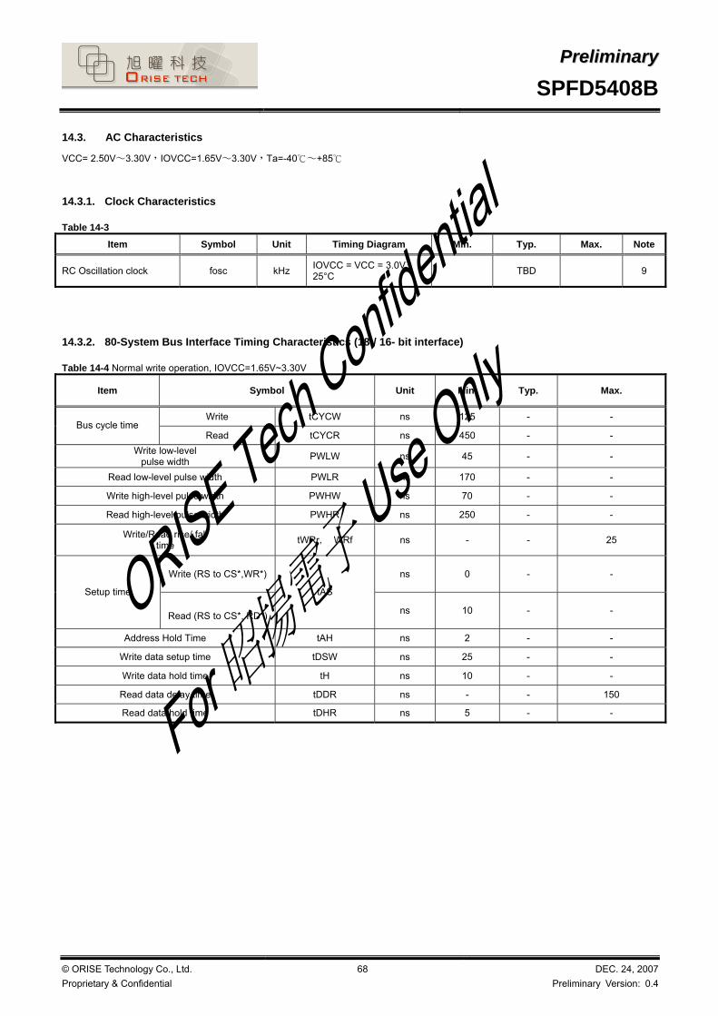
PPrreelliimmiinnaarryy SPFD5408B
© ORISE Technology Co., Ltd. Proprietary & Confidential
68 DEC. 24, 2007Preliminary Version: 0.4
14.3. AC Characteristics
VCC= 2.50V~3.30V,IOVCC=1.65V~3.30V,Ta=-40℃~+85 ℃
14.3.1. Clock Characteristics
Table 14-3
Item Symbol Unit Timing Diagram Min. Typ. Max. Note
RC Oscillation clock fosc kHz IOVCC = VCC = 3.0V, 25°C TBD 9
14.3.2. 80-System Bus Interface Timing Characteristics (18-/ 16- bit interface)
Table 14-4 Normal write operation, IOVCC=1.65V~3.30V
Item Symbol Unit Min. Typ. Max.
Write tCYCW ns 125 - - Bus cycle time
Read tCYCR ns 450 - - Write low-level
pulse width PWLW ns 45 - -
Read low-level pulse width PWLR ns 170 - -
Write high-level pulse width PWHW ns 70 - -
Read high-level pulse width PWHR ns 250 - -
Write/Read rise/ fall time tWRr, WRf ns - - 25
Write (RS to CS*,WR*) ns 0 - -
Setup time
Read (RS to CS*, RD*)
tAS
ns 10 - -
Address Hold Time tAH ns 2 - -
Write data setup time tDSW ns 25 - -
Write data hold time tH ns 10 - -
Read data delay time tDDR ns - - 150
Read data hold time tDHR ns 5 - -

PPrreelliimmiinnaarryy SPFD5408B
© ORISE Technology Co., Ltd. Proprietary & Confidential
69 DEC. 24, 2007Preliminary Version: 0.4
Figure 14-1 80-System Bus Interface
RESET*
VIL VIL
VIH
Figure 14-2 Reset Operation

PPrreelliimmiinnaarryy SPFD5408B
© ORISE Technology Co., Ltd. Proprietary & Confidential
70 DEC. 24, 2007Preliminary Version: 0.4
14.3.3. Clock-synchronized Serial Interface Timing Characteristics
Normal Write Function(IOVCC=1.65~3.30V)
Table 14-5
Item Symbol Unit Min. Typ. Max.
Write (received) tSCYC ns 100 - 20.000 Serial Time Clock Cycle
Read (transmitted) tSCYC ns 350 - 20.000
Write (received) tSCH ns 40 - - Serial Clock high-level
width
Read (transmitted) tSCH ns 150 - -
Write (received) tSCL ns 40 - - Serial Clock low-level width
Read (transmitted) tSCL ns 150 - -
Serial clock rise/fall
time tSCr,tSCf ns - -
20
Chip select setup time tCSU ns 20 - - Chip select hold time tCH ns 60 - -
Serial input data setup time tSISU ns 30 - -
Serial input data hold time tSIH ns 30 - - Serial output data delay time tSOD ns - - 130
Serial output data hold time tSOH ns 5 - -
14.3.4. Reset Timing Characteristics (IOVCC=1.65~3.30V)
Table 14-6
Item Symbol Unit Min. Typ. Max.
Reset low-level width tRES ms 1 - -
Reset rise time trRES µs - - 10

PPrreelliimmiinnaarryy SPFD5408B
© ORISE Technology Co., Ltd. Proprietary & Confidential
71 DEC. 24, 2007Preliminary Version: 0.4
14.3.5. RGB Interface Timing Characteristics
18-/ 16- bit RGB interface, IOVCC=1.65~3.30V
Table 14-7
Item Symbol Unit Min. Typ. Max.
VSYNC/HSYNC Setup time TSYNCS clock 0 - 1
ENABLE Setup time TENS ns 10 - -
ENABLE Hold time TENH ns 20 - -
DOTCLK low-level pulse width PWDL ns 40 - -
DOTCLK high-level pulse width PWDH ns 40 - -
DOTCLK cycle time TCYCD ns 100 - -
Data setup time TPDS ns 10 - -
Data hold time TPDH ns 40 - -
DOTCLK, VSYNC and HSYNC rise/fall time Trgbr Trgbf ns - - 25
6-bit RGB interface, IOVCC=1.65~3.30V
Table 14-8
Item Symbol Unit Min. Typ. Max.
VSYNC/HSYNC setup time TSYNCS clock 0 - 1
ENABLE setup time TENS ns 10 - -
ENABLE hold time TENH ns 25 - -
DOTCLK low-level pulse width PWDL ns 25 - -
DOTCLK high-level pulse width PWDH ns 25 - -
DOTCLK cycle time TCYCD ns 60 - -
Data setup-time TPDS ns 10 - -
Data hold time TPDH ns 25 - -
DOTCLK, VSYNC, and HSYNC rise/fall time Trgb Ttrgbf ns - - 25

PPrreelliimmiinnaarryy SPFD5408B
© ORISE Technology Co., Ltd. Proprietary & Confidential
72 DEC. 24, 2007Preliminary Version: 0.4
15. CHIP INFORMATION 15.1. PAD Assignment
S4
S5
S2
S6
S7
S3
DU
MM
Y26
DU
MM
Y25
S1
S71
7S
718
S71
9S
720
S71
6
G31
0
G31
8
DU
MM
Y21
DU
MM
Y22
G6
G4
G2
G32
0G
316
G31
4G
312
G8
DU
MM
Y20
S71
5S
714
G31
5G
317
G31
9D
UM
MY
27
G31
3
G7
G5
G3
G1
G9
DU
MM
Y11
TEST
12
IOG
ND
DU
M3
VPP2
4TE
STO
25
TEST
O3
6IM
0_ID
7IM
18
IM2
9IM
310
TEST
211
TEST
O4
12TE
STO
513
TEST
O6
14TE
STO
715
TEST
O8
16TE
STO
917
TEST
O10
18R
ESET
19R
ESET
20VS
YNC
21H
SYN
C22
DO
TCLK
23EN
ABLE
24D
B17
25D
B16
26D
B15
27D
B14
28D
B13
29TE
STO
1130
DB
1231
DB
1132
DB
1033
DB
934
DB
835
TEST
336
TEST
O12
37D
B7
38D
B6
39D
B5
40D
B4
41D
B3
42D
B2
43D
B1
44D
B0
45TE
STO
1346
SDO
47SD
I48
RD
49W
R_S
CL
50R
S51
CS
52TE
STO
1453
TEST
O15
54FM
ARK
55TE
STO
1656
TS8
57TS
758
TS6
59TS
560
TS4
61TS
362
TS2
63TS
164
TS0
65D
UM
MY2
66IO
VCC
67IO
VCC
68IO
VCC
69IO
VCC
70IO
VCC
71IO
VCC
72VD
DD
73VD
DD
74VD
DD
75VD
DD
76VD
DD
77VD
DD
78VD
DD
79VD
DD
80VD
DD
81VD
DD
82VD
DD
83D
UM
MY3
84G
ND
85G
ND
86G
ND
87G
ND
88G
ND
89G
ND
90G
ND
91G
ND
92VG
S93
VGS
94R
GN
D95
RG
ND
96R
GN
D97
RG
ND
98R
GN
D99
AGN
D10
0AG
ND
101
AGN
D10
2AG
ND
103
AGN
D10
4D
UM
MY4
105
DU
MM
Y510
6D
UM
MY6
107
VCO
M10
8VC
OM
109
VCO
M11
0VC
OM
111
VCO
M11
2VC
OM
113
VCO
M11
4VC
OM
H11
5VC
OM
H11
6VC
OM
H11
7VC
OM
H11
8VC
OM
H11
9VC
OM
H12
0VC
OM
L12
1VC
OM
L12
2VC
OM
L12
3VC
OM
L12
4VR
EG1O
UT
125
VREG
1OU
T12
6VR
EG1O
UT
127
DU
MM
Y712
8D
UM
MY8
129
DU
MM
Y913
0VC
L13
1VC
L13
2VC
L13
3VC
L13
4VC
L13
5D
DVD
H13
6D
DVD
H13
7D
DVD
H13
8D
DVD
H13
9D
DVD
H14
0D
DVD
H14
1VC
I114
2VC
I114
3VC
I114
4VC
I14
5VC
I14
6VC
I14
7VC
I14
8VC
I14
9VC
I15
0VC
I15
1VC
I15
2VC
I15
3VC
I15
4VC
I15
5VC
I15
6VC
I15
7VC
I15
8VC
I15
9VC
I16
0VC
I16
1VC
I16
2D
UM
MY1
016
3D
UM
MY1
116
4C
12N
165
C12
N16
6C
12N
167
C12
N16
8C
12N
169
C12
P17
0C
12P
171
C12
P17
2C
12P
173
C12
P17
4C
11N
175
C11
N17
6C
11N
177
C11
N17
8C
11N
179
C11
P18
0C
11P
181
C11
P18
2C
11P
183
C11
P18
4VG
L18
5VG
L18
6VG
L18
7VG
L18
8VG
L18
9VG
L19
0VG
L19
1VG
L19
2VG
L19
3VG
L19
4G
ND
195
GN
D19
6G
ND
197
VGH
198
VGH
199
VGH
200
VGH
201
VGH
202
VGH
203
DU
MM
Y12
204
DU
MM
Y13
205
C13
N20
6C
13N
207
C13
N20
8C
13N
209
C13
P21
0C
13P
211
C13
P21
2C
13P
213
C21
N21
4C
21N
215
C21
N21
6C
21N
217
C21
N21
8C
21N
219
C21
N22
0C
21P
221
C21
P22
2C
21P
223
C21
P22
4C
21P
225
C21
P22
6C
21P
227
C22
N22
8C
22N
229
C22
N23
0C
22N
231
C22
N23
2C
22N
233
C22
N23
4C
22P
235
C22
P23
6C
22P
237
C22
P23
8C
22P
239
C22
P24
0C
22P
241
DU
MM
Y14
242
DU
MM
Y15
243
15.2. PAD Dimension
Size Item PAD No.
X Y Unit
Chip Size - 17820 865
Chip thickness - 400 ± 25
1~243 70 - Pad pitch
244~1291 16 -
1~243 50 80 Pad size
244~1291 16 98
µm
Note1: Chip size included scribe line.
15.2.1. Output Pads
15.2.2. Input Pads

PPrreelliimmiinnaarryy SPFD5408B
© ORISE Technology Co., Ltd. Proprietary & Confidential
73 DEC. 24, 2007Preliminary Version: 0.4
15.3. Bump Characteristics
Item Standard Note
Bump Hardness 75Hv ± 25Hv
Bump Height 15µm ± 3µm
Co-planarity (in Chip) R≦ 2µm R : Max-Min
Roughness (in Bump) R≦ 2µm R : Max-Min
Bump Size “X” ± 3µm x “Y” ± 3µm X/Y: bump size
Shear Force >4.5g/mil^2

PPrreelliimmiinnaarryy SPFD5408B
© ORISE Technology Co., Ltd. Proprietary & Confidential
74 DEC. 24, 2007Preliminary Version: 0.4
15.4. PAD LocationsNo. Pad Name X Y 1 DUMMY1 -8610 -307.5 2 TEST1 -8540 -307.5 3 IOGNDDUM -8470 -307.5 4 VPP2 -8400 -307.5 5 TESTO2 -8330 -307.5 6 TESTO3 -8260 -307.5 7 IM0_ID -8190 -307.5 8 IM1 -8120 -307.5 9 IM2 -8050 -307.5
10 IM3 -7980 -307.5 11 TEST2 -7910 -307.5 12 TESTO4 -7840 -307.5 13 TESTO5 -7770 -307.5 14 TESTO6 -7700 -307.5 15 TESTO7 -7630 -307.5 16 TESTO8 -7560 -307.5 17 TESTO9 -7490 -307.5 18 TESTO10 -7420 -307.5 19 RESET -7350 -307.5 20 RESET -7280 -307.5 21 VSYNC -7210 -307.5 22 HSYNC -7140 -307.5 23 DOTCLK -7070 -307.5 24 ENABLE -7000 -307.5 25 DB17 -6905 -307.5 26 DB16 -6825 -307.5 27 DB15 -6745 -307.5 28 DB14 -6665 -307.5 29 DB13 -6585 -307.5 30 TESTO11 -6495 -307.5 31 DB12 -6405 -307.5 32 DB11 -6325 -307.5 33 DB10 -6245 -307.5 34 DB9 -6165 -307.5 35 DB8 -6085 -307.5 36 TEST3 -5990 -307.5 37 TESTO12 -5920 -307.5 38 DB7 -5825 -307.5 39 DB6 -5745 -307.5 40 DB5 -5665 -307.5 41 DB4 -5585 -307.5 42 DB3 -5505 -307.5 43 DB2 -5425 -307.5 44 DB1 -5345 -307.5 45 DB0 -5265 -307.5 46 TESTO13 -5180 -307.5 47 SDO -5110 -307.5 48 SDI -5040 -307.5 49 RD -4970 -307.5 50 WR_SCL -4900 -307.5 51 RS -4830 -307.5 52 CS -4760 -307.5 53 TESTO14 -4690 -307.5
No. Pad Name X Y 54 TESTO15 -4620 -307.555 FMARK -4550 -307.556 TESTO16 -4480 -307.557 TS8 -4410 -307.558 TS7 -4340 -307.559 TS6 -4270 -307.560 TS5 -4200 -307.561 TS4 -4130 -307.562 TS3 -4060 -307.563 TS2 -3990 -307.564 TS1 -3920 -307.565 TS0 -3850 -307.566 DUMMY2 -3780 -307.567 IOVCC -3710 -307.568 IOVCC -3640 -307.569 IOVCC -3570 -307.570 IOVCC -3500 -307.571 IOVCC -3430 -307.572 IOVCC -3360 -307.573 VDDD -3290 -307.574 VDDD -3220 -307.575 VDDD -3150 -307.576 VDDD -3080 -307.577 VDDD -3010 -307.578 VDDD -2940 -307.579 VDDD -2870 -307.580 VDDD -2800 -307.581 VDDD -2730 -307.582 VDDD -2660 -307.583 VDDD -2590 -307.584 DUMMY3 -2520 -307.585 GND -2450 -307.586 GND -2380 -307.587 GND -2310 -307.588 GND -2240 -307.589 GND -2170 -307.590 GND -2100 -307.591 GND -2030 -307.592 GND -1960 -307.593 VGS -1890 -307.594 VGS -1820 -307.595 RGND -1750 -307.596 RGND -1680 -307.597 RGND -1610 -307.598 RGND -1540 -307.599 RGND -1470 -307.5
100 AGND -1400 -307.5101 AGND -1330 -307.5102 AGND -1260 -307.5103 AGND -1190 -307.5104 AGND -1120 -307.5105 DUMMY4 -1050 -307.5106 DUMMY5 -980 -307.5
No. Pad Name X Y 107 DUMMY6 -910 -307.5108 VCOM -840 -307.5109 VCOM -770 -307.5110 VCOM -700 -307.5111 VCOM -630 -307.5112 VCOM -560 -307.5113 VCOM -490 -307.5114 VCOM -420 -307.5115 VCOMH -350 -307.5116 VCOMH -280 -307.5117 VCOMH -210 -307.5118 VCOMH -140 -307.5119 VCOMH -70 -307.5120 VCOMH 0 -307.5121 VCOML 70 -307.5122 VCOML 140 -307.5123 VCOML 210 -307.5124 VCOML 280 -307.5125 VREG1OUT 350 -307.5126 VREG1OUT 420 -307.5127 VREG1OUT 490 -307.5128 DUMMY7 560 -307.5129 DUMMY8 630 -307.5130 DUMMY9 700 -307.5131 VCL 770 -307.5132 VCL 840 -307.5133 VCL 910 -307.5134 VCL 980 -307.5135 VCL 1050 -307.5136 DDVDH 1120 -307.5137 DDVDH 1190 -307.5138 DDVDH 1260 -307.5139 DDVDH 1330 -307.5140 DDVDH 1400 -307.5141 DDVDH 1470 -307.5142 VCI1 1540 -307.5143 VCI1 1610 -307.5144 VCI1 1680 -307.5145 VCI 1750 -307.5146 VCI 1820 -307.5147 VCI 1890 -307.5148 VCI 1960 -307.5149 VCI 2030 -307.5150 VCI 2100 -307.5151 VCI 2170 -307.5152 VCI 2240 -307.5153 VCI 2310 -307.5154 VCI 2380 -307.5155 VCI 2450 -307.5156 VCI 2520 -307.5157 VCI 2590 -307.5158 VCI 2660 -307.5159 VCI 2730 -307.5

PPrreelliimmiinnaarryy SPFD5408B
© ORISE Technology Co., Ltd. Proprietary & Confidential
75 DEC. 24, 2007Preliminary Version: 0.4
No. Pad Name X Y 160 VCI 2800 -307.5 161 VCI 2870 -307.5 162 VCI 2940 -307.5 163 DUMMY10 3010 -307.5 164 DUMMY11 3080 -307.5 165 C12N 3150 -307.5 166 C12N 3220 -307.5 167 C12N 3290 -307.5 168 C12N 3360 -307.5 169 C12N 3430 -307.5 170 C12P 3500 -307.5 171 C12P 3570 -307.5 172 C12P 3640 -307.5 173 C12P 3710 -307.5 174 C12P 3780 -307.5 175 C11N 3850 -307.5 176 C11N 3920 -307.5 177 C11N 3990 -307.5 178 C11N 4060 -307.5 179 C11N 4130 -307.5 180 C11P 4200 -307.5 181 C11P 4270 -307.5 182 C11P 4340 -307.5 183 C11P 4410 -307.5 184 C11P 4480 -307.5 185 VGL 4550 -307.5 186 VGL 4620 -307.5 187 VGL 4690 -307.5 188 VGL 4760 -307.5 189 VGL 4830 -307.5 190 VGL 4900 -307.5 191 VGL 4970 -307.5 192 VGL 5040 -307.5 193 VGL 5110 -307.5 194 VGL 5180 -307.5 195 GND 5250 -307.5 196 GND 5320 -307.5 197 GND 5390 -307.5 198 VGH 5460 -307.5 199 VGH 5530 -307.5 200 VGH 5600 -307.5 201 VGH 5670 -307.5 202 VGH 5740 -307.5 203 VGH 5810 -307.5 204 DUMMY12 5880 -307.5 205 DUMMY13 5950 -307.5 206 C13N 6020 -307.5 207 C13N 6090 -307.5 208 C13N 6160 -307.5 209 C13N 6230 -307.5 210 C13P 6300 -307.5 211 C13P 6370 -307.5 212 C13P 6440 -307.5 213 C13P 6510 -307.5 214 C21N 6580 -307.5
No. Pad Name X Y 215 C21N 6650 -307.5216 C21N 6720 -307.5217 C21N 6790 -307.5218 C21N 6860 -307.5219 C21N 6930 -307.5220 C21N 7000 -307.5221 C21P 7070 -307.5222 C21P 7140 -307.5223 C21P 7210 -307.5224 C21P 7280 -307.5225 C21P 7350 -307.5226 C21P 7420 -307.5227 C21P 7490 -307.5228 C22N 7560 -307.5229 C22N 7630 -307.5230 C22N 7700 -307.5231 C22N 7770 -307.5232 C22N 7840 -307.5233 C22N 7910 -307.5234 C22N 7980 -307.5235 C22P 8050 -307.5236 C22P 8120 -307.5237 C22P 8190 -307.5238 C22P 8260 -307.5239 C22P 8330 -307.5240 C22P 8400 -307.5241 C22P 8470 -307.5242 DUMMY14 8540 -307.5243 DUMMY15 8610 -307.5244 DUMMY20 8659 202.5245 G320 8643 319.5246 G318 8627 202.5247 G316 8611 319.5248 G314 8595 202.5249 G312 8579 319.5250 G310 8563 202.5251 G308 8547 319.5252 G306 8531 202.5253 G304 8515 319.5254 G302 8499 202.5255 G300 8483 319.5256 G298 8467 202.5257 G296 8451 319.5258 G294 8435 202.5259 G292 8419 319.5260 G290 8403 202.5261 G288 8387 319.5262 G286 8371 202.5263 G284 8355 319.5264 G282 8339 202.5265 G280 8323 319.5266 G278 8307 202.5267 G276 8291 319.5268 G274 8275 202.5269 G272 8259 319.5
No. Pad Name X Y 270 G270 8243 202.5271 G268 8227 319.5272 G266 8211 202.5273 G264 8195 319.5274 G262 8179 202.5275 G260 8163 319.5276 G258 8147 202.5277 G256 8131 319.5278 G254 8115 202.5279 G252 8099 319.5280 G250 8083 202.5281 G248 8067 319.5282 G246 8051 202.5283 G244 8035 319.5284 G242 8019 202.5285 G240 8003 319.5286 G238 7987 202.5287 G236 7971 319.5288 G234 7955 202.5289 G232 7939 319.5290 G230 7923 202.5291 G228 7907 319.5292 G226 7891 202.5293 G224 7875 319.5294 G222 7859 202.5295 G220 7843 319.5296 G218 7827 202.5297 G216 7811 319.5298 G214 7795 202.5299 G212 7779 319.5300 G210 7763 202.5301 G208 7747 319.5302 G206 7731 202.5303 G204 7715 319.5304 G202 7699 202.5305 G200 7683 319.5306 G198 7667 202.5307 G196 7651 319.5308 G194 7635 202.5309 G192 7619 319.5310 G190 7603 202.5311 G188 7587 319.5312 G186 7571 202.5313 G184 7555 319.5314 G182 7539 202.5315 G180 7523 319.5316 G178 7507 202.5317 G176 7491 319.5318 G174 7475 202.5319 G172 7459 319.5320 G170 7443 202.5321 G168 7427 319.5322 G166 7411 202.5323 G164 7395 319.5324 G162 7379 202.5

PPrreelliimmiinnaarryy SPFD5408B
© ORISE Technology Co., Ltd. Proprietary & Confidential
76 DEC. 24, 2007Preliminary Version: 0.4
No. Pad Name X Y 325 G160 7363 319.5 326 G158 7347 202.5 327 G156 7331 319.5 328 G154 7315 202.5 329 G152 7299 319.5 330 G150 7283 202.5 331 G148 7267 319.5 332 G146 7251 202.5 333 G144 7235 319.5 334 G142 7219 202.5 335 G140 7203 319.5 336 G138 7187 202.5 337 G136 7171 319.5 338 G134 7155 202.5 339 G132 7139 319.5 340 G130 7123 202.5 341 G128 7107 319.5 342 G126 7091 202.5 343 G124 7075 319.5 344 G122 7059 202.5 345 G120 7043 319.5 346 G118 7027 202.5 347 G116 7011 319.5 348 G114 6995 202.5 349 G112 6979 319.5 350 G110 6963 202.5 351 G108 6947 319.5 352 G106 6931 202.5 353 G104 6915 319.5 354 G102 6899 202.5 355 G100 6883 319.5 356 G98 6867 202.5 357 G96 6851 319.5 358 G94 6835 202.5 359 G92 6819 319.5 360 G90 6803 202.5 361 G88 6787 319.5 362 G86 6771 202.5 363 G84 6755 319.5 364 G82 6739 202.5 365 G80 6723 319.5 366 G78 6707 202.5 367 G76 6691 319.5 368 G74 6675 202.5 369 G72 6659 319.5 370 G70 6643 202.5 371 G68 6627 319.5 372 G66 6611 202.5 373 G64 6595 319.5 374 G62 6579 202.5 375 G60 6563 319.5 376 G58 6547 202.5 377 G56 6531 319.5 378 G54 6515 202.5 379 G52 6499 319.5
No. Pad Name X Y 380 G50 6483 202.5381 G48 6467 319.5382 G46 6451 202.5383 G44 6435 319.5384 G42 6419 202.5385 G40 6403 319.5386 G38 6387 202.5387 G36 6371 319.5388 G34 6355 202.5389 G32 6339 319.5390 G30 6323 202.5391 G28 6307 319.5392 G26 6291 202.5393 G24 6275 319.5394 G22 6259 202.5395 G20 6243 319.5396 G18 6227 202.5397 G16 6211 319.5398 G14 6195 202.5399 G12 6179 319.5400 G10 6163 202.5401 G8 6147 319.5402 G6 6131 202.5403 G4 6115 319.5404 G2 6099 202.5405 DUMMY21 6083 319.5406 DUMMY22 6047 319.5407 S720 6031 202.5408 S719 6015 319.5409 S718 5999 202.5410 S717 5983 319.5411 S716 5967 202.5412 S715 5951 319.5413 S714 5935 202.5414 S713 5919 319.5415 S712 5903 202.5416 S711 5887 319.5417 S710 5871 202.5418 S709 5855 319.5419 S708 5839 202.5420 S707 5823 319.5421 S706 5807 202.5422 S705 5791 319.5423 S704 5775 202.5424 S703 5759 319.5425 S702 5743 202.5426 S701 5727 319.5427 S700 5711 202.5428 S699 5695 319.5429 S698 5679 202.5430 S697 5663 319.5431 S696 5647 202.5432 S695 5631 319.5433 S694 5615 202.5434 S693 5599 319.5
No. Pad Name X Y 435 S692 5583 202.5436 S691 5567 319.5437 S690 5551 202.5438 S689 5535 319.5439 S688 5519 202.5440 S687 5503 319.5441 S686 5487 202.5442 S685 5471 319.5443 S684 5455 202.5444 S683 5439 319.5445 S682 5423 202.5446 S681 5407 319.5447 S680 5391 202.5448 S679 5375 319.5449 S678 5359 202.5450 S677 5343 319.5451 S676 5327 202.5452 S675 5311 319.5453 S674 5295 202.5454 S673 5279 319.5455 S672 5263 202.5456 S671 5247 319.5457 S670 5231 202.5458 S669 5215 319.5459 S668 5199 202.5460 S667 5183 319.5461 S666 5167 202.5462 S665 5151 319.5463 S664 5135 202.5464 S663 5119 319.5465 S662 5103 202.5466 S661 5087 319.5467 S660 5071 202.5468 S659 5055 319.5469 S658 5039 202.5470 S657 5023 319.5471 S656 5007 202.5472 S655 4991 319.5473 S654 4975 202.5474 S653 4959 319.5475 S652 4943 202.5476 S651 4927 319.5477 S650 4911 202.5478 S649 4895 319.5479 S648 4879 202.5480 S647 4863 319.5481 S646 4847 202.5482 S645 4831 319.5483 S644 4815 202.5484 S643 4799 319.5485 S642 4783 202.5486 S641 4767 319.5487 S640 4751 202.5488 S639 4735 319.5489 S638 4719 202.5

PPrreelliimmiinnaarryy SPFD5408B
© ORISE Technology Co., Ltd. Proprietary & Confidential
77 DEC. 24, 2007Preliminary Version: 0.4
No. Pad Name X Y 490 S637 4703 319.5 491 S636 4687 202.5 492 S635 4671 319.5 493 S634 4655 202.5 494 S633 4639 319.5 495 S632 4623 202.5 496 S631 4607 319.5 497 S630 4591 202.5 498 S629 4575 319.5 499 S628 4559 202.5 500 S627 4543 319.5 501 S626 4527 202.5 502 S625 4511 319.5 503 S624 4495 202.5 504 S623 4479 319.5 505 S622 4463 202.5 506 S621 4447 319.5 507 S620 4431 202.5 508 S619 4415 319.5 509 S618 4399 202.5 510 S617 4383 319.5 511 S616 4367 202.5 512 S615 4351 319.5 513 S614 4335 202.5 514 S613 4319 319.5 515 S612 4303 202.5 516 S611 4287 319.5 517 S610 4271 202.5 518 S609 4255 319.5 519 S608 4239 202.5 520 S607 4223 319.5 521 S606 4207 202.5 522 S605 4191 319.5 523 S604 4175 202.5 524 S603 4159 319.5 525 S602 4143 202.5 526 S601 4127 319.5 527 S600 4111 202.5 528 S599 4095 319.5 529 S598 4079 202.5 530 S597 4063 319.5 531 S596 4047 202.5 532 S595 4031 319.5 533 S594 4015 202.5 534 S593 3999 319.5 535 S592 3983 202.5 536 S591 3967 319.5 537 S590 3951 202.5 538 S589 3935 319.5 539 S588 3919 202.5 540 S587 3903 319.5 541 S586 3887 202.5 542 S585 3871 319.5 543 S584 3855 202.5 544 S583 3839 319.5
No. Pad Name X Y 545 S582 3823 202.5546 S581 3807 319.5547 S580 3791 202.5548 S579 3775 319.5549 S578 3759 202.5550 S577 3743 319.5551 S576 3727 202.5552 S575 3711 319.5553 S574 3695 202.5554 S573 3679 319.5555 S572 3663 202.5556 S571 3647 319.5557 S570 3631 202.5558 S569 3615 319.5559 S568 3599 202.5560 S567 3583 319.5561 S566 3567 202.5562 S565 3551 319.5563 S564 3535 202.5564 S563 3519 319.5565 S562 3503 202.5566 S561 3487 319.5567 S560 3471 202.5568 S559 3455 319.5569 S558 3439 202.5570 S557 3423 319.5571 S556 3407 202.5572 S555 3391 319.5573 S554 3375 202.5574 S553 3359 319.5575 S552 3343 202.5576 S551 3327 319.5577 S550 3311 202.5578 S549 3295 319.5579 S548 3279 202.5580 S547 3263 319.5581 S546 3247 202.5582 S545 3231 319.5583 S544 3215 202.5584 S543 3199 319.5585 S542 3183 202.5586 S541 3167 319.5587 S540 3151 202.5588 S539 3135 319.5589 S538 3119 202.5590 S537 3103 319.5591 S536 3087 202.5592 S535 3071 319.5593 S534 3055 202.5594 S533 3039 319.5595 S532 3023 202.5596 S531 3007 319.5597 S530 2991 202.5598 S529 2975 319.5599 S528 2959 202.5
No. Pad Name X Y 600 S527 2943 319.5601 S526 2927 202.5602 S525 2911 319.5603 S524 2895 202.5604 S523 2879 319.5605 S522 2863 202.5606 S521 2847 319.5607 S520 2831 202.5608 S519 2815 319.5609 S518 2799 202.5610 S517 2783 319.5611 S516 2767 202.5612 S515 2751 319.5613 S514 2735 202.5614 S513 2719 319.5615 S512 2703 202.5616 S511 2687 319.5617 S510 2671 202.5618 S509 2655 319.5619 S508 2639 202.5620 S507 2623 319.5621 S506 2607 202.5622 S505 2591 319.5623 S504 2575 202.5624 S503 2559 319.5625 S502 2543 202.5626 S501 2527 319.5627 S500 2511 202.5628 S499 2495 319.5629 S498 2479 202.5630 S497 2463 319.5631 S496 2447 202.5632 S495 2431 319.5633 S494 2415 202.5634 S493 2399 319.5635 S492 2383 202.5636 S491 2367 319.5637 S490 2351 202.5638 S489 2335 319.5639 S488 2319 202.5640 S487 2303 319.5641 S486 2287 202.5642 S485 2271 319.5643 S484 2255 202.5644 S483 2239 319.5645 S482 2223 202.5646 S481 2207 319.5647 S480 2191 202.5648 S479 2175 319.5649 S478 2159 202.5650 S477 2143 319.5651 S476 2127 202.5652 S475 2111 319.5653 S474 2095 202.5654 S473 2079 319.5

PPrreelliimmiinnaarryy SPFD5408B
© ORISE Technology Co., Ltd. Proprietary & Confidential
78 DEC. 24, 2007Preliminary Version: 0.4
No. Pad Name X Y 655 S472 2063 202.5 656 S471 2047 319.5 657 S470 2031 202.5 658 S469 2015 319.5 659 S468 1999 202.5 660 S467 1983 319.5 661 S466 1967 202.5 662 S465 1951 319.5 663 S464 1935 202.5 664 S463 1919 319.5 665 S462 1903 202.5 666 S461 1887 319.5 667 S460 1871 202.5 668 S459 1855 319.5 669 S458 1839 202.5 670 S457 1823 319.5 671 S456 1807 202.5 672 S455 1791 319.5 673 S454 1775 202.5 674 S453 1759 319.5 675 S452 1743 202.5 676 S451 1727 319.5 677 S450 1711 202.5 678 S449 1695 319.5 679 S448 1679 202.5 680 S447 1663 319.5 681 S446 1647 202.5 682 S445 1631 319.5 683 S444 1615 202.5 684 S443 1599 319.5 685 S442 1583 202.5 686 S441 1567 319.5 687 S440 1551 202.5 688 S439 1535 319.5 689 S438 1519 202.5 690 S437 1503 319.5 691 S436 1487 202.5 692 S435 1471 319.5 693 S434 1455 202.5 694 S433 1439 319.5 695 S432 1423 202.5 696 S431 1407 319.5 697 S430 1391 202.5 698 S429 1375 319.5 699 S428 1359 202.5 700 S427 1343 319.5 701 S426 1327 202.5 702 S425 1311 319.5 703 S424 1295 202.5 704 S423 1279 319.5 705 S422 1263 202.5 706 S421 1247 319.5 707 S420 1231 202.5 708 S419 1215 319.5 709 S418 1199 202.5
No. Pad Name X Y 710 S417 1183 319.5711 S416 1167 202.5712 S415 1151 319.5713 S414 1135 202.5714 S413 1119 319.5715 S412 1103 202.5716 S411 1087 319.5717 S410 1071 202.5718 S409 1055 319.5719 S408 1039 202.5720 S407 1023 319.5721 S406 1007 202.5722 S405 991 319.5723 S404 975 202.5724 S403 959 319.5725 S402 943 202.5726 S401 927 319.5727 S400 911 202.5728 S399 895 319.5729 S398 879 202.5730 S397 863 319.5731 S396 847 202.5732 S395 831 319.5733 S394 815 202.5734 S393 799 319.5735 S392 783 202.5736 S391 767 319.5737 S390 751 202.5738 S389 735 319.5739 S388 719 202.5740 S387 703 319.5741 S386 687 202.5742 S385 671 319.5743 S384 655 202.5744 S383 639 319.5745 S382 623 202.5746 S381 607 319.5747 S380 591 202.5748 S379 575 319.5749 S378 559 202.5750 S377 543 319.5751 S376 527 202.5752 S375 511 319.5753 S374 495 202.5754 S373 479 319.5755 S372 463 202.5756 S371 447 319.5757 S370 431 202.5758 S369 415 319.5759 S368 399 202.5760 S367 383 319.5761 S366 367 202.5762 S365 351 319.5763 S364 335 202.5764 S363 319 319.5
No. Pad Name X Y 765 S362 303 202.5766 S361 287 319.5767 DUMMY23 271 202.5768 DUMMY24 -271 202.5769 S360 -287 319.5770 S359 -303 202.5771 S358 -319 319.5772 S357 -335 202.5773 S356 -351 319.5774 S355 -367 202.5775 S354 -383 319.5776 S353 -399 202.5777 S352 -415 319.5778 S351 -431 202.5779 S350 -447 319.5780 S349 -463 202.5781 S348 -479 319.5782 S347 -495 202.5783 S346 -511 319.5784 S345 -527 202.5785 S344 -543 319.5786 S343 -559 202.5787 S342 -575 319.5788 S341 -591 202.5789 S340 -607 319.5790 S339 -623 202.5791 S338 -639 319.5792 S337 -655 202.5793 S336 -671 319.5794 S335 -687 202.5795 S334 -703 319.5796 S333 -719 202.5797 S332 -735 319.5798 S331 -751 202.5799 S330 -767 319.5800 S329 -783 202.5801 S328 -799 319.5802 S327 -815 202.5803 S326 -831 319.5804 S325 -847 202.5805 S324 -863 319.5806 S323 -879 202.5807 S322 -895 319.5808 S321 -911 202.5809 S320 -927 319.5810 S319 -943 202.5811 S318 -959 319.5812 S317 -975 202.5813 S316 -991 319.5814 S315 -1007 202.5815 S314 -1023 319.5816 S313 -1039 202.5817 S312 -1055 319.5818 S311 -1071 202.5819 S310 -1087 319.5

PPrreelliimmiinnaarryy SPFD5408B
© ORISE Technology Co., Ltd. Proprietary & Confidential
79 DEC. 24, 2007Preliminary Version: 0.4
No. Pad Name X Y 820 S309 -1103 202.5 821 S308 -1119 319.5 822 S307 -1135 202.5 823 S306 -1151 319.5 824 S305 -1167 202.5 825 S304 -1183 319.5 826 S303 -1199 202.5 827 S302 -1215 319.5 828 S301 -1231 202.5 829 S300 -1247 319.5 830 S299 -1263 202.5 831 S298 -1279 319.5 832 S297 -1295 202.5 833 S296 -1311 319.5 834 S295 -1327 202.5 835 S294 -1343 319.5 836 S293 -1359 202.5 837 S292 -1375 319.5 838 S291 -1391 202.5 839 S290 -1407 319.5 840 S289 -1423 202.5 841 S288 -1439 319.5 842 S287 -1455 202.5 843 S286 -1471 319.5 844 S285 -1487 202.5 845 S284 -1503 319.5 846 S283 -1519 202.5 847 S282 -1535 319.5 848 S281 -1551 202.5 849 S280 -1567 319.5 850 S279 -1583 202.5 851 S278 -1599 319.5 852 S277 -1615 202.5 853 S276 -1631 319.5 854 S275 -1647 202.5 855 S274 -1663 319.5 856 S273 -1679 202.5 857 S272 -1695 319.5 858 S271 -1711 202.5 859 S270 -1727 319.5 860 S269 -1743 202.5 861 S268 -1759 319.5 862 S267 -1775 202.5 863 S266 -1791 319.5 864 S265 -1807 202.5 865 S264 -1823 319.5 866 S263 -1839 202.5 867 S262 -1855 319.5 868 S261 -1871 202.5 869 S260 -1887 319.5 870 S259 -1903 202.5 871 S258 -1919 319.5 872 S257 -1935 202.5 873 S256 -1951 319.5 874 S255 -1967 202.5
No. Pad Name X Y 875 S254 -1983 319.5876 S253 -1999 202.5877 S252 -2015 319.5878 S251 -2031 202.5879 S250 -2047 319.5880 S249 -2063 202.5881 S248 -2079 319.5882 S247 -2095 202.5883 S246 -2111 319.5884 S245 -2127 202.5885 S244 -2143 319.5886 S243 -2159 202.5887 S242 -2175 319.5888 S241 -2191 202.5889 S240 -2207 319.5890 S239 -2223 202.5891 S238 -2239 319.5892 S237 -2255 202.5893 S236 -2271 319.5894 S235 -2287 202.5895 S234 -2303 319.5896 S233 -2319 202.5897 S232 -2335 319.5898 S231 -2351 202.5899 S230 -2367 319.5900 S229 -2383 202.5901 S228 -2399 319.5902 S227 -2415 202.5903 S226 -2431 319.5904 S225 -2447 202.5905 S224 -2463 319.5906 S223 -2479 202.5907 S222 -2495 319.5908 S221 -2511 202.5909 S220 -2527 319.5910 S219 -2543 202.5911 S218 -2559 319.5912 S217 -2575 202.5913 S216 -2591 319.5914 S215 -2607 202.5915 S214 -2623 319.5916 S213 -2639 202.5917 S212 -2655 319.5918 S211 -2671 202.5919 S210 -2687 319.5920 S209 -2703 202.5921 S208 -2719 319.5922 S207 -2735 202.5923 S206 -2751 319.5924 S205 -2767 202.5925 S204 -2783 319.5926 S203 -2799 202.5927 S202 -2815 319.5928 S201 -2831 202.5929 S200 -2847 319.5
No. Pad Name X Y 930 S199 -2863 202.5931 S198 -2879 319.5932 S197 -2895 202.5933 S196 -2911 319.5934 S195 -2927 202.5935 S194 -2943 319.5936 S193 -2959 202.5937 S192 -2975 319.5938 S191 -2991 202.5939 S190 -3007 319.5940 S189 -3023 202.5941 S188 -3039 319.5942 S187 -3055 202.5943 S186 -3071 319.5944 S185 -3087 202.5945 S184 -3103 319.5946 S183 -3119 202.5947 S182 -3135 319.5948 S181 -3151 202.5949 S180 -3167 319.5950 S179 -3183 202.5951 S178 -3199 319.5952 S177 -3215 202.5953 S176 -3231 319.5954 S175 -3247 202.5955 S174 -3263 319.5956 S173 -3279 202.5957 S172 -3295 319.5958 S171 -3311 202.5959 S170 -3327 319.5960 S169 -3343 202.5961 S168 -3359 319.5962 S167 -3375 202.5963 S166 -3391 319.5964 S165 -3407 202.5965 S164 -3423 319.5966 S163 -3439 202.5967 S162 -3455 319.5968 S161 -3471 202.5969 S160 -3487 319.5970 S159 -3503 202.5971 S158 -3519 319.5972 S157 -3535 202.5973 S156 -3551 319.5974 S155 -3567 202.5975 S154 -3583 319.5976 S153 -3599 202.5977 S152 -3615 319.5978 S151 -3631 202.5979 S150 -3647 319.5980 S149 -3663 202.5981 S148 -3679 319.5982 S147 -3695 202.5983 S146 -3711 319.5984 S145 -3727 202.5

PPrreelliimmiinnaarryy SPFD5408B
© ORISE Technology Co., Ltd. Proprietary & Confidential
80 DEC. 24, 2007Preliminary Version: 0.4
No. Pad Name X Y 985 S144 -3743 319.5 986 S143 -3759 202.5 987 S142 -3775 319.5 988 S141 -3791 202.5 989 S140 -3807 319.5 990 S139 -3823 202.5 991 S138 -3839 319.5 992 S137 -3855 202.5 993 S136 -3871 319.5 994 S135 -3887 202.5 995 S134 -3903 319.5 996 S133 -3919 202.5 997 S132 -3935 319.5 998 S131 -3951 202.5 999 S130 -3967 319.5
1000 S129 -3983 202.5 1001 S128 -3999 319.5 1002 S127 -4015 202.5 1003 S126 -4031 319.5 1004 S125 -4047 202.5 1005 S124 -4063 319.5 1006 S123 -4079 202.5 1007 S122 -4095 319.5 1008 S121 -4111 202.5 1009 S120 -4127 319.5 1010 S119 -4143 202.5 1011 S118 -4159 319.5 1012 S117 -4175 202.5 1013 S116 -4191 319.5 1014 S115 -4207 202.5 1015 S114 -4223 319.5 1016 S113 -4239 202.5 1017 S112 -4255 319.5 1018 S111 -4271 202.5 1019 S110 -4287 319.5 1020 S109 -4303 202.5 1021 S108 -4319 319.5 1022 S107 -4335 202.5 1023 S106 -4351 319.5 1024 S105 -4367 202.5 1025 S104 -4383 319.5 1026 S103 -4399 202.5 1027 S102 -4415 319.5 1028 S101 -4431 202.5 1029 S100 -4447 319.5 1030 S99 -4463 202.5 1031 S98 -4479 319.5 1032 S97 -4495 202.5 1033 S96 -4511 319.5 1034 S95 -4527 202.5 1035 S94 -4543 319.5 1036 S93 -4559 202.5 1037 S92 -4575 319.5 1038 S91 -4591 202.5 1039 S90 -4607 319.5
No. Pad Name X Y 1040 S89 -4623 202.51041 S88 -4639 319.51042 S87 -4655 202.51043 S86 -4671 319.51044 S85 -4687 202.51045 S84 -4703 319.51046 S83 -4719 202.51047 S82 -4735 319.51048 S81 -4751 202.51049 S80 -4767 319.51050 S79 -4783 202.51051 S78 -4799 319.51052 S77 -4815 202.51053 S76 -4831 319.51054 S75 -4847 202.51055 S74 -4863 319.51056 S73 -4879 202.51057 S72 -4895 319.51058 S71 -4911 202.51059 S70 -4927 319.51060 S69 -4943 202.51061 S68 -4959 319.51062 S67 -4975 202.51063 S66 -4991 319.51064 S65 -5007 202.51065 S64 -5023 319.51066 S63 -5039 202.51067 S62 -5055 319.51068 S61 -5071 202.51069 S60 -5087 319.51070 S59 -5103 202.51071 S58 -5119 319.51072 S57 -5135 202.51073 S56 -5151 319.51074 S55 -5167 202.51075 S54 -5183 319.51076 S53 -5199 202.51077 S52 -5215 319.51078 S51 -5231 202.51079 S50 -5247 319.51080 S49 -5263 202.51081 S48 -5279 319.51082 S47 -5295 202.51083 S46 -5311 319.51084 S45 -5327 202.51085 S44 -5343 319.51086 S43 -5359 202.51087 S42 -5375 319.51088 S41 -5391 202.51089 S40 -5407 319.51090 S39 -5423 202.51091 S38 -5439 319.51092 S37 -5455 202.51093 S36 -5471 319.51094 S35 -5487 202.5
No. Pad Name X Y 1095 S34 -5503 319.51096 S33 -5519 202.51097 S32 -5535 319.51098 S31 -5551 202.51099 S30 -5567 319.51100 S29 -5583 202.51101 S28 -5599 319.51102 S27 -5615 202.51103 S26 -5631 319.51104 S25 -5647 202.51105 S24 -5663 319.51106 S23 -5679 202.51107 S22 -5695 319.51108 S21 -5711 202.51109 S20 -5727 319.51110 S19 -5743 202.51111 S18 -5759 319.51112 S17 -5775 202.51113 S16 -5791 319.51114 S15 -5807 202.51115 S14 -5823 319.51116 S13 -5839 202.51117 S12 -5855 319.51118 S11 -5871 202.51119 S10 -5887 319.51120 S9 -5903 202.51121 S8 -5919 319.51122 S7 -5935 202.51123 S6 -5951 319.51124 S5 -5967 202.51125 S4 -5983 319.51126 S3 -5999 202.51127 S2 -6015 319.51128 S1 -6031 202.51129 DUMMY25 -6047 319.51130 DUMMY26 -6083 319.51131 G1 -6099 202.51132 G3 -6115 319.51133 G5 -6131 202.51134 G7 -6147 319.51135 G9 -6163 202.51136 G11 -6179 319.51137 G13 -6195 202.51138 G15 -6211 319.51139 G17 -6227 202.51140 G19 -6243 319.51141 G21 -6259 202.51142 G23 -6275 319.51143 G25 -6291 202.51144 G27 -6307 319.51145 G29 -6323 202.51146 G31 -6339 319.51147 G33 -6355 202.51148 G35 -6371 319.51149 G37 -6387 202.5

PPrreelliimmiinnaarryy SPFD5408B
© ORISE Technology Co., Ltd. Proprietary & Confidential
81 DEC. 24, 2007Preliminary Version: 0.4
No. Pad Name X Y 1150 G39 -6403 319.5 1151 G41 -6419 202.5 1152 G43 -6435 319.5 1153 G45 -6451 202.5 1154 G47 -6467 319.5 1155 G49 -6483 202.5 1156 G51 -6499 319.5 1157 G53 -6515 202.5 1158 G55 -6531 319.5 1159 G57 -6547 202.5 1160 G59 -6563 319.5 1161 G61 -6579 202.5 1162 G63 -6595 319.5 1163 G65 -6611 202.5 1164 G67 -6627 319.5 1165 G69 -6643 202.5 1166 G71 -6659 319.5 1167 G73 -6675 202.5 1168 G75 -6691 319.5 1169 G77 -6707 202.5 1170 G79 -6723 319.5 1171 G81 -6739 202.5 1172 G83 -6755 319.5 1173 G85 -6771 202.5 1174 G87 -6787 319.5 1175 G89 -6803 202.5 1176 G91 -6819 319.5 1177 G93 -6835 202.5 1178 G95 -6851 319.5 1179 G97 -6867 202.5 1180 G99 -6883 319.5 1181 G101 -6899 202.5 1182 G103 -6915 319.5 1183 G105 -6931 202.5 1184 G107 -6947 319.5 1185 G109 -6963 202.5 1186 G111 -6979 319.5 1187 G113 -6995 202.5 1188 G115 -7011 319.5 1189 G117 -7027 202.5 1190 G119 -7043 319.5 1191 G121 -7059 202.5 1192 G123 -7075 319.5 1193 G125 -7091 202.5 1194 G127 -7107 319.5 1195 G129 -7123 202.5 1196 G131 -7139 319.5 1197 G133 -7155 202.5 1198 G135 -7171 319.5
No. Pad Name X Y 1199 G137 -7187 202.51200 G139 -7203 319.51201 G141 -7219 202.51202 G143 -7235 319.51203 G145 -7251 202.51204 G147 -7267 319.51205 G149 -7283 202.51206 G151 -7299 319.51207 G153 -7315 202.51208 G155 -7331 319.51209 G157 -7347 202.51210 G159 -7363 319.51211 G161 -7379 202.51212 G163 -7395 319.51213 G165 -7411 202.51214 G167 -7427 319.51215 G169 -7443 202.51216 G171 -7459 319.51217 G173 -7475 202.51218 G175 -7491 319.51219 G177 -7507 202.51220 G179 -7523 319.51221 G181 -7539 202.51222 G183 -7555 319.51223 G185 -7571 202.51224 G187 -7587 319.51225 G189 -7603 202.51226 G191 -7619 319.51227 G193 -7635 202.51228 G195 -7651 319.51229 G197 -7667 202.51230 G199 -7683 319.51231 G201 -7699 202.51232 G203 -7715 319.51233 G205 -7731 202.51234 G207 -7747 319.51235 G209 -7763 202.51236 G211 -7779 319.51237 G213 -7795 202.51238 G215 -7811 319.51239 G217 -7827 202.51240 G219 -7843 319.51241 G221 -7859 202.51242 G223 -7875 319.51243 G225 -7891 202.51244 G227 -7907 319.51245 G229 -7923 202.51246 G231 -7939 319.51247 G233 -7955 202.5
No. Pad Name X Y 1248 G235 -7971 319.51249 G237 -7987 202.51250 G239 -8003 319.51251 G241 -8019 202.51252 G243 -8035 319.51253 G245 -8051 202.51254 G247 -8067 319.51255 G249 -8083 202.51256 G251 -8099 319.51257 G253 -8115 202.51258 G255 -8131 319.51259 G257 -8147 202.51260 G259 -8163 319.51261 G261 -8179 202.51262 G263 -8195 319.51263 G265 -8211 202.51264 G267 -8227 319.51265 G269 -8243 202.51266 G271 -8259 319.51267 G273 -8275 202.51268 G275 -8291 319.51269 G277 -8307 202.51270 G279 -8323 319.51271 G281 -8339 202.51272 G283 -8355 319.51273 G285 -8371 202.51274 G287 -8387 319.51275 G289 -8403 202.51276 G291 -8419 319.51277 G293 -8435 202.51278 G295 -8451 319.51279 G297 -8467 202.51280 G299 -8483 319.51281 G301 -8499 202.51282 G303 -8515 319.51283 G305 -8531 202.51284 G307 -8547 319.51285 G309 -8563 202.51286 G311 -8579 319.51287 G313 -8595 202.51288 G315 -8611 319.51289 G317 -8627 202.51290 G319 -8643 319.51291 DUMMY27 -8659 202.5

PPrreelliimmiinnaarryy SPFD5408B
© ORISE Technology Co., Ltd. Proprietary & Confidential
82 DEC. 24, 2007Preliminary Version: 0.4
15.5. Alignment Mark
--Alignment Mark coordinate
Left (-8751, 269)
Right (8751, 269)
--Alignment Mark size
10um5u
m
15um
20um
15um
29um
29um
5um
10um
15um
20um
15um
29um
29um

PPrreelliimmiinnaarryy SPFD5408B
© ORISE Technology Co., Ltd. Proprietary & Confidential
83 DEC. 24, 2007Preliminary Version: 0.4
16. DISCLAIMER The information appearing in this publication is believed to be accurate.
Integrated circuits sold by ORISE Technology are covered by the warranty and patent indemnification provisions stipulated in the terms
of sale only. ORISE Technology makes no warranty, express, statutory implied or by description regarding the information in this
publication or regarding the freedom of the described chip(s) from patent infringement. FURTHERMORE, ORISE Technology MAKES
NO WARRANTY OF MERCHANTABILITY OR FITNESS FOR ANY PURPOSE. ORISE Technology reserves the right to halt
production or alter the specifications and prices at any time without notice. Accordingly, the reader is cautioned to verify that the data
sheets and other information in this publication are current before placing orders. Products described herein are intended for use in
normal commercial applications. Applications involving unusual environmental or reliability requirements, e.g. military equipment or
medical life support equipment, are specifically not recommended without additional processing by ORISE Technology for such
applications. Please note that application circuits illustrated in this document are for reference purposes only.

PPrreelliimmiinnaarryy SPFD5408B
© ORISE Technology Co., Ltd. Proprietary & Confidential
84 DEC. 24, 2007Preliminary Version: 0.4
17. REVISION HISTORY
Date Revision # Description Page
DEC. 24, 2007 0.4 1. modify R03 description
2. modify write data to GRAM format
3. modify 80 system 16-/8- bit interface format
4. modify SPI format
5. Add PAD Assignment.
15
28
45
46
72
NOV. 22, 2007 0.3 1. Modify Pad size.
2. Modify Alignment Mark.
72
81
NOV. 12, 2007 0.2 1. Modify SIGNAL DESCRIPTIONS
2. Modify Instruction (R30h~R3Fh) and γ Control (R30h to R3Fh)
3. Modify Panel Control 3 (R12h)
4. Modify Power Management System:
5. Modify PAD Dimension.
10~11
13, 32
24
59~61
72
OCT. 29, 2007 0.1 Original version 84