S6E63D6 - Display Future
164
Property of Samsung Electronics Co., Ltd Copyright © 2007 Samsung Electronics, Inc. All Rights Reserved S6E63D6 Rev.1.10 MOBILE DISPLAY DRIVER IC
-
Upload
khangminh22 -
Category
Documents
-
view
2 -
download
0
Transcript of S6E63D6 - Display Future

Property of Samsung Electronics Co., Ltd Copyright © 2007 Samsung Electronics, Inc. All Rights Reserved
S6E63D6
Rev.1.10
MOBILE DISPLAY DRIVER IC

S6E63D6 Data Sheet_REV 1.10 Mobile Display Driver IC
Page 2/164 2007-09-10
Trademark & Copyright Information
Copyright © 2007-2007 Samsung Electronics Co., Ltd. All Rights Reserved.
This is proprietary information of Samsung Electronics Co., Ltd.
No part of the information contained in this document maybe reproduced or used without the prior consent of
Samsung Electronics Co., Ltd.
Samsung reserves the right to make changes in its products or product specifications with the intent to
improve function or design at any time and without notice and is not required to update this documentation
to reflect such changes.
Samsung Electronics Co., Ltd.
San #24 Nongseo-Dong, Giheung-Gu,
Yongin-City, Gyeonggi-Do, Korea
446-711
IMPORTANT NOTICE!!
Precautions against Light The conductivity of a semiconductor is strongly influenced by eletro-magnetic radiation such as visible light,
infrared light, ultraviolet light, or gamma radiation. When light is absorbed, electron-hole pairs are generated
raising the conductivity of the material, eventually altering the electrical characteristics of the IC. Therefore, if
the packages that expose IC’s to external light sources, such as COB, COG, TCP, and COF, are used,
effective means to shield the IC from the light coming in all directions – top, bottom, and the sides – must be
devised. Full observation of the following precautions is strongly recommended.
1. Make sure that the IC and substrate (board or glass) are protected from a stray light.
2. Always test and inspect products under the environment with no of light penetration.

S6E63D6 Data Sheet_REV 1.10 Mobile Display Driver IC
Page 3/164 2007-09-10
Revision History
Ver. Date History
1.10 2007-09-10 - Change chip thickness in pad dimensions
1.00 2007-07-26 - Change technical specification format. - Change source output voltage range. 0.96→0.3V(16page) - Change the format of pad dimensions.(18page) - Change the default value of CLS from 0 to 1. - Change setting range of CLWEx.(53page) - Add the note about panel interface control.(54page) - Add the section of device code read.(55page) - Modify figure16. Pattern Diagram for Voltage Setting(89page) - Modify figure48. Timing Diagram of Register Read through SPI(104page) - Delete the section of display modes and gram access control, because it is duplicated.(110page) - Change set up flow of stand by.(150page) - Change source output voltage range. 0.96→0.3V(154page) - Add driving voltage (dVGH, dVGL). - Add current consumption during normal operation. - Add stand by mode current. - Add source output voltage deviation - Add source output voltage difference - Add output voltage deviation - Add MDDI I/O DC/AC characteristics.
0.20 2007-04-06 - Change S_RS, S_WRB in Tabel10: MDDI pad description - Add “Panel ITO must not cross all dummy pads” - Change BP, FP in Display Duty Control - Modify figure8. vertical scroll display - Change Gamma Amplitude Adjustment Setting in Table 54, 56, 57 - Change EL_ONOH, EL_ONOL in DC Characteristics - Update AC Characteristics - Update RGB data interface characteristics
0.10 2007-02-12 - R62h,R63h,R64h DK register is deleted. - R80h register is deleted. - Change VLOUT2 at BT<1:0>=10,11 - Change IM0/ID → ID_MIB - Change VLOUT2 in DC Characteristics from 8.1 to 7.8
0.00 2007-01-18 - Initial Release for review

S6E63D6 Data Sheet_REV 1.10 Mobile Display Driver IC
Page 4/164 2007-09-10
Contents
1. Introduction............................................................................................. 15
1.1. Purpose of this document................................................................................................................... 15
2. Features................................................................................................... 16
3. Block Diagram of IC................................................................................ 17
4. Pad Information ...................................................................................... 18
4.1. Pad Dimensions ................................................................................................................................... 18
4.2. Pad Arrangement Layout (TOP view)................................................................................................. 19
4.3. COG Align Key Coordinate ................................................................................................................. 20
4.4. Pad Center Coordinates ...................................................................................................................... 21
5. I/O Siganl Description............................................................................. 25
5.1. Power Supply Signals.......................................................................................................................... 25
5.2. System / RGB Interface Signals ......................................................................................................... 27
5.3. MDDI Signals ........................................................................................................................................ 29
5.4. Display Signals..................................................................................................................................... 30
5.5. Miscellaneous Signals......................................................................................................................... 30
6. Function Description.............................................................................. 31
6.1. System Interface .................................................................................................................................. 31
6.2. High Speed Serial Interface (MDDI).................................................................................................... 32
6.3. Sub Panel Control ................................................................................................................................ 32
6.4. External Interface (RGB I/F) ................................................................................................................ 32
6.5. Address Counter (AC) ......................................................................................................................... 32
6.6. Graphics RAM (GRAM)........................................................................................................................ 32
6.7. Timing Generator ................................................................................................................................. 32
6.8. Grayscale Voltage Generator.............................................................................................................. 32
6.9. Oscillation Circuit (OSC) ..................................................................................................................... 33
6.10. Source Driver Circuit ......................................................................................................................... 33
6.11. LTPS Panel Interface Circuit............................................................................................................. 33

S6E63D6 Data Sheet_REV 1.10 Mobile Display Driver IC
Page 5/164 2007-09-10
6.12. GRAM Adddress Map ........................................................................................................................ 34
7. Instructions ............................................................................................. 35
7.1. Instruction Table .................................................................................................................................. 36
7.2. Instruction Descriptions...................................................................................................................... 39
7.2.1. Index................................................................................................................................................ 39
7.2.2. Status Read..................................................................................................................................... 39
7.2.3. No Operation (R00h) ....................................................................................................................... 39
7.2.4. Display Duty Control (R01h)............................................................................................................ 40
7.2.5. RGB Interface Control (R02h) ......................................................................................................... 42
7.2.6. Entry Mode (R03h) .......................................................................................................................... 46
7.2.7. Clock Control (R04h)....................................................................................................................... 50
7.2.8. Display Control 1 (R05h) ................................................................................................................. 51
7.2.9. Display Control 2 (R06h) ................................................................................................................. 52
7.2.10. Panel Interface Control 1 (R07h, R08h)........................................................................................ 53
7.2.11. Panel Interface Control 2 (R09h) .................................................................................................. 54
7.2.12. Device Code Read (R0Fh) ............................................................................................................ 55
7.2.13. Stand By (R10h) ............................................................................................................................ 55
7.2.14. Power GEN 1 (R12h) .................................................................................................................... 56
7.2.15. Power GEN 2 (R13h) .................................................................................................................... 57
7.2.16. Power GEN 3 (RF8h) .................................................................................................................... 58
7.2.17. Power GEN 4 (RF9h) .................................................................................................................... 59
7.2.18. Power Booster Control (R14h) ...................................................................................................... 60
7.2.19. Oscillator Control (R18h)............................................................................................................... 61
7.2.20. Source Driver Control (R1Ah) ....................................................................................................... 62
7.2.21. GRAM Address Set (R20h, R21h) ................................................................................................ 64
7.2.22. Write Data to GRAM (R22h).......................................................................................................... 65
7.2.23. Read Data from FROM GRAM (R22h) ......................................................................................... 66
7.2.24. Select Data Bus 1 (R23h).............................................................................................................. 67
7.2.25. Select Data Bus 2 (R24h).............................................................................................................. 67

S6E63D6 Data Sheet_REV 1.10 Mobile Display Driver IC
Page 6/164 2007-09-10
7.2.26. Vertical Scroll Control 1 (R30h, R31h) .......................................................................................... 68
7.2.27. Vertical Scroll Control 2 (R32h)..................................................................................................... 70
7.2.28. Partial Screen Driving Position (R33h, R34h) ............................................................................... 72
7.2.29. Vertical RAM Address Position (R35h, R36h)............................................................................... 74
7.2.30. Horizontal RAM Address Position (R37h) ..................................................................................... 74
7.2.31. Client Initiated Wake up (R38h) .................................................................................................... 75
7.2.32. MDDI Link Wake up Start Position (R39h).................................................................................... 75
7.2.33. Sub Panel Control 1 (R3Ah, R3Bh)............................................................................................... 76
7.2.34. Sub Panel Control 2 (R3Ch).......................................................................................................... 77
7.2.35. Test Key Command (R60h)........................................................................................................... 78
7.2.36. MTP Control (R61h) ...................................................................................................................... 78
7.2.37. MTP Register Setting (R62h, R63h, R64h, R65h) ........................................................................ 79
7.2.38. GPIO Control (R66h, R67h, R68h, R69h, R6Ah).......................................................................... 84
7.2.39. Gamma Control (R70h to R78h) ................................................................................................... 86
7.2.40. EL Control (RF4h) ......................................................................................................................... 87
8. Reset Function........................................................................................ 88
8.1. Instruction Set Initialization ................................................................................................................ 88
9. Power Supply.......................................................................................... 89
9.1. Pattern Diagrams for Voltge Setting .................................................................................................. 89
9.2. Voltage Regulation Fuction ................................................................................................................ 90
10. Interface Specification.......................................................................... 91
10.1. System Interface ................................................................................................................................ 92
10.1.1. 68-system 18-bit Bus Interface...................................................................................................... 94
10.1.2. 68-system 16-bit Bus Interface...................................................................................................... 95
10.1.3. 68-system 9-bit Bus Interface........................................................................................................ 96
10.1.4. 68-system 8-bit Bus Interface........................................................................................................ 97
10.1.5. 80-system 18-bit Bus Interface...................................................................................................... 98
10.1.6. 80-system 16-bit Bus Interface...................................................................................................... 99
10.1.7. 80-system 9-bit Bus Interface...................................................................................................... 100

S6E63D6 Data Sheet_REV 1.10 Mobile Display Driver IC
Page 7/164 2007-09-10
10.1.8. 80-system 8-bit Bus Interface...................................................................................................... 101
10.1.9. 68-/80-system 8-/9-bit Interface Synchronization Function......................................................... 102
10.1.10. Serial Peripheral Interface......................................................................................................... 103
10.1.11. Index and Parameer Recognition.............................................................................................. 105
10.2. External Display Interface (RGB Interface) ................................................................................... 106
10.2.1. 18-bit RGB Interface.................................................................................................................... 107
10.2.2. 16-bit RGB Interface.................................................................................................................... 107
10.2.3. 6-bit RGB Interface...................................................................................................................... 108
10.2.4. Usage on External Display Interface........................................................................................... 110
10.3. MDDI (Mobile Display Digital Interface) ......................................................................................... 111
10.3.1. Introduction of MDDI ................................................................................................................... 111
10.3.2. DATA-STB Encoding................................................................................................................... 111
10.3.3. MDDI DATA / STB....................................................................................................................... 112
10.3.4. Hibernation / Wake-up................................................................................................................. 113
10.3.5. MDDI Link Wake-up Procedure................................................................................................... 114
10.3.6. GPIO Control ............................................................................................................................... 123
10.3.7. MDDI Packet ............................................................................................................................... 124
10.3.8. MDDI Operating State ................................................................................................................. 128
10.3.9. Tearing-less Display.................................................................................................................... 130
10.3.10. Sub Panel Control ..................................................................................................................... 131
11. AMOLED Panel Interface.................................................................... 138
11.1. AMOLED Panel Interface Signal ..................................................................................................... 138
11.2. AMOLED Panel Interface Timing.................................................................................................... 139
12. R, G, B Independent Gamma Adjustment Function ......................... 140
12.1. Structure of Grayscaler ................................................................................................................... 141
12.2. R, G, B Independent Gamma Adjustment Registers .................................................................... 142
12.2.1. Amplitude Adjusting Registers .................................................................................................... 143
12.2.2. Curve Adjusting Registers........................................................................................................... 145
12.2.3. Curve Adjusting Block ................................................................................................................. 146

S6E63D6 Data Sheet_REV 1.10 Mobile Display Driver IC
Page 8/164 2007-09-10
12.3. 64 Gray Scale Output Voltage......................................................................................................... 147
12.4. Output Level as the function of GRAM Data ................................................................................. 148
13. 8-Color Display Mode ......................................................................... 149
14. Set-up Flow of Stand by ..................................................................... 150
15. Oscillation Circuit ............................................................................... 151
16. Application Circuit.............................................................................. 152
17. DC / AC Specification ......................................................................... 153
17.1. Absolute Maximum Rating.............................................................................................................. 153
17.2. DC Characteristics ........................................................................................................................... 154
17.3. LTPS Panel Interface Signal Level Shifter Output Characteristics............................................. 156
17.4. Source Driver Output Characteristics ........................................................................................... 157
17.5. AC Characteristics ........................................................................................................................... 158
17.5.1. AC Characteristics on System Interface (Parallel 68 Mode)....................................................... 158
17.5.2. AC Characteristics on System Interface (Parallel 80 Mode)....................................................... 159
17.5.3. AC Characteristics on System Interface (SPI) ............................................................................ 160
17.5.4. AC Characteristics on RGB Interface.......................................................................................... 161
17.6. MDDI IO DC / AC Characteristics.................................................................................................... 162
17.7. Reset Timing..................................................................................................................................... 163
17.8. External Power on / off Sequence .................................................................................................. 164
17.8.1. External Power On Sequence..................................................................................................... 164
17.8.2. External Power Off Sequence..................................................................................................... 164

S6E63D6 Data Sheet_REV 1.10 Mobile Display Driver IC
Page 9/164 2007-09-10
Table Index Table 1. S6E63D6 Pad Dimensions ...................................................................................................... 18
Table 2. Pad Center Coordinates 1 [Unit : µm].................................................................................... 21
Table 3. Pad Center Coordinates 2 [Unit : µm].................................................................................... 22
Table 4. Pad Center Coordinates 3 [Unit : µm].................................................................................... 23
Table 5. Pad Center Coordinates 4 [Unit : µm].................................................................................... 24
Table 6. Power Supply Signal Description 1 ....................................................................................... 25
Table 7. Power Supply Signal Description 2 ....................................................................................... 26
Table 8. System / RGB Interface Signal Description 2 ....................................................................... 28
Table 9. MDDI Signal Description......................................................................................................... 29
Table 10. Display Signal Description ..................................................................................................... 30
Table 11. Miscellaneous Signal Description ......................................................................................... 30
Table 12. Register Selection (18-/16-/9-/8- parallel interface) .............................................................. 31
Table 13. CSB Signal (GRAM update control)....................................................................................... 31
Table 14. Register Selection (Serial peripheral interface) ................................................................... 31
Table 15. Instrunction Table 1 ................................................................................................................ 36
Table 16. Instrunction Table 2 ................................................................................................................ 37
Table 17. Instrunction Table 3 ................................................................................................................ 38
Table 18. Blank Period Control with FP and BP ................................................................................... 40
Table 19. NL and Drive Duty.................................................................................................................... 41
Table 20. RM, DM, GRAM Access Interface and Display Operation Mode......................................... 43
Table 21. RIM and RGB Interface Mode ................................................................................................. 43
Table 22. Display Functions and Display Modes.................................................................................. 44
Table 23. Display State and Interface..................................................................................................... 44
Table 24. VSPL and VSYNC..................................................................................................................... 45
Table 25. HSPL and VSYNC .................................................................................................................... 45
Table 26. EPL, ENABLE and RAM access ............................................................................................. 45
Table 27. HSPL and VSYNC .................................................................................................................... 45
Table 28. Multiple Data Transfer Function 1.......................................................................................... 46
Table 29. Multiple Data Transfer Function 2.......................................................................................... 47
Table 30. Source Output Direction Control with SS (SS = “1”) ........................................................... 48
Table 31. Address Direction Setting ...................................................................................................... 49
Table 32. DCR and Division Ratio of DCCLK ........................................................................................ 50
Table 33. Color Control by CL ................................................................................................................ 52
Table 34. REV and Source Output Level in Normal Display Area....................................................... 52
Table 35. CLWEx and the Intervals ........................................................................................................ 53
Table 36. SHE and the Latency of G_sw and B_sw.............................................................................. 54
Table 37. CLTE and the falling position of R_sw.................................................................................. 54
Table 38. The Setting of VCI1.................................................................................................................. 56
Table 39. The Setting of VINT ................................................................................................................. 57
Table 40. The Setting of VGH.................................................................................................................. 58
Table 41. The Setting of VGL .................................................................................................................. 59

S6E63D6 Data Sheet_REV 1.10 Mobile Display Driver IC
Page 10/164 2007-09-10
Table 42. The Setting of DC2 and DC1................................................................................................... 60
Table 43. The Setting of BT..................................................................................................................... 60
Table 44. The Setting of RADJ................................................................................................................ 61
Table 45. The Setting of GAMMA_TEST ................................................................................................ 62
Table 46. The Setting of SDUM_ON........................................................................................................ 62
Table 47. The Setting of SAP .................................................................................................................. 63
Table 48. GRAM Address Range ............................................................................................................ 64
Table 49. System Interface Mode ........................................................................................................... 67
Table 50. The setting of scroll start address......................................................................................... 68
Table 51. The setting of scroll end address .......................................................................................... 69
Table 52. The setting of scroll end address .......................................................................................... 70
Table 53. Restrictions on the Partial Screen Driving Position Register Setting ............................... 73
Table 54. Sub Panel Interface Mode....................................................................................................... 77
Table 55. The Setting of R(G, B)21_BT .................................................................................................. 79
Table 56. The Setting of R(G, B)63_BT .................................................................................................. 80
Table 57. The Setting of E_OST.............................................................................................................. 80
Table 58. MTP Writing Time .................................................................................................................... 83
Table 59. MTPG, MTPD Voltage Tolerance ............................................................................................ 83
Table 60. System Interface Mode ........................................................................................................... 92
Table 61. Start Byte Format on SPI ...................................................................................................... 103
Table 62. RS an R/W Bit Function on SPI ............................................................................................ 103
Table 63. Relationship between RIM and RGB Interface ................................................................... 106
Table 64. Relationship between EPL and ENABLE ............................................................................ 106
Table 65. Display Function and External Display Interface ............................................................... 110
Table 66. The Description of register for GPIO................................................................................... 123
Table 67. MDDI Packet and Function ................................................................................................... 124
Table 68. MDDI Operating State............................................................................................................ 128
Table 69. Amplitude Adjusting Register .............................................................................................. 143
Table 70. Relationship between Amplitude Adjusting Register and V0........................................... 143
Table 71. Relationship between Amplitude Adjusting Register and V63......................................... 144
Table 72. Gamma Curve Adjusting Register ....................................................................................... 145
Table 73. Relationship between Value of Curve Adjusting Register and Voltage Dividing Ratio . 146
Table 74. Grayscale Output Voltage Formula ..................................................................................... 147
Table 75. GRAM Data and Gray Scale Level........................................................................................ 148
Table 76. Example of Frame Frequency Calculation.......................................................................... 151
Table 77. Display Clock Frequency...................................................................................................... 151
Table 78. Absolute Maximum rating..................................................................................................... 153
Table 79. DC Characteristics 1 ............................................................................................................. 154
Table 80. DC Characteristics 2 ............................................................................................................. 155
Table 81. DC Characteristics 3 ............................................................................................................. 155
Table 82. AC Chracteristics of Level shifter Outputs......................................................................... 156
Table 83. AC Characteristics of Source Driver Output ...................................................................... 157
Table 84. Parallel Interface AC Characteristics (68 Mode)................................................................. 158
Table 85. Parallel Interface AC Characteristics (80 Mode)................................................................. 159

S6E63D6 Data Sheet_REV 1.10 Mobile Display Driver IC
Page 11/164 2007-09-10
Table 86. SPI AC Characteristics.......................................................................................................... 160
Table 87. RGB Interface AC Characteristics ....................................................................................... 161
Table 88. Data / Strobe Rx DC Characteristics.................................................................................... 162
Table 89. Data / Strobe Rx AC Characteristics.................................................................................... 162
Table 90. Driver Electrical DC Characteristics .................................................................................... 162
Table 91. AC characteristics (RESET timing)...................................................................................... 163
Table 92. Reset Operation Regarding tRES Pulse Width................................................................... 163

S6E63D6 Data Sheet_REV 1.10 Mobile Display Driver IC
Page 12/164 2007-09-10
Figure Index Figure 1. Block Diagram of S6E63D6..................................................................................................... 17
Figure 2. Pad Layout ............................................................................................................................... 19
Figure 3. COG Align Key......................................................................................................................... 20
Figure 4. System / RGB Interface Signal Description 1 ....................................................................... 27
Figure 5. GRAM Address (SS=”0”) ........................................................................................................ 34
Figure 6. GRAM Address (SS=”1”) ........................................................................................................ 34
Figure 7. The Waveform of TE Signal .................................................................................................... 52
Figure 8. Memory Data Write Sequence ................................................................................................ 65
Figure 9. Memory Data Read Sequence ................................................................................................ 66
Figure 10. Vertical Scroll Display............................................................................................................. 71
Figure 11. Driving On Partial Screen ....................................................................................................... 73
Figure 12. Window Address Function ..................................................................................................... 74
Figure 13. The Block diagram of sequence for V0, V21, V63 compensation....................................... 81
Figure 14. MTP Initialization, Programing and Reading ........................................................................ 82
Figure 15. Timing of MTP Programing..................................................................................................... 83
Figure 16. Pattern Diagram for Voltage Setting...................................................................................... 89
Figure 17. Voltage Regulation Function.................................................................................................. 90
Figure 18. System Interface and RGB Interface ..................................................................................... 91
Figure 19. 8/9-bit Bus System .................................................................................................................. 92
Figure 20. 18/16-bit Bus System .............................................................................................................. 93
Figure 21. Instruction Format for 68-system 18-bit Interface................................................................ 94
Figure 22. RAM Data Write Format for 68-system 18-bit Interface ....................................................... 94
Figure 23. Timing Diagram of 68-system 18-bit Bus Interface.............................................................. 94
Figure 24. Instruction Format for 68-system 16-bit Interface................................................................ 95
Figure 25. RAM Data Write Format for 68-system 16-bit Interface ....................................................... 95
Figure 26. Timing Diagram of 68-system 16-bit Bus Interface.............................................................. 95
Figure 27. Instruction Format for 68-system 9-bit Interface.................................................................. 96
Figure 28. RAM Data Write Format for 68-system 9-bit Interface ......................................................... 96
Figure 29. Timing Diagram of 68-system 9-bit Bus Interface................................................................ 96
Figure 30. Instruction Format for 68-system 8-bit Interface.................................................................. 97
Figure 31. RAM Data Write Format for 68-system 8-bit Interface ......................................................... 97
Figure 32. Timing Diagram of 68-System 8-Bit bus interface ............................................................... 97
Figure 33. Instruction Format for 80-system 18-bit Interface................................................................ 98
Figure 34. RAM Data Write Format for 80-system 18-bit Interface ....................................................... 98
Figure 35. Timing Diagram of 80-system 18-bit Bus Interface.............................................................. 98
Figure 36. Instruction Format for 80-system 16-bit Interface................................................................ 99
Figure 37. RAM Data Write Format for 80-system 16-bit Interface ....................................................... 99
Figure 38. Timing Diagram of 80-system 16-bit Bus Interface.............................................................. 99
Figure 39. Instruction Format for 80-system 9-bit Interface................................................................ 100
Figure 40. RAM Data Write Format for 80-system 9-bit Interface ....................................................... 100
Figure 41. Timing Diagram of 80-system 9-bit Bus Interface.............................................................. 100

S6E63D6 Data Sheet_REV 1.10 Mobile Display Driver IC
Page 13/164 2007-09-10
Figure 42. Instruction Format for 80-system 8-bit Interface................................................................ 101
Figure 43. RAM Data Write Format for 80-system 8-bit Interface ....................................................... 101
Figure 44. Timing Diagram of 80-System 8-Bit bus interface ............................................................. 101
Figure 45. 8-/9-bit Interface Transfer Synchronization ........................................................................ 102
Figure 46. bit Assignment of Instructions on SPI ................................................................................ 103
Figure 47. timing diagram of Index Register Set through SPI ............................................................ 104
Figure 48. Timing Diagram of Consecutive Register Data-Write through SPI .................................. 104
Figure 49. Timing Diagram of Register Read through SPI .................................................................. 104
Figure 50. Index and Parameter Recognition with 8-/9-bit Interface .................................................. 105
Figure 51. Index and Parameter Recognition with 18-/16-bit Interface .............................................. 105
Figure 52. Bit Assignment of GRAM on 18-bit RGB Interface............................................................. 107
Figure 53. Bit Assignment of GRAM on 16-bit RGB Interface............................................................. 107
Figure 54. Timing Diagram of 18-/16-bit RGB Interface ....................................................................... 107
Figure 55. Bit Assignment of GRAM on 6-bit RGB Interface............................................................... 108
Figure 56. Timing Diagram of 6-bit RGB Interface ............................................................................... 108
Figure 57. Transfer Synchronization Function on 6-bit RGB Interface mode ................................... 109
Figure 58. Physical Connection of MDDI Host and Client ................................................................... 111
Figure 59. DATA-STB Encoding............................................................................................................. 111
Figure 60. DATA / STB Generation & Recovery Circuit ....................................................................... 112
Figure 61. Differential Connection between Host and Client .............................................................. 112
Figure 62. MDDI Transceiver / Receiver State in Hibernation ............................................................. 113
Figure 63. Process from Entering Hibernation to Exiting Hibernation .............................................. 115
Figure 64. Host-initiated Link Wake-up Procedure .............................................................................. 116
Figure 65. Host-initiated Link Wake-up Sequence ............................................................................... 117
Figure 66. Host-initiated Wake-up Process from Hibernation with Connection from Client ........... 118
Figure 67. Client-initiated Link Wake-up Procedure ............................................................................ 119
Figure 68. Client-initiated Link Wake-up Sequence ............................................................................. 120
Figure 69. VSYNC Based Link Wake-up Procedure ............................................................................. 121
Figure 70. GPIO Based Link Wake-up Procedure ................................................................................ 122
Figure 71. MDDI Packet Structure.......................................................................................................... 124
Figure 72. Sub-frame Header Packet Structure.................................................................................... 125
Figure 73. Register Access Packet Structure ....................................................................................... 125
Figure 74. Video Stream Packet Structure ............................................................................................ 126
Figure 75. Filler Packet Structure .......................................................................................................... 126
Figure 76. Link Shutdown Packet Structure ......................................................................................... 127
Figure 77. Operating State in MDDI mode............................................................................................. 129
Figure 78. Tearing-less Display: Display speed is faster than data write.......................................... 130
Figure 79. Tearing-less Display: Data write speed is faster than display.......................................... 130
Figure 80. Schematic Diagram of Sub Panel Control Function .......................................................... 131
Figure 81. Main / Sub Panel Selection Procedure ................................................................................ 132
Figure 82. 80 Mode TFT Type 9-/8-bit Register Access Data Transfer............................................... 133
Figure 83. 80 Mode TFT Type 9-bit Video Data Transfer ..................................................................... 134
Figure 84. 80 Mode TFT Type 8-bit Video Data Transfer ..................................................................... 134
Figure 85. 80 Mode STN Type Convetional Register Data Transfer ................................................... 135

S6E63D6 Data Sheet_REV 1.10 Mobile Display Driver IC
Page 14/164 2007-09-10
Figure 86. 80 mode STN Type Register Data Included Parameter Transfer ...................................... 135
Figure 87. 80 Mode STN Type 16-bit Video Data Transfer................................................................... 136
Figure 88. 80 Mode STN Type 8-bit Video Data Transfer..................................................................... 136
Figure 89. Index/parameter Write for Sub Panel DDI ........................................................................... 137
Figure 90. Image Data Write for Sub Panel DDI .................................................................................... 137
Figure 91. Change Data Path from Sub Panel to Main Panel .............................................................. 137
Figure 92. An Exemplary Combination of AMOLED Panel and DDI ................................................... 138
Figure 93. Timing Diagram of Panel Interface Signals ........................................................................ 139
Figure 94. VSYNC and Panel Interface Signals in External Clock Operation Mode ......................... 139
Figure 95. Grayscale Control.................................................................................................................. 140
Figure 96. Structure of Grayscaler......................................................................................................... 141
Figure 97. The Operation of Adjusting Register................................................................................... 142
Figure 98. Gamma Curve Adjustment ................................................................................................... 145
Figure 99. Relationship between RAM Data and Output Voltage ....................................................... 148
Figure 100. 8-color Display Control ......................................................................................................... 149
Figure 101. Set-up Flow of Stand by........................................................................................................ 150
Figure 102. Formula for the Frame Frequency ....................................................................................... 151
Figure 103. S6E63D6 Application Circuit (80 System CPU Parallel Interface) .................................... 152
Figure 104. AC Characteristics of Level Shifter Output ........................................................................ 156
Figure 105. LTPS Signal Load Test Point................................................................................................ 156
Figure 106. AC Characteristics of Source Driver Output ...................................................................... 157
Figure 107. AC Characteristics (68 Mode)............................................................................................... 158
Figure 108. AC Characteristics (80 Mode)............................................................................................... 159
Figure 109. AC Characteristics (SPI Mode)............................................................................................. 160
Figure 110. AC Characteristics (RGB Interface Mode) .......................................................................... 161
Figure 111. AC characteristics (RESET timing)...................................................................................... 163
Figure 112. Spike Rejection During a Valid Reset Pulse. ...................................................................... 163
Figure 113. External Power on Sequence ............................................................................................... 164
Figure 114. External Power off Sequence ............................................................................................... 164

S6E63D6 Data Sheet_REV 1.10 Mobile Display Driver IC
Page 15/164 2007-09-10
1. Introduction 1.1. Purpose of this document
This document is to provide a complete reference specification of S6E63D6. Based on this reference
specification, IC design engineers could design the IC, and test engineers test the compliance of the
manufactured IC to guarantee the performance, and application engineers assist the customers to make
sure that the customer use this IC properly.
The S6E63D6 is a single chip solution for Gate-IC-less AMOLED panel. Source driver with built-in memory,
gate-IC-less level shifter and power circuits are integrated on this LSI. It can display to the maximum of 240-
RGB x 320-dot graphics on 260k-color AMOLED panel. Moreover, the chip supports LTPS panel.

S6E63D6 Data Sheet_REV 1.10 Mobile Display Driver IC
Page 16/164 2007-09-10
2. Features
S6E63D6 offers the following key features:
240-RGBx320-dot AM-OLED display controller/driver IC for 262,144 colors
Gateless IC
240 channel source driver with time shared driving function
262,144 colors can be displayed at the same time with RGB separated gamma adjust.
262,144 / 65,536/ 8 colors can be displayed.
18-/16-/9-/8-bit high-speed parallel bus interface (80- and 68- system)
Serial peripheral interface (SPI)
18-/16-/6-bit RGB interface
MDDI (Mobile Display Digital Interface) support
Internal ram capacity: 240 x 18 x 320 = 1,382,400 bits
Writing to a window-ram address area by using a window-address function
Internal power supply circuit
I/O power-supply VDD3 to VSS = 1.65 to 3.3V
Analog power-supply VCI to VSS = 2.5 to 3.3V
VGH = 3.0 to 8.0V (gate circuit power supply)
VGL = -8.0 to -3.0V (gate circuit power supply)
VINT = - 4.0 to -1.0V (OLED pixel initialization first power supply)
Source output range = 0.3 to 4.2V
S6E63D6 is released COG type package format only.

S6E63D6 Data Sheet_REV 1.10 Mobile Display Driver IC
Page 17/164 2007-09-10
3. Block Diagram of IC
Figure 1 shows the block diagram of S6E63D6.
Figure 1. Block Diagram of S6E63D6

S6E63D6 Data Sheet_REV 1.10 Mobile Display Driver IC
Page 18/164 2007-09-10
4. Pad Information
This chapter provides general information about pads for a display modul manufacturer.
4.1. Pad Dimensions
Table 1. S6E63D6 Pad Dimensions Size
Item Pad Type X Y
Unit
Die size(1) - 15,580 1,330
Input Pad 60 Pad pitch
Output Pad 54
Input Pad
(1-251) 30±2 91±2
Output Pad
(264-539) 36±2 91±2 Bumped Pad top size
Output Pad
(252-263, 540-551) 91±2 36±2
Bumped pad height In Wafer 15±3
Chip Thickness - 300±10(2)
µm
[NOTE] 1. Scribe lane included in this chip size (Scribe lane [width]: 80 um) 2. Chip thickness can be varies based on the customer’s need.

S6E63D6 Data Sheet_REV 1.10 Mobile Display Driver IC
Page 19/164 2007-09-10
4.2. Pad Arrangement Layout (TOP view)
Figure 2. Pad Layout

S6E63D6 Data Sheet_REV 1.10 Mobile Display Driver IC
Page 20/164 2007-09-10
4.3. COG Align Key Coordinate
Figure 3. COG Align Key

S6E63D6 Data Sheet_REV 1.10 Mobile Display Driver IC
Page 21/164 2007-09-10
4.4. Pad Center Coordinates
Table 2. Pad Center Coordinates 1 [Unit : µm] NO NAME X Y NO NAME X Y NO NAME X Y
1 DUMMY -7500.0 -572.5 51 C32P -4500.0 -572.5 101 VSSA -1500.0 -572.5 2 MTPG -7440.0 -572.5 52 C32P -4440.0 -572.5 102 VSSA -1440.0 -572.5 3 MTPD -7380.0 -572.5 53 DUMMYL3 -4380.0 -572.5 103 VSS -1380.0 -572.5 4 VCI -7320.0 -572.5 54 DUMMYL2 -4320.0 -572.5 104 VSS -1320.0 -572.5 5 VCI -7260.0 -572.5 55 DUMMYL1 -4260.0 -572.5 105 VSS -1260.0 -572.5 6 VCI -7200.0 -572.5 56 C32M -4200.0 -572.5 106 VSS -1200.0 -572.5 7 VCI -7140.0 -572.5 57 C32M -4140.0 -572.5 107 VSS -1140.0 -572.5 8 VCI -7080.0 -572.5 58 C32M -4080.0 -572.5 108 VSS -1080.0 -572.5 9 VCI1 -7020.0 -572.5 59 VLOUT3 -4020.0 -572.5 109 VSS -1020.0 -572.5 10 VCI1 -6960.0 -572.5 60 VLOUT3 -3960.0 -572.5 110 VSS -960.0 -572.5 11 VCI1 -6900.0 -572.5 61 VLOUT3 -3900.0 -572.5 111 VSS -900.0 -572.5 12 VCI1 -6840.0 -572.5 62 VLOUT3 -3840.0 -572.5 112 VSS -840.0 -572.5 13 VCI1 -6780.0 -572.5 63 VLOUT3 -3780.0 -572.5 113 VSS -780.0 -572.5 14 VSSC -6720.0 -572.5 64 VLIN3 -3720.0 -572.5 114 VSS -720.0 -572.5 15 VSSC -6660.0 -572.5 65 VLIN3 -3660.0 -572.5 115 RTEST -660.0 -572.5 16 VSSC -6600.0 -572.5 66 VLIN3 -3600.0 -572.5 116 VSS_MDDI -600.0 -572.5 17 VSSC -6540.0 -572.5 67 VLIN3 -3540.0 -572.5 117 VSS_MDDI -540.0 -572.5 18 VSSC -6480.0 -572.5 68 VLIN3 -3480.0 -572.5 118 VSS_MDDI -480.0 -572.5 19 VSSC -6420.0 -572.5 69 DUMMY -3420.0 -572.5 119 VSS_MDDI -420.0 -572.5 20 C12M -6360.0 -572.5 70 DUMMY -3360.0 -572.5 120 MDP -360.0 -572.5 21 C12M -6300.0 -572.5 71 VLIN2 -3300.0 -572.5 121 MDP -300.0 -572.5 22 C12M -6240.0 -572.5 72 VLIN2 -3240.0 -572.5 122 MDP -240.0 -572.5 23 C12P -6180.0 -572.5 73 VLIN2 -3180.0 -572.5 123 MDN -180.0 -572.5 24 C12P -6120.0 -572.5 74 VLIN2 -3120.0 -572.5 124 MDN -120.0 -572.5 25 C12P -6060.0 -572.5 75 VLIN2 -3060.0 -572.5 125 MDN -60.0 -572.5 26 C11M -6000.0 -572.5 76 VLOUT2 -3000.0 -572.5 126 MSP 0.0 -572.5 27 C11M -5940.0 -572.5 77 VLOUT2 -2940.0 -572.5 127 MSP 60.0 -572.5 28 C11M -5880.0 -572.5 78 VLOUT2 -2880.0 -572.5 128 MSP 120.0 -572.5 29 C11P -5820.0 -572.5 79 VLOUT2 -2820.0 -572.5 129 MSN 180.0 -572.5 30 C11P -5760.0 -572.5 80 VLOUT2 -2760.0 -572.5 130 MSN 240.0 -572.5 31 C11P -5700.0 -572.5 81 C21P -2700.0 -572.5 131 MSN 300.0 -572.5 32 VLOUT1 -5640.0 -572.5 82 C21P -2640.0 -572.5 132 VCI_MDDI 360.0 -572.5 33 VLOUT1 -5580.0 -572.5 83 C21P -2580.0 -572.5 133 VCI_MDDI 420.0 -572.5 34 VLOUT1 -5520.0 -572.5 84 DUMMY -2520.0 -572.5 134 VCI_MDDI 480.0 -572.5 35 VLOUT1 -5460.0 -572.5 85 DUMMY -2460.0 -572.5 135 VCI_MDDI 540.0 -572.5 36 VLOUT1 -5400.0 -572.5 86 C21M -2400.0 -572.5 136 Vtest 600.0 -572.5 37 VLOUT1 -5340.0 -572.5 87 C21M -2340.0 -572.5 137 Vtest 660.0 -572.5 38 VLIN1 -5280.0 -572.5 88 C21M -2280.0 -572.5 138 VDD3 720.0 -572.5 39 VLIN1 -5220.0 -572.5 89 V0 -2220.0 -572.5 139 VDD3 780.0 -572.5 40 VLIN1 -5160.0 -572.5 90 V0 -2160.0 -572.5 140 VDD3 840.0 -572.5 41 VLIN1 -5100.0 -572.5 91 V63 -2100.0 -572.5 141 VDD3 900.0 -572.5 42 VLIN1 -5040.0 -572.5 92 V63 -2040.0 -572.5 142 VDD3 960.0 -572.5 43 VLIN1 -4980.0 -572.5 93 VGS -1980.0 -572.5 143 FUSE_EN 1020.0 -572.5 44 C31P -4920.0 -572.5 94 VGS -1920.0 -572.5 144 S_PB 1080.0 -572.5 45 C31P -4860.0 -572.5 95 VSSA -1860.0 -572.5 145 VSSDUM 1140.0 -572.5 46 C31P -4800.0 -572.5 96 VSSA -1800.0 -572.5 146 ID_MIB 1200.0 -572.5 47 C31M -4740.0 -572.5 97 VSSA -1740.0 -572.5 147 VDD3DUM 1260.0 -572.5 48 C31M -4680.0 -572.5 98 VSSA -1680.0 -572.5 148 MDDI_EN 1320.0 -572.5 49 C31M -4620.0 -572.5 99 VSSA -1620.0 -572.5 149 TEST_MODE[1] 1380.0 -572.5 50 C32P -4560.0 -572.5 100 VSSA -1560.0 -572.5 150 TEST_MODE[0] 1440.0 -572.5

S6E63D6 Data Sheet_REV 1.10 Mobile Display Driver IC
Page 22/164 2007-09-10
Table 3. Pad Center Coordinates 2 [Unit : µm] NO NAME X Y NO NAME X Y NO NAME X Y 151 EXCLK 1500.0 -572.5 201 MVDD 4500.0 -572.5 251 DUMMY 7500.0 -572.5 152 EN_EXCLK 1560.0 -572.5 202 MVDD 4560.0 -572.5 252 DUMMY 7697.5 -296.0 153 TEST_IN[6] 1620.0 -572.5 203 MVDD 4620.0 -572.5 253 DUMMY 7697.5 -242.0 154 TEST_IN[5] 1680.0 -572.5 204 MVDD 4680.0 -572.5 254 DUMMY 7697.5 -188.0 155 TEST_IN[4] 1740.0 -572.5 205 RVDD 4740.0 -572.5 255 DUMMY 7697.5 -134.0 156 TEST_IN[3] 1800.0 -572.5 206 RVDD 4800.0 -572.5 256 DUMMY 7697.5 -80.0 157 TEST_IN[2] 1860.0 -572.5 207 RVDD 4860.0 -572.5 257 DUMMY 7697.5 -26.0 158 TEST_IN[1] 1920.0 -572.5 208 RVDD 4920.0 -572.5 258 DUMMY 7697.5 28.0 159 TEST_IN[0] 1980.0 -572.5 209 DUMMY 4980.0 -572.5 259 DUMMY 7697.5 82.0 160 VSSDUM 2040.0 -572.5 210 VSP 5040.0 -572.5 260 DUMMY 7697.5 136.0 161 DB17 2100.0 -572.5 211 VSP 5100.0 -572.5 261 DUMMY 7697.5 190.0 162 DB16 2160.0 -572.5 212 VSP 5160.0 -572.5 262 DUMMY 7697.5 244.0 163 DB15 2220.0 -572.5 213 VSP 5220.0 -572.5 263 DUMMY 7697.5 298.0 164 DB14 2280.0 -572.5 214 VREG1OUT 5280.0 -572.5 264 DUMMY 7425.0 572.5 165 DB13 2340.0 -572.5 215 VREG1OUT 5340.0 -572.5 265 DUMMY 7371.0 572.5 166 DB12 2400.0 -572.5 216 VREG1OUT 5400.0 -572.5 266 DUMMY 7317.0 572.5 167 DB11 2460.0 -572.5 217 VREG1OUT 5460.0 -572.5 267 DUMMY 7263.0 572.5 168 DB10 2520.0 -572.5 218 VCI 5520.0 -572.5 268 DUMMY 7209.0 572.5 169 DB9 2580.0 -572.5 219 VCI 5580.0 -572.5 269 DUMMY 7155.0 572.5 170 VSSDUM 2640.0 -572.5 220 VCI 5640.0 -572.5 270 DUMMY 7101.0 572.5 171 DB8 2700.0 -572.5 221 VCI 5700.0 -572.5 271 DUMMY 7047.0 572.5 172 DB7 2760.0 -572.5 222 VCI 5760.0 -572.5 272 DUMMY 6993.0 572.5 173 DB6 2820.0 -572.5 223 VCIRIN 5820.0 -572.5 273 DUMMY 6939.0 572.5 174 DB5 2880.0 -572.5 224 DUMMYR3 5880.0 -572.5 274 DUMMY 6885.0 572.5 175 DB4 2940.0 -572.5 225 DUMMYR2 5940.0 -572.5 275 R_sw 6831.0 572.5 176 DB3 3000.0 -572.5 226 DUMMYR1 6000.0 -572.5 276 R_sw 6777.0 572.5 177 DB2 3060.0 -572.5 227 VGH 6060.0 -572.5 277 G_sw 6723.0 572.5 178 DB1 3120.0 -572.5 228 VGH 6120.0 -572.5 278 G_sw 6669.0 572.5 179 DB0 3180.0 -572.5 229 VGH 6180.0 -572.5 279 B_sw 6615.0 572.5 180 VSSDUM 3240.0 -572.5 230 VGH 6240.0 -572.5 280 B_sw 6561.0 572.5 181 VSYNC 3300.0 -572.5 231 VGH 6300.0 -572.5 281 DUMMY 6507.0 572.5 182 HSYNC 3360.0 -572.5 232 DUMMY 6360.0 -572.5 282 DUMMY 6453.0 572.5 183 DOTCLK 3420.0 -572.5 233 VGL 6420.0 -572.5 283 SOUT_DUM1 6399.0 572.5 184 ENABLE 3480.0 -572.5 234 VGL 6480.0 -572.5 284 SOUT[1] 6345.0 572.5 185 SDI 3540.0 -572.5 235 VGL 6540.0 -572.5 285 SOUT[2] 6291.0 572.5 186 SDO 3600.0 -572.5 236 VGL 6600.0 -572.5 286 SOUT[3] 6237.0 572.5 187 CSB 3660.0 -572.5 237 VGL 6660.0 -572.5 287 SOUT[4] 6183.0 572.5 188 RW_WRB 3720.0 -572.5 238 VINT 6720.0 -572.5 288 SOUT[5] 6129.0 572.5 189 RS 3780.0 -572.5 239 VINT 6780.0 -572.5 289 SOUT[6] 6075.0 572.5 190 VDD3DUM 3840.0 -572.5 240 VINT 6840.0 -572.5 290 SOUT[7] 6021.0 572.5 191 E_RDB 3900.0 -572.5 241 VINT 6900.0 -572.5 291 SOUT[8] 5967.0 572.5 192 RESETB 3960.0 -572.5 242 VINT 6960.0 -572.5 292 SOUT[9] 5913.0 572.5 193 TE 4020.0 -572.5 243 VINT 7020.0 -572.5 293 SOUT[10] 5859.0 572.5 194 TEST_OUT[2] 4080.0 -572.5 244 VINT 7080.0 -572.5 294 SOUT[11] 5805.0 572.5 195 TEST_OUT[1] 4140.0 -572.5 245 DUMMY 7140.0 -572.5 295 SOUT[12] 5751.0 572.5 196 TEST_OUT[0] 4200.0 -572.5 246 EL_ON 7200.0 -572.5 296 SOUT[13] 5697.0 572.5 197 VDD 4260.0 -572.5 247 ELVDD 7260.0 -572.5 297 SOUT[14] 5643.0 572.5 198 VDD 4320.0 -572.5 248 ELVDD 7320.0 -572.5 298 SOUT[15] 5589.0 572.5 199 VDD 4380.0 -572.5 249 ELVDD 7380.0 -572.5 299 SOUT[16] 5535.0 572.5 200 VDD 4440.0 -572.5 250 ELVDD 7440.0 -572.5 300 SOUT[17] 5481.0 572.5

S6E63D6 Data Sheet_REV 1.10 Mobile Display Driver IC
Page 23/164 2007-09-10
Table 4. Pad Center Coordinates 3 [Unit : µm] NO NAME X Y NO NAME X Y NO NAME X Y
301 SOUT[18] 5427.0 572.5 351 SOUT[68] 2727.0 572.5 401 SOUT[118] 27.0 572.5 302 SOUT[19] 5373.0 572.5 352 SOUT[69] 2673.0 572.5 402 SOUT[119] -27.0 572.5 303 SOUT[20] 5319.0 572.5 353 SOUT[70] 2619.0 572.5 403 SOUT[120] -81.0 572.5 304 SOUT[21] 5265.0 572.5 354 SOUT[71] 2565.0 572.5 404 SOUT[121] -135.0 572.5 305 SOUT[22] 5211.0 572.5 355 SOUT[72] 2511.0 572.5 405 SOUT[122] -189.0 572.5 306 SOUT[23] 5157.0 572.5 356 SOUT[73] 2457.0 572.5 406 SOUT[123] -243.0 572.5 307 SOUT[24] 5103.0 572.5 357 SOUT[74] 2403.0 572.5 407 SOUT[124] -297.0 572.5 308 SOUT[25] 5049.0 572.5 358 SOUT[75] 2349.0 572.5 408 SOUT[125] -351.0 572.5 309 SOUT[26] 4995.0 572.5 359 SOUT[76] 2295.0 572.5 409 SOUT[126] -405.0 572.5 310 SOUT[27] 4941.0 572.5 360 SOUT[77] 2241.0 572.5 410 SOUT[127] -459.0 572.5 311 SOUT[28] 4887.0 572.5 361 SOUT[78] 2187.0 572.5 411 SOUT[128] -513.0 572.5 312 SOUT[29] 4833.0 572.5 362 SOUT[79] 2133.0 572.5 412 SOUT[129] -567.0 572.5 313 SOUT[30] 4779.0 572.5 363 SOUT[80] 2079.0 572.5 413 SOUT[130] -621.0 572.5 314 SOUT[31] 4725.0 572.5 364 SOUT[81] 2025.0 572.5 414 SOUT[131] -675.0 572.5 315 SOUT[32] 4671.0 572.5 365 SOUT[82] 1971.0 572.5 415 SOUT[132] -729.0 572.5 316 SOUT[33] 4617.0 572.5 366 SOUT[83] 1917.0 572.5 416 SOUT[133] -783.0 572.5 317 SOUT[34] 4563.0 572.5 367 SOUT[84] 1863.0 572.5 417 SOUT[134] -837.0 572.5 318 SOUT[35] 4509.0 572.5 368 SOUT[85] 1809.0 572.5 418 SOUT[135] -891.0 572.5 319 SOUT[36] 4455.0 572.5 369 SOUT[86] 1755.0 572.5 419 SOUT[136] -945.0 572.5 320 SOUT[37] 4401.0 572.5 370 SOUT[87] 1701.0 572.5 420 SOUT[137] -999.0 572.5 321 SOUT[38] 4347.0 572.5 371 SOUT[88] 1647.0 572.5 421 SOUT[138] -1053.0 572.5 322 SOUT[39] 4293.0 572.5 372 SOUT[89] 1593.0 572.5 422 SOUT[139] -1107.0 572.5 323 SOUT[40] 4239.0 572.5 373 SOUT[90] 1539.0 572.5 423 SOUT[140] -1161.0 572.5 324 SOUT[41] 4185.0 572.5 374 SOUT[91] 1485.0 572.5 424 SOUT[141] -1215.0 572.5 325 SOUT[42] 4131.0 572.5 375 SOUT[92] 1431.0 572.5 425 SOUT[142] -1269.0 572.5 326 SOUT[43] 4077.0 572.5 376 SOUT[93] 1377.0 572.5 426 SOUT[143] -1323.0 572.5 327 SOUT[44] 4023.0 572.5 377 SOUT[94] 1323.0 572.5 427 SOUT[144] -1377.0 572.5 328 SOUT[45] 3969.0 572.5 378 SOUT[95] 1269.0 572.5 428 SOUT[145] -1431.0 572.5 329 SOUT[46] 3915.0 572.5 379 SOUT[96] 1215.0 572.5 429 SOUT[146] -1485.0 572.5 330 SOUT[47] 3861.0 572.5 380 SOUT[97] 1161.0 572.5 430 SOUT[147] -1539.0 572.5 331 SOUT[48] 3807.0 572.5 381 SOUT[98] 1107.0 572.5 431 SOUT[148] -1593.0 572.5 332 SOUT[49] 3753.0 572.5 382 SOUT[99] 1053.0 572.5 432 SOUT[149] -1647.0 572.5 333 SOUT[50] 3699.0 572.5 383 SOUT[100] 999.0 572.5 433 SOUT[150] -1701.0 572.5 334 SOUT[51] 3645.0 572.5 384 SOUT[101] 945.0 572.5 434 SOUT[151] -1755.0 572.5 335 SOUT[52] 3591.0 572.5 385 SOUT[102] 891.0 572.5 435 SOUT[152] -1809.0 572.5 336 SOUT[53] 3537.0 572.5 386 SOUT[103] 837.0 572.5 436 SOUT[153] -1863.0 572.5 337 SOUT[54] 3483.0 572.5 387 SOUT[104] 783.0 572.5 437 SOUT[154] -1917.0 572.5 338 SOUT[55] 3429.0 572.5 388 SOUT[105] 729.0 572.5 438 SOUT[155] -1971.0 572.5 339 SOUT[56] 3375.0 572.5 389 SOUT[106] 675.0 572.5 439 SOUT[156] -2025.0 572.5 340 SOUT[57] 3321.0 572.5 390 SOUT[107] 621.0 572.5 440 SOUT[157] -2079.0 572.5 341 SOUT[58] 3267.0 572.5 391 SOUT[108] 567.0 572.5 441 SOUT[158] -2133.0 572.5 342 SOUT[59] 3213.0 572.5 392 SOUT[109] 513.0 572.5 442 SOUT[159] -2187.0 572.5 343 SOUT[60] 3159.0 572.5 393 SOUT[110] 459.0 572.5 443 SOUT[160] -2241.0 572.5 344 SOUT[61] 3105.0 572.5 394 SOUT[111] 405.0 572.5 444 SOUT[161] -2295.0 572.5 345 SOUT[62] 3051.0 572.5 395 SOUT[112] 351.0 572.5 445 SOUT[162] -2349.0 572.5 346 SOUT[63] 2997.0 572.5 396 SOUT[113] 297.0 572.5 446 SOUT[163] -2403.0 572.5 347 SOUT[64] 2943.0 572.5 397 SOUT[114] 243.0 572.5 447 SOUT[164] -2457.0 572.5 348 SOUT[65] 2889.0 572.5 398 SOUT[115] 189.0 572.5 448 SOUT[165] -2511.0 572.5 349 SOUT[66] 2835.0 572.5 399 SOUT[116] 135.0 572.5 449 SOUT[166] -2565.0 572.5 350 SOUT[67] 2781.0 572.5 400 SOUT[117] 81.0 572.5 450 SOUT[167] -2619.0 572.5

S6E63D6 Data Sheet_REV 1.10 Mobile Display Driver IC
Page 24/164 2007-09-10
Table 5. Pad Center Coordinates 4 [Unit : µm] NO NAME X Y NO NAME X Y NO NAME X Y
451 SOUT[168] -2673.0 572.5 501 SOUT[218] -5373.0 572.5 551 DUMMY -7697.5 -296.0 452 SOUT[169] -2727.0 572.5 502 SOUT[219] -5427.0 572.5 453 SOUT[170] -2781.0 572.5 503 SOUT[220] -5481.0 572.5 454 SOUT[171] -2835.0 572.5 504 SOUT[221] -5535.0 572.5 455 SOUT[172] -2889.0 572.5 505 SOUT[222] -5589.0 572.5 456 SOUT[173] -2943.0 572.5 506 SOUT[223] -5643.0 572.5 457 SOUT[174] -2997.0 572.5 507 SOUT[224] -5697.0 572.5 458 SOUT[175] -3051.0 572.5 508 SOUT[225] -5751.0 572.5 459 SOUT[176] -3105.0 572.5 509 SOUT[226] -5805.0 572.5 460 SOUT[177] -3159.0 572.5 510 SOUT[227] -5859.0 572.5 461 SOUT[178] -3213.0 572.5 511 SOUT[228] -5913.0 572.5 462 SOUT[179] -3267.0 572.5 512 SOUT[229] -5967.0 572.5 463 SOUT[180] -3321.0 572.5 513 SOUT[230] -6021.0 572.5 464 SOUT[181] -3375.0 572.5 514 SOUT[231] -6075.0 572.5 465 SOUT[182] -3429.0 572.5 515 SOUT[232] -6129.0 572.5 466 SOUT[183] -3483.0 572.5 516 SOUT[233] -6183.0 572.5 467 SOUT[184] -3537.0 572.5 517 SOUT[234] -6237.0 572.5 468 SOUT[185] -3591.0 572.5 518 SOUT[235] -6291.0 572.5 469 SOUT[186] -3645.0 572.5 519 SOUT[236] -6345.0 572.5 470 SOUT[187] -3699.0 572.5 520 SOUT[237] -6399.0 572.5 471 SOUT[188] -3753.0 572.5 521 SOUT[238] -6453.0 572.5 472 SOUT[189] -3807.0 572.5 522 SOUT[239] -6507.0 572.5 473 SOUT[190] -3861.0 572.5 523 SOUT[240] -6561.0 572.5 474 SOUT[191] -3915.0 572.5 524 SOUT_DUM240 -6615.0 572.5 475 SOUT[192] -3969.0 572.5 525 DUMMY -6669.0 572.5 476 SOUT[193] -4023.0 572.5 526 DUMMY -6723.0 572.5 477 SOUT[194] -4077.0 572.5 527 DUMMY -6777.0 572.5 478 SOUT[195] -4131.0 572.5 528 DUMMY -6831.0 572.5 479 SOUT[196] -4185.0 572.5 529 DUMMY -6885.0 572.5 480 SOUT[197] -4239.0 572.5 530 DUMMY -6939.0 572.5 481 SOUT[198] -4293.0 572.5 531 XCK -6993.0 572.5 482 SOUT[199] -4347.0 572.5 532 XCK -7047.0 572.5 483 SOUT[200] -4401.0 572.5 533 CK -7101.0 572.5 484 SOUT[201] -4455.0 572.5 534 CK -7155.0 572.5 485 SOUT[202] -4509.0 572.5 535 DUMMY -7209.0 572.5 486 SOUT[203] -4563.0 572.5 536 DUMMY -7263.0 572.5 487 SOUT[204] -4617.0 572.5 537 SIN -7317.0 572.5 488 SOUT[205] -4671.0 572.5 538 SIN -7371.0 572.5 489 SOUT[206] -4725.0 572.5 539 DUMMY -7425.0 572.5 490 SOUT[207] -4779.0 572.5 540 DUMMY -7697.5 298.0 491 SOUT[208] -4833.0 572.5 541 DUMMY -7697.5 244.0 492 SOUT[209] -4887.0 572.5 542 DUMMY -7697.5 190.0 493 SOUT[210] -4941.0 572.5 543 DUMMY -7697.5 136.0 494 SOUT[211] -4995.0 572.5 544 DUMMY -7697.5 82.0 495 SOUT[212] -5049.0 572.5 545 DUMMY -7697.5 28.0 496 SOUT[213] -5103.0 572.5 546 DUMMY -7697.5 -26.0 497 SOUT[214] -5157.0 572.5 547 DUMMY -7697.5 -80.0 498 SOUT[215] -5211.0 572.5 548 DUMMY -7697.5 -134.0 499 SOUT[216] -5265.0 572.5 549 DUMMY -7697.5 -188.0 500 SOUT[217] -5319.0 572.5 550 DUMMY -7697.5 -242.0

S6E63D6 Data Sheet_REV 1.10 Mobile Display Driver IC
Page 25/164 2007-09-10
5. I/O Siganl Description 5.1. Power Supply Signals
Table 6. Power Supply Signal Description 1
Symbol Type Description
VDD Power
Power supply for internal logic and internal RAM. Internally, voltage regulator output is connected to this pad. Connect a capacitor for stabilization. Don’t apply any external power to this pad.
MVDD Power Internal power for RAM. Connect this pad to VDD externally.
RVDD Power Regulated logic power voltage (1.5V)
VDD3 Power I/O power supply. (1.65V ~ 3.3V)
VCI Power Power supply for analog circuits. (VCI : 2.5 ~ 3.3V) An internal reference power supply for VCI1 amp.
VCI_MDDI Power Analog power supply (VCI_MDDI : 2.5 ~ 3.3V)
VSS VSSA VSSC
Ground System ground (0V).
VSS_MDDI Power System ground level for I/O
VGS I A reference level for the grayscale voltage generation circuit. Connect this pad to an external resistor when a source driver is used to adjust grayscale levels for each panel.
VCI1 I/O A reference voltage for 1st booster.
VCIRIN I A reference voltage input pad for power block when using an external VCIR generation mode.
VLIN1 / VLOUT1
I/O Input pad for applying VLOUT1 voltage level / 1st booster output pad. Recommend to connect VLIN1 to VLOUT1.
VLIN2 / VLOUT2
I/O Input pad for applying VLOUT2 voltage level / 2nd booster output pad. Recommend to connect VLIN2 to VLOUT2.

S6E63D6 Data Sheet_REV 1.10 Mobile Display Driver IC
Page 26/164 2007-09-10
Table 7. Power Supply Signal Description 2
Symbol Type Description
VLIN3 / VLOUT3
I/O Input pad for applying VLOUT3 voltage level / 3rd booster output pad. Recommend to connect VLIN3 to VLOUT3.
C11P,C11M C12P,C12M
I/O External capacitor connection pads used for the 1’st booster circuit.
C21P,C21M I/O External capacitor connection pads used for the 2nd booster circuit.
C31P,C31M C32P,C32M
I/O External capacitor connection pads used for the 3rd booster circuit.
VREG1OUT I/O A reference level for the grayscale voltage with the amplitude between VLOUT1 and GND.
VGH O The positive voltage used in the gate driver.
VGL O The negative voltage used in the gate driver.
VINT O A voltage for initializing an OLED panel.
VSP O Test signal, this pad must be open.
ELVDD I Test signal, this pad must be fixed to VSS level.
MTPG I A voltage for the MTP programming (Initialization, Erasing, and Programming). If not use, this pad must be open.
MTPD I A voltage for the MTP programming (Initialization, Erasing, and Programming). If not use, this pad must be open.
Vtest I Test signal, this pad must be fixed to VSS level.

S6E63D6 Data Sheet_REV 1.10 Mobile Display Driver IC
Page 27/164 2007-09-10
5.2. System / RGB Interface Signals
Figure 4. System / RGB Interface Signal Description 1
Symbol Type Description
S_PB I Selects the CPU interface mode “Low” = Parallel Interface, “High” = Serial Interface
MDDI_EN I Selects the MDDI interface “Low” = MDDI Disable, “High” = MDDI Enable
ID_MIB I Selects the CPU type “Low” = Intel 80x-system, “High” = Motorola 68x-system If S-PB = “High”, the pad is used as ID setting bit for a device code.
CSB I Chip select signal input signal. Low: S6E63D6 is selected and can be accessed High: S6E63D6 is not selected and cannot be accessed
RS I Register select signal. Low: Index/status, High: Instruction parameter, GRAM data Must be fixed at VDD3 level when not used.
Signal function CPU type Signal description
RW 68-system Read/Write operation selection signal.Low: Write, High: Read
WRB 80-system Write strobe signal. (Input signal) Data is fetched at the rising edge.
RW_WRB/SCL I
SCL Serial Peripheral Interface (SPI)
The synchronous clock signal. (Input signal)
Signal function CPU type Signal description
E 68-system Read/Write operation enable signal.
RDB 80-system Read strobe signal. (Input signal) Read out data at the low level.
E_RDB I
When SPI mode is selected, fix this pad at VDD3 level.
SDI I For a serial peripheral interface (SPI), input data is fetched at the rising edge of the SCL signal. Fix SDI pad at VSS level if the pad is not used.
SDO O For a serial peripheral interface (SPI), serves as the serial data output signal (SDO). Successive bits are output at the falling edge of the SCL signal.
RESETB I Reset signal Initializes the IC when low. Should be reset after power-on.

S6E63D6 Data Sheet_REV 1.10 Mobile Display Driver IC
Page 28/164 2007-09-10
Table 8. System / RGB Interface Signal Description 2
Symbol Type Description
DB17-DB0 I/O
Bi-directional data bus. When CPU I/F, 18-bit interface : DB 17-0 16-bit interface : DB 17-10, DB 8-1 9-bit interface : DB 8-0 8-bit interface : DB 8-1 When RGB I/F, 18-bit interface : DB 17-0 16-bit interface : DB 17-10, DB 8-1 6-bit interface : DB 8-3 Fix unused pad to the VSS level.
Data enable signal pad for RGB interface. EPL=”0”: Only in case of ENABLE=”Low”, the IC can be access via RGB interface. EPL=”1”: Only in case of ENABLE=”High”, the IC can be access via RGB interface
EPL ENABLE GRAM Write GRAM Address
0 0 Valid Updated
0 1 Invalid Held
1 0 Invalid Held
1 1 Valid Updated
ENABLE I
Fix ENABLE pad at VSS level if the pad is not used.
VSYNC I Frame-synchronizing signal. VSPL= “0”: Low active, VSPL=”1”: High active Fix this pad at VSS level if the pad is not used.
HSYNC I Line-synchronizing signal. HSPL=”0”: Low active, HSPL=”1”: High active Fix this pad at VSS level if the pad is not used.
DOTCLK I
Input signal for clock signal of external interface: dot clock. DPL=”0”: Display data is fetched at DOTCLK’s rising edge DPL=”1”: Display data is fetched at DOTCLK’s falling edge Fix this pad at VSS level if the pad is not used.

S6E63D6 Data Sheet_REV 1.10 Mobile Display Driver IC
Page 29/164 2007-09-10
5.3. MDDI Signals
Table 9. MDDI Signal Description
Symbol Type Description
MDP I/O Positive MDDI data input/output. If MDDI is not used, this pad should be floating.
MDN I/O Negative MDDI data input/output. If MDDI is not used, this pad should be floating.
MSP I Positive MDDI strobe input. If MDDI is not used, this pad should be floating.
MSN I Negative MDDI strobe input. If MDDI is not used, this pad should be floating.
GPIO[9:0] (DB[17:8])
I/O General purpose input/output If GPIO is not used in MDDI mode, these pads should be fixed at VSS level.
S_CSB (DB[7]) O
Chip select for Sub Panel Driver IC Low: Sub Panel Driver IC is selected and can be accessed. High: Sub Panel Driver IC is not selected and can not be accessed. If sub panel is not used in MDDI mode, this pad should be floating
S_RS (DB[6])
O Register select for Sub Panel Driver IC Low : Index/status, High : Control If sub panel is not used in MDDI mode, this pad should be floating
S_WRB (DB[5])
O Write Strobe signal for Sub Panel Driver IC If sub panel is not used in MDDI mode, this pad should be floating
S_DB[8:0] (DB[4:0], TE, TEST_OUT[2:0])
O For Sub Panel, these pads can be used to transfer DB[8:0] data to Sub Panel Driver IC. If sub panel is not used in MDDI mode, these pads should be floating.
HSYNC VSYNC ENABLE DOTCLK
I In MDDI mode, Fixed at VSS level.
RW_WRB E_RDB RS
I In MDDI mode, Fixed at VDD3 level.
CSB I In MDDI mode, Fixed at VDD3 level.

S6E63D6 Data Sheet_REV 1.10 Mobile Display Driver IC
Page 30/164 2007-09-10
5.4. Display Signals
Table 10. Display Signal Description
Symbol Type Description
SOUT[1:240] O Source driver output signals. The direction of them is determined by the value of SS register.
SIN O Start pulse of vertical line shift.
CK, XCK O Clock for gate driver shift.
R_sw, G_sw, B_sw
O LTPS signals
EL_ON O The external ELVDD regulator enable signal
5.5. Miscellaneous Signals
Table 11. Miscellaneous Signal Description
Symbol Type Description
DUMMYR[3:1] DUMMYL[3:1]
- Contact resistance measurement pads. In normal operation, leave these pads open
DUMMY - Dummy pads don’t care. Leave these pads open.
V0/V63 O Gamma voltage monitoring pad.
VDD3DUM O This pad is connected to VDD3 line internally. Use for to connect neighbor-setting pads.
VSSDUM O This pad is connected to VSS line internally. Use for to connect neighbor-setting pads.
FUSE_EN I Don’t use this pad. IC maker’s test pad. This pad must be tied to VDD3.
RTEST I Don’t use this pad. IC maker’s test pad. This pad must be tied to VSS.
EN_EXCLK I Don’t use this pad. IC maker’s test pad. Fix this pad at VSS level if the pad is not used.
EXCLK I Don’t use this pad. IC maker’s test pad. Fix this pad at VSS level if the pad is not used.
TEST_MODE[1:0]
I Don’t use these pads. IC maker’s test pads. Fix these pads at VSS level if the pads are not used.
TEST_IN[6:0] I Don’t use these pads. IC maker’s test pads. Fix these pads at VSS level if the pads are not used.
TE O Tearing effect output signal. In normal operation, leave this pad open.
TEST_OUT[2:0] O Output pads used only for test purpose at vendor-side. In normal operation, leave these pads open.
Note. 1. Panel ITO must not cross all dummy pads.

S6E63D6 Data Sheet_REV 1.10 Mobile Display Driver IC
Page 31/164 2007-09-10
6. Function Description 6.1. System Interface
The S6E63D6 has ten high-speed system interfaces: an 80-system 18-/16-/9-/8-bit bus, a 68-system 18-/16-
/9-/8-bit and two type serial interface (SPI: Serial Peripheral Interface).
The S6E63D6 has three 18-bit registers: an index register (IR), a write data register (WDR), and a read data
register (RDR). The IR stores index information for control register and GRAM. The WDR temporarily stores
data to be written into control register and GRAM. The RDR temporarily stores data read from GRAM. Data
written into the GRAM from CPU is initially written to the WDR and then written to the GRAM automatically.
Data is read through the RDR when reading from the GRAM, and the first read data is invalid and the
second and the following data are valid.
Execution time for instruction, except oscillation start, is 0-clock cycle so that instructions can be written in
succession.
Table 12. Register Selection (18-/16-/9-/8- parallel interface) SYSTEM RW_WRB E_RDB RS Operations
0 1 0 Write index to IR 1 1 0 Read internal status 0 1 1 Write to control register and GRAM through WDR
68
1 1 1 Read from GRAM through RDR 0 1 0 Write index to IR 1 0 0 Read internal status 0 1 1 Write to control register and GRAM through WDR
80
1 0 1 Read from GRAM through RDR
Table 13. CSB Signal (GRAM update control) CSB Operation
0 Data is written to GRAM, GRAM address is updated
1 Data is not written to GRAM, GRAM address is not updated
Table 14. Register Selection (Serial peripheral interface) R/W bit RS bit Operation
0 0 Write index to IR
1 0 Read internal status
0 1 Write data to control register and GRAM through WDR
1 1 Read data from GRAM through RDR

S6E63D6 Data Sheet_REV 1.10 Mobile Display Driver IC
Page 32/164 2007-09-10
6.2. High Speed Serial Interface (MDDI)
This interface will be introduced, see the section “Description of MDDI Interface”
6.3. Sub Panel Control
Sub panel control block will be introduced, see the section “Description of Sub Panel Control”
6.4. External Interface (RGB I/F)
The S6E63D6 incorporates RGB interface as external interface for motion picture display.
When the RGB interface is selected, the synchronization signals (VSYNC, HSYNC, and DOTCLK) are
available for display. The RGB data for display (DB17-0) are written according to enable signal (ENABLE) in
synchronization with VSYNC, HSYNC, and DOTCLK signal. This allows flicker-free updating of the screen.
See the section on the external display interface.
6.5. Address Counter (AC)
The address counter (AC) assigns address to GRAM. When an address-set-instruction is written to the IR,
the address information is sent from IR to AC. After writing to the GRAM, the address value of AC is
automatically increased/ decreased by 1 according to ID1-0 bit of control register. After reading data from
GRAM, the AC is updated automatically.
6.6. Graphics RAM (GRAM)
The graphics RAM (GRAM) has 18-bits/pixel and stores the bit-pattern data for 240-RGB x 320-dot display.
6.7. Timing Generator
The panel interface controller generates timing signals for LTPS drive. Also it generates control signals for
the operation of internal circuits such as source driver and GRAM. The GRAM read operations done by this
timing generator and GRAM write operations done through system interface are performed independently to
avoid the interference between them.
6.8. Grayscale Voltage Generator
The grayscale voltage circuit generates OLED driving voltage that corresponds to the grayscale levels as
specified in the grayscale gamma-adjusting registers. 262,144 possible colors can be displayed at the same
time by this LSI.
Gamma is set for R,G, and B individually.

S6E63D6 Data Sheet_REV 1.10 Mobile Display Driver IC
Page 33/164 2007-09-10
6.9. Oscillation Circuit (OSC)
The S6E63D6 can provide R-C oscillation simply through the internal oscillation-resistor. The appropriate
oscillation frequency for operating voltage, display size, and frame frequency can be obtained by adjusting
the internal register. Since R-C oscillation stops during the standby mode, current consumption can be
reduced. For details, see the Oscillation Circuit section.
6.10. Source Driver Circuit
The source driving circuit of S6E63D6 consists of a 240 source drivers (SOUT[1] to SOUT[240]). Image data
is latched when 240-pixel data has arrived. The latched data then enables the source drivers to generate
drive waveform outputs.
The SS register can change the shift direction of 240 source driver output data for the device-mount
configuration.
6.11. LTPS Panel Interface Circuit
LTPS panel interface circuit does level–shift operation and outputs to control LTPS panel.

S6E63D6 Data Sheet_REV 1.10 Mobile Display Driver IC
Page 34/164 2007-09-10
6.12. GRAM Adddress Map
The image data stored in GRAM corresponds to pixel data on display as shown below:
Figure 5. GRAM Address (SS=”0”)
Figure 6. GRAM Address (SS=”1”)

S6E63D6 Data Sheet_REV 1.10 Mobile Display Driver IC
Page 35/164 2007-09-10
7. Instructions
The S6E63D6 uses the 18-bit bus architecture. Before the internal operation of the S6E63D6 starts, control
information is stored temporarily in the registers described below to allow high-speed interfacing with a high-
performance microcomputer. The internal operation of the S6E63D6 is determined by signals sent from the
microcomputer. These signals, which include the register selection signal (RS), the read/write signal (R/W),
and the data bus signals (DB17 to DB0), make up the S6E63D6 instructions.
There are seven categories of instructions that:
Specify the index
Control the display
Control power management
Set internal GRAM addresses
Transfer data to and from the internal GRAM
Set grayscale level for the internal grayscale palette table
Interface with the LTPS driver and power supply IC
Normally, instructions that write data are used the most. However, an auto-update of internal GRAM
addresses after each data write can lighten the microcomputer program load. As instructions are executed in
0 cycles, they can be written in succession.
The 16-bit instruction assignment differs from interface-setup (18-/16-/9-/8-/SPI), so instructions should be
fetched according to the data format.

S6E63D6 Data Sheet_REV 1.10 Mobile Display Driver IC
Page 36/164 2007-09-10
7.1. Instruction Table
Table 15. Instrunction Table 1
Index Reg. No
R/W RS IB 15
IB 14
IB 13
IB 12
IB 11
IB 10
IB 9
IB 8
IB 7
IB 6
IB 5
IB 4
IB 3
IB 2
IB 1
IB 0
IR W 0 Set index register
value X X X X X X X X ID7 ID6 ID5 ID4 ID3 ID2 ID1 ID0
SR R 0 Status Read X X X X X X X L8 L7 L6 L5 L4 L3 L2 L1 L0 I/F
Control
R0h W 0 No Operation No operation
R01h W 1 Display Duty control FP3 FP2 FP1 FP0 BP3 BP2 BP1 BP0 X X NL5 NL4 NL3 NL2 NL1 NL0
R02h W 1 RGB Interface
Control X X X X X X X RM DM X RIM1 RIM0 VSPL HSPL EPL DPL
R03h W 1 Entry Mode CLS MDT1 MDT0 BGR X X X SS X X I/D1 I/D0 X X X AM
R04h W 1 Clock Control X X X X X X X X X X DCR1 DCR0 X X X X
R05h W 1 Display Control1 X X X X X X X X X X X X X X X DISP_
ON
R06h W 1 Display Control2 X X X X X X X X X X X CL X X TEMO
N REV
R07h W 1 Panel IF Control1 X X X CLWE
A4 CLWE
A3 CLWE
A2 CLWE
A1 CLWE
A0 X X X X X X X X
R08h W 1 Panel IF Control1 X X X CLWE
B4 CLWE
B3 CLWE
B2 CLWE
B1 CLWE
B0 X X X
CLWEC4
CLWEC3
CLWEC2
CLWEC1
CLWEC0
Display Control
R09h W 1 Panel IF Control2 X X X X X X X X X SHE2 SHE1 SHE0 X CLTE
2 CLTE
1 CLTE
0
Device Read
R0Fh R 1 Device code read Read 63D6h
0 1 1 0 0 0 1 1 1 1 0 1 0 1 1 0
R10h W 1 Stand By X X X X X X X X X X X X X NAP X STB
R12h W 1 Power Gen1 X X X X X X X X X X X X VC3 VC2 VC1 VC0
R13h W 1 Power Gen2 X X VINT3 VINT2 VINT1 VINT0 X X X X X X X X X X
RF8h W 1 Power Gen3 X X X X X X X X X X X VGH4 VGH3 VGH2 VGH1 VGH0
RF9h W 1 Power Gen4 X X X X X X X X X X X VGL4 VGL3 VGL2 VGL1 VGL0
R14h W 1 Power Booster
Control X DC22 DC21 DC0 DC12 DC11 DC10 X X X X X X BT1 BT0
R18h W 1 Oscillator Control X X X X X X X X X X RADJ
5 RADJ
4 RADJ
3 RADJ
2 RADJ
1 RADJ
0
Power Control
R1Ah W 1 Source Driver Control X X X X X X X X X X GAM
MA_TEST
SDUM
_ON X SAP2 SAP1 SAP0
R20h W 1 X X X X X X X X AD7 AD6 AD5 AD4 AD3 AD2 AD1 AD0GRAM
Access R21h W 1
GRAM address set
AD16-0: Set GRAM X X X X X X X AD16 AD15 AD14 AD13 AD12 AD11 AD10 AD9 AD8

S6E63D6 Data Sheet_REV 1.10 Mobile Display Driver IC
Page 37/164 2007-09-10
Table 16. Instrunction Table 2
Index Reg. No
R/W RS IB 15
IB 14
IB 13
IB 12
IB 11
IB 10
IB 9
IB 8
IB 7
IB 6
IB 5
IB 4
IB 3
IB 2
IB 1
IB 0
W 1 GRAM Write WD17-0 : Pad assignment varies according to the interface method GRAM Access
R22h
R 1 GRAM Read RD17-0 : Pad assignment varies according to the interface method
R23h W 0 Select 18/16-Bit Data Bus Interface I/F Control
R24h W 0
I/F Select
Select 9/8-Bit Data Bus Interface
R30h W 1 X X X X X X X SSA8 SSA7 SSA6 SSA5 SSA4 SSA3 SSA2 SSA1 SSA0
R31h W 1
Vertical Scroll Control 1
X X X X X X X SEA8 SEA7 SEA6 SEA5 SEA4 SEA3 SEA2 SEA1 SEA0
R32h W 1 Vertical Scroll Control 2
X X X X X X X SST8 SST7 SST6 SST5 SST4 SST3 SST2 SST1 SST0
R33h W 1 X X X X X X X SS18 SS17 SS16 SS15 SS14 SS13 SS12 SS11 SS10
R34h W 1
Partial Screen Driving Position
X X X X X X X SE18 SE17 SE16 SE15 SE14 SE13 SE12 SE11 SE10
R35h W 1 X X X X X X X VSA8 VSA7 VSA6 VSA5 VSA4 VSA3 VSA2 VSA1 VSA0
R36h W 1
Vertical RAM Address Position
X X X X X X X VEA8 VEA7 VEA6 VEA5 VEA4 VEA3 VEA2 VEA1 VEA0
Position Control
R37h W 1 Horizontal RAM Address Position
HSA7 HSA6 HSA5 HSA4 HSA3 HSA2 HSA1 HSA0 HEA7 HEA6 HEA5 HEA4 HEA3 HEA2 HEA1 HEA0
38h W 1 Client initiated wake-up
X X X X X X X X X X X X X X X VWAKE_EN
39h W 1 MDDI Link wake-up
start position WKL8 WKL7 WKL6 WKL5 WKL4 WKL3 WKL2 WKL1 WKL0 X WKF3 WKF2 WKF1 WKF0 X X
3Ah W 1 X X X X X X X X SUB_
SEL7
SUB_
SEL 6
SUB_
SEL 5
SUB_
SEL 4
SUB_
SEL 3
SUB_
SEL 2
SUB_
SEL 1
SUB_
SEL 0
3Bh W 1 X X X X X X X X SUB_
WR7
SUB_
WR 6
SUB_
WR 5
SUB_
WR 4
SUB_
WR 3
SUB_
WR 2
SUB_
WR 1
SUB_
WR 0
MDDI I/F
3Ch W 1
Sub panel control
X X X X X X X X FCV_
ENX X X
MPU_
MODE
STN_
EN
SUB_I
M1
SUB_I
M0

S6E63D6 Data Sheet_REV 1.10 Mobile Display Driver IC
Page 38/164 2007-09-10
Table 17. Instrunction Table 3
Index Reg. No
R/W RS IB 15
IB 14
IB 13
IB 12
IB 11
IB 10
IB 9
IB 8
IB 7
IB 6
IB 5
IB 4
IB 3
IB 2
IB 1
IB 0
R60h W 1 Test Key X X X X X X X X 0 0 0 0 1 1 1 1
R61h W 1 MTP Control X X X X X X X MTP_
WRBX X X
MTP_
SEL X X X
MTP_
ERB
R62h W 1 MTP Register Setting R
X X X X R21_B
T2 R21_B
T1 R21_B
T0 X X X X X
R63_BT3
R63_BT2
R63_BT1
R63_BT0
R63h W 1 MTP Register Setting
G X X X X
G21_
BT2
G21_
BT1
G21_
BT0X X X X X
G63_
BT3
G63_
BT2
G63_
BT1
G63_
BT0
R64h W 1 MTP Register Setting B
X X X X B21_B
T2 B21_B
T1 B21_B
T0 X X X X X
B63_BT3
B63_BT2
B63_BT1
B63_BT0
MTP Control
R65h W 1 MTP Register Setting
Offset X X X X X X X X X X X X X
E_OS
T2
E_OS
T1
E_OS
T_0
R66h W 1 GPIO value X X X X X X GPIO9 GPIO8 GPIO7 GPIO6 GPIO5 GPIO4 GPIO3 GPIO2 GPIO1 GPIO0
R67h W 1 GPIO in/output control X X X X X X GPIO_
CON9
GPIO_
CON8
GPIO_
CON7
GPIO_
CON6
GPIO_
CON5
GPIO_
CON4
GPIO_
CON3
GPIO_
CON2
GPIO_
CON1
GPIO_
CON0
R68h W 1 GPIO Clear X X X X X X GPCL
R9GPCL
R8GPCL
R7GPCL
R6GPCL
R5 GPCL
R4 GPCL
R3 GPCL
R2 GPCL
R1GPCL
R0
R69h W 1 GPIO interrupt
Enable X X X X X X
GPIO_
EN9
GPIO_
EN8
GPIO_
EN7
GPIO_
EN6
GPIO_
EN5
GPIO_
EN4
GPIO_
EN3
GPIO_
EN2
GPIO_
EN1
GPIO_
EN0
GPIO Control
R6Ah W 1 GPIO polarity selection
X X X X X X GPPO
L9 GPPO
L8 GPPO
L7 GPPO
L6 GPPO
L5 GPPO
L4 GPPO
L3 GPPO
L2 GPPO
L1 GPPO
L0
R70h W 1 Gamma Top Bottom
Control R X X CR56 CR55 CR54 CR53 CR52 CR51 CR50 X X X CR03 CR02 CR01 CR00
R71h W 1 Gamma Top Bottom Control G
X X CG56 CG55 CG54 CG53 CG52 CG51 CG50 X X X CG03 CG02 CG01 CG00
R72h W 1 Gamma Top Bottom
Control B X X CB56 CB55 CB54 CB53 CB52 CB51 CB50 X X X CB03 CB02 CB01 CB00
R73h W 1 Gamma Control R 1,2 X X CR15 CR14 CR13 CR12 CR11 CR10 X X CR25 CR24 CR23 CR22 CR21 CR20
R74h W 1 Gamma Control R 3,4 X X CR35 CR34 CR33 CR32 CR31 CR30 X X CR45 CR44 CR43 CR42 CR41 CR40
R75h W 1 Gamma Control G 1,2 X X CG15 CG14 CG13 CG12 CG11 CG10 X X CG25 CG24 CG23 CG22 CG21 CG20
R76h W 1 Gamma Control G 3,4 X X CG35 CG34 CG33 CG32 CG31 CG30 X X CG45 CG44 CG43 CG44 CG41 CG40
R77h W 1 Gamma Control B 1,2 X X CB15 CB14 CB13 CB12 CB11 CB10 X X CB25 CB24 CB23 CB22 CB21 CB20
Gamma
Control
R78h W 1 Gamma Control B 3,4 X X CB35 CB34 CB33 CB32 CB31 CB30 X X CB45 CB44 CB43 CB42 CB41 CB40
EL Control
RF4h W 1 EL control X X X X X X X X X X EL_TE
ST EL_O
N X X X X

S6E63D6 Data Sheet_REV 1.10 Mobile Display Driver IC
Page 39/164 2007-09-10
7.2. Instruction Descriptions
7.2.1. Index
The index instruction specifies indexes. It sets the register number in the range of 00000000b to 11110100b
in binary form. However, do not access index registers and instruction bits that are not allocated in this
document. R/W RS IB15 IB14 IB13 IB12 IB11 IB10 IB9 IB8 IB7 IB6 IB5 IB4 IB3 IB2 IB1 IB0W 0 X X X X X X X X ID7 ID6 ID5 ID4 ID3 ID2 ID1 ID0
7.2.2. Status Read
The status read instruction reads out the internal status of the IC. R/W RS IB15 IB14 IB13 IB12 IB11 IB10 IB9 IB8 IB7 IB6 IB5 IB4 IB3 IB2 IB1 IB0
R 0 0 0 0 0 0 0 0 L8 L7 L6 L5 L4 L3 L2 L1 L0
L8–0: Indicate the position of horizontal line currently being driven.
7.2.3. No Operation (R00h)
R/W RS IB15 IB14 IB13 IB12 IB11 IB10 IB9 IB8 IB7 IB6 IB5 IB4 IB3 IB2 IB1 IB0W 0 No Operation
This command does not have any effect on the display module. However it can be used to terminate
Memory Write and Read in 22h command.

S6E63D6 Data Sheet_REV 1.10 Mobile Display Driver IC
Page 40/164 2007-09-10
7.2.4. Display Duty Control (R01h)
R/W RS IB15 IB14 IB13 IB12 IB11 IB10 IB9 IB8 IB7 IB6 IB5 IB4 IB3 IB2 IB1 IB0W 1 FP3 FP2 FP1 FP0 BP3 BP2 BP1 BP0 X X NL5 NL4 NL3 NL2 NL1 NL0
*01h Initial Value = 1000_1000_XX10_1000
7.2.4.1. FP / BP
Set the period of blank area, which is placed at the beginning and the end of a frame. FP[3:0] is for a Front
Porch and BP[3:0] is for a Back Porch. When Front Porch and Back Porch are set, the settings should meet
the following conditions.
BP+FP ≤20 lines
FP ≥ 8 lines
BP ≥ 8 lines
When S6E63D6 operates in External Clock Operation mode, the Back Porch (BP) will start on the falling
edge of the VSYNC signal and display operation begins just after the Back Porch period. The Front Porch
(FP) will start when data of the number of lines specified by the NL has been displayed. During the period
between the completion of the Front Porch and the next VSYNC signal, the display will remain blank.
Table 18. Blank Period Control with FP and BP FP[3:0] (BP[3:0]) Number of Raster Periods In Front (Back) Porch
0000 Setting disable
0001 Setting disable
0010 Setting disable
0011 Setting disable
0100 Setting disable
--- Setting disable
1000 8
--- ---
1100 12
1101 Setting disable
1110 Setting disable
1111 Setting disable
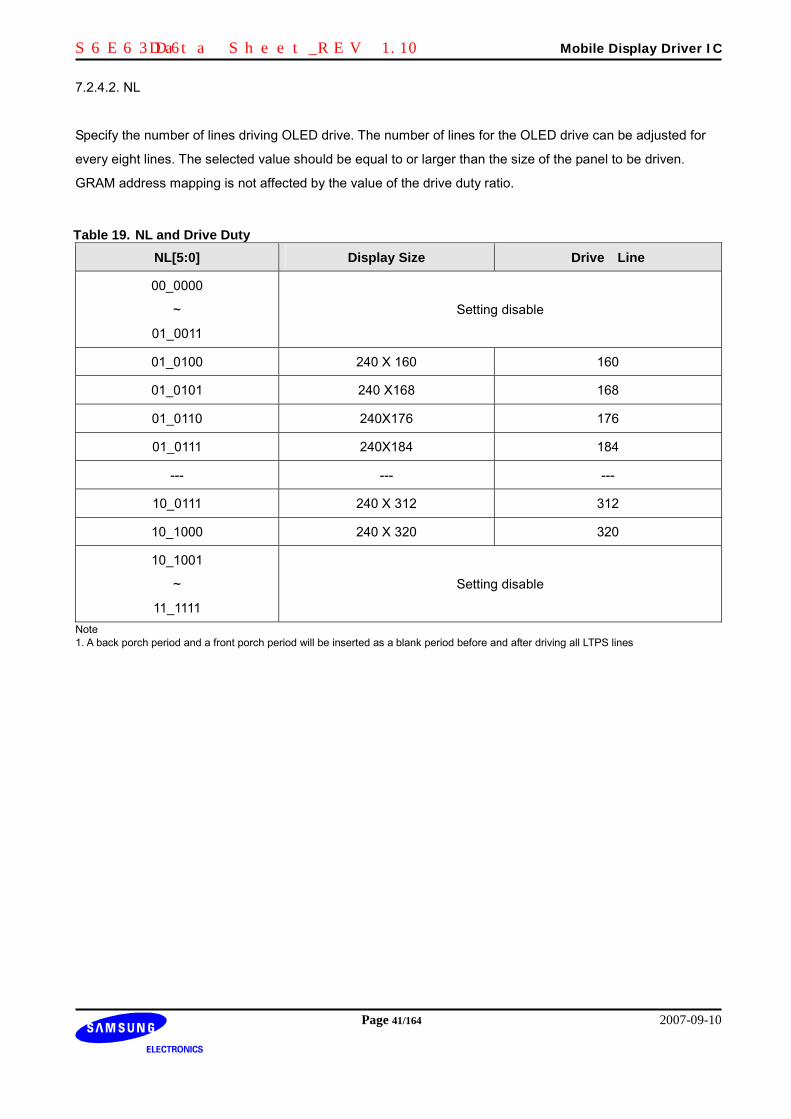
S6E63D6 Data Sheet_REV 1.10 Mobile Display Driver IC
Page 41/164 2007-09-10
7.2.4.2. NL
Specify the number of lines driving OLED drive. The number of lines for the OLED drive can be adjusted for
every eight lines. The selected value should be equal to or larger than the size of the panel to be driven.
GRAM address mapping is not affected by the value of the drive duty ratio.
Table 19. NL and Drive Duty NL[5:0] Display Size Drive Line
00_0000
~
01_0011
Setting disable
01_0100 240 X 160 160
01_0101 240 X168 168
01_0110 240X176 176
01_0111 240X184 184
--- --- ---
10_0111 240 X 312 312
10_1000 240 X 320 320
10_1001
~
11_1111
Setting disable
Note 1. A back porch period and a front porch period will be inserted as a blank period before and after driving all LTPS lines

S6E63D6 Data Sheet_REV 1.10 Mobile Display Driver IC
Page 42/164 2007-09-10
7.2.5. RGB Interface Control (R02h)
R/W RS IB15 IB14 IB13 IB12 IB11 IB10 IB9 IB8 IB7 IB6 IB5 IB4 IB3 IB2 IB1 IB0W 1 X X X X X X X RM DM X RIM1 RIM0 VSPL HSPL EPL DPL
*02h Initial Value = XXXX_XXX0_0X00_0000
7.2.5.1. Internal Clock Mode
All display operation is controlled by signals generated by the internal clock in internal clock mode.
All inputs through the external display interface are invalid. The internal RAM can be accessed only via the
system interface.
7.2.5.2. RGB Interface Mode
The display operation is controlled by the frame synchronization clock (VSYNC), raster-row synchronization
signal (HSYNC), and dot clock (DOTCLK) in RGB interface mode. These signals should be supplied during
display operation in this mode.
The display data is transferred to the internal RAM via DB17-0 for each pixel. Combining the function of the
high-speed write mode and the window address enables display of both the motion picture area and the
internal RAM area simultaneously. In this method, data is only transferred when the screen is updated,
which reduces the amount of data transferred.
The periods of the front (FP), back (BP) porch, and the display are automatically generated in the S6E63D6
by counting the raster-row synchronization signal (HSYNC) based on the frame synchronization signal
(VSYNC).
7.2.5.3. RM
Specify the interface for GRAM accesse as shown below. This register and DM register can be set
independently.

S6E63D6 Data Sheet_REV 1.10 Mobile Display Driver IC
Page 43/164 2007-09-10
7.2.5.4. DM
Specify the display operation mode. The interface can be set based on the bit of DM. In internal clock
opeartion mode the source clock for display operation comes from internal oscillator while in external clock
opeartion mode it comes from RGB interface(DOTCLK, VSYNC, HSYNC).
Table 20. RM, DM, GRAM Access Interface and Display Operation Mode RM DM GRAM Access Interface Display operation mode
0 0 System interface Internal clock operation
1 1 RGB interface External clock operation Note 1. [RM, DM]= 01, [RM, DM]=10 Setting disable.
7.2.5.5. RIM
Specify RGB interface mode when the RGB interface is used. This register is valid when RM is set to “1”.
DM and this register should be set before proper display operation is performed through the RGB interface.
Table 21. RIM and RGB Interface Mode RIM[1:0] RGB Interface mode
00 18-bit RGB interface (one transfer per pixel)
01 16-bit RGB interface (one transfer per pixel)
10 6-bit RGB interface (three transfers per pixel)
11 Setting disable

S6E63D6 Data Sheet_REV 1.10 Mobile Display Driver IC
Page 44/164 2007-09-10
You should notice that some display functions, which will be described later, cannot be used according to the
display mode shown below.
Table 22. Display Functions and Display Modes Function External Clock Operation Mode Internal Clock Operation Mode
Partial Display Cannot be used Can be used
Scroll Function Cannot be used Can be used
Rotation Cannot be used Can be used
Mirroring Cannot be used Can be used
Window Function Cannot be used Can be used
Display mode and RAM Access is controlled as shown below. For each display status, display mode control
and RAM Access control are combined properly.
Table 23. Display State and Interface Display State RAM Access (RM) Display Operation Mode (DM)
Still Pictures System interface
(RM=0) Internal clock mode
(DM=0)
Motion Pictures RGB interface
(RM=1) External clock mode
(DM=1) Note 1. The instruction register can only be set through the system interface(SPI), when RGB interface mode. 2. The RGB interface mode(RIM) should not be set during operation. 3. For the transition flow for each operation mode, see the External Display Interface section.

S6E63D6 Data Sheet_REV 1.10 Mobile Display Driver IC
Page 45/164 2007-09-10
7.2.5.6. VSPL
Determine the active polarity of VSYNC.
Table 24. VSPL and VSYNC VSPL VSYNC Description
0 (1) 0 (1) Valid (Valid)
0 (1) 1 (0) Invalid (Invalid)
7.2.5.7. HSPL
Determine the active polarity of HSYNC.
Table 25. HSPL and VSYNC HSPL HSYNC Description
0 (1) 0 (1) Valid (Valid)
0 (1) 1 (0) Invalid (Invalid)
7.2.5.8. EPL
Determine the active polarity of ENABLE for using RGB interface.
Table 26. EPL, ENABLE and RAM access EPL ENABLE RAM Write RAM Address
0 (1) 0 (1) Valid (Valid) Updated (Updated)
0 (1) 1 (0) Invalid (Invalid) Hold (Hold)
7.2.5.9. DPL
Determine the active polarity of DOTCLK.
Table 27. HSPL and VSYNC DPL DOTCLK Description
0 (1) ↑(↓) Valid (Valid)
0 (1) ↓ (↑) Invalid (Invalid)

S6E63D6 Data Sheet_REV 1.10 Mobile Display Driver IC
Page 46/164 2007-09-10
7.2.6. Entry Mode (R03h)
R/W RS IB15 IB14 IB13 IB12 IB11 IB10 IB9 IB8 IB7 IB6 IB5 IB4 IB3 IB2 IB1 IB0W 1 CLS MDT1 MDT0 BGR X X X SS X X I/D1 I/D0 X X X AM
*03h Initial Value = 1000_XXX0_XX11_XXX0 7.2.6.1. CLS
This bit is used to define the color and interface bus format, When MDT0-1 = 00 CLS = 0: 65K-color mode through 8-bit(Index address 24h) or 16-bit bus(Index address 23h) CLS = 1: 262K-color mode through 9-bit(Index address 24h) or 18-bit bus(Index address 23h) 7.2.6.2. MDT1
This bit is active on the 80-system of 8-bit bus and the data for 1-pixel is transported to the memory for 3 write cycles. This bit is on the 80-system of 16-bit bus and the data for 1-pixel is transported to the memory for 2 write cycles. When the 80-system interface mode is not set in the 8-bit or16-bit mode, set MDT1 bit to be “0”. 7.2.6.3. MDT0 When 8-bit or16-bit 80 interface mode and MDT1 bit =1, MDT0 defines color depth for the IC. 8-bit (80-system), MDT0 = 0: 262k-color mode (3 times of 6-bit data transfer to GRAM) 8-bit (80-system), MDT0 = 1: 65k-color mode (5-bit, 6-bit, 5-bit data transfer to GRAM) 16-bit (80-system), MDT0 = 0: 262k-color mode (16-bit, 2-bit data transfer to GRAM) 16-bit (80-system), MDT0 = 1: 262k-color mode (2-bit, 16-bit data transfer to GRAM)
Table 28. Multiple Data Transfer Function 1 Interface
Mode MDT1 MDT0 Multiple Data Transfer Function
* 0 0 Default value. Multiple data transfer(MDT1-0) function is not available. Data transfer is controlled by interface mode. (Depends on S_PB, ID_MIB pads, CLS register and Index address 23h or 24h)
0 1 Multiple data transfer(MDT1-0) function is not available. 80/68
system
8-bit
1 0
DB8
DB7
DB6
DB5
DB4
DB3
DB17
DB16
DB15INPUT DATA
R5 R4 R3 R2 R1 R0 G5 G4 G3 G2 G1 G0
S(n)
B5 B4 B3 B2 B1 B0RGB Arrangement
Output
Note: n= 1 to 240
DB14
DB13
DB12
DB17
DB16
DB15
DB14
DB13
DB12
1st Transmission 2nd Transmission 3rd Transmission
DB8
DB7
DB6
DB5
DB4
DB3
DB8
DB7
DB6
DB5
DB4
DB3

S6E63D6 Data Sheet_REV 1.10 Mobile Display Driver IC
Page 47/164 2007-09-10
Table 29. Multiple Data Transfer Function 2 Interface
Mode MDT1 MDT0 Multiple Data Transfer Function
80/68
system
8-bit
1 1
DB17
DB16
DB15
DB14
DB13
DB12
DB17
DB16
DB15INPUT DATA
R5 R4 R3 R2 R1 R0 G5 G4 G3 G2 G1 G0
S(n)
B5 B4 B3 B2 B1 B0RGB Arrangement
Output
Note: n= 1 to 240
DB14
DB13
DB12
DB17
DB16
DB15
DB14
DB13
DB12
1st Transmission 2nd Transmission 3rd Transmission
DB8
DB7
DB6
DB5
DB4
DB3
DB8
DB7
DB6
DB5
DB4
DB3
DB8
DB7
DB6
DB5
DB4
DB3
0 1
0
DB17
DB16
DB15
DB14
DB13
DB12
DB11
DB10
DB8INPUT DATA
R5 R4 R3 R2 R1 R0 G5 G4 G3 G2 G1 G0
S(n)
B5 B4 B3 B2 B1 B0RGB Arrangement
Output
Note: n= 1 to 240
DB7
DB6
DB5
DB4
DB3
DB2
DB1
DB17
DB16
1st Transmission 2nd Transmission
80/68
system
16-bit
1
1
DB2
DB1
DB17
DB16
DB15
DB14
DB13
DB12
DB11INPUT DATA
R5 R4 R3 R2 R1 R0 G5 G4 G3 G2 G1 G0
S(n)
B5 B4 B3 B2 B1 B0RGB Arrangement
Output
Note: n= 1 to 240
DB10
DB8
DB7
DB6
DB5
DB4
DB3
DB2
DB1
1st Transmission 2nd Transmission

S6E63D6 Data Sheet_REV 1.10 Mobile Display Driver IC
Page 48/164 2007-09-10
7.2.6.4. BGR About writing 18-bit data to GRAM, it is changed <R><G><B> into <B><G><R>. BGR = 0; DB[17:12], DB[11:6], DB[5:0] is assigned to R, G, B. Actually the analog value that corresponds to DB[17:12] is output firstly at source output BGR = 1; DB[17:12], DB[11:6], DB[5:0] is assigned to B, G, R. Actually the analog value that corresponds to DB[5:0] is output firstly at source output. 7.2.6.5. SS Select the direction of the source driver channel in pixel unit. When user changes the value of SS, memory should be updated to apply the change.
Table 30. Source Output Direction Control with SS (SS = “1”) S240 S239 S238 S3 S2 S1
G1 “00000”H “00001”H “00002”H •••••••••• “000ED”H “000EE”H “000EF”H
G2 “00100”H “00101”H “00102”H •••••••••• “001ED”H “001EE”H “001EF”H
G3 “00200”H “00201”H “00202”H •••••••••• “002ED”H “002EE”H “002EF”H
G4 “00300”H “00301”H “00302”H •••••••••• “003ED”H “003EE”H “003EF”H
G5 “00400”H “00401”H “00402”H •••••••••• “004ED”H “004EE”H “004EF”H
G6 “00500”H “00501”H “00502”H •••••••••• “005ED”H “005EE”H “005EF”H
G7 “00600”H “00601”H “00602”H •••••••••• “006ED”H “006EE”H “006EF”H
G8 “00700”H “00701”H “00702”H •••••••••• “007ED”H “007EE”H “007EF”H
M M M M M M M M
G313 “13800”H “13801”H “13802”H ••••••••• “138ED”H “138EE”H “138EF”H
G314 “13900”H “13901”H “13902”H ••••••••• “139ED”H “139EE”H “139EF”H
G315 “13A00”H “13A01”H “13A02”H ••••••••• “13AED”H “13AEE”H “13AEF”H
G316 “13B00”H “13B01”H “13B02”H ••••••••• “13BED”H “13BEE”H “13BEF”H
G317 “13C00”H “13C01”H “13C02”H ••••••••• “13CED”H “13CEE”H “13CEF”H
G318 “13D00”H “13D01”H “13D02”H ••••••••• “13DED”H “13DEE”H “13DEF”H
G319 “13E00”H “13E01”H “13E02”H ••••••••• “13EED”H “13EEE”H “13EEF”H
G320 “13F00”H “13F01”H “13F02”H ••••••••• “13FED”H “13FEE”H “13FEF”H Note 1. For the case of SS = “0”, refer to “GRAM ADDRESS MAP” presented earlier. You should notice that the order of source output is reversed.

S6E63D6 Data Sheet_REV 1.10 Mobile Display Driver IC
Page 49/164 2007-09-10
7.2.6.6. ID
When ID[1], ID[0] = 1, the address counter (AC) is automatically increased by 1 after the data is written to the GRAM. When ID[1], ID[0] = 0, the AC is automatically decreased by 1 after the data is written to the GRAM. The increment/decrement setting of the address counter using ID[1:0] is done independently for the horizontal address and vertical address. 7.2.6.7. AM Set the automatic update method of the AC after the data is written to GRAM. When AM = “0”, the data is continuously written in horizontally. When AM = “1”, the data is continuously written vertically. When window addresses are specified, the GRAM in the window range can be written to according to the ID[1:0] and AM.
Table 31. Address Direction Setting
ID[1:0] = “00” H: decrement V: decrement
ID[1:0] = “01” H: increment V: decrement
ID[1:0] = “10” H: decrement V: increment
ID[1:0] = “11” H: increment V: increment
AM=”0” Horizontal Update
00000h
13FEFh
00000h
13FEFh
00000h
13FEFh
00000h
13FEFh
AM=”1” Vertical Update
0000h
13FEFh
0000h
13FEFh
0000h
13FEFh
0000h
13FEFh
Note 1. When window addresses have been set, the GRAM can only be written within the window. When AM or ID is set, the start address should be written accordingly prior to memory write.

S6E63D6 Data Sheet_REV 1.10 Mobile Display Driver IC
Page 50/164 2007-09-10
7.2.7. Clock Control (R04h)
R/W RS IB15 IB14 IB13 IB12 IB11 IB10 IB9 IB8 IB7 IB6 IB5 IB4 IB3 IB2 IB1 IB0W 1 X X X X X X X X X X DCR1 DCR0 X X X X
*04h Initial Value = XXXX_XXXX_XX00_XXXX
7.2.7.1. DCR
Set the division ratio of booster clock, DCCLK, in external clock operation mode. In this case, DOTCLK must
be input periodically and continuously.
Table 32. DCR and Division Ratio of DCCLK DCR[1:0] Division ratio of DCCLK
00 DOTCLK / 4
01 DOTCLK / 8
10 DOTCLK / 16
11 DOTCLK / 32

S6E63D6 Data Sheet_REV 1.10 Mobile Display Driver IC
Page 51/164 2007-09-10
7.2.8. Display Control 1 (R05h)
R/W RS IB15 IB14 IB13 IB12 IB11 IB10 IB9 IB8 IB7 IB6 IB5 IB4 IB3 IB2 IB1 IB0 W 1 X X X X X X X X X X X X X X X DISP_ON
*05h Initial Value = XXXX_XXXX_XXXX_XXX0
7.2.8.1. DISP_ON
Output from the Frame Memory is enabled.
This register makes No Change of contents of frame memory
DISP_ON = 0 (Display is black image),
DISP_ON = 1,
Memory Display(Example)
Memory Display(Example)

S6E63D6 Data Sheet_REV 1.10 Mobile Display Driver IC
Page 52/164 2007-09-10
7.2.9. Display Control 2 (R06h)
R/W RS IB15 IB14 IB13 IB12 IB11 IB10 IB9 IB8 IB7 IB6 IB5 IB4 IB3 IB2 IB1 IB0W 1 X X X X X X X X X X X CL X X TEMON REV
*06h Initial Value = XXXX_XXXX_XXX0_XX00
7.2.9.1. CL Sets color depth of display.
Table 33. Color Control by CL CL Description
0 262,144 / 65,536 colors [NOTE]
1 8 colors Note 1. It depend on interface mode(18bit or 16bit). 7.2.9.2. TEMON TEMON = 0, Disable the TE output signal from the SIN signal line for preventing Tearing Effect. TEMON = 1, Enable the TE output signal from the SIN signal line for preventing Tearing Effect.
Figure 7. The Waveform of TE Signal
7.2.9.3. REV Displays all characters and graphics display sections with reversal when REV = 1. The grayscale level can be reversed.
Table 34. REV and Source Output Level in Normal Display Area
REV GRAM Data Source Output Level in Displayed Area
0 6’b000000
~ 6’b111111
V0 (High Voltage) ~
V63(Low Voltage)
1 6’b000000
~ 6’b111111
V63 (Low Voltage) ~
V0 (High Voltage)

S6E63D6 Data Sheet_REV 1.10 Mobile Display Driver IC
Page 53/164 2007-09-10
7.2.10. Panel Interface Control 1 (R07h, R08h)
R/W RS IB15 IB14 IB13 IB12 IB11 IB10 IB9 IB8 IB7 IB6 IB5 IB4 IB3 IB2 IB1 IB0
W 1 X X X CLW EA4
CLW EA3
CLWEA2
CLWEA1
CLWEA0
X X X X X X X X
*07h Initial Value = XXX1_0010_XXXX_XXXX
R/W RS IB15 IB14 IB13 IB12 IB11 IB10 IB9 IB8 IB7 IB6 IB5 IB4 IB3 IB2 IB1 IB0W 1 X X X CLW
EB4 CLW EB3
CLWEB2
CLWEB1
CLWEB0
X X X CLW EC4
CLW EC3
CLW EC2
CLWEC1
CLWEC0
*08h Initial Value = XXX1_0010_XXX1_0010
7.2.10.1. CLWEA, CLWEB, CLWEC
Specifies the interval time of R_sw, G_sw, B_sw respectively.
Table 35. CLWEx and the Intervals CLWEx[4:0] Description
0_0000 Setting disable
--- Setting disable
0_1011 Setting disable
0_1100 6 HCLK
--- ---
1_0010 9 HCLK
--- ---
1_1110 15 HCLK
1_1111 15.5 HCLK Note 1. For the information of HCLK, refer to “FRAME FREQUENCY CACULATION”

S6E63D6 Data Sheet_REV 1.10 Mobile Display Driver IC
Page 54/164 2007-09-10
7.2.11. Panel Interface Control 2 (R09h)
R/W RS IB15 IB14 IB13 IB12 IB11 IB10 IB9 IB8 IB7 IB6 IB5 IB4 IB3 IB2 IB1 IB0
W 1 X X X X X X X X X SHE2 SHE1 SHE0 X CLT E2
CLTE1
CLTE0
*09h Initial Value = XXXX_XXXX_X010_X010
7.2.11.1. SHE
Specify the latency of G_sw and B_sw.
Table 36. SHE and the Latency of G_sw and B_sw SHE[2:0] Description
000 Setting disable
001 0.5 HCLK
010 1 HCLK
--- ---
110 3 HCLK
111 3.5 HCLK
7.2.11.2. CLTE
Specify the falling position of R_sw.
Table 37. CLTE and the falling position of R_sw CLTE[2:0] Description
000 Setting disable
001 0.5 HCLK
010 1 HCLK
011 1.5 HCLKs
--- ---
110 3 HCLKs
111 3.5 HCLKs Note 1. CLWEA + CLWEB + CLWEC + SHE + CLTE ≤ 32 HCLK

S6E63D6 Data Sheet_REV 1.10 Mobile Display Driver IC
Page 55/164 2007-09-10
7.2.12. Device Code Read (R0Fh)
R/W RS IB15 IB14 IB13 IB12 IB11 IB10 IB9 IB8 IB7 IB6 IB5 IB4 IB3 IB2 IB1 IB0W 1 0 1 1 0 0 0 1 1 1 1 0 1 0 1 1 0
You can read device code(‘63D6h’) by index 0Fh.
7.2.13. Stand By (R10h)
R/W RS IB15 IB14 IB13 IB12 IB11 IB10 IB9 IB8 IB7 IB6 IB5 IB4 IB3 IB2 IB1 IB0W 1 X X X X X X X X X X X X X NAP X STB
*10h Initial Value = XXXX_XXXX_XXXX_X0X1
7.2.13.1. STB
When STB = “1”, S6E63D6 enters Standby mode, where display operation completely stops including the
internal R-C oscillation. Furthermore, no external clock pulses are supplied.
Standby mode cancel ; STB = “0”
7.2.13.2. NAP
It is for MDDI I/F.
When NAP = “1”, S6E63D6 enters NAP mode, where display operation completely stops except the internal
R-C oscillation (if STB = 0). NAP mode is the same state with the STB mode but internal R-C oscillation
operates.
Note 1. The default of STB for MDDI client is “0” to enable MDDI I/F after Reset is applied. 2. NAP is only valid MDDI I/F( when MDDI_EN = 1), Even if NAP is ‘1’ at other I/F(MDDI_EN = 0), S6E63D6 does not enter the NAP mode.

S6E63D6 Data Sheet_REV 1.10 Mobile Display Driver IC
Page 56/164 2007-09-10
7.2.14. Power GEN 1 (R12h)
R/W RS IB15 IB14 IB13 IB12 IB11 IB10 IB9 IB8 IB7 IB6 IB5 IB4 IB3 IB2 IB1 IB0W 1 X X X X X X X X X X X X VC3 VC2 VC1 VC0
*12h Initial Value = XXXX_XXXX_XXXX_1000
7.2.14.1. VCI1
Reference voltage of VLOUT1, VLOUT2 and VLOUT3
Table 38. The Setting of VCI1 VC[3:0] VCI1 [Without Load]
0000 2.10 V
0001 2.15 V
0010 2.20 V
0011 2.25 V
0100 2.30 V
0101 2.35 V
0110 2.40 V
0111 2.45 V
1000 2.50 V
1001 2.55 V
1010 2.60 V
1011 2.65 V
1100 2.70 V
1101 2.75 V
1110 Setting disable
1111 Setting disable Note 1. Set VCI1 in the range of VCI > VCI1 + 0.3V

S6E63D6 Data Sheet_REV 1.10 Mobile Display Driver IC
Page 57/164 2007-09-10
7.2.15. Power GEN 2 (R13h)
R/W RS IB15 IB14 IB13 IB12 IB11 IB10 IB9 IB8 IB7 IB6 IB5 IB4 IB3 IB2 IB1 IB0W 1 X X VINT3 VINT2 VINT1 VINT0 X X X X X X X X X X
*13h Initial Value = XX01_01XX_XXXX_XXXX
7.2.15.1. VINT
VINT[3:0] set VINT (control voltage of OLED Panel). It can be amplified -2.0 to -0.5 times of VCIR.
Table 39. The Setting of VINT VINT[3:0] VINT value
0000 -1.0 V
0001 -1.2 V
0010 -1.4 V
0011 -1.6 V
0100 -1.8 V
0101 -2.0 V
0110 -2.2 V
0111 -2.4 V
1000 -2.6 V
1001 -2.8 V
1010 -3.0 V
1011 -3.2 V
1100 -3.4 V
1101 -3.6 V
1110 -3.8 V
1111 -4.0 V Note 1. Set VINIT in the range of VINT > VLOUT3 + 1.0V

S6E63D6 Data Sheet_REV 1.10 Mobile Display Driver IC
Page 58/164 2007-09-10
7.2.16. Power GEN 3 (RF8h)
R/W RS IB15 IB14 IB13 IB12 IB11 IB10 IB9 IB8 IB7 IB6 IB5 IB4 IB3 IB2 IB1 IB0 W 1 X X X X X X X X X X X VGH4 VGH3 VGH2 VGH1 VGH0
*F8h Initial Value = XXXX_XXXX_XXX1_0100
7.2.16.1. VGH
VGH[4:0] set VGH (High Voltage Level for Gate).
Table 40. The Setting of VGH VGH[4:0] VGH value VGH[4:0] VGH value
00000 Setting disable 10000 5.2 V
00001 Setting disable 10001 5.4 V
00010 Setting disable 10010 5.6 V
00011 Setting disable 10011 5.8 V
00100 Setting disable 10100 6.0 V
00101 3.0 V 10101 6.2 V
00110 3.2 V 10110 6.4 V
00111 3.4 V 10111 6.6 V
01000 3.6 V 11000 6.8 V
01001 3.8 V 11001 7.0 V
01010 4.0 V 11010 7.2 V
01011 4.2 V 11011 7.4 V
01100 4.4 V 11100 7.6 V
01101 4.6 V 11101 7.8 V
01110 4.8 V 11110 8.0 V
01111 5.0 V 11111 Setting disable Note 1. Set VGH in the range of VGH < VLOUT2 - 1.0V

S6E63D6 Data Sheet_REV 1.10 Mobile Display Driver IC
Page 59/164 2007-09-10
7.2.17. Power GEN 4 (RF9h)
R/W RS IB15 IB14 IB13 IB12 IB11 IB10 IB9 IB8 IB7 IB6 IB5 IB4 IB3 IB2 IB1 IB0 W 1 X X X X X X X X X X X VGL4 VGL3 VGL2 VGL1 VGL0
*F9h Initial Value = XXXX_XXXX_XXX1_0100
7.2.17.1. VGL
VGL[4:0] bits set VGL (Low Voltage Level for Gate).
Table 41. The Setting of VGL VGL[4:0] VGL value VGL[4:0] VGL value
00000 Setting disable 10000 -5.2 V
00001 Setting disable 10001 -5.4 V
00010 Setting disable 10010 -5.6 V
00011 Setting disable 10011 -5.8 V
00100 Setting disable 10100 -6.0 V
00101 -3.0 V 10101 -6.2 V
00110 -3.2 V 10110 -6.4 V
00111 -3.4 V 10111 -6.6 V
01000 -3.6 V 11000 -6.8 V
01001 -3.8 V 11001 -7.0 V
01010 -4.0 V 11010 -7.2 V
01011 -4.2 V 11011 -7.4 V
01100 -4.4 V 11100 -7.6 V
01101 -4.6 V 11101 -7.8 V
01110 -4.8 V 11110 -8.0 V
01111 -5.0 V 11111 Setting disable Note 1. Set VGL in the range of VGL > VLOUT3 + 1.0V
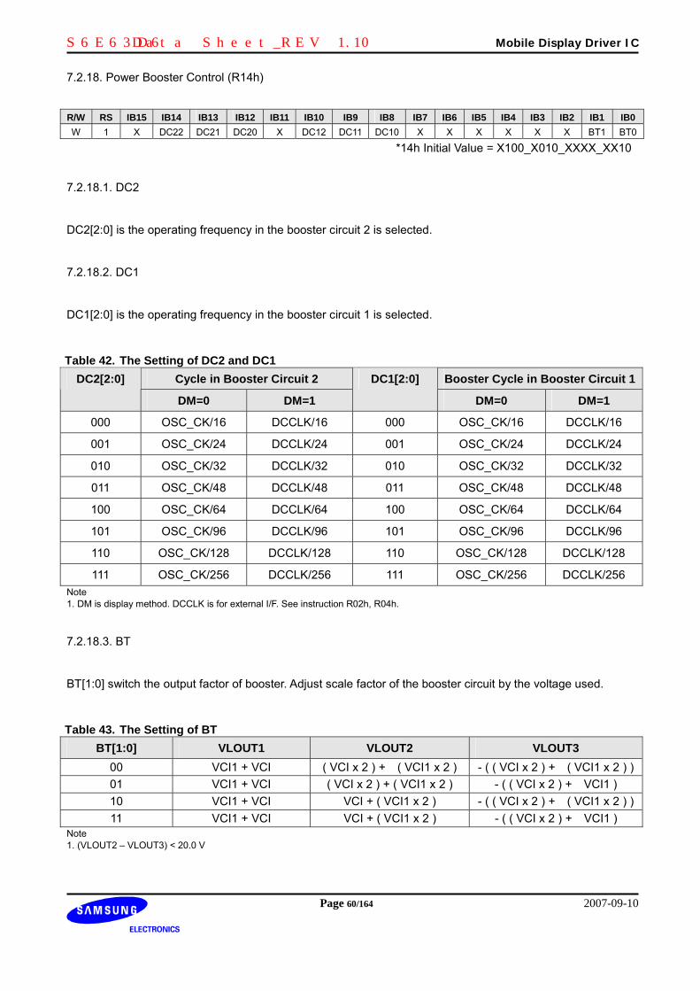
S6E63D6 Data Sheet_REV 1.10 Mobile Display Driver IC
Page 60/164 2007-09-10
7.2.18. Power Booster Control (R14h)
R/W RS IB15 IB14 IB13 IB12 IB11 IB10 IB9 IB8 IB7 IB6 IB5 IB4 IB3 IB2 IB1 IB0W 1 X DC22 DC21 DC20 X DC12 DC11 DC10 X X X X X X BT1 BT0
*14h Initial Value = X100_X010_XXXX_XX10
7.2.18.1. DC2
DC2[2:0] is the operating frequency in the booster circuit 2 is selected.
7.2.18.2. DC1
DC1[2:0] is the operating frequency in the booster circuit 1 is selected.
Table 42. The Setting of DC2 and DC1 Cycle in Booster Circuit 2 Booster Cycle in Booster Circuit 1DC2[2:0]
DM=0 DM=1
DC1[2:0]
DM=0 DM=1
000 OSC_CK/16 DCCLK/16 000 OSC_CK/16 DCCLK/16
001 OSC_CK/24 DCCLK/24 001 OSC_CK/24 DCCLK/24
010 OSC_CK/32 DCCLK/32 010 OSC_CK/32 DCCLK/32
011 OSC_CK/48 DCCLK/48 011 OSC_CK/48 DCCLK/48
100 OSC_CK/64 DCCLK/64 100 OSC_CK/64 DCCLK/64
101 OSC_CK/96 DCCLK/96 101 OSC_CK/96 DCCLK/96
110 OSC_CK/128 DCCLK/128 110 OSC_CK/128 DCCLK/128
111 OSC_CK/256 DCCLK/256 111 OSC_CK/256 DCCLK/256 Note 1. DM is display method. DCCLK is for external I/F. See instruction R02h, R04h.
7.2.18.3. BT
BT[1:0] switch the output factor of booster. Adjust scale factor of the booster circuit by the voltage used.
Table 43. The Setting of BT BT[1:0] VLOUT1 VLOUT2 VLOUT3
00 VCI1 + VCI ( VCI x 2 ) + ( VCI1 x 2 ) - ( ( VCI x 2 ) + ( VCI1 x 2 ) )01 VCI1 + VCI ( VCI x 2 ) + ( VCI1 x 2 ) - ( ( VCI x 2 ) + VCI1 ) 10 VCI1 + VCI VCI + ( VCI1 x 2 ) - ( ( VCI x 2 ) + ( VCI1 x 2 ) )11 VCI1 + VCI VCI + ( VCI1 x 2 ) - ( ( VCI x 2 ) + VCI1 )
Note 1. (VLOUT2 – VLOUT3) < 20.0 V

S6E63D6 Data Sheet_REV 1.10 Mobile Display Driver IC
Page 61/164 2007-09-10
7.2.19. Oscillator Control (R18h)
R/W RS IB15 IB14 IB13 IB12 IB11 IB10 IB9 IB8 IB7 IB6 IB5 IB4 IB3 IB2 IB1 IB0W 1 X X X X X X X X X X RAD
J5 RAD J4
RAD J3
RAD J2
RADJ1
RADJ0
*18h Initial Value = XXXX_XXXX_XX01_1111
7.2.19.1. RADJ
Select the oscillation frequency of internal oscillator.
Table 44. The Setting of RADJ RADJ[5:0] Oscillation Speed RADJ[5:0] Oscillation Speed
000000 x 0.543(Min.) 010101 x 0.782
000001 x 0.551 010110 x 0.800
000010 x 0.560 010111 x 0.818
000011 x 0.568 011000 x 0.835
000100 x 0.578 011001 x 0.855
000101 x 0.586 011010 x 0.877
000110 x 0.596 011011 x 0.899
000111 x 0.606 011100 x 0.921
001000 x 0.615 011101 x 0.946
001001 x 0.626 011110 x 0.972
001010 x 0.637 011111 x 1.000
001011 x 0.647 100000 x 1.037
001100 x 0.660 100001 x 1.067
001101 x 0.671 100010 x 1.101
001110 x 0.685 100011 x 1.135
001111 x 0.697 100100 x 1.172
010000 x 0.707 100101 x 1.212
010001 x 0.721 100110 x 1.256
010010 x 0.736 100111 x 1.302
010011 x 0.751 101000 X1.352(Max.)
010100 x 0.766 101001 ~ 111111 Setting disable

S6E63D6 Data Sheet_REV 1.10 Mobile Display Driver IC
Page 62/164 2007-09-10
7.2.20. Source Driver Control (R1Ah)
R/W RS IB15 IB14 IB13 IB12 IB11 IB10 IB9 IB8 IB7 IB6 IB5 IB4 IB3 IB2 IB1 IB0
W 1 X X X X X X X X X X GAMMA_TEST
SDU M_ON
X SAP
2 SAP
1 SAP
0
*1Ah Initial Value = XXXX _XXXX_XX00_X101
7.2.20.1. GAMMA_TEST
When GAMMA_TEST=’1’, V0/V63 pads are shorted to each gamma voltage V0/V63 and gamma voltage
V0/V63 can be monitored or be forced by external voltage level.
Table 45. The Setting of GAMMA_TEST GAMMA_TEST V0 / V63
0 Hi-z
1 V0 / V63
7.2.20.2. SDUM_ON
When SDUM_ON=’1’, SOUT_DUM1 and SOUT_DUM240 pads are shorted to SOUT[1], SOUT[240] output
and can be monitored.
Table 46. The Setting of SDUM_ON SDUM_ON SOUT_DUM1 / SOUT_DUM240
0 Hi-z
1 SOUT[1] / SOUT[240]

S6E63D6 Data Sheet_REV 1.10 Mobile Display Driver IC
Page 63/164 2007-09-10
7.2.20.3. SAP
Adjust the slew-rate of the operational amplifier of the source driver. If higher SAP[2:0] is set, OLED panel
having higher resolution of higher frame frequency can be driven because the slew-rate of the operational
amplifier is increased. But, these bits must be set as adequate value because the amount of fixed current of
the operational amplifier is also adjusted. During non-display, when SAP[2:0]=”000”, operational amplifiers
are turned off, so current consumption can be reduced
Table 47. The Setting of SAP
SAP[2:0] Slew-Rate of Operational
Amplifier
Amount of Current in
Operational Amplifier
000 Operation of the operational amplifier stops.
001 Slow Small
010 Slow or medium Small or medium
011 Medium Medium
100 Medium or small fast Medium or small large
101 Small fast Small large
110 Fast large
111 Big fast Big large

S6E63D6 Data Sheet_REV 1.10 Mobile Display Driver IC
Page 64/164 2007-09-10
7.2.21. GRAM Address Set (R20h, R21h)
R/W RS IB15 IB14 IB13 IB12 IB11 IB10 IB9 IB8 IB7 IB6 IB5 IB4 IB3 IB2 IB1 IB0W 1 X X X X X X X X AD7 AD6 AD5 AD4 AD3 AD2 AD1 AD0
*20h Initial Value = XXXX _XXXX_0000_0000
R/W RS IB15 IB14 IB13 IB12 IB11 IB10 IB9 IB8 IB7 IB6 IB5 IB4 IB3 IB2 IB1 IB0
W 1 X X X X X X X AD16
AD15
AD14
AD13
AD 12
AD 11
AD 10
AD9 AD8
*21h Initial Value = XXXX _XXX0_0000_0000
7.2.21.1. AD
You can write initial GRAM address into internal Address Counter (AC). When GRAM data is transferred
through System Interface or RGB Interface, the AC is automatically updated according to AM and ID. This
allows consecutive write / read without re-setting address in AC.
Ensure that the address is set within the specified window area.
When RGB interface is used (RM=”1”) to access GRAM, AD[16:0] will be set in the address counter at the
falling edge of the VSYNC signal. And when one uses System Interface to access GRAM (RM = “0”),
AD[16:0] will be set upon the execution of an instruction.
Table 48. GRAM Address Range AD[16:0] GRAM setting
“00000h” to “00AFh” Bitmap data for G1
“00100h” to “01AFh” Bitmap data for G2
“00200h” to “02AFh” Bitmap data for G3
“00300h” to “03AFh” Bitmap data for G4
M
M
M
M
“13C00h” to “13CEFh” Bitmap data for G317
“13D00h” to “13DEFh” Bitmap data for G318
“13E00h” to “13EEFh” Bitmap data for G319
“13F00h” to “13FEFh” Bitmap data for G320

S6E63D6 Data Sheet_REV 1.10 Mobile Display Driver IC
Page 65/164 2007-09-10
7.2.22. Write Data to GRAM (R22h)
R/W RS IB15 IB14 IB13 IB12 IB11 IB10 IB9 IB8 IB7 IB6 IB5 IB4 IB3 IB2 IB1 IB0W 1 RAM write data (WD17-0): Pad assignment varies according to the interface method.
(see the following figure for more information) R/W RS WD
15 WD 14
WD13
WD 12
WD 11
WD10
WD9 WD8 WD7 WD6 WD5 WD4 WD3 WD2 WD1 WD0
W 1 When RGB-interface
WD17-0: Input data for GRAM can be expanded to 18 bits. The expansion format varies according to the interface method. The input data selects the grayscale level. After a write, the address is automatically updated according to I/D bit settings. When 16- or 8-bit interface is in use, the write data is expanded to 18 bits by writing the MSB of the <R><B> data to its LSB. When data is written to RAM used by RGB interface via the system interface, please make sure that write data conflicts do not occur. When the 18-bit RGB interface is in use, 18-bit data is written to RAM via DB17-0 and 262,144-colors are available. When the 16-bit RGB interface is in use, the MSB is written to its LSB and 65,536-colors are available.
Write Index 00h or anotherwhere, Address hold
Write More ?
Address is updated by 1
Start
Yes
No
Index Write (22h)
( Memory Write )
Window Address Set(index 35h, 36h, 37h)
Write Data
Start Address Set(index 20h, 21h)
Figure 8. Memory Data Write Sequence

S6E63D6 Data Sheet_REV 1.10 Mobile Display Driver IC
Page 66/164 2007-09-10
7.2.23. Read Data from FROM GRAM (R22h)
R/W RS DB 17
DB 16
DB 15
DB14
DB 13
DB 12
DB11
DB10
DB9
DB8
DB7
DB6
DB 5
DB 4
DB 3
DB2
DB1
DB0
R 1 RAM Read data (RD17-0): Pad assignment varies according to the interface method. (see the following figure for more information)
RD17–0: Read 18-bit data from the GRAM. When the data is read to the CPU, the first-word read
immediately after the GRAM address setting is latched from the GRAM to the internal read-data latch. The
data on the data bus (DB17–0) becomes invalid and the second-word read is normal.
In case of 16-/8-bit interface, the LSB of <R><B> color data will not be read.
This function is not available in RGB interface mode.
Figure 9. Memory Data Read Sequence

S6E63D6 Data Sheet_REV 1.10 Mobile Display Driver IC
Page 67/164 2007-09-10
7.2.24. Select Data Bus 1 (R23h)
R/W RS IB15 IB14 IB13 IB12 IB11 IB10 IB9 IB8 IB7 IB6 IB5 IB4 IB3 IB2 IB1 IB0W 1 Select 18-/16-bit Data Bus Interface
7.2.25. Select Data Bus 2 (R24h)
R/W RS IB15 IB14 IB13 IB12 IB11 IB10 IB9 IB8 IB7 IB6 IB5 IB4 IB3 IB2 IB1 IB0W 1 Select 9-/8-bit Data Bus Interface
You can select system interface mode by pads and instruction as following.
Table 49. System Interface Mode Pads Registers
MDDI _EN
S_PB ID_MIB Index Address
Command(CLS)
CommandMDT[1]
CommandMDT[0]
Description
0 X 80-system 8-bit 65k bus interface
0 80-system 8-bit 260k bus interface 0 (80 8bit)
1 1 80-system 8-bit 65k bus interface
Default & 24h (9/8bit)
1 (80 9bit) X X 80-system 9-bit 260k bus interface
0 80-system 16-bit 65k bus interface 0 1 80-system 16-bit 260k bus interface
0 (80 16bit)
1 X 80-system 16-bit 260k bus interface
0 (80 mode)
Index 23h (18/16bit)
1 (80 18bit) X X 80-system 18-bit 260k bus interface
0 X 68-system 8-bit 65k bus interface
0 68-system 8-bit 260k bus interface 0 (68 8bit)
1 1 68-system 8-bit 65k bus interface
Default & 24h (9/8bit)
1 (68 9bit) X X 68-system 9-bit 260k bus interface
0 68-system 16-bit 65k bus interface 0 1 68-system 16-bit 260k bus interface
0 (68 16bit)
1 X 68-system 16-bit 260k bus interface
0 (Parallel)
1 (68 mode)
Index 23h (18/16bit)
1 (68 18bit) X X 68-system 18-bit 260k bus interface
0
1 (Serial) ID X X X X Serial peripheral interface (SPI)
1 X X X X X MDDI Note 1. For defails, see the Entry Mode (R03h)

S6E63D6 Data Sheet_REV 1.10 Mobile Display Driver IC
Page 68/164 2007-09-10
7.2.26. Vertical Scroll Control 1 (R30h, R31h)
R/W RS IB15 IB14 IB13 IB12 IB11 IB10 IB9 IB8 IB7 IB6 IB5 IB4 IB3 IB2 IB1 IB0
W 1 X X X X X X X SSA
8 SSA
7 SSA
6 SSA
5 SSA
4 SSA
3 SSA
2 SSA
1 SSA
0
*30h Initial Value = XXXX _XXX0_0000_0000
R/W RS IB15 IB14 IB13 IB12 IB11 IB10 IB9 IB8 IB7 IB6 IB5 IB4 IB3 IB2 IB1 IB0
W 1 X X X X X X X SEA
8 SEA
7 SEA
6 SEA
5 SEA
4 SEA
3 SEA
2 SEA
1 SEA
0
*31h Initial Value = XXXX _XXX1_0011_1111
7.2.26.1. SSA
Specify scroll start address at the scroll display for vertical smooth scrolling.
Table 50. The setting of scroll start address SSA8 SSA7 SSA6 SSA5 SSA4 SSA3 SSA2 SSA1 SSA0 Scroll Start Address
0 0 0 0 0 0 0 0 0 0 raster-row
0 0 0 0 0 0 0 0 1 1 raster-row
0 0 0 0 0 0 0 1 0 2 raster-row
0 0 0 0 0 0 0 1 1 3 raster-row
0 0 0 0 0 0 1 0 0 4 raster-row
0 0 0 0 0 0 1 0 1 5 raster-row
: :
1 0 0 1 1 1 1 0 0 316 raster-row
1 0 0 1 1 1 1 0 1 317 raster-row
1 0 0 1 1 1 1 1 0 318 raster-row
1 0 0 1 1 1 1 1 1 319 raster-row

S6E63D6 Data Sheet_REV 1.10 Mobile Display Driver IC
Page 69/164 2007-09-10
7.2.26.2. SEA
Specify scroll end address at the scroll display for vertical smooth scrolling.
Table 51. The setting of scroll end address SEA8 SEA7 SEA6 SEA5 SEA4 SEA3 SEA2 SEA1 SEA0 Scroll End Address
0 0 0 0 0 0 0 0 0 0 raster-row
0 0 0 0 0 0 0 0 1 1 raster-row
0 0 0 0 0 0 0 1 0 2 raster-row
0 0 0 0 0 0 0 1 1 3 raster-row
0 0 0 0 0 0 1 0 0 4 raster-row
0 0 0 0 0 0 1 0 1 5 raster-row
: :
1 0 0 1 1 1 1 0 0 316 raster-row
1 0 0 1 1 1 1 0 1 317 raster-row
1 0 0 1 1 1 1 1 0 318 raster-row
1 0 0 1 1 1 1 1 1 319 raster-row Note 1. Don’t set any higher raster-row than 319 (“13F”H) 2. Set SS18-10 ≤ SSA8-0, if set out of range, SSA8-0 = SS18-10. 3. Set SE18-10 ≥ SEA8-0, if set out of range, SEA8-0 = SE18-10

S6E63D6 Data Sheet_REV 1.10 Mobile Display Driver IC
Page 70/164 2007-09-10
7.2.27. Vertical Scroll Control 2 (R32h)
R/W RS IB15 IB14 IB13 IB12 IB11 IB10 IB9 IB8 IB7 IB6 IB5 IB4 IB3 IB2 IB1 IB0
W 1 X X X X X X X SST
8 SST
7 SST
6 SST
5 SST
4 SST
3 SST
2 SST
1 SST
0
*32h Initial Value = XXXX _XXX0_0000_0000
7.2.27.1. SST
Specify scroll start and step at the scroll display for vertical smooth scrolling. Any raster-row from the 1st to
320th can be scrolled for the number of the raster-row. After 319th raster-row is displayed, the display
restarts from the first raster-row. When SST8-0 = 00000000, Vertical Scroll Function is disabled.
Table 52. The setting of scroll end address SST8 SST7 SST6 SST5 SST4 SST3 SST2 SST1 SST0 Scroll Step
0 0 0 0 0 0 0 0 0 0 raster-row
0 0 0 0 0 0 0 0 1 1 raster-row
0 0 0 0 0 0 0 1 0 2 raster-row
0 0 0 0 0 0 0 1 1 3 raster-row
0 0 0 0 0 0 1 0 0 4 raster-row
0 0 0 0 0 0 1 0 1 5 raster-row
: :
1 0 0 1 1 1 1 0 0 316 raster-row
1 0 0 1 1 1 1 0 1 317 raster-row
1 0 0 1 1 1 1 1 0 318 raster-row
1 0 0 1 1 1 1 1 1 319 raster-row Note 1. Don’t set any higher raster-row than 319 (“13F”H) 2. Set SS18-10 < SSA8-0 + SST8-0 ≤ SEA8-0 ≤ SE18-10, if set out of range, Scroll function is disabled.

S6E63D6 Data Sheet_REV 1.10 Mobile Display Driver IC
Page 71/164 2007-09-10
This figure explains the vertical scroll display mode.
(n)th frame
(n+1)th frame
SSA8-0
Scroll Region
SEA8-0
SSA8-0
Scroll Region
SEA8-0
1. Set Scroll Start Address Register (SSA8-0)
2. Set Scroll End Address Register (SEA8-0)
(n+2)th frame
SSA8-0
Scroll Region
SEA8-0
H
I
4. 3 raster-rows are scrolled
Ex) SST8-0 = 00000000113. Set Scroll Step Register (SST8-0)
H
IT
HIT
6. 2 raster-rows are scrolledEx) SST8-0 = 000000101 (Step = 5)
8. When set Scroll Step SST8-0 = 00000000, Scroll Function is disabled
5. Set Scroll Step Register (SST8-0)
7. if want, Continuously 2 raster-rows are scrolled Set Scroll Step Register (SST8-0) Ex) SST8-0 = 000000111 (Step = 7)
SST8-0 = 000001001 (Step = 9) :
SS1
SE1
SS1
SE1
SS1
SE1
Figure 10. Vertical Scroll Display

S6E63D6 Data Sheet_REV 1.10 Mobile Display Driver IC
Page 72/164 2007-09-10
7.2.28. Partial Screen Driving Position (R33h, R34h)
R/W RS IB15 IB14 IB13 IB12 IB11 IB10 IB9 IB8 IB7 IB6 IB5 IB4 IB3 IB2 IB1 IB0
W 1 X X X X X X X SS1
8 SS1
7 SS1
6 SS1
5 SS1
4 SS1
3 SS1
2 SS1
1 SS1
0
*33h Initial Value = XXXX _XXX0_0000_0000
R/W RS IB15 IB14 IB13 IB12 IB11 IB10 IB9 IB8 IB7 IB6 IB5 IB4 IB3 IB2 IB1 IB0
W 1 X X X X X X X SE1
8 SE1
7 SE1
6 SE1
5 SE1
4 SE1
3 SE1
2 SE1
1 SE1
0
*34h Initial Value = XXXX _XXX1_0011_1111 7.2.28.1. SS1
Specify the drive starting position for the first screen in a line unit. The OLED driving starts from the ‘set
value +1’ gate driver.
7.2.28.2. SE1
Specify the driving end position for the screen in a line unit. The OLED driving is performed to the ‘set value
+ 1’ gate driver. For instance, when SS18–10 = 019h and SE18–10 = 029h are set, the OLED driving is
performed from G26 to G42, and non-display driving is performed for G1 to G25, G43, and others. Ensure
that SS18–10 ≤ SE18–10 ≤ 13Fh.
Note 1. DO NOT set the partial setting when the operation is in the normal display condition. Set this register only when in the partial display condition. Ex) SS18-0=007h and SE18-0=010h are performed from G8 to G17.
The S6E63D6 can select and drive partial screens at any position with the screen-driving position registers
(R33h, R34h). Any partial screens required for display are selectively driven and reducing OLED-driving
voltage and power consumption

S6E63D6 Data Sheet_REV 1.10 Mobile Display Driver IC
Page 73/164 2007-09-10
This figure explains the partial display mode.
OCT 1st 08:00 AMG26
G42
Non-display area
Partial screen
17 raster-row driving
Non-display area
• Driving raster-row: NL5-0 = 101000 (320 lines)
• Partial screen setting: SS18-10 = 019H, SE18-10 = 029H
Figure 11. Driving On Partial Screen
7.2.28.3. Restriction on Patrial Display Area Setting
The following restrictions must be satisfied when setting the start line (SS18 to 10) and end line (SE18 to 10)
of the partial screen driving position register (R33h, R34h) for the S6E63D6. Note that incorrect display may
occur if the restrictions are not satisfied.
Table 53. Restrictions on the Partial Screen Driving Position Register Setting Register setting Display operation
(SE18 to 10) – (SS18 to 10) = NL*8 Full screen display
Normally displays (SS18 to 10) to (SE18 to 10)
(SE18 to 10) – (SS18 to 10) < NL*8
Partial display
Normally displays (SS18 to 10) to (SE18 to 10)
Black display for all other times (RAM data is not
related at all)
(SE18 to 10) – (SS18 to 10) > NL*8 Setting disabled Note 1. 000h ≤ SS18 to 10 ≤ SE18 to 10 ≤ 13Fh7

S6E63D6 Data Sheet_REV 1.10 Mobile Display Driver IC
Page 74/164 2007-09-10
7.2.29. Vertical RAM Address Position (R35h, R36h)
R/W RS IB15 IB14 IB13 IB12 IB11 IB10 IB9 IB8 IB7 IB6 IB5 IB4 IB3 IB2 IB1 IB0
W 1 X X X X X X X VSA
8 VSA
7 VSA
6 VSA
5 VSA
4 VSA
3 VSA
2 VSA
1 VSA
0
*35h Initial Value = XXXX _XXX0_0000_0000
R/W RS IB15 IB14 IB13 IB12 IB11 IB10 IB9 IB8 IB7 IB6 IB5 IB4 IB3 IB2 IB1 IB0
W 1 X X X X X X X VEA
8 VEA
7 VEA
6 VEA
5 VEA
4 VEA
3 VEA
2 VEA
1 VEA
0
*36h Initial Value = XXXX _XXX1_0011_1111 7.2.29.1. VSA / VEA Specify the vertical start/end positions of a window for access in memory. Data can be written to the GRAM from the address specified by VSA8-0 to the address specified by VEA8-0. Note that an address must be set before RAM is written. 7.2.30. Horizontal RAM Address Position (R37h)
R/W RS IB15 IB14 IB13 IB12 IB11 IB10 IB9 IB8 IB7 IB6 IB5 IB4 IB3 IB2 IB1 IB0
W 1 HSA
7 HAS
6 HAS
5 HAS
4 HAS
3 HAS
2 HAS
1 HAS
0 HES
7 HEA
6 HEA
5 HEA
4 HEA
3 HEA
2 HEA
1 HEA
0
*37h Initial Value = 0000 _0000_1110_1111 7.2.30.1. HAS / HEA Specify the horizontal start/end positions of a window for access in memory. Data can be written to the GRAM from the address specified by HSA7-0 to the address specified by HEA 7-0. Note that an address must be set before RAM is written.
00000h
13F00h
000EFh
13FEFh
HSA HEA
VSA
VEA
GRAM
Window
Window Address Range - 0 - 0
HSAVSA
HEAVEA
EFh13Fh
Figure 12. Window Address Function Note 1. Ensure that the window addresses are within the GRAM address space.
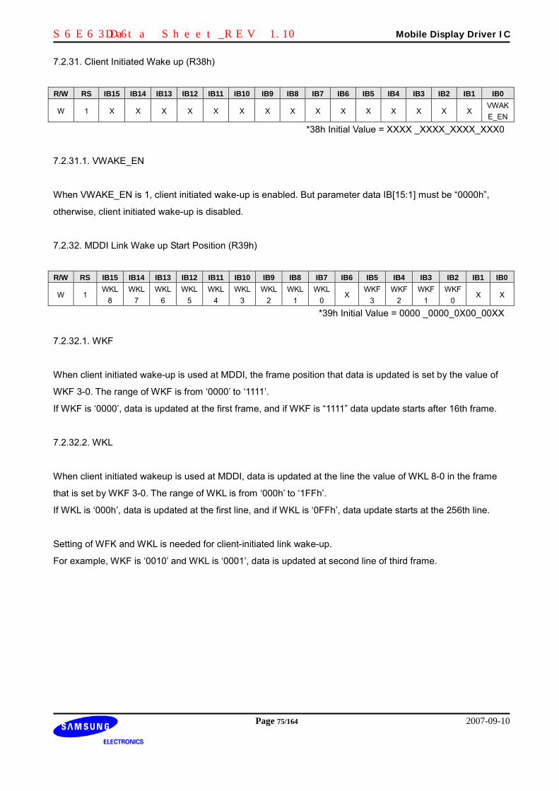
S6E63D6 Data Sheet_REV 1.10 Mobile Display Driver IC
Page 75/164 2007-09-10
7.2.31. Client Initiated Wake up (R38h)
R/W RS IB15 IB14 IB13 IB12 IB11 IB10 IB9 IB8 IB7 IB6 IB5 IB4 IB3 IB2 IB1 IB0
W 1 X X X X X X X X X X X X X X X VWAKE_EN
*38h Initial Value = XXXX _XXXX_XXXX_XXX0
7.2.31.1. VWAKE_EN
When VWAKE_EN is 1, client initiated wake-up is enabled. But parameter data IB[15:1] must be “0000h”,
otherwise, client initiated wake-up is disabled.
7.2.32. MDDI Link Wake up Start Position (R39h)
R/W RS IB15 IB14 IB13 IB12 IB11 IB10 IB9 IB8 IB7 IB6 IB5 IB4 IB3 IB2 IB1 IB0
W 1 WKL
8 WKL
7 WKL
6 WKL
5 WKL
4 WKL
3 WKL
2 WKL
1 WKL
0 X
WKF3
WKF 2
WKF 1
WKF 0
X X
*39h Initial Value = 0000 _0000_0X00_00XX 7.2.32.1. WKF
When client initiated wake-up is used at MDDI, the frame position that data is updated is set by the value of
WKF 3-0. The range of WKF is from ‘0000’ to ‘1111’.
If WKF is ‘0000’, data is updated at the first frame, and if WKF is “1111” data update starts after 16th frame.
7.2.32.2. WKL
When client initiated wakeup is used at MDDI, data is updated at the line the value of WKL 8-0 in the frame
that is set by WKF 3-0. The range of WKL is from ‘000h’ to ‘1FFh’.
If WKL is ‘000h’, data is updated at the first line, and if WKL is ‘0FFh’, data update starts at the 256th line.
Setting of WFK and WKL is needed for client-initiated link wake-up.
For example, WKF is ‘0010’ and WKL is ‘0001’, data is updated at second line of third frame.

S6E63D6 Data Sheet_REV 1.10 Mobile Display Driver IC
Page 76/164 2007-09-10
7.2.33. Sub Panel Control 1 (R3Ah, R3Bh)
R/W RS IB15 IB14 IB13 IB12 IB11 IB10 IB9 IB8 IB7 IB6 IB5 IB4 IB3 IB2 IB1 IB0
W 1 X X X X X X X X SUB_SEL7
SUB_SEL6
SUB_SEL5
SUB _SE L4
SUB _SE L3
SUB _SE L2
SUB_SEL1
SUB_SEL0
*3Ah Initial Value = XXXX _XXXX_0111_1010
R/W RS IB15 IB14 IB13 IB12 IB11 IB10 IB9 IB8 IB7 IB6 IB5 IB4 IB3 IB2 IB1 IB0
W 1 X X X X X X X X SUB_WR
7
SUB_WR
6
SUB_WR
5
SUB _WR
4
SUB _WR
3
SUB _WR
2
SUB_WR
1
SUB_WR
0
*3Bh Initial Value = XXXX _XXXX_0010_0010 7.2.33.1. SUB_SEL
SUB_SEL is the index of main/sub panel selection. Initial value of SUB_SEL is ‘7Ah’.
In MDDI mode, If written register address is ‘7Ah’ (initial state: SUB_SEL is ‘7Ah’) and register data is 0001h’,
then main panel is selected, and if that is ‘0000h’, then sub panel is selected.
Using SUB_SEL register, Main / Sub panel selection index change is possible.
7.2.33.2. SUB_WR SUB_WR is the index of sub panel data write. Initial value of SUB_WR is ‘22h’. When MDDI host transfer GRAM data to sub panel driver IC via video stream packet, SUB_WR (initially 22h), index for GRAM access is automatically transferred before GRAM data transfer. When sub panel driver IC uses other address, 22h address have to be changed. Then user can change SUB_WR value from 22h to other value.

S6E63D6 Data Sheet_REV 1.10 Mobile Display Driver IC
Page 77/164 2007-09-10
7.2.34. Sub Panel Control 2 (R3Ch)
R/W RS IB15 IB14 IB13 IB12 IB11 IB10 IB9 IB8 IB7 IB6 IB5 IB4 IB3 IB2 IB1 IB0
W 1 X X X X X X X X FCV_EN
X X X MPU _MO DE
STN _EN
SUB_IM1
SUB_IM0
*3Ch Initial Value = XXXX _XXXX_0XXX_0001
7.2.34.1. SUB_IM
Specify the sub-panel interface mode.
Table 54. Sub Panel Interface Mode SUB_IM1 SUB_IM0 Interface
0 0 Setting disable
0 1 9bit Interface mode
1 0 Setting disable
1 1 8bit Interface mode
7.2.34.2. STN_EN
Specify the panel property.
STN_EN = “1”: STN panel.
STN_EN = “0”: TFT panel.
7.2.34.3. MPU_MODE
Specify the MPU interfaces
MPU_MODE = “1”: 68 mode
MPU_MODE = “0”: 80 mode
7.2.34.4. FCV_EN
FCV_EN is data format conversion enable signal
FCV_EN = “1”: 16 bit data format conversion (not used)
FCV_EN = “0”: current 16bit data format

S6E63D6 Data Sheet_REV 1.10 Mobile Display Driver IC
Page 78/164 2007-09-10
7.2.35. Test Key Command (R60h)
R/W RS IB15 IB14 IB13 IB12 IB11 IB10 IB9 IB8 IB7 IB6 IB5 IB4 IB3 IB2 IB1 IB0W 1 X X X X X X X X 0 0 0 0 1 1 1 1
Test Key Command is a protection command. When Test Key Command(0Fh) is applied, MTP_WRB and
MTP_ERB are valid
7.2.36. MTP Control (R61h)
R/W RS IB15 IB14 IB13 IB12 IB11 IB10 IB9 IB8 IB7 IB6 IB5 IB4 IB3 IB2 IB1 IB0
W 1 X X X X X X X MTP_WR
B X X X
MTP _SE
L X X X
MTP_ER
B
*61h Initial Value = XXXX _XXX1_XXX1_XXX1
7.2.36.1. MTP_WRB
MTP Write enable signal. If you want to write data to MTP cell, set MTP_WRB = 0
7.2.36.2. MTP_SEL
Select MTP value or register value added to CR5[6:0], CG5[6:0], CB5[6:0], CR3[5:0], CG3[5:0], and
CB3[5:0]
7.2.36.3. MTP_ERB
Enable for MTP initial or erase. When MTP_ERB = 0, MTP initialization or erase is enabled.
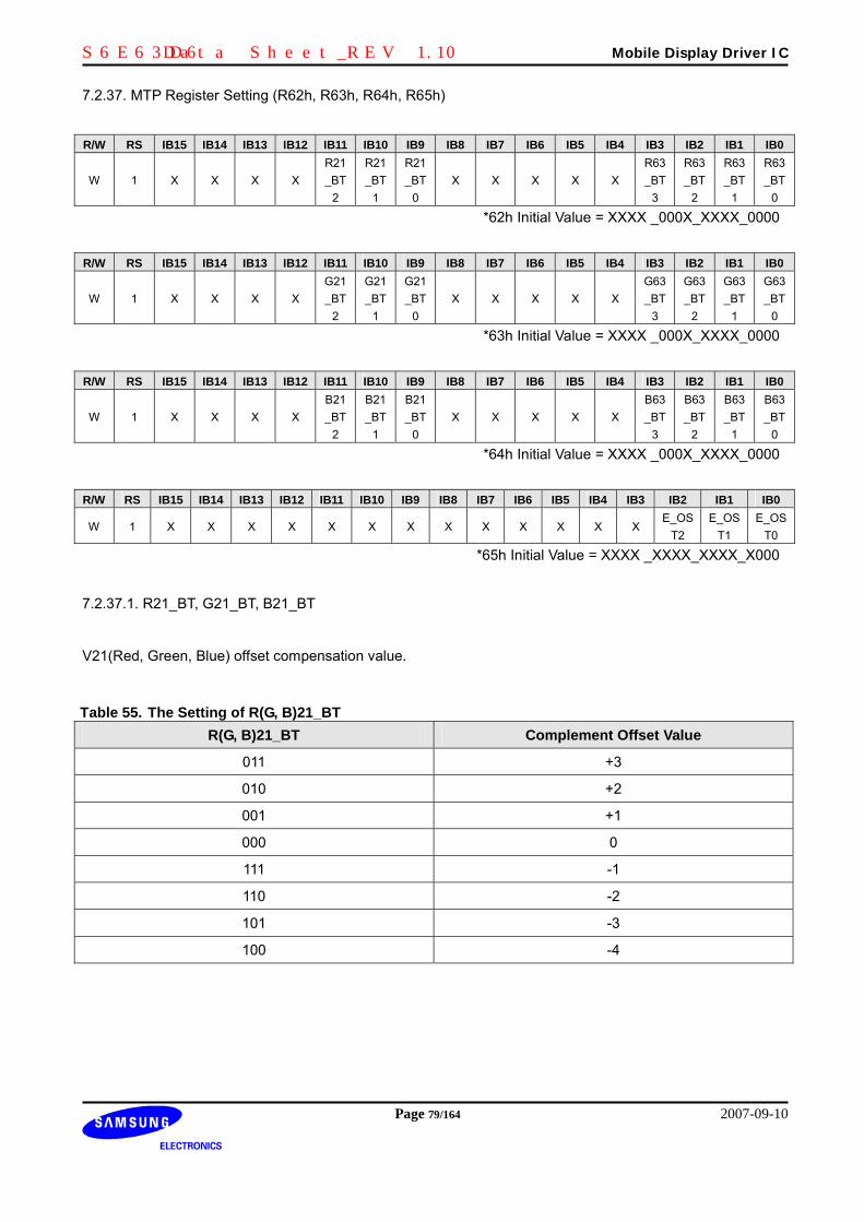
S6E63D6 Data Sheet_REV 1.10 Mobile Display Driver IC
Page 79/164 2007-09-10
7.2.37. MTP Register Setting (R62h, R63h, R64h, R65h)
R/W RS IB15 IB14 IB13 IB12 IB11 IB10 IB9 IB8 IB7 IB6 IB5 IB4 IB3 IB2 IB1 IB0
W 1 X X X X R21 _BT
2
R21_BT
1
R21_BT
0 X X X X X
R63 _BT
3
R63 _BT
2
R63_BT
1
R63_BT
0
*62h Initial Value = XXXX _000X_XXXX_0000
R/W RS IB15 IB14 IB13 IB12 IB11 IB10 IB9 IB8 IB7 IB6 IB5 IB4 IB3 IB2 IB1 IB0
W 1 X X X X G21 _BT
2
G21_BT
1
G21_BT
0 X X X X X
G63 _BT
3
G63 _BT
2
G63_BT
1
G63_BT
0
*63h Initial Value = XXXX _000X_XXXX_0000
R/W RS IB15 IB14 IB13 IB12 IB11 IB10 IB9 IB8 IB7 IB6 IB5 IB4 IB3 IB2 IB1 IB0
W 1 X X X X B21 _BT
2
B21_BT
1
B21_BT
0 X X X X X
B63 _BT
3
B63 _BT
2
B63_BT
1
B63_BT
0
*64h Initial Value = XXXX _000X_XXXX_0000
R/W RS IB15 IB14 IB13 IB12 IB11 IB10 IB9 IB8 IB7 IB6 IB5 IB4 IB3 IB2 IB1 IB0
W 1 X X X X X X X X X X X X X E_OS
T2 E_OS
T1 E_OS
T0
*65h Initial Value = XXXX _XXXX_XXXX_X000
7.2.37.1. R21_BT, G21_BT, B21_BT
V21(Red, Green, Blue) offset compensation value.
Table 55. The Setting of R(G, B)21_BT R(G, B)21_BT Complement Offset Value
011 +3
010 +2
001 +1
000 0
111 -1
110 -2
101 -3
100 -4

S6E63D6 Data Sheet_REV 1.10 Mobile Display Driver IC
Page 80/164 2007-09-10
7.2.37.2. R63_BT, G63_BT, B63_BT
V63(Red, Green, Blue) offset compensation value.
Table 56. The Setting of R(G, B)63_BT R(G, B)63_BT Complement Offset Value R(G, B)63_BT Complement Offset Value
0111 +7 1111 -1
0110 +6 1110 -2
0101 +5 1101 -3
0100 +4 1100 -4
0011 +3 1011 -5
0010 +2 1010 -6
0001 +1 1001 -7
0000 0 1000 -8
7.2.37.3. E_OST
ELVDD offset compensation value.
Table 57. The Setting of E_OST E_OST Complement Offset Value
011 +3
010 +2
001 +1
000 0
111 -1
110 -2
101 -3
100 -4

S6E63D6 Data Sheet_REV 1.10 Mobile Display Driver IC
Page 81/164 2007-09-10
This block diagram shows the sequence for compensation of V0, V21, V63 value.
Figure 13. The Block diagram of sequence for V0, V21, V63 compensation

S6E63D6 Data Sheet_REV 1.10 Mobile Display Driver IC
Page 82/164 2007-09-10
This figure shows the flow of MTP initialization, programing and reading.
Figure 14. MTP Initialization, Programing and Reading

S6E63D6 Data Sheet_REV 1.10 Mobile Display Driver IC
Page 83/164 2007-09-10
This figure explains the timing of MTP programming.
Figure 15. Timing of MTP Programing
Table 58. MTP Writing Time Timing Min Max Unit
tVS 1 - ms
tVH 1 - ms
tDWS 10 - μs
tDWH 10 - μs
tPGM 100 200 Ms
Table 59. MTPG, MTPD Voltage Tolerance Item Operation Min Typ Max Unit
Initialize (Erase) 21.0 21.5 22.0 V Tolerance of MTPG
Program (Write) - 0 - V
Initialize (Erase) - 0 - V Tolerance of MTPD
Program (Write) 17.0 17.5 18.0 V

S6E63D6 Data Sheet_REV 1.10 Mobile Display Driver IC
Page 84/164 2007-09-10
7.2.38. GPIO Control (R66h, R67h, R68h, R69h, R6Ah)
R/W RS IB15 IB14 IB13 IB12 IB11 IB10 IB9 IB8 IB7 IB6 IB5 IB4 IB3 IB2 IB1 IB0
W 1 X X X X X X GPIO9
GPIO8
GPIO7
GPIO6
GPIO5
GPI O4
GPI O3
GPI O2
GPIO1
GPIO0
*66h Initial Value = XXXX _XX00_0000_0000
R/W RS IB15 IB14 IB13 IB12 IB11 IB10 IB9 IB8 IB7 IB6 IB5 IB4 IB3 IB2 IB1 IB0
W 1 X X X X X X GPIO_CON9
GPIO_CON8
GPIO_CON7
GPIO_CON6
GPIO_CON5
GPI O_C ON4
GPI O_C ON3
GPI O_C ON2
GPIO_CON1
GPIO_CON0
*67h Initial Value = XXXX _XX00_0000_0000
R/W RS IB15 IB14 IB13 IB12 IB11 IB10 IB9 IB8 IB7 IB6 IB5 IB4 IB3 IB2 IB1 IB0
W 1 X X X X X X GPCLR9
GPCLR8
GPCLR7
GPCLR6
GPCLR5
GPC LR4
GPC LR3
GPC LR2
GPCLR1
GPCLR0
*68h Initial Value = XXXX _XX00_0000_0000
R/W RS IB15 IB14 IB13 IB12 IB11 IB10 IB9 IB8 IB7 IB6 IB5 IB4 IB3 IB2 IB1 IB0
W 1 X X X X X X GPIO_EN9
GPIO_EN8
GPIO_EN7
GPIO_EN6
GPIO_EN5
GPI O_E N4
GPI O_E N3
GPI O_E N2
GPIO_EN1
GPIO_EN0
*69h Initial Value = XXXX _XX00_0000_0000
R/W RS IB15 IB14 IB13 IB12 IB11 IB10 IB9 IB8 IB7 IB6 IB5 IB4 IB3 IB2 IB1 IB0
W 1 X X X X X X GPPOL9
GPPOL8
GPPOL7
GPPOL6
GPPOL5
GPP OL4
GPP OL3
GPP OL2
GPPOL1
GPPOL0
*6Ah Initial Value = XXXX _XX11_1111_1111
7.2.38.1. GPIO
When GPIO is input mode, GPIO value is set to the register.
When GPIO is output mode, GPIO register value is output to GPIO PAD.
7.2.38.2. GPIO_CON
Control of GPIO
When GPIO_CON is “0”, then GPIO is input mode, and when “1”, then GPIO is output mode
7.2.38.3. GPCLR
When GPIO is input mode, GPCLR clears specified GPIO interrupt (set by GPIO PAD input).

S6E63D6 Data Sheet_REV 1.10 Mobile Display Driver IC
Page 85/164 2007-09-10
7.2.38.4. GPIO_EN
When GPIO is input mode, if GPIO_EN is “1”, it acts as enable internal interrupt.
7.2.38.5. GPPOL
If the bit is set to “1”, GPIO interrupt happens at rising edge of GPIO, If set to “0”, it happens at falling edge.
For more information about these registers, refer to GPIO Control section.

S6E63D6 Data Sheet_REV 1.10 Mobile Display Driver IC
Page 86/164 2007-09-10
7.2.39. Gamma Control (R70h to R78h)
R/W RS IB15 IB14 IB13 IB12 IB11 IB10 IB9 IB8 IB7 IB6 IB5 IB4 IB3 IB2 IB1 IB0
W 1 X X CR5
6 CR5
5 CR5
4 CR5
3 CR5
2 CR5
1 CR5
0 X X X
CR0 3
CR0 2
CR01
CR00
W 1 X X CG5
6 CG5
5 CG5
4 CG5
3 CG5
2 CG5
1 CG5
0 X X X
CG0 3
CG0 2
CG01
CG00
W 1 X X CB5
6 CB5
5 CB5
4 CB5
3 CB5
2 CB5
1 CB5
0 X X X
CB0 3
CB0 2
CB01
CB00
W 1 X X CR1
5 CR1
4 CR1
3 CR1
2 CR1
1 CR1
0 X X
CR25
CR2 4
CR2 3
CR2 2
CR21
CR20
W 1 X X CR3
5 CR3
4 CR3
3 CR3
2 CR3
1 CR3
0 X X
CR45
CR4 4
CR4 3
CR4 2
CR41
CR40
W 1 X X CG1
5 CG1
4 CG1
3 CG1
2 CG1
1 CG1
0 X X
CG25
CG2 4
CG2 3
CG2 2
CG21
CG20
W 1 X X CG3
5 CG3
4 CG3
3 CG3
2 CG3
1 CG3
0 X X
CG45
CG4 4
CG4 3
CG4 2
CG41
CG40
W 1 X X CB1
5 CB1
4 CB1
3 CB1
2 CB1
1 CB1
0 X X
CB25
CB2 4
CB2 3
CB2 2
CB21
CB20
W 1 X X CB3
5 CB3
4 CB3
3 CB3
2 CB3
1 CB3
0 X X
CB45
CB4 4
CB4 3
CB4 2
CB41
CB40
These registers set the gamma set.
CR5[6:0]: The amplitude adjust register
CR4[4:0]: The amplitude adjust register
CR3[4:0]: The amplitude adjust register
CR2[4:0]: The amplitude adjust register
CR1[4:0]: The amplitude adjust register
CR0[3:0]: The amplitude adjust register
CG5[6:0]: The amplitude adjust register
CG4[4:0]: The amplitude adjust register
CG3[4:0]: The amplitude adjust register
CG2[4:0]: The amplitude adjust register
CG1[4:0]: The amplitude adjust register
CG0[3:0]: The amplitude adjust register
CB5[6:0]: The amplitude adjust register
CB4[4:0]: The amplitude adjust register
CB3[4:0]: The amplitude adjust register
CB2[4:0]: The amplitude adjust register
CB1[4:0]: The amplitude adjust register
CB0[3:0]: The amplitude adjust register
For more information, refer to the R, G, B Independent Gamma Adjustmetn Function.

S6E63D6 Data Sheet_REV 1.10 Mobile Display Driver IC
Page 87/164 2007-09-10
7.2.40. EL Control (RF4h)
R/W RS IB15 IB14 IB13 IB12 IB11 IB10 IB9 IB8 IB7 IB6 IB5 IB4 IB3 IB2 IB1 IB0
W 1 X X X X X X X X X X EL_
TESTEL_ ON
X X X X
*66h Initial Value = XXXX _XXXX_XX10_XXXX
7.2.40.1. EL_TEST
EL_TEST selects manual EL_ON register.
EL_TEST must be set to “1”.
7.2.40.2. EL_ON
EL_ON controls ELVDD power.

S6E63D6 Data Sheet_REV 1.10 Mobile Display Driver IC
Page 88/164 2007-09-10
8. Reset Function
The S6E63D6 is initialized internally by RESET input. The reset input should be held ‘L’ for at least 10us. Do
not access the GRAM nor initially set the instructions until the R-C oscillation frequency is stable after power
has been supplied (10 ms).
8.1. Instruction Set Initialization
1. Display duty control (R01h) : FP3_0=1000, BP3_0=1000, NL5_0=10_1000 2. RGB interface control (R02h) : RM=0, DM=0, RIM1_0=00, VSPL=0, HSPL=0, EPL=0, DPL=0 3. Entry mode (R03h) : CLS=1, MDT1_0=00, BGR=0, SS=0, ID1_0=11, AM=0 4. Clock control (R04h) : DCR1_0=00 5. Display control 1 (R05h) : DISP_ON=0 6. Display control 2 (R06h) : CL=0, TEMON=0, REV=0 7. Panel interface control 1 (R07h) : CLWEA4_0=1_0010 8. Panel interface control 2 (R08h) : CLWEB4_0=1_0010, CLWEC4_0=1_0010 9. Panel interface control 3 (R09h) : SHE2_0=010, CLTE2_0=010 10. Stand by (R10h) : NAP=0, STB=1 11. Power gen 1 (R12h) : VC3_0=1000 12. Power gen 2 (R13h) : VINT3_0=0101 13. Power gen 3 (RF8h) : VGH4_0=1_0100 14. Power gen 4 (RF9h) : VGL4_0=1_0100 15. Power booster control (R14h) : DC22_0=100, DC12_0=010, BT1_0=10 16. Oscillator control (R18h) : RADJ5_0=01_1111 17. Source driver control (R1Ah) : GAMMA_TEST=0, SDUM_ON=0, SAP2_0=101 18. GRAM address set (R20h) : AD7_0=0000_0000, AD16_8=0_0000_0000 19. Vertical scroll control 1 (R30h, R31h) : SSA8_0=0_0000_0000, SEA8_0=1_0011_1111 20. Vertical scroll control 2 (R32h) : SST8_0=0_0000_0000 21. Partial screen driving position (R33h, R34h) : SS18_0=0_0000_0000, SE18_0=1_0011_1111 22. Vertical RAM address position (R35h, R36h) : VSA8_0=0_0000_0000, VEA8_0=1_0011_1111 23. Horizontal RAM address position (R37h) : HAS7_0=0000_0000, HEA7_0=1110_1111 24. Client initiated wake up (R38h) : VWAKE_EN=0 25. MDDI link wake up start position (R39h) : WKL8_0=0_0000_0000, WKF3_0=0000 26. Sub panel control 1(R3Ah, R3Bh) : SUB_SEL7_0=0111_1010, SUB_WR7_0=0010_0010 27. Sub panel control 2 (R3Ch) : FCV_EN=0, MPU_MODE=0, STN_EN=0, SUB_IM1_0=01 28. MTP control (R61h) : MTP_WRB=1, MTP_SEL=1, MTP_ERB=1 29. MTP register setting (R62h, 63h, 64h, 65h) : R21_BT2_0=000, R63_BT3_0=0000,
G21_BT2_0=000, G63_BT3_0=0000, B21_BT2_0=000, B63_BT3_0=0000, E_OST2_0=000
30. GPIO control (R66h, R67h, R68h. R69h, R6Ah) : GPIO9_0=00_0000_0000, GPIO_CON9_0=00_0000_0000, GPCLR9_0=00_0000_0000, GPIO_EN9_0=00_0000_0000, GPPOL9_0=11_1111_1111
31. EL_ON (RF4h) : EL_TEST=1, EL_ON=0

S6E63D6 Data Sheet_REV 1.10 Mobile Display Driver IC
Page 89/164 2007-09-10
9. Power Supply 9.1. Pattern Diagrams for Voltge Setting The following figure shows a pattern diagram for the voltage setting and an example of waveforms.
Figure 16. Pattern Diagram for Voltage Setting

S6E63D6 Data Sheet_REV 1.10 Mobile Display Driver IC
Page 90/164 2007-09-10
9.2. Voltage Regulation Fuction
The S6E63D6 has the internal voltage regulator. By the use of this function, unexpected damages on
internal logic circuit can be avoided. Furthermore, power consumption can also be obtained. Detailed
function description and application configuration is described in the following diagram.
Figure 17. Voltage Regulation Function

S6E63D6 Data Sheet_REV 1.10 Mobile Display Driver IC
Page 91/164 2007-09-10
10. Interface Specification
The S6E63D6 incorporates a system interface, which is used to set instructions, and an external display
interface, which is used to display motion pictures, and a MDDI, which is high speed serial interface.
Selecting these interfaces to match the screen data (motion picture or still picture) enables efficient transfer
of data for display.
The external display interface includes RGB interface. This allows flicker-free screen update.
When RGB interface is selected, the synchronization signals (VSYNC, HSYNC, and DOTCLK) are available
for use in operating the display. The display data (DB17-0) is written according to the values of the data
enable signal (ENABLE) in synchronization with the VSYNC, HSYNC, and DOTCLK signals. In addition,
using the window address function enables rewriting only to the internal RAM area to display motion pictures.
Using this function also enables simultaneously display of the motion picture area and the RAM data that
was written.
HOSTs S6E63D6
CSBRSRW_WRBE_RDBDB
RW_WRB/SCLSDISDO
(CSB)
VSYNCHSYNCENABLEDOTCLK(DB)
18/16/9/8
18/16/6
CPUInterface
SerialPeripheralInterface
SystemInterface
RGBInterface
RGBInterface
S_PBID_MIB
Figure 18. System Interface and RGB Interface

S6E63D6 Data Sheet_REV 1.10 Mobile Display Driver IC
Page 92/164 2007-09-10
10.1. System Interface
S6E63D6 is enabling to set instruction and access to RAM by selecting S_PB, ID_MIB pads and Instruction
in the system interface mode.
Table 60. System Interface Mode Pads Registers
MDDI _EN
S_PB ID_MIB Index Address
Command(CLS)
CommandMDT[1]
CommandMDT[0]
Description
0 X 80-system 8-bit 65k bus interface
0 80-system 8-bit 260k bus interface 0 (80 8bit)
1 1 80-system 8-bit 65k bus interface
Default & 24h (9/8bit)
1 (80 9bit) X X 80-system 9-bit 260k bus interface
0 80-system 16-bit 65k bus interface 0 1 80-system 16-bit 260k bus interface
0 (80 16bit)
1 X 80-system 16-bit 260k bus interface
0 (80 mode)
Index 23h (18/16bit)
1 (80 18bit) X X 80-system 18-bit 260k bus interface
0 X 68-system 8-bit 65k bus interface
0 68-system 8-bit 260k bus interface 0 (68 8bit)
1 1 68-system 8-bit 65k bus interface
Default & 24h (9/8bit)
1 (68 9bit) X X 68-system 9-bit 260k bus interface
0 68-system 16-bit 65k bus interface 0 1 68-system 16-bit 260k bus interface
0 (68 16bit)
1 X 68-system 16-bit 260k bus interface
0 (Parallel)
1 (68 mode)
Index 23h (18/16bit)
1 (68 18bit) X X 68-system 18-bit 260k bus interface
0
1 (Serial) ID X X X X Serial peripheral interface (SPI)
1 X X X X X MDDI Note 1. For defails, see the Entry Mode (R03h)
We can select system interface mode by pads and instruction, don’t care 8-/16-bit bus system after power
on.
1. In case of 8/9-bit bus system.
Figure 19. 8/9-bit Bus System

S6E63D6 Data Sheet_REV 1.10 Mobile Display Driver IC
Page 93/164 2007-09-10
2. In case of 18/16-bit bus system.
Figure 20. 18/16-bit Bus System

S6E63D6 Data Sheet_REV 1.10 Mobile Display Driver IC
Page 94/164 2007-09-10
10.1.1. 68-system 18-bit Bus Interface
10.1.1.1. Bit Assignment
DB17INPUT DATA
Instruction Bit(IB)
DB16
DB15
DB14
DB13
DB12
DB11
DB10
DB9
DB8
DB7
DB6
DB5
DB4
DB3
DB2
DB1
DB0
IB15
IB14
IB13
IB12
IB11
IB10
IB9
IB8
IB7
IB6
IB5
IB4
IB3
IB2
IB1
IB0
Figure 21. Instruction Format for 68-system 18-bit Interface
GRAM DATA
R5 R4 R3 R2 R1 R0 G5 G4 G3 G2 G1 G0 B5 B4 B3 B2 B1 B0RGB Arrangement
DB17
DB16
DB15
DB14
DB13
DB12
DB11
DB10
DB9
DB8
DB7
DB6
DB5
DB4
DB3
DB2
DB1
DB0
Figure 22. RAM Data Write Format for 68-system 18-bit Interface
10.1.1.2. Timing Diagram
There are 4 timing conditions for 68-system 18-bit CPU interface, which are index write timing condition,
data write timing condition, data read timing condition and status read timing condition.
Index Write
68x-18/16bit
index data data
Mode
RS
E
RW
DB
Data Write Data Read Status Read
status
CSB
Figure 23. Timing Diagram of 68-system 18-bit Bus Interface

S6E63D6 Data Sheet_REV 1.10 Mobile Display Driver IC
Page 95/164 2007-09-10
10.1.2. 68-system 16-bit Bus Interface
10.1.2.1. Bit Assignment
DB17INPUT DATA
Instruction Bit(IB)
DB16
DB15
DB14
DB13
DB12
DB11
DB10
DB8
DB7
DB6
DB5
DB4
DB3
DB2
DB1
IB15
IB14
IB13
IB12
IB11
IB10
IB9
IB8
IB7
IB6
IB5
IB4
IB3
IB2
IB1
IB0
Figure 24. Instruction Format for 68-system 16-bit Interface
DB17
DB16
DB15
DB14
DB13
DB12
DB11
DB10
DB8
DB7
DB6
DB5
DB4
DB3
DB2
DB1GRAM DATA
R5 R4 R3 R2 R1 R0 G5 G4 G3 G2 G1 G0 B5 B4 B3 B2 B1 B0RGB Arrangement
Figure 25. RAM Data Write Format for 68-system 16-bit Interface
10.1.2.2. Timing Diagram
There are 4 timing conditions for 68-system 16-bit CPU interface, which are index write timing condition,
data write timing condition, data read timing condition and status read timing condition.
Index Write
68x-18/16bit
index data data
Mode
RS
E
RW
DB
Data Write Data Read Status Read
status
CSB
Figure 26. Timing Diagram of 68-system 16-bit Bus Interface

S6E63D6 Data Sheet_REV 1.10 Mobile Display Driver IC
Page 96/164 2007-09-10
10.1.3. 68-system 9-bit Bus Interface
10.1.3.1. Bit Assignment
1st Transmission 2nd Transmission
DB8INPUT DATA
Instruction Bit(IB)
DB7
DB5
DB5
DB4
DB3
DB2
DB1
DB0
IB15
IB14
IB13
IB12
IB11
IB10
IB9
IB8
IB7
IB6
IB5
IB4
IB3
IB2
IB1
IB0
DB17
DB16
DB15
DB14
DB13
DB12
DB11
DB10
DB9
DB8
DB7
DB5
DB5
DB4
DB3
DB2
DB1
DB0
Figure 27. Instruction Format for 68-system 9-bit Interface
DB8
DB7
DB6
DB5
DB4
DB3
DB2
DB1
DB0GRAM DATA
R5 R4 R3 R2 R1 R0 G5 G4 G3 G2 G1 G0 B5 B4 B3 B2 B1 B0RGB Arrangement
1st Transmission
DB8
DB7
DB6
DB5
DB4
DB3
DB2
DB1
DB0
2nd Transmission
Figure 28. RAM Data Write Format for 68-system 9-bit Interface 10.1.3.2. Timing Diagram There are 4 timing conditions for 68-system 9-bit CPU interface, which are index write timing condition, data write timing condition, data read timing condition and status read timing condition. In this mode, 16-bit instructions and GRAM data are divided into two half words and the transfer starts from the upper half word. Note that the upper byte must also be written when the index register is written.
Figure 29. Timing Diagram of 68-system 9-bit Bus Interface

S6E63D6 Data Sheet_REV 1.10 Mobile Display Driver IC
Page 97/164 2007-09-10
10.1.4. 68-system 8-bit Bus Interface 10.1.4.1. Bit Assignment
DB8INPUT DATA
Instruction Bit(IB)
DB7
DB6
DB5
DB4
DB3
DB2
DB1
IB15
IB14
IB13
IB12
IB11
IB10
IB9
IB8
IB7
IB6
IB5
IB4
IB3
IB2
IB1
IB0
1st Transmission 2nd Transmission
DB17
DB16
DB15
DB14
DB13
DB12
DB11
DB10
DB8
DB7
DB6
DB5
DB4
DB3
DB2
DB1
Figure 30. Instruction Format for 68-system 8-bit Interface
DB8
DB7
DB6
DB5
DB4
DB3
DB2
DB1
DB17
DB16
DB15
DB14
DB13
DB12
DB11
DB10GRAM DATA
R5 R4 R3 R2 R1 R0 G5 G4 G3 G2 G1 G0 B5 B4 B3 B2 B1 B0RGB Arrangement
1st Transmission 2nd Transmission
DB8
DB7
DB6
DB5
DB4
DB3
DB2
DB1
Figure 31. RAM Data Write Format for 68-system 8-bit Interface 10.1.4.2. Timing Diagram There are 4 timing conditions for 68-system 8-bit CPU interface, which are index write timing condition, data write timing condition, data read timing condition and status read timing condition. In this mode, 16-bit instructions and GRAM data are divided into two half words and the transfer starts from the upper half word. Note that the upper byte must also be written when the index register is written.
Figure 32. Timing Diagram of 68-System 8-Bit bus interface

S6E63D6 Data Sheet_REV 1.10 Mobile Display Driver IC
Page 98/164 2007-09-10
10.1.5. 80-system 18-bit Bus Interface
10.1.5.1. Bit Assignment
DB17INPUT DATA
Instruction Bit(IB)
DB16
DB15
DB14
DB13
DB12
DB11
DB10
DB9
DB8
DB7
DB6
DB5
DB4
DB3
DB2
DB1
DB0
IB15
IB14
IB13
IB12
IB11
IB10
IB9
IB8
IB7
IB6
IB5
IB4
IB3
IB2
IB1
IB0
Figure 33. Instruction Format for 80-system 18-bit Interface
GRAM DATA
R5 R4 R3 R2 R1 R0 G5 G4 G3 G2 G1 G0 B5 B4 B3 B2 B1 B0RGB Arrangement
DB17
DB16
DB15
DB14
DB13
DB12
DB11
DB10
DB9
DB8
DB7
DB6
DB5
DB4
DB3
DB2
DB1
DB0
Figure 34. RAM Data Write Format for 80-system 18-bit Interface
10.1.5.2. Timing Diagram
There are 4 timing conditions for 80-system 18-bit CPU interface, which are index write timing condition,
data write timing condition, data read timing condition and status read timing condition.
Figure 35. Timing Diagram of 80-system 18-bit Bus Interface

S6E63D6 Data Sheet_REV 1.10 Mobile Display Driver IC
Page 99/164 2007-09-10
10.1.6. 80-system 16-bit Bus Interface
10.1.6.1. Bit Assignment
DB17INPUT DATA
Instruction Bit(IB)
DB16
DB15
DB14
DB13
DB12
DB11
DB10
DB8
DB7
DB6
DB5
DB4
DB3
DB2
DB1
IB15
IB14
IB13
IB12
IB11
IB10
IB9
IB8
IB7
IB6
IB5
IB4
IB3
IB2
IB1
IB0
Figure 36. Instruction Format for 80-system 16-bit Interface
DB17
DB16
DB15
DB14
DB13
DB12
DB11
DB10
DB8
DB7
DB6
DB5
DB4
DB3
DB2
DB1GRAM DATA
R5 R4 R3 R2 R1 R0 G5 G4 G3 G2 G1 G0 B5 B4 B3 B2 B1 B0RGB Arrangement
Figure 37. RAM Data Write Format for 80-system 16-bit Interface
10.1.6.2. Timing Diagram
There are 4 timing conditions for 80-system 16-bit CPU interface, which are index write timing condition,
data write timing condition, data read timing condition and status read timing condition.
Figure 38. Timing Diagram of 80-system 16-bit Bus Interface

S6E63D6 Data Sheet_REV 1.10 Mobile Display Driver IC
Page 100/164 2007-09-10
10.1.7. 80-system 9-bit Bus Interface
10.1.7.1. Bit Assignment
1st Transmission 2nd Transmission
DB8INPUT DATA
Instruction Bit(IB)
DB7
DB5
DB5
DB4
DB3
DB2
DB1
DB0
IB15
IB14
IB13
IB12
IB11
IB10
IB9
IB8
IB7
IB6
IB5
IB4
IB3
IB2
IB1
IB0
DB17
DB16
DB15
DB14
DB13
DB12
DB11
DB10
DB9
DB8
DB7
DB5
DB5
DB4
DB3
DB2
DB1
DB0
Figure 39. Instruction Format for 80-system 9-bit Interface
DB8
DB7
DB6
DB5
DB4
DB3
DB2
DB1
DB0GRAM DATA
R5 R4 R3 R2 R1 R0 G5 G4 G3 G2 G1 G0 B5 B4 B3 B2 B1 B0RGB Arrangement
1st Transmission
DB8
DB7
DB6
DB5
DB4
DB3
DB2
DB1
DB0
2nd Transmission
Figure 40. RAM Data Write Format for 80-system 9-bit Interface 10.1.7.2. Timing Diagram There are 4 timing conditions for 80-system 9-bit CPU interface, which are index write timing condition, data write timing condition, data read timing condition and status read timing condition. In this mode, 16-bit instructions and GRAM data are divided into two half words and the transfer starts from the upper half word. Note that the upper byte must also be written when the index register is written.
Figure 41. Timing Diagram of 80-system 9-bit Bus Interface

S6E63D6 Data Sheet_REV 1.10 Mobile Display Driver IC
Page 101/164 2007-09-10
10.1.8. 80-system 8-bit Bus Interface 10.1.8.1. Bit Assignment
DB8INPUT DATA
Instruction Bit(IB)
DB7
DB6
DB5
DB4
DB3
DB2
DB1
IB15
IB14
IB13
IB12
IB11
IB10
IB9
IB8
IB7
IB6
IB5
IB4
IB3
IB2
IB1
IB0
1st Transmission 2nd Transmission
DB17
DB16
DB15
DB14
DB13
DB12
DB11
DB10
DB8
DB7
DB6
DB5
DB4
DB3
DB2
DB1
Figure 42. Instruction Format for 80-system 8-bit Interface
DB8
DB7
DB6
DB5
DB4
DB3
DB2
DB1
DB17
DB16
DB15
DB14
DB13
DB12
DB11
DB10GRAM DATA
R5 R4 R3 R2 R1 R0 G5 G4 G3 G2 G1 G0 B5 B4 B3 B2 B1 B0RGB Arrangement
1st Transmission 2nd Transmission
DB8
DB7
DB6
DB5
DB4
DB3
DB2
DB1
Figure 43. RAM Data Write Format for 80-system 8-bit Interface 10.1.8.2. Timing Diagram There are 4 timing conditions for 80-system 8-bit CPU interface, which are index write timing condition, data write timing condition, data read timing condition and status read timing condition. In this mode, 16-bit instructions and GRAM data are divided into two half words and the transfer starts from the upper half word. Note that the upper byte must also be written when the index register is written.
Figure 44. Timing Diagram of 80-System 8-Bit bus interface

S6E63D6 Data Sheet_REV 1.10 Mobile Display Driver IC
Page 102/164 2007-09-10
10.1.9. 68-/80-system 8-/9-bit Interface Synchronization Function
The S6E63D6 supports the transfer synchronization function, which resets the upper/lower counter to count
upper/lower 8-/9-bit data transfer in the 8-/9-bit bus interface. Noise causing transfer mismatch between the
upper and lower bits can be corrected by a reset triggered by writing a “22h” instruction. The next transfer
starts from the upper bits. Executing synchronization function periodically can recover any runaway in the
display system.
Figure 45. 8-/9-bit Interface Transfer Synchronization

S6E63D6 Data Sheet_REV 1.10 Mobile Display Driver IC
Page 103/164 2007-09-10
10.1.10. Serial Peripheral Interface Setting the S_PB pad to the VDD3 level allows serial peripheral interface (SPI) transfer, using the chip select line (CSB), serial transfer clock line (SCL), serial input data (SDI), and serial output data (SDO). For a serial interface, the ID bit is selected by the ID_MIB pad. If the chip is set up for serial interface, the DB17-0 pads are used only data bus of RGB Interface. The S6E63D6 initiates serial data transfer by transferring the start byte at the falling edge of CSB input. It ends serial data transfer at the rising edge of CSB input. The S6E63D6 is selected when the 6-bit chip address in the start byte matches the 6-bit device identification code that is assigned to the S6E63D6. When selected, the S6E63D6 receives the subsequent data string. The least significant bit (LSB) of the identification code can be determined by the ID_MIB pad. The five upper bits must be 01110. Two different chip addresses must be assigned to a single S6E63D6 because the seventh bit of the start byte is used as a register select bit (RS). That is, when RS = 0, data can be written to the index register or status can be read, and when RS = 1, an instruction can be issued. Read or write operation is selected according to the eighth bit of the start byte (R/W bit). The data is received when the R/W bit is 0, and is transmitted when the R/W bit is 1. After receiving the start byte, the S6E63D6 receives or transmits the subsequent data byte-by-byte. The data is transferred with the MSB first. All S6E63D6 instructions are 16 bits. Two bytes are received with the MSB first (DB15 to DB0), then the instructions are internally executed. After the start byte has been received, the first byte is fetched as the upper eight bits of the instruction and the second byte is fetched as the lower eight bits of the instruction.
Table 61. Start Byte Format on SPI Transfer bit S 1 2 3 4 5 6 7 8
Device ID code Start byte format Transfer start
0 1 1 1 0 ID
RS R/W
Note 1. ID bit is selected by the ID_MIB pad.
Table 62. RS an R/W Bit Function on SPI RS R/W Function
0 0 Set index register
0 1 Read status
1 0 Write register data (parameter)
1 1 Read register data (parameter)
10.1.10.1. Bit Assignment
Figure 46. bit Assignment of Instructions on SPI

S6E63D6 Data Sheet_REV 1.10 Mobile Display Driver IC
Page 104/164 2007-09-10
10.1.10.2. Timing Diagram
Figure 47. timing diagram of Index Register Set through SPI
Figure 48. Timing Diagram of Consecutive Register Data-Write through SPI
Figure 49. Timing Diagram of Register Read through SPI

S6E63D6 Data Sheet_REV 1.10 Mobile Display Driver IC
Page 105/164 2007-09-10
10.1.11. Index and Parameer Recognition
If more parameter command is being sent, exceed parameters are ignored.
Figure 50. Index and Parameter Recognition with 8-/9-bit Interface
Figure 51. Index and Parameter Recognition with 18-/16-bit Interface

S6E63D6 Data Sheet_REV 1.10 Mobile Display Driver IC
Page 106/164 2007-09-10
10.2. External Display Interface (RGB Interface)
The following interfaces are available as external display interface. It is determined by bit setting of RIM1-0.
RAM accesses can be performed via the RGB interface.
Table 63. Relationship between RIM and RGB Interface RIM1 RIM0 RGB Interface DB Pads
0 0 18-bit RGB interface DB17 to 0
0 1 16-bit RGB interface DB17 to 10, DB8 to 1
1 0 6-bit RGB interface DB8 to 3
1 1 Setting disable
The relationship between EPL and ENABLE signals is shown below. When ENABLE is not active, the
address is not updates. When ENABLE is active, the address is updated.
Table 64. Relationship between EPL and ENABLE EPL ENABLE RAM Write RAM Address
0 0 Valid Update
0 1 Invalid Hold
1 0 Invalid Hold
1 1 Valid Update

S6E63D6 Data Sheet_REV 1.10 Mobile Display Driver IC
Page 107/164 2007-09-10
10.2.1. 18-bit RGB Interface 10.2.1.1. Bit Assignment
Figure 52. Bit Assignment of GRAM on 18-bit RGB Interface 10.2.2. 16-bit RGB Interface 10.2.2.1. Bit Assignment
Figure 53. Bit Assignment of GRAM on 16-bit RGB Interface 10.2.2.2. Timing Diagram
Figure 54. Timing Diagram of 18-/16-bit RGB Interface
Note 1. HSYNC Period must be >= 256 DOTCLK

S6E63D6 Data Sheet_REV 1.10 Mobile Display Driver IC
Page 108/164 2007-09-10
10.2.3. 6-bit RGB Interface
In order to transfer data on 6bit RGB Interface there should be three transfers.
10.2.3.1. Bit Assignment
Figure 55. Bit Assignment of GRAM on 6-bit RGB Interface
10.2.3.2. Timing Diagram
Figure 56. Timing Diagram of 6-bit RGB Interface Note 1. Three clocks are regarded as one clock for transfer when data is transferred in 6-bit interface. 2. VSYNC, HSYNC, ENABLE, DOTCLK, and DB[8:3] should be transferred in units of three clocks. 3. HSYNC Period must be >= 256 * 3 DOTCLK

S6E63D6 Data Sheet_REV 1.10 Mobile Display Driver IC
Page 109/164 2007-09-10
10.2.3.3. Transfer Synchronization on 6-bit RGB Interface
The figure shows transfer synchronization function for 6bit RGB interface. S6E63D6 has a transfer counter
to count 1st, 2nd and 3rd data transfer of 6bit RGB Interface. The transfer counter is reset on the falling
edge of HSYNC and enters the 1st data transmission state. Transfer mismatch can be corrected at every
new transfer restarts with HSYNC signal. In this method, when data is consecutively transferred in such a
way as displaying motion pictures, the effect of transfer mismatch will be reduced and recovered by normal
operation.
The internal display is operated in units of three DOTCLKs. When DOTCLK is not input in units of pixels,
clock mismatch occurs and the frame, which is operated, and the next frame are not displayed correctly
Figure 57. Transfer Synchronization Function on 6-bit RGB Interface mode

S6E63D6 Data Sheet_REV 1.10 Mobile Display Driver IC
Page 110/164 2007-09-10
10.2.4. Usage on External Display Interface
1. When external display interface is in use, the following functions are not available.
Table 65. Display Function and External Display Interface Function External Display Interface System Interface
Partial Display Cannot be used Can be used
Scroll Function Cannot be used Can be used
Rotation Cannot be used Can be used
Mirroring Cannot be used Can be used
Window Function Cannot be used Can be used
2. VSYNC, HSYNC, and DOTCLK signals should be supplied during display operation via RGB interface.
3. RGB data are transferred for three clock cycles in 6-bit RGB interface. Data transferred, therefore, should
be transferred in units of RGB.
4. Interface signals, VSYNC, HSYNC, DOTCLK, ENABLE and DB17-0 should be set in units of RGB (pixels)
to match RGB transfer.
5. Transitions between internal operation mode and external display interface should follow the mode
transition sequence shown below.
6. During the period between the completion of displaying one frame data and the next VSYNC signal, the
display will remain front porch period.

S6E63D6 Data Sheet_REV 1.10 Mobile Display Driver IC
Page 111/164 2007-09-10
10.3. MDDI (Mobile Display Digital Interface)
10.3.1. Introduction of MDDI The S6E63D6 supports MDDI. The MDDI is a differential & serial interface with high speed. Both command and image data transfer can be achieved with MDDI. MDDI host & client are linked with Data and STB line. Through Data line, command or image data is transferred from MDDI host to MDDI client, and vice versa. Data is transferred by packet unit. Through STB line, strobe signal is transferred. When the link is in “FORWARD direction”, data is transfered from host to client, in “REVERSE direction”, client transfer reverse data to MDDI host.
Figure 58. Physical Connection of MDDI Host and Client
10.3.2. DATA-STB Encoding Data is encoded using a DATA-STB method. DATA is carried over a bi-directional differential cable, while STB is carried over a unidirectional differential cable driven only by the host. Figure below illustrates how the data sequence “1110001011” is transmitted using DATA-STB encoding.
Figure 59. DATA-STB Encoding

S6E63D6 Data Sheet_REV 1.10 Mobile Display Driver IC
Page 112/164 2007-09-10
The Following figure shows a sample circuit to generate DATA and STB from input data, and then recover the input data from DATA and STB.
Figure 60. DATA / STB Generation & Recovery Circuit
10.3.3. MDDI DATA / STB The Data (MDP/MDN) and STB(MSP/MSN) signals are always operated in a differential mode to maximize noise immunity. Each differential pair is parallel-terminated with the characteristic impedance of the cable. All parallel-terminations are in the client device. Figure below illustrates the configuration of the drivers, receivers, and terminations. The driver of each signal pair has a differential current output. While receiving MDDI packets the MDDI_DATA and MDDI_STB pairs use a conventional differential receiver with a differential voltage threshold of zero volts. In the hibernation state the driver outputs are disabled and the parallel termination resistors pull the differential voltage on each signal pair to zero volts. During hibernation a special receiver on the MDDI_DATA pairs has an offset input differential voltage threshold of positive 125 mV, which causes the hibernation line receiver to interpret the un-driven signal pair as logic-zero level.
STB(host)
Data(host to client)
Enable(host)
Data(client to host)
wake-up(client to host)
HOST
VT = 0
VT =125mV
MDDI STB+
MDDI STB-
MDDI DATA+
MDDI DATA-
CLIENT
STB(client)VT = 0
VT = 0
Rterm
Rterm
VT =125mV
Enable(client)
Data(host to client)
Data(client to host)
wake-up(host to client)
Figure 61. Differential Connection between Host and Client

S6E63D6 Data Sheet_REV 1.10 Mobile Display Driver IC
Page 113/164 2007-09-10
10.3.4. Hibernation / Wake-up
S6E63D6 support hibernation mode for reducing interface power consumption.
The MDDI link can enter the hibernation state quickly and wake up from hibernation quickly. This allows the
system to force the MDDI link into hibernation frequently to reduce power consumption.
In hibernation mode, hi-speed transceivers and receivers are disabled and low-speed & low-power receivers
are enabled to detect wake-up sequence.
STB(host)
Data(host to client)
Enable(host)
Data(client to host)
wake-up(client to host)
HOST
OFF
OFF
OFF
VT = 0
VT =125mV
MDDI STB+
MDDI STB-
MDDI DATA+
MDDI DATA-
CLIENT
STB(client)
OFF
VT = 0
OFF
VT = 0
Rterm
Rterm
VT =125mV
Enable(client)
Data(host to client)
Data(client to host)
wake-up(host to client)
ON ON
OFF
Figure 62. MDDI Transceiver / Receiver State in Hibernation
When the link wakes up from hibernation the host and client exchange a sequence of pulses. These pulses
can be detect using low-speed, low-power receivers that consume only a fraction of the current of the
differential receivers required to receive the signals at the maximum link operating speed.
Both the client and the host can wake up the link, so 2-types of wake-up are supported in S6E63D6: Host-
initiated link wakeup and Client-initiated link wakeup.

S6E63D6 Data Sheet_REV 1.10 Mobile Display Driver IC
Page 114/164 2007-09-10
10.3.5. MDDI Link Wake-up Procedure
10.3.5.1. Rules for Entering the Hibernation State
The host sends 64 MDDI_Stb cycles after the CRC of the Link Shutdown Packet. Also after this
CRC the host shall drive MDDI_Data0 to a logic-zero level and disable the MDDI_Data0 output of
the host in the range of after the rising edge of the 16th to before the rising edge of the 48th
MDDI_Stb cycles (including output disable propagation delays).
The host shall finish sending the 64 MDDI_Stb cycles after the CRC of the Link Shutdown packet
before it initiates the wake-up sequence.
The client shall wait until after the rigins edge of the 48th MDDI_Stb cycle after the CRC of the Link
Shutdown Packet or later before it drives MDDI_Data0 to a logic-one level to attempt to wake-up
the host.
The client shall place its high-speed receivers for MDDI_Data0 and MDDI_Stb into hibernation any
time after the rising edge of the 48th MDDI_Stb cycle after the CRC of the Link Shutdown Packet. It
is recommended that the client place its high-speed MDDI_Data0 and MDDI_Stb receivers into
hibernation before the rising edge of the 64th MDDI_Stb cycle after the CRC of the Link Shutdown
Packet.
10.3.5.2. Rules for Wake-up from the Hibernation State
When the client needs service from the host it generates a request pulse by driving MDDI_Data0 to
a logic-one level for 70 to 1000µsec while MDDI_Stb is inactive and keeps MDDI_Data0 driven to a
logic-one level for 70 MDDI_Stb cycles(range of 60 to 80) after MDDI_Stb becomes active. Then
the client disables the MDDI_Data0 driver by placing it into a high-impedance state.
If MDDI_Stb is active during hibernation(which is unlikely, but allowed per the spec) then the client
may only drive MDDI_Data0 to a logic one level for 70 MDDI_Stb cycles (range of 60 to 80). This
action causes the host to restart data traffic on the forward link and to poll the client for its status.
The host shall detect the presence of the request pulse from the client (using the low-power
differential receiver with a +125mV offset) and begin the startup sequence by first driving MDDI_Stb
to a logic-zero level and MDDI_Data0 to a logic-high level for at least 200nsec, and then while
toggling MDDI_Stb it shall continue to drive MDDI_Data0 to a logic-one level for 150 MDDI_Stb
cycles (range of 140 to 160) and to logic-zero for 50 MDDI_Stb cycles. The client shall not send a
service request pulse if it detects MDDI_Data0 at a logic-one level for more than 80 MDDI_Stb

S6E63D6 Data Sheet_REV 1.10 Mobile Display Driver IC
Page 115/164 2007-09-10
cycles. After the client has detected MDDI_Data0 at a logic-one level for 60 to80 MDDI_Stb cycles
it shall begin to search for the interval where drives MDDI_Data0 to a logic-zero level for 50
MDDI_Stb cycles then the host starts sending packets on the link. The first packet sent shall be a
Sub-frame Header Packet. The client begins to look for the Sub-frame header Packet after
MDDI_Data0 is at a logic-zero level for 40 MDDI_Stb cycles of the 50 cycle interval.
The host may initiate the wake-up by first enabling MDDI_Stb and simultaneously drive it to a logic-
zero level. MDDI_Stb shall not be driven to a logic-one level until pulses are output as described
below. After MDDI_Stb reaches a valid logic-zero level the host shall enable MDDI_Data0 and
simultaneously drive it to a logic-one level. MDDI_Data0 shall not be driven to a logic-zero level
during the wake-up process until the interval where it is driven to a logic-zero level for an interval of
50 MDDI_Stb pulses as described below. The host shall wait at least 200 nsec after MDDI_Data0
reaches a valid logic-one level before driving pulses on MDDI_Stb. This timing relationship shall
always occur while considering the worst-case output enable delays. This guarantees that the client
has sufficient time to fully enable its MDDI_Stb receiver after being woken up by a logic-one level
on MDDI_Data0 that was driven by the host.
Figure 63. Process from Entering Hibernation to Exiting Hibernation

S6E63D6 Data Sheet_REV 1.10 Mobile Display Driver IC
Page 116/164 2007-09-10
10.3.5.3. Host-initiated Link Wake-up Procedure The simple case of a host-initiated wake-up is described below without contention from the client trying to wake up at the same time. The following sequence of events is illustrated in the following figure.
Figure 64. Host-initiated Link Wake-up Procedure
The Detailed descriptions for labeled events are as follows: A. The host sends a Link Shutdown Packet to inform the client that the link will transition to the low-power hibernation state. B. Following the CRC of the Link Shutdown Packet the host toggles MDDI_Stb for 64 cycles to allow processing in the client to finish before it stops MDDI_Stb from toggling which stops the recovered clock in the client device. Also during this interval the host initially sets MDDI_Data0 to a logic-zero level, and then disables the MDDI_Data0 output in the range of 16 to 48 MDDI_Stb cycles (including output disable propagation delays) after the CRC. It may be desirable for the client to place its high-speed receivers for MDDI_Data0 and MDDI_Stb into a low power state any time after 48 MDDI_Stb cycles after the CRC and before point C. C. The host enters the low-power hibernation state by disabling the MDDI_Data0 and MDDI_Stb drivers and by placing the host controller into a low-power hibernation state. It is also allowable for MDDI_Stb to be driven to logic-zero level or to continue toggling during hibernation. The client is also in the low-power hibernation state. D. After a while, the host begins the link restart sequence by enabling the MDDI_Data0 and MDDI_Stb driver outputs. The host drives MDDI_Data0 to a logic-one level and MDDI_Stb to logic-zero level for at least the time it takes for the drivers to fully enable their outputs. The host shall wait at least 200 nsec after MDDI_Data0 reaches a valid logic-one level and MDDI_Stb reaches a valid logic-zero level before driving pulses on MDDI_Stb. This gives the client sufficient time to prepare to receive high-speed pulses on MDDI_Stb. The client first detects the wake-up pulse using a low-power differential receiver having a +125mV input offset voltage. E. The host drivers are fully enabled and MDDI_Data0 is being driven to a logic-one level. The host begins to toggle MDDI_Stb in a manner consistent with having a logic-zero level on MDDI_Data0 for a duration of 150 MDDI_Stb cycles. F. The host drives MDDI_Data0 to logic-zero level for 50 MDDI_Stb cycles. The client begins to look for the Sub-frame Header Packet after MDDI_Data0 is at logic-zero level for 40 MDDI_Stb cycles.
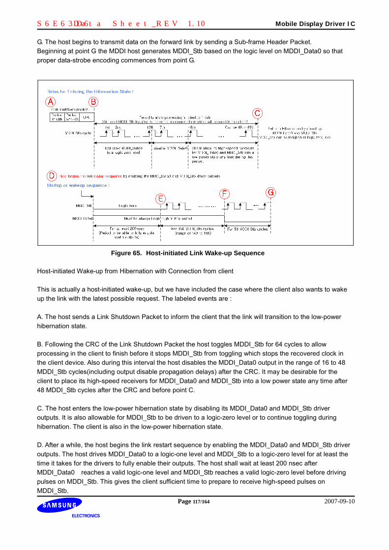
S6E63D6 Data Sheet_REV 1.10 Mobile Display Driver IC
Page 117/164 2007-09-10
G. The host begins to transmit data on the forward link by sending a Sub-frame Header Packet. Beginning at point G the MDDI host generates MDDI_Stb based on the logic level on MDDI_Data0 so that proper data-strobe encoding commences from point G.
Figure 65. Host-initiated Link Wake-up Sequence Host-initiated Wake-up from Hibernation with Connection from client This is actually a host-initiated wake-up, but we have included the case where the client also wants to wake up the link with the latest possible request. The labeled events are : A. The host sends a Link Shutdown Packet to inform the client that the link will transition to the low-power hibernation state. B. Following the CRC of the Link Shutdown Packet the host toggles MDDI_Stb for 64 cycles to allow processing in the client to finish before it stops MDDI_Stb from toggling which stops the recovered clock in the client device. Also during this interval the host disables the MDDI_Data0 output in the range of 16 to 48 MDDI_Stb cycles(including output disable propagation delays) after the CRC. It may be desirable for the client to place its high-speed receivers for MDDI_Data0 and MDDI_Stb into a low power state any time after 48 MDDI_Stb cycles after the CRC and before point C. C. The host enters the low-power hibernation state by disabling its MDDI_Data0 and MDDI_Stb driver outputs. It is also allowable for MDDI_Stb to be driven to a logic-zero level or to continue toggling during hibernation. The client is also in the low-power hibernation state. D. After a while, the host begins the link restart sequence by enabling the MDDI_Data0 and MDDI_Stb driver outputs. The host drives MDDI_Data0 to a logic-one level and MDDI_Stb to a logic-zero level for at least the time it takes for the drivers to fully enable their outputs. The host shall wait at least 200 nsec after MDDI_Data0 reaches a valid logic-one level and MDDI_Stb reaches a valid logic-zero level before driving pulses on MDDI_Stb. This gives the client sufficient time to prepare to receive high-speed pulses on MDDI_Stb.

S6E63D6 Data Sheet_REV 1.10 Mobile Display Driver IC
Page 118/164 2007-09-10
E. The host drivers are fully enabled and MDDI_Data0 is being driven to a logic-one level. The host begins to toggle MDDI_Stb in a manner consistent with having a logic-zero level on MDDI_Data0 for a duration of 150 MDDI_Stb cycles. F. At up to 70 MDDI_Stb cycles after point E the client has not yet recognized that the host is driving MDDI_Data0 to a logic-one level so the client also drives MDDI_Data0 to a logic-one level. This occurs because the client has a need to request service from the host and does not recognize that the host has already begun the link restart sequence. G. The client ceases to drive MDDI_Data0, and places its driver into a high-impedance state by disabling its output. The host continues to drive MDDI_Data0 to a logic-one level for 80 additional MDDI_Stb cycles. H. The host drives MDDI_Data0 to a logic-zero level for 50 MDDI_Stb cycles. The client begins to look for the Sub-frame Header Packet after MDDI_Data0 is at a logic-zero level for 40 MDDI_Stb cycles. I. The host begins to transmit data on the forward link by sending a Sub-frame Header Packet. Beginning at point I the MDDI host generates MDDI_Stb based on the logic level on MDDI_Data0 so that proper data-strobe encoding commences from point I.
Figure 66. Host-initiated Wake-up Process from Hibernation with Connection from Client

S6E63D6 Data Sheet_REV 1.10 Mobile Display Driver IC
Page 119/164 2007-09-10
10.3.5.4. Client-initiated Link Wake-up Procedure An example of a typical client-initiated service request event with no contention is illustrated in the following figure.
Figure 67. Client-initiated Link Wake-up Procedure The Detailed descriptions for labeled events are as follows: A. The host sends a Link Shutdown Packet to inform the client that the link will transition to the low-power hibernation state. B. Following the CRC of the Link Shutdown Packet the host toggles MDDI_Stb for 64 cycles to allow processing in the client to finish before it stops MDDI_Stb from toggling which stops the recovered clock in the client device. Also during this interval the host initially sets MDDI_Data0 to a logic-zero level, and then disables the MDDI_Data0 output in the range of 16 to 48 MDDI_Stb cycles (including output disable propagation delays) after the CRC. It may be desirable for the client to place its high-speed receivers for MDDI_Data0 and MDDI_Stb into a low power state any time after 48 MDDI_Stb cycles after the CRC and before point C. C. The host enters the low-power hibernation state by disabling its MDDI_Data0 and MDDI_Stb driver outputs. It is also allowable for MDDI_Stb to be driven to logic-zero level or to continue toggling during hibernation. The client is also in the low-power hibernation state. D. After a while, the client begins the link restart sequence by enabling the MDDI_Stb receiver and also enabling an offset in its MDDI_Stb receiver to guarantee the state of the received version of MDDI_Stb is a logic-zero level in the client before the host enables its MDDI_Stb driver. The client will need to enable the offset in MDDI_Stb immediately before enabling its MDDI_Stb receiver to ensure that the MDDI_Stb receiver in the client is always receiving a valid differential signal and to prevent erroneous received signals from propagating into the client. After that, the client enables its MDDI_Data0 driver while driving MDDI_Data0 to a logic-one level. It is allowed for MDDI_Data0 and MDDI_Stb to be enabled simultaneously if the time to enable the offset and enable the standard MDDI_Stb differential receiver is less than 200 nsec. E. Within 1 msec the host recognizes the service request pulse, and the host begins the link restart sequence by enabling the MDDI_Data0 and MDDI_Stb driver outputs. The host drives MDDI_Data0 to a logic-one level and MDDI_Stb to a logic-zero level for at least the time it takes for the drivers to fully enable their outputs. The host shall wait at least 200 nsec after MDDI_Data0 reaches a valid logic-one level and MDDI_Stb reaches a valid fully-driven logic-zero level before driving pulses on MDDI_Stb.

S6E63D6 Data Sheet_REV 1.10 Mobile Display Driver IC
Page 120/164 2007-09-10
This gives the client sufficient time to prepare to receive high-speed pulses on MDDI_Stb. F. The host begins outputting pulses on MDDI_Stb and shall keep MDDI_Data0 at a logic-one level for a total duration of 150 MDDI_Stb pulses through point H. The host generates MDDI_Stb in a manner consistent with sending a logic-zero level on MDDI_Data0. When the client recognizes the first pulse on MDDI_Stb it shall disable the offset in its MDDI_Stb receiver. G. The client continues to drive MDDI_Data0 to a logic-one level for 70 MDDI_Stb pulses, and the client disables its MDDI_Data0 driver at point G. The host continues to drive MDDI_Data0 to a logic-one level for duration of 80 additional MDDI_Stb pulses, and at point H drives MDDI_Data0 to logic-zero level. H. The host drives MDDI_Data0 to logic-zero level for 50 MDDI_Stb cycles. The client begins to look for the Sub-frame Header Packet after MDDI_Data0 is at logic-zero level for 40 MDDI_Stb cycles. I. After asserting MDDI_Data0 to logic-zero level and driving MDDI_Stb for duration of 50 MDDI_Stb pulses the host begins to transmit data on the forward link at point I by sending a Sub-frame Header Packet. The client begins to look for the Sub-frame Header Packet after MDDI_Data0 is at logic-zero level for 40 MDDI_Stb cycles.
Figure 68. Client-initiated Link Wake-up Sequence

S6E63D6 Data Sheet_REV 1.10 Mobile Display Driver IC
Page 121/164 2007-09-10
S6E63D6 supports 2-types of client-initiated link wake-up: VSYNC based Link Wake-up & GPIO based Link Wake-up. As client-initiated wake-up action is executed in hibernation state only, register setting for each wake-up have to be set before link shut-down. VSYNC Based Link Wake-up
In display-ON state, when the IC finishes displaying all internal GRAM data, data request must be transferred to MDDI host for new video data. As MDDI link is usually in hibernation for reducing interface power consumption, MDDI link wake-up must be done before internal GRAM update. In that case, client initiated link wake-up can be used as data request. When VSYNC based link wake-up register (50h: VWAKE_EN) is set, client initiated wake-up is executed in synchronization with the vertical-sync signal which generated in S6E63D6. Using VSYNC based link wake-up, tearing-less display can be accomplished if interface speed and wake-up time is well known. The following figure shows detailed timing for VSYNC based link wake-up.
VWAKE_EN
link_active
frame_update
client_wakeup
A B C D E FSYNC STATE HIBERNATION STATE WAKE-UP STATE SYNC STATE
Figure 69. VSYNC Based Link Wake-up Procedure The Detailed descriptions for labeled events are as follows: A. MDDI host writes to the VSYNC based link wakeup register to enable a wake-up based on internal vertical-sync signal. B. link_active goes low when the host puts in the link into hibernation after no more data needs to be sent to the S6E63D6. C. frame_update, the internal vertical-sync signal goes high indicating that update pointer has wrapped around and is now reading from the beginning of the frame buffer. Link wake-up point can be set using WKF and WKL (51h) registers. WKF specifies the number of frame before wake-up; WKL specifies the number of lines before wake-up. D. client_wakeup input to the MDDI client goes high to start the client initiated link wake-up. E. link_active goes high after the host brings the link out of hibernation. F. After link wake-up, client_wakeup signal and the VWAKE_EN register are cleared automatically.

S6E63D6 Data Sheet_REV 1.10 Mobile Display Driver IC
Page 122/164 2007-09-10
GPIO Based Link Wake-up In VSYNC-based link wake-up, wake-up enable register setting prior to link shut-down. GPIO based Link wake-up is enabled by interrupt from outside of the IC. For GPIO based link wake-up, GPIO interrupt enable and GPIO PAD mode (to input mode) setting must be set. Once S6E63D6 receive interrupt, internal GPIO base link wake-up flag set to high, and the following procedure is similar to that of VSYNC based link wake-up. The following figure shows detailed timing for GPIO based link wake-up.
GPIO_EN
link_active
frame_update
client_wakeup
A B D E F GSYNC STATE HIBERNATION STATE WAKE-UP STATE SYNC STATE
GPIO(input)*
GPIO_INT*
C H
Figure 70. GPIO Based Link Wake-up Procedure The Detailed descriptions for labeled events are as follows: A. Host sets the GPIO interrupt enable register (69h: GPIO_EN) for a particular GPIO through register access packet. B. Link goes into hibernation (and link_active)goes low) when the host has no more data to send to the IC. C. GPIO input goes high, and the GPIO interrupt (GPIO_INT) is latched. D. Frame_update signal goes high indicating that the display has wrapped around. Link wake-up point can be set using WKF and WKL (51h) registers. E. Client_wakeup input to the MDDI client goes high to start the client initiated link wake-up. F. Link_active goes high after the host brings the link out of hibernation. G. After link wake-up, client_wakeup signal is reset to low. H. MDDI host clears the interrupt by writing to the interrupt clear register with the bit set for that particular interrupt (GPCLR: 68h). Between point G and H the host will have read the GPIO_INT values to see what interrupts are active.

S6E63D6 Data Sheet_REV 1.10 Mobile Display Driver IC
Page 123/164 2007-09-10
10.3.6. GPIO Control
S6E63D6 offers 10(maximum) GPIO that can be used as input or output independently.
Some application or device on the upper clamshell needs several control signals which are supplied by base
band modem or application processor directly. If number of application on the upper clamshell increases,
also control signals increase, causing the interface more costly.
In S6E63D6, GPIO can be the solution for that problem. User may control the 10 GPIOs as input or output
by use of simple register setting. So additional connection between base band modem / AP (application
processor) and components on upper clamshell are not needed.
The following table shows several set of register for GPIO.
Table 66. The Description of register for GPIO Register Width Description Reset Value
Write For GPIO output mode: output GPIO register(66h) value to GPIO PAD
GPIO
(66h)
[9:0]
Read GPIO PAD status
10’h000
Write GPIO PAD input/output mode control : (0 : input / 1 : output) GPIO_CON
(67h)
[9:0]
Read GPIO_CON (67h) register value
10’h000
Write For GPIO input mode: clear specified GPIO interrupt (set by GPIO PAD input).
GPCLR
(68h)
[9:0]
Read GPIO interrupt state (set by GPIO PAD input).
10’h000
Write For GPIO input mode: enable specified GPIO interrupt GPIO_EN
(69h)
[9:0]
Read GPIO_EN (69h) register value.
10’h000
Write For GPIO input mode: GPIO interrupt polarity setting GPPOL
(6Ah)
[9:0]
Read GPPOL (6Ah) register value.
10’h3FF
In GPIO output mode, the IC output GPIO (66h) register value to the defined PAD.
Set GPIO_CON register as output mode before use GPIO output.
10 different GPIO output can be controlled simultaneously using 1-register access packet (66h register
access) so that minimum access time for each GPIO output will be 1-register access time.
GPIO input mode can only be used as client-initiated link wake-up.
For more information, refer to GPIO based link wake-up section.

S6E63D6 Data Sheet_REV 1.10 Mobile Display Driver IC
Page 124/164 2007-09-10
10.3.7. MDDI Packet
MDDI transfer data by packet format. MDDI host can make many packets and transfer them.
In S6E63D6, several packets format is supported. Most packets are transferred from MDDI host to client
(forward direction); but reverse encapsulation packet is transferred from MDDI client to host (reverse
direction).
A number of packets, started by sub-frame header packet, construct 1 sub frame.
Figure 71. MDDI Packet Structure
Refer to MDDI packet structure, sub-frame header packet is placed in front of a sub-frame, and some sub-
frame construct media-frame together.
The following table describes 9 types of packet which is supported in S6E63D6.
Table 67. MDDI Packet and Function Packet Function Direction
Sub-frame header packet Header of each sub frame Forward
Register access packet Register setting Forward
Video stream packet Video data transfer Forward
Filler packet Fill empty packet space Forward
Reverse link encapsulation packet Reverse data packet Forward
Round-trip delay measurement packet Host->client->host delay check Forward/Reverse
Client capability packet Capability of client check Forward
Client request and status packet Information about client status Forward
Link shutdown packet End of frame Forward

S6E63D6 Data Sheet_REV 1.10 Mobile Display Driver IC
Page 125/164 2007-09-10
10.3.7.1. Sub-frame Header Packet
Figure 72. Sub-frame Header Packet Structure
10.3.7.2. Register Access Packet
Figure 73. Register Access Packet Structure

S6E63D6 Data Sheet_REV 1.10 Mobile Display Driver IC
Page 126/164 2007-09-10
10.3.7.3. Video Stream Packet
Figure 74. Video Stream Packet Structure
10.3.7.4. Filler Packet
Figure 75. Filler Packet Structure

S6E63D6 Data Sheet_REV 1.10 Mobile Display Driver IC
Page 127/164 2007-09-10
10.3.7.5. Link Shutdown Packet
Figure 76. Link Shutdown Packet Structure
: fixed value
For More information about MDDI packet, please refer to VESA MDDI spec.

S6E63D6 Data Sheet_REV 1.10 Mobile Display Driver IC
Page 128/164 2007-09-10
10.3.8. MDDI Operating State
In MDDI, six operation modes are available. The following table describes six modes.
Table 68. MDDI Operating State STATE OSC Booster Circuit Internal Logic status MDDI I/O Wake-up by
SLEEP OFF Disabled Display OFF
MDDI Link hibernation
Hibernation
driver ON Host – Initiated
WAIT ON Disabled Display OFF
MDDI Link in SYNC
standard driver
ON -
NORMAL ON Enabled Display ON
MDDI Link in SYNC
standard driver
ON -
NAP ON Disabled Display OFF
MDDI Link in SYNC
standard driver
ON -
IDLE ON Enabled Display ON
MDDI Link hibernation
Hibernation
driver ON
Host – Initiated
Client –Initiated
(Vsync, GPIO)
STOP OFF Disabled Display OFF
MDDI Link OFF Driver All OFF RESET
SLEEP: Initial status when external power is connected to the IC. In this state, internal oscillator is not operating, and MDDI link is in hibernation state. As no command or signal is applied to the IC except RESET input, internal logic or booster circuit is OFF. WAIT: After the wake-up sequence, the IC is in WAIT state. MDDI link is in SYNC, and internal logic or booster is still OFF because no other register access or video stream packet is transferred to the IC. NORMAL: MDDI link, booster circuit, and internal logic circuit is ON. Register access or Video data transfer is available in NORMAL state. IDLE: When no more video data update is needed, MDDI link is in hibernation so that interface power can be reduced. Internal booster circuit & logic circuits are still operating. MDDI link wakeup will be accomplished when vsync wakeup register is set before hibernation or GPIO interrupt is set. NAP: This state is set by register access. Booster Circuit and Internal logic is OFF, but MDDI link is ON. MDDI link have to be in SYNC because the IC must receive commands for power save or normal operation STOP: STOP state is set by register access (R10h). In this state, MDDI link, internal oscillator, booster, and logic circuit are all OFF. To release STOP state, input reset signal. After reset, status is SLEEP state.

S6E63D6 Data Sheet_REV 1.10 Mobile Display Driver IC
Page 129/164 2007-09-10
The following pigure shows the operating state in MDDI mode.
MDDI Link wake-up!
Figure 77. Operating State in MDDI mode

S6E63D6 Data Sheet_REV 1.10 Mobile Display Driver IC
Page 130/164 2007-09-10
10.3.9. Tearing-less Display In S6E63D6, the matching between data write timing and written data display timing is important. If timing is mismatched, tearing effect can occur. To avoid display tearing effect, two possible ways are suggested. First case is that data write is slower than speed of displaying written data. In this case, data write speed is not critical, but current consumption in interface will be increased because data transfer time is long. Other case is that data write is faster than speed of displaying written data. In this case, data update speed is very high so that transfer time is short. So current consumption in interface can be minimized, but it requires fast data transfer. The most important thing is to avoid data scan conflicts with data update. The following figures describe some examples to avoid display tearing phenomenon. 10.3.9.1. Display speed is faster than data write.
Figure 78. Tearing-less Display: Display speed is faster than data write. 10.3.9.2. Display speed is slower than data write.
Figure 79. Tearing-less Display: Data write speed is faster than display.

S6E63D6 Data Sheet_REV 1.10 Mobile Display Driver IC
Page 131/164 2007-09-10
10.3.10. Sub Panel Control
S6E63D6 support sub panel control function which controls sub panel driver IC using 80-mode protocol
(CSB, RS, WRB & DB). When MDDI host (Base band modem) sends several packets to S6E63D6, if the
packet is for sub panel, the IC converts the packet to 80-mode protocol & sends them to sub panel driver IC.
So separated line for sub panel control are not needed. After all, S6E63D6 enables the sub panel driver IC
which doesn’t support MDDI to be applied to the system. S6E63D6 supports only 9/8 bit format for sub panel
control.
LCD driver IC
TFT-LCD Module(SUB display)
LCD driver IC
Sub Panel (Normal LDI)
MSM (Baseband Modem)
MDDI HOSTMDDI TRX/ RX
80 mode Parallel I/F
Main Panel (MDDl-Supported LDI)
OLED Module(MAIN display)
Figure 80. Schematic Diagram of Sub Panel Control Function

S6E63D6 Data Sheet_REV 1.10 Mobile Display Driver IC
Page 132/164 2007-09-10
10.3.10.1. Main / Sub Panel Selection
Using 7Ah register (7Ah address can be changed using SUB_SEL register), main / sub panel data path can
be selected.
When S6E63D6 receives register access packet (Initially 7Ah index) from MDDI host, it decodes the packet
and checks the last bit of the register data field is ‘1’ or ‘0’. If the last bit is ‘0’, the following register access
packet or video stream packet is transferred to the sub panel control signal generation block.
Sub panel selection address (Initially 7Ah) can be changed using SUB_SEL register. Do not change the
SUB_SEL value to previously occupied address.
Register Address = SUB_SEL
Register Data = 0000h
Register Data = 0001h
MAIN panel Selection Procedure
Command Transfer(Register Access packet)
SUB panel Selection Procedure
Video Data Transfer(Video Stream packet)
Register Address = SUB_SEL
Command / Data transfer to SubPanel driver IC (80-mode protocol)
Note: Initial value of SUB_SEL = 7Ah
Figure 81. Main / Sub Panel Selection Procedure
When video data is transferred to the sub panel driver IC via S6E63D6, additional GRAM access command
(normally 22h) is automatically generated in S6E63D6.

S6E63D6 Data Sheet_REV 1.10 Mobile Display Driver IC
Page 133/164 2007-09-10
10.3.10.2. Sub Panel Control Timing
TFT type sub panel timing
TFT type register data transfer timing
If sub panel is selected, and sub panel type is TFT, register setting is executed like below figure.
Register data is transferred through S_DB[8:1] in 9/8 bit type. Refer to sub panel control(3Ch index) section.
In 9/8 bit mode, S_DB[8:1] is used. In this mode, data is transferred at two times. First transfer is MSB 8bit
and second transfer is LSB 8bit.
Figure 82. 80 Mode TFT Type 9-/8-bit Register Access Data Transfer
In 68 mode, S_WRB must be connected to E_RDB of sub panel module. RW_WRB of sub panel module
must be tied to VSS, because S6E63D6 writes data to sub panel module only.

S6E63D6 Data Sheet_REV 1.10 Mobile Display Driver IC
Page 134/164 2007-09-10
TFT type video data transfer timing
In TFT type sub panel, STN_EN register in 3Ch index is “0”, and if user wants to use 68-mode interface
protocol, then MPU_MODE is set to “1”. 9/8 mode is selected as setting SUB_IM register. Refer to 3Ch
index description.
In 68 mode, S_WRB must be connected to E_RDB of sub panel module. RW_WRB of sub panel module
must be tied to VSS, because S6E63D6 writes data to sub panel module only.
This figure shows 80-mode TFT type 9 bit video data transfer.
Figure 83. 80 Mode TFT Type 9-bit Video Data Transfer
This figure shows 80-mode TFT type 8 bit video data transfer.
Figure 84. 80 Mode TFT Type 8-bit Video Data Transfer

S6E63D6 Data Sheet_REV 1.10 Mobile Display Driver IC
Page 135/164 2007-09-10
STN type sub panel timing
STN type register data transfer timing This figure shows conventional type STN mode register data setting. Conventional type does not include parameter. Instruction type is only 8bit. To use STN type, STN_EN is set to “1”. In STN type, S6E63D6 controls S_RS pad using register address[0] in register access packet. Register address[0] is “0”, then S_RS is set to “0”, and register address[0] is “1”, S_RS is set to “1”. Refer to sub panel control(3Ch index) section.
00002h(0001h parameter)
000AAh(55h index)
CRC
S_DB[17:0]
S_CSB
S_RS
S_WRB
index write
MDDIData
Stream
RegisterAddress(0000h)
HeaderCRC
RegisterData
(0055h)
1 Register Access Packet
CRC
RegisterAddress(0000h)
HeaderCRC
RegisterData
(0001h)
parameter write
Figure 85. 80 Mode STN Type Convetional Register Data Transfer This type is used to include parameter. When instruction is transferred, S_RS is zero, and when parameter is transferred, S_RS is “1”. S_RS is controlled using register address[0] of register access packet.
000AAh(55h index)
00002h(0001h parameter)
CRC
S_DB[17:0]
S_CSB
S_RS
S_WRB
index write
MDDIData
Stream
RegisterAddress(0000h)
HeaderCRC
RegisterData
(0055h)
1 Register Access Packet
CRC
RegisterAddress(0001h)
HeaderCRC
RegisterData
(0001h)
parameter write (RS = 1)
Figure 86. 80 mode STN Type Register Data Included Parameter Transfer

S6E63D6 Data Sheet_REV 1.10 Mobile Display Driver IC
Page 136/164 2007-09-10
STN type video data transfer timing
In STN mode, video data start register (like 22H is TFT mode) does not need generally. But some STN type
needs video data start register. If this type STN DDI is used, user has to set the register index.
This figure shows STN 16 bit mode video data transfer.
Header
00044h(write disabled)
pixel write
CRC
Pixel data #1(01ABCh)
CRC
1 Video Stream Packet(18-bpp)
Pixel data #2(100FFh)
Pixel data #4(000FFh)
Pixel data #3(0FF00h)
Pixel data #5(00001h)
Pixel data #101ABCh
Pixel data #2100FFh
Pixel data #30FF00h
Pixel data #4000FFh
Pixel data #500001h
pixel write pixel write pixel write pixel write
DB[17:0](data output to sub LDI)
S_CSB(chip select for sub LDI)
S_RS(command / data select)
S_WRB(write enable for sub LDI)
MDDIData Stream
Figure 87. 80 Mode STN Type 16-bit Video Data Transfer
This figure shows STN 8bit mode video data transfer. If STN video data is 16bit mode, data transfer is
executed during 2 times. Fist transfer is MSB 8bits, and second is LSB 8bits.
Header
22h
pixel write
CRC
Pixel data #1(1ABCh)
CRC
1 Video Stream Packet(16-bpp)
Pixel data #2(00FFh)
Pixel data #4(01FFh)
Pixel data #3(FF00h)
Pixel data #5(0001h)
1Ah MSB
pixel write pixel write pixel write pixel write
DB[17:10](data output to sub LDI)
S_CSB(chip select for sub LDI)
S_RS(command / data select)
S_WRB(write enable for sub LDI)
MDDIData Stream
BCh LSB
Pixel data #1
00h MSB
FFh LSB
Pixel data #2
FFh MSB
00h LSB
01h MSB
FFh LSB
Pixel data #3 Pixel data #422h write disabled
22h 00h MSB
01h LSB
Pixel data #5
Figure 88. 80 Mode STN Type 8-bit Video Data Transfer

S6E63D6 Data Sheet_REV 1.10 Mobile Display Driver IC
Page 137/164 2007-09-10
Index/parameter write for sub panel DDI
Figure 89. Index/parameter Write for Sub Panel DDI
Image data write for sub panel DDI
Figure 90. Image Data Write for Sub Panel DDI
Change data path from sub panel to main panel
Figure 91. Change Data Path from Sub Panel to Main Panel

S6E63D6 Data Sheet_REV 1.10 Mobile Display Driver IC
Page 138/164 2007-09-10
11. AMOLED Panel Interface 11.1. AMOLED Panel Interface Signal
S6E63D6 outputs some timing signals (SIN, CK, SCK, R_sw, G_sw, B_sw) for controlling an AMOLED panel
with built-in gates. S6E63D6 has built-in level shifter for AMOLED panel. Output voltage level for high is
VGH voltage, for low is VGL voltage.
Figure 92. An Exemplary Combination of AMOLED Panel and DDI

S6E63D6 Data Sheet_REV 1.10 Mobile Display Driver IC
Page 139/164 2007-09-10
Figure 94. VSYNC and Panel Interface Signals in External Clock Operation Mode

S6E63D6 Data Sheet_REV 1.10 Mobile Display Driver IC
Page 140/164 2007-09-10
12. R, G, B Independent Gamma Adjustment Function
S6E63D6 provides the gamma adjustment function to display 262,144 colors simultaneously.
The gamma adjustment is executed by the amplitude adjusting registers and curve adjusting registers.
Since, those control registers incorporate independent adjustment of the gamma function for R, G, B
independently, it is highly possible that user determine the best appropriate configuration according to the
trait of the display panel.
Figure 95. Grayscale Control


S6E63D6 Data Sheet_REV 1.10 Mobile Display Driver IC
Page 142/164 2007-09-10
12.2. R, G, B Independent Gamma Adjustment Registers
These are registers to set up the grayscale voltage in accordance with the gamma specification of the
AMOLED panel. The registers can set up both amplitude and curve character of grayscale voltage
respectively with corresponding bits as the function of grayscale number. Each configuration can be made
for R, G, B independently.
There shows the operation of each register below.
Figure 97. The Operation of Adjusting Register
Gray Scale Data
Grq
y Scale
a) Top level control(4bit : 16step)
V0 V63 Gray Scale Data
Gra
y Scale
Voltage
b) Bottom level control(7bit : 128step)
V0 V63 Gray Scale Data
Gra
y S
cale
Voltage
Flexible curve by 4 point control(6bits: 64step)
VREG1OUT V63
Amplitude adjustment Curve adjustment

S6E63D6 Data Sheet_REV 1.10 Mobile Display Driver IC
Page 143/164 2007-09-10
12.2.1. Amplitude Adjusting Registers
These are the registers for adjusting the amplitude of grayscale voltage. The registers for adjusting
amplitude consists of two parts, one of which is for top level voltage (V0) and the other of which is for bottom
level voltage (V63). CR0[3:0], CG0[3:0] and CB0[3:0] registers control the top level voltage. CR5[6:0],
CG5[6:0] and CB5[6:0] registers control the bottom level voltage. V0 and V63 are selected in divided voltage
from ladder resistor strings between VGS and VREG1OUT. Separate registers are prepared for R, G, B
respectively.
Table 69. Amplitude Adjusting Register Register for R for G for B Content of configuration
CR0[3:0] CG0[3:0] CB0[3:0] Grayscale voltage adjusting for top level voltage
R70H ~ R72H CR5[6:0] CG5[6:0] CB5[6:0]
Grayscale voltage adjusting for bottom level
voltage


S6E63D6 Data Sheet_REV 1.10 Mobile Display Driver IC
Page 145/164 2007-09-10
12.2.2. Curve Adjusting Registers
The curve adjusting registers are used for adjusting the characteristic curve of the grayscale voltage as the
function of grayscale number. The registers also control R, G, B independently like the amplitude adjusting
register. To accomplish the adjustment, these registers control the each 4 reference voltage by three 47 to 1
selector and a 64 to 1 selector. The 47 or 64 leveled reference voltage generated from the ladder resistor
strings between V0 and V63. The registers for adjusting curve consist of 4 reference point – V4, V10, V21
and V42.
Table 72. Gamma Curve Adjusting Register Register For R for G for B Content of configuration
CR1[5:0] CG1[5:0] CB1[5:0] Grayscale voltage adjusting for V4
CR2[5:0] CG2[5:0] CB2[5:0] Grayscale voltage adjusting for V10
CR3[5:0] CG3[5:0] CB3[5:0] Grayscale voltage adjusting for V21 R73H ~ R78H
CR4[5:0] CG4[5:0] CB4[5:0] Grayscale voltage adjusting for V42
CR1[5:0], CG1[5:0], CB1[5:0] Regis ter Control for V 4
Gray scale data
Gra
yscale
voltage
CR2[5:0], CG2[5:0], CB2[5:0] Regis ter Control forV 10
Gray scale data
Gra
yscale
voltage
CR3[5:0], CG3[5:0], CB3[5:0] Register Control forV 21
Gray scale data
Gra
yscale
voltage
CR4[5:0], CG4[5:0], CB4[5:0] Regis ter Control forV 42
Grayscale data
Gra
yscale
voltage
Figure 98. Gamma Curve Adjustment


S6E63D6 Data Sheet_REV 1.10 Mobile Display Driver IC
Page 148/164 2007-09-10
12.4. Output Level as the function of GRAM Data
Output level could be described as the function of GRAM DATA like below.
REV = 0
REV = 1V0
V63
Out
put L
evel
RAM data
0000
00
1111
11
V0
V63
Out
put L
evel
RAM data
0000
00
1111
11
V0
V63
Out
put L
evel
RAM data
0000
00
1111
11
V0
V63
Out
put L
evel
RAM data(Independently controlable characteristics to RGB)00
0000
1111
11
Figure 99. Relationship between RAM Data and Output Voltage
Table 75. GRAM Data and Gray Scale Level GRAM
data Grayscale
GRAM
data Grayscale
GRAM
data Grayscale
GRAM
data Grayscale
RGB REV=0 REV=1 RGB REV=0 REV=1 RGB REV=0 REV=1 RGB REV=0 REV=1
000000 V0 V63 010000 V16 V47 100000 V32 V31 110000 V48 V15
000001 V1 V62 010001 V17 V46 100001 V33 V30 110001 V49 V14
000010 V2 V61 010010 V18 V45 100010 V34 V29 110010 V50 V13
000011 V3 V60 010011 V19 V44 100011 V35 V28 110011 V51 V12
000100 V4 V59 010100 V20 V43 100100 V36 V27 110100 V52 V11
000101 V5 V58 010101 V21 V42 100101 V37 V26 110101 V53 V10
000110 V6 V57 010110 V22 V41 100110 V38 V25 110110 V54 V9
000111 V7 V56 010111 V23 V40 100111 V39 V24 110111 V55 V8
001000 V8 V55 011000 V24 V39 101000 V40 V23 111000 V56 V7
001001 V9 V54 011001 V25 V38 101001 V41 V22 111001 V57 V6
001010 V10 V53 011010 V26 V37 101010 V42 V21 111010 V58 V5
001011 V11 V52 011011 V27 V36 101011 V43 V20 111011 V59 V4
001100 V12 V51 011100 V28 V35 101100 V44 V19 111100 V60 V3
001101 V13 V50 011101 V29 V34 101101 V45 V18 111101 V61 V2
001110 V14 V49 011110 V30 V33 101110 V46 V17 111110 V62 V1
001111 V15 V48 011111 V31 V32 101111 V47 V16 111111 V63 V0

S6E63D6 Data Sheet_REV 1.10 Mobile Display Driver IC
Page 149/164 2007-09-10
13. 8-Color Display Mode
The S6E63D6 incorporates 8-color display mode. The voltage levels to be used are VREG1OUT and V63
and all the other grayscale levels V0~V62are halt. So that it attempts to lower power consumption.
During the 8-color mode, the Gamma micro adjustment register, C1R~C4R, C1G~C4G and C1B~C4B are
invalid. The level power supply (V0-V62) is in OFF condition during the 8-color mode in order to select
VREG1OUT/V63.
Figure 100. 8-color Display Control

S6E63D6 Data Sheet_REV 1.10 Mobile Display Driver IC
Page 150/164 2007-09-10
14. Set-up Flow of Stand by
The figure shows set-up flow of stand by.
External Power OnSequence
Reset
VCI1 setting(R12h)
BT2-0,DC12-10,DC21-20
Stand By Off Status
<Stand By Off flow>
Stand By Off status
Stand By Onstatus
Booster control(R14h)
Power Gen(R13h,RF8h,RF9h)
<Stand By On flow>
VINT3-0, VGH4-0, VGL4-0
VC3-0
Oscillator Control(R18h)RADJ5-0
Source Amp(R1Ah)SAP2-0
Stand By (R10h)
STB = 0
If needed
1 ms 1 ms
Wait More than 140 ms
Stand By (R10h)
STB = 1
Wait More than 120 ms
EL Control (RF4h)
EL_ON=1
EL Control (RF4h)
EL_ON=0
Display Control (R05h)
DISP_ON=0
Display Control (R05h)
DISP_ON=1
Figure 101. Set-up Flow of Stand by

S6E63D6 Data Sheet_REV 1.10 Mobile Display Driver IC
Page 151/164 2007-09-10
15. Oscillation Circuit
The S6E63D6 can provide R-C oscillation. S6E63D6 internal oscillator does not need to attach the external
resistor. The appropriate oscillation frequency for operating voltage, display size, and frame frequency can
be obtained by adjusting the oscillator frequency control register setting. Since R-C oscillation stops during
the standby mode, power consumption can be reduced.
Frame Frequency Calculation
The relation between the AMOLED driver duty and the frame frequency can be found by the following
expression.
Figure 102. Formula for the Frame Frequency
Table 76. Example of Frame Frequency Calculation Parameters Description
Line Number 320
Frame Frequency 60
BP 8
FP 8
Fosc 1,290,240 Hz
Table 77. Display Clock Frequency Clock Operatin Mode 1 HCLK 1 Horizontal Period
Internal Clock Operation Fosc / 2 32 HCLKs
External Clock Operation Fdotclk / 8(RIM=00,01)
Fdotclk/24(RIM = 10) 32 HCLKs


S6E63D6 Data Sheet_REV 1.10 Mobile Display Driver IC
Page 153/164 2007-09-10
17. DC / AC Specification 17.1. Absolute Maximum Rating
Table 78. Absolute Maximum rating (VSS = 0V)
Item Symbol Rating Unit
Supply voltage VDD3 -0.3 ~ 5.0 V
Supply voltage for booster circuit VCI -0.3 ~ 5.0 V
Supply Voltage range |VLIN2 – VLIN3| 20 V
Input Voltage range Vin -0.3 to VDD + 0.5 V Note 1. Absolute maximum rating is the limit value. When the IC is exposed operating environment beyond this range, the IC does not assure operations and may be damaged permanently, not be able to be recovered. 2. Absolute maximum rating is guaranteed only when our company’s package used.

S6E63D6 Data Sheet_REV 1.10 Mobile Display Driver IC
Page 154/164 2007-09-10
17.2. DC Characteristics
Table 79. DC Characteristics 1 (Ta = -40 ~ 85, VSS = 0V)
Characteristic Symbol CONDITION MIN TYP MAX Unit NoteVGH - 3.0 - 8.0 V VGL - -8.0 - -3.0 V Driving voltage VINT - -4.0 - -1.0 V
Logic Operating Voltage RVDD - 1.45 1.5 1.55 V
Operating frequency fosc
Frame frequency = 60Hz
Display line = 320 line
1161.1 1290.2 1419.3 kHz
1st booster input voltage VCI1 - 2.1 - 2.75 V 1st booster output voltage VLOUT1 Without load +4.6 - +5.5 V
1st booster output efficiency VLOUT1 I_VLOUT1_LOAD =
2.3mA 90 95 - %
2nd booster output voltage VLOUT2 Without load 7.8 V
2nd booster output efficiency VLOUT2 I_VLOUT2_LOAD =
0.1mA 90 93 - %
3rd booster output voltage VLOUT3 Without load - -10.6 - V
3rd booster output efficiency VLOUT3 I_VLOUT3_LOAD =
0.1mA 90 93 - %
Source Output voltage deviation
(channel to channel) - - - ±5 - mV
Source Output voltage difference
( nearest channel) - 20 Gray Pattern - 5 - mV
Output voltage deviation (Chip to Chip)
- - - ±15 - mV
Source driver output voltage range
Vso - 0.3 - 4.2 V
dVGH voltage deviation - - 300 mV Driving voltage
dVGL voltage deviation - - 300 mV IVDD3 - 1.0 5.0 uA Current consumption
during normal operation IVCI No load,
Ta = 25 °C - 3.5 4.0 mA *1
IVDD3 - 0.1 5.0 uA Stand by mode current
IVCI Ta = 25 °C
- 10 20 uA Note 1. VDD3=1.8V, VCI=2.8V, fosc=1290.2KHz (320 display line), NL[5:0]=" 10_1000", SAP[2:0]=”101”, DC22[2:0]=”100”, DC12[2:0]=”010” , BT[1:0]=10, VC[3:0]="1000", VGH[4:0]="10100", VGL[4:0]=”10100”, VINT[3:0]=”0101"

S6E63D6 Data Sheet_REV 1.10 Mobile Display Driver IC
Page 155/164 2007-09-10
Table 80. DC Characteristics 2 (Ta = -40 ~ 85, VSS = 0V)
Characteristic Symbol CONDITION MIN TYP MAX Unit NotePower Supply Voltage VCI Operating Voltage 2.5 2.8 3.3 V Power Supply Voltage VDD3 I/O supply Voltage 1.65 1.8 3.3 V Logic High level input
voltage VIH 0.7*VDD3 VDD3 V
Logic Low level input voltage
VIL 0.0 0.3*VDD3 V
Logic High level output voltage
VOH IOUT = -1mA 0.8*VDD3 VDD3 V
Logic Low level output voltage
VOL IOUT = +1mA 0.0 0.2*VDD3 V
Analog High level output voltage
EL_ONOH 8uA 1.8 VCI V
Analog Low level output voltage
EL_ONOL 8uA 0 0.3 V
Table 81. DC Characteristics 3 (VDD3 = 1.65~3.3V, VCI = 2.5~3.3V, Ta = 25)
Characteristic Symbol CONDITION MIN TYP MAX Unit NoteVREG1OUT . 4.185 4.2 4.215 V


S6E63D6 Data Sheet_REV 1.10 Mobile Display Driver IC
Page 158/164 2007-09-10
17.5. AC Characteristics
17.5.1. AC Characteristics on System Interface (Parallel 68 Mode)
Table 84. Parallel Interface AC Characteristics (68 Mode) (VDD = 1.5V, VDD3 = 1.65 to 3.3V, TA = -40 to +85oC)
Specification Characteristic Symbol
Min. Max. Unit
Write tCYCW68 85 - ns Cycle time
Read tCYCR68 500 - ns Pulse rise / fall time tR, tF - 15 ns
Write tWLW68 27.5 - ns Pulse width low
Read tWLR68 250 - ns Write tWHW68 27.5 - ns
Pulse width high Read tWHR68 250 - ns
RS,RW to CSB, E setup time tAS68 10 - ns RS,RW to CSB, E hold time tAH68 2 - ns CSB to E time tCW68 15 - ns Write data setup time tWDS68 40 - ns Write data hold time tWDH68 15 - ns Read data delay time tRDD68 - 200 ns Read data hold time tRDH68 5 - ns
Figure 107. AC Characteristics (68 Mode)

S6E63D6 Data Sheet_REV 1.10 Mobile Display Driver IC
Page 159/164 2007-09-10
17.5.2. AC Characteristics on System Interface (Parallel 80 Mode)
Table 85. Parallel Interface AC Characteristics (80 Mode) (VDD = 1.5V, VDD3 = 1.65 to 3.3V, TA = -40 to +85oC)
Specification Characteristic Symbol
Min. Max. Unit
Write tCYCW80 85 - ns Cycle time
Read tCYCR80 500 - ns Pulse rise / fall time tR, tF - 15 ns
Write tWLW80 27.5 - ns Pulse width low
Read tWLR80 250 - ns Write tWHW80 27.5 - ns
Pulse width high Read tWHR80 250 - ns
RS to CSB, WRB(RDB) setup time tAS80 10 - ns RS to CSB, WRB(RDB) hold time tAH80 2 - ns CSB to WRB(RDB) time tCW80 15 - ns Write data setup time tWDS80 40 - ns Write data hold time tWDH80 15 - ns Read data delay time tRDD80 - 200 ns Read data hold time tRDH80 5 - ns
Figure 108. AC Characteristics (80 Mode)
Administrator
Highlight
Administrator
Highlight
Administrator
Highlight
Administrator
Highlight
Administrator
Highlight
Administrator
Highlight
Administrator
Highlight
Administrator
Highlight

S6E63D6 Data Sheet_REV 1.10 Mobile Display Driver IC
Page 160/164 2007-09-10
17.5.3. AC Characteristics on System Interface (SPI)
Table 86. SPI AC Characteristics (VDD = 1.5V, VDD3 = 1.65 to 3.3V, TA = -40 to +85oC)
Specification Characteristic Symbol
Min. Max. Unit
Serial clock write cycle time tSCYC 130 - ns
Serial clock read cycle time tSCYC 250 - ns
Serial clock rise / fall time tR, tF - 15 ns
Pulse width high for write tSCHW 50 - ns
Pulse width high for read tSCHR 110 - ns
Pulse width low for write tSCLW 50 - ns
Pulse width low for read tSCLR 110 - ns
Chip select setup time tCSS 20 - ns
Chip select hold time tCSH 60 - ns
Serial input data setup time tSIDS 30 - ns
Serial input data hold time tSIDH 30 - ns
Serial output data delay time tSODD - 130 ns
Serial output data hold time tSODH 5 - ns
Transfer Start
VOH1
VOL1
VIL
VIH
VIL
VOH1
VOL1
VIH
tSIDS tSIDH
tSODH
SCL
SDI
SDO
VIL VIL
VIH VIH
VIL VIL
VIH VIH
CSB
VIH
VIL
tSODD
tCSS tCSHtR tFtSCHW /
tSCHRtSCLW /tSCLR
tSCYC
INPUT DATA INPUTDATA
OUTPUT DATA OUTPUTDATA
Transfer End
Figure 109. AC Characteristics (SPI Mode)

S6E63D6 Data Sheet_REV 1.10 Mobile Display Driver IC
Page 161/164 2007-09-10
17.5.4. AC Characteristics on RGB Interface
Table 87. RGB Interface AC Characteristics (VDD = 1.5V, VDD3 = 1.65 to 3.3V, TA = -40 to +85oC) Specification Unit
Characteristic Symbol Min. Max. Min. Max.
Unit
DOTCLK cycle time tDCYC 100 - 55 - ns
DOTCLK rise / fall time tR, tF - 15 - 15 ns
DOTCLK pulse width high tDCHW 40 - 25 - ns
DOTCLK pulse width low tDCLW 40 - 25 - ns
Vertical sync setup time tVSYS 30 - 30 - ns
Vertical sync hold time tVSYH 30 - 30 - ns
Horizontal sync setup time tHSYS 30 30 ns
Horizontal sync hold time tHSYH 30 30 ns
ENABLE setup time tENS 30 - 30 - ns
ENABLE hold time tENH 20 - 20 - ns
PD data setup time tPDS 30 - 30 - ns
PD data hold time tPDH 20 - 20 - ns
HSYNC-ENABLE time tHE 1 HBP 1 HBP tDCYC
VSYNC-HSYNC time tHV 1 175 1 527 tDCYC Note 1. HBP is horizontal back-porch.
(When VSPL=0, HSPL=0, DPL=0, EPL=1) Figure 110. AC Characteristics (RGB Interface Mode)

S6E63D6 Data Sheet_REV 1.10 Mobile Display Driver IC
Page 162/164 2007-09-10
17.6. MDDI IO DC / AC Characteristics
Table 88. Data / Strobe Rx DC Characteristics Parameter Description MIN TYP MAX Unit Note
VIT+ Receiver differential input high threshold voltage. Above this differential voltage the input signal shall be interpreted as a logicone level.
50 mV
VIT- Receiver differential input low threshold voltage. Below this differential voltage the input signal shall be interpreted as a logiczero level.
-50 mV
VIT+
Receiver differential input high threshold voltage (offset for hibernation wake-up). Above this differential voltage the input signal shall be interpreted as a logic-one level.
125 175 mV
VIT-
Receiver differential input low threshold voltage (offset for hibernation wake-up). Below this differential voltage the input signal shall be interpreted as logic-zero level.
75 125 mV
VInput-Range Allowable receiver input voltage range with respect to client ground.
0 1.65 V
Rterm Parallel termination resistance value 98 100 102 Ω
Table 89. Data / Strobe Rx AC Characteristics Parameter Description MIN TYP MAX Unit Note
VIT+ Receiver differential input high threshold voltage in AC condition.
100 mV
VIT- Receiver differential input low threshold voltage in AC condition.
-100 mV
Table 90. Driver Electrical DC Characteristics Parameter Description MIN TYP MAX Unit Note
Idiffabs Absolute driver differential output current range (Currnt through the termination resistor)
2.5 4.5 mA Rterm= 100 Ω
Vout-rng-int Single-ended driver output voltage range with respect to ground, internal mode
0.35 1.60 V Under all conditions,
including double-drive

S6E63D6 Data Sheet_REV 1.10 Mobile Display Driver IC
Page 163/164 2007-09-10
17.7. Reset Timing
The following figure shows the spec. of reset pulse pulse width.
tRES
RESETBVIL VIL
Figure 111. AC characteristics (RESET timing) Reset low pulse width shorter than 10us do not make reset. It means undesired short pulse such as glitch, bouncing noise or electrostatic discharge do not cause irregular system reset. Please refer to the table below
Table 91. AC characteristics (RESET timing) Parameter Description Min Max Unit
tRES Reset low pulse width 10 - us
Table 92. Reset Operation Regarding tRES Pulse Width tRES Pulse Action
Shorter than 5 us No reset
Longer than 10 us Reset
Between 5 us and 10 us Not determined
1. User may or may not use RESETB signal. In order to use it, user should satisfy the conditions described in the above tables. But when not wants to use RESETB, user may fix this pad to VDD3 level because internally generated POR (Power-On-Reset) is used. 2. Spike Rejection also applies during a valid reset pulse as shown below:
Figure 112. Spike Rejection During a Valid Reset Pulse.
Less than 20ns width positive spike will be rejected.
10us
Reset is accepted
20ns

S6E63D6 Data Sheet_REV 1.10 Mobile Display Driver IC
Page 164/164 2007-09-10
17.8. External Power on / off Sequence
17.8.1. External Power On Sequence
VDD3 must be applied earlier than VCI or at least applied simultaneously with VCI. When regulator cap is
1μF, RESETB must be applied after VCI have been applied. The applied time gap between VCI and
RESETB is minimum 1ms. As regulator cap becomes larger, this time gap must be increased. Otherwise
function is not guaranteed.
Figure 113. External Power on Sequence
17.8.2. External Power Off Sequence
VDD3 must be powered down later than VCI or at least powered down simultaneously with VCI. VCI must
be powered down after RESETB have been powered down. The time gap of powered down between
RESETB and VCI is minimum 1ms. Otherwise function is not guaranteed.
Figure 114. External Power off Sequence
With collaboration of https://www.displayfuture.com