
Propeller LED Message Display - SFIT.CO.IN
47
Project Report on Propeller LED Message Display Submitted in partial fulfillment of the requirements of the degree of BACHELOR OF ENGINEERING in ELECTRONICS AND TELECOMMUNICATION by LENIN FONSECA (ROLL NO. 30) VINIT GAIKAR (ROLL NO. 31) ARUNLAL GUPTA (ROLL NO. 38) ROLLINS MIRANDA (ROLL NO. 61) Under the guidance of MS. PALLAVI PATIL Department of Electronics and Telecommunication Engineering St. Francis Institute of Technology, Mumbai University of Mumbai (2017-2018)
-
Upload
khangminh22 -
Category
Documents
-
view
3 -
download
0
Transcript of Propeller LED Message Display - SFIT.CO.IN
Project Report on
Propeller LED Message Display
Submitted in partial fulfillment of the requirements
of the degree of
BACHELOR OF ENGINEERING
in
ELECTRONICS AND TELECOMMUNICATION
by
LENIN FONSECA (ROLL NO. 30)
VINIT GAIKAR (ROLL NO. 31)
ARUNLAL GUPTA (ROLL NO. 38)
ROLLINS MIRANDA (ROLL NO. 61)
Under the guidance of
MS. PALLAVI PATIL
Department of Electronics and Telecommunication Engineering
St. Francis Institute of Technology, Mumbai
University of Mumbai
(2017-2018)

II

III

IV
ABSTRACT
The Propeller LED Message Display works on the principle of an optical phenomenon called
the persistence of vision which works in the background to reproduce a sequence of visual
images in a motion picture. Most of the existing display grids consists of large number of
LEDs and hence consume a lot of energy. In the present work, virtual grids are used in order
to reduce the number of LEDs. Virtual grids are formed by placing eight LEDs serially on a
propeller. The propeller is subject to rotation at high speed to create virtual grids for
displaying short messages which can be used in advertising and in marketing campaign as a
display device. As compared to the conventional dot-matrix displays the POV display
consumes less power.
Keywords: Propeller, Persistence of Vision.

V
Contents
Chapter 1 Introduction 1
1.1 Motivation 1
1.2 Problem Statement 1
1.3 Methodology 2
1.4 Organization of Project Report 2
Chapter 2 Literature Survey 3
2.1 Existing System 4
2.2 Propeller LED 2D display 4
2.3 Advantages of POV globe over Propeller LED 2D display 4
Chapter 3
Design Methodology 6
3.1 Block diagram 6
3.2 Ignition Timing 7
3.3 Bitwise input to LED 7
3.4 Design Flowchart 9
Chapter 4 Software and Hardware Support 10
4.1 Eagle CAD 10
4.2 Arduino (IDE) 10
4.3 Arduino Board 11
4.4 Atmega328p Microcontroller 12
4.4.1 Specifications 12
4.4.2 Pin Configuration/Description 13
4.5 IC 74HC595(Serial to Parallel converter) 15
4.5.1 Specifications 15
4.5.2 Pin Configuration/Description 16
4.5.3 Functional Block Diagram 17
4.5.4 Timing Diagram 19
4.6 Hall Effect sensor 20
4.6.1 Specifications 21
4.6.2 Pin Description 21

VI
4.6.3 Functional Block 22
4.7 Crystal Oscillator 23
4.8 DC Motor 23
4.9 LED 23
4.10 IC LM7805 24
4.10.1 Pin Description 24
4.11 IN4007 25
4.12 Mechanical Support 25
Chapter 5 Results and Discussion 27
5.1 PCB Layouts 27
5.2 Project Model 28
5.3 Display Output 29
5.4 Circuit Explanation 30
5.5 Power Comparison 31
Chapter 6 Conclusion 32
6.1 Conclusion 32
6.2 Future Scope 32
Appendix A Flowchart 33
Appendix B Timeline 34
References 36
Acknowledgement 37

VII
List of Figures
Figure
No.
Figure Captions Page
No.
2 Path of electron beam when using a raster scanning technique 3
3.1 Block diagram 6
3.3 Bitwise input to LED 8
3.4 Design Flowchart 9
4.3 Arduino Board 11
4.4 Atmega 328p IC 12
4.4.2 Atmega 328p Pin Configuration 13
4.5 IC 74HC595 15
4.5.2 IC 74HC595 Pin Configuration 16
4.5.3 IC 74HC595 Functional Block Diagram 17
4.5.4 IC 74HC595 Timing Diagram 19
4.6 WSH130 Hall Effect sensor 20
4.6.3 WSH130 Functional Block 22
4.10 IC LM7805 24
5.1.1 PCB Layout (main) 27
5.1.2 PCB Layout (reference) 27
5.2.1 Project Model 28
5.2.2 Main Circuit 28
5.3.1 Character Display 29
5.3.2 Pattern Display 29

VIII
List of Tables
Table
No.
Title Page
No.
4.4.1 Atmega 328p IC specifications 12
4.5.1 IC74HC595 specifications 15
4.5.2 IC 74HC595 Pin Description 16
4.6.1 WSH130 Specifications 21
4.6.2 WSH130 Pin Description 21
4.9 LED specifications 23
4.10.1 IC LM7805 Pin description 24
5.5 Power Comparison details 31

IX
List of Abbreviations
ADC Analog to Digital converter
AVR Alfred and Vegard's RISC
CAD Computer Aided Design
CAM Computer-aided manufacturing
EDA Electronic Design Automation
EEPROM Electrically erasable programmable read-only memory
FTDI Future Technology Devices International
IC Integrated Circuit
ICSP In-circuit serial programming
IDE Integrated development environment
ISP In system programming
LED Light Emitting Diode
MIPS Million Instructions per second
MQTT Message Queue Telemetry Transport
PCB Printed Circuit Board
POV Persistence of vision
QFNP Quad Flat No-Lead package
RCLK Register clock pin
RISC Reduced instruction set computer
SER Serial data pin
SHCP Shift register clock pulse
SPI Service provider interface
SRAM Static random-access memory
SRCLK Serial clock
STCP Storage clock pulse
TQFP Thin quad flat package
USART Universal Synchronous/Asynchronous Receiver/Transmitter
USB Universal Serial Bus

X
1
Chapter 1
Introduction
The Propeller LED Message Display works on the principle of an optical phenomena
called the persistence of vision which works in the background to reproduce a sequence of
visual images in a motion picture. The display will allow the users to program an image or a
pattern on the LED grid via PC interface. A persistence of vision (POV) refers to the
phenomenon of the human eye in which an after image exists for a brief time. Spinning a
one-dimensional row of LED’s through a two-dimensional space at such a high frequency
creates a continuous series of images.
1.1 Motivation
The purpose of this project is to design and create a persistence of vision (POV) display. The
display will allow the users to program an image or a pattern on the LED grid via PC
interface. A persistence of vision (POV) refers to the phenomenon of the human eye in which
an after image exists for a brief time. A POV display exploits this phenomenon by spinning
in one dimensional row of LED’s through a two-dimensional space at such a high frequency
that a two-dimensional display is visible.
1.2 Problem Statement
Conventional dot matrix displays need large number of LEDs which increases the power
consumption.

2
1.3 Methodology
We use a propeller type display so that the led count can be kept to a bare minimum and make
it more efficient than traditional displays.
1.4 Organization of Project Report
This project report is organized as follows:
Chapter 2 presents the literature survey on the existing techniques.
Chapter 3 provides a brief explanation of design methodology.
Chapter 4 presents the details about software and hardware support in our project.
Chapter 5 is dedicated to results and discussions.
Chapter 6 presents the conclusions and future scope for this project.

3
Chapter 2
Literature Survey
This project was started with a simple principle which is frequently encountered in our
everyday life, which is Persistence of Vision. This phenomenon makes one feel fast
moving/changing objects to appear continuous.
Fig 2: Path of electron beam when using a raster scanning technique [2].
A television is a common example; in which image is re-scanned every 25 times, thereby
appear continuous. Further, a glowing objects if rotated in a circle at fast speed, it shows a
continuous circle. By modifying this basic idea, 8 LEDs can be rotated in a circle, showing 7
concentric circles. But if these LEDs are switched at precise intervals, a steady display
pattern can be shown as per Fig 2.

4
2.1 Existing System
Existing systems use individual LED to display each pixel. This results in a huge number of
LEDs even for small sized displays.
Most LED displays are limited to displaying the 16 hexadecimal characters. Some can
display only the numbers 0 through 9. Existing LED displays are limited to possible binary
combinations of the four input leads, for a total of 16. Due to this there is a limited number of
combinations for the seven segments on the LED display.
2.2 Propeller LED 2D display
The Propeller LED 2D display is the evolved part of 7 segment display.
• Here a linear (1-dimensional) array of LED lights rotates around a single point, like a bike
wheel.
• By measuring their rotation rate and controlling their flashes with millisecond precision,
we can create the illusion of a 2-dimensional image lingering in thin air.
• It requires less number of led compared to 7 segment displays but still it is more than
number of led required in POV globe (our project) which can display more character and
images which is not possible in 7 segment or propeller LED display.
2.3 Advantages of POV globe over Propeller LED 2D display
• A three-dimensional display has the added benefit of being viewable from any direction
around the system which is not possible in 1-dimensional array of LED system which can
be only viewed from one or two side at a time.
• The resolution of a POV display is partially dictated by the number of LEDs physically
present in the system. However, due to the persistence of vision phenomenon caused by
physical movement of the LEDs, the perceived resolution in the directions of motion is

5
much greater than the actual number of LEDs present. This type of better resolution is not
possible by any means of modification in Propeller LED display.
• POV displays uses single-color LEDs in order to produce their text, images or other
media.
• The novelty of the device would be a key factor here, as well as the potentially reduced
cost of the lower number of LEDs required compared to LEDs required in Propeller
display.
• The main advantage is that the POV display consumes comparatively less power than the
conventional LED displays.

6
Chapter 3
Design Methodology
3.1 Block diagram
Fig 3.1: Block diagram.
As shown in Fig 3.1, we divide this system into 4 main parts:
• The electronics, which control at least 24–40 LEDs using an Arduino Uno
microcontroller and 74HC595 shift registers.
• The POV Calculator software that breaks down an image into a bit-pattern.

7
• The Arduino sketch that breaks this pattern into segments and sends it to the shift
registers
The mechanics that rotate the LEDs. The microcontroller’s job is to issue a predetermined
pattern of binary pixels to the large number of LEDs. This data must be sent synchronously
with the ring’s rotation, triggered by Hall effect sensor which is a is a transducer that varies
its output voltage in response to a magnetic field. Hall effect sensors are used for proximity
switching, positioning, speed detection, and current sensing applications. But the Arduino has
relatively few output pins, so we resort to a trick. We use simple shift register chips, which
collect the serially transmitted data (8 bits per chip) and on command make the data parallel
(available all at once) at their output pins.
This strategy takes advantage of the Arduino’s high-speed serial (SPI) pins, requires much
less programming effort, and greatly simplifies the wiring.
3.2 Ignition Timing
When the globe is spinning, the bit-pattern that’s output to the LEDs must always begin at
precisely the right instant. The purpose of the Hall sensor mounted on the ring is to fly past a
stationary magnet with each revolution. This triggers a hardware interrupt on Arduino pin
D2, providing the “ignition timing” for starting each output. The output frequency is also
calculated from the rotational speed so that the pattern can be sent at a matching speed.
3.3 Bitwise input to LED
A shift register is a clocked logic circuit that stores and supplies a push of binary data. It
consists of a series of flip-flops. As shown in fig 3.3, with each clock pulse on the clock pin
(SRCLK), one bit (state HIGH or LOW) is sent to the serial data pin (SER) and stored in the
register at the first flip-flop location. On the next clock pulse, that bit is passed to the next
space in the register and the first space is reassigned a new bit like a bucket brigade. Thus, the
data is always shifted by one digit at each clock pulse as per shown in fig 3.4. In a latching
register like the 74HC595, the data is first loaded into an internal buffer, then copied all at
once to the output register when the latch signal is received a HIGH pulse on the register
clock pin (RCLK).

8
Fig 3.3: Bitwise input to LED [3]
This way, we can transmit the next batch of data without disturbing the existing state of the
outputs (and our LEDs). When the shift register fills up spaces Q0–Q7 (parallel data output
pins) it overflows to the Q7’ output (pin 9), which continues to pass new values along to the
next shift register in the daisy chain, even while the latch isn’t being triggered.

9
3.4 Design Flowchart
Hall Effect Sensor
Detects the magnetic
Field each time the
Wheel rotates past the
magnet.
Microcontroller (Atmega 328p)
Uses timers to send
Instructions to shift registers
and cycles through pattern
every X rotations.
LED arrays
Cycle on/off to
Display images.
Shift Registers
(IC 74HC595)
Distribute the on/off
Timing instructions.
Arduino UNO
Connects to a computer through
a USB to serial cord to upload
any program.
(2)
(1)
(3)
(4)
Fig 3.4: Design flowchart
According to the Block Diagram, the above fig 3.4 demonstrates the series of actions which will be
performed during the operation of the system.

10
Chapter 4
Software and Hardware Support
This chapter constitutes of a detailed view of the software and hardware support used in the
project
4.1 Eagle CAD
Eagle is a scriptable electronic design automation (EDA) application with schematic capture,
printed circuit board (PCB) layout, auto-router and computer-aided manufacturing (CAM)
features. It contains a schematic editor, for designing circuit diagrams. Schematics are stored
in files with .SCH extension, parts are defined in device libraries with .LBR extension. Parts
can be placed on many sheets and connected together through ports.
4.2 Arduino (IDE)
Arduino consists of both a physical programmable circuit board (often referred to as a
microcontroller) and a piece of software, or IDE (Integrated Development Environment) that
runs on your computer, used to write and upload computer code to the physical board. Unlike
most previous programmable circuit boards, the Arduino does not need a separate piece of
hardware (called a programmer) in order to load new code onto the board – you can simply
use a USB cable. Additionally, the Arduino IDE uses a simplified version of C++, making it
easier to learn to program. Finally, Arduino provides a standard form factor that breaks out
the functions of the micro-controller into a more accessible package.

11
4.3 Arduino Board
Arduino board as shown in fig 4.3 is able to read inputs light on a sensor, a finger on a
button, or a Twitter message and turn it into an output activating a motor, turning on an LED,
publishing something online. We can tell our board what to do by sending a set of
instructions to the microcontroller on the board. To do so we use the Arduino programming
language (based on Wiring), and the Arduino Software (IDE), based on Processing.
Fig 4.3: Arduino Board [4]
Over the years Arduino has been the brain of thousands of projects, from everyday objects to
complex scientific instruments. A worldwide community of makers - students, hobbyists,
artists, programmers, and professionals has gathered around this open-source platform, their
contributions have added up to an incredible amount of accessible knowledge that can be of
great help to novices and experts alike. As soon as it reached a wider community, the
Arduino board started changing to adapt to new needs and challenges, differentiating its offer
from simple 8-bit boards to products for IoT applications, wearable, 3D printing, and
embedded environments. All Arduino boards are completely open-source, empowering users
to build them independently and eventually adapt them to their particular needs. The
software, too, is open-source, and it is growing through the contributions of users worldwide.

12
4.4 Atmega328p Microcontroller
Fig 4.4: Atmega 328p IC [5]
As shown in fig 4.3, the high-performance Microchip 8-bit AVR RISC-based microcontroller
combines 32KB ISP flash memory with read-while-write capabilities, 1KB EEPROM, 2KB
SRAM, 23 general purpose I/O lines, 32 general purpose working registers, three flexible
timer/counters with compare modes, internal and external interrupts, serial programmable
USART, a byte-oriented 2-wire serial interface, SPI serial port, 6-channel 10-bit A/D
converter, programmable timer with internal oscillator, and five software selectable power
saving modes. The device operates between 1.8-5.5 volts. The device achieves throughputs
approaching 1 MIPS per MHz, balancing power consumption and processing speed.
4.4.1 Specifications
PARAMETERS VALUES
Pin Count 28/32
Flash (Bytes) 32K
SRAM (Bytes) 2K
EEPROM (Bytes) 1K
General Purpose I/O Lines 23
SPI 2
TWI (I2C) 1
USART 1
ADC 10-bit 15kSPS
ADC Channels 8
8-bit Timer/Counters 2
16-bit Timer/Counters 1
Table 4.4.1: Atmega 328p IC specifications [5]

13
4.4.2 Pin Configuration/Description
• VCC:
Digital supply voltage.
• GND:
Ground
• Port B (PB [7:0]) XTAL1/XTAL2/TOSC1/TOSC2:
Port B is an 8-bit bi-directional I/O port with internal pull-up resistors (selected for
each bit). The Port B output buffers have symmetrical drive characteristics with both high
sink and source capability.
Fig 4.4.2: Pin Configuration [5]
As inputs, Port B pins that are externally pulled low will source current if the pull-up
resistors are activated. The Port B pins are tri-stated when a reset condition becomes
active, even if the clock is not running. Depending on the clock selection fuse settings,
PB6 can be used as input to the inverting Oscillator amplifier and input to the internal
clock operating circuit. Depending on the clock selection fuse settings, PB7 can be used
as output from the inverting Oscillator amplifier. If the Internal Calibrated RC Oscillator

14
is used as chip clock source, PB[7:6] is used as TOSC[2:1] input for the Asynchronous
Timer/Counter2 if the AS2 bit in ASSR is set.
• Port C (PC[5:0]):
Port C is a 7-bit bi-directional I/O port with internal pull-up resistors (selected for each
bit). The PC[5:0] output buffers have symmetrical drive characteristics with both high
sink and source capability. As inputs, Port C pins that are externally pulled low will
source current if the pull-up resistors are activated. The Port C pins are tri-stated when a
reset condition becomes active, even if the clock is not running.
• PC6/RESET:
If the RSTDISBL Fuse is programmed, PC6 is used as an I/O pin. Note that the electrical
characteristics of PC6 differ from those of the other pins of Port C. If the RSTDISBL
Fuse is unprogrammed, PC6 is used as a Reset input. A low level on this pin for longer
than the minimum pulse length will generate a Reset, even if the clock is not running.
Shorter pulses are not guaranteed to generate a Reset. The various special features of Port
C are elaborated in the Alternate Functions of Port C section.
• Port D (PD[7:0]):
Port D is an 8-bit bi-directional I/O port with internal pull-up resistors (selected for each
bit). The Port D output buffers have symmetrical drive characteristics with both high sink
and source capability. As inputs, Port D pins that are externally pulled low will source
current if the pull-up resistors are activated. The Port D pins are tri-stated when a reset
condition becomes active, even if the clock is not running.
• AVCC:
AVCC is the supply voltage pin for the A/D Converter, PC[3:0], and PE[3:2]. It should be
externally connected to VCC, even if the ADC is not used. If the ADC is used, it should
be connected to VCC through a low-pass filter. Note that PC[6:4] use digital supply
voltage, VCC.
• AREF:
AREF is the analog reference pin for the A/D Converter.
• ADC[7:6] (TQFP and VFQFN Package Only):
In the TQFP and VFQFN package, ADC[7:6] serve as analog inputs to the A/D converter.
These pins are powered from the analog supply and serve as 10-bit ADC channels.

15
4.5 IC 74HC595 (Serial to parallel converter)
Fig 4.5: IC 74HC595 [6]
The 74HC/HCT595 are high-speed Si-gate CMOS devices and are pin compatible with low
power Schottky TTL. The IC (fig 4.5) is an 8-stage serial shift register with a storage register
and 3-state outputs. The shift register and storage register have separate clocks. Data is
shifted on the positive-going transitions of the SHCP input. The data in each register is
transferred to the storage register on a positive-going transition of the STCP input. If both
clocks are connected together, the shift register will always be one clock pulse ahead of the
storage register.
4.5.1 Specifications
SYMBOL PARAMETER TYP.
UNIT HC HCT
tPHL/tPLH Propagation delay SHCP to Q7’ STCP to Qn’ 𝑀𝑅̅̅̅̅̅ to Q7’
16
17
14
21
20
19
ns
ns
ns
fMAX Maximum clock frequency SHCP, STCP 100 57 MHz
CI Input Capacitance 3.5 3.5 pF
CPD Power dissipation capacitance per package 115 130 pF
Table 4.5.1: IC74HC595 specifications [7]

16
4.5.2 Pin Configuration/Description
Fig 4.5.2: IC74HC595 Pin configuration [7]
SYMBOL PIN DESCRIPTION
Q0 to Q7 15,1 to 7 Parallel data output
GND 8 Ground (0 V)
Q7’ 9 Serial data output
𝑀𝑅̅̅̅̅̅ 10 Master reset (active LOW)
SHCP 11 Shift register clock input
STCP 12 Storage register clock input
𝑂𝐸̅̅ ̅̅ 13 Output enable (active LOW)
Ds 14 Serial data input
Vcc 16 Positive supply voltage
Table 4.5.2: IC74HC595 Pin description [7]

17
4.5.3 Functional Block diagram
Fig 4.5.3: IC 74HC595 functional block diagram [7]
From fig 4.5.3, the serial interface on the 74HC595 is a 4-wire serial interface using four
inputs (DIN, CLK, LE, Output Enable) and a data output (DOUT). This interface is used to
write display data to the 74HC595. The serial -interface data Byte length is 8 bits, D0–D7.
The functions of the five interface pins are as follows DIN is the serial-data input and must be
stable when it is sampled on the rising edge of CLK. Data is shifted in, MSB first. This
means that data bit D15 is clocked in first, followed by 8 more data bits finishing with the

18
LSB, D0. CLK is the serial-clock input, which shifts data at DIN into the 74HC595 8-bit shift
register on its rising edge. LE is the latch load input of the 74HC595 that transfers data from
the 74HC595 8-bit shift register to its 8-bit latch when LE is high (transparent latch) and
latches the data on the falling edge of LE. The fourth input provides output-enable control of
the output drivers. OE is high to force outputs OUT0–OUT8 high impedance, without
altering the contents of the output latches, and low to enable outputs OUT0–OUT8 to follow
the state of the output latches. OE is independent of the operation of the serial interface. Data
can be shifted into the serial-interface shift register and latched, regardless of the state of OE.
DOUT is the serial-data output, which shifts data out from the 8-bit shift register on the rising
edge of CLK. Data at DIN is propagated through the shift register and appears at DOUT 8
clock cycles later. In our circuit, we make use of 2 LED drivers as we want to drive 40 LEDs.
The LED drivers are cascaded one after the other. Thus, we can send serially send 4 bytes of
data to control the 40 LEDs. When 4 bytes of Data has been transferred, the serial to parallel
shift register inside the driver is full. When the remaining data is received at Din of driver,
the data in the above-mentioned register is clocked out into the cascaded LED driver. Now,
both serial to parallel shift registers are full and ready for operation. Thus, we can increase
the number of LEDs by increasing the number of cascaded drivers.

19
4.5.4 Timing Diagram
Fig 4.5.4: IC 74AHC595 timing diagram [7]
As shown in above fig 4.5.4, Data is shifted on the positive-going transitions of the SHCP
input. The data in each register is transferred to the storage register on a positive-going
transition of the STCP input. If both clocks are connected together, the shift register will
always be one clock pulse ahead of the storage register. The shift register has a serial input
(DS) and a serial standard output (Q7’) for cascading. It is also provided with asynchronous
reset (active LOW) for all 8-shift register stages. The storage register has 8 parallel 3-state
bus driver outputs. Data in the storage register appears at the output whenever the output
enable input (OE) is LOW.

20
4.6 Hall Effect sensor
Fig 4.6: WSH130 Hall Effect sensor [8]
WSH130 is designed to integrate Hall sensor with output driver together on the same chip, it
is suitable for speed measurement, revolution counting, positioning, and DC brushless motors
ref fig 4.5 It includes a temperature compensated voltage regulator, a differential amplifier, a
Hysteresis controller and an open-collector output driver capable of sinking up to 20mA
current load. An on-chip protection resistor is implemented to prevent reverse power fault.
The temperature-dependent bias increases the supply voltage of the hall plates and adjusts the
switching points to the decreasing induction of magnets at higher temperatures.
The output can keep switching on/off on more precise switch point regardless to the ambient
temperature. WSH130 are rated for operation over temperature range from –40˚ C to 125 ˚C
and voltage ranges from 2.4V to 26V.

21
4.6.1 Specifications
PARAMETERS VALUES
Output breakdown Voltage (Vout) 30 V
Magnetic flux density (B) Unlimited
Reverse Protection Voltage (Vr) 26 V
Output ON Current (continuous) (Ic) 25 mA
Operating Temperature Range (Ta) -40˚C to +125˚C
Storage Temperature Range (Ts) -65˚C to +150˚C
Package Power Dissipation (Pd) 500mw
Table 4.6.1: WSH130 Specifications [9]
4.6.2 Pin Description
NAME PIN DESCRIPTION
Vdd 1 Positive power supply
GND 2 Ground
Vout 3 Output pin
Table 4.6.2: WSH130 Pin description [9]

22
4.6.3 Functional Block
Fig 4.6.3: WSH130 Function Block [9]
Refer fig 4.6.3, In a Hall effect sensor, a thin strip of metal has a current applied along it, in
the presence of a magnetic field the electrons are deflected towards one edge of the metal
strip, producing a voltage gradient across the short-side of the strip (perpendicular to the feed
current). Inductive sensors are just a coil of wire, in the presence of a changing magnetic field
a current will be induced in the coil, producing a voltage at its output. Hall effect sensors
have the advantage that they can detect static (non-changing) magnetic fields.
In its simplest form, the sensor operates as an analog transducer, directly returning a voltage.
With a known magnetic field, its distance from the Hall plate can be determined. Using
groups of sensors, the relative position of the magnet can be deduced. Frequently, a Hall
sensor is combined with threshold detection so that it acts as and is called a switch. Hall
sensors are commonly used to time the speed of wheels and shafts, such as for internal
combustion engine ignition timing, tachometers and anti-lock braking systems. They are used
in brushless DC electric motors to detect the position of the permanent magnet. In the
pictured wheel with two equally spaced magnets, the voltage from the sensor will peak twice
for each revolution. This arrangement is commonly used to regulate the speed of disk drives.

23
4.7 Crystal Oscillator (16 MHz)
Oscillators are always used in electrical designs but commonly used for generating radio
waves, tone generators, generating counters to keep tracking time, and generating clock
signals to maintain the speed of the digital processors including computers what we are
regular using. When we start working on digital processors like micro-controllers we
encounter a thing called clock oscillator. A clock oscillator is a circuit that generates square
wave that controls how faster a processor runs. More faster the oscillator clock best the
processing performance at the cost of increased power consumption.
4.8 DC Motor
Every motor has magnetic poles, just like a permanent magnet. These poles are created by
bundles of magnet wire wound together in the slots of the stationary part of the motor (the
stator core). Look inside an electric motor, and we can count the number of poles or
windings. The number and alignment of these bundles of wires creates magnetic poles, and
the number of poles in the motor determine the motor’s speed, stated in revolutions per
minute. No-load RPM is a factor of motor poles and power frequency, not voltage,
horsepower, or motor diameter.
4.9 LED
Our display uses super bright 5mm LEDs which are extremely bright with a wide beam angle
so they’re good for use in projects, illuminations or anywhere where we need low power,
high intensity reliable lighting or indication.
Parameters Values
Reverse Voltage 5 Volt
Reverse Current (Vr =5V) 100mA
Operating Temperature Range -40oC to 85oC
Storage Temperature Range -40oC to 100oC
Lead Soldering Temperature
(1.6mm (1/16) From Body)
260oC for 5 Seconds
Table 4.9: LED specifications [10]
24
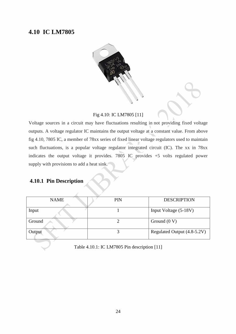
4.10 IC LM7805
Fig 4.10: IC LM7805 [11]
Voltage sources in a circuit may have fluctuations resulting in not providing fixed voltage
outputs. A voltage regulator IC maintains the output voltage at a constant value. From above
fig 4.10, 7805 IC, a member of 78xx series of fixed linear voltage regulators used to maintain
such fluctuations, is a popular voltage regulator integrated circuit (IC). The xx in 78xx
indicates the output voltage it provides. 7805 IC provides +5 volts regulated power
supply with provisions to add a heat sink.
4.10.1 Pin Description
NAME PIN DESCRIPTION
Input 1 Input Voltage (5-18V)
Ground 2 Ground (0 V)
Output 3 Regulated Output (4.8-5.2V)
Table 4.10.1: IC LM7805 Pin description [11]

25
4.11 IN4007
A diode is a device which allows current flow through only one direction. That is the current
should always flow from the Anode to cathode. From fig 4.11, the cathode terminal can be
identified by using a grey bar as shown in the picture above. For 1N4007 Diode, the
maximum current carrying capacity is 1A and it withstands peaks up to 30A. Hence, we can
use this in circuits that are designed for less than 1A. The reverse current is 5uA which is
negligible. The power dissipation of this diode is 3W.
4.12 Mechanical Support
To make the mechanical support the steps given below were followed
Step 1: The Rotor ring
To make the rotor ring, we used aluminum flat bar (20 mm wide and 3 mm thick) as it should
be flexible enough and problem-free to work with. Before bending, holes are drilled for the
LEDs, the Hall sensor, the central axis, and the balancing weights. If we use a 4.9mm drill
bit, we can press-fit 5mm LEDs tightly into the ring without glue and then bend the bar into a
circle carefully.
Step 2: The LEDs
For easier assembly and repair, we didn’t solder the LEDs to the circuit board, but connected
them with female jumper wires. These come with a connector on each end; since we need just
one connector per lead, we cut them to make 2 leads from each jumper. The cable ends are
stripped a few millimeters and a piece of heat-shrink tubing is slipped over each one.
On each LED, the positive lead (anode, the longer leg) is bent outward at a 90° angle. The
negative lead (cathode, shorter leg) is cut to 5mm–7mm in length and bent into a small eyelet.
Then the positive lead is trimmed to 10mm–15mm long and the stripped cable end is wound
around it, soldered in place, and insulated with the heat-shrink.

26
Step 3: The Center Mast
Attach the board to the threaded rod that serves as an axis. Threaded rods under tension tend
to become distorted, so no to tighten the nuts too tightly. Alternatively, we could substitute
ordinary 8mm steel rod, threaded only at the ends.
Step 4: The Wooden Base
Fix the threaded metal rod along with the aluminum ring on a four-legged wooden support.
Then bolt the DC motor to the moving rotor from the other side of the wooden base exactly at
the center.

27
Chapter 5
Results and Discussion
This section consists of the results that we obtained after PCB fabrication and implementation
of the project model.
5.1 PCB Layouts
Fig 5.1.1: PCB layout (main)
Fig 5.1.2: PCB layout (reference)

28
5.2 Project Model
Fig 5.2.1: Project Model
Fig 5.2.2: Main circuit

29
5.3 Display Output
Fig 5.3.1: Character Display
Fig 5.3.2: Pattern Display (Globe)

30
5.4 Circuit Explanation
The functional circuitry comprises just a microcontroller which drives the 40 LEDs via Shift
Resistor IC 74HC595 and is linked to the Hall sensor. As the microcontroller cannot source
enough current and IO Pin to Interface 40 LED’s for pulsing the hefty LEDs, a follower stage
comprising Shift Resistor IC’s is provided. The eight rotating LEDs ‘write’ an image built up
from eight lines of light (not from left to right of course but in continuous 360-degree
rotation) and for this reason the microcontroller needs to be synchronized with what in TV or
computer displays we would call a frame pulse, a signal indicating the start of a new image.
This task is handled by the Hall switch, which alters its output level when it detects a
magnetic field (in the vicinity of magnet in other words). Its normal State produces a ‘high’
output that goes ‘low’ on approaching a magnet. This change of level sets in motion the
process of building up the image.
The program produces small image elements representing text fragments relating to character
strings stored in the controller. These text fragments are then re-written as columns and fed
out to the LEDs in a defined time frame. The rotation of the motor creates the impression of
text written around the periphery of the ring. These characters are stored in the array, which
contains three elements (three segments of text) that are read out and displayed sequentially.
Readout of these characters is synchronized by the Hall switch already mentioned, which also
provides the information whether the motor is in operation (when the motor is static the
LEDs all remain unlit). The length of the rolling text in the ‘display’ depends on the radius of
the circle created by the rotating LEDs, hence on the length of the rotor arm. The set-up
illustrated in the output images operates with a text length of 4 characters. The program
operates as an endless loop that is synchronized by the Hall switch and delivers 4 characters
continuously.

31
5.5 Power Comparison
For comparing the power consumption of POV display with the traditional dot-matrix ones we
consider an example of displaying characters “24X7” on both the displays.
Calculations:
Considering 24 hours a day and 52 weeks in a year.
Total operating hours (168 hrs. per week) in a year = 52×168 = 8736 hrs.
For POV display
1. Power = 32×0.1W = 3.2 W = 0.0032 kW
2. Power consumption (in kWh) = 0.0032×8736 = 28 kWh
For Dot-matrix display
3. Power = 48×0.1W = 4.8 W = 0.0048 kW
4. Power consumption (in kWh) = 0.0048×8736 = 42 kWh
PARAMETERS POV DISPLAY DOT-MATRIX DISPLAY
Power required 3.2 W 4.8 W
Power Consumption (in kWh) 28 kWh 42 kWh
Table 5.5: Power Comparison details
From above table 5.5, the difference of power consumption between both the displays is
about 14 kWh. Hence, it is concluded that the POV display consumes a minimum of 33.3%
less power than the conventional dot-matrix display.

32
Chapter 6
Conclusion
6.1 Conclusion
We have successfully implemented a simple form of the display in which both the pattern and a
message can be displayed. The advantages of the developed system over existing one is that it
has added benefit of being viewable from all the direction around the display which is not
possible in the existing one-dimensional displays and it is easily customizable in terms of the
message we want to display as per our need. While our display depends on the resolution we
perceive it may cause limitations on the length of characters we want to display. Also, improper
alignment of hall sensor with the magnet may lead to distorted image. Overall, the main motive
of the power saving is achieved by our system as compared to the existing systems. The
possible applications of the display are advertisements, entertainment, novelty decorations,
education, animations, etc.
6.2 Future Scope
The major enhancement of the current system would be to allow wireless transmission of
images to the system. This would allow for increased processing power, as processing could be
achieved on an external computer and the resultant images/frames transmitted to the POV
display. Patterns or interactive games, for example, could then be easily implemented within
the system: all heavy lifting would be performed at the computer level and the POV system
would effectively become a wireless display monitor.

33
Appendix A
Start
Literature Survey
Study of each and every components and their market survey
Block Diagram and Schematic designing
Circuit designing on breadboard
PCB layout implementation
Fabrication, Assembly and Testing
Stop

34
Appendix B
Timeline Chart for Semester VII
Month July August September October
Week no. 1 2 3 4 1 2 3 4 5 1 2 3 4 1 2 3 4 5
Task
Performed
Problem Definition Identifying the
goal of
the project
Preparation Gathering
Information on
Embedded
systems
Study of related
IEEE paper
Design of block
diagram
Hardware Implementation Study of
Arduino IDE
Simulation of a
single array of
LED on
breadboard.
Presentation Presentation
White book Preparing the
white book

35
Timeline Chart for Semester VIII Month January February March April
Week no. 1 2 3 4 5 1 2 3 4 1 2 3 4 1 2 3 4 5
Task Performed
Software Implementation Designing the circuit
schematic
Presentation Presentation
Software Implementation Designing the layout
using Eagle CAD.
Fabrication Getting the layout
fabricated on the PCB.
Hardware Implementation Soldering of the
components on the PCB.
Mechanical
implementation of rotor
ring and wooden base.
Poster Preparing the poster. Poster Presentation.
Testing Testing the final circuit.
Documentation Preparation of the black
book

36
References
[1] Viet Nguyen, Omar Vazquez and Rhonal Soto, “LED Globe with the use of
Persistence of Vision.” College of Engineering and Computer Science,
University of Central Florida, Orlando, FL, 32826, USA.
[2] https://www.allaboutcircuits.com/textbook/digital/chpt-12/serial-in-parallel-
out-shift-register/, Date:20/10/17, Time:4:30pm
[3] http://makezine.com/persistencevisionledglobe/Date:31/10/17,Time:5:00pm
[4] https://create.arduino.cc/, Date:21/10/17, Time:5:00pm
[5] http://www.atmel.com/Images/Atmel-42735-8-bit-AVR-Microcontroller-
ATmega328-328P_Datasheet.pdf, Date:14/10/17, Time:11:00am
[6] http://www.newark.com/texas-instruments/sn74hc595n/8-bit-sipo-shift-
register-dip/dp/60K6845, Date:21/10/17, Time:9:15pm
[7] https://www.allaboutcircuits.com/textbook/digital/chpt-12/serial-in-parallel-
out-shift-register/, Date:20/10/17, Time:4:30pm
[8] https://eleparts.co.kr/goods/view_contents?no=43040&setMode=pc&zoom=1
Date:02/04/18, Time:07:40pm
[9] https://www.winson.com.tw/Data%20Sheet/WSH130.pdf,
Date:02/04/18, Time:8:20pm
[10] https://www.alldatasheet.com/5mm+LED+datasheet
Date:02/04/18, Time:8:22pm
[11] https://www.alldatasheet.com/datasheetpdf/pdf/82833/FAIRCHILD/LM7805.
html,Date: 02/04/18, Time: 8:00pm
[12] Muhammad Ali Mazidi, Janice Gillispie Mazidi and Rolin D. McKinlay,
“The 8051 Microcontrollers,” in The 8051 Microcontroller and Embedded
Systems Using Assembly and C, 2nd ed. Pearson, 2006.

37