70GS-62S S/M 00 Vers - Index of
48
70GS-62S MODEL 70GS-62SDE / GG / IT SHARP CORPORATION PAL BG SYSTEM COLOUR TELEVISION SESG70GS62S00 SERVICE MANUAL Issued: 30th May 01 This document has been published to be used for after sales service only. GA-10 CHASSIS In the interests of user safety (required by safety regulations in some countries) the set should restored to its original condition and only parts identical to those specified should be used. ADJUSTMENTS PROCEDURES......................7 STEREO LED FLASHING CODES..................11 PARTS LISTING..............................................38 CONTENTS ELECTRICAL SPECIFICATION........................3 IMPORTANT SERVICE NOTES........................4 CONTROL & TERMINALS.................................5 SCHEMATIC DIAGRAM..................................31 PRINTED WIRING BOARDS..........................12 PACKING OF THE SET & ACCESSORIES....46 CHASSIS LAYOUT ...........................................16 ICs ADITIONAL INFORMATION.....................21 COMPONENT LOCATION TABLES................16
-
Upload
khangminh22 -
Category
Documents
-
view
1 -
download
0
Transcript of 70GS-62S S/M 00 Vers - Index of

1
70GS-62S
MODEL 70GS-62SDE / GG / IT
SHARP CORPORATION
PAL BG SYSTEM COLOUR TELEVISION
SESG70GS62S00
SERVICE MANUAL Issued: 30th May 01
This document has been published to be used for after sales service only.
GA-10 CHASSIS
In the interests of user safety (required by safetyregulations in some countries) the set should restoredto its original condition and only parts identical tothose specified should be used.
ADJUSTMENTS PROCEDURES......................7STEREO LED FLASHING CODES..................11 PARTS LISTING..............................................38
CONTENTSELECTRICAL SPECIFICATION........................3IMPORTANT SERVICE NOTES........................4CONTROL & TERMINALS.................................5
SCHEMATIC DIAGRAM..................................31
PRINTED WIRING BOARDS..........................12 PACKING OF THE SET & ACCESSORIES....46
CHASSIS LAYOUT...........................................16
ICs ADITIONAL INFORMATION.....................21COMPONENT LOCATION TABLES................16

2
70GS-62S
Use this page to keep any special servicing information as Technical Report (Bulletin), Technical Information, etc.If only part number changes are required, just change part number directly the part number in the Parts Listing Section.If you need more information, please refer to the Technical Report (Bulletin).
SERVICE MANUAL UPDATE LOG SHEET
Part No.Technical Report No.Technical Bulletin No.
Cause / Solution Page No. ApplicationData /Serial No.

3
70GS-62S
ELECTRICAL SPECIFICATIONS
•Focus ....................... High Bi-Potential Electrostatic
•Sweep Deflection ..................................... Magnetic
•Picture Intermediate frequency................... 38.9MHz
•Sound Carrier Trap................................... 33.4MHz
•Adjacent Sound Carrier Trap ................... 40.4MHz
•Adjacent Picture Carrier Trap.................. 31.9MHz.•Aerial Input Impedance
VHF/UHF ...................... 75 ohm Unbalanced
•Tuning Ranges........... 48.25 MHz thru 855.25 MHzVHF: E2-E12 CH S1-S41 CH (Hiperband)UHF: E21-E69 CH
•White LevelSet brightness control to get total picture tube cathode current of 600 milliammeter under no signalcondition. Maximum necessary correction of each picture tube cathode current to get 8900 de-grees K-20 MPCD screen temperature should not exceed 15% of its original value.
X=0.290 Y=0.300
WARNING
The chassis in this receiver is partially hot. Use an isolation transformer between the line cord plugand power receptacle, when servicing this chassis.To prevent electric shock, do not remove cover. No user-serviceable parts inside. Refer servicing toqualified service personnel.
Specifications are subject to change without prior notice.
•Power Input .................... 220V-240 Volts AC 50Hz
•Power ConsumptionNormal Operation ...................................87WStand-by Operation ..................................1W
•Audio Power Output Rating (MPO) / ImpedanceInternal Left Speaker ...................... 10W, 7ΩInternal Right Speaker .................... 10W, 7Ω
•SpeakersLeft / Right ...................................... 12 x 6cm
•ConvergenceStatic (Centre) ........ between any two coloursDynamic ..................... after static equals zero
MODEL DESTINATION & DIFFERENCES:70GS-62SDE: Germany, Austria. Particular Operation Manual.70GS-62SGG: Greece. No Operation Manual from Factory.
Greek Teletext (NVM: Page 00, Position 95, Value: 03 05).70GS-62SIT: Italy. Particular Operation Manual.

4
70GS-62S
IMPORTANT SERVICING NOTESOnly qualified service personnel are allowed to carry out maintenance and repair of this receiver.
SERVICING OF HIGH VOLTAGE SYSTEM AND CRTIt is important that the static charge is removed from the high voltage system when carrying out workon the receiver. This can be achieved by connecting a 10K resistor (with a suitably insulated lead) fromthe CRT cavity connector to the CRT ground tag. This must be carried out with the AC supply discon-nected from the receiver.Note the following:• The CRT in this receiver employs Integral Implosion Protection.• If the CRT has to be changed it MUST be replaced with the correct type for continued safe
working• DO NOT lift the CRT by its neck.• When handing the CRT, ensure that shatterproof goggles are worn.• Ensure that the CRT is discharge before handling.
X-RAYThis receiver is designed to keep any x-ray emission to an absolute minimum. Some fault conditionsand servicing procedures may produce potentially hazardous x-ray radiation levels. This is a problemwhen in close proximity to the receiver for long periods of time. To reduce any risks associated withthis, please observe the following precautions:
1. When undertaking any servicing on this chassis, DO NOT increase the EHT to more than 29.9 KV, (at a instantaneous beam current of 1300µΑ).2. Ensure that during normal operation the EHT does not exceed 27KV±1.5KV (at a beam current of 1000µΑ). This level has been preset in the factory. Always check that this level has not been ex-
ceeded after carrying out any repair on the receiver.3. DO NOT replace the CRT with any other type than that specified in the parts listing as this may cause excessive x-ray radiation.
BEFORE RETURNING THE RECEIVER TO THE CUSTOMERIn addition to the above checks, the following should also be carried out before returning the receiverto the customer.
1. Inspect all the leads to ensure that they are dressed correctly and that they are not obstructed or pinched by any other parts.2. Ensure that all protective devices are in good condition. These will include nonmetallic control knobs, insulating fish papers, cabinets backs, compartment covers or shields, mechanical insulators, etc.

5
70GS-62S
TV 1. Stand-by ON/OFF switch (TV)
Video 2. Power ON / OFF switch (VCR)
TV 3. Digit buttons 0 ∼ 94. Flashback button
Teletext 5. Colour button (green)6. Colour button (red)
TV 7. Volume Down/Cursor control Left8. Menu button
Teletext 9. Reveal button10. List selector11. Store button12. Cancel button13. Top/ Bottom/Full button14. Reset button
Video 15. Rewind/picture search/reverse16. Play button17. Pause / Still button18. Stop button
TV 19. TV / VIDEO selector20. Channel call button21. Single/Double entry
Teletext 22. Colour button (yellow)23. Colour button (blue)
TV 24. Channel Up/Cursor control Up25. Volume Up/Cursor control Right26. Channel Down/Cursor control Down27. TV button / Subtitle
TV/Teletext 28. Time button
TV 29. Sound mode selector
Teletext 30. Hold button
TV 31. Sound Mute button
Teletext 32. Text/Mix button33. Index button
Video 34. Channel Up selector35. Fast forward/picture search/forward36. Channel Down selector37. Record button
8
?
I i
LIST
X
TV / VCR / TEXT REMOTE CONTROL
G1061SA
TV/VIDEO
0
MENU
CH
VCR
S
I/II/I+II
TV VCR
TV
CH
CH
2
5
1
4
7 9
6
3
32.
34. 33.
31.
35. 36. 37.
30. 29.
27.
28.
25.
26.
24. 23.
20.
19.
21.
22.
2.
3.
1.
4.
5.
6.
7.
8.
9.10.11.
13.14.15.16.17.18.
12.
REMOTE CONTROL

6
70GS-62S
CH
1 5 3 2 6 6 4 8 7
/ I / II OPC
FRONT TV
1. Main PowerOn/Off Switch
2. Power Indicator
3. Program Selector(UP/DOWN)
4. Volume Buttons(UP/DOWN)
5. Remote Control Sensor
6. Sound Indicator
7. Remote Control Indicator
8. DOOR
Behind the door
9. Headphone Socket(3.5 mm Ø / 16~600 )
HOW TO OPEN THE DOOR
Press the top of the door, opening it slightly.Hook your finger inside and pull open.
OPC
REAR TV
RF Input1. Antenna terminal
21-pin In/Out2. 21-pin Euro SCART (RGB)3. 21-pin Audio/Video (AV-1)
With S-Video Input
9
AV/TERMINAL
SCART PERITELEVISION
2
3
1
CONTROLS & TERMINALS

7
70GS-62S
ADJUSTMENT PROCEDURESAll adjustments to this chassis, except for focus, are carried out in the service mode.
••••• SERVICE MODEThe service mode is provided to enable the engineer to correctly set up the receiver to the CRT fitted in the set.Note that these adjustments may vary from one receiver to another.
To enter the service mode, carry out the following procedure.1. Connect a test pattern to the antenna terminal.2. Tune the receiver to this signal.3. Turn the receiver off using the mains switch.4. Press volume down and channel up buttons on the front of the receiver at the same time. See Fig.1.5. Keeping these buttons pressed, turn the mains on. See Fig.1.6. When the set starts up it will be in service mode.7. Release the two buttons.
••••• Use the channel up and down buttons to move between the options.••••• Use the volume control buttons to change the data.••••• To store the data, use the stand-by button on the remote control.••••• To exit the service mode, turn the receiver off using the mains switch.
When the service mode is entered the following On Screen Display appears
-SERVICE SOFTWARE AND HEXADECIMAL COUNTER DISPLAY:SW ON XXXX SW OFF XXXX HOURS ON XXXX
The figures displayed in the XXXX locations are hexadecimal representations of the number of times that particularfunction has been executed. For example if the hexadecimal number displayed after SW ON was 0E4A, this wouldcorrespond to the receiver being turned on 3658 times.
Adjustment menu:
The following adjustments can be carried out in the service mode.
• Horizontal Shift• East West Width• Pin Phase• Pin Amp• Corner Amplitude• Corner Symmetry• Vertical Linearity• Vertical Angle• Vertical Bow• Vertical Amplitude• S Correction• Vertical Shift• Red Gain• Green Gain
• Blue Gain• Red Cut Off• Green Cut Off• Blue Cut Off• Alter NVM Page• Alter NVM Position• Alter NVM Value• Teletext Mix Mode Contrast• Teletext Contrast• OSD Contrast• DVCO Adjustment (Only PAL)• DVCO Adjustment (Only NTSC)• AGC Adjustment• Auto Installation On/Off

8
70GS-62S
The following geometry adjustments can be carried out. Detailed instructions on how to execute these are given onthe following pages
Horizontal
• Horizontal Shift• E-W Width• Pin Phase• Pin Amp• Corner Amplitude• Corner Symetry
Vertical
• Vertical Amplitude• S Correction• Vertical Shift• Vertical Linearity• Vertical Angle• Vertical Bow
Just in case the TV set requires a full geometries adjustment, please proceed first withVertical according to the above order, and after that, adjust Horizontal according to theabove order.
Horizontal ShiftAdjust the horizontal shift so that the picture is centred.The effect of this adjustment is shown in figure 2.
• When the volume up button is pressed, the picture moves to the right.• When the volume down button is pressed, the picture moves to the left.• Press the stand-by button on the remote control to store.
E-W WidthAdjust the E-W Width so that 9% over-scan is achieved.The effect of this adjustment is shown in figure 3.
• When the volume up button is pressed, horizontal scanning increases.• When the volume down button is pressed, horizontal scanning decreases.• Press the stand-by button on the remote control to store.
Pin PhaseAdjust the Pin Phase so that the picture is symmetrical top and bottom.The effect of this adjustment is shown in figure 4.
• When the volume up button is pressed, side pincushion changes.• When the volume down button is pressed, side pincushion changes.• Press the stand-by button on the remote control to store.
Pin AmpAdjust the Pin Amplitude so that the picture is centred.The effect of this adjustment is shown in figure 5.
• When the volume up button is pressed, side pincushion changes from pincushion tobarrel shape.
• When the volume down button is pressed, side pincushion changes from barrelshape to pincushion.
• Press the stand-by button on the remote control to store.
Corner AmplitudeAdjust the Corner Amplitude so that the picture is centred.The effect of this adjustment is shown in figure 6.Note: This adjustment affects to upper and lower sides.
• When the volume up button is pressed, side pincushion changes from pincushion tobarrel shape.
• When the volume down button is pressed, side pincushion changes from barrelshape to pincushion.
• Press the stand-by button on the remote control to store.
Fig.2
Fig.3
Fig.4
Fig.5
Fig.6

9
70GS-62S
Corner Symmetry
Adjust the Corner Symmetry so that the picture is centred.The effect of this adjustment is shown in figure 7.Note: This adjustment affects to upper and lower sides.
• When the volume up button is pressed, side pincushion changes from pincushion tobarrel shape.
• When the volume down button is pressed, side pincushion changes from pincushion tobarrel shape.
• Press the stand-by button on the remote control to store.
Vertical Linearity
Adjust the Vertical Linearity so that the upper and lower parts of the picture are symmetrical.The effect of this adjustment is shown in figure 8.
• When the volume up button is pressed, the upper picture scanning decreases and thelower picture scanning increases.
• When the volume down button is pressed, the upper picture scanning increases and thelower picture scanning decreases.
• Press the stand-by button on the remote control to store.
Vertical AngleAdjust the Vertical Amplitude so that the picture is centred.The effect of this adjustment is shown in figure 9
• When the volume up button is pressed, the vertical angle changes to right.• When the volume down button is pressed, the vertical angle changes to left.• Press the stand-by button on the remote control to store.
Vertical BowAdjust the Vertical Bow so that the picture is centred.The effect of this adjustment is shown in figure 10
• When the volume up button is pressed, the vertical bow changes to right.• When the volume down button is pressed, the vertical bow changes to left.• Press the stand-by button on the remote control to store.
Vertical Amplitude
Adjust the Vertical Amplitude so that the picture is over-scanned.The effect of this adjustment is shown in figure 11.
• When the volume up button is pressed, the vertical size of the picture decreases.• When the volume down button is pressed, the vertical size of the picture increases.• Press the stand-by button on the remote control to store.
S Correction
Adjust the S Correction so that the picture symmetrical between the top, centre and bottom.The effect of this adjustment is shown in figure 12.
• When the volume up button is pressed, the top and bottom scanning increases and thecentre scanning decreases.
Fig.8
Fig.12
Fig.11
Fig.10
Fig.9
Fig.7
10
70GS-62S
Colour Adjustments
The following adjustments should only be carried out whenthe CRT IC801 are replaced.
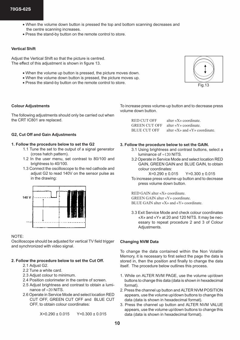
G2, Cut Off and Gain Adjustments
1. Follow the procedure below to set the G21.1 Tune the set to the output of a signal generator
(cross hatch pattern).1.2 In the user menu, set contrast to 80/100 and
brightness to 40/100.1.3 Connect the oscilloscope to the red cathode and
adjust G2 to read 140V on the sensor pulse asin the drawing:
NOTE:Oscilloscope should be adjusted for vertical TV field triggerand synchronized with video signal.
2. Follow the procedure below to set the Cut Off.2.1 Adjust G2.2.2 Tune a white card.2.3 Adjust colour to minimum.2.4 Position colorimeter in the centre of screen.2.5 Adjust brightness and contrast to obtain a lumi-
nance of ≈20 NITS.2.6 Operate in Service Mode and select location RED
CUT OFF, GREEN CUT OFF and BLUE CUTOFF, to obtain colour coordinates:
X=0.290 ± 0.015 Y=0.300 ± 0.015
To increase press volume-up button and to decrease pressvolume down button.
RED CUT OFF alter «X» coordinate.GREEN CUT OFF alter «Y» coordinate.BLUE CUT OFF alter «X» and «Y» coordinate.
3. Follow the procedure below to set the GAIN.3.1 Using brightness and contrast buttons, select a
luminance of ≈120 NITS.3.2 Operate in Service Mode and select location RED
GAIN, GREEN GAIN and BLUE GAIN, to obtaincolour coordinates:
X=0.290 ± 0.015 Y=0.300 ± 0.015To increase press volume-up button and to decrease
press volume down button.
RED GAIN alter «X» coordinate.GREEN GAIN alter «Y» coordinate.BLUE GAIN alter «X» and «Y» coordinate.
3.3 Exit Service Mode and check colour coordinates«X» and «Y» at 20 and 120 NITS. It may be nec-essary to repeat procedure 2 and 3 of ColourAdjustments.
Changing NVM Data
To change the data contained within the Non VolatileMemory, it is necessary to first select the page the data isstored in, then the position and finally to change the dataitself. The procedure below outlines this process.
1. While on ALTER NVM PAGE, use the volume up/downbuttons to change this data (data is shown in hexadecimalformat).
2. Press the channel up button and ALTER NVM POSITIONappears, use the volume up/down buttons to change thisdata (data is shown in hexadecimal format).
3. Press the channel up button and ALTER NVM VALUEappears, use the volume up/down buttons to change thisdata (data is shown in hexadecimal format).
• When the volume down button is pressed the top and bottom scanning decreases andthe centre scanning increases.
• Press the stand-by button on the remote control to store.
Vertical Shift
Adjust the Vertical Shift so that the picture is centred.The effect of this adjustment is shown in figure 13.
• When the volume up button is pressed, the picture moves down.• When the volume down button is pressed, the picture moves up.• Press the stand-by button on the remote control to store. Fig.13
140 V
CH1 gnd

11
70GS-62S
4. Once this data has been set, press the stand-by buttonto store.
5. If another NVM value has to be changed, use the chan-nel down button to select the page or position and repeatas necessary.
Note:DO NOT change any NVM data, unless you have been ad-vised to do so by a Sharp representative. If data is incor-rectly changed, serious damage may occur to the receiver.
Contrast Adjustments
Three types of contrast levels can be varied as listed be-low:
• TELETEXT MIX MODE CONTRAST• TELETEXT CONTRAST• OSD CONTRAST
Use the volume up/down buttons to adjust to a suitable level,then press the stand-by button to store.
DVCO Adjustment (PAL)Carry out the DVCO Adjustment (PAL) as shown below:
1. Receive a Phillips pattern signal.2. While in the DVCO ADJUSTMENT (PAL) menu, press
the stand-by button.3. The adjustment will be carried out automatically and
stored.
DVCO Adjustment (NTSC)No adjustment required.
AGC AdjustmentTo correctly align the Automatic Gain Control, follow theprocedure outlined below:
1. Tune the set into a pattern generator on CH10.2. Adjust the signal strength of the pattern generator to 57
dB/uV3. Enter the service mode.4. Enter the AGC Adjustment menu.5. Press the stand-by button on the remote control.6. The adjustment will be carried out and stored automati-
cally.
Auto Installation On/OffTo return the receiver to the original Auto Installation mode,using the volume up or down button, set the Auto Installa-tion On/Off to On. This setting is automatically stored andwhen the receiver is turned on the next time it will start up inAuto Installation mode.
STEREO LED FLASHING CODES.
If the TV set does not work and the stereo led is flashing,follow the sequence according to the information below, asa guide to fault finding.
1. Unable to read or write into NVM: 66% ON, 33% OFFtwice and OFF for a second.
2. MSP failure: 66% ON, 33% OFF for three times andOFF for a second.
3. VCT failure: 66% ON, 33% OFF for four times and OFFfor a second.
On Off
On Off
On Off

12
70GS-62S
Page 13
22
23
24
25
17
18
19
20
21
11
12
13
14
15
16
1
2
3
4
5
6
7
8
9
10
Y
X0 10 11 121 2 3 4 5 6 7 8 9
JF64
D71
9
D79
8F
703
F70
2
JF653
2
1
(M)
C710 J15
C72
9
+ R50
3R55
3
J242R651
C61
9
J275
C617
L605
J322
F602
C70
5
Q50
2
J309
C71
1
D749
POR701
C720
+
JF702
C731+
Q709
R738
J39
C732
+
A K
J206
TP602
TP601
TP701
D60
7
C602
J16
L3
TRC
GND
1211
10
98
7
65
L901
R907
C901
+
R554
R531
J153
+
D71
2
JF27
K
IC702R
+
C726
J65
T702
C62
8
(F)
1 23 4
5
C601
C621
C10
19
+ J5
J2
R79
8
D740
+
C734
C625
J38
C713
R787
C738
R53
0
R609
(H)
5
R650
R617
J142
Q702J116
C79
6
R723
C717
R718
C799
C704
R71
4
J4
C70
2
+ C511
C61
3
R74
7
J68
M1000
D610
J205
J15
F601
J212
J214
J213
C63
0
J216
D60
2
J239
IC703
J16
J273
J272
J15
J217
J16J16
J16
C504
T3.
15A
H
S70
1
L701
L501
Q605
B
C
E
Q601
R614
S705S704 OPC1S703S702
T601
12
11
10
9
8
7 6
5
4
3
2
1
(L2)
C622
+
C623
C620
R62
9
J276
J16T701
J32
J16
D611
J152J151
D701
C703
D704
C706
D70
3
J15
R746
R214
R50
1
+C61
8
D605
C609
+
J296
R
IC70
5K
D51
0
C64
0
+
FB
501
+
C526
J122
IC50
1
J74
J155
J148
J207
FB603
R51
8
C72
1
D736
D729
Q70
3
D70
9
D61
3
D612
R79
0
J37
C798
Q701
DIP
L705
J149
+C73
5
J215
J115
C725
C73
0
R799
C727 +
LP701
C701
D702
(G)
2
1
J67J1
18
J117
F704
D722
+
C72
8
D720
D721
+
C733
R603
L609
D63
4
J40
C64
2
+
C70
7
Q60
2
JF28
C60
3
J34
+
C712
J35
C524
+
C709
D621
J166
R908
C905
R906
J1
+C52
0
L610J307
FB
702
FB
701
C627
FB
703
(H).
1
C904
+
D627
+
C737
J165
JF61
C914
J326
D609
R601
R602
VAR1
F70
1
F7315N4. MOTHER UNIT PWB. Component side.

13
70GS-62S
Page
12
Y
X
22
23
24
25
17
18
19
20
21
11
12
13
14
15
16
1
2
3
4
5
6
7
8
9
10
20 21 22 23 24 2513 14 15 16 17 18 19
L318
R936
J159
C809
+C
1040
(AV).
C61
9
75
R61
8
17
JF63
R62
7JF
62
J295
L100
7
R387
JL13
C40
2
JL12.
J269
JL14
.C
404
C916
R21
3
+C308
IC708
I
C31
6
+
C309
JL8
J281J280
J286J285
L602
JL7
JF55
L351J17
JF46
JF47
J202
J139
J47
JF702
+C1041J83
+
C909
R738
J263
C1005
+
J203
J237
J238 R25
2
J236
J235
L401
R22
3J2
59
R337
TP201
C1016
JL8.
FB303
J16 R904
+
C80
3
19
IC901
.F
7316BM
N4
G2
.
TRC
J218
J169
J173
J125
J126
J170L801
JF38
J284
1
12
(SA
)
J107
J105
J106
J102(RT)
J108
L100
1
J99
J98
C201
X201
R652
C626
+
J230 J1
87
J233
J234
C80
1+
C220
J279
J250
JF37
J171
J228
J227
J226
J222
J179
J225
J232
J223
J251
R20
2
J224J181
J190
J110
5
C10
19J5
L302
J13
J195
J193
X1002
+
C215
1
1
1
RG
BA
V1
J156
C320
+
E
Q708
C
J167
K7315BM
.
J103
J100
J30
C386
J290
C64
3
C388
L303
R35
8
J20
J19
(VS)
L350
C362
+
C358
J158
J217
J163J162
J56
J55
C35
5
IC302
C37
3
R355
F7315BMN4
ESPA¥A
TN201
AGC
TU
AS
CL
DA
B+
33V
IF1
IF2
J161
L202
C204
+
J262
5 1
SF201
SF202
1
5
C20
5
8
1
IC304
J401
CN44
26
5317
QKITP7315BMN4D1001 D1002
IC10
02
IC30
5R
219
R22
0
R62
9
J276
C62
4
C319 C317
J160
C392
J321
J164
+
C311
J23
J24
L352
(SP)1
C361 C376
IC30
1
C353
J18
C37
0
L353
L315
C36
5
+
J52
R359
L316
+
C377
C33
08
C3309C372
+
C36
8
C378
+C
3310
+
J136
+
C1001
J191J192
J91
J92
(SB
)
1
6
J247J248J249
J243J244J245
J257
J246J253
C21
2
+
C389
J127
J157
X30
1
J178
J95
AV1
IC202
1
(MO
)
J268
J266
J62
J114
C1006
+
IC50
1
5
L203
J194
+
C330
+
C1031
J220 J2
21
C304
+
+
C301
J289FB302
1 (K)
8
+
C805
+
C302
J177
J189J180
J219
J97
J94
J96
J184
JF54
J140
JL1.
J172
J196
J201
J198
0
(K).
1
C902D901
C915
+C422
R203
J231
JL3
C524
C318
R631D630
J183
J166
J137
R908
C905
K7316B
M
L100
4
J89
J88
J90
R10
36
J93
J9
JL1
JL7.
JF48
J176
C303+
J44
J45
(AV)
J109
J111
J61
C351+
J59
J113
D1007
J197
JF32
JF36
J277
J278
J287J282 J283
J182
C22
1
(H).
1
D903
J310
L403
JL14
+
C22
2
JL13
.L4
02
+C36
3
L301
J165
FB402
FB401
J188
FB801
1
02
C312 +
JL17
JL17.
C35
6
J138
JL12J328
J82
J133
C1027
F7315N4. MOTHER UNIT PWB. Component side.
14
70GS-62S
Page 15
X
22
23
24
25
17
18
19
20
21
11
12
13
14
15
16
1
2
3
4
5
6
7
8
9
10
Y
19 18 17 16 15 14 1325 24 23 22 21 20
C10
51
C1017
J329
JF72
JF69
J298
L318
C10
49
C1048
J258
R208 C208
Q906
J159
J308
R423C809
+
D62
2
K
C223
K
D62
8
J29
R333
C30
5
C30
6
Q10
05J3
19
J318J317
D10
03K
R93
5
R93
4
C339
R413
C543
J295
C1013
C1015C1014
R1023
R10
26
L100
7
C42
4
J256
R387
Q403
C40
2
J269
JF59
C43
3
C40
4
R90
1
C91
6
C1046
C1045
C397
C1044 C385 R330R
213
R405
D40
4
K
D40
3
K
J10
IC1009
JF4
C741
+
C30
8
IC708
C316
C30
7
KD723
C31
0
+
C30
9
C323
J281J280
J286J285
R1018
L1005
C405
J32
JF55
J43
C380
J22
L351 J17
JF46
JF47
J202
J139
R339
JF44
J47
K
D20
4C
214
D20
5K
C213
R240
J85
JF702
C10
42
+C10
41
J83J1
04
C911
R905
C910
J42
+
J101
J79
J
J80
R738
J292
R221
R21
0
C20
9
R21
1
R21
2J2
65
J263
J294
J270
C10
30
C1004
+
J203
J204
J237
J238
R25
2
J236
J235
R22
2
R509
L401
C42
3
C38
2
R337
R386
C80
2
C1028
R80
1
R410
R41
8
R322
J300
D42
2
K
D40
8KR22
5
R1004
C324
C326
J16
R90
4
+C803
IC90
1
9
1
R92
1
Q907R926
Q90
8
R915 R91
8
Q910
R93
3
R92
7
Q90
9
R932
R92
2
R92
3
C908R919
R91
7
R916
R90
3
Q90
4
Q90
5R
925
R910
R91
1
R912
R91
4 R90
2
C907
R913
Q901
C90
6
Q90
2
R909
R92
0
Q90
3
C359
C407
C32
7
J175
R802
J173
J125
J126
KD
1008
J170
L801
C350
JF38
R30
3
R62
8
J284
R10
08
12
(SA
)
J107 J1
05J1
06
J102
R362
J108
L100
1
C1008
L100
3
C1010 J99
C1011
J98
C201
X201
R65
2
D623
K
JF29
Q60
9
+
C43
1
J230
C216
J187
J233J2
34
C80
1
Q20
4
+
C22
0
J279
C42
7C
428 C337C
341
JF26
R321
JF23
C43
0
C34
7
C42
9
C34
8
J250C203
JF25
R416
JF24
D1004
K
JF37
J171
J228 J2
27J2
26
J222
J179
J225
R422
J229
J232
J223
J251
J252
J261
J190
J110
J50R38
5
Q306
+
J5
R332
R32
8 JF19
L302R
329
C52
3
K
D1009
G
C343 C344
J302
J299
J193
+
C21
5
Q1006
C10
20
J25
JF18
R1007
Q70
7 Q706
Q40
5
Q40
4
Q305
R10
37
R1034
R1025
J185
R10
15
R10
14
R10
13
R10
10
R1009
R1005
R10
03
R758
R75
7
R75
6
R755
R62
5
R624
R
R45
0
R43
4
R42
1
R42
0
R411
R40
9
R40
7
R37
0
R36
9
J48
R357
R356
R353
R347
R34
6
R34
5
R34
4
R338R
336
R335
R33
4
R331
R326 R325R324
R32
3
R320
R319
R313
R312R311
R310
R309
R308
R230
R209
R207
R20
6
R20
4
R201
JF15
JF14
J28
J8J7
J21
J53
J301
C3313
C33
04C
3305
C33
03C
3302
C3301
C33
00
C1021
C10
12
C21
1C
210
C207C202
K D724
K
D20
3
D202
K
L205
J156
C32
0 +
D72
7
K
E
C
Q708
R40
6
K
D42
1
IC10
03
J167
D1006
K
J103
J100
K
D406
J30
J290
C38
8
L303
R35
8
J20
J19
(VS
)
L350
C36
2
+
C35
8
J158
J217
J163J162
IC10
04
J56
J55
C355
C373
R355
IF2IF1
B+
DA
CL
AS
TN201
J161
+D201 K
IC201
SF202
C20
5
IC1001
1
8
1IC304
J401CN4
D100
D10
02
V
32
1716
1
IC10
02
R21
9R
220
C623
C319
C31
7
J160
J321
J164
+
C311
J23J24
L352
(SP
)
1
C36
1C
376
C35
3
J18
C37
0C
365
+
J52
R359
L316+
C37
7
+
C368
C37
8
+
+
J136
+
C10
01
J191J192
J91
J92
(SB
)
K
D409
K
D410
J247J248J249
J243J244
J245
J257
J246J253
C21
2
+
J157
IC30
3
1
2425
80
J178
J95
1
D42
0KD411
K
IC202
R412
1
(MO
)
J266
R41
9
J62
J114
K
D10
05
C321
C325
C340
C357
C36
0
C36
6
C36
7C
369
C371
C374C
375
C379
C38
3
C38
4
C387
C39
0
C391
C40
3
C502C503
C506C507C510
J14
J271
J260
J84
J6
J64
J58
J54
J27
J49
J51
J31
J57
J15
J267
J264
J60
J112
J288
J291
J186
J255
JF5
JF6
JF7
JF8
JF9
JF10
JF12
JF13
Q10
01
Q10
02
Q10
03
Q1007
Q10
08
J124C505
+
J74
JF17
R1040
R408
L203
J26
R380
R38
1
R382
R35
2
C35
4R
383
C1024
C1018
L100
6
J194
+ C330
+C
1031
J221
KD305
R306
R30
4 +
K D30
4
+
C301
J289
FB
302
1
(K)
+
J134
R804
R301
+
C30
2
R302
R10
11
J177
R30
5
J189
J254
J219
J11
C1009J9
7
J94
J96
C40
8 C40
9
JF54
J140
R10
41
J174
J172
C34
6
R10
24
J129
J130
C393
R340
C394
C396C395R341
C1002
L100
2
C322
JF1
R21
7
J196
R1020
C1034
R36
1
C1037
Q20
1
C10
38
R93
1
6
D90
1
C915
C21
7
C218C206
C219
R630
+
C42
2
R20
3
R20
5
J231
C524
Q202
C912
R1035
C318
R10
16
J166
J137
R1001
R1002
R1006
R908
C90
5
R803
J128
J86
J87
D902K
C38
1
L317
JF39
J89
J88
J90
R10
36
J93
J9
JF53
JF48
J176
JF50
+
J44
J45
JF16
JF52
C399
C398R342
J63
J109
J111
J61
C351
+
C35
2
J59
J113
D1007
J197
R435
J277
J278
J287 J282J283
J182
C22
1J304 R76
6
J305
J33
R36
0
1
D90
3J310
C904
C10
33
K
D10
11
C10
60
C338
R231
L403
R41
5D
405
K
R41
4
J311
JF58
+
C22
2
C432
R41
7
L402
J81
C1036
C1043
D30
6
K
J314
R343
J313
J315J316
J312
L1008
JF43
+
C363
C364
R351
J46
R350
R32
7
C345
KD423 KD424
C342K
D425 K
D42
6R31
8
K
D407
L301
K
D30
3
K
D302
R307
C313
J165
FB402
FB401
J188
C225
C22
4
R1022
FB801
J297
+
R384
C328
C329
C35
6
C1007
C10
03J138
J328C810
C10
32 C1006
J82
JF66
JF67
JF68 J133
J168
JF71
JF70
C804
C521
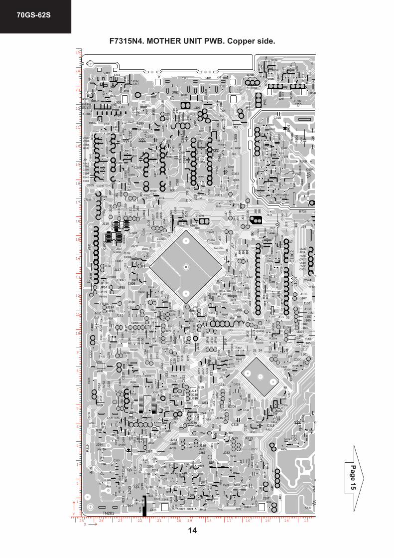
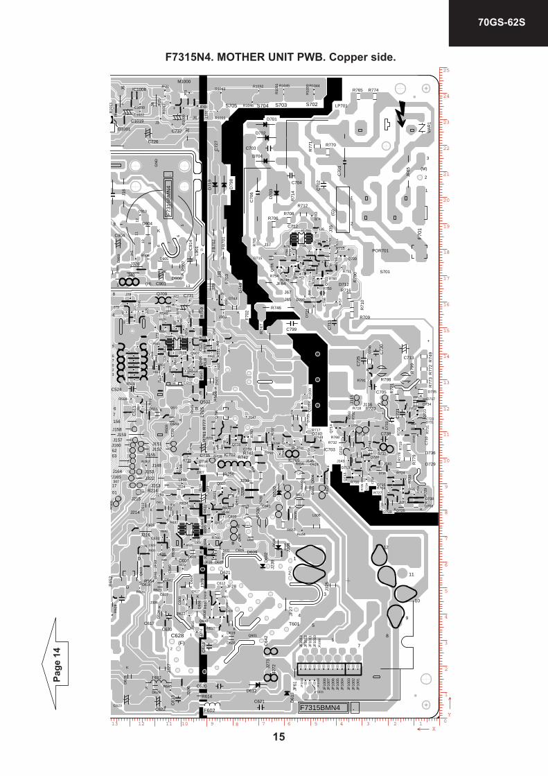
F7315N4. MOTHER UNIT PWB. Copper side.
15
70GS-62S
Page
14
Y
X
22
23
24
25
17
18
19
20
21
11
12
13
14
15
16
1
2
3
4
5
6
7
8
9
10
010 9 8 7 6 5 4 3 2 113 12 11
JF64
D71
9
D79
8
D744
K
D74
2
K
F70
3
F70
2
JF65 (M)
1
2
3
J303
C71
0
KD73
7
D74
7
K
J75
R548
R535
K
D60
4
R55
0
D508K
KD511
R502
J159 C72
9
+
R50
3
R50
5
C60
4
R635C632
R760
R633
C629
R63
9
R643
C631
J306
R626
J327
C617
K
D62
8
D904
K
K
D905
D906K
R656
R728
R72
1
J324
J322
C606
R21
5
J320
R1033R
935
F602
JF60
R10
99
R74
4
R745
R51
6
R511
R791
C705
KD
746
B
E
Q502
J309
D60
6
K
R612
K
D617
JF57
R709
R71
0
R716
R788
R78
6Q
721
R750
C71
1
D74
9
JF70
1
R611C736R735
R73
3
D51
2
K
R767
R54
4C
534
POR701
R1032
+
R75
9
J72 C731+
C55
0
Q709
J77
J76
J79
J78
J80
8
J39
+
JF1015
JF10
16
J206
R509
Q60
3
C512
C74
0
JF3
C54
2
R10
39
J147
C71
9
D739
K
JF35
JF34
R644D607
KD631
C913
J16
.
L3
+
F73
16B
MN
4
1211
10 9
8
7
65
GN
D
L901
R90
7
C901
R782
R63
2C
525
R72
5
R554
R79
5
J153
R62
8
+
R74
9R
772
R77
3
KD735
D712
R50
6
JF27
IC702
K
D728
R65
2
+
C726
R71
3
R752Q70
4
R70
5
J65
Q720
C628(F)
1
2
C621
KD629
C1019
+
J5
J2
R798
R717D740
R768
Q71
3
J143
K D73
3
+
R732
C625
D
SG
J38
K
D74
3
R72
6
R75
3
R701
D73
0 KC738
J209
J208
R53
0
J210
J1465
R65
0
D61
5
K
R617
KD713
J116R722
D717
K
K D734R723R718
C799
C704
R71
4
D71
6
K
.
C1022
J4
C70
2
R645
R55
1Q
510
R55
2
J123
+
C51
1
R513
J119
C52
2
R549
R534
R508
R52
6R52
8
C61
3
IC502
Q507
J73
J120
R54
5
R74
7
Q611
Q608
Q60
6
Q604
R10
17
R10
13
R638
R637
R62
0R
608
R604
R51
5
R510
R36
9
JF10
13JF
1012
JF10
11JF
1010
JF10
09
JF10
08JF
1007
JF10
06JF
1005
JF10
04
JF10
03JF
1002
JF10
01
JF21
JF20
M1000
Q61
3
D62
6 K
156
F601
J214
J213
C630
J216
D60
2
J239
IC703
7
L606
J273
J272
IC60
1
Q503
J158
17
6362
S701
B
E
Q60
5
Q601
R614
S705 S704
D1001
S703 S702
+
12
11
10
9
8
76
5
4
3
2
1
T601
C622+C623
C620
J160
J164
IC1008
J152J151
D701
C703
D704
C70
6
D70
3
R765 R774
J157
R746
R214
KD619
K
D625
K
D608
+C618
+
23
67
C50
8
0
C610
J6
J145
J296
IC705
R
5
D51
0
+J293
R51
7
R54
7R50
4
R514
Q50
5
J121
R512
+
J122
R62
3
C641
R770
R77
14
R78
3
J155
J148
Q712
R715
R75
1
Q72
3
C723K D731
R73
1
C72
1
D736
D729
R727R704 Q725
C71
6
KD738
D708KKD725
R781
R72
9
Q715
R724
R72
0R
779
R71
9
Q10
04
D70
6
K
D70
5
K
D61
3
D612
R79
0
R785
D74
1
K
R70
3
IC701
J37
R706
R712
R708
C79
8
KD
714
J66
KD707
F7315BMN4
L705
+
C735
J215
J115
C713C
725
C73
0
R79
9
C60
7
C72
7
+
J3
LP701
C70
1
R62
2
D702
2
1
(G)
J67
R754Q
705
R748
Q61
0
R742
R79
4
R77
7
+
J69
R250
KD715
J71
J70
R78
4
R50
7
L609
D63
4
D63
5
K
R73
6
R776
R76
1 Q71
4
R79
2R
793
J40
C64
2
D636K
JF33
C54
0
Q79
6
R711
+
R607D61
8 KJF28
C612
R61
6
D620
K
R610
C60
3J2
74
R78
9
+
C712J36 J3
5
C524
+
R700
Q724
J141
KD718
D732K
R653
D621
C71
8
C72
4
R1043
6
8
R906J41
R654
R10
30
R10
31 R1044R1045
R1046
J1
R740
R73
9
D748K
KD616
R621
+
C52
0
R73
7
Q711C739R743
R78
0
L610
J307
FB
702
FB
701
C627
JF10
14
(H).1
D90
3
C904
C60
8
R741C72
2
C715
C1050
K
D750
J81
J241
C541
+
C737
01
307J165
Q607
J323
R634
J325
JF61
C91
4
J326
D62
4
K
D609C605
R65
5
R77
8
VA
R1
F70
1
D50
7
K
D632K
D633K
F7315N4. MOTHER UNIT PWB. Copper side.

16
70GS-62S
F7315N4. CHASSIS LAYOUT.
PTC UNIT (F7347N0) PWB & COMPONENT LOCATION TABLES.
1
2
3
4
5
Y
X0 1 2
(DG)
PO
R17
01
1
D17
02R
1704
R1701
C1701
+
F7347BMN0
JL23
!
"#
"#$
%&
&
&
(
) !
& !! !!
&
Copper Side.
Component Side.
Y
X
1
2
3
4
5
02 1
R1701
(DG) POR1701
IC70
8
13
46
D17
01
K
D17
02
R17
04
C1702
R17
03
Q1701
C1701
+
R1702
Component Side. Copper Side.

17
70GS-62S
MOTHER UNIT (F7315N4) PWB COMPONENT LOCATION TABLES.Component Side.
.1 ! !
.1$
2 ! !
!
3 ! !
3$
4 !
4$
+
+%
&/ !
,. ! !
,0
, !
1,
.1
!
! !
! !
$ !
!
!!
!
!
!
!
!!
!
!
!
!
!
!
! !
!
! !!!
!
! !
! !
! !
!
!
!
! !
! !
!
!
! !
!
! !
!
!
! !
!
!
!
!
!
!
!
!
! !
! !
!
!
!
!!
!
!! !!
!
!
!
!
! !
!
!
!
! !
!
!
!
! !
! ! !
!
!
! !
!
!
!
!! !
!
!
!
! !
!
!
! !
!!
! !
!
!
* !! !
!!!
! !!!
! !!
!
!
!!
! !
!
!
! !
!
!! !
!
!!
!
! !
! !!
! !
! !
!
! ! !
2
2
2 !
2 !
2
2 !
20.
20
20 !
20
20 !
20
20 !
20
20
20
20
!
( !
(
( !
(
( !
( !
( !
( !
(
( !
( !
(
( !
(! !
"
" !
" ! !
" !
" !
" !! !
"
" !
"! !
" !
" !
"
"
" !
"
" !
" !
" !
"
" !
"
"
"
"
"
"
"! ! !
"
" ! !!
" ! !
"! ! !!
" !
" !
" !
"
"
" !
" !!
"! ! !
" !
" ! !
" !
"
"
" !
" !! !
" !
"
" ! !
" !
"
" ! !
" !
"
" !
" ! !!
" !! !
"! !
" !
" ! !
" ! !
" !!!
"
" !
" !! !
"
"! !
"!
"! !!
"! !
"! !
"! ! !
"!
"! ! !
"! !
"! !
"! !
" !
" !
" !
" ! !
" ! !
" !
" ! !
"
" !
" ! !
"
"
" !
" !
"
"! !
"
"
"
"
" ! !
" !
" !
" !
" ! !
" !
" !
" !
"
" !!
"
" !
"
" !!
"
"!
" ! !
" ! ! !
" !
"
"
" !
"
"
"! !!
" !
" ! !
"
"
"! !
"
" !
"
"
" !
"
"
"
"
"
" !
"!
"
"
"
"
" !
"
"
" !! !
"!
"! !!
"! !
"! !! !
"
" ! !
"! !
"
" !
" !
"
" !
" !
" ! !
" !
" !
"!
" !
" !
" !!
" ! !
"
"
" ! !
" !
" !
"
"!
" !
" !!
"
"
"
"

18
70GS-62S
"
" ! !
"
"! !
"! !
"! !
"!
"! !
"! !!
"! !
"!
"! !
"!
"!
"!!
"2 !
"2
"2
"2
"2 !
"2 !
"2
"2
"2
"2 !!
"2 !
"2 !
"2
"2
"2 !
"2
"2
"2 !
"2 !
"2 !!
"#
"#$ !
"#
"#$ !
"# ! !
"#$
"#
"#$
"# ! !
"#$
"# !
"# !
"#$
"# !
"#$
#
# !
#
# !
#
# ! !
#
#
# !
# !!! ! !
# !
#
# ! !
# !! ! !
#
MOTHER UNIT (F7315N4) PWB COMPONENT LOCATION TABLES.Component Side Copper Side
#
#
#
#
#
# !
#
# ! ! !!
# !! !!
#
# !
# ! !
#! !! !
# ! !
+ ! !
%& !
) !!
) !
)
) !
)
)
) !
)
) !! !
) !
)!
)! !
& !
&
& !
& !!
&
&! !
& ! !
& ! !
& !
& !
& ! !
&
&!
&
& !
&
& !
&
& !
& !!
&
&
&
& ! !
& !
& !
&
& !
&
& !
& !! !
& !!
& !
&
& ! !
& !
& !
& !
&
&
&
&! !
&!
&!!
&! !
&!
&! !!
&! !
&! !
&-2 5
&-2
, !
,
,
,
,
,2 !
,2
/
/ !
/
/*
/ !
/ ! !
/
/
/
/
/ !
/ !
/ !
/ !!
/
/ !
/
/ !!
/! !
/ !
/
/ !
/ !
/ !
/ !
/
/ !
/ !
/
/!
/ ! !
/
/ !!
/ !
/ !
/ ! !
/ !
/ !
/
/
/!
/ !
/ !
/
/
/
/ !
/ ! !
/
/
/
/
/ !
/
/ ! !
/ !
/
/ !
/ !
/ !
/ !! !
/ !
/ !
/ !
/ !
/! !
/ ! !
/ !
/ !
/ ! !
/ ! !
/
/
/
/
/ !
/!
/! !
/! !
/!
/! !
/! !
/! !
/! !!
/! !
/! !
/!
/!!
/& !
1.&
6
6 !
6
!
!!
! !
!
!
! !
!
!
!
! !
!
!
! !
!
!
!!
!
!
!
!
!
!
!
!
!
!
!!!
!
!
!
! !
!
!!
! !!
!
! !
!!
!
!
!!!
! !
!
!
!
!
!
! ! !
!
!
! !
!
! !
! !
!
! !
! !
!
!!
! !!! !
!
!!
! !
!
!!!
!
!
!!
!!
! !!
!
!!
! !
! !
! ! !
! !
! ! !
! !
! !
! ! !
!! !
! !!
! !!
! ! !
!
!
!
! !
! !
!

19
70GS-62S
MOTHER UNIT (F7315N4) PWB COMPONENT LOCATION TABLES.Copper Side.
!!
!
!
!
!
! !!
!!!
!! !
! !
!
!
!
!
!!
!
!
!
!
!
!
! !
! !
! ! !
! !!
! !
!
!
!
! !
! !! !
! !
!
! !
! !!
!! !
!
! !
! !
!
!
!
! !
!!
! !
!
!!
!
!
!
!
!
!
!
!
!
! !
!
!
! !!
!
!
!!
!
!
!
!
!! !!
!!
!
!
! !
!
! !
!
!
!
! !
!
! !
! !!
! ! !
( !
( ! !
(! !!
( !
(
(
( !
(
"
"
"
"
"
"!
"
"
" !
" !
"
"!
" !
"
"
" ! !
" !!
"
" ! !
"
" !
" !
" !
"
" !
"
" ! !
"
"! !
" !
" !
"
"! ! !
"
" !
"
"
"
"
" !
" ! !
" ! !
" !
"
" !
"
" !
"
" !
" !
" !!
" !
"! !
"! !
"! ! !
"!
"! !
"! !
"! !
"!! !
" !
" !!
" !!
"
"
" !
"
"
" !
" ! !
"
"
"
" !
"
"
" !
"
"!
"
" !
"
" !! !
"
" !
"! !
"
"
"
"
"
" ! !
" !!
"! !
"
"
" !!!
" !
" !
" !! !
" !
" !
" !
" !
" !
" !
"
"
"
"
" !!
"
"
" ! !
" ! !
"! !
" !
" !
" !
"
" !
"
" !
"2 !!
"2
"2 ! !
"2 !
"2 !
"2 ! !
"2 ! !
"2 !
"2 ! !
"2 !
"2! !
"2 !
"2 !
"2 !
"2 ! !
"2
"2
"2
"2 ! !
"2 !
"2 !
"2 ! !
"2
"2 !
"2 !
"2! !
"2 !
"2
"2
"2 !
"2
"2
"2 ! !
"2! !
"2 !
"2 ! ! !
"2
"2
"2! !
"2 !! !
"2
"2 ! !
"2 ! !
"2 !
"2 !!
"2 ! !
"2 !
"2
"2! !!
"2
"2 !
"2
"2
"2
"2 !
"2 !!
"2
"2
"2 !
"2 !
"2
"2! !
# !
# !! !
#
# !
#
# ! !
# !
# !
) !!
) !
) !
)
) ! !
) !!
) !
) ! !
) !
)
) !
)
)
)
) !! !
) !
)
) !
) !!
)
) !
)
) !!
)
)
) !
)
)
) !
) !
) ! !
) !
) !
)
) !
) !
) ! !
)
) !
)
) ! !
) !
)!
)!
)! !

20
70GS-62S
MOTHER UNIT (F7315N4) PWB COMPONENT LOCATION TABLES.Copper Side.
)!
)!
)! ! !
)! !
)! !
)!! !
)! !
& ! !
& !
& !
& !
& !
& ! !
& !
& ! !
&! ! !
& ! !
&
&
& !
& !
& !
&
&
& !
&
&
&
& !
& !
& !
& ! !
& !
&
& ! !!
& !
& !!
&!
& !
& !
&
&
& !
& !
&!! !!
& !
& !
& !
& !
& !
&
&!
&
&
&
& ! !
&
&
&
&
& !
&
& !
& !
& !
&
&
&
&
& ! !
& ! !!
& ! !!
&! !
&
& !
& !
&
&
&! !!!
& !
& ! !
& !
& !
& !
& !
&
& !
&
&!
&
&
& !
& !
& ! !!
& ! !!
& !!
&
&! !!!
& !
& ! !
& !
&
& !!!
&
& !! !
& !! !
& !
& !! !
& !
& !
& !
& !
&
& !
&
& !
& !
& ! !
& ! !
&
& !
& !
& !
& !
&
& !
& !
&
&!
&
&
& !
& ! !
& !
& !
&
&
&
&! !! !
&
&
& ! !
& !
& !
& !
& !
&
& !!
& ! ! !
& !
&
& !
&! !
&
&
&
& !
& !!!
& !
& !
&
&
& !
& !
& ! !
& ! !
&
& !!!
& !
&!
& !!! !
&
&
&
& !
&
&
& ! !
& !
& ! !
& ! !
& !
& !!
& !
& !
&
&
& !
&
& !
&
& !!
& !
& !
& !
& !
& !
& !!
&
&
&
& ! !
& ! !
& !
& !
& ! !
&
&
& !
& !
&! !
& !
&
& !
&
&
& !
& !!
&!
& ! ! !
&
& !
& ! !
& !
& !
& !
& !
&!
& !
&
& !
& !
& !
& !
&!
&
&
& !!
&
&
& !
& ! !!
&! !
& !!
& !
&
& ! !
& ! !
& !
& !
& !
&
&! !
&
& !!
& !
& !
& !
& !
&
& !
&
& !
& ! !
& !
&
& !
&! ! !!
& !!
& !
& ! !
& ! !
& ! !
& !
&
& !
&!
&! !!
&! !
&! !
&!
&! !
&
&
& !
& !!
&!
&! !
&! !
&!
&!!
&! !
&!
&!
&!
&!
&! ! !
&! !
&! ! !
&!
&!! ! !
&! !
&!
&!
&! !
&! !
&! ! !
&! !
&! !! !
&!
&! !! !
&! !
&! !!

21
70GS-62S
QUICK REFERENCE DATA
SYMBOL PARAMETER CONDITIONS MIN. TYP. MAX. UNIT
VP supply voltage note 1 4.75 5.00 5.50 V
IP supply current 52 61 70 mA
Vi(VIF)(rms) VIF input signal voltage sensitivity(RMS value)
−1 dB video at output − 60 100 µV
GVIF(cr) VIF gain control range see Fig.10 60 66 − dB
fVIF vision carrier operating frequencies see Table 28 − 33.4 − MHz
− 33.9 − MHz
− 38.0 − MHz
− 38.9 − MHz
− 45.75 − MHz
− 58.75 − MHz
∆fVIF VIF frequency window of digitalacquisition help
related to fVIF; see Fig.7 − ±2.3 − MHz
Vo(v)(p-p) video output signal voltage(peak-to-peak value)
normal mode; see Fig.9 1.7 2.0 2.3 V
trap bypass mode;see Fig.9
0.95 1.10 1.25 V
Gdif differential gain “CCIR 17”; note 2
B/G standard − − 5 %
L standard − − 7 %
ϕdif differential phase “CCIR 17” − 2 4 deg
Bv(−3dB)(trap) −3 dB video bandwidth includingsound carrier trap
CL < 20 pF; RL > 1 kΩ;AC load; note 3
ftrap = 4.5 MHz 3.95 4.05 − MHz
ftrap = 5.5 MHz 4.90 5.00 − MHz
ftrap = 6.0 MHz 5.40 5.50 − MHz
ftrap = 6.5 MHz 5.50 5.95 − MHz
αSC1 trap attenuation at first sound carrier M/N standard 30 36 − dB
B/G standard 30 36 − dB
S/NW weighted signal-to-noise ratio ofvideo signal
see Fig.5; note 4 56 59 − dB
PSRR17 power supply ripple rejection atpin 17
fripple = 70 Hz; video signal;grey level; positive andnegative modulation;see Fig.8
20 25 − dB
Bv(−1dB) −1 dB video bandwidth CL < 20 pF; RL > 1 kΩ;AC load; trap bypass mode
5 6 − MHz
AFCstps AFC steepness ∆I21/∆f 0.85 1.05 1.25 µA/kHz
Vo(AF)(rms) audio output signal voltage at pin 8(RMS value)
27 kHz FM deviation;50 µs de-emphasis
430 540 650 mV
THDaudio total harmonic distortion of audiosignal
27 kHz FM deviation;50 µs de-emphasis
− 0.15 0.50 %
AM; m = 54% − 0.5 1.0 %
ICs ADITIONAL INFORMATION: TDA9885 (IC201)

22
70GS-62S
Notes
1. Values of video and sound parameters can be decreased at VP = 4.75 V.
2. Condition: luminance range (4 steps) 0 to 80%.
3. The sound carrier frequencies (depending on TV standard) are attenuated by the integrated sound carrier traps(see Figs 16 to 21; H (s) is the absolute value of transfer function).
4. S/N is the ratio of black-to-white amplitude to the black level noise voltage (RMS value, pin 17). B = 5 MHz weightedin accordance with “CCIR 567”.
5. The intercarrier output signal at pin 12 can be calculated by the following formula taking into account the internalvideo signal with 1.1 V (p-p) as a reference:
where:
= correction term for RMS value, = sound-to-picture carrier ratio at VIF input (pins 1 and 2) in dB,
6 dB = correction term of internal circuitry and ±3 dB = tolerance of video output and intercarrier output amplitudeVo(intc)(rms).
6. The reference input pin 15 is able to operate as a 1-pin crystal oscillator as well as input terminal with externalreference signal, e.g. from the tuning system.
BAF(−3dB) −3 dB audio frequency bandwidth forFM
without de-emphasis;dependent on loop filter atpin 4
80 100 − kHz
S/NW(audio) weighted signal-to-noise ratio ofaudio signal
27 kHz FM deviation;50 µs de-emphasis;vision carrier unmodulated
52 56 − dB
AM; m = 54% 45 50 − dB
αAM(sup) AM suppression of FM demodulator 50 µs de-emphasis;AM: f = 1 kHz; m = 0.54referenced to 27 kHzFM deviation
40 46 − dB
PSRR8(AM) power supply ripple rejection at pin 8 fripple = 70 Hz; see Fig.8 20 26 − dB
PSRR8(FM) power supply ripple rejection at pin 8 fripple = 70 Hz; see Fig.8 14 20 − dB
Vo(rms) IF intercarrier level (RMS value),valid also for radio
QSS mode; SC1; soundcarrier 2 off
90 140 180 mV
L standard; withoutmodulation
90 140 180 mV
intercarrier mode; SC1;sound carrier 2 off
− note 5 − mV
fref frequency of reference signal atpin 15
note 6 − 4 − MHz
Vref(rms) amplitude of reference signal source(RMS value)
operation as input terminal 80 − 400 mV
SYMBOL PARAMETER CONDITIONS MIN. TYP. MAX. UNIT
Vo(intc)(rms) 1.1 V (p-p)1
2 2-----------× 10
Vi SC( )Vi PC( )--------------- dB( ) 6 dB 3 dB±+
20----------------------------------------------------------------
×=
1
2 2-----------
Vi SC( )Vi PC( )--------------- dB( )
ICs ADITIONAL INFORMATION: TDA9885 (IC201)

23
70GS-62S
BLOCK DIAGRAM
TA
GC
CV
AG
C p
os
CB
L
VIF
-PLL
4 M
Hz
exte
rnal
AF
C
vide
o ou
tput
2 V
(p-
p)[1
.1 V
(p-
p) w
ithou
t tra
p]
AU
D
CA
F
de-e
mph
asis
netw
ork
FM
-PLL
filte
r
soun
d in
terc
arrie
r ou
tput
CA
GC
AG
ND
VP
VIF
1
VIF
-AG
CR
C V
CO
DIG
ITA
L V
CO
CO
NT
RO
LA
FC
DE
TE
CT
OR
VID
EO
TR
AP
S
4.5
to 6
.5 M
Hz
NA
RR
OW
-BA
ND
FM
-PLL
DE
TE
CT
OR
I2C
-BU
S T
RA
NS
CE
IVE
R
VIF
-PLL
SIN
GLE
RE
FE
RE
NC
E Q
SS
MIX
ER
/IN
TE
RC
AR
RIE
R M
IXE
R A
ND
AM
-DE
MO
DU
LAT
OR
SIF
-AG
CS
UP
PLY
12
14
16
19 1
5 2
1
17 8 65
412
7 1
1 1
018
20
2324
OU
TP
UT
PO
RT
S
MA
D
AU
DIO
PR
OC
ES
SIN
GA
ND
SW
ITC
HE
S
9
TU
NE
R A
GCCA
GC
neg
322
crys
tal
and
MA
D s
elec
t
TD
A98
85
n.c.
13
OP
1O
P2
SC
LS
DA
DG
ND
SIO
MA
DF
MP
LL
CV
BS
TO
P
VIF
2
SIF
1
SIF
2D
EE
M
AF
D
RE
FV
AG
CV
PLL
filte
r
(1)
(1)
Not
con
nect
ed fo
r T
DA
9885
.
refe
renc
e or
ICs ADITIONAL INFORMATION: TDA9885 (IC201)

24
70GS-62S
PINNING
SYMBOL PIN DESCRIPTION
VIF1 1 VIF differential input 1
VIF2 2 VIF differential input 2
OP1 3 output 1 (open-collector)
FMPLL 4 FM-PLL for loop filter
DEEM 5 de-emphasis output for capacitor
AFD 6 AF decoupling input for capacitor
DGND 7 digital ground
AUD 8 audio output
TOP 9 tuner AGC TakeOver Point (TOP)
SDA 10 I2C-bus data input/output
SCL 11 I2C-bus clock input
SIOMAD 12 sound intercarrier output and MADselect
n.c. 13 not connected
Note
1. Not connected for TDA9885.
TAGC 14 tuner AGC output
REF 15 4 MHz crystal or reference input
VAGC 16 VIF-AGC for capacitor; note 1
CVBS 17 video output
AGND 18 analog ground
VPLL 19 VIF-PLL for loop filter
VP 20 supply voltage (+5 V)
AFC 21 AFC output
OP2 22 output 2 (open-collector)
SIF1 23 SIF differential input 1
SIF2 24 SIF differential input 2
SYMBOL PIN DESCRIPTION
handbook, halfpage
TDA9885TTDA9886T
MXXxxx
1
2
3
4
5
6
7
8
9
10
11
12
VIF1
VIF2
OP1
FMPLL
DEEM
AFD
DGND
AUD
TOP
SDA
SCL
SIOMAD
SIF2
SIF1
OP2
AFC
VP
VPLL
AGND
CVBS
VAGC(1)
REF
TAGC
n.c.
24
23
22
21
20
19
18
17
16
15
14
13
Fig.2 Pin configuration for SO24.
(1) Not connected for TDA9885.
handbook, halfpage
TDA9885TSTDA9886TS
MXXxxx
1
2
3
4
5
6
7
8
9
10
11
12
VIF1
VIF2
OP1
FMPLL
DEEM
AFD
DGND
AUD
TOP
SDA
SCL
SIOMAD
SIF2
SIF1
OP2
AFC
VP
VPLL
AGND
CVBS
VAGC(1)
REF
TAGC
n.c.
24
23
22
21
20
19
18
17
16
15
14
13
Fig.3 Pin configuration for SSOP24.
(1) Not connected for TDA9885.
ICs ADITIONAL INFORMATION: TDA9885 (IC201)

25
70GS-62S
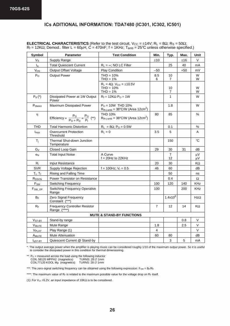
ICs ADITIONAL INFORMATION: TDA7480 (IC301, IC302, IC501)
ABSOLUTE MAXIMUM RATINGS
Symbol Parameter Value Unit
VCC DC Supply Voltage ±20 V
Tstg, Tj Storage and Junction Temperature –40 to 150 °C
VFREQ Maximum Voltage Across VFREQ (Pin 9) 8 V
Top Operating Temperature Range -20 to 70 °C
ESD Maximum ESD on Pins ±1.8 kV
THERMAL DATA
Symbol Parameter Value Unit
Rth j-amb Thermal Resistance Junction to ambient 80 °C/W
Rth j-pin Thermal Resistance Junction to Pin Max. 12 °C/W
PIN FUNCTIONS
N. Name Function
1234567891011121314151617181920
-VCC-VCC-VCCOUT
BOOTDIODEBOOT
NCFEEDCAP
FREQUENCYSGN-GND
INST-BY-MUTE
NC+VCC SIGN
VREG+VCC POW
-VCC-VCC-VCC-VCC
NEGATIVE SUPPLY.NEGATIVE SUPPLY.NEGATIVE SUPPLY.PWM OUTPUTBOOTSTRAP DIODE ANODEBOOTSTRAP CAPACITORNOT CONNECTEDFEEDBACK INTEGRATING CAPACITANCESETTING FREQUENCY RESISTORSIGNAL GROUNDINPUTST-BY/ MUTE CONTROL PINNOT CONNECTEDPOSITIVE SIGNAL SUPPLY10V INTERNAL REGULATORPOSITIVE POWER SUPPLYNEGATIVE SUPPLY (TO BE CONNECTED TO PIN 16 VIA C5)NEGATIVE SUPPLYNEGATIVE SUPPLYNEGATIVE SUPPLY
-VCC
OUT
BOOTDIODE
N.C.
BOOT
FEEDCAP
FREQ
1
3
2
4
5
6
7
8
9 STBY/MUTE
N.C.
+VCC SIGN
+VCC POW
VREG
-VCC
-VCC
20
19
18
17
16
14
15
13
12
D96AU537B
SGN-GND 10 IN11
-VCC
-VCC
-VCC
-VCC
PIN CONNECTION (Top view)
0 4 8 12 Area(cm2)30
40
50
60
Rthj-a(˚C/W)
D97AU675
COPPER AREA 35µTHICKNESS
PC BOARD
Rth with "on board" Square Heatsink vs. cop-per area.
26
70GS-62S
ICs ADITIONAL INFORMATION: TDA7480 (IC301, IC302, IC501)
ELECTRICAL CHARACTERISTICS (Refer to the test circuit, VCC = ±14V; RL = 8Ω; RS = 50Ω;Rf = 12KΩ; Demod.. filter L = 60µH, C = 470nF; f = 1KHz; Tamb = 25°C unless otherwise specified.)
Symbol Parameter Test Condition Min. Typ. Max. Unit
VS Supply Range ±10 ±16 V
Iq Total Quiescent Current RL = ∞; NO LC Filter 25 40 mA
VOS Output Offset Voltage Play Condition –50 +50 mV
PO Output Power THD = 10%THD = 1%
8.56
107
WW
RL = 4Ω VCC = ±10.5VTHD = 10%THD = 1%
107
WW
Pd (*) Dissipated Power at 1W OutputPower
Rf = 12KΩ PΟ = 1W 1 W
PDMAX Maximum Dissipated Power PΟ = 10W THD 10%Rth-j-amb = 38°C/W (Area 12cm2)
1.8 W
ηEfficiency ≡
PO
PO + PD ≡
PO
PI (**)
THD 10%Rth-j-amb = 38°C/W (Area 12cm2)
80 85 %
THD Total Harmonic Distortion RL = 8Ω; PO = 0.5W 0.1 %
Imax Overcurrent ProtectionThreshold
RL = 0 3.5 5 A
Tj Thermal Shut-down JunctionTemperature
150 °C
GV Closed Loop Gain 29 30 31 dB
eN Total Input Noise A Curvef = 20Hz to 22KHz
712
µVµV
Ri Input Resistance 20 30 KΩSVR Supply Voltage Rejection f = 100Hz; Vr = 0.5 46 60 dB
Tr, Tf Rising and Falling Time 50 ns
RDSON Power Transistor on Resistance 0.4 ΩFSW Switching Frequency 100 120 140 KHz
FSW_OP Switching Frequency OperativeRange
100 200 KHz
BF Zero Signal FrequencyConstant (***)
1.4x10⁹ HzΩ
RF Frequency Controller ResistorRange (****)
7 12 14 KΩ
MUTE & STAND-BY FUNCTIONS
VST-BY Stand-by range 0.8 V
VMUTE Mute Range 1.8 2.5 V
VPLAY Play Range (1) 4 V
AMUTE Mute Attenuation 60 80 dB
IqST-BY Quiescent Current @ Stand-by 3 5 mA
*: The output average power when the amplifier is playing music can be considered roughly 1/10 of the maximum output power. So it is useful to consider the dissipated power in this condition for thermal dimensioning.
**: PO = measured across the load using the following inductor: COIL 58120 MPPA2 (magnetics) TURNS: 28 ∅ 1mm COIL77120 KOOL Mµ (magnetics) TURNS: 28 ∅ 1mm
***: The zero-signal switching frequency can be obtained using the following expression: FSW = BF/RF
****: The maximum value of RF is related to the maximum possible value for the voltage drop on RF itself.
(1): For V12 >5.2V, an input impedance of 10KΩ is to be considered.

27
70GS-62S
ICs ADITIONAL INFORMATION: MSP3401G (IC303)
Block Diagram of the MSP 34x1G
So
urc
e S
elec
t
Loud-
SCART1
SCART2
SCART1
SCART2
SCART4
SCART3
MONO
De-modulator
HeadphoneHeadphone
I2S
SoundProcessing
speakerSound
Processing
DAC
DAC
ADC
Loud-
DAC
DACADC
Subwoofer
SCARTDSP Input Select
Pre-processing
SCART Output Select
Prescale
PrescaleI2S1
I2S2
Sound IF1
Sound IF2
speaker
80-pin PQFP package
65
66
67
68
69
70
71
72
73
74
75
76
77
78
79
80
40
39
38
37
36
35
34
33
32
31
30
29
28
27
26
251 2 3 4 5 6 7 8 9 10 11 12 13 14 15 16 17 18 19 20 21 22 23 24
64 63 62 61 60 59 58 57 56 55 54 53 52 51 50 49 48 47 46 45 44 43 42 41AVSUP
AVSUP
ANA_IN1+
ANA_IN−
ANA_IN2+
TESTEN
XTAL_IN
XTAL_OUT
TP
AUD_CL_OUT
NC
NC
D_CTR_I/O_1
D_CTR_I/O_0
ADR_SEL
STANDBYQ
CAPL_M
AHVSUP
CAPL_A
SC1_OUT_L
SC1_OUT_R
VREF1
SC2_OUT_L
SC2_OUT_R
NC
NC
DACM_SUB
NC
DACM_L
DACM_R
VREF2
DACA_L
NC
AVSS
AVSS
MONO_IN
NC
VREFTOP
SC1_IN_R
SC1_IN_L
ASG1
NC
SC2_IN_R
SC2_IN_L ASG2
SC3_IN_R
SC3_IN_L
ASG4
SC4_IN_R
SC4_IN_L
NC
AGNDC
AHVSS
AHVSS
NC
NC
I2C_CL
I2C_DA
I2S_CL
I2S_WS
I2S_DA_OUT
I2S_DA_IN1
ADR_DA
ADR_WS
ADR_CL
NC
DVSUP
DVSUP DVSUP
DVSS
DVSS
DVSS
I2S_DA_IN2
NC
NC
NC
RESETQ
NC
NC
DACA_R
MSP 34x1G

28
70GS-62S
Absolute Maximum Ratings
Symbol Parameter Pin Name Min. Max. Unit
TA Ambient Operating Temperature − 0 701) °C
TS Storage Temperature − −40 125 °C
VSUP1 First Supply Voltage AHVSUP −0.3 9.0 V
VSUP2 Second Supply Voltage DVSUP −0.3 6.0 V
VSUP3 Third Supply Voltage AVSUP −0.3 6.0 V
dVSUP23 Voltage between AVSUP and DVSUP
AVSUP,DVSUP
−0.5 0.5 V
PTOT Power DissipationPLCC68PSDIP64PSDIP52PQFP80PLQFP64
AHVSUP,DVSUP, AVSUP
1200130012001000 9601)
mWmWmWmWmW
VIdig Input Voltage, all Digital Inputs −0.3 VSUP2+0.3 V
IIdig Input Current, all Digital Pins − −20 +20 mA2)
VIana Input Voltage, all Analog Inputs SCn_IN_s,3)
MONO_IN−0.3 VSUP1+0.3 V
IIana Input Current, all Analog Inputs SCn_IN_s,3)
MONO_IN−5 +5 mA2)
IOana Output Current, all SCART Outputs SCn_OUT_s3) 4), 5) 4), 5)
IOana Output Current, all Analog Outputs except SCART Outputs
DACp_s3) 4) 4)
ICana Output Current, other pins connected to capacitors
CAPL_p,3)
AGNDC
4) 4)
1) PLQFP64: 65 °C2) positive value means current flowing into the circuit3) “n” means “1”, “2”, “3”, or “4”, “s” means “L” or “R”, “p” means “M” or “A”4) The analog outputs are short-circuit proof with respect to First Supply Voltage and ground.5) Total chip power dissipation must not exceed absolute maximum rating.
ICs ADITIONAL INFORMATION: MSP3401G (IC303)

29
70GS-62S
ICs ADITIONAL INFORMATION: VCT3832 (IC1001)
Absolute Maximum Ratings
Symbol Parameter Pin Name Min. Max. Unit
TA Ambient Operating Temperature − 65 °C
TC Case Temperature (PSDIP64) − 115 °C
TC Case Temperature (PMQFP128) − 115 °C
TS Storage Temperature −40 125 °C
PTOT Total Power Dissipation − 1400 mW
VSUPx Supply Voltage VSUPx −0.3 6 V
VI Input Voltage, all Inputs −0.3 VSUPx+0.31) V
VO Output Voltage, all Outputs −0.3 VSUPx+0.31) V
VIO Input/Output Voltage, all Open Drain Out-puts
−0.3 6 V
Block diagram of the VCT 38xxA (shaded blocks are optional)
Video Front-end
Comb Filter
Color Decoder
Display Processor Video
Back-endPanorama
Scaler
4 3
4
12
31
2I2C Master
16 kBText RAM
3 kBOSD
96 kBCPU ROM
TPU DMA CPU
24 IO Ports
Watchdog
2 CapCom
2 Timer
15:1 Mux10-bit ADC
8-bit PWM
Audio 3
2
Clock Oscillator
1 kB CPU RAM
XTAL1
XTAL2
VIN
AIN
Pxy
ADB, DB, CB
RGBOUT
RGBIN
VE
RT
PR
OT
HF
LB
SE
NS
E
I2C
XR
EF
HO
UT
VR
D
VR
T
SG
ND
Color, PrioMSyncI2C
VSUPAB
VS
UP
P1
GN
DP
1
Reset Logic
RESQ
VS
UP
S
TEST
GNDAB
VS
UPA
F
VS
UP
D
GN
DA
F
GN
DD
RS
W
2
GN
DM
EW
8
14-bit PWM
2 2
3CIN SVM
Vid
eo
GN
DS
CLK20
RDY
BE
24 kB
VCT 38xx
AOUT
VSync
VOUT
24 kB ROM
3 kB OSD RAM
Pict.Improv.

30
70GS-62S
ICs ADITIONAL INFORMATION: VCT3832 (IC1001)
48113AIN2
114AIN1
115AOUT2
116AOUT1
117RESQ
118SCL
119SDA
120XTAL1
121XTAL2
122VSUPS
123GNDS
124WE1Q
125WE2Q
126OE1Q
127OE2Q
128ADB18
CBIN
VSUPAF47
GNDAF46
SGND45
VRT44
VOUT43
P1042
P1141
P1240
P1339
GNDP138
VSUPP137
P1436
P1535
P1634
P1733
VSUPADBGNDADB
ADB16ADB15
ADB14ADB13
ADB12ADB11
ADB10
ADB17
ADB9ADB8
1 2 3 4 5 6 7 8 9 10 11 12 13 14 15 16 17 18 19 20 21 22 23 24
96 95 94 93 92 91 90 89 88 87 86 85 84 83 82 81 80 79 78 77 76 75 74 73
25 26 27 28 29 30 31 32
ADB7ADB6
ADB5VSUPADB
ADB1ADB0
DB0DB1
DB2DB3
VSUPDBGNDDB
DB4DB5
DB6DB7
ADB2ADB3
ADB4GNDADB
72 71 70 69 68 67 66 65
49 CIN1
50 CIN2/CRIN
51 VIN1
52 VIN2
53 VIN3
54 VIN4
55 DISINTROM
56 P27
57 P26
58 P25
59 P24
60 VSUPP2
61 GNDP2
62 P23
63 P22
64 P2197VERTQ
98VERT
99EW
100SENSE
101GNDM
102RSW1
103RSW2
104SVMOUT
105ROUT
106GOUT
107BOUT
108VSUPAB
109GNDAB
110VRD
111XREF
112AIN3
SAFETYVPROT
BINGIN
RINFBLIN
TESTP30
P31
HFLB
P32P33GNDP3
VSUPP3P34
P35
HOUTCLK20
VB0VB1
VB2VB3
VB4VB5
VB6VB7
VBCLKP20
VSUPDGNDD
P37P36
VCT 38xx

31
70GS-62S
DESCRIPTION OF SCHEMATIC DIAGRAM
SAFETY NOTE:
1. DISCONNECT THE AC PLUG FROM THE ACOUTLET BEFORE REPLACING PARTS.
2. SEMICONDUCTOR HEAT SINKS SHOULD BEREGARDED AS POTENTIAL SHOCK HAZARDSWHEN THE CHASSIS IS OPERATING.
NOTE:1. The unit of resistance «ohm»is omitted (K=1000
ohms. M= Megaohm).2. All resistors are 1/8 watt. unless otherwise noted.3. All capacitors are mF, unless otherwise noted
(P= mmF).4. The capacitor with Part No. RC-FZ9XXXBMNJ
is designed to with stand 63V.5. The capacitor with Part No. RC-FZ4XXXBMNJ
is designed to with stand 50V.
SERVICE PRECAUTION:
THE AREA ENCLOSED BY THIS LINE ( )IS DIRECTLY CONNECTED WITH AC MAINSVOLTAGE.WHEN SERVICING THE AREA, CONNECT ANISOLATING TRANSFORMER BETWEEN TVRECEIVER AND AC LINE TO ELIMINATE HAZ-ARD OF ELECTRIC SHOCK.
WAVEFORMS MEASUREMENT:
1. TEST EQUIPMENT: Digital Oscilloscope (Tektronix TDS 3012).
2. TEST CONDITIONS: PAL B/G full colour bar, 1KHz sinewave (volume regulation 50%).
Note: Waveforms 8 and 11 should be taken with the TV set in Stand-by mode.
Red in1 Green in2 Blue in3
!
IMPORTANT SAFETY NOTE:
PARTS MARKED WITH « » ( ) AREIMPORTANT FOR MAINTAINING THE SAFETYOF THE SET. BE SURE TO REPLACE THESEPARTS WITH SPECIFIED ONES FOR MAINTAIN-ING THE SAFETY AND PERFORMANCE OF THESET.
CAUTIONThis circuit diagram is original one, therefore there may be light differencefrom yours.

32
70GS-62S
I Sense7 V St-by8 E/W Output9
V Switch10 V Control St-by11 Vp (Primary)12
Vertical Input13 E/W Correction14 V inner correction15
Vertical + input16 VH17 H Control18
Red output4 Green output5 Blue output6

33
70GS-62S
V in Headphone R22 V in Speaker L23 V out Speaker L24
V out Speaker R25 V in Speker R26 X100227
V Flyback Vertical28 Vertical output29 Vertical input30
IF Video output31
Vb (Horizontal)19 Vc (Horizontal)20 V in Headphone L21

34
70GS-62S
SCHEMATIC DIAGRAM OF MOTHER UNIT (K7315N4).
1
I
H
G
F
E
D
C
B
A
2 3 4 5 6 7
Page 35
Page 36M
1000
BR G
+5V
+5V
+5V
12
34
56
1 2 3 4 5
12
34
+5V
ST
BY
+3.3VSTBY
+3,
3VS
TB
Y
+16
V+
5VS
TB
Y
+3.
3V
+5V
ST
BY
+5V
ST
BY
+3.
3V
+5V
+16
V
-16V
+16
5V
+5V
+12
V
+12
V
+12
V
+12
V
+5V
+13
V
12
3
4 5
6
7
8
+5V
ST
BY
IX16
41B
M
Q70
9
+5V
ST
BY
+5STBY
QP
WB
F73
47B
MN
0
DU
NT
K73
47B
MV
0
QP
WB
F73
16B
MN
5
DU
NT
K73
16B
MV
1
CH
CH
VO
L+V
OL-
ONLY AVLINK
GB
VPROT
HOUT
R
VI2
VI1
AV2
ALCLOCK
CR1
MUTE
AV2
KE
Y
PROT
FI
FB
IR LED
OP
C
ST
BY
E/W
PROT
KE
Y
AV1
KEY
LED
AV1
AL
.
.
.
.
.
.
.
.
.
.
.
.
. .
.
.
.
.
.
.
.
.
.
R10
074K
7(T
Q)
C70
133
0nF
(275
V)
FZ
0188
BM
R10
023K
3
R10
013K
3
D72
0S
UF
15J
L701
F01
11B
M
D79
8
EG
P20
BD
X06
29 D71
9
EG
P20
BD
X06
29
JF70
110
0nF
IC10
03X
24645S8
IX1603B
M
NC
1
S1
2
S2
3
VS
S4
SD
A5
SC
L6
WP
7
VC
C8
D72
7D
X00
45
Q70
8B
C54
7T
X01
06
Q70
62S
C24
12
R10
091K
D10
04D
X05
51
R10
10
100K
C10211nF
R62
41K
R62
5
330
C8053.3uF
F70
1F
S-C
3226
(M)
GN
0304
3
2
CU
0205
BM
1
D10
01P
X01
05
12
3
12
R10
1310
0
IC90
1T
DA
6107 VI(1
)1
VI(2
)2
VI(3
)3
GN
D4
SE
NS
5
VD
D6
VO
(3)
7
VO
(2)
8
VO
(1)
9R
906
2K7
(1/2
W)
C90
110
uF(2
50V
)
D90
11N
4004
DX
0501
BM
C90
2P
B3D
E47
2
FO
CU
S
G2
(L3)
(H)
CN
W-2
710B
M
R90
82K
7(1
/2W
)
R90
72K
7(1
/2W
)
R90
44M
7(1
/8W
)
S70
2
K00
79G
E
S70
3
K00
79G
E
S70
4
K00
79G
E
S70
5
K00
79G
E
R10
3310
0
C73
710
0uF
(16V
)
R10
9910
0
D71
2B
YV
28-6
00D
X06
18B
M
D70
3
DX
0555
RF
2005
D70
4D
X05
55R
F20
05
D70
1
DX
0555
RF
2005
D70
2
DX
0555
RF
2005
C70
310
nF25
0VK
Z00
29C
E
C70
410
nF25
0VK
Z00
29C
E
C70
668
0nF
(400
V)
(G)
PLG
N02
07
C70
210
nF25
0VK
Z00
29C
E
R71
310
K
R70
639
0K(T
Q)
R73
868
R75
539
0
R75
610
0
R75
8
2R7
D10
07
DX
0045
Q90
32S
C24
12
Q90
22S
C24
12
Q90
12S
A10
37
R91
339
0
R91
22K
2
R91
039
0
R91
110
0Q
906
TX
0232
Q90
52S
C24
12
Q90
42S
A10
37
R91
839
0
R91
72K
2
R91
539
0
R91
610
0Q
909
2SC
2412
Q90
82S
C24
12
Q90
72S
A10
37
R91
912
0
R92
339
0
R92
22K
2
R92
039
0
R92
110
0
D90
2
C5V
1E
X04
08B
M
C91
010
0nF
R90
51K
(K)
CN
W-2
865B
M
C91
110
0nF
L100
61u
H(N
M)
C10
4047
uF
Q10
012S
C24
12
LP70
1R
LAM
P00
1
R77
182
K(T
Q)
R76
582
K(T
Q)
R77
482
K(T
Q)
R77
082
K(T
Q)
D10
06D
X05
51R
1035
33K
R1040
2M2
D10
09C
4V7
EX
0544
BM
R90
3
0R
902 0
Q70
2T
X02
37B
M
R72
53K
3
D71
7D
X00
45
C72
110
nF(F
Z)
D73
1D
X00
45
R74
968
0K(T
Q)
R71
110
R71
518
K(1
%)
+VS
-VS
IC70
1
IX15
56
8
7
6
54
3
2
1
R78
8
22K
Q72
12S
A10
37
Q72
02S
C24
12
R78
510
0K
C71
21u
F(1
60V
)
R78
322
0KR
712
390K
(TQ
)R
705
8K2
Q71
22S
A10
37
D71
6
C6V
2E
X05
84B
M2%
R75
1
100K
R78
61K
8
R78
418
K
D71
5D
X05
51
R71
6
390K
(TQ
)
R71
033
0K(T
Q)
(1%
)
R70
933
0K(T
Q)(
1%)
C71
168
nF(2
50V
)F
Z02
06B
M
R70
839
0K(T
Q)
Q70
42S
A10
37
Q70
52S
C24
12
R75
410
K
R75
210
K
D71
4C
6V8
EX
0411
BM
D74
1C
4V3
EX
0543
BM
R70
1
22K
R74
822
0K
R79
027
0(1
/2W
)
D70
7D
X05
51R78
910
0K
D74
2D
X05
51
C79
822
0pF
2KV
KZ
0035
CE
C90
510
0nF
(400
V)
(FZ
)
R77
268
0K(T
Q)
R77
368
0K
R71
9
2M2
R77
9
2M2
R77
8
2M2
D74
4D
X05
51
R92
6
560
R92
7
560
R92
5
560
Q91
02S
A10
37
R93
33K
3R
932
1K8
R93
1
8K2
C91
222
0pF
R79
91 (1
/2W
)X
Z02
00B
M
PO
R17
01P
0001
BM
D73
4D
X05
51
R72
110
0(T
Q)
R72
2
R70
32K
7
C80
410
0nF
R1020
10K
C40
9
100n
F
C40
8
100n
F
L602
3.3u
H(D
F)
C40
7
100n
F
R8042K2
FB
701
LN-0
037B
M
C72
010
00uF
(6.3
V)
FB
702
LN-0
037B
M
T702
Z05
90B
M
3146
R10
1810
0
R10
2210
0
R90
1
0
C10
3310
0nF
C1034100nF
R36
110
0K
C1036
100nF
L901
0
D74
7D
X05
51B
M
R10
43
680
R75
9
(TQ
)56
0
14 12 13 11
T701
RN
Z05
89B
M
56 4
C72
710
00uF
(25V
)
D90
3
DX
0539
C90
410
uF
R93
4
100K
(TQ
)
R93
5
100K
(TQ
)
C10
4247
0nF
D74
9D
X05
18B
M
C73
110
0uF
(25V
)
F70
3
FU
S
Q70
1T
X02
37B
M
FB
703
TP
701
R10
30
2K2
R10
31
1K
R10
32
1K
D10
11
EX
0545
TR
C8 9 10 6 11
571
1213
R75
71K
8
D90
4D
X06
00
D90
6D
X06
00
D90
5D
X06
00
L100
1uH
(DF
)
L100
51u
H(D
F)
C91
62n
2
S70
1
P06
00B
M
C10
2022
0nF
C71
3
(450
V)
68uF
EZ
0141
BM
C10
0210
0nF
R8021K2
R91
412
0
C10
182n
2
R90
912
0
Q70
72S
C24
12
Q10
062S
C24
12
R10
393K
9
R10
1410
0
C80
347
0uF
R10
41
1K
L100
21u
H(D
F)
F70
2
FU
S
R803270
C90
947
0uF
(16V
)
R10
173K
3
D10
05
C33
EX
0564
BM
C10
2410
0nF
C72
622
00uF
(25V
)
R10
162K
2
D10
13C
5V6
EX
0546
BM
L801
1uH
VA
R1
VX
0035
BM
C10
4910
nF
J181
LN-0
037C
E
C10
03
2.2n
F
C72
810
0uF
(200
V)
IC70
8F
X01
11
Q17
01B
T13
4W
R17
0110
0(1
/2W
)
R17
0210
0
R17
03
1K
D17
021N
4005
C17
0147
0uF
(16V
)
R17
0447 (1
/3W
)
D17
01
C8V
2
C17
02
680
FB801D10
14C
8V2
EX
0413
BM
C810390pF
R42
375 (T
Q)
FB401
FB402
R93
647
R
C80
968
0nF
1N41
48D
1015
EX
0045
D72
4B
2V4
EX
0400
BM
C10
4810
nF
C10
047
uF
C10
32n
2
C10
1710
0nF
C10
2710
nF
C10
0147
0uF
(6.3
V)
R10
112K
2
C10
3
270p
C10
01u
F
R75
022
K
R78
2
47K
IC10
01
IX18
23B
VC
T383
VERTQ97
VERT98
EW99
SENSE100
GNDM101
RSW1102
RSW2103
SVMOUT104
ROUT105
GOUT106
BOUT107
VSUPAB108
GNDAB109
VRD110
XREF111
AIN3112
AIN2113
IN1114VUPAF47
VOUT48
CIN149
CIN250
VIN151
VIN252
VIN353
VIN454
DISINTROM55
P2756
P2657
P2558
P2459
VSUPP260
GNDP261
P2362
P2263
P2164
P20
65
VB
CLK
66
VB
767
VB
668
VB
569
VB
470
VB
371
VB
272
VB
173
VB
074
CLK
2075
HO
UT
76
VS
UP
D77
GN
DD
78
P37
79
P36
80
P35
81
P34
82
VS
UP
P3
83
GN
DP
384
P33
85
P32
86
P31
87
P30
88
NC
89
FB
LIN
90
RIN
91
GIN
92
BIN
93
VP
RO
T94
SA
FE
TY
95
HF
LB96
R71
4.5
6(3
W)
R10
348K
2
D10
12C
5V6
EX
0546
BM
C10
5110
nF
C10
1947
uF(1
6V)
C70
710
0uF
(25V
)
JF70
23,
3uH
(CF
)
Q10
052S
C24
12
R10
08
10K
R75
32K
2
R10
06
4K7
C91
533
nF
C91
433
nF

35
70GS-62S
SCHEMATIC DIAGRAM OF MOTHER UNIT (K7315N4).
8 9 10 11 12 13 14
I
H
G
F
E
D
C
B
APage
34
Page 37
Vh
GND
FS
V OUT
V IN
12
34
+13
V
-13V
+5V
+25
V
+5V
3 4 5 6
ONLY 28"
ON
LY 2
8"
-1
+
+16
5V
+13
V
+5V
+16
5V
+5V
+13
V
-13V
+16
5V
+13
V
-6V
+18
0V-6V
9
10
11
12
13
14
15
16
17
18
19
20
FO
R 7
315N
4 V
ER
SIO
N
AB
OLI
SH
PA
RTS
D10
14 -
RH
-EX
0413
BM
ZZ
*
D03
07 -
RH
-EX
0413
BM
ZZ
*
D03
08 -
RH
-EX
0413
BM
ZZ
*
D10
15 -
RH
-EX
0045
BM
ZZ
*
R06
57 -
RR
-XZ
0215
BM
ZZ
+
C03
53 -
RC
-FZ
9104
BM
NJ+
C03
58 -
RC
-FZ
9104
BM
NJ+
C03
68 -
RC
-FZ
9104
BM
NJ+
C03
73 -
RC
-FZ
9104
BM
NJ+
C03
56 -
RC
-FZ
9334
BM
NJ+
C03
70 -
RC
-FZ
9334
BM
NJ+
RE
F.
PA
RTS
CO
DE
PA
RTS
RE
F.
PA
RTS
CO
DE
PA
RT
S W
ITH
DIF
ER
EN
T C
OD
E (
SA
ME
VA
LUE
)P
AR
TS
C03
88 -
RC
-FZ
4334
BM
NJ+
C03
89 -
RC
-FZ
4334
BM
NJ+
C03
86 -
RC
-FZ
9224
BM
NJ+
D09
02 -
RH
-EX
0545
BM
ZZ
*
D10
03 -
RH
-EX
0551
BM
ZZ
*
D04
11 -
RH
-EX
0546
BM
ZZ
*
PA
RTS
RE
F.
PA
RTS
CO
DE
D04
03 -
RH
-EX
0549
BM
ZZ
*
D04
20 -
RH
-EX
0546
BM
ZZ
*
D05
07 -
RH
-EX
0554
BM
ZZ
*
D05
12 -
RH
-EX
0564
BM
ZZ
*
D06
15 -
RH
-EX
0560
BM
ZZ
*
D06
22 -
RH
-EX
0554
BM
ZZ
*
D06
35 -
RH
-EX
0551
BM
ZZ
*
PA
RTS
RE
F.
CO
DE
PA
RTS
D07
08 -
RH
-EX
0558
BM
ZZ
*
D07
14 -
RH
-EX
0548
BM
ZZ
*
D07
17 -
DX
-EX
0551
BM
ZZ*
D07
24 -
RH
-EX
0574
BM
ZZ
*
D07
25 -
RH
-EX
0556
BM
ZZ
*
D07
27 -
DX
-EX
0551
BM
ZZ*
D07
30 -
RH
-EX
0584
BM
ZZ
*
D07
31 -
DX
-EX
0551
BM
ZZ*
D07
35 -
RH
-EX
0556
BM
ZZ
*
RE
F.
PA
RTS
PA
RTS
CO
DE
D07
37 -
DX
-EX
0551
BM
ZZ*
D07
38 -
DX
-EX
0551
BM
ZZ*
D07
39 -
RH
-EX
0564
BM
ZZ
*
D07
46 -
DX
-EX
0551
BM
ZZ*
L100
2 -V
P-N
M1R
0MR
10N
*
L100
3 -V
P-N
M1R
0MR
10N
*
L100
5 -V
P-N
M1R
0MR
10N
*
PA
RTS
RE
F.
PA
RTS
CO
DE
D10
03 -
DX
-EX
0606
BM
ZZ*
C10
52-V
CK
ZP
A1H
B33
2K+
D10
12 -
RH
-EX
0546
BM
ZZ
*
D10
13 -
RH
-EX
0546
BM
ZZ
*
PA
RT
S A
DD
J330
,J3
31,J
332,
J333
, J33
4,J3
35, J
F78
,JF
79, L
319,
R45
1,R
452,
J20
4
PA
RT
S W
ITH
DIF
ER
EN
T C
OD
E (
DIF
ER
EN
T V
ALU
E )
D10
03 -
RH
-DX
0606
BM
ZZ
*
PA
RTS
RE
F.
PA
RTS
CO
DE
PA
RTS
RE
F.
PA
RTS
CO
DE
JL01
2- Q
CN
W-2
736B
MZ
Z
C10
60 -V
CK
YTV
1HF1
04Z*
JL18
3- Q
JUM
-400
1GE
FW
*
JL19
2- Q
JUM
-200
1GE
FW
*
J015
2 - V
RS
-TV
1JD
000J
*
J002
7 - V
RS
-TV
1JD
000J
*
J032
5 - V
RS
-TQ
2BD
000J
*
PA
RTS
RE
F.
PA
RTS
CO
DE
J003
3 - V
RS
-TV
1JD
000J
*
J006
1 -
VP
-DF
220K
0000
*
JL08
8- Q
JUM
-100
1GE
FW
*
L040
2 -
VR
D-R
A2B
E22
0J*
L040
3 -
VR
D-R
A2B
E22
0J*
PA
RTS
VA
LUE
330
nF
330
nF
HO
UT
VPROT
PR
OT
CR1
VI2
.
.
.
.
.
.
.
.
.
.
.
.
.
R60
32R
2(3
W)
C60
647
nF(H
B)
R53
0
XZ
0208
BM
4.7
(1/2
W)
L2 M00
17C
E
C40
310
nF
R51
24K
7
R51
51K
2C
522
100n
F
+VS
-VSIC50
2
BA
4558
8 7 6 54321
IC50
120 19 18 17 16 15 14 13 12 11
R54
41K
R54
927
K
C51
12.
2uF
R43
51K
Q40
42S
C24
12
R45
022
R54
518
0K
D61
0
DX
0518
1N58
19
D40
3
EX
0412
7V5
D72
0S
UF
15J
DX
0628
BM
C79
933
00pF
4KV
KZ
0106
GE
C60
110
nF1.
6Kv
FZ
0228
BM
IC70
5K
A43
1AZ
IX16
74
D51
0D
X05
771N
4935
DX
0629
R51
318
0K
C52
410
0nF
(FZ
)
C60
439
0pF
C60
722
pFR
609
3.3
1/2W
XZ
0206
BM
C60
52.
2nF
Q60
5K
SC
2500
TX
0192
C61
01n
F
D61
2D
X05
771N
4935
C62
12.
2nF
(500
V)
D61
3D
X05
771N
4935
C62
02.
2nF
(500
V)
R50
939
K
R61
410
K(1
/2W
)
C61
347
0nF
(FZ
)
17
19
15
16
18
20
R60
282 (1
/4W
)
R60
182 (1
/4W
)
F60
122
uH(C
F)
F60
222
uH(C
F)
C73
347
0uF
(35V
)
C61
718
0nF
(250
V)
FZ
0229
BM
L609
3.3u
HP
0144
21
R10
10
100K
3
C40
268
0nF
(FZ
)
R73
910
0
R74
547
K
C72
2
27nF
C60
947
0uF
(6.3
V)
R74
022
0
R74
1
330K
Q61
32S
K29
64T
X02
27B
M
R62
32K
2
D60
8D
X05
51B
M
D72
1S
UF
15J
DX
0628
BM
Q60
2T
X02
38B
M
D62
0C
18E
X05
58B
M
Q60
42S
C24
12
Q60
82S
A10
37R
610
68
R60
82K
2 R61
64.
7C
608
100n
FR
612
2K2
Q60
32S
C24
12
R6072K2
D61
9D
X05
51
D61
8D
X05
51
C61
268
0pF
D60
5
DX
0518
1N58
19
C60
3 220n
F(F
Z)
D60
6D
X05
51D
604
DX
0551
D61
7D
X05
51
R62
04K
7
D60
7R
GP
02-1
6ED
X06
34B
MR
621
330
C62
833
0pF
(2K
v)F
Z02
16B
M
R63
36K
8
Q61
12S
A10
37
L605
Z07
25
R63
06K
8
C61
910
0nF
(250
V)
FZ
0198
BM
R62
947
0K(R
A)
D62
3C
4V7
EX
0544
BM
C62
610
uF
Q60
92S
C24
12
R62
8
10K
D62
2C
12E
X04
17B
M
R62
782
K(1
/2W
)
R62
6
100
C62
5
1nF
R73
868
(1/2
W)
Q71
12S
C24
12
Q60
72S
C24
12
R60
41K
+VS
-VS
IC60
1B
A45
588 7 6 5
4321
C63
022
nF(F
Z)
R63
51M
R63
74K
7
D62
5D
X05
51R
643
820K
C63
12n
2
R63
810
0K
C54
0
3,3
nFC63
222
pF
2 3 8 5 69
7
T601
F20
85
13 4 1
10
D62
4D
X05
51B
M
R62
21K
5
D61
6E
X05
45B
M
R50
868
0
R64
50
D10
09C
4V7
EX
0544
BM
R40
675 (T
Q)
R53
427
K
R72
922
K
R72
53K
3
D71
7D
X00
45
Q70
3T
X02
37B
M
D71
3D
X05
51
C71
710
nF(F
Z)
Q72
3T
X02
32
R72
810
0(T
Q)
D71
8
DX
0551
Q72
4T
X02
32
D73
1D
X00
45
D73
2
DX
0551
C72
347
0pF
R73
14K
7
D73
61N
4937
D72
91N
4937
Q72
52S
C24
12
Q71
52S
A10
37
R70
410
0K
R72
015
K
D73
9C
33E
X04
27B
M
R72
41M
D73
8D
X00
45
R78
122
KC
716
6n8
R72
65K
61%
D70
8D
X04
21
C71
910
0nF
R78
715
R(1
/2W
)X
Z02
14B
M
D73
7D
X00
45
R61
722 1/
2WX
Z02
16
D70
5C
5V6
EX
0546
BM
R71
70
D70
6D
X05
51
D70
9D
X00
45
R71
810 (1
/2W
)X
Z02
12B
M
C73
210
uF
R65
022 1/
2WX
Z02
16
C71
022
nF(F
Z)
D73
5C
15E
X04
19B
M
R53
112
0K
R72
33K
3(R
A)
R77
368
0K(T
Q)
R71
9
2M2
(TQ
)
R77
9
2M2
(TQ
)
R77
8
2M2
(TQ
)D
730
C6V
2E
X04
10B
M
D73
3C
6V2
EX
0547
BM
R73
73K
3
L705
330K
P03
08B
M
Q71
02S
C24
12
R77
612
0
D72
8D
X05
51
D74
4D
X05
51
IC70
2K
A43
1AZ
IX16
74R
735
3K9
Q71
32S
A10
37
R61
83K
3(1
/2W
)X
Z02
42B
M
R76
81K
C73
027
0pF
(500
V)
R79
322
K
D74
6D
X00
45
R79
139
0
C73
447
uF(1
6V)
R79
447
C73
547
0uF
(6.3
V)
R76
03K
9
R73
33K
9
C73
910
0nF
FB
603
LN00
37
R63
41K
R55
0
R55
1
(K)
CN
W-2
865B
M
(H)
CN
W-2
710B
M
R72
210
K
C80
410
0nF
Q79
62S
K29
64T
X02
27B
M
C62
347
0uF
(35V
)
C73
610
0nF
D72
2
DX
0518
BM
D74
0D
X00
45
F70
4
FU
S
R74
312
0K(1
%)
(TQ
)
C64
147
0nF
C72
410
0nF
C54
3
680p
F
C74
022
0pF
D63
5
IN41
48D
X00
45
R65
3
180
(TQ
)D
634
4V7
D63
6D
X05
51B
M
R76
747
0
R70
04K
7
D63
3D
631
C54
1
330p
F
R76
647
0
R55
410
0
11 9 10 8 9
5 2 71
IC70
3F
X01
13
4
1 2
3
390
R63
2
R65
410
0
R65
52K
7
L610
P03
11B
M56
0K
TP
701
C62
747
0nF
C70
53n
3(6
30V
)F
Z02
17B
M
Q61
0T
X02
40B
MC
624
220n
F(2
50V
)F
Z62
24B
M
R63
133
0K(R
A)
D62
1D
X06
30B
M
D75
0
EX
0556
BM
C15
R79
556
D61
5C
22E
X04
23B
M
C61
822
0uF
(16V
)
R79
222
K
Q10
042S
C24
12
R65
718
R(1
/2W
)X
Z02
15B
M
R77
70,
68
R76
10,
68
C80
347
0uF
D61
11N
4936
DX
0578
C52
6
220u
F(2
5V)
R74
212
0K(1
%)
(TQ
)
R65
11K
2(1
/2W
)
L801
1uH
R54
86K
8
R73
21K
5
R40
575
C72
810
0uF
(200
V)
EZ
0258
CE
C64
047
0uF
(6.3
V)
D743C18EX558BM
D60
9
DX
0518
1N58
19
D62
7
R45
122
R61
122 (T
Q)
R78
0
33 (TQ
)
C79
610
0pF
2KV
KZ
0031
R63
927
0K
C70
910
uF
D42
14V
7E
X05
44
R74
78M
21/
2W(U
A)
R74
43K
9(1
%)
D72
5C
15E
X04
19B
M
Q60
1T
X02
26
C62
247
0uF
(25V
)
C71
847
0pF
R6562K2
C60
24.
7nF
(1.6
Kv)
FZ
0227
BM
R74
68M
2(1
/2W
)(U
A)
D40
4
EX
0549
7V5
C72
53n
3(6
30V
)F
Z02
17B
M
R64
4
1K8
D60
2B
Y22
8
R79
818
R(1
/2W
)X
Z02
15B
M
C43
21n
FC
520
470u
F(3
5V)
C73
810
0nF
(FZ
)
C72
947
0uF
(6.3
V)
Q71
42S
C24
12
C62
968
nF
Q60
62S
C24
12
R72
71K
C54
24,
7nF
C22
510
0nF
C71
568
nF
D74
8C
6V8
EX
0548
BM
L606
3,3u
H(D
F)

36
70GS-62S
1 2 3 4 5 6 7
R
Q
P
O
N
M
L
K
J
SCHEMATIC DIAGRAM OF MOTHER UNIT (K7315N4).
Page 37
Page 34
1234O
UT
L
GN
D
GN
D
OU
T R
+5V
+16V
+16
V
-16V
-16V
-13V
+13
V
MS
P34
01G
RH
-IX18
16B
M
+5V
+3.
3VS
TB
Y
+5V
ST
BY
+5V
+5V
ST
BY
+5V
+8V
21
22
2324
25
26
27
+3,
3VS
TB
Y
DU
NT
K73
15B
MV
1
SC
2OU
TR
SC
2OU
TL
SC
1OU
TR
SC
1OU
TL
SC
2IN
L
SC
1IN
L
SC
1IN
R
SC
2IN
R
AL
I2S
OU
T
HEADR
SC
4IN
L
I2S
IN
SC
3IN
L
SC
4IN
R
I2S
CL
HEADR
SC
3IN
R
HEADL
I2S
WS
HEADL
A5
A11
AFT
A8
A16
A17
D1
A1
D0
AFT
D7
D4
D3
MUTE
A14
IR
A7
CR1
D3
D0 A4
PROT
A2
A13
A8
A6
SC
L
D5
STBY
OPC
D5
A14A
2
A9
A11
A15
A17
D7
A6
A10
A13
D1 A5
A4
RES
RES
A0
D6
A0
A3
D6
D4
A7
A15
PROT
A3
A9
SD
A
A12
A16
SCLSDA
A12
D2
A10
LED
OP
C
D2
A1
LED
FRONT
SC4INR
SC4INL
FR
ON
T
VOUT
GN
D
GN
D
.
.
.
.
.
.
.
IC30
4M
5218
L
+12V8
OUTL7
-INL6
+INL5
GND4
+INR3
-INR2
OUTR1
C35
122
0uF
(25V
)
R35
02K
2
R35
315
0 R35
715
0
C35
010
0nF
C36
056
0pF
C37
556
0pF
C36
147
0nF
(FZ
)
(SP
)
QP
LGN
0441
CE
ZZ
C36
910
0pF
R35
610
KC
367
100n
F
C37
11n
F
L316
3.3u
H(C
F)
C37
822
0uF
(25V
)C
379
100n
F
L350
3.3u
H(C
F)
C35
410
0pF
R35
212
K
C35
94.
7nF
C35
71n
FC
362
0.47
uF
L351
3.3u
H(C
F)
C36
322
0uF
(25V
)
L315
3.3u
H(C
F)
C36
610
0nF
C36
522
0uF
(25V
)
C36
410
0nF
IC30
1
TD
A74
80
1 2 3 4 5 6 7 8 9 10
20 19 18 17 16 15 14 13 12 11
C37
44.
7nF
C32
110
0nF
R31
110
0K
R30
210
0
R30
310
0
R30
610
0KR
305
100K
R30
410
0
R33
22K
7
R10
374K
7
R33
12K
7
R33
510
0K
C37
647
0nF
(FZ
)
R10
364K
7(R
A)
R33
710 (R
A)
R33
010
L352
P03
12 L353
P03
12
R36
222
KQ
305
2SC
2412
C37
20.
47uF
R30
74K
7
R33
610
0K
R33
41K
C38
41n
F
R33
31K
C38
522
0nF
R30
110
0
C30
310
uF(1
6V)
C30
210
uF
C30
110
uF
C30
410
uF(1
6V)
C38
31n
F
R10
0327
KD
1003
DX
0513
C8053.3uF
C37
71u
F
R36
010
0K
R32
815
0
R32
915
0C
381
10nF
D10
02P
X01
05
12
3
IC30
2
TD
A74
80
1 2 3 4 5 6 7 8 9 10
20 19 18 17 16 15 14 13 12 11
C32
2
L301
10uH
(DF
)
(CN
4)
JAK
J004
7CE
ZZ
1543
267
C10
1210
0nF
R35
127
K
JF17
JF12
C30
51n
F
R37
068
KR
369
3K3
D10
08B
3V9
EX
0579
BM
R10
26 10
R10
2522
0
Q10
082S
C24
12
Q10
072S
A10
37
C10
1610
0nF
(FZ
)
R35
527
K(R
A)
R35
810
0K(R
A)
R35
910
0K(R
A)
R38
115
K
R38
315
K
R38
218
K
R38
018
K
Q30
62S
A10
37
R38
51M
D30
6D
X05
51
R38
422
K
C38
010
nF
C80
410
0nF
C10
1347
0nF
R80
110
K
R10
1510
0
C32
810
0nF
C32
347
pF
24
F
X30
1B
0203
18,4
32M
Hz
C31
110
uF(1
6V)
C32
010
uF(1
6V)
C31
210
uF(1
6V)
IC30
3
NC
64
NC
63
AV
SS
62
AV
SS
61
MO
NO
60
NC
59
VR
EF
TO
P58
SC
1_IN
_R57
SC
1_IN
_L56
AS
G1
55
SC
2_IN
_R54
SC
2_IN
_L53
AS
G2
52
SC
3_IN
_R51
SC
3_IN
_L50
AS
G4
49
SC
4_IN
_R48
CAPL_M40
AHVSUP39
CAPL_A38
SC1_OUT_L37
SC1_OUT_R36
VREF135
SC2_OUT_L34
SC2_OUT_R33
ASG332
NC31
DACM_SUB30
NC29
DACM_L28
DACM_R27
VREF226
DAC_L25
DA
C_R
24
I2S
_DA
_IN
217
DV
SS
16
DV
SS
15
DV
SU
P13
DV
SU
P12
DV
SU
P11
AD
R_C
L10
AD
R_W
S9
AD
R_D
A8
I2S
_DA
_IN
17
I2S
_DA
_OU
T6
I2S
_WS
5
I2S
_CL
4
I2C
_DA
3
I2C
_CL
2
NC
1
STANDBYQ80
ADR_SEL79
D_CTR_OUT078
D_CTR_OUT177
NC76
NC75
AUD_CL_OUT74
TP73
XTAL_OUT72
XTAL_IN71
TESTEN70
ANA_IN2+69
ANA_IN-68
ANA_IN1+67
AVSUP66
AVSUP65
SC
4_IN
_L47
NC
46
AG
ND
C45
AH
VS
S44
AH
VS
S43
NC
42
NC
41
NC
18
NC
19
NC
20
RE
SE
TQ
21
NC
22
NC
23
DV
SS
14
D30
37V
5E
X05
49
R30
9
100
C10
3710
nF
C10
38
560p
F
C10
153.
3pF
C10
4122
0uF
(10V
)
C10
43
1nF
C10
44
1nF
C10
4510
0pF
C10
4610
0pF
R38
710
0
L100
11u
H(D
F)
D72
3C
8V2
EX
0550
C30
83.
3uF
C22
3
100p
FL1
003
1uH
(DF
)
R10
1410
0
R10
2310
K
L100
21u
H(D
F)
L100
41u
H
C10
145p
F
R10
0422
0
C10
1010
0nF
R10
2433
0
X10
0220
.25
B02
19B
M
R30
8
100
L801
1uH
L318
22uH
J90
LN-0
037C
E
J91
LN-0
037C
E
J92
LN-0
037C
EJ9
4LN
-003
7CE
J96
LN-0
037C
E
L302
3.3u
H(D
F)
D30
57V
5E
X05
49
C39
01n
FC
391
1nFJ4
01
Z01
01B
M
L303
3.3u
H(D
F)D307
C8V2
D30
8C
8V2
C10
523,
3nF
R33
922
0R
338
220
R42
375 (T
Q)
C225100pF
IC10
02
SS
T37
VF
040-
90IX
1841
BM
A18
1
A16
2
A15
3
A12
4
A7
5
A6
6
A5
7
A4
8
A3
9
A2
10
A1
11
A0
12D
721
E22
A10
23
OE
24
A11
25
A9
26
A8
27
A13
28
A14
29
A17
30
WE
31
VC
C32
D0
13
D1
14
D2
15
VS
S16
D3
17
D4
18
D5
19
D6
20
L319
22uH
C35
210
0nF
C31
633
0nF
C31
733
0nF
C31
833
0nF
C31
933
0nF
JF74
C38
622
0nF
JF4
C30
710
0nF
Q10
032S
C24
12
R31
210
0K
D30
27V
5E
X05
49
D30
47V
5E
X05
49
C33
131n
F
C10
3133
0uF
(6.3
V)
C10
0547
uF
C10
322n
2
C30
61n
F
C30
933
0uF
(10V
)
R31
010
0K
C10
0910
0nF
C224100pF
C10
30
270p
F
C10
041u
FC
1006
10uF
C10
6010
0nF
C10
0747
nF
C31
010
0nF
C31
347
nF
C10
1110
0nF
C10
082n
2
IC10
01
X18
23B
M
VC
T383
1A
XREF111
AIN3112
AIN2113
AIN1114
AOUT2115
AOUT1116
RESQ117
SCL118
SDA119
XTAL1120
XTAL2121
VSUPS122
GNDS123
WE1Q124
WE2Q125
OE1Q126
OE2Q127
ADB1B128A
DB
171
VS
UP
AD
B2
GN
DA
DB
3
AD
B16
4
AD
B15
5
AD
B14
6
AD
B13
7
AD
B12
8
AD
B11
9
AD
B10
10
AD
B9
11
AD
B8
12
AD
B7
13
AD
B6
14
AD
B5
15
VS
UP
AD
B16
GN
DA
DB
17
AD
B4
18
AD
B3
19
AD
B2
20
AD
B1
21
AD
B0
22
DB
023
DB
124
DB
225
DB
326
VS
UP
DB
27
GN
DD
B28
DB
429
DB
530
DB
631
DB
732
P1733
P1634
P1535
P1436
VSUPP137
GNDP138
P1339
P1240
P1141
P1042
TEST43
VRT44
SGND45
GNDAF46
VSUPAF47
VOUT48
CIN149
CIN250
C38
710
0nF
C33
033
0uF
C32
910
0nF
C38
210
0nF
R31
310
0K
Q10
022S
C24
12
C35
3
100n
F
C35
8
100n
F
C36
8
100n
F
C37
3
100n
F
C35
633
0nF
C37
033
0nF
C33
833
0nF
C33
933
0nF

37
70GS-62S
8 9 10 11 12 13 14
R
Q
P
O
N
M
L
K
J
SCHEMATIC DIAGRAM OF MOTHER UNIT (K7315N4) .
Page
36
Page 35
12
34
5
R OUT
R IN
L OUT
L IN
B
SS
G
R
FS
V OUT
V IN
R OUT
R IN
L OUT
L IN
SS
FS
AV LINK
AV LINK
SERVICIO
HH
VV
+5V
+5V
+5V
+5V
+5V
+25
V
SH
AR
PE
LEC
TRO
NIC
A E
SP
AN
A
S.A
.
NO
MB
RE
CO
DIG
O
ES
CA
LA
MO
DE
LOF
EC
HA
RE
VIS
ION
ES
N
23456
FE
CH
A
A-1
KI
TP
7B
MN
15
Mot
her
Boa
rd
70G
S62
S
RE
ALI
ZA
DO
VE
RIF
ICA
DO
AP
RO
BA
DO
Q
1
3
+16
5V
+13
V
-13V+5V
+3.
3VS
TB
Y
-13V
28-0
5-20
0104
-04-
2001
HA
ST
A IN
FO
131
29
6
2928
30
19-0
4-20
01H
AS
TA
INF
O 1
3631
19-0
4-20
01H
AS
TA
INF
O 1
3732
09-0
5-20
01H
AS
TA
INF
O 1
4834
17-0
4-20
01H
AS
TA
INF
O 1
3330
31
27-0
4-20
01H
AS
TA
INF
O 1
4533
5
AG
C
HF
B B G
SC
2IN
RS
C2I
NL
AG
C
SC1INL
SC1OUTL
SC1OUTR
SC1INR
SC2OUTR
SC2OUTL
VPROT
R
AL
VI1
AL
SC1IN
SC2IN
SI
AGC
AV1
SC
L
VOUTALCLOCK
FI
CR1
AV2
SD
A
FB
SD
A
SC
L
SCLSDA
GND
.
.
.
.
.
.
234567891011
R31
927
0R
320
100
R32
127
0
R43
41K
C33
768
0pF
C33
81n
F
JF9
R21
712
K
C40
310
nF
R40
775
R31
810
0
C34
068
0pF
C34
11n
F
FB
302
LN00
37(F)
QP
LGN
0505
CE
ZZ
C50
310
0pF
C50
233
0nF
C50
74.
7nF
Q50
52S
C24
12
IC50
1TD
A74
80L
1 2 3 4 5 6 7 8 9 10
20 19 18 17 16 15 14 13 12 11
9 K
D50
8D
X05
51B
M
R50
612
0(T
Q)
Q50
3N
06-9
0LT
X02
39
R50
24K
7
R51
61K
C51
12.
2uF
R43
51KR
450
22
Q40
52S
C24
12
C34
72n
2 R32
610
0K
C34
82n
2
R32
710
0K
R32
510
0
R32
410
0
R32
310
0
FB
303
LN00
37
R42
182
L202
12uH
(DF
)
IC20
2IX
0037
R21
318
K1/
2W
C21
422
0pF
C21
327
pF
R32
210
0
R21
927
0(R
A)
C50
856
0pF
R51
115
0(T
Q)
R50
31K (R
A)
JF7
C50
510
0nF
C50
610
0nF
D40
3
EX
0412
7V5
D41
0E
X05
49 7V5
D40
9E
X05
49 7V5
D40
8E
X05
49 7V5
D40
7E
X05
49 7V5
C52
368
nFC
521
68nF
R54
73K
9
L501
P02
71
R50
5
2K2
Q50
2
KS
A92
8AT
X02
01
C52
410
0nF
(FZ
)
L203
6.8u
H(C
F)
C53
41n
F
FB
501
LN00
37
R51
82R
2(2
W)
R55
31.
2(1
/3W
)X
Z01
01B
MC
504
680n
F(F
Z)
D42
0C
5V6
EX
0409
JF8
17
19
13
15
9
11
5
7
1
3
2
4
6
8
10
12
14
16
18
20
17
13
15
9
11
5
7
1
3
2
4
6
8
10
12
14
16
D50
7C
12E
X04
17
SF
201
G19
84C
0274
BM
5
4
3
1
2
TH20
1A
RTU
NH
0123
BM
1
AV
1
SC
AR
T
CZ
2112
BM
21
C20
147
0nF
(FZ
)
C20
522
0nF
(FZ
)
C20
610
nFR
206
5K6
3
R41
122
K
R41
08K
2
R40
88K
2
R40
922
K
C40
468
0nF
(FZ
)
X20
14M
Hz
B02
01B
M
IC20
1
TDA
9885
IX17
99B
M
VIF
11
VIF
22
OP
13
FM
PLL
4
DE
EM
5
AF
D6
DG
ND
7
AU
D8
TO
P9
SD
A10
RE
F15
VA
GC
16
CV
BS
17
AG
ND
18
VP
LL19
VP
20
AF
C21
OP
222
SIF
123
SIF
224
SC
L11
SO
UT
12N
C13
TA
GC
14
C32
210
0nF
L301
10uH
(DF
)
R22
333 (1
/2W
)
C42
222
0uF
(10V
)
R20
522
0
Q40
3T
X02
32
R24
082
K
C80
168
0nF
(FZ
)
R10
26 10
C10
1610
0nF
(FZ
)
R21
5
8K2
(TQ
)
R25
0
8K2
(TQ
)
R52
633
K
R20
210
0(R
A)
R20
310
0(R
A)
R22
027
0(R
A)
C80
410
0nF
R23
022
K
C32
347
pF
C324
47pF
X30
1B
0203
18,4
32M
Hz
R41
41K
R41
575
R41
675
R41
775
R41
875 R
420
75
R41
368
R41275
R41
975
C21
9
390n
F
L401
12uH
R22
547
K
SF
202
K93
56C
0286
BM
54
3
1 2
JF10
JF42
C51
033
0nF
D51
11N
4148
3.3p
F
D51
2
C33
EX
0427
C10
4122
0uF
(10V
)
R20
422
K
C21
547
uF(1
6V)
C34
468
0pF
C34
368
0pF
D42
4
EX
0554
D42
3E
X05
54
D42
5E
X05
54D
426
EX
0554
BM
JF43
JF44
JF50
TP
201
C21
0
D20
5E
X05
46B
M
R23
122
0
C20
810
nF
R10
2310
K
5pF
R51
08K
2
C20
71n
5
D20
4E
X05
46B
M
R50
115
02W
L801
1uH
R21
418
K1/
2W
J96
LN-0
037C
E
C51
222
0nF
R52
810
0K
R50
4
39K
R51
71M
R51
456
0
Q50
7
2SB
852
TX
0203
C224100nF
C4331nF
R45
222
R20
733
0
C21
247
0uF
(10V
)
4
D42
2
EX
0556
BM
C15
D40
6
EX
0549
7V5
R53
56K
8
C32
75p
F
C32
547
pF
C32
65p
F
C20
410
0uF
(16V
)
C21
110
nF
D40
5
EX
0549
7V5
Q20
12S
A10
37
C33
033
0uF
(10V
)
C22
133
0nF
C20
210
0nF
C22
210
0uF
(6,3
V)
R42
222
0
D41
1C
5V6
EX
0409
C32
910
0nF
R50
756
0K
C20
322
nF
Dig
itally
sig
ned
by A
dolfo
Fer
nand
ezcn
=A
dolfo
Fer
nand
ez, o
u=C
AD
GLO
BA
L N
ET
WO
RK
, o=
SH
AR
P, c
=E
SD
ate:
200
1.05
.28
10:3
8:28
ZR
easo
n: T
his
docu
men
t is
read
y fo
r ap
prov
al
Dig
itally
sig
ned
by R
ober
t Com
asD
ate:
200
1.05
.28
10:5
1:18
+01
'00'
Rea
son:
<no
ne>
Dig
itally
sig
ned
by J
ose
Vill
arra
sacn
=Jo
se V
illar
rasa
, ou=
Eng
inee
ring
Dep
t., o
=S
EE
S, c
=E
SD
ate:
200
1.05
.28
10:5
2:42
+01
'00'
Rea
son:
I am
app
rovi
ng th
is d
ocum
ent

38
70GS-62S
+.&478 ,.&-.&/, -#(1-&9,-/(%*
10 -3"7* &/:3;(&%*/3%+,%* , )
(#0+1 -%(#,-/*</%&: , .+ .1
!"#$=05. <*/4"1 ."<,/3.,,(,, , , 0) 3
=050 <*/4 0+1 &/<*(/(*,3.*, , , 55 55
=05 <*/40+1 /+%<#-(*,3.* , 55 55
% &'
/3 &/<*30+;; /<*-&///3%+,%* , .6 0.
( &35(6!!0+;; (/.!3(#(, , .- .
( &35(6-;; (<"1*- , .2 .
( 13(/.5 (/./3%+,%* , .2 .4
( 13(/.5 (/./3%+,%* , .2 .4
( &35(6 0+;; (+,5).5.+(&%*., , .) 00
( 13(+#5 (+# , .. 77
( &35(6 0+;; $($/.#/3%+,%* , . .#
( 13(0.5 (0.,+ , . .
( 13(0.5 (0.,+ , . .
( &35(6 0+;; (0.!,,+&%3+ , . .
( &35(6 0+;; (4..;,.+,<* , .. .
( &35260+;; %/%%<#-&/-/1(,3.9 , .. .
( &35(6 0+;; (4..;,.+,<* , .. .
( &35(60+;; (1/.5)35.)2+(&%*., , ./ 0-
( 35(6", -&%+,-/,%2/, , , . 0.
( &35(6 0+;; (*1+6 ,,+6(%& , ., .1
) 1,,.4)5 /&/0,+ , .. ..
) &35/60+;; /&/00,+3(#(, , .. ..
) 1,,.4)5 /&/0,+ , .. ..
) &35/60+;; /&/00,+3(#(, , .. ..
) &35/60+;; /&/00,+3(#(, , .. ..
) 1,,.4)5 /&/0,+ , .. ..
) &35/60+;; /&/4,.!.,.+<* , .. .
) &35/6!0+;; /&/,<* 5!#,(#(%*(6 , .. 77
) &35/60+;; /&/00,+3(#(, , .. ..
) &35/60+;; /&/,0&%3+ , .. .0
) &35/6 0+;; /&/0<3,/ , . .4
) 35/60+1 /&/,-/&35/6&-2%&+ , 55 55
) &35/60+;; /&/00,+3(#(, , .. ..
) &35/60+;; /&/00,+3(#(, , .. ..
) &35/6!0+;; /&/4,,.+,<* , .0 .
) &35/60+;; /&/00,+3(#(, , .. ..
) &35/60+;; /&/00,+3(#(, , .. ..
) 1,,.4)5 /&/0,+ , .. ..
) ! &35/60+;; /&/00,+3(#(, , .. ..
) &35/60+;; /&/,4!!/%,3(0. , 55 55
>>>>>>>
>
>
) 1,,.4)5 /&/0,+ , .. ..
) &35/60+;; /&/4! /%,3(0. , .. .
) 35/60+1 /&/,-/&35/6&-2%&+ , 55 55
) 35/60+1 /&/,-/&35/6&-2%&+ , 55 55
) 35/60+1 /&/,-/&35/6&-2%&+ , 55 55
) 1,,.4)5 /&/0,+ , .. ..
) &35/60+;; /&/00,+3(#(, , .. ..
) &35/60+;; /&/00,+3(#(, , .. ..
) &35/60+;; /&/00,+3(#(, , .. ..
) &35/6 0+;; /&/0 , .. .0
)! &35(60+;; (#!1,/ , 55 55
) &35/60+;; /&/00,+3(#(, , .. ..
) &35/60+;; /&/00,+3(#(, , .. ..
) 1,,.4)5 /&/0,+ , .. ..
) 1,,.4)5 /&/0,+ , .. ..
) &35/60+;; /&/00,+3(#(, , .. ..
) 1,,.4)5 /&/0,+ , .. ..
) &35/60+;; /&/00,+3(#(, , .. ..
) 1,,.4)5 /&/0,+ , .. ..
) &35/60+;; /&/00,+3(#(, , .. ..
) &35/60+;; /&/00,+3(#(, , .. ..
) &35/60+;; /&/00,+3(#(, , .. ..
)! &35/60+;; /&/4! /%,3(0. , .. .
) &35/60+;; /&/00,+3(#(, , .. ..
) &35/60+;; /&/00,+3(#(, , .. ..
) &35/60+;; /&/00,+3(#(, , .. ..
) &35/60+;; /&/00,+3(#(, , .. ..
) &35/60+;; /&/00,+3(#(, , .. ..
) &35/60+;; /&/00,+3(#(, , .. ..
) 1,,.4)5 /&/0,+ , .. ..
) &35/60+;; /&/00,+3(#(, , .. ..
1&,5/)0" %3+?=,+ , .. 77
&35-6 0+;; ;-*-&(%-/;+1 /24,+ , .. ..
&35-6 0+;; ;-*-&(%-/;+1 /24,+ , .. ..
&35-6!0+;; ;-*-&(%-/;+1/24,+ , .. ..
&35-6!0+;; ;-*-&(%-/;+1/24,+ , .. ..
&35-6!0+;; ;-*-&(%-/;+1/24,+ , .. ..
&35-6!0+;; ;-*-&(%-/;+1/24,+ , .. ..
&3560+;; (%-##/24,+ , .. ..
&35-60+;; ;-*-&(%-0;6!1 , .0 .0
&35-60+;; ;-*-&(%-0;6!1 , .0 .0
&35-6!0+;; ;-*-&(%-/;+1/24,+ , .. ..
&35-6!0+;; ;-*-&(%-/;+1/24,+ , .. ..
&35-6!0+;; ;-*-&(%-/;+1/24,+ , .. ..
&35-6!0+;; ;-*-&(%-/;+1/24,+ , .. ..
&35-6!0+;; ;-*-&(%-/;+1/24,+ , .. ..
&35-6!0+;; ;-*-&(%-/;+1/24,+ , .. ..
! &35-6!0+;; ;-*-&(%-/;+1/24,+ , .. ..
&35-6!0+;; ;-*-&(%-/;+1/24,+ , .. ..
&35-6 0+;; ;-*-&(%-/;+1 /24,+ , .. ..
&35-6 0+;; ;-*-&(%-/;+1 /24,+ , .. ..
&35-60+;; ;-*-&(%-/;+1/24,+ , .. ..
&35-6 0+;; ;-*-&(%%/;+/24,+ , .. ..
&35-60+;; ;-*-&(%-/;+/24,+ , .. ..
&35-60+;; ;-*-&(%-/;+/24,+ , .. ..
&35-60+;; ;-*-&(%-/;+/24,+ , .. ..
&35-60+;; ;-*-&(%-/;+/24,+ , .. ..
&35-60+;; ;-*-&(%-/;+/24,+ , .. ..
&3560+;; (%-##/24,+ , .. ..
&3560+;; (%-*!.. , .0 .-
&3560+;; (%-##/24,+ , .. ..
&35-6 0+;; ;-*-&(%-/;+/24,+ , .. ..
&356!!0+;; (%-095 , . .-
&3560+;; (%-##/24,+ , .. ..
&3560+;; (%-*!$(*,/&<+-*/, , 55 55
&3560+;; (%-##/24,+ , .. ..
&356 0+;; (%-&5 -$,-+(%*</%& , 55 55
&3560+;; (%-##/24,+ , .. ..
! &3560+;; (%-*!$(*,/&<+-*/, , 55 55
&3560+;; (%-*!$(*,/&<+-*/, , 55 55
&3560+;; (%-*! .. , .. ..
&3560+;; (%-*!.. , .0 .-
PARTS LISTING REPLACEMENT PARTS
Replacement parts which have special safety characteristics are identi-fied in this manual. Electrical components having such features are iden-tified by ! in the Replacement Part List.The use of a substitute replacement part which does not have the samesafety characteristics as the factory recommended is not permitted.Replacement parts not shown in this service manual may create shockfire, or other hazards.
HOW TO ORDER REPLACEMENT PARTSTo have your order completed promplty and corretly please supply thefollowing information.
1. MODEL NUMBER3. PART NO.5. CODE
2. REF. NO.4. DESCRIPTION6. QUANTITY

39
70GS-62S
&3560+;; (%-*!.. , .0 .-
&35-6 0+;; ;-*-&(%-/;+/24,+ , .. ..
&35-60+;; ;-*-&(%-/;+1/24,+ , .. ..
&3560+;; (%-##/24,+ , .. ..
&3560+;; (%-##/24,+ , .. ..
! &3560+;; (%-##/24,+ , .. ..
&35-60+;; ;-*-&(%-/;+/24,+ , .. ..
&356 0+;; (%-+$,-+(%*</%& , 55 55
&35-60+;; ;-*-&(%-/;+/24,+ , .. ..
&35-60+;; ;-*-&(%-/;+1/24,+ , .. ..
&3560+;; (%-##/24,+ , .. ..
&3560+;; (%-##/24,+ , .. ..
&3560+;; (%-##/24,+ , .. ..
&3560+;; (%-##/24,+ , .. ..
&35-60+;; ;-*-&(%-0;6!1 , .. ..
&3560+;; (%-##/24,+ , .. ..
&3560+;; (%-##/24,+ , .. ..
&3560+;; (%-&22.%& , .. .0
&3560+;; (%-&22.%& , .. .0
&3560+;; (%-&22.%& , .. .0
&3560+;; (%-&22.%& , .. .0
&35-6 0+;; ;-*-&(%-/;+1 /24,+ , .. ..
&3560+;; (%-##/24,+ , .. ..
&3560+;; (%-##/24,+ , .. ..
&35-60+;; ;-*-&(%-/;+/24,+ , .. ..
! &3560+;; (%-* , .. ..
&356 0+;; (%-&"$,-+(%*</%&-, , .. 77
&3560+;; (%-##/24,+ , .. ..
&35-60+;; ;-*-&(%-/;+ 1/24,+ , .. ..
&3560+;; (%-##/24,+ , .. ..
&35-60+;; ;-*-&(%-/;+0 1/24,+? , .. ..
&3560+;; (%-##/24,+ , .. ..
&3560+;; (%-##/24,+ , .. ..
! &356 !0+;; (%--0$,-+(%*</%& , 55 55
&356 0+;; (%-,<2"$,-+(%*</%& , 55 55
&356 0+;; (%-,<2"$,-+(%*</%& , 55 55
&3560+;; (%-*!$(*,/&<+-*/, , 55 55
&35-60+;; ;-*-&(%-/;+1/24,+ , .. ..
&35-60+;; (%-;-*-&/;+01/24,+? , .. ..
&35-6 0+;; ;-*-&(%%/;+/24,+ , .. ..
&3560+;; (%-##/24,+ , .. ..
&3560+;; (%-##/24,+ , .. ..
! &356!0+;; (%-*!.. , .. .0
&35-60+;; ;-*-&(%-/;+0 1/24,+? , .. ..
&3560+;; (%-##/24,+ , .. ..
&3560+;; (%-##/24,+ , .. ..
&35-60+;; ;-*-&(%-/;+0 1/24,+? , .. ..
&3560+;; (%-##/24,+ , .. ..
&35-6 0+;; ;-*-&(%%/;+/24,+ , .. ..
&356!0+;; (%-*!.. , .. .0
&3560+;; (%-##/24,+ , .. ..
&3560+;; (%-##/24,+ , .. ..
! &35-6 0+;; ;-*-&(%-/;+/24,+ , .. ..
&3560+;; (%-* , .. ..
&35-60+;; ;-*-&(%-/;+1/24,+ , .. ..
&3560+;; (%-##/24,+ , .. ..
&35-60+;; ;-*-&(%-/;+/24,+ , .. ..
&3560+;; (%-##/24,+ , .. ..
&3560+;; (%-##/24,+ , .. ..
&3560+;; (%-##/24,+ , .. ..
&35-60+;; ;-*-&(%-/;+ 1/24,+ , .. ..
! &3560+;; (%-*!$(*,/&<+-*/, , 55 55
&35-6 0+;; ;-*-&(%%/;+/24,+ , .. ..
! &356 !0+;; (%--0$,-+(%*</%& , 55 55
&3560+;; #-,05+1=&%3+ , . .
&3560+;; #-,05+1=&%3+ , . .
&356 0+;; (%-0.,3(#(,,+ , .. .0
&3560+;; (%-##/24,+ , .. ..
&35-6 0+;; ;-*-&(%-/;+/24,+ , .. ..
&3560+;; (%-##/24,+ , .. ..
&3560+;; (%-* , .. ..
&35-6!0+;; ;-*-&(%-/;+01!/24,+? , .. ..
! &35-60+;; ;-*-&(%-/;+1/24,+ , .. ..
&35-60+;; ;-*-&(%-/;+1/24,+ , .. ..
&35-6 0+;; ;-*-&(%-/;+1 /24,+ , .. ..
&35-6 0+;; ;-*-&(%-/;+1 /24,+ , .. ..
&35-60+;; ;-*-&(%-0;6!1 , .0 .0
&3560+;; (%-* , .. ..
(6 &&,00+;; &9,/.#+3; , .4 .+
6 &&,00+;; &9,/.#@+3; , . .
6 &&,0!0+;; &9,/.#$3+; , . .3
)# 1524 -.4%(#<3? , .. 77
# 152 &4 -.4%(# $<3? , .. ..
# 1524 -.4%(#<3? , .. 77
# 152&4 -.4%(#@<3? , .0 .0
# 152&4 -.4%(#@<3? , .0 .0
# 152&4 -.4%(#$<3? , .0 .0
# 152&4 -.4%(#$<3? , .0 .0
# 1524 -.4%(#<3? , .0 .0
# 152&4 -.4%(#$<3? , .0 .0
# 152&4 -.4%(#$<3? , .0 .0
# &(#0+;; %(#.+95 4A&/%4% , 55 55
# &(#0+;; %(#.+95 4A&/%4% , 55 55
# 1524 -.4%(#<3? , .. 77
# 1&5&.0-" &-,%3+?= , .. ..
# 1&5&.0-" &-,%3+?= , .. ..
# &(#0+;; %(#054(-+-* , . .
# 152&4 -.4%(#@<3? , .0 .0
# &(#;0+;; #(*-.#(/9%(#.5:3(#(, , 55 55
# 1&,5/)0" %3+?=,+ , .. 77
# ! &(#-;; -.4(%(#$B3$./4 , .. .0
# &(#0+;; %(#.+95 4A&/%4% , 55 55
# &(#20+;; %(#3&5! , .- .#
# &(#0+;; %(#.+954A&/%4% , 55 55
# 152&+ -.4%(#<3? , .. 77
# 152&+ -.4%(#<3? , .. 77
# 15*+&+&* %(#<3,+ , .0 .0
# 15*+&+&* %(#<3,+ , .0 .0
# 152&+ -.4%(#<3? , .. 77
# 15*+&+&* %(#<3,+ , .0 .0
# 15*+&+&* %(#<3,+ , .0 .0
# &0#*5-;; 0.#<*20.3.!5/9 , .0 .0
# 1&,5/)0" %3+?=,+ , .. 77
&),2 &2(#0+;; ,.=2(#/-&!,(-+-*, , .2 .4
,2 &2(# 0+;; 2(#/-&4! +,(-+-*, , . .
&/ &/&*20+;; 20/.5:(-+-**C*1-&,(%*, , 55 55
/ &/&*20+;; 20/.5:3(#(,*+,-../$ , 55 55
/ &/&*;0+;; 3%-&.5:(-+-**C*1-&,(%*, , 55 55
/ &/&*;!0+;; 3%-&.5:3(#(,*C*1-&,(%*, , 55 55
/ &/&*;!0+;; 2.5:3(#(, , 55 55
&52;!0+*" %#2(#+*2? 1 , .0 .
149/132; -&.+*21,+ , .. ..
149/132; -&.+*21,+ , .. 77
1-..=+ -#-<2? 1 , .. 77
&52;!0+*" %#2(#+*2? 1 , .. .
149/132; -&.+*21,+ , .. ..
149/1304 -&.+@*21,+ , .. 77
149/132; -&.+*21,+ , .. ..
1&,5/1"" %3+?=,+ , .. ..
149/132; -&.+*21,+ , .. ..
1-...=+ -#-<2?1 , .. .0
1/133" -&.+21,+ , .. ..
1/133" -&.+21,+ , .. 77
1-..= + -#-<2? 1 , .. 77
! 1/133!" -&.+!21,+ , .. 77
&52;!0+*" %#2(#+*2? 1 , .. .
1-.."=+ -#-<2? @1 , .. 77
1/133" -&.+21,+ , .. 77
1/133" -&.+21,+ , .. 77
>
>
>
>
>
>
>
>
>

40
70GS-62S
1/133" -&.+21,+ , .. 77
1-..3= + -#-<2?1 , .. 77
1-..3= + -#-<2?1 , .. 77
1-..= + -#-<2? 1 , .. 77
1-..= + -#-<2? 1 , .. 77
149/1304 -&.+*21,+ , .. ..
149/1304 -&.+*21,+ , .. ..
149/132; -&.+*21,+ , .. ..
1-..3=+ -#-@<2?1 , .. ..
! 1-...=+ -#-<2?1 , .. 77
149/132; -&.+*21,+ , .. ..
1-..= + -#-<2? 1 , .. 77
1-..= + -#-<2? 1 , .. 77
149/132; -&.+*21,+ , .. 77
&52;!0+*" %#2(#+*2? 1 , .. .
&52;!0+*" %#2(#+*2? 1 , .. .
&52;!0+*" %#2(#+*2? 1 , .. .
! &52;!0+*" %#2(#+*2? 1 , .. .
1-..= + -#-<2? 1 , .. 77
149/132; -&.+*21,+ , .. ..
149/132; -&.+*21,+ , .. ..
1/133" -&.+21,+ , .. ..
1/133" -&.+21,+ , .. ..
1/133" -&.+21,+ , .. ..
1/133& -&.+21,+ , .. ..
1/133& -&.+21,+ , .. ..
149/132; -&.+*21,+ , .. ..
! 149/132; -&.+*21,+ , .. ..
1-...=+ -#-<2?1 , .. 77
1/133 " -&.+ 21,+ , .. 77
149/1304 -&.+*21,+ , .. ..
1/133 " -&.+ 21,+ , .. 77
149/1304 -&.+*21,+ , .. ..
1/133 " -&.+ 21,+ , .. 77
1/133 " -&.+ 21,+ , .. 77
149/1304 -&.+@*21,+ , .. ..
149/1304 -&.+@*21,+ , .. ..
149/132; -&.+*21,+ , .. ..
1-..-=+ -#-<2?1 , .. ..
149/132; -&.+*21,+ , .. ..
&52;!0+*" %#2(#+*2? 1 , .. .0
1/133" -&.+21,+ , .. 77
&52;!0+*" %#2(#+*2? 1 , .. .
149/1304 -&.+*21,+ , .. ..
&52;!0+*" %#2(#+*2? 1 , .. .0
! 149/1304 -&.+@*21,+ , .. ..
1/133 " -&.+ 21,+ , .. ..
&52;!0+*" %#2(#+*2? 1 , .0 .
1-..3=+ -#-@<2?1 , .. 77
1-..-=+ -#-<2?1 , .. ..
149/132; -&.+*21,+ , .. ..
1-..-=+ -#-<2?1 , .. ..
149/132; -&.+*21,+ , .. ..
149/132; -&.+*21,+ , .. ..
&52;!0+*" %#2(#+*2? 1 , .. .0
! 1/133" -&.+21,+ , .. 77
&52;!0+*" %#2(#+*2? 1 , .. .
149/1304 -&.+*21,+ , .. ..
1-..3=+ -#-@<2?1 , .. 77
&52;!0+*" %#2(#+*2? 1 , .. .0
149/1304 -&.+@*21,+ , .. ..
1/133 " -&.+ 21,+ , .. ..
&52;!0+*" %#2(#+*2? 1 , .0 .
1-..3=+ -#-<2?1 , .. ..
1-..-=+ -#-<2?1 , .. ..
! 149/132; -&.+*21,+ , .. ..
149/132; -&.+*21,+ , .. ..
149/132; -&.+*21,+ , .. ..
149/132; -&.+*21,+ , .. ..
149/1304 -&.+*21,+ , .. ..
149/1304 -&.+*21,+ , .. ..
149/1-2; -&.+*21,+ , .. ..
&52;!0+*" %#2(#+*2? 1 , .. .
149/132; -&.+*21,+ , .. ..
&52;0+*" %#2(#+21?-)51.*.,%*( , .. 77
! &52;0+*" %#2(#+21?-)51.*.,%*( , .. 77
! 149/1304 -&.+*21,+ , .. ..
! 149/1304 -&.+*21,+ , .. ..
&52;! 0+*" %#2(#+ *2? 1 , .0 .
149/132; -&.+*21,+ , .. ..
&52;! 0+*" %#2(#+ *2? 1 , .0 .
149/132; -&.+*21,+ , .. ..
149/132; -&.+*21,+ , .. ..
! 149/132; -&.+*21,+ , .. ..
1-...=+ -#-<2?1 , .. 77
149/1304 -&.+*21,+ , .. ..
149/1304 -&.+*21,+ , .. ..
149/1-2; -&.+*21,+ , .. .0
1/133" -&.+21,+ , .. 77
&52;! 0+*" %#2(#+ *2? 1 , .0 .
149/132; -&.+*21,+ , .. ..
149/132; -&.+*21,+ , .. ..
149/1304 -&.+@*21,+ , .. ..
1/133 " -&.+ 21,+ , .. ..
149/1-2; -&.+*21,+ , .. .0
1-..3=+ -#-@<2?1 , .. .0
149/1-2; -&.+*21,+ , .. ..
1-.3.1*+ -#-<2?1D , .. 77
149/130 4 -&.+ *21,+ , .. ..
149/132; -&.+*21,+ , .. ..
149/130 4 -&.+ *21,+ , .. ..
&52;!0+*" %#2(#+*2? 1 , .. .0
1-..-=+ -#-<2?1 , .. ..
149/1304 -&.+*21,+ , .. ..
149/1304 -&.+@*21,+ , .. 77
1/133" -&.+21,+ , .. ..
149/1304 -&.+@*21,+ , .. ..
1/133 " -&.+ 21,+ , .. 77
&52;0+;; .$*2@ 4&+-%, , 55 55
&52;0+;; .$@ 4&+-%, , 55 55
&52;!0+*" %#2(#+*2? 1 , .. .
1/133!" -&.+!21,+ , .. 77
149/1304 -&.+@*21,+ , .. ..
149/1304 -&.+*21,+ , .. ..
1/133" -&.+21,+ , .. 77
149/1304 -&.+*21,+ , .. ..
! 1-.."=+ -#-<2? @1 , .. 77
149/1304 -&.+*21,+ , .. ..
1/133 " -&.+ 21,+ , .. 77
&52;!0+*" %#2(#+*2? 1 , .0 .
&52;!0+;; .$*21&+-%, , 55 55
1-..=+ -#-<2? 1 , .. 77
! &52;!0+;; %#*2?1 0 , .. 77
149.304 -&.+@*2?1 , .. 77
149.304 -&.+@*2?1 , .. 77
1-..-=+ -#-<2?1 , .. 77
1-..1=+ -#-<2?1 , .. 77
&52; 0+*" 2(#+*21-%, , 55 55
&52;!0+*" %#2(#+*2? 1 , .. .0
1-..3= + -#-<2?1 , .. 77
&52;!0+*" %#2(#+*2? 1 , .0 .
&52; 0+;; %#2410 , .. 77
! 149/132 ; -&.+ *21,+ , .. 77
&52;!0+*" %#2(#+*2? 1 , .. .0
149/1304 -&.+@*21,+ , .. ..
1/133" -&.+21,+ , .. 77
1-.."=+ -#-<2? @1 , .. 77
149/12; -&.+*2 1,+ , .. ..
&52;0+;; 055+*216,(-+-*, , .. 77
&54;!-;; -&.+*2@?1 , . .
&54;!-;; -&.+*2@?1 , . .
&54;!-;; -&.+*2@?1 , . .
&52;0+;; 2(#+* 1 0 , .. 77
&52; 0+*" 2(#+ *2?1 , .- .3
1-..-=+ -#-<2?1 , .. 77
! 1-..3= + -#-<2?1 , .. 77
&52;!0+*" %#2(#+*2? 1 , .. .0
&52; 0+;; %# *2?1 0 , .. 77
>

41
70GS-62S
1-..=+ -#-<2? 1 , .. .0
&5-;0+;; -#- <21 , . .#
149/130 4 -&.+ *21,+ , .. ..
149/130 4 -&.+ @*21,+ , .. ..
&52;!0+*" %#2(#+*2? 1 , .. .0
1/133" -&.+21,+ , .. 77
! 149/132; -&.+*21,+ , .. ..
1-.."=+ -#-<2? @1 , .. 77
&52;!0+*" %#2(#+*2? 1 , .. .0
149/1304 -&.+*21,+ , .. ..
1/133" -&.+21,+ , .. 77
149/132; -&.+*21,+ , .. ..
&52;0+;; 2(#+* 1 0 , .. 77
1-..-=+ -#-<2?1 , .0 77
1-..-=+ -#-<2?1 , . .
&5-;-;; -#-+21 , . .4
! 1-.."=+ -#-<2? @1 , .. 77
149.304 -&.+2?1 , .. 77
1-..-=+ -#-<2?1 , .. 77
1-..3= + -#-<2?1 , .. 77
1-.3.1*+ -#-<2?1D , .. 77
1-..= + -#-<2? 1 , .. 77
1-.."=+ -#-<2? @1 , .. 77
149/132; -&.+*21,+ , .. ..
1-..=+ -#-<2? 1 , .. 77
&52;!0+*" %#2(#+*2? 1 , .. .0
! 149/132; -&.+*21,+ , .. ..
1/133" -&.+21,+ , .. 77
! &54;-;; -&.+241 , .. 77
! &54;-;; -&.+241 , .. .
!! &54; -;; -&.+--+546 , .0 .
&52;! 0+*" %#2(#+ *2? 1 , .0 .
1-...=+ -#-<2?1 , .. .0
149/132; -&.+*21,+ , .. ..
1-..3=+ -#-@<2?1 , .. ..
! &52; 0+*" %#2(#+ 21?-)51.*.,%*( , .. 77
149/130!4 -&.+!21,+ , .. 77
1-.."=+ -#-<2? @1 , .. 77
149/132; -&.+*21,+ , .. ..
149/1304 -&.+@*21,+ , .. ..
149/12; -&.+<2 1,+ , .. 77
1-..3= + -#-<2?1 , .. 77
1-..3= + -#-<2?1 , .. 77
149/132; -&.+*21,+ , .. 77
149/1304 -&.+@*21,+ , .. ..
! 149/132; -&.+*21,+ , .. ..
149/132; -&.+*21,+ , .. ..
149/132; -&.+*21,+ , .. ..
149/132; -&.+*21,+ , .. ..
149/12; -&.+*2 1,+ , .. ..
1/133& -&.+21,+ , .. ..
1/133& -&.+@21,+ , .. ..
&52;!0+*" %#2(#+*2? 1 , .. .0
149/132; -&.+*21,+ , .. ..
149/1304 -&.+@*21,+ , .. ..
! 1-..= + -#-<2? 1 , .. 77
149/132; -&.+*21,+ , .. 77
149/1304 -&.+*21,+ , .. ..
149/132; -&.+*21,+ , .. ..
149/132; -&.+*21,+ , .. ..
14;.32; -&.+*2?1 , .. 77
1/133" -&.+21,+ , .. ..
1-.."=+ -#-<2? @1 , .. 77
149/1304 -&.+@*21,+ , .. ..
149/132; -&.+*21,+ , .. ..
149/132; -&.+*21,+ , .. ..
149/132; -&.+*21,+ , .. ..
149/132; -&.+*21,+ , .. ..
1/133 " -&.+ 21,+ , .. ..
1-..3= + -#-<2?1 , .. 77
1-...=+ -#-<2?1 , .. 77
149/12; -&.+*2 1,+ , .. ..
149/1304 -&.+*21,+ , .. ..
149/1304 -&.+*21,+ , .. ..
>
1/133" -&.+21,+ , .. 77
1/133" -&.+21,+ , .. 77
149/132; -&.+*21,+ , .. ..
! 149/132; -&.+*21,+ , .. ..
149/132; -&.+*21,+ , .. ..
149/132; -&.+*21,+ , .. ..
14;.304 -&.+@*2?1 , .. ..
149/132; -&.+*21,+ , .. ..
149/1304 -&.+*21,+ , .. ..
& 1&5&.0-" &-,%3+?= , .. ..
& 1&5&.0-" &-,%3+?= , .. ..
& 1&,5/1"" 4%3+?=,+ , .. ..
& 1&,5/1"" %3+?=,+ , .. ..
& 1&,5/1" " @ 4%3+?=,+ , .. ..
& 1&,5/1"" %3+?=,+ , .. 77
& 1&5&.3" &-,4%3+?= , .. 77
& 1&5&.3" &-,4%3+?= , .. 77
& 1&,5/)0" %6&-@4%3+?=,+ , .. 77
& 1&,5/1"" 4%3+?=,+ , .. ..
&! 1&5&.0-" &-,%3+?= , .. 77
& 1&5&.0-" &-,%3+?= , .. 77
& 1&5&.3" &-,%3+?= , .. 77
& 1&,5/1"" 4%3+?=,+ , .. ..
& 1&,5/1"" 4%3+?=,+ , .. ..
& 1&,5/1"" %3+?=,+ , .. ..
& 1&,5/1"" 4%3+?=,+ , .. ..
& 1&,5/)0" %6&-@4%3+?=,+ , .. 77
& 1&,5/1"" %3+?=,+ , .. ..
& 1&,5/1"" %3+?=,+ , .. ..
& 1&,5/1"" %3+?=,+ , .. ..
& 1&,5/1"" %3+?=,+ , .. ..
& 1&,5/1"" 4%3+?=,+ , .. ..
& 1&,5/1"" 4%3+?=,+ , .. ..
& 1&,5/1"" $4%3+?=,+ , .. ..
& 1&,5/1"" %3+?=,+ , .. ..
&! 1&,5/1"" %3+?=,+ , .. ..
& 1&,5/1"" 4%3+?=,+ , .. ..
& 1&,5/1"" 4%3+?=,+ , .. ..
& 1&,5/1"" 4%3+?=,+ , .. ..
& 1&,5/1"" 4%3+?=,+ , .. ..
& 1&,5/1"" %3+?=,+ , .. ..
&! 1&,5/1"" %3+?=,+ , .. ..
& 1&,5/1"" %3+?=,+ , .. ..
& 1&,5/1"" %3+?=,+ , .. ..
& 1&,5/1"" %3+?=,+ , .. ..
& 1&,5/1"" %3+?=,+ , .. ..
& 1&,5/1"" %3+?=,+ , .. ..
& 1&,5/1"" %3+?=,+ , .. ..
& 1&,5/1"" 4%3+?=,+ , .. ..
& 1&,5/1"" 4%3+?=,+ , .. ..
& 1&,5/1"" %3+?=,+ , .. ..
&! 1&,5/1"" %3+?=,+ , .. ..
& 1&,5/1"" %3+?=,+ , .. 77
& 1&,5/1"" @4%3+?=,+ , .. 77
& 1&,5/1"" @4%3+?=,+ , .. 77
& 1&,5/1"" 4%3+?=,+ , .. ..
& 1&,5/1"" 4%3+?=,+ , .. ..
& 1&,5/1"" 4%3+?=,+ , .. ..
& 1&,5/1"" 4%3+?=,+ , .. ..
& 1&5&.0-" &-,%3+?= , .. ..
& 1&,5/1"" %3+?=,+ , .. ..
&! 1&,5/1"" %3+?=,+ , .. ..
& 1&,5/1"" @4%3+?=,+ , .. 77
& 1&,5/1"" 4%3+?=,+ , .. 77
& 1&,5/1"" 4%3+?=,+ , .. ..
& 1&,5/1"" %3+?=,+ , .. ..
& 1&5&.0-" &-,4%3+?= , .. 77
& 1&,5/1"" 4%3+?=,+ , .. ..
& 1&,5/1"" %3+?=,+ , .. ..
& 1&5&.0-" &-,4%3+?= , .. 77
&! 1&5&.0-" &-,4%3+?= , .. 77
& 1&,5/1"" 4%3+?=,+ , .. ..

42
70GS-62S
& 1&,5/1"" 4%3+?=,+ , .. ..
& 1&,5/1"" 4%3+?=,+ , .. ..
& ! 1&,5/1"" $4%3+?=,+ , .. 77
& 1&,5/1"" $4%3+?=,+ , .. 77
& 1&,5/1"" 4%3+?=,+ , .. ..
& 1&,5/1"" 4%3+?=,+ , .. ..
& 1&,5/1"" 4%3+?=,+ , .. ..
& 1&,5/1"" 4%3+?=,+ , .. ..
& 1&,5/1"" 4%3+?=,+ , .. ..
& 1&,5/1"" +%3+?=,+ , .. ..
& 1&5&.0-" &-,%3+?= , .. ..
& 1&,5/1"" %3+?=,+ , .. 77
& 1&,5/)0" %6&-%3+?=,+ , .. ..
& 1&,5/1"" %3+?=,+ , .. 77
& 1&,5/1"" @4%3+?=,+ , .. ..
&! 1&,5/1"" 4%3+?=,+ , .. ..
& 1&,5/1"" @4%3+?=,+ , .. ..
& 1&,5/1"" 4%3+?=,+ , .. ..
& 1&,5/)0" %6&-%3+?=,+ , .. ..
& 1&,5/)0 " %6&- %3+?=,+ , .. 77
& 1&,5/1"" 4%3+?=,+ , .. ..
& 1&,5/1"" %3+?=,+ , .. 77
& 1&,5/1"" %3+?=,+ , .. 77
& 1&,5/1"" %3+?=,+ , .. 77
& 1&,5/1"" %3+?=,+ , .. 77
&! 1&,5/)0" %6&-%3+?=,+ , .. ..
& 1&,5/1"" %3+?=,+ , .. 77
& 1&,5/1"" %3+?=,+ , .. ..
& 1&,5/1"" %3+?=,+ , .. ..
& 1&,5/)0" %6&-%3+?=,+ , .. ..
& 1&,5/1"" 4%3+?=,+ , .. ..
& 1&,5/1"" 4%3+?=,+ , .. ..
& 1&,5/1"" %3+?=,+ , .. 77
& 1&,5110" +-/%6&-,%3+?= , .. ..
& 1&,5/1"" $4%3+?=,+ , .. ..
& 1&5&.0-" &-,4%3+?= , .. 77
& 1&,5/1"!" !4%3+?=,+ , .. 77
& 1&,5/1"" @4%3+?=,+ , .. 77
& 1&,5/)0" %6&-%3+?=,+ , .. 77
& 1&,5/1" " 4%3+?=,+ , .. 77
& 1&,5/1" " %3+?=,+ , .. ..
&! 1&,5/1"!" !4%3+?=,+ , .. 77
& 1&,5/1"" @4%3+?=,+ , .. ..
& 1&,5/)0" %6&-%3+?=,+ , .. 77
& 1&,5/1"" $4%3+?=,+ , .. ..
& 1&,5/1"" 4%3+?=,+ , .. 77
& 1&,5/1" " %3+?=,+ , .. ..
& 1&,5/1"" @4%3+?=,+ , .. ..
& 1&,5/1"" 4%3+?=,+ , .. ..
& 1&,5/1"" +%3+?=,+ , .. ..
& 1&*5#<0&" ,-/+-/2(#+@%3+?=#= , .. .0
& 1&,5/1"" 4%3+?=,+ , .. ..
& 1&,5/1"" 4%3+?=,+ , .. ..
& &&56;0+;; 2<,&-,&/.?= , .. ..
& 1&5&.0-" &-,4%3+?= , .. 77
& 1&,5/1"" 4%3+?=,+ , .. 77
& 1&,5/1" " $4%3+?=,+ , .. 77
& 1&,5/1"" 4%3+?=,+ , .. ..
& 1&,5/1"" 4%3+?=,+ , .. 77
& 1&,5/1"!" $!4%3+?=,+ , .. 77
& 1&,5/1" " $4%3+?=,+ , .. 77
&! 1&,5/1"" 4%3+?=,+ , .. 77
& 1&,5/1"" %3+?=,+ , .. ..
& 1&,5/1"" %3+?=,+ , .. ..
& &&56;0+;; 2<,&-,&/.?= , .. .0
& 1&5&.0-" &-,%3+?= , .. ..
& 1&5&.--" &-,%3+?= , .. 77
& 1&5&.--" &-,%3+?= , .. 77
& 1&*5#<#0&" ,-/+-/2(#+@%3+?=#= , .. .0
& 1&,5/1"" 4%3+?=,+ , .. ..
& 1&,5/1"" @4%3+?=,+ , .. 77
& 1&,5/1"" @4%3+?=,+ , .. 77
& ! &&56; 0+;; 2<,&-,&/.?= , .. .0
& 1&,5/1" " %3+?=,+ , .. 77
& 1&,5/)0" %6&-%3+?=,+ , .. 77
& 1&,5/1"" @4%3+?=,+ , .. 77
& 1&5&.3" &-,4%3+?= , .. 77
& 1&,5/1"&" @%3+?=,+ , .. ..
& &&56; 0+;; 2<,&-,&/.?= , .. .0
& &&56;0+;; 2<,&-,4/.?= , .. .0
& 1&,5/1"" $4%3+?=,+ , .. ..
& 1&,5/1"" %3+?=,+ , .. 77
& 1&,5/1"" $4%3+?=,+ , .. ..
& 1&,5/1"" @4%3+?=,+ , .. 77
& 1&,5/1"" 4%3+?=,+ , .. ..
& 1&,5/1"" %3+?=,+ , .. 77
& 1&,5/1"" %3+?=,+ , .. ..
& 1&5&.3" &-,4%3+?= , .. 77
& 1&,5/1"" 4%3+?=,+ , .. ..
& ! 1&5&.0-" &-,4%3+?= , .. 77
& 1&,5/1" " $4%3+?=,+ , .. 77
& 1&5&.3" &-,4%3+?= , .. 77
& 1&,5/1"!" !%3+?=,+ , .. ..
& 1&,5/1" " $4%3+?=,+ , .. 77
& 1&,5/1"" 4%3+?=,+ , .. ..
& 1&,5/1"" +%3+?=,+ , .. ..
& 1&,5/1"" $4%3+?=,+ , .. ..
& 1&,5/1"" 4%3+?=,+ , .. ..
& ! 1&,5/1"" 4%3+?=,+ , .. 77
& 1&,5/1"" 4%3+?=,+ , .. 77
& 1&,5/1"" @4%3+?=,+ , .. ..
& 1&,5/1"" %3+?=,+ , .. ..
& &&56; 0+;; 2<,&-,&/.?= , .. .0
& 1&5&.3" &-,$4%3+?= , .. ..
& 1&,5/)0" %6&-%3+?=,+ , .. 77
& 1&,5/1"" %3+?=,+ , .. ..
& 1&,5/1"" @4%3+?=,+ , .. 77
& 1&,5/1"" @4%3+?=,+ , .. 77
& &&56;0+;; 2<,&-,&/.?= , .. .0
& 1&,5/1"" $4%3+?=,+ , .. ..
& 1&,5/1"" 4%3+?=,+ , .. ..
& 1&,5/1"" @4%3+?=,+ , .. 77
& 1&,5/1"" 4%3+?=,+ , .. ..
& 1&,5/1"" @4%3+?=,+ , .. ..
& 1&,5/)0!" %6&-!4%3+?=,+ , .. 77
& 1&,5/)0!" %6&-!4%3+?=,+ , .. 77
&! 1&,5/)02 %6&-4%3+?=,+ , .. 77
& 1&,5/)02 %6&-4%3+?=,+ , .. 77
& 1&,5/1"" %3+?=,+ , .. 77
& 1&,5/)0!" %6&-!4%3+?=,+ , .. 77
& 1&,5/1"" 4%3+?=,+ , .. ..
& 1&*511#0& " +-/2(#+&@ %3+?= , .. .0
& 1&,5/1"2 4%3+?=,+ , .. 77
& 1&,5/)0!" %6&-!4%3+?=,+ , .. 77
& 1&,5/1"" %3+?=,+ , .. ..
& &&56;0+;; 2<,&-,&/.?= , .. .0
&! 1&,5/)0" %6&-@+%3+?=,+ , .. 77
& 1&,5/1"" 4%3+?=,+ , .. ..
& 1&,5/)0" %6&-3+?=,+ , .. ..
& 1&,5/1"" 4%3+?=,+ , .. ..
& 1&5&.0-" &-,@4%3+?= , .. 77
& 1&,5/1"" +%3+?=,+ , .. ..
& 1&,5/1"" $4%3+?=,+ , .. 77
& 1&,5/1" 2 @ 4%3+?=,+ , .. ..
& 1&,5/1"" 4%3+?=,+ , .. ..
& 1&,5/)0" %6&-3+?=,+ , .. ..
&! 1&,5/1"" 4%3+?=,+ , .. ..
& 1&,5/1"2 @4%3+?=,+ , .. 77
& 1&,5/1"" $4%3+?=,+ , .. ..
& 1&,5/1"!2 $!4%3+?=,+ , .. ..
& 1&,5/1"!2 $!4%3+?=,+ , .. ..
& 1&,5/1"" $4%3+?=,+ , .. 77
& 1&5&.3" &-,%3+?= , .. 77
&! 1&,5/1"" %3+?=,+ , .. ..
& 1&,5/1"" %3+?=,+ , .. ..
& 1&,5/1"" 4%3+?=,+ , .. 77
& 1&,5/)02 &-%64%3+?=,+ , .. 77
& 1&,5/)02 &-%64%3+?=,+ , .. 77

43
70GS-62S
& 1&,5/1"!2 $!4%3+?=,+ , .. ..
& 1&,5/1"" 4%3+?=,+ , .. ..
& 1&5<.34 ,%#(&@+%3+?= , .. ..
& 1&5<.34 ,%#(&@+%3+?= , .. ..
& 1&,5/1"" 4%3+?=,+ , .. 77
&! 1&,5/)0 " %6&- 4%3+?=,+ , .. 77
& 1&,5/1"" 4%3+?=,+ , .. ..
& 1&,5/1"" 4%3+?=,+ , .. ..
& 1&,5/1"" 4%3+?=,+ , .. ..
& 1&,5/1"" @4%3+?=,+ , .. 77
& 1&,5/1"" 4%3+?=,+ , .. ..
& 1&,5/1"!" !%3+?=,+ , .. ..
& 1&,5/1"" %3+?=,+ , .. ..
& 1&,5/1"" @4%3+?=,+ , .. ..
& 1&,5/1"&" @%3+?=,+ , .. 77
&! 1&,5/)0 " %6&- %3+?=,+ , .. 77
& 1&,5/1"!" $!4%3+?=,+ , .. 77
& 1&,5/)0& " %6&-@ %3+?=,+#& , .. 77
& 1&,5/)0" %6&-4%3+?=,+ , .. 77
& 1&,5/1"" %3+?=,+ , .. 77
& 1&,5/1"" %3+?=,+ , .. 77
& 1&,5/1"" 4%3+?=,+ , .. ..
& 1&,5/)0" %6&-4%3+?=,+ , .. 77
& 1&,5/)0" %6&-4%3+?=,+ , .. 77
& 1&,5/)0 " %6&- 4%3+?=,+ , .. 77
& 1&,5/)0 " %6&- 4%3+?=,+ , .. 77
& 1&,5/)0" %6&-4%3+?=,+ , .. 77
& 1&,5/1"" %3+?=,+ , .. ..
& 1&,5/)0& " %6&-@ %3+?=,+#& , .. 77
& 1&,5/)0" %6&-@+%3+?=,+ , .. 77
&! 1&,5/)0" %6&-@+%3+?=,+ , .. 77
& 1&,5/)0" %6&-%3+?=,+ , .. 77
& 1&,5/1"" 4%3+?=,+ , .. ..
& 1&,5/1"" 4%3+?=,+ , .. ..
& 1&,5/1"" 4%3+?=,+ , .. 77
& 1&,5/1"" 4%3+?=,+ , .. ..
& 1&,5/1"" 4%3+?=,+ , .. ..
& 1&,5/1"" @4%3+?=,+ , .. ..
& &&56;0+;; 2<,&-,&/.?= , .. .0
& 1&,5/1"" 4%3+?=,+ , .. ..
&! 1&,5/1"" 4%3+?=,+ , .. ..
&! 1&5&.3" &-,%3+?= , .. 77
&! 1&,5/1"!" !%3+?=,+ , .. ..
&! 1&,5/1"" 4%3+?=,+ , .. ..
&! 1&,5/1"" 4%3+?=,+ , .. ..
&! 1&,5/1"" %3+?=,+ , .. 77
&! 1&,5/1" " %3+?=,+ , .. 77
&! &&56;0+;; 2<,&-,&/.?= , .. .0
&!! &&56;0+;; 2<,&-,&/.?= , .. .0
& 1&,5/1"" 4%3+?=,+ , .. ..
& 1&,5/1"" @4%3+?=,+ , .. ..
& 1&,5/1"" %3+?=,+ , .. ..
& 1&,5/1"" @4%3+?=,+ , .. 77
& 1&,5/1"" $4%3+?=,+ , .. 77
& 1&,5/1"" $4%3+?=,+ , .. 77
& 1&,5/1"" 4%3+?=,+ , .. 77
& 1&,5/1"" %3+?=,+ , .. ..
& 1&,5/1"" $4%3+?=,+ , .. ..
& 1&,5/)0" %6&-@4%3+?=,+ , .. 77
& 1&,5/1"" 4%3+?=,+ , .. ..
&! 1&,5/1"" 4%3+?=,+ , .. ..
& 1&,5/1"" 4%3+?=,+ , .. ..
& 1&,5/1"" @4%3+?=,+ , .. 77
& 1&,5/1"" %3+?=,+ , .. ..
& 1&,5/1"" %3+?=,+ , .. ..
& 1&,5/1"" %3+?=,+ , .. ..
& 1&,5/1"" @4%3+?=,+ , .. 77
& 1&,5/1"" $4%3+?=,+ , .. 77
& 1&,5/1"" %3+?=,+ , .. ..
& 1&,5/1"" 4%3+?=,+ , .. ..
& 1&,5/1"" %3+?=,+ , .. ..
& 1&,5/1"" 4%3+?=,+ , .. ..
& 1&,5/1"" %3+?=,+ , .. 77
& 1&,5/1"" %3+?=,+ , .. ..
>
>
& 1&,5/1"" %3+?=,+ , .. 77
& 1&,5/1"2 @4%3+?=,+ , .. 77
& 1&,5/1"2 4%3+?=,+ , .. 77
& 1&,5/1"2 4%3+?=,+ , .. 77
& 1&,5/1"" %3+?=,+ , .. ..
& 1&,5/1"" @4%3+?=,+ , .. ..
& 1&,5/1"" 4%3+?=,+ , .. ..
& 1&5&.0-" &-,@4%3+?= , .. ..
& 1&,5/1"" $4%3+?=,+ , .. ..
&! 1&,5/1"!" $!4%3+?=,+ , .. 77
& 1&,5/1"" @+%3+?=,+ , .. 77
& 1&,5/1"" 4%3+?=,+ , .. ..
& 1&,5/1" " %3+?=,+ , .. ..
&!! 1&,5/1"" %3+?=,+ , .. ..
&)).1 )*=5!0+;; ,3(#-=(&-=.9,&%<*&%/-/- , 55 55
.1 ),%;0+;; /=(*,.&/3.,,(,.5 , 55 55
* )".4"-;; -.&3%*-".43,"!!5 , .. .
2 )#*-;; #< , .. .0
)#*-;; #< , .. 77
3 )*=5 0+;; =(&-3:: , .. 77
4 )*=5 0+;; =(&-4 =.9, , . 77
# )/(+-2+ /( , .. ..
+ )#*-;; #< , .. 77
, )#*-;; #<(* , .. 77
1.& &35160+;; 1.&(,/%&1.3(#(, , .. .
2 1524 -.4%(#<3? , .. ..
2 1524 -.4%(#<3? , .. ..
2 )2,5 -;; 2<,-/$.31 , . .-
2 )2,5"-;; 2<,[email protected]#(//-#2<,- , . .-
2 )2,5"-;; 2<,[email protected]#(//-#2<,- , . .-
2 )2,5"-;; 2<,[email protected]#(//-#2<,- , . .-
20 &0#*5-;; 0.#<*20.3.!5/9 , .0 .0
20 &0#*5-;; 0.#<*20.3.!5/9 , .0 .0
20 &0#*5-;; 0.#<*20.3.!5/9 , .0 .0
20 &0#*5-;; 0.#<*20.3.!5/9 , .0 .0
20 &0#*5-;; 0.#<*20.3.!5/9 , .0 .0
20 &0#*5-;; 0.#<*20.3.!5/9 , .0 .0
20 &0#*5-;; 0.#<*20.3.!5/9 , .0 .0
20 &0#*5-;; 0.#<*20.3.!5/9 , .0 .0
20 &0#*5-;; 0.#<*20.3.!5/9 , .0 .0
20 &0#*5-;; 0.#<*20.3.!5/9 , .0 .0
" 1&,5/1"" %3+?=,+ , .. ..
" 1&,5/1"" %3+?=,+ , .. ..
" 1&,5/1"" %3+?=,+ , .. ..
" 1&,5/1"" %3+?=,+ , .. ..
" 1&,5/1"" %3+?=,+ , .. ..
" 1&,5/1"" %3+?=,+ , .. ..
" 1&,5/1"" %3+?=,+ , .. ..
" 1&,5/1"" %3+?=,+ , .. ..
" 1&,5/1"" %3+?=,+ , .. ..
" 1&,5/1"" %3+?=,+ , .. ..
" 1&,5/1"" %3+?=,+ , .. ..
" 1&,5/1"" %3+?=,+ , .. ..
" 1&,5/1"" %3+?=,+ , .. ..
" 1&,5/1"" %3+?=,+ , .. ..
"! 1&,5/1"" %3+?=,+ , .. ..
" 1&,5/1"" %3+?=,+ , .. ..
" 1&,5/1"" %3+?=,+ , .. ..
" 1&,5/1"" %3+?=,+ , .. ..
" 1&,5/1"" %3+?=,+ , .. ..
" 1&,5/1"" %3+?=,+ , .. ..
" 1&,5/1"" %3+?=,+ , .. ..
" 1&,5/1"" %3+?=,+ , .. ..
"! 1&,5/1"" %3+?=,+ , .. ..
" 1&,5/1"" %3+?=,+ , .. ..
" 1&,5/1"" %3+?=,+ , .. ..
" 1&,5/1"" %3+?=,+ , .. ..
" 1&,5/1"" %3+?=,+ , .. ..
" 1&,5/1"" %3+?=,+ , .. ..
" 1&,5/1"" %3+?=,+ , .. ..
" 1&,5/1"" %3+?=,+ , .. ..
" 1524 -.4%(#<3? , .0 .0
>

44
70GS-62S
" 1&,5/)0" %3+?=,+ , .. 77
" 1&,5/)0" %3+?=,+ , .. 77
" 1&,5/1"" %3+?=,+ , .. ..
" 1&,5/1"" %3+?=,+ , .. ..
" 1&,5/1"" %3+?=,+ , .. ..
" 1&,5/1"" %3+?=,+ , .. ..
" 1&,5/1"" %3+?=,+ , .. ..
" 1&,5/1"" %3+?=,+ , .. ..
" 1&,5/1"" %3+?=,+ , .. ..
" 1&,5/1"" %3+?=,+ , .. ..
" 1&,5/1"" %3+?=,+ , .. ..
" 1&,5/1"" %3+?=,+ , .. ..
"! 1&,5/1"" %3+?=,+ , .. ..
" 1&,5/1"" %3+?=,+ , .. ..
" 1&,5/1"" %3+?=,+ , .. ..
" 1&,5/1"" %3+?=,+ , .. ..
" 1&,5/)0" %3+?=,+ , .. 77
" 1&,5/)0" %3+?=,+ , .. 77
"! 1&,5/1"" %3+?=,+ , .. ..
" )".4;0+;; ".4%*-/%& , . 77
"2 1&,5/1"" %3+?=,+ , .. ..
"2 1&,5/1"" %3+?=,+ , .. ..
"2 1&,5/1"" %3+?=,+ , .. ..
"2 1&,5/1"" %3+?=,+ , .. ..
"2! 1&,5/1"" %3+?=,+ , .. ..
"2 1&,5/1"" %3+?=,+ , .. ..
"2 1&,5/1"" %3+?=,+ , .. ..
"2 1&,5/1"" %3+?=,+ , .. ..
"2 1&,5/1"" %3+?=,+ , .. ..
"2 1&,5/1"" %3+?=,+ , .. ..
"2 1&,5/1"" %3+?=,+ , .. ..
"2 1&,5/1"" %3+?=,+ , .. ..
"2 1&,5/1"" %3+?=,+ , .. ..
"2 1&,5/1"" %3+?=,+ , .. ..
"2 ! 1&,5/1"" %3+?=,+ , .. ..
"2 1&,5/1"" %3+?=,+ , .. ..
"2 1&,5/1"" %3+?=,+ , .. ..
"2 1&,5/1"" %3+?=,+ , .. ..
"2 149/132; -&.+*21,+ , .. ..
"2 &0#*5-;; 0.#<*20.3.!5/9 , .0 .0
"2 1&,5/1"" %3+?=,+ , .. ..
"2 1&,5/1"" %3+?=,+ , .. ..
"2 1&,5/1"" %3+?=,+ , .. ..
"# )*=5 0+;; =(&-=.9 , .0 77
"# )*=5 0+;; =(&-=.9 , .0 77
"# )*=5 0+;; =(&-=.9 , .0 77
# &#.+0+;; *-%*/9-30*-%/&%*( , .0 .
+ &&+<0+;; &&--(1-&/,/24 , .0 .2
, ),=5 0+;; ,=(/3,- , .2 .#
, ),=54!-;; /./(#-,=(/3 , .. 77
, ),=54!-;; /./(#-,=(/3 , .. 77
, ),=54!-;; /./(#-,=(/3 , .. 77
, ),=54!-;; /./(#-,=(/3 , .. 77
),%;, ,%4-/((* , .. .0
%
(! 13(/. )5 (.+#$1(-%/. )*3(#(, , . .#
)! 1,,.4)5 /&/0,+ , .. ..
)! &35/60+;; /&/00,+3(#(, , .. ..
)! &35/60+;; /&/00,+3(#(, , .. ..
)! 1,,.4)5 /&/0,+ , .. ..
)! &35/60+;; /&/00,+3(#(, , .. ..
)! &35/60+;; /&/00,+3(#(, , .. ..
)! 1,,.4)5 /&/0,+ , .. ..
)! &35/60+;; /&/00,+3(#(, , .. ..
)!! &35/60+;; /&/00,+3(#(, , .. ..
)! 1,,.4)5 /&/0,+ , .. ..
! &3560+;; (%-* , .. ..
! &35-60+;; ;-*-&(%-/;+1/24,+ , .. ..
>
" 1&,5/1"" %3+?=,+ , .. ..
" 1&,5/1"" %3+?=,+ , .. ..
" 1&,5/1"" %3+?=,+ , .. ..
" ! 1&,5/1"" %3+?=,+ , .. ..
" 1&,5/1"" %3+?=,+ , .. ..
" 1&,5/1"" %3+?=,+ , .. ..
" 1&,5/1"" %3+?=,+ , .. ..
" 1&,5/1"" %3+?=,+ , .. ..
" 1&,5/1"" %3+?=,+ , .. ..
" 1&,5/1"" %3+?=,+ , .. ..
" 1&,5/1"" %3+?=,+ , .. ..
" 1&,5/1"" %3+?=,+ , .. ..
"! 1&,5/1"" %3+?=,+ , .. ..
" 1&,5/1"" %3+?=,+ , .. ..
" 1&,5/1"" %3+?=,+ , .. ..
" 1&,5/1"" %3+?=,+ , .. ..
" 1&,5/1"" %3+?=,+ , .. ..
" 1&,5/1"" %3+?=,+ , .. ..
" 1&,5/1"" %3+?=,+ , .. ..
"! &0#*5-;; 0.#<*20.3.!5/9 , .0 .0
"! &0#*5-;; 0.#<*20.3.!5/9 , .0 .0
" 1&,5/1"" %3+?=,+ , .. ..
" 1&,5/1"" %3+?=,+ , .. ..
" 1&,5/1"" %3+?=,+ , .. ..
"! 1&,5/1"" %3+?=,+ , .. ..
" 1&,5/1"" %3+?=,+ , .. ..
" 1&,5/1"" %3+?=,+ , .. ..
" 1&,5/1"" %3+?=,+ , .. ..
" 1&,5/1"" %3+?=,+ , .. ..
" 1&,5/1"" %3+?=,+ , .. ..
"! 1&,5/1"" %3+?=,+ , .. ..
" 1&,5/1"" %3+?=,+ , .. ..
" 1&,5/1"" %3+?=,+ , .. ..
" 1&,5/1"" %3+?=,+ , .. ..
" 1&,5/1"" %3+?=,+ , .. ..
" 1&,5/1"" %3+?=,+ , .. ..
" 1&,5/)0" %3+?=,+ , .. 77
" 1&,5/1"" %3+?=,+ , .. ..
" 1&,5/1"" %3+?=,+ , .. ..
" 1&,5/1"" %3+?=,+ , .. ..
" 1&,5/1"" %3+?=,+ , .. ..
" &0#*5-;; 0.#<*20.3.!5/9 , .0 .0
" 1&,5/1"" %3+?=,+ , .. ..
" 1&,5/1"" %3+?=,+ , .. ..
" 1&,5/)0" %3+?=,+ , .. 77
"! 1&,5/)0" %3+?=,+ , .. 77
" 1&,5/)0" %3+?=,+ , .. 77
"! 1&,5/1"" %3+?=,+ , .. ..
"! &0#*5-;; 0.#<*20.3.!5/9 , .0 .0
" 1&,5/1"" %3+?=,+ , .. ..
" 1&,5/1"" %3+?=,+ , .. ..
" 1&,5/1"" %3+?=,+ , .. ..
" 1&,5/1"" %3+?=,+ , .. ..
" 1&,5/1"" %3+?=,+ , .. ..
" 1&,5/1"" %3+?=,+ , .. ..
" 1&,5/1"" %3+?=,+ , .. ..
" 1&,5/1"" %3+?=,+ , .. ..
" 1&,5/1"" %3+?=,+ , .. ..
" 1&,5/1"" %3+?=,+ , .. ..
" 1&,5/)0" %3+?=,+ , .. 77
" 1&,5/1"" %3+?=,+ , .. ..
" 1&,5/1"" %3+?=,+ , .. ..
" 1&,5/1"" %3+?=,+ , .. ..
"! 1&,5/1"" %3+?=,+ , .. ..
"! 1&,5/1"" %3+?=,+ , .. ..
"! 1&,5/)0" %3+?=,+ , .. 77
"! 1&,5/)0" %3+?=,+ , .. 77
"! 1&,5/)0" %3+?=,+ , .. 77
"! 1&,5/1"" %3+?=,+ , .. ..
"!! 1&,5/1"" %3+?=,+ , .. ..
" 1&,5/1"" %3+?=,+ , .. ..
" 1&,5/1"" %3+?=,+ , .. ..
" 1&,5/)0" %3+?=,+ , .. 77
" 1&,5/1"" %3+?=,+ , .. ..

45
70GS-62S
& &&56;0+;; 2<,&-,&/.?= , .. .0
& 1&,5/1"" %3+?=,+ , .. ..
& 1&,5/1"" 4%3+?=,+ , .. ..
& &&56;0+;; 2<,&-,&/.?= , .. .0
&))#<0+1 &-#-/.)#<%&/..&-2%& , 55 55
&)).30+* ,=(/3%1-& , .. 77
&&+0+,. &.53%,(-* , ., .=
<0./<.";; 0.//-&9& 6 , .- .3
&%&20+;; 2-&&(/-%&-/25 -6 , .2 .4
2 )*=5 0+;; %*==.9, , .0 .-
).;0+,. .%& , .3 .&
1, 0. ,-.4-&%3+=.(=. , .- .
+0%12 .0.0+1 .0(*-/,-/, , , .9 77
$ %&2 0+, %%& , 55 55
$ 4.(50+ %%&#./3 , . .2
$ 300+-,0 0.- , . .3
$ 3-)0+,. %=-&#--,5, , .. 77
$ 3-)0+,. &-%&./(%* , .. 77
$ "0/*5!0+, <%=*0<//%*:&-9 , .. .
$ "0/*50+, 0<//%*-,,04 , .. .
$ 3(*0+,. (* , .. 77
.00 0+4. &-.&.0(*-/, ,* , .& 77
6/.,0 &-.&.0(*-/,&-=, , .. ..
6/0,0 .1,&-=, , .. ..
&)/(*,5 !0+* %=*-&,+.*<.#, ,- , . .
/(*,5!0+* %=*-&,+.*<.#, ,(/ , . 77
>>
>
! &356!0+;; (%-09/+/24 , .. .
! &356 0+;; (%-09/24,+ , .. .
! &356 0+;; (%-09/24,+ , .. .
! &356 0+;; (%-09/24,+ , .. .
! 1-..-= + -#-<2?1 , .. 77
! 1490-; -5-;4+<&./. , .. 77
! 1-..-= + -#-<2?1 , .. 77
! &52; 0+*" 2(#+$<2?1 , .. 77
!! 1-..=+ -#-<2? 1 , .. 77
! 149/132; -&.+*21,+ , .. ..
! 149/132; -&.+*21,+ , .. ..
! 1/133" -&.+21,+ , .. 77
! &35160+;; 1.&(,/%&!01 , 55 55
! &35160+;; 1.&(,/%&!01 , 55 55
! 149.304 -&.+@*2?1 , .. 77
&! 1&,5/1"" %3+?=,+ , .. ..
&! 1&,5/1"" %3+?=,+ , .. ..
&! 1&,5/1"" %3+?=,+ , .. ..
&! 1&5&.0-" &-,@+%3+?= , .. 77
&! 1&,5/1"" 4%3+?=,+ , .. ..
&! 1&5&.3" &-,@4%3+?= , .. 77
&! 1&5&.3" &-,@4%3+?= , .. 77
&! 1&5&.3" &-,@4%3+?= , .. 77
&!! 1&,5/1"" %3+?=,+ , .. ..
&! 1&,5/1"!" !%3+?=,+ , .. ..
&! 1&,5/1"" %3+?=,+ , .. ..
&! 1&,5/1"" @4%3+?=,+ , .. 77
&! 1&,5/1"!" !%3+?=,+ , .. ..
&! 1&,5/1"" %3+?=,+ , .. ..
&! 1&,5/1"!" !%3+?=,+ , .. ..
&! 1&,5/1"" %3+?=,+ , .. ..
&! 1&,5/1"" @4%3+?=,+ , .. 77
&! 1&,5/1"!" !%3+?=,+ , .. ..
&!! 1&,5/1"" %3+?=,+ , .. ..
&! 1&,5/1"!" !%3+?=,+ , .. ..
&! 1&,5/1"" %3+?=,+ , .. ..
&! 1&,5/1"" @4%3+?=,+ , .. 77
&! 1&,5/1"!" !%3+?=,+ , .. ..
&! 1&,5/1" " %3+?=,+ , .. ..
&! 1&,5/1" " %3+?=,+ , .. ..
&! 1&,5/1" " %3+?=,+ , .. ..
&! 1&,5/1"" @4%3+?=,+ , .. ..
&! 1&,5/1"" @4%3+?=,+ , .. ..
&! 1&,5/1"" $4%3+?=,+ , .. 77
&! 1&,5/)0" %6&-4%3+?=,+ , .. 77
&! 1&,5/)0" %6&-4%3+?=,+ , .. 77
&! &&56;0+;; 2<,&-,&/.?= , .. .0
&))* ),%10+;; ,%43,53%,3( , . .
# )/(+-2+ /( , .. ..
" 1&,5/1"" %3+?=,+ , .. ..
" 1&,5/1"" %3+?=,+ , .. ..
% &)
( &35260+;; %/%%<#-&/# "/%,3(0. , .0 .-
) 130/=25 (%-0/=53(#(, , . .-
&35-60+;; ;-*-&(%-/;+1/24,+ , .. ..
&3560+;; (%-* , .0 ..
(%& &+/0+;; /0!550 , .. .
1-..=+ -#-<2? 1 , .. 77
>

46
70GS-62S
FRONTSPAKC5448BMN2Carton Box
WrapperSPAKP2006BMZZ
Pack-adSPAKX4053BMZZ
PACKING OF THE SET
2
3
4
3
1
1.3
1.7
1.51.1 1.2 1.6 1.4

47
70GS-62S
DOCUMENTATION OF SOURCES.1. TDA 9886, Philips Data Sheet:
TDA9885; TDA9886. I2C-bus controlled single/multistandard alignement-fee IF-PLL. Preliminary specifica-tion. File under Integrated Circuits, IC02. 1999 Dec 14.
2. TDA 7480, ST Microelectronics Data Sheet:TDA7480. 10W Mono Class D Amplifier. 1/10/1998
3. MSP3411G, Micronas Intermetall Data SheetPreliminary data sheet: MSP 34x1G Multistandard Sound Processor Family with Virtual Dolby Surround,Edition Oct. 15, 1999, 6251-511-1PD. First release of preliminary data sheet.
4. VCT 3832, Micronas Intermetall Data SheetAdvance Information: VCT 38xxA Video/Controller/Teletext IC Family, Edition Oct. 17, 2000, 6251-518-1AL. First release of the advance information.
Q601, Q602 REPLACEMENT NOTES:
When Q601 or Q602 requires to be replaced, please consider the following steps in order to avoid damaging any part.1. Gently unclamp clip from side to side using a screwdriver to remove, as shown on Fig.12. Check that clip is not deformed when replacing. If deformed press inwards as shown on Fig. 2
Remote ControlRRMCG1071BMSA
Operation Manual Set
FIG.1
FIG.2
Screwdriver
Press inwards
BatteriesUBATU0247AJZZ

48
70GS-62S
PRINTED BY: ON:
No part of this publication may be reproduced,stored in a retrieval system, or transmitted in anyform or by any means, electronic, mechanical,photocopying, recording, or otherwise, withoutprior written permission of the publisher.
SHARP ELECTRONICA ESPAÑA S.A.TV DivisionEngineering Dept.Polígono Industrial Can Sant JoanSant Cugat del VallèsBarcelonaSpain
Think Ecology, please use
RECYCLED PAPER


![Philips LC4331_4341_4345 [00].pdf](https://static.fdokumen.com/doc/165x107/631978880255356abc08473e/philips-lc433143414345-00pdf.jpg)