22 Radio Receiver Projects for the Evil Genius
299
-
Upload
khangminh22 -
Category
Documents
-
view
2 -
download
0
Transcript of 22 Radio Receiver Projects for the Evil Genius


Evil Genius Series
Bionics for the Evil Genius: 25 Build-it-Yourself Projects
Electronic Circuits for the Evil Genius: 57 Lessons with Projects
Electronic Gadgets for the Evil Genius: 28 Build-it-Yourself Projects
Electronic Games for the Evil Genius
Electronic Sensors for the Evil Genius: 54 Electrifying Projects
50 Awesome Auto Projects for the Evil Genius
50 Model Rocket Projects for the Evil Genius
Mechatronics for the Evil Genius: 25 Build-it-Yourself Projects
MORE Electronic Gadgets for the Evil Genius: 40 NEW Build-it-Yourself Projects
101 Spy Gadgets for the Evil Genius
123 PIC® Microcontroller Experiments for the Evil Genius
123 Robotics Experiments for the Evil Genius
PC Mods for the Evil Genius
Solar Energy Projects for the Evil Genius
25 Home Automation Projects for the Evil Genius
51 High-Tech Practical Jokes for the Evil Genius

TOM PETRUZZELLIS
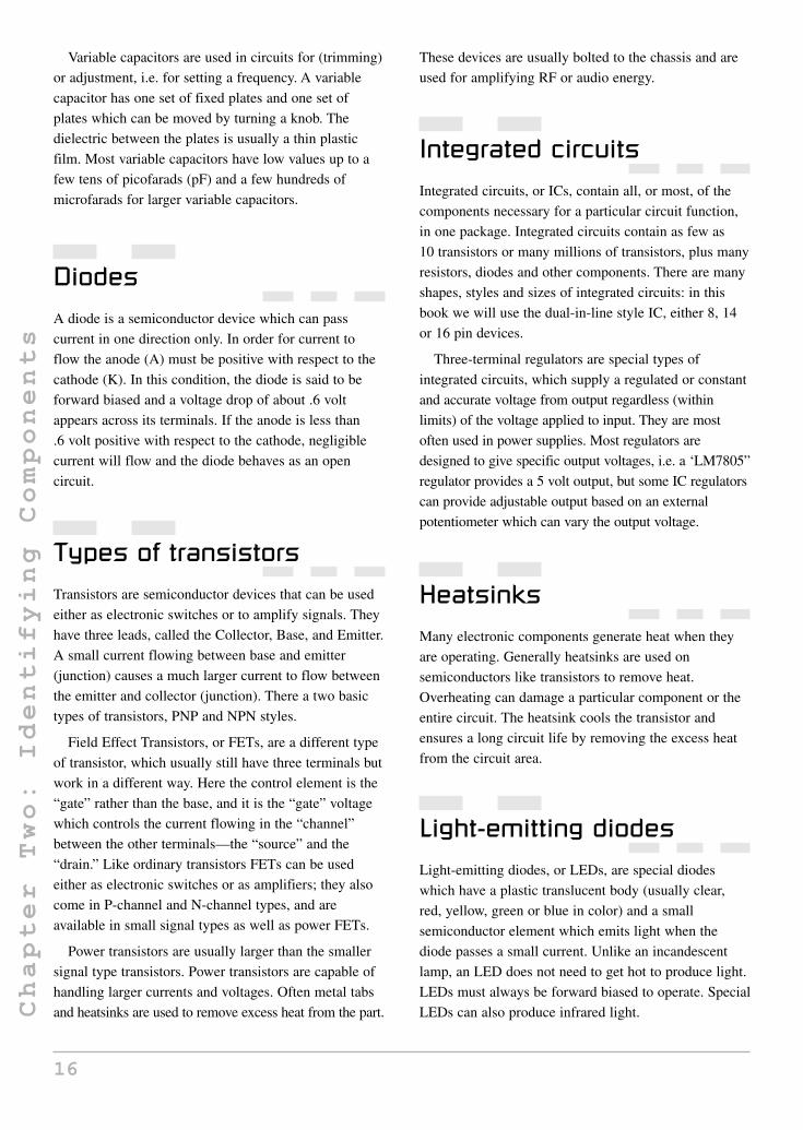
22 Radio ReceiverProjects for the
Evil Genius
New York Chicago San Francisco Lisbon London MadridMexico City Milan New Delhi San Juan Seoul
Singapore Sydney Toronto

Copyright © 2008 by The McGraw-Hill Companies, Inc. All rights reserved. Manufactured in the United States of America. Except as permitted underthe United States Copyright Act of 1976, no part of this publication may be reproduced or distributed in any form or by any means, or stored in a database or retrieval system, without the prior written permission of the publisher.
0-07-159475-2
The material in this eBook also appears in the print version of this title: 0-07-148929-0.
All trademarks are trademarks of their respective owners. Rather than put a trademark symbol after every occurrence of a trademarked name, we usenames in an editorial fashion only, and to the benefit of the trademark owner, with no intention of infringement of the trademark. Where such desig-nations appear in this book, they have been printed with initial caps.
McGraw-Hill eBooks are available at special quantity discounts to use as premiums and sales promotions, or for use in corporate training programs.For more information, please contact George Hoare, Special Sales, at [email protected] or (212) 904-4069.
TERMS OF USE
This is a copyrighted work and The McGraw-Hill Companies, Inc. (“McGraw-Hill”) and its licensors reserve all rights in and to the work. Use of thiswork is subject to these terms. Except as permitted under the Copyright Act of 1976 and the right to store and retrieve one copy of the work, you maynot decompile, disassemble, reverse engineer, reproduce, modify, create derivative works based upon, transmit, distribute, disseminate, sell, publishor sublicense the work or any part of it without McGraw-Hill’s prior consent. You may use the work for your own noncommercial and personal use;any other use of the work is strictly prohibited. Your right to use the work may be terminated if you fail to comply with these terms.
THE WORK IS PROVIDED “AS IS.” McGRAW-HILL AND ITS LICENSORS MAKE NO GUARANTEES OR WARRANTIES AS TO THEACCURACY, ADEQUACY OR COMPLETENESS OF OR RESULTS TO BE OBTAINED FROM USING THE WORK, INCLUDING ANYINFORMATION THAT CAN BE ACCESSED THROUGH THE WORK VIA HYPERLINK OR OTHERWISE, AND EXPRESSLY DISCLAIMANY WARRANTY, EXPRESS OR IMPLIED, INCLUDING BUT NOT LIMITED TO IMPLIED WARRANTIES OF MERCHANTABILITY ORFITNESS FOR A PARTICULAR PURPOSE. McGraw-Hill and its licensors do not warrant or guarantee that the functions contained in the work willmeet your requirements or that its operation will be uninterrupted or error free. Neither McGraw-Hill nor its licensors shall be liable to you or anyoneelse for any inaccuracy, error or omission, regardless of cause, in the work or for any damages resulting therefrom. McGraw-Hill has no responsibility for the content of any information accessed through the work. Under no circumstances shall McGraw-Hill and/or its licensors be liablefor any indirect, incidental, special, punitive, consequential or similar damages that result from the use of or inability to use the work, even if any ofthem has been advised of the possibility of such damages. This limitation of liability shall apply to any claim or cause whatsoever whether such claimor cause arises in contract, tort or otherwise.
DOI: 10.1036/0071489290

Thomas Petruzzellis is an electronics engineercurrently working at the geophysical laboratory atthe State University of New York, Binghamton.Also an instructor at Binghamton, with 30 years’experience in electronics, he is a veteran authorwho has written extensively for industrypublications, including Electronics Now, ModernElectronics, QST, Microcomputer Journal, andNuts & Volts. Tom wrote five previous books,
including an earlier volume in this series,Electronic Sensors for the Evil Genius. He is alsothe author of Create Your Own ElectronicsWorkshop; STAMP 2 Communications and ControlProjects; Optoelectronics, Fiber Optics, and LaserCookbook; Alarm, Sensor, and Security CircuitCookbook, all from McGraw-Hill. He lives inVestal, New York.
About the Author
About the Author
Copyright © 2008 by The McGraw-Hill Companies, Inc. Click here for terms of use.

This page intentionally left blank

Acknowledgments
I would like to thank the following people andcompanies listed below for their help in makingthis book possible. I would also like to thanksenior editor Judy Bass and all the folks atMcGraw-Hill publications who had a part inmaking this book possible. We hope the book willinspire both radio and electronics enthusiasts tobuild and enjoy the radio projects in this book.
Richard Flagg/RF Associates
Wes Greenman/University of Florida
Charles Higgins/Tennessee State University
Fat Quarters Software
Radio-Sky Publishing
Ramsey Electronics
Vectronics, Inc
Russell Clift
Todd Gale
Eric Vogel
Acknowledgments
Copyright © 2008 by The McGraw-Hill Companies, Inc. Click here for terms of use.

This page intentionally left blank

ix
Project 10 Experiments
Acknowledgments vii
Introduction xi
1 Radio Background and History 1
2 Identifying Components and Reading 12Schematics
3 Electronic Parts Installation and 25Soldering
4 AM, FM, and Shortwave Crystal 39Radio Projects
5 TRF AM Radio Receiver 49
6 Solid-State FM Broadcast Receiver 59
7 Doerle Single Tube Super-Regenerative 70Radio Receiver
8 IC Shortwave Radio Receiver 81
9 80/40 Meter Code Practice Receiver 94
10 WWV 10 MHz “Time-Code” Receiver 104
11 VHF Public Service Monitor 116(Action-Band) Receiver
12 6 & 2-Meter Band Amateur 127Radio Receiver
13 Active and Passive Aircraft Band 140Receivers
14 VLF or Very Low Frequency 153Radio Receiver
15 Induction Loop Receiving System 165
16 Lightning Storm Monitor 175
17 Ambient Power Receiver 186
18 Earth Field Magnetometer Project 192
19 Sudden Ionospheric Disturbance 203(SIDs) Receiver
20 Aurora Monitor Project 212
21 Ultra-Low Frequency (ULF) Receiver 224
22 Jupiter Radio Telescope Receiver 233
23 Weather Satellite Receiver 246
24 Analog to Digital Converters (ADCs) 262
Appendix: Electronic Parts Suppliers 273
Index 277
Contents
For more information about this title, click here

This page intentionally left blank

Introduction
xi
22 Radio Receiver Projects for the Evil Geniuswas created to inspire readers both young and oldto build and enjoy radio and receiver projects, andperhaps propel interested experimenters into acareer in radio, electronics or research. This bookis for people who are interested in radio andelectronics and those who enjoy building andexperimenting as well as those who enjoy research.
Radio encompasses many different avenues forenthusiasts to explore, from simple crystal radios tosophisticated radio telescopes. This book is anattempt to show electronics and radio enthusiasts thatthere is a whole new world “out there” to explore.
Chapter 1 will present the history andbackground and elements of radio, such asmodulation techniques, etc. Chapter 2 will help thenewcomers to electronics, identifying componentsand how to look and understand schematics vs.pictorial diagrams. Next, Chapter 3 will show thereaders how to install electronic components ontocircuit boards and how to correctly solder beforeembarking on their new radio building adventure.
We will start our adventure with the simple“lowly” crystal radio in Chapter 4. Generallycrystal radios are only thought of as simple AMradios which can only pickup local broadcaststations. But did you know that you can buildcrystal radios which can pickup long-distancestations as well as FM and shortwave broadcastsfrom around the world? You will learn how tobuild an AM, FM and shortwave crystal radio, inthis chapter.
In Chapter 5, you will learn how AM radio isbroadcast, from a radio station to a receiver in yourhome, and how to build your own TRF or TunedRadio Frequency AM radio receiver. In Chapter 6,we will discover how FM radio works and how tobuild an FM radio with an SCA output forcommercial free radio broadcasts.
Chapter 7 will present the exciting world ofshortwave radio. Shortwave radio listening has alarge following and encompasses an entire hobbyin itself. You will be able to hear shortwavestations from around the world, including China,Russia, Italy, on your new shortwave broadcastreceiver. Old time radio buffs will be interested inthe single tube Doerle super-regenerativeshortwave radio.
If you are interested in a portable shortwavereceiver that you could take on a camping trip,then you may want to construct the multi-bandintegrated circuit shortwave radio receiverdescribed in Chapter 8.
If you are interested in Amateur Radio or arethinking of learning Morse code or want toincrease your code speed, you may want toconsider building this 80 and 40-meter codereceiver. This small lightweight portable receivercan be built in a small enclosure and taken oncamping trips, etc.
In Chapter 10, you will learn how to build anduse a WWW time code receiver, which can be usedto pick up time signal broadcast from the NationalInstitute of Standards and Technology (NIST) or
Copyright © 2008 by The McGraw-Hill Companies, Inc. Click here for terms of use.

National Atomic Time Clock in Boulder CO. Timesignal broadcasts present geophysical andpropagation forecasts as well as marine and seaconditions. They will also help you set the time onyour best chronometer.
With the VHF Public service receiver featured inChapter 11, you will discover the high frequency“action bands” which cover the police, fire, taxis,highway departments and marine frequencies. Youwill be able to listen-in to all the excitingcommunications in your hometown.
The 6-meter and 2-meter dual VHF AmateurRadio receiver in Chapter 12 will permit todiscover the interesting hobby of Amateur Radio.The 6-meter and 2-meter ham radio bands are twoof the most popular VHF bands for technicianclass licensees. You may discover that you mightjust want to get you own ham radio license andtalk to ham radio operators through local VHFrepeaters or to the rest of the world.
Why not build an aircraft radio and listen-in toairline pilots talking from 747s to the control towermany miles away. You could also build the passiveAir-band radio which you use to listen-in to yourpilot during your own flight. Passive aircraft radioswill not interfere with airborne radio so they arepermitted on airplanes, without restriction. Checkout these two receivers in Chapter 13.
Chapter 14 will also show you how to build aninduction communication system, which will allowyou to broadcast a signal around home or officeusing a loop of wire, to a special inductionreceiver. The induction loop broadcast system is agreat aid to the hearing impaired, since it canbroadcast to hearing aids as well.
The VLF, or “whistler” radio in Chapter 15, willpickup very very low frequency radio waves fromaround the world. You will be able to listen to lowfrequency beacon stations, submarinetransmissions and “whistlers” or the radio wavescreated from electrical storms on the other side ofthe globe. This project is great for researchprojects where you can record and later analyze
your results by feeding your recorded signal into asound card running an FFT program. Use yourcomputer to record and analyze these interestingsignals. There are many free programs availableover the Internet. An FFT audio analyzer programcan display the audio spectrum and show youwhere the signals plot out in respect to frequency.
If you are interested in weather, then you willappreciate the Lightening to Storm Receiver inChapter 16, which will permit you to “see” theapproaching storm berfore it actually arrives. Thisreceiver will permit you to have advanced warningup to 50 miles or more away; it will warn you wellin advance of an electrical storm, so you candisconnect any outdoor antennas.
The Ambient Power Module receiver projectillustrated in Chapter 17, will allow to you pickupa broad spectrum of radio waves which getconverted to DC power, and which can be used topower low current circuits around your home oroffice. This is a great project for experimentationand research. You can use it to charge cell phones,emergency lights, etc.
Our magnetometer project shown in Chapter 18can be used to see the diurnal or daily changes inthe Earth’s magnetic field, and you can record theresult to a data-logger or recording multi-meter.
If you are an avid amateur radio operator orshortwave listener, you many want to build a SIDsreceiver shown in Chapter 19. A SIDs receiver canbe used to determine when radio signals and/orpropagation is disturbed by solar storms. Thisreceiver will quickly alert you to unfavorable radioconditions. You can collect the receiver to yourpersonal computer’s sound card and use the datarecorded to correlate radio propagation againststorm conditions.
The Aurora receiver project in Chapter 20 willalert you, with both sound and meter display, whenthe Earth’s magnetic increases just before anAurora display is about to take place. UFO andAlien contact buffs can use this receiver to knowwhen UFOs are close by.
xii
Introduction

xiii
For those interested in more earthly researchprojects, why not build your own ULF or ultra lowfrequently receiver, shown in Chapter 21, whichcan be utilized for detecting low frequency wavegenerated by earthquakes and fault lines. With thisreceiver you will be able to conduct your ownresearch projects on monitoring the pulse of theEarth. You can connect your ELF receiver to adata-logger and record the signals over time tocorrelate your research with that of others.
You can explore the heavens by constructingyour own radio telescope to monitor the radiosignals generated from the planet Jupiter. Thisradio receiver, illustrated in Chapter 22, will pickup radio signals which indicate electrical and ormagnetic storms on the Jovian planet. The RadioJupiter receiver can be coupled to your personal
computer, and can be used for a research project torecord and analyze these radio storm signals.
Why not construct your own weather satellitereceiving station, shown in Chapter 23. Thisreceiver will allow you to receive APT polarsatellites broadcasting while passing overhead. Youcan display the satellite weather maps on thecomputer’s screen or save them later to showfriends and relatives.
Chapter 24 discusses different analog to digitalconverters which you can use to collect and recorddata from the different receiver projects.
We hope you will find the 22 Radio Projects forthe Evil Genius a fun and thought-provoking book,that will find a permanent place on yourelectronics or radio bookshelf. Enjoy!
Introduction

This page intentionally left blank

22 Radio ReceiverProjects for the Evil
Genius

This page intentionally left blank

Radio Background and History
Chapter 1
Electromagnetic energy encompasses an extremely wide
frequency range. Radio frequency energy, both natural
radio energy created by lightning and planetary storms
as well as radio frequencies generated by man for
communications, entertainment, radar, and television
are the topic of this chapter. Radio frequency energy,
or RF energy, covers the frequency range from the low
end of the radio spectrum, around l0 to 25 kHz, which
is used by high-power Navy stations that communicate
with submerged nuclear submarines, through the
familiar AM broadcast band from 550 to 1600 kHz.
Next on the radio frequency spectrum are the shortwave
bands from 2000 kHz to 30,000 kHz. The next band of
frequencies are the very high frequency television
channels covering 54 to 2l6 MHz, through the very
popular frequency modulation FM band from 88 to
l08 MHz. Following the FM broadcast band are aircraft
frequencies on up through UHF television channels and
then up through the radar frequency band of 1000 to
1500 MHz, and extending through approximately
300 gHz. See frequency spectrum chart in Figure 1-1.
The radio frequency spectrum actually extends almost
up to the lower limit of visible light frequencies.
Radio historyOne of the more fascinating applications of electricity is
in the generation of invisible ripples of energy called
radio waves. Following Hans Oersted’s accidental
discovery of electromagnetism, it was realized that
electricity and magnetism were related to each other.
When an electric current was passed through a conductor,
a magnetic field was generated perpendicular to the axis
of flow. Likewise, if a conductor was exposed to a
change in magnetic flux perpendicular to the conductor,
a voltage was produced along the length of that
conductor.
Joseph Henry, a Princeton University professor, and
Michael Faraday, a British physicist, experimented
separately with electromagnets in the early 1800s. They
each arrived at the same observation: the theory that a
current in one wire can produce a current in another
wire, even at a distance. This phenomenon is called
electromagnetic induction, or just induction. That is,
one wire carrying a current induces a current in a
second wire. So far, scientists knew that electricity
and magnetism always seemed to affect each other at
right angles. However, a major discovery lay hidden
just beneath this seemingly simple concept of related
perpendicularity, and its unveiling was one of the
pivotal moments in modern science.
The man responsible for the next conceptual
revolution was the Scottish physicist James Clerk
Maxwell (1831–1879), who “unified” the study of
electricity and magnetism in four relatively tidy
equations. In essence, what he discovered was that
electric and magnetic fields were intrinsically related
to one another, with or without the presence of a
conductive path for electrons to flow. Stated more
formally, Maxwell’s discovery was this: a changing
electric field produces a perpendicular magnetic field,
and a changing magnetic field produces a perpendicular
electric field. All of this can take place in open space,
the alternating electric and magnetic fields supporting
each other as they travel through space at the speed of
light. This dynamic structure of electric and magnetic
fields propagating through space is better known as an
electromagnetic wave.
Later, Heinrich Hertz, a German physicist, who is
honored by our replacing the expression “cycles per
second” with hertz (Hz), proved Maxwell’s theory
between the years 1886 and l888. Shortly after that, in
1892, Eouard Branly, a French physicist, invented a
device that could receive radio waves (as we know them
today) and could cause them to ring an electric bell.
1Copyright © 2008 by The McGraw-Hill Companies, Inc. Click here for terms of use.

2
Note that at the time all the research being conducted in
what was to become radio and later radio-electronics,
was done by physicists.
In 1895, the father of modem radio, Guglielmo
Marconi, of Italy, put all this together and developed
the first wireless telegraph and was the first to
commercially put radio into ships. The wire telegraph
had already been in commercial use for a number of
years in Europe. The potential of radio was finally
realized through one of the most memorable events
in history. With the sinking of the Titanic in 1912,
communications between operators on the sinking
ship and nearby vessels, and communications to shore
stations listing the survivors brought radio to the public
in a big way.
AM radio broadcasting began on November 2, 1920.
Four pioneers: announcer Leo Rosenberg, engineer
William Thomas, telephone line operator John Frazier
and standby R.S. McClelland, made their way to a
makeshift studio—actually a shack atop the Westinghouse
“K” Building in East Pittsburgh—flipped a switch and
began reporting election returns in the Harding vs. Cox
Presidential race. At that moment, KDKA became the
pioneer broadcasting station of the world.
Radio spread like wildfire to the homes of everyone
in America in the 1920s. In a few short years, over
75 manufacturers began selling radio sets. Fledgling
manufacturers literally came out of garages over-night.
Many young radio enthusiasts rushed out to buy parts
and radio kits which soon became available.
Radio experimenters discovered that an amplitude-
modulated wave consists of a carrier and two identical
sidebands which are both above and below the carrier
wave. The Navy conducted experiments in which they
attempted to pass one sideband and attenuate the
other. These experiments indicated that one sideband
contained all the necessary information for voice
transmission, and these discoveries paved the way for
development of the concept of single-sideband or SSB
transmission and reception.
In 1923, a patent was granted to John R. Carson on
his idea to suppress the carrier and one sideband.
In that year the first trans-Atlantic radio telephone
demonstration used SSB with pilot carrier on a
frequency of 52 kc. Single sideband was used because of
limited power capacity of the equipment and the narrow
bandwidths of efficient antennas for those frequencies.
By 1927, trans-Atlantic SSB radiotelephony was open
for public service. In the following years, the use of SSB
was limited to low-frequency and wire applications.
Early developments in FM transmission suggested that
this new mode might prove to be the ultimate in voice
communication. The resulting slow development of SSB
technology precluded practical SSB transmission and
reception at high frequencies. Amateur radio SSB
activity followed very much the same pattern. It wasn’t
until 1948 that amateurs began seriously experimenting
with SSB, likely delayed by the wartime blackouts.
The breakthroughs in the war years, and those
following the war, were important to the development of
HF-SSB communication. Continued advances inChapter One: Radio Background and History
wavelength (λ) in metres
LONGWAVELENGTHLOWFREQUENCY
Radiowaves
frequency (ν) in hertz
Radar
Microwaves
Infrared
VISIBLE LIGHT
RED
1 m104
104 106 108 1010 1012 1014 1016 1018 1020 1022
102 10−2 10−4 10−6 10−8 10−10 10−12 10−14
VIOLET
X-rays
Gammarays SHORT
WAVELENGTHHIGH
FREQUENCY
Ultraviolet
Figure 1-1 Electromagnetic spectrum

technology made SSB the dominant mode of HF radio
communication.
The radio-frequency spectrum, once thought to be
adequate for all needs, has become very crowded.
As the world’s technical sophistication progresses,
the requirements for rapid and dependable radio
communications increase. The competition for available
radio spectrum space has increased dramatically.
Research and development in modern radio systems has
moved to digital compression and narrow bandwidth
with highly developed modulation schemes and satellite
transmission.
The inventor most responsible for the modern day
advances in radio systems was Edwin H. Armstrong.
He was responsible for the Regenerative circuit in 1912,
the Superheterodyne radio circuit in 1918, the
Superregenerative radio circuit design in 1922 and
the complete FM radio system in 1933. His inventions
and developments form the backbone of radio
communications as we know it today. The majority of
all radio sets sold are FM radios, all microwave relay
links are FM, and FM is the accepted system in all
space communications. Unfortunately, Armstrong
committed suicide while still embittered in patent
lawsuits: later vindicated, his widow received a windfall.
Sony introduced their first transistorized radio in
1960, small enough to fit in a vest pocket, and able to
be powered by a small battery. It was durable, because
there were no tubes to burn out. Over the next 20 years,
transistors displaced tubes almost completely except for
very high power, or very high frequency, uses. In the
1970s; LORAN became the standard for radio navigation
system, and soon, the US Navy experimented with
satellite navigation. Then in 1987, the GPS constellation
of satellites was launched and navigation by radio in the
sky had a new dimension. Amateur radio operators began
experimenting with digital techniques and started to send
pictures, faxes and teletype via the personal computer
through radio. By the late 1990s, digital transmissions
began to be applied to radio broadcasting.
Types of radio wavesThere are many kinds of natural radiative energy
composed of electromagnetic waves. Even light is
electromagnetic in nature. So are shortwaves, X-rays
and “gamma” ray radiation. The only difference
between these kinds of electromagnetic radiation is the
frequency of their oscillation (alternation of the electric
and magnetic fields back and forth in polarity).
By using a source of AC voltage and a device called
an antenna, we can create electromagnetic waves.
It was discovered that high frequency electromagnetic
currents in an antenna wire, which in turn result in a
high frequency electromagnetic field around the
antenna, will result in electromagnetic radiation
which will move away from the antenna into free
space at the velocity of light, which is approximately
300,000,000 meters per second.
In radio transmission, a radiating antenna is used
to convert a time-varying electric current into an
electromagnetic wave, which freely propagates through
a nonconducting medium such as air or space.
An antenna is nothing more than a device built to
produce a dispersing electric or magnetic field.
An electromagnetic wave, with its electric and magnetic
components, is shown in Figure 1-2.
When attached to a source of radio frequency signal
generator, or transmitter, an antenna acts as a transmitting
device, converting AC voltage and current into
electromagnetic wave energy. Antennas also have the
ability to intercept electromagnetic waves and convert
their energy into AC voltage and current. In this mode,
an antenna acts as a receiving device.
Radio frequenciesspectrumRadio frequency energy is generated by man for
communications, entertainment, radar, television,
3
Chapter One: Radio Background and Historyλ=Wavelength
Electric field
Magneticfield Direction
Figure 1-2 Magnetic vs. electric wave

navigation, etc. This radio frequency or (RF) energy
covers quite a large range of radio frequencies from the
low end of the radio spectrum from l0 to 25 kHz, which
is the domain occupied by the high-power Navy stations
that communicate with submerged nuclear submarines:
these frequencies are called Very Low Frequency waves
or VLF. Above the VLF frequencies are the medium
wave frequencies or (MW), i.e. the AM radio broadcast
band from 550 to 1600 kHz. The shortwave bands or
High Frequency or (HF) bands cover from 2000 kHz to
30,000 kHz and make use of multiple reflections from
the ionosphere which surrounds the Earth, in order to
propagate the signals to all parts of the Earth. The Very
High Frequencies or VHF bands begin around 30 MHz;
these lower VHF frequencies are called low-band VHF.
Mid-band VHF frequencies begin around 50 MHz
which cover the lowest TV channel 2. Low-band
television channels 2 through 13 cover the 54 to 2l6 MHz
range. The popular frequency modulation or (FM)
broadcast band covers the range from 88 to l08 MHz,
which is followed by low-band Air-band frequencies
from 118 to 136 MHz. High-band VHF frequencies
around 144 are reserved for amateur radio, public service
around 150 MHz, with marine frequencies around
156 MHz. UHF frequencies begin around 300 MHz
and go up through the radar frequency band of 1000 to
1500 MHz, and extending through approximately
300 gHz. Television channels 14 through 70 are placed
between 470 and 800 MHz. American cell phone
carriers have cell phone communications around
850 MHz. Geosynchronous weather satellites signals
are placed around 1.6 GHz, and PCS phone devices
are centered around 1.8 GHz. The Super-high frequency
(SHF) bands range from 3 to 30 GHz, with C-band
microwave frequencies around 3.8 GHz, then X-band,
from 7.25 to 8.4 GHz, followed by the KA and
KU-band microwave bands.
Table 1-1 illustrates the division of radio frequencies.
The radio frequency spectrum extends almost up to the
lower limit of visible light frequencies, with just the
infrared frequencies lying in between it and visible light.
The radio frequency spectrum is a finite resource which
must be used and shared with many people and agencies
around the world, so cooperation is very important.
So how does a radio work? As previously mentioned,
radio waves are part of a general class of waves known
as electromagnetic waves. In essence, they are electrical
and magnetic energy which travels through space in the
form of a wave. They are different from sound waves
(which are pressure waves that travel through air or
water, as an example) or ocean waves (similar to sound
waves in water, but much lower in frequency and are
much larger). The wave part is similar, but the energy
involved is electrical and magnetic, not mechanical.
Electromagnetic waves show up as many things.
At certain frequencies, they show up as radio waves.
At much higher frequencies, we call them infrared light.
Still higher frequencies make up the spectrum known as
visible light. This goes on up into ultraviolet light, and
X-rays, things that radio engineers rarely have to worry
about. For our discussions, we’ll leave light to the
physicists, and concentrate on radio waves.
Radio waves have two important characteristics that
change. One is the amplitude, or strength of the wave.
This is similar to how high the waves are coming into
shore from the ocean. The bigger wave has a higher
amplitude. The other thing is frequency. Frequency is
how often the wave occurs at any point. The faster the
wave repeats itself, the higher the frequency. Frequency
is measured by the number of times in a second that the
wave repeats itself. Old timers remember when frequency
was described in units of cycles per second. In more
recent times we have taken to using the simplified term
of hertz (named after the guy who discovered radio
waves). Metric prefixes are often used, so that 1000 hertz
is a kilohertz, one million hertz is a megahertz, and so on.
A typical radio transmitter, for example, takes an
audio input signal, such as voice or music and amplifies
it. The amplified audio is in turn sent to a modulator
and an RF exciter which comprises the radio frequency
transmitter. The exciter in the transmitter generates a
main carrier wave. The RF signal from the exciter is
further amplified by a power amplifier and then the RF
signal is sent out to an antenna which radiates the signal
into the sky and out into the ionosphere. Depending
upon the type of transmitter used the modulation
technique can be either AM, FM, SSB signal sideband,
CW, or digital modulation, etc.
AM modulationAmplitude modulation (AM) is a technique used in
electronic communication, most commonly for
transmitting information via a carrier wave wirelessly.
4
Chapter One: Radio Background and History

It works by varying the strength of the transmitted
signal in relation to the information being sent.
In the mid-1870s, a form of amplitude modulation
was the first method to successfully produce quality
audio over telephone lines. Beginning in the early
1900s, it was also the original method used for audio
radio transmissions, and remains in use by some forms
of radio communication—“AM” is often used to refer
to the medium-wave broadcast band (see AM
Radio–Chapter 5).
Amplitude modulation (AM) is a type of modulation
technique used in communication. It works by varying
5
Chapter One: Radio Background and History
Table 1-1Radio frequency spectrum chart
Frequency range
Extremely Low Frequency (ELF) 0 to 3 kHz
Very Low Frequency (VLF) 3 kHz to 30 kHz
Radio Navigation & maritime/aeronautical mobile 9 kHz to 540 kHz
Low Frequency (LF) 30 kHz to 300 kHz
Medium Frequency (MF) 300 kHz to 3000 kHz
AM Radio Broadcast 540 kHz to 1630 kHz
Travellers Information Service 1610 kHz
High Frequency (HF) 3 MHz to 30 MHz
Shortwave Broadcast Radio 5.95 MHz to 26.1 MHz
Very High Frequency (VHF) 30 MHz to 300 MHz
Low Band: TV Band 1 - Channels 2-6 54 MHz to 88 MHz
Mid Band: FM Radio Broadcast 88 MHz to 174 MHz
High Band: TV Band 2 - Channels 7-13 174 MHz to 216 MHz
Super Band (mobile/fixed radio & TV) 216 MHz to 600 MHz
Ultra-High Frequency (UHF) 300 MHz to 3000 MHz
Channels 14-70 470 MHz to 806 MHz
L-band: 500 MHz to 1500 MHz
Personal Communications Services (PCS) 1850 MHz to 1990 MHz
Unlicensed PCS Devices 1910 MHz to 1930 MHz
Superhigh Frequencies (SHF)
(Microwave) 3 GHz to 30.0 GHz
C-band 3600 MHz to 7025 MHz
X-band 7.25 GHz to 8.4 GHz
Ku-band 10.7 GHz to 14.5 GHz
Ka-band 17.3 GHz to 31.0 GHz
Extremely High Frequencies (EHF)
(Millimeter Wave Signals) 30.0 GHz to 300 GHz
Additional Fixed Satellite 38.6 GHz to 275 GHz
Infrared Radiation 300 GHz to 430 THz
Visible Light 430 THz to 750 THz
Ultraviolet Radiation 1.62 PHz to 30 PHz
X-Rays 0.30 PHz to 30 EHz
Gamma Rays 0.30 EHz to 3000 EHz

the strength of the transmitted signal in relation to the
information being sent, for example, changes in the
signal strength can be used to reflect sounds being
reproduced in the speaker. This type of modulation
technique creates two sidebands with the carrier wave
signal placed in the center between the two sidebands.
The transmission bandwidth of AM is twice the signal’s
original (baseband) bandwidth—since both the positive
and negative sidebands are ‘copied’ up to the carrier
frequency, but only the positive sideband is present
originally. See Figure 1-3. Thus, double-sideband AM
(DSB-AM) is spectrally inefficient. The power
consumption of AM reveals that DSB-AM with its
carrier has an efficiency of about 33% which is too
efficient. The benefit of this system is that receivers are
cheaper to produce. The forms of AM with suppressed
carriers are found to be 100% power efficient, since no
power is wasted on the carrier signal which conveys no
information. Amplitude modulation is used primarily in
the medium wave band or AM radio band which covers
520 to 1710 kHz. AM modulation is also used by
shortwave broadcasters in the SW bands from between
5 MHz and 24 MHz, and in the aircraft band which
covers 188 to 136 MHz.
FM modulationFrequency modulation (FM) is a form of modulation
which represents information as variations in the
instantaneous frequency of a carrier wave. Contrast this
with amplitude modulation, in which the amplitude
of the carrier is varied while its frequency remains
constant. In analog applications, the carrier frequency is
varied in direct proportion to changes in the amplitude
of an input signal. Digital data can be represented by
shifting the carrier frequency among a set of discrete
values, a technique known as frequency-shift keying.
The diagram in Figure 1-4, illustrates the FM modulation
scheme, the RF frequency is varied with the sound input
rather than the amplitude.
FM is commonly used at VHF radio frequencies
for high-fidelity broadcasts of music and speech,
as in FM broadcasting. Normal (analog) TV sound is
also broadcast using FM. A narrowband form is used
for voice communications in commercial and amateur
radio settings. The type of FM used in broadcast is
generally called wide-FM, or W-FM. In two-way radio,
narrowband narrow-FM (N-FM) is used to conserve
bandwidth. In addition, it is used to send signals
into space.
Wideband FM (W-FM) requires a wider bandwidth
than amplitude modulation by an equivalent modulating
signal, but this also makes the signal more robust against
noise and interference. Frequency modulation is also
more robust against simple signal amplitude fading
phenomena. As a result, FM was chosen as the
modulation standard for high frequency, high fidelity
radio transmission: hence the term “FM radio.”
FM broadcasting uses a well-known part of the VHF
band between 88 and 108 MHz in the USA.
FM receivers inherently exhibit a phenomenon
called capture, where the tuner is able to clearly
receive the stronger of two stations being broadcast on
6
Chapter One: Radio Background and History
Figure 1-3 Amplitude modulation waveform

the same frequency. Problematically, however,
frequency drift or lack of selectivity may cause one
station or signal to be suddenly overtaken by another
on an adjacent channel. Frequency drift typically
constituted a problem on very old or inexpensive
receivers, while inadequate selectivity may plague
any tuner. Frequency modulation is used on the FM
broadcast band between 88 and 108 MHz as well as in
the VHF and UHF bands for both public service and
amateur radio operators.
Single sideband (SSB)modulationSingle sideband modulation (SSB) is a refinement upon
amplitude modulation, which was designed to be more
efficient in its use of electrical power and spectrum
bandwidth. Single sideband modulation avoids this
bandwidth doubling, and the power wasted on a carrier,
but the cost of some added complexity.
The balanced modulator is the most popular method
of producing a single sideband modulated signal. The
balanced modulator provides the “sidebands” of energy
that exist on either side of the carrier frequency but
eliminates the RF carrier, see Figure 1-5. The carrier is
removed because it is the sidebands that provide the
actual meaningful content of material, within the
modulation envelope. In order to make SSB even more
efficient, one of these two sidebands is removed by a
bandpass. So the intelligence is preserved with SSB
and it becomes a more efficient use of radio spectrum
energy. It provides almost 9 Decibels (dBs) of signal
gain over an amplitude modulated signal that includes
an RF “carrier” of the same power level! As the final
RF amplification is now concentrated in a single
sideband, the effective power output is greater than in
normal AM (the carrier and redundant sideband
account for well over half of the power output of
an AM transmitter). Though SSB uses substantially
less bandwidth and power, it cannot be demodulated
by a simple envelope detector like standard AM.
SSB was pioneered by telephone companies in the
1930s for use over long-distance lines, as part of a
technique known as frequency-division multiplexing
(FDM). This enabled many voice channels to be sent
down a single physical circuit. The use of SSB meant
that the channels could be spaced (usually) just 4000 Hz
apart, while offering a speech bandwidth of nominally
300–3400 Hz. Amateur radio operators began to
experiment with the method seriously after World War II.
It has become a de facto standard for long-distance
voice radio transmissions since then.
7
Chapter One: Radio Background and History
Figure 1-4 FM modulation waveform

Single Sideband Suppressed Carrier (SSB-SC)
modulation was the basis for all long-distance telephone
communications up until the last decade. It was
called “L carrier.” It consisted of groups of telephone
conversations modulated on upper and/or lower
sidebands of contiguous suppressed carriers. The
groupings and sideband orientations (USB, LSB)
supported hundreds and thousands of individual
telephone conversations. Single sideband communications
are used by amateur radio operators and government,
and utility stations primarily in the shortwave bands for
long-distance communications.
Shortwave radioShortwave radio operates between the frequencies of
1.80 MHz and 30 MHz and came to be referred to as
such in the early days of radio because the wavelengths
associated with this frequency range were shorter than
those commonly in use at that time. An alternate name is
HF or high frequency radio. Short wavelengths are
associated with high frequencies because there is an
inverse relationship between frequency and wavelength.
Shortwave frequencies are capable of reaching the other
side of the Earth, because these waves can be refracted by
the ionosphere, by a phenomenon known as Skywave
propagation. High-frequency propagation is dependent upon
a number of different factors, such as season of the year,
solar conditions, including the number of sunspots, solar
flares, and overall solar activity. Solar flares can prevent the
ionosphere from reflecting or refracting radio waves.
Another factor which determines radio propagation is
the time of the day; this is due to a particular transient
atmosphere ionized layer forming only during day when
atoms are broken up into ions by sun photons. This layer
is responsible for partial or total absorption of particular
frequencies. During the day, higher shortwave frequencies
(i.e., above 10 MHz) can travel longer distances than
lower ones; at night, this property is reversed.
Different types of modulation techniques are used on
the shortwave frequencies in addition to AM and FM.
AM, amplitude modulation, is generally used for
shortwave broadcasting, and some aeronautical
communications, while Narrow-band frequency
modulation (NFM) is used at the higher HF frequencies.
Single sideband or (SSB), is used for long-range
communications by ships and aircraft, for voice
transmissions by amateur radio operators. CW,
Continuous Carrier Wave or (CW), is used for Morse
code communications. Various other types of digital
communications such as radioteletype, fax, digital,
SSTV and other systems require special hardware and
software to decode. A new broadcasting technique
called Digital Radio Mondiale or (DRM) is a digital
modulation scheme used on bands below 30 MHz.
Shortwave listeningMany hobbyists listen to shortwave broadcasters and for
some listeners the goal is to hear as many stations from
as many countries as possible (DXing); others listen to
specialized shortwave utility, or “UTE,” transmissions
8
Chapter One: Radio Background and History
Figure 1-5 Single sideband modulation waveform

such as maritime, naval, aviation, or military signals.
Others focus on intelligence signals. Many, though,
tune the shortwave bands for the program content of
shortwave broadcast stations, aimed to a general
audience (such as the Voice of America, BBC World
Service, Radio Australia, etc.). Some even listen to
two-way communications by amateur radio operators.
Nowadays, as the Internet evolves, the hobbyist can
listen to shortwave signals via remotely controlled
shortwave receivers around the world, even without
owning a shortwave radio (see for example
http://www.dxtuners.com). Alternatively, many
international broadcasters (such as the BBC) offer live
streaming audio on their web-sites. Table 1-2, lists some
of the popular shortwave broadcast bands.
Shortwave listeners, or SWLs, can obtain QSL cards
from broadcasters, utility stations or amateur radio
operators as trophies of the hobby. Some stations
even give out special certificates, pennants, stickers
and other tokens and promotional materials to
shortwave listeners.
Major users of the shortwave radio bands include
domestic broadcasting in countries with a widely
dispersed population with few long-wave, medium-wave,
or FM stations serving them. International broadcasting
stations beamed radio broadcasts to foreign audiences.
Speciality political, religious, and conspiracy
theory radio networks, individual commercial and
non-commercial paid broadcasts for the north American
and other markets. Utility stations transmitting
messages not intended for a general public, such as
aircraft flying between continents, encoded or ciphered
diplomatic messages, weather reporting, or ships at
sea. Amateur radio operators have rights to use many
frequencies in the shortwave bands; you can hear their
communications using different modulation techniques
and even obtain a license to communicate in these
bands yourself. Contact the Amateur Radio Relay
League for more information. Table 1-3 illustrates the
amateur radio frequencies and how they are divided
between the different license classes. On the shortwave
band you will also encounter time signal stations and
number stations, thought to be spy stations operating on
the shortwave bands.
Types of receiversA radio signal is transmitted through the ionosphere
and is picked up by the antenna in your radio receiver.
The antenna is fed to an RF amplifier and usually an
intermediate amplifier or IF amplifier and then on to a
detector of some sort depending upon the type of
receiver you are using. From the detector, the resultant
audio signal is amplified and sent to a loudspeaker for
listening. Figure 1-6 illustrates a block diagram of a
typical AM radio receiver. The antenna is sent to the RF
amplifier. The mixer is fed by both the local oscillator
and the RF amplifier. The signal from the mixer is sent
to a bandpass filter and then on to the first IF amplifier.
The first IF amplifier is next sent to the detector and
then on to the final audio amplifier stage which drives
the speaker. The illustration depicted in Figure 1-7
shows a typical FM receiver block diagram. The antenna
feeds the RF amplifier stage. Both the RF amplifier and
local oscillator are fed into the mixer. The signal from
the mixer is next sent to the IF amplifier stage. From
the IF amplifier stage the signal is next sent to the FM
demodulator section, which feeds the signal to the
voltage amplifier and then the signal is fed to the final
audio amplifier stage and on to the speaker. Note the
feedback path between, i.e. the AGC or automatic
frequency control from the FM demodulator back to
9
Chapter One: Radio Background and History
Table 1-2Shortwave broadcast chart
MegahertzBand Band (MHz) Kilohertz (KHz)
120 Meter 2.3–2.5 MHz 2300–2500 KHz
90 Meter 3.2–3.40 MHZ 3200–3400 KHz
75 Meter 3.90–4.00 MHZ 3900–4000 KHz
60 Meter 4.750–5.060 MHz 4750–5060 KHz
49 Meter 5.950–6.20 MHz 5950–6200 KHz
41 Meter 7.10–7.60 MHz 7100–7600 KHz
31 Meter 9.20–9.90 MHz 9500–9900 KHz
25 Meter 11.60–12.200 MHz 11600–12200 KHz
22 Meter 13.570–13.870 MHZ 13570–13870 KHz
19 Meter 15.10–15.800 MHz 15100–15800 KHz
16 Meter 17.480–17.900 MHz 17480–17900 KHz
13 Meter 21.450–21.850 MHz 21450–21850 KHz
11 Meter 25.60–26.100 MHz 25600–26100 KHz

the local oscillator. Finally, the shortwave radio block
diagram is illustrated in the diagram in Figure 1-8. The
antenna line is fed to the RF amplifier section. Both the
local oscillator and the RF amplifier are fed to a filter
section, which is in turn sent to the IF amplifier section.
The output signal from the IF amplifier section is next
sent to the product detector. A BFO or beat frequency
oscillator signal is sent to the product detector, this is
what permits SSB reception. The signal from the
product detector is next sent to the audio amplifier and
then on to the speaker. The receivers shown are the
most common types of receivers. There are in fact
many different variations in receiver designs including
receivers made to receive special digital signals, which
we will not discuss here.
Next, we will move our discussion to identifying
electronics components and reading schematics
and learning how to solder before we forge
ahead and begin building some fun radio receiver
projects.
10
Chapter One: Radio Background and History
Amateur stations operating at 1900-2000 kHz must not causeharmful interference to the radiolocation service and areafforded no protection from radiolocation operations.
1800
3525
70257100 7150
7225
3500 3750 4000
7000 7150 7300
3675 3725
3775
3850
1900 2000 kHz
kHz
kHz
G
N,P*
A
E
G †
N,P*
N,P*
A †
E †
G
A
E
G
A
E
E,A,G
E,A,G,P,T*
E,A,G,P,T*
E,A,G,P,T*
E,A,G,P,T,N*
MHz.
N
MHz.
MHz.
MHz.
MHz.
MHz.
kHz.
kHz.
E,A,G,P,T*
E,A,G,P,T*
N,P*
E,A,G
E,A,G
160 Meters
12 Meters
10 Meters
24,890
28,50028,100
24,930 24,990
29,70028,30028,000
50.1
50.0
144.1
144.0 145.0
225.0222.0
420.0 450.0
928.0902.0
1270 1295
13001240
54.0
6 Meters
2 Meters
1.25 Meters ***
70 Centimeters **
33 Centimeters **
23 Centimeters **
US AMATEUR POWER LIMITS
Novice, Advanced and Technician Plus Allocations
80 Meters
60 Meters
40 Meters
30 Meters
20 Meters
17 Meters
15 Meters
General, Advanced and Amateur Extra licensees may use the followingfive channels on a secondary basis with a maximum effective radiatedpower of 50 W PEP relative to a half wave dipole. Only upper sidebandsuppressed carrier voice transmissions may be used.The frequencies are 5330.5, 5345.5, 5355.5, 5371.5 and 5403.5kHz. The occupiedbandwidth is limited to 2.8kHz centered on 5332, 5345, 5355, 5373and 5405 kHz respectively.
Novices and Technician Plus Licensees are limited to200 watts PEP output on 10 meters.
New Novice, Advanced and Technician Plus licenses are no longer being issued, but existing Novice,Technician Plus and Advanced class licenses are unchanged. Amateurs can continue to renew theselicenses. Technician who pass the 5 wpm Morse code exam after that date have Technician Plus privileges, although their license says Technician. They must retain the 5 wpm Certificate of SuccessfulCompletion of Examination (CSCE) as proof. The CSCE is valid indefinitely for operating authorization,but is valid only for 365 days for upgrade credit.
At all times, transmitter powershould be kept down to thatnecessary to carry out thedesired communications. Poweris rated in watts PEP output.Unless otherwise stated, the maximum power output is1500W.Power for all license classes is limited to 200 W in the 10,100- 10,150 kHz band and in allNovice subbands below 28,100kHz.Novices and Technicians arerestricted to 200 W in the 28,100-28,500 kHz subbands. In addition, Novices are restricted to25 W in the 222-225 MHz band and 5 W in the 1270-1295 MHz subband.
KEY
= CW, RTTY and data
= CW only
E = AMATEUR EXTRAA = ADVANCEDG = GENERAL
T = TECHNICIANP = TECHNICIAN PLUS
N = NOVICE*Technicians who have passed the 5 wpm Morse code exam are indicated as "P".
**Geographical and power restrictions apply to all bands with frequencies above 420MHz. See The ARRL FCC Rule Book for more information about your area.
***219-220 MHz allocated to amateurs on a secondary basis for fixed digital message forwarding systems only and can be operated by all licensees except Novices.
All licensees except Novices are authorized all modes on thefollowing frequencies:2300-2310 MHz2390-2450 MHz3300-3500 MHz5650-5925 MHz10.0-10.5 GHz24.0-24.25 GHz47.0-47.2 GHz76.0-81.0 GHz122.225-123.0 GHz134-141 GHz241-250 GHzAll above 275 GHz
= CW, RTTY, data, phone
= CW, RTTY, data MCW,
= CW, phone and image
= CW and SSB phone
Novices are limitted to 25 watts PEP output from 222 to 225 MHz.
Novices are limited to 5 watts PEP output from 1270 to 1295 MHz.
Phone and image modes are permitted between 7075 and 7100 kHz for FCC licensed stations in ITU Regions 1 and 3 and by FCC licensed stations in ITU Region 2 West of 130 degrees West longitude or South of 20 degrees North latitude. See sections 97.305(c) and 97.307(f)(11). Novice and Technician Plus licensees outside ITU Region2 may use CW only between 7050 and 7075 kHz. See Section 97.301(e).These exemptions do not apply to stations in the continental US.
Maximum power on 30 meters is 200 watts PEP output.Amateurs must avoid interference to the fixed service outside the US.
kHz
kHz
kHz
kHz
10,15010,100
14,025
14,000
18,068 18,110
21,100 21,200
21,300
21,225
21,45021,20021,000
21,025
18,168
14,150
14,150
14,175
14,225
14,350
E,A,G
E,A,G
†
test, phone and image
and image
Table 1-3US amateur radio bands

11
Chapter One: Radio Background and History
Figure 1-6 AM radio block diagram
Figure 1-8 SSB shortwave receiver block diagram
Figure 1-7 FM radio block diagram

Identifying Components and Reading Schematics
Chapter 2
Identifying electroniccomponentsIf you are a beginner to electronics or radio, you may
want to take a few minutes to learn a little about
identifying electronic components, reading schematics,
and installing electronic components on a circuit board.
You will also learn how to solder, in order to make
long-lasting and reliable solder joints.
Electronic circuits comprise electronic components
such as resistors and capacitors, diodes, semiconductors
and LEDs, etc. Each component has a specific purpose
that it accomplishes in a particular circuit. In order to
understand and construct electronic circuits it is
necessary to be familiar with the different types of
components, and how they are used. You should also
know how to read resistor and capacitor color codes,
recognize physical components and their representative
diagrams and pin-outs. You will also want to know the
difference between a schematic and a pictorial diagram.
First, we will discuss the actual components and their
functions and then move on to reading schematics,
then we will help you to learn how to insert the
components into the circuit board. In the next chapter
we will discuss how to solder the components to the
circuit board.
The diagrams shown in Figures 2-1, 2-2 and 2-3
illustrate many of the electronic components that we
will be using in the projects presented in this book.
Types of resistorsResistors are used to regulate the amount of current
flowing in a circuit. The higher the resistor’s value or
resistance, the less current flows and conversely a lower
resistor value will permit more current to flow in a
circuit. Resistors are measured in ohms (Ω) and are
identified by color bands on the resistor body. The first
band at one end is the resistor’s first digit, the second
color band is the resistor’s second digit and the third
band is the resistors’s multiplier value. A fourth color
band on a resistor represents the resistor’s tolerance
value. A silver band denotes a 10% tolerance resistor,
while a gold band denotes a 5% resistor tolerance. No
fourth band denotes that a resistor has a 20% tolerance.
As an example, a resistor with a brown, black, and red
band will represent the digit (1), the digit (0), with a
multiplier value of (00) or 1000, so the resistor will
have a value of 1k or 1000 ohms. There are a number of
different styles and sizes of resistor. Small resistors can
be carbon, thin film or metal. Larger resistors are made
to dissipate more power and they generally have an
element wound from wire.
A potentiometer (or pot) is basically a variable
resistor, generally having three terminals and fitted with
a rotary control shaft which varies the resistance as it is
rotated. A metal wiping contact rests against a circular
carbon or wire wound resistance track. As the wiper
arm moves about the circular resistance, the resistance
to the output terminals changes. Potentiometers are
12Copyright © 2008 by The McGraw-Hill Companies, Inc. Click here for terms of use.

13
Chapter Two: Identifying Components
commonly used as volume controls in amplifiers and
radio receivers.
A trimpot is a special type of potentiometer which,
while variable, is intended to be adjusted once or only
occasionally. For this reason a control shaft is not
provided but a small slot is provided in the center of the
control arm. Trimpots are generally used on printed
circuit boards.
A light-dependent resistor (LDR) is a special type of
resistor that varies its resistance value according to the
amount of light falling on it. When it is in the dark,
an LDR will typically have a very high resistance,
i.e. millions of ohms. When light falls on the LDR the
resistance drops to a few hundred ohms.
Types of capacitorsCapacitors block DC current while allowing varying or
AC current signals to pass. They are commonly used for
coupling signals from part of a circuit to another part of
a circuit, they are also used in timing circuits. There are
a number of different types of capacitor as described
below.
Figure 2-1 Electronic components 1

Polyester capacitors use polyester plastic film as their
insulating dielectric. Some polyester capacitors are
called greencaps because they are coated with a green
or brown color coating on the outside of the component.
Their values are specified in microfarads or (µF),
nanofarads, (nF), or picofarads (pF) and range from
1 nF up to about 10 µF. These capacitors do not have
polarity and have fixed values.
MKT capacitors are another type of capacitor, but
they are rectangular or (block) in shape and are usually
yellow in color. One of the major advantages of these
capacitors is a more standardized lead spacing, making
them more useful for PC board projects. The components
can generally be substituted for polyester types.
Ceramic capacitors use a tiny disk of ceramic or
porcelain material in their construction for a dielectric
14
Chapter Two: Identifying Components
Figure 2-2 Electronic components 2

and they range in value from 1 pF up to 2.2 µF. Those
with values above 1 nF are often made with multiple
layers of metal electrodes and dielectric, to allow higher
capacitance values in smaller bodies. These capacitors
are usually called ‘multilayer monolithics’ and
distinguished from lower value disk ceramic types.
Ceramic capacitors are often used in RF radio circuits
and filter circuits.
Electrolytic capacitors use very thin film of metal
oxide as their dielectric, which allows them to provide
a large amount of capacitance in a very small volume.
They range in value from 100 nF up to hundreds and
thousands of microfarads (µF). They are commonly
used to filter power supply circuits, coupling audio
circuits and in timing circuits. Electrolytic capacitors
have polarity and must be installed with respect to
these polarity marking. The capacitor will have
either a white or black band denoting polarity
with a plus (+) or minus (−) marking next to the
color band.
15
Chapter Two: Identifying Components
Figure 2-3 Electronic components 3
Variable capacitors are used in circuits for (trimming)
or adjustment, i.e. for setting a frequency. A variable
capacitor has one set of fixed plates and one set of
plates which can be moved by turning a knob. The
dielectric between the plates is usually a thin plastic
film. Most variable capacitors have low values up to a
few tens of picofarads (pF) and a few hundreds of
microfarads for larger variable capacitors.
DiodesA diode is a semiconductor device which can pass
current in one direction only. In order for current to
flow the anode (A) must be positive with respect to the
cathode (K). In this condition, the diode is said to be
forward biased and a voltage drop of about .6 volt
appears across its terminals. If the anode is less than
.6 volt positive with respect to the cathode, negligible
current will flow and the diode behaves as an open
circuit.
Types of transistorsTransistors are semiconductor devices that can be used
either as electronic switches or to amplify signals. They
have three leads, called the Collector, Base, and Emitter.
A small current flowing between base and emitter
(junction) causes a much larger current to flow between
the emitter and collector (junction). There a two basic
types of transistors, PNP and NPN styles.
Field Effect Transistors, or FETs, are a different type
of transistor, which usually still have three terminals but
work in a different way. Here the control element is the
“gate” rather than the base, and it is the “gate” voltage
which controls the current flowing in the “channel”
between the other terminals—the “source” and the
“drain.” Like ordinary transistors FETs can be used
either as electronic switches or as amplifiers; they also
come in P-channel and N-channel types, and are
available in small signal types as well as power FETs.
Power transistors are usually larger than the smaller
signal type transistors. Power transistors are capable of
handling larger currents and voltages. Often metal tabs
and heatsinks are used to remove excess heat from the part.
These devices are usually bolted to the chassis and are
used for amplifying RF or audio energy.
Integrated circuitsIntegrated circuits, or ICs, contain all, or most, of the
components necessary for a particular circuit function,
in one package. Integrated circuits contain as few as
10 transistors or many millions of transistors, plus many
resistors, diodes and other components. There are many
shapes, styles and sizes of integrated circuits: in this
book we will use the dual-in-line style IC, either 8, 14
or 16 pin devices.
Three-terminal regulators are special types of
integrated circuits, which supply a regulated or constant
and accurate voltage from output regardless (within
limits) of the voltage applied to input. They are most
often used in power supplies. Most regulators are
designed to give specific output voltages, i.e. a ‘LM7805”
regulator provides a 5 volt output, but some IC regulators
can provide adjustable output based on an external
potentiometer which can vary the output voltage.
HeatsinksMany electronic components generate heat when they
are operating. Generally heatsinks are used on
semiconductors like transistors to remove heat.
Overheating can damage a particular component or the
entire circuit. The heatsink cools the transistor and
ensures a long circuit life by removing the excess heat
from the circuit area.
Light-emitting diodesLight-emitting diodes, or LEDs, are special diodes
which have a plastic translucent body (usually clear,
red, yellow, green or blue in color) and a small
semiconductor element which emits light when the
diode passes a small current. Unlike an incandescent
lamp, an LED does not need to get hot to produce light.
LEDs must always be forward biased to operate. Special
LEDs can also produce infrared light.
16
Chapter Two: Identifying Components

LED displays consist of a number of LEDs together
in a single package. The most common type has seven
elongated LEDs arranged in an “8” pattern. By choosing
which combinations of LEDs are lit, any number of
digits from “0” through “9” can be displayed. Most of
these “7-segment” displays also contain another small
round LED which is used as a decimal point.
Types of inductorsInductors or “coils” are basically a length of wire,
wound into a cylindrical spiral (or layers of spirals) in
order to increase their inductance. Inductance is the
ability to store energy in a magnetic field. Many coils
are wound on a former of insulating material, which
may also have connection pins to act as the coil’s
terminals. The former may also be internally threaded to
accept a small core or “slug” of ferrite, which can be
adjusted in position relative to the coil itself to vary the
coil inductance.
A transformer consists of a number of coils of
windings of wire wound on a common former, which is
also inside a core of iron alloy, ferrite of other magnetic
material. When an alternating current is passed through
one of the windings (primary), it produces an alternating
magnetic field in the core and this in turn induces AC
voltages in the other (secondary) windings. The voltages
produced in the other winding depend on the number of
turns in those windings, compared with the turns in the
primary winding. If a secondary winding has fewer
turns than the primary, it will produce a lower voltage,
and be called a step-down transformer. If the secondary
winding has more windings than the primary, then the
transformer will produce a higher voltage and it will be
a step-up transformer. Transformers can be used to
change the voltage levels of AC power and they are
available in many different sizes and power handling
capabilities.
MicrophonesA microphone converts audible sound waves into
electrical signals which can be then amplified. In an
electret microphone, the sound waves vibrate a circular
diaphragm made from very thin plastic material which
has a permanent charge in it. Metal films coated on each
side form a capacitor, which produces a very small
AC voltage when the diaphragm vibrates. All electret
microphones also contains FET which amplifies the
very small AC signals. To power an FET amplifier, the
microphone must be supplied with a small DC voltage.
LoudspeakersA loudspeaker converts electrical signals into sound
waves that we can hear. It has two terminals which go
to a voice coil, attached to a circular cone made of
either cardboard or thin plastic. When electrical signals
are applied to the voice coil, its creates a varying
magnetic field from a permanent magnet at the back of
the speaker. As a result the cone vibrates in sympathy
with the applied signal to produce sound waves.
RelaysMany electronic components are not capable of
switching higher currents or voltages, so a device called
a relay is used. A relay has a coil which forms an
electromagnet, attracting a steel “armature” which itself
pushes on one or more sets of switching contacts. When
a current is passed through the coil to energize it, the
moving contacts disconnect from one set of contacts to
another, and when the coil is de-energized the contacts
go back to their original position. In most cases, a relay
needs a diode across the coil to prevent damage to the
semiconductor driving the coil.
SwitchesA switch is a device with one or more sets of switching
contacts, which are used to control the flow of current
in a circuit. The switch allows the contacts to be
controlled by a physical actuator of some kind—such as
a press-button toggle lever, rotary or knob, etc. As the
name denotes, this type of switch has an actuator bar
which slides back and forth between the various contact
positions. In a single-pole, double throw, or “SPDT”
17
Chapter Two: Identifying Components

slider switch, a moving contacte links the center contact
to either of the two end contacts. In contrast, a double-
pole double throw (DPDT) slider switch has two of
these sets of contacts, with their moving contacts
operating in tandem when the slider is actuated.
WireA wire is simply a length of metal conductor, usually
made from copper since its conductivity is good, which
means its resistance is low. When there is a risk of a wire
touching another wire and causing a short, the copper
wire is insulated or covered with a plastic coating which
acts as an insulating material. Plain copper wire is not
usually used since it will quickly oxidize or tarnish in
the presence of air. A thin metal alloy coating is often
applied to the copper wire; usually an alloy of tin or
lead is used.
Single or multi-strand wire is covered in colored PVC
plastic insulation and is used quite often in electronic
applications to connect circuits or components together.
This wire is often called “hooku” wire. On a circuit
diagram, a solid dot indicates that the wires or PC
board tracks are connected together or joined, while a
“loop-over” indicates that they are not joined and must
be insulated. A number of insulated wires enclosed
in an outer jacket is called an electrical cable. Some
electrical cables can have many insulated wires in them.
SemiconductorsubstitutionThere are often times when building an electronic
circuit, it is difficult or impossible to find or locate the
original transistor or integrated circuit. There are a
number of circuits shown in this book which feature
transistors, SCRs, UJTs, and FETs that are specified but
cannot easily be found. Where possible many of these
foreign components are converted to substitute values,
either with a direct replacement or close substitution.
Many foreign parts can be easily converted directly to a
commonly used transistor or component. Occasionally
an outdated component has no direct common
replacement, so the closest specifications of that
component are attempted. In some instances we have
specified replacement components with substitution
components from the NTE brand or replacements. Most
of the components for the projects used in this book are
quite common and easily located or substituted without
difficulty.
When substituting components in the circuit, make
sure that the pin-outs match the original components.
Sometimes, for example, a transistor may have bottom
view drawing, while the substituted value may have a
drawing with a top view. Also be sure to check the pin-outs
or the original components versus the replacement.
As an example, some transistors will have EBC versus
ECB pin-outs, so be sure to look closely at possible
differences which may occur.
Reading electronicschematicsThe heart of all radio communication devices, both
transmitters and receivers, all revolve around some type
of oscillator. In this section we will take a look at what
is perhaps the most important part of any receiver, and
that is the oscillator. Communication transmitters,
receivers, frequency standards and synthesizers all use
some type of oscillators circuits. Transmitters need
oscillators for their exciters, while receivers most often
use local oscillators to mix signals. In this section you
will see how specific electronics components are
utilized to form oscillator circuits. Let’s examine a few
of the more common types of oscillator designs and
their building considerations. In this section, you will
also tell the difference between a schematic diagram
and a pictorial diagram. A schematic diagram illustrates
the electronic symbols and how the components
connect to one another, it is the circuit blue-print and
pretty much universal among electronic enthusiasts.
A pictorial diagram, on the other hand, is a “picture” of
how the components might appear in an actual circuit
on a circuit board of one type or another. Take a close
look at the difference between the two types of
diagram, and they will help you later when building
actual circuits. Our first type of oscillator shown below
is The Hartley.
18
Chapter Two: Identifying Components

Hartley oscillator
The Hartley RF oscillator, illustrated in Figure 2-4, is
centered around the commonly available 2N4416A FET
transistor. This general purpose VFO oscillator operates
around 5100 kHz. The frequency determining
components are L1, C1, a 10 pF trimmer and capacitors
C2, C3, C4, C5 and C6. Note capacitor C6 is a
10-100 pF variable trimmer type. Capacitor C7 is to
reduce the loading on the tuned circuit components. Its
value can be small but be able to provide sufficient
drive to the succeeding buffer amplifier stage. You can
experiment using a small viable capacitor trimmer, such
as a 5-25 pF.
The other components, such as the two resistors, silicon
diode at D1 are standard types, nothing particularly
special. The Zener diode at D2 is a 6.2 volt type.
Capacitor C8 can be selected to give higher/lower output
to the buffer amplifier. Smaller C6 values give lower
output and conversely higher values give larger output.
In order to get the circuit to work properly, you need
to have an inductive reactance for L1 of around about
180 ohms. At 5 MHz this works out at about 5.7 uH.
The important consideration, is that the feedback point
from the source of the JFET connects to about 25%
of the windings of L1 from the ground end. An air
cored inductor is shown in the diagram. It could be,
for example, 18-19 turns of #20 gauge wire on a
25.4 mm (1′′) diameter form spread evenly over a
length of about 25.4 mm (1′′). The tap would be at about
41⁄2 turns. Alternatively, with degraded performance,
you could use a T50-6 toroid and wind say 37 turns of
#24 wire (5.48 µH) tapping at 9 turns.
So to have the oscillator operate at around 5 MHz, we
know the LC is 1013 and if L is say 5.7 µH then total C
for resonance (just like LC Filters eh!) is about 177 pF.
We want to be able to tune from 5000 to 5100 kHz, a
tuning ratio of 1.02, which means a capacitance ratio of
1.04 (min to max).
Colpitts oscillators
Colpitts oscillators are similar to the shunt fed Hartley
oscillator circuit except the Colpitts oscillator, instead of
having a tapped inductor, utilizes two series capacitors
in its LC circuit. With the Colpitts oscillator the
connection between these two capacitors is used as the
center tap for the circuit. A Colpitts oscillator circuit is
shown at Figure 2-5, and you will see some similarities
with the Hartley oscillator.
The simplest Colpitts oscillator to construct and get
running is the “series tuned” version, more often
referred to as the “Clapp Oscillator.” Because there is
no load on the inductor, a high “Q” circuit results with
a high L/C ratio and of course much less circulating
current. This aids drift reduction. Because larger
inductances are required, stray inductances do not
have as much impact as perhaps in other circuits.
The total capacitive reactance of the parallel
combination of capacitors depicted as series tuning
below the inductor in a series tuned Colpitts oscillator
or “Clapp oscillator” should have a total reactance of
19
Chapter Two: Identifying Components
Figure 2-4 Hartley oscillator circuit

around 200 ohms. Not all capacitors may be required in
your particular application. Effectively all the capacitors
are in series in a Colpitts oscillator, i.e. they appear as
parallel connected but their actual values are in fact
in series.
Ideally, your frequency determining components L1
and the parallel capacitors should be in a grounded
metal shield. The FET used in the Colpitts oscillator is
the readily available 2N4416A. Note, the metal FET
case is connected to the circuit ground. The output from
the Colpitts oscillator is through output capacitor 47 pF;
this should be the smallest of values possible, consistent
with continued reliable operation into the next buffer
amplifier stage.
Crystal oscillators
Crystal oscillators are oscillators where the primary
frequency determining element is a quartz crystal.
Because of the inherent characteristics of the quartz
crystal the crystal oscillator may be held to extreme
accuracy of frequency stability.
Crystal oscillators are, usually, fixed frequency
oscillators where stability and accuracy are the primary
considerations. For example, it is almost impossible to
design a stable and accurate LC oscillator for the upper
HF and higher frequencies without resorting to some
sort of crystal control. Hence the reason for crystal
oscillators.
The crystal oscillator depicted at Figure 2-6 is a
typical example of an RF or radio frequency crystal
oscillators which may be used for exciters or RF
converters. Transistor Q1, can be any transistor which
will operate up to 150 MHz, such as a 2N2222A.
The turns ratio on the tuned circuit depicts an
anticipated nominal load of 50 ohms. This allows a
theoretical 2.5k ohms on the collector, so typically a
7:1 turns ratio for T1 would be used. Use the: L * C =
25330 / F02 formula for determining L and C in the
tuned circuits of crystal oscillator. Personally I would
make L a reactance of around 250 ohms. In this case,
I’d make C1 a smaller trimmer capacitor. The crystal at
X1 could be an overtone type crystal for the crystal,
selecting a L * C for the odd particular multiple of
overtone wanted in your crystal oscillators. Typically
the output of the crystal oscillator would be followed by
a buffer circuit. A pictorial diagram of the crystal
controlled oscillator circuit is shown in Figure 2-7. Note
that the components in this diagram are illustrated as
component blocks as they might actually look placed on
the circuit, rather than as electronic symbols in a circuit
diagram or schematic.
20
Chapter Two: Identifying Components
Figure 2-5 Series tuned Colpitts oscillator circuit

21
Chapter Two: Identifying Components
Figure 2-6 Crystal oscillator circuit
Figure 2-7 Crystal oscillator pictorial diagram

Ceramic resonator VFO oscillator
The ceramic resonator VFO, or variable frequency
oscillator circuit shown in Figure 2-8, illustrates a 7MH
oscillator with a variable crystal oscillator (VXO). The
VXO oscillator is extremely stable, but allows only a
small variation in frequency, as compared with a
conventional VFO. In contrast, a VFO with an LC
resonant circuit can be tuned over a range of several
hundred kHz, but its frequency stability will depend
upon its construction, and is never as good as a crystal
oscillator. The use of a ceramic resonator as a frequency
determining component fulfills both requirements.
The VXO oscillator is very stable yet it can vary the
frequency, so the oscillator can be tuned. The range of a
VXO oscillator circuit is not as wide as an LC oscillator
but it offers a tuning range of 35 kHz with good
frequency stability. The somewhat unusual resonant
LC circuit at the collector of Q1 has two functions.
It improves the shape of the output signal and also
compensates for the amplitude drop starting at approx.
7020 kHz. Transistor Q1 is a readily obtainable
2N3904 and the ceramic resonator is a Murata SFE 7.02
M2C type or equivalent. Inductor L1 consists of two
coils on a T50-2 powered iron toroid. The primary
coil is 8-turns, while the secondary coil is 2-turns.
The diagram shown in Figure 2-9 depicts the ceramic
resonator as a pictorial diagram, where the components
look as a components block that might be placed in a
circuit rather than an actual schematic diagram.
Voltage controlled oscillator (VCO)
A voltage controlled oscillator, or VCO, is an oscillator
where the main variable tuning capacitor is a varactor
diode. The voltage controlled oscillator is tuned across
the “band” by a well regulated Dc voltage applied to the
varactor diode, which varies the net capacitance applied
to the tuned circuit. The voltage controlled oscillator,
shown in Figure 2-10, illustrates a VCO which operates
in the amateur radio band between 1.8 and 2.0 MHz.
Buying quality variable capacitors today is often
quite expensive, so VCOs are an extremely attractive
alternative. As an alternative, all you need is an
extremely stable and clean source of Dc power,
a varactor diode and a high quality potentiometer—
usually a 10 turn type. Note that circuit “Q” tends to be
somewhat degraded by using varactor diodes instead of
variable capacitors.
When a reverse voltage is applied to a diode, it
exhibits the characteristics of a capacitor. Altering the
voltage alters the capacitance. Common diodes such as
22
Chapter Two: Identifying Components
Figure 2-8 Ceramic resonator VFO circuit

23
Chapter Two: Identifying Components
Figure 2-10 Voltage controlled oscillator (VCO) circuit
Figure 2-9 Ceramic resonator VFO pictorial circuit diagram

1N914 and 1N4004 can be used, but more commonly a
special diode known as a varactor diode is specifically
manufactured for VCO use, such as Motorola’s
MVAM115.
The variable capacitor in this circuit is replaced
by a varactor diode as a tuning diode, in series with
capacitor C2. Note, the two, diodes back-to-back in
series. Although this in effect divides total varactor
diode capacitance by two, it eliminates RF energy
present in the tank circuit driving a single diode into
conduction on peaks which will increase the bias
voltage; this also gives rise to harmonics.
Inductor L is wound on a toroid, an Amidon T50-2
type which would require about 55 turns of #26 wire,
or even the T68-2 type requiring about 51 turns of #24
wire. Both gauges mentioned are those which will
conveniently fit around the core. The inductor should
have a value of about 15 µH. Capacitor C2 should have
around180 pF, and the total capacitance of C1 a/b
should be 390 pF. C4 is used to reduce the loading of
the tuned circuit components. Its value can be small
but be able to provide sufficient drive to the succeeding
buffer amplifier stage. You can experiment using a small
viable capacitor trimmer, such as a 5-25 pF.
The 10K potentiometer is a 10 turn “quality”
potentiometer for tuning; the upper and lower trim pots
(set and forget) allow you to adjust the voltage range of
your choice that your tuning potentiometer will see. Use
“quality” trimpots for these potentiometers, since they
will affect the stability of the tuning of the circuit. The
100K resistor and the two 0.1 µF capacitors are further
filtering. The diagram in Figure 2-11 depicts a pictorial
diagram of the voltage controlled oscillator circuit.
The circuit is shown as the components might appear
rather than as symbols in a schematic diagram. The
pictorial diagram often reflects an actual layout or
parts placement and how the parts may appear on a
circuit board.
Now that you can identify electronics components
and you understand how they function in an electronics
circuit, as well how electronics circuits are drawn, we
can move on to the how-to-soldering section. In the next
chapter, you will learn how to install components and
how to solder the components onto a circuit board.
24
Chapter Two: Identifying Components
Figure 2-11 Voltage controlled oscillator (VCO) pictorial diagram

Electronic parts installation and soldering
Chapter 3
Before we discuss mounting the components to the
printed circuit board we should take a few minutes to
discuss the resistor and capacitor codes which are used
to help identify and install these components. Table 3-1
lists the resistor color code information. Resistors
generally have three or four color bands which help
identify the resistor values. The color band will start
from one edge of the resistor body; this is the first color
code which represents the first digit, and the second
color band depicts the second digit value, while the
third color band is the resistor’s multiplier value. The
fourth color band represents the resistor tolerance value.
If there is no fourth band then the resistor has a 20%
tolerance; if the fourth band is silver, then the resistor
has a 10% tolerance value, and if the fourth band is gold
then the resistor has a 5% tolerance value. Therefore, if
you have a resistor with the first band having a brown
color, the second band with a black color and a third
band with an orange color and a fourth with gold, then
one (1) times zero (0) multiplied by a value of (1000),
so the resistor will have a 10,000 ohm or 10k ohm value
with a 5% tolerance.
Now let’s move to identifying various capacitors.
When identifying and installing the ceramic, mylar or
poly capacitors, you will need to refer to Table 3-2,
which lists capacitor (code) values vs. actual capacitor
values. Most large capacitors, such as electrolytic types,
will have their actual value printed on the body of the
capacitor. But often with small capacitors they are just
too small to have the actual capacitor values printed on
them. An abbreviated code was devised to mark the
capacitor, as shown in the table. A code marking of
(104) would therefore denote a capacitor with a value of
.1 µF (microfarads) or 100 nF (nanofarads). Once you
understand how these component codes work, you can
easily identify the resistors and capacitor and proceed to
mount them on the printed circuit board.
Before we begin building actual electronic radio
receiver circuits, you will need to understand how to
prepare the electronic components before installing them
onto the circuit board. First, you will need to know how
to “dress” or prepare resistor leads, which is shown in
Figure 3-1. Resistor leads are first bent to fit the PC
board component holes, then the resistor is mounted to
the circuit board. Figure 3-2 depicts how capacitor leads
are bent to fit the PC board holes. Once, the capacitor
leads are prepared, the capacitor can be installed onto
the circuit board. The diagram shown in Figure 3-3
illustrates how to prepare diode leads before mounting
them to the PB board. Finally, Figure 3-4 depicts
transistor lead preparation, while Figure 3-5 shows how
integrated circuit leads are prepared for installation.
Learning how to solderEveryone working in electronics needs to know how to
solder well. Before you begin working on a circuit,
carefully read this chapter on soldering. In this section
you will learn how to make good solder joints when
soldering point-to-point wiring connections as well as
for PC board soldering connections.
In all electronics work, the wiring connections must
be absolutely secure. A loose connection in a radio
results in noise, scratching sounds, or no sound at all.
In a TV, poor connections can disrupt the sound or
picture. The safe operation of airplanes and the lives of
astronauts in flight depend on secure electronics
connections.
25Copyright © 2008 by The McGraw-Hill Companies, Inc. Click here for terms of use.

Figure 3-1 Preparing resistor leads for horizontal mounting
26
Chapter Three: Electronic Parts Installation
Table 3-1Resistor color code chart
Color Band 1st Digit 2nd Digit Multiplier Tolerance
Black 0 0 1
Brown 1 1 10 1%
Red 2 2 100 2%
Orange 3 3 1,000 (K) 3%
Yellow 4 4 10,000 4%
Green 5 5 100,000
Blue 6 6 1,000,000 (M)
Violet 7 7 10,000,000
Gray 8 8 100,000,000
White 9 9 1,000,000,000
Gold 0.1 5%
Silver 0.01 10%
No color 20%

27
Chapter Three: Electronic Parts Installation
Table 3-2Capacitor code identification information
This table is designed to provide the value of alphanumeric coded ceramic, mylar and mica capacitors in general. They come in
many sizes, shapes, values and ratings; many different manufacturers worldwide produce them and not all play by the same rules.
Most capacitors actually have the numeric values stamped on them; however, some are color coded and some have alphanumeric
codes. The capacitor’s first and second significant number IDs are the first and second values, followed by the multiplier number
code, followed by the percentage tolerance letter code. Usually the first two digits of the code represent the significant part of the
value, while the third digit, called the multiplier, corresponds to the number of zeros to be added to the first two digits.
Value Type Code Value Type Code
1.5 pF Ceramic 1,000 pF /.001 µF Ceramic / Mylar 102
3.3 pF Ceramic 1,500 pF /.0015 µF Ceramic / Mylar 152
10 pF Ceramic 2,000 pF /.002 µF Ceramic / Mylar 202
15 pF Ceramic 2,200 pF /.0022 µF Ceramic / Mylar 222
20 pF Ceramic 4,700 pF /.0047 µF Ceramic / Mylar 472
30 pF Ceramic 5,000 pF /.005 µF Ceramic / Mylar 502
33 pF Ceramic 5,600 pF /.0056 µF Ceramic / Mylar 562
47 pF Ceramic 6,800 pF /.0068 µF Ceramic / Mylar 682
56 pF Ceramic .01 Ceramic / Mylar 103
68 pF Ceramic .015 Mylar
75 pF Ceramic .02 Mylar 203
82 pF Ceramic .022 Mylar 223
91 pF Ceramic .033 Mylar 333
100 pF Ceramic 101 .047 Mylar 473
120 pF Ceramic 121 .05 Mylar 503
130 pF Ceramic 131 .056 Mylar 563
150 pF Ceramic 151 .068 Mylar 683
180 pF Ceramic 181 .1 Mylar 104
220 pF Ceramic 221 .2 Mylar 204
330 pF Ceramic 331 .22 Mylar 224
470 pF Ceramic 471 .33 Mylar 334
560 pF Ceramic 561 .47 Mylar 474
680 pF Ceramic 681 .56 Mylar 564
750 pF Ceramic 751 1 Mylar 105
820 pF Ceramic 821 2 Mylar 205
1st Significant Figure
2nd Significant Figure
Multiplier
Tolerance
CSGNetwork.Com 6/4/92
0.1 µF 10%
104 k

28
Chapter Three: Electronic Parts Installation
Figure 3-2 “Dressing” capacitor component leads
(a) Grip outer lead near body and bend out by 45°
(b) Grip about 2 mm down and bend down by 45°, parallel again
(c) Both leads cranked to match 2.5 mm PC board hole spacing
Figure 3-4 “Dressing” TO-92 transistor leads
Figure 3-3 Preparing diode leads for horizontal mounting

Soldering joins two pieces of metal, such as electrical
wires, by melting them together with another metal to
form a strong, chemical bond. Done correctly, it unites
the metals so that electrically they act as one piece of
metal. Soldering is not just gluing metals together.
Soldering is tricky and intimidating in practice, but
easy to understand in theory. Basic supplies include a
soldering iron, which is a prong of metal that heats to a
specific temperature through electricity, like a regular
iron. The solder, or soldering wire, often an alloy of
aluminum and lead, needs a lower melting point than
the metal you’re joining. Finally, you need a cleaning
resin called flux that ensures the joining pieces are
incredibly clean. Flux removes all the oxides on the
surface of the metal that would interfere with the
molecular bonding, allowing the solder to flow into
the joint smoothly. You also need two things to solder
together.
The first step in soldering is cleaning the surfaces,
initially with sandpaper or steel wool and then by
melting flux onto the parts. Sometimes, flux is part of
the alloy of the soldering wire, in an easy-to-use
mixture. Then, the pieces are both heated above the
melting point of the solder (but below their own melting
point) with the soldering iron. When touched to the
joint, this precise heating causes the solder to “flow” to
the place of highest temperature and makes a chemical
bond. The solder shouldn’t drip or blob, but spread
smoothly, coating the entire joint. When the solder
cools, you should have a clean, sturdy connection.
Many people use soldering in their field, from
electrical engineering and plumbing to jewelry and
crafts. In a delicate procedure, a special material, called
solder, flows over two pre-heated pieces and attaches
them through a process similar to welding or brazing.
Various metals can be soldered together, such as gold
and sterling silver in jewelry, brass in watches and
clocks, copper in water pipes, or iron in leaded glass
stained windows. All these metals have different
melting points, and therefore use different solder. Some
“soft” solder, with a low melting point, is perfect for
wiring a circuit board. Other “hard” solder, such as for
making a bracelet, needs a torch rather than a soldering
iron to get a hot enough temperature. Electrical
engineers and hobbyists alike can benefit from learning
the art and science of soldering.
29
Chapter Three: Electronic Parts Installation
Figure 3-5 DIL IC packages and preparing them for insertion

Solder
The best solder for electronics work is 60/40 rosin-core
solder. It is made of 60% tin and 40% lead. This mixture
melts at a lower temperature than either lead or tin
alone. It makes soldering easy and provides good
connections. The rosin keeps the joint clean as it is
being soldered. The heat of the iron often causes a
tarnish or oxide to form on the surface. The rosin
dissolves the tarnish to make the solder cling tightly.
Solders have different melting points, depending on
the ratio of tin to lead. Tin melts at 450°F and lead at
621°F. Solder made from 63% tin and 37% lead melts
at 361°F, the lowest melting point for a tin and lead
mixture. Called 63-37 (or eutectic), this type of solder
also provides the most rapid solid-to-liquid transition
and the best stress resistance. Solders made with
different lead/tin ratios have a plastic state at some
temperatures. If the solder is deformed while it is in the
plastic state, the deformation remains when the solder
freezes into the solid state. Any stress or motion applied
to “plastic solder” causes a poor solder joint.
The 60-40 solder has the best wetting qualities.
Wetting is the ability to spread rapidly and bond
materials uniformly; 60-40 solder also has a low
melting point. These factors make it the most commonly
used solder in electronics.
Some connections that carry high current can’t be
made with ordinary tin-lead solder because the heat
generated by the current would melt the solder.
Automotive starter brushes and transmitter tank
circuits are two examples. Silver-bearing solders have
higher melting points, and so prevent this problem.
High-temperature silver alloys become liquid in the
1100°F to l200°F range, and a silver-manganese
(85-15) alloy requires almost 1800°F.
Because silver dissolves easily in tin, tin bearing
solders can leach silver plating from components. This
problem can greatly reduced by partially saturating the
tin in the solder with silver or by eliminating the tin.
Tin-silver or tin-lead-silver alloys become liquid at
temperatures from 430°F for 96.5-3.5 (tin-silver), to
588°F for 1.0-97.5-1.5 (tin-lead-silver). A 15.080.0-5.0
alloy of lead-indium-silver melts at 314°F.
Never use acid-core solder for electrical work.
It should be used only for plumbing or chassis work.
For circuit construction, only use fluxes or
solder-flux combinations that are labeled for
electronic soldering.
The rosin or the acid is a flux. Flux removes oxide by
suspending it in solution and floating it to the top. Flux
is not a cleaning agent! Always clean the work before
soldering. Flux is not a part of a soldered connection—
it merely aids the soldering process. After soldering,
remove any remaining flux. Rosin flux can be removed
with isopropyl or denatured alcohol. A cotton swab is a
good tool for applying the alcohol and scrubbing the
excess flux away. Commercial flux-removal sprays are
available at most electronic-part distributors.
The soldering iron
Soldering is used in nearly every phase of electronic
construction so you’ll need soldering tools. A soldering
tool must be hot enough to do the job and lightweight
enough for agility and comfort. A temperature controlled
iron works well, although the cost is not justified for
occasional projects. Get an iron with a small conical or
chisel tip. Soldering is not like gluing; solder does more
than bind metal together and provide an electrically
conductive path between them. Soldered metals and
the solder combine to form an alloy.
You may need an assortment of soldering irons to
do a wide variety of soldering tasks. They range in size
from a small 25-watt iron for delicate printed-circuit
work to larger 100 to 300-watt sizes used to solder large
surfaces. If you could only afford a single soldering tool
when initially setting up your electronics workbench
than, an inexpensive to moderately priced pencil-type
soldering iron with between 25 and 40-watt capacity
is the best for PC board electronics work. A 100-watt
soldering gun is overkill for printed-circuit work, since
it often gets too hot, cooking solder into a brittle mess
or damaging small parts of a circuit. Soldering guns are
best used for point-to-point soldering jobs, for large
mass soldering joints or large components. Small
“pencil” butane torches are also available, with optional
soldering-iron tips. A small butane torch is available
from the Solder-It Company. Butane soldering irons are
ideal for field service problems and will allow you to
solder where there is no 110 volt power source. This
company also sells a soldering kit that contains paste
30
Chapter Three: Electronic Parts Installation
solders (in syringes) for electronics, pot metal and
plumbing. See the Appendix for the address
information.
Keep soldering tools in good condition by keeping
the tips well tinned with solder. Do not run them at full
temperature for long periods when not in use. After
each period of use, remove the tip and clean off any
scale that may have accumulated. Clean an oxidized tip
by dipping the hot tip in sal ammoniac (ammonium
chloride) and then wiping it clean with a rag. Sal
ammoniac is somewhat corrosive, so if you don’t
wipe the tip thoroughly, it can contaminate electronic
soldering. You can also purchase a small jar of “Tip
Tinner,” a soldering iron tip dresser, from your local
Radio Shack store. Place the tip of the soldering iron
into the “Tip Tinner” after every few solder joints.
If a copper tip becomes pitted, file it smooth and
bright and then tin it immediately with solder. Modern
soldering iron tips are nickel or iron clad and should
not be filed. The secret of good soldering is to use the
right amount of heat. Many people who will have not
soldered before use too little heat dabbing at the joint to
be soldered and making little solder blobs that cause
unintended short circuits. Always use caution when
soldering. A hot soldering iron can burn your hand
badly or ruin a tabletop. It’s a good idea to buy or make
a soldering iron holder.
Soldering station
Often when building or repairing a circuit, your
soldering iron is kept switched “on” for unnecessarily
long periods, consuming energy and allowing the
soldering iron tip to burn and develop a buildup of
oxide. Using this soldering-iron temperature controller,
you will avoid destroying sensitive components when
soldering.
Buying a lower wattage iron may solve some of the
problems, but new problems arise when you want to
solder some heavy-duty component, setting the stage for
creating a “cold” connections. If you’ve ever tried to
troubleshoot some instrument in which a cold solder
joint was at the root of the problem, you know how
difficult such defects are to locate. Therefore, the best
way to satisfy all your needs is to buy a temperature
controller electronics workbench.
A soldering station usually consists of a temperature
controlled soldering iron with an adjustable heat or
temperature control and a soldering iron holder and
cleaning pad. If you are serious about your electronics
hobby or if you have been involved with electronics
building and repair for any length of time, you will
eventually want to invest in a soldering station at some
point in time. There are real low cost soldering station
for hobbyists, for under $30, but it makes more sense to
purchase a moderately price soldering station such as
the quality Weller series. A typical soldering station is
shown in Figure 3-6.
Soldering gun
An electronics workbench would not be complete
without a soldering gun. Soldering guns are useful for
soldering large components to terminal strips, or
splicing wires together or when putting connectors on
coax cable. There are many instances where more heat
is needed than a soldering iron can supply. For example,
a large connector mass cannot be heated with a small
soldering iron, so you would never be able to “tin” a
connector with a small wattage soldering iron. A
soldering gun is a heavy duty soldering device which
does in fact look like a gun. Numerous tips are available
for a soldering gun and they are easily replaceable using
two small nuts on the side arm of the soldering gun.
Soldering guns are available in two main heat ranges.
31
Chapter Three: Electronic Parts Installation
Figure 3-6 Temperature controlled soldering station

Most soldering guns have a two-step “trigger” switch
which enable you to select two heat ranges for different
soldering jobs. The most common soldering gun
provides both a 100 watt setting when the “trigger”
switch is pressed to its first setting, and as the “trigger”
switch is advanced to the next step, the soldering gun
will provide 150 watts, when more heat is needed.
A larger or heavy-duty soldering gun is also available,
but a little harder to locate is the 200 to 250 watt solder
gun. The first “trigger” switch position provides 200 watts,
while the second switch position provides the 250 watt
heat setting. When splicing wires together either using
the “Western Union” or parallel splice or the end splice,
a soldering gun should be used especially if the wire
gauge is below size 22 ga. Otherwise the solder may
not melt properly and the connections may reflect a
“cold” solder joint and therefore a poor or noisy splice.
Soldering wires to binding post connections should be
performed with a soldering gun to ensure proper heating
to the connection. Most larger connectors should be
soldered or pre-tinned using a soldering gun for even
solder flow.
Preparing the soldering iron
If your iron is new, read the instructions about preparing
it for use. If there are no instructions, use the following
procedure. It should be hot enough to melt solder
applied to its tip quickly (half a second when dry,
instantly when wet with solder). Apply a little solder
directly to the tip so that the surface is shiny. This
process is called “tinning” the tool. The solder coating
helps conduct heat from the tip to the joint face, the tip
is in contact with one side of the joint. If you can place
the tip on the underside of the joint, do so. With the tool
below the joint, convection helps transfer heat to the
joint. Place the solder against the joint directly opposite
the soldering tool. It should melt within a second for
normal PC connections, within two seconds for most
other connections. If it takes longer to melt, there is not
enough heat for the job at hand. Keep the tool against
the joint until the solder flows freely throughout the
joint. When it flows freely, solder tends to form concave
shapes between the conductors. With insufficient heat
solder does not flow freely; it forms convex shapes-
blobs. Once solder shape changes from convex to
concave, remove the tool from the joint. Let the joint
cool without movement at room temperature. It usually
takes no more than a few seconds. If the joint is moved
before it is cool, it may take on a dull, satin look that is
characteristic of a “cold” solder joint. Reheat cold joints
until the solder flows freely and hold them still until
cool. When the iron is set aside, or if it loses its shiny
appearance, wipe away any dirt with a wet cloth or
sponge. If it remains dull after cleaning, tin it again.
Overheating a transistor or diode while soldering can
cause permanent damage. Use a small heatsink when
you solder transistors, diodes or components with
plastic parts that can melt. Grip the component lead
with a pair of pliers up close to the unit so that the heat
is conducted away. You will need to be careful, since it
is easy to damage delicate component leads. A small
alligator clip also makes a good heatsink to dissipate
from the component.
Mechanical stress can damage components, too.
Mount components so there is no appreciable mechanical
strain on the leads.
Soldering to the pins of coil forms male cable plugs
can be difficult. Use suitable small twist drill to clean
the inside of the pin and then tin it with resin-core
solder. While it is still liquid, clear the surplus solder
from each pin with a whipping motion or by blowing
through the pin from the inside of the form or plug.
Watch out for flying hot solder, you can get severe
burns. Next, file the nickel tip. Then insert the wire and
solder it. After soldering, remove excess solder with a
file, if necessary. When soldering to the pins of plastic
coil-forms, hold the pin to be soldered with a pair of
heavy pliers to form a heatsink. Do not allow the pin to
overheat; it will loosen and become misaligned.
Preparing work for soldering
If you use old junk parts, be sure to completely clean all
wires or surfaces before applying solder. Remove all
enamel, dirt, scale, or oxidation by sanding or scraping
the parts down to bare metal. Use fine sandpaper or
emery paper to clean flat surfaces or wire. (Note, no
amount of cleaning will allow you to solder to aluminum.
When making a connection to a sheet of aluminum, you
must connect the wire by a solder lug or a screw.)
When preparing wires, remove the insulation with
wire strippers or a pocketknife. If using a knife, do not
32
Chapter Three: Electronic Parts Installation

cut straight into the insulation; you might nick the wire
and weaken it. Instead, hold the knife as if you were
sharpening a pencil, taking care not to nick the wire as
you remove the insulation. For enameled wire, use the
back of the knife blade to scrape the wire until it is
clean and bright. Next, tin the clean end of the wire.
Now, hold the heated soldering-iron tip against the
under surface of the wire and place the end of the
rosin-core solder against the upper surface. As the
solder melts, it flows on the clean end of the wire.
Hold the hot tip of the soldering iron against the under
surface of the tinned wire and remove the excess solder
by letting it flow down on the tip. When properly
tinned, the exposed surface of the wire should be
covered with a thin, even coating of solder.
How to solder
The two key factors in quality soldering are time and
temperature. Generally, rapid heating is desired,
although most unsuccessful solder jobs fail because
insufficient heat has been applied. Be careful; if heat is
applied too long, the components or PC board can be
damaged, the flux may be used up and surface oxidation
can become a problem. The soldering-iron tips should be
hot enough to readily melt the solder without burning,
charring or discoloring components, PC boards or wires.
Usually, a tip temperature about 100°F above the solder
melting point is about right for mounting components
on PC boards. Also, use solder that is sized appropriately
for the job. As the cross-section of the solder decreases,
so does the amount of heat required to melt it.
Diameters from 0.025 to 0.040 inches are good for
nearly all circuit wiring.
Always use a good quality multi-core solder.
A standard 60% tin, 40% lead alloy solder with cores
of non-corrosive flux will be found easiest to use. The
flux contained in the longitudinal cores of multi-core
solder is a chemical designed to clean the surfaces to be
joined of deposited oxides, and to exclude air during the
soldering process, which would otherwise prevent these
metals coming together. Consequently, don’t expect to
be able to complete a joint by using the application of
the tip of the iron loaded with molten solder alone, as
this usually will not work. Having said that, there is a
process called tinning where conductors are first coated
in fresh, new solder prior to joining by a hot iron.
Solder comes in gauges like wire. The two most
common types of solder, are 18 ga., used for general
work, and the thinner 22 ga., used for fine work on
printed circuit boards.
A well-soldered joint depends on
1. Soldering with a clean, well-tinned tip.
2. Cleaning the wires or parts to be soldered.
3. Making a good mechanical joint before soldering.
4. Allowing the joint to get hot enough before
applying solder.
5. Allowing the solder to set before handling or
moving soldered parts.
Making a good mechanical joint
Unless you are creating a temporary joint, the next step
is to make a good mechanical connection between the
parts to be soldered. For instance, wrap the wire
carefully and tightly around a soldering terminal or
soldering lug, as shown in Figure 3-7. Bend wire and
make connections with long-nosed pliers. When
connecting two wires together, make a tight splice
before soldering. Once you have made a good
mechanical contact, you are ready for the actual
soldering.
The next step is to apply the soldering iron to the
connection, soldering the connection as shown.
33
Chapter Three: Electronic Parts Installation
Figure 3-7 Wire to lug soldering joint

In soldering a wire splice, hold the iron below the splice
and apply solder to the top of the splice. If the tip of the
iron has a bit of melted solder on the side held against
the splice, heat is transferred more readily to the splice
and the soldering is done more easily. Don`t try to
solder by applying solder to the joint and then pressing
down on it with the iron. Be sure not to disturb the
soldered joint until the solder has set. It may take a
few seconds for the solder to set, depending upon the
amount of solder used in making the joint. Now take a
good look at the joint. It should have a shiny, smooth
appearance—not pitted or grainy. If it does have a
pitted, granular appearance as seen in Figure 3-8. reheat
the joint, scrape off the solder, and clean the connection.
Then start over again. After the solder is well set, pull
on the wire to see if it is a good, tight connection. If you
find that you made a poor soldering job don’t get upset,
be thankful you found it and do it over again. A quick
reference solder check list is shown in the listing in
Table 3-3.
Soldering printed circuit boards
Most electronic devices use one or more printed circuit
(PC) boards. A PC board is a thin sheet of fiberglass
or phenolic resin that has a pattern of foil conductors
“printed” on it. You insert component leads into holes
in the board and solder the leads to the foil pattern.
This method of assembly is widely used and you will
probably encounter it if you choose to build from a
kit. Printed circuit boards make assembly easy. First,
insert component leads through the correct holes in the
circuit board. Mount parts tightly against the circuit
board unless otherwise directed. After inserting a lead
into the board, bend it slightly outward to hold the part
in place.
When the iron is hot, apply some solder to the
flattened working end at the end of the bit, and wipe it
on a piece of damp cloth or sponge so that the solder
forms a thin film on the bit. This is tinning the bit.
34
Chapter Three: Electronic Parts Installation
Table 3-3Soldering check list
1. Prepare the joint. Clean all surfaces and conductors thoroughly with fine steel wool. First, clean the circuit traces,
then clean the component leads.
2. Prepare the soldering iron or gun. The soldering device should be hot enough to melt solder applied to the tip.
Apply a small amount of solder directly to the tip, so that the surface is shiny.
3. Place the tip in contact with one side of the joint, if possible place the tip below the joint.
4. Place the solder against the joint directly opposite the soldering tool. The solder should melt within two seconds;
if it takes longer use a larger iron.
5. Keep the soldering tool against the joint until the solder flows freely throughout the joint. When it flows freely the
joint should form a concave shape; insufficient heat will form a convex shape.
6. Let the joint cool without any movement, the joint should cool and set-up with in a few seconds. If the joint is moved
before it cools the joint will look dull instead of shiny and you will likely have a cold solder joint. Re-heat the joint
and begin anew.
7. Once the iron is set aside, or if it loses its shiny appearance, wipe away any dirt with a wet cloth or wet sponge.
When the iron is clean the tip should look clean and shiny. After cleaning the tip apply some solder.
Figure 3-8 Inferior wire to lug solder joint

Melt a little more solder on to the tip of the soldering
iron, and put the tip so it contacts both parts of the joint.
It is the molten solder on the tip of the iron that allows
the heat to flow quickly from the iron into both parts of
the joint. If the iron has the right amount of solder on it
and is positioned correctly, then the two parts to be
joined will reach the solder’s melting temperature in a
couple of seconds. Now apply the end of the solder to
the point where both parts of the joint and the soldering
iron are all touching one another. The solder will melt
immediately and flow around all the parts that are at, or
over, the melting part temperature. After a few seconds
remove the iron from the joint. Make sure that no parts
of the joint move after the soldering iron is removed
until the solder is completely hard. This can take quite a
few seconds with large joints. If the joint is disturbed
during this cooling period it may become seriously
weakened.
The most important point in soldering is that both
parts of the joint to be made must be at the same
temperature. The solder will flow evenly and make a
good electrical and mechanical joint only if both parts
of the joint are at an equal high temperature. Even
though it appears that there is a metal-to-metal contact
in a joint to be made, very often there exists a film of
oxide on the surface that insulates the two parts. For this
reason it is no good applying the soldering iron tip to
one half of the joint only and expecting this to heat the
other half of the joint as well.
It is important to use the right amount of solder, both
on the iron and on the joint. Too little solder on the iron
will result in poor heat transfer to the joint, too much
and you will suffer from the solder forming strings as
the iron is removed, causing splashes and bridges to
other contacts. Too little solder applied to the joint will
give the joint a half finished appearance: a good bond
where the soldering iron has been, and no solder at all
on the other part of the joint.
The hard cold solder on a properly made joint should
have a smooth shiny appearance and if the wire is
pulled it should not pull out of the joint. In a properly
made joint the solder will bond the components very
strongly indeed, since the process of soldering is similar
to brazing, and to a lesser degree welding, in that the
solder actually forms a molecular bond with the
surfaces of the joint. Remember it is much more
difficult to correct a poorly made joint than it is to make
the joint properly in the first place. Anyone can learn to
solder, it just takes practice.
The diagram in Figure 3-9 shows how to solder a
component lead to a PC board pad. The tip of the
soldering iron heats both the lead and the copper pad,
so the end of the solder wire melts when it’s pushed
into the contact. The diagram illustrated in Figure 3-10
shows how a good solder joint is obtained. Notice that it
has a smooth and shiny “fillet” of solder metal, bonding
all around to both the component lead and the copper
pad of the PC board. This joint provides a reliable
electrical connection.
Try to make the solder joint as quickly as possible
because the longer you take, the higher the risk that the
component itself and the printed circuit board pad and
track will overheat and be damaged. But don’t work so
quickly that you cannot make a good solder joint.
35
Chapter Three: Electronic Parts Installation
Figure 3-9 Proper technique for soldering
components on PC board
Figure 3-10 Excellent solder joint

Having to solder the joint over again always increases
the risk of applying too much heat to the PCB.
As the solder solidifies, take a careful look at the
joint you have made, to make sure there’s a smooth
and fairly shiny metal “fillet” around it. This should be
broadly concave in shape, showing that the solder has
formed a good bond to both metal surfaces. If it has a
rough and dull surface or just forms a “ball” on the
component lead, or a “volcano” on the PCB pad
with the lead emerging from the crater, you have a
“dry joint.” If your solder joint looks like the picture
shown in Figure 3-11, you will have to re-solder the
joint over again. Figure 3-12 shows another type of dry
solder joint which would have to be re-soldered. These
types of “dry” solder joints if now redone will cause the
circuit to be unreliable and intermittent.
For projects that use one or more integrated circuits,
with their leads closely-spaced pins, you may find it
easier to use a finer gauge solder, i.e. less than 1 mm in
diameter. This reduces the risk of applying too much
solder to each joint, and accidentaly forming “bridges”
between pads to PC “tracks.”
The finished connection should be smooth and bright.
Reheat any cloudy or grainy-looking connections.
Finally, clip off the excess wire length, as shown in
Figure 3-13.
Occasionally a solder “bridge” will form between
two adjacent foil conductors. You must remove these
bridges; otherwise a short circuit will exist between the
two conductors. Remove a solder bridge by heating the
bridge and quickly wiping away the melted solder with
a soft cloth. Often you will find a hole on the board
plugged by solder from a previous connection. Clear the
hole by heating the solder while pushing a component
lead through the hole from the other side of the board.
Good soldering is a skill that is learnt by practice.
How to un-solder
In order to remove components, you need to learn the
art of de-soldering. You might accidentally make a
wrong connection or have to move a component that
you put in an incorrect location. Take great care while
un-soldering to avoid breaking or destroying good parts.
The leads on components such as resistors or transistors
and the lugs on other parts may sometimes break off
when you are un-soldering a good, tight joint. To avoid
heat damage, you must use as much care in un-soldering
delicate parts as you do in soldering them. There are
three basic ways of un-soldering. The first method is to
heat the joint and “flick” the wet solder off. The second
method is to use a metal wick or braid to remove the
melted solder. This braid is available at most electronics
36
Chapter Three: Electronic Parts Installation
Figure 3-11 Inferior solder joint: Example 1
Figure 3-12 Inferior solder joint: Example 2 Figure 3-13 Trimming excess component leads

parts stores; use commercially made wicking material
(braid). Place the braid against the joint that you want to
un-solder. Use the heated soldering iron to gently press
the braid against the joint. As the solder melts, it is
pulled into the braid. By repeating this process,
you can remove virtually all the solder from the joint.
Then re-heat the joint and lift off the component
leads. Another useful tool is an air-suction solder
remover.
Most electronics parts stores have these devices.
Before using a de-solder squeeze bulb, use your
soldering iron to heat the joint you want to un-solder
until the solder melts. Then squeeze the bulb to create
a vacuum inside. Touch the tip of the bulb against the
melted solder. Release the bulb to suck up the molten
solder. Repeat the process until you’ve removed most
of the solder from the joint. Then re-heat the joint and
gently pry off the wires. This third method is easy, and
is the preferred method, since it is fast and clean. You
can use a vacuum device to suck up molten solder.
There are many new styles of solder vacuum devices
on the market that are much better than the older
squeeze bulb types. The new vacuum de-soldering tools
are about 8 to 12 inches long with a hollow Teflon tip.
You draw the vacuum with a push handle and set it.
As you re-heat the solder around the component to be
removed, you push a button on the device to suck the
solder into the chamber of the de-soldering tool.
De-soldering station
A de-soldering station is a very useful addition to an
electronics workshop or workbench, but in many cases
they just cost too much for most hobbyists. De-soldering
stations are often used in production environments or as
re-work stations, when production changes warrant
changes to many circuit boards in production. Some
repair shops used de-soldering stations to quickly and
efficiently remove components.
Another useful de-soldering tool is one made
specifically for removing integrated circuits. The
specially designed de-soldering tip is made the same
size as the integrated circuit, so that all IC pins can be
de-soldered at once. This tool is often combined with a
vacuum suction device to remove the solder as all the
IC pins are heated. The IC de-soldering tips are made in
various sizes; there are 8 pin, 14 pin and 16 pin versions,
which are used to uniformly de-solder all IC pins
quickly and evenly, so as not to destroy the circuit
board. The specialized soldering tips are often used in
conjunction with vacuum systems to remove the solder
at the same time.
Remember these things when un-soldering:
1. Be sure there is a little melted solder on the tip of
your iron so that the joint will heat quickly.
2. Work quickly and carefully to avoid heat damage to
parts. Use long-nosed pliers to hold the leads of
components just as you did while soldering.
3. When loosening a wire lead, be careful not to bend
the lug or tie point. Use pieces of wire or some old
radio parts and wire. Practice until you can solder
joints that are smooth, shiny, and tight. Then
practice un-soldering connections until you are
satisfied that you can do them quickly and without
breaking wires or lugs.
Caring for your soldering iron
To get the best service from your soldering iron, keep it
cleaned and well tinned. Keep a damp cloth on the
bench as you work. Before soldering a connection, wipe
the tip of the iron across the cloth, then touch some
fresh solder to the tip. The tip will eventually become
worn or pitted. You can repair minor wear by filing the
tip back into shape. Be sure to tin the tip immediately
after filing it. If the tip is badly worn or pitted, replace
it. Replacement tips can be found at most electronics
parts stores. Remember that oxidation develops more
rapidly when the iron is hot. Therefore, do not keep the
iron heated for long periods unless you are using it.
Do not try to cool an iron rapidly with ice or water.
If you do, the heating element may be damaged and
need to be replaced or water might get into the barrel
and cause rust. Take care of your soldering iron and it
will give you many years of useful service.
Remember, soldering equipment gets hot! Be careful.
Treat a soldering burn as you would any other. Handling
lead or breathing soldering fumes is also hazardous.
Observe these precautions to protect yourself and
others!
37
Chapter Three: Electronic Parts Installation

Ventilation
Properly ventilate the work area where you will be
soldering. If you can smell fumes, you are breathing
them. Often when building a new circuit or repairing a
“vintage” circuit you may be soldering continuously
for a few hours at a time. This can mean you will be
breathing solder fumes for many hours and the fumes
can cause you to get dizzy or lightheaded. This is
dangerous because you could fall down and possibly
hurt yourself in the process. Many people highly
allergic are also allergic to the smell of solder fumes.
Solder fumes can cause sensitive people to get sinus
infections. So ventilating solder fumes is an important
subject. There are a few different ways to handle this
problem. One method is to purchase a small fan unit
housed with a carbon filter which sucks the solder
fumes into the carbon filter to eliminate them. This is
the most simple method of reducing or eliminating
solder fumes from the immediate area. If there is a
window near your soldering area, be sure to open the
window to reduce the exposure to solder fumes. Another
method of reducing or eliminating solder fumes is to buy
or build a solder smoke removal system. You can purchase
one of these systems but they tend to be quite expensive.
You can create your own solder smoke removal system
by locating or purchasing an 8 to 10 foot piece of 2 inch
diameter flexible hose, similar to your vacuum cleaner
hose. At the solder station end of the hose, you can affix
the hose to a wooden stand in front of your work area.
The other end of the hose is funneled into a small
square “muffin” type fan placed near a window. Be sure
to wash your hands after soldering, especially before
handling food, since solder contains lead; also try to
minimize direct contact with flux and flux solvents.
38
Chapter Three: Electronic Parts Installation

AM, FM, and Shortwave Crystal Radio Projects
Chapter 4
Parts list
Simple Crystal Radio
L1 150 turns of 24 ga.
enameled wire on
4” × 2” dia tube
C1 365 pF tuning
capacitor (old radio)
D1 1N34 germanium diode
(not a silicon diode)
C2 .005 µF, 35 voltdisk capacitor
H1 high impedance
headphones (crystal
or 2000k type)
ANT 80–100 foot long
wire antenna
GND cold water pipe or
ground rod
Misc wood block, coil
tube, hardware,
screws, clips,
washers, Krylon spray,
wire, etc.
FM Crystal Radio Set
R1 47k ohm 1/4 watt, 5%
resistor
C1 82 pF capacitor
C2 80 pF air variable
capacitor
C3 18 pF capacitor
D1 1N34 or rock crystal
diode
L1 5 turns AWG #18
bare copper or silver
wire, 12 mm inside
diameter, tapped at
2.5 turns
H1 high impedance
headphones (crystal
type of 2k ohm type)
Ant antenna- 7” of
#18 bare copper wire
Misc wood block, wire,
hardware, clips, etc.
SupersensitiveAM/Shortwave CrystalRadio
L1 11 turns, 22 ga.
enameled wire on
27/8” cardboard form
L2 (AM) 54 turns,
22 ga. enameled wire
on 3” air-core form
Taps are brought
out at 40T, 27T,
15T and 6T
L2 (SW) 15 turns,
22 ga. enameled wire
on 3” air-core form
Taps are brought
out at 12T, 9T, 6T
and 3T
39Copyright © 2008 by The McGraw-Hill Companies, Inc. Click here for terms of use.

D1 germanium diode or
galena crystal
w/”cat’s whisker”
C1 500 pF turning
capacitor
C2 .001 µF, 35 voltdisk capacitor
S1 single-pole –
5-position rotary
switch
S2 single-pole -
6-position rotary
switch
H1 crystal headphone
or 2k headphones
(Baldwin, Brandes)
ANT 80–100 foot long
wire antenna
GND cold water pipe or
ground rod
Misc wood block,
hardware, wire, clips,
screws, Krylon, etc.
A crystal radio is the simplest form of AM (amplitude
modulation) receiver ever invented. It has great potential
for experimentation and usually requires no source of
power for its operation other than the radio signal itself,
and costs little. Most people do not realize that crystal
radios can be built to pickup shortwave as well as FM
radio signals. Did you know that you can build very
sensitive and selective crystal radios far better than
most commercial AM radios! Ever thought of building
a crystal radio? Building a crystal radio will give you
immense satisfaction, and the results are sure to please.
Crystal sets date back to the earliest days of wireless
(pre-W.W.I) and an enormous variety of circuit designs
have been produced over the years. Their popularity has
been variable as developments in other more elaborate
forms of reception have taken place. However,
fascination with this crystal radio design, building and
experimentation, is still very strong today with national
and international organizations and clubs offering
competitions.
So how does a crystal radio work? An AM transmitter
sends out its broadcast in the form of an electromagnetic
wave that radiates from its transmitting antenna. The
AM transmitter sends out a fixed frequency carrier
wave. When sound is present in the program material,
the strength, or amplitude, of these waves is made to
vary in response to the audio content of the program.
The resulting wave is called an amplitude modulated
wave. See Figure 4-1.
The purpose of a simple AM or crystal radio receiver
is to pick up these AM waves and extract the audio signal
so that it can be heard by the listener. It does this by a
process called “detection.” The detection process utilizes
a device called a detector which effectively strips off
either the upper half or lower half of the AM wave.
It only remains to filter out the carrier wave to leave the
audio signal and the job is done! The following diagram
shows how the detector and filter work together to
“recover” the original audio signal. The strength of the
recovered audio signal is small but, given the right
conditions, it can be large enough to drive a pair of
headphones; all without any power source other than the
signal itself.
The diagram shown in Figure 4-2 illustrates a basic
crystal radio. In its simplest form, a crystal radio is
composed of just our main components. A good
antenna, a detector, a filter capacitor and pair of
headphones. The basic diagram shows the input section
at (A), the rectifier section at (B), the filter section
at (C) and finally the headphones at section (D).
The antenna consists of a length of wire suspended
above the ground, while the ground or earth connection
could be a metal spike driven into the ground. When a
40
Chapter Four: AM, FM, and Shortwave Crystal Radio Projects
Modulation Envelope
Amplitude Modulationof a Carrier Wave
Time
Carrier Wave
Am
plitu
de
0
+
−
Figure 4-1 Amplitude modulation

capacitor is connected in parallel with an inductor and
an alternating voltage applied across the combination,
alternating current will flow. The amount of current that
flows depends upon the frequency of the applied
voltage. At a particular frequency, called the resonant
frequency, almost no current flows. For frequencies
above or below the resonant frequency, significant
current will flow. In Figure 4-2, capacitor C1 plus the
aerial capacitance forms the capacitor of our tuned
circuit, while L1 forms the inductor. At the resonant
frequency of the tuned circuit, almost no current flows
to earth through L1 or C1, leaving virtually all of it free
to flow through the detector. Alternating currents at
broadcast frequencies either above or below the
resonant frequency will tend to flow through C1 or L1
to earth. Thus we have added selectivity to the receiver.
Notice that C1 is adjustable, as signified by the arrow.
By varying C1 we can tune the receiver to select
specific broadcast frequencies.
The main requirement for a detector is that it should
act as a non-return “valve” or one-way “switch” to the
alternating currents of the AM wave. If you could look
at the alternating current in a circuit you would see it
flowing back and forth, first one way and then the other.
A detector placed in such a circuit allows the alternating
current to flow easily in one direction but not in the
other. Certain naturally occurring minerals were found
to have this property and these became some of the
earliest forms of detectors. One such mineral, the
crystalline form of galena (lead sulphide), was found
to be particularly good at detection, and became very
popular for building crystal radios. The detector consists
of galena in a small cup or tin. A small coil of wire,
with one free end was called the “cat’s whisker” which
was used to make contact with the crystal.
The remaining uni-directional current is filtered by
the combined effect of the headphone impedance and
the capacitor at C2 and only the desired audio signal
current passes on through to the headphones at H1.
One drawback with the very simple circuit shown is
that it has little selectivity. That is, it picks up all AM
broadcast signals with similar efficiency and often close
together. So as time passed more advanced, more
sensitive and more selective receivers were born.
Let’s construct a simple crystal radio. In order to build
the crystal radio shown in Figure 4-3, you will need to
secure some tools and supplies. First you will need to
find a clean well lit work bench or table to spread out all
your tools, charts, diagrams and components. You will
also need to secure a soldering iron, some 60/40 rosin
core solder and a small jar of “Tip Tinner,” a soldering
iron tip cleaner/dresser, obtainable from your local
Radio Shack store. You will also want to locate some
small tools such a pair of end-cutters, a pair of needle-
nose pliers, a magnifying glass and a set of Phillips and
flat-blade screwdrivers for this project. Grab the crystal
radio schematic, see Figure 4-2, and the resistor and
capacitor identification charts, and place them in front
of you, so we can get started building the project. The
resistor identification chart in Table 4-1 will help you
41
Chapter Four: AM, FM, and Shortwave Crystal Radio Projects
Figure 4-2 Basic crystal radio

identify resistors needed for the some of the projects in
this chapter. Each resistor will have three or four colored
bands on the body of the resistor. These colors identify
the resistor’s value. The color bands start at one end of
the resistor, the first colored band is the first digit of the
resistor’s value, while the second resistor represents
the resistor’s second digit of the value. The third colored
band is the resistor’s multiplier value. For example, a
resistor whose first color band is yellow represents a
digit four (4), while a second color band which is violet
is seven (7). If the third color band is orange, then the
multiplier would be (000) or one thousand, so the value
would be 47,000 or 47k ohms. Resistors usually have a
fourth colored band which represents the resistor’s
tolerance value. A silver band denotes a 10% tolerance
value, while a gold band denotes a 5% tolerance
resistor. No color band represents a tolerance
value of 20%.
Our crystal radio projects in this chapter all utilize
capacitors of some sort. Capacitors usually are available
in two major classifications, polarized and non-
polarized. The project in this chapter will utilize only
non-polarized capacitors. Non-polarized capacitors can
often be physically very small and not have their actual
value printed on the body of the capacitor, so a chart
was developed to help identify a capacitor using a
three-digit code. See Table 4-2.
As this project will not require a circuit board, we
will build the crystal radio on a 6′′ × 6′′ × 3⁄4′′ wood
block base. You can elect to use an additional piece of
wood at a right angle to the base as a front panel to
secure the tuning capacitor as shown in Figure 4-3.
42
Chapter Four: AM, FM, and Shortwave Crystal Radio Projects
Table 4-1Resistor color code chart
Color Band 1st Digit 2nd Digit Multiplier Tolerance
Black 0 0 1
Brown 1 1 10 1%
Red 2 2 100 2%
Orange 3 3 1,000 (K) 3%
Yellow 4 4 10,000 4%
Green 5 5 100,000
Blue 6 6 1,000,000 (M)
Violet 7 7 10,000,000
Gray 8 8 100,000,000
White 9 9 1,000,000,000
Gold 0.1 5%
Silver 0.01 10%
No color 20%
Figure 4-3 AM crystal radio

43
Chapter Four: AM, FM, and Shortwave Crystal Radio Projects
Table 4-2Capacitance code information
This table provides the value of alphanumeric coded ceramic, mylar and mica capacitors in general. They come in many sizes,
shapes, values and ratings; many different manufacturers worldwide produce them and not all play by the same rules. Some
capacitors actually have the numeric values stamped on them; however, many are color coded and some have alphanumeric codes.
The capacitor’s first and second significant number IDs are the first and second values, followed by the multiplier number code,
followed by the percentage tolerance letter code. Usually the first two digits of the code represent the significant part of the value,
while the third digit, called the multiplier, corresponds to the number of zeros to be added to the first two digits.
Value Type Code Value Type Code
1.5 pF Ceramic 1,000 pF /.001 µF Ceramic / Mylar 102
3.3 pF Ceramic 1,500 pF /.001 5µF Ceramic / Mylar 152
10 pF Ceramic 2,000 pF /.002 µF Ceramic / Mylar 202
15 pF Ceramic 2,200 pF /.0022 µF Ceramic / Mylar 222
20 pF Ceramic 4,700 pF /.0047 µF Ceramic / Mylar 472
30 pF Ceramic 5,000 pF /.005 µF Ceramic / Mylar 502
33 pF Ceramic 5,600 pF /.0056 µF Ceramic / Mylar 562
47 pF Ceramic 6,800 pF /.0068 µF Ceramic / Mylar 682
56 pF Ceramic .01 Ceramic / Mylar 103
68 pF Ceramic .015 Mylar
75 pF Ceramic .02 Mylar 203
82 pF Ceramic .022 Mylar 223
91 pF Ceramic .033 Mylar 333
100 pF Ceramic 101 .047 Mylar 473
120 pF Ceramic 121 .05 Mylar 503
130 pF Ceramic 131 .056 Mylar 563
150 pF Ceramic 151 .068 Mylar 683
180 pF Ceramic 181 .1 Mylar 104
220 pF Ceramic 221 .2 Mylar 204
330 pF Ceramic 331 .22 Mylar 224
470 pF Ceramic 471 .33 Mylar 334
560 pF Ceramic 561 .47 Mylar 474
680 pF Ceramic 681 .56 Mylar 564
750 pF Ceramic 751 1 Mylar 105
820 pF Ceramic 821 2 Mylar 205
1st Significant Figure
2nd Significant Figure
Multiplier
Tolerance
CSGNetwork.Com 6/4/92
0.1 µF 10%
104 k

Next, you will need to locate a plastic or cardboard tube
approximately 31⁄2 to 4′′ long by 2′′ in diameter on which
to wind your coil. Punch a hole at both ends of the tube
about 1⁄2′′ from the actual end of the tube. Start winding
the coil at one end of the tube using #24 ga. enameled
wire, leave about 6′′ of wire free at the first hole to
allow connection to the circuit. Wind the coil with each
winding touching the previous winding but not
overlapping the prior winding. Wind about
150 turns of wire across the length of the tube. After
winding about 150 turns take the free end of the
remaining wire and put it through the last punched hole,
leave about 6′′ of wire so you can connect the coil to the
circuit. When you are finished winding the coil, you
can varnish the coil winding or just spray Krylon
around the coil to keep the winding close to the coil,
so they won’t spread out or come loose. Fasten the coil
to a 6′′ × 6′′ wood block; you can mount the coil upright
as shown in Figure 4-3, or you can lay the coil down
near one edge of the wood block and secure it to the
block with some brackets or clips. You will have to use
a knife and scrape off the enameled insulation of the
two coil wires before you can fasten or solder them to
the tuning capacitor. Now fasten the tuning capacitor
to the wood block near the coil assembly, and wire the
coil in parallel with the tuning capacitor. Next locate a
germanium diode; make sure you use only a germanium
diode and not the more common silicon diode.
Remember to observe the correct polarity when
connecting the diode in the circuit, the black to white
colored band is the cathode lead. The cathode end of the
diode points to the headphone in the circuit diagram.
The anode side of the diode connects to one end of the
“tank” or coil/capacitor and the cathode side of the
diode connects to capacitor C2 and one end of the high
impedance headphones. The free end of the headphones
connects to the remaining end of the capacitor at C2
which connects to the free end of the “tank” circuit.
You can connect the headphones via a terminal strip,
a Fahnestock clip or headphone jack mounted on the
wood block. Crystal radios generally require high
impedance headphones, so you must use either a small
crystal headphone or a pair of older high impedance
(2000) ohm headphones; these are still available
through EBAY or from Antique Electronics.
You could elect to build the radio using a galena
crystal, with a “cat’s whisker” instead of the germanium
diode to give the radio an “old-time” look if desired:
see the Appendix for Antique Radio Supply.
Connect an antenna and a ground wire to rod in the
ground or an electrical ground in your house and your
crystal radio will be ready to test out. The ground wire
can be attached to a metal cold water pipe, or to a metal
rod stuck a couple of feet into the earth. Do not attach it
to a line carrying gas or electricity. The crystal radio
will operate forever without a power supply, but you do
need a good antenna to make the radio work well. The
simplest outdoor antenna for receiving signals is a
horizontal wire with the lead-in wire to the set
connected on one end. An insulated wire 50 to 100 feet
long placed as high and clear of surrounding objects as
possible works best: see Figure 4-4. Both ends of the
antenna should have insulators and rigid support. Tree
branches are not good because they sway in the wind.
If you use a tree trunk, have slack in the wire so it can
move without pulling the wire. Keep the antenna wire
far away from chimneys, metal roofs, gutters, drain
pipes, telephone, and especially power lines. The
antenna and lead-in should be one continuous piece of
wire. Use stranded copper wire, with only the lead-in
extending beyond the insulator. A lightning arrestor and
ground wire should also be used to avoid a direct hit by
lightning.
A crystal radio will generally be able to detect radio
signals within 25 to 35 miles, during the day and often
much further at night. A simple crystal radio is not very
selective, if there are many local AM radio stations that
are close in frequency, then you may have some trouble
tuning them in, and you may have to build a more
selective radio, such as the All-Wave model below.
The crystal radio project above is a great project for
demonstrating the principles of AM radio and the fun
and excitement of building a crystal radio or
“free-power” radio.
44
Chapter Four: AM, FM, and Shortwave Crystal Radio Projects
Figure 4-4 Basic long-wire antenna

FM radio crystal radioBelieve it or not, you can actually create a simple FM
radio crystal radio. An FM crystal receiver is depicted in
Figure 4-5. The key to understanding how this simple
circuit can decode FM signals is to understand what
happens when an FM signal is coupled to a tuned circuit.
A good tuned circuit (one with a high “Q factor”)
will attenuate signals that are not near its resonant
frequency. If you apply an FM signal to a good tuned
circuit, as the frequency of the FM signal moves away
from the resonant frequency of the tuned circuit,
the tuned circuit will attenuate that signal. As the
frequency of the FM signal moves toward the resonant
frequency of the tuned circuit, the tuned circuit will let
more of the signal pass through. Thus, a tuned circuit
will impose amplitude changes on an FM radio signal
that match the frequency changes. A crystal diode is
sensitive to amplitude changes, so it converts the
amplitude changes into a signal that the listener can
hear through headphones.
Using a tuned circuit to induce amplitude changes
onto an FM signal, then converting the amplitude
changes to sound frequencies, is called slope detection.
“Slope” refers to the slope of the tuned circuits’
attenuation curve. If you have an AM receiver you can
listen to an FM signal by using the slope of the tuned
circuits in the receiver. This slope tuning method gives
you none of the real advantages of FM. For instance,
FM is noted for its immunity to static. An AM receiver
used to slope detect will hear static. The only real
advantage to slope detection is that is can be cheap and
convenient. When tuning in an FM signal with an AM
receiver, the clearest sound occurs when the FM center
frequency is offset from the center frequency of the
receiver’s tuned circuits. If the FM signal is at the
receiver’s center frequency, then frequency deviations
both up and down produce downward amplitude
changes. When the FM signal is off center frequency,
up and down frequency changes create up and down
amplitude changes in the receiver.
The FM crystal receiver circuit, shown in Figure 4-6,
looks almost identical to a classic AM crystal circuit;
but look closely, there are a few major changes.
The FM crystal radio is relatively easy to build and
can be built on a small block of wood as shown. The
components values for the “tank” or resonant circuit
were reduced to resonate at higher frequencies in the
FM band. This was done by experimenting with smaller
and smaller coils and capacitors values. The antenna is
also much reduced in size (from that of AM crystal radio)
to resonate at higher frequencies. The antenna is actually
a 7′′ long bare copper wire. The coil at L1 is just four
turns #18 copper or silver wire, 12 mm inside diameter,
tapped at 2.5 turns, The coil was wrapped around a
“magic marker,” then slipped off and expanded. As you
can see, this is far different than the 150 turn coil for the
AM crystal radio. The detector diode, once again, is a
1N34 germanium diode and not a silicon diode, or you
could use a galena crystal as a detector if you desire.
Capacitor C3 is 18 pF, but is not critical and can be 10 to
50 pF. Resistor R1 is a 47k ohm, 1⁄4 watt, 5% carbon
composition type. The air variable capacitor, used in the
prototype, was an 80 pF variable type and it had two
trimmers in it which should be adjusted for best reception.
45
Chapter Four: AM, FM, and Shortwave Crystal Radio ProjectsFigure 4-6 Simple FM crystal radioFigure 4-5 FM crystal radio

Commonly available vernier dial and knob will fit the
tuning capacitor and will work nicely. When building
the FM crystal radio it is important to keep the
components physically close together and the wiring
short as possible. You can build the FM crystal radio in
an open style format on a wood or Lucite plastic sheet.
You can make your receiver a work of art, and impress
your friends with an FM crystal radio built from scratch.
Note that you will have to use high impedance
headphones for this receiver. A detected FM signal is
converted to AM due to an effect called slope detection
that modulates amplitude.
This FM crystal radio works best near the transmitter,
reception seems fine up to 15 miles away. Secondly,
the sound level is not very loud; a quiet room is best
for listening. One must be willing to move the set
around to find a location for the best reception of signals.
If desired, you could connect the audio output of the
FM set directly to an audio amplifier’s fed to a small
speaker.
SupersensitiveAM/Shortwave crystalradioThere are several characteristics that make the
difference between a good and a great receiver. One of
these characteristics is sensitivity. Great receivers can
pick up weak signals and amplify them into a useful
output. A second characteristic is selectivity. Great
receivers can separate signals so that only one is heard
at a time. The third and final thing that separates good
receivers from great receivers is fidelity. Great receivers
not only pick up weak signals but can reproduce a
signal without distortion. The last project in this chapter
is the All-Wave, AM/Shortwave crystal radio. This
All-Wave design takes the crystal radio concept a little
further and provides a more sensitive and more selective
radio for you to build and enjoy.
The All-Wave Crystal Radio is a supersensitive and
selective AM and shortwave receiver; see Figure 4-7.
The design of the All-Wave radio has been around since
the early 1930s and is still a very efficient receiver
design that is fun to build and use. The receiver will
tune from below the AM broadcast band to around the
40 meter band, so you will be able to pickup
international shortwave reception quite well. You will be
surprised how well it performs with a good pair of high
impedance headphones.
The key to this efficient receiver’s design lies with
the two coils, L1 and L2, which are shown in the
schematic at Figure 4-8. Coil L2 is a multi-tapped
plug-in coil based on the band selected. For the AM
radio band, L2 is the 54 turn multi-tapped coil, with
tapped from the ground end at 6T, 15T, 27T and at 40T.
The shortwave version of the L2 coil is a 15 turn
multi-tapped coil with tapped at 3T, 6T, 9T, and 12 turns.
Depending upon the band chosen, you simply plug in
the AM or shortwave coil. The AM and shortwave coils
(L2) were wound on a 3′′ cardboard tube, but you could
use a plastic form instead. The untuned primary coil (L1)
was wound a slightly smaller 2 7⁄8 form, so that it can be
slipped inside of the L2 coil at the ground side of the
coil assembly. The interchangeable coils (L2) were
mounted on a non-metallic carrier, a piece of phenolic
board with five pin-plugs secured to the carrier board.
The coil form for L2 was glued to the phenolic carrier
board which forms the plug-in coil assembly. The wire
tapes are brought out to the five pin-plugs on the carrier
board, so that the coil (L2) assembly can be plugged into
sockets on the radio’s wood base plate, see Figure 4-9.
This will allow either the AM coil or the shortwave coil
to be plugged into the crystal receiver. You could elect
to build a fixed coil version of the crystal radio for
either AM or shortwave reception if you desire, making
the receiver a bit easier to build.
The detector for the All-Wave Crystal Radio can be
either a 1N34 germanium diode or you could elect to
46
Chapter Four: AM, FM, and Shortwave Crystal Radio Projects
Figure 4-7 Shortwave crystal radio

47
Chapter Four: AM, FM, and Shortwave Crystal Radio ProjectsFigure 4-9 Shortwave coil assembly
Figure 4-8 Sensitive/selective AM/shortwave crystal radio. Courtesy of Midnight Science

build the radio more like the “original” version by using
a galena crystal with a “cat’s whisker.” The galena crystal
and “cat’s whisker” are still available, see Appendix.
Be careful to install the diode or galena crystal with the
proper orientation.
The original All-Wave receiver used a 500 pF tuning
capacitor at C1, but you could also use a 365 pF type
which are easier to locate from sources such as Antique
Radio Supply. Mount the tuning capacitor to the wood
block base using standoff and screws. The ceramic disk
capacitor at C2 acts as an audio filter, ahead of the high
impedance headphones.
The All-Wave receiver needs to be used with either a
crystal earphone or a pair of dual high impedance (2K)
headphones such as the old Baldwin or Brandes
headphones which are still available via EBAY or
from Antique Radio Supply, see Appendix.
Switches S1 and S2 are used to select the taps between
the antenna and the detector. The two switches are
labeled Right and Left as shown in the diagram. The
same station may come in on several taps, but use the one
which places the station lowest on the turning capacitor
setting for the loudest signals. Move the Right (S2)
forward or clock-wise, one to three taps before advancing
the Left switch (S1). The efficiency of this radio seems to
lie partly in the low loss coils, but mostly in the one basic
change in the circuit, in which the detector is connected
permanently to the last turn of L2 towards ground.
The All-Wave Crystal radio is just about completed
and you now have only to connect a good antenna and
ground for the receiver to spring-to-life! The All-Wave
Crystal Radio should be connected to a good ground
such as a cold water pipe or 6 to 8 foot copper ground
rod pounded into the ground. The All-Wave receiver
will perform best with an 80 to 100 foot insulated
long-wire antenna placed up-in-the-air outdoors
away from metal objects. An alternate antenna
might be a 50 to 60 foot insulated wire strung around
your attic, away from any metal objects. You will be
amazed at how well this receiver will work with a
good antenna and a good pair of high impedance
headphones.
In the event that your new All-Wave Crystal Radio
fails to work, you will have to re-check a few details.
First check the diode and how it was oriented in the
circuit, you may have placed it backward and this will
prevent the receiver from functioning. You will also
need to check the coil connections and placement of L1
with respect to coil L2. There is no polarity regarding
coil L1, but its placement at the ground end of L2 is
important in order for the receiver to work properly.
Also check the connections to L2, you may have
reversed two end wires of the coil, and this will prevent
the radio from working as well. Try the receiver once
more, hopefully all of the connections are right now
and the receiver should work fine. Reconnect up your
ground and antenna, put on your high impedance
headphones and you’ll be ready to listen to your new
All-Wave receiver. You may want to have a “log” book
close to your new radio to log down the far away
stations you will receive with this radio. During
nighttime hours, you will be able to receive stations
much further away, and when the shortwave coil is
plugged in you will hear international shortwave
stations from all around the world on your new All-Wave
receiver. Have fun with your new All-Wave crystal radio.
48
Chapter Four: AM, FM, and Shortwave Crystal Radio Projects

TRF AM Radio Receiver
Chapter 5
Parts list
TRF AM Radio Project
R1 120k ohm, 1/4 watt,
5% resistor
R2 2.7k ohm, 1/4 watt,
5% resistor
R3 10k ohm
potentiometer (volume)
R4 10k ohm
potentiometer (trim)
R5 820 ohm, 1/4 watt,
5% resistor
R6,R9,R13 10k ohm, 1/4 watt, 5% resistor
R7,R8 22k ohm, 1/4 watt,
5% resistor
R10 150k ohm, 1/4 watt,
5% resistor
R11,R12 4.7k ohm, 1/4 watt, 5% resistor
C1 10 nF, 35 volt
polyester capacitor
C2 500 pF tuning
capacitor (variable)
C3 100 nF, 35 volt
polyester capacitor
C4,C5 2.2 µF, 35 voltelectrolytic capacitor
C6 33 µF, 35 voltelectrolytic capacitor
C7 220 µF, 35 voltelectrolytic capacitor
C8 2200 µF, 35 voltelectrolytic capacitor
L1 220 µH coil; see text(Ocean State-LA-540)
D1,D2,D3,D4,D5,D6
1N4148 silicon diodes
Q1 BC108B–NTE123A
transistor
Q2 BC109C–NTE123AP
transistor
Q3 BC179C–NTE234
transistor
U1 ZN414 or MK484 –
TRF Radio IC
U2 LM741 Op-amp IC
S1 SPST power switch
B1 9-volt transistor
radio battery
SPK 8-ohm speaker or
headphone
Misc PC board, chassis,
battery holder,
battery clip, wire,
hardware
AM radio is the name given for the type of radio
broadcasting used in the medium wave band in all parts
of the world and in the long wave band in certain areas,
notably Europe. Medium wave frequencies in the US
range from 540 to 1710 kHz with 10 kHz spacing.
The letters AM stand for amplitude modulation,
49Copyright © 2008 by The McGraw-Hill Companies, Inc. Click here for terms of use.

the technique by which speech and music are impressed
on the radio waves. The sound waves from the studio
are converted into electrical signals by the microphones,
and these electrical signals are used to vary the
amplitude, or the distance from ‘peak’ to ‘trough’ of the
main constant frequency carrier wave generated at the
transmitting station. As a result, the signal radiated by
the station varies in amplitude in step with the
variations in the loudness and pitch of the sound in the
studio. In the receiver, the amplitude variations of the
radio signal are separated from the carrier wave by a
process known as demodulation, and after further
amplification are fed to the loudspeaker.
Amplitude modulation is also used by international
broadcasting stations operating in the shortwave band,
and for some professional communications such as air
traffic control, ship-to-shore traffic, and some mobile
radio services.
AM radio stations in the medium wave or AM radio
band can provide a service over an area the size of a
town or of a whole continent, depending upon the
power of the transmitter which can vary from less than
a hundred watts to hundreds of kilowatts. Long wave
AM radio stations cover even larger areas. Normally,
all radio waves travel only in straight lines, which would
limit a radio station to an area of only about 40 miles
(65 km) in diameter—as far as the horizon. Medium
and long wave stations can actually cover much larger
areas because their signals are bent round the curvature
of the Earth by the ionosphere (an electrically charged
layer in the upper atmosphere which can reflect radio
waves). In the US, where AM radio stations are
operated on a commercial basis, coverage is generally
and deliberately limited to one city and its environs.
Major cities such as New York are served by large
numbers of stations, each radiating a different program.
AM radio stations in the US generally operate with
omni-direction patterns during the day. In the evening
many AM broadcasters switch to directional antenna
beam patterns, and their broadcasts go much further due
to ionospheric bending. This is why you can hear AM
broadcast stations more distant in the evening.
AM radio first began with the experimental broadcast
in 1906 by Reginald Fessenden, and was used for
small-scale voice and music broadcasts up until World
War I. The great increase in the use of AM radio came
the following decade. The first licensed commercial
radio services began on AM in the 1920s (the first
licensed American radio station was started by Frank
Conrad: KDKA in Pittsburgh, Pennsylvania). Radio
programming boomed during the “Golden Age of
Radio” (1920s–1950s). Dramas, comedy and all other
forms of entertainment were produced, as well as
broadcasts of news and music.
The quality of reproduction on AM radio is not
as good as FM radio because of limitations in the
amplitude modulation technique itself and because
of overcrowding and subsequent interference in the
medium wave band. Interference is particularly serious
at night because the nature of the ionosphere alters after
sunset, so that it can then reflect medium wave signals
back to Earth a long way beyond their normal service
area. Here, they interfere with other stations, producing
whistles and other unwanted noises.
The AM method is still used for most popular
broadcasting. Although the alternative FM radio system
gives better quality, it is more difficult to receive, and is
less suitable than AM for use in inexpensive transistor
portables and car radios.
The most important concept in any communications
system is the ability to send information from one place
to another via a transmitter to a receiver, see Figure 5-1.
This means you have to find a way to impress the audio
signal information on the radio wave in such a way that
it can be recovered at the other end. This process is
known as modulation. In order to modulate a radio
wave, you have to change either or both of the two
basic characteristics of the wave: the amplitude or the
frequency.
If you change the amplitude, or strength, of the signal
in a way corresponding to the information you are
trying to send, you are using a modulation system
called amplitude modulation, or AM. The earliest means
of radio communications was by Morse code, and the
code key would turn the transmitter on and off. The
amplitude went from nothing to full power whenever
the key was pressed, a basic form of AM.
Modern AM transmitters vary the signal level
smoothly in direct proportion to the sound they are
transmitting. Positive peaks of the sound produce
maximum radio energy, and negative peaks of the
sound produce minimum energy.
The main disadvantage of AM is that most natural
and man made radio noise is AM in nature, and
50
Chapter Five: TRF AM Radio Receiver
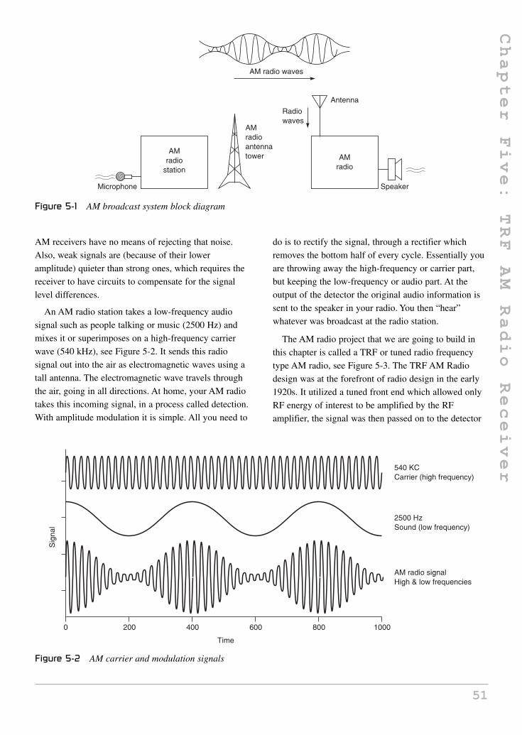
AM receivers have no means of rejecting that noise.
Also, weak signals are (because of their lower
amplitude) quieter than strong ones, which requires the
receiver to have circuits to compensate for the signal
level differences.
An AM radio station takes a low-frequency audio
signal such as people talking or music (2500 Hz) and
mixes it or superimposes on a high-frequency carrier
wave (540 kHz), see Figure 5-2. It sends this radio
signal out into the air as electromagnetic waves using a
tall antenna. The electromagnetic wave travels through
the air, going in all directions. At home, your AM radio
takes this incoming signal, in a process called detection.
With amplitude modulation it is simple. All you need to
do is to rectify the signal, through a rectifier which
removes the bottom half of every cycle. Essentially you
are throwing away the high-frequency or carrier part,
but keeping the low-frequency or audio part. At the
output of the detector the original audio information is
sent to the speaker in your radio. You then “hear”
whatever was broadcast at the radio station.
The AM radio project that we are going to build in
this chapter is called a TRF or tuned radio frequency
type AM radio, see Figure 5-3. The TRF AM Radio
design was at the forefront of radio design in the early
1920s. It utilized a tuned front end which allowed only
RF energy of interest to be amplified by the RF
amplifier, the signal was then passed on to the detector
51
Chapter Five: TRF AM Radio Receiver
Figure 5-1 AM broadcast system block diagram
Figure 5-2 AM carrier and modulation signals
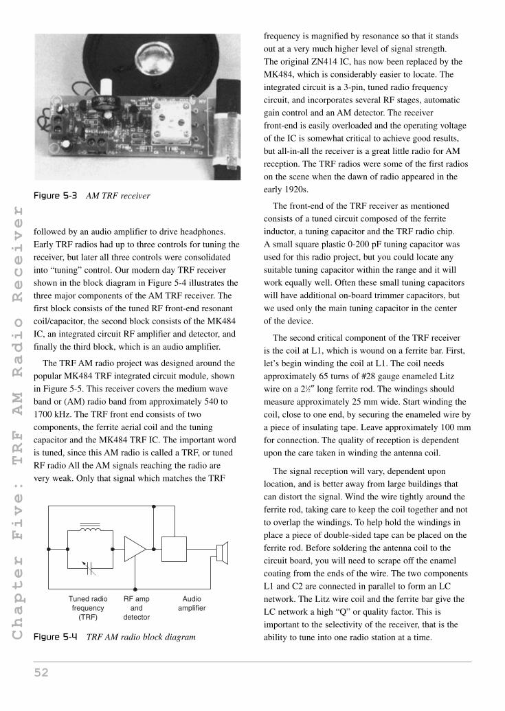
followed by an audio amplifier to drive headphones.
Early TRF radios had up to three controls for tuning the
receiver, but later all three controls were consolidated
into “tuning” control. Our modern day TRF receiver
shown in the block diagram in Figure 5-4 illustrates the
three major components of the AM TRF receiver. The
first block consists of the tuned RF front-end resonant
coil/capacitor, the second block consists of the MK484
IC, an integrated circuit RF amplifier and detector, and
finally the third block, which is an audio amplifier.
The TRF AM radio project was designed around the
popular MK484 TRF integrated circuit module, shown
in Figure 5-5. This receiver covers the medium wave
band or (AM) radio band from approximately 540 to
1700 kHz. The TRF front end consists of two
components, the ferrite aerial coil and the tuning
capacitor and the MK484 TRF IC. The important word
is tuned, since this AM radio is called a TRF, or tuned
RF radio All the AM signals reaching the radio are
very weak. Only that signal which matches the TRF
frequency is magnified by resonance so that it stands
out at a very much higher level of signal strength.
The original ZN414 IC, has now been replaced by the
MK484, which is considerably easier to locate. The
integrated circuit is a 3-pin, tuned radio frequency
circuit, and incorporates several RF stages, automatic
gain control and an AM detector. The receiver
front-end is easily overloaded and the operating voltage
of the IC is somewhat critical to achieve good results,
but all-in-all the receiver is a great little radio for AM
reception. The TRF radios were some of the first radios
on the scene when the dawn of radio appeared in the
early 1920s.
The front-end of the TRF receiver as mentioned
consists of a tuned circuit composed of the ferrite
inductor, a tuning capacitor and the TRF radio chip.
A small square plastic 0-200 pF tuning capacitor was
used for this radio project, but you could locate any
suitable tuning capacitor within the range and it will
work equally well. Often these small tuning capacitors
will have additional on-board trimmer capacitors, but
we used only the main tuning capacitor in the center
of the device.
The second critical component of the TRF receiver
is the coil at L1, which is wound on a ferrite bar. First,
let’s begin winding the coil at L1. The coil needs
approximately 65 turns of #28 gauge enameled Litz
wire on a 21⁄2′′ long ferrite rod. The windings should
measure approximately 25 mm wide. Start winding the
coil, close to one end, by securing the enameled wire by
a piece of insulating tape. Leave approximately 100 mm
for connection. The quality of reception is dependent
upon the care taken in winding the antenna coil.
The signal reception will vary, dependent upon
location, and is better away from large buildings that
can distort the signal. Wind the wire tightly around the
ferrite rod, taking care to keep the coil together and not
to overlap the windings. To help hold the windings in
place a piece of double-sided tape can be placed on the
ferrite rod. Before soldering the antenna coil to the
circuit board, you will need to scrape off the enamel
coating from the ends of the wire. The two components
L1 and C2 are connected in parallel to form an LC
network. The Litz wire coil and the ferrite bar give the
LC network a high “Q” or quality factor. This is
important to the selectivity of the receiver, that is the
ability to tune into one radio station at a time.
52
Chapter Five: TRF AM Radio Receiver
Figure 5-4 TRF AM radio block diagram
Figure 5-3 AM TRF receiver

The coil winding and the ferrite bar act as an efficient
wire antenna, as no additional antenna is required. The
only disadvantage is that the tuned circuit is directional
and depends on the orientation of the bar with respect
to the originating broadcast station. The coil winding
and the ferrite bar act as an efficient wire antenna.
No additional external antenna is needed. The only
disadvantage is that the tuned circuit is directional.
Signal strength depends on the orientation of the bar
with respect to the origin of the signal. The coil and
tuning capacitor may be taken from an old AM radio
to save time, if desired.
The third main component of the TRF radio front-end
is the TRF integrated circuit. The MK484 is a Japanese
copy of the original ZN414. It contains an RF amplifier,
active detector and automatic gain control (AGC to
improve sensitivity) all in a 3-pin package. The input
impedance is typically 4 M ohm. It operates over
a range of 150 kHz to 3 MHz. DC supply of 1.1 V to
1.8 V and 0.3 mA current drain makes it ideal for
battery operation. The output is typically 40–60 mV of
audio signal. It is important to realize that the radio IC
does not create any sounds by itself. It can only take the
RF signal provided from the TRF circuit, amplify it,
separate the audio signal from the RF (called detection)
and pass the audio signal on to be amplified. It has no
selective or rejection components contained in it. (This
is in contrast to superhetrodyne receivers.)
In this circuit, a small voltage regulator is built
around the BC108B transistor, four 1N4148 diodes, the
2.7k and 10k preset resistor and the 820 ohm resistor.
The 10k pot acts as a selectivity control for the whole
receiver, controlling the operating voltage for the
ZN414 (or MK484). If you live in an area that is
permeated with strong radio signals, then the voltage
may need to be decreased. I found optimum
performance with a supply of around 1.2 volts.
The audio amplifier is built around an inverting
741 op-amp amplifying circuit. Extra current boost is
provided using the BC109C/BC179 complementary
53
Chapter Five: TRF AM Radio Receiver
Figure 5-5 TRF AM receiver broadcast band receiver

transistor pair to drive an 8 ohm loudspeaker. The
voltage gain of the complete audio amplifier is around
15. The audio output of the complete receiver is really
quite good and free from distortion. I used a small
wooden enclosure and the complete tuning assembly
from an old radio.
Before we begin the AM radio project, you will want
to locate a well lit and well ventilated work space. You
will want a large work table or work bench to spread
out all you components, diagrams and tools. Locate a
small pencil tipped 27 to 33 watt soldering iron and a
roll of 60/40, 22 ga. tin/lead rosin core solder. If you
don’t have a jar of “Tip Tinner,” a soldering iron tip
conditioner/dresser, then you will want to go to a local
Radio Shack store and purchase one. Place all the
component parts in front of you along with the
necessary project diagrams, so it will be easy to work
with everything in front of you. Grab a few small tools,
such as a pair of end-cutters, a pair of needle-nose
pliers, a pair of tweezers, a magnifying glass, a small
flat-blade, and small Phillips screwdriver. Once
everything is right in front of you we can begin
building the AM radio project. Warm up your
soldering iron and we will begin. It is a good idea
to use a circuit board for this project, since circuit
boards provide a more reliable method used to build
circuits: you could elect to use prototype construction
or point-to-point wiring on a perf-board as an
alternative.
Refer to the chart in resistor color chart in Table 5-1
and the capacitor code chart in Table 5-2. Resistors used
in this project will be mostly carbon composition type
resistors and potentiometers. Each resistor will have
three or four color bands on the body of the resistor.
The first band closest to one edge will be the first color
which represents the first value. For example, a brown
color band will signify the first digit as a one (1). The
second color band represents the second digit value. So
if the second color is red, then the value of the second
digit would be two (2). The third color band is the
multiplier value. So, if the third color is orange then the
multiplier value would be (000), so the resistor value
would be 12,000 or 12k ohms. Often there is a fourth
color band which represents the tolerance value. No
fourth band denotes a resistor with a 20% tolerance, a
silver band denotes a 10% tolerance value, and a gold
band represents a 5% tolerance value. Now refer the
capacitor code chart. Many small capacitors are too
small to have their full value marked on the body of the
capacitor, so a three-digit code is used to represent the
value.
Let’s begin installing the project resistors now; find
and identify a couple of resistors at a time. Once you are
54
Chapter Five: TRF AM Radio Receiver
Table 5-1Resistor color code chart
Color Band 1st Digit 2nd Digit Multiplier Tolerance
Black 0 0 1
Brown 1 1 10 1%
Red 2 2 100 2%
Orange 3 3 1,000 (K) 3%
Yellow 4 4 10,000 4%
Green 5 5 100,000
Blue 6 6 1,000,000 (M)
Violet 7 7 10,000,000
Gray 8 8 100,000,000
White 9 9 1,000,000,000
Gold 0.1 5%
Silver 0.01 10%
No color 20%

55
Chapter Five: TRF AM Radio Receiver
Table 5-2Capacitance code information
This table provides the value of alphanumeric coded ceramic, mylar and mica capacitors in general. They come in many sizes,
shapes, values and ratings; many different manufacturers worldwide produce them and not all play by the same rules. Some
capacitors actually have the numeric values stamped on them; however, many are color coded and some have alphanumeric codes.
The capacitor’s first and second significant number IDs are the first and second values, followed by the multiplier number code,
followed by the percentage tolerance letter code. Usually the first two digits of the code represent the significant part of the value,
while the third digit, called the multiplier, corresponds to the number of zeros to be added to the first two digits.
Value Type Code Value Type Code
1.5 pF Ceramic 1,000 pF /.001 µF Ceramic / Mylar 102
3.3 pF Ceramic 1,500 pF /.0015 µF Ceramic / Mylar 152
10 pF Ceramic 2,000 pF /.002 µF Ceramic / Mylar 202
15 pF Ceramic 2,200 pF /.0022 µF Ceramic / Mylar 222
20 pF Ceramic 4,700 pF /.0047 µF Ceramic / Mylar 472
30 pF Ceramic 5,000 pF /.005 µF Ceramic / Mylar 502
33 pF Ceramic 5,600 pF /.0056 µF Ceramic / Mylar 562
47 pF Ceramic 6,800 pF /.0068 µF Ceramic / Mylar 682
56 pF Ceramic .01 Ceramic / Mylar 103
68 pF Ceramic .015 Mylar
75 pF Ceramic .02 Mylar 203
82 pF Ceramic .022 Mylar 223
91 pF Ceramic .033 Mylar 333
100 pF Ceramic 101 .047 Mylar 473
120 pF Ceramic 121 .05 Mylar 503
130 pF Ceramic 131 .056 Mylar 563
150 pF Ceramic 151 .068 Mylar 683
180 pF Ceramic 181 .1 Mylar 104
220 pF Ceramic 221 .2 Mylar 204
330 pF Ceramic 331 .22 Mylar 224
470 pF Ceramic 471 .33 Mylar 334
560 pF Ceramic 561 .47 Mylar 474
680 pF Ceramic 681 .56 Mylar 564
750 pF Ceramic 751 1 Mylar 105
820 pF Ceramic 821 2 Mylar 205
1st Significant Figure
2nd Significant Figure
Multiplier
Tolerance
CSGNetwork.Com 6/4/92
0.1 µF 10%
104 k

sure you have correctly identified each resistor, and you
know where each resistor is placed on the PC board,
you can go ahead and install them on the circuit board.
Solder the resistors in place and then trim the excess
component leads with your end-cutters. Cut the excess
component leads flush to the edge of the circuit board.
Install the remaining resistors, solder them in place and
remember to trim the excess leads from the board.
Next we will move on to installing the capacitors.
This project uses two types of capacitors, small mica or
polyester types and electrolytic types. The smaller
capacitors may not have their actual value printed on
them, but might have a three-digit code on them.
Refer to the capacitor code chart to help identify
each capacitor before installing them on the PC board.
Slowly identify each capacitor and place it in the correct
location on the circuit board. Solder these small
capacitors in their respective locations after referring to
the schematic and parts layout diagrams. This project
also utilizes larger electrolytic capacitors. Electrolytic
capacitors have polarity and this must be observed if the
circuit is to work correctly. Take a look at one of the
larger electrolytic capacitors and you will notice that it
may have a black or white color band or a plus (+) or
minus (−) marking on one side of the capacitor body.
When placing these types of capacitors on the circuit
board, be sure you have oriented the capacitor correctly.
Install the electrolytic capacitors on the circuit board
and solder them in place; remember to trim the excess
component lead with your end-cutter.
Let’s move on to installing the silicon diodes. The
AM radio project uses six silicon diodes, and they too
have polarity which must be observed. Each diode will
have either a white or black band at one end of the
diode’s body. This band denotes the cathode lead of
the particular diode. Refer to the parts layout and
schematic diagram when installing the six resistors.
Place the diodes on the circuit board and solder them
in place on the board. Don’t forget to cut the extra lead
lengths.
Locate the semiconductor pin-out diagram shown in
Figure 5-6. Now, go ahead and identify all three of the
transistors for the project and install the transistors on
the circuit board. There are two NPN types and one PNP
type transistors in the AM radio project. Transistors
usually have three leads, a Base lead, a Collector lead
and an Emitter lead. The symbol for a transistor is a
vertical line which is the Base lead and two lines
running at 45°angles with respect to the Base lead.
The angled lead with the arrow pointing towards or
away from the Base lead is the Emitter lead and the
remaining lead is the Collector lead. Be sure you can
identify each of the transistor leads before placing them
on the circuit board. Solder the transistors in place on
56
Chapter Five: TRF AM Radio Receiver
EBC
C
E
B B
NPN NPN
BC108B BC109C BC179C
PNP
B
C
E
C
E
EBC EBCLM741
1 8
1
OUT IN GND
ZN414
ZN414
MK484
MK484
MK484
ZN414
2 3
1OUT IN GND
2 3
1234
8765
Figure 5-6 Semiconductor pin-outs

the circuit board; when finished remember to trim the
excess component leads.
The ZN414 or MK484 TRF module looks very much
like a common three-lead transistor. Carefully refer to
the pin-out diagram for the MK484 before installing, in
order to prevent damaging it upon power-up. One lead
is the input lead from the tuned circuit. One lead is the
ground lead and the remaining lead is the output lead
which is directed to the actual circuit.
The AM radio project uses a single dual in-line
integrated circuit, an LM471. We elected to use an IC
socket as insurance against a possible circuit failure
at some point in time. Integrated circuit sockets are
inexpensive and make life easier in the event of a circuit
problem, since it is much easier to unplug an IC rather
than attempting to unsolder a multi-pin integrated
circuit. Go ahead and solder-in a good quality IC socket
for U2. Take a look at U2 and you will notice that at
one end of the plastic package you will find a cut-out,
notch or indented circle. Pin 1 of the IC will be just to
the left of the notch or cut-out. Be sure to align pin of
the IC to pin 1 of the IC socket, pin 1 of U2 is the null
offset pin which is not used in this circuit. Note that pin
2 of U2 is the inverting input which is connected to the
junction of R6 and R8.
Next locate the ferrite inductor coil or L1; you will
notice that it is in parallel with the tuning capacitor C2.
The parallel tuned circuit is placed between capacitor
C1 and the input of U1, the MK484 TRF IC. These
components are best placed at one end of the PC board
if possible, or can be placed off the PC board on the
front of your enclosure. Now, locate the volume control,
the 10k ohm potentiometer; it is a chassis mounted
control which can be mounted on the front panel of
your enclosure.
Let’s wrap up the project. First you will want to
solder the battery clip; note that the black wire of the
battery clip will go to the circuit board minus
or ground bus and the red battery clip wire will go in
series with one post on the on-off switch at S1, the
remaining post of the SPST toggle switch will connect
to the Collector of Q1. Finally locate two 4′′ pieces
of #22 ga. insulated hookup wire. Bare both ends of
the two wires, solder one end of each wire to the
speaker leads. Now take one free wire end and solder it
to the common ground of the circuit and then solder
the remaining free wire end to the minus end of
capacitor C8.
This completes the construction of the AM radio
project. Let’s take a well deserved rest and when we
return we will check the circuit board for possible “cold”
solder joints and possible “short” circuits. Pick up the
circuit board with the foil side facing upwards toward
you. Look closely at the circuit board, first we will
inspect the circuit board for possible “cold” solder joints.
The solder joints should all look clean, shiny and bright.
If any of the solder joints look dull, dark or “blobby”
then you should remove the solder from that joint and
re-solder the joint over again. Now pick up the circuit
board once again and we will look for possible “short”
circuits. “Short” circuits are usually caused from one of
two reasons. The first cause of “short” circuits are loose
solder “blobs” or solder balls which can sometimes
stick to the circuit board. The second cause for
“short” circuits is to have “stray” component leads
stick to the foil side of the board. Rosin core solder
residue can often be sticky and often solder “blobs” or
“stray” component leads can bridge across circuit
traces causing a “short” circuit. Look over the board
and remove anything that looks like it might be
bridging any circuit traces. Once the circuit inspection
has occurred, you can prepare the circuit for its
first test.
Connect up a fresh 9 volt battery to the AM radio
circuit. Once the battery is connected to the circuit, you
can “flip” the on-off switch to the on position and you
should begin to hear some “hiss” from the speaker. If
you do not hear anything, turn up the volume control to
mid-position. At this point you should begin to hear some
sounds from the speaker. Move the tuning capacitor
control across the AM radio band and if all goes well
you should begin to hear some local stations. Move the
ferrite core coil or the circuit board around in a 360°pattern to see where the station is loudest. Hopefully the
radio works fine without any further adjustments.
In the event that the AM radio circuit does not work
at all, you will have to remove the battery from the
circuit and inspect the circuit board one more time, but
this time you will be looking for components placed
incorrectly. Remember earlier, we talked about certain
components have polarity such as diodes, electrolytic
capacitors, transistors, etc. Now, you will need to
57
Chapter Five: TRF AM Radio Receiver

inspect the PC board closely to see if you might have
placed a component incorrectly. Its easy to make a
mistake and insert a capacitor or diode incorrectly; it
happens to professionals too! Another possible cause
for failure is that you may have placed an IC incorrectly
in the socket! Finally, it’s easy to incorrectly install
one of the transistors. Look at each transistor carefully,
you may want to refer to the manufacturer’s
specification and/or pin-out information sheets along
with the circuit layout and schematic diagram to confirm
transistor pin-outs. Once you have inspected the circuit
board for misplaced components and have corrected any
mistakes, you can reapply power to the AM radio circuit
and check out the circuit once again. Have fun listening
to your new AM radio, you will have the great
satisfaction of listening to the radio that you just built.
58
Chapter Five: TRF AM Radio Receiver
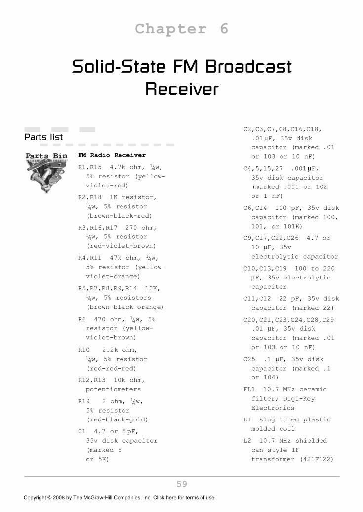
Solid-State FM Broadcast Receiver
Chapter 6
Parts list
FM Radio Receiver
R1,R15 4.7k ohm, 1/4w,
5% resistor (yellow-
violet-red)
R2,R18 1K resistor,1/4w, 5% resistor
(brown-black-red)
R3,R16,R17 270 ohm,1/4w, 5% resistor
(red-violet-brown)
R4,R11 47k ohm, 1/4w,
5% resistor (yellow-
violet-orange)
R5,R7,R8,R9,R14 10K,1/4w, 5% resistors
(brown-black-orange)
R6 470 ohm, 1/4w, 5%
resistor (yellow-
violet-brown)
R10 2.2k ohm, 1/4w, 5% resistor
(red-red-red)
R12,R13 10k ohm,
potentiometers
R19 2 ohm, 1/4w,
5% resistor
(red-black-gold)
C1 4.7 or 5pF,
35v disk capacitor
(marked 5
or 5K)
C2,C3,C7,C8,C16,C18,
.01 µF, 35v diskcapacitor (marked .01
or 103 or 10 nF)
C4,5,15,27 .001 µF,35v disk capacitor
(marked .001 or 102
or 1 nF)
C6,C14 100 pF, 35v disk
capacitor (marked 100,
101, or 101K)
C9,C17,C22,C26 4.7 or
10 µF, 35velectrolytic capacitor
C10,C13,C19 100 to 220
µF, 35v electrolyticcapacitor
C11,C12 22 pF, 35v disk
capacitor (marked 22)
C20,C21,C23,C24,C28,C29
.01 µF, 35v diskcapacitor (marked .01
or 103 or 10 nF)
C25 .1 µF, 35v diskcapacitor (marked .1
or 104)
FL1 10.7 MHz ceramic
filter; Digi-Key
Electronics
L1 slug tuned plastic
molded coil
L2 10.7 MHz shielded
can style IF
transformer (421F122)
59Copyright © 2008 by The McGraw-Hill Companies, Inc. Click here for terms of use.

D1 varactor diode,
33 pF
D2 Zener diode,
6.2 volt
U1 ULN2111 or MC1357 IC
U2 LM386 IC
U3 SA602 IC
Q1,Q3 2N3904 NPN
transistor
Q2 2SC2498 or 2SC2570A
NPN transistor
B1 9 volt transistor
radio battery
Misc PC board, battery
holder, battery clip,
RCA jacks
1/8′′ earphone jack, wire,
antenna
The FM broadcast receiver will permit you to listen to
your favorite radio shows as well as allow you to tune
outside of the standard FM broadcast band to “listen-in”
to FM room bugs, FM mikes and other interesting
hidden transmitters. The FM receiver could also be
connected to an SCA adapter, so that you may listen to
‘MUSAK’ radio show used in stores and restaurants.
The FM radio project is just plain fun and will teach
you about FM radio theory.
The FM broadcast receiver demonstrates the basics
of FM radio theory in one compact, simple circuit!
Separate circuits are “sections” of the receiver, making it
easy to visualize every function. The latest in IC circuitry
is used in the FM receiver, which allows high performance.
The FM receiver project is designed to receive
wide-band FM transmissions typical of FM broadcast
stations, wireless mikes, and telephone transmitters or
“bugs,” rather than Narrow Band FM transmissions
(NBFM) as used on police or public service radios.
Why not build your own FM Broadcast receiver like
the one shown in Figure 6-1. Not only will you learn
how FM receiver works but you will be able to build
and utilize your new FM radio. The FM receiver is
great for listening to FM broadcasts and news as well as
listening-in to commercial SCA—free music, stock
quotes, sports, etc. The receiver has an SCA or sub-carrier
output which can be fed into an SCA converter to allow
this reception of these signals.
The receiver tunes from 70 to 110 MHz, ideal for
tuning in out-of-band FM wireless mikes, “bugs” and
other “hidden” transmitters. The FM receiver also
features plenty of audio output, and operates from a
standard 9 volt battery for truly portable operation.
FM modulationFrequency modulation (FM) is a form of modulation
which represents information as variations in the
instantaneous frequency of a carrier wave. Contrast this
with amplitude modulation, in which the amplitude
of the carrier is varied while its frequency remains
constant. In analog applications, the carrier frequency is
varied in direct proportion to changes in the amplitude
of an input signal. Digital data can be represented by
shifting the carrier frequency among a set of discrete
values, a technique known as frequency-shift keying.
The diagram in Figure 6-2 illustrates the FM
modulation scheme, the RF frequency is varied with
the sound input rather than the amplitude.
FM is commonly used at VHF radio frequencies for
high-fidelity broadcasts of music and speech, as in FM
broadcasting. Normal (analog) TV sound is also broadcast
using FM. A narrowband form is used for voice
communications in commercial and amateur radio
settings. The type of FM used in broadcast is generally
60
Chapter Six: Solid-State FM Broadcast Receiver
Figure 6-1 FM receiver

called wide-FM, or W-FM. In two-way radio, narrowband
narrow-fm (N-FM) is used to conserve bandwidth.
In addition, it is used to send signals into space.
Wideband FM (W-FM) requires a wider bandwidth
than amplitude modulation by an equivalent modulating
signal, but this also makes the signal more robust
against noise and interference. Frequency modulation
is also more robust against simple signal amplitude
fading phenomena. As a result, FM was chosen as the
modulation standard for high frequency, high fidelity
radio transmission: hence the term “FM radio.” FM
broadcasting uses a well-known part of the VHF band
between 88 and 108 MHz in the USA.
FM receivers inherently exhibit a phenomenon called
capture, where the tuner is able to clearly receive the
stronger of two stations being broadcast on the same
frequency. Problematically, however, frequency drift or
lack of selectivity may cause one station or signal to be
suddenly overtaken by another on an adjacent channel.
Frequency drift typically constituted a problem on
very old or inexpensive receivers, while inadequate
selectivity may plague any tuner. Frequency modulation
is used on the FM broadcast band between 88 and
108 MHz as well as in the VHF and UHF bands for
both public service and amateur radio operators.
FM receiver circuitdescriptionThe FM receiver block diagram in Figure 6-3 illustrates
the fundamentals of FM reception. The schematic
diagram of the FM broadcast receiver is depicted in
Figure 6-4. FM broadcast signals captured by the whip
antenna or from the input jack are applied to the RF
amplifier Q2, a high gain, low noise microwave style
transistor. Input signals are amplified about 100 times
or equivalent to 20 dB. After being boosted, these input
signals are routed to the SA602 mixer-oscillator chip
for conversion down to the 10.7 MHz Intermediate
Frequency (IF). The SA602 is a very popular chip used
in a great variety of receivers from cellular telephones
to satellite receivers. The reason for its popularity is that
it contains most of a receiver’s “front end” circuitry on
a single, easy-to-use chip. Internal to the SA602 is an
oscillator tuned by an external tank circuit; C11, 12, L1
and varactor diode D1. A varactor diode acts like a
voltage variable capacitor and the voltage applied across
it comes from tuning pot R12. This IF signal is an exact
reproduction of the desired signal, but at 10.7 MHz.
We then band-pass filter it with ceramic filter FL-1.
61
Chapter Six: Solid-State FM Broadcast Receiver
Figure 6-3 FM broadcast receiver block diagram
Frequencymodulator
Carrier wavegenerated attransmitter
Sound signalto microphone
Electrical image of sound formedby microphone
Frequency modulatedcarrier wave – theFM radio signal thatis transmitted
Figure 6-2 FM modulation

62
C hapter Six: Solid-State FM Broadcast Receiver
Figure 6-4 FM broadcast receiver. Courtesy of Ramsey Electronics

63
Chapter Six: Solid-State FM Broadcast Receiver
The ceramic filter allows only the desired 10.7 MHz
signal to pass, rejecting any adjacent channel signals.
Transistor Q1 amplifies the IF signal before it is applied
to the detector chip U1.
One of the primary advantages of FM is that the
program information (modulation) is contained in carrier
frequency variations and not in amplitude changes
like AM, which would be susceptible to noise and
interference. This means that we can limit or clip the
signal, thus removing any noise and not affecting the
desired information. The first section of U1 performs
this limiting function, providing high gain and clipping
any amplitude (noise) variations. FM is detected in the
second section using a process known as quadrature
detection. We’ll not get into this too deeply because it
requires a knowledge of trigonometry identities—let’s
just say it extracts the frequency modulated program
information. Capacitor C1 and coil assembly L2
comprise a phase shift network that is required by the
quadrature detector. Demodulated signals are amplified
and sent out through pin 1 to the volume control, AFC
circuitry and the SCA buffer amp. The AFC circuitry is
used to properly keep the receiver locked on to the
tuned-in radio station. Resistor R9 and capacitor C17
filter out any audio voltage variations so that only major
frequency changes will shift the tuning voltage to lock
the frequency.
Audio signals from the volume control are amplified
to speaker levels by U2, an LM-386 audio amplifier
chip. Transistor Q3 provides a buffer stage to external
SCA devices you may connect up to the receiver.
SCA units decode (demodulate, actually) “hidden”
audio and data services transmitted over standard
FM broadcast channels. These services include stock
quotes, sports scores, talk shows and even background
music—commercial free!
Circuit assemblyLook for a clean well lit area in which to assembly your
shortwave receiver. You will need a 27 to 30 watt pencil
tip soldering iron, some 60/40 tin/lead rosin core solder.
You will also need a few hand tools including a pair of
end-cutters, needle-nose pliers, a few screwdrivers and
a pair of tweezers to pick up small parts. You will want
to locate a small jar of “Tip Tinner” from your local
Radio Shack store. “Tip Tinner” is a soldering iron tip
cleaner/dresser which is invaluable when soldering
circuit board. Locate the schematic and layout diagrams
and we will begin to construct your new shortwave
receiver. Place the project circuit board in front of you
and we will begin building the receiver.
Locate all of the resistors for the project and place
them in front of you. Each resistor has a color code
which describes its value. Check the color code against
the parts list and schematic before installing them onto
the circuit board. Refer to the resistor color chart in
Table 6-1. Place about four or five resistors on the
PC board and place these resistors in their respective
locations carefully making sure each on is in the correct
location. Let your soldering iron tip heat both the
component lead wire and PC board trace enough so
that the wire itself and the foil trace both become hot
enough together to melt a bit of solder so that it flows
smoothly from the component leads to the PC board
trace. Now, go ahead and solder each of the resistors
onto the circuit board. Trim off the excess component
leads with and small pair of end-cutters. Pick up and
identify the next grouping of resistors and install them
on the circuit board, follow up by soldering this next
batch of resistors to the circuit board, remember to trim
the extra lead lengths form the PC board.
Once all the resistors have been installed on to the
circuit board, we can move on to identifying all of the
capacitors for the project. Note that there will be
different looking capacitors for this project, some will
be small disks, while others will be larger body devices
with minus and plus marking on them. These larger
capacitors with polarity marking are electrolytic
capacitors and they have polarity which must be
observed for the circuit to work correctly. Look through
the parts pile and locate the capacitors and place them
in front of you. You will notice a number of small disk
capacitors, we will install these first. Look closely at
each of the disk capacitors at their markings. Sometimes
the capacitors are very small and they may not have
their actual value printed on them but will instead
have some sort of code. Refer to the parts list for these
codes or the capacitor code chart Table 6-2. Locate
four or five of these small disk capacitors, identify
them and install them on the circuit board, while
referring to the schematic and layout diagrams.

64
Chapter Six: Solid-State FM Broadcast Receiver
Table 6-1Resistor color code chart
Color Band 1st Digit 2nd Digit Multiplier Tolerance
Black 0 0 1
Brown 1 1 10 1%
Red 2 2 100 2%
Orange 3 3 1,000 (K) 3%
Yellow 4 4 10,000 4%
Green 5 5 100,000
Blue 6 6 1,000,000 (M)
Violet 7 7 10,000,000
Gray 8 8 100,000,000
White 9 9 1,000,000,000
Gold 0.1 5%
Silver 0.01 10%
No color 20%
After inserting the disk capacitors on to the circuit
board, you can go ahead and solder them to the circuit
board. Remember to cut the excess component leads.
Next, move on and install another grouping of small
disk capacitors, then solder them in place on the printed
circuit board. Cut the extra component leads after
soldering in the capacitors. When you are finished
installing the small capacitors we will move on to the
larger electrolytic types.
Next, we will identify and install the electrolytic
capacitors. Electrolytic capacitors each have polarity
markings on them in the form of a black band with
either a plus or minus marking, which denotes the
polarity of the device. You must pay particular attention
to these markings in order for the FM receiver to work
properly. Refer to the schematic and parts layout
diagrams when installing C9, C17, C22 and C26, which
are all 4.7 to 10 µF electrolytic capacitors. Install these
four capacitors and solder them to the circuit board.
Remember to trim the excess component leads. Cut the
excess leads flush to the edge of the PC board with a
pair of small end-cutters. Now locate and install
electrolytic capacitors C10, C13 and C19, these are all
100 to 200 µF electrolytic types. After placing them on
the PC board in their proper location and with respect to
polarity marking you can go ahead and solder them to
the PC board.
At this time, locate diodes D1, the varactor “tuning”
diode and D2, a Zener diode from the parts pile. Install
D1, varactor diode. It has a black body with green and
red bands. Observe the correct positioning of the banded
end by following the silkscreen. The green band is
positioned as shown on the silkscreen. Now, install D2,
the Zener diode. It has a gray painted glass body with
a black band. Orient the band as shown on the layout
diagram. A Zener diode acts as a voltage regulator,
keeping the voltage across it constant. This keeps
frequency drift to a minimum. Once both of the diodes
have been placed on the PC board you can solder them
in place and then trim the extra lead lengths flush to the
edge of the circuit board.
Next, we are going to locate and install the two
inductors; see Table 6-3. Locate the slug tuned plastic
molded coil, which is coil L1. Once you have located it,
you can place it on the PC; remember to check the
schematic and parts layout diagram for placement
details. Now, locate L2, the 10.7 MHz shielded metal
quadrature coil. Notice that it will only go into the PC
board one way. Place L2 on the board and now solder
both L1 and L2 to the PC board. Trim the excess
component leads from the board.
At this time, you can locate FL1, the 10.7 MHz
ceramic IF filter. This part looks like a disk capacitor

65
Chapter Six: Solid-State FM Broadcast Receiver
Table 6-2Capacitance code information
This table provides the value of alphanumeric coded ceramic, mylar and mica capacitors in general. They come in many sizes,
shapes, values and ratings; many different manufacturers worldwide produce them and not all play by the same rules. Some
capacitors actually have the numeric values stamped on them; however, many are color coded and some have alphanumeric codes.
The capacitor’s first and second significant number IDs are the first and second values, followed by the multiplier number code,
followed by the percentage tolerance letter code. Usually the first two digits of the code represent the significant part of the value,
while the third digit, called the multiplier, corresponds to the number of zeros to be added to the first two digits.
Value Type Code Value Type Code
1.5 pF Ceramic 1,000 pF /.001 µF Ceramic / Mylar 102
3.3 pF Ceramic 1,500 pF /.0015 µF Ceramic / Mylar 152
10 pF Ceramic 2,000 pF /.002 µF Ceramic / Mylar 202
15 pF Ceramic 2,200 pF /.0022 µF Ceramic / Mylar 222
20 pF Ceramic 4,700 pF /.0047 µF Ceramic / Mylar 472
30 pF Ceramic 5,000 pF /.005 µF Ceramic / Mylar 502
33 pF Ceramic 5,600 pF /.0056 µF Ceramic / Mylar 562
47 pF Ceramic 6,800 pF /.0068 µF Ceramic / Mylar 682
56 pF Ceramic .01 Ceramic / Mylar 103
68 pF Ceramic .015 Mylar
75 pF Ceramic .02 Mylar 203
82 pF Ceramic .022 Mylar 223
91 pF Ceramic .033 Mylar 333
100 pF Ceramic 101 .047 Mylar 473
120 pF Ceramic 121 .05 Mylar 503
130 pF Ceramic 131 .056 Mylar 563
150 pF Ceramic 151 .068 Mylar 683
180 pF Ceramic 181 .1 Mylar 104
220 pF Ceramic 221 .2 Mylar 204
330 pF Ceramic 331 .22 Mylar 224
470 pF Ceramic 471 .33 Mylar 334
560 pF Ceramic 561 .47 Mylar 474
680 pF Ceramic 681 .56 Mylar 564
750 pF Ceramic 751 1 Mylar 105
820 pF Ceramic 821 2 Mylar 205
1st Significant Figure
2nd Significant Figure
Multiplier
Tolerance
CSGNetwork.Com 6/4/92
0.1 µF 10%
104 k

but has three leads. Amazingly, its function is equal to a
small handful of inductors and capacitors hooked up in
a bandpass filter configuration. For those techno-types,
its bandwidth is 280 kHz centered at 10.7 MHz with
an insertion loss of only 6 dB. Go ahead and solder FL1
in now.
Let’s locate the transistors for the receiver now! Next,
refer to the semiconductor pin-out diagram shown in
Figure 6-5. Transistors are three semiconductors which
generally have three leads: Base lead, a Collector lead
and an Emitter lead. The transistor symbol shows that
the Base lead is a vertical line. Both the Collector and
Emitter leads are diagonal lines which point to the Base
lead. The Emitter lead has a small arrow which points
toward or away from the Base lead. Try and locate
transistor Q1, a 2N3904 type. Watch placement of its
flat side, refer to the parts layout diagram and the
schematic for proper placement. Install Q2, 2SC2498
or 2SC2570A NPN transistor. Transistors are VERY
critical of correct orientation of their leads. Be sure to
pay close attention to the position of the flat side of the
transistor. Finally, install Q3, 2N3904 transistor. Be sure
to observe flat side orientation of the transistors when
mounting them. Now go ahead and solder the transistors
in place on the PC board.
Let’s take a short break and when we return we will
install the integrated circuits and the final components.
Before installing the integrated circuits, please consider
using integrated circuit sockets as an insurance policy
against having to try and un-solder a 14 pin IC from
the circuit board which is a difficult task even for the
seasoned electronics technician. Integrated circuits
DO fail and if one ever does, you can simply unplug
it and replace it with a new one. Refer to the schematic
and parts layout diagrams when installing the
integrated circuits. Solder in the IC sockets in their
respective locations and then we will install the
actual ICs.
Integrated circuit packages will generally have a cut-
out, notch or indented circle at the top end of the IC
package. The cut-out or notch will usually be at the top
center while if there is an indented circle it will be at
the top left of the IC package. Pin 1 of the IC will
always be left of the cut-out or notch, so you can easily
identify the pin-outs. Using your schematic and parts
66
Chapter Six: Solid-State FM Broadcast Receiver
Figure 6-5 Semiconductor pin-outs
LM386
1 81234
8765
SA602
1 81234
8765
ULN2111MC1357
1 141
2
3
4
5
6
7
14
13
12
11
10
9
8
C
E
B
NPN
EBC
C
E
B
NPN
EBC
C
E
B
NPN
BEC
Table 6-3Inductor coil winding information
L1 21⁄2 turn coil #22 ga. insulated magnet wire on slug
tuned coil form. Unwind original coil and rewind.
21⁄2 turns onto Series 48 adjustable coil form
48A Series Coil (48A117MPC) Circuit Specialists.
L2 10.7 MHz shielded can style IF transformer (red)
Part # (421F122) Mouser Electronics.

layout diagrams observe the correct orientation of
the integrated circuits before inserting them into the
sockets. First locate and install U1, the ULN2111 FM
demodulator chip. Since this chip has 14 pins, be
especially careful not to bend any pins under as you
insert it into the PC board. When you solder the chip,
verify that you are soldering all 14 pins. Next, let’s
install U2, the LM386 audio amplifier IC chip. The
LM386 is a very popular part, and with good reason.
Tucked inside that little plastic case are about 20
transistors that take a feeble audio signal and amplify it
up to room-filling volume! Finally, go ahead and install
U3, the SA602 IC mixer-oscillator. The marked end of
the IC (band or dot) must face the edge of the PC board.
If you wish, install an 8-pin DIP socket, still remembering
to orient and install the SA602 correctly. Remember to
firmly press the integrated circuits into their sockets.
The receiver project has two potentiometers, R12 is
the “tuning” control, while R13 is the volume control.
Locate the two 10k ohm potentiometers and install them,
being sure to refer to the schematic and parts layout
diagrams. Note that both potentiometers are on the front
panel of the PC board. Install potentiometer R12, the
tuning control. Insert it into the PC board so it seats
firmly and is straight and even. Solder the three pins
and the two mounting tabs. Next, install potentiometer
R13, the volume control in the same manner.
Now locate S1, the on-off push button switch. Solder
all six pins firmly. We’ve installed some “landmark”
parts so far just to get us used to soldering our PC
board. Finally, we are going to place the panel jacks on
the rear portion of the circuit board. Locate and install
J1, the RCA antenna jack, solder all four points. Now
locate and install J2, the speaker jack, solder all three
pins. At last, install J3, the SCA output jack, solder all
four points.
There are only a few more components to go before
we finish our FM receiver project. Install the 9 volt
battery clamp. Use a scrap component lead wire looped
through the holes in the clamp and into the holes in the
PC board. Solder the wire to the clamp but don’t use too
much solder as this will prevent you from seating the
battery fully into the clamp. Now, go ahead and install
the 9 volt battery snap connector. Make sure you put the
right color wire into the proper hole on the PC board.
At long last, you are all done and ready to listen to
tunes from your radio.
Before we apply power to the FM receiver for the
first time we should make one last inspection of our
work. First you will want to make sure that you have
installed the diodes, electrolytic capacitors and the
transistors with the correct orientation. Failure to do so
may result in a damaged circuit, when power is first
applied. Don’t forget to check the orientation of the
integrated circuits for proper location and orientation.
Now we will inspect the PC board for “cold” solder
joints. Pick up the PC board with the foil side facing
upwards towards you. Take a look at all of the solder
connections and make sure that they all look clean,
smooth and shiny. If you find a solder joint that looks
dirty, dark, dull or “blobby” then un-solder the connection,
remove the solder and re-solder the connection once again
until it looks good. Finally, we are going to inspect the
PC board for possible “short” circuits. Often “cut”
components leads can form “bridges” which can “short”
out the circuit board traces, thus causing power to flow
into the wrong places, and possibly damage the circuit.
Also look carefully for any solder blobs that can form
“bridges” between circuit traces. Now that you have
inspected the PC circuit board, we can move on to testing
and aligning your new receiver.
Testing and alignmentA hex head alignment tool is required to tune up
your FM receiver. If you do not already have a set of
plastic or nylon coil alignment tools and expect to
build other radio or transmitter type kits, such tools are
well worth having and can be found at any electronics
store, including Radio Shack. While a hex style
Allen wrench will fit the coil slug, the metal itself
will drastically change the coil’s inductance while it is
in the slug. For this reason you should not use an Allen
wrench unless you don’t mind the trial and error process
of turning the slug, withdrawing the tool, checking
tuning, reinserting the tool, re-tuning, checking
and so on.
You can fabricate your own non-metallic tuning tool
with some patience, a bit of sandpaper and a piece of
plastic rod. Try a large wooden matchstick, kebab
skewer, or small plastic crochet needle. Carefully sand
down the end to a hex shaped form and check for
proper fit within the coil slug. It is better to have the
67
Chapter Six: Solid-State FM Broadcast Receiver

tool fit loosely rather than too tight, since a tight tool
will cause stress on the delicate slug.
Connect up a fresh 9 volt battery (preferably heavy
duty alkaline type), a speaker or earphone, a short
length of wire (about two feet) to serve as antenna, or
the telescopic whip if the optional matching case and
knob set was purchased. Now, set the volume and the
tuning controls to the center of their range, then press
the power switch “ON,” you should hear some rushing
noise from your speaker. Next, rotate the volume
control and see if it does its job, then slowly turn L2’s
slug back and forth for maximum noise. This noise
should be similar to what you would hear when a
regular FM radio is tuned between stations. L2 may
be tuned with a regular blade style screwdriver.
Try turning the tuning control, and see if you can
receive any stations, but don’t be alarmed if nothing is
received since we haven’t adjusted the oscillator coil
yet. The oscillator coil, L1, is adjustable to receive
from 70 to 110 MHz. We have to adjust it to cover the
frequency range of interest. For alignment purposes
we’ll work with the understanding that the standard
FM 88-108 MHz band is what we wish to receive.
Using an insulated alignment tool, slowly rotate L1’s
slug gently so that the slug is even with the top of the
coil form. (Do not force the slug; if it binds, rotate the
slug back and gently “rock it” to-and-fro as you would a
thread forming tap. Slugs are by nature very brittle and
will crack easily.) Now carefully rotate the slug into the
coil form seven turns. The slug will be in about 1⁄4′′.Rotate the tune control until you hear an FM broadcast
signal. Adjust L2 for best sound. Install R9, 10k ohm
(brown, black, orange). R9 adds in AFC voltage to
stabilize against drift. Without it your radio may
“wander.” After a signal is received, rotate the tune
control to receive other stations. If the stations seem to
“jump away” as you try to tune one in, the coil L1 is
adjusted incorrectly and should be re-tuned. The reason
for this odd phenomenon is that the AFC circuit is
pushing the signal away rather than pulling it in. This
is caused by having the oscillator 10.7 MHz below the
desired signal rather than 10.7 MHz above it. A similar
example of this is closing your eyes, hearing a sound,
but not being able to determine if it is in front of, or
behind you. Readjusting L1 will correct this situation.
Make sure the slug is about three turns from the top of
the coil form.
Calibrating the receiver is easy. First tune in a station
known to operate at the low end (88 MHz) of the FM
broadcast band. Rotate the tune control almost fully
counter-clockwise to where that station should logically
be located on the dial. Turn L1’s slug until that same
station is received. The tune control should now tune in
the entire FM broadcast band. An easy way of making
your own dial is to paste a small rectangle of paper
behind the tuning dial knob. Then as you tune in
different frequencies, pencil in on the paper the received
frequency.
Additional receiverconsiderationsYour FM receiver was designed for clean, undistorted
audio from average FM broadcast stations, while
keeping battery current drain low. You may significantly
increase the FM radio’s audio output by adding a single
10 uF electrolytic capacitor across pins 1 and 8 on the
LM-386 audio amplifier IC. The “+” side should
connect to pin 1. An easy way of adding this capacitor
is to simply “tack” solder it right on the IC pins on the
solder side of the PC board. A 50-cent of speaker, lying
naked on your workbench, will not give you a fair test
of your FM receiver audio quality or volume. Speaker
quality and well-designed enclosures have their clear
purposes! A reasonable speaker in a box delivers a
pleasant listening volume as well as significantly
improved fidelity.
Out-of-band operationAlthough many people use their receiver for
comfortable FM broadcast reception, some James Bond
types will want to use it to receive clandestine
transmissions from phone bugs, room transmitters, etc.
It’s a simple matter to re-tune coil L1 to receive the
frequency band of interest. First make sure you verify
68
Chapter Six: Solid-State FM Broadcast Receiver

that your receiver receives the FM broadcast band
correctly before re-tuning.
SCA outputMany FM broadcast stations now transmit sub-carriers
on their signals. Sub-carriers are signals that are
modulated on the carrier, just like the normal audio
signals, except that they are too high in frequency to be
heard. Normal audio signals range in frequency from
20 to 20,000 hertz. Most sub-carriers start at 56,000 hertz
(56 kHz). These sub-carriers are themselves modulated,
sometimes with audio signals, such as background
music, but more and more these days with various
forms of data. Some of the information carried on these
sub-carrier data services include stock quotes, weather
reports, news, sports and even paging signals. There is
no limit to the variety of data that can be sent on a sub-
carrier signal, and broadcasters are finding new things
to send all the time!
The SCA output is a baseband demodulated
sub-carrier signal output before any low pass filtering
or de-emphasis. It provides a handy connection point
for add-on SCA adapters such as the Ramsey SCA-1
kit. You can also connect this output to a receiver
capable of receiving 30 to 75 kHz FM signals, or a PLL
demodulator you’ve built yourself. Check out the data
sheet from Signetics concerning the NE-565 PLL chip;
an SCA demodulator is featured.
69
Chapter Six: Solid-State FM Broadcast Receiver

Doerle Single Tube Super-Regenerative
Radio Receiver
Chapter 7
Parts list
Doerle Receiver –Original #19 Dual Triode
R1 2.2 megohm 1⁄2w, 10%
resistor
R2 330k ohm 1⁄2w, 10%
resistor
R3 47k ohm, 1⁄2w, 10%
resistor
R4 100k ohm,
potentiometer panel
mount
R5 25 ohm reostat
C1 5–18 pF antenna
trimmer capacitor
C2 140 pF main tuning
capacitor
C3 .001 mF, 200 volt
disk capacitor
C4 100 pF, 200 volt
disk capacitor
C5 .1 mF, 200 volt disk
capacitor
C6 .005 mF, 200 volt
disk capacitor
L1 2.5 mH choke coil -
Digi-Key Electronics
L2 “tickler” coil (see
text)
L3 main tuning coil
(see text)
T1 #19 triode tube –
2.5 volt filaments
B1 Type A filament
batteries (6 volts)
B2 Type B battery 90
volt battery pack
HP 200 ohm high
impedance headphones
Misc chassis, tuning
dial, wire, sockets,
standoffs, screws, etc.
Doerle Receiver – 6SN7Version
R1 2.2 megohm 1⁄2w, 10%
resistor
R2 1000 ohm, 1⁄2w, 10%
resistor
R3 470k ohm
potentiometer panel
mount
R4 100k ohm, 1⁄2w 10%
resistor
R5 100k ohm
potentiometer
C1 8–18 pF trimmer
capacitor
70Copyright © 2008 by The McGraw-Hill Companies, Inc. Click here for terms of use.

71
Chapter Seven: Super-Regenerative Radio Receiver
C2 100 pF main tuning
capacitor
C3 50 pF variable tuning
control (fine tune)
C4,C5 470 pF, 200 volt
disk capacitor
C6 100 pF, 200 volt
disk capacitor
C7 .01 mF, 200 volt
disk capacitor
C8 .22 mF, 200 volt
capacitor
L1 2.5 mH choke coil
Digi-Key Electronics
L2 “tickler” coil
(see text)
L3 main tuning coil
(see text)
T1 6SN7 triode tube
B1 type A battery -
6.3 volt power supply
or batteries
B2 type B battery - 150
volt power supply or
batteries
HP 200 ohm high
impedance headphones
Misc chassis, tuning
dial, wire, standoffs,
screws, etc.
Old Time Radio lovers will enjoy building this single tube
regenerative AM/Shortwave receiver called the Doerle
Radio, shown in Figures 7-1 and 7-2. It is a classic radio
from around 1934, which was offered as a radio kit that a
radio enthusiast could build at home. This very sensitive
receiver is a fun-to-build radio which can be powered
from batteries as they did in the “old days” or you could
construct an AC power supply for it. The original Doerle
radio receiver was offered as a kit for $3.00. The early
Doerle receiver used a #19 dual triode receiving tube, one
section of the tube acted as a regenerative detector and the
second section of the tube acted as an audio amplifier.
Doerle perfected this receiver design in 1933 when the
new #19 tube became readily available.
In this chapter we will build a copy of the original
Doerle radio and we will also show you how to build the
Doerle radio receiver using a more modern tube such as
the 6SL7, which may be a lot easier to locate these days.
If you are a “purist” you may want to try and locate the
original #19 triode tube, which is still actually available.
You can build either version, which you can construct to
look just like the original radio looked back in the 1930s.
This radio is a study in simplicity, the low parts count
kept the original cost down. A single sheet of metal,
probably steel, painted in black wrinkle finish became a
chassis. The single #19 tube powered by batteries
eliminated unnecessary tubes and power supplies. The
result is a simple, high-performance shortwave radio
that beginners could afford to build and operate during
the depths of the Great Depression.
First let’s examine the circuit diagram, shown in
Figure 7-3 for the original Doerle radio. The antenna is
Figure 7-2 Doerle receiver – inside view
Figure 7-1 Doerle receiver

72
Chapter Seven: Super-Regenerative Radio Receiver
coupled through a small 15 pfd screwdriver adjusted
variable capacitor to the main tuning coil wound on a
four pin form. A 10 pfd variable capacitor across it
gives a fairly good trade-off between slow tuning rate
and wide tuning range. The signal is fed through a grid
leak configuration to one of the grids of the #19 tube.
From the plate, the signal goes to the tickler wound on
the same four pin coil form. The top side of the tickler
coil connects to a 500 pfd capacitor and a 2.1 mH radio
frequency choke (RF). The choke allows DC plate
voltage into the tickler but prevents the radio frequency
(RF) alternating current from getting into the rest of the
circuit. The 500 pfd capacitor takes the RF to ground,
thereby allowing RF voltage to build up on the tickler
winding. Without this 500 pfd capacitor the receiver
would probably not regenerate properly.
Variations in the DC voltage delivered to the detector
plate feed through a .1 mfd capacitor to the second grid.
A 250K, 1⁄2 watt resistor pulls the grid to DC ground, to
provide the necessary zero bias for this class B amplifier
tube, yet the resistance is high enough so that the AC
avoids the ground and readily flows into the second grid.
Voltage on the detector plate is changed by a 50K
resistor attached to the wiper of a 50K regeneration
potentiometer that is connected from the B+ battery to
ground. Plate current in the detector flows through
these two resistors. Variations in current creates a
varying voltage drop across this pair. The varying
voltage is the audio signal that is applied to grid of the
audio triode.
The B+ voltage source is fed through headphones to
the second plate to complete the audio amplifier part of
the circuit. The sound that is heard in the headphones
comes from the variations in the audio plate current.
A .006 mfd capacitor on the plate is large enough to
take any stray RF to ground, but is not so large to take
audio frequency (AF) voltage to ground. This capacitor
aids receiver stability and audio quality.
A 20 ohm rheostat in series with one of the filament
legs allows adjustment of the voltage. A rheostat is a
low resistance, high wattage potentiometer. In the 1930s,
you would have used two No. 6 1.5 volt dry cells (they
were about 6′′ tall and 2 3⁄4′′ diameter) as your filament
power supply. The rheostat would cut the voltage down
to two volts needed by the tube’s filament. As the
voltage provided by the batteries dropped with use, you
would adjust the rheostat to maintain the proper voltage
on the filament. In other words, the rheostat allowed
you to continue using the filament batteries as their
voltage dropped to the point of total failure. Since the
Figure 7-3 Original #19 dual triode receiver

filament current for a #19 triode tube is just over 250
mA, so a 20 ohm resistor would allow you to use
filament batteries up to 6 volts. And quite frequently
that 6 volts was the battery borrowed from the family
car.
Building the original Doerle receiverThe first step in building this or any project is getting
the parts. In fact, this may be the most difficult step.
When it comes to building a replica of an old radio like
this, you just cannot go out and buy everything you
need. You may have to adapt and use whatever you have
on hand or can scavenge. For a project of this type you
may want to build the circuit using point-to-point wiring
between terminal and components rather than a circuit
board to give the radio an “old-time” look. You are
probably going to need both a soldering iron and a
soldering gun to build this radio. You will also want to
consult with the resistor color code chart in Table 7-1
and the capacitor code chart in Table 7-2 in order to
identify the correct components.
Building this old radio can be lots of fun, but locating
all of these old components can be difficult, and in fact
you won’t be able to locate the exact same items. You’ll
get something close. You’ll have to mix and match
whatever you can find. Most of these components are
available at flea markets if you visit enough of them.
Many of the components are available new from
dealers, such as Antique Radio Supply, see Appendix.
But often you’ll have to pay substantially higher yet fair
prices. The used #19 tube was purchased from a flea
market dealer for $5. Yet, that same tube can be
obtained brand new from Antique Electronic Supply for
about $6, see Appendix. Again, you may have to
scrounge, make do, adapt, experiment, and make a few
mistakes. But the results are well worth it.
One idea is to build a prototype receiver with
whatever components you can find, no matter how new
or old, and get it working. Then, over the next few
years, visit flea markets, antique radio meets, check out
dealers’ catalogs, and accumulate the older, more
authentic parts. After you accumulate some of those
rare, old, beautiful parts from the 20% and 30%, rebuild
the receiver. And then a few years later rebuild it again.
And every time you rebuild it, add older and more
authentic parts, until you get an exact copy of the
#19 Doerle receiver. The radio will become more and
more of an authentic replica of a receiver from the early
days of radio. With patience, practice, and plenty of
enjoyment, you can build a fine radio.
Looking at the illustration of the Doerle-1 version,
we see in the center a large, slow-motion dial drive
Table 7-1Resistor color code chart
Color Band 1st Digit 2nd Digit Multiplier Tolerance
Black 0 0 1
Brown 1 1 10 1%
Red 2 2 100 2%
Orange 3 3 1,000 (K) 3%
Yellow 4 4 10,000 4%
Green 5 5 100,000
Blue 6 6 1,000,000 (M)
Violet 7 7 10,000,000
Gray 8 8 100,000,000
White 9 9 1,000,000,000
Gold 0.1 5%
Silver 0.01 10%
No color 20%
73
Chapter Seven: Super-Regenerative Radio Receiver

74
Chapter Seven: Super-Regenerative Radio Receiver
Table 7-2Capacitance code information
This table provides the value of alphanumeric coded ceramic, mylar and mica capacitors in general. They come in many sizes,
shapes, values and ratings; many different manufacturers worldwide produce them and not all play by the same rules. Some
capacitors actually have the numeric values stamped on them; however, many are color coded and some have alphanumeric codes.
The capacitor’s first and second significant number IDs are the first and second values, followed by the multiplier number code,
followed by the percentage tolerance letter code. Usually the first two digits of the code represent the significant part of the value,
while the third digit, called the multiplier, corresponds to the number of zeros to be added to the first two digits.
Value Type Code Value Type Code
1.5 pF Ceramic 1,000 pF /.001 µF Ceramic / Mylar 102
3.3 pF Ceramic 1,500 pF /.0015 µF Ceramic / Mylar 152
10 pF Ceramic 2,000 pF /.002 µF Ceramic / Mylar 202
15 pF Ceramic 2,200 pF /.0022 µF Ceramic / Mylar 222
20 pF Ceramic 4,700 pF /.0047 µF Ceramic / Mylar 472
30 pF Ceramic 5,000 pF /.005 µF Ceramic / Mylar 502
33 pF Ceramic 5,600 pF /.0056 µF Ceramic / Mylar 562
47 pF Ceramic 6,800 pF /.0068 µF Ceramic / Mylar 682
56 pF Ceramic .01 Ceramic / Mylar 103
68 pF Ceramic .015 Mylar
75 pF Ceramic .02 Mylar 203
82 pF Ceramic .022 Mylar 223
91 pF Ceramic .033 Mylar 333
100 pF Ceramic 101 .047 Mylar 473
120 pF Ceramic 121 .05 Mylar 503
130 pF Ceramic 131 .056 Mylar 563
150 pF Ceramic 151 .068 Mylar 683
180 pF Ceramic 181 .1 Mylar 104
220 pF Ceramic 221 .2 Mylar 204
330 pF Ceramic 331 .22 Mylar 224
470 pF Ceramic 471 .33 Mylar 334
560 pF Ceramic 561 .47 Mylar 474
680 pF Ceramic 681 .56 Mylar 564
750 pF Ceramic 751 1 Mylar 105
820 pF Ceramic 821 2 Mylar 205
1st Significant Figure
2nd Significant Figure
Multiplier
Tolerance
CSGNetwork.Com 6/4/92
0.1 µF 10%
104 k

friction-driven by a small knob at the bottom of the set.
This allows fine tuning of stations. To the upper left are
the antenna and ground terminals. Just to the right in a
hole in the front panel is exposed the screw which
adjusts the antenna coupling capacitor. Below left is the
filament rheostat knob. At the upper right are the
headphone terminals with the regeneration control
located at the lower right. Although the receiver as
shown in the original drawings may appear complex, it
really is not. This is one of simplest receivers that you
could build.
The original chassis for the Doerle receiver was an
L-shaped piece of sheet metal, most likely steel, and
painted with a black wrinkle finish. While the front
panel was perfectly rectangular, the base was
trapezoidal. Dimples were embossed into the base plate
which served as feet.
For our replica Doerle receiver, you can start with an
11′′ × 9′′ sheet of .063′′ (1⁄16′′) aluminum to construct the
chassis. The most complicated mechanical problems
that you may encounter in building the receiver is the
mounting #19 dual triode tube up on standoffs,
mounting the variable capacitors and building the coils
on the coil-form, see Figure 7-4.
The original Doerle model used a simple single
bearing variable capacitor. We elected to use a heavy
duty Hammarlund tuning capacitor; it is of significantly
higher quality and is much heavier, so you will have to
support the rear end of the capacitor with a bracket of
some type. Once a Z-bracket as fabricated and attached
to the breadboard, the prototype dial-drive-capacitor
assembly was solid, yet turned smoothly.
Since a solid, rigid mount for the tuning capacitor is
essential if you are to achieve frequency stability and
eliminate microphonics, you must get this part of the
assembly correct. And since your components will need
their own custom mounting hardware, you’ll need to
experiment until you get it right. That’s why the
breadboard prototype is so useful. Take your time.
In continuing the capacitor assembly, I used a pair of 1⁄2′′long 6-32 machine screws in the top and bottom pair of
holes on the drive mechanism. In the left-right pair of
holes, I used a pair of 11⁄2′′ long 6-32 machine screws.
The extra length became mounting studs to which an
aluminum cross-arm was attached. In the cross-arm was
drilled a 3⁄8′′ hole to accommodate the mounting flange
of the capacitor.
After the capacitor holes were drilled, the burrs
removed, and edges of the panel were rounded and
smoothed, I roughed up the surface with fine sandpaper.
75
Table 7-3Short-wave band listening frequencies
Shortwave Band Shortwave Band
120 meters = 2300–2495 kHz 25 meters = 11.500–12.160 MHz
90 meters = 3200–3400 kHz 22 meters = 13.570–13.870 MHz
75 meters = 3900–4000 kHz 19 meters = 15.030–15.800 MHz
60 meters = 4750–5060 kHz 17 meters = 17.480–17.900 MHz
49 meters = 5730–6295 kHz 16 meters = 18.900–19.020 MHz
41 meters = 6890–6990 kHz 13 meters = 21.450–21.750 MHz
41 meters = 7100–7600 kHz 11 meters = 25.670–26.100 MHz
31 meters = 9250–9990 kHz
Figure 7-4 Doerle coil assembly
Chapter Seven: Super-Regenerative Radio Receiver
76
Chapter Seven: Super-Regenerative Radio Receiver
Next, the panel was bent into an L shape. You can use
an old sheet metal brake, or you can could do the same
by clamping the metal between a couple of 1 by 2’s or
lengths of angle iron held tightly together in a vise or
with C-clamps. Since only a single, simple bend is
required, you might get by clamping the sheet metal to
a table top and by bending the sheet over the edge.
In order to obtain smooth tuning with a large range,
you should locate some sort of planetary drive
mechanism in front of the main tuning capacitor, such
as a used National Velvet Vernier dial drive, which can
be removed from an old radio. The first step was to
dismantle it into the drive mechanism, the knob, and the
dial plate. To mount the actual planetary drive
mechanism, I had to cut a 5⁄8′′ hole in the plate with a
socket punch. Next, the drive collar was slipped through
the 5⁄8′′ hole. With a marker I marked the location of the
four mounting holes.
In moving the capacitor and dial drive to the finished
receiver, I chose to position the angle mounting bracket
vertically as shown in the photos. This made fabrication
and installation of a new base bracket much easier, and
allowed more clearance for the tube and coil socket as
well as for the terminal strip below the dial drive.
When the components are “test” mounted, you can
move from the prototype stage to the finished L-shaped
panel, if you are happy with the final layout. Then you
can spray on a thick coat of fast drying metal primer.
Once dry, I wet-sanded it under a stream of water until
smooth. Then came the black wrinkle paint. If you wish
to try and duplicate the original, you will want to try
and create the wrinkle finish. If you are not that
concerned about having the radio look exactly like the
original radio, you can just paint the chassis with a
single coat of black paint. Black Krylon paint is
available in a spray can in your local home
improvement store. For best results in creating a wrinkle
finish, you must put down a heavy layer of paint. It
must be heavy so that it can wrinkle up as it dries. If the
coat is too light, or if you try to apply a second light
coat over the existing layer, you won’t get the best
results. It might even be shiny where it is supposed to
be flat black.
It is recommended that you paint one surface at a
time and let it dry. Then reposition the chassis so that
another surface is horizontal and then paint that. Of
course, it will take four times as long to paint the radio
than if you get in a hurry and paint the whole thing at
once, but the results will be more predictable. You can
bake it in an electric kitchen oven at the lowest possible
heat. Nasty smelling solvents are baked out of the paint,
so your wife or mother may not be too happy with you!
After mounting the tuning capacitor, the only other
assembly of any complexity is the coil socket and
antenna trimmer mount. Mounting the other
components was fairly easily done. You can use
machine screws, spacers of wood, plastic, porcelain, and
metal. You can slice wood spacers from hardwood
planks, but you’ll need a table saw to do a good job.
Plastic spacers can be cut from plastic tubing, but just
be sure to get the rigid stuff used by plumbers for water
supply lines. Porcelain spacers are something, which
can be scavenged at a local hamfest or radio flea market.
A small trimmer capacitor is mounted on porcelain
standoffs in order to insulate both terminals from the
chassis. Between the standoffs is a drilled 3⁄8′′ hole in the
front panel to allow screwdriver adjustment. That
sounds simple enough. But behind the trimmer is the
socket that accepts the four-pin lube socket coil form.
What I used here were a couple of 2′′ 6-32 machine
screws cut to the appropriate length with heavy clippers.
They were then fed through the coil socket mounting
holes and through brake line spacers into the porcelain
standoffs. Two soldering lugs were sandwiched
between each metal spacer and porcelain standoff.
One lug on each side was soldered to a capacitor lead.
The other lug on each side became connector for
the trimmer. Since the metal spacer pressed tightly
against the capacitor lead, it was imperative that the
four pin socket be made of insulating material. Here
I used an old phenolic wafer socket. A metal socket
would short out the capacitor. It sounds complicated but
it should be fairly easily understood by studying the
photographs.
Wiring was done with some modern plastic covered
hookup wire, and with some genuinely old cloth-covered
hookup wire salvaged from a piece of old tube gear.
Watch for old tube gear with long lengths of cloth-covered
wiring at flea markets. New old stock cloth covered wire
is around but it is not always easy to find. Sometimes you
can look for old wire while scavenging at hamfests.
The coils used in the original circuit were 11⁄2′′ dia. by
3′′ tall phenolic coil forms. You can use phenolic bases
from four prong tubes for the coil forms and they can be

purchased from Antique Electronic Supply. The low
frequency or main “short-wave” coil is close-wound
with about 30 turns of #26 wire. You wind the “tickler”
coil, which is 9 or10 turns of #24 ga. wire below the
tuning coil, and both coils were covered with clear
fingernail polish. The coil covers approximately 2.5 to
4.5 MHz. The exact number of turns you’ll need is
going to depend on the tuning capacitor you use and the
stray capacitance that results from your particular
component layout, among other things. You’ll have to
experiment to get the right number of turns.
The original Dorele receiver had plug-in coils for
different radio bands. In order to construct an AM radio
coil, you will have to wind another main coil along with
another “tickler” coil on a second coil form. The main
coil will need about 40 turns of #26 ga. wire, with a
9–10 turn “tickler” winding.
Battery terminals can also be purchased at a radio flea
market. Using a table saw you could elect to slice a 1⁄4′′strip from an oak 1×6. That gave me a mounting strip of3⁄4′′ × 5 1⁄2′′ × 1⁄41′′ thick, just right for this radio.
Firing up your originalDoerle receiverNow your #19 Doerle radio receiver is bolted together
and wired up. It’s time to try it out. First, check the
wiring, then check it again. It’s easy to make stupid
wiring errors, sometimes after checking the wiring once
or twice! Have a friend look over the circuit before
applying power to the circuit for the first time. The coils
used in the original drawing look like 11⁄2′′ dia. by 3′′ tall
coil forms. You can use phenolic bases from four prong
tubes. They’re not from old tubes but from Antique
Electronic Supply.
The low frequency coil is close-wound with
about 30 turns of #26 wire. You can wind about 10 turns
of tickler below the tuning coil, and cover both coils
with clear fingernail polish. The coil covers
approximately 2.5 to 4.5 MHz. The exact number of
turns you’ll need is going to depend on the tuning
capacitor you use and the stray capacitance that results
from your particular component layout among other
things. You’ll have to experiment to get the right
number of turns.
The original ten turns of tickler turned out to be too
many, so you may have to improvise to get it right.
You’ll discover this problem very quickly if, when you
advance the regeneration control, the receiver goes into
a deafening howl. You may need to remove one turn of
tickler coil at a time until regeneration starts up
smoothly near the end of the control clockwise rotation.
You should adjust the tickler with the tuning capacitor
open, that is, at the receiver’s highest frequency. Here,
more regeneration is necessary than at lower
frequencies. And you must adjust the antenna trimmer
control for the minimum capacity that gives excellent
sensitivity. Adjusting the antenna trimmer “couples” or
“de-couples” the connection between the receiver and
the antenna, and can have a pronounced effect on
regeneration adjustment and overall sensitivity.
The #19 tube filaments can be powered by alkaline
flashlight batteries. Alkaline batteries should be used
rather than cheaper zinc-carbon types since alkaline can
deliver higher currents, and because they’ll last much
longer. Alkaline batteries will give many more hours of
use for your money. You can hook the filament batteries
up to the set with the rheostat set to maximum
resistance. You can then rotate the rheostat, with a
voltmeter connected to the filament leads, in order to
allow the meter to show two volts. Then put a reference
dot on the panel with a marker pen. You can do
something similar to the finished machine. As the
batteries age, their voltage will drop making it
necessary to adjust the control to maintain the two volts
on the filaments.
If you do not want to use flashlight batteries, you
may consider nickel-cadmium batteries. They’re
inexpensive, each cell delivers about 1.2 volts, so you
will need two, three or even four in series, which will
deliver as much as 4.8 volts. And when they run down,
you can recharge them. But before you go to that
trouble: try flashlight batteries. You may be surprised by
how long they last. As for a 90 volt B+ battery, you will
most likely not be able to find them and if you do they
will be expensive. Newark Electronics still had them,
the last time I checked their catalog. It is easy enough to
build a 90 volt “stack” of batteries. You can build a
battery “pack” by buying ten 9 volt transistor radio
batteries, and taping them together with electrical tape.
When you do this, alternate their terminals so that you
can easily wire the batteries in series.
77
Chapter Seven: Super-Regenerative Radio Receiver

78
Chapter Seven: Super-Regenerative Radio Receiver
The tube manuals lists the filament current at 260 mA.
A voltmeter will show that the filament battery voltage
drops about .2 volt over 15 to 20 minutes of operation.
The batteries will last quite a long time. As for B+, a
“stack” of 9 volt transistor radio batteries produced
about 97 volts. With the receiver fired up and properly
adjusted, the current draw was only 4 mA, significantly
less than what a transistor radio battery is capable of
delivering. After several minutes, the B+ battery
dropped to 95.9 volts, so you can expect to get long life
out of this battery pack. Several changes of filament
batteries will be needed before the B+ battery dies.
So how does a Doerle radio receiver perform? For
such a simple radio, it performs very well. Just a quick
run through the band allowed me to copy amateur CW
and marine Morse code. The foreign shortwave
broadcasters came blasting-in.
Improvements? Yes, I can think of some. First, a
volume control would be useful. I suspect that radio
stations today run far more power than they did in the
30s. Therefore, the signals in the headphones are so
loud as to be painful. A volume control would be useful
to cut some signals down to size. I find the tuning a
little too fast. Tuning a single sideband signal in is
touchy and difficult in some cases. This could be fixed
by going to five pin coils forms where the tuning
capacitor could be attached to a tap in the tuning coil.
Such a modification, however, changes the Doerle kit
which was built for shortwave listeners, not amateurs.
If you’re a ham, you’ll probably want to modify the
design so that a ham band is spread out along the whole
dial. And the last change that I would make is to
improve the antenna trimmer adjustment. Adjusting the
trimmer with a screwdriver can be painful after awhile.
You don’t do it very often, but when necessary it’s not a
convenient thing.
The 6SL7 Doerle receiverIn 1934, there was only one dual triode available for
battery operation, the #19 dual triode! But the 1930s
were years of explosive growth in the electronics
industry. Just months after the #19 triode was released
new metal tubes appeared, and in another ten years,
seven and nine pin miniature tubes became available.
These new series of tubes offered a variety of new dual
triode tubes, many of which were better suited for the
Doerle receiver circuit: see the 6SL7 Doerle receiver
schematic shown in Figure 7-5.
If you elect to build this modified version of the
Doerle, you will need to locate a 6SL7. The 6SL7 is a
glass octal high-µ or (hi-gain) twin triode. The µ (mu)
of a tube is the amplification factor, or voltage gain.
Although the value of what is considered “high µ” has
increased over the years, today “high” means a µ of
from 60 to 100 or more. That means that the maximum
voltage gain possible is 60 to 100, but usually it is
significantly less.
High voltage gain tubes usually don’t develop very
much power. High power tubes usually have lower
voltage gain. You can get both in the same tube.
The #19 is an audio power tube with a relatively low µ.
The 6SL7, on the other hand, has a µ of 70, but delivers
little power. If you build both the #19 and 6SL7
versions, you’ll immediately hear the increased
headphone volume of the latter tube. Headphones don’t
need much power, so high voltage gain tubes works
well, although more gain is usually better. A medium-µ
tube like the #19 triode will give great performance.
The 6SL7 was very common, and is still available. It is
a higher-power, lower-voltage-gain tube with the same
pin-out arrangement as the 6SL7.
The only major change introduced into this version of
the Doerle is the mechanical layout. In this version, the
prototype used an old National ACN dial drive, found at
a local hamfest or flea-market, for a couple of dollars.
I mounted it on an aluminum face place wrapped
around a piece of 1 × 6 oak. The actual planetary drive is
identical to that under the phenolic dial plates of the
Velvet Vernier used in the model 19 Doerle. The ACN is
much larger, 5′′ × 7′′ overall, and allows the user to mark
a paper scale so that the dial becomes direct reading.
The antenna coupling trimmer was replaced by an
8-18 pF air variable stripped from an old radio.
A custom bracket was snipped out of aluminum sheet
and quickly bent up. By mounting the bracket on the
wood base away from other meta components the
capacitor electrically “floated” as needed. A knob
allows the operator to reach around the side and easily
adjust coupling when necessary. But you can take a
similar small capacitor and cannibalize it by removing
one or more plates to reduce the capacity. Just try get
something less than 50 pfd for antenna coupling.

A half megohm potentiometer replaced the
330 kilohm grid resistor used in the audio side of the
original receiver, by connecting the panel-mounted pot
to the rest of the circuit with miniature coaxial cable to
reduce AC hum. In the original circuit, the audio grid
was biased as before, but now has control over the
volume. With a high gain tube like the 6SL7, it is
important to reduce the audio output so that you don’t
destroy your hearing. A one kilohm resistor and a
10 mfd capacitor in parallel are inserted in the cathode
lead of the audio triode to provide at least some
negative bias to help the tube amplify with less
distortion. You may want to increase or decrease the
value of the resistor to achieve the necessary grid
voltage specified in the tube manual. The voltage you
measure across the cathode resistor is your grid bias.
If you compare the original circuit with this version,
you’ll find that almost all the same components can be
used. The few differences are minor. And, again, don’t
be afraid to substitute. Just about anything within reason
will work.
The biggest problem with this version of the Doerle
receiver is that you will likely need a power supply,
since you have to supply 6.3 volts AC into the filaments.
Remember the original Doerle radio had 2.5 volt
filaments, and you’ll need about 150 volts for the plates
on the 6SL7.
Does the 6SL7 version of the Doerle radio work?
It sure does! You can use the same coils used in the
original version of the Doerle radio for the 6SL7
version of the radio. When powering this version of the
Doerle receiver be sure to set the volume control all the
way down before applying power, since the audio
output is much greater than that of the original radio.
Put on a pair of headphones and turn on the 150 volts
B+. Remember, you must use high impedance type
headphones for this type of radio, not 8 ohm types. The
Internet is a good source of the old 2000 ohm high
impedance headphones. Bringing up the regeneration
and audio controls brought in stations immediately.
Many stations appeared across the dial, and they were
surprisingly easy to tune in.
One important change in this circuit is the use of two
capacitors in the main tuning LC circuit. In the circuit
shown, you’ll see a 50 pF fixed capacitor is parallel
with a 100 pF variable capacitor. Since capacitance in
Figure 7-5 New 6SL7 Doerle received
79
Chapter Seven: Super-Regenerative Radio Receiver

80
Chapter Seven: Super-Regenerative Radio Receiver
parallel adds, the combination of the two essentially
creates a virtual variable capacitor with a range of 50 to
150 pF. The net effect is to slow down the rate of
tuning. The amount of band that can be covered by a
single coil is reduced, but makes tuning far less
“touchy.” This is important when tuning a sideband
signal because very slight changes in tuning are
needed to clear up the signal. You might want to
replace the 50 pF with a 20–150 pF trimmer or
something similar. By adjusting the trimmer, you can
change the “speed” at which signals are tuned in. More
capacitance reduces the speed, but it will also
decrease the band of frequencies covered by the coil
being used. You might want to replace the 50 pF fixed
capacitor with a 140 pF for use as a band-set capacitor
and a 35 pF for use as a band-spread capacitor.
Both should be equipped with slow-motion dial drives.
You can use just about any dial drive that turns
up at a flea market or in a radio parts catalog. You can
mix and match components. Many times you’ll need
more mechanical skills than you will need electronic
skills for building old radios, so dig through
your junk box, visit a hamfest and have fun building an
old radio!

81
IC Shortwave Radio Receiver
Chapter 8
Parts list
Shortwave ReceiverProject
R1,R5,R20 100k ohm, 1/4w
5% resistor [brown-
black-yellow]
R2,R4 22k ohm,1/4w,
5% resistor
R3,R7,R9,R10 1k ohm,1/4w 5% resistor
[brown-black-red]
R13,R17,R18,R24 1k ohm,1/4w 5% resistor
[brown-black-red]
R6,R8,R11,R19,R23
10k ohm, 1/4w
5% resistor
[brown-black-orange]
R12 1M ohm, 1/4w
5% resistor
[brown-black-green]
R14,R21 10K
potentiometers, 103,
or 10nF
R15 2 ohm, 1/4w
5% resistor
[red-black-gold]
R16,R22,R25 270 ohm,1/4w 5% resistor
[red-violet-brown]
R26 100 ohm, 1/4w
5% resistor
[yellow-violet-orange]
C1,C3,C20,C21,C25
.001 µF, 35 vdc diskcapacitor
C2 330 pF, 35 vdc
mylar capacitor
C4,C6,C8,C28 .01 µFdisk capacitors, 35
vdc (marked.01, 103,
or 10nF)
C5,C17 100 pF disk
capacitors, 35 vdc
(marked 100, 101,
or 100K)
C7,C10,C12,C18,C19,C29
1µF ceramic disk
capacitor, 35 vdc
(marked.1 or 104)
C9,C24 1 µF, 35 vdcelectrolytic capacitor
C11,C22,C23,C27 10 µF,35 vdc electrolytic
capacitor
C13,C14 220 µF, 35 vdcelectrolytic capacitor
C15 (see text)
C16 (see text)
C26 1000 µF, 35 vdcelectrolytic capacitor
C30 10 pF, 35 vdc
mylar capacitor
L1,L2 1 µH molded typeinductor
(brown-black-gold)-
Digi-Key
L3 12 µH molded typeinductor (brown-red-
black) -Digi-Key
T1,T2 shielded can
inductor
(42IF-103) Mouser
Electronics
Copyright © 2008 by The McGraw-Hill Companies, Inc. Click here for terms of use.

82
Chapter Eight: IC
Shortwave Radio Receiver
T3 shielded can
inductor (42IF-123)
Mouser Electronics
D1 1N270 diode, glass
bead style
D2 Red LED (RSSI)
D3 Varactor diode,
transistor style with
2-leads (MVAM108)
Q1,Q2,Q3 2N3904 NPN
transistors
U1 LM358 8-pin DIP IC
U2 LM386 8-pin DIP IC
S1 DPDT PC-mount
pushbutton switch
J1 RCA-type PC-mount
jack
J2 subminiature 1/8 inch
PC-mount jack
B1 9 volt transistor
radio battery
Misc PC board, battery
holder, battery clip,
wire, hardware,
speaker
Have you ever wanted to listen-in into the fascinating
world of radio? The shortwave radio project will allow
you to listen to international stations such as the BBC,
Radio Canada, Radio Moscow, Radio Sweden. Using
just a few feet of wire as you antenna you will be able
to reach out and hear the world. Shortwave listening is
fun for folks of all ages from 8 to 80 years of age.
The shortwave radio project shown in Figure 8-1
covers the shortwave bands from 4 to 10 MHz. The
receiver uses varactor diode for smooth tuning across the
band. The superheterodyne shortwave receiver provides
both great sensitivity and selectivity. The tuning control as
well as the volume and RF gain controls are all located on
the front panel for easy operation. The shortwave receiver
is powered from a common 9 volt transistor radio battery,
so the receiver can be taken virtually anywhere. The
receiver would make an ideal scout, school or club project.
You’ll easily tune into broadcasts from many other
countries as well. As you become more and more
familiar with the world of shortwave broadcasting,
you’ll be deciding on your own favorite band. You will
hear a variety of other “interesting” sounds, but just
remember that this receiver is designed for AM only.
If a Morse code signal really sounds “good,” it is
because it is being transmitted in AM tone-modulated
form, or perhaps the signal is so close to an AM
broadcast carrier that the carrier acts as a “beat-
frequency-oscillator” (BFO). Even though this receiver
will permit you to tune through several different ham
radio bands, the signals are not likely to be intelligible.
Reception of CW and SSB signals on an AM receiver
requires a BFO. This is not a complicated feature, but it
is not a feature of this receiver. Our companion
receivers designed for the ham bands will let you tune
into these SSB and CW broadcasts.
Shortwave listening as a hobby in itselfMany people worldwide enjoy listening to shortwave
broadcasts of all kinds, and they keep written records of
what they hear. Almost every nation on Earth has some
sort of shortwave broadcast service, though many are
much more challenging to tune than the powerful signals
of Radio Moscow and the BBC. In addition, these
“SWLs” (Shortwave Listeners) listen to ham operators,
government and commercial stations and even clandestine
operations. Some shortwave listeners enjoy collecting
QSL cards from stations which they have logged.
Shortwave listening is, for some, a step toward getting a
ham radio license. For others, it is a great hobby in itself.
Figure 8-1 Shortwave radio

The Shortwave Receiver is a good introductory
receiver for this hobby. After you decide exactly what
kinds of listening are of the most interest to you, you’ll
be in a better position to choose a more elaborate
receiver.
To learn more about this SWL hobby, look for a copy
of Popular Communications at newsstands. An
inexpensive and interesting general introduction to all
kinds of radio listening is the book, Shortwave Listening
Guide by William Barden, Jr. (1987; Radio Shack
Catalog Number 62-1084). To learn more about the
hobby of ham radio, write to ARRL (American Radio
Relay League), 225 Main Street, Newington,
CT 06111.
Circuit descriptionTake a moment and examine the shortwave receiver
block diagram in Figure 8-2. The simplified signal flow
of the block diagram shows the basic sections of the
receiver. The corresponding components are noted
under each main block and can be cross-referenced to
the schematic.
The main shortwave receiver diagram is illustrated in
Figure 8-3. The receiver circuit begins at the antenna
input at J1. RF signals (Fc = carrier frequency) from the
antenna are applied to the RF input and filtering allowing
only the signals of interest to pass through. The high pass
filter helps eliminate unwanted signals picked up by the
antenna, so improving the overall reception quality of the
radio. After the input signal is filtered, it moves to the
mixer stage. Notice on the diagram that there are two
inputs to the mixer. We have discussed one of these input
signals coming into the mixer but not the other. Now,
look down at the local oscillator block. The local
oscillator (LO for short) acts as your tuning control for
what frequencies you can receive by generating a signal
on the board close in value to that which will be used by
the mixer. There is a direct relationship between the
generated frequency of the local oscillator (LO) and the
exact receive frequency (Fc) you want to listen to. This
will become clear when we finish discussing the block
diagram. The LO section is a Colpitts oscillator that takes
advantage of smooth varactor diode tuning. The varactor
(D3) forms an L/C (inductor/capacitor) tank circuit with
T3. Increasing the voltage on the varactor diode with
R21 (tuning pot) increases the capacitance of D3, thus
increasing the frequency output of the LO section.
Now that we know the two signals coming into the
mixer stage, both the Fc (receive carrier frequency)
and the LO (generated local oscillator), we can better
cover its operation. The mixer takes these input
signals and performs a few very basic operations. The
technical explanation of how the mixer combines these
83
Figure 8-2 Shortwave receiver block diagram
Chapter Eight: IC
Shortwave Radio Receiver

84
C hapter Eight: IC Shortwave Radio Receiver
Figure 8-3 Shortwave receiver schematic. Courtesy of Ramsey Electronics
signals through Fourier Series is interesting but very
drawn out. The point of using the block diagram,
however, is to simplify matters. Therefore, the
function of the mixer is to obtain the “product” and the
“sum” of the input signals. This means you take the
input signals and merely “add” and “subtract” their
values to determine what you get on the output.
The general formulas to use are quite simply,
“Fc + LO = Mixer Output” and “Fc – LO = Mixer
Output.”
The output of the mixer stage unfortunately has other
signals besides the ones we want. This brings us to the
next stage, Intermediate Frequency Filtering. An
Intermediate Frequency (IF) is a signal somewhere
between the RF signal Fc we started with and the final
audio message we are trying to get. The desired
IF we are dealing with is a fixed number, such as
455 kHz. As long as the proper relationship between
Fc and the LO exists, the IF value will stay constant.
Due to the fact that the IF frequency stays the
same all the time, the Intermediate Frequency Filter can
be very narrow. The filter will remove any other
signals coming from the mixer that are not in the proper
pass band and yield a clean signal for further
processing.
The next stage is an amplifier with an adjustable gain
feedback loop. The gain control is dependent on the
amount of signal being received (this Automatic Gain
Control “AGC” will be covered in a moment). The
amplifier boosts the signal level of the incoming IF and
gives us a stronger signal to work with. After the
amplifier stage is another Intermediate Frequency Filter.
This helps remove any unwanted residual signals still
present and cleans up the amplified IF for a high quality
signal. At this point the audio signal we are trying to
obtain is riding on the IF signal.
The demodulator circuit finally extracts the
message from the IF section through a process called
envelope detection. Now that we have our message
back in the audio realm, it is directed through the
audio circuitry to the speaker output. The demodulated
audio branches off before the audio circuitry and
is used to perform some useful functions. The RSSI
LED, Received Signal Strength Indicator Light
Emitting Diode, gives us a general signal level
feature. The stronger the signal we receive, the brighter
the LED will glow. This is great for help pulling in
those weak transglobal transmitter signals. The gain of
the RSSI circuit is controlled by the value the
feedback resistor R17. If you are commonly using a
small whip antenna and listening to weak signals,
you may need to increase the value of R17 to
customize the response indication of D2, the signal
strength LED.
The final stage, and the real secret to the sensitivity
of the receiver, is the Automatic Gain Control (AGC).
The gain control looks at the amount of signal level
present at the output of the demodulator and varies the
amount of gain the amplifier has accordingly. If there is
a strong signal coming through the demodulator the
AGC circuit lowers the gain of the amplifier.
If the received signal coming through the demodulator
is very weak, the AGC circuit increases the
gain of the amplifier (Q2) allowing us to receive
signals from around the world and listen to them
with clarity.
Receiver assemblyLook for a clean well lit area in which to assemble your
shortwave receiver. You will need a 27 to 30 watt pencil
tip soldering iron, some 60/40 tin/lead rosin core solder,
a few hand tools including a pair of end-cutters, a
needle-nose pliers, a few screwdrivers and a pair of
tweezers to pick up small parts. Locate your schematic
and layout diagrams and we will begin to construct your
new shortwave receiver. Let your soldering iron tip heat
both the component lead wire and PC board trace
enough so that the wire itself AND the foil trace BOTH
become hot enough TOGETHER to melt a bit of solder
so that it flows smoothly from the pin to the PC board
trace. Locate the printed circuit board and all the
components and we will start.
Before we begin constructing the shortwave receiver,
refer to the resistor color code chart in Table 8-1 and the
capacitor code chart in Table 8-2. Each resistor will
have three or four color bands on them. The first color
band will start close to one edge of the resistor body.
The first color band will represent the first digit of the
resistor value. The second color band will represent the
second digit value, while the third color band illustrates
85
Chapter Eight: IC
Shortwave Radio Receiver

86
Chapter Eight: IC
Shortwave Radio Receiver
the resistor multiplier value. The fourth band, if there is
one, will represent the resistor’s tolerance value.
A silver band is a 10% tolerance, while a gold band
depicts a 5% tolerance value. No fourth color band
notes a resistor with a 20% tolerance. Locate all of the
resistors for the project and place them in front of you.
Each resistor has a color code which describes its value.
Check the color code against the parts list and
schematic before installing them onto the circuit board.
Place about four or five resistors on the PC board and
place these resistors in their respective locations
carefully making sure each one is in the correct
location. Next solder each of the resistors onto the
circuit board. Trim off the excess component leads with
a small pair of end-cutters. Pick up and identify the next
grouping of resistors and install them on the circuit
board, follow up by soldering this next batch of resistors
to the circuit board, remember to trim the extra lead
lengths form the PC board.
Once all the resistors have been installed onto the
circuit board we can move on to identifying all of the
capacitors for the project. Note that there will be
different-looking capacitors for this project, some will
be small disks, while others will be larger body devices
with minus and plus marking on them. These larger
capacitors with polarity marking are electrolytic
capacitors and they have polarity which must be
observed for the circuit to work correctly. Look through
the parts pile and locate the capacitors and place them
in front of you. You will notice a number of small disk
capacitors, we will install these first. Look closely at
each of the disk capacitors at their markings. Sometimes
the capacitors are very small and they may not have
their actual value printed on them but will instead have
some sort of code. Refer to the parts list for these codes.
Locate four or five of these small disk capacitors,
identify them and install them on the circuit board,
while referring to the schematic and layout diagrams.
After inserting the disk capacitors onto the circuit
board, you can go ahead and solder them to the circuit
board. Remember to cut the excess component leads.
Next move on and install another grouping of small disk
capacitors, then solder them in place on the printed
circuit board. Cut the extra component leads after
soldering in the capacitors. When you are finished
installing the small capacitors we will move on to the
larger electrolytic types.
Capacitors C9 and C24 are 1.0 µF electrolytic
capacitors and capacitors, while C11, C22, C23, and
C27 are 10 µF electrolytic capacitors. Capacitors C13
and C14 are 220 µF, while C26 is a 1000 µF electrolytic
capacitor. When installing these capacitors you must
orient them with respect to their polarity. Each
electrolytic will have either a plus or minus marking
Table 8-1Resistor color code chart
Color Band 1st Digit 2nd Digit Multiplier Tolerance
Black 0 0 1
Brown 1 1 10 1%
Red 2 2 100 2%
Orange 3 3 1,000 (K) 3%
Yellow 4 4 10,000 4%
Green 5 5 100,000
Blue 6 6 1,000,000 (M)
Violet 7 7 10,000,000
Gray 8 8 100,000,000
White 9 9 1,000,000,000
Gold 0.1 5%
Silver 0.01 10%
No color 20%

Table 8-2Capacitance code information
This table provides the value of alphanumeric coded ceramic, mylar and mica capacitors in general. They come in many sizes,
shapes, values and ratings; many different manufacturers worldwide produce them and not all play by the same rules. Some
capacitors actually have the numeric values stamped on them; however, many are color coded and some have alphanumeric codes.
The capacitor’s first and second significant number IDs are the first and second values, followed by the multiplier number code,
followed by the percentage tolerance letter code. Usually the first two digits of the code represent the significant part of the value,
while the third digit, called the multiplier, corresponds to the number of zeros to be added to the first two digits.
Value Type Code Value Type Code
1.5 pF Ceramic 1,000 pF /.001 µF Ceramic / Mylar 102
3.3 pF Ceramic 1,500 pF /.0015 µF Ceramic / Mylar 152
10 pF Ceramic 2,000 pF /.002 µF Ceramic / Mylar 202
15 pF Ceramic 2,200 pF /.0022 µF Ceramic / Mylar 222
20 pF Ceramic 4,700 pF /.0047 µF Ceramic / Mylar 472
30 pF Ceramic 5,000 pF /.005 µF Ceramic / Mylar 502
33 pF Ceramic 5,600 pF /.0056 µF Ceramic / Mylar 562
47 pF Ceramic 6,800 pF /.0068 µF Ceramic / Mylar 682
56 pF Ceramic .01 Ceramic / Mylar 103
68 pF Ceramic .015 Mylar
75 pF Ceramic .02 Mylar 203
82 pF Ceramic .022 Mylar 223
91 pF Ceramic .033 Mylar 333
100 pF Ceramic 101 .047 Mylar 473
120 pF Ceramic 121 .05 Mylar 503
130 pF Ceramic 131 .056 Mylar 563
150 pF Ceramic 151 .068 Mylar 683
180 pF Ceramic 181 .1 Mylar 104
220 pF Ceramic 221 .2 Mylar 204
330 pF Ceramic 331 .22 Mylar 224
470 pF Ceramic 471 .33 Mylar 334
560 pF Ceramic 561 .47 Mylar 474
680 pF Ceramic 681 .56 Mylar 564
750 pF Ceramic 751 1 Mylar 105
820 pF Ceramic 821 2 Mylar 205
1st Significant Figure
2nd Significant Figure
Multiplier
Tolerance
CSGNetwork.Com 6/4/92
0.1 µF 10%
104 k
87
Chapter Eight: IC
Shortwave Radio Receiver

88
Chapter Eight: IC
Shortwave Radio Receiver
on them. You must look at the schematic and layout
diagram and observe the polarity marking on the
diagram match up with the markings on the capacitor
when installing them to ensure that the circuit will
work. Failure to observe polarity marking may result in
damage to the circuit when it is first powered up.
Identify these electrolytic capacitors and install on the
PC board. Solder them in place and then cut the extra
lead lengths flush to the edge of the circuit board.
Take a short break and locate the semiconductor
pin-out diagram, shown in Figure 8-4, which illustrates
the output pins of the transistors and integrated circuits
in the receiver. Next, let’s move on to identifying and
installing the two diodes; note that diode D2 is the
varactor or tuning diode and D1 is a glass bead style
diode, while D3 is the red LED RSSI indicator. Diodes
have marking on them that denote polarity and it must
be observed for the circuit to work correctly. You will
notice that a diode will have a small black or white
colored band at one end of the diode body. This band
denotes the diode’s cathode. You will remember that a
diode’s symbol looks like a triangle pointing to a line.
Well, the triangle is the anode and the line corresponds
to the black or white band on the diode. Refer to the
schematic when installing the two diodes and make sure
you have installed them in the correct PC locations
before soldering them in place. The RSSI LED is
mounted on the front of the PC board near the
potentiometers.
Now locate the three NPN transistors and we will
install them on the PC board. Remember that transistors
each will most likely have three leads, a Base lead, a
Collector lead and an Emitter lead. The symbol for a
transistor is a vertical line, with two other leads, at 45°angles, pointing to this vertical line. One of these angled
leads will have a small arrow pointing towards or away
from the vertical line, this lead is the Emitter lead. The
vertical lead is the Base lead and the remaining lead is
the Collector. Locate and identify these four transistors
and install them on the PC board. Be sure you can
identify each lead and that each lead goes to the correct
PC hole on the board; refer to the layout diagram and
schematic before soldering the transistors to the printed
circuit board. Don’t forget to trim the excess lead from
the transistors after the transistors have been soldered to
the board.
Now, it’s time for a little “destruction”! (If you
jumped ahead and installed T3, we’ve got bad news for
you.) Before this, two shielded transformers can be
installed, and the internal capacitors need to be
removed. Looking at the underside of these two
transformers, you’ll see a tubular part, probably white
with a brown band, somewhat like a resistor. These are
brittle and easily crushed with any sharp object that can
be pressed against them with mild force (small nail,
small screwdriver). You’ll find these capacitors will
easily disintegrate into particles. DO NOT crush the
capacitors in the other two inductors. After crushing the
capacitor, install T3. Next locate the remaining inductor
cans, i.e. T1 and T2 and install them on the PC board;
remember orientation of the inductor cans is important.
Now locate the small “resistor like” inductor, i.e. L1,
C
E
B
C
ENPNNPN
2N3904 2N3904
EBC
MVAM108
EBC
B
LM358
1 81234
8765
LM386
1 81234
8765
1 2
Figure 8-4 Semiconductor pin-outs

L2 and L3. Solder the inductors to the circuit board and
remember to trim the excess leads.
Finally we are going to install the integrated circuits
to the circuit board. Consider installing IC sockets,
instead of mounting the IC’s directly to the PC board.
Integrated circuit sockets are good insurance in the
event of a possible circuit failure at some later date. It is
much easier to unplug an IC rather than trying to un-
solder one from a PC board. Mount three IC sockets to
the PC boards at the respective locations of U1 and U2.
Before installing the ICs we will need to make sure that
you can identify the pin-outs on each of the ICs. Have a
look at the eight pin integrated circuits, note that at the
top of each of them you will see a notch in the center of
the device or a small indented circle at the left side at
the top of the package. The IC pin to the left of the
notch or indented circle is pin one (1). Refer to the
schematic and layout diagram to observe where pin one
(1) is for each of the integrated circuits before installing
them to the PC board. Once you are sure of the pin-outs
for each of the ICs and where they go on the PC board,
you can insert them into the proper IC socket. If there
are any jumpers on the circuit board, you can go ahead
and install them now.
Well, we have made quite a bit of progress on
building your shortwave receiver. Take a short break and
when we return we will mount the remaining final
components. At this time look through the remaining
parts and look for the two chassis mounted
potentiometers R1 and R2. Place the potentiometes at
the front of the PC board and solder them in place.
Now, locate and install the power on-off switch at S1,
and solder it in place on the printed circuit board.
Finally locate and install J1, an RCA chassis jack and
J2, the 1⁄8 ′′ phone jack onto the PC board. Locate the
battery clip and solder it to the PC board, where you see
the plus and minus markings. The red battery clip wire
will go the plus marking on the board, while the
black wire will go to the minus marking on the board.
Install the battery clamp. Position battery and holder so
as not to cover nearby PC board mounting holes. Use
the method for securing the clamp that is most
convenient for you, such as a (1) wire looped through
clamp and PC board holes and soldered, (2) small screws,
(3) double-faced adhesive strips or (4) hot-melt glue.
Your shortwave broadcast receiver is now almost
finished. Now, you will need to decide what frequency
range you would like your receiver to tune, and then
select the values for C15 and C16 from the chart, shown
in Table 8-3. A suggested configuration would be
C15 = 47 pF and C16 = 100 pF. This will give you
complete coverage from 6 to 11 MHz by adjusting T3
in or out. This is a very active section of the shortwave
band and will provide you with hours of listening
enjoyment any time of the day. Select and install C15
and C16.
Finally, you will need to locate an enclosure for the
receiver, and then install the circuit board into the
enclosure. Place the knobs on the potentiometer shafts,
locate a 9 volt transistor radio battery and connect it to
the receiver battery clips. Connect up an antenna and
you are ready to test out your new receiver.
Before turning on your receiver, double-check that
you have correctly oriented all three of the ICs,
that you have correctly oriented the transistors, that you
have installed the diodes correctly, and that you have
installed the electrolytic capacitors correctly.
Finally we will inspect the circuit board for “cold”
solder joints and possible “short” circuits. Pickup
the PC board with the foil side of the board facing
you and inspect the solder connections. You will
want to make sure that all of the solder connections
look clean, smooth and shiny. If any of the solder joints
look dull, dirty or “blobby” then you should un-solder
that particular joint and re-solder it over again so that it
looks clean, smooth and shiny. Next, let’s inspect the
CP board for any possible “short” circuits. Often “stray”
cut component leads will “bridge” across between
circuit traces and “short” out a PC trace. Another
possible source of “short” circuits is a solder blob which
Table 8-3Band selection components
C16 = .001 T3 Slug In T3 Slug out
C15 6.5−13 MHz 9−18.3 MHz
C15 5.1−7.9 MHz 7.1−10.7 MHz
C15 4.3−5.3 MHz 6−8.3 MHz
C16 = 100 pF T3 Slug in T3 Slug out
C15 8.4−14.2 MHz 11.5−19.5 MHz
C15 6−8.1 MHz 8.5−11 MHz
C15 4.9−6.3 MHz 6.7−8.4 MHz
89
Chapter Eight: IC
Shortwave Radio Receiver

90
Chapter Eight: IC
Shortwave Radio Receiver
can “bridge” across a circuit trace. Carefully inspect the
PC board for any solder blobs or “stray” wires before
connecting up a 9 volt battery.
Initial testing andadjustmentNow, connect up a speaker or headphones, connect up
some sort of antenna and install a fresh 9-volt battery
and we can begin testing the receiver. We have come to
the “moment-of-truth,” go ahead and turn the receiver
power switch to the “on” position. After adjusting the
volume to a pleasant level, you should hear some
shortwave stations by turning the Tune Control, no
matter how any of the adjustable coils happen to be set.
While listening to any kind of station, whether
broadcast or Teletype, etc., use a small screwdriver to
adjust the slugs in transformers T1 and T2 for the best-
sounding reception. The Tuning Control covers varying
segments of the bands selected by adjustment of
oscillator coil T3. Adjustment of T3 anywhere between
the full In position to the full Out position will give the
user full range between the minimum and maximum
frequency coverage set by C15 and C16.
Both T1 and T2 must be adjusted with a non-metallic
alignment tool such as is used in radio-TV service. If
you do not have one, a suitable tool can be made by
patiently sanding a screwdriver-like blade on the end of
a wooden match stick, kebab skewer or small plastic
crochet needle. Again, please be aware that a metal
screwdriver blade will drastically increase the coil
inductance and make adjustment quite difficult. T1 and
T2 are simply adjusted for strongest reception of any
signal range that is tuned in.
If you do not have any sort of testing or frequency
reference equipment whatsoever, the easiest way to
begin using the receiver, is to set the Tune Control at its
midpoint, slowly tune T3 with your alignment tool as
though it were a tuning dial. Stop when you come
into the middle of a group or cluster of foreign
broadcast stations. Try tuning around these stations with
the Tune Control. If you like what you hear, readjust
both T1 and T2 for best reception. Eventually, you will
get a clue as to what general frequency band you are
hearing, because many stations periodically announce
their frequencies, particularly at sign-on and
sign-off times.
If you like precision, use a frequency counter or
calibrated receiver to find the SR2’s strong oscillator
signal, remembering that there is a 455 kHz IF
difference (above or below) between the local
oscillator frequency and the broadcast signal you are
hearing.
Shortwave antenna ideasThe type of antenna you’ll want to use for your
shortwave receiver depends on the degree of interest
you have in shortwave listening, on whether you are
limited to an indoor or balcony antenna. If you cannot
use an outdoor antenna, you can make yourself a whip
antenna from telescoping radio antenna from your local
Radio Shack store. A better antenna would be to throw a
10 to 20 foot piece of insulated wire out the window,
secured to a pole or tree away from your window.
You could also place a length of wire in your attic to act
as an antenna. An even better antenna would be a dipole
antenna “cut” for the desired radio band of most
interest. In order to construct your own dipole antenna,
you can refer to the diagram depicted in Figure 8-5.
Simply use the formula: 468 divided by the frequency
in Megahertz for example. If you wanted to construct a
dipole for 7.410 MHz, you would divide 468 by 7.410.
The results would be 63.157 feet, so one-half of that
number is 31.5 feet. Each leg of the dipole antenna
would then be 31.5 feet. If you do construct your own
dipole antenna, you should keep the antenna away from
metal objects and use insulated wire and be sure to keep
Figure 8-5 Shortwave dipole antenna
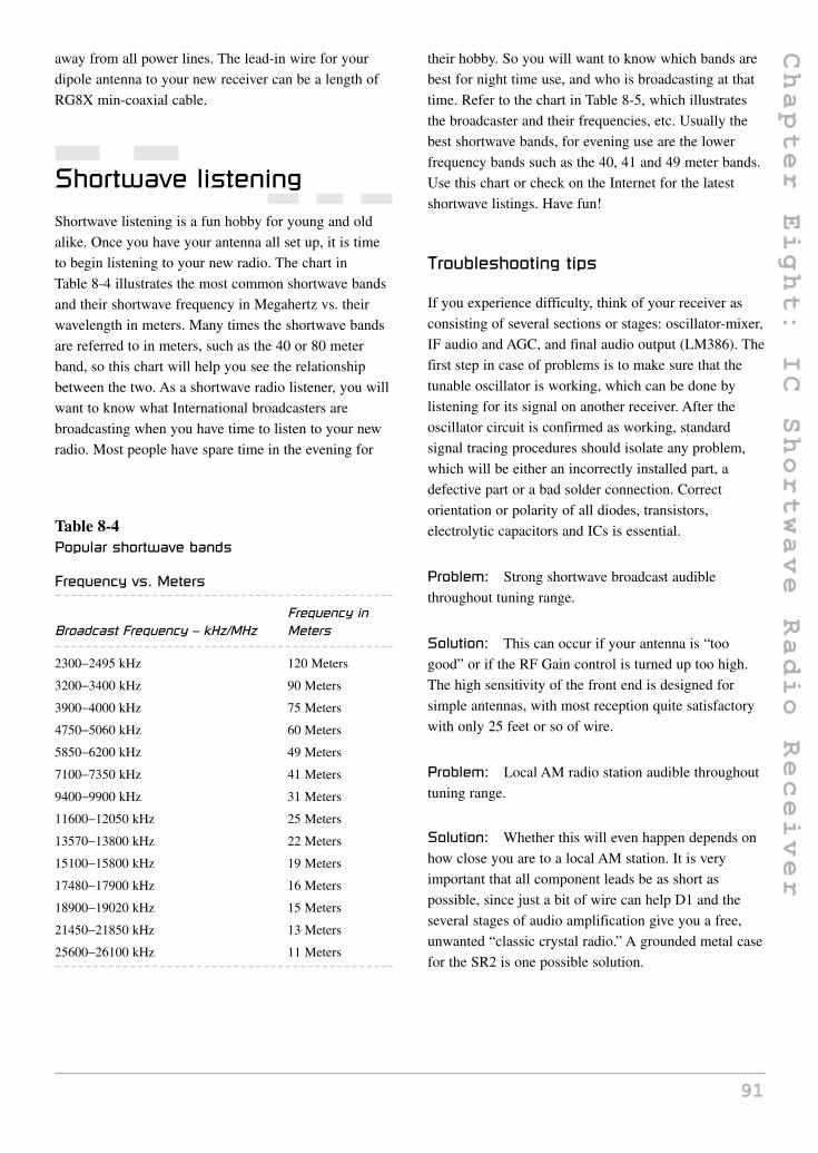
away from all power lines. The lead-in wire for your
dipole antenna to your new receiver can be a length of
RG8X min-coaxial cable.
Shortwave listeningShortwave listening is a fun hobby for young and old
alike. Once you have your antenna all set up, it is time
to begin listening to your new radio. The chart in
Table 8-4 illustrates the most common shortwave bands
and their shortwave frequency in Megahertz vs. their
wavelength in meters. Many times the shortwave bands
are referred to in meters, such as the 40 or 80 meter
band, so this chart will help you see the relationship
between the two. As a shortwave radio listener, you will
want to know what International broadcasters are
broadcasting when you have time to listen to your new
radio. Most people have spare time in the evening for
their hobby. So you will want to know which bands are
best for night time use, and who is broadcasting at that
time. Refer to the chart in Table 8-5, which illustrates
the broadcaster and their frequencies, etc. Usually the
best shortwave bands, for evening use are the lower
frequency bands such as the 40, 41 and 49 meter bands.
Use this chart or check on the Internet for the latest
shortwave listings. Have fun!
Troubleshooting tips
If you experience difficulty, think of your receiver as
consisting of several sections or stages: oscillator-mixer,
IF audio and AGC, and final audio output (LM386). The
first step in case of problems is to make sure that the
tunable oscillator is working, which can be done by
listening for its signal on another receiver. After the
oscillator circuit is confirmed as working, standard
signal tracing procedures should isolate any problem,
which will be either an incorrectly installed part, a
defective part or a bad solder connection. Correct
orientation or polarity of all diodes, transistors,
electrolytic capacitors and ICs is essential.
Problem: Strong shortwave broadcast audible
throughout tuning range.
Solution: This can occur if your antenna is “too
good” or if the RF Gain control is turned up too high.
The high sensitivity of the front end is designed for
simple antennas, with most reception quite satisfactory
with only 25 feet or so of wire.
Problem: Local AM radio station audible throughout
tuning range.
Solution: Whether this will even happen depends on
how close you are to a local AM station. It is very
important that all component leads be as short as
possible, since just a bit of wire can help D1 and the
several stages of audio amplification give you a free,
unwanted “classic crystal radio.” A grounded metal case
for the SR2 is one possible solution.
Table 8-4Popular shortwave bands
Frequency vs. Meters
Frequency in Broadcast Frequency – kHz/MHz Meters
2300−2495 kHz 120 Meters
3200−3400 kHz 90 Meters
3900−4000 kHz 75 Meters
4750−5060 kHz 60 Meters
5850−6200 kHz 49 Meters
7100−7350 kHz 41 Meters
9400−9900 kHz 31 Meters
11600−12050 kHz 25 Meters
13570−13800 kHz 22 Meters
15100−15800 kHz 19 Meters
17480−17900 kHz 16 Meters
18900−19020 kHz 15 Meters
21450−21850 kHz 13 Meters
25600−26100 kHz 11 Meters
91
Chapter Eight: IC
Shortwave Radio Receiver
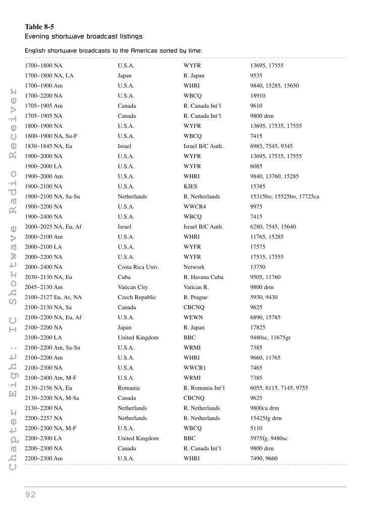
92
Chapter Eight: IC
Shortwave Radio Receiver
Table 8-5Evening shortwave broadcast listings
English shortwave broadcasts to the Americas sorted by time:
1700−1800 NA U.S.A. WYFR 13695, 17555
1700−1800 NA, LA Japan R. Japan 9535
1700−1900 Am U.S.A. WHRI 9840, 15285, 15650
1700−2200 NA U.S.A. WBCQ 18910
1705−1905 Am Canada R. Canada Int’l 9610
1705−1905 NA Canada R. Canada Int’l 9800 drm
1800−1900 NA U.S.A. WYFR 13695, 17535, 17555
1800−1900 NA, Su-F U.S.A. WBCQ 7415
1830−1845 NA, Eu Israel Israel B/C Auth. 6985, 7545, 9345
1900−2000 NA U.S.A. WYFR 13695, 17535, 17555
1900−2000 LA U.S.A. WYFR 6085
1900−2000 Am U.S.A. WHRI 9840, 13760, 15285
1900−2100 NA U.S.A. KJES 15385
1900−2100 NA, Sa-Su Netherlands R. Netherlands 15315bo, 15525bo, 17725ca
1900−2200 NA U.S.A. WWCR4 9975
1900−2400 NA U.S.A. WBCQ 7415
2000−2025 NA, Eu, Af Israel Israel B/C Auth. 6280, 7545, 15640
2000−2100 Am U.S.A. WHRI 11765, 15285
2000−2100 LA U.S.A. WYFR 17575
2000−2200 NA U.S.A. WYFR 17535, 17555
2000−2400 NA Costa Rica Univ. Network 13750
2030−2130 NA, Eu Cuba R. Havana Cuba 9505, 11760
2045−2130 Am Vatican City Vatican R. 9800 drm
2100−2127 Eu, As, NA Czech Republic R. Prague 5930, 9430
2100−2130 NA, Sa Canada CBCNQ 9625
2100−2200 NA, Eu, Af U.S.A. WEWN 6890, 15785
2100−2200 NA Japan R. Japan 17825
2100−2200 LA United Kingdom BBC 9480sc, 11675gr
2100−2200 Am, Sa-Su U.S.A. WRMI 7385
2100−2200 Am U.S.A. WHRI 9660, 11765
2100−2300 NA U.S.A. WWCR1 7465
2100−2400 Am, M-F U.S.A. WRMI 7385
2130−2156 NA, Eu Romania R. Romania Int’l 6055, 6115, 7145, 9755
2130−2200 NA, M-Sa Canada CBCNQ 9625
2130−2200 NA Netherlands R. Netherlands 9800ca drm
2200−2257 NA Netherlands R. Netherlands 15425fg drm
2200−2300 NA, M-F U.S.A. WBCQ 5110
2200−2300 LA United Kingdom BBC 5975fg, 9480sc
2200−2300 NA Canada R. Canada Int’l 9800 drm
2200−2300 Am U.S.A. WHRI 7490, 9660

Table 8-5Evening shortwave broadcast listings—cont’d
English shortwave broadcasts to the Americas sorted by time:
2200−2300 NA, M-F U.S.A. WBCQ 18910
2200−2300 NA, Sa-Su U.S.A. WWRB 3185
2200−2400 LA Guyana V. of Guyana 3290
2200−2400 NA, Su-F Canada CBCNQ 9625
2200−2400 Am Anguilla Wld Univ Network 6090
2200−2400 NA U.S.A. WWCR3 5070
2200−2400 NA U.S.A. WWCR4 9985
2200−2400 NA, Eu, Af U.S.A. WEWN 7560, 9975
2200−2400 NA U.S.A. WWRB Overcomer 6890
2230−2257 NA, Af Czech Republic R. Prague 5930, 9435
2300−2330 NA Germany Deutsche Welle 9800ca drm
2300−2350 NA Turkey V. of Turkey 5960
2300−2356 NA, Eu Romania R. Romania Int’l 6055, 6115, 7105, 9610
2300−2400 NA Egypt R. Cairo 11885
2300−2400 NA China China R. Int’l 6040, 11970
2300−2400 NA U.S.A. WBCQ 5110
2300−2400 Am U.S.A. WINB 9265
2300−2400 NA Cuba R. Havana Cuba 9550
2300−2400 NA, LA China China R. Int’l 5990ca
2300−2400 NA U.S.A. WHRA 5850
2300−2400 Am U.S.A. WHRI 7315, 7490
2300−2400 LA U.S.A. WYFR 15170, 15400
2300−2400 NA U.S.A. WWCR1 3215
2300−2400 NA U.S.A. WWRB 3185, 5050
2300−2400 LA, Su-F U.S.A. WWRB 5745
2330−2357 NA Czech Republic R. Prague 5930, 7345
2330−2359 NA Sweden R. Sweden 9800ca drm
2330−2400 NA Lithuania R. Vilnius 7325
2330−2400 Am, Su U.S.A. WRMI 9955
2335−2400 LA, Su-M Austria Osterreich 1 9870
2343−2358 LA, Tu-Sa Austria Osterreich 1 9870
Relay site codes: ae-United Arab Emirates, al-Albania, an-Antigua, ar-Armenia, as-Ascension, au-Austria, bo-Bonaire Neth. Antilles, bu-Bulgaria,
ca-Sackville Canada, ch-China, cl-Chile, cu-Cuba, cy-Cyprus, de-Delano USA, fg-French Guiana, fr-France, ga-Gabon, ge-Germany, gr-Greenville
USA, it-Italy, ja-Japan, ka-Kazakhstan, ko-South Korea, la-Latvia, li-Lithuania, ma-Madagascar, ml-Mali, mo-Moldova, ne-Netherlands, om-Oman,
po-Sines Portugal, ru-Russia, rw-Rwanda, sc-Cypress Creek SC, se-Seychelles, si-Singapore, sl-Sri Lanka, so-Slovakia, sp-Spain, sw-Sweden,
ta-Taiwan, th-Thailand, uk-United Kingdom, uz-Uzbekistan, wb-WBCQ USA, wr-WRMI USA, wy-WYFR USA, za-South Africa.
Notes – Days of week: Su-Sunday, M-Monday, Tu-Tuesday, W-Wednesday, Th-Thursday, F-Friday, Sa-Saturday, exW-except Wednesday.
Target areas: Af-Africa, Am-America, As-Asia, Eu-Europe, LA-Latin America, ME-Middle East, NA-North America, Oc-Oceania/Australia; Other:
alt-alternate frequency, drm-Digital Radio Mondiale, occ-occasional use, se-Special English.
Courtesy of Daniel Sampson; www.primetimeshortwave.com
93
Chapter Eight: IC
Shortwave Radio Receiver

80/40 Meter Code Practice Receiver
Chapter 9
Parts list
80/40 Meter DirectConversion ReceiverSpecifications
Sensitivity 3-uV or
better
Modes CW, RTTY (FSK),
SSB, AM
Audio output 50 mW
typical
Frequency coverage
Portions of the 80,
75, and 40 meter
bands
Power Source 9 volt
transistor battery,
alkaline preferred
PC Board 4.000” ×4.700”
80/40 Meter DirectConversion Receiver
R2 15 ohm, 1/4w,
5% resistor (brown,
green, black)
R3,R8 100 ohm, 1/4w,
5% resistor (brown,
black, brown)
R1 1000 ohm variable
potentiometer
C1 8.2 pF ceramic
disk (8.2)
C18 100 pF ceramic
trimmer capacitor
C19 15-50 pF variable
capacitor (main
tuning) - see text
C2,C6,C7 .1 µFmonolithic (.1 or 104)
C3 see chart below
C4 not used
C5 see chart below
C8,C9,C10 .1 µFmonolithic (.1 or 104)
C20 .01 µF ceramic disk(.01 or 103)
C12,C13,C14 1 µF,35 volt electrolytic
capacitor
C16,C17 470 µF, 35 voltelectrolytic capacitor
C11,C15 10 µF, 35 voltelectrolytic capacitor
U1 SA602 RF Mixer IC,
8-pin DIP
U2 78L05 voltage
regulator
U3 LM386 audio
amplifier, 8-pin DIP
S1 Power On-off
switch
J1 RCA antenna jack
J2 1/8′′ headphone jack
B1 9 volt transistor
radio battery
Misc PC board, IC
sockets, chassis,
knobs, wire, battery
94Copyright © 2008 by The McGraw-Hill Companies, Inc. Click here for terms of use.

95
Chapter Nine: 80/40 Meter Code Practice Receiver
holder, battery clip,
hardware, etc.
80 Meter Band Tuningcomponents
C3,C5 470 monolithic
capacitor (471)
L1 6.8 µH variableinductor, shielded
L2 3.3 µH molded choke(orange-orange-gold)
L3 33 µH molded choke(orange-orange-black)
40 Meter Band TurningComponents
C3 470 pF monolithic
(471)
C5 680 pF monolithic
(681)
L1 1.5 µH variableinductor, shielded
L2 1 µH molded choke(brown-black-gold)
L3 10 µH molded choke(brown-black-black)
* Inductors available
from Digi-Key
Electronics, see
Appendix.
Whether you’re a novice or an “old-timer,” you’ll be
pleasantly surprised at how this dual band Direct
Conversion Receiver performs! The receiver can be
constructed to receive either the 80 meter or 40 meter
amateur radio bands. You will be able to receive AM,
CW and SSB, signals from hams around the world.
Far-away signals are easily copied; and the sensitivity
of the 80/40 Meter Direct Conversion Receiver rivals
more expensive receivers. This receiver is ideal for
practicing and increasing your CW or code efficiency or
just having fun listening to shortwave broadcasts or ham
radio operators, at home or away. Build the receiver for
your favorite band, tuning options allow you to
customize the tuning range from full-band to 100 kHz or
less. Powered by a common 9 volt transistor battery, it’s
always ready for action on vacation and camping trips!
The 80/40 Meter Direct Conversion Receiver shown in
Figure 9-1, can easily be constructed by a radio neophyte
in a few hours with the easy-to-follow instructions.
Circuit descriptionThe circuit diagram shown in Figure 9-2 illustrates the
schematic for the 80/40 Meter Direct Conversion
Receiver. A dipole or suitable antenna is fed directly to
input jack J1, which is coupled to potentiometer R1,
which serves as a continuously variable RF attenuator
and also serves as the receiver’s gain control. Using the
RF gain control to set volume is advantageous as it also
reduces strong in-band signals that could otherwise
overload the receiver front end. Series inductors L2 and
L3, and trimmer capacitor C18, provide front-end
bandpass filtering, and an impedance match to 50 to
75-ohm antenna systems. IC U1 is an NE602/612 mixer
and Local Oscillator (LO) in an 8-pin dip package. The
mixer section is an active Gilbert cell design for good
conversion gain and low noise figure. The LO section
uses heavy capacitive loading to minimize frequency
drift. Tuning is capacitive, using a modern Hi-Q
miniature plastic variable. The local oscillator (LO)
stability is enhanced by a 78L05 voltage regulator.
Since this is a direct conversion receiver, the LO is
tuned to the carrier frequency of Single Sideband
Signals, or to a difference of 300 to 800 Hz on CW
Figure 9-1 80/40 meter code receiver

96
Chapter Nine: 80/40 Meter Code Practice Receiver
signals, to produce an aural output that is differentially
coupled to a LM386 audio IC. The audio amplifier IC is
coupled to the headphone jack at J2 by capacitor C16.
The receiver circuit is power from a single 9 volt
transistor radio battery.
Let’s get started! Before we begin building the
80/40 meter receiver, you will need to locate a clean
well lit and well ventilated work area. A large table or
workbench would be a suitable work surface for your
project. Next you will want to locate a small 27 to
33 watt pencil tipped soldering iron, as well as a roll of
#22 gauge 60/40 tin/lead solder and a small jar of
“Tip Tinner,” a soldering iron tip cleaner/dresser, from
your local Radio Shack store. You will also want to
secure a few hand tools for the project, such as a pair of
small end-cutters, a pair of tweezers and a pair of
needle-nose pliers. Locate a small Phillips and a small
flat-blade screwdriver, as well as a magnifying glass to
round out your tool list. Grab the schematic, parts layout
diagram as well as the resistor and capacitor identifier
charts and we will begin our project. Place all the project
components on the table in front of you. The 80/40
direct conversion radio is an RF or radio frequency
project and it is best constructed on a printed circuit
board with large ground plane areas covering the board
for the best RF grounding techniques. Once you have all
the parts and PC board in front of you, heat up the
soldering iron and we’ll get started!
First, find your resistor identifier chart in Table 9-1,
which will help you select the resistors from the parts
pile. Resistors used in this project are mostly small 1⁄4 watt carbon composition type resistors, which have
colored bands along the resistor body. The first color
band should be closest to one end of the resistor body.
This first color band represents the first digit of the
resistor value. For example, resistor R2 has four color
bands, the first one is a brown band followed by a green
band followed by a black band. The fourth band is gold.
Figure 9-2 80/40 meter direct conversion amateur radio receiver. Courtesy of Vectronics

The first band is brown, which denotes a digit one (1),
the second band is green, which represents a digit five
(5), and the third band is black, which represents a
multiplier of zero (0), so the resistor value is 15 ohms
with a tolerance value of 5%. Identify the remaining
resistors for the project and we can begin “populating”
the PC board. Place a few resistors on the board at one
time, so as not to confuse the process. Make sure that
you place the correct resistor into the correct PC
location before soldering it in place. Once you solder a
few resistors in place on the PC board you can use your
end-cutter to trim the excess component leads. Cut the
excess leads flush to the edge of the circuit board. Then
place a few more resistors on the PC board and solder
them on to the board. Remember to trim the component
leads as necessary.
Next we will locate the capacitors for the 80/40 meter
receiver. Capacitors are listed as electrolytic and non-
electrolytic types. The non-electrolytic types are
generally smaller in value and size as compared with
the electrolytic types. Non-electrolytic capacitors, in
fact, can be so small that their actual value cannot be
printed on them, so a special chart was devised as
shown in Table 9-2. The chart illustrates the three digit
codes which are often used to represent capacitors. For
example, a .001 µF capacitor will have (102), while
a .01 µF capacitor will have (103) marked on it to
represent its true value. Use the chart to identify the
small capacitors in the project. Non-electrolytics have
no polarity markings on them so they can be installed in
either direction on the PC board.
Electrolytic capacitors are usually larger in size and
value and they will have a white or black band on the
side of the capacitor body or a plus (+) or minus (−)
marking on the body of the capacitor near the leads.
These markings are polarity markings and that indicate
the direction in which the capacitor must be mounted on
the PC board. Failure to observe polarity when
installing the capacitor may result in damage to the
capacitor or to the circuit itself, so pay particular
attention to capacitor polarity when placing the
capacitors on the board. Note that the receiver can be
built for either the 80 meter ham band or the 40 meter
ham band. You will need to look at the parts list when
deciding which band you want to receive. The inductors
L1, L2 and L3 as well as capacitors C3, C4 and C5
determine the band selection.
Let’s go ahead and place some of the non-electrolytic
capacitors on the PC board. Identify a few small
capacitors at a time and place them on the PC board and
solder them in place. Trim the component leads after.
Go ahead and install the remaining non-electrolytic
capacitors after choosing your desired band. Install the
capacitors and solder them in place, remember to cut
Table 9-1Resistor color code chart
Color Band 1st Digit 2nd Digit Multiplier Tolerance
Black 0 0 1
Brown 1 1 10 1%
Red 2 2 100 2%
Orange 3 3 1,000 (K) 3%
Yellow 4 4 10,000 4%
Green 5 5 100,000
Blue 6 6 1,000,000 (M)
Violet 7 7 10,000,000
Gray 8 8 100,000,000
White 9 9 1,000,000,000
Gold 0.1 5%
Silver 0.01 10%
No color 20%
97
Chapter Nine: 80/40 Meter Code Practice Receiver
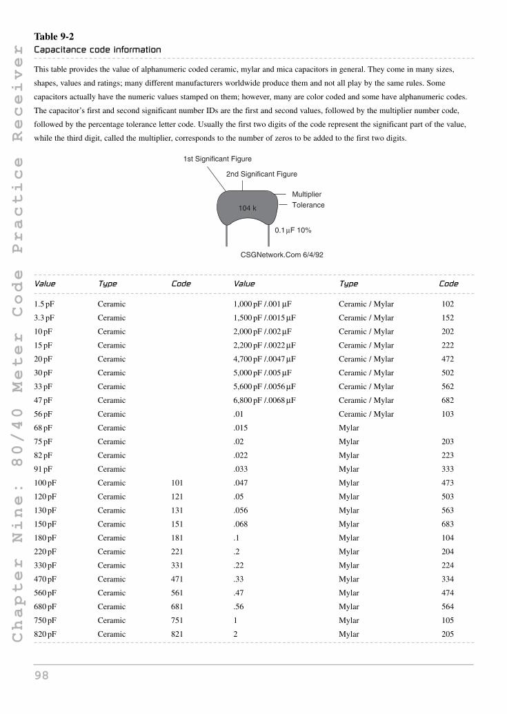
98
Chapter Nine: 80/40 Meter Code Practice Receiver
Table 9-2Capacitance code information
This table provides the value of alphanumeric coded ceramic, mylar and mica capacitors in general. They come in many sizes,
shapes, values and ratings; many different manufacturers worldwide produce them and not all play by the same rules. Some
capacitors actually have the numeric values stamped on them; however, many are color coded and some have alphanumeric codes.
The capacitor’s first and second significant number IDs are the first and second values, followed by the multiplier number code,
followed by the percentage tolerance letter code. Usually the first two digits of the code represent the significant part of the value,
while the third digit, called the multiplier, corresponds to the number of zeros to be added to the first two digits.
Value Type Code Value Type Code
1.5 pF Ceramic 1,000 pF /.001 µF Ceramic / Mylar 102
3.3 pF Ceramic 1,500 pF /.0015 µF Ceramic / Mylar 152
10 pF Ceramic 2,000 pF /.002 µF Ceramic / Mylar 202
15 pF Ceramic 2,200 pF /.0022 µF Ceramic / Mylar 222
20 pF Ceramic 4,700 pF /.0047 µF Ceramic / Mylar 472
30 pF Ceramic 5,000 pF /.005 µF Ceramic / Mylar 502
33 pF Ceramic 5,600 pF /.0056 µF Ceramic / Mylar 562
47 pF Ceramic 6,800 pF /.0068 µF Ceramic / Mylar 682
56 pF Ceramic .01 Ceramic / Mylar 103
68 pF Ceramic .015 Mylar
75 pF Ceramic .02 Mylar 203
82 pF Ceramic .022 Mylar 223
91 pF Ceramic .033 Mylar 333
100 pF Ceramic 101 .047 Mylar 473
120 pF Ceramic 121 .05 Mylar 503
130 pF Ceramic 131 .056 Mylar 563
150 pF Ceramic 151 .068 Mylar 683
180 pF Ceramic 181 .1 Mylar 104
220 pF Ceramic 221 .2 Mylar 204
330 pF Ceramic 331 .22 Mylar 224
470 pF Ceramic 471 .33 Mylar 334
560 pF Ceramic 561 .47 Mylar 474
680 pF Ceramic 681 .56 Mylar 564
750 pF Ceramic 751 1 Mylar 105
820 pF Ceramic 821 2 Mylar 205
1st Significant Figure
2nd Significant Figure
Multiplier
Tolerance
CSGNetwork.Com 6/4/92
0.1 µF 10%
104 k

the extra leads flush to the edge of the circuit board.
Now, you can go ahead and install the electrolytic
capacitors onto the circuit board. Go ahead and solder
them in place and trim the leads as necessary.
This receiver project uses a number of small
inductors. These small inductors will generally have
color bands on them to help identify them. Molded
chokes appear, at first glance, to be similar to resistors
in both shape and band marking. However, a closer look
will enable you to differentiate between the
two––chokes are generally larger in diameter and fatter
at the ends than resistors. When doing your inventory,
separate out any chokes and consult the parts list for
specific color-code information. Note, that inductor L1
is an adjustable slug tuned type. Remember that specific
chokes are used for each band: see parts list before
mounting the chokes. Chokes do not have polarity so
they can be mounted in either direction on the PC
board.
The 80/40 meter receiver utilizes two integrated
circuits and a regulator IC. Take a look at the diagram
shown in Figure 9-3, which illustrates the
semiconductor pin-outs. When constructing the project
it is best to use IC sockets as an insurance against a
possible circuit failure down-the-road. Its much easier to
unplug an IC rather than trying to un-solder it from the
PC board. IC sockets will have a notch or cut-out at one
end of the plastic socket. Pin one (1) of the IC socket
will be just to the left of the notch or cut-out. Note that
pin 1 of U1 connects to C1, while pin one (1) of U2
connects to C15. When inserting the IC into its
respective socket make sure you align pin one (1) of the
IC with pin one (1) the socket. Failure to install the IC
properly could result in damage to the IC as well as to
the circuit when power is first applied.
Let’s finish the circuit board by mounting the
volume control and the adjustable capacitors. The
volume control potentiometer at R1 is a right angle
PC board mounted type, which is placed at the edge
of the PC board as is the main tuning capacitor.
Capacitor C18, which is connected at the junction of L3
and C1, is an 8.2 pF trimmer type; go ahead and solder
it to the circuit board using two pieces of bare #22 ga.
stiff single conductor wire.
Locate main-tuning capacitor C19, now locate the
mounting location for main tuning capacitor C19. The
tuning capacitor was mounted on its side using double-
sided sticky tape. Remove the protective cover from the
double-sided tape, and firmly press the body of
capacitor C19 to mount it to the PC board. Firmly press
the double-sided tape over the silk-screened outline for
the body of C19. You may decide to mount the tuning
capacitor in a different way. At the rear of the capacitor:
locate the four internal trimmer capacitors, and using a
small jeweler’s screwdriver or alignment tool, fully open
(unmesh) all four trimmers. Note: tuning shaft faces
front of board. Bend the two rotor lugs so they are
parallel to the front face of the capacitor as shown
above. Connect the two rotor lugs to the PC board
ground points as shown using scraps of lead wire
trimmed from resistors as jumper wires. Cut a 6′′ length
of 24-AWG insulated hook-up wire in half. Remove
about 1⁄4′′ of the insulation from each of the cut ends.
Solder the jumpers to the capacitor rotor lugs, and to the
ground foil run on the bottom of the PC board. Since
the tuning capacitor has four sections, you can increase
the tuning ranges by paralleling different sections to
give a greater tuning range: see Table 9-3. If you used
just the 140 pF section, your tuning range would be
190 kHz, but if you combined the 140 pF section
with the 40 pF section your tuning range would become
180 pF and so forth. Capacitor jumpers: 180 pF = use
140-pF and 40-pF sections paralleled; 222 pF = use
140-pF and 82-pF sections paralleled; 262 pF = use
140-pF, 82-pF and a 40-pF sections paralleled;
302 pF = use all four capacitor sections in parallel.
The 80/40 meter code practice receiver can be built for
either of your favorite ham bands. First you will need to
decide which band you are interested in. Then you will
have to select the proper components from the chart in
Table 9-4, for the band of interest. Note that you will have
to select three capacitors and three coils for each band.
99
1234
8765
1234
8765
Input
00774433SA602
78L05
LM386
Bottom view
GND
Output
(TO-92)Plastic package (z)
Figure 9-3 Semiconductor pin-outs
Chapter Nine: 80/40 Meter Code Practice Receiver

100
Chapter Nine: 80/40 Meter Code Practice Receiver
Let’s take a few minutes for a short well-deserved
break, and when we return we will look over the circuit
board for any possible “cold” solder joints or “short”
circuits. Pick up the circuit board with the foil side
facing upwards toward you. First, we will examine the
circuit board for “cold” solder joints. Take a look at all
of the solder joints on the board, they should look clean,
bright and shiny. If you see any solder joints which look
dark, dull or “blobby,” then you should remove the
solder with a solder-sucker and then reapply more
solder and re-solder the joint all over again so that it
looks good. Next, we will look the board over for any
possible “short” circuits which are often caused by
“stray” component leads cut from the board or from
small solder blobs which may have bridged between
circuit traces. Rosin core solder can often leave a sticky
residue which will collect component leads and solder
blobs, so look the PC board over carefully for any
foreign objects on the foil side of the board.
The 80/40 meter receiver radio prototype was
mounted in a metal chassis box on plastic standoffs.
The PC board was aligned in the enclosure so that the
volume control, and main tuning control and power
switch were all mounted at one side of the case. Alight
the PC board along the edge of the chassis box, so that
you drill holes in the chassis for the volume and tuning
controls. The 1⁄8 ′′ switched headphone jack at J2 was
mounted on the front of the chassis, while the antenna
input jack at J1 was mounted on the rear of the case. The
9 volt transistor radio battery was mounted in a battery
holder which was fastened to the bottom panel of the
chassis box.
Your new 80/40 meter direct conversion receiver
project is almost completed. Apply the battery clip to
the 9 volt battery. Connect up an antenna to the antenna
jack, a dipole antenna cut for the band of interest would
be the best type of antenna. For test purposes, you could
connect a long piece of wire to the antenna jack for a
temporary antenna. Plug in an 8 ohm headphone and
then, turn on the power switch to the “On” position.
Now, adjust the volume control to the mid-position and
then turn the main tuning control. If all-goes-well, you
should begin to hear some radio stations. You may want
to test the radio in the early morning or evening when
these two bands are most active for best results.
Hopefully you will hear some stations while you tune
across the band.
If for some reason, your receiver is DEAD, then you
will want to turn off the receiver and remove the battery
clip and do another inspection of the circuit board. This
inspection is best done by another pair of eyes, someone
who is skilled at electronics might be your best choice
for inspection. You will want to make sure that you
installed the electrolytic capacitors correctly with
respect to their polarity. You will also want to make sure
that the integrated circuits are aligned correctly in their
respective sockets: it’s easy to make a mistake. Check to
make sure that the regulator IC at U2 was correctly
Table 9-3Band tuning range
80 Meter Tuning
302 pF 350 kHz
262 pF 310 kHz
222 pF 270 kHz
180 pF 230 kHz
140 pF 190 kHz
82 pF 110 kHz
40 pF 55 kHz
40 Meter Tuning Range
302 pF N/A
262 pF N/A
222 pF N/A
180 pF 310 kHz
140 pF 250 kHz
82 pF 150 kHz
40 pF 75 kHz
Table 9-480/40 Band change components
40-Meter Components 80-Meter Components
C3 - 470 pF capacitor C3 - 470 pF capacitor
C4 - not used C4 - not used
C5 - 680 pF capacitor C5 - 470 pF capacitor
L1 - 1.5 µH molded coil L1 - 6.8 µH molded coil
L2 - 1 µH molded coil L2 - 3.3 µH molded coil
L3 - 10 µH molded coil L3 - 33 µH molded coil

installed with the input of the regulator going to
capacitor C12, and the output of the regulator going to
capacitor C11. Finally, make sure that you have the
battery clip polarity wired correctly. Once you have
examined the circuit board once more, you can go
ahead and reconnect the battery and antenna and try the
receiver again to see if it works now.
If your receiver is now working correctly, we can
move on to the alignment of your new receiver.
There are two primary methods of aligning the
receiver’s local oscillator.
Receiver alignmentmethod 1: using anadditional receiverPlace your new 80/40 meter receiver next to an amateur
or general coverage receiver that covers the band of
interest. Connect a short 3 or 4 foot wire antenna to the
receiver, route the antenna wire so it passes near the
direct conversion receiver PC board. Next, select a
tuning tool that properly fits coil L1. The 20 meter kit
requires a hex type alignment tool. The other kits
require a small blade type tool that matches the slot in
the coil core, or use a small jeweler’s screwdriver. Now,
set coil L1 tuning core to the top of the coil form. At
this time, tune the receiver to the lowest operating
frequency by turning the tuning capacitor shaft fully
CCW (counter clockwise). Next, go ahead and set the
monitor receiver to the lowest frequency you wish to
receive on the direct conversion receiver. The receiver
should be set to a wide filter bandwidth, and if it has a
BFO, it should be on. Install a fresh 9 volt alkaline
battery to the receiver, and turn it on by depressing the
push-action power switch.
Finally, carefully adjust the core in coil L1 until it is
heard sweeping across the monitor receiver frequency.
Set the coil for zero beat, or strongest S-meter reading
on the receiver. Note that metal alignment tools will
cause some frequency shift, and interact with the tuning
when removed or inserted into the coil. You will have to
adjust the coil in small increments, and observe the point
where the proper frequency is reached when the tool is
removed.
Receiver alignmentmethod 2: using a signalgeneratorFirst, set the signal generator to the direct conversion
receiver’s lowest operating frequency. Set the generator
output level for a 30-µV CW signal. Next, connect the
generator RF output to the VEC direct conversion
antenna jack (J1) using coax cable and the appropriate
mating connectors or adapters. Now, connect a speaker
or headphones to jack J2 on the receiver. At this point,
set the receiver gain fully CW (clockwise) and the
tuning knob fully CCW (counter clockwise). Next,
select a tuning tool that properly fits coil L1. The
20 meter kit requires a hex type alignment tool. The
other kits require a small blade type tool that matches
the slot in the coil core. Or, a jeweler’s screwdriver may
be used. Go ahead and set coil L1 tuning core to the top
of the coil form. Now, connect a fresh 9 volt alkaline
battery to the receiver, and turn it on using the
push-action power switch. Finally, carefully adjust the
core in coil L1 until the generator signal is heard. Set
the coil for zero beat. Note that metal alignment tools
will cause some frequency shift, and interact with the
tuning when removed or inserted into the coil. You will
have to adjust the coil in small increments, and observe
the point where the proper frequency is reached when
the tool is removed.
Final alignmentOnce the tuning range is set, the RF input stage must be
peaked for best sensitivity. This can be done using a
signal generator, or on-the-air signals. Find an
alignment tool or jeweler’s screwdriver that fits trimmer
capacitor C18. Use one of the following three methods
to peak C18.
1. Using a signal generator, peak C18 for best
sensitivity. Reduce the signal generator output, or
reduce the R1 Gain control setting, to prevent
overload as C18 is brought into resonance.
2. Using off-air signals, adjust C18 until signals are
loudest. Reduce the R1 Gain control as C18 is
101
Chapter Nine: 80/40 Meter Code Practice Receiver

102
Chapter Nine: 80/40 Meter Code Practice Receiver
brought into resonance to prevent overload. Verify
that C18 is properly peaked while monitoring a
known on-air signal.
3. With an outside antenna connected, peak C18 for
maximum atmospheric noise in the headphones or
speaker. Verify that C18 is properly peaked while
monitoring a known on-air signal.
Antenna considerationsWith your new receiver completed and aligned, you can
attach a dipole antenna for the chosen band of
operation. Direct conversion receivers need good
antennas. Using a random length of wire will give poor
results. Half-wave dipoles are very effective antennas
and are simple to construct. For low-power or QRP
work, or for receive only applications, low-cost
RG-58 52 ohm coax is fine. The formula for dipole
antennas: 234/(frequency in MHz) = 1⁄4-wavelength in feet
will give the length of wire needed for each leg of the
dipole. For example, if you wanted to build a 40-meter
dipole for the CW portion of the band you would divide
234 by 7.040 MHz and the result would be 33.238 feet per
leg on either side of the center insulator: see Figure 9-4.
Tuning notesWhile trying to tune CW stations, you should tune
across the band until a CW signal is heard. Set the gain
control at R1 for a comfortable listening level.
Then, carefully adjust the tuning control until the
“beat note,” or tone, sounds best for you.
Most experienced CW operators prefer a lower beat
note of about 300 or 400 Hz.
When trying to tune-in single-side band (SSB) stations,
you may need a little practice to tune-in the signal
properly. Direct conversion receivers offer no upper or
lower sideband rejection, so you will have to slowly
tune across the SSB signal until the voices become
natural sounding. Use the gain control to prevent
overload and to set a comfortable listening level.
In order to tune-in AM stations, you will need to
realize that, unlike SSB signals, AM signals have a
carrier frequency. That means you will hear a beat note
as you tune across an AM signal. Tune the signal so the
beat note becomes lower in frequency and stop when
“zero beat” (beat note disappears) is reached.
Possible overloadproblemsAn unfortunate fact of life is that low-power amateur
signals are surrounded by high-power SW broadcast
signals, so there may be a possibility of overload
problems. In order to compensate for this possible
problem, you may need to lower the gain control.
Simply lowering the gain setting will resolve many
overload problems. Another approach to an overload
problem is to use a preselector. A preselector provides
protection from strong out-of-band signals. They are
most effective when the interfering signal is far from the
operating frequency.
A resonant antenna favors signals in the band it was
cut for, so when faced with a severe overload problem,
you elect to use a resonant antenna. The final approach
to solving an overload problem is to change the
direction the dipole faces; this may lower unwanted
pickup of undesired SW signals. Lowering the
antenna will change its angle of pickup; a low antenna
may favor local stations over the low-angle of
distant broadcast signals. A shorter antenna can also
be tried; it will be less efficient and signals will be
weaker.
Figure 9-4 80/40 meter dipole antenna

The chart shown in Table 9-5 illustrates the W1AW
code practice sessions for Ham Radio operators or those
interested in obtaining a Ham Radio license. The
80-meter frequency is 3.5815 MHz and the 40-meter
frequency is 7.0475. The Amateur Radio Relay League
(ARRL) offers these code practice sessions every day to
help amateur radio enthusiasts increase their code
speed. The ARRL is a great resource for those
interested in Amateur Radio and offers many books,
magazines and free literature in including videos to help
you understand what Amateur Radio is all about. Take a
few minutes and explore their web-site.
103
Table 9-5W1AW on-air code practice sessions
Pacific Mtn Central East Mon Tues Weds Thur Fri
6 am 7 am 8 am 9 am fast code slow code fast code slow code
7-9 am 8-10 am 9-11 am 10-noon visiting operator time ———— ————
10 am-12:45 pm 11 am-1:45 pm noon-2:45 pm 1-3:45 pm
1 pm 2 pm 3 pm 4 pm fast slow fast slow fast
2 pm 3 pm 4 pm 5 pm ———— code bulletin ———— ————
3 pm 4 pm 5 pm 6 pm ———— teleprint bulletin ———— ————
4 pm 5 pm 6 pm 7 pm slow fast slow fast slow
5 pm 6 pm 7 pm 8 pm ———— code bulletin ———— ————
6 pm 7 pm 8 pm 9 pm ———— teleprint bulletin ———— ————
6:45 pm 7:45 8:45 9:45 ———— voice bulletin ———— ————
7 pm 8 pm 9 pm 10 pm fast slow fast slow fast
8 pm 9 pm 10 pm 11 pm ———— code bulletin ———— ————
Frequencies are 1.8175, 3.5815, 7.0475, 14.0475, 18.0975, 21.0675, 28.0675 and 147.555 MHz.
Slow Code = practice sent at 5, 71⁄2, 10, 13 and 15 words per minute (wpm).
Fast Code = practice sent at 35, 30, 25, 20, 15, 13 and 10 wpm.
Chapter Nine: 80/40 Meter Code Practice Receiver
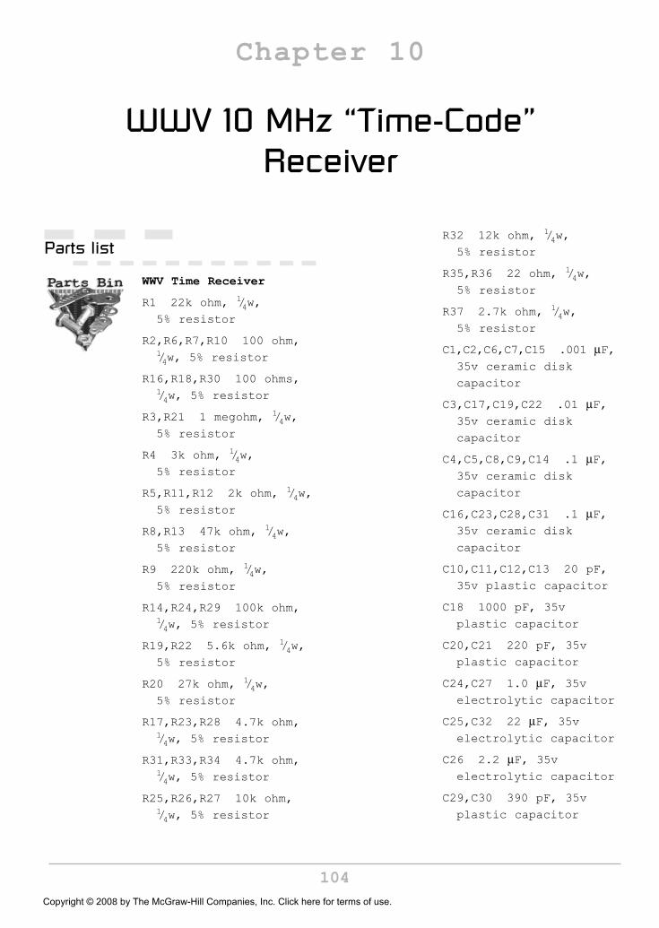
WWV 10 MHz “Time-Code” Receiver
Chapter 10
Parts list
WWV Time Receiver
R1 22k ohm, 1/4w,
5% resistor
R2,R6,R7,R10 100 ohm,1/4w, 5% resistor
R16,R18,R30 100 ohms,1/4w, 5% resistor
R3,R21 1 megohm, 1/4w,
5% resistor
R4 3k ohm, 1/4w,
5% resistor
R5,R11,R12 2k ohm, 1/4w,
5% resistor
R8,R13 47k ohm, 1/4w,
5% resistor
R9 220k ohm, 1/4w,
5% resistor
R14,R24,R29 100k ohm,1/4w, 5% resistor
R19,R22 5.6k ohm, 1/4w,
5% resistor
R20 27k ohm, 1/4w,
5% resistor
R17,R23,R28 4.7k ohm,1/4w, 5% resistor
R31,R33,R34 4.7k ohm,1/4w, 5% resistor
R25,R26,R27 10k ohm,1/4w, 5% resistor
R32 12k ohm, 1/4w,
5% resistor
R35,R36 22 ohm, 1/4w,
5% resistor
R37 2.7k ohm, 1/4w,
5% resistor
C1,C2,C6,C7,C15 .001 µF,35v ceramic disk
capacitor
C3,C17,C19,C22 .01 µF,35v ceramic disk
capacitor
C4,C5,C8,C9,C14 .1 µF,35v ceramic disk
capacitor
C16,C23,C28,C31 .1 µF,35v ceramic disk
capacitor
C10,C11,C12,C13 20 pF,
35v plastic capacitor
C18 1000 pF, 35v
plastic capacitor
C20,C21 220 pF, 35v
plastic capacitor
C24,C27 1.0 µF, 35velectrolytic capacitor
C25,C32 22 µF, 35velectrolytic capacitor
C26 2.2 µF, 35velectrolytic capacitor
C29,C30 390 pF, 35v
plastic capacitor
104Copyright © 2008 by The McGraw-Hill Companies, Inc. Click here for terms of use.

105
Chapter Ten: WWV 10 MHz “Time-Code” Receiver
C33 100 µF, 35velectrolytic capacitor
C34 2200 µF, 35velectrolytic capacitor
C35 10 µF, 35velectrolytic capacitor
C36,C37 1000 µF, 35velectrolytic capacitor
C38 330 µF, 35velectrolytic capacitor
C39 470 µF, 35 voltelectrolytic capacitor
CV1 10-40 pF trimmer
capacitor
CV2 10-70 pF trimmer
capacitor
VR1 10k ohm RF gain
potentiometer
VR2 1M ohm Sensitivity
potentiometer
VR3 10k ohm volume
control potentiometer
L1 4.1 µH coil - 27turns on T-28-2
ferrite core using 22
AWG wire tap 2-turns
from ground side
L2,L4 12 turns on
FT37-43 ferrite toroid
core
L3 3.0 µH - 25 turns#26 AWG wire on T50-2
ferrite core
L5 12 turns on FT37-43
ferrite toroid
core
L6 1000 µH coil
D1 1N5711 silicon
Schottky diode NTE 112
D2 optional LED - power
“on” indicator
Y1,Y2,Y3 10 MHz
crystal
(F) 3-ferrite beads -
(see front-end)- run
wire through beads
Q1,Q2,Q3 Dual Gate
MOSFET 40673 or ECG222
Q4,Q5 nJFET MPF102
Q6,Q7 2N3904 NPN
transistor
Q8 2N3906 PNP
transistor
U1 Signetics NE5532
Op-Amp
J1 RCA jack - antenna
J2 Coaxial power jack
SPK 8-ohm 3′′ speaker
S1 SPST power switch
Misc PC board, wire,
hardware, sockets,
etc.
Does anybody really know what time it is? The WWV
receiver, shown in Figures 10-1 and 10-2, is designed to
tune the National Institute of Standards and Technology
(NIST) atomic clock for moment by moment time
accuracy! This is a great receiver project that actually
serves a dedicated purpose. Put one in the boat or on a
desk and you’ll always know what time it is!
The WWV receiver is quite sensitive, and with a good
antenna you should be able to receive time signals most
of the time! The receiver features easy tuning and
small size, it can be packed up and taken anywhere and
runs on a 12 volt DC power supply, or a 12 volt
battery for portable operation. An earphone jack is
provided for headset operation so you can use it
night or day.
Figure 10-1 WWV time code received

106
Chapter Ten: WWV 10 MHz “Time-Code” Receiver
People have always been fascinated with the
measurement and properties of time. What happened to
that last second that you just spent reading this sentence?
Perhaps this is the reason that so many of us have tuned
in over the years to the National Institute of Standards
and Technology (NIST) “clock” operating at a
transmitting frequency of 10 MHz. The cesium standard
NIST-7 has an accuracy of 5 × 10-15 seconds. Now that’s
accurate! In fact, the definition of a “second” is the
duration of 9,192,631,770 periods of the radiation
corresponding to the transition between the two hyperfine
levels of the ground state of the cesium-133 atom.
We set our clocks, watches, and chronometers to the
all-important “beep” of the radio signal that denotes the
correct time to the second. In addition; avid listeners of
the NIST clock are also treated to the following
(from the NIST web site).
The OMEGA Navigation System status reports are
voice announcements broadcast on WWV at 16 minutes
after the hour. The OMEGA Navigation System consists
of eight radio stations transmitting in the 10- to 14-kHz
frequency band. These stations serve as international
aids to navigation. The status reports are updated as
necessary by the U.S. Coast Guard. Current geophysical
alerts (Geoalerts) are broadcast in voice from WWV at
18 minutes after the hour. The messages are less than
45 s in length and are updated every 3 hours (typically
at 0000, 0300, 0600, 0900, 1200, 1500, 1800, and
2100 UTC). Hourly updates are made when
necessary.
Marine storm warnings are broadcast for the marine
areas that the United States has warning responsibility
for under international agreement. The storm warning
information is provided by the National Weather
Service. Storm warnings for the Atlantic and eastern
North Pacific are broadcast by voice on WWV at 8, 9,
and 10 minutes after the hour. An additional segment
(at 11 minutes after the hour on WWV) is used
occasionally if there are unusually widespread storm
conditions. The brief voice messages warn mariners of
storm threats present in their areas. The storm warnings
are based on the most recent forecasts. Updated
forecasts are issued by the National Weather Service at
0500, 1100, 1700, and 2300 UTC for WWV. Since
March 1990 the U.S. Coast Guard has sponsored two
voice announcements per hour on WWV giving current
status information about the GPS satellites and related
operations. The 45-s announcements begin at 14 and
15 minutes after each hour.
WWV radiates 10,000 watts on 5, 10, and 15 MHz.
The WWV antennas are half-wave dipoles that radiate
omnidirectional patterns. The station uses double
sideband amplitude modulation. The modulation level is
50 percent for the steady tones, 25 percent for the
BCD time code, 100 percent for the seconds pulses
and the minute and hour markers, and 75 percent for the
voice announcements. That’s a lot of information being
broadcast, and you can easily pickup these signals with
the high frequency 10 MHz Time Receiver shown in
this project. The WWV Time receiver has excellent
sensitivity, selectivity, and dynamic range. (from the
NIST web site http://www.nist.gov/)
Circuit descriptionThe 10 MHz WWV Receiver is shown in the block
diagram of Figure 10-3 and in the main schematic
diagram in Figure 10-4. The WWV Time Code receiver
is an AM TRF or Tuned Radio Frequency or TRF type
receiver. This receiver project is designed specifically
for 10 MHz time signal operation. The block diagram of
the WWV receiver illustrates the four major sections of
the receiver. The receiver’s front-end, as shown in the
schematic diagram, features two sensitive dual-gate
MOSFETs in the front-end circuit with a single-pole
filter. An RF gain control is shown at VR1 which
adjusts the input sensitivity, via a 10k ohm
potentiometer. Note inductor L1 is 4.1 µH coil, which
consists of 27 turns of 22 ga. AWG wire wound on a
Figure 10-2 WWV time code received – inside view

T-68 ferrite core. Inductors L2 and L4 consist of 12
turns of 22 ga. AWG wire on an FT37-43 ferrite core,
and finally L3 consists of 25 turns of #26 ga. AWG wire
on a T50-2 ferrite core. For even greater selectivity (but
greater insertion loss), you can consider moving the L1
tap to 1 turn from ground. Fine tuning the WWV
receiver is accomplished by adjusting CV1 and CV2
trimmer capacitors. The front-end MOSFETs are
extremely sensitive to static electricity, so be very
careful in handling them. Note the two ferrite beads,
one is placed in series with the Drain lead of Q1, while
the second ferrite bead is in series with the Drain of Q2.
These ferrite beads are important, so be sure to
use them. The receiver front-end, at J1, should be
connected to a dipole antenna “cut” for 10 MHz. TRF
receivers are especially sensitive and are subject to
overloading a BCB or Broadcast Band Interference, so
internal lead lengths should be kept short between
components and the front-end should be shielded and
the receiver placed in a metal enclosure for best results.
The output impedance of Q2 is 2000 ohms, which
nicely matches the input impedance of the Cohn crystal
filter, in the crystal filter section of the receiver. This
filter utilizes three 10 MHz crystals. Choose 10 MHz
crystals that are marked for a 20 pF or 32 pF load
capacitance if possible. Using a 10 MHz crystal
oscillator, find three that are closest to one another in
frequency. You may substitute 2.2k ohm resistors
instead of the specified 2k with a slight penalty in pass
band shape. The crystal filter section utilizes a single
dual-gate MOSFET transistor at Q3. Coil L5 is 12 turns
on an FT37-43 ferrite core. The output of the Cohn
crystal filter is next fed to the input of the AM detector
stage.
The AM detector has three distinct advantages;
it has high bandwidth, low distortion and incredible
(and variable) sensitivity. The variable bias control
allows the listener to adjust the bias to maintain
detected audio fidelity even when the RF signal is weak.
The detector uses a Schottky UHF mixer diode at D1.
Increasing the diode bias from zero volts to maximum
causes three things to happen: increased sensitivity,
increased audio high frequency response, and a slight
increase in receiver noise.
The AM detector section matches the 2000 ohm
impedance of the crystal filter stage quite nicely.
A sensitivity control at VR2 is a 1 megohm
potentiometer, which feeds directly to L6, a 1000 µH
coil. Coil L6 is connected directly to a Schottky diode
at D1. The resultant signal is next sent through a 5.6k
ohm resistor and on to a 1 µF capacitor which feeds the
nJFET at Q4. The Source lead of Q1 is connected to the
Drain lead of Q5, and the Source lead of Q5 is
connected to ground via a 5.6k ohm resistor. Note the
two 22 µF electrolytic capacitors on each of the Drain
leads of the nJFETs.
When the WWV RF signal is weak, turning the bias
off may result in the detected WWV signal
disappearing. Increasing the bias will bring the WWV
signal back in. You run the bias control pot about half
way and, of course, higher as WWV fades out. The
fidelity that the bias adds even when the WWV signal is
strong is quite pleasing to the ear. For the 1 µF and
2.2 µF capacitors, I used polyester film types which
sounded better than electrolytic capacitors.
The audio amplifier section features low noise audio
amplifier. Distortion is very low as long as the input is
Figure 10-3 10 MHz WWV receiver block diagram
107
Chapter Ten: WWV 10 MHz “Time-Code” Receiver
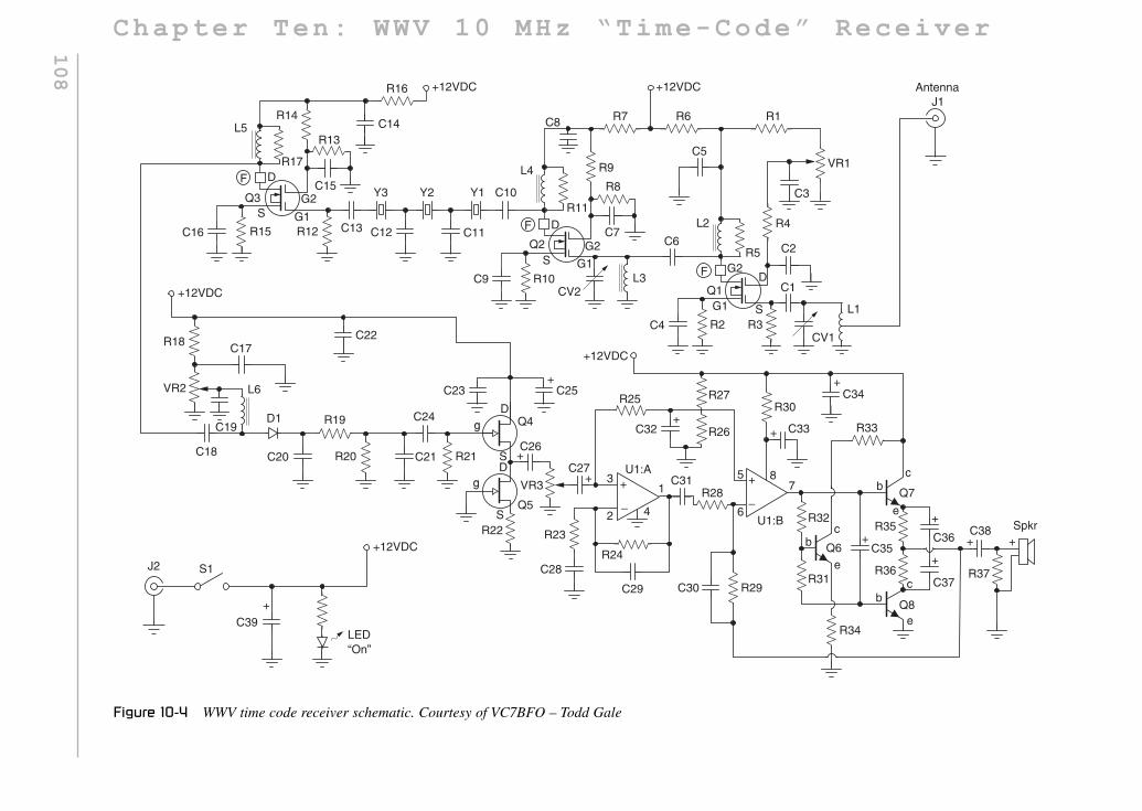
108
C hapter Ten: WWV 10 MHz “Time-Code” Receiver
Figure 10-4 WWV time code receiver schematic. Courtesy of VC7BFO – Todd Gale

not over driven. The audio amplifier section consists of a
dual NE5532 op-amp and three transistors. Transistors
Q6 and Q7 are NPN types, while transistor Q7 is a PNP
type. The input signal from the detector is fed directly to
the volume control at VR3, a 10k ohm potentiometer.
The input signal is first sent to the non-inverting stage of
the first op-amp at pin 3. The output of the first op-amp
section at pin 1 is next sent to the second stage of the
op-amp through a .1 µF capacitor in series with a 4.7k
ohm resistor to pin of U1:b. The output of U1, at pin 7 is
then fed to the output transistor stage. The output of the
transistor pair is two 1000 µF capacitors which coupled
to a 330 µF capacitor which feeds the 8 ohm speaker.
The entire WWV receiver is powered from a 12 volt
“wall-wart” power or can be powered from a 12 volt
battery for portable operation.
Receiver assemblyYou are probably quite anxious to begin the assembly of
the receiver project; it is best to follow the assembly
steps in order. Try to avoid the urge to “jump ahead”
installing components. Locate your layout and
schematic diagram. Place all the components in front of
you and locate a 27-30 watt pencil tip soldering iron.
Make sure you have a large work table in order to
spread out all the parts and diagrams. A printed circuit
board is highly recommended for this project, so you
should have your circuit board in front of you oriented
correctly, in order to begin populating the PC board.
Remember that the components will be mounted on the
“component” side of the circuit board and soldered on
the “solder” side of the circuit board, the side with the
printed circuit traces. Locate a spool of 60/40 tin/lead
rosin core solder for this project.
First we will begin by locating all of the resistors for
the project. Most all of the resistors are 1⁄4 watt carbon
composition type resistors except for the potentiometer.
Before we begin building the Time receiver, take a
moment to refer to the resistor color chart shown in
Table 10-1. Note that each resistor will have three or four
color bands beginning at one end of the resistor body.
The first color code represents the resistor’s first digit
value, while the second color band denotes the resistor’s
second digit value. The third color band represents the
multiplier value of the resistor and the fourth band denotes
the tolerance value of the resistor. If the fourth color band
is silver then the resistor has a tolerance of 10%, while a
gold band denotes a 5% tolerance. If there is no fourth
color band then the resistor has a tolerance of 20%. The
first color band of a 10,000 ohm resistor, for example,
Table 10-1Resistor color code chart
Color Band 1st Digit 2nd Digit Multiplier Tolerance
Black 0 0 1
Brown 1 1 10 1%
Red 2 2 100 2%
Orange 3 3 1,000 (K) 3%
Yellow 4 4 10,000 4%
Green 5 5 100,000
Blue 6 6 1,000,000 (M)
Violet 7 7 10,000,000
Gray 8 8 100,000,000
White 9 9 1,000,000,000
Gold 0.1 5%
Silver 0.01 10%
No color 20%
109
Chapter Ten: WWV 10 MHz “Time-Code” Receiver

110
Chapter Ten: WWV 10 MHz “Time-Code” Receiver
would be brown with a value of (1). The second color
band would be black with a value of (0). The third color
band would be orange with a value of (000). Read the
color codes on the resistors and compare them to the
parts list and layout diagram so that you place the correct
resistor in the correct hole on the printed circuit board.
You can install the resistors in groups of four or five.
Solder the first group of resistors onto the circuit board,
then cut the excess component leads flush to the edge of
the PC board using a pair of small end-cutters. Then
move on to the next group of resistors until all of the
resistors have been installed.
Next we will move on to installing the capacitors.
Most all of the capacitors will have some sort of
marking on them, so compare the value or marking on
the component with the parts list before installing the
components on the PC board. Note that capacitors C24,
C25, C26, C27 are all electrolytic capacitors; these
capacitors will have additional polarity markings on
them and they must be installed with respect to these
polarity markings in order for the circuit to work
properly. Each of these capacitors will have a white or
black band with either a plus or minus marking on one
side or edge of the component. You must orient the
capacitor correctly, so you should refer to the layout
diagram and schematic diagram when installing these
parts. Also note that capacitors C32 through C38 are
also all electrolytic types. All the other capacitors have
no polarity marking so they can be installed in either
direction. Now, you will want to refer to the capacitor
code chart shown in Table 10-2, which illustrates the
codes used for small size capacitors. Often very small
capacitors will not have their actual value printed on
them, because there may not be enough room, so a
three-digit code was developed. Look at the chart and
compare the numbers on the chart with the actual
capacitors to help identify them. You can go ahead and
install all of the capacitors at this time. It is best to
install the capacitors in groups of four or five at a time,
then solder them on to the circuit board before
moving on to the next group of capacitors; this helps
keep some order to the building process. It is also
advisable to check off each of the components
against the parts list, so you can keep tabs on your
progress and make sure that all of the parts are
accounted for. Solder a group of four or five
components, cut the excess leads and then move on to
the next group of components. This will keep things in
an orderly fashion.
Next, go ahead and locate and install the
Schottky diode at D1. Note that the diode has a polarity
marking on the glass enclosure. At one end of the
diode body you should see a black or white band; this
denotes the cathode side of the diode. Look at your
schematic diagram to observe the direction of the
cathode band in the circuit before you install
the diodes.
The WWV receiver incorporates six inductors; five of
the inductors are wound on ferrite cores, while L6 is a
ready-made 1000 µH choke coil. Refer to the chart in
Table 10-3 for details on winding each of the coils.
When winding the coil you will have to scrape the
insulation off each of the wire ends in order to solder
the coil to the circuit board. You will need to secure the
coil to the circuit board using a couple of “dabs” of
rubber cement. Once the coils have been secured to the
PC board, you can solder the coil leads to the
circuit board, and then remove the excess lead
lengths.
Locate the three crystals, Y1, Y2 and Y3 and place
them on the PC board. Now solder the crystals to the
PC board and then trim the excess leads flush to the
edge of the circuit board.
Before we attempt to install the semiconductors, take
a quick look at the semiconductor pin-out diagram
shown in Figure 10-5. Now locate the MOSFETs Q1,
Q2 and Q3. These devices are very static sensitive and
must be handled very carefully using an anti-static
wrist-band to avoid damage before they are soldered
into the circuit. Transistor sockets are highly
recommended for all of the transistors, see the pin-out
diagram for the MOSFETs and make sure you can
identify each of the leads before placing the MOSFETs
on to the circuit board. The MOSFETs have two Gate
leads, G1 and G2, as well as a Source lead (S) and a
Drain lead (D). Once you are sure of each of the leads,
you can go ahead and install the MOSFETS onto
the circuit board. The AM detector portion of the
receiver utilizes two nJFETS at Q4 and Q5, these
semiconductors are also static sensitive and must be
handled with extreme care to avoid damage. The
nJFETS have three leads, like most conventional
transistors, but they have a Gate, Source and Drain lead,

Table 10-2Capacitance code information
This table provides the value of alphanumeric coded ceramic, mylar and mica capacitors in general. They come in many sizes,
shapes, values and ratings; many different manufacturers worldwide produce them and not all play by the same rules. Some
capacitors actually have the numeric values stamped on them; however, many are color coded and some have alphanumeric codes.
The capacitor’s first and second significant number IDs are the first and second values, followed by the multiplier number code,
followed by the percentage tolerance letter code. Usually the first two digits of the code represent the significant part of the value,
while the third digit, called the multiplier, corresponds to the number of zeros to be added to the first two digits.
Value Type Code Value Type Code
1.5 pF Ceramic 1,000 pF /.001 µF Ceramic / Mylar 102
3.3 pF Ceramic 1,500 pF /.0015 µF Ceramic / Mylar 152
10 pF Ceramic 2,000 pF /.002 µF Ceramic / Mylar 202
15 pF Ceramic 2,200 pF /.0022 µF Ceramic / Mylar 222
20 pF Ceramic 4,700 pF /.0047 µF Ceramic / Mylar 472
30 pF Ceramic 5,000 pF /.005 µF Ceramic / Mylar 502
33 pF Ceramic 5,600 pF /.0056 µF Ceramic / Mylar 562
47 pF Ceramic 6,800 pF /.0068 µF Ceramic / Mylar 682
56 pF Ceramic .01 Ceramic / Mylar 103
68 pF Ceramic .015 Mylar
75 pF Ceramic .02 Mylar 203
82 pF Ceramic .022 Mylar 223
91 pF Ceramic .033 Mylar 333
100 pF Ceramic 101 .047 Mylar 473
120 pF Ceramic 121 .05 Mylar 503
130 pF Ceramic 131 .056 Mylar 563
150 pF Ceramic 151 .068 Mylar 683
180 pF Ceramic 181 .1 Mylar 104
220 pF Ceramic 221 .2 Mylar 204
330 pF Ceramic 331 .22 Mylar 224
470 pF Ceramic 471 .33 Mylar 334
560 pF Ceramic 561 .47 Mylar 474
680 pF Ceramic 681 .56 Mylar 564
750 pF Ceramic 751 1 Mylar 105
820 pF Ceramic 821 2 Mylar 205
1st Significant Figure
2nd Significant Figure
Multiplier
Tolerance
CSGNetwork.Com 6/4/92
0.1 µF 10%
104 k
111
Chapter Ten: WWV 10 MHz “Time-Code” Receiver

112
Chapter Ten: WWV 10 MHz “Time-Code” Receiver
unlike conventional transistors, with a Base, Emitter and
Collector. Once the nJFETS have been identified, they
can be installed on the circuit board. Finally, the audio
amplifier section utilizes three conventional transistors.
Transistors Q6 and Q7 are NPN types, while Q8 is a
PNP transistor. Transistors have three “legs” and must
be oriented correctly. Notice that the part contains a
“flat” side with the writing imprinted on it. Be sure to
follow the parts diagram for correct placement. To
install, slide the center legs through the circuit board
and push the component as close to the board as
possible without “straining” the leads. Identify the
transistor pin-outs and then go ahead and install the
transistors onto the circuit board. Remember to trim the
Table 10-3Inductor coil winding information
Coil Value Ferrite Core Description
L1 4.1 µH T-28 toroid (*) 27 turns #22 AWG wire on ferrite core
L2 FT-37-43 (**) 12 turns #22 AWG wire on ferrite core
L3 3.0 µH T50-2 toroid * 25 turns #26 AWG wire on ferrite core
L4 FT37-43 (**) 12 turns #22 AWG wire on ferrite core
L5 FT37-43 (**) 12 turns #22 AWG wire on ferrite core
L6 1000 µH pre-wound choke coil; Digi-Key
* Toroids can be obtained from Circuit Specialists; see Appendix.
** FT-37-43 toroid available from RP electronics; see Appendix.
NE5532
1 81
2
3
4
8
7
6
5
GS
D
TO-92
MPF102
GS
D
TO-92
MPF102
ECG222 ECG222 ECG222
NPN NPN PNP
C
E
B
EBC
2N3904
C
E
B
EBC
2N3904
C
E
B
EBC
2N3906
Figure 10-5 Semiconductor pin-outs

excess transistor leads after all of the transistors have
been installed on the PC board.
It is a good idea to use an IC socket for each of the
integrated circuits in the event of a component failure at
a possible later date.
Leads length from the boardNow that your soldering skills are at their peak, we’ll
install the integrated circuit. An integrated circuit socket
is highly recommended in the event of a possible circuit
failure. It is much easier to simply unplug a “burnt” IC,
rather than trying to un-solder a defective IC from the
circuit board. Most hobbyists have considerable trouble
trying to un-solder multi-pin integrated circuits from a
PC board successfully, so it is easier to install a socket
from the beginning. Most IC sockets will have a notch
or cut-out and one end of the plastic package. Pin 1
will be just to the left of the notch or cut-out. Make sure
you orient the socket, so that pin 1 will be close to C29,
C31 and R22. When installing the IC into the socket
make sure you align pin of the IC with pin 1 of the IC
socket.
That’s a lot of parts! Take a short break and rest your
weary eyes. Before we start up again, we will check
your solder joints for “short” circuits and “cold” solder
joints. First, pick up the circuit board with the foil side
of the board facing upwards toward you. Take a close
look at the solder joints in front of you. The solder
joints should all look clean, bright and shiny. If any of
the solder joints look dark, dull or “blobby,” then you
need to remove the solder from that particular joint, re-
apply solder and re-solder the joint all over again. Next,
we will inspect the circuit board for possible “short”
circuits. Look closely for small solder “blobs” that often
bridge circuit traces. Also look carefully for any “stray”
components leads which may have stuck to the foil side
of the PC board. Sometimes sticky rosin from solder
can leave a residue that will “hold” pieces of wire on
the board, often causing “short” circuits between circuit
traces.
Identify and install the three potentiometer; they can
now be mounted on the metal enclosure that you chose
to use for the receiver. Make up three or four inches
leads for each of the potentiometer leads, so you can
connect the potentiometer to the circuit board. All three
potentiometers can be mounted on the front panel of the
receiver enclosure. Using a length of speaker wire,
connect the speaker to the circuit board. The speaker
can be mounted on the top or front of the enclosure.
If you desire you can customize your new receiver with
an LED power indicator. Install a red LED on the front
panel. Being a diode, this component is polarized and
must be oriented correctly. Examine the LED and notice
how one lead is longer than the other. The longer of the
two leads is the anode, or (+) connection. Most diodes
also have a flat side molded in the component body. This
corresponds to the cathode or (−) side of the part. This flat
should face in the direction of the band marking of the
diode. Leave the diode’s leads as long as possible as this
component will also mount to the front panel as a power
indicator. You can connect up the LED across the power
input of the circuit’s +12 volt lead and ground.
You can also customize the receiver by installing a
closed circuit earphone jack if desired, so that the jack
will bypass the speaker when the headphones are
plugged into the jack.
Moving to the rear of the enclosure, install antenna
connector J1, you can use an RCA jack or a BNC
connector as desired. Next, go ahead and mount a
coaxial power plug on the rear panel of the chassis and
then solder the connectors to the circuit board using a
length of insulated wire. Now you will need to decide
how you will power your new WWV receiver. You elect
to power the receiver from a 12 volt battery or
re-chargeable power pack or from a 12 volt DC “wall-
wart” power supply.
Congratulations, you have successfully completed
your WWV receiver; now let’s move on to final testing
of the receiver!
Initial receiver testingThis project was designed to be pretty much “plug and
play,” with minimal testing upon completion. Turn all
three potentiometers to their mid-point position.
Connect up you power supply or battery and depress the
power switch. The power on LED should illuminate.
Connect up your outdoor antenna via connector J1.
113
Chapter Ten: WWV 10 MHz “Time-Code” Receiver

114
Chapter Ten: WWV 10 MHz “Time-Code” Receiver
Now increase the RF gain control, more clockwise.
You can also adjust the volume control for more gain as
well. You should begin to hear the “beep” signal from
the WWV Colorado transmitting station. You may have
to adjust VR2 until the signal is sound best in the
speaker. If the signal is too strong, you may have to
adjust the RF gain and volume control as needed.
In the event that you do not hear any sounds from your
new receiver, you will have to turn off the receiver and
remove the battery and do a close inspection of the circuit.
The most common reasons for circuit problems is due to
placing the wrong component in a particular circuit board
location or possible reverse placement of a component.
Take a look at the Time-Code Receiver circuit board very
carefully. Sometimes it is better to get a pair of “fresh
eyes” or have a friend take a look at your circuit to find a
possible error. Look at each of the resistors and make sure
you have placed the correct resistor in each resistor
location; read the color code carefully. Check the
placement of the diodes and electrolytic capacitors to
make sure you have installed them with respect to their
polarity marking. Next, take a close look to make sure that
you have installed the transistors correctly, looking closely
at the pin-outs with respect to the manufacturer’s pin-out
diagram. Finally, examine the circuit to make sure that the
integrated circuit has been oriented properly in its IC
socket, since this is a common cause for error. Once you
have fully inspected the circuit board and located your
error, you can re-connect the battery and switch on the
receiver to test it once again.
Antenna considerationsIn order to obtain the best reception on your new WWV
Time-Code receiver you will want to construct an
optimum antenna. Using a random length of wire will
give poor results. A very efficient method to use with
the WWV Time-Code receiver is a dipole antenna
“cut” for the proper frequency of 10 MHz. Half-wave
dipoles are very effective antennas and are simple to
construct. For low-power work or receiver use, you can
use low-cost RG-58 52 ohm coax from the dipole
antenna to your new receiver. The formula for dipole
antennas: 234/(frequency in MHz) = 1⁄4-wavelength in
feet will give the length of wire needed for each leg of
the dipole. For example, if you wanted to build a
10 MHz dipole for your Time-Code receiver, you
would divide 234 by 10 MHz and the result would be
23.4 feet per leg on either side of the center insulator. The
diagram in Figure 10-6 illustrates a dipole antenna which
can be used with the Time-Code receiver. Depending
upon your location, you will want to orient the antenna for
best reception. The antenna should be placed broad-side
or parallel towards Colorado for best reception.
Using your new WWVreceiverYou will have fun learning about other interesting things
on WWV besides the time function feature, such as
accurate tone frequencies, geophysical alerts (solar
activity reports), marine storm warnings, the global
positioning system (GPS) and Omega navigation system
status reports.
Table 10-4 shows the broadcast schedule for
WWV in Fort Collins, CO. A similar schedule is
available for WWVH in Hawaii. This diagram is
extracted from a National Institute of Standards and
Technology (NIST) publication. If you want to order a
copy, it is available for a modest charge from the
Government Printing Office, Washington DC 20402.
Write and ask for a current list of available publications.
The two features of most interest are precise frequency
of the carrier signal, to calibrate radio and test
equipment, and precise time information given each
minute as a voice transmission. But there are many
other interesting parts of their transmissions.
Figure 10-6 MHz dipole antenna

There are various tones which can be used to check
audio equipment or musical instruments and they can be
captured to detect the start of each hour or each minute.
At certain intervals, voice announcements are made for
the benefit of other government agencies.
The predominant ones are as follows:
Marine storm warnings are prepared by the
National Weather Service and broadcast for areas of the
Atlantic and Pacific Oceans which are of interest to the
US Government.
Global Positioning System status announcements are
prepared by the Coast Guard to give current status
information about the GPS satellites.
Omega Navigation System reports are prepared by
the Coast Guard to give the status of the 8 Omega
transmitting stations in the 10–l4 kHz frequency range.
These serve as navigation aids.
Geophysical alerts are prepared by the Space
Environment Service Center of NOAA. They are
broadcast on the 18th minute of the hour and give
information of interest to amateur radio operators, as
well to as various scientific organizations regarding
solar activity, geomagnetic fields, solar flares, and other
geophysical statistics. This propagation information can
help you decide when the DX will be good.
Beginning of each hour is identified by
0.8 second-long, 1500 Hz tone.
Beginning of each minute is identified by
0.8 second-long, 1000 Hz tone.
The 29th and 59th second pulses of each minute are
omitted.
440 Hz tone is omitted during the first hour of
each day.
You will have fun learning about other interesting things
on WWV at certain times besides just the time function
feature. Features such as accurate tone frequencies,
geophysical alerts (solar activity reports), marine storm
warnings, and global positioning system (GPS) and
Omega navigation system status reports.
600 Hz tone600 Hz tone
SpecialSpecial
announcementannouncement
or
500 Hz tone500 Hz tone
UTC voice
announcement
UTC voiceannouncement
Location40°40'49.0''N; 105°02'27.0'' W
45
40
35
Standard broadcast frequenciesand radiated power
20 MHz - 2.5 kWUT1 corrections
30minutes
For additional information contactNist Radio Station WWV2000 East County Rd. 58Fort Collins, CO 80524
(303) 484-2372
seconds
Station ID
Noaudiotone
Station ID
0
55
50
440 Hz 1-hour mark
Nist reserved
Storminformation
GPS reports
00 Special
announcement
or
500 Hz tone
600 Hz tone
45
52.5Silent except tick
Silent except tick
6000
4552.560
Omega reports
15
10
5
Geoalerts
Beginning of each hour is identified by0.8-second-long, 1500-Hz tone.
2025
Beginning of each minute is identified by0.8-second-long, 1000-Hz tone.
The 29th and 59th second pulses of each minute are omitted.
440 Hz tone is omitted during firsthour of each day.
2.5 MHz - 2.5 kW 10 MHz - 10 kW15 MHz - 10 kW5 MHz - 2.5 kW
BC
DT
IM
E
CO
D EO N 1 0 0 H z
S UB
CA
RR
IE
R
WWVBroadcast Format
Table 10-4
115
Chapter Ten: WWV 10 MHz “Time-Code” Receiver

VHF Public Service Monitor (Action-Band) Receiver
Chapter 11
Parts list
VHF Public ServiceMonitor Receiver:
R1,R2,R3 10kohm
potentiometer
R4,R8,R13,R21 47kohm,1/4w, 5% resistor
[yellow-violet-orange]
R5 470ohm, 1/4w, 5%
resistor
[yellow-violet-brown]
R6,R9,R20 270ohm, 1/4w,
5% resistor
[red-violet-brown]
R7,R17,R19 10kohm, 1/4w,
5% resistor
[brown-black-orange]
R10 1megohm, 1/4w, 5%
resistor
[brown-black-green]
R11,R12 1kohm, 1/4w, 5%
resistor
[brown-black-red]
R14 33kohm, 1/4w, 5%
resistor
[orange-orange-orange]
R15 470kohm, 1/4w, 5%
resistor
[yellow-violet-yellow]
R16 100kohm, 1/4w, 5%
resistor
[brown-black-yellow]
R18 18kohm, 1/4w, 5%
resistor
[brown-gray-orange]
R22 2ohm, 1/4w, 5%
resistor
[red-black-gold]
C1,C6,C22 100pF, 35 vdc
disk capacitor [marked
100, 101, or 101K]
C2,C5 10pF, 35 vdc
disk capacitor
C3,C4 56pF, 35 vdc
disk capacitor
C7,C8,C11,C20 .001 µF,35 vdc disk capacitor
[.001 or 102 or 1nF]
C9,C10 15pF, 35 vdc
disk capacitor
C13,C16,C17,C21 .01 µF,35 vdc disk capacitor
[marked .01 or 103 or
10nF]
C12 8.2pF, 35 vdc disk
capacitor
C14,C32,C33,C35 100 to
220 µF, 35 vdcelectrolytic capacitor
C15,C30,C36 4.7 µF, 35vdc electrolytic
capacitor
C18 220pF, 35 vdc disk
capacitor [marked 220
or 221]
C19 22pF, 35 vdc disk
capacitor
116Copyright © 2008 by The McGraw-Hill Companies, Inc. Click here for terms of use.

117
Chapter Eleven: VHF Public Service Monitor
C23,C24,C25 .001 µF, 35vdc disk capacitor
[.001 or 102 or 1nF]
C26,C28,C29,C31 .01 µF,35 vdc disk capacitor
[marked .01 or 103
or 10nF]
C34 .1 µF, 35 vdc diskcapacitor [marked .1
or 104]
C27 1.0 µF, 35 vdcelectrolytic capacitor
L1,L2 2-turn coil 5/32”
OD dia - #24 ga.
Insulated magnet wire
L3 slug-tuned 3 1/2turn
coil, see Table 11-3
L4 450kHz shielded
quadrature coil, see
Table 11-3
D1 Varactor diode,
BB505 [orange body
marked BB505]
D2 1N4148 signal diode
Q1 2SC2498 or 2SC2570A
transistor
Q2,Q3,Q4 2N3904
transistor
U1 SA602 8-pin IC
U2 MC3359 18-pin FM
receiver IC
U3 LM386 8-pin audio
amplifier IC
Y1 10.24MHz Crystal
FL1 10.7MHz ceramic
filter [brown, molded,
3 leads]
FL2 450kHz ceramic
filter [black, square]
S1 DPDT push switch
J1 PC mount RCA jack
J2 PC mount
subminiature speaker
jack
B1 9volt transistor
radio battery
ANT telescoping antenna
Misc PC board, battery
holder, battery clip,
speaker, etc.
Keep an ear on the local action from your easy chair
with the VHF Public Service Receiver project, shown in
Figure 11-1. The VHF Public Service Radio will allow
you to tune the VHF high-band Police and Fire band,
marine band, weather band, as well as railroad
frequencies. The receiver tunes any 5 MHz portion of
the 136 to 175 MHz band. Excellent performance, less
than 1 uV sensitivity. The receiver features: tuned input,
low noise pre-amp stage with true dual-conversion
superhet design with 2 pole Ceramic High Intermediate
Filter or I-F and 6 pole ceramic low I-F filters! The
receiver also features front panel volume, squelch, and
tuning controls. This is a great inexpensive receiver to
put on your desk at home or to “watch” local radio
activity while you are away from home on vacation or
business trip.
Circuit descriptionThe heart of the VHF Public Service Receiver shown in
the block diagram of Figure 11-2 is the MC3359
VHF Public Service Receiver
Figure 11-1 VHF public service receiver

118
Chapter Eleven: VHF Public Service Monitor
integrated circuit. The integrated circuit is a complete
high gain low power FM IF sub-system which includes
an oscillator, a mixer, a limiting amplifier, AFC,
quadrature discriminator, op-amp, squelch, scan control
and mute switch all combined in a single IC. The
MC3359 was designed to detect narrow-band FM
signals using a 455 KHz ceramic filter.
Let’s get into more details of the VHF Public Service
Receiver by examining the schematic diagram shown in
Figure 11-3. VHF signals from the antenna are
amplified through the tuned input circuit (L1, C3 and
L2, C4) by Q1, a microwave bipolar transistor. Q1’s
output is fed to the input of the SA602 IC, an efficient
single-package (8-pin DIP) mixer-product detector-
oscillator. The tuneable oscillator section of the SA602
is aligned to operate at 10.7 MHz higher than the signal
fed and amplified by Q1. For example, to receive
144-148 MHz signals, the oscillator must tune 154.7 to
158.7 MHz in order for the SA602’s mixing capability
to produce a steady 10.7 MHz output signal to the rest
of the circuit. The oscillator frequency is determined by
L3 and its associated capacitors, and varied by the
varactor tuning network using D1 and varied by R1.
The output from pin 4 of the SA602 passes through a
ceramic 10.7 MHz filter, amplified by transistor Q2 and
applied to input pin 18 of U2. Q3 provides AFC
(Automatic Frequency Control) by keeping the local
oscillator of U1 from drifting away from an incoming
signal. This is accomplished by tuning the varactor
circuit in the direction opposite the drift.
Figure 11-2 VHF monitor receiver block diagram

Figure 11-3 VHF public service block diagram
119
Chapter Eleven: VHF Public Service Monitor

120
Chapter Eleven: VHF Public Service Monitor
The MC3359 IC has an internal oscillator controlled
by the 10.24 MHz crystal. The 10.24 MHz signal is
mixed with the 10.7 MHz input from U1 to convert
down to the low IF of 450 kHz. The 450 kHz IF is
filtered by FL2 and then amplified by a limiting
amplifier in U2. Audio demodulation takes place in the
quadrature detector, with L4 adjusting the detector. The
audio modulation is detected in U2, and the background
noise is used to control the squelch. U3 amplifies the
audio output from pin 10 of U2 to a practical level for
speaker or headphone operation. Pin 16 of U2 will
ground the input of U3 when the squelch is closed. L4,
a 450 kHz IF coil, permits adjustment of the 90 °voltage-current phasing (“quadrature”) of FL2’s output
to the FM detector demodulator (pin 8 of the MC3359).
Circuit assemblyLook for a clean well lit area in which to assembly your
shortwave receiver. You will need a 27 to 30 watt pencil
tip soldering iron, some 60/40 tin/lead rosin core solder,
a few hand tools, including a pair of end-cutters, a
needle nose pliers, a few screwdrivers and a pair of
tweezers to pick up small parts. Locate your schematic
and layout diagrams and we will begin to construct your
new shortwave receiver. Let your soldering iron tip heat
both the component lead wire and PC board trace
enough so that the wire itself AND the foil trace BOTH
become hot enough TOGETHER to melt a bit of solder
so that it flows smoothly from the pin to the PC board
trace. Locate the printed circuit board and all the
components and we will start.
Locate all of the resistors for the project and place
them in front of you. Each resistor has a color code
which describes its value. The first color band at one
edge of the resistor body represents the resistor’s first
digit value, while the second color band denotes the
second digit of the resistor value. The third color band
represents the multiplier value of the resistor. A fourth
color band is the tolerance value. A silver band denotes
a 10% tolerance, while a gold band denotes a 5%
tolerance. The absence of a fourth color band denotes a
20% tolerance value. Check the color code against the
parts list and schematic before installing them onto the
circuit board. Refer to the resistor color chart in
Table 11-1. Place about four or five resistors on the PC
board and place these resistors in their respective
locations carefully making sure each one is in the
correct location. Next, solder each of the resistors onto
the circuit board. Trim off the excess component leads
with a small pair of end-cutters. Pick up and identify the
next grouping of resistors and install them on the circuit
board, follow up by soldering this next batch of resistors
Table 11-1Resistor color code chart
Color Band 1st Digit 2nd Digit Multiplier Tolerance
Black 0 0 1
Brown 1 1 10 1%
Red 2 2 100 2%
Orange 3 3 1,000 (K) 3%
Yellow 4 4 10,000 4%
Green 5 5 100,000
Blue 6 6 1,000,000 (M)
Violet 7 7 10,000,000
Gray 8 8 100,000,000
White 9 9 1,000,000,000
Gold 0.1 5%
Silver 0.01 10%
No color 20%

to the circuit board; remember to trim the extra lead
lengths form the PC board.
Once all the resistors have been installed onto the
circuit board, we can move on to identifying all of the
capacitors for the project. Note that there will be
different looking capacitors for this project, some will
be small disks, while others will be larger body devices
with minus and plus marking on them. These larger
capacitors with polarity marking are electrolytic
capacitors and they have polarity which must be
observed for the circuit to work correctly. Look through
the parts pile and locate the capacitors and place them
in front of you. You will notice a number of small disk
capacitors, we will install these first. Look closely at
each of the disk capacitors at their markings. Sometimes
the capacitors are very small and they may not have
their actual value printed on them but will instead have
some sort of code marked on them. Refer to the parts
list for these codes or the capacitor code chart in
Table 11-2. Locate four or five of these small disk
capacitors, identify them and install them on the circuit
board, while referring to the schematic and layout
diagrams. After inserting the disk capacitors onto the
circuit board, you can go ahead and solder them to the
circuit board. Remember to cut the excess component
leads. Next, move on and install another grouping of
small disk capacitors, then solder them in place on the
printed circuit board. Cut the extra component leads
after soldering in the capacitors. When you are finished
installing the small capacitors we will move on to the
larger electrolytic types.
Capacitors C14, C32, C33 and C35 are all 100 uF to
200 µF electrolytic types. These capacitors will have
either a plus or minus marking and/or black band
denoting polarity. You must orient these capacitors with
respect to their polarity markings. Check both the layout
diagram and the schematic diagram for polarity
references. Note also that capacitors C15, C30 and C36
are also electrolytic capacitors with a 4.7 µF value.
These too must be oriented correctly for the circuit to
operate correctly when power is applied. It is possible
to actually damage the circuit upon power-up if these
capacitors have been installed incorrectly, so pay careful
attention when mounting these capacitors. Install the
electrolytic capacitors in groups of two or three. Once
they have been placed on the circuit board, you can
move on to soldering them in place. Remember to trim
the excess component leads from the PC board after
soldering.
Next we will move to installing the two diodes.
Diode D1 is the varactor “tuning” diode while D2 is a
1N4148 silicon diode. When mounting the diodes be
careful to observe polarity markings on the diodes.
Usually each diode will have a black or white band at
one end of the diode body. This color band denotes the
cathode end of the diode. Refer to the schematic
diagram and layout diagrams in order to see how the
diodes should be mounted with respect to polarity
considerations.
Before we go ahead and install the semiconductors,
take a look at the semiconductor pin-out diagram in
Figure 11-4 which will help you orient the components.
Now locate the transistors from the components.
Transistor Q1 is a 2SC2498 or 2SC2507A, while
transistors Q2, Q3 and Q4 are 2N3904 NPN types.
Transistors have three leads, a Base lead, a Collector
lead and an Emitter lead. The symbol for the Base is a
vertical line, while the Collector and Emitter are slanted
lines pointing to the Base lead. The Emitter lead is
shown with a small arrow pointing towards or away
from the Base lead. Refer to the schematic and layout
diagrams to determine the orientation of the transistors.
Clearly identify Q1, the 2SC2498 or 2SC2570A
transistor. Do not confuse it with the other transistors
supplied. Position Q1 as shown on the PC board layout,
with the flat side facing to the right, toward the middle
of the board. Press the transistor snugly into the PC
board so that only a minimum amount of wire lead is
exposed above the board. In soldering, don’t be afraid to
use enough heat to make good clean connections.
Once the transistors are in place on the PC board,
you can go ahead and solder them to the foil side of the
PC board. Don’t forget to trim the extra component
leads.
Now we are going to install FL1, the ceramic filter.
This component looks like a capacitor with three leads
and may be installed either way. Next go ahead and
locate FL2, the 450 kHz filter. Its three leads are
delicate and fit in only one way. At this time you can
locate Y1, the 10.24 MHz crystal. No special procedure
is required. Simply press the crystal firmly into its holes
as far as it will go. Now go ahead and solder in the
crystal and ceramic filters, remove the excess
leads if any.
121
Chapter Eleven: VHF Public Service Monitor

122
Chapter Eleven: VHF Public Service Monitor
Table 11-2Capacitance code information
This table provides the value of alphanumeric coded ceramic, mylar and mica capacitors in general. They come in many sizes,
shapes, values and ratings; many different manufacturers worldwide produce them and not all play by the same rules. Some
capacitors actually have the numeric values stamped on them; however, many are color coded and some have alphanumeric codes.
The capacitor’s first and second significant number IDs are the first and second values, followed by the multiplier number code,
followed by the percentage tolerance letter code. Usually the first two digits of the code represent the significant part of the value,
while the third digit, called the multiplier, corresponds to the number of zeros to be added to the first two digits.
Value Type Code Value Type Code
1.5 pF Ceramic 1,000 pF /.001 µF Ceramic / Mylar 102
3.3 pF Ceramic 1,500 pF /.0015 µF Ceramic / Mylar 152
10 pF Ceramic 2,000 pF /.002 µF Ceramic / Mylar 202
15 pF Ceramic 2,200 pF /.0022 µF Ceramic / Mylar 222
20 pF Ceramic 4,700 pF /.0047 µF Ceramic / Mylar 472
30 pF Ceramic 5,000 pF /.005 µF Ceramic / Mylar 502
33 pF Ceramic 5,600 pF /.0056 µF Ceramic / Mylar 562
47 pF Ceramic 6,800 pF /.0068 µF Ceramic / Mylar 682
56 pF Ceramic .01 Ceramic / Mylar 103
68 pF Ceramic .015 Mylar
75 pF Ceramic .02 Mylar 203
82 pF Ceramic .022 Mylar 223
91 pF Ceramic .033 Mylar 333
100 pF Ceramic 101 .047 Mylar 473
120 pF Ceramic 121 .05 Mylar 503
130 pF Ceramic 131 .056 Mylar 563
150 pF Ceramic 151 .068 Mylar 683
180 pF Ceramic 181 .1 Mylar 104
220 pF Ceramic 221 .2 Mylar 204
330 pF Ceramic 331 .22 Mylar 224
470 pF Ceramic 471 .33 Mylar 334
560 pF Ceramic 561 .47 Mylar 474
680 pF Ceramic 681 .56 Mylar 564
750 pF Ceramic 751 1 Mylar 105
820 pF Ceramic 821 2 Mylar 205
1st Significant Figure
2nd Significant Figure
Multiplier
Tolerance
CSGNetwork.Com 6/4/92
0.1 µF 10%
104 k

Look through the remaining components and locate
the inductors L1 through L4. Coils L1 and L2 are small
1 and 1⁄2 turn coils. Go ahead and install coils L1 and L2,
they are both the same. Now, locate and install L3, the
slug tuned coil. It is important that the body of this coil
be snug against the PC board for mechanical stability,
which directly affects the frequency stability of the
receiver. Make good, solid solder connections, when
installing the above coils. Finally locate coil L4, the
455 kHz quadrature coil, soldering the two pins and the
two mounting tabs. Remove any excess lead lengths if
any; see Table 11-3 for coil winding information.
Let’s move on to installing the SA602 IC, you may
wish to use an 8-pin DIP socket rather than soldering
the IC directly to the board. Reasons for doing this
might include the peace of mind of beginners afraid of
damaging the IC, or experienced builders testing the
merits of the SA602’s cousin, the SE602. However,
please be aware that we have seen more service
problems with improper socket insertion than from
soldering heat damage to ICs. Even if this is your first
IC, don’t be afraid to use enough heat to make eight
clean connections, but DO be sure to correctly orient
the end marked by a band, dot, or notch. Before
soldering, make sure that the IC or socket is perfectly
flat against the top of the PC board. Install U1, the
SA602, in accord with the preceding directions.
Now, install MC3359 IC, U2. As in the case of the
SA602 IC, you could choose to install an 18-pin IC
socket rather than soldering the IC directly. Re-read the
discussion of IC sockets offered for the installation
of U1. Larger ICs such as the MC3359 require
considerably more care in socket insertion. Notice that
the end of the IC marked by a band, dot, or notch must
be oriented correctly as shown on the parts layout
diagram. Solder each of the 18 connections carefully.
EBC EBC EBC SA602
MC3359
1 81
2
3
4
8
7
6
5
LM386
2N39042N3904
2N3904 2SC2498
1 81
2
3
4
8
7
6
5
EBC
1 8
9 10
Figure 11-4 Semiconductor pin-outs
Table 11-3Coil winding information
L1,L2 2-turn coil - #24 ga. Insulated magnet wire - 5/32′′ OD dia.
Air-core coil.
L3 3 1⁄2 turn coil ferrite slug-tuned coil, unwind original coil from form and rewind 31⁄2 turns of #24 ga. insulated magnet
wire on form - use series 49A coil
Circuit Specialists (49A127MPC).
L4 450 kHz shielded quadrature coil
TOKO America Coils (7MC-81282).
123
Chapter Eleven: VHF Public Service Monitor

124
Chapter Eleven: VHF Public Service Monitor
Make sure you have good lighting as well as good
technique to make sure that no solder “bridges” flow
between the connections.
Finally locate and install U3, the LM386 IC audio
amplifier integrated circuit. Once again use of an IC
socket is highly recommended. Solder the IC socket to
the PC board and insert the LM386 paying particular
attention to the small notch or indented circle on the top
of the IC body. Pin 1 is to the left of the notch,
cut-out or indented circle.
Take a short well-deserved break and when we return,
we will install the remaining components on the PC
board and finish up building the receiver. Now locate
power switch S1. Press S1 firmly into its six holes and
solder all six pins. The switch fits the board only one
way. Next, install J1, the RCA-style antenna jack and
solder all four points. Now, install J2, the subminiature
headphone jack. Solder all three points. Be gentle
and patient in inserting, so as not to damage the
solder tabs.
Locate all three potentiometers and we will install
them now. Potentiometer controls R1, R2 and R3 are all
mounted in a row next to switch S1. Insert the three PC
mount potentiometers into their positions. Check that
the controls are pressed in firmly and straight against
the top of the board. Solder the three center pins and
then the two larger mechanical mounting tabs. Use
enough solder for a solid connection.
The circuit board may require a few jumpers;
“cut” component leads make good jumpers. Insert the
jumpers and solder into place, remember to trim the
excess leads. We are now down to the home-stretch.
Install the battery snap terminal in the two holes below
S1, making sure that the positive (red) lead is inserted
into the (+) hole on the PC board.
Finally, go ahead and mount the battery bracket, it
may be attached in a variety of ways. A wire jumper can
be passed through the two holes on the PC board, then
both ends soldered on the underside of the board. You
may prefer to use very small screws or even a double-
sided mounting adhesive strip or glue. In using such
methods, make sure that the battery will not block the
PC board’s mounting hole in its vicinity.
Wiring of the PC board is now complete. If you have
the patience, we suggest a short break. Then take a
magnifying lens and a bright light and examine all your
solder joints, touching up any connection which appears
less than perfect. Make sure all excess leads have been
trimmed, and that one is not bent back flat against the
board, possibly causing a short. Brush the solder side of
the board with a stiff brush to make sure that no loose
wire trimmings or solder drippings are lodged between
connections. Connect up a suitable antenna and connect
up the 9 volt battery to the receiver and you are ready to
try out the receiver for the first time.
After power is first applied and you have connected
up your antenna, you will need to adjust the gain
control to midrange. Next, you should adjust the
squelch control just below the threshold point, so that
you can hear the normal background hiss. Now begin
turning the tuning control and you should soon come
across a public service transmission from a local police
or fire broadcast.
In the event that you do not hear any hiss coming
from the speaker or headphones, or you do not hear any
stations after about 20 to 30 minutes, then you may have
to troubleshoot the receiver for any errors that may have
occurred during the building process. First, disconnect
the battery and antenna and un-mount the receiver
circuit board from the enclosure. Have a friend assist
you in inspecting the circuit board; a different set of
eyeballs can often help to find errors quickly.
The most common causes for circuit failure are
resistors placed in the wrong locations, the second
possible cause for errors are improper installation of
diodes and electrolytic capacitors. Make sure that you
re-check the orientation of these components one more
time and refer to the schematic, and parts layout
diagrams. Another possible cause for mistake is the
improper installation of transistors and integrated
circuits. Be sure to recheck the orientation of
transistors. Each transistor has three leads, an Emitter, a
Collector and a Base lead. Closely inspect and compare
the schematic diagram along with the parts layout
diagram and manufacturer’s specifications sheets to
ensure that you have oriented the transistors correctly.
Lastly, integrated circuits are often placed backwards in
their sockets. After you have checked all the above tips,
make sure that the battery is connected correctly with
the black battery or minus lead (−) connected to the
circuit ground and the plus (+) or red battery lead
connected to the power input regulator of the circuit.
Reconnect the battery and the antenna and then switch
the receiver to the “On” position and retest the receiver
once again to make sure that it is now working.
Testing, alignment and adjustmentIn order to prepare the VHF FM Receiver for reliable
monitoring operation, you will need a few basic tools,
such as useful VHF signal source, a hexagonal, non-
metallic coil slug alignment tool for L3, and a small
screwdriver to adjust L4. To align your new receiver,
you will need to locate some sort of a signal source.
This signal can be from your test bench equipment or
from a “live” source such as a local repeater. The “live”
signals are best for fine-tuning, but they also have that
VHF communications character of being fast and to the
point. Good test bench signal sources include your own
2-meter transceiver, if you are licensed to use it, a signal
generator or grid-dip oscillator. If you do not have a
steady test signal source for the band within
135–175 MHz of primary interest to you, and still wish
to verify immediately the proper operation of your
receiver, a good and steady VHF signal source will be
your local NOAA Weather Service station, broadcasting
around 160 MHz. Once you have verified reliable
reception of your regional NOAA station, adjustment to
your desired listening range will become easier.
If you do not already have a set of plastic or nylon coil
alignment tools and do expect to try further ham radio or
electronic hobby projects, such tools are worth having
and can be found inexpensively at any electronics store
including Radio Shack. While a metal hex key wrench
can fit the coil slug, the metal itself would damage the
coil inductance drastically and therefore should not be
used. With patience and sandpaper, a useable tool might
be formed from a wood or plastic rod.
The alignment procedure should begin as follows:
first make sure the power switch is off. Next, connect
the antenna, earphone or speaker and battery, then turn
the slug of L3 until it is even with the top of the coil
form. Then turn the slug of L3 clockwise seven turns
back into the form.
Now, turn the slug of L4 until it is flush with the top of
the coil and then turn it two turns back into the coil. Next
turn all three controls to the left, fully counterclockwise.
Now, you can turn the power switch to “On.” Now turn
R2 (volume control) until you hear some noise. Finally,
adjust L4 for maximum noise from the speaker.
Further alignment now consists of adjusting the
oscillator coil L3 to permit the tuning control (R1) to
cover the 5 MHz segment between 135 and 175 MHz of
primary interest to you. Assuming you wish to adjust
for the 2-meter 144–148 MHz Amateur Band, adjust L3
until you hear your intended test signal. If you are a
beginner with no license or other equipment, any ham
operator with a 2-meter transceiver should be willing to
give you the test signal and extra help that you need.
Your new VHF receiver is very sensitive, so operate the
transceiver on low power on a simplex frequency from a
distance of at least across the room. An 8′′ piece of wire
will be a sufficient receiving antenna for such tests. If
you don’t know any hams, visit a friendly two-way radio
service center to get close to the test signal you need!
Receiver sensitivityYour FM receiver features sensitivity under 1 uv.
Radio hams constantly marvel at how an FR146 displayed
at hamfests tunes in dozens of hand-held QSOs on the
premises without an antenna connected! You can expect to
monitor local repeater and simplex transmissions easily,
using a simple ground-plane style antenna.
CustomizationFor many people, a pilot lamp to indicate “power on” is
more than a nice touch. They expect it and depend on it.
Adding a simple LED power-on indicator to your VHF
receiver is easy. All you need is the LED itself and a
small 1k to 2.2k resistor. Study the PC traces between
the positive battery supply wire and the on-off switch.
The unused connectors on top of your switch are an
ideal point to get the + DC voltage needed for the anode
(longer lead) of the LED. Plan where and how you wish
to install the LED in your enclosure.
Locating the LED immediately above the on-off
switch is logical and ideal. The simplest way to make a
good installation is to drill a neat hole just slightly
smaller than the diameter of the LED. Then, enlarge the
125
Chapter Eleven: VHF Public Service Monitor

126
Chapter Eleven: VHF Public Service Monitor
hole a little bit at a time just enough to let the LED be
pressed in and held firmly. The resistor may be
connected to either the anode or cathode of the LED,
but the anode MUST go to + DC, with the cathode
connected to the nearest common ground point.
Antenna considerationsFor local VHF reception, the VHF receiver will operate
fine just using a whip antenna. If you wish to receive
stations which are further away than just the local
stations, you may want to install some sort of an
outdoor antenna such a ground plane or Discone
antenna for VHF operation. Since most of the
transmissions in this band are of vertical polarization,
vertical antennas, ground plane and Discone
antennas will work best in this band. Various VHF
scanner type antennas from your local Radio Shack
store will work fine. The chart illustrated in Table 11-4
shows the utilization of the VHF Public Service band.
Have fun and enjoy you new VHF “action” band
receiver.
Table 11-4VHF high-band frequency band utilization
150.995 MHz to 151.130 MHz Highway maintenance
151.145 MHz to 151.475 MHz Forestry conservation
152.030 MHz to 152.240 MHz Mobile telephone
152.270 MHz to 152.450 MHz Taxi services
152.510 MHz to 152.810 MHz Mobile telephone
153.410 MHz to 154.115 MHz Utilities/light/power/water and local gov’t
153.830/153.890/154.010/154.070 MHz Fire
154.130 MHz to 154.445 MHz Fire
154.650 MHz to 155.700 MHz State & Local police
155.715 MHz to 156.255 MHz Local Gov’t / police/ highway maintenance
156.275 MHz to 157.425 MHz Marine Frequencies
157.530 MHz to 158.265 MHz Taxi & Mobile telephones
158.280 MHz to 158.460 MHz Utilities water/power/industrial
158.730 MHz to 159.210 MHz Highway Maintenance & police
159.225 MHz to 159.465 MHz Forestry
159.495 MHz to 160.200 MHz Motor carrier trucks
160.215 MHz to 161.565 MHz Railroad
161.640 MHz to 161.760 MHz Broadcast pickups & Studio to Xmiter Links
161.800 MHz to 162.00 MHz Maritime Shore Stations
162.400 MHz to 162.550 MHz NOAA weather broadcasts
162.250 MHz to 173.500 MHz Gov’t sonobuoys
169.00 MHz to 172.000 MHz Low power wireless mikes
173.2037 MHz to 173.396 MHz Fixed/mobile industrial & remote control
173.400 MHz to 173.5000 MHz Remote control & telemetry

6 & 2-Meter Dual-Band Amateur Radio Receiver
Chapter 12
Parts list
6N2 Meter Amateur RadioReceiver
R1 68k, 1/4w,
5% resistor
R2 47k, 1/4w,
5% resistor
R3, R7 3.3k, 1/4w,
5% resistor
R5 20k 5% 1/4W
R8 8.2k, 5% 1/4W
R9 Jumper wire (use a
discarded resistor
lead)
R10, R12 1k, 1/4w,
5% resistor
R11 10k, 1/4w,
5% resistor
R15 10ohm, 1/4w,
5% resistor
VR1, VR3 100k
potentiometer
(chassis mount)
VR2 5k, 20% linear
potentiometer (chassis
mount)
C1 120pF, 25v
capacitor (121)
C2 .005µF, 35v 20%
capacitor (502)
C3,C4,C9 .1µF +80, –20%50v capacitor (104)
C5 3.9pF, 50v disk
capacitor
C6 33pF, 50v, 10% disk
capacitor
C7 470pF, 50v, 10%
50v disk
C8 7pF, 25v, 20% disk
capacitor
C10 1000pF, 50v,
10% disk capacitor
(102)
C11,C13,C16 .01µF,
50v, +80, –20%capacitor (103)
C17 51pF, 25v, 10%
capacitor (51K)
C12 68pF, 25v, 10%
capacitor (68K)
C14, C21 4.7µF, 50v
Radial capacitor
C15 220µF, 16v Radial
capacitor
C18,C19,C20 .1µF, 50v,
+80, –20% capacitor(104)
C22 .047µF, 50v,
+80, –20% capacitor(473)
D1, D2 Diode 1N914
silicon diode
U1 IC MC3362P FM
Receiver IC
U2 IC LM386N-1 Audio
Amp IC
127Copyright © 2008 by The McGraw-Hill Companies, Inc. Click here for terms of use.

U3 IC 78L05 Regulator
+5v 78L05
L1 Coil (4.5 turns
coated wire- #24ga.)
-air-core
L2, L3 Coil (on form
with core)
L4 Coil (1.5 turns
coated wire- #24ga.)
-air-core
L5 .64mH Coil (yellow)
I-F Transformer
(42IF301)
F1 455kHz Ceramic
Filter
F2 10.7MHz Ceramic
Filter
Y1 10.245MHz Crystal
SW1, SW2 Switch Slide
DPDT
B1 9volt transistor
radio battery
SPKR 8ohm speaker
J1 RCA jack - antenna
Misc PC Board, battery
holder, battery clip,
The 6N2 receiver is a dual conversion, dual band
amateur radio receiver; it combines the excitement of
two very active amateur radio bands in one small
receiver, see Figure 12-1. The 6N2 receiver will allow
radio enthusiasts, both the young and old, to get a
glimpse of the active world of VHF amateur radio. This
receiver combines both the 2-meter and the 6-meter
bands which are popular with radio enthusiasts around
the country. The 2-meter band is probably the most
active ham radio band especially for newcomers with a
technician class license. Two-meter band coverage is
usually quite good in most parts of the country. The
2-meter band features many ham radio repeaters, and in
some have wide-area long-range repeaters in most US
states and in many Canadian provinces. These ham
radio repeaters allow amateur radio operators to
communicate over long distances. The 6-meter band has
often been called the “magic band.” This amateur band
is usually only used for fairly local coverage but when
the band is “open” you can often hear hams on the
opposite side of the US or in Cuba or the Caribbean,
which is really exciting!
You can listen-in to these exciting two ham radio
bands and hear all the action, day or night with the 6N2
portable receiver. You may just decide the action sounds
like something you would like to be part of, and you
can easily get your own ham radio “ticket” or license.
Contact the Amateur Radio Relay League (ARRL) at
http://www.arrl.org; they have many books, publications
as well as introductory videos. They are a great resource
in locating local ham radio clubs, where you can make
friends and learn a lot about ham radio and
communication.
The 6N2 radio is known as a narrow band FM VHF
receiver. FM of course is a type of modulation
and is denoted as Frequency Modulation. Frequency
modulation means the data or voice changes the
frequency of the radio wave. The other popular
forms of modulation are AM (Amplitude Modulation)
and PM (Phase Modulation). We also mentioned
narrow band, which notes that the selectivity of the
entire system is limited to only enough frequencies to
pass voice or low frequency data. A commercial
broadcast FM receiver would have a bandwidth large
enough to pass music and high frequency data
transmissions.
The 6N2 receiver is a dual conversion, two-band
radio receiver. In a dual conversion receiver, the original
radio frequency is converted first to a 10.7 MHz
intermediate frequency (I-F) and amplified in (Block 4).
The 10.7 MHz signal is then converted to 455 kHz and
amplified in (Block 3). Noise is removed and the
128
Chapter Twelve: 6 & 2-Meter Dual-Band Amateur Radio
Figure 12-1 6N2 meter amateur radio receiver

modulated signal is recovered from the 455 kHz I-F
signal in (Block 2). The audio signal is amplified to
drive a speaker in (Block 1), see Figure 12-2. The 6N2
receiver specifications are illustrated in Table 12-1.
So you ask, why dual conversion? To answer this
question, take a look at the diagram shown in
Figure 12-3, and it may become more clear. In order to
obtain the desired intermediate frequency (I-F) signal by
mixing the local oscillator with the desired radio
frequency, an unwanted output may result due to a
transmission spaced one intermediate frequency or (I-F)
on the opposite side of the oscillator (image). By using
a large I-F frequency, this image is moved further out of
the band of desired frequencies. The second conversion
provides the selectivity to filter out the desired narrow
band transmission.
The 6N2 receiver operates on two of the most
popular VHF amateur radio bands. The 6N2 VHF
amateur radio receiver receives both the 6-meter ham
band and the 2-meter ham bands, and you can select the
band with a band-switch.
To help you visualize the relationship between
frequency and wavelength, take a look at the diagram
shown in Figure 12-4. If the speed of a wave (meters
per second) is divided by the number of waves that pass
a given point (cycles per second), the seconds cancel
and you obtain the wavelength λ = meters per cycle.
The speed of radio waves is approximately 300,000,000
meters per second. If the frequency is 50 to 54 MHz,
the wavelength becomes 300,000,000/50,000,000 or
6 meters. So for the 2-meter band, which is
approximately 150 MHz, the wavelength becomes
300,000,000/150,000,000 or 2 meters. The actual
bands are: 2-meter band which covers 144 MHz to
148 MHz, and the 6-meter band which covers 50 MHz
to 54 MHz.
The 6N2 dual band VHF receiver is composed
of four major blocks, i.e. blocks 1 through 4. It is
a bit easier to follow how the receiver works if we
break it down into smaller defined blocks, see
Figure 12-5. The heart of the receiver is the
integrated circuit at U1, an almost complete FM
receiver on-a-chip. The FM receiver chip only
requires timing components, a crystal and RF tuning
components, a filter. The output of the FM radio
chip is sent to the audio amplifier chip at U2. Power for
the receiver is regulated via the regulator chip at U3.
129
Chapter Twelve: 6 & 2-Meter Dual-Band Amateur Radio
Antenna
Convert to10.7 MHz
and amplify
Convert to455 kHz
and amplify
Remove noiseand demodulate
Block 3 Block 2Block 4
Audioamplify
Block 1
Speaker
Figure 12-2 6⁄2 meter amateur radio receiver block diagram
Table 12-1The 6N2 amateur radio specifications
2-meter band covers 144 MHz to 148 MHz
6-meter band covers 50 MHz to 54 MHz
Single supply voltage (4-12 v)
Idle current - 4 milliamps
Inputs referenced to ground
Input resistance - 50 k
Self-centering output voltage
Total harmonic distortion less than 0.2%
Output power with 9 volt supply voltage
Voltage gain with 10 µF from pin 1 to 8 - 200 or 46 dB
Voltage gain with pins 1 and 8 open - 20 or 26 dB
Bandwidth with pins 1 and 8 open - 300 kHz

The receiver is relatively straightforward and can
therefore be constructed in stages, one through four.
We will begin with Stage 1, which can be built and
tested separately. You can progress step by step and
build and test each stage before moving on to the next
stage. Let’s begin with Block 1, the audio amplifier
stage.
The audio amplifier – block 1The audio section in this receiver is amplified by using
an integrated circuit audio power amplifier. The output
130
Chapter Twelve: 6 & 2-Meter Dual-Band Amateur Radio
Desired frequency
Desired bandof frequencies
Local oscillator
Image frequency
Single conversion with 455 kHz IF frequency
vs.
Second conversionto 455 kHz
Crystal oscillatorat 10.245 MHz
Desiredfrequency
10.7MHz
Desired bandof frequencies
Local oscillator
Image frequency
Double conversion puts the image outside the desired bandand still allows narrow band output
10.7 MHz
Figure 12-3 Single vs. double conversion receiver
vs.
Amplitude modulationFrequency modulation
2 meters 6 meters
144 MHz50 MHz
2-meter band covers 144 to 148 MHz6-meter band covers 50 to 54 MHz
Figure 12-4 Frequency coverage diagram

131
Chapter Twelve: 6 & 2-Meter Dual-Band Amateur Radio
L1
C16
Antenna
R6D2
C1
1
2
3
4
5
6
7
8
9
10
11
12 13
14
15
16
17
18
19
20
21
22
23
24
L2C9
R10
VR2
R9
R7
C13D1
C11C10
C12
C7
VCC
2 m 6 m
C8
R4
2 m 6 m
VCC
C17
Y1
F1
C18 C19
C20
R11
R1
L5 R2
VR1
C5
R3
F2
C6
L3
L4
C4C14
VCC
R8 VR3
C2C22
R15
C15 Speaker
U3C21
9V DC
S1
C3
S2B
0 1 +
6
+
+
S2A
U1
U2
3
2
5
4
+
–
+
Figure 12-5 VHF public service receiver schematic. Courtesy of Elenco Electronics

132
Chapter Twelve: 6 & 2-Meter Dual-Band Amateur Radio
impedance of the amplifier is low enough to drive an
8 ohm speaker directly. The coupling capacitor value is
picked to pass audio signals down to 100 cycles by
matching the reactance of the capacitor with the speaker
impedance.
Due to the high input resistance of the amplifier
(50 k), the audio coupling capacitor C3 can be as
small as 0.1 µF. The equivalent resistance at the
junction of R8 and VR3 is approximately 6.6 k (the
parallel combination of R8, VR3 and the 50 k input
impedance of the LM-386). The capacitor C2 and this
equivalent resistance sets the 3 dB corner used to
attenuate any IF voltage at pin 13. A simple RC
filter attenuates at a rate of 6 dB per octave (an octave is
the same as doubling the frequency). By using 6.6 k as
the equivalent resistance and 0.005 µF as the
capacitance, we get a 3 dB corner at approximately
4.8 kHz. To get to 455 kHz, you must double
4.8 kHz approximately 6.6 times. This equates to a
reduction of the IF voltage at the R8 - VR3 junction
of 39.6 dB (6 dB per octave times 6.6 octaves), or
95 times.
Recovering the data – block 2In working with FM receivers, there are some terms that
need to be defined. First, let’s determine the term
deviation as the frequency swing of the incoming
FM signal. When no modulation is present, the
incoming signal is a fixed frequency carrier wave (Fc).Positive deviation (Fp) is the increase in Fc due to
modulation, and negative deviation (Fn) is the decrease
in Fc due to the modulation. The detector must be linear
over the maximum total deviation (Fp max. - Fn max.)
produced by the transmitter or distortion will occur.
Before the second I-F signal reaches the detector, it is
applied to a limiting amplifier inside the integrated
circuit. A limiting amplifier is designed to remove any
amplitude variations in the signal by amplifying the
signal well beyond the limit of the amplifier. The
frequency variations (FM) are not affected by the
limiter. The limiter removes the affects of fading
(driving through a tunnel) and impulse noise (lightning
and ignition). These affects produce significant
unwanted amplitude variations in the received signal,
but minor frequency variations. Noise immunity is one
of the great advantages of frequency modulation over
amplitude modulation. The remaining signal contains
only the frequency modulation.
The 6N2 receiver uses a quadrature detector to
demodulate the FM signal. After the noise is
removed by the limiter, the signal is internally
connected to the quadrature detector. A parallel
tuned circuit must be connected from pin 12 to the
power supply. This circuit produces the 90° phase
needed by the quadrature detector. A resistor shunting
this coil sets the peak separation of the detector. If the
value of the resistor is lowered, it will increase the
linearity, but decrease the amplitude of the recovered
audio.
The quadrature detector combines two phases of the
I-F signal that are 90° apart, or in quadrature, to recover
the modulation. The shifted signal is used to gate the
non-shifted signal in a synchronous detector. When the
frequency increases above the carrier frequency
(positive deviation), the phase shift increases causing a
decrease in the width of the gated impulse output. In a
similar manner, when negative deviation occurs, the
gated impulse output will widen. The gated output is
then filtered to remove the pulses and recover the
modulating signal.
455 kHz conversion –blocks 3 & 4The first local oscillator should be set at 133.3 MHz to
137.3 MHz for the 2-meter band and 39.3 MHz to
43.3 MHz for the 6-meter band. This oscillator is free-
running varactor-tuned. The first mixer converts the RF
input to an I-F frequency of 10.7 MHz. This I-F signal is
then filtered through a ceramic filter and fed into the
second mixer. If the oscillator of the second mixer is
precisely set at 10.245 MHz, it will produce an output
containing the sum (20.945 MHz) and the difference
(0.455 MHz or 455 kHz) frequencies. This 455 kHz
signal is then sent to the limiter, detector, and audio
circuits. The mixers are doubly balanced to reduce
spurious (unwanted) responses. The first and second
mixers have conversion gains of 18 to 22 dB respectively.

Conversion gain is the increase in a signal after the
signal has been converted to a new frequency and
amplified. For both converters, the mixers are designed
to allow the use of pre-tuned ceramic filters. After the
first mixer, a 10.7 MHz ceramic bypass filter is used.
This eliminates the need for special test equipment for
aligning I-F circuits. The ceramic filter also has a better
aging and temperature characteristic than conventional
LC tuned circuits.
Assembling the 6N2receiverBefore constructing your new 6N2 receiver, you will
need to locate a clean well lit, well ventilated work
space. Locate a small pencil tipped 27 to 33 watt
soldering iron. You should also locate a spool of 22 ga.
rosin core solder, a small container of “Tip Tinner”
from your local Radio Shack store. “Tip Tinner” helps
to clean and dress the soldering iron tip. Place the
schematics and parts layout diagram in front of you
along with all of the project components. A few small
tools would be helpful to constructing your project, so
find a small pair of end-cutters, a pair of tweezers, a
magnifying glass, a small Phillips and flat-blade
screwdrivers, and we can begin. When building a
project with integrated circuits it is wise to consider
installing integrated circuit sockets on the PC board, as
a form of insurance in the event of a possible circuit
failure somewhere down the road. It is much more easy
to simply unplug a damaged IC and simply replace it by
plugging in a new one.
Before we get some momentum on the project, you
may also want to refer to the chart in Table 12-2.
This table lists the color codes for the resistors, and will
greatly aide you in constructing the receiver. Go ahead
and locate resistor R1, a 68 k resistor, its color code is
(blue-gray-orange). Now locate resistor R2, a 47 k ohm
resistor with (yellow-violet-orange) color code. Place
these resistors on the circuit board in their respective
locations and solder them in place. Now you can
identify the remaining resistors and place them on the
circuit board and solder them in their proper locations.
Use your end-cutters to trim the excess component
leads. Cut the extra component leads flush to the edge
of the circuit board.
Now locate and install capacitors; first locate and
identify capacitors C1 and C2. Capacitor C1 is a small
disk capacitor marked (121) or120 pF. Small capacitors
often do not have their actual values printed on them but
use a three-digit code to represent their value. Refer to
the chart in Table 12-3 to help you identify the small
capacitors. Now look for capacitor C2, its value
133
Chapter Twelve: 6 & 2-Meter Dual-Band Amateur Radio
Table 12-2Resistor color code chart
Color Band 1st Digit 2nd Digit Multiplier Tolerance
Black 0 0 1
Brown 1 1 10 1%
Red 2 2 100 2%
Orange 3 3 1,000 (K) 3%
Yellow 4 4 10,000 4%
Green 5 5 100,000
Blue 6 6 1,000,000 (M)
Violet 7 7 10,000,000
Gray 8 8 100,000,000
White 9 9 1,000,000,000
Gold 0.1 5%
Silver 0.01 10%
No color 20%

134
Chapter Twelve: 6 & 2-Meter Dual-Band Amateur Radio
Table 12-3Capacitance code information
This table is designed to provide the value of alphanumeric coded ceramic, mylar and mica capacitors in general. They come in
many sizes, shapes, values and ratings; many different manufacturers worldwide produce them and not all play by the same rules.
Some capacitors actually have the numeric values stamped on them; however, some are color coded and some have alphanumeric
codes. The capacitor’s first and second significant number IDs are the first and second values, followed by the multiplier number
code, followed by the percentage tolerance letter code. Usually the first two digits of the code represent the significant part of the
value, while the third digit, called the multiplier, corresponds to the number of zeros to be added to the first two digits.
Value Type Code Value Type Code
1.5 pF Ceramic 1,000 pF /.001 µF Ceramic / Mylar 102
3.3 pF Ceramic 1,500 pF /.0015 µF Ceramic / Mylar 152
10 pF Ceramic 2,000 pF /.002 µF Ceramic / Mylar 202
15 pF Ceramic 2,200 pF /.0022 µF Ceramic / Mylar 222
20 pF Ceramic 4,700 pF /.0047 µF Ceramic / Mylar 472
30 pF Ceramic 5,000 pF /.005 µF Ceramic / Mylar 502
33 pF Ceramic 5,600 pF /.0056 µF Ceramic / Mylar 562
47 pF Ceramic 6,800 pF /.0068 µF Ceramic / Mylar 682
56 pF Ceramic .01 Ceramic / Mylar 103
68 pF Ceramic .015 Mylar
75 pF Ceramic .02 Mylar 203
82 pF Ceramic .022 Mylar 223
91 pF Ceramic .033 Mylar 333
100 pF Ceramic 101 .047 Mylar 473
120 pF Ceramic 121 .05 Mylar 503
130 pF Ceramic 131 .056 Mylar 563
150 pF Ceramic 151 .068 Mylar 683
180 pF Ceramic 181 .1 Mylar 104
220 pF Ceramic 221 .2 Mylar 204
330 pF Ceramic 331 .22 Mylar 224
470 pF Ceramic 471 .33 Mylar 334
560 pF Ceramic 561 .47 Mylar 474
680 pF Ceramic 681 .56 Mylar 564
750 pF Ceramic 751 1 Mylar 105
820 pF Ceramic 821 2 Mylar 205
1st Significant Figure
2nd Significant Figure
Multiplier
Tolerance
CSGNetwork.Com 6/4/92
0.1 µF 10%
104 k

is .005 µF, but may be marked (502). Go ahead and
install these capacitors in their respective locations on
the circuit board. Remember to trim the excess
component lead lengths with your end-cutters. Next,
locate the remaining small capacitors and install them
on the circuit board.
Next, we are going to locate and install the
electrolytic capacitors. Electrolytic capacitors are
generally larger in size and higher in value than the
small value capacitors and usually they are vertical or
horizontally mounted. Remember, electrolytic
capacitors have polarity and must be installed with
respect to this polarity if the circuit is going to work
properly. The capacitor’s value will be printed on the
body of the capacitor along with a white or black
polarity marking, either a plus or minus marking.
Pay attention to this plus or minus marking and
align it with the proper holes on the PC board, you
will have to refer to the schematic and or parts
layout diagram when placing the electrolytic
capacitors. Locate and install the remaining
electrolytic capacitors onto the circuit board.
Remember to trim the excess electrolytic
capacitor leads after they are soldered in place.
In this project there are two silicon diodes. Diodes
are generally rectangular in shape like a resistor but
they are often clear glass or painted black. You will see
a black or white band at one edge of the diode body,
this marking denotes the diode’s polarity. The colored
band is the diode’s cathode lead. When installing the
diode make sure that you observe the polarity marking
by referring to the parts layout and the schematic
diagram. Polarity is important and must be observed in
order for the circuit to work properly.
The 6N2 receiver has two crystal filters, a 455 kHz
one and a 10.7 MHz one. These devices are small
three-lead devices and look much like a small capacitor
with three leads. Make sure that you can identify them
properly before installing them on the circuit board. The
455 kHz unit connects to U1 at pins 5, 6 and 7, while
the 10.7 MHz crystal filter is connected to pins 17, 18
and 19. The receiver also employs a single 10.24 MHz
crystal which is connected between pins 4 and 6.
This is a two-lead device and is usually a small
metal can.
Now locate the air-wound coils L1 and L4. Coil L1 is
41⁄2 turns of wire, it will be placed on the right edge of
the PC board, and coil L4, a 11⁄2 turn air-wound coil, will
be mounted at the bottom center of the board. Coils
L2 and L3 are 9 turn coils wound on a coil form with a
ferrite tunable slug in the center of the form. Coil L5 is a
0.64 mH coil in a small metal can with five leads. Coil
L5 is a tunable slug tuned coil with a yellow ferrite core,
see Table 12-4 for coil winding details.
The 6N2 receiver utilizes three integrated circuits.
Before we go ahead and install the integrated circuits,
let’s take a brief look at the semiconductor pin-out
diagram shown in Figure 12-6. The main receiver chip
U1 is the Motorola MC3362, a 24 pin dual conversion
FM receiver on-a-chip which contains oscillators,
mixers, quadrature discriminator, and meter drive/carrier
detect circuitry all in one chip. The audio amplifier at
U2 is an LM386 chip, while U3 is 5 volt regulator, an
LM78L05. When installing the integrated circuits, you
will need to identify the pin-outs of each of the
integrated circuits. It is advisable to install IC sockets
prior to installing the ICs on the circuit board, to avoid the
rare event of circuit failure at a late date. It is much easier
to simply unplug an IC and insert another without
un-soldering a 24 pin chip from the circuit board.
Integrated circuits will generally have a small cut-out at
one end of the IC package or a small indented circle at
one end of the chip. Pin one (1) of the integrated circuit
will be to the left of these markings. Be sure to orient the
IC before placing into its proper socket. Note that pin 1 of
U1 will connect to the junction of capacitors C7
and C16.
135
Chapter Twelve: 6 & 2-Meter Dual-Band Amateur Radio
Table 12-4Coil Winding Information
L1 4.5 turns insulated magnet wire - #22 ga. Air-core
coil wound on 1⁄4′′ form then remove coil.
L2, L3 81⁄2 turns #24 ga. insulated magnet wire coil-wound
on 49A Series form - ferrite slug adjustable
(49A127MPC) Circuit Specialists.
Remove original coil from form and rewind 81⁄2 turns.
L4 1.5 turns insulated magnet wire - #22 ga. Air-core
wound on 1⁄4′′ form then remove coil.
L5 .64 mH Coil (yellow) 455 kHz I-F Transformer
Circuit Specialists - (42IF301).

Finishing the PC boardassemblyNow cut three 3′′ pieces of wire from the roll of 22
gauge solid wire and strip 1⁄4 ′′ of insulation off each end.
Using these wires, solder the 5k potentiometer (VR2) to
the PC board. Be sure to mechanically attach each wire.
Note that VR3 is the tuning control potentiometer, the
center lead is connected to the PC board hole marked
(D), while the left-most pot terminal gets connected to
the hole marked (N). The final potentiometer wire on
the right side of the potentiometer goes to the hole
marked (P).
Finally, connect up a short piece of coax to the
terminals on the PC board marked ANT and GND.
The center wire of the coax goes to the terminal
marked antenna (ANT) and shield wire from the coax
goes to the terminal marked ground or (GND). The
other free end of the coax goes to RCA antenna jack
which gets mounted on the front panel of the
chassis box.
After completing the circuit board, take a short break
and when we return, we will examine the circuit board
for possible “cold” solder joints and “short” circuits.
Pick up the circuit board with the foil side of the circuit
board facing upwards toward you. First, we will look at
the circuit board for possible “cold” solder joints. Take
a close look at the solder joints, they should all look
clean, shiny and bright. If any of the solder joints look
dark, dull or “blobby,” then you should un-solder that
particular joint and clean it and then re-solder the joint
so that it looks clean, shiny and bright. Next we will
examine the circuit board for possible “short”
circuits.
The front panel assemblyThe speaker was mounted on the receiver’s front panel.
Using the three black 4-40 screws, 4-40 nuts and #4
internal tooth washers, mount the three small right-
angle brackets to the speaker mounting holes. The short
side of the brackets should be against the panel. Use a
blunt tool to bend the brackets over the speaker. Using
the hardware shown, mount the phono jack. Using the
hardware shown, mount the On-Off switch, 2M/6M
switch, squelch pot, volume pot, and tuning pot to the
front panel.
Orient the speaker terminals, so they don’t interfere
with the nearby battery mounting. Solder the loose end
of the shielded cable to the phono jack, center
conductor to the phono jack terminal and shield to the
GND terminal. Peel the backing off one side of the 1⁄2′′wide, double-sided tape and stick it to the battery
clamp. Peel the backing off the other side of the
double-sided tape and stick it to the inside bottom of the
plastic case. With the power switch OFF, connect a 9V
alkaline battery to the battery snap and put the battery
into the battery clamp. When the final test and
alignment (next section of manual) is completed,
place the front plate on the plastic case and insert the
four nylon plugs into the holes in each corner of
the plate.
Connecting the front panel parts to the PC boardTo wire the speaker, pot and switch, cut the indicated
length of wire from the roll of 22 gauge solid wire and
strip 1⁄4′′ of insulation off each end. Next, go ahead
136
Chapter Twelve: 6 & 2-Meter Dual-Band Amateur Radio
24
23
22
21
20
19
18
17
16
15
14
1312
11
10
9
8
7
6
5MC3362
MC3362P
LM386-1
LM78L05
Bottom view
(TO-92) Plastic package (Z)
CAD
Output Input
4
3
2
1
1234
8765
Figure 12-6 Semiconductor pin-outs

and mount the phono jack at J1. Finally mount the
On/Off switch, the 2 meter/6 meter band switch, the
squelch potentiometer, the volume potentiometer, and
tuning potentiometer to the front panel as shown
in Figure 12–7. For the jumper wire, cut 2′′ of 22 gauge
solid wire, strip 1⁄4 ′′ of insulation off each end and solder
to the points indicated. Attach two 4′′ long pieces of
insulated wire to the speaker terminals and solder them.
Now solder two 4′′ pieces of insulated wire
to the On-Off switch, use the center terminal and
one of the outside terminals on the switch. Next attach
three 3′′ long insulated wires to the volume control
on VR3.
Next locate the Squelch control (VR1) and solder two
3′′ long insulated wires to the potentiometer. Take the
two free wires and connect them to the PC board. The
center terminal from the potentiometer goes to the PC
board hole marked (Q), while the other potentiometer
lead goes to the hole marked (R).
Take the free ends of the two speaker wires and
solder them to the circuit board at their respective
terminal strip on the bottom left side of the PC board.
Now take the two free ends of the On-Off switch
leads and solder them to the terminals on the left
side of the PC board. Next take the three potentiometer
leads and solder them to the PC board. The center
terminal of VR3 goes to the terminal marked (D)
on the circuit board. The left-most potentiometer
terminal goes to the hole marked (C) on the PC
board, while the right-most potentiometer terminal
goes to the hole marked (E) on the circuit board.
Finally locate the 9 volt snap battery terminal stip
and connect it to the battery terminals on the far left
marked BATT.
Now that your 6N2 receiver has been completed,
it is time to test out your receiver to see if it is
going to work. Connect up the 9 volt battery clip
to the 9 volt battery. Connect an antenna to the
antenna terminal. For testing purposes you can
simply connect a 19′′ piece of wire to the antenna
terminals, or if you have an outdoor antenna you
can connect it up to the receiver. Position the band
switch to the 2-meter band position. Now adjust the
volume control to the mid-way position, and adjust the
squelch control counterclockwise so that you just
break the squelch and you should hear the receiver
noise coming from the speaker. If all is well, you
should hear a hissing sound or receiver noise. Adjust
the tuning control around the band, back and forth, and
you should eventually hear a ham radio operator calling
another friend.
In the event that you hear no receiver noise and
the receiver appears “dead,” you will have to disconnect
the antenna and battery clip and examine the receiver’s
circuit board for any errors which might have occurred
during construction. Some of the most common causes
for construction errors include installing diodes and
electrolytic capacitors backwards in the circuit;
remember that these components have polarity and it
must be observed in order for the circuit to work
properly. Another common problem is having resistors
installed in the wrong place on the circuit board.
Finally, when installing semiconductors such as
transistors and FETs, you must refer to the
manufacturer’s pin-out diagram and the parts layout
diagram along with the schematic when constructing
the circuit. Often times transistors are installed
incorrectly; also check the orientation of all integrated
circuits to make sure that you have oriented them
correctly with respect to their marking and pin
numbers. Hopefully you have found your error by
now and are ready to reassemble the circuit in order to
test once again.
Reconnect the antenna and battery leads and turn the
On-Off switch to the “On” position. Turn up the volume
control to the midway position, and set the BAND
switch to the 2-meter position. The 2-meter band will
137
Chapter Twelve: 6 & 2-Meter Dual-Band Amateur Radio
Figure 12-7 6N2 meters

generally be much more active than the 6-meter band
unless there is a 6-meter band “opening.” Now, you will
need to adjust the squelch control. The correct
adjustment of the squelch control is to advance the
control until the receiver noise is silenced. When the
receiver is tuned across the band and a signal is found,
the squelch will release and the transmission will be
heard. As you continue tuning away from this signal,
the squelch should again come into effect and “squelch”
the receiver noise. Remember that the function of the
squelch control is to eliminate static when there is no
signal present. This control sets the level of passable
signals. The squelch control works by raising the
voltage to the (–) input to the audio amplifier and thus
disabling the amplifier output. Turn the squelch control
fully counterclockwise. The audio should produce a
hissing sound. Turning the squelch control clockwise
should quiet the audio. Check the leads going to the
control.
Now that the receiver seems to be functioning, you
will need to calibrate the receiver using an RF
frequency generator. You will need to borrow an RF
signal generator from a friend or local radio enthusiast
in order to calibrate your receiver for best
operation.
Frequency measurementsAttach a two foot or longer length of wire to the
male RCA plug and connect it to the radio antenna
jack. Install a fresh battery and turn the power
ON. Make sure that the squelch control is fully
counterclockwise and the volume control is set at
mid-position. A “rushing” noise should be heard
from the speaker when no signal is present, which
is normal. Slowly tune the radio on each band and
listen for activity. Reception will only be possible
if someone is transmitting. If you know someone with
a 2M or 6M transmitter, you should test your receiver
with known frequencies of transmission and adjust
the high frequency oscillator for proper tuning of
desired bands.
A calibrated RF generator may also be used to adjust
the oscillators. Start with the 2-meter band. Loosely
couple the output of the RF generator to the receiver
input. Turn the tuning control on the receiver to the full
counterclockwise position (lowest frequency). With the
squelch control tuned fully counterclockwise (OFF), a
“rushing” noise will be heard. Tune the RF generator
until the receiver noise disappears and note the
frequency on the generator dial. Next, rotate the receiver
tuning control to the full clockwise position (higher
frequencies). Repeat the above procedure to determine
the upper frequency of your tuning range. If the range is
too low, decrease L4 by spreading the turns. If the
range is too high, substitute the 39 pF capacitor
with the 33 pF capacitor in C6. Then, repeat both
procedures to determine the upper and lower frequency
limits. With a little perseverance, you should arrive at a
range covering the 2-meter band (144 to 148 MHz). Set
the generator at different points (144, 145, 146, etc.)
and tune the radio for quieting at each setting. Mark the
dial with the appropriate values. Using the plastic
alignment tool to adjust L3, follow the same procedure
for the 6-meter band (50 to 54 MHz). Note: Before the
receiver is properly adjusted, you may receive a
broadcast from an FM station or TV station. These
signals will be distorted because they are wide band
FM transmissions and the 6N2 is a narrow band
amateur receiver.
If a frequency counter is available, it can be
used to measure the frequency of the local oscillator
at pin 20 of U1. On the 2-meter band, the counter
should read 133.3 MHz to 137 MHz, and on the
6-meter band, it should read 39.3 MHz to
43.3 MHz.
Antenna considerationsFor local VHF reception, the VHF receiver will
operate fine just using a whip antenna. If you wish
to receive stations which are further away than just
the local stations, you may want to install some sort
of outdoor antenna such as a ground plane or
discone antenna for VHF operation. Since most
of the transmissions in this band are of vertical
polarization, vertical antennas, ground plane and
discone antennas will work very well in this
band. Various VHF scanner type antennas from
your local Radio Shack store will work fine
as well.
138
Chapter Twelve: 6 & 2-Meter Dual-Band Amateur Radio

Connect up a whip antenna or an outdoor Discone
antenna and you can now begin to listen-in to the
exciting world of VHF ham radio communication. The
charts in Table 12-5 illustrate the band plan for the two
popular ham radio VHF bands. Note the SSB satellite
and long-range portion of the 2-meter band from
144.1 MHz to 144.3 MHz and the 6-meter DX windows
around 51.1 and 52.05 MHz.
139
Chapter Twelve: 6 & 2-Meter Dual-Band Amateur Radio
Table 12-5
6METERS
50.1 51 52.05
DX WINDOWDX WINDOW
53 54 MHz.1R.C R.C
2METERS
144 .1 .3
SSB
.5 .6.9 .1 .2 .5 .8 .4 .6 .61 .39 .42 .6 148 MHz147146
SATELLITE ONLY(NO FM)
145
2- Meter & 6-Meter Amateur Radio BandS

Active and Passive Aircraft Band Receivers
Chapter 13
Parts list
Active Aircraft Receiver
R1,R2,R3 10k
potentiometers
R5,7,11,18,25,27 1kohm
[brown-black-red]
R6,R28 270ohm
[red-violet-brown]
R8,12,17,23 10kohm
[brown-black-orange]
R26 22kohm
[red-red-orange]
R13,R22 33kohm
[orange-orange-orange]
R4,9,15,16,20,21,24
47kohm
[yellow-violet-orange]
R19 100kohm
[brown-black-yellow]
R10,R14 1megohm
[brown-black-green]
C3,C5 3.9pF ceramic
capacitor
C11 10pF ceramic
capacitor
C12,C14 27pF ceramic
capacitor
C2,C4,C6 82pF ceramic
capacitor
C1,7,8,13,16 .001µF
disk capacitor
(marked.001 or 102)
C9,17,19,20,28,30 .01µF
disk capacitor
(marked .01 or 103 or
10nf)
C23,C24 .1µF disk
capacitor (marked .1
or 104)
C22 .47µF electrolytic
capacitor
C10,15,21,25,26,31 4.7
to 10µF electrolytic
capacitor
C18,27,29 100 to 220µF
electrolytic capacitor
Q1 2SC2498 or 2SC2570A
NPN UHF transistor
Q2 2N3904 NPN
transistor
U1 SA602 8 pin IC
U2 MC1350 8 pin IC
U3 LM324 14 pin IC
U4 LM386 8 pin IC
D1 BB505 varactor diode
(marked BB505)
D2 1N270 germanium diode
D3 1N4148 silicon diode
L1,L3,L5 See Table 13-3
L2,L4 See Table 13-3
L6 See Table 13-3
L7 See Table 13-3
FL1 10.7MHz ceramic
filter - (Murata/
Digi-Key)
140Copyright © 2008 by The McGraw-Hill Companies, Inc. Click here for terms of use.

S1 PC mount DPDT switch
J1 PC mount RCA jack
J2 subminiature phone
jack
B1 9volt battery
Misc PC board, battery
clip, battery holder
*** Ramsey Electronics
Inc.
Passive Aircraft Monitor
R1,R2 10megohm, 1/4watt,
5% resistor
R3 100kohm
potentiometer - volume
(chassis mount)
R4,R5 3.3k ohm, 1/4watt,
5% resistor
R6 100k ohm, 1/4watt,
5% resistor
R7 100ohm 1/4watt,
5% resistor
C1 1.5pF, 35volt
mica/poly capacitor
C2 5-18pF trimmer
capacitor (tuning)
C3 .01 µF, 35voltceramic disk capacitor
C4 330pF, 35volt
polyester capacitor
C5,C8 100 µF, 35voltelectrolytic
capacitor
C6,C7 1 µF, 35voltelectrolytic capacitor
D1 1N34 germanium diode
L1 .15 µH choke coil -(Digi-Key)
U1 LM358 dual op-amp
S1 SPST toggle switch
B1 9volt transistor
radio battery
PH high-impedance
(2kohm) headphone
Misc battery clip,
battery holder, wire,
enclosure, etc.
Eavesdroping in on the pilots as they trace their way
across the sky can be very fascinating and exciting
listening for aircraft enthusiasts of all ages. An aircraft
receiver will allow you to listen-in to high flying
commercial aircraft from jumbos to pipers, as well as
control towers passing instructions to the airplanes
overhead. It will provide many hours of interesting
listening.
In this chapter, we will present two different types of
aircraft receivers: a passive aircraft receiver and an
active aircraft receiver. A passive aircraft receiver is a
more simple receiver with no local oscillator to interfere
with the on-board aircraft electronics. A passive aircraft
receiver is defined as a tuned detector with an amplifier
which can be carried aboard an airplane in order to
listen-in to the pilot while you are on a flight. You will
be able to listen-in to the pilot in flight as well as the
control tower when in fairly close range. This type of
receiver does not interfere with the airplane’s
electronics and in most instances you will be permitted
to use this type of receiver on-board your aircraft. The
active receiver is a more sensitive active receiver which
can be used at home to listen-in to high-flying aircraft
as well as control towers over longer distances.
Listening to aircraft communications can be very
interesting but very cryptic, with lots of bursts of
information passing in a short period of time.
Active aircraft bandreceiverIdeal for arm-chair pilots, student pilots and the
seasoned pilots, this sensitive receiver will pick up
planes up to 100 miles away. The active aircraft band
receiver tunes the aircraft band between 118 and
136 MHz and will allow you to listen to control towers,
centers, and planes en-route to their destination. The
active aircraft band receiver, shown in Figure 13-1 has
good sensitivity, image rejection, signal-to-noise ratio
and stability. It is designed for casual “listening in” both
141
Chapter Thirteen: Aircraft Band Receivers

ground and air communication, for both commercial
airlines and general aviation, and it will provide you
with many years of easy sky-monitoring enjoyment.
This project is especially good for people with an
interest in learning more about aviation and electronics
and radio. The active aircraft receiver can be built by
folks of all ages and skill levels.
What you can hearA basic fact about the VHF Aviation Band which even
licensed pilots can overlook or forget is that
communications are in the AM mode, not FM, as in the
case of the FM broadcast band immediately below it,
and the VHF public service and ham bands immediately
above it. No matter where you live, you will be able to
receive at least the airborne side of many air traffic
communications. If you know where to tune, you’ll hear
any aircraft you can see, PLUS planes a hundred miles
away and more, since VHF signals travel “line of sight”.
An airliner at 35,000 feet altitude in the next state is
still line of sight to your antenna. Similarly, whatever
ground stations you may hear are also determined by
this “line of sight” character of VHF communication. If
there are no major obstacles between your antenna and
an airport (tall buildings, hills, etc.), you’ll be able to
hear both sides of many kinds of aviation
communication. Be prepared for them to be fast and to
the point, and for the same airplane to move to several
different frequencies in the span of a few minutes! The
most common types of ground services with which
pilots communicate is the control tower, ground control,
clearance delivery and ATIS or “Automatic Terminal
Information System.”
At most metropolitan airports, a pilot communicates
with the FAA on a frequency called “Clearance
Delivery” to obtain approval or clearance of the
intended flight plan. This communication is done before
contacting ground control for taxi instructions. From the
control tower, ground movements on ramps and
taxiways are handled on the “Ground Control”
frequency, while runway and in-flight maneuvers near
the airport (takeoffs, local traffic patterns, final
approaches and landings) are on the “Control Tower”
frequency. ATIS, or “Automatic Terminal Information
System” is a repeated broadcast about basic weather
information, runways in use, and any special
information such as closed taxiways or runways. Such a
broadcast offers an excellent steady signal source for
initial adjustment of your receiver. If you are close
enough to the airport to receive ATIS, you will hear the
Approach Control and the Departure Control
transmissions. These air traffic radar controllers
coordinate all flight operations in the vicinity of busy
metropolitan airport areas, and are called the ATC
Center.
When you hear a pilot talking with “Jacksonville
Center” or “Indianapolis Center,” you know the aircraft
is really enroute on a flight rather than just leaving or
just approaching a destination. A pilot will be in touch
with several different “Regional Centers” during a
cross-country flight. These smaller centers are called
“Unicom” centers.
Airports without control towers rely on the local
“Unicom” frequency dedicated only to advisory
communications between pilots and ground personnel
such as fuel service operators. The people on the ground
can advise the pilot on the status of incoming or
outgoing aircraft, but the pilot remains responsible for
landing and takeoff decisions. Typical Unicom
frequencies are 122.8 and 123.0 MHz.
The FAA’s network of Flight Service Stations keeps
track of flight plans, provides weather briefings and
other services to pilots. Some advisory radio
communication takes place between pilots and a
regional “FSS.” If there is an FSS in your local area, but
no airport control towers, the FSS radio frequency will
stay interesting.
142
Chapter Thirteen: Aircraft Band Receivers
Figure 13-1 Active aircraft band receiver

Fast talking pilot and controllersAviation communication is brief, but it is clear and
full of meaning. Usually, pilots repeat back exactly
what they hear from a controller so that both know
that the message or instructions were correctly
interpreted. If you are listening in, it is hard to track
everything said from a cockpit, particularly in big city
areas. Just to taxi, take off and fly a few miles, a pilot
may talk with six or eight different air traffic control
operations, all on different frequencies, all within a few
minutes! Here are the meanings of a few typical
communications:
“Miami center, delta 545 heavy out of three-zero for two-five.”
Delta Flight 545 acknowledges Miami Center’s
clearance to descend from 30,000 feet to 25,000 feet
altitude. The word “heavy” means that the plane is a
jumbo jet such as 747, DC-10, etc.
“Seneca 432 lima cleared to outer marker. contact Tower 118.7.”
The local Approach Control is saying that the
Piper Seneca with the N-number (tail number)
ending in “432L” is cleared to continue flying an
instrument approach to the outer marker (a precision
radio beacon located near the airport) and should
immediately call the airport radio control tower at
118.7 MHz. This message also implies that the
controller does not expect to talk again with that
aircraft.
“Cessna 723, squawk 6750, climb and maintain five thousand.”
A controller is telling the Cessna pilot to set the
airplane’s radar transponder to code 6750, climb to and
fly level at an altitude of 5000 feet.
“United 330, traffic at 9 o’clock, 4 miles, altitude unknown.”
The controller alerts United Airlines flight #330 of radar
contact with some other aircraft off to the pilot’s left at
a 9 o’clock position. Since the unknown plane’s altitude
is also unknown, both controller and pilot realize that it
is a smaller private plane not equipped with
altitude-reporting equipment.
Active receiver circuitdescriptionNow, take a look at the schematic diagram shown in
Figure 13-2. The aircraft band antenna is first coupled
through C1 to a three-section tuned LC filter input
network. The aircraft band signals ranging from 118 to
135 MHz signals are amplified by VHF transistor Q1
and fed to the input of U1, the SA602 mixer-oscillator.
Inductor L6 and its associated capacitor network
establish the LO (local oscillator) frequency at
10.7 MHz higher than the incoming 118–135 MHz
signals. The local oscillator frequency may be tuned
across about 15 MHz by the varactor tuning network
formed by diode D1 and resistor R1. The 10.7 MHz
difference between the local oscillator and the received
signal is fed through the 10.7 MHz ceramic filter FL1,
and then amplified by Q2 and the signal is then applied
to U2, the MC1350 IF amplifier IC with AGC input.
The 10.7 MHz IF is peaked by inductor L7, and the
AM audio signal is then demodulated by diode D2
and fed through the four op-amps of U3, the LM324,
where volume control, AGC output, audio filtering
and squelch functions are managed. The LM386 (U4)
is the audio amplifier, and is capable of driving
simple communications speakers to excellent volume
levels.
Circuit constructionThe aircraft band receiver is best constructed on a
printed circuit board for best results. Place your
schematic diagram in front of you, heat up your 27 to
30 watt pencil tipped soldering iron and prepare to insert
143
Chapter Thirteen: Aircraft Band Receivers

144
C hapter Thirteen: Aircraft Band Receivers
R4
R5
C8
R6
1
2U1
C10 R7 R11
C16
R28 C31 C18
R10
Q2
FL-1
C19
U2
C7
L4
C5
C3
L5
C6C9
Q1
3 6 7
R8
C4 L6C13
C11
C12
+9 V
R1R9
C14
D1
A
K
L3
C2
L1
L2
C1
J1
C24
R22
+9 V R21
J2C29
C27
C28R27
R23
R24
R20
+9 V
R3
C25
Ground
C26
C15+9 V
U4
74
3
2
+ 56
+
U3cU3d
U3a
D3
R119 12
14 13
+
–R18
810
9
+
–+
–
+
–
75
6U3b
C22+
11
1
4 2
3 R15
R14
R2
R13
R16
C21 +9 V
C20
R25
C23
R17
R12
C30
T1
R26D2
+
S1+
B1
41
23
+
4
32
1
65
87
C17
+8
+
+
–
Figure 13-2 Active aircraft receiver schematic. Courtesy of Ramsey Electronics

the components into the circuit board. You can fabricate
your own circuit board from scratch if you are an
experienced builder or you could elect to build the
receiver from the kit supplier, Ramsey Electronics,
listed in the Appendix. We will build the receiver in
sections and will begin first with the antenna and input
pre-amplifier section.
Before we go ahead and build the aircraft receiver,
let’s take a few moments to look at Table 13-1, which
illustrates the resistor color chart. Resistors have three
or four color bands, which begin at one edge of the
resistor body. The first color band represents the
resistor’s first digit value, while the second color band
denotes the second digit of the resistor value. The third
color band represents the multiplier value of the resistor.
The fourth color band denotes the tolerance value of the
resistor. A silver band represents a 10% tolerance, while
a gold band notes a 5% tolerance value. The absence of
a fourth color band states that the resistor has a
20% tolerance value. Therefore, a 10,000 ohm or
10 k ohm resistor would have a brown band (1) a
black band (0) and a multiplier of (000), and an orange
band.
Go ahead and install resistors R4, R5 and R6, then
solder them in place on the PC board. Then cut the
excess leads from the PC board with a pair of
end-cutters. Cut the excess leads flush to the
PC board.
Next we are going to install the capacitors for the
project. Capacitors are described as electrolytic and
non-electrolytic types. Electrolytic types are large sized
and larger in value than non-electrolytic types.
Electrolytic type capacitors have polarity, i.e. both a
positive and negative terminal, often with color band
and/or (+) or minus (−) marking on them. These
electrolytic capacitors must be installed with respect to
these polarity markings if you expect the circuit to work
correctly. Take your time installing them and refer
regularly to both the schematic and parts layout
diagrams. Non-electrolytic capacitors can sometimes be
very small in size, and often their actual value will NOT
be printed on them. A three-digit code is used to help
identify these capacitors; refer to Table 13-2. For
example, a .001 µF capacitor would be marked with (102),
while a .01 µF capacitor would be marked with (103).
Go ahead and install capacitors C1 through C8 into
their respective PC holes on the PC board, being sure to
observe polarity on the capacitors before installing them
on the PC board. Most electrolytics will have a black
band or a plus or minus marking next to a pin. Solder
the capacitors to the PC board, then remove the excess
leads. Next install inductors L1, L2, L3 and L4 into
145
Chapter Thirteen: Aircraft Band Receivers
Table 13-1Resistor color code chart
Color Band 1st Digit 2nd Digit Multiplier Tolerance
Black 0 0 1
Brown 1 1 10 1%
Red 2 2 100 2%
Orange 3 3 1,000 (K) 3%
Yellow 4 4 10,000 4%
Green 5 5 100,000
Blue 6 6 1,000,000 (M)
Violet 7 7 10,000,000
Gray 8 8 100,000,000
White 9 9 1,000,000,000
Gold 0.1 5%
Silver 0.01 10%
No color 20%

146
Chapter Thirteen: Aircraft Band Receivers
Table 13-2Capacitance code information
This table provides the value of alphanumeric coded ceramic, mylar and mica capacitors in general. They come in many sizes,
shapes, values and ratings; many different manufacturers worldwide produce them and not all play by the same rules. Some
capacitors actually have the numeric values stamped on them; however, many are color coded and some have alphanumeric codes.
The capacitor’s first and second significant number IDs are the first and second values, followed by the multiplier number code,
followed by the percentage tolerance letter code. Usually the first two digits of the code represent the significant part of the value,
while the third digit, called the multiplier, corresponds to the number of zeros to be added to the first two digits.
Value Type Code Value Type Code
1.5 pF Ceramic 1,000 pF /.001 µF Ceramic / Mylar 102
3.3 pF Ceramic 1,500 pF /.0015 µF Ceramic / Mylar 152
10 pF Ceramic 2,000 pF /.002 µF Ceramic / Mylar 202
15 pF Ceramic 2,200 pF /.0022 µF Ceramic / Mylar 222
20 pF Ceramic 4,700 pF /.0047 µF Ceramic / Mylar 472
30 pF Ceramic 5,000 pF /.005 µF Ceramic / Mylar 502
33 pF Ceramic 5,600 pF /.0056 µF Ceramic / Mylar 562
47 pF Ceramic 6,800 pF /.0068 µF Ceramic / Mylar 682
56 pF Ceramic .01 Ceramic / Mylar 103
68 pF Ceramic .015 Mylar
75 pF Ceramic .02 Mylar 203
82 pF Ceramic .022 Mylar 223
91 pF Ceramic .033 Mylar 333
100 pF Ceramic 101 .047 Mylar 473
120 pF Ceramic 121 .05 Mylar 503
130 pF Ceramic 131 .056 Mylar 563
150 pF Ceramic 151 .068 Mylar 683
180 pF Ceramic 181 .1 Mylar 104
220 pF Ceramic 221 .2 Mylar 204
330 pF Ceramic 331 .22 Mylar 224
470 pF Ceramic 471 .33 Mylar 334
560 pF Ceramic 561 .47 Mylar 474
680 pF Ceramic 681 .56 Mylar 564
750 pF Ceramic 751 1 Mylar 105
820 pF Ceramic 821 2 Mylar 205
1st Significant Figure
2nd Significant Figure
Multiplier
Tolerance
CSGNetwork.Com 6/4/92
0.1 µF 10%
104 k
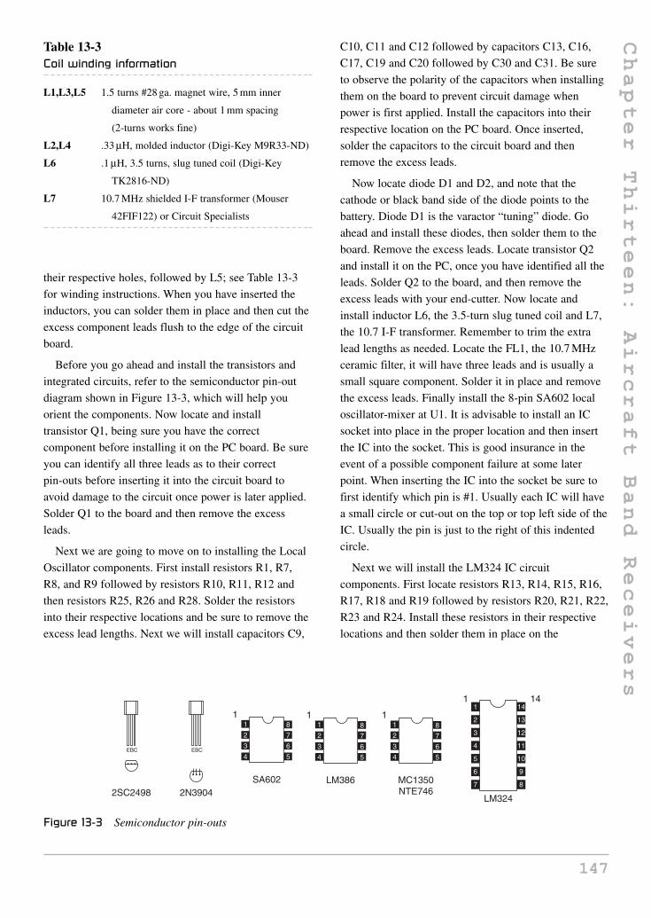
their respective holes, followed by L5; see Table 13-3
for winding instructions. When you have inserted the
inductors, you can solder them in place and then cut the
excess component leads flush to the edge of the circuit
board.
Before you go ahead and install the transistors and
integrated circuits, refer to the semiconductor pin-out
diagram shown in Figure 13-3, which will help you
orient the components. Now locate and install
transistor Q1, being sure you have the correct
component before installing it on the PC board. Be sure
you can identify all three leads as to their correct
pin-outs before inserting it into the circuit board to
avoid damage to the circuit once power is later applied.
Solder Q1 to the board and then remove the excess
leads.
Next we are going to move on to installing the Local
Oscillator components. First install resistors R1, R7,
R8, and R9 followed by resistors R10, R11, R12 and
then resistors R25, R26 and R28. Solder the resistors
into their respective locations and be sure to remove the
excess lead lengths. Next we will install capacitors C9,
C10, C11 and C12 followed by capacitors C13, C16,
C17, C19 and C20 followed by C30 and C31. Be sure
to observe the polarity of the capacitors when installing
them on the board to prevent circuit damage when
power is first applied. Install the capacitors into their
respective location on the PC board. Once inserted,
solder the capacitors to the circuit board and then
remove the excess leads.
Now locate diode D1 and D2, and note that the
cathode or black band side of the diode points to the
battery. Diode D1 is the varactor “tuning” diode. Go
ahead and install these diodes, then solder them to the
board. Remove the excess leads. Locate transistor Q2
and install it on the PC, once you have identified all the
leads. Solder Q2 to the board, and then remove the
excess leads with your end-cutter. Now locate and
install inductor L6, the 3.5-turn slug tuned coil and L7,
the 10.7 I-F transformer. Remember to trim the extra
lead lengths as needed. Locate the FL1, the 10.7 MHz
ceramic filter, it will have three leads and is usually a
small square component. Solder it in place and remove
the excess leads. Finally install the 8-pin SA602 local
oscillator-mixer at U1. It is advisable to install an IC
socket into place in the proper location and then insert
the IC into the socket. This is good insurance in the
event of a possible component failure at some later
point. When inserting the IC into the socket be sure to
first identify which pin is #1. Usually each IC will have
a small circle or cut-out on the top or top left side of the
IC. Usually the pin is just to the right of this indented
circle.
Next we will install the LM324 IC circuit
components. First locate resistors R13, R14, R15, R16,
R17, R18 and R19 followed by resistors R20, R21, R22,
R23 and R24. Install these resistors in their respective
locations and then solder them in place on the
147
Chapter Thirteen: Aircraft Band Receivers
Table 13-3Coil winding information
L1,L3,L5 1.5 turns #28 ga. magnet wire, 5 mm inner
diameter air core - about 1 mm spacing
(2-turns works fine)
L2,L4 .33 µH, molded inductor (Digi-Key M9R33-ND)
L6 .1 µH, 3.5 turns, slug tuned coil (Digi-Key
TK2816-ND)
L7 10.7 MHz shielded I-F transformer (Mouser
42FIF122) or Circuit Specialists
EBC EBC
SA602
11
2
3
4
8
7
6
5
LM386 MC1350NTE7462SC2498 2N3904
11
2
3
4
8
7
6
5
1
LM324
141
1
2
3
4
8
1
2
3
4
5
6
7
14
13
12
11
10
9
8
7
6
5
Figure 13-3 Semiconductor pin-outs

PC board. Remember to cut the extra leads. Now locate
diode D3, remember to observe the polarity when
installing D3. Solder the diode in place, then remove the
excess lead lengths. Now locate and install capacitors
C18, C21, C22 followed by capacitors C23, C24 and
C25. Remember electrolytic capacitors have polarity
markings and they must be observed for the circuit to
operate correctly. You will see either a plus or minus
marking at one end of the capacitor. Once installed,
solder the capacitors in place and then remove the extra
leads by cutting them flush to the circuit board. Finally
install an integrated circuit socket for U3 and then place
U3 into the socket, but be sure to install it correctly,
observing the indented circle as near pin 1 on the IC.
Finally we are going to install the audio amplifier
components. First locate resistor R27 and install it on
the PC board. Next solder it in place and cut the extra
leads. Now, locate and install capacitors C26, C27, C28,
and C29. Remember C26 and C27 are electrolytic
types, so polarity must be observed before installing
them. Finally install an IC socket for U4 the LM386
amplifier IC. When installing U4 be sure to observe the
correct orientation before inserting it into the socket to
prevent damage when power is applied.
Now you finish up the circuit by installing the 9 volt
battery holder, the 9 volt battery clip, followed by
switch S1. Once these components have been installed
you can locate and install jacks J1 and J2 onto the
circuit board.
If you haven’t already installed the potentiometers,
R1, R2 and R3, go ahead and install them and solder
the controls firmly in place. Be sure the mounting tabs
are completely soldered for a good mechanical
connection.
Let’s take a short break and when we return we will
inspect the PC board for poor solder joints and “short”
circuits before applying power to the circuit board. Pick
up the circuit board and bring the foil side of the board
up towards you to inspect the board. First, we will look
for “cold” or poor solder joints on the PC board. Take a
look at each of the solder joints. You want to make sure
each of the solder joints appears to look clean, smooth
and shiny. If you see any solder joints that look dull or
“blobby” then you will need to remove the solder from
the joint with a solder-sucker or wick and then re-solder
the joint, so that it appears to be clean, shiny and
smooth.
Next we will inspect the PC board for “short”
circuits. Often “stray” or “cut” component leads will
“bridge” across or between circuit traces on the PC
board. These possible “shorts” can cause damage to the
circuit when power is first applied, so it is best to
remove any “bridging” leads or solder blobs or “shorts”
before power is sent to the circuit board. Look over the
board carefully for any signs of “bridging” wires or
blobs of solder. Once you are comfortable with your
inspection, you can lay the circuit board back down on
the table.
EnclosurerecommendationsIf your first goal is economy and rugged portability, you
will find that the circuit board can be nicely mounted in
a standard VHS videotape storage box, which also gives
room for a speaker or earphone storage, and even a roll
of antenna wire. The controls are easily mounted at one
end of such a box. It may be necessary to cut away the
molded posts which secure the tape cassette itself.
These storage boxes come in several styles, so pick one
which truly looks practical as a project
enclosure.
The most economical metal enclosure nicely suited
for Ramsey PC board kits is the Radio Shack
270-253A. This metal utility cabinet can accommodate
one or two different receiver boards plus a speaker, with
room for various refinements you might want to add,
such as a bigger battery pack, fine tuning control, and
so forth. When you have selected your enclosure, you
can place the circuit board into the case and mount it.
Be sure to allow the extension of the squelch control,
the volume control and the tuning control on the front
panel of the chassis. The speaker can be mounted on the
top of the case, and the earphone and antenna jack can
be mounted on the rear of the receiver.
Congratulations, you have successfully completed
your active aircraft band receiver. Now you are ready to
test and adjust the receiver before setting down and
enjoying it. Now, you can attach a speaker or pair of
headphones to jack J2. Next, attach a whip antenna to
jack J1, and then connect a 9 volt battery to the battery
clip leads and we can go ahead and test the active
148
Chapter Thirteen: Aircraft Band Receivers

aircraft receiver. Now, turn the On-Off switch to the
“ON” position. Be sure to turn down the squelch control
to below the threshold point, so you can hear a hissing
sound coming from the speaker or headphone. Now,
turn up the volume control to about midway. Take a few
minutes to tune up and down the band with the
main tuning control. If after about 15 minutes, you do
not hear any transmissions on your radio or if you do
not hear any hissing sounds from the speaker,
then you know there could be a problem with your
receiver.
In the event of a problem with your new aircraft band
receiver, you will have to disconnect the speaker,
antenna and battery and visually inspect the circuit
board for any errors. Often a second or new pair of eyes
is very helpful in locating problems on circuit boards.
The most likely causes of circuit failure are misplaced
components or components such as diodes and
electrolytic capacitors installed backwards. The second
most likely cause for problems are semiconductors,
such as transistors installed backwards. Be sure to
re-check the manufacturer data sheets for proper pin-out
information when installing the transistors. Finally,
check the orientation of the integrated circuits in their
respective sockets; sometimes the ICs can be put in
backwards in their sockets causing the circuit to
malfunction. Once you have fully inspected and
hopefully located your problem, you can reconnect the
battery, headphones and antenna and then retest the
receiver once again.
AntennaconsiderationsAn antenna for your new aircraft receiver can be as
simple as a 21′′ piece of wire, an extendable whip
antenna or a roof-mounted ground-plane aviation
antenna. Most folks near an airport will get plenty of in-
the-air action from a wire or whip antenna, but if you’re
more than a few miles away, a decent roof-mount
antenna is the way to go. Radio Shack sells an ideal
antenna designed for scanners which covers the aircraft
band nicely and it costs around $30. A low cost TV
antenna works well, even better if rotated 90 degrees
(remember aircraft antennas are vertically polarized).
Adjustment and alignmentAlignment of the air-band receiver consists of simply
adjusting L6 for the desired tuning range and peaking
the IF transformer (L7). If you are using a signal
generator, frequency counter or other VHF receiver for
calibration, remember that you want to set the local
oscillator frequency 10.7 MHz higher than the desired
signal or range to be received. Adjustment of the L6
oscillator coil MUST be made with a non-metallic
alignment tool. The use of a metal tool of any kind will
detune the coil drastically, making alignment almost
impossible. Also, if you’re receiving FM broadcast
stations, you have the slug tuned too far down in the
coil form. Turn it until it is higher in the form and try
again. One other thing that you can do to improve the
operation of your kit is to spread out the three 2-turn
coils at the antenna input, L1, L3, and L5. Stretching
these out will give you greater sensitivity.
Once you know you are receiving aircraft or airport
transmissions, adjust the IF transformer (L7) for best
reception. Typically, L7 is adjusted 2–3 turns from the
top of the shield can. If you don’t have any signal
reference equipment at home, and are not yet hearing
airplanes, your best bet is to pack up your AR1C and
needed tools and head for the nearest airport! If there is
no control tower, don’t hesitate to visit a general
aviation service center on the airport grounds. If
you’ve never done this before, you will probably
find it to be a fun and interesting experience. Ask
which are the most active frequencies and adjust L6
and your front panel tuning control until you hear the
action. A ground service operator or private pilot may
be willing to give you a brief test transmission on the
122.8 Unicom frequency. Remember, also, that if
your airport has ATIS transmissions, you can get a
steady test signal as soon as you are line-of-sight with
its antenna.
The aircraft receiver does not produce a loud hiss
when no signal is being received (unlike an FM receiver
or expensive AM receiver); this is due to the somewhat
limited amount of IF or Intermediate Frequency gain.
Increasing the IF gain would produce a hiss and
marginally better sensitivity (about a microvolt) but also
require much more alignment, AGC circuitry, and
builder ability—far beyond the intention of this kit.
149
Chapter Thirteen: Aircraft Band Receivers

Tuning the aircraft receiverWith the varactor tuning control capable of going across
10–15 MHz, and with pilots and controllers talking so
briefly, you will need to get used to tuning your
receiver! You’ll find that ANY knob gives smoother
tuning than the bare control shaft, and that a “vernier”
dial will make the procedure even easier—but at the
expense of being able to check up and down the band
quickly, which you might like to do if you’re tracking
the same airplane. The air-band receiver is designed to
let you explore the entire communications section of the
aviation band. If you become really interested only in
being able to check a certain frequency such as a nearby
FAA control tower, or Unicom, it will be helpful to
mark that spot on a dial template such as is reproduced
for your convenience below.
“VOR” or “OMNI”transmissionsWhile driving around the countryside you may have come
across a tall white “cone” structure near your airport or in
the middle of a big farming field; it is useful for you to
know that these are VHF navigational aids operating in
the 118–135 MHz frequency range, just below the air-
ground communications range, sending a steady signal
which may be helpful in initial alignment. If you tune in
such a signal on your receiver, remember that you will
have to increase the local oscillator frequency later in
order to listen to air traffic communications.
Passive aircraft receiverThe passive air-band receiver is a type of “crystal” radio
which contains no local oscillator which might
interferes with the on-board aircraft’s sensitive
electronics. The passive aircraft receiver broadly tunes
from 118 MHz to 136 MHz, and was designed to listen-
in to in-flight communications between your pilot and
the control tower. The passive aircraft receiver is shown
in Figure 13-4. The passive aircraft receiver can be built
small enough to place inside your vest pocket and it
operates from an ordinary 9 volt battery.
The passive aircraft receiver is basically an amplified
type of “crystal radio” designed to receive AM aircraft
transmissions. The “passive” design uses no oscillators
or other RF circuitry capable of interfering with aircraft
communications. This receiver utilizes a coil/capacitor
tuned “front-end,” which feeds an RF signal to a detector
diode. The tuning capacitor may be any small variable
with a range from about 5 pF to about 15 or 20 pF. The
0.15 µH inductor may be a molded choke or a few turns
wound with a small diameter. Experiment with the coil
to get the desired tuning range. The aircraft frequencies
are directly above the FM band so a proper inductor will
tune FM stations with the capacitor set near maximum
capacity. (The FM stations will sound distorted since
they are being slope detected.) A 1N34 germanium
detector diode or a Schottky diode like the 1N5711 or
HP2835 should be used as the detector diode in this
receiver circuit. The 10 megohm resistors provide a small
diode bias current for better detector efficiency.
The LM358 dual op-amp amplifier draws under 1 ma
so the battery life should be quite long. Potentiometer
R3 is used to adjust the gain to the second stage of the
dual op-amp. The second op-amp stage drives a
100 ohm resistor in series with a 100 µF capacitor. You
must use a high impedance “crystal” headphone, since
the op-amp output will not drive a speaker directly.
A speaker amplifier may be added to drive a speaker or
low-z earphone, if desired, but the power consumption
will increase sharply, as will the size of the receiver.
The passive aircraft receiver is powered from an
ordinary 9 volt transistor radio battery. The entire
aircraft band receiver can be built inside a small
plastic box. Simply mount an SPST slide switch on the
side of the case to apply power to the circuit. If you
elect, you can install a 1⁄8′′ phone jack for the “crystal”
headphone.
ConstructionThe passive air-band receiver can be constructed on
a regular circuit board or it could be built on a
150
Chapter Thirteen: Aircraft Band Receivers

“quick-board” which contains ready-made circuit traces,
these are available at Radio Shack stores.
You may want to lay out the circuit so that the tuning
control is at one edge of the board, which will make
things a little easier when installing the circuit in an
enclosure. Building the circuit is pretty straightforward
and should only take a few hours to build. Refer to
Table 13-1 for identifying the resistors and Table 13-2
for identifying the small capacitors in the circuit.
Remember it is very important to install the diode
correctly with respect to its polarity in order for the
circuit to work properly. The passive air-band receiver
also contains a few electrolytic capacitors, and you will
remember that these devices have polarity and it must
be observed for the circuit to work. The aircraft receiver
uses a dual op-amp to amplify the signals and you will
have to ensure that it is installed correctly. An integrated
circuit is highly recommended for the op-amp. In the
event of a circuit failure at some later date, it is much
easier to simply unplug an IC rather than trying to un-
solder one from a PC board to replace it with a new
one. When installing the IC into its socket, you will
have to make sure that you orient it correctly. An IC
will typically have a notch or small cut-out at one end
of the IC case. Pin one (1) will be to the left of the
cut-out of notch when viewed from the top of the IC.
In this project pin 1 of the IC connects to potentiometer
R3, while pin 8 of the IC is connected to the
power source. Note that pin 4 of the IC is connected to
the circuit ground.
You can elect to use a small speaker in this circuit,
but in order to make a miniature receiver you may want
to simply use a small 1⁄8′′ mini jack and just plug into a
pair of small earphones. The circuit is powered from a
standard 9 volt battery; remember the black or minus (−)
battery clip is connected to ground, while the plus (+) or
red battery clip lead is connected to capacitor C5 at the
plus (+) end.
You will want to have the tuning capacitor C2
near the edge of the circuit board, so that you can
allow the tuning knob to protrude through the case
so you can easily tune the receiver. Once the
receiver has been completed, you should take a few
minutes rest.
After the break, you should inspect the foil side of
the circuit board for any “cold” solder joints. Cold
solder joints often look dark, dull or “blobby.” If you
see any solder joints that look this way, you should re-
solder the connections. You should also take a moment
to examine the circuit board for any “short-circuits”
which may be the result of a “stray” component lead
shorting between circuit traces.
You can make yourself an antenna from a piece of
stiff 20 ga. wire as a whip antenna to capacitor C1, or
install a miniature jack in order to plug in a
151
Chapter Thirteen: Aircraft Band Receivers
Antenna
C1
C2
R1
L1
C3
D1
C4
R2
R3
R4
C6
B1
C5
R5
C7
5
6
9 V
R6
7R7 C8
Phones
S1+
+
+
++
+
–U1:B
3
2
81
4
+U1:A
–
Figure 13-4 Passive aircraft receiver schematic

whip antenna. The antenna can be a 6′′ piece of #20 ga.
stiff solid copper wire or a small telescoping aluminum
antenna connected to capacitor C1. Radio Shack has a
good selection of whip antennas. You could elect to
solder the wire antenna directly to C1 and just bring the
antenna out the top of the enclosure, or you could install
a small 1⁄2 ′′ mini jack for the antenna on the rear of the
enclosure. The selectivity is reduce as the antenna
length is increased so best performance is achieved with
the shortest acceptable antenna. Try increasing the
1.8 pF capacitor value when using very short antennas
and decreasing it for long antennas. In order to “tune”
the passive aircraft receiver you can either leave a small
hole on the side of the plastic enclosure to adjust the
frequency using a plastic tuning tool, or you need to
find a way to attach a plastic knob onto the tuning
screw; you will have to drill a larger hole in the case to
bring the knob outside the case for easy tuning.
To test the passive aircraft receiver, park near
your local airport. Turn on the passive air-band
receiver, attach your wire antenna or pull up your
telescoping antenna and tune the receiver. You should
try to listen when you see an aircraft take-off or land or
when you see an aircraft taxiing along the runway. If
you can get close to the tower in a small airport, that
should ensure that you will be able to test your
receiver adequately. As you see a plane arrive or leave,
“tune” around the band and you should hear either the
pilot or the control tower. If you plan on taking the
passive aircraft receiver on-board an aircraft to
listen-in to the pilot during your flight, you should ask
the pilot or stewardess if it is permitted aboard your
aircraft. Generally you are given permission without a
problem. Enjoy building and using your new aircraft
receivers!
152
Chapter Thirteen: Aircraft Band Receivers

VLF or Very Low Frequency Radio Receiver
Chapter 14
Parts list
VLF Whistler Receiver
R1,R4 10k ohm 1/4w,
5% resistor
R2,R3 22k ohm 1/4w,
5% resistor
R5 6.2 megohm, 1/4w
5% resistor
R6 1 meg ohm
potentiometer
(trimpot) - single
turn
R7 10 megohm, 1/4w
5% resistor
R8 1k ohm, 1/4w
5% resistor
R9 1k ohm, 1/4w
5% resistor
R10 3.3k ohm, 1/4w
5% resistor
R11,R12 820 ohm, 1/4w
5% resistor
R13 10k ohm
potentiometer
(panel)
R14,R17 10 ohm, 1/4w,
5% resistor
R15,R16 2.2k ohm, 1/4w,
5% resistor
C1,C3 47 pF, 35 volt
mica capacitor
C2 100 pF, 35 volt
mica capacitor
C4,C5,C6 3.3 nF,
35 volt mylar capacitor
C7,C15 .01 µF, 35 voltceramic disk capacitor
C8 27 pF, 35 volt mica
capacitor
C9 1 µF, 35 voltelectrolytic capacitor
C10 .18 µF, 35 volttantalum capacitor
C11 .12 µF, 35 volttantalum capacitor
C12 1.8 µF, 35 volttantalum capacitor
C13 .68 µF, 35 volttantalum capacitor
C14 .22 µF, 35 volttantalum capacitor
C16 .068 µF, 35 volttantalum capacitor
C17,C18 .22 µF, 35 volttantalum capacitor
C19 .05 µF, 35 voltceramic disk capacitor
C20,C22,C24 100 µF,35 volt electrolytic
capacitor
153Copyright © 2008 by The McGraw-Hill Companies, Inc. Click here for terms of use.

154
Chapter Fourteen: VLF Radio Receiver
C21,C23 .1 µF,35 voltceramic disk capacitor
L1 120 mH coil (Mouser
electronics)
L2 150 mH coil (Mouser
electronics)
L3 18 mH coil (Mouser
electronics)
L4 56 mH coil (Mouser
electronics)
Q1a,Q1b U401 Siliconix
Dual matched N-Channel
FETs
Q2 MPSA56 transistor
U1 LM386 op-amp
S1 DPDT toggle switch
(trap)
S2 DPDT toggle switch
(high-pass)
S3 DPDT toggle switch
(low-pass)
B1 9 volt transistor
radio battery
J1,J2 1/8 mini phone
jack w/switch
J3 SO-238 UHF chassis
jack
P1 PL259 UHF plug
P2 binding post
(ground)
Misc PC board, IC
socket, solder, wire,
antenna, battery
holder
Battery clip, hardware,
chassis
“Natural Radio” is a name sometimes used for describing
radio noise with natural origins, mainly due to but not
confined to lightning. At first suggestion, you may think
that listening to lightning crackles would be dull or
uninteresting, but electromagnetic radiation from
lightning can travel great distances and undergo strange
modifications along the way. The frequencies of the
original pulse can be spread out in time (a process
called “dispersion”) since the higher frequencies travel
a little faster than the lower. The result is that the short
impulse from a lightning strike in South America can
sound like a chirp in Texas. Slower sweeping tones are
called “whistlers” and they are a bit of a mystery. The
energy from a lightning bolt streams out into space into
a region called the “magnetosphere,” magnetized
plasma created by the interaction of solar wind with the
Earth’s magnetic field. The lightning pulse is reflected
or “ducted” back down to Earth after a very long trip
during which time the frequencies are spread out by a
dispersion-like process. Short whistlers might be due to
dispersion, but some whistlers last five seconds so
ordinary dispersion is probably inadequate an
explanation. A radio wave can travel a million miles in
five seconds, so to accumulate that much difference in
arrival times, the signal would have to travel hundreds
of millions of miles, assuming a pretty steep dispersion
curve. More likely, the whistler is an emission from the
magnetosphere triggered by the lightning pulse. When
conditions are just right, numerous lightning strikes
combine with numerous reflections to give an eerie
chorus that sounds a bit like a flock of geese.
Most people have never heard of Natural Radio
produced by several of natures’s processes, including
lightning storms and aurora, aided by events occurring
on the Sun. The majority of Earth’s natural radio
emissions occur in the extremely-low-frequency and
very-low-frequency (ELF/VLF) radio spectrum. Whistlers,
one of the more frequent natural radio emissions to be
heard, are just one of many natural radio “sounds” the
Earth produces at all times in one form or another, and
these signals have caught the interest and fascination of
a small but growing number of hobby listeners and
professional researchers for the past four decades.
Whistlers are amazing sounding bursts of ELF/VLF
radio energy initiated by lightning strikes which “fall”
in pitch. A whistler, as heard in the audio output from a
VLF or “whistler” receiver, generally falls lower in pitch,
from as high as the middle-to-upper frequency range of
our hearing downward to a low pitch of a couple hundred
cycles-per-second (Hz). Measured in frequency terms, a
whistler can begin at over 10,000 Hz and fall to less than
200 Hz, though the majority are heard from 6000 down
to 500 Hz. Whistlers can tell scientists a great deal of

the space environment between the Sun and the Earth
and also about Earth’s magnetosphere.
The causes of whistlers are generally well known
today though not yet completely understood. What is
clear is that whistlers owe their existence to lightning
storms. Lightning stroke energy happens at all
electromagnetic frequencies simultaneously. The Earth
is literally bathed in lightning-stroke radio energy from
an estimated 1500 to 2000 lightning storms in progress
at any given time, triggering over a million lightning
strikes daily. The total energy output of lightning storms
far exceeds the combined power output of all man-made
radio signals and electric power generated from power
plants.
Whistlers also owe their existence to Earth’s
magnetic field (magnetosphere), which surrounds the
planet like an enormous glove, and also to the Sun.
Streaming from the Sun is the Solar Wind, which
consists of energy and charged particles, called ions.
And so, the combination of the Sun’s Solar Wind, the
Earth’s magnetosphere surrounding the entire planet,
and lightning storms all interact to create the intriguing
sounds and great varieties of whistlers.
How do whistlers occur from this combination of
natural solar-terrestrial forces? Some of the radio energy
bursts from lightning strokes travel into space beyond
Earth’s ionosphere layers and into the magnetosphere,
where they follow approximately the lines-of-force of
the Earth’s magnetic field to the opposite polar
hemisphere along “ducts” formed by ions streaming
toward Earth from the Sun’s Solar Wind. Solar-Wind
ions get trapped in and aligned with Earth’s magnetic
field. As the lightning energy travels along a field-
aligned duct, its radio frequencies become spread out
(dispersed) in a similar fashion to light shining into a
glass prism. The higher radio frequencies arrive before
the lower frequencies, resulting in a downward falling
tone of varying purity.
A whistler will often be heard many thousands of
miles from its initiating lightning stroke—and in the
opposite polar hemisphere! Lightning storms in British
Columbia and Alaska may produce whistlers that are
heard in New Zealand. Likewise, lightning storms in
eastern North America may produce whistlers that are
heard in southern Argentina or even Antarctica.
Even more remarkably, whistler energy can also be
“bounced back” through the magnetosphere near
(or not-so-near) the lightning storm from which it
was born!
Whistlers are descending tones. Their duration can
range from a fraction of a second to several seconds,
with the rate of frequency shift steadily decreasing as
the frequency decreases. A whistler’s note may be pure,
sounding almost as if it was produced using a laboratory
audio signal generator; other whistlers are more diffuse,
sounding like a breathy “swoosh” or composed of
multiple tones. On occasion, some whistlers produce
echoes or long progressions of echoes, known as “echo
trains,” that can continue for many minutes.
Whistlers can occur in any season. Some types are
more likely to be heard in summer than winter and
vice-versa. Statistically, the odds are especially high
for good whistler activity between mid-March and
mid-April.
Whistlers and the sounds of the dawn chorus are not
heard equally well everywhere in the world. Reception
of these are poor in equatorial regions, with best
reception at geomagnetic latitudes above 50°. Fortunately
the continental United States and Canada are well
positioned for reception of whistlers and other signals
of natural radio.
Considered by many listeners to be the “Music of
Earth”, whistlers are among the accidental discoveries of
science. In the late 19th century, European long-distance
telegraph and telephone operators were the first people
to hear whistlers. The long telegraph wires often picked
up the snapping and crackling of lightning storms,
which was mixed with the Morse code “buzzes” or
voice audio from the sending station. Sometimes, the
telephone operators also heard strange whistling tones
in the background. They were attributed to problems in
the wires and connections of the telegraph system and
disregarded.
The first written report of this phenomenon dates
back to 1886 in Austria, when whistlers were heard on a
22-km (14 mile) telephone wire without amplification.
The German scientist, H. Barkhausen, was eavesdropping
on Allied telephone conversations during World War I.
In order to pick up the telephone conversations, he
inserted two metal probes in the ground some distance
apart and connected these to the input of a sensitive
audio amplifier. He was surprised to hear whistling
tones which lasted for one or two seconds and which
glided from a high frequency in the audio range to a
155
Chapter Fourteen: VLF Radio Receiver

lower frequency where they disappeared into the
amplifier or background noise level. On occasion, the
whistlers were so numerous and loud that he could not
detect any type of telephone.
Later, three researchers from the Marconi Company
in England reported in 1928 on the work they had done
in whistler research. Eckersley, Smith, and Tremellen
established a positive correlation between whistler
occurrence and solar activity, and they found that whistlers
frequently occur in groups preceded by a loud click.
The time between the click and the whistlers was about
three seconds. They concluded that there must have been
two paths of propagation involved; one for the click
which preceded the whistler, and a second, much longer
path, over which the whistler and its echoes propagated.
Eckersley was able to show in 1931 that Earth’s
magnetic field permits a suitably polarized wave to pass
completely through the ionosphere. This was in
accordance with the magneto-ionic theory. Tremellen
had on one occasion observed that during a summer
thunderstorm at night every visible flash was followed
by a whistler. This served as the first definite evidence
of the relationship between lightning discharges and
whistlers—the click being the lightning discharged
which caused the whistler. As the Marconi workers
continued their research, they also discover a new type
of atmospheric which sounded somewhat like the
warbling of birds. Since the sound tended to occur
most frequently at dawn, they gave it the name dawn
chorus.
L.R.O. Storey of Cambridge University began an
intensive study of whistlers in 1951. He confirmed
Eckersley’s law which showed that most whistlers
originate in ordinary lightning discharges, and found the
path of propagation of the whistler to be along the lines
of the Earth’s magnetic field.
Other interesting sounds include “tweeks,” which have
been described by one listener as a cross between chirping
birds and a hundred little men hitting iron bars with
hammers. The ephemeral “dawn chorus,” is a cacophony
of sounds that resembles nothing else on Earth.
Tweeks are abrupt descending notes that resemble
“pings.” They are usually heard at night during the
winter and early spring.
The dawn chorus has been variously described as
sounding like birds at sunrise, a swamp full of frogs, or
seals barking. In fact, it varies constantly. “Hooks,”
“risers,” and “hiss” are all part of the dawn chorus, but
sometimes these sounds are also heard as solitary
events. A hook starts out like a whistler but then
abruptly turns into a rising tone. Risers increase in
frequency from beginning to end. And hiss sounds just
like its name. Appropriately enough, dawn chorus is
best heard around dawn, but it may occur at any time of
the day or night. The dawn chorus is most likely to be
heard during and shortly after geomagnetic storms.
A whistler receiverYou cannot easily buy a radio capable of tuning 1 to
10 kHz, but it is possible to build a sensitive receiver to
permit you to hear the sounds of natural radio. We will
explore what causes these sounds and see how you can
study them yourself.
A whistler receiver, even though whistlers and related
emissions occur at acoustical frequencies, is a receiver
of radio signals. To hear whistlers, you must intercept
their electromagnetic energy with an antenna and
transform it to the mechanical vibrations to which our
ears respond.
The “classic” whistler receiving system consists of an
antenna for signal collection, an amplifier to boost the
signal level, and headphones or a speaker to transform
the signal to sound waves. (A magnetic tape recorder
can be substituted for the headphones or speaker.)
A whistler receiver can simply be an audio amplifier
connected to an antenna system. However, powerful
man-made interference immediately above and below
the frequencies of interest tend to seriously overload
receivers of this sort and make reception of whistlers
and related phenomena difficult.
To overcome these problems, a good whistler receiver
circuit includes a circuit called a low-pass filter that
attenuates all signals above 7 kHz. This greatly reduces
interference from such sources. To escape interference
from AC power lines and other forms of non-natural
radio noise, the receiver is designed for portable operation
“in the field” away from such interference sources.
A sensitive dual FET whistler receiver is shown in
the photo in Figure 14-1, and in the schematic diagram
in Figure 14-2. The antenna is first fed to an RF filter
156
Chapter Fourteen: VLF Radio Receiver

which is composed of resistors R1 through R4 and
capacitors C1 through C3. This filter only allows the
desired frequencies to be sent to the next section of the
receiver. The RF filter is next fed to the 60 Hz filter or
“trap” which filters out 60 Hz power line frequencies
before the RF signals are amplified. The 60 Hz filter
can be switched in and out of the circuit with switch
S1:a. The dual matched FET transistor Q1 along with
transistor Q2 are used to amplify the RF signals of the
desired band of frequencies. The amplified signals are
then fed to the input of a set of selectable filters which
can be switched in and out of the circuit. Toggle switch
S2 is used to switch in the high-pass filter circuit, while
switch S3 is used to switch-in the low-pass filter. You
can select either or both filters if desired.
The output of the low-pass filter circuit is coupled to
the final audio amplifier stage via capacitor C17.
Potentiometer R12 controls the audio level entering the
LM386 audio amplifier at U1; also note that R12 also
contains a switch S5, which is used to supply power to
the LM386 audio amplifier. The output of the LM386 is
coupled to an audio output jack via capacitor C20. Note
that capacitor C18 is coupled to a recorder output jack
to allow a chart recorder or analog to digital converter
to be used to monitor and record the output from the
whistler receiver. The whistler receiver is powered from
a 9 volt battery for both stationary and field receiving
applications.
Building a whistlerreceiverBefore we start building the Whistler receiver,
you will need to locate a clean, well lit and well
ventilated area. A workbench or large table top to
spread out all you diagrams, components and tools for
the project. First, you will need a small pencil tipped
27 to 33 watt soldering iron, a spool of 22 ga. 60/40
tin/lead solder, and a small jar of “Tip Tinner.” “Tip
Tinner” is a soldering iron tip cleaner/dresser and is
available at your local Radio Shack store. You will
also want to locate a few small tools such as a pair of
end-cutters, a pair of needle-nose pliers, a pair of tweezers
and a magnifying glass. Look for a small flat-blade
screwdriver as well as a small Phillips screwdriver to
round out your tools for the project. Next locate all the
components for the Whistler project as well as all of the
diagrams including the schematic, parts layout diagram
and the necessary charts and tables and we will begin.
In order to construct a stable well performing radio
receiver, it is recommended practice to build the
Whistler receiver on a printed circuit board, with large
ground plane areas. You will need to use good RF
building practices, such as keeping leads as short as
possible, clean solder joints, etc. With your circuit board
in hand we will begin building the circuit.
Take a look at the schematic diagram and you will
notice that there are dotted or dashed lines. These dashed
lines represent shielded compartments on the circuit
board. These shielded areas are used to separate different
portions of the circuit from one another. You can create a
shielded area by soldering a vertical piece of scrap
circuit board material onto the circuit board ground
plane areas on the circuit board. You could also
modularize the circuit building three small circuit
boards, one for the RF filter and “trap” circuit, one for
the high-pass and low-pass filter, and a third board for
the audio amplifier and power circuit. Small metal shield
covers could be built using scrap circuit board material.
First, you will need to locate the resistors for the
project, and you will also want to refer to the resistor
color code chart in Table 14-1, which will help you to
identify each of the resistors. Resistors generally have
three or four color bands which are used to denote the
157
Chapter Fourteen: VLF Radio Receiver
Headphone ampFilters
Front end
Figure 14-1 VLF whistler receiver

158
C hapter Fourteen: VLF Radio Receiver
Antenna
R1 R2 R3 R4R17
C1 C2 C3
60 Hz trap
S1:a S1:b
Ground
P1 S4
C22C21 C23
C24
9 V
++ +
C6C7
C5
R5
R6
C8
3
2R10
Q1:A R9 Q2
ba
c3
2
1Q1b
R7 C9
C10 R8
High pass
S2:a
R11
C13C11
C12
L2 L3
C15
C16
L4 S3:b
R12
C17
L5
S2:b S2:a
C18 C19
R15
S5 R14
U12
6
34
7
5
1 8
Phonepower
C20
C21
R16
J1
J2
Record
Phones
Low pass
+C14
1
+
R13
Figure 14-2 FET VLF receiver schematic. Courtesy of Eric Vobel

resistor’s value. The first color band will be closest to
one edge of the resistor. The first color band represents
the first digit of the value. Resistor R1, for example, is a
10k ohm resistor. Its first color band would be brown (1),
the second color band would be black (0) and the third
color band which denotes the resistor’s multiplier value
would be orange or (000), so 10,000 or ten thousand
ohms. A fourth color band represents the resistor’s
tolerance value. The absence of a fourth color band
denotes a 20% tolerance, while a silver band represents
a 10% tolerance and a gold denotes a 5% tolerance
resistor. Use the color code chart to identify resistors
R1, R2 and R3. When you are confident that you know
the color codes and can identify these resistors, you can
go ahead and solder these resistors onto the circuit
board. Use your end-cutters to cut the excess
component leads flush to the edge of the circuit board.
Now locate another grouping of resistors and install
them to the circuit board, then solder them in place on
the PC board. Remember to trim the extra component
lead lengths from the PC board. Install the remaining
resistors onto the circuit board, until all have been
mounted to the board, solder them in place and trim the
leads as necessary.
Next, we are going to install the capacitors for the
Whistler receiver. Capacitors come in two major
types, i.e. electrolytic and non-electrolytic. Generally the
non-electrolytic capacitors are the small types such as
ceramic disks, mylar or polyester types. These small
capacitors may have their actual value printed on them,
or if the capacitors are very small may instead have a
three-digit code printed on them. Refer to the chart in
Table 14-2, which will help you identify these capacitors.
A .001 µF capacitor, for example, would have (102)
marked on the body of the device to denote its value
of .001 µF. Electrolytic capacitors are generally the
larger capacitors with polarity marking on them.
You will find either a black or white color band on them
or a plus (+) or minus (−) marking on them. Electrolytic
capacitors have polarity, so this means that you have to
orient them correctly while installing them in order for
the circuit to work properly. Reversing electrolytic
capacitors can often cause the circuit to malfunction,
and it can destroy the component and/or the circuit
itself, so be careful when installing them. Refer to the
schematic and the parts layout diagram when installing
electrolytic capacitors.
Let’s begin installing the capacitors now. Try and
separate the electrolytic capacitors from the other types
of capacitors. Locate a few of the non-electrolytic
capacitors, identify them and install a few of the
capacitors on the circuit board. Go ahead and solder
these capacitors onto the PC board, once you are sure
you have correctly identified them. Trim the excess
159
Chapter Fourteen: VLF Radio Receiver
Table 14-1Resistor color code chart
Color Band 1st Digit 2nd Digit Multiplier Tolerance
Black 0 0 1
Brown 1 1 10 1%
Red 2 2 100 2%
Orange 3 3 1,000 (K) 3%
Yellow 4 4 10,000 4%
Green 5 5 100,000
Blue 6 6 1,000,000 (M)
Violet 7 7 10,000,000
Gray 8 8 100,000,000
White 9 9 1,000,000,000
Gold 0.1 5%
Silver 0.01 10%
No color 20%

160
Chapter Fourteen: VLF Radio Receiver
Table 14-2Capacitance code information
This table provides the value of alphanumeric coded ceramic, mylar and mica capacitors in general. They come in many sizes,
shapes, values and ratings; many different manufacturers worldwide produce them and not all play by the same rules. Some
capacitors actually have the numeric values stamped on them; however, many are color coded and some have alphanumeric codes.
The capacitor’s first and second significant number IDs are the first and second values, followed by the multiplier number code,
followed by the percentage tolerance letter code. Usually the first two digits of the code represent the significant part of the value,
while the third digit, called the multiplier, corresponds to the number of zeros to be added to the first two digits.
Value Type Code Value Type Code
1.5 pF Ceramic 1,000 pF /.001 µF Ceramic / Mylar 102
3.3 pF Ceramic 1,500 pF /.0015 µF Ceramic / Mylar 152
10 pF Ceramic 2,000 pF /.002 µF Ceramic / Mylar 202
15 pF Ceramic 2,200 pF /.0022 µF Ceramic / Mylar 222
20 pF Ceramic 4,700 pF /.0047 µF Ceramic / Mylar 472
30 pF Ceramic 5,000 pF /.005 µF Ceramic / Mylar 502
33 pF Ceramic 5,600 pF /.0056 µF Ceramic / Mylar 562
47 pF Ceramic 6,800 pF /.0068 µF Ceramic / Mylar 682
56 pF Ceramic .01 Ceramic / Mylar 103
68 pF Ceramic .015 Mylar
75 pF Ceramic .02 Mylar 203
82 pF Ceramic .022 Mylar 223
91 pF Ceramic .033 Mylar 333
100 pF Ceramic 101 .047 Mylar 473
120 pF Ceramic 121 .05 Mylar 503
130 pF Ceramic 131 .056 Mylar 563
150 Pf Ceramic 151 .068 Mylar 683
180 pF Ceramic 181 .1 Mylar 104
220 pF Ceramic 221 .2 Mylar 204
330 pF Ceramic 331 .22 Mylar 224
470 pF Ceramic 471 .33 Mylar 334
560 pF Ceramic 561 .47 Mylar 474
680 pF Ceramic 681 .56 Mylar 564
750 pF Ceramic 751 1 Mylar 105
820 pF Ceramic 821 2 Mylar 205
1st Significant Figure
2nd Significant Figure
Multiplier
Tolerance
CSGNetwork.Com 6/4/92
0.1 µF 10%
104 k

component leads from the PC board. Install a few more
non-electrolytic capacitors and solder them to the board,
remember to cut the extra leads from the board. Install
the remaining non-electrolytic capacitors to the circuit
board and solder them in place.
Next, locate the electrolytic capacitors and we will
install them on the PC board. Refer to the schematic
and parts layout diagrams to make sure you can orient
the capacitors correctly before soldering them. Place a
few electrolytic capacitors on the board and solder them
in, trim the excess leads as necessary. Add the
remaining electrolytic capacitors on to the PC board and
solder them in place.
The Whistler receiver also has a number of coils in
the circuit, most of them are low cost and readily
available from Mouser Electronics, see Appendix.
Identify the coils for the project and place them in their
respective locations on the PC board. Now, solder them
in place and remember to trim the excess component
leads flush to the edge of the circuit board.
Looking at the circuit you will notice three transistors,
more correctly one dual FETs and one conventional
transistor. Before we go ahead and install the
semiconductors, take a quick look at the semiconductor
pin-out diagram shown in Figure 14-3. The FETs are
very sensitive to static electricity damage, so be
extremely careful when handling them, use a grounded
anti-static wrist-band. The FETs have three leads much
like a regular transistor but their pin-outs are a bit
different. An FET will usually have a Drain, Source and
Gate lead; see pin-out diagram for each particular FET,
when installing them on the PC board. The conventional
transistor at Q2 is a PNP type which has a Base, Collector
and Emitter lead, once again refer to the transistor
pin-out diagram, the schematic and parts layout
diagrams when installing the transistor and FET.
Installing the FET and transistor incorrectly will prevent
the circuit from working correctly and may damage the
component as well, so be careful when installing the
FET and transistor.
The receiver has a single integrated circuit at U1, an
LM386 audio amplifier IC. As an insurance policy
against a possible circuit failure in the present or
possible future date, it is recommended that you use an
integrated circuit socket. Integrated circuit sockets will
usually have a notch or cut-out at one end of the socket;
this is supposed to represent pin 1 of the IC socket. You
will have to align the socket correctly so that pin 2 of
the IC socket connects to the ground bus. Note that
pin 1 is not used in this application. When installing the
IC into the socket, you will note that the IC itself will
have either a small indented circle, a cut-out or a notch
at one end of the plastic IC body. Pin 1 of the IC is just
to the left of the notch. Insert the IC into the socket
making sure pin of the IC is aligned with pin of the
socket.
Take a short break and when we return we will check
over the printed circuit board for “cold” solder joints
and possible “short” circuits. Pick up the PC board with
the foil side facing upwards toward you. First we will
inspect the PC board for possible “cold” solder joints.
Take a look at all of the solder joints. All the solder joints
should appear to look clean, shiny and bright, with well
formed solder connections. If any of the solder joints
appear dull, dark or “blobby,” then you should un-solder
and remove the solder from the joint and re-solder the
joint all over again, so that it looks good. Next, we will
inspect the PC board for possible “short” circuits. “Short”
circuits can be caused by small solder balls or blobs
which stick to the underside of the board. Many times
rosin core solder leaves a sticky residue on the PC
board. Sometimes “stray” component leads will
adhere to the underside of the board and often they can
form a bridge across the PC traces on the PC board
causing a “short” circuit, which can damage the circuit
upon power-up, so be careful to remove any
component leads or solder blobs from the underside of
the board.
The VLF Whistler receiver was housed in a metal
chassis box to prevent “stray” RF from affecting the
circuit operation. The main circuit board can be
mounted to the bottom of the enclosure with 1/8′′
161
Chapter Fourteen: VLF Radio Receiver
EBCLM386
MPSA56NTE159
1 81234
8765
SiliconixU401
1 81234
8765
Figure 14-3 Semiconductor pin-outs

plastic standoffs. The 60 Hz “trap” filter switch, the
high-pass filter and low-pass filter switches, along with
the power on-off switch, were mounted on the front
panel of the chassis box. The headphone power
amplifier power switch, the headphone jack and volume
control at R13 were also mounted on the front panel of
the chassis box. The SO-238 antenna jack, the 1/8′′
record jack and the ground binding post were all
mounted on the rear panel of the chassis box. A 9 volt
battery holder was used to secure the battery to the left
rear corner of the chassis box. Once the circuit has been
mounted in the selected chassis, you can move on to
applying power and testing the VLF receiver. Connect a
fresh 9 volt battery to the VLF receiver, connect a pair
of headphones and a whip antenna to the antenna
terminals. Turn the power switch to the “ON” position
and you should hear a hissing sound from the
headphones. If the receiver is totally quiet and you hear
nothing, you have a problem! First, you will need to
disconnect the battery, the headphones and the antenna,
and you will need to carefully examine the circuit
board. The most common cause for circuit failure is
improper installation of electrolytic capacitors and
diodes. Remember that these components have polarity
and it must be observed for the circuit to work correctly.
Look over the circuit very carefully. It is often advisable
to have a second pair of eyes. Have a knowledgeable
electronics friend help you examine the circuit board for
mistakes. Another cause for possible errors are the
incorrect placement of resistors. Often colors are
mistaken and resistors are installed in the wrong
location. Another possible problem can be the
installation of the semiconductors, namely in this circuit
the transistors or FETs. Check the manufacturer’s pin-out
diagrams for the particular device and carefully
re-examine the installation. Hopefully at this point you
have found your error and corrected it and you can then
re-connect the battery, antenna and headphones and
re-test the VLF receiver to make sure it is now working.
Using your VLF receiverThe whistler receiver works best out doors in open
areas, with a vertical antenna of roughly 3 to 12 feet in
height. It can also be used in wooded or obstructed
areas with wire antennas between roughly 50 to 200 feet
in length connected instead of the vertical antenna. Wire
antennas should be insulated and supported off the
ground as high as you can place them. The performance
of a wire antenna improves the more you can get it in
the clear and the more vertically it can be positioned. If
you do use a wire antenna, you may have to reduce the
value of the input resistor R1 for best results.
The whistler receiver also needs a ground connection,
also called a counterpoise. A simple but often effective
ground can be provided by your body in contact with
the ground terminal (BP2). I have used an improvised
finger ring attached to a wire connected to the ground
terminal. Other places to make a ground connection
include car bodies, wire fences, or other large metal
objects not connected in any way to an AC power
circuit. Another approach is to use short sections of
copper tubing as ground stakes which can be driven
into the ground and connected to your receiver. Try
several different grounding schemes to see which one
provides the quietest reception. Don’t be too surprised,
however, to discover that you wind up having to still
make body contact with the ground terminal for quietest
reception!
The prototype receiver, with a whip antenna, was
mounted on a piece of wood approximately 2′′ × 60′′.
You can install the antenna at one end of the long
rectangular piece of wood (it can be mounted on a
bracket or just taped on) and the receiver can be
mounted at the other end of the piece of wood, about
one foot down from the antenna using duct tape, two-
sided foam tape or a mounting bracket. A length of wire
was run from the receiver’s ground terminal down the
wood and taped in place at several places. Now I had a
handy walking stick that was easy to carry and use!
The base can be stuck into any convenient hole, jammed
into a rock pile, clamped onto a fence or vehicle, or
even held by hand.
For the best chance of hearing whistlers and related
phenomena, you will have to put some distance between
the whistler receiver and the AC power grid. The bare
minimum distance is about one quarter mile from any
AC power line; the more distance you can put between
the receiver and AC power lines, the better. You’ll need
to do some exploration to discover quiet sites near you.
Once you arrive at a potential listening site, set up your
receiver, put in a ground connection, and see what
happens. What you will hear depends to some extent
162
Chapter Fourteen: VLF Radio Receiver

on the time of day, but you can always expect some
sharp, crackling static. The intensity and volume of this
static will depend on propagation conditions and where
thunderstorms are in relation to your location. Chances
are that you’ll also hear some power line hum, but
hopefully it won’t be very loud. If your listening site is
too noisy, you need to try another listening site.
If your ears have good high frequency response, you
will probably hear a continuing sequence of one-second
tones. These are from the OMEGA radio-navigation
system. OMEGA is transmitted from 10 to 14 kHz, and
OMEGA transmitters are very powerful. You may also
hear anything that can produce an electrostatic discharge,
particularly if the humidity is low. These miscellaneous
noise sources can include wind noise, the buzz of insects
flying near the antenna, dry leaves or grass moving, and
even the electrostatic charges that build up on your
clothing. Passing vehicles will often produce noise from
their electrical and ignition systems. And if you have a
digital watch, keep it away from the antenna or you’ll
be listening to it instead of whistlers!
Anything you hear other than whistlers and
related phenomena or OMEGA signals are likely to be
the result of extraneous signals “overloading” your
receiver. Burbling sounds (possibly mixed with OMEGA
tones) are caused by military signals in the 15 to 30 kHz
range, perhaps overloading the receiver. A “ticking”
sound at a 10 Hz rate is from Loran-C radio-navigation
signals at 100 kHz. In general, don’t be surprised if you
experience “overloading” from transmitters operating
on any frequency if they are within sight of the
location where you’re using your whistler receiver!
Table 14-3 illustrates some very low frequency stations
around the world that broadcast low frequency signals,
these signals are located at the upper edge of the VLF
receiver’s range.
163
Chapter Fourteen: VLF Radio Receiver
Table 14-3Very low frequency radio stations
Site ID Frequency kHz Power KW
Cutler, ME NAA 24.0 1000
Jim Creek, WA NLK 24.8 250
Lualualei, HI NPM 21.4 566
LaMoure, ND NML4 25.2
Aquada, Puerto Rico NAU 40.75 100
Keflavik, Iceland NRK 37.5 100
Niscemi, Italy 39.9 25
Harold E. Holt, Australia NWC 19.8 1000
Rhauderfehn, Germany 18.5 500
Rosnay, France HWU 15.1 400
St. Assie, France FTA 16.8 23
Bombay, India 15.1
Tavolara, Italy ICV 20.27 43
Ebino Huyshu, Japan 23.4
Noviken, Norway JXN 16.4 45
Arkhanghelsk, Russia UGE 19.4 150* input pwr
Batumi, Russia UVA 14.6 100* input pwr
Kaliningrad, Russia UGKZ 30.3 100* input pwr
Matotchkinchar, Russia UFQE 18.1 100* input pwr
Vladivostok, Russia UIK 15.0 100* input pwr
Anthorn, United Kingdom GQD .019 42

Time of listeningMost of the VLF signals, such as clicks, pops, and tweeks,
can be heard almost at any time of the day or night.
Whistler occurrence is a function of both thunderstorm
occurrence and propagation conditions through the
ionosphere. The rate is higher at night than during the
day because of the diurnal variation in the D-region
absorption, which is highest when the Sun is above the
horizon. At night, the D-layer does not exist since it is
ionized by solar ultraviolet rays. The whistler rate, or
the number of whistlers heard per minute, has a marked
dependence on sunspot activity, the rate increasing with
the sunspot number. Whistlers are heard only when
sufficient ionization exists along the path to guide the
waves along the Earth’s magnetic field. This ionization
is assumed to be supplied from the Sun during a solar.
To hear a whistler or other signals such as dawn chorus,
you will no doubt have to get away from the power
line and industrial noise. The listening time for these
signals will be from near local midnight to early
morning hours.
Observing and recording hintsRemember the best location to observe VLF signals is
out in the countryside, in an area where few cars or
trucks are likely to pass. You will want to get as far
away from power lines as possible for optimum results.
The lower the power line noise is, the stronger the VLF
emission signals will be.
Some whistlers are related phenomena and so
short-lived and impossible to predict that you might
want to consider using a tape recorder to record the
signals in the field unattended. Take a portable,
battery-operated, cassette tape recorder with you and
use a long audio cable to run to the tape recorder from
the audio output of the VLF receiver. Any tape recorder
with an external microphone input can be used. Best
results are obtained with a recorder which has no ALC
or automatic level control. The VLF receiver shown has
an output jack which can be coupled to a recorder input
for field recording. You may have to place the tape
recorder away from the receiver to avoid picking up
motor noise.
After returning home with your recording, if your
receiver was out in the field, you can “play” your
recording back into the sound card of your personal
computer using an FFT or DSP sound recording program
to analyze the recording. For those who are going to use
their whistler receiver as a stationary receiver at home,
you could use your PC to record on a continuous basis.
Audio recording and FFT programs are available on the
Internet for free. Good luck and happy exploring!
Additional notes
You can view spectrograms of whistlers as well as hear
excellent recordings of many more whistlers than
we used in generating the audio clip for this article,
courtesy of NASA: http://image.gsfc.nasa.gov/
poetry/inspire/advanced.html
A free Fast Fourier Transform (FFT) Waveform
Analyzer program and an Audio Waveform
Generator program can be downloaded for use on
your own computer at:
FFT discussion:
http://www.dataq.com/applicat/articles/an11.htm
Some US Government agencies doing whistler
research are:
NASA’s Godard Space Flight center invites participation
in a program called “INSPIRE” (an acronym for
Interactive NASA Space Physics Ionosphere Radio
Experiments) http://image.gsfc/poetry/inspire
NOAA: http://ngdc.noaa.gov/stp/stp.html
http://www.ngdc.noaa.gov/stp/stp.htm
gopher://proton.sec.noaa.gov
Some of the university labs involved with
whistlers are:
University of Alaska Geological Institute
University of Iowa: http://www-w.physics.uiowa.edu/
~/jsp/polar/sounds/whistlers.html
Stanford University: http://www.stanford.edu/~vlf/
Science/Science.html
[An excellent site, but I could only access it via the
“Google” search engine]
UCLA: http://www.physics.edu/plasma-
exp/Research/TransportWhistlers
Kyoto University, Kyoto, Japan
164
Chapter Fourteen: VLF Radio Receiver

Induction Loop Receiving System
Chapter 15
Parts list
Induction LoopTransmitter I
TX Mono amplifier or
receiver – 5–10 watts
output
R1 10 ohm 10 watt
10% resistor
L1 loop coil around
room (see text)
Induction LoopTransmitter II
R1 10k ohm
potentiometer chassis
mount
R2 220 ohm 1/4 watt
resistor, 5%
(red-red-brown)
R3 2.2k ohm 1/4 watt,
5% resistor
(red-red-gold)
R4 1 ohm 1/2 watt,
5% resistor
(brown-black-gold)
R5 10 ohm 10 watt,
10% resistor
C1 10 µf, 25 voltelectrolytic capacitor
C2,C5 100 nF, 35 volt
poly capacitor
C3 100 µF, 35 voltelectrolytic capacitor
C4 470 µF, 35 voltelectrolytic capacitor
C6 2200 µF, 35 voltelectrolytic capacitor
U1 TDA2002/3 6 to
10 watt audio
amplifier module
HS heatsink for U1
L1 loop coil (see text)
Misc PC board, wire,
hardware, chassis, etc.
Induction Loop Receiver
R1 1 megohm 1/4 watt,
5% resistor
R2 10k ohm 1/4 watt,
5% resistor
R3 1000 ohm
potentiometer (tone)
R4 470 ohm 1/4 watt,
5% resistor
R5 10k ohm
potentiometer (volume)
R6 10 ohm, 1/4 watt,
5% resistor
C1 39 nF, 35 volt
mylar capacitor
C2 1 µF, 35 voltelectrolytic capacitor
C3,C7 .1 µF, 35 voltdisk capacitor
C4 4.7 nF, 35 volt
poly capacitor
C5 10 µF, 35 voltelectrolytic capacitor
C6 220 µF, 35 voltelectrolytic capacitor
165Copyright © 2008 by The McGraw-Hill Companies, Inc. Click here for terms of use.

166
Chapter Fifteen: Induction Loop Receiving System
Q1 BC548 transistor
U1 LM386 audio
amplifier IC
L1 800 turns on a
9 × 70 mm ferrite rod
(see text)
S1 SPST on-off switch
B1 9volt transistor
radio battery
PH 8 ohm headphones
Misc PC board, wire,1/8” phone jacks,
battery clip, case
Induction loop technology has been around for many
years, for use with the hearing impaired. Induction loop
communication systems were originally designed to
provide assistance in the school classrooms for the deaf,
but today induction loop communications technology is
now used for many other applications, such as museum
displays, theater communications, mine and cave
communication systems, and signal tracing. Induction
loop systems have been installed in churches, public
halls and auditoriums, schools, lecture halls, cinemas,
service counter windows, drive-thru order and pick up
windows, information kiosks, offices, airports, train
stations, parks, tour and guide buses, automobiles,
boats, riding academies, and homes.
Induction loop amplification operates on the basic
principle of electronics called magnetic induction.
When an electrical current is amplified and passes
through a loop of wire, a magnetic field is generated
around the wire. The field varies in direct proportion to
the strength and frequency of the signal being
transmitted. When another wire is placed close to the
field of the first wire, an identical electrical current is
induced within it. The second current can be amplified
and converted into an exact duplicate of the original
sound signal.
In technical language, a current is said to be
“induced” in the second wire. Hence the term
“induction.” In an induction loop system, the induction
loop coil in the transmitter sends an electromagnetic
signal, which is “induced” to the receiver’s induction
loop coil in the receiving unit. An Induction Loop
System consists of an amplifier and a loop, the amplifier
is connected to a sound source such as a TV, a radio, a
public address system or a dedicated microphone. It
then amplifies this sound signal and sends it out, in the
form of an alternating current, through the loop. The
loop itself consists of insulated wire, one turn of which
is placed around the perimeter of the room in a simple
loop system. When the alternating current from the
amplifier flows through the loop, a magnetic field is
created within the room. The magnetic field “induces”
the signal into the Induction loop coil in the induction
receiver unit.
In the portable induction receiver, the induction coil
picks up the induced signal from the transmitting loop
coil. The fluctuations in the magnetic field are converted
into alternating currents once more. These are in turn
amplified and converted by the induction loop receiver
into sound. The magnetic field within the loop area is
strong enough to allow the person with the hearing aid
or Induction Loop Receiver to move around freely in
the room and still receive the sound at a comfortable
listening level.
Many modern day hearing aids incorporate a
telecoil into the hearing device. So if a hearing aid user
switches to the T or MT position on their hearing aid,
the telecoil in the hearing aid picks up the induced
signal from an induction loop transmitter and amplifies
the signal for the hearing aid user to hear. This is a
convenient feature for hearing aid users, in classrooms,
churches, and museums with induction coil
transmitters.
The listener can receive an audio signal without being
physically or electrically connected to the loop, so in
effect induction loop transmission is a form of wireless
telephony. The listener receives the sound in one of two
ways; either through the use of the T-coil or telephone
switch on a hearing aid instrument or through an
induction receiver that can work with earphone, which
we will discuss in our project.
The basic induction loop system consists of a
“transmitter” section and a “receiver” section, as shown
in Figure 15-1. The “transmitter” section consists of a
microphone or signal source, an audio amplifier to
boost the signal, and a large loop or wire around the
room or listening area. The “receiver” section
consists of a smaller loop coil, an audio amplifier
which boost the incoming audio and a pair of
headphones.

“Transmitter” loop unitYou can easily build your own induction loop
communication system. First we will begin by
describing the “transmitter” section of the system, as
shown in Figure 15-2. In its simplest form an induction
loop “transmitter” can consist of a mono or stereo Hi-Fi
receiver, a resistor and a large loop coil placed around
the perimeter of a house, room, or your easy chair. If
you have a stereo receiver with a speaker output A-B
switch, you can select the (B) output for your induction
loop system. You would place an 8 ohm, 10 watt
resistor across the output of the left channel’s output
and then place an 8 ohm, 10 watt resistor in series with
a large loop coil as shown. When you wanted to use the
induction loop system, you would switch to the (B)
speaker output; it’s that simple.
If you wanted to construct your own amplifier
specifically for an induction loop audio system, you
could utilize the 6 to 10 watt audio amplifier shown in
Figure 15-3. In order to drive an induction loop, you
would need an amplifier with at least about 5 watts of
power or more to have a workable system. The
amplifier shown in this diagram would work just fine
for driving a large loop coil. An audio input signal is fed
into the audio input section at the point marked (A) on
the schematic. Your audio source could be adjusted via
the potentiometer at R1. Note, that you may need an
additional pre-amp ahead of the amplifier if you use a
low output microphone. You can feed a radio or TV
signal directly into the potentiometer at R1 to drive the
induction loop “transmitter.” The audio amplifier
module shown is an 8 watt National Semiconductor
LM2002 module, but you could also use a higher power
module such as their LM2005. The output of the audio
amplifier is wired in series with an 8 to 10 ohm, 10 watt
167
Chapter Fifteen: Induction Loop Receiving System
Transmitter
Tx Rx
Audioamplifier
Microphone
Large loopcoil
Small loopcoil
Receiver
Audioamplifier
Figure 15-1 Induction loop communications system block diagram
Tx
L1
R1
Loop coil
5–18 wattaudio amplifier
orstereo receiver
1-channel
Figure 15-2 Induction loop transmitter I

resistor in order to drive the coil. This resistor also
protects the output of the audio amplifier.
The inductive loop is a winding of wire through
which an audio signal passes, which creates a field
within which the audio signal can be detected by
appropriate equipment, either a telecoil in a hearing aid
or an induction loop receiver. The loop coil is basically a
simple 4 or 5 turn loop placed around the room fed from
an audio amplifier. The loop then converts the sound to a
magnetic field that can be received by a second loop coil
and amplified. Note that more turns in the transmission
coil result in a stronger transmitted signal. The loop
should have a DC impedance of at least 8 ohms, or you
can add a resistor in series with the coil to reach 8 ohms.
Pick a path around the room on the ceiling, or under
the carpet. A room measuring 15′ × 20′ will have a
perimeter of 70′, which will require a minimum of four
complete turns of 22 gauge wire, six turns of 20 gauge
wire, or nine turns of 18 gauge wire. Pick a path around
the room near the ceiling, and wind (or hang) your
“coil,” or loop, starting and ending at the amplifier. If
the back of your amplifier says something like “8 ohms
minimum,” double the required wire length (load). Buy
120% of the wire you’ll need to ensure that you can
complete the loop. You should add a power resistor to
ensure an appropriate load and reduce wire length, but
the amplifier output will be divided between the loop
and the resistor, proportionately, which means less
radiated energy. This solution requires a lot of energy
so try not to compromise. If required, get 4 ohms
at 10 watt minimum. There’s another and simpler
approach: I have a coil built into my favorite chair. It’s
only 18′′ in diameter, but includes 120′ of 28 gauge wire
(0.071 ohms per foot). That’s about 25 turns of that
relatively thin wire.
Another approach to constructing a large loop is to
take a long length of 25 pair telephone cable ‘Inside
Wire’ that’s long enough to go around the perimeter of a
room. Then get a 66 block (or some other kind of punch
down block) and punch down the wires so they connect
in a multiple turn loop. In this way you can add or
subtract turns as you wish if you need that later. You
could tack this “telephone” cable to the ceiling of the
basement underneath the room you choose.
Connect either end of the loop coil wire to
the plus (+) or red terminal and the other end to the
minus (−) black terminal, on the audio amplifier’s
speaker terminals. Most amplifiers or stereo receivers
have SPEAKER A and B switches; put your coil circuit
on the unused output (B). Remember to place an 8 to
10 ohm, 10 watt resistor in series with the speaker
output and the coil loop windings.
“Receiver” loop unitThe induction loop receiver, shown in the photo
Figure 15-4 and the schematic diagram in Figure 15-5,
is very sensitive and can be the basis for a monaural
168
Chapter Fifteen: Induction Loop Receiving System
Loop coil
L1
Audioinput
(A)
R1
C1+
1 U1
+
–
4
+2
C4
C2 C3+
R2
R3
C5
R4
C6 R5+
3
5
+6–12 V DC
Figure 15-3 Induction loop transmitter II

induction loop wireless headphone system. The
induction coil receiver is used inside the area of
transmission loop. The receiver coil at L1 consists of
800 turns of #26 ga. enamel wire wound on a
9 × 70 mm ferrite core.
Another approach to constructing a small loop coil
for your inductive loop receiving coil is to obtain a
“telephone pickup coil” if available or a suitable coil
from some other device. The coil in the prototype was
salvaged from a surplus 24 volt relay. Actually, two
relays were needed since the first was destroyed in the
attempt to remove the surrounding metal so that a single
solenoid remained. Epoxy putty was used to secure the
thin wires and the whole operation was a bit of a
challenge. A reed relay coil will give reduced sensitivity
but would be much easier to use. The experimentally
inclined might try increasing the inductance of a reed
relay by replacing the reed switch with soft iron. Avoid
shielded inductors or inductors with iron pole pieces
designed to concentrate the magnetic field in a small
area or confine it completely (as in a relay or
transformer) unless you can remove the iron. The
resulting coil should be a simple solenoid like wire
wrapped around a nail. Don’t try to wind your own—it
takes too many turns. Evaluate several coils simply by
listening. Coils with too little inductance will sound
“tinny” with poor low frequency response, and other
coils will sound muffled, especially larger iron core
coils. This prototype was tested with a large 100 mH air
core coil with superb results but the 2′′ diameter was
just too big for this application. The induction receiver
develops a 1–2 mV signal across its internal coil from
the fluctuating magnetic field. Transistor Q1 provides
pre-amplification to drive a headphone amplifier. The
tone at R3 control varies the amount of gain in the high
frequencies. Capacitors C1 and C2 block AC hum
(C2 also blocks DC to the amplifier input). C3 functions
as a low-pass filter to prevent oscillation. The output of
the volume control at R5 is fed to the input of an LM
386 audio amplifier IC. In this configuration the
amplifier has a gain of 200. Capacitor C7 and R6 form
the output “boost” circuit which drives the output to the
speaker through C6. The output of the LM385 at pin is
used to drive an 8 ohm headphone. The induction loop
receiver circuit can be powered from a 9 volt DC power
supplies or batteries.
Are you ready to begin constructing the induction
receiver circuit? First you will need to locate a clean,
well lit work table or work bench. You will want a
large table so you can spread out all the components,
the diagrams and tools that you will need to build the
project. Next you will need to locate a small pencil
tipped 27 to 33 watt soldering iron and some
60/40 tin/lead rosin core solder for the project.
Try and locate a small container of “Tip Tinner,” a
soldering iron tip cleaner/dresser which conditions the
soldering iron tip; this is available from your local
Radio Shack store. You should also locate a
few small hand tools such as a pair of end-cutters,
a pair of needle-nose pliers, a pair of tweezers,
a small flat-blade and a Phillips screwdriver and a
magnifying glass.
The induction loop receiver prototype was
constructed on a small glass-epoxy circuit board which
measured 21/4′′ × 3′′. A circuit board makes for a more
reliable and professional circuit. Place all the diagrams
in front of you on the work table along with all of the
components for the induction loop receiver and we will
begin building the project.
The induction loop receiver project contains about
four resistors and two potentiometers. Locate the
resistors using the color chart in Table 15-1, this will
help you identify each of the resistors. Place the
resistors into their respective locations on the circuit
board, then solder them in place on the PC board.
Locate your end-cutters and trim the excess component
169
Chapter Fifteen: Induction Loop Receiving System
Figure 15-4 Induction receiver

leads, by cutting them flush to the edge of the circuit
board. Potentiometer R3 is a CP board mounted type,
you can go ahead and install it on the board and then
solder it in place; you can remove any excess leads if
necessary.
Next we are going to move to installing the capacitors
for the project. There a two distinct types of capacitors—
small ceramic, mylar or polyester capacitors and larger
electrolytic types. The small capacitors will most likely
have a three-digit code stamped on them and not their
actual value, since often the capacitor body is
very small. Refer to the chart shown in Table 15-2,
which illustrates the capacitor codes. You can search
through the parts pile and try and identify the capacitors
against the code chart and place the correct value into its
respective location on the circuit board. After all of the
small capacitors have been placed on the PC board, you
can solder them in place. Remember to cut the excess
leads from the components. Now, locate the larger
electrolytic capacitors and place them in front of you and
determine where they will go on the circuit board. Once
you are certain where the capacitors should be placed on
the board, you should take another look to make sure
that you have installed the capacitors correctly with
respect to its polarity. If an electrolytic capacitor is not
installed correctly the circuit will not work properly and
may be damaged upon power-up. So you will want to
install them correctly the first time through.
Note, there are a number of capacitors in this
project, and in looking over the schematic, you will
notice that a few of the capacitors will have polarity
marking on them. These capacitors are electrolytic
types and you must observe the polarity when installing
them on the circuit board in order for the circuit to
work properly. Electrolytic capacitors will have either a
white or black band at one side of the capacitor body or
they may be marked with a plus (+) or minus (−)
marking on the capacitor body and this denotes the
polarity. Refer to the schematic and parts layout
diagrams when installing electrolytic capacitors in order
to install them correctly with respect to their polarity
markings.
Before we go ahead and install the semiconductors,
take a brief look at the diagram depicted in Figure 15-6.
The semiconductor pin-out diagrams will help you
orient the semiconductors when building the induction
receiver. The induction loop receiver also incorporates
one transistor at Q1 which is connected to R1/R2 and
R4 and C2. Transistors generally have three leads
protruding from the bottom of the body. A Base lead,
170
Chapter Fifteen: Induction Loop Receiving System
B1– +
+9 V
R2R1
S1
C1
L1
Q1
C3
C2+
R3R4
C4R5
C5
16
3
2 4
58
+
U1+
– +
C6
C7 R6Phones
Figure 15-5 Induction loop receiver schematic

a Collector lead and and an Emitter lead. Referring to
the schematic you will note that the vertical line on the
transistor symbol is the Base lead, while the Collector
lead is connected to the junction of R1 and R2.
The Emitter lead has the small arrow pointing
downwards which connects to the junction of C2 and
R4. Refer to the actual transistor pin-out diagram to
see where each lead exits the transistor case. Generally
small plastic TO-92 transistor case bodies will have all
three leads in-a-row with the Emitter at one end, the
Base lead in the center, and the Collector lead at the
opposite end of the device.
The induction loop receiver has one integrated circuit
at U1, this is an LM386 audio amplifier chip, which has
eight leads in a dual in-line package. Prior to installing
the IC, you should install a good quality IC socket. An
IC socket is good insurance in the event of a possible
circuit failure at some point in time. Since most people
cannot successfully un-solder an integrated circuit
without damaging the PC board, an IC socket makes
good sense. Place the IC socket on the circuit board and
solder it in place on the PC board. Locate the LM386
and take a look at the chip. You will note that the IC
package will have either a cut-out, a notch or small
indented circle at one end of the IC package. Pin 1 of
the IC will be just to the left of the notch or cut-out.
Orient the IC correctly into the socket, while referring
to the schematic and layout diagrams. Place the IC into
the socket.
The receiver loop coil at L1 can be either the
800 turn coil wound on a plastic form, an old “high”
impedance relay, or one of the black plastic suction
cup-telephone pickup devices. Solder the coil in place
between the circuit ground and the capacitor at C1. You
could also elect to use a second 1/8′′ phone jack to allow
the coil to be plugged into the circuit using a 6′′ to
8′′ length of coax cable.
The volume control used for the prototype was a
chassis mounted miniature 10k ohm potentiometer.
We used a mini 1/8′′ PC style phone jack on the
circuit board at the output of the audio amplifier at C6;
this will allow you to plug in a headphone for
listening.
Take a short well deserved rest and when we return
we will check the circuit board for possible “short”
circuits and “cold” solder joints. Pickup the circuit
board with the foil side of the circuit board facing
upwards toward you. Look the circuit board over
carefully to see if there are any “cold” solder joints. The
solder joints should look clean, smooth and shiny. If any
of the solder joints look dull, or “blobby,” then you
Chapter Fifteen: Induction Loop Receiving System
171
Table 15-1Resistor color code chart
Color Band 1st Digit 2nd Digit Multiplier Tolerance
Black 0 0 1
Brown 1 1 10 1%
Red 2 2 100 2%
Orange 3 3 1,000 (K) 3%
Yellow 4 4 10,000 4%
Green 5 5 100,000
Blue 6 6 1,000,000 (M)
Violet 7 7 10,000,000
Gray 8 8 100,000,000
White 9 9 1,000,000,000
Gold 0.1 5%
Silver 0.01 10%
No color 20%

172
Chapter Fifteen: Induction Loop Receiving System
Table 15-2Capacitance code information
This table provides the value of alphanumeric coded ceramic, mylar and mica capacitors in general. They come in many sizes,
shapes, values and ratings; many different manufacturers worldwide produce them and not all play by the same rules. Some
capacitors actually have the numeric values stamped on them; however, many are color coded and some have alphanumeric codes.
The capacitor’s first and second significant number IDs are the first and second values, followed by the multiplier number code,
followed by the percentage tolerance letter code. Usually the first two digits of the code represent the significant part of the value,
while the third digit, called the multiplier, corresponds to the number of zeros to be added to the first two digits.
Value Type Code Value Type Code
1.5 pF Ceramic 1,000 pF /.001 µF Ceramic / Mylar 102
3.3 pF Ceramic 1,500 pF /.0015 µF Ceramic / Mylar 152
10 pF Ceramic 2,000 pF /.002 µF Ceramic / Mylar 202
15 pF Ceramic 2,200 pF /.0022 µF Ceramic / Mylar 222
20 pF Ceramic 4,700 pF /.0047 µF Ceramic / Mylar 472
30 pF Ceramic 5,000 pF /.005 µF Ceramic / Mylar 502
33 pF Ceramic 5,600 pF /.0056 µF Ceramic / Mylar 562
47 pF Ceramic 6,800 pF /.0068 µF Ceramic / Mylar 682
56 pF Ceramic .01 Ceramic / Mylar 103
68 pF Ceramic .015 Mylar
75 pF Ceramic .02 Mylar 203
82 pF Ceramic .022 Mylar 223
91 pF Ceramic .033 Mylar 333
100 pF Ceramic 101 .047 Mylar 473
120 pF Ceramic 121 .05 Mylar 503
130 pF Ceramic 131 .056 Mylar 563
150 pF Ceramic 151 .068 Mylar 683
180 pF Ceramic 181 .1 Mylar 104
220 pF Ceramic 221 .2 Mylar 204
330 pF Ceramic 331 .22 Mylar 224
470 pF Ceramic 471 .33 Mylar 334
560 pF Ceramic 561 .47 Mylar 474
680 pF Ceramic 681 .56 Mylar 564
750 pF Ceramic 751 1 Mylar 105
820 pF Ceramic 821 2 Mylar 205
1st Significant Figure
2nd Significant Figure
Multiplier
Tolerance
CSGNetwork.Com 6/4/92
0.1 µF 10%
104 k

should remove the solder from the joint and re-solder
the connection point over again until it looks good. Next
we will inspect the PC board for any possible “short”
circuits which may be the result of “stray” component
leads which may have stuck to the foil side of the PC
board. These “stray” components leads often “stick” to
the board by solder residue. Solder blobs are often a
cause of “short” circuits, so look the board over
carefully for any solder blobs as well. Once the circuit
board has been inspected, we can move on to installing
the circuit board into a case or enclosure.
We mounted the induction loop receiver in a 3′′ × 6′′by 11/2′′ metal chassis box. We placed one 1/8′′ jack at
the rear of the case for coil L1, then we placed the
second 1/4′′ phone jack, power on-off switch and volume
control on the front side of the chassis box. Locate a
9 volt battery clip and solder the black or minus (−) lead
to the circuit ground. Next you will want to wire the red
or positive (+) battery clip in series with the On-Off
switch to the two power junction points on the PC
board, one at R2 and the other at pin 6 of the LM386
IC. Once the circuit is inside the enclosure, you can
begin testing the induction loop system. First you will
want to make sure that the “transmitter” portion of the
system is up and running. If you elected to use an
existing stereo receiver or amplifier, make sure that the
large coil is connected through a series resistor to the
speaker terminals of the amplifier. Set the receiver or
amplifier to MONO. If you elected to build your own
audio amplifier to drive the large loop, again connect up
the coil via an 8 ohm 10 watt series resistor. Once the
“transmitter” is ready, with your music or audio source
connected, we can move on to testing the induction loop
receiver.
Switch the induction receiver to the “On” position.
When you first turn on the unit you will probably hear a
lot of buzzing from the wiring in the room. Rotate the
receiver in a horizontal plane to find a “null” where the
hum is minimal. If you can get a reasonable null, you
should be able to hear the source material from the
“transmitter” loop or at least some hum coming from
the earphone. If your “transmitter” loop is “broadcasting”
then you should hear the source music or speech on the
headphone of your induction loop receiver. If all goes
well, both your transmitter and receiver section will be
working and you will be hearing the source material in
your remote headphones.
In the event that the induction receiver does not work
when first power-up, you will have to remove the
battery and carefully examine the circuit board for any
errors. The most common cause for failure are improper
placement of resistors, electrolytic capacitors and diodes
installed backwards, and semiconductors such as
transistors installed incorrectly. Have a knowledgeable
electronics friend provide a second pair-of-eyes to help
you examine the circuit for errors. It is very easy to
miss a problem since, as the builder, you will continue
to see the same circuit, the same way over and over.
Once the error has been found and corrected, you can
re-connect the battery and test the circuit once
again.
As mentioned earlier, you can use the system for
hard of hearing people, for museum displays and
demonstrations, for theater personnel, late night TV
listening, etc. You could wind a transmitter loop around
your easy chair and use the system to “broadcast” TV
sound to your earphones for late night listening. This is
a great Boy Scout project for helping old folks
who live in nursing homes to better enjoy TV, radio and
music.
You can also use the induction loop receiver by itself
without the transmitter loop, to trace power wires
behind a wall or ceiling by listening for a sharp increase
in hum as the coil passes near the wire. Make sure that
current is flowing in the wires to be traced by turning
on a lamp or other appliance. Other wires can be traced
if they are carrying alternating current in the audio
173
Chapter Fifteen: Induction Loop Receiving System
EBC
BC548NTE123AP
LM386
1 81
2
3
4
8
7
6
5
LM2002
+IN
Vs
Vout
end−IN
Figure 15-6 Semiconductor pin-outs
range or a signal generator can be connected to
produce the current. Connect the generator to the wire
to be traced and connect the generator’s “ground”
to the house wiring ground. Also ground the far end of
the wire you are tracing so that current flows in
the wire. This ground connection can also just be a
temporary wire laying on the floor running from the
generator ground to the far end of the wire you wish to
trace. Have fun using your new induction loop
receiver!
174
Chapter Fifteen: Induction Loop Receiving System

Lightning Storm Monitor
Chapter 16
Parts list
Lightning Storm MonitorR1 47kohm 1/4w,
5% resistor
R2,R4,R7 10kohm 1/4w,
5% resistor
R3 5.6kohm 1/4w,
5% resistor
R5 470kohm 1/4w,
5% resistor
R6,R10,R11 22kohm 1/4w,
5% resistor
R8 390ohm 1/4w,
5% resistor
R9 4000megohm or
greater (see text)
R12 220k ohm 1/4w,
5% resistor
R13 1megohm 1/4w,
5% resistor
R14 100kohm 1/4w,
5% resistor
R15 10ohm
VR1 500kohm
potentiometer
(chassis mount)
VR2,VR9 1megohm
potentiometer
(trimmer)
VR3 3kohm
potentiometer
(trimmer)
VR4,VR5,VR6 10kohm
potentiometer
(chassis mount)
VR7 25kohm
potentiometer(trimmer)
VR8 10 megohm
potentiometer
(chassis mount)
VR10 10megohm
potentiometer
(trimmer)
C1,C9 2.2pF, 50volt
mica capacitor
C2,C10 180pF, 50volt
mica capacitor
C3,C4,C6,C8,C11,C12,C22,
C23 10µF, 50voltelectrolytic capacitor
C5 .01µF, 50volt diskcapacitor
C7,C21 100pF, 50volt
mica capacitor
C13 .22µF, 50volt diskcapacitor
C14,C15,C16,C19,C24
.1µF, 50volt diskcapacitor
C17 .47µF, 50volt diskcapacitor
C18 220µF, 50voltelectrolytic capacitor
C20 470µF, 50voltelectrolytic capacitor
D1,D2 1N914 silicon
diode
L1 coil optional -
3000 turns on 2’ × 6”
PVC form
Q1 J176 P-Channel JFET
175Copyright © 2008 by The McGraw-Hill Companies, Inc. Click here for terms of use.

U1 LF355 (JFET)
U2,U3,U5 LM741N op-amp
U4 LM380 audio amplifier
S1 SPDT switch (Hi/Lo)
S2 SPST switch (load)
ceramic high voltage
type
M1 500 ua meter
(RM1200 ohm)
M2 250-0-250 FS meter
(RM450 ohm)
J1 1/8” switches jack
J2 RCA jack - signal
output jack for data
collection
J3 SO-239 - Antenna-2
input jack
J4 Antenna-1 - RCA jack
for whip or outdoor
Ant.
CT Capacitive Hat
(see text)
Misc IC and transistor
sockets, wire,
PC board.
Multi-voltage PowerSupply
R1 5k potentiometer -
(trimmer)
R2 240ohm, 1/4watt,
5% resistor
C1,C4,C7 4700µF, 50voltelectrolytic capacitor
C2,C5,C8 .1 µF, 50voltceramic disk capacitor
C6,C6,C9 10 µF, 50voltelectrolytic capacitor
BR1 4-diode bridge
rectifier – 3amp,
100volt
U1 LM317 - (+) voltageadjustable regulator
U2 LM7805 - (+) voltageregulator
U3 LM7905 - (−) voltageregulator
T1 24-VCT transformer
2-amp-center tapped
S1 SPST toggle switch -
On-Off
F1 2-amp fast blow fuse
Misc PC board, wire,
connectors, etc.
Intense electrical storms created by unstable weather
conditions frequently occur all around the world. At any
given point in time there is likely to be an electrical
storm occurring somewhere in the world. Most people
would really appreciate having an advance warning of
an approaching electrical storm, especially hikers,
boaters or backyard party goers. Why not construct your
own lightning monitor to obtain an advance warning of
an approaching storm before it arrives, thus giving you
ample time to seek shelter from the elements. The
lightning detector will give you ample warning of an
approaching electrical storm before you see and hear the
lightning. The sensitive lightning detector project will
alert you to an oncoming storm over 50 miles away,
giving you time to take cover or to go inside to safety.
During a lightning strike, is the Earth considered
positive or negative, is a question often asked. In an
electrical storm, the storm cloud is charged like a giant
capacitor. The upper portion of the cloud is positive
and the lower portion is negative. Like all capacitors,
an electrical field gradient exists between the upper
positive and lower negative regions. The strength or
intensity of the electric field is directly related to the
amount of charge build-up in the cloud. This cloud
charging is created by a colliding water droplets.
As the collisions continue and the charges at the top
and bottom of the cloud increase, the electric field
becomes more intense—so intense, in fact, that the
electrons at the Earth’s surface are repelled deeper into
the Earth by the strong negative charge at the lower
portion of the cloud. This repulsion of electron causes
the Earth’s surface to acquire a strong, positive charge.
The strong electric field also causes the air around the
cloud to break down and become ionized (a plasma).
176
Chapter Sixteen: Lightning Storm Monitor

A point is reached (usually when the gradient exceeds
tens of thousands of volts per inch) where the ionized air
begins to act like a conductor. At this point, the ground
sends out feelers to the cloud, searching for a path of least
resistance. Once that path is established, the cloud-to-earth
capacitor discharges in a bright flash of lightning.
Because there is an enormous amount of current in a
lightning strike, there’s also an enormous amount of
heat (in fact, a bolt of lightning is hotter than the
surface of the sun). The air around the strike becomes
super heated, hot enough in fact that the air immediately
close to the strike actually explodes. The explosion
creates a sound wave that we call thunder. A typical
high energy lightning strike is shown in Figure 16-1.
Cloud-to-ground strikes are not the only form of
lightning though. There are also ground-to-cloud
(usually originating from a tail structure) and cloud-
to-cloud strikes. These strikes are further defined into
normal lightning, sheet lightning, heat lightning, ball
lightning, red sprite, blue jet, and others that are lesser
defined. For more information on lightning, see:
http://science.howstuffworks.com/lightning.htm.
Satellites are more often used to follow lightning
strikes around the world but haven’t advanced to the
point where they can accurately map local areas. There
are two major types of sensors commonly used—
magnetic direction finders and VHF Interferometery.
The National Lightning Detection (NLDN), which is
operated by Global Atmospherics, Inc., (GAI) in
Tucson, AZ, is a network of more than 130 magnetic
direction finders that covers the entire USA—more than
twice the coverage of existing weather radar networks.
Each direction finder determines the location of a
lightning discharge using triangulation and is capable of
detecting cloud-to-ground lightning flashes at distances
of up to 250 miles and more. Processed information is
transmitted to the Network Control Center where it’s
displayed in the form of a grid map showing lightning
across the USA: (www.lightningstorm.com/tux/jsp/gpg/
lex1/mapdisplay_free.jsp).
Recently, NASA has improved the resolution of the
system by adding acoustical measurements to the mix.
Although the flash and resulting thunder occur at
essentially the same time, light travels at 186,000 miles
per second, whereas sound travels at the relative snail
pace of one-fifth of a mile in the same time. Thus,
the flash—if not obscured by clouds—is seen before the
thunder is heard. By counting the seconds between the
flash and the thunder and dividing by 5, an estimate of
the distance to the strike (in miles) can be made.
In the NASA lightning sensor, a low frequency
receiver detects the lightning strike. The leading edge
of the electric-field pulse is used to start a timer and
the leading edge of the thunder pulse is used to stop the
timer. A microcontroller in each receiver transmits the
time measured to a processing station, where the times
are converted to distances that are used to compute the
location of the lightning strike to within l2 inches.
However, the NASA sensors have to be located within a
30 mile radius of the strike to be accurate.
If you are interested in monitoring static levels
around you in stormy weather, and the ability to have
some advance warning of an impending storm, then this
circuit will be of great interest to you especially if you
are involved in the radio hobby and have antennas high
in the air. The Lightning Storm Monitor has proven to
be very reliable and useful for advanced storm warning
activities.
The Lightning Monitor circuit is shown in the
schematic in Figure 16-2. The Lightning Monitor is
actually two receivers in one, a spheric monitor and a
static electricity monitor. The static monitor portion of
the circuit begins at the outdoor Antenna-2, a capacitive
hat type antenna which is fed with coax from the
antenna to the receiver. The gate of the P JFET is tied
177
Chapter Sixteen: Lightning Storm Monitor
Figure 16-1 Lightning

178
Chapter Sixteen: Lightning Storm Monitor
Antenna
L1S1 H:
C1
C2
Low
R2VR1
+5 V+
C32 7
U1+
–
3 4
C7
R5
C5 R3
6
R1C4
+–5 V R4
+
2
3 4
7
6
C8+ –5 V
+5 V
C6+
C10
VR2
C11+
7–
+U3
2
3
C9R6D1
VR3
R8
C13 D2
C12R7
–5 V+
Sphericmeter
J1C20
+
R15
C19 +12 V
+C18
U4
14 12 11 10 8
6
1 2 3 4 5 7
C17+
Speaker
C24J2
VR4
C14C15
VR6 C16
VR7
– +
M2
M1
VR5
Staticmeter
Capacitivehat
Antenna2
C21
+5 V
R22Q1
+5 V
VR8
C22+
SG
DS2
VR10
R9
2 7
3 U55
41
6
R11R12
–5 V+
C23R13
+5 V
VR9R14–6 V
+5 V
–U2
+
–
– +
Figure 16-2 Lightning monitor. Courtesy of Russell Clit

to ground since a dual polarity supply is used, through
a very high resistance. In the original prototype, I
experimented with an 11,000 megohm resistor. These
high value resistors are hard to find; you may notice
that it is a moot point if there is too much leakage in
your circuit. In that light, it is best to standoff the gate
and use a high quality new coax to your outside
antenna, usually a capacitive hat type. You must also
come up with a mount design which keeps rain from the
point on the mount where current could flow to ground,
or you will notice that your meter becomes very
insensitive as it starts raining.
The prototype used a 22′′ shaft from an amateur radio
antenna in a mobile antenna mount, with two nuts on top
to hold the capacitive hat and a plastic umbrella to protect
the mount from moisture. Likewise the coax connection
must be well sealed from moisture, an SO-239 type
connectors at the antenna and on the chassis for the meter
inside the house. As far as the resistance load goes, if you
cannot locate a high value for R9, you can fabricate a high
value type if need be, for the strong field load. A 10 meg
potentiometer which could be switched out of circuit was
used in the prototype. For the switch at S2, you could use
a ceramic high voltage type to minimize leakage. The
FET type is not critical; in the prototype a J176 came
from All Electronics, also the meter and the 10 meg
potentiometer came from them as well.
Through experimentation it was found that controlling
the offset of an op-amp gave a very sensitive way to
control meter balance, far superior to trying to shift the
meter itself. If you cannot locate a zero center meter you
might ground the end, or put it on a trimmer tap where the
ends of the pot are on the plus and minus of the supply, say
a 5 or 10 K pot. If you can find it, a 250-0-250 µA meter is
suggested. In the maximum gain mode you can notice field
gradient changes in clear weather from morning to night,
as well as detect storms more than a state away. One
problem you will notice with this circuit, especially at high
gain settings, is that you have to re-zero the meter often as
the polarity changes overhead in stormy weather.
The higher the gain of the op-amp or the higher the
input impedance of the FET gate, the more this becomes a
problem, which is why a provision was made to lower the
impedance of the gate circuit and reduce the op-amp gain
in strong fields. Note the provision for audio to be taken
from the op-amp, and mixed with separate levels for the
static and RF signals, as well as a master volume.
In the Spheric, or RF section of the Lightning
Monitor, the whip antenna at Antenna-1 was fed to a
coil consisting of a 4′ foot long 6′′ inch diameter PVC
pipe, the coil consists of about 3000 turns of insulated
wire on it. You will find that just a straight whip antenna
works fine, so it was found that the large coil is not
mandatory. The original thought for using the coil at the
antenna was to have a lot of signal at low frequencies
with a high Q inductor, to give more signal while trying
to reduce the overall gain of the circuit, to minimize
60 cycle hum. On that note, long whips or especially
long wires are not very desirable here, so stay with a
5′ to 6′ vertical whip antenna.
The input signal is amplified with a JFET input
op-amp at U1, with selectable input range through a small
value capacitor to allow high gain to be achieved with
minimum 60 cycle hum. A LM741 op-amp gives gain to
provide audio signal and then another LM741 is used
to drive a 500 µA single ended meter for a reading of
RF levels. You may find it easier to make the series
resistance control for the meter to be a front mounted
control as well as the gain control for the meter driver,
i.e. the 741 op-amp, as it give much more flexibility
under differing weather conditions. This meter is very
helpful in determining the number of lightning strokes
per unit time in severe weather.
The audio output from the Spheric monitor section
is derived form an LM380 IC circuit; you will notice
interaction between controls if you build it as shown.
A buffer and mixer circuit might be helpful here, but in
the original design we decided to keep the parts count
low. Also, an equalizer circuit for the signal out is a very
good addition, so you can tailor the output response
and reduce unwanted signals such as line power noise.
A signal output is provided so the output can be fed to a
digital multi-meter with PC interface, if desired to log
readings of the Lightning Monitor over time.
Building the lightningmonitorPrior to constructing the Lightning Monitor, you will
want to locate a well lit and well ventilated work area.
A large clean work bench or work table would be
suitable for building the project. Grab a 27 to 33 watt
179
Chapter Sixteen: Lightning Storm Monitor

pencil tipped soldering iron, a roll of 22 gauge
60/40 tin/lead rosin core solder. You should also have
a small jar of “Tip Tinner,” a soldering iron tip dresser
which is available from your local Radio Shack store.
You’ll probably want to gather a few tools, such as a
pair of end-cutters, a small pair of needle-nose pliers,
a pair of tweezers, a magnifying glass, a small Phillips
screwdriver as well as a small flat-blade screwdriver.
Place your schematic diagram along with your circuit
layout diagram and various charts and tables in front of
you on your work table. Place your project components
and circuit board in front of you and we can begin
constructing the Lightning Monitor. A printed circuit is
highly recommended for building this project rather
than trying to use perf-board construction to permit
more reliable operation from your circuit. Warm up
your soldering iron and we will begin construction!
Let’s begin building the monitor by first identifying
the project resistors. Locate the resistors from the parts
pile. Refer to the chart in Table 16-1, which illustrates
the resistor color codes and their values. Resistor R1,
for example, is a 47k ohm 1⁄4 watt 5% resistor. Try and
locate it from the parts pile. The first color band at one
edge of the resistor body should be yellow, which
is the number (4). The second color band should be
violet or number (7) on the chart. The third color band
is the multiplier and should be orange in color and
represents a multiplier value of 1000, so 47 times
1000 is 47,000 ohms or 47k ohms. The fourth color band
on resistors represents the resistor’s tolerance. A silver
band denotes a 10% tolerance, a gold band represents a
5% tolerance resistor and no color band denotes a
20% tolerance resistor. Once you have found R1, you
can try and locate resistor R2 and so on. You can place
the resistors on the circuit board in groups of four or so
in their respective locations on the circuit board. Once
you have the first four resistors placed on the PC board,
you can go ahead and solder them in place on the board.
After the resistors have been soldered onto the circuit
board, you can cut the excess component leads flush
to the edge of the circuit board using your end-cutters.
Now, you can locate the next batch of four resistors
and place them in their respective locations on the
circuit board, then go ahead and solder them in place.
Remember to trim the excess component leads. Finish
up installing the resistors and then we will move on to
installing the two silicon diodes.
There are two silicon diodes in this project, and
they are located in the meter range and display circuit.
Diodes have two leads, a cathode lead and an anode
lead. Take a look at the resistors and you will notice that
there will be either a black or white color band at one
edge of the diode’s body. The color band denotes the
cathode lead of the diode. It is important that you install
180
Chapter Sixteen: Lightning Storm Monitor
Table 16-1Resistor color code chart
Color Band 1st Digit 2nd Digit Multiplier Tolerance
Black 0 0 1
Brown 1 1 10 1%
Red 2 2 100 2%
Orange 3 3 1,000 (K) 3%
Yellow 4 4 10,000 4%
Green 5 5 100,000
Blue 6 6 1,000,000(M)
Violet 7 7 10,000,000
Gray 8 8 100,000,000
White 9 9 1,000,000,000
Gold 0.1 5%
Silver 0.01 10%
No color 20%
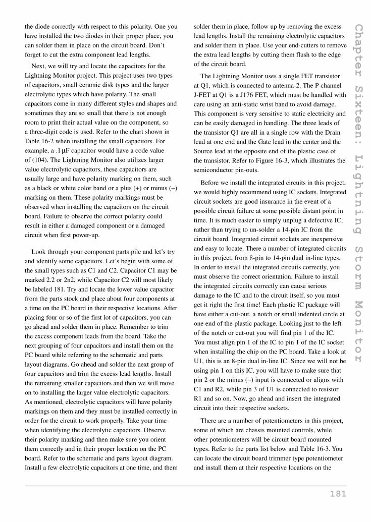
the diode correctly with respect to this polarity. One you
have installed the two diodes in their proper place, you
can solder them in place on the circuit board. Don’t
forget to cut the extra component lead lengths.
Next, we will try and locate the capacitors for the
Lightning Monitor project. This project uses two types
of capacitors, small ceramic disk types and the larger
electrolytic types which have polarity. The small
capacitors come in many different styles and shapes and
sometimes they are so small that there is not enough
room to print their actual value on the component, so
a three-digit code is used. Refer to the chart shown in
Table 16-2 when installing the small capacitors. For
example, a .1 µF capacitor would have a code value
of (104). The Lightning Monitor also utilizes larger
value electrolytic capacitors, these capacitors are
usually large and have polarity marking on them, such
as a black or white color band or a plus (+) or minus (−)
marking on them. These polarity markings must be
observed when installing the capacitors on the circuit
board. Failure to observe the correct polarity could
result in either a damaged component or a damaged
circuit when first power-up.
Look through your component parts pile and let’s try
and identify some capacitors. Let’s begin with some of
the small types such as C1 and C2. Capacitor C1 may be
marked 2.2 or 2n2, while Capacitor C2 will most likely
be labeled 181. Try and locate the lower value capacitor
from the parts stock and place about four components at
a time on the PC board in their respective locations. After
placing four or so of the first lot of capacitors, you can
go ahead and solder them in place. Remember to trim
the excess component leads from the board. Take the
next grouping of four capacitors and install them on the
PC board while referring to the schematic and parts
layout diagrams. Go ahead and solder the next group of
four capacitors and trim the excess lead lengths. Install
the remaining smaller capacitors and then we will move
on to installing the larger value electrolytic capacitors.
As mentioned, electrolytic capacitors will have polarity
markings on them and they must be installed correctly in
order for the circuit to work properly. Take your time
when identifying the electrolytic capacitors. Observe
their polarity marking and then make sure you orient
them correctly and in their proper location on the PC
board. Refer to the schematic and parts layout diagram.
Install a few electrolytic capacitors at one time, and them
solder them in place, follow up by removing the excess
lead lengths. Install the remaining electrolytic capacitors
and solder them in place. Use your end-cutters to remove
the extra lead lengths by cutting them flush to the edge
of the circuit board.
The Lightning Monitor uses a single FET transistor
at Q1, which is connected to antenna-2. The P channel
J-FET at Q1 is a J176 FET, which must be handled with
care using an anti-static wrist band to avoid damage.
This component is very sensitive to static electricity and
can be easily damaged in handling. The three leads of
the transistor Q1 are all in a single row with the Drain
lead at one end and the Gate lead in the center and the
Source lead at the opposite end of the plastic case of
the transistor. Refer to Figure 16-3, which illustrates the
semiconductor pin-outs.
Before we install the integrated circuits in this project,
we would highly recommend using IC sockets. Integrated
circuit sockets are good insurance in the event of a
possible circuit failure at some possible distant point in
time. It is much easier to simply unplug a defective IC,
rather than trying to un-solder a 14-pin IC from the
circuit board. Integrated circuit sockets are inexpensive
and easy to locate. There a number of integrated circuits
in this project, from 8-pin to 14-pin dual in-line types.
In order to install the integrated circuits correctly, you
must observe the correct orientation. Failure to install
the integrated circuits correctly can cause serious
damage to the IC and to the circuit itself, so you must
get it right the first time! Each plastic IC package will
have either a cut-out, a notch or small indented circle at
one end of the plastic package. Looking just to the left
of the notch or cut-out you will find pin 1 of the IC.
You must align pin 1 of the IC to pin 1 of the IC socket
when installing the chip on the PC board. Take a look at
U1, this is an 8-pin dual in-line IC. Since we will not be
using pin 1 on this IC, you will have to make sure that
pin 2 or the minus (−) input is connected or aligns with
C1 and R2, while pin 3 of U1 is connected to resistor
R1 and so on. Now, go ahead and insert the integrated
circuit into their respective sockets.
There are a number of potentiometers in this project,
some of which are chassis mounted controls, while
other potentiometers will be circuit board mounted
types. Refer to the parts list below and Table 16-3. You
can locate the circuit board trimmer type potentiometer
and install them at their respective locations on the
181
Chapter Sixteen: Lightning Storm Monitor

182
Chapter Sixteen: Lightning Storm Monitor
Table 16-2Capacitor code information
This table is designed to provide the value of alphanumeric coded ceramic, mylar and mica capacitors in general. They come in
many sizes, shapes, values and ratings; many different manufacturers worldwide produce them and not all play by the same rules.
Most capacitors actually have the numeric values stamped on them; however, some are color coded and some have alphanumeric
codes. The capacitor’s first and second significant number IDs are the first and second values, followed by the multiplier number
code, followed by the percentage tolerance letter code. Usually the first two digits of the code represent the significant part of the
value, while the third digit, called the multiplier, corresponds to the number of zeros to be added to the first two digits.
Value Type Code Value Type Code
1.5 pF Ceramic 1,000 pF /.001 µF Ceramic / Mylar 102
3.3 pF Ceramic 1,500 pF /.0015 µF Ceramic / Mylar 152
10 pF Ceramic 2,000 pF /.002 µF Ceramic / Mylar 202
15 pF Ceramic 2,200 pF /.0022 µF Ceramic / Mylar 222
20 pF Ceramic 4,700 pF /.0047 µF Ceramic / Mylar 472
30 pF Ceramic 5,000 pF /.005 µF Ceramic / Mylar 502
33 pF Ceramic 5,600 pF /.0056 µF Ceramic / Mylar 562
47 pF Ceramic 6,800 pF /.0068 µF Ceramic / Mylar 682
56 pF Ceramic .01 Ceramic / Mylar 103
68 pF Ceramic .015 Mylar
75 pF Ceramic .02 Mylar 203
82 pF Ceramic .022 Mylar 223
91 pF Ceramic .033 Mylar 333
100 pF Ceramic 101 .047 Mylar 473
120 pF Ceramic 121 .05 Mylar 503
130 pF Ceramic 131 .056 Mylar 563
150 pF Ceramic 151 .068 Mylar 683
180 pF Ceramic 181 .1 Mylar 104
220 pF Ceramic 221 .2 Mylar 204
330 pF Ceramic 331 .22 Mylar 224
470 pF Ceramic 471 .33 Mylar 334
560 pF Ceramic 561 .47 Mylar 474
680 pF Ceramic 681 .56 Mylar 564
750 pF Ceramic 751 1 Mylar 105
820 pF Ceramic 821 2 Mylar 205
1st Significant Figure
2nd Significant Figure
Multiplier
Tolerance
CSGNetwork.Com 6/4/92
0.1 µF 10%
104 k

circuit board. Solder them in place and then trim the
excess leads if necessary.
Let’s take a well deserved break and when we return
we will inspect the circuit board for possible “short”
circuits and “cold” solder joints. Pick up the Lightning
Monitor circuit board with the foil side of the board
facing upwards towards you. First we will inspect the
PC board for possible “cold” solder joints. Take a look
at the solder joints, they should all look clean, shiny and
bright. If you see any solder joints that appear dull, dark
or “blobby,” then you should remove the solder from
the joint and re-solder the joint all over again until it
looks good. Once you are confident that all looks well,
we can move on to inspecting the PC board for possible
“short” circuits. There are two main causes for “short”
circuits, small round solder blobs laying across a PC
“trace” can cause a circuit to “short-out.” The second
cause of “short” circuits is a “stray” component lead.
Often when cutting excess component leads,
they will “stick” to the circuit board from rosin core
solder residue. Make sure that there are no “stray” leads
bridging between the circuit board traces. Once you
are confident that there are no “shorts,” we can move
on to finishing the project.
Now, let’s move on to mounting the larger components
and hardware on the chassis box. The chassis mounted
183
Chapter Sixteen: Lightning Storm Monitor
Table 16-3Potentiometer functions
Potentiometer Function Type
VR1 Spheric Gain Control 500k chassis mount
VR2 Meter Gain Control 1 megohm trimmer
VR3 Meter Range Control 3k trimmer
VR4 Spheric Volume Control 10k chassis mount
VR5 Static Volume Control 10k chassis mount
VR6 Main Volume Control 10k chassis mount
VR7 Static Range Control 25k trimmer
VR8 Static Gain Control 10M chassis mount
VR9 Static Meter Balance Control 1 megohm trimmer
VR10 Load Control 10 megohm trimmer
SG
D
TO-92
LM741N
1 81
2
3
4
8
7
6
5
LM741N
1 81
2
3
4
8
7
6
5
LM741N
1 81
2
3
4
8
7
6
5
LF355
J176 jFET
1 81
2
3
4
8
7
6
5
LM380
1 81
2
3
4
8
7
6
5
Figure 16-3 Semiconductor pin-outs

potentiometers were all mounted on the front of the
metal chassis used to house the project, and wired to the
circuit board with 20 ga. insulated wire. The two toggle
switches, S1 and S2, were also mounted on the front
panel of the chassis and were wired to the circuit board
using 22 ga. insulated wire.
The Lightning Monitor utilizes two analog meters,
one for each monitoring circuit. The meter for the
Spheric circuit at M1, was a 500 µA meter, while the
Static meter circuit uses a 250-0-250 µA center reading
meter at M2. Both of these meters were found surplus
and were mounted on the front panel of the metal
chassis.
The speaker was mounted on the rear panel of the
chassis and wired to the circuit board using two 6′′lengths or #22 ga. insulated wire. A 1⁄8′′ switched mini
audio panel jack for headphone use was mounted on the
front panel. An RCA jack was provided for antenna-1;
you can use a whip antenna or an outdoor whip antenna.
An SO-239 antenna connector was mounted at the rear
panel to allow the Capacitive Hat antenna-2 to connect
to the circuit board, via a small piece of coax cable.
The Capacitive Hat antenna is shown in Figure 16-4,
it can be built with an antenna bracket mounted on a
pole outdoors. An SO-239 jack was mounted on the
small antenna bracket. A threaded shaft was silver
soldered to the center terminal of the connector with a
small rain guard on it. At the top of the threaded shaft
a metal coffee can lid is held in place with two nuts.
The antenna can be placed outdoor on a pole near the
house with a length of coax cable leading from the
antenna to the antenna jack on the Lightning
Monitor.
If you wish to experiment, you can try an indoor 5′whip without the coil and see how the circuit performs.
You could also experiment with an outdoor whip
antenna without the coil and you could build the coil
and place it in series with an outdoor whip antenna if
desired.
The Lightning Monitor needs a power supply which
can provide a 12 volt source for the audio amplifier
circuit as well as a plus and minus power supply for
the op-amps. The diagram in Figure 16-5 illustrates a
12 volt and dual plus/minus 5 volt power supply which
can be used to power the Lightning Monitor. The
prototype Lightning Monitor incorporated the power
supply in the same chassis as the actual monitor. You
will need to locate a 12 volt, 250 mA center-tapped
transformer ahead of the rectifier circuit. The rectifier
circuit is fed directly to the regulator integrated circuits
as shown. You will need to connect the dual voltage
power supply to the Lightning Monitor. The plus voltage
is connected to pins 7 on both the LM741 and the
LF355 op-amp as well as to the J-FET at Q1. The
negative voltage supply is connected to pin 4 of both
the LM741 and the LF355 op-amp, as well as to the
JFET at Q1. The 12 volt power supply is used to power
the LM380 audio amplifier.
Once the power supply and Lightning Monitor have
been completed, you connect the whip antenna-1 and
the Capacitive Hat antenna-2 and prepare for testing the
Lightning Monitor. To best test the circuit you will need
to wait for a thunderstorm. However, you can do some
testing of the circuit. First, apply power to the Lightning
Monitor circuit, turn the Off-On switch to the “On”
position. Make sure both antennas are connected. Turn
up the main volume and the Static Volume controls past
the 1⁄2 position and adjust VR7 to past 1⁄2. You will need
to generate some static electricity by rubbing a lucite
rod with some animal fur to create a static charge. Bring
the lucite rod near the Capacitive Hat antenna and you
should see the Static Meter at M2 swing into action.
This will give you a good indication that the Static
portion of the meter is working. You may be able to test
the Spheric Meter portion of the circuit if you have an
RF broadband noise generator.
If the Lightning Monitor doesn’t seem to work at all
or appears DEAD, then you will want to turn “Off ” the
circuit and remove the power and inspect the circuit
board once again. While inspecting the circuit board
184
Chapter Sixteen: Lightning Storm Monitor
NutsMetal coffee
can lid
Threaded shaft
Antennamount
SO239
Rainguard(plastic umbrella)
Figure 16-4 Antenna-2 – Capacitive hat antenna

you will be looking to make sure that the electrolytic
capacitors have been installed correctly, to be sure that
the diodes and the JFET have been installed correctly as
well. Have a knowledgeable electronic hobbyist inspect
the circuit, since it is easy to overlook something and
not catch it the second time. Make sure that your power
supplies are connected to the correct points and that the
op-amps have been installed correctly. Once you are
confident of your inspection and hopefully you found
your error, you can re-apply power and re-test the circuit
again. Good luck and be safe when experimenting with
outdoor antennas, keeping them away from power lines.
185
Chapter Sixteen: Lightning Storm Monitor
PL1
S1
F1
117 V AC
24 V CTT1 BR1
AC +AC –
U1
U2
U3
C1 C2+ +
R1
R2
C3+
1
2
3
1
2
3
C6+
1
2
3
C9C7 C8+ + +
+12 V DC
+5 V DC output
Commonground
–5 V DC output
+ +C4 C5
Figure 16-5 Multi-voltage power supply

Ambient Power Receiver
Chapter 17
Parts list
Original Ambient PowerModule I
C2,C3 .047 µF, 50voltcapacitor
C1,C4 40 µF, 50voltelectrolytic capacitor
D1,D2 1N34 diodes
D3,D4 1N34 diodes
ANT 50+ foot broadband
monopole antenna
GND Earth ground stake
Misc PC board, wire,
hardware, enclosure
Ambient Power Module II
D1,D2,D3,D4,D5,D6 1N60
germanium diodes
D7,D8,D9,D10,D11,D12
1N60 germanium diodes
C1,C2,C3,C4,C5,C6
470 µF, 50voltelectrolytic
capacitors
C7,C8,C9,C10,C11,C12
470µF, 50voltelectrolytic capacitors
L1 480 turns #22 wire
on 3” plastic tube
ANT 50+ foot broadband
monopole antenna
GND earth ground stake
Misc printed circuit
board, wire, hardware,
case
In 1979, Joe Tate began experimenting with methods
of turning radio energy in the air into usable electric
power. He first developed a clock which drew its power
from an antenna that was just a long piece of wire
stretched out horizontally about 20 feet above the
ground. The power supply for the clock worked
something like an old-style crystal radio, except that
it did not have a tuning circuit. Because of this, the
“Crystal Clock” was able to absorb a wide spectrum of
radio noise from the antenna and yield electric power.
The power supply was able to deliver much more
current than was developed in a crystal radio, although
its output was just still just a few millivolts.
Joe began recording the power supply’s output over
a long period of time to determine its dependability.
After all, the device relied completely on whatever
stray signals happened to be in the air. Using an Atari
computer, the output of the clock’s power supply was
measured continuously and recorded on floppy disk.
This was done by feeding the unregulated voltage
output directly into the computer’s joystick port.
Joe began calling this power supply the “Ambient
Power Module” (APM) because it extracted power from
ambient background radio noise. This small circuit,
when connected to antenna and ground, used the
potential difference between air and ground to generate
a small direct current continuously. Joe’s original claims
stated that the APM could produce up to 36 volt/9 watts.
Joe applied for a US Patent and was later granted patent
#4,628,299. As he studied the recorded data, mild
fluctuations were noted in a daily cycle. The patterns
were consistent over long periods of time, though they
differed in different locations. Aside from that, the
APM looked like a very dependable source of power.
In the spring of 1984, he discovered an interesting
correlation between voltage fluctuations from the APM
and a local earthquake event; this point will be
discussed later.
The APM operates, as a broadband receiver of energy
in the lower portion of the radio spectrum, receiving
186Copyright © 2008 by The McGraw-Hill Companies, Inc. Click here for terms of use.

187
Chapter Seventeen: Ambient Power Receiver
most of its power from below 1 MHz. The basic circuit
may be combined with a variety of voltage regulation
schemes.
The original Ambient Power Module is shown
in Figure 17-1 and the schematic diagram circuit in
Figure 17-2 is used to convert the ambient RF energy
to a direct voltage which can be used and handled by
data processing equipment. This design makes use of
doubler, splitter and rectifier circuit configurations.
Designated as an ambient power module (APM), the
circuit is connected to an antenna, preferably a 50 foot
or greater broadband monopole antenna. The antenna is
connected to the APM circuit via two capacitors C2 and
C3, each being in series with the antenna input line for
coupling and each having a value of 0.047 microfarad.
Taking the left or negative side of the circuit first,
it comprises two rectifiers (diodes) D3 and D4
(1N34 type) and a filter capacitor C4
(40 microfarads). Rectifier D2 is connected in parallel
to the signal path and rectifier D1 is connected in series,
in the well-known voltage multiplier arrangement.
Capacitor C1 is connected in parallel across the output of
the APM to smooth the rectified output. The right or
positive side of the circuit is similar, except for the
polarity of the diodes.
In operation, an RF voltage is developed across the
antenna; this voltage is voltage multiplied by the two
rectifiers on each side of the circuit. The resultant
voltage output is smoothed or filtered by capacitors
C2 and C4. The circuit is very symmetrical with the
plus side mirroring the minus side of the circuit. The
output of the APM is ideal for low voltage, high
impedance devices, like digital clocks, calculators,
radios and smoke alarms, which are the most likely
applications for this power source.
One possible application for the APM is to
charge small NiCad batteries which provide effective
voltage regulation as well as convenient electrical
storage. Charging lead acid batteries is not practical
because their internal leakage is too high for the
APM to keep up with. Similarly, this system will not
provide enough power for incandescent lights
except in areas of very high radio noise. The APM
could also be used to power small electronic devices
with CMOS circuitry, like clocks and calculators.
Smoke alarms and low voltage LEDs, and small
emergency power/lighting circuits can also be powered
by the APM. Use your imagination to devise an
application for the APM.
Building the APM circuitThe builder has a choice of wiring techniques which
may be used to construct the module. It may be hand
wired onto a terminal strip, laid out on a bread board,
experiment board, or printed circuit. We chose to build
the original circuit on a small printed circuit board.
Locate a clean well lit work table to build the APM.
Find a small 27 to 33 watt pencil-tipped soldering iron,
as well as some “Tip Tinner.” “Tip Tinner” is a
soldering iron tip cleaner/dressing compound which
helps to clean the soldering tip after use and can be
obtained at your local Radio Shack store. Try and
locate a pair of end-cutters, a pair of small needle-nose
pliers and a set of screwdrivers. Grab your schematic
Ambient powermodule
Figure 17-1 Ambient power module
Antenna
–V
C1
D1
C2
D2
C3
D3 +V
D4
C4
Figure 17-2 Ambient power module 1

diagram and look closely at it, before we begin
construction.
The APM power receiver consists mainly of diodes
and capacitors and you will recall that both of these type
of components have polarity which must be observed for
the circuit to function correctly. The diodes used in the
APM circuit are germanium diodes and NOT silicon
diodes which have a voltage drop. Diodes will have
either a white or black band at one side of the diode’s
body. This colored band denotes the cathode end of the
diode. When installing the diodes on the PC board
make sure you observe the correct placement of all the
diodes.
The APM circuit utilizes various capacitors, both
electrolytic and non-electrolytic types. Electrolytic
capacitors are often larger size capacitors with larger
values. Electrolytic capacitors have polarity and
may have either a black or white color bands with plus
or minus marking at one end of the capacitor body.
When installing the electrolytic capacitors make
sure that you orient the capacitors correctly with
respect to the circuit diagram. The chart in Table 17-1
may help you to identify the small value capacitors.
In many instances, small value/size capacitors
often use a three-digit code to represent a capacitor
value.
Once all the components have been placed on the
PC board, you can take a short break and when we
return we will inspect the circuit board for possible
“short” circuits and “cold” solder joints. Pick up the
circuit board with the foil side facing upwards toward
you. Look over the board carefully and inspect the solder
connections. The solder joints should all look clean,
smooth and shiny. If any of the solder joints look dull,
dirty or “blobby” then remove the solder from the joint
and re-solder the connection over again so that it
looks good.
Next we will inspect the circuit board for any “short”
circuit which could result from solder blobs or remaining
component leads left from the building process.
A component lead resting across a PC trace can result
in a “short” circuit which could cause the circuit
to fail.
Once you are satisfied that your circuit looks good,
you can move on to testing the APM receiver. First you
will need to attach a good antenna ground connection to
the APM receiver module.
Antenna requirementsThe antenna needs to be of sufficient size to supply the
APM with enough RF current to cause conduction in
the germanium diodes and charge the ground coupling
capacitors. It has been found that a long horizontal
antenna wire works best. A fifty foot monopole, or
long-wire antenna will work well, but a small antenna
should work, and of course you can experiment with
your own antenna ideas. The antenna will work best
when elevated to 20–30 feet. Lower elevations will
work, but a longer wire may be necessary for best
results.
In most locations, possible supporting structures
already exist. The wire may be stretched between the top
of a building and some nearby tree or telephone pole,
see Figure 17-3. If live wires are present on the building
or pole, care should be taken to keep your antenna and
body well clear of these hazards. To mount the wire,
standard commercial insulators may be used as well as
homemade devices. Plastic pipe makes an excellent
antenna insulator. Synthetic rope also works very well,
and has the advantage of being secured simply by tying
a knot. It is convenient to mount a pulley at some
elevated point so the antenna wire may be pulled up to it
using the rope which doubles as an insulator.
Grounding the APMThe APM requires a good ground circuit in order to
operate efficiently. Usually a good ground can be
established by connecting a wire to the water or gas
pipes of a building. Solder or screw the wire to the
APM ground terminal. In buildings with plastic pipes
or joints, some other hookup must be used. A metal
rod or pipe may be driven into the ground in a shady
location where the earth usually is damper. Special
copper coated steel rods are made for grounds, which
have the advantage of good bonding to copper wire.
A ground of this type is usually found within the electrical
system of most buildings. Conduit is a convenient
ground provided that the conduit is properly grounded.
This may be checked with an ohmmeter by testing
continuity between the conduit and system ground
(ground rod). Just as with the antenna, keep the ground
188
Chapter Seventeen: Ambient Power Receiver

189
Chapter Seventeen: Ambient Power Receiver
Table 17-1Capacitance code information
This table provides the value of alphanumeric coded ceramic, mylar and mica capacitors in general. They come in many sizes,
shapes, values and ratings; many different manufacturers worldwide produce them and not all play by the same rules. Most
capacitors actually have the numeric values stamped on them; however, some are color coded and some have alphanumeric codes.
The capacitor’s first and second significant number IDs are the first and second values, followed by the multiplier number code,
followed by the percentage tolerance letter code. Usually the first two digits of the code represent the significant part of the value,
while the third digit, called the multiplier, corresponds to the number of zeros to be added to the first two digits.
Value Type Code Value Type Code
1.5 pF Ceramic 1,000 pF /.001 µF Ceramic / Mylar 102
3.3 pF Ceramic 1,500 pF /.0015 µF Ceramic / Mylar 152
10 pF Ceramic 2,000 pF /.002 µF Ceramic / Mylar 202
15 pF Ceramic 2,200 pF /.0022 µF Ceramic / Mylar 222
20 pF Ceramic 4,700 pF /.0047 µF Ceramic / Mylar 472
30 pF Ceramic 5,000 pF /.005 µF Ceramic / Mylar 502
33 pF Ceramic 5,600 pF /.0056 µF Ceramic / Mylar 562
47 pF Ceramic 6,800 pF /.0068 µF Ceramic / Mylar 682
56 pF Ceramic .01 Ceramic / Mylar 103
68 pF Ceramic .015 Mylar
75 pF Ceramic .02 Mylar 203
82 pF Ceramic .022 Mylar 223
91 pF Ceramic .033 Mylar 333
100 pF Ceramic 101 .047 Mylar 473
120 pF Ceramic 121 .05 Mylar 503
130 pF Ceramic 131 .056 Mylar 563
150 pF Ceramic 151 .068 Mylar 683
180 pF Ceramic 181 .1 Mylar 104
220 pF Ceramic 221 .2 Mylar 204
330 pF Ceramic 331 .22 Mylar 224
470 pF Ceramic 471 .33 Mylar 334
560 pF Ceramic 561 .47 Mylar 474
680 pF Ceramic 681 .56 Mylar 564
750 pF Ceramic 751 1 Mylar 105
820 pF Ceramic 821 2 Mylar 205
1st Significant Figure
2nd Significant Figure
Multiplier
Tolerance
CSGNetwork.Com 6/4/92
0.1 µF 10%
104 k

wire away form the hot wires. The APM’s ground wire
may pass through conduit with other wires but should
only be installed by qualified personnel. Grounding in
extremely dry ground can be enhanced by burying some
salt around the rod. The salt will increase the conductivity
of the soil and also help retain water content around the
ground rod. Some researchers have found that it is much
better to get the largest surface area of metal in contact
with the ground as possible, and have tried digging a hole
and planting aluminum foil sheets in the ground.
Once you have tested the operation of the APM, you
can disconnect the antenna and decide how you wish to
enclose the APM circuit. You may want to experiment
with the housing, since researchers have discovered that
the germanium diodes are sensitive to sunlight and the
voltage output is increased when the circuit is in
sunlight. If you want to experiment along these lines,
then you may wish to enclose the circuit in a clear
plastic box. You can drill holes for two terminals posts
for the plus and minus output connections, an RCA jack
for the antenna input connection, a terminal for the
ground connection, and your APM is complete and
ready for operation.
The APM-IIThe original APM is a great circuit for experimentation.
It has been found that the germanium diodes are also
sensitive to light, so if you house the APM in a clear
plastic box and have it exposed to sunlight it will
produce more output. Have fun experimenting with the
APM receiver and you may find the perfect application
for it, such as powering another receiver or night light,
clock, emergency radio/lighting, etc.
Over time experimenters have improved upon the
original APM design and claim increased output from
the original design, so the reader is free to experiment
and build both versions of the APM if desired. The
second APM receiver, shown in Figure 17-4, illustrates
the newer version of the APM with increased output
voltage and current. The APM-II has quite a few more
stages and has many more diodes and capacitors. You
will note that the APM-II also uses germanium diodes
which have more output than trying to use silicon diodes.
Also note the higher capacitance values in the second
design which were used to increase the output
considerably. When constructing the APM-II be sure
to pay careful attention to mounting the diode and
capacitors; since there are many more components and
they all have polarity marking on them, it is much more
possible to make a mistake in orientation. Take your
time when constructing the circuit. The APM-II also
uses an input coil, which is said to improve the output.
Some experimenters claim that the antenna can be
eliminated and that the antenna connection can be
connected to another separate ground, but this has not
been verified. The APM-II is also sensitive to light
which can increase the output if used outside. Some
users claim that the power produced by the APM also
seems to improve near bridges, ships and anything
containing a great deal of metal.
Over time many scientists and researchers have
reported bright flashes in the sky during strong
earthquakes, as well as computer breakdowns during
severe tremors. Scientists have long suspected that
seismic activity is associated with a variety of electrical
effects. Researchers have been taking a careful look
at this link, with an eye toward using it to predict
earthquakes.
Joseph Tate and William Daily of Lawrence
Livermore National Laboratory in Livermore, CA.
created a system of radio wave monitors distributed
along California’s San Andreas fault using the
APM design. Tate and Daily recorded two kinds of
changes in atmospheric radio waves prior to
earthquakes that occurred between 1983 and 1986. Joe
was able to witness and record the output of the APM
during the earthquakes that followed, since he
continuously monitored the output of the APM on a
computer, so he could go back and look at the output on
any given day.
190
Chapter Seventeen: Ambient Power Receiver
Figure 17-3 Horizontal long-wire antenna

The most common change is a drop in the radio signals
that normally pervade the air as a result of lightning and
human sources such as car ignition systems and electric
power grids. This reduction typically occurs one to
six days before an earthquake and can last for many
hours. For example, a magnitude 6.2 earthquake that
shook Hollister, CA, in April 1984 was preceded
six days earlier by a 24-hour drop in radio signals
being monitored 30 miles from the quake’s epicenter.
Tate and Daily have found that the larger the earthquake,
the longer the time between the radio wave depression
and the quake.
Laboratory studies have shown that the electrical
conductivity of rocks increases as they are stressed.
Based on this and their electrical modeling of the
ground, Tate and Daily think the increased conductivity
of stressed rocks near the fault causes more radio waves
to be absorbed by the ground rather than their traveling
through the air. They also plan to test a possible link
between radio wave drops and the emission of radon
gas, which itself is thought to be a quake precursor. The
radon may ionize the air, making it temporarily more
absorptive than the detector antenna.
The researchers have also found, in addition to these
drops, another pre-quake phenomenon in which short
pulses of increased radio wave activity are emitted. For
example, five days before the magnitude 6.5 earthquake
hit palm Springs, CA, in July 1986, a station 15 miles
from the epicenter detected a rise in radio signals. This
sort of emission is consistent with laboratory work
showing that cracking rocks release electromagnetic
signals.
Tate says that in their first attempts at predicting
earthquakes, they did not miss a single event, so he
is optimistic about using this technique for short-term
forecasting of San Andreas quakes.
If you live in an earthquake prone area such as
California, you could use you APM not only for small
low voltage emergency power/lighting system but you
could connect the APM to an analog to digital converter
card in a personal computer and record the fluctuations
during earthquakes. The APM will provide many
avenues for the builder and/or researcher. Disconnect
your APM during thunderstorm activity to avoid
damage to the APM and other household devices. Have
fun and be safe.
191
Chapter Seventeen: Ambient Power Receiver
Antenna
+V –VD1 C6
L1
C7
C1 D2D3 C5 C8 D10
D12
D11 C12
D4D5 C4 C9 D8
D9 C11C2
C3 D6 D7 C10
Load
+V –V
+ –A B30 V
Figure 17-4 Ambient power module II

Earth Field Magnetometer Project
Chapter 18
Parts list
Earth Field Magnetometer
R1,R3,R4,R5 4.7kohm,1/4w, 5% resistor
R2 100ohms, 1/4w,
5% resistor
R6 10k ohm 1/4w,
5% resistor
C1,C2 15pF, 35 volt
capacitor
C3,C4 47nF, 35 volt
electrolytic
capacitor
C5 10 µF, 35 voltcapacitor
C6,C8 1 µF, 35 voltcapacitor
C7 22 µF, 35 voltelectrolytic capacitor
C9 10 µF, 35 voltTantalum capacitor
D1,D2 1N914 silicon
diode
D3 1N4001 silicon diode
X1 10MHz crystal
U1 SCL006A -
magnetometer output IC
U2 AD-557 - digital
to analog converter
chip
U3,U4 LM7805, 5 volt
regulator
J1,J2 wire jumpers
S1 4-position rotary
gain switch
S2 normally open
pushbutton switch
S3 SPST toggle power
switch
Logger HOBO H08-002-02
(ONSET)
Misc PC board, wire,
IC sockets, chassis,
etc.
Optional FieldMagnetometer PowerSupply
C1 470 µF, 50 voltelectrolytic capacitor
C2 1 µf, 50 voltceramic capacitor
C3 15 µf, 50 voltelectrolytic capacitor
BR1 diode bridge
rectifier 100v/2-amp
T1 24 volt center
tapped transformer -.5A
U1 LM7809 IC regulator
9 volts
S1 SPST power switch
PL1 115 VAC power plug
MISC PC board, wire,
hardware, etc.
1. Speake & Co. Ltd.
(Elvicta Estate,
Crickhowell, Powys.
Wales, UK; http://
www.speakesensors.com).
192Copyright © 2008 by The McGraw-Hill Companies, Inc. Click here for terms of use.
193
Chapter Eighteen: Earth Field Magnetometer Project
2. Fat Quarters Software
(24774 Shoshonee
Drive, Murieta, CA
92562; Tel: 909-698-
7950; Fax: 909-698-
7913; Web: http://
www.fatquarterssoftware
.com)
3. ONSET Computers, PO
Box 3450 Pocasset, MA
02559-3450 (1-800-564-
4377) http://www.
onsetcomp.com
Magnetic fields are all around us. The Earth itself
produces a magnetic field, which is why compasses
work. Anytime an electrical current flows in a conductor,
a magnetic field is generated. That is why transformers,
inductors, and radio antennas work. There are several
different devices that could be used to sense a magnetic
field. One of the most familiar to electronics hobbyists
is the Hall-effect device. However, in this chapter
we’ll take a look at a magnetic sensor that is as easy
to use, but is more sensitive, more linear, and more
temperature stable than typical Hall-effect devices.
And just like Hall-effect devices, it can be used to make
a variety of instruments, including magnetometers
and gradiometers.
For those unfamiliar with them, magnetometers
are used in a variety of applications in science and
engineering. One high-tech magnetometer is used by
Navy aircraft to locate submarines. Radio scientists use
magnetometers to monitor solar activity. Earth scientists
use magnetometers to study diurnal changes in the
Earth’s magnetic field. Archeologists use magnetometers
to locate buried artifacts, while marine archeologists
and treasure hunters use the devices to locate sunken
wrecks and sunken treasure.
The Earth Field Magnetometer that we will be exploring
uses a “flux-gate magnetic sensor.” The device, in
essence, is basically an over-driven magnetic-core
transformer which the “transducible” event is the
saturation of the magnetic material. These devices
can be made very small and compact, yet will still
provide reasonable accuracy.
In its most simple form the flux-gate magnetic sensor
consists of a nickel-iron rod used as a core, wound,
with two coils. One coil is used as the excitation coil,
while the other is used as the output or sensing coil.
The excitation coil is driven with a square-wave signal
with an amplitude high enough to saturate the core. The
current in the output coil will increase in a linear
manner so long as the core is not saturated. But when
the saturation point is reached, the inductance of the
coil drops and the current rises to a level limited only
by the coil’s other circuit resistances.
If the simple flux-gate sensor was in a magnetically
pure environment, then the field produced by the
excitation coil would be the end of the story. But there
are magnetic fields all around us, and these either add
to or subtract from the magnetic field in the core of the
flux-gate sensor. Magnetic field lines along the axis of
the core have the most effect on the total magnetic field
inside the core. As a result of the external magnetic
fields, the saturation condition occurs either earlier or
later than would occur if we were only dealing with the
magnetic field of interest. Whether the saturation occurs
early or later depends on whether the external field
opposes or reinforces the intended field.
Flux-gate magnetometerThe Earth Field Magnetometer project is illustrated in
Figure 18-1 and the remotely located FM-3 flux-gate
sensor is depicted in Figure 18-2.
The heart of the magnetometer is of course the
flux-gate sensor. A compact low-cost line of flux-gate
sensors are manufactured by Speake & Co. Ltd. and
distributed in the United States by Fat Quarters
Software. The FGM-3 sensor is the device used in
Figure 18-1 Magnetometer

this project. It is a 62 mm-long by 16 mm-diameter
(2.44 by 0.63 inch) device. Like all the devices in the line,
it converts the magnetic field strength to a signal
with a proportional frequency. The FGM-3 sensor
has only three leads: Red: +5 VDC (power), Black:
0 volts (ground), and White: output signal (a square-
wave whose frequency varies with the applied field).
The output signal is a train of TTL compatible pulses
with a period that ranges from 8 to 25 mS, or a
frequency range of 40 to 125 kHz. The detection
sensitivity of the FGM-3 device is +/− 0.5 oersted
(+50 utesla). That range covers the Earth’s magnetic
field, making it possible to use the sensor in
Earth-field magnetometers. Using two or three sensors
in conjunction with each other provides functions such
as compass orientation, three-dimensional orientation
measurement systems, and three-dimensional
gimbaled devices such as virtual-reality helmet display
devices. It can also be used in applications such as
ferrous metal detectors, underwater shipwreck
finders, and in factories as conveyer-belt sensors or
counters. There are a host of other applications where a
small change in a magnetic field needs to be
detected.
The FGM series also includes two other devices, the
FGM-2 and the FGM-3h. The FGM-2 is an orthogonal
sensor that has two FGM-1 devices on a circular
platform at right angles to one another. That orthogonal
arrangement permits easier implementation of orientation
measurement, compass, and other applications. The
FGM-3h is the same size and shape as the FGM-3, but
is about 2.5 times more sensitive. Its output frequency
changes approximately 2 to 3 Hz per gamma of field
change, with a dynamic range of +/− 0.15 oersted
(about one-third the Earth’s magnetic field strength).
The output signal in all the devices in the FGM series
is +5 volt (TTL-compatible) pulse whose period is
directly proportional to the applied magnetic field
strength. This relationship makes the frequency of the
output signal directly proportional to the magnetic field
strength. The period varies typically from 8.5 µs to
25 µs or a frequency of about l20 kHz to 50 kHz. For
the FGM-3 the linearity is about 5.5% over its +/− 0.5
oersted range.
The response pattern of the FGM-x series sensors is
shown in Figure 18-3. It is a “figure-8” pattern that has
major lobes (maxima) along the axis of the sensor, and
nulls (minima) at right angles to the sensor axis. This
pattern suggests that for any given situation there is a
preferred direction for sensor alignment. The long axis
of the sensor should be pointed towards the target
source. When calibrating or aligning sensor circuits, it is
common practice to align the sensor along the east-west
direction in order to minimize the effects of the Earth’s
magnetic field.
The flux-gate sensor is coupled directly to a special
interface chip, manufactured by Speake. This special
SCL006A integrated circuit is shown in the main
schematic diagram shown in Figure 18-4. It provides
the circuitry needed to perform the Earth field
magnetometry sensing. It integrates field fluctuations
in one-second intervals, producing very sensitive output
variations in response to small field variations. The
magnetometer is of special interest to people doing
radio-propagation studies, and those who want to monitor
for solar flares. It also works as a laboratory magnetometer
for various purposes. The SCL006A is housed in an
18-pin DIP IC package and is shown at U1. The FGM-3
194
Chapter Eighteen: Earth Field Magnetometer Project
Figure 18-2 FGM-3 Magnetometer sensor
NorthA
B
South
Maximumsensitivity
Maximumsensitivity
16 mmFGM-3
62 mm
F/B
Ground (black)
Out (white)
+5 V (red)
Figure 18-3 FGM-3 Magnetometer sensor

195
Chapter Eighteen: Earth Field Magnetometer Project
3
1
2
Gnd
R5
R4
R1
U1
D1
D2
1
2
3
4
5
6
7
8
9
18
17
16
15
14
13
12
11
10
R3
Red
White
Black
Reset
J1 A
B
C
C7+
C8+
U4O I
C9+
White
Black
RedSensor
FGM-3
R2 X1C1
C2C3 + Power
Min
Gain
Max1
2 34
S1
S2S3
+9–12 V
D3
+C5
IO
C6+
U3
1 2 3 4 5 6 7 812
13
10 9 14 15 16
C4+
11
J2
Closed
R6
Output
Output
Figure 18-4 Main magnetometer circuit

flux-gate sensor is coupled to the input pin at pin 17 of U1.
The reference oscillator of the SCL0006A is controlled
by components X1, C1, C2 and R2. A sensitivity
switch, S1, provides four positions, each with a
different overall sensitivity range. Switch S2 is used to
reset the SCL0006A, when applied for about two
seconds.
The second op-amp at U2, is an Analog Devices
AD557 D/A converter. The magnetometer circuit is
designed so that it could be run from a 9 to 15 volt
battery for use in the field. Power supplied from the
battery is controlled by power switch S3 which
supplies 9 volts to the regulator. For stationary
research, the magnetometer should be powered from an
110 volt AC to 9–15 volt DC power supply. The
regulator U3 drops the 9 volt input supply power down
to 5-volts to power the magneto-meter circuit. The
output signal is a DC voltage that can be monitored by a
strip-chart or X-Y paper recorder, a voltmeter or the
signal can be fed into a computer using an
A-to-D converter. In the prototype we used the output
to drive a portable mini data-logger such as the
ONSET corporation HOBO H08-002-02. You will
want to select the 2.5 volt model logger. You could also
elect to use a digital multi-meter with RS-232 output
which can be fed to a computer’s serial port for
data-logging.
ConstructionThe Earth-field magnetometer project was built on two
printed circuit boards. The main circuit board is shown
in Figure 18-5, was constructed on a 31⁄2′′ × 41⁄2′′ PC
board, while the remotely located FGM-3 sensor was
paired with a second 5-volt regulator shown in Figure
18-6. Regulator U4 was mounted on a 2′′ × 3′′ PC
board, which was attached to a sheet of flexible
plastic using plastic screws. The FGM-3 sensor probe
was then mounted on the 2′′ × 41⁄2′′ plastic sheet. The
plastic sheet was used to mount the probe, ahead of the
regulator in order to give the flux-gate probe some
isolation from surrounding metal. The flux-gate probe is
mounted length-wise and parallel to the length of the
PVC pipe. The FGM-3 sensor and remote regulator were
then housed in a 21⁄2′′ diameter × 12′′ long PVC pipe,
which is separated by a length of three-conductor cable.
Note that you could also elect to purchase a flux-
magnetometer kit including PC board, the FGM-3
196
Chapter Eighteen: Earth Field Magnetometer Project
Main board
1
2
3
Ground
Red A
B
C
White
Black
Output
Power
Reset
3-conductorcable
Min Max1 2 3 4
Gain
P1 S3
S2
FGM-3
C8C7 In
OutU4
+ +
RedWhite
Black
C9+
Recorderground
Powerground
Reset
+9–12 V DC
Output
To meteror
A/D logger
Gai
n
Sen
sor
S1
Sensor
Figure 18-5 Magnetometer connection diagram

197
Chapter Eighteen: Earth Field Magnetometer Project
Mainboard
White
Power
Black
B
P1
C
3-conductorcable
U4+ +
+C7 C8
BlackC9
In Out Red
WhiteGround FGM-3
Flux-gatesensor
sensor, ICs, and most other parts, but less the gain
switch, can be from Fat Quarters Software for about
$80.00.
Are you ready to begin constructing the flux-gate
magnetometer? Before we begin you will want to secure
a well lit and well ventilated work area, as well as a
bench or large table for assembling your magnetometer
project. Locate a small pencil-tipped 27 to 33 watt
soldering iron, as well as a roll of 22 ga. 60/40 tin/lead
rosin core solder. Go to your local Radio Shack store
and purchase a small jar of “Tip Tinner”; this is a
soldering iron tip cleaner/dresser compound, which
works wonders. You will also need a few hand tools for
the project. You will need a pair of small end-cutters,
a pair of needle-nose pliers, a pair of tweezers, and a
magnifying glass. A small flat-blade screwdriver and a
small Phillips screwdriver should round out your tool
requirements.
While you could build the magnetometer project on
a perf-board or you could use point-point wiring it is
recommended that you build the circuit on a printed
circuit board for most reliable circuit operation and long
life. Prepare your circuit board, and then we will be
able to go ahead and build the magnetometer receiver
project.
Locate all of the project diagram, such as the
schematic, parts layout diagrams and the
component pin-out sheets as well as the resistor and
capacitor identification tables and we will be almost
ready to begin. Place all of the magnetometer project
components on the work bench in front of you,
warm up your soldering iron and let’s get going.
First, refer to the chart in Table 18-1, which
illustrates the resistor color code. The resistor for this
project will have three or four color bands on them.
The first color band is closest to one end of the resistor
body. The first color band represents the first digit of
the resistor’s value, the second color represents the
second digit of the resistor value, the third color band
represents the resistor’s multiplier value, and the fourth
band denotes the resistor’s tolerance value. A silver
fourth band denotes a 10% tolerance value, while a gold
band represents a 5% tolerance value; no fourth color
band denotes a resistor with 20% tolerance. Resistors
R1, R3, R4 and R5, for example, are 4.7k ohm types.
The first color band is yellow, which represents a four
(4), while the second color band is violet or seven (7),
and the third color band is red denoting a multiplier
of (100), so you see (4) (7) times (100) equals 4700 or
4.7k ohms. Identify all of the 4.7k ohm resistors and
place them on the circuit board at their correct location.
Next, solder these resistors to the circuit board. Then
follow-up by cutting the excess component leads flush
to the edge of the circuit board with your end-cutters.
Now locate R2 and R6 and install them in their proper
locations, then solder them in place on the PC board.
Remember to trim the excess resistor leads with your
end-cutter.
Next we will move to identifying and installing the
capacitors for the project. Capacitors are available in two
major categories—electrolytic and non-electrolytic types.
Electrolytic capacitors are generally both larger in size
and larger in value than non-electrolytic types.
Electrolytic capacitors have polarity and hence, they
will have polarity marking on them to identify
Figure 18-6 Flux-gate sensor board

their leads. You will usually find a black or white
colored band or a plus (+) or minus (−) marking near
one of the capacitor leads; this denotes the polarity. You
will have to orient an electrolytic capacitor onto the
circuit board with respect to the capacitor’s polarity.
When you mount electrolytic capacitors on the circuit
board, you will have to refer to both the circuit
schematic and the parts layout diagrams in order to
install the capacitor properly. Failure to install
electrolytic capacitors correctly may result in damage to
the capacitor itself and perhaps damage to the circuit as
well. Non-electrolytic capacitors will generally be
smaller in value and physical size. Sometimes the non-
electrolytic capacitors will have their value printed on
them, and at other times the capacitor may be physically
very small when a three-digit code is used to identify
the capacitor. The chart in Table 18-2, helps to identify
capacitors based on this code. Use the chart to help
identify the capacitors. You will want to make sure that
you install the correct value capacitor into the right
location on the circuit board in order for the circuit to
work correctly. For example, a capacitor marked with
(102) denotes a value of .001 µF, while a capacitor with
a marking of (103) denotes a capacitor value of .01 µF.
Look through the component pile and identify the
capacitors and what type they are and then refer to the
parts layout diagram and capacitor code chart before
installing them on the circuit board. Go ahead and place
a few of the capacitors at their respective locations on the
PC board and solder them in place. Remember to trim the
extra component lead length with your end-cutters.
The magnetometer main circuit board utilizes three
silicon diodes. Diodes have polarity and they must be
installed correctly for the circuit to operate correctly.
Each diode will have either a black or white colored
band at one end of the diode body. The colored band
represents the diode’s cathode lead, the opposite lead is
the anode. Remember the diode’s electronic symbol is
an arrow or triangle pointing to a vertical line. The
vertical line is the cathode of the diode. Refer to the
schematic and parts layout diagram when mounting
the diodes onto the circuit board. Place the diodes on
the circuit board and solder them in place. Trim the
excess leads as necessary.
The magnetometer project employs a 10 MHz crystal
which is connected to pin 16 of U1. The crystal has no
polarity so it can be placed in either direction on the
board. Handle the crystal carefully so as to not break off
the leads from the crystal body.
Before we begin placing the semiconductors on the
PC board, you will want to refer to the semiconductor
198
Chapter Eighteen: Earth Field Magnetometer Project
Table 18-1Resistor color code chart
Color Band 1st Digit 2nd Digit Multiplier Tolerance
Black 0 0 1
Brown 1 1 10 1%
Red 2 2 100 2%
Orange 3 3 1,000 (K) 3%
Yellow 4 4 10,000 4%
Green 5 5 100,000
Blue 6 6 1,000,000 (M)
Violet 7 7 10,000,000
Gray 8 8 100,000,000
White 9 9 1,000,000,000
Gold 0.1 5%
Silver 0.01 10%
No color 20%

199
Chapter Eighteen: Earth Field Magnetometer Project
Table 18-2Capacitance code information
This table provides the value of alphanumeric coded ceramic, mylar and mica capacitors in general. They come in many sizes,
shapes, values and ratings; many different manufacturers worldwide produce them and not all play by the same rules. Most
capacitors actually have the numeric values stamped on them; however, some are color coded and some have alphanumeric codes.
The capacitor’s first and second significant number IDs are the first and second values, followed by the multiplier number code,
followed by the percentage tolerance letter code. Usually the first two digits of the code represent the significant part of the value,
while the third digit, called the multiplier, corresponds to the number of zeros to be added to the first two digits.
Value Type Code Value Type Code
1.5 pF Ceramic 1,000 pF /.001 µF Ceramic / Mylar 102
3.3 pF Ceramic 1,500 pF /.0015 µF Ceramic / Mylar 152
10 pF Ceramic 2,000 pF /.002 µF Ceramic / Mylar 202
15 pF Ceramic 2,200 pF /.0022 µF Ceramic / Mylar 222
20 pF Ceramic 4,700 pF /.0047 µF Ceramic / Mylar 472
30 pF Ceramic 5,000 pF /.005 µF Ceramic / Mylar 502
33 pF Ceramic 5,600 pF /.0056 µF Ceramic / Mylar 562
47 pF Ceramic 6,800 pF /.0068 µF Ceramic / Mylar 682
56 pF Ceramic .01 Ceramic / Mylar 103
68 pF Ceramic .015 Mylar
75 pF Ceramic .02 Mylar 203
82 pF Ceramic .022 Mylar 223
91 pF Ceramic .033 Mylar 333
100 pF Ceramic 101 .047 Mylar 473
120 pF Ceramic 121 .05 Mylar 503
130 pF Ceramic 131 .056 Mylar 563
150 pF Ceramic 151 .068 Mylar 683
180 pF Ceramic 181 .1 Mylar 104
220 pF Ceramic 221 .2 Mylar 204
330 pF Ceramic 331 .22 Mylar 224
470 pF Ceramic 471 .33 Mylar 334
560 pF Ceramic 561 .47 Mylar 474
680 pF Ceramic 681 .56 Mylar 564
750 pF Ceramic 751 1 Mylar 105
820 pF Ceramic 821 2 Mylar 205
1st Significant Figure
2nd Significant Figure
Multiplier
Tolerance
CSGNetwork.Com 6/4/92
0.1 µF 10%
104 k

pin-out diagram shown in Figure 8-7, which will assist
you in orienting the ICs. The magnetometer project
utilizes two main integrated circuits which are rather
expensive, so we recommend using IC sockets. As a
good insurance policy locate two IC sockets and solder
them in place for U1 and U2. If an IC fails at some later
date ‘down the road’, you can simply unplug the
defective one and replace it with a new one. Note that
the IC sockets will usually have a notch or cut-out at
one end of the plastic package. The lead just to the left
of the notch is pin. You will have to make sure that
pin one (1) of each socket is connected to the correct
components; refer to the schematic and parts layout
diagrams. Note pin one (1) of U1 goes to the anode of
diodes D1 and D2, while pin one (1) of U2 is connected
to pin six (6) of U1. When installing the ICs into their
respective sockets, you will have to make sure pin one
(1) of the IC is placed into pin one (1) of the socket to
prevent damage to the integrated circuits.
It is a good time to take a short, well deserved rest
and when we return we will examine the main circuit
board for any possible “cold” solder joints or “short”
circuits. Pick up the main circuit board with the foil
side facing upwards towards you. Look over the main
circuit board, we will be looking at the solder joints for
possible “cold” solder joints. The solder joints should
all look clean, bright and shiny, if you see any solder
joints that look dull, dark or “blobby,” you will need to
un-solder the joint and remove the solder with a solder-
sucker and then re-solder the connection, so that the
new solder joint looks good. Next we will examine the
PC board for possible “short” circuits. Often “short”
circuits can be caused by “stray” component leads or
solder “blobs” which may have stuck to the underside
of the PC board from solder residue. Look for solder
blobs or solder bridges which may be “shorting” or
bridging between circuit traces on the PC board. With
the PC board free from any defect, we can continue on
and prepare for connecting the sensor and power-up the
circuit.
The main magnetometer board was mounted on
standoffs in a metal chassis box, as seen in Figure 18-8.
The on-off power switch and sensitivity rotary switch
were mounted on the front panel of the chassis box,
along with the meter binding posts. A 3-position screw
terminal block or 3-circuit connector can be mounted on
the side of the chassis box to allow the main circuit to
connect to the remote sensor board.
200
Chapter Eighteen: Earth Field Magnetometer Project
SCL006A
AD557
AD557
•1
2
3
4
5
6
7
8
9 10
11
12
13
14
15
16
17
18(Top View)
LM7805 LM7809
OutputCommonInput
OC
I
OC
I
The common terminal is in electricalcontact with the mounting base.
(Top View)
OutputCommonInput
The common terminal is in electricalcontact with the mounting base.
1 •
2
3
4
5
6
7
8
16
15
14
13
12
11
10
9
Figure 18-7 Semiconductor pin-outs
Figure 18-8 Magnetometer – inside view

Now refer to the sensor power supply circuit diagram
shown in Figure 18-6. This diagram illustrates the
remote flux-gate sensor and power regulator PC board.
The sensor and regulator were placed on a small circuit
board, and in a water proof PVC cylinder so it can be
buried below the frost-line at about 4 feet underground.
The sensor should be placed well away from your
house, buried level in the ground with the ends of the
sensor facing East-West. The remote sensor is powered
from the main circuit board. You will want to place the
remote sensor and power supply in a non-metallic PVC
case and waterproof the case so water cannot leak inside
the case. The sensor will need to be facing the outside
of the PVC cylinder away from the other electronics
inside the package. Use no metal fasteners to secure
the circuit to the PVC enclosure. You will have to
make provisions to allow the three conductor to exit
the opposite end of the PVC case away from the
sensor end.
The main magnetometer circuit board was placed in a
metal chassis which measures 6′′ × 3′′ × 2′′ as shown in
the photo. The power switch, power LED, gain switch
and reset switch along with the output binding posts,
were mounted on the front of the chassis box. A four
position terminal strip was mounted along the side of
the chassis box to allow the remote sensor to be
connected to the main circuit. A coaxial power jack was
also mounted on the side of the chassis box to allow a
12 volt “wall wart” power supply to plug-in and power
the circuit.
If you wish to construct your own power supply
for the magnetometer project, refer to the diagram in
Figure 18-9, which illustrates a 12 volt power supply
from line-voltage. A 24 volt center tapped transformer
feeds AC to the 4-diode bridge rectifier package at BR1.
The DC output from the rectifier is filtered via C1 and
C2 and then sent to a 9 volt IC regulator chip at U1.
The output of the regulator chip is filtered at its output.
This optional power supply will provide 9 volts which
can be used to power the magnetometer circuit, if you
choose not to use a 9 to 12 “wall wart” power supply.
The main circuit board was mounted on standoffs
inside the bottom of the chassis box. Once you have
mounted the main circuit board and the controls, you
can locate a length of 20 to 24 gauge, three or four
conductor cables and connect the sensor board to the
main circuit board. Connect a digital voltmeter to the
output terminal binding posts and set the meter to read
5 volts to 10 volts. Connect up your power supply to the
main circuit board and we can now test the
magnetometer to see if it is working. Turn the power
switch to on, and set the meter range or gain switch to
maximum sensitivity. With the sensor away from the
main circuit board and chassis, bring a small magnet
within rage of the sensor to say about 2 feet away.
After about eight or ten seconds, you should see the
effects of bringing the magnet near to the sensor. The
reading will NOT be instantaneous, but you should see
the meter read up to 2 volts or so. Move the magnet
away and you should see the meter respond in 8 or
10 seconds. If all is well you will have a working
portable flux-gate magnetometer, which can be
used for many applications such as monitoring diurnal
magnetic Earth variations or solar storms. You can even
use the magnetometer as a UFO detector or driveway
monitor.
201
Chapter Eighteen: Earth Field Magnetometer Project
117 V ACPL1
S1T1
24 V CT
BR1
AC
AC
+ + + +
OutU1
In
C1 C2 C3
+V
Ground
_
Figure 18-9 Magnetometer power supply

If your magnetometer did not “spring-to-life” then
you will have to turn off the circuit and remove the
power supply, and look the circuit over carefully to
make sure you didn’t install a component incorrectly.
Grab your schematic, parts layout diagrams and charts
and let’s take a closer look at the circuit board.
Remember we talked about certain components, like
capacitors and diodes having polarity. Make sure that
you installed the electrolytic capacitors and diodes with
respect to their proper polarity; this is common cause
for error. If need be, have another person, such as a
parent or skilled technician or engineer or knowledgeable
friend, look over the circuit for you. The same person
looking over the same circuit numerous times often
prevents you from finding your errors; you need a fresh
look from another person to catch mistakes. Another
cause for error is placing the integrated circuits in the
wrong socket or in the wrong direction in the socket.
After looking the board over carefully, you can re-apply
the sensor and power supply connections and test the
circuit once again, hopefully it will work fine this time
around.
Once you know the magnetometer and sensor
circuits are working properly, you can make provisions
for mounting the sensor in a water-tight PVC case.
The remote flux-gate sensor probe was mounted in a
21⁄2′′ × 12′′ length of PVC pipe. Circuit board guides
were epoxied to the inside of the PVC pipe to
allow the circuit board to be slid into the PVC pipe.
One 21⁄2′′ end cap was cleaned and cemented to the
outside probe end of the PVC pipe. A 1⁄2′′ hole was
drilled and tapped in the center of the second PVC
end cap. Try to use as little metal as possible when
mounting the sensor in the PVC pipe, use brass or
plastic screws where possible. A brass nipple fitting
cemented in the tapped hole allows the three conductor
cables to exit the probe assembly in the PVC pipe.
Before cementing the final end cap to the PVC pipe
you will want to test the Earth-Field magnetometer
before burying the sensor probe assembly. Since the
sensor is NOT an expensive temperature referenced
or compensated type sensor it is subject to extreme
temperature variations, so if you live in the northern
climate zones, it will be necessary to mount the
sensor underground, below the frost-line, to prevent
temperature swings from affecting the reading of the
meter. In most frost-prone areas, you will need to
mount the water-proof sensor assembly about 4′ to 41⁄2′underground. The sensor should be mounted as far away
from metal objects and traffic as possible to ensure the
best results. The sensor package should be mounted so
that it will face North-South as shown in Figure 18-3.
The output of the magnetometer can be connected to
a logging digital multi-meter, so the imported data can
be later analyzed by your personal computer. You could
also use an inexpensive portable data-logger such as the
HOBO series from Onset Computers, or you could use
an analog to digital converter card in your PC to collect
the data sample over time. If your meter is set to the
most sensitive position, and everything is in working
order, you should easily be able to monitor the Earth’s
diurnal variations twice a day. You should also be able
to detect strong magnetic storms on the Sun, with your
new magnetometer.
202
Chapter Eighteen: Earth Field Magnetometer Project

Sudden Ionospheric Disturbance(SIDs) Receiver
Chapter 19
Parts list
SIDs Receiver
R1,R2,R3,R4 3.3k ohm1/4w resistor
R5 10kohm potentiometer
(chassis mount)
R6 1kohm 1/4w resistor
R7 100k potentiometer
(PC mount)
R8 100ohm 1/4w resistor
R9 10kohm 1/4w resistor
R10 470kohm 1/4w
resistor
R11 56kohm 1/4w resistor
R12 22kohm 1/4w resistor
R13 5k ohm
potentiometer
(PC mount)
C1 100pF, 35v ceramic
capacitor
C2 1500pF, 35v mylar
capacitor
C3 .001 µF, 35v ceramiccapacitor
C4 1 µF, 35v tantalumcapacitor
C5 10 µF 35v tantalumcapacitor
C6,C7 10 µF, 35velectrolytic
capacitor
C8,C9 0.1 µF, 35vceramic capacitor
C10,C11 1000 µF, 35velectrolytic capacitor
D1,D2 1N914 silicon
diode
D3,D4 1N34 germanium
diode
U1 LM353 op-amp
(National
Semiconductor)
U2 RC4136 op-amp (Texas
Instruments)
U3 79L09 - 5volt
regulator (− volts)
U4 78L09 - 5volt
regulator (+ volts)
T1 600 to 600ohm
inter-stage/ matching
transformer
L1 Loop antenna
(see text)
S1 DPST toggle switch
(on-off)
F1 .50 amp fast-blow
fuse
BR1 bridge rectifier -
50v DC/2amp
PL1 117 VAC plug
Misc PC board, IC
sockets, wire, solder,
solder lugs, chassis
hardware, screws,
standoffs, etc.
203Copyright © 2008 by The McGraw-Hill Companies, Inc. Click here for terms of use.

A sudden ionospheric disturbance (SID) is an
abnormally high plasma density in the ionosphere
caused by an occasional sudden solar flare, which often
interrupts or interferes with telecommunications
systems. The SID results in a sudden increase in radio-
wave absorption that is most severe in the upper
medium-frequency (MF) and lower high-frequency
(HF) ranges.
When a solar flare occurs on the Sun, a blast of
ultraviolet and X-ray radiation hits the day-side of the
Earth after 8 minutes. This high energy radiation is
absorbed by atmospheric particles raising them to
excited states and knocking electrons free in the
process of photo-ionization. The low altitude
ionospheric layers (D region and E region) immediately
increase in density over the entire day-side. The
Earth’s ionosphere reacts to the intense X-ray and
ultraviolet radiation released during a solar flare and
often produces shortwave radio fadeout on the day-side
of the Earth as the result of enhanced X-rays from a
solar flare.
Shortwave radio waves (in the HF range) are
absorbed by the increased particles in the low
altitude ionosphere causing a complete blackout
of radio communications. This is called a Short Wave
Fadeout. These fadeouts last for a few minutes to a few
hours and are most severe in the equatorial regions
where the Sun is most directly overhead. The
ionospheric disturbance enhances long wave (VLF)
radio propagation. SIDs are observed and recorded by
monitoring the signal strength of a distant VLF
transmitter. As the fadeouts occur, reception of the
station strength varies thus creating a fluctuating voltage
output at the receiver which can be recorded and
observed using a computer with a chart recorder
program.
You can build and investigate the phenomena of
SIDs with a special receiver and a low cost
data-logger setup. You can not only observe when
solar flares are occurring but you can collect and
analyze the data and display it on your computer. The
SIDs receiver is a great opportunity to observe first-
hand when a solar event occurs, but you can use it to
predict when radio blackouts will affect radio
propagation, which is extremely useful for amateur
radio operators.
VLF signal propagationWhy do VLF signals strengthen at night instead of
getting weaker? If propagation is basically via the
waveguide effect, why doesn’t the signal drop DOWN
at night when the waveguide disappears with the D
layer? Is there some kind of reduced absorption at
night? If so, where is it taking place and why? Also,
what accounts for the big fluctuations in signal strength
at night, apparently more or less at random?
The strength of the received signal depends on the
effective reflection coefficient of the region from which
the radio wave reflects in its multi-hop path between
Earth and the ionosphere. In daytime the reflecting region
is lower, the air density is higher, and the free electron
density is controlled strongly by the solar radiation, etc.
At night time the reflecting region is higher, the air
density is lower, and the free electron density is
controlled by variable ambient conditions as well as
variable influences from electron “precipitation” from
above, etc.
At noon the electron density is about 10 electrons/cm3
at an altitude of 40 km, 100 electrons/cm3 at an altitude
of 60 km, 1000 electrons/cm3 at an altitude of 80 km
and 10,000 electrons/cm3 at an altitude of 85 km.
At night these figures become 10 electrons
electrons/cm3 at 85 km, 100 electrons/cm3 at 88 km
and 1000 electrons/cm3 at 95 km and then remains
somewhat the same up to at least 140 km. At night the
electron density in the lower part of the D region pretty
much disappears. At 40 km the electron collision
frequency is about 1,000,000,000 collisions per second
whereas at 80 km the collision frequency drops to
1,000,000 collision per second. The reflection coefficient
depends on (among other things) the number density of
free electrons, the collision frequency, and the frequency
of the radio signal. It is found by a mathematical
integration throughout the entire D-region and of course
the result depends on what time of the 24 hour day one
performs the integration.
We can think of the E-Layer propagating the signal at
night. Then the prominent sunrise pattern we see is a
shift from E-Layer propagation back to D-Layer as
the sun rises and forms the daytime D-Layer.
204
Chapter Nineteen: SIDs Receiver

The sunset pattern is the reverse. An interesting feature
of waveguide mode propagation was that the signal was
split into two components which can form an
interference pattern.
You can build your own Sudden Ionospheric
Disturbances (SIDs) receiver, shown in Figure 19-1, and
begin your own investigation of solar flares and their
effects on radio propagation. The SIDs receiver is a
simple VLF receiver designed to be used with a loop
antenna which can be placed either inside or outside.
The receiver monitors the strong VLF signal from the
US Navy NAA 24 kHz transmitter in Cutler Maine.
The Sudden Ionospheric Disturbance (SID) receiver
is a modified Stokes’ Gyrator tuned VLF receiver based
on the circuit from Communications Quarterly Spring
1994 pp. 24–26. The main circuit diagram shown is
Figure 19-2, it illustrates SIDs receiver which consists
of two integrated circuits, a Texas Instruments RC4136
and a National LF353 operation amplifier. The SIDs
receiver is fed from a loop antenna at L1. The antenna
is coupled to the SIDs receiver via a miniature 600 to
600 ohm matching transformer at T1. The output from
the secondary of T1 is fed to two protection diodes at
D1 and D2 at the front end of the receiver. The output
of the diode network is then coupled to a 100 pF
capacitor at C1. Capacitor C2 is connected from the
205
Chapter Nineteen: SIDs Receiver
Figure 19-1 Sudden ionospheric disturbance receiver
U2:D
L1
T1 C2 C1
D4 D3 C3
U2:B U2:A+V +V
5 11
476
+–
–V R1
112
13
7
–V R2
R3
13 1112
14 7
C4 R9
+V
–V
R7R5
9 8+V
11 710
–VD2
D1
R13U2:C
R4
Output(A)
R6
R12
1
4 2
38+–
U1:A R10
+C5
R11
–V
+V
M1
R8
++
––
Figure 19-2 Sudden ionospheric disturbance receiver

output of C1 to ground at the input of the first op-amp
stage U2:B. Integrated circuit sections U2:A and U2:B
form an amplifier/filter and tuning. The “tuning” is
controlled via R6, which is placed in a shielded
enclosure to prevent circuit oscillation. The potentiometer
is kept separate in a small shielded box formed by some
scrap pieces of thin circuit board soldered together.
The output from U2:A is next fed to IC:D and U2:C
which forms an amplifier/integrator section. A final
buffer amplifier section at U1 is used to drive the
0-1 mA meter at the output. The output of the SIDs
receiver at (A) can be coupled a low cost data-logger
in order to record signals over time.
The SIDs receiver was built on a circuit board circuit
board, for most reliable operation, but other types of RF
building techniques could be used. The circuit board is
available from FAR Circuits—see Appendix. Before we
begin building the circuit take a few minutes to locate a
clean well lit work table or work bench. You will want
to locate a small 27 to 33 watt pencil-tipped soldering
iron, a roll of 60/40 tin/lead rosin core solder, and a
small jar of “Tip Tinner,” a soldering iron tip
cleaner/dresser. “Tip Tinner” is available at a local
Radio Shack store. You will also need some small hand
tools, such as a small flat-blade screwdriver, a Phillips
screwdriver, a pair of small needle-nose pliers, a pair of
tweezers, a magnifying glass and a pair of end-cutters.
Once you have gathered all the tools, locate all the
circuit diagrams, such as the schematics, the parts layout
diagram, the resistor and capacitor code charts, etc.
Place all the component parts, along with all your tools
and diagrams, in front of you, warm up your solder iron
and we will start building the SIDs receiver project.
First we will identify the resistors for the project.
Refer to the chart shown in Table 19-1, which will help
you to identify the resistor color codes. Resistors
usually have three or four color bands on the body of
the resistor which denotes the resistor value. The color
bands begin at one end of the resistor body close to the
edge. The first color band on resistor R1 is orange, this
denotes the digit three (3). The second color band is
also orange, which is the digit number three (3), and the
third color band is the resistor’s multiplier value which
is red, and this suggests a multiplier value of 100. So
the resistor value for R1 is (3) times (3) times (100) or
3.3k or 3300 ohms. The tolerance value of a resistor is
noted in the four color band. A fourth color band which
is silver is a 10% tolerance resistor, while a gold fourth
band denotes a 5% tolerance value. If there is no fourth
color band then the resistor will have a 20% tolerance
value. Once you have identified resistor R1, you will
note that resistors R1, R2, R3 and R4 all have the same
color codes, therefore they all have the same value.
Check your parts layout diagram and the schematic to
206
Chapter Nineteen: SIDs Receiver
Table 19-1Resistor color code chart
Color Band 1st Digit 2nd Digit Multiplier Tolerance
Black 0 0 1
Brown 1 1 10 1%
Red 2 2 100 2%
Orange 3 3 1,000 (K) 3%
Yellow 4 4 10,000 4%
Green 5 5 100,000
Blue 6 6 1,000,000 (M)
Violet 7 7 10,000,000
Gray 8 8 100,000,000
White 9 9 1,000,000,000
Gold 0.1 5%
Silver 0.01 10%
No color 20%

see where these resistors are to be placed on the circuit
board. Once you verify where the resistors are placed,
you can install all four resistors on the circuit board and
solder them in place on the board. Now locate your
end-cutter and trim the excess component leads. Cut the
extra component lead lengths flush to the edge of the
circuit board. Now go ahead and identify another group
of three or four resistors and place them on the circuit
board. Once you are sure of their respective locations
you can solder the next grouping of resistors onto the
circuit board, remember to trim the excess component
leads from the board. Place all the remaining resistors
on the circuit board and solder them all in place, trim
the extra leads as necessary.
Now we will move on to installing the capacitors for
the SIDs receiver project. Capacitors come in two major
flavors, non-polarized and polarized types. First, we will
talk about non-polarized capacitors. Usually non-polarized
capacitors are smaller value types which could take form
as ceramic disks, mica, tantalum or polyester types.
Often the capacitors are small in size and frequently the
capacitor values are printed as three-digit codes rather
than their actual values, since this code system takes
less space to print. We have included a chart in
Table 19-2, which lists the actual capacitor values and
their respective codes. For example, a capacitor with a
value of .001 µF will have a code designation of 102,
a .01 µF capacitor will have 103, and a 0.1 µF capacitor
will have a code of 104 marked on it. The SIDs project
has a number of non-polarized type capacitors which
you will need to install. Take a look through the
component pile and see if you can identify the small
non-polar capacitors before attempting to install them
on the PC board.
Polarized capacitors are called electrolytic capacitors,
and they are often larger in physical size. Electrolytic
capacitors will always have some sort of polarity marking
on them. You will see either a black or white band or a
plus (+) or minus (−) marking somewhere on the capacitor
body. It is very important that you install these types of
capacitors with respect to their polarity in order for the
circuit to work properly and to not be damaged upon
power-up. You will need to refer to the schematic and
parts layout diagrams when installing electrolytic
capacitors to make sure that you have installed them
correctly. The plus (+) marking on the capacitor will point
to the most positive portion of the circuit.
Let’s go ahead and identify the non-polarized
capacitors first. Check the capacitor code chart and make
sure that you can identify each of the non-polarized
capacitors. In groups of two or three capacitors install
them on the PC board. When you have determined that
you have installed the correct values into their respective
location on the circuit board, you can solder the
capacitors in place on the board. Remember to trim the
excess capacitor leads from the circuit board. Once you
have the first grouping of capacitors installed you can
move on to installing another group of non-polarized
capacitors, until you have installed all of the
non-polarized capacitors.
Next, find the electrolytic capacitors from the parts
pile and we will install them in their proper locations.
Refer now to the schematic and parts layout diagrams
so that you can orient the capacitors correctly when
mounting them on the PC board. Install two or three
electrolytic capacitors and then solder them in place on
the PC board. Remember to cut the extra lead lengths
flush to the PC board. Identify and install the
remaining electrolytic capacitors on the board and
solder them in place. Trim the component leads as
necessary.
The SIDs receiver employs two silicon diodes at the
“front-end” and two germanium diodes near the final
output stage. Diodes have polarity so they must be
installed in the proper orientation for the circuit to
function properly. Diodes will generally have either a
white or black band on the side of the diode’s body.
The colored band denotes the cathode of the diode.
Remember that a symbol for a diode is a triangle
pointing to a vertical line. The vertical line is the
cathode of the diode. Make sure you install the proper
diodes in their proper locations with respect to polarity:
you will need to refer to the schematic and parts layout
diagrams.
The SIDs receiver uses two integrated circuits at U1
and U2. Integrated circuit sockets are highly recommended
as an insurance policy against any possible failure in the
distant future. Before we go ahead and install the
semiconductors, take a quick look at the semiconductor
pin-out diagram shown in Figure 19-3. The pin-out
diagram will assist you install the integrated circuits.
IC sockets are inexpensive and will greatly be appreciated
in the event of a circuit failure, since most people
cannot un-solder a 14 or 16 pin integrated circuit
207
Chapter Nineteen: SIDs Receiver

208
Chapter Nineteen: SIDs Receiver
Table 19-2Capacitance code information
This table provides the value of alphanumeric coded ceramic, mylar and mica capacitors in general. They come in many sizes,
shapes, values and ratings; many different manufacturers worldwide produce them and not all play by the same rules. Most
capacitors actually have the numeric values stamped on them; however, some are color coded and some have alphanumeric codes.
The capacitor’s first and second significant number IDs are the first and second values, followed by the multiplier number code,
followed by the percentage tolerance letter code. Usually the first two digits of the code represent the significant part of the value,
while the third digit, called the multiplier, corresponds to the number of zeros to be added to the first two digits.
Value Type Code Value Type Code
1.5 pF Ceramic 1,000 pF /.001 µF Ceramic / Mylar 102
3.3 pF Ceramic 1,500 pF /.0015 µF Ceramic / Mylar 152
10 pF Ceramic 2,000 pF /.002 µF Ceramic / Mylar 202
15 pF Ceramic 2,200 pF /.0022 µF Ceramic / Mylar 222
20 pF Ceramic 4,700 pF /.0047 µF Ceramic / Mylar 472
30 pF Ceramic 5,000 pF /.005 µF Ceramic / Mylar 502
33 pF Ceramic 5,600 pF /.0056 µF Ceramic / Mylar 562
47 pF Ceramic 6,800 pF /.0068 µF Ceramic / Mylar 682
56 pF Ceramic .01 Ceramic / Mylar 103
68 pF Ceramic .015 Mylar
75 pF Ceramic .02 Mylar 203
82 pF Ceramic .022 Mylar 223
91 pF Ceramic .033 Mylar 333
100 pF Ceramic 101 .047 Mylar 473
120 pF Ceramic 121 .05 Mylar 503
130 pF Ceramic 131 .056 Mylar 563
150 pF Ceramic 151 .068 Mylar 683
180 pF Ceramic 181 .1 Mylar 104
220 pF Ceramic 221 .2 Mylar 204
330 pF Ceramic 331 .22 Mylar 224
470 pF Ceramic 471 .33 Mylar 334
560 pF Ceramic 561 .47 Mylar 474
680 pF Ceramic 681 .56 Mylar 564
750 pF Ceramic 751 1 Mylar 105
820 pF Ceramic 821 2 Mylar 205
1st Significant Figure
2nd Significant Figure
Multiplier
Tolerance
CSGNetwork.Com 6/4/92
0.1 µF 10%
104 k

without damage to the circuit board. Integrated circuits
must be installed correctly for the circuit to work
properly. Looking at the IC, you will notice a small
notch or cut-out or small indented circle at one end of
the IC body. Pin one (1) of the IC will be just to the
left of this cut-out or notch. The IC socket will often
appear the same way with a notch or cut-out with pin
one (1) to the left of the notch or cut-out. You must
orient pin of the IC with pin 1 of the IC socket, and
you must them be sure to orient pin of the IC socket
to match up with the proper components on the circuit
board. For example, pin one (1) of U1 is connected to
the output of the circuit at the junction of R8 and R11.
Note that pin 8 is the plus power supply input, while pin
4 is the ground on U1. Pin one (1) of U2 corresponds to
the minus (−) INPUT #1 at U2:A, which is connected to
the junction of R1 and R2.
A small metal compartment should be placed around
the main tuning potentiometer R6 in order to shielded
this control. This can be done with the use of some
scrap circuit board material which can be soldered
together to form a small box. You will have to use a
soldering gun or a higher temperature soldering
iron, in order to solder large areas of circuit board
material.
The output of the SIDs receiver is fed to the 0-1 mA
analog meter at M1. The output of the SIDs monitor can
also be fed to the input of an analog to digital converter
place in a personal computer, for recording over long
lengths of time.
Since the SIDs receiver utilizes integrated circuits
which require the use of a dual power supply providing
both a plus and minus voltage to the circuit, and since
the circuit is meant to be left on for long periods
of time the use of a dual voltage AC power supply is
recommended. The diagram shown in Figure 19-4
illustrates a simple dual plus and minus voltage power
supply which can be used to power the SIDs receiver.
A 9 volt 500 mA center tapped transformer was used to
drive a bridge rectifier, which provides both a plus and
minus voltage that is sent to a 9 volt plus regulator.
An LM78L09 regulator and the minus leg of the bridge
is sent to an LM79L09 minus 9 volt regulator. The
power supply could be built on perf-board or on a
printed circuit board if desired. The power supply and
SIDs receiver could be mounted alongside one another
in the same chassis.
Take a short break and when we return we will
inspect the circuit board for any possible “cold” solder
joints or “short” circuits. Pick up the circuit board so
that the foil side of the PC board faces upwards toward
you. Look over the foil side of the board very carefully.
The solder joints should all look clean, bright and shiny.
If you see any solder joints that look dull, dark, dirty
or “blobby” then you should remove the solder and
re-solder the joint so that it looks clean, bright and
shiny. Next we are going to inspect the PC board for
any possible “short” circuits. Sometimes “cut”
component leads will “stick” to the board from solder
residue left on the board. These “stray” wires can often
cause a “short” between the solder traces. Also look
closely for any solder “blob” or “solder balls,”
which may have stuck to the underside of the
PC board.
The SIDs receiver and power supply can both be
installed in a metal chassis box enclosure. The
prototype receiver was mounted in a sloping cabinet as
in Figure 19-1. The power supply was mounted alongside
209
Chapter Nineteen: SIDs Receiver
LM353
LM79L05LM78L05
1 81
2
3
4
8765
RM4136
1 141
2
3
4
5
6
7
14
13
12
11
10
9
8
(TO-92)Plastic Package (Z)
(TO-92)Plastic Package (Z)
OUTPUT INPUT
GND
Bottom view
OUTPUT
INPUT
GND
Bottom view
0077480200774400
Figure 19-3 Semiconductor pin-outs

the SIDs receiver. The tuning control as well as the
power on-off switch and meter were all mounted
on the front panel of the enclosure. The power cord was
led out of the rear panel through a stain-relief. A power
fuse was installed inside a chassis mounted fuse
holder on the rear of the panel. A dual binding
post/banana chassis jack was mounted on the top of the
chassis to connect the antenna loop to the SIDs receiver.
An RCA jack was placed on the rear of the chassis to
allow the receiver to connect to an analog to digital
converter.
The SIDs receiver requires a rather large loop
antenna, which can be placed inside your attic or placed
outside away from large metal structures or aluminum
siding, in a sheltered area. The coil at L1 is a diamond
shaped loop antenna as shown in Figure 19-5. The loop
consisting of 50 turns of solid #24 enameled or plastic
coated wire, on a PVC pipe square or diamond form.
The loop has an enclosed area of about 9 square feet.
Locate four 21⁄2′′ diameter × 24′′ long pieces of
PVC pipe and form a square or diamond shape coil
form as shown. A PVC elbow was placed on top and
both sides of the loop form as shown, while a PVC
“T” was used at the bottom of the loop form to allow
winding of the coil around the four protrusions at each
leg of the loop. The four hole center hub holds the loop
form together. The main vertical PVC pipe was secured
into a flange which was fastened to a wooden block at
the base of the loop antenna. The lead-in from the
loop antenna should form a loose twisted pair.
This balanced lead-in is routed as far away from
metal as possible to the 600 to 600 ohm matching
transformer at T1. This transformer arrangement
reduces 60 Hz hum interference from entering the SIDs
receiver.
The output of the SIDs receiver can be coupled to a
solid state data-logger from the output of the receiver at
point (A) at the receiver output terminals. In order to
save and later view and correlate your recorded data
you will need to acquire some form of data-logger.
There are three good options for saving your data. The
first option is the Onset Computer HOBO series of
data-loggers. Onset offers a number of different
models from 8-bit to 12-bit models which are
reasonably priced from around $60.00. The data-loggers
are powered by a small button battery which will last
for a long time. Onset also offers low cost software for
up/downloading information to the data-logger.
Starting times and dates can be preset as well as
voltage parameters and timing between samples. These
are a great alternative. Another data-logger option is the
new introductory “starter package” from Dataq DI-
194RS 10-bit resolution PC data-logger kit for $24.95.
This data-logger option is a real bargain, providing both
hardware and software and it can get you started
recording data in just a short time. The company
offers many other data recorder options as well.
Check their website for details http://www.dataq.com.
210
Chapter Nineteen: SIDs Receiver
PL1
S1
F1
117 V AC
T124 V CT
BR1
ACAC
+–
+ +
+ + +
+
+
–
C10 C8
U3
1
2
3
C11 C92
1 3
U4
C7
Ground
C6
Figure 19-4 Dual voltage power supply

In normal operation, the SIDs receiver would be
permanently tuned to a powerful VLF station such as
(NAA), the powerful US Navy 24 kHz VLF transmitter
station in the state of Maine, and your data-logger or
A/D converter would constantly monitor the signal
from NAA to record propagation changes on your
personal computer for study. Once the receiver has
been completed, you can attach the antenna, power
supply and data recorder. Connect the output of the data
recorder to your personal computer and you are ready
to begin recording. Now turn on the receiver and you
should see a signal on your computer chart recorder
display. If you remove the antenna from the circuit the
output should go to zero or base-line. If your SIDs
receiver does not appear to work, then you will need
to disconnect the power supply and data recorder and
antenna and inspect the circuit board for possible
errors. The most common cause for circuit failure after
building a new circuit is the improper installation of
components, such as electrolytic capacitors, diodes and
semiconductors such as transistors or integrated circuits.
You may also want to check the placement of resistors
on the circuit board. Ask a knowledgeable
electronics enthusiast to help you inspect the circuit
board for errors. Having completed the inspection, and
hopefully an error was found, you can reconnect the
antenna and power supply and then re-test the
receiver.
SIDs researchopportunitiesYou can join the foremost group involved with SIDs
research. The AAVSO or American Association of
Variable Start Observers SID Program consists of solar
observers who monitor very low frequency (VLF) radio
stations for sudden enhancements of their signals.
Earth’s ionosphere reacts to the intense X-ray and
ultraviolet radiation released during a solar flare. The
ionospheric disturbance enhances VLF radio propagation.
By monitoring the signal strength of a distant VLF
transmitter, sudden ionospheric disturbances (SIDs) are
recorded and indicate a recent solar flare event. All SID
monitoring stations are home built by the observers.
The SID station operates unattended until the end of
each month. Recordings are then analyzed for the
beginning, end, and duration of SID events. A simple
A/D converter design for specific use with the VLF
receivers is available by contacting the chairman. SID
observers submit strip-charts or computer plots to the
SID coordinator for visual inspection at the end of each
month. Many observers analyze their own stripcharts
and computer plots. Analyzed results are submitted via
e-mail to the SID Analyst for correlation with other
observers’ results. The final SID report combines
individual observers’ reports with the SID Coordinator
visual analysis. SID event results are sent monthly to
the National Geophysical Data Center (NGDC) for
publication in the Solar-Geophysical Data Report where
they are accessed by researchers worldwide. The
reduced SIDs data and particularly interesting plots are
reproduced in the monthly AAVSO Solar Bulletin
mailed to all contributing members.
211
Chapter Nineteen: SIDs Receiver
Figure 19-5 Loop antenna

Aurora Monitor Project
Chapter 20
Parts list
Aurora Monitor:Sensor Head Unit
R1,R2 1.5megohm 1/4watt,
5% resistor
R3 5.6megohm, 1/4watt,
5% resistor
R4 100k potentiometer
PCB trimmer
R5 10megohm 1/4watt,
5% resistor
C1,C2,C3 .1 µF, 35voltdisk capacitor
D1 1N914 silicon
diode
LM4250 low noise/high
gain op-amp
L1 sensing coil, see
text
B1,B2 1.5 volt “C” cell
battery
J1 RCA input jack
Misc PC board, coil
form, wire, coax, etc.
Control/Display Unit
R6 18kohms, 1/4watt,
5% resistor
R7 12kohms, 1/4watt,
5% resistor
R8,R9,R12,R20
10kohms, 1/4watt,
5% resistor
R10 30kohms, 1/4watt,
5% resistor
R11 50kohms, panel-
mount potentiometer
R13 200kohms, 1/4watt,
5% resistor
R14 3megohm, 1/4 watt,
5% resistor
R15 1megohm, PCB
trimmer potentiometer
R16 1megohm, 1/4watt,
5% resistor
R17 1megohm,
panel-mount
potentiometer
R18,R19 5kohm
panel-mount
potentiometer
R21 1kohm, 1/4watt,
5% resistor
R22 100ohms, 1/2W,
5% resistor
R23 4.7kohms, 1/4watt,
5% resistor
C4 0.005 µF, 25voltceramic disk capacitor
C5,C7,C9,C10 0.1 µF,25 volt ceramic disk
capacitor
C6 0.02 µF, 25voltceramic disk capacitor
C8 4.7 µF, 25voltaluminum electrolytic
capacitor
C11 .010 µF, 25voltdisk capacitor
(optional)
C12 1 µF, 35volt
212Copyright © 2008 by The McGraw-Hill Companies, Inc. Click here for terms of use.

213
Chapter Twenty: Aurora Monitor Project
aluminum electrolytic
capacitor
D1,D2,D3,D4 1N914
silicon diodes
Q1 2N2907 PNP
transistor
Q2,Q3 2N394, NPN
transistor
U1 LM4250 low noise
op-amp (National
Semiconductor),
U2 LTC1062 (Linear
Technology)
U3 LM201A dual op-amp
(National
Semiconductor)
U4 LM747 op-amp
(National
Semiconductor)
S1 DPDT toggle power
switch
S2,S4 SPST toggle
switches
S3 3-position rotary
switch, break before
make
M1 100-micro-ampere
moving-coil panel-
mounted meter
SPKR1 8 ohm speaker,
2” dia.
B1,B2,B3,B4 1.5v (AA)
or (C) cells (+) plus
voltage supply
B5,B6,B7,B8 1.5v (AA)
or (C) cells (-)
minus voltage supply
J2,J3 RCA jack
Misc PC board, chassis,
wire, coax, hardware,
standoffs, RTV
compound,
washers, etc.
The Aurora Borealis is one of nature’s most spectacular
nighttime displays. Shimmering curtains of green,
white, and even red light dance in the northern skies.
Visible effects of charged particles from the Sun raining
down on the Earth’s ionosphere, northern lights or
auroras, are visible in the northern night sky during high
sunspot activity. The Aurora Australis, the southern
hemisphere’s counterpart of the Aurora Borealis, can be
seen at night by looking toward the south pole.
These displays of undulating light are formed when
flares from the Sun’s surface (sunspots) launch showers
of high-energy ionized particles and X-rays into space.
Mostly electrons, the showers stream out from the sun
and are attracted by the Earth’s magnetosphere, an
invisible magnetic field around the Earth.
Shaped like a pumpkin, the magnetosphere terminates
at both magnetic poles but is many miles thick above
the equator. Dimples at both poles form “sinks” that
funnel the particles toward the poles where they ionize
the gas in the ionosphere. Those collisions induce the
gases to emit their characteristic light wavelengths—as
in neon signs and fluorescent lamps.
The charged particle bombardment of the
magnetosphere initially compresses it, temporarily
increasing the strength of the Earth’s geomagnetic field.
The aurora monitor described here is sensitive enough
to detect changes in the field caused by those “magnetic
storms.” Thus it can indirectly sense sunspots and
predict the presence of auroras in the night sky.
The monitor also senses changes or anomalies in the
magnetic field caused by large metal objects such as
cars or trucks moving near the monitor. This permits it
to act as an intrusion detection monitor able to detect
the approach of vehicles at night in restricted areas. The
monitor can also detect the presence of permanent
magnets (such as those in speakers), and stray fields
from AC-power lines.
Early warning of auroras will both permit you to
observe them in the night sky or use them for boosting
the range of your amateur radio transmissions. Auroras
and their accompanying magnetic storms generally
block or scramble the lower radio frequencies, but the
higher frequencies can overcome this interference.
Radio amateurs aim their antennas north during those
storms, thus taking advantage of the phenomena to
reach other hams on the opposite side of the Earth that
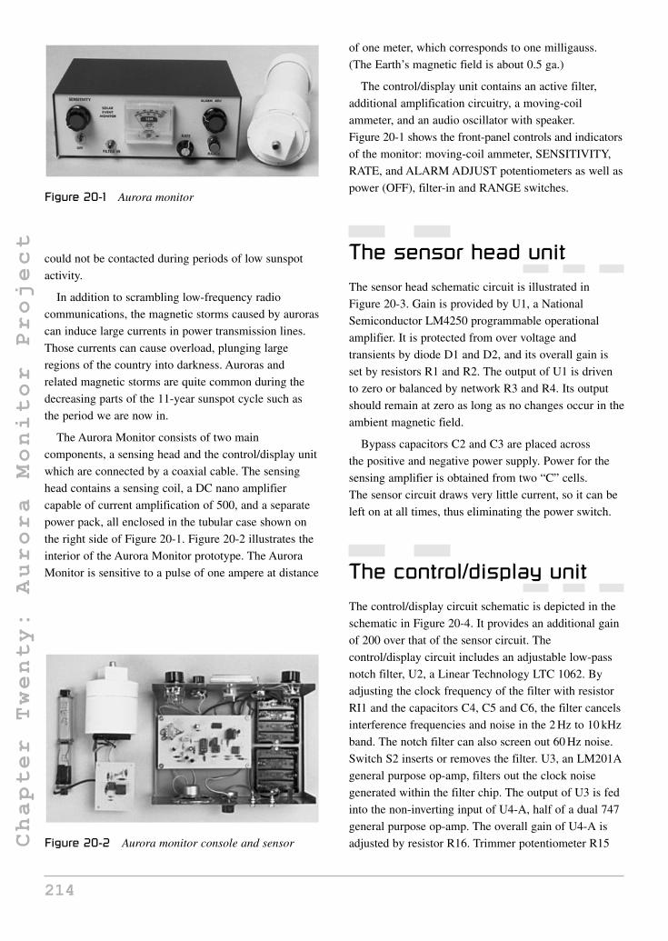
could not be contacted during periods of low sunspot
activity.
In addition to scrambling low-frequency radio
communications, the magnetic storms caused by auroras
can induce large currents in power transmission lines.
Those currents can cause overload, plunging large
regions of the country into darkness. Auroras and
related magnetic storms are quite common during the
decreasing parts of the 11-year sunspot cycle such as
the period we are now in.
The Aurora Monitor consists of two main
components, a sensing head and the control/display unit
which are connected by a coaxial cable. The sensing
head contains a sensing coil, a DC nano amplifier
capable of current amplification of 500, and a separate
power pack, all enclosed in the tubular case shown on
the right side of Figure 20-1. Figure 20-2 illustrates the
interior of the Aurora Monitor prototype. The Aurora
Monitor is sensitive to a pulse of one ampere at distance
of one meter, which corresponds to one milligauss.
(The Earth’s magnetic field is about 0.5 ga.)
The control/display unit contains an active filter,
additional amplification circuitry, a moving-coil
ammeter, and an audio oscillator with speaker.
Figure 20-1 shows the front-panel controls and indicators
of the monitor: moving-coil ammeter, SENSITIVITY,
RATE, and ALARM ADJUST potentiometers as well as
power (OFF), filter-in and RANGE switches.
The sensor head unitThe sensor head schematic circuit is illustrated in
Figure 20-3. Gain is provided by U1, a National
Semiconductor LM4250 programmable operational
amplifier. It is protected from over voltage and
transients by diode D1 and D2, and its overall gain is
set by resistors R1 and R2. The output of U1 is driven
to zero or balanced by network R3 and R4. Its output
should remain at zero as long as no changes occur in the
ambient magnetic field.
Bypass capacitors C2 and C3 are placed across
the positive and negative power supply. Power for the
sensing amplifier is obtained from two “C” cells.
The sensor circuit draws very little current, so it can be
left on at all times, thus eliminating the power switch.
The control/display unitThe control/display circuit schematic is depicted in the
schematic in Figure 20-4. It provides an additional gain
of 200 over that of the sensor circuit. The
control/display circuit includes an adjustable low-pass
notch filter, U2, a Linear Technology LTC 1062. By
adjusting the clock frequency of the filter with resistor
RI1 and the capacitors C4, C5 and C6, the filter cancels
interference frequencies and noise in the 2 Hz to 10 kHz
band. The notch filter can also screen out 60 Hz noise.
Switch S2 inserts or removes the filter. U3, an LM201A
general purpose op-amp, filters out the clock noise
generated within the filter chip. The output of U3 is fed
into the non-inverting input of U4-A, half of a dual 747
general purpose op-amp. The overall gain of U4-A is
adjusted by resistor R16. Trimmer potentiometer R15
214
Chapter Twenty: Aurora Monitor Project
Figure 20-1 Aurora monitor
Figure 20-2 Aurora monitor console and sensor

adjusts the offset or balance. PULSE SHAPE
potentiometer R17 and capacitor C5 form an optional
pulse-shaping network for coupling the Aurora Monitor
to a chart recorder or an analog-to-digital conversion
board of a personal computer.
The output of U4-A is coupled to a voltage follower
at U4-B. The output of U4-B is divided into two
channels. One channel is fed through 5000-ohm
SENSITIVITY potentiometer R18, which adjusts the
output level of the signal fed to the 100-microampere
panel meter MI. Movement of the meter’s needle shows
changes in the local magnetic field. Potentiometer R18
also adjusts the output signal that can be fed to a chart
recorder for data-logging.
The other channel is fed through ALARM ADJUST
5000-ohm potentiometer, R19, which sets the
threshold or set-point for the reflex oscillator circuit
that follows it. The oscillator consists of transistors Q1,
Q2, and Q3 and associated components. Speaker
SPKR1 gives an audible indication of changes in the
local magnetic field. The network of diode D3 and
aluminum electrolytic capacitor C8 performs additional
filtering for the input signal to the reflex oscillator
section.
Transistor Q1 controls the audible alarm by clamping
the negative voltage returning through the ground path.
When a magnetic event occurs, the speaker emits an
audible alarm, and the meter gives a visual indication of
a changing magnetic field. The adjustment of ALARM
ADJUST potentiometer R24 can remove distortion from
the sound of the speaker.
The author’s prototype control/display unit is
powered by eight AA cells: four cells provide positive
voltage and four cells provide negative voltage. As an
alternative, the monitor can be powered by rechargeable
nickel-cadmium cells.
ConstructionIn order to begin constructing the Aurora Monitor, you
will need to secure a clean will lit work table or work
bench so you can spread out all the tools, project
components, charts and diagrams. You will need to
locate a small 27 to 33 watt pencil-tipped soldering iron,
a small roll of 60/40 rosin core solder, a small jar of
“Tip Tinner,” soldering iron tip cleaner/dresser, from
your local Radio Shack store. A few small hand tools
215
Chapter Twenty: Aurora Monitor Project
L1R3
D1 D2
R1 C1+1.5 V –1.5 V
1.5 V 1.5 V
B1 – + B2
2
3
76
84
15
+1.5 V
C3
R2
J1
C2
R4
R5
–1.5 V
U1Softiron
core
Figure 20-3 Aurora monitor sensor head

216
Chapter Twenty: Aurora Monitor Project
Out In
S2
J2
+6 V4
6
R6
R8 R12
R7 R10+6 V
U2
8
3
R972
6U3
3 4
R14
R13
C9
1 913
12U4:A
+
–
24
C10
–6 V
+6 V5 2
R11
C4 C5 C6
S3
–6 V S1
+
– +
–
B1 B2–6 V
+6 V
R15
R24 +6 V
R20C7R21
R22
Q1c
b
c T1
c
e
b
Q2R16–6 V
3
6
10U4:B
–
+
R17
C11
S4 R18
J3C12
C8
D4
R19D3 R23
c
+c
bQ3
M1Recorder
Figure 20-4 Aurora monitor display/control unit

are also required to construct the project. You should
locate a small pair or end-cutters, a pair of needle-nose
pliers, a pair of tweezers, a magnifying glass a small
flat-blade screwdriver and a small Phillips screwdriver.
The Aurora Monitor project was constructed on two
circuit boards, one for the sensor head unit and a second
PC board for the control display unit. We will begin
constructing the sensor head unit first, see the schematic
in Figure 20-3. The sensor head board measured 2 1⁄16
by 2 9⁄16, it was housed along with the sensor head coil in
a suitable PVC pipe housing.
Place the project components in front of you on the
table, locate the resistor and capacitor identifier charts
in Tables 20-1 and 20-2, heat up your soldering iron and
we will begin. First refer to the resistor identifier chart,
it illustrates the resistor color codes and their
representative values. Most resistors will have three or
four color codes on the body of the resistor. The color
codes begin at one end of the resistor’s body. The first
color band denotes the first digit of the resistor value,
while the second color band represents the second digit
of the resistor code. The third color band on the resistor
denotes the multiplier value of the resistor, and the
fourth color code represents the tolerance of the resistor.
A silver band notes a 10% tolerance value, while a gold
band denotes a 5% resistor, and the absence of a fourth
band implies a 20% tolerance for the resistor. For
example, resistor R1 has a 1.5 megohm value. The first
color band would be brown or one (1), the second color
band would be green or five (5), and the third color or
multiplier would be green or (100,000). Go ahead and
locate resistors R1 and R2 which are used in the sensor
head unit and place them on the sensor head PC board
in their respective locations. Solder them in place and
then trim the excess component leads with your
end-cutter. Cut the excess leads flush to the edge of
the circuit board. Next locate the remaining resistors on
the sensor head unit and populate the board. Solder the
resistors to the board and trim the excess leads.
Next we are going to install the capacitors on the
sensor head unit of the Aurora monitor. Capacitors are
listed as electrolytic or non-electrolytic types.
Non-electrolytic types are usually small capacitors, often
they are so small that their actual value is not printed on
the body of the capacitor but a three-digit code is used,
see Table 20-2. For example, a .01 µF capacitor would
be marked (103) while a .1 µF capacitor would be
marked (104). Locate capacitors C1, C2 and C3 which
are .1 µf values. Place them on the sensor head PC
board and solder them in place on the board, remember
to trim the excess component leads with your end-
cutters. There are no electrolytic type capacitors on the
sensor head unit but there are some on the
control/display PC board. Electrolytic capacitors are
usually larger in size and value, and usually they will
have a polarity marking of some kind on the body
217
Chapter Twenty: Aurora Monitor Project
Table 20-1Resistor color code chart
Color Band 1st Digit 2nd Digit Multiplier Tolerance
Black 0 0 1
Brown 1 1 10 1%
Red 2 2 100 2%
Orange 3 3 1,000 (K) 3%
Yellow 4 4 10,000 4%
Green 5 5 100,000
Blue 6 6 1,000,000 (M)
Violet 7 7 10,000,000
Gray 8 8 100,000,000
White 9 9 1,000,000,000
Gold 0.1 5%
Silver 0.01 10%
No color 20%

218
Chapter Twenty: Aurora Monitor Project
Table 20-2Capacitor code identification information
This table is designed to provide the value of alphanumeric coded ceramic, mylar and mica capacitors in general. They come in
many sizes, shapes, values and ratings; many different manufacturers worldwide produce them and not all play by the same rules.
Most capacitors actually have the numeric values stamped on them; however, some are color coded and some have alphanumeric
codes. The capacitor’s first and second significant number IDs are the first and second values, followed by the multiplier number
code, followed by the percentage tolerance letter code. Usually the first two digits of the code represent the significant part of the
value, while the third digit, called the multiplier, corresponds to the number of zeros to be added to the first two digits.
Value Type Code Value Type Code
1.5 pF Ceramic 1,000 pF /.001 µF Ceramic / Mylar 102
3.3 pF Ceramic 1,500 pF /.0015 µF Ceramic / Mylar 152
10 pF Ceramic 2,000 pF /.002 µF Ceramic / Mylar 202
15 pF Ceramic 2,200 pF /.0022 µF Ceramic / Mylar 222
20 pF Ceramic 4,700 pF /.0047 µF Ceramic / Mylar 472
30 pF Ceramic 5,000 pF /.005 µF Ceramic / Mylar 502
33 pF Ceramic 5,600 pF /.0056 µF Ceramic / Mylar 562
47 pF Ceramic 6,800 pF /.0068 µF Ceramic / Mylar 682
56 pF Ceramic .01 Ceramic / Mylar 103
68 pF Ceramic .015 Mylar
75 pF Ceramic .02 Mylar 203
82 pF Ceramic .022 Mylar 223
91 pF Ceramic .033 Mylar 333
100 pF Ceramic 101 .047 Mylar 473
120 pF Ceramic 121 .05 Mylar 503
130 pF Ceramic 131 .056 Mylar 563
150 pF Ceramic 151 .068 Mylar 683
180 pF Ceramic 181 .1 Mylar 104
220 pF Ceramic 221 .2 Mylar 204
330 pF Ceramic 331 .22 Mylar 224
470 pF Ceramic 471 .33 Mylar 334
560 pF Ceramic 561 .47 Mylar 474
680 pF Ceramic 681 .56 Mylar 564
750 pF Ceramic 751 1 Mylar 105
820 pF Ceramic 821 2 Mylar 205
1st Significant Figure
2nd Significant Figure
Multiplier
Tolerance
CSGNetwork.Com 6/4/92
0.1 µF 10%
104 k

of the capacitor. You will find either a plus (+) or minus
(−) marking near one of the leads on the capacitor body.
Both the sensor head and control/display board utilize
silicon diodes. Diodes also have polarity, so they must
be installed correctly in order for the circuit to work
properly. Look closely at a diode and you will see either
a white or black color band near one end of the diode
body. The colored band indicates the cathode end of the
diode. Go ahead and install D1 on the sensor head board.
The sensor head and the display boards both have
integrated circuits on them, so before we begin installing
the ICs, take a quick look at the pin-out diagram depicted
in Figure 20-5, which will help you orient the integrated
circuits. Integrated circuits are highly recommended as an
insurance against possible circuit failure at some later
date. It is much easier to simply unplug an IC and place a
new one in the socket rather than trying to un-solder a
14 or 16 pin IC from a circuit board. Integrated circuit
sockets will usually have a notch or cut-out at one end of
the plastic IC socket. To the immediate left of the notch or
cut-out you will see pin one (1) of the socket. Pin (1) of
U1 is connected to one end of potentiometer R4. The IC
package itself will also have a notch or cut-out at the top
end of the IC. When placing the IC into its respective
socket make sure you align pin one (1) of the IC with pin
one (1) of the socket. The integrated circuits must be
inserted into the socket properly aligned or the circuit will
not work and may damage the components. Go ahead and
place U1 into its socket on the sensor head PC board.
Sensor coil assembly
The sensor coil at L1 detects changes in the local
magnetic field. You will need to wind approximately
50,000 turns of 28 AWG magnet wire over a soft iron
core 1⁄2′′ in diameter and 10′′. (The iron core
concentrates the flux lines by offering a lower
reluctance path than air.)
Wind the fine insulated magnet wire carefully on the
iron core to avoid kinks and breakage. Tape the ends of
the winding temporarily to the core and carefully solder
hook-up wire at each end to form permanent
terminals. The terminals can be secured to the core
with room-temperature vulcanizing (RTV) adhesive to
relieve any strains that might develop in the fine
magnet wire.
In the prototype, the sensing circuit board, coil, and
battery pack, consisting of two “C” cells were housed in
a case made from standard diameter PVC water pipe cut
to a length that will accommodate all of those elements
as shown in Figures 20-6.
The covers for the sensing head housing are PCV
end-caps that press-fit over the 23⁄8′′ outside diameter of
the pipe. The upper cap is a simple cup, but the lower
cap is a sleeve with a threaded insert at its end. Drill a
hole in the square base of the threaded insert for jack J1
and fasten it with a ring nut. Then close the cover on the
empty pipe and drill two pilot holes 180° apart in the
sleeve for self-tapping screws to clamp the cap in
position after the sensor head is assembled.
Cut about a 6′′ length of RG-174/U coaxial cable,
strip both ends and solder the inner conductor of one
end to the jack terminal and its shield to the jack lug.
Solder the inner conductor and shield of the other end to
the sensor circuit board.
Attach the coil to the sensor circuit board with about
a 6′′ length of RG-174/U coaxial cable as shown.
Connect the inner conductor to one terminal and the
shield to the other and solder both in position. The
prototype includes a twin “C” cell holder that, with
cells in position, has a maximum width dimension of
219
Chapter Twenty: Aurora Monitor Project
LM201A
1 81234
8765
LM1062
1 81234
8765
LM4250
1 81234
8765
LM747
1 141
2
3
4
5
6
7
14
13
12
11
10
9
8
Figure 20-5 Semiconductor pin-outs

less than 2′′ permitting it to slide easily into the sensor
head pipe section.
Cut three lengths of hook-up wire to extend the
lengths of the positive, negative and ground leads of the
battery pack. Solder one end of those wires to the
holder leads and the other ends to the sensor circuit
board.
Bond the upper cap to the PVC pipe section with
PVC cement. Then position U1 in its socket,
making certain that pin 1 is located correctly. Finally,
insert the “C” cells in the holder. Wrap a layer of
polyurethane foam around coil L1 to center it within
the pipe section and insert both in the pipe section with
the cover at the end. Then assemble the completed
circuit board and battery pack to make sure that all of
these parts will fit in the pipe section. Set the
assembly aside until you are ready to perform the
checkout steps.
Control/display unitThe control/display prototype circuit board measured
27⁄8′′ × 5′′ to fit inside the instrument case selected. The
schematic for the control/display board is shown in
Figure 20-4. The dimensions of the circuit boards can
be modified for packaging in the instrument and sensor
head cases of your choice. Place the control/display
circuit board in front of you, along with all its
respective components, and we will begin constructing
the control/display board.
First we will begin by placing the resistors on the
PC board; locate R6, an 18k ohm resistor, and R7 a
12k ohm resistor, and place them on the board and
solder them in place in their respective locations on the
board. Next locate and install resistors R8, R9, R12, and
R20; these are all 10k ohm resistors, solder them in
place and cut the excess component leads with your
end-cutter. Locate and install the remaining resistors,
solder them in place and trim the excess component
leads afterward.
Next, you can locate the capacitors C4, a .005 µF disk
capacitor, and it may be marked (502). Install C4 on the
PC board and solder it in place, remember to cut the
excess lead lengths. Now, locate capacitors C5, C7, C9
and C10; these are all .1 µF capacitors and may be
220
Chapter Twenty: Aurora Monitor Project
Figure 20-6 Sensor
PVC end cap
Coilassembly
Plasticfoam
PVC pipe
Sensorcircuitboard
(slide fit)
Twin cellholder
TwoC cells
Pvcend cap
Threadedinsert
Jack
Plug
Coaxial cableto control unit
marked (104). Install these capacitors and solder them
in place and then trim the extra leads. Now, locate C8, a
4.7 µF electrolytic capacitor. Capacitor C8 has polarity,
so it must be installed with respect to these marking.
Look at the schematic, and you will see that the plus (+)
side of C8 is connected to the junction of resistor R23
and diode D3. Install C8, and then solder it place, trim
the excess leads as necessary. Go ahead and install the
remaining capacitors and solder them in place on the
PC board.
The control/display section of the Aurora Monitor
employs two silicon diodes, and they must be installed
with respect to their polarity. The colored band denotes
the cathode end of the diode. The cathode end of D3 is
fed to R23, while the cathode end of D4 is sent to C12
and M1.
Transistors are generally three-lead devices, with a
Base lead, a Collector lead, and an Emitter lead. The
Base lead is depicted as a straight vertical line with two
arrows pointing to it. The Emitter lead will have a small
arrow pointing towards or away from it. When the arrow
points toward the Base lead the transistor is a PNP type.
If the arrow is pointing away from the Base lead then
the transistor is an NPN type. Transistor Q1 is a
PNP type, while Q2 and Q3 are NPN types. Identify
the transistor leads and install them in their
respective locations on the PC board, trim the leads as
necessary.
The control/display portion of the Aurora Monitor
utilizes three integrated circuits. Integrated circuits are
highly recommended in the event of a circuit failure at a
later date. Be sure to install the ICs correctly: pin one
(1) of U2 is connected to R7, while pin one (1) of U3 is
not used, pin two (2) is jointed with R9 and R8 and
R12. Integrated circuit U4 has pin one (1) connected to
the junction of R13 and R14. Failure to install the
integrated circuits correctly may result in damage to the
IC or to other components as well.
Finally you will need to connect the small audio
transformer to the circuit. The higher impedance (1K)
end of the transformer is connected to the junction of
Q1 and R22, and the other 1k lead is connected to the
collector of Q3. The secondary or 8 ohm winding of T1
is sent to the small 8 ohm speaker. The transformer can
be mounted on the circuit board or on the bottom of the
chassis box. The 100 uA panel meter is wired between
the Emitter of Q3 and ground.
The control/display assembly is housed in a standard
7′′ × 5′′ × 3′′ aluminum electronics instrument case with
a removable cover. Drill the holes in the front panel of
the case for power ON switch S1, FILTER IN switch
S2, RANGE switch S3 and (if used) optional recorder
switch S4. Also drill the holes for SENSITIVITY,
ALARM ADJUST, and RATE potentiometers (R18,
R19, and R11 respectively). Cut out the hole for
mounting meter M1. Note: If you want to use the
monitor strictly as a security monitoring system the
meter can be omitted.
Drill the holes in the back panel for jacks J2 and J3,
and PULSE SHAPE potentiometer R17. Drill a series of
holes in a circular pattern for the speaker SPKR1. Drill
holes in the bottom of the case for mounting the
control/display circuit board and two quad “C” cell
holders. Remember the circuit uses both a plus
(+) 6 volt supply and a minus (−) 6 volt supply. We
chose to power the circuit from batteries, but you could
use a dual 6 volt power supply to power the control/
display unit.
Assemble the panel-mounted switches, jacks,
potentiometers, meter and speaker to the front and back
panels of the case as shown in Figure 20-2. (You might
prefer to bond the face of the speaker to the inside of the
back panel with RTV adhesive rather than bolts and nuts.)
Determine the length of speaker wires needed to
permit assembly of the circuit board in the instrument
case, cut the wires to length and solder them to the
board. Cut and solder all leads from panel-mounted
components to the circuit board, allowing sufficient
lengths to permit unimpeded circuit board assembly, yet
not allowing too much slack.
Cut about a 6′′ length of RG-174/U coaxial cable to
connect INPUT jack J2 and the FILTER IN Switch S2
and two other lengths about 6′′ long to connect S2 to
the FILTER-IN and FILTER-OUT pads on the
control/display board. Strip all cable ends and solder
and trim all connections.
Assemble the control/display board to the base of the
case with screws and 1⁄2′′ insulating standoffs, lock
washers and nuts. Bolt the two quad AA cell holders to
the base of the case. Position the ICs in their sockets on
the control-display board, making sure that all pin 1’s
are in their correct positions. Insert the eight AA cells in
the spring-loaded holders, observing the correct polarity.
221
Chapter Twenty: Aurora Monitor Project
Cut a length of RG-174/U coaxial cable to the length
that will suit your installation. Strip the wire ends and
attach phono plugs PL1 and PL2 to cable ends and
solder or crimp them in position.
Before applying power to the Aurora Monitor, you
may want to inspect the two circuit boards for “cold”
solder joints and “short” circuits. Look carefully at the
foil side of the sensor head unit and examine the solder
joints. The solder joints should all look clean, bright and
shiny. If any of the solder joints look dark, dull, or
“blobby” then remove the solder from the joint and
re-solder the connection. Next examine the
control/display board for “cold” solder joints. Now, we
will inspect the two boards for possible “short” circuits.
“Short” circuits are usually caused by “stray”
component leads which get stuck to the board from the
sticky residue left from rosin core solder or from small
solder balls which may “short” across the circuit traces.
Examine both circuit boards for “stray” leads and solder
balls and remove them if you see any. Now, you are
ready to apply power to the circuits in order to “test”
the circuits.
Test and checkoutTest the sensing circuit first. Connect a general purpose
oscilloscope or multi-meter to the output of U1.
Position a permanent magnet near coil L1 and the
oscilloscope display should show a pronounced pulse.
If a multi-meter is used, its readout should jump.
Next, move L1 away from the magnet and the
reading on the multi-meter should fall to zero. If the
reading does not go to zero, adjust trimmer
potentiometer R4 in the sensor circuit. When the
sensing head is adjusted and working correctly, close
the lower cap and fasten it with two non-magnetic
stainless steel self-tapping screws to complete the
assembly. Connect one end of the plug-terminated
coaxial cable to the sensor head jack 1 and the other end
to the control/ display unit jack J2.
Turn on the power toggle switch of the
control/display unit and turn SENSITIVITY
potentiometer R18 full clockwise. The meter should
remain at zero. Rotate ALARM ADJUST potentiometer
R19 clockwise until the alarm just begins to sound.
Then turn it back slightly so that no sound is heard to
obtain the maximum sensitivity setting. Next, turn
potentiometer R19 full clockwise. There should be no
sound from the speaker.
Position a small magnet or piece of metal next to coil
L1 in the sensor head and the unit should now be
activated: the speaker should emit sound, and the meter
should read full scale. If everything checks out, you can
now start observing magnetic field disturbances or
anomalies.
In a quiet magnetic environment it might be
necessary to adjust potentiometer R4 in the sensor head
to the threshold of the meter movement. This fine
adjustment eliminates any small dead zones in
sensitivity. Test the instrument’s ability to detect the
Earth’s magnetic field by rotating the sensing head with
short, quick, snapping motions in a counter-clockwise
direction. The meter movement should jump off scale.
As rotation is continued, a direction will be found
where the meter will have its lowest response. This
nulling point is the north-south direction. Any objects
containing permanent magnets such as speakers or
meters that are brought into close proximity to the
Aurora Monitor’s sensing head coil L1 will affect the
accuracy of the instrument’s readings.
In the event that the Aurora Monitor does not work
upon power-up, you will need to disconnect the power
supply and sensor head unit and inspect the circuit
board for possible errors which might have occurred
while building the Aurora Monitor. The most common
cause for error when constructing the circuit is the
incorrect installation of the electrolytic capacitors, the
diodes and semiconductors such as transistors and
integrated circuits. You may have installed one of these
components backwards, so you will need to carefully
inspect the circuit board. A second pair of eyes could be
very helpful in locating potential errors of this sort.
Have a knowledgeable electronic enthusiast help you
inspect the circuit for errors. Another cause for error is
mis-locating resistors. You may have placed the wrong
value of resistor in a particular location, this would
cause the circuit to malfunction. After carefully
inspecting the Aurora Monitor circuit boards, you may
quickly find your error and correct it. Once the error has
been located, you reconnect the sensor head unit, and
then re-apply power and then you can test the Aurora
Monitor once again.
222
Chapter Twenty: Aurora Monitor Project

The Aurora Monitor can be connected to a chart
recorder or it can pass signals to a personal computer with
an analog-to-digital converter board. The recorder or PC
can collect data for the study of magnetic fields, magnetic
storms, and sunspot activity over long periods of time for
further analysis. A set of high-impedance (greater than
1 kilohm) headphones can be plugged into jack J3 if you
wish to “hear” the changes in magnetic fields.
If you want a permanent installation, mount the
sensing head assembly so that it is directed away from
any large metal obstructions, oriented on a north-south
axis, and pointed slightly upwards. It’s a good idea to
fasten it to a heavy wooden post to prevent wind-
induced vibrations.
223
Chapter Twenty: Aurora Monitor Project
Ultra-Low Frequency (ULF) Receiver
Chapter 21
Parts list
ULF Receiver
R1,R4 50kohm trim
potentiometer
R2 50kohm - 20 turn pot
R3 100kohm trim pot
R5,R6,R10 10k ohm, 1/4w,
5% resistor
R7,R8,R9,R12,R21 33k
ohm, 1/4w, 5% resistor
R11,R16 1k ohm, 1/4w,
5% resistor
R13,R20 22k ohm, 1/4w,
5% resistor
R14,R15,R18,R19 47k
ohm, 1/4w, 5% resistor
R17 50k ohm pot
R22 2.2k ohm, 1/4w,
5% resistor
C1,C2,C3,C4,C5,C6 .1 µF,35 volt disk capacitor
C11,C12,C13,C14 .1 µF,35 volt disk capacitor
C8,C9 1 µF tantalum, 35 volt electrolytic
capacitor
C10 .01 µF, 35 voltdisk capacitor
C7 .05 µF, 35 volt diskcapacitor
D1 Zener diode
U1,U2 LTC1063 IC
U3,U4 TL074 op-amp IC
U5 INA114 Differential
amplifier IC
J1,J2,J3 3-terminal
screw terminal strips
S1 SPST power switch
F1 1-amp fast-blow fuse
Misc PC board, chassis,
wire, hardware, power
cord, etc.
ULF Receiver PowerSupply
C1,C4 2200 µF, 35 voltelectrolytic
capacitor
C2,C5 .33 µF, 35 voltceramic capacitor
C3,C6 .1 µF, 35 voltceramic capacitor
U1 LM7805 - fixed
positive voltage
regulator
U2 LM7905 - fixed
negative voltage
regulator
D1,D2,D3,D4 50 volt,
2 amp silicon
diode
T1 110v-12v center
tapped transformer -
2amp
Misc circuit board,
wire, terminals, plug,
fuse, etc.
224Copyright © 2008 by The McGraw-Hill Companies, Inc. Click here for terms of use.

If you are interested in monitoring the ultra-low
frequency spectrum from .001 Hz to 30 Hz, the ULF
receiver will allow you to do some serious research into
earthquake monitor and Earth field studies. This project
is intended for curious individuals who want to
participate in the research and experimentation of the
study of extremely low frequency signals which
travel through the interior of our Earth. This project will
allow you to construct a ULF receive station to be
used to collect data for later analysis and compare it
with others who belong to the ELFRAD group
and those researchers involved with the Public
Seismic Network.
The ELFRAD low frequency group coordinates a
research group which studies the low frequency
spectrum and reports to one another the research that
individual members do and makes available the
information for comparison through their central
website. In order to achieve their goal, it is necessary to
have most of the equipment and construction parameters
standardized as much as possible, so the ELFRAD
Group will furnish software and support.
A complete standardized ELFRAD monitoring
station consists of a ULF receiver, an antenna array, and
interface card and a personal computer, and in this
project we will discuss how to put a receive station
together in your home workshop.
The Ultra-Low Frequency Receiver allows the
desired ultra-low frequency signals to be recovered from
the Earth. The signals are directed to a conditioning
circuit which not only protects the receiver equipment
from transients caused by lightning and other sources
but attenuates the ambient 60 or 50 Hz frequency
caused by commercial power, with the receiver’s
power-line notch line filter. The signals then pass
through a circuit which removes any ground loop
problems which may occur at your computer interface.
The low frequencies of interest are then passed through
a series of filters to remove most of the noise and
unwanted signals above 25 Hz. This desired band of
signals is then coupled to the analog-to-digital interface
in your personal computer to be recorded on the hard
drive. The interface used in the prototype accepted up to
eight channels of data samples and was able to collect
200 samples per second, record them and then display
them on the computer screen in either real time or
compressed time format.
At any time it is possible to take any period of data
previously recorded, generate a file and display the data
for analysis. You are also able to post filter the data,
with band pass, notch, low pass, and high pass
capability.
The Ultra Low Frequency Receiver project is shown
in Figure 21-1. This ULF receiver circuit was designed
as an all purpose ULF and ELF receiver with a
frequency range from DC to 30 hertz. The signals from
both leads of the non-polarized antenna array are
connected to J3, as seen in the schematic diagram in
Figure 21-2 and 21-3, a two sheet diagram The antenna
input signal travels to pins 2 and 3 on U5, which is a
high impedance differential instrumentation amplifier.
This chip’s gain is controlled by a single variable
resistor at R3.
The combined signals then travel from pin 6 of U5 on
to U3:A which is a buffer amplifier, followed by a 2
pole low pass filter at U3:B and U3:C and signal
amplifier at U3:D. From pin 14 on U3, the partially
filtered signal travels on to integrated circuit U2 and U1
which are 5 pole Butterworth low pass filters in cascade.
The LTC1063 ICs at U1 and U2 are clock controlled and
the frequency is set at 3000 hertz by R9. This configures
the two LTC1063 chips to have a cut-off frequency of
about 30 hertz. The clock ratio is 1/100.
The integrated circuit at U4 consists of a X5 gain
amplifier at U4:D, a buffer at U4:C and another 2 pole
analog low pass filter at U4:B and U4:A. Trim
potentiometer R17 is the final gain control for the
desired output voltage at U4:A. IC section U4B is a
2 pole low pass filter which removes any residual
clocking pulses from the signal which may have
been caused by U1 and U2. The amplified output
signal at J1 can be routed to your analog-to-digital
converter card in your PC. Power is supplied to the
ULF receiver at the terminals of J2. The output from the
ULF receiver can be routed to an analog-to-digital
225
Chapter Twenty-one: Ultra-Low Frequency (ULF)
Receiver
Figure 21-1 ULF receiver

converter card in a personal computer for recording and
displaying the receiver’s output in real time or for later
viewing.
The ULF receiver circuit is powered from a dual
plus/minus 5 volt power supply, shown in the schematic
at Figure 21-4. The power supply will furnish plus and
minus 5 volts DC for all of the op-amps in the receiver.
A 110 to 12 volt center tapped transformer is fed
directly to a four diode bridge rectifier. The resultant
DC signal is then coupled to two 2200 µF filter
capacitors at C1 and C4. The plus voltage output from
C1 is then fed to the input of an LM7805. The output of
U1 is then sent to a .1 µF capacitor at the positive output
terminals. The minus voltage output from C4 is sent to aChapter Twenty-one: Ultra-Low Frequency (ULF)
Receiver
226
AntennainputJ3
A
B D2
R6
R7
R3
U5
P1P2P3P4
P8P7P6P5
C3
C4Ground
R6
C7 R2
R16
R11R5 R12 R13 R1
U3:AU3:B
U3:C
U3:D
R14 R15
C11 C12C6
C5
24
113
56
4
7
11
+
–
10
98
11
1314
12 11–
––
++
+ +
–
P1 P2 P3 P4
Figure 21-2 ULF receiver schematic – Part I

negative voltage regulator at U2, an LM7905. The
output from U2 is then sent to capacitor C6, at the
minus voltage output terminals.
Let’s get started building the ULF receiver! Before
we begin building the ULF receiver, you will need to
locate a clean well lit and well ventilated work area.
A large table or workbench would be a suitable work
surface for your project. Next you will want to locate a
small 27 to 33 watt pencil-tipped soldering iron, as well
as a roll of #22 ga. 60/40 tin/lead solder and a small jar
227
Chapter Twenty-one: Ultra-Low Frequency (ULF)
Receiver
J1 J2 J3 J4
C9
–5 V
+5 VPower
J2
U2 U1
R9
C8C10
P1P2P3P4
P8P7P6P5
P1P2P3P4
P8P7P6P5
R17 R4
134
14
12 11
C1
U4:D
910
84
11U4:C
C2 C13 C14
R18 R19U4:B6
511
7
R21 R20
R22 J1
41
2
3 11
U4:A
Outputsignal
+–
+–
+–
+–
+
–
Figure 21-3 ULF receiver schematic – Part II
110 V AC T1
F1
S1
D1–D4
C1 C2C3
+
U1In Out
+5 V DC
Ground
In Out
C4 C5 C6
U2 -5 V DC
+
+ +
Figure 21-4 ULF receiver power supply

of “Tip Tinner,” a soldering iron tip cleaner/dresser from
your local Radio Shack store. You will also want to
secure a few hand tools for the project, such as a pair of
small end-cutters, a pair of tweezers and a pair of
needle-nose pliers. Locate a small Phillips and a small
flat-blade screwdriver, as well as a magnifying glass to
round out your tool list. Grab the schematic, parts
layout diagram as well as the resistor and capacitor
identifier charts and we will begin our project. Place all
the project components on the table in front of you.
The ultra-low frequency receiver is an RF or radio
frequency project and it is best constructed on a printed
circuit board with large ground plane areas covering the
board for the best RF grounding techniques. Once you
have all the parts and PC board in front of you, heat up
the soldering iron and we’ll get started!
First, find your resistor identifier chart in Table 21-1,
which will help you select the resistors from the
parts pile. Resistors used in this project are mostly small1⁄4 watt carbon composition type resistors, which have
colored bands along the resistor body. The first color
band should be closest to one end of the resistor body.
This first color band represents the first digit of the
resistor value. For example, resistor R5, R6 and R10 has
four color bands, the first one is a brown band followed
by a black band followed by an orange band. The fourth
band is gold. The first band is brown which denotes a
digit one (1), the second band is black which represents
a digit five (0) and the third band is orange, which
represents a multiplier of zero (000), so the resistor
value is 10,000 or 10k ohms with a tolerance value of
5%. Identify the remaining resistors for the project and
we can begin “populating” the PC board. Place a few
resistors on the board at one time, so as not to confuse
the process. Make sure that you place the correct resistor
into the correct PC location before soldering it in place.
Once you solder a few resistors in place on the PC
board, you can use your end-cutter to trim the excess
component leads. Cut the excess leads flush to the edge
of the circuit board. Then place a few more resistors on
the PC board and solder them on to the board.
Remember to trim the component leads as necessary.
Next we will locate the capacitors for the ULF
receiver. Capacitors are listed as electrolytic and
non-electrolytic types. The non-electrolytic types are
generally smaller in value and size as compared with
the electrolytic types. Non-electrolytic capacitors in fact
can be so small that their actual value cannot be printed
on them, so a special chart was devised as shown in
Table 21-2. The chart illustrates the three-digit codes
which are often used to represent capacitors. For
example a .001 µF capacitor will have (102), while a
.01 µF capacitor will have (103) marked on it to
represent its true value. Use the chart to identify the
228
Chapter Twenty-one: Ultra-Low Frequency (ULF)
Receiver
Table 21-1Resistor color code chart
Color Band 1st Digit 2nd Digit Multiplier Tolerance
Black 0 0 1
Brown 1 1 10 1%
Red 2 2 100 2%
Orange 3 3 1,000 (K) 3%
Yellow 4 4 10,000 4%
Green 5 5 100,000
Blue 6 6 1,000,000 (M)
Violet 7 7 10,000,000
Gray 8 8 100,000,000
White 9 9 1,000,000,000
Gold 0.1 5%
Silver 0.01 10%
No color 20%

small capacitors in the project. Non-electrolytic have no
polarity markings on them so they can be installed in
either direction on the PC board.
Electrolytic capacitors are usually larger in size and
value and they will have a white or black band on the
side of the capacitor body or a plus (+) or minus (−)
marking on the body of the capacitor near the leads.
These markings are polarity markings and that indicate
the direction in which the capacitor must be mounted on
the PC board. Failure to observe polarity when
installing the capacitor may result in damage to the
capacitor or to the circuit itself, so pay particular
attention to capacitor polarity when placing the
capacitors on the board.
Let’s go ahead and place some of the non-electrolytic
capacitors on the PC board. Identify a few small
capacitors at a time and place them on the PC board and
solder them in place. Trim the component leads after.
Go ahead and install the remaining non-electrolytic
capacitors after choosing your desired band.
Install the capacitors and solder them in place,
remember to cut the extra leads flush to the edge of the
circuit board. Now, you can go ahead and install the
electrolytic capacitors onto the circuit board. Go ahead
and solder them in place and trim the leads as
necessary.
The ULF receiver utilizes five integrated circuits and
two regulators integrated circuits. Locate the
semiconductor pin-out diagram illustrated in
Figure 21-5, which will help you install the ICs. When
constructing the project it is best to use IC sockets as an
insurance against a possible circuit failure down-the-
road; it’s much easier to unplug an IC rather than trying
to un-solder an IC from the PC board. IC sockets will
have a notch or cut-out at one end of the plastic socket.
Pin one (1) of the IC socket will be just to the left of the
notch or cut-out. Note, pin 1 U1 connects to pin 7 of
U2, while pin 1 of U2 connects to the output of U3:D.
Now take a look at U3, pin 1 of U3 is connected to
R14, while pin 1 of U4 is fed to the output through R22.
Finally, pin 1 of U5 is connected to potentiometer R3.
Now place each of the integrated circuits into their
respective sockets.
A protection Zener diode is placed across the antenna
input pins between resistors R6 and R7. Note that all
diodes have polarity, including Zener diodes. Diodes
will have either a black or white colored band at one
end of the resistor body. The lead closest to the colored
band is the cathode lead of the diode.
The main ULF schematic diagram is broken into two
diagrams, since the schematic is rather large. You have
most likely noted that along the bottom of diagram
(A), you will see designations of P1, P2, P3 and P4.
These are not connectors as such but merely to help
separate the two diagrams for illustration purposes. The
receiver was constructed on a single printed circuit
board. In the original prototype, the antenna input
shown at J3 was a screw terminal strip, but this could be
changed to an SO-238 antenna jack mounted on the
chassis enclosure. The power connection was made at a
second screw terminal jack at J2, which had three
terminal posts for plus/minus and ground connections.
The output of the ULF receiver was connected to a third
screw terminal jack at J3, this could be changed to an
RCA jack if desired.
The ULF receiver contains a number of variable
resistors or potentiometers in the circuit. Potentiometer
R1, R3 are PC board trimmer types, while R2, which is
a 20 turn precision chassis mounted potentiometer, and
R4 is a conventional chassis mounted linear taper
potentiometer.
The ULF receiver is now almost completed, so take a
short well deserved break, and when we return we will
inspect the circuit board for any possible “cold” solder
joints and “short” circuits before we apply power to the
circuit. Pick up the PC board with the foil side of the
board facing upwards toward you. Examine the foil side
of the board carefully, take a look at the solder joints.
All of the solder joints should look clean, bright, shiny
and smooth; if any of the solder joints look dark, dull or
“blobby” then you should remove the solder from the
joint with a solder-sucker and then completely re-solder
the joint all over again so that the solder joints all look
good. Next we will examine the PC board for any
possible “short” circuits, which may be caused from
“stray” component leads which were cut from the
board. Another possible cause of short circuits are
solder blobs which may have stuck to the foil side of
the board. Rosin core solder often leaves a sticky
residue which can cause leads and solder blobs to stick
to the board and possibly “bridge” across circuit traces.
Next we will need to build the dual voltage power
supply circuit board. The power supply was built on the
circuit board as well. The transformer was mounted off
229
Chapter Twenty-one: Ultra-Low Frequency (ULF)
Receiver

230
Chapter Twenty-one: Ultra-Low Frequency (ULF)
Receiver Table 21-2
Capacitance code information
This table provides the value of alphanumeric coded ceramic, mylar and mica capacitors in general. They come in many sizes,
shapes, values and ratings; many different manufacturers worldwide produce them and not all play by the same rules. Some
capacitors actually have the numeric values stamped on them; however, many are color coded and some have alphanumeric codes.
The capacitor’s first and second significant number IDs are the first and second values, followed by the multiplier number code,
followed by the percentage tolerance letter code. Usually the first two digits of the code represent the significant part of the value,
while the third digit, called the multiplier, corresponds to the number of zeros to be added to the first two digits.
Value Type Code Value Type Code
1.5 pF Ceramic 1,000 pF /.001 µF Ceramic / Mylar 102
3.3 pF Ceramic 1,500 pF /.0015 µF Ceramic / Mylar 152
10 pF Ceramic 2,000 pF /.002 µF Ceramic / Mylar 202
15 pF Ceramic 2,200 pF /.0022 µF Ceramic / Mylar 222
20 pF Ceramic 4,700 pF /.0047 µF Ceramic / Mylar 472
30 pF Ceramic 5,000 pF /.005 µF Ceramic / Mylar 502
33 pF Ceramic 5,600 pF /.0056 µF Ceramic / Mylar 562
47 pF Ceramic 6,800 pF /.0068 µF Ceramic / Mylar 682
56 pF Ceramic .01 Ceramic / Mylar 103
68 pF Ceramic .015 Mylar
75 pF Ceramic .02 Mylar 203
82 pF Ceramic .022 Mylar 223
91 pF Ceramic .033 Mylar 333
100 pF Ceramic 101 .047 Mylar 473
120 pF Ceramic 121 .05 Mylar 503
130 pF Ceramic 131 .056 Mylar 563
150 pF Ceramic 151 .068 Mylar 683
180 pF Ceramic 181 .1 Mylar 104
220 pF Ceramic 221 .2 Mylar 204
330 pF Ceramic 331 .22 Mylar 224
470 pF Ceramic 471 .33 Mylar 334
560 pF Ceramic 561 .47 Mylar 474
680 pF Ceramic 681 .56 Mylar 564
750 pF Ceramic 751 1 Mylar 105
820 pF Ceramic 821 2 Mylar 205
1st Significant Figure
2nd Significant Figure
Multiplier
Tolerance
CSGNetwork.Com 6/4/92
0.1 µF 10%
104 k

the circuit board and on the bottom of the chassis. The
diode bridge was placed on the circuit board, paying
careful attention to the polarity of the diodes. You could
elect to individual diodes or one of those four diode
bridge rectifiers all in one package. If you choose the
second option again you must observe the polarity of
the plastic package. The AC input section will be
marked with two wavy lines, the AC side has no
polarity. The DC side of the bridge will have a plus (+)
and a minus (−) marking. When installing the six
capacitors be sure to observe polarity since four of them
are electrolytic types. Note that there are two power
supplies and the polarity placement orientation is
different for the two power supply sections. The
LM7805 is the plus voltage regulator, while the
LM7905 regulator is the minus voltage regulator; don’t
mix them up, and take your time to install them at the
correct locations to avoid damage to the circuit. A fuse
was placed in series with the power switch to the
transformer input leads. A power line-cord with a
110 volt plug was used to supply power to the
transformer. Once the power supply circuit has been
completed, you can carefully inspect the circuit board
for any “cold” solder joints and “short” circuits before
applying power for the first time.
The Ultra-Low Frequency Receiver requires an
antenna “site” for proper operation. This is not the usual
conventional type of antenna that you encounter with
most receivers, since this is a special type of receiver
project. The array is designed to be built completely
underground. Space for construction is necessary and
may be anywhere from 100 to 1000 linear feet, see
Figure 21-6.
Due to the fact that we will be dealing with extremely
long wavelengths on the order of miles rather than feet,
you are going to need a little space. As long as you have
a strip of property at least one 100 or more feet in
length you will be able to detect the signals. There are
several items of interest in determining your location.
You will be building two arrays widely separated from
each other. The further apart the better. Also if you have
a choice, a damp location is better than dry rocky soil.
The first step in constructing your antenna/detector is
to determine the magnetic orientation. Take an ordinary
pocket compass and locate magnetic North. The line of
sight between the two points should be aligned with
North-South. The next step is to obtain some copper
clad ground rods at least eight feet in length, put on
some gloves and start driving one into the ground. We
found that a standard metal fence post driver purchased
from the local farm store was ideal for the job. It helps
also to take a pair of post diggers and dig out a hole
about 18′′ deep. Then drive the rod down into the
ground below the surface of the hole leaving enough
room to make a connection.
Next measure out a distance as far as possible, at
least 30 meters (98 ft) in a North or South direction and
repeat the procedure above, driving a copper clad eight
foot ground rod into the soil. Then connect the two
widely spaced rods together using a length of wire.
Obtain an ohmmeter, and open the wire conductor and
measure the resistance. Make a note of the reading,
then reverse the ohmmeter leads and measure again.
Then take this reading, average it with the other reading
and you will have a close indication of the DC
resistance between the two probes (ground rods). Very
likely, unless you have excellent soil conductivity in
your area, the reading will be several thousand ohms.
The point is to lower this reading as much as possible.
231
Chapter Twenty-one: Ultra-Low Frequency (ULF)
Receiver
1234
8765
INA114
1 8
1234
8765
LTC1063
1 8 1 14
TL074
14
13
12
11
10
9
87
6
5
4
3
2
1
Figure 21-6 ULF receiver antenna circuitFigure 21-5 Semiconductor pin-outs
Ground A B
To J3

The lower the better. A workable resistance is 50 to 500
ohms but the ideal resistance would be around 5 to 10
ohms. In most cases, however, this would be
unobtainable unless you used many ground rods or
copper strapping at each end.
Keep adding rods at each probe site, spaced 20 feet
apart from one another connected together with #6
copper bare wire, until the resistance gets down to
between 25 and 500 ohms. Keep in mind two items.
The further apart the probe sites, the lower the
resistance, and the more rods driven into the ground, the
lower the resistance. We have found that on the average,
five grounds at each end of the site are sufficient to
obtain this reading.
Another option rather than using ground rods, in
rocky or extremely hard soil, you may use a ditch
trencher and bury #6 or #4 copper wire at least 24
inches deep. The copper wire should be placed in an
“X” fashion with a length of at least 25 feet. The lead
cable will then be connected to the center point of
the “X.”
Now obtain a length of CATV lead in wire such as
RG-11 or RG-59, from your local electronic parts store.
A good source to try is the local Cable TV company.
Sometimes they have lengths of scrap lying around their
warehouse and will be happy to get rid of it. Connect
the center conductor only (not the outside shield) to
each antenna array using copper clamps. Take each
piece of co-ax to the location of your receiver. Then
install a suitable connector to the two ends. These two
cables will be the input leads to the receiver. The shield
should be connected to earth ground using a single
copper clad ground rod. Do not use the power ground
and make sure the ground connection is at least 20 feet
from power ground.
With the ULF receiver, power supply and antenna
constructed and ready to go, we just have one more
detail left to complete our ELFRAD ULF monitoring
station. The most expensive components will be the
computer and analog-to-digital interface device. A PC
type of computer is recommended using Windows 98,
NT, Win2000, or XP software will work nicely. Since
most of everyone owns a computer or laptop these days,
the only thing left to be purchased is the A/D interface.
The software for the A/D converter is available from the
supplier of the A/D interface listed below. You will need
at least a two channel A/D board, since it is
recommended that you also record a short wave radio
tuned to WWV, which keeps computer synched to within
plus or minus 2 milliseconds. Also if desired, a GPS type
of time standard is available. The A/D converter is
available at http://seismicnet.com/ serialatod.html.
For more information on Earthquake monitoring you
may finds these sites helpful.
ELFRAD Research Group
The low frequency radio research group, which provides
support to interested researchers.
Helps researchers in correlating and comparing data.
http://www.elfrad.com/
Public Seismic Network
A seismic research group dedicated to earthquake
monitoring.
Helps researchers in correlating and comparing data.
http://psn.quake.net/
232
Chapter Twenty-one: Ultra-Low Frequency (ULF)
Receiver
Jupiter Radio Telescope Receiver
Chapter 22
Parts list
Jupiter Radio Telescope
R1 68ohm
R2 294ohm
R3 17.4ohm
R4 294ohm
R5 100ohm
R6 2.2kohm
R7 10kohm linear
potentiometer
R8 2.2kohm
R9, R19 100kohm
R10 220ohm
R11 1.5kohm
R12,R20,R21,R27 1kohm
R13,R18 27kohm
R14 100kohm
R15 10kohm
potentiometer/
switch
R16 10kohm
R17 1.5kohm
R22,R23 2ohm
R24 1ohm
R25 220ohm
R26 47ohm
R28,R29,R30,R31,R32
10ohm
C1 39 pF, 35v disk
ceramic
C2 4-40 pF, variable
capacitor
C3 56 pF, 35v disk
ceramic
C4 22 pF, 35v disk
ceramic
C5,C8,C11,C14 .01mF,
35v dipped ceramic
C6 4-40pF, variable
capacitor
C7 not used
C9,C12,C13 47pF, 35v
disk ceramic
C10 270pF, 35v disk
ceramic
C15 10pF, disk
ceramic
C16,C24,C25 10mF, 35
vdc, electrolytic
C17,C18,C21,C23,C26C29
.1mF, 35v dipped
ceramic
C19 1mF, 35v metal
polyester
C20,C22 0.068mF, 35v
5% metal film
C27 10mF, 35vdc,
tantalum, stripe,
C28 220pF, 35v disk
ceramic
C30,C31,C33 10mF, 35
vdc, electrolytic
C32 330mF, 35 vdc,
electrolytic
C34,C35,C36 0.1mF, 35v
dipped ceramic
C37 10pF, 35v disk
ceramic
233Copyright © 2008 by The McGraw-Hill Companies, Inc. Click here for terms of use.

C38 10mF, 35vdc,
electrolytic
C39 100mF, 35vdc,
electrolytic
C40,C41,C42,C43 0.1mF,
35v dipped
ceramic
C44 10mF, 35vdc,
electrolytic
D1 1N4001
D2,D3 1N914
LED Red LED
VD1 MV209, varactor
diode
ZD1 1N753, 6.2v, Zener
diode, 400 mw
ZD2 1N5231, 5.1v, Zener
diode, 500mw
L1 0.47mH, (gold,
yellow, violet,
silver)
L2 1mH, (brown, gold,
black, silver)
L3 3.9mH, (orange,
gold, white, gold)
L4,L5 1.5mH,
adjustable inductor
L6,L7 82mH, fixed
inductor
Q1 J-310, junction
field effect (JFET)
Q2 2N-3904, bipolar,
NPN
Q3 2N-3906, bipolar,
PNP
U1 SA602AN,
mixer/oscillator IC
U2,U3 LM387 or NTE824 -
audio pre-amplifier IC
OSC1 20MHz crystal
oscillator module
J1 Power jack, 2.1 mm
J2 F female chassis
connector
J3,J4 3.5mm stereo
jack, open ckt
Misc PC Board,
enclosure, knobs,
solder lugs, wire
Jupiter is the fifth planet from the Sun and is the largest
one in the solar system. If Jupiter were hollow, more
than one thousand Earths could fit inside. It also
contains more matter than all of the other planets
combined. It has a mass of 1.9 × 1027 kg and is
142,800 kilometers (88,736 miles) across the equator.
Jupiter possesses 28 known satellites, four of which—
Callisto, Europa, Ganymede and Io—were observed by
Galileo as long ago as 1610. Another 12 satellites have
been recently discovered and given provisional
designators until they are officially confirmed and
named. There is a ring system, but it is very faint
and is totally invisible from the Earth. (The rings
were discovered in 1979 by Voyager 1.) The atmosphere
is very deep, perhaps comprising the whole
planet, and is somewhat like the Sun. It is composed
mainly of hydrogen and helium, with small amounts
of methane, ammonia, water vapor and other
compounds.
Colorful latitudinal bands, atmospheric clouds and
storms illustrate Jupiter’s dynamic weather systems, see
Figure 22-1. The cloud patterns change within hours or
days. The Great Red Spot is a complex storm moving in
a counter-clockwise direction. At the outer edge,
material appears to rotate in four to six days; near the
center, motions are small and nearly random in
direction. An array of other smaller storms and eddies
can be found throughout the banded clouds.
Auroral emissions, similar to Earth’s northern lights,
were observed in the polar regions of Jupiter. The
auroral emissions appear to be related to material from
Io that spirals along magnetic field lines to fall into
Jupiter’s atmosphere. Cloud-top lightning bolts, similar
to super-bolts in Earth’s high atmosphere, were also
observed.
The Jupiter Radio Telescope is a special shortwave
receiver which will pick up radio signals from the
planet Jupiter and also from the Sun, and it is a very
exciting project, see Figure 22-2. This project will allow
234
Chapter Twenty-two: Jupiter Radio Telescope Receiver

you to do amateur research into radio astronomy in your
own back yard.
Radio signals from Jupiter are very weak—they produce
less than a millionth of a volt at the antenna terminals of
the receiver. These weak radio frequency (RF) signals
must be amplified by the receiver and converted to
audio signals of sufficient strength to drive headphones
or a loudspeaker. The receiver also serves as a narrow
filter, tuned to a specific frequency to hear Jupiter while
at the same time blocking out strong Earth based radio
stations on other frequencies. The receiver and its
accompanying antenna are designed to operate over a
narrow range of shortwave frequencies centered on 20.1
MHz (megahertz). This frequency range is optimum for
hearing Jupiter signals.
The block diagram shown in Figure 22-3 illustrates
the various components of the Jupiter Radio Telescope.
First shown the antenna intercepts weak electromagnetic
waves which have traveled some 500 million miles from
Jupiter to the Earth. When these electromagnetic waves
strike the wire antenna, a tiny RF voltage is developed
at the antenna terminals. Signals from the antenna are
delivered to the antenna terminals of the receiver by a
coaxial transmission line. Next the signals are delivered
to the RF Bandpass Filter and Preamplifier, they are
filtered to reject strong out-of-band interference and are
then amplified using a junction field effect transistor
(JFET). This transistor and its associated circuitry
provide additional filtering and amplify incoming
signals by a factor of 10. The receiver input circuit is
designed to efficiently transfer power from the antenna
235
Chapter Twenty-two: Jupiter Radio Telescope Receiver
Figure 22-1 Jupiter
Figure 22-2 Radio Jupiter receiver project

to the receiver while developing a minimum of noise
within the receiver itself.
Next the signals move to the local oscillator (LO) and
mixer to perform the important task of converting the
desired radio frequency signals down to the range of
audio frequencies. The local oscillator generates a
sinusoidal voltage wave form at a frequency in the
vicinity of 20.1 MHz. The exact frequency is set by the
front panel tuning control. Both the amplified RF signal
from the antenna and the LO frequency are fed into
the mixer. The mixer develops a new signal which is the
arithmetic difference between the LO and the incoming
signal frequency. Suppose the desired signal is at
20.101 MHz and the LO is tuned to 20.100 MHz.
236
Chapter Twenty-two: Jupiter Radio Telescope Receiver Antenna
RFbandpass
filter
20.00 MHztest
oscillator
RFpreamp
J310
Lo/mixerWE602
Tuning20.1 MHz+/– 150 kHz5-pole
lowpassfilter
AudiopreampWIE824
Volume
Audioamp
Audio out1
Audio out2
Externalamplifiedspeaker
Figure 22-3 Jupiter radio block diagram

The difference in frequency is therefore 20.101–20.100
=.001 MHz, which is the audio frequency of 1 kilohertz.
If a signal were at 20.110 MHz, it would be converted to
an audio frequency of 10 kHz. Since the RF signal is
converted directly to audio, the radio is known as a
direct conversion receiver.
To eliminate interfering stations at nearby
frequencies, a low pass filter is next used, which is like
a window, a few kilohertz wide through which Jupiter
signals can enter. When listening for Jupiter or the Sun,
the radio will be tuned to find a “clear channel.” Since
frequencies more than a few kilohertz away from the
center frequency may contain interfering signals, these
higher frequencies must be eliminated. This is the
purpose of the low pass filter following the mixer. It
passes low (audio) frequencies up to about 3.5 kHz and
attenuates higher frequencies.
Finally the low pass filter feeds an audio amplifier
stage which takes the very weak audio signal from the
mixer and amplifies it enough to drive headphones
directly, or to drive an external amplified speaker
assembly.
Circuit diagramWe have already seen a block diagram of the Jupiter
radio receiver which shows the radio as a group of
functional blocks connected together. While this type of
diagram does not show individual components like
resistors and capacitors, it is useful in understanding
signal flow and the various functions performed within
the radio. The next level of detail is the schematic
diagram. A schematic is used to represent the
wiring connections between all of the components
which make up a circuit. The schematic diagram uses
symbols for each of the different components
rather than pictures of what the components actually
look like.
A schematic diagram of the complete receiver is seen
in Figure 22-4. On this schematic, the part types are
numbered sequentially. For example, inductors are
denoted L1 through L7, and resistors are denoted R1
through R31. Signal flow as shown in the schematic is
as follows. The signal from the antenna connector (J2)
is coupled to a resonant circuit (bandpass filter L1, C2,
C3) and then to the J-310 transistor (Q1), where it
is amplified. The output of the J-310 goes through
another resonant filter (L3, C6) before being applied to
the resonant input circuit (L4, C9, C10) of the SA602
integrated circuit (U1), which serves as the local
oscillator and mixer. The center frequency of the local
oscillator is set by inductor L5 and adjusted by the
tuning control R7. The audio output from U1 passes
through the lowpass audio filter (L6, L7, C20, C21, and
C22). The audio signal is next amplified by U2 (an
NTE824) before going to the volume control R15. The
final audio amplifier stages comprise U3 (another
NTE824), and the output transistors Q2 (2N-3904) and
Q3 (2N-3906). After the receiver has been assembled,
the variable capacitors C2 and C6 and variable
inductors L4 and L5 will be adjusted to tune the
receiver for operation at 20.1 MHz.
PC board assemblyBefore we begin building the circuit, take a few minutes
to locate a clean well lit work table or work bench. You
will want to locate a small 27 to 33 watt pencil-tipped
soldering iron, a roll of 60/40 tin/lead rosin core solder,
and a small jar of “Tip Tinner,” a soldering iron tip
cleaner/dresser. “Tip Tinner” is available at a local
Radio Shack store. You will also need some small hand
tools, such as a small flat-blade screwdriver, a Phillips
screwdriver, a pair of small needle-nose pliers, a
pair of tweezers, a magnifying glass and pair of
end-cutters.
Once you have gathered all the tools, locate all the
circuit diagrams, such as the schematics, the parts
layout diagram, the resistor and capacitor code charts,
etc. Place all the component parts along with all your
tools and diagrams in front of you, warm up your solder
iron and we will start building the Radio Jupiter receiver
project.
First we will identify the resistors for the project.
Refer to the chart shown in Table 22-1, which will help
you to identify the resistor color codes. Resistors
usually have three or four color bands on the body of
the resistor which denotes the resistor value. The color
bands begin at one end of the resistor body close
to the edge. The first color band on resistor R1 is blue,
this denotes the digit six (6). The second color band is
237
Chapter Twenty-two: Jupiter Radio Telescope Receiver

238
Chapter Twenty-two: Jupiter Radio Telescope ReceiverPower
J1DC in
D1
C39 C40 C41
S1
R5
R27C42
C8
C7
C6
C4
C3
C2
L1
C1J2
Antenna
RFinput
R1C5
L2G
S DQ1
L3
D1
R3
R2 R4
C9
L4
C10
U1
C13
C12C11
C43
C16R10 C44
C17
C18
A
ZD1
L6 L7 C23
C19
C20 C21 C22R11
U2
C25
C26
8
7
65
3
R14
R13R12
C24 C27
C38 R7
R8
R9
VD1 L5
C15
C14
1 83
4 56
72
++
+
+
+
A
TP1
C37
R26
OSC-1R25
C35ZD2C36
R15
8 147
8
7
65
3
Avoidgain
C29
C28R16
C31
U3
R21
D2
D3
R20R17 R19
R18
C30
Q2
b
c
e
b
c
e
C33 R28
R23
R22
R24
C32R29
R30
R31
J3
J4
C34
+
+
+
Record
Audioout
R6
+
+
+
Figure 22-4 Radio Jupiter receiver schematic

gray, which is the digit number eight (8) and the third
color band is the resistor’s multiplier value which is
black and this suggests a multiplier value of 1. So the
resistor value for R1 is (6) times (8) times (1) or
68 ohms. The tolerance value of a resistor is noted in the
fourth color band. A fourth color band which is silver is
a 10% tolerance resistor, while a gold fourth band
denotes a 5% tolerance value. If there is no fourth color
band then the resistor will have a 20% tolerance value.
Next, locate R2, R3 and R4, then check your parts
layout diagram and the schematic to see where these
resistors are to be placed on the circuit board. Once you
verify where the resistors are placed, you can install
these resistors on the circuit board and solder them in
place on the board. Now locate your end-cutter and trim
the excess component leads. Cut the extra component
lead lengths flush to the edge of the circuit board. Now
go ahead and identify another group of three or four
resistors and place them on the circuit board. Once you
are sure of their respective locations you can solder the
next grouping of resistors onto the circuit board,
remember to trim the excess component leads from the
board. Place all the remaining resistors on the circuit
board and solder them all in place, trim the extra leads
as necessary.
Now we will move on to installing the capacitors for
the Radio Jupiter receiver project. Capacitors come in
two major flavors, non-polarized and polarized types.
First, we will talk about non-polarized capacitors.
Usually non-polarized capacitors are smaller value types
which could take form as ceramic disks, mica, tantalum
or polyester types. Often the capacitors are small in size
and frequently the capacitor values are printed as three-
digit codes rather than their actual values, since this
code system takes less space to print. We have included
a chart in Table 22-2, which lists the actual capacitor
values and their respective codes. For example, a
capacitor with a value of .001 µF will have a code
designation of 102, a .01 µF capacitor will have 103 and
a 0.1 µF capacitor will have a code of 104 marked on it.
The Radio Jupiter project has a number of non-
polarized type capacitors which you will need to install.
Take a look through the component pile and see if you
can identify the small non-polar capacitors before
attempting to install them on the PC board.
Polarized capacitors are called electrolytic capacitors,
they are often larger in physical size. Electrolytic
capacitors will always have some sort of polarity
marking on them. You will see either a black or white
band or a plus (+) or minus (−) marking somewhere on
the capacitor body. It is very important that you install
these types of capacitors with respect to their polarity in
order for the circuit to work properly and to not be
damaged upon power-up. You will need to refer to the
239
Chapter Twenty-two: Jupiter Radio Telescope Receiver
Table 22-1Resistor color code chart
Color Band 1st Digit 2nd Digit Multiplier Tolerance
Black 0 0 1
Brown 1 1 10 1%
Red 2 2 100 2%
Orange 3 3 1,000 (K) 3%
Yellow 4 4 10,000 4%
Green 5 5 100,000
Blue 6 6 1,000,000 (M)
Violet 7 7 10,000,000
Gray 8 8 100,000,000
White 9 9 1,000,000,000
Gold 0.1 5%
Silver 0.01 10%
No color 20%

240
Chapter Twenty-two: Jupiter Radio Telescope Receiver Table 22-2
Capacitance code information
This table provides the value of alphanumeric coded ceramic, mylar and mica capacitors in general. They come in many sizes,
shapes, values and ratings; many different manufacturers worldwide produce them and not all play by the same rules. Some
capacitors actually have the numeric values stamped on them; however, many are color coded and some have alphanumeric codes.
The capacitor’s first and second significant number IDs are the first and second values, followed by the multiplier number code,
followed by the percentage tolerance letter code. Usually the first two digits of the code represent the significant part of the value,
while the third digit, called the multiplier, corresponds to the number of zeros to be added to the first two digits.
Value Type Code Value Type Code
1.5 pF Ceramic 1,000 pF /.001 µF Ceramic / Mylar 102
3.3 pF Ceramic 1,500 pF /.0015 µF Ceramic / Mylar 152
10 pF Ceramic 2,000 pF /.002 µF Ceramic / Mylar 202
15 pF Ceramic 2,200 pF /.0022 µF Ceramic / Mylar 222
20 pF Ceramic 4,700 pF /.0047 µF Ceramic / Mylar 472
30 pF Ceramic 5,000 pF /.005 µF Ceramic / Mylar 502
33 pF Ceramic 5,600 pF /.0056 µF Ceramic / Mylar 562
47 pF Ceramic 6,800 pF /.0068 µF Ceramic / Mylar 682
56 pF Ceramic .01 Ceramic / Mylar 103
68 pF Ceramic .015 Mylar
75 pF Ceramic .02 Mylar 203
82 pF Ceramic .022 Mylar 223
91 pF Ceramic .033 Mylar 333
100 pF Ceramic 101 .047 Mylar 473
120 pF Ceramic 121 .05 Mylar 503
130 pF Ceramic 131 .056 Mylar 563
150 pF Ceramic 151 .068 Mylar 683
180 pF Ceramic 181 .1 Mylar 104
220 pF Ceramic 221 .2 Mylar 204
330 pF Ceramic 331 .22 Mylar 224
470 pF Ceramic 471 .33 Mylar 334
560 pF Ceramic 561 .47 Mylar 474
680 pF Ceramic 681 .56 Mylar 564
750 pF Ceramic 751 1 Mylar 105
820 pF Ceramic 821 2 Mylar 205
1st Significant Figure
2nd Significant Figure
Multiplier
Tolerance
CSGNetwork.Com 6/4/92
0.1 µF 10%
104 k

schematic and parts layout diagrams when installing
electrolytic capacitors to make sure that you have
installed them correctly. The plus (+) marking on the
capacitor will point to the most positive portion of the
circuit.
Let’s go ahead and identify the non-polarized
capacitors first. Check the capacitor code chart and
make sure that you can identify each of the non-
polarized capacitors. In groups of two or three
capacitors install them on the PC board. When you have
determined that you have the installed the correct values
into their respective location on the circuit board, you
can solder the capacitors in place on the board.
Remember to trim the excess capacitor leads from
the circuit board. Once you have the first grouping of
capacitors installed you can move on to installing
another group of non-polarized capacitors, until
you have installed all of the non-polarized
capacitors.
Next, find the electrolytic capacitors from the parts
pile and we will install them in their proper locations.
Refer now to the schematic and parts layout diagrams
so that you can orient the capacitors correctly when
mounting them on the PC board. Install two or three
electrolytic capacitors and then solder them in place on
the PC board. Remember to cut the extra lead lengths
flush to the PC board. Identify and install the remaining
electrolytic capacitors on the board and solder them in
place. Trim the component leads as necessary.
In order to avoid damaging the receiver, it is
important to install the capacitors, diodes as well as the
semiconductors with respect to proper polarity marking
on each of the components. Electrolytic capacitors have
either a plus or minus marking on them and must be
installed correctly by observing the polarity of the
capacitor with respect to the PC board.
Next, we will install the semiconductors. Locate the
semiconductor pin-out diagram shown in Figure 22-5,
which will help you install the semiconductor devices
properly. There are a number of diodes in the Radio
Jupiter project, including Zener and varactor diodes and
they all have polarity. In order for the circuit to work
properly, these devices must be installed with respect to
their polarity. Diodes will generally have a white or
black colored band at one edge of the diode body. The
band usually denotes the cathode end of the diode.
Transistors generally have three leads—a Base,
Collector and Emitter; pay particular attention to these
leads when installing the transistors. Integrated circuits
always have some type of markings which indicate their
orientation. You will find either a plastic cut-out on the
top of the integrated circuit package or an indented
circle next to pin 1 of the IC. Be sure to use these
markings when installing the integrated circuits. It is a
good idea to incorporate integrated circuit sockets as a
low cost insurance policy, in the event of a circuit
failure, if it ever happens. It is much easier to remove
an old dead IC, and simply insert a new one rather
than trying to undo many pins and risk damage to the
circuit board.
There are a number of coils in this project, and
although there is no polarity to the coils, you will need
241
Chapter Twenty-two: Jupiter Radio Telescope Receiver
1 81234
8765
1 81234
8765
GS
DTO-92
J310 JFET2N3904 2N3906
SA602AN LM387NTE824
PNPNPNEE
BB
CC
EBCEBC
Figure 22-5 Semiconductor pin-outs

to pay attention to the values of the coils as well as
which ones are adjustable and which are fixed before
installing them on the PC board. Note, on the schematic
there are two points marked (A), one is at R6 and the
other at C16, both of these points are connected
together. Note, there is a test point marked (TP1) at the
OSC-1 module which can be used to ensure that the
oscillator module is working correctly.
Power is brought to the circuit via the coaxial power
input jack at J1. The antenna connection is shown at J2.
This connector can be either a BNC or an “F” type
chassis mounted connector. The receiver circuit
has two audio output jacks both at J3 and J4.
Two circuits of mini 1⁄8′′ stereo jacks were used in
the prototype.
Once the printed circuit has been assembled, you will
need to recheck the solder joints to make sure they are
smooth and that there are no cold solder joints. Also
observe the PC circuit lines to ensure that there are no
bridges or “shorts” formed by cut component leads.
Once the circuit has been checked, you are ready to
install the circuit board in the chassis.
A metal enclosure was chosen, since this is a
sensitive RF receiver and you will want to keep outside
interference from affecting the circuit operation, see
Figure 22-2. You will have to wire the four jacks J1
through J4 to the circuit board. We elected to mount the
power and antenna jacks on the rear panel of the chassis
box. One audio jack was mounted on the front panel,
while the second audio jack was mounted on the rear
chassis panel. The power switch S1 was wired to the PC
and mounted on the front panel of the receiver along
with the power indicating LED. The tuning control R7
and volume control R15 were both mounted on the front
panel of the chassis box.
Once you are satisfied that your circuit board is
wired correctly. You are ready to apply power to the
circuit and begin testing the circuit for proper
operation.
Testing and alignmentThe receiver requires 12 volts DC (vdc) which may be
obtained from a well regulated power supply or from a
battery. Current drain is approximately 60 milliamps (ma).
The power cable supplied with the kit has a female
power plug on one end and stripped leads on the other.
Notice that the power cable has a black stripe, or tracer,
along one of the wires. This is the wire that is
connected to the center conductor of the plug and must
be connected to the (+) side of the power source. The
Radio Shack RS 23-007 (Eveready) 12 volt battery or
equivalent is suitable.
Next, turn the Jupiter receiver’s power switch to OFF.
Connect either headphones or an amplified speaker
(Radio Shack 277-1008C or equivalent) to the receiver
audio output (J3 or J4). These jacks accept 3.5 mm (1⁄8′′)monaural or stereo plugs.
If you are using a Radio Shack amplified
speaker, turn it ON and adjust the volume control
on the speaker up about 1⁄8 turn. If you are using
headphones, hold them several inches from your
ear as there may be a loud whistle due to the internal
test oscillator. Turn the receiver ON. The LED should
light. Set the volume control to the 12 o’clock
position. Allow the receiver to “warm-up” for several
minutes.
Set the TUNING control to the 10 o’clock position.
Carefully adjust inductor L5 with the white tuning stick
until a loud low frequency tone is heard in the speaker
(set volume control as desired). Caution: Do not screw
down the inductor slugs too far, as the ferrite material
could crack. By adjusting L5 to hear the tone, you are
tuning the receiver to 20.00 MHz. The signal which you
hear is generated in OSC1, a crystal controlled test
oscillator built into the receiver. Once L5 has been set,
DO NOT readjust it during the remainder of the
alignment procedure. (When the receiver tunes
20.00 MHz with the nob set to the 10 o’clock position it
will tune 20.1 MHz with the knob centered on the
12 o’clock position.) The following steps involve
adjusting variable capacitors (C2 and C6) and a variable
inductor (L4) to obtain the maximum signal strength
(loudest tone) at the audio output. For some, it is
difficult to discern slight changes in the strength of an
audio tone simply by ear. For this reason three different
methods are described, each using a form of test
instrument. In the event that no test equipment is
available, then a fourth method—simply relying on the
ear—is possible. In all cases, adjust the receiver tuning
knob so that the audio tone is in the range of about
500 to 2000 Hz. Use procedure A as a method to use in
242
Chapter Twenty-two: Jupiter Radio Telescope Receiver

tuning up your receiver. Procedures B-D are optional
tuning methods.
If no test equipment is available, then simply tune
by ear for the loudest audio signal. Listen to the
tone and carefully adjust the tuning knob to keep the
pitch constant. If the pitch changes during the alignment,
it indicates that the receiver has drifted
off frequency. As you make adjustments, the signal will
get louder. Reduce the receiver volume control as
necessary to keep the tone from sounding distorted or
clipped.
To test the receiver on the air, simply connect the
antenna. For best performance, use a 50 ohm antenna
designed to operate in the frequency range of
19.9–20.2 MHz. At certain times of the day, you should
be able to hear WWV or WWVH on 20.000 MHz.
These are standard time and frequency stations, located
in Colorado and Hawaii, which broadcast the time of
day as well as other information related to propagation
and solar-terrestrial conditions. The Jupiter Radio
Telescope direct conversion receiver design does not
allow clear reception of amplitude modulated (AM)
stations like WWV, so the voice will probably be
garbled, unless you tune very precisely. The receiver
does work well on single sideband (SSB) signals and
code (CW).
In the event that the Jupiter receiver does not appear
to work, you will need to disconnect the power supply
and antenna and examine the circuit board for errors.
The most common cause for building errors are the
incorrect installation of the electrolytic capacitors and
diodes which may have been installed backwards, since
the components have polarity which must be observed.
Another possible cause for errors are the incorrect
placement of resistors. Often color codes are read
wrong and the wrong resistor may be installed at a
particular location. Finally one of the most common
causes for errors is the incorrect installation of
transistors and integrated circuits. Make sure that you
can identify the manufacturer’s pin-out diagrams and
pay particular attention to if the pin-outs are for top or
bottom views. Have a knowledgeable electronics
enthusiast help you scan the circuit for possible
mistakes; a second pair of eyes always helps to find
errors you may have missed as the builder. Once you
have located and fixed the problem, you can apply
power and re-test the circuit for proper operation.
The jupiter radio telescope antennaThe antenna intercepts weak electromagnetic waves that
have traveled some 500 million miles from Jupiter to
the Earth or 93 million miles from the Sun. When these
electromagnetic waves strike the wire antenna, a tiny
radio frequency (RF) voltage is developed at the
antenna terminals. A basic dipole antenna is shown in
Figure 22-6. The recommended antenna for the Jupiter
Radio Telescope is the dual dipole shown in Figure 22-7.
Signals from each single dipole antenna are brought
together with a power combiner via two pieces of
coaxial cable. The output of the power combiner is
delivered to the receiver by another section of coaxial
transmission line. The antenna system requires a fair-
sized area for setup: minimum requirements are a
25 × 35 ft. flat area that has soil suitable for putting
stakes into the ground. As the antenna system is
sensitive to noise it is best not to set it up near any
high tension power lines or close to buildings. Also for
safety reasons, please keep the antenna away from
power lines during construction and operation.
The best locations are in rural settings where the
interference is minor. Since many of the observations
occur at night it is wise to practice setting up the
antenna during the day to make sure the site is safe and
easily accessible.
If you want to locate your receiver indoors and your
antenna is outside or on the rooftop, and your
antenna lead will not reach, you must use a longer
243
Chapter Twenty-two: Jupiter Radio Telescope Receiver
Eye bolt
InsulatorAntenna #14copper wire
3 ferrites
Supportmast
Supportrope
Coaxial λ /2of RG-59
Connector
Stakes
Eye bolt
Figure 22-6 Basic dipole antenna diagram. Courtesy
Wes Greenman, Charles Higgins
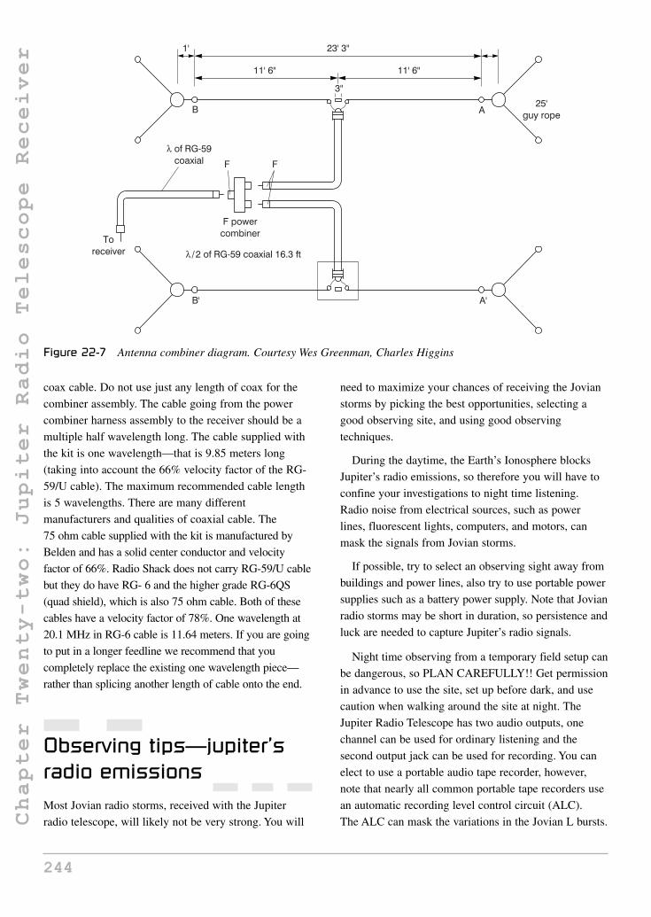
coax cable. Do not use just any length of coax for the
combiner assembly. The cable going from the power
combiner harness assembly to the receiver should be a
multiple half wavelength long. The cable supplied with
the kit is one wavelength—that is 9.85 meters long
(taking into account the 66% velocity factor of the RG-
59/U cable). The maximum recommended cable length
is 5 wavelengths. There are many different
manufacturers and qualities of coaxial cable. The
75 ohm cable supplied with the kit is manufactured by
Belden and has a solid center conductor and velocity
factor of 66%. Radio Shack does not carry RG-59/U cable
but they do have RG- 6 and the higher grade RG-6QS
(quad shield), which is also 75 ohm cable. Both of these
cables have a velocity factor of 78%. One wavelength at
20.1 MHz in RG-6 cable is 11.64 meters. If you are going
to put in a longer feedline we recommend that you
completely replace the existing one wavelength piece—
rather than splicing another length of cable onto the end.
Observing tips—jupiter’sradio emissionsMost Jovian radio storms, received with the Jupiter
radio telescope, will likely not be very strong. You will
need to maximize your chances of receiving the Jovian
storms by picking the best opportunities, selecting a
good observing site, and using good observing
techniques.
During the daytime, the Earth’s Ionosphere blocks
Jupiter’s radio emissions, so therefore you will have to
confine your investigations to night time listening.
Radio noise from electrical sources, such as power
lines, fluorescent lights, computers, and motors, can
mask the signals from Jovian storms.
If possible, try to select an observing sight away from
buildings and power lines, also try to use portable power
supplies such as a battery power supply. Note that Jovian
radio storms may be short in duration, so persistence and
luck are needed to capture Jupiter’s radio signals.
Night time observing from a temporary field setup can
be dangerous, so PLAN CAREFULLY!! Get permission
in advance to use the site, set up before dark, and use
caution when walking around the site at night. The
Jupiter Radio Telescope has two audio outputs, one
channel can be used for ordinary listening and the
second output jack can be used for recording. You can
elect to use a portable audio tape recorder, however,
note that nearly all common portable tape recorders use
an automatic recording level control circuit (ALC).
The ALC can mask the variations in the Jovian L bursts.
244
Chapter Twenty-two: Jupiter Radio Telescope Receiver 1' 23' 3"
11' 6" 11' 6"
3"
B A25'
guy rope
A'
λ of RG-59coaxial
F powercombiner
λ /2 of RG-59 coaxial 16.3 ft
B'
Toreceiver
FF
Figure 22-7 Antenna combiner diagram. Courtesy Wes Greenman, Charles Higgins

Use a tape recorder that allows you to SWITCH OFF
the ALC. Keep the ALC turned off.
Another alternative for recording Jovian storms is the
use of a computer or laptop to record the signals from
your Jupiter radio telescope. Using a laptop computer to
record the Jovian storms has the distinct advantage that
you can analyze the audio recording with special
spectral software which can help you make sense of the
complex signals received.
Note you could also elect to use an audio tape
recorder to record the Jovian signals in the field and
later when you return home play the tape recording into
your laptop or personal desktop computers. There are
many audio analyzing software programs out there on
the Internet, many are free. Many programs allow FTT
and frequency division analysis.
245
Chapter Twenty-two: Jupiter Radio Telescope Receiver

Weather Satellite Receiver
Chapter 23
Parts list
Weather SatelliteReceiver
R1 22ohm, 1/4watt,
5% resistor
R2 150kohm, 1/4watt,
5% resistor
R3 110k ohm, 1/4watt,
5% resistor
R4,R10,R11 22k ohm,1/4watt, 5% resistor
R5 47k ohm, 1/4watt,
5% resistor
R6 1.8k ohm, 1/4watt,
5% resistor
R7 360 ohm, 1/4watt,
5% resistor
R8 100 ohm, 1/4watt,
5% resistor
R9 470k ohm, 1/4watt,
5% resistor
R12,R13,R16,R27 1k
ohm, 1/4watt,
5% resistor
R14 240 ohm, 1/4watt,
5% resistor
R15 1.2k ohm, 1/4watt,
5% resistor
R17 5.6k ohm, 1/4watt,
5% resistor
R18 39k ohm, 1/4watt,
5% resistor
R19,R21 10k ohm,1/4watt, 5% resistor
R20,R31 2.2k ohm,1/4watt, 5% resistor
R22 100k ohm, 1/4watt,
5% resistor
R23 220 ohm, 1/4watt,
5% resistor
R24 390k ohm, 1/4watt,
5% resistor
R25 10 ohm, 1/4watt,
5% resistor
R26 1.5k ohm, 1/4watt,
5% resistor
R28 4.7k ohm, 1/4watt,
5% resistor
R29 300 ohm, 1/4watt,
5% resistor
R30 47 ohm, 14watt,
5% resistor
VR1 50k linear pot,
16mm PC board mount
VR2 25k linear pot,
16mm PC board mount
VR3 50k log pot, 16mm
PC board mount
VR4,VR5 50k 10-turn
trimpots, PC board
mount
C1,C2,C3,C5 2.2nF,
16v, disk ceramic
capacitor
C6,C7,C8,C12 2.2nF,
16v, disk ceramic
capacitor
C4,C10 3-10pF trimcaps
C9 1 nF, 16v, disk
ceramic capacitor
246Copyright © 2008 by The McGraw-Hill Companies, Inc. Click here for terms of use.

C11,C34,C35 10 µF, 16vtantalum capacitor
C13,C27 10pF, 16v, NPO
ceramic capacitor
C14,C19,C21,C23,C25
10nF, 16v, mono
ceramic capacitor
C15,C16 15pF, 16v, NPO
ceramic capacitor
C17 10 µF, 35v Tantalumcapacitor
C18a,C18b,C20,C22
100nF, 16v, mono
ceramic capacitor
C24,C26,C28,C32 100nF,
16v, mono ceramic
capacitor
C29 390pF, 16v, NPO
ceramic capacitor
C30 4,7nF,16v, metal
polyester capacitor
C31 1nF, 16v, metal
polyester capacitor
C33 470nF, 16v, metal
polyester capacitor
C36 330 µF, 16v,electrolytic capacitor
C37 47nF, 16v, metal
polyester capacitor
C38 22nF,16v, metal
polyester capacitor
C39 2200 µF, 25v,electrolytic capacitor
C40 470 µF, 35v,electrolytic capacitor
RFC1 4.3 µH slug tunedcoil – see Table 23-3
RFC2 10 µH slug tunedcoil – prewound
RFC3 68 µH slug tunedcoil – prewound
L1 see Table 23-3
L2 see Table 23-3
L3 see Table 23-3
L4 see Table 23-3
D2 5.1V 400mW Zener
diode
D3,D4 3mm red LED
D1 ZMV833ATA varicap
X1,X2 5.5MHz ceramic
filters, Murata
SFTRD5M50AF00-B0
Q1 BF998 dual-gate
MOSFET
Q2 PN100 NPN transistor
U1 SA605D mixer/IF
amplifier/FM detector
U2 TL072 dual op-amp
U3 LM386 audio amp
U4 78L05 +5V regulator
J1,J2 BNC type
jacks
J3 1/8, 3.5 mm stereo
headphone jack
J4 1 2.5mm concentric
power socket, PC-mount
S1 SPDT miniature
toggle switch
Misc PC board
(double-sided, not
plated through)
TO-220 heatsink,
1 coil former,
4.83mm OD with F16
ferrite slug
1 F29 ferrite bead
(for RFC1)
1 short length of
0.8mm tinned copper
wire for L1
1 length of 0.8mm
enameled copper wire
for L2, L3
247
Chapter Twenty-three: Weather Satellite Receiver

The days of guessing the weather by looking at the
clouds overhead have just ended. Now you can look at
the clouds from above! This satellite receiver/decoding
project will allow you to receive pictures from satellites
600 km overhead, see Figure 23-1. A typical NOAA
satellite can cover nearly one-sixteenth of the Earth in a
single pass! Living in New York, for example, we can
clearly capture images from mid-Hudson bay (where
there was still ice in late spring), all the way down past
Cuba, as well as spanning from Wisconsin to far out in
the Atlantic Ocean. The clarity of the image was enough
to see the individual Finger Lakes (in New York), and
shadows on the underside of thunderstorms. With the
weather satellite receiver and a personal computer, you
can easily receive and decode weather satellite pictures
from overhead satellites.
The US National Oceanographic and Atmospheric
Administration (NOAA) operates both GEO and LEO
polar satellites. Here we concentrate primarily on the
polar orbiters. The NOAA polar satellites orbit at 850 km
and pass within view of all areas on Earth at least twice
day. The satellite carries a number of instruments
including cameras for both visible and infrared light.
The cameras scan back and forth at right angles to the
ground path, like a broom sweeping side-to-side as you
walk forward, taking picture strips that cover an area
3000 km wide. The satellite thus makes a continuous
picture as if it were a tape reeling out from an endless
roll. The image, however, is not recorded on the
satellite. Each image strip is immediately broadcast to
the ground at a frequency just above 137 MHz. The
satellite will be in range for up to 12 minutes as the
satellite passes from horizon to horizon.
The broadcast uses the APT (Automatic Picture
Transmission) analog format for the imagery. (A digital
format High Resolution Picture Transmission (HRPT)
signal is also transmitted but it is more difficult to
receive and decode and we did not try to receive it in
this project.) Currently, there are six operational NOAA
polar orbiters but usually only two or three have the
APT activated at a given time. (In this report, only
images from NOAA-14 and NOAA-15 were received.)
See NOAA satellite status.
The Russian METEOR series of satellites also
broadcast with the APT format. In addition, the remote
sensing SICH and OKEAN radar satellites occasionally
broadcast images but only over Russia (scanners in
nearby countries have picked up some of these images).
The APT systemThe APT satellites give about 12 good images a day,
wherever you are in the world. The resolution is 4 km
per pixel and there are visible and infrared sensors. This
is a simple system where the satellite is in low Earth
orbit and very easily received at 137 MHz. The two
frequencies in main use are 136.50 for NOAA 12 and
15 and 137.62 MHz for NOAA 14. A simple crossed
dipole antenna can be used, or for marine use a
stainless steel quadrifilar helix antenna. These simple
omni-directional antennas do not need moving or
tracking to receive the satellite. The satellite is so
strong that when is about 20° above the horizon
perfect results will be obtained. The APT signal is
easily recognizable by its modulated frequency (FM)
and carrier tonality ranging between 1500 and 2500 Hz.
New satellites have a 2400 Hz carrier like this NOAA
14 APT signal.
In APT mode, satellites transmit at the rate of
120 LPM (lines per minute) alternating two channels,
one for the visible image, the other for the infrared
image. This is through the decoding software that you
select one or another channel.
Russian weather satellites only transmit infrared
images at 120 LPM. The sound of their transmission is
248
Chapter Twenty-three: Weather Satellite Receiver
Figure 23-1 Satellite view – USA

thus slightly different from the other weather satellites
like on this record of a RESURS 01-N4 signal with an
IOC of 382. On their side, METEOR 3-05 uses a
higher carrier closer to 2500 Hz with an IOC of 382
as well.
The WX satellite receiver project will allow you to
receive weather satellite transmissions on the VHF
band, where most of the polar-orbiting satellites are
located. You will recognize these transmissions on the
news when you see the time lapse of the clouds darting
across the countryside. The weather man in this case
has taken multiple images on the computer, aligned and
pieced them together, and then run through one image
after the other. It is possible to do this same thing with
this kit and the proper software.
The way in which a weather satellite works is fairly
simple. Just think of your office fax machine as an
example. The satellites circle the Earth going north to
south back to north again almost directly over the poles,
which is why they call it a polar orbit. This means that
the satellite will cover every location on the Earth at
least twice per day. With a good antenna, and partly
because of overlap of consecutive orbits, you can
conceivably receive the same satellite up to six
times a day! Notice though that the image received
from polar orbits will be upside down on every
other pass.
The satellite retrieves the data in a linear fashion,
one line at a time using a scanning radiometer.
The scanning radiometer transmits the equivalent of a
single television horizontal line as the satellite circles
the earth. The system uses a series of optics and a motor
driven rotating mirror system to receive a very narrow
line of the image of the Earth. Each line is received at a
right angle to the satellite’s orbital track, so as the
satellite circles the Earth, a line is received from west to
east or east to west depending on the orbit of the
satellite. The total image is received from north to south
or south to north, depending on the orbit also, and this
motion is what relays the equivalent of the vertical scan
in a television. You can continue receiving this satellite
as long as it is within the line of sight.
Since all of the receivable satellites are similar, we
will describe the ones you will most commonly
receive. The NOAA/TIROS satellites, during the first
half of the transmission, send visible light data to the
receiver at the same time they are taking in the view.
Meanwhile during the same part of the scan, they are
recording the infrared view. During the second half of
the scan, while the sensors are facing away from the
Earth, it sends the infrared data. The user then sees
the data as two images side by side, on the left the
visible light data is seen, and on the right, infrared data
is seen. In between the images are synchronization
pulses that help computers to align the individual lines
precisely.
These particular satellites continuously transmit an
FM signal modulated with a 2400 Hz tone. This tone is
very precise in frequency so the image seen is aligned
properly. The 2400 Hz tone is AM modulated with the
intensity of the current view of the Earth. The brighter
or colder the point on the Earth, the higher in amplitude
the 2400 Hz signal is.
The receiver demodulates the FM signal and
retrieves the 2400 Hz tone. The detector board in the
computer will then find the peak amplitude of each
wave of the 2400 Hz tone, and each peak, upper and
lower, now represents a single pixel on the screen. For
the NOAA/TIROS satellites, each horizontal line
represents 2400 pixels, since the incoming frequency is
2400 Hz, and the scanning radiometer rotates twice
per second. The full 12 minute pass of a NOAA
satellite requires approximately 3.5 MB (3.5 million 8
bit pixels) of storage! This is much more data (pixels)
than can be seen on a super VGA screen at any
one time.
Many people mistakenly think that they can easily
utilize a conventional VHF scanner as an APT satellite
picture receiver. Most scanners and communications
receivers usually only provide a choice of two
bandwidth settings for VHF FM reception: “narrow”
and “wide.” The narrow setting gives a bandwidth of
±15 kHz or less, which is fine for NBFM reception, and
the wide bandwidth setting usually gives a bandwidth of
about ±100 kHz, so this is the setting that must be used.
Unfortunately, this “wide” bandwidth is actually too
wide for weather satellite signals and, as a result, the
demodulated audio level is relatively low. At the same
time, the wider reception bandwidth allows more noise
through, so the signal-to-noise ratio can become quite
poor. Only a few scanners have the correct bandwidth
and these currently include the AOR5000 and Icom
IC-PCR1000. The second problem with all scanners,
249
Chapter Twenty-three: Weather Satellite Receiver

including the ones mentioned, is that a weather satellite
system needs a very good performance receiver, one
that provides high sensitivity, good signal to noise and
high immunity to other adjacent transmissions. So, you
may get a scanner to work, but it will not provide the
optimum results.
Ideally, in order to obtain the best results you really
need to have a receiver with a ±30 kHz bandwidth.
This type of specialized VHF receiver is available
but fairly pricey. Hence the motivation for
developing the low-cost weather satellite receiver
described here.
The weather satellite receiver project in this chapter
features good sensitivity, at about 0.7V for 12 dB of
quieting. At the same time, the effective bandwidth is
approximately ±35 kHz, which is quite suitable for
weather satellite reception. The satellite receiver is built
into a very compact plastic instrument box, as shown in
Figure 23-2. All of the circuitry is mounted on a
double-sided PC board, so it’s quite easy to build. It has
switch tuning between two preset frequency channels,
for ease of use. There are RF Gain, Audio Muting and
Audio Gain controls and the receiver can drive a small
monitor speaker or headphones, as well as providing a
line level signal to feed into your PC for recording and
decoding.
The heart of the receiver is a Philips SA605D IC
high-performance low-power FM mixer and IF system
on a single chip. As you can see from the block diagram
of Figure 23-3, it contains a local oscillator transistor
and balanced mixer, plus a high-gain IF amplifier and
IF limiter, a received signal strength (RSSI) detector, an
250
Chapter Twenty-three: Weather Satellite Receiver
Figure 23-2 Weather satellite receiver
IF filter IF filter
X1 X2
20 19 18 16 12 14 16V CC
2
34 15 7 8 5 9
10
111
RFinput
MixerIF amplifier
IF limiter
Localoscillator
RSSIdetector
Quaddetector
B E
To oscillatortuned circuit
RSSIout
Mutedaudio
Mute
Audioout
90° phaseshift
Figure 23-3 Weather satellite receiver block diagram

FM quadrature detector and finally an audio muting
circuit. The local oscillator transistor can operate at
frequencies up to about 500 MHz in an LC circuit, or
up to 150 MHz with a suitable crystal. The mixer can
operate up to 500 MHz as well, while the IF amplifier
and limiter can operate up to about 25 MHz with a
combined gain of about 90 dB.
The main receiver diagram illustrated in Figure 23-4
depicts the complete weather satellite receiver circuit
details. In this receiver project, we’re using the SA605D
in a fairly conventional single-conversion superhet
configuration, with the IF amplifier and limiter working
at 5.5 MHz. This allows us to take advantage of high
selectivity 5.5 MHz TV sound IF ceramic filters to
provide most of our bandwidth shaping. The two filters
in question are X1 and X2, which are both Murata
SFT5.5MA devices.
As shown in the receiver schematic, X1 is connected
between the mixer output and the IF amplifier input,
while X2 is connected between the IF amplifier output
and the limiter input. The resistors connected to the
filter inputs and outputs are mainly for impedance
matching, while the 10 nF capacitors are for DC
blocking. The 90° phase shift required for U1’s
quadrature FM detector is provided by coil L4 and its
parallel 390 pF capacitor, which are tuned to 5.5 MHz.
The local oscillator transistor inside U11 is connected
in a Colpitts circuit. This includes coil L3, together with
the two 15 pF capacitors (which provide the emitter tap)
and a 10 pF capacitor in series with the Varicap
diode D1.
The Varicap diode D1 is the receiver’s tuning
capacitor. Its tuning voltage for each of the two
channels is set by 10-turn trimpots VR4 and VR5, with
switch S1 selecting between them. We can tune the
receiver simply by changing the local oscillator
frequency because we only need to tune over a
relatively small range (i.e. 137.3–137.85 MHz
maximum), which is within the selectivity curve of the
“front end” tuned circuits.
The satellite receiver’s front end uses a BF998 dual-
gate MOSFET (Q1) connected in a standard cascode
amplifier configuration. The incoming VHF signals are
fed into a tap (for impedance matching) on antenna coil
L1, which is tuned to about 137.55 MHz using trimmer
capacitor VC1. The signal from the top of this tuned
circuit is then fed directly to gate 1 of Q1, while gate
2 is bypassed to ground but also fed with an adjustable
DC voltage via VR1 for RF gain control. The amplified
VHF signal on Q1’s drain is fed to pin 1 of U1 via a
1 nF coupling capacitor. Additional RF selectivity is
provided by coil L2 and trimmer capacitor VC2, which
are again tuned to about 137.55 MHz. The 100 ohm
resistor and 10 µH RF choke form an untuned high-
impedance load for Q1.
Notice that as well as being coupled to the tap on
L1 via a 2.2 nF capacitor, the antenna input is also
connected to the +12V supply line via RFC1 and a
series 22 ohm resistor. As you may have guessed, these
components are there to provide “phantom” DC power
for the masthead pre-amplifier. At the output end of U1,
we take the demodulated APT signals from the “muted
audio” output at pin 8. This allows us to take advantage
of the SA605’s built-in muting circuit, which works by
using comparator stage U2b to compare U1’s RSSI
output from pin 7 (proportional to the logarithm of
signal strength) with an adjustable DC control voltage
from muting pot VR2. When the RSSI voltage rises
above the voltage from VR2, U2b’s output switches
high and this is fed to pin 5 of U1 via a 2.2 k ohm series
resistor to un-mute the audio. D2, a 5.1V Zener diode,
limits the swing on pin 5 of U1 to less than 6V.
Transistor Q2 and LED1 form a simple signal
strength indicator. This also uses the RSSI output from
U1. In operation, the voltage across the 390 k ohm
resistor and 100 nF capacitor rises from about +0.26V
under no-signal conditions to about +5V with a very
strong input signal. So with Q2 connected as an emitter
follower and LED1 in its emitter load, the LED current
and brightness are made to vary quite usefully with
signal strength.
The demodulated APT signal from pin 8 of U1 is first
fed through op-amp U2a, which is configured as an
active low-pass filter. This has a turnover frequency of
5 kHz and is used for final de-emphasis and noise
reduction. From there, the signal is fed to audio gain
control VR3 and then to audio amplifier stage U3. This
is a standard LM386 audio amplifier IC, configured for
a gain of about 40 times. Its output is fed to both the
monitor speaker socket and to a line output socket for
connection to your PC’s sound card.
Most of the receiver’s circuitry operates from +12V,
with the exception of U1 which needs +6V. As a result,
251
Chapter Twenty-three: Weather Satellite Receiver

252
C hapter Twenty-three: Weather Satellite Receiver
C1 R4
VR1
R1
RfC1R2
R5
J1
C2
C3
C4
VR4
C6
C7
L1
R3
C5
G1
R7C8
S
DG2
G1
R8R6
RfC2
C11
+12 V
VR5B
AS1
R10
C9
L2
C10
+6 V
R9
D1
L3
C13
C14
C15
C16R11
C12
R12X1
R13 R14 R15
R16
C19
C20C21C22
C23 C24C25
C26
20 19 18 17 16 15 13 14 121
24 3 5 6 7
C2711
10
8
C28
C29
L4
C30R17
C18C17
RfC3
+6 V
+12 V
R27 J2
U2:A3
2C31
+12 V
R18C33
R20 R19
D2 U2:B
4
78
6
5
+12 V
C32R24
R22c
b
c
Q2
R23
R21
U3
R26
C343
2
61
85
74
C35R25
C37
C36J3
A
K
D3
VR2
R28
+6 V
Out OutIn InU4
R29
R30
C38
R31
P4C39 C40
J4
U5
++
+
+
+
+
+
+
+12 V
+
U1
1
Figure 23-4 Weather satellite receiver schematic. Courtesy of Silicon Chip Magazine

the power supply circuitry includes U5 to provide a
regulated and smoothed +12 V supply from an external
supply such as a 14.5–18 V “wall-wart.” This is
followed by 5V regulator U4 which has its output
“jacked up” using 300 ohm and 47 ohm resistors to
provide close to +6 V for the SA605D (U1). Note that if
you want to run the receiver from a 12 V battery, this
can be quite easily done by replacing REG1 with a wire
link. In addition, the 2200 µF capacitor should be
replaced with a 16 V Zener diode (ZD2) for
over-voltage protection.
ConstructionBefore beginning the project make sure that you have a
clean well lit and well ventilated work space for
constructing your satellite receiver. Locate all the
diagrams and place them in front of you on the table or
work bench. Locate a 27 to 30 watt pencil-tip soldering
iron, along with some “Tip Tinner,” which is used to
prepare and clean your soldering iron tip. Locate a roll
of 60/40 tin/lead rosin core solder as well as a few small
hand tools such as a pair of small end-cutters, a
needle-nose pliers, a pair of tweezers, and some small
screwdrivers.
Construction of the weather satellite receiver is
straightforward with virtually all of the parts mounted
on a small PC board. The board is double-sided but the
top copper pattern is used mainly as a ground-plane.
This means that the board doesn’t need to have plated-
through holes but there are quite a few component leads
which do have to be soldered on both sides of the board.
There are also a number of “pin-through” or “hole-
through” wires which have to be soldered to both sides
of the PC board around U1. These connect the Earth
patterns on both sides of the board and ensure that this
high-gain chip operates in a stable manner.
The various input and output connectors are mounted
along the rear edge of the circuit board, while the
controls and indicator LEDs mount along the front
edge. The only component not actually mounted on the
board is S1, the channel select toggle switch. This
mounts on the front panel, with its three connection lugs
wired to PC board terminal pins directly underneath
using very short lengths of insulated hookup wire.
Start the assembly by mounting these three terminal
pins first, they are the only pins used in the receiver
project. Next, mount the four connectors CON1-CON4
along the rear edge, followed by the resistors. Table 23-1
shows the resistor color codes but it’s also a good idea
to check each value using a digital multi-meter before
253
Chapter Twenty-three: Weather Satellite Receiver
Table 23-1Resistor color code chart
Color Band 1st Digit 2nd Digit Multiplier Tolerance
Black 0 0 1
Brown 1 1 10 1%
Red 2 2 100 2%
Orange 3 3 1,000 (K) 3%
Yellow 4 4 10,000 4%
Green 5 5 100,000
Blue 6 6 1,000,000 (M)
Violet 7 7 10,000,000
Gray 8 8 100,000,000
White 9 9 1,000,000,000
Gold 0.1 5%
Silver 0.01 10%
No color 20%

soldering it in position. All resistors are mounted to the
top of the PC board but note that some of them have
one lead soldered to the top copper as well as the
bottom copper. Once the resistors are in place, you can
use excess resistor leads to allow connection from one
side of the board to the other side, since this project
uses a two-sided circuit board. Each “pin-through or
through-hole” is fitted by simply passing a wire through
the hole in the board, then soldering it on both sides and
trimming off the excess lead lengths.
The small ceramic capacitors can now all be installed
on the left-hand side of the board. Note that some of these
also have their “cold” leads soldered on both sides of the
board, as indicated by the red dots. Once they’re in,
install the MKT capacitors and the electrolytic capacitors,
making sure that the latter are all correctly orientated.
Use the chart shown in Table 23-2 to help locate the small
capacitors from the parts pile. Often small capacitors do
not have their actual value printed on them but instead use
a three-digit code to represent the actual value.
Finally go ahead and mount the trimmer capacitors
VC1 and VC2. These should be mounted so that their
adjustment rotors are connected to earth (this makes it
much easier to align the receiver later). It’s simply a
matter of orientating them on the board.
Next, we will move on to installing the RF chokes.
RFC2 and RFC3 are both pre-wound (10 µH and 68 µH
respectively) but RFC1 needs to be wound on an F29
ferrite bead. It’s very easy to wind though, because it
requires only three turns of 0.25 mm enameled
copper wire.
Winding coilsAt this point in time, it’s a good idea to wind and mount
the remaining coils. Table 23-3 gives the winding
details of the coils. As shown, L1–L3 are air-cored
types, each consisting of five turns of 0.8 mm diameter
wire wound on a 5 mm mandrel. Note, however, that L1
is wound using tinned copper wire, while L2 and L3 are
both wound using enameled copper wire. Don’t forget
to scrape off the enamel at each end, so they can be
soldered to the board pads.
Coils L1–L3 should all be mounted so that their turns
are about 2 mm above the board. After you’ve fitted L1,
don’t forget to fit its “tap” connection lead as well. This
can be made from a resistor lead off-cut, since it’s very
short. It connects to a point 1⁄3 of a turn up from the
“cold” (earth) end of the coil, i.e. just above half-way
up the side of the first turn.
The final coil to wind is quad detector coil L4. Unlike
the others, this is wound on a 4.83 mm OD former with
a base and a copper shield can. It’s wound from 20
turns of 0.25 mm enameled copper wire and tuned with
an F16 ferrite slug. Coil formers with ferrite slugs are
difficult to locate, check the Appendix. You could
also experiment with a small “junk” IF transformer
can. You could try and unwind the existing coil and
re-winding your own coil over the plastic former.
You must make sure that there is a ferrite slug in the
center of the coil former. Once L4 is wound, and
installed onto the board, cover it with its shield can.
You can next mount the two ceramic filters X1 and X2.
These devices can be fitted either way around but make
sure that their pins are pushed through the board holes
as far as they’ll go before you solder them
underneath.
The next step is to construct and install the small
metal shield around coil L2, C10 and most of the
components in the drain circuit of Q1. This shield is
U-shaped and measures 20 mm high, with the front and
back “arms” 36 mm long and the side section 20 mm
long. The bottom edges of all three sides are soldered to
the board’s ground-plane in a number of places, to hold
it firmly in position and to ensure it stays at earth
potential.
The two 10-turn trimpots (VR4 and VR5) can now be
soldered in position at the front-center of the board.
They can then be followed by the three main control
pots, which are all 16 mm diameter types. Trim each
pot’s spindle length to about 9 mm before fitting it and
make sure you fit each one in its correct position as they
are all different. In particular, note that VR1 and VR3
both have a value of 50 k ohm but VR1 is a linear pot
while VR3 is a log type.
After installing the potentiometers, it’s a good
idea to connect their metal shield cans together
and then run a lead to the board’s top copper to earth
them. This is done using a length of tinned copper
wire, with a short length of insulated hookup
wire then connecting them to the board copper at
front right.
254
Chapter Twenty-three: Weather Satellite Receiver

255
Chapter Twenty-three: Weather Satellite Receiver
Table 23-2Capacitance code information
This table provides the value of alphanumeric coded ceramic, mylar and mica capacitors in general. They come in many sizes,
shapes, values and ratings; many different manufacturers worldwide produce them and not all play by the same rules. Some
capacitors actually have the numeric values stamped on them; however, many are color coded and some have alphanumeric codes.
The capacitor’s first and second significant number IDs are the first and second values, followed by the multiplier number code,
followed by the percentage tolerance letter code. Usually the first two digits of the code represent the significant part of the value,
while the third digit, called the multiplier, corresponds to the number of zeros to be added to the first two digits.
Value Type Code Value Type Code
1.5 pF Ceramic 1,000 pF /.001 µF Ceramic / Mylar 102
3.3 pF Ceramic 1,500 pF /.0015 µF Ceramic / Mylar 152
10 pF Ceramic 2,000 pF /.002 µF Ceramic / Mylar 202
15 pF Ceramic 2,200 pF /.0022 µF Ceramic / Mylar 222
20 pF Ceramic 4,700 pF /.0047 µF Ceramic / Mylar 472
30 pF Ceramic 5,000 pF /.005 µF Ceramic / Mylar 502
33 pF Ceramic 5,600 pF /.0056 µF Ceramic / Mylar 562
47 pF Ceramic 6,800 pF /.0068 µF Ceramic / Mylar 682
56 pF Ceramic .01 Ceramic / Mylar 103
68 pF Ceramic .015 Mylar
75 pF Ceramic .02 Mylar 203
82 pF Ceramic .022 Mylar 223
91 pF Ceramic .033 Mylar 333
100 pF Ceramic 101 .047 Mylar 473
120 pF Ceramic 121 .05 Mylar 503
130 pF Ceramic 131 .056 Mylar 563
150 pF Ceramic 151 .068 Mylar 683
180 pF Ceramic 181 .1 Mylar 104
220 pF Ceramic 221 .2 Mylar 204
330 pF Ceramic 331 .22 Mylar 224
470 pF Ceramic 471 .33 Mylar 334
560 pF Ceramic 561 .47 Mylar 474
680 pF Ceramic 681 .56 Mylar 564
750 pF Ceramic 751 1 Mylar 105
820 pF Ceramic 821 2 Mylar 205
1st Significant Figure
2nd Significant Figure
Multiplier
Tolerance
CSGNetwork.Com 6/4/92
0.1 µF 10%
104 k

Mounting thesemiconductorsBefore we go ahead and install the semiconductors, let’s
take a brief look at the semiconductor pin-out diagram
illustrated in Figure 23-5, which will assist you in
orienting the integrated circuits. Now you can go ahead
and mount the semiconductors. Begin by installing the
Varicap diode at D1, and the 5.1V Zener diode at D2
and transistor Q2. Next, install regulator U5 and its
associated heatsink. These parts are secured to the board
using a 6 mm-long M3 screw, nut and lock-washer.
Note that U5’s center pin should be soldered on both
sides of the board but take care not to touch either of
the two large adjacent electrolytic capacitors with the
barrel of your soldering iron.
Go ahead and mount regulator U4, followed by U22
(TL072) and U3 (LM386). Note that pin 4 on both these
devices should be soldered to the copper on the top of
the board as well as the bottom. The two D3 and D4 are
both mounted horizontally, so that they later protrude
through matching 3 mm holes in the front panel. Note
that they are both fitted with their cathode leads towards
the left. Bend their leads down through 90° about 5 mm
from the LED bodies, then solder them in position so
that the axis of each LED is 5 mm above the board.
The final components to be mounted on the PC board
include the Dual-Gate MOSFET at Q1 and the SA605D
IC at (U1), U2 and transistor Q2. These components
should be handled very carefully, using an anti-static
wrist-band to avoid static charges building up on the
components. The two integrated circuits should be
mounted in IC sockets. IC sockets are an insurance
policy against circuit failure at a later date. It is much
easier to simply unplug a faulty IC, rather than trying to
un-solder 14 or 16 pins from the circuit. Most people
cannot un-solder 16 pins without damaging a circuit
board. When mounting the IC sockets, observe a small
cut-out at one edge of the socket. The cut-out will
identify the top of the socket. Usually pin of the IC will
be located to the left of the cut-out. Solder the sockets
in their respective locations. Finally insert the ICs into
their respective sockets, noting pin 1 is to the left of the
small indented circle or cut-out on the top of the IC
package. When handling the MOSFET be extremely
256
Chapter Twenty-three: Weather Satellite Receiver
Table 23-3Coil winding details
L1 5 turns of 0.8 mm (20 ga.) tinned copper wire, 7 mm
long (wound on 5 mm diameter mandrel). Tap at
0.3 turns. Air core, mounted 2 mm above board.
L2 5 turns of 0.8 mm (20 ga.) enameled copper wire,
9 mm long (wound on 5 mm diameter mandrel).
Air core, mounted 2 mm above board.
L3 5 turns of 0.8 mm (20 ga.) enameled copper wire,
8 mm long (wound on 5 mm diameter mandrel).
Air core, mounted 2 mm above board.
L4 20 turns of 0.25 mm (30 ga.) enameled copper wire,
tight wound on 4.83 mm OD former with F16
tuning slug and shield can.
RFC1 3 turns of 0.25 mm (30 ga.) enameled copper wire
wound on an F29 ferrite bead.
1 8 1 8
TL072
78L05
Bottom View
(TO-92)Plastic Package (Z)
DAO
OUTPUT INPUT
00774400
SA605
LM386
1
2
3
4
5
6
7
8
9
10 11
12
13
14
15
16
17
18
19
20
1
23
4
8
76
5
1
23
4
8
76
5
Figure 23-5 Semiconductor pin-outs

careful to avoid damage from static electricity. Do not
move around when installing these static sensitive
components and be sure to use an anti-static wrist band
to avoid damage.
The completed PC board is housed in a suitable
low-profile plastic instrument case.
First, you can mount switch S1 on the front panel and
connect three 30 mm lengths of insulated hookup wire
to the three pins on the PC board. That done, the front
panel can be mated with the PC board by positioning
it on the three pot ferrules and doing up the nuts.
The three leads from the PC board pins can then be
soldered to the switch lugs.
The rear panel is not attached to the board assembly.
Instead, it simply slips over connectors CON1 and CON2
and is then slid into the rear slot when the assembly is
fitted into the bottom half of the case. Now go ahead and
mount the antenna connector onto the rear panel. Finally,
the completed assembly is fastened in place using eight
6 mm-long 4-gauge self-tapping screws.
After completing the circuit board assembly, you
should take a short rest and when we return we will
inspect the circuit board for any possible “short” circuits
or “cold” solder joints. Pick up the circuit board with
the foil side of the circuit facing upwards toward you.
First inspect the circuit board for possible “cold” solder
joints. All of the solder joints should look clean, bright
and shiny. If any of the solder joints look dark, dull or
“blobby,” then you should un-solder that particular joint,
remove the solder then re-apply some solder and re-
solder the joint all over again. After inspecting all of the
solder joints, we can move on to looking for “short”
circuits. Often sticky rosin core solder will leave a
residue on a circuit board. When excess component
leads are cut from the board during assembly, many
times the “cut” leads will stick to the circuit board and
they can “bridge” across the circuit pads and cause a
“short” circuit which could damage the circuit when
first powered-up. Another potential cause for a
“short” circuit is a small solder ball which may
have stuck to the circuit board, this too can cause a
“short” circuit.
Once you have inspected the circuit board to your
satisfaction, you can connect up the power supply leads
to the power input jack and you will be ready to test the
weather satellite receiver.
Circuit testFirst, turn all three front-panel pots fully anticlockwise,
connect up your antenna to the antenna input connector,
and then apply power from a suitable 14–18V DC
“wall-wart” power supply or a 12V battery. Check that
the green power LED immediately begins glowing.
If it does, check the voltage on REG1’s output lead
(i.e. the right-hand lead) with your multi-meter, it
should read close to +12V with respect to ground.
Similarly, the voltage at REG2’s (right-hand) output pin
should measure very close to +6V.
If you now plug an 8 ohm speaker into CON3
terminals, and then turn up audio gain control VR3, you
should hear a small amount of hiss and noise. When you
turn up the RF gain control VR1 as well, this noise
should increase a little further but LED1 shouldn’t
begin glowing except only very faintly when VR1 is
turned fully clockwise.
Now turn VR1 fully anticlockwise again and use your
multi-meter to measure the DC voltage at the top of the
390k resistor located just behind transistor Q2 (i.e. to
the right of 5.1V Zener diode). The voltage across this
resistor should be less than 0.30V and preferably about
0.26V. If it’s any higher than 0.30V, the IF amplifier in
IC1 may be unstable. Assuming that your receiver has
passed all these tests, it should be working correctly and
is now ready for alignment.
Receiver alignmentThe final alignment of the weather satellite receiver is
best done with a satellite signal. However, you need to
give it a basic alignment first so that you can at least
find the signal from a satellite when it’s within range.
For the basic alignment, you’ll need access to a
frequency counter capable of measuring up to 150 MHz
and an RF signal generator which can be set to give an
output at 137.50 MHz and at 137.62 MHz. It should be
able to provide either unmodulated (CW) output or
frequency modulation, with a modulating frequency of
2.4 kHz and a deviation of ±25 kHz or thereabouts. If
the generator can’t be accurately set to the above
frequencies, you’ll need to use the frequency counter to
257
Chapter Twenty-three: Weather Satellite Receiver

help set its frequency. You’ll also need your multi-meter
during the “tuning-up” process, to monitor received
signal level.
The first step is to set the local oscillator frequencies
for the two reception channels. This is done by
adjusting trimpots VR4 and VR5 respectively, while
measuring the oscillator’s frequency with the frequency
counter. The oscillator signal is coupled to the counter
via a “sniffer” coil which is connected to the end of a
coaxial cable. The other end of this cable is then
connected to the counter’s input. Note that there is no
direct physical connection between the oscillator coil
and the counter’s sniffer coil. Instead, the sniffer
coil is placed about 9 mm in front of oscillator coil (L3)
and roughly on-axis (i.e. just in front of the 10 pF
capacitor).
The sniffer coil can be made by winding four
turns of 0.8 mm enameled copper wire on a 5 mm drill
shank. Its ends can then be soldered to a BNC socket
which is then connected to the end of the counter input
cable. This arrangement picks up enough oscillator
energy to give reliable counter readings, without
needing to be any closer to L3 (to avoid “pulling” the
frequency).
Assuming you want to receive the NOAA satellites,
set the oscillator frequency for channel A to 132.0 MHz
(using VR4), and the frequency for channel B to
132.12 MHz (using VR5). These correspond to
reception frequencies of 137.5 MHz for NOAAs 12 and
15 and 137.62 MHz for NOAA 17. If you want to try
for other satellites, you’ll need to find out their APT
frequency and set the oscillator frequency to
5.5 MHz below that figure instead, and adjust the
tuning controls.
Once the oscillator frequencies have been set, the
next step is to peak up the RF stage tuned circuits. This
is done by setting your RF signal generator to produce
an unmodulated (CW) signal at 137.5 MHz, initially
with a level of about 30 mV. That done, connect the
generator’s output to the antenna input of the receiver,
using a series DC blocking capacitor if the generator
doesn’t have one (so that the generator doesn’t short out
the +12V phantom power for the masthead amplifier).
Next, connect your multi-meter (set to the 5V DC
range) across the 390k ohm resistor just behind Q2 and
make sure switch S1 is set to the channel A position.
Now turn up RF gain control VR1 to about midway and
use an alignment tool or a very small screwdriver to
adjust trimmer cap C10 until you find a peak in the
voltage reading on a multi-meter. If you can’t find a
peak, you may have to pull the turns on coil L2 slightly
further apart to reduce its inductance. Once the peak is
found, adjust VC2 carefully to maximize the meter
reading (the multi-meter is reading the RSSI voltage
from IC1, so it’s essentially showing the received signal
strength).
When you’re certain that the L2/C10 circuit is tuned
to 137.5 MHz, check the actual voltage reading of the
meter. If it’s more than 2.5V, reduce the output level
from the RF generator until the multi-meter reading
drops to about 2.0V. Now you’re ready to peak the
receiver’s input tuned circuit—i.e. L1 and VC1. This is
done in exactly the same way as for L2 and C10. Just
adjust C4 slowly until the multi-meter indicates
a peak and then carefully set C4 for the maximum
peak reading. If you can’t find another peak, you
may need to pull the turns of L1 slightly further apart
as before.
The final alignment step is to set the slug in
quadrature detector coil L4 to the correct position for
optimum FM demodulation of the 5.5 MHz IF signals.
This is done by first switching the signal generator so
that it’s still producing a 137.5 MHz signal but this
should now be frequency modulated—preferably with a
2.4 kHz tone and a deviation of about ±25 kHz.
Now, connect an 8 ohm speaker to the receiver’s
speaker socket (CON3) and turn up the audio gain
control (VR3) to about the 10 o’clock position. You may
not be able to hear the 2.4 kHz modulating signal at this
stage but in any case, slowly and carefully adjust the
slug in L4 using a non-magnetic alignment tool. Sooner
or later you’ll start to hear the 2.4 kHz tone and you
should also be able to tune the coil for maximum audio
level and minimum distortion and noise.
Once this has been done, the basic alignment of your
weather satellite receiver is finished and it’s ready for
final alignment using the signals from a weather
satellite. But before you’ll be able to do this, you’ll
need to build or buy a suitable antenna and perhaps a
small masthead pre-amplifier to boost the signal if
necessary. The best antenna for APT weather satellite
reception is either a turnstile or quadrifillar antenna.
258
Chapter Twenty-three: Weather Satellite Receiver

APT antennaconsiderationsThe crossed dipole or turnstile antenna is shown in
Figure 23-6; it is recommended for nearly all APT
weather satellite applications. It is made from aluminum
and is strong and durable. It can be fixed onto a vertical
mast and should be positioned as high as possible. The
satellite signal will not go through trees or buildings and
to get the best possible continuous signal it needs to be
mounted onto a mast as high as possible. On the end or
top of a building is preferred although, for test purposes,
it can simply be stuck into the grass at ground level.
Another good choice for APT satellite reception is
the quadrifilar helix antenna, see Figure 23-7. It offers
slightly better performance than the crossed dipole but it
is considerably more costly.
The success of weather satellite reception is very
much dependent on having a good antenna. The ARRL
Weather Satellite Handbook, is a good source of
information on building antennas and low-cost antenna
pre-amplifiers. You can either build a good antenna or
readily purchase one from one of the vendors listed in
the Appendix. Good quality, low-loss 50. coax should
be used between the antenna and the satellite receiver,
since satellite signals are generally weak. The coax
should be plugged into the BNC jack on the rear of
the receiver. If you are using large diameter coax,
it may be necessary to use a UHF-BNC adapter.
Another alternative is to use a short length of smaller
diameter, more flexible, coax between the main cable
and the receiver. That cable can have a BNC plug on
one end and a UHF plug and double female adapter on
the other. If you use a 137 MHz pre-amplifier, you can
overcome some cable losses by installing the pre-amp
right up at the antenna. This establishes a low noise
figure before going through the loss of the cable. If you
find you do need a 137 MHz mast-head pre-amplifier,
you can build one or buy one from Hamtronics or
Ramsey Electronics. We do not recommend trying to
feed B+ to power the pre-amp through the coax as some
enthusiasts do. It doesn’t pay to try to save the small
cost of lightweight hook-up wire and de-grade the
performance of the pre-amp in the process.
Run a separate wire pair to power the pre-amplifier
if needed.
Receiver operationOperation of the receiver is fairly obvious, but we will
comment on several features of interest. Normally,
when used to drive a computer’s sound card, you will
want to listen on a speaker to hear what the signal
sounds like. The VOLUME control can be adjusted to
whatever level is comfortable for listening and proper
259
Chapter Twenty-three: Weather Satellite Receiver
Figure 23-6 VHF turnstile antenna Figure 23-7 Quadrifillar antenna

for the computer’s sound card. This is especially true
during the initial acquisition period. However, most
times you probably want the ability to mute the speaker;
so installing a switch in line with the receiver output to
the speaker is handy.
To adjust the SQUELCH control, turn it clockwise
just a little beyond the point where the squelch closes
with no signal (just noise). The squelch circuit has
adjustable sensitivity—the further clockwise you set
the control, the stronger the signal must be to open
the squelch. This is handy to set how strong you want
the satellite signal to be before the tape recorder turns
on. Be careful not to set it too far clockwise, though,
because the squelch might not open even with a strong
signal. The weather satellite receiver will allow you to
select two different channels. Channel selection is done
with switch S1. Use the selector switch to choose
channel A or B, then use potentiometer VR4 or VR5 to
“tune-in” the desired satellite frequency. The satellite
receiver’s audio is fed to the speaker output at J3 and
also to a low-level output at J2 which can be fed to
either a tape recorder or decoder card in a personal
computer.
Setting up you APTreceive stationIn order to set up your own weather satellite receiving
station you will have to acquire a few more items, as
seen in Figure 23-8. In addition to the satellite receiver
and antenna, you will need a personal computer, some
sort of interface and a software package to display the
satellite picture and a satellite tracking program if
desired. A tracking program is not required, but it is fun
to be able to know in advance when the satellite is
overhead.
How to see satellite weather pictures on your
personal computer, you must follow the steps below:
1. Track the desired satellite to find when it will appear
and how long it will be in view (i.e. how high in
elevation it will rise). (See NASA’s online J-Track
program for an example of NOAA satellite tracking.)
2. Tune the receiver to the right frequency, e.g.
137.620 MHz for NOAA-14 and 137.500 for
NOAA-15 and pick off the AM signal that carries
the image data. The 2400 Hz AM sub-carrier signal
will produce a distinctive “tick-tock” sound from
the speakers.
3. Receive the signal for as much of the satellite pass
as possible.
4. Decode the signal into the image. (Depending on
the system, this is done in real-time or the signal is
saved to file that is decoded later.) Most new
computers (i.e. running at 800 MHz to 3 GHz with
WIN2000 or XP software) with a good sound card
can be used to decode the software directly from
the satellite receiver audio.
With your 137-138 MHz turnstile or quadifillar
satellite antenna connected to your weather satellite
receiver, and your WX receiver connected to your sound
card in your PC, via a shielded audio cable, you will be
able to get stunning color images directly from weather
satellites.
In order to decode an APT weather satellite signal
from your WX satellite receiver, you will need to load
some WX decoding software into your personal
computer.
There are number of choices for APT satellite
decoding software, some of which are free for the
download, such as WXtoImg which is a fully automated
APT and WEFAX weather satellite (wxsat) decoder.
The software supports recording, decoding, editing, and
viewing on all versions of Windows, Linux, and
260
Chapter Twenty-three: Weather Satellite Receiver
Antenna
Pre-amplifier
Satellite receiver
Personalcomputer
Sounddecoder
card
SpeakerPowersupply
Figure 23-8 Weather satellite receiving system
diagram

MacOS X. The WXtoImg software supports real-time
decoding, map overlays, advanced color enhancements,
3-D images, animations, multi-pass images, projection
transformation (e.g. Mercator), text overlays, automated
web page creation, temperature display, GPS interfacing,
and control for many weather satellite receivers,
communications receivers, and scanners. Check the
download site at: http://www.wxtoimg.com/downloads/.
Another good source for the WXSAT satellite
decoding software is the HF-FAX web-site located at
http://www.hffax.de/html/hauptteil_wxsat.htm. Once
your software is loaded and your system check
completed, you can refer to the chart in Table 23-4, for
the most popular satellite frequencies.
Additional APT weather satellite source information
137 MHz quadrifillar antenna construction info:
http://www.askrlc.co.uk/
137 MHz turnstile antenna construction info:
http://www.qslnet.de/member/pa1pj/turnstile.pdf
TimeStep – http://www.time-step.com
Hamtronics – http://www.hamtronics.com/
Ramsey Electronics –
http://www.ramseyelectronics.com/
Dartcom – http://www.dartcom.co.uk
Swagur Enterprises, USA www.swagur.com
Vanguard Electronic Labs, USA www.cyberpad.com
261
Chapter Twenty-three: Weather Satellite Receiver
Table 23-4137 MHz Weather satellite receiver frequencies
Country Satellite Format Frequency
USA NOAA - 12 APT 137.500 MHz
USA NOAA - 14 APT 137.620 MHz
USA NOAA - 15 APT 137.500 MHz
USA NOAA - 17 APT 137.620 MHz
USA - 2008 launch NOAA - 18 APT 137.9125 MHz
Russia METEOR APT 137.300 MHz
Russia METEOR APT 137.400 MHz
Russia METEOR APT 137.850 MHz
Russia OKEAN APT 137.400 MHz

Analog To Digital Converters (ADCs)
Chapter 24
Parts list
ADC - 1
C1 .1 µF, 35 voltcapacitor
C2 10 µF, 35 voltelectrolytic capacitor
C3 5 µF, 35 voltelectrolytic capacitor
U1 LM78L05 5 volt
regulator IC
U2 MAX187 A/D
converter IC
ADC - 2
R1-R8 100 k ohm,1/4watt, 5% resistor
C1 1 µF, 35 voltelectrolytic capacitor
C2,C5 .1 µF, 35 voltdisk capacitor
C3 47 µF, 35 voltelectrolytic capacitor
C4 4.7 µF, 35 voltelectrolytic capacitor
D1 1N4001 silicon diode
U1 MAX186 A/D converter
IC (Maxim
Semiconductor)
U2 LM7805 – 5 volt
regulator IC
P1 DB-25 – 25-pin
parallel port
connector
Misc PC board, wire,
enclosure, terminal
strip, etc.
A number of radio receiver projects in this book are
based on collecting data from receivers rather than
listening to sound coming from a radio. In this chapter
we will discuss four different approaches to buying
and/or building analog to digital converters which you
can use to collect or save data for analyzing at a later
time. By using an analog to digital converter, you can
collect, save and later playback and analyze signals that
were recorded over days or over weeks and then, using
special software, you can analyze the signals to
determine trends of specific signals. We will present
two different A/D or analog to digital converter projects
which you can build with inexpensive integrated circuits
and connect to your personal computer’s parallel port.
Next, we will show you how you can purchase a low cost
commercial analog to digital converter with software and
finally we will describe a high quality A/D system which
is used by members of the Public Seismic Network to
record earthquake signals around the country. The PSN
A/D converter is a true 16-bit multi-channel assembled
A/D system which connects to your personal computer’s
serial port. These four A/D systems are great choices for
collecting radio signals over an extended period of time.
Examine each of these A/D solutions and see which one
is best for your particular applications. Most of the A/D
collections systems described below come with free
software for recording data.
ADC – 1: single channelanalog to digital converterThis single channel 12-bit analog to digital converter,
shown in Figure 24-1, can be built with the minimum of
262Copyright © 2008 by The McGraw-Hill Companies, Inc. Click here for terms of use.

components and the software for it is free. The single
channel A/D converter is built around the $14 low cost
MAX187 A/D converter from MAXIM Semiconductors.
The circuit consists of the A/D converter chip, a
regulator chip, and a few capacitors; it can’t get more
simple than this! The single channel A/D converter
readily connects to your computer’s parallel port
through a BD-25 connector. The analog input voltage
can be from zero (0) to 4.095 volts as a maximum
signal level. A 9 volt battery or small 9 to 12 volt DC
“wall-wart” power supply can be used to power the A/D
circuit, which can be housed in a small plastic case.
The A/D input from your signal source is fed to pin 2
of the MAX187 chip. The 5 volt regulator’s output
powers the MAX187 chip via pin 1. The MAX817
outputs to your personal computer are on pins 6, 7 and 8.
Only three capacitors are needed for this A/D, two of
which are used in the regulated power supply section of
the circuit.
You will need a small 30 watt soldering iron, some
60/40 rosin core solder for building this project. A small
jar of “Tip Tinner” from your local Radio Shack is used
to clean and dress the soldering tip. Locate a few small
hand tools, including a pair of small end-cutters and a
needle-nose pliers and a flat-blade and Phillips
screwdriver and we will begin building the A/D
converter.
Heat up your soldering iron and let’s get building.
The ADC-1 circuit can be built on a small perf-board or
direct prototyping board available at Radio Shack or
you could make your own circuit board for the project.
The circuit only utilizes capacitors, both polar and non-
polar types. Non-polarized capacitors are usually
smaller capacitor and sometimes they do not have their
actual value printed on them. Often a three-digit code is
used to represent their value. For example, a . 001 µF
capacitor will have (102), while a .01 µF capacitor will
have a (103) marked on it. This project also uses large
polarized or electrolytic capacitors, these capacitors
have polarity markings on them which must be
observed if you want the circuit to work properly. Use
the chart in Table 24-2 to help identify the project
capacitors. Identify all of the capacitors before
installing them on the circuit board. Once you have
identified all of the capacitors, you can go ahead and
install them on the circuit board. Trim the excess
component leads flush to the edge of the circuit board
with your end-cutters.
Take a quick look at the semiconductor pin-out
diagram shown in Figure 24-2. This diagram will help
you install the integrated circuits in the A/D projects.
An integrated circuit socket for this project is highly
recommended, as an insurance from a possible circuit
failure if it ever happens. It is much easier to simply
replace the IC rather than trying to un-solder the IC
from the circuit board. The IC socket will have a
cut-out or notch at one end of the package. Solder the
IC socket onto the PC board. Pin one (1) will be
assigned to the pin just to the left of the notch or cut-
out. Pin one (1) of the IC socket is connected to the
263
Chapter Twenty-four: Analog To Digital Converters
A/Dinput
U1
C3C2C1
U2MAX187
LM98LOS
P12 3 12
24 25
3 1
2
1
2
3
4 5
6
7
8
+
+ +
Figure 24-1 Single channel A/D converter – ADC 1. Courtesy of Radio-Sky Publishing

output of the regulator U1. When inserting the IC into
its socket pay particular attention to the orientation. Pin
one (1) of the IC must be inserted into pin one (1) of the
IC socket. Note that there will be a notch or cut-out or
small indented circle on the top of the IC package. Pin
one (1) of the IC will be just to the left of the cut-out
or notch.
One neat way to package the units is inside a two
way parallel port manual switch box. These can be
bought for about $10 at computer shows. One of the
DB25 connectors is removed from the back of the
switch and replaced with a power and a analog input
jack. Leads 2, 3, 12, 24 and 25 from the removed DB25
are soldered directly to the appropriate places on the
A to D board. The switch can then be used to pass
through to the printer when the A to D is not in use. You
could also elect to mount the A/D converter in a small
plastic box if desired with a 25 pin connector on the
rear of the enclosure.
Before applying power to the A/D circuit, take a
moment to inspect the foil side of the PC board. Pick up
the PC board with the foil side of the board facing
upwards towards you. We are going to examine the PC
board for possible “cold” solder joints and “short”
circuits before applying power for the first time. Look
carefully at the solder joints, they should all look clean,
shiny and bright. If any of the solder joints look dark,
dull or “blobby” then remove the solder from the joint
and then re-solder the joint all over again. Next, we will
examine the PC board for possible “short” circuits
which are often caused by the sticky rosin residue left
on the circuit board from the solder. Often “cut”
components or small solder balls can adhere to the foil
side of the board and “short” between the circuit traces.
Once you have examined the PC board carefully, you
can go ahead and power-up the circuit for the first time.
Install the free A/D collection software, either Data
Collect Lite or Radio-Sky Pipe from the Radio-Sky
web-site, or see Appendix, and start collecting data
from one of your new receivers. In the event the circuit
does not work, check over the installation of the
electrolytic capacitors and the polarity of the power
supply connections. The MAX87 chip should be
available from Digi-Key Corporation, see Appendix.
ADC – 2: 8 channel analogto digital converterAn 8 channel 12-bit analog to digital converter (ADC)
project is shown in Figure 24-3, and connects to the
264
Chapter Twenty-four: Analog To Digital Converters
MAXIMMAXIM
ADC-1
(TO-92)Plastic Package (Z)
OUTPUT INPUT
Bottom View
78L05MAX187
78L05
1
1
1
1
1
1
1
1
1
1
1
1
1
1
1
1
1
1
MAX186
DAO00774400
VDD
AIN
SHDN
RFF
SCLK
CS
DOUT
GND
ADC-2
MAX187MAX189
1
2
3
4
8
7
6
5
(TO-92)Plastic Package (Z)
OUTPUT INPUT
CH0 VDD
SCLK
CS
DIN
SSTRB
DOUT
DGND
AGND
REFADJ
VREF
CH1
CH2
CH3
CH4
CH5
CH6
CH7
SHDN
VSS
DAO
Bottom View00774400
MAX186MAX188
1
2
3
4
5
6
7
8
9
10
20
19
18
17
16
15
14
13
12
11
Figure 24-2 Semiconductor pin-outs

parallel port of your personal computer. This second
low cost analog to digital converter circuit is one you
can readily build yourself in a few hours from scratch.
This A/D converter works with free software from a
company known as Radio-Sky, which specializes in
products for Radio Astronomy. Their free software,
which works with the low cost ADC, is called Radio-
Sky Pipe. The ADC is based on a single low cost
integrated circuit from MAXIM Semiconductors. Pins 1
through 8 on the MAX186 A/D converted chip
correspond to Channels 1 through 8. A 100 kilo-ohm
resistor is placed across each input channel pin and is
connected to ground. The A/D converter circuit
connects to a personal computer via the parallel port.
You will need to choose the appropriate parallel port
address which is selected in the free Radio-Sky Pipe
software. Note that all of the .1 µF (microfarad)
capacitors are non-polarized types, typically disk
ceramic capacitors. They should be rated for at least
15 volts. The A/D circuit may be powered by a battery or
any well filtered external DC power supply. (You may
order the MAX186 IC from Radio-Sky Publishing, or
from Digi-Key or Mouser Electronics, see Appendix.)
The A/D circuit can be built on a small breadboard or
on a printed circuit board. A circuit board and partial kit
of parts (no case, connectors, or power supply) is
available from Radio-Sky. Before we begin building the
single channel A/D converter you will need to secure a
clean well lit work area. You will need to locate a small
27 to 33 watt pencil-tipped soldering iron, a roll of
60/40 rosin core solder and small jar of “Tip Tinner,” a
soldering iron tip cleaner/dresser. Collect together a few
small hand tools such as a pair of end-cutters, a pair of
needle-nose pliers, a flat-blade and a Phillips screw-
driver and a magnifying glass. Grab the schematic, parts
layout diagram and the resistor and capacitor
identifications charts below, and we will begin.
This project employs eight 100,000 ohm resistors at
the input to each of the A/D channels. Take a look at the
resistor identification chart in Table 24-1. Each resistor
will have three or four color bands on the body of the
resistor, which start at one end of the resistor body.
265
Chapter Twenty-four: Analog To Digital Converters
R1–R4
IN1
IN2
IN3
IN4
IN5
IN6
IN7
IN8
R5–R8
1
2
3
4
5
6
7
8
9
10
20
19
18
17
16NC
15
14
13
12
11
C1
NC
C4 C5
7805
U23 1
2 C3
C2D1
+8 to 15 V DC
P1
142
3
15
24
25
+
+
+
+
U1
MAX186
Figure 24-3 8 channel A/D converter – ADC 2. Courtesy of Radio-Sky Publishing

The first color band will represent the first digit of the
resistor code, the second color band denotes the second
digit of the code, and finally the third color code
represents the resistor’s multiplier value. Resistors will
generally have a tolerance code which is the fourth
color band. The absence of a fourth color band indicates
a 20% tolerance value, while a silver color band denotes
a 10% tolerance and a gold band represents a 5%
tolerance resistor. A 100k ohm resistor’s first band
should be brown (1), its second color band is black (0)
and its third band will be yellow (0000), so (1)(0) times
(0000) = 100,000 ohms or 100k ohms. Place the eight
resistors on the circuit board and solder them in place.
Next, trim the excess component leads flush to the edge
of the PC board with your end-cutters.
Capacitors are generally identified as polar and non-
polar types. The polarized capacitors are also called
electrolytic capacitors and they have polarity, as each of
the two leads are labeled as plus (+) or minus (−) and
this polarity must be observed when installing these
capacitors in order for the circuit to work correctly.
Non-polarized capacitors are usually small in physical
size and in their actual value. Take a look at the
capacitor identifier chart in Table 24-2, it illustrates the
capacitor codes used to identify smaller sized
capacitors. Many times small capacitors do not have
room to print their entire details on the body of the
capacitor, so a three-digit code is utilized to label them.
For example, a .001 µF is labeled (102), while a .01 µF
capacitor is labeled as (103). Identify all of the
capacitors in the ADC-2 project and separate them into
piles polarized vs. non-polarized and place them in front
of you. Once identified you can go ahead and install the
capacitors on the PC board in their respective locations.
Pay particular attention to installing the electrolytic
capacitors correctly. Once you have placed the
capacitors on the board, you can solder them in place,
then cut the extra component leads flush to the edge of
the board.
The analog to digital converter contains a single
silicon diode at D1. Remember that diodes have polarity
and they must be mounted correctly for the circuit to
work. Diodes will generally have an anode and cathode
lead, they will have a white or black band closer to one
end of the diode. The end closest to the colored band is
the cathode lead, look at the schematic or part layout
diagram and then install the diode.
This circuit employs two integrated circuits, the main
A/D converter chip and a regulator chip. An integrated
circuit socket for U1 is highly recommended, so in the
event of a possible IC failure, you can simply plug-in a
new chip without having to un-solder 20 pins or more
from the foil side of the PC board. Integrated circuit
sockets will usually have a notch or cut-out at one end
of the package. The pin just to the left of the notch or
266
Chapter Twenty-four: Analog To Digital Converters
Table 24-1Resistor color code chart
Color Band 1st Digit 2nd Digit Multiplier Tolerance
Black 0 0 1
Brown 1 1 10 1%
Red 2 2 100 2%
Orange 3 3 1,000 (K) 3%
Yellow 4 4 10,000 4%
Green 5 5 100,000
Blue 6 6 1,000,000 (M)
Violet 7 7 10,000,000
Gray 8 8 100,000,000
White 9 9 1,000,000,000
Gold 0.1 5%
Silver 0.01 10%
No color 20%

267
Chapter Twenty-four: Analog To Digital Converters
Table 24-2Capacitance code information
This table provides the value of alphanumeric coded ceramic, mylar and mica capacitors in general. They come in many sizes,
shapes, values and ratings; many different manufacturers worldwide produce them and not all play by the same rules. Some
capacitors actually have the numeric values stamped on them; however, many are color coded and some have alphanumeric codes.
The capacitor’s first and second significant number IDs are the first and second values, followed by the multiplier number code,
followed by the percentage tolerance letter code. Usually the first two digits of the code represent the significant part of the value,
while the third digit, called the multiplier, corresponds to the number of zeros to be added to the first two digits.
Value Type Code Value Type Code
1.5 pF Ceramic 1,000 pF /.001 µF Ceramic / Mylar 102
3.3 pF Ceramic 1,500 pF /.0015 µF Ceramic / Mylar 152
10 pF Ceramic 2,000 pF /.002 µF Ceramic / Mylar 202
15 pF Ceramic 2,200 pF /.0022 µF Ceramic / Mylar 222
20 pF Ceramic 4,700 pF /.0047 µF Ceramic / Mylar 472
30 pF Ceramic 5,000 pF /.005 µF Ceramic / Mylar 502
33 pF Ceramic 5,600 pF /.0056 µF Ceramic / Mylar 562
47 pF Ceramic 6,800 pF /.0068 µF Ceramic / Mylar 682
56 pF Ceramic .01 Ceramic / Mylar 103
68 pF Ceramic .015 Mylar
75 pF Ceramic .02 Mylar 203
82 pF Ceramic .022 Mylar 223
91 pF Ceramic .033 Mylar 333
100 pF Ceramic 101 .047 Mylar 473
120 pF Ceramic 121 .05 Mylar 503
130 pF Ceramic 131 .056 Mylar 563
150 pF Ceramic 151 .068 Mylar 683
180 pF Ceramic 181 .1 Mylar 104
220 pF Ceramic 221 .2 Mylar 204
330 pF Ceramic 331 .22 Mylar 224
470 pF Ceramic 471 .33 Mylar 334
560 pF Ceramic 561 .47 Mylar 474
680 pF Ceramic 681 .56 Mylar 564
750 pF Ceramic 751 1 Mylar 105
820 pF Ceramic 821 2 Mylar 205
1st Significant Figure
2nd Significant Figure
Multiplier
Tolerance
CSGNetwork.Com 6/4/92
0.1 µF 10%
104 k
cut-out will be designated as pin 1. Be sure to align pin
one (1) of the IC socket with IN1 and pin twenty (20)
with the output of the regulator at U2. The actual IC
itself will also have a notch or cut-out and pin one
(1) will also be just to the left of the notch. Make sure
that when you place the IC into its socket that you align
pin one (1) of the IC with pin one (1) of the socket.
Failure to observe the correct orientation of the IC will
result in damage to the IC and perhaps damage to the
circuit when power is first applied.
Once the circuit board is built, you can wire a DB-25
connector to the A/D chip and ground and your analog
to digital converter will be just about finished. Find a
suitable small plastic or metal enclosure for the circuit
board. The 10 inputs can be wired to a 10-position
screw terminal strip or you could use the second
25 pin connector as the input connector to the circuit.
Use whatever is convenient.
Before applying power to the circuit for the first time,
you will need to inspect the circuit board for possible
“cold” solder joints and “short” circuits. Pick up the
circuit board, with the foil side facing upwards towards
you. Examine the solder joints carefully. Each of the
solder joints should look clean, shiny and bright. If any
of the solder joints look dark, dull or “blobby”, then
remove the solder from the joint and then re-solder the
joint over again so that it looks good. Next, we will
inspect the board for possible “short” circuits.
Many times sticky residue from the rosin core solder
will cause “cut” component leads and small solder balls
to adhere to the foil side of the board, thus “shorting-
out” circuit traces. Remove anything that looks foreign.
Now you can connect the A/D circuit to the parallel
port of your computer and apply power to the circuit.
You can power the A/D converter from a small DC
“wall-wart” power supply. Install the free Radio-Sky
software and you are ready to begin collecting data.
The A/D circuit will work in the Standard version of
Radio-Sky Pipe, but only Channel 1 will be available.
The Pro-Upgrade allows you to use any number of
channels up to 8. The channels used must be
sequential. Analog inputs should be restricted to the
0 to 4.095V range.
If the circuit doesn’t work on power-up, disconnect
power and re-examine the circuit board to make sure
that you didn’t make an error when constructing
the circuit. Most common errors are installing the
capacitor and diodes incorrectly. Also take note of the
IC installation if the circuit does not initially work.
ADC – 3: Dataq DI-194RS/ DI-154RS starter kitsThe Dataq DI-194RS is a low cost ready-made 10-bit
ADC starter kit available for the low price of $24.00,
while the DI154RS is a 12-bit ADC system priced at
$39.00, see Figure 24-4. This A/D system has many
features and includes a copy of WinDaq/Lite chart
recorder software. This is a great budget ADC system
for readers who want to begin collecting data
immediately. These ADCs would go well with any of
the receiver projects in this book.
4-Channel, 10-Bit, data acquisitionstarter kit - DI194RS
4-Channel, 12-Bit, data acquisitionstarter kit - DI154RS
• Compact Data Acquisition Starter Kit
• 4-Channel, 10-Bit, ±10V ADC
• Provided with a Serial Port Interface Cable
268
Chapter Twenty-four: Analog To Digital Converters
Figure 24-4 Dataq data-logger

• Two Digital Inputs for Remote Start/Stop and
Remote Event Marker Control
• Includes WinDaq/Lite Chart Recorder Software,
WinDaq Waveform Browser Playback and Analysis
Software, and Documentation
• Provided Active X Controls allow you to program
the DI-194 from any Windows programming
environment
• Kids - Get a free Data Acquisition Starter Kit for
your Science Fair Project.
The DI-194RS and DI-154RS, DATAQ’s four-channel
data acquisition starter kits, are a low-cost way to
experience WINDAQ software, now with more features
and capabilities than ever before. With these starter kits,
you can digitize virtually any transducer’s analog output
signal and record it to your PC’s hard disk. At the same
time, view the transducer’s output on your PCs monitor
in a triggered sweep (oscilloscope-like) or scrolling
(chart recorder-like) display format. The starter kits
provide a taste of the exceptional power and speed
possible with WINDAQ software. They provide 12-bit
(DI-154RS) and 10-bit (DI-194RS) measurement
accuracy, a ±10V analog measurement range, up to
240 samples/second throughput, and four analog input
channels. A CD demonstrates WINDAQ Waveform
Browser (WWB), our playback and analysis software,
but to get a hands-on illustration of the data recording
and display capabilities of WINDAQ/Lite, you need a
DI-154RS or DI-194RS starter kit. When connected to
your PC’s serial port, these starter kits allow you to
record, display, and analyze data using your own
signals. The kits ship with WINDAQ/Lite
(Recording Software and Playback and Analysis
software). Data acquisition rates up to 240 samples per
second are supported for Windows 2000 and XP.
The DI-154RS and DI-194RS derive their power
directly from the RS-232 serial port to which it is
connected. So there are no batteries to replace or
external power supplies to connect. The DI-154RS and
DI-194RS starter kits are equipped with two digital
inputs for remote start/stop and remote event marker
control. Both starter kits are provided with an ActiveX
Control Library that allows you to program the starter
kits from any Windows programming environment.
The included WINDAQ/Lite data acquisition software
offers real time display and disk streaming for the
Windows environment. Their real time display can
operate in a smooth scroll or triggered sweep mode of
operation, and can be scaled into any unit of measure.
Event markers with comments allow you to annotate
your data acquisition session with descriptive
information as you’re recording to disk. Raise your
productivity to new heights with WINDAQ’s unique
multi-tasking feature. Record waveform data to disk in
the background while running any combination of
programs in the foreground—even WINDAQ Waveform
Browser playback software to review and analyze the
waveform data as it’s being stored! The DI-194RS
Module with the WINDAQ Resource CD, screwdriver,
and cable—all included with each starter kit. DI-154RS
module case is identical.
DI-194RS Starter Kit: http://www.dataq.com/products/startkit/di194rs.htm
DI-154RS Starter Kit: http://www.dataq.com/products/startkit/di154rs.htm
ADC – 4: PSN true 16-bit serial output analog to digital converter
The Public Seismic Network analog to digital board is a
true 16-bit analog to digital converter for serious
researchers who want high speed and high accuracy and
excellent resolution. This ADC is used by the Public
Seismic Network, a group of dedicated researchers
based in California who collect earthquake events.
Many researchers world-wide use this equipment to
collect data. PSN ADC’s are used to collect seismic,
magnetic, radio and weather information. A free data
collection software package is also available. The PSN
board costs about $180, see Figure 24-5.
True 16-bit PSN A/D board
16-Bit ADC board features:
• Low Cost Analog to Digital Card for Seismic and
Other Low Frequency Data Recording
• True 16-Bit Resolution with Oversampling (more
information)
269
Chapter Twenty-four: Analog To Digital Converters

• Standalone ADC Board with RS-232 Serial Output
• 8 Single-Ended Analog Input Channels
• Compatible with WinSDR Datalogging Software
• Time Accuracy < 3 Millisecond with GPS Timing
System
• Uses GPS, WWV, WWVB and Other Time
References for Accurate Time Keeping
• Low power Requirement: < 1 Watt without Timing
Reference; < 1.5 Watts with GPS Timing
• Uses Low Power High Speed PIC18F452
Microprocessor
Specifications
• Analog Inputs:
• Channels: 8 Single-Ended Inputs
• Resolution: 16-Bit Successive Approximation
• Accuracy: 16 Bits
• Dynamic Range: 96 dB
• Input Range: ± 5 or ±10 Volts, Jumper
Selectable
• A/D Converter Chip: Linear Technology
LTC1605CN
• Input Impedance: 4.7k or 100k (Note 1)
• Sample Rates:
• 200, 100, 50, 20 and 10 Samples Per Second
• WWV Time Correction Option:
• Tone Detector and Bandpass Filter to Detect
800 ms Top of the Minute Tone Mark
• ±20 Millisecond Time Accuracy when Locked
to WWV Time Signal
270
Chapter Twenty-four: Analog To Digital Converters
Figure 24-5 16-bit analog to digital converter

• GPS Support:
• Supports these GPS Receivers: Garmin GPS
16/18 Sensor or the Motorola ONCORE series
of GPS receivers
• ±3 Millisecond Time Accuracy when Receiver
is Locked to GPS Time
• Board Size:
• 6.500 × 5.750 inches or 16.51 × 14.605
centimeters
• Power Supply Requirements:
• 16 to 28 VDC or 11 to 18 VAC at 100 MA or
more
• PSN-ADC-SERIAL Version II Board without
WWV Timing Circuitry and Power Supply - Cost:
$185.00
• WWV Timing Option - Cost: $25.00
• Garmin GPS 18 Timing System - Cost: $98.00
• Power Supply Options:
• 110 VAC 60 Hz Wall Mounted Power Supply -
Cost: $10.00
• Universal 110 VAC to 220 VAC 50 / 60 Hz
Power Supply with one Adapter Plug - Cost:
$25.00
• Six foot 9-pin Male / Female RS-232 Cable - Cost:
$5.00
• Enclosures for the PSN-ADC-SERIAL Board.
• Plastic Box with Metal Front/Rear Panels - Cost:
$15.00
Box Size: L: 8.0 W: 7.8 H: 2.5 inches. This box can
be used to hold the A/D and Amp/Filter boards.
Note: This is just the box, you will need to drill any
front/rear panel and mounting holes.
True 16-bit performance
The Analog to Digital converter chip on the PSN-ADC-
SERIAL board has an internal noise level of ± 3 counts.
With the use of over-sampling, the internal noise level
of the chip can be averaged out to produce a true 16-bit
(96 dB) dynamic range. The amount of oversampling
depends on the sample rate. The number of samples that
are averaged together at 200 samples per second is 16
and at sample rate below 200 sps the number of samples
averaged together is 32.
Board differences
There are two versions of this ADC board. The boards
are identical except for the Analog Input connector and
location on the board. The board with the DB25 right
angle connector is for customers who only need the
ADC board. This version allows access to all of the
connectors at the edge of the board. The board
with the 26 pin ribbon connector header can be
used with the PSN-ADC-EQAMP Amplifier/Filter
board with mating 26 pin header connector. This
arrangement produces a module that can be mounted in
an off-the-self box.
Software
WinSDR (Download) can be used to record data using
the PSN-ADC-SERIAL Version I or II ADC boards.
This program is included with the purchase of the
board. This Windows DLL Driver (pdf version) can be
used by programmers who would like to write their own
data-logger program or add the A/D board to an existing
program. The DLL Driver zip file includes an example,
written in VC++ 6.0, showing how to use the PSN A/D
Board DLL file.
Earthworm, a powerful seismic software package that
can run under various operating systems, can now
receive data using the PSN-ADC-SERIAL board or
WinSDR. See this link for more information. A device
driver for the Windows version of Seislog is now
available. Contact me for more information.
To order a board contact Larry at: 1.650.365.7162
16-Bit ADC system board: http://psn.quake.net/
serialatod.html#16-Bit%20Performance
WinSDR software: http://psn.quake.net/winsdr/
271
Chapter Twenty-four: Analog To Digital Converters

This page intentionally left blank

Electronic Parts Suppliers
Appendix
We have listed some electronic parts suppliers. We
cannot guarantee any particular level of service from
these companies and supply this list only as a
convenience to our readers.
Allegro Electronic Systems - Semiconductormanufacturer
3 Mine Mountain Rd. Cornwall
Bridge, CT. 06754
Phone: 1-203-672-0123
http://www.allegromicro.com/
AmaSeis Seismic Software - Free seismic software
available from: Alan Jones
www.binghamton.edu/faculty/jones/AmaSeis.html
Amidon Associates Inc. - Toroidal cores
240 Briggs Ave
Costa Mesa, CA 92626
Phone: 714-850-4660 1-800-898-1883
http://www.amidoncorp.com/
Email: [email protected]
Analog Devices Inc. - Now selling their parts to
individual semiconductors on the Internet
3 Technology Way
Norwood, MA - 02062
http://www.analog.com/
Centerpointe Electronics, Inc. - I-F can type
inductors/transformers
5241 Lincoln Ave. Unit #A-7
Cypress, CA 90630
Email: [email protected]
http://www.cpcares.com/
Circuit Specialist Inc. - Good parts selection, test
equipment, kits
220 South Country Club Drive #2
Mesa, AZ 85210
Phone: (800) 528-1417 +1-480-464-2485
http://www.cir.com/
C & S Sales - Some kits and test equipment
Wheeling, IL 60090
Phone: 1-800-292-7711
http://www.cs-sales.com/
Dan’s Small Parts and Kits - Low tech site, but nice
parts selection
PO Box 3634
Missoula, Montana. 59806-3634
Phone: 406 258 2782
http://www.danssmallpartsandkits.net/
DATAQ Instruments, Inc. - A/D data-loggers
241 Springside Drive
Akron, OH 44333
Phone: 330-668-1444
http://www.dataq.com/
E-mail: [email protected]
Debco Electronics Inc. - Sometimes has some good
bargains
4025 Edwards Road
Cincinnati, Ohio, USA, 45209
Phone: (513) 531-4499
http://www.debco.com/
273Copyright © 2008 by The McGraw-Hill Companies, Inc. Click here for terms of use.

274
Appendix: Electronic Parts Suppliers
Digi-Key Corporation - Extensive selection of
electronic parts on-line
PO Box 677
Thief River Falls, Minnesota 56701
http://www.digikey.com/
Downeast Microwave Inc - Microwave components
and kits for amateurs
954 Rt. 519 Frenchtown
NJ 08825 USA
Phone: 908-996-3584 (Voice)
http://www.downeastmicrowave.com/
Edmund Scientific Company - Science items, parts
and kits
101 E. Gloucester Pike
Barrington, New Jersey 08007
Phone: 800-728-6999
http://scientificsonline.com/
Electronic Goldmine - Many unique surplus parts
9322 N. 94th Way
Suite 104
Scottsdale, AZ 85258
http://www.goldmine-elec.com/
Electronix Express - Parts and kits
365 Blair Road
Avenel, New Jersey 07001
Phone: 1-800-972-2225
http://www.elexp.com/
Electus Distribution - Ferrite coil formers
100 Silverwater Road, Silverwater
Sydney, Australia
http://www.electusdistribution.com.au/productResults.
asp?form=CAT&CATID=34&SUBCATID=83
Elenco Electronics Inc. - Radio and electronic kits
150 Carpenter Avenue
Wheeling, IL 60090 USA
http://www.elenco.com
email: [email protected]
(847) 541-3800
(800) 533-2441
Fat Quarters Software - FM-1, FM-3 magnetometer
sensors
24774 Shoshonee Dr.
Murieta, CA 92562
Phone: 909-698-7950
http://www.fatquarterssoftware.com
FAR Circuits - Circuit boards for many projects.
18N640 Field Court
Dundee, Illinois 60118
Phone: (847) 836-9148 Voice/Fax
http://www.farcircuits.net/
Freescale Semiconductor - Semiconductor manufacturer
7700 West Parmer Lane
Mailstop PL-02
Austin, TX 78729
http://www.freescale.com/
Hamtronics - Radio kits and parts
65 Moul Road
Hilton, NY 14468-9535
http://www.hamtronics.com/
Kits and Parts - Semiconductors and Toroids
http://partsandkits.com/
Linear Technology Corporate Headquarters -
Manufacturer of high quality op-amps
1630 McCarthy Blvd.
Milpitas, CA 95035-7417
Phone: 408-432-1900
http://www.linear.com/index.jsp
Loadstone Pacific - Ferrite coil formers, inductors
4769 East Wesley Drive
Anaheim, CA 92807
Phone: 800-694-8089 714-970-0900
http://www.lodestonepacific.com/coilforms
Maplin Electronics - AM Radio chip ZN414/MK484
Maplin Electronics Ltd
National Distribution Center
Valley Road
Wombwell
Barnsley
South Yorkshire
S73 0BS
www.maplin.co.uk

Maxim Integrated Circuits - IC manufacturer - great
documentation samples
120 San Gabriel Drive
Sunnyvale, CA 94086
Phone: 408-737-7600
http://www.maxim-ic.com/
Mincircuits - RF parts, MMICs, mixers, etc.
PO Box 350166,
Brooklyn, NY 11235 U.S.A.
Phone: (718) 934-4500
http://www.mini-circuits.com/
Mouser Electronics - Extensive electronics
components, no minimum order
1000 North Main Street
Mansfield, TX 76063-1514
http://www.mouser.com/
National Semiconductor - Semiconductor manufacturer
2900 Semiconductor Dr.
PO Box 58090
Santa Clara, California
USA 95052-8090
Phone: (408) 721-5000
http://www.national.com/
Newark Electronics - Extensive inventory of
electronic parts
4801 North Ravenswood Avenue
Chicago, Illinois 60640-4496
Phone: 1-800-342-1445
http://www.newark.com/
Ocean State Electronics - AM Radio chip
ZN414/MK484
PO Box 1458
6 Industrial Drive
Westerly, RI 02891
Phone: 1-401-596-3080
http://www.oselectronics.com
Onset Computers - HOBO Data Loggers
PO Box 3450
Pocasset, MA 02559
Phone: 800-564-4377
www.onsetcomp.com
Public Seismic Network - 16-bit Analog to Digital
converter
Larry Cochrane
http://psn.quake.net/serialatod.html
email: [email protected]
Radio Jove Project - Radio Jupiter project
c/o Dr. James Thieman
Code 633
NASA’s GSFC
Greenbelt, MD 20771
Phone: 1-301-286-9790
Radio Shack - The Internet version of the omnipresent
store
Riverfront Campus World Headquarters
300 Radio Shack Circle
Fort Worth, TX 76102-1964
Phone: (817) 415-3700
http://www.radioshack.com/home/index.jsp
Radio-Sky Publishing - Amateur radio astronomy,
parts and publications
PMB 242
PO Box 7063
Ocean View, Hawaii 96737
http://www.radiosky.com/
Ramsey Electronics - Electronic kit supplier
590 Fishers Station Dr.
Victor, NY 14564 USA
Phone: 800-446-2295
http://www.ramseyelectronics.com/
RF Parts Company - Small RF parts
435 South Pacific Street
San Marcos, California 92078
http://www.rfparts.com/
RP Electronics2060 Rosser Ave.
Burnaby B.C.
Canada V5C 5Y
Phone: (604) 738-6722
http://www.rpelectronics.com
275
Appendix: Electronic Parts Suppliers

276
Appendix: Electronic Parts Suppliers
Speake & Co Limited - Manufacturer of FM1, FM-3
magnetometer Elvicta Estate
Crickhowell
Powys NP8 1DF
United Kingdom
Texas Instruments Inc. - Semiconductor manufacturer
12500 TI Boulevard
Dallas, TX 75243-4136
Phone: 800-336-5236
http://www.ti.com/
Toko America, Inc.1250 Feehanville Drive
Mt. Prospect, IL 60056
Phone: (847) 297-0070
1-800-PIK-TOKO
http://www.tokoam.com/
Vectronics - Radio kits
300 Industrial Park Road
Starkville, MS 39759
http://www.vectronics.com/
Vishay Intertechnology, Inc. - Dual matched
N-Channel FETs
63 Lincoln Highway
Malvern, PA 19355-2143
http://www.vishay.com/
Interesting Web-sites
Amateur Radio Relay League - Ham radio organization
225 Main Street
Newington, CT, 06111-1494 USA
Phone: 860-594-0200
email: http://www.arrl.org/
ELFRAD Group - Low frequency research group
114 Artist Ln
Statesville, NC 28677
http://www.elfrad.com/
email: [email protected]
Radio Waves Below 22 kHz -Interesting low frequency
web-site
http://www.vlf.it/

277
3-terminal regulators 14, 166N2-meter Band Amateur Radio receiver 127–39
6N2 meters 137antenna 138–39appearance 128band plan 139coil winding information 135diagram (block) 129diagram (schematic) 131frequency coverage (diagram) 130receiver specifications 129semiconductor pin-outs 136single vs. dual conversion 130
80/40 Meter Direct Conversion Receiver 94–103antenna 102, 102appearance 95band change components 100band tuning range 100diagram (schematic) 96overload problems 102semiconductor pin-outs 99tuning 102W1AW code practice sessions 103
AAircraft Band Receiver (active) 140–50
antenna 149appearance 142audible communications 141–43coil winding information 147diagram (schematic) 144semiconductor pin-outs 147tuning 150
Aircraft Band Receiver (passive) 150–52antenna 151–52diagram (schematic) 151
aircraft frequencies 150AM (amplitude) modulation 4–6
wave-form 6AM radio broadcasting 1, 2, 4, 49–51
carrier and modulation signals 51diagram (block) 51
AM radio receiver 49–58AM/Shortwave Crystal Radio 39–40, 46–48
appearance 46diagram (block) 47shortwave coil assembly 47
AM Simple Crystal Radio 39–44amplitude modulation 40
AM Simple Crystal Radio (Continued)antenna 40, 44, 44appearance 42coil winding 44detector 41diagram 41
amateur radio receiver 127–39bands 10
Amateur Radio Relay Ligue (ARRL) 103, 128Ambient Power Receiver 186–91
antenna 188, 190appearance 187diagram (schematic) module I 187diagram (schematic) module II 191earthquakes 191grounding 188, 190
amplifier 9–10amplitude modulation see AMAnalog to Digital Converters (ADCs) 262–71
16-bit converter 269–7116-bit converter (appearance) 2708 channel converter 264–688 channel converter diagram 265Dataq kit (appearance) 268Dataq kits 268–69semiconductor pin-outs 264single channel converter 262–64single channel converter diagram 263software 271
antennas 3, 9–10APM-II 190–91basic long-wire 44capacitive hat 184capacitive hat antenna 177, 179dipole 90, 102, 114, 243, 243Discone 126, 138dual-dipole 244ground rods 231–32horizontal long-wire 188, 190loop 210loop antenna 211power supply 184power supply schematic 185quadrifillar 259, 259, 261VHF scanner 138, 149VHF turnstile 259, 259, 261whip 126, 138, 149, 151–52
Armstrong, Edwin H. 3ARRL (Amateur Radio Relay Ligue) 103, 128atomic clock 105–06
Index
Headings in italics indicate projects. Page numbers in italics indicateillustrations.
Copyright © 2008 by The McGraw-Hill Companies, Inc. Click here for terms of use.

aurora borealis 213–14Aurora Monitor 212–23
appearance 214coil winding information 219–20control/display schematic circuit 216control/display unit 214–15semiconductor pin-outs 219sensor 220sensor head schematic circuit 215sensor head unit 214
BBarkhausen, H. 155Branly, Edouard 1bugs (FM) 60, 68–69
Ccable 15capacitance code 25, 27capacitors 13–16, 42
ceramic 13, 14–15code chart 27disk 63–64electrolytic 13, 15, 64identification 12, 25MKT polyester 13, 14non-electrolytic 97polarization 42polyester (greencap) 13, 14preparing leads 28trimmer 13variable 13, 16variable (alternative) 22–24
circuitsintegrated 14printed 34–36
Clapp Oscillator see Colpitts oscillatorcoils 44 see also inductors
soldering to the pins 32color code chart 26Colpitts oscillator 19
circuit 20Conrad, Frank 50converters, analog to digital 262–71cristal oscillator 20
circuit 21pictorial diagram 21
Cristal radio projects 39–48AM/Shortwave Crystal Radio 39–40AM Simple Crystal Radio 39FM Crystal Radio 39
cycles per second see Hertz
DDaily, William 190–91dawn chorus 156de-solder 36–37
detector 41deviation 132diagrams, reading 18–24Digital Radio Mondiale (DRM) 8digital transmission 3diodes 16
germanium 44LEDs (light-emitting diodes) 14preparing leads 28silicon 14, 44zener 14
disk capacitors 63–64Doerle Receiver - 6SL7 70–71, 78–80
6SL7 tube 78diagram (schematic) 79history 78
Doerle Receiver - Original 70–78appearance 71coil winding 75, 76–77diagram (schematic) 72history 71original parts 73short-wave band frequencies 75
double-sideband (DSB) AM 6
EEarth Field Magnetometer 192–202
appearance 193, 200connection diagram 196diagram (schematic) 195flux-gate sensor 194flux-gate sensor board 197flux-gate sensor diagram (block) 194magnetic fields 193power supply schematic 201semiconductor pin-outs 200
earthquakes, predicting 191Eckersley, Smith, Tremellen 156electret microphone 15electric cables 18electromagnetism 1–4electronic components 12–24, 13, 14, 15
installation 25–38preparing leads 25, 26, 28, 29
ELFRAD group 225, 232extremely low frequency (ELF) see ELFRAD
FFaraday, Michael 1ferrite bead (slug) 17Fessenden, Reginald 50FET see transistorsfirefighters VHF 117flux 29, 30FM broadcast receiver 59–69FM Crystal Radio 39, 45–46
appearance 45circuit 45
278
Index

FM (frequency modulation) 6–7, 61radios 3wave-form 7
FM radio 3Frazier, John 2frequence modulation see FMfrequencies (spectrum) 2, 4frequency drift 61
Ggalena crystal 41, 44geophysical alerts 115GPS (Global Positioning System) 3, 115greencaps 13, 14grounding 188, 190
HHam Radio licence 9, 103, 128Hartley oscillator 19, 19headphones 44health and safety 38heatsinks 15, 16Henry, Joseph 1Hertz, Heinrich 1High Frequency (HF) bands 4history, radio 1–3
IIC (integrated circuits) 16
3-terminal regulators 16IC Shortwave Radio Receiver 81–93
appearance 82diagram (block) 83diagram (schematic) 84evening broadcast listings 92–93frequency range selection 89popular shortwave bands 91semiconductor pin-outs 88shortwave antennas 90–91shortwave listening (SWL) 82–83,
91–93Induction Loop Receiving System 165–74
appearance 169coil winding information 171diagram (block) 167induction loop technology 166receiver 168–74receiver schematic 170semiconductor pin-outs 173transmitter 167–68transmitter I schematic 167transmitter II schematic 168use 173–74
induction loop technology 166inductors (coils) 15, 16–17integrated circuits (IC) 14, 16
preparing leads 29
ionospheric disturbance receiver 203–11
JJupiter 234, 235Jupiter Radio Telescope 233–45
antenna 243–44, 243, 244appearance 235diagram (block) 236diagram (schematic) 238planet 234, 235radio storms 244–45semiconductor pin-outs 241
LLDR (light-dependent resistor) 13, 13leads, preparing 25LEDs (light-emitting diodes) 14, 16–17
power indicator light 125–26licenses 9, 103, 128
US amateur radio bands 10light-dependent resistor (LDR) 13, 13light-emitting diodes see LEDslightning 176–77, 177Lightning Storm Monitor 175–85
antenna 177, 179, 184diagram (schematic) 178lightning 176–77, 177semiconductor pin-outs 183
listening-inaircraft communication 141–43public service VHF 117
loop antenna 210, 211loudspeakers 15, 17
Mmagnetic
fields 193induction 166storms 213–14
magnetometers 193Marconi, Guglielmo 2marine storm warnings 115marine VHF 117Maxwell, James Clerk 1McClelland, R.S. 2medium wave (MV) see AMmicrophones 15, 17MKT capacitor 13, 14MOSFETs see transistors
Nnarrow-band FM transmission 60–61National Institute of Standards and Technology (NIST)
105–06Natural Radio see whistlersNPN see transistors
279
Index

Oohm (Ω) 12OMEGA Navigation System 106, 115oscillation 3oscillators 9–10, 18–24
Pparts suppliers 272–75PNP see transistorspolice VHF 117potentiometer (pot) 12–13, 13power indicator LED 125–26power transistors 14, 16printed circuit (PC) boards 34–36public service VHF 116–26, 126
Rradar frequency band 1radio frequency (RF) spectrum 1, 3–4
chart 5radio storms (Jupiter) 244–45radio telescope 233–45radio waves 4, 6, 7railroad VHF 117receivers 9–10
diagrams 11relays 15, 17resistors 12–13, 13, 42
codes 25color code chart 26light-dependent 13, 13preparing leads 26tolerance 12variable 12
Rosenberg, Leo 2rosin flux 30
Ssatellite navigation see GPSschematics, electronic 18–24seismic network, public (PSN) 232semiconductors 16 see also capacitors; diodes; resistors;
transistorssubstitution 18
SHF (Super High Frequency) 4shortwave
bands 1, 91broadcast chart 9, 92–93fadeout 204
shortwave listening (SWL) 8–9, 82–83, 91–93shortwave radio 8
receiver 81–93silicon diodes 14single-sideband see SSBsniffer coil 258solder 30, 33
soldering 25, 29–38check list soldering 34check list un-soldering 37flux 29guns 30, 31–32irons 30–31, 37joint quality 35, 36mechanical joints 33–34, 33, 34overheating 32preparation (iron) 32preparation (material) 32–33printed circuit (PC) boards 34–36remove solder 36–37solder 30, 33station 31, 31temperature 33trimming leads 36ventilation 38to wire 32–33wire gauges 33
Solid-state FM Broadcast Receiver 59–69diagram (block) 61diagram (schematic) 62inductor coil winding information 66semiconductor pin-outs 66
speakers 15, 17SSB technology 2–3
modulation 7–8wave-form 8
Storey, L.R.O. 156storms, electrical 176–77sub-carriers 69Sudden Ionospheric Disturbance Receiver 203–11
antenna 210, 211appearance 205diagram (schematic) 205power supply schematic 210semiconductor pin-outs 209short wave fadeout 204use 211VLF signal propagation 204–05
Super High Frequency (SHF) 4switches 17–18
electronic 16slider 15
TTate, Joseph 186, 190–91temperature (soldering) 33, 35Thomas, William 2thunderstorms 176–77time code receiver 104–15tinning 33, 34, 41tools and supply 41
hexagonal plastic tool 67–68transformers 15transistorized radio 3transistors 16
FET 14MOSFET 14
280
Index
transistors (Continued)NPN 14PNP 14power transistors 14preparing leads 28
TRF AM Radio Receiver 49–58appearance 52diagram (block) 52diagram (schematic) 53semiconductor pin-outs 56
trimpot see potentiometer (pot)tube #19 71–73
UUHF (Ultra High Frequency) 4ultra-low frequency spectrum 225Ultra-Low Frequency (ULF) Receiver 224–32
antenna 231–32antenna circuit 231appearance 225diagram I (schematic) 226diagram II (schematic) 227ELFRAD group 225, 232power supply schematic 227semiconductor pin-outs 231ULF-spectrum 225
un-solder 36–37check list 37
VVariable Frequency Oscillator (VFO) see VFOVCO (Voltage Controlled Oscillator) 22–24, 23
circuit 23pictorial diagram 24
ventilation 38Very High Frequency see VHFVery Low Frequency see VLFVFO (Variable Frequency Oscillator) 22
circuit 22pictorial diagram 23
VHF Public Service Receiver 116–26antenna 126appearance 117coil winding information 123diagram (block) 118diagram (schematic) 119power LED 125semiconductor pin-outs 123VHF public service frequency bands 126
VHF (Very High Frequency) 1, 4
VLF (Very Low Frequency) 4VLF Very Low Frequency Radio Receiver 153–64
appearance 157dawn chorus 156diagram (schematic) 158recording 164semiconductor pin-outs 161times of listening 164using the receiver 162–63VLF radio stations 163whistlers 154–56
voltage controlled oscillator see VCOvolume control see potentiometer (pot)
WW1AW on air code practice sessions 103Weather Satellite Receiver 246–61
antenna 259, 259, 261appearance 250coil winding information 254, 256, 258diagram (block) 250diagram (schematic) 252frequencies 261operation 259–60satellite view (USA) 248semiconductor pin-outs 256set-up 260–61set-up diagram (block) 260
weather VHF 117whistler receiver 156–64whistlers 154–56wide-band FM transmission 60–61wire 15, 18
soldering to 32–33WWV broadcast schedule 115WWV Time Code Receiver 104–16
antenna 114, 114appearance (inside) 106appearance (outside) 105atomic clock 105–06coil winding information 112diagram (block) 107diagram (schematic) 108LED power indicator 113NIST (Nat.Inst.Standards and Technology) 106semiconductor pin-outs 112WWV broadcast schedule 115
Zzener diodes 14, 64
281
Index