21264/EV68CB and 21264/EV68DC Hardware Reference ...
360
Compaq Computer Corporation Shrewsbury, Massachusetts 21264/EV68CB and 21264/EV68DC Hardware Reference Manual Part Number: DS–0031B–TE This manual is directly derived from the internal 21264/EV68CB and 21264/EV68DC Specifications, Revision 1.2. You can access this hardware reference manual in PDF format from the following site: ftp://ftp.compaq.com/pub/products/alphaCPUdocs In the interests of brevity, the symbol EV68CB/EV68DC is used in this document to represent both the 21264/EV68CB and the 21264/EV68DC. Revision/Update Information: Revision 1.1, June 2001
-
Upload
khangminh22 -
Category
Documents
-
view
1 -
download
0
Transcript of 21264/EV68CB and 21264/EV68DC Hardware Reference ...

21264/EV68CB and21264/EV68DCHardware Reference Manual
Part Number: DS–0031B–TE
This manual is directly derived from the internal 21264/EV68CB and 21264/EV68DCSpecifications, Revision 1.2. You can access this hardware reference manual in PDFformat from the following site:
ftp://ftp.compaq.com/pub/products/alphaCPUdocs
In the interests of brevity, the symbol EV68CB/EV68DC is used in this document torepresent both the 21264/EV68CB and the 21264/EV68DC.
Revision/Update Information: Revision 1.1, June 2001
Compaq Computer CorporationShrewsbury, Massachusetts

June 2001
The information in this publication is subject to change without notice.
COMPAQ COMPUTER CORPORATION SHALL NOT BE LIABLE FOR TECHNICAL OR EDITORIALERRORS OR OMISSIONS CONTAINED HEREIN, NOR FOR INCIDENTAL OR CONSEQUENTIAL DAM-AGES RESULTING FROM THE FURNISHING, PERFORMANCE, OR USE OF THIS MATERIAL. THISINFORMATION IS PROVIDED “AS IS” AND COMPAQ COMPUTER CORPORATION DISCLAIMS ANYWARRANTIES, EXPRESS, IMPLIED OR STATUTORY AND EXPRESSLY DISCLAIMS THE IMPLIED WAR-RANTIES OF MERCHANTABILITY, FITNESS FOR PARTICULAR PURPOSE, GOOD TITLE AND AGAINSTINFRINGEMENT.
This publication contains information protected by copyright. No part of this publication may be photocopied orreproduced in any form without prior written consent from Compaq Computer Corporation.
© Compaq Computer Corporation 2001.All rights reserved. Printed in the U.S.A.
EV68CB/EV68DC Hardware Reference Manual
COMPAQ, the Compaq logo, the Digital logo, and VAX Registered in United States Patent and Trademark Office.
Alpha is a trademark of Compaq Information Technologies Group, L.P.
Pentium is a registered trademark of Intel Corporation.
Other product names mentioned herein may be trademarks and/or registered trademarks of their respective compa-nies.

Table of Contents
Preface
1 Introduction
1.1 The Architecture . . . . . . . . . . . . . . . . . . . . . . . . . . . . . . . . . . . . . . . . . . . . . . . . . . . . . . . . . . 1–11.1.1 Addressing . . . . . . . . . . . . . . . . . . . . . . . . . . . . . . . . . . . . . . . . . . . . . . . . . . . . . . . . . . . 1–21.1.2 Integer Data Types. . . . . . . . . . . . . . . . . . . . . . . . . . . . . . . . . . . . . . . . . . . . . . . . . . . . . 1–21.1.3 Floating-Point Data Types . . . . . . . . . . . . . . . . . . . . . . . . . . . . . . . . . . . . . . . . . . . . . . . 1–21.2 EV68CB/EV68DC Microprocessor Features . . . . . . . . . . . . . . . . . . . . . . . . . . . . . . . . . . . . . 1–3
2 Internal Architecture
2.1 EV68CB/EV68DC Microarchitecture . . . . . . . . . . . . . . . . . . . . . . . . . . . . . . . . . . . . . . . . . . . 2–12.1.1 Instruction Fetch, Issue, and Retire Unit . . . . . . . . . . . . . . . . . . . . . . . . . . . . . . . . . . . . 2–22.1.1.1 Virtual Program Counter Logic . . . . . . . . . . . . . . . . . . . . . . . . . . . . . . . . . . . . . . . . 2–22.1.1.2 Branch Predictor . . . . . . . . . . . . . . . . . . . . . . . . . . . . . . . . . . . . . . . . . . . . . . . . . . . 2–32.1.1.3 Instruction-Stream Translation Buffer . . . . . . . . . . . . . . . . . . . . . . . . . . . . . . . . . . . 2–52.1.1.4 Instruction Fetch Logic . . . . . . . . . . . . . . . . . . . . . . . . . . . . . . . . . . . . . . . . . . . . . . 2–62.1.1.5 Register Rename Maps . . . . . . . . . . . . . . . . . . . . . . . . . . . . . . . . . . . . . . . . . . . . . 2–62.1.1.6 Integer Issue Queue . . . . . . . . . . . . . . . . . . . . . . . . . . . . . . . . . . . . . . . . . . . . . . . . 2–62.1.1.7 Floating-Point Issue Queue . . . . . . . . . . . . . . . . . . . . . . . . . . . . . . . . . . . . . . . . . . 2–72.1.1.8 Exception and Interrupt Logic . . . . . . . . . . . . . . . . . . . . . . . . . . . . . . . . . . . . . . . . . 2–82.1.1.9 Retire Logic . . . . . . . . . . . . . . . . . . . . . . . . . . . . . . . . . . . . . . . . . . . . . . . . . . . . . . . 2–82.1.2 Integer Execution Unit . . . . . . . . . . . . . . . . . . . . . . . . . . . . . . . . . . . . . . . . . . . . . . . . . . 2–82.1.3 Floating-Point Execution Unit . . . . . . . . . . . . . . . . . . . . . . . . . . . . . . . . . . . . . . . . . . . . . 2–102.1.4 External Cache and System Interface Unit . . . . . . . . . . . . . . . . . . . . . . . . . . . . . . . . . . 2–112.1.4.1 Victim Address File and Victim Data File . . . . . . . . . . . . . . . . . . . . . . . . . . . . . . . . 2–112.1.4.2 I/O Write Buffer . . . . . . . . . . . . . . . . . . . . . . . . . . . . . . . . . . . . . . . . . . . . . . . . . . . . 2–112.1.4.3 Probe Queue. . . . . . . . . . . . . . . . . . . . . . . . . . . . . . . . . . . . . . . . . . . . . . . . . . . . . . 2–112.1.4.4 Duplicate Dcache Tag Array . . . . . . . . . . . . . . . . . . . . . . . . . . . . . . . . . . . . . . . . . . 2–112.1.5 Onchip Caches. . . . . . . . . . . . . . . . . . . . . . . . . . . . . . . . . . . . . . . . . . . . . . . . . . . . . . . . 2–112.1.5.1 Instruction Cache . . . . . . . . . . . . . . . . . . . . . . . . . . . . . . . . . . . . . . . . . . . . . . . . . . 2–112.1.5.2 Data Cache . . . . . . . . . . . . . . . . . . . . . . . . . . . . . . . . . . . . . . . . . . . . . . . . . . . . . . . 2–122.1.6 Memory Reference Unit . . . . . . . . . . . . . . . . . . . . . . . . . . . . . . . . . . . . . . . . . . . . . . . . . 2–122.1.6.1 Load Queue . . . . . . . . . . . . . . . . . . . . . . . . . . . . . . . . . . . . . . . . . . . . . . . . . . . . . . 2–132.1.6.2 Store Queue . . . . . . . . . . . . . . . . . . . . . . . . . . . . . . . . . . . . . . . . . . . . . . . . . . . . . . 2–132.1.6.3 Miss Address File . . . . . . . . . . . . . . . . . . . . . . . . . . . . . . . . . . . . . . . . . . . . . . . . . . 2–132.1.6.4 Dstream Translation Buffer . . . . . . . . . . . . . . . . . . . . . . . . . . . . . . . . . . . . . . . . . . . 2–132.1.7 SROM Interface . . . . . . . . . . . . . . . . . . . . . . . . . . . . . . . . . . . . . . . . . . . . . . . . . . . . . . . 2–132.2 Pipeline Organization . . . . . . . . . . . . . . . . . . . . . . . . . . . . . . . . . . . . . . . . . . . . . . . . . . . . . . 2–132.2.1 Pipeline Aborts . . . . . . . . . . . . . . . . . . . . . . . . . . . . . . . . . . . . . . . . . . . . . . . . . . . . . . . . 2–162.3 Instruction Issue Rules . . . . . . . . . . . . . . . . . . . . . . . . . . . . . . . . . . . . . . . . . . . . . . . . . . . . . 2–16
EV68CB/EV68DC Hardware Reference Manual iii

2.3.1 Instruction Group Definitions . . . . . . . . . . . . . . . . . . . . . . . . . . . . . . . . . . . . . . . . . . . . . 2–172.3.2 Ebox Slotting . . . . . . . . . . . . . . . . . . . . . . . . . . . . . . . . . . . . . . . . . . . . . . . . . . . . . . . . . 2–182.3.3 Instruction Latencies . . . . . . . . . . . . . . . . . . . . . . . . . . . . . . . . . . . . . . . . . . . . . . . . . . . 2–202.4 Instruction Retire Rules . . . . . . . . . . . . . . . . . . . . . . . . . . . . . . . . . . . . . . . . . . . . . . . . . . . . . 2–212.4.1 Floating-Point Divide/Square Root Early Retire . . . . . . . . . . . . . . . . . . . . . . . . . . . . . . . 2–222.5 Retire of Operate Instructions into R31/F31 . . . . . . . . . . . . . . . . . . . . . . . . . . . . . . . . . . . . . 2–222.6 Load Instructions to R31 and F31 . . . . . . . . . . . . . . . . . . . . . . . . . . . . . . . . . . . . . . . . . . . . . 2–232.6.1 Normal Prefetch: LDBU, LDF, LDG, LDL, LDT, LDWU, HW_LDL Instructions . . . . . . . 2–232.6.2 Prefetch with Modify Intent: LDS Instruction . . . . . . . . . . . . . . . . . . . . . . . . . . . . . . . . . 2–232.6.3 Prefetch, Evict Next: LDQ and HW_LDQ Instructions . . . . . . . . . . . . . . . . . . . . . . . . . . 2–242.7 Special Cases of Alpha Instruction Execution . . . . . . . . . . . . . . . . . . . . . . . . . . . . . . . . . . . . 2–242.7.1 Load Hit Speculation . . . . . . . . . . . . . . . . . . . . . . . . . . . . . . . . . . . . . . . . . . . . . . . . . . . 2–242.7.2 Floating-Point Store Instructions . . . . . . . . . . . . . . . . . . . . . . . . . . . . . . . . . . . . . . . . . . 2–262.7.3 CMOV Instruction . . . . . . . . . . . . . . . . . . . . . . . . . . . . . . . . . . . . . . . . . . . . . . . . . . . . . . 2–262.8 Memory and I/O Address Space Instructions . . . . . . . . . . . . . . . . . . . . . . . . . . . . . . . . . . . . 2–272.8.1 Memory Address Space Load Instructions . . . . . . . . . . . . . . . . . . . . . . . . . . . . . . . . . . 2–272.8.2 I/O Address Space Load Instructions. . . . . . . . . . . . . . . . . . . . . . . . . . . . . . . . . . . . . . . 2–272.8.3 Memory Address Space Store Instructions . . . . . . . . . . . . . . . . . . . . . . . . . . . . . . . . . . 2–282.8.4 I/O Address Space Store Instructions . . . . . . . . . . . . . . . . . . . . . . . . . . . . . . . . . . . . . . 2–292.9 MAF Memory Address Space Merging Rules . . . . . . . . . . . . . . . . . . . . . . . . . . . . . . . . . . . . 2–302.10 Instruction Ordering . . . . . . . . . . . . . . . . . . . . . . . . . . . . . . . . . . . . . . . . . . . . . . . . . . . . . . . . 2–302.11 Replay Traps . . . . . . . . . . . . . . . . . . . . . . . . . . . . . . . . . . . . . . . . . . . . . . . . . . . . . . . . . . . . . 2–312.11.1 Mbox Order Traps . . . . . . . . . . . . . . . . . . . . . . . . . . . . . . . . . . . . . . . . . . . . . . . . . . . . . 2–312.11.1.1 Load-Load Order Trap . . . . . . . . . . . . . . . . . . . . . . . . . . . . . . . . . . . . . . . . . . . . . . 2–312.11.1.2 Store-Load Order Trap . . . . . . . . . . . . . . . . . . . . . . . . . . . . . . . . . . . . . . . . . . . . . . 2–312.11.2 Other Mbox Replay Traps . . . . . . . . . . . . . . . . . . . . . . . . . . . . . . . . . . . . . . . . . . . . . . . 2–322.12 I/O Write Buffer and the WMB Instruction . . . . . . . . . . . . . . . . . . . . . . . . . . . . . . . . . . . . . . . 2–322.12.1 Memory Barrier (MB/WMB/TB Fill Flow) . . . . . . . . . . . . . . . . . . . . . . . . . . . . . . . . . . . . 2–322.12.1.1 MB Instruction Processing . . . . . . . . . . . . . . . . . . . . . . . . . . . . . . . . . . . . . . . . . . . 2–332.12.1.2 WMB Instruction Processing . . . . . . . . . . . . . . . . . . . . . . . . . . . . . . . . . . . . . . . . . . 2–332.12.1.3 TB Fill Flow . . . . . . . . . . . . . . . . . . . . . . . . . . . . . . . . . . . . . . . . . . . . . . . . . . . . . . . 2–342.13 Performance Measurement Support—Performance Counters . . . . . . . . . . . . . . . . . . . . . . . 2–352.14 Floating-Point Control Register . . . . . . . . . . . . . . . . . . . . . . . . . . . . . . . . . . . . . . . . . . . . . . . 2–352.15 AMASK and IMPLVER Instruction Values . . . . . . . . . . . . . . . . . . . . . . . . . . . . . . . . . . . . . . 2–372.15.1 AMASK. . . . . . . . . . . . . . . . . . . . . . . . . . . . . . . . . . . . . . . . . . . . . . . . . . . . . . . . . . . . . . 2–382.15.2 IMPLVER . . . . . . . . . . . . . . . . . . . . . . . . . . . . . . . . . . . . . . . . . . . . . . . . . . . . . . . . . . . . 2–382.16 Design Examples . . . . . . . . . . . . . . . . . . . . . . . . . . . . . . . . . . . . . . . . . . . . . . . . . . . . . . . . . 2–38
3 Hardware Interface
3.1 EV68CB/EV68DC Microprocessor Logic Symbol . . . . . . . . . . . . . . . . . . . . . . . . . . . . . . . . . 3–13.2 EV68CB/EV68DC Signal Names and Functions. . . . . . . . . . . . . . . . . . . . . . . . . . . . . . . . . . 3–33.3 Pad Assignments . . . . . . . . . . . . . . . . . . . . . . . . . . . . . . . . . . . . . . . . . . . . . . . . . . . . . . . . . 3–83.4 Mechanical Specifications . . . . . . . . . . . . . . . . . . . . . . . . . . . . . . . . . . . . . . . . . . . . . . . . . . . 3–173.5 EV68CB/EV68DC Packaging . . . . . . . . . . . . . . . . . . . . . . . . . . . . . . . . . . . . . . . . . . . . . . . . 3–18
4 Cache and External Interfaces
4.1 Introduction to the External Interfaces. . . . . . . . . . . . . . . . . . . . . . . . . . . . . . . . . . . . . . . . . . 4–14.1.1 System Interface . . . . . . . . . . . . . . . . . . . . . . . . . . . . . . . . . . . . . . . . . . . . . . . . . . . . . . 4–34.1.1.1 Commands and Addresses. . . . . . . . . . . . . . . . . . . . . . . . . . . . . . . . . . . . . . . . . . . 4–44.1.2 Second-Level Cache (Bcache) Interface . . . . . . . . . . . . . . . . . . . . . . . . . . . . . . . . . . . . 4–44.2 Physical Address Considerations . . . . . . . . . . . . . . . . . . . . . . . . . . . . . . . . . . . . . . . . . . . . . 4–44.3 Bcache Structure . . . . . . . . . . . . . . . . . . . . . . . . . . . . . . . . . . . . . . . . . . . . . . . . . . . . . . . . . . 4–74.3.1 Bcache Interface Signals . . . . . . . . . . . . . . . . . . . . . . . . . . . . . . . . . . . . . . . . . . . . . . . . 4–74.3.2 System Duplicate Tag Stores. . . . . . . . . . . . . . . . . . . . . . . . . . . . . . . . . . . . . . . . . . . . . 4–7
iv EV68CB/EV68DC Hardware Reference Manual
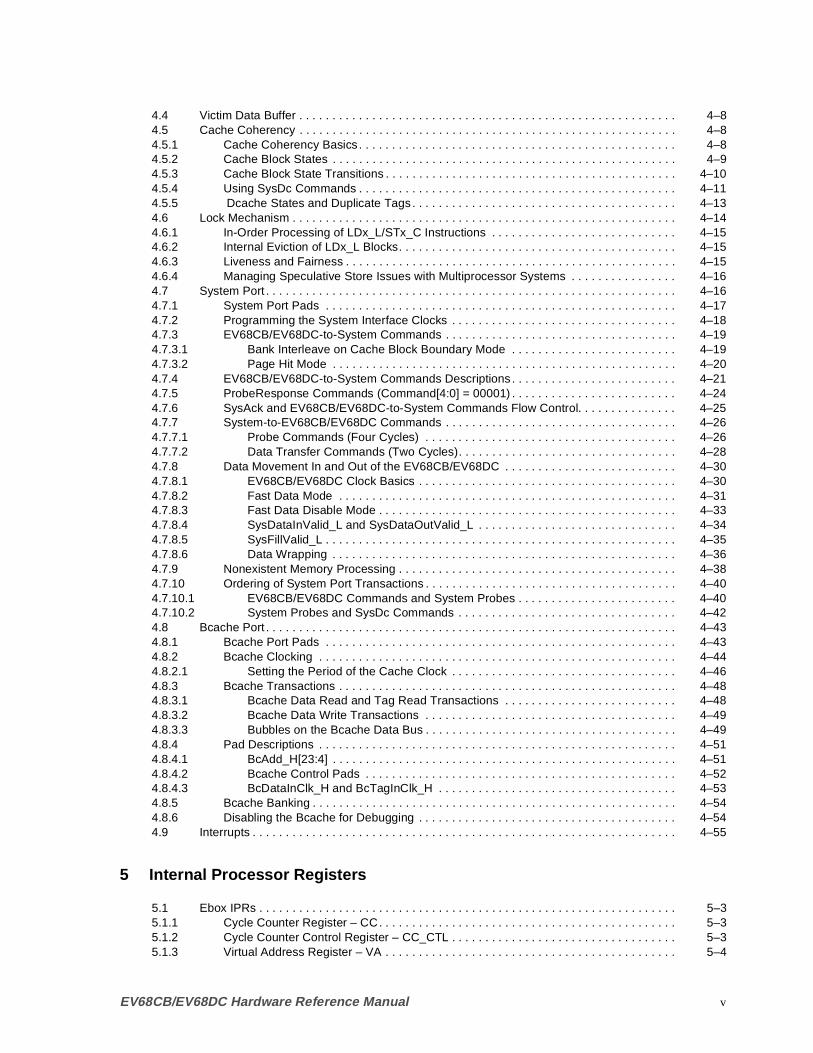
4.4 Victim Data Buffer . . . . . . . . . . . . . . . . . . . . . . . . . . . . . . . . . . . . . . . . . . . . . . . . . . . . . . . . . 4–84.5 Cache Coherency . . . . . . . . . . . . . . . . . . . . . . . . . . . . . . . . . . . . . . . . . . . . . . . . . . . . . . . . . 4–84.5.1 Cache Coherency Basics . . . . . . . . . . . . . . . . . . . . . . . . . . . . . . . . . . . . . . . . . . . . . . . . 4–84.5.2 Cache Block States . . . . . . . . . . . . . . . . . . . . . . . . . . . . . . . . . . . . . . . . . . . . . . . . . . . . 4–94.5.3 Cache Block State Transitions . . . . . . . . . . . . . . . . . . . . . . . . . . . . . . . . . . . . . . . . . . . . 4–104.5.4 Using SysDc Commands . . . . . . . . . . . . . . . . . . . . . . . . . . . . . . . . . . . . . . . . . . . . . . . . 4–114.5.5 Dcache States and Duplicate Tags . . . . . . . . . . . . . . . . . . . . . . . . . . . . . . . . . . . . . . . . 4–134.6 Lock Mechanism . . . . . . . . . . . . . . . . . . . . . . . . . . . . . . . . . . . . . . . . . . . . . . . . . . . . . . . . . . 4–144.6.1 In-Order Processing of LDx_L/STx_C Instructions . . . . . . . . . . . . . . . . . . . . . . . . . . . . 4–154.6.2 Internal Eviction of LDx_L Blocks. . . . . . . . . . . . . . . . . . . . . . . . . . . . . . . . . . . . . . . . . . 4–154.6.3 Liveness and Fairness . . . . . . . . . . . . . . . . . . . . . . . . . . . . . . . . . . . . . . . . . . . . . . . . . . 4–154.6.4 Managing Speculative Store Issues with Multiprocessor Systems . . . . . . . . . . . . . . . . 4–164.7 System Port . . . . . . . . . . . . . . . . . . . . . . . . . . . . . . . . . . . . . . . . . . . . . . . . . . . . . . . . . . . . . . 4–164.7.1 System Port Pads . . . . . . . . . . . . . . . . . . . . . . . . . . . . . . . . . . . . . . . . . . . . . . . . . . . . . 4–174.7.2 Programming the System Interface Clocks . . . . . . . . . . . . . . . . . . . . . . . . . . . . . . . . . . 4–184.7.3 EV68CB/EV68DC-to-System Commands . . . . . . . . . . . . . . . . . . . . . . . . . . . . . . . . . . . 4–194.7.3.1 Bank Interleave on Cache Block Boundary Mode . . . . . . . . . . . . . . . . . . . . . . . . . 4–194.7.3.2 Page Hit Mode . . . . . . . . . . . . . . . . . . . . . . . . . . . . . . . . . . . . . . . . . . . . . . . . . . . . 4–204.7.4 EV68CB/EV68DC-to-System Commands Descriptions . . . . . . . . . . . . . . . . . . . . . . . . . 4–214.7.5 ProbeResponse Commands (Command[4:0] = 00001) . . . . . . . . . . . . . . . . . . . . . . . . . 4–244.7.6 SysAck and EV68CB/EV68DC-to-System Commands Flow Control. . . . . . . . . . . . . . . 4–254.7.7 System-to-EV68CB/EV68DC Commands . . . . . . . . . . . . . . . . . . . . . . . . . . . . . . . . . . . 4–264.7.7.1 Probe Commands (Four Cycles) . . . . . . . . . . . . . . . . . . . . . . . . . . . . . . . . . . . . . . 4–264.7.7.2 Data Transfer Commands (Two Cycles). . . . . . . . . . . . . . . . . . . . . . . . . . . . . . . . . 4–284.7.8 Data Movement In and Out of the EV68CB/EV68DC . . . . . . . . . . . . . . . . . . . . . . . . . . 4–304.7.8.1 EV68CB/EV68DC Clock Basics . . . . . . . . . . . . . . . . . . . . . . . . . . . . . . . . . . . . . . . 4–304.7.8.2 Fast Data Mode . . . . . . . . . . . . . . . . . . . . . . . . . . . . . . . . . . . . . . . . . . . . . . . . . . . 4–314.7.8.3 Fast Data Disable Mode . . . . . . . . . . . . . . . . . . . . . . . . . . . . . . . . . . . . . . . . . . . . . 4–334.7.8.4 SysDataInValid_L and SysDataOutValid_L . . . . . . . . . . . . . . . . . . . . . . . . . . . . . . 4–344.7.8.5 SysFillValid_L . . . . . . . . . . . . . . . . . . . . . . . . . . . . . . . . . . . . . . . . . . . . . . . . . . . . . 4–354.7.8.6 Data Wrapping . . . . . . . . . . . . . . . . . . . . . . . . . . . . . . . . . . . . . . . . . . . . . . . . . . . . 4–364.7.9 Nonexistent Memory Processing . . . . . . . . . . . . . . . . . . . . . . . . . . . . . . . . . . . . . . . . . . 4–384.7.10 Ordering of System Port Transactions . . . . . . . . . . . . . . . . . . . . . . . . . . . . . . . . . . . . . . 4–404.7.10.1 EV68CB/EV68DC Commands and System Probes . . . . . . . . . . . . . . . . . . . . . . . . 4–404.7.10.2 System Probes and SysDc Commands . . . . . . . . . . . . . . . . . . . . . . . . . . . . . . . . . 4–424.8 Bcache Port . . . . . . . . . . . . . . . . . . . . . . . . . . . . . . . . . . . . . . . . . . . . . . . . . . . . . . . . . . . . . . 4–434.8.1 Bcache Port Pads . . . . . . . . . . . . . . . . . . . . . . . . . . . . . . . . . . . . . . . . . . . . . . . . . . . . . 4–434.8.2 Bcache Clocking . . . . . . . . . . . . . . . . . . . . . . . . . . . . . . . . . . . . . . . . . . . . . . . . . . . . . . 4–444.8.2.1 Setting the Period of the Cache Clock . . . . . . . . . . . . . . . . . . . . . . . . . . . . . . . . . . 4–464.8.3 Bcache Transactions . . . . . . . . . . . . . . . . . . . . . . . . . . . . . . . . . . . . . . . . . . . . . . . . . . . 4–484.8.3.1 Bcache Data Read and Tag Read Transactions . . . . . . . . . . . . . . . . . . . . . . . . . . 4–484.8.3.2 Bcache Data Write Transactions . . . . . . . . . . . . . . . . . . . . . . . . . . . . . . . . . . . . . . 4–494.8.3.3 Bubbles on the Bcache Data Bus . . . . . . . . . . . . . . . . . . . . . . . . . . . . . . . . . . . . . . 4–494.8.4 Pad Descriptions . . . . . . . . . . . . . . . . . . . . . . . . . . . . . . . . . . . . . . . . . . . . . . . . . . . . . . 4–514.8.4.1 BcAdd_H[23:4] . . . . . . . . . . . . . . . . . . . . . . . . . . . . . . . . . . . . . . . . . . . . . . . . . . . . 4–514.8.4.2 Bcache Control Pads . . . . . . . . . . . . . . . . . . . . . . . . . . . . . . . . . . . . . . . . . . . . . . . 4–524.8.4.3 BcDataInClk_H and BcTagInClk_H . . . . . . . . . . . . . . . . . . . . . . . . . . . . . . . . . . . . 4–534.8.5 Bcache Banking . . . . . . . . . . . . . . . . . . . . . . . . . . . . . . . . . . . . . . . . . . . . . . . . . . . . . . . 4–544.8.6 Disabling the Bcache for Debugging . . . . . . . . . . . . . . . . . . . . . . . . . . . . . . . . . . . . . . . 4–544.9 Interrupts . . . . . . . . . . . . . . . . . . . . . . . . . . . . . . . . . . . . . . . . . . . . . . . . . . . . . . . . . . . . . . . . 4–55
5 Internal Processor Registers
5.1 Ebox IPRs . . . . . . . . . . . . . . . . . . . . . . . . . . . . . . . . . . . . . . . . . . . . . . . . . . . . . . . . . . . . . . . 5–35.1.1 Cycle Counter Register – CC. . . . . . . . . . . . . . . . . . . . . . . . . . . . . . . . . . . . . . . . . . . . . 5–35.1.2 Cycle Counter Control Register – CC_CTL . . . . . . . . . . . . . . . . . . . . . . . . . . . . . . . . . . 5–35.1.3 Virtual Address Register – VA . . . . . . . . . . . . . . . . . . . . . . . . . . . . . . . . . . . . . . . . . . . . 5–4
EV68CB/EV68DC Hardware Reference Manual v
5.1.4 Virtual Address Control Register – VA_CTL . . . . . . . . . . . . . . . . . . . . . . . . . . . . . . . . . 5–45.1.5 Virtual Address Format Register – VA_FORM. . . . . . . . . . . . . . . . . . . . . . . . . . . . . . . . 5–55.2 Ibox IPRs. . . . . . . . . . . . . . . . . . . . . . . . . . . . . . . . . . . . . . . . . . . . . . . . . . . . . . . . . . . . . . . . 5–65.2.1 ITB Tag Array Write Register – ITB_TAG . . . . . . . . . . . . . . . . . . . . . . . . . . . . . . . . . . . 5–65.2.2 ITB PTE Array Write Register – ITB_PTE . . . . . . . . . . . . . . . . . . . . . . . . . . . . . . . . . . . 5–65.2.3 ITB Invalidate All Process (ASM=0) Register – ITB_IAP . . . . . . . . . . . . . . . . . . . . . . . . 5–75.2.4 ITB Invalidate All Register – ITB_IA. . . . . . . . . . . . . . . . . . . . . . . . . . . . . . . . . . . . . . . . 5–75.2.5 ITB Invalidate Single Register – ITB_IS. . . . . . . . . . . . . . . . . . . . . . . . . . . . . . . . . . . . . 5–75.2.6 ProfileMe PC Register – PMPC . . . . . . . . . . . . . . . . . . . . . . . . . . . . . . . . . . . . . . . . . . . 5–85.2.7 Exception Address Register – EXC_ADDR . . . . . . . . . . . . . . . . . . . . . . . . . . . . . . . . . . 5–85.2.8 Instruction Virtual Address Format Register — IVA_FORM. . . . . . . . . . . . . . . . . . . . . . 5–95.2.9 Interrupt Enable and Current Processor Mode Register – IER_CM. . . . . . . . . . . . . . . . 5–95.2.10 Software Interrupt Request Register – SIRR . . . . . . . . . . . . . . . . . . . . . . . . . . . . . . . . . 5–105.2.11 Interrupt Summary Register – ISUM . . . . . . . . . . . . . . . . . . . . . . . . . . . . . . . . . . . . . . . 5–115.2.12 Hardware Interrupt Clear Register – HW_INT_CLR . . . . . . . . . . . . . . . . . . . . . . . . . . . 5–125.2.13 Exception Summary Register – EXC_SUM . . . . . . . . . . . . . . . . . . . . . . . . . . . . . . . . . . 5–135.2.14 PAL Base Register – PAL_BASE . . . . . . . . . . . . . . . . . . . . . . . . . . . . . . . . . . . . . . . . . 5–155.2.15 Ibox Control Register – I_CTL . . . . . . . . . . . . . . . . . . . . . . . . . . . . . . . . . . . . . . . . . . . . 5–155.2.16 Ibox Status Register – I_STAT. . . . . . . . . . . . . . . . . . . . . . . . . . . . . . . . . . . . . . . . . . . . 5–185.2.17 Icache Flush Register – IC_FLUSH . . . . . . . . . . . . . . . . . . . . . . . . . . . . . . . . . . . . . . . . 5–215.2.18 Icache Flush ASM Register – IC_FLUSH_ASM . . . . . . . . . . . . . . . . . . . . . . . . . . . . . . 5–215.2.19 Clear Virtual-to-Physical Map Register – CLR_MAP . . . . . . . . . . . . . . . . . . . . . . . . . . . 5–215.2.20 Sleep Mode Register – SLEEP . . . . . . . . . . . . . . . . . . . . . . . . . . . . . . . . . . . . . . . . . . . 5–215.2.21 Process Context Register – PCTX. . . . . . . . . . . . . . . . . . . . . . . . . . . . . . . . . . . . . . . . . 5–215.2.22 Performance Counter Control Register – PCTR_CTL . . . . . . . . . . . . . . . . . . . . . . . . . . 5–235.3 Mbox IPRs. . . . . . . . . . . . . . . . . . . . . . . . . . . . . . . . . . . . . . . . . . . . . . . . . . . . . . . . . . . . . . . 5–255.3.1 DTB Tag Array Write Registers 0 and 1 – DTB_TAG0, DTB_TAG1 . . . . . . . . . . . . . . . 5–255.3.2 DTB PTE Array Write Registers 0 and 1 – DTB_PTE0, DTB_PTE1 . . . . . . . . . . . . . . . 5–265.3.3 DTB Alternate Processor Mode Register – DTB_ALTMODE. . . . . . . . . . . . . . . . . . . . . 5–265.3.4 Dstream TB Invalidate All Process (ASM=0) Register – DTB_IAP . . . . . . . . . . . . . . . . 5–275.3.5 Dstream TB Invalidate All Register – DTB_IA . . . . . . . . . . . . . . . . . . . . . . . . . . . . . . . . 5–275.3.6 Dstream TB Invalidate Single Registers 0 and 1 – DTB_IS0,1 . . . . . . . . . . . . . . . . . . . 5–275.3.7 Dstream TB Address Space Number Registers 0 and 1 – DTB_ASN0,1 . . . . . . . . . . . 5–285.3.8 Memory Management Status Register – MM_STAT . . . . . . . . . . . . . . . . . . . . . . . . . . . 5–285.3.9 Mbox Control Register – M_CTL . . . . . . . . . . . . . . . . . . . . . . . . . . . . . . . . . . . . . . . . . . 5–295.3.10 Dcache Control Register – DC_CTL . . . . . . . . . . . . . . . . . . . . . . . . . . . . . . . . . . . . . . . 5–305.3.11 Dcache Status Register – DC_STAT . . . . . . . . . . . . . . . . . . . . . . . . . . . . . . . . . . . . . . . 5–315.4 Cbox CSRs and IPRs . . . . . . . . . . . . . . . . . . . . . . . . . . . . . . . . . . . . . . . . . . . . . . . . . . . . . . 5–325.4.1 Cbox Data Register – C_DATA . . . . . . . . . . . . . . . . . . . . . . . . . . . . . . . . . . . . . . . . . . . 5–335.4.2 Cbox Shift Register – C_SHFT . . . . . . . . . . . . . . . . . . . . . . . . . . . . . . . . . . . . . . . . . . . 5–335.4.3 Cbox WRITE_ONCE Chain Description . . . . . . . . . . . . . . . . . . . . . . . . . . . . . . . . . . . . 5–335.4.4 Cbox WRITE_MANY Chain Description . . . . . . . . . . . . . . . . . . . . . . . . . . . . . . . . . . . . 5–385.4.5 Cbox Read Register (IPR) Description . . . . . . . . . . . . . . . . . . . . . . . . . . . . . . . . . . . . . 5–41
6 Privileged Architecture Library Code
6.1 PALcode Description . . . . . . . . . . . . . . . . . . . . . . . . . . . . . . . . . . . . . . . . . . . . . . . . . . . . . . . 6–16.2 PALmode Environment . . . . . . . . . . . . . . . . . . . . . . . . . . . . . . . . . . . . . . . . . . . . . . . . . . . . . 6–26.3 Required PALcode Function Codes . . . . . . . . . . . . . . . . . . . . . . . . . . . . . . . . . . . . . . . . . . . 6–36.4 Opcodes Reserved for PALcode. . . . . . . . . . . . . . . . . . . . . . . . . . . . . . . . . . . . . . . . . . . . . . 6–36.4.1 HW_LD Instruction . . . . . . . . . . . . . . . . . . . . . . . . . . . . . . . . . . . . . . . . . . . . . . . . . . . . . 6–36.4.2 HW_ST Instruction . . . . . . . . . . . . . . . . . . . . . . . . . . . . . . . . . . . . . . . . . . . . . . . . . . . . . 6–46.4.3 HW_RET Instruction . . . . . . . . . . . . . . . . . . . . . . . . . . . . . . . . . . . . . . . . . . . . . . . . . . . 6–56.4.4 HW_MFPR and HW_MTPR Instructions . . . . . . . . . . . . . . . . . . . . . . . . . . . . . . . . . . . . 6–66.5 Internal Processor Register Access Mechanisms . . . . . . . . . . . . . . . . . . . . . . . . . . . . . . . . . 6–76.5.1 IPR Scoreboard Bits. . . . . . . . . . . . . . . . . . . . . . . . . . . . . . . . . . . . . . . . . . . . . . . . . . . . 6–86.5.2 Hardware Structure of Explicitly Written IPRs . . . . . . . . . . . . . . . . . . . . . . . . . . . . . . . . 6–8
vi EV68CB/EV68DC Hardware Reference Manual

6.5.3 Hardware Structure of Implicitly Written IPRs . . . . . . . . . . . . . . . . . . . . . . . . . . . . . . . . 6–96.5.4 IPR Access Ordering . . . . . . . . . . . . . . . . . . . . . . . . . . . . . . . . . . . . . . . . . . . . . . . . . . . 6–96.5.5 Correct Ordering of Explicit Writers Followed by Implicit Readers. . . . . . . . . . . . . . . . . 6–106.5.6 Correct Ordering of Explicit Readers Followed by Implicit Writers. . . . . . . . . . . . . . . . . 6–116.6 PALshadow Registers . . . . . . . . . . . . . . . . . . . . . . . . . . . . . . . . . . . . . . . . . . . . . . . . . . . . . . 6–116.7 PALcode Emulation of the FPCR . . . . . . . . . . . . . . . . . . . . . . . . . . . . . . . . . . . . . . . . . . . . . 6–116.7.1 Status Flags . . . . . . . . . . . . . . . . . . . . . . . . . . . . . . . . . . . . . . . . . . . . . . . . . . . . . . . . . . 6–126.7.2 MF_FPCR . . . . . . . . . . . . . . . . . . . . . . . . . . . . . . . . . . . . . . . . . . . . . . . . . . . . . . . . . . . 6–126.7.3 MT_FPCR . . . . . . . . . . . . . . . . . . . . . . . . . . . . . . . . . . . . . . . . . . . . . . . . . . . . . . . . . . . 6–126.8 PALcode Entry Points . . . . . . . . . . . . . . . . . . . . . . . . . . . . . . . . . . . . . . . . . . . . . . . . . . . . . . 6–126.8.1 CALL_PAL Entry Points . . . . . . . . . . . . . . . . . . . . . . . . . . . . . . . . . . . . . . . . . . . . . . . . . 6–126.8.2 PALcode Exception Entry Points . . . . . . . . . . . . . . . . . . . . . . . . . . . . . . . . . . . . . . . . . . 6–136.9 Translation Buffer (TB) Fill Flows . . . . . . . . . . . . . . . . . . . . . . . . . . . . . . . . . . . . . . . . . . . . . 6–146.9.1 DTB Fill . . . . . . . . . . . . . . . . . . . . . . . . . . . . . . . . . . . . . . . . . . . . . . . . . . . . . . . . . . . . . 6–146.9.2 ITB Fill . . . . . . . . . . . . . . . . . . . . . . . . . . . . . . . . . . . . . . . . . . . . . . . . . . . . . . . . . . . . . . 6–166.10 Performance Counter Support . . . . . . . . . . . . . . . . . . . . . . . . . . . . . . . . . . . . . . . . . . . . . . . 6–176.10.1 General Precautions . . . . . . . . . . . . . . . . . . . . . . . . . . . . . . . . . . . . . . . . . . . . . . . . . . . 6–186.10.2 Aggregate Mode Programming Guidelines . . . . . . . . . . . . . . . . . . . . . . . . . . . . . . . . . . 6–186.10.2.1 Aggregate Mode Precautions . . . . . . . . . . . . . . . . . . . . . . . . . . . . . . . . . . . . . . . . . 6–186.10.2.2 Operation . . . . . . . . . . . . . . . . . . . . . . . . . . . . . . . . . . . . . . . . . . . . . . . . . . . . . . . . 6–196.10.2.3 Aggregate Counting Mode Description . . . . . . . . . . . . . . . . . . . . . . . . . . . . . . . . . . 6–206.10.2.3.1 Cycle counting . . . . . . . . . . . . . . . . . . . . . . . . . . . . . . . . . . . . . . . . . . . . . . . . . 6–206.10.2.3.2 Retired instructions cycles . . . . . . . . . . . . . . . . . . . . . . . . . . . . . . . . . . . . . . . . 6–206.10.2.3.3 Bcache miss or long latency probes cycles . . . . . . . . . . . . . . . . . . . . . . . . . . . 6–206.10.2.3.4 Mbox replay traps cycles . . . . . . . . . . . . . . . . . . . . . . . . . . . . . . . . . . . . . . . . . 6–206.10.2.4 Counter Modes for Aggregate Mode. . . . . . . . . . . . . . . . . . . . . . . . . . . . . . . . . . . . 6–206.10.3 ProfileMe Mode Programming Guidelines . . . . . . . . . . . . . . . . . . . . . . . . . . . . . . . . . . . 6–206.10.3.1 ProfileMe Mode Precautions . . . . . . . . . . . . . . . . . . . . . . . . . . . . . . . . . . . . . . . . . . 6–206.10.3.2 Operation . . . . . . . . . . . . . . . . . . . . . . . . . . . . . . . . . . . . . . . . . . . . . . . . . . . . . . . . 6–216.10.3.3 ProfileMe Counting Mode Description . . . . . . . . . . . . . . . . . . . . . . . . . . . . . . . . . . 6–236.10.3.3.1 Cycle counting . . . . . . . . . . . . . . . . . . . . . . . . . . . . . . . . . . . . . . . . . . . . . . . . . 6–236.10.3.3.2 Inum retire delay cycles . . . . . . . . . . . . . . . . . . . . . . . . . . . . . . . . . . . . . . . . . . 6–236.10.3.3.3 Retired instructions cycles . . . . . . . . . . . . . . . . . . . . . . . . . . . . . . . . . . . . . . . . 6–236.10.3.3.4 Bcache miss or long latency probes cycles . . . . . . . . . . . . . . . . . . . . . . . . . . . 6–236.10.3.3.5 Mbox replay traps cycles . . . . . . . . . . . . . . . . . . . . . . . . . . . . . . . . . . . . . . . . . 6–236.10.3.4 Counter Modes for ProfileMe Mode . . . . . . . . . . . . . . . . . . . . . . . . . . . . . . . . . . . . 6–24
7 Initialization and Configuration
7.1 Power-Up Reset Flow and the Reset_L and DCOK_H Pads . . . . . . . . . . . . . . . . . . . . . . . . 7–17.1.1 Power Sequencing and Reset State for Signal Pads. . . . . . . . . . . . . . . . . . . . . . . . . . . 7–37.1.2 Clock Forwarding and System Clock Ratio Configuration . . . . . . . . . . . . . . . . . . . . . . . 7–47.1.3 PLL Ramp Up. . . . . . . . . . . . . . . . . . . . . . . . . . . . . . . . . . . . . . . . . . . . . . . . . . . . . . . . . 7–67.1.4 BiST and SROM Load and the TestStat_H Pad . . . . . . . . . . . . . . . . . . . . . . . . . . . . . . 7–67.1.5 Clock Forward Reset and System Interface Initialization . . . . . . . . . . . . . . . . . . . . . . . . 7–77.2 Fault Reset Flow . . . . . . . . . . . . . . . . . . . . . . . . . . . . . . . . . . . . . . . . . . . . . . . . . . . . . . . . . . 7–87.3 Energy Star Certification and Sleep Mode Flow . . . . . . . . . . . . . . . . . . . . . . . . . . . . . . . . . . 7–97.4 Warm Reset Flow . . . . . . . . . . . . . . . . . . . . . . . . . . . . . . . . . . . . . . . . . . . . . . . . . . . . . . . . . 7–117.5 Array Initialization . . . . . . . . . . . . . . . . . . . . . . . . . . . . . . . . . . . . . . . . . . . . . . . . . . . . . . . . . 7–127.6 Initialization Mode Processing . . . . . . . . . . . . . . . . . . . . . . . . . . . . . . . . . . . . . . . . . . . . . . . . 7–127.7 External Interface Initialization . . . . . . . . . . . . . . . . . . . . . . . . . . . . . . . . . . . . . . . . . . . . . . . 7–147.8 Internal Processor Register Power-Up Reset State . . . . . . . . . . . . . . . . . . . . . . . . . . . . . . . 7–147.9 IEEE 1149.1 Test Port Reset . . . . . . . . . . . . . . . . . . . . . . . . . . . . . . . . . . . . . . . . . . . . . . . . 7–167.10 Reset State Machine . . . . . . . . . . . . . . . . . . . . . . . . . . . . . . . . . . . . . . . . . . . . . . . . . . . . . . . 7–167.11 Phase-Lock Loop (PLL) Functional Description . . . . . . . . . . . . . . . . . . . . . . . . . . . . . . . . . . 7–197.11.1 Differential Reference Clocks. . . . . . . . . . . . . . . . . . . . . . . . . . . . . . . . . . . . . . . . . . . . . 7–197.11.2 PLL Output Clocks . . . . . . . . . . . . . . . . . . . . . . . . . . . . . . . . . . . . . . . . . . . . . . . . . . . . . 7–19
EV68CB/EV68DC Hardware Reference Manual vii

7.11.2.1 GCLK . . . . . . . . . . . . . . . . . . . . . . . . . . . . . . . . . . . . . . . . . . . . . . . . . . . . . . . . . . . 7–197.11.2.2 Differential EV68CB/EV68DC Clocks . . . . . . . . . . . . . . . . . . . . . . . . . . . . . . . . . . . 7–197.11.2.3 Nominal Operating Frequency . . . . . . . . . . . . . . . . . . . . . . . . . . . . . . . . . . . . . . . . 7–197.11.2.4 Power-Up/Reset Clocking . . . . . . . . . . . . . . . . . . . . . . . . . . . . . . . . . . . . . . . . . . . . 7–20
8 Error Detection and Error Handling
8.1 Data Error Correction Code. . . . . . . . . . . . . . . . . . . . . . . . . . . . . . . . . . . . . . . . . . . . . . . . . . 8–28.2 Icache Data or Tag Parity Error. . . . . . . . . . . . . . . . . . . . . . . . . . . . . . . . . . . . . . . . . . . . . . . 8–28.3 Dcache Tag Parity Error . . . . . . . . . . . . . . . . . . . . . . . . . . . . . . . . . . . . . . . . . . . . . . . . . . . . 8–38.4 Dcache Data Single-Bit Correctable ECC Error . . . . . . . . . . . . . . . . . . . . . . . . . . . . . . . . . . 8–38.4.1 Load Instruction . . . . . . . . . . . . . . . . . . . . . . . . . . . . . . . . . . . . . . . . . . . . . . . . . . . . . . . 8–38.4.2 Store Instruction (Quadword or Smaller) . . . . . . . . . . . . . . . . . . . . . . . . . . . . . . . . . . . . 8–48.4.3 Dcache Victim Extracts . . . . . . . . . . . . . . . . . . . . . . . . . . . . . . . . . . . . . . . . . . . . . . . . . 8–48.5 Dcache Store Second Error . . . . . . . . . . . . . . . . . . . . . . . . . . . . . . . . . . . . . . . . . . . . . . . . . 8–48.6 Dcache Duplicate Tag Parity Error . . . . . . . . . . . . . . . . . . . . . . . . . . . . . . . . . . . . . . . . . . . . 8–58.7 Bcache Tag Parity Error . . . . . . . . . . . . . . . . . . . . . . . . . . . . . . . . . . . . . . . . . . . . . . . . . . . . 8–58.8 Controlling Bcache Block Parity Calculation . . . . . . . . . . . . . . . . . . . . . . . . . . . . . . . . . . . . . 8–58.9 Bcache Data Single-Bit Correctable ECC Error . . . . . . . . . . . . . . . . . . . . . . . . . . . . . . . . . . 8–58.9.1 Icache Fill from Bcache . . . . . . . . . . . . . . . . . . . . . . . . . . . . . . . . . . . . . . . . . . . . . . . . . 8–68.9.2 Dcache Fill from Bcache . . . . . . . . . . . . . . . . . . . . . . . . . . . . . . . . . . . . . . . . . . . . . . . . 8–68.9.3 Bcache Victim Read. . . . . . . . . . . . . . . . . . . . . . . . . . . . . . . . . . . . . . . . . . . . . . . . . . . . 8–78.9.3.1 Bcache Victim Read During a Dcache/Bcache Miss . . . . . . . . . . . . . . . . . . . . . . . 8–78.9.3.2 Bcache Victim Read During an ECB Instruction . . . . . . . . . . . . . . . . . . . . . . . . . . . 8–78.10 Memory/System Port Single-Bit Data Correctable ECC Error. . . . . . . . . . . . . . . . . . . . . . . . 8–78.10.1 Icache Fill from Memory. . . . . . . . . . . . . . . . . . . . . . . . . . . . . . . . . . . . . . . . . . . . . . . . . 8–78.10.2 Dcache Fill from Memory . . . . . . . . . . . . . . . . . . . . . . . . . . . . . . . . . . . . . . . . . . . . . . . . 8–88.11 Bcache Data Single-Bit Correctable ECC Error on a Probe . . . . . . . . . . . . . . . . . . . . . . . . . 8–98.12 Double-Bit Fill Errors . . . . . . . . . . . . . . . . . . . . . . . . . . . . . . . . . . . . . . . . . . . . . . . . . . . . . . . 8–98.13 Error Case Summary. . . . . . . . . . . . . . . . . . . . . . . . . . . . . . . . . . . . . . . . . . . . . . . . . . . . . . . 8–10
9 Electrical Data
9.1 Electrical Characteristics . . . . . . . . . . . . . . . . . . . . . . . . . . . . . . . . . . . . . . . . . . . . . . . . . . . . 9–19.2 DC Characteristics . . . . . . . . . . . . . . . . . . . . . . . . . . . . . . . . . . . . . . . . . . . . . . . . . . . . . . . . 9–29.3 Power Supply Sequencing and Avoiding Potential Failure Mechanisms . . . . . . . . . . . . . . . 9–59.4 AC Characteristics. . . . . . . . . . . . . . . . . . . . . . . . . . . . . . . . . . . . . . . . . . . . . . . . . . . . . . . . . 9–6
10 Thermal Management
10.1 Operating Temperature . . . . . . . . . . . . . . . . . . . . . . . . . . . . . . . . . . . . . . . . . . . . . . . . . . . . . 10–110.2 Heat Sink Specifications . . . . . . . . . . . . . . . . . . . . . . . . . . . . . . . . . . . . . . . . . . . . . . . . . . . . 10–310.3 Thermal Design Considerations . . . . . . . . . . . . . . . . . . . . . . . . . . . . . . . . . . . . . . . . . . . . . . 10–7
11 Testability and Diagnostics
11.1 Test Pads . . . . . . . . . . . . . . . . . . . . . . . . . . . . . . . . . . . . . . . . . . . . . . . . . . . . . . . . . . . . . . . 11–111.2 SROM/Serial Diagnostic Terminal Port . . . . . . . . . . . . . . . . . . . . . . . . . . . . . . . . . . . . . . . . . 11–211.2.1 SROM Load Operation. . . . . . . . . . . . . . . . . . . . . . . . . . . . . . . . . . . . . . . . . . . . . . . . . . 11–211.2.2 Serial Terminal Port . . . . . . . . . . . . . . . . . . . . . . . . . . . . . . . . . . . . . . . . . . . . . . . . . . . . 11–211.3 IEEE 1149.1 Port. . . . . . . . . . . . . . . . . . . . . . . . . . . . . . . . . . . . . . . . . . . . . . . . . . . . . . . . . . 11–311.4 TestStat_H Pad . . . . . . . . . . . . . . . . . . . . . . . . . . . . . . . . . . . . . . . . . . . . . . . . . . . . . . . . . . . 11–411.5 Power-Up Self-Test and Initialization . . . . . . . . . . . . . . . . . . . . . . . . . . . . . . . . . . . . . . . . . . 11–511.5.1 Built-in Self-Test . . . . . . . . . . . . . . . . . . . . . . . . . . . . . . . . . . . . . . . . . . . . . . . . . . . . . . . 11–5
viii EV68CB/EV68DC Hardware Reference Manual

11.5.2 SROM Initialization. . . . . . . . . . . . . . . . . . . . . . . . . . . . . . . . . . . . . . . . . . . . . . . . . . . . . 11–511.5.2.1 Serial Instruction Cache Load Operation . . . . . . . . . . . . . . . . . . . . . . . . . . . . . . . . 11–611.6 Notes on IEEE 1149.1 Operation and Compliance . . . . . . . . . . . . . . . . . . . . . . . . . . . . . . . 11–7
A Alpha Instruction Set
A.1 Alpha Instruction Summary . . . . . . . . . . . . . . . . . . . . . . . . . . . . . . . . . . . . . . . . . . . . . . . . . . A–1A.2 Reserved Opcodes . . . . . . . . . . . . . . . . . . . . . . . . . . . . . . . . . . . . . . . . . . . . . . . . . . . . . . . . A–8A.2.1 Opcodes Reserved for Compaq. . . . . . . . . . . . . . . . . . . . . . . . . . . . . . . . . . . . . . . . . . . A–8A.2.2 Opcodes Reserved for PALcode . . . . . . . . . . . . . . . . . . . . . . . . . . . . . . . . . . . . . . . . . . A–9A.3 IEEE Floating-Point Instructions . . . . . . . . . . . . . . . . . . . . . . . . . . . . . . . . . . . . . . . . . . . . . . A–9A.4 VAX Floating-Point Instructions. . . . . . . . . . . . . . . . . . . . . . . . . . . . . . . . . . . . . . . . . . . . . . . A–11A.5 Independent Floating-Point Instructions . . . . . . . . . . . . . . . . . . . . . . . . . . . . . . . . . . . . . . . . A–11A.6 Opcode Summary . . . . . . . . . . . . . . . . . . . . . . . . . . . . . . . . . . . . . . . . . . . . . . . . . . . . . . . . . A–12A.7 Required PALcode Function Codes . . . . . . . . . . . . . . . . . . . . . . . . . . . . . . . . . . . . . . . . . . . A–13A.8 IEEE Floating-Point Conformance . . . . . . . . . . . . . . . . . . . . . . . . . . . . . . . . . . . . . . . . . . . . A–14
B EV68CB/EV68DC Boundary-Scan Register
B.1 Boundary-Scan Register . . . . . . . . . . . . . . . . . . . . . . . . . . . . . . . . . . . . . . . . . . . . . . . . . . . . B–1B.1.1 BSDL Description of the Alpha EV68CB/EV68DC Boundary-Scan Register. . . . . . . . . B–1
C Serial Icache Load Predecode Values
D PALcode Restrictions and Guidelines
D.1 Restriction 1 : Reset Sequence Required by Retire Logic and Mapper . . . . . . . . . . . . . . . D–1D.2 Restriction 2 : No Multiple Writers to IPRs in Same Scoreboard Group . . . . . . . . . . . . . . . D–8D.3 Restriction 4 : No Writers and Readers to IPRs in Same Scoreboard Group . . . . . . . . . . D–8D.4 Guideline 6 : Avoid Consecutive Read-Modify-Write-Read-Modify-Write . . . . . . . . . . . . D–9D.5 Restriction 7 : Replay Trap, Interrupt Code Sequence, and STF/ITOF . . . . . . . . . . . . . . . D–9D.6 Restriction 9 : PALmode Istream Address Ranges . . . . . . . . . . . . . . . . . . . . . . . . . . . . . . D–10D.7 Restriction 10: Duplicate IPR Mode Bits . . . . . . . . . . . . . . . . . . . . . . . . . . . . . . . . . . . . . . . D–10D.8 Restriction 11: Ibox IPR Update Synchronization . . . . . . . . . . . . . . . . . . . . . . . . . . . . . . . . D–11D.9 Restriction 12: MFPR of Implicitly-Written IPRs EXC_ADDR, IVA_FORM, and EXC_SUM D–11D.10 Restriction 13 : DTB Fill Flow Collision . . . . . . . . . . . . . . . . . . . . . . . . . . . . . . . . . . . . . . . . . D–11D.11 Restriction 14 : HW_RET . . . . . . . . . . . . . . . . . . . . . . . . . . . . . . . . . . . . . . . . . . . . . . . . . . . D–11D.12 Guideline 16 : JSR-BAD VA . . . . . . . . . . . . . . . . . . . . . . . . . . . . . . . . . . . . . . . . . . . . . . . . . D–12D.13 Restriction 17: MTPR to DTB_TAG0/DTB_PTE0/DTB_TAG1/DTB_PTE1 . . . . . . . . . . . . . D–12D.14 Restriction 18: No FP Operates, FP Conditional Branches, FTOI, or STF in Same Fetch Block as
HW_MTPR . . . . . . . . . . . . . . . . . . . . . . . . . . . . . . . . . . . . . . . . . . . . . . . . . . . . . . . . . . . . . . D–12D.15 Restriction 19: HW_RET/STALL After Updating the FPCR by way of MT_FPCR in PALmode D–12D.16 Guideline 20 : I_CTL[SBE] Stream Buffer Enable . . . . . . . . . . . . . . . . . . . . . . . . . . . . . . . . D–12D.17 Restriction 21: HW_RET/STALL After HW_MTPR ASN0/ASN1. . . . . . . . . . . . . . . . . . . . . . D–12D.18 Restriction 22: HW_RET/STALL After HW_MTPR IS0/IS1. . . . . . . . . . . . . . . . . . . . . . . . . . D–13D.19 Restriction 23: HW_ST/P/CONDITIONAL Does Not Clear the Lock Flag. . . . . . . . . . . . . . . D–13D.20 Restriction 24: HW_RET/STALL After HW_MTPR IC_FLUSH, IC_FLUSH_ASM, CLEAR_MAP
. . . . . . . . . . . . . . . . . . . . . . . . . . . . . . . . . . . . . . . . . . . . . . . . . . . . . . . . . . . . . . . . . . . . . . . D–14D.21 Restriction 25: HW_MTPR ITB_IA After Reset . . . . . . . . . . . . . . . . . . . . . . . . . . . . . . . . . . . D–14D.22 Guideline 26: Conditional Branches in PALcode . . . . . . . . . . . . . . . . . . . . . . . . . . . . . . . . . D–14D.23 Restriction 27: Reset of ‘Force-Fail Lock Flag’ State in PALcode . . . . . . . . . . . . . . . . . . . . . D–15D.24 Restriction 28: Enforce Ordering Between IPRs Implicitly Written by Loads and Subsequent Loads
. . . . . . . . . . . . . . . . . . . . . . . . . . . . . . . . . . . . . . . . . . . . . . . . . . . . . . . . . . . . . . . . . . . . . . . D–15D.25 Guideline 29 : JSR, JMP, RET, and JSR_COR in PALcode. . . . . . . . . . . . . . . . . . . . . . . . . D–15
EV68CB/EV68DC Hardware Reference Manual ix

D.26 Restriction 30 : HW_MTPR and HW_MFPR to the Cbox CSR . . . . . . . . . . . . . . . . . . . . . . . D–15D.27 Restriction 31 : I_CTL[VA_48] Update . . . . . . . . . . . . . . . . . . . . . . . . . . . . . . . . . . . . . . . . . D–17D.28 Restriction 32 : PCTR_CTL Update . . . . . . . . . . . . . . . . . . . . . . . . . . . . . . . . . . . . . . . . . . . D–17D.29 Restriction 33 : HW_LD Physical/Lock Use. . . . . . . . . . . . . . . . . . . . . . . . . . . . . . . . . . . . . . D–18D.30 Restriction 34 : Writing Multiple ITB Entries in the Same PALcode Flow . . . . . . . . . . . . . . . D–18D.31 Guideline 35 : HW_INT_CLR Update . . . . . . . . . . . . . . . . . . . . . . . . . . . . . . . . . . . . . . . . . D–18D.32 Restriction 36 : Updating I_CTL[SDE]. . . . . . . . . . . . . . . . . . . . . . . . . . . . . . . . . . . . . . . . . . D–18D.33 Restriction 37 : Updating VA_CTL[VA_48] . . . . . . . . . . . . . . . . . . . . . . . . . . . . . . . . . . . . . . D–18D.34 Restriction 38 : Updating PCTR_CTL . . . . . . . . . . . . . . . . . . . . . . . . . . . . . . . . . . . . . . . . . . D–18D.35 Guideline 39: Writing Multiple DTB Entries in the Same PAL Flow. . . . . . . . . . . . . . . . . . . . D–19D.36 Restriction 40: Scrubbing a Single-Bit Error . . . . . . . . . . . . . . . . . . . . . . . . . . . . . . . . . . . . . D–19D.37 Restriction 41: MTPR ITB_TAG, MTPR ITB_PTE Must Be in the Same Fetch Block . . . . . D–21D.38 Restriction 42: Updating VA_CTL, CC_CTL, or CC IPRs . . . . . . . . . . . . . . . . . . . . . . . . . . . D–21D.39 Restriction 43: No Trappable Instructions Along with HW_MTPR. . . . . . . . . . . . . . . . . . . . . D–21D.40 Restriction 44: Not Applicable to the EV68CB/EV68DC . . . . . . . . . . . . . . . . . . . . . . . . . . . . D–21D.41 Restriction 45: No HW_JMP or JMP Instructions in PALcode . . . . . . . . . . . . . . . . . . . . . . . D–21D.42 Restriction 46: Avoiding Livelocks in Speculative Load CRD Handlers . . . . . . . . . . . . . . . . D–22D.43 Restriction 47: Cache Eviction for Single-Bit Cache Errors . . . . . . . . . . . . . . . . . . . . . . . . . D–22D.44 Restriction 48: MB Bracketing of Dcache Writes to Force Bad Data ECC and Force Bad Tag Parity
. . . . . . . . . . . . . . . . . . . . . . . . . . . . . . . . . . . . . . . . . . . . . . . . . . . . . . . . . . . . . . . . . . . . . . . D–24
E EV68CB/EV68DC-to-Bcache Pad Interface
E.1 Forwarding Clock Pad Groupings . . . . . . . . . . . . . . . . . . . . . . . . . . . . . . . . . . . . . . . . . . . . . E–1E.2 Late-Write Non-Bursting SSRAMs . . . . . . . . . . . . . . . . . . . . . . . . . . . . . . . . . . . . . . . . . . . . E–2E.3 Dual-Data Rate SSRAMs . . . . . . . . . . . . . . . . . . . . . . . . . . . . . . . . . . . . . . . . . . . . . . . . . . . E–3
Glossary
Index
x EV68CB/EV68DC Hardware Reference Manual

Figures
2–1 EV68CB/EV68DC Block Diagram . . . . . . . . . . . . . . . . . . . . . . . . . . . . . . . . . . . . . . . . . . . . 2–32–2 Branch Predictor . . . . . . . . . . . . . . . . . . . . . . . . . . . . . . . . . . . . . . . . . . . . . . . . . . . . . . . . . . 2–42–3 Local Predictor . . . . . . . . . . . . . . . . . . . . . . . . . . . . . . . . . . . . . . . . . . . . . . . . . . . . . . . . . . . 2–42–4 Global Predictor. . . . . . . . . . . . . . . . . . . . . . . . . . . . . . . . . . . . . . . . . . . . . . . . . . . . . . . . . . . 2–52–5 Choice Predictor . . . . . . . . . . . . . . . . . . . . . . . . . . . . . . . . . . . . . . . . . . . . . . . . . . . . . . . . . . 2–52–6 Integer Execution Unit—Clusters 0 and 1 . . . . . . . . . . . . . . . . . . . . . . . . . . . . . . . . . . . . . . . 2–92–7 Floating-Point Execution Units . . . . . . . . . . . . . . . . . . . . . . . . . . . . . . . . . . . . . . . . . . . . . . . 2–102–8 Pipeline Organization . . . . . . . . . . . . . . . . . . . . . . . . . . . . . . . . . . . . . . . . . . . . . . . . . . . . . . 2–142–9 Pipeline Timing for Integer Load Instructions . . . . . . . . . . . . . . . . . . . . . . . . . . . . . . . . . . . . 2–242–10 Pipeline Timing for Floating-Point Load Instructions . . . . . . . . . . . . . . . . . . . . . . . . . . . . . . . 2–252–11 Floating-Point Control Register . . . . . . . . . . . . . . . . . . . . . . . . . . . . . . . . . . . . . . . . . . . . . . . 2–362–12 Typical Uniprocessor Configuration . . . . . . . . . . . . . . . . . . . . . . . . . . . . . . . . . . . . . . . . . . . 2–392–13 Typical Multiprocessor Configuration . . . . . . . . . . . . . . . . . . . . . . . . . . . . . . . . . . . . . . . . . . 2–393–1 EV68CB/EV68DC Microprocessor Logic Symbol . . . . . . . . . . . . . . . . . . . . . . . . . . . . . . . . . 3–23–2 Package Dimensions (Bottom View) . . . . . . . . . . . . . . . . . . . . . . . . . . . . . . . . . . . . . . . . . . . 3–173–3 EV68CB/EV68DC Bottom View . . . . . . . . . . . . . . . . . . . . . . . . . . . . . . . . . . . . . . . . . . . . . . 3–184–1 EV68CB/EV68DC System and Bcache Interfaces . . . . . . . . . . . . . . . . . . . . . . . . . . . . . . . . 4–34–2 EV68CB/EV68DC Bcache Interface Signals . . . . . . . . . . . . . . . . . . . . . . . . . . . . . . . . . . . . . 4–74–3 Cache Subset Hierarchy . . . . . . . . . . . . . . . . . . . . . . . . . . . . . . . . . . . . . . . . . . . . . . . . . . . . 4–94–4 System Interface Signals. . . . . . . . . . . . . . . . . . . . . . . . . . . . . . . . . . . . . . . . . . . . . . . . . . . . 4–174–5 Fast Transfer Timing Example . . . . . . . . . . . . . . . . . . . . . . . . . . . . . . . . . . . . . . . . . . . . . . . 4–324–6 SysFillValid_L Timing . . . . . . . . . . . . . . . . . . . . . . . . . . . . . . . . . . . . . . . . . . . . . . . . . . . . . . 4–365–1 Cycle Counter Register . . . . . . . . . . . . . . . . . . . . . . . . . . . . . . . . . . . . . . . . . . . . . . . . . . . . . 5–35–2 Cycle Counter Control Register. . . . . . . . . . . . . . . . . . . . . . . . . . . . . . . . . . . . . . . . . . . . . . . 5–35–3 Virtual Address Register . . . . . . . . . . . . . . . . . . . . . . . . . . . . . . . . . . . . . . . . . . . . . . . . . . . . 5–45–4 Virtual Address Control Register . . . . . . . . . . . . . . . . . . . . . . . . . . . . . . . . . . . . . . . . . . . . . . 5–45–5 Virtual Address Format Register (VA_48 = 0, VA_FORM_32 = 0) . . . . . . . . . . . . . . . . . . . . 5–55–6 Virtual Address Format Register (VA_48 = 1, VA_FORM_32 = 0) . . . . . . . . . . . . . . . . . . . . 5–65–7 Virtual Address Format Register (VA_48 = 0, VA_FORM_32 = 1) . . . . . . . . . . . . . . . . . . . . 5–65–8 ITB Tag Array Write Register . . . . . . . . . . . . . . . . . . . . . . . . . . . . . . . . . . . . . . . . . . . . . . . . 5–65–9 ITB PTE Array Write Register . . . . . . . . . . . . . . . . . . . . . . . . . . . . . . . . . . . . . . . . . . . . . . . . 5–75–10 ITB Invalidate Single Register . . . . . . . . . . . . . . . . . . . . . . . . . . . . . . . . . . . . . . . . . . . . . . . . 5–75–11 ProfileMe PC Register. . . . . . . . . . . . . . . . . . . . . . . . . . . . . . . . . . . . . . . . . . . . . . . . . . . . . . 5–85–12 Exception Address Register . . . . . . . . . . . . . . . . . . . . . . . . . . . . . . . . . . . . . . . . . . . . . . . . . 5–85–13 Instruction Virtual Address Format Register (VA_48 = 0, VA_FORM_32 = 0) . . . . . . . . . . . 5–95–14 Instruction Virtual Address Format Register (VA_48 = 1, VA_FORM_32 = 0) . . . . . . . . . . . 5–95–15 Instruction Virtual Address Format Register (VA_48 = 0, VA_FORM_32 = 1) . . . . . . . . . . . 5–95–16 Interrupt Enable and Current Processor Mode Register . . . . . . . . . . . . . . . . . . . . . . . . . . . . 5–105–17 Software Interrupt Request Register . . . . . . . . . . . . . . . . . . . . . . . . . . . . . . . . . . . . . . . . . . . 5–115–18 Interrupt Summary Register . . . . . . . . . . . . . . . . . . . . . . . . . . . . . . . . . . . . . . . . . . . . . . . . . 5–115–19 Hardware Interrupt Clear Register . . . . . . . . . . . . . . . . . . . . . . . . . . . . . . . . . . . . . . . . . . . . 5–125–20 Exception Summary Register . . . . . . . . . . . . . . . . . . . . . . . . . . . . . . . . . . . . . . . . . . . . . . . . 5–145–21 PAL Base Register . . . . . . . . . . . . . . . . . . . . . . . . . . . . . . . . . . . . . . . . . . . . . . . . . . . . . . . . 5–155–22 Ibox Control Register. . . . . . . . . . . . . . . . . . . . . . . . . . . . . . . . . . . . . . . . . . . . . . . . . . . . . . . 5–165–23 Ibox Status Register . . . . . . . . . . . . . . . . . . . . . . . . . . . . . . . . . . . . . . . . . . . . . . . . . . . . . . . 5–185–24 Process Context Register . . . . . . . . . . . . . . . . . . . . . . . . . . . . . . . . . . . . . . . . . . . . . . . . . . . 5–225–25 Performance Counter Control Register . . . . . . . . . . . . . . . . . . . . . . . . . . . . . . . . . . . . . . . . . 5–235–26 DTB Tag Array Write Registers 0 and 1 . . . . . . . . . . . . . . . . . . . . . . . . . . . . . . . . . . . . . . . . 5–255–27 DTB PTE Array Write Registers 0 and 1 . . . . . . . . . . . . . . . . . . . . . . . . . . . . . . . . . . . . . . . . 5–265–28 DTB Alternate Processor Mode Register . . . . . . . . . . . . . . . . . . . . . . . . . . . . . . . . . . . . . . . 5–265–29 Dstream Translation Buffer Invalidate Single Registers . . . . . . . . . . . . . . . . . . . . . . . . . . . . 5–275–30 Dstream Translation Buffer Address Space Number Registers 0 and 1 . . . . . . . . . . . . . . . . 5–285–31 Memory Management Status Register . . . . . . . . . . . . . . . . . . . . . . . . . . . . . . . . . . . . . . . . . 5–285–32 Mbox Control Register. . . . . . . . . . . . . . . . . . . . . . . . . . . . . . . . . . . . . . . . . . . . . . . . . . . . . . 5–295–33 Dcache Control Register . . . . . . . . . . . . . . . . . . . . . . . . . . . . . . . . . . . . . . . . . . . . . . . . . . . . 5–315–34 Dcache Status Register. . . . . . . . . . . . . . . . . . . . . . . . . . . . . . . . . . . . . . . . . . . . . . . . . . . . . 5–32
EV68CB/EV68DC Hardware Reference Manual xi
5–35 Cbox Data Register . . . . . . . . . . . . . . . . . . . . . . . . . . . . . . . . . . . . . . . . . . . . . . . . . . . . . . . . 5–335–36 Cbox Shift Register . . . . . . . . . . . . . . . . . . . . . . . . . . . . . . . . . . . . . . . . . . . . . . . . . . . . . . . . 5–335–37 WRITE_MANY Chain Write Transaction Example . . . . . . . . . . . . . . . . . . . . . . . . . . . . . . . . 5–396–1 HW_LD Instruction Format . . . . . . . . . . . . . . . . . . . . . . . . . . . . . . . . . . . . . . . . . . . . . . . . . . 6–46–2 HW_ST Instruction Format . . . . . . . . . . . . . . . . . . . . . . . . . . . . . . . . . . . . . . . . . . . . . . . . . . 6–46–3 HW_RET Instruction Format . . . . . . . . . . . . . . . . . . . . . . . . . . . . . . . . . . . . . . . . . . . . . . . . . 6–66–4 HW_MFPR and HW_MTPR Instructions Format . . . . . . . . . . . . . . . . . . . . . . . . . . . . . . . . . 6–66–5 Single-Miss DTB Instructions Flow Example. . . . . . . . . . . . . . . . . . . . . . . . . . . . . . . . . . . . . 6–146–6 ITB Miss Instructions Flow Example . . . . . . . . . . . . . . . . . . . . . . . . . . . . . . . . . . . . . . . . . . . 6–167–1 Power-Up Timing Sequence . . . . . . . . . . . . . . . . . . . . . . . . . . . . . . . . . . . . . . . . . . . . . . . . . 7–37–2 Fault Reset Sequence of Operation . . . . . . . . . . . . . . . . . . . . . . . . . . . . . . . . . . . . . . . . . . . 7–97–3 Sleep Mode Sequence of Operation . . . . . . . . . . . . . . . . . . . . . . . . . . . . . . . . . . . . . . . . . . 7–117–4 Example for Initializing Bcache . . . . . . . . . . . . . . . . . . . . . . . . . . . . . . . . . . . . . . . . . . . . . . . 7–137–5 EV68CB/EV68DC Reset State Machine State Diagram . . . . . . . . . . . . . . . . . . . . . . . . . . . . 7–1710–1 Type 1 Heat Sink . . . . . . . . . . . . . . . . . . . . . . . . . . . . . . . . . . . . . . . . . . . . . . . . . . . . . . . . . . 10–310–2 Type 2 Heat Sink . . . . . . . . . . . . . . . . . . . . . . . . . . . . . . . . . . . . . . . . . . . . . . . . . . . . . . . . . . 10–410–3 Type 3 Heat Sink . . . . . . . . . . . . . . . . . . . . . . . . . . . . . . . . . . . . . . . . . . . . . . . . . . . . . . . . . . 10–510–4 Type 4 Heat Sink . . . . . . . . . . . . . . . . . . . . . . . . . . . . . . . . . . . . . . . . . . . . . . . . . . . . . . . . . . 10–611–1 TAP Controller State Machine . . . . . . . . . . . . . . . . . . . . . . . . . . . . . . . . . . . . . . . . . . . . . . . . 11–411–2 TestStat_H Pad Timing During Power-Up Built-In Self-Test (BiST) . . . . . . . . . . . . . . . . . . . 11–511–3 TestStat_H Pad Timing During Built-In Self-Initialization (BiSI) . . . . . . . . . . . . . . . . . . . . . . 11–511–4 SROM Content Map . . . . . . . . . . . . . . . . . . . . . . . . . . . . . . . . . . . . . . . . . . . . . . . . . . . . . . . 11–6
xii EV68CB/EV68DC Hardware Reference Manual

Tables
1–1 Integer Data Types . . . . . . . . . . . . . . . . . . . . . . . . . . . . . . . . . . . . . . . . . . . . . . . . . . . . . . . . 1–22–1 Pipeline Abort Delay (GCLK Cycles). . . . . . . . . . . . . . . . . . . . . . . . . . . . . . . . . . . . . . . . . . . 2–162–2 Instruction Name, Pipeline, and Types . . . . . . . . . . . . . . . . . . . . . . . . . . . . . . . . . . . . . . . . . 2–172–3 Instruction Group Definitions and Pipeline Unit . . . . . . . . . . . . . . . . . . . . . . . . . . . . . . . . . . . 2–182–4 Instruction Class Latency in Cycles. . . . . . . . . . . . . . . . . . . . . . . . . . . . . . . . . . . . . . . . . . . . 2–202–5 Minimum Retire Latencies for Instruction Classes . . . . . . . . . . . . . . . . . . . . . . . . . . . . . . . . 2–212–6 Instructions Retired Without Execution . . . . . . . . . . . . . . . . . . . . . . . . . . . . . . . . . . . . . . . . . 2–232–7 Rules for I/O Address Space Load Instruction Data Merging . . . . . . . . . . . . . . . . . . . . . . . . 2–282–8 Rules for I/O Address Space Store Instruction Data Merging . . . . . . . . . . . . . . . . . . . . . . . . 2–292–9 MAF Merging Rules. . . . . . . . . . . . . . . . . . . . . . . . . . . . . . . . . . . . . . . . . . . . . . . . . . . . . . . . 2–302–10 Memory Reference Ordering . . . . . . . . . . . . . . . . . . . . . . . . . . . . . . . . . . . . . . . . . . . . . . . . . 2–302–11 I/O Reference Ordering . . . . . . . . . . . . . . . . . . . . . . . . . . . . . . . . . . . . . . . . . . . . . . . . . . . . . 2–312–12 TB Fill Flow Example Sequence 1 . . . . . . . . . . . . . . . . . . . . . . . . . . . . . . . . . . . . . . . . . . . . 2–342–13 TB Fill Flow Example Sequence 2 . . . . . . . . . . . . . . . . . . . . . . . . . . . . . . . . . . . . . . . . . . . . 2–342–14 Floating-Point Control Register Fields. . . . . . . . . . . . . . . . . . . . . . . . . . . . . . . . . . . . . . . . . . 2–362–15 EV68CB/EV68DC AMASK Values . . . . . . . . . . . . . . . . . . . . . . . . . . . . . . . . . . . . . . . . . . . . 2–382–16 AMASK Bit Assignments . . . . . . . . . . . . . . . . . . . . . . . . . . . . . . . . . . . . . . . . . . . . . . . . . . . . 2–383–1 Signal Pad Types Definitions . . . . . . . . . . . . . . . . . . . . . . . . . . . . . . . . . . . . . . . . . . . . . . . . 3–33–2 EV68CB/EV68DC Signal Descriptions . . . . . . . . . . . . . . . . . . . . . . . . . . . . . . . . . . . . . . . . . 3–33–3 EV68CB/EV68DC Signal Descriptions by Function . . . . . . . . . . . . . . . . . . . . . . . . . . . . . . . 3–63–4 Pad List Sorted by Signal Name . . . . . . . . . . . . . . . . . . . . . . . . . . . . . . . . . . . . . . . . . . . . . . 3–83–5 Pad LIst Sorted by CLGA Location . . . . . . . . . . . . . . . . . . . . . . . . . . . . . . . . . . . . . . . . . . . . 3–123–6 Ground and Power (VSS and VDD) Pad List . . . . . . . . . . . . . . . . . . . . . . . . . . . . . . . . . . . . 3–164–1 Translation of Internal References to External Interface Reference . . . . . . . . . . . . . . . . . . . 4–54–2 EV68CB/EV68DC-Supported Cache Block States . . . . . . . . . . . . . . . . . . . . . . . . . . . . . . . . 4–94–3 Cache Block State Transitions . . . . . . . . . . . . . . . . . . . . . . . . . . . . . . . . . . . . . . . . . . . . . . . 4–104–4 System Responses to EV68CB/EV68DC Commands . . . . . . . . . . . . . . . . . . . . . . . . . . . . . 4–104–5 System Responses to EV68CB/EV68DC Commands and Reactions . . . . . . . . . . . . . . . . . 4–114–6 System Port Pads . . . . . . . . . . . . . . . . . . . . . . . . . . . . . . . . . . . . . . . . . . . . . . . . . . . . . . . . . 4–174–7 Programming Values for System Interface Clocks . . . . . . . . . . . . . . . . . . . . . . . . . . . . . . . . 4–184–8 Program Values for Data-Sample/Drive CSRs . . . . . . . . . . . . . . . . . . . . . . . . . . . . . . . . . . . 4–184–9 Forwarded Clocks and Frame Clock Ratio . . . . . . . . . . . . . . . . . . . . . . . . . . . . . . . . . . . . . . 4–194–10 Bank Interleave on Cache Block Boundary Mode of Operation . . . . . . . . . . . . . . . . . . . . . . 4–194–11 Page Hit Mode of Operation . . . . . . . . . . . . . . . . . . . . . . . . . . . . . . . . . . . . . . . . . . . . . . . . . 4–204–12 EV68CB/EV68DC-to-System Command Fields Definitions . . . . . . . . . . . . . . . . . . . . . . . . . 4–204–13 Maximum Physical Address for Short Bus Format . . . . . . . . . . . . . . . . . . . . . . . . . . . . . . . . 4–214–14 EV68CB/EV68DC-to-System Commands Descriptions . . . . . . . . . . . . . . . . . . . . . . . . . . . . 4–214–15 Programming INVAL_TO_DIRTY_ENABLE[1:0]. . . . . . . . . . . . . . . . . . . . . . . . . . . . . . . . . . 4–234–16 Programming SET_DIRTY_ENABLE[2:0] . . . . . . . . . . . . . . . . . . . . . . . . . . . . . . . . . . . . . . . 4–244–17 EV68CB/EV68DC ProbeResponse Command . . . . . . . . . . . . . . . . . . . . . . . . . . . . . . . . . . . 4–244–18 ProbeResponse Fields Descriptions . . . . . . . . . . . . . . . . . . . . . . . . . . . . . . . . . . . . . . . . . . . 4–254–19 System-to-EV68CB/EV68DC Probe Commands . . . . . . . . . . . . . . . . . . . . . . . . . . . . . . . . . 4–264–20 System-to-EV68CB/EV68DC Probe Commands Fields Descriptions . . . . . . . . . . . . . . . . . . 4–274–21 Data Movement Selection by Probe[4:3] . . . . . . . . . . . . . . . . . . . . . . . . . . . . . . . . . . . . . . . . 4–274–22 Next Cache Block State Selection by Probe[2:0] . . . . . . . . . . . . . . . . . . . . . . . . . . . . . . . . . 4–274–23 Data Transfer Command Format . . . . . . . . . . . . . . . . . . . . . . . . . . . . . . . . . . . . . . . . . . . . . 4–284–24 SysDc[4:0] Field Description . . . . . . . . . . . . . . . . . . . . . . . . . . . . . . . . . . . . . . . . . . . . . . . . . 4–294–25 SYSCLK Cycles Between SysAddOut and SysData. . . . . . . . . . . . . . . . . . . . . . . . . . . . . . . 4–324–26 Cbox CSR SYSDC_DELAY[4:0] Examples . . . . . . . . . . . . . . . . . . . . . . . . . . . . . . . . . . . . . 4–334–27 Four Timing Examples . . . . . . . . . . . . . . . . . . . . . . . . . . . . . . . . . . . . . . . . . . . . . . . . . . . . . 4–344–28 Data Wrapping Rules . . . . . . . . . . . . . . . . . . . . . . . . . . . . . . . . . . . . . . . . . . . . . . . . . . . . . . 4–364–29 System Wrap and Deliver Data . . . . . . . . . . . . . . . . . . . . . . . . . . . . . . . . . . . . . . . . . . . . . . . 4–374–30 Wrap Interleave Order. . . . . . . . . . . . . . . . . . . . . . . . . . . . . . . . . . . . . . . . . . . . . . . . . . . . . . 4–374–31 Wrap Order for Double-Pumped Data Transfers. . . . . . . . . . . . . . . . . . . . . . . . . . . . . . . . . . 4–384–32 EV68CB/EV68DC Commands with NXM Addr. and System Response . . . . . . . . . . . . . . . 4–394–33 EV68CB/EV68DC Response to System Probe and In-Flight Command Interaction. . . . . . . 4–41
EV68CB/EV68DC Hardware Reference Manual xiii

4–34 Rules for System Control of Cache Status Update Order . . . . . . . . . . . . . . . . . . . . . . . . . . . 4–424–35 Range of Maximum Bcache Clock Ratios . . . . . . . . . . . . . . . . . . . . . . . . . . . . . . . . . . . . . . . 4–434–36 Bcache Port Pads . . . . . . . . . . . . . . . . . . . . . . . . . . . . . . . . . . . . . . . . . . . . . . . . . . . . . . . . . 4–434–37 BC_CPU_CLK_DELAY[1:0] Values . . . . . . . . . . . . . . . . . . . . . . . . . . . . . . . . . . . . . . . . . . . 4–454–38 BC_CLK_DELAY[1:0] Values . . . . . . . . . . . . . . . . . . . . . . . . . . . . . . . . . . . . . . . . . . . . . . . . 4–454–39 Program Values to Set the Cache Clock Period (Single-Data) . . . . . . . . . . . . . . . . . . . . . . . 4–464–40 Program Values to Set the Cache Clock Period (Dual-Data Rate) . . . . . . . . . . . . . . . . . . . . 4–474–41 Data-Sample/Drive Cbox CSRs . . . . . . . . . . . . . . . . . . . . . . . . . . . . . . . . . . . . . . . . . . . . . . 4–474–42 Programming the Bcache to Support Each Size of the Bcache . . . . . . . . . . . . . . . . . . . . . . 4–514–43 Programming the Bcache Control Pads . . . . . . . . . . . . . . . . . . . . . . . . . . . . . . . . . . . . . . . . 4–524–44 Control Pad Assertion for RAM_TYPE A . . . . . . . . . . . . . . . . . . . . . . . . . . . . . . . . . . . . . . . 4–524–45 Control Pad Assertion for RAM_TYPE B . . . . . . . . . . . . . . . . . . . . . . . . . . . . . . . . . . . . . . . 4–524–46 Control Pad Assertion for RAM_TYPE C . . . . . . . . . . . . . . . . . . . . . . . . . . . . . . . . . . . . . . . 4–534–47 Control Pad Assertion for RAM_TYPE D . . . . . . . . . . . . . . . . . . . . . . . . . . . . . . . . . . . . . . . 4–535–1 Internal Processor Registers . . . . . . . . . . . . . . . . . . . . . . . . . . . . . . . . . . . . . . . . . . . . . . . . . 5–15–2 Cycle Counter Control Register Fields Description . . . . . . . . . . . . . . . . . . . . . . . . . . . . . . . . 5–45–3 Virtual Address Control Register Fields Description . . . . . . . . . . . . . . . . . . . . . . . . . . . . . . . 5–55–4 ProfileMe PC Fields Description . . . . . . . . . . . . . . . . . . . . . . . . . . . . . . . . . . . . . . . . . . . . . . 5–85–5 IER_CM Register Fields Description . . . . . . . . . . . . . . . . . . . . . . . . . . . . . . . . . . . . . . . . . . . 5–105–6 Software Interrupt Request Register Fields Description . . . . . . . . . . . . . . . . . . . . . . . . . . . . 5–115–7 Interrupt Summary Register Fields Description. . . . . . . . . . . . . . . . . . . . . . . . . . . . . . . . . . . 5–125–8 Hardware Interrupt Clear Register Fields Description . . . . . . . . . . . . . . . . . . . . . . . . . . . . . . 5–135–9 Exception Summary Register Fields Description . . . . . . . . . . . . . . . . . . . . . . . . . . . . . . . . . 5–145–10 PAL Base Register Fields Description . . . . . . . . . . . . . . . . . . . . . . . . . . . . . . . . . . . . . . . . . 5–155–11 Ibox Control Register Fields Description . . . . . . . . . . . . . . . . . . . . . . . . . . . . . . . . . . . . . . . . 5–165–12 Ibox Status Register Fields Description . . . . . . . . . . . . . . . . . . . . . . . . . . . . . . . . . . . . . . . . 5–195–13 IPR Index Bits and Register Fields . . . . . . . . . . . . . . . . . . . . . . . . . . . . . . . . . . . . . . . . . . . . 5–215–14 Process Context Register Fields Description . . . . . . . . . . . . . . . . . . . . . . . . . . . . . . . . . . . . 5–225–15 Performance Counter Control Register Fields Description . . . . . . . . . . . . . . . . . . . . . . . . . . 5–235–16 Performance Counter Control Register Input Select Fields. . . . . . . . . . . . . . . . . . . . . . . . . . 5–255–17 DTB Alternate Processor Mode Register Fields Description. . . . . . . . . . . . . . . . . . . . . . . . . 5–265–18 Memory Management Status Register Fields Description . . . . . . . . . . . . . . . . . . . . . . . . . . 5–285–19 Mbox Control Register Fields Description . . . . . . . . . . . . . . . . . . . . . . . . . . . . . . . . . . . . . . . 5–305–20 Dcache Control Register Fields Description . . . . . . . . . . . . . . . . . . . . . . . . . . . . . . . . . . . . . 5–315–21 Dcache Status Register Fields Description . . . . . . . . . . . . . . . . . . . . . . . . . . . . . . . . . . . . . . 5–325–22 Cbox Data Register Fields Description . . . . . . . . . . . . . . . . . . . . . . . . . . . . . . . . . . . . . . . . . 5–335–23 Cbox Shift Register Fields Description . . . . . . . . . . . . . . . . . . . . . . . . . . . . . . . . . . . . . . . . . 5–335–24 Cbox WRITE_ONCE Chain Order . . . . . . . . . . . . . . . . . . . . . . . . . . . . . . . . . . . . . . . . . . . . 5–345–25 Cbox WRITE_MANY Chain Order . . . . . . . . . . . . . . . . . . . . . . . . . . . . . . . . . . . . . . . . . . . . 5–395–26 Cbox Read IPR Fields Description . . . . . . . . . . . . . . . . . . . . . . . . . . . . . . . . . . . . . . . . . . . . 5–416–1 Required PALcode Function Codes . . . . . . . . . . . . . . . . . . . . . . . . . . . . . . . . . . . . . . . . . . . 6–36–2 Opcodes Reserved for PALcode. . . . . . . . . . . . . . . . . . . . . . . . . . . . . . . . . . . . . . . . . . . . . . 6–36–3 HW_LD Instruction Fields Descriptions . . . . . . . . . . . . . . . . . . . . . . . . . . . . . . . . . . . . . . . . . 6–46–4 HW_ST Instruction Fields Descriptions . . . . . . . . . . . . . . . . . . . . . . . . . . . . . . . . . . . . . . . . . 6–56–5 HW_RET Instruction Fields Descriptions . . . . . . . . . . . . . . . . . . . . . . . . . . . . . . . . . . . . . . . 6–66–6 HW_MFPR and HW_MTPR Instructions Fields Descriptions . . . . . . . . . . . . . . . . . . . . . . . . 6–76–7 Paired Instruction Fetch Order . . . . . . . . . . . . . . . . . . . . . . . . . . . . . . . . . . . . . . . . . . . . . . . 6–96–8 PALcode Exception Entry Locations . . . . . . . . . . . . . . . . . . . . . . . . . . . . . . . . . . . . . . . . . . . 6–136–9 IPRs Used for Performance Counter Support . . . . . . . . . . . . . . . . . . . . . . . . . . . . . . . . . . . . 6–186–10 Aggregate Mode Returned IPR Contents . . . . . . . . . . . . . . . . . . . . . . . . . . . . . . . . . . . . . . . 6–196–11 Aggregate Mode Performance Counter IPR Input Select Fields . . . . . . . . . . . . . . . . . . . . . . 6–206–12 CMOV Decomposed . . . . . . . . . . . . . . . . . . . . . . . . . . . . . . . . . . . . . . . . . . . . . . . . . . . . . . . 6–216–13 ProfileMe Mode Returned IPR Contents . . . . . . . . . . . . . . . . . . . . . . . . . . . . . . . . . . . . . . . . 6–226–14 ProfileMe Mode PCTR_CTL Input Select Fields . . . . . . . . . . . . . . . . . . . . . . . . . . . . . . . . . . 6–247–1 EV68CB/EV68DC Reset State Machine Major Operations. . . . . . . . . . . . . . . . . . . . . . . . . . 7–17–2 Signal Pad Reset State . . . . . . . . . . . . . . . . . . . . . . . . . . . . . . . . . . . . . . . . . . . . . . . . . . . . . 7–37–3 Pad Signal Names and Initialization State . . . . . . . . . . . . . . . . . . . . . . . . . . . . . . . . . . . . . . 7–57–4 Power-Up Flow Signals and Their Constraints . . . . . . . . . . . . . . . . . . . . . . . . . . . . . . . . . . 7–77–5 Effect on IPRs After Fault Reset . . . . . . . . . . . . . . . . . . . . . . . . . . . . . . . . . . . . . . . . . . . . . . 7–8
xiv EV68CB/EV68DC Hardware Reference Manual

7–6 Effect on IPRs After Transition Through Sleep Mode . . . . . . . . . . . . . . . . . . . . . . . . . . . . . . 7–107–7 Signals and Constraints for the Sleep Mode Sequence . . . . . . . . . . . . . . . . . . . . . . . . . . . . 7–117–8 Effect on IPRs After Warm Reset . . . . . . . . . . . . . . . . . . . . . . . . . . . . . . . . . . . . . . . . . . . . . 7–117–9 WRITE_MANY Chain CSR Values for Bcache Initialization . . . . . . . . . . . . . . . . . . . . . . . . . 7–127–10 Internal Processor Registers at Power-Up Reset State . . . . . . . . . . . . . . . . . . . . . . . . . . . . 7–147–11 EV68CB/EV68DC Reset State Machine State Descriptions . . . . . . . . . . . . . . . . . . . . . . . . . 7–177–12 Differential Reference Clock Frequencies in Full-Speed Lock . . . . . . . . . . . . . . . . . . . . . . . 7–208–1 EV68CB/EV68DC Error Detection Mechanisms . . . . . . . . . . . . . . . . . . . . . . . . . . . . . . . . . . 8–18–2 64-Bit Data and Check Bit ECC Code. . . . . . . . . . . . . . . . . . . . . . . . . . . . . . . . . . . . . . . . . . 8–28–3 Error Case Summary. . . . . . . . . . . . . . . . . . . . . . . . . . . . . . . . . . . . . . . . . . . . . . . . . . . . . . . 8–109–1 Maximum Electrical Ratings . . . . . . . . . . . . . . . . . . . . . . . . . . . . . . . . . . . . . . . . . . . . . . . . . 9–19–2 Signal Types . . . . . . . . . . . . . . . . . . . . . . . . . . . . . . . . . . . . . . . . . . . . . . . . . . . . . . . . . . . . . 9–29–3 VDD (I_DC_POWER) . . . . . . . . . . . . . . . . . . . . . . . . . . . . . . . . . . . . . . . . . . . . . . . . . . . . . . 9–39–4 Input DC Reference Pad (I_DC_REF) . . . . . . . . . . . . . . . . . . . . . . . . . . . . . . . . . . . . . . . . . 9–39–5 Input Differential Amplifier Receiver (I_DA). . . . . . . . . . . . . . . . . . . . . . . . . . . . . . . . . . . . . . 9–39–6 Input Differential Amplifier Clock Receiver (I_DA_CLK) . . . . . . . . . . . . . . . . . . . . . . . . . . . . 9–39–7 Pad Type: Open-Drain Output Driver (O_OD). . . . . . . . . . . . . . . . . . . . . . . . . . . . . . . . . . . . 9–49–8 Bidirectional, Differential Amplifier Receiver, Open-Drain Output Driver (B_DA_OD) . . . . . 9–49–9 Pad Type: Open-Drain Driver for Test Pads (O_OD_TP) . . . . . . . . . . . . . . . . . . . . . . . . . . . 9–49–10 Bidirectional, Differential Amplifier Receiver, Push-Pull Output Driver (B_DA_PP) . . . . . . . 9–49–11 Push-Pull Output Driver (O_PP) . . . . . . . . . . . . . . . . . . . . . . . . . . . . . . . . . . . . . . . . . . . . . . 9–59–12 Push-Pull Output Clock Driver (O_PP_CLK). . . . . . . . . . . . . . . . . . . . . . . . . . . . . . . . . . . . . 9–59–13 AC Specifications . . . . . . . . . . . . . . . . . . . . . . . . . . . . . . . . . . . . . . . . . . . . . . . . . . . . . . . . . 9–710–1 EV68CB/EV68DC Operating Temperature at Heat Sink Center (Ts) . . . . . . . . . . . . . . . . . . 10–110–2 qsa at Various Airflows for the EV68CB/EV68DC . . . . . . . . . . . . . . . . . . . . . . . . . . . . . . . . . 10–210–3 Maximum Ta for the EV68CB/EV68DC @ 1.000 GHz and @ 1.7 V with Various Airflows. . 10–210–4 Maximum Ta for the EV68CB/EV68DC @ 1.250 GHz and @ 1.7 V with Various Airflows. . 10–210–5 Maximum Ta for the EV68CB/EV68DC @ 1.330 GHz and @ 1.7 V with Various Airflows. . 10–211–1 Dedicated Test Port Pads . . . . . . . . . . . . . . . . . . . . . . . . . . . . . . . . . . . . . . . . . . . . . . . . . . . 11–111–2 IEEE 1149.1 Instructions and Opcodes . . . . . . . . . . . . . . . . . . . . . . . . . . . . . . . . . . . . . . . . 11–311–3 Icache Bit Fields in an SROM Line . . . . . . . . . . . . . . . . . . . . . . . . . . . . . . . . . . . . . . . . . . . . 11–7A–1 Instruction Format and Opcode Notation . . . . . . . . . . . . . . . . . . . . . . . . . . . . . . . . . . . . . . . A–1A–2 Architecture Instructions . . . . . . . . . . . . . . . . . . . . . . . . . . . . . . . . . . . . . . . . . . . . . . . . . . . . A–2A–3 Opcodes Reserved for Compaq . . . . . . . . . . . . . . . . . . . . . . . . . . . . . . . . . . . . . . . . . . . . . . A–8A–4 Opcodes Reserved for PALcode. . . . . . . . . . . . . . . . . . . . . . . . . . . . . . . . . . . . . . . . . . . . . . A–9A–5 IEEE Floating-Point Instruction Function Codes . . . . . . . . . . . . . . . . . . . . . . . . . . . . . . . . . . A–9A–6 VAX Floating-Point Instruction Function Codes . . . . . . . . . . . . . . . . . . . . . . . . . . . . . . . . . . A–11A–7 Independent Floating-Point Instruction Function Codes . . . . . . . . . . . . . . . . . . . . . . . . . . . . A–12A–8 Opcode Summary . . . . . . . . . . . . . . . . . . . . . . . . . . . . . . . . . . . . . . . . . . . . . . . . . . . . . . . . . A–12A–9 Key to Opcode Summary Used in Table A–8 . . . . . . . . . . . . . . . . . . . . . . . . . . . . . . . . . . . . A–13A–10 Required PALcode Function Codes . . . . . . . . . . . . . . . . . . . . . . . . . . . . . . . . . . . . . . . . . . . A–13A–11 Exceptional Input and Output Conditions . . . . . . . . . . . . . . . . . . . . . . . . . . . . . . . . . . . . . . A–15E–1 Bcache Forwarding Clock Pad Groupings . . . . . . . . . . . . . . . . . . . . . . . . . . . . . . . . . . . . . E–1E–2 Late-Write Non-Bursting SSRAMs Data Pad Usage. . . . . . . . . . . . . . . . . . . . . . . . . . . . . . . E–2E–3 Late-Write Non-Bursting SSRAMs Tag Pad Usage . . . . . . . . . . . . . . . . . . . . . . . . . . . . . . . E–2E–4 Dual-Data Rate SSRAM Data Pad Usage . . . . . . . . . . . . . . . . . . . . . . . . . . . . . . . . . . . . . . E–3E–5 Dual-Date Rate SSRAM Tag Pin Usage . . . . . . . . . . . . . . . . . . . . . . . . . . . . . . . . . . . . . . . . E–4
EV68CB/EV68DC Hardware Reference Manual xv


of
ter-, and
-d
d
regis-
ure
a-
han-
sues.
nt.
res.
rip-
Preface
Audience
This manual is for system designers and programmers who use the Alpha 21264/EV68CB and 21264/EV68DC microprocessors (referred to as theEV68CB/EV68DC).
Content
This manual contains the following chapters and appendixes:
Chapter 1, Introduction, introduces the EV68CB/EV68DC and provides an overviewthe Alpha architecture.
Chapter 2, Internal Architecture, describes the major hardware functions and the innal chip architecture. It describes performance measurement facilities, coding rulesdesign examples.
Chapter 3, Hardware Interface,lists and describes the internal hardware interface signals, and provides mechanical data and packaging information, including signal palists.
Chapter 4, Cache and External Interfaces, describes the external bus functions antransactions, lists bus commands, and describes the clock functions.
Chapter 5, Internal Processor Registers, lists and describes the internal processorter set.
Chapter 6, Privileged Architecture Library Code, describes the privileged architectlibrary code (PALcode).
Chapter 7, Initialization and Configuration, describes the initialization and configurtion sequence.
Chapter 8, Error Detection and Error Handling, describes error detection and errordling.
Chapter 9, Electrical Data, provides electrical data and describes signal integrity is
Chapter 10, Thermal Management, provides information about thermal manageme
Chapter 11, Testability and Diagnostics, describes chip and system testability featu
Appendix A, Alpha Instruction Set, summarizes the Alpha instruction set.
Appendix B, EV68CB/EV68DC Boundary-Scan Register, presents the BSDL desction of the EV68CB/EV68DC boundary-scan register.
EV68CB/EV68DC Hardware Reference Manual xvii

fol-
Appendix C, Serial Icache Load Predecode Values, provides a pointer to the AlphaMotherboards Software Developer’s Kit (SDK), which contains this information.
Appendix D, PALcode Restrictions and Guidelines, lists restrictions and guidelinesthat must be adhered to when generating PALcode.
Appendix E, EV68CB/EV68DC-to-Bcache Pad Interface, provides the pin interfacebetween the EV68CB/EV68DC and Bcache SSRAMs.
The Glossary lists and defines terms associated with the EV68CB/EV68DC.
An Index is provided at the end of the document.
Documentation Included by Reference
The companion volume to this specification, theAlpha Architecture Handbook, Version4, contains the instruction set architecture. You can access this document from thelowing website: ftp://ftp.compaq.com/pub/products/alphaCPUdocs
xviii EV68CB/EV68DC Hardware Reference Manual

s
have
s
e
e
Terminology and Conventions
This section defines the abbreviations, terminology, and other conventions usedthroughout this document.
Abbreviations
• Binary Multiples
The abbreviations K, M, and G (kilo, mega, and giga) represent binary multipleand have the following values.
For example:
• Register Access
The abbreviations used to indicate the type of access to register fields and bitsthe following definitions:
K = 210 (1024)M = 220 (1,048,576)G = 230 (1,073,741,824)
2KB = 2 kilobytes = 2 × 210 bytes4MB = 4 megabytes = 4 × 220 bytes8GB = 8 gigabytes = 8 × 230 bytes2K pixels = 2 kilopixels = 2 × 210 pixels4M pixels = 4 megapixels= 4 × 220 pixels
Abbreviation Meaning
IGN IgnoreBits and fields specified are ignored on writes.
MBZ Must Be ZeroSoftware must never place a nonzero value in bits and fields specified asMBZ. A nonzero read produces an Illegal Operand exception. Also, MBZfields are reserved for future use.
RAZ Read As ZeroBits and fields return a zero when read.
RC Read ClearsBits and fields are cleared when read. Unless otherwise specified, such bitcannot be written.
RES ReservedBits and fields are reserved by Compaq and should not be used; however,zeros can be written to reserved fields that cannot be masked.
RO Read OnlyThe value may be read by software. It is written by hardware. Software writoperations are ignored.
RO,n Read Only, and takes the valuen at power-on reset.The value may be read by software. It is written by hardware. Software writoperations are ignored.
EV68CB/EV68DC Hardware Reference Manual xix

64.
f
rey aits
ee
y
e
y
ey
• Sign extension
SEXT(x) meansx is sign-extended to the required size.
Addresses
Unless otherwise noted, all addresses and offsets are hexadecimal.
Aligned and Unaligned
The termsalignedandnaturally alignedare interchangeable and refer to data objectsthat are powers of two in size. An aligned datum of size 2n is stored in memory at abyte address that is a multiple of 2n; that is, one that hasn low-order zeros. For ex-ample, an aligned 64-byte stack frame has a memory address that is a multiple of
A datum of size 2n is unalignedif it is stored in a byte address that is not a multiple o2n.
Bit Notation
Multiple-bit fields can include contiguous and noncontiguous bits contained in squabrackets ([]). Multiple contiguous bits are indicated by a pair of numbers separated bcolon [:]. For example, [9:7,5,2:0] specifies bits 9,8,7,5,2,1, and 0. Similarly, single bare frequently indicated with square brackets. For example, [27] specifies bit 27. Salso Field Notation.
Caution
Cautions indicate potential damage to equipment or loss of data.
RW Read/WriteBits and fields can be read and written.
RW,n Read/Write, and takes the valuen at power-on reset.Bits and fields can be read and written.
W1C Write One to ClearIf read operations are allowed to the register, then the value may be read bsoftware. If it is a write-only register, then a read operation by softwarereturns an UNPREDICTABLE result. Software write operations of a 1 causthe bit to be cleared by hardware. Software write operations of a 0 do notmodify the state of the bit.
W1S Write One to SetIf read operations are allowed to the register, then the value may be read bsoftware. If it is a write-only register, then a read operation by softwarereturns an UNPREDICTABLE result. Software write operations of a 1 causthe bit to be set by hardware. Software write operations of a 0 do not modifthe state of the bit.
WO Write OnlyBits and fields can be written but not read.
WO,n Write Only, and takes the valuen at power-on reset.Bits and fields can be written but not read.
Abbreviation Meaning
xx EV68CB/EV68DC Hardware Reference Manual

it
hexa-
lu-
lon]
atd toon.
Data Units
The following data unit terminology is used throughout this manual.
Do Not Care (X)
A capital X represents any valid value.
External
Unless otherwise stated, external means not contained in the chip.
Field Notation
The names of single-bit and multiple-bit fields can be used rather than the actual bnumbers (see Bit Notation). When the field name is used, it is contained in squarebrackets ([]). For example,RegisterName[LowByte]specifiesRegisterName[7:0].
Note
Notes emphasize particularly important information.
Numbering
All numbers are decimal or hexadecimal unless otherwise indicated. The prefix 0x indi-cates a hexadecimal number. For example, 19 is decimal, but 0x19 and 0x19A aredecimal (also see Addresses). Otherwise, the base is indicated by a subscript; forexample, 1002 is a binary number.
Ranges and Extents
Rangesare specified by a pair of numbers separated by two periods (..) and are incsive. For example, a range of integers 0..4 includes the integers 0, 1, 2, 3, and 4.
Extentsare specified by a pair of numbers in square brackets ([]) separated by a co(:) and are inclusive. Bit fields are often specified as extents. For example, bits [7:3specifies bits 7, 6, 5, 4, and 3.
Register Figures
The gray areas in register figures indicate reserved or unused bits and fields.
Bit ranges that are coupled with the field name specify the bits of the named field thare included in the register. The bit range may, but need not necessarily, corresponthe bitExtentin the register. See the explanation above Table 5–1 for more informati
Signal Names
The following examples describe signal-name conventions used in this document.
Term Words Bytes Bits Other
Byte ½ 1 8 —
Word 1 2 16 —
Longword 2 4 32 Dword
Quadword 4 8 64 2 longword
EV68CB/EV68DC Hardware Reference Manual xxi

e
r-,
nta-
w-anine
pro-
t tonICT-
ny
ns.
as
of,nt
ur-
essor
AlphaSignal[n:n] Boldface, mixed-case type denotes signal names that arassigned internal and external to the EV68CB/EV68DC(that is, the signal traverses a chip interface pad).
AlphaSignal_x[n:n] When a signal has high and low assertion states, a lowecase italicx represents the assertion states. For exampleSignalName_x[3:0] representsSignalName_H[3:0]andSignalName_L[3:0].
UNDEFINED
Operations specified as UNDEFINED may vary from moment to moment, implemetion to implementation, and instruction to instruction within implementations. Theoperation may vary in effect from nothing to stopping system operation.
UNDEFINED operations may halt the processor or cause it to lose information. Hoever, UNDEFINED operations must not cause the processor to hang, that is, reachunhalted state from which there is no transition to a normal state in which the machexecutes instructions.
UNPREDICTABLE
UNPREDICTABLE results or occurrences do not disrupt the basic operation of thecessor; it continues to execute instructions in its normal manner. Further:
• Results or occurrences specified as UNPREDICTABLE may vary from momenmoment, implementation to implementation, and instruction to instruction withiimplementations. Software can never depend on results specified as UNPREDABLE.
• An UNPREDICTABLE result may acquire an arbitrary valuesubject to a few con-straints. Such a result may be an arbitrary function of the input operands or of astate information that is accessible to the process in its current access mode.UNPREDICTABLE results may be unchanged from their previous values.
Operations that produce UNPREDICTABLE results may also produce exceptio
• An occurrence specified as UNPREDICTABLE may happen or not based on anarbitrary choice function. The choice function is subject to the same constraintsare UNPREDICTABLE results and, in particular, must not constitute a securityhole.
Specifically, UNPREDICTABLE results must not depend upon, or be a functionthe contents of memory locations or registers that are inaccessible to the curreprocess in the current access mode.
Also, operations that may produce UNPREDICTABLE results must not:
– Write or modify the contents of memory locations or registers to which the crent process in the current access mode does not have access, or
– Halt or hang the system or any of its components.
For example, a security hole would exist if some UNPREDICTABLE resultdepended on the value of a register in another process, on the contents of proctemporary registers left behind by some previously running process, or on asequence of actions of different processes.
xxii EV68CB/EV68DC Hardware Reference Manual

X
Do not care. A capital X represents any valid value.
EV68CB/EV68DC Hardware Reference Manual xxiii


he264/
ar-ware
ters.ns.
ongis-
tioncon-s can
ne
1Introduction
This chapter provides a brief introduction to the Alphaarchitecture, Compaq’s RISC(reduced instruction set computing) architecture designed for high performance. Tchapter then summarizes the specific features of the Alpha 21264/EV68CB and 21EV68DC microprocessors (hereafter called the EV68CB/EV68DC) that implementsthe Alpha architecture. Appendix A provides a list of Alpha instructions.
The companion volume to this specification, theAlpha Architecture Handbook, Version4, contains the instruction set architecture. Also available is theAlpha ArchitectureReference Manual, Third Edition, which contains the complete architecture informa-tion.
1.1 The Architecture
The Alpha architecture is a 64-bit load and store RISC architecture designed with pticular emphasis on speed, multiple instruction issue, multiple processors, and softmigration from many operating systems.
All registers are 64 bits long and all operations are performed between 64-bit regisAll instructions are 32 bits long. Memory operations are either load or store operatioAll data manipulation is done between registers.
The Alpha architecture supports the following data types:
• 8-, 16-, 32-, and 64-bit integers
• IEEE 32-bit and 64-bit floating-point formats
• VAX architecture 32-bit and 64-bit floating-point formats
In the Alpha architecture, instructions interact with each other only by one instructiwriting to a register or memory location and another instruction reading from that reter or memory location. This use of resources makes it easy to build implementationsthat issue multiple instructions every CPU cycle.
The EV68CB/EV68DC uses a set of subroutines, called privilegedarchitecture librarycode (PALcode), that is specific to a particular Alpha operating system implementaand hardware platform. These subroutines provide operating system primitives fortext switching, interrupts, exceptions, and memory management. These subroutinebe invoked by hardware or CALL_PAL instructions. CALL_PAL instructions use thefunction field of the instruction to vector to a specified subroutine. PALcode is writtein standard machine code with some implementation-specific extensions to provid
EV68CB/EV68DC Hardware Reference Manual Introduction 1–1

The Architecture
mul--
s--
/
ressest
A
y.
direct access to low-level hardware functions. PALcode supports optimizations fortiple operating systems, flexible memory-management implementations, and multiinstruction atomic sequences.
The Alpha architecture performs byte shifting and masking with normal 64-bit, regiter-to-register instructions. The EV68CB/EV68DC performs single-byte and singleword load and store instructions.
1.1.1 Addressing
The basic addressable unit in the Alpha architecture is the 8-bit byte. The EV68CBEV68DC supports a 48-bit or 43-bit virtual address (selectable under IPR control).
Virtual addresses as seen by the program are translated into physical memory addby the memory-management mechanism. The EV68CB/EV68DC supports a 44-biphysical address.
1.1.2 Integer Data Types
Alpha architecture supports the four integer data types listed in Table 1–1.
Note: Alpha implementations may impose a significant performance penaltywhen accessing operands that are not naturally aligned. Refer to theAlphaArchitecture Handbook, Version 4for details.
1.1.3 Floating-Point Data Types
The EV68CB/EV68DC supports the following floating-point data types:
• Longword integer format in floating-point unit
• Quadword integer format in floating-point unit
• IEEE floating-point formats
– S_floating
– T_floating
• VAX floating-point formats
– F_floating
– G_floating
– D_floating (limited support)
Table 1–1 Integer Data Types
Data Type Description
Byte A byte is 8 contiguous bits that start at an addressable byte boundary.A byte is an 8-bit value.
Word A word is 2 contiguous bytes that start at an arbitrary byte boundary.A word is a 16-bit value.
Longword A longword is 4 contiguous bytes that start at an arbitrary byte boundary.longword is a 32-bit value.
Quadword A quadword is 8 contiguous bytes that start at an arbitrary byte boundar
1–2 Introduction EV68CB/EV68DC Hardware Reference Manual

EV68CB/EV68DC Microprocessor Features
ack--
of
e
in-gh-
em-
andd-
he
ich,rans-on),
ach
g
1.2 EV68CB/EV68DC Microprocessor Features
The EV68CB/EV68DC microprocessor is a superscalar pipelined processor. It is paged in a 675-pad CLGA (ceramic land grid array) carrier and has removable application-specific heat sinks. A number of configuration options allow its use in a rangesystem designs ranging from extremely simple uniprocessor systems with minimumcomponent count to high-performance multiprocessor systems with very high cachand memory bandwidth.
The EV68CB/EV68DC can issue four Alpha instructions in a single cycle, thereby mimizing the average cycles per instruction (CPI). A number of low-latency and/or hithroughput features in the instruction issue unit and the onchip components of the mory subsystem further reduce the average CPI.
The EV68CB/EV68DC and associated PALcode implements IEEE single-precisiondouble-precision, VAX F_floating and G_floating data types, and supports longwor(32-bit) and quadword (64-bit) integers. Byte (8-bit) and word (16-bit) support is provided by byte-manipulation instructions. Limited hardware support is provided for tVAX D_floating data type.
Other EV68CB/EV68DC features include:
• The ability to issue up to four instructions during each CPU clock cycle.
• A peak instruction execution rate of four times the CPU clock frequency.
• An onchip, demand-paged memory-management unit with translation buffer, whwhen used with PALcode, can implement a variety of page table structures and tlation algorithms. The unit consists of a 128-entry, fully-associative data translatibuffer (DTB) and a 128-entry, fully-associative instruction translation buffer (ITBwith each entry able to map a single 8KB page or a group of 8, 64, or 512 8KBpages. The allocation scheme for the ITB and DTB is round-robin. The size of etranslation buffer entry’s group is specified byhint bits stored in the entry. TheDTB and ITB implement 8-bit address space numbers (ASN), MAX_ASN=255.
• Two onchip, high-throughput pipelined floating-point units, capable of executinboth VAX and IEEE floating-point data types.
• An onchip, 64KB virtually-addressed instruction cache with 8-bit ASNs(MAX_ASN=255).
• An onchip, virtually-indexed, physically-tagged dual-read-ported,64KB datacache.
• Supports a 48-bit or 43-bit virtual address (program selectable).
• Supports a 44-bit physical address.
• An onchip I/O write buffer with four 64-byte entries for I/O write transactions.
• An onchip, 8-entry victim data buffer.
• An onchip, 32-entry load queue.
• An onchip, 32-entry store queue.
• An onchip, 8-entry miss address file for cache fill requests and I/O readtransactions.
EV68CB/EV68DC Hardware Reference Manual Introduction 1–3
EV68CB/EV68DC Microprocessor Features
s.
g
r to
• An onchip, 8-entry probe queue, holding pending system port probe command
• An onchip, duplicate tag array used to maintain level 2 cache coherency.
• A 64-bit data bus with onchip parity and error correction code (ECC) support.
• Support for an external second-level (Bcache) cache. The size and some timinparameters of the Bcache are programmable.
• An internal clock generator providing a high-speed clock used by the EV68CB/EV68DC, and two clocks for use by the CPU module.
• Onchip performance counters to measure and analyze CPU and system perfor-mance.
• Chip and module level test support, including an instruction cache test interface tosupport chip and module level testing.
• A 2.0-V external interface.
Refer to Chapter 9 for EV68CB/EV68DC dc and ac electrical characteristics. RefetheAlpha Architecture Handbook, Version 4,Appendix E, for waivers and any otherimplementation-dependent information.
1–4 Introduction EV68CB/EV68DC Hardware Reference Manual

d ac-
theon
e a
le-e
2Internal Architecture
This chapter provides both an overview of the EV68CB/EV68DC microarchitecture ansystem designer’s view of the EV68CB/EV68DC implementation of the Alpha architeture. The combination of the EV68CB/EV68DC microarchitecture and privilegedarchi-tecture library code (PALcode) defines the chip’s implementation of the Alphaarchitecture. If a certain piece of hardware seems to be “architecturally incomplete,”missing functionality is implemented in PALcode. Chapter 6 provides more information PALcode.
This chapter describes the major functional hardware units and is not intended to bdetailed hardware description of the chip. It is organized as follows:
• EV68CB/EV68DC microarchitecture
• Pipeline organization
• Instruction issue and retire rules
• Load instructions to R31/F31 (software-directed instruction prefetch)
• Special cases of Alpha instruction execution
• Memory and I/O address space
• Miss address file (MAF) and load-merging rules
• Instruction ordering
• Replay traps
• I/O write buffer and the WMB instruction
• Performance measurement support
• Floating-point control register
• AMASK and IMPLVER instruction values
• Design examples
2.1 EV68CB/EV68DC Microarchitecture
The EV68CB/EV68DC microprocessor is a high-performance third-generation impmentation of the Compaq Alpha architecture. The EV68CB/EV68DC consists of thfollowing sections, as shown in Figure 2–1:
• Instruction fetch, issue, and retire unit (Ibox)
EV68CB/EV68DC Hardware Reference Manual Internal Architecture 2–1

EV68CB/EV68DC Microarchitecture
ons:
-s, inlogic
• Integer execution unit (Ebox)
• Floating-point execution unit (Fbox)
• Onchip caches (Icache and Dcache)
• Memory reference unit (Mbox)
• External cache and system interface unit (Cbox)
• Pipeline operation sequence
2.1.1 Instruction Fetch, Issue, and Retire Unit
The instruction fetch, issue, and retire unit (Ibox) consists of the following subsecti
• Virtual program counter logic
• Branch predictor
• Instruction-stream translation buffer (ITB)
• Instruction fetch logic
• Register rename maps
• Integer and floating-point issue queues
• Exception and interrupt logic
• Retire logic
2.1.1.1 Virtual Program Counter Logic
The virtual program counter (VPC) logic maintains the virtual addresses for instructions that are in flight. There can be up to 80 instructions, in 20 successive fetch slotflight between the register rename mappers and the end of the pipeline. The VPCcontains a 20-entry table to store these fetched VPC addresses.
2–2 Internal Architecture EV68CB/EV68DC Hardware Reference Manual

EV68CB/EV68DC Microarchitecture
ic-
Figure 2–1 EV68CB/EV68DC Block Diagram
2.1.1.2 Branch Predictor
The branch predictor is composed of three units: the local, global, and choice predtors. Figure 2–2 shows how the branch predictor generates the predicted branchaddress.
INTUNIT
1(U1)
AddressALU 1(L1)
AddressALU 0
(L0)
BranchPredictor
VPCQueue
INTUNIT
0(U0)
Integer Registers 1(80 Registers)
Integer Registers 0(80 Registers)
Ebox
FPADDDIV
SQRT
FPMUL
FP Registers(72 Registers)
Fbox
Dual-Ported Data Cache
PhysicalAddress
MboxDTB
(Dual-ported, 128-entry)Load
QueueStore
QueueMiss Address
File
Arbiter
VictimBuffer
IOWB
DuplicateTag Store
ProbeQueue
CacheData
128
CacheIndex
20
SystemBus
64
SystemAddress
15
128
CboxFP Issue Queue(15 Entries)
Integer Issue Queue(20 Entries)
Ibox
Decode andRename Registers
RetireUnit
ITB
Predecode
Fetch Unit
Next Address
Virtual Address FourInstructions
Instruction Cache
128
PhysicalAddress
Data
Data
FM-05642-AI4
EV68CB/EV68DC Hardware Reference Manual Internal Architecture 2–3

EV68CB/EV68DC Microarchitecture
.l
e-asis
satu-
al
tory2he
cur-
Figure 2–2 Branch Predictor
Local Predictor
The local predictor uses a 2-level table that holds the history of individual branchesThe 2-level table design approaches the prediction accuracy of a larger single-levetable while requiring fewer total bits of storage. Figure 2–3 shows how the local prdictor generates a prediction. Bits [11:2] of the VPC of the current branch are usedthe index to a 1K entry table in which each entry is a 10-bit value. This 10-bit valueused as the index to a 1K entry table of 3-bit saturating counters. The value of therating counter determines the predication, taken/not-taken, of the current branch.
Figure 2–3 Local Predictor
Global Predictor
The global predictor is indexed by a global history of all recent branches. The globpredictor correlates the localhistory of the current branchwith all recent branches. Fig-ure 2–4 shows how the global predictor generates a prediction. The global path hisis comprised of the taken/not-taken state of the 12 most-recent branches. These 1states are used to form an index into a 4K entry table of 2-bit saturating counters. Tvalue of the saturating counter determines the predication, taken/not-taken, of therent branch.
LocalPredictor
GlobalPredictor
ChoicePredictor
PredictedBranchAddress
FM-05810.AI4
LocalHistoryTable
1K x 10
FM-05811.AI4
LocalPredictor
1K x 3+/-
10Index
VPC[11:2]
Local Branch Prediction
1
3
10
3
2–4 Internal Architecture EV68CB/EV68DC Hardware Reference Manual

EV68CB/EV68DC Microarchitecture
sesoice
tingtputs
rla-64,
for
Figure 2–4 Global Predictor
Choice Predictor
The choice predictor monitors the history of the local and global predictors and choothe best of the two predictors for a particular branch. Figure 2–5 shows how the chpredictor generates its choice of the result of the local or global prediction. The 12-bitglobal path history (see Figure 2–4) is used to index a 4K entry table of 2-bit saturacounters. The value of the saturating counter determines the choice between the ouof the local and global predictors.
Figure 2–5 Choice Predictor
2.1.1.3 Instruction-Stream Translation Buffer
The Ibox includes a 128-entry, fully-associative instruction-stream translation buffe(ITB) that is used to store recently used instruction-stream (Istream) address transtions and page protection information. Each of the entries in the ITB can map 1, 8,or 512 contiguous 8KB pages. The allocation scheme is round-robin.
The ITB supports an 8-bit ASN and contains an ASM bit. TheIcache is virtuallyaddressed and contains the access-check information, so the ITB is accessed onlyIstream references that miss in the Icache.
Istream transactions to I/O address space are UNDEFINED.
GlobalPath
History
FM-05812.AI4
GlobalPredictor
4K x 2+/-
12
Index
Global Branch Prediction
1
2
2
GlobalPath
History
FM-05813.AI4
ChoicePredictor
4K x 2
12
Choice Prediction12
2
EV68CB/EV68DC Hardware Reference Manual Internal Architecture 2–5

EV68CB/EV68DC Microarchitecture
u-dic-most
tsachee
, in
ion’sl
altheat
thetruc-. Athelytate
cle:
2.1.1.4 Instruction Fetch Logic
The instruction prefetcher (predecode) reads an octaword, containing up to four natrally aligned instructions per cycle, from the Icache. Branch prediction and line pretion bits accompany the four instructions. The branch prediction scheme operatesefficiently whenonly one branch instruction is contained among the four fetchedinstructions. The line prediction scheme attempts to predict the Icache line that thebranch predictor will generate, and is described in Section 2.2.
An entry from the subroutine return prediction stack, together with set prediction bifor use by the Icache stream controller, are fetched along with the octaword. The Icstream controller generates fetch requests for additional Icache lines and stores thIstream data in the Icache. There is no separate buffer tohold Istream requests.
2.1.1.5 Register Rename Maps
The instruction prefetcher forwards instructions to the integer and floating-point regis-ter rename maps. The rename maps perform the two functions listed here:
• Eliminate register write-after-read (WAR) and write-after-write (WAW) datadependencies while preserving true read-after-write (RAW) data dependenciesorder to allow instructions to be dynamically rescheduled.
• Provide a means of speculatively executing instructions before the control flowprevious to those instructions is resolved. Both exceptions and branchmispredictions represent deviations from the control flow predicted by theinstruction prefetcher.
The map logic translates each instruction’s operand register specifiers from thevirtualregister numbers in the instruction to thephysicalregister numbers that hold the corre-sponding architecturally-correct values. The map logic also renames each instructdestination register specifier from the virtual number in the instruction to a physicaregister number chosen from a list offreephysical registers, and updates the registermaps.
The map logic can process four instructions per cycle. It does not return the physicregister, which holds the old value of an instruction’s virtual destination register, tofree list until the instruction has been retired, indicating that the control flow up to thinstruction has been resolved.
If a branch mispredict or exception occurs, the map logic backs up the contents ofinteger and floating-point register rename maps to the state associated with the instion that triggered the condition, and the prefetcher restarts at the appropriate VPCmost, 20 valid fetch slots containing up to 80 instructions can be in flight between tregister maps and the end of the machine’s pipeline, where the control flow is finalresolved. The map logic is capable of backing up the contents of the maps to the sassociated with any of these 80 instructions in a single cycle.
The register rename logic places instructions into an integer or floating-point issuequeue, from which they are later issued to functional units for execution.
2.1.1.6 Integer Issue Queue
The 20-entry integer issue queue (IQ), associated with the integer execution units(Ebox), issues the following types of instructions at a maximum rate of four per cy
2–6 Internal Architecture EV68CB/EV68DC Hardware Reference Manual

EV68CB/EV68DC Microarchitecture
rs. Aby thelus-
sters.e 20rs oror
and
thenertionster,
thegli-
ol-
ltiplyh ofsterch
• Integer operate
• Integer conditional branch
• Unconditional branch – both displacement and memory format
• Integer and floating-point load and store
• PAL-reserved instructions: HW_MTPR, HW_MFPR, HW_LD, HW_ST,HW_RET
• Integer-to-floating-point (ITOFx) and floating-point-to-integer (FTOIx)
Each queue entry asserts four request signals—one for each of the Ebox subclustequeue entry asserts a request when it contains an instruction that can be executedsubcluster, if the instruction’s operand register values are available within the subcter.
There are two arbiters—one for the upper subclusters and one for the lower subclu(Subclusters are described in Section 2.1.2.) Each arbiter picks two of the possiblrequesters for service each cycle. A given instruction only requests upper subclustelower subclusters, but because many instructions can only be executed in one typeanother this is not too limiting.
For example, load and store instructions can only go to lower subclusters and shiftinstructions can only go to upper subclusters. Other instructions, such as additionlogic operations, can execute in either upper or lower subclusters and are staticallyassigned before being placed in the IQ.
The IQ arbiters choose between simultaneous requesters of a subcluster based onage of the request—older requests are given priority over newer requests. If a giveinstruction requests both lower subclusters, and no older instruction requests a lowsubcluster, then the arbiter assigns subcluster L0 to the instruction. If a given instrucrequests both upper subclusters, and no older instruction requests an upper subcluthen the arbiter assigns subcluster U1 to the instruction. This asymmetry betweenupper and lower subcluster arbiters is a circuit implementation optimization with negible overall performance effect.
2.1.1.7 Floating-Point Issue Queue
The 15-entry floating-point issue queue (FQ) associated with the Fbox issues the flowing instruction types:
• Floating-point operates
• Floating-point conditional branches
• Floating-point stores
• Floating-point register to integer register transfers (FTOIx)
Each queue entry has three request lines—one for the add pipeline, one for the mupipeline, and one for the two store pipelines. There are three arbiters—one for eacthe add, multiply, and store pipelines. The add and multiply arbiters pick one requeper cycle, while the store pipeline arbiter picks two requesters per cycle, one for eastore pipeline.
EV68CB/EV68DC Hardware Reference Manual Internal Architecture 2–7

EV68CB/EV68DC Microarchitecture
ge ofstoree
rreg-r.ry ine
tions
ied
n
th-the
te.
nd
ted80-ig-
The FQ arbiters pick between simultaneous requesters of a pipeline based on the athe request—older requests are given priority over newer requests. Floating-pointinstructions and FTOIx instructions in even-numbered queue entries arbitrate for onstore port. Floating-point store instructions and FTOIx instructions in odd-numberedqueue entries arbitrate for the second store port.
Floating-point store instructions and FTOIx instructions are queued in both the integeand floating-point queues. They wait in the floating-point queue until their operandister values are available. They subsequently request service from the store arbiteUpon being issued from the floating-point queue, they signal the corresponding entthe integer queue to request service. Upon being issued from the integer queue, thoperation is completed.
2.1.1.8 Exception and Interrupt Logic
There are two types of exceptions: faults and synchronous traps. Arithmetic excepare precise and are reported as synchronous traps.
The four sources of interrupts are listed as follows:
• Level-sensitive hardware interrupts sourced by theIRQ_H[5:0] pads
• Edge-sensitive hardware interrupts generated by the serial line receive pad,performance counter overflows, and hardware corrected read errors
• Software interrupts sourced by the software interrupt request (SIRR) register
• Asynchronous system traps (ASTs)
Interrupt sources can be individually masked. In addition, AST interrupts are qualifby the current processor mode.
2.1.1.9 Retire Logic
The Ibox fetches instructions in program order, executes them out of order, and theretires them in order. The Ibox retire logic maintains thearchitectural state of themachine by retiring an instruction only if all previous instructions have executed wiout generating exceptions or branch mispredictions. Retiring an instruction commitsmachine to any changes the instruction may have made to the software-visible staThe three software-visible states are listed as follows:
• Integer and floating-point registers
• Memory
• Internal processor registers (including control/status registers and translationbuffers)
The retire logic can sustain a maximum retire rate of eight instructions per cycle, acan retire up to as many as 11 instructions in a single cycle.
2.1.2 Integer Execution Unit
The integer execution unit (Ebox) is a 4-path integer execution unit that is implemenas two functional-unit “clusters” labeled 0 and 1. Each cluster contains a copy of anentry, physical-register file and two “subclusters”, named upper (U) and lower (L). Fure 2–6 shows the integer execution unit. In the figure,iop_wr is the cross-cluster busfor moving integer result values between clusters.
2–8 Internal Architecture EV68CB/EV68DC Hardware Reference Manual

EV68CB/EV68DC Microarchitecture
clus-ster
s the
fol-
Figure 2–6 Integer Execution Unit—Clusters 0 and 1
Most instructions have 1-cycle latency for consumers that execute within the sameter. Also, there is another 1-cycle delay associated with producing a value in one cluand consuming the value in the other cluster. The instruction issue queue minimizeperformance effect of this cross-cluster delay. The Ebox contains the followingresources:
• Four 64-bit adders that are used to calculate results for integer add instructions(located in U0, U1, L0, and L1)
• The adders in the lower subclusters that are used to generate theeffective virtualaddress for load and store instructions (located in L0 and L1)
• Four logic units
• Two barrel shifters and associated byte logic (located in U0 and U1)
• Two sets of conditional branch logic (located in U0 and U1)
• Two copies of an 80-entry register file
• One pipelined multiplier (located in U1) with 7-cycle latency for all integer multiplyoperations
• One fully-pipelined unit (located in U0), with 3-cycle latency, that executes thelowing instructions:
– CTLZ, CTPOP, CTTZ
– PERR, MINxxx, MAXxxx, UNPKxx, PKxx
L0
Register
U0
Load/Store Data
L1
Register
U1
Load/Store Data
iop_wr
iop_wr
eff_VA eff_VA
iop_wr
iop_wr
FM-05643.AI4
EV68CB/EV68DC Hardware Reference Manual Internal Architecture 2–9

EV68CB/EV68DC Microarchitecture
lphaers,
alrts.hin a
s
Xg-
t.
ing-ot
The Ebox has 80 register-file entries that contain storage for the values of the 31 Ainteger registers (the value of R31 is not stored), the values of 8 PALshadow registand 41 results written by instructions that have not yet been retired.
Ignoring cross-cluster delay, the two copies of the Ebox register file contain identicvalues. Each copy of the Ebox register file contains four read ports and six write poThe four read ports are used to source operands to each of the two subclusters witcluster. The six write ports are used as follows:
• Two write ports are used to write results generated within the cluster.
• Two write ports are used to write results generated by the other cluster.
• Two write ports are used to write results from load instructions. These two portare also used for FTOIx instructions.
2.1.3 Floating-Point Execution Unit
The floating-point execution unit (Fbox) has two paths. The Fbox executes both VAand IEEE floating-point instructions. It supports IEEE S_floating-point and T_floatinpoint data types and all rounding modes. It also supports VAX F_floating-point andG_floating-point data types, and provides limited support for D_floating-point formaThe basic structure of the floating-point execution unit is shown in Figure 2–7.
Figure 2–7 Floating-Point Execution Units
The Fbox contains the following resources:
• 72-entry physical register file
• Fully-pipelined multiplier with 4-cycle latency
• Fully-pipelined adder with 4-cycle latency
• Nonpipelined divide unit associated with the adder pipeline
• Nonpipelined square root unit associated with the adder pipeline
The 72 Fbox register file entries contain storage for the values of the 31 Alpha floatpoint registers (F31 is not stored) and 41 values written by instructions that have nbeen retired.
LK98-0004A
FP Mul
Reg
FP Add
FP Div
SQRT
Floating-PointExecution Units
2–10 Internal Architecture EV68CB/EV68DC Hardware Reference Manual

EV68CB/EV68DC Microarchitecture
areusedated
c-
ys-
robe
andbes.
wing
The Fbox register file contains six reads ports and four write ports. Four read portsused to source operands to the add and multiply pipelines, and two read ports areto source data for store instructions. Two write ports are used to write results generby the add and multiply pipelines, and two write ports are used to write results fromfloating-point load instructions.
2.1.4 External Cache and System Interface Unit
The interface for thesystem and external cache (Cbox) controls the Bcache and systemports. It contains the following structures:
• Victim address file (VAF)
• Victim data file (VDF)
• I/O write buffer (IOWB)
• Probe queue (PQ)
• Duplicate Dcache tag (DTAG)
2.1.4.1 Victim Address File and Victim Data File
The victim address file (VAF) and victim data file (VDF) together form an 8-entry vitim buffer used for holding:
• Dcache blocks to be written to the Bcache
• Istream cacheblocks from memory to be written to the Bcache
• Bcache blocks to be written to memory
• Cache blocks sent to the system in response to probe commands
2.1.4.2 I/O Write Buffer
The I/O write buffer (IOWB) consists of four 64-byte entries and associated addressand control logic used for buffering I/O write data between the store queue and the stem port.
2.1.4.3 Probe Queue
The probe queue (PQ) is an 8-entry queue that holds pending system port cache pcommands and addresses.
2.1.4.4 Duplicate Dcache Tag Array
The duplicate Dcache tag (DTAG) array holds a duplicate copy of the Dcache tagsis used by the Cbox when processing Dcache fills, Icache fills, and system port pro
2.1.5 Onchip Caches
The EV68CB/EV68DC contains two onchip primary-level caches.
2.1.5.1 Instruction Cache
The instruction cache (Icache) is a64KB virtual-addressed, 2-way set-predict cache.Set prediction is used to approximate the performance of a 2-set cache without slothe cache access time. Each Icache block contains:
• 16 Alpha instructions (64 bytes)
EV68CB/EV68DC Hardware Reference Manual Internal Architecture 2–11

EV68CB/EV68DC Microarchitecture
and
ch
ally
owits
in
yruc-
• Virtual tag bits [47:15]
• 8-bit address space number (ASN) field
• 1-bit address space match (ASM) bit
• 1-bit PALcode bit to indicate physical addressing
• Valid bit
• Data and tag parity bits
• Four access-check bits for the following modes: kernel, executive, supervisor,user (KESU)
• Additional predecoded information to assist with instruction processing and fetcontrol
2.1.5.2 Data Cache
The data cache (Dcache) is a 64KB, 2-way set-associative, virtually indexed, physictagged, write-back, read/write allocate cache with 64-byte blocks. Duringeach cyclethe Dcache can perform one of the following transactions:
• Two quadword (or shorter) read transactions to arbitrary addresses
• Two quadword write transactions to the same aligned octaword
• Two non-overlapping less-than-quadword writes to the same aligned quadword
• One sequential read and write transaction from and to the same aligned octaword
Each Dcache block contains:
• 64 data bytes and associated quadword ECC bits
• Physical tag bits
• Valid, dirty, shared, and modified bits
• Tag parity bit calculated across the tag, dirty, shared, and modified bits
• One bit to control round-robin set allocation (one bit per two cache blocks)
The Dcache contains two sets, each with 512 rows containing 64-byte blocks per r(that is, 32K bytes of data per set). The EV68CB/EV68DC requires two additional bof virtual address beyond the bits that specify an 8KB page, in order to specify aDcache row index. A given virtual address might be found in four unique locationsthe Dcache, depending on the virtual-to-physical translation for those two bits. TheEV68CB/EV68DC prevents this aliasing by keeping only one of the four possibletranslated addresses in the cache at any time.
2.1.6 Memory Reference Unit
The memory reference unit (Mbox) controls the Dcache and ensures architecturallcorrect behavior for load and store instructions. The Mbox contains the following sttures:
• Load queue (LQ)
• Store queue (SQ)
2–12 Internal Architecture EV68CB/EV68DC Hardware Reference Manual

Pipeline Organization
andbox,
haved therderarethehe.
ding
edntriess
c-llow-
• Miss address file (MAF)
• Dstream translation buffer (DTB)
2.1.6.1 Load Queue
The load queue (LQ) is a reorder buffer for load instructions. It contains 32 entriesmaintains the state associated with load instructions that have been issued to the Mbut for which results have not been delivered to the processor and the instructionsretired. The Mbox assigns load instructions to LQ slots based on the order in whichthey were fetched from the Icache, then places them into the LQ after they are issued bythe IQ. The LQ helps ensure correctAlpha memory reference behavior.
2.1.6.2 Store Queue
The store queue (SQ) is a reorder buffer and graduation unit forstore instructions. Itcontains 32 entries and maintains the state associated with store instructions thatbeen issued to the Mbox, but for which data has not been written to the Dcache aninstruction retired. The Mbox assigns store instructions to SQ slots based on the oin which they were fetched from the Icache and places them into the SQ after theyissued by the IQ. The SQ holds data associated with store instructions issued fromIQ until they are retired, at which point the store can be allowed to update the DcacThe SQ also helps ensure correct Alpha memory reference behavior.
2.1.6.3 Miss Address File
The 8-entry miss address file (MAF) holds physical addresses associated with penIcache and Dcache fill requests and pending I/O space read transactions.
2.1.6.4 Dstream Translation Buffer
The Mbox includes a 128-entry, fully associative Dstream translation buffer (DTB) usto store Dstream address translations and page protection information. Each of the ein the DTB can map 1, 8, 64, or 512 contiguous 8KB pages. The allocation scheme iround-robin. The DTB supports an 8-bit ASN and contains an ASM bit.
2.1.7 SROM Interface
The serial read-only memory (SROM) interface provides the initialization data loadpath from a system SROM to theIcache. Refer to Chapter 7 for more information.
2.2 Pipeline Organization
The 7-stage pipeline provides an optimized environment for executing Alpha instrutions. The pipeline stages (0 to 6) are shown in Figure 2–8 and described in the foing paragraphs.
EV68CB/EV68DC Hardware Reference Manual Internal Architecture 2–13

Pipeline Organization
tar-
tableseitede
willtaken
liedipe-
e is
Figure 2–8 Pipeline Organization
Stage 0 — Instruction Fetch
The branch predictor uses a branch history algorithm to predict a branch instructionget address.
Up to four aligned instructions are fetched from theIcache, in program order. Thebranch prediction tables are also accessed in this cycle. The branch predictor usesand a branch history algorithm to predict a branch instruction target address for onbranch or memory format JSR instruction per cycle. Therefore, the prefetcher is limto fetching through one branch per cycle. If there is more than one branch within thfetch line, and the branch predictor predicts that the first branch will not be taken, itpredict through subsequent branches at the rate of one per cycle, until it predicts abranch or predicts through the last branch in the fetch line.
The Icache array also contains a line prediction field, the contents of which are appto the Icache in the next cycle. The purpose of the line predictor is to remove the pline bubble which would otherwise be created when the branch predictor predicts abranch to be taken. In effect, the line predictor attempts to predict the Icache linewhichthe branch predictor will generate. On fills, the line predictor value at each fetch lininitialized with the index of the next sequential fetch line, and later retrained by thebranch predictor if necessary.
Stage 1 — Instruction Slot
The Ibox maps four instructions per cycle from the 64KB 2-way set-predict Icache.Instructions are mapped in order, executed dynamically, but are retired in order.
BranchPredictor
InstructionCache(64KB)(2-Set)
IntegerRegisterRename
Map
Floating-Point
RegisterRename
Map
IntegerIssue
Queue(20)
IntegerRegister
File
Floating-PointIssue
Queue(15)
Floating-Point
RegisterFile
ALUShifter
ALU ShifterMultiplier
ALUAddress
AddressALU
Floating-PointAdd, Divide,
and Square Root
Floating-PointMultiply
64KBData
Cache
BusInterface
Unit
SystemBus(64 Bits)
CacheBus(128 Bits)
Physical Address(44 Bits)
FourInstructions
FM-05575.AI4
0 21 3 4 5 6
2–14 Internal Architecture EV68CB/EV68DC Hardware Reference Manual

Pipeline Organization
tes tohx
at)etbe
pipe-ssed.f theoset
theor
h allgests
d
ach
mere
ing-
le.
Nor-or
In the slot stage, the branch predictor compares the next Icache index that it generathe index that was generated by the line predictor. If there is a mismatch, the brancpredictor wins—the instructions fetched during that cycle are aborted, and the indepredicted by the branch predictor is applied to theIcache during the next cycle. Linemispredictions result in one pipeline bubble.
The line predictor takes precedence over the branch predictor during memory formcalls or jumps. If the line predictor was trained with a true (as opposed to predictedmemory format call or jump target, then its contents take precedence over the targhint field associated with these instructions. This allows dynamic calls or jumps tocorrectly predicted.
The instruction fetcher produces the full VPC address during the fetch stage of theline. The Icache produces the tags for both Icache sets 0 and 1 each time it is acceThat enables the fetcher to separate set mispredictions from true Icache misses. Iaccess was caused by a set misprediction, the instruction fetcher aborts the last twfetched slots and refetches the slot in the next cycle. It also retrains the appropriateprediction bits.
The instruction data is transferred from the Icache to theinteger and floating-point reg-ister map hardware during this stage. When the integer instruction is fetched fromIcache and slotted into the IQ, the slot logic determines whether the instruction is fthe upper or lower subclusters. The slot logic makes the decision based on theresources needed by the (up to four) integer instructions in the fetch block. Althougfour instructions need not be issued simultaneously, distributing their resource usaimproves instruction loading across the units. For example, if a fetch block containtwo instructions that can be placed in either cluster followed by two instructions thamust execute in the lower cluster, the slot logic would designate that combination aEELL and slot them as UULL. Slot combinations are described in Section 2.3.2 anTable 2–3.
Stage 2 — Map
Instructions are sent from the Icache to the integer and floating-point register maps dur-ing the slot stage and register renaming is performed during the map stage. Also, einstruction is assigned a unique 8-bit number, called aninum, which is used to identifythe instruction and its program order with respect to other instructions during the tithat it is in flight. Instructions are considered to be in flight between the time they amapped and the time they are retired.
Mapped instructions and their associated inums are placed in the integer and floatpoint queues by the end of the map stage.
Stage 3 — Issue
The 20-entry integer issue queue (IQ) issues instructions at the rate of four per cycThe 15-entry floating-point issue queue (FQ) issues floating-point operate instructions,conditional branch instructions, and store instructions, at the rate of two per cycle.mally, instructions are deleted from the IQ or FQ two cycles after they are issued. Fexample, if an instruction is issued in cyclen, it remains in the FQ or IQ in cyclen+1but does not request service, and is deleted in cyclen+2.
EV68CB/EV68DC Hardware Reference Manual Internal Architecture 2–15

Instruction Issue Rules
float-
r-
thelts
y.
are
Stage 4 — Register Read
Instructions issued from the issue queues read their operands from the integer anding-point register files and receive bypass data.
Stage 5 — Execute
The Ebox and Fbox pipelines begin execution.
Stage 6 — Dcache Access
Memory reference instructions access the Dcache and data translation buffers. Nomally load instructions access the tag and data arrays while storeinstructions onlyaccess the tag arrays. Store data is written to the store queue where it is held untilstore instruction is retired. Most integer operate instructions write their register resuin this cycle.
2.2.1 Pipeline Aborts
The abort penalty as given is measured from the cycle after the fetch stage of theinstruction which triggers the abort to the fetch stage of the new target, ignoring anIbox pipeline stalls or queuing delay that the triggering instruction might experienceTable 2–1 lists the timing associated with each common source of pipeline abort.
2.3 Instruction Issue Rules
This section defines instruction classes, the functional unit pipelines to which theyissued, and their associated latencies.
Table 2–1 Pipeline Abort Delay (GCLK Cycles)
Abort ConditionPenalty(Cycles) Comments
Branch misprediction 7 Integer or floating-point conditional branchmisprediction.
JSR misprediction 8 Memory format JSR or HW_RET.
Mbox order trap 14 Load-load order or store-load order.
Other Mbox replay traps 13 —
DTB miss 13 —
ITB miss 7 —
Integer arithmetic trap 12 —
Floating-point arithmetictrap
13+latency Add latency of instruction. See Section 2.3.3 forinstruction latencies.
2–16 Internal Architecture EV68CB/EV68DC Hardware Reference Manual

Instruction Issue Rules
2.3.1 Instruction Group Definitions
Table 2–2 lists the instruction class, the pipeline assignments, and the instructionsincluded in the class.
Table 2–2 Instruction Name, Pipeline, and Types
ClassName Pipeline Instruction Type
ild L0, L1 All integer load instructions
fld L0, L1 All floating-point load instructions
ist L0, L1 All integer store instructions
fst FST0, FST1, L0, L1 All floating-point store instructions
lda L0, L1, U0, U1 LDA, LDAH
mem_misc L1 WH64, ECB, WMB
rpcc L1 RPCC
rx L1 RS, RC
mxpr L0, L1(depends on IPR)
HW_MTPR, HW_MFPR
icbr U0, U1 Integer conditional branch instructions
jsr L0 BR, BSR, JMP, CALL, RET, COR, HW_RET,CALL_PAL
iadd L0, U0, L1, U1 Instructions with opcode 1016, except CMPBGE
ilog L0, U0, L1, U1 AND, BIC, BIS, ORNOT, XOR, EQV, CMPBGE
ishf U0, U1 Instructions with opcode 1216
cmov L0, U0, L1, U1 Integer CMOV — either cluster
imul U1 Integer multiply instructions
imisc U0 CTLZ, CTPOP, CTTZ, PERR, MINxxx, MAXxxx,PKxx, UNPKxx
fcbr FA Floating-point conditional branch instructions
fadd FA All floating-point operate instructions except multiply,divide, square root, and conditional move instructions
fmul FM Floating-point multiply instruction
fcmov1 FA Floating-point CMOV—first half
fcmov2 FA Floating-point CMOV— second half
fdiv FA Floating-point divide instruction
fsqrt FA Floating-point square root instruction
nop None TRAP, EXCB, UNOP - LDQ_U R31, 0(Rx)
EV68CB/EV68DC Hardware Reference Manual Internal Architecture 2–17

Instruction Issue Rules
tage2–3
2.3.2 Ebox Slotting
Instructions that are issued from the IQ, and could execute in either upper or lowerEbox subclusters, are slotted to one pair or the other during the pipeline mapping sbased on the instruction mixture in the fetch line. The codes that are used in Tableare as follows:
• U—The instruction only executes in an upper subcluster.
• L—The instruction only executes in a lower subcluster.
• E—The instruction could execute in either an upper or lower subcluster.
Table 2–3 defines the slotting rules. The table fieldInstruction Class 3, 2, 1 and 0iden-tifies each instruction’s location in the fetch line by the value of bits [3:2] in its PC.
ftoi FST0, FST1, L0, L1 FTOIS, FTOIT
itof L0, L1 ITOFS, ITOFF, ITOFT
mx_fpcr FM Instructions that move data from the floating-pointcontrol register
Table 2–3 Instruction Group Definitions and Pipeline Unit
Instruction Class3 2 1 0
Slotting3 2 1 0
Instruction Class3 2 1 0
Slotting3 2 1 0
E E E E U L U L L L L L L L L L
E E E L U L U L L L L U L L L U
E E E U U L L U L L U E L L U U
E E L E U L L U L L U L L L U L
E E L L U U L L L L U U L L U U
E E L U U L L U L U E E L U L U
E E U E U L U L L U E L L U U L
E E U L U L U L L U E U L U L U
E E U U L L U U L U L E L U L U
E L E E U L U L L U L L L U L L
E L E L U L U L L U L U L U L U
E L E U U L L U L U U E L U U L
E L L E U L L U L U U L L U U L
E L L L U L L L L U U U L U U U
E L L U U L L U U E E E U L U L
E L U E U L U L U E E L U L U L
E L U L U L U L U E E U U L L U
Table 2–2 Instruction Name, Pipeline, and Types (Continued)
ClassName Pipeline Instruction Type
2–18 Internal Architecture EV68CB/EV68DC Hardware Reference Manual

Instruction Issue Rules
E L U U L L U U U E L E U L L U
E U E E L U L U U E L L U U L L
E U E L L U U L U E L U U L L U
E U E U L U L U U E U E U L U L
E U L E L U L U U E U L U L U L
E U L L U U L L U E U U U L U U
E U L U L U L U U L E E U L U L
E U U E L U U L U L E L U L U L
E U U L L U U L U L E U U L L U
E U U U L U U U U L L E U L L U
L E E E L U L U U L L L U L LL
L E E L L U U L U L L U U L L U
L E E U L U L U U L U E U L U L
L E L E L U L U U L U L U L U L
L E L L L U L L U L U U U L U U
L E L U L U L U U U E E U U L L
L E U E L U U L U U E L U U L L
L E U L L U U L U U E U U U L U
L E U U L L U U U U L E U U L L
L L E E L L U U U U L L U U L L
L L E L L L U L U U L U U U L U
L L E U L L U U U U U E U U U L
L L L E L L L U U U U L U U U L
— — U U U U U U U U
Table 2–3 Instruction Group Definitions and Pipeline Unit (Continued)
Instruction Class3 2 1 0
Slotting3 2 1 0
Instruction Class3 2 1 0
Slotting3 2 1 0
EV68CB/EV68DC Hardware Reference Manual Internal Architecture 2–19

Instruction Issue Rules
ail-nsnc-
load
f
if
2.3.3 Instruction Latencies
After an instruction is placed in the IQ or FQ, its issue point is determined by the avability of its register operands, functional unit(s), and relationship to other instructioin the queue. There are register producer-consumer dependencies and dynamic futional unit availability dependencies thataffect instruction issue. The mapper removesregister producer-producer dependencies.
The latency to produce a register result is generally fixed. The one exception is forinstructions that miss the Dcache. Table 2–4 lists the latency, in cycles, for eachinstruction class.
Table 2–4 Instruction Class Latency in Cycles
Class Latency Comments
ild 313+
Dcache hit.Dcache miss, latency with 6-cycle Bcache. Add additional Bcache loop latency iBcache latency is greater than 6 cycles.
fld 414+
Dcache hit.Dcache miss, latency with 6-cycle Bcache. Add additional Bcache loop latencyBcache latency is greater than 6 cycles.
lda 1 Possible 1-cycle Ebox cross-cluster delay.
mem_misc — Does not produce register value.
ist — Does not produce register value.
fst — Does not produce register value.
rpcc 1 Possible 1-cycle cross-cluster delay.
rx 1 —
mxpr 1 or 3 HW_MFPR: Ebox IPRs = 1.Ibox and Mbox IPRs = 3.
HW_MTPR does not produce a register value.
icbr — Conditional branch. Does not produce register value.
ubr 3 Unconditional branch. Does not produce register value.
jsr 3 —
iadd 1 Possible 1-cycle Ebox cross-cluster delay.
ilog 1 Possible 1-cycle Ebox cross-cluster delay.
ishf 1 Possible 1-cycle Ebox cross-cluster delay.
cmov1 1 Only consumer is cmov2. Possible 1-cycle Ebox cross-cluster delay.
cmov2 1 Possible 1-cycle Ebox cross-cluster delay.
imul 7 Possible 1-cycle Ebox cross-cluster delay.
imisc 3 Possible 1-cycle Ebox cross-cluster delay.
fcbr — Does not produce register value.
2–20 Internal Architecture EV68CB/EV68DC Hardware Reference Manual

Instruction Retire Rules
ns
d
d
2.4 Instruction Retire Rules
An instruction is retired when it has been executed to completion, and all previousinstructions have been retired. The execution pipeline stage in which an instructionbecomes eligible to be retired depends upon the instruction’s class.
Table 2–5 gives the minimum retire latencies (assuming that all previous instructiohave been retired) for various classes of instructions.
fadd 46
Consumer other than fst or ftoi.Consumer fst or ftoi.Measured from when an fadd is issued from the FQ to when an fst or ftoi is issuefrom the IQ.
fmul 46
Consumer other than fst or ftoi.Consumer fst or ftoi.Measured from when an fmul is issued from the FQ to when an fst or ftoi is issuefrom the IQ.
fcmov1 4 Only consumer is fcmov2.
fcmov2 46
Consumer other than fst.Consumer fst or ftoi.Measured from when an fcmov2 is issued from the FQ to when an fst or ftoi isissued from the IQ.
fdiv 1291512
Single precision - latency to consumer of result value.Single precision - latency to using divider again.Double precision - latency to consumer of result value.Double precision - latency to using divider again.
fsqrt 18153330
Single precision - latency to consumer of result value.Single precision - latency to using unit again.Double precision - latency to consumer of result value.Double precision - latency to using unit again.
ftoi 3 —
itof 4 —
nop — Does not produce register value.
Table 2–5 Minimum Retire Latencies for Instruction Classes
Instruction Class Retire Stage Comments
Integer conditional branch 7 —
Integer multiply 7/13 Latency is 13 cycles for the MUL/V instruction.
Integer operate 7 —
Memory 10 —
Floating-point add 11 —
Floating-point multiply 11 —
Table 2–4 Instruction Class Latency in Cycles (Continued)
Class Latency Comments
EV68CB/EV68DC Hardware Reference Manual Internal Architecture 2–21

Retire of Operate Instructions into R31/F31
nsr-withing
has
frompy aThe
le
t
2.4.1 Floating-Point Divide/Square Root Early Retire
The floating-point divider and square root unit can detect that, for many combinatioof source operand values, no exception can be generated. Instructions with these opeands can be retired before the result is generated. When detected, they are retiredthe same latency as the FP add class. Early retirement is not possible for the followinstruction/operand/architecture state conditions:
• Instruction is not a DIV or SQRT.
• SQRT source operand is negative.
• Divide operand exponent_a is 0.
• Either operand is NaN or INF.
• Divide operand exponent_b is 0.
• Trapping mode is /I (inexact).
• INE status bit is 0.
Early retirement is also not possible for divide instructions if the resulting exponentany of the following characteristics (EXP is the result exponent):
• DIVT, DIVG: (EXP >= 3FF16) OR (EXP <= 216)
• DIVS, DIVF: (EXP >= 7F16) OR (EXP <= 38216)
2.5 Retire of Operate Instructions into R31/F31
Many instructions that have R31 or F31 as their destination are retired immediatelyupon decode (stage 3). These instructions do not produce a result and are removedthe pipeline as well. They do not occupy a slot in the issue queues and do not occufunctional unit. Table 2–6 lists these instructions and some of their characteristics.instruction type in Table 2–6 is from Table C-6 in Appendix C of theAlpha ArchitectureHandbook, Version 4.
Floating-point DIV/SQRT 11 + latency Add latency of unit reuse for the instruction indicated in Tab2–4. For example, latency for a single-precision fdiv would be11 plus 9 from Table 2–4. Latency is 11 if hardware detects thano exception is possible (see Section 2.4.1).
Floating-point conditionalbranch
11 Branch instruction mispredict is reported in stage 7.
BSR/JSR 10 JSR instruction mispredict is reported in stage 8.
Table 2–5 Minimum Retire Latencies for Instruction Classes (Continued)
Instruction Class Retire Stage Comments
2–22 Internal Architecture EV68CB/EV68DC Hardware Reference Manual

Load Instructions to R31 and F31
fetch
hesa
t be
ions.
as achere
2.6 Load Instructions to R31 and F31
This section describes how the EV68CB/EV68DC processes software-directed pretransactions and load instructions with a destination of R31 and F31.
Prefetches allocate a MAF entry. How the MAF entry is allocated is what distinguisthe type of prefetch. A normal prefetch is equivalent to a normal load MAF (that is,MAF entry that puts the block into the Dcache in a readable state). A prefetch withmodify intent is equivalent to a normal store MAF (that is, a MAF entry that puts theblock into the Dcache in a writeable state). A prefetch, evict next, is equivalent to a nor-mal load MAF, with the additional behavior described in Section 2.6.3.
A prefetch is not performed if the prefetch hits in the Dcache (as if it were a normalload).
Load operations to R31 and F31 may generate exceptions. These exceptions musdismissed by PALcode.
The following sections describe the operational prefetch behavior of these instruct
2.6.1 Normal Prefetch: LDBU, LDF, LDG, LDL, LDT, LDWU, HW_LDL Instructions
The EV68CB/EV68DC processes these instructions as normal cache line prefetches. Ifthe load instruction hits the Dcache, the instruction is dismissed, otherwise theaddressed cache block is allocated into the Dcache.
The HW_LDL instruction construct equates to the HW_LD instruction with the LENfield clear. See Table 6–3.
2.6.2 Prefetch with Modify Intent: LDS Instruction
The EV68CB/EV68DC processes an LDS instruction, with F31 as the destination,prefetchwith modify intent transaction (ReadBlkMod command). The addressed cablock is allocated into the Dcache with write intent, and the dirty and modified bits aset.
Table 2–6 Instructions Retired Without Execution
Instruction Type Notes
INTA, INTL, INTM, INTS All with R31 as destination.
FLTI, FLTL, FLTV All with F31 as destination. MT_FPCR is not includedbecause it has no destination—it is never removed from thepipeline.
LDQ_U All with R31 as destination.
MISC TRAPB and EXCB are always removed. Others are neverremoved.
FLTS All (SQRT, ITOF) with F31 as destination.
EV68CB/EV68DC Hardware Reference Manual Internal Architecture 2–23
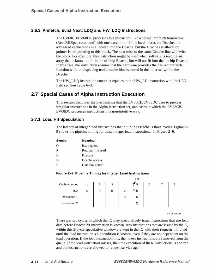
Special Cases of Alpha Instruction Execution
t
e.
s
e 2–
loadIQ
dthethe
orted
2.6.3 Prefetch, Evict Next: LDQ and HW_LDQ Instructions
The EV68CB/EV68DC processes this instruction like a normal prefetch transaction(ReadBlkSpec command) with one exception—if the load misses the Dcache, theaddressed cache block is allocated into the Dcache, but the Dcache set allocationpointer is left pointing to this block. The next miss to the same Dcache line will evicthe block. For example, this instruction might be used when software is reading anarray that is known to fit in the offchip Bcache, but will not fit into the onchip DcachIn this case, the instruction ensures that the hardware provides the desired prefetchfunction without displacing useful cache blocks stored in the other set within theDcache.
The HW_LDQ instruction construct equates to the HW_LD instruction with the LENfield set. See Table 6–3.
2.7 Special Cases of Alpha Instruction Execution
This section describes the mechanisms that the EV68CB/EV68DC uses to procesirregular instructions in the Alpha instruction set, and cases in which the EV68CB/EV68DC processes instructions in a non-intuitive way.
2.7.1 Load Hit Speculation
The latency of integer load instructions that hit in the Dcache is three cycles. Figur9 shows the pipeline timing for these integer load instructions. In Figure 2–9:
Figure 2–9 Pipeline Timing for Integer Load Instructions
There are two cycles in which the IQ may speculatively issue instructions that usedata before Dcache hit information is known. Any instructions that are issued by thewithin this 2-cycle speculative window are kept in the IQ with their requests inhibiteuntil the load instruction’s hit condition is known, even if they are not dependent onload operation. If the load instruction hits, then these instructions are removed fromqueue. If the load instruction misses, then the execution of these instructions is aband the instructions are allowed to request service again.
Symbol Meaning
Q Issue queue
R Register file read
E Execute
D Dcache access
B Data bus active
1Cycle Number
ILD
Instruction 1
Instruction 2
2 3 4 5 6 7 8
Q R E D B
Q R
Q
Hit
FM-05814.AI4
2–24 Internal Architecture EV68CB/EV68DC Hardware Reference Manual

Special Cases of Alpha Instruction Execution
ecu-nsforothin in
gerad
hit
win-dec-
atives.
Fig-10:
ointsuc-
For example, in Figure 2–9, instruction 1 and instruction 2 are issued within the splative window of the load instruction. If the load instruction hits, then both instructiowill be deleted from the queue by the start of cycle 7—one cycle later than normalinstruction 1 and at the normal time for instruction 2. If the load instruction misses, binstructions are aborted from the execution pipelines and may request service agacycle 6.
IQ-issued instructions are aborted if issued within the speculative window of an inteload instruction that missed in the Dcache, even if they are not dependent on the lodata. However, if software misses are likely, the EV68CB/EV68DC can still benefitfrom scheduling the instruction stream for Dcache miss latency. The EV68CB/EV68DC includes a saturating counter that is incremented when load instructionsand is decremented when load instructions miss. When the upper bit of the counterequals zero, the integer load latency is increased to five cycles and the speculativedow is removed. The counter is 4 bits wide and is incremented by 1 on a hit and isremented by two on a miss.
Since load instructions to R31 do not produce a result, they do not create a speculwindow when they execute and, therefore, never waste IQ-issue cycles if they mis
Floating-point load instructions that hit in the Dcache have a latency of four cycles.ure 2–10 shows the pipeline timing for floating-point load instructions. In Figure 2–
Figure 2–10 Pipeline Timing for Floating-Point Load Instructions
The speculative window for floating-point load instructions is one cycle wide.FQ-issued instructions that are issued within the speculative window of a floating-pload instruction that has missed, are only aborted if they depend on the load beingcessful.
For example, in Figure 2–10 instruction 1 is issued in the speculative window of theload instruction.
If instruction 1 is not a user of the data returned by the load instruction, then it isremoved from the queue at its normal time (at the start of cycle 7).
Symbol Meaning
Q Issue queue
R Register file read
E Execute
D Dcache access
B Data bus active
1Cycle Number
FLD
Instruction 1
Instruction 2
2 3 4 5 6 7 8
Q R E D B
Q R
Q
Hit
FM-05815.AI4
EV68CB/EV68DC Hardware Reference Manual Internal Architecture 2–25

Special Cases of Alpha Instruction Execution
s,ey
FQtsoreon’s
bysoint
oer Rbter,pathsis
t inical
e in
ruc-
c-tains
If instruction 1 is dependent on the load instruction data and the load instruction hitinstruction 1 is removed from the queue one cycle later (at the start of cycle 8). If thload instruction misses, then instruction 1 is aborted from the Fbox pipeline and marequest service again in cycle 7.
2.7.2 Floating-Point Store Instructions
Floating-point store instructions are duplicated and loaded into both the IQ and thefrom the mapper. Each IQ entry contains a control bit, fpWait, that when set preventhat entry from asserting its requests. This bit is initially set for each floating-point stinstruction that enters the IQ, unless it was the target of a replay trap. The instructiFQ clone is issued when its Ra register is about to become clean, resulting in its IQclone’s fpWait bit being cleared and allowing the IQ clone to issue and be executedthe Mbox. This mechanism ensures that floating-point store instructions are alwayissued to the Mbox, along with the associated data, without requiring the floating-pregister dirty bits to be available within the IQ.
2.7.3 CMOV Instruction
For the EV68CB/EV68DC, the Alpha CMOV instruction has three operands, and spresents a special case. The required operation is to move either the value in registor the value from the old physical destination register into the new destination regisbased upon the value in Ra. Since neither the mapper nor the Ebox and Fbox dataare otherwise required to handle three operand instructions, the CMOV instructiondecomposed by the Ibox pipeline into two 2-operand instructions:
The Alpha architecture instruction CMOV Ra, Rb⇒ Rc
Becomes the EV68CB/EV68DC instructions CMOV1 Ra, oldRc⇒ newRc1
CMOV2 newRc1, Rb⇒ newRc2
The first instruction, CMOV1, tests the value of Ra and records the result of this tesa 65th bit of its destination register, newRc1. It also copies the value of the old physdestination register, oldRc, to newRc1.
The second instruction, CMOV2, then copies either the value in newRc1 or the valuRb into a second physical destination register, newRc2, based on the CMOVpredicatebit stored in newRc1.
In summary, the original CMOV instruction is decomposed into two dependent insttions that each use a physical register from the free list.
To further simplify this operation, the two component instructions of a CMOV instrution are driven through the mappers in successive cycles. Hence, if a fetch line conn CMOV instructions, it takesn+1 cycles to run that fetch line through the mappers.
For example, the following fetch line:
ADD CMOVx SUB CMOVy
Results in the following three map cycles:
ADD CMOVx1
CMOVx2 SUB CMOVy1
CMOVy2
2–26 Internal Architecture EV68CB/EV68DC Hardware Reference Manual

Memory and I/O Address Space Instructions
nct
m-
ssce.
space
rate
aallya-
nd
dt infor
sdress
e
cesedne
The Ebox executes integer CMOV instructions as two distinct 1-cycle latency opera-tions. The Fbox add pipeline executes floating-point CMOV instructions as two disti4-cycle latency operations.
2.8 Memory and I/O Address Space Instructions
This section provides an overview of the way the EV68CB/EV68DC processes meory and I/O address space instructions.
The EV68CB/EV68DC supports, and internally recognizes, a 44-bit physical addrespace that is divided equally between memory address space and I/O address spaMemory address space resides in the lower half of the physical address space(PA[43]=0) and I/O address space resides in the upper half of the physical address(PA[43]=1).
The IQ can issue any combination of load and store instructions to the Mbox at theof two per cycle. The two lower Ebox subclusters, L0 and L1, generate the48-bit effective virtual address for these instructions.
An instruction is defined to benewerthan another instruction if it follows that instruc-tion in program order and isolder if it precedes that instruction in program order.
2.8.1 Memory Address Space Load Instructions
The Mbox begins execution of a load instruction by translating its virtual address tophysical address using the DTB and by accessing the Dcache. The Dcache is virtuindexed, allowing these two operations to be done in parallel. The Mbox puts informtion about the load instruction, including its physical address, destination register, adata format, into the LQ.
If the requested physical location is found in the Dcache (a hit), the data is formatteand written into the appropriate integer or floating-point register. If the location is nothe Dcache (a miss), the physical address is placed in the miss address file (MAF)processing by the Cbox. The MAF performs a merging function in which a new misaddress is compared to miss addresses already held in the MAF. If the new miss adpoints to the same Dcache block as a miss address in the MAF, then the new missaddress is discarded.
When Dcache fill data is returned to the Dcache by the Cbox, the Mbox satisfies threquesting load instructions in the LQ.
2.8.2 I/O Address Space Load Instructions
Because I/O space load instructions may have sideeffects, they cannot be performedspeculatively. When the Mbox receives an I/O space load instruction, the Mbox plathe load instruction in the LQ, where it is held until it retires. The Mbox replays retirI/O space load instructions from the LQ to the MAF in program order, at a rate of oper GCLK cycle.
EV68CB/EV68DC Hardware Reference Manual Internal Architecture 2–27

Memory and I/O Address Space Instructions
nd-ows
the
to
ord
ord
on
w.I/O
o aa-
lts of
ssn a.
ehese
m
evict
.
The Mbox allocates a new MAF entry to an I/O load instruction and increases I/O bawidth by attempting to merge I/O load instructions in a merge register. Table 2–7 shthe rules for merging data. The columns represent the load instructions replayed toMAF while the rows represent the size of the load in the merge register.
In summary, Table 2–7 shows some of the following rules:
• Byte/word load instructions and different size load instructions are not allowedmerge.
• A stream of ascending non-overlapping, but not necessarily consecutive, longwload instructions are allowed to merge into naturally aligned 32-byte blocks.
• A stream of ascending non-overlapping, but not necessarily consecutive, quadwload instructions are allowed to merge into naturally aligned 64-byte blocks.
• Merging of quadwords can be limited to naturally-aligned 32-byte blocks basedthe Cbox WRITE_ONCE chain 32_BYTE_IO field.
• Issued MB, WMB, and I/O load instructions close the I/O register merge windoTo minimize latency, the merge window is also closed when a timer detects nostore instruction activity for 1024 cycles.
After the Mbox I/O register has closed its merge window, the Cbox sends I/O readrequests offchip in the order that they were received from the Mbox.
2.8.3 Memory Address Space Store Instructions
The Mbox begins execution of a store instruction by translating its virtual address tphysical address using the DTB and by probing the Dcache. The Mbox puts informtion about the store instruction, including its physical address, its data and the resuthe Dcache probe, into the store queue (SQ).
If the Mbox does not find the addressed location in the Dcache, it places the addreinto the MAF for processing by the Cbox. If the Mbox finds the addressed location iDcache block that is not dirty, then it places a ChangeToDirty request into the MAF
A store instruction can write its data into the Dcache when it is retired, and when thDcache block containing its address is dirty and not shared. SQ entries that meet ttwo conditions can be placed into thewritable state. These SQ entries are placed intothewritable state in program order at a maximum rate of two entries per cycle. TheMbox transferswritable store queue entry data from the SQ to the Dcache in prograorder at a maximum rate of two entries per cycle. Dcache lines associated withwritablestore queue entries are locked by the Mbox. System port probe commands cannotthese blocks until their associated writable SQ entries have been transferred into theDcache. This restriction assists in STx_C instruction and Dcache ECC processing
Table 2–7 Rules for I/O Address Space Load Instruction Data Merging
Merge Register/Replayed Instruction Load Byte/Word Load Longword Load Quadword
Byte/Word No merge No merge No merge
Longword No merge Merge up to 32 bytes No merge
Quadword No merge No merge Merge up to 64 bytes
2–28 Internal Architecture EV68CB/EV68DC Hardware Reference Manual

Memory and I/O Address Space Instructions
r load
the
amtore
ableesenttore
ord
ord
on
w.I/O
ace
SQ entry data that has not been transferred to the Dcache may source data to neweinstructions. The Mbox compares the virtual Dcache index bits of incoming loadinstructions to queued SQ entries, and sources the data from the SQ,bypassing theDcache, when necessary.
2.8.4 I/O Address Space Store Instructions
The Mbox begins processing I/O space store instructions, like memory space storeinstructions, by translating the virtual address and placing the state associated withstore instruction into the SQ.
The Mbox replays retired I/O space store entries from the SQ to the IOWB in progrorder at a rate of one per GCLK cycle. The Mbox never allows queued I/O space sinstructions to source data to subsequent load instructions.
The Cbox maximizes I/O bandwidth when it allocates a new IOWB entry to an I/Ostore instruction by attempting to merge I/O store instructions in a merge register. T2–8 shows the rules for I/O space store instruction data merging. The columns reprthe load instructions replayed to the IOWB while the rows represent the size of the sin the merge register.
Table 2–8 shows some of the following rules:
• Byte/word store instructions and different sizestore instructions are not allowed tomerge.
• A stream of ascending non-overlapping, but not necessarily consecutive, longwstore instructions are allowed to merge into naturally aligned 32-byte blocks.
• A stream of ascending non-overlapping, but not necessarily consecutive, quadwstore instructions are allowed to merge into naturally aligned 64-byte blocks.
• Merging of quadwords can be limited to naturally-aligned 32-byte blocks basedthe Cbox WRITE_ONCE chain 32_BYTE_IO field.
• Issued MB, WMB, and I/O load instructions close the I/O register merge windoTo minimize latency, the merge window is also closed when a timer detects nostore instruction activity for 1024 cycles.
After the IOWB merge register has closed its merge window, the Cbox sends I/O spstore requests offchip in the order that they were received from the Mbox.
Table 2–8 Rules for I/O Address Space Store Instruction Data Merging
Merge Register/Replayed Instruction
StoreByte/Word Store Longword Store Quadword
Byte/Word No merge No merge No merge
Longword No merge Merge up to 32 bytes No merge
Quadword No merge No merge Merge up to 64 bytes
EV68CB/EV68DC Hardware Reference Manual Internal Architecture 2–29

MAF Memory Address Space Merging Rules
erg-listsytethe
s,
2.9 MAF Memory Address Space Merging Rules
Because all memory transactions are to 64-byte blocks, efficiency is improved by ming several small data transactions into a single larger data transaction. Table 2–9the rules the EV68CB/EV68DC uses when merging memory transactions into 64-bnaturally aligned data block transactions. Rows represent the merged instruction inMAF and columns represent the new issued transaction.
In summary, Table 2–9 shows that only like instruction types, with the exception ofload instructions merging with store instructions, are merged.
2.10 Instruction Ordering
In the absence of explicit instruction ordering, such as with MB or WMB instructionthe EV68CB/EV68DC maintains a default instruction ordering relationship betweenpairs of load and store instructions.
The EV68CB/EV68DC maintains the default memory data instruction ordering asshown in Table 2–10 (assume address X and address Y are different).
Table 2–9 MAF Merging Rules
MAF/New LDx STx STx_C WH64 ECB Istream
LDx Merge — — — — —
STx Merge Merge — — — —
STx_C — — Merge — — —
WH64 — — — Merge — —
ECB — — — — Merge —
Istream — — — — — Merge
Table 2–10 Memory Reference Ordering
First Instruction in Pair Second Instruction in Pair Reference Order
Load memory to address X Load memory to address X Maintained (litmus test 1)
Load memory to address X Load memory to address Y Not maintained
Store memory to address X Store memory to address X Maintained
Store memory to address X Store memory to address Y Maintained
Load memory to address X Store memory to address X Maintained
Load memory to address X Store memory to address Y Not maintained
Store memory to address X Load memory to address X Maintained
Store memory to address X Load memory to address Y Not maintained
2–30 Internal Architecture EV68CB/EV68DC Hardware Reference Manual

Replay Traps
ue ton is
box
mory
ns inkestar-ns
uc-
dressiny
The EV68CB/EV68DC maintains the default I/O instruction ordering as shown inTable 2–11 (assume address X and address Y are different).
2.11 Replay Traps
There are some situations in which a load or store instruction cannot be executed da condition that occurs after that instruction issues from the IQ or FQ. The instructioaborted (along with all newer instructions) and restarted from the fetch stage of thepipeline. This mechanism is called a replay trap.
2.11.1 Mbox Order Traps
Load and store instructions may be issued from the IQ in a different order than theywere fetched from the Icache, while the architecture dictates that Dstream memorytransactions to the same physical bytes must be completed in order. Usually, the Mmanages the memory reference stream by itself to achieve architecturally correctbehavior, but the two cases in which the Mbox uses replay traps to manage the mestream areload-loadandstore-loadorder traps.
2.11.1.1 Load-Load Order Trap
The Mbox ensures that load instructions thatread the same physical byte(s) ultimatelyissue in correct order by using theload-loadorder trap. The Mbox compares theaddress of each load instruction, as it is issued, to the address of all load instructiothe load queue. If the Mbox finds a newer load instruction in the load queue, it invoa load-loadorder trap on the newer instruction. This is a replay trap that aborts theget of the trap and all newer instructions from the machine and refetches instructiostarting at the target of the trap.
2.11.1.2 Store-Load Order Trap
The Mbox ensures that a load instruction ultimately issues after an older store instrtion that writes some portion of its memory operand by using thestore-loadorder trap.The Mbox compares the address of each store instruction, as it is issued, to the adof all load instructions in the load queue. If the Mbox finds a newer load instructionthe load queue, it invokes astore-loadorder trap on the load instruction. This is a replatrap. It functions like theload-loadorder trap.
Table 2–11 I/O Reference Ordering
First Instruction in Pair Second Instruction in Pair Reference Order
Load I/O to address X Load I/O to address X Maintained
Load I/O to address X Load I/O to address Y Maintained
Store I/O to address X Store I/O to address X Maintained
Store I/O to address X Store I/O to address Y Maintained
Load I/O to address X Store I/O to address X Maintained
Load I/O to address X Store I/O to address Y Not maintained
Store I/O to address X Load I/O to address X Maintained
Store I/O to address X Load I/O to address Y Not maintained
EV68CB/EV68DC Hardware Reference Manual Internal Architecture 2–31

I/O Write Buffer and the WMB Instruction
anthem
tping
nis-be
, or
eue,
ever,ion.
thec-
ndsom-
y thatitted
e pro-
The Ibox contains extra hardware to reduce the frequency of thestore-loadtrap. Thereis a 1-bit by 1024-entry VPC-indexed table in the Ibox called the stWait table. WhenIcache instruction is fetched, the associated stWait table entry is fetched along withIcache instruction. The stWait table produces 1 bit for each instruction accessed frothe Icache. When a load instruction gets astore-loadorder replay trap, its associated biin the stWait table is set during the cycle that the load is refetched. Hence, the trapload instruction’s stWait bit will be set the next time it is fetched.
The IQ will not issue load instructions whose stWait bit is set while there are older usued store instructions in the queue. A load instruction whose stWait bit is set canissued the cycle immediately after the last older store instruction is issued from thequeue. All the bits in the stWait table are unconditionally cleared every 16384 cyclesevery 65536 cycles if I_CTL[ST_WAIT_64K] is set.
2.11.2 Other Mbox Replay Traps
The Mbox also uses replay traps to control the flow of the load queue and store quand to ensure that there are never multiple outstanding misses to different physicaladdresses that map to the same Dcache or Bcache line. Unlike the order traps, howthese replay traps are invoked on the incoming instruction that triggered the condit
2.12 I/O Write Buffer and the WMB Instruction
The I/O write buffer (IOWB) consists of four 64-byte entries with the associatedaddress and control logic used to buffer I/O write data between thestore queue (SQ)and the system port.
2.12.1 Memory Barrier (MB/WMB/TB Fill Flow)
The Cbox CSR SYSBUS_MB_ENABLE bit determines if MB instructions produceexternal system port transactions. When the SYSBUS_MB_ENABLE bit equals 0,Cbox CSR MB_CNT[3:0] field contains the number of pending uncommitted transations. The counter will increment for each of the following commands:
• RdBlk, RdBlkMod, RdBlkI
• RdBlkSpec (valid), RdBlkModSpec (valid), RdBlkSpecI (valid)
• RdBlkVic, RdBlkModVic, RdBlkVicI
• CleanToDirty, SharedToDirty, STChangeToDirty, InvalToDirty
• FetchBlk, FetchBlkSpec (valid), Evict
• RdByte, RdLw, RdQw, WrByte, WrLW, WrQW
The counter is decremented with the C (commit) bit in the Probe and SysDc comma(see Section 4.7.7). Systems can assert the C bit in the SysDc fill response to the cmands that originally incremented the counter, or attached to the last probe seen bcommand when it reached the system serialization point. If the number of uncommtransactions reaches 15 (saturating the counter), the Cbox will stall MAF and IOWBprocessing until at least one of the pending transactions has been committed. Probcessing is not interrupted by the state of this counter.
2–32 Internal Architecture EV68CB/EV68DC Hardware Reference Manual

I/O Write Buffer and the WMB Instruction
llson-E
de
s-
ty
try
s-
ny
ere
WB
de
2.12.1.1 MB Instruction Processing
When an MB instruction is fetched in the predicted instruction execution path, it stain the map stage of the pipeline. This also stalls all instructions after the MB, and ctrol of instruction flow is based upon the value in Cbox CSR SYSBUS_MB_ENABLas follows:
• If Cbox CSR SYSBUS_MB_ENABLE is clear, the Cbox waits until the IQ isempty and then performs the following actions:
a. Sends all pending MAF and IOWB entries to the system port.
b. Monitors Cbox CSR MB_CNT[3:0], a 4-bit counter of outstanding committeevents. When the counter decrements from one to zero, the Cbox marks thyoungest probe queue entry.
c. Waits until the MAF contains no more Dstreamreferences and the SQ, LQ, andIOWB are empty.
When all of the above have occurred and a probe response has been sent to the sytem for the marked probe queue entry, instruction execution continues with theinstruction after the MB.
• If Cbox CSR SYSBUS_MB_ENABLE is set, the Cbox waits until the IQ is empand then performs the following actions:
a. Sends all pending MAF and IOWB entries to the system port
b. Sends the MB command to the system port
c. Waits until the MB command is acknowledged, then marks the youngest enin the probe queue
d. Waits until the MAF contains no more Dstreamreferences and the SQ, LQ, andIOWB are empty
When all of the above have occurred and a probe response has been sent to the sytem for the marked probe queue entry, instruction execution continues with theinstruction after the MB.
Because the MB instruction is executed speculatively, MB processing can begiand the original MB can be killed. In the internal acknowledge case, the MB mahave already been sent to the system interface, and the system is still expected torespond to the MB.
2.12.1.2 WMB Instruction Processing
Write memory barrier (WMB) instructions are issued into the Mbox store-queue, whthey wait until they are retired and all prior store instructions become writable. TheMbox then stalls the writable pointer and informs the Cbox. The Cbox closes the IOmerge register and responds in one of the following two ways:
• If Cbox CSR SYSBUS_MB_ENABLE is clear, the Cbox performs the followingactions:
a. Stalls further MAF and IOWB processing.
b. Monitors Cbox CSR MB_CNT[3:0], a 4-bit counter of outstanding committeevents. When the counter decrements from one to zero, the Cbox marks thyoungest probe queue entry.
EV68CB/EV68DC Hardware Reference Manual Internal Architecture 2–33

I/O Write Buffer and the WMB Instruction
queue
y in
queue
them-the
hould
ld be
are,oad
c. When a probe response has been sent to the system for the marked probeentry, the Cbox considers the WMB to be satisfied.
• If Cbox CSR SYSBUS_MB_ENABLE is set, the Cbox performs the followingactions:
a. Stalls further MAF and IOWB processing.
b. Sends the MB command to the system port.
c. Waits until the MB command is acknowledged by the system with a SysDcMBDone command, then sends acknowledge and marks the youngest entrthe probe queue.
d. When a probe response has been sent to the system for the marked probeentry, the Cbox considers the WMB to be satisfied.
2.12.1.3 TB Fill Flow
Load instructions (HW_LDs) to a virtual page table entry (VPTE) are processed byEV68CB/EV68DC to avoid litmus test problems associated with the ordering of meory transactions from another processor against loading of a page table entry andsubsequent virtual-mode load from this processor.
Consider the sequence shown in Table 2–12. The data could be in the Bcache. Pj sfetch datai if it is using PTEi.
Also consider the related sequence shown in Table 2–13. In this case, the data coucached in the Bcache; Pj should fetch datai if it is using PTEi.
The EV68CB/EV68DC processes Dstream loads to the PTE by injecting, in hardwsome memory barrier processing between the PTE transaction and any subsequent lor store instruction. This is accomplished by the following mechanism:
1. The integer queue issues a HW_LD instruction with VPTE.
Table 2–12 TB Fill Flow Example Sequence 1
Pi Pj
Write Datai Load/Store datai
MB <TB miss>
Write PTEi Load-PTE<write TB>Load/Store (restart)
Table 2–13 TB Fill Flow Example Sequence 2
Pi Pj
Write Datai Istream read datai
MB <TB miss>
Write PTEi Load-PTE<write TB>Istream read (restart) - will miss the Icache
2–34 Internal Architecture EV68CB/EV68DC Hardware Reference Manual

Performance Measurement Support—Performance Counters
ata-ill[4]
eis
yrd bit
veg-
d
t
.
xpro-/
y
o-
callyo-
2. The integer queue issues a HW_MTPR instruction with a DTB_PTE0, that is ddependent on the HW_LD instruction with a VPTE, and is required in order to fthe DTBs. The HW_MTPR instruction, when queued, sets IPR scoreboard bitsand [0].
3. When a HW_MTPR instruction with a DTB_PTE0 is issued, the Ibox signals thCbox indicating that a HW_LD instruction with a VPTE has been processed. Thcauses the Cbox to begin processing the MB instruction. The Ibox prevents ansubsequent memory operations being issued by not clearing the IPR scoreboa[0]. IPR scoreboard bit [0] is one of the scoreboard bits associated with theHW_MTPR instruction with DTB_PTE0.
4. When the Cbox completes processing the MB instruction (using one of the abosequences, depending upon the state of SYSBUS_MB_ENABLE), the Cbox sinals the Ibox to clear IPR scoreboard bit [0].
The EV68CB/EV68DC uses a similar mechanism to process Istream TB misses anfills to the PTE for the Istream.
1. The integer queue issues a HW_LD instruction with VPTE.
2. The IQ issues a HW_MTPR instruction with an ITB_PTE that is data-dependenupon the HW_LD instruction with VPTE. This is required in order to fill the ITB.The HW_MTPR instruction, when queued, sets IPR scoreboard bits [4] and [0]
3. The Cbox issues a HW_MTPR instruction for the ITB_PTE and signals the Ibothat a HW_LD/VPTE instruction has been processed, causing the Cbox to startcessing the MB instruction. The Mbox stalls Ibox fetching from when the HW_LDVPTE instruction finishes until the probe queue is drained.
4. When the EV68CB/EV68DC is finished (SYS_MB selects one of the abovesequences), the Cbox directs the Ibox to clear IPR scoreboard bit [0]. Also, theMbox directs the Ibox to start prefetching.
Inserting MB instruction processing within the TB fill flow is only required for multi-processor systems. Uniprocessor systems can disable MB instruction processing bdeasserting Ibox CSR I_CTL[TB_MB_EN].
2.13 Performance Measurement Support—Performance Counters
The EV68CB/EV68DC provides hardware support for two methods of obtaining prgram performance feedback information. The two methods do not require programmodification. The first method offers similar capabilities to earlier microprocessor per-formance counters. The second method supports the new ProfileMe way of statistisampling individual instructions during program execution to develop a model of prgram execution. Both methods use the same hardware registers.
See Section 6.10 for information about counter control.
2.14 Floating-Point Control Register
The floating-point control register (FPCR) is shown in Figure 2–11.
EV68CB/EV68DC Hardware Reference Manual Internal Architecture 2–35

Floating-Point Control Register
the
Figure 2–11 Floating-Point Control Register
The floating-point control register fields are described in Table 2–14.
Table 2–14 Floating-Point Control Register Fields
Name Extent Type Description
SUM [63] RW Summary bit. Records bit-wise OR of FPCR exception bits.
INED [62] RW Inexact Disable. If this bit is set and a floating-point instruction that enablestrapping on inexact results generates an inexact value, the result is placed indestination register and the trap is suppressed.
UNFD [61] RW Underflow Disable. The EV68CB/EV68DC hardware cannot generate IEEEcompliant denormal results. UNFD is used in conjunction with UNDZ as fol-lows:
UNDZ [60] RW Underflow to zero. When UNDZ is set together with UNFD, underflow trapsare disabled and the EV68CB/EV68DC places a true zero in the destinationregister. See UNFD, above.
63 62 61 60 59 4958 4857 4756 55 54 53 52 51 50 0
SUM
INED
UNFD
UNDZ
DYN
IOV
INE
UNF
OVF
DZE
INV
OVFD
DZED
INVD
DNZ LK99-0050A
UNFD UNDZ Result
0 X Underflow trap.
1 0 Trap to supply a possible denormal result.
1 1 Underflow trap suppressed. Destination is written with atrue zero (+0.0).
2–36 Internal Architecture EV68CB/EV68DC Hardware Reference Manual

AMASK and IMPLVER Instruction Values
ns
E
lt
t
-
s
g-
2.15 AMASK and IMPLVER Instruction Values
The AMASK and IMPLVER instructions return the supported architecture extensioand processor type, respectively.
DYN [59:58] RW Dynamic rounding mode. Indicates the rounding mode to be used by an IEEfloating-point instruction when the instruction specifies dynamic roundingmode:
IOV [57] RW Integer overflow. An integer arithmetic operation or a conversion from float-ing-point to integer overflowed the destination precision.
INE [56] RW Inexact result. A floating-point arithmetic or conversion operation gave a resuthat differed from the mathematically exact result.
UNF [55] RW Underflow. A floating-point arithmetic or conversion operation gave a resultthat underflowed the destination exponent.
OVF [54] RW Overflow. A floating-point arithmetic or conversion operation gave a result thaoverflowed the destination exponent.
DZE [53] RW Divide by zero. An attempt was made to perform a floating-point divide with adivisor of zero.
INV [52] RW Invalid operation. An attempt was made to perform a floating-point arithmeticoperation and one or more of its operand values were illegal.
OVFD [51] RW Overflow disable. If this bit is set and a floating-point arithmetic operation generates an overflow condition, then the appropriate IEEE nontrapping result isplaced in the destination register and the trap is suppressed.
DZED [50] RW Division by zero disable. If this bit is set and a floating-point divide by zero isdetected, the appropriate IEEE nontrapping result is placed in the destinationregister and the trap is suppressed.
INVD [49] RW Invalid operation disable. If this bit is set and a floating-point operate generatean invalid operation condition and EV68CB/EV68DC is capable of producingthe correct IEEE nontrapping result, that result is placed in the destination reister and the trap is suppressed.
DNZ [48] RW Denormal operands to zero. If this bit is set, treat all Denormal operands as asigned zero value with the same sign as the Denormal operand.
Reserved [47:0]1 — —
1 Alpha architecture FPCR bit 47 (DNOD) is not implemented by the EV68CB/EV68DC.
Table 2–14 Floating-Point Control Register Fields (Continued)
Name Extent Type Description
Bits Meaning
00 Chopped
01 Minus infinity
10 Normal
11 Plus infinity
EV68CB/EV68DC Hardware Reference Manual Internal Architecture 2–37

Design Examples
5.,
pro-gura-
sys-
S,
as
of
2.15.1 AMASK
The EV68CB/EV68DC returns the AMASK instruction values provided in Table 2–1The I_CTL register reports the EV68CB/EV68DC pass level (see I_CTL[CHIP_ID]Section 5.2.15).
The AMASK bit definitions provided in Table 2–15 are defined in Table 2–16.
2.15.2 IMPLVER
For the EV68CB/EV68DC, the IMPLVER instruction returns the value 2.
2.16 Design Examples
The EV68CB/EV68DC can be designed into many different uniprocessor and multicessor system configurations. Figures 2–12 and 2–13 illustrate two possible confitions. These configurations employ additional system/memory controller chipsets.
Figure 2–12 shows a typical uniprocessor system with a second-level cache. Thistem configuration could be used in standalone or networked workstations.
Table 2–15 EV68CB/EV68DC AMASK Values
EV68CB/EV68DC Pass Level AMASK Feature Mask Value
See I_CTL[CHIP_ID], Table 5–11 130716
Table 2–16 AMASK Bit Assignments
Bit Meaning
0 Support for the byte/word extension (BWX)The instructions that comprise the BWX extension are LDBU, LDWU, SEXTB,SEXTW, STB, and STW.
1 Support for the square-root and floating-point convert extension (FIX)The instructions that comprise the FIX extension are FTOIS, FTOIT, ITOFF, ITOFITOFT, SQRTF, SQRTG, SQRTS, and SQRTT.
2 Support for the count extension (CIX)The instructions that comprise the CIX extension are CTLZ, CTPOP, and CTTZ.
8 Support for the multimedia extension (MVI)The instructions that comprise the MVI extension are MAXSB8, MAXSW4,MAXUB8, MAXUW4, MINSB8, MINSW4, MINUB8, MINUW4, PERR, PKLB,PKWB, UNPKBL, and UNPKBW.
9 Support for precise arithmetic trap reporting in hardware. The trap PC is the samethe instruction PC after the trapping instruction is executed.
12 Support for using a prefetch with modify intent to improve the performance of thefirst attempt to acquire a lock. When clear, indicates possible prefetch error withlocks, described in waiver 10 to the Alpha Architecture and in the prefetch sectionthe appropriate processor (21264/EV6 and 21264/EV67) specifications.
2–38 Internal Architecture EV68CB/EV68DC Hardware Reference Manual

Design Examples
-levelheer
Figure 2–12 Typical Uniprocessor Configuration
Figure 2–13 shows a typical multiprocessor system, each processor with a secondcache. Each interface controller must employ a duplicate tag store to maintain caccoherency. This system configuration could be used in a networked database servapplication.
Figure 2–13 Typical Multiprocessor Configuration
21264
TagAddress
Out
AddressAddress
In
Data
Data
L2 Cache
TagStore
DataStore
21272 CoreLogic Chipset
Data SliceChips
ControlChips
Host PCIBridge Chip
DuplicateTag Store(Optional)
DRAMArrays
Address
Data
64-bit PCI BusFM-05573
64-bit PCI Bus
64-bit PCI Bus
21264
L2Cache
21264
L2Cache
21272 CoreLogic Chipset
ControlChip
Data SliceChips
Host PCIBridge Chip
Host PCIBridge Chip
DRAMArrays
Address
Data
DRAMArrays
Address
Data
FM-05574
EV68CB/EV68DC Hardware Reference Manual Internal Architecture 2–39


rzed
3Hardware Interface
This chapter contains the EV68CB/EV68DC microprocessor logic symbol and pro-vides information about signal names, their function, and their location. This chaptealso describes the mechanical specifications of the EV68CB/EV68DC. It is organias follows:
• The EV68CB/EV68DC logic symbol
• The EV68CB/EV68DC signal names and functions
• Lists of the signal pads, sorted by name and CLGA(ceramic land grid array) loca-tion
• The specifications for the EV68CB/EV68DC mechanical package
• The bottom view of the EV68CB/EV68DC package
3.1 EV68CB/EV68DC Microprocessor Logic Symbol
Figure 3–1 show the logic symbol for the EV68CB/EV68DC chip.
EV68CB/EV68DC Hardware Reference Manual Hardware Interface 3–1

EV68CB/EV68DC Microprocessor Logic Symbol
Figure 3–1 EV68CB/EV68DC Microprocessor Logic Symbol
21264
System Interface Bcache Interface
SysAddIn_L[14:0]
SysAddInClk_L
SysAddOut_L[14:0]
SysAddOutClk_L
SysVref
SysData_L[63:0]
SysCheck_L[7:0]
SysDataInClk_H[7:0]
SysDataOutClk_L[7:0]
SysDataInValid_L
SysDataOutValid_L
SysFillValid_L
BcAdd_H[23:4]
BcData_H[127:0]
BcCheck_H[15:0]
BcDataInClk_H[7:0]
BcDataOutClk_x[3:0]
BcDataOE_L
BcDataWr_L
BcTag_H[42:20]
BcTagInClk_H
BcTagOutClk_x
BcVref
BcTagDirty_H
BcTagParity_H
BcTagShared_H
BcTagValid_H
BcTagOE_L
BcTagWr_L
BcLoad_L
Clocks
2.5 V
ClkIn_x
FrameClk_x
EV6Clk_x
PLL_VDD
SromClk_H
SromOE_L
TestStat_H
Tdo_H
Miscellaneous
IRQ_H[5:0]
ClkFwdRst_H
SromData_H
Tms_H
Trst_L
Tck_H
Tdi_H
PllBypass_H
MiscVref
Reset_L
DCOK_H
FM-05646b
3–2 Hardware Interface EV68CB/EV68DC Hardware Reference Manual

EV68CB/EV68DC Signal Names and Functions
crip-–4
e
3.2 EV68CB/EV68DC Signal Names and Functions
Table 3–1 defines the EV68CB/EV68DC signal types referred to in this section.
Table 3–2 lists all signal pads in alphabetic order and provides a full functional destion of the pads. Table 3–3 lists the signal pads according to their function. Table 3lists the signal pads and their corresponding ceramic land grid array (CLGA) locationsin alphabetic order for the signal type. Table 3–5 lists the pad grid array locations inalphabetical order. Table lists the ground (VSS) and power (VDD) pads.
Table 3–1 Signal Pad Types Definitions
Signal Type Definition
Inputs
I_DC_REF Input DC reference pad
I_DA Input differential amplifier receiver
I_DA_CLK Input clock pad
Outputs
O_OD Open drain output driver
O_OD_TP Open drain driver for test pads
O_PP Push/pull output driver
O_PP_CLK Push/pull output clock driver
Bidirectional
B_DA_OD Bidirectional differential amplifier receiver with open drain output
B_DA_PP Bidirectional differential amplifier receiver with push/pull output
Other
Spare Reserved to COMPAQ1
1 All Spare connections are Reserved to COMPAQ to maintain compatibility betweenpasses of the chip. Designers should not use these pads.
NoConnect No connection — Do not connect to these pads for any revision of thEV68CB/EV68DC. These pads must float.
Table 3–2 EV68CB/EV68DC Signal Descriptions
Signal Type Count Description
BcAdd_H[23:4] O_PP 20 These signals provide the index to the Bcache.
BcCheck_H[15:0] B_DA_PP 16 ECC check bits forBcData_H[127:0].
BcData_H[127:0] B_DA_PP 128 Bcache data signals.
BcDataInClk_H[7:0] I_DA 8 Bcache data input clocks. These clocks are used with highspeed SDRAMs, such as DDRs, that provide a clock-out withdata-output pads to optimize Bcache read bandwidths. TheEV68CB/EV68DC internally synchronizes the data to its logicwith clock forward receive circuits similar to the system inter-face.
EV68CB/EV68DC Hardware Reference Manual Hardware Interface 3–3

EV68CB/EV68DC Signal Names and Functions
his
f-
is
s
t
,
e
d-
n
BcDataOE_L O_PP 1 Bcache data output enable. The EV68CB/EV68DC asserts tsignal during Bcache read operations.
BcDataOutClk_H[3:0]BcDataOutClk_L[3:0]
O_PP 8 Bcache data output clocks. These free-running clocks are diferential copies of the Bcache clock and are derived from theEV68CB/EV68DC GCLK. Their period is a multiple of theGCLK and is fixed for all operations. They can be configuredso that their rising edge lagsBcAdd_H[23:4] by 0 to 2 GCLKcycles. The EV68CB/EV68DC synchronizes tag output infor-mation with these clocks.
BcDataWr_L O_PP 1 Bcache data write enable. The EV68CB/EV68DC asserts thsignal when writing data to the Bcache data arrays.
BcLoad_L O_PP 1 Bcache burst enable.
BcTag_H[42:20] B_DA_PP 23 Bcache tag bits.
BcTagDirty_H B_DA_PP 1 Tag dirty state bit. During cache write operations, theEV68CB/EV68DC will assert this signal if the Bcache data habeen modified.
BcTagInClk_H I_DA 1 Bcache tag input clock. The EV68CB/EV68DC uses this inpuclock to latch the tag information on Bcache read operations.This clock is used with high-speed SDRAMs, such as DDRsthat provide a clock-out with data-output pads to optimizeBcache read bandwidths. The EV68CB/EV68DC internallysynchronizes the data to its logic with clock forward receivecircuits similar to the system interface.
BcTagOE_L O_PP 1 Bcache tag output enable. This signal is asserted by theEV68CB/EV68DC for Bcache read operations.
BcTagOutClk_HBcTagOutClk_L
O_PP 2 Bcache tag output clock. These clocks “echo” the clock-for-wardedBcDataOutClk_x[3:0] clocks.
BcTagParity_H B_DA_PP 1 Tag parity state bit.
BcTagShared_H B_DA_PP 1 Tag shared state bit. The EV68CB/EV68DC will write a 1 onthis signal line if another agent has a copy of the cache line.
BcTagValid_H B_DA_PP 1 Tag valid state bit. If set, this line indicates that the cache linis valid.
BcTagWr_L O_PP 1 Tag RAM write enable. The EV68CB/EV68DC asserts thissignal when writing a tag to the Bcache tag arrays.
BcVref I_DC_REF 1 Bcache tag reference voltage.
ClkFwdRst_H I_DA 1 Systems assert this synchronous signal to wake up a poweredown EV68CB/EV68DC. TheClkFwdRst_H signal isclocked into a EV68CB/EV68DC register by the capturedFrameClk_x signals. Systems must ensure that the timing ofthis signal meets EV68CB/EV68DC requirements (see Sectio4.7.2).
ClkIn_HClkIn_L
I_DA_CLK 2 Differential input signals provided by the system.
DCOK_H I_DA 1 dc voltage OK. Must be deasserted until dc voltage reachesproper operating level. After that,DCOK_H is asserted.
Table 3–2 EV68CB/EV68DC Signal Descriptions (Continued)
Signal Type Count Description
3–4 Hardware Interface EV68CB/EV68DC Hardware Reference Manual

EV68CB/EV68DC Signal Names and Functions
of
-,
.
to
.
m
EV6Clk_HEV6Clk_L
O_PP_CLK 2 Provides an external test point to measure phase alignmentthe PLL.
FrameClk_HFrameClk_L
I_DA_CLK 2 A skew-controlled differential 50% duty cycle copy of the system clock. It is used by the EV68CB/EV68DC as a referenceor framing, clock.
IRQ_H[5:0] I_DA 6 These six interrupt signal lines may be asserted by the systemThe response of the EV68CB/EV68DC is determined by thesystem software.
MiscVref I_DC_REF 1 Voltage reference for the miscellaneous pads(see Table 3–3).
PllBypass_H I_DA 1 When asserted, this signal will cause the two input clocks(ClkIn_ x) to be applied to the EV68CB/EV68DC internal cir-cuits, instead of the EV68CB/EV68DC global clock (GCLK).
PLL_VDD 2.5 V 1 2.5-V dedicated power supply for the EV68CB/EV68DC PLL.
Reset_L I_DA 1 System reset. This signal protects the EV68CB/EV68DC fromdamage during initial power-up. It must be asserted untilDCOK_H is asserted. After that, it is deasserted and theEV68CB/EV68DC begins its reset sequence.
SromClk_H O_OD_TP 1 Serial ROM clock. Supplies the clock that causes the SROMadvance to the next bit. The cycle time for this clock is 256times the cycle time of the GCLK (internal EV68CB/EV68DCclock).
SromData_H I_DA 1 Serial ROM data. Input data line from the SROM.
SromOE_L O_OD_TP 1 Serial ROM enable. Supplies the output enable to the SROM
SysAddIn_L[14:0] I_DA 15 Time-multiplexed command/address/ID/Ack from system tothe EV68CB/EV68DC.
SysAddInClk_L I_DA 1 Single-ended forwarded clock from system forSysAddIn_L[14:0] andSysFillValid_L .
SysAddOut_L[14:0] O_OD 15 Time-multiplexed command/address/ID/mask from theEV68CB/EV68DC to the system bus.
SysAddOutClk_L O_OD 1 Single-ended forwarded clock output forSysAddOut_L[14:0].
SysCheck_L[7:0] B_DA_OD 8 Quadword ECC check bits forSysData_L[63:0].
SysData_L[63:0] B_DA_OD 64 Data bus for memory and I/O data.
SysDataInClk_H[7:0] I_DA 8 Single-ended system-generated clocks for clock forwardedinput system data.
SysDataInValid_L I_DA 1 When asserted, marks a valid data cycle for data transfers tothe EV68CB/EV68DC.
SysDataOutClk_L[7:0] O_OD 8 Single-ended EV68CB/EV68DC-generated clocks for clockforwarded output system data.
SysDataOutValid_L I_DA 1 When asserted, marks a valid data cycle for data transfers frothe EV68CB/EV68DC.
Table 3–2 EV68CB/EV68DC Signal Descriptions (Continued)
Signal Type Count Description
EV68CB/EV68DC Hardware Reference Manual Hardware Interface 3–5

EV68CB/EV68DC Signal Names and Functions
-
Table 3–3 lists signals by function and provides an abbreviated description.
SysFillValid_L I_DA 1 When asserted, this bit indicates validation for the cache filldelivered in the previous system SysDc command.
SysVref I_DC_REF 1 System interface reference voltage.
Tck_H I_DA 1 IEEE 1149.1 test clock.
Tdi_H I_DA 1 IEEE 1149.1 test data-in signal.
Tdo_H O_OD_TP 1 IEEE 1149.1 test data-out signal.
TestStat_H O_OD_TP 1 Test status pad. System reset drives the test status pad low.TheTestStat_Hpad is forced high at the start of the IcacheBiST. If the Icache BiST passes, the pad is deasserted at theend of the BiST operation; otherwise, it remains high.The EV68CB/EV68DC generates a timeout reset signal if aninstruction is not retired within eight billion cycles.The EV68CB/EV68DC signals the timeout reset event by outputting a 100 GCLK cycle wide pulse onTestStat_H.
Tms_H I_DA 1 IEEE 1149.1 test mode select signal.
Trst_L I_DA 1 IEEE 1149.1 test access port (TAP) reset signal.
Table 3–3 EV68CB/EV68DC Signal Descriptions by Function
Signal Type Count Description
BcVref Domain
BcAdd_H[23:4] O_PP 20 Bcache index.
BcCheck_H[15:0] B_DA_PP 16 ECC check bits forBcData_H[127:0].
BcData_H[127:0] B_DA_PP 128 Bcache data.
BcDataInClk_H[7:0] I_DA 8 Bcache data input clocks.
BcDataOE_L O_PP 1 Bcache data output enable.
BcDataOutClk_H[3:0]BcDataOutClk_L[3:0]
O_PP 8 Bcache data output clocks.
BcDataWr_L O_PP 1 Bcache data write enable.
BcLoad_L O_PP 1 Bcache burst enable.
BcTag_H[42:20] B_DA_PP 23 Bcache tag bits.
BcTagDirty_H B_DA_PP 1 Tag dirty state bit.
BcTagInClk_H I_DA 1 Bcache tag input clock.
BcTagOE_L O_PP 1 Bcache tag output enable.
BcTagOutClk_HBcTagOutClk_L
O_PP 2 Bcache tag output clocks.
BcTagParity_H B_DA_PP 1 Tag parity state bit.
BcTagShared_H B_DA_PP 1 Tag shared state bit.
Table 3–2 EV68CB/EV68DC Signal Descriptions (Continued)
Signal Type Count Description
3–6 Hardware Interface EV68CB/EV68DC Hardware Reference Manual

EV68CB/EV68DC Signal Names and Functions
.
t of
ed-
m.
BcTagValid_H B_DA_PP 1 Tag valid state bit.
BcTagWr_L O_PP 1 Tag RAM write enable.
BcVref I_DC_REF 1 Tag data input reference voltage.
SysVref Domain
SysAddIn_L[14:0] I_DA 15 Time-multiplexed SysAddIn, system-to-EV68CB/EV68DC.
SysAddInClk_L I_DA 1 Single-ended forwarded clock from system forSysAddIn_L[14:0] andSysFillValid_L .
SysAddOut_L[14:0] O_OD 15 Time-multiplexed SysAddOut, EV68CB/EV68DC-to-system
SysAddOutClk_L O_OD 1 Single-ended forwarded-clock.
SysCheck_L[7:0] B_DA_OD 8 Quadword ECC check bits forSysData_L[63:0].
SysData_L[63:0] B_DA_OD 64 Data bus for memory and I/O data.
SysDataInClk_H[7:0] I_DA 8 Single-ended system-generated clocks for clock forwardedinput system data.
SysDataInValid_L I_DA 1 When asserted, marks a valid data cycle for data transfers tothe EV68CB/EV68DC.
SysDataOutClk_L[7:0] O_OD 8 Single-ended EV68CB/EV68DC-generated clocks for clockforwarded output system data.
SysDataOutValid_L I_DA 1 When asserted, marks a valid data cycle for data transfersfrom the EV68CB/EV68DC.
SysFillValid_L I_DA 1 Validation for fill given in previous SysDC command.
SysVref I_DC_REF 1 System interface reference voltage.
Clocks and PLL
ClkIn_HClkIn_L
I_DA_CLK 2 Differential input signals provided by the system.
EV6Clk_HEV6Clk_L
O_PP_CLK 2 Provides an external test point to measure phase alignmenthe PLL.
FrameClk_HFrameClk_L
I_DA_CLK 2 A skew-controlled differential 50% duty cycle copy of thesystem clock. It is used by the EV68CB/EV68DC as a refer-ence, or framing, clock.
PLL_VDD 2.5 V 1 2.5-V dedicated power supply for the EV68CB/EV68DCPLL.
MiscVref Domain
ClkFwdRst_H I_DA 1 Systems assert this synchronous signal to wake up a powerdown EV68CB/EV68DC. TheClkFwdRst_H signal isclocked into a EV68CB/EV68DC register by the capturedFrameClk_x signals.
DCOK_H I_DA 1 dc voltage OK. Must be deasserted until dc voltage reachesproper operating level. After that,DCOK_H is asserted.
IRQ_H[5:0] I_DA 6 These six interrupt signal lines may be asserted by the syste
Table 3–3 EV68CB/EV68DC Signal Descriptions by Function (Continued)
Signal Type Count Description
EV68CB/EV68DC Hardware Reference Manual Hardware Interface 3–7

Pad Assignments
e
3–5
3.3 Pad Assignments
The EV68CB/EV68DC package has 676 pads aligned in a ceramic land grid array(CLGA) design. There are 375 functional signal pads, 1 dedicated 2.5-V pad for thPLL, 152 groundVSSpads, and 148VDD pads. Table 3–4 lists the signal pads andtheir corresponding CLGA locations in alphabetical order for the signal type. Tablelists the CLGA locations in alphabetical order.
MiscVref I_DC_REF 1 Reference voltage for miscellaneous pads.
PllBypass_H I_DA 1 When asserted, this signal will cause the input clocks(ClkIn_ x) to be applied to the EV68CB/EV68DC internal cir-cuits, instead of the EV68CB/EV68DC’s global clock(GCLK).
Reset_L I_DA 1 System reset. This signal protects the EV68CB/EV68DC fromdamage during initial power-up. It must be asserted untilDCOK_H is asserted. After that, it is deasserted and theEV68CB/EV68DC begins its reset sequence.
SromClk_H O_OD_TP 1 Serial ROM clock.
SromData_H I_DA 1 Serial ROM data.
SromOE_L O_OD_TP 1 Serial ROM enable.
Tck_H I_DA 1 IEEE 1149.1 test clock.
Tdi_H I_DA 1 IEEE 1149.1 test data-in signal.
Tdo_H O_OD_TP 1 IEEE 1149.1 test data-out signal.
TestStat_H O_OD_TP 1 Test status pad.
Tms_H I_DA 1 IEEE 1149.1 test mode select signal.
Trst_L I_DA 1 IEEE 1149.1 test access port (TAP) reset signal.
Table 3–4 Pad List Sorted by Signal Name
Signal NameCLGALocation Signal Name
CLGALocation Signal Name
CLGALocation
BcAdd_H_10 A17 BcAdd_H_11 B17 BcAdd_H_12 C17
BcAdd_H_13 D17 BcAdd_H_14 E17 BcAdd_H_15 A19
BcAdd_H_16 B19 BcAdd_H_17 C19 BcAdd_H_18 D19
BcAdd_H_19 E19 BcAdd_H_20 A20 BcAdd_H_21 B20
BcAdd_H_22 C20 BcAdd_H_23 D20 BcAdd_H_4 E14
BcAdd_H_5 A16 BcAdd_H_6 B16 BcAdd_H_7 C16
BcAdd_H_8 D16 BcAdd_H_9 E16 BcCheck_H_0 G02
BcCheck_H_1 N03 BcCheck_H_10 W05 BcCheck_H_11 AD05
BcCheck_H_12 H20 BcCheck_H_13 N22 BcCheck_H_14 W22
BcCheck_H_15 AE22 BcCheck_H_2 W03 BcCheck_H_3 AD04
Table 3–3 EV68CB/EV68DC Signal Descriptions by Function (Continued)
Signal Type Count Description
3–8 Hardware Interface EV68CB/EV68DC Hardware Reference Manual

Pad Assignments
BcCheck_H_4 G25 BcCheck_H_5 N24 BcCheck_H_6 W24
BcCheck_H_7 AE23 BcCheck_H_8 H06 BcCheck_H_9 N06
BcData_H_0 A04 BcData_H_1 B04 BcData_H_10 K04
BcData_H_100 E22 BcData_H_101 F20 BcData_H_102 G21
BcData_H_103 G22 BcData_H_104 H21 BcData_H_105 H22
BcData_H_106 K21 BcData_H_107 K22 BcData_H_108 L21
BcData_H_109 L22 BcData_H_11 K03 BcData_H_110 N20
BcData_H_111 N21 BcData_H_112 P22 BcData_H_113 P21
BcData_H_114 P20 BcData_H_115 T22 BcData_H_116 T21
BcData_H_117 U22 BcData_H_118 U21 BcData_H_119 W23
BcData_H_12 L04 BcData_H_120 W21 BcData_H_121 Y23
BcData_H_122 Y22 BcData_H_123 Y21 BcData_H_124 AB23
BcData_H_125 AB22 BcData_H_126 AC22 BcData_H_127 AD22
BcData_H_13 L03 BcData_H_14 N05 BcData_H_15 N04
BcData_H_16 P03 BcData_H_17 P04 BcData_H_18 T02
BcData_H_19 T03 BcData_H_2 C04 BcData_H_20 T04
BcData_H_21 U02 BcData_H_22 U03 BcData_H_23 U04
BcData_H_24 Y03 BcData_H_25 Y04 BcData_H_26 Y05
BcData_H_27 AB03 BcData_H_28 AB04 BcData_H_29 AB05
BcData_H_3 D03 BcData_H_30 AC03 BcData_H_31 AC04
BcData_H_32 A23 BcData_H_33 B23 BcData_H_34 C23
BcData_H_35 D24 BcData_H_36 E23 BcData_H_37 E24
BcData_H_38 G23 BcData_H_39 G24 BcData_H_4 E04
BcData_H_40 H23 BcData_H_41 H24 BcData_H_42 H25
BcData_H_43 K23 BcData_H_44 K24 BcData_H_45 L23
BcData_H_46 L24 BcData_H_47 N23 BcData_H_48 P24
BcData_H_49 P23 BcData_H_5 E03 BcData_H_50 T25
BcData_H_51 T24 BcData_H_52 T23 BcData_H_53 U25
BcData_H_54 U24 BcData_H_55 U23 BcData_H_56 Y24
BcData_H_57 AB26 BcData_H_58 AB25 BcData_H_59 AB24
BcData_H_6 G04 BcData_H_60 AC26 BcData_H_61 AC25
BcData_H_62 AC24 BcData_H_63 AD23 BcData_H_64 A05
BcData_H_65 B05 BcData_H_66 C05 BcData_H_67 D05
BcData_H_68 E05 BcData_H_69 G06 BcData_H_7 G03
BcData_H_70 G05 BcData_H_71 H07 BcData_H_72 H05
Table 3–4 Pad List Sorted by Signal Name (Continued)
Signal NameCLGALocation Signal Name
CLGALocation Signal Name
CLGALocation
EV68CB/EV68DC Hardware Reference Manual Hardware Interface 3–9

Pad Assignments
BcData_H_73 K07 BcData_H_74 K06 BcData_H_75 K05
BcData_H_76 L07 BcData_H_77 L06 BcData_H_78 L05
BcData_H_79 N07 BcData_H_8 H04 BcData_H_80 P05
BcData_H_81 P06 BcData_H_82 P07 BcData_H_83 T05
BcData_H_84 T06 BcData_H_85 U05 BcData_H_86 U06
BcData_H_87 W04 BcData_H_88 W06 BcData_H_89 Y06
BcData_H_9 H03 BcData_H_90 AA07 BcData_H_91 AA08
BcData_H_92 AB07 BcData_H_93 AB08 BcData_H_94 AC05
BcData_H_95 AC07 BcData_H_96 A22 BcData_H_97 B22
BcData_H_98 C22 BcData_H_99 D22 BcDataInClk_H_0 E01
BcDataInClk_H_1 L01 BcDataInClk_H_2 P01 BcDataInClk_H_3 Y01
BcDataInClk_H_4 D26 BcDataInClk_H_5 L26 BcDataInClk_H_6 P26
BcDataInClk_H_7 W26 BcDataOE_L D14 BcDataOutClk_H_0 H01
BcDataOutClk_H_1 T01 BcDataOutClk_H_2 G26 BcDataOutClk_H_3 U26
BcDataOutClk_L_0 G01 BcDataOutClk_L_1 U01 BcDataOutClk_L_2 H26
BcDataOutClk_L_3 T26 BcDataWr_L C14 BcLoad_L C13
BcTag_H_20 D07 BcTag_H_21 C07 BcTag_H_22 B07
BcTag_H_23 A07 BcTag_H_24 D08 BcTag_H_25 C08
BcTag_H_26 B08 BcTag_H_27 A08 BcTag_H_28 E10
BcTag_H_29 D10 BcTag_H_30 C10 BcTag_H_31 B10
BcTag_H_32 J11 BcTag_H_33 H11 BcTag_H_34 G11
BcTag_H_35 F11 BcTag_H_36 E11 BcTag_H_37 D11
BcTag_H_38 C11 BcTag_H_39 B11 BcTag_H_40 J12
BcTag_H_41 H13 BcTag_H_42 G13 BcTagDirty_H H14
BcTagInClk_H A11 BcTagOE_L D13 BcTagOutClk_H A14
BcTagOutClk_L A13 BcTagParity_H J13 BcTagShared_H J14
BcTagValid_H G14 BcTagWr_L E13 BcVref A10
ClkFwdRst_H AE10 ClkIn_H AF04 ClkIn_L AF05
DCOK_H AD10 EV6Clk_H AB01 EV6Clk_L AC01
FrameClk_H AF10 FrameClk_L AF11 IRQ_H_0 AD07
IRQ_H_1 AE07 IRQ_H_2 AF07 IRQ_H_3 AD08
IRQ_H_4 AE08 IRQ_H_5 AF08 MiscVref V14
NoConnect AA11 NoConnect AA10 PLL_VDD T10
PllBypass_H AB10 Reset_L AE11 Spare J15
Spare V17 Spare AC08 Spare AC10
Table 3–4 Pad List Sorted by Signal Name (Continued)
Signal NameCLGALocation Signal Name
CLGALocation Signal Name
CLGALocation
3–10 Hardware Interface EV68CB/EV68DC Hardware Reference Manual

Pad Assignments
Spare AF22 Spare AF23 SromClk_H AC11
SromData_H AD11 SromOE_L AB11 SysAddIn_L_0 Y17
SysAddIn_L_1 AA17 SysAddIn_L_10 AD14 SysAddIn_L_11 AE14
SysAddIn_L_12 Y13 SysAddIn_L_13 AA13 SysAddIn_L_14 AB13
SysAddIn_L_2 AB17 SysAddIn_L_3 Y16 SysAddIn_L_4 AA16
SysAddIn_L_5 AB16 SysAddIn_L_6 Y14 SysAddIn_L_7 AA14
SysAddIn_L_8 AB14 SysAddIn_L_9 AC14 SysAddInClk_L AF14
SysAddOut_L_0 AC20 SysAddOut_L_1 AD20 SysAddOut_L_10 AE17
SysAddOut_L_11 AF17 SysAddOut_L_12 AC16 SysAddOut_L_13 AD16
SysAddOut_L_14 AE16 SysAddOut_L_2 AE20 SysAddOut_L_3 AF20
SysAddOut_L_4 AC19 SysAddOut_L_5 AD19 SysAddOut_L_6 AE19
SysAddOut_L_7 AF19 SysAddOut_L_8 AC17 SysAddOut_L_9 AD17
SysAddOutClk_L AF16 SysCheck_L_0 H08 SysCheck_L_1 N08
SysCheck_L_2 W07 SysCheck_L_3 Y11 SysCheck_L_4 J18
SysCheck_L_5 N19 SysCheck_L_6 U18 SysCheck_L_7 W17
SysData_L_0 F10 SysData_L_1 G10 SysData_L_10 K09
SysData_L_11 K08 SysData_L_12 L09 SysData_L_13 L08
SysData_L_14 M09 SysData_L_15 N09 SysData_L_16 P08
SysData_L_17 P09 SysData_L_18 R09 SysData_L_19 T07
SysData_L_2 H10 SysData_L_20 T08 SysData_L_21 U07
SysData_L_22 U08 SysData_L_23 U09 SysData_L_24 V09
SysData_L_25 W08 SysData_L_26 Y08 SysData_L_27 V10
SysData_L_28 W10 SysData_L_29 Y10 SysData_L_3 E08
SysData_L_30 V11 SysData_L_31 W11 SysData_L_32 G16
SysData_L_33 H16 SysData_L_34 J16 SysData_L_35 G17
SysData_L_36 H17 SysData_L_37 J17 SysData_L_38 G19
SysData_L_39 H19 SysData_L_4 E07 SysData_L_40 K18
SysData_L_41 K19 SysData_L_42 K20 SysData_L_43 L18
SysData_L_44 L19 SysData_L_45 L20 SysData_L_46 M18
SysData_L_47 N18 SysData_L_48 P19 SysData_L_49 P18
SysData_L_5 F08 SysData_L_50 R18 SysData_L_51 T20
SysData_L_52 T19 SysData_L_53 T18 SysData_L_54 U20
SysData_L_55 U19 SysData_L_56 V18 SysData_L_57 W20
SysData_L_58 W19 SysData_L_59 Y19 SysData_L_6 F07
SysData_L_60 AA20 SysData_L_61 AA19 SysData_L_62 AB20
Table 3–4 Pad List Sorted by Signal Name (Continued)
Signal NameCLGALocation Signal Name
CLGALocation Signal Name
CLGALocation
EV68CB/EV68DC Hardware Reference Manual Hardware Interface 3–11
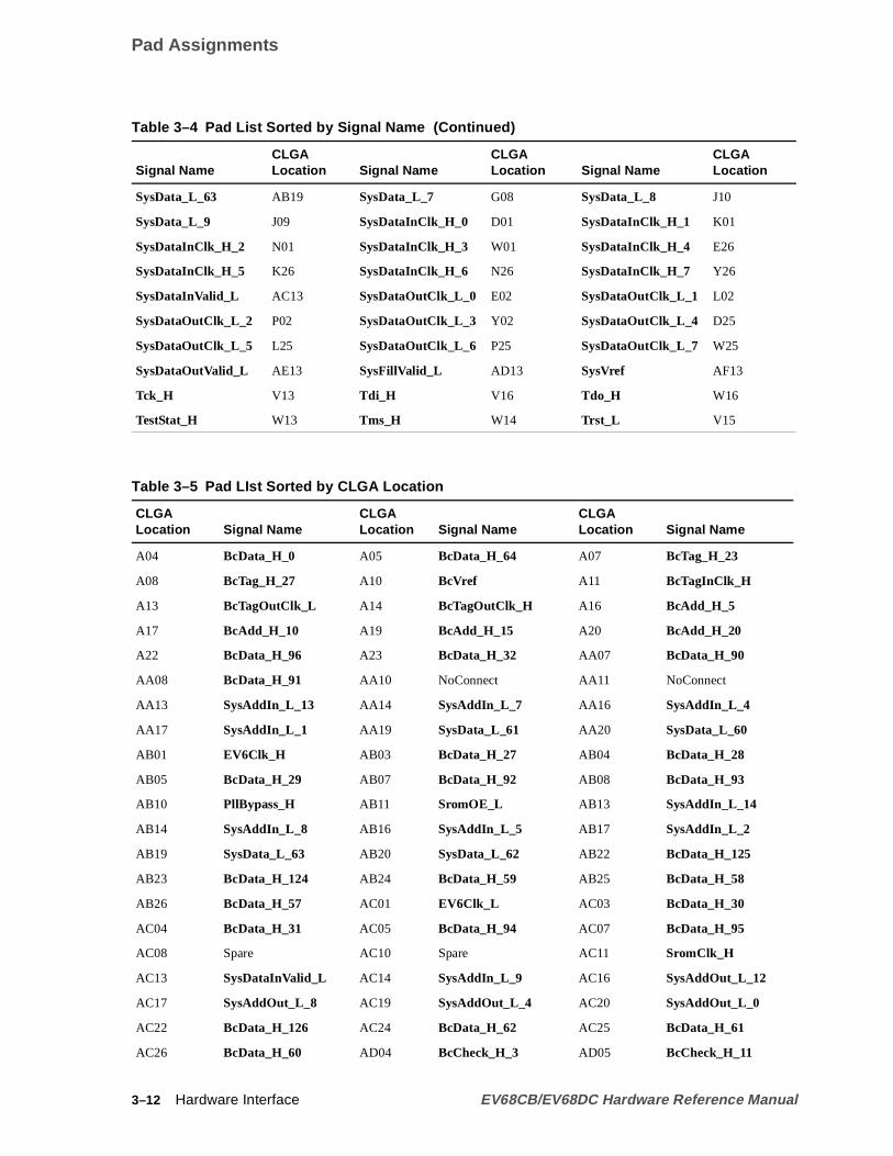
Pad Assignments
SysData_L_63 AB19 SysData_L_7 G08 SysData_L_8 J10
SysData_L_9 J09 SysDataInClk_H_0 D01 SysDataInClk_H_1 K01
SysDataInClk_H_2 N01 SysDataInClk_H_3 W01 SysDataInClk_H_4 E26
SysDataInClk_H_5 K26 SysDataInClk_H_6 N26 SysDataInClk_H_7 Y26
SysDataInValid_L AC13 SysDataOutClk_L_0 E02 SysDataOutClk_L_1 L02
SysDataOutClk_L_2 P02 SysDataOutClk_L_3 Y02 SysDataOutClk_L_4 D25
SysDataOutClk_L_5 L25 SysDataOutClk_L_6 P25 SysDataOutClk_L_7 W25
SysDataOutValid_L AE13 SysFillValid_L AD13 SysVref AF13
Tck_H V13 Tdi_H V16 Tdo_H W16
TestStat_H W13 Tms_H W14 Trst_L V15
Table 3–5 Pad LIst Sorted by CLGA Location
CLGALocation Signal Name
CLGALocation Signal Name
CLGALocation Signal Name
A04 BcData_H_0 A05 BcData_H_64 A07 BcTag_H_23
A08 BcTag_H_27 A10 BcVref A11 BcTagInClk_H
A13 BcTagOutClk_L A14 BcTagOutClk_H A16 BcAdd_H_5
A17 BcAdd_H_10 A19 BcAdd_H_15 A20 BcAdd_H_20
A22 BcData_H_96 A23 BcData_H_32 AA07 BcData_H_90
AA08 BcData_H_91 AA10 NoConnect AA11 NoConnect
AA13 SysAddIn_L_13 AA14 SysAddIn_L_7 AA16 SysAddIn_L_4
AA17 SysAddIn_L_1 AA19 SysData_L_61 AA20 SysData_L_60
AB01 EV6Clk_H AB03 BcData_H_27 AB04 BcData_H_28
AB05 BcData_H_29 AB07 BcData_H_92 AB08 BcData_H_93
AB10 PllBypass_H AB11 SromOE_L AB13 SysAddIn_L_14
AB14 SysAddIn_L_8 AB16 SysAddIn_L_5 AB17 SysAddIn_L_2
AB19 SysData_L_63 AB20 SysData_L_62 AB22 BcData_H_125
AB23 BcData_H_124 AB24 BcData_H_59 AB25 BcData_H_58
AB26 BcData_H_57 AC01 EV6Clk_L AC03 BcData_H_30
AC04 BcData_H_31 AC05 BcData_H_94 AC07 BcData_H_95
AC08 Spare AC10 Spare AC11 SromClk_H
AC13 SysDataInValid_L AC14 SysAddIn_L_9 AC16 SysAddOut_L_12
AC17 SysAddOut_L_8 AC19 SysAddOut_L_4 AC20 SysAddOut_L_0
AC22 BcData_H_126 AC24 BcData_H_62 AC25 BcData_H_61
AC26 BcData_H_60 AD04 BcCheck_H_3 AD05 BcCheck_H_11
Table 3–4 Pad List Sorted by Signal Name (Continued)
Signal NameCLGALocation Signal Name
CLGALocation Signal Name
CLGALocation
3–12 Hardware Interface EV68CB/EV68DC Hardware Reference Manual

Pad Assignments
AD07 IRQ_H_0 AD08 IRQ_H_3 AD10 DCOK_H
AD11 SromData_H AD13 SysFillValid_L AD14 SysAddIn_L_10
AD16 SysAddOut_L_13 AD17 SysAddOut_L_9 AD19 SysAddOut_L_5
AD20 SysAddOut_L_1 AD22 BcData_H_127 AD23 BcData_H_63
AE07 IRQ_H_1 AE08 IRQ_H_4 AE10 ClkFwdRst_H
AE11 Reset_L AE13 SysDataOutValid_L AE14 SysAddIn_L_11
AE16 SysAddOut_L_14 AE17 SysAddOut_L_10 AE19 SysAddOut_L_6
AE20 SysAddOut_L_2 AE22 BcCheck_H_15 AE23 BcCheck_H_7
AF04 ClkIn_H AF05 ClkIn_L AF07 IRQ_H_2
AF08 IRQ_H_5 AF10 FrameClk_H AF11 FrameClk_L
AF13 SysVref AF14 SysAddInClk_L AF16 SysAddOutClk_L
AF17 SysAddOut_L_11 AF19 SysAddOut_L_7 AF20 SysAddOut_L_3
AF22 Spare AF23 Spare B04 BcData_H_1
B05 BcData_H_65 B07 BcTag_H_22 B08 BcTag_H_26
B10 BcTag_H_31 B11 BcTag_H_39 B16 BcAdd_H_6
B17 BcAdd_H_11 B19 BcAdd_H_16 B20 BcAdd_H_21
B22 BcData_H_97 B23 BcData_H_33 C04 BcData_H_2
C05 BcData_H_66 C07 BcTag_H_21 C08 BcTag_H_25
C10 BcTag_H_30 C11 BcTag_H_38 C13 BcLoad_L
C14 BcDataWr_L C16 BcAdd_H_7 C17 BcAdd_H_12
C19 BcAdd_H_17 C20 BcAdd_H_22 C22 BcData_H_98
C23 BcData_H_34 D01 SysDataInClk_H_0 D03 BcData_H_3
D05 BcData_H_67 D07 BcTag_H_20 D08 BcTag_H_24
D10 BcTag_H_29 D11 BcTag_H_37 D13 BcTagOE_L
D14 BcDataOE_L D16 BcAdd_H_8 D17 BcAdd_H_13
D19 BcAdd_H_18 D20 BcAdd_H_23 D22 BcData_H_99
D24 BcData_H_35 D25 SysDataOutClk_L_4 D26 BcDataInClk_H_4
E01 BcDataInClk_H_0 E02 SysDataOutClk_L_0 E03 BcData_H_5
E04 BcData_H_4 E05 BcData_H_68 E07 SysData_L_4
E08 SysData_L_3 E10 BcTag_H_28 E11 BcTag_H_36
E13 BcTagWr_L E14 BcAdd_H_4 E16 BcAdd_H_9
E17 BcAdd_H_14 E19 BcAdd_H_19 E22 BcData_H_100
E23 BcData_H_36 E24 BcData_H_37 E26 SysDataInClk_H_4
F07 SysData_L_6 F08 SysData_L_5 F10 SysData_L_0
F11 BcTag_H_35 F20 BcData_H_101 G01 BcDataOutClk_L_0
Table 3–5 Pad LIst Sorted by CLGA Location (Continued)
CLGALocation Signal Name
CLGALocation Signal Name
CLGALocation Signal Name
EV68CB/EV68DC Hardware Reference Manual Hardware Interface 3–13

Pad Assignments
G02 BcCheck_H_0 G03 BcData_H_7 G04 BcData_H_6
G05 BcData_H_70 G06 BcData_H_69 G08 SysData_L_7
G10 SysData_L_1 G11 BcTag_H_34 G13 BcTag_H_42
G14 BcTagValid_H G16 SysData_L_32 G17 SysData_L_35
G19 SysData_L_38 G21 BcData_H_102 G22 BcData_H_103
G23 BcData_H_38 G24 BcData_H_39 G25 BcCheck_H_4
G26 BcDataOutClk_H_2 H01 BcDataOutClk_H_0 H03 BcData_H_9
H04 BcData_H_8 H05 BcData_H_72 H06 BcCheck_H_8
H07 BcData_H_71 H08 SysCheck_L_0 H10 SysData_L_2
H11 BcTag_H_33 H13 BcTag_H_41 H14 BcTagDirty_H
H16 SysData_L_33 H17 SysData_L_36 H19 SysData_L_39
H20 BcCheck_H_12 H21 BcData_H_104 H22 BcData_H_105
H23 BcData_H_40 H24 BcData_H_41 H25 BcData_H_42
H26 BcDataOutClk_L_2 J09 SysData_L_9 J10 SysData_L_8
J11 BcTag_H_32 J12 BcTag_H_40 J13 BcTagParity_H
J14 BcTagShared_H J15 Spare J16 SysData_L_34
J17 SysData_L_37 J18 SysCheck_L_4 K01 SysDataInClk_H_1
K03 BcData_H_11 K04 BcData_H_10 K05 BcData_H_75
K06 BcData_H_74 K07 BcData_H_73 K08 SysData_L_11
K09 SysData_L_10 K18 SysData_L_40 K19 SysData_L_41
K20 SysData_L_42 K21 BcData_H_106 K22 BcData_H_107
K23 BcData_H_43 K24 BcData_H_44 K26 SysDataInClk_H_5
L01 BcDataInClk_H_1 L02 SysDataOutClk_L_1 L03 BcData_H_13
L04 BcData_H_12 L05 BcData_H_78 L06 BcData_H_77
L07 BcData_H_76 L08 SysData_L_13 L09 SysData_L_12
L18 SysData_L_43 L19 SysData_L_44 L20 SysData_L_45
L21 BcData_H_108 L22 BcData_H_109 L23 BcData_H_45
L24 BcData_H_46 L25 SysDataOutClk_L_5 L26 BcDataInClk_H_5
M09 SysData_L_14 M18 SysData_L_46 N01 SysDataInClk_H_2
N03 BcCheck_H_1 N04 BcData_H_15 N05 BcData_H_14
N06 BcCheck_H_9 N07 BcData_H_79 N08 SysCheck_L_1
N09 SysData_L_15 N18 SysData_L_47 N19 SysCheck_L_5
N20 BcData_H_110 N21 BcData_H_111 N22 BcCheck_H_13
N23 BcData_H_47 N24 BcCheck_H_5 N26 SysDataInClk_H_6
P01 BcDataInClk_H_2 P02 SysDataOutClk_L_2 P03 BcData_H_16
Table 3–5 Pad LIst Sorted by CLGA Location (Continued)
CLGALocation Signal Name
CLGALocation Signal Name
CLGALocation Signal Name
3–14 Hardware Interface EV68CB/EV68DC Hardware Reference Manual

Pad Assignments
P04 BcData_H_17 P05 BcData_H_80 P06 BcData_H_81
P07 BcData_H_82 P08 SysData_L_16 P09 SysData_L_17
P18 SysData_L_49 P19 SysData_L_48 P20 BcData_H_114
P21 BcData_H_113 P22 BcData_H_112 P23 BcData_H_49
P24 BcData_H_48 P25 SysDataOutClk_L_6 P26 BcDataInClk_H_6
R09 SysData_L_18 R18 SysData_L_50 T01 BcDataOutClk_H_1
T02 BcData_H_18 T03 BcData_H_19 T04 BcData_H_20
T05 BcData_H_83 T06 BcData_H_84 T07 SysData_L_19
T08 SysData_L_20 T10 PLL_VDD T18 SysData_L_53
T19 SysData_L_52 T20 SysData_L_51 T21 BcData_H_116
T22 BcData_H_115 T23 BcData_H_52 T24 BcData_H_51
T25 BcData_H_50 T26 BcDataOutClk_L_3 U01 BcDataOutClk_L_1
U02 BcData_H_21 U03 BcData_H_22 U04 BcData_H_23
U05 BcData_H_85 U06 BcData_H_86 U07 SysData_L_21
U08 SysData_L_22 U09 SysData_L_23 U18 SysCheck_L_6
U19 SysData_L_55 U20 SysData_L_54 U21 BcData_H_118
U22 BcData_H_117 U23 BcData_H_55 U24 BcData_H_54
U25 BcData_H_53 U26 BcDataOutClk_H_3 V09 SysData_L_24
V10 SysData_L_27 V11 SysData_L_30 V13 Tck_H
V14 MiscVref V15 Trst_L V16 Tdi_H
V17 Spare V18 SysData_L_56 W01 SysDataInClk_H_3
W03 BcCheck_H_2 W04 BcData_H_87 W05 BcCheck_H_10
W06 BcData_H_88 W07 SysCheck_L_2 W08 SysData_L_25
W10 SysData_L_28 W11 SysData_L_31 W13 TestStat_H
W14 Tms_H W16 Tdo_H W17 SysCheck_L_7
W19 SysData_L_58 W20 SysData_L_57 W21 BcData_H_120
W22 BcCheck_H_14 W23 BcData_H_119 W24 BcCheck_H_6
W25 SysDataOutClk_L_7 W26 BcDataInClk_H_7 Y01 BcDataInClk_H_3
Y02 SysDataOutClk_L_3 Y03 BcData_H_24 Y04 BcData_H_25
Y05 BcData_H_26 Y06 BcData_H_89 Y08 SysData_L_26
Y10 SysData_L_29 Y11 SysCheck_L_3 Y13 SysAddIn_L_12
Y14 SysAddIn_L_6 Y16 SysAddIn_L_3 Y17 SysAddIn_L_0
Y19 SysData_L_59 Y21 BcData_H_123 Y22 BcData_H_122
Y23 BcData_H_121 Y24 BcData_H_56 Y26 SysDataInClk_H_7
Table 3–5 Pad LIst Sorted by CLGA Location (Continued)
CLGALocation Signal Name
CLGALocation Signal Name
CLGALocation Signal Name
EV68CB/EV68DC Hardware Reference Manual Hardware Interface 3–15

Pad Assignments
Table lists the EV68CB/EV68DC ground and power (VSSandVDD, respectively) padlist.
Table 3–6 Ground and Power (VSS and VDD) Pad List
Signal CLGA Location
VSS A02 A06 A12 A18 A24 A26 AA02 AA04 AA06 AA12
AA18 AA22 AA24 AA26 AB09 AB15 AB21 AC02 AC06 AC12
AC18 AC23 AD01 AD03 AD09 AD15 AD21 AD25 AE02 AE04
AE06 AE12 AE18 AE24 AE26 AF01 AF03 AF09 AF15 AF21
AF25 B01 B03 B09 B13 B15 B21 B25 C02 C06
C12 C18 C24 C26 D04 D09 D15 D21 E06 E12
E18 E20 F01 F03 F05 F09 F13 F15 F17 F19
F21 F23 F25 G07 G12 G18 H09 H15 J02 J04
J06 J08 J20 J22 J24 J26 K11 K13 K15 K17
K25 L10 L12 L14 L16 M01 M03 M05 M07 M11
M13 M15 M17 M19 M21 M23 M25 N02 N10 N12
N14 N16 P11 P13 P15 P17 R02 R04 R06 R08
R10 R12 R14 R16 R20 R22 R24 R26 T09 T11
T13 T15 T17 U10 U12 U14 U16 V01 V03 V05
V07 V19 V21 V23 V25 W02 W12 W18 Y09 Y15
Y20 Y25 — — — — — — — —
VDD A03 A09 A15 A21 A25 AA01 AA03 AA05 AA09 AA15
AA21 AA23 AA25 AB02 AB06 AB12 AB18 AC09 AC15 AC21
AD02 AD06 AD12 AD18 AD24 AD26 AE01 AE03 AE05 AE09
AE15 AE21 AE25 AF02 AF06 AF12 AF18 AF24 AF26 B02
B06 B12 B14 B18 B24 B26 C01 C03 C09 C15
C21 C25 D02 D06 D12 D18 D23 E09 E15 E21
E25 F02 F04 F06 F12 F14 F16 F18 F22 F24
F26 G09 G15 G20 H02 H12 H18 J01 J03 J05
J07 J19 J21 J23 J25 K02 K10 K12 K14 K16
L11 L13 L15 L17 M02 M04 M06 M08 M10 M12
M14 M16 M20 M22 M24 M26 N11 N13 N15 N17
N25 P10 P12 P14 P16 R01 R03 R05 R07 R11
R13 R15 R17 R19 R21 R23 R25 T12 T14 T16
U11 U13 U15 U17 V02 V04 V06 V08 V12 V20
V22 V24 V26 W09 W15 Y07 Y12 Y18 — —
3–16 Hardware Interface EV68CB/EV68DC Hardware Reference Manual

Mechanical Specifications
t a
3.4 Mechanical Specifications
This section shows the EV68CB/EV68DC mechanical package dimensions withouheat sink. For heat sink information and dimensions, refer to Chapter 10.
Figure 3–2 shows the package physical dimensions without a heat sink.
Figure 3–2 Package Dimensions (Bottom View)
675x0.86mm8.943mm
6.275mm
8.74mm
8.74mm
31.75mm
49.53mm
15.875mm
1.27mm
2.36mm
1.27mm 3.915mm
15.875mm
31.75mm
49.53mm
6.583mm
LK99-0181a
EV68CB/EV68DC Hardware Reference Manual Hardware Interface 3–17

EV68CB/EV68DC Packaging
3.5 EV68CB/EV68DC Packaging
Figure 3–3 shows the EV68CB/EV68DC package from the bottom view.
Figure 3–3 EV68CB/EV68DC Bottom View
LK99-0180a
AF
AE
AD
AC
AB
AA
Y
W
V
U
T
R
P
N
M
L
K
J
H
G
F
D
C
B
A
0102030405060708091011121314151617181920212223242526
3–18 Hardware Interface EV68CB/EV68DC Hardware Reference Manual

ws:
ents.
,f the
4Cache and External Interfaces
This chapter describes the EV68CB/EV68DC cache and external interface, whichincludes the second-level cache (Bcache) interface and the systeminterface. It alsodescribes locks, interrupt signals, and ECC/parity generation. It is organized as follo
• Introduction to the external interfaces
• Physical address considerations
• Bcache structure
• Victim data buffer
• Cache coherency
• Lock mechanism
• System port
• Bcache port
• Interrupts
Chapter 3 lists and defines all EV68CB/EV68DC hardware interface signal pads.Chapter 9 describes the EV68CB/EV68DC hardware interface electrical requirem
4.1 Introduction to the External Interfaces
An EV68CB/EV68DC-based system can be divided into three major sections:
• EV68CB/EV68DC microprocessor
• Second-level Bcache
• System interface logic
– Optional duplicate tag store– Optional lock register– Optional victim buffers
The EV68CB/EV68DC external interface is flexible and mandates few design rulesallowing a wide range of prospective systems. The external interface is composed oBcache interface and thesystem interface.
• Input clocks must have the same frequency as their corresponding output clock. Forexample, the frequency ofSysAddInClk_L must be the same asSysAddOutClk_L.
EV68CB/EV68DC Hardware Reference Manual Cache and External Interfaces 4–1

Introduction to the External Interfaces
-
• The Bcache interface includes a 128-bit bidirectional data bus, a 20-bit unidirectional address bus, and several control signals.– TheBcDataOutClk_x[3:0] clocks are free-running and are derived from theinternal GCLK. The period ofBcDataOutClk_x[3:0] is a programmable mul-tiple of GCLK.
– The Bcache turns theBcDataOutClk_x[3:0] clocks around and returns themto the EV68CB/EV68DC asBcDataInClk_H[7:0] . Likewise,BcTagOutClk_x returns asBcTagInClk_H .
– The Bcache interface supports a 64-byte block size.
• The system interface includes a 64-bit bidirectional data bus, two 15-bitunidirectional address buses, and several control signals.
– TheSysAddOutClk_L clock is free-running and is derived from the internalGCLK. The period ofSysAddOutClk_L is a programmable multiple ofGCLK.
– TheSysAddInClk_L clock is a turned-around copy ofSysAddOutClk_L.
Figure 4–1 shows a simplified view of the external interface. The function and purposeof each signal is described in Chapter 3.
4–2 Cache and External Interfaces EV68CB/EV68DC Hardware Reference Manual

Introduction to the External Interfaces
htds.
Figure 4–1 EV68CB/EV68DC System and Bcache Interfaces
4.1.1 System Interface
This section introduces the system (external) bus interface. The system interface ismade up of two unidirectional 15-bit address buses, 64 bidirectional data lines, eigbidirectional check bits, two single-ended unidirectional clocks, and a few control paThe 15-bit address buses provide time-shared address/command/ID in two or fourGCLK cycles. The Cbox controls the system interface.
BcData_H[127:0]
BcAdd_H[23:4]
BcCheck_H[15:0]
BcDataInClk_H[7:0]BcDataOutClk_ x[3:0]
BcDataOE_L
BcDataWr_L
21264
SysAddOut_L[14:0]
SysAddInClk_L
SysAddIn_L[14:0]
SysAddOutClk_L
SysVref
FM-05818B
SysDataInClk_H[7:0]
SysCheck_L[7:0]
SysData_L[63:0]
SysDataOutClk_L[7:0]
SysDataInValid_L
SysFillValid_L
SysDataOutValid_L
BcTag_H[42:20]
BcTagInClk_H
BcTagOutClk_ x
BcVref
BcTagParity_H
BcTagWr_L
BcTagOE_L
BcTagValid_H
BcTagDir ty_H
BcTagShared_H
BcLoad_L
Data Tag Status System
IRQ_H[5:0]
[23:4] [23:6] [23:6]
EV68CB/EV68DC Hardware Reference Manual Cache and External Interfaces 4–3

Physical Address Considerations
. Thetem
eem in
-
ss.
alf-the
allythephys-nter-
ar
istent
r-dibed
4.1.1.1 Commands and Addresses
The system sends probe and data movement commands to the EV68CB/EV68DCEV68CB/EV68DC can hold up to eight probe commands from the system. The syscontrols the number of outstanding probe commands and must ensure that theEV68CB/EV68DC 8-entry probe queue does not overflow.
The Cbox contains an 8-entry miss buffer (MAF) and an 8-entry victim buffer (VAF).
A miss occurs when the EV68CB/EV68DC probes the Bcache but does not find thaddressed block. The EV68CB/EV68DC can queue eight cache misses to the systits MAF.
4.1.2 Second-Level Cache (Bcache) Interface
The EV68CB/EV68DC Cbox provides control signals and an interface for a secondlevel cache, the Bcache. The EV68CB/EV68DC supports a Bcache from 1MB to16MB, with 64-byte blocks. A 128-bit data bus is used for transfers between theEV68CB/EV68DC and the Bcache. The Bcache must be comprised of synchronoustatic RAMs (SSRAMs) and must contain either one, two, or three internal registerAll Bcache control and address pads are clocked synchronously on Bcache cycleboundaries. The Bcache clock rate varies as a multiple of the CPU clock cycle in hcycle increments from 1.5 to 4.0, and in full-cycle increments of 5, 6, 7, and 8 timesCPU clock cycle. The 1.5 multiple is only available in dual-data mode.
4.2 Physical Address Considerations
The EV68CB/EV68DC supports a 44-bit physical address space that is divided equbetween memory space and I/O space. Memory space resides in the lower half ofphysical address space (PA[43] = 0) and I/O space resides in the upper half of theical address space (PA[43] = 1). The EV68CB/EV68DC recognizes these spaces inally.
The EV68CB/EV68DC-generated external references to memory space are always offixed 64-byte size, though the internal access granularity is byte, word, longword, oquadword. All EV68CB/EV68DC-generated externalreferences to memory or I/Ospace are physical addresses that are either successfully translated from a virtualaddress or produced by PALcode. Speculative execution may cause a reference tonon-existent memory. Systems must check the range of all addresses and report nonexaddresses to the EV68CB/EV68DC.
Table 4–1 describes the translation of internal references to external interface refeences. The first column lists the instructions used by the programmer, including loa(LDx) and store (STx) instructions of several sizes. The column headings are descrhere:
• DcHit (block was found in the Dcache)
• DcW (block was found in a writable state in the Dcache)
• BcHit (block was found in the Bcache)
• BcW (block was found in a writable state in the Bcache)
• Status and Action (status at end of instruction and action performed by theEV68CB/EV68DC)
4–4 Cache and External Interfaces EV68CB/EV68DC Hardware Reference Manual

Physical Address Considerations
edpace
.
Prefetches (LDL, LDF, LDG, LDT, LDBU, LDWU) to R31 use the LDx flow, andprefetch with modify intent (LDS) uses the STx flow. If the prefetch target is addressto I/O space, the upper address bit is cleared, converting the address to memory s(PA[42:6] ). Notes follow the table.
Table 4–1 Translation of Internal References to External Interface Reference
Instruction DcHit DcW BcHit BcW Status and Action
LDx Memory 1 X X X Dcache hit, done.
LDx Memory 0 X 1 X Bcache hit, done.
LDx Memory 0 X 0 X Miss, generate RdBlk command.
LDx I/O X X X X RdBytes, RdLWs, or RdQWs based on size.
Istream Memory 1 X X X Dcache hit, Istream serviced from Dcache.
Istream Memory 0 X 1 X Bcache hit, Istream serviced from Bcache.
Istream Memory 0 X 0 X Miss, generate RdBlkI command.
STx Memory 1 1 X X Store Dcache hit and writable, done.
STx Memory 1 0 X X Store hit and not writable, set dirty flow (note 1).
STx Memory 0 X 1 1 Store Bcache hit and writable, done.
STx Memory 0 X 1 0 Store hit and not writable, set-dirty flow (note 1).
STx Memory 0 X 0 X Miss, generate RdBlkMod command.
STx I/O X X X X WrBytes, WrLWs, or WrQWs based on size.
STx_C Memory 0 X X X Fail STx_C.
STx_C Memory 1 0 X X STx_C hit and not writable, set dirty flow (note 1).
STx_C I/O X X X X Always succeed and WrQws or WrLws are generated,based on the size.
WH64 Memory 1 1 X X Hit, done.
WH64 Memory 1 0 X X WH64 hit not writable, set dirty flow (note 1).
WH64 Memory 0 X 1 1 WH64 hit dirty, done.
WH64 Memory 0 X 1 0 WH64 hit not writable, set dirty flow (note 1).
WH64 Memory 0 X 0 X Miss, generate InvalToDirty command (note 2).
WH64 I/O X X X X NOP the instruction. WH64 isUNDEFINED for I/Ospace.
ECB Memory X X X X Generate evict command (note 3).
ECB I/O X X X X NOP the instruction. ECB instruction is UNDEFINEDfor I/O space.
MB/WMBTBFill Flows
X X X X Generate MB command (note 4). Also see Section 3.2.5
EV68CB/EV68DC Hardware Reference Manual Cache and External Interfaces 4–5

Physical Address Considerations
thed sta-r-
Cfor
-nvi-ert.
victat is
s-
,an
av-cheponse
-if
B/
be
proto-referys-B/ction
Table 4–1 notes:
1. Set Dirty Flow: Based on the Cbox CSR SET_DIRTY_ENABLE[2:0], SetDirtyrequests can be either internally acknowledged (called a SetModify) or sent tosystem environment for processing. When externally acknowledged, the sharetus information for the cache block is also broadcast. The commands sent extenally are SharedToDirty or CleanToDirty. Based on the Cbox CSRENABLE_STC_COMMAND[0], the external system can be informed of a STx_generating a SetDirty using the STCChangeToDirty command. See Table 4–16more information.
2. InvalToDirty: Based on the Cbox CSR INVAL_TO_DIRTY_ENABLE[1:0], InvalToDirty requests can be either internally acknowledged or sent to the system eronment as InvalToDirty commands. This Cbox CSR provides the ability to convWH64 instructions to RdModx operations. See Table 4–15 for more information
3. Evict: There are two aspects to the commands that are generated by an ECBinstruction: first, those commands that are generated to notify the system of an ebeing performed; second, those commands that are generated by any victim thcreated by servicing the ECB.
– If Cbox CSR ENABLE_EVICT[0] is clear, no command is issued by theEV68CB/EV68DC on the external interface to notify the system of an evictbeing performed. If Cbox CSR ENABLE_EVICT[0] is set, the EV68CB/EV68DC issues an Evict command on the system interface only if a Bcacheindex match to the ECB address is found in the EV68CB/EV68DC cache sytem.
Note that whenever ENABLE_EVICT[0] is true (in the write-many chain),BC_CLEAN_VICTIM must also be true (in the write-once chain). Otherwisethe EV68CB/EV68DC could respond miss to a probe, rather than hit, beforeEvict command has been sent off chip, but after the Evict command hasremoved a (clean) block from the internal caches and the Bcache. That behior might cause systems that maintain an external duplicate copy of the Bcatags to become confused, because the system could receive the probe resindicating the miss before it receives the Evict command.
– The EV68CB/EV68DC can issue the commands CleanVictimBlk and WrVictimBlk for a victim that is created by an ECB. CleanVictimBlk is issued onlyCbox CSR BC_CLEAN_VICTIM is set and there is a Bcache index matchvalid but not dirty in the EV68CB/EV68DC cache system. WrVictimBlk isissued for any Bcache match of the ECB address that is dirty in the EV68CEV68DC cache system.
4. MB: Based on the Cbox CSR SYSBUS_MB_ENABLE, the MB command cansent to the pads.
Each of these CSRs is programmed appropriately, based on the cache coherencecol used by the system environment. For example, uniprocessor systems would pto internally acknowledge most of these transactions. In contrast, multiprocessor stems may require notification and control of any change in cache state. The EV68CEV68DC and the external system must cooperate to maintain cache coherence. Se4.5 explains the EV68CB/EV68DC part of the cache coherency protocol.
4–6 Cache and External Interfaces EV68CB/EV68DC Hardware Reference Manual
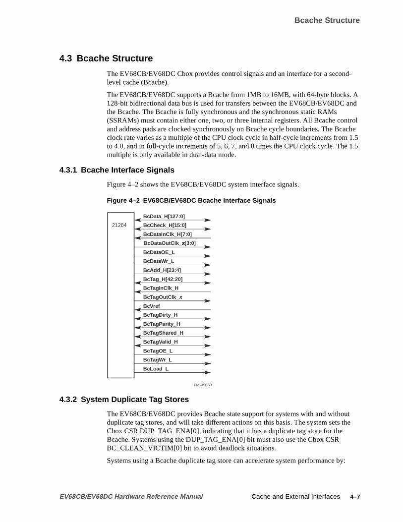
Bcache Structure
-
Aand
trolache
1.51.5
the
4.3 Bcache Structure
The EV68CB/EV68DC Cbox provides control signals and an interface for a secondlevel cache (Bcache).
The EV68CB/EV68DC supports a Bcache from 1MB to 16MB, with 64-byte blocks.128-bit bidirectional data bus is used for transfers between the EV68CB/EV68DCthe Bcache. The Bcache is fully synchronous and the synchronous static RAMs(SSRAMs) must contain either one, two, or three internal registers. All Bcache conand address pads are clocked synchronously on Bcache cycle boundaries. The Bcclock rate varies as a multiple of the CPU clock cycle in half-cycle increments fromto 4.0, and in full-cycle increments of 5, 6, 7, and 8 times the CPU clock cycle. Themultiple is only available in dual-data mode.
4.3.1 Bcache Interface Signals
Figure 4–2 shows the EV68CB/EV68DC system interface signals.
Figure 4–2 EV68CB/EV68DC Bcache Interface Signals
4.3.2 System Duplicate Tag Stores
The EV68CB/EV68DC provides Bcache state support for systems with and withouduplicate tag stores, and will take different actions on this basis. The system sets tCbox CSR DUP_TAG_ENA[0], indicating that it has a duplicate tag store for theBcache. Systems using the DUP_TAG_ENA[0] bit must also use the Cbox CSRBC_CLEAN_VICTIM[0] bit to avoid deadlock situations.
Systems using a Bcache duplicate tag store canaccelerate system performance by:
21264
BcData_H[127:0]
FM-05650
BcCheck_H[15:0]
BcDataInClk_H[7:0]
BcDataOutClk_x[3:0]x
BcDataOE_L
BcDataWr_L
BcAdd_H[23:4]
BcTag_H[42:20]
BcTagInClk_H
BcTagOutClk_ x
BcVref
BcTagDirty_H
BcTagParity_H
BcTagShared_H
BcTagValid_H
BcTagOE_L
BcTagWr_L
BcLoad_L
EV68CB/EV68DC Hardware Reference Manual Cache and External Interfaces 4–7

Victim Data Buffer
iss),lC
iss
g
nd
the)ed
his
e-
are
her-
• Issuing probes and SysDc fill commands to the EV68CB/EV68DC out-of-orderwith respect to their order at the system serialization point
• Filtering out all probe misses from the EV68CB/EV68DC cache system
If a probe misses in the EV68CB/EV68DC cache system (Bcache miss and VAF mthe EV68CB/EV68DC stalls probe processing with the expectation that a SysDc filwill allocate this block. Because of this, in duplicate tag mode, the EV68CB/EV68Dcan never generate a probe miss response.
When Cbox CSR DUP_TAG_ENA[0] equals 0, the EV68CB/EV68DC delivers a mresponse for probes that do not hit in its cache system.
4.4 Victim Data Buffer
The EV68CB/EV68DC has eight victim data buffers (VDBs). They have the followinproperties:
• The VDBs are used for both victims (fills that are replacing dirty cache blocks) afor system probes that require data movement. The CleanVictimBlk command(optional) assigns and uses a VDB.
• Each VDB has two valid bits that indicate the buffer is valid for a victim or validfor a probe or valid for both a victim and a probe. Probe commands that matchaddress of a victim address file (VAF) entry with an asserted probe-valid bit (Pwill stall the EV68CB/EV68DC probe queue. No ProbeResponses will be returnuntil the P bit is clear.
• The release victim buffer (RVB)bit, when asserted, causes the victim valid bit, onthe victim data buffer (VDB) specified in the ID field, to be cleared. The RVB bitwill also clear the IOWB when systems move data on I/O write transactions. In tcase, ID[3] equals one.
• The release probe buffer (RPB) bit, when asserted (with a WriteData or ReleasBuffer SysDc command), clears the P bit in the victim buffer entry specified in theID field.
• Read data commands and victim write commands use IDs 0-7, while IDs 8-11used to address the four I/O write buffers.
4.5 Cache Coherency
This section describes the basics and protocols of the EV68CB/EV68DC cache coency scheme.
4.5.1 Cache Coherency Basics
The EV68CB/EV68DC systems maintain the cache hierarchy shown in Figure 4–3.
4–8 Cache and External Interfaces EV68CB/EV68DC Hardware Reference Manual

Cache Coherency
ache
ted
h
at a
data
hevali-
em
Figure 4–3 Cache Subset Hierarchy
The following tasks must be performed to maintain cache coherency:
• Istream data from memory spaces may be cached in the Icache and Bcache. Iccoherence is not maintained by hardware—it must be maintained by software usingthe CALL_PAL IMB instruction.
• The EV68CB/EV68DC maintains the Dcache as a subset of the Bcache. TheDcache is set-associative but is kept a subset of the larger externally implemendirect-mapped Bcache.
• System logic must help the EV68CB/EV68DC to keep the Bcache coherent witmain memory and other caches in the system.
• The EV68CB/EV68DC requires the system to allow only one change to a blocktime. This means that if the EV68CB/EV68DC gains the bus to read or write ablock, no other node on the bus should be allowed to access that block until thehas been moved.
• The EV68CB/EV68DC provides hardware mechanisms to support several caccoherency protocols. The protocols can be separated into two classes: write indate cache coherency protocol and flush cache coherency protocol.
4.5.2 Cache Block States
Table 4–2 lists the cache block states supported by the EV68CB/EV68DC.
Table 4–2 EV68CB/EV68DC-Supported Cache Block States
State Name Description
Invalid The EV68CB/EV68DC does not have a copy of the block.
Clean This EV68CB/EV68DC holds a read-only copy of the block, and no other agent in the systholds a copy. Upon eviction, the block is not written to memory.
SystemMain Memory
Icache
Bcache
Dcache
FM-05824.AI4
EV68CB/EV68DC Hardware Reference Manual Cache and External Interfaces 4–9
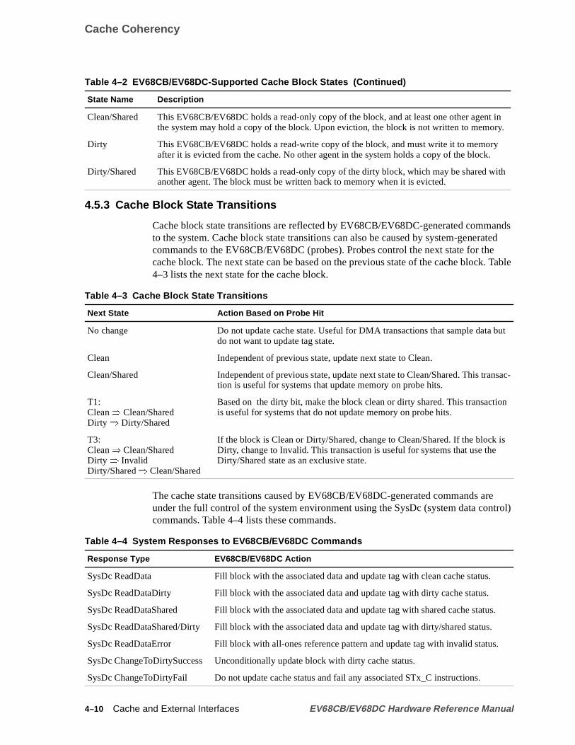
Cache Coherency
ted
Table
etrol)
t iny.
ith
but
ansac-
n
s
.
us.
.
s.
4.5.3 Cache Block State Transitions
Cache block state transitions arereflected by EV68CB/EV68DC-generated commandsto the system. Cache block state transitions can also be caused by system-generacommands to the EV68CB/EV68DC (probes). Probes control the next state for thecache block. The next state can be based on the previous state of the cache block.4–3 lists the next state for the cache block.
The cache state transitions caused by EV68CB/EV68DC-generated commands arunder the full control of the system environment using the SysDc (system data concommands. Table 4–4 lists these commands.
Clean/Shared This EV68CB/EV68DC holds a read-only copy of the block, and at least one other agenthe system may hold a copy of the block. Upon eviction, the block is not written to memor
Dirty This EV68CB/EV68DC holds a read-write copy of the block, and must write it to memoryafter it is evicted from the cache. No other agent in the system holds a copy of the block.
Dirty/Shared This EV68CB/EV68DC holds a read-only copy of the dirty block, which may be shared wanother agent. The block must be written back to memory when it is evicted.
Table 4–3 Cache Block State Transitions
Next State Action Based on Probe Hit
No change Do not update cache state. Useful for DMA transactions that sample datado not want to update tag state.
Clean Independent of previous state, update next state to Clean.
Clean/Shared Independent of previous state, update next state to Clean/Shared. This trtion is useful for systems that update memory on probe hits.
T1:Clean⇒ Clean/SharedDirty ⇒ Dirty/Shared
Based on the dirty bit, make the block clean or dirty shared. This transactiois useful for systems that do not update memory on probe hits.
T3:Clean⇒ Clean/SharedDirty ⇒ InvalidDirty/Shared⇒ Clean/Shared
If the block is Clean or Dirty/Shared, change to Clean/Shared. If the block iDirty, change to Invalid. This transaction is useful for systems that use theDirty/Shared state as an exclusive state.
Table 4–4 System Responses to EV68CB/EV68DC Commands
Response Type EV68CB/EV68DC Action
SysDc ReadData Fill block with the associated data and update tag with clean cache status
SysDc ReadDataDirty Fill block with the associated data and update tag with dirty cache status.
SysDc ReadDataShared Fill block with the associated data and update tag with shared cache stat
SysDc ReadDataShared/Dirty Fill block with the associated data and update tag with dirty/shared status
SysDc ReadDataError Fill block with all-ones reference pattern and update tag with invalid statu
SysDc ChangeToDirtySuccess Unconditionally update block with dirty cache status.
SysDc ChangeToDirtyFail Do not update cache status and fail any associated STx_C instructions.
Table 4–2 EV68CB/EV68DC-Supported Cache Block States (Continued)
State Name Description
4–10 Cache and External Interfaces EV68CB/EV68DC Hardware Reference Manual

Cache Coherency
-
.
s all
C-
ave
8CB/
ore
B/ts
4.5.4 Using SysDc Commands
Note the following:
• The conventional response for RdBlk commands is SysDc ReadData or ReadDataShared.
• The conventional response for a RdBlkMod command is SysDc ReadDataDirty
• The conventional response for ChangeToDirty commands isChangeToDirtySuccess or ChangeToDirtyFail.
However, the system environment is not limited to these responses. Table 4–5 showEV68CB/EV68DC commands, system responses, and the EV68CB/EV68DCreaction.The EV68CB/EV68DC commands are described in the following list:
• Rdx commands are generated by load or Istream references.
• RdBlkModx commands are generated by store references.
• The ChxToDirty command group includes CleanToDirty, SharedToDirty, and STChangeToDirty commands, which are generated by store references that hit in theEV68CB/EV68DC cache system.
• InvalToDirty commands are generated by WH64 instructions that miss in theEV68CB/EV68DC cache system.
• FetchBlk and FetchBlkSpec are noncached references to memory space that hmissed in the EV68CB/EV68DC cache system.
• Rdiox commands are noncached references to I/O address space.
• Evict and STCChangeToDirty commands are generated by ECB and STx_Cinstructions, respectively.
Table 4–5 shows the system responses to EV68CB/EV68DC commands and EV6EV68DC reactions.
Table 4–5 System Responses to EV68CB/EV68DC Commands and Reactions
EV68CB/EV68DC CMD SysDc EV68CB/EV68DC Action
Rdx ReadDataReadDataShared
This is a normal fill. The cache block is filled and marked clean orshared based on SysDc.
Rdx ReadDataShared/Dirty The cache block is filled and marked dirty/shared. Succeeding stcommands cannot update the block without external reference.
Rdx ReadDataDirty The cache block is filled and marked dirty.
Rdx ReadDataError The cache block access was to NXM address space. The EV68CEV68DC delivers an all-ones pattern to any load command and evicthe block from the cache (with associated victim processing). Thecache block is marked invalid.
Rdx ChangeToDirtySuccessChangeToDirtyFail
Both SysDc responses are illegal for read commands.
EV68CB/EV68DC Hardware Reference Manual Cache and External Interfaces 4–11

Cache Coherency
e
e.
CB/
-
t
er-
snd
xTo-
ble.
e
ed
ip
RdBlkModx ReadDataReadDataSharedReadDataShared/Dirty
The cache block is filled and marked with a nonwritable status. If thstore instruction that generated the RdBlkModx command is stillactive (not killed), the EV68CB/EV68DC will retry the instruction,generating the appropriate ChangeToDirty command. Succeedingstore commands cannot update the block without external referenc
RdBlkModx ReadDataDirty The EV68CB/EV68DC performs a normal fill response, and thecache block becomes writable.
RdBlkModx ChangeToDirtySuccessChangeToDirtyFail
Both SysDc responses are illegal for read/modify commands.
RdBlkModx ReadDataError The cache block command was to NXM address space. The EV68EV68DC delivers an all-ones pattern to any dependent load com-mand, forces a fail action on any pending store commands to thisblock, and any store to this block is not retried. The Cbox evicts thecache block from the cache system (with associated victim processing). The cache block is marked invalid.
ChxToDirty ReadDataReadDataSharedReadDataShared/Dirty
The original data in the Dcache is replaced with the filled data. Theblock is not writable, so the EV68CB/EV68DC will retry the storeinstruction and generate another ChxToDirty class command. Toavoid a potential livelock situation, the STC_ENABLE CSR bit musbe set. Any STx_C instruction to this block is forced to fail. In addi-tion, a Shared/Dirty response causes the EV68CB/EV68DC to genate a victim for this block upon eviction.
ChxToDirty ReadDataDirty The data in the Dcache is replaced with the filled data. The block iwritable, so the store instruction that generated the original commacan update this block. Any STx_C instruction to this block is forcedto fail. In addition, the EV68CB/EV68DC generates a victim for thisblock upon eviction.
ChxToDirty ReadDataError Impossible situation. The block must be cached to generate a ChDirty command. Caching the block is not possible because all NXMfills are filled noncached.
ChToDirty ChangeToDirtySuccess Normal response. ChangeToDirtySuccess makes the block writaThe EV68CB/EV68DC retries the store instruction and updates theDcache. Any STx_C instruction associated with this block is allowedto succeed.
ChxToDirty ChangeToDirtyFail The MAF entry is retired. Any STx_C instruction associated with thblock is forced to fail. If a STx instruction generated this block, theEV68CB/EV68DC retries and generates either a RdBlkModx(because the reference that failed the ChangeToDirty also invalidatthe cache by way of an invalidating probe) or another ChxToDirtycommand.
InvalToDirty ReadDataReadDataSharedReadDataShared/Dirty
The block is not writable, so the EV68CB/EV68DC will retry theWH64 instruction and generate a ChxToDirty command.
InvalToDirty ReadDataError The EV68CB/EV68DC doesn’t send InvalToDirty commands offchspeculatively. This NXM condition is a hard error. Systems shouldperform a machine check.
Table 4–5 System Responses to EV68CB/EV68DC Commands and Reactions (Continued)
EV68CB/EV68DC CMD SysDc EV68CB/EV68DC Action
4–12 Cache and External Interfaces EV68CB/EV68DC Hardware Reference Manual

Cache Coherency
ad a
ys-ing
d tobe
wo
r-
ting
ron-
he
B/s
The EV68CB/EV68DC sends a WrVictimBlk command to the system when it evictsDirty or Dirty/Shared cache block. The EV68CB/EV68DC may be configured to senCleanVictimBlk to the system (by way of the Cbox CSR BC_CLEAN_VICTIM[0])when evicting a clean or shared block. Both commands allocate buffers in the VAF(victim address file). This buffer is a coherent part of the EV68CB/EV68DC cache stem. Write data control and deallocation of the VAF can be directly controlled by usthe SysDc WriteData and ReleaseBuffer commands.
4.5.5 Dcache States and Duplicate Tags
Each Dcache block contains an extra state bit (modified bit), beyond those requiresupport the cache protocol. If set, this bit indicates that the associated block shouldwritten to the Bcache when it is evicted from the Dcache. The modified bit is set in tcases:
1. When a block is filled into the Dcache from memory its modified bit is set, ensuing that it also gets written back into the Bcache at some future time.
2. When the processor writes to a dirty Dcache block the modified bit is set, indicait should be written to the Bcache when evicted.
The contents of the modified bit are functionally invisible to the external cache enviment, but knowledge of the bits function is useful to programmers optimizing thescheduling of the Bcache data bus.
InvalToDirty ReadDataDirtyChangeToDirtySuccess
The block is writable. Done.
InvalToDirty ChangeToDirtyFail Illegal. InvalToDirty instructions must provide a cache block.
FetchxRdiox
ReadDataReadDataSharedReadDataShared/DirtyReadDataDirty
The EV68CB/EV68DC delivers the data block, independent of itsstatus, to waiting load instructions and does not cache the block in tEV68CB/EV68DC cache system.
Fetchx ReadDataError The cache block address was to an NXM address space. TheEV68CB/EV68DC delivers the all-ones patterns to any dependentload instructions and does not cache the block in the EV68CB/EV68DC cache system.
Rdiox ReadDataError The cache block access was to NXM address space. The EV68CEV68DC delivers an all-ones pattern to any load command and doenot cache the block in the EV68CB/EV68DC cache system.
Evict ChangeToDirtyFail Retiring the MAF entry is the only legal response.
STCChangeToDirty
ReadDataXChangeToDirtyFail
All fill and ChangeToDirtyFail responses will fail the STx_C require-ments.
STCChangeToDirty
ChangeToDirtySuccess The STx_C instruction succeeds.
MB MBDone Acknowledgment for MB.
Table 4–5 System Responses to EV68CB/EV68DC Commands and Reactions (Continued)
EV68CB/EV68DC CMD SysDc EV68CB/EV68DC Action
EV68CB/EV68DC Hardware Reference Manual Cache and External Interfaces 4–13

Lock Mechanism
yng
findlly-rit-cksbuteep
findit
theress
ort
ld inr
om-
orand.
f itswise,
heche
ict
t use
The Cbox contains a duplicate copy of the Dcache tagarray. In contrast to the Dcachetag array (DTAG), which is virtually indexed, the Cbox copy of the Dcache tag arra(CTAG) is physically-indexed. The Cbox uses the CTAG array entries in the followisituations.
1. When the Mbox requests a Dcache fill, the Cbox uses the CTAG array entry toif the Dcache already contains the requested physical address in another virtuaindexed Dcache line. If it does, the Cbox invalidates that cache line after first wing the data back to the Bcache if it was in the modified state. The Cbox also cheto see if the Dcache contains an address different from the requested address,maps to the same Bcache line. If it does, the Dcache line is evicted in order to kthe Dcache a subset of the Bcache.
2. When the Ibox requests an Icache fill, the Cbox uses the CTAG array entries toif the Dcache contains the requested physical address in the modified state. Ifdoes, the Cbox forces the line to be written back to the Bcache before servicingIcache fill request. The Cbox also checks to see if the Dcache contains an adddifferent from the requested address butwhich maps to the same Bcache line. Inthis case the Istream request will miss the Bcache, and the Cbox willservice the request by launching a noncached Fetch command to the system pand will not put the Istream block into the Bcache. This mechanism allows theEV68CB/EV68DC to use acache resident lock flag forLDx_L/STx_C instruc-tions.
3. The Cbox uses the CTAG array entries to find whether probe addresses are hethe Dcache without interrupting load/store instruction processing in the processocore.
4.6 Lock Mechanism
The EV68CB/EV68DC does not contain a dedicated lock register, nor are system cponents required to do so.
When a load-lock (LDx_L) instruction executes, data is accessed from the DcacheBcache. If there is a cache miss, data is accessed from memory with a RdBlk commIts associated cache line is filled into the Dcache in the clean state, if it is not alreadythere.
When the store-conditional (STx_C) instruction executes, it is allowed to succeed iassociated cache line is still present in the Dcache and can be made writable; otherit fails.
This algorithm is successful because another agent in the system writing to the cacline between the load-lock and the store-conditional cache line would make the caline invalid. This mechanism’s coherence is based on the following four items:
1. LDx_L instructions are processed in-order in relation to the associated STx_C.
2. Once a block is locked by way of an LDx_L instruction, no internal agent can evthe block from the Dcache as a side-effect of its processing.
3. Any external agent that intends to update the contents of the stored block musan invalidating probe command to inform the EV68CB/EV68DC.
4–14 Cache and External Interfaces EV68CB/EV68DC Hardware Reference Manual

Lock Mechanism
fair-gen-en a
c-bit
il
, the
e
ruc-
toreons
-thatfer-
4. The system is the only agent with sufficient information to manage the tasks ofness and liveness. However, to enable these tasks, the EV68CB/EV68DC onlyerates external commands for nonspeculative STx_C instructions, and once givsuccess indication from the system, must faithfully update the Dcache with theSTx_C value.
The system is entirely responsible for item number three. TheEV68CB/EV68DC playsan active role in items one, two, and four.
4.6.1 In-Order Processing of LDx_L/STx_C Instructions
The EV68CB/EV68DC uses the stWait logic in the IQ to ensure that LDx_L/STx_Cpairs are issued in order. The stWait logic treats an Ldx_L instruction like Stx instrutions. STx_C instructions are always loaded into the IQ with their associate stWaitset. Thus, a STx_C instruction is not issued until the older LDx_L is out of the IQ.
4.6.2 Internal Eviction of LDx_L Blocks
The EV68CB/EV68DC prevents the eviction of cache blocks in the Dcache due toeither of the following references:
• Istream referenceswith a Bcache index that matches the Dcache block and aBcache tag that mismatches the Dcache block.
To avoid evictions of LDx_L blocks, Istream references that match theindex of ablock in the Dcache are converted to noncachedreferences.
• Ldx or Stx references with a Dcache index that matches the block.
In the Alpha architecture, Dstream references between aLDx_L/STx_C pair forcethe value of the STx_C success flag to be UNPREDICTABLE. The EV68CB/EV68DC forces all STx_C instructions that interrupt an LDx_L/STx_C pair to fain program order.
There should be no Dstream references between LDx_L/STx_C pairs; howeverout-of-order nature of the EV68CB/EV68DC can introduce Dstream referencesbetween LDx_L/STx_C pairs. To prevent load or store instructions older than thLDx_L from evicting the LDx_L cache block, the Mbox invokes a replay trap onthe incoming load or store instruction, which also aborts the LDx_L. These insttions are issued in program order in the next iteration of the trap retry down thepipeline. To prevent newer load or store instructions from evicting the lockedcache line, the Ibox ensures that a STx_C is issued before any newer load or sinstruction by placing the STx_C into the IQ and stalling all subsequent instructiin the map stage of the pipe until the IQ is empty.
Branch instructions between the LDx_L/STx_C pair may be mispredicted, introducing load and store instructions that evict the locked cache block. To preventfrom happening, there is a bit in the instruction fetcher that is set for a LDx_L reence and cleared on any other memoryreference. Whenthis bit is set, the branchpredictor predicts all branches to fall through.
4.6.3 Liveness and Fairness
To prevent a livelock condition, the EV68CB/EV68DC processes the STx_C as fol-lows:
EV68CB/EV68DC Hardware Reference Manual Cache and External Interfaces 4–15

System Port
the
) isablealf of
-
d the
side
of a-
ves
e
ee-
8CB/.
-
n-s are
tem.nds
1. If a STx_C misses the Dcache, then no system port transaction is started andSTx_C fails.
2. If a STx_C hits a block that is not dirty, then a ChangeToDirty (Shared or Cleanlaunched after the STx_C retires and all older store queue entries are in the writstate. This ensures that once the ChangeToDirty command is launched on behthe STx_C, the STx_C will be executed to completion if the ChangeToDirty command succeeds.
If the ChangeToDirty command succeeds, the STx_C enters the writable state, anMbox locks the Dcache line. The Mbox does not release the Dcache line until theSTx_C data is transferred to the Dcache.This ensures that no other agent, by way of aprobe, can take the block before the STx_C can update the locked block.
4.6.4 Managing Speculative Store Issues with Multiprocessor Systems
The EV68CB/EV68DC provides two mechanisms to manage an inherent potentialeffect of speculative execution with multiprocessor systems — a livelock conditioncaused by a speculative store that misses in one processor affecting the executionLDx_L/STx_C pair in another processor. The potential livelock condition in multiprocessor systems can be effectively controlled by placing processors in a conservatimode, where speculative store MAFs are blocked. The EV68CB/EV68DC manageconservative mode with the Mbox IPR, M_CTL[SMC], described in Table 5–19.
• M_CTL[SMC] can be set to place the EV68CB/EV68DC in full-time conservativmode.
• M_CTL[SMC] can be set to place the EV68CB/EV68DC in periodic conservativmode, timed by two counters: an 8-bit primary counter that tracks branch misprdicts and conditional branch retires, and a backup counter that places the EV6EV68DC in conservative mode for a period of 16K cycles every 2 million cycles
The 8-bit counter is enabled by placing M_CTL[SMC] in periodic conservativemode. The backup counter takeseffect whenever the 8-bit counter is enabled. Further, the backup counter can be reset to 0 by clearing a previously setM_CTL[SMC], allowing synchronization between processors.
4.7 System Port
The system port is the EV68CB/EV68DC’s connection to either a memory or I/O cotroller or to a shared multiprocessor system controller. System port interface signalshown in Figure 4–4.
The system port supports transactions between the EV68CB/EV68DC and the sysSystems must receive and drive signals that are asserted low. Transaction commaare communicated on signal linesSysAddOut_L[14:0] (EV68CB/EV68DC-to-system)andSysAddIn_L[14:0] (system-to-EV68CB/EV68DC). Transaction data is transferredon a bidirectional data bus over padsSysData_L[63:0]with ECC on padsSysCheck_L[7:0].
4–16 Cache and External Interfaces EV68CB/EV68DC Hardware Reference Manual

System Port
Figure 4–4 System Interface Signals
4.7.1 System Port Pads
Table 3–1 defines the EV68CB/EV68DC signal types referred to in this section. Table4–6 lists the system port pad groups along with their type, number, and functionaldescription.
Table 4–6 System Port Pads
Pad Name Type Count Description
IRQ_H[5:0] I_DA 6 These six interrupt signal lines may be asserted by the sys-tem.
SysAddIn_L[14:0] I_DA 15 Time-multiplexed SysAddIn, system-to-EV68CB/EV68DC.
SysAddInClk_L I_DA 1 Single-ended forwarded clock from system forSysAddIn_L[14:0] andSysFillValid_L .
SysAddOut_L[14:0] O_OD 15 Time-multiplexed SysAddOut, EV68CB/EV68DC-to-sys-tem.
SysAddOutClk_L O_OD 1 Single-ended forwarded clock.
SysVref I_DC_REF 1 System interface reference voltage.
SysCheck_L[7:0] B_DA_OD 8 Quadword ECC check bits forSysData_L[63:0].
SysData_L[63:0] B_DA_OD 64 Data bus for memory and I/O data.
SysDataInClk_H[7:0] I_DA 8 Single-ended system-generated clocks for clock forwardedinput system data.
SysDataInValid_L I_DA 1 When asserted, marks a valid data cycle for data transfers tothe EV68CB/EV68DC.
SysDataOutClk_L[7:0] O_OD 8 Single-ended EV68CB/EV68DC-generated clocks for clockforwarded output system data.
SysDataOutValid_L I_DA 1 When asserted, marks a valid data cycle for data transfersfrom the EV68CB/EV68DC.
SysFillValid_L I_DA 1 Validation for fill given in previous SysDc command.
21264
SysAddIn_L[14:0]
FM-05652-EV67
SysAddInClk_L
SysAddOut_L[14:0]
SysAddOutClk_L
SysVref
SysData_L[63:0]
SysCheck_L[7:0]
SysDataInClk_H[7:0]
SysDataOutClk_L[7:0]
SysDataInValid_L
SysDataOutValid_L
SysFillValid_L
IRQ_H[5:0]
EV68CB/EV68DC Hardware Reference Manual Cache and External Interfaces 4–17
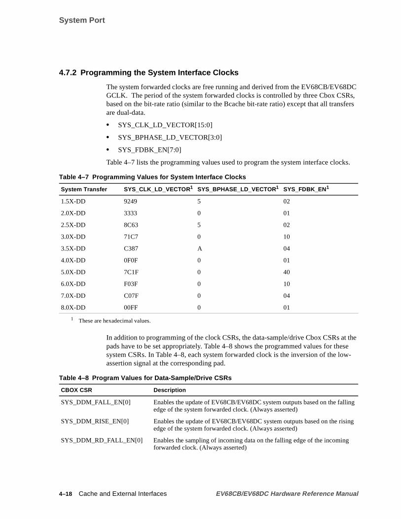
System Port
DCs,
ers
ks.
t these
w-
ing
ing
4.7.2 Programming the System Interface Clocks
The system forwarded clocks are free running and derived from the EV68CB/EV68GCLK. The period of the system forwarded clocks is controlled by three Cbox CSRbased on the bit-rate ratio (similar to the Bcache bit-rate ratio) except that all transfare dual-data.
• SYS_CLK_LD_VECTOR[15:0]
• SYS_BPHASE_LD_VECTOR[3:0]
• SYS_FDBK_EN[7:0]
Table 4–7 lists the programming values used to program the system interface cloc
In addition to programming of the clock CSRs, the data-sample/drive Cbox CSRs apads have to be set appropriately. Table 4–8 shows the programmed values for thesystem CSRs. In Table 4–8, each system forwarded clock is the inversion of the loassertion signal at the corresponding pad.
Table 4–7 Programming Values for System Interface Clocks
System Transfer SYS_CLK_LD_VECTOR 1
1 These are hexadecimal values.
SYS_BPHASE_LD_VECTOR 1 SYS_FDBK_EN 1
1.5X-DD 9249 5 02
2.0X-DD 3333 0 01
2.5X-DD 8C63 5 02
3.0X-DD 71C7 0 10
3.5X-DD C387 A 04
4.0X-DD 0F0F 0 01
5.0X-DD 7C1F 0 40
6.0X-DD F03F 0 10
7.0X-DD C07F 0 04
8.0X-DD 00FF 0 01
Table 4–8 Program Values for Data-Sample/Drive CSRs
CBOX CSR Description
SYS_DDM_FALL_EN[0] Enables the update of EV68CB/EV68DC system outputs based on the falledge of the system forwarded clock. (Always asserted)
SYS_DDM_RISE_EN[0] Enables the update of EV68CB/EV68DC system outputs based on the risedge of the system forwarded clock. (Always asserted)
SYS_DDM_RD_FALL_EN[0] Enables the sampling of incoming data on the falling edge of the incomingforwarded clock. (Always asserted)
4–18 Cache and External Interfaces EV68CB/EV68DC Hardware Reference Manual

System Port
set
era-
-
–10it to
nd-
)
Table 4–9 lists the program values for CSR SYS_FRAME_LD_VECTOR[4:0] thatthe ratio between the forwarded clocks and the frame clock.
4.7.3 EV68CB/EV68DC-to-System Commands
This section describes the EV68CB/EV68DC-to-system commands format and option. The command, address, ID, and mask bits are transmitted in four consecutivecycles onSysAddOut_L[14:0]. The EV68CB/EV68DC sends the command information in one of the two following modes as selected by the Cbox CSR bit.
• Bank interleave on cache block boundary mode—SYSBUS_FORMAT[0] = 0
• Page hit mode—SYSBUS_FORMAT[0] = 1
The physical address (PA) bits arrangements for the two modes is shown in Tables 4and 4–11. The purpose of the two modes is to give the system the PA bits that allowselect the memory bank and drive the RAS address as soon as possible.
4.7.3.1 Bank Interleave on Cache Block Boundary Mode
Table 4–10 shows the command format for the bank interleave on cache block bouary mode of operation (EV68CB/EV68DC-to-system).
SYS_DDM_RD_RISE_EN[0] Enables the sampling of incoming data on the rising edge of the incomingforwarded clock. (Always asserted)
SYS_DDMF_ENABLE Enables the falling edge of the system forwarded clock. (Always asserted
SYS_DDMR_ENABLE Enables the rising edge of the system forwarded clock. (Always asserted)
Table 4–9 Forwarded Clocks and Frame Clock Ratio
Clock Ratio Transfer Mode Value 1
1 These are hexadecimal values.
1:1 All 00
2:1 3.0X, 3.5X, 8.0X 1E
2:1 1.5X, 2.0X, 2.5X 4.0X, 5.0X, 6.0X 7.0X 1F
4:1 8X 15
4:1 1.5X, 4.0X, 5.0X, 6.0X, 7.0X 0B
4:1 3.0X, 3.5X 14
4:1 2.0X, 2.5X 0A
Table 4–10 Bank Interleave on Cache Block Boundary Mode of Operation
SysAddOut_L[14:2] SysAddOut_L[1] SysAddOut_L[0]
Cycle 1 M1 Command[4:0] PA[34:28] PA[36] PA[38]
Table 4–8 Program Values for Data-Sample/Drive CSRs (Continued)
CBOX CSR Description
EV68CB/EV68DC Hardware Reference Manual Cache and External Interfaces 4–19

System Port
ys-
of 8nd/
tem-H
ble issther
tes
inates
4.7.3.2 Page Hit Mode
Table 4–11 shows the command format for page hit mode (EV68CB/EV68DC-to-stem).
Table 4–12 describes the field definitions for Tables 4–10 and 4–11.
Cycle 2 PA[27:22], PA[12:6] PA[35] PA[37]
Cycle 3 M2 Mask[7:0] CH ID[2:0] PA[40] PA[42]
Cycle 4 RV PA[21:13], PA[5:3] PA[39] PA[41]
Table 4–11 Page Hit Mode of Operation
SysAddOut_L[14:2] SysAddOut_L[1] SysAddOut_L[0]
Cycle 1 M1 Command[4:0] PA[31:25] PA[32] PA[33]
Cycle 2 PA[24:12] PA[11] PA[34]
Cycle 3 M2 Mask[7:0] CH ID[2:0] PA[35] PA[37]
Cycle 4 RV PA[34:32], PA[11:3] PA[36] PA[38]
Table 4–12 EV68CB/EV68DC-to-System Command Fields Definitions
SysAddOut Field Definition
M1 When set, reports a miss to the system for the oldest probe.When clear, has no meaning.
Command[4:0] The 5-bit command field is defined in Table 4–14.
SysAddOut[1:0] This field is needed for systems with greater than 32GB of memory, up to a maximumTerabyte (8TB). Cost-focused systems can tie these bits high and use a 13-bit commaaddress field.
M2 When set, reports that the oldest probe has missed in cache. Also, this bit is set for systo-EV68CB/EV68DC probe commands that hit but have no data movement (see the Cbit, below).When clear, has no meaning.M1 and M2 are not asserted simultaneously. Reporting probe results as soon as possicritical to high-speed operation, so when a result is known the EV68CB/EV68DC usethe earliest opportunity to send an M signal to the system. M bit assertion can occur eiin a valid command or a NZNOP.
ID[2:0] The ID number for the MAF, VDB, or WIOB associated with the command.
RV If set, validates this command.In speculative read mode (optional), RV = 1 validates the command and RV = 0 indicaa NOP.For all nonspeculative commands RV = 1.
Mask[7:0] The byte, LW, or QW mask field for the corresponding I/O commands.
CH The cache hit bit is asserted, along with M2, when probes with no data movement hitthe Dcache or Bcache. This response can be generated by a probe that explicitly indicno data movement or a ReadIfDirty command that hits on a valid but clean or sharedblock.
Table 4–10 Bank Interleave on Cache Block Boundary Mode of Operation (Continued)
SysAddOut_L[14:2] SysAddOut_L[1] SysAddOut_L[0]
4–20 Cache and External Interfaces EV68CB/EV68DC Hardware Reference Manual

System Port
fig-de
luescal
anyand
by
t.
es as
System designers can minimize pad count for systems with a small memory by conuring both the bank interleave on cache block boundary mode and the page hit moformats into ashort busformat. The padSysAddOut_L[1] and/orSysAddOut_L[0]are not used (selected by Cbox CSR SYS_BUS_SIZE[1:0]). Table 4–13 lists the vafor SYS_BUS_FORMAT and SYS_BUS_SIZE[1:0] and shows the maximum physimemory size.
Because addresses above the maximum PA are not visible to the external system,memory transaction generated to addresses above the maximum PA are detectedconverted to transactions to NXM (nonexistent memory) and processed internallythe EV68CB/EV68DC.
4.7.4 EV68CB/EV68DC-to-System Commands Descriptions
Table 4–14 describes the EV68CB/EV68DC-to-system commands.
Table 4–13 Maximum Physical Address for Short Bus Format
SYS_BUS_FORMAT
SYS_BUS_SIZE[1:0] Maximum PA Comment
0 00 42 Bank interleave + full address
0 01 36 Bank interleave +SysAddOut_L[0] unused
0 10 Illegal Illegal combination
0 11 34 Bank interleave + bothSysAddOut_L[1:0] are used for I/O
1 00 38 Page hit mode + full address
1 01 36 Page hit mode +SysAddOut_L[0] unused
1 10 Illegal Illegal combination
1 11 34 Page hit mode + bothSysAddOut_L[1:0] are unused
Table 4–14 EV68CB/EV68DC-to-System Commands Descriptions
CommandCommand
[4:0] Function
NOP 00000 The EV68CB/EV68DC drives this command on idle cycles during reseAfter the clock forward reset period, the first NZNOP is generated andthis command is no longer generated.
ProbeResponse 00001 Returns probe status and ID number of the VDB entry holding therequested cache block.
NZNOP 00010 This nonzero NOP helps to parse the command packet.
VDBFlushRequest 00011 VDB flush request. The EV68CB/EV68DC sends this command to thsystem when an internally generated transaction Bcache index matcheBcache victim or probe in the VDB. The system should flush VDB entrieassociated with all probe and WrVictimBlk transactions that occurredbefore this command.
MB1 00111 Indicates an MB was issued, optional when Cbox CSRSYSBUS_MB_ENA[0] is set.
ReadBlk 10000 Memory read.
EV68CB/EV68DC Hardware Reference Manual Cache and External Interfaces 4–21

System Port
).
or
ReadBlkMod 10001 Memory read with modify intent.
ReadBlkI 10010 Memory read for Istream.
FetchBlk 10011 Noncached memory read.
ReadBlkSpec2 10100 Speculative memory read (optional).
ReadBlkModSpec2 10101 Speculative memory read with modify intent (optional).
ReadBlkSpecI2 10110 Memory read for Istream (optional).
FetchBlkSpec2 10111 Speculative memory noncached ReadBlk (optional).
ReadBlkVic3 11000 Memory read with a victim (optional).
ReadBlkModVic3 11001 Memory read with modify intent, with a victim (optional).
ReadBlkVicI3 11010 Memory read for Istream with a victim (optional).
WrVictimBlk 00100 Write-back of dirty block.
CleanVictimBlk 00101 Address of a clean victim (optional).
Evict4 00110 Invalidate evicted block at the given Bcache index (optional).
ReadBytes 01000 I/O read, byte mask.
ReadLWs 01001 I/O read, longword mask.
ReadQWs 01010 I/O read, quadword mask.
WrBytes 01100 I/O write, byte mask.
WrLWs 01101 I/O write, longword mask.
WrQWs 01110 I/O write, quadword mask.
CleanToDirty6 11100 Sets a block dirty that was previously clean (optional for duplicate tags
SharedToDirty6 11101 Sets a block dirty that was previously shared (optional for multiprocesssystems).
STCChangeToDirty6 11110 Sets a block dirty that was previously clean or shared for a STx_Cinstruction (optional for multiprocessor systems).
InvalToDirtyVic3,5 11011 Invalid to dirty with a victim (optional).
InvalToDirty5 11111 WH64 Acts like a ReadBlkMod without the fill cycles (optional).
Table 4–14 EV68CB/EV68DC-to-System Commands Descriptions (Continued)
CommandCommand
[4:0] Function
4–22 Cache and External Interfaces EV68CB/EV68DC Hardware Reference Manual

System Port
ting
la-
ombi-x,
ns
k
-
d
x
isc-
t
Table 4–14 footnotes:
1. Systems can optionally enable MB instructions to the external system by asserCbox CSR SYSBUS_MB_ENABLE. This mode is described in Section 2.12.1.
2. To minimize load-to-use memory latency, systems can optionally enable specutive transactions to memory space by asserting the Cbox CSRSPEC_READ_ENABLE[0]. If the Cbox system command queue is empty, abypass between the Bcache interface and the system interface is enabled (in cnation with this mode). When the next new transaction is delivered by the Mbothe Cbox starts MAF memory references to the system interface before the resultsof Bcache hit is known. The RV bit is deasserted on a Bcache hit, or inBC_RDVICTIM[0] mode (see footnote 3, below), and for Bcache miss transactiothat generate a victim (clean or dirty). Otherwise, the RV bit is asserted.
3. Systems can optionally enable RdBlkVic, RdBlkModVic, and InvalToDirtyViccommands using Cbox CSR BC_RDVICTIM[0]. In this mode of operationRdBlkxVic command cycles are always followed immediately by the WrVictimBlcommands. Also, when CleanVictimBlk commands are enabled, theyimmediately follow RdBlkVic, RdBlkModVic, and InvalToDirtyVic commands.
4. Systems can optionally enable Evict commands by asserting the Cbox CSRENABLE_EVICT. In this mode, all ECB instructions will generate an Evict command, and in combination with BC_RDVICTIM[0] mode, the WriteVictim orCleanVictim (when Cbox CSR BC_CLEAN_VICTIM[0] is asserted) is associatewith the Evict command is atomically sent after the Evict command.
5. Optionally, systems can enable InvalToDirty commands by programming CboxCSR INVAL_TO_DIRTY_ENABLE[1:0]. Table 4–15 shows how to programINVAL_TO_DIRTY_ENABLE[1:0].
6. Optionally, systems can enable CleanToDirty or SharedToDirty commands byusing Cbox CSR SET_DIRTY_ENABLE[2:0]. These three bits control the Cboaction upon a block that was hit in the Dcache with a status of dirty/shared, clean/shared, or clean respectively.
Table 4–15 Programming INVAL_TO_DIRTY_ENABLE[1:0]
INVAL_TO_DIRTY_ENABLE[1:0] Cbox Action
X0 WH64 instructions are converted to RdModx commands at the interface.Beyond this point, no other agent sees the WH64 instruction. This modeuseful for microprocessors that do not want to support InvalToDirty transations.
01 WH64 instructions are enabled, but they are acknowledged within theEV68CB/EV68DC.
11 WH64 instructions are enabled, and generate InvalToDirty transactions athe EV68CB/EV68DC pads.
EV68CB/EV68DC Hardware Reference Manual Cache and External Interfaces 4–23

System Port
iti-
dis-and
, theiti-
r
).
nd
ds
Systems that require an explicit indication of ChangeToDirty status changes inated by STx_C instructions can assert Cbox CSR STC_ENABLE[0]. When thisregister field = 000, CleanToDirty and SharedToDirty commands are used. Thetinction between a ChangeToDirty command generated by a STx_C instructionone generated by a STx instruction is important to systems that want to serviceChangeToDirty commands with dirty data from a source processor. In this casedistinction between a locked exclusive instruction and a normal instruction is crcal to avoid livelock for a LDx_L/STx_C sequence.
4.7.5 ProbeResponse Commands (Command[4:0] = 00001)
The EV68CB/EV68DC responds to system probes that did not miss with a 4-cycletransfer onSysAddOut_L[14:0]. As shown in Table 4–14, the Command[4:0] field foa ProbeResponse command equals 00001. Table 4–17 shows the format of theEV68CB/EV68DC ProbeResponse command.
Table 4–16 Programming SET_DIRTY_ENABLE[2:0]
SET_DIRTY_ENABLE[2,0] (DS,CS,C) Cbox Action
000 Everything acknowledged internally (uniprocessor).
001 Only clean blocks generate external acknowledge (CleanToDirty commands only
010 Only clean/shared blocks generate external acknowledge (SharedToDirty commaonly).
011 Clean and clean/shared blocks generate external acknowledge.
100 Only dirty/shared blocks generate external acknowledge (SharedToDirty commanonly).
101 Only dirty/shared and clean blocks generate external acknowledge.
110 Only dirty/shared and clean/shared blocks generate external acknowledge.
111 All transactions generate external acknowledge.
Table 4–17 EV68CB/EV68DC ProbeResponse Command
SysAddOut_L[14:2] SysAddOut_L[1] SysAddOut_L[0]
Cycle 1 0 00001 Status[1:0] DM VS VDB[2:0]
X X
Cycle 2 0 MS MAF[2:0]
X X
Cycle 3 0 X X X
Cycle 4 X X X
4–24 Cache and External Interfaces EV68CB/EV68DC Hardware Reference Manual

System Port
cache2-be
e
ndsne
e
-
T
4.
Table 4–18 describes the ProbeResponse command fields.
The system uses the SysDc signal lines to retrieve data for probes that requested ablock from the EV68CB/EV68DC. See Section 4.7.7.2 for more information aboutcycle data transfer commands. Probes that respond with M1, M2, or CH=1 will notreported to the system in a probe response command.
4.7.6 SysAck and EV68CB/EV68DC-to-System Commands Flow Control
Controlling the flow of EV68CB/EV68DC-to-system commands is a joint task of theEV68CB/EV68DC and the system. The flow is controlled using the A bit, which isasserted by the system, and the Cbox CSR SYSBUS_ACK_LIMIT[4:0] counter. Thcounter has the following properties:
• The EV68CB/EV68DC increments its command-outstanding counter when it sea command to the system. The EV68CB/EV68DC decrements the counter by oeach time the A bit (SysAddIn_L[14]) is asserted in a system-to-EV68CB/EV68DC command. The A bit is transmitted during cycle four of a probe modecommand or during cycle two of a SysDc command.
• The EV68CB/EV68DC stops sending new commands when the counter hits thmaximum count specified by Cbox CSR SYSBUS_ACK_LIMIT[4:0]. When thiscounter is programmed to zero, the CMD_ACK count is ignored (unlimited commands are allowed in-flight).
• Because RdBlkxVic and WrVictimBlk commands are atomic when the CSRBC_RDVICTIM[0] is set, the EV68CB/EV68DC does not send a RdBlkxVic com-mand if the SYSBUS_ACK_LIMIT[4:0] is equal to one less than the maximumoutstanding count. The limit cannot be programmed with a value of one whenRdBlkxVic commands are enabled unless the Cbox CSR RDVIC_ACK_INHIBIcommand is also asserted (see Table 5–24).
Table 4–18 ProbeResponse Fields Descriptions
ProbeResponse Field Description
Command[4:0] The value 00001 identifies the command as a ProbeResponse.
DM Indicates that data movement should occur (copy of probe valid bit). See Section 4.
VS Write victim sent bit.
VDB[2:0] ID number of the VDB entry containing the requested cache block. This field is validwhen either the DM bit or the VS bit equals 1.
MS MAF address sent.
MAF[2:0] This field indicates the SharedToDirty, CleanToDirty, orSTCChangetoDirty MAF entry that matched the full probe address.
Status[1:0] Result of probe:Status[1:0] Probe state
00 HitClean01 HitShared10 HitDirty11 HitSharedDirty
EV68CB/EV68DC Hardware Reference Manual Cache and External Interfaces 4–25

System Port
ust
ofbox
xd
ds to
com-
eank
.
• There is no mechanism for the system to reject an EV68CB/EV68DC-to-systemcommand. ProbeResponse, VDBFlushReq, NOP, NZNOP, and RdBlkxSpec (with aclear RV bit) commands do not require a response from the system. Systems mprovide adequate resources for responses to all probes sent to the EV68CB/EV68DC.
• Systems that program the Cbox CSR BC_RDVICTIM[0] to immediately followvictim write transactions with read transactions and allocate combined resourcesfor the pair, may find it useful to increment the SYSBUS_ACK_LIMIT[4:0]counter only once for the pair. These systems may assert Cbox CSRRDVIC_ACK_INHIBIT, which does not increment theSYSBUS_ACK_LIMIT[4:0] count for RdBlkVic, RdBlkModVic, and RdBlkVicIcommands.
• Systems that maintain victim data buffers may find it useful to limit the numberoutstanding WrVictimBlk commands. This can be accomplished by using the CCSR SYSBUS_VIC_LIMIT[2:0]. When the number of outstanding WrVictimcommands or CleanVictim commands reaches this programmed limit, the Cbostops generating victim commands on the system port. Because victim and reacommands are atomic when BC_RDVICTIM[0] = 1, the RdBlkxVic commands arestalled when the victim limit is reached. Programming theSYSBUS_VIC_LIMIT[2:0] to zero disables this limit.
4.7.7 System-to-EV68CB/EV68DC Commands
The system can send either probes (4-cycle) or data movement (2-cycle) commanthe EV68CB/EV68DC. Signal padSysAddIn_L[14] in the first command cycle indi-cates the type of command being sent (1 = probe, 0 = data transfer). Sections 4.7.7.1and 4.7.7.2 describe the formats of the two types of commands.
4.7.7.1 Probe Commands (Four Cycles)
Probes are always 4-cycle commands that contain a field to indicate a valid SysDcmand. The format of the 4-cycle command is shown below.
Note: TheSysAddIn_L[1:0] signal lines are optional and are used for memorydesigns greater than 32GB. The position of the address bits matches thselected format of the SysAddOut bus. The example below shows the binterleave format.
Table 4–19 shows the format of the system-to-EV68CB/EV68DC probe commands
Table 4–19 System-to-EV68CB/EV68DC Probe Commands
SysAddIn_L[14:2] SysAddIn_L[1] SysAddIn_L[0]
Cycle 1 1 Probe[4:0] PA[34:28] PA[36] PA[38]
Cycle 2 PA[27:22], PA[12:6] PA[35] PA[37]
Cycle 3 0 SysDc[4:0] RVB RPB A ID[3:0] PA[40] PA[42]
Cycle 4 C PA[21:13], PA[5:3] PA[39] PA[41]
4–26 Cache and External Interfaces EV68CB/EV68DC Hardware Reference Manual

System Port
crip-
f
t-
Table 4–20 describes the system-to-EV68CB/EV68DC probe commands fields destions.
The probe command field Probe[4:0] has two sections, Probe[4:3] and Probe[2:0].
Table 4–21 lists the data movement selected by Probe[4:3].
Table 4–22 lists the next cache block state selected by Probe[2:0].
Table 4–20 System-to-EV68CB/EV68DC Probe Commands Fields Descriptions
SysAddIn_L[14:0]Field Description
Probe[4:0] Probe type and next tag state (see Tables 4–21 and 4–22).
SysDc[4:0] Controls data movement in and out of the EV68CB/EV68DC. See Table 4–24 for a list odata movement types.
RVB Clears the victim or I/O write buffer (IOWB) valid bit specified in ID[3:0].
RPB Clears probe valid bit specified in ID[2:0].
A Command acknowledge. When set, the EV68CB/EV68DC decrements its command oustanding counter (SYSBUS_ACK_LIMIT[4:0]).
ID[3:0] Identifies the victim data buffer (VDB) number or the I/O write buffer (IOWB) number.Bit [3] is only asserted for the IOWB.
C Commit bit. This bit decrements the uncommitted event counter (MB_CNTR) used forMB acknowledge.
Table 4–21 Data Movement Selection by Probe[4:3]
Probe[4:3] Data Movement Function
00 NOP
01 Read if hit, supply data to system if block is valid.
10 Read if dirty, supply data to system if block is valid/dirty.
11 Read anyway, supply data to the system at index of probe.
Table 4–22 Next Cache Block State Selection by Probe[2:0]
Probe[2:0] Next Tag State
000 NOP
001 Clean
010 Clean/Shared
011 Transition31: Clean⇒ Clean/SharedDirty ⇒ InvalidDirty/Shared⇒ Clean/Shared
100 Dirty/Shared
EV68CB/EV68DC Hardware Reference Manual Cache and External Interfaces 4–27

System Port
eue.thees
ches
ideses.
ome
con-
the
-
The EV68CB/EV68DC holds pending probe commands in a 8-entry deep probe quThe system must count the number of probes that have been sent and ensure thatprobes do not overrun the EV68CB/EV68DC queue. The EV68CB/EV68DC removprobes from the internal probe queue when the probe response is sent.
The EV68CB/EV68DC expects to hit in cache on a probe response, so it always feta cache block from the Bcache on system probes. This can become a performance prob-lem for systems that do not monitor the Bcache tags, so the EV68CB/EV68DC provCbox CSR PRB_TAG_ONLY[0], which only accesses Bcache tags for system probFor a Bcache hit, the EV68CB/EV68DC retries the probe reference to get the associateddata. In this mode, the EV68CB/EV68DC has a cache-hit counter that maintains shistory of past cache hits in order to fetch the data with the tag in the cases wherestreamed transactions are being performed to the host processor.
4.7.7.2 Data Transfer Commands (Two Cycles)
Data transfer commands use a 2-cycle format onSysAddIn_L[14:0]. The SysDc[4:0]field indicates success or failure for ChangeToDirty and MB commands, and errorditions as shown in Table 4–24.
The pattern of data is controlled by theSysDataInValid_L andSysDataOutValid_Lsignals. These signals are valid each cycle of data transfer, indicating any gaps indata cycle pattern. TheSysDataInValid_L andSysDataOutValid_L signals aredescribed in Section 4.7.8.4. Table 4–23 shows the format of the data transfer command.
101 Invalid
110 Transition12: Clean⇒ Clean/SharedDirty ⇒ Dirty/Shared
111 Reserved
1 Transition3 is useful in nonduplicate tag systems that want to give writable status to the reader and donot know if the block is clean or dirty.
2 Transition1 is useful in nonduplicate tag systems that do not update memory on ReadBlk hits to adirty block in another processor.
Table 4–23 Data Transfer Command Format
SysAddIn_L[14:2] SysAddIn_L[1] SysAddIn_L[0]
Cycle 1 0 SysDc[4:0] RVB RPB A ID[3:0] X X
Cycle 2 C X X X
Table 4–22 Next Cache Block State Selection by Probe[2:0] (Continued)
Probe[2:0] Next Tag State
4–28 Cache and External Interfaces EV68CB/EV68DC Hardware Reference Manual

System Port
theot
nt,ws
ing
eadD-
Data
-
e
r.
he
r.
Table 4–24 describes the SysDc[4:0] field.
The A bit in the first cycle indicates that the command is acknowledged. When A = 1,EV68CB/EV68DC decrements its command outstanding counter, but the A bit is nnecessarily related to the current SysDc command.
Probe commands can combine a SysDc command along with MBDone. In that evethe probe is considered ahead of the SysDc command. If the SysDc command allothe EV68CB/EV68DC to retire an instruction before an MB, or allows the EV68CB/EV68DC itself to retire an MB (SysDc is MBDone), that MB will not complete untilthe probe is executed.
The system can select the ending cache status for a cache fill operation by specifythe status in one of the following SysDc commands:
ReadData (Clean) ReadDataShared (Clean/Shared)
ReadDataDirty (Dirty) ReadDataShared/Dirty (Shared/Dirty)
The system returns ReadDataShared or ReadData for ReadBlk commands, and RataDirty for a ReadMod command. However, other combinations are possible, butshould be used only after a careful study of thesituation.
Table 4–24 SysDc[4:0] Field Description
SysDc[4:0] Command SysDc[4:0] Description
NOP 00000 NOP, SysData is ignored by the EV68CB/EV68DC.
ReadDataError 00001 Data is returned for read commands. The system drives the Sysbus, I/O, or memory NXM.
ChangeToDirtySuccess 00100 No data. SysData is ignored by the EV68CB/EV68DC. This command is also used for the InvalToDirty response.
ChangeToDirtyFail 00101 No data. SysData is ignored by the EV68CB/EV68DC. This com-mand is also used for the Evict response.
MBDone 00110 Memory barrier operation completed.
ReleaseBuffer 00111 Command to alert the EV68CB/EV68DC that the RVB, RPB, andID field are valid.
ReadData(System Wrap)
100xx Data returned for read commands. The system drives SysData. Thsystem uses SysDc[1:0] to control the wrap order. See Section4.7.8.6 for a description of the data wrapping scheme.
ReadDataDirty(System Wrap)
101xx Data is returned for Rdx and RdModx commands. The ending tagstatus is dirty. The system uses SysDc[1:0] to define the wrap orde
ReadDataShared(System Wrap)
110xx Data is returned for read commands. The system drives the data. Ttag is marked shared. The system uses SysDc[1:0] to control thewrap order.
ReadDataShared/Dirty(System Wrap)
111xx Data is returned for the RdBlk command. The ending tag status isShared/Dirty. The system uses SysDc[1:0] to control the wrap orde
WriteData 010xx Data is sent for EV68CB/EV68DC write commands or systemprobes. The EV68CB/EV68DC drives during the SysData cycles.The lower two bits of the command specify the octaword addressaround which the EV68CB/EV68DC wraps the data.
EV68CB/EV68DC Hardware Reference Manual Cache and External Interfaces 4–29

System Port
in the,eight
com-sys-e six
fut-ssor.
using
ncywodata8.1.
d-
wdata
an
yondeue
k’s
;
The ChangeToDirtySuccess and ChangeToDirtyFail commands cannot be issuedshadow of SysDc cache fill commands (ReadDataError, ReadData, ReadDataDirtyReadDataShared, and ReadDataShared/Dirty). Each cache fill command allocatescycles on the SysData bus. Systems are required to ensure that any future SysDcmands do not cause conflicts with those eight SysData bus cycles. In addition, thetem must not issue ChangeToDirtySuccess or ChangeToDirtyFail commands in thSysAddrIn cycles after any of the ReadDatax commands because doing so will over-load internal MAF resources in the EV68CB/EV68DC.
Because of an internal EV68CB/EV68DC constraint, a minimum memory latency o4 × BCACHE_CLK_PERIOD is imposed. This latency is measured from A3 of the ogoing command (the last cycle) to the delivery of the SysDc command to the proce
4.7.8 Data Movement In and Out of the EV68CB/EV68DC
There are two modes of operation for data movement in and out of the EV68CB/EV68DC: fast mode and fast mode disable. The data movement mode is selectedCbox CSR FAST_MODE_DISABLE[0]. Fast data mode allows movement of datafrom the EV68CB/EV68DC to bypass protocol and achieve the lowest possible latefor probe’s data, write victim data, and I/O write data. Rules and conditions for the tmodes are listed and described in Sections 4.7.8.2 and 4.7.8.3. Before discussingmovement operation, EV68CB/EV68DC clock basics are described in Section 4.7.
4.7.8.1 EV68CB/EV68DC Clock Basics
The EV68CB/EV68DC uses a clock forwarding technique to achieve very high banwidth on its pad interfaces. The clock forwarding technique has three main principles:
1. Local point-to-point transfers can be made safely, and at veryhigh bandwidth, if thesender can provide the receiver with a forward clock (FWD_CLK) to latch thetransmitted data at the receiver.
– TheSysAddOutClk_L andSysDataOutClk_L[7:0] pads provide the for-warding clocks for transfers out of the EV68CB/EV68DC.
– TheSysAddInClk_L andSysDataInClk_H[7:0] pads provide the forwardingclocks for transfers into the EV68CB/EV68DC.
2. If only one state element was used to capture the transmitted data, and the skebetween the two clock systems was greater then the bit-rate of the transfer, thevalid time of the transmitted data would not be sufficient to safely transfer thelatched data into the receivers clock domain. In order to avoid this problem, thereceiver provides a queue that is manipulated in the transmitter’s time domain.Using this queue, the data valid window of the transmitted data is extended (toarbitrary size based on the queue size), and the transfer to the receiver’s clockdomain can be safely made by delaying the unloading of this queue element bethe skew between the two clock domains. The internal clock that unloads this quis labelled INT_FWD_CLK. INT_FWD_CLK is timed at both the rising and fall-ing edges of the external clock, thus appearing to run at twice the external clocfrequency.
3. The first two points provide the steady state basis for clock forwarded transfershowever, both the sender and receiver must be correctly initialized to enable coher-ent and predictable transfers.This clock initialization is performed during systeminitialization using theClkFwdRst_H andFrameClk_H signals.
4–30 Cache and External Interfaces EV68CB/EV68DC Hardware Reference Manual

System Port
iples
, the
are/
ock,
-for-
ycles)xtut
tedycle
-ataarts:
he
If both the sender and the receiver are sampling at the same rate, these three princare sufficient to safely make point-to-point transfers using clock forwarding.However,it is often desirable for systems to align clock-forwarded transactions on a slowerSYSCLK that is the basis of all non-processor system transactions.
The EV68CB/EV68DC supports three ratios for SYSCLK to INT_FWD_CLK:one-to-one (1-1), two-to-one (2-1), and four-to-one (4-1). Using one of these ratiosEV68CB/EV68DC starts transactions on SYSCLK boundaries. This ratio is pro-grammed into the EV68CB/EV68DC using the Cbox CSRSYS_FRAME_LD_VECTOR[4:0]. This ratio is independent of thefrequency ofFrameClk_H.
For data movement, the EV68CB/EV68DC reacts to SysDc commands when theyresolved into the EV68CB/EV68DC’s clock domain. This occurs when the EV68CBEV68DC’s INT_FWD_CLK unloads the SysDc command from the clock forwardingqueue. This moment is determined by the amount of delay programmed into the clforwarding silo (by way of Cbox CSR SYS_RCV_MUX_CNT_PRESET[1:0]). Thusall the timing relationships are relative to this unload point in time, which will bereferred to as thepoint the command is perceived by EV68CB/EV68DC.
4.7.8.2 Fast Data Mode
The EV68CB/EV68DC is the default driver of the bidirectional SysData bus1. As theEV68CB/EV68DC is processing WrVictim, ProbeResponse (only the hit case), andIOWB commands to the system, accompanying data is made available at the clockwarded bus.
Because there is a bandwidth difference between address (4 cycles) and data (8 ctransfers, the EV68CB/EV68DC tries to fully use fast data mode by delaying the neSysAddOut write command until a fast data mode slot is available on the SysDataObus.
SysDc commands(cache fill or explicit write commands) that collide with the fast dataon the SysData bus have higher priority, and so may interrupt the successful completionof the fast transfer. Systems are responsible for detecting and replaying all interrupfast transfers. There are no gaps in a fast transfer and no data wrapping (the first ccontains QW0, addressed by PA[5:3] = 000).
The system must release victim buffers, and probe buffers and IOWB entries by sending a SysDc command with the appropriate RVB/RPB bit for both successful fast dtransfers and for transfers that have been replayed. Fast data transfers have two p
1. SysAddOut command with the probe response, WrVictim, or Wr(I/O)
2. Data
The command precedes data by at least one SYSCLK period. Table 4–25 shows tnumber of SYSCLK cycles between SysAddOut and SysData for all system clockratios (clock forwarded bit times) and system framing clock multiples.
1 The SysData bus containsSysData_L[63:0]andSysCheck_L[7:0].
EV68CB/EV68DC Hardware Reference Manual Cache and External Interfaces 4–31
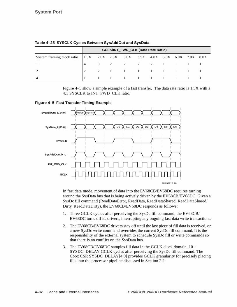
System Port
th a
n ared/
s.
oreso
g
Figure 4–5 show a simple example of a fast transfer. The data rate ratio is 1.5X wi4:1 SYSCLK to INT_FWD_CLK ratio.
Figure 4–5 Fast Transfer Timing Example
In fast data mode, movement of data into the EV68CB/EV68DC requires turningaround the SysData bus that is being actively driven by the EV68CB/EV68DC. GiveSysDc fill command (ReadDataError, ReadData, ReadDataShared, ReadDataShaDirty, ReadDataDirty), the EV68CB/EV68DC responds as follows:
1. Three GCLK cycles after perceiving the SysDc fill command, the EV68CB/EV68DC turns off its drivers, interrupting any ongoing fast data write transaction
2. The EV68CB/EV68DC drivers stay off until the last piece of fill data is received,a new SysDc write command overrides the current SysDc fill command. It is thresponsibility of the external system to schedule SysDc fill or write commandsthat there is no conflict on the SysData bus.
3. The EV68CB/EV68DC samples fill data in the GCLK clock domain, 10 +SYSDC_DELAY GCLK cycles after perceiving the SysDc fill command. TheCbox CSR SYSDC_DELAY[4:0] provides GCLK granularity for precisely placinfills into the processor pipeline discussed in Section 2.2.
Table 4–25 SYSCLK Cycles Between SysAddOut and SysData
GCLK/INT_FWD_CLK (Data Rate Ratio)
System framing clock ratio 1.5X 2.0X 2.5X 3.0X 3.5X 4.0X 5.0X 6.0X 7.0X 8.0X
1 4 3 2 2 2 2 1 1 1 1
2 2 2 1 1 1 1 1 1 1 1
4 1 1 1 1 1 1 1 1 1 1
FM05822B.AI4
SysData_L[63:0]
SYSCLK
ProbeSysAddOut_L[14:0]
SysAddOutClk_L
D0
Response
D1 D2 D3 D4 D5 D6
INT_FWD_CLK
GCLK
4–32 Cache and External Interfaces EV68CB/EV68DC Hardware Reference Manual

System Port
hediddle
les,
n-
con-
ans-
enthefnos.
the
Dc
Table 4–26 shows four example configurations and shows their use of theSYSDC_DELAY[4:0].
System 1 has six GCLKs to every SYSCLK and only sends 4-cycle commands to tEV68CB/EV68DC. Thus, a period of three SYSCLKs between the SysDc commanand data leaves a period of 15 GCLKs between SysDc and data (SysDc is in the mof the 4-cycle command). A SYSDC_DELAY[4:0] of five would align sampling andreceipt of SysData.
System 2 has four GCLKs in every SYSCLK, so leading data by three SYSCLK cycand programming the SYSDC_DELAY[4:0] to two, aligns sampling and receiving.
Timing for systems 3 and 4 is derived in a similar manner.
Note: The maximum valid value for SYSDC_DELAY must be less than the miimum number of GCLK cycles between two consecutive SYSDC com-mands to the EV68CB/EV68DC.
If a fast data transfer is interrupted and fails to complete, the system must use theventional protocol to send a SysDc WriteData command to the EV68CB/EV68DC,removing the desired data buffer. Section 4.7.8.3 describes the timing events for trferring data from the EV68CB/EV68DC to the system.
4.7.8.3 Fast Data Disable Mode
The system controls all data movement to and from the EV68CB/EV68DC. Movemof data into and out of the EV68CB/EV68DC is preceded by a SysDc command. TEV68CB/EV68DC drivers are only enabled for the duration of an 8-cycle transfer odata from the EV68CB/EV68DC to the system. Systems must ensure that there isoverlap of enabled drivers and that there is adequate settle time on the SysData bu
Given a SysDc fill command, the EV68CB/EV68DC samples data 10 +SYSDC_DELAY GCLK cycles after the command is perceived within the EV68CB/EV68DC clock domain. Because there is no linkage with the output driver, fills intoEV68CB/EV68DC are not affected by the SYS_RCV_MUX_PRESET[1:0] value.
In both modes, given a SysDc write command, the EV68CB/EV68DC looks for thenext SYSCLK edge 8.5 cycles after perceiving the SysDc write command in its clockdomain. Because the SysDc write command must be perceived before its use, Syswrite commands are dependent upon the amount of delay introduced by Cbox CSRSYS_RCV_MUX_CNT_PRESET[1:0].
Table 4–26 Cbox CSR SYSDC_DELAY[4:0] Examples
System Bit Rate System Framing Clock Ratio 1
1 The system framing clock ratio is the number of INT_FWD_CLK cycles perSYSCLK cycles.
SYSDC_DELAY
System 1 1.5X 4:1 5 (3 SYSCLK cycles)
System 2 2.0X 2:1 2 (3 SYSCLK cycles)
System 3 2.5X 2:1 0 (2 SYSCLK cycles)
System 4 4X 2:1 6 (2 SYSCLK cycles)
EV68CB/EV68DC Hardware Reference Manual Cache and External Interfaces 4–33
System Port
l-
t a
om
dingtheata
d one
leseiv-re-ite
data
sfers
Table 4–27 lists information for the four timing examples. In Table 4–27, note the folowing:
• SysDc write commands are not affected by the SYSDC_DELAY parameter.
• The SYS_RCV_MUX_PRESET adds delay at the rate of one INT_FWD_CLK atime. For example, adding the delay of one bit time to system 1 adds 1.5 GCLKcycles to the delay and drives the SysDc write command-to-data relationship frone to two SYSCLKs.
• For write transfers, the EV68CB/EV68DC drivers are enabled on the precedingGCLK BPHASE, before the start of a write transfer, and disabled on the succeeGCLK BPHASE at the end of the write transfer. The write data is enveloped byEV68CB/EV68DC drivers to guarantee that every data transfer has the same dvalid window.
The four examples described here assume no skew for the 2.0X and 4.0X cases anbit time of skew for the 1.5X and 2.5X cases.
For system 1, the distance between SysDc and the first SYSCLK is nine GCLK cycbut the additional delay of one bit time (1.5 GCLKs) puts the actual delay after percing the SysDc command to 7.5 GCLKs, which misses the 8.5 cycle constraint. Thefore, the EV68CB/EV68DC drives data two SYSCLKs after receiving the SysDc wrcommand.
For system 2, the distance between SysDc and the second SYSCLK is eight GCLKcycles, which also misses the 8.5 cycle constraint, so the EV68CB/EV68DC drivesthree SYSCLK cycles after receiving the SysDc write command (12 cycles).
The other two cases are derived in a similar manner.
4.7.8.4 SysDataInValid_L and SysDataOutValid_L
The SysDataValid signals (SysDataInValid_L andSysDataOutValid_L) are driven bythe system and control the rate of data delivery to and from the EV68CB/EV68DC.
SysDataInValid _L
The SysDataInValid_L signal controls the flow of data into the EV68CB/EV68DC,and may be used to introduce an arbitrary number of cycles between octaword traninto the EV68CB/EV68DC. The rules for usingSysDataInValid_L follow:
Table 4–27 Four Timing Examples
System Bit Rate System Framing Clock Ratio 1
1 The system framing clock ratio is the number of INT_FWD_CLK cycles perSYSCLK cycles.
Write Data
System 1 1.5X 4:1 2 SYSCLKs
System 2 2.0X 2:1 3 SYSCLKs
System 3 2.5X 2:1 2 SYSCLKs
System 4 4.0X 2:1 2 SYSCLKs
4–34 Cache and External Interfaces EV68CB/EV68DC Hardware Reference Manual

System Port
DC
r
f
by
The
oCig-
1. TheSysDataInValid_L signal must be asserted for both cycles of a SysDc fillcommand, and two quadwords of data must be delivered to the EV68CB/EV68in succeeding bit-clock cycles with the appropriate timing inreference to the SysDcfill command (SYSDC_DELAY + 10 CPU cycles).
2. Any number of bubble cycles can be introduced within the fill by deassertingSysDataInValid_L between octaword transfers.
3. The transfer of fill data can continue by assertingSysDataInValid_L for at leasttwo bit-clock cycles, and delivering data SYSDC_DELAY + 10 CPU cycles aftethe assertion ofSysDataInValid_L.
4. The EV68CB/EV68DC must seeSysDataInValid_L asserted for eight data cyclesin order to complete a fill. When the eighth cycle of an assertedSysDataInValid_Lis perceived by the EV68CB/EV68DC, the transfer is complete.
5. Systems that do not useSysDataInValid_L may tie the pad to the asserted state.
If SYSDC_DELAY is greater than the bit-time of a transfer, theSysDataInValid_Lsignal must be internally pipelined. To enable the correct sampling ofSysDataInValid_L, the EV68CB/EV68DC provides a delay, with Cbox CSRDATA_VALID_DELAY[1:0], that is equal to SYSDC_DELAY[4:0]/bit-time. Forexample, consider system 1 in Table 4–26, which has a SYSDC_DELAY of fiveGCLKs. Running at a bit-time of 1.5X, the DATA_VALID_DELAY[1,0] is pro-grammed with a value of three.
SysDataOutValid_L
Systems that use a ratio of 1:1 for SYSCLK:INT_FWD_CLK may control the flow odata out of the EV68CB/EV68DC by usingSysDataOutValid_L as follows:
1. TheSysDataOutValid_L pad must be asserted for at least the first cycle of theSysDc write command that initiates a write transfer.
2. Any number of bubble cycles may be introduced between quadword transfersdeassertingSysDataOutValid_L.
3. The EV68CB/EV68DC must see theSysDataOutValid_L signal asserted for eightdata cycles to complete a write transaction, and when the eighth cycle of anassertedSysDataOutValid_L is perceived by theEV68CB/EV68DC, the transferis complete.
4.7.8.5 SysFillValid_L
TheSysFillValid_L pad, when asserted, validates the current memory and I/O datatransfer into the EV68CB/EV68DC. The system designer may tie this pad to theasserted state (validating all fills), or use it to enable or cancel fills as they progress.EV68CB/EV68DC samplesSysFillValid_L at D1 time (when the EV68CB/EV68DCsamples the second data cycle).If SysFillValid_L is asserted at D1 time, the fill will continue uninterrupted. If it is notasserted, the EV68CB/EV68DC cancels the fill, but expects all eight QWs of data tarrive at its system bus before continuing to the next fill. Also, the EV68CB/EV68Dmaintains the state of the MAF, expecting another valid fill to the same MAF entry. Fure 4–6 illustratesSysFillValid_L timing.
EV68CB/EV68DC Hardware Reference Manual Cache and External Interfaces 4–35

System Port
64
readta tountil
ll)ed
s andny
uiref
Figure 4–6 SysFillValid_L Timing
4.7.8.6 Data Wrapping
All data movement between the EV68CB/EV68DC and the system is composed ofbytes in eight cycles on the data bus. All 64 bytes of memory data are valid. Thisapplies to memory read transactions, memory write transactions, and system probetransactions. The wrap order is interleaved. The internal data bus, which delivers dathe functional units and the Dcache, is 16 bytes wide, and so, no transfers happentwo data cycles occur on the interface.
Table 4–28 lists the rules for data wrapping. I/O read and write addresses on theSysAddOut bus point to the desired byte, word, LW, or QW, with a combination ofSysAddOut_L[5:3] and the mask field [7:0].
The order in which data is provided to the EV68CB/EV68DC (for a memory or I/O fior moved from the EV68CB/EV68DC (write victims or probe reads) can be determinby the system. The system chooses to reflect back the same low-order address bitthe corresponding octaword found in the SysAddOut field or the system chooses aother starting point within the block.
SysDc commands for the ReadData, ReadDataShared, and WriteData groups reqthat systems define the position of the first QW by inserting the appropriate value oSysAddOut_L[5:3] into bits [1:0] of the command field. The recommended startingpoint is the QW pointed to by the EV68CB/EV68DC; however, some systems may
Table 4–28 Data Wrapping Rules
CommandSignificant AddressBits
MaskType Rules
ReadQW andWrQW
SysAddOut_L[5:3] QW SysAddOut_L[5:3] contain the exact PA bits of the firstLDQ or STQ to the block. The mask bits point to the validQWs merged in ascending order.
ReadLW andWrLW
SysAddOut_L[5:3] LW SysAddOut_L[5:3] contain the exact PA bits of the firstLDL or STL to the block. The mask bits point to the validLWs merged in ascending order within one hexword.
LDByte/WordandSTByte/Word
SysAddOut_L[5:3] Byte SysAddOut_L[5:3] contain the exact QW PA bits of theLDByte/Word or STByte/Word instruction. The mask bitspoint to the valid byte in the QW.
FM-05823B.FH8
Command Receiver
SysFillValid_L
SysDcSysAddIn_L[14:0]
SysData_L[63:0] D0 D1 D2 D3 D4
T3
Transport Delay on Address
4–36 Cache and External Interfaces EV68CB/EV68DC Hardware Reference Manual

System Port
cate
ae
W
find it more beneficial to begin the transfer elsewhere. The system must always indithe starting point to the EV68CB/EV68DC. The wrap order for subsequent QWs isinterleaved.
Table 4–29 defines the method for systems to specify wrap and deliver data.
Note 1: Transfers to and from the EV68CB/EV68DC have eight data cycles fortotal of eight quadwords. The starting point is defined by the system. Thpreferred starting point is the onepointed to by SysAddOut_L[5:4]. Sys-tems can insert the SysAddOut_L[5:4] into the SysDc[1:0] field of thecommand. See Table 4–30 for the wrap order.
Note 2: LW and byte/word read transfers differ from all other transfers. The systemunloads only four QWs of data into eight data cycles by sending each Qtwice (referred to as double-pumped data transfer). The first QW returnedis determined bySysAddOut_L[4:3]. The system again may elect tochoose its own starting point for the transfer and insert that value intoSysDc[1:0]. See Table 4–31 for the wrap order.
Table 4–30 defines the interleaved scheme for the wrap order.
Table 4–29 System Wrap and Deliver Data
Source/Destination SysDc[4:2] SysDc[1:0] Size Rules
Memory 100 (ReadData) SysAddOut_L[5:4] Block (64 Bytes) See Note 1
Memory 101(ReadDataDirty) SysAddOut_L[5:4] Block (64 Bytes) See Note 1
Memory 110 (ReadDataShared) SysAddOut_L[5:4] Block (64 Bytes) See Note 1
Memory 111(Read DataShared/Dirty) SysAddOut_L[5:4] Block (64 Bytes) See Note 1
Memory 010 (WriteData) SysAddOut_L[5:4] Block (64 Bytes) See Note 1
I/O 100 (ReadData) SysAddOut_L[5:4] QW (8-64 Bytes) See Note 1
I/O 100 (ReadData) SysAddOut_L[4:3] LW(4-32 Bytes) See Note 2
I/O 100 (ReadData) SysAddOut_L[4:3] Byte/Word See Note 2
I/O 010 (WriteData) SysAddOut_L[5:4] QW (8-64 Bytes) See Note 1
I/O 010 (WriteData) SysAddOut_L[5:4] LW(4-32 Bytes) See Note 1
I/O 010 (WriteData) SysAddOut_L[5:4] Byte/Word See Note 1
Table 4–30 Wrap Interleave Order
PA Bits [5:3] of Transferred QW
First quadword 000 010 100 110
Second quadword 001 011 101 111
Third quadword 010 000 110 100
Fourth quadword 011 001 111 101
Fifth quadword 100 110 000 010
EV68CB/EV68DC Hardware Reference Manual Cache and External Interfaces 4–37

System Port
le-
m
ideref-ases,ow-
Table 4–31 defines the wrap order for double-pumped data transfers.
4.7.9 Nonexistent Memory Processing
Like its predecessors, the EV68CB/EV68DC can generate references tononexistent(NXM) memory or I/O space. However, unlike the earlier Alpha microprocessor impmentations, the EV68CB/EV68DC can generate speculative references to memoryspace. To accommodate the speculative nature of the EV68CB/EV68DC, the systemust not generate or lock error registers because of speculative references. TheEV68CB/EV68DC translates all memory references through the translation lookasbuffer (TLB) and, in some cases, the EV68CB/EV68DC may generate speculativeerences (instruction execution down mispredicted paths) to NXM space. In these cthe system sends a SysDc ReadDataError and the EV68CB/EV68DC does the folling:
• Delivers an all-ones pattern to all load instructions to the NXM address
• Force-fails all store instructions to the NXM address (much like a STx_Cfailure)
• Invalidates the cache block at the same index by way of an atomic Evictcommand
Sixth quadword 101 111 001 011
Seventh quadword 110 100 010 000
Eighth quadword 111 101 011 001
Table 4–31 Wrap Order for Double-Pumped Data Transfers
PA [5:3] of Transferred QW
First quadword x00 x01 x10 x11
Second quadword x00 x01 x10 x11
Third quadword x01 x00 x11 x10
Fourth quadword x01 x00 x11 x10
Fifth quadword x10 x11 x00 x01
Sixth quadword x10 x11 x00 x01
Seventh quadword x11 x10 x01 x00
Eighth quadword x11 x10 x01 x00
Table 4–30 Wrap Interleave Order (Continued)
PA Bits [5:3] of Transferred QW
4–38 Cache and External Interfaces EV68CB/EV68DC Hardware Reference Manual

System Port
e
ough/
ndl
cu-nig-
pond
e,c-
e
ree
enF
pli-F
is
isuld
nd
Table 4–32 shows each EV68CB/EV68DC command, with NXM addresses, and thappropriate system response.
Table 4–32 EV68CB/EV68DC Commands with NXM Addr. and System Response
EV68CB/EV68DCCommand NXMAddress System/EV68CB/EV68DC Response
ProbeResponse Probe responses for addresses to NXM space are of UNPREDICTABLE status. Alththe final status of a ReadDataError is Invalid, the EV68CB/EV68DC fills the block ValidClean and uses an atomic Evict command to invalidate the block. Systems that sendprobes to NXM space to the EV68CB/EV68DC must disregard the probe result.
RdBlkRdBlkSpecRdBlkVic
Load references to NXM space can be speculative. In this case, systems should respowith a SysDc ReadDataError fill that the EV68CB/EV68DC uses to service the originaload/Istream command. If the original load command was speculative, the EV68CB/EV68DC will remove the load instruction that generated the NXM command, and startprocessing instructions down the correctly predicted path. If the command was not spelative, there must be an error in the operating system mapping of a virtual address to aillegal physical address, and the EV68CB/EV68DC provides an all ones pattern as a snature for this bug. The NXM block is not cached in the Dcache or Bcache.
RdBlkIRdBlkSpecIRdBlkVicI
Istream references to NXM space can be speculative. In this case, systems should reswith a SysDc ReadDataError fill, which the EV68CB/EV68DC will use to service andexecute the original Istream reference. If the original Istream reference was speculativthe EV68CB/EV68DC will remove the instructions started after the mispredicted instrution that generated the NXM reference, and start instruction processing down the cor-rectly predicted path. If the reference was not speculative, there must be an error in thoperating system mapping of a virtual address to an illegal physical address, and theEV68CB/EV68DC provides an all ones pattern as a signature for this bug. The NXMblock is not cached in the Bcache, but can be cached in the Icache.
RdBlkModRdBlkModSpecRdBlkModVic
Store instructions to NXM space initiate RdBlkMod commands. Again, speculative stoinstructions are removed. Nonspeculative store instructions are forced to fail, much likSTx_C instructions that fail. The NXM block is not cached in the Dcache or Bcache.
WrVictimBlk Dirty Victims to NXM space are illegal. Systems should perform a machine check, withthe EV68CB/EV68DC indicating a severe error.
CleanVictimBlk The EV68CB/EV68DC can generate CleanVictimBlk commands to NXM space if theCbox CSR BC_CLEAN_VICTIM[0] bit is asserted and a SysDc ReadDataError has begenerated. Systems that use clean victims must faithfully deallocate the CleanVictim VAentry.
Evict If the Cbox CSR ENABLE_EVICT is asserted, the EV68CB/EV68DC will generateEvict commands to NXM space. Systems may use this command to invalidate their ducate tags. Systems must respond with SysDc ChangeToDirtyFail to retire the NXM MAentry.
RdBytesRdLWsRdQWs
Load instructions to I/O space are not speculative, so an I/O reference to NXM spacean error. Systems must respond with ReadDataError and should generate a machinecheck to indicate an operating system error.
WrBytesWrLWsWrQWs
Store instructions to I/O space are not speculative, so an I/O reference to NXM spacean error. Systems must respond by deallocating the appropriate IOWB entries, and shogenerate a machine check to indicate an operating system error.
FetchBlkFetchBlkSpec
Loads to noncached memory in NXM space may be speculative. Systems must respowith a SysDc ReadDataError to retire the MAF entry.
EV68CB/EV68DC Hardware Reference Manual Cache and External Interfaces 4–39

System Port
nsac-
and
ner-
e-
or
reissu-
F-
ble
m-
ere
he
rror,
4.7.10 Ordering of System Port Transactions
This section describes ordering of system port transactions. The two classes of trations are listed here:
• EV68CB/EV68DC commands and system probes
• System probes and SysDc transfers
4.7.10.1 EV68CB/EV68DC Commands and System Probes
This section describes the interaction of EV68CB/EV68DC-generated commandssystem-generated probes that reference the same cache block. Some definitions are pre-sented here:
• ProbeResponses generated by the EV68CB/EV68DC respond to all system-geated probe commands. System-generated data transfer commands respond to allEV68CB/EV68DC-generated data transfer commands.
• The victim address file (VAF) and victim data buffer (VDB) entries each have indpendent valid bits for both a victim and a probe.
• Probe results indicate a hit on a VAF/VDB and when a WrVictim command hasbeen sent to the system. Systems can decide whether to move the buffer oncetwice.
• ProbeResponses are issued in the order that the system-generated probes wereceived; however, there is no requirement for the system to retain order whening release buffer commands.
• Probe processing can stall inside the EV68CB/EV68DC when the probe entryindex matches PA[19:6] of a previous probe entry in the VAF.
• The EV68CB/EV68DC reserves one VAF entry for probe processing, so that VAfull conditions cannot stall the processing of probes at the head of the queue.
Table 4–33 lists all interactions between pending internal EV68CB/EV68DC com-mands and the Probe[2:0] command field, Next Cache Block State, described in Ta4–22.
Table 4–33 shows the EV68CB/EV68DC response to system probe and in-flight comand interaction. In the table, note the following:
• ReadBlkVic and ReadBlkModVic commands do not appear in Table 4–33. If this interaction between the probe and the victim, it is the same as a WrVictimBlkcommand.
CleanToDirtySharedToDirtySTCChangeToDirty
ChangeToDirty commands to NXM space are impossible in the EV68CB/EV68DCbecause all NXM references to memory space are atomically filled with an Invalid cacstatus.
InvalToDirtyInvalToDirtyVic
InvalToDirty commands are not speculative, so InvalToDirty commands to NXM spaceindicate an operating system error. Systems should respond with a SysDc ReadDataEand should generate a machine check to indicate error.
Table 4–32 EV68CB/EV68DC Commands with NXM Addr. and System Response (Continued)
EV68CB/EV68DCCommand NXMAddress System/EV68CB/EV68DC Response
4–40 Cache and External Interfaces EV68CB/EV68DC Hardware Reference Manual

System Port
The
otherDCthe
ed
is
tr
-the
m-
use
• Probes that invalidate locked blocks do not generate a ReadBlkMod command.EV68CB/EV68DC fails the STx_C instruction as defined in theAlpha ArchitectureHandbook, Version 4.
• All read commands (RdBlk, RdBlkMod, Fetch, InvalToDirty) do not interactbecause the EV68CB/EV68DC does not yet own the block.
Table 4–33 EV68CB/EV68DC Response to System Probe and In-Flight Command Interaction
Pending InternalEV68CB/EV68DCCommand EV68CB/EV68DC Response to System Probe and In-Flight Command Interaction
ReadBlkReadBlkModFetchBlkInvalToDirtyWrVictimBlk
This case assumes that a WrVictimBlk command has been sent to the system and anagent has performed a load/store instruction to the same address. The EV68CB/EV68provides VAF hit information with the probe response so that the system can managerace condition between the WrVictimBlk command from this processor and a possibleWrVictimBlk command from the probing processor. This race condition can be managby either forcing the completion of the WrVictimBlk command to memory before allow-ing the progress by the probing processor, or by killing the WrVictimBlk command in thprocessor.
CleanToDirtySharedToDirty
This case assumes that a SetDirty command has been sent to the system environmenbecause of a store instruction that hit in the EV68CB/EV68DC caches and that anotheprocessor has performed a load/store instruction to the same address. The EV68CB/EV68DC provides MAF hit information so that the system can correctly respond to theSet/Dirty command. If the next state of the probe was Invalid (the other processor performed a store instruction), and the probe reached the system serialization point beforeSet/Dirty command, the system must either fail the Set/Dirty command or provide theupdated data from the other processor.
STCChangeToDirty This case is similar to case 2, except that the initiating instruction for the Set/Dirty comand is a STx_C. An address match with an invalidating probe must fail the Set/Dirtycommand. Delivering the updated data from the other processor is not an option becaof the requirements of the LDx_L/STx_C instruction pair.
EV68CB/EV68DC Hardware Reference Manual Cache and External Interfaces 4–41

System Port
llowc-
ms
c),
s
r therbe
c-
e
c-
4.7.10.2 System Probes and SysDc Commands
Ordering of cache transactions at the system serialization point must bereflected in theEV68CB/EV68DC cache system. Table 4–34 shows the rules that a system must foto control the order of cache status update within the EV68CB/EV68DC cache strutures (including the VAF) at the EV68CB/EV68DC pads.
Table 4–34 Rules for System Control of Cache Status Update Order
First Second Rule
Probe Probe To control the sequence of cache status updates between probes, systecan present the probes in order to the EV68CB/EV68DC, and theEV68CB/EV68DC will update the appropriate cache state (including theVAF) in order.
Probe SysDc MAF To ensure that a probe updates the internal cache status before a SysDMAF transaction (including fills and ChangeToDirtySuccess commandssystems must wait for the probe response before presenting the SysDcMAF command to the EV68CB/EV68DC. To ensure that a probe updatea VAF entry before a SysDc VAF (release buffer), systems must wait forthe probe response.
Probe SysDc VAF Same as Probe/SysDc MAF, above.
SysDc MAF Probe To ensure that a SysDc MAF command updates the EV68CB/EV68DCcache system before a probe to the same address, systems must deliveD1 (the second QW of data delivered to the EV68CB/EV68DC) before oin the same cycle as the A3 of the probe (the last cycle of the 4-cycle procommand). This rule also applies to ChangeToDirtySuccess commandsthat have a virtual D0 and D1 transaction.
SysDc MAF SysDc MAF SysDc MAF transactions can be ordered into the EV68CB/EV68DC byordering them appropriately at the EV68CB/EV68DC interface.
SysDc MAF SysDc VAF SysDc MAF transactions and SysDc VAF transactions cannot interactwithin the EV68CB/EV68DC because the EV68CB/EV68DC does notgenerate MAF transactions to the same address as existing VAF transations.
SysDc VAF Probe To ensure that a SysDc VAF invalidates a VAF entry before a probe to thsame address, the SysDc VAF command must precede the first cycle of the4-cycle probe command.
SysDc VAF SysDc MAF SysDc MAF transactions and SysDc VAF transactions cannot interactwithin the EV68CB/EV68DC because the EV68CB/EV68DC does notgenerate MAF transactions to the same address as existing VAF transations.
SysDc VAF SysDc VAF SysDc VAF transactions can be ordered into the EV68CB/EV68DC byordering them appropriately at the EV68CB/EV68DC interface.
4–42 Cache and External Interfaces EV68CB/EV68DC Hardware Reference Manual

Bcache Port
s.44-
blefast
teicate
4.8 Bcache Port
The EV68CB/EV68DC supports a second-level cache (Bcache) with 64-byte blockThe Bcache size can be 1MB, 2MB, 4MB, 8MB, or 16MB. The Bcache port has a 1bit data bus that is used for data transfers between the EV68CB/EV68DC and theBcache. All Bcache control and address signal lines are clocked synchronously onBcache clock cycleboundaries.
The Bcache supports the following multiples of the GCLK period: 1.5X (dual-datamode only), 2X, 2.5X, 3X, 3.5X, 4X, 5X, 6X, 7X, and 8X. However, the EV68CB/EV68DC imposes a maximum Bcache clock period based on the SYSCLK ratio. Ta4–35 lists the range of maximum Bcache clock periods. Section 4.7.8.2 describesmode.
The EV68CB/EV68DC provides a range of programmable Cbox CSRs to manipulathe Bcache port pads so that a variety of industry-standard SSRAMs can communefficiently with theEV68CB/EV68DC. The following SSRAMs can be used:.
• Nonburst mode Reg/Reg late-write SSRAMs
• Burst mode Reg/Reg late-write dual-data SSRAMs
4.8.1 Bcache Port Pads
Table 3–1 defines the EV68CB/EV68DC signal types referred to in this section. Table4–36 lists the Bcache port pad groups along with their type, number, reference clock,and functional description.
Table 4–35 Range of Maximum Bcache Clock Ratios
SYSCLK RatioBcache Clock Ratio with Fast ModeEnabled
Bcache Clock Ratio with Fast ModeDisabled
1.5X 4.0X 7.0X
2.0X 4.0X 7.0X
2.5X 5.0X 8.0X
3.0X 6.0X 8.0X
3.5X 7.0X 8.0X
4.0X 7.0X 8.0X
5.0X 8.0X 8.0X
6.0X 8.0X 8.0X
7.0X 8.0X 8.0X
8.0X 8.0X 8.0X
Table 4–36 Bcache Port Pads
Pad Name Type Count Reference Clock Description
BcAdd_H[23:4] O_PP 20 Int_Index_BcClk Bcache index
BcCheck_H[15:0] B_DA_PP 16 Int_Data_BcClk⇒ outputBcDataInClk_H⇒ input
ECC check bits for BcData
EV68CB/EV68DC Hardware Reference Manual Cache and External Interfaces 4–43

Bcache Port
puts,
4.8.2 Bcache Clocking
For clocking, the Bcache port pads can be divided into three groups.
1. The Bcache index pads (address and control) are referenced to Int_Add_BcClk, aninternal version of the Bcache forwarded clock. The index pads are valid for thewhole period of the Int_Add_BcClk. The index pads are:
BcAdd_H[23:4]BcDataOE_LBcDataWr_LBcLoad_LBcTagOE_LBcTagWr_L
2. The data pads, when driven as outputs, arereferenced to Int_Data_BcClk, anotherinternal version of the Bcache forwarded clock. The data pads, when used as incan be referenced to the incoming Bcache clocks,BcDataInClk_H[7:0] and
BcData_H[127:0] B_DA_PP 128 Int_Data_BcClk⇒ outputBcDataInClk_H⇒ input
Bcache data
BcDataInClk_H[7:0] I_DA 8 NA Bcache data input clocks
BcDataOE_L O_PP 1 Int_Index_BcClk Bcache data output enable/chipselect
BcDataOutClk_H[3:0]BcDataOutClk_L[3:0]
O_PP 8 NA Bcache data clocks— high and lowversion
BcDataWr_L O_PP 1 Int_Index_BcClk Bcache data write enable
BcLoad_L O_PP 1 Int_Index_BcClk Bcache burst enable
BcTag_H[42:20] B_DA_PP 23 Int_Data_BcClk⇒ outputBcTagInClk_H⇒ input
Bcache tag data
BcTagDirty_H B_DA_PP 1 Int_Data_BcClk⇒ outputBcTagInClk_H⇒ input
Bcache tag dirty bit
BcTagInClk_H I_DA 1 NA Tag input data reference clock
BcTagOE_L O_PP 1 Int_Index_BcClk Bcache tag output enable/chipselect
BcTagOutClk_HBcTagOutClk_L
O_PP 2 NA Bcache tag clock— high and lowversions
BcTagParity_H B_DA_PP 1 Int_Data_BcClk⇒ outputBcTagInClk_H⇒ input
Bcache tag parity bit
BcTagShared_H B_DA_PP 1 Int_Data_BcClk⇒ outputBcTagInClk_H⇒ input
Bcache tag shared bit
BcTagValid_H B_DA_PP 1 Int_Data_BcClk⇒ outputBcTagInClk_H⇒ input
Bcache tag valid bit
BcVref I_DC_REF 1 NA Input reference voltage for tag data
BcTagWr_L O_PP 1 Int_Index_BcClk Bcache data write enable
Table 4–36 Bcache Port Pads (Continued)
Pad Name Type Count Reference Clock Description
4–44 Cache and External Interfaces EV68CB/EV68DC Hardware Reference Manual

Bcache Port
lytheaSRs
BcTagInClk_H . Int_Data_BcClk can be delayed relative to Int_Add_BcClk from0 to 3 GCLK cycles by using Cbox CSR BC_CPU_CLK_DELAY[1:0]. The datapads are:
BcCheck_H[15:0]BcData_H[127:0]BcTag_H[42:20]BcTagDirty_HBcTagParity_HBcTagShared_HBcTagValid_H
3. The Bcache clock pads (BcDataOutClk_x[3:0] andBcTagOutClk_x) clock theindex and data pads at the SSRAMs. These clocks can be delayed fromInt_Data_BcClk from 0 to 2 GCLK phases (half cycles) using Cbox CSRBC_CPU_CLK_DELAY[1:0].
Table 4–37 provides the BC_CPU_CLK_DELAY[1:0] values, which is the delayfrom BC_ADDRESS to BC_WRITE_DATA (and BC_CLOCK_OUT) in GCLKcycles.
In the EV68CB/EV68DC topology, the index pads are loaded by all the SSRAMs,while the clock and data pads see a limit load. This arrangement requires a relativelarge amount of delay between the index pads and the Bcache clock pads to meetsetup constraints at the SSRAMs. The EV68CB/EV68DC Cbox CSRs can provideprogrammable amount of delay between the index and clock pads by using Cbox CBC_CPU_CLK_DELAY[1:0] and BC_CLK_DELAY[1:0].
Table 4–38 provides the BC_CLK_DELAY[1:0] values, which is the delay fromBC_WRITE_DATA to BC_CLOCK_OUT, in GCLK phases.
Table 4–37 BC_CPU_CLK_DELAY[1:0] Values
BC_CPU_CLK_DELAY[1:0] Value GCLK Cycles of Delay
0 0
1 1
2 2
3 3
Table 4–38 BC_CLK_DELAY[1:0] Values
BC_CLK_DELAY[1:0] Value GCLK Phases
0 Invalid (turns off BC_CLOCK_OUT)
1 0
2 1
3 2
EV68CB/EV68DC Hardware Reference Manual Cache and External Interfaces 4–45

Bcache Port
e
e
hedata.
in-
ted5X-
CB/for
artse is
hateriod
With BC_CPU_CLK_DELAY[1:0] and BC_CLK_DELAY[1:0], a 500-MHzEV68CB/EV68DC can provide up to 8 ns (3× 2 + 2) of delay between the index andthe outgoing forwarded clocks. The relative loading difference between the data and thclock is minimal, so Cbox CSR BC_CLK_DELAY[1:0] alone is sufficient to providethe delay needed for the setup constraint at the Bcache data register.
4.8.2.1 Setting the Period of the Cache Clock
The free running Bcache clocks are derived from the EV68CB/EV68DC GCLK. Thperiod of the Bcache clocks is programmed using the following three Cbox CSRs:
1. BC_CLK_LD_VECTOR[15:0]
2. BC_BPHASE_LD_VECTOR[3:0]
3. BC_FDBK_EN[7:0]
To program these three CSRs, the programmer must know the bit-rate of the Bcacdata, and whether only the rising edge or both edges of the clock are used to latchFor example, a 200-MHz late-write SSRAM has a data period of 5 ns. For a 2-nsGCLK, the READCLK_RATIO must be set to 2.5X. This part is called a 2.5X SD (sgle-data part).
Table 4–39 shows how the three CSRs are programmed for single-data devices.
With the exception of the 2.5X-SD and 3.5X-SD cases, the clock waveform generaby the EV68CB/EV68DC for the forwarded clocks has a 50-50 duty cycle. In the 2.SD case, the EV68CB/EV68DC produces an asymmetric clock that is high for twoGCLK phases and low for three phases. Likewise, for the 3.5X-SD case, the EV68EV68DC produces an asymmetric clock that is high for three GCLK phases and lowfour GCLK phases. Also, for both of these cases, the EV68CB/EV68DC will only sttransactions on the rising edge of the GCLK and the Bcache clock. The 1.5X-SD canot supported.
A dual-data rate (DDR) SSRAM’s data rate is derived in a similar manner, except tbecause both edges of the clock are used, the SSRAM clock generated is 2X the pof the data. This part is called a 2.5X DDR SSRAM.
Table 4–39 Program Values to Set the Cache Clock Period (Single-Data)
Bcache Transfer BC_CLK_LD_VECTOR 1
1 These are hexadecimal values.
BC_BPHASE_LD_VECTOR 1 BC_FDBK_EN 1
2.0X-SD 5555 0 01
2.5X-SD 94A5 3 02
3.0X-SD 9249 A 02
3.5X-SD 4C99 C 04
4.0X-SD 3333 0 01
5.0X-SD 8C63 5 02
6.0X-SD 71C7 0 10
7.0X-SD C387 A 04
8.0X-SD 0F0F 0 01
4–46 Cache and External Interfaces EV68CB/EV68DC Hardware Reference Manual

Bcache Port
theo-
to
ed
to
ed
gt
Table 4–40 shows how the three CSRs are programmed for dual-data devices.
In addition to programming the clock CSRs, the data-sample/drive Cbox CSRs, atpads, must be set appropriately. Table 4–41 lists these CSRs and provides their prgrammed value.
Table 4–40 Program Values to Set the Cache Clock Period (Dual-Data Rate)
BcacheTransfer BC_CLK_LD_VECTOR 1
1 These are hexadecimal values.
BC_BPHASE_LD_VECTOR 1 BC_FDBK_EN 1
1.5X-DD 9249 A 02
2.0X-DD 3333 0 01
2.5X-DD 8C63 5 02
3.0X-DD 71C7 0 10
3.5X-DD C387 A 04
4.0X-DD 0F0F 0 01
5.0X-DD 7C1F 0 40
6.0X-DD F03F 0 10
7.0X-DD C07F 0 04
8.0X-DD 00FF 0 01
Table 4–41 Data-Sample/Drive Cbox CSRs
Cbox CSR Description
BC_DDM_FALL_EN[0] Enables the update of the EV68CB/EV68DC’s Bcache outputs referencedthe falling edge of the Bcache forwarded clock. Dual-data RAMs assert thisCSR.
BC_TAG_DDM_FALL_EN[0] Enables the update of the EV68CB/EV68DC’s Bcache tag outputs referencto the falling edge of the Bcache forwarded clock. Alway deasserted.
BC_DDM_RISE_EN[0] Enables the update of the EV68CB/EV68DC’s Bcache outputs referencedthe rising edge of the Bcache forwarded clock. Always asserted.
BC_TAG_DDM_RISE_EN[0] Enables the update of the EV68CB/EV68DC’s Bcache tag outputs referencto the rising edge of the Bcache forwarded clock. Always asserted.
BC_DDMF_ENABLE[0] Enables the rising edge of the Bcache forwarded clock. Always asserted.
BC_DDMR_ENABLE[0] Enables the falling edge of the Bcache forwarded clock. Always asserted.
BC_FRM_CLK[0] Forces the EV68CB/EV68DC to only start Bcache transactions on the risinedge of Bcache clocks that also coincide with the rising edge of GCLK. Musbe asserted for all dual-data parts and single-data parts at 2.5X and 3.5X.
BC_CLKFWD_ENABLE[0] Enables clock forward enable. Always asserted.
EV68CB/EV68DC Hardware Reference Manual Cache and External Interfaces 4–47

Bcache Port
, andcon-
riteions.
ecle.priateelayhe
dexbox
cle,
e
),
tLK
ed
andits.
ition,
CLK
4.8.3 Bcache Transactions
The Cbox uses the programmed clock values to start data read, tag read, data writetag write transactions on the rising edge of a Bcache clock. The Cbox can also befigured to introduce a programmable number of bubbles when changing between wand read commands. The following three sections describe these Bcache transact
4.8.3.1 Bcache Data Read and Tag Read Transactions
The EV68CB/EV68DC always reads four pieces of data (64 bytes) from the Bcachduring a data read transaction, and always interrogates the tag array on the first cyOnce started, data read transactions are never cancelled. Assuming that the approvalues have been programmed for the Bcache clock period, and with satisfactory dparameters for the SSRAM setup/hold Bcache address latch requirements, a Bcacread command proceeds through the EV68CB/EV68DC Cbox as follows:
1. When the EV68CB/EV68DC clocks out the first address value on the Bcache inpads with the appropriate Int_Add_BcClk value, the Cbox loads the values of CCSR BC_LAT_DATA_PATTERN[31:0] and Cbox CSRBC_LAT_TAG_PATTERN[23:0] into two shift registers, which shift during everyGCLK cycle.
2. The address and control pads are latched into the SSRAMs. During the next cythe SSRAMs provide data and tag information to the EV68CB/EV68DC.
3. Using the returning forwarded clocks (BcDataInClk_H[7:0] , BcTagInClk_H ), thedata/tag information is loaded into the EV68CB/EV68DC clock forwarding queufor the Bcache.
4. Based on the value of BC_RCV_MUX_PRESET_CNT[1,0] (the unload pointerthe result of a Bcache write command is loaded into a EV68CB/EV68DC GCLK(BPHASE) register.
5. The Cbox CSR BC_LAT_DATA_PATTERN[31:0] andBC_LAT_TAG_PATTERN[23:0] contain the GCLK frequency at which the outpuof the clock forward FIFO can be consumed by the processor. This provides GCgranularity for the Bcache interface, so that the EV68CB/EV68DC can minimizlatency to the Bcache. When the values based on these Cbox CSRs are shiftedown to the bottom of the shift register, the processor samples the Bcache datadelivers it to the consumers of load data in the EV68CB/EV68DC functional un
For example, when a 2.5X-SD SSRAM has a latency of eight GCLK cycles fromBcAdd_H[23:4] to the output of Bcache FIFO, Cbox CSRBC_LAT_DATA_PATTERN[31:0] is programmed to 94816 and Cbox CSRBC_LAT_TAG_PATTERN[23:0] is programmed to 816. The data pattern contains theplacement for four pieces of data and the aggregate rate of the data is 2.5X. In addbit one of the BC_LAT_DATA_PATTERN is placed at a GCLK latency of six GCLKcycles, which is the minimum latency supported by the EV68CB/EV68DC. TheBC_LAT_TAG_PATTERN contains the placement of the tag data to the EV68CB/EV68DC.
A shift of one to the left increases the latency of the Bcache transfer to nine GCLKcycles, and a shift to the right reduces the latency of the Bcache transfer to seven Gcycles.
4–48 Cache and External Interfaces EV68CB/EV68DC Hardware Reference Manual

Bcache Port
-arate
d
g.rs toite
lk
R
itete-
ks
gbye
the
rite
The Cbox performs isolated tag read transactions in response to system probe commands. In addition, when using burst-mode SSRAMs, the Cbox can combine a septag read transaction with the tail end of a dataread transaction, thusoptimizing Bcachebandwidth. A Bcache tag read transaction proceeds exactly like a Bcache data reatransaction, except that only the BC_LAT_TAG PATTERN is used to update the tagshift register.
4.8.3.2 Bcache Data Write Transactions
During a data write transaction, the EV68CB/EV68DC always writes four pieces ofdata (64 bytes of data and 8 bytes of ECC) to the Bcache, and always writes the taarray during the first cycle. Once started, data write operations are never cancelledGiven the appropriate programming of the Bcache clock period and delay parametesatisfy SSRAM setup/hold requirements of the Bcache address latch, a Bcache wrtransaction proceeds through the Cbox as follows:
1. The Cbox transmits the index and write control signals during an Int_Adr_BcCedge.
2. The data is placed on Bcache data, tag, and tag status pads on the appropriateInt_Data_BcClk edge from 0 to 7 Bcache bit-times later, based on the Cbox CSBC_LATE_WRITE_NUM[2:0]. The BC_LATE_WRITE_NUM[2:0] supports thelate-write SSRAM, which optimize Bcache data bus bandwidth by minimizingbubbles between read and write transactions. For example, single-data late-wrSSRAMs would need this CSR programmed to a value of one, and dual-data lawrite SSRAMs would need this CSR programmed to a value of two.
3. The difference between the data delivery (Int_Data_BcClk) and forwarded clocout provides the setup for the data at the Bcache data flip-flop.
4. For Bcache writes, the EV68CB/EV68DC drivers are enabled on the GCLKBPHASE preceding the start of a write transfer, and disabled on the succeedinGCLK BPHASE at the end of a write transfer. Thus, the write data is envelopedthe EV68CB/EV68DC drivers to guarantee that every data transfer has the samdata-valid window.
4.8.3.3 Bubbles on the Bcache Data Bus
When changing between read and write transactions on the bidirectional bus, it is oftennecessary to introduce NOP cycles (bubbles) to allow the bus to settle and to drainBcache read pipeline. The Cbox provides two CSRs, BC_RD_WR_BUBBLES[5:0]and BC_WR_RD_BUBBLES[3:0], to help control the bubbles between read and wtransactions.
EV68CB/EV68DC Hardware Reference Manual Cache and External Interfaces 4–49

Bcache Port
the
r
, a
tag
tag
The optimum parameters for these CSRs are determined by formulas that includefollowing terms:
Term Description
bcfrm Bcache frame clock.• In dual-data mode, bcfrm is twice the ratio.• In single-data mode, the value for bcfrm is determined by whethe
the ratio is even or odd:– When the ratio is even, bcfrm is equal to the ratio.– When the ratio is odd, bcfrm is twice the ratio.
For example, in single-data mode:
GCLK The processor clock.
Ratio The number of GCLK cycles per peak Bcache bandwidth transfer. For exampleratio of 2.5 means the peak Bcache bandwidth is 16 bytes for every 2.5 GCLKcycles.
rd_wr The minimum spacing required between the read and write indices at the data/pads, expressed as GCLK cycles.
wr_rd The minimum spacing required between the write and read indices at the data/pads, expressed as GCLK cycles.
Ratio Bcfrm
2 2
2.5 5
4–50 Cache and External Interfaces EV68CB/EV68DC Hardware Reference Manual

Bcache Port
s.
nd
The Relationship Between Write-to-Read — BC_WR_RD_BUBBLES and wr_rd
The following formulas calculate the relationship between the Cbox CSRBC_WR_RD_BUBBLES and wr_rd:
wr_rd = (BC_WR_RD_BUBBLES – 1) * bcfrm
or
BC_WR_RD_BUBBLES = ((wr_rd + bcfrm – 1) / bcfrm) + 1
There is never a need to use a value of 0 or 1 for BC_WR_RD_BUBBLES.
If wr_rd = 4*ratio , then value 3 would be the minimumBC_WR_RD_BUBBLES value whenbcfrm = 2*ratio , and value 5 would be theminimum BC_WR_RD_BUBBLES value whenbcfrm = ratio .
There is a special case forratio = 2.0 in single-data mode. In this case, the for-mula is:
wr_rd = (BC_WR_RD_BUBBLES – 2) * bcfrm
The Relationship Between Read-to-Write — BC_RD_WR_BUBBLES and rd_wr
Use the following formula to calculate the value for the Cbox CSRBC_RD_WR_BUBBLES that produces the minimum rd_wr restriction:
BC_RD_WR_BUBBLES = rd_wr – 6
Note that a value for BC_RD_WR_BUBBLES of zero really means 64 GCLK cycleIn that case, amend the formula. For example, it is impossible to haverd_wr = 6 inthe 1.5x dual-data rate mode case.
4.8.4 Pad Descriptions
This section describes the characteristics of the Bcache interface pads.
4.8.4.1 BcAdd_H[23:4]
TheBcAdd_H[23:4] pads are high drive outputs that provides the index for theBcache. The EV68CB/EV68DC supports Bcache sizes of 1MB, 2MB, 4MB, 8MB, a16MB. Table 4–42 lists the values to be programmed into Cbox CSRsBC_ENABLE[0] and BC_SIZE[3:0] to support each size of the Bcache.
Table 4–42 Programming the Bcache to Support Each Size of the Bcache
BC_ENABLE[0] BC_SIZE[3:0] Bcache Size
1 0000 1MB
1 0001 2MB
1 0011 4MB
1 0111 8MB
1 1111 16MB
EV68CB/EV68DC Hardware Reference Manual Cache and External Interfaces 4–51

Bcache Port
/
of
d
sing
When the Cbox CSR BC_BANK_ENABLE[0] is not set, the unusedBcAdd_H[23:4]pads are tied to zero. For example, when configured as a 4MB cache, the EV68CBEV68DC never changesBcAdd_H[23:22] from logic zero, and whenBC_BANK_ENABLE[0] is asserted, the EV68CB/EV68DC drives the complementthe MSB index on the next higherBcAdd_H pad.
4.8.4.2 Bcache Control Pads
The Bcache control pads (BcLoad_L, BcDataWr_L , BcDataOE_L, BcTagWr_L ,BcTagOE_L) are controlled using Cbox CSRs BC_BURST_MODE_ENABLE[0] anBC_PENTIUM_MODE[0].
Table 4–43 shows the four combinations of Bcache control pad behavior obtained uthe two CSRs.
Table 4–44 lists the combination of control pad assertion forRAM_TYPE A.
Table 4–45 lists the combination of control pad assertion for RAM_TYPE B.
Table 4–43 Programming the Bcache Control Pads
BC_PENTIUM_MODE BC_BURST_MODE_ENABLE RAM_TYPE
0 0 RAM_TYPE A
0 1 RAM_TYPE B
1 0 Unsupported
1 1 Unsupported
Table 4–44 Control Pad Assertion for RAM_TYPE A
TYPE A NOP RA0 RA1 RA2 RA3 NOP NOP WA0 WA1 WA2 WA3 NOP
BcLoad_L H H H H H H H H H H H H
BcDataOE_L H L L L L H H L L L L H
BcDataWr_L H H H H H H H L L L L H
BcTagOE_L H L H H H H H L H H H H
BcTagWr_L H H H H H H H L H H H H
Table 4–45 Control Pad Assertion for RAM_TYPE B
TYPE B NOP RA0 RA1 RA2 RA3 NOP NOP WA0 WA1 WA2 WA3 NOP
BcLoad_L H L H H H H H L H H H H
BcDataOE_L H L L L L H H L L L L H
BcDataWr_L L H H H H L L L L L L L
BcTagOE_L H L H H H H H L H H H H
BcTagWr_L H H H H H H H L H H H H
4–52 Cache and External Interfaces EV68CB/EV68DC Hardware Reference Manual

Bcache Port
che
e
videock,
utput
Table 4–46 lists the combination of control pad assertion for RAM_TYPE C.
Table 4–47 lists the combination of control pad assertion for RAM_TYPE D.
Notes:
1. The NOP condition for RAM_TYPE B is consistent with bursting nonPentiumstyle SSRAMs.
2. In both RAM_TYPE A and RAM_TYPE B, the padsBcDataOE_L andBcTagOE_Lfunction changes from output-enable control to chip-select control.
3. In both RAM_TYPE C and RAM_TYPE D SSRAMs, the padsBcDataOE_L andBcTagOE_L function as an asynchronous output enable that envelopes the Bcaread data by providing an extra cycle of output enable.
Using these Cbox CSRs, late-write nonbursting and dual-data rate SSRAMs can bconnected to the EV68CB/EV68DC as described in Appendix E.
4.8.4.3 BcDataInClk_H and BcTagInClk_H
TheBcDataInClk_H[7:0] andBcTagInClk_H pads are used to capture tag data anddata from the Bcache data and tag RAMs respectively. Dual-data rate SSRAMs proa clock output with the data output pads to minimize skew between the data and clthus allowing maximum bandwidth. The EV68CB/EV68DC internally synchronizesthe data to its GCLK with clock forward receive circuitry similar to that in the systeminterface. For nonDDR SSRAMs, systems can connect the Bcache data and tag oclock pads to the Bcache data and tag input clock pads.
Table 4–46 Control Pad Assertion for RAM_TYPE C
TYPE C NOP RA0 RA1 RA2 RA3 NOP NOP WA0 WA1 WA2 WA3 NOP
BcLoad_L H H H H H H H H H H H H
BcDataOE_L H H L L L L L H H H H H
BcDataWr_L H H H H H H H L L L L H
BcTagOE_L H L L H H H H H H H H H
BcTagWr_L H H H H H H H L H H H H
Table 4–47 Control Pad Assertion for RAM_TYPE D
TYPE D NOP RA0 RA1 RA2 RA3 NOP NOP WA0 WA1 WA2 WA3 NOP
BcLoad_L H L H H H H H L H H H H
BcDataOE_L H H L L L L L H H H H H
BcDataWr_L H H H H H H H L L L L H
BcTagOE_L H H L L H H H H H H H H
BcTagWr_L H H H H H H H L H H H H
EV68CB/EV68DC Hardware Reference Manual Cache and External Interfaces 4–53

Bcache Port
SR-er
it
trans-
write
ver,led.
st
-d if
ENn
4.8.5 Bcache Banking
Bcache banking is possible by decoding the index MSB (as determined by Cbox CBC_SIZE[3:0]) and asserting Cbox CSR BC_BANK_ENABLE[0]. To facilitate banking, the EV68CB/EV68DC provides the complement of the MSB bit in the next highunused index bit. For example, when configured as an 8MB cache with bankingenabled, the EV68CB/EV68DC drives the inversion of PA[22] onBcAdd_H[23] foruse as a chip enable in a banked configuration. Because there is no higher index bavailable for 16MB caches, this scheme only works for cache sizes of 1MB, 2MB,4MB, and 8MB.
Setting BC_RD_RD_BUBBLE to 1 introduces one Bcache clock cycle of delaybetween consecutive read transactions, regardless of whether or not they are readactions to the same bank.
Setting BC_WR_WR_BUBBLE to 1 introduces one Bcache clock cycle of delaybetween consecutive write transactions, regardless of whether or not they are writetransactions to the same bank.
Setting BC_SJ_BANK_ENABLE to 1 introduces one Bcache clock cycle of delaybetween consecutive read transactions to a different bank (based on the MSB of theindex), even if BC_RD_RD_BUBBLE is set to 0. No additional delay is insertedbetween consecutive read transactions to the same bank or between consecutivetransactions.
4.8.6 Disabling the Bcache for Debugging
The Bcache is a required component for a EV68CB/EV68DC-based system. Howefor debug purposes, the EV68CB/EV68DC can be operated with the Bcache disabThe Bcache can be disabled by clearing all of the BC_ENABLE bits in the CboxWRITE_MANY CSR. When disabling the Bcache, the following additional steps mube taken:
1. The various Bcache control bits in the Cbox WRITE_ONCE chain must be programmed to a valid combination (normally the same settings that would be usethe Bcache were enabled).
2. The Bcache must still be initialized (using BC_INIT mode) during the reset PALflow, after which the Bcache should be left disabled.
3. Error Detection and Correction should be disabled by clearing DC_DAT_ERR_(bit 7 of the DC_CTL IPR), or the following bits in the Cbox WRITE_ONCE chaimust be programmed to the indicated values:
BC_CLK_DELAY[1:0] = 0x1BC_CPU_CLK_DELAY[1:0] = 0x1BC_CPU_LATE_WRITE_NUM[1:0] = 0x1BC_LATE_WRITE_NUM[2:0] = 0x0BC_LATE_WRITE_UPPER = 0DUP_TAG_ENABLE = 0
4–54 Cache and External Interfaces EV68CB/EV68DC Hardware Reference Manual

Interrupts
indi-
4.9 Interrupts
The system may request interrupts by way of theIRQ_H[5:0] pads. These six interruptsources are identical. They may be asynchronous, are level sensitive, and can bevidually masked by way of the EIE field of the CM_IER IPR. The system designerdetermines how these signals are used and selects their relative priority.
EV68CB/EV68DC Hardware Reference Manual Cache and External Interfaces 4–55


dR.ghe
heorre-s
5Internal Processor Registers
This chapter describes EV68CB/EV68DC internal processor registers(IPRs). They areseparated into the following circuit logic groups: Ebox, Ibox, Mbox, and Cbox.
The gray areas in register figures indicate reserved fields. Bit ranges that are couplewith the field name specify those bits in that named field that are included in the IPFor example, in Figure 5–2, the field named COUNTER[31:4] contains bits 31 throu4 of the COUNTER field from Section 5.1.1. The bit range of COUNTER[31:4] in thIPR is also listed in the columnExtentin Table 5–2. In many cases, such as this one, tbit ranges correspond. However, the bit range of the named field need not always cspond to theExtentin the IPR. For example, in Figure 5–14, the field VA[47:13] residein IPR IVA_FORM[37:3] under the stated conditions.
The register contents after initialization are listed in Section 7.8.
Table 5–1 lists the EV68CB/EV68DC internal processor registers.
Table 5–1 Internal Processor Registers
Register Name MnemonicIndex(Binary)
Score-BoardBit Access
MT/MFIssuedfrom EboxPipe
LatencyforMFPR(Cycles)
Ebox IPRs
Cycle counter CC 1100 0000 5 RW 1L 1
Cycle counter control CC_CTL 1100 0001 5 W0 1L —
Virtual address VA 1100 0010 4, 5, 6, 7 RO 1L 1
Virtual address control VA_CTL 1100 0100 5 WO 1L —
Virtual address format VA_FORM 1100 0011 4, 5, 6, 7 RO 1L 1
Ibox IPRs
ITB tag array write ITB_TAG 0000 0000 6 WO 0L —
ITB PTE array write ITB_PTE 0000 0001 4, 0 WO 0L —
ITB invalidate all process (ASM=0) ITB_IAP 0000 0010 4 WO 0L —
ITB invalidate all ITB_IA 0000 0011 4 WO 0L —
ITB invalidate single ITB_IS 0000 0100 4, 6 WO 0L —
ProfileMePC PMPC 0000 0101 — RO — —
Exception address EXC_ADDR 00000110 — RO 0L 3
EV68CB/EV68DC Hardware Reference Manual Internal Processor Registers 5–1

Instruction VA format IVA_FORM 0000 0111 5 RO 0L 3
Current mode CM 0000 1001 4 RW 0L 3
Interrupt enable IER 0000 1010 4 RW 0L 3
Interrupt enable and current mode IER_CM 0000 10xx 4 RW 0L 3
Software interrupt request SIRR 0000 1100 4 RW 0L 3
Interrupt summary ISUM 0000 1101 — RO — —
Hardware interrupt clear HW_INT_CLR 0000 1110 4 WO 0L —
Exception summary EXC_SUM 0000 1111 — RO 0L 3
PAL base address PAL_BASE 0001 0000 4 RW 0L 3
Ibox control I_CTL 0001 0001 4 RW 0L 3
Ibox status I_STAT 0001 0110 4 RW 0L 3
Icache flush IC_FLUSH 0001 0011 4 W 0L —
Icache flush ASM IC_FLUSH_ASM 0001 0010 4 WO 0L —
Clear virtual-to-physical map CLR_MAP 0001 0101 4, 5, 6, 7 WO 0L —
Sleep mode SLEEP 0001 0111 4, 5, 6, 7 WO 0L —
Process context register PCTX 01xn nnnn1 4 W 0L 3
Process context register PCTX 01xx xxxx 4 R 0L 3
Performance counter control PCTR_CTL 0001 0100 4 RW 0L 3
Mbox IPRs
DTB tag array write 0 DTB_TAG0 0010 0000 2, 6 WO 0L —
DTB tag array write 1 DTB_TAG1 1010 0000 1, 5 WO 1L —
DTB PTE array write 0 DTB_PTE0 0010 0001 0, 4 WO 0L —
DTB PTE array write 1 DTB_PTE1 1010 0001 3, 7 WO 0L —
DTB alternate processor mode DTB_ALTMODE 0010 0110 6 WO 1L —
DTB invalidate all process (ASM = 0) DTB_IAP 1010 0010 7 WO 1L —
DTB invalidate all DTB_IA 1010 0011 7 WO 1L —
DTB invalidate single (array 0) DTB_IS0 0010 0100 6 WO 0L —
DTB invalidate single (array 1) DTB_IS1 1010 0100 7 WO 1L —
DTB address space number 0 DTB_ASN0 0010 0101 4 WO 0L —
DTB address space number 1 DTB_ASN1 1010 0101 7 WO 1L —
Memory management status MM_STAT 0010 0111 — RO 0L 3
Mbox control M_CTL 0010 1000 6 WO 0L —
Dcache control DC_CTL 0010 1001 6 WO 0L —
Dcache status DC_STAT 0010 1010 6 RW 0L 3
Table 5–1 Internal Processor Registers (Continued)
Register Name MnemonicIndex(Binary)
Score-BoardBit Access
MT/MFIssuedfrom EboxPipe
LatencyforMFPR(Cycles)
5–2 Internal Processor Registers EV68CB/EV68DC Hardware Reference Manual

Ebox IPRs
cle.unter
theter.
thed dis-
5.1 Ebox IPRs
This section describes the internal processor registers that control Ebox functions.
5.1.1 Cycle Counter Register – CC
The cycle counter register (CC) is a read-write register. The lower half of CC is acounter that, when enabled by way of CC_CTL[32], increments once each CPU cyThe upper half of the register is 32 bits of register storage that may be used as a cooffset as described in theAlpha Architecture Handbook, Version 4under Processor CycleCounter (PCC) Register.
A HW_MTPR instruction to the CC writes the upper half of the register and leaveslower half unchanged. The RPCC instruction returns the full 64-bit value of the regisFigure 5–1 shows the cycle counter register.
Figure 5–1 Cycle Counter Register
5.1.2 Cycle Counter Control Register – CC_CTL
The cycle counter control register (CC_CTL) is a write-only register through whichlower half of the CC register may be written and its associated counter enabled anabled. Figure 5–2 shows the cycle counter control register.
Figure 5–2 Cycle Counter Control Register
Cbox IPRs
Cbox data C_DATA 0010 1011 6 RW 0L 3
Cbox shift control C_SHFT 0010 1100 6 WO 0L Ò
1Whenn equals 1, that process context field is selected (FPE, PPCE, ASTRR, ASTER, ASN).
Table 5–1 Internal Processor Registers (Continued)
Register Name MnemonicIndex(Binary)
Score-BoardBit Access
MT/MFIssuedfrom EboxPipe
LatencyforMFPR(Cycles)
OFFSET
COUNTER
63 32 31 0
LK99-0008A
CC_ENA
COUNTER[31:4]
63 433 332 31 0
LK99-0009A
EV68CB/EV68DC Hardware Reference Manual Internal Processor Registers 5–3

Ebox IPRs
tvir-
heit
viorress
s
Table 5–2 describes the CC_CTL register fields.
5.1.3 Virtual Address Register – VA
The virtual address register (VA) is a read-only register. When a DTB miss or faultoccurs, the associatedeffective virtual address is written into the VA register. VA is nowritten when a LD_VPTE gets a DTB miss or Dstream fault. Figure 5–3 shows thetual address register.
Figure 5–3 Virtual Address Register
5.1.4 Virtual Address Control Register – VA_CTL
The virtual address control register (VA_CTL) is a write-only register that controls tway in which the faulting virtual address stored in the VA register is formatted whenis read by way of the VA_FORM register. It also contains control bits that affect thebehavior of the memory pipe virtual address sign extension checkers and the behaof the Ebox extract, insert, and mask instructions. Figure 5–4 shows the virtual addcontrol register.
Figure 5–4 Virtual Address Control Register
Table 5–2 Cycle Counter Control Register Fields Description
Name Extent Type Description
Reserved [63:33] — —
CC_ENA [32] WO Counter Enable.
When set, this bit allows the cycle counter to increment.
COUNTER[31:4] [31:4] WO CC[31:4] may be written by way of this field. Write transactionto CC_CTL result in CC[3:0] being cleared.
Reserved [3:0] — —
VA[63:0]
63 0
LK99-0010A
63 29 3 2 130 0
VPTB[63:30]
VA_FORM_32
VA_48
B_ENDIANLK99-0014A
5–4 Internal Processor Registers EV68CB/EV68DC Hardware Reference Manual

Ebox IPRs
hehetored
r
l
th
Table 5–3 describes the virtual address control register fields.
5.1.5 Virtual Address Format Register – VA_FORM
The virtual address format register (VA_FORM) is a read-only register. It contains tvirtual page table entry address derived from the faulting virtual address stored in tVA register. It also contains the virtual page table base and associated control bits sin the VA_CTL register.
Figure 5–5 shows VA_FORM when VA_CTL(VA_48) equals 0 andVA_CTL(VA_FORM_32) equals 0.
Figure 5–5 Virtual Address Format Register (VA_48 = 0, VA_FORM_32 = 0)
Figure 5–6 shows VA_FORM when VA_CTL(VA_48) equals 1 andVA_CTL(VA_FORM_32) equals 0.
Table 5–3 Virtual Address Control Register Fields Description
Name Extent Type Description
VPTB[63:30] [63:30] WO Virtual Page Table Base.
See the VA_FORM register section for details.
Reserved [29:3] — —
VA_FORM_32 [2] WO This bit is used to control address formatting when reading theVA_FORM register. See the section on the VA_FORM register fodetails.
VA_48 [1] WO,0 This bit controls the format applied to effective virtual addressesby the VA_FORM register and the memory pipe virtual addresssign extension checkers. When VA_48 is clear, the 43-bit virtualaddress format is used, and when VA_48 is set, the 48-bit virtuaaddress format is used.When VA_48 is set, the sign extension checkers generate anaccess control violation (ACV) if VA[63:0]≠ SEXT (VA[47:0]).When VA_48 is clear, the sign extension checkers generate anACV if VA[63:0] ≠ SEXT(VA[42:0]).
B_ENDIAN [0] WO Big Endian Mode.
When set, the shift amount (Rbv[2:0]) is inverted for EXTxx,INSxx, and MSKxx instructions. The lower bits of the physicaladdress for Dstream accesses are inverted based upon the lengof the reference as follows:
Byte: Invert bits [2:0]Word: Invert bits [2:1]Longword: Inverts bit [2]
VPTB[63:33]
VA[42:13]
63 33 332 2 0
LK99-0011A
EV68CB/EV68DC Hardware Reference Manual Internal Processor Registers 5–5

Ibox IPRs
yut-oth
oows
he
Figure 5–6 Virtual Address Format Register (VA_48 = 1, VA_FORM_32 = 0)
Figure 5–7 shows VA_FORM when VA_CTL(VA_48) equals 0 andVA_CTL(VA_FORM_32) equals 1.
Figure 5–7 Virtual Address Format Register (VA_48 = 0, VA_FORM_32 = 1)
5.2 Ibox IPRs
This section describes the internal processor registers that control Ibox functions.
5.2.1 ITB Tag Array Write Register – ITB_TAG
The ITB tag array write register (ITB_TAG) is a write-only register. The ITB tag arrais written by way of this register. A write transaction to ITB_TAG writes a register oside the ITB array. When a write to the ITB_PTE register is retired, the contents of bthe ITB_TAG and ITB_PTE registers are written into the ITB entry. The specific ITBentry that is written is determined by a round-robin algorithm; the algorithm writes tentry number 0 as the first entry after the EV68CB/EV68DC is reset. Figure 5–8 shthe ITB tag array write register.
Figure 5–8 ITB Tag Array Write Register
5.2.2 ITB PTE Array Write Register – ITB_PTE
The ITB PTE array write register (ITB_PTE) is a write-only register through which tITB PTE array is written. A round-robin allocation algorithm is used. A write to theITB_PTE array, when retired, results inboth the ITB_TAG and ITB_PTE arrays beingwritten. The specific entry that is written is chosen by the round-robin algorithmdescribed above. Figure 5–9 shows the ITB PTE array write register.
63 38 3743 342 2 0
VPTB[63:43]
SEXT(VA[47])
VA[47:13] LK99-0012A
63 29 322 22130 0
VPTB[63:30]
VA[31:13] LK99-0013A
63 48 47 13 12 0
VA[47:13] LK99-0015A
5–6 Internal Processor Registers EV68CB/EV68DC Hardware Reference Manual

Ibox IPRs
rit-
ng
n-
c-ll
Figure 5–9 ITB PTE Array Write Register
5.2.3 ITB Invalidate All Process (ASM=0) Register – ITB_IAP
The ITB invalidate all process register (ITB_IAP) is a pseudo register that, when wten to, invalidates all ITB entries whose ASM bit is clear. An explicit write toIC_FLUSH_ASM is required to flush the Icache of blocks with ASM equal to zero.
5.2.4 ITB Invalidate All Register – ITB_IA
The ITB invalidate all register (ITB_IA) is a pseudo register that, when written to,invalidates all ITB entries. An explicit write to IC_FLUSH is required to flush theIcache.
5.2.5 ITB Invalidate Single Register – ITB_IS
The ITB invalidate single register (ITB_IS) is a write-only register. Writing a virtualpage number to this register invalidates any ITB entry that meets one of the followicriteria:
• The ITB entry’s virtual page number matches ITB_IS[47:13] (or fewer bits if graularity hint bits are set in the ITB entry) and its ASN field matches the addressspace number supplied in PCTX[46:39].
• The ITB entry’s virtual page number matches ITB_IS[47:13] and its ASM bit is set.
Figure 5–10 shows the ITB invalidate single register.
Figure 5–10 ITB Invalidate Single Register
Note: Because the Icache is virtually indexed and tagged, it is normally not neessary to flush the Icache when paging. Therefore, a write to ITB_IS winot flush the Icache.
63 9 8 7 6 544 443 13 312 11 10 0
PFN[43:13]
URE
SRE
ERE
KRE
GH[1:0]
ASMLK99-0016A
63 48 47 13 12 0
INVAL_ITB[47:13] LK99-0017A
EV68CB/EV68DC Hardware Reference Manual Internal Processor Registers 5–7

Ibox IPRs
e
d by
tion
of
uc-
5.2.6 ProfileMe PC Register – PMPC
The ProfileMe PC register (PMPC) is a read-only register that contains the PC of thlast profiled instruction. Additional information is available in the I_STAT andPCTR_CTL register descriptions.
Usage of PMPC in performance monitoring is described in Section 6.10.
Figure 5–11 shows the ProfileMe PC register.
Figure 5–11 ProfileMe PC Register
Table 5–4 describes the ProfileMe PC register fields.
5.2.7 Exception Address Register – EXC_ADDR
The exception address register (EXC_ADDR) is a read-only register that is updatehardware when it encounters an exception or interrupt.
EXC_ADDR[0] is set if the associated exception occurred in PALmode. The excepactions are listed here:
• If the exception was a fault or a synchronous trap, EXC_ADDR contains the PCthe instruction that triggered the fault or trap.
• If the exception was an interrupt, EXC_ADDR contains the PC of the next instrtion that would have executed if the interrupt had not occurred.
Figure 5–12 shows the exception address register.
Figure 5–12 Exception Address Register
Table 5–4 ProfileMe PC Fields Description
Name Extent Type Description
PC[63:2] [63:2] RO Address of the profiled instruction
Reserved [1] RO Read as zero
PAL [0] RO Indicates that the PC field contains a physical-mode PALmodeaddress
63 2 1 0
PC[63:2]
PALLK99-0018A
63 2 1 0
PC[63:2]
PALLK99-0018A
5–8 Internal Processor Registers EV68CB/EV68DC Hardware Reference Manual

Ibox IPRs
Itthe32
nter-ither
5.2.8 Instruction Virtual Address Format Register — IVA_FORM
The instruction virtual address format register (IVA_FORM) is a read-only register.contains the virtual PTE address derived from the faulting virtual address stored inEXC_ADDR register, and from the virtual page table base, VA_48 and VA_FORM_bits, stored in the I_CTL register.
Figure 5–13 shows IVA_FORM when I_CTL(VA_48) equals 0 andI_CTL(VA_FORM_32) equals 0.
Figure 5–13 Instruction Virtual Address Format Register (VA_48 = 0, VA_FORM_32 = 0)
Figure 5–14 shows IVA_FORM when I_CTL(VA_48) equals 1 andI_CTL(VA_FORM_32) equals 0.
Figure 5–14 Instruction Virtual Address Format Register (VA_48 = 1, VA_FORM_32 = 0)
Figure 5–15 shows IVA_FORM when I_CTL(VA_48) equals 0 andI_CTL(VA_FORM_32) equals 1.
Figure 5–15 Instruction Virtual Address Format Register (VA_48 = 0, VA_FORM_32 = 1)
5.2.9 Interrupt Enable and Current Processor Mode Register – IER_CM
The interrupt enable and current processor mode register (IER_CM) contains the irupt enable and current processor mode bit fields. These bit fields can be written eindividually or together with a single HW_MTPR instruction. When bits [7:2] of theIPR index field of a HW_MTPR instruction contain the value 0000102, this register isselected. Bits [1:0] of the IPR index indicate which bit fields are to be written: bit[1]corresponds to the IER field and bit[0] corresponds to the processor mode field. AHW_MFPR instruction to this register returns the values in both fields. Figure 5–16shows the interrupt enable and current processor mode register.
63 33 332 2 0
VPTB[63:33]
VA[42:13] LK99-0019A
63 38 3743 342 2 0
VPTB[63:43]
SEXT(VA[47])
VA[47:13] LK99-0020A
63 29 322 22130 0
VPTB[63:30]
VA[31:13] LK99-0021A
EV68CB/EV68DC Hardware Reference Manual Internal Processor Registers 5–9

Ibox IPRs
s.
ts to
Figure 5–16 Interrupt Enable and Current Processor Mode Register
Table 5–5 describes the interrupt enable and current processor mode register field
5.2.10 Software Interrupt Request Register – SIRR
The software interrupt request register (SIRR) is a read-write register containing birequest software interrupts. To generate a particular software interrupt, its correspond-ing bits in SIRR and IER[SIER] must both be set. Figure 5–17 shows the softwareinterrupt request register.
Table 5–5 IER_CM Register Fields Description
Name Extent Type Description
Reserved [63:39] — —
EIEN[5:0] [38:33] RW External Interrupt Enable
SLEN [32] RW Serial Line Interrupt Enable
CREN [31] RW Corrected Read Error Interrupt Enable
PCEN[1:0] [30:29] RW Performance Counter Interrupt Enables
SIEN[15:1] [28:14] RW Software Interrupt Enables
ASTEN [13] RW AST Interrupt Enable
When set, enables those AST interrupt requests that are alsoenabled by the value in ASTER.
Reserved [12:5] — —
CM[1:0] [4:3] RW Current Mode
00 Kernel01 Executive10 Supervisor11 User
Reserved [2:0] — —
63 39 2938 28 514 433 13 332 12 231 30 0
EIEN[5:0]
SLEN
CREN
PCEN[1:0]
SIEN[15:1]
ASTEN
CM[1:0]LK99-0022A
5–10 Internal Processor Registers EV68CB/EV68DC Hardware Reference Manual

Ibox IPRs
ingle bit
lta-lye
8
Figure 5–17 Software Interrupt Request Register
Table 5–6 describes the software interrupt request register fields.
5.2.11 Interrupt Summary Register – ISUM
The interrupt summary register (ISUM) is a read-only register that records all pendhardware, software, and AST interrupt requests that have their corresponding enabset.
If a new interrupt (hardware, serial line, crd, or performance counters) occurs simuneously with an ISUM read, the ISUM read returns zeros. That condition is normalassumed to be a passive release condition. The interrupt is signaled again when thPALcode returns to native mode. The effects ofthis condition can be minimized byreading ISUM twice and ORing the results.
Usage of ISUM in performance monitoring is described in Section 6.10. Figure 5–1shows the interrupt summary register.
Figure 5–18 Interrupt Summary Register
Table 5–6 Software Interrupt Request Register Fields Description
Name Extent Type Description
Reserved [63:29] — —
SIR[15:1] [28:14] RW Software Interrupt Requests
Reserved [13:0] — —
63 29 28 14 13 0
SIR[15:1] LK99-0023A
63 39 29 938 28 8 514 433 13 332 231 11 10 0
EI[5:0]
SL
CR
PC[1:0]
SI[15:1]
ASTU
ASTS
ASTE
ASTKLK99-0024A
30
EV68CB/EV68DC Hardware Reference Manual Internal Processor Registers 5–11

Ibox IPRs
tot the
e
e
Table 5–7 describes the interrupt summary register fields.
5.2.12 Hardware Interrupt Clear Register – HW_INT_CLR
The hardware interrupt clear register (HW_INT_CLR) is a write-only register usedclear edge-sensitive interrupt requests. See Section D.32 for more information abouPALcode restriction concerning this register. Figure 5–19 shows the hardware interruptclear register.
Figure 5–19 Hardware Interrupt Clear Register
Table 5–7 Interrupt Summary Register Fields Description
Name Extent Type Description
Reserved [63:39] — —
EI[5:0] [38:33] RO External Interrupts
SL [32] RO Serial Line Interrupt
CR [31] RO Corrected Read Error Interrupts
PC[1:0] [30:29] RO Performance Counter Interrupts
PC0 when PC[0] is set.
PC1 when PC[1] is set.
SI[15:1] [28:14] RO Software Interrupts
Reserved [13:11] — —
ASTU, ASTS [10],[9] RO AST Interrupts
For each processor mode, the bit is set if an associated ASTinterrupt is pending. This includes the mode’s ASTER andASTRR bits and whether the processor mode value held in thIER_CM register is greater than or equal to the value for themode.
Reserved [8:5] — —
ASTE, ASTK [4],[3] RO AST Interrupts
For each processor mode, the bit is set if an associated ASTinterrupt is pending. This includes the mode’s ASTER andASTRR bits and whether the processor mode value held in thIER_CM register is greater than or equal to the value for themode.
Reserved [2:0] — —
63 29 28 27 26 2533 32 31 30 0
SL
CR
PC[1:0]
MCHK_D
FBTPLK99-0025A
5–12 Internal Processor Registers EV68CB/EV68DC Hardware Reference Manual

Ibox IPRs
trap
is
beisn-
-
tion
ad
Table 5–8 describes the hardware interrupt clear register fields.
5.2.13 Exception Summary Register – EXC_SUM
The exception summary register (EXC_SUM) is a read-only register that containsinformation about instructions that have triggered traps. The register is updated atdelivery time. Its contents are valid only if it is read (by way of a HW_MFPR) in thefirst fetch block of the exception handler. There are three types of traps for which thregister captures related information:
• Arithmetic traps: The instruction generated an exceptional condition that shouldreported to the operating system, and/or the FPCR status bit associated with thcondition is clear and should be set by PALcode. Additionally, the REG field cotains the register number of the destination specifier for the instruction that triggered the trap.
• Istream ACV: The BAD_IVA bit of this register indicates whether the offendingIstream virtual address is latched into the EXC_ADDR register or the VA register.
• Dstream exceptions: The REG field contains the register number of either thesource specifier (for stores) or the destination specifier (for loads) of the instructhat triggered the trap.
Figure 5–20 shows the exception summary register.
Table 5–8 Hardware Interrupt Clear Register Fields Description
Name Extent Type Description
Reserved [63:33] — —
SL [32] W1C Clears serial line interrupt request
CR [31] W1C Clears corrected read error interrupt request
PC[1:0] [30:29] W1C Clears performance counter interrupt requests
MCHK_D [28] W1C Clears Dstream machine check interrupt request
Reserved [27] — —
FBTP [26] W1S Forces the next Bcache hit that fills the Icache to generate b
Icache fill parity
Reserved [25:0] — —
EV68CB/EV68DC Hardware Reference Manual Internal Processor Registers 5–13

Ibox IPRs
8-
n
Figure 5–20 Exception Summary Register
Table 5–9 describes the exception summary register fields.
Table 5–9 Exception Summary Register Fields Description
Name Extent Type Description
SEXT(SET_IOV) [63:48] RO, 0 Sign-extended value of bit 47, SET_IOV.
SET_IOV [47] RO PALcode should set FPCR[IOV].
SET_INE [46] RO PALcode should set FPCR[INE].
SET_UNF [45] RO PALcode should set FPCR[UNF].
SET_OVF [44] RO PALcode should set FPCR[OVF].
SET_DZE [43] RO PALcode should set FPCR[DZE].
SET_INV [42] RO PALcode should set FPCR[INV].
PC_OVFL [41] RO Indicates that EXC_ADDR was improperly sign extended for 4bit mode over/underflow IACV.
Reserved [40:14] RO, 0 Reserved for COMPAQ.
BAD_IVA [13] RO Bad Istream VA.
This bit should be used by the IACV PALcode routine to deter-mine whether the offending I-stream virtual address is latched ithe EXC_ADDR register or the VA register. If BAD_IVA is clear,EXC_ADDR contains the address; if BAD_IVA is set, VA con-tains the address.
63 48 847 746 645 544 14 443 13 342 12 241 140 0
SEXT(SET_IOV)
SET_IOV
SET_INE
SET_UNF
SET_OVF
SET_DZE
SET_INV
PC_OVFL
BAD_IVA
REG[4:0]
INT
IOV
INE
UNF
FOV
DZE
INV
SWCLK99-0026A
5–14 Internal Processor Registers EV68CB/EV68DC Hardware Reference Manual

Ibox IPRs
hys-aftergis-
ol
se
x
r-
5.2.14 PAL Base Register – PAL_BASE
The PAL base register (PAL_BASE) is a read-write register that contains the base pical address for PALcode. Its contents are cleared by chip reset but are not clearedwaking up from sleep mode or from fault reset. Figure 5–21 shows the PAL base reter.
Figure 5–21 PAL Base Register
Table 5–10 describes the PAL base register fields.
5.2.15 Ibox Control Register – I_CTL
The Ibox control register (I_CTL) is a read-write register that controls various Iboxfunctions. Its contents are cleared by chip reset. Figure 5–22 shows the Ibox contrregister.
REG[4:0] [12:8] RO Destination register of load or operate instruction that triggeredthe trap OR source register of store that triggered the trap. Thebits may contain the Rc field of an operate instruction or the Rafield of a load or store instruction. The value is UNPREDICTABLEif the trap was triggered by an ITB miss, interrupt, OPCDEC, orother non load/st/operate.
INT [7] RO Set to indicate Ebox integer overflow trap, clear to indicate Fbotrap condition.
IOV [6] RO Indicates Fbox convert-to-integer overflow or Ebox integer oveflow trap.
INE [5] RO Indicates floating-point inexact error trap.
UNF [4] RO Indicates floating-point underflow trap.
FOV [3] RO Indicates floating-point overflow trap.
DZE [2] RO Indicates divide by zero trap.
INV [1] RO Indicates invalid operation trap.
SWC [0] RO Indicates software completion possible. This bit is set if theinstruction that triggered the trap contained the /S modifier.
Table 5–10 PAL Base Register Fields Description
Name Extent Type Description
Reserved [63:44] RO, 0 Reserved for COMPAQ.
PAL_BASE[43:15] [43:15] RW Base physical address for PALcode.
Reserved [14:0] RO, 0 Reserved for COMPAQ.
Table 5–9 Exception Summary Register Fields Description (Continued)
Name Extent Type Description
63 1544 1443 0
PAL_BASE[43:15] LK99-0027A
EV68CB/EV68DC Hardware Reference Manual Internal Processor Registers 5–15

Ibox IPRs
r
s
ree
Figure 5–22 Ibox Control Register
Table 5–11 describes the Ibox control register fields.
Table 5–11 Ibox Control Register Fields Description
Name Extent Type Description
SEXT(VPTB[47]) [63:48] RW,0 Sign extended VPTB[47].
VPTB[47:30] [47:30] RW,0 Virtual Page Table Base. See Section 5.1.5 for details.
CHIP_ID[5:0] [29:24] RO This is a read-only field that supplies the revision ID numbefor the EV68CB/EV68DC part.EV68CB/EV68DC pass 2.3 ID is 01 01112.EV68CB/EV68DC pass 2.4 ID is 01 10112.
BIST_FAIL [23] RO,0 Indicates the status of BiST (clear = pass, set = fail),described in Section 11.5.1.
TB_MB_EN [22] RW,0 When set, the hardware ensures that the virtual-mode loadin DTB and ITB fill flows that access the page table and thesubsequent virtual mode load or store that is being retried a‘ordered’ relative to another processor’s stores. This must bset for multiprocessor systems in which no MB instruction ispresent in the TB fill flow, unless there are other mecha-nisms present that ensure coherency.
MCHK_EN [21] RW,0 Machine check enable — set to enable machine checks.
SEXT(VPTB[47])
VPTB[47:30]
CHIP_ID[5:0]
BIST_FAIL
TB_MB_EN
MCHK_EN
ST_WAIT_64K
PCT1_EN
PCT0_EN
SINGLE_ISSUE_H
VA_FORM_32
VA_48
SL_RCV
HWE
BP_MODE[1:0]
SBE[1:0]
SDE[1:0]
SPE[2:0]
IC_EN[1:0]
SPCE
SL_XMIT
63 29 19 948 18 847 17 716 615 524 1423 13 322 12 221 11 130 20 10 0
LK99-0029A
5–16 Internal Processor Registers EV68CB/EV68DC Hardware Reference Manual

Ibox IPRs
n
or--
or-
-
n
r.
.
-
d
ST_WAIT_64K [20] RW,0 The stWait table is used to reduce load/store order traps.When set, the stWait table is cleared after 64K cycles. Wheclear, the stWait table is cleared after 16K cycles. See Sec-tion 2.11.
PCT1_EN [19] RW,0 Enable performance counter #1. If this bit is one, the perfmance counter will count if either the system (SPCE) or process (PPCE) performance counter enable is asserted.
PCT0_EN [18] RW,0 Enable performance counter #0. If this bit is one, the perfmance counter will count if EITHER the system (SPCE) orprocess (PPCE) performance counter enable is set.
SINGLE_ISSUE_H [17] RW,0 When set, this bit forces instructions to issue only from thebottom-most entries of the IQ and FQ.
VA_FORM_32 [16] RW,0 This bit controls address formatting on a read of theIVA_FORM register.
VA_48 [15] RW,0 This bit controls the format applied to effective virtualaddresses by the IVA_FORM register and the Ibox virtualaddress sign extension checkers. When VA_48 is clear, 43bit virtual address format is used, and when VA_48 is set,48-bit virtual address format is used. The effect of this bit onthe IVA_FORM register is identical to the effect ofVA_CTL[VA_48] on the VA_FORM register. See Section5.1.5.When VA_48 is set, the sign extension checkers generate aACV if va[63:0] ≠ SEXT(va[47:0]). When VA_48 is clear,the sign extension checkers generate an ACV if va[63:0]≠SEXT(va[42:0]).This bit also affects DTB_DOUBLE traps. If set, the DTBdouble miss traps vector to the DTB_DOUBLE_4 entrypoint.DTB_DOUBLE PALcode flow selection is not affected byVA_CTL[VA_48].
SL_RCV [14] RO See Section 11.2.
SL_XMIT [13] WO When set, drives a value onSromClk_H. See Section 11.2.
HWE [12] RW,0 If set, allow PALRES instructions to be executed in kernelmode. Note that modification of the ITB while in kernelmode/native mode may cause UNPREDICTABLE behavio
BP_MODE[1:0] [11:10] RW,0 Branch Prediction Mode Selection.
BP_MODE[1], if set, forces all branches to be predicted tofall through. If clear, the dynamic branch predictor is chosenBP_MODE[0]. If set, the dynamic branch predictor chooseslocal history prediction. If clear, the dynamic branch predictor chooses local or global prediction based on the state ofthe chooser.
SBE[1:0] [9:8] RW,0 Stream Buffer Enable.
The value in this bit field specifies the number of Istreambuffer prefetches (besides the demand-fill) that are launcheafter an Icache miss. If the value is zero, only demandrequests are launched.
Table 5–11 Ibox Control Register Fields Description (Continued)
Name Extent Type Description
EV68CB/EV68DC Hardware Reference Manual Internal Processor Registers 5–17

Ibox IPRs
ox
t,
5.2.16 Ibox Status Register – I_STAT
The Ibox status register (I_STAT) is a read/write-1-to-clear register that contains Ibstatus information.
Usage of I_STAT in performance monitoring is described in Section 6.10.
Figure 5–23 shows the Ibox status register.
Figure 5–23 Ibox Status Register
SDE[1:0] [7:6] RW,0 PALshadow Register Enable.
Enables access to the PALshadow registers. If SDE[1] is seR4-R7 and R20-R23 are used as PALshadow registers.SDE[0] does not affect EV68CB/EV68DC operation.
SPE[2:0] [5:3] RW,0 Super Page Mode Enable.
Identical to the SPE bits in the Mbox M_CTL SPE[2:0]. SeeSection 5.3.9.
IC_EN[1:0] [2:1] RW,3 Icache Set Enable.
At least one set must be enabled. The entire cache may beenabled by setting both bits. Zero, one, or two Icache setscan be enabled.This bit does not clear the Icache, but only disables fills tothe affected set.
SPCE [0] RW,0 System Performance Counting Enable.
Enables performance counting for the entire system if indi-vidual counters (PCTR0 or PCTR1) are enabled by settingPCT0_EN or PCT1_EN, respectively.
Performance counting for individual processes can beenabled by setting PCTX[PPCE]. See Section 5.2.21 formore information.
See Section 6.10 for information about performance count-ing.
Table 5–11 Ibox Control Register Fields Description (Continued)
Name Extent Type Description
63 39 2938 2837 34 33 3241 40 30 0
MIS
TRP
LS0
TRAP TYPE[3:0]
ICM
OVR[2:0]
PAR LK99-0031A
5–18 Internal Processor Registers EV68CB/EV68DC Hardware Reference Manual

Ibox IPRs
eca-
hehe
eto
))
Table 5–12 describes the Ibox status register fields.
Table 5–12 Ibox Status Register Fields Description
Name Extent Type Description
Reserved [63:41] RO Reserved for COMPAQ.
MIS [40] RO ProfileMe Mispredict Trap.If the I_STAT[TRP] bit is set, this bit indicates that the profiled instruc-tion caused a mispredict trap. JSR/JMP/RET/COR or HW_JSR/HW_JMP/HW_RET/HW_COR mispredicts do not set this bit but can brecognized by the presence of one of these instructions at the PMPC lotion with the I_STAT[TRP] bit set. This identification is exact in all casesexcept error condition traps. Hardware corrected Icache parity or DcacECC errors, and machine check traps can occur on any instruction in tpipeline.
TRP [39] RO ProfileMe Trap.This bit indicates that the profiled instruction caused a trap. The trap typfield, PMPC register, and instruction at the PMPC location are neededdistinguish all trap types.
LS0 [38] RO ProfileMe Load-Store Order Trap.If the profiled instruction caused a replay trap, this bit indicates that theprecise trap cause was an Mbox load-store order replay trap.If clear, this bit indicates that the replay trap was any one of the follow-ing:
Mbox load-load orderMbox load queue fullMbox store queue fullMbox wrong size trap (such as, STL→ LDQ)Mbox Bcache alias (2 physical addresses map to same Bcache lineMbox Dcache alias (2 physical addresses map to same Dcache lineIcache parity errorDcache ECC error
EV68CB/EV68DC Hardware Reference Manual Internal Processor Registers 5–19
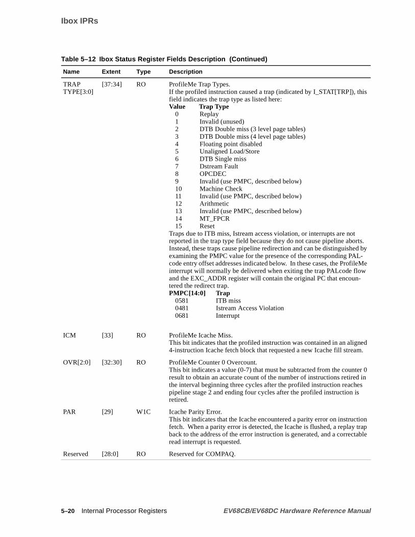
Ibox IPRs
s.by
-Me
d.
r 0in
onapble
TRAPTYPE[3:0]
[37:34] RO ProfileMe Trap Types.If the profiled instruction caused a trap (indicated by I_STAT[TRP]), thisfield indicates the trap type as listed here:Value Trap Type
0 Replay1 Invalid (unused)2 DTB Double miss (3 level page tables)3 DTB Double miss (4 level page tables)4 Floating point disabled5 Unaligned Load/Store6 DTB Single miss7 Dstream Fault8 OPCDEC9 Invalid (use PMPC, described below)10 Machine Check11 Invalid (use PMPC, described below)12 Arithmetic13 Invalid (use PMPC, described below)14 MT_FPCR15 Reset
Traps due to ITB miss, Istream access violation, or interrupts are notreported in the trap type field because they do not cause pipeline abortInstead, these traps cause pipeline redirection and can be distinguishedexamining the PMPC value for the presence of the corresponding PALcode entry offset addresses indicated below. In these cases, the Profileinterrupt will normally be delivered when exiting the trap PALcode flowand the EXC_ADDR register will contain the original PC that encoun-tered the redirect trap.PMPC[14:0] Trap
0581 ITB miss0481 Istream Access Violation0681 Interrupt
ICM [33] RO ProfileMe Icache Miss.This bit indicates that the profiled instruction was contained in an aligne4-instruction Icache fetch block that requested a new Icache fill stream
OVR[2:0] [32:30] RO ProfileMe Counter 0 Overcount.This bit indicates a value (0-7) that must be subtracted from the counteresult to obtain an accurate count of the number of instructions retiredthe interval beginning three cycles after the profiled instruction reachespipeline stage 2 and ending four cycles after the profiled instruction isretired.
PAR [29] W1C Icache Parity Error.This bit indicates that the Icache encountered a parity error on instructifetch. When a parity error is detected, the Icache is flushed, a replay trback to the address of the error instruction is generated, and a correctaread interrupt is requested.
Reserved [28:0] RO Reserved for COMPAQ.
Table 5–12 Ibox Status Register Fields Description (Continued)
Name Extent Type Description
5–20 Internal Processor Registers EV68CB/EV68DC Hardware Reference Manual

Ibox IPRs
is
enist and
theust
tate ton up.
textth
5.2.17 Icache Flush Register – IC_FLUSH
The Icache flush register (IC_FLUSH) is a pseudo register. Writing to this registerinvalidates all Icache blocks. The cache is flushed when the next HW_RET/STALLinstruction is retired. See Section D.20 for more information.
5.2.18 Icache Flush ASM Register – IC_FLUSH_ASM
The Icache flush ASM register (IC_FLUSH_ASM) is a pseudo register. Writing to thregister invalidates allIcacheblocks with their ASM bit clear.
5.2.19 Clear Virtual-to-Physical Map Register – CLR_MAP
The clear virtual-to-physical map register (CLR_MAP) is a pseudo register that, whwritten, results in the clearing of the current map of virtual to physical registers. Thregister must only be written after there are no register-borne dependencies presenthere are no unretired instructions. See an example in the PALcode restrictions.
5.2.20 Sleep Mode Register – SLEEP
The sleep mode register (SLEEP) is a pseudo register that, when written, results inPLL speed being reduced and the chip entering a low-power mode. This register monly be written after a sequence of code has been run which saves all necessary sDRAM, flushes the caches, and unmasks certain interrupts so the chip can be wokeSee Section 7.3 for details.
5.2.21 Process Context Register – PCTX
The process context register (PCTX) contains information associated with the conof a process. Any combination of the bit fields within this register may be written wia single HW_MTPR instruction. When bits [7:6] of the IPR index field of aHW_MTPR instruction contain the value 012, this register is selected. Bits [4:0] of theIPR index indicate which bit fields are to be written. Usage of PCTX in performancemonitoring is described in Section 6.10.
Table 5–13 lists the correspondence between IPR index bits and register fields.
A HW_MFPR from this register returns the values in all of its component bit fields.
Figure 5–24 shows the process context register.
Table 5–13 IPR Index Bits and Register Fields
IPR Index Bit Register Field
0 ASN
1 ASTER
2 ASTRR
3 PPCE
4 FPE
EV68CB/EV68DC Hardware Reference Manual Internal Processor Registers 5–21

Ibox IPRs
rci-
Figure 5–24 Process Context Register
Table 5–14 describes the process context register fields.
Table 5–14 Process Context Register Fields Description
Name Extent Type Description
Reserved [63:47] — —
ASN[7:0] [46:39] RW Address space number.
Reserved [38:13] — —
ASTRR[3:0] [12:9] RW AST request register—used to request AST interrupts ineach of the four processor modes.To generate a particular AST interrupt, its correspondingbits in ASTRR and ASTER must be set, along with theASTE bit in IER.Further, the value of the current mode bits in the PS registemust be equal to or higher than the value of the mode assoated with the AST request.The bit order with this field is:
User Mode 12Supervisor Mode 11Executive Mode 10Kernel Mode 9
ASTER[3:0] [8:5] RW AST enable register—used to individually enable each ofthe four AST interrupt requests.The bit order with this field is:
User Mode 8Supervisor Mode 7Executive Mode 6Kernel Mode 5
Reserved [4:3] — —
63 39 938 847 46 5 413 312 2 1 0
ASN[7:0]
ASTRR[3:0]
ASTER[3:0]
FPE
PPCELK99-0032A
5–22 Internal Processor Registers EV68CB/EV68DC Hardware Reference Manual

Ibox IPRs
Pro-
-
d-
-
s
1 0
034A
5.2.22 Performance Counter Control Register – PCTR_CTL
The performance counter control register (PCTR_CTL) is a read-write register thatcontrols the function of the performance counters for either aggregate counting orfileMe sampling counting.
Usage of PCTR_CTL in performance monitoring is described in Section 6.10.
Figure 5–25 shows the performance counter control register.
Figure 5–25 Performance Counter Control Register
Table 5–15 describes the performance counter control register fields.
FPE [2] RW,1 Floating-point enable—if clear, floating-point instructionsgenerate FEN exceptions. This bit is set by hardware onreset.
PPCE [1] RW Process performance counting enable.
Enables performance counting for an individual processwith counters PCTR0 or PCTR1, which are enabled by setting PCT0_EN or PCT1_EN, respectively.
Performance counting for the entire system can be enableby setting I_CTL[SPCE]. See Section 5.2.15 for more information.
See Section 6.10 for information about performance counting.
Reserved [0] — —
Table 5–15 Performance Counter Control Register Fields Description
Name Extent Type Description
SEXT(PCTR0_CTL[47]) [63:48] RO When read, this field is sign extended from PCTR_CTL[47]. Writeto this field are ignored.
Table 5–14 Process Context Register Fields Description (Continued)
Name Extent Type Description
63 48 2847 27 26 625 5 4 3 2
SEXT(PCTR0_CTL[47])
PCTR0[19:0]
PM_STALLED
PM_KILLED_BM
PCTR1[19:0]
SL0
SL1[1:0]
VAL
TAKLK99-0
EV68CB/EV68DC Hardware Reference Manual Internal Processor Registers 5–23

Ibox IPRs
d
if
r
d
-
ore
PCTR0[19:0] [47:28] RW Performance counter 0.PCTR0 is enabled by I_CTL[PCT0_EN] and either I_CTL[SPCE] orPCTX[PPCE].
In Aggregate mode:When enabled, PCTR0 is incremented at each cycle by the selecteinput. (See Section 6.10.2 for more information.)On overflow, if enabled by IER_CM[PCEN0],ISUM[PC0] is set and an interrupt is triggered.
In ProfileMe mode:On overflow, a count window is opened and PCTR0 is incrementedas described in Section 6.10.3. When the count window overflows,enabled by IER_CM[PCEN0], ISUM[PC0] is set and an interrupt istriggered.
See Table 5–16 for counter modes.
PM_STALLED [27] RO The profiled instruction stalled for at least one cycle between thefetch and map stages of the pipeline.
PM_KILLED_BM [26] RO The profiled instruction was killed during or before the cycle inwhich it was mapped.
PCTR1[19:0] [25:6] RW Performance counter 1.
PCTR1 is enabled by I_CTL[PCT1_EN] and either I_CTL[SPCE] oPCTX[PPCE].
In Aggregate mode:When enabled, PCTR1 is incremented at each cycle by the selecteinput. (See Section 6.10.2 for more information.)On overflow, if enabled by IER_CM[PCEN1], ISUM[PC1] is set andan interrupt is triggered.
In ProfileMe mode, how PCTR1 is incremented is described in Section 6.10.3.
In either case, PCTR1 is incremented no more than 1 per cycle.
See Table 5–16 for counter modes.
Reserved [5] RO Reads to this field return zero. Writes to this field are ignored.
SL0 [4] RW Selector 0.0 = Aggregate counting mode1 = ProfileMe modeSee Table 5–16 for more information.
SL1[1:0] [3:2] RW Selector 1.Selects counter PCTR0 and PCTR1 modes. See Table 5–16 for minformation.
Table 5–15 Performance Counter Control Register Fields Description (Continued)
Name Extent Type Description
5–24 Internal Processor Registers EV68CB/EV68DC Hardware Reference Manual

Mbox IPRs
.
hm.
se
5.3 Mbox IPRs
This section describes the internal processor registers that control Mbox functions
5.3.1 DTB Tag Array Write Registers 0 and 1 – DTB_TAG0, DTB_TAG1
The DTB tag array write registers 0 and 1 (DTB_TAG0 and DTB_TAG1) are write-only registers through which the two memory pipe DTB tagarrays are written. Writetransactions to DTB_TAG0 and DTB_TAG1 write data to registers outside the DTBarrays. When write transactions to the corresponding DTB_PTE registers are retired,the contents of both the DTB_TAG and DTB_PTE registers are written into theirrespective DTB arrays, at locations determined by the round-robin allocation algoritFigure 5–26 shows the DTB tag array write registers 0 and 1.
Figure 5–26 DTB Tag Array Write Registers 0 and 1
VAL [1] RO Profiled instruction valid.When set, indicates a nontrapping profiled instruction retired valid.When clear, indicates that a nontrapping profiled instruction waskilled after the cycle in which it was mapped. Valid retire/abort statufor a trapping profiled instruction is determined by the trap type (seI_STAT[TRAP_TYPE]).
TAK [0] RO ProfileMe conditional branch taken.Indicates program branch direction, if the profiled instruction is aconditional branch.
Table 5–16 Performance Counter Control Register Input Select Fields
SL0[4] SL1[3:2] Mode PCTR0 PCTR1
0 00 Aggregate Retired instructions Cycle counting
0 01 Aggregate Cycle counting Not defined
0 10 Aggregate Retired instructions Bcache miss or long latency probes
0 11 Aggregate Cycle counting Mbox replay traps
1 00 ProfileMe Retired instructions Cycle counting
1 01 ProfileMe Cycle counting Inum retire delay
1 10 ProfileMe Retired instructions Bcache miss or long latency probes
1 11 ProfileMe Cycle counting Mbox replay traps
Table 5–15 Performance Counter Control Register Fields Description (Continued)
Name Extent Type Description
63 48 47 13 12 0
VA[47:13]LK99-0035A
EV68CB/EV68DC Hardware Reference Manual Internal Processor Registers 5–25

Mbox IPRs
ersn byen7
ter
er.
5.3.2 DTB PTE Array Write Registers 0 and 1 – DTB_PTE0, DTB_PTE1
The DTB PTE array write registers 0 and 1 (DTB_PTE0 and DTB_PTE1) are registthrough which the DTB PTE arrays are written. The entries to be written are chosea round-robin allocation scheme. Write transactions to the DTB_PTE registers, whretired, result in both the DTB_TAG and DTB_PTE arrays being written. Figure 5–2shows the DTB PTE array write registers 0 and 1.
Figure 5–27 DTB PTE Array Write Registers 0 and 1
5.3.3 DTB Alternate Processor Mode Register – DTB_ALTMODE
The DTB alternate processor mode register (DTB_ALTMODE) is a write-only regiswhose contents specify the alternate processor mode used by some HW_LD andHW_ST instructions. Figure 5–28 shows the DTB alternate processor mode regist
Figure 5–28 DTB Alternate Processor Mode Register
Table 5–17 describes the DTB_ALTMODE register fields.
Table 5–17 DTB Alternate Processor Mode Register Fields Description
Name Extent Type Description
Reserved [63:2] — —
63 62 9 8 716 615 514 413 332 12 231 11 110 0
PA[43:13]
UWE
SWE
EWE
KWE
URE
SRE
ERE
KRE
GH[1:0]
ASM
FOW
FORLK99-0036A
63 2 1 0
ALT_MODE[1:0]LK99-0037A
5–26 Internal Processor Registers EV68CB/EV68DC Hardware Reference Manual

Mbox IPRs
ries
TB
arethe
cri-
s
5.3.4 Dstream TB Invalidate All Process (ASM=0) Register – DTB_IAP
The Dstream translation buffer invalidate all process (ASM=0) register (DTB_IAP) is awrite-only pseudo register. Write transactions to this register invalidate all DTB entin which the address space match (ASM) bit is clear.
5.3.5 Dstream TB Invalidate All Register – DTB_IA
The Dstream translation buffer invalidate all register (DTB_IA) is a write-only pseudoregister. Write transactions to this register invalidate all DTB entries and reset the Dnot-last-used pointer to its initial state.
5.3.6 Dstream TB Invalidate Single Registers 0 and 1 – DTB_IS0,1
The Dstream translation buffer invalidate single registers (DTB_IS0 and DTB_IS1)write-only pseudo registers through which software may invalidate a single entry inDTB arrays. Writing a virtual page number to one of these registers invalidates anyDTB entry in the corresponding memory pipeline which meets one of the followingteria:
• The DTB entry’s virtual page number matches DTB_IS[47:13] and its ASN fieldmatches DTB_ASN[63:56].
• The DTB entry’s virtual page number matches DTB_IS[47:13] and its ASM bit iset.
Figure 5–29 shows the Dstream translation buffer invalidate single registers.
Figure 5–29 Dstream Translation Buffer Invalidate Single Registers
ALT_MODE[1:0] [1:0] WO Alt_Mode:ALT_MODE[1:0] Mode
00 Kernel01 Executive10 Supervisor11 User
Table 5–17 DTB Alternate Processor Mode Register Fields Description (Continued)
Name Extent Type Description
63 48 47 13 12 0
VA[47:13] LK99-0015A
EV68CB/EV68DC Hardware Reference Manual Internal Processor Registers 5–27
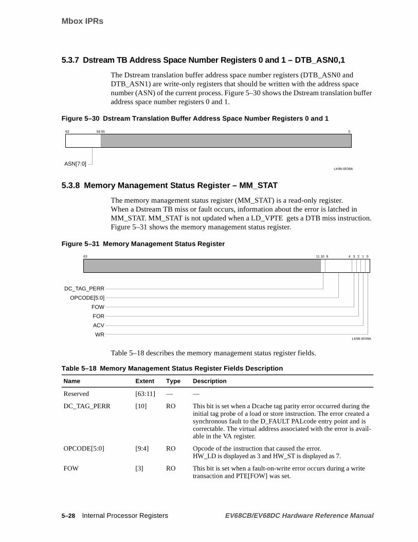
Mbox IPRs
uffer
n.
hea
il-
5.3.7 Dstream TB Address Space Number Registers 0 and 1 – DTB_ASN0,1
The Dstream translation buffer address space number registers (DTB_ASN0 andDTB_ASN1) are write-only registers that should be written with the address spacenumber (ASN) of the current process. Figure 5–30 shows the Dstream translation baddress space number registers 0 and 1.
Figure 5–30 Dstream Translation Buffer Address Space Number Registers 0 and 1
5.3.8 Memory Management Status Register – MM_STAT
The memory management status register (MM_STAT) is a read-only register.When a Dstream TB miss or fault occurs, information about theerror is latched inMM_STAT. MM_STAT is not updated when a LD_VPTE gets a DTB miss instructioFigure 5–31 shows the memory management status register.
Figure 5–31 Memory Management Status Register
Table 5–18 describes the memory management status register fields.
Table 5–18 Memory Management Status Register Fields Description
Name Extent Type Description
Reserved [63:11] — —
DC_TAG_PERR [10] RO This bit is set when a Dcache tag parity error occurred during tinitial tag probe of a load or store instruction. The error createdsynchronous fault to the D_FAULT PALcode entry point and iscorrectable. The virtual address associated with the error is avaable in the VA register.
OPCODE[5:0] [9:4] RO Opcode of the instruction that caused the error.HW_LD is displayed as 3 and HW_ST is displayed as 7.
FOW [3] RO This bit is set when a fault-on-write error occurs during a writetransaction and PTE[FOW] was set.
63 56 55 0
ASN[7:0]LK99-0038A
63 9 4 3 211 110 0
DC_TAG_PERR
OPCODE[5:0]
FOW
FOR
ACV
WRLK99-0039A
5–28 Internal Processor Registers EV68CB/EV68DC Hardware Reference Manual

Mbox IPRs
om
-
Note: The Ra field of the instruction that triggered the error can be obtained frthe Ibox EXC_SUM register.
5.3.9 Mbox Control Register – M_CTL
The Mbox control register (M_CTL) is a write-only register. Its contents are cleared bychip reset. Figure 5–32 shows the Mbox control register.
Figure 5–32 Mbox Control Register
FOR [2] RO This bit is set when a fault-on-read error occurs during a readtransaction and PTE[FOR] was set.
ACV [1] RO This bit is set when an access violation occurs during a transaction. Access violations include a bad virtual address.
WR [0] RO This bit is set when an error occurs during a write transaction.
Table 5–18 Memory Management Status Register Fields Description (Continued)
Name Extent Type Description
63 6 45 3 1 0
SMC[1:0]
SPE[2:0]
LK99-0040A
EV68CB/EV68DC Hardware Reference Manual Internal Processor Registers 5–29

Mbox IPRs
e ref-
33
e
es
nndr-
nndr-
Table 5–19 describes the Mbox control register fields.
Note: Superpage accesses are only allowed in kernel mode. Non-kernel moderences to superpages result in access violations.
5.3.10 Dcache Control Register – DC_CTL
The Dcache control register (DC_CTL) is a write-only register that controls Dcacheactivity. The contents of DC_CTL are initialized by chip reset as indicated. Figure 5–shows the Dcache control register.
Table 5–19 Mbox Control Register Fields Description
Name Extent Type Description
Reserved [63:6] — —
SMC[1:0] [5:4] WO,0 Speculative miss control (see Section 4.6.4).
SPE[2:0] [3:1] WO,0 Superpage mode enables.
SPE[2], when set, enables superpage mapping when VA[47:46] = 2. In thismode, VA[43:13] are mapped directly to PA[43:13] and VA[45:44] areignored.
SPE[1], when set, enables superpage mapping when VA[47:41] = 7E16. Inthis mode, VA[40:13] are mapped directly to PA[40:13] and PA[43:41] arecopies of PA[40] (sign extension).
SPE[0], when set, enables superpage mapping when VA[47:30] = 3FFFE16.In this mode, VA[29:13] are mapped directly to PA[29:13] and PA[43:30] arcleared.
Reserved [0] — —
Bits Meaning When Set
00 Allow full-time speculation.
01 Force full-time conservative mode. Make retries wait until retire,force all new stores that do not hit dirty to retry, and cause prefetchwith modify intent (see Section 2.6.2) to behave like normalprefetches.
10 Place EV68CB/EV68DC in periodic conservative mode by using a8-bit counter to add by 4 each time a branch mispredict happens asubtract by one each time a conditional branch retires. Enter consevative mode if the MSB of the counter is set.
11 Place EV68CB/EV68DC in periodic conservative mode by using a8-bit counter to add by 8 each time a branch mispredict happens asubtract by one each time a conditional branch retires. Enter consevative mode if the MSB of the counter is set.
5–30 Internal Processor Registers EV68CB/EV68DC Hardware Reference Manual

Mbox IPRs
ityr.
to.
d
of
g
Figure 5–33 Dcache Control Register
Table 5–20 describes the Dcache control register fields.
5.3.11 Dcache Status Register – DC_STAT
The Dcache status register (DC_STAT) is a read-write register. If a Dcache tag parerror or data ECC error occurs, information about the error is latched in this registeFigure 5–34 shows the Dcache status register.
Table 5–20 Dcache Control Register Fields Description
Name Extent Type Description
Reserved [63:8] — —
DCDAT_ERR_EN [7] WO,0 Dcache data ECC and parity error enable.
DCTAG_PAR_EN [6] WO,0 Dcache tag parity enable.
F_BAD_DECC [5] WO,0 Force Bad Data ECC. When set, ECC data isnot written intothe cache along with the block that is loaded by a fill or store.Writing data that is different from that already in the block willcause bad ECC to be present. Since the old ECC value willremain, the ECC will bebad.
F_BAD_TPAR [4] WO,0 Force Bad Tag Parity. When set, this bit causes bad tag paritybe put into the Dcache tag array during Dcache fill operations
Reserved [3] — —
F_HIT [2] WO,0 Force Hit. When set, this bit causes all memory space load anstore instructions to hit in the Dcache, independent of theDcache tag address compare. F_HIT does not force the statusthe block to register as DIRTY (the tag status bits are still con-sulted), so stores may still generate offchip activity.In this mode, only one of the two sets may be enabled, and taparity checking must be disabled (set DCTAG_PER_EN tozero).
SET_EN[1:0] [1:0] WO,3 Dcache Set Enable. At least one set must be enabled.
63 8 7 6 5 4 3 2 1 0
DCDAT_ERR_EN
DCTAG_PAR_EN
F_BAD_DECC
F_BAD_TPAR
F_HIT
SET_EN[1:0]LK99-0041A
EV68CB/EV68DC Hardware Reference Manual Internal Processor Registers 5–31

Cbox CSRs and IPRs
aret
x-
bits
er-
er-
Figure 5–34 Dcache Status Register
Table 5–21 describes the Dcache status register fields.
5.4 Cbox CSRs and IPRs
This section describes the Cbox CSRs and IPRs.
The Cbox configuration registers are split into three shift register chains:
• The hardware allocates 367 bits for the WRITE_ONCE chain, of which theEV68CB/EV68DC uses 304 bits. During hardware reset (after BiST), 367 bitsalways shifted into the WRITE_ONCE chain from the SROM, MSB first, so thathe unused bits are shifted out the end of the WRITE_ONCE chain.
• A 36-bit WRITE_MANY chain that is loaded using MTPR instructions to the Cbodata register. Six bits of information are shifted into the WRITE_MANY chain during each write transaction to the Cbox data register.
• A 60-bit Cbox ERROR_REG chain that is read by using MFFR instructions fromthe Cbox data register in combination with MTPR instructions to the Cbox shiftregister. Each write transaction to the Cbox shift register destructively shifts sixof information out of the Cboxerror register.
Table 5–21 Dcache Status Register Fields Description
Name Extent Type Description
Reserved [63:5] — —
SEO [4] W1C Second error occurred. When set, this bit indicates that a secondDcache store ECC error occurred within 6 cycles of the previousDcache store ECC error.
ECC_ERR_LD [3] W1C ECC error on load. When set, this bit indicates that a single-bit ECCerror occurred while processing a load from the Dcache or any fill.
ECC_ERR_ST [2] W1C ECC error on store. When set, this bit indicates that an ECC erroroccurred while processing a store.
TPERR_P1 [1] W1C Tag parity error — pipe 1. When set, this bit indicates that a Dcachtag probe from pipe 1 resulted in a tag parity error. The error is uncorectable and results in a machine check.
TPERR_P0 [0] W1C Tag parity error — pipe 0. When set, this bit indicates that a Dcachtag probe from pipe 0 resulted in a tag parity error. The error is uncorectable and results in a machine check.
63 5 4 3 2 1 0
SEO
ECC_ERR_LD
ECC_ERR_ST
TPERR_P1
TPERR_P0LK99-0042A
5–32 Internal Processor Registers EV68CB/EV68DC Hardware Reference Manual

Cbox CSRs and IPRs
arees
toion
5.4.1 Cbox Data Register – C_DATA
Figure 5–35 shows the Cbox data register.
Figure 5–35 Cbox Data Register
Table 5–22 describes the Cbox data register fields.
5.4.2 Cbox Shift Register – C_SHFT
Figure 5–36 shows the Cbox shift register.
Figure 5–36 Cbox Shift Register
Table 5–23 describes the Cbox shift register fields.
5.4.3 Cbox WRITE_ONCE Chain Description
The WRITE_ONCE chain order is contained in Table 5–24. In the table:
• Many CSRs are duplicated for ease of hardware implementation. These CSRsindicated in italics. They must be written with values that are identical to the valuwritten to the original CSRs.
Table 5–22 Cbox Data Register Fields Description
Name Extent Type Description
Reserved [63:6] — —
C_DATA[5:0] [5:0] RW Cbox data register. A HW_MTPR instruction to this register causes sixbits of data to be placed into a serial shift register. When theHW_MTPR instruction is retired, the data is shifted into the Cbox. Afterthe Cbox shift register has been accessed, performing a HW_MFPRinstruction to this register will return six bits of data.
Table 5–23 Cbox Shift Register Fields Description
Name Extent Type Description
Reserved [63:1] — —
C_SHIFT [0] W1 Writing a 1 to this register bit causes six bits of Cbox IPR data to shift inthe Cbox data register. Software can then use a HW_MFPR read operatto the Cbox data register to read the six bits of data.
63 6 5 0
C_DATA[5:0]LK99-0043A
63 1 0
C_SHIFTLK99-0044A
EV68CB/EV68DC Hardware Reference Manual Internal Processor Registers 5–33

Cbox CSRs and IPRs
se
e,
e
he
• Only a brief description of each CSR is given. The functional description of theCSRs is contained in Chapter 4.
• The order of multibit vectors is [MSB:LSB], so the LSB is first bit in the Cboxchain.
Table 5–24 describes the Cbox WRITE_ONCE chain order from LSB to MSB.
Table 5–24 Cbox WRITE_ONCE Chain Order
Cbox WRITE_ONCE Chain Description
32_BYTE_IO[0] Enable 32_BYTE I/O mode.
BC_CLK_RATIO[1] Asserted when Bcache is at 1.5x ratio.
SKEWED_FILL_MODE[0] Must be asserted for Bcache 1.5x ratio; for maximum performanccan also be asserted for 3.0x and 3.5x ratios.
DCVIC_THRESHOLD[7:0] Threshold of the number of Dcache victims that will accumulatebefore streamed write transactions to the Bcache are initiated. ThCbox can accumulate up to six victims for streamed Dcache pro-cessing. This register is programmed with the decoded value of tthreshold count.
BC_CLEAN_VICTIM[0] Enable clean victims to the system interface.
SYS_BUS_SIZE[1:0] Size of SysAddOut and SysAddOut buses.
SYS_BUS_FORMAT[0] Indicates system bus format.
SYS_CLK_RATIO[4:1] Speed of system bus.Code Multiplier0001 1.5X0010 2.0X0100 2.5X1000 3.0X
DUP_TAG_ENABLE[0] Enable duplicate tag mode in the EV68CB/EV68DC.
PRB_TAG_ONLY[0] Enable probe-tag only mode in the EV68CB/EV68DC.
FAST_MODE_DISABLE[0] When asserted, disables fast data movement mode.
BC_RDVICTIM[0] Enables RdVictim mode on the pads.
BC_CLEAN_VICTIM[0] Duplicate CSR.
RDVIC_ACK_INHIBIT Enable inhibition of incrementing acknowledge counter for RdViccommands.
SYSBUS_MB_ENABLE Enable MB commands offchip.
SYSBUS_ACK_LIMIT[0:4] Sysbus acknowledge limit CSR.
SYSBUS_VIC_LIMIT[0:2] Limit for victims.
BC_CLEAN_VICTIM[0] Duplicate CSR.
BC_WR_WR_BUBBLE[0] Write to write GCLK bubble.
BC_RD_WR_BUBBLES[0:5] Read to write GCLK bubbles for the Bcache interface.
BC_RD_RD_BUBBLE[0] Read to read GCLK bubble for banked Bcaches.
BC_SJ_BANK_ENABLE Enable bank mode for Bcache.
5–34 Internal Processor Registers EV68CB/EV68DC Hardware Reference Manual

Cbox CSRs and IPRs
-
se
BC_WR_RD_BUBBLES[0:3] Write to read GCLK bubbles.
DUP_TAG_ENABLE Duplicate CSR.
SKEWED_FILL_MODE Duplicate CSR.
BC_RDVICTIM Duplicate CSR.
SKEWED_FILL_MODE Duplicate CSR.
BC_RDVICTIM Duplicate CSR.
BC_CLEAN_VICTIM Duplicate CSR.
DUP_TAG_MODE Duplicate CSR.
SKEWED_FILL_MODE Duplicate CSR.
ENABLE_PROBE_CHECK Enable error checking during probe processing.
SPEC_READ_ENABLE[0] Enable speculative references to the system port.
SKEWED_FILL_MODE Duplicate CSR.
SKEWED_FILL_MODE Duplicate CSR.
MBOX_BC_PRB_STALL Must be asserted when BC_RATIO = 4.0X, 5.0X, 6.0X, 7.0X, or8.0X.
BC_LAT_DATA_PATTERN[0:31] Bcache data latency pattern.
BC_LAT_TAG_PATTERN[0:23] Bcache tag latency pattern.
BC_RDVICTIM Duplicate CSR.
ENABLE_STC_COMMAND[0] Enable STx_C instructions to the pads.
BC_LATE_WRITE_NUM[0:2] Number of Bcache clocks to delay the data for Bcache write commands.
BC_CPU_LATE_WRITE_NUM[0:1] Number of GCLK cycles to delay the Bcache clock/data fromindex.
BC_BURST_MODE_ENABLE[0] Burst mode enable signal.
BC_PENTIUM_MODE[0] Enable Pentium mode RAM behavior.
BC_CLK_RATIO[1] Duplicate CSR.
BC_FRM_CLK[0] Force all Bcache transactions to start on rising edges of the A phaof a GCLK.
BC_CLK_DELAY[0:1] Delay of Bcache clock for 0,0,1,2 GCLK phases.
BC_DDMR_ENABLE[0] Enables the rising edge of the Bcache forwarded clock (alwaysenabled).
BC_DDMF_ENABLE[0] Enable the falling edge of the Bcache forwarded clock (alwaysenabled).
BC_LATE_WRITE_UPPER[0] Asserted when (BC_LATE_WRITE_NUM > 3) or((BC_LATE_WRITE_NUM = 3) and(BC_CPU_LATE_WRITE_NUM > 1)).
Table 5–24 Cbox WRITE_ONCE Chain Order (Continued)
Cbox WRITE_ONCE Chain Description
EV68CB/EV68DC Hardware Reference Manual Internal Processor Registers 5–35

Cbox CSRs and IPRs
.
ed
sed
.
for-
tem
BC_TAG_DDM_FALL_EN[0] Enables the update of the EV68CB/EV68DC Bcache tag outputsbased on the falling edge of the forwarded clock.
BC_TAG_DDM_RISE_EN[0] Enables the update of the EV68CB/EV68DC Bcache tag outputsbased on the rising edge of the forwarded clock.
BC_CLKFWD_ENABLE[0] Enable clock forwarding on the Bcache interface.
BC_RCV_MUX_CNT_PRESET[0:1] Initial value for the Bcache clock forwarding unload pointer FIFO
BC_LATE_WRITE_UPPER[0] Duplicate CSR.
SYS_DDM_FALL_EN[0] Enables the update of the EV68CB/EV68DC system outputs bason the falling edge of the system forwarded clock.
SYS_DDM_RISE_EN[0] Enables the update of the EV68CB/EV68DC system outputs baon the rising edge of the system forwarded clock.
SYS_CLKFWD_ENABLE[0] Enables clock forwarding on the system interface.
SYS_RCV_MUX_CNT_PRESET[0:1] Initial value for the system clock forwarding unload pointer FIFO
SYS_CLK_DELAY[0:1] Delay of 0 to 2 phases between the forwarded clock out andaddress/data.
SYS_DDMR_ENABLE[0] Enables the rising edge of the system forwarded clock (alwaysenabled).
SYS_DDMF_ENABLE[0] Enables the falling edge of the system forwarded clock (alwaysenabled).
BC_DDM_FALL_EN[0] Enables update of data/address on the rising edge of the systemwarded clock.
BC_DDM_RISE_EN[0] Enables the update of data/address on the falling edge of the sysforwarded clock.
BC_CLKFWD_ENABLE Duplicate CSR.
BC_RCV_MUX_CNT_PRESET[0:1] Duplicate CSR.
BC_CLK_DELAY[0:1] Duplicate CSR.
BC_DDMR_ENABLE Duplicate CSR.
BC_DDMF_ENABLE Duplicate CSR.
SYS_DDM_FALL_EN Duplicate CSR.
SYS_DDM_RISE_EN Duplicate CSR.
SYS_CLKFWD_ENABLE Duplicate CSR.
SYS_RCV_MUX_CNT_PRESET[0:1] Duplicate CSR.
SYS_CLK_DELAY[0:1] Duplicate CSR.
SYS_DDMR_ENABLE Duplicate CSR.
SYS_DDMF_ENABLE Duplicate CSR.
BC_DDM_FALL_EN Duplicate CSR.
BC_DDM_RISE_EN Duplicate CSR.
Table 5–24 Cbox WRITE_ONCE Chain Order (Continued)
Cbox WRITE_ONCE Chain Description
5–36 Internal Processor Registers EV68CB/EV68DC Hardware Reference Manual

Cbox CSRs and IPRs
BC_CLKFWD_ENABLE Duplicate CSR.
BC_RCV_MUX_CNT_PRESET[0:1] Duplicate CSR.
SYS_DDM_FALL_EN Duplicate CSR.
SYS_DDM_RISE_EN Duplicate CSR.
SYS_CLKFWD_ENABLE Duplicate CSR.
SYS_RCV_MUX_CNT_PRESET[0:1] Duplicate CSR.
SYS_CLK_DELAY[0:1] Duplicate CSR.
SYS_DDMR_ENABLE Duplicate CSR.
SYS_DDMF_ENABLE Duplicate CSR.
BC_DDM_FALL_EN Duplicate CSR.
BC_DDM_RISE_EN Duplicate CSR.
BC_CLKFWD_ENABLE Duplicate CSR.
BC_RCV_MUX_CNT_PRESET[0:1] Duplicate CSR.
BC_CLK_DELAY[0:1] Duplicate CSR.
BC_DDMR_ENABLE Duplicate CSR.
BC_DDMF_ENABLE Duplicate CSR.
SYS_DDM_FALL_EN Duplicate CSR.
SYS_DDM_RISE_EN Duplicate CSR.
SYS_CLKFWD_ENABLE Duplicate CSR.
SYS_RCV_MUX_CNT_PRESET[0:1] Duplicate CSR.
SYS_CLK_DELAY[1:0] Duplicate CSR.
SYS_DDMR_ENABLE Duplicate CSR.
SYS_DDMF_ENABLE Duplicate CSR.
BC_DDM_FALL_EN Duplicate CSR.
BC_DDM_RISE_EN Duplicate CSR.
BC_CLKFWD_ENABLE Duplicate CSR.
BC_RCV_MUX_CNT_PRESET[1:0] Duplicate CSR.
SYS_CLK_DELAY[0:1] Duplicate CSR.
SYS_DDMR_ENABLE Duplicate CSR.
SYS_DDMF_ENABLE Duplicate CSR.
SYS_DDM_FALL_EN Duplicate CSR.
SYS_DDM_RISE_EN Duplicate CSR.
SYS_CLKFWD_ENABLE Duplicate CSR.
SYS_RCV_MUX_CNT_PRESET[0:1] Duplicate CSR.
Table 5–24 Cbox WRITE_ONCE Chain Order (Continued)
Cbox WRITE_ONCE Chain Description
EV68CB/EV68DC Hardware Reference Manual Internal Processor Registers 5–37

Cbox CSRs and IPRs
ames
se
ck
al-
ck
al-
5.4.4 Cbox WRITE_MANY Chain Description
The WRITE_MANY chain order is contained in Table 5–25. Note the following:
• Many CSRs are duplicated for ease of hardware implementation. These CSR nare indicated in italics and have two leading asterisks.
• Only a brief description of each CSR is given. The functional description of theCSRs is contained in Chapter 3.
CFR_GCLK_DELAY[0:3] Number of GCLK cycles to delay internal ClkFwdRst.
CFR_EV6CLK_DELAY[0:2] Number of EV6Clk_x cycles to delay internal ClkFwdRst.
CFR_FRMCLK_DELAY[0:1] Number of FrameClk_x cycles to delay internal ClkFwdRst.
BC_LATE_WRITE_NUM[0:2] Duplicate CSR.
BC_CPU_LATE_WRITE_NUM[1:0] Duplicate CSR.
JITTER_CMD[0] Add one GCLK cycle to the SYSDC write path.
FAST_MODE_DISABLE[0] Duplicate CSR.
SYSDC_DELAY[3:0] Number of GCLK cycles to delay SysDc fill commands beforeaction by the Cbox.
DATA_VALID_DLY[1:0] Number of Bcache clock cycles to delay signal SysDataInValidbefore sample by the Cbox.
BC_DDM_FALL_EN Duplicate CSR.
BC_DDM_RISE_EN Duplicate CSR.
BC_CPU_CLK_DELAY[0:1] Delay of Bcache clock for 0, 1, 2, 3 GCLK cycles.
BC_FDBK_EN[0:7] CSR to program the Bcache forwarded clock shift register feedbapoints.
BC_CLK_LD_VECTOR[0:15] CSR to program the Bcache forwarded clock shift register load vues.
BC_BPHASE_LD_VECTOR[0:3] CSR to program the Bcache forwarded clock b-phase enables.
SYS_DDM_FALL_EN Duplicate CSR.
SYS_DDM_RISE_EN Duplicate CSR.
SYS_CPU_CLK_DELAY[0:1] Delay of 0..3 GCLK cycles between the forwarded clock out andaddress/data.
SYS_FDBK_EN[0:7] CSR to program the system forwarded clock shift register feedbapoints.
SYS_CLK_LD_VECTOR[0:15] CSR to program the system forwarded clock shift register load vues.
SYS_BPHASE_LD_VECTOR[0:3] CSR to program the system forwarded clock b-phase enables.
SYS_FRAME_LD_VECTOR[0:4] CSR to program the ratio between frame clock and system for-warded clock.
SYSDC_DELAY[4] Fifth SYSDC_DELAY bit.
Table 5–24 Cbox WRITE_ONCE Chain Order (Continued)
Cbox WRITE_ONCE Chain Description
5–38 Internal Processor Registers EV68CB/EV68DC Hardware Reference Manual

Cbox CSRs and IPRs
ain.
• The order of multibit vectors is [MSB:LSB], so the LSB is first bit in the Cboxchain.
Table 5–25 describes the Cbox WRITE_MANY chain order from LSB to MSB.
Figure 5–37 shows an example of PALcode used to write to the WRITE_MANY ch
Figure 5–37 WRITE_MANY Chain Write Transaction Example
;; Initialize the Bcache configuration in the Cbox;; BC_VALID_MODE = 1; BC_ENABLE = 1
Table 5–25 Cbox WRITE_MANY Chain Order
Cbox WRITE_MANY Chain Description For Information:
BC_VALID_MODE Control Bcache block parity calculation Section 8.8
INIT_MODE[0] Enable initialize mode Section 7.6
BC_SIZE[3:0] Bcache size Table 4–42
BC_ENABLE[0] Enable the Bcache Table 4–42
BC_ENABLE Duplicate CSR Table 4–42
BC_SIZE[0:3] Duplicate CSR Table 4–42
BC_ENABLE1
1 MBZ during initialization mode; see Section 7.6 for information.
Duplicate CSR Table 4–42
BC_ENABLE1 Duplicate CSR Table 4–42
BC_ENABLE1 Duplicate CSR Table 4–42
INVAL_TO_DIRTY_ENABLE[1] WH64 acknowledges Table 4–15
ENABLE_EVICT Enable issue evict Table 4–1
BC_ENABLE Duplicate CSR Table 4–42
INVAL_TO_DIRTY_ENABLE[0] WH64 acknowledges Table 4–15
BC_ENABLE Duplicate CSR Table 4–42
BC_ENABLE Duplicate CSR Table 4–42
BC_ENABLE Duplicate CSR Table 4–42
SET_DIRTY_ENABLE[0] SetDirty acknowledge programming Table 4–16
INVAL_TO_DIRTY_ENABLE[0] Duplicate CSR Table 4–15
SET_DIRTY_ENABLE[2:1] SetDirty acknowledge programming Table 4–16
BC_BANK_ENABLE[0] Enable bank mode for Bcache Section 4.8.5
BC_SIZE[0:3] Duplicate CSR Table 4–42
INIT_MODE Duplicate CSR Section 7.6
BC_WRT_STS[0:3] Write status for Bcache in initialize-mode(Valid, Dirty, Shared, Parity)
Section 7.6
EV68CB/EV68DC Hardware Reference Manual Internal Processor Registers 5–39

Cbox CSRs and IPRs
; INIT_MODE = 0; BC_SIZE = 0xF; INVALID_TO_DIRTY_ENABLE = 3; ENABLE_EVICT = 1; SET_DIRTY_ENABLE = 6; BC_BANK_ENABLE = 1; BC_WRT_STS = 0;; The value for the write_many chain is based on Table 5–25.;; The value is sampled from MSB, 6 bits at a time, as it is written; to EV6__DATA. Therefore, before the value can be shifted in, it must be; inverted on a by 6 basis. The code then writes out 6 bits at a time,; shifting right by 6 after each write.;; So the following transformation is done on the write_many value:;; [35:30]|[29:24]|[23:18]|[17:12]|[11:06]|[05:00] =>; [05:00]|[11:06]|[17:12]|[23:18]|[29:24]|[35:30];; WRITE_MANY chain = 0x07FBFFFFD; value to be shifted in = 0xF7FFEFFC1;; Before the chain can be written, I_CTL[SBE] must be disabled,; and the code must be forced into the Icache.;
ALIGN_CACHE_BLOCK <^x47FF041F>; align with nops
mb ; wait for MEM-OP’s to completelda r0, ^x0086(r31) ; load I_CTL.....hw_mtpr r0, EV6__I_CTL ; .....SDE=2, IC_EN=3, SBE=0br r0, . ; create dest address
addq r0, #17, r0 ; finish computing dest addresshw_mtpr r31, EV6__IC_FLUSH ; flush the Icachebne r31, . ; separate retireshw_jmp_stall (r0) ; force flush
ALIGN_CACHE_BLOCK <^x47FF041F> ; align with nops
bc_config:mb ; pull this block in Icachelda r1, ^xFFC1(r31) ; data[15:00] = 0xFFC1ldah r0, ^x7FFE(r31) ; data[31:16] = 0x7FFEzap r1, #^x0c, r1 ; clear out bits [31:16]
bis r1, r0, r1 ; or in bits [31:16]addq r31, #6, r0 ; shift in 6 x 6 bits
bc_config_shift_in:hw_mtpr r1, EV6__DATA ; shift in 6 bitssubq r0, #1, r0 ; decrement R0
beq r0, bc_config_done ; done if R0 is zerosrl r1, #6, r1 ; align next 6 bitsbr r31, bc_config_shift_in ; continue shifting
bc_config_done:hw_mtpr r31, <EV6__MM_STAT ! 64> ; wait until last shift
beq r31, bc_config_end ; predicts fall thrubr r31, .-4 ; predict infinite loopbis r31, r31, r31 ; nopbis r31, r31, r31 ; nop
bc_config_end:
5–40 Internal Processor Registers EV68CB/EV68DC Hardware Reference Manual

Cbox CSRs and IPRs
LSB
5.4.5 Cbox Read Register (IPR) Description
The Cbox read register is read 6 bits at a time. Table 5–26 shows the ordering fromto MSB.
Table 5–26 Cbox Read IPR Fields Description
Name Description
C_SYNDROME_1[7:0] Syndrome for upper QW in OW of victim that was scrubbed.
C_SYNDROME_0[7:0] Syndrome for lower QW in OW of victim that was scrubbed.
C_STAT[4:0]
C_STS[3:0] If C_STAT equalsxxx_MEM_ERR orxxx_BC_ERR, then C_STS contains thestatus of the block as follows; otherwise, the value of C_STS is X:
C_ADDR[6:42] Address of last reported ECC or parity error. If C_STAT value isDSTREAM_DC_ERR, only bits 6:19 are valid.
Bits Error Status
0 0 0 0 0 Either no error, or error on a speculative load, ora Bcache victim read due to a Dcache/Bcache miss
0 0 0 0 1 BC_PERR (Bcache tag parity error)
0 0 0 1 0 DC_PERR (duplicate tag parity error)
0 0 0 1 1 DSTREAM_MEM_ERR
0 0 1 0 0 DSTREAM_BC_ERR
0 0 1 0 1 DSTREAM_DC_ERR
0 0 1 1 X PROBE_BC_ERR
0 1 0 0 0 Reserved
0 1 0 0 1 Reserved
0 1 0 1 0 Reserved
0 1 0 1 1 ISTREAM_MEM_ERR
0 1 1 0 0 ISTREAM_BC_ERR
0 1 1 0 1 Reserved
0 1 1 1 X Reserved
1 0 0 1 1 DSTREAM_MEM_DBL
1 0 1 0 0 DSTREAM_BC_DBL
1 1 0 1 1 ISTREAM_MEM_DBL
1 1 1 0 0 ISTREAM_BC_DBL
Bit Value Status of Block
7:4 Reserved
3 Parity
2 Valid
1 Dirty
0 Shared
EV68CB/EV68DC Hardware Reference Manual Internal Processor Registers 5–41


e-
ptsh as
6Privileged Architecture Library Code
This chapter describes the EV68CB/EV68DC privileged architecture library code(PALcode). The chapter is organized as follows:
• PALcode description
• PALmode environment
• Required PALcode function codes
• Opcodes reserved for PALcode
• Internal processor register access mechanisms
• PALshadow registers
• PALcode emulation of FPCR
• PALcode entry points
• Translation buffer fill flows
• Performance counter support
6.1 PALcode Description
PALcode is macrocode that provides an architecturally-defined, operating-system-spcific programming interface that is common across all Alpha microprocessors. Theactual implementation of PALcode differs for each operating system. PALcode runswith privileges enabled, instruction stream (Istream) mapping disabled, and interrudisabled. PALcode has privilege to use five special opcodes that allow functions sucphysical data stream (Dstream) references and internal processor register (IPR) manip-ulation.
PALcode can be invoked by the following events:
• Reset
• System hardware exceptions (MCHK, ARITH)
• Memory-management exceptions
• Interrupts
• CALL_PAL instructions
PALcode has characteristics that make it appear to be a combination of microcode,ROM BIOS, and system service routines, though the analogy to any of these otheritems is not exact. PALcode exists for several major reasons:
EV68CB/EV68DC Hardware Reference Manual Privileged Architecture Library Code 6–1
PALmode Environment
tl
archi-isle-
truc-e.
ase
e ofem-ine,
ta-
tinescodee
ntam
e
itsse.aedo.g
-
• There are some necessary support functions that are too complex to implemendirectly in a processor chip’s hardware, but that cannot be handled by a normaoperating system software routine. Routines to fill the translation buffer (TB),acknowledge interrupts, and dispatch exceptions are some examples. In sometectures, these functions are handled by microcode, but the Alpha architecturecareful not to mandate the use of microcode so as to allow reasonable chip impmentations.
• There are functions that must run atomically, yet involve long sequences of instions that may need complete access to all of the underlying computer hardwarAn example of this is the sequence that returns from an exception or interrupt.
• There are some instructions that are necessary for backward compatibility or eof programming; however, these are not used often enough to dedicate them tohardware, or are so complex that they would jeopardize the overall performancthe computer. For example, an instruction that does a VAX style interlocked mory access might be familiar to someone used to programming on a CISC machbut is not included in the Alphaarchitecture. Another example is the emulation ofan instruction that has no direct hardware support in a particular chip implemention.
In each of these cases, PALcode routines are used to provide the function. The rouare nothing more than programs invoked at specified times, and read in as Istreamin the same way that all other Alpha code is read. Once invoked, however, PALcodruns in a special mode called PALmode.
6.2 PALmode EnvironmentPALcode runs in a special environment called PALmode, defined as follows:
• Istream memory mapping is disabled. Because the PALcode is used to implemetranslation buffer fill routines, Istream mapping clearly cannot be enabled. Dstremapping is still enabled.
• The program has privileged access to all of the computer hardware. Most of thfunctions handled by PALcode are privileged and need control of the lowestlevels of the system.
• Interrupts are disabled. If a long sequence of instructions need to be executedatomically, interrupts cannot be allowed.
An important aspect of PALcode is that it uses normal Alpha instructions for most ofoperations; that is, the same instruction set that nonprivileged Alpha programmers uThere are a few extra instructions that are only available in PALmode, and will causedispatch to the OPCDEC PALcode entry point if attempted while not in PALmode. ThAlpha architecture allows some flexibility in what these special PALmode instructionsIn the EV68CB/EV68DC, the special PALmode-only instructions perform the followinfunctions:
• Read or write internal processor registers (HW_MFPR, HW_MTPR)
• Perform memory load or store operations without invoking the normal memorymanagement routines (HW_LD, HW_ST)
• Return from an exception or interrupt (HW_RET)
6–2 Privileged Architecture Library Code EV68CB/EV68DC Hardware Reference Manual

Required PALcode Function Codes
these
be
e
is
spe-
pro--code
alta
When executing in PALmode, there are certain restrictions for using the privilegedinstructions because PALmode gives the programmer complete access to many ofinternal details of the EV68CB/EV68DC. Refer to Section 6.4 for information on thespecial PALmode instructions.
Caution: It is possible to cause unintended side effects by writing what appears toperfectly acceptable PALcode. As such, PALcode is not something thatmany users will want to change. Before writing PALcode, at least becomfamiliar with the information in Appendix D.
6.3 Required PALcode Function Codes
Table 6–1 lists opcodes required for all Alpha implementations. The notation usedoo.ffff, where oo is the hexadecimal 6-bit opcode and ffff is the hexadecimal 26-bitfunction code.
6.4 Opcodes Reserved for PALcode
Table 6–2 lists the opcodes reserved by the Alpha architecture for implementation-cific use. These opcodes are privileged and are only available in PALmode.
These instructions generally produce an OPCDEC exception if executed while thecessor is not in PALmode. If I_CTL[HWE] is set, these instructions can also be executed in kernel mode. Software that uses these instructions must adhere to the PALrestrictions listed in this section.
6.4.1 HW_LD Instruction
PALcode uses the HW_LD instruction to access memory outside the realm of normAlpha memory management and to perform special Dstream load transactions. Daalignment traps are disabled for the HW_LD instruction.
Figure 6–1 shows the HW_LD instruction format.
Table 6–1 Required PALcode Function Codes
Mnemonic Type Function Code
DRAINA Privileged 00.0002
HALT Privileged 00.0000
IMB Unprivileged 00.0086
Table 6–2 Opcodes Reserved for PALcode
Mnemonic OpcodeArchitectureMnemonic Function
HW_LD 1B PAL1B Dstream load instruction
HW_ST 1F PAL1F Dstream store instruction
HW_RET 1E PAL1E Return from PALcode routine
HW_MFPR 19 PAL19 Copies the value of an IPR into an integer GPR
HW_MTPR 1D PAL1D Writes the value of an integer GPR into an IPR
EV68CB/EV68DC Hardware Reference Manual Privileged Architecture Library Code 6–3

Opcodes Reserved for PALcode
alDataT
ss
d
Figure 6–1 HW_LD Instruction Format
Table 6–3 describes the HW_LD instruction fields.
6.4.2 HW_ST Instruction
PALcode uses the HW_ST instruction to access memory outside the realm of normAlpha memory management and to do special forms of Dstream store instructions.alignment traps are inhibited for HW_ST instructions. Figure 6–2 shows the HW_Sinstruction format.
Figure 6–2 HW_ST Instruction Format
Table 6–3 HW_LD Instruction Fields Descriptions
Extent Mnemonic Value Description
[31:26] OPCODE 1B16 The opcode value.
[25:21] RA — Destination register number.
[20:16] RB — Base register for memory address.
[15:13] TYPE 0002 Physical — The effective address for the HW_LD instruction is physical.
0012 Physical/Lock — The effective address for the HW_LD instruction isphysical. It is the load lock version of the HW_LD instruction.
0102 Virtual/VPTE — Flags a virtual PTE fetch (LD_VPTE). Used by trap logicto distinguish a single TB miss from a double TB miss. Kernel mode accechecks are performed.
1002 Virtual — The effective address for the HW_LD instruction is virtual.
1012 Virtual/WrChk — The effective address for the HW_LD instruction isvirtual. Access checks for fault-on-read (FOR), fault-on-write (FOW), reaand write protection.
1102 Virtual/Alt — The effective address for the HW_LD instruction is virtual.Access checks use DTB_ALT_MODE IPR.
1112 Virtual/WrChk/Alt — The effective address for the HW_LD instruction isvirtual. Access checks for FOR, FOW, read and write protection. Accesschecks use DTB_ ALT_MODE IPR.
[12] LEN 0
1
Access length is longword.
Access length is quadword.
[11:0] DISP — Holds a 12-bit signed byte displacement.
31 26 25 21 20 16 15 13 1112 0
FM-05654.AI4
TYPE
LEN
DISPRBRAOPCODE
31 26 25 21 20 16 15 13 1112 0
FM-05654.AI4
TYPE
LEN
DISPRBRAOPCODE
6–4 Privileged Architecture Library Code EV68CB/EV68DC Hardware Reference Manual

Opcodes Reserved for PALcode
Blue
-set
truc-
wnNT
y.
s
Table 6–4 describes the HW_ST instruction fields.
6.4.3 HW_RET Instruction
The HW_RET instruction is used to return instruction flow to a specified PC. The Rfield of the HW_RET instruction specifies an integer GPR, which holds the new vaof the PC. Bit [0] of this register provides the new value of PALmode after theHW_RET instruction is executed. Bits [15:14] of the instruction determine the stackaction.
Normally the HW_RET instruction succeeds a CALL_PAL instruction, or a trap handler that pushed its PC onto the prediction stack. In this mode, the HINT should beto ‘10’ to pop the PC and generate a predicted target address for the HW_RET instion.
In some conditions, the HW_RET instruction is used in the middle of a PALcode floto cause a group of instructions to retire. In these cases, if the HW_RET instructiodoes not have a corresponding instruction that pushed a PC onto the stack, the HIfield should be set to ‘00’ to keep the stack from being modified.
In the rare circumstance that the HW_RET instruction might be used like a JSR orJSR_COROUTINE, the stack can be managed by setting the HINT bits accordingl
See Section D.25 for more information about the HW_RET instruction.
Figure 6–3 shows the HW_RET instruction format.
Table 6–4 HW_ST Instruction Fields Descriptions
Extent Mnemonic Value Description
[31:26] OPCODE 1F16 The opcode value.
[25:21] RA — Write data register number.
[20:16] RB — Base register for memory address.
[15:13] TYPE 0002 Physical — The effective address for the HW_ST instruction is physical.
0012 Physical/Cond — The effective address for the HW_ST instruction isphysical. Store conditional version of the HW_ST instruction. The lockflag is returned in RA. Refer to PALcode restrictions for correct use of thifunction.
0102 Virtual — The effective address for the HW_ST instruction is virtual.
1102 Virtual/Alt — The effective address for the HW_ST instruction is virtual.Access checks use DTB_ ALT_MODE IPR.
All others Unused.
[12] LEN 0
1
Access length is longword.
Access length is quadword.
[11:0] DISP — Holds a 12-bit signed byte displacement.
EV68CB/EV68DC Hardware Reference Manual Privileged Architecture Library Code 6–5

Opcodes Reserved for PALcode
r reg-te-
toor-
ed
et.
s
Figure 6–3 HW_RET Instruction Format
Table 6–5 describes the HW_RET instruction fields.
6.4.4 HW_MFPR and HW_MTPR Instructions
The HW_MFPR and HW_MTPR instructions are used to access internal processoisters. The HW_MFPR instruction reads the value from the specified IPR into the inger register specified by the RA field of the instruction. The HW_MTPR instructionwrites the value from the integer GPR, specified by the RB field of the instruction, inthe specified IPR. Figure 6–4 shows the HW_MFPR and HW_MTPR instructions fmat.
Figure 6–4 HW_MFPR and HW_MTPR Instructions Format
Table 6–5 HW_RET Instruction Fields Descriptions
Extent Mnemonic Value Description
[31:26] OPCODE 1E16 The opcode value.
[25:21] RA — Register number. It should be R31.
[20:16] RB — Target PC of the HW_RET instruction. Bit [0] of the register’s contentsdetermines the new value of PALmode.
[15:14] HINT 00
01
10
11
HW_JMP — The PC is not pushed onto the prediction stack. The predicttarget is PC + (4*DISP[12:0]).
HW_JSR — The PC is pushed onto the prediction stack. The predictedtarget is PC + (4*DISP[12:0]).
HW_RET — The prediction is popped off the stack and used as the targ
HW_COROUTINE — The prediction is popped off the stack and used athe target. The PC is pushed onto the stack.
[13] STALL — If set, the fetcher is stalled until the HW_RET instruction is retired oraborted. The EV68CB/EV68DC will:
• Force a mispredict
• Kill instructions that were fetched beyond the HW_RET instruction
• Refetch the target of the HW_RET instruction
• Stall until the HW_RET instruction is retired or aborted
If instructions beyond the HW_RET have been issued out of order, theywill be killed and refetched.
[12:0] DISP — Holds a 13-bit signed longword displacement.
31 26 25 21 20 16 15 13 12 0
FM-05656.AI4
HINT
STALL
14
DISPRBRAOPCODE
31 26 25 21 20 16 15 0
FM-05657.AI4
8 7
SCBD_MASKRBRAOPCODE INDEX
6–6 Privileged Architecture Library Code EV68CB/EV68DC Hardware Reference Manual

Internal Processor Register Access Mechanisms
ed for
is
d
mem-men-
ions
ted
PR.
n is
rit-
.
Table 6–6 describes the HW_MFPR and HW_MTPR instructions fields.
6.5 Internal Processor Register Access Mechanisms
This section describes the hardware and software access mechanisms that are usthe 21264s IPRs.
Because the Ibox reorders and executes instructions speculatively, extra hardwarerequired to provide software with the correct view of the architecturally-defined state.The Alpha architecture defines two classes of state: general-purpose registers anmemory. Register renaming is used to provide architecturally-correct register filebehavior. The Ibox and Mbox each have dedicated hardware that provides correctory behavior to the programmer. Because the internal processor registers are impletation-specific, and their state is not defined by the Alpha architecture, accessmechanisms for these registers may be defined that impose restrictions and limitaton the software that uses them.
For every IPR, each instruction type can be classified by how it affects and is affecby the value held by that IPR.
• Explicit readers are HW_MFPR instructions that explicitly read the value of theIPR.
• Implicit readers are instructions whose behavior is affected by the value of the IFor example, each load instruction is an implicit reader of the DTB.
• Explicit writers are HW_MTPR instructions that explicitly write a value into theIPR.
• Implicit writers are instructions that may write a value into the IPR as a sideeffectof execution. For example, a load instruction that generates an access violatioan implicit writer of the VA, MM_STAT, and EXC_ADDR IPRs. In the EV68CB/EV68DC, only instructions that generate an exception will act as implicit IPR wers.
Only certain IPRs, such as those with write-one-to-clear bits, are both implicitly andexplicitly written. The read-write semantics of these IPRs is controlled by software
Table 6–6 HW_MFPR and HW_MTPR Instructions Fields Descriptions
Extent Mnemonic Value Description
[31:26] OPCODE 1916
1D16
The opcode value for the HW_MFPR instruction.
The opcode value for the HW_MTPR instruction.
[25:21] RA — Destination register for the HW_MFPR instruction. It should be R31for the HW_MTPR instruction.
[20:16] RB — Source register for the HW_MTPR instruction. It should be R31 for theHW_MFPR instruction.
[15:8] INDEX — IPR index.
[7:0] SCBD_MASK — Specifies which IPR scoreboard bits in the IQ are to be applied to thisinstruction. If a mask bit is set, it indicates that the corresponding IPRscoreboard bit should be applied to this instruction.
EV68CB/EV68DC Hardware Reference Manual Privileged Architecture Library Code 6–7

Internal Processor Register Access Mechanisms
are.ch
selp
ich
r the
rnthose
rd
fer-
thatre
ret set
llons.
g
n
d
d its
6.5.1 IPR Scoreboard Bits
In previous Alpha implementations, IPR registers were not scoreboarded in hardwSoftware was required to schedule HW_MTPR and HW_MFPR instructions for eamachine’s pipeline organization in order to ensure correct behavior. This softwarescheduling task is more difficult in the EV68CB/EV68DC because the Ibox performdynamic scheduling. Hence, eight extra scoreboard bits are used within the IQ to hmaintain correct IPR access order. The HW_MTPR and HW_MFPRinstruction for-mats contain an 8-bit field that is used as an IPR scoreboard bit mask to specify whof the eight IPR scoreboard bits are to be applied to the instruction.
If any of the unmasked scoreboard bits are set when an instruction is about to enteIQ, then the instruction, and those behind it, are stalled outside the IQ until all theunmasked scoreboard bits are clear and the queue does not contain any implicit oexplicit readers that were dependent onthose bits when they entered the queue. Wheall the unmasked scoreboard bits are clear, and the queue does not contain any ofreaders, the instruction enters the IQ and the unmasked scoreboard bits are set.
HW_MFPR instructions are stalled in the IQ until all their unmasked IPR scoreboabits are clear.
When scoreboard bits [3:0] and [7:4] are set, their effect on other instructions is difent, and they are cleared in a different manner.
If any of scoreboard bits [3:0] are set when a load or store instruction enters the IQ,load or store instruction will not be issued from the IQ until those scoreboard bits aclear.
Scoreboard bits [3:0] are cleared when the HW_MTPR instructions that set them aissued (or are aborted). Bits [7:4] are cleared when the HW_MTPR instructions thathem are retired (or are aborted).
Bits [3:0] are used for the DTB_TAG and DTB_PTE register pairs within the DTB fiflows. These bits can be used to order writes to the DTB for load and store instructiSee Sections 5.3.1 and 6.9.1.
Bit [0] is used in both DTB and ITB fill flows to trigger, in hardware, a lightweightmemory barrier (TB-MB) to be inserted between a LD_VPTE and the correspondinvirtual-mode load instruction that missed in the TB.
6.5.2 Hardware Structure of Explicitly Written IPRs
IPRs that are written by software are physically implemented as two registers. Whethe HW_MTPR instruction that writes the IPR executes, it writes its value to thefirstregister. When the HW_MTPR instruction is retired, the contents of thefirst register arewritten into thesecondregister. Instructions that either implicitly or explicitly read thevalue of the IPR access thesecondregister. Read-after-write and write-after-writedependencies are managed using the IPR scoreboard bits. To avoid write-after-reaconflicts, thesecondregister is not written until the writer is retired. The writer will notbe retired until the previous reader is retired, and the reader is retired after it has reavalue from thesecondregister.
Some groups of IPRs are built using a single sharedfirst register. To prevent write-after-write conflicts, IPRs that share afirst register also share scoreboard bits.
6–8 Privileged Architecture Library Code EV68CB/EV68DC Hardware Reference Manual

Internal Processor Register Access Mechanisms
gen-o to
pt-theer-
pro-
rthe
6.5.3 Hardware Structure of Implicitly Written IPRs
Implicitly written IPRs are physically built using only a single level of register, how-ever the IPR has two hardware states associated with it:
1. Default State—The contents of the register may be written when an instructionerates an exception. If an exception occurs, write a new value into the IPR and gstate 2.
2. Locked State—The contents of the register may only be overwritten by an exceing instruction that is older than the instruction associated with the contents ofIPR. If such an exception occurs, overwrite the value of the IPR. When the trigging instruction, or instruction that is older than the triggering instruction, is killedby the Ibox, go to state 1.
6.5.4 IPR Access Ordering
IPR access mechanisms must allow values to be passed through each IPR from aducer to its intended consumers.
Table 6–7 lists all of the paired instruction orderings between instructions of the fouIPR access types. It specifies whether access order must be maintained, and if so,mechanisms used to ensure correct ordering.
Table 6–7 Paired Instruction Fetch Order
SecondInstruction First Instruction
Implicit Reader Implicit Writer Explicit Reader Explicit Writer
ImplicitReader
Read transac-tions can bereordered.
No IPRs in this class. Read transactions canbe reordered.
A variety of mechanisms areused to ensure order:scoreboard bits to stall issue ofreader; HW_RET_STALL tostall reader; double write plusbuffer blocks to force retire andallow for propagation delay.
ImplicitWriter
No IPRs in thisclass.
The hardware struc-ture of implicitlywritten IPRs handlesthis case.
IPR-specific PALcoderestrictions arerequired for this case.An interlock mecha-nism must be placedbetween the explicitreader and the implicitwriter (a read transac-tion).
No IPRs in this class.
ExplicitReader
Read transac-tions can bereordered.
If the reader is in thePALcode routineinvoked by theexception associatedwith the writer, thenordering is guaran-teed.
Read transactions canbe reordered.
Scoreboard bits stall issue ofreader until writer is retired.
EV68CB/EV68DC Hardware Reference Manual Privileged Architecture Library Code 6–9

Internal Processor Register Access Mechanisms
the
PR
re-
.
he
tionre-
eits
d).
i-ETsur-
thestis
For convenience of implementation, there is no IPR scoreboard bit checking withinsame fetch block (octaword-aligned octaword).
• Within one fetch block, there can be only one explicit writer (HW_MTPR) to anIPR in a particular scoreboard group.
• Within one fetch block, an explicit writer (HW_MTPR) to an IPR in a particularscoreboard group cannot be followed by an explicit reader (HW_MFPR) to an Iin that same scoreboard group.
• Within one fetch block, an explicit writer (HW_MTPR) to an IPR in a particularscoreboard group cannot be followed by an implicit reader to an IPR in that scoboard group. This case covers writes to DTB_PTE or DTB_TAG followed by aLD, ST, or any memory operation, including HW_RETs without the ‘stall’ bit set
6.5.5 Correct Ordering of Explicit Writers Followed by Implicit Readers
Across fetch blocks, the correct ordering of the explicit write of the DTB_PTE orDTB_TAG followed by an implicit reader (memory operation) is guaranteed using tIPR scoreboard bits.
However, there are cases where correct ordering of explicit writers followed by implicitreaders cannot be guaranteed using the IPR scoreboard mechanism. If the instructhat implicitly reads the IPR does so before the issue stage of the pipeline, the scoboard mechanism is not sufficient.
For example, modification of the ITB affects instructions before the issue state of thpipeline. In this case, PALcode must contain a HW_RET instruction, with its stall bset, before any instruction that implicitly reads the IPR(s) in question. This preventinstructions that are newer than the HW_RET instruction from being successfullyfetched, issued, and retired until after the HW_RET instruction is retired (or aborte
There are also cases when the HW_RET with the STALL bit mechanism is not suffcient. There may be additional propagation delay past the retirement of the HW_Rinstruction. In these cases, instead of using a HW_RET, a suggested method of ening the ordering is coding a group of 5 fetch blocks, where the first contains theHW_MTPR to the IPR, the second contains a HW_MTPR to the same IPR or one insame scoreboard group, and where the following 3 fetch blocks each contain at leaone non-NOP instruction. See Appendix D for a listing of cases where this methodrecommended.
ExplicitWriter
Reader readssecond register.Writer cannotwrite secondregister until itis retired.
Write-one-to-clearbits, or performancecounter special case.For example, perfor-mance counter incre-ments are typicallynot scoreboardedagainst read transac-tions.
Reader reads secondregister. Writer cannotwrite second registeruntil it is retired.
Scoreboard bits stall secondwriter in map stage until firstwriter is retired.
Table 6–7 Paired Instruction Fetch Order (Continued)
SecondInstruction First Instruction
6–10 Privileged Architecture Library Code EV68CB/EV68DC Hardware Reference Manual

PALshadow Registers
L-wing
, thend
andis-
reg-m-E[1]
the
hean
for
R
6.5.6 Correct Ordering of Explicit Readers Followed by Implicit Writers
Certain IPRs that are updated as a result of faulting memory operations require PAcode assistance to maintain ordering against newer instructions. Consider the follocode sequence:
HW_MFPR IPR_MM_STAT
LDQ rx,(ry)
It is typically the case that these instructions would issue in-order:
• The MFPR is data-ready and both instructions use a lower subcluster. HoweverHW_MFPRs (and HW_MTPRs) respond to certain resource-busy indications ado not issue when the MBOX informs the IBOX that a certain set of resources(store bubbles) are busy.
• The LDs respond to a different set of resource-busy indications (load-bubbles)could issue around the HW_MFPR in the presence of the former. PALcode asstance is required to enforce the issue order.
One totally reliable method is to insert an MB (memory barrier)instruction before thefirst load that occurs after the HW_MFPR MM_STAT. Another method would be toforce a register dependency between the HW_MFPR and the LD.
6.6 PALshadow Registers
The EV68CB/EV68DC contains eight extra virtual integer registers, called shadowisters, which are available to PALcode for use as scratch space and storage for comonly used values. These registers are made available under the control of the SDfield of the I_CTL IPR. These shadow registers overlay R4 through R7 and R20through R23, when the CPU is in PALmode and SDE[1] is set.
PALcode generally runs with shadow mode enabled. Any PALcode that supportsCALL_PAL instructions must run in that mode because the hardware writes aPALshadow register with the return address of CALL_PAL instructions.
PALcode may occasionally be required to toggle shadow mode to obtain access tooverlayed registers. See the PALcode restriction, Updating I_CTL[SDE], in SectionD.32.
6.7 PALcode Emulation of the FPCR
The FPCR register contains status and control bits. They are accessed by way of tMT_FPCR and MF_FPCR instructions. The register is physically implemented likeexplicitly written IPR. It may be written with a value from the floating-point registerfile by way of the MT_FPCR instruction. Architecturally-compliant FPCR behaviorrequires PALcode assistance. The FPCR register must operate as listed here:
1. Correct operation of the status bits, which must be set when a floating-pointinstruction encounters an exceptional condition, independent of whether a trapthe condition is enabled.
2. Correct values must be returned when the FPCR is read by way of a MF_FPCinstruction.
EV68CB/EV68DC Hardware Reference Manual Privileged Architecture Library Code 6–11

PALcode Entry Points
loat-theThe
m.
No
is
is
c-
uc-
off-L
rnsis-r theif
3. Correct actions must occur when the FPCR is written by way of a MT_FPCRinstruction.
6.7.1 Status Flags
The FPCR status bits in the EV68CB/EV68DC are set with PALcode assistance. Fing-point exceptions, for which the associated FPCR status bit is clear or for whichassociated trap is enabled, result in a hardware trap to the ARITH PALcode routine.EXC_SUM register contains information to allow this routine to update the FPCRappropriately, and to decide whether to report the exception to the operating syste
6.7.2 MF_FPCR
The MF_FPCR is issued from the floating-point queue and executed by the Fbox.PALcode assistance is required.
6.7.3 MT_FPCR
The MT_FPCR instruction is issued from the floating-point queue. This instructionimplemented as an explicit IPR write operation. The value is written into thefirst latch,and when the instruction is retired, the value is written into thesecondlatch. There is noIPR scoreboarding mechanism in the floating-point queue, so PALcode assistancerequired to ensure that subsequent readers of the FPCR get the updated value.
After writing the first latch, the MT_FPCR instruction invokes a synchronous trap tothe MT_FPCR PALcode entry point. The PALcode can return using a HW_RETinstruction with its STALL bit set. This sequence ensures that the MT_FPCR instrution will be correctly ordered for subsequent readers of the FPCR.
6.8 PALcode Entry Points
PALcode is invoked at specific entry points, of which there are two classes:CALL_PAL and exceptions.
6.8.1 CALL_PAL Entry Points
CALL_PAL entry points are used whenever the Ibox encounters a CALL_PAL instrtion in the Istream. To speed the processing of CALL_PAL instructions, CALL_PALinstructions do not invoke pipeline aborts but are processed as normal jumps to theset from the contents of the PAL_BASE register, which is specified by the CALL_PAinstruction’s function field.
The Ibox fetches a CALL_PAL instruction, bubbles one cycle, and then fetches theinstructions at the CALL_PAL entry point. For convenience of implementation, retufrom CALL_PAL are aided by a linkage register (much like JSRs). PALshadow regter R23 is used as the linkage register. The Ibox loads the PC of the instruction afteCALL_PAL instruction, into the linkage register. Bit [0] of the linkage register is setthe CALL_PAL instruction was executed while the processor was in PALmode.
The Ibox pushes the value of the return PC onto the return prediction stack.CALL_PAL instructions start at the following offsets:
• Privileged CALL_PAL instructions start at offset 200016.
• Nonprivileged CALL_PAL instructions start at offset 300016.
6–12 Privileged Architecture Library Code EV68CB/EV68DC Hardware Reference Manual

PALcode Entry Points
of
ythatdic-
e-
r-
.
Each CALL_PAL instruction includes a function field that is used to calculate the PCits associated PALcode entry point. The PALcode OPCDEC exception flow will beinvoked if the CALL_PAL function field satisfies any of the following requirements:
• Is in the range of 4016 to 7F16 inclusive
• Is greater than BF16
• Is between 0016 and 3F16 inclusive, and IER_CM[CM] is not equal to the kernelmode value 0
If none of the conditions above are met, the PALcode entry point PC is as follows:
• PC[63:15] = PAL_BASE[63:15]
• PC[14] = 0
• PC[13] = 1
• PC[12] = CALL_PAL function field [7]
• PC[11:6] = CALL_PAL function field [5:0]
• PC[5:1] = 0
• PC[0] = 1 (PALmode)
6.8.2 PALcode Exception Entry Points
When hardware encounters an exception, Ibox execution jumps to a PALcode entrpoint at a PC determined by the type of exception. The return PC of the instructiontriggered the exception is placed in the EXC_ADDR register and onto the return pretion stack.
Table 6–8 shows the PALcode exception entry locations and their offset from thePAL_BASE IPR.
Table 6–8 PALcode Exception Entry Locations
Entry Name Type Offset 16 Description
DTBM_DOUBLE_3 Fault 100 Dstream TB miss on virtual page table entry fetch. Use threlevel flow.
DTBM_DOUBLE_4 Fault 180 Dstream TB miss on virtual page table entry fetch. Use foulevel flow.
FEN Fault 200 Floating point disabled.
UNALIGN Fault 280 Unaligned Dstream reference.
DTBM_SINGLE Fault 300 Dstream TB miss.
DFAULT Fault 380 Dstream fault or virtual address sign check error.
OPCDEC Fault 400 Illegal opcode or function field:• Opcode 1, 2, 3, 4, 5, 6 or 7• Opcode 1916, 1B16, 1D16, 1E16 or 1F16 , not PALmode or
not I_CTL[HWE]• Extended precision IEEE format• Unimplemented function field of opcodes 1416 or 1C16
IACV Fault 480 Istream access violation or virtual address sign check error
EV68CB/EV68DC Hardware Reference Manual Privileged Architecture Library Code 6–13

Translation Buffer (TB) Fill Flows
liar-
6.9 Translation Buffer (TB) Fill Flows
This section shows the expected PALcode flows for DTB miss and ITB miss. Famiity with EV68CB/EV68DC IPRs is assumed.
6.9.1 DTB Fill
Figure 6–5 shows single-miss DTB instructions flow.
Figure 6–5 Single-Miss DTB Instructions Flow Example
hw_mfprp23, EV6__EXC_ADDR ; (0L) get exception address
hw_mfprp4, EV6__VA_FORM ; (4-7,1L) get vpte address
hw_mfprp5, EV6__MM_STAT ; (0L) get miss info
hw_mfpr p7, EV6__EXC_SUM ; (0L) get exc_sum for ra
hw_mfpr p6, EV6__VA ; (4-7,1L) get original va
bic p7, #1, p7 ; clear double miss flag
xor p4, p6, p4 ; interlock p4 and p6
xor p4, p6, p4 ; restore p4
trap__dtbm_single_vpte:
hw_ldq/v p4, (p4) ; (1L) get vpte
blt p_misc, trap__d1to1 ; (xU) <63>=1 => 1-to-1
blbcp4, trap__invalid_dpte ; (xU) invalid => branch
and p4, #^x80, p7 ; isolate mb bit
xor p7, #^x80, p7 ; flip mb bit
ALIGN_FETCH_BLOCK <^x47FF041F>
PVC_VIOLATE <2> ; ignore scoreboard violation
hw_mtprp6, EV6__DTB_TAG0 ; (2&6,0L) write tag0
hw_mtpr p6, EV6__DTB_TAG1 ; (1&5,1L) write tag1
hw_mtprp4, <EV6__DTB_PTE0 ! ^x44> ; (0,4,2,6) (0L) write pte0
hw_mtprp4, <EV6__DTB_PTE1 ! ^x22> ; (3,7,1,5) (1L) write pte1
MCHK Interrupt 500 Machine check.
ITB_MISS Fault 580 Istream TB miss.
ARITH Synch. Trap 600 Arithmetic exception or update to FPCR.
INTERRUPT Interrupt 680 Interrupts: hardware, software, and AST.
MT_FPCR Synch. Trap 700 Invoked when a MT_FPCR instruction is issued.
RESET/WAKEUP Interrupt 780 Chip reset or wake-up from sleep mode.
Table 6–8 PALcode Exception Entry Locations (Continued)
Entry Name Type Offset 16 Description
6–14 Privileged Architecture Library Code EV68CB/EV68DC Hardware Reference Manual

Translation Buffer (TB) Fill Flows
gped
ns
he
isre
ro-s
ASSUME <tb_mb_en + pte_eco> ne 2
.if ne pte_eco
bne p7, trap__dtbm_single_mb ; branch for mb
hw_ret (p23) ; return
trap__dtbm_single_mb:
mb
hw_ret(p23) ; return
.iff
hw_ret(p23) ; return
; (assumes tb_mb_en on multi-processors)
.endc
The following list presents information about the single-miss DTB code example:
• In Figure 6–5, where (x,y) or (y) appear in the comments,x specifies the scoreboardbits andy specifies the Ebox subcluster.
• r4 −r7 and r20 − r23 are PALshadow registers.
• PALshadow r22 contains a flag that indicates whether the native code is runnin“1−to−1”, that is, running in a mode where the physical address should be map1−to−1 to the virtual address, rather than being taken from a page table.
• IPR scoreboard bits [3:0] are used to order the restarted load or store instructiofor the DTB write transactions.
• MM_STAT and VA will not be overwritten if the LD_VPTE instruction misses theDTB. There is no issue order constraint.
• The code is written to prevent a later execution of the DTB fill instruction frombeing issued before a previous execution and corrupting the previous write to tTB registers. The correct sequence of executions is accomplished by placing codedependencies on scoreboard bits [7:4] in the path of the successive writers. Thprevents the successive writers from being issued before the previous writers aretired.
• When I_CTL[TB_MB_EN] = 1, the issue of MTPR DTB_PTE0 triggers, in hard-ware, a lightweight memory barrier (TB-MB). The lightweight memory barrierenforces read-ordering of store instructions from another processor (I) to this pcessor’s (J) page table and this processor’s virtual memory area such that if thiprocessor sees the write to the PTE from (I) it will see the new data.
Processor I Processor J
Wr Data LD/ST
MB <tb miss>
Wr PTE LD-PTE, write TBLD/ST
EV68CB/EV68DC Hardware Reference Manual Privileged Architecture Library Code 6–15

Translation Buffer (TB) Fill Flows
sB fill
to
ot
to
y to
neofb-
1
g,cu-
B
• The conditional branch is placed in the code so that all of the MTPR instructionare issued and retired or none of them are issued and retired. This allows the Thardware to update the TB whenever it sees the retiring of PTE1 and to ignorewrites to TAG0/TAG1/PTE0/PTE1 in the interim between the issuing of thosewrites and a retire of PTE1.
• As an alternative to using I_CTL[TB_MB_EN] = 1 to enforceread ordering,I_CTL[TB_MB_EN] can be set to 0 and the PALcode may use a bit in the PTEindicate whether to do an explicit MB.
The flow example in Figure 6–5 shows the code using pte_eco and the code nusing pte_eco. It assumes the following:
– In a multi-processor configuration, if pte_eco is not enabled, it is necessaryenable tb_mb_en.
– In a uni-processor configuration, if pte_eco is not enabled, it is not necessarenable tb_mb_en.
– At no time should pte_eco and tb_mb_en both be enabled.
• The value in DTB_PTEx[GH] determines whether the scoreboard mechanism alois sufficient to guarantee all subsequent load/store instructions (implicit readersthe DTB) are ordered relative to the creation of a new DTB entry; whether all susequent loads and stores to the loaded address will hit in the DTB.
– If DTB_PTEx[GH] is zero, the scoreboard mechanism alone is sufficient.
– If DTB_PTEx[GH] is not zero, the scoreboard mechanism alone is not suffi-cient (although this is not a problem). In this case, the new DTB entry is notvisible to subsequent load/store instructions until after the MTPR DTB_PTEretires.
Issuing a HW_RET_STALL instead of a HW_RET would guarantee orderinbut is not necessary. Code executes correctly without the stall although exetion might result in two passes through the DTB miss flow, rather than one,because the re-execution of the memory operation after the first DTB missmight miss again.
This behavior is functionally correct because DTB loads that tag-match anexisting DTB entry are ignored by the EV68CB/EV68DC and the second DTmiss execution will load exactly the same entry as the first.
6.9.2 ITB Fill
Figure 6–6 shows the ITB miss instructions flow.
Figure 6–6 ITB Miss Instructions Flow Example
hw_mfpr r4, EV6__IVA_FORM ; (0L) get vpte address
hw_mfpr r23, EV6__EXC_ADDR ; (0L) get exception address
lda r6, ^x0FFF(r31) ; (xU) create mask for prot
bis r31, r31, r31 ; (xU) fill out fetch block
trap__itb_miss_vpte:
hw_ldq/v r4, (r4) ; (xL) get vpte
and r4, r6, r5 ; (xL) get prot bits
blt p_misc, trap__i1to1 ; (xU) 1-to-1 => branch
6–16 Privileged Architecture Library Code EV68CB/EV68DC Hardware Reference Manual

Performance Counter Support
gped
ted
tos
o-
col-
bled,nd
srl r4, #OSF_PTE__PFN__S, r6 ; (xU) shift PFN to <0>
sll r6, #EV6__ITB_PTE__PFN__S, r6 ; (xU) shift PFN into place
and r4, #<1@OSF_PTE__FOE__S>, r7 ; (xL) get FOE bit
blbc r4, trap__invalid_ipte ; (xU) invalid => branch
bne r7, trap__foe ; (xU) FOE => branch
srl r4, #7, r7 ; check for mb bit
bis r5, r6, r6 ; (xL) PTE in ITB format
hw_mtpr r23, EV6__ITB_TAG ; (6,0L) write tag
hw_mtpr r6, EV6__ITB_PTE ; (0&4,0L) write PTE
ASSUME <tb_mb_en + pte_eco> ne 2
.if ne pte_eco
blbc r7, trap__itb_miss_mb ; branch for mb
hw_ret_stall (r23); (0L)
trap__itb_miss_mb:
mb
.endc
hw_ret_stall (r23) ; (0L)
The following list presents information about the ITB miss flow code example:
• In Figure 6–6, where (x,y) or (y) appear in the comments,x specifies the scoreboardbits andy specifies the Ebox subcluster.
• The ITB is only accessed on Icache misses.
• r4 −r7 and r20 − r23 are PALshadow registers.
• PALshadow r22 contains a flag that indicates whether the native code is runnin“1−to−1”, that is, running in a mode where the physical address should be map1−to−1 to the virtual address, rather than being taken from a page table.
• The HW_RET instruction should have its STALL bit set to ensure that the restarIstream does not read the ITB until the ITB is written.
As an alternative to using I_CTL[TB_MB_EN] = 1 to enforceread ordering,I_CTL[TB_MB_EN] can be set to 0 and the PALcode may use a bit in the PTEindicate whether to do an explicit MB. The flow example in Figure 6–6 assumethis alternative.
6.10 Performance Counter Support
The EV68CB/EV68DC provides hardware support for two methods of obtaining prgram performance feedback information. The two methods do not require programmodification. Instead, performance monitoring utilities make calls to the PALcode toset up the counters and contain interrupt handlers that call PALcode to retrieve thelected data. The first method, Aggregate mode, offers capabilities that are similar toearlier microprocessor performance counters. This mode counts events when enauntil it overflows, causing an interrupt that can retrieve the collected data. The seco
EV68CB/EV68DC Hardware Reference Manual Privileged Architecture Library Code 6–17

Performance Counter Support
eted
toice
uset
to
ancre-nt
unt.
method, ProfileMe mode, supports a new way of statistically sampling individualinstructions during program execution. This mode counts events triggered by a targinflight instruction.
Counter support uses the hardware registers listed in Table 6–9.
6.10.1 General Precautions
Initialize both counters, PCTR_CTL[PCTR0 and PCTR1], to zero in reset PALcodeavoid spurious interrupts when exiting initial PALcode. Counters must be written twduring initialization to ensure that the overflow latch has been cleared (see the PALcoderestrictions in Sections D.28 and D.34).
The counters should never be left within one cycle of overflow when disabled becathat can cause some interrupts to be blocked in anticipation of an overflow interrup(see PALcode restriction 32).
If a counter is at the overflow threshold and a value is written to that counter, thecounter signals an overflow interrupt upon leaving PALmode, even if that counter isdisabled. To avoid that interrupt, the PALcode should clear the interrupt by writingHW_INT_CLR.
Interrupts are disabled in PALmode.
As a quirk of the implementation, while counting is disabled, a read of PCTR_CTL cyield value+some increment, where value is the actual value in PCTR_CTL, and inment for PCTR0 is in the range 0..4 (retired instructions in that cycle), and incremefor PCTR1 is dependent on SL1.
6.10.2 Aggregate Mode Programming Guidelines
Use the following information to program counters in Aggregate mode.
6.10.2.1 Aggregate Mode Precautions
Counters continue to count after overflow.
Only the counters return useful data. See Table 6–11 for counting modes.
Counters can be read by a PALcode instruction at any time to get the aggregate co
Table 6–9 IPRs Used for Performance Counter Support
Register Name Mnemonic Relevant Fields Described in Section
ProfileMe PC PMPC All fields 5.2.6
Interrupt enable and current proces-sor mode
IER_CM PCEN[1:0] 5.2.9
Interrupt summary ISUM PC[1:0] 5.2.11
Ibox control I_CTL SPCE, PCT0_EN, PCT1_EN 5.2.15
Ibox status I_STAT OVR, ICM, TRAP-TYPE,LSO, TRP, MIS
5.2.16
Ibox process context PCTX PPCE 5.2.21
Performance counter support PCTR_CTL All fields 5.2.22
6–18 Privileged Architecture Library Code EV68CB/EV68DC Hardware Reference Manual

Performance Counter Support
by
d the
nter-
or-
e-
The legal range for PCTR0 when writing the IPR is 0:(2**20-16).
The legal range for PCTR1 when writing the IPR is 0:(2**20-4).
6.10.2.2 Operation
1. Setup
The following IPRs need to be set up by PALcode instructions.
2. Count
If PCTR0 and PCTR1 are enabled, will increment according to modes selectedSL0 and SL1.
3. Overflow
If PCEN[1:0] is enabled, PC[1:0] is set when PCTR0 or PCTR1 overflows.
4. Hardware interrrupt
When PC[1:0] is set, the PALcode interrupt routine is entered. Interrupt is acknowl-edged and PALcode generates an interrupt to the operating system performancemonitoring utility.
5. Operating system interrupt handler
The handler should read the IPR PCTR_CTL, as shown in Table 6–10, to notewhich counter overflowed in the handler's data structures. The handler may reacounter to see how many events have happened since the overflow.
The handler may also choose to write the counters to control the frequency of irupts.
IPR Name Relevant Fields Meaning
IER_CM PCEN[1:0] Enable Interrupts.
PCTX PPCE Enable Process Performance Counting or use I_CTL[SPCE].
PCTR_CTL SL0 Selects Aggregate or ProfileMe mode; set to 0 for Aggregate mode.
SL1 Selects PCTR0 and PCTR1 counting modes. See Table 6–11 for more infmation.
PCTR0[19:0] Set counter 0 starting value [0:(2**20-16)]. See Section 6.10.1 for setupprecautions.
PCTR1[19:0] Set counter 1 starting value [0:(2**20-4)]. See Section 6.10.1 for setup prcautions.
I_CTL SPCE Enable System Performance Counting or use PCTX[PPCE].
PCT0_EN Enable performance counter 0.
PCT1_EN Enable performance counter 1.
Table 6–10 Aggregate Mode Returned IPR Contents
IPR Field Contents
PCTR_CTL PCTR0[19:0] Counter #0 value
PCTR1[19:0] Counter #1 value
EV68CB/EV68DC Hardware Reference Manual Privileged Architecture Library Code 6–19

Performance Counter Support
B/
.
6.10.2.3 Aggregate Counting Mode Description
6.10.2.3.1 Cycle counting
Counts cycles.
PCTR0 is incremented by the number of cycles counted, that is, 1.
6.10.2.3.2 Retired instructions cycles
PCTR0 is incremented by up to 8 retired instructions per cycle when enabled viaI_CTL[PCT0_EN] and either I_CTL[SPCE] or PCTX[PPCE]. On overflow, an inter-rupt is triggered as ISUM[PC0] if enabled via IER_CM[PCEN0].
The EV68CB/EV68DC can retire up to 11 instructions per cycle, which exceedsPCTR0's maximum increment of 8 per cycle. However, no retires go uncountedbecause the EV68CB/EV68DC cannot sustain 11 retires per cycle, and the EV68CEV68DC corrects PCTR0 in subsequent cycles.
A squashed instruction does not count as a retire.
6.10.2.3.3 Bcache miss or long latency probes cycles
This input counts the number of times the Bcache result was a miss.
Essentially, a long latency probe is a data request from other processes that causeBcache misses in a system.
This count is phase shifted three cycles early and thus includes events that occurredthree cycles before the start and before the end of the ProfileMe window.
6.10.2.3.4 Mbox replay traps cycles
This input counts Mbox replay traps.
6.10.2.4 Counter Modes for Aggregate Mode
Table 6–11 shows the counter modes that are used with Aggregate mode.
6.10.3 ProfileMe Mode Programming Guidelines
Use the following information to program counters in ProfileMe mode.
6.10.3.1 ProfileMe Mode Precautions
Squashed NOPs count as valid fetched instructions.
Counter 1 must be explicitly cleared in the trap handler before each data collection
Table 6–11 Aggregate Mode Performance Counter IPR Input Select Fields
SL0[4] SL1[3:2] PCTR0 PCTR1
0 00 Retired instructions Cycle counting
0 01 Cycle counting Not defined
0 10 Retired instructions Bcache miss or long latency probes
0 11 Cycle counting Mbox replay traps
6–20 Privileged Architecture Library Code EV68CB/EV68DC Hardware Reference Manual

Performance Counter Support
ema-
via
and
Pro-
d by
r-
d
The CMOV instruction is decomposed into two valid fetched instructions that, in thabsence of stalls, are fetched in consecutive cycles. See Table 6–12 for more infortion.
6.10.3.2 Operation
1. Setup
The following IPRs need to be set up by using PALcode instructions.
2. Open window
PCTR0 accumulates up to 4 valid fetched instructions per cycle when enabledI_CTL[PCT0_EN] and either I_CTL[SPCE] or PCTX[PPCE].
The valid fetched instruction that causes PCTR0 to overflow opens the windowbecomes theprofiled instruction and covers a period of time near to when theinstruction was in flight. The first cycle of the window is the 5th cycle after theinstruction was fetched. A residual count of up to 7 valid fetched instructions isaccumulated in PCTR0 in the two cycles between overflow and the start of thefileMe window. This residual count is returned in I_STAT[overcount(2,0)].
3. Count
If PCTR0 and PCTR1 are enabled, they increment according to modes selecteSL0 & SL1.
4. End window
The last cycle of the window depends on whether the instruction traps, retires,aborts, and/or is squashed by the fetcher.
Table 6–12 CMOV Decomposed
Instruction New Instructions
CMOV Ra, Rb--> Rc CMOV1 Ra, oldRc−−> newRc1
CMOV2 newRc1, Rb−−> newRc2
IPR Name Relevant Fields Meaning
IER_CM PCEN[1:0] Enable Interrupts.
PCTX PPCE Enable Process Performance Counting or use I_CTL[SPCE].
PCTR_CTL SL0 Selects Aggregate or ProfileMe mode; set to 1 for ProfileMe mode.
SL1 Selects PCTR0 and PCTR1 counting modes. See Table 6–14 for more infomation.
PCTR0[19:0] Set counter 0 value (2**20-N). This selects approximately the Nth validfetched instruction as the profiled instruction. Because writes to PCTR0 areincremented by 0..4, the profiled instruction is one of the (N-4)th to Nth valifetched instructions. See Section 6.10.1 for more setup precautions.
PCTR1[19:0] Set counter 1 value = 0. See Section 6.10.1 for more setup precautions.
I_CTL SPCE Enable System Performance Counting or use PCTX[PPCE].
PCT0_EN Enable performance counter 0.
PCT1_EN Enable performance counter 1.
EV68CB/EV68DC Hardware Reference Manual Privileged Architecture Library Code 6–21
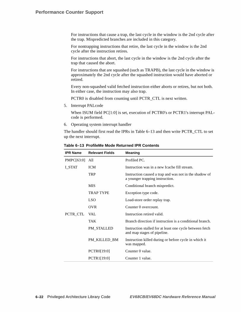
Performance Counter Support
fter
w isor
th.
set
For instructions that cause a trap, the last cycle in the window is the 2nd cycle athe trap. Mispredicted branches are included in this category.
For nontrapping instructions that retire, the last cycle in the window is the 2ndcycle after the instruction retires.
For instructions that abort, the last cycle in the window is the 2nd cycle after thetrap that caused the abort.
For instructions that are squashed (such as TRAPB), the last cycle in the windoapproximately the 2nd cycle after the squashed instruction would have abortedretired.
Every non-squashed valid fetched instruction either aborts or retires, but not boIn either case, the instruction may also trap.
PCTR0 is disabled from counting until PCTR_CTL is next written.
5. Interrupt PALcode
When ISUM field PC[1:0] is set, execution of PCTR0's or PCTR1's interrupt PAL-code is performed.
6. Operating system interrupt handler
The handler should first read the IPRs in Table 6–13 and then write PCTR_CTL toup the next interrupt.
Table 6–13 ProfileMe Mode Returned IPR Contents
IPR Name Relevant Fields Meaning
PMPC[63:0] All Profiled PC.
I_STAT ICM Instruction was in a new Icache fill stream.
TRP Instruction caused a trap and was not in the shadow ofa younger trapping instruction.
MIS Conditional branch mispredict.
TRAP TYPE Exception type code.
LSO Load-store order replay trap.
OVR Counter 0 overcount.
PCTR_CTL VAL Instruction retired valid.
TAK Branch direction if instruction is a conditional branch.
PM_STALLED Instruction stalled for at least one cycle between fetchand map stages of pipeline.
PM_KILLED_BM Instruction killed during or before cycle in which itwas mapped.
PCTR0[19:0] Counter 0 value.
PCTR1[19:0] Counter 1 value.
6–22 Privileged Architecture Library Code EV68CB/EV68DC Hardware Reference Manual

Performance Counter Support
w
he-in
there
le
f Y
a
yruc-usedTR0ired
ebe
6.10.3.3 ProfileMe Counting Mode Description
6.10.3.3.1 Cycle counting
In ProfileMe mode, either counter counts cycles during the window of the profiledinstruction.
6.10.3.3.2 Inum retire delay cycles
This input is used to measure a lower bound on the inum retire delay of the profiledinstruction. The maximum final value of PCTR1 is the length of the ProfileMe windominus 2.
Counts cycles that a profiled instruction delayed the retire pointer advance during tProfileMe window. The EV68CB/EV68DC tracks instructions in the pipeline by allocating them "inums" near the front of the pipeline. All inums are retired in the orderwhich they were allocated at the end of the pipeline.
Inums are allocated in batches of four, so there may be more inums allocated thanare program instructions in flight. Every inum is retired in order, including those foraborted instructions.
The "retire pointer" points to the next inum to be retired. An inum retires in the cycthat the retire pointer advances past the inum.
Let X and Y be consecutive inums in the allocation order. The "inum retire delay" ois [(cycle in which Y retired) – (cycle in which X retired)]. A large inum retire delayindicates a possible performance bottleneck (for example, an instruction stalled ondata cache miss).
6.10.3.3.3 Retired instructions cycles
When counting retired instructions in ProfileMe mode, the final count in PCTR0 mainclude instructions that retired before the ProfileMe window and may exclude insttions that retired near the end of the ProfileMe window. These discrepancies are caby a variable delay between the time that an instruction retires and the time that PCis incremented for that retire. This discrepancy is in the range of plus or minus 4 retinstructions.
6.10.3.3.4 Bcache miss or long latency probes cycles
This input counts the number of times the Bcache result was a miss.
Essentially, a long latency probe is a data request from other processes that causeBcache misses in a system.
This count is phase shifted three cycles early and thus includes events that occurredthree cycles before the start and before the end of the ProfileMe window.
6.10.3.3.5 Mbox replay traps cycles
This input counts Mbox replay traps.
PCTR1 is enabled to count Mbox replay traps that occur during a window that is thProfileMe window phase-shifted one cycle later. The first replay trap counted wouldthe 7th cycle after the instruction is fetched.
EV68CB/EV68DC Hardware Reference Manual Privileged Architecture Library Code 6–23

Performance Counter Support
6.10.3.4 Counter Modes for ProfileMe Mode
Table 6–14 shows the counter modes that are used with ProfileMe mode.
Table 6–14 ProfileMe Mode PCTR_CTL Input Select Fields
SL0[4] SL1[3:2] PCTR0 PCTR1
1 00 Retired instructions Cycle counting
1 01 Cycle counting Inum retire delay
1 10 Retired instructions Bcache miss or long latency probes
1 11 Cycle counting Mbox replay traps
6–24 Privileged Architecture Library Code EV68CB/EV68DC Hardware Reference Manual

s-
7Initialization and Configuration
This chapter provides information on EV68CB/EV68DC-specific microprocessor sytem initialization and configuration. It is organized as follows:
• Power-up reset flow
• Fault reset flow
• Energy star certification and sleep mode flow
• Warm reset flow
• Array initialization
• Initialization mode processing
• External interface initialization
• Internal processor register (IPR) reset state
• IEEE 1149.1 test port reset
• Reset state machine state transitions
• Phase-locked loop (PLL) functional description
Initialization is controlled by the reset state machine, which is responsible for fourmajor operations. Table 7–1 describes the four major operations.
7.1 Power-Up Reset Flow and the Reset_L and DCOK_H Pads
The EV68CB/EV68DC reset sequence is triggered using the two input signalsReset_LandDCOK_H in a sequence that is described in Section 7.1.1. AfterReset_Lis deas-serted, the following sequence of operations takes place:
Table 7–1 EV68CB/EV68DC Reset State Machine Major Operations
Operation Function
Ramp up Sequence the PLL input and output dividers (Xdiv and Zdiv) to gradually raise the internalGCLK frequency and generate time intervals for the PLL to re-establish lock.
BiST/SROM Receive a synchronous transfer on theClkFwdRst_H pad in order to start built-in self-test andSROM load at a predictable GCLK cycle.
Clock forwardinterface
Receive a synchronous transfer on theClkFwdRst_H pad in order to initialize the clock for-warding interface.
Ramp down Sequence the PLL input and output dividers (Xdiv and Zdiv) to gradually lower the internalGCLK frequency during sleep mode.
EV68CB/EV68DC Hardware Reference Manual Initialization and Configuration 7–1

Power-Up Reset Flow and the Reset_L and DCOK_H Pads
n
s-ns to
d to
h
-ed
istial-ice
, note
ter-
+
1. The clock forwarding and system clock ratio configuration information is loadedonto the EV68CB/EV68DC. See Section 7.1.2.
2. The internal PLL is ramped up to operating frequency.
3. The internal arrays built-in self-test (BiST) is run, followed by Icache initializatiousing an external serial ROM (SROM) interface.
The EV68CB/EV68DC systems, unlike the Alpha 21064 and 21164 microprocesor systems, are required to have an SROM. The SROM provides the only meaconfigure the system port, and the SROM pads can be used as a software-controlledUART.
The Icache must contain PALcode that starts at location 0x780. This code is useconfigure the EV68CB/EV68DC IPRs as necessary before causing any offchipreador write commands. This allows the EV68CB/EV68DC to be configured to matcthe external system implementation.
4. After configuring the EV68CB/EV68DC, control can be transferred to code anywhere in memory, including the noncacheable regions. The Icache can be flushby a write operation to the ITB invalidate-all register after control is transferred.This transfer of control should be to addresses not loaded in theIcache by theSROM interface or the Icache may provide unexpected instructions.
5. Typically, any state required by the PALcode is initialized and then the consolestarted (switching out of PALmode and into native mode). The console code iniizes and configures the system and boots an operating system from an I/O devsuch as a disk or the network.
Figure 7–1 shows the sequence of events at power-up, or cold reset. In Figure 7–1the following symbols for constraints and information:
Constraints:
Information:
A Setup (A0) and hold (A1) for IRQ’s to be latched by DCOK (2 ns for each).
B Enough time forReset_Lto propagate through 5 stages of RESET synchronizer (clocked by the innal framing clock, which is driven byEV6Clk_x). Worst case for the EV68CB/EV68DC would be5x8x16 = 640 GCLK cycles.
C Min = 1 FrameClk cycle.
a 8 GCLK cycles from DCOK assertion to first “real”EV6Clk_x cycle.
b Approximately 525 GCLK cycles for external framing clock to be sampled and captured.
c 1 FrameClk_x cycle.
d 3 FrameClk_x cycles.
e Approximately 264 GCLK cycles to prevent first command from appearing too early.
f Approximately 700,000 GCLK cycles for BiST + approximately 100,000 GCLK cycles fixed timeapproximately 50,000 GCLK cycles per line of Icache for SROM load.
g 16 GCLK cycles.
7–2 Initialization and Configuration EV68CB/EV68DC Hardware Reference Manual

Power-Up Reset Flow and the Reset_L and DCOK_H Pads
on
Figure 7–1 Power-Up Timing Sequence
7.1.1 Power Sequencing and Reset State for Signal Pads
Power sequencing and avoiding potential failure mechanisms is described in Secti9.3.
The reset state for the signal pads is listed in Table 7–2.
Table 7–2 Signal Pad Reset State
Signal Reset State Signal Reset State
Bcache
BcAdd_H[23:4] Tristated
BcCheck_H[15:0] Tristated BcTagInClk_H NA (input)
BcData_H[127:0] Tristated BcTagOE_L Tristated
BcDataInClk_H[7:0] NA (input) BcTagOutClk_x Tristated
BcDataOE_L Tristated BcTagParity_H Tristated
BcDataOutClk_x[3:0] Tristated BcTagShared_H Tristated
BcDataWr_L Tristated BcTagValid_H Tristated
BcLoad_L Tristated BcTagWr_L Tristated
BcTag_H[42:20] Tristated BcVref NA(I_DC_REF)
BcTagDirty_H Tristated
System Interface
IRQ_H[5:0] NA (input) SysDataInClk_H[7:0] NA (input)
SysAddIn_L[14:0] NA (input) SysDataInValid_L NA (input)
SysAddInClk_L NA (input) SysDataOutClk_L[7:0] Tristated
IRQ_H
DCOK_H
state
SromOE_L
internal ClkFwdRst
TestStat_H
external Clks
valid
WAIT_NORMALWAIT_SETTLE RAMP1 RAMP2 WAIT_ClkFwdRst0 WAIT_BiST WAIT_ClkFwdRst1
no min no min
End of BiST BiST Fails BiST Passes
A0
a
B
b c
f
C
g
d
e
FM-06486B.FH8
A1
RUN
ClkFwdRst_H
Reset_L
EV68CB/EV68DC Hardware Reference Manual Initialization and Configuration 7–3

Power-Up Reset Flow and the Reset_L and DCOK_H Pads
d,l
the
es
s the
In addition, as power is being ramped,Reset_Lmust be asserted — this allows theEV68CB/EV68DC to reset internal state. Once the target voltage levels are attainesystems should assertDCOK_H . This indicates to the EV68CB/EV68DC that internalogic functions can be evaluated correctly and that the power-up sequenceshould becontinued. Prior toDCOK_H being asserted, the logic internal to the EV68CB/EV68DC is being reset and the internal clock network is running (either clocked byPLL VCO, which is at a nominal speed, or byClkIn_H , if the PLL is bypassed).
The reset state machine is in state WAIT_SETTLE.
7.1.2 Clock Forwarding and System Clock Ratio Configuration
WhenDCOK_H is asserted, the EV68CB/EV68DC samples several pads and latchin some initialization state, including the value of the PLL Ydiv divisor, which specifiesthe ratio of the system clock to the internal clock (see Section 7.11.2.3), and enablecharge pump on the phase-locked loop.
SysAddOut_L[14:0] Initially, during power-up reset, stateis not defined. If not during power-up, preserves previous state. Then,after the clock forward reset period(as the external clocks start), signaldriven to NZNOP until the resetstate machine enters RUN, when itis driven to NOP.
SysDataOutValid_L NA (input)
SysAddOutClk_L Tristated SysFillValid_L NA (input)
SysCheck_L[7:0] Tristated SysVref NA(I_DC_REF)
SysData_L[63:0] Tristated
Clocks
ClkFwdRst_H NA (input) FrameClk_x NA (input)
ClkIn_HClkIn_L
NA (input) PLL_VDD NA(I_DC_REF)
EV6Clk_HEV6Clk_L
NA (input)
Miscellaneous
DCOK_H Must be deasserted until dc voltagereaches proper operating level.
Tck_H NA (input)
PllBypass_H NA (input) Tdi_H NA (input)
Reset_L NA (input) Tdo_H Unspecified
SromClk_H Tristated TestStat_H Tristated
SromData_H NA (input) Tms_H NA (input)
SromOE_L Tristated Trst_L NA (input)
Table 7–2 Signal Pad Reset State (Continued)
Signal Reset State Signal Reset State
7–4 Initialization and Configuration EV68CB/EV68DC Hardware Reference Manual

Power-Up Reset Flow and the Reset_L and DCOK_H Pads
st ofpsf
g
he
Table 7–3 summarizes the pads and the suggested/required initialization state. Mothis information is supplied by placing (switch-selectable or hardwired) weak pull-uor pull-downs on theIRQ_H pads. TheIRQ_H pads are sampled on the rising edge oDCOK_H , during which time the EV68CB/EV68DC is in reset and is not generatinany system activity. During normal operation, theIRQ_H pads supply interruptrequests to the EV68CB/EV68DC.
It is possible to disable the EV68CB/EV68DC PLL and source GCLK directly fromClkIn_ x. This mode is selected viaPllBypass_H. The EV68CB/EV68DC still pro-duces a divided-down clock onEV6Clk_x; this output clock, which tracks GCLK, canbe used in a feedback loop to generate a locked input clock via an external PLL. Tinput clock can be locked against a slower speed system reference clock.
Table 7–3 Pad Signal Names and Initialization State
Signal Name Sample Time Function Value
PllBypass_H Continuous input SelectClkIn_ x onto GCLK instead of internalPLL.
0 Bypass1
1 Use PLL
ClkFwdRst_H Sampling methodaccording toIRQ_H[4]
— —
Reset_L Continuous input — —
IRQ_H[5] Rising edge ofDCOK_H
Select 1:1 FrameClk mode.Internal FrameClk can be generated two ways:
0 Sample withFrameClk_H
1 Use a copy ofEV6Clk_H
IRQ_H[4] Rising edge ofDCOK_H
Select method of samplingClkFwdRst_H toproduce internal ClkFwdRst — either withexternal or internal copy ofFrameClk_x.
0 Sample with Exter-nal FrameClk_x
1 Sample with Inter-nal Frameclk
IRQ_H[3:0] Rising edge ofDCOK_H
Select Ydiv divisor value. This is the divide-down factor between GCLK andEV6Clk_x.
When the PLL is in use and the EV68CB/EV68DC is ramped-up to full speed, the VCOadjusts in order to phase-align (and rate-match)EV6Clk_x to ClkIn_ x. When the PLL is not inuse, andClkIn_ x is bypassed onto GCLK,EV6Clk_x is slower thanClkIn_ x by the divi-sor Ydiv.
IRQ_H[3:0] Divisor
0011 30100 40101 50110 60111 70000 81000 91001 101010 111011 121100 131101 141110 151111 16
1 By samplingFrameClk_H. Used ifFrameClk_H is slower thanClkIn_H .
2 As a direct copy ofEV6Clk_H . Used ifFrameClk_H is the same frequency asClkIn_H or is DC.
EV68CB/EV68DC Hardware Reference Manual Initialization and Configuration 7–5

Power-Up Reset Flow and the Reset_L and DCOK_H Pads
ro
l
.t
e
CLK
nles.
7.1.3 PLL Ramp Up
After the configuration is loaded through theIRQ_H pads, the next phase in the poweup flow is the internal PLL ramp up sequence. Ramping up of the PLL is required tguarantee that the dynamic change in frequency will not cause the supply on theEV68CB/EV68DC to fall due to the supply loop inductance. Clock control circuitrysteps GCLK from power-up/reset clocking to 1/16th operating frequency, to ½ operat-ing frequency, and finally normal operating frequency.
After the assertion ofDCOK_H , the EV68CB/EV68DC waits for the deassertion ofReset_Lfrom the system while the PLL attempts to achieve a lock. The PLL internaramp dividers are set to divide down the input clock by 16 and the PLL attempts toachieve lock against an effective input frequency ofClkIn_ x/16. Once lock isachieved, the actual internal frequency (GCLK) isClkIn_ x*(Y div divisor value)/16.There should be a minimum delay of 100 ms between the assertion ofDCOK_H andthe deassertion ofReset_Lto allow for this locking The reset state machine is in theWAIT_NOMINAL state.
After the deassertion ofReset_L, the reset state machine goes into the RAMP1 stateThe EV68CB/EV68DC ramps the internal frequency by changing the effective inpufrequency of the PLL toClkIn_ x/2 for a sufficient lock interval (at most, 20µs at 400MHz). The state machine then goes into the RAMP2 state, changing theeffectiveinputfrequency to ClkIn/1 for an additional lock interval (about 20µs). The lock periods aregenerated by the internal duration counter, which is driven by GCLK. The countercounts 4108 GCLK cycles during theClkIn_ x/2 lock interval. Note that GCLK is pro-duced by the output of the PLL, which is locking to an input clock which is 1/2 of thoperatingfrequency — therefore, the 4108 cycle interval constitutes a 6-20µs intervalwhen the operating frequency is 400–1250 MHz. Then, the counter counts 8205 Gcycles during theClkIn_ x/1 lock interval.
7.1.4 BiST and SROM Load and the TestStat_H Pad
The EV68CB/EV68DC uses the deassertion ofClkFwdRst_H (which must be deas-serted for a minimum of oneFrameClk_H cycle and then reasserted) to begin built-inself-test (BiST). The reset state machine goes into the WAIT_BiST state. Details oBiST are given in Chapter 11. The power-up BiST lasts approximately 700,000 cycThe result of the self-test is made available on theTestStat_Hpad. The pad is forcedlow by the system reset. It is then forced high during BiST.
DCOK_H Continuous input When deasserted, initializes the internalEV68CB/EV68DC reset state machine andkeeps the PLL internal oscillator running at anominal speed. Assertion, which implies powerto the EV68CB/EV68DC is good, causes config-uration information to be sampled.
—
1 The maximum permissible instantaneous change inClkIn_ x frequency is 333 MHz (to prevent cur-rent spikes).
Table 7–3 Pad Signal Names and Initialization State (Continued)
Signal Name Sample Time Function Value
7–6 Initialization and Configuration EV68CB/EV68DC Hardware Reference Manual

Power-Up Reset Flow and the Reset_L and DCOK_H Pads
om-
/
s-
set
is
f
As BiST completes, theTestStat_Hpad is held low for 16 GCLK cycles. Then, ifBiST succeeds, the pad remains low. Otherwise, it is asserted. After successfully cpleting BiST, the EV68CB/EV68DC then performs the SROM load sequence(described in Chapter 11). After the SROM load sequence is finished, the EV68CBEV68DC deassertsSromOE_L.
7.1.5 Clock Forward Reset and System Interface Initialization
After the deassertion ofSromOE_L, the reset state machine enters theWAIT_ClkFwdRst1 state, where the EV68CB/EV68DC waits for the system to deasertClkFwdReset_H. The EV68CB/EV68DC samples the deasserting edge ofClkFwdReset_H to take synchronous actions. It uses this synchronous event to rethe clock forwarding interface, start theoutgoing clocks, and deassert internal reset.The chip then waits 264 cycles before issuing commands. The reset state machinethen in RUN and the EV68CB/EV68DC begins fetching code at address 0x780.
Table 7–4 lists signals relevant to the power-up flow, provides a short description oeach, and any relevant constraints.
Table 7–4 Power-Up Flow Signals and Their Constraints
Signal Name Description Constraint
ClkIn_ x Differential clocks that areinputs to PLL or arebypassed onto GCLKdirectly
Clocks must be running beforeDCOK_H isasserted.
PLL_VDD VDD supply to PLL PLL_VDD must leadVDD.
VDD VDD supply to theEV68CB/EV68DC chiplogic (except PLL)
—
DCOK_H Logic signal to theEV68CB/EV68DC that theVDD supply is good
—
Reset_L RESET pad asserted bySYSTEM to the EV68CB/EV68DC
Reset_Lmust be asserted prior toDCOK_H andmust remain asserted for at least 100 ms afterDCOK_H is asserted. This allows for PLL settlingtime. Deassertion ofReset_Lcauses the EV68CB/EV68DC to ramp divisors to their final value andbegin BiST.
ClkFwdRst_HDeassertion #1
Signal asserted by SYS-TEM to synchronouslycommence built-in self-testand SROM load
ClkFwdRst_H must be deasserted after PLL hasachieved its lock in its final divisor value (about 20µs). The deassertion causes built-in self-test tobegin on an internal clock cycle that corresponds toone framing clock cycle afterClkFwdRst_H isdeasserted.ClkFwdRst_H can be asserted afterone frame clock cycle. See Figure 7–1.
ClkFwdRst_HDeassertion #2
Signal asserted by SYS-TEM to initialize and resetclock forwarding interfaces
ClkFwdRst_H must be deasserted when the Cboxhas loaded configuration information. This occursas the first part of the serial ROM load, after BiSTis run. OnceClkFwdRst_H is deasserted, theinterface is initialized and can receive proberequests from the EV68CB/EV68DC.
EV68CB/EV68DC Hardware Reference Manual Initialization and Configuration 7–7

Fault Reset Flow
the
rm-
low-
7.2 Fault Reset Flow
The fault reset sequence of operation is triggered by the assertion of theClkFwdRst_Hsignal line. Figure 7–2 shows the fault reset sequence of operation. The reset statemachine is initially in RUN state.ClkFwdRst_H is asserted by the system, whichcauses the state machine to transition to the WAIT_FAULT_RESET state.
The EV68CB/EV68DC internally resets a minimum amount of internal state. Noteeffects of that reset on the IPRs in Table 7–5.
The EV68CB/EV68DC then waits forClkFwdRst_H to deassert twice:
• One deassert to transition directly to the WAIT_ClkFwdRst1 state without perfoing any BiST
• One deassert to initialize the clock forwarding interface
The EV68CB/EV68DC then begins fetching code at PAL_BASE + 0x780.
Figure 7–2 shows the fault reset sequence of operation. In Figure 7–2, note the foling symbols for constraints and information:
Constraints:
Information:
Table 7–5 Effect on IPRs After Fault Reset
IPR After Reset
PAL_BASE Maintained (not reset)
I_CTL Bit value = 3 (both Icaches are enabled)
PCTX[FPE] Set
WRITE_MANY Cleared (That is, the WRITE_MANY chain is initialized and the Bcache is turned off.)
EXC_ADDR Set to an address that is close to the PC
A Min = 1 FrameClk_x cycle
a Approximately 264 GCLK cycles
b Approximately 525 GCLK cycles for external framing clock to be sampled and captured
c 1 FrameClk_x cycle plus 2 GCLK cycles
e NextFrameClk_x rising edge
f 3 FrameClk_x cycles
g Approximately 264 GCLK cycles to prevent first command from appearing too early
7–8 Initialization and Configuration EV68CB/EV68DC Hardware Reference Manual

Energy Star Certification and Sleep Mode Flow
-
0hering
e
ing a
it
e-
upnd the
d
Figure 7–2 Fault Reset Sequence of Operation
7.3 Energy Star Certification and Sleep Mode Flow
The EV68CB/EV68DC is Energy Star compliant. Energy Star is a program administered by theEnvironmental Protection Agency to reduce energy consumption. Forcompliance, a computer must automatically enter a low power sleep mode using 3watts or less after a specified period of inactivity. When the system is awakened, tuser shall be returned automatically to the same situation that existed prior to entesleep mode.
During normal operation, the EV68CB/EV68DC encounters inactive periods andenters a mode that saves the entire active processor state to memory.
The PALcode is responsible for saving all necessary state to DRAM and flushing thcaches.
The sleep mode sequence of operations is triggered by the PALcode twice performHW_MTPR to the Ibox SLEEP IPR. The first write prevents the assertion ofClkFwdRst_H from fault-resetting the chip.
The PALcode then informs the system, in an implementation-dependent way, thatmay assertClkFwdRst_H.
On the second HW_MTPR to the SLEEP IPR, the PLL begins to ramp down and thEV68CB/EV68DC can then respond to theClkFwdRst_H that was asserted by the system, causing the outgoing clocks from the EV68CB/EV68DC to stop.
The PLL ramp-down sequence takes exactly the same amount of time as the rampsequence described in Section 7.1.3. The same internal duration counter is used areset state machine transitions through the DOWN1, DOWN2, and DOWN3 stateswhich have similar PLL divisor ratios and clock speeds to the RAMP2, RAMP1, anWAIT_NOMINAL states.
state
SromOE_L
ClkFwdRst_H
internal ClkFwdRst
RUN WAIT_FAULT_RESET
internal clks aligned
external Clks
WAIT_ClkFwdRst0 WAIT_ClkFwdRst1
no min no min
b c
A
e
f
ga
FM-06488B.AI4
RUN
EV68CB/EV68DC Hardware Reference Manual Initialization and Configuration 7–9

Energy Star Certification and Sleep Mode Flow
B/ter-
nt to
fol-
After the PLL has finished ramping down, the reset state machine enters theWAIT_INTERRUPT state. Note theeffects of the entryinto that state on the IPRslisted in Table 7–6.
Note that Interrupt enables are maintained during sleep mode, enabling the EV68CEV68DC to wake up. The EV68CB/EV68DC waits for either an unmasked clock inrupt or an unmasked device interrupt from the system.
When an enabled interrupt occurs, the PLL ramps back to full frequency. Subsequethat, the EV68CB/EV68DC performs a built-in self-initialization (BiSI), a shortenedbuilt-in self-test, which initializes the internal arrayed structures. The SROM is notreloaded. Instead, the EV68CB/EV68DC begins fetching code from the system ataddress PAL_BASE + 0x780.
Figure 7–3 shows the sleep mode sequence of operations. In Figure 7–3, note thelowing constraint and informational symbols:
Constraints:
Informational symbols:
Table 7–6 Effect on IPRs After Transition Through Sleep Mode
IPR Effects After Transition Through Sleep Mode
PAL_BASE Maintained (not reset)
I_CTL Bit value = 3 (both Icaches are enabled)
PCTX[FPE] Set
WRITE_MANY Cleared (That is, the WRITE_MANY chain is initialized and the Bcache isturned off.)
A Min = 1 FrameClk_x cycle
a Approximately 525 GCLK cycles for external framing clock to be sampled and captured
b NextFrameClk_x rising edge
c 1 FrameClk_x cycle
d 3 FrameClk_x cycles
e Approximately 264 GCLK cycles to prevent first command from appearing too early
f Approximately 8192 GCLK cycles for BiSI
g 16 GCLK cycles
7–10 Initialization and Configuration EV68CB/EV68DC Hardware Reference Manual

Warm Reset Flow
en,state
ts
Figure 7–3 Sleep Mode Sequence of Operation
Table 7–7 describes each signal and constraint for the sleep mode sequence.
7.4 Warm Reset Flow
The warm reset sequence of operation is triggered by the assertion of theReset_Lsig-nal line. The reset state machine is initially in RUN state. The EV68CB/EV68DC thby default, ramps down the PLL (similar to the sleep flow sequence) and the resetmachine ends up in the WAIT_RESET state.
Note the effects of entry into that state on the IPRs listed in Table 7–8.
Table 7–7 Signals and Constraints for the Sleep Mode Sequence
Signal Name Description Constraint
ClkFwdRst_H Signal asserted by the system toinitialize and reset clock forwardinginterfaces
ClkFwdRst_H must be asserted by the systemwhen entering sleep mode. The system deasserClkFwdRst_H no sooner than oneFrameClk_Hcycle after sourcing an interrupt to the EV68CB/EV68DC.
Forwarded clocks Bit clocks forwarded to/from theEV68CB/EV68DC
Clocks stop running underClkFwdRst_H.
System interrupt Asynchronous interrupt whichcauses the EV68CB/EV68DC toexit sleep mode
—
Table 7–8 Effect on IPRs After Warm Reset
IPR Effects After Warm Reset
PAL_BASE Cleared
I_CTL Cleared
PCTX[FPE] Set
WRITE_MANY Cleared (That is, the WRITE_MANY chain is initialized and the Bcache isturned off.)
state
SLEEP IPR
Wake-up interrupt
SromOE_L
ClkFwdRst_H
internal ClkFwdRst
external Clks
RUN DOWN1 DOWN2 DOWN3 WAIT_INTR RAMP1 RAMP2 WAIT_ClkFwdRst0 WAIT_BiSI WAIT_ClkFwdRst1
internal clks
TestStat_H
no min no min
a c
A d
e
b f
FM-06487A.AI4
RUN
EV68CB/EV68DC Hardware Reference Manual Initialization and Configuration 7–11

Array Initialization
eine
cheC,
insan
a-
The EV68CB/EV68DC waits untilReset_Lis deasserted before transitioning from thWAIT_RESET state. The EV68CB/EV68DC ramps up the PLL until the state machenters the WAIT_ClkFwdRst0 state. Note that the system must assertClkFwdRst_Hbefore the state machine enters the WAIT_ClkFwdRst0 state. Then, similarly to theother flows,SromOE_L is asserted and the system waits for the deassertion ofClkFwdRst_H.
On the deassertion ofClkFwdRst_H, the EV68CB/EV68DC performs BiST and theSROM loading procedure.
After BiST and SROM loading have completed,SromOE_L deasserts and theEV68CB/EV68DC waits forClkFwdRst_H to deassert before starting the externalclocks and, like the other flows, waits for 264 cycles before starting instructions.
7.5 Array Initialization
The following arrays are initialized by BiST:
• Icache and Icache tag• Dcache, Dcache tag, and Duplicate Dcache tag• Branch history table
The external second-level cache (Bcache) is disabled byReset_L.
The Bcache must be initialized by PALcode before it is enabled.
7.6 Initialization Mode Processing
The initialization mode allows the EV68CB/EV68DC to generate and manipulate cablocks before the system interface has been initialized. Within the EV68CB/EV68Dthe Cbox configuration registers are divided into the WRITE_ONCE and theWRITE_MANY shift register chains (see Sections 5.4.3 and 5.4.4). TheWRITE_ONCE chain is loaded from the SROM during reset processing, and containformation such as the clock forwarding setup values. The WRITE_MANY chain cbe written many times using MTPR instructions.
The WRITE_MANY chain contains the following CSRs that are important to initializtion mode, which must be set to the values in Table 7–9 to initialize the Bcache.
Table 7–9 WRITE_MANY Chain CSR Values for Bcache Initialization
WRITE_MANY Chain CSRs Required Value at Initialization Mode
BC_ENABLE 1The duplicate bits for BC_ENABLE in [14:12] mustbe 0 during initialization mode.
BC_SIZE[3:0] The exact size or maximum size of the Bcache.
INVAL_TO_DIRTY_ENABLE[1:0] 1
SET_DIRTY_ENABLE[2:0] 0
INIT_MODE 1
7–12 Initialization and Configuration EV68CB/EV68DC Hardware Reference Manual

Initialization Mode Processing
ns.
d
Except for INIT_MODE, all the CSR registers have been described in earlier sectioWhen asserted, INIT_MODE has the following behavior:
• Cache block updates to the Dcache set the block to the Clean state.
• Updates to the Bcache use the BC_WRT_STS[3:0] bits.
• WrVictimBlk command generation to the system interface are squashed.
Using the INVAL_TO_DIRTY_ENABLE and INIT_MODE registers, initializationcode loaded from the SROM can generate and delete blocks inside the EV68CB/EV68DC without system interaction. This behavior is very useful for initialization anstartup processing, when the system interfaces are not fully functional. Figure 7–4shows a code example for initializing Bcache.
Figure 7–4 Example for Initializing BcacheReset chip and load Icache with this code
set init_mode ;now all WrVictims are ignored
;bc_enable_a 1
;zeroblk_enable_a 1
;set_dirty_enable_a 0
;init_mode_a 1
;enable_evict_a 0
;bc_wrt_sts_a 0
;bc_bank_enable_a 0
;bc_size_a 15
;now all writes to Bcache actually invalidate
;the Bcache. (if space was needed for scratch
;pad, the status bits could just as
;well be Valid)
for 2 X b c_size ;This loop generates legal ECC data, and
{ WH64 address } ;invalidate tags which are written to the
;Bcache for all but the final 64KB of address.
turn_off_bcache: ;bc_enable_a 0
;init_mode_a 0
;bc_size_a 0
;zeroblk_enable_a 1
;enable_evict_a 0
;set_dirty_enable_a 0
;bc_bank_enable_a 0
;bc_wrt_sts_a 0
EVICT_ENABLE 0
BC_WRT_STS[3:0] 0
BC_BANK_ENABLE 0
Table 7–9 WRITE_MANY Chain CSR Values for Bcache Initialization (Continued)
WRITE_MANY Chain CSRs Required Value at Initialization Mode
EV68CB/EV68DC Hardware Reference Manual Initialization and Configuration 7–13

External Interface Initialization
ally
te
sesati-
it
ers,and
rsers
SweepMemory: ;Write good parity/ecc to memory by
; writing a all memory locations. This is
;done by WH64 of memory addresses
turn_on_bcache: ;bc_enable_a 0
;bc_size_a Actual Bcache size
;zeroblk_enable_a 3
;set_dirty_enable_a 6
;init_mode_a 0
;enable_evict_a 0
;bc_wrt_sts_a 0
;bc_bank_enable_a 0
for 2 X b c_size ;This loop generates legal ECC data, and
{ WH64 address } ;invalidate tags which are written to the
;Bcache for all but the final 64KB of address.
for 2 X d cache size
{ ECB address } ;and cleans up the Dcache also.
(done)
In addition to initialization, the dynamic programming ability of the WRITE_MANYchain provides the basic tools to build various other software flows such as dynamicchanging the Bcache enable/size parameters for performance testing.
7.7 External Interface Initialization
After reset, the system interface is in the default configuration dictated by the reset staof the IPR bits that select the configuration options.
The response to system interface commands and internally generated memory accesis determined by this default configuration. System environments that are not compble with the default configuration must use the SROMIcache load feature toinitiallyload and execute a PALcode program to configure the external system interface unIPRs as needed.
7.8 Internal Processor Register Power-Up Reset State
Many IPR bits are not initialized by reset. They are located in error-reporting registand other IPR states. They must be initialized by initialization PALcode. Tables 7–57–6, and 7–8, list the effects on IPRs by fault reset, transition through sleep mode,warm reset, respectively. Table 7–10 lists the state of all internal processor registe(IPRs) immediately following power-up reset. The table also specifies which registneed to be initialized by power-up PALcode.
Table 7–10 Internal Processor Registers at Power-Up Reset State
Mnemonic Register Name Reset State Comments
Ibox IPRs
ITB_TAG ITB tag array write X —
ITB_PTE ITB PTE array write X —
7–14 Initialization and Configuration EV68CB/EV68DC Hardware Reference Manual

Internal Processor Register Power-Up Reset State
ITB_IAP ITB invalidate-all (ASM=0) X —
ITB_IA ITB invalidate all X Must be written to in PALcode.
ITB_IS ITB invalidate single X —
PMPC ProfileMePC X —
EXC_ADDR Exception address X —
IVA_FORM Instruction VA format X —
IER_CM Interrupt enable current mode X Must be written to in PALcode.
SIRR Software interrupt request X —
ISUM Interrupt summary X —
HW_INT_CLR Hardware interrupt clear X Must be cleared in PALcode.
EXC_SUM Exception summary X —
PAL_BASE PAL base address Cleared —
I_CTL Ibox control IC_EN = 3 All other bits are cleared on reset.
I_STAT Ibox status X Must be cleared in PALcode.
IC_FLUSH Icache flush X —
CLR_MAP Clear virtual-to-physical map X —
SLEEP Sleep mode X —
PCTX Ibox process context PCTX[FPE] is set. All other bits are X.
PCTR_CTL Performance counter control X Must be cleared in PALcode.
Ebox IPRs
CC Cycle counter X Must be cleared in PALcode.
CC_CTL Cycle counter control X Must be cleared in PALcode.
VA Virtual address X —
VA_FORM Virtual address format X —
VA_CTL Virtual address control X Must be cleared in PALcode.
Mbox IPRs
DTB_TAG0 DTB tag array write 0 Cleared —
DTB_TAG1 DTB tag array write 1 Cleared —
DTB_PTE0 DTB PTE array write 0 Cleared —
DTB_PTE1 DTB PTE array write 1 Cleared —
DTB_ALTMODE DTB alternate processor mode X PALcode must initialize.
DTB_IAP DTB invalidate all processASM = 0
X —
DTB_IA DTB invalidate all process X Must be written to in PALcode.
Table 7–10 Internal Processor Registers at Power-Up Reset State (Continued)
Mnemonic Register Name Reset State Comments
EV68CB/EV68DC Hardware Reference Manual Initialization and Configuration 7–15

IEEE 1149.1 Test Port Reset
stputs
from
7.9 IEEE 1149.1 Test Port Reset
SignalTrst_L must be asserted when powering up the EV68CB/EV68DC.Trst_Lmust not be deasserted prior to assertion ofDCOK_H . Trst_L can remain assertedduring normal operation of the EV68CB/EV68DC.
7.10 Reset State Machine
The state diagram in Figure 7–5 summarizes how the EV68CB/EV68DC transitioninto running code. Each state is described in Table 7–11. Table 7–11 describes ouand approximate state transition equations. Note that there are implicit transitionseach state to an appropriate down-ramp state whenReset_Lis asserted.
DTB_IS0 DTB invalidate single (array 0) X —
DTB_IS1 DTB invalidate single (array 1) X —
DTB_ASN0 DTB address space number 0 Cleared —
DTB_ASN1 DTB address space number 1 Cleared —
MM_STAT Memory management status X —
M_CTL Mbox control Cleared —
DC_CTL Dcache control DC_CTL[7:2] are cleared at reset.DC_CTL[1:0] are set at power up.
DC_STAT Dcache status X Must be cleared in PALcode.
Cbox IPRs
C_DATA Cbox data X Must be read in PALcode.
C_SHFT Cbox shift control X —
Table 7–10 Internal Processor Registers at Power-Up Reset State (Continued)
Mnemonic Register Name Reset State Comments
7–16 Initialization and Configuration EV68CB/EV68DC Hardware Reference Manual

Reset State Machine
-
Figure 7–5 EV68CB/EV68DC Reset State Machine State Diagram
Table 7–11 EV68CB/EV68DC Reset State Machine State Descriptions
State Name Description
COLD Chip cold. Transitioned to WAIT_SETTLE with assertion ofReset_L, PLL_VDD, andVDD .
WAIT_SETTLE PLL_VDD asserted; PLL at minimum frequency.
WAIT_NOMINAL Triggered by assertion ofDCOK_H . PLL achieves a lock at Xdiv and Zdiv divisors equal16 and 32, respectively.
RAMP1 Triggered byReset_Ldeassertion; Xdiv and Zdiv divisors are changed to 2 and 4, respectively, increasing the internal GCLK frequency. An internal duration counter is initial-ized to count 4108 GCLK cycles.
WAIT_SETTLE[16,32]
WAIT_NOMINAL
[16,32]
RAMP1[2,4]
RAMP2[1,2]
WAIT_ClkFwdRst0
WAIT_ClkFwdRst1
RUN
FAULT_RESET
DOWN3[16,32]
DOWN2[2,4]
DOWN1[1,2]
COLDWAIT_
BiSIWAIT_BiST
BiSIfinished
Counterfinished
Reset_Ldeasserted
Reset_Lasserted
DCOK_Hasserted
Counter finished
ClkFwdRst_Hdeasserted
Counterfinished
*No BiST/BiSIon recovery from Fault
Reset
BiSTfinished
ClkFwdRst_Hdeasserted
Counter finished
Reset_Ldeasserted
EnabledInterrupt
ClkFwdRst_Hasserted
Sleep Modeor Reset_Lasserted
Out of SleepMode
Out of FAULT_ RESET*
Counterfinished
Counterfinished &Sleep Mode
Counterfinished &
not Sleep Mode
LKG-10982A-98WF
Reset_Lasserted
PLL Ramp Up
PLL Ramp Down
WAIT_INTERRUPT
WAIT_RESET
Numbers in "[,]" are Xdiv and Zdiv divisors,
respectively
EV68CB/EV68DC Hardware Reference Manual Initialization and Configuration 7–17

Reset State Machine
er is
tes
n
an
-
ted.
insm
ed.the
ts
t toof
to
RAMP2 Triggered by the duration counter reaching 4108 cycles, the Xdiv and Zdiv divisors arechanged to 1 and 2, respectively, and the frequency is increased. The duration countreloaded to count 8205-cycles.
WAIT_ClkFwdRst0 Triggered by the duration counter reaching 8205 cycles (or by the deassertion ofReset_Lwhile in the WAIT_RESET state). EV68CB/EV68DC assertsSromOE_L andwaits for SYSTEM to deassertClkFwdReset_H. The deassertion must be synchronousto a falling edge ofFrameClk_H. EV68CB/EV68DC uses this deassertion to beginBiST and SROM load at a predictable time. EV68CB/EV68DC samples and generaan internal, aligned copy ofFrameClk_H, and, in turn, uses this clock to sampleClkFwdReset_H.
WAIT_BiST BiST and SROM load is started. The SROM first loads the Write-once chain and thereads the number of bits of Icache data to load.
WAIT_BiSI This state is entered when 'waking up' from sleep mode. EV68CB/EV68DC receivesexternal interrupt, ramps the PLL, synchronously samples a transition onClkFwdReset_H, and runs built-in self-initialization to clear the internal caches. Builtin self-test is not performed and the SROM is not loaded.
WAIT_ClkFwdRst1 Entered when the appropriate amount of BiST and SROM loading has been compleEV68CB/EV68DC deassertsSromOE_L and waits for SYSTEM to deassertClkFwdReset_H. The deassertion must be synchronous to a rising edge ofFrameClk_H. EV68CB/EV68DC uses this synchronous event to reset the clock for-warding interface and deassert internal reset. EV68CB/EV68DC subsequently begrunning code (either preloaded in the SROM or located in memory) and begins systetransactions.
RUN Chip is running software, interface is reset, and system transactions can be processFrom power-up, the Icache sets are enabled and contain bootstrap code loaded fromSROM; EV68CB/EV68DC executes code from Icache. From wake-up, the Icache seare disabled and EV68CB/EV68DC fetches and executes code from DRAM.
WAIT_RESET Triggered by duration counter reaching 264 cycles, or whenReset_Lis asserted when inWAIT_INTERRUPT state. EV68CB/EV68DC waits in this state untilReset_Lis deas-serted, at which point, the PLL starts to ramp up again.
FAULT_RESET ClkFwdReset is asserted while the EV68CB/EV68DC is running. The EV68CB/EV68DC internally resets a minimum amount of internal state, waits for clock forwardreset deassertion, and begins fetching code at PAL_BASE + 0x780.
DOWN1 EV68CB/EV68DC was in a state in which GCLK was at its highest speed andReset_Lwas asserted. Internal chip functions are reset and the internal duration counter is se8205 cycles. The purpose of this sequence is to down-ramp the clocks in anticipationpower being removed. If power is not removed (that is, reset is being toggled),EV68CB/EV68DC ramps the clocks back to the original speed.This state is also entered when software writes the I_CTL internal processor registersleep mode.
Table 7–11 EV68CB/EV68DC Reset State Machine State Descriptions (Continued)
State Name Description
7–18 Initialization and Configuration EV68CB/EV68DC Hardware Reference Manual

Phase-Lock Loop (PLL) Functional Description
that
e
s a
y
by
r-
thed,
7.11 Phase-Lock Loop (PLL) Functional Description
The PLL multiplies the clock frequency of a differential input reference clock andaligns the phase of its output to that differential input clock. Thus, the EV68CB/EV68DC can communicate synchronously on clock boundaries with clock periodsare defined by the system.
7.11.1 Differential Reference Clocks
A skew-controlled, ac-coupled differential clock is provided to the PLL by way ofClkIn_ x. ClkIn_ x are input signals to a differential amplifier. The frequency ofClkIn_ x can range from 80 MHz to 200 MHz.ClkIn_ x can be sourced by a variety ofcomponents that include PECL fanout parts or system PLLs.ClkIn_ x are also the pri-mary clock source for the EV68CB/EV68DC when in PLL bypass mode.
7.11.2 PLL Output Clocks
The following sections summarize the PLL output clocks.
7.11.2.1 GCLK
The PLL provides an output clock, GCLK, with afrequency that can range from 400MHz to 1.4286 GHz under full-speed conditions. GCLK is the nominal onchip clockthat is distributed to the entire EV68CB/EV68DC chip.
7.11.2.2 Differential EV68CB/EV68DC Clocks
TheEV6Clk_x output pads provide an external test point to measure the PLL phasalignment. They do not provide a clock source.EV6Clk_x are square-wave signalsthat drive rail-to-rail continually from 0 to VDD.
7.11.2.3 Nominal Operating Frequency
Under normal operating conditions, the frequency of the PLL output clock, GCLK, isimple function of the Ydiv divider value.
DOWN2 Triggered by duration counter reaching 8205 cycles, the PLL ramps GCLK frequencdown by the first divider ratio (Xdiv and Zdiv equal 2 and 4, respectively). This has theeffect of halving the GCLK frequency. The duration counter is set to 4108 cycles.
DOWN3 Triggered by duration counter reaching 4108 cycles, the PLL ramps frequency downthe second divider ratio (Xdiv and Zdiv equal 16 and 32, respectively). This has theeffect of reducing the frequency by a factor of 16 (of the original frequency). The intenal counter is set to 264 cycles.
WAIT_INTERRUPT Triggered by duration counter reaching 264 cycles, the EV68CB/EV68DC waits foreither an unmasked clock interrupt or unmasked device interrupt from system. Theinterrupts are wired to the interrupt request and enable internal registers. When anenabled interrupt occurs, the PLL ramps back to full frequency. Subsequent to that,built-in self-init (BiSI) initializes arrayed structures. The SROM is not reloaded; insteathe EV68CB/EV68DC begins fetching code from the SYSTEM.
Table 7–11 EV68CB/EV68DC Reset State Machine State Descriptions (Continued)
State Name Description
EV68CB/EV68DC Hardware Reference Manual Initialization and Configuration 7–19

Phase-Lock Loop (PLL) Functional Description
a
f
z
Table 7–12 shows the allowableClkIn_ x frequencies for a given operating frequencyof the EV68CB/EV68DC and the Ydiv divider. For example, to set the EV68CB/EV68DC GCLKfrequency to 500 MHz with aClkIn_ x frequency of 166.7 MHz, thesystem must select a Ydiv divider of 3 by placing the value 00112 on padsIRQ_H[3:0] .
Table 7–12 Differential Reference Clock Frequencies in Full-Speed Lock
7.11.2.4 Power-Up/Reset Clocking
During the power-up/reset sequence, when not in PLL bypass mode, there may beperiod of time whenClkIn_ x is not yet running, but there is a voltage onPLL_VDD .The signalDCOK_H is deasserted until power is good throughout the system. The10% to 90% rise time ofDCOK_H should be less than 2 ns. The deasserted state oDCOK_H and the presence ofPLL_VDD causes the PLL to generate a global clockthat is distributed throughout the EV68CB/EV68DC with a frequency range of 1 MHto 500 MHz. The presence of the global clock during this period avoids permanentdamage to the EV68CB/EV68DC.
GCLK Reference Clock Frequency (MHz) for Ydiv Dividers 1
1 Valid reference clock (ClkIn_x ) frequencies for the EV68CB/EV68DC are specified in the range from80 to 200. Divider values that are out of that range are displayed as a dash “—”.
Period(ns)
Frequency(MHz)
32
2 Dividers of 1 and 2 are to be used only in a PLL test mode.
4 5 6 7 8 9 10 11 12 13 14 15 16
2.5 400 133.3 100 80 — — — — — — — — — — —
2.4 416.7 138.9 104.2 83.3 — — — — — — — — — — —
2.3 434.8 144.9 108.7 87.0 — — — — — — — — — — —
2.2 454.5 151.2 113.6 90.9 — — — — — — — — — — —
2.1 476.2 158.7 119.0 95.2 — — — — — — — — — — —
2.0 500 166.7 125.0 100 83.3 — — — — — — — — — —
1.9 526.3 175.4 131.6 105.3 87.7 — — — — — — — — — —
1.8 555.6 185.2 138.9 111.1 92.6 — — — — — — — — — —
1.7 588.2 196.1 147.1 117.6 98.0 84.0 — — — — — — — — —
1.6 625 — 156.3 125.0 104.2 89.3 — — — — — — — — —
1.5 666.7 — 166.7 133.3 111.1 95.2 83.3 — — — — — — — —
1.4 714.3 — 178.6 142.9 119.1 102.0 89.3 — — — — — — — —
1.3 769.2 — 192.3 153.8 128.2 109.9 96.2 85.5 — — — — — — —
1.2 833.3 — — 166.7 138.9 119.0 104.2 92.6 83.3 — — — — — —
1.1 909.1 — — 181.8 151.5 129.9 113.6 101 90.9 — — — — — —
1.0 1000 — — 200 166.7 142.9 125 111,1 100 90.9 83.3— — — —
0.9 1111.1 — — — 185.2 158.7 138.9 123.5 111.1101.0 92.6 85.5 — — —
0.8 1250 — — — — 178.6 156.3 138.9 125 113.6104.2 96.2 89.3 83.3 —
0.7 1428.6 — — — — — 178.6 158.7142.8 129.9 119.1 109.9 102.095.2 89.3
7–20 Initialization and Configuration EV68CB/EV68DC Hardware Reference Manual

an-
is
8Error Detection and Error Handling
This chapter gives an overview of the EV68CB/EV68DC error detection and error hdling mechanisms, and is organized as follows:
• Data error correction code
• Icache data or tag parity error
• Dcache tag parity error
• Dcache data correctable ECC error
• Dcache store second error
• Dcache duplicate tag parity error
• Bcache tag parity error
• Bcache block parity calculation
• Bcache data correctable ECC error
• Memory/system port data correctable ECC error
• Bcache data correctable ECC error on a probe
• Double-bit fill errors
• Error case summary
Table 8–1 summarizes the EV68CB/EV68DC error detection.
Table 8–1 EV68CB/EV68DC Error Detection Mechanisms
Component Error Detection Mechanism
Bcache tag Parity protected.
Bcache data array Quadword-ECC protected.
Dcache tag array Parity protected.
Dcache duplicate tag array Parity protected.
Dcache data array Quadword-ECC protected, however this mode of operationonly supported in systems that have ECC enabled on both thesystem and Bcache ports.
EV68CB/EV68DC Hardware Reference Manual Error Detection and Error Handling 8–1
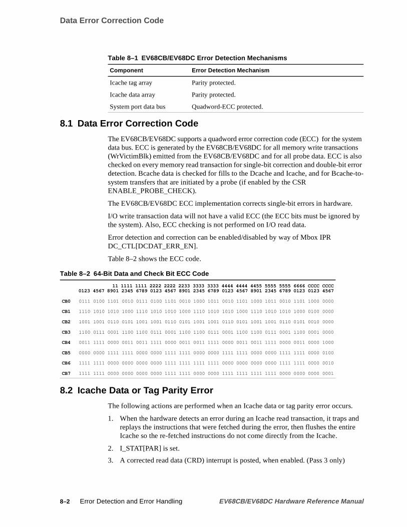
Data Error Correction Code
temnsorrore-to-
by
andire
8.1 Data Error Correction Code
The EV68CB/EV68DC supports a quadword error correction code (ECC) for the sysdata bus. ECC is generated by the EV68CB/EV68DC for all memory write transactio(WrVictimBlk) emitted from the EV68CB/EV68DC and for all probe data. ECC is alschecked on every memory read transaction for single-bit correction and double-bit edetection. Bcache data is checked for fills to the Dcache and Icache, and for Bcachsystem transfers that are initiated by a probe (if enabled by the CSRENABLE_PROBE_CHECK).
The EV68CB/EV68DC ECC implementation corrects single-bit errors in hardware.
I/O write transaction data will not have a valid ECC (the ECC bits must be ignoredthe system). Also, ECC checking is not performed on I/O read data.
Error detection and correction can be enabled/disabled by way of Mbox IPRDC_CTL[DCDAT_ERR_EN].
Table 8–2 shows the ECC code.
8.2 Icache Data or Tag Parity Error
The following actions are performed when an Icache data or tag parityerror occurs.
1. When the hardware detects an error during an Icache read transaction, it trapsreplays the instructions that were fetched during the error, then flushes the entIcache so the re-fetched instructions do not come directly from the Icache.
2. I_STAT[PAR] is set.
3. A corrected read data (CRD) interrupt is posted, when enabled. (Pass 3 only)
Icache tag array Parity protected.
Icache data array Parity protected.
System port data bus Quadword-ECC protected.
Table 8–2 64-Bit Data and Check Bit ECC Code
11 1111 1111 2222 2222 2233 3333 3333 4444 4444 4455 5555 5555 6666 CCCC CCCC0123 4567 8901 2345 6789 0123 4567 8901 2345 6789 0123 4567 8901 2345 6789 0123 0123 4567
CB0 0111 0100 1101 0010 0111 0100 1101 0010 1000 1011 0010 1101 1000 1011 0010 1101 1000 0000
CB1 1110 1010 1010 1000 1110 1010 1010 1000 1110 1010 1010 1000 1110 1010 1010 1000 0100 0000
CB2 1001 1001 0110 0101 1001 1001 0110 0101 1001 1001 0110 0101 1001 1001 0110 0101 0010 0000
CB3 1100 0111 0001 1100 1100 0111 0001 1100 1100 0111 0001 1100 1100 0111 0001 1100 0001 0000
CB4 0011 1111 0000 0011 0011 1111 0000 0011 0011 1111 0000 0011 0011 1111 0000 0011 0000 1000
CB5 0000 0000 1111 1111 0000 0000 1111 1111 0000 0000 1111 1111 0000 0000 1111 1111 0000 0100
CB6 1111 1111 0000 0000 0000 0000 1111 1111 1111 1111 0000 0000 0000 0000 1111 1111 0000 0010
CB7 1111 1111 0000 0000 0000 0000 1111 1111 0000 0000 1111 1111 1111 1111 0000 0000 0000 0001
Table 8–1 EV68CB/EV68DC Error Detection Mechanisms
Component Error Detection Mechanism
8–2 Error Detection and Error Handling EV68CB/EV68DC Hardware Reference Manual

Dcache Tag Parity Error
DC-s offol-
e
not
cacheare
or.
adsmay
8.3 Dcache Tag Parity Error
The primary copies of the Dcache tags are used only when servicing EV68CB/EV68generated load and store instructions. There are correctable and uncorrectable formthis error. If an issued load or store instruction detects a Dcache tag parity error, thelowing actions are performed:
1. MM_STAT[DC_TAG_PERR] is set.
2. A Dstream fault (DFAULT) is taken.
3. The virtual address associated with the error is available in the VA register.
4. The PALcode flushes the error block by temporarily disablingDC_CTL[DCTAG_PAR_EN] and evicting the block using two HW_LD instruc-tions. The onchip duplicate tag provides the correct victim address and cachecoherence state.
If a retried load instruction detects the Dcache tag parity error, the memoryreferencemay have already been retired, so the EXC_ADDR is not available. In this case, therror is uncorrectable and the Mbox performs the following actions:
• Either DC_STAT[TPERR_P0] or DC_STAT[TPERR_P1] is set, indicating thesource of the error.
• When enabled, a machine check (MCHK) is posted. The MCHK is taken whenin PALmode.
8.4 Dcache Data Single-Bit Correctable ECC Error
The following operations may cause Dcache data ECC errors:
• Load instructions
• Stores of less than quadword length
• Dcache victim read transactions
The hardware flow used for Dcache data ECC errors depends on the event thatcaused the error.
8.4.1 Load Instruction
Loads that read data from the Dcache may do so either in the same cycle as the Dtag probe (typical case) or in some subsequent cycle (load-queue retry). The hardwfunctional flows for these two error cases differ slightly.
When a load instruction reads the Dcache data array in the same cycle as the tagarray,if an ECC error occurs on the LSD ECC error detectors, then the Iboxstops retiringinstructions and does not resume retiring until after hardware recovers from the err
If an ECC error occurs on the LSD ECC error detectors, when a load instruction rethe Dcache tag array before it reads the Dcache data array, then the load instructionhave already been retired. In either case:
• The incorrect data is written into the load instruction’s destination register;however, the load queue retains the state associated with the load instruction.
EV68CB/EV68DC Hardware Reference Manual Error Detection and Error Handling 8–3

Dcache Store Second Error
a,or is
ins
t
not
• A consumer of the load instruction’s data may be issued before the error isrecognized; however, the Ibox will invoke a replay trap at an instruction that isolder than (or equal to) any instruction that consumes the load instruction’s datand then stalls the replayed Istream in the map stage of the pipeline until the errcorrected.
• Given a READ_ERR read-type from the Mbox for the error load instruction, theCbox scrubs the block in the Dcache by evicting the block into the victim buffer(thereby scrubbing it) and writing it back into the Dcache as follows:
– C_STAT[DSTREAM_DC_ERR] is set.
– C_ADDR contains bits [19:6] of the Dcache address of the block that contathe error (bits [42:20] of the physical address are not updated).
– DC_STAT[ECC_ERR_LD] is set.
– The load queue retries the load and rewrites the register.
– A corrected read data (CRD) error interrupt is posted, when enabled.
Note: Errors in speculative load instructions cause a CRD error interruptto be posted but the data is not scrubbed by hardware. The PALcodecannot perform a scrub because C_STAT is zero and C_ADDR does nocontain the address of the error.
8.4.2 Store Instruction (Quadword or Smaller)
A store instruction that is a quadword or smaller could invoke a Dcache ECC error,since the original quadword must be read to calculate the new check bits.
• The Mbox scrubs the original quadword and replays the write transaction.
• DC_STAT[ECC_ERR_ST] is set.
• A corrected read data (CRD) error interrupt is posted, when enabled.
8.4.3 Dcache Victim Extracts
• Dcache victims with an ECC error are scrubbed as they are written into thevictim data buffer.
• No status is logged.
• No exception is posted.
8.5 Dcache Store Second Error
A second store instructionerror is logged when it occurs close behind the first.Neither error is corrected.
• DC_STAT[ECC_ERR_ST] is set.
• DC_STAT[SEO] is set.
• When enabled, a machine check (MCHK) is posted. The MCHK is taken whenin PALmode.
8–4 Error Detection and Error Handling EV68CB/EV68DC Hardware Reference Manual
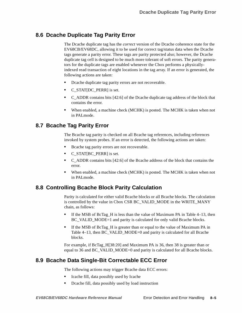
Dcache Duplicate Tag Parity Error
e
achenera-
, the
hat
not
the
not
tion
en
.
8.6 Dcache Duplicate Tag Parity Error
The Dcache duplicate tag has thecorrectversion of the Dcache coherence state for thEV68CB/EV68DC, allowing it to be used for correct tag/status data when the Dcachetags generate a parity error. These tags are parity protected also; however, the Dcduplicate tag cell is designed to be much more tolerant of soft errors. The parity getors for the duplicate tags are enabled whenever the Cbox performs a physically-indexed read transaction of eight locations in the tag array. If an error is generatedfollowing actions are taken:
• Dcache duplicate tag parity errors are not recoverable.
• C_STAT[DC_PERR] is set.
• C_ADDR contains bits [42:6] of the Dcache duplicate tag address of the block tcontains the error.
• When enabled, a machine check (MCHK) is posted. The MCHK is taken whenin PALmode.
8.7 Bcache Tag Parity Error
The Bcache tag parity is checked on all Bcache tag references, including referencesinvoked by system probes. If an error is detected, the following actions are taken:
• Bcache tag parity errors are not recoverable.
• C_STAT[BC_PERR] is set.
• C_ADDR contains bits [42:6] of the Bcache address of the block that containserror.
• When enabled, a machine check (MCHK) is posted. The MCHK is taken whenin PALmode.
8.8 Controlling Bcache Block Parity Calculation
Parity is calculated for either valid Bcache blocks or all Bcache blocks. The calculais controlled by the value in Cbox CSR BC_VALID_MODE in the WRITE_MANYchain, as follows:
• If the MSB of BcTag_H is less than the value of Maximum PA in Table 4–13, thBC_VALID_MODE=1 and parity is calculated for only valid Bcache blocks.
• If the MSB of BcTag_H is greater than or equal to the value of Maximum PA inTable 4–13, then BC_VALID_MODE=0 and parity is calculated for all Bcacheblocks.
For example, if BcTag_H[38:20] and Maximum PA is 36, then 38 is greater than orequal to 36 and BC_VALID_MODE=0 and parity is calculated for all Bcache blocks
8.9 Bcache Data Single-Bit Correctable ECC Error
The following actions may trigger Bcache data ECC errors:
• Icache fill, data possibly used by Icache
• Dcache fill, data possibly used by load instruction
EV68CB/EV68DC Hardware Reference Manual Error Detection and Error Handling 8–5

Bcache Data Single-Bit Correctable ECC Error
ity isted,
s
r.
ine
rror
rmal
at
tion.
d the
r,
(orB/the
s
• Bcache victim during an ECB instruction or during a Dcache/Bcache miss
The recovery mechanism depends on the action that triggered theerror.
8.9.1 Icache Fill from Bcache
For an Icache fill, the LSD ECC checkers detect the error, and bad Icache data pargenerated for the octaword that contains the quadword in error. If an error is detecthe following actions are taken:
• The hardware flushes the Icache.
• C_STAT[ISTREAM_BC_ERR] is set.
• C_ADDR contains bits [42:6] of the Bcache fill address of the block that containthe error.
• C_SYNDROME_0[7:0] and C_SYNDROME_1[7:0] contain the syndrome ofquadword 0 and 1, respectively, of the octaword subblock that contains the erro
• A machine check (MCHK) is posted and taken immediately. The PALcode machcheck handler performs a scrubbing operation as described in Section D.36 toensure that the origination point of the error is corrected.
Note: A corrected read data (CRD) error interrupt is also posted in case this eis in a speculative path and the MCHK is removed. The CRD PALcodereads the status, to detect this condition, and scrubs the block. In the noMCHK flow, the PALcode clears the pending CRD error.
8.9.2 Dcache Fill from Bcache
If the quadword inerror is not used to satisfy a loadinstruction, a hardware recoveryflow is not invoked. The quadword inerror, and its associated check bits, are writteninto the Dcache. However, status is logged as shown in the bulleted list below, andcorrected read data (CRD) error interrupt isposted, when enabled. PALcode may electo correct the error by scrubbing the block. If the error is not corrected by PALcodewhen it occurs, the error will be detected and corrected by a later load/victim opera
If the quadword inerror is used to satisfy a loadinstruction, then the flow is very simi-lar to that used for a Dcache ECC error. The LSD ECC checker detects the error anEV68CB/EV68DC performs the following actions:
• The load instruction’s destination register is written with incorrect data; howevethe load queue will retain the state associated with the load instruction.
• A consumer of the load instruction’s data may be issued before the error isrecognized. The Ibox will invoke a replay trap at an instruction that is older thanequal to) any instruction that consumes the load instruction’s data. The EV68CEV68DC then stalls the replayed Istream in the map stage of the pipeline, untilerror is corrected.
• With a READ_ERR read type from the Mbox for the load instruction inerror, theCbox scrubs the block in the Dcache by evicting the block into the victim bufferand writing it back into the Dcache.
• C_STAT[DSTREAM_BC_ERR] is set.
• C_ADDR contains bits [42:6] of the Bcache fill address of the block that containthe error.
8–6 Error Detection and Error Handling EV68CB/EV68DC Hardware Reference Manual

Memory/System Port Single-Bit Data Correctable ECC Error
r.
utcrub
s, andinfor-RD
d cor-
no
• C_SYNDROME_0[7:0] and C_SYNDROME_1[7:0] contain the syndrome ofquadword 0 and 1, respectively, of the octaword subblock that contains the erro
• The load queue retries the load instruction and rewrites the register.
• DC_STAT[ECC_ERR_LD] is set.
• A corrected read data (CRD) error interrupt is posted, when enabled.
Note: Errors in speculative load instructions cause a CRD error to be posted bthe data is not scrubbed by hardware. The PALcode cannot perform a soperation because C_STAT is zero and C_ADDR does not contain theaddress of the block in error.
8.9.3 Bcache Victim Read
A victim from the Bcache is written directly to the system port, without correction. TheECC parity checker on the LSD detects the error and posts a corrected read data (CRD)error interrupt. The Cbox error register is not updated.
8.9.3.1 Bcache Victim Read During a Dcache/Bcache Miss
While the Bcache is servicing a Dcache miss and that Bcache access is also a misan error occurs during that Bcache data access, the Cbox does not latch the errormation. However, the Mbox correction state machine is activated and it invokes a Cerror despite the fact that no correction is performed.
The Bcache access error is written out to memory and is subsequently detected anrected by the next consumer of the data.
• No correction is made.
• No status is logged (C_STAT = 0).
• A CRD error interrupt is posted, when enabled.
8.9.3.2 Bcache Victim Read During an ECB Instruction
A victim from the Bcache that occurs while an ECB instruction is being executed iswritten directly to the system port without correction. No Cbox registers are set andexception is taken.
8.10 Memory/System Port Single-Bit Data Correctable ECC Error
The following actions may cause memory/system port data ECC errors:
• Icache fill–data possibly used by Icache
• Dcache fill–data possibly used by a load instruction
The recovery mechanism depends on the event that caused the error.
8.10.1 Icache Fill from Memory
For an Icache fill the LSD ECC generators detect the error, and bad Icache dataparity is generated for the octaword that contains the quadword in error.
• The hardware flushes the Icache.
EV68CB/EV68DC Hardware Reference Manual Error Detection and Error Handling 8–7

Memory/System Port Single-Bit Data Correctable ECC Error
t
r.
ine
writ-nd a
-
r,
a.rror
at
r.
• C_STAT[ISTREAM_MEM_ERR] is set.
• C_ADDR contains bits [42:6] of the system memory fill address of the block thacontains the error.
• C_SYNDROME_0[7:0] and C_SYNDROME_1[7:0] contain the syndrome ofquadword 0 and 1, respectively, of the octaword subblock that contains the erro
• A machine check (MCHK) is posted and taken immediately. The PALcode machcheck handler performs a scrubbing operation as described in Section D.36 toensure that the origination point of the error is corrected.
Note: Also, a corrected read data (CRD) error isposted, when enabled, in casethis error is in a speculative path and the MCHK is removed. The CRDerror PALcode reads the status to detect this condition and scrubs the block.In the normal MCHK flow, the PALcode clears the pending CRD error.
8.10.2 Dcache Fill from Memory
If the quadword inerror is not used to satisfy a loadinstruction, no hardwarerecovery flow is invoked. The quadword in error, and its associated check bits, areten into the Dcache. However, status is logged as shown in the bulleted list below acorrected read data (CRD) error interrupt isposted, when enabled. PALcode maychoose to correct the error by scrubbing the block. If the error is not corrected by PALcode at the time, the error will be detected and corrected by a load/victim operation.
If the quadword inerror is used to satisfy a loadinstruction, then the flow is very simi-lar to that used for a Dcache ECC error:
• The load instruction’s destination register is written with incorrect data; howevethe load queue will retain the state associated with the load instruction.
• A consumer of the load instruction’s data may be issued before the error isrecognized; however, the Ibox will invoke a replay trap at an instruction that isolder than (or equal to) any instruction that consumes the load instruction’s datThe Ibox stalls the replayed Istream in the map stage of the pipeline until the eis corrected.
• With a READ_ERR read type from the Mbox for the load instruction inerror, theCbox scrubs the block in the Dcache by evicting the block into the victim bufferand writing it back into the Dcache.
• C_STAT[DSTREAM_MEM_ERR] is set.
• C_ADDR contains bits [42:6] of the system memory fill address of the block thcontains the error.
• C_SYNDROME_0[7:0] and C_SYNDROME_1[7:0] contain the syndrome ofquadword 0 and 1, respectively, of the octaword subblock that contains the erro
• The load queue retries the load instruction and rewrites the register.
• DC_STAT[ECC_ERR_LD] is set.
• A corrected read data (CRD) error interrupt is posted, when enabled.
8–8 Error Detection and Error Handling EV68CB/EV68DC Hardware Reference Manual

Bcache Data Single-Bit Correctable ECC Error on a Probe
utatahe
adasor.
e
r.
will
he
t
not
Note: Errors in speculative load instructions cause a CRD error to be posted bthe data is not scrubbed by hardware. The PALcode cannot scrub the dbecause C_STAT is zero, and C_ADDR does not have the address of tblock with the error.
8.11 Bcache Data Single-Bit Correctable ECC Error on a Probe
The probed processor extracts the block from its Bcache, signaling a corrected redata (CRD) error and latching error information. The single-bit ECC detected error datis not corrected by the probed processor, but is forwarded to the requesting procesThe requesting processor then detects a related system fillerror as a result of this sys-tem probe transaction.
• No hardware correction is performed.
• C_STAT[PROBE_BC_ERR] is set.
• C_ADDR contains bit [42:6] of the Bcache address of the block that contains therror.
• C_SYNDROME_0[7:0] and C_SYNDROME_1[7:0] contain the syndrome ofquadword 0 and 1, respectively, of the octaword subblock that contains the erro
• A CRD error interrupt is posted, when enabled.
• The PALcode on the probed processor may choose to scrub the error, though itprobably be scrubbed by the requesting processor.
8.12 Double-Bit Fill Errors
Double-bit errors for fills are detected, but not corrected, in the EV68CB/EV68DC. Tfollowing events may cause a double-bit fill error:
• Icache fill from Bcache
• Dcache fill from Bcache
• Icache fill from memory
• Dcache fill from memory
If an error is detected, the following actions are taken:
• C_STAT is set to one of the following:
ISTREAM_BC_DBL (Icache fill from Bcache)
DSTEAM_BC_DBL (Dcache fill from Bcache)
ISTREAM_MEM_DBL (Icache fill from memory)
DSTREAM_MEM_DBL (Dcache fill from memory)
• C_ADDR contains bits [42:6] of the system memory fill address of the block thacontains the error.
• When enabled, a machine check (MCHK) is posted. The MCHK is taken whenin PALmode.
EV68CB/EV68DC Hardware Reference Manual Error Detection and Error Handling 8–9

Error Case Summary
merlue.
-
• A double-bit fill error from memory, marked by the data's corresponding ECC,when written to cache, also writes the corresponding ECC to cache. Any consuof that error (such as another CPU) also consumes the corresponding ECC va
Note: C_ADDR may be inaccurate in heavy traffic conditions. C_STAT is accurate.
8.13 Error Case Summary
Table 8–3 summarizes the various error cases and their ramifications.
Table 8–3 Error Case Summary
Error Exception StatusHardwareAction PALcode Action
Icache data or tagparity error
CRD ISTAT[PAR] Icache flushed Log as CRD
Dcache tag parityerror (on issue)
DFAULT MM_STAT[DC_TAG_PERR]VA[address]
— Evict with twoHW_LDs and log asCRD
Dcache tag parityerror (on retry)
MCHK1 DC_STAT[TPERR_P0] orDC_STAT[TPERR_P1]
— Log as MCHK
Dcache single-bitECC error on load
CRD DC_STAT[ECC_ERR_LD]C_STAT[DSTREAM_DC_ERR]C_ADDR[bits [19:6] of the erroraddress. [42:20] not updated.]
Corrected andscrubbed
Log as CRD
Dcache single-bitECC error onspeculative load
CRD DC_STAT[ECC_ERR_LD]C_STAT contains zero
None Log as CRD
Dcache single-bitECC error on smallstore
CRD DC_STAT[ECC_ERR_ST] Corrected andscrubbed
Log as CRD
Dcache single-bitECC error on victimread
None None Corrected andscrubbed
None
Dcache second erroron store
MCHK1 DC_STAT[SEO] No correctionon either store
Log as MCHK
Dcache duplicate tagparity error
MCHK1 C_STAT[DC_PERR]C_ADDR[error address]
Uncorrectable Log as MCHK
Bcache tag parityerror
MCHK1 C_STAT[BC_PERR]C_ADDR[error address]
Uncorrectable Log as MCHK
Bcache single-biterror on Icache fill
MCHKand CRD2
C_STAT[ISTREAM_BC_ERR]C_ADDR[error address]C_SYNDROME_0C_SYNDROME_1
Icache flushed Scrub error as describedin Section D.36.Log as CRD
Bcache single-biterror on Dcache fill
CRD DC_STAT[ECC_ERR_LD]C_STAT[DSTREAM_BC_ERR]C_ADDR[error address]C_SYNDROME_0C_SYNDROME_1
Corrected andscrubbed inDcache3
Scrub error as describedin Section D.36.Log as CRD
8–10 Error Detection and Error Handling EV68CB/EV68DC Hardware Reference Manual

Error Case Summary
Bcache victim readon Dcache/Bcachemiss
CRD DC_STAT[ECC_ERR_LD]C_STAT contains 0
None Log as CRD
Bcache victim readon ECB
None None None None
Memory single-biterror on Icache fill
MCHKand CRD2
C_STAT[ISTREAM_MEM_ERR]C_ADDR[error address]C_SYNDROME_0C_SYNDROME_1
Icache flushed Scrub error as describedin Section D.36.Log as CRD
Memory single-biterror on Dcache fill
CRD DC_STAT[ECC_ERR_LD]C_STAT[DSTREAM_MEM_ERR]C_ADDR[error address]C_SYNDROME_0C_SYNDROME_1
Corrected andscrubbed inDcache3
Scrub error as describedin Section D.36.Log as CRD
Bcache single-biterror on a probe hit
CRD C_STAT[PROBE_BC_ERR]C_ADDR[error address]4
C_SYNDROME_0C_SYNDROME_1
None May scrub error asdescribed in SectionD.36.Log as CRD
Bcache double-biterror on Icache fill
MCHK1 C_STAT[ISTREAM_BC_DBL]C_ADDR[error address]4
None Log as MCHK
Bcache double-biterror on Dcache fill
MCHK1 C_STAT[DSTREAM_BC_DBL]C_ADDR[error address]4
None Log as MCHK
Memory double-biterror on Icache fill
MCHK1 C_STAT[ISTREAM_MEM_DBL]C_ADDR[error address]4
None Log as MCHK
Memory double-biterror on Dcache fill
MCHK1 C_STAT[DSTREAM_MEM_DBL]C_ADDR[error address]4
None Log as MCHK
1 Machine check taken in native mode. It is deferred while in PALmode.2 CRD error posted in case the machine check is down a speculative path.3 For a single-bit error on a non-target quadword, the error is not corrected in hardware,
but is corrected by PALcode during the scrub operation.4 The contents of C_ADDR may not be accurate when there is heavy cache fill traffic.
Table 8–3 Error Case Summary (Continued)
Error Exception StatusHardwareAction PALcode Action
EV68CB/EV68DC Hardware Reference Manual Error Detection and Error Handling 8–11


tsower
may
e
t of
9Electrical Data
This chapter describes the electrical characteristics of the EV68CB/EV68DC and iinterface pads. The chapter contains both ac and dc electrical characteristics and psupply considerations, and is organized as follows:
• Electrical characteristics
• DC characteristics
• Power supply sequencing
• AC characteristics
9.1 Electrical Characteristics
Table 9–1 lists the maximum electrical ratings for the EV68CB/EV68DC.
Notes: Stresses above those listed under the given maximum electrical ratingscause permanent device failure. Functionality at or above theselimits is not implied. Exposure to these limits for extended periods of timmay affect device reliability.
Power data is preliminary and based on measurements from a limited sematerial.
Table 9–1 Maximum Electrical Ratings
Characteristics Ratings
Storage temperature –55° C to +125° C (–67° F to 257° F)
Junction temperature 0° C to 100° C (32° F to 212° F)
Open-drain driver interface 2.0 V
Push-pull driver interface 1.7 V
Minimum dc voltage on signal pads VSS– 400 mV
Maximum power @ indicated VDDfor the following frequencies: Frequency Peak Power
1.000 GHz 64 W @ 1.7 V
1.250 GHz 75 W1 @ 1.7 V
1 Estimated value (not measured).
1.330 GHz 80 W1 @ 1.7 V
EV68CB/EV68DC Hardware Reference Manual Electrical Data 9–1

DC Characteristics
B/
2
.
the
9.2 DC Characteristics
This section contains the dc characteristics for the EV68CB/EV68DC. The EV68CEV68DC pads can be divided into 10 distinct electrical signal types. The mappingbetween these signal types and the package pads is shown in Chapter 3. Table 9–shows the signal types.
Tables 9–3 through 9–12 show the dc switching characteristics of each signal typeAlso, the following notes apply to Tables 9–3 to 9–12.
1. The differential voltage, Vdiff, is the absolute difference between the differentialinput pads.
2. Delta VBIAS is defined as the open-circuit differential voltage on the appropriatedifferential pairs. Test condition for these inputs are to let the input network selfbias and measure the open circuit voltage. The test load must be≥ 1M ohm. In nor-mal operation, these inputs are coupled with a 680-pF capacitor.
3. Functional operation of the EV68CB/EV68DC with less than allVDD andVSSpads connected is not implied.
4. The test load is a 50-ohm resistor to VDD/2. The resistor can be connected toEV68CB/EV68DC pad by a 50-ohm transmission line of any length.
5. DC test conditions set the minimum swing required. These dc limits set the trippoint precision.
6. Input pad capacitance values include 2.0 pF added for package capacitance.
Table 9–2 Signal Types
Signal Type Description
I_DC_POWER Supply voltage pads (VDD/PLL_VDD )
I_DC_REF Input dc reference pad
I_DA Input differential amplifier receiver
I_DA_CLK Input differential amplifier clock receiver
O_OD Open-drain output driver
O_OD_TP Open-drain driver for test pads
O_PP Push-pull output driver
O_PP_CLK Push-pull output clock driver
B_DA_OD Bidirectional differential amplifier receiver — open-drain
B_DA_PP Bidirectional differential amplifier receiver — push-pull
9–2 Electrical Data EV68CB/EV68DC Hardware Reference Manual

DC Characteristics
Note: Current out of an EV68CB/EV68DC pad is represented by a – symbolwhile a + symbol indicates current flowing into an EV68CB/EV68DCpad.
Table 9–3 VDD (I_DC_POWER)
Parameter Symbol Description Test Conditions Minimum Maximum
VDD Processor core supply voltage — 1.6 V 1.7 V
Power (sleep) Processor power required (sleep) @ VDD = 1.7 VNote 3
— 8.5 W1
1 Power measured at 37.5 MHz while running the “Ebox aliveness test.”
PLL_VDD PLL supply voltage — 2.45 V 2.55 Vc
PLL_IDD PLL supply current (running) Freq = 1 GHz — 25 mA
Table 9–4 Input DC Reference Pad (I_DC_REF)
ParameterSymbol Description Test Conditions Minimum Maximum
VREF DC input reference voltage — 600 mV VDD – 100 mV
| II | Input current VSS≤ V ≤ VDD — 150 µA
Table 9–5 Input Differential Amplifier Receiver (I_DA)
ParameterSymbol Description Test Conditions Minimum Maximum
VIL Low-level input voltage Note 5 — VREF – 200 mV
VIH High-level input voltage — VREF + 200 mV —
| II | Input current VSS≤ V ≤ VDD — 150 µA
CIN Input-pad capacitance Freq =10 MHz — TBDNote 6
Table 9–6 Input Differential Amplifier Clock Receiver (I_DA_CLK)
ParameterSymbol Description Test Conditions Minimum Maximum
Vdiff Differential input voltage — 200 mv Note 1 —
| ∆ VBIAS | Open-circuit differential I≤ ± 1 µANote 2
— 50 mV
| II | Input current VSS≤ V ≤ VDD — 150µA
CIN Input-pad capacitance Freq =10 MHz — TBDNote 6
EV68CB/EV68DC Hardware Reference Manual Electrical Data 9–3

DC Characteristics
Table 9–7 Pad Type: Open-Drain Output Driver (O_OD)
ParameterSymbol Description
TestConditions Minimum Maximum
VOL Low-level output voltage IOL = 50 mA — 400 mV
|IOZ | High impedance output current 0 < V < VDD — 150µA
COD Open-drain pad capacitance Freq = 10 MHz — TBDNote 6
Table 9–8 Bidirectional, Differential Amplifier Receiver, Open-Drain Output Driver (B_DA_OD)
ParameterSymbol Description Test Conditions Minimum Maximum
VIL Low-level input voltage Note 5 — VREF –200 mv
VIH High-level input voltage — VREF + 200 mV —
VOL Low-level output voltage IOL = 50 mA — 400 mV
| II | Input current VSS≤ V ≤ VDD — 150 µA1
CIN Input-pad capacitance Freq =10 MHz — TBDNote 6
1 Measurement taken with output driver disabled.
Table 9–9 Pad Type: Open-Drain Driver for Test Pads (O_OD_TP)
ParameterSymbol Description
TestConditions Minimum Maximum
VOL Low-level output voltage IOL = 15 mA — 400 mV
| IOZ | High-impedance output current 0 < V < VDD — 150µA
COD_TP Pad capacitance Freq = 10 MHz — TBDNote 6
Table 9–10 Bidirectional, Differential Amplifier Receiver, Push-Pull Output Driver (B_DA_PP)
ParameterSymbol Description Test Conditions Minimum Maximum
VIL Low-level input voltage — — VREF – 200 mV
VIH High-level input voltage — VREF + 200 mV —
VOL Low-level output voltage IOL = 6 mA — 400 mV
VOH High-level output voltage IOH = –6 mA VDD – 400 mV —
| II | Input current VSS≤ V ≤ VDD — 150µA1
CIN Input-pad capacitance Freq =10 MHz — TBDNote 6
1 Measurement taken with output driver disabled.
9–4 Electrical Data EV68CB/EV68DC Hardware Reference Manual

Power Supply Sequencing and Avoiding Potential Failure Mechanisms
st be
ety of
so
alulk
f its
9.3 Power Supply Sequencing and Avoiding Potential Failure Mech-anisms
Before the power-on sequencing can occur,systems should ensure thatDCOK_H isdeasserted andReset_Lis asserted. Then, systems ramp power to the EV68CB/EV68DCPLL_VDD @ 2.5 V and the EV68CB/EV68DC power planes (VDD @ 1.65V, not to exceed 1.70 V under any circumstances), withPLL_VDD leadingVDD.Systems should supply differential clocks to the EV68CB/EV68DC onClkIn_H andClkIn_L . The clocks should be running as power is supplied.
When enabling the power supply inputs in a system, three failure mechanisms muavoided:
1. Bidirectional signal buses must not conflict during power-up. A conflict on thesbuses can generate high current conditions, which can compromise the reliabilithe associated chips.
2. Similarly, input receivers should not see intermediate voltage levels that can algenerate high current conditions, which can compromise the reliability of thereceiving chip.
3. Finally, no CMOS chip should see an input voltage that is higher than its internVDD. In such a condition, a reasonable level of charge can be injected into the bof the die. This condition can expose the chip to a positive-feedback latchupcondition.
The EV68CB/EV68DC addresses those three failure mechanisms by disabling all ooutputs and bidirectional pads (with three exceptions) until the assertion ofDCOK_H .The three exceptions areTdo_H, EV6Clk_L , andEV6Clk_H . Tdo_H is used only in
Table 9–11 Push-Pull Output Driver (O_PP)
ParameterSymbol Description
TestConditions Minimum Maximum
VOL Low-level output voltage IOL = 40 mA — 500 mV
VOH High-level output voltage IOL = –40 mA VDD – 500 mV —
| IOZ | High-impedance output current 0 < V < VDD — 150µA
COD Open-drain pad capacitance Freq = 10 MHz — TBDNote 6
Table 9–12 Push-Pull Output Clock Driver (O_PP_CLK)
ParameterSymbol Description
TestConditions Minimum Maximum
VOL Low-level output voltage Note 4 — VDD/2 – 230 mV
VOH High-level output voltage Note 4 VDD/2 + 230 mV —
| IOZ | High-impedance outputcurrent
0 < V < VDD — 40 mA1
1 Measured value includes current from onchip termination structures.
EV68CB/EV68DC Hardware Reference Manual Electrical Data 9–5

AC Characteristics
,
ter-
bus
rain
bus
rnal
ional
d,l
the
h
the tester environment and does not need to be disabled.EV6Clk_L andEV6Clk_Hare outputs that are both generated and consumed by the EV68CB/EV68DC; thusVDD tracks for both the producer and consumer.
On the push-pull interfaces:
• Disabling all output drivers leaves the output signal at the DC bias point of themination network.
• Disabling the bidirectional drivers leaves the other consumers of the bus as themaster.
On the open-drain interfaces:
• Disabling all output drivers leaves the output signal at the voltage of the open-dpull-up.
• Disabling all bidirectional drivers leaves the other consumers of the bus as themaster.
To avoid failure mechanism number two, systems must sequence and control extesignal flow in such a way as to avoidzero differential into the EV68CB/EV68DC inputreceivers (I_DA, I_DA_CLK, B_DA_OD, B_DA_PP, and B_DA_PP). Finally, toavoid failure mechanism number three, systems must sequence input and bidirectpads (I_DA, I_DA_CLK, B_DA_OD, B_DA_PP, and I_DC_REF) such that theEV68CB/EV68DC does not see a voltage above its VDD.
In addition, as power is being ramped,Reset_Lmust be asserted — this allows theEV68CB/EV68DC to reset internal state. Once the target voltage levels are attainesystems should assertDCOK_H . This indicates to the EV68CB/EV68DC that internalogic functions can be evaluated correctly and that the power-up sequenceshould becontinued. Prior toDCOK_H being asserted, the logic internal to the EV68CB/EV68DC is being reset and the internal clock network is running (either clocked byVCO, which is at a nominal speed, or byClkIn_H , if the PLL is bypassed).
The reset state machine is in state WAIT_SETTLE.
9.4 AC Characteristics
Abbreviations:
The following abbreviations apply to Table 9–13:
• TSU = Setup time
• Duty cycle = Minimum clock duty cycle
• TDH = Hold time
• Slew rate = referenced to signal edge
AC Test Conditions:
The following conditions apply to the measurements that are listed in Table 9–13:
• TSU, TDH, and TSKew values include the following onchip and package varia-tions: min/max metal capacitance, GCLK skew, transistor gate length variation(OCV), across-chip temperature and voltage variation, and package lead-lengtvariation.
9–6 Electrical Data EV68CB/EV68DC Hardware Reference Manual

AC Characteristics
sig-h inia-
t is
-
• The ac specification values for TSU, TDH, and TSKew assume a ± 0.4 V inputnal amplitude, relative to Vref, one volt per nanosecond slew rates, no mismatcpad loading, and zero time-offset between forwarded clocks and data. Any devtion from those conditions can result in degraded chip performance.
– VDD is in the range between 1.55 V and 1.65 V.
– SysVref is 1.1 Volts.
– BcVref is 0.75 Volts.
• All output skew data is based on simulation into a 50-ohm transmission line thaterminated with 50 ohms to VDD/2 for Bcache timing, and with 50 ohms to VDDfor all other timing.
Timings are measured at the pads as follows:
– For open-drain outputs, timing is measured to (Vol + Vterm)/2. Where Vterm isthe offchip termination voltage for system signals.
– For non-open-drain outputs, timing is measured to (Vol + Voh)/2.– For all inputs other than type I_DA_CLK, timing is measured to the point
where the input signal crosses VREF.– For type I_DA_CLK inputs, timing is measured when the voltage on the com
plementary inputs is equal.
Table 9–13 AC Specifications
Signal Name Type Reference Signal TSU 1 TDH2 TSkew Duty Cycle TSlew
SysAddIn_L[14:0 I_DA SysAddInClk_L 250 ps 400 ps NA NA 1.0 V/ns
SysFillValid_L I_DA SysAddInClk_L 250 ps 400 ps NA NA 1.0 V/ns
SysDataInValid_L I_DA SysAddInClk_L 250 ps 400 ps NA NA 1.0 V/ns
SysDataOutValid_L I_DA SysAddInClk_L 250 ps 400 ps NA NA 1.0 V/ns
SysAddInClk_L I_DA NA NA NA NA 45–55% 1.0 V/ns
SysAddOut_L[14:0] O_OD SysAddOutClk_L NA NA ± 300 ps3 NA NA
SysAddOutClk_L O_OD EV6Clk_x NA NA ± 350 ps 45-55% NA
SysData_L[63:0] B_DA_OD SysDataInClk_H[7:0] 250 ps 400 ps NA NA 1.0 V/ns
SysDataOutClk_L[7:0]4 NA NA ± 300 ps3 NA NA
SysCheck_L[7:0] B_DA_OD SysDataInClk_H[7:0] 250 ps 400 ps NA NA 1.0 V/ns
SysDataOutClk_L[7:0]4 NA NA ± 300 ps3 NA NA
SysDataInClk_H[7:0] I_DA NA NA NA NA 45-55% 1.0 V/ns
SysDataOutClk_L[7:0] O_OD EV6Clk_x NA NA ± 350 ps 45-55% NA
BcAdd_H[23:4] O_PP BcTagOutClk_x NA NA ± 300 ps5,6 NA —
BcDataOE_L O_PP BcDataOutClk_x[3:0]7 45-55% —
BcLoad_L O_PP 38-63%8 —
BcDataWr_L O_PP 40-60%9 —
BcData_H[127:0] B_DA_PP BcDataOutClk_x[3:0]10 NA NA ± 300 ps6 45-55% 1.0 V/ns
38-63%8 NA
40-60%9 NA
BcDataInClk_H[7:0] 250 ps 400 ps NA NA NA
EV68CB/EV68DC Hardware Reference Manual Electrical Data 9–7

AC Characteristics
BcDataInClk_H[7:0] I_DA NA NA NA NA 45-55%
BcDataOutClk_H[3:0] O_PP EV6Clk_x NA NA ± 350 ps
BcDataOutClk_L[3:0] O_PP EV6Clk_x NA NA ± 350 ps
BcTag_H[42:20] B_DA_PP BcTagInClk_H 250 ps 400 ps NA NA 1.0 V/ns
BcTagDirty_H B_DA_PP BcTagInClk_H 250 ps 400 ps NA NA 1.0 V/ns
BcTagParity_H B_DA_PP BcTagInClk_H 250 ps 400 ps NA NA 1.0 V/ns
BcTagShared_H B_DA_PP BcTagInClk_H 250 ps 400 ps NA NA 1.0 V/ns
BcTagValid_H B_DA_PP BcTagInClk_H 250 ps 400 ps NA NA 1.0 V/ns
BcTagValid_H B_DA_PP BcTagOutClk_x NA NA ± 300 ps6 45-55% NA
BcTagDirty_H B_DA_PP 38-63%8 NA
BcTagShared_H B_DA_PP 40-60%9 NA
BcTagParity_H B_DA_PP
BcTagOE_L O_PP
BcTagWr_L O_PP
BcTagInClk_H I_DA NA NA NA NA 45-55%
BcTagOutClk_x O_PP EV6Clk_x NA NA ± 350 ps
IRQ_H[5:0] I_DA DCOK_H 10 ns11 10 ns11 NA NA 100 mV/ns
Reset_L12 I_DA NA NA NA NA 100 mV/ns
DCOK_H 13 I_DA NA NA NA NA 100 mV/ns
PllBypass_H14 I_DA NA NA NA NA 100 mV/ns
ClkIn_ x15 I_DA_CLK NA NA NA 40–60%16 1.0 V/ns
FrameClk_x17 I_DA_CLK ClkIn_ x 400 ps 400 ps NA NA 1.0 V/ns
EV6Clk_x18 O_PP_CLK ClkIn_ x NA NA ±1.0 ns YDiv±5% NA
EV6Clk_x19 Cycle Compression Specification: See Note 19
ClkFwdRst_H I_DA FrameClk_x 400 ps 400 ps NA NA 1.0 V/ns
SromData_H I_DA SromClk_H 2.0 ns 2.0 ns NA 100 mV/ns
SromOE_L O_OD EV6Clk_x NA NA ± 2.0 ns
SromClk_H20 O_OD EV6Clk_x NA NA ± 7.0 ns
Tms_H I_DA Tck_H 2.0 ns 2.0 ns NA NA 100 mV/ns
Trst_L 21 I_DA Tck_H NA NA NA NA 100 mV/ns
Tdi_H I_DA Tck_H 2.0 ns 2.0 ns NA NA 100 mV/ns
Tdo_H O_OD Tck_H NA NA ± 7.0 ns NA NA
Tck_H I_DA IEEE 1149.1 Port Freq. = 5.0MHz Max.
NA NA NA 45-55% 100 mV/ns
TestStat_H O_OD EV6Clk_x NA NA ± 4.0 ns NA NA
Table 9–13 AC Specifications (Continued)
Signal Name Type Reference Signal TSU 1 TDH2 TSkew Duty Cycle TSlew
9–8 Electrical Data EV68CB/EV68DC Hardware Reference Manual

AC Characteristics
r-
1 The TSU specified for all clock-forwarded signal groups is with respect to the associated clock.2 The TDH specified for all clock-forwarded signal groups is with respect to the associated clock.3 The TSkew value applies only when the SYS_CLK_DELAY[0:1] entry in the Cbox WRITE_ONCE
chain (Table 5–24) is set to zero phases of delay between forwarded clock out and address/data.4 The TSkew specified forSysData_Lsignals is only with respect to the associated clock.5 These signals should be referenced toBcTagOutClk_x when measuring TSkew, provided that
BcTagOutClkl_x andBcDataOutClk_x have no programmed offset.6 The TSkew value applies only when the BC_CLK_DELAY[0:1] entry in the Cbox WRITE_ONCE
chain (Table 5–24) is set to zero phases of delay for Bcache clock.7 The TSkew specified forBcAdd_H signals is only with respect to the associated clock.8 The duty cycle for 2.5X single data mode 2 GCLK phases high and 3 GCLK phases low.9 The duty cycle for 3.5X single data mode 3 GCLK phases high and 4 GCLK phases low.10 The TSkew specified forBcData_H signals is only with respect to the associated clock pair.11 IRQ_H[5:0] must have their TSU and TDH times referenced toDCOK_H during power-up to ensure
the correct Y divider and resultingEV6Clk_x duty cycle. When the EV68CB/EV68DC is executinginstructionsIRQ_H[5:0] act as normal asynchronous pads to handle interrupts.
12 Reset_Lis an asynchronous pad. It may be asserted asynchronously.13 DCOK_H is an asynchronous pad. Note the minimum slew rate on the assertion edge.14 PllBypass_Hmay not switch whenClkIn_ x is running. This pad must either be deasserted during
power-up or the EV68CB/EV68DC core power pad (VDD pads) indicating the EV68CB/EV68DC’sinternal PLL will be used. Note that it is illegal to usePllBypass_Hasserted during power-up unless aClkIn_ x is present.
15 See Section 7.11.2 for a discussion ofClkIn_ x as it relates to operating the EV68CB/EV68DC’sinternal PLL versus running the EV68CB/EV68DC in PLL bypass mode.ClkIn_ x has specific inputjitter requirements to ensure optimum performance of the internal EV68CB/EV68DC PLL.
16 In PLL bypass mode, duty cycle deviation from 50%–50% directly degrades device operating fre-quency.
17 The TSU and TDH ofFrameClk_x are referenced to the deasserting edge ofClkIn_ x.18 This signal is a feedback to the internal PLL and may be monitored for overall EV68CB/EV68DC jit-
ter. It can also be used as a feedback signal to an external PLL when in PLL bypass mode. Proper temination ofEV6Clk_x is imperative.
19 The cycle or phase cannot be more than 5% shorter than the nominal. Do not confuse this measure-ment with duty cycle.
20 The period forSromClk_H is 256 GCLK cycles.21 WhenTrst_L is deasserted,Tms_H must not change state.Trst_L is asserted asynchronously but
may be deasserted synchronously.
EV68CB/EV68DC Hardware Reference Manual Electrical Data 9–9


sign
f thet
ted in
ing
10Thermal Management
This chapter describes the EV68CB/EV68DC thermal management and thermal deconsiderations, and is organized as follows:
• Operating temperature
• Heat sink specifications
• Thermal design considerations
10.1 Operating Temperature
The EV68CB/EV68DC is specified to operate when the temperature in the center oheat sink (Ts) is as shown in Table 10–1. Temperature Ts should be measured at the heasink base at the center of the four mounting holes. A GRAFOIL pad is the interfacematerial between the package and the heat sink.
The temperatures specified in this chapter are based on the peak power values lisTable 9–1.
Note: Compaq recommends using the heat sink because it reduces overheatthat causes thermal failure.
Table 10–1 EV68CB/EV68DC Operating Temperature at Heat Sink Center (Ts)
Ts Frequency
54.6° C 1.000 GHz
46.8° C1
1 Estimated value (not measured).
1.250 GHz
43.2° C1 1.330 GHz
EV68CB/EV68DC Hardware Reference Manual Thermal Management 10–1

Operating Temperature
re
Table 10–2 lists the values for the heat-sink-to-ambient (θsa) for the EV68CB/EV68DC675-pad CLGA. Tables 10–3 through 10–5 show the allowable ambient temperatu(Ta), without exceeding Ts, at various airflows.Table 10–2 θsa at Various Airflows for the EV68CB/EV68DC
Airflow (linear ft/min) 200 400 600 800
θsawith heat sink type 1 (°C/W) 0.54 0.31 0.24 0.21
θsawith heat sink type 2 (°C/W) 0.49 0.25 0.19 0.16
θsawith heat sink type 3 (°C/W) 0.60 0.31 0.23 0.19
θsawith heat sink type 41 (°C/W)
1 Heat sink type 4 has a 80 mm× 80 mm× 15 mm fan attached.
0.23 0.23 0.21 0.17
Table 10–3 Maximum T a for the EV68CB/EV68DC @ 1.000 GHz and @ 1.7 V with Various Airflows
Airflow (linear ft/min) 200 400 600 800
θsawith heat sink type 1 (°C/W) 20.3 35.0 39.1 41.4
θsawith heat sink type 2 (°C/W) 23.1 38.4 42.5 44.5
θsawith heat sink type 3 (°C/W) 16.2 34.7 39.8 42.4
θsawith heat sink type 41 (°C/W)
1 Heat sink type 4 has a 80 mm× 80 mm× 15 mm fan attached.
39.8 39.8 41.1 43.7
Table 10–4 Maximum T a for the EV68CB/EV68DC @ 1.250 GHz and @ 1.7 V with Various Airflows
Airflow (linear ft/min) 200 400 600 800
θsawith heat sink type 1 (°C/W) New, and currently unspecified, thermalinterface material is required for thosesystems operating the EV68CB/EV68DCat 1250 MHz. Such material will be spec-ified in a future revision to this chapter.
θsawith heat sink type 2 (°C/W)
θsawith heat sink type 3 (°C/W)
θsawith heat sink type 41 (°C/W)
1 Heat sink type 4 has a 80 mm× 80 mm× 15 mm fan attached.
Table 10–5 Maximum T a for the EV68CB/EV68DC @ 1.330 GHz and @ 1.7 V with Various Airflows
Airflow (linear ft/min) 200 400 600 800
θsawith heat sink type 1 (°C/W) New, and currently unspecified, thermalinterface material is required for thosesystems operating the EV68CB/EV68DCat 1330 MHz. Such material will be spec-ified in a future revision to this chapter.
θsawith heat sink type 2 (°C/W)
θsawith heat sink type 3 (°C/W)
θsawith heat sink type 41 (°C/W)
1 Heat sink type 4 has a 80 mm× 80 mm× 15 mm fan attached.
10–2 Thermal Management EV68CB/EV68DC Hardware Reference Manual

Heat Sink Specifications
10.2 Heat Sink Specifications
Four heat sink types are specified.
Figure 10–1 shows the heat sink type 1, along with its approximate dimensions.
Figure 10–1 Type 1 Heat Sink
LK99-0234a
2.050
2.350
0.875
4.100
0.875
1.500
0.300
0.060
0.0500.100
2.050
4.100
EV68CB/EV68DC Hardware Reference Manual Thermal Management 10–3

Heat Sink Specifications
Figure 10–2 shows the heat sink type 2, along with its approximate dimensions.
Figure 10–2 Type 2 Heat Sink
LK99-0232a
1.900
2.350
0.725
3.800
0.400
0.685
1.500
0.20
0.0400.0750.080
1.575
3.150
10–4 Thermal Management EV68CB/EV68DC Hardware Reference Manual

Heat Sink Specifications
Figure 10–3 shows heat sink type 3, along with its approximate dimensions.
Figure 10–3 Type 3 Heat Sink
LK99-0233a
0.685
2.3501.900
2.350
0.725
4.950
0.400
1.500
0.20
0.0400.0750.080
1.575
3.150
EV68CB/EV68DC Hardware Reference Manual Thermal Management 10–5

Heat Sink Specifications
Figure 10–4 shows the heat sink type 4, along with its approximate dimensions.
The cooling fins of heat sink type 4 are cross-cut. Also, an 80 mm× 80 mm× 15 mmfan is attached to heat sink type 4
Figure 10–4 Type 4 Heat Sink
2.000
0.3000.885
0.0600.900
0.0500.100
0.0800.040
0.200
3.200
3.200
1.600
3.055
1.600
0.425
2.350
0.425
0.200
0.250
0.080
LK99-0235a
10–6 Thermal Management EV68CB/EV68DC Hardware Reference Manual

Thermal Design Considerations
e
let
erce
10.3 Thermal Design Considerations
Follow these guidelines for printed circuit board (PCB) component placement:
• Orient the EV68CB/EV68DC on the PCB with the heat sink fins aligned with thairflow direction.
• Avoid preheating ambient air. Place the EV68CB/EV68DC on the PCB so that inair is not preheated by any other PCB components.
• Do not place other high power devices in the vicinity of the EV68CB/EV68DC.
Do not restrict the airflow across the EV68CB/EV68DC heat sink. Placement of othdevices must allow for maximum system airflow in order to maximize the performanof the heat sink.
EV68CB/EV68DC Hardware Reference Manual Thermal Management 10–7


sticfrom
isted.1.
aable
11Testability and Diagnostics
This chapter describes the EV68CB/EV68DC user-oriented testability and diagnofeatures. These features include automatic power-up self-test, Icache initializationexternal serial ROMs, and the serial diagnostic terminal port.
The boundary-scan register, which is another testability and diagnostic feature, is lin Appendix B. The boundary-scan register is compatible with IEEE Standard 1149
This chapter is organized as follows:
• Test pads
• SROM/serial diagnostic terminal port
• IEEE 1149.1 port
• TestStat_H pad
• Power-up self-test andinitialization
• Notes on IEEE 1149.1 operation and compliance
The EV68CB/EV68DC has several manufacturing test features that are used only bythe factory, and they are beyond the scope of this chapter.
11.1 Test Pads
The EV68CB/EV68DC test access ports include the IEEE 1149.1 test access port,dual-purpose SROM/Serial diagnostic terminal port, and a test status output pad. T11–1 lists the test access port pads.
Table 11–1 Dedicated Test Port Pads
Pad Name Type Function
Tms_H Input IEEE 1149.1 test mode select
Tdi_H Input IEEE 1149.1 test data in
Trst_L Input IEEE 1149.1 test logic reset
Tck_H Input IEEE 1149.1 test clock
Tdo_H Output IEEE 1149.1 test data output
SromData_H Input SROM data/Diagnostic terminal data input
EV68CB/EV68DC Hardware Reference Manual Testability and Diagnostics 11–1

SROM/Serial Diagnostic Terminal Port
onfter
l
to
the
n bestem
e
11.2 SROM/Serial Diagnostic Terminal Port
This port supports two functions. During power-up, it supports automatic initializatiof the Cbox configuration registers and the Icache from the system serial ROMs. Apower-up, it supports a serial diagnostic terminal.
11.2.1 SROM Load Operation
The following actions are performed while the SROM is loaded:
• TheSromOE_L pad supplies the output enable as well as the reset to the seriaROM. (Refer to the serial ROM specifications for details.) The EV68CB/EV68DCasserts this signal low for the duration of the Icache load from the serial ROM.When the load has been completed, the signal remains deasserted.
• TheSromClk_H pad supplies the clock to the SROM that causes it to advancethe next bit. Simultaneously, it causes the existing data on theSromData_H pad tobe shifted into an internal shift register. The cycle time of this clock is 256 timesCPU clock rate. (If the FASTROM flag is set, the rate is 16 times the CPU clockrate.) The hold time onSromData_H is 2* CPU cycle time with respect toSromClk_H.
• TheSromData_H pad reads data from the SROM.
Every data and tag bit in Icache is loaded by that sequence.
11.2.2 Serial Terminal Port
After the SROM data is loaded into the Icache, the three SROM interface signals caused as a software UART and the pads become parallel I/O pads that can drive a sydebug or diagnostic terminal by using an interface such as RS422.
The serial line interface is automatically enabled if theSromOE_L pad is wired to thefollowing pads:
• An active high enable RS422 (or 26LS32) driver, driving toSromData_H
• An active high enable RS422 (or 26LS31) receiver, driven fromSromClk_H
After reset,SromClk_H is driven from the Ibox I_CTL[SL_XMIT]. This register iscleared during reset, so it starts driving as a 0, but it can be written by software. Thdata becomes available at the pad after the HW_MTPR instruction that wroteI_CTL[SL_XMIT] is retired.
SromClk_H Output SROM clock/Diagnostic terminal data output
SromOE_L Output SROM enable/Diagnostic terminal enable
TestStat_H Output BiST status/timeout output
Table 11–1 Dedicated Test Port Pads (Continued)
Pad Name Type Function
11–2 Testability and Diagnostics EV68CB/EV68DC Hardware Reference Manual

IEEE 1149.1 Port
ata
s as
n the
port
AP
ic. It
stersup-
ro-ip
ne
st
st
On the receive side, while in native mode, any transition on the Ibox I_CTL[SL_RCV], driven from theSromData_H pad, results in a trap to the PALcode inter-rupt handler. When in PALmode, all interrupts are blocked. The interrupt routine thenbegins sampling I_CTL [SL_RCV] under a software timing loop to input as much das needed, using the chosen serial line protocol.
11.3 IEEE 1149.1 Port
The IEEE 1149.1 Test Access Port consists of theTdi_H , Tdo_H, Tms_H, Tck_H,andTrst_L pads. These pads access the IEEE 1149.1 mandated public test featurewell as several private chip manufacturing test features.
The port meets all requirements of the standard except that there are no pull-ups oTdi_H , Tms_H, andTrst_L pads, as required by the present standard.
The scope of 1149.1 compliant features on the EV68CB/EV68DC is limited to theboard level assembly verification test. The systems that do not intend to drive thismust terminate the port pads as follows: pull-ups onTdi_H andTms_H, pull-downs onTck_H andTrst_L .
The port logic consists of the usual standard compliant components, namely, the TController State Machine, the Instruction Register, and the Bypass Register.
The Bypass Register provides a short shift path through the chip’s IEEE 1149.1 logis generally useful at the board level testing. It consists of a 1-bit shift register.
The Instruction Register holds test instructions. On the EV68CB/EV68DC, this regiis 5 bits wide. Table 11–2 describes the supported instructions. The instruction setports several public and private instructions. The public instructions operate and pduce behavior compliant with the standard. The private instructions are used for chmanufacturing test and must not be used outside of chip manufacturing.
Figure 11–1 shows the TAP controller state machine state diagram. The signalTms_Hcontrols the state transitions that occur with the rising clock edge. TAP state machistates are decoded and used for initiating various actions for testing.
Table 11–2 IEEE 1149.1 Instructions and Opcodes
Opcode Instruction Operation/Function
00xxx01xxx10xxx
Private These instructions are for factory test use only. The user munot load them as they may have a harmful effect on theEV68CB/EV68DC.
11000 SAMPLE IEEE 1149.1 SAMPLE instruction.
11001 HIGHZ IEEE 1149.1 HIGHZ instruction.
11010 CLAMP IEEE 1149.1 CLAMP instruction.
11011 EXTEST IEEE 1149.1 EXTEST instruction.
111001110111110
Private These instructions are for factory test use only. The user munot load them as they may have a harmful effect on theEV68CB/EV68DC.
11111 BYPASS IEEE 1149.1 BYPASS instruction.
EV68CB/EV68DC Hardware Reference Manual Testability and Diagnostics 11–3

TestStat_H Pad
fail
her-ori-
r-t
r
Figure 11–1 TAP Controller State Machine
11.4 TestStat_H Pad
TheTestStat_Hpad serves two purposes. During power-up, it indicates BiST pass/status. After power-up, it indicates the EV68CB/EV68DC timeout event.
The system reset forcesTestStat_Hto low. Tbox forces it high during the internal BiSTand array initialization operations. During result extraction (DoResult state), the Tboxdrives it low for 16 cycles. After that, the pad remains low if the BiST has passes, otwise, it is asserted high and remains high until chip is reset again. Figure 11–2 pictally shows the behavior of the pad during the power-up operations.
Note: A system designer may sample theTestStat_Hpad on the first rising edgeof theSromClk_H pad to determine BiST results. After the power-up duing the normal chip operation, whenever the EV68CB/EV68DC does noretire an instruction for 8 billion CPU cycles, the pad is asserted high fo100 CPU cycles.
Test Logic Reset
Run-Test/Idle Select-IR-Scan
0
0
0
0
0
0
0
0
0
0
0
0
0
0
0
1
1 1 1
1
1
1
11
11
1
1
1
1
1
0
Select-DR-Scan
Capture-DR
Shift-DR
Exit1-DR
Pause-DR
Exit2-DR
Update-DR
Capture-IR
Shift-IR
Exit1-IR
Pause-IR
Exit2-IR
Update-IR
Scan SequenceScan Sequence
Valuesshownare forTMS.
MK145508.AI4
11–4 Testability and Diagnostics EV68CB/EV68DC Hardware Reference Manual

Power-Up Self-Test and Initialization
ll
ur-
U
ce of
Figure 11–2 TestStat_H Pad Timing During Power-Up Built-In Self-Test (BiST)
Figure 11–3 TestStat_H Pad Timing During Built-In Self-Initialization (BiSI)
11.5 Power-Up Self-Test and Initialization
Upon powering up, the EV68CB/EV68DC automatically performs the self-test of amajor embedded RAM arrays and then loads the Cbox configuration registers and theinstruction cache from the system SROM. The chip’s internal logic is held in reset ding these operations. See Chapter 9 for sequencing of power-up operations.
11.5.1 Built-in Self-Test
The power-up self-test is performed on theinstruction cache and tag arrays, the datacache and tag arrays, the triplicate tag arrays, and the various RAM arrays located in thebranch history table logic. The power-up self-test lasts for approximately 700,000 CPcycles. The result of self-test is made available as Pass/Fail status on theTestStat_Hpad (see Section 11.4).
The result of self-test is also available in an IPR bit. Software can read this statusthrough IPR I_CTL(23) (0 = pass, 1 = fail). See Section 5.2.15.
The power-up BiST leaves all bits in all arrays initialized to zeroes. The instructioncache and the tag are reinitialized as part of the SROM initialization step. This isdetailed in Section 11.5.2.
11.5.2 SROM Initialization
Power-up initialization on the EV68CB/EV68DC is different from previous generationAlpha systems in two aspects. First, in the EV68CB/EV68DC systems, the presenserial ROMs is mandatory as initialization of several Cbox configuration registersdepends on them. Second, it is possible to skip or partially fill Icache from serialROMs. Figure 11–4 shows the map of the data in serial ROMs.
BiSTResult
ClkFwdReset_L
Tbox_Reset_A_L
TBox Reset Engine
TestStatus_H
DoBistIdle DoResult DoSROM Idle
LKG-10950A-98WF
BiSTResult OR T
TimeOut
ClkFwdRst_L1
Tbox_Rst_A_L1
TBox Reset Engine1
TestStatus_H1
DoMfgSelfinitIdle Idle
LKG-10951A-98WF
EV68CB/EV68DC Hardware Reference Manual Testability and Diagnostics 11–5

Power-Up Self-Test and Initialization
c-er
pace
he is
-
der
ty
theag-
In the SROM represented in Figure 11–4, the length for fields Cbox ConfigData(0,n) plus MBZ(m,0) must equal 367 bits. (If Cbox Config Data(0,n) is(0,366), MBZ would be zero.)
For the EV68CB/EV68DC, Cbox Config Data is 304 bits; the value forn is 303.
Therefore, the value MBZ field for Pass 3 is:
MBZ(m,0) = 367 minus 304 = 63 = (62,0)
Tables 11–3 and 5–24 describe the details of the Icache and Cbox bit fields, respetively. Note that fetch_count(1,0) must be 3, which guarantees that the SROM nevpartially loads an Icacheblock.
Figure 11–4 SROM Content Map
11.5.2.1 Serial Instruction Cache Load Operation
All Icache bits, including each block’s tag, address space number (ASN), address smatch (ASM), and valid and branch history bits are loaded serially from offchip serialROMs. Once the serial load has been invoked by the chip reset sequence, the cacloaded from the lower to the higher addresses.
The serial Icache fill invoked by the chip reset sequence operates internally at a frequency of .
Table 11–3 lists the Icache bit fields in an SROM line. Fetch bits are listed in the orof shift direction (to down and to right). In Table 11–3:
The load occurs at the rate of 1 bit per 256 CPU cycles. The chip outputs a 50% ducycle clock on theSromClk_H pad.
The serial ROMs can contain enough Alpha code to complete the configuration ofexternal interface (for example, set the timing on the external cache RAMs, and dinose the path between the CPU chip and the real ROM).
Bit Type Meaning
c Disp_add carry
i Instruction
iq Iqueue predecodes
tr Trouble bits
dv Destination valid
ea Ea_src
par-MBZ Must be zero
fetch [0](0,192) fetch[j-1](0,192) fetch[j](0,192) fetch_count(11,0) Cbox Config Data(0, n) MBZ(m,0)(first block) (last block)
GCLK256
----------------
11–6 Testability and Diagnostics EV68CB/EV68DC Hardware Reference Manual

Notes on IEEE 1149.1 Operation and Compliance
isarednd
de
wnon
The instruction cache lines are loaded in the reverse order. If the fetch_count(9,0)zero, then, no instruction cache lines are loaded. Since the valid bits are already cleby the BiST operation, the first instruction fetch is missed in the instruction cache athe chip seeks instructions from the offchip memory.
Refer to the Alpha Motherboards Software Developer’s Kit (SDK) for example C cothat calculates the predecode values of a serial Icache load.
11.6 Notes on IEEE 1149.1 Operation and Compliance
1. IEEE 1149.1 port pads on the EV68CB/EV68DC are not pulled up or pulled doon the chip. The necessary pull-up or pull-down function must be implementedthe board.
2. Tms_H should not change whenTrst_L is being deasserted.
References
IEEE Std. 1149.1-1993A Test Access Port and Boundary Scan Architecture.
See Appendix B for a listing of the Boundary-Scan Register.
Table 11–3 Icache Bit Fields in an SROM Line
Fetch Bit Icache Data Fetch Bit Icache Data Fetch Bit Icache Data
0 par-MBZ 86 par-MBZ 172 lp_train
1 c[3] 87 c[0] 173:175 lp_src(2:0)
2:27 i[3](25,20,24,19,23,18,22,17,21,16:0)
88:113 i[0](25,20,24,19,3,18,22,17,21,16:0)
176:181 lp_idx(14:9)
28 c[2] 114 c[1] 182:186 lp_idx(8:4)
29:42 i[2](25,20,24,19,23,18,22,17,21,16:12)
115:128 i[1] (25,20,24,19,23,18,22,17,21,16:12)
187 lp_idx(15)
43 parity 129 parity 188:192 lp_ssp[4:0]
44:55 i[2](11:0) 130:141 i[1](11:0) — —
56 dv[3] 142 dv[0] — —
57:59 iq[3](2:0) 143:145 iq[0](2:0) — —
60:65 i[3](26:31) 146:151 i[0](26:31) — —
66,68 ea[3](2:0) 152:154 ea[0](2:0) — —
69 dv[2] 155 dv[1] — —
70,72 iq[2](2:0) 156:158 iq[1](2:0) — —
73:78 i[2](26:31) 159:164 i[1](26:31) — —
79:81 ea[2](2:0) 165:167 ea[1](2:0) — —
82:85 tr(7:4) 168:171 tr(0:3) — —
EV68CB/EV68DC Hardware Reference Manual Testability and Diagnostics 11–7


e inl-
AAlpha Instruction Set
This appendix provides a summary of the Alpha instruction set and describes theEV68CB/EV68DC IEEE floating-point conformance. It is organized as follows:
• Alpha instruction summary
• Reserved opcodes
• IEEE floating-point instructions
• VAX floating-point instructions
• Independent floating-point instructions
• Opcode summary
• Required PALcode function codes
• IEEE floating-point conformance
A.1 Alpha Instruction Summary
This section contains a summary of all Alpha architecture instructions. All values arhexadecimal radix. Table A–1 describes the contents of the Format and Opcode coumns that are in Table A–2.
Table A–1 Instruction Format and Opcode Notation
Instruction FormatFormatSymbol
OpcodeNotation Meaning
Branch Bra oo oo is the 6-bit opcode field.
Floating-point F-P oo.fff oo is the 6-bit opcode field.fff is the 11-bit function code field.
Memory Mem oo oo is the 6-bit opcode field.
Memory/function code Mfc oo.ffff oo is the 6-bit opcode field.ffff is the 16-bit function code in the displacementfield.
EV68CB/EV68DC Hardware Reference Manual Alpha Instruction Set A–1

Alpha Instruction Summary
Qualifiers for operate instructions are shown in Table A–2. Qualifiers for IEEE andVAX floating-point instructions are shown in Tables A–5 and A–6, respectively.
Memory/ branch Mbr oo.h oo is the 6-bit opcode field.h is the high-order 2 bits of the displacement field.
Operate Opr oo.ff oo is the 6-bit opcode field.ff is the 7-bit function code field.
PALcode Pcd oo oo is the 6-bit opcode field; the particular PAL-code instruction is specified in the 26-bit functioncode field.
Table A–2 Architecture Instructions
Mnemonic Format Opcode Description
ADDF F-P 15.080 Add F_floating
ADDG F-P 15.0A0 Add G_floating
ADDL Opr 10.00 Add longword
ADDL/V Opr 10.40 Add longword with integer overflow enable
ADDQ Opr 10.20 Add quadword
ADDQ/V Opr 10.60 Add quadword with integer overflow enable
ADDS F-P 16.080 Add S_floating
ADDT F-P 16.0A0 Add T_floating
AMASK Opr 11.61 Architecture mask
AND Opr 11.00 Logical product
BEQ Bra 39 Branch if= zero
BGE Bra 3E Branch if≥ zero
BGT Bra 3F Branch if > zero
BIC Opr 11.08 Bit clear
BIS Opr 11.20 Logical sum
BLBC Bra 38 Branch if low bit clear
BLBS Bra 3C Branch if low bit set
BLE Bra 3B Branch if≤ zero
BLT Bra 3A Branch if < zero
BNE Bra 3D Branch if≠ zero
BR Bra 30 Unconditional branch
Table A–1 Instruction Format and Opcode Notation (Continued)
Instruction FormatFormatSymbol
OpcodeNotation Meaning
A–2 Alpha Instruction Set EV68CB/EV68DC Hardware Reference Manual

Alpha Instruction Summary
BSR Mbr 34 Branch to subroutine
CALL_PAL Pcd 00 Trap to PALcode
CMOVEQ Opr 11.24 CMOVE if= zero
CMOVGE Opr 11.46 CMOVE if≥ zero
CMOVGT Opr 11.66 CMOVE if > zero
CMOVLBC Opr 11.16 CMOVE if low bit clear
CMOVLBS Opr 11.14 CMOVE if low bit set
CMOVLE Opr 11.64 CMOVE if≤ zero
CMOVLT Opr 11.44 CMOVE if < zero
CMOVNE Opr 11.26 CMOVE if ≠ zero
CMPBGE Opr 10.0F Compare byte
CMPEQ Opr 10.2D Compare signed quadword equal
CMPGEQ F-P 15.0A5 Compare G_floating equal
CMPGLE F-P 15.0A7 Compare G_floating less than or equal
CMPGLT F-P 15.0A6 Compare G_floating less than
CMPLE Opr 10.6D Compare signed quadword less than or equal
CMPLT Opr 10.4D Compare signed quadword less than
CMPTEQ F-P 16.0A5 Compare T_floating equal
CMPTLE F-P 16.0A7 Compare T_floating less than or equal
CMPTLT F-P 16.0A6 Compare T_floating less than
CMPTUN F-P 16.0A4 Compare T_floating unordered
CMPULE Opr 10.3D Compare unsigned quadword less than or equal
CMPULT Opr 10.1D Compare unsigned quadword less than
CPYS F-P 17.020 Copy sign
CPYSE F-P 17.022 Copy sign and exponent
CPYSN F-P 17.021 Copy sign negate
CTLZ Opr 1C.32 Count leading zero
CTPOP Opr 1C.30 Count population
CTTZ Opr 1C.33 Count trailing zero
CVTDG F-P 15.09E Convert D_floating to G_floating
CVTGD F-P 15.0AD Convert G_floating to D_floating
CVTGF F-P 15.0AC Convert G_floating to F_floating
Table A–2 Architecture Instructions (Continued)
Mnemonic Format Opcode Description
EV68CB/EV68DC Hardware Reference Manual Alpha Instruction Set A–3

Alpha Instruction Summary
CVTGQ F-P 15.0AF Convert G_floating to quadword
CVTLQ F-P 17.010 Convert longword to quadword
CVTQF F-P 15.0BC Convert quadword to F_floating
CVTQG F-P 15.0BE Convert quadword to G_floating
CVTQL F-P 17.030 Convert quadword to longword
CVTQS F-P 16.0BC Convert quadword to S_floating
CVTQT F-P 16.0BE Convert quadword to T_floating
CVTST F-P 16.2AC Convert S_floating to T_floating
CVTTQ F-P 16.0AF Convert T_floating to quadword
CVTTS F-P 16.0AC Convert T_floating to S_floating
DIVF F-P 15.083 Divide F_floating
DIVG F-P 15.0A3 Divide G_floating
DIVS F-P 16.083 Divide S_floating
DIVT F-P 16.0A3 Divide T_floating
ECB Mfc 18.E800 Evict cache block
EQV Opr 11.48 Logical equivalence
EXCB Mfc 18.0400 Exception barrier
EXTBL Opr 12.06 Extract byte low
EXTLH Opr 12.6A Extract longword high
EXTLL Opr 12.26 Extract longword low
EXTQH Opr 12.7A Extract quadword high
EXTQL Opr 12.36 Extract quadword low
EXTWH Opr 12.5A Extract word high
EXTWL Opr 12.16 Extract word low
FBEQ Bra 31 Floating branch if= zero
FBGE Bra 36 Floating branch if≥ zero
FBGT Bra 37 Floating branch if >zero
FBLE Bra 33 Floating branch if≤ zero
FBLT Bra 32 Floating branch if <zero
FBNE Bra 35 Floating branch if≠ zero
FCMOVEQ F-P 17.02A FCMOVE if= zero
FCMOVGE F-P 17.02D FCMOVE if≥ zero
Table A–2 Architecture Instructions (Continued)
Mnemonic Format Opcode Description
A–4 Alpha Instruction Set EV68CB/EV68DC Hardware Reference Manual

Alpha Instruction Summary
FCMOVGT F-P 17.02F FCMOVE if > zero
FCMOVLE F-P 17.02E FCMOVE if≤ zero
FCMOVLT F-P 17.02C FCMOVE if < zero
FCMOVNE F-P 17.02B FCMOVE if ≠ zero
FETCH Mfc 18.8000 Prefetch data
FETCH_M Mfc 18.A000 Prefetch data, modify intent
FTOIS F-P 1C.78 Floating to integer move, S_floating
FTOIT F-P 1C.70 Floating to integer move, T_floating
IMPLVER Opr 11.6C Implementation version
INSBL Opr 12.0B Insert byte low
INSLH Opr 12.67 Insert longword high
INSLL Opr 12.2B Insert longword low
INSQH Opr 12.77 Insert quadword high
INSQL Opr 12.3B Insert quadword low
INSWH Opr 12.57 Insert word high
INSWL Opr 12.1B Insert word low
ITOFF F-P 14.014 Integer to floating move, F_floating
ITOFS F-P 14.004 Integer to floating move, S_floating
ITOFT F-P 14.024 Integer to floating move, T_floating
JMP Mbr 1A.0 Jump
JSR Mbr 1A.1 Jump to subroutine
JSR_COROUTINE Mbr 1A.3 Jump to subroutine return
LDA Mem 08 Load address
LDAH Mem 09 Load address high
LDBU Mem 0A Load zero-extended byte
LDF Mem 20 Load F_floating
LDG Mem 21 Load G_floating
LDL Mem 28 Load sign-extended longword
LDL_L Mem 2A Load sign-extended longword locked
LDQ Mem 29 Load quadword
LDQ_L Mem 2B Load quadword locked
LDQ_U Mem 0B Load unaligned quadword
Table A–2 Architecture Instructions (Continued)
Mnemonic Format Opcode Description
EV68CB/EV68DC Hardware Reference Manual Alpha Instruction Set A–5

Alpha Instruction Summary
LDS Mem 22 Load S_floating
LDT Mem 23 Load T_floating
LDWU Mem 0C Load zero-extended word
MAXSB8 Opr 1C.3E Vector signed byte maximum
MAXSW4 Opr 1C.3F Vector signed word maximum
MAXUB8 Opr 1C.3C Vector unsigned byte maximum
MAXUW4 Opr 1C.3D Vector unsigned word maximum
MB Mfc 18.4000 Memory barrier
MF_FPCR F-P 17.025 Move from FPCR
MINSB8 Opr 1C.38 Vector signed byte minimum
MINSW4 Opr 1C.39 Vector signed word minimum
MINUB8 Opr 1C.3A Vector unsigned byte minimum
MINUW4 Opr 1C.3B Vector unsigned word minimum
MSKBL Opr 12.02 Mask byte low
MSKLH Opr 12.62 Mask longword high
MSKLL Opr 12.22 Mask longword low
MSKQH Opr 12.72 Mask quadword high
MSKQL Opr 12.32 Mask quadword low
MSKWH Opr 12.52 Mask word high
MSKWL Opr 12.12 Mask word low
MT_FPCR F-P 17.024 Move to FPCR
MULF F-P 15.082 Multiply F_floating
MULG F-P 15.0A2 Multiply G_floating
MULL Opr 13.00 Multiply longword
MULL/V Opr 13.40 Multiply longword with integer overflow enable
MULQ Opr 13.20 Multiply quadword
MULQ/V Opr 13.60 Multiply quadword with integer overflow enable
MULS F-P 16.082 Multiply S_floating
MULT F-P 16.0A2 Multiply T_floating
ORNOT Opr 11.28 Logical sum with complement
PERR Opr 1C.31 Pixel error
PKLB Opr 1C.37 Pack longwords to bytes
Table A–2 Architecture Instructions (Continued)
Mnemonic Format Opcode Description
A–6 Alpha Instruction Set EV68CB/EV68DC Hardware Reference Manual

Alpha Instruction Summary
PKWB Opr 1C.36 Pack words to bytes
RC Mfc 18.E000 Read and clear
RET Mbr 1A.2 Return from subroutine
RPCC Mfc 18.C000 Read process cycle counter
RS Mfc 18.F000 Read and set
S4ADDL Opr 10.02 Scaled add longword by 4
S4ADDQ Opr 10.22 Scaled add quadword by 4
S4SUBL Opr 10.0B Scaled subtract longword by 4
S4SUBQ Opr 10.2B Scaled subtract quadword by 4
S8ADDL Opr 10.12 Scaled add longword by 8
S8ADDQ Opr 10.32 Scaled add quadword by 8
S8SUBL Opr 10.1B Scaled subtract longword by 8
S8SUBQ Opr 10.3B Scaled subtract quadword by 8
SEXTB Opr 1C.00 Sign extend byte
SEXTW Opr 1C.01 Sign extend word
SLL Opr 12.39 Shift left logical
SQRTF F-P 14.08A Square root F_floating
SQRTG F-P 14.0AA Square root G_floating
SQRTS F-P 14.08B Square root S_floating
SQRTT F-P 14.0AB Square root T_floating
SRA Opr 12.3C Shift right arithmetic
SRL Opr 12.34 Shift right logical
STB Mem 0E Store byte
STF Mem 24 Store F_floating
STG Mem 25 Store G_floating
STL Mem 2C Store longword
STL_C Mem 2E Store longword conditional
STQ Mem 2D Store quadword
STQ_C Mem 2F Store quadword conditional
STQ_U Mem 0F Store unaligned quadword
STS Mem 26 Store S_floating
STT Mem 27 Store T_floating
Table A–2 Architecture Instructions (Continued)
Mnemonic Format Opcode Description
EV68CB/EV68DC Hardware Reference Manual Alpha Instruction Set A–7

Reserved Opcodes
y can
A.2 Reserved Opcodes
This section describes the opcodes that are reserved in the Alpha architecture. Thebe reserved for Compaq or for PALcode.
A.2.1 Opcodes Reserved for Compaq
Table A–3 lists opcodes reserved for Compaq.
STW Mem 0D Store word
SUBF F-P 15.081 Subtract F_floating
SUBG F-P 15.0A1 Subtract G_floating
SUBL Opr 10.09 Subtract longword
SUBL/V Opr 10.49 Subtract longword with integer overflow enable
SUBQ Opr 10.29 Subtract quadword
SUBQ/V Opr 10.69 Subtract quadword with integer overflow enable
SUBS F-P 16.081 Subtract S_floating
SUBT F-P 16.0A1 Subtract T_floating
TRAPB Mfc 18.0000 Trap barrier
UMULH Opr 13.30 Unsigned multiply quadword high
UNPKBL Opr 1C.35 Unpack bytes to longwords
UNPKBW Opr 1C.34 Unpack bytes to words
WH64 Mfc 18.F800 Write hint — 64 bytes
WMB Mfc 18.4400 Write memory barrier
XOR Opr 11.40 Logical difference
ZAP Opr 12.30 Zero bytes
ZAPNOT Opr 12.31 Zero bytes not
Table A–3 Opcodes Reserved for Compaq
Mnemonic Opcode Mnemonic Opcode
OPC01 01 OPC05 05
OPC02 02 OPC06 06
OPC03 03 OPC07 07
OPC04 04 — —
Table A–2 Architecture Instructions (Continued)
Mnemonic Format Opcode Description
A–8 Alpha Instruction Set EV68CB/EV68DC Hardware Reference Manual
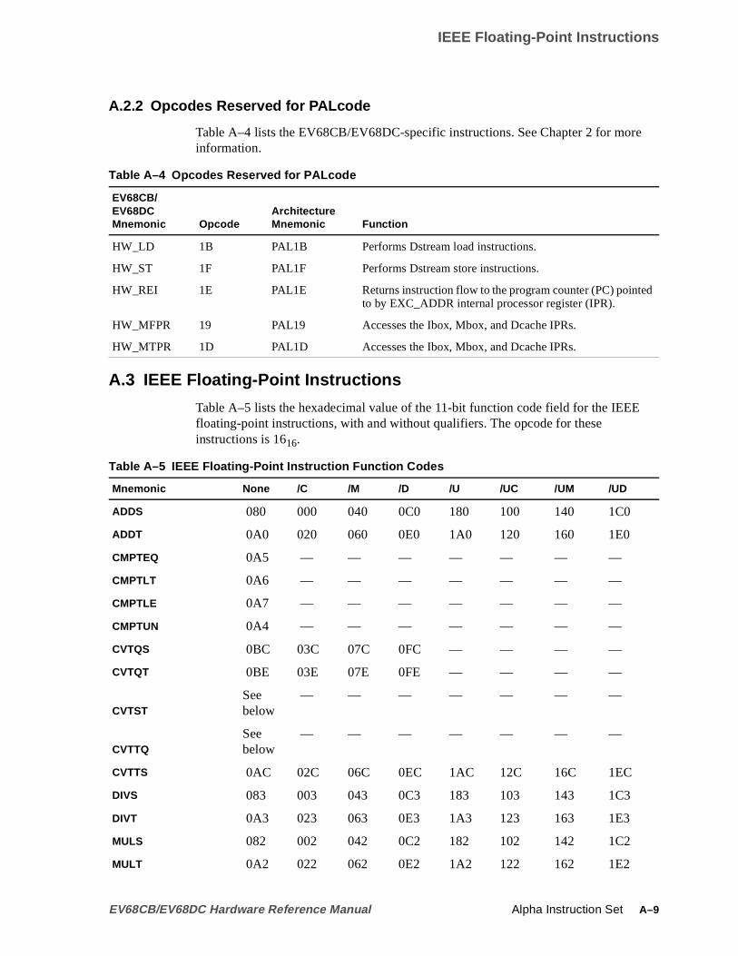
IEEE Floating-Point Instructions
d
A.2.2 Opcodes Reserved for PALcode
Table A–4 lists the EV68CB/EV68DC-specific instructions. See Chapter 2 for moreinformation.
A.3 IEEE Floating-Point Instructions
Table A–5 lists the hexadecimal value of the 11-bit function code field for the IEEEfloating-point instructions, with and without qualifiers. The opcode for theseinstructions is 1616.
Table A–4 Opcodes Reserved for PALcode
EV68CB/EV68DCMnemonic Opcode
ArchitectureMnemonic Function
HW_LD 1B PAL1B Performs Dstream load instructions.
HW_ST 1F PAL1F Performs Dstream store instructions.
HW_REI 1E PAL1E Returns instruction flow to the program counter (PC) pointeto by EXC_ADDR internal processor register (IPR).
HW_MFPR 19 PAL19 Accesses the Ibox, Mbox, and Dcache IPRs.
HW_MTPR 1D PAL1D Accesses the Ibox, Mbox, and Dcache IPRs.
Table A–5 IEEE Floating-Point Instruction Function Codes
Mnemonic None /C /M /D /U /UC /UM /UD
ADDS 080 000 040 0C0 180 100 140 1C0
ADDT 0A0 020 060 0E0 1A0 120 160 1E0
CMPTEQ 0A5 — — — — — — —
CMPTLT 0A6 — — — — — — —
CMPTLE 0A7 — — — — — — —
CMPTUN 0A4 — — — — — — —
CVTQS 0BC 03C 07C 0FC — — — —
CVTQT 0BE 03E 07E 0FE — — — —
CVTSTSeebelow
— — — — — — —
CVTTQSeebelow
— — — — — — —
CVTTS 0AC 02C 06C 0EC 1AC 12C 16C 1EC
DIVS 083 003 043 0C3 183 103 143 1C3
DIVT 0A3 023 063 0E3 1A3 123 163 1E3
MULS 082 002 042 0C2 182 102 142 1C2
MULT 0A2 022 062 0E2 1A2 122 162 1E2
EV68CB/EV68DC Hardware Reference Manual Alpha Instruction Set A–9

IEEE Floating-Point Instructions
SQRTS 08B 00B 04B 0CB 18B 10B 14B 1CB
SQRTT 0AB 02B 06B 0EB 1AB 12B 16B 1EB
SUBS 081 001 041 0C1 181 101 141 1C1
SUBT 0A1 021 061 0E1 1A1 121 161 1E1
Mnemonic /SU /SUC /SUM /SUD /SUI /SUIC /SUIM /SUID
ADDS 580 500 540 5C0 780 700 740 7C0
ADDT 5A0 520 560 5E0 7A0 720 760 7E0
CMPTEQ 5A5
CMPTLT 5A6
CMPTLE 5A7
CMPTUN 5A4
CVTQS 7BC 73C 77C 7FC
CVTQT 7BE 73E 77E 7FE
CVTTS 5AC 52C 56C 5EC 7AC 72C 76C 7EC
DIVS 583 503 543 5C3 783 703 743 7C3
DIVT 5A3 523 563 5E3 7A3 723 763 7E3
MULS 582 502 542 5C2 782 702 742 7C2
MULT 5A2 522 562 5E2 7A2 722 762 7E2
SQRTS 58B 50B 54B 5CB 78B 70B 74B 7CB
SQRTT 5AB 52B 56B 5EB 7AB 72B 76B 7EB
SUBS 581 501 541 5C1 781 701 741 7C1
SUBT 5A1 521 561 5E1 7A1 721 761 7E1
Mnemonic None /S
CVTST 2AC 6AC
Mnemonic None /C /V /VC /SV /SVC /SVI /SVIC
CVTTQ 0AF 02F 1AF 12F 5AF 52F 7AF 72F
Mnemonic D /VD /SVD /SVID /M /VM /SVM /SVIM
CVTTQ 0EF 1EF 5EF 7EF 06F 16F 56F 76F
Table A–5 IEEE Floating-Point Instruction Function Codes (Continued)
A–10 Alpha Instruction Set EV68CB/EV68DC Hardware Reference Manual

VAX Floating-Point Instructions
rder
g-e
Programming Note:
In order to use CMPTxx with software completion trap handling, it is necessary tospecify the /SU IEEE trap mode, even though an underflow trap is not possible. In oto use CVTQS or CVTQT with software completion trap handling, it is necessary tospecify the /SUI IEEE trap mode, even though an underflow trap is not possible.
A.4 VAX Floating-Point Instructions
Table A–6 lists the hexadecimal value of the 11-bit function code field for the VAXfloating-point instructions. The opcode for these instructions is 1516.
A.5 Independent Floating-Point Instructions
Table A–7 lists the hexadecimal value of the 11-bit function code field for the floatinpoint instructions that are not directly tied to IEEE or VAX floating point. The opcodfor the following instructions is 1716.
Table A–6 VAX Floating-Point Instruction Function Codes
Mnemonic None /C /U /UC /S /SC /SU /SUC
ADDF 080 000 180 100 480 400 580 500
ADDG 0A0 020 1A0 120 4A0 420 5A0 520
CMPGEQ 0A5 4A5
CMPGLE 0A7 4A7
CMPGLT 0A6 4A6
CVTDG 09E 01E 19E 11E 49E 41E 59E 51E
CVTGD 0AD 02D 1AD 12D 4AD 42D 5AD 52D
CVTGF 0AC 02C 1AC 12C 4AC 42C 5AC 52C
CVTGQ See below
CVTQF 0BC 03C
CVTQG 0BE 03E
DIVF 083 003 183 103 483 403 583 503
DIVG 0A3 023 1A3 123 4A3 423 5A3 523
MULF 082 002 182 102 482 402 582 502
MULG 0A2 022 1A2 122 4A2 422 5A2 522
SQRTF 08A 00A 18A 10A 48A 40A 58A 50A
SQRTG 0AA 02A 1AA 12A 4AA 42A 5AA 52A
SUBF 081 001 181 101 481 401 581 501
SUBG 0A1 021 1A1 121 4A1 421 5A1 521
Mnemonic None /C /V /VC /S /SC /SV /SVC
CVTGQ 0AF 02F 1AF 12F 4AF 42F 5AF 52F
EV68CB/EV68DC Hardware Reference Manual Alpha Instruction Set A–11

Opcode Summary
ithow.
uldthe
is
Table A–7 Independent Floating-Point Instruction Function Codes
A.6 Opcode Summary
Table A–8 lists all Alpha opcodes from 00 (CALL_PAL) through 3F (BGT). In thetable, the column headings that appear over the instructions have a granularity of 816.The rows beneath the Offset column supply the individual hexadecimal number toresolve that granularity.
If an instruction column has a 0 in the right (low) hexadecimal digit, replace that 0 wthe number to the left of the backslash (\) in the Offset column on the instruction’s rIf an instruction column has an 8 in the right (low) hexadecimal digit, replace that 8with the number to the right of the backslash in the Offset column.
For example, the third row (2/A) under the 1016 column contains the symbol INTS*,representing the all-integer shift instructions. The opcode for those instructions wothen be 1216 because the 0 in 10 is replaced by the 2 in the Offset column. Likewise,third row under the 1816 column contains the symbol JSR*, representing all jumpinstructions. The opcode for those instructions is 1A because the 8 in the headingreplaced by the number to the right of the backslash in the Offset column. Theinstruction format is listed under the instruction symbol.
Mnemonic None /V /SV
CPYS 020 — —
CPYSE 022 — —
CPYSN 021 — —
CVTLQ 010 — —
CVTQL 030 130 530
FCMOVEQ 02A — —
FCMOVGE 02D — —
FCMOVGT 02F — —
FCMOVLE 02E — —
FCMOVLT 02C — —
MF_FPCR 025 — —
MT_FPCR 024 — —
Table A–8 Opcode Summary
Offset 00 08 10 18 20 28 30 38
0/8 PAL*(pal)
LDA(mem)
INTA*(op)
MISC*(mem)
LDF(mem)
LDL(mem)
BR(br)
BLBC(br)
1/9 Res LDAH(mem)
INTL*(op)
\PAL\ LDG(mem)
LDQ(mem)
FBEQ(br)
BEQ(br)
2/A LDBU Res INTS*(op)
JSR*(mem)
LDS(mem)
LDL_L(mem)
FBLT(br)
BLT(br)
A–12 Alpha Instruction Set EV68CB/EV68DC Hardware Reference Manual

Required PALcode Function Codes
d is
Table A–9 explains the symbols used in Table A–8.
A.7 Required PALcode Function Codes
Table A–10 lists opcodes required for all Alpha implementations. The notation useoo.ffff, whereoo is the hexadecimal 6-bit opcode andffff is the hexadecimal 26-bitfunction code.
3/B Res LDQ_U(mem)
INTM*(op)
\PAL\ LDT(mem)
LDQ_L(mem)
FBLE(br)
BLE(br)
4/C LDWU Res ITFP* FPTI* STF(mem)
STL(mem)
BSR(br)
BLBS(br)
5/D Res STW FLTV*(op)
\PAL\ STG(mem)
STQ(mem)
FBNE(br)
BNE(br)
6/E Res STB FLTI*(op)
\PAL\ STS(mem)
STL_C(mem)
FBGE(br)
BGE(br)
7/F Res STQ_U(mem)
FLTL*(op)
\PAL\ STT(mem)
STQ_C(mem)
FBGT(br)
BGT(br)
Table A–9 Key to Opcode Summary Used in Table A–8
Symbol Meaning
FLTI* IEEE floating-point instruction opcodes
FLTL* Floating-point operate instruction opcodesFLTV* VAX floating-point instruction opcodes
FPTI* Floating-point to integer register move opcodesINTA* Integer arithmetic instruction opcodes
INTL* Integer logical instruction opcodesINTM* Integer multiply instruction opcodes
INTS* Integer shift instruction opcodesITFP* Integer to floating-point register move opcodes
JSR* Jump instruction opcodesMISC* Miscellaneous instruction opcodes
PAL* PALcode instruction (CALL_PAL) opcodes
\PAL\ Reserved for PALcode
Res Reserved for Compaq
Table A–10 Required PALcode Function Codes
Mnemonic Type Function Code
DRAINA Privileged 00.0002
HALT Privileged 00.0000
IMB Unprivileged 00.0086
Table A–8 Opcode Summary (Continued)
Offset 00 08 10 18 20 28 30 38
EV68CB/EV68DC Hardware Reference Manual Alpha Instruction Set A–13

IEEE Floating-Point Conformance
n-d
ral
ete
ds
dng
d
t,ludetic
x,lues
t
hesult
A.8 IEEE Floating-Point Conformance
The EV68CB/EV68DC supports the IEEE floating-point operations defined in theAlpha System Reference Manual, Revision7 and therefore also from theAlpha Archi-tecture Handbook, Version 4. Support for a complete implementation of the IEEE Stadard for Binary Floating-Point Arithmetic (ANSI/IEEE Standard 754 1985) is provideby a combination of hardware and software. The EV68CB/EV68DC provides sevehardware features to facilitate complete support of the IEEE standard.
The EV68CB/EV68DC provides the following hardware features to facilitate complsupport of the IEEE standard:
• The EV68CB/EV68DC implements precise exception handling in hardware, asdenoted by the AMASK instruction returning bit 9 set. TRAPB instructions aretreated as NOPs and are not issued.
• The EV68CB/EV68DC accepts both Signaling and Quiet NaNs as input operanand propagates them as specified by the Alpha architecture. In addition, theEV68CB/EV68DC delivers a canonical Quiet NaN when an operation is requireto produce a NaN value and none of its inputs are NaNs. Encodings for SignaliNaN and Quiet NaN are defined by theAlpha Architecture Handbook, Version 4.
• The EV68CB/EV68DC accepts infinity operands and implements infinity arith-metic as defined by the IEEE standard and theAlpha Architecture Handbook, Ver-sion 4.
• The EV68CB/EV68DC implements SQRT for single (SQRTS) and double(SQRTT) precision in hardware.
Note: In addition, the EV68CB/EV68DC also implements the VAX SQRTF anSQRTG instructions.
• The EV68CB/EV68DC implements the FPCR[DNZ] bit. When FPCR[DNZ] is sedenormal input operand traps can be avoided for arithmetic operations that incthe /S qualifier. When FPCR[DNZ] is clear, denormal input operands for arithmeoperations produce an unmaskable denormal trap. CPYSE/CPYSN, FCMOVxand MF_FPCR/MT_FPCR are not arithmetic operations, and pass denormal vawithout initiating arithmetic traps.
• The EV68CB/EV68DC implements the following disable bits in the floating-poincontrol register (FPCR):
– Underflow disable (UNFD)
– Overflow disable (OVFD)
– Inexact result disable (INED)
– Division by zero disable (DZED)
– Invalid operation disable (INVD)
If one of these bits is set, and an instruction with the /S qualifier set generates tassociated exception, the EV68CB/EV68DC produces the IEEE nontrapping reand suppresses the trap. These nontrapping responses include correctly signedinfinity, largest finite number, and Quiet NaNs as specified by the IEEEstandard.
A–14 Alpha Instruction Set EV68CB/EV68DC Hardware Reference Manual

IEEE Floating-Point Conformance
rmal
,nlyione
tion,the
ra-
p-
The EV68CB/EV68DC does not produce a denormal result for the underflowexception. Instead, a true zero (+0) is written to the destination register. In theEV68CB/EV68DC, the FPCR underflow to zero (UNDZ) bit must be set if theunderflow disable (UNFD) bit is set. If desired, trapping on underflow can beenabled by the instruction and the FPCR, and software may compute the denovalue as defined in the IEEE standard.
The EV68CB/EV68DC records floating-point exception information in two places:
• The FPCR status bits record the occurrence of all exceptions that are detectedwhether or not the corresponding trap is enabled. The status bits are cleared othrough an explicit clear command (MT_FPCR); hence, the exception informatthey record is a summary of all exceptions that have occurred since the last timthey were cleared.
• If an exception is detected and the corresponding trap is enabled by the instrucand is not disabled by the FPCR control bits, the EV68CB/EV68DC will recordcondition in the EXC_SUM register and initiate an arithmetic trap.
The following items apply to Table A–11:
• The EV68CB/EV68DC traps on a denormal input operand for all arithmetic opetions unless FPCR[DNZ] = 1.
• Input operand traps take precedence over arithmetic result traps.
• The following abbreviations are used:
Inf: Infinity
QNaN: Quiet NaN
SNaN: Signalling NaN
CQNaN: Canonical Quiet NaN
For IEEE instructions with /S, Table A–11 lists all exceptional input and outputconditions recognized by the EV68CB/EV68DC, along with the result and excetion generated for each condition.
Table A–11 Exceptional Input and Output Conditions
Alpha InstructionsEV68CB/EV68DC HardwareSupplied Result Exception
ADDx SUBx INPUT
Inf operand ±Inf (none)
QNaN operand QNaN (none)
SNaN operand QNaN Invalid Op
Effective subtract of two Inf operands CQNaN Invalid Op
ADDx SUBx OUTPUT
Exponent overflow ±Inf or ±MAX Overflow
Exponent underflow +0 Underflow
Inexact result Result Inexact
EV68CB/EV68DC Hardware Reference Manual Alpha Instruction Set A–15

IEEE Floating-Point Conformance
MULx INPUT
Inf operand ±Inf (none)
QNaN operand QNaN (none)
SNaN operand QNaN Invalid Op
0 * Inf CQNaN Invalid Op
MULx OUTPUT (same as ADDx)
DIVx INPUT
QNaN operand QNaN (none)
SNaN operand QNaN Invalid Op
0/0 or Inf/Inf CQNaN Invalid Op
A/0 (A not 0) ±Inf Div Zero
A/Inf ±0 (none)
Inf/A ±Inf (none)
DIVx OUTPUT (same as ADDx)
SQRTx INPUT
+Inf operand +Inf (none)
QNaN operand QNaN (none)
SNaN operand QNaN Invalid Op
-A (A not 0) CQNaN Invalid Op
-0 -0 (none)
SQRTx OUTPUT
Inexact result root Inexact
CMPTEQ CMPTUN INPUT
Inf operand True or False (none)
QNaN operand False for EQ, True for UN (none)
SNaN operand False for EQ,True for UN Invalid Op
CMPTLT CMPTLE INPUT
Inf operand True or False (none)
QNaN operand False Invalid Op
SNaN operand False Invalid Op
CVTfi INPUT
Inf operand 0 Invalid Op
QNaN operand 0 Invalid Op
Table A–11 Exceptional Input and Output Conditions (Continued)
Alpha InstructionsEV68CB/EV68DC HardwareSupplied Result Exception
A–16 Alpha Instruction Set EV68CB/EV68DC Hardware Reference Manual

IEEE Floating-Point Conformance
See Section 2.14 for information about the floating-point control register (FPCR).
SNaN operand 0 Invalid Op
CVTfi OUTPUT
Inexact result Result Inexact
Integer overflow Truncated result Invalid Op
CVTif OUTPUT
Inexact result Result Inexact
CVTff INPUT
Inf operand ±Inf (none)
QNaN operand QNaN (none)
SNaN operand QNaN Invalid Op
CVTff OUTPUT (same as ADDx)
FBEQ FBNE FBLT FBLE FBGT FBGELDS LDTSTS STTCPYS CPYSNFCMOVx
Table A–11 Exceptional Input and Output Conditions (Continued)
Alpha InstructionsEV68CB/EV68DC HardwareSupplied Result Exception
EV68CB/EV68DC Hardware Reference Manual Alpha Instruction Set A–17


can
ter
withr1.
BEV68CB/EV68DC Boundary-Scan Register
This appendix contains the BSDL description of the EV68CB/EV68DC boundary-sregister.
B.1 Boundary-Scan Register
The Boundary-Scan Register (BSR) on the EV68CB/EV68DC is 367 bits long. It isaccessed by the three public (SAMPLE, EXTEST, CLAMP) instructions. The regisoperation for the public instructions is compliant with the IEEE 1149.1 standard.
The boundary-scan register covers all input, output, and bidirectional pins (bumps)the exception of the compliance enable pins and pins that are power-supply-type oanalog in nature. The BSDL for the boundary-scan register is given in Section B.1.
B.1.1 BSDL Description of the Alpha EV68CB/EV68DC Boundary-Scan Register
-------------------------------------------------------------------------------
-- alpha21264c.bsdl
--The BSDL Description for 21264C’s IEEE 1149.1 Circuits
-------------------------------------------------------------------------------
-- Revision History
--Rev who DateDescription
-------------------------------------------------------------------------------
--1.0 dkb 27-Apr-00 Adapted from alpha 21264a BSDL.
-- Deleted Spare_0. Spare_5 and reduced Spare_7 from 7 to 4.
-- Updated VDD and VSS counts
--1.1 jwb 18-May-00 Corrected syntax errors caught by GR BasicScan compiler
-------------------------------------------------------------------------------
entity Alpha_21264c is-- (ref B.8)
generic (PHYSICAL_PIN_MAP :string := “LGA_EV6X”);-- (ref B.8.2)
port (-- (ref B.8.3)
TestStat_H :out bit ;
SromOE_L :out bit ;
SromClk_H :out bit ;
SromData_H :in bit ;
Reset_L :in bit ;
IRQ_H :in bit_vector (0 to 5) ;
DcOk_H :linkage bit ; -- Compliance enable input
NoConnect_0 :linkage bit ; -- n/c
EV68CB/EV68DC Hardware Reference Manual EV68CB/EV68DC Boundary-Scan Register B–1

Boundary-Scan Register
NoConnect_1 :linkage bit ; -- n/c
PllBypass_H :linkage bit ;
FrameClk_H :linkage bit ;
FrameClk_L :linkage bit ;
ClkFwdRst_H :in bit ;
BcCheck_H :inout bit_vector (0 to 15);
BcData_H :inout bit_vector (0 to 127);
SysData_L :inout bit_vector (0 to 63) ;
SysCheck_L :inout bit_vector (0 to 7) ;
BcDataInClk_H :in bit_vector (0 to 7) ;
SysDataOutClk_L :out bit_vector (0 to 7) ;
Spare_7 :linkage bit_vector (0 to 3) ; -- 7 bits in ev67
SysDataInClk_H :in bit_vector (0 to 7) ;
BcDataOutClk_L :out bit_vector (0 to 3) ; -- JWB corrected
BcDataOutClk_H :out bit_vector (0 to 3) ; -- JWB corrected
ClkIn_H :linkage bit ; -- Oscillator
ClkIn_L :linkage bit ; -- Oscillator
PLL_VDD :linkage bit ;
EV6Clk_H :linkage bit ;
EV6Clk_L :linkage bit ;
Spare_4 :linkage bit ;
-- Spare_5 converted to ??? Spare_5 :linkage bit ;
BcTag_H :inout bit_vector (20 to 42);
BcVref :linkage bit ;
BcTagInClk_H :in bit ; -- Name in model: BcTagClkIn_H
BcTagParity_H :inout bit ;
BcTagShared_H :inout bit ;
BcTagDirty_H :inout bit ;
BcTagValid_H :inout bit ;
BcTagOutClk_L :out bit ;
BcTagOutClk_H :out bit ;
BcTagOE_L :out bit ;
BcTagWr_L :out bit ;
BcDataWr_L :out bit ;
BcLoad_L :out bit ;
BcDataOE_L :out bit ;
BcAdd_H :out bit_vector (4 to 23) ;
SysAddOut_L :out bit_vector (0 to 14) ;
SysAddIn_L :in bit_vector (0 to 14) ;
SysAddInClk_L :in bit ;
SysAddOutClk_L :out bit ; --JWB added
SysVref :linkage bit ; --JWB added
SysFillValid_L :in bit ;
SysDataInValid_L :in bit ;
SysDataOutValid_L :in bit ;
-- deleted on 21264C Spare_0:linkage bit ; -- n/c
MiscVref :linkage bit ; --
Spare_2 :linkage bit ; -- n/c
Tdi_H :in bit ;
Tdo_H :out bit ;
B–2 EV68CB/EV68DC Boundary-Scan Register EV68CB/EV68DC Hardware Reference Manual

Boundary-Scan Register
Trst_L :in bit ;
Tck_H :in bit ;
Tms_H :in bit ;
VSS :linkage bit_vector (0 to 150); -- was 103
VDD :linkage bit_vector (0 to 146)); -- was 93
use STD_1149_1_1994.all ;-- (ref B.8.4)
attribute COMPONENT_CONFORMANCE of Alpha_21264c: entity is “STD_1149_1_1993”;
attribute PIN_MAP of Alpha_21264c : entity is PHYSICAL_PIN_MAP ;
constant LGX_EV6X : PIN_MAP_STRING := “ “ &
“SysAddIn_L : (Y17, AA17, AB17, Y16, AA16, AB16, Y14, AA14, “&
“ AB14, AC14, AD14, AE14, Y13, AA13, AB13), “&
“SysAddInClk_L : AF14, “&
“SysVref : AF13, “&
“SysFillValid_L : AD13, “&
“SysAddOut_L : (AC20, AD20, AE20, AF20, AC19, AD19, AE19, AF19,”&
“ AC17, AD17, AE17, AF17, AC16, AD16, AE16), “&
“SysAddOutClk_L : AF16, “&
“SysData_L : (F10, G10, H10, E08, E07, F08, F07, G08, “&
“ J10, J09, K09, K08, L09, L08, M09, N09, “&
“ P08, P09, R09, T07, T08, U07, U08, U09, “&
“ 09, W08, Y08, V10, W10, Y10, V11, W11, “&
“ G16, H16, J16, G17, H17, J17, G19, H19, “&
“ K18, K19, K20, L18, L19, L20, M18, N18, “&
“ P19, P18, R18, T20, T19, T18, U20, U19, “&
“ V18, W20, W19, Y19, AA20, AA19, AB20, AB19),”&
“SysCheck_L : (H08, N08, W07, Y11, J18, N19, U18, W17), “&
“SysDataInClk_H : (D01, K01, N01, W01, E26, K26, N26, Y26), “&
“SysDataOutClk_L : (E02, L02, P02, Y02, D25, L25, P25, W25), “&
“SysDataInValid_L : AC13, “&
“SysDataOutValid_L : AE13, “&
“BcAdd_H : (E14, A16, B16, C16, D16, E16, A17, B17, “&
“ C17, D17, E17, A19, B19, C19, D19, E19, “&
“ A20, B20, C20, D20), “&
“BcDataOE_L : D14, “&
“BcLoad_L : C13, “&
“BcDataWr_L : C14, “&
“BcData_H : (A04, B04, C04, D03, E04, E03, G04, G03, “&
“ H04, H03, K04, K03, L04, L03, N05, N04, “&
“ P03, P04, T02, T03, T04, U02, U03, U04, “&
“ Y03, Y04, Y05, AB03, AB04, AB05, AC03, AC04, “&
“ A23, B23, C23, D24, E23, E24, G23, G24, “&
“ H23, H24, H25, K23, K24, L23, L24, N23, “&
“ P24, P23, T25, T24, T23, U25, U24, U23, “&
“ Y24, AB26, AB25, AB24, AC26, AC25, AC24, AD23, “&
“ A05, B05, C05, D05, E05, G06, G05, H07, “&
“ H05, K07, K06, K05, L07, L06, L05, N07, “&
“ P05, P06, P07, T05, T06, U05, U06, W04, “&
“ W06, Y06, AA07, AA08, AB07, AB08, AC05, AC07, “&
EV68CB/EV68DC Hardware Reference Manual EV68CB/EV68DC Boundary-Scan Register B–3

Boundary-Scan Register
“ A22, B22, C22, D22, E22, F20, G21, G22, “&
“ H21, H22, K21, K22, L21, L22, N20, N21, “&
“ P22, P21, P20, T22, T21, U22, U21, W23, “&
“ W21, Y23, Y22, Y21, AB23, AB22, AC22, AD22),”&
“BcCheck_H : (G02, N03, W03, AD04, G25, N24, W24, AE23, “&
“ H06, N06, W05, AD05, H20, N22, W22, AE22),”&
“BcDataInClk_H : (E01, L01, P01, Y01, D26, L26, P26, W26), “&
“Spare_7 : (AF23, V17, J15, AC08), “& -- was 7 bits in ev67
“BcDataOutClk_L : (G01, U01, H26, T26), “&
“BcDataOutClk_H : (H01, T01, G26, U26), “&
“BcTag_H : (D07, C07, B07, A07, D08, C08, B08, A08, “&
“ E10, D10, C10, B10, J11, H11, G11, F11, “&
“ E11, D11, C11, B11, J12, H13, G13), “&
“BcTagValid_H : G14, “&
“BcTagDirty_H : H14, “&
“BcTagShared_H : J14, “&
“BcTagParity_H : J13, “&
“BcTagOE_L : D13, “&
“BcTagWr_L : E13, “&
“BcTagInClk_H : A11, “&
“BcVref : A10, “&
“BcTagOutClk_L : A13, “&
“BcTagOutClk_H : A14, “&
“IRQ_H : (AD07, AE07, AF07, AD08, AE08, AF08), “&
“Reset_L : AE11, “&
“SromData_H : AD11, “&
“SromCLK_H : AC11, “&
“SromOE_L : AB11, “&
“Tms_H : W14, “&
“Tck_H : V13, “&
“Trst_L : V15, “&
“Tdi_H : V16, “&
“Tdo_H : W16, “&
“TestStat_H : W13, “&
“ClkIn_H : AF04, “&
“ClkIn_L : AF05, “&
“FrameClk_H : AF10, “&
“FrameClk_L : AF11, “&
“PllBypass_H : AB10, “&
“NoConnect_0 : AA11, “&
“NoConnect_1 : AA10, “&
“ClkFwdRst_H : AE10, “&
“EV6Clk_H : AB01, “&
“EV6Clk_L : AC01, “&
“Spare_4 : AC10, “&
“PLL_VDD : T10, “&
“MiscVref : V14, “&
“Spare_2 : AF22, “&
“DCOK_H : AD10, “&
“VSS : (F19, N14, AE12, L14, J04, K15, G07, AA12, “&
B–4 EV68CB/EV68DC Boundary-Scan Register EV68CB/EV68DC Hardware Reference Manual
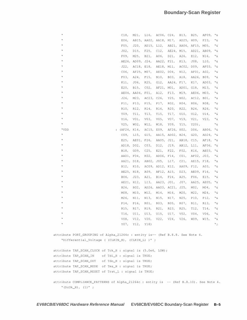
Boundary-Scan Register
“ C18, M21, L16, AC06, C24, B13, B25, AF09, “&
“ E06, AB15, AA02, AA18, M17, AD25, H09, F23, “&
“ F05, J20, AD15, L12, AB21, AA06, AF15, M05, “&
“ J02, D15, F25, C12, AE24, M15, AD21, AB09, “&
“ F09, M25, B21, A06, D21, A26, E12, N16, “&
“ AE26, AD09, J24, AA22, F21, K13, J08, L10, “&
“ J22, AC18, E18, AE18, M11, AC02, D09, AF03, “&
“ C06, AF25, M07, AE02, D04, N12, AF01, A02, “&
“ F03, A24, F15, N10, B03, A18, AA26, B09, “&
“ K11, J06, K25, G12, AA24, F17, K17, AD03, “&
“ E20, B15, C02, AF21, M01, AD01, G18, M13, “&
“ AE04, AA04, F01, A12, F13, M19, AE06, M03, “&
“ J26, M23, AC23, C26, Y25, N02, AC12, B01, “&
“ P11, P13, P15, P17, R02, R04, R06, R08, “&
“ R10, R12, R14, R16, R20, R22, R24, R26, “&
“ T09, T11, T13, T15, T17, U10, U12, U14, “&
“ U16, V01, V03, V05, V07, V19, V21, V23, “&
“ V25, W02, W12, W18, Y09, Y15, Y20), “&
“VDD : (AF24, K14, AC15, E09, AF26, H02, D06, AB06, “&
“ C09, L15, G15, AA15, AD02, B24, G20, AD24, “&
“ E25, AE01, F26, AA05, J21, AB18, C15, AF18, “&
“ AD18, D02, C03, D12, J19, AB12, L11, AF06, “&
“ B18, G09, C25, E21, F22, F02, K16, AE03, “&
“ AA01, F04, K02, AD06, F14, C01, AF02, J03, “&
“ AA21, D18, AB02, J05, L17, C21, AE15, F18, “&
“ B12, K10, AC09, AD12, K12, AA09, F12, A03, “&
“ AE25, H18, A09, AF12, A15, D23, AE09, F16, “&
“ B06, J23, A21, B14, F24, A25, F06, E15, “&
“ AE21, H12, L13, AA23, J01, J07, AA25, AE05, “&
“ B26, B02, AD26, AA03, AC21, J25, M02, M04, “&
“ M08, M10, M12, M14, M16, M20, M22, M24, “&
“ M26, N11, N13, N15, N17, N25, P10, P12, “&
“ P14, P16, R01, R03, R05, R07, R11, R13, “&
“ R15, R17, R19, R21, R23, R25, T12, T14, “&
“ T16, U11, U13, U15, U17, V02, V04, V06, “&
“ V08, V12, V20, V22, V24, V26, W09, W15, “&
“ Y07, Y12, Y18) “;
attribute PORT_GROUPING of Alpha_21264c : entity is-- (Ref B.8.8. See Note 4.
“Differential_Voltage ( (CLKIN_H), (CLKIN_L) )” ;
attribute TAP_SCAN_CLOCK of Tck_H : signal is (5.0e6, LOW);
attribute TAP_SCAN_IN of Tdi_H : signal is TRUE;
attribute TAP_SCAN_OUT of Tdo_H : signal is TRUE;
attribute TAP_SCAN_MODE of Tms_H : signal is TRUE;
attribute TAP_SCAN_RESET of Trst_L : signal is TRUE;
attribute COMPLIANCE_PATTERNS of Alpha_21264c : entity is -- (Ref B.8.10). See Note 4.
“(DcOk_H), (1)” ;
EV68CB/EV68DC Hardware Reference Manual EV68CB/EV68DC Boundary-Scan Register B–5

Boundary-Scan Register
attribute INSTRUCTION_LENGTH of Alpha_21264c : entity is 5 ;
attribute INSTRUCTION_OPCODE of Alpha_21264c : entity is
“EXTEST (11011),”&-- No longer mandated to be (00000)!
“SAMPLE (11000),”&-- JWB changed “PRELOAD” to “SAMPLE”
“CLAMP (11010),”&
“HIGHZ (11001),”&
“DIE_ID (11110),”&
“BYPASS (11111)”;
attribute INSTRUCTION_CAPTURE of Alpha_21264c : entity is “00001” ;
attribute INSTRUCTION_PRIVATE of Alpha_21264c : entity is “Private”; -- See Note 4.
attribute REGISTER_ACCESS of Alpha_21264c : entity is-- (ref B.8.13)
“BOUNDARY (EXTEST, SAMPLE),” &-- Redundant. Added for completeness
“BYPASS (BYPASS, HIGHZ, CLAMP),” &-- ditto
“DIE_ID[32] (DIE_ID)”;
attribute BOUNDARY_LENGTH of Alpha_21264c : entity is 367 ;
attribute BOUNDARY_REGISTER of Alpha_21264c : entity is
-----------------------------------------------------------------------------
-- scan cell safe cntrl disable disable
-- cell type port function | cell value state
----|-----|-----|-------------------|--------|---|----|------|--------------
“ 366 ( BC_2, TestStat_H, OUTPUT2, x ), “& --
“ 365 ( BC_2, SromOE_L, OUTPUT2, X ), “& --
“ 364 ( BC_2, SromClk_H, OUTPUT2, x ), “& --
“ 363 ( BC_2, SromData_H, INPUT, x ), “& --
“ 362 ( BC_3, reset_L, INPUT, x ), “& --
“ 361 ( BC_3, IRQ_H(5), INPUT, x ), “& --
“ 360 ( BC_3, IRQ_H(4), INPUT, x ), “& --
“ 359 ( BC_3, IRQ_H(3), INPUT, x ), “& --
“ 358 ( BC_3, IRQ_H(2), INPUT, x ), “& --
“ 357 ( BC_3, IRQ_H(1), INPUT, x ), “& --
“ 356 ( BC_3, IRQ_H(0), INPUT, x ), “& --
“ 355 ( BC_3, ClkFwdRst_H, INPUT, x ), “& --
“ 354 ( BC_2, BcCheck_H(3), BIDIR, x, 339, 0, Z ), “& --
“ 353 ( BC_2, BcCheck_H(11), BIDIR, x, 339, 0, Z ), “& --
“ 352 ( BC_2, SysCheck_L(3), BIDIR, x, 336, 0, WEAK1 ), “& --
“ 351 ( BC_2, BcData_H(31), BIDIR, x, 339, 0, Z ), “& --
“ 350 ( BC_2, BcData_H(95), BIDIR, x, 339, 0, Z ), “& --
“ 349 ( BC_2, SysData_L(31), BIDIR, x, 336, 0, WEAK1 ), “& --
“ 348 ( BC_2, BcData_H(30), BIDIR, x, 339, 0, Z ), “& --
“ 347 ( BC_2, BcData_H(94), BIDIR, x, 339, 0, Z ), “& --
“ 346 ( BC_2, SysData_L(30), BIDIR, x, 336, 0, WEAK1 ), “& --
“ 345 ( BC_2, BcData_H(29), BIDIR, x, 339, 0, Z ), “& --
“ 344 ( BC_2, BcData_H(93), BIDIR, x, 339, 0, Z ), “& --
“ 343 ( BC_2, SysData_L(29), BIDIR, x, 336, 0, WEAK1 ), “& --
“ 342 ( BC_2, BcData_H(28), BIDIR, x, 339, 0, Z ), “& --
“ 341 ( BC_2, BcData_H(92), BIDIR, x, 339, 0, Z ), “& --
“ 340 ( BC_2, SysData_L(28), BIDIR, x, 336, 0, WEAK1 ), “& --
B–6 EV68CB/EV68DC Boundary-Scan Register EV68CB/EV68DC Hardware Reference Manual

Boundary-Scan Register
“ 339 ( BC_3, *, CONTROL, 0 ), “& -- bccell0
“ 338 ( BC_3, BcDataInClk_H(3), INPUT, x ), “& --
“ 337 ( BC_2, SysDataOutClk_L(3), OUTPUT2, x ), “& --
“ 336 ( BC_3, *, CONTROL, 0 ), “& -- sccell0
“ 335 ( BC_3, SysDataInClk_H(3), INPUT, x ), “& --
“ 334 ( BC_2, BcData_H(27), BIDIR, x, 339, 0, Z ), “& --
“ 333 ( BC_2, BcData_H(91), BIDIR, x, 339, 0, Z ), “& --
“ 332 ( BC_2, SysData_L(27), BIDIR, x, 336, 0, WEAK1 ), “& --
“ 331 ( BC_2, BcData_H(26), BIDIR, x, 339, 0, Z ), “& --
“ 330 ( BC_2, BcData_H(90), BIDIR, x, 339, 0, Z ), “& --
“ 329 ( BC_2, SysData_L(26), BIDIR, x, 336, 0, WEAK1 ), “& --
“ 328 ( BC_2, BcData_H(25), BIDIR, x, 339, 0, Z ), “& --
“ 327 ( BC_2, BcData_H(89), BIDIR, x, 339, 0, Z ), “& --
“ 326 ( BC_2, SysData_L(25), BIDIR, x, 336, 0, WEAK1 ), “& --
“ 325 ( BC_2, BcData_H(24), BIDIR, x, 339, 0, Z ), “& --
“ 324 ( BC_2, BcData_H(88), BIDIR, x, 339, 0, Z ), “& --
“ 323 ( BC_2, SysData_L(24), BIDIR, x, 336, 0, WEAK1 ), “& --
“ 322 ( BC_2, BcDataOutClk_L(1), OUTPUT2, x ), “& --
“ 321 ( BC_2, BcDataOutClk_H(1), OUTPUT2, x ), “& --
“ 320 ( BC_2, BcCheck_H(2), BIDIR, x, 305, 0, Z ), “& --
“ 319 ( BC_2, BcCheck_H(10), BIDIR, x, 305, 0, Z ), “& --
“ 318 ( BC_2, SysCheck_L(2), BIDIR, x, 302, 0, WEAK1 ), “& --
“ 317 ( BC_2, BcData_H(23), BIDIR, x, 305, 0, Z ), “& --
“ 316 ( BC_2, BcData_H(87), BIDIR, x, 305, 0, Z ), “& --
“ 315 ( BC_2, SysData_L(23), BIDIR, x, 302, 0, WEAK1 ), “& --
“ 314 ( BC_2, BcData_H(22), BIDIR, x, 305, 0, Z ), “& --
“ 313 ( BC_2, BcData_H(86), BIDIR, x, 305, 0, Z ), “& --
“ 312 ( BC_2, SysData_L(22), BIDIR, x, 302, 0, WEAK1 ), “& --
“ 311 ( BC_2, BcData_H(21), BIDIR, x, 305, 0, Z ), “& --
“ 310 ( BC_2, BcData_H(85), BIDIR, x, 305, 0, Z ), “& --
“ 309 ( BC_2, SysData_L(21), BIDIR, x, 302, 0, WEAK1 ), “& --
“ 308 ( BC_2, BcData_H(20), BIDIR, x, 305, 0, Z ), “& --
“ 307 ( BC_2, BcData_H(84), BIDIR, x, 305, 0, Z ), “& --
“ 306 ( BC_2, SysData_L(20), BIDIR, x, 302, 0, WEAK1 ), “& --
“ 305 ( BC_3, *, CONTROL, 0 ), “& -- bccell1
“ 304 ( BC_3, BcDataInClk_H(2), INPUT, x ), “& --
“ 303 ( BC_2, SysDataOutClk_L(2), OUTPUT2, x ), “& --
“ 302 ( BC_3, *, CONTROL, 0 ), “& -- sccell1
“ 301 ( BC_3, SysDataInClk_H(2), INPUT, x ), “& --
“ 300 ( BC_2, BcData_H(19), BIDIR, x, 305, 0, Z ), “& --
“ 299 ( BC_2, BcData_H(83), BIDIR, x, 305, 0, Z ), “& --
“ 298 ( BC_2, SysData_L(19), BIDIR, x, 302, 0, WEAK1 ), “& --
“ 297 ( BC_2, BcData_H(18), BIDIR, x, 305, 0, Z ), “& --
“ 296 ( BC_2, BcData_H(82), BIDIR, x, 305, 0, Z ), “& --
“ 295 ( BC_2, SysData_L(18), BIDIR, x, 302, 0, WEAK1 ), “& --
“ 294 ( BC_2, BcData_H(17), BIDIR, x, 305, 0, Z ), “& --
“ 293 ( BC_2, BcData_H(81), BIDIR, x, 305, 0, Z ), “& --
“ 292 ( BC_2, SysData_L(17), BIDIR, x, 302, 0, WEAK1 ), “& --
“ 291 ( BC_2, BcData_H(16), BIDIR, x, 305, 0, Z ), “& --
“ 290 ( BC_2, BcData_H(80), BIDIR, x, 305, 0, Z ), “& --
EV68CB/EV68DC Hardware Reference Manual EV68CB/EV68DC Boundary-Scan Register B–7

Boundary-Scan Register
“ 289 ( BC_2, SysData_L(16), BIDIR, x, 302, 0, WEAK1 ), “& --
“ 288 ( BC_2, BcCheck_H(1), BIDIR, x, 273, 0, Z ), “& --
“ 287 ( BC_2, BcCheck_H(9), BIDIR, x, 273, 0, Z ), “& --
“ 286 ( BC_2, SysCheck_L(1), BIDIR, x, 270, 0, WEAK1 ), “& --
“ 285 ( BC_2, BcData_H(15), BIDIR, x, 273, 0, Z ), “& --
“ 284 ( BC_2, BcData_H(79), BIDIR, x, 273, 0, Z ), “& --
“ 283 ( BC_2, SysData_L(15), BIDIR, x, 270, 0, WEAK1 ), “& --
“ 282 ( BC_2, BcData_H(14), BIDIR, x, 273, 0, Z ), “& --
“ 281 ( BC_2, BcData_H(78), BIDIR, x, 273, 0, Z ), “& --
“ 280 ( BC_2, SysData_L(14), BIDIR, x, 270, 0, WEAK1 ), “& --
“ 279 ( BC_2, BcData_H(13), BIDIR, x, 273, 0, Z ), “& --
“ 278 ( BC_2, BcData_H(77), BIDIR, x, 273, 0, Z ), “& --
“ 277 ( BC_2, SysData_L(13), BIDIR, x, 270, 0, WEAK1 ), “& --
“ 276 ( BC_2, BcData_H(12), BIDIR, x, 273, 0, Z ), “& --
“ 275 ( BC_2, BcData_H(76), BIDIR, x, 273, 0, Z ), “& --
“ 274 ( BC_2, SysData_L(12), BIDIR, x, 270, 0, WEAK1 ), “& --
“ 273 ( BC_3, *, CONTROL, 0 ), “& -- bccell2
“ 272 ( BC_3, BcDataInClk_H(1), INPUT, x ), “& --
“ 271 ( BC_2, SysDataOutClk_L(1), OUTPUT2, x ), “& --
“ 270 ( BC_3, *, CONTROL, 0 ), “& -- sccell2
“ 269 ( BC_3, SysDataInClk_H(1), INPUT, x ), “& --
“ 268 ( BC_2, BcData_H(11), BIDIR, x, 273, 0, Z ), “& --
“ 267 ( BC_2, BcData_H(75), BIDIR, x, 273, 0, Z ), “& --
“ 266 ( BC_2, SysData_L(11), BIDIR, x, 270, 0, WEAK1 ), “& --
“ 265 ( BC_2, BcData_H(10), BIDIR, x, 273, 0, Z ), “& --
“ 264 ( BC_2, BcData_H(74), BIDIR, x, 273, 0, Z ), “& --
“ 263 ( BC_2, SysData_L(10), BIDIR, x, 270, 0, WEAK1 ), “& --
“ 262 ( BC_2, BcData_H(9) , BIDIR, x, 273, 0, Z ), “& --
“ 261 ( BC_2, BcData_H(73), BIDIR, x, 273, 0, Z ), “& --
“ 260 ( BC_2, SysData_L(9), BIDIR, x, 270, 0, WEAK1 ), “& --
“ 259 ( BC_2, BcData_H(8) , BIDIR, x, 273, 0, Z ), “& --
“ 258 ( BC_2, BcData_H(72), BIDIR, x, 273, 0, Z ), “& --
“ 257 ( BC_2, SysData_L(8), BIDIR, x, 270, 0, WEAK1 ), “& --
“ 256 ( BC_2, BcDataOutClk_L(0), OUTPUT2, x ), “& --
“ 255 ( BC_2, BcDataOutClk_H(0), OUTPUT2, x ), “& --
“ 254 ( BC_2, BcCheck_H(0), BIDIR, x, 239, 0, Z ), “& --
“ 253 ( BC_2, BcCheck_H(8), BIDIR, x, 239, 0, Z ), “& --
“ 252 ( BC_2, SysCheck_L(0), BIDIR, x, 236, 0, WEAK1 ), “& --
“ 251 ( BC_2, BcData_H(7) , BIDIR, x, 239, 0, Z ), “& --
“ 250 ( BC_2, BcData_H(71), BIDIR, x, 239, 0, Z ), “& --
“ 249 ( BC_2, SysData_L(7), BIDIR, x, 236, 0, WEAK1 ), “& --
“ 248 ( BC_2, BcData_H(6) , BIDIR, x, 239, 0, Z ), “& --
“ 247 ( BC_2, BcData_H(70), BIDIR, x, 239, 0, Z ), “& --
“ 246 ( BC_2, SysData_L(6), BIDIR, x, 236, 0, WEAK1 ), “& --
“ 245 ( BC_2, BcData_H(5) , BIDIR, x, 239, 0, Z ), “& --
“ 244 ( BC_2, BcData_H(69), BIDIR, x, 239, 0, Z ), “& --
“ 243 ( BC_2, SysData_L(5), BIDIR, x, 236, 0, WEAK1 ), “& --
“ 242 ( BC_2, BcData_H(4) , BIDIR, x, 239, 0, Z ), “& --
“ 241 ( BC_2, BcData_H(68), BIDIR, x, 239, 0, Z ), “& --
“ 240 ( BC_2, SysData_L(4), BIDIR, x, 236, 0, WEAK1 ), “& --
B–8 EV68CB/EV68DC Boundary-Scan Register EV68CB/EV68DC Hardware Reference Manual

Boundary-Scan Register
“ 239 ( BC_3, *, CONTROL, 0 ), “& -- bccell3
“ 238 ( BC_3, BcDataInClk_H(0), INPUT, x ), “& --
“ 237 ( BC_2, SysDataOutClk_L(0), OUTPUT2, x ), “& --
“ 236 ( BC_3, *, CONTROL, 0 ), “& -- sccell3
“ 235 ( BC_3, SysDataInClk_H(0), INPUT, x ), “& --
“ 234 ( BC_2, BcData_H(3) , BIDIR, x, 239, 0, Z ), “& --
“ 233 ( BC_2, BcData_H(67), BIDIR, x, 239, 0, Z ), “& --
“ 232 ( BC_2, SysData_L(3), BIDIR, x, 236, 0, WEAK1 ), “& --
“ 231 ( BC_2, BcData_H(2) , BIDIR, x, 239, 0, Z ), “& --
“ 230 ( BC_2, BcData_H(66), BIDIR, x, 239, 0, Z ), “& --
“ 229 ( BC_2, SysData_L(2), BIDIR, x, 236, 0, WEAK1 ), “& --
“ 228 ( BC_2, BcData_H(1) , BIDIR, x, 239, 0, Z ), “& --
“ 227 ( BC_2, BcData_H(65), BIDIR, x, 239, 0, Z ), “& --
“ 226 ( BC_2, SysData_L(1), BIDIR, x, 236, 0, WEAK1 ), “& --
“ 225 ( BC_2, BcData_H(0) , BIDIR, x, 239, 0, Z ), “& --
“ 224 ( BC_2, BcData_H(64), BIDIR, x, 239, 0, Z ), “& --
“ 223 ( BC_2, SysData_L(0), BIDIR, x, 236, 0, WEAK1 ), “& --
“ 222 ( BC_2, BcTag_H(20), BIDIR, x, 208, 0, Z ), “& --
“ 221 ( BC_2, BcTag_H(21), BIDIR, x, 208, 0, Z ), “& --
“ 220 ( BC_2, BcTag_H(22), BIDIR, x, 208, 0, Z ), “& --
“ 219 ( BC_2, BcTag_H(23), BIDIR, x, 208, 0, Z ), “& --
“ 218 ( BC_2, BcTag_H(24), BIDIR, x, 208, 0, Z ), “& --
“ 217 ( BC_2, BcTag_H(25), BIDIR, x, 208, 0, Z ), “& --
“ 216 ( BC_2, BcTag_H(26), BIDIR, x, 208, 0, Z ), “& --
“ 215 ( BC_2, BcTag_H(27), BIDIR, x, 208, 0, Z ), “& --
“ 214 ( BC_2, BcTag_H(28), BIDIR, x, 208, 0, Z ), “& --
“ 213 ( BC_2, BcTag_H(29), BIDIR, x, 208, 0, Z ), “& --
“ 212 ( BC_2, BcTag_H(30), BIDIR, x, 208, 0, Z ), “& --
“ 211 ( BC_2, BcTag_H(31), BIDIR, x, 208, 0, Z ), “& --
“ 210 ( BC_2, BcTag_H(32), BIDIR, x, 208, 0, Z ), “& --
“ 209 ( BC_2, BcTag_H(33), BIDIR, x, 208, 0, Z ), “& --
“ 208 ( BC_3, *, CONTROL, 0 ), “& -- tccell0
“ 207 ( BC_3, BcTagInClk_H, INPUT, x ), “& --
“ 206 ( BC_2, BcTag_H(34), BIDIR, x, 208, 0, Z ), “& --
“ 205 ( BC_2, BcTag_H(35), BIDIR, x, 208, 0, Z ), “& --
“ 204 ( BC_2, BcTag_H(36), BIDIR, x, 208, 0, Z ), “& --
“ 203 ( BC_2, BcTag_H(37), BIDIR, x, 208, 0, Z ), “& --
“ 202 ( BC_2, BcTag_H(38), BIDIR, x, 208, 0, Z ), “& --
“ 201 ( BC_2, BcTag_H(39), BIDIR, x, 208, 0, Z ), “& --
“ 200 ( BC_2, BcTag_H(40), BIDIR, x, 208, 0, Z ), “& --
“ 199 ( BC_2, BcTag_H(41), BIDIR, x, 208, 0, Z ), “& --
“ 198 ( BC_2, BcTag_H(42), BIDIR, x, 208, 0, Z ), “& --
“ 197 ( BC_2, BcTagParity_H, BIDIR, x, 208, 0, Z ), “& --
“ 196 ( BC_2, BcTagShared_H, BIDIR, x, 208, 0, Z ), “& --
“ 195 ( BC_2, BcTagDirty_H, BIDIR, x, 208, 0, Z ), “& --
“ 194 ( BC_2, BcTagValid_H, BIDIR, x, 208, 0, Z ), “& --
“ 193 ( BC_2, BcTagOutClk_L, OUTPUT2, x ), “& --
“ 192 ( BC_2, BcTagOutClk_H, OUTPUT2, x ), “& --
“ 191 ( BC_2, BcTagOE_L, OUTPUT2, x ), “& --
“ 190 ( BC_2, BcTagWr_L, OUTPUT2, x ), “& --
EV68CB/EV68DC Hardware Reference Manual EV68CB/EV68DC Boundary-Scan Register B–9

Boundary-Scan Register
“ 189 ( BC_2, BcDataWr_L, OUTPUT2, x ), “& --
“ 188 ( BC_2, BcLoad_L, OUTPUT2, x ), “& --
“ 187 ( BC_2, BcDataOE_L, OUTPUT2, x ), “& --
“ 186 ( BC_2, BcAdd_H(4), OUTPUT2, x ), “& --
“ 185 ( BC_2, BcAdd_H(5), OUTPUT2, x ), “& --
“ 184 ( BC_2, BcAdd_H(6), OUTPUT2, x ), “& --
“ 183 ( BC_2, BcAdd_H(7), OUTPUT2, x ), “& --
“ 182 ( BC_2, BcAdd_H(8), OUTPUT2, x ), “& --
“ 181 ( BC_2, BcAdd_H(9), OUTPUT2, x ), “& --
“ 180 ( BC_2, BcAdd_H(10), OUTPUT2, x ), “& --
“ 179 ( BC_2, BcAdd_H(11), OUTPUT2, x ), “& --
“ 178 ( BC_2, BcAdd_H(12), OUTPUT2, x ), “& --
“ 177 ( BC_2, BcAdd_H(13), OUTPUT2, x ), “& --
“ 176 ( BC_2, BcAdd_H(14), OUTPUT2, x ), “& --
“ 175 ( BC_2, BcAdd_H(15), OUTPUT2, x ), “& --
“ 174 ( BC_2, BcAdd_H(16), OUTPUT2, x ), “& --
“ 173 ( BC_2, BcAdd_H(17), OUTPUT2, x ), “& --
“ 172 ( BC_2, BcAdd_H(18), OUTPUT2, x ), “& --
“ 171 ( BC_2, BcAdd_H(19), OUTPUT2, x ), “& --
“ 170 ( BC_2, BcAdd_H(20), OUTPUT2, x ), “& --
“ 169 ( BC_2, BcAdd_H(21), OUTPUT2, x ), “& --
“ 168 ( BC_2, BcAdd_H(22), OUTPUT2, x ), “& --
“ 167 ( BC_2, BcAdd_H(23), OUTPUT2, x ), “& --
“ 166 ( BC_2, SysData_L(32), BIDIR, x, 150, 0, WEAK1 ), “& --
“ 165 ( BC_2, BcData_H(96), BIDIR, x, 153, 0, Z ), “& --
“ 164 ( BC_2, BcData_H(32), BIDIR, x, 153, 0, Z ), “& --
“ 163 ( BC_2, SysData_L(33), BIDIR, x, 150, 0, WEAK1 ), “& --
“ 162 ( BC_2, BcData_H(97), BIDIR, x, 153, 0, Z ), “& --
“ 161 ( BC_2, BcData_H(33), BIDIR, x, 153, 0, Z ), “& --
“ 160 ( BC_2, SysData_L(34), BIDIR, x, 150, 0, WEAK1 ), “& --
“ 159 ( BC_2, BcData_H(98), BIDIR, x, 153, 0, Z ), “& --
“ 158 ( BC_2, BcData_H(34), BIDIR, x, 153, 0, Z ), “& --
“ 157 ( BC_2, SysData_L(35), BIDIR, x, 150, 0, WEAK1 ), “& --
“ 156 ( BC_2, BcData_H(99), BIDIR, x, 153, 0, Z ), “& --
“ 155 ( BC_2, BcData_H(35), BIDIR, x, 153, 0, Z ), “& --
“ 154 ( BC_3, SysDataInClk_H(4), INPUT, x ), “& --
“ 153 ( BC_3, *, CONTROL, 0 ), “& -- sccell4
“ 152 ( BC_2, SysDataOutClk_L(4), OUTPUT2, x ), “& --
“ 151 ( BC_3, BcDataInClk_H(4), INPUT, x ), “& --
“ 150 ( BC_3, *, CONTROL, 0 ), “& -- bccell4
“ 149 ( BC_2, SysData_L(36), BIDIR, x, 150, 0, WEAK1 ), “& --
“ 148 ( BC_2, BcData_H(100), BIDIR, x, 153, 0, Z ), “& --
“ 147 ( BC_2, BcData_H(36), BIDIR, x, 153, 0, Z ), “& --
“ 146 ( BC_2, SysData_L(37), BIDIR, x, 150, 0, WEAK1 ), “& --
“ 145 ( BC_2, BcData_H(101), BIDIR, x, 153, 0, Z ), “& --
“ 144 ( BC_2, BcData_H(37), BIDIR, x, 153, 0, Z ), “& --
“ 143 ( BC_2, SysData_L(38), BIDIR, x, 150, 0, WEAK1 ), “& --
“ 142 ( BC_2, BcData_H(102), BIDIR, x, 153, 0, Z ), “& --
“ 141 ( BC_2, BcData_H(38), BIDIR, x, 153, 0, Z ), “& --
“ 140 ( BC_2, SysData_L(39), BIDIR, x, 150, 0, WEAK1 ), “& --
B–10 EV68CB/EV68DC Boundary-Scan Register EV68CB/EV68DC Hardware Reference Manual

Boundary-Scan Register
“ 139 ( BC_2, BcData_H(103), BIDIR, x, 153, 0, Z ), “& --
“ 138 ( BC_2, BcData_H(39), BIDIR, x, 153, 0, Z ), “& --
“ 137 ( BC_2, SysCheck_L(4), BIDIR, x, 150, 0, WEAK1 ), “& --
“ 136 ( BC_2, BcCheck_H(12), BIDIR, x, 153, 0, Z ), “& --
“ 135 ( BC_2, BcCheck_H(4), BIDIR, x, 153, 0, Z ), “& --
“ 134 ( BC_2, BcDataOutClk_H(2), OUTPUT2, x ), “& --
“ 133 ( BC_2, BcDataOutClk_L(2), OUTPUT2, x ), “& --
“ 132 ( BC_2, SysData_L(40), BIDIR, x, 119, 0, WEAK1 ), “& --
“ 131 ( BC_2, BcData_H(104), BIDIR, x, 116, 0, Z ), “& --
“ 130 ( BC_2, BcData_H(40), BIDIR, x, 116, 0, Z ), “& --
“ 129 ( BC_2, SysData_L(41), BIDIR, x, 119, 0, WEAK1 ), “& --
“ 128 ( BC_2, BcData_H(105), BIDIR, x, 116, 0, Z ), “& --
“ 127 ( BC_2, BcData_H(41), BIDIR, x, 116, 0, Z ), “& --
“ 126 ( BC_2, SysData_L(42), BIDIR, x, 119, 0, WEAK1 ), “& --
“ 125 ( BC_2, BcData_H(106), BIDIR, x, 116, 0, Z ), “& --
“ 124 ( BC_2, BcData_H(42), BIDIR, x, 116, 0, Z ), “& --
“ 123 ( BC_2, SysData_L(43), BIDIR, x, 119, 0, WEAK1 ), “& --
“ 122 ( BC_2, BcData_H(107), BIDIR, x, 116, 0, Z ), “& --
“ 121 ( BC_2, BcData_H(43), BIDIR, x, 116, 0, Z ), “& --
“ 120 ( BC_3, SysDataInClk_H(5), INPUT, x ), “& --
“ 119 ( BC_3, *, CONTROL, 0 ), “& -- sccell5
“ 118 ( BC_2, SysDataOutClk_L(5), OUTPUT2, x ), “& --
“ 117 ( BC_3, BcDataInClk_H(5), INPUT, x ), “& --
“ 116 ( BC_3, *, CONTROL, 0 ), “& -- bccell5
“ 115 ( BC_2, SysData_L(44), BIDIR, x, 119, 0, WEAK1 ), “& --
“ 114 ( BC_2, BcData_H(108), BIDIR, x, 116, 0, Z ), “& --
“ 113 ( BC_2, BcData_H(44), BIDIR, x, 116, 0, Z ), “& --
“ 112 ( BC_2, SysData_L(45), BIDIR, x, 119, 0, WEAK1 ), “& --
“ 111 ( BC_2, BcData_H(109), BIDIR, x, 116, 0, Z ), “& --
“ 110 ( BC_2, BcData_H(45), BIDIR, x, 116, 0, Z ), “& --
“ 109 ( BC_2, SysData_L(46), BIDIR, x, 119, 0, WEAK1 ), “& --
“ 108 ( BC_2, BcData_H(110), BIDIR, x, 116, 0, Z ), “& --
“ 107 ( BC_2, BcData_H(46), BIDIR, x, 116, 0, Z ), “& --
“ 106 ( BC_2, SysData_L(47), BIDIR, x, 119, 0, WEAK1 ), “& --
“ 105 ( BC_2, BcData_H(111), BIDIR, x, 116, 0, Z ), “& --
“ 104 ( BC_2, BcData_H(47), BIDIR, x, 116, 0, Z ), “& --
“ 103 ( BC_2, SysCheck_L(5), BIDIR, x, 119, 0, WEAK1 ), “& --
“ 102 ( BC_2, BcCheck_H(13), BIDIR, x, 116, 0, Z ), “& --
“ 101 ( BC_2, BcCheck_H(5), BIDIR, x, 116, 0, Z ), “& --
“ 100 ( BC_2, SysData_L(48), BIDIR, x, 87, 0, WEAK1 ), “& --
“ 99 ( BC_2, BcData_H(112), BIDIR, x, 84, 0, Z ), “& --
“ 98 ( BC_2, BcData_H(48), BIDIR, x, 84, 0, Z ), “& --
“ 97 ( BC_2, SysData_L(49), BIDIR, x, 87, 0, WEAK1 ), “& --
“ 96 ( BC_2, BcData_H(113), BIDIR, x, 84, 0, Z ), “& --
“ 95 ( BC_2, BcData_H(49), BIDIR, x, 84, 0, Z ), “& --
“ 94 ( BC_2, SysData_L(50), BIDIR, x, 87, 0, WEAK1 ), “& --
“ 93 ( BC_2, BcData_H(114), BIDIR, x, 84, 0, Z ), “& --
“ 92 ( BC_2, BcData_H(50), BIDIR, x, 84, 0, Z ), “& --
“ 91 ( BC_2, SysData_L(51), BIDIR, x, 87, 0, WEAK1 ), “& --
“ 90 ( BC_2, BcData_H(115), BIDIR, x, 84, 0, Z ), “& --
EV68CB/EV68DC Hardware Reference Manual EV68CB/EV68DC Boundary-Scan Register B–11

Boundary-Scan Register
“ 89 ( BC_2, BcData_H(51), BIDIR, x, 84, 0, Z ), “& --
“ 88 ( BC_3, SysDataInClk_H(6), INPUT, x ), “& --
“ 87 ( BC_3, *, CONTROL, 0 ), “& -- sccell6
“ 86 ( BC_2, SysDataOutClk_L(6), OUTPUT2, x ), “& --
“ 85 ( BC_3, BcDataInClk_H(6), INPUT, x ), “& --
“ 84 ( BC_3, *, CONTROL, 0 ), “& -- bccell6
“ 83 ( BC_2, SysData_L(52), BIDIR, x, 87, 0, WEAK1 ), “& --
“ 82 ( BC_2, BcData_H(116), BIDIR, x, 84, 0, Z ), “& --
“ 81 ( BC_2, BcData_H(52), BIDIR, x, 84, 0, Z ), “& --
“ 80 ( BC_2, SysData_L(53), BIDIR, x, 87, 0, WEAK1 ), “& --
“ 79 ( BC_2, BcData_H(117), BIDIR, x, 84, 0, Z ), “& --
“ 78 ( BC_2, BcData_H(53), BIDIR, x, 84, 0, Z ), “& --
“ 77 ( BC_2, SysData_L(54), BIDIR, x, 87, 0, WEAK1 ), “& --
“ 76 ( BC_2, BcData_H(118), BIDIR, x, 84, 0, Z ), “& --
“ 75 ( BC_2, BcData_H(54), BIDIR, x, 84, 0, Z ), “& --
“ 74 ( BC_2, SysData_L(55), BIDIR, x, 87, 0, WEAK1 ), “& --
“ 73 ( BC_2, BcData_H(119), BIDIR, x, 84, 0, Z ), “& --
“ 72 ( BC_2, BcData_H(55), BIDIR, x, 84, 0, Z ), “& --
“ 71 ( BC_2, SysCheck_L(6), BIDIR, x, 87, 0, WEAK1 ), “& --
“ 70 ( BC_2, BcCheck_H(14), BIDIR, x, 84, 0, Z ), “& --
“ 69 ( BC_2, BcCheck_H(6), BIDIR, x, 84, 0, Z ), “& --
“ 68 ( BC_2, BcDataOutClk_H(3), OUTPUT2, x ), “& --
“ 67 ( BC_2, BcDataOutClk_L(3), OUTPUT2, x ), “& --
“ 66 ( BC_2, SysData_L(56), BIDIR, x, 53, 0, WEAK1 ), “& --
“ 65 ( BC_2, BcData_H(120), BIDIR, x, 50, 0, Z ), “& --
“ 64 ( BC_2, BcData_H(56), BIDIR, x, 50, 0, Z ), “& --
“ 63 ( BC_2, SysData_L(57), BIDIR, x, 53, 0, WEAK1 ), “& --
“ 62 ( BC_2, BcData_H(121), BIDIR, x, 50, 0, Z ), “& --
“ 61 ( BC_2, BcData_H(57), BIDIR, x, 50, 0, Z ), “& --
“ 60 ( BC_2, SysData_L(58), BIDIR, x, 53, 0, WEAK1 ), “& --
“ 59 ( BC_2, BcData_H(122), BIDIR, x, 50, 0, Z ), “& --
“ 58 ( BC_2, BcData_H(58), BIDIR, x, 50, 0, Z ), “& --
“ 57 ( BC_2, SysData_L(59), BIDIR, x, 53, 0, WEAK1 ), “& --
“ 56 ( BC_2, BcData_H(123), BIDIR, x, 50, 0, Z ), “& --
“ 55 ( BC_2, BcData_H(59), BIDIR, x, 50, 0, Z ), “& --
“ 54 ( BC_3, SysDataInClk_H(7), INPUT, x ), “& --
“ 53 ( BC_3, *, CONTROL, 0 ), “& -- sccell7
“ 52 ( BC_2, SysDataOutClk_L(7), OUTPUT2, x ), “& --
“ 51 ( BC_3, BcDataInClk_H(7), INPUT, x ), “& --
“ 50 ( BC_3, *, CONTROL, 0 ), “& -- bccell7
“ 49 ( BC_2, SysData_L(60), BIDIR, x, 53, 0, WEAK1 ), “& --
“ 48 ( BC_2, BcData_H(124), BIDIR, x, 50, 0, Z ), “& --
“ 47 ( BC_2, BcData_H(60), BIDIR, x, 50, 0, Z ), “& --
“ 46 ( BC_2, SysData_L(61), BIDIR, x, 53, 0, WEAK1 ), “& --
“ 45 ( BC_2, BcData_H(125), BIDIR, x, 50, 0, Z ), “& --
“ 44 ( BC_2, BcData_H(61), BIDIR, x, 50, 0, Z ), “& --
“ 43 ( BC_2, SysData_L(62), BIDIR, x, 53, 0, WEAK1 ), “& --
“ 42 ( BC_2, BcData_H(126), BIDIR, x, 50, 0, Z ), “& --
“ 41 ( BC_2, BcData_H(62), BIDIR, x, 50, 0, Z ), “& --
“ 40 ( BC_2, SysData_L(63), BIDIR, x, 53, 0, WEAK1 ), “& --
B–12 EV68CB/EV68DC Boundary-Scan Register EV68CB/EV68DC Hardware Reference Manual

Boundary-Scan Register
“ 39 ( BC_2, BcData_H(127), BIDIR, x, 50, 0, Z ), “& --
“ 38 ( BC_2, BcData_H(63), BIDIR, x, 50, 0, Z ), “& --
“ 37 ( BC_2, SysCheck_L(7), BIDIR, x, 53, 0, WEAK1 ), “& --
“ 36 ( BC_2, BcCheck_H(15), BIDIR, x, 50, 0, Z ), “& --
“ 35 ( BC_2, BcCheck_H(7), BIDIR, x, 50, 0, Z ), “& --
“ 34 ( BC_2, SysAddOut_L(0), OUTPUT2, x ), “& --
“ 33 ( BC_2, SysAddOut_L(1), OUTPUT2, x ), “& --
“ 32 ( BC_2, SysAddOut_L(2), OUTPUT2, x ), “& --
“ 31 ( BC_2, SysAddOut_L(3), OUTPUT2, x ), “& --
“ 30 ( BC_2, SysAddOut_L(4), OUTPUT2, x ), “& --
“ 29 ( BC_2, SysAddOut_L(5), OUTPUT2, x ), “& --
“ 28 ( BC_2, SysAddOut_L(6), OUTPUT2, x ), “& --
“ 27 ( BC_2, SysAddOut_L(7), OUTPUT2, x ), “& --
“ 26 ( BC_2, SysAddOutClk_L, OUTPUT2, x ), “& --
“ 25 ( BC_2, SysAddOut_L(8), OUTPUT2, x ), “& --
“ 24 ( BC_2, SysAddOut_L(9), OUTPUT2, x ), “& --
“ 23 ( BC_2, SysAddOut_L(10), OUTPUT2, x ), “& --
“ 22 ( BC_2, SysAddOut_L(11), OUTPUT2, x ), “& --
“ 21 ( BC_2, SysAddOut_L(12), OUTPUT2, x ), “& --
“ 20 ( BC_2, SysAddOut_L(13), OUTPUT2, x ), “& --
“ 19 ( BC_2, SysAddOut_L(14), OUTPUT2, x ), “& --
“ 18 ( BC_3, SysAddIn_L(0), INPUT, x ), “& --
“ 17 ( BC_3, SysAddIn_L(1), INPUT, x ), “& --
“ 16 ( BC_3, SysAddIn_L(2), INPUT, x ), “& --
“ 15 ( BC_3, SysAddIn_L(3), INPUT, x ), “& --
“ 14 ( BC_3, SysAddIn_L(4), INPUT, x ), “& --
“ 13 ( BC_3, SysAddIn_L(5), INPUT, x ), “& --
“ 12 ( BC_3, SysAddIn_L(6), INPUT, x ), “& --
“ 11 ( BC_3, SysAddIn_L(7), INPUT, x ), “& --
“ 10 ( BC_3, SysAddIn_L(8), INPUT, x ), “& --
“ 9 ( BC_3, SysAddInClk_L, INPUT, x ), “& --
“ 8 ( BC_3, SysAddIn_L(9), INPUT, x ), “& --
“ 7 ( BC_3, SysAddIn_L(10), INPUT, x ), “& --
“ 6 ( BC_3, SysAddIn_L(11), INPUT, x ), “& --
“ 5 ( BC_3, SysAddIn_L(12), INPUT, x ), “& --
“ 4 ( BC_3, SysAddIn_L(13), INPUT, x ), “& --
“ 3 ( BC_3, SysAddIn_L(14), INPUT, x ), “& --
“ 2 ( BC_3, SysFillValid_L, INPUT, x ), “& --
“ 1 ( BC_3, SysDataInValid_L, INPUT, x ), “& --
“ 0 ( BC_3, SysDataOutValid_L, INPUT, x ) “;
attribute DESIGN_WARNING of Alpha_21264c: entity is
“1. IEEE 1149.1 circuits on Alpha 21264c are designed primarily to support “&
“ testing in off-line module manufacturing environment. The SAMPLE/PRELOAD”&
“ instruction support is designed primarily for supporting interconnection”&
“ verification test and not for at-speed samples of pin data. “&
“2. TDO is Open-Drain signal. “&
“3. Add comment on port pin electrical characteristics: “&
“4. Comment out if compiler does not support this statement. “;
end Alpha_21264c;
EV68CB/EV68DC Hardware Reference Manual EV68CB/EV68DC Boundary-Scan Register B–13


CSerial Icache Load Predecode Values
See the Alpha Motherboards Software Developer’s Kit (SDK) for information.
EV68CB/EV68DC Hardware Reference Manual Serial Icache Load Predecode Values C–1


itial-
tsnsere-t
DPALcode Restrictions and Guidelines
D.1 Restriction 1 : Reset Sequence Required by Retire Logic andMapper
For convenience of implementation, the Ibox retire logic done status bits are not inized during reset. Instead, as shown in the example below, the first batch of validinstructions sweeps through inum-space and initializes these bits. The 80 status bi(one for each inflight instruction) must be marked not done by the first 80 instructiomapped after reset, and later marked done when those instructions are retired. Thfore, the first 20 fetch blocks must contain four valid instructions each, and must nocontain any retire logic NOP instructions.
reset:** (1) Initialize 80 retirator "done" status bits and** the integer and floating mapper destinations.** (2) Do A MTPR ITB_IA, which turns on the mapper source** enables.** (3) Create a map stall to complete the ITB_IA.**** State after execution of this code:** retirator initialized** destinations mapped** source mapping enabled** itb flushed**** The PALcode need not assume the following since the SROM is not** required to do these:** dtb flushed** dtb_asn0 0** dtb_asn1 0** dtb_alt_mode 0*/
/*** Initialize retirator and destination map, doing 80 retires.*/
addq r31,r31,r0 /* initialize Int. Reg. 0*/addq r31,r31,r1 /* initialize Int. Reg. 1*/addt f31,f31,f0 /* initialize F.P. Reg. 0*/mult f31,f31,f1 /* initialize F.P. Reg. 1*/
addq r31,r31,r2 /* initialize Int. Reg. 2*/addq r31,r31,r3 /* initialize Int. Reg. 3*/
EV68CB/EV68DC Hardware Reference Manual PALcode Restrictions and Guidelines D–1

Restriction 1 : Reset Sequence Required by Retire Logic and Mapper
addt f31,f31,f2 /* initialize F.P. Reg. 2*/mult f31,f31,f3 /* initialize F.P. Reg. 3*/
addq r31,r31,r4 /* initialize Int. Reg. 4*/addq r31,r31,r5 /* initialize Int. Reg. 5*/addt f31,f31,f4 /* initialize F.P. Reg. 4*/mult f31,f31,f5 /* initialize F.P. Reg. 5*/
addq r31,r31,r6 /* initialize Int. Reg. 6*/addq f31,r31,r7 /* initialize Int. Reg. 7*/addt f31,f31,f6 /* initialize F.P. Reg. 6*/mult f31,f31,f7 /* initialize F.P. Reg. 7*/
addq r31,r31,r8 /* initialize Int. Reg. 8*/addq r31,r31,r9 /* initialize Int. Reg. 9*/addt f31,f31,f8 /* initialize F.P. Reg. 8*/mult f31,f31,f9 /* initialize F.P. Reg. 9*/
addq r31,r31,r10 /* initialize Int. Reg. 10*/addq r31,r31,r11 /* initialize Int. Reg. 11*/addt f31,f31,f10 /* initialize F.P. Reg. 10*/mult f31,f31,f11 /* initialize F.P. Reg. 11*/
addq r31,r31,r12 /* initialize Int. Reg. 12*/addq r31,r31,r13 /* initialize Int. Reg. 13*/addt f31,f31,f12 /* initialize F.P. Reg. 12*/mult f31,f31,f13 /* initialize F.P. Reg. 13*/
addq r31,r31,r14 /* initialize Int. Reg. 14*/addq r31,r31,r15 /* initialize Int. Reg. 15*/addt f31,f31,f14 /* initialize F.P. Reg. 14*/mult f31,f31,f15 /* initialize F.P. Reg. 15*/
addq r31,r31,r16 /* initialize Int. Reg. 16*/addq r31,r31,r17 /* initialize Int. Reg. 17*/addt f31,f31,f16 /* initialize F.P. Reg. 16*/mult f31,f31,f17 /* initialize F.P. Reg. 17*/
addq r31,r31,r18 /* initialize Int. Reg. 18*/addq r31,r31,r19 /* initialize Int. Reg. 19*/addt f31,f31,f18 /* initialize F.P. Reg. 18*/mult f31,f31,f19 /* initialize F.P. Reg. 19*/
addq r31,r31,r20 /* initialize Int. Reg. 20*/addq r31,r31,r21 /* initialize Int. Reg. 21*/addt f31,f31,f20 /* initialize F.P. Reg. 20*/mult f31,f31,f21 /* initialize F.P. Reg. 21*/
addq r31,r31,r22 /* initialize Int. Reg. 22*/addq r31,r31,r23 /* initialize Int. Reg. 23*/addt f31,f31,f22 /* initialize F.P. Reg. 22*/mult f31,f31,f23 /* initialize F.P. Reg. 23*/
addq r31,r31,r24 /* initialize Int. Reg. 24*/addq r31,r31,r25 /* initialize Int. Reg. 25*/addt f31,f31,f24 /* initialize F.P. Reg. 24*/mult f31,f31,f25 /* initialize F.P. Reg. 25*/
addq r31,r31,r26 /* initialize Int. Reg. 26*/
D–2 PALcode Restrictions and Guidelines EV68CB/EV68DC Hardware Reference Manual

Restriction 1 : Reset Sequence Required by Retire Logic and Mapper
addq r31,r31,r27 /* initialize Int. Reg. 27*/addt f31,f31,f26 /* initialize F.P. Reg. 26*/mult f31,f31,f27 /* initialize F.P. Reg. 27*/
addq r31,r31,r28 /* initialize Int. Reg. 28*/addq r31,r31,r29 /* initialize Int. Reg. 29*/addt f31,f31,f28 /* initialize F.P. Reg. 28*/mult f31,f31,f29 /* initialize F.P. Reg. 29*/
addq r31,r31,r30 /* initialize Int. Reg. 30*/addt f31,f31,f30 /* initialize F.P. Reg. 30*/addq r31,r31,r0 /* initialize retirator 63*/addq r31,r31,r0 /* initialize retirator 64*/
addq r31,r31,r0 /* initialize retirator 65*/addq r31,r31,r0 /* initialize retirator 66*/addq r31,r31,r0 /* initialize retirator 67*/addq r31,r31,r0 /* initialize retirator 68*/
addq r31,r31,r0 /* initialize retirator 69*/addq r31,r31,r0 /* initialize retirator 70*/addq r31,r31,r0 /* initialize retirator 71*/addq r31,r31,r0 /* initialize retirator 72*/
addq r31,r31,r0 /* initialize retirator 73*/addq r31,r31,r0 /* initialize retirator 74*/addq r31,r31,r0 /* initialize retirator 75*/addq r31,r31,r0 /* initialize retirator 76*/
addq r31,r31,r0 /* initialize retirator 77*/addq r31,r31,r0 /* initialize retirator 78*/addq r31,r31,r0 /* initialize retirator 79*/addq r31,r31,r0 /* initialize retirator 80*/
/* stop deleting*/
mtpr r31,EV6__ITB_IA /* flush the ITB (SCRBRD=4) *** this alsoturns on mapper source enables ****/
mtpr r31,EV6__DTB_IA /* flush the DTB (SCRBRD=7)*/mtpr r31,EV6__VA_CTL /* clear VA_CTL (SCRBRD=5)*/mtpr r31,EV6__M_CTL /* clear M_CTL (SCRBRD=6)*/
/*** Create a stall outside the IQ until the mtpr EV6__ITB_IA retires.** We can use DTB_ASNx even though we don’t seem to follow the restriction on** scoreboard bits (4-7).It’s okay because there are no real dstream** operations happening.*/
mtpr r31,EV6__DTB_ASN0 /* clear DTB_ASN0 (SCRBRD=4) creates a map-stall under the above mtpr to SCRBRD=4*/
mtpr r31,EV6__DTB_ASN1 /* clear DTB_ASN1 (SCRBRD=7)*/mtpr r31,EV6__CC_CTL /* clear CC_CTL (SCRBRD=5)*/mtpr r31,EV6__DTB_ALT_MODE/* clear DTB_ALT_MODE (SCRBRD=6)*/
/*** MAP_SHADOW_REGISTERS**** The shadow registers are mapped. This code may be done by the SROM
EV68CB/EV68DC Hardware Reference Manual PALcode Restrictions and Guidelines D–3

Restriction 1 : Reset Sequence Required by Retire Logic and Mapper
** or the PALcode, but it must be done in the manner and order below.**** It assumes that the retirator has been initialized, that the** non-shadow registers are mapped, and that mapper source enables are on.**** Source enables are on. For fault-reset and wake from sleep, we need to** ensure we are in the icache so we don’t fetch junk that touches the** shadow sources before we write the destinations. For normal reset,** we are already in the icache. However, so this macro is useful for** all cases, force the code into the icache before doing the mapping.**** Assume for fault-reset, and wake from sleep case, the exc_addr is** stored in r1.*/
addq r31,r31,r0 /* nop*/addq r31,r31,r0 /* nop*/addq r31,r31,r0 /* nop*/br r31, tch0 /* fetch in next block*/
.align 3nxt0: lda r0,0x0086(r31) /* load I_CTL.....*/
mtpr r0,EV6__I_CTL /* .....SDE=2, IC_EN=3 (SCRBRD=4)*/br r31, nxt1 /* continue executing in next block*/
tch0: br r31, tch1 /* fetch in next block*/
nxt1: mtpr r31,EV6__IER_CM /* clear IER_CM (SCRBRD=4) creates a map-stallunder the above mtpr to SCRBRD=4*/
addq r31,r31,r0 /* nop*/br r31, nxt2 /* continue executing in next block*/
tch1: br r31, tch2 /* fetch in next block*/
nxt2: addq r31,r31,r0 /* 1st buffer fetch block for above map-stall*/
addq r31,r31,r0 /* nop*/br r31, nxt3 /* continue executing in next block*/
tch2: br r31, tch3 /* fetch in next block*/
nxt3: addq r31,r31,r0 /* 2nd buffer fetch block for above map-stall*/addq r31,r31,r0 /* nop*/br r31, nxt4 /* continue executing in next block*/
tch3: br r31, tch4 /* fetch in next block*/
nxt4: addq r31,r31,r0 /* need 3rd buffer fetch block to get correctSDE bit for next fetch block*/
addq r31,r31,r0 /* nop*/br r31, nxt5 /* continue executing in next block*/
tch4: br r31, tch5 /* fetch in next block*/
nxt5: addq r31,r31,r4 /* initialize Shadow Reg. 0*/addq r31,r31,r5 /* initialize Shadow Reg. 1*/br r31, nxt6 /* continue executing in next block*/
tch5: br r31, tch6 /* fetch in next block*/
nxt6: addq r31,r31,r6 /* initialize Shadow Reg. 2*/addq r31,r31,r7 /* initialize Shadow Reg. 3*/br r31, nxt7 /* continue executing in next block*/
tch6: br r31, tch7 /* fetch in next block*/
nxt7: addq r31,r31,r20 /* initialize Shadow Reg. 4*/
D–4 PALcode Restrictions and Guidelines EV68CB/EV68DC Hardware Reference Manual

Restriction 1 : Reset Sequence Required by Retire Logic and Mapper
addq r31,r31,r21 /* initialize Shadow Reg. 5*/br r31, nxt8 /* continue executing in next block*/
tch7: br r31, tch8 /* fetch in next block*/
nxt8: addq r31,r31,r22 /* initialize Shadow Reg. 6*/addq r31,r31,r23 /* initialize Shadow Reg. 7*/br r31, nxt9 /* continue executing in next block*/
tch8: br r31, nxt0 /* go back to 1st block and start executing*/nxt9:
/*** INIT_WRITE_MANY**** Write the cbox write many chain, initializing the bcache configuration.**** This code is on a cache block boundary,**** *** the bcache is initialized OFF for the burnin test ****/
/*** Because we aligned on and fit into a icache block, and because sbe=0,** and because we do an mb at the beginning (which blocks further progress** until the entire block has been fetched in), we don’t have to** fool with pulling this code in before executing it.*/
#undef bc_enable_a#undef init_mode_a#undef bc_size_a#undef zeroblk_enable_a#undef enable_evict_a#undef set_dirty_enable_a#undef bc_bank_enable_a#undef bc_wrt_sts_a
#define bc_enable_a 0#define init_mode_a 0#define bc_size_a 0#define zeroblk_enable_a 1#define enable_evict_a 0#define set_dirty_enable_a 0#define bc_bank_enable_a 0#define bc_wrt_sts_a 0
loadwm:lda r1, WRITE_MANY_CHAIN_H(r31)sll r1, 32, r1 /* data<35:32> */LDLI(r1, WRITE_MANY_CHAIN_L, r1) /* data<31:00> */addq r31,6,r0 /* shift in 6x 6-bits*/mb /* wait for all istream/dstream to complete*/
br r31, bccshf.align 6
bccshf:mtpr r1,EV6__DATA /* shift in 6 bits*/subq r0,1,r0 /* decrement R0*/beq r0,bccend /* done if R0 is zero*/srl r1,6,r1 /* align next 6 bits*/
EV68CB/EV68DC Hardware Reference Manual PALcode Restrictions and Guidelines D–5

Restriction 1 : Reset Sequence Required by Retire Logic and Mapper
br r31,bccshf /* continue shifting*/bccend:mtpr r31,EV6__EXC_ADDR + 16/* dummy IPR write - sets SCBD bit 4 */
addq r31,r31,r0 /* nop*/addq r31,r31,r1 /* nop*/
mtpr r31,EV6__EXC_ADDR + 16 /* also a dummy IPR write -/* stalls until above write/* retires*/
beq r31, bccnxt /* predicts fall through in PALmode*/br r31, .-4 /* fools ibox predictor into infinite loop*/addq r31,r31,r1 /* nop*/
bccnxt:addq r31,4,r0 /* load PCTX.....*/mtpr r0,EV6__PROCESS_CONTEXT /* ..... FPE=1 (SCRBRD=4)*/lda r0,DC_CTL_INIT_K(r31) /* load DC_CTL.....*/mtpr r0,EV6__DC_CTL /* .....ECC_EN=0, FHIT=0, SET_EN=3
/* (SCRBRD=6)*/
addq r31,r31,r0 /* nop*/addq r31,r31,r1 /* nop*/lda r0,0xff61(r31) /* R0 = x̂ff61 (superpage) */zap r0,0xfc,r0 /* PTE protection for DTB write in next
block*/
mtpr r31,EV6__DTB_TAG0 /* write DTB_TAG0 (SCRBRD=2,6)*/mtpr r31,EV6__DTB_TAG1 /* write DTB_TAG1 (SCRBRD=1,5)*/mtpr r0,EV6__DTB_PTE0 /* write DTB_PTE0 (SCRBRD=0,4)*/mtpr r0,EV6__DTB_PTE1 /* write DTB_PTE1 (SCRBRD=3,7)*/
mtpr r31,EV6__SIRR /* clear SIRR (SCRBRD=4)*/lda r0,0x08FF(r31) /* load FPCR.....*/sll r0,52,r0 /* .....initial FPCR value*/itoft r0, f0 /* nop itoftr0,f0 ; value = 0x8FF0000000000000*/
mt_fpcr f0 /* nop mt_fpcrf0,f0,f0; do the load*/lda r0,0x2086(r31) /* load I_CTL.....*/ldah r0,0x0050(r0) /* .....TB_MB_EN=1, CALL_PAL_R23=1, SL_XMIT=1,
/* SBE=0, SDE=2, IC_EN=3*/mtpr r0,EV6__I_CTL /* value = 0x0000000000502086 (SCRBRD=4)*/
mtpr r31,EV6__CC /* clear CC (SCRBRD=5)*/lda r0,0x001F(r31) /* write-one-to-clear bits in HW_INT_CLR,
/* I_STAT and DC_STAT*/sll r0,28,r0 /* value = 0x00000001F0000000*/mtpr r0,EV6__HW_INT_CLR/* clear bits in HW_INT_CLR (SCRBRD=4)*/
mtpr r0,EV6__I_STAT /* clear bits in I_STAT/*(SCRBRD=4) creates a map-stall/* under the above mtpr to SCRBRD=4*/
lda r0,0x001F(r31) /* value = 0x000000000000001F*/mtpr r0,EV6__DC_STAT /* clear bits in DC_STAT (SCRBRD=6)*/addq r31,r31,r0 /* nop*/
mtpr r31,EV6__PCTR_CTL /* 1st buffer fetch block for above map-stall/* and 1st clear PCTR_CTL (SCRBRD=4)*/
bis r31,1,r0 /* set up value for demon write*/bis r31,1,r0 /* set up value for demon write*/mulq/v r31,r31,r0 /* nop*/
D–6 PALcode Restrictions and Guidelines EV68CB/EV68DC Hardware Reference Manual

Restriction 1 : Reset Sequence Required by Retire Logic and Mapper
mtpr r31,EV6__PCTR_CTL /* 2nd buffer fetch block for above map-stall/* and 2nd clear PCTR_CTL (SCRBRD=4)*/
bis r31,1,r0 /* set up value for demon write*/bis r31,1,r0 /* set up value for demon write*/mulq r31,r31,r0 /* nop*/
lda r0,0x780(r31) /* this is new initialization stuff toprevent*/
mbwhint r0 /* ld/st below from going off-chip */mbbis r31,1,r0 /* set up value for demon write*/
ldq_p r1,0x780(r31) /* flush Pipe 0 LD logic*/ldq_p r0,0x788(r31) /* flush Pipe 1 LD logic*/mb /* wait for LD’s to complete*/mb /* wait for LD’s to complete*/
stq_p r1,0x780(r31) /* flush Pipe 0 ST logic*/stq_p r0,0x788(r31) /* flush Pipe 1 ST logic*/bis r31, 32, r0 /* load loop count of 32*/
jsr_init_loop:bsr r31,jsr_init_loop_nxt /* JSR to PC+4*/
jsr_init_loop_nxt:stq_p r1,0x780(r31) /* flush Pipe 0 ST logic*/subq r0,1,r0 /* decrement loop count*/beq r0,jsr_init_done /* done?*/br r31,jsr_init_loop /* continue loop*/
jsr_init_done:lda r0,0x03FF(r31) /* create FP one..... */sll r0,52,r0 /* .....value = 0x3FF0000000000000 */itoft r0,f0 /* put it into F0 reg */addq r31,r31,r1 /* nop (also clears R1) */
mult f0,f0,f0 /* flush mul-pipe */addt f0,f0,f0 /* flush add-pipe */divt f0,f0,f0 /* flush div-pipe */sqrtt f0,f0 /* flush div-pipe */
cvtqt f0,f0 /* flush add-pipe (integer logic) */perr r31,r31,r0 /* flush MVI logic */maxuw4 r31,r31,r0 /* flush MVI logic */pkwb r31,r0 /* flush MVI logic */
rc r0 /* clear interrupt flag*/addq r31,r31,r1 /* nop (also clears R1)*/addq r31,r31,r1 /* nop (also clears R1)*/addq r31,r31,r1 /* nop (also clears R1)*/
/** This palbase init exists for the rare cases* when this code is loaded into upper memory.* That is the case when this code is loaded* and executed in memory on a system that has* already been initialized. This technique* can sometimes be used to debug snippets of* this code.*/
EV68CB/EV68DC Hardware Reference Manual PALcode Restrictions and Guidelines D–7

Restriction 2 : No Multiple Writers to IPRs in Same Scoreboard Group
atord).ear.the
cit
R
Gns
br r31,palbase_initpalbase_init:
br r0, br60 /* r0 <- current location */br60: lda r1, (EntryPoint-br60)(r0) /* r1 <- location of codebase */
mtpr r1, EV6__PAL_BASE /* set up pal_base register */
bis r31, 2, r0mtpr r0, EV6__VA_CTL
bis r31, 8, r0mtpr r0, EV6__M_CTL
br r0, jmp0jmp0: addq r0, (jmp1-jmp0+1), r0
hw_rets/jmp(r0)jmp1:
lda r1, 1(r31) /* r1 <- cc_ctl enable bit */sll r1, 32, r1mtpr r1, EV6__CC_CTL /* Enable/clear the cycle counter. */
/*** Now initialize the dcache to allow the** minidebugger so save gpr’s*/
D.2 Restriction 2 : No Multiple Writers to IPRs in Same ScoreboardGroup
For convenience of implementation, only one explicit writer (HW_MTPR) to IPRs thare in the same group can appear in the same fetch block (octaword-aligned octawMultiple explicit writers to IPRs that are not in the same scoreboard group can appIf this restriction is violated, the IPR readers might not see the in-order state. Also,IPR might ultimately end up with a bad value.
D.3 Restriction 4 : No Writers and Readers to IPRs in Same Score-board Group
This restriction is made for the convenience of microprocessor implementation.An explicit reader of an IPR in a particular scoreboard group cannot follow an expliwriter (HW_MTPR) to an IPR in that same scoreboard group within one fetch block(octaword-aligned octaword). Also within one fetch block, an implicit reader of an IPin a particular scoreboard group cannot follow an explicit writer (HW_MTPR) to anIPR in that scoreboard group. This restriction covers writes to DTB_PTE or DTB_TAfollowed by LD, ST, or any memory operation, including all types of JMP instructioand HW_RET instructions that do not have the STALL bit set.
D–8 PALcode Restrictions and Guidelines EV68CB/EV68DC Hardware Reference Manual

Guideline 6 : Avoid Consecutive Read-Modify-Write-Read-Modify-Write
e
econ-
re is
struc-pera-dregis-
s, it is
or-irty
esescktwas
ons,teeintlow
at-rn inL-erthe
oftione R31
D.4 Guideline 6 : Avoid Consecutive Read-Modify-Write-Read-Modify-Write
Avoid consecutive read-modify-write-read-modify-write sequences to IPRs in the samscoreboard group.
The latency between the first write and the second read is determined by the retirelatency of the IPR. For convenience of implementation, the latency between the timwhen the read is issued and when the final write is issued depends on the run-timetents of the issue queue. It is somewhere between four and nine cycles, even if theno data dependency between the read and write.
D.5 Restriction 7 : Replay Trap, Interrupt Code Sequence, and STF/ITOF
On an Mbox replay trap, the EV68CB/EV68DC Ibox guarantees that the refetched loador store instruction that caused the trap is issued before any newer load or store intions. For load and integer store instructions, this is a consequence of the natural otion of the issue queue. The refetchedinstruction enters the age-prioritized queue aheaof newer load and store instructions and does not have any dependencies on dirtyters.
Because there is no overhead time for checking these register dependencies (that iknown upon enqueueing that there are no dirty registers), the queue will issue therefetched instruction in priority order. For floating-point store instructions, there is nmally some overhead associated with checking the floating-point source register dstatus, so the store instruction would normally wait before being issued. This wouldhave the undesired consequence of allowing newer load and store instructions to bissued out of order. A deadlock can occur if issuing the instructions out-of-order cauthe floating-point store instruction to continually replay the trap. To avoid the deadloon a floating-point store instruction replay trap, the source register dirty status is nochecked (the source register is assumed to be clean because the store instructionissued previously).
The hardware mechanism that keeps track of replayed floating-point store instructiand cancels the dirty register check, requires some software restrictions to guaranthat it is applied appropriately to the replayed instruction and not to other floating-postore instructions. The hardware mechanism marks the position in the fetch block (two bits of the PC) where the replay trap occurred. This action cancels the dirty floing-point source register check of the next valid instruction enqueued to the integequeue (integer, all load and store, and ITOF instructions) that has the same positiothe fetch block (normally the replayed STF). If the PC is somehow diverted to a PAcode flow, this hardware might inadvertently cancel the register check of some othSTF (or ITOF) instruction. Fortunately, there are a minimal number of reasons whyPC might be diverted during a replay trap. They are interrupts and ITB fills.
The following PALcode example shows that an STF or ITOF instruction, in a givenposition in a fetch block, must be preceded by a valid instruction that is issued outthe integer queue in the same position in an earlier fetch block. Acceptable instrucclasses include load, integer store, and integer operate instructions that do not havas a destination or branch.
EV68CB/EV68DC Hardware Reference Manual PALcode Restrictions and Guidelines D–9

Restriction 9 : PALmode Istream Address Ranges
esscan
Bad_interrupt_flow_entry:
ADDQ R31,R31,R0
STF Fa,(Rb) ; This STF might not undergo a dirty source register
; check and might give wrong results
ADDQ R31,R31,R0
ADDQ R31,R31,R0
................................
Good_interrupt_flow_entry:
ADDQ R31,R31,R0; Enables FP dirty source register
; check for (PC[1:0] == 00)
ADDQ R31,R31,R0; Enables FP dirty source register
; check for (PC[1:0] == 01)
ADDQ R31,R31,R0; Enables FP dirty source register
; check for (PC[1:0] == 10)
ADDQ R31,R31,R0; Enables FP dirty source register
; check for (PC[1:0] == 11)
ADDQ R31,R31,R0
STF Fa,(Rb); This STF will successfully undergo
; a dirty source register check
ADDQ R31,R31,R0
ADDQ R31,R31,R0
D.6 Restriction 9 : PALmode Istream Address Ranges
PALmode[physical] Istream addresses must ensure proper sign extension for theselected value of I_CTL[VA_48]. When I_CTL[VA_48] is clear, indicating 43-bit vir-tual address format, PALmode[physical] Istream addresses must sign-extend addrbits above bit 42 although the physical address range is 44 bits. An illegal addressonly be generated by a PALmode JSR-type instruction or a HW_RET instructionreturning to a PALmode address.
D.7 Restriction 10: Duplicate IPR Mode Bits
The virtual address size is selectable by programming IPR bits I_CTL[VA_48]and VA_CTL[VA_48]. These bit values should usually be equal when operating innative (virtual) mode. The I_CTL[VA_48] bit determines the DTB double3/double4PALcode entry, the JSR mispredict comparison width, the VPC address generationwidth, the Istream ACV limits, and the IVA_FORM format selection. TheVA_CTL[VA_48] bit determines the VA_FORM format selection and the DstreamACV limits. IPR mode bits I_CTL[VA_FORM_32] and VA_CTL[VA_FORM_32]should be consistent when executing in native mode.
D–10 PALcode Restrictions and Guidelines EV68CB/EV68DC Hardware Reference Manual

Restriction 11: Ibox IPR Update Synchronization
ET
y
of
forsec-
r
uc-ked
yed.
cu-thee
duent
be.
-yn-
D.8 Restriction 11: Ibox IPR Update Synchronization
When updating any Ibox IPR, a return to native (virtual) mode should use the HW_Rinstruction with the associated STALL bit set to ensure that the updated IPR valueaffects all instructions following the return path. The new IPR value takes effect onlafter the associated HW_MTPR instruction is retired.
For update to some IPR fields with propagation delay, such as I_CTL[SDE] andPCTX[FPE], synchronization as described in Section D.32 is the preferred methodsynchronization.
D.9 Restriction 12: MFPR of Implicitly-Written IPRs EXC_ADDR,IVA_FORM, and EXC_SUM
Implicitly written IPRs are non-renamed hardware registers that must be availablesubsequent traps. After any trap to PALcode, hardware protects the values from aond implicit write by locking these registers and delaying subsequent traps for asafe(limited time). Their values can be read reliably by a HW_MFPR within the first fouinstructions of a PALcode flow and prior to any taken branch in that PALcode flow,whichever is earlier. These instructions should not include PALmode trapping instrtions. After the delimiting instruction defined above retires, these registers are unlocand may change due to new exception conditions.
If a second exception occurs before the registers are unlocked, it will be either delaor forced to replay trap (a non-PALmode trap) until the register has been unlockedAfter being unlocked, a subsequent new path exception condition will be allowed toreload the register and trap to PALcode. The EV68CB/EV68DC may complete exetion of the first PALcode flow, encountering the second exception condition beforedelimiting instruction is retired, hence the need for the locking mechanism to ensurvisibility of the initial register value.
The VA_FORM, VA, and MM_STAT registers are not included in this list of protecteIPRS. See Section D.24 for a description of how to protect these IPRs from subseqimplicit writers.
D.10 Restriction 13 : DTB Fill Flow Collision
Two DTB fill flows might collide such that the HW_MTPR’s in the second fill could beissued before all of the HW_MTPR’s in the first PALcode flow are retired. This canprevented by putting appropriate software scoreboard barriers in the PALcode flow
D.11 Restriction 14 : HW_RET
There can be no HW_RET in the first fetch block of a PALcode routine, otherthan CALL_PAL routines. With a HW_RET in the first fetch block of a PALcode routine, the HW_RET will be mispredicted and the JSR/RETURN stack could lose its schronization.
EV68CB/EV68DC Hardware Reference Manual PALcode Restrictions and Guidelines D–11
Guideline 16 : JSR-BAD VA
L-
d infull
t be
-k as-
on oftohe
toup-
for
Re.
D.12 Guideline 16 : JSR-BAD VA
A JSR memory format instruction that generates a bad VA (IACV) trap requires PAcode assistance to determine the correct exception address. If theEXC_SUM[BAD_IVA] is set, bits [63,1] of the exception address are valid in the VAIPR and not the EXC_ADDR as usual. The PALmode bit, however, is always locateEXC_ADDR[0] and must be combined, if necessary, by PALcode to determine theexception address.
D.13 Restriction 17: MTPR to DTB_TAG0/DTB_PTE0/DTB_TAG1/DTB_PTE1
These four write operations must be executed atomically, that is, either all four musretired or none of them may be retired.
D.14 Restriction 18: No FP Operates, FP Conditional Branches,FTOI, or STF in Same Fetch Block as HW_MTPR
No FP operate instructions (including Mx_FPCR), FP conditional branches, FTOI register move instructions, or FP store instructions are allowed in the same fetch blocany HW_MTPR instructions. This includes ADDx/MULx/DIVx/SQRTx/FPConditionalBranch/STx/FTOIx, wherex is any applicable FP data type, but does not includeLDx/ITOFx.
D.15 Restriction 19: HW_RET/STALL After Updating the FPCR byway of MT_FPCR in PALmode
FPCR updating occurs in hardware based on the retirement of a nontrapping versiMT_FPCR (in PALcode). Use a HW_RET/STALL after the nontrapping MT_FPCRachieve minimum latency (four cycles) between the retiring of the MT_FPCR and tfirst FLOP that uses the updated FPCR.
D.16 Guideline 20 : I_CTL[SBE] Stream Buffer Enable
The I_CTL[SBE] bits should not be enabled when running with the Icache disabledavoid potentially long fill delays. When the Icache is disabled, the only method of splying instructions is by way of a stream hit. If the fill is returned in non-sequentialwrap order, the stream will continue fetching through the entire page while waitinga hit. Normally the data will be found in the cache.
D.17 Restriction 21: HW_RET/STALL After HW_MTPR ASN0/ASN1
There must be a scoreboard bit-to-register dependency chain to prevent HW_MTPASN0 or HW_MTPR ASN1 from being issued while any of scoreboard bits [7:4] arset. The following example contains a code sequence that creates the dependency chain
:Assume Ra holds value to write to ASN0/ASN1
HW_MFPR R0, VA, SCBD<7,6,5,4>
XOR R0, R0, R0
BIS R0, R9, R9
D–12 PALcode Restrictions and Guidelines EV68CB/EV68DC Hardware Reference Manual

Restriction 22: HW_RET/STALL After HW_MTPR IS0/IS1
ust
r nei-
y be
-ad-
-
n
BIS R31, R31, R31
HW_MTPR R9, ASN0, SCBD<4>
HW_MTPR R9, ASN1, SCBD<7>
This sequence guarantees, through the register dependency on R0, that neitherHW_MTPR are issued before scoreboard bits [7:4] are cleared. In addition, there mbe a HW_RET/STALL after a HW_MTPR ASN0/HW_MTPR ASN1 pair. Finally,these two writes must be executed atomically, that is, either both must be retired other may be retired.
D.18 Restriction 22: HW_RET/STALL After HW_MTPR IS0/IS1
There must be a scoreboard bit-to-register dependency chain to prevent eitherHW_MTPR IS0 or HW_MTPR IS1 from issuing instructions whileanyof scoreboardbits [7:4] are set. The following example contains a code sequence thatcreates thedependency chain.
HW_MFPR R0, VA, SCBD<7,6,5,4>,R0
XOR R0, R0, R0
BIS R0, R9, R9
BIS R31 ,R31, R31
HW_MTPR R9, IS0, SCBD<6>
HW_MTPR R9, IS1, SCBD<7>
This sequence guarantees, through the register dependency on R0, that neitherHW_MTPR are issued before scoreboard bits [7:4] are cleared. There must be aHW_RET/STALL after an HW_MTPR IS0/HW_MTPR IS1 pair. Also, these twowrites must be executed atomically, that is, either both must be retired or neither maretired.
D.19 Restriction 23: HW_ST/P/CONDITIONAL Does Not Clear theLock Flag
A HW_ST/P/CONDITIONAL will not clear the lock flag such that a successive storeconditional (either STx_C or HW_ST/C) might succeed even in the absence of a lolocked instruction. In the EV68CB/EV68DC, a store-conditional is forced to fail ifthere is an intervening memory operation between the store-conditional and its addressmatching LDxL. The following example shows the memory operations.
LDL/Q/F/G/S/T
STL/Q/F/G/S/T
LDQ_U (not to R31)
STQ_U
Absent from this list are HW_LD (any type), HW_ST (any type), ECB, and WH64.Their absence implies that they willnot force a subsequent store-conditional instructioto fail. PALcodemustinsert a memory operation from the above list after a HW_ST/CONDITIONAL in order to force a future store-conditional to fail if it was not pre-ceded by a load-locked operation:
HW_LDxL
EV68CB/EV68DC Hardware Reference Manual PALcode Restrictions and Guidelines D–13

Restriction 24: HW_RET/STALL After HW_MTPR IC_FLUSH, IC_FLUSH_ASM,
rtilted.
nnot
ched
o
inguse
yR,edET
tviahe
cu-he
tos
xxx
HW_ST/C -> R0
Bxx R0, try_again
STQ ; Force next ST/C to fail if no preceding LDxL
HW_RET
D.20 Restriction 24: HW_RET/STALL After HW_MTPR IC_FLUSH,IC_FLUSH_ASM, CLEAR_MAP
There must be a HW_RET/STALL after a HW_MTPR IC_FLUSH, IC_FLUSH_ASM, oCLEAR_MAP. The Icache flush associated with these instructions will not occur unthe HW_RET/STALL occurs and all outstanding Istream fetches have been comple
Also, there must be a guarantee that the HW_MTPR IC_FLUSH or HW_MTPRIC_FLUSH_ASM will not be retired simultaneously with the HW_RET/STALL. Thiscan be ensured by inserting a conditional branch between the two (BNE R31, 0 cabe mispredicted in PALmode), or by ensuring at least 10 instructions between theMTPR instruction and the HW_RET/STALL containing at least one instruction in eaquad aligned group with a valid destination. Finally, the HW_RET/STALL that is usfor CLEAR_MAP cannot trigger a cache flush. That is, if both a CLEAR_MAP andIC_FLUSH are desired, there must be two HW_RET/STALLs, one following eachHW_MTPR.
D.21 Restriction 25: HW_MTPR ITB_IA After Reset
An HW_MTPR ITB_IA is required in the reset PALcode to initialize the ITB. It is alsrequired that PALcode not be exited, even via a mispredicted path until thisHW_MTPR ITB_IA has been retired. PALmode can change temporarily after fetcha HW_RET, regardless of the STALL qualifier, down a mispredicted path leading toof the ITB before it is actually initialized.
Unexpected instruction fetch and execution can occur following misprediction of anmemory format control instruction (JMP, JSR, RET, JSR_CO, or HW_JMP, HW_JSHW_RET, HW_JSR_CO regardless of the STALL qualifier), or after any mispredictconditional branch instruction. If the unexpected instruction flow contains a HW_Rinstruction, PALmode may be exited prematurely.
One way to ensure that PALmode is not exited is to place the HW_MTPR ITB_IA aleast 80 instructions before any possible HW_RET instruction can be encounteredany fetch path. Since memory format control instructions can mispredict to any caclocation, they should also be avoided within these 80 instructions.
D.22 Guideline 26: Conditional Branches in PALcode
To avoid pollution of the branch predictors and improve overall branch prediction acracy, conditional branch instructions in PALcode will be predicted to not be taken. Tonly exception to this rule are conditional branches within the first cache fetch (upfour instructions) of all PALcode flows except CALL_PAL flows. Conditional brancheshould be avoided in this window.
D–14 PALcode Restrictions and Guidelines EV68CB/EV68DC Hardware Reference Manual

Restriction 27: Reset of ‘Force-Fail Lock Flag’ State in PALcode
d-a
soft-wing
y
eLDs
ssert
s
enttive-itingush
)rget
butol-il
D.23 Restriction 27: Reset of ‘Force-Fail Lock Flag’ State in PALcode
A virtual mode load or store is required in PALcode before the execution of any loalocked or store-conditional instructions. The virtual-mode load or store may not beHW_LD, HW_ST, LDx_L, ECB, or WH64.
D.24 Restriction 28: Enforce Ordering Between IPRs Implicitly Writ-ten by Loads and Subsequent Loads
Certain IPRs, which are updated as a result of faulting memory operations, requireware assistance to maintain ordering against newer instructions. Consider the follocode sequence:
HW_MFPR IPR_MM_STAT
LDQ rx, (ry)
These instructions would typically be issued in-order. The HW_MFPR is data-readand both instructions use a lower subcluster. However, the HW_MFPRs (andHW_MTPRs) respond to certain resource-busy indications and are not issued when thMbox informs the Ibox that a certain set of resources (store-bubbles) are busy. Therespond to a different set of resource-busy indications (load-bubbles) and could beissued around the HW_MFPR in the presence of the former. Software assistance irequired to enforce the issue order. One sure way to enforce the issue order is to inan MB instruction before the first load that occurs after the HW_MFPR MM_STAT.The VA, VA_FORM, and DC_CTL registers require a similar constraint. All LOADinstructions except HW_LD might modify any or all of these registers. HW_LD doenot modify MM_STAT.
D.25 Guideline 29 : JSR, JMP, RET, and JSR_COR in PALcode
Unprivileged JSR, JMP, RET, and JSR_COR instructions will always mispredict whused in PALcode. In addition, HW_RET to a PALmode target will always mispredicsince the JSR stack only predicts native-mode return addresses. HW_RET to a namode target uses the JSR stack for prediction and should usually be used when exPALmode in order to maintain JSR stack alignment since all PALmode traps also pthe value of the EXC_ADDR on the JSR stack.
Privileged versions of the JSR type instructions (HW_JSR,HW_JMP,HW_JSR_CORcan be used both within PALmode or to exit PALmode and generate a predicted tabased on their hint bits and the current processor PALmode state.
D.26 Restriction 30 : HW_MTPR and HW_MFPR to the Cbox CSR
External bus activity must be isolated from writes and reads to the Cbox CSR. Thisrequires that all Dstream and Istream fills must be avoideduntil after the HW_MTPR/HW_MFPR updates are completed. An MB instruction can block Dstream activity,blocking all Istream fills, including prefetches, requires more extensive code. The flowing code example blocks all Istream fill requests and stalls instruction fetch untafter the desired MTPR/MFPR action is completed. This code disables Istreamprefetching by way of a HW_MTPR to I_CTL[SBE], IC_FLUSH, andHW_RET_STALL sequence.
EV68CB/EV68DC Hardware Reference Manual PALcode Restrictions and Guidelines D–15

Restriction 30 : HW_MTPR and HW_MFPR to the Cbox CSR
ALIGN_FETCH_BLOCKsys__cbox:
mb ; quiet the dstreamhw_mfpr p6, EV6__I_CTL ; (4,0L) get i_ctllda p4, ^xFCFF(r31) ; mask for clearing SBE bitsand p6, p4, p4 ; clear SBE bits
sbe_off_offset = <sys__cbox_sbe_off_done - sys__cbox_sbe_off>
hw_mtpr p4, EV6__I_CTL ; (4,0L) write new i_ctlbr p6, sys__cbox_sbe_off
sys__cbox_sbe_off:addq p6, #<sbe_off_offset+1>, p6 ; past stall in palmodebsr r31, . ; stack pushALIGN_FETCH_BLOCK <^x47FF041F>; alignhw_mtpr r31, EV6__IC_FLUSH ; (4,0L) eliminate prefetchesbne r31, . ; pvc #24PVC_JSR sbe_off ; synch and flushhw_ret_stall (p6) ; use ret, pop stackPVC_JSR sbe_off, dest=1 ; br stops predictor
sys__cbox_sbe_off_done:br r31, sys__cbox_touch1 ; now pull in the next block
ALIGN_CACHE_BLOCKsys__cbox_over1: ; block 1
addq r31, #11, p6 ; initialize shift count (11x)addq r31, r31, p7 ; initialize shift databr r31, sys__cbox_over2 ; go to block 2
sys__cbox_touch1: ;br r31, sys__cbox_touch2 ; touch block 2
sys__cbox_over2: ; block 2hw_mtpr r31, EV6__SHIFT_CONTROL ; (6,0L) shift in 6 bitssubq p6, #1, p6 ; decrement shift countbr r31, sys__cbox_over3 ; go to block 3
sys__cbox_touch2: ;br r31, sys__cbox_touch3 ; touch block 3
sys__cbox_over3: ; block 3hw_mtpr r31, <EV6__MM_STAT ! 64 > ; (6,0L) wait for shiftbis p5, #1, p5 ; return in pal modebr r31, sys__cbox_over4 ; go to block 4
sys__cbox_touch3: ;br r31, sys__cbox_touch4 ; touch block 4
sys__cbox_over4: ; block 4hw_mfpr p4, EV6__DATA ; (6,0L) read cbox databis r31, r31, r31 ; nopbr r31, sys__cbox_over5 ; go to block 5
sys__cbox_touch4: ;br r31, sys__cbox_touch5 ; touch block 5
sys__cbox_over5: ; block 5and p4, #^x3F, p4 ; clean to <5:0>addq p4, p7, p7 ; accumulate shift databr r31, sys__cbox_over6 ; go to block 6
sys__cbox_touch5: ;br r31, sys__cbox_touch6 ; touch block 6
D–16 PALcode Restrictions and Guidelines EV68CB/EV68DC Hardware Reference Manual
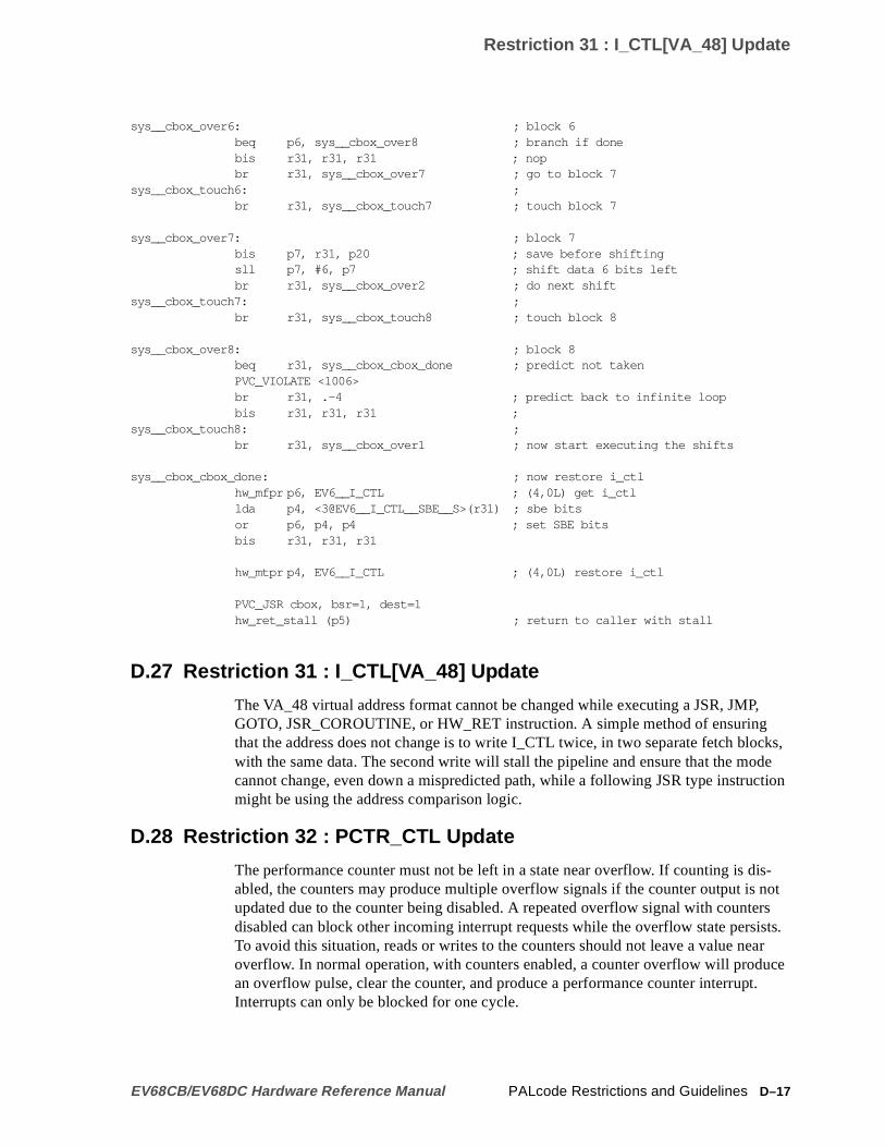
Restriction 31 : I_CTL[VA_48] Update
cks,detion
otrssts.rce.
sys__cbox_over6: ; block 6beq p6, sys__cbox_over8 ; branch if donebis r31, r31, r31 ; nopbr r31, sys__cbox_over7 ; go to block 7
sys__cbox_touch6: ;br r31, sys__cbox_touch7 ; touch block 7
sys__cbox_over7: ; block 7bis p7, r31, p20 ; save before shiftingsll p7, #6, p7 ; shift data 6 bits leftbr r31, sys__cbox_over2 ; do next shift
sys__cbox_touch7: ;br r31, sys__cbox_touch8 ; touch block 8
sys__cbox_over8: ; block 8beq r31, sys__cbox_cbox_done ; predict not takenPVC_VIOLATE <1006>br r31, .-4 ; predict back to infinite loopbis r31, r31, r31 ;
sys__cbox_touch8: ;br r31, sys__cbox_over1 ; now start executing the shifts
sys__cbox_cbox_done: ; now restore i_ctlhw_mfpr p6, EV6__I_CTL ; (4,0L) get i_ctllda p4, <3@EV6__I_CTL__SBE__S>(r31) ; sbe bitsor p6, p4, p4 ; set SBE bitsbis r31, r31, r31
hw_mtpr p4, EV6__I_CTL ; (4,0L) restore i_ctl
PVC_JSR cbox, bsr=1, dest=1hw_ret_stall (p5) ; return to caller with stall
D.27 Restriction 31 : I_CTL[VA_48] Update
The VA_48 virtual address format cannot be changed while executing a JSR, JMP,GOTO, JSR_COROUTINE, or HW_RET instruction. A simple method of ensuringthat the address does not change is to write I_CTL twice, in two separate fetch blowith the same data. The second write will stall the pipeline and ensure that the mocannot change, even down a mispredicted path, while a following JSR type instrucmight be using the address comparison logic.
D.28 Restriction 32 : PCTR_CTL Update
The performance counter must not be left in a state near overflow. If counting is dis-abled, the counters may produce multiple overflow signals if the counter output is nupdated due to the counter being disabled. A repeated overflow signal with countedisabled can block other incoming interrupt requests while the overflow state persiTo avoid this situation, reads or writes to the counters should not leave a value neaoverflow. In normal operation, with counters enabled, a counter overflow will produan overflow pulse, clear the counter, and produce a performance counter interruptInterrupts can only be blocked for one cycle.
EV68CB/EV68DC Hardware Reference Manual PALcode Restrictions and Guidelines D–17

Restriction 33 : HW_LD Physical/Lock Use
ldheillr
y tost ishe
uenturinged
-rs
loca-
e. If
rop-sver-
i-
D.29 Restriction 33 : HW_LD Physical/Lock Use
The HW_LD physical/lock instruction must be one of the first three instructions in aquad-instruction aligned fetch block. A pipelineerror can occur if the HW_LDphysi-cal/lock is fetched as the fourth instruction of the fetch block.
D.30 Restriction 34 : Writing Multiple ITB Entries in the Same PAL-code Flow
Before a PALcode flow writes multiple ITB entries, additional scoreboard bits shoube set to avoid possible corruption of the TAG IPR prior to final update in the ITB. Taddition of scoreboard bits 0 and 4 to the standard scoreboard bit 6 for ITB_TAG wprevent subsequent HW_MTPR ITB_TAG writes from changing the staging registeTAG value prior to retirement of the HW_MTPR ITB_PTE that triggers the final ITBupdate.
D.31 Guideline 35 : HW_INT_CLR Update
When writing the HW_INT_CLR IPR to clear interrupt requests, it may be necessarwrite the same value twice in distinct fetch blocks to ensure that the interrupt requecleared before exiting PALcode. A second write will cause a scoreboard stall until tfirst write retires, creating a convenient synchronization with the PALmode exit.
D.32 Restriction 36 : Updating I_CTL[SDE]
A software interlock is required between updates of the I_CTL[SDE] and a subseqinstruction fetch that may use any destination registers. A suggested method of ensthis interlock is to use two MTPR I_CTL instructions in separate fetch blocks, followby three more fetch blocks of non-NOP instructions.
D.33 Restriction 37 : Updating VA_CTL[VA_48]
A software interlock is required between updates of the VA_CTL[VA_48] and following LD or ST instructions. This is necessary since the VA_CTL update will not occuuntil the HW_MTPR VA_CTL instruction retires. A sufficient method of ensuring thiinterlock is to write the VA_CTL with the same data in two successive fetch blocks,causing a mapper stall. The dependant LD or ST instructions can be placed in anytion of the second fetch block.
D.34 Restriction 38 : Updating PCTR_CTL
When updating the PCTR_CTL, it may be necessary to write the update value twicthe counter being updated is currently disabled by way of the respective I_CTL orPCTX bits, the value must be written twice to ensure that the counter overflow is perly cleared. The overflow bit is conditionally latched using the same write enable athe counter update, so an additional write of the counter value will ensure that the oflow logic accuratelyreflects the addition of the new counter value plus the input condtions. The new update value must not be within one cycle of overflow (within 16 forSL0, within 4 for SL1) as required by Section D.28.
D–18 PALcode Restrictions and Guidelines EV68CB/EV68DC Hardware Reference Manual

Guideline 39: Writing Multiple DTB Entries in the Same PAL Flow
r-
upbits):
cheongr non-
ivemory.
D.35 Guideline 39: Writing Multiple DTB Entries in the Same PALFlow
If a PALcode flow intends to write multiple DTB entries (as would occur in a doublemiss), it must take care to keep subsequent HW_MTPR DTB_TAGx writes from corupting the staging register TAG values prior to retirement of the HW_MTPRDTB_PTEx, which triggers the final DTB update.
For example, in the double miss DTB flow, the following code could be used to holdthe return to the single miss flow (the numbers in parentheses are the scoreboard
hw_mtpr r4, EV6__DTB_TAG0 ; (2&6) write tag0hw_mtpr r4, EV6__DTB_TAG1 ; (1&5) write tag 1hw_mtpr r5, EV6__DTB_PTE0 ; (0&4) write pte0hw_mtpr r5, EV6__DTB_PTE1 ; (3&7) write pte1
bis r31, r31, r31 ; force new fetch blockbis r31, r31, r31bis r31, r31, r31hw_mtpr r31, <EV6__MM_STAT ! ^x80> ; (7) wait for pte write
hw_ret (r6) ; return to single miss
D.36 Restriction 40: Scrubbing a Single-Bit Error
On Bcache and Memory single bit errors on Icache fills, the hardware flushes theIcache, but the PALcode must scrub the block in the Bcache and memory. On Bcaand Memory single bit errors on Dcache fills, the hardware scrubs the Dcache as las the error was on a target quadword, but the PALcode must scrub the Dcache fotarget quadwords, and must in general scrub the block in the Bcache and memory.
The scrub consists of reading each quadword in the block, with at least one exclusaccess load/store to ensure the corrected data will be scrubbed in Bcache and meThe scrub itself causes a CRD to be flagged, which is cleared by the PALcode beforeexiting to native mode.
; Sample code for scrubbing a single bit error.;; Since we only have the block address, and the hardware only corrects; target quadwords, we read each quadword.; In order to ensure eviction to bcache and memory, a store; is needed to mark the block dirty. An exclusive access is; used to ensure we scrub in main memory. Virtual access is; used because of restrictions in use of hw_ld/hw_st lock; instructions.; After the scrub, read the cbox chain again.; The scrub will cause a crd, but will get cleared with a write; to hw_int_clr.;; Current state:; r5 base of crd logout frame;
hw_ldq/p r4, MCHK_CRD__C_ADDR(r5) ; get address backbis r31, r31, r31bis r31, r31, r31bis r31, r31, r31
EV68CB/EV68DC Hardware Reference Manual PALcode Restrictions and Guidelines D–19

Restriction 40: Scrubbing a Single-Bit Error
hw_mtpr r31, EV6__DTB_IA ; (7,1L) flush dtblda r20, ^x3301(r31) ; set WE, REbis r31, r31, r31bis r31, r31, r31
hw_mtpr r31, <EV6__MM_STAT ! ^x80> ; wait for retiresrl r4, #13, r6 ; shift byte offsetsll r6, #EV6__DTB_PTE0__PFN__S, r6 ; shift into positionbis r6, r20, r6 ; produce pte
hw_mtpr r4, EV6__DTB_TAG0 ; (2&6,0L) write tag0hw_mtpr r4, EV6__DTB_TAG1 ; (1&5,1L) write tag1hw_mtpr r6, EV6__DTB_PTE0 ; (0&4,0L) write pte0hw_mtpr r6, EV6__DTB_PTE1 ; (3&7,1L) write pte1
mb ; quiet before we startbis r31, r31, r31bis r31, r31, r31bis r31, r31, r31
ldq r6, ^x00(r4) ; re-read the bad block QW #0ldq r6, ^x08(r4) ; re-read the bad block QW #1ldq r6, ^x10(r4) ; re-read the bad block QW #2ldq r6, ^x18(r4) ; re-read the bad block QW #3ldq r6, ^x20(r4) ; re-read the bad block QW #4ldq r6, ^x28(r4) ; re-read the bad block QW #5ldq r6, ^x30(r4) ; re-read the bad block QW #6mb ; no other mem-ops till done
ldq_l r6, ^x38(r4) ; re-read the bad block QW #7stq_c r6, ^x38(r4) ; now store it to force scrubmband r6, r31, r6 ; consumer of above
beq r6, sys__crd_scrub_done ; these 2 lines......br r31, .-4 ; .....stop pre-fetching
sys__crd_scrub_done:bsr r7, sys__cbox ; clean the cbox error chainbis r31, r31, r31
hw_mtpr r31, EV6__DTB_IA ; (7,1L) flush dtbbis r31, r31, r31bis r31, r31, r31bis r31, r31, r31
hw_mtpr r31, <EV6__MM_STAT ! ^x80> ; wait for retirebis r31, #1, r7 ; get a 1sll r7, #EV6__HW_INT_CLR__CR__S, r7 ; shift into positionhw_mtpr r7, EV6__HW_INT_CLR ; (4,0L) clear crd
lda r7, EV6__DC_STAT_W1C_CRD(r31) ; W1C bitshw_mtpr r7, EV6__DC_STAT ; (6,0L)bis r31, r31 ,r31bis r31, r31 ,r31
hw_mtpr r31, <EV6__MM_STAT ! ^x50> ; stall till they retire
D–20 PALcode Restrictions and Guidelines EV68CB/EV68DC Hardware Reference Manual

Restriction 41: MTPR ITB_TAG, MTPR ITB_PTE Must Be in the Same Fetch Block
is-rom
PR
s.ex-
la-
D.37 Restriction 41: MTPR ITB_TAG, MTPR ITB_PTE Must Be in theSame Fetch Block
Write the ITB_TAG and ITB_PTE registers in the same fetch block. This avoids amispredict path write of invalid data to the ITB_TAG register.
D.38 Restriction 42: Updating VA_CTL, CC_CTL, or CC IPRs
When writing to the VA_CTL, CC_CTL, or CC IPRs, write the same value twice in dtinct fetch blocks. This ensures that the instruction is retired before any mispredict fa younger branch, DTB miss trap, or hw_ret_stall.
D.39 Restriction 43: No Trappable Instructions Along withHW_MTPR
There cannot be any mispredictable/trappable instructions together with an HW_MTin the current fetch block.
D.40 Restriction 44: Not Applicable to the EV68CB/EV68DC
D.41 Restriction 45: No HW_JMP or JMP Instructions in PALcode
Do not include HW_JMP or JMP instructions in PALcode; use HW_RET instead.
HW_JMP always predicts in PALmode, and may mispredict to random cache blockThis may cause speculative code to begin executing in PALmode and may have unpected side effects such as I/O stream references.
HW_RET always predicts in native mode, and when it mispredicts, it avoids specutive execution in PALmode.
EV68CB/EV68DC Hardware Reference Manual PALcode Restrictions and Guidelines D–21

Restriction 46: Avoiding Livelocks in Speculative Load CRD Handlers
w ofrror,
ads
k a
samee
e
ruc-
ed/
atheing-by
ess
D.42 Restriction 46: Avoiding Livelocks in Speculative Load CRDHandlers
Speculative load CRD handlers that release from the interrupt without scrubbing acache block could suffer from the following livelock condition:
1. An initial error on a speculative load forces a CRD interrupt.
2. The CRD releases without scrubbing the block. A speculative load in the shadothe hw_ret (or hw_ret_stall) touches a Dcache location that has the single-bit eforcing a CRD.
3. The CRD handler is entered again immediately.
4. Go to (2).
This problem can be avoided if all jumps in the CRD handler path for speculative louse the following sequence:
mb ; make sure hw_ret goes
ALIGN_FETCH_BLOCK <^x47FF041F>mulq p6, #1, p6 ; Hold up loadsmulq p6, #1, p6 ; Hold up loadshw_mtpr p6, <EV6__MM_STAT ! ^x44> ; Hold up loadsPVC_VIOLATE<43> ; Ignore restriction 43hw_ret_stall (p23) ; Return
This sequence prevents speculative loads from issuing in the shadow of thehw_ret_stall. Note that it is a violation of restriction 4 to have in the same fetch blocMTPR that specifies scoreboard bit 2 (an explicit writer in the memory operationgroup) and a HW_RET (an implicit reader in the memory operation group). Under nor-mal circumstances, the intention would be for a HW_RET to wait until the MTPRissues, and that can only be enforced by putting the two instructions in different fetchblocks. In this case, the intention is for the HW_RET to issuebeforethe MTPR. Thehardware does not enforce the scoreboarding when the two instructions are in thefetch block, and thus the HW_RET can issue and mispredict before any speculativloads (which are held up by the MTPR) can issue.
D.43 Restriction 47: Cache Eviction for Single-Bit Cache Errors
A live lock can occur if issuing instructions out-of-order causes a floating-point storinstruction (with sberr) to replay trap.
A hardware mechanism exists that keeps track of replayed floating-point store insttions, and cancels the dirty register check. See Section D.5 for more details.
If the floating-point store instruction has an sberr and the CRD_HANDLER is enterexited before the instruction is replayed, the mechanism will lose track of the instruc-tion. When the instruction is replayed, the dirty register check is not canceled, andreplay trap occurs, causing the floating-point store instruction to continually replaytrap until the sberr is evicted from cache. The sberr will not evict, because the floatpoint store instruction is killed by the replay trap. Killed instructions are not scrubedthe Error Recovery Machine, and CBOX_ERR[C_ADDR] may not contain the addrof the sberr. Because CBOX_ERR[C_ADDR] is not guaranteed, the CRD_HANDLERmight not evict the sberr.
D–22 PALcode Restrictions and Guidelines EV68CB/EV68DC Hardware Reference Manual

Restriction 47: Cache Eviction for Single-Bit Cache Errors
to
If "CBOX_ERR[C_ADDR]" has not changed when the CRD_HANDLER is re-entered, or "CBOX_ERR[C_STAT] == 0x0", all cache locations should to be evictedavoid the live lock described above.; Sample code for evicting cache.; This method loads a 64K block, then exits the CRD_HANDLER; to check if the sberr has been evicted. If not it loads the next 64K block.; In the sample code below,; sx is a shadow register; ldi is a macro that loads a 64-bit constant into the specified register
full_scrub:hw_ldq/p s5, 104(r31)
ldi s1, ^x200 ; Loop dec valueldi s2, ^x1C0 ; Start offsetldi s3, ^x10000 ; Block size (64K -> size of dcache)ldi s4, ^x2000000 ; 2X bcache size
addq s3,s5,s5ble s5, s4, <.+4> ; Skip next instruction if ADDR
; .le. 2X bcachebis r31, r31, s5 ; Set ADDR = 0x0hw_stq/p s5, 104(r31) ; Store ADDR for next pass thrusubq s5, s2, s5mb ; Make sure no speculative loads
; happen in the CRD handler.align 4, NOP_OPCODE ; |blbc r31, <.+4> ; |br r31, <.-4> ; V.align 4, NOP_OPCODE ; Make sure no speculative loads
; happen in the CRD handler
next_reread:; ******** four cache blocks
; Evict dcache by prefetching to all dcache indexes.; use 'hw_ldl r31 xxxx' Normal Prefetch; Do not use 'hw_ldq/p r31 xxx' Prefetch,; Evict Next because this will always access the same set in dcache.hw_ldl/p r31,̂ x1C0(s5) ; Re-read the bad block QW #0hw_ldl/p r31,̂ x180(s5) ; Re-read the bad block QW #0hw_ldl/p r31,̂ x140(s5) ; Re-read the bad block QW #0hw_ldl/p r31,̂ x100(s5) ; Re-read the bad block QW #0
hw_ldl/p r31,̂ xC0(s5) ; Re-read the bad block QW #0hw_ldl/p r31,̂ x80(s5) ; Re-read the bad block QW #0hw_ldl/p r31,̂ x40(s5) ; Re-read the bad block QW #0hw_ldl/p r31,̂ x00(s5) ; Re-read the bad block QW #0
subq s5, s1, s5 ; Decrement addrsubq s3, s1, s3 ; Decrement counterble s3, <.+4>br r31, next_rereadbsr s7, sys__cbox ; Read and clean cbox error ipr
EV68CB/EV68DC Hardware Reference Manual PALcode Restrictions and Guidelines D–23

Restriction 48: MB Bracketing of Dcache Writes to Force Bad Data ECC and Force
-qui-
D.44 Restriction 48: MB Bracketing of Dcache Writes to Force BadData ECC and Force Bad Tag Parity
Writes to DC_CTL[F_BAD_DECC] and DC_CTL[DCDAT_ERR_EN] must be bracketed by MB instructions to quiesce the memory system. The Istream must also beesced before and during the sequence, as described in Section D.26.
D–24 PALcode Restrictions and Guidelines EV68CB/EV68DC Hardware Reference Manual

EEV68CB/EV68DC-to-Bcache Pad Interface
This appendix provides the pad interface between theEV68CB/EV68DC and BcacheSSRAMs.
E.1 Forwarding Clock Pad Groupings
Table E–1 lists the correspondance between the clock signals for the EV68CB/EV68DC and Bcache (late-write non-bursting and dual-data rate) SSRAMs.
Table E–1 Bcache Forwarding Clock Pad Groupings
Pad and Pad Input Clock Output Clocks
BcData_H[71:64,7:0] BcDataInClk_H[0] BcDataOutClk_x[0]
BcCheck_H[8,0] BcDataInClk_H[0] BcDataOutClk_x[0]
BcData_H[79:72,15:8] BcDataInClk_H[1] BcDataOutClk_x[0]
BcCheck_H[9,1] BcDataInClk_H[1] BcDataOutClk_x[0]
BcData_H[87:80,23:16] BcDataInClk_H[2] BcDataOutClk_x[1]
BcCheck_H[10,2] BcDataInClk_H[2] BcDataOutClk_x[1]
BcData_H[95:88,31:24] BcDataInClk_H[3] BcDataOutClk_x[1]
BcCheck_H[11,3] BcDataInClk_H[3] BcDataOutClk_x[1]
BcData_H[103:96,39:32] BcDataInClk_H[4] BcDataOutClk_x[2]
BcCheck_H[12,4] BcDataInClk_H[4] BcDataOutClk_x[2]
BcData_H[111:104,47:40] BcDataInClk_H[5] BcDataOutClk_x[2]
BcCheck_H[13,5] BcDataInClk_H[5] BcDataOutClk_x[2]
BcData_H[119:112,55:48] BcDataInClk_H[6] BcDataOutClk_x[3]
BcCheck_H[14.6] BcDataInClk_H[6] BcDataOutClk_x[3]
BcData_H[127:120,63:56] BcDataInClk_H[7] BcDataOutClk_x[3]
BcCheck_H[15,7] BcDataInClk_H[7] BcDataOutClk_x[3]
BcTag_H[42:20] BcTagInClk_H BcTagOutClk_x
BcTagParity_H BcTagInClk_H BcTagOutClk_x
EV68CB/EV68DC Hardware Reference Manual EV68CB/EV68DC-to-Bcache Pad Interface E–1

Late-Write Non-Bursting SSRAMs
AMsma-
E.2 Late-Write Non-Bursting SSRAMs
Table E–2 provides the data pad connections between late-write non-bursting SSRand the EV68CB/EV68DC or the system board. Table E–3 provides the same infortion for the tag pads.
Data Pad Usage
Tag Pad Usage
Unused Bcache tag pads should be pulled to ground through a 200-ohm resistor.
BcTagShared_H BcTagInClk_H BcTagOutClk_x
BcTagDirty_H BcTagInClk_H BcTagOutClk_ x
BcTagValid_H BcTagInClk_H BcTagOutClk_x
Table E–2 Late-Write Non-Bursting SSRAMs Data Pad Usage
EV68CB/EV68DC Signal Name or BoardConnection Late-Write SSRAM Data Pad Name
BcAdd_H[21:4] SA_H[17:0]
BcDataOutClk_H[3:0] CK_H
Set from board to 1/2 the EV68CB/EV68DC corevoltage
CK_L
BcData_H[127:0]/BcCheck_H[15:0] DQx
BcDataWr_L SW_L
Unconnected Tck_H
Unconnected Tdo_H
Unconnected Tms_H
Unconnected Tdi_H
From board, pull down to VSS G_L
From board, pull down to VSS SBx_L
From board, pull down to VSS orBcDataOE_L SS_L (Vendor dependent)
Table E–3 Late-Write Non-Bursting SSRAMs Tag Pad Usage
EV68CB/EV68DC Signal Name or BoardConnection Late-Write SSRAM Tag Pad Name
BcAdd_H[22:6] SA_H[16:0]
BcTag_H[42:20] DQx
BcTagOE_L or from board, pull down to VSS SS_L (Vendor dependent)
BcTagWr_L SW_L
From board, pull down toVSS SBx_L
Table E–1 Bcache Forwarding Clock Pad Groupings (Continued)
Pad and Pad Input Clock Output Clocks
E–2 EV68CB/EV68DC-to-Bcache Pad Interface EV68CB/EV68DC Hardware Reference Manual

Dual-Data Rate SSRAMs
d theor
E.3 Dual-Data Rate SSRAMs
Table E–4 provides the data pad connections between dual-data rate SSRAMs anEV68CB/EV68DC or the system board. Table E–5 provides the same information fthe tag pads.
Data Pad Usage
BcTagOutClk_H CK_H
Set from board to 1/2 the EV68CB/EV68DC corevoltage
CK_L
Set from board to 1/2 the EV68CB/EV68DC corevoltage
VREF1_HVREF2_H
Set from board (implementation dependent) ZQ_H
BcTagValid_H DQx
BcTagDirty_H DQx
BcTagShared_H DQx
Unconnected TMS_H
Unconnected TDI_H
Unconnected TCK_H
Unconnected TDC_H
Table E–4 Dual-Data Rate SSRAM Data Pad Usage
EV68CB/EV68DC Signal Name or BoardConnection Dual-Data Rate SSRAM Data Pad Name
BcAdd_H[21:4] SA_H[17:0]
BcData_H[33:20]/BcCheck_H[15:0]
DQx
BcLoad_L LD_L (B1)
BcDataWr_L R/W_L(B2)
From board, pulled up to VDD LBO_L
From board, pulled down to VSS Q_L
BcDataInClk_H CQ_H
BcDataOutClk_H CK_H
BcDataOutClk_L CK_L
Set from board to 1/2 the EV68CB/EV68DCcore voltage
VREF1_HVREF2_H
Set from board (implementation-dependent) ZQ_H
Unconnected or terminated CQ_L
Table E–3 Late-Write Non-Bursting SSRAMs Tag Pad Usage (Continued)
EV68CB/EV68DC Signal Name or BoardConnection Late-Write SSRAM Tag Pad Name
EV68CB/EV68DC Hardware Reference Manual EV68CB/EV68DC-to-Bcache Pad Interface E–3

Dual-Data Rate SSRAMs
Tag Pin Usage
Unused Bcache tag pins should be pulled to ground through a 200-ohm resistor.
From board, pulled up toVDD TCK_H
Unconnected TDO_H
From board, pulled up to VDD TMS_H
From board, pulled up to VDD TDI_H
Unconnected or pulled down to VSS TRST_L
BcDataOE_L OE_L (G_L)
From board, pulled down to VSS SD/DD_L (B3)
Table E–5 Dual-Date Rate SSRAM Tag Pin Usage
EV68CB/EV68DC Signal Name or BoardConnection Dual-Data Rate SSRAM Tag Pad Name
BcAdd_H[23:6] SA_H[17:0]
BcTag_H[33:20] DQx
BcTagOE_L LD_L (B1)
BcTagWr_L R/W_L (B2)
From board, pulled up to VDD LBO_L
From board, pulled down to VSS Q_LSA[19:18]
BcTagInClk_H CQ_H
BcTagOutClk_H CK_H
BcTagOutClk_L CK_L
Set from board to 1/2 core voltage VREF1_HVREF2_H
Set from board (implementation-dependent) ZQ_H
BcTagValid_H DQx
BcTagDirty_H DQx
BcTagShared_H DQx
BcTagParity_H DQx
Unconnected or terminated CQ_L
From board, pulled up to VDD TCK_H
Unconnected TDO_H
From board, pulled up to VDD TMS_H
From board, pulled up to VDD TDI_H
Table E–4 Dual-Data Rate SSRAM Data Pad Usage (Continued)
EV68CB/EV68DC Signal Name or BoardConnection Dual-Data Rate SSRAM Data Pad Name
E–4 EV68CB/EV68DC-to-Bcache Pad Interface EV68CB/EV68DC Hardware Reference Manual

Dual-Data Rate SSRAMs
Unconnected TRST_L
From board, pulled down to VSS OE_L (G_L)
From board, pulled up to VDD SD/DD_L (B3)
Table E–5 Dual-Date Rate SSRAM Tag Pin Usage (Continued)
EV68CB/EV68DC Signal Name or BoardConnection Dual-Data Rate SSRAM Tag Pad Name
EV68CB/EV68DC Hardware Reference Manual EV68CB/EV68DC-to-Bcache Pad Interface E–5


the
edASNsss
N
s
Glossary
This glossary provides definitions for specific terms and acronyms associated withAlpha EV68CB/EV68DC microprocessor and chips in general.
abort
The unit stops the operation it is performing, without saving status, to perform someother operation.
address space number (ASN)
An optionally implemented register used to reduce the need for invalidation of cachaddress translations for process-specific addresses when a context switch occurs.are processor specific; the hardware makes no attempt to maintain coherency acromultiple processors.
address translation
The process of mapping addresses from one address space to another.
ALIGNED
A datum of size 2**N is stored in memory at a byte address that is a multiple of 2**(that is, one that has N low-order zeros).
ALU
Arithmetic logic unit.
ANSI
American National Standards Institute. An organization that develops and publishestandards for the computer industry.
ASIC
Application-specific integrated circuit.
ASM
Address space match.
ASN
Seeaddress space number.
assert
To cause a signal to change to its logical true state.
AST
Seeasynchronous system trap.
EV68CB/EV68DC Hardware Reference Manual Glossary –1

ocificuptsrou-ter-
nel.
c-
1.
s).h theys-is
ck
asynchronous system trap (AST)
A software-simulated interrupt to a user-defined routine. ASTs enable a user process tbe notified asynchronously, with respect to that process, of the occurrence of a speevent. If a user process has defined an AST routine for an event, the system interrthe process and executes the AST routine when that event occurs. When the ASTtine exits, the system resumes execution of the process at the point where it was inrupted.
bandwidth
Bandwidth is often used to express the rate of data transfer in a bus or an I/O chan
barrier transaction
A transaction on the external interface as a result of an MB (memory barrier) instrution.
Bcache
Seesecond-level cache.
bidirectional
Flowing in two directions. The buses are bidirectional; they carryboth input and outputsignals.
BiSI
Built-in self-initialization.
BiST
Built-in self-test.
bit
Binary digit. The smallest unit of data in a binary notation system, designated as 0 or
bit time
The total time that a signal conveys a single valid piece of information (specified in nAll data and commands are associated with a clock and the receiver’s latch on botrise and fall of the clock. Bit times are a multiple of the EV68CB/EV68DC clocks. Stems must produce a bit time identical to EV68CB/EV68DC’s bit time. The bit timeone-half the period of the forwarding clock.
BIU
Bus interface unit.SeeCbox.
Block exchange
Memory feature that improves bus bandwidth by paralleling a cache victim write-bawith a cache miss fill.
board-level cache
See second-level cache.
Glossary –2 EV68CB/EV68DC Hardware Reference Manual

r
on-
tsa, and
ered
con-
d inified,tain-nsis-
ain
boot
Short for bootstrap. Loading an operating system into memory is called booting.
BSR
Boundary-scan register.
buffer
An internal memory area used for temporary storage of data records during input ooutput operations.
bugcheck
A software condition, usually the response to software’s detection of an “internal incsistency,” which results in the execution of the system bugcheck code.
bus
A group of signals that consists of many transmission lines or wires. It interconneccomputer system components to provide communications paths for addresses, datcontrol information.
byte
Eight contiguous bits starting on an addressable byte boundary. The bits are numbright to left, 0 through 7.
byte granularity
Memory systems are said to have byte granularity if adjacent bytes can be writtencurrently and independently by different processes or processors.
cache
Seecache memory.
cache block
The smallest unit of storage that can be allocated or manipulated in a cache. Alsoknown as a cache line.
cache coherence
Maintaining cache coherence requires that when a processor accesses data cacheanother processor, it must not receive incorrect data and when cached data is modall other processors that access that data receive modified data. Schemes for maining consistency can be implemented in hardware or software. Also called cache cotency.
cache fill
An operation that loads an entire cache block by using multiple read cycles from mmemory.
cache flush
An operation that marks all cache blocks as invalid.
EV68CB/EV68DC Hardware Reference Manual Glossary –3

he
sed toedre
or. Acopiesory in
ts.
ons.
ber
een
cache hit
The status returned when a logic unit probes a cache memory and finds a valid cacentry at the probed address.
cache interference
The result of an operation that adversely affects the mechanisms and procedures ukeep frequently used items in a cache. Such interference may cause frequently usitems to be removed from a cache or incur significant overhead operations to ensucorrect results. Either action hampers performance.
cache line
Seecache block.
cache line buffer
A buffer used to store a block of cache memory.
cache memory
A small, high-speed memory placed between slower main memory and the processcache increases effective memory transfer rates and processor speed. It containsof data recently used by the processor and fetches several bytes of data from memanticipation that the processor will access the next sequential series of bytes. TheEV68CB/EV68DC microprocessor contains two onchip internal caches.See alsowrite-through cache and write-back cache.
cache miss
The status returned when cache memory is probed with no valid cache entry at theprobed address.
CALL_PAL instructions
Special instructions used to invoke PALcode.
Cbox
External cache and system interface unit. Controls the Bcache and the system por
central processing unit (CPU)
The unit of the computer that is responsible for interpreting and executing instructi
CISC
Complex instruction set computing. An instruction set that consists of a large numof complex instructions.Contrast withRISC.
clean
In the cache of a system bus node, refers to a cache line that is valid but has not bwritten.
clock
A signal used to synchronize the circuits in a computer.
Glossary –4 EV68CB/EV68DC Hardware Reference Manual

that
ni-
struc-
lling
clock offset (or clkoffset)
The delay intentionally added to the forwarded clock to meet the setup and holdrequirements at the Receive Flop.
CMOS
Complementary metal-oxide semiconductor. A silicon device formed by a processcombines PMOS and NMOS semiconductor material.
conditional branch instructions
Instructions that test a register for positive/negative or forzero/nonzero. They can alsotest integer registers for even/odd.
control and status register (CSR)
A device or controller register that resides in the processor’s I/O space. The CSR itiates device activity and records its status.
CPI
Cycles per instruction.
CPU
Seecentral processing unit.
CSR
Seecontrol and status register.
cycle
One clock interval.
data bus
A group of wires that carry data.
Dcache
Data cache. A cache reserved for storage of data. The Dcache does not contain intions.
DDR
Dual-data rate. A dual-data rate SSRAM can provide data on both the rising and faedges of the clock signal.
denormal
An IEEE floating-point bit pattern that represents a number whose magnitude liesbetween zero and the smallest finite number.
DIP
Dual inline package.
EV68CB/EV68DC Hardware Reference Manual Glossary –5

yne
that
must
n
).
be
direct-mapping cache
A cache organization in which only one address comparison is needed to locate andata in the cache, because any block of main memory data can be placed in only opossible position in the cache.
direct memory access (DMA)
Access to memory by an I/O device that does not require processor intervention.
dirty
One status item for a cache block. The cache block is valid and has been written soit may differ from the copy in system main memory.
dirty victim
Used in reference to a cache block in the cache of asystem bus node. The cache blockis valid but is about to be replaced due to a cache block resource conflict. The datatherefore be written to memory.
DMA
Seedirect memory access.
DRAM
Dynamic random-access memory. Read/write memory that must berefreshed (readfrom or written to) periodically to maintain the storage of information.
DTB
Data translation buffer.Also defined asDstream translation buffer.
DTL
Diode-transistor logic.
dual issue
Two instructions are issued, in parallel, during the same microprocessor cycle. Theinstructions use different resources and so do not conflict.
ECC
Error correction code. Code and algorithms used by logic to facilitate error detectioand correction. See alsoECC error.
ECC error
An error detected by ECC logic, to indicate that data (or the protected “entity”) hasbeen corrupted. The error may be correctable (soft error) or uncorrectable (hard error
ECL
Emitter-coupled logic.
EEPROM
Electrically erasable programmable read-only memory. A memory device that canbyte-erased, written to, and read from.Contrast withFEPROM.
Glossary –6 EV68CB/EV68DC Hardware Reference Manual

-
al-
nt
e bitges
is
ncy.lock
sys-eset
external cache
Seesecond-level cache.
FEPROM
Flash-erasable programmable read-only memory. FEPROMs can be bank- or bulkerased.Contrast withEEPROM.
FET
Field-effect transistor.
FEU
The unit within the EV68CB/EV68DC microprocessor that performs floating-point cculations.
firmware
Machine instructions stored in nonvolatile memory.
floating point
A number system in which the position of the radix point is indicated by the exponepart and another part represents the significant digits or fractional part.
flush
Seecache flush.
forwarded clock
A single-ended differential signal that is aligned with its associated fields. The for-warded clock is sourced and aligned by the sender with a period that is two times thtime. Forwarded clocks must be 50% duty cycle clocks whose rising and falling edare aligned with the changing edge of the data.
FPGA
Field-programmable gate array.
FPLA
Field-programmable logicarray.
FQ
Floating-point issue queue.
framing clock
The framing clock defines the start of a transmission either from the system to theEV68CB/EV68DC or from the EV68CB/EV68DC to the system. The framing clocka power-of-2 multiple of the EV68CB/EV68DCGCLK frequency, and is usually thesystem clock. The framing clock and the input oscillator can have the same frequeThe add_frame_select IPR sets that ratio of bit times to framing clock. The frame ccould have a period that is four times the bit time with a add_frame_select of 2X.Transfers begin on the rising and falling edge of the frame clock. This is useful fortems that have system clocks with a period too small to perform the synchronous r
EV68CB/EV68DC Hardware Reference Manual Glossary –7

nd/
d and/
r not
, or-bitares.
d
ver
-
of the clock forward logic. Additionally, the framing clock can have a period that isless than, equal to, or greater than the time it takes to send a full four cycle commaaddress.
GCLK
Global clock within the EV68CB/EV68DC.
granularity
A characteristic of storage systems that defines the amount of data that can be reaor written with a single instruction, or read and/or written independently.
hardware interrupt request (HIR)
An interrupt generated by a peripheral device.
high-impedance state
An electrical state of high resistance to current flow, which makes the device appeaphysically connected to the circuit.
hit
Seecache hit.
Icache
Instruction cache. A cache reserved for storage of instructions. One of the threeareas ofprimary cache (located on the EV68CB/EV68DC) used to store instructions. TheIcache contains 8KB of memory space. It is a direct-mapped cache. Icache blockslines, contain 32 bytes of instruction stream data with associated tag as well as a 6ASM field and an 8-bit branch history field per block. Icache does not contain hardwfor maintaining cache coherency with memory and is unaffected by the invalidate bu
IDU
A logic unit within the EV68CB/EV68DC microprocessor that fetches, decodes, anissues instructions. It also controls the microprocessor pipeline.
IEEE Standard 754
A set of formats and operations that apply to floating-point numbers. The formats co32-, 64-, and 80-bit operand sizes.
IEEE Standard 1149.1
A standard for the Test Access Port and Boundary Scan Architecture used in boardlevel manufacturing test procedures.
Inf
Infinity.
INT nn
The term INTnn, wherenn is one of 2, 4, 8, 16, 32, or 64, refers to a data field size ofnncontiguous NATURALLY ALIGNED bytes. For example, INT4refers to a NATU-RALLY ALIGNED longword.
Glossary –8 EV68CB/EV68DC Hardware Reference Manual

ard-lecks
ro-mory
ed
interface reset
A synchronously received reset signal that is used to preset and start the clock forwing circuitry. During this reset, all forwarded clocks are stopped and the presettabcount values are applied to the counters; then, some number of cycles later, the cloare enabled and are free running.
Internal processor register (IPR)
Special registers that are used to configure options or report status.
IOWB
I/O write buffer.
IPGA
Interstitial pin grid array.
IQ
Integer issue queue.
ITB
Instruction translation buffer.
JFET
Junction field-effect transistor.
latency
The amount of time it takes the system to respond to an event.
LCC
Leadless chip carrier.
LFSR
Linear feedback shift register.
load/store architecture
A characteristic of a machine architecture where data items are first loaded into a pcessor register, operated on, and then stored back to memory. No operations on meother than load and store are provided by the instruction set.
longword (LW)
Four contiguous bytes starting on an arbitrary byte boundary. The bits are numberfrom right to left, 0 through 31.
LQ
Load queue.
LSB
Least significant bit.
EV68CB/EV68DC Hardware Reference Manual Glossary –9

ana-
nin
colred
are
machine check
An operating system action triggered by certain system hardware-detectederrors thatcan be fatal to system operation. Once triggered, machine check handler softwarelyzes the error.
MAF
Miss address file.
main memory
The large memory, external to the microprocessor, used for holding most instructiocode and data. Usually built from cost-effective DRAM memory chips. May be usedconnection with the microprocessor’s internalcaches and an external cache.
masked write
A write cycle that only updates a subset of a nominal data block.
MBO
Seemust be one.
Mbox
This section of the processor unit performs address translation, interfaces to theDcache, and performs several other functions.
MBZ
Seemust be zero.
MESI protocol
A cache consistency protocol with full support for multiprocessing. The MESI protoconsists of four states that define whether a block is modified (M), exclusive (E), sha(S), or invalid (I).
MIPS
Millions of instructions per second.
miss
Seecache miss.
module
A board on which logic devices (such as transistors, resistors, and memory chips)mounted and connected to perform a specific system function.
module-level cache
Seesecond-level cache.
MOS
Metal-oxide semiconductor.
MOSFET
Metal-oxide semiconductor field-effect transistor.
Glossary –10 EV68CB/EV68DC Hardware Reference Manual

e col-
ed to
han
ze ofess
ered
MSI
Medium-scale integration.
multiprocessing
A processing method that replicates the sequential computer and interconnects thlection so that each processor can execute the same or a different program at the sametime.
must be one (MBO)
A field that must be supplied as one.
must be zero (MBZ)
A field that is reserved and must be supplied as zero. If examined, it must be assumbe UNDEFINED.
NaN
Not-a-Number. An IEEE floating-point bit pattern that represents something other ta number. This comes in two forms: signaling NaNs (for Alpha, those with an initialfraction bit of 0) and quiet NaNs (for Alpha, those with an initial fraction bit of 1).
NATURALLY ALIGNED
SeeALIGNED.
NATURALLY ALIGNED data
Data stored in memory such that the address of the data is evenly divisible by the sithe data in bytes. For example, an ALIGNED longword is stored such that the addrof the longword is evenly divisible by 4.
NMOS
N-type metal-oxide semiconductor.
NVRAM
Nonvolatile random-access memory.
OBL
Observability linear feedback shift register.
octaword
Sixteen contiguous bytes starting on an arbitrary byte boundary. The bits are numbfrom right to left, 0 through 127.
OpenVMS Alpha operating system
The version of the open VMS operating system for Alpha platforms.
operand
The data or register upon which an operation is performed.
EV68CB/EV68DC Hardware Reference Manual Glossary –11

thek.
y
s.
n.
fum-
ped
output mux counter
Counter used to select the output mux that drives address and data. It is reset withInterface Reset and incremented by a copy of the locally generated forwarded cloc
PAL
Privilegedarchitecture library.See alsoPALcode. A device that can be programmed ba process that blows individual fuses to create a circuit.
PALcode
Alpha privileged architecture library code, written to support Alpha microprocessorPALcode implements architecturally defined behavior.
PALmode
A special environment for running PALcode routines.
parameter
A variable that is given a specific value that is passed to a program before executio
parity
A method for checking the accuracy of data by calculating the sum of the number oones in a piece of binary data. Even parity requires the correct sum to be an even nber, odd parity requires the correct sum to be an odd number.
PGA
Pin grid array.
pipeline
A CPU design technique whereby multiple instructions are simultaneously overlapin execution.
PLA
Programmable logic array.
PLCC
Plastic leadless chip carrier or plastic-leaded chip carrier.
PLD
Programmable logic device.
PLL
Phase-locked loop.
PMOS
P-type metal-oxide semiconductor.
PQ
Probe queue.
Glossary –12 EV68CB/EV68DC Hardware Reference Manual

cated
ehis
e
h
PQFP
Plastic quad flat pack.
primary cache
The cache that is the fastest and closest to the processor. The first-level caches, loon the CPU chip, composed of the Dcache and Icache.
program counter
That portion of the CPU that contains the virtual address of the next instruction to bexecuted. Most current CPUs implement the program counter (PC) as a register. Tregister may be visible to the programmer through the instruction set.
PROM
Programmable read-only memory.
pull-down resistor
A resistor placed between a signal line and a negative voltage.
pull-up resistor
A resistor placed between a signal line to a positive voltage.
QNaN
Quiet Nan. See NaN.
quad issue
Four instructions are issued, in parallel, during the same microprocessor cycle. Thinstructions use different resources and so do not conflict.
quadword
Eight contiguous bytes starting on an arbitrary byte boundary. The bits are numberedfrom right to left, 0 through 63.
RAM
Random-access memory.
RAS
Row address select.
RAW
Read-after-write.
READ_BLOCK
A transaction where the EV68CB/EV68DC requests that an external logic unit fetcread data.
read data wrapping
System feature that reduces apparent memory latency by allowingread data cycles todiffer theusual low-to-high sequence. Requires cooperation between the EV68CB/EV68DC and external hardware.
EV68CB/EV68DC Hardware Reference Manual Glossary –13

aile
lock
y the
ng
ni-
d
truc-SCng
read stream buffers
Arrangement whereby each memory module independently prefetches DRAM datprior to an actual read request for that data. Reduces average memory latency whimproving total memory bandwidth.
receive counter
Counter used to enable the receive flops. It is clocked by the incoming forwarded cand reset by the Interface Reset.
receive mux counter
The receive mux counter is preset to a selectable starting point and incremented blocally generated forward clock.
register
A temporary storage or control location in hardware logic.
reliability
The probability a device or system will not fail to perform its intended functions duria specified time interval when operated under stated conditions.
reset
An action that causes a logic unit to interrupt the task it is performing and go to its itialized state.
RISC
Reduced instruction set computing. A computer with an instruction set that is pairedown and reduced in complexity so that most can be performed in a single processorcycle. High-level compilers synthesize the more complex, least frequently used instions by breaking them down into simpler instructions. This approach allows the RIarchitecture to implement a small, hardware-assisted instruction set, thus eliminatithe need for microcode.
ROM
Read-only memory.
RTL
Register-transfer logic.
SAM
Serial access memory.
SBO
Should be one.
SBZ
Should be zero.
scheduling
The process of ordering instruction execution to obtain optimum performance.
Glossary –14 EV68CB/EV68DC Hardware Reference Manual

he
iativeromso-
ss
SDRAM
Synchronous dynamic random-access memory.
second-level cache
A cache memory provided outside of the microprocessor chip, usually located on tsame module. Also called board-level, external, or module-levelcache.
set-associative
A form of cache organization in which the location of a data block in main memoryconstrains, but does not completely determine, its location in the cache. Set-assocorganization is a compromise between direct-mapped organization, in which data fa given address in main memory has only one possible cache location, and fully asciative organization, in which data from anywhere in main memory can be put any-where in the cache. An “n-way set-associative” cache allows data from a given addrein main memory to be cached in any ofn locations.
SIMM
Single inline memory module.
SIP
Single inline package.
SIPP
Single inline pin package.
SMD
Surface mount device.
SNaN
Signaling NaN.SeeNaN.
SRAM
SeeSSRAM.
SROM
Serial read-only memory.
SSI
Small-scale integration.
SSRAM
Synchronous static random-access memory.
stack
An area of memory set aside for temporary datastorage or for procedure and interruptservice linkages. A stack uses the last-in/first-out concept. As items are added to(pushed on) the stack, the stack pointer decrements. As items are retrieved from(popped off) the stack, the stack pointer increments.
EV68CB/EV68DC Hardware Reference Manual Glossary –15

om-
e
ock
.
gedra-
STRAM
Self-timed random-access memory.
superpipelined
Describes a pipelined machine that has a larger number of pipe stages and more cplex scheduling and control.See alsopipeline.
superscalar
Describes a machine architecture that allows multiple independent instructions to bissued in parallel during a given clock cycle.
system clock
The primary skew controlled clock used throughout the interface components to cltransfer between ASICs, main memory, and I/O bridges.
tag
The part of a cache block that holds the address information used to determine if amemory operation is a hit or a miss on that cache block.
target clock
Skew controlled clock that receives the output of the RECEIVE MUX.
TB
Translation buffer.
tristate
Refers to a bused line that has three states:high, low, and high-impedance.
TTL
Transistor-transistor logic.
UART
Universal asynchronous receiver-transmitter.
UNALIGNED
A datum of size 2**N stored at a byte address that is not a multiple of 2**N.
unconditional branch instructions
Instructions that change the flow of program control without regard to any conditionContrast withconditional branch instructions.
UNDEFINED
An operation that may halt the processor or cause it to lose information. Only privilesoftware (that is, software running in kernel mode) can trigger an UNDEFINED opetion. (This meaning only applies when the word is written in all upper case.)
Glossary –16 EV68CB/EV68DC Hardware Reference Manual

pro--g
ts
to
to
UNPREDICTABLE
Results or occurrences that do not disrupt the basic operation of the processor; thecessor continues to execute instructions in its normal manner. Privileged or unprivileged software can trigger UNPREDICTABLE results or occurrences. (This meaninonly applies when the word is written in all upper case.)
UVPROM
Ultraviolet (erasable) programmable read-only memory.
VAF
Seevictim address file.
valid
Allocated. Valid cache blocks have been loaded with data and may return cache hiwhen accessed.
VDF
Seevictim data file.
VHSIC
Very-high-speed integrated circuit.
victim
Used in reference to a cache block in the cache of asystem bus node. The cache blockis valid but is about to be replaced due to a cache block resource conflict.
victim address file
The victim address file and the victim data file, together, form an 8-entry buffer usedhold information for transactions to the Bcache and main memory.
victim data file
The victim address file and the victim data file, together, form an 8-entry buffer usedhold information for transactions to the Bcache and main memory.
virtual cache
A cache that is addressed with virtual addresses. The tag of the cache is a virtualaddress. This process allows direct addressing of the cache without having to gothrough the translation buffer making cache hit times faster.
VLSI
Very-large-scale integration.
VPC
Virtual program counter.
VRAM
Video random-access memory.
EV68CB/EV68DC Hardware Reference Manual Glossary –17
um-
buty
pies,ies to
ess
s to
ept ofte the
WAR
Write-after-read.
word
Two contiguous bytes (16 bits) starting on an arbitrary byte boundary. The bits are nbered from right to left, 0 through 15.
write-back
A cache management technique in which write operation data is written into cacheis not written into main memory in the same operation. This may result in temporardifferences between cache data and main memory data. Some logic unit must maintaincoherency between cache and main memory.
write-back cache
Copies are kept of any data in the region; read and write operations may use the coand write operations use additional state to determine whether there are other copinvalidate or update.
WRITE_BLOCK
A transaction where the EV68CB/EV68DC requests that an external logic unit procwrite data.
write data wrapping
System feature that reduces apparent memory latency by allowing write data cyclediffer theusual low-to-high sequence. Requires cooperation between the EV68CB/EV68DC and external hardware.
write-through cache
A cache management technique in which a write operation to cache also causes thsame data to be written in main memory during the same operation. Copies are keany data in a region; read operations may use the copies, but write operations updaactual data location and either update or invalidate all copies.
Glossary –18 EV68CB/EV68DC Hardware Reference Manual

Index
Numerics32_BYTE_IO Cbox CSR
defined, 5–34
AAbbreviations, xix
binary multiples, xixregister access, xix
AC characteristics, 9–6
Address conventions, xx
Aggregate mode, 6–18
Aligned convention, xx
Alpha instruction summary, A–1
AMASK instruction values, 2–37
ARITH synchronous trap, 6–14
BB_DA_OD pad type, 3–3, 9–2
values for, 9–4B_DA_PP pad type, 3–3, 9–2
values for, 9–4BC_BANK_ENABLE Cbox CSR, 4–52, 5–39,
7–13
BC_BPHASE_LD_VECTOR Cbox CSR, 4–46defined, 5–38
BC_BURST_MODE_ENABLE Cbox CSR, 4–52defined, 5–35
BC_CLEAN_VICTIM Cbox CSR, 4–23defined, 5–34
BC_CLK_DELAY Cbox CSR, 4–45defined, 5–35
BC_CLK_LD_VECTOR Cbox CSR, 4–46defined, 5–38
BC_CLKFWD_ENABLE Cbox CSR, 4–47defined, 5–36
BC_CLOCK_OUT Cbox CSR, 4–45
BC_CPU_CLK_DELAY Cbox CSR, 4–45defined, 5–38
BC_CPU_LATE_WRITE_NUM Cbox CSRdefined, 5–35
BC_DDM_FALL_EN Cbox CSR, 4–47defined, 5–36
BC_DDM_RISE_EN Cbox CSR, 4–47defined, 5–36
BC_DDMF_ENABLE Cbox CSR, 4–47defined, 5–35
BC_DDMR_ENABLE Cbox CSR, 4–47defined, 5–35
BC_ENABLE Cbox CSR, 4–51, 5–39, 7–12
BC_FDBK_EN Cbox CSR, 4–46defined, 5–38
BC_FRM_CLK Cbox CSR, 4–47defined, 5–35
BC_LAT_DATA_PATTERN Cbox CSR, 4–48defined, 5–35
BC_LAT_TAG_PATTERN Cbox CSR, 4–48defined, 5–35
BC_LATE_WRITE_NUM Cbox CSR, 4–49defined, 5–35
BC_LATE_WRITE_UPPER Cbox CSRdefined, 5–35
BC_PENTIUM_MODE Cbox CSR, 4–52defined, 5–35
BC_PERR error status in C_STAT, 5–41
BC_RCV_MUX_CNT_PRESET Cbox CSRdefined, 5–36
BC_RCV_MUX_PRESET_CNT Cbox CSR, 4–48
BC_RD_RD_BUBBLE Cbox CSRdefined, 5–34
BC_RD_WR_BUBBLES Cbox CSR, 4–49defined, 5–34
BC_RDVICTIM Cbox CSR, 4–23, 4–26defined, 5–34
BC_SIZE Cbox CSR, 4–51, 5–39, 7–12
EV68CB/EV68DC Hardware Reference Manual Index–1

BC_SJ_BANK_ENABLE Cbox CSRdefined, 5–34
BC_TAG_DDM_FALL_EN Cbox CSR, 4–47defined, 5–36
BC_TAG_DDM_RISE_EN Cbox CSR, 4–47defined, 5–36
BC_WR_RD_BUBBLES Cbox CSR, 4–49defined, 5–35
BC_WR_WR_BUBBLE Cbox CSR, 4–54defined, 5–34
BC_WRT_STS Cbox CSR, 5–39, 7–13
Bcachebanking, 4–54bubbles on the data bus, 4–49clocking, 4–44control pads, 4–52data read transactions, 4–48data single-bit correctable ECC error, 8–5data single-bit correctable ECC error on a probe,
8–9data write transactions, 4–49error case summary for, 8–10filling Dcache error, 8–6filling Icache error, 8–6forwarding clock pad groupings, E–1maximum clock ratio, 4–43port, 4–43port pads, 4–43programming the size of, 4–51setting clock period, 4–46structure of, 4–7tag parity errors, 8–5tag read transactions, 4–48victim read during an ECB instruction error,
8–7victim read during Dcache/Bcache miss error,
8–7victim read error, 8–7
BcAdd_H signal pads, 3–3, 4–43characteristics, 4–51
BcCheck_H signal pads, 3–3, 4–43
BcData_H signal pads, 3–3, 4–44
BcDataInClk_H signal pads, 3–3, 4–44using, 4–53
BcDataOE_L signal pad, 3–4, 4–44
BcDataOutClk_x signal pads, 3–4, 4–44
BcDataWr_L signal pad, 3–4, 4–44
BcLoad_L signal pad, 3–4, 4–44
BcTag_H signal pads, 3–4, 4–44
BcTagDirty_H signal pad, 3–4, 4–44
BcTagInClk_H signal pad, 3–4, 4–44using, 4–53
BcTagOE_L signal pad, 3–4, 4–44
BcTagOutClk_x signal pads, 3–4, 4–44
BcTagParity_H signal pad, 3–4, 4–44
BcTagShared_H signal pad, 3–4, 4–44
BcTagValid_H signal pad, 3–4, 4–44
BcTagWr_L signal pad, 3–4, 4–44
BcVref signal pad, 3–4, 4–44
Bidirectional differential amplifier receiver -open-drain. See B_DA_OD
Bidirectional differential amplifier receiver -push-pull. See B_DA_PP
Binary multiple abbreviations, xix
BiST. See Built-in self-test
Bit notation conventions, xx
Boundary-scan register, B–1
Branch history table, initialized by BiST, 7–12
Branch mispredication, pipeline abort delay from,2–16
Branch predictor, 2–3
BSDL description of the boundary-scan register,B–1
Built-in self-test, 11–5load, 7–6
CC_ADDR Cbox read register field, 5–41
C_DATA Cbox data register, 5–33at power-on reset state, 7–16
C_SHFT Cbox shift register, 5–33at power-on reset state, 7–16
C_STAT Cbox read register field, 5–41
C_STS Cbox read register field, 5–41
C_SYNDROME_0 Cbox read register field, 5–41
C_SYNDROME_1 Cbox read register field, 5–41
Cache block states, 4–9response to EV68CB/EV68DC commands,
4–10transitions, 4–10
Cache coherency, 4–8
CALL_PAL entry points, 6–12
Caution convention, xx
Index–2 EV68CB/EV68DC Hardware Reference Manual

Cboxdata register C_DATA, 5–33described, 2–11, 4–3duplicate Dcache tag array, 2–11duplicate Dcache tag array with, 4–14HW_MTPR and HW_MFPR to CSR, D–15I/O write buffer, 2–11internal processor registers, 5–3probe queue, 2–11read register, 5–41shift register C_SHFT, 5–33victim address file, 2–11WRITE_MANY chain, 5–38WRITE_MANY chain example, 5–39WRITE_ONCE chain, 5–33
CC cycle counter register, 5–3at power-on reset state, 7–15
CC_CTL cycle counter control register, 5–3at power-on reset state, 7–15
CFR_EV6CLK_DELAY Cbox CSR, defined, 5–38
CFR_FRMCLK_DELAY Cbox CSR, defined, 5–38
CFR_GCLK_DELAY Cbox CSR, defined, 5–38
ChangeToDirtyFail, SysDc command, 4–10, 4–11,4–12
ChangeToDirtySuccess, SysDc command, 4–10,4–11, 4–12, 4–13
Choice predictor, 2–5
ChxToDirty, EV68CB/EV68DC command, 4–12
CLAMP public instruction, B–1
Clean cache block state, 4–9
Clean/Shared cache block state, 4–10
CleanToDirty, EV68CB/EV68DC command, 4–22,4–40
system probes, with, 4–41CleanVictimBlk, EV68CB/EV68DC command,
4–22, 4–39
ClkFwdRst_H signal pad, 3–4, 4–30with system initialization, 7–7
ClkIn_x signal pads, 3–4
Clock forwarding, 7–4
CLR_MAP clear virtual-to-physical map register,5–21
at power-on reset state, 7–15CMOV instruction, special cases of, 2–26
COLD reset machine state, 7–17
CommandsEV68CB/EV68DC to system, 4–19system to EV68CB/EV68DC, 4–26when to NXM, 4–38
Conventions, xixabbreviations, xixaddress, xxaligned, xxbit notation, xxcaution, xxdata units, xxido not care, xxiexternal, xxifield notation, xxinote, xxinumbering, xxiranges and extents, xxiregister figures, xxisignal names, xxiunaligned, xxX, xxi
CTAG, 4–14
DData cache. See Dcache
Data mergingload instructions in I/O address space, 2–28store instructions in I/O address space, 2–29
Data transfer commands, system, 4–28
Data typesfloating point support, 1–2integer supported, 1–2supported, 1–1
Data units convention, xxi
Data wrap, 4–36double-pumped, 4–38interleaved, 4–37
DATA_VALID_DLY Cbox CSR, defined, 5–38
dccharacteristics of, 9–2input pad capacitance defined, 9–2test load defined, 9–2
DC_CTL Dcache control register, 5–30at power-on reset state, 7–16error correction and, 8–2
DC_PERR error status in C_STAT, 5–41
DC_STAT Dcache status register, 5–31at power-on reset state, 7–16
EV68CB/EV68DC Hardware Reference Manual Index–3

Dcachedescribed, 2–12duplicate tag parity errors, 8–5duplicate tags with, 4–14error case summary for, 8–10fill from Bcache error, 8–6fill from memory errors, 8–8initialized by BiST, 7–12pipelined, 2–16single-bit correctable ECC error, 8–3store second error, 8–4tag parity errors, 8–3victim extracts, 8–4
Dcache data single-bit correctable ECC errors, 8–3
Dcache tag, initialized by BiST, 7–12
DCOK_H signal pad, 3–4power-on reset flow, 7–1
DCVIC_THRESHOLD Cbox CSR, defined, 5–34
DFAULT fault, 6–13
Differential EV68CB/EV68DC clocks, 7–19
Differential reference clocks, 7–19
Dirty cache block state, 4–10
Dirty/Shared cache block state, 4–10
Do not care convention, xxi
Double-bit fill errors, 8–9
DOWN1 reset machine state, 7–18
DOWN2 reset machine state, 7–19
DOWN3 reset machine state, 7–19
Dstream translation buffer, 2–13See also DTB
DSTREAM_BC_DBL error status in C_STAT,5–41
DSTREAM_BC_ERR error status in C_STAT,5–41
DSTREAM_DC_ERR error status in C_STAT,5–41
DSTREAM_MEM_DBL error status in C_STAT,5–41
DSTREAM_MEM_ERR error status in C_STAT,5–41
DTAG. See Duplicate Dcache tag array
DTB entries, writing multiple in same PAL flow,D–19
DTB fill , 6–14
DTB, pipeline abort delay with, 2–16
DTB_ALTMODE alternate processor mode register,5–26
at power-on reset state, 7–15
DTB_ASN0 address space number register 0, 5–28at power-on reset state, 7–16
DTB_ASN1 address space number register 1, 5–28at power-on reset state, 7–16
DTB_IA invalidate-all process register, 5–27at power-on reset state, 7–15
DTB_IAP invalidate-all (ASM=0) process register,5–27
at power-on reset state, 7–15DTB_IS0 invalidate single (array 0) register, 5–27
at power-on reset state, 7–16DTB_IS1 invalidate single (array 1) register, 5–27
at power-on reset state, 7–16DTB_PTE0 array write 0 register
at power-on reset state, 7–15MTPR to, D–12
DTB_PTE0 array write register 0, 5–26
DTB_PTE1 array write 1 register, 5–26at power-on reset state, 7–15MTPR to, D–12
DTB_TAG0 array write 0 register, 5–25at power-on reset state, 7–15MTPR to, D–12
DTB_TAG1 array write 1 register, 5–25at power-on reset state, 7–15MTPR to, D–12
DTBM_DOUBLE_3 fault, 6–13
DTBM_DOUBLE_4 fault, 6–13
DTBM_SINGLE fault, 6–13
Dual-data rate SSRAM pad assignments, E–3
DUP_TAG_ENABLE Cbox CSR, defined, 5–34
Duplicate Dcache tag array, 2–11
Duplicate Dcache, initialized by BiST, 7–12
Duplicate tag array, Cbox copy. See CTAG
Duplicate tag stores, Bcache, 4–7
EEbox
cycle counter control register CC_CTL, 5–3cycle counter register CC, 5–3described, 2–8executed in pipeline, 2–16internal processor registers, 5–1slotting, 2–18subclusters, 2–18virtual address control register VA_CTL, 5–4virtual address format register VA_FORM, 5–5virtual address register, 5–4
ECB instruction, external interface reference, 4–5
Index–4 EV68CB/EV68DC Hardware Reference Manual

ECC64-bit data and check bit code, 8–2Dcache data single-bit correctable errors, 8–3for system data bus, 8–2memory/system port single-bit correctable
errors, 8–7store instructions, 8–4
ENABLE_EVICT Cbox CSR, 4–23, 5–39
ENABLE_PROBE_CHECK Cbox CSR, 8–2defined, 5–35
ENABLE_STC_COMMAND Cbox CSR, defined,5–35
Energy star certification, 7–9
Error case summary, 8–10
Error correction code. See ECC
Error detection mechanisms, 8–1
EV68CB/EV68DC, features of, 1–3
EV6Clk_x signal pads, 3–5
Evict, EV68CB/EV68DC command, 4–13, 4–22,4–39
EVICT_ENABLE Cbox CSR, 7–13
EXC_ADDR exception address register, 5–8after fault reset, 7–8at power-on reset state, 7–15
EXC_SUM exception summary register, 5–13at power-on reset state, 7–15
Exception and interrupt logic, 2–8
Exception condition summary, A–15
External cache and system interface unit. See Cbox
External convention, xxi
External interface initialization, 7–14
EXTEST public instruction, B–1
FF31
load instructions with, 2–23retire instructions with, 2–22
Fast data disable mode, 4–33
Fast data mode, 4–30, 4–31
FAST_MODE_DISABLE Cbox CSR, 4–30defined, 5–34
Fault reset flow, 7–8
Fault reset sequence of operations, 7–9
FAULT_RESET reset machine state, 7–18
Fboxdescribed, 2–10executed in pipeline, 2–16
FEN fault, 6–13
FetchBlk, EV68CB/EV68DC command, 4–22,4–39
system probes, with, 4–41FetchBlkSpec, EV68CB/EV68DC command, 4–22,
4–39
Field notation convention, xxi
Floating-point arithmetic trap, pipeline abort delaywith, 2–16
Floating-point control register, 2–35PALcode emulation of, 6–11
Floating-point execution unit. See Fbox
Floating-point instructionsIEEE, A–9independent, A–11VAX , A–11
Floating-point issue queue, 2–7
Forwarding clock pad groupings, E–1
FPCR. See Floating-point control register
FQ. See Floating-point issue queue
FrameClk_x signal pads, 3–5, 4–30
GGCLK, 7–19
Global predictor, 2–4
HHeat sink center temperature, 10–1
Heat sink specifications, 10–3
HW_INT_CLR hardware interrupt clear register,5–12
at power-on reset state, 7–15updating, D–18
HW_LD PALcode instruction, 6–3, A–9, D–18
HW_MFPR PALcode instruction, 6–6, A–9
HW_MTPR PALcode instruction, 6–6, A–9
HW_REI PALcode instruction, A–9
HW_RET PALcode instruction, 6–5
HW_ST PALcode instruction, 6–4, A–9
II/O address space
instruction data merging, 2–29load instruction data merging, 2–28load instructions with, 2–27store instructions with, 2–29
I/O write buffer, 2–11defined, 2–32
EV68CB/EV68DC Hardware Reference Manual Index–5

e
I_CTL Ibox control register, 5–15after fault reset, 7–8after warm reset, 7–11at power-on reset state, 7–15PALshadow registers, 6–11through sleep mode, 7–10VA_48 field update, D–17
I_DA pad type, 3–3, 9–2values for, 9–3
I_DA_CLK pad type, 3–3, 9–2values for, 9–3
I_DC_POWER pad type, 9–2
I_DC_REF pad type, 3–3, 9–2values for, 9–3
I_STAT Ibox status register, 5–18at power-on reset state, 7–15
IACV fault, 6–13
Iboxbranch predictor, 2–3clear virtual-to-physical map register
CLR_MAP, 5–21exception address register EXC_ADDR, 5–8exception and interrupt logic, 2–8exception summary register EXC_SUM, 5–13floating-point issue queue, 2–7hardware interrupt clear register HW_INT_CLR,
5–12Ibox control register I_CTL, 5–15Ibox process context register PCTX, 5–21Ibox status register I_STAT, 5–18Icache flush ASM register IC_FLUSH_ASM,
5–21Icache flush register IC_FLUSH, 5–21instruction fetch logic, 2–6instruction virtual address format register
IVA_FORM, 5–9instruction-stream translation buffer, 2–5integer issue queue, 2–6internal processor registers, 5–1interrupt enable and current processor mode
register IER_CM, 5–9interrupt summary register ISUM, 5–11ITB invalidate single register ITB_IS, 5–7ITB invalidate-all ASM (ASM=0) register
ITB_IAP, 5–7ITB invalidate-all register ITB_IA, 5–7ITB PTE array write register ITB_PTE, 5–6ITB tag array write register ITB_TAG, 5–6PAL base register PAL_BASE, 5–15performance counter control register
PCTR_CTL, 5–23ProfileMe register PMPC, 5–8register rename maps, 2–6retire logic, 2–8retire logic and mapper, required sequence for,
D–1sleep mode register SLEEP, 5–21software interrupt request register SIRR, 5–10subsections in, 2–2virtual program counter logic, 2–2
IC_FLUSH Icache flush registerat power-on reset state, 7–15
IC_FLUSH_ASM Icache flush ASM register, 5–21
Icachedata errors, 8–2error case summary for, 8–10fill from Bcache error, 8–6fill from memory error, 8–7flush register IC_FLUSH, 5–21initialized by BiST, 7–12tag, initialized by BiST, 7–12
IEEE 1149.1notes for compliance to, 11–7test port reset, 7–16test port, operation of, 11–3
IEEE floating-point conformance, A–14
IEEE floating-point instruction opcodes, A–9
IER_CM interrupt enable and current processor modregister, 5–9
at power-on reset state, 7–15IMPLVER instruction values, 2–38
Independent floating-point function codes, A–11
INIT_MODE Cbox CSR, 5–39, 7–12
Initialization mode processing, 7–12
Input dc reference pad. See I_DC_REF pad type
Input differential amplifier clock receiver. SeeI_DA_CLK pad type
Input differential amplifier receiver. See I_DA padtype
Instruction fetch logic, 2–6
Instruction fetch, issue, and retire unit. See Ibox
Instruction fetch, pipelined, 2–14
Instruction issue rules, 2–16
Instruction latencies, pipelined, 2–20
Instruction ordering, 2–30
Instruction retire latencies, minimum, 2–21
Instruction retire rulesF31, 2–22floating-point divide, 2–22floating-point square root, 2–22pipelined, 2–21R31, 2–22
Instruction slot, pipelined, 2–14
Instruction-stream translation buffer, 2–5
Int_Add_BcClk internal forwarded clock, 4–44,4–48
Int_Data_BcClk internal forwarded clock, 4–44,4–49
INT_FWD_CLK clock queue, 4–30
Integer arithmetic trap, pipeline abort delay with,
Index–6 EV68CB/EV68DC Hardware Reference Manual

2–16
Integer execution unit. See Ebox
Integer issue queue, 2–6pipelined, 2–15
Internal processor registers, 5–1accessing, 6–7explicitly written, 6–8implicitly written, 6–9ordering access, 6–9paired fetch order, 6–9scoreboard bits for, 6–8
INTERRUPT interrupt, 6–14
INVAL_TO_DIRTY Cbox CSR, 4–23programming, 4–23
INVAL_TO_DIRTY_ENABLE Cbox CSR, 5–39,7–12
InvalToDirty, EV68CB/EV68DC command, 4–12,4–22, 4–40
system probes, with, 4–41InvalToDirtyVic, EV68CB/EV68DC command,
4–22, 4–40
IOWB. See I/O write buffer
IPRs. See Internal processor registers
IQ. See Integer issue queue
IRQ_H signal pads, 3–5
Istream, 2–5
Istream memory referencestranslation to external references, 4–5
ISTREAM_BC_DBL error status in C_STAT, 5–41
ISTREAM_BC_ERR error status in C_STAT, 5–41
ISTREAM_MEM_DBL error status in C_STAT,5–41
ISTREAM_MEM_ERR error status in C_STAT,5–41
ISUM interrupt summary register, 5–11at power-on reset state, 7–15
ITB, 2–5
ITB fill , 6–16
ITB miss, pipeline abort delay with, 2–16
ITB_IA invalidate-all register, 5–7at power-on reset state, 7–15
ITB_IAP invalidate-all (ASM=0) register, 5–7at power-on reset state, 7–15
ITB_IS invalidate single register, 5–7at power-on reset state, 7–15
ITB_MISS fault, 6–14
ITB_PTE array write register, 5–6at power-on reset state, 7–14
ITB_TAG array write register, 5–6at power-on reset state, 7–14
IVA_FORM instruction virtual address formatregister, 5–9
at power-on reset state, 7–15
JJITTER_CMD Cbox CSR, defined, 5–38
JMP misprediction, in PALcode, D–15
JSR mispredictionin PALcode, D–15pipeline abort delay with, 2–16
JSR_COR misprediction, in PALcode, D–15
Junction temperature, 9–1
LLate-write non-bursting SSRAM pad assignments,
E–2
LDBU instruction, normal prefetch with, 2–23
LDF instruction, normal prefetch with, 2–23
LDG instruction, normal prefetch with, 2–23
LDQ instruction, prefetch with evict next, 2–24
LDS instruction, prefetch with modify intent, 2–23
LDT instruction, normal prefetch with, 2–23
LDWU instruction, normal prefetch with, 2–23
LDx_L instructionsin-order processing for, 4–15locking mechanism for, 4–14
Load hit speculation, 2–24
Load instructionsECC with, 8–3I/O reference ordering, 2–31Mbox order traps, 2–31memory reference ordering, 2–30translation to external interface, 4–5
Load MAF, 2–23
Load queue, described, 2–13
Load-load order trap, 2–31
Local predictor, 2–4
Lock mechanism, 4–14
Logic symbol, the EV68CB/EV68DC, 3–2
LQ. See Load queue
MM_CTL Mbox control register, 5–29
at power-on reset state, 7–16MAF, load, 2–23
EV68CB/EV68DC Hardware Reference Manual Index–7

MAF, store, 2–23
MAF. See Miss address file
MB instruction processing, 2–33
MB, EV68CB/EV68DC command, 4–13, 4–21
MB_CNT Cbox CSR, operation, 2–32
MBDone, SysDc command, 4–13
MboxDcache control register DC_CTL, 5–30Dcache status register DC_STAT, 5–31described, 2–12Dstream translation buffer, 2–13DTB address space number registers 0 and 1
DTB_ASNx, 5–28DTB alternate processor mode register
DTB_ALTMODE, 5–26DTB invalidate-all (ASM=0) process register
DTB_IAP, 5–27DTB invalidate-all process register DTB_IA,
5–27DTB invalidate-single registers 0 and 1
DTB_ISx, 5–27DTB PTE array write registers 0 and 1
DTB_PTEx, 5–26DTB tag array write registers 0 and 1
DTB_TAGx, 5–25internal processor registers, 5–2load queue, 2–13Mbox control register M_CTL, 5–29memory management status register
MM_STAT, 5–28miss address file, 2–13order traps, 2–31pipeline abort delay with order trap, 2–16pipeline abort delays, 2–16store queue, 2–13
MBOX_BC_PRB_STALL Cbox CSR, defined,5–35
MCHK interrupt, 6–14
Mechanical specifications, 3–17
Memoryerror case summary for, 8–11filling Dcache errors, 8–8filling Icache errors, 8–7
Memory address spaceload instructions with, 2–27merging rules, 2–30store instructions with, 2–28
Memory barrier instructionstranslation to external interface, 4–5
Memory barriers, 2–32
Memory reference unit. See Mbox
MF_FPCR instruction, 6–12
Microarchitecturesummarized, 2–1
MiscVref signal pad, 3–5
Miss address file, 2–13I/O address space loads, 2–27memory address space loads, 2–27memory address space stores, 2–28
MM_STAT memory management status register,5–28
at power-on reset state, 7–16MT_FPCR instruction, 6–12
MT_FPCR synchronous trap, 6–14
NNoConnect pad type, 3–3
Nonexistent memoryprocessing, 4–38
NOP, EV68CB/EV68DC command, 4–21
Note convention, xxi
Numbering convention, xxi
NXM. See Nonexistent memory
NZNOP, EV68CB/EV68DC command, 4–21
OO_OD pad type, 3–3, 9–2
values for, 9–4O_OD_TP pad type, 3–3, 9–2
values for, 9–4O_PP pad type, 3–3, 9–2
values for, 9–5O_PP_CLK pad type, 3–3, 9–2
values for, 9–5OPCDEC fault, 6–13
OpcodesIEEE floating-point, A–9independent floating-point, A–11reserved for Compaq, A–8reserved for PALcode, A–9summary of, A–12VAX floating-point, A–11
Open-drain driver for test pads. See O_OD_TP
Open-drain output driver. See O_OD pad type
Operating temperature, 10–1
PPackaging, 3–18
Paired instruction fetch order, 6–9
PAL_BASE register, 5–15after fault reset, 7–8after warm reset, 7–11at power-on reset state, 7–15through sleep mode, 7–10
Index–8 EV68CB/EV68DC Hardware Reference Manual

PALcodeconditional branches in, D–14described, 6–1entry points for, 6–12exception entry points, 6–13guidelines for, D–1HW_LD instruction, 6–3HW_MFPR instruction, 6–6HW_MTPR instruction, 6–6HW_RET instruction, 6–5HW_ST instruction, 6–4required function codes, 6–3reserved opcodes for, 6–3restrictions for, D–1
PALmode environment, 6–2
PALshadow registers, 6–11
PCTR_CTL performance counter control counterregister
updating, D–17PCTR_CTL performance counter control register,
5–23at power-on reset state, 7–15updating, D–18
PCTX Ibox process context register, 5–21after fault reset, 7–8after warm reset, 7–11at power-on reset state, 7–15through sleep mode, 7–10
Phase-lock loop. See PLL
Physical address considerations, 4–4
Pipelineabort delay, 2–16Dcache access, 2–16Ebox execution, 2–16Ebox slotting, 2–18Fbox execution, 2–16instruction fetch, 2–14instruction group definitions, 2–17instruction issue rules, 2–16instruction latencies, 2–20instruction retire rules, 2–21instruction slot, 2–14issue queue, 2–15organization, 2–13register maps, 2–15register reads, 2–16
PLLdescription, 7–19output clocks, 7–19ramp up, 7–6
PLL_IDD, values for, 9–3
PLL_VDD signal pad, 3–5
PLL_VDD, values for, 9–3
PllBypass_H signal pad, 3–5
PMPC ProfileMe register, 5–8
PortsIEEE 1149.1, 11–3serial terminal, 11–2SROM load, 11–2
Powermaximum, 9–1sleep defined, 9–3
Power supply sequencing, 9–5
Power-onflow signals and constraints, 7–7reset flow, 7–1self-test and initialization, 11–5timing sequence, 7–3
PRB_TAG_ONLY Cbox CSR, 4–28defined, 5–34
Privileged architecture library codeSeePALcode
Probe commands, system, 4–26, 4–40
Probe queue, 2–11
PROBE_BC_ERR error status in C_STAT, 5–41
ProbeResponse, EV68CB/EV68DC command,4–21, 4–24, 4–39
ProfileMe mode, 6–20
Push-pull output clock driver. See O_PP_CLK
Push-pull output driver. See O_PP
RR31
load instructions with, 2–23retire instructions with, 2–22speculative loads to, 2–25
RAMP1 reset machine state, 7–17
RAMP2 reset machine state, 7–18
Ranges and extents convention, xxi
RdBlk, EV68CB/EV68DC command, 4–39
RdBlkI, EV68CB/EV68DC command, 4–39
RdBlkMod, EV68CB/EV68DC command, 4–39
RdBlkModSpec, EV68CB/EV68DC command,4–39
RdBlkModVic, EV68CB/EV68DC command, 4–39
RdBlkSpec, EV68CB/EV68DC command, 4–39
RdBlkSpecI, EV68CB/EV68DC command, 4–39
RdBlkVic, EV68CB/EV68DC command, 4–39
RdBlkVicI, EV68CB/EV68DC command, 4–39
RdBytes, EV68CB/EV68DC command, 4–39
RdLWs, EV68CB/EV68DC command, 4–39
RdQWs, EV68CB/EV68DC command, 4–39
EV68CB/EV68DC Hardware Reference Manual Index–9

RDVIC_ACK_INHIBIT Cbox CSR, 4–25, 4–26defined, 5–34
ReadBlk, EV68CB/EV68DC command, 4–21system probes, with, 4–41
ReadBlkI, EV68CB/EV68DC command, 4–22
ReadBlkMod, EV68CB/EV68DC command, 4–22system probes, with, 4–41
ReadBlkModSpec, EV68CB/EV68DC command,4–22
ReadBlkModVic, EV68CB/EV68DC command,4–22
ReadBlkSpec, EV68CB/EV68DC command, 4–22
ReadBlkSpecI, EV68CB/EV68DC command, 4–22
ReadBlkVic, EV68CB/EV68DC command, 4–22
ReadBlkVicI, EV68CB/EV68DC command, 4–22
ReadBytes, EV68CB/EV68DC command, 4–22
ReadData, SysDc command, 4–10, 4–11, 4–12
ReadDataDirty, SysDc command, 4–10, 4–11,4–12, 4–13
ReadDataError, SysDc command, 4–10, 4–11,4–12, 4–13
ReadDataShared, SysDc command, 4–10, 4–11,4–12
ReadDataShared/Dirty, SysDc command, 4–10,4–11, 4–12
ReadLWs, EV68CB/EV68DC command, 4–22
ReadQWs, EV68CB/EV68DC command, 4–22
Register access abbreviations, xix
Register figure conventions, xxi
Register maps, pipelined, 2–15
Register rename maps, 2–6
Replay traps, 2–31
RESET interrupt, 6–14
Reset state machinemajor operations of, 7–1
Reset_L signal pad, 3–5power-on reset flow, 7–1
RET misprediction, in PALcode, D–15
Retire logic, 2–8, D–1
RO,n convention, xix
RUN reset machine state, 7–18
RW,n convention, xx
SSAMPLE public instruction, B–1
Scrubbing single-bit errors, D–19
I_CTL Ibox control registerupdating I_CTL, D–18
Second-level cache. See Bcache
Security holeswith UNPREDICTABLE results, xxii
Serial terminal port, 11–2
SET_DIRTY_ENABLE Cbox CSR, 4–23, 5–39,7–12
programming, 4–24SharedToDirty, EV68CB/EV68DC command,
4–22, 4–40system probes, with, 4–41
Signal name convention, xxi
Signal pad types, defined, 3–3
Signal padstest, 11–1
Single-bit error scribbing, D–19
Single-bit errors in hardware, correcting, 8–2
SIRR software interrupt request register, 5–10at power-on reset state, 7–15
Sleep modeflow, 7–9timing sequence, 7–11
SLEEP mode register, 5–21at power-on reset state, 7–15
Spare pad type, 3–3
SPEC_READ_ENABLE Cbox CSR, 4–23defined, 5–35
SQ. See Store queue
SROM content map, 11–6
SROM initialization, 11–5
SROM interface, in microarchitecture, 2–13
SROM line, Icache bit fields in a, 11–6
SROM load, 7–6
SROM load operation, 11–2
SromClk_H signal pad, 3–5, 11–2
SromData_H signal pad, 3–5, 11–2
SromOE_L signal pad, 3–5, 11–2
SSRAMsdual-data rate pad assignments, E–3late-write non-bursting pad assignments, E–2
STC_ENABLE Cbox CSR, 4–24
STCChangeToDirty, EV68CB/EV68DC command,4–13, 4–22, 4–40
Storage temperature, 9–1
Index–10 EV68CB/EV68DC Hardware Reference Manual

Store instructionsDcache ECC errors with, 8–4I/O address space, 2–29I/O reference ordering, 2–31Mbox order traps, 2–31memory address space, 2–28memory reference ordering, 2–30translation to external interface, 4–5
Store MAF, 2–23
Store queue, 2–13
Store-load order trap, 2–31
STx_C instructionsin-order processing for, 4–15locking mechanism for, 4–14
Supply voltage signal pads. See I_DC_POWER padtype
Synchronous static random-access memory. SeeSSRAMs
SYS_BPHASE_LD_VECTOR Cbox CSR, 4–18defined, 5–38
SYS_BUS_FORMAT Cbox CSR, defined, 5–34
SYS_BUS_SIZE Cbox CSR, 4–21defined, 5–34
SYS_CLK_DELAY Cbox CSR, defined, 5–36
SYS_CLK_LD_VECTOR Cbox CSR, 4–18defined, 5–38
SYS_CLK_RATIO Cbox CSR, defined, 5–34
SYS_CLKFWD_ENABLE Cbox CSR, defined,5–36
SYS_CPU_CLK_DELAY Cbox CSRdefined, 5–38
SYS_DDM_FALL_EN Cbox CSR, 4–18defined, 5–36
SYS_DDM_RD_FALL_EN Cbox CSR, 4–18
SYS_DDM_RD_RISE_EN Cbox CSR, 4–19
SYS_DDM_RISE_EN Cbox CSR, 4–18defined, 5–36
SYS_DDMF_ENABLE Cbox CSR, 4–19defined, 5–36
SYS_DDMR_ENABLE Cbox CSR, 4–19defined, 5–36
SYS_FDBK_EN Cbox CSR, 4–18defined, 5–38
SYS_FRAME_LD_VECTOR Cbox CSR, 4–19,4–31
defined, 5–38SYS_RCV_MUX_CNT_PRESET Cbox CSR, 4–31
defined, 5–36SYS_RCV_MUX_PRESET Cbox CSR, 4–33
SysAddIn_L signal pads, 3–5
SysAddInClk_L signal pad, 3–5
SysAddOut_L signal pads, 3–5
SysAddOutClk_L signal pad, 3–5
SYSBUS_ACK_LIMIT Cbox CSR, 4–25defined, 5–34
SYSBUS_FORMAT Cbox CSR, 4–21
SYSBUS_MB_ENABLE Cbox CSR, 4–23defined, 5–34operation, 2–32
SYSBUS_VIC_LIMIT Cbox CSR, 4–26defined, 5–34
SysCheck_L signal pad, 3–5
SYSCLK, 4–31
SysData_L signal pad, 3–5
SysDataInClk_H signal pad, 3–5
SysDataInValid_L signal pad, 3–5rules for, 4–34
SysDataOutClk_L signal pad, 3–5
SysDataOutValid_L signal pad, 3–5rules for, 4–35
SysDc commands, 4–11system probes, with, 4–42
SysDc field, system to EV68CB/EV68DCcommands, 4–29
SYSDC_DELAY Cbox CSR, 4–32defined, 5–38
SysFillValid_L signal pad, 3–6rules for, 4–35
System clock ratio configuration, 7–4
System initialization, 7–7
System interface clocks, programming, 4–18
System port, 4–16
SysVref signal pad, 3–6
TTag parity errors, 8–2
TB fill flow , 2–34, 6–14
Tck_H signal pad, 3–6
Tdi_H signal pad, 3–6
Tdo_H signal pad, 3–6
Temperaturesoperating, 10–1
Terminology, xix
TestStat_H signal pad, 3–6purpose for, 11–4with BiST and SROM load, 7–6
Thermal design characteristics, 10–7
Tms_H signal pad, 3–6
EV68CB/EV68DC Hardware Reference Manual Index–11

Trapsload-load order, 2–31Mbox order, 2–31replay, 2–31store-load order, 2–31
Trst_L signal pad, 3–6
UUNALIGN fault, 6–13
Unaligned convention, xx
UNDEFINED, xxii
UNPREDICTABLE, xxii
VVA virtual address register, 5–4
at power-on reset state, 7–15VA_CTL virtual address control register, 5–4
at power-on reset state, 7–15updating VA_48 field, D–18
VA_FORM virtual address format register, 5–5at power-on reset state, 7–15
VAF. See Victim address file
VAX floating-point instruction opcodes, A–11
VBIAS defined, 9–2
VDB. See Victim data buffer
VDBFlushRequest, EV68CB/EV68DC command,4–21
VDD signal pad list, 3–16
VDD, values for, 9–3
VDF. See Victim data file
Vdiff defined, 9–2
Victim address filedescribed, 2–11
Victim address file, described, 2–11
Victim data buffer (VDB), 4–8
Victim data file, 2–11
Virtual address support, 1–2
Virtual program counter logic, 2–2
VPC. See Virtual program counter logic
VREF, values for, 9–3
VSS signal pad list, 3–16
WWAIT_BiSI reset machine state, 7–18
WAIT_BiST reset machine state, 7–18
WAIT_ClkFwdRst0 reset machine state, 7–18
WAIT_ClkFwdRst1 reset machine state, 7–18
WAIT_INTERRUPT reset machine state, 7–19
WAIT_NOMINAL reset machine state, 7–17
WAIT_RESET reset machine state, 7–18
WAIT_SETTLE reset machine state, 7–17
WAKEUP interrupt, 6–14
WAR, eliminating, 2–6
Warm reset flow, 7–11
WAWeliminating, 2–6
WMB instruction processing, 2–33
WO,n convention, xx
Wrap orderdouble-pumped, 4–38interleaved, 4–37
WrBytes, EV68CB/EV68DC command, 4–22, 4–39
Write hint instructions, translation to externalinterface, 4–5
WRITE_MANY chain, 5–38example, 5–39values for Bcache initialization, 7–12
WRITE_MANY registerafter fault reset, 7–8after warm reset, 7–11through sleep mode, 7–10
WRITE_ONCE chain description, 5–33
Write-after-read. See WAR
Write-after-write. See WAW
WrLWs, EV68CB/EV68DC command, 4–22, 4–39
WrQWs, EV68CB/EV68DC command, 4–22, 4–39
WrVictimBlk, EV68CB/EV68DC command, 4–22,4–39
system probes, with, 4–41
XX convention, xxi
Index–12 EV68CB/EV68DC Hardware Reference Manual