
2-s2.0-85037612402.pdf - OPUS at UTS
13
“© 2017 IEEE. Personal use of this material is permitted. Permission from IEEE must be obtained for all other uses, in any current or future media, including reprinting/republishing this material for advertising or promotional purposes, creating new collective works, for resale or redistribution to servers or lists, or reuse of any copyrighted component of this work in other works.”
-
Upload
khangminh22 -
Category
Documents
-
view
8 -
download
0
Transcript of 2-s2.0-85037612402.pdf - OPUS at UTS

“© 2017 IEEE. Personal use of this material is permitted. Permission from IEEE must be obtained for all other uses, in any current or future media, including
reprinting/republishing this material for advertising or promotional purposes, creating
new collective works, for resale or redistribution to servers or lists, or reuse of any
copyrighted component of this work in other works.”

1
Simplified Tightly-Coupled Cross-DipoleArrangement for Base Station Applications
Can Ding, Member, IEEE, Haihan Sun, Student Member, IEEE,Richard W. Ziolkowski, Fellow, IEEE, and Y. Jay Guo, Fellow, IEEE
.
Abstract—The electromagnetic fundamentals that govern theperformance characteristics of dual-polarized tightly-coupledcross-dipoles that are widely used in cellular base station ap-plications are investigated. The mutual coupling effects and theirimpact on standard performance indices are stressed. A modelis developed that considers this type of cross-dipole as an array.Links between the physical dimensions of the components ofthis model and key radiation characteristics, including direc-tivity, half-power-beamwidth (HPBW), and cross polarizationdiscrimination (XPD) levels, are established. The model guidesthe introduction and optimization of a simplified cross-dipolestructure that exhibits excellent performance. A prototype wasfabricated, assembled, and tested. The measured results are ingood agreement with their simulated values, validating the modeland its governing principles.
Index Terms—Arrays, base station antenna, cross-dipole an-tennas, dual-polarization, tightly-coupled elements.
I. INTRODUCTION
OUR daily lives have benefited significantly from thedevelopment of wireless communication technologies.
Modern mobile systems provide us with not only communica-tions, but also other applications such as internet connectivity,bio monitoring, activity tracking, video conferencing, andeven virtual reality. The upcoming 5th generation (5G) wire-less communication systems promise even more revolutionarytechnologies to the benefit of our daily lives, including homeservice robotics and autonomous cars.
One of the initial major challenges to building 5G wirelesscommunication systems will be the need to integrate future 5Gantennas with existing 3G/4G antenna platforms. This near-term complication will engender more stringent requirementson base station antennas, i.e., they must be able to managethese more complicated electromagnetic environments. As aconsequence, it is now becoming imperative for the mobileindustry to develop new antenna technologies to address thechallenges in deploying 5G base stations antennas. However,without any regulatory standards for them in place, the mosteffective starting point in preparation for future 5G devel-opments is a more thorough investigation of the operating
Manuscript submitted 03 Oct. 2017. This work was funded by AustralianResearch Council (ARC) DP160102219
All the authors are with the Global Big Data Technologies Centre (GB-DTC), University of Technology Sydney (UTS), Sydney, NSW, 2121, Aus-tralia. e-mail:([email protected])
Richard W. Ziolkowski is also with the Department of Electrical andComputer Engineering, The University of Arizona, Tucson, AZ 85721 USA.Email: [email protected].
Fig. 1. Configuration of a typical base station array for cellular coverage.
principles that govern current base station antennas on 3G/4Gplatforms.
Base station antennas for current 2G/3G/4G platforms aredesigned to provide dual-polarizations of ±45 to enhancethe system capacity and to combat the multipath propagationeffects. To provide a full coverage of a geographic area, usually3 arrays are employed to have an omnidirectional pattern inthe horizontal plane and a narrow beam in the vertical plane. Atypical example is shown in Fig. 1. The antenna elements usedin this configuration are required to be able to maintain stableradiation performance in the target band. Commonly usedindustry specifications for the antennas in this configurationare:
• VSWR < 1.5• Half-Power Beamwidth (HPBW) in the horizontal plane:
65 ± 5• Polarization ±45• Cross Polarization Discrimination (XPD):
at boreside in the horizontal cut > 20 dBwithin ±60 in the horizontal cut > 10 dB
• Front-Back-Ratio (FBR): > 20 dB• Port Isolation: > 25 dBNote that the horizontal cut refers to the xz-plane of the
antenna elements illustrated in Fig. 2. Current wireless cellularcommunication systems employ several frequency bands for2G/3G/4G applications, including GSM700 (698-793 MHz),GSM850 (824-894 MHz), GSM900 (880-960 MHz), DCS(1.71-1.88 GHz), PCS (1.85-1.99 GHz), UMTS (1.92-2.17GHz), LTE2300 (2.3-2.4 GHz), and LTE2500 (2.5-2.69 GHz).Base station antenna arrays that can cover all of these bands
2
are preferred since they can be used in multiple applications.However, to guarantee a good radiation performance, a lowerband from 698 to 960 MHz (31.6%) and a higher bandfrom 1710 to 2690 MHz (44.5%) are covered separately bytwo different antenna arrays. We note that it is still a greatchallenge for the array covering the higher band to meet allof the specifications.
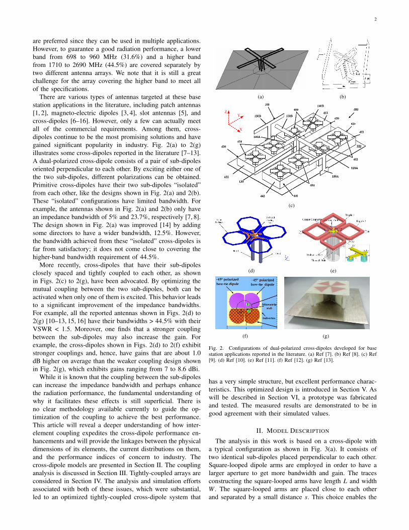
There are various types of antennas targeted at these basestation applications in the literature, including patch antennas[1, 2], magneto-electric dipoles [3, 4], slot antennas [5], andcross-dipoles [6–16]. However, only a few can actually meetall of the commercial requirements. Among them, cross-dipoles continue to be the most promising solutions and havegained significant popularity in industry. Fig. 2(a) to 2(g)illustrates some cross-dipoles reported in the literature [7–13].A dual-polarized cross-dipole consists of a pair of sub-dipolesoriented perpendicular to each other. By exciting either one ofthe two sub-dipoles, different polarizations can be obtained.Primitive cross-dipoles have their two sub-dipoles “isolated”from each other, like the designs shown in Fig. 2(a) and 2(b).These “isolated” configurations have limited bandwidth. Forexample, the antennas shown in Fig. 2(a) and 2(b) only havean impedance bandwidth of 5% and 23.7%, respectively [7, 8].The design shown in Fig. 2(a) was improved [14] by addingsome directors to have a wider bandwidth, 12.5%. However,the bandwidth achieved from these “isolated” cross-dipoles isfar from satisfactory; it does not come close to covering thehigher-band bandwidth requirement of 44.5%.
More recently, cross-dipoles that have their sub-dipolesclosely spaced and tightly coupled to each other, as shownin Figs. 2(c) to 2(g), have been advocated. By optimizing themutual coupling between the two sub-dipoles, both can beactivated when only one of them is excited. This behavior leadsto a significant improvement of the impedance bandwidths.For example, all the reported antennas shown in Figs. 2(d) to2(g) [10–13, 15, 16] have their bandwidths > 44.5% with theirVSWR < 1.5. Moreover, one finds that a stronger couplingbetween the sub-dipoles may also increase the gain. Forexample, the cross-dipoles shown in Figs. 2(d) to 2(f) exhibitstronger couplings and, hence, have gains that are about 1.0dB higher on average than the weaker coupling design shownin Fig. 2(g), which exhibits gains ranging from 7 to 8.6 dBi.
While it is known that the coupling between the sub-dipolescan increase the impedance bandwidth and perhaps enhancethe radiation performance, the fundamental understanding ofwhy it facilitates these effects is still superficial. There isno clear methodology available currently to guide the op-timization of the coupling to achieve the best performance.This article will reveal a deeper understanding of how inter-element coupling expedites the cross-dipole performance en-hancements and will provide the linkages between the physicaldimensions of its elements, the current distributions on them,and the performance indices of concern to industry. Thecross-dipole models are presented in Section II. The couplinganalysis is discussed in Section III. Tightly-coupled arrays areconsidered in Section IV. The analysis and simulation effortsassociated with both of these issues, which were substantial,led to an optimized tightly-coupled cross-dipole system that
(a) (b)
X
Y
Z
(c)
(d) (e)
(f) (g)
Fig. 2. Configurations of dual-polarized cross-dipoles developed for basestation applications reported in the literature. (a) Ref [7]. (b) Ref [8]. (c) Ref[9]. (d) Ref [10]. (e) Ref [11]. (f) Ref [12]. (g) Ref [13].
has a very simple structure, but excellent performance charac-teristics. This optimized design is introduced in Section V. Aswill be described in Section VI, a prototype was fabricatedand tested. The measured results are demonstrated to be ingood agreement with their simulated values.
II. MODEL DESCRIPTION
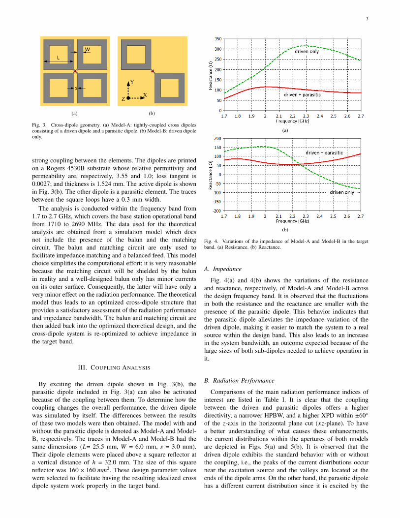
The analysis in this work is based on a cross-dipole witha typical configuration as shown in Fig. 3(a). It consists oftwo identical sub-dipoles placed perpendicular to each other.Square-looped dipole arms are employed in order to have alarger aperture to get more bandwidth and gain. The tracesconstructing the square-looped arms have length L and widthW . The square-looped arms are placed close to each otherand separated by a small distance s. This choice enables the
3
L
s
W
(a)
X
Y
Z
(b)
Fig. 3. Cross-dipole geometry. (a) Model-A: tightly-coupled cross dipolesconsisting of a driven dipole and a parasitic dipole. (b) Model-B: driven dipoleonly.
strong coupling between the elements. The dipoles are printedon a Rogers 4530B substrate whose relative permittivity andpermeability are, respectively, 3.55 and 1.0; loss tangent is0.0027; and thickness is 1.524 mm. The active dipole is shownin Fig. 3(b). The other dipole is a parasitic element. The tracesbetween the square loops have a 0.3 mm width.
The analysis is conducted within the frequency band from1.7 to 2.7 GHz, which covers the base station operational bandfrom 1710 to 2690 MHz. The data used for the theoreticalanalysis are obtained from a simulation model which doesnot include the presence of the balun and the matchingcircuit. The balun and matching circuit are only used tofacilitate impedance matching and a balanced feed. This modelchoice simplifies the computational effort; it is very reasonablebecause the matching circuit will be shielded by the balunin reality and a well-designed balun only has minor currentson its outer surface. Consequently, the latter will have only avery minor effect on the radiation performance. The theoreticalmodel thus leads to an optimized cross-dipole structure thatprovides a satisfactory assessment of the radiation performanceand impedance bandwidth. The balun and matching circuit arethen added back into the optimized theoretical design, and thecross-dipole system is re-optimized to achieve impedance inthe target band.
III. COUPLING ANALYSIS
By exciting the driven dipole shown in Fig. 3(b), theparasitic dipole included in Fig. 3(a) can also be activatedbecause of the coupling between them. To determine how thecoupling changes the overall performance, the driven dipolewas simulated by itself. The differences between the resultsof these two models were then obtained. The model with andwithout the parasitic dipole is denoted as Model-A and Model-B, respectively. The traces in Model-A and Model-B had thesame dimensions (L= 25.5 mm, W = 6.0 mm, s = 3.0 mm).Their dipole elements were placed above a square reflector ata vertical distance of h = 32.0 mm. The size of this squarereflector was 160 × 160 mm2. These design parameter valueswere selected to facilitate having the resulting idealized crossdipole system work properly in the target band.
(a)
(b)
Fig. 4. Variations of the impedance of Model-A and Model-B in the targetband. (a) Resistance. (b) Reactance.
A. Impedance
Fig. 4(a) and 4(b) shows the variations of the resistanceand reactance, respectively, of Model-A and Model-B acrossthe design frequency band. It is observed that the fluctuationsin both the resistance and the reactance are smaller with thepresence of the parasitic dipole. This behavior indicates thatthe parasitic dipole alleviates the impedance variation of thedriven dipole, making it easier to match the system to a realsource within the design band. This also leads to an increasein the system bandwidth, an outcome expected because of thelarge sizes of both sub-dipoles needed to achieve operation init.
B. Radiation Performance
Comparisons of the main radiation performance indices ofinterest are listed in Table I. It is clear that the couplingbetween the driven and parasitic dipoles offers a higherdirectivity, a narrower HPBW, and a higher XPD within ±60of the z-axis in the horizontal plane cut (xz-plane). To havea better understanding of what causes these enhancements,the current distributions within the apertures of both modelsare depicted in Figs. 5(a) and 5(b). It is observed that thedriven dipole exhibits the standard behavior with or withoutthe coupling, i.e., the peaks of the current distributions occurnear the excitation source and the valleys are located at theends of the dipole arms. On the other hand, the parasitic dipolehas a different current distribution since it is excited by the

4
TABLE ICOMPARISON OF THE RADIATION PERFORMANCE OF
MODEL-A AND MODEL-B
A: driven+parasitic B: driven onlyDirectivity (dBi) 8.6 - 9.3 8.5 - 9
HPBW () 63 - 69 65 - 75XPD@0 (dB) > 50 > 50XPD@60 (dB) 9 - 11 7 - 11
C3
C1C2
peakvalley
I_d I_p
peak
(a)
valley
C2' C1'
Left
branch
Middle
branch
Right
branch
X
Y
Z
(b)
Fig. 5. Current distributions on the traces of the models. (a) Model-A. (b)Model-B.
capacitive coupling between the parallel branches of the twosub-dipoles.
The currents were monitored on several branches of thedipoles and as a pair of adjacent branches. One observedfeature was that the induced current I_p and the driven currentI_d are out of phase. This phenomenon is interesting sincea reverse current should theoretically reduce the directivity,but the realized directivity is even higher. In order to explainthis dichotomy, the trace current monitors: C1, C2, C3, C1’and C2’, were located as shown in Fig. 5. They are placednear the peaks of the current distributions on the individualbranches. Due to the diagonal symmetry of the aperture,the current distributions on the x- and y-aligned branchesare identical. Therefore, only the y-aligned currents weremonitored and analyzed. Moreover, the y-aligned currents onthe left-, middle-, and right branches work together to producefield contributions analogous to a 3-element dipole array. Thisaspect facilitated explaining the results. The magnitudes andphases of the currents within the entire frequency band wereobtained.
The current magnitudes on the middle branches of the twomodels at C1 and C1’ are compared in Fig. 6(a). Their valueson the left branches at C2, C2’ and those on the right branch atC3 are compared in Fig. 6(b). First, notice that the magnitudesof the total current (I_d - I_p) on the middle branch withor without the coupling are at the same level (i.e., C1≈C1’).Although the coupling introduces a reverse current Ip on theparasitic dipole, an increase of the current density on the drivendipole Id compensates for it. Hence, there is no reduction inthe directivity. Second, notice that the currents on the left-mostbranch of the driven dipole with or without the coupling alsoremain at a similar level (i.e., C2≈C2’). Third, notice that thereis additional current (C3) induced on the top right branch ofthe parasitic element and it has a magnitude comparable to thedriven current on the left branch (i.e., C3 is comparable with
(a)
(b)
(c)
Fig. 6. Simulated currents. (a) Current magnitude on the middle branchesof Model-A and Model-B. (b) Current magnitudes on the side branches ofModel-A and Model-B. (c) Current phases on three different branches ofModel-A.
C2). Finally, the phases of the currents on the left-, middle-,and right-branches of Model-A are plotted in Fig. 6(c). Thephase differences between these currents are < 90 within theentire band. Therefore, the contributions to the radiated fieldfrom the three y-aligned currents add coherently on boresight.The outcome is the fact that a higher directivity and a narrowerHPBW are obtained from this cross-dipole system.
The XPD is another crucial factor used to assess theradiation performance of a base station antenna. For cellularcoverage applications, the value of the XPD along the bore-sight direction (θ = 0, point A in Fig. 7) is required to be > 20dB, and the minimum XPD within the entire set of coverageangles (−60 < θ < 60, points B and B’ in Fig. 7) has to be >10 dB. Usually, the worst XPD occurs at the bandwidth edges.

5
In a majority of cases, the condition that the XPD@0 > 20can be satisfied. However, to maintain the XPD@±60 > 10 dBwithin the entire operation band is a challenge. For example,the calculated XPD@±60 for Model-B is from 7-11 dB overthat band.
In order to achieve a higher XPD in base station antennadesigns, one must start by investigating what contributes toit. Grasping the impact of this performance factor can beconfusing because one normally looks at the ±45 polarizationvectors in the xz-plane cut (ϕ = 0) rather than in the ϕ = 45cut. To examine its meaning, consider the electric field that isgenerated by the cross-dipole antenna as shown in Fig. 7. Thefar-field x- and y-components can be expressed as:
x · −→E = Exe jϕx , y · −→E = Eye jϕy (1)
which is commensurate with the presence of the alreadyidentified x- and y-aligned currents in Fig. 5(a). Then the co-and cross-polarized field vectors in the ϕ = ±45 cut planestake the form:
Eco = cosπ
4Exe jϕx + cos
π
4Eye jϕy ,
Ecross = cosπ
4Exe jϕx − cos
π
4Eye jϕy .
(2)
The XPD is the ratio of the co- and cross-pol magnitudes:
XPD = Eco
Ecross
= √E2x + E2
y + 2ExEycos(ϕx − ϕy)E2x + E2
y − 2ExEycos(ϕx − ϕy)
=
√1 + M1 − M
,
(3)
where
M =2ExEycos(ϕx − ϕy)
E2x + E2
y
. (4)
Note that if one observes the fields at a point infinitelyfar away from the antenna aperture, both the Ex and Ey
components arrive at essentially the same time, which meansϕx = ϕy . Therefore, the term M can be written to a very goodapproximation as
M =2ExEy
E2x + E2
y
=2
Ex
Ey+
Ey
Ex
. (5)
Then to connect the XPD value to the field components mostnaturally generated by the currents on the antenna elements,we define
XPD′ =Ex
Ey. (6)
as the cross polarization discrimination factor between the x-and y-polarized far-field components. Then the actual XPDfactor can be expressed as
XPD =XPD′ + 1XPD′ − 1
. (7)
Consequently, it is now clear that in order to obtain a largerXPD as required for base station applications, XPD’ should beas close to 1 as possible. In other words, we have to optimizethe antenna to maintain the difference between the magnitudesof the generated x- and y-polarized radiation to be as small
Fig. 7. Schematic 3D radiation pattern of the proposed tightly-coupled cross-dipole.
Fig. 8. Comparison of x- and y-aligned radiation patterns of Models-A and-B.
as possible in the xz-plane cut across the entire operationalband.
Fig. 8 compares the x- and y-polarized radiation patternsgenerated with Model-A and Model-B in the xz-plane cut. Astrictly diagonal, symmetric structure relative to the boresightdirection would ensure that Ex = Ey and, hence, wouldproduce an infinitely high XPD@0. As shown, this is true forboth models. However, the symmetry in a real environment isdifficult to ensure and the ratio of the field components maydeteriorate some from unity, resulting in a lower XPD. Forexample, a radome used to cover a base station antenna mayscatter differently in the x- and y-directions, which leads to abroken symmetry and a decreased XPD at boresight.
Note that this symmetry generally no longer exists at theedges of the coverage directions, i.e., when θ ∼ ±60. Asillustrated in Fig. 8, although both Ex and Ey are gettingsmaller as θ varies from 0 to ±60, Ex (solid lines) decreasesfaster than Ey (dashed lines). This behavior is more noticeablefor the non-symmetric Model-B. Although the x- and y-aligned currents are nearly the same, the asymmetry of theoverall structure causes the patterns in the E-plane (horizontalcut, xz-plane) and H-plane (vertical cut, yz-plane) to bedifferent. Moreover, one finds this asymmetry also leads toa more severe narrowing of the patterns in both planes. Incontrast, the more symmetric Model-A, in which the parasitic

6
(a) (b) (c)
Fig. 9. Representation of the current distributions. (a) Schematic for thetightly-coupled cross-dipole antenna. (b) Equivalent six-element dipole arrayfor model-A. (c) Reduced, equivalent three-element dipole array model.
sub-dipole is excited by the mutual coupling effects, leads tomore stable and less narrowing of the E- and H-plane patternsand to a larger XPD across the entire coverage range.
IV. TIGHTLY-COUPLED CROSS-DIPOLE ANTENNADESIGN METHODOLOGY
To more closely tie the design parameters to its performancecharacteristics, we have developed an analytical array modelof the tightly-coupled cross-dipole antenna. This model and aparameter study based on it provide further insights into howthe system achieves low VSWR, stable HPBW, and high XPDacross the coverage range and the operational bandwidth.
A. Array Model
Fig. 9(a) presents a schematic of the current distributions onthe cross-dipole aperture. The solid and dashed arrows denotethe directly-excited currents and the induced parasitic currents,respectively. To develop the array model, only the y-alignedcurrents are considered. An analogous model can be developedin the same manner for the x-aligned currents.
The three current monitors C1, C2, and C3, identifiedpreviously, monitor the magnitudes and phases at the peaksof their distributions. Due to the observed symmetries, thereare only three unique current vectors on the aperture:
−→C1 = C1e jϕ1,−→C2 = C2e jϕ2,−→C3 = C3e jϕ3 .
(8)
They are identified in Fig. 9(b). Although these three currentvectors have different magnitudes and phases, they all actuallyhave similar quarter-period quasi-sinusoidal magnitude distri-butions and small phase differences < 90 as long as the sizeof the cross-dipole system is reasonable (i.e., the side length ofthe aperture is near a quarter-wavelength). Therefore, we canmerge the current vectors on the six branches of the modeldepicted in Fig. 9(b) into the three dipole current vectorsshown in Fig. 9(c).
Next, because the detected currents on the outside branchesof the three-element array are the same, the currents on theirequivalent dipoles will be denoted by the vector
−→Is . The current
on the equivalent center dipole is then denoted by the vector−→Im. From the Model-A simulation data it is found that thecurrents
−→Im and
−→Is have identical half-period quasi-sinusoidal
current directions, to be denoted as−→I0 . Thus, they can be
represented as−→Is =
−→I0(C3e jϕ3 + C2e jϕ2 )/2,
−→Im =
−→I0C1e jϕ1,
(9)
where−→Is is the combination of the branch currents C2 and
C3, as depicted in Fig. 9.The radiation pattern generated by these three y-polarized
current elements can be represented as
Fy(θ, ϕ) = AF(θ, ϕ) ∗ f0(θ, ϕ), (10)
where AF(θ, ϕ) is the three-element array factor and f0(θ, ϕ)is the radiation pattern of a dipole element. The correspondingradiation pattern, Fx(θ, ϕ), that is generated by the analogousx-oriented three-element dipole array model has the sameform. Consequently, it can be related to Fy(θ, ϕ) by a simplerotation, i.e., as:
Fx(θ, ϕ) = Fy(θ, ϕ + 90). (11)
Therefore, combining the fields radiated by both the x- andy-aligned currents, the total radiation pattern is:
F(θ, ϕ) = Fx(θ, ϕ) + Fy(θ, ϕ)= Fy(θ, ϕ + 90) + Fy(θ, ϕ).
(12)
The xz-cut of this radiation pattern is
F(θ, ϕ = 0) = Fy(θ, ϕ = 0) + Fy(θ, ϕ = 90)= AF(θ, ϕ = 0) ∗ f0(θ, ϕ = 0)+ AF(θ, ϕ = 90) ∗ f0(θ, ϕ = 90)= AF(θ, ϕ = 0) ∗ fH (θ) + AF(θ, ϕ = 90) ∗ fE (θ)
(13)
where fH (θ) and fE (θ) represent the H- and E-plane patternsof the dipole oriented along
−→I0 . Because the y-aligned currents
are spaced along the x-axis, the array factor along the y-axisis identically equal to 1.0, i.e.,
AF(θ, ϕ = 90) ≡ 1. (14)
Therefore, the cross-dipole’s radiation pattern in the xz-cut(13) can be rewritten as
F(θ, ϕ)|ϕ=0 = AF(θ, ϕ = 0) ∗ fH (θ) + fE (θ). (15)
where AFH is the three-dipole element array factor in thedipole’s H-plane. The first and second terms in this expressionrepresent the contributions from the x- and y-aligned dipolecurrents, respectively.
From Eq. (6) one then has
XPD′ = AFH ∗ fH/ fE (16)
and the XPD factor from Eq. (7) becomes:
XPD(θ) =XPD′(θ) + 1XPD′(θ) − 1
= fE (θ) + AFH (θ) fH (θ)fE (θ) − AFH (θ) fH (θ)
(17)
Therefore, it is concluded that the radiation performancecharacteristics, XPD and HPBW, are determined simply withthe array factor AFH (θ) and the dipole’s E- and H-planepatterns, fE (θ) and fH (θ). Consequently, when the physical

7
0
30
60
90
120
150
180
210
240
270
300
330
-30
-20
-10
0
1.7 GHz 2.2 GHz 2.7 GHz
(a)
0
30
60
90
120
150
180
210
240
270
300
330
-30
-20
-10
0
1.7 GHz 2.2 GHz 2.7 GHz
(b)0
30
60
90
120
150
180
210
240
270
300
330
-3
-2
-1
0
AF 1.7 GHz AF 2.2 GHz AF 2.7 GHz
(c)
0
30
60
90
120
150
180
210
240
270
300
330
-30
-20
-10
0
1.7 GHz 2.2 GHz 2.7 GHz
(d)
Fig. 10. Simulated radiation patterns. (a) E-plane pattern and (b) H-planepattern of a single half-wavelength dipole placed a quarter-wavelength abovean infinite ground plane and oriented parallel to it. (c) Three-element arrayfactor pattern alone. (d) Model-A-based cross-dipole radiation pattern.
dimensions of the cross-dipole antenna are being optimized,one is equivalently manipulating the array factor and theradiation patterns of the array elements.
From equation (9) and Fig. 9(c), the three-element dipolearray factor is calculated as:
AF(θ) = 3∑n=1
Wne−jk ·rn
= |As I0e jϕs e jk(−d)cos(θ) + AmI0e jϕm e j0
+ As I0e jϕs e jk(d)cos(θ) |= |I0e jϕm [Ase j(ϕs−ϕm)(e−jkdcosθ + e jkdcosθ ) + Am]|= I0 |2Ascos(kdcosθ)e j(∆ϕ) + Am |= I0[2Ascos(kdcosθ)cos(∆ϕ) + Am]2
+ [2Ascos(kdcosθ)sin(∆ϕ)]2 12
(18)
where k = 2π/λ, ∆ϕ = ϕs − ϕm, and d is the separationdistance between the dipole elements. The array factor is thuscalculated straightforwardly once the magnitudes and phasesof the currents are obtained from the monitors C1, C2, andC3.
Figs. 10(a) and 10(b) show the E- and H-plane radiationpatterns, fE (θ) and fH (θ), respectively, of a straight half-wavelength dipole placed a quarter-wavelength above a groundplane and oriented parallel to it for several source frequencies.To eliminate the effect of the ground plane’s size, it is set tobe infinitely large. It is observed from these two sub-figuresthat a typical dipole placed above a reflector has its H-planepattern getting wider and its E-plane pattern being relativelystable as the frequency increases. Fig. 10(c) plots the array
Fig. 11. Revised and simplified cross-dipole configuration.
factor patterns of Model-A alone in free space. Fig. 10(d) plotsthe corresponding cross-dipole array patterns calculated from(15) at the same frequencies. These composite patterns arevery stable across the target band. It is clear that along withthe stable E-plane patterns, the array factor variations withfrequency nicely compensate for the variations in the H-planepatterns, resulting in very stable overall patterns.
B. Parameter Analysis
The array model analysis theoretically demonstrated why astable radiation pattern can be realized across a wide band witha cross-dipole configuration. Because only the E- and H-planepatterns of the equivalent dipole elements and the H-planearray factor determined the overall pattern, there are methodsavailable to engineer these key factors. These include:
• E-plane pattern of a dipole above a reflector fE (θ):Dipole length; distance away from the reflector; reflectorsize.
• H-plane pattern of a dipole above a reflector fH (θ):Distance away from the reflector; reflector size.
• H-plane array factor AFH (θ):Shape of the array element, which changes the amplitudeand phase distributions on it (e.g., adding a slot/stub to orbending it can result in a different array factor); separationdistance between the array elements.
These methods are employed to optimize the design of thesimplified, practical cross-dipole model illustrated in Fig. 11.The adjustable parameters are the aperture length L, outsidebranch width W (black branches), inside branch width W ′
(grey branches), gap width s, antenna height h, and groundplane reflector size G. It is noted that any of these parametersand any of their combinations can affect the radiation patterns.Furthermore, some of these parameters are also critical forimpedance matching. To obtain a cross-dipole system thatmeets all of the design specifications, it is very helpful toknow how each parameter impacts the overall performance.A variety of parameter sweeps were investigated. During eachsweep, only one of these design parameters was allowed tovary and the others were fixed to the values listed in Table II.These tabulated dimensions are their optimized values, whichwere obtained with an exhaustive set of simulations, and arethe ones used for the fabrication of the prototype antenna.

8
TABLE IIOPTIMIZED DIMENSIONS OF THE SIMPLIFIED CROSS-DIPOLE
ANTENNA (DIMENSIONS IN MILLIMETERS)
Parameter Value DescriptionL 60.0 Aperture lengthW 5.5 Width of the outside branchesW ′ 4.0 Width of inside branchess 5.4 Distance between inside armsh 33.0 Antenna heightG 160.0 Ground plane length
Figs. 12 and 13 illustrate how each design parameter affectsthe HPBW and the input impedance of the cross-dipolesystem. Only the HPBW results are presented in Fig. 12 sinceit is a key coverage parameter and whatever impacts it will alsoaffect the other radiation performance characteristics such asthe XPD and gain. The input impedance results given in Fig.13 are obtained for the cross-dipole elements placed above thereflector, but with no feed network being present.
As shown in Fig. 12(a), the HPBW varies significantlywith the aperture length L. This is attributed to the fact thatL is closely related to the array factor AFH (θ) and L/2 isthe separation distance between the array elements. A largerL results in a more directive AFH (θ), and thus a narrowerHPBW. At the same time, L is also a key parameter for tuningthe input impedance as shown in Fig. 13(a).
Figs. 12(e) and 12(f) show that the HPBW also changeswith the antenna height h and the ground plane reflector sizeG. These larger variations are associated with the fact that hand G critically impact the dipole radiation patterns fE (θ) andfH (θ). However, they do not affect the couplings that occurbetween the elements in the aperture. Consequently, they donot affect the array factor AFH (θ). Moreover, as long as theyare changed in reasonable ranges, they do not affect the inputimpedance. This feature is illustrated in Figs. 13(e) and 13(f).
As shown in Figs. 12(b), 12(c), and 12(d), the remainingparameters: s, W , and W ′, only demonstrate minor abilities toaid in the tuning of the HPBW. This fact is easy to understandsince the radiation pattern of a dipole is much more closelyrelated to its length rather than to its widths. On the other hand,optimizing those widths and the coupling distance betweenthe dipole branches is critical for realizing good impedancematching. The parameter sweep results shown in Figs. 13(b),13(c), and 13(d) prove the fact that these parameters have adefinite impact on the input impedance tuning.
C. DiscussionThe presented analysis and results demonstrate that the
tightly-coupled cross-dipole configuration addressed in thiswork can be decomposed into two arrays, an x-aligned and ay-aligned 3-element dipole array placed above a ground planereflector. The radiation pattern was determined to be given bytwo factors: the E- and H-plane patterns of the dipole elementand its ground plane image, and the bare H-plane array factor.Because with increasing frequency the patterns associated withthe dipole (pattern widens) and array factor (pattern narrows)have compensating effects, high pattern and, hence, high XPDconsistency can be achieved across the entire operational band.
(a)
(b)
(c)
(d)
(e)
(f)
Fig. 12. HPBW plotted on the Z-Smith diagram for the parameters: (a) L,(b) s, (c) W , (d) W ′, (e) h, and (f) G.

9
(a)
(b)
(c)
(d)
(e)
(f)
Fig. 13. Input impedance plotted on the Z-Smith diagram for the parameters:(a) L, (b) s, (c) W , (d) W ′, (e) h, and (f) G.
The imaging effects, of course, can be controlled by thereflector’s size G and the distance h between dipole elementsand reflector. They have a significant effect on the radiationpattern but only a minor effect on the input impedance. Thearray factor is a much more important factor for the radiationperformance, especially for the XPD. However, as shown inFig. 11, it is not easy to adjust the array factor because ofcompeting effects. Changing L can change the array factor,but it also affects the impedance matching. A more appropriateand practical method to change the array factor is to introduceparasitic elements. Equivalently, this introduces more arrayelements, resulting an array factor that can be engineered. Forexample, the practical design shown in Fig. 2(c) employ wallssurrounding the high band elements and two parasitic dipolesfor the low band elements to shape the system’s output beams.
Based on the identified features of the equivalent dipole ar-ray model, the following design procedure is advocated. First,the design dimensions L, h, and G should be determined toyield a satisfactory radiation performance. We have employedthe commercial software environment CST Microwave Studio(MWS) for these simulation parameter studies. The antennaheight h and reflector size G should be kept as small as possi-ble to guarantee a compact structure. Parasitic elements shouldbe considered to better shape the beam if necessary. Second,the design parameters s, W , and W ′ should be optimizedto facilitate good input impedance matching. To determinewhether the realized cross-dipoles can be matched in the targetband, one can export the MWS S1p file representing the inputimpedance. One can then connect it with an idealized matchingcircuit in the MWS circuit simulator as shown in Fig. 14(c)to optimize the system. This matching method, as describedin [17], is an optimal way to match the dipole antennas to thefeed network and readily leads to a printed circuit board (PCB)implementation. Subsequently, a physical matching circuit canbe designed from the resulting optimized circuit theory model.Finally, if needed, minor overall adjustments can be made tothe overall design to achieve excellent impedance matchingperformance.
V. ANTENNA DESIGN
It was desired to fabricate and test a prototype of oursimplified cross-dipole antenna. Following our design proce-dure, the basic structure and its radiation performance wereobtained. A matching circuit was then designed to facilitate itsrealization. Then, the combined antenna and matching circuitwere optimized together to achieve the final prototype design.
A. Matching
The ideal cross-dipole structure shown in Fig. 11 togetherwith the ground plane reflector were firstly optimized numer-ically to have a good radiation performance. As noted for theidealized system, the structure was designed to be printed ona Rogers 4530B substrate. The optimized dimensions of thestructure are those listed in Table II. The next step was todesign the matching network.
As shown in Fig. 14(a), two feed networks, one for eachsub-dipole, are placed perpendicular with each other and to

10
(a)
(b)
(c)
Fig. 14. Optimized simplified cross-dipole antenna. (a) Perspective view. (b)Details of the two feed networks implemented using PCBs. (c) Circuit theorymodel of the matching circuit.
TABLE IIIOPTIMIZED DIMENSIONS OF THE TWO FEED NETWORKS
(DIMENSIONS IN MILLIMETERS)
Parameter Feed A Feed B DescriptionW_SL 6.0 6.0 Width of the SLL_SL 30.7 28.0 Length of the SLW_TL1 6.0 6.0 Width of the TL1L_TL1 2.4 5.1 length of the TL1W_TL2 6.0 6.0 Width of the TL2L_TL2 15.0 15.0 Length of the TL2W_OL 6.0 6.0 Width of the OLL_OL 1.5 1.5 Length of the OLg 4.0 4.0 Separation distance between SL
the cross-dipole aperture. A matching circuit was implementedusing microstrip technology. Two feed networks were designedto excite the two polarization states; they are depicted in Fig.14(b). Note that TL2 and OL are conventional microstrip lines.
(a)
(b)
(c)
Fig. 15. Photos of the antenna and measurement system. (a) Fabricated andassembled antenna prototype. (b) Mounting the antenna. (c) Antenna undertest (AUT).
They are designed on the front conducting layer. The linesTL1 and SL are realized as coupled lines printed on the backconducting layer. They not only form a balun to provide abalanced feed, but they also act as the ground planes for themicrostrip lines TL2 and OL. This implementation results ina compact structure. The coaxial cables of the 50 Ω sourceare connected to the ends of TL2.
As shown in Fig. 14(c), the S1p file representing the inputimpedance between points A and C (or points B and D)was extracted from the full-wave simulation software CSTMicrowave Studio 2016. It was connected with the depictedideal matching circuit in the MWS circuit simulator. Thematching circuit consists of two segments of transmission linesTL1 and TL2, a short circuit transmission line SL, and an opencircuit transmission line OL. Together with the cross-dipole

11
1.4 1.6 1.8 2.0 2.2 2.4 2.6 2.8 3.0-50
-40
-30
-20
-10
0
Ref
lect
ion
Coe
ffici
ent (
dB)
Frequency (GHz)
S11-SIM S22-SIM S11-MEA S22-MEA
Fig. 16. Simulated and measured reflection coefficients of the two ports.
itself, the matching circuit acts like a ladder-type filter. Theworking mechanisms of this matching circuit are described in[17]. By optimizing the parameters of the transmission lines,excellent matching was achieved. The optimized dimensionvalues of the feed networks are listed in Table III.
B. Results
The antenna was fabricated and tested. Fig. 15 shows thepictures of the antenna prototype and the test arrangement.The performance characteristics of the antenna were measuredwith an outdoor antenna range owned by Vecta Pty Ltd [18],located in Castle Hill, Sydney, Australia.
Plots of the simulated and measured reflection coefficients atthe two ports as functions of the source frequency are shownin Fig. 16. The achieved impedance bandwidth with returnloss < –15 dB is 1.1 GHz from 1.7 GHz to 2.8 GHz, whichis even wider than the target bandwidth. Note that there isa slight difference between the |S11 | and |S22 | values. Thisis due to the fact that the two feed networks were designednot to be exactly the same as shown in Fig. 14(b). Thischoice avoids cross-talk between them. The co- and cross-polarization radiation patterns of the −45-polarized cross-dipole at 1.7, 2.2, and 2.7 GHz are shown in Figs. 17(a),17(b), and 17(c), respectively. The radiation patterns of the+45-polarized cross-dipole are not given since those resultsare essentially the same. Fig. 18 illustrates the simulatedand measured HPBWs of the two polarization states. Theyshare a similar pattern, but a noticeable discrepancy at higherfrequencies is observed. It is attributed mainly to the antennafabrication and assembling errors. Despite this, the achievedHPBWs are quite stable and can meet the general industrialrequirements. According to the measured results, the XPD atthe boresight is > 20 dB and the lowest XPD level within themain beam (−60 < θ < 60) is > 8 dB. The measured XPDlevels are lower than the simulated results. According to theengineer associated with Vecta’s outdoor antenna range, theobserved higher measured cross polarization levels are simplydue to the imperfect ground plane (earth). The measured front-to-back ratio (FBR) is > 20 dB across this band. The measuredrealized gain varies from 7.3 to 8.2 dBi, which agrees very
0
30
60
90
120
150
180
210
240
270
300
330
-20
-10
0
10
co-sim cross-sim co-mea cross-mea
(a)0
30
60
90
120
150
180
210
240
270
300
330
-20
-10
0
10
co-sim cross-sim co-mea cross-mea
(b)0
30
60
90
120
150
180
210
240
270
300
330
-20
-10
0
10
co-sim cross-sim co-mea cross-mea
(c)
Fig. 17. Simulated and measured co- and cross-polarization radiation patternsat (a) 1.7, (b) 2.2, and (c) 2.7 GHz.
well with the simulated values. The corresponding simulatedradiation efficiency values are above 81% across the entireband.
VI. CONCLUSION
A dual-polarized tightly-coupled cross-dipole system, suchas those widely used in current 2G/3G/4G base stations, wasanalyzed. For the first time a deep insight into how this typeof antenna works was given by decomposing the cross-dipoleinto two equivalent dipole arrays. By observing and studyingthe current distributions on the simplified model, it was foundthat the radiation performance of the system is determined bytwo terms: the patterns of the dipole arrays in the presence of

12
1.7 1.8 1.9 2.0 2.1 2.2 2.3 2.4 2.5 2.6 2.755
60
65
70
75
Hal
f Pow
er B
eam
wid
th (d
egre
e)
Frequency (GHz)
Port 1-SIM Port 2-SIM Port 1-MEA Port 2-MEA
Fig. 18. Simulated and measured HPBW for the two polarizations across thetarget band.
the ground plane reflector and their array factor pattern. Theinteraction between these two factors makes the cross-dipolesystem achieve a very stable radiation performance, which isa requirement for all commercial base station applications. Adesign strategy based on a novel simplified dipole array modelwas introduced and validated.
An optimized cross-dipole system was synthesized fol-lowing this design strategy. Low |S11| values, < -15 dB,were obtained along with excellent radiation performance. Aprototype antenna based on this design was fabricated andtested. The measured performance characteristics were in verygood agreement with their simulated values.
The knowledge generated from this work not only providesuseful guidance for designing base station systems for currentwireless networks, but it also can be applied to the designof future 5G base station antennas. We anticipate that thelatter application may benefit the most from the enhancedunderstanding and validated design strategies presented in thisarticle.
REFERENCES
[1] Y. Jin and Z. Du, “Broadband Dual-Polarized F-Probe Fed Stacked PatchAntenna for Base Stations,” IEEE Antennas and Wireless PropagationLetters, vol. 14, pp. 1121-1124, 2015.
[2] Y. Gou, S. Yang, Q. Zhu and Z. Nie, “A Compact Dual-Polarized DoubleE-Shaped Patch Antenna With High Isolation,” IEEE Transactions onAntennas and Propagation, vol. 61, no. 8, pp. 4349-4353, Aug. 2013.
[3] B. Q. Wu and K. M. Luk, “A Broadband Dual-Polarized Magneto-ElectricDipole Antenna With Simple Feeds,” IEEE Antennas and WirelessPropagation Letters, vol. 8, pp. 60-63, 2009.
[4] K. M. Luk and B. Wu, “The Magnetoelectric Dipole – A WidebandAntenna for Base Stations in Mobile Communications,” Proceedings ofthe IEEE, vol. 100, no. 7, pp. 2297-2307, July 2012.
[5] R. Lian, Z. Wang, Y. Yin, J. Wu and X. Song, “Design of a Low-ProfileDual-Polarized Stepped Slot Antenna Array for Base Station,” IEEEAntennas and Wireless Propagation Letters, vol. 15, pp. 362-365, 2016.
[6] S. X. Ta, I. Park and R. W. Ziolkowski, “Crossed Dipole Antennas: Areview,” IEEE Antennas and Propagation Magazine, vol. 57, no. 5, pp.107-122, Oct. 2015.
[7] H. D. Hristov, H. Carrasco, R. Feick, and B. L. Ooi, “Low-profileX antenna with flat reflector for polarization diversity applications,”Microwave and Optical Technology Letters, vol. 51, pp. 1508-1512, 2009.
[8] Daoyi Su, J. J. Qian, Hua Yang and D. Fu, “A novel broadbandpolarization diversity antenna using a cross-pair of folded dipoles,” IEEEAntennas and Wireless Propagation Letters, vol. 4, pp. 433-435, 2005.
[9] B. B. Jones and J. K. A. Allan, “Ultra-Wideband Dual-Band CellularBase Station Antenna,” US Patent 2014/0139387 A1, May, 2014.
[10] Q. X. Chu, D. L. Wen and Y. Luo, “A Broadband ±45 Dual-PolarizedAntenna With Y-Shaped Feeding Lines,” IEEE Transactions on Antennasand Propagation, vol. 63, no. 2, pp. 483-490, Feb. 2015.
[11] Z. Bao, Z. Nie and X. Zong, “A Novel Broadband Dual-PolarizationAntenna Utilizing Strong Mutual Coupling,” IEEE Transactions onAntennas and Propagation, vol. 62, no. 1, pp. 450-454, Jan. 2014.
[12] Y. Cui, R. Li and H. Fu, “A Broadband Dual-Polarized Planar Antennafor 2G/3G/LTE Base Stations,” IEEE Transactions on Antennas andPropagation, vol. 62, no. 9, pp. 4836-4840, Sept. 2014.
[13] Y. Gou, S. Yang, J. Li and Z. Nie, “A Compact Dual-PolarizedPrinted Dipole Antenna With High Isolation for Wideband Base StationApplications,” IEEE Transactions on Antennas and Propagation, vol. 62,no. 8, pp. 4392-4395, Aug. 2014.
[14] H. D. Hristov, H. Carrasco, R. Feick, and G. S. Kirov, “Broadbandtwo-port X antenna array with flat reflector for polarization diversityapplications,” Microwave and Optical Technology Letters, vol. 52, pp.2833-2837, Dec. 2010.
[15] H. Huang, Y. Liu, and S. X. Gong, “A Broadband Dual-Polarized BaseStation Antenna With Anti-Interference Capability,” IEEE Antennas andPropagation Letters, vol. 16, pp. 613-616, Mar. 2017.
[16] D. Z. Zheng and Q. X Chu, “A Multimode Wideband ±45 Dual-Polarized Antenna With Embedded Loops,” IEEE Antennas and Propa-gation Letters, vol. 16, pp. 613-616, Mar. 2017.
[17] C. Ding, B. B. Jones, Y. J. Guo, and P.-Y. Qin, “Wideband Matchingof Full-Wavelength Dipole with Reflector for Base Station, ” IEEETransactions on Antennas and Propagation, early access.
[18] Vectalabs. September 22, 2017 [Online], Available: http://vectalabs.com.