16-Bit Tri-Port Universal Bus Exchangers datasheet (Rev. E)
15
SN54ABTH32316, SN74ABTH32316 16-BIT TRI-PORT UNIVERSAL BUS EXCHANGERS SCBS179E – JUNE 1992 – REVISED MAY 1997 1 POST OFFICE BOX 655303 • DALLAS, TEXAS 75265 Members of the Texas Instruments Widebus+ Family State-of-the-Art EPIC-ΙΙB BiCMOS Design Significantly Reduces Power Dissipation UBE (Universal Bus Exchanger) Combines D-Type Latches and D-Type Flip-Flops for Operation in Transparent, Latched, Clocked, or Clock-Enabled Mode ESD Protection Exceeds 2000 V Per MIL-STD-883, Method 3015 Latch-Up Performance Exceeds 500 mA Per JEDEC Standard JESD-17 Typical V OLP (Output Ground Bounce) < 0.8 V at V CC = 5 V, T A = 25°C High-Impedance State During Power Up and Power Down Distributed V CC and GND Pin Configuration Minimizes High-Speed Switching Noise High-Drive Outputs (–32-mA I OH , 64-mA I OL ) Bus Hold on Data Inputs Eliminates the Need for External Pullup/Pulldown Resistors Package Options Include 80-Pin Plastic Thin Quad Flat (PN) Package With 12 × 12-mm Body Using 0.5-mm Lead Pitch and 84-Pin Ceramic Quad Flat (HT) Package 22 23 C8 C7 C6 GND C5 C4 C3 C2 C1 V CC GND B16 B15 B14 B13 B12 GND B11 B10 B9 60 59 58 57 56 55 54 53 52 51 50 49 48 47 46 45 44 43 42 41 24 1 2 3 4 5 6 7 8 9 10 11 12 13 14 15 16 17 18 19 20 A2 A3 A4 GND A5 A6 A7 A8 A9 V CC GND A10 A11 A12 A13 A14 GND A15 A16 NC 25 26 27 28 ’ABTH32316 . . . PN PACKAGE (TOP VIEW) GND 79 78 77 76 75 80 74 OEA OEC SELC LEC CLKC CLKENC NC GND B2 LEA OEB SELB LEB CLKB CLKENB NC 72 71 70 73 29 30 31 32 33 69 68 21 CLKENA C15 67 66 65 64 34 35 36 37 B3 B4 B5 GND C14 C13 C12 GND A1 SELA B6 B7 38 39 40 C11 C10 63 62 61 V CC C16 C9 CC V CLKA B1 B8 NC – No internal connection Copyright 1997, Texas Instruments Incorporated PRODUCTION DATA information is current as of publication date. Products conform to specifications per the terms of Texas Instruments standard warranty. Production processing does not necessarily include testing of all parameters. Widebus+, EPIC-ΙΙB, and UBE are trademarks of Texas Instruments Incorporated. Please be aware that an important notice concerning availability, standard warranty, and use in critical applications of Texas Instruments semiconductor products and disclaimers thereto appears at the end of this data sheet.
-
Upload
khangminh22 -
Category
Documents
-
view
1 -
download
0
Transcript of 16-Bit Tri-Port Universal Bus Exchangers datasheet (Rev. E)
SN54ABTH32316, SN74ABTH3231616-BIT TRI-PORT UNIVERSAL BUS EXCHANGERS
SCBS179E – JUNE 1992 – REVISED MAY 1997
1POST OFFICE BOX 655303 • DALLAS, TEXAS 75265
Members of the Texas InstrumentsWidebus+ Family
State-of-the-Art EPIC-ΙΙB BiCMOS DesignSignificantly Reduces Power Dissipation
UBE (Universal Bus Exchanger)Combines D-Type Latches and D-TypeFlip-Flops for Operation in Transparent,Latched, Clocked, or Clock-Enabled Mode
ESD Protection Exceeds 2000 V PerMIL-STD-883, Method 3015
Latch-Up Performance Exceeds 500 mAPer JEDEC Standard JESD-17
Typical V OLP (Output Ground Bounce)< 0.8 V at VCC = 5 V, TA = 25°C
High-Impedance State During Power Upand Power Down
Distributed V CC and GND Pin ConfigurationMinimizes High-Speed Switching Noise
High-Drive Outputs (–32-mA I OH, 64-mA IOL)
Bus Hold on Data Inputs Eliminates theNeed for External Pullup/PulldownResistors
Package Options Include 80-Pin PlasticThin Quad Flat (PN) Package With12 × 12-mm Body Using 0.5-mm Lead Pitchand 84-Pin Ceramic Quad Flat (HT) Package
22 23
C8C7C6GNDC5C4C3C2C1VCCGNDB16B15B14B13B12GNDB11B10B9
60
59
58
57
56
55
54
53
52
51
50
49
48
47
46
45
44
43
42
4124
1
2
3
4
5
6
7
8
9
10
11
12
13
14
15
16
17
18
19
20
A2A3A4
GNDA5A6A7A8A9
VCCGNDA10A11A12A13A14
GNDA15A16NC
25 26 27 28
’ABTH32316 . . . PN PACKAGE(TOP VIEW)
GN
D
79 78 77 76 7580 74
OE
AO
EC
SE
LCLE
CC
LKC
CLK
EN
CN
C
GN
D B2
LEA
OE
BS
ELB
LEB
CLK
BC
LKE
NB
NC
72 71 7073
29 30 31 32 33
69 68
21
CLK
EN
A
C15
67 66 65 64
34 35 36 37
B3
B4
B5
GN
D
C14
C13
C12
GN
D
A1
SE
LA
B6
B7
38 39 40
C11
C10
63 62 61
VC
C
C16
C9
CC
V
CLK
A B1
B8
NC – No internal connection
Copyright 1997, Texas Instruments IncorporatedPRODUCTION DATA information is current as of publication date.Products conform to specifications per the terms of Texas Instrumentsstandard warranty. Production processing does not necessarily includetesting of all parameters.
Widebus+, EPIC-ΙΙB, and UBE are trademarks of Texas Instruments Incorporated.
Please be aware that an important notice concerning availability, standard warranty, and use in critical applications ofTexas Instruments semiconductor products and disclaimers thereto appears at the end of this data sheet.

SN54ABTH32316, SN74ABTH3231616-BIT TRI-PORT UNIVERSAL BUS EXCHANGERS
SCBS179E – JUNE 1992 – REVISED MAY 1997
2 POST OFFICE BOX 655303 • DALLAS, TEXAS 75265
SN54ABTH32316 . . . HT PACKAGE(TOP VIEW)
23 24
C8C7C6GNDC5C4C3C2C1VCCNCGNDB16B15B14B13B12GNDB11B10B9
63
62
61
60
59
58
57
56
55
54
53
52
51
50
49
48
47
46
45
44
43
25
1
2
3
4
5
6
7
8
9
10
11
12
13
14
15
16
17
18
19
20
21
A2A3A4
GNDA5A6A7A8A9
VCCNC
GNDA10A11A12A13A14
GNDA15A16NC
26 27 28 29
NC
83 82 81 80 7984 78
OE
AO
EC
SE
LCLE
CC
LKC
NC
B1
LEA
OE
BS
ELB
LEB
CLK
BC
LKE
NB
NC
76 75 7477
30 31 32 33 34
73 72
22
CLK
EN
A
C16
71 70 69 68
35 36 37 38
B2
B3
B4
B5
C15
C14
C13
C12
A1
SE
LA
GN
D B6
B8
39 40 41 42
GN
DC
11
C9
67 66 65 64
VC
C
GN
D
C10
CLK
A
VC
C
GN
D
B7
NC
CLK
EN
C
NC – No internal connection
description
The ’ABTH32316 consist of three 16-bit registered input/output (I/O) ports. These registers combine D-typelatches and flip-flops to allow data flow in transparent, latch, and clock modes. Data from one input port can beexchanged to one or more of the other ports. Because of the universal storage element, multiple combinationsof real-time and stored data can be exchanged among the three ports.
Data flow in each direction is controlled by the output-enable (OEA, OEB, and OEC), select-control (SELA,SELB, and SELC), latch-enable (LEA, LEB, and LEC), and clock (CLKA, CLKB, and CLKC) inputs. The A dataregister operates in the transparent mode when LEA is high. When LEA is low, data is latched if CLKA is heldat a high or low logic level. If LEA and clock-enable A (CLKENA) are low, data is stored on the low-to-hightransition of CLKA. Output data selection is accomplished by the select-control pins. All three ports haveactive-low output enables, so when the output-enable input is low, the outputs are active; when theoutput-enable input is high, the outputs are in the high-impedance state.
When VCC is between 0 and 2.1 V, the device is in the high-impedance state during power up or power down.However, to ensure the high-impedance state above 2.1 V, OE should be tied to VCC through a pullup resistor;the minimum value of the resistor is determined by the current-sinking capability of the driver.

SN54ABTH32316, SN74ABTH3231616-BIT TRI-PORT UNIVERSAL BUS EXCHANGERS
SCBS179E – JUNE 1992 – REVISED MAY 1997
3POST OFFICE BOX 655303 • DALLAS, TEXAS 75265
description (continued)
Active bus-hold circuitry is provided to hold unused or floating data inputs at a valid logic level.
The SN54ABTH32316 is characterized for operation over the full military temperature range of –55°C to 125°C.The SN74ABTH32316 is characterized for operation from –40°C to 85°C.
Function Tables
STORAGE†
INPUTSOUTPUT
CLKENA CLKA LEA AOUTPUT
H X L X Q0‡
L ↑ L L L
L ↑ L H H
X H L X Q0‡
X L L X Q0‡
X X H L L
X X H H H
† A-port register shown. B and C ports are similarbut use CLKENB, CLKENC, CLKB, CLKC, LEB,and LEC.
‡ Output level before the indicated steady-stateinput conditions were established
A-PORT OUTPUT
INPUTSOUTPUT A
OEA SELAOUTPUT A
H X Z
L H Output of C register
L L Output of B register
B-PORT OUTPUT
INPUTSOUTPUT B
OEB SELBOUTPUT B
H X Z
L H Output of A register
L L Output of C register
C-PORT OUTPUT
INPUTSOUTPUT C
OEC SELCOUTPUT C
H X Z
L H Output of B register
L L Output of A register

SN54ABTH32316, SN74ABTH3231616-BIT TRI-PORT UNIVERSAL BUS EXCHANGERS
SCBS179E – JUNE 1992 – REVISED MAY 1997
4 POST OFFICE BOX 655303 • DALLAS, TEXAS 75265
logic diagram (positive logic)
CLK
1 of 16 Channels
CE
C
OEA
SELA
CLKA
CLKENA
LEA
CLK
CE
C
OEB
SELB
CLKB
CLKENB
LEB
CLK
CE
C
OEC
SELC
CLKC
CLKENC
LEC
C1
B1
A1
77
76
74
73
75
52
24
25
27
28
26
32
78
79
22
21
23
80
Pin numbers shown are for the PN package.

SN54ABTH32316, SN74ABTH3231616-BIT TRI-PORT UNIVERSAL BUS EXCHANGERS
SCBS179E – JUNE 1992 – REVISED MAY 1997
5POST OFFICE BOX 655303 • DALLAS, TEXAS 75265
absolute maximum ratings over operating free-air temperature range (unless otherwise noted) †
Supply voltage range, VCC –0.5 V to 7 V. . . . . . . . . . . . . . . . . . . . . . . . . . . . . . . . . . . . . . . . . . . . . . . . . . . . . . . . . . Input voltage range, VI (except I/O ports) (see Note 1) –0.5 V to 7 V. . . . . . . . . . . . . . . . . . . . . . . . . . . . . . . . . . Voltage range applied to any output in the high or power-off state, VO –0.5 V to 5.5 V. . . . . . . . . . . . . . . . . . . Current into any output in the low state, IO: SN54ABTH32316 96 mA. . . . . . . . . . . . . . . . . . . . . . . . . . . . . . . . .
SN74ABTH32316 128 mA. . . . . . . . . . . . . . . . . . . . . . . . . . . . . . . . Input clamp current, IIK (VI < 0) –18 mA. . . . . . . . . . . . . . . . . . . . . . . . . . . . . . . . . . . . . . . . . . . . . . . . . . . . . . . . . . . Output clamp current, IOK (VO < 0) –50 mA. . . . . . . . . . . . . . . . . . . . . . . . . . . . . . . . . . . . . . . . . . . . . . . . . . . . . . . . Package thermal impedance, θJA (see Note 2): PN package 62°C/W. . . . . . . . . . . . . . . . . . . . . . . . . . . . . . . . . . Storage temperature range, Tstg –65°C to 150°C. . . . . . . . . . . . . . . . . . . . . . . . . . . . . . . . . . . . . . . . . . . . . . . . . . .
† Stresses beyond those listed under “absolute maximum ratings” may cause permanent damage to the device. These are stress ratings only, andfunctional operation of the device at these or any other conditions beyond those indicated under “recommended operating conditions” is notimplied. Exposure to absolute-maximum-rated conditions for extended periods may affect device reliability.
NOTES: 1. The input and output negative-voltage ratings may be exceeded if the input and output clamp-current ratings are observed.2. The package thermal impedance is calculated in accordance with EIA/JEDEC Std JESD51.
recommended operating conditions (see Note 3)
SN54ABTH32316 SN74ABTH32316UNIT
MIN MAX MIN MAXUNIT
VCC Supply voltage 4.5 5.5 4.5 5.5 V
VIH High-level input voltage 2 2 V
VIL Low-level input voltage 0.8 0.8 V
VI Input voltage 0 VCC 0 VCC V
IOH High-level output current –24 –32 mA
IOL Low-level output current 48 64 mA
∆t/∆v Input transition rise or fall rate Outputs enabled 10 10 ns/V
∆t/∆VCC Power-up ramp rate 200 200 µs/V
TA Operating free-air temperature –55 125 –40 85 °C
NOTE 3: Unused control pins must be held high or low to prevent them from floating.

SN54ABTH32316, SN74ABTH3231616-BIT TRI-PORT UNIVERSAL BUS EXCHANGERS
SCBS179E – JUNE 1992 – REVISED MAY 1997
6 POST OFFICE BOX 655303 • DALLAS, TEXAS 75265
electrical characteristics over recommended operating free-air temperature range (unlessotherwise noted)
PARAMETER TEST CONDITIONSSN54ABTH32316 SN74ABTH32316
UNITPARAMETER TEST CONDITIONSMIN TYP† MAX MIN TYP† MAX
UNIT
VIK VCC = 4.5 V, II = –18 mA –1.2 –1.2 V
VCC = 4.5 V, IOH = –3 mA 2.5 2.5
VOHVCC = 5 V, IOH = –3 mA 3 3
VVOHVCC = 4 5 V
IOH = –24 mA 2V
VCC = 4.5 VIOH = –32 mA 2
VOL VCC = 4 5 VIOL = 48 mA 0.55
VVOL VCC = 4.5 VIOL = 64 mA 0.55
V
Vhys 100 100 mV
IIControl inputs VCC = 0 to 5.5 V, VI = VCC or GND ±1 ±1
µAIIA, B, or C ports VCC = 2.1 V to 5.5 V, VI = VCC or GND ±100 ±20
µA
II(h ld) A B or C ports VCC = 4 5 VVI = 0.8 V 100 100
µAII(hold) A, B, or C ports VCC = 4.5 VVI = 2 V –100 –100
µA
IOZPU‡ VCC = 0 to 2.1 V, VO = 0.5 V to 2.7 V, OE = X ±50 ±50 µA
IOZPD‡ VCC = 2.1 V to 0, VO = 0.5 V to 2.7 V, OE = X ±50 ±50 µA
Ioff VCC = 0, VI or VO ≤ 4.5 V ±100 ±100 µA
ICEX VCC = 5.5 V, VO = 5.5 V Outputs high 50 50 µA
IO§ VCC = 5.5 V, VO = 2.5 V –50 –100 –180 –50 –100 –180 mA
VCC = 5.5 V, Outputs high 2 2
ICC
VCC = 5.5 V,IO = 0, Outputs low 40 40 mAVI = VCC or GND Outputs disabled 1 1
∆ICC¶ VCC = 5.5 V, One input at 3.4 V,Other inputs at VCC or GND
1 0.5 mA
Ci Control inputs VI = 2.5 V or 0.5 V 3 3 pF
Cio A, B, or C ports VO = 2.5 V or 0.5 V 11.5 11.5 pF
† All typical values are at VCC = 5 V, TA = 25°C.‡ This parameter is specified by characterization.§ Not more than one output should be tested at a time, and the duration of the test should not exceed one second.¶ This is the increase in supply current for each input that is at the specified TTL voltage level rather than VCC or GND.
timing requirements over recommended ranges of supply voltage and operating free-airtemperature (unless otherwise noted) (see Figure 1)
SN54ABTH32316 SN74ABTH32316UNIT
MIN MAX MIN MAXUNIT
fclock Clock frequency 0 150 0 150 MHz
t Pulse durationLE high 3.3 3.3
nstw Pulse durationCLK high or low 3.3 3.3
ns
A, B, or C before CLK↑ 2.6 2.4
tsu Setup time A or B before LE↓ 2.5 2.1 ns
CLKEN before CLK↑ 3.5 3.2
A, B, or C after CLK↑ 1.8 1.4
th Hold time A or B after LE↓ 2.4 2.1 ns
CLKEN after CLK↑ 1.5 1.1
SN54ABTH32316, SN74ABTH3231616-BIT TRI-PORT UNIVERSAL BUS EXCHANGERS
SCBS179E – JUNE 1992 – REVISED MAY 1997
7POST OFFICE BOX 655303 • DALLAS, TEXAS 75265
switching characteristics over recommended ranges of supply voltage and operating free-airtemperature, C L = 50 pF (unless otherwise noted) (see Figure 1)
PARAMETERFROM TO SN54ABTH32316 SN74ABTH32316
UNITPARAMETER(INPUT) (OUTPUT) MIN MAX MIN MAX
UNIT
fmax 150 150 MHz
tPLHA B or C C B or A
0.8 6.5 1.4 6.1ns
tPHLA, B, or C C, B, or A
0.5 6.8 1.1 6.6ns
tPLHSEL A B or C
0.8 6.7 1.4 6.5ns
tPHLSEL A, B, or C
0.8 6.8 1.8 6.5ns
tPLHLE A B or C
1.5 8 2.6 7.5ns
tPHLLE A, B, or C
1.5 7.4 2.6 6.9ns
tPLHCLK A B or C
1.5 8 2.5 7.5ns
tPHLCLK A, B, or C
1.5 7.2 2.5 6.7ns
tPZHOE A B or C
0.8 6.7 1.5 6.4ns
tPZLOE A, B, or C
1.5 7.1 2.4 6.8ns
tPHZOE A B or C
0.8 7.2 1.5 6ns
tPLZOE A, B, or C
0.8 6.4 1.9 6.1ns

SN54ABTH32316, SN74ABTH3231616-BIT TRI-PORT UNIVERSAL BUS EXCHANGERS
SCBS179E – JUNE 1992 – REVISED MAY 1997
8 POST OFFICE BOX 655303 • DALLAS, TEXAS 75265
PARAMETER MEASUREMENT INFORMATION
1.5 V
thtsu
From Output Under Test
CL = 50 pF(see Note A)
LOAD CIRCUIT
S1
7 V
Open
GND
500 Ω
500 Ω
Data Input
Timing Input 1.5 V3 V
0 V
1.5 V 1.5 V
3 V
0 V
3 V
0 V
1.5 V
tw
Input
VOLTAGE WAVEFORMSSETUP AND HOLD TIMES
VOLTAGE WAVEFORMSPROPAGATION DELAY TIMES
INVERTING AND NONINVERTING OUTPUTS
VOLTAGE WAVEFORMSPULSE DURATION
tPLH
tPHL
tPHL
tPLH
VOH
VOH
VOL
VOL
1.5 V 1.5 V
3 V
0 V
1.5 V1.5 V
Input
1.5 V
OutputControl
OutputWaveform 1
S1 at 7 V(see Note B)
OutputWaveform 2S1 at Open
(see Note B)
VOL
VOH
tPZL
tPZH
tPLZ
tPHZ
1.5 V1.5 V
3.5 V
0 V
1.5 V VOL + 0.3 V
1.5 V VOH – 0.3 V
≈ 0 V
3 V
VOLTAGE WAVEFORMSENABLE AND DISABLE TIMES
LOW- AND HIGH-LEVEL ENABLING
Output
Output
tPLH/tPHLtPLZ/tPZLtPHZ/tPZH
Open7 V
Open
TEST S1
NOTES: A. CL includes probe and jig capacitance.B. Waveform 1 is for an output with internal conditions such that the output is low except when disabled by the output control.
Waveform 2 is for an output with internal conditions such that the output is high except when disabled by the output control.C. All input pulses are supplied by generators having the following characteristics: PRR ≤ 10 MHz, ZO = 50 Ω, tr ≤ 2.5 ns, tf ≤ 2.5 ns.D. The outputs are measured one at a time with one transition per measurement.
1.5 V
Figure 1. Load Circuit and Voltage Waveforms

PACKAGE OPTION ADDENDUM
www.ti.com 9-Mar-2021
Addendum-Page 1
PACKAGING INFORMATION
Orderable Device Status(1)
Package Type PackageDrawing
Pins PackageQty
Eco Plan(2)
Lead finish/Ball material
(6)
MSL Peak Temp(3)
Op Temp (°C) Device Marking(4/5)
Samples
5962-9680801QXA ACTIVE CFP HT 84 250 Non-RoHS &Non-Green
SNPB N / A for Pkg Type -55 to 125 5962-9680801QXASNJ54ABTH32316HT
SN74ABTH32316PN ACTIVE LQFP PN 80 119 RoHS & Green NIPDAU Level-3-260C-168 HR -40 to 85 ABTH32316
SNJ54ABTH32316HT ACTIVE CFP HT 84 250 Non-RoHS &Non-Green
SNPB N / A for Pkg Type -55 to 125 5962-9680801QXASNJ54ABTH32316HT
(1) The marketing status values are defined as follows:ACTIVE: Product device recommended for new designs.LIFEBUY: TI has announced that the device will be discontinued, and a lifetime-buy period is in effect.NRND: Not recommended for new designs. Device is in production to support existing customers, but TI does not recommend using this part in a new design.PREVIEW: Device has been announced but is not in production. Samples may or may not be available.OBSOLETE: TI has discontinued the production of the device.
(2) RoHS: TI defines "RoHS" to mean semiconductor products that are compliant with the current EU RoHS requirements for all 10 RoHS substances, including the requirement that RoHS substancedo not exceed 0.1% by weight in homogeneous materials. Where designed to be soldered at high temperatures, "RoHS" products are suitable for use in specified lead-free processes. TI mayreference these types of products as "Pb-Free".RoHS Exempt: TI defines "RoHS Exempt" to mean products that contain lead but are compliant with EU RoHS pursuant to a specific EU RoHS exemption.Green: TI defines "Green" to mean the content of Chlorine (Cl) and Bromine (Br) based flame retardants meet JS709B low halogen requirements of <=1000ppm threshold. Antimony trioxide basedflame retardants must also meet the <=1000ppm threshold requirement.
(3) MSL, Peak Temp. - The Moisture Sensitivity Level rating according to the JEDEC industry standard classifications, and peak solder temperature.
(4) There may be additional marking, which relates to the logo, the lot trace code information, or the environmental category on the device.
(5) Multiple Device Markings will be inside parentheses. Only one Device Marking contained in parentheses and separated by a "~" will appear on a device. If a line is indented then it is a continuationof the previous line and the two combined represent the entire Device Marking for that device.
(6) Lead finish/Ball material - Orderable Devices may have multiple material finish options. Finish options are separated by a vertical ruled line. Lead finish/Ball material values may wrap to twolines if the finish value exceeds the maximum column width.
PACKAGE OPTION ADDENDUM
www.ti.com 9-Mar-2021
Addendum-Page 2
Important Information and Disclaimer:The information provided on this page represents TI's knowledge and belief as of the date that it is provided. TI bases its knowledge and belief on informationprovided by third parties, and makes no representation or warranty as to the accuracy of such information. Efforts are underway to better integrate information from third parties. TI has taken andcontinues to take reasonable steps to provide representative and accurate information but may not have conducted destructive testing or chemical analysis on incoming materials and chemicals.TI and TI suppliers consider certain information to be proprietary, and thus CAS numbers and other limited information may not be available for release.
In no event shall TI's liability arising out of such information exceed the total purchase price of the TI part(s) at issue in this document sold by TI to Customer on an annual basis.
OTHER QUALIFIED VERSIONS OF SN54ABTH32316, SN74ABTH32316 :
• Catalog: SN74ABTH32316
• Military: SN54ABTH32316
NOTE: Qualified Version Definitions:
• Catalog - TI's standard catalog product
• Military - QML certified for Military and Defense Applications
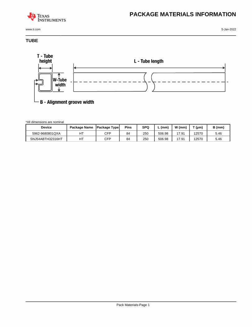
TUBE
*All dimensions are nominal
Device Package Name Package Type Pins SPQ L (mm) W (mm) T (µm) B (mm)
5962-9680801QXA HT CFP 84 250 506.98 17.91 12570 5.46
SNJ54ABTH32316HT HT CFP 84 250 506.98 17.91 12570 5.46
PACKAGE MATERIALS INFORMATION
www.ti.com 5-Jan-2022
Pack Materials-Page 1

TRAY
Chamfer on Tray corner indicates Pin 1 orientation of packed units.
*All dimensions are nominal
Device PackageName
PackageType
Pins SPQ Unit arraymatrix
Maxtemperature
(°C)
L (mm) W(mm)
K0(µm)
P1(mm)
CL(mm)
CW(mm)
SN74ABTH32316PN PN LQFP 80 119 7 x 17 150 315 135.9 7620 17.9 14.3 13.95
PACKAGE MATERIALS INFORMATION
www.ti.com 5-Jan-2022
Pack Materials-Page 2
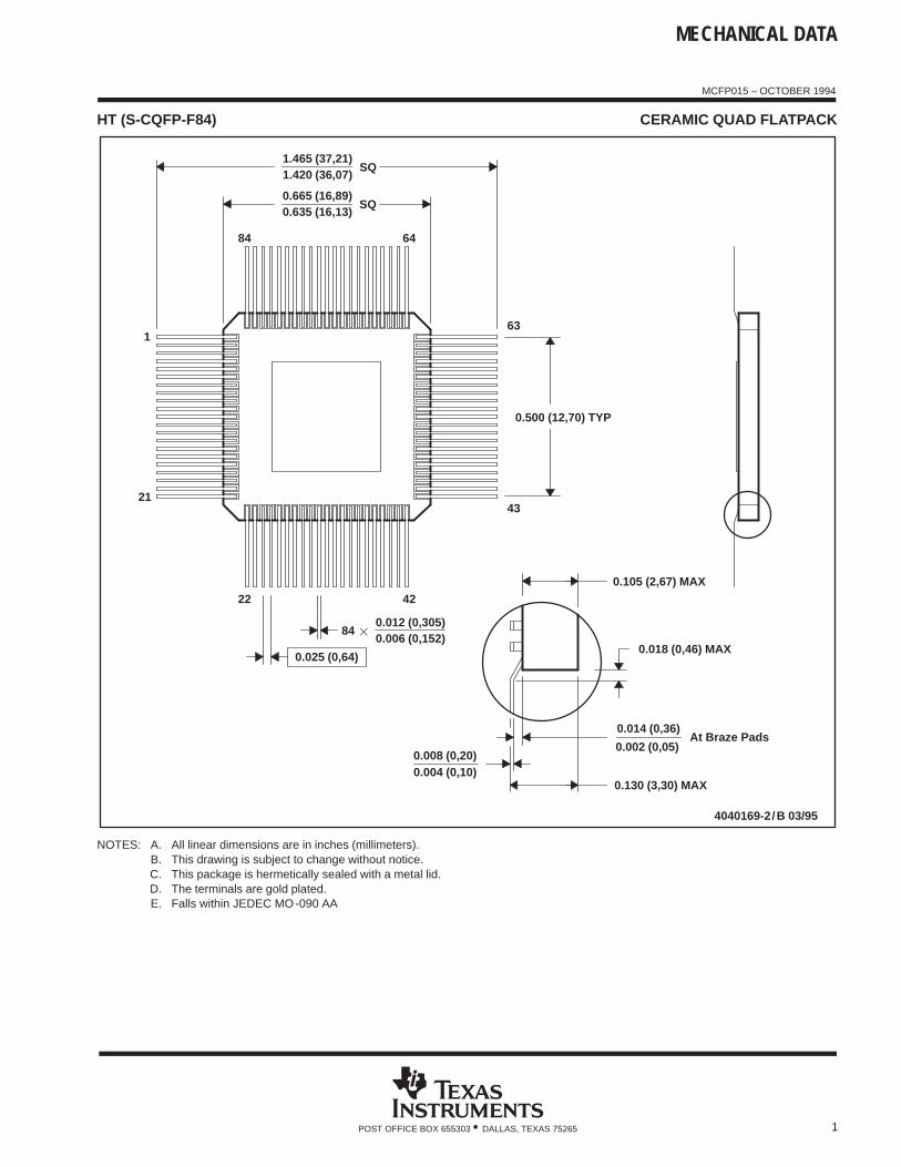
MECHANICAL DATA
MCFP015 – OCTOBER 1994
1POST OFFICE BOX 655303 • DALLAS, TEXAS 75265
HT (S-CQFP-F84) CERAMIC QUAD FLATPACK
4040169-2/B 03/95
63
43
0.500 (12,70) TYP
0.018 (0,46) MAX
0.105 (2,67) MAX
0.002 (0,05)
0.130 (3,30) MAX
0.014 (0,36)At Braze Pads
SQ1.465 (37,21)
64
SQ
84
0.635 (16,13)0.665 (16,89)
1.420 (36,07)
1
21
42
84 0.006 (0,152)0.012 (0,305)
22
0.004 (0,10)0.008 (0,20)
0.025 (0,64)
NOTES: A. All linear dimensions are in inches (millimeters).B. This drawing is subject to change without notice.C. This package is hermetically sealed with a metal lid.D. The terminals are gold plated.E. Falls within JEDEC MO-090 AA
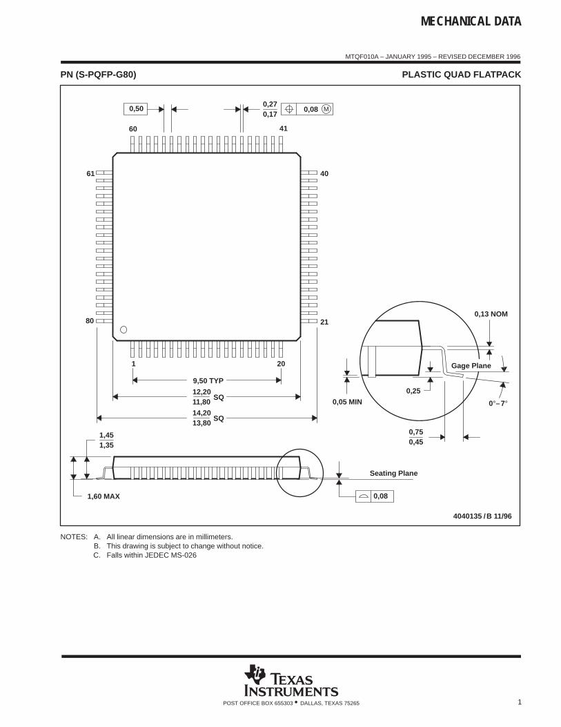
MECHANICAL DATA
MTQF010A – JANUARY 1995 – REVISED DECEMBER 1996
1POST OFFICE BOX 655303 • DALLAS, TEXAS 75265
PN (S-PQFP-G80) PLASTIC QUAD FLATPACK
4040135 /B 11/96
0,170,27
0,13 NOM
40
21
0,25
0,450,75
0,05 MIN
Seating Plane
Gage Plane
4160
61
80
20
SQ
SQ
1
13,8014,20
12,20
9,50 TYP
11,80
1,451,35
1,60 MAX 0,08
0,50 M0,08
0°–7°
NOTES: A. All linear dimensions are in millimeters.B. This drawing is subject to change without notice.C. Falls within JEDEC MS-026
IMPORTANT NOTICE AND DISCLAIMERTI PROVIDES TECHNICAL AND RELIABILITY DATA (INCLUDING DATA SHEETS), DESIGN RESOURCES (INCLUDING REFERENCE DESIGNS), APPLICATION OR OTHER DESIGN ADVICE, WEB TOOLS, SAFETY INFORMATION, AND OTHER RESOURCES “AS IS” AND WITH ALL FAULTS, AND DISCLAIMS ALL WARRANTIES, EXPRESS AND IMPLIED, INCLUDING WITHOUT LIMITATION ANY IMPLIED WARRANTIES OF MERCHANTABILITY, FITNESS FOR A PARTICULAR PURPOSE OR NON-INFRINGEMENT OF THIRD PARTY INTELLECTUAL PROPERTY RIGHTS.These resources are intended for skilled developers designing with TI products. You are solely responsible for (1) selecting the appropriate TI products for your application, (2) designing, validating and testing your application, and (3) ensuring your application meets applicable standards, and any other safety, security, regulatory or other requirements.These resources are subject to change without notice. TI grants you permission to use these resources only for development of an application that uses the TI products described in the resource. Other reproduction and display of these resources is prohibited. No license is granted to any other TI intellectual property right or to any third party intellectual property right. TI disclaims responsibility for, and you will fully indemnify TI and its representatives against, any claims, damages, costs, losses, and liabilities arising out of your use of these resources.TI’s products are provided subject to TI’s Terms of Sale or other applicable terms available either on ti.com or provided in conjunction with such TI products. TI’s provision of these resources does not expand or otherwise alter TI’s applicable warranties or warranty disclaimers for TI products.TI objects to and rejects any additional or different terms you may have proposed. IMPORTANT NOTICE
Mailing Address: Texas Instruments, Post Office Box 655303, Dallas, Texas 75265Copyright © 2022, Texas Instruments Incorporated