11 W + 11 W amplifier with DC volume control
15
December 2007 Rev 2 1/15 15 TDA7495SA 11 W + 11 W amplifier with DC volume control Features ! 11 W + 11 W output power with R L = 8 Ω, THD = 10%, V CC = 28 V ! Stand-by and mute functions ! Low turn-on and turn-off “pop” noise ! Linear volume control DC coupled to power operational amplifier ! No boucherot cell ! No RC input network for stand-by ! Single supply up to 35 V ! Short-circuit protection ! Thermal overload protection ! Internally fixed gain ! Soft clipping ! Variable output after volume control circuit ! Clipwatt15 package, RoHS Description The TDA7495SA is a stereo 11 W + 11 W class AB power amplifier specially designed for high-quality sound and TV applications. Its features include linear volume control, stand-by and mute functions. The TDA7495SA is delivered in the Clipwatt15 package Multipower BI50II technology Clipwatt15 VOLUME OP AMP + - MUTE/STBY PROTECTIONS 1 470nF INR 30K VOLUME OP AMP + - 30K 1000µF 1000µF 1µF 10K 5 470nF INL 8 S_GND 2 14 9 10 12 3 4 300K 100nF VOLUME VAROUT_L OUTR STBY MUTE OUTL 11 PW_GND 470µF SVR 7 D96AU440D V S VAROUT_R PW_GND 15 13 +5V S1 ST-BY +5V S2 MUTE +5V S_GND 60K Table 1. Device summary Order code Package Packaging TDA7495SA Clipwatt15 Tube www.st.com Obsolete Product(s) - Obsolete Product(s) Obsolete Product(s) - Obsolete Product(s) Obsolete Product(s) - Obsolete Product(s)
-
Upload
khangminh22 -
Category
Documents
-
view
1 -
download
0
Transcript of 11 W + 11 W amplifier with DC volume control

December 2007 Rev 2 1/15
15
TDA7495SA
11 W + 11 W amplifier with DC volume control
Features! 11 W + 11 W output power with
RL = 8 Ω, THD = 10%, VCC = 28 V
! Stand-by and mute functions
! Low turn-on and turn-off “pop” noise
! Linear volume control DC coupled to power operational amplifier
! No boucherot cell
! No RC input network for stand-by
! Single supply up to 35 V
! Short-circuit protection
! Thermal overload protection
! Internally fixed gain
! Soft clipping
! Variable output after volume control circuit
! Clipwatt15 package, RoHS
Description The TDA7495SA is a stereo 11 W + 11 W class AB power amplifier specially designed for high-quality sound and TV applications. Its features include linear volume control, stand-by and mute functions. The TDA7495SA is delivered in the Clipwatt15 package
Multipower BI50II technology
Clipwatt15
VOLUME
OP AMP
+
-
MUTE/STBYPROTECTIONS
1
470nF
INR
30K
VOLUME
OP AMP
+
-30K
1000µF
1000µF
1µF
10K
5
470nF
INL
8S_GND
2
14
9
10
12
3 4
300K100nF
VOLUME VAROUT_L
OUTR
STBY
MUTE
OUTL
11PW_GND
470µF
SVR 7
D96AU440D
VSVAROUT_R
PW_GND15
13
+5V
S1 ST-BY+5V
S2 MUTE+5V
S_GND
60K
Table 1. Device summary
Order code Package Packaging
TDA7495SA Clipwatt15 Tube
www.st.com
Obsolete Product(
s) - O
bsolete Product(
s)
Obsolete Product(
s) - O
bsolete Product(
s)
Obsolete Product(
s) - O
bsolete Product(
s)
Obsolete Product(
s) - O
bsolete Product(
s)
Obsolete Product(
s) - O
bsolete Product(
s)
Obsolete Product(
s) - O
bsolete Product(
s)
Pin connections TDA7495SA
2/15
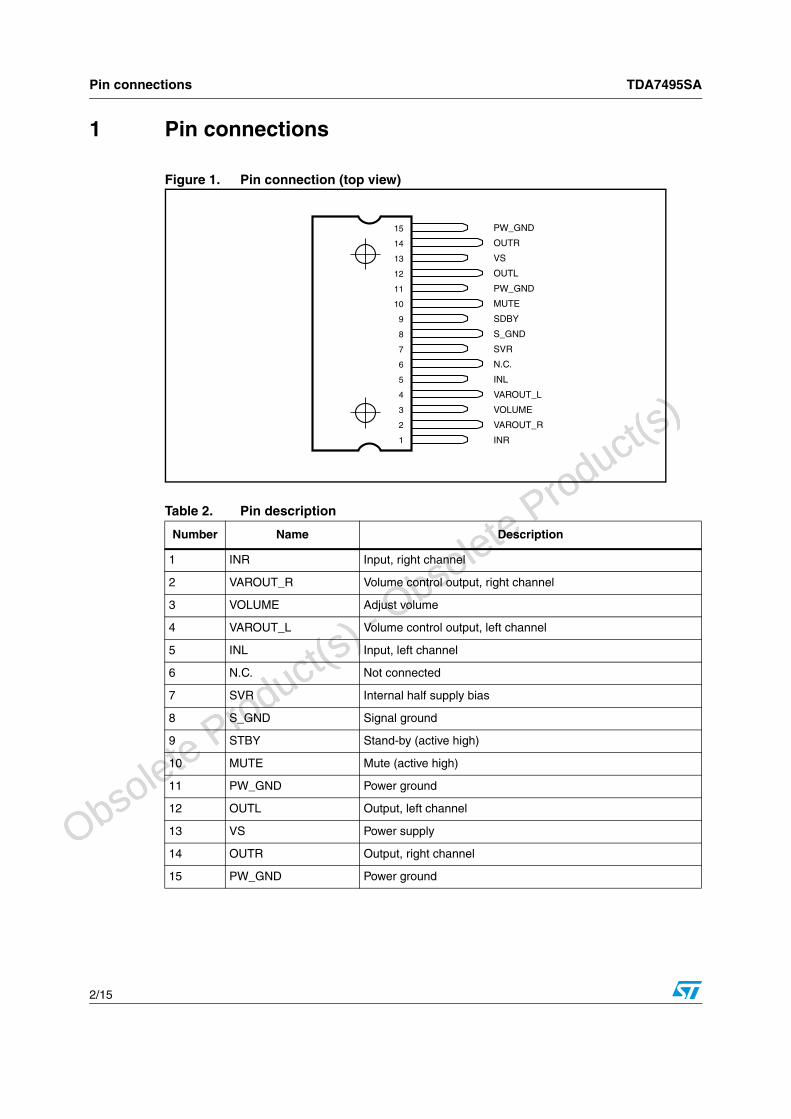
1 Pin connections
Figure 1. Pin connection (top view)
Table 2. Pin description
Number Name Description
1 INR Input, right channel
2 VAROUT_R Volume control output, right channel
3 VOLUME Adjust volume
4 VAROUT_L Volume control output, left channel
5 INL Input, left channel
6 N.C. Not connected
7 SVR Internal half supply bias
8 S_GND Signal ground
9 STBY Stand-by (active high)
10 MUTE Mute (active high)
11 PW_GND Power ground
12 OUTL Output, left channel
13 VS Power supply
14 OUTR Output, right channel
15 PW_GND Power ground
1
2
3
4
5
6
7
9
10
11
8
PW_GND
MUTE
STBY
S_GND
SVR
N.C.
INL
N.C.
N.C.
N.C.
INR
13
14
15
12
PW_GND
OUTR
VS
OUTL
D02AU1412A
PW_GND
OUTR
VS
OUTL
PW_GND
MUTE
SDBY
S_GND
SVR
N.C.
INL
VAROUT_L
VOLUME
VAROUT_R
INR

Obsolete Product(
s) - O
bsolete Product(
s)
Obsolete Product(
s) - O
bsolete Product(
s)
Obsolete Product(
s) - O
bsolete Product(
s)
TDA7495SA Electrical specifications
3/15
2 Electrical specifications
Unless otherwise stated, the test conditions for the specifications given in Table 5 below are: VS = 20 V, RL = 8 Ω, generator resistance Rg = 50 Ω, Tamb = 25° C. Refer also to the application circuit of Figure 2 on page 5.
Table 3. Absolute maximum ratings
Symbol Parameter Value Unit
VS DC supply voltage 35 V
VIN Maximum input voltage 8 Vpp
Ptot Total power dissipation (Tamb = 70° C) 15 W
Tamb Ambient operating temperature 0 to 70 °C
Tstg,TJ Storage and junction temperature -40 to 150 °C
V3 Volume control DC voltage 7 V
Table 4. Thermal data
Symbol Parameter Min Typ Max Unit
Rth j-case Thermal resistance junction-case 4.5 5.0 °C/W
Rth j-amb Thermal resistance junction-ambient 48 °C/W
Table 5. Electrical characteristics
Symbol Parameter Test condition Min Typ Max Unit
Vs Supply voltage range 11 35 V
Iq Total quiescent current 70 100 mA
DCVosOutput DC offset referred to SVR potential
No input signal -650 650 mV
VO Quiescent output voltage 10 V
PO Output power
THD = 10%, VS = 28 V
THD = 1%, VS = 28 V9.57.5
118
W
THD = 10%, VS = 20 V, RL = 4 ΩTHD = 1%, VS = 20 V, RL = 4 Ω
75
86
W
THD = 10%, VS = 18 VTHD = 1%, VS = 18 V
3.52.2
3.82.9
W
THD Total harmonic distortion Gv = 30 dB, PO = 1 W, f = 1 kHz 0.4 %
Ipeak Peak output current (internally limited) 1.7 2.4 A
VIN Input signal 2.8V RMS
Ri Input resistance 22.5 30 kΩ
RVarOutOutput resistance at pins VAROUT_L, VAROUT_R
30 100 Ω

Obsolete Product(
s) - O
bsolete Product(
s)
Obsolete Product(
s) - O
bsolete Product(
s)
Obsolete Product(
s) - O
bsolete Product(
s)
Electrical specifications TDA7495SA
4/15
RL_VarOut
Load resistance which can be connected to pins VAROUT_L, VAROUT_R
2 kΩ
Gv Closed-loop gain VOLUME >4.5 V 28.5 30 31.5 dB
GvlineVolume control output at max gain
VOLUME > 4.5 V,RL_VarOut > 30 kΩ
-1.5 0 1.5 dB
AMin_VOLAttenuation at minimum volume setting
VOLUME < 0.5 V 80 dB
BW 0.6 MHz
eN Total output noise
f = 20 Hz to 22 kHz PLAY, max volume
500 800 µV
f = 20 Hz to 22 kHz PLAY, max attenuation
100 250 µV
f = 20 Hz to 22 kHz MUTE 60 150 µV
SR Slew rate 5 8 V/µs
SVR Supply voltage rejection
f = 1 kHz; max volume CSVR = 470 µF; VRIP = 1 V RMS
35 39 dB
f = 1 kHz; max attenuation CSVR = 470 µF; VRIP = 1 V RMS
55 65 dB
TM Thermal muting 150 ° C
TS Thermal shut-down 160 ° C
Mute, stand-by and input selection functions
VSTBY Stand-by threshold 2.3 2.5 2.7 V
VMUTE Mute threshold 2.3 2.5 2.7 V
IqSTBYQuiescent current in stand-by
0.6 1 mA
AMUTE Mute attenuation 50 65 dB
ISTBYbias Bias current for pin STBY
In stand-by mode,VSTBY = 5 V, VMUTE = 5 V
80 µA
In play or mute mode -20 -5 µA
IMUTEbias Bias current for pin MUTEIn mute mode 1 5 µA
In play mode 0.2 2 µA
Table 5. Electrical characteristics (continued)
Symbol Parameter Test condition Min Typ Max Unit

Obsolete Product(
s) - O
bsolete Product(
s)
Obsolete Product(
s) - O
bsolete Product(
s)
Obsolete Product(
s) - O
bsolete Product(
s)
TDA7495SA Applications
5/15
3 Applications
3.1 Circuit diagram and components
Figure 2. Application circuit
The recommended values of the external components are those shown on the application circuit of Figure 2. Table 6 below indicates how the performance changes when component values different to the recommended are used.
Table 6. Application suggestions
SymbolSuggested
valuePurpose
Larger thansuggestion
Smaller thansuggestion
R1 300 kΩ Volume control circuitLarger volume regulation time
Smaller volume regulation time
R2 10 kΩ Mute time constant Larger mute on/off time Smaller mute on/off time
P1 50 kΩ Volume control
C1 1000 µF Supply voltage decoupling Danger of oscillation
C2, C3 470 nF Input AC couplingLower low-frequency cutoff
Higher low-frequency cutoff
C4 470 µF Ripple rejection Better SVR Worse SVR
C5 100 nFVolume control time constant
Larger volume regulation time
Smaller volume regulation time
C6, C8 1000 µF Output AC couplingLower low-frequency cutoff
Higher low-frequency cutoff
C7 1 µF Mute time constant Larger mute on/off time Smaller mute on/off time
C9 100 nF Supply voltage decoupling Danger of oscillation
VOLUME
OP AMP
+
-
MUTE/STBYPROTECTIONS
1
C2 470nF
INR
30K
VOLUME
OP AMP
+
-30K
C8 1000µF
C6 1000µF
C71µF
R2 10K
5
C3 470nF
INL
8S_GND
2
14
9
10
12
3 4
R1 300KC5
100nF
VOLUME
OUTR
S1 STBY
S2 MUTE
OUTL
11
C4 470µF
SVR 7
D96AU493D
VSVAROUT_R
PW_GND15
13
C90.1µF
C11000µF
+VS
PW_GND
VOLP1
50KLOG
+5V
TP1
PW_GND
PW_GND
S_GND
+5V
+5V
VAROUT_L
STBY MUTE Mode
L L Play
L H Mute
H L Standby
H H Standby
Obsolete Product(
s) - O
bsolete Product(
s)
Obsolete Product(
s) - O
bsolete Product(
s)
Obsolete Product(
s) - O
bsolete Product(
s)
Applications TDA7495SA
6/15
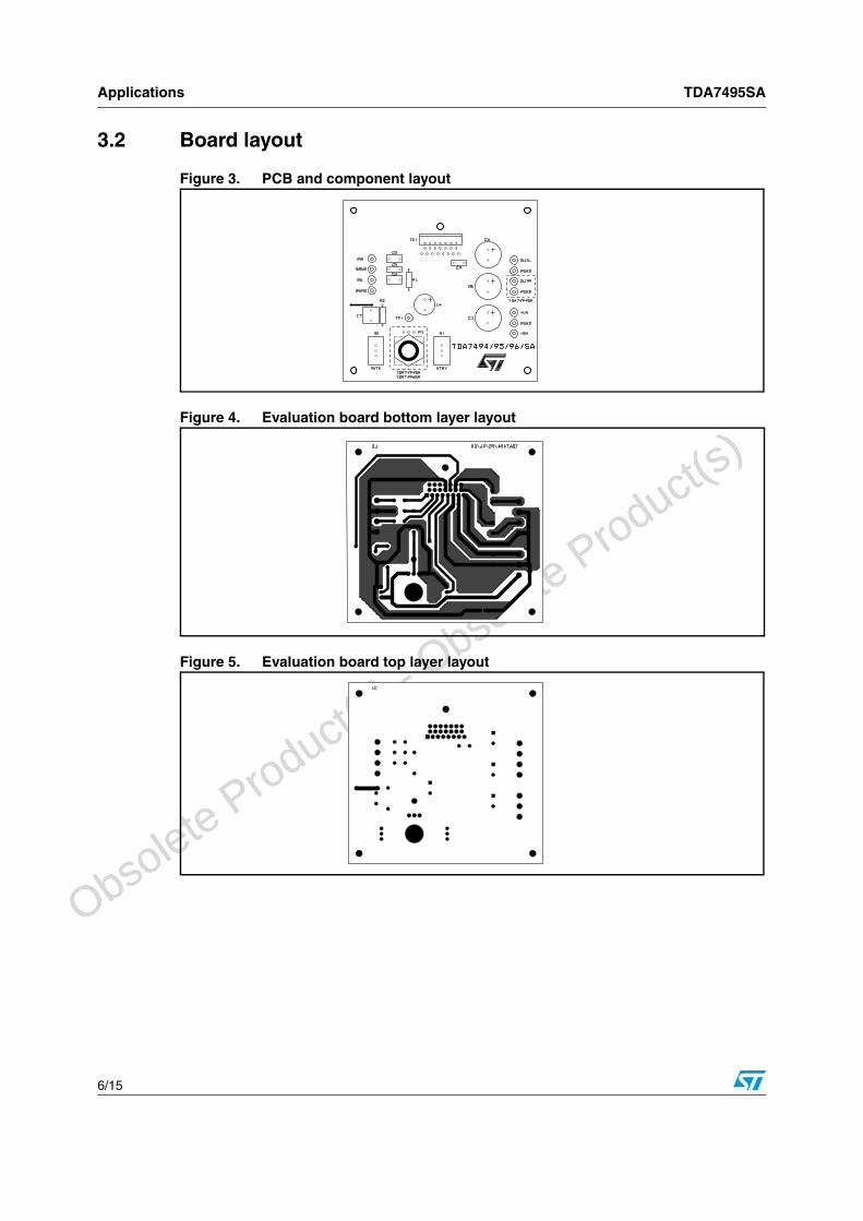
3.2 Board layout
Figure 3. PCB and component layout
Figure 4. Evaluation board bottom layer layout
Figure 5. Evaluation board top layer layout

Obsolete Product(
s) - O
bsolete Product(
s)
Obsolete Product(
s) - O
bsolete Product(
s)
Obsolete Product(
s) - O
bsolete Product(
s)
TDA7495SA Applications
7/15
3.3 Power-up/down sequenceIn order to reduce the loud speaker “pop” noise when switching the device on or off we recommend that you follow the sequence of operations shown in Figure 6 below.
Figure 6. Recommended sequence using mute and stand-by functions
Using the mute function only
To simplify the application, pin STBY can be connected directly to ground so that the device is always active. Then, to maintain the power-up/down performance you should adhere to the following conditions:
" At turn-on the transition mute to play must be made when pin SVR is higher than 2.5 V.
" At turn-off the TDA7495SA must be set to mute from the play condition before pin SVR falls below 2.5 V.
OFFSTBY MUTE PLAY STBYOFF MUTE
28
VS (V)
5
ST-BYpin#9 (V)
5
MUTEpin#10 (V)
INPUT(mV)
VOUT(V)
IQ(mA)
D96AU531A
VSVRpin#7(V)
2.5V
Obsolete Product(
s) - O
bsolete Product(
s)
Obsolete Product(
s) - O
bsolete Product(
s)
Obsolete Product(
s) - O
bsolete Product(
s)
Applications TDA7495SA
8/15
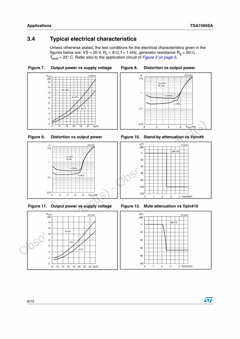
3.4 Typical electrical characteristicsUnless otherwise stated, the test conditions for the electrical characteristics given in the figures below are: VS = 20 V, RL = 8 Ω, f = 1 kHz, generator resistance Rg = 50 Ω, Tamb = 25° C. Refer also to the application circuit of Figure 2 on page 5.
Figure 7. Output power vs supply voltage Figure 8. Distortion vs output power
11 15 19 23 27 31 VS(V)0
2
4
6
8
10
12
14
POUT(W)16
d=10%
d=1%
RL=8Ω
D97AU559
0 2 4 6 POUT(W)0.01
0.1
1
d(%)
D97AU562
f=15KHz
VS=20VRL=4Ω
f=1KHz
Figure 9. Distortion vs output power Figure 10. Stand-by attenuation vs Vpin#9
0 2 4 6 8 POUT(W)0.01
0.1
1
d(%)
D97AU560
f=15KHz
VS=28VRL=8Ω
f=1KHz
0 1 2 3 4 Vpin#9(V)-120
-100
-80
-60
-40
-20
0
ATT(dB)
D97AU565
0dB=1W
Figure 11. Output power vs supply voltage Figure 12. Mute attenuation vs Vpin#10
D97AU561
10 12 14 16 18 20 22 24 VS(V)0
2
4
6
8
10
12
14
POUT(W)
RL=4Ω
d=10%
d=1%
0 1 2 3 4 Vpin#10(V)-100
-80
-60
-40
-20
0
ATT(dB)
D97AU566
0dB=1W

Obsolete Product(
s) - O
bsolete Product(
s)
Obsolete Product(
s) - O
bsolete Product(
s)
Obsolete Product(
s) - O
bsolete Product(
s)
TDA7495SA Applications
9/15
3.5 Internal equivalent circuits
Figure 13. Supply voltage vs frequency Figure 14. Gain vs volume control voltage (#3)
20 100 1K f(Hz)-100
-80
-60
-40
-20
SVR(dB)
D97AU564
VRIP=1VRMS
MAX VOLUME
MAX ATTENUATION
0.0 1.0 2.0 3.0 4.0 Vpin#3(V)-80
-70
-60
-50
-40
-30
-20
-10
0
10
20
30
Gain(dB)
D97AU563
POUT=1W
Figure 15. Power dissipation vs output power Figure 16. Power dissipation vs output power
0.1 1 10 POUT(W)0
2
4
6
8
PDISS(W)
D97AU567
VS=14V
VS=18V
VS=24V
RL=2 x 8Ωf=1KHz10
VS=28V
0.1 1 10 POUT(W)0
4
8
12
16
PDISS(W)
D97AU568
VS=20V
VS=26V
RL=2 x 4Ωf=1KHz
Figure 17. Pin: SVR Figure 18. Pins: INL, INR
+
-
+
-
6K
6K
1K
1K
30K
30K
SVR
20K
20K
VS VS VS
OUT L
OUT R
100µA
D97AU585A
500µA
30K
VS
INn
SVRD97AU589
6K

Obsolete Product(
s) - O
bsolete Product(
s)
Obsolete Product(
s) - O
bsolete Product(
s)
Obsolete Product(
s) - O
bsolete Product(
s)
Applications TDA7495SA
10/15
Figure 19. Pins: PW-GND, S-GND Figure 20. Pin: STBY
GNDD97AU593
VS
10µA
65K
VS
STBY
D97AU594
200
Figure 21. Pin: MUTE Figure 22. Pins: OUTR, OUTL
50µA
200MUTE
D97AU592
10K
VS
OUT
D97AU588
VS
Figure 23. Pins: VAROUT_L, VAROUT_R Figure 24. Pin: VOLUME
VAROUT-L
D97AU590
VS
VOL
D97AU591
VS
10µA

Obsolete Product(
s) - O
bsolete Product(
s)
Obsolete Product(
s) - O
bsolete Product(
s)
Obsolete Product(
s) - O
bsolete Product(
s)
TDA7495SA Thermal considerations
11/15
4 Thermal considerations
In order to avoid the intervention of the thermal protection, it is important to choose an adequate heatsink.
The parameters that influence the heatsink size are:
" maximum dissipated power for the device (Pdmax)
" maximum thermal resistance junction to case (RTh j-c)
" maximum ambient temperature Tamb_max
Example:
For VCC = 20 V, RL = 8 Ω, RTh j-c = 5° C/W, Tamb_max = 50° C
Pdmax = Number_of_channels * = 5 W
For the heatsink,
Figure 25 shows the power derating curve for the device.
Figure 25. Power derating curve
Vcc2
2Π2
RL⋅-----------------------
RTh j-c150 Tamb_max–
Pd max---------------------------------------- RTh j-c– 100
5---------- 5– 15°C/W= = =
a) Infinite Heatsink
b) 7 °C/ W
c) 10 °C/ W
(c)
(a)(d)
0
5
10
15
20
0 40 80 120 160
Tamb (°C)
Pd
(W
) a) Infinite Heatsink
b) 7 °C/ W
c) 10 °C/ W
(c)
(a)
(b)
0
5
10
15
20
0 40 80 120 160
Tamb (°C)
Pd
(W
)
d) 3.3 °C/ W

Obsolete Product(
s) - O
bsolete Product(
s)
Obsolete Product(
s) - O
bsolete Product(
s)
Obsolete Product(
s) - O
bsolete Product(
s)
Clipwatt mounting suggestions TDA7495SA
12/15
5 Clipwatt mounting suggestions
The suggested method for securing the Clipwatt package on an external heat sink is by a spring clip placed as close as possible to the center of the plastic body, as indicated in the example of Figure 26.
Thermal grease can be used to further reduce the thermal resistance of the contact between package and heatsink.
The clip should apply a force of 7 - 10 kg to provide sufficient pressure for a good contact. Care must be taken to ensure that the contact pressure on the package does not exceed 15 kg/mm².
As an example, if the clip applies a 15-kg force on the package then the clip must have a contact area of at least 1 mm².
Figure 26. Example of correctly placed clip

Obsolete Product(
s) - O
bsolete Product(
s)
Obsolete Product(
s) - O
bsolete Product(
s)
Obsolete Product(
s) - O
bsolete Product(
s)
TDA7495SA Package information
13/15
6 Package information
In order to meet environmental requirements, ST offers these devices in ECOPACK® packages. These packages have a Lead-free second level interconnect. The category of second Level Interconnect is marked on the package and on the inner box label, in compliance with JEDEC Standard JESD97. The maximum ratings related to soldering conditions are also marked on the inner box label. ECOPACK is an ST trademark. ECOPACK specifications are available at: www.st.com.
OUTLINE ANDMECHANICAL DATA
0044538 G
DIM.mm inch
MIN. TYP. MAX. MIN. TYP. MAX.
A 3.2 0.126
B 1.05 0.041
C 0.15 0.006
D 1.50 0.061
E 0.49 0.55 0.019 0.022
F 0.67 0.73 0.026 0.029
G 1.14 1.27 1.4 0.045 0.050 0.055
G1 17.57 17.78 17.91 0.692 0.700 0.705
H1 12 0.480
H2 18.6 0.732
H3 19.85 0.781
L 17.9 0.704
L1 14.55 0.572
L2 10.7 11 11.2 0.421 0.433 0.441
L3 5.5 0.217
M 2.54 0.100
M1 2.54 0.100
Clipwatt15
Weight: 1.92gr
Outline and mechanical data

Obsolete Product(
s) - O
bsolete Product(
s)
Obsolete Product(
s) - O
bsolete Product(
s)
Obsolete Product(
s) - O
bsolete Product(
s)
Revision history TDA7495SA
14/15
7 Revision history
Table 7.Document revision history
Date Revision Description
Sep 2003 1 Initial release
11-Dec 2007 2 Updated package and PCB information

Obsolete Product(
s) - O
bsolete Product(
s)
Obsolete Product(
s) - O
bsolete Product(
s)
Obsolete Product(
s) - O
bsolete Product(
s)
TDA7495SA Revision history
15/15
Please Read Carefully:
Information in this document is provided solely in connection with ST products. STMicroelectronics NV and its subsidiaries(“ST”) reserve the right to make changes, corrections, modifications or improvements, to this document, and the productsand services described herein at any time, without notice.
All ST products are sold pursuant to ST’s terms and conditions of sale.
Purchasers are solely responsible for the choice, selection and use of the ST products and services described herein, andST assumes no liability whatsoever relating to the choice, selection or use of the ST products and services described herein.
No license, express or implied, by estoppel or otherwise, to any intellectual property rights is granted under this document.If any part of this document refers to any third party products or services it shall not be deemed a license grant by ST for theuse of such third party products or services, or any intellectual property contained therein or considered as a warrantycovering the use in any manner whatsoever of such third party products or services or any intellectual property containedtherein.
UNLESS OTHERWISE SET FORTH IN ST’S TERMS AND CONDITIONS OF SALE ST DISCLAIMS ANY EXPRESS ORIMPLIED WARRANTY WITH RESPECT TO THE USE AND/OR SALE OF ST PRODUCTS INCLUDING WITHOUTLIMITATION IMPLIED WARRANTIES OF MERCHANTABILITY, FITNESS FOR A PARTICULAR PURPOSE (ANDTHEIR EQUIVALENTS UNDER THE LAWS OF ANY JURISDICTION), OR INFRINGEMENT OF ANY PATENT,COPYRIGHT OR OTHER INTELLECTUAL PROPERTY RIGHT.
UNLESS EXPRESSLY APPROVED IN WRITING BY AN AUTHORIZED ST REPRESENTATIVE, ST PRODUCTS ARENOT RECOMMENDED, AUTHORIZED OR WARRANTED FOR USE IN MILITARY, AIR CRAFT, SPACE, LIFE SAVING,OR LIFE SUSTAINING APPLICATIONS, NOR IN PRODUCTS OR SYSTEMS WHERE FAILURE OR MALFUNCTIONMAY RESULT IN PERSONAL INJURY, DEATH, OR SEVERE PROPERTY OR ENVIRONMENTAL DAMAGE. STPRODUCTS WHICH ARE NOT SPECIFIED AS "AUTOMOTIVE GRADE" MAY ONLY BE USED IN AUTOMOTIVEAPPLICATIONS AT USER’S OWN RISK.
Resale of ST products with provisions different from the statements and/or technical features set forth in this document shallimmediately void any warranty granted by ST for the ST product or service described herein and shall not create or extendin any manner whatsoever, any liability of ST.
ST and the ST logo are trademarks or registered trademarks of ST in various countries.
Information in this document supersedes and replaces all information previously supplied.
The ST logo is a registered trademark of STMicroelectronics. All other names are the property of their respective owners.
© 2007 STMicroelectronics - All rights reserved
STMicroelectronics group of companies
Australia - Belgium - Brazil - Canada - China - Czech Republic - Finland - France - Germany - Hong Kong - India - Israel - Italy - Japan - Malaysia - Malta - Morocco - Singapore - Spain - Sweden - Switzerland - United Kingdom - United States of
America
www.st.com