3921 LOCKdN AMPLIFIER INSTRUCTION MANUAL ...
100
3921 LOCKdN AMPLIFIER INSTRUCTION MANUAL INSTRUCTION AND MANUAL ITHACO M)OEL 3921 LOCKr.:IN AMPLIFIER . ' REV . 0 NOVEMBER , 1985 REV . 1 JULY, 1986 ITHACO, INC. 735 West Clinton Street P 0 Box 6437 Ithaca , New York Telephone 607-272-7640
-
Upload
khangminh22 -
Category
Documents
-
view
0 -
download
0
Transcript of 3921 LOCKdN AMPLIFIER INSTRUCTION MANUAL ...

3921 LOCKdN AMPLIFIER INSTRUCTION MANUAL
INSTRUCTION AND MANUAL
ITHACO M)OEL 3921
LOCKr.:IN AMPLIFIER . ' REV . 0 NOVEMBER , 1985
REV. 1 JULY, 1986
ITHACO, INC. 735 West Clinton Street
P 0 Box 6437 Ithaca , New York
Telephone 607-272-7640

3921 AMPLIFIER INSTRUCTION MANUAL
ITHACO, Inc. warr ants each Amplifier to be free of defects in material and workmanship for a period of two years after shipment to the original purchaser; batteries are specifically excluded.
All other conditions remain ' as printed in the Warranty inserted at the end of this Instruction Manual
Rev . July, 1986 JLS
Minor corrections to clarify autophase interference threshold (Pg . 26) and preamp power out (Pg. 11).
2
392 ,OCK-IN .AMPLIFIER INSTRUCTION MANUAL
SECTION
2
3
4
1 • 1 1.2
2. 1 2.2 2.3 2.4 2.5 2.6
3. 1
3.2
3.3
4.1
4.2
4.3
3 • 1 • 1 3. 1 • 2
3. 2. 1
3.3.1 3.3.2
4. 1 • 1 4. 1 • 2 4. 1 • 3 4. 1 • 4
4. 2 1 4.2.2 4.2.3
4. 3. 1 4.3.2 4.3.3
4.3.4 4.3.5
4.3.6 4.3.7
. · ..
4.3.3.1
4.3.5.1 4.3.5.2
TABLE OF CONTENTS
DESCRIPTION
GENERAL DESCRIPTION
Description Features
SPECIFICATIONS
Signal Channel Reference Channel Phase Sensitive Detector Output Options Miscellaneous Specifications
PREPARATION FOR USE
Inspection Components Supplied Electrical Checkout Enclosure and Mounting Installation of Rack Mount Ears AC Power and Grounding Fuses Grounding
FUNCTIONS AND USE
Controls, Indicators and Connectors Signal Input Section Output Section Reference Section Meter and Power Section Input/Output Connectors Signal Input Reference Input External Preamps Operation Starting Settings Reference Input Sensitivity and Mult Setting Dynamic Reserve Time Constant and Post Filter Phase Setting Autophase Manual Phase Setting Zero Offset Sweep Speed
3
PAGE
·." :. ·,. .. . ' ·
7 -
7 7
9
9 9
1 0 1 0 1 1 11
15
1 5 1 5 15 1 5 1 5 1 6 17 1 7
1 9
19 19 21 22 23 24 24 25 26 26 27 27 27 28 29 31 31 31 32 33

·. .. . . ':.: .. AMPLIFIER. ·INST.RUCTION . . . . . . . .'1: ·:4 ·< . ..
. . ·3921 . . .. . . .·· .. . .
. "l'I : , .. ·. . l ... . . -.-. . · .· . .. . . o) "PRINCiPLE OF · OPERATiON 35 . .. 5 ..
5.1 The Basic Lock-In Amplifier 35 5. 1 . 1 The 3921 PSD Compared to Others 35
5.2 cfrcui·t Description· 36 5.2.1 Signal Input 36 5.2.2 PSD 36 5.2.3 Output 37 5.2.4 Reference System 37
5.2.4.1 PLL-I 37 5.2.4.2 PLL-II and Phase Shifter 37
5.2.5 Auto phase 37
6 MAINTENANCE 39
6.1 Introduction 39 6.2 Operational Inspection 39
6. 2. 1 Mechanical Zero Check 40 6.2.2 Reference Lock Checks 40 6.2.3 Accuracy Checks 40
6.2.3.1 . Off set Checks 41 6.2.3.2 Gain Accuracy Checks 41 6.2.3.3 Frequency Response and Auto Function Check 42
6.2.4 Reference Signal Checks 42 6.2.5 Post Filter Function 43 6.2.6 Zero Offset 43 6.2.7 Ratio Option Check 43
6.3 Calibration Adjustments 43 ' 6.3.1 Reference Adjustments 44
6.3.1.1 Minimum Reference Level 44 6.3.1.2 Minimum Lock Frequency 45
6.3.2 Signal Accuracy Adjustments 45 6.3.2.1 Off set 45 6.3.2.2 Gain Calibrations 46
7 PARTS LIST 49
7. 1 Introduction 49 1.2 Replaceable Parts List 49 7.3 Ordering Information 50
8 CIRCUIT DIAGRAMS 71
8. 1 Introduction 71 8.2 Reading the Drawings 71
8. 2. 1 Special Symbols 72 8.3 Circuit Diagram List 73
9 RATIO METER 85 9. 1 Introduction 85 9.2 Specifications 86 9.3 Installation 87 9.4 Operation 89
9. 4. 1 Dual Beam Setup 89 9.5 Circuit Description 90 9.6 Calibration 90
I\;_
-3921 LOCK-IN AMPLIFIER INSTRUCTION MANUAL
1 . 1
2.2 2.3 2.4 2.5 2.6 2.7 2.8 2.9 2. 1 0
3.1 3.2
4.1 4.2 4.3 4.4 4.5 4.6 4.7 4.8
5. 1
6.1 6.2 6.3
9.1 9.2 9.3 9.4
9.5
LIST OF FIGURES
Block Diagram
Noise Figure Contours Self Noise vs Frequency Harmonic Rejection Frequency Response CMRR VS Frequency Phase Shift vs Fr.equency Phase Shift vs Ref Level 6dB/oct LPF Response 12dB/oct Post Filter Response
Instrument Dimensions Line Filter Circuit
Front Panel Rear Panel Output Lowpass Filter Characteristics Output, Meter and Polarity Relationships Floating and Grounded LIA Inputs Dynamic Reserve Sensitivity Setting Procedure Phase Adjustment Procedure
Basic Lock-In Amplifier Block Diagram
Operational Inspection Setup Calibration · Setup Component Location
Introduction Ratio Meter Block Diagram Ratio Meter Connection Dual Beam, Dual Lock-In Ratiometric ·
Optical System Ratio Meter Component Location
7
1 2 12 12 ___ 12 1 2 12 1 2 1 3 1 3
1 6 1 7
20 20 21 24 25 29 30 32
35
39 44 47
85 86 88 89
91

4-1 4-2
5-1
7-1 7-2 7-3 7-4 7-5 7-6 7-7 7-8 7-9 7-10
.. :: •
·. :··
LIST OF TABLES
Dynamic Range Sweep Speed
AC Amplifier Gains
Reference Designators and Abbreviations Accessories Chassis Wiring PSD, TC & Output Ckt PLL-I & PLL-II Ckt Power Supply Ckt Signal Amplifier Ckt Overall Ckt Main Board Ckt Code List of Manufacturers
. . ··.: ... · .
.. .. '"'; .. ...
28 33
36
51 53 54 55 58 63 64 66 67 69
. . . . . ,.........

-
3921 LOCK-IN - AMPLIFIER . INSTRUCTION ·MANUAL -· · ... · •. ·
SECTION 1
GENERAL DESCRIPTION
1.1 DESCRIPTION
The Model 3921 Lockr.In Amplifier represents a breakthrough , -in -performance vs price. Built around a ccxnpletely new phase sensitive detector circuit that eliminates harmonic responses, it achieves significant cost savings by eliminating all signal channel pref":detection filtering. The unit operates over the entire frequency range of 10 Hz to 15 kHz without decade or range switching, and will provide fundamental only response throughout the complete range.
PHASE SEHSITIVE TIME DETECTOR CONSTANT IHPUT SENSITIVITY
ZERO OFFSET
OUTPUT MULTIPLIER
GHO FLOAT
REFIN
INPUT OVL
OETECTO
COMP A RA TOR
AUTO
P\.l. I
LOW PASS AMP
POST FILTER
OFFSET AMP
OUTPUT OVL
DETECTOR
PHASE SHIFTER
.,.; ___ U._N..,.LOCK
UHLOCX OETECTO
SIGN•L
!1SV PLL II
!8..SV
Figure 1. 1
POWtR SUPPLY
+-
1. 2 FEATURES
The instrument incorporates an electronic Autophase Servo System, accuated by a pushbutton, that eliminates the need for tedious manual phase adjustments. The System is operable over the full dynamic reserve of the instrument ·for random noise interference.
The input preamplifier can be used in either a floating (quasi--differential) or grounded mode similar to the inputs on more expensive ITHACO models. This configuration is usually more convenient for the user to deal with than a true differential input, which requires fabrication of special cables.

3921 AMPLIFIER INSTRUCTION · MANUAL
Other features include: continuous frequency tracking over the entire operating frequency range at 1 Hz/sec @ 10 Hz and 150 Hz/sec @ 1 kHz slew rate, time constants to 30 seconds · plus 1 · second post filter, continuous sensitivity setting, separate input · overload and output overload detectors with separate overload lights, analog ratio option . available, and a front panel switch for turning off all indicator lamps while making low level optical measurements. Its basic 10 µV to 1V sensitivity can be extended to 10 nV using ITHACO remote preamplifiers powered fran the 3921. Current inp11t preamplif iers are also available.
The ITHACO Model 3921 employs a new type of phase sensitive detector circuit (Patent Pending) which retains the advantages of a square wave m1x1ng circuit but overcomes the major problem of harmonic responses. By approximating a sinusoid with incremental switching, the circuit provides the low phase jitter and switching prec1s1on possible with modern digital technology. Extensive use of logic integrated circuits provides a precisely timed four step per half cycle waveform. The circuit suppresses by more than 55 dB all harmonic responses below the 15th harmonic of the reference frequency. See Figure 3.
Development of this new type of phase sensitive detector means that for most applications, such as mechanically chopped optical or pulsed laser systems, the need for prerdetection filtering in the signal channel is eliminated. The attendant circuit simplification provides real cost savings without compromise in accuracy.
The autophase capability of the Model 3921 makes initial setup simple, and the Servo System remains active as long as the front panel switch remains depressed, providing phase independent operation. This eliminates a potentially serious source of error in applications where the phase changes as measurement conditions are changed.

3921 AMPLIFIER INSTRUCTION MANUAL 9
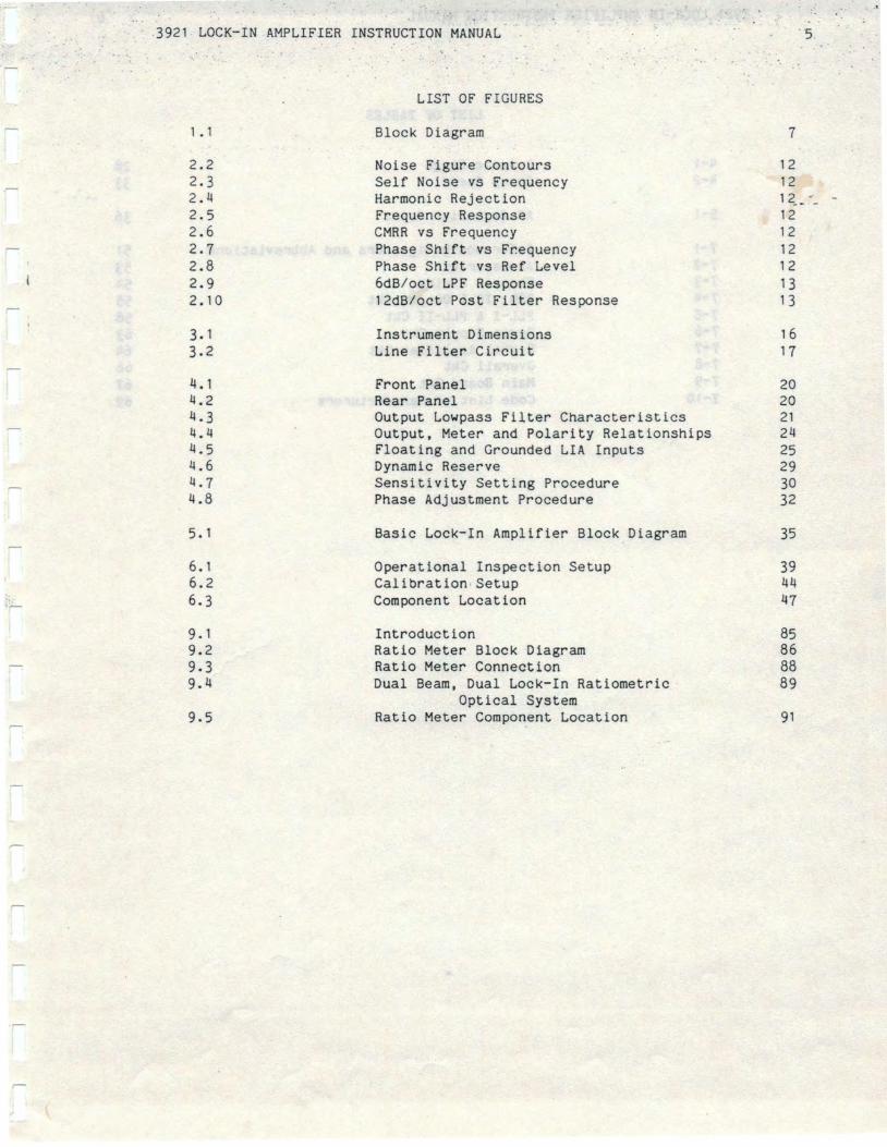
2.1 SIGNAL CHANNEL
Frequency Range:
Sensitivity:
Sensitivity Accuracy:
Stability of Setting:
Input:
Inp11t Impedance:
Maximum Inp11t:
Maximum Common Mode Voltage:
Common Mode Rejection:
Noise:
Overload:
2.2 REFERENCE CHANNEL
Modes:
Frequency Range:
Phase Adjustment:
Autophase:
Autophase Lamp:
SECTION 2
SPECIFICATIONS
10 Hz to 15 kHz
10 µ V to 1 V for f:ill scale ( 10 ,v) output in 1,..10n100 sequence. Continuously variable by 10 turn locking control (MULTiplier).
Less than 3% error at f11ll scale ( 10 Hz to 1 0 kHz), less than 5%@ 15 kHz.
100 ppm/C 0 typ
Quasir.differential, may grounded either at the signal source
10MQ shunted by <80 pF
be floated or
±200 V de. ±15 V peak ac,
±10 v
100 dB at 100 Hz
or the
25 nV per root Hertz (typical) at 1 kHz with shorted input. See Figure 2.3.
Separate indicators for input overload and output overload conditions.
External F, 2F
10 Hz to 15 Hz (to 7.5 kHz at 2F)
±100° continuously variable (manual mode) plus 0°190° and 0°1180° switches
Electronic Servo System for automatic phase adjustment
Goes on when the automatic phase adjustment process is completed

.• . _,j J.1'4.:>. mu '-'l .:1 u1'4 l·uuwi:1..1 · " . . ...... .. . .. . . . ..
l :· :t ;: ... ':; • ... '":'. t • .. · · ..
Camp :· . .. . when·· ttie . s _ignal .. level .. dro'ps·. Threshold: fo ·less than .one· thirtieth of the randan pnp.
input noise (10 10 kHz broadband).*
Autophase Lamp Sinusoid Threshold:
Reference Voltage Range:
Extinguishes when rms signal level drops to less · than one eighth o"f · the peak to peak amplitude of an incoherent discrete frequency interference.*
300 mV to 30 V peak to peak (sinusoidal waveform)
Maximum Allowable Voltage: 200 V de, ±50 V peak ac
Input Impedance:
Tracking Rate: Manual Mode:
Autophase Mode:
100 kO Shunted by <100 pF
0.04 Hz/sec per Hz reference frequency with less than 10° phase error (e.g. 40 Hz @ 1 kHz) Typically Hz/sec per Hz with ref lock maintained and <1% signal error (e.g. 150 Hz/sec at 1 kHz):
*Typically Autophase will continue to work very accurately for signal levels an order of magnitude or more below this threshold, but with very slow response time.
2. 3 PHASE SENSITIVE DETECTOR:
Harmonic Rejection:
Dynamic Reserve:
Time Constants:
p OS t Filter :
2. 4 OUTPUT
Meter:
Output Voltage:
Output Impedance:
Zero Offset:
Typically greater than 55 dB through the 14th harmonic (See Figure 2.4)
Greater than 60 dB pp noise/full scale rms signal voltage
10 msec to 30 sec in a sequence, 6 dB octave (25 Hz to 0.008 Hz equiv. noise· bandwidth)
sec time constant, 12 dB/octave
0 to ±110% scale, 2.5% accuracy
±10 V de full scale
1 ooon
10 turn potentiometer and pol ad ty switch
·, . .

,. . ·. . ·.· .. ·.
_:_.· . :
:· · .,...._
2. 5 OPTIONS
Option 02
3921RM
3921 V1 M7
. .
5Qp.pm/-(:O . -:3 t-.·x o ::s- .f f 500ppm/C0 . at Xl (5 mV offset/C0 )
50pp.m/8 holirs at X1 o (a·. 5 mV offse t/8 hr) _. 500ppm/8 !lours . ?-t X1 (5 ·mv offset/8 hr)
.·. ·"
Analog Ratio Option
Rack Mount Kit
Preamplifier Power Cable
2.6 MISCELLANEOUS SPECIFICATIONS
Lamps Off:
Power:
Environment al: Operation Storage:
Dimensions:
Weight:
Preamp de Power Out
1 N.C. 2 N.C. 3 N.C.
By front panel switch
100, 120, 220, 240 V ac ±10% 50/60·Hz at 12 VA
o0 to 40°C, 10% to · 90% RH -10° to 10% to 80% RH
1 8 • 9 " ( 4 8 Omm ) W x 3 • 4 6 " ( 8 8mm ) H x 1 3 • 8 " (350mm)D. Fits standard rack mount
15 lbs (7 kg) without options
±20 Vdc via rear panel connector @ 300 (±50 mA max.).
MATING CABLE CONNECTOR HIROSE RM12BR0-6S PIN NF-314-03042-00
4 -20V OUT 5 +20 V OUT 6 POWER GND
lOOM tScB 20dBI
lOM
lM -Cl -u :! lOOk .. ;;; u
°' u u lOk Q
<11
lk
..... ....;;a,----------' 10 100 lk lOk lOOk
FREQUENCY <Hz>
Figur• 2.2 NOISE FIGURE CONTOURS AT 290•lc
_200 : ...... 100 > so "' ... a % 20 "" ..J "' 10 "' 10
-;:- -:;-
100 11& "REQUEHCY (Ha)
Figure 2.3 SELF NOISE VS FREQUENCY
0 I 1 1 I 1 1 I I
-10 I -"- I I ] I I ] I I
-20
-30
-I I I I i I I I I I I
I I I I l I I
; I T T I
' T 1 I I 0::
-50 I 1 ] I I I _l I l 1 I
-60
-:o
1 ! I l I i 11 ...1 I
' I I I I I j I!
1 l I l I 1 \ I 11 l L... [ I fij i _[
101&
l I I
I I I 1 I I I I I
I I I I I I 1 ' I
T i I
I I
I I 11
l T ll f 1 I
J 5 7 9 11 13 15 1 i 19 FlN ·FREJI'
Figure 2.4 HARMONIC REJECTION
._,
I
Ll---...,...-1 $--,---,.--1 I --r----r-1 1--r-I -S 10 100 11. IOa
FREQUENCY (H 11
ai' 0
"' 100 Q a:: 0 % 80 20 %-0 c 60 }w
Figure 2.5 FREQUENCY RESPONSE
Iii" 7 v '--'-- --- ---,.__ .
s 10 a: 100 11& FREQUEHCI' (Hz)
Figure2.6 CMRR VS FREQUENCY
... 10 • c a. 5 • ...
0 w..
r---. 101&
l: ... "' -s ... b"'
...::.
41(
f -10 10 100 11& lOlc
FREQUEHCI' (Hz)
Figu,.. 2.7 PHASE SHIFT VS FREQUENCY
... • a. • e. II: 0 II: II: ... ... ...
10
0 t----
.. -10
0.05 0.1 0.2 REFERENCE LEVEL (V""•)
Figure2.8 PHASE SHIFT VS REF LEVEL
2

3921 LOCKt"IN . AMPLIFIER .. INSTRUCTION MANUAL"; . .. . •· ·13 .. ...
· ...
t/T Eo (%)
Eo (%) toot 0.5 39.35.
1i.o 63.21 :i. 5 77 ...
0 sE:.47 I I
60 ", ., .-:-! . -:J J.. •
3.0 95.02 40 3.5 96.98
4.0 98.17 20 4.5 98.89
5.0 99.32
2 3 4 5 6 5.5 99.59 6.0 , 99.75
Time (t/T)
Figure 2-9 6dB/OCT LPF RESPONSE (Post Filter Off or Time Constant > 1 sec)
Eo (\)
1col
80 l I
601 40! 20
1 2 3 s 6 Time Seconds
SECOMOS
0.5 1.0
; 1. 5
2.5 3.0 3.5 4.0 4.5 5.0 5.5 6.0
Figure 12dB OCT POST FILTER RESPONSE (Time Constant < 1 sec)
Eo (%)
9.02 26.(2 44.22
59.4C I 71. 27 80.09 86.41 90.84 93.89 95.96 97.34 98.26

. . AMPLIFIER INSTRUCTION MANUAL.· . . ., . .1 4 ... ... .: .. - • •. ... :·
·, ---. ·. ) .

3921 AMPLIFIER INSTRUCTION MANUAL 15
SECTION 3
PREPARATION FOR USE
3.1 INSPECTION
Upon unpacking the instrument, inspect it for any damage that may have occurred in transit. Save all packing materials in case the unit must be ret11rned. Visually check to confirm that there are no broken controls or connectors, and that the case and panel surfaces are free from dents and scratches. If any damage is detected, the c11stomer must file a claim with the carrier and should also forward a copy to ITHACO. We will then give advice on the disposition of the eq11ipment and will arrange for repair or replacement without waiting for a settlement of the claim against the carrier.
3.1.1 COMPONENTS SUPPLIED
3921 Lock-In Amplifier Ins tr 11c t ion Manua 1 Power Cable, 3 Conductor x 7 feet Fuse + Spare (mounted in fuseholder, 0.5A for 100 or 120 Vac line power) BNC Signal Cable Hex Wrench (1.5 mm across flats) for turns counting knobs
1.1.2 ELECTRICAL CHECKOUT
,, The customer sho11ld operate the equipment to verify that it functions correctly. See Section 6.2, Operational Inspection.
3.2 ENCLOSURE AND MOUNTING
The instrument is housed in a bench top enclosure which includes a hinged front leg assembly for easy viewing of the front panel. Tile enclosure fits into a 3 1/2" high space in a standard 19" relay rack. For this pu·rpose ITHACO makes an optional Rack Mounting Kit, the 3921RM, which consists of two brackets and the necessary nuts and bolts for their installation on the front corners of the enclosure.
3.2.1 INSTALLATION OF RACK MOUNT EARS
Remove four screws from the two rear plastic moldings. Remove moldings and slide out side panels. Then remove the two screws on either side nearest the front of the instrument. Place sub bracket so that its holes line up with the removed screw holes. Place eared bracket so that its holes also line up, and secure with two flat head screws. Repeat on other side. Slide new shorter side panels in place and rear molded pieces.
. 3 921 LOCKr.IN AMPLIFIER INSTRUCTION . MANUAL ·.
J
18/0.7 ..
429/16.9-
44SL11.s-
li /; . ----------- -350/13.8 .. 368/14.S•
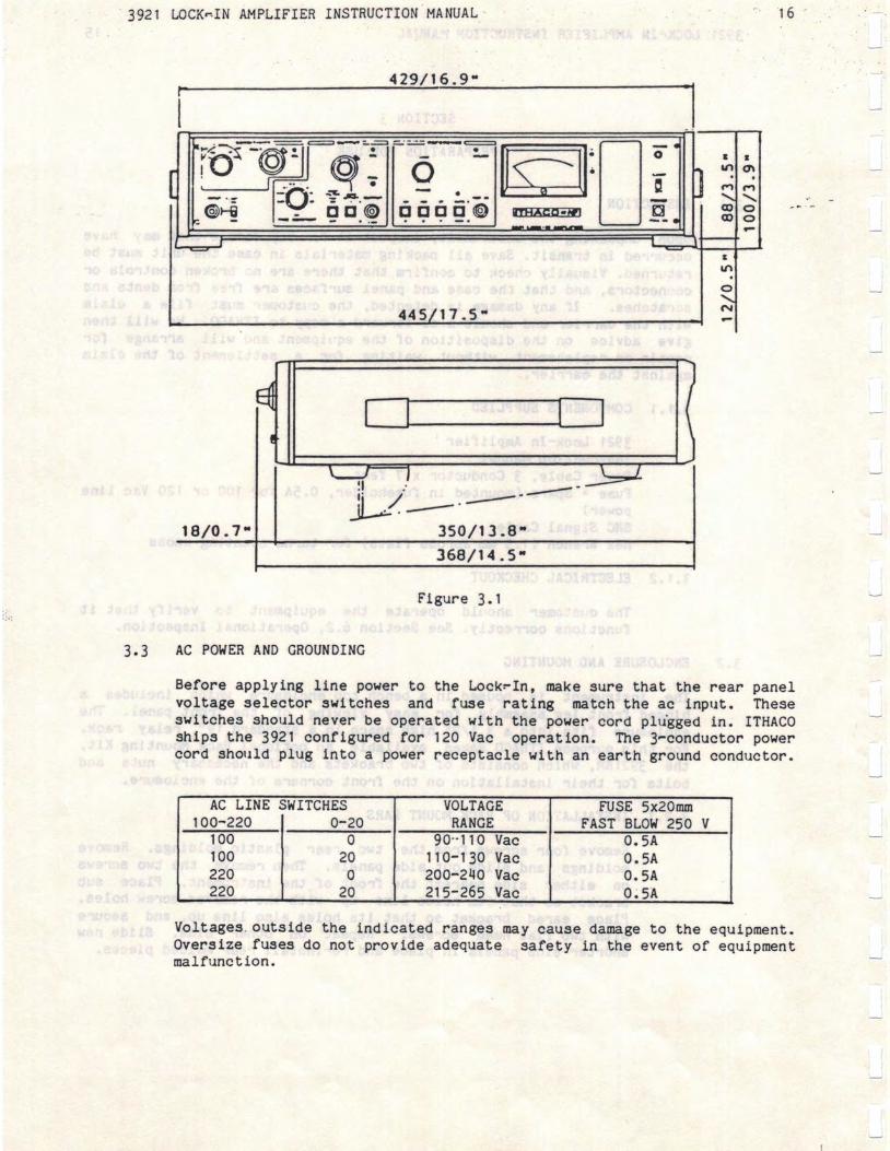
Figure 3.1
3.3 AC POWER AND GROUNDING
· 1 - .
s
0 "' M ......... aJ aJ
"I 1t--- &
"' .
-
I 0\ . M ......... 0 0 -
Before applying line power to the make sure that the rear panel voltage selector switches and fuse rating match the ac input. These switches should never be operated with the power cord plu'gged ITHACO ships the 3921 configured for 120 Vac operation. The power cord should plug into a power receptacle with an earth ground conductor.
AC LINE SWITCHES VOLTAGE FUSE 5x20mm 100-220 0-20 RANGE FAST BLOW 250 v
100 0 90·-110 Vac O.SA 100 20 110-130 Vac O.SA 220 0 200-240 Vac 0.5A 220 20 215-265 Vac
Voltages . outside the indicated ranges may cause damage to the equipment. Oversize fuses do not provide adequate safety in the event of equipment malfunction.

3921 INSTRUCTION MANUAL 1 7
3. 3. 1 FUSES
The fuseholder is accessable when the power cord is removed from the rear panel. To remove it, insert a standard screwdriver in the slot and pull forward. The active fuse and a spare both fit in the holder, with the spare residing in the space closer to the exterior of the instrument.
3. 3. 2 GROUNDING
A rear panel terminal provides an alternative means for providing a ground to prevent electrical interferLnce or shock hazards. It
I may be used to supplement a missing . or 11ntrustworthy power receptacle earth ground. It also may be :1sed in place of power ground in instances whsre ground loop interference could cause measurement diff ic111t ies.
The instrument uses a line filter as shown below to prevent problems with electromagnetic interference. Leakage current does not exceed 0.5 mA rms at 250 Vac 60 Hz. The unit conforms to electronic measuring equipment safety standards detailed in IEC Publication 348.
Figure 3. 2 LINE FILTER CIRCUIT

· . . ; . . ·· ....
.392-1 AMPLIFIER INSTRUCTION MANUAL . . . ' ' '• I .
. . · .: . .' · ' . .. 18 . .

,....... .
3921 AMPLIFIER INSTRUCTION MANUAL 19
SECTION 4
FUNCTIONS AND USE
4.1 CONTROLS, INDICATORS AND CONNECTORS
4.1.1 SIGNAL INPUT SECTION
(1) SENSITIVITY SWITCH (Input Voltage Range)
(2)
This sets the ac input gain in a 1 r.1 Or.1 00 sequence. It is calibrated in volts and rms required to achieve a full scale output ( 100% on meter or 1 O Vdc on 0:1tput BNC) when the MULT control is set to 1.00.
MULT (Sensitivity Multiplier Dial)
This 10 turn potentiometer controls the post-detector de gain of the instrument, progressively reducing the gain as it is turned from its lower limit of 1.00 to its upper limit of 11.00, thereby reducing the overall sensitivity. The overall sensitivity equals the product of the MULT control and SENSITIViTY control settings.
Reading the absolute val11e of a changing input is facilitated by using MULT settings of 1, 2, 5 or 10.
For a steady signal, one can read the absolute value by setting the SENSITIVITY and MULT controls for a full scale output (100% on meter or 10 Vdc out). The product of the two settings equals the input level.
(3) OVL (Input Overload Lamp)
When on, it indicates that the ac input amplifier is being driven into distortion, either by _ the coherent signal or by its accompanying noise. The sensitivity control must be · decreased.
(4) INPUT (Signal Input Connector)
The unknown signal input to be measured is applied here.
(5) FLOAT/GND (Input BNC Shell Grounding Switch)
Used to prevent ground loops due to doubly grounded input circuitry. Provides input in FLOAT position and singlenended input in GND position.

I
3921 AMPLIFIER INSTRUCTION MANUAL
l I r
J
4 5 6
21 ;= I- -- --
10 11
L
7 9 12
13 19 I
14 15 16 17 18
v
Figure 4.1 FRONT PANEL
UNUSED
-0 0 ·---_!_
OPTION 02 ANALOG RATIO
A REA
i0' % 0 0 0 0 0 /1L J -CJ-- 0 0 .......-1 L J -.....-
AC FUSE LINE CHASSIS UNUSED POWER HOLDER VOLTAGE GROUND CORD SELECTOR
RECEPTACLE
Figure 4.2 REAR PANEL
20
20 22
_,,, . -- 01 0 0 0 .. - a \
[ITHA l;_O •Hr
>•7t 1.0C" .... -.'"<" 7.
I 21
0
7 23
REMOTE PREAMP POWER
f 01
l '-J j
24
-
-
- t--
0 j -l .._.......
UNUSED
LOCKrIN AMPLIFIER INSTRUCTION MANUAL 21
4.1.2 OUTPUT SECTION
8 = ..L. .. , 1
f =-c 2" ri
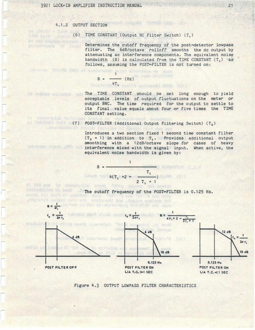
(6) TIME CONSTANT (Output RC Filter Switch) (T 1 )
Determines , the ·cutoff ·frequency of the lowpass filter. The 6dB/octave rolloff smooths the de output by attenuating ac interference components. The equivalent bandwidth (B) is calculated from the TIME CONSTANT (T 1 ) -a-s-follows, assuming the is not turned on:
B (Hz)
The TIME CONSTANT should be set long enough to yield acceptable levels of output fluctuations on the meter or output BNC. The time required for the outp11t to settle to its final value equals about four or five times the TIME CONSTANT setting.
(7) POST.-fILTER (Additional Outp.ut Filtering Switch) (T 2 )
Introduces a two section fixed 1 second time constant filter (T 2 "'1) in addition to T1 • Provides additional 011tput smoothing with a 12d8/octave slope for cases of heavy interference mixed with the signal inp11t. When active, the equivalent noise bandwidth is given by:
a-----------4(T 1 +2 - . ----)
2 T 1 + 1
1be cutoff frequency of the POSTMFILTER is 0.125 Hz.
f =-1-c 211r,
12 dB 1
fc=--
POST FILTER OFF
18 dB
0.125 Hz POST FILTER OH LIA T.C. >1 SEC
Figure 4.3 OUTPUT LOWPASS FILTER CHARACTERISTICS
0.125 Hz POST FILTER ON LIA T.C.< 1 SEC
2" r,
18 dB

22
• ... ; • • t: •• ; . . . • •
(8) ZERO OFFSET _Dial)
Adds a fixed de voltage to the 011tput. With MULT = 10.00, an offset of up to ±100% of fuil scale can be added. With MULT • · 1 ;00, this .increases to·. ±.1000%: Th.is feature allo"w·s one to observe small changes in signal level by suppressing coherent background level.
(9) +;- (Offset Polarity Push button)
Adds or subtracts val11e determined by ZERO OFFSET control. POSITIVE when in.
(10) ZERO (Baseline Offset Calibration) ·
This screwdriver adjustment sets the baseline output to O mV de when the INPUT is shorted.
(11) OVL (Output Overload Lamp)
Indicates Post,..detector de output amplifier saturation if MULT is set too high. Will flicker if the TIME CONSTANT is not set high enough to suppress output fluctuations.
(12) OUTPUT (de Output Connector)
Provides ±10 V de full scale output for DVM, chart recorder or digitization by computer.
4.1.3 REFERENCE SECTION
(13) PHASE (Reference Phase Shifter Knob)
Allows for manual ±100° phase adjustment of the REF IN frequency relative to the SIGNAL input. Used in conjunction with the 0°190° and 0°/180° push buttons to find the phase for maximum output, and therefore the true signal strength, when the AUTO/MAN push but ton is set to manual.
( 14) 0° 190° (Quadrature Phase Shift Push but ton)
When in, provides a 90° reference phase shift to facilitate manual phase adjustment.
(15) 0°/180° (Reference Phase Inversion Push button)
When in, reverses the polarity of the REF IN signal to allow 360° phase coverage in AUTO or MAN mode.
.. .

3921 AMPLIFIER INSTRUCTION MANUAL 23
( 16) 2F IF (Second Harmonic Push but ton)
Normally this is left in the out (F) position. When this control is in the (2F) ·position, the Lockhln doubles the REF INPUT frequency and responds to the signal INPUT frequency component at twice the reference frequency.
(17) AUTO/MAN (Autophase Function Push button)
When in, provides for automatic adjustment of phase ±100°. An electronic servo loop operates until an output maximum is found. For signals shifted by more than ±100° relative to the reference, the 0°/180° push but ton ( 1 4) must be depressed. The lamp above the p11sh but ton goes on to indicate that the A11tophase circ11itry has detected successful automatic phasing of the reference input.
(18) REF IN (Reference Input Connector)
The synchronizing signal is applied here.
(19) UNLOCK (Reference Non-synchronizing Indicator Lamp)
Goes on to warn that the phase-locked loop has not frequency.
4.1.4 METER AND POWER SECTION
internal reference oscillator captured the external reference
(20) METER (Analog Output Indicator)
Moving coil galvanometer with 0-100% scale for absolute output readings. Also has a 0-1-2 scale for ratio measurements if Analog Ration Option 02 is installed.
(21) METER ZERO
Screwdriver adjustment mechanically nulls the meter ·with unit power turned off.
(22) +/- (Meter Polarity Lamps)
Since the Lock-:-In Output is proportional to Acosqi and the reference phase qi may range from 0° to 360°, the de OUTPUT may range from -A to +A. To achieve higher meter resolution, this output is rectified to an absolute value in the meter circuit. The polarity lamps indicate the sign of this output. See Figure 4.4.
' :

i•.
. . 3921 · . .. 24". .
4.2
DC OUTPUT (V)
HETER I NO I CA Tl ON
+/• POl.AAI TY INDICATION
Figure 4.4 OUTPUT, METER AND POLARITY RELATIONSHIPS TO PHASE OF LOCK-IN
(23) LAMP OFF (Front Panel LED Defeat Switch)
When off, no indicator lamps will function. This prevents interference with detectors in low level optical work.
(24) POWER (ac Line Input Switch)
Pull out to turn on unit.
INPUT/OUTPUT CONNECTORS
4.2.1 SIGNAL INPUT
Due to the higl1 impedance and sensitivity of the Lockr-In input, one should always use co-axial cable. The grounding of the shield conductor should be made at one point only to prevent ground loop interference.
When the signal source has a ground return path, use the FLOAT position to break the BNC shell ground connection at the The FLOAT position provides input amplification.
CAUTION! To prevent damage when FLOATING the input, be sure that the common node ac voltage (between BNC shell and the cabinet) does not exceed ±10 volts peak. The center conductor may safely exhibit · 200 V de and ±15 V peak ac relative to the SIGNAL input BNC shell.

.-
3921 LOCKnTN · AMPLIFIER INSTRUCTION MANUAL 25
When the signal source does not have a gr-ound reference, :1se the-GND position. This shorts out one input of the differential amplifier and provides shield grounding for the inp11t cable the lock-in chassis.
One way to detect ground loop errors involves reducing the signal exactly 1 O dB using a precision attenuator ahead of the input. The lock-in 011tp11t should drop by a factor of 0.316. If the FLOAT/GND switch is incorrectly set, some other ratio will be observed. If both positions of the switch seem to give bad results, review and experiment with system gro1mds incl:1ding source ground, power cord ground and chassis ground. See Sect ion 3.3.2. Selection of the proper external preamp may solve the grounding problems in st:1bborn cases.
SIGNAL HAS GNO REP'
COMMON MOOE
INT! Rf'EREHCm
SIGNAi.. HAS NO GMO fU!f'
0
l.IA IHPUT
GHO
6
QUASl-OIFFeRENTl.AL INPUT
SINGLE EHOEO INPUT
Figure 4.5 FLOATING AND GROUNDED LIA INPUTS
4.2.2 REFERENCE INPUT
The Model 3921 must have an external reference input to operate. For sinewaves, the level may range from 0.3 V to 30 V p-o, however for levels below 1 V the reference level wist not fluctuate or else errors will occur due to reference phase variations. For rectangular wave input, the duty cycle must lie between 20:1 and 1 :20.
TI"le LIA will not operate if the UNLOCK lamp is lighted.
.. . . : .. ... .
.... ·.
.. .. """ · r:. .. . .... : -:: .... . \·. ,, • • • • .... • ......;. •• • 1 ... ....
3921 .. LOCK-IN .AMPLIFIER INSTRUCTION· MANUAL ... .... :·.. ... . , ; -·
. ·. ·.
4.3
4.2.3 EXTERNAL PREAMPS
. . . . . · ..
ITHACO remote preamplif iers may be powered from the rear panel ±20 V connector to . achieve -impedance. mp,tching, low no.ise performance, true differential input, current input, or greater sensitivity (e.g. 100 nV full scale).
ITHACO PREAMP MODEL
1 641 1651
1661 1671 1681
125 143 144
TYPE
Current Differential Transformer or Direct Single Ended Lo Noise Single Ended Lo Noise Single Ended Differential
Single Ended Lo Power Single Ended Lo Power. Single Ended Med Power
INPUT IMPEDANCE
0 1 OK
100M 40K
100M 100M
1000M 1000M 1000M
In general meaning the
the preamp should be treated as a input to the 3921 should FLOAT.
OPERATION
GAIN
10 8 /10 6 /10't V/A 60dB 20dB 40d8 -20dB 20dB
OdB 20dB 40dB
grounded source,
To obtain ·a measurement, three basic parameters of the lock-in must be set: SENSITIVITY, TIME CONSTANT and PHASE. The SENSITIVITY range switch and the MULT dial together determine the rms ac input to de output gain and also the dynamic reserve (tolerance to incoherent interference or signal harmonics without overloading the input). The TIME CONSTANT switch controls the degree of output smoothing to suppress 9utput ripple and random fluctuations. The PHASE controls must be set to shift the phase of the reference to 0° or 180° relative to the signal in order to get a true output. If mis-set, an error proportional to the cosine of the phase angle will result.
In a typical measurement, one would set the SENSITIVITY controls to get an output that is a reasonable precentage of full scale, adjust the TIME CONSTANT to effect an acceptable compromise between settling time and output fluctuations due to noise, and operate the PHASE controls to achieve an output maximum. The settings normally would be made in the order given, with some repeated as the control parameters are refined. If the AUTO lamp goes on in the AUTO phase mode, then the manual phase adjustment will be unneccesary.

- .. . · ' ; .... , . . ·· . .·
" .. 3921 .. LOCKrIN .AMPLIFIER INSTRUCTION t-1-ANl/AL . : 27 .. .
4.3.1
.. ·= .....
STARTING SETTINGS·
Before beginning · a measuremerit, the following initial control settings (see .·Fig • . 4-•. J )·: .
SENSITIVITY 100 mV MULT 1.00 FLOAT/GND GND TIME CONSTANT 0.3 sec ZERO OFFSET 0.00 POST FILTER OFF 0°190° oo 0°/180° oo F/2F F AUTO/MAN MAN LAMP ON
Mechanical zero of the meter (21) can be checked before power is turned on. Adjust if necessary. With power on, electrical ZERO (10) can be set with the input shorted using the above settings. If very accurate nulling via a DVM is desired, allow at least 1/2 hour warmup. Adjust if necessary.
4.3.2 REFERENCE INPUT
Connect REFerence IN put signal. off in several seconds, or continuously, check to see that:
If the UNLOCK lamp fails to go if it does not remain off
1. The frequency 1 ies between 1 O Hz and 1 5 kHz.
2. The level lies between 0.3 and 30 V pp (sinewave).
3. The duty cycla lies between 20:1 and 1 :20 (pulsewave).
4. The waveform is relatively clean with regard to jitter noise and frequency instability.
4.3.3 SENSITIVITY AND MULT SETTING
Connect the signal to be measured to the INPUT BNC and set the FLOAT/GND switch as appropriate (see section 4.2.1, 4.2.3 and Figure 4.5).
Start. with MULT • 10.00. This provides the greatest accuracy at the expense of the lowest dynamic reserve. This setting might be reduced later for several reasons:
1. To achieve maximum sensitivity if the signal is below 100 µV rms (10 µV switch setting).
2. To achieve a larger full scale meter indication. In this case, it is advantage to -use MULT control settings of 1 .00, 2.00 or 5.00 to facilitate reading the meter.
.•.

3. To · increase . overload tolerance if the rms signal is more than 40 dB below the input interference. The dynamic reserve increases to 60 dB at a setting of 1.00.
4. To set meter to a normalized re.ading · such as 100% or 50% (.1 on meter red scale) for a nominal signal level. Thus, for example, one could read the relative attenuation percentage directly off the meter and know that a 100% indication has- _.,._ an absolute value equal to the product of the SENSITIVITY switch setting and the MULT setting.
Increase the SENSITIVITY until a reading above 10% of full scale is obtained. If a flashing output overload lamp (11) occurs but the meter reading is not offscale, raise the TIME CONSTANT to increase the smoothing of the output.
If the meter indication is low but the input overload lamp (3) lights, the problem is due to interference that exceeds the dynamic reserve. Set MULT to 1.00 and try again. ·
4.3.3.1 DYNAMIC RESERVE
Table 4.1 defines the dynamic reserve limits for various settings of SENSITIVITY and MULT, where:
Dynamic Reserve •
Maximum Noise Volt age without over load (pp)
Full Scale Voltage (rms)
MULT SENSITIVITY
1.00 10.00
lOµV x1000 x100 100uV x1000 x1 OCJ
1mV x1000 x100 10mV x1000 x100
100mV x200 x20
TABLE 4.1 DYNAMIC RESERVE
Figure 4.2 summarizes the tradeoff between output stability and dynamic reserve as a function of the MULT control setting. At 1.00, the unit will tolerate the most interference (1000:1) but, due to drift, noise and so forth, the out 11ncertainty will also be the greatest. At 10.00 the unit will be able to handle only one tenth as much interference, but the stability and measurement accuracy will increase tenfold.
• a.,

3921 LOCKCJIN AMPLIFIER INSTRUCTION MANUAL 29
10' N ._ I'-! r--. eo• .-... IW'Vf CIW-.ot.G U"fll -Ti
._ -I- ... ,; • u 1--I- 5
z 10 ._... -
f 11U. SCAll s -1 .. u !
- Q z et i 1-- 5 z 0
HS ' i
f:::j H
........, --t-
z l ' s ' 1
Figure 4.6 DYNAMIC RESERVE
4.3.4 TIME CONSTANT AND POST FILTER
These controls set the system bandwidth, thereby establishing the degree of interference rejection. Too high a bandwidth relative to the noise (overly low TIME CONSTANT setting) manifests itself as excessive output fluctuations. Increase the TIME CONSTANT setting, if necessary, to achieve an acceptably steady reading.
In low level work, line frequency harmonics near the signal frequency may cause a beat frequency in the output of the at 30 Hz or below. This can be observed by attaching an oscilloscope to the OUTPUT connector. If this ripple is large enough, it may interfere with readings or cause an output overload (11). Activating the POST FILTER will suppress the ripple by introducing a 12dB/octave (40dB/decade) rolloff starting at 0.125 Hz. This can be increased to 18dB/octave (60dB/decade) by also setting the TIME CONSTANT to one second. For best results, the operating frequency ought to be chosen to lie roughly centered between nearby harmonics of 60Hz. Typically one selects a frequency 25 Hz from one harmonic and 35 Hz from the other --e.g., 215 Hz which lies between the 3rd harmonic (180 Hz) and the 4th (240 Hz).

I:,
3921 AMPLIFIER INSTRUCTION .MANUAL
SENSITIVITY
MULT
TIME COHST A.HT
100 "'v .10
0.3 ••c
.THE LEVEL OF THE INPUT SIGNAL CONTAINING HOISE IS EXCESSIVE.
IHCREASE THE VALUE OF =::>i--;..;;.;;;......;11i4 THE TIME CONST AHT
IHCREAS! S!HSITIVITY
DECREASE ntE SEHSITivtTY ONE STEP
DECREASE THE Ml.IL. T COHTROL. SETTING TO S.00 OR 2.00 OR 1.00
REM> THI! INOICATED VALUE
HO
· YES
COHTROL
INCREASE TH! VALUE Of THE TIME COHSTANT CONTROL.
THE SIGNAL TO ae DETECTED IS TOO USE A REMOTE PREAMP OR COHSIDER USING A MORE SENSITIVE LOCK-iN AMPLIFIER
FIGURE 4.7 SUGGESTED SENSITIVITY SETTING PROCEDURE
30

jl
4.3.5 PHASE SETTING
Since the output of the lock-in is proportional to where equals the phase difference between the signal and reference
inputs and A represents the signal magnitude, the phase must be properly adjusted to be a true reading. In general start out with Autophase active. If the Auto lamp will not come on, then -MANual phasing ought to be investigated.
The Autophase circuit employs a separate phase sensitive detector. This technique is far superior to competitive techniques which electronically drive the phase to achieve an output null, then shift the phase 90°. First, the 3921 Autophase function is unaffected by the TIME CONSTANT setting. · second, it works very well in the presence of high noise levels.
4.3.5.1
4.3.5.2
AUTOPHASE
Set 0°1180° and 0°190° Switches to 0° (out) and depress the AUTO switch. If the AUTO lamp does not come on with the SENSITIVITY switch set approximately correctly, reverse the 0°/180° switch. Failure of the lamp to go on within several seconds indicates that the input noise is large enough to impair functioning of the Autophase circuitry. This does not necessarily mean that the AUTO mode should not be used.
If the lamp is off due to poor SNR, there is a very good chance that the AUTO mode is still functioning to produce better results than the MAN mode. Typically this would happen when the input signal falls to a low level against a constant noise background. In this noisy environment, manual phase setting probably will be slower and less reliable than the automatic method. Be warned that below the lamp threshold the Autophase circuit is very slow (e.g., requires minutes to settle if the signal is 20 dB below threshold). However, if the signal drops without changing phase, this settling time constraint is removed. For both discrete frequency and random noise interference, accurate Autophase functioning is routinely observed until the signal falls 30 dB below the lamp threshold, at which point the signal is barely measurable anyway due to background noise.
MANUAL PHASE SETTING
In principle one could set phase manually by manipulating the PHASE control for a maximum meter reading, which would occur when the phase difference between the signal and the shifted reference input equalled 0° or 180° (180° would result in a negative output BNC voltage with an absolute value equal to the positive value which would be obtained if the 0°/180°

3921 LOCK-lN AMPLH.lt;J:'{ l"lJU'lU.IU .... ' '·'<1· · . •
switch were reversed). This procedure is slow and prone to error, particularly if the input is noisy and/or a long TIME CONSTANT is in effect.
A much quicker and more accurate method is to adjust phase for a m1n1mum output reading (near 0% on the meter), then reverse the 0°/90° switch to take measurements.
4.3.6 ZERO OFFSET
For normal measurements made via the front panel meter, . this control should be set to 0.00. ZERO OFFSET is provided for two reasons. First, if observation of the OUTPUT is made on a chart recorder or DVM, the OUTPUT can be zero suppressed to facilitate measurement of small changes in a large background signal. The resolution increases in proportion to the additional gain provided by the external measurement device (e.g., 1 volt full scale on a chart recorder would yield a tenfold improvement). Second, if the MULT control is set to 1 .00, then the SENSITIVITY switch can be increased one step from 1 mv to 100 µV), with the meter indication being brought on scale using the ZERO OFFSET control. This increases the resolution of the 3921 tenfold.
J.OJUST TI4C '"AS! IN T1i! MAN MOO! (SURO. l'OR AH OUTPUT NUW
Rl!AO TI1! IHOfCl.T!D VAUJ!
Figure 4.8 PHASE ADJUSTMENT PROCEDURE

/
.. :. 3921 LOCK-IN .AMPLIFIER INSTRUCTION MANUAL 33
4.3.7
. · .. ·. '··
When using ZERO OFFSET to increase · meter resolution (MULT = 1 .00), first set ZERO OFFSET= 0.00 and rotate the SENSITIVITY switch to get an on-scale reading. Next, increase the SENSITIVITY one step (ccw). Note polarity of meter on(+)(-) lamps (22). -Switch to opposite polarity on ZERO OFFSET (+) (-) lamps (9) then increase ZERO OFFSET dial to null the meter. To obtain a precise null, adjust for equal brightness observing the(+)(-) polari_t.y·_ -lamps.
The expression below gives the signal measurement in terms of panel control settings.
Meter % V. =SENSITIVITY
in 100 x MULT -OFFSET)
If output ripple exists on the LIA output, it can interfere with zero suppression. As the meter approaches a null, the meter polarity circuit (Figure 4.5) will rectify the ripple, resulting in a residual meter reading that cannot be reduced using the ZERO OFFSET control alone. Both the (+) and (-) polarity lamps will be fully lighted. This effect can be eliminated by increasing the TIME CONSTANT or activating the POST FILTER switch, per Section 4.3.4. The ripple problem would not be apparent if an average responding ac voltmeter were reading the OUTPUT connector.
SWEEP SPEED
The Model 3921 reference frequency can be swept continuously over its full operating range: 10 Hz, to 15 kHz. In the MANual phase mode, reference lock will be maintained with less than 10% phase error (less than 3% amplitude error) as long as the sweep speed is not too fast relative to the reference frequency (0.04 Hz/sec per Hz).
In the AUTO phase mode faster tracking will prevail (0.1 Hz/sec per hz, typically) with lower signal error (1% or less).
FREQUENCY MAX MAN PHASE SPEED MAX AUTO PHASE SWEEP HZ SPEED (3%ERROR) SPEED (1%ERROR)
Hz/sec Hz/sec
10 0.4 1 100 4 10 1000 40 150
TABLE 4.2 SWEEP SPEED
The values refer only to reference tracking effects. The measurement accuracy will also be dependent upon the output response time as set by the TIME CONSTANT control.

· ...
·3921 LOCK-IN .AMPL:IFI"E°R · .INSTHUCTI .. ON MANUAL ,,, -y. . • :..:- ·.
34 ··.·"

3921 LOCK-IN AMPLIFIER INSTRUCTION· MANUAL 35
SECTION 5
PRINCIPLE Or OPERATION
5.1 THE BASIC LOCK-IN AMPLIFIER
8
The lock-in amplifier is an extremely selective ac voltmeter. -It- -operates on the principle of narrowbanding to reject interference while passing the signal at the frequency of interest. In effect, the amplifier locks the center of its passband precisely onto a second i nput frequency, the reference input, which is coherent with the signal.
SIGNAL INTERFERING FREQUENCY
l 1t t r- RANOOM NOISE
__..,_ I /f.r'-1/! I F, -.de
F, F,
SIGNAL BEAT FREQUENCY
-------SIGNAL INPUT -----de NOISY
EXPERIMENT 0
REF CKT F, __ __
LPF
TIME CONSTANT, T
Figure 5:1 BASIC LOCK-IN AMPLIFIER BLOCK DIAGRAM
The phase sensitive detector (PSD) multiplies the input by the reference frequency, downshifting the spectrum so that the signal of interest appears as a pure de level at its output. All other input components appear as beat frequencies or frequency shifted noise fluctuations. These can be removed by a simple, utterly stable RC (TIME CONSTANT) low pass filter (LPF) to provide practically arbitrarily narrow equivalent noise bandwidths (B). The effective Q referred to the reference frequency-approximately F /(1/4T)-can be set above 10 7 for the 3921. r
The effectiveness of the filtering process varies as the square root of the bandwidth. This means that a 100-fold increase in TIME CONSTANT would be needed to achieve a 10-fold reduction in the output fluctuations being caused by random noise within the passband of the lock-in. The penalty would be 100-fold increase in meter response time.
5.1 .1 THE 3921 PSD COMPARED TO OTHERS
Ideally the PSD should be a linear multiplier with a sinusoidal reference input. However no practical circuit exists which can operate over a wide dynamic range with sufficient accuracy and stability.

3921 LOCK-IN AMPLIFIER INSTRUCTION MANUAL 36 ..
The classical lock-in amplifier employs a switching PSD which in effect multiplies the input by a square wave reference signal. While very accurate, it suffers from odd harmonic responses to signal input components that correspond to the overtones of the reference drive to the PSD. One common solution to this problem is to insert a tuned amplifier into the signal path to eliminate odd harmonics before they get to the PSD; an approach which has serious drawbacks of its own such as intolerance to reference -frequency drift. ITHACO Dynatrac lock-ins circumvent these problems by a heterodyning technique, an approach not suitable for a low cost instrument.
The Model 3921 works on a hybrid principle using switching technology to approximate a sinusoidally driven linear multiplier in a stepwise fashion. This yields very good harmonic rejection using a simple PSD circuit. As a result, the need for heterodyning or input bandpass conditioning filters is eliminated, allowing a low cost, reliable instrument to be produced which outperforms comparable but more costly lock-ins.
5.2 CIRCUIT DESCRIPTION (See Fig. 1.1)
5.2.1 SIGNAL INPUT (Fig. 8.1)
5.2.2
The ac input amplifier consists of three stages, A1, A2 and A3. Their gains are set by the SENSITIVITY switch as shown in Table 5.1. Differential amplifier A1 accepts a floating input. A2 provides a single ended signal referenced to frame ground. A3 drives the PSD with 0° and 180° split phase outputs. A1 and A2 are monitored for input overload indication.
SENSITIVITY STAGE GAINS OVERALL GAIN A 1 A2 A3
10 µV 10.3 10 20 2060 100 µV 10. 3 10 2 206
1 mV 10.3 2 20.6 10 mV 1.03 2 2.06
100 mV 1.03 .2 0.206
--TABLE 5. 1 AC AMPLIFIER GAINS
PSD (Fig. 8.2)
This is the heart of the lock-in. A pair of digital multplexers sequentially switch in a weighted portion of the signal to its output. The full scale drive to the PSD ranges from 20.6 mV rms (MULT = 1.00) to 206 mV rms (MULT 10.00).

3921 LOCK-IN AMPLIFIER INSTRUCTION MANUAL 37
5.2.3 OUTPUT (Fig 8.3)
The PSD feeds the single pole lowpass filter-amplifier the corner frequency of which is controlled by the TIME switch.
(Q106a) CONSTANT
The next amplifier stage (Q106b) incorporates the ZERO trim, the -ZERO OFFSET dial and the two-pole, fixed frequency POST FILTER controls.
This is followed by the - variable gain MULT de amplifier (Q107b) which provides the OUTPUT BNC signal. It also feeds the rectifying meter amplifier (Q107A), and in turn the polarity indicating lamps (via Q108 c and d). Q108 a and b monitor for output overloads, lighting the OVL lamp whenever the output (including ripple) exceeds the range ±11 .5 V.
5.2.4 REFERENCE SYSTEM
5.2.4.1
5.2.4.2
PLL-I (Fig. 8.4)
Input comparator Q201a waveshapes the reference input for the phase locked loop consisting of Q203 and associated components. Q204, 211, 212 a and b, and 1/2 Q213 form a sawtooth VCO within the loop. Q212c, 1/2 Q213 and Q214 form the feedback loop, which contains provision for 180° phase reversal and 2F operation. Q201b, c and d comprise an unlock lamp driver for PLL-I and PLL-II.
PLL-II AND PHASE SHIFTER (Fig. 8.5)
Q212d accomplishes a continuous comparing the sawtooth output of The PLL-II circuit, Q220, makes and filtering prov1s1ons. generate the timing waveforms element Q238 allows for the 90°
±100° PHASE shift by PLL-I with a de level. use of its on-chip VCO
Q205, Q206 and Q210 for the PSD. Feedback phase shift feature.
5.2.5 AUTOPHASE (Fig. 8.6)
A square wave PSD Q299 (separate from the main signal processing PSD) operates on the output of the A3 amplifier. In the AUTO mode, this is processed - to a de level and fed to the phase shifter, nulling the phase error in the main PSD. In the MAN mode, the de level is provided by the PHASE knob. Q231a and Q233 extinquish the AUTO lamp if the input signal to noise ratio exceeds a preset threshold.

. .. . : ... 3921 'LOCK-IN ... AMPLIFIER MAJ-WAL,<· " . ..... '"\'.; ·· .
·,· · . i··;. ......... .. , .to... • _ ........
. .• . ..

... . 3921 AMPLIFIER IN.STRUCTION · MANUAL ·
. · . ... . . ..
6. 1 INTRODUCTION
SECTION 6
MAINTENANCE
39 . ·
. · .. •.
This manual contains procedures for operational inspection and for user calibration adjustments. Schematic diagrams are provided to assist in trouble shooting. Problems which cannot be remedied in the field should be referred to the ITHACO Customer Service Department.
6.2 OPERATIONAL INSPECTION
These checks verify control functioning and whether or not the unit meets accuracy specifications.
SINE --Pd-OSCLLATOR
DIGITAL nM
VOLTMETER
SIG IN DECIBEL SIG OUT K:J--..... -+-t--....,--+• REFIN OUTPUT
1VnM
GNQ A TTEHUA TOR . GMO IMPEDANCE : Z
FREQUENCY COUNTER
(OPTIONAL)
FIGURE 6.1 OPERATIONAL INSPECTION SETUP
3921 LIA
REAR PANEL GROUND
DC DIGITAL
VOLTMETER
Set the oscillator sinewave output to 1.000 V rms at 400 Hz and thereafter leave its level control alone . (measure with a precision digital rms voltmeter such as a Hewlett Packard Model 34702A) .. Use a precision decade attenuator such as a General Radio Type 1450 - TA to deliver calibrated signal levels to the lock-in at 1.000 V, 100 mV, .•• , 10 µV corresponding to attenuations of O dB, 20 dB, ••• , 100 dB. Provide earth grounding as shown and be sure to load the attenuator output with a resistance equal to its internal impedance (e.g., 600 Q 1% for the GR 1450 - TA). One should refrain from resetting the oscillator output level when changing from 400 Hz to other frequencies since rms meters generally tend to be inaccurate at the high and low ends of the 3921 frequency range. Use a high quality signal generator which you can trust not to change output amplitude when the frequency is changed such as a Wavetek Model 110 or Hewlett Packard Model 209A.

·· 3921 AMPLIFIER INSTRUCTION 40
6.2.1 . MECHANICAL ZERO "CHECK
With power off, verify. that the front panel METER reads zero. If not, adjust the screw (21).
6.2.2 REFERENCE LOCK CHECKS
Connect REF IN to output of attenuator and set attenuation to ,o·-dB (1 V rms sinusoidal reference input).
Settings: F/2F Lamp Switch
F On
The UNLOCK lamp should go off for the full frequency range of the instrument. Check at 10 Hz, 100 Hz, 1 kHz, 10 kHz and 15 kHz. Allow several seconds for re-locking when frequency is switched.
At 400 Hz, apply a 30 dB attenuation (31 .6 mV rms reference input). The unlock lamp must remain off. The reference level at which lock is lost (typically below 10 mV rms) can be checked using the ac voltmeter if desired.
With a 400 Hz 31 .6 mV rms reference input applied, set the F/2F switch to 2F. Verify that the UNLOCK lamp will extinquish.
Move the REF in cable to the oscillator output (1 V rms drive) for the remainder of the operational inspection tests.
6.2.3 ACCURACY CHECKS
Set up for testing according to Section 6.2 and Figure 6.1. Use the following standard settings except as noted otherwise:
Settings: SENSITIVITY MULT FLOAT/GND TIME CONSTANT ZERO OFFSET POST FILTER AUTO/MAN 0°/180° 0°/90° F/2F
Input Signal
Reference
1 mV 10.00 FLOAT 0.3 sec 0.00 OFF AUTO oo oo F
10.00 mV rms Sinewave
(atten-40 dB) at 400 Hz 1 V rms sinewave
With these settings the lock-in will display a full scale output.

3921 LOCK-IN . AMPLIFIER INSTRUCTION MANUAL
6.2.3.1
6.2.3.2
OFFSET CHECKS
Settings: MULT INPUT FLOAT/ GND
1. 00 Shorted GND
With the frequency at 400 Hz observe the OUTPUT offsGt- -on the DVM. Assuming the unit has warmed up at least 30 minutes with the covers on, adjust the front panel baseline ZERO trimpot (10) for a 0.00 ±0.010 V de reading. When MULT = 1 .00, the baseline has a 5 mV/C 0
coefficient specification (0.5 mV/C 0 when MULT = 10.00)
Increase the frequency to 10 kHz. Verify that the OUTPUT is less than 500 mV (5% on METER). An excessive baseline shift indicates a synchronous offset error.
GAIN ACCURACY CHECKS
Settings: SENSITIVITY 1 mV MULT 1 .00 FLOAT/GND FLOAT AUTO/MAN MAN
Input Signal 1 . 00 mV rms (ATTEN=60 dB)
Frequency 400 Hz
Absolute Accuracy
Set 0°/90° to 90° and adjust PHASE for an output null ±100 mV. Reset 0°/90° to 0° (to get an output maximum reading of ACOS 0° A). The METER should read 100% of full scale ±3% (10 V ±300 mV on DVM).
MULTiplier Function and Accuracy
Turn MULT control from 1 .00 to 10.00. The METER should decrease continuously to about 10% of full scale.
Increase INPUT signal to 10.00 mV (40 dB atten) and verify a reading of 100% of full scale ±3% (10 V ±300 mV).

, .. · . ...
. . .3921 AMPLirIER INSTRUCTION MANUAL
.... . •. •.
6.2.3.3
SENSITIVITY Switch Relative Accuracy
Settings: SENSITIVITY MULT
Input Signal
mV · 10.xx
10.00 mV rms (40 dB Atten) @ 400 Hz
Adjust MULT control for a 100% METER reading (10.00 V OUTPUT). Using the precision attenuator in 20 dB steps from O dB (1 V rms) to 80 dB µV rms), check each SENSITIVITY switch position from 100 mV to 10 µV for a full scale reading ±3% (10 V ±300 mV).
FREQUENCY RESPONSE AND AUTO FUNCTION CHECK
With setup given above, recheck for a 100% (10.00 V) reading with a 10.00 mV (40d8) input at 400 Hz (phased MAN mode).
Check for a 100% ±3% (10 V ±300 mV) reading for operating frequencies of 10 Hz, 100 Hz, 1 kHz and 10 kHz. Use a 3 second TIME CONSTANT for 10 Hz 0.3 seconds for the other frequencies. Also check for 100% ±5% (10 V ±500 mV) at 15 kHz. For each frequency, momentarily turn on the AUTOphase function and verify that the AUTO lamp goes on and that the reading in AUTO mode is within the ±3% specifications (±5% at 15 kHz).
6.2.4 REFERENCE SIGNAL CHECKS
Settings: SENSITIVITY MULT FLOAT/GND TIME CONSTANT ZERO OFFSET POST FILTER AUTO/MAN 0/180° F/2F
Input Signal
Reference Input
1 mV 10.xx FLOAT 0.3 sec 0.00 OFF MAN oo F
10 mV rms Sinewave (40 dB atten) @ 400 Hz 1 V rms Sinewave
Phase the lock-in in the MAN mode by nulling the METER with the 0°190° switch set to 90°, then reversing the 0°190° switch to o0 •
Then tweak MULT for a full scale output. The positive (+) (-) polarity lamp should be on.
:i.:

3921 LOCK-IN AMPLIFlER MANUAL · 43
Reverse the 0°/180° switch to 180°. The (+) lamp shquld go off and the (-) lamp should go on. The METER reading should be
(DVM reading would .change sign from plus to minus).
Switch to 2F mode. Verify that the unlock lamp goes back off. Assuming that the signal generator sinewave has less than 1% distortion, the METER reading should be nearly zero.
6.2.5 POST FILTER FUNCTION
Switch F/2F to F. With the standard settings as given in Section change the SENSITIVITY to 10 mV then back to 1 mV and the METER settling time. Switch in the POST FILTER Now the settling time should be several times slower when. SENSITIVITY is switched.
6.2.6 ZERO OFFSET
Settings: MULT INPUT FLOAT/GND ZERO OFFSET POST FILTER
10.00 Shorted GND 0.00 (- polarity) OFF
Starting at 0.00, increase the ZERO OFFSET dial to 10.00. The METER reading should increase continuously (equal to the dial indication) with a full scale reading ±1% at a dial setting of 10.00. The (-) polarity lamp should be on. Reverse the ZERO OFFSET (+) (-) switch. The (-) lamp should go off and the (+) lamp should go on. Now the meter should read within ±5% of full scale.
With ZERO = 10.00, reduce the MULT dial setting. The out-put OVL lamp should go on at a setting of roughly 8.70 (11.5 Von OUTPUT DVM ). This checks the OUTPUT overload detector.
6.2.7 RATIO OPTION CHECK
See Section 9.6
6.3 CALIBRATION ADJUSTMENTS
The following screwdriver adjustments to trimpots and trim capacitors are to be used if the unit does not meet the specifications tested for in Section 6.2. Calibration should not be done until the internal temperature of the cabinet has stabilized (allow at least a 30 minute warmup).
To gain access to the adjustments, remove the two molded plastic pieces from the rear of the instrument by loosening the four retaining screws. The top will then slide rearward. Use care when handling the unit, as the side and bottom panels also are free to move when rear moldings are removed.

' ·- ·¥; . ,
. Figure 6.3 shows the location of board components .• Do not touch anywhere .at Keep the cqvers in place, sliding the
top open only whil.e making an
1 V "" FUHDAMEHT AL
RECT. rbi1 '-OSCJLl..A TOR
..,_ .... IH DECSEL SIG OU
SIHE -Pd- la.-__...
1 v "".
DIGITAL
VOLTMETER
GNO ATTENUATOR GNO
CASE IMPEDANCE : Z
FREQUENCY COUNTER
(OPTIONAL)
Figure 6.2 CALIBRATION SETUP
REAR PANEL
DC DIGITAL
VOLTMETER
... ... .
Use an oscillator with in-phase sine and square wave outputs. Initially route the sinewave to the reference input and the squarewave to the signal input. Later on both signal and reference will be sinewaves. Use a precision attenuator with an output load equal to its internal impedance in the signal path. Provide earth grounding as shown.
6.3.1 REFERENCE ADJUSTMENTS
6.3.1.1 MINIMUM REFERENCE LEVEL
Perform this procedure if the instrument won't lock with a 30 mV rms reference input per Section 6.2.2. This adjustment is made by minimizing the phase shift when the reference level is dropped 20 dB from a 1.00 V rms sinewave to a 100 mV rms sinewave.
Settings: SENSITIVITY MULT FLOAT/GNO ZERO OFFSET POST FILTER TIME CONSTANT 0°/90° 0°1180° F/2F AUTO/MAN
Signal Input
Reference Input
1 mV 10.00 FLOAT 0.00 OFF 0.3 sec 90° oo F MAN
400 Hz squarewave with 10 mV rms fundamental 1 V rm3 3inewave
...• . ·.· ; .·, ..
. . . . ..

3921 LOCK-IN AMPLIFIER INSTRUCTION MANUAL 45
6.3.1.2
Apply a V rms sinewave reference input. With attenuator set to 40 dB, adjust squarewave signal input for approximately a full scale output in the AUTO MODE. Switch to MAN mode and adjust PHASE to null the meter (± 100 mV de on DVM).
Reduce the s inewave reference input to 1 00 mV Adj ust RV201 for DVM reading within ± 50 mV de of the reading obtained at the 1 .00 V rms reference input level.
MINIMUM LOCK FREQUENCY
Perform this step if the instrument won't lock at the lowest frequency (e.g., 10 Hz) per section 6.2.2. The procedure trims the free-running frequency of the PLL oscillator to roughly 1 Hz.
Settings: F/2F Reference Input Scope Attachment
F 1 V rms sinewave TP-12
With a reference applied, you should see a synchronous sawtooth wave at TP-12 with a 0.4 volt trough and 15 volt peak. Remove the reference signal. Adjust RV202 so that the sawtooth frequency equals approximately 1 cycle per second.
6.3.2 SIGNAL ACCURACY ADJUSTMENTS
6.3.2.1 OFFSET
Adjust the offset of the de output amplifier (RV101) if the ZERO adjustment (10) won't null the output at 400 Hz per Section 6.2.3.1. Adjust the PSD trimmers (CV101/102) if the synchronous OFFSET error at 10 kHz is excessive per Section 6.2.3.1.
Settings: SENSITIVITY MULT INPUT FLOAT/GND TIME CONSTANT POST FILTER ZERO OFFSET ZERO (10) F/2F AUTO/MAN Reference
100 mV 1.00 Shorted GND 0.3 sec OFF 0.00 Centered F MAN 1 v rms sinewave

_3921 LOCK-IN AMPLIFIER INSTRUCTION 46
6.3.2.2
Set the reference frequency to 400 Hz. ' Adjust RV101 for zero output (± 100 mV de on DVM).
Set the reference frequency to 10 kHz. Adjust CV101 and /or CV102 as required to null the output (± 100 mV de on DVM).
When done, null the offset to ±10 mV at 400 Hz using the ZERO adjustment (10).
GAIN CALIBRATIONS
Adjust RV103, 104 and 105 if inaccuracy is observed in Section 6.2.3.2. Some of these · trims will affect the others, so if you do one you must do the others, and in the order given.
Settings: SENSITIVITY MULT FLOAT/GND TIME CONSTANT POST FILTER ZERO OFFSET F/2F AUTO/MAN
Reference Input Signal
1 mV 10.00 FLOAT 0.3 sec OFF 0.00 F AUTO
400 Hz 1 V rms sinewave Calibrated 10 mV rms
sinewa.ve
Move the signal input cable feeding the attenuator from the square to the sinusoidal output of the signal generator. Use digital rms voltmeter for setting oscillator output to exactly 1.000 V rms at 400 Hz. Set attenuator to 40 dB to supply a calibrated 10.00 mV rms input to the 3921 •
RV103: Adjust for a 10.00 V de OUTPUT on DVM. RV105: Adjust for full scale panel METER indication
(100%).
Attenuate signal to 60 dB (1.000 mV rms input). Set MULT to 1.00.
RV104: Adjust for a 10.00 V de OUTPUT on DVM.

3921 LOCK-IN .AMPLIFIER ·INSTRUCTION MANUAL :
c= 1 ·-·· r .
I .. i -....
.J ,
Figure 6.3 COMPONENT LOCATION
·, .·. 47-

f' 'l.'1 '
' ) 392:1 . LUCK-IN AMPL!FtER INSTRUCTION "·
· _ 0 •

3921 LOCK-IN AMPLIFIER INSTRUCTION MANUAL
SECTION 7
PARTS LIST
7.1 INTRODUCTION
This section lists information concerning the electrical parts requir..e-d- -to repair failures. Table 7-1 lists the abbreviations used in the parts list. Tables 7-2 thru 7-10 are the parts lists themselves, and Table 7-11 is a listing of the parts manufacturer's codes.
7.2 REPLACEABLE PARTS LIST
The parts lists of Tables 7-2 to 7-10 contain the following information.
CKT NO.
This is the part number within a particular circuit diagram. It is assigned per assembly.
ITHACO PART NO.
This is the ITHACO part code number. When ordering parts from ITHACO, specify this code number and part name.
NAME AND DESCRIPTION
This is the part name and a simple description or specifications.
MFR CODE
This is the code number for the part manufacturer. Table 7-11 lists the correspondence between code numbers and manufacturers.
MFR PART NUMBER
This is the manufacturer's individual part number. The OBD listed in this column indicates parts that had been manufactured to special ITHACO specifications (order by description).
QTY
This is the number of parts used.

. .
3921 LOCK-IN AMPLiFIER INSTRUCTION MANUAL : . . : . . '
7.3 ORDERING INFORMATION
In ordering parts from this parts the following information should be
Model name (Ex.: 3961)
Instrument serial no. (Ex.: 4Q-27456)
ITHACO part no. (Ex.: 302-01241-00)
Name and description (Ex.: Fuse, Cartridge: 3A, 250V)
Quantity (Ex.: 2)
Parts specified as pairs must always be ordered as a pair.
. . . : .. · \· ..

r-
3921 LOCK-IN AMPLIFIER .INSTRUCTION : J • •• • - ... : .... ' '.-
TABLE 7-1 REFERENCE DESIGNATORS AND ABBREVIATIONS
REFERENCE DESIGNATORS
AS ATT B BT c CV D OS F FL H J K L M MP NE
Assembly Attenuator Fan, Motor Battery Capacitor Capacitor, variable Diode Display Fuse, Fuse Holder Filter Timer Jack, Receptacle Relay Inductor Meter Miscellaneous Parts Neon Lamp
ABBREVIATIONS
ASSY Assembly CAB Carbon CAP Capacitor CER Ceramic CONN Connector DIP Dual in line ELECT Electrical,
electrolytic FXD Fixed LED Light emitting
diode MET Metal (film) MF Metalized film NUM Numerical PC Printed Circuit
(NOTE)
p PB PC PJ PL Q R RN RV s T TH TM v w x z
PLSTC POLY PWR REC PT RECT RES SEG
SI SIP
SW TA VAR WW
Plug Printed Circuit Board Photocell Printed Circuit Jack Pilot Lamp Transistor, IC Resistor Resistor, network Resistor, variable Switch Transformer Thermistor Terminal Vacuum Tube Wire Crystal (oscillator) Network
Plastic Polyester, Polystyrene Power Receptacle Rectifier Resistor Segment
Silicon Single in line
Switch Tantalum Variable Wirewound
Components such as IC sockets, heat sings and fuse clips are sometimes indicated by a suffixed (') after the reference designator for the main part (i.e., the IC transistor or fuse).
(Example) Q9 Q9'
Transistor Heat sink
. - . : ·... .
.51 . ·.

.. . . .
.1· . 3921 LOCK-IN AMP.LIFIER ·INSTRUCTION ... MANUAL :
. ... . ,.,. ,) : • • • ' I ·52 ·.·· ,. . . '· '
. . . · ...... ·. -. ·.-·· ..... · . ... :,·

3921. AMPLIFIER .INSTRUCTION MANUAL
·'
NF CIC! l'eO. PART r40. NA"E ANO DESCRIPTION
IHA CODE '1fA PART NU'1BEA
53
QTY
352-02033-00 CABlE,PWA: H022 UC-904-J11 .. 3 52-04 532-00 fASTENER:PWA CABLE 1(003 CB-3 1
701-10026-eO HEX ICE y W RENCH: (1. 5) 22s-01cos-co OH"1+/-1111/2W S010 HAN1/2 1 a.a" OHlll f -A! 224-0lOOC-OO AES.,fXD,MET:100 0H"1+/-1X11/4W H002 l'U-25 100 OH" F 1
Table 7-2 ACCESSORIES

3°9.2l . LOCK-IN AMPLIFIER INSTRUC°TION MANUAL · ..... ··, ... ·.
HF · . ,.., .. CK T NO. PAIT NO. NA"E ANO DESCRIPTION CODE ""' PA RT NUM8 ER OTT
P1 n P! P4 P5 Pe P7
PL1
Pl 2 Pl!
PL4 Fl5 Pl6 •v 1 • RV 1
'v2• ltV4 S1 S2 S!
314-03042-00 240-03211.-00 330-105.10-00 314-06581-00 314-06581-00
314-065t1-00 314-06581-CO 314-06530-00 314-06581-00 314-06530-00
314-06581-00 314-06t1 5-00 304-00t19-00
304-0061c;-oo 304-00619-00 304-0061 c;.-oo 239-03511-00 239-08076-00
239-03511-00 237-100 71-00 332-09511-00 332-00238-CO 332-09511-00
332-50031-00 314-0874!-CO 314-08214-CO 330-05!46-00·
COHH1ACPT1"ETAl:6 . CONTACT,,E"ALE CONN,INLfT,LlNf .. fILTElt:3A,2S0Y · CONTACT,ELECifOR AW' WlltE ' CONN1800J,PlUG:10 CONTACT CONN,80DY,PLUG:10 CONTACT
CONN,80DY,PLUG:10 CONTACT CONN,80DT,PlUG:10 CONTACT CONN180DT1PLUG:5 CONTACT CONN180DY,PlUG:10 CONTACT
CONTACT
CONN,80DY,PlUG:10 CONTACT COHTACT,(lEC:fOR 22-26AWG WIRE LED :11£0 lED:tlED LED:RED
LfD:tlU LED:UD LED:RED DI Al: RES.,VAR,wW:10K OH",5x
DUI.: RES.,VAl,CAl:5K OH, sw,SllDE:1A,125V sw,TOG,lf:JA,250V SV1SLID£:1A1125V
sw,vot.TAGf S(LECTOR:D424401,424402 CONN1IOOY1PlUG:8 CONTACT CONTACT1£LfCT:fOR 11-24AVG VIRE EINOING POST,METAI.
Table 7-3 CHASSIS WIRING
HOOS R"1ZBRD•6S T017 H01Z N007 163690-S N007 163690-S
N007 163690-S N007 163690-S H007 163690-3 N007 163690•5 N007 163690•3
N007 163690-S N007 163691-1 SC14 Gl2PR1 S014 Gl2Plt1 $014 'L2Plt1
S014 GL2P•1 S014 GL2Plt1 $014 GL2PR1 N017 23" Ko10 "-zzs1c 10K oH"
N017 23" T02S RVZ4TN15S8 5K OH" H013 H013 "TA206N H013 "FS201 N
£001 "oos 5239-oa "005 5167TL soo9 z-058
1 1
1 :--j -
1
46
a

3921 LOCK-IN AMPLIFIER INSTRUCTION MANUAL 55
Hf MFA ·CKT HO. PART NA"E ANO DESCRIPTION COOE "FR PART NU"SER : QTY
C1C1 C 1C2 C1C3 C1C4 C1C5
c 1(•t C1C7 c 1Cf
c 1
(110
C111 (112
C113 c 114 C115
(116
(117
C11t C119 C120
c 111
C122 c 12! C124 C125
C126 C127 c 12t C129 C1!0
c 1 !1 -C1!2 C133 · c 1 !4
c 1 "!S
CV1u1 cv1c2 0 1 r-1
01".'2 01:!
01"e 0, r7
01:£
207-06162-00 207-06162-CO 207-06138-00 207-06138-GO 20J-OO 51'-00
203-00514-00 203-0C514-GO 203-00514-00 203-00514•00 203-00514-CO
203-00514-00 203-00514-00 203-00514-00 207-06103-00 203-00514-00
203-00514-00 203-00514-00 207-0t201-00 207-06201-GO 207-06308-CO
206-00135-00 206-00259-CO 206-04114-00 203-00514-00 203-00 514-00
203-00514-00 203-00514-00 203-00514-00 203-00514•00 203-00514-00
202-03071-00 202-03071-00 206-06541-00
20l-OOC!5-00
21q-01st2-oo · 160-00137-00 160-001! 7-CO 160-00137-CO
160-001 37-00 160-00137-00 160-001!7-00 160-00137-00 160-00137-00
CAP.,Fxo,POlY:220PF,+/-5l,150V CAP.,FX01POlY:220Pf,+/-511150V
CAP.1FI01CER:0.047Uf ,+80X-20X125V
CAP.,Fxo,CER:0.047UF,+80l-20X12SV CAP.1FXD1CER:0.047Uf,+80l-20%125V CAP.1FID1CER:0.047lf,+80X-20%12SV CAP.1llD1C!R:0.047Uf,+80X-20X125V CAP.1FID1CER:0.047Uf,+80X-20%125V
CAP.1FI01CER:0.047Uf,+80l-20%125V CAF.,f ID1CER:0.047Uf ,+80%-20%12SV CAP.,110,cE•:o.047u,,•5ox-2ox,2sv CAP.,fl01POl1:120P',+l-SX,t50V CA,.,,11,C£1:0.047Uf,+80%-201125V
(AP.,,ID1CER:0.047Uf ,+!0%-20l125V CAP.,FID1CER:0.047CF1+80%-20%125V CAP.1FI01POlT:330PF,+/-S11150V CAP.,,ID1POlY:330Pf,+/-5%1150V CAP.1FID1POlT:820Pf,+/-SX1150V
CAP9,FI01"T:0.01UF,+/-10%150V CAP.,flD1"T:0.1U,,+/-10X150V CAP.1FID1PlSTC:tUf1•/-10:,2oov CAP.,llD1CER:0.047UF,+80%-20X125V CAP.1flD1CE•:0.047UF1•801-201125V
CAP.,flD1CER:0.047Cf,+80X-201125V CAP.,,ID1CER:0.047U,,+80%-20%125V CAP.1f I01C!R:0.047Cf ,+80%-20%125V CAP.1flD1C£R:0.047UJ,+80X-20%125V CAP.,,ID1CER:0.047Uf,+80X-20%125V
CAP.1flD1TA:1ou,,+/-20%125V CAP.1fl01TA:10Uf,+/-20X125V CAP.,flD1"F:2.2Uf,+/-10X1100V
CAP.1flD1CER:100Pf,+/-10%1SOV
CAP.,VAR1PlSTC:1.4PF_S.5PF1250V CAP.1VAR1PlSTC:1.4Ff_5.5PF,250V OIODE:Sl OICDE:SI OJOOE:SI
DlOOE:SI DIOOE:SI OIOOE:SI DIOOE:SI OJOOE:SI
H00' C 014 SI 2200J C014Sl2200J
N004 C014SX1600J N004 CQ14SX1600J M010 ECK-F1E473ZV
"010 ECK-F1E473ZV ECK-F1E473ZV
'010 ECK-F1E473ZV "010 £CK-•tE473lV "010 ECK-11!473ZV
"010 £CK-F1£473ZV M010 ECK-11£473ZV M010 !CK-F1£4731Y N004 CQ14Sl1200J "010 ECK-F1£473ZV
"010 ECK-F1!473ZV M010 £CK-f1£473ZV N004 CQ14Sl3300J N004 CQ14Sl3300J N004 CQ14SX8200J
S026 D£P-103K 50V S026 DEP-10U50V S002 TM£-105K200A M010 £CK-f1E473ZV "010 £CK-F1£473ZV
fl010 ICJC-F1E47HV "010 ECK-,1E473ZV "010 ECK-f1E473ZV "010 ECK-f 1E473ZV "010 ECK-f1£473ZY
N004 CS15E1£100" N004 CS15£1£100" "003 fHl-HS1003-225K
FNX-HS1003-105K "002 DD1048101K50V02
H002 2222 ao5 11553 H002 2222 808 11558 T004 1$1588 T004 1S158S T004 1$1588
T004 1S1588 T004 1s1585 T004 1$1588 T004 1$1588 T004 1$1588
Table 7-4 PSD, TC & OUTPUT CKT
1
1
1

392 .1 LOCK-IN AMPLIFIER INSTRUCTION' MANUAL . . .. " , ·· , .,
H F . · . . , . , . . . . . . · '4 F II (KT .. o • . .'PAR.T .. . hO. NA"E ·ANO . DESC·AlPTION . · ,; " COOE IHlt . PART ffUP'IB.EA . QTY ' : · ·.
01oc; J2 J3 J4
F!
G1C1
'1C2 Q1(13
G104 010!
f; 1 t'7
010t
• 1 (11
•102 •1C! •104 1105
A 1 t't •107 •1ci ., cc; 11110
1111 •112 Iii 11! Jr114
•115
It 11t 1117 •l11a A119 Jr 12C.
•121
• 122 •11! '114 •11!
"1 cc i: 127
", u.
160-00137-00 314_- ._03484-CO
314-034!3-00
330-01049-00 340-102 Ci3 •00 134-1Q521·CC 134-10s21-co 110-04550-00
120-20044-00 110-04550-00 120-20044-00 120-20044-00 122-02011-00
22'-02371-CO 2 24-07611-00 224-04222-CO 224-02371-CO 224-07611 -co
224-04222-00 224-01001-00 224-01001-00 2z4-ooc;2-co · 224-04992-CO
22'-03321-00 224-03321-CO 224-02002-00 224-02002-00 224-03742-00
224-01272-00 224-01272-CO 224-01001-00 224-01t22-CO 224-01 l22-00
224-01!22-00 2 25-078 73-00
2 24-049c;2-oo 224-Gl.992-00
224-0H12-CO 225-03653-00 224-02211-CO 224-034CO-OO
O(OOE:Sl CONN1ltCPT1TOP:10
• • ,z ••
CONN1ltCPT1TOP:10 .CONN,RCPT1TOP:10 CONTACT1FE,,.AL£ CONN1ACPT1TOP:5 CONTACT1FE"ALE
TEUUNAL1PIN: P.C.BOAAO:NP-10293,0••••• lC:C-"OS IC:C-f'OS , ET ,ouA L:
lC:OPEAATIONAL A"PLlFIER fET,OUAL: IC:OP£AATIONAL IC:OPEAATIONAL AP'IPLlf IElt lC:QUAO,VOLTAGE CO"PARATO•
RES.1FID1"ET:2.37K OH"1+/-1X11/4W OH",+l-1:,1/4W OH"1+/-ll11/4W
AES.,FID,,.ET:2.l7K OHM1+/-1X11/4W RES.,FI01MET:7.68K OH"1•/-1X11/4W
RES.1fl01,.ET:42.2K OH"1+/-1%11/4W RES.1FlO,,.ET:1.ooK OH"1•/-1l11/4W
OHM1+/-1%11/4W RES.1FID1"lT:49.9K OHM1+/-1X11/4W RES.,llD1"ET:49.9K OH"1+/-1%11/4W
OHM1+/-l%11/4W RES.1llD1,.lT:l.32K OH"1+/-1X11/4W RES.1flD1"£T:20.0K OH"1•/-1l11/4W R£S.1flD1"ET:20.0K OH"1+/-1111/4W RES.,flD1MET:37.4K OH"1+/-1X11/4W
RES.1FlD1MET:12.7K OHM,+/-1%11/4W RES.,flO,MET:12.7K OH"1+/-1%11/4W RES.1FlD1MET:1.00K OHM1+/-1%11/4W RES.,FJO,MET:18.2K OH"1•/-ll11/4W AES.,flO,,.ET:18.2K 0HM,+/-1111/4W
OHM1+/-1%11/4W RES.1FlD1MET:787K CHM1•/-1x,112w
OHM,+/-1111/2W OH"1•/-tl11/4W
RES.,Fl0,"ET:49.9K OH",+l-1l11/4W
CH"1+/-1l11/2W OH"1+/-1X11/4W
CH"1+/-1111/2W 0H",+l-1X11/4W
OH"1+/-1%11/4W
T004 1S158a N007 163680-8 HOOi l H007 163680'.'98 N007 163680-3
£012 LC-2-G (YELLOW) £005 080 H001 M88405 28 H001 M8840528 N004 UPA70A
T022 TL072C P N004 UPA70A T022 TL072CP T022 TL072CP S003 NJM2901N
H002 P'IA-25 2.37K OH" f H002 MR-25 7.68K OHM H002 MR-25 42.2K OHP'I HC02 "R-25 2.37K OHM f H002 "R-25 7.6!K OH"
H002 P'IR-25 42.2K OM" f H002 MR-25 1.00K OHM F H002 "R-25 1.00K OHM F M002 "R-25 . 49.9K OHM F H002 MR-25 49.9K OHM F
H002 "R-25 l.32K OHM f H002 Mlt-25 l.l2K OH" F H002 MR-25 20.0K OHM F H002 "R-25 20.0K OH" F H002 P'IR-25 37.4K OHM f
H002 P'IA-25 12.7K OH" f H002 "R-25 12.7K OM" f H002 MR-25 1.00K OHM F
H002 "R-25 18.2K OHM F H002 '4R-2S 18.2K OHM F
HOC2 P'IA-25 18.2K OHM F K013 SN14K2H 787K OHM f
K013 SN14K2H 665K OH" F H002 MR-25 49.9K OH" F H002 MR-25 49.9K OHM
K013 SN14K2H 332K 0H'4 F H002 MR-25 68.1K OH" F K013 SN14K2H 0H'4 F H002 "11·25 2.21K OH" f
HQ02 "A-25 340 OH" F
Table 7-4 PSD, TC & OUTPUT CKT (cont)
1·
- ' -
1

3921 LOCK-IN AMPLIFIER INSTRUCTION MANUAL 57
1'1FR CIC T -.o. NAl'IE ANO OESCAIPTIOH C COE "FA PART NUl'l!ER QTY -----------------------------------------------------------------------------------------------
•07 •13£ 11!c; 1140
1141
•14' 11'!
•144
t146 A147 •1,a R14</
'15C
P151 •152 A 15 :! R154
ll156 a158 RV1C1 ilV1C2 AV1Q3
AV1G4 AV1C5 StV1Gt. s, 01 S1C2
s {'2 ..
2 24-03400-00 224-0?742-CO 224-02 741-00 224-01003-CO 225-08253-CO
2 25-069!3-00 224-02213-00 22 5-04 53 3-CO 224-01iO?-OO 224-01052-CO
224-01e21-oo 224-01 OCil-00 224-01U1-00 .224-01 u1-cc 224-034!1-00
2H-01152-00 224-01001-00 2 24-034 &1-00 2 24-011'2-00 224-(;1821-00
224-01001-00 224-01302-00 224-01 225-01004-00 224-06651-00
225-064 90-00 23!-10236-00 23!-1023!-00 23!-10327-00
238-10262-00 23!-10271-00 2 38-103 35-00 332-t 6t. 51-00 332-1t137-CO
359-03554-00
OHl'11+/-1X11/4W REs.,1xo, .. ET:37.41C OH,,.,+1-·1X11/4W
AES.,,X011'1ET:100K CH"1•/-1X11/4W RES.,,xo,,ET:825K CH"1•/-1x,112w
RES.,,X011'1ET:698K CH,,.1+/-ll11/2W RES.,,X011'1ET:221K OH"1+/-1l11/4W
CH"1•1-1x,112w OM"1•/•1l11/4W
RES.1IX011'1ET:10.51C 0Hl'l,+/-1X11/4W
RES.,fX01l'IET:1.82K OHl'!,+/-1X11/4W IES.11JD,"ET:100K 1es.,110,"ET:1.82K OH"1+/-1l11/4W RES.,llO,"fT:1.82K OM"1•/-1%11/4W RES.,fXD,"ET:l.48K 0M"••/-1X111/4W
AES.,1xo,"ET:11.5K 0H"1•/-1l11/4W RES.,•xo,MET:t.OOIC RES.1IX01MET:3.48K 0M"••/-1X111/4W RES.,,J01MET:11.5K OH"1+/-1%11/4W AES.11JD,,,.ET:1.82K 0HM,+/-1%11/4W
AES.1IX01MET:1.00K OHl'l1•/-1%11/4W RES.,,X01MET:13.0K OM"1•/-t%11/4W AES.1FXD1MET:13.0K OHl'l1+/-1X11/4W IES.,,xo,"ET:1.00" OH"1•/-1X11/2W RES.,,xo,,,.ET:6.51K OHM1•/-1X11/4W
OM"1+/-1%11/4V IES.1fXD1MET:649 OH"1•/-1%11/2W R£S.1VAl1CER"ET:50 OMM RES.1VAl1CER"ET:50 OH" RES.1VAR1C£R"ET:50K OHM
RES.1VAR1CER"ET:SOC OH" RES.1VAR1CER"ET:1K OHi'! RES.1VAR1CERMET:1COK OHM
SW1PUSH:
6UTTON1PUSH SW:GREY SPACEA1PUSH SW:3 MILLI LONG
H002 MA-25 340 OH" , H002 MA-25 37.4K OHM F " H002 MA-25 2.74K OH" F H002 MR-25 100K OH" , K013 SN14K2H 8251C OH" f
K013 SN14K2H 698K OHM f
M002 "A-25 221K OH" ' K013 SN141C2H 453K OH" F
M002 "R-25 150K OHM f H002 "•-25 10.SK OH" f
M002 MA-25 1.82K OH" F H002 MR-25 100K OM" f
H002 MR-25 1.82K OHM F
M002 "R-25 1.82K OH" F
H002 "R-25 l.48K OH"
MQ02 "R-25 11.SK OHM F H002 "A-25 1.00K OH" F H002 MR-25 3.481C OHi'! f
H002 "R-25 11.5K OM" , H002 "R-25 1.82K OHM f
H002 "R-25 1.QOK ' H002 "R-25 13.QK OH" H002 "1-25 13.0K OHM K013 SN14K2H 1.00M OH" F
H002 MR-25 6.51K OH" F
H002 "R-25 3.32K OHM f
K013 SN14K2M 649 OHM F
K010 50 OH" K010 ET-6P 50 OHM K010 ET-6P SOK OHM
K010 ET-6P 500 OHM K010 er-6P 1K OHM K010 ET-6P 100K OH" T027 080 RP7X 3-3-8 BG 1004 K2215L
1004 8951 1004 3 MILLI-SPACER
Table PSD, TC & OUTPUT CKT (cont)
1
1 1
-
1
1
1 1
1
1
1
2
4
. ;

·3921 . LOCK-IN AMPLIFIER INSTRUCTION MANUAL
NJ "' ll CKT PUT JiiO.; NA"E AND DESCRIPTION COOE "'" PART 'NUP'ISER an
C 2C1
C2C! C2':4
C 2C7 C2CE. C2CY C21G
c 211 c 212 C213 C214 C21!
C21t C217 C2H. C2H C2lG
C221 C222 C22! C224 C225
C22t. C227 c22a C229 C2!0
C231 C232 C2!3
C2!5
. c 2!t. Cc!7 C( :'E.
C24C
C(41 C24( C243
• C244
206-04114-CO 207-061:0-00
203-Ci0514-0C 206-00101-CO
206-04114-00 206-00259-00 203-00514-00 203-00514-00 203-00514-00
206-00135-00 202-G20!2-00
203•00514-00 203-0CiS14-00
202-02032-00 202-02032-00 203-00514-00 203-00514-00 203-00s14-00
203-00514-00 203-0051'-00 207-Ct2E6-00 206-04114-00 200-60271-00
200-60271-00 206-00151-00 203-00093-00 203-00514-00 203-00514-CO
20!-00514-00 203-00514-00 203-00514-00 202-03055-00 202-03055-CO
206-00259-00 206-04114-00 203-00514-CO 202-03071-00 202-03071-00
203-0G!14-CO 203-0051'-&0 203-00514-00 203-00514-00 203-00514-QO
CAP.,JJO,PlSTC:1Uf,+/-10%,200V
c AP., no, c E.• : _150P f' CAP.,fl01CER:0.047Uf,+80l-20X125V CAP.,fl01P'IT:0.0056Uf ,+/-10X1SOV
CAP.,JJO,PlSTC:1Uf,+/-10X1200V CAP.,FJO,P'IT:0.1UF,•/-1QX,50V CAP.,JJO,C£R:0.047Uf,+80X-20X125V CAP.,FJO,CER:0•047Uf ,+80X-20X125V CAP.,fJO,CER:0.047lf,+80X-20X125V
CAP,fX01TA:4.7Uf,+/-20X116V CAP.,FJO,CER:100Pf,+/-10X150V CAP.,,xo,(£R:0.047Uf,+80X-20X12SV CAP.,FJ01CER:0.047Uf ,+80X-20X125V
CAP,fJO,TA:4.7U,,+/-20X,16V CAP,,JO,TA:4.7Uf,+/-20X,16Y CAP.,fJD,CER:0.047Uf,+80X-20X,25V CAP.,fxo,CER:0.047Uf,+80%-20X125V CAP.,fX01CER:0.047Uf,+80X-20X,25V
CAP.,,xo,cE•:O.o47u,,+aox-2ox,2sv CAP.,FXD1CER:0.047Uf,+80X-20X125V CAP.,,xo,PLSTC:680Pf,+/-5X,150V CAP.1FX01PLSTC:1UF,+/-10l1200V CAP.,fXD1El£CT:100UF,+/-20X116V
CAP.,,XD1EL£CT:100Uf,+/-20X116V CAP.,fxo,MT:0.015Uf,+/-10X150V CAP.,,xo,CER:150P,,•/-10X150V CAP.1fX01CER:0.047Uf ,+aox-2ox,2sv CAP.,FX01CER:0.047Uf,+80%-20X125V
CAP.,fxO,CER:0.047U,,+80X-20X,25V CAF.,,xo,CER:0.047UF1+80X-20X125V CAF.,fX01CElt:0.047Uf,+80X-20X125V CAP.,fJO,TA:4.7Uf,+/-20X,2SV CAP.,fJO,TA:4.7U,,+/-2QX,25V
CAP.,fJO,PLSTC:1UF,+/-10X1200V CAP.,1xo,cE•:o.041cr,+aox-2ox,2sv CAP.,fxo,TA:10Uf,+/-2QX,25V CAP.,FJO,TA:10Uf',+/-2QX,25V
CAP.,110,ce•:0.047Uf,+8CX-20X125V CAP.,IJO,CEll:0.047Ll1+80X-20X,2sv CAP.,fxO,CEll:0.047Uf,+80X-20X,25V CAP.,IX01CEll:Q.047Lf,+80X-20X,25V CAP.,fxO,CEA:0.047Uf ,+80X-20X,25V
Table 7-5 PLL-I & PLL-II CKT
S002 TP'IE-105K200A H004 P'l002 OD1048151K50V02 "010 ECK-F1E473ZV 5026 OEP-562K SOV
S002 T"E-10SK200A S026 DEP-104K50V "010 ECK-F1E473ZV "010 ECK-11E473ZV P'1010 ECK-F1E473ZV
S026 DEP-103K SOY N004 CS15E1C4R7" "002 001048101KSOV02 "010 (CK-11E473ZV "010
N004 CS15E1CU7" N004 CS15E1C4R7P'I P'l010 ECK-F1E473ZV "010 "010 ECK-,1E473ZV
M010 ECK-F1E473ZV "010 ECK-F1E473ZV N004 CQ14SX6800J S002 T"E-105K200A P'l001 CEUSP'1C101
P'l001 CEUS"1C101 S026 DEP-153K SOY "002 D01048151KSOV02 "010 ECK-f1E473ZV "010 ECK-f1E473ZV
"010 ECK-F1E473ZV P'l01C ECK-F1E473ZV "010 ECK-F1E473ZV N004 CS1SE1E4R7" N004 CS15E1E4R7"
S026 OEP-104K50V S002 TP'IE-105K200A P'l010 ECK-F1E473ZV H004 CS15E1E100" N004 CS15E1E100P'I
"010 ECK-F1E473ZV "010 ECK-11E473ZV
ECK-F1E473ZV "010 ECK-F1E473ZV "010 ECK-f1E473ZV
1
1 .,
1
1

3921 LOCK-IN AMPLIFIER INSTRU.CTION MANUAL · : : .· .
. · .. Nf · . "FR
CICT ·"o. PAAT t.c. NA"[ AHO OESCRlPTlOH .- CODE .. ,R f'ART ·. NUPIBER . QTl
C(4C
C24c; C250 02C1
02N
D2C'6 C211
D21' 021! J6 .,p, 'Pl
02G3 02(-4 0205
02C6 02C7 02Qt
021c
0211 c;212 C21! 0:214 021S
021t 0217 ona 021 c;
022a
O(!C 02!1 C:2!2
0 - ''
'2!4 c 2
2(13-00514-00 202-03055-00 ZOZ-03055-CO 160-001 37•00 160-001 !7-CO
1 t0-001 !7-CC 160-001 :n-oo 1 H-CO 164-05412-<'0 160-00137-00
160-00137-00 164-051 70-00 314-034'4-00 330-01049-CO 330-10013-CO
122-02011-00 113-oo!aa-oo 1 !4-CC461-00 134-000 70-00 134-05161-CO
134-00304-00 112-00219-00 112-00219-00 112-00219-00 134-00100-00
120-20044-00 122-02011-00 134-00274.-00 134-00S33-CO 120-04545-00
122-0351?-00 112-00219-CO 112-00219-CO 112-00219-CO 134-00461-CC
1 J4-QC118-CC 134-005 33-00 134-005 33-00 120-20044-CO 120-200 44-00
1 2 2 -o 2 o 11 -o o 113-003 8E-OO 112-00219-00 110-COt!o-CO 11C-00t!6-00
CAP.,Fxo,c£•:0.047UF,+80X-20%,2SY CAP.,Fxo,TA:4.7UF1•/-20X,2SY
OIOOE:SI OJOOE:SI
OIOOE:SI OIOOE:SI OIOOE:SI DIOOE,ZENER:Sl,0.4W19.41Y-9.90Y DIOOE:Sl
DICDE :SI
CONN,ICPT,T0,:10 CONTACT,IE"ALE HUtlMAL,,IN: TEUtlMAL,,IN:
IC:QUAO,VOLTAGE CO"PAAATOA T•ANSISTOA:Sl,NPN IC:C-fllOS IC: c-,.os IC:C-ll!OS
lC:C-MOS TIANSISTOA:SJ,PN, TAANSlSTOR:Sl1PHP TAANSISTOR:Sl,PNP lC:C-•OS
lC:O,ERATIONAL A"'llPlER lC:QUAO,VOlTAGE COMPA•ATOR lC:C-fllOS IC:C-fl'OS IC:OPEAATIONAl A"Pll,lER
IC:YOLTAGE COfllPARATOR TRANSISTOA:Sl1PNP TAANSlSTOA:Sl,PNP TAANSISTOA:Sl,PNP lC :C-MOS
tc:c-,.os IC:C-MOS lC:C-MOS lC:OPEAATIONAl lC:OPEAATIONAL APIPLif IEA
IC:QUAO,VOLTAGE CO,PARATOA TAANSISTOA:Sf,NPN TAANSISTOA:SI,PNP HT: f ET:
fll010 ECK-f1£473ZY N004 H004 CS15E1E4RJ" T004 1S1588 T004 1S158S
T004 1S 15U T004 1s15aa T004 1S1588 N004 U10EB2 T004 1S1588
T004 1S1588 N004 U4. 7£82 H001 163680-8 £012 LC-2-G (YELLOW) N012 IT-03A-1.3B
SOOl NJfll2901N "'010 2sca2aA-<o> .. 003 MD140468 T004 TC4007UBP T004 TC45168P
T004 TC4030BP fll010 ZSAS64-U> fll010 ZSA564-(Q) "010 2SA564-(Q) T004 TC40108P
T022 Tl.072CP SOOl NJ,.2901N T004 TC40278P T004 TC4053BP
A007 U•318H
N013 L"311H "010 ZSA564-(Q) fll010 2SA564-(Q) M010 2SA564-(0) M003 H0140468
T004 TC4011BP T004 TC40538P T004 TC4053BP T022 TL072CP T022 TL072C P
S003 NJfll2901N "010 2sca2a•-<a> "010 2SA564•(Q) T004 2SK30ATP"•Y T004 2SK30ATP,.-Y
Table 7-5 PLL-I & PLL-II CKT (cont)
1
1
12 2
1 1
. . ·.

3921 LOCK-IN AMPLIFIER INSTRUCTION MANUAL · .. - . 60 : ·.
Nf I" f It ,. CKT PART NO. ANO DESCRIPTION . CODE "'. PART
0
NU"8ER
llZ01 "2C2 lt2C3 •204
•205 •2C6 •2C7 •20C. 1209
R210 •211 •212 •213 1t214
R215 11t2H:
121!
,. 2 2v AZ 21 1<22 122! 1224
1225 •226 1227 1226 1229
12:!0 R231 R2:!2 •l33 "2!4
1tB7
12'C 112'1
It 242
134-00533-CO 224-010C2-CO 224-010CJ-CO . . . .
224-02323-00 2 24-03321 -co
-OO 2 24-01001 -oo 224-02212-CO 225-01006.-00 224-03010-00
22 5-06194-CO 2 24-03320-00 2 24 -024 -oo 2 24-02 '91-CCi Z25-010C4-00
224-01503-00 224-020C:!-OO 224-02552-CO 2 24 -02001-00 224-01101-00
224-01101-00 224-01372-00 2 24 -o 7501 -o 0 224-01002-00 224-01002-00
224-03321-00 224-03321-00 224-01002-00 224-04991-00 224-04320-00
224-01502-00 224-01101-0Q 224-01003-00 224-01002-00 224-01002-00
224-010C2-00 224-01002-00 224-01002-CO 224-010(13-00 224-01!21-00
224-C!321-uu 2 2 4-02 4ct2-C C 224-02152-00 224-u2671-CO 2(4-G1 sv2-co
lC:C-MOS AES.,Fxo,"£T:10.0K RES.1fl01"ET:100K CHM1+/-1%11/4W IES.,,xo,"ET:232K OHM1+/-1%11/4W
OH"1+/-1X11/4W
R£S.,fxo,"ET:4.99K OH"1+/-1X11/4W kES.,fl01"ET:1.ooK 0H"1+/-lX11/4W RES.,fJD,"ET:22.1K 1es.,1xo,"£T:1.oo" OH",+1-1x,112w R£S.,,xo,"ET:301 OH",+l-1X11/4W
AES.,,xo,"ET:6.19" OHM,+1-1x,112w RES.,llD1"ET:332 OHM,+/-1X11/4W 1es.,110,"ET:2.49K 0H"1+/-1%11/4W
OH",+l-1X11/4W RES.1llD1M£T:1.oo" OH"1+1-1x,112w
•Es.,,xo,"ET:150K OH"1•/-1X,1/4W -ES.,IXO,MET:200K OWM1•/-1X,1/4W IES.,Fxo,"£T:25.5K OHM,+/-1X,1/4W IES.1llD1"ET:2.00K OHM,+/-1X11/4W "ES.,IXD,"ET:1.10K OHM,+/-1X11/4W
AES.,flD1MET:1.10K OH"1+/-1X11/4W IES.1flD1"ET:13.7K OHM,+/-1X11/4W RES.,fXD,"ET:7.50K OHM,+/-1%11/4W RES.1flD1MET:10.0K OHM,+/-1X11/4W AES.,llD,"ET:10.0K OH"1+/-1X11/4W
RES.1llD1"lT:3.32K OH"1+/-1X11/4W R£s.,1xo,"lT:J.32K OH"1•/-1X11/4W RES.1llD1"lT:10.0K l£S.1FlD1MET:4.99K OHM,+/-1X11/4W RES.,IXD1MlT:432 OH"1+/-1X11/4W
AES.,fxo,"£T:15.0K OHM,+/-1X11/4W 1es.,110,M£T:1.10K OH"1+/-1X11/4W IES.,FXO,M(T:100K OH"1+/-1X11/4W
OHM,+/-1X,1/4W RES.,IXD,MET:10.0K OHM,+/-1X11/4W
AES.1FlD1"£T:10.0K OHM,+/-1X,1/4W RES.,llO,"ET:10.0K OH"1+/-1X11/4W l(S.,Fxo,"ET:10.0K OHM,+/-1X11/4W 1£S.,flO,"£T:100K CH"1+/-1%11/4W
OHM,+/-1X,1/4W
RES.,,xo,"tT:3.32K OH"1•/-1X11/4W R£S.,Fxo,"ET:24.9K OH"1•/-1x,,1/4W AES.,FXO,"ET:21.5K 0H",+l-1X,1/4W RES.,Fxo,"ET:2.67K RES.,Fxo,"ET:15.0K OH"1•/-1X,1/4W
Table 7-5 PLL-I & CKT (cont)
T004 TC4053BP H002 "•-25 10.0K . OH" I
H002 100K OH" f H002 "lt-2S 23ZK OHM f H002 "lt-25 3.32K OH" I
. 1
H002 "lt-25 4.99K OH" F 1
H002 "lt-25 1.00K OHM F
H002 "R-25 22.1K OHM K013 SN14K2H 1.00" OH" H002 "R-25 301 OH" f
SC10 HltN1/2 6.19M OH" f H002 "•-25 332 OHM I
H002 "R-25 2.49K OHM F
H002 "R-25 2.49K OH" f
K013 SN14K2H 1.00" OHM f
H002 "•-25 150K OH" I
H002 M•-25 ZOOK OH" I
H002 "•-25 25.5K OH" H002 Ml-25 2.00K OHM f
H002 "A-25 1.10K OHM F
H002 "lt-25 1.10K OH" H002 "R-25 13.7K OHM H002 •R-25 7.SOK OHM F H002 MR-25 10.0K OHM F H002 "R-25 10.0K OH" F
H002 MR-25 3.32K OH" f
H002 Mlt-25 3.32K OH" f
H002 Ml-25 10.0K OHM f
H002 MR-25 4.99K OHM F
H002 MR-25 432 OH" I
H002 MR-25 15.0K OHM I
H002 "R-25 1.10K OHM I
H002 MR-25 100K OH" I
H002 MR-25 10.0K OH" H002 "R-25 10.0K OHM
H002 "R-25 10.0K OHM I
H002 "R-25 10.0K OH" H002 MR-25 10.0K OH" F
H002 MR-25 100K OHM F
H002 "R-25 1.82K OHM F
MR-25 3.32K OHM F
H002 "A-25 24.9K OH" F
H002 "R-25 21.5K OH" F
H002 "R-25 2.67K OH" F H002 "R-25 15.0K OH" F

3921 LOCK-IN AMPLIFIER INSTRUCTION MANCAL 61
NF CKT PART NA"( ANO DESCRIPTION CODE MFA PART NUM8EA QTY -----------------------------------------------------------------------------------------------A 24 5 112 46 1247 t2H •2':,
•250 1251 •252 '253 1254
1255 •256 lt2 5 7 •258 •259
126G •261 •262 1263 •264
•26S •266 A267 lt26i 126c;
11270 1271 •272
1274
1275 1276 12.77 •27f •27«;
12t!C IH1 1a2 12e3 •2!4
A2!5 •2ec na1 A2'.&
224-015(J2-CO 224-01502-CO 224-010C1-CO
224-01501-00
225-07504-00 224-01743-00 225-07!23-00 2 24-04t 42-CC 224-02491-00
224-02001-00 224-02001-00 2' 4 -o -o 0 224-010S2-CO 224-01001-00
224-03013-00 224-01402-00 224-01001-:JO 226-27529-00 226-Z75C9-CO
224-02211-00 2 24-01003-00 224-01001-00 224-01211-00 2(4-07151-00
2 24-04 224-05112-CC 224-01500-00 2 24-01 soo-oo 224-01472-00
224-01412-00 224-01003-00 224-01821-00 224-064c;1-oo 2 24-0!4 51-00
224-03019-00 224-03019-00 224-01003-00 224-010(,3-00 224-04992-CO
224-049H-OG 2'4-03321-00 226-27570-00 224-04641-00 226-275t1-00
AES.1FX01MET:15.0K OH"1•/-1%11/4W AES.,IXO,MET:15.CK OH"1•/-1X11/4W ltES.,f XO,"ET:1.00K OH"1+/-1%11/4W •es.,Fxo,"ET:l.00" OHM1•/-1X11/2W
IES.,Fxo,"ET:7.50" OHM1•/-1x,112w
AES.,IJO,"ET:732K CH"1•1-1x,112w RES.1FX01"ET:46.4K IES.,lxo,"ET:2.49K OHM1•/-1X11/4W
AEs.,1xo,"ET:2.00K OH"1•/-1X,1/4W AEs.,1xo,"ET:2.00K 0H"1•/-1X11/4W IES.1FID1"(T:7.,0K OH"1+/-1111/4W AES.,,xo,"(T:10.5K 0H"1•/-1111/4W •Es.,•xo,"ET:1.00K OH"1•/-1X,1/4W
AES.,fXD,"ET:l01K CH"1+/-1%11/4W AES.1fl01"ET:14.QK OH"1+/-1%,1/4W AEs.,1xo,"ET:1.00K OH"1•/-1X,1/4W AES.1FXD1MET:3.3" OH"1•/-5111/2W
CH"1+/-5X11/2W
OHM1•/-1X11/4W ltES.,fXD1"ET:100K OH"1+/-1111/4W RES.1FXD1"ET:1.00K OH"1•1-1x,11(w AES.,FXD,"ET:1.21K OH"1+/-1X11/4V RES.,IXO,MET:7.15K OHM,+/-1X,1/4W
IES.,,xo,MET:49.9K 0HM,+/-1X11/4W AES.,fXD,MET:51.1K OH"1+/-1X11/4V AES.,,xo,MET:150 OH"1•/-1X11/4W 1es.,110,"ET:150 OH"1•/-1X11/4W AES.,•xo,"ET:14.7K OH"1•/-1%11/4V
AEs.,•xD,"ET:14.7K OHM,+/-1%11/4W AES.,fXD,"ET:100K OH"1+/-1X11/4V AES.,fxO,"ET:1.82K OHM1+/-1111/4W AES.,fxo,"ET:6.49K OH"1•/-1X11/4W
OH"1•/-1111/4W
IES.,fXO,"ET:3C.1 OH"1+/-1X11/4W AES.1FX01"ET:30.1 OH"1+/-1X11/4W AES.,fXD,"ET:100K CH"1•/-1%,1/4W AES.,lxo,"ET:100K OH"1•/-1111/4W
OHM,+/-1X,1/4W
RES.,Fxo,"ET:49.9K OHM,+/-1%11/4W RES.,Fxo,"ET:3.32K IES.,Fxo,"ET:1.5M CH"1+/-5111/2W
OH"1+/-1X11/4W AES.1Fl01"ET:2.7" CH"1•/-5X11/2W
H002 M•-25 15.0K OH" H002 "A-25 15.0K OH" M002 "lt-25 1.00K OH" K013 SN14K2H 1.00" OH" M002 "lt-25 1.50K OH" F
S010 HltN1/2 7.50" OH" f
HC02 Ml-25 174K OH" F K013 SN14K2H 732K OH" F
H002 M•-25 46.4K OH" , H002 "C-25 Z.49K OH" f
H002 MA-25 2.00K OH" I
H002 "lt-25 2.00K OH" H002 "A-25 7.SOK OH" H002 "1-25 10.SK OH" f H002 Ml-25 1.00K OH" I
H002 MA-25 J01K OH" I
HG02 "A-25 14.0K OH" F H002 "R-25 1.00K OH" N015 IP-23H 3.3" OH" J
H015 IP-23H 3.3M OH" J
H002 "R-25 2.21K OHM F
H002 "A-25 100K OH" F H002 "1-25 1.00K OHM F
M002 "•-25 1.i1K OH" F
H002 7.15K OH" f
H002 "A-25 49.9K OH" M002 "A-25 51.1K OHM F H002 MC-25 150 OH" I
H002 "A-25 150 OH" f H002 "R-25 14.7K OHM f
H002 MR-25 14.7K OHM MA-25 100K OH" f
H002 MR-25 1.82K OH" H002 "A-25 6.49K OH" F
H002 MA-25 8.45K OHM F
H002 "R-25 30.1 OH" F
H002 "R-25 30.1 OH" F H002 "R-25 100K OM"
"A-25 100K OHM f
H002 MR-25 49.9K OH" F
H002 "R-25 49.9K OHM f
H002 "A-25 3.32K OH" f
N015 RP-23H 1.5" OH" J
H002 "A-25 4.64K OH" F N015 IP-2JH 2.7" OH" J
Table 7-5 PLL-I & PLL-II CKT (cont)
1
1
, 1

. : 1 , 3921 LOC.I<-IN · INSTRUCTION MANUAL·· , · 62
, ... . ,. . .
• ·:· • ." .. : : '; · .. · ··=·· ....... ·., ......... .._.. ..,._ - . ....... .
(KT 11.:. NA"E ANO DESCRIPTION QTY
•290 224-01e12-co AES.1FX01"ET!1!.71C 0Hl'l,:./-1%,1/4'tl H002 "P-25 18.71C OHl'I , 224-·010Cil.:.,OG '· REs.;;xo,,.ET: 0 H"' ; ;_, _ 1% , 1 / 4 W H002 ... 1Cf.OIC ·· OH" . , -'291
•<n 2 RES.,FJO,,.ET:15.0IC OH,.,+/-1%,1/i.W HQQ2 "'A-25 15.0IC OH" , •tt201 2l!-1CJ51-CO RES.,YAR,CER,.ET:50CIC OH" IC010 ET-6P 5001C OH"
238-10351-CO IES.,YAA,CEA"ET:5001C OH,. IC010 £T-6P 500K OH,.
S201 332-H242-0C S '"'PUSh: I004 K4215L
S2{'1' 359-03554-00 8UTTON,PUSH SW:GAE Y 1004 8951 J S2C:1" BUT TOM, PUSH SW: I VO It Y 1004 8201
S2<.'1 • 359-06014-00 SPACER,PUSH SW:J "ILLl LONG 1004 3 IULLI-SPACER 4
Table 7-5 PLL-I & PLL-II CKT (cont)

1.-
3921 LOCK-IN AMPLIFIER INSTRUCTION MANUAL
CKT
001 CJO< C3C! (30-.
005
C3Ct C3C7 006
Cl1u
C!H O!C1
D!Cl C!C4
0 !06 D!l)7 J7 Jl
ll'P1
,P2 Cl!Q1 0302 03C3
'1304
R3C1 R302
30!
R304 R30S
206-04017-CO 200-soa2a-oo 200-soaa-oo 20l-00514-CO 20l-00514-00
200-50445-00 200-sous-cc; 202-03071-Cu 202-03071-Cli 202-0l071-0Q
202•03071-CO 162-00012-00 1 164-05200-00 160•001 70-CO
160-001 70-CC 160-00170-CO 1 to-00110-00 l 14-034 n-oo 314-03484-CO
330-01049-00 330-10013-00 126-0H34-CO 126-02442-CO 126-02434-00
126-02442-CO l54-0102e-OO 224-04759-CO 224-010C1-00 224-01001-00
225-03019-00 225-03019-00
CAP.,r10,£L£CT:470U,,+/-20X150V CAP.,rxo,£LECT:47Cur,+1-201,5ov
CAP.,r10,cE•:c.041ur,+aox-201,2sv
CAP.,rxo,(L£CT:220Uf,+/-20X,25V CAP.,rxo,£LCCT:220Uf,+/-20X,25Y
CAP.,1xo,TA:1ou1,+1-201,2sv c•P.,110,ra:1cur,+1-2ox,2sv
CAP.,1xo,TA:1ou1,+1-201,25v OIODE,PW•,RECT18RJOG£:1A,100V OlOOl1ZENER:Sl10.4W,4.94V_,.2ov OIOOE,ZtNtR:Sl,Q.4W,4.94V.5.20V
1tc1:1a,2oov
OIOOE,PWI ltCT:1A1200V 0100£,PWI RECT:1A,(00V DIODE1PWR RECT:1A1200V CONN,RCPT,TOP:5 CONTACT,f£"ALE CONN,•CPT,TOP:10 CONTACT,fE"ALE
TEA,.INAL1PIN: TEAMINAL1PlN: IC:VOLTAGE REGULATOR 1C:VOLTAG£ AEGULATCR IC:VOLTAGE REGULATCR
1C:VOLTAG£ REGULATOR SPEACER1TRSNSISTOR: RES.,flD1MET:47.5 OHM,+/-1X,1/4W RES.,rxo,MET:1.00K OHM1•/-ll11/4W •ES.1llD1M£T:1.00K OHM,+/-1l11/4W
REs.,rxo,MET:l0.1 OHM,+/-11,112w · CHM,+1-1x,112w
Table 7-6 POWER SUPPLY CKT
MFR CODE "'R PART NUMBER
S002 TME•104K200A · M001 CEUST1H471 M001 CEUST1H471 M01C ECK-F1E473ZV "010 ECK-F1E473ZV
"001 CEUSTH221 "001 CEUST1£221 N004 CS15E1£100" N004 CS15l1£100" N004 CS1HH100"
N004 CS1SEH100M SOOS S1R8A10 (1S-2371A) N004 ROS .1EB2 N004 I05.1EB2 T004 151886
T004 151886 T004 1S1886 T004 151886 N007 163680-3 N007 163680-8
£012 LC-2-G (YELLOW> N012 •T-03A-1.3B S003 NJ"7815A S003 NJM7915A S003 NJM7815A
S003 NJM7915A T004 AC316A H002 "R-25 47.5 OHM F M002 "R-25 1.00K OHM F H002 Ml-25 1.00K OHM f
K01l SN14K2H 30.1 OHM f
K01l SN14K2H 30.1 OH" F
63
QTT
- _ f_
1
1
1
5 3
1
1
4

3921 LOCK-IN AMPLIFIER INSTRUCTION. MANUAL
CKT HO.
C1 C.2
(4
cs Ct C7 ca
C10
C11 C12 c 13 CH
C15
C16 C17 C18 C19 C2C
C21 C22 en C24 C25
C26 D1 D2 03 04
J1 PllP1 l'!P2 Pel ci
Q2 O! 04
07
Ot . 09
C:H'
It 1
PA ltT r.o.
206-01212-00 2ot-01212-oo 202-02075-CO ZOZ-02075•00 203-00514-00
207-05603-00 207-062 43-00 202-02075-00 202-0"'75-CO 203-00514-00
203-00514-00 2Cl-00514•00 202-03011-00 202-03071-CO 203-00514-00
203-00514-00 14-00
203-00514-00 2 0 3 -0 0 51 4-C O 203-00514-00
203-00514-00 203-00514-00
202-03071-00 202-03071-00
202-03071-00 1t4-05412-00 164-05412-00 160-00137-00 160-001 !7-00
314-03484-00 330-10013-CO J!o-0104c;-cc 340-204c;4-03 110-00t94-CO
110-00694-00 110-Q06c;4-00 110-00694-00 120-200 44-CO 120-20044-00
120-06oc;2-oo 122-02011-00 126-02345-00 126-02337-00 224-01!20-00
NA"E AND DESCRIPTION
r1P.,,ID1"F:0.2UF,•/-1%,200V · CAP.,fX01"F:0.2UF,+/-1%1200Y CAP.1IXD1T1:22UF1+/-20%116V CAP.1llD1TA:22Ul1+/-201116V CAP.1fX01CEl:0.047U,,+801-201125V
C1P.,,xo,PClT:47Pl,+/-10X1150Y CAP.1FX01PLSTC:470F,,+/-5%1150V CAP.1FX01TA:22UF1+/-20%116Y CAP.,Fxo,TA:22UF1•/-ZOl116V CAP.1FX01CER:0.047UF1+80X-201125V
C•P.1FXD1CER:0.047Uf1+80%-201125V C•P.1fXD1CER:0.047UF1+80X-ZOX125Y CAP.1FX01TA:10UF1+/-ZOX125Y CAP.,fXD1TA:10UF1+/-20%125V CAP.,FXD1CEl:0.047Uf 1+80%•20X125V
CAP.,fX01CER:0.047Uf1+80X-20X125V CAP.1FX01CEl:0.047.Uf,+80%•20%125Y ·
CAP.1FXD1C£R:0.047Ul1+80X-20%125V CAP.1FXD1CER:0.047UF,+80X•201125V
CAP.1FXD1CER:C.C47UF1•80X-20%125V CAP.1IXD1CER:0.047Uf1+80l-Z0%125Y CAP.1FX01TA:10Uf,+/-20X125V CAP.1IXD1T1:10Uf ,+/-201125V CAP.1FXD1TA:10Uf,+/-20X125V
CAP.1fXD1T1:10Uf ,+/-20X125Y DlOOl1Z£NER:Sl10.4W19.41Y-9.90V Dl00£1Z(N(l:Sl10.4W19.41V-9.90Y DlOOE:Sl DIODE:SI
CONN1ICPT1TOP:10 CONTACT,FE"ALE TER"lNAl1PIN: TER,.INAl1PIN: P.C.801RD:NP20494C1038751 fET:
HT: HT: HT: lC:OPERATIONAl A"PllFIElt IC:OPEAATIONAl A"PLlflEA
IC:OPERATIONAL A"PLlFIER IC:QUA01VOllAGE COMPAAATOA IC:VOlTAGE ltEGUlATOR lC:VOlTAGE AEGUlATOlt ltES.11XO,,.ET:1!2 OH"1•/-lX11/4W
Table 7-7 SIGNAL AMPLIFIER CKT
I' FA CODE
£003 2,.Fo o.2ur r E003 2"10 o.2u1 ' N004 CS15E1C220" N004 cs1sr1c·220" "010 ECK-f1E473ZV
N004 CQ14SX0470K N004 CQ14SX4700J N004 CS15£1C220" N004 CS15E1C220"
ECK-f1E473ZV
"010 ECK-f 1£473ZV M010 ECK-F1£473ZV N004 CS15£1E100" N004 CS15E1E100"
ECK-f1£473ZV
'010 ECK-F1E473ZV "010 ECK-f1£473ZV M010 ECK-f1E473ZY M010 ECK-F1£473ZV
ECK-f 1E47lZY
"010 £CK-11£473ZV M010 ECK-f1E473ZV N004 CS15E1E100" N004 CS15E1E100" N004 CS15E1E100"
N004 CS15E1E100" N004 I010EBZ N004 I010EBZ T004 1S1588 T004 1$1588
N007 163680-8 N012 RT-03A-1.3B E012 LC-2-G (YELLOW> £005 OBD T004 2SK30ATM-GR
T004 2SK30ATM-GR T004 2SK301TM-GR T004 2SK30ATM-GR T022 TL072CP T022 Tl072CP
N013 LF412 CN S003 NJ"2901N S003 NJ"78L 15A 5003 NHH9L 151 H002 flllt-25 182 OHM F
64
QTY
1 .
2 10

3921 LOCK-IN AMPLIFIER INSTRUCTION MANUAL
NF CIC T !It(;. PAIT ,_O.
l'H R CODE 1Hlt PART NU,..BER
65
QTY -----------------------------------------------------------------------------------------------
17
• E.
Ii 12
AH
AH
117 lit
AZC Ii 21
R 21! irzc;
R!O Ii! 1
AT--4:
224-01000-00 224-03C12-CO 224-01000-00 2Z5-01C05-C'O
224-01!20-00 226-02496-00
224-04002-CO ZH-049,5-CO
224-02002-<'0 224-01Q(j1-00 2,4-04!£1-00 224-05111-00 224-G5111-CO
224-05111-00 224-GS 111-cc
226-03182-00
224-01963-CO 224·019t2-CO
226-G751C-OO 226-05321-CO
226-G2747-00 22 4-04! i2-CO 224-02002-00 224-020G2-CO 224-02002-00
224-02002-00 224-04322-00 224-01001-00 224-0!2!0-00 2i4-02430-QO
224-010\:0-CO zz4 -010co-oa 2(4-03013-QO 2(4-03013-00
2!8-lGaQ-CO 2!t-1C;JC1-CO 23t-10271-CG 3!2-1C!43-GO
AES.,Fxo,MET:100 0HM,+/-1X11/4W AES.,fXD,"£T:!0.1K OHM,+/-1l11/4W AES.,fXD,MET:100 OHM,+/-1l11/4W
OH",+l-1X,1/2W
OH,..,+/-1X,1/4W AES.,Fxo,MET:2K 0HM,+/-0.5X,1/4W AES.,Fxo,,..ET:9.09K OH,..,+/-0.5X,1/4W RES.,fXD,"ET:20.0K OHM,+/-tX,1/4W ACS.,rxo,MET:9.09K 0H",•l-O.Sl,1/4W
RES.,Fxo,MET:20.0K aes.,Fxo,,..ET:t.OOK
OH",+/•tl,1/4W OH"1•/-1X,1/4V
R(S.,llD,"ET:5.11K 0H",+1•1X11/4W
A£S.,txo,"(T:4.32K OH"1•/-tl11/4V RES.,fXD1MET:S.11K OHM,+/-1X11/4W A£S.1FID1"ET:S.t1K 0H",+l-1X11/4W RES.1flD1"ET:200K OH"1+/-0.Sl11/4W AES.,fXD,"ET:20K OH",+/-0.5X11/4W
RES.,Fxo,"ET:196K AES.,Fxo,"ET:19.6K 0H",+l-1X,1/4W
OH"1+/-1X,1/4W OH",+1-o.sx,112w
OH",+l-0.5X,1/4W
RES.,Fxo,"ET:4.32K 0H"1•/-0.5111/4W 0H",+/•1111/4V OH",+l-1%,1/4W
AES.,fXD,"ET:20.0K 0HM,+/•1X,1/4V 0H",+l-1X11/4W
RES.,Fxo,"ET:20.0K 0H",+l-1l11/4W AES.,Fxo,"ET:43.2K 0H",+l-1X11/4V REs.,rxo,"ET:1.00K OH",+l-1%,1/4W RES.,fJO,MET:825 AES.,Fxo,"ET:243 0H",+l-1X,1/4V
AES.,Fxo,"ET:243 OH",+/-ll11/4W AES.,fXO,MET:100 0H",+l-1X,1/4V RES.,Fxo,"ET:100 OH"1•/-1X,1/4V
OH"1•/-1X,1/4W AES.,FXD,"ET:301K 0HM,+/-1X,1/4W
aes.,vAR,CERMET:2K OH" RES.,VAA,CEA"ET:10K OH"
OH" S•,AOTARY:0421636-2
S010 HAN1/2 10.Q" OHM H002 "A-2S 100 OHM f H002 Ml-ZS 30.1K OH" F
H002 "1-25 100 OH" , S01Q HIN1/2 10.0M OHM f
H002 "A-2S 182 OH"' H002 IP-42A 2K OHM 0
AP-42A 9.09K OH" 0
H002 Ml-25 20.0K OHM I
N015 lP•42A 9.09K OH" t
H002 "'•-ZS 20.0K OH" H002 Ml•25 1.00K OH" f
H002 "A-25 4.32K OH" , H002 "R-25 5.11K OH" H002 "R-25 5.11K OH" f
H002 MA-25 4.32K OHM f H002 5.11K OH" F H002 "1-25 5.11K OHM f
N015 IP-42A 200K OH" 0
N015 AP-4ZA 20K OH" D
H002 "R-25 196K OH" f H002 "R-25 19.0.C OH" f
H002 "R•2S 4l.2K OH" f N015 IP-23A 432K OH" 0
NC15 IP-42A 43.2K OHM D
N015 AP-42A 4.32K OH" 0
H002 "1-25 43.2K OH" F H002 "A-25 20.0K OH" f
H002 "R-25 20.0K OH" F H002 "R-25 20.QK OH"
HOOZ "1-25 ZO.OK OH" H002 "R-25 43.2K OH"' f
H002 "R-25 t.OOK OH" f
H002 "R•Z5 425 OH" F HC02 "A•2S 243 OH"
H002 MA-25 243 OH" H002 "R-25 100 OH" f
H002 Mlt-25 100 OH" H002 "I-ZS 301K OH" F H002 MA-2S J01K OH" F
K010 £T-6P 2K OH" K010 ET-6P 10K OH" K010 ET-6P 1K OH" T027 080 AP7X 2-4-5 BG
Table 7-7 SIGNAL AMPLIFIER CKT (Cont)
,
1
1
1 , 1
1 ,
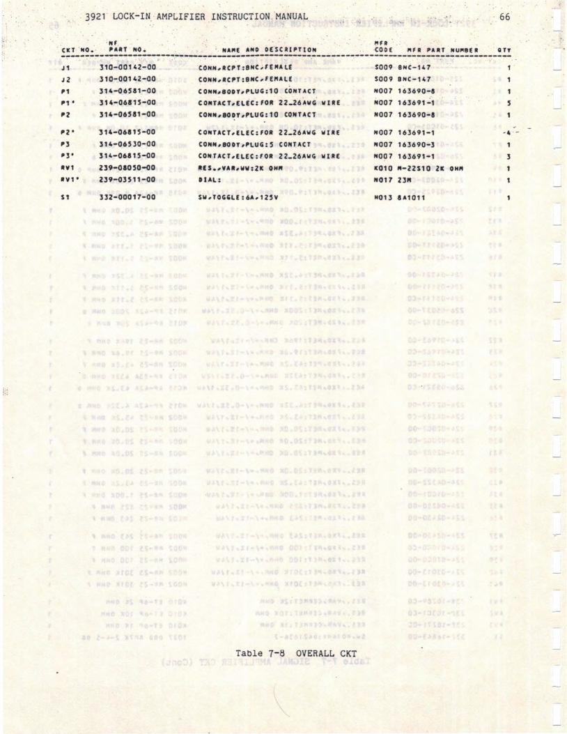
. 3921 · INSTRUCTION . MANUAL ....... ...
:·; ·: . . ' Nf "fA .. CICT ·No.·. . PAIT NO. NA,.E ANO OE.SCJllPTION ·CODE PHlt PAltT NU,.Hlt CUT
...
J1 310-00142-00 CONN,ltCPT:8NCiFE"Al£ S009 BHC-147 1 .
JZ 310-00142-00 CONN1RCPT:BNC1FE"Al£ S009 BHC-147 ,,, 314-<36531-00 CONN,80DY,PLUG:10 CONT ACT N007 163690-& P1 • 314-06115-00 CONTACT,ELEC:fOR 22-26AWG VIRE N007 163691-1 5 n 314-06511-00 CONN,80DT,PLUG:10 CONT ACT N007 163690-a
P2• 314-06115-00 CONTACT1ELEC:fOR 22-26AVG VIRE N007 163691-1 Pl 314-06530-00 CONN1800T1PLUG:5 CONTACT N007 163690-3 p3• 314-06815-00 CONTACT,ELEC:FOR 2 2-26AVG VIRE N097 163691-1 3 It,, 1 239-01050-00 RfS.,VAR,WW:21C OH" K010 "-22s10 ZIC OH" 1v1• 239-03511-00 DIAL: N017 23"
S1 332-00017-00 SW1TOG,Lf:6A1125V H013 &A1011
Table 7-8 OVERALL CKT

3921 LOCK-IN AMPLIFIER INSTRUCTION MANUAL
CIC T NO.
C1 C2 C3 C4 cs C6 C7 ca C9 C10
C11 C12 C13 C1'
C15
C16 C17 C18 C19 C20
C21 C22 C23 01 D2
D3 D4 D5 D6 D7
Q3 Q4
as 06 07
08 09 lt1 lt2 lt3
Hf PART NO.
203-00514-00 203-000"5-00 203-00131-00 203-00085-00 203-00514-00
203-00085-00 203-00514-00 203-00085-00 203-00514-00 203-00131-00
203-00085-00 203-00514-00 203-00514-00 203-00514-00 203-00514-00
203-00514-00 203-00514-00 203-00514-00 203-00514-00 203-00514-00
203-00514-00 203-00085-00 203-00085-00 160-00137-00 160-00137-00
160-00137-00 160-00137-00 160-00137-00 160-00137-00 1 64-0 5 200-00
314-03484-00 330-01049-00 340-30397-01 120-20516-00 120-04529-00
110-00694-00 110-00694-00 120-04529-00 120-20516-00 115-95019-00
115-95019-00 120-2002a-oo 225-01004-00 225-01004-00 224-03929-00
NA"E ANO DESCRIPTION
CAP.,fXD1CER:0.047Uf,+80%-20X125V CAP.,flD1C£R:100Pf ,+/-10%150V CAP.,flD1CE1t:1000Pf,+100X-OX150V CAP.,flD1CElt:100Pf,+/-10X,SOV CAP.1fXD1CE1t:0,047Uf ,+80X-20X125V
CAP.,fXD1C£R:100Pf,+/-10X150Y CAP.,flD1CER:0.047Uf ,+80X-20X125V CAP.,fXD1CER:100Pf,+/-10X1SOY CAP.,fXD1CER:0.047Uf ,+80X-20X125Y CAP.,fXD,CER:1000Pf,+100X-OX150V
CAP.1flD1CER:100Pf,+/-10X1SOY CAP.1fXD1CER:0.047Uf 1+80X-20X125Y CAP.,fXD1CER:0.047Uf1+80X-20X125V CAP.1fXD1CE1t:0.047Uf,+80X-20X125Y CAP.1flD1CER:0.047Uf,+80X-20X125Y
CAP.,f XD1CER:0.047UF,+80X-20X125V CAP.,fX01CER:0.047Uf,+80X-20X125V CAP.,fl01CER:0.047Uf,+80%-20X125Y CAP.,fl01CER:0.047Uf ,+80X-20X125V CAP.,fX01CER:0.047Uf,+80X-20%125V
CAP.,flD1CE1t:0.047Uf,+80%-20X125V CAP.1fl01CER:100Pf ,+/-10%1SOY CAP.,fX01CElt:100Pf,+/-10l1SOV DIODE: SI DIODE:SI
OIOOE:SI OIOOE:SI OIOOE:SI OIODE:SI DIOOE1ZENER:Sl10.4V14.94Y-S.20Y
CONN1RCPT1TOP:10 CONTACT,fE"ALE TEA .. lNAL1PlN: P.C.80ARO:NP-30397A10312069 IC:OPERATIONAL A"PllflER IC:OPERATIONAL A"PllflER
f ET: HT:
IC:OPERATlONAl A"PLlf lER lC:OPERATlONAL A"PLlf IER TltANS1STOR,TWIN:D424011
TRANSISTOR,TW1N:0424011 lC:OPEltATlONAL A"PLlflER RES.,fXD1MET:1.oo .. OH .. ,+1-1x,112w RES.1fX01MET:1.00M OH .. ,+1-1x,112w RES.,Fxo,MET:39.2 OH .. ,+/-1X11/4W
Table 7-9 MAIN BOARD CKT
" f It PA tlT N UM B E ll
"010 ECK-f1£473ZV "002 D01048101K50V02
D0104E102P50V02 "002 OD1048101K50V02 M010 ECK-f1E473ZY
"002 001048101K50V02 "010 ECK-F1E473ZV "002 OD1048101K50V02 "010 ECK-F1E473ZV "0CZ
I
"002 001048101K50V02 M010 ECK-F1E473ZV "010 ECK-f1E473ZV "010 ECK-f1E473ZV "010 ECK-F1E473ZV
"010 ECK-F1E473ZV M010 ECK-F1E473ZV "010 ECK-f1E47lZY "010 ECK-F1E473ZV M010 ECK-f1E473ZV
"010 ECK-f1E473ZY "002 D01048101K50V02 "002 001048101K50V02 T004 1$1588 T004 1S1588
T004 1S1588 T004 1S1588 1004 1s1s88 T004 1S1588 H004 U5.1EB2
N007 163680-8 E012 LC-2-G <YELLOW) EOOS 080 P004 OP-16fJ N013 LM308H
T004 2SK30ATM-GA T004 2SK30ATM-GR N013 LM308H P004 OP-16FJ 1003 1 TS-1276
1003 ITS-1276 T022 TL082C P K013 SN14K2H 1.00" OHM f
K013 SN141C2H 1.00M OHM f
H002 MR-25 39.2 OHM f
67
QTY
1 -
1
1
1 ·
s
1
1

3921 LOCK-IN AMPLIFIER ·INSTRUCTION MANUAL . : .. ·_ .. .. "
· Hf CKT HO. PAAT NO. "'· COOE
.· , . . :
66 ·
QTY
14 IS 16 17 18
19 110 111 112 11]
R14 •15 •16 •17 •18
119 120 A21 •22 1t23
124 1125 lt26 lt27 128
lt29 130 131 132 •33
RJ4
A35 •36 RV1 •v2
IV] RV4 RVS RV6 •v7
224-01503-00 224-03831-00 224-01503-00 224-02001-00 225-01004-00
224-01002-00 225-01004-00 224-01002-00 224-01000-00 224-04992-00
224-02492-00 224-02009-00 2 24-01503-00 224-04992-00 225-01004-00
225-04993-00 225•0ll23·00 224-03929-00 224-01503-00 224-03831-00
22S-01004-00 224-03010-00 224-01503-00 225-01004-00 224-04991-00
224-01000-00 224-0S622-00 224-04222-00 224-03831-00 225-09093-00
225-01004-00 22S-04990-00 224-09099-00 238-10122-00 238-10122-00
2 38-100 7 6-00 238-10122-00 238-10122-00 238-10122-00 238-10149-00
238-10025-00
RES.1IXD1"ET:150K OHM1+/-ll11/4V . RES.1IXD1"£T:J.8lK OHM,+/-1X11/4V RES.,IXD1"ET:1SOK OHM,+/-1l11/4V RES.,,XD1MET:2.00K 0HM,+/•1111/4V ltES.1IXD1MET:1.00M OHM,+/-1X11/2V
ltES.1IXD1MET:10.0K OHM,+/-1111/4V ltES.1IXD1MET:1.00M OHM1+/-1111/2W R£S.,IXD1ME!:(O.OK OHM,+/-1X11/4W RES.,,XD1MET:100 OMM1+/•1111/4W IES.,,XD,MtT:49.9K 0HM,+/•1X11/4V
IES.1flD1MET:24.9K OMM1+/-ll111/4V ltES.,IXD,MtT:20.0 0HM,+/•1X11/4V ltS.1fl01MET:150K CHM1+/-1X11/4V 1tEs.,1xo,MET:49.9K OHM1+/-1111/4V •ts.,,10,MET:1.oo" OHM1+1-1x,112w
•Es.,,xo,MET:499K OHM1+/-1111/2W R($,,,xo,MET:ll2K OHM1+1-1x,112v RES.1llD1M£T:J9.2 OHM1+/•1%11/4V RES.1fXD1MET:150K OHM1+/•1X11/4V ltES.1fXD1MET:3.8lK OHM1+/-1%11/4V
RtS.1flD1MET:1.00M OHM1+1-1x,112w RES.,,XD1MET:l01 OHM1+/•1X11/4V RES.,fXD1MET:1SOK OHM1+/-1X11/4V RES.,,xo,MET:1.00M OHM1+1-1x,112v RfS.1fXD1MET:4.99K OHM1+/-1%11/4V
RES.1fXD1Mtf:100 OHM1+/-1X11/4V RtS.1fXD1M!T:56.2K OHM1+/-1X11/4V RES.,,xo,MET:42.2K OHM1+/-1111/4W RES.,,xo,MET:3.8lK OHM,+/-1%11/4W RES.1llD1MET:909K OHM,+/-1x,112v
RES.,,XD1MET:1.00M OHM1+/-1x,112v RES.,,XD1M£T:499 OMM1+1-1x,112w RES.,fXD1MET:90.9 OHM1+/•1%11/4V RES.1YAR1CERMET:SOK OHM RES.1YAlt1CERMET:SOK OHM
RES.1YAR1CEltMET:1K OHM RES.1YAlt1CfltMET:SOK OHM RES.1YAR1CEIMET:SOK OHM RES.1VAl1CEltMET:50K OHM RES.1VAR1CER"ET:200KOH"
H002 "l-2S - 150K "OH" · f · · H002 "1•25 3.83K ' .0M" ·f
H002 "R-2S 150K OHM ' H002 "R-2S Z.OOK OHM f K013 SN14K2H 1.00" OH"'
H002 "lt-2S 10.0K OHM f
K013 SN14K2H 1.00" OH" f
H002 MR-25 10.0K OH" f M002 "l-2S 100 OMA I
H002 "•-ZS 49.tK ONM '
M002 M••25 24.9K OH" f
H002 "••25 20.0 OHM I
H002 Ml-25 1SOK OHM f
H002 Ml•2S 49.tK OHM I
K013 SM14K2H 1.00" OM" I
K013 SM14KZH 499K OHM ' K013 SN14K2H 3l2K OH" F H002 M••25 39.2 OHM I
H002 "1-25 1SOK OHM f
MOOZ "1•25 3.SJK OHM I
K01l SN14K2H 1.00" OH" f
H002 "1-25 301 OMM ' H002 "1-25 1SOK OHM f
K013 SM14K2H 1.00" OMM F
H002 "I-ZS 4.99K OH" F
M002 Ml-2S 100 OH" ' H002 Ml-ZS 56.2K OHM F
H002 "R-25 42.2K OHM F
H002 "1-25 J.83K OH" f
K01l SN14K2H 909K OHM F
K013 SN14K2H 1.00" OHM f
K01l SN14K2H 499 OHM F H002 "1•25 90.9 OHM F
K010 RJ•6P SOK OHM K010 RJ•6P SOK OHM
K010 RJ-6P 1K OH" K010 RJ-6P SOK OHM K010 RJ-6P SOK OH" K010 RJ-6P SOK OM" K010 IJ-6P ZOOK OHM
K010 ltJ-6P 20 OHM
Table 7-9 MAIN BOARD CKT (cont)
. ,
. 1
-1--
1
1
1
1
1
1
1
1 1

3921 LOCK-IN AMPLIFIER INSTRUCTION MANUAL
ITHACO MFR. CODE MANUFACTURER .
A001 Alps Electric Co., Ltd A007 Advanced Micro Devices Inc. B001 Burr-Brown Corporation D003 Dai-Ichi Denshi Kogyo K.K.
E001 NF Circuit Design Block Co., Ltd. EOOS Eight Kogyo Co., Ltd. E012 MC Eight Co., Ltd.
H001 Fujitsu Ltd. H002 Philips Electronic Components and Materials Division H003 Hitachi Ltd. HOOS Hirose Electric Co., Ltd.
H014 Harris Semiconductor Inc. ·. H022 Hanai Electric Wire Co., Ltd. H026 Fuji Ceramics Co., Ltd.
1003 Intersil Corporation K006 Kawasaki Densen K.K. KOOB Kitagawa Ind Co., Ltd. K010 Copal Electronics Co., Ltd.
K013 Kowa Denko Co., Ltd. M001 Marconi Electronics Co., Ltd. M002 Murata Mfg. Co., Ltd. M004 Mitsumi Electric Co., Ltd.
MOOS Molex-Japan Co., Ltd. M007 Morimatsu Denshi Kogyo Co., Ltd. M010 Matsushita Electronics Corp. M014 Motorola Semiconductor Products
M019 Matsukyu Co., Ltd. N001 Japan Servo Co. Ltd. N003 Nippon Chemical condenser Co., Ltd. N004 Nippon Electric Co., Ltd.
N013 National Semiconductor Corp. N015 Nikkohm Co., Ltd. N016 Japan Fine Chemical Company, Inc.
N018 Nihon Kaiheiki Ind. Co., Ltd. 0002 Okita Works Co., Ltd. R001 Ryosan Denki Co., Ltd. S001 Soshin Electric Co. Ltd.
Table 7-10 CODE LIST OF MANUFACTURERS

3921 INSTRUCTiqN, MANUAL
S002 S003 S006 S007
·E1e6tric Compani Inc. New Japan Radio Co. Ltd. Sanken Electric Co., Ltd. Sato Parts Ltd.
S009 Stack Electric Co., Ltd. S010 Seidensha Electric Works Ltd. S018 Signetics Corporation S026 Shinyei Kaisha
T004 Toshiba Corporation T005 Toyo Fuse Co., Ltd. T009 Omron Electric Co., Ltd. T017 TDK Electronics Co., Ltd.
T022 Texas Instruments Inc. T025 Tokyo Cosmos Electric Co., Ltd. W004 Wako Term Blk Mfg. Co., Ltd. YOOl Yuasa Battery Co., Ltd.
Y003 Yamaichi Electric Mfg., Co., Ltd. Y006 Yamagishi Musen Denki K.K. Y007 Yagumo Tsushin Kogyo Co., Ltd. Y008 Yokogawa-Hewlett-Packard Co., Ltd.
Table 7-10 CODE LIST OF MANUFACTURERS (Cont)
70
. . ... .

3921 LOCK-IN AMPLIFIER .INSTRUCTION MANUAL ·71
SECTION 8 . .
CIRCUIT DIAGRAMS
8.1 INTRODUCTION
This section includes schematics. Refer to Section 7 for information on reference designators used in these drawings.
8. 2 DRAWINGS
The drawing name is assigned as shown below.
SIGNAL CONDITIONER BOARD CKT 1/2
Drawing name
T
This indicates that this sheet is the first of two comprising this drawing.
·.· .. . . ·

3 921 LOCK-:IN AMPLIFIER INSTRUCTION . MANUAL . 72 . .
8.2.1 SPECIAL SYMBOLS
7 TP-1
' r---1 I
--'->- I I I I
r----1 >-+--+
I
0--<>--
C>--
--?2-1>--
' I I
. • ! •• : : •• : ':.· .. .
Twisted pair line
Test point
Multi-pin connector
Open collector (inverter)
Indicates connections within the same PC board. Connections are made to parts having the same symbol within or near these symbols.
Indicates connections to a PC board edge connector.

3921 LOCK-IN AMPLIFIER INSTRUCTION MANUAL 73
8.3 CIRCUIT DIAGRAMS LIST
8.4 SIG AMP CKT 75
8.5 PSD CKT 76
8.6 TC & OUTPUT CKT 77
8.7 PLL-1 CKT 78
8.8 PLL-11 CKT 79
8.9 PHASE CONTROL CKT 80
8. 10 POWER SUPPLY CKT 81
8. 11 OVERALL CKT 82
8.12 RA TIO METER CKT 83

. ·.·
3921 LOCK-IN AMPLIFIER INSTfWCTION MANUAL ·74 '• ,.·
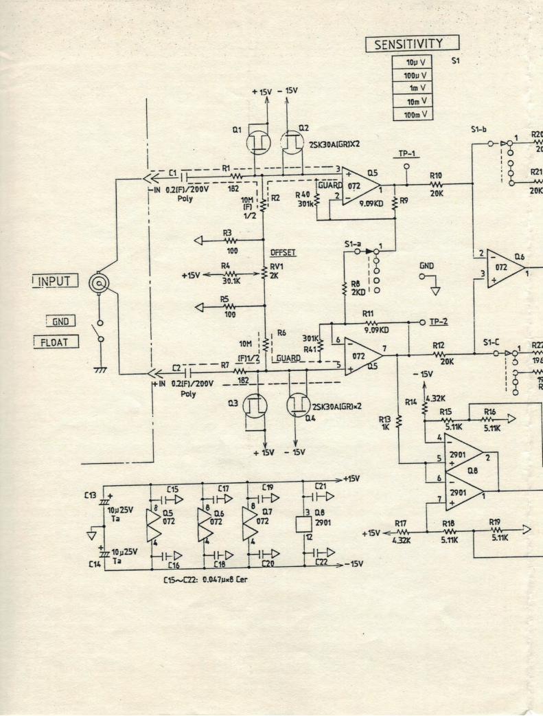


3921 LOCK-IN AMPLIFIER INSTRUCTION MANUAL . 85 .
SECTION 9
RATIO METER (Option 02 )
9. 1 INTRODUCTION
The Option 02 Ratio Meter installs in the blank panel area at the rear of the Model 3921 Lock-In Amplifier.
RATIO METER RATIO OUTPUT RATIO X e O.OSK jYI
X=OUiPUT (INT)
NORMAL (11V MAX)
Figure 9.1 RATIO METER PANEL
The Ratio Meter provides for signal normalization using an external de input according to the expression:
E 0
E 0
K
x IYI -
0.5k x
Ratio output
Multiplier, continuously variable from 0.5 to 10.5 on 1 a-turn dial. Lock-In de output*
Absolute value of external de input
Typically the Ratio Meter is used to compensate for fluctuations in the excitation of the system being measured. In optical work, for example, it would correct for variations in source intensity, as explained in Section 9. 4.
*LIA must be phased for positive output (meter"+" lamp on).

. ; 3921
:
y
9.2
LOCK-IN AMPLIFIER . . . . '.\. .. .... . . . : .. ..1.. ••
3921 LOCK IN AMPLIFIER
METER x
NOR
IYI x O.SK lYl
Figure 9.2 RATIO METER BLOCK DIAGRAM
SPECIFICATIONS
Operating ranges:
10 mV s x s lOV 100 mV y s lOV
0.50 s K s 10.50 0 s E s + 11 v
0 (max output)
x 20 0 < s (without overload)
IYI K
Accuracy (typical):
( 1 v s y s 1 ov) ±0.2% of full scale ±2.0% of full scale (0.lV SYS lV)
Where 10 mV S X S 1 OV, K • 1o.00 and full seal e E - t O V.
0 K factor dial accuracy ±1%
Output Stability (typical): With respect to a full scale output E
0
K • 10 x - I YI - 0. 1 v 15 ppm/°C
K • 1 0 x !YI - 1 :2 5 ppm/°C
.K • 1 0 x jYj - 2: 1 10 ppm/°C
• t 0 V:
(typ)
(typ)
(typ)
.. . . '- 86: .. ·
. "· ' · ..
RATIO OUTPUT
. ".·---;"'" . ',

3921 LOCK-IN AMPLIFIER INSTRUCTION MANUAL
Input/Output:
Y Input Ratio Output
BNC Connector, 1 mn impedance BNC connector, 5 Kn impedance
87
With K=10 and X=jYj, the Ratio Meter yields a 5 V de output. This would cause a half scale reading on the METER ( i.e., "1" on the- -0··_ to 2 ratio scale).
9.3 INSTALLATION
When ordered together, the Model 3921 Lock-In and Ratio Meter will be assembled and ready operate. separately purchased Ratio Meter, follow these steps:
the Option-02 To install a
1. Unpack Ratio Meter from carton and inspect for damage and loose components. The carton should also contain a BNC - BNC cable and a multiconductor connection cable with three plugs.
2. Remove the two molded plastic pieces from the rear of the instrument (4 screws) and slide back top cover.
3. Remove blank panel from rear of instrument with Ratio Meter. Install connecting cable (connectors are keyed).
4. Replace top cover and rear molded pieces.
(2 screws) and replace as shown in Figure 9.3

3921 LOCK-IN AMPLIFIER INSTRUCTION MANUAL . 88
c,. JS
TOP VIEW
JS
RATIO METER REAR PANEL
Figure 9.3 RATIO METER CONNECTION

.. -
3921 LOCK-IN AMPLIFIER INSTRUCTION MANUAL 89
9.4 OPERATION EXAMPLE
This section describes a dual beam, dual lock-in optical system. This type of setup gives the most accurate results but others are possible, as described in ITHACO Applications Note IAN 37.
MODEL 220
DUAL BEAM OIOPPER
f 1
f 1
OUT
f 2
---
Ol!I'
y IN
f 2
SAMPLE __ _..,. DETECTOR
REF IN t I
REF IN
LIA 1
LIA 2 t2 WITH RATIO OPTION
Figure 9.4 DUAL BEAM, DUAL LOCK-IN RATIOMETRIC OPTICAL SYSTEM
9.4.1 DUAL BEAM SETUP
A half mirror splits the source beam. The dual row chopper blade modulates the beams at two separate frequencies f 1 and r2 • After the signal beam f 2 passes through the experiment, a second half mirror recombines the beams to fall on a single detector. The
output feeds to a pair of lock-in amplifiers. LIA #1 is supplied a synchronizing frequency f 1 and responds to the reference beam (Y). LIA #2.is synchronized at r2 and responds to the experimental signal beam (X). The output of LIA #1 contains fluctuations due to source & detector instability. When its out-put feeds to the Ratio Meter in LIA #2, the quotient will cancel

. . . . . LOCK-IN AMPLIFIER· INSTRUCTION ·MANUAL . . " .
the corresponding instabilities in X, leaving only the changes due to the actual experiment in the RATIO Output. For accurate
of rapid you must have the TIME CONSTANT and POST FILTER set the same on both · lock-ins. Next set the K value to obtain an easily read ratio output. When making relative measurements from a starting condition, for an output of 1 on the 0-2 METER scale or 5.00 V on the 0-10 v- ·-OUTPUT connector. When making absolute measurements, adjust the K value to yield a true reading on the 0-100% METER scale (or 0-10 V OUTPUT scale) at the beginning of the measurement run.
9.5 CIRCUIT DESCRIPTION
Input buffer Q2 feeds the Y input into absolute value circuit Q5. Current drivers Q1 and Q6 operate the X and !YI log transistors Q7. Q9B drives K logger Q8 (lower transistor). This transistor also adds log X to log K. Antilog transistor Q8 (upper) subtracts log IYI from log X + log K. Current to voltage converter Q9a provides output amplification. Overall we have:
x OUTPUT - 0.5 antilog (log x +log K - log jYj) 0.5 K
Using the matched Q7 transistor pair to log both X and Y minimizes error when X and Y fall to a low level. These two values will tend to rise and fall together in ratiometric applications.
9. 6 CALIBRATION
Normally only the output gain (RV7) and offset (RV6) adjustment. Refer other adjustments to the factory. calibration if the output error exceeds specifications. This also can serve as an operational check for the Ratio Meter.
will need Make field
procedure
Allow the case temperature to stabilize at least 1/2 hour. Open cover only briefly while making adjustments and be careful to touch nothing but the appropriate trimpots.
1. Open case per Section 9.3 #2.
2. Apply a 400 Hz signal and reference to the Lock-In and set MULT for a 10.00 volt X reading on the OUTPUT BNC (NORMAL/RATIO= NORMAL).
3. Apply 10.000 V to the Y input and set K to 10.00.
4. Adjust RV7 (K-ADJ) for a 5.00 V output on the RATIO output ( can be measured on front panel BNC by switching NORMAL/RATIO to RATIO).
A reading between 4.95 and 5.05 is within tolerance.

3921 . LOCK-IN AMPLIFIER INSTRUCTION MANUAL 91
5. With NORMAL/RATIO = NORMAL, decrease the signal to the lock-in by approximately 60 dB to achieve a 10.00 mV reading at the OUTPUT BNC (use MULT control) (Y 10.000 V).
6. Adjust RV6 (OFFSET) for a 5 mV reading on the RATIO output. (NORMAL/ RATIO = RATIO).
A reading between .0045 and .0055 volts is within tolerance .
7. Replace cover and rear molded pieces.
RV4 _!!!... OT'3 05 cs RV I I 10 .J. 09 !Q ()_ RIS 0 it JI U U
.J ya RiA AY6 QJ -lf!- Q'"•<t-r;
..!!L A2 it C A27 AJS Q4 0 dY3 -01 a 0 a .. F 01 _ 0:: 0 E OSCO m All N c c u u r--;> i 1- 0 No [ """[ '"\fl4 ft f9 CZJ U 8 0 8 ..,, '""' ./ ..IT!.{ !J20 E Eo7 ;.. 01
J!L_AIO liL 0 * _.,Cll AY1 RV9;
lo Oz _m_ 0 CJ9 tff AJ' 00 H H rH'"'F1 C18 .,, .. ,. .. ,,. .......... HP-30397 A
Figure 9.5 RATIO METER COMPONENT LOCATION

ITHACO, Inc. warrants each instrument to be free of defects in material and workmanship for a period of two years, unless otherwise specified, after shipment to the original purchaser; batteries and light beam choppers are specifically excluded. Liability under this warranty is limited to repairing or adjusting any instrument returned to the factory for that purpose. The warranty of this instrument is void if the instrument has been
·modified other than in accordance with written instructions from ITHACO, or if defect or failure is judged by ITHACO to be caused by abnormal conditions of operation, storage or transportation.
This warranty is subject to verification by ITHACO, that a defect or failure exists, and to compliance by the original purchaser with the following instructions:
1. Before returning the instrument, notify ITHACO with full details of the problem; including the model number and serial number of the instrument involved.
2. After receiving the above information, ITHACO will give you shipping instructions or service instructions. After receipt of the shippin2 instructions, ship the instrument to ITHACO. Full liability for damage during shipment is borne by the purchaser. It is recommended that instruments shipped to us be fully insured and packed surrounded by at least 2 inches of shock-absorbing material.
ITHACO reserves the right to make changes in design at any time without incurring any obligation to install same on units previously purchased.
This warranty is expressly in lieu of all other obligations or liabilities on the part of ITHACO, and ITHACO neither assumes, nor authorizes any other person to assume for it, any liability in connection with the sale of ITHACO instruments.
ITHACO INC. 735 West Clinton Street
P 0 Box 6437 Ithaca, New York 14851-6437
Phone 607-272-7640