


Bahasa
Halaman
Hukum


CityU-Learning Summer Talk 2020
講座題目: 一切從「芯」開始.智能手機是如何運算的
張澤松博士 副教授
電機工程學系
香港城市大學

什麼是計算? Computing?
2

機械計算 到 電子計算
3

太空人?
4
拆解 智能手機
5
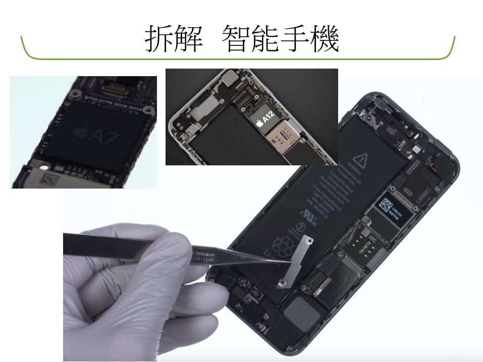
CRAY-2 Supercomputer (1985) $16M USD
6
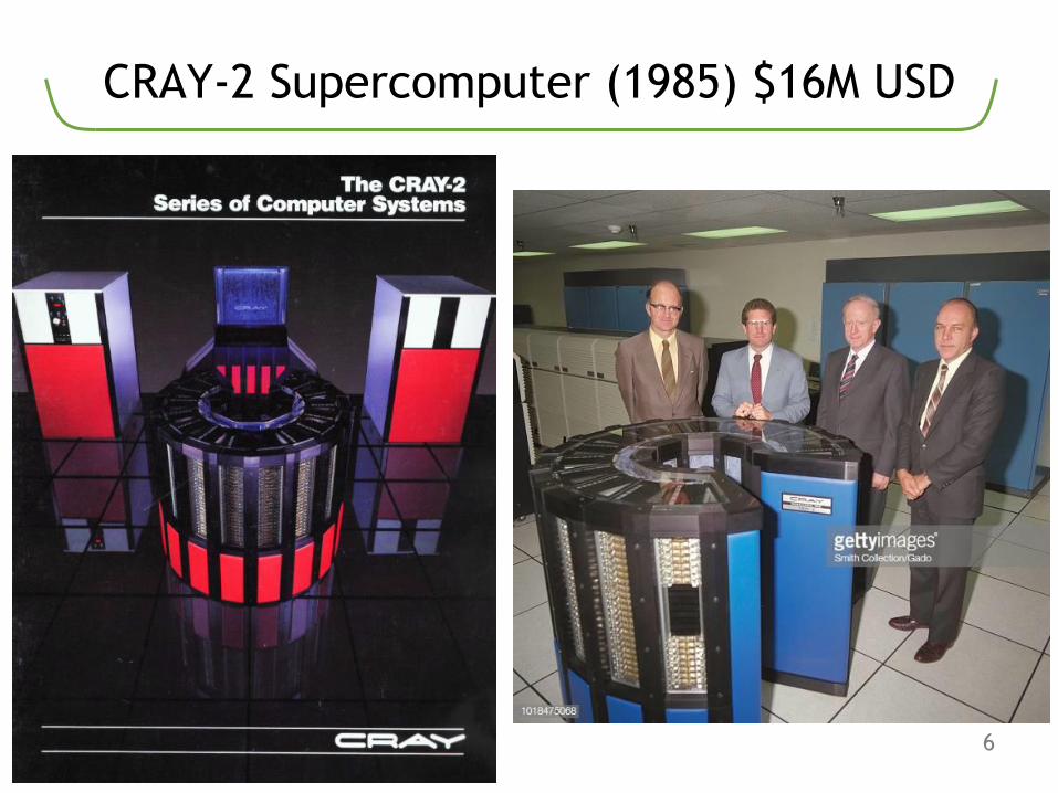
你的手機是一台超級計算機
7

每秒浮點運算次數
• Integer:
– 2 x 3 = 0010 x 0101
• Floating-point:
– 1.23456 x 8.765432
• floating point operations per
second (FLOPS, flops or flop/
s) is a measure of computer
performance.8

• Floating point
– A method represent a real number
– Large dynamic range
– 𝑁 = 𝑓𝑟𝑎𝑐𝑡𝑖𝑜𝑛 × 2𝑒𝑥𝑝𝑜𝑛𝑒𝑛𝑡, stored as
– For example:
• (5.25)10= (101.01)2= +(1.0101)2× 22
9
Floating point number浮點運算
2+127=129=1000_0001
Since the exponent
can be negative,
we should add 127
as bias for single
precision
5.25
=
5 + 0.25
=
101 + 0.01
Floating point number浮點運算
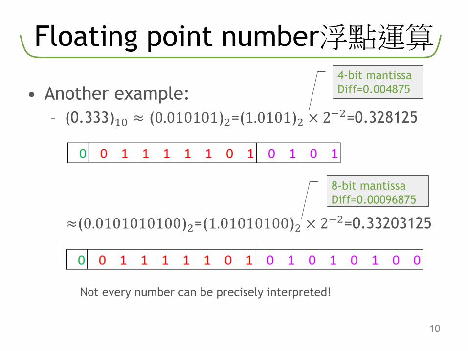
• Another example:
– (0.333)10 ≈ (0.010101)2=(1.0101)2 × 2−2=0.328125
10
≈(0.0101010100)2=(1.01010100)2 × 2−2=0.33203125
4-bit mantissa
Diff=0.004875
8-bit mantissa
Diff=0.00096875
Not every number can be precisely interpreted!

Floating point number浮點運算
• Why use floating point number
– Easy to interpret very small and very large numbers
– For image rendering like fig (1), lots of vector based
computation like fig (2) needed.
11
@Techquickie
Polling FP

你的手機有多快?
12

Super Computer – World #4
• In China, 125.4 PFLOP/s
13

InnoTech Expo 2017
• Design & Develop by Chinese Researchers
• What do you see below?
14

15
微處理器是如何製造的?
• Have you ever wondered how the
microprocessor, the brain 'behind the magic'
of your PC, is made?

16
用沙子做成的?
Do you believe microprocessor is made from sand?

17
什麼是一加一?
• Microprocessor is the brain of the computer
and intelligent device
• Perform arithmetical, logical and
input/output operations
=
1+1=?
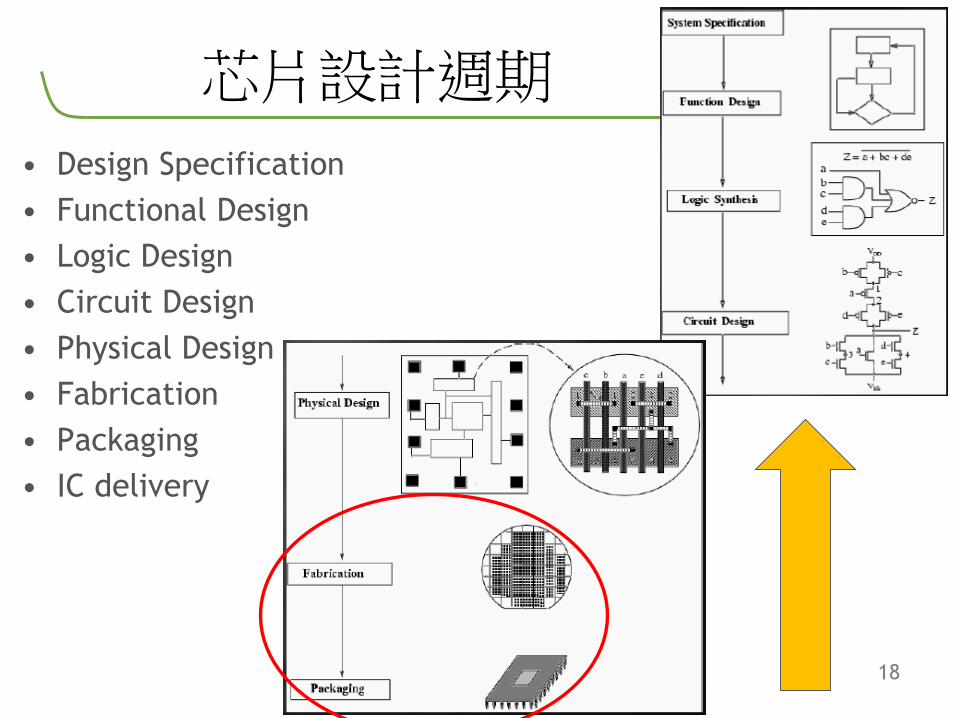
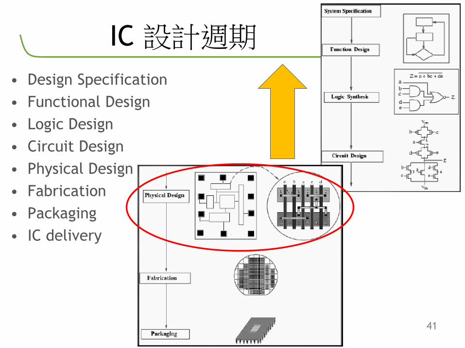
芯片設計週期
• Design Specification
• Functional Design
• Logic Design
• Circuit Design
• Physical Design
• Fabrication
• Packaging
• IC delivery
18

19
從邏輯門到集成電路
Logic gates perform arithmetical, logical and
input/output operations
Key question: How to build the logic gates?
Logic gates Microprocessor die Microprocessor chip

AND gate / OR gate 與門/或門?
a b C
0 0 0
0 1 0
1 0 0
1 1 1
Truth Table for
AND gated e f
0 0 0
0 1 1
1 0 1
1 1 1
Truth Table for OR
gate
A B C D E F

21
製作芯片的材料
Silicon (Si)
is a semiconductor
an excellent
conductor
an insulator of
electricity, by the
introduction of
minor amounts of
impurities

22
我們在哪裡可以找到矽?
Sand composed of silicon dioxide
the starting point for making a processor

23
製作芯片的材料
Metal oxide semiconductor (MOS) structure is
obtained by growing
a layer of silicon dioxide (SiO2) on top of a silicon
substrate and depositing a layer of polycrystalline
silicon
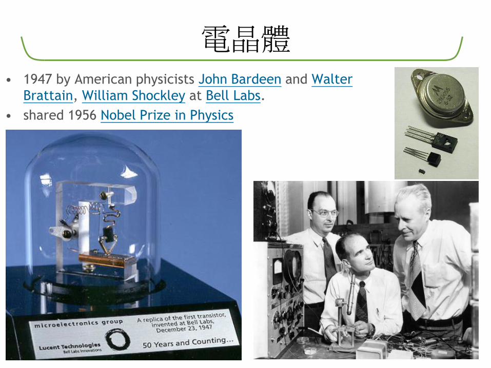
電晶體• 1947 by American physicists John Bardeen and Walter
Brattain, William Shockley at Bell Labs.
• shared 1956 Nobel Prize in Physics
24

25
關於二氧化矽
Silicon dioxide is a dielectric material,
equivalent to a planar capacitor
with one of the electrodes replaced by a semiconductor
A voltage is applied across a MOS structure modifies the distribution of charges in the semiconductor
Cross section
of an NMOS
without
channel
formed: OFF
state
Cross section
of an NMOS
with channel
formed: ON
state
Polling Transistor
26
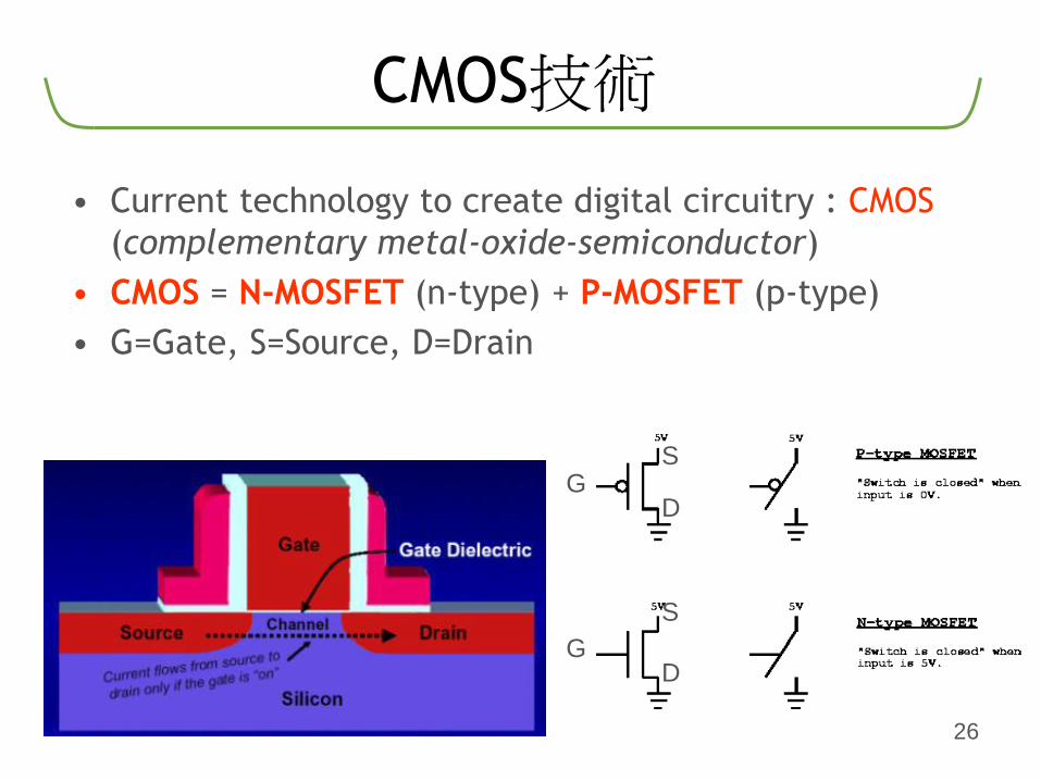
CMOS技術
• Current technology to create digital circuitry : CMOS
(complementary metal-oxide-semiconductor)
• CMOS = N-MOSFET (n-type) + P-MOSFET (p-type)
• G=Gate, S=Source, D=Drain
G
GD
S
S
D

Transistor 晶體管介紹視頻
27Ref: https://www.youtube.com/watch?v=stM8dgcY1CA
28
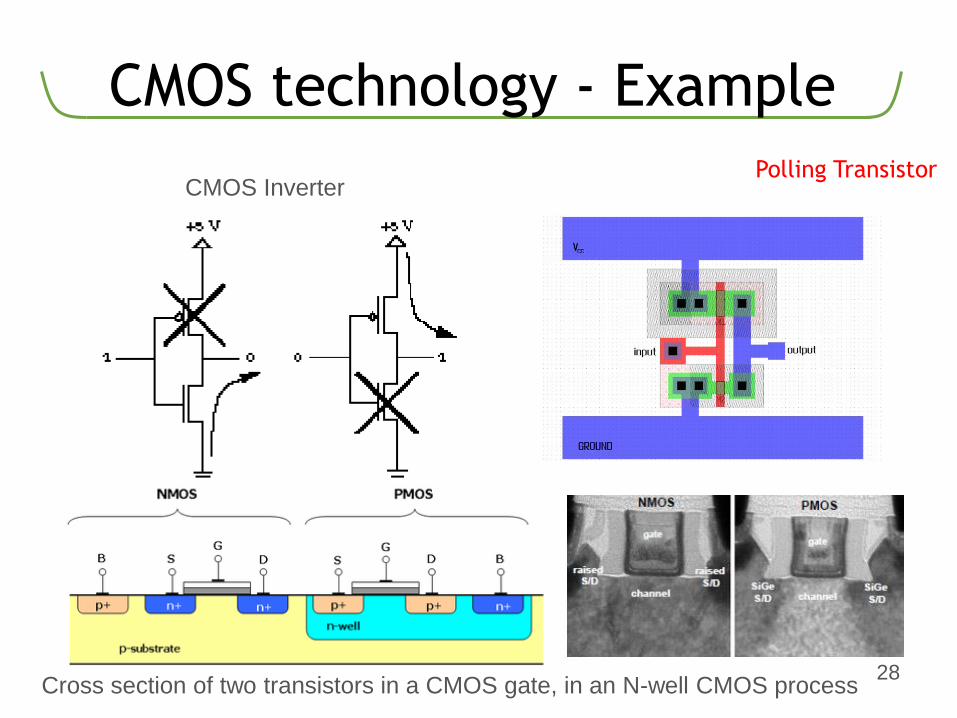
CMOS technology - Example
Cross section of two transistors in a CMOS gate, in an N-well CMOS process
CMOS InverterPolling Transistor

29
製造芯片
• Sand / Ingot
• Ingot / Wafer
• Photo Lithography
• Ion Implantation
• Etching
• Temporary Gate Formation
• “Gate-Last” High-k/Metal Gate Formation
• Metal Deposition
• Metal Layers
• Wafer Sort / Singulation
• Packaging
• Class Testing / Completed Processor

30
芯片製造
Intel Corporation: From Sand to Silicon – the Making of a chip

31
Sand / Ingot (錠, 鑄塊)
Sand -
Silicon is the
second most
abundant element
in the earth's crust
Melted Silicon -
Sand is melted and
allowed to cool down into
a solid which is a single,
continuous and unbroken
crystal lattice in the shape
of a cylinder
Monocrystalline
Silicon Ingot

32
Ingot / Wafer (薄片; 圓片; 晶片)
Ingot Slicing -
The ingot is cut
into individual
silicon discs called
wafers
Wafer -
The wafers are
polished until they
have flawless,
mirror-smooth
surfaces.
33
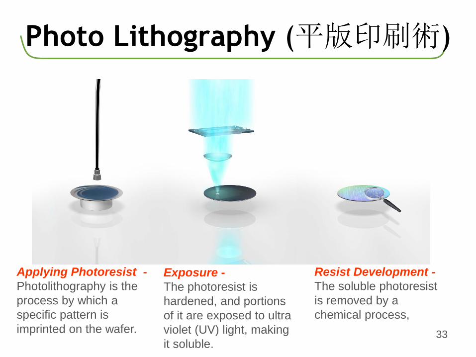
Photo Lithography (平版印刷術)
Applying Photoresist -
Photolithography is the
process by which a
specific pattern is
imprinted on the wafer.
Exposure -
The photoresist is
hardened, and portions
of it are exposed to ultra
violet (UV) light, making
it soluble.
Resist Development -
The soluble photoresist
is removed by a
chemical process,
34
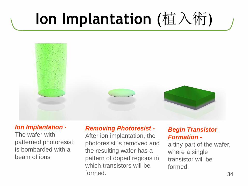
Ion Implantation (植入術)
Ion Implantation -
The wafer with
patterned photoresist
is bombarded with a
beam of ions
Removing Photoresist -
After ion implantation, the
photoresist is removed and
the resulting wafer has a
pattern of doped regions in
which transistors will be
formed.
Begin Transistor
Formation -
a tiny part of the wafer,
where a single
transistor will be
formed.

35
Etching (蝕刻術)
Etch -
Remove unwanted
silicon
Removing Photoresist -
The hard mask is chemically
removed
36
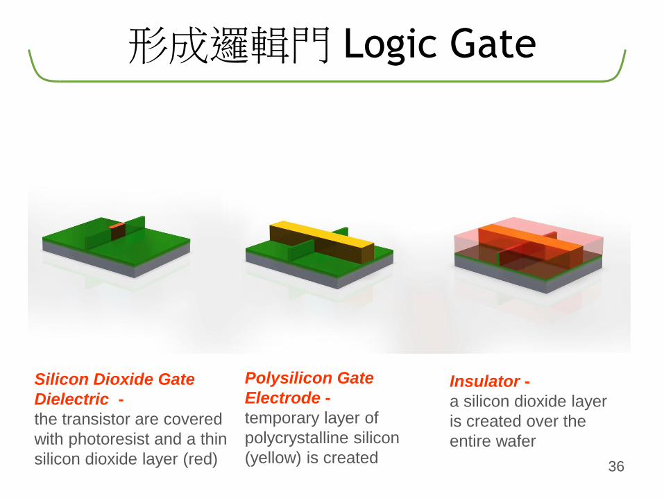
形成邏輯門 Logic Gate
Silicon Dioxide Gate
Dielectric -
the transistor are covered
with photoresist and a thin
silicon dioxide layer (red)
Polysilicon Gate
Electrode -
temporary layer of
polycrystalline silicon
(yellow) is created
Insulator -
a silicon dioxide layer
is created over the
entire wafer

37
Metal Layers 金屬層
Polishing -
The excess material is
mechanically polished
away
Metal Layers -
Multiple metal layers are created to interconnect
(wires) all the transistors on the chip in a specific
configuration.
38
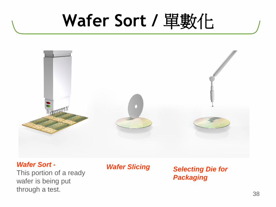
Wafer Sort / 單數化
Wafer Sort -
This portion of a ready
wafer is being put
through a test.
Wafer Slicing Selecting Die for
Packaging

39
Packaging (包裝術)
Individual DiePackaging -
The package
substrate, the die and
the heat spreader are
put together to form a
completed processor.
Processor
40
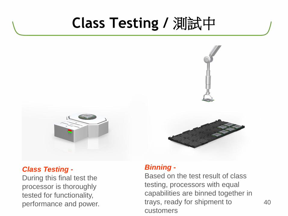
Class Testing / 測試中
Class Testing -
During this final test the
processor is thoroughly
tested for functionality,
performance and power.
Binning -
Based on the test result of class
testing, processors with equal
capabilities are binned together in
trays, ready for shipment to
customers
IC 設計週期
• Design Specification
• Functional Design
• Logic Design
• Circuit Design
• Physical Design
• Fabrication
• Packaging
• IC delivery
41

芯片佈局
42Ref: https://www.youtube.com/watch?v=oSrUsM0hoPs

芯片佈局
• Complex Programmable Logic Devices (CPLDs):
– Come in sizes ranging from 500 to 16,000 gates.
43

集成電路佈局
• Automatic Layout Generation
• Layout Engineers
44

TSMC 台積電工藝技術
45

納米 one billionth of a meter
• 1 x 10⁻⁹ m46

1 nanometer
47

22nm vs. 10nm vs. 7nm
48

Complexity: 電子設計自動化(EDA)
49

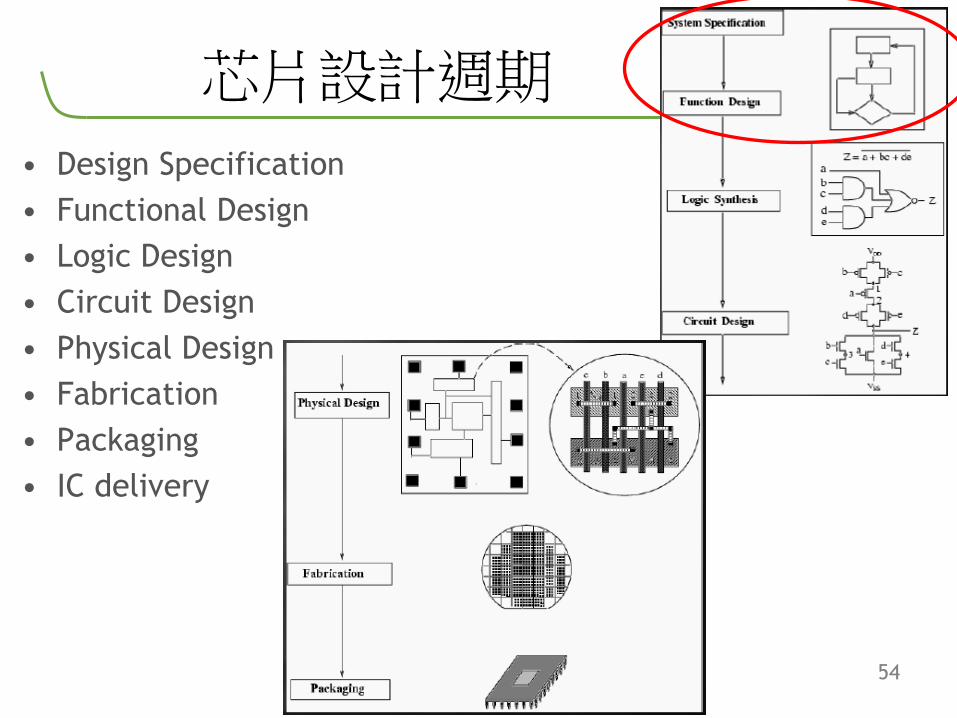
芯片設計週期
• Design Specification
• Functional Design
• Logic Design
• Circuit Design
• Physical Design
• Fabrication
• Packaging
• IC delivery
50

組合邏輯與 順序邏輯
Combinational Sequential
Output = f(input) Output = f(input, state)
CombinationalLogic
Circuit
OutInCombinational
LogicCircuit
OutIn
State
51

硬件描述語言格式和語法
• A Way to Describe our IC in a human readable format
52
芯片設計週期
• Design Specification
• Functional Design
• Logic Design
• Circuit Design
• Physical Design
• Fabrication
• Packaging
• IC delivery
54

集成電路
55
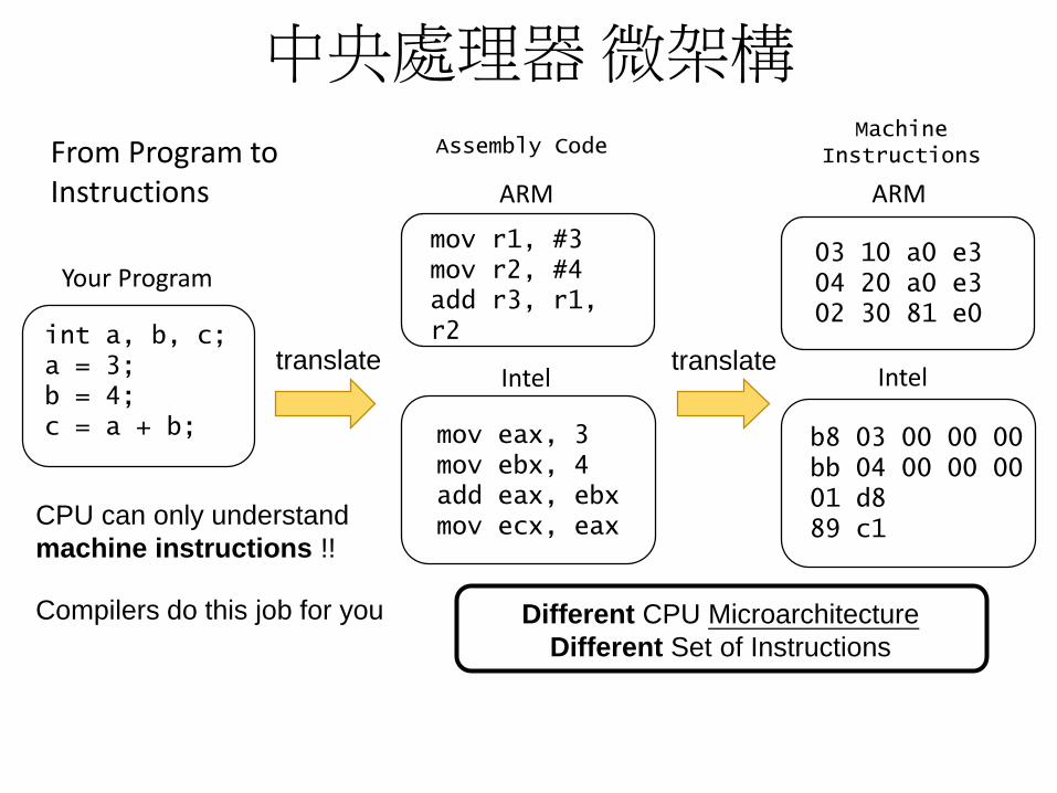
int a, b, c;a = 3;b = 4;c = a + b;
From Program to Instructions ARM
mov r1, #3mov r2, #4add r3, r1, r2
Intel
mov eax, 3mov ebx, 4add eax, ebxmov ecx, eax
Your Program
ARM
03 10 a0 e304 20 a0 e302 30 81 e0
Intel
b8 03 00 00 00bb 04 00 00 0001 d889 c1
Assembly CodeMachine
Instructions
CPU can only understand
machine instructions !!
Compilers do this job for you Different CPU Microarchitecture
Different Set of Instructions
translatetranslate
中央處理器微架構

A Simple 3-Stage “ARM” CPU
mov r1, #4
mov r2, #3
add r3, r1, r2
Instruction Memory
Fetch
r1
r2
r3
Decode
+-x÷
Execute
Program Instructions are
loaded into instr mem
before program
execution
中央處理器是如何工作的?

A Simple 3-Stage “ARM” CPU
mov r1, #4
mov r2, #3
add r3, r1, r2
Instruction Memory
Fetch
r1
r2
r3
Decode
+-x÷
Execute
Three Stage CPU
1. Fetch - fetch an instr. from mem
2. Decode - interpret the instr. properly
3. Execute - execute the instr.
中央處理器是如何工作的?
A Simple 3-Stage “ARM” CPU
mov r1, #4
mov r2, #3
add r3, r1, r2
Instruction Memory
Fetch
r1
r2
r3
Decode
+-x÷
Execute
Program Counter
Points to Instr. to be executed
中央處理器是如何工作的?

A Simple 3-Stage “ARM” CPU
mov r1, #4
mov r2, #3
add r3, r1, r2
Instruction Memory
Fetch
r1
r2
r3
Decode
+-x÷
Execute
Set R1 to 4
Program counter points the
first instr.
中央處理器是如何工作的?
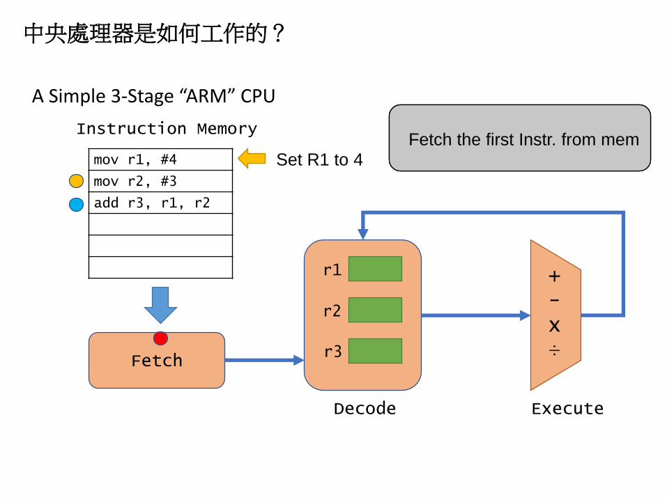
A Simple 3-Stage “ARM” CPU
mov r1, #4
mov r2, #3
add r3, r1, r2
Instruction Memory
Fetch
r1
r2
r3
Decode
+-x÷
Execute
Set R1 to 4
Fetch the first instruction to
CPU from instruction memory Fetch the first Instr. from mem
中央處理器是如何工作的?
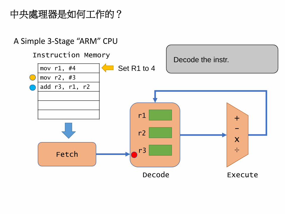
A Simple 3-Stage “ARM” CPU
mov r1, #4
mov r2, #3
add r3, r1, r2
Instruction Memory
Fetch
r1
r2
r3
Decode
+-x÷
Execute
Set R1 to 4 Decode the instr.
中央處理器是如何工作的?

A Simple 3-Stage “ARM” CPU
mov r1, #4
mov r2, #3
add r3, r1, r2
Instruction Memory
Fetch
r1
r2
r3
Decode
+-x÷
Execute
Set R1 to 4 No execution needed
4
中央處理器是如何工作的?

A Simple 3-Stage “ARM” CPU
mov r1, #4
mov r2, #3
add r3, r1, r2
Instruction Memory
Fetch
r1
r2
r3
Decode
+-x÷
Execute
Set R1 to 4
4
Write 4 to r1
中央處理器是如何工作的?

A Simple 3-Stage “ARM” CPU
mov r1, #4
mov r2, #3
add r3, r1, r2
Instruction Memory
Fetch
r1 4
r2
r3
Decode
+-x÷
Execute
Set R1 to 4 Write 4 to r1
中央處理器是如何工作的?
A Simple 3-Stage “ARM” CPU
mov r1, #4
mov r2, #3
add r3, r1, r2
Instruction Memory
Fetch
r1 4
r2
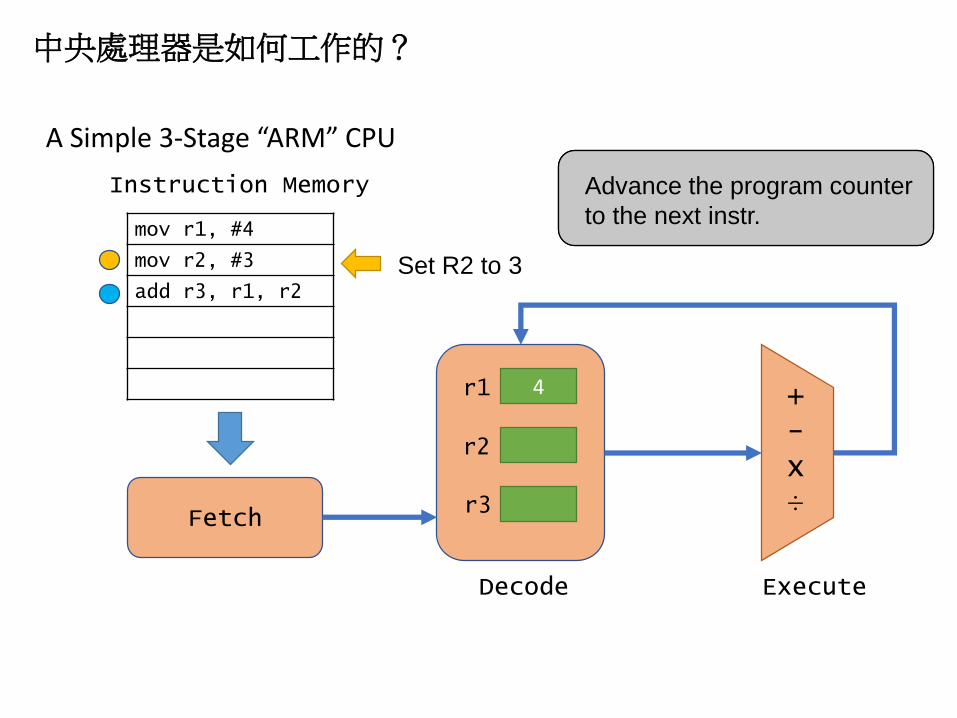
r3
Decode
+-x÷
Execute
Set R2 to 3
Advance the program counter
to the next instr.
中央處理器是如何工作的?

A Simple 3-Stage “ARM” CPU
mov r1, #4
mov r2, #3
add r3, r1, r2
Instruction Memory
Fetch
r1 4
3r2
r3
Decode
+-x÷
Execute
Set R2 to 3
Similar to the first instr.
Write 3 to r2
中央處理器是如何工作的?

A Simple 3-Stage “ARM” CPU
mov r1, #4
mov r2, #3
add r3, r1, r2
Instruction Memory
Fetch
r1 4
3r2
r3
Decode
+-x÷
Execute
Move program counter to
the last instr.
R3 <- R1 + R2
中央處理器是如何工作的?

A Simple 3-Stage “ARM” CPU
mov r1, #4
mov r2, #3
add r3, r1, r2
Instruction Memory
Fetch
r1 4
3r2
r3
Decode
+-x÷
Execute
Fetch the last instr.
R3 <- R1 + R2
中央處理器是如何工作的?

4
3
A Simple 3-Stage “ARM” CPU
mov r1, #4
mov r2, #3
add r3, r1, r2
Instruction Memory
Fetch
r1 4
3r2
r3
Decode
+-x÷
Execute
Load required register values
R3 <- R1 + R2
中央處理器是如何工作的?

3
4
A Simple 3-Stage “ARM” CPU
mov r1, #4
mov r2, #3
add r3, r1, r2
Instruction Memory
Fetch
r1 4
3r2
r3
Decode
+-x÷
Execute
Add them together
R3 <- R1 + R27
中央處理器是如何工作的?
A Simple 3-Stage “ARM” CPU
mov r1, #4
mov r2, #3
add r3, r1, r2
Instruction Memory
Fetch
r1 4
3
7
r2
r3
Decode
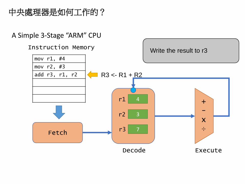
+-x÷
Execute
Write the result to r3
R3 <- R1 + R2
中央處理器是如何工作的?

中央處理器微架構
• Machine Code running on this architecture
• Compile a high-level language to machine code
73Research work at CityU – Secure AIoT Microprocessor
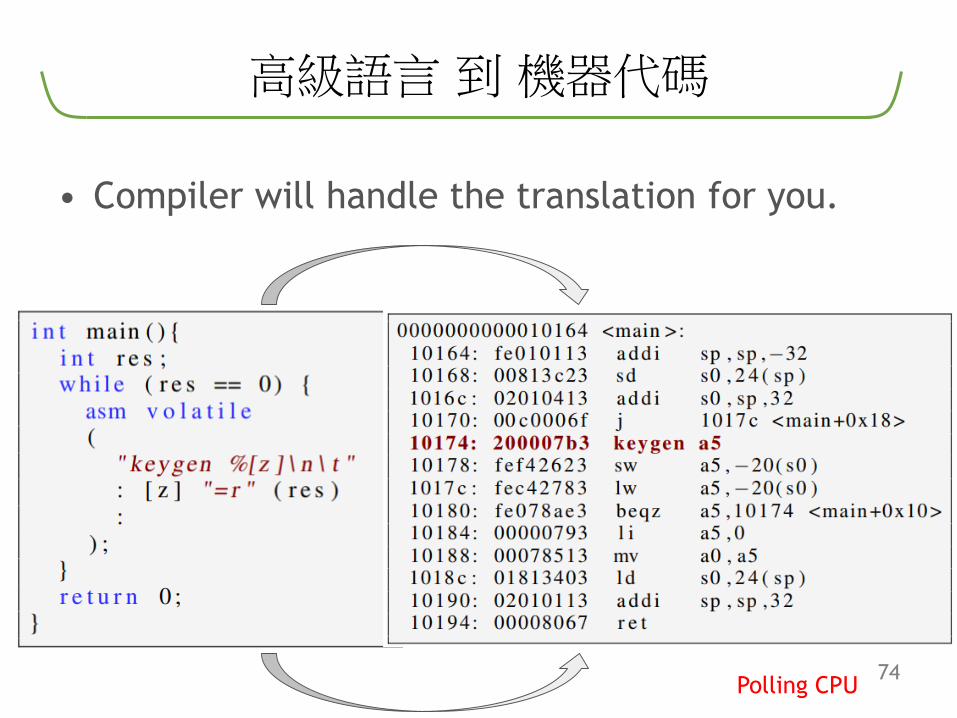
高級語言 到 機器代碼
• Compiler will handle the translation for you.
74Polling CPU
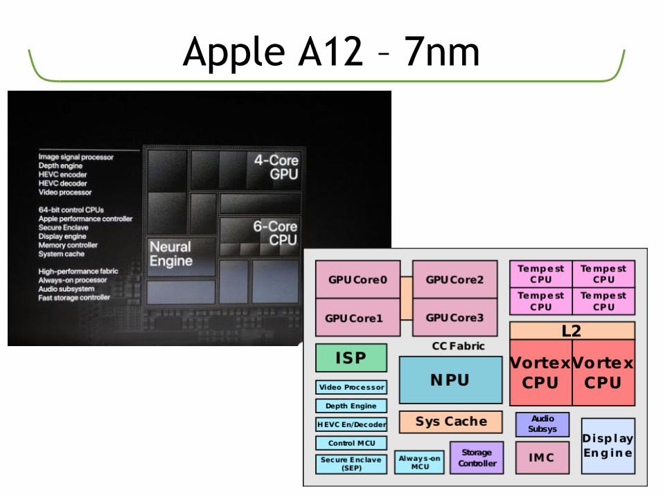
Apple A12 – 7nm
75

華為和 Apple 核心處理器
76
77
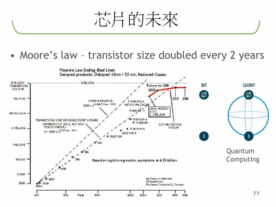
芯片的未來
• Moore’s law – transistor size doubled every 2 years
Quantum
Computing

x86 vs. ARM
78
• Mobile computing market is continuously growing.
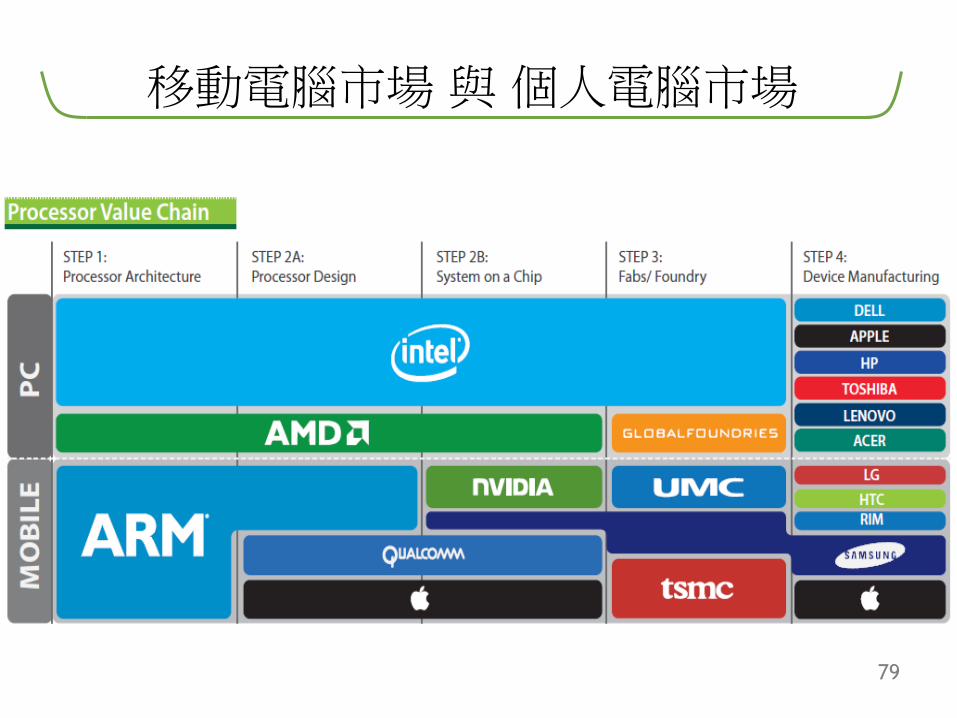
移動電腦市場 與個人電腦市場
79

80
物理知識製作芯片
• Circuit design
– Current, Voltage, Power, Resistance,
Capacitance … (P = VI, P=I2R … )
Layout Intel i7 CPU

81
化學知識製作芯片
• Silicon compounds (Silicon Oxide …)
• Find new materials to replace silicon ?
– Smaller
– Faster
– Less power
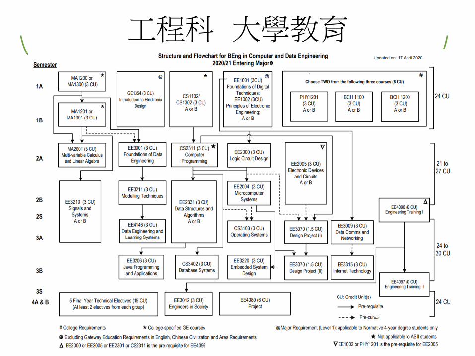
工程科 大學教育
82
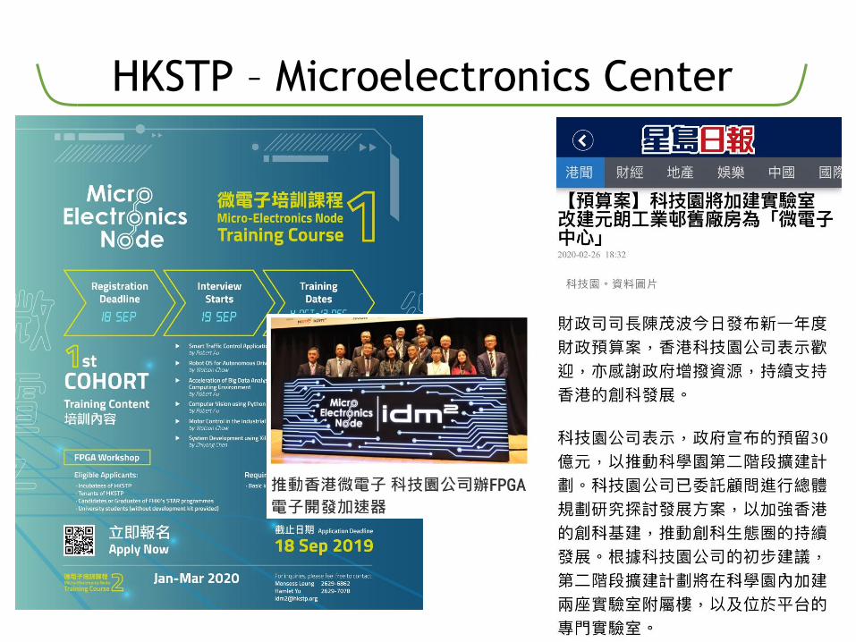
HKSTP – Microelectronics Center
83

總結: 一切從「芯」開始
• Design Specification
• Functional Design
• Logic Design
• Circuit Design
• Physical Design
• Fabrication
• Packaging
• IC delivery
• Thank you very much for your listening. 84

General Advice 給您的建議
Solid Mathematics, Science
Foundation in High School
Moderate Coding skills
Identify your strong interest domain
Create an active learning circle with
the help from school teachers & parents

Past workshops


What’s Next? 下一步是什麼?
1) Principal Nomination Scheme
2) AI Workshop for High School Students
3) EE International students summer course
4) Face Recognition workshop for High School Students
5) Others upcoming
https://www.ee.cityu.edu.hk/home/

https://www.ee.cityu.edu.hk/home/doc/programme/CityU_EE-V3.0.pdf

Acknowledgements 致謝
• CityU Provost Office, CityU-Learning Team
• Prof. Stella Pang – Head, Department of EE, CityU
• Yang Lyu, Vic Huang, PhD Student, Department of EE, CityU
• Kit Sit, PhD Student, Imperial College London, UK
• Clarissa Yung, UG Student, Edinburgh, UK
中學和高中教育
• HKCEE
– Mathematics
– Additional Mathematics
– Physics, Chemistry, Biology
– Computer Studies
• HKAL
– Pure Mathematics
– Applied Mathematics
– Physics
– Chemistry92
大學工科教育
• BEng
– Digital Logic (no VHDL)
– System Design (VHDL)
– FYP (published one paper in TENCON, South Korea)
93
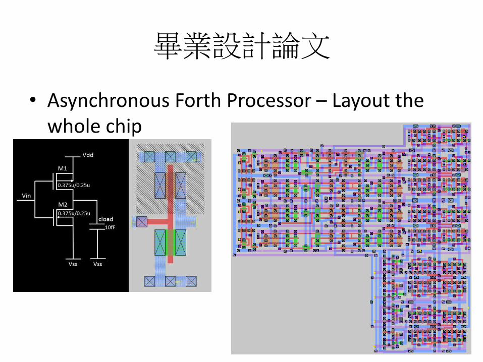
畢業設計論文
• Asynchronous Forth Processor – Layout the whole chip
94

從頭開始設計我的第一個處理器
• Fabricate my first Chip!
• IEEE TENCON is a flagship conference in Asia-Pacific.
95
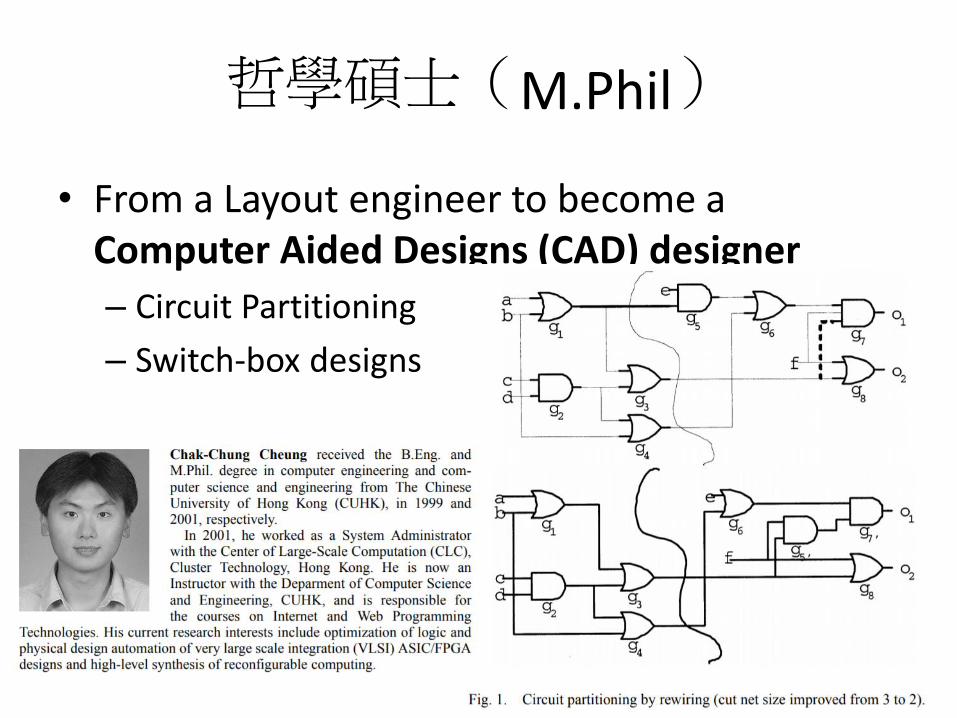
哲學碩士(M.Phil)
• From a Layout engineer to become a Computer Aided Designs (CAD) designer
– Circuit Partitioning
– Switch-box designs
96

高性能計算公司
• Cluster Technology Limited
• Founding System Administrator
• HPC MPI Message Passing
97

英國博士學位研究
• Spent 3.5 years in London
• High-level designer
• Compiler design
98

Prof. Michael Flynn - Stanford
99

博士後研究工作@ UCLA
• From Crypto-graphic, Arithmetic Design to system-level and designer.
100

客座研究員@ Princeton
• Design a secure OpenSPARC Processor
101

Solomon Systech @ 香港科技園
• OLED Display IC Chip Designer
• Founded by a group of former Motorola Engineers
• Around 400 people
102

城市大學電機工程
103
• My 10th year in CityU, EE

Copyright © 2022 FDOKUMEN

