ZiLOG Design Concepts - Z8 Application Ideas
151
ZILOG WORLDWIDE HEADQUARTERS ¥ 910 E. HAMILTON AVENUE ¥ CAMPBELL, CA 95008 TELEPHONE: 408.558.8500 ¥ FAX: 408.558.8300 ¥ WWW .Z I LOG. COM ZiLOG Design Concepts Z8 Application Ideas AN004901-0900
-
Upload
khangminh22 -
Category
Documents
-
view
3 -
download
0
Transcript of ZiLOG Design Concepts - Z8 Application Ideas

Z
I
LOG W
ORLDWIDE
H
EADQUARTERS
¥ 910 E. H
AMILTON
A
VENUE
¥ C
AMPBELL
, CA 95008T
ELEPHONE
: 408.558.8500 ¥ F
AX
: 408.558.8300 ¥
WWW
.Z
I
LOG.
COM
ZiLOG Design Concepts
Z8 Application Ideas
AN004901-0900

AN004901-0900
ZiLOG Design ConceptsZ8 Application Ideas
This publication is subject to replacement by a later edition. To determine whether a later edition exists, or to request copies of publications, contact:
ZiLOG Worldwide Headquarters
910 E. Hamilton AvenueCampbell, CA 95008Telephone: 408.558.8500Fax: 408.558.8300www.ZiLOG.com
Windows is a registered trademark of Microsoft Corporation.
Information Integrity
The information contained within this document has been verified according to the general principles of electrical and mechanical engineering. Any applicable source code illustrated in the document was either written by an authorized ZiLOG employee or licensed consultant. Permission to use these codes in any form, besides the intended application, must be approved through a license agreement between both parties. ZiLOG will not be responsible for any code(s) used beyond the intended application. Contact the local ZiLOG Sales Office to obtain necessary license agreements.
Document Disclaimer
© 2000 by ZiLOG, Inc. All rights reserved. Information in this publication concerning the devices, applications, or technology described is intended to suggest possible uses and may be superseded. ZiLOG, INC. DOES NOT ASSUME LIABILITY FOR OR PROVIDE A REPRESENTATION OF ACCURACY OF THE INFORMATION, DEVICES, OR TECHNOLOGY DESCRIBED IN THIS DOCUMENT. ZiLOG ALSO DOES NOT ASSUME LIABILITY FOR INTELLECTUAL PROPERTY INFRINGEMENT RELATED IN ANY MANNER TO USE OF INFORMATION, DEVICES, OR TECHNOLOGY DESCRIBED HEREIN OR OTHERWISE. Except with the express written approval ZiLOG, use of information, devices, or technology as critical components of life support systems is not authorized. No licenses or other rights are conveyed, implicitly or otherwise, by this document under any intellectual property rights.

ZiLOG Design ConceptsZ8 Application Ideas
iii
Table of ContentsIntroduction . . . . . . . . . . . . . . . . . . . . . . . . . . . . . . . . . . . . . . . . . . . . . . . . . . . . . ix
OTP Selection Guide . . . . . . . . . . . . . . . . . . . . . . . . . . . . . . . . . . . . . . . . . . . . . . xi
Automotive Rear Sonar . . . . . . . . . . . . . . . . . . . . . . . . . . . . . . . . . . . . . . . . . . . . 1
Automotive Speedometer, Odometer, and Tachometer . . . . . . . . . . . . . . . . . . . 4
Autonomous Micro-Blimp Controller . . . . . . . . . . . . . . . . . . . . . . . . . . . . . . . . . . 6
Battery-Operated Door-Entry System . . . . . . . . . . . . . . . . . . . . . . . . . . . . . . . . . 9
The Crab . . . . . . . . . . . . . . . . . . . . . . . . . . . . . . . . . . . . . . . . . . . . . . . . . . . . . . 12
Desktop Fountain . . . . . . . . . . . . . . . . . . . . . . . . . . . . . . . . . . . . . . . . . . . . . . . 15
DCF77 Clock . . . . . . . . . . . . . . . . . . . . . . . . . . . . . . . . . . . . . . . . . . . . . . . . . . . 18
Diagnostic Compressor Protector . . . . . . . . . . . . . . . . . . . . . . . . . . . . . . . . . . . 20
Digital Dimmer Box . . . . . . . . . . . . . . . . . . . . . . . . . . . . . . . . . . . . . . . . . . . . . . 24
Door Access Controller . . . . . . . . . . . . . . . . . . . . . . . . . . . . . . . . . . . . . . . . . . . 27
Electrolytic Capacitor ESR Meter . . . . . . . . . . . . . . . . . . . . . . . . . . . . . . . . . . . 30
Electronic Door Control . . . . . . . . . . . . . . . . . . . . . . . . . . . . . . . . . . . . . . . . . . . 33
Firearm Locking System (FLS) . . . . . . . . . . . . . . . . . . . . . . . . . . . . . . . . . . . . . 35
Forecaster Intelligent Water Delivery Valve . . . . . . . . . . . . . . . . . . . . . . . . . . . 38
Improved Linear Single-Slope ADC . . . . . . . . . . . . . . . . . . . . . . . . . . . . . . . . . 40
Integrated Sailboat Electronic System . . . . . . . . . . . . . . . . . . . . . . . . . . . . . . . 43
Intelligent Guide for the Blind . . . . . . . . . . . . . . . . . . . . . . . . . . . . . . . . . . . . . . 45
Internet Email Reporting Engine . . . . . . . . . . . . . . . . . . . . . . . . . . . . . . . . . . . . 48
Lunar Telemetry Beacon . . . . . . . . . . . . . . . . . . . . . . . . . . . . . . . . . . . . . . . . . . 51
Magic Dice . . . . . . . . . . . . . . . . . . . . . . . . . . . . . . . . . . . . . . . . . . . . . . . . . . . . . 54
Modular Light Display Panel . . . . . . . . . . . . . . . . . . . . . . . . . . . . . . . . . . . . . . . 57
Nasal Oscillatory Transducer . . . . . . . . . . . . . . . . . . . . . . . . . . . . . . . . . . . . . . 60
New Sensor Technologies . . . . . . . . . . . . . . . . . . . . . . . . . . . . . . . . . . . . . . . . 63
Phone Dialer . . . . . . . . . . . . . . . . . . . . . . . . . . . . . . . . . . . . . . . . . . . . . . . . . . . 66
Pocket Music Synthesizer . . . . . . . . . . . . . . . . . . . . . . . . . . . . . . . . . . . . . . . . . 69
Portable Individual Navigator (PIN) . . . . . . . . . . . . . . . . . . . . . . . . . . . . . . . . . . 72
Postal Shock Recorder . . . . . . . . . . . . . . . . . . . . . . . . . . . . . . . . . . . . . . . . . . . 75
PWM Input/Output Interface Module . . . . . . . . . . . . . . . . . . . . . . . . . . . . . . . . . 78
Reaction Tester . . . . . . . . . . . . . . . . . . . . . . . . . . . . . . . . . . . . . . . . . . . . . . . . . 80
Remote-Controlled Air Conditioner . . . . . . . . . . . . . . . . . . . . . . . . . . . . . . . . . . 83
Remote-Control Antenna Positioner . . . . . . . . . . . . . . . . . . . . . . . . . . . . . . . . . 86
AN004901-0900

ZiLOG Design ConceptsZ8 Application Ideas
iv
RF Dog Collar . . . . . . . . . . . . . . . . . . . . . . . . . . . . . . . . . . . . . . . . . . . . . . . . . . 89
Signature Recognition and Authentication . . . . . . . . . . . . . . . . . . . . . . . . . . . . 91
Smart Phone Accessory . . . . . . . . . . . . . . . . . . . . . . . . . . . . . . . . . . . . . . . . . . 93
Smart Solar Water Heating System . . . . . . . . . . . . . . . . . . . . . . . . . . . . . . . . . 95
Smart Window with Fuzzy Control . . . . . . . . . . . . . . . . . . . . . . . . . . . . . . . . . . 97
Solar Tracker . . . . . . . . . . . . . . . . . . . . . . . . . . . . . . . . . . . . . . . . . . . . . . . . . . 100
Speedometer . . . . . . . . . . . . . . . . . . . . . . . . . . . . . . . . . . . . . . . . . . . . . . . . . . 103
Stages Baby Monitor . . . . . . . . . . . . . . . . . . . . . . . . . . . . . . . . . . . . . . . . . . . . 106
Sun Tracking to Optimize Solar Power Generation . . . . . . . . . . . . . . . . . . . . . 109
Tandy Light Control . . . . . . . . . . . . . . . . . . . . . . . . . . . . . . . . . . . . . . . . . . . . . 112
Temperature Measuring Device . . . . . . . . . . . . . . . . . . . . . . . . . . . . . . . . . . . 115
Transmission Trainer . . . . . . . . . . . . . . . . . . . . . . . . . . . . . . . . . . . . . . . . . . . . 118
UFO Flight Regulation System . . . . . . . . . . . . . . . . . . . . . . . . . . . . . . . . . . . . 121
Vehicle Anti-Theft Module . . . . . . . . . . . . . . . . . . . . . . . . . . . . . . . . . . . . . . . . 124
Windmill Commander . . . . . . . . . . . . . . . . . . . . . . . . . . . . . . . . . . . . . . . . . . . 126
Wireless Accelerometer . . . . . . . . . . . . . . . . . . . . . . . . . . . . . . . . . . . . . . . . . 129
AN004901-0900

ZiLOG Design ConceptsZ8 Application Ideas
v
List of FiguresFigure 1. Automotive Rear Sonar Block Diagram . . . . . . . . . . . . . . . . . . . . . . . 2
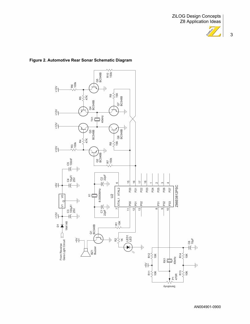
Figure 2. Automotive Rear Sonar Schematic Diagram . . . . . . . . . . . . . . . . . . . 3
Figure 3. Automotive Velometer, Mileometer, and Tachometer Block Diagram 4
Figure 4. Automotive Velometer, Mileometer, and Tachometer Schematic Diagram . . . . . . . . . . . . . . . . . . . . . . . . . . . . . . . . . . . . . . . . . . . . . . . 5
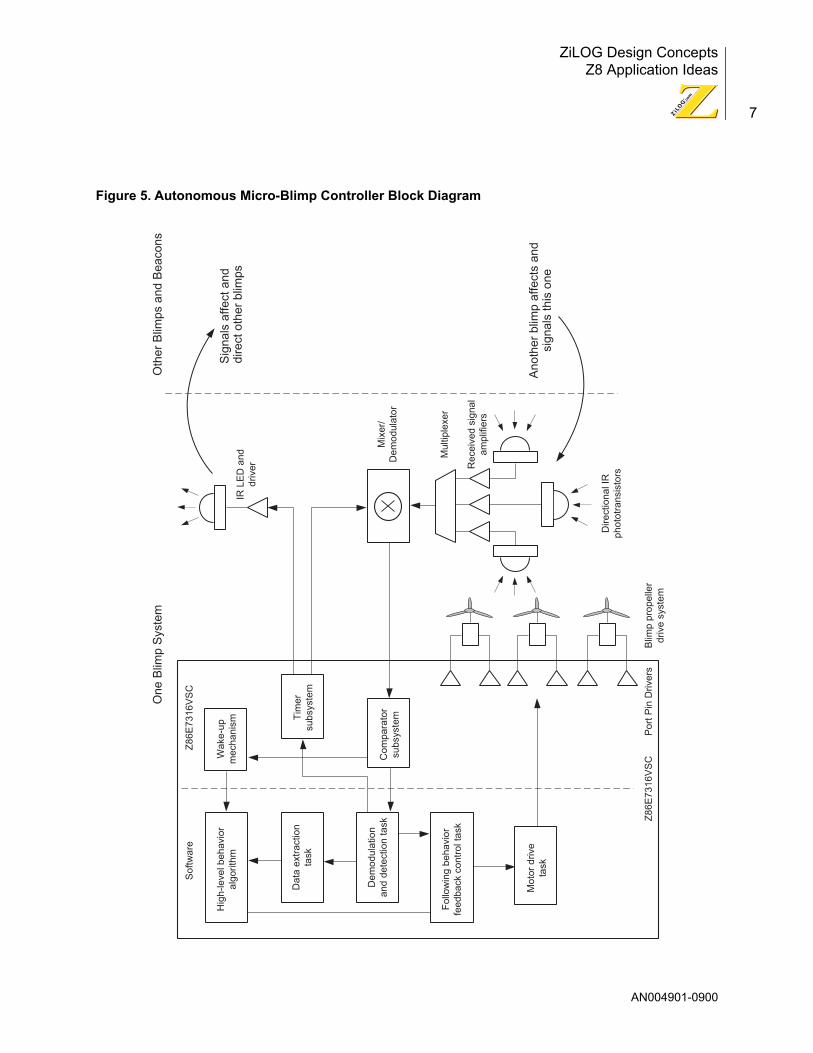
Figure 5. Autonomous Micro-Blimp Controller Block Diagram . . . . . . . . . . . . . 7
Figure 6. Autonomous Micro-Blimp Controller Schematic Diagram . . . . . . . . . 8
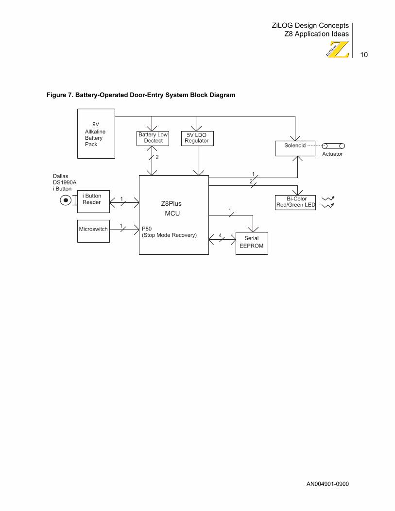
Figure 7. Battery-Operated Door-Entry System Block Diagram . . . . . . . . . . . 10
Figure 8. Battery-Operated Door-Entry System Schematic Diagram . . . . . . . 11
Figure 9. The Crab Block Diagram . . . . . . . . . . . . . . . . . . . . . . . . . . . . . . . . . 13
Figure 10. The Crab Schematic Diagram . . . . . . . . . . . . . . . . . . . . . . . . . . . . . 14
Figure 11. Desktop Fountain Block Diagram . . . . . . . . . . . . . . . . . . . . . . . . . . 16
Figure 12. Desktop Fountain Schematic Diagram . . . . . . . . . . . . . . . . . . . . . . 17
Figure 13. DCF77 Clock Schematic Diagram . . . . . . . . . . . . . . . . . . . . . . . . . . 19
Figure 14. Diagnostic Compressor Protector Block Diagram . . . . . . . . . . . . . . 22
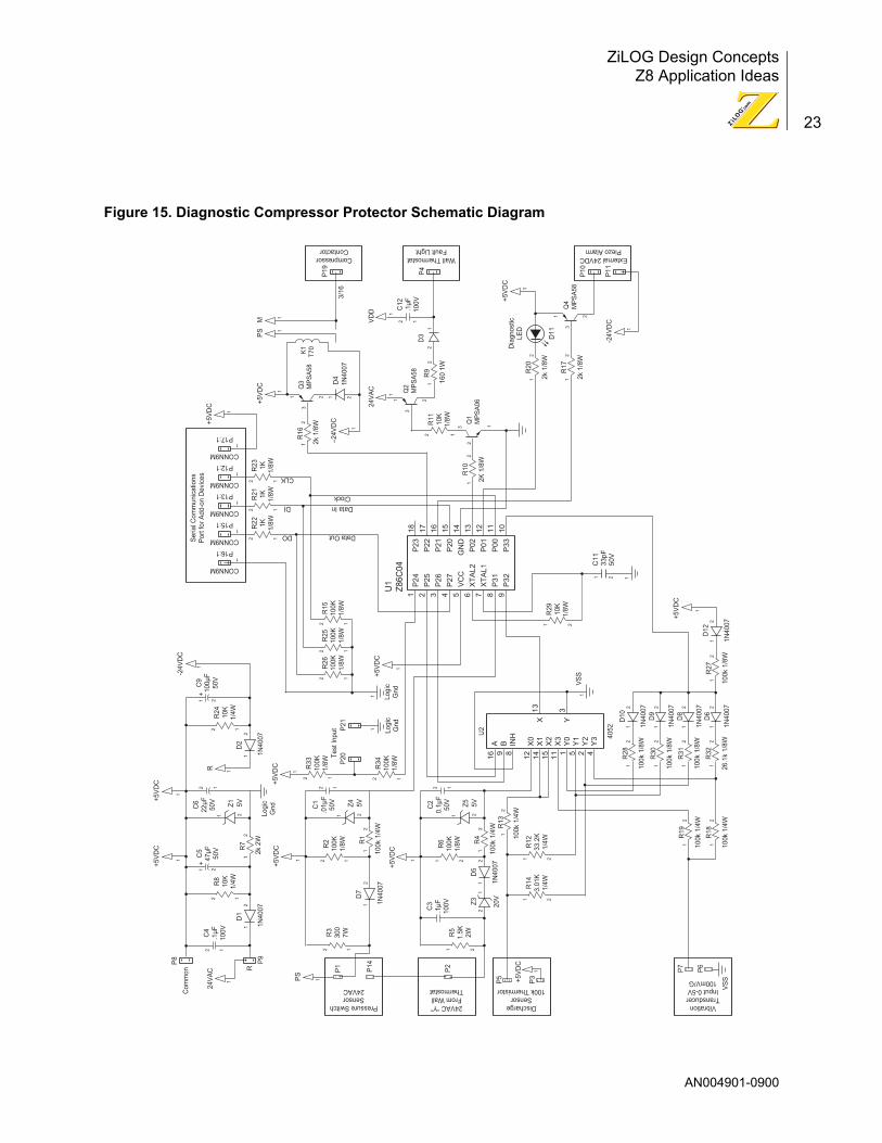
Figure 15. Diagnostic Compressor Protector Schematic Diagram . . . . . . . . . . 23
Figure 16. Digital Dimmer Box Block Diagram . . . . . . . . . . . . . . . . . . . . . . . . . 25
Figure 17. Digital Dimmer Box Schematic Diagram . . . . . . . . . . . . . . . . . . . . . 26
Figure 18. Door Access Controller Block Diagram . . . . . . . . . . . . . . . . . . . . . . 28
Figure 19. Door Access Controller Schematic Diagram . . . . . . . . . . . . . . . . . . 29
Figure 20. Electrolytic Capacitor ESR Meter Schematic Diagram . . . . . . . . . . 32
Figure 21. Electronic Door Control Block Diagram . . . . . . . . . . . . . . . . . . . . . . 34
Figure 22. Firearm Locking System Block Diagram . . . . . . . . . . . . . . . . . . . . . 36
Figure 23. Firearm Locking System Schematic Diagram . . . . . . . . . . . . . . . . . 37
Figure 24. Forecaster Intelligent Water Delivery Valve Schematic . . . . . . . . . . 39
Figure 25. Improved Linear Single Slope ADC Block Diagram . . . . . . . . . . . . 41
Figure 26. Improved Linear Single Slope ADC Schematic Diagram . . . . . . . . 42
Figure 27. Integrated Sailboat Electronic System Block Diagram . . . . . . . . . . 44
Figure 28. Integrated Sailboat Electronic System Schematic Diagram . . . . . . 44
Figure 29. Intelligent Guide for the Blind Block Diagram . . . . . . . . . . . . . . . . . 46
Figure 30. Intelligent Guide for the Blind Schematic Diagram . . . . . . . . . . . . . 47
Figure 31. Internet Email Reporting Engine Block Diagram . . . . . . . . . . . . . . . 49
Figure 32. Internet Email Reporting Engine Software Block Diagram . . . . . . . 49
Figure 33. Internet Email Reporting Engine Schematic Diagram . . . . . . . . . . . 50
AN004901-0900

ZiLOG Design ConceptsZ8 Application Ideas
vi
Figure 34. Magic Dice Block Diagram . . . . . . . . . . . . . . . . . . . . . . . . . . . . . . . . 55
Figure 35. Magic Dice Schematic Diagram . . . . . . . . . . . . . . . . . . . . . . . . . . . . 56
Figure 36. Modular Light Display Panel Module Block Diagram . . . . . . . . . . . . 58
Figure 37. Modular Light Display Panel Module Schematic Diagram . . . . . . . . 59
Figure 38. Nasal Oscillatory Transducer Block Diagram . . . . . . . . . . . . . . . . . 61
Figure 39. Nasal Oscillatory Transducer Schematic Diagram . . . . . . . . . . . . . 62
Figure 40. New Sensor Technology Waveform . . . . . . . . . . . . . . . . . . . . . . . . 64
Figure 41. New Sensor Technology Block Diagram . . . . . . . . . . . . . . . . . . . . . 65
Figure 42. Phone Dialer Block Diagram . . . . . . . . . . . . . . . . . . . . . . . . . . . . . . 67
Figure 43. Phone Dialer Schematic Diagram . . . . . . . . . . . . . . . . . . . . . . . . . . 68
Figure 44. Pocket Music Synthesizer Block Diagram . . . . . . . . . . . . . . . . . . . . 70
Figure 45. Pocket Music Synthesizer Schematic Diagram . . . . . . . . . . . . . . . . 71
Figure 46. Portable Individual Navigator A/D Ratio Over Time . . . . . . . . . . . . 73
Figure 47. Portable Individual Navigator Schematic Diagram . . . . . . . . . . . . . 74
Figure 48. Postal Shock Recorder Block Diagram . . . . . . . . . . . . . . . . . . . . . . 76
Figure 49. Postal Shock Recorder Schematic Diagram . . . . . . . . . . . . . . . . . . 77
Figure 50. PWM Input Output/Interface Module Block Diagram . . . . . . . . . . . . 79
Figure 51. Reaction Tester Block Diagram . . . . . . . . . . . . . . . . . . . . . . . . . . . . 81
Figure 52. Reaction Tester Schematic Diagram . . . . . . . . . . . . . . . . . . . . . . . . 82
Figure 53. Remote-Control Air Conditioner Block Diagram . . . . . . . . . . . . . . . 84
Figure 54. Remote-Control Air Conditioner Schematic Diagram . . . . . . . . . . . 85
Figure 55. Remote Controlled Antenna Positioner Block Diagram . . . . . . . . . . 87
Figure 56. Hand-Held Remote Block Diagram . . . . . . . . . . . . . . . . . . . . . . . . . 87
Figure 57. Remote Controlled Antenna Positioner Schematic Diagram . . . . . . 88
Figure 58. RF Dog Collar Block Diagram . . . . . . . . . . . . . . . . . . . . . . . . . . . . . 90
Figure 59. Signature Recognition and Authentication Module Block Diagram . 91
Figure 60. Signature Recognition and Authentication Module Schematic Diagram . . . . . . . . . . . . . . . . . . . . . . . . . . . . . . . . . . . . . . . . . . . . . . 92
Figure 61. Smart Phone Accessory Block Diagram . . . . . . . . . . . . . . . . . . . . . 93
Figure 62. Smart Phone Accessory Schematic Diagram . . . . . . . . . . . . . . . . . 94
Figure 63. Smart Solar Water Heating System Block Diagram . . . . . . . . . . . . 96
Figure 64. Smart Window with Fuzzy Control . . . . . . . . . . . . . . . . . . . . . . . . . . 98
Figure 65. Smart Window with Fuzzy Control Schematic Diagram . . . . . . . . . 99
Figure 66. Solar Tracker Block Diagram . . . . . . . . . . . . . . . . . . . . . . . . . . . . . 101
Figure 67. Solar Tracker Schematic Diagram . . . . . . . . . . . . . . . . . . . . . . . . . 102
Figure 68. Speedometer Flow Diagram . . . . . . . . . . . . . . . . . . . . . . . . . . . . . 104
AN004901-0900

ZiLOG Design ConceptsZ8 Application Ideas
vii
Figure 69. Speedometer Block Diagram . . . . . . . . . . . . . . . . . . . . . . . . . . . . . 105
Figure 70. Stages Baby Monitor Block Diagram . . . . . . . . . . . . . . . . . . . . . . . 107
Figure 71. Stages Baby Monitor Schematic Diagram . . . . . . . . . . . . . . . . . . . 108
Figure 72. Sun Tracking Block Diagram . . . . . . . . . . . . . . . . . . . . . . . . . . . . . 110
Figure 73. Sun Tracking Schematic Diagram . . . . . . . . . . . . . . . . . . . . . . . . . 111
Figure 74. Tandy Light Control Block Diagram . . . . . . . . . . . . . . . . . . . . . . . . 113
Figure 75. Tandy Light Control Schematic Diagram . . . . . . . . . . . . . . . . . . . . 114
Figure 76. Temperature Measuring Device Block Diagram . . . . . . . . . . . . . . 116
Figure 77. Temperature Measuring Device Schematic Diagram . . . . . . . . . . 117
Figure 78. Transmission Trainer Block Diagram . . . . . . . . . . . . . . . . . . . . . . . 119
Figure 79. Transmission Trainer Schematic Diagram . . . . . . . . . . . . . . . . . . . 120
Figure 80. UFO Flight Regulation System Block Diagram . . . . . . . . . . . . . . . 122
Figure 81. UFO Flight Regulation System Schematic Diagram . . . . . . . . . . . 123
Figure 82. Vehicle Anti-Theft Module Block Diagram . . . . . . . . . . . . . . . . . . . 125
Figure 83. Vehicle Anti-Theft Module Schematic Diagram . . . . . . . . . . . . . . . 125
Figure 84. Windmill Commander Block Diagram . . . . . . . . . . . . . . . . . . . . . . 127
Figure 85. Windmill Commander Schematic Diagram . . . . . . . . . . . . . . . . . . 128
Figure 86. Wireless Accelerometer Block Diagram . . . . . . . . . . . . . . . . . . . . 130
Figure 87. Wireless Accelerometer Schematic Diagram . . . . . . . . . . . . . . . . 131
AN004901-0900

ZiLOG Design ConceptsZ8 Application Ideas
AN004901-0900
viii
List of Tables
Table 1. OTP Selection Guide . . . . . . . . . . . . . . . . . . . . . . . . . . . . . . . . . . . . .xii
Table 2. Sensor Inputs . . . . . . . . . . . . . . . . . . . . . . . . . . . . . . . . . . . . . . . . . . 21
Table 3. Firearm Sensor Input Functions . . . . . . . . . . . . . . . . . . . . . . . . . . . 35
Table 4. Graphics Display Features . . . . . . . . . . . . . . . . . . . . . . . . . . . . . . . 43
Table 5. Serial Commands . . . . . . . . . . . . . . . . . . . . . . . . . . . . . . . . . . . . . . 48

ZiLOG Design ConceptsZ8 Application Ideas
AN004901-0900
ix
Introduction
Are you driven to design the best?
Co-sponsored with
CMP Media, Inc.
, ZiLOGÕs 1999 ÒDriven to DesignÓ contest sought the most innovative and creative use of ZiLOGÕs award-winning Z8
¨
or Z8Plus
¨
OTP microcontroller.
The 47 abstracts contained in this book offer the designer a launching pad from which to prompt ideas and develop designs incorporating the ZiLOG Z8 or Z8Plus microcontrollers. They range in scope from helping blind individuals navigate busy intersections to providing increased protection for the handling and delivery of fragile packages.
Students and engineers from all over the world submitted the design concepts presented in this compendium. Each abstract includes block and schematic diagrams to help the designer comprehend the contestantsÕ visions of products that are viable in todayÕs connected world.

ZiLOG Design ConceptsZ8 Application Ideas
AN004901-0900
x
ZiLOG OTP Selection Guide
ROM(KB)
PACKAGE PINS
OPERATINGTEMPERATURE OSCILLATOR
ZiLOGPART NUMBER
VOLTAGE RANGE
PROGRAMMINGADAPTER
EMULATOR/ACCESS. KIT FEATURES
ROMEQUIV.
0.5K DIP 18 -40/105 Selectable Z86E0208PEC1925 4.5V - 5.5V Not Required Z86CCP01ZEM** 1 Timer + WDT Z86C02 0/70 Z86E0208PSC1925 3.5V - 5.5V 2 Comparators SOIC 18 -40/105 Z86E0208SEC1925 4.5V - 5.5V Z86E0700ZDP 61 RAM + 14 I/O + POR 0/70 Z86E0208SSC1925 3.5V - 5.5V SSOP 20 -40/105 Z86E0208HEC1925 4.5V - 5.5V Z86E0800ZDH 0/70 Z86E0208HSC1925 3.5V - 5.5V DIP 18 0/70 Selectable Z86E0308PSC 4.5V - 5.5V Z86E0601ZDP 1 Timer + Timer Out Z86C03
SOIC Z86E0308SSC 2 Comparators + WDT 61 RAM + 14 I/O + POR
DIP 18 -40/105 XTAL Z8E00010PEC 4.5V - 5.5V Not Required Z8ICE001ZEM Z8Plus Core None 0/70 Z8E00010PSC 3.5V - 5.5V 1 Timer SOIC 18 -40/105 Z8E00010SEC 4.5V - 5.5V Z86E0700ZDP WDT + Reset Pin 0/70 Z8E00010SSC 3.5V - 5.5V 32 RAM + 13 I/O SSOP 20 -40/105 Z8E00010HEC 4.5V - 5.5V Z8E00101ZDH
0/70 Z8E00010HSC 3.5V - 5.5V DIP 18 -40/105 Selectable Z8PE002PZ010EC 4.5V - 5.5V Not Required Z8Plus Core 0/70 Z8PE002PZ010SC 3.0V - 5.5V 3 Timers / PWM SOIC 18 -40/105 Z8PE002SZ010EC 4.5V - 5.5V Z86E0700ZDP 1 Comparator + WDT 0/70 Z8PE002SZ010SC 3.0V - 5.5V 64 RAM + 14 I/O + POR SSOP 20 -40/105 Z8PE002HZ010EC 4.5V - 5.5V Z8E00101ZDH
0/70 Z8PE002HZ010SC 3.0V - 5.5V1K DIP 18 -40/105 XTAL Z86E0412PEC 4.5V - 5.5V Not Required Z86CCP01ZEM** 2 Timers + WDT Z86C04
RC Z86E0412PEC1903 2 Comparators 0/70 XTAL Z86E0412PSC1866 125 RAM + 14 I/O + POR RC Z86E0412PSC1903
SOIC 18 -40/105 XTAL Z86E0412SEC Z86E0700ZDP RC Z86E0412SEC1903
0/70 XTAL Z86E0412SSC1866 RC Z86E0412SSC1903
SSOP 20 -40/105 XTAL Z86E0412HEC1866 Z86E0800ZDH Z86E0412HSC1866
DIP 18 0/70 Selectable Z86E0612PSC Z86E0601ZDP 2 Timers + SPI + WDT Z86C06SOIC Z86E0612SSC 2 Comparators + 125 RAM
Timer Out + 14 I/O + POR DIP 18 -40/105 XTAL Z8E00110PEC 4.5V - 5.5V Not Required Z8ICE001ZEM Z8Plus Core None 0/70 Z8E00110PSC 3.5V - 5.5V 3 Timers / PWM SOIC 18 -40/105 Z8E00110SEC 4.5V - 5.5V Z86E0700ZDP 1 Comparator + WDT 0/70 Z8E00110SSC 3.5V - 5.5V Reset Pin SSOP 20 -40/105 Z8E00110HEC 4.5V - 5.5V Z8E00101ZDH 64 RAM + 13 I/O 0/70 Z8E00110HSC 3.5V - 5.5V DIP 18 -40/105 Selectable Z8PE003PZ010EC 4.5V - 5.5V Not Required Z8Plus Core 0/70 Z8PE003PZ010SC 3.0V - 5.5V 3 Timers / PWM SOIC 18 -40/105 Z8PE003SZ010EC 4.5V - 5.5V Z86E0700ZDP 1 Comparator + WDT 0/70 Z8PE003SZ010SC 3.0V - 5.5V Reset Pin SSOP 20 -40/105 Z8PE003HZ010EC 4.5V - 5.5V Z8E00101ZDH 64 RAM + 14 I/O + POR
0/70 Z8PE003HZ010SC 3.0V - 5.5V2K DIP 18 -40/105 XTAL Z86E0812PEC 4.5V - 5.5V Not Required Z86CCP01ZEM** 2 Timers + WDT Z86C08
RC Z86E0812PEC1903 2 Comparators 0/70 XTAL Z86E0812PSC1866 125 RAM + 14 I/O + POR RC Z86E0812PSC1903
SOIC 18 -40/105 XTAL Z86E0812SEC Z86E0700ZDP RC Z86E0812SEC1903 0/70 XTAL Z86E0812SSC1866 RC Z86E0812SSC1903
SSOP 20 -40/105 XTAL Z86E0812HEC1866 Z86E0800ZDH Z86E0812HSC1866
DIP 28 -40/105 Selectable Z86E3116PEC 4.5V - 5.5V Not Required Z86CCP01ZEM** 2 Timers + WDT Z86C31 0/70 Z86E3116PSC 3.5V - 5.5V and 2 Comparators
SOIC 28 -40/105 Z86E3116SEC 4.5V - 5.5V Z86C3000ZAC Z86CCP00ZAC 125 RAM + 24 I/O + POR 0/70 Z86E3116SSC 3.5V - 5.5V
PLCC 28 -40/105 Z86E3116VEC 4.5V - 5.5V 0/70 Z86E3116VSC 3.5V - 5.5V
4K DIP 28 -40/105 Selectable Z86E132PZ016EC1 3.0V - 5.5V ZICSP000100ZDP Z86C3600ZEM UART + 2 Comparators Z86C34***0/70 Z86E132PZ016SC + ICSP OTP Programming (16K ROM)
SOIC 28 -40/105 Z86E132SZ016EC1 ZICSP000300ZDS ZLGICSP0100ZPR 2 Timers + 237 RAM, 0/70 Z86E132SZ016SC 24 I/O + WDT + POR
DIP 40 -40/105 Selectable Z86E142PZ016EC1 ZICSP000400ZDP Z86C3600ZEM UART + 2 Comparators Z86C44**** 0/70 Z86E142PZ016SC + ICSP OTP Programming (16K ROM)
QFP 44 -40/105 Z86E142FZ016EC ZICSP000600ZDF ZLGICSP0100ZPR 2 Timers + 236 RAM,0/70 Z86E142FZ016SC 32 I/O + WDT + POR
DIP 28 -40/105 Selectable Z86E3016PEC 4.5V - 5.5V Not Required Z86CCP01ZEM** 2 Timers + WDT Z86C30 0/70 Z86E3016PSC 3.5V - 5.5V 2 Comparators SOIC 28 0/70 Z86E3016SEC 4.5V - 5.5V Z86C3000ZAC 237 RAM + 24 I/O + POR Z86E3016SSC 3.5V - 5.5V PLCC 28 0/70 Z86E3016VEC 4.5V - 5.5V Z86E3016VSC 3.5V - 5.5V DIP 28 0/70 Selectable Z86E3312PSC 3.5V - 5.5V Z86E3400ZDP Z86CCP01ZEM** Clock-free WDT Reset Z86C33
SOIC Z86E3312SSC Z86E3400ZDS and 237 RAM + 2 ComparatorsPLCC Z86E3312VSC Z86E3400ZDV Z86CCP00ZAC 2 Timers + 24 I/O + PORDIP 40 0/70 RC Z86E1505PSC 4.5V - 5.5V Z86E1500ZDP Z86CCP01ZEM+ 1 Timer + WDT Z86K15/K16
188 RAM + 32 I/O (K16=5K ROM) QFP 44 -40/105 Selectable Z86E4016FEC 4.5V - 5.5V Z86E4001ZDF Z86CCP01ZEM** 2 Timers + WDT Z86C40
0/70 Z86E4016FSC 3.5V - 5.5V and 2 Comparators DIP 40 -40/105 Z86E4016PEC 4.5V - 5.5V Not Required Z86CCP00ZAC 236 RAM + 32 I/O + POR
0/70 Z86E4016PSC 3.5V - 5.5V PLCC 44 -40/105 Z86E4016VEC 4.5V - 5.5V Z86E4001ZDV
0/70 Z86E4016VSC 3.5V - 5.5V QFP 44 0/70 Selectable Z86E4312FSC 3.5V - 5.5V Z86E4400ZDF Z86CCP01ZEM** Clock-free WDT Reset Z86C43 DIP 40 Z86E4312PSC Z86E4400ZDP 2 Timers + 2 Comparators PLCC 44 Z86E4312VSC Z86E4400ZDV 236 RAM + 32 I/O DIP 28 -40/105 XTAL Z86E8316PEC 4.5V - 5.5V Z86E8300ZDP Z86C8401ZEM 8 Bit - 8 Channel A/D Z86C83
0/70 Z86E8316PSC 3.5V - 5.5V 2 Timers + WDTSOIC -40/105 Z86E8316SEC 4.5V - 5.5V Z86E8300ZDS 2 Comparators
0/70 Z86E8316SSC 3.5V - 5.5V 237 RAM + 21 I/O + PORPLCC -40/105 Z86E8316VEC 4.5V - 5.5V Z86E8300ZDV
0/70 Z86E8316VSC 3.5V - 5.5V

ZiLOG Design ConceptsZ8 Application Ideas
AN004901-0900
xi
ROM(KB)
PACKAGE PINS
OPERATINGTEMPERATURE OSCILLATOR
ZiLOGPART NUMBER
VOLTAGE RANGE
PROGRAMMINGADAPTER
EMULATOR/ACCESS. KIT FEATURES
ROMEQUIV.
8K DIP 28 -40/105 Selectable Z86E133PZ016EC1 3.0V - 5.5V ZICSP000100ZDP Z86C3600ZEM UART + 2 Comparators Z86C34***0/70 Z86E133PZ016SC + ICSP OTP Programming (16K ROM)
SOIC 28 -40/105 Z86E133SZ016EC1 ZICSP000300ZDS ZLGICSP0100ZPR 2 Timers + 237 RAM, 0/70 Z86E133SZ016SC 24 I/O + WDT + POR
DIP 40 -40/105 Selectable Z86E143PZ016EC1 ZICSP000400ZDP Z86C3600ZEM UART + 2 Comparators Z86C44**** 0/70 Z86E143PZ016SC + ICSP OTP Programming (16K ROM)
QFP 44 -40/105 Z86E143FZ016EC ZICSP000600ZDF ZLGICSP0100ZPR 2 Timers + 236 RAM0/70 Z86E143FZ016SC 32 I/O + WDT + POR
DIP 28 0/70 Selectable Z8673312PSC 3.5V - 5.5V Z86E3400ZDP Z86CCP01ZEM** 2 Timers + WDT Z86233SOIC Z8673312SSC Z86E3400ZDS 2 ComparatorsPLCC Z8673312VSC Z86E3400ZDV 237 RAM + 24 I/O + PORQFP 44 0/70 Selectable Z8674312FSC Z86E4400ZDF 2 Timers + WDT Z86243DIP 40 Z8674312PSC Z86E4400ZDP 2 Comparators
PLCC 44 Z8674312VSC Z86E4400ZDV 236 RAM + 32 I/O + POR QFP 44 0/70 XTAL Z86E2112FSC 4.5V - 5.5V Z86E2101ZDF Z86C1200ZEM 2 Timers + UART + WDT Z86C21
DIP 40 Z86E2112PSC Z86E2301ZDP 8 Open Drain OutputsPLCC 44 Z86E2112VSC Z86E2101ZDV 236 RAM + 32 I/O
16K DIP 28 -40/105 Selectable Z86E134PZ016EC1 3.0V - 5.5V ZICSP000100ZDP Z86C3600ZEM UART + 2 Comparators Z86C340/70 Z86E134PZ016SC + ICSP OTP Programming
SOIC 28 -40/105 Z86E134SZ016EC1 ZICSP000300ZDS ZLGICSP0100ZPR 2 Timers + 237 RAM 0/70 Z86E134SZ016SC 24 I/O + WDT + POR
DIP 40 -40/105 Selectable Z86E144PZ016EC1 ZICSP000400ZDP Z86C3600ZEM UART + 2 Comparators Z86C44 0/70 Z86E144PZ016SC + ICSP OTP Programming
QFP 44 -40/105 Z86E144FZ016EC ZICSP000600ZDF ZLGICSP0100ZPR 2 Timers + 236 RAM,0/70 Z86E144FZ016SC 32 I/O + WDT + POR
DIP 28 0/70 Selectable Z86E3412PSC 3.5V - 5.5V Z86E3400ZDP Z86CCP01ZEM** 2 Timers + WDT Z86C34SOIC Z86E3412SSC Z86E3400ZDS (Must be modified 2 Comparators
PLCC Z86E3412VSC Z86E3400ZDV see website) 237 RAM + 24 I/O + POR
QFP 44 0/70 Selectable Z86E4412FSC Z86E4400ZDF or 2 Timers + WDT Z86C44
DIP 40 Z86E4412PSC Z86E4400ZDP Z86C5000ZEM 2 Comparators
PLCC 44 Z86E4412VSC Z86E4400ZDV 236 RAM + 32 I/O + POR
QFP 44 0/70 XTAL Z86E6116FSC 4.5V - 5.5V Z86E2101ZDF Z86C1200ZEM 2 Timers + UART Z86C61
DIP 40 Z86E6116PSC Z86E2301ZDP 236 RAM + 32 I/O
PLCC 44 Z86E6116VSC Z86E2101ZDV
QFP 44 0/70 Selectable Z86E7216FSC Included With Emulator Z86L7103ZEM 2 Adv. Timers + WDT Z86C72
PDIP 40 Z86E7216PSC 2 ComparatorsPLCC 44 Z86E7216VSC 738 RAM +31 I/O
32K DIP 28 -40/105 Selectable Z86E135PZ016EC1 3.0V - 5.5V ZICSP000100ZDP Z86C3600ZEM UART + 2 Comparators Z86C35
0/70 Z86E135PZ016SC + ICSP OTP Programming
SOIC 28 -40/105 Z86E135SZ016EC1 ZICSP000300ZDS ZLGICSP0100ZPR 2 Timers + 237 RAM, 0/70 Z86E135SZ016SC 24 I/O + WDT + POR
DIP 40 -40/105 Selectable Z86E145PZ016EC1 ZICSP000400ZDP Z86C3600ZEM UART + 2 Comparators Z86C45 0/70 Z86E145PZ016SC + ICSP OTP Programming
QFP 44 -40/105 Z86E145FZ016EC ZICSP000600ZDF ZLGICSP0100ZPR 2 Timers + 236 RAM,0/70 Z86E145FZ016SC 32 I/O + WDT + POR
QFP 44 0/70 XTAL Z86E6316FSC 4.5V - 5.5V Z86E2101ZDF Z86C1200ZEM 2 Timers + UART Z86C63 DIP 40 Z86E6316PSC Z86E2301ZDP 236 RAM + 32 I/O PLCC 44 Z86E6316VSC Z86E2101ZDV
PDIP 40 0/70 Selectable Z86D7308PSC 2.0V - 3.6V Included With Emulator Z86L9800ZEM 2 Adv. Timers + WDT Z86L87 (16K ROM)PLCC 44 Z86D7308VSC 2 Comparators Z86L89 (24K ROM)
236 RAM + 31 I/O Z86L73 (32K ROM)
PDIP 28 0/70 Selectable Z86D8608PSC Included With Emulator Z86L9800ZEM 2 Adv. Timers + WDT Z86L82 (4K ROM)SOIC 28 Z86D8608SSC 2 Comparators Z86L85 (8K ROM)
236 RAM + 23 I/O Z86L88 (16K ROM)Z86L81 (24K ROM)Z86L86 (32K ROM)
SSOP 48 0/70 Selectable Z86D990HZ008SC 3.0V - 5.5V TBD Z86L9900100ZEM 2 Adv. Timers + 1GPTimer Z86L990
PDIP 40 Z86D990PZ008SC Included With Emulator WDT + 2 Comparators (16K ROM)4 Ch 8-bit ADC
489 RAM + 32 I/OPDIP 28 0/70 Selectable Z86D991PZ008SC Included With Emulator 2 Adv. Timers + 1GPTimer Z86L991SOIC 28 Z86D991SZ008SC WDT + 2 Comparators (16K ROM)
4 Ch 8-bit ADC489 RAM + 23 I/O
QFP 44 0/70 Selectable Z86E7316FSC 4.5V - 5.5V Included With Emulator Z86L7103ZEM 2 Adv. Timers + WDT Z86C88PDIP 40 Z86E7316PSC 2 Comparators (16K ROM)
PLCC 44 Z86E7316VSC 236 RAM + 31 I/O
64K DIP 28 -40/105 Selectable Z86E136PZ016EC1 3.0V - 5.5V ZICSP000100ZDP Z86C3600ZEM UART + 2 Comparators Z86C36
0/70 Z86E136PZ016SC + ICSP OTP ProgrammingSOIC 28 -40/105 Z86E136SZ016EC1 ZICSP000300ZDS ZLGICSP0100ZPR 2 Timers + 237 RAM
0/70 Z86E136SZ016SC 24 I/O + WDT + POR
DIP 40 -40/105 Selectable Z86E146PZ016EC1 ZICSP000400ZDP Z86C3600ZEM UART + 2 Comparators Z86C46 0/70 Z86E146PZ016SC + ICSP OTP Programming
QFP 44 -40/105 Z86E146FZ016EC ZICSP000600ZDF ZLGICSP0100ZPR 2 Timers + 236 RAM,0/70 Z86E146FZ016SC 32 I/O + WDT + POR
1 Extended Temperature Device will be available in Q4 2000. * Selectable Oscillator means Crystal or RC can be chosen
** The Z86CCP01ZEM is rated at 12 MHz. For speed above 12 MHz, use the Z86C5000ZEM emulator. For Z86C06 SPI Emulation, use the Z86C5000ZEM
*** ROM device has 16K internal Program Memory.
**** ROM device has 16K internal Program Memory. External program & data memory access should start from 16K (address = 4000H)
+ The Z86CCP01ZEM is used only for programming the EPROM version, and the Z86K1500ZEM is used only for emulation of this part. ++ The Z86CCP01ZEM is used only for programming the EPROM version, and the Z86U1800ZEM is used only for emulation of this pa
DESCRIPTION OF Z8 ADAPTERS
Z86CCP00ZAC: 28 / 40-Pin DIP Accessory Kit Z86CCP01Z Z86E2101ZDF: 44-Pin QFP to 40-Pin DIP Adapter Z86C4001ZDV: 44-Pin PLCC to 40-Pin DIP Adapter Z86C3000ZAC: 28-Pin SOIC/PLCC Accessory Kit for Z86C Z86E2101ZDV: 44-Pin PLCC to 40-Pin DIP Adapter Z86E4001ZDV: 44-Pin PLCC to 40-Pin DIP Adapter Z86E0601ZDP: 18-Pin SOIC to 18-Pin DIP Adapter Z86E3400ZDP: 28-Pin DIP to 18-Pin DIP Adapter Z86E8300ZDP: 28-Pin DIP to 28-Pin DIP Adapter Z86E0700ZDP: 18-Pin SOIC to 18-Pin DIP Adapter Z86E3400ZDS: 28-Pin SOIC to 18-Pin DIP Adapter Z86E8300ZDS: 28-Pin SOIC to 28-Pin DIP Adapter Z86E0800ZDH: 20-Pin SSOP to 18-Pin DIP Adapter Z86E3400ZDV: 28-Pin PLCC to 18-Pin DIP Adapter Z86E8300ZDV: 28-Pin PLCC to 28-Pin DIP Adapter Z86E1500ZDP: 40-Pin DIP Adapter Z86E4400ZDF: 44-Pin QFP to 18-Pin DIP Adapter Z8E00101ZDH: 20-Pin SSOP to 18-Pin DIP (Z8ICE) Adapter ZLGICSP0100ZPICSP Programmer for Z8 MUZE Family Z86E4400ZDP: 40-Pin DIP to 18-Pin DIP Adapter Z8PE0030000ZDP: Z8ICE000ZEM & Z8ICE010ZEM Upgrade Kit ZICSP000100ZD 28-Pin DIP Programming Adapter for ICSP ZICSP000400ZDP: 40-Pin DIP Programming Adapter for ICSP Programmer ZICSP000300ZD 28-Pin SOIC Programming Adapter for ICS ZICSP000600ZDF: QFP Programming Adapter for ICSP Programmer

ZiLOG Design ConceptsZ8 Application Ideas
1
Automotive Rear SonarSubmitted by: R. Hugo Vieira Neto and Francisco Eugenio Mauro
Abstract
The Automotive Rear Sonar is intended for automotive use. It is simple, effective, and inexpensive. Designed with a ZiLOG Z8 OTP microcontroller, this device measures the distance between the vehicle and any obstacle when in reverse gear. The driver is informed when a collision is about to occur.
The sonar utilizes a pair of ultrasonic transducers to send and receive 40-kHz wave bursts. The goal is to measure the time of flight of the ultrasonic burst if an echo occurs.
A Z86E08 microcontroller running at 8 MHz acts as the system control block. Some of the Z86E08s key features are:
¥ Short instruction execution times (generation of the 40-kHz ultrasonic signal by software)
¥ Onboard analog comparators (making ultrasonic detection simple and inexpensive)
¥ Onboard counter/timers with prescalers (making ultrasonic wave time-of-flight easy to measure)
Ultrasonic waves are strongly attenuated along their propagation in the air. That makes their detection quite difficult as distance increases. In order to achieve fea-sible detection, the transmitter is given as much power as possible, and the receiver circuit is furnished enough sensitivity to detect small-echo signals.
The transmitter driver is responsible for the excitation of the ultrasonic transmitter. For maximum output power, an H-bridge amplifier configuration is used to drive the transducer that is controlled by a pair of I/O pins of the Z8 port P2.
One of the Z8Õs onboard analog comparators implements the receiver detector. To adequately bias the comparator inputs, a resistive network is connected to the Z8 port P3, which features a sensitivity adjustment for the output amplitude of the receiver transducer.
Another transmitter driver circuit is implemented on another pair of I/O pins on port P2. A receiver detector is implemented using the other available analog com-parator input on port P3. The resulting pair of ultrasonic transmitters and receivers is mechanically mounted on the left and right sides of the carÕs rear bumper for more safety.
AN004901-0900

ZiLOG Design ConceptsZ8 Application Ideas
2
A low-power voltage regulator IC supplies the 5 volts required by the Z8 from the vehicleÕs 12-volt battery. The carÕs reverse gear light circuit can also supply power, so that the sonar would he turned on when in reverse gear only.
User feedback is performed visually by means of an LED and/or audibly by a piezoelectric buzzer.
Figure 1. Automotive Rear Sonar Block Diagram
TransmitterDriver
ReceiverDetector
User�Feedback
SystemControl
Obstacle
AN004901-0900
ZiLOG Design ConceptsZ8 Application Ideas
3
Figure 2. Automotive Rear Sonar Schematic Diagram
XT
AL2
P20
P21
P22
P23
P24
P25
P26
P27
7 11 12 13 8 9 10
XT
AL1
P00
P01
P02
P31
P32
P33
6 15 16 17 18 1 2 3 4
U2
Z86
E08
12P
SC
C1
22pF
C2
22pF
R7
150k
R3
100k
R1
15K
R10
150k
P1
470R
Sensitivity
Q1
BC
548B
Q2
BC
548B
Q6
BC
548B
Q4
BC
548B
Q3
BC
548B
Q7
BC
548B
Q5
BC
548B
D1
1N41
48
+5V
BZ
1B
uzze
r
Fro
m R
ever
seG
era
Ligh
t Circ
uit LE
D1
LED
R2
1K
R4
47K
R5
47K
R11
10K
R8
15K
R9
15K
R12
10K
C6
10µ
F
C3
100µ
F/
25V
C4
10µ
F/
25V
X1
8.00
00M
Hz
TX
1
40kH
z
RX
1
40kH
z
+12
V+
12V
R6
100k
+12
V+
12V
+12
V
R13
10K
R14
10K
+5V
C5
100n
F
+5V
V1
V0
G
AN004901-0900

ZiLOG Design ConceptsZ8 Application Ideas
4
Automotive Speedometer, Odometer, and TachometerSubmitted by: Niu Zhiming
Abstract
The automotive speedometer, odometer, and tachometer can provide the velocity, mileage, and rotational speed of an automobile engine. The central controlling unit is a Z86E04 microcontroller.
Air-Core (moving-magnet) meters are often favored over other movements as a result of their mechanical ruggedness. There are three basic pieces: a magnet and pointer attached to a freely-rotating axle, and two coils. Each coil is oriented at a right angle in respect to the other.
The air-core meter is voltage-driven. According to the measuring values of the automotive velocity and the engine rotational speed, ports P24, P25, P26, and P27 generate four PWM drive signals.
The only moving part is the axle assembly. The magnet aligns itself with the vector sum of the H field of each coil and extra magnetic fields, where H is the magnetic field strength vector.
Figure 3. Automotive Velometer, Mileometer, and Tachometer Block Diagram
Magnet
Axle
Pointer
Cosine Coil
Sine Coil
AN004901-0900

ZiLOG Design ConceptsZ8 Application Ideas
5
Figure 4. Automotive Velometer, Mileometer, and Tachometer Schematic Diagram
P24
P25
P26
P27
P31
P32
P33
18 17 16 15 13 12 11 7
1 2 3 4 8 9 10 6
P23
P22
P21
P20
P02
P01
P00
Ð+
Ð +
5 67
U2
Z86
E04
VD
D
14
C1
C4
E6
Sig
nal f
rom
tach
omet
erge
nera
tor
of e
ngin
e
Sig
nal f
rom
sen
sor
ofau
tom
otiv
e ve
loci
tyAla
rm o
f eng
ine
supe
rtac
hom
eter
C2
C3 R
12
R10
R9
N5
5
VD
D
VD
D
VC
C
R21
C6
R22
R25
R19
R19
R37 U
1:D
R8
R4
E4
R13
R32
R33
(Var
isto
r)
R27
N7
Vin
Vou
t
GN
D
N8
R14
R11
C5
R16
N6
N4
L4
Cos
inC
oil2
13
1412
C6
VD
D
R17
R18
R15
C7R
26
R29
+
+
E5
+
Ð +
VC
C
R36 U
1:C
R7
R3
E3
N3
L3 Sin
eC
oil2
9
810
+
Ð +
VC
C
VC
C
R36 U
1:B
R6
R2
E2
N2
L2
Cos
inC
oil1
6
75
+
Ð +
VC
C
VC
C
VC
C
VC
C
VC
C
VC
C
VD
D
R34
U1:
A
U3:
B
Ð+3
3
8 4
2
2
1
1
Vin
Vou
t
GN
D
3
2
1
U3:
A
R5
R1
E1
N1
L1 Sin
eC
oil1
2
13
+
R20
N2
N1
D1
S1L5
D2
Mile
omet
erV
BA
T
VB
AT
V1
V2
R23
R24
R29
R28
R31
AN004901-0900

ZiLOG Design ConceptsZ8 Application Ideas
6
Autonomous Micro-Blimp ControllerSubmitted by: Vadim Konradi
Abstract
This project utilizes multiple autonomous mobile nodes to interact via an infrared energy communications medium, with basic homing behavior and message pass-ing. The implementation is micro-blimps, which are small, compact, and weight- and energy-efficient. Micro-blimps are generally one meter in length, with helium envelopes, pager-size motors driving propellers, IR transmitters, receivers, 3-DOF-drive system. The small size and low weight of Z8 microcontrollers and bat-teries also contributes to overall energy savings.
Consider a group of blimps, calmly buoyant near the ceiling like water beetles at the surface of the water. Suddenly, a prey object appears, drawing their attention. Each senses the infrared homing signal of the sender. They descend from the ceiling, each drawn to the sender, each recognizing and homing in on the signals emitted by each otherÕs tails. The senderÕs signal is extinguished, and the blimps coalesce into self-organizing trains and nose-to-tail circles, following each other as they drift lazily back to the ceiling to perform again later.
U1 is a Z8 OTP from the General-Purpose Z8 Microcontroller family. Port 0 drives the propeller motors and addresses the bumper-switch matrix columns. Port 1 drives the resistor-summing junction, establishing the demodulation. Port 2 in open-drain mode selects mixer/demodulator channels, reads configuration switches to select operational modes, and addresses bumper-switch matrix rows. Port 3 inputs connect to the comparator system, measuring the mixer/demodula-tor output. Timer system outputs connect to Port 3, generating both modulated and reference carrier signals.
U2 operational amplifiers implement IR bandpass amplifiers. The U3 CMOS switch forms a mixer/demodulator. S1 sets options and S2ÐS5 are collision bumpers.
AN004901-0900
ZiLOG Design ConceptsZ8 Application Ideas
7
Figure 5. Autonomous Micro-Blimp Controller Block Diagram
Hig
h-le
vel b
ehav
ior
algo
rithm
Fol
low
ing
beha
vior
feed
back
con
trol
task
Dat
a ex
trac
tion
task
Dem
odul
atio
nan
d de
tect
ion
task
Wak
e-up
mec
hani
sm
Mot
or d
rive
task
Tim
ersu
bsys
tem
Z86
E73
16V
SC
Por
t Pin
Driv
ers
Blim
p pr
opel
ler
driv
e sy
stem
Dire
ctio
nal I
Rph
otot
rans
isto
rs
IR L
ED
and
driv
er
Mix
er/
Dem
odul
ator
Mul
tiple
xer
Rec
eive
d si
gnal
ampl
ifier
s
Sof
twar
eZ
86E
7316
VS
C
One
Blim
p S
yste
mO
ther
Blim
ps a
nd B
eaco
ns
Sig
nals
affe
ct a
nd �
dire
ct o
ther
blim
ps
Ano
ther
blim
p af
fect
s an
dsi
gnal
s th
is o
ne
Com
para
tor
subs
yste
m
AN004901-0900

ZiLOG Design ConceptsZ8 Application Ideas
8
Figure 6. Autonomous Micro-Blimp Controller Schematic Diagram
CO
M1
IN1
CO
M2
IN2
CO
M3
IN3
CO
M4
IN4
V+
VL
GN
D
V-
3 14 11 6
NO
1
NO
2
NO
3
NO
4
2 1 15 16 10 9 7 8 13 12 5 4
MA
X46
02
U3
CM
OS
Sw
itch
Syn
chro
nous
Dem
odul
ator
R7
R5
20k
200k
C4
6.3µ
F
P23
P24
P25
P26
P27
P07
P08
XT
AL1
XT
AL2
PR
EF
1
P31
P32
P33
/RE
SE
T
R//R
L
37 38 36 40 41 44 5 17 18 32 6 7 8 42 43 3 4 20 21 25 26 13 33 11
P37
P36
P35
P00
P01
P02
P03
P04
P05
P34
P20
P21
P22
P10
P11
P12
P13
P14
P15
P16
P17
R/W /AS
/DS
9 10 14 15 16 22 19 26 27 39 29 30 31 35 12
RO
W6
RO
W7
CO
L7
CO
L8
XT
AL1
XT
AL2
Z86
E73
16V
SC
U1
R6
20k
R8
20k
Q1
Pho
toN
PN
VC
C_3
V
U2A
VC
C_3
V
VC
C_3
V
Vis
ual L
ED
Indi
cato
rIR
Tra
nsm
itter
3-A
xis
IR R
ecei
vers
and
Pre
amps
VC
C_3
V
S3
S6
Y1
8MH
z2
13
VC
C_3
V
BT
13.
6VLi
thiu
m
VC
C_3
V
R15
100
k
12
3
65
4
R17
100
k
R19
100
k
R31 1M
R30 1M
VC
C_3
V
S1
SW
DIP
-3
VC
C
-+3
8 11
21
LM32
4
R2
100k
R3
1k
R13
2k_0
805
D1
HS
MS
-C
650
D2
HS
DL-
4220
R1
20k
C1
1µF
+
C2
1000
µF
6.3V
+
Q2
Pho
toN
PN
VC
C_3
V
U2B
VC
C_3
VVDD24VDD23
12
34
2423
VSS1VSS2VSS34
-+5
8 11
67
LM32
4
R9
R26
10k
R27
10k
R28
10k
R29
10k
Res
isto
r su
mm
ing
junc
tion
to s
et d
emod
ulat
or d
etec
tion
thre
shol
d.
100k
R10 1k
R4
20k
C3
1µF
R22
10k
R23
10k
R24
10k
R25
10k
Q3
Pho
toN
PN
VC
C_3
V U2C
VC
C_3
V
-+10
8 11
98
LM32
4
R14
100k
R16 1k
R11
20k
C5
1µF
S2
S5
S4
M1
TP
1
Q4
2N22
22A
3-A
xis
Driv
eM
otor
s
M2
Mot
or
Mot
or
Mot
orM
3
CA
RR
IER
VIS
OU
T
IR O
UT
MO
D R
EF
VC
C_3
V R12
10
AN004901-0900

ZiLOG Design ConceptsZ8 Application Ideas
9
Battery-Operated Door-Entry SystemSubmitted by: Steve Price
Abstract
The purpose of this Z8Plus-based system is to improve the security of an existing door. This simple low-cost entry system utilizes the Dallas Semiconductor D51990A iButton technology in addition to or instead of a conventional mechani-cal key. A battery system is preferred to eliminate complex wiring to the door.
The Z8Plus microcontroller is ideally suited to battery applications, due to its low quiescent current, which is typically 250nA in STOP mode.
The Z8Plus is brought out of STOP mode by pressing the wake-up switch SW. This switch is an integral part of the iButton receptacle. The Z8Plus checks the battery voltage using a single on-chip comparator. The Z8Plus then looks for the presence of an iButton in the receptacle PL1. If an iButton is detected, then its 6-byte serial code is read via PB1 using a 1-wire power/data protocol.
iButton codes for up to 20 users can be stored in the EEPROM. The received code is checked against the table of stored codes in the EEPROM. If the correct code is found, the solenoid/actuator is activated for a short defined period that allows the door to be opened. The hi-color LED is green during this state. A flash-ing green warning indicates that battery voltage is low. At the end of this period, the peripherals are turned off and the Z8Plus returns to STOP mode.
Should the unit fail due to exhausted batteries, a provision exists to bring an emergency power terminal PL2 out to the front panel. A 9-volt battery can be con-nected between the power terminal and earth ground of the iButton receptacle, while a valid iButton is read. When the door is opened, the batteries can be replaced. A method of resetting the Z8Plus may also be required.
A predefined Master iButton places this system into LEARN mode. All user-button codes stored in the EEPROM are erased. The operator touches each new iButton within 10 seconds of each other, storing the new user-button codes into the sys-tem. The hi-color LED provides user feedback.
Monitoring of the battery supply rail is achieved using the on-chip comparator. A 5-volt reference is fed into one input of the comparator, while the other input moni-tors the battery rail via the potential divider R4 and R5. For the potential divider to function, the software must write a 0 to PB2. The resistor values provide a battery voltage of 6.5V that produces a 5-volt output from the potential divider. After the measurement, the software turns PB2 into an input that stops the current from flowing through the potential divider, thereby conserving current.
The solenoid must be chosen for the application, in addition to the values of the transistor TR1 and base resistor R8.
AN004901-0900
ZiLOG Design ConceptsZ8 Application Ideas
10
Figure 7. Battery-Operated Door-Entry System Block Diagram
9V
Solenoid
Actuator
AllkalineBatteryPack
DallasDS1990Ai Button
i ButtonReader
Microswitch
Z8Plus
MCU
P80(Stop Mode Recovery)
Battery LowDectect
5V LDORegulator
2
1
4
2
1
1
1
Bi-ColorRed/Green LED
SerialEEPROM
AN004901-0900

ZiLOG Design ConceptsZ8 Application Ideas
11
Figure 8. Battery-Operated Door-Entry System Schematic Diagram
17 16 5 18 1 2 3 4
13
1
58IC
2
2 3 414 15
12 11 10 9 8 7 6
XT
AL1
VC
C
+5V
C3
C1
C2
4 0
0MH
Z
100N
F22
PF
22P
F
VS
S
IC1
XT
AL2
/RS
T
PB
0
R7
GR
N
RE
D
LED
1
470R
L1
D6
TR
1IN
4001
R8
CS
CLK
DI
DO
PB
1
PB
2
PB
3
PB
4
PA
0
PA
1
PA
2
PA
3
PA
4
PA
5
PA
6
PA
7
Z8E
001
BI-
CO
LOU
RLE
D
SO
LEN
OID
EM
ER
GE
NC
Y9V
PO
WE
R
i BU
TT
ON
RE
CE
PT
AC
LE
WA
KE
-UP
93LC
46
+5V
+5V
+5V
C4
100N
F
C9
3
IC3
1
2
100N
F
C7
100N
FC
610
0NF
1N58
17
D2
D3
6V8
R4
180K
R5
54K
12V
ZD
2
ZD
1
PL1
D4
D5
PL2
SV
1N58
17
1N58
17
1N58
176
x 1.
5V A
AB
AT
TE
RIE
SC
810
0UF
C10
100U
F
VS
S
VC
C
R3
100K
D1
1N41
48
R2
100K
R1
50K
LP29
50
C5
100U
F
C4
7UF
R6
100K
AN004901-0900

ZiLOG Design ConceptsZ8 Application Ideas
12
The CrabSubmitted by: Andreas Voigt
Abstract
The Crab is an autonomous robot, featuring a low-cost design, and powered by three AA batteries, with motion provided by DC motors. Obstacle detection and bump switches are incorporated into the design. Speed and distance is monitored to facilitate vectored motion patterns that offer the ability to collect and move small objects. The robot features an LED, speaker, and wireless communication possi-bilities with other forms of life. Floor sensors are added to avoid accidental falls.
Infrared reflection sensors have proven their reliability. One standard for DC motor drive is an H-bridge, which is controlled by the PWM. Counting index holes in wheels allows the Crab to compute speed and distance. Wireless communication is implemented via a standard TV remote- control receiver chip and 40-kHz pulses from the infrared LEDs (IRLEDs).
The Z86E31 was chosen because it is powerful and easy to use, and for its low-cost development using a ZiLOG CCP emulator and ZDS. Programming this chip in assembler language is easy. To keep costs as low as possible, one design rule is to use software to emulate hardware.
Transmit IRLEDs are placed on the bottom left and right in front of the Crab to pro-duce floor sensors. Two IRLEDs look forward to detect obstacles. The mouth can capture small objects and hold them in place, as long as no backward motion is performed. One IRLED and a phototransistor monitor the operation of the mouth, forming a photointerrupter with an IRLED at the back, operating together as a beacon. The IR receiver chip is placed above the mouth. This chip is used for communication and as detector for 40-kHz pulses, generated by the IRLEDs and reflected by any object, even the floor, and also detecting TV remote controls and other crabs. The phototransistors to the front monitor ambient light.
The top layer of the software consists of the mood model, the behavior layer below. Both are state-machines, and the action layer, the one executing motion or sound commands, is based upon the subsumption architecture, introduced by Professor Rodney Brooks. Transitions can be triggered, for example, depending on perception changes or elapsed time.
The prototype exhibits all kinds of moods, and demands attention from time to time. It gets hungry (for light) and may get very depressed if not provided enough stimuli or attention. The Crab may even demonstrate suicidal actionsÑfor exam-ple, jumping off the desk on purpose.
AN004901-0900

ZiLOG Design ConceptsZ8 Application Ideas
13
Figure 9. The Crab Block Diagram
Mouth�interrupter
Front IRLEDs
Beacon IRLED
88 millimeters
124 millimeters
Left ambientlight sensor
Floor IRLEDleft
Floor IRLEDrightWheel index sensors
Right ambientlight sensor
AN004901-0900

ZiLOG Design ConceptsZ8 Application Ideas
14
Figure 10. The Crab Schematic Diagram
P00
P01
P02
P03
P04
P05
P06
P07
P30
P31
P32
P33
P34
P35
P36
P37
22
1
3
2
00
GN
D
1
12
2
12
12F
loor
L
P20
P21
P22
P23
P24
P25
P26
P27
osc1
osc2
19 20 21 23 4 5 6 7 18 11 12 13 14 15 17 16
Z86
E31
IC1
50pF
2
2
11
3
12M
outh
100µ
F
C8
MO
T1
12F
loor
R
12F
ront
L
12
11
2
2
Fro
nt R
1K 100R
Bac
k
C1
10nF
2 110
0nF
2 1
2 1
12
12
100K
12In
dex
R
12
100K
100K
1212
Inde
x L
12
100K
12
1K
12
1K
12
1K
12
1K
10R
10�R
10R
10R
12
12
12
12
1K
12
Pie
zo21
100K
Leftbump
100nF
Rightbump
Floor left
Floor right
Mouth
Index l
Index r
Green
Front l
Beacon
Front r
100nF
12
2 1
2 1
100K
12
1K
BA
T2
1 2
12
2
21
12 1
1K 12 21
1K 12 21
1K 12 21
1K 12 21
1K 12 21
1K 12 21
1K 12 21
1K 12 21
IR1
SF
H50
6
+
-
BA
T1
1 2
+ -
BA
T3
1 2
+ -
31
22 1
2
2
11
3
100n
F
C7
12
100n
F
12
31
22
1 2
1
2
2
11
3 31
22 1
2
2
11
3 31
22 1
~
MO
T2
1 2~
AN004901-0900

ZiLOG Design ConceptsZ8 Application Ideas
15
Desktop FountainSubmitted by: Don Deschane
Abstract
This project is a desktop-size pulsed water fountain with multiple jets. Each jet operates by quickly boiling a small amount of water at the bottom of a tube. The gas bubble created pushes the water in the tube a few inches up into the air. The same concept is used in coffee percolators and ink jet print heads. In this case, the largest jet is no more than 1mm in diameter.
A Z8 microcontroller controls and monitors each jet individually, and causes an array of jets to pulse in various patterns and rhythms. Some jets point directly upwards, causing a splatter effect, while others are aimed at an angle, causing tubes or bubbles of water to fly up and follow a hyperbolic trajectory on the way back down into the fountain. Different incarnations of the product feature different numbers, sizes, and arrangement of jets and other options, such as underwater illumination and buttons to select patterns.
The heart of the fountain is the jet boiler, one per jet. The bottom surface contains a resistor, which heats up when power is applied. Water enters from the sides in one or more small tubes and exits primarily through the larger top opening when a steam bubble forms on the heaters. The microcontroller monitors the temperature of the heater in real time to determine when the bubble forms, and subsequently turns off the heater.
Each heating cycle begins with a cool temperature. When power is applied, the heater temperature increases gradually as the water warms, then quickly as the water boils and stops absorbing the heat. Power is turned off and as new water enters the chamber, the heaterÕs temperature drops.
The heater temperature is measured using the Z8Õs A/D converter. The resistance varies with temperature. These changes are measured via the Z8 A/D converter connected to the jetÕs power drive sensor.
Each jet should fire in a fraction of a second, but with different size jets, the heat-ing time probably is not consistent, so the Z8 firmware must schedule the start of heating properly so that each bubble forms at the correct time (especially impor-tant for simultaneous firings). This system can he fine-tuned using real-time oper-ating information, which also compensates for variations in ambient water temperature, heater effectiveness, and power-supply voltage from unit to unit, over time.
Monitoring the jets can also detect when the fountain runs out of water, clogs up, or gets knocked over. If a heater heats up too quickly or fails to cool, the fountain shuts down.
AN004901-0900

ZiLOG Design ConceptsZ8 Application Ideas
16
Figure 11. Desktop Fountain Block Diagram
Z8Microcontroller
GSC
Note: Other versions may support more jets with additional MUX circuits and/or larger Z8.
Jet0 - Repeat for each jet
PowerDriver
Jet Heater
7 more jets
OUT
SENSE
Power/Status LED
+
AN004901-0900

ZiLOG Design ConceptsZ8 Application Ideas
17
Figure 12. Desktop Fountain Schematic Diagram
P00
ACC
P01
AC1
P02
AC2
P03
AC3
P04
AC4
P05
AC5
P06
AC6
P34
AC7
XTAL1
VCC
AVCC
GND
AGND
Unlisted pins areunconnected
16MHz Z86C83
Power Supply
OSC
JET1
+5
+5
120VAC+12 (regulated)
heater (JET0)
¥� Duplicate jet driver for each jet heater.¥� Actual component values and driver�� design depends on size and power� requirements of each jet.
THIS VERSION SUPPORTS 8 JETS
sense
+12
+12+5
GND
JET2
JET3
+5 (regulated)
drive
JET4
JET5
JET6
JET7
P36
470 LED� ON = ON� 0FF = OFF� FLASH = FAULT
AN004901-0900

ZiLOG Design ConceptsZ8 Application Ideas
18
DCF77 ClockSubmitted by: Andreas Richter
Abstract
This project describes a stand-alone clock. The clock uses a ZiLOG Z86E08, con-trolled by the DCF77 Time Radio Signal, which is used in Germany. The clock pro-vides time functions to the exact second, and date functions (day, month, and year).
The display consists of a 6 x 7-segment LED display with a common cathode. By using the Z86E08, the hardware is reduced to a 74HC138 demultiplexer, resis-tors, and a DCF77 receiver (Conrad Electronics 64 1138). The software performs the display multiplexing, decodes the DCF77 signal, and generates a stand-alone clock. The clock is synchronized by the DCF77 signal.
AN004901-0900

ZiLOG Design ConceptsZ8 Application Ideas
19
Figure 13. DCF77 Clock Schematic Diagram
P2.
4
P2.
5
P2.
6
P2.
7
Vcc
XT
AL2
XT
AL1
P3.
1
P3.
2
8x10
0 O
hm
Z86
E08
DC
F77
-Sig
nal
+5V
Dat
e/T
ime
P2.
3
P2.
2
P2.
1
P2.
0
GN
D
P0.
2
P0.
1
P0.
0
P3.
3
A0
A1
A2
/E1
/E2
E3
/Q7
GND
74HCT138
Vcc
/Q0
/Q1
/Q2
/Q3
/Q4
/Q5
/Q6
+5V
+5V
10k
12M
Hz
2x47
p
4.7k
+5V
+5V
7-S
egm
ent D
ispl
ays
Com
mon
Kat
hode
P G F E D C B A
KK
KK
KK
A G
EC
D
P
FB
AN004901-0900

ZiLOG Design ConceptsZ8 Application Ideas
20
Diagnostic Compressor ProtectorSubmitted by: Mark E. Miller
Abstract
The majority of Heating, Ventilating, and Cooling (HVAC) system failures occur over a period of time. When a compressor fails to operate, it is usually after con-tinuous operation while incurring a system fault. The product presented in this design is an early-warning device that monitors key parameters. It also functions as a compressor protector that inhibits operation in potentially damaging condi-tions such as electrical brown-outs, overheating, and overpressure. Using this device results in savings for the homeowner (minor repairs cost less than replac-ing a compressor), minimizes diagnostic time for the service person (diagnostic codes are output to several places), and reduces warranty returns to original equipment manufacturers (OEMs).
The control is a low-cost design that performs an anti-short cycle (ASC) function and diagnostics. The anti-short cycle operation is accomplished by monitoring when the compressor is being requested to run. After a run cycle completes, it is inhibited from running for 3Ð5 minutes, thereby allowing the pressure in the sys-tem to equalize before the run cycle starts again. As a diagnostic device, the con-trol monitors the voltage, temperature, pressure, and vibration of a compressorÕs operation. A low threshold is established for each parameter to alert the owner that service is required prior to a catastrophic failure. A high threshold, also moni-tored, diagnoses fault conditions.
The most damaging system failures occur when more than one parameter goes out of range (an example would be high pressure and high temperature). Using triangulation of the fault parameters to lock out compressor operation reduces misdiagnosis and false lockouts.
The ZiLOG Z86C04/Z86C08 and Z86C03/Z86C06 microcontrollers lend them-selves well to this design. The comparator inputs are invaluable for the analog inputs and are required for accurate thresholds. The programmable timer is also a key feature that is useful for some of the time-related thresholds. The ZiLOG pin-out compatibility permits a single layout that can be populated in several ways, such as a low-cost minimum-protection device (Z86C03), an optional serial port for data logging/external interface (Z86C06), and added algorithms for extended compressor life (Z86C04/Z86C08).
AN004901-0900

ZiLOG Design ConceptsZ8 Application Ideas
21
Table 2. Sensor Inputs
Input Name Low Threshold High Threshold Comments
24VAC Control Voltage The control voltage drops below 16VAC
The control voltage is below 18VAC and above 16VAC
Monitors voltage to keep from operation during brownouts, eliminates contact chatter
Pressure Switch The pressure switch cycles more than twice during six hours of run time
The pressure switch cycles more than five times during six hours of run time
Used to evaluate over-pressure conditions resulting from improper refrigerant charge or flow
Compressor Discharge Temperature
120¼F is the minimum discharge temperature; time below the threshold determines severity
250¼F is the maximum discharge temperature; time above threshold determines severity
Exceeding the threshold is early warning; duration and frequency determine severity
Vibration Sensor A low-level threshold is set to monitor vibrations exceeding 10G
Duration and frequency exceeding 10G is used for high threshold
Ignored during startup and shut down periods
AN004901-0900

ZiLOG Design ConceptsZ8 Application Ideas
22
Figure 14. Diagnostic Compressor Protector Block Diagram
FA
ULT
LIG
HT
PR
ES
SU
RE
SW
ITC
HC
ON
TA
CT
OR
ALA
RM
T7N
TE
ST
RE
SE
T
CO
MM
ON
INPUT
SERIAL PORT
Z86E04/8CD4052
24 VAC
DISCHARGETHRMISTOR
VIBRATIONSENSOR
Vib
ratio
n S
enso
rA
ttach
to to
p of
com
pres
sor
usin
gla
rge
Hos
e C
lam
p
Cla
mp
The
rmis
tor
to d
isch
arge
line
of C
ompr
esso
r
Opt
iona
l Ser
ial
Dat
a P
ort f
orF
utur
e E
xpan
sion
ie, R
S48
5, d
ispl
ay,
RF
tran
smitt
er,
Mod
em, e
tc.
May
be
mou
nted
inou
tdoo
r un
it or
rem
ote
Aud
ible
Ala
rm
Hig
h-V
olta
geC
onta
cts
Com
pres
sor
Con
tact
orT
urns
Com
pres
sor
and
Out
door
Fan
ON
/OF
F
100K
The
rmis
tor
Fau
lt Li
ght
Indo
rr W
all
The
rmos
tat
Fau
lt Li
ght
Con
trol
Lin
e
Y R
eque
st fo
r
Com
pres
sor
24V
AC
= O
NC
omm
on =
OF
F
Use
Pre
ssur
eS
witc
h al
read
ypr
esen
t in
syst
em
Hig
h- P
ress
ure
Sw
itch
240/
24V
AC
Tra
nsfo
rmer
24V
AC
Sec
onda
ry s
ide
240V
AC
Prim
ary
side
of T
rans
form
er
AN004901-0900
ZiLOG Design ConceptsZ8 Application Ideas
23
Figure 15. Diagnostic Compressor Protector Schematic Diagram
P24
P25
P26
P27
VC
C
XT
AL2
XT
AL1
P31
P32
18 17 16 15 14 13 12 11 10
P23
P22
P21
P20
GN
D
P02
P01
P00
P33
A B INH
X0
X1
X2
X3
Y0
Y1
Y2
Y3
X Y
13 3
16 9 8 12 14 15 11 1 5 2 4
1 2 3 4 5 6 7 8 9
U1
Z86
C04
R28
100k
1/8
W
D10
1N40
07
C11
33pF
50V
R10
+5V
DC
VibrationTransducerInput 0-5V100mV/G
4052
U2
1
1
12
2
3
2
2K 1
/8W
R11
10K
1/8W Q1
MP
SA
06
1
1
12
R27
100k
1/8
W
12
12
VS
S
VS
S
2
R29
10K
1/8W
12R
3410
0K1/
8W
1
1
2R
2610
0K1/
8W
12R
22 1K 1/8W
12R
21 1K 1/8W
12R
23 1K 1/8W
12R
3310
0K1/
8W
12R
2510
0K1/
8W12
R15
100K
1/8W
+5V
DC
R30
100k
1/8
W
D9
1N40
07
12
12
R31
100k
1/8
W
D8
1N40
07
12
12
D12
1N40
07
1
1
1 2
3
1 22
3
1 2
R14
3.01
K1/
4W
C2
0.1µ
F50
V
1 2
R12
33.2
K1/
4W
1 2
R6
100K
1/8W
+5V
DC
Tes
t Inp
ut
1
+5V
DC
1
+5V
DC
1
+5V
DC
1
PS
1
1
11
1 2
1
2
D5
1N40
07
12
R32
26.1
k 1/
8W
D6
1N40
07
R20
2k 1
/8W
12
R18
100k
1/4
W
12
R19
P7
100k
1/4
W
12
12
12
P20
P6
DischargeSensor
100k Thermistor
P5
P3
24VAC ÒYÓFrom WallThermostat
P2
Pressure SwitchSensor24VAC
CompressorContactor
P1
P14
P21
Logi
cG
nd
P19
3/16
Wall ThermostatFault Light
P4
External 24VDCPiezo Alarm
P10
P8
R
P9
P16:1
DO Data Out
Data In
Clock
DI
CLK
CONN9M
1P15:1
CONN9M
1P13:1
CONN9M
1P12:1
CONN9M
1P17:1
CONN9M
Logi
cG
nd
+5V
DC
1
R13
100k
1/4
W
12
R4
100k
1/4
W
12
Z3
20V
12
Z5 5V
1 2
C3
.1µF
100V
1 2
R5
1.5K 2W
C1
.01µ
F50
V
12R
210
0K1/
8W
+5V
DC
1
D7
1N40
07
12
R1
100k
1/4
W
12
Z4 5V
1 2
12
12
C6
22µF
50V
12R
810
K1/
4W
+5V
DC
24V
AC
1
+5V
DC
1
D1
1N40
07
12
R7
2k 2
WLo
gic
Gnd
12
R16
2k 1
/8W
12
D2
1N40
07
12
Z1 5V
1 2
D4
D3
1N40
07
1 2
12C
4.1
µF10
0V
Com
mon
1
1
2
C12
.1µF
100V
12
C5
47µF
50V
1 2
12
R3
300
7W
+
12R
2410
K1/
4W
C9
100µ
F50
V
1 2
+R 1
-24V
DC
Ser
ial C
omm
unic
atio
nsP
ort f
or A
dd-o
n D
evic
es1
Q3
MP
SA
58
Q2
MP
SA
58
K1
T70
R9
160
1W
Dia
gnos
ticLE
D
D11
11
2
PS 1
M 1
Ð24V
DC
1
-24V
DC
1
24V
AC
1
VD
D 1
+5V
DC
1
1 2
3Q
4M
PS
A58
P11
R17
2k 1
/8W
12
AN004901-0900

ZiLOG Design ConceptsZ8 Application Ideas
24
Digital Dimmer BoxSubmitted by: R. Hugo Vieira Neto and Francisco Eugenio Mauro
Abstract
The Digital Dimmer Box is intended for stage illumination in theaters. It is simple and inexpensive. Designed with a ZiLOG Z8 OTP microcontroller, the device is completely compatible with older analog dimmer boxes and supports 4400-Watt loads.
In stage illumination, dimming of each incandescent lamp is controlled by an ana-log voltage (ranging from 0 to 10 volts) and is supplied by a remote console.
To achieve linear perception, a dimmer box should exhibit a nonlinear response to the control voltage. Older dimmer boxes employ analog processing for the task of compensation. The digital approach uses a simple software look-up table concept to implement response compensation. As a result, a dedicated external analog circuit is not required.
The system control block uses the Z86E08 microcontroller running at 12 MHz. Some of the Z86E08Õs key features are:
¥ Onboard counter/timers with prescalers (generation of phase-control signals)
¥ Onboard analog comparators (AC line zero-crossing detection and control voltage acquisition)
¥ ROM space (implementation of one or more look-up tables for visual response compensation)
To implement the A/D converter, an R-2R network is mounted on port P2. The out-put is used as the reference voltage (pin P33) for the Z8Õs onboard analog com-parators on port P3. The analog control voltage is connected to the first analog comparator input (pin P31) and the A/D conversion is completed by software using a successive approximation technique.
The counter/timer generates a time delay between the zero-crossing of the line voltage and the TRIACÕs triggering pulse. As a result, power is delivered to the load. At 12 MHz, it is possible to achieve delays from 0 to 8.33ms with the correct settings of the counter/timer prescaler, which corresponds to the phase-triggering range for an AC line frequency of 60Hz.
AN004901-0900

ZiLOG Design ConceptsZ8 Application Ideas
25
Figure 16. Digital Dimmer Box Block Diagram
SystemControl
DIMMER BOX
A/DConverter
RemoteConsole
Zero-CrossingDetector
AC Line(220V)
TRIAC
Control Voltage
Load(4400W)
AN004901-0900

ZiLOG Design ConceptsZ8 Application Ideas
26
Figure 17. Digital Dimmer Box Schematic Diagram
R2
20.0
K
R3
20.0
K
R4
20.0
K
R5
10.0
K
C1
22pF
C2
22pF
D2
1N�
4148
R6
20.0
k
R1
20.0
k
CO
NT
RO
LV
OLT
AG
E(0
-10V
)
+5V
+5V
+5V
AC
LIN
E
(220
V)
LED
1
LED
C6
1000
µF
/25
V
D1
1N41
48
R8
20.0
K
R9
10.0
K
R12
20.0
K
R13
10.0
K
R15
20.0
K
R16
10.0
K
R17
20.0
K
R18
10.0
K
R20
20.0
K
R21
10.0
K
R22
20.0
K
R23
10.0
K
C3
100n
F D3
1N�
4148
R19
10k
R10
180R
R11
330R
R7
1k
R14
S1
S2
S3
P1
LOA
D1
Q1
61
42
MA
C22
4A10
4400
W
6+6V
/100
mA
T1
P2
18k
D4
1N�
4148
D6
1N 4007
D5
1N 4007
XT
AL2
P20
P21
P22
P23
P24
P25
P26
P27
11 12 13 8 9 107
15 16 17 18 1 2 3 46
X1
12.0
000M
Hz
U2
P00
P01
P02
P31
P32
P33
Z86
E08
12P
SC
C4
10µ
F/
25V
C5
100n
F
U1
MO
C30
20N
V1 U378
L05
13
2
GV
0
AN004901-0900

ZiLOG Design ConceptsZ8 Application Ideas
27
Door Access ControllerSubmitted by: Suksaeng Kukanok
Abstract
The Z8 Door Access Controller (Z8DAC) screens an authorized person for access to a restricted area. The Z8 microcontroller is used as the main controller. This application uses most of the on-chip resources, such as program memory, regis-ter, I/O, timer and interrupts.
The Z8DAC can be set up as a multiple Z8DAC configuration, using an RS-485 interface or one Z8DAC configuration using an RS-232 interface. The Z86E30 microcontroller configuration consists of a magnetic card reader, keyboard, LCD display, I2C EEPROM, I2C RTC, and an asynchronous bus and door control ports.
When using the magnetic card reader, The Z8 looks up the card ID using the ID parameter in the EEPROM. The content of the parameter provides the time allowed for access and the access key code (if necessary). If the controller requires a key code, the user must key in the access code within 30 seconds. If the unauthorized code is tried more times than the maximum number allowed, a panic signal is generated on P27. After the Z8 determines that access is allowed, the door unlocks itself. When the door opens, the door sensor sends a signal to the controller and locks the door.
The parameter and each authorized ID are downloaded to the target Z8DAC. The PC on the system can be connected online or offline. If it is an online connection, the PC monitors in real time. If the connection is offline, the PC monitors using a batch process.
AN004901-0900

ZiLOG Design ConceptsZ8 Application Ideas
28
Figure 18. Door Access Controller Block Diagram
RTCI2C
Z8DAC#1
Block diagram when connected with PC via RS485
Block diagram when connected with PC via RS232
Functional block diagram
I2CRAM
Z8DAC#2
Door Control
Door Sensor
LCD DisplayKey Pad
PC
Door LockControl
SerialCommunication
with PC
RS485
RS232
Alarm
Host Controllerand Monitor
Z8DAC
Host Controllerand Monitor
Z8DACCore
Z8DAC#N
12:00 > 123456
AN004901-0900

ZiLOG Design ConceptsZ8 Application Ideas
29
Figure 19. Door Access Controller Schematic Diagram
P20
P21
P22
P23
P24
P25
P26
P27
XT
AL2
XT
AL1
10 20 21 23 4 5 6 7 18 11 12 13 14 15 17 16
DB
4
DB
5
DB
6
DB
7
CO
1
CO
2
CO
3
RX
INT
RD
D
RC
P
TX
DIR
E RS
SD
A
SC
L
Doo
r O
pen
Bee
p
WP
B-li
gh
Ala
rm O
ut
P00
P01
P02
P03
P04
P05
P06
P07
P30
P31
P32
P33
P34
P35
P36
P37
OS
CI
OS
CI
AD
VDD GND
INT
SC
L
SD
A
24 25 26 27 28 1 2 3 9 10
C7
5-30
P o
r F
ix
15P
2%
VC
C
VC
C
VC
C
VC
CV
CC
P5
Key
Pad
Con
nect
or
VC
C
VC
C
Mag
netic
Con
nect
or
VC
C
VR
110
k
VC
C
U1
U9
SC
1601
D
Gnd
Vo
RW
DB
4
DB
6
A NC
2 4 6 8 10 12 14
GN
D
Vo
DB
4
DB
6
B_l
igh
RS
E DB
5
DB
7
Vcc RS E
DB
5
DB
7 K
NC
1 3 5 7 9 11 13
P6
LCD
Con
nect
or
V+
VÐ
Ti
Ro
Ti
Ro
1 3 4 5 14 13 7 8
C1+
C1Ð
C2+
C2Ð T
o Ri
To Ri
Gnd
3
Rxd
2
Txd
1
Gnd
3
A
2
B
1
2 6 11 12 10 9
U6
MA
X23
2
1516
C5
22/1
6
GN
D
VC
C
GNDVCCVoRSR/WEDB0DB1DB2DB3DB4DB5DB6DB7AnodeCathode
123456789
10111213141516
123456
12345678
R1R2R3R4CO1CO2CO3
123456
C6
22/1
6
B1
CR
2016
D2
8 4
VDD GND8 22
PC
F85
83
X2
32.7
68K
Hz
BA
T85
X1
12M
Hz
C8
30p
C9
30p
D1
BA
T85
R2
10k
R1
10k
R4
12V
K1
RE
LAY
12V
3k9 R
5
Q2
BC
327
D3
Dio
de
3k9
R10
10k
R8
1k
1JP4
C2
22/1
6C
322
/16 C
4
22/1
6
RX
RX
485
RX
232
2 3
RC
PR
DD
GN
D+5
3 2 1
RC
PR
DD
R18
10k
VC
C R11
10k
D5
C31
3
D5
C31
3
R12
10k
R13
150
R3
3k9
LS1
Buz
zer
R9
10k
AC
A1
A2
7 6 5
WP
SC
L
SD
A
WP
SC
L
SD
A
VDD GND
WP
SC
L
SD
A
1 2 3
7 6 5
1 2 3
7 6 5
1 2 3
8U
3U
4U
2
424
LC25
6
A0
A1
A2
VDD GND
WP
SC
L
SD
A
8 4P
CF
8583
VC
C
R16
10k
R17
10k
R15
10k
VC
CR
6B
-ligh
1kR
7
12
12
1 2
D6
C31
312
V
K3
LS2
S1
Doo
r S
enso
r
Sol
enoi
dLo
ck
Ala
rmD
evic
e
C1
1/25
0
12V
K2
RE
LAY
12V
Q1
BC
327
D4
Dio
de
Q3
BC
327
1JP5
TX
TX
485
TX
232
2 3
DA
Tx
DE
/RE
Rx
TX
485
DIR
RX
485
R
R2
R1
T1
T2
B
6
58
VC
C
GN
D
U5
7517
6
7
4 3 2
R14
100
1
Z86
E30
AN004901-0900

ZiLOG Design ConceptsZ8 Application Ideas
30
Electrolytic Capacitor ESR MeterSubmitted by: Bob Parker
Abstract
A major cause of electronic equipment failure is due to electrolytic capacitors developing excessive Equivalent Series Resistance (ESR). These capacitors may exhibit the characteristics of a normal capacitor, yet with a significant resistor in series. This design is for a digital meter that directly indicates the ESR of a capac-itor.
A Z86E04 microcontroller, supported by a relatively small amount of hardware, allows the following features to be easily and economically implemented:
¥ Power on/off and test lead resistance zeroing with a single push-button
¥ Three automatically-selected measurement ranges
¥ Low battery voltage warning
¥ Automatic power switch-off
When pressed, the push-button initially forces Q1 to switch on. When running, the microcontroller switches to Q2. When the button is pressed again, Q2 is detected on P26. If the firmware measures the low resistance of shorted test leads, it sub-tracts their measured value from all future ESR readings. However, if the firmware detects an open circuit, it switches off Q2 and consequently Q1, turning off the battery supply.
A measurement begins when the microcontroller switches off the ramp-capacitor discharge transistor (Q11), allowing C10Õs voltage to increase linearly with time.
One of the Z86E04 timers initiates a series of 8-µs pulses spaced 500µs apart, which drive either Q3, Q4, or Q5 to send current pulses of an amplitude depen-dent on the measurement range, through the capacitor under test. Between the pulses, Q6 is switched on to prevent the capacitor from accumulating a charge.
The voltage pulses across the test capacitor, proportional to its ESR, are amplified and applied to the microcontrollerÕs P31 comparator. The firmware terminates this process when the voltage on C10 exceeds the amplified pulse amplitude. The total number of pulses is used to calculate and display the capacitorÕs ESR, after subtraction of the test lead resistance.
Between measurement cycles, the microcontroller allows C10 time to charge to 2volts. If the battery voltage sample on its P32 comparator is below this 2volts, the firmware periodically flashes a b on the display as a Low-Battery warning.
AN004901-0900

ZiLOG Design ConceptsZ8 Application Ideas
31
Display segment and decimal point data is sent serially from port 0 to a serial-to-parallel shift register (IC3), driving the LED displays that are multiplexed at a 100-Hz rate determined by the Z86E04Õs second timer. This timer additionally controls the automatic switch-off period and all other system timing.
This design takes advantage of all the Z86E04 analog comparators and timers to produce a simple but versatile capacitor ESR meter. The firmware occupies about 700 bytes of program memory, and runs effortlessly at a 3.58-MHz crystal fre-quency.
AN004901-0900

ZiLOG Design ConceptsZ8 Application Ideas
32
Figure 20. Electrolytic Capacitor ESR Meter Schematic Diagram
P33
P27
P02
P01
P00
P23
LAT
CH
DA
TA
CLK
DIG
IT S
ELE
CT
Par
alle
lS
egm
ent
Dat
a
Ser
ial-P
aral
lel
Shi
ft R
eg. (
IC3)
Dis
play
Circ
uitr
y
Ram
p C
ap D
isch
arge
Sw
itch
(Q11
)
Am
plitu
de p
ropo
rtio
nal
to c
apac
itor
ES
R
500µ
S
P32
P25
P26
P22
P21
P20
P24
P31
OU
TIN
+5V
Pow
er S
witc
hD
river
(Q
2)
Pus
h bu
tton
dete
ct
+5V
9.4µ
A
+5V
Reg
ulat
or
(IC
1)
3.58
MH
z
P31
GN
D
X1
X
2
VC
C
IC2
Z86
E04
08O
RZ
86E
0412
+ Ð
+-
+-
+5V
+5V
2V
max
100m
S m
ax
8µS
Not
to S
cale
Pul
se A
mpl
ifier
Gai
n =
+20
(Q7,
8)
Cap
acito
run
der
test
Tes
t cur
rent
puls
es
Q3,
4, 5
Cur
rent
pul
sesw
itche
s
On/
Off/
Zer
oP
ush
But
ton
Ram
p ge
n.ca
paci
tor
(C10
)
Con
stan
tcu
rren
tso
urce
(Q9,
10)
R6
0.5m
A
Q3
Q4
Q5
R8
5mA
R10
50m
A
R25
9VB
atte
ry
Pow
er s
witc
h(Q
1)
Bat
t. V
olta
geS
ampl
e
2V
Cap
acito
rdi
scha
rge
switc
h (Q
6)
R26
ES
R
AN004901-0900

ZiLOG Design ConceptsZ8 Application Ideas
33
Electronic Door ControlSubmitted by: Fernando Garcia Sedano
Abstract
Electronic door controls have been developed to control electrically-operated doors for railway toilets, especially for the handicapped.
All commands received by the door control module are processed by the Z86E4016PEC microcontroller. The microcontroller also drives a ZiLOG Z853606VEC clock I/O (CIO). The CIO counts the encoder pulses and acts as a PWM generator. It uses two of three internal counter/timers. The Z86E40 software is used to modify the PWM-generated duty cycle and carrier frequency.
Commands to and from the main toilet unit are sent via the octal D-latch U15 and D-latch U14. D-latch U17 implements the logic to satisfy the requirements of the Z8 timing signals and the Z84C15 intelligent peripheral controllerÕs (IPC) main control unit.
The Z8 microcontroller uses an MG2-12 encoder to control door displacements, direction, and the opening and closing speeds.
The electronic door control module has operated effectively on railway toilets in Spain since 1999.
AN004901-0900

ZiLOG Design ConceptsZ8 Application Ideas
34
Figure 21. Electronic Door Control Block Diagram
MAIN CONTROLUNIT (Z84C15)
CIO COUNTERAND TIMER UNIT
(Z8536)
OUTPUT ISOLATIONBARRIER
(3 X HCPL2211)
FULL BRIDGEDRIVER
(HIP4082)
INPUT ISOLATIONBARRIER
(4 X HCPL2211)
OUTPUTBUFFER
(74HCT373)
Z8 MAIN CONTROLLER (Z86E40) 5 Vdc Z8
72 Vdc
Electric (DC) MotorGR 63x55 (DUNKER)
EncoderMG 2-12 (DUNKER)
5 Vdc CI0
INPUTBUFFER
(74HCT374)
STATE COMMANDS
H-B
ridge
(Ful
l brid
ge)
ME
AN004901-0900
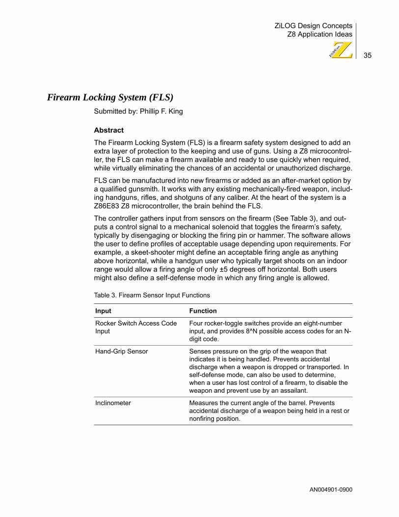
ZiLOG Design ConceptsZ8 Application Ideas
35
Firearm Locking System (FLS)Submitted by: Phillip F. King
Abstract
The Firearm Locking System (FLS) is a firearm safety system designed to add an extra layer of protection to the keeping and use of guns. Using a Z8 microcontrol-ler, the FLS can make a firearm available and ready to use quickly when required, while virtually eliminating the chances of an accidental or unauthorized discharge.
FLS can be manufactured into new firearms or added as an after-market option by a qualified gunsmith. It works with any existing mechanically-fired weapon, includ-ing handguns, rifles, and shotguns of any caliber. At the heart of the system is a Z86E83 Z8 microcontroller, the brain behind the FLS.
The controller gathers input from sensors on the firearm (See Table 3), and out-puts a control signal to a mechanical solenoid that toggles the firearmÕs safety, typically by disengaging or blocking the firing pin or hammer. The software allows the user to define profiles of acceptable usage depending upon requirements. For example, a skeet-shooter might define an acceptable firing angle as anything above horizontal, while a handgun user who typically target shoots on an indoor range would allow a firing angle of only ±5 degrees off horizontal. Both users might also define a self-defense mode in which any firing angle is allowed.
Table 3. Firearm Sensor Input Functions
Input Function
Rocker Switch Access Code Input
Four rocker-toggle switches provide an eight-number input, and provides 8^N possible access codes for an N-digit code.
Hand-Grip Sensor Senses pressure on the grip of the weapon that indicates it is being handled. Prevents accidental discharge when a weapon is dropped or transported. In self-defense mode, can also be used to determine, when a user has lost control of a firearm, to disable the weapon and prevent use by an assailant.
Inclinometer Measures the current angle of the barrel. Prevents accidental discharge of a weapon being held in a rest or nonfiring position.
AN004901-0900

ZiLOG Design ConceptsZ8 Application Ideas
36
Figure 22. Firearm Locking System Block Diagram
Zilog Z8 OTPMicrocontroller
Four dual-position switchesfor access code entry
Inclinometermounted in the
axis of the barrel
Grip Switchindicating that thegun is being held
Solenoid lock on firing pinand Indicator LED.
(Non-energized defaultposition is safety-engaged)
1
2
3
4
5
6
7
8
AN004901-0900

ZiLOG Design ConceptsZ8 Application Ideas
37
Figure 23. Firearm Locking System Schematic Diagram
P20
12U
127
11
8
S8
9
7 10
26
P21
/AC
1P
22/A
C2
P23
/AC
3P
24/A
C4
P25
/AC
5P
26/A
C6
P27
/AC
7
AV
CC
VC
C
VC
C
GN
D
Q2
MO
SF
ET
N
Q1
MO
SF
ET
N
M1
Spr
ing
Bal
ance
dS
olen
oid
(Mec
hani
cal i
nter
face
to fi
ring
pin
lock
)
V_i
nc
Incl
inom
eter
AG
ND
89252423222120
S10
R1
1K
(Rec
esse
d� i
nter
nal
res
et s
witc
h)
19 10
GN
D
P00
P01
P02
P03
P04
P05
P06
28 71 2
21U
2
3 4 5 6 13 14 15 16 17 18
ZiL
OG
Z86
E83P
31P
32P
33P
34P
35P
36
XT
AL1
XT
AL2
/RE
SE
T
S9
VC
CV
CC
VC
C
VC
C
VC
C is
pro
vide
d by
a �
high
-ene
rgy
lithi
um c
ell
S7
6
S6
S5 11
5 12
4
S4
S3 13
3 14
2
S2
S1 15
1 16
C1
Y1
8MH
z
22pF
C2
22pF
C3
.1µ
FC
4.1
µF
C5
.1µ
FC
6.1
µF
C7
.1µ
F
Incl
inom
eter
Pow
er C
ontr
ol
Ana
log
varia
ble
capa
cita
nce
incl
inom
eter
with
bui
lt-in
sens
e-am
plifi
er.
RP
1AR
esis
tor
�8p
ack-
1K
Grip
Sw
itch-
The
Grip
Sw
itch
also
gen
erat
es th
e ev
ent o
n P
ort
32 th
at b
rings
the
syst
em o
ut o
fS
top
Mod
e w
hen
not i
n ac
tive
use.
Ess
entia
lly, p
icki
ng u
p th
e gu
n w
akes
up
the
FLS
.
AN004901-0900

ZiLOG Design ConceptsZ8 Application Ideas
38
Forecaster Intelligent Water Delivery ValveSubmitted by: James Martin
Abstract
The Forecaster Intelligent Water Delivery Valve measures soil moisture and changes in air temperature and barometric pressure to prevent unnecessary watering before, during, or after natural rainfall. Simple analysis of three sensor readings over time determines whether to postpone water delivery in expectation of natural rainfall, or to skip to the next programmed cycle.
The primary function of the Z8 microcontroller is timed actuation of an electric water valve. Timing may be relative or absoluteÑrelative timing is described herein for simplicity.
User selection of watering schedule and duration can be set in a routine as simple as a relative start time (for example, hours from now) and duration (in ten-minute increments), and can be implemented with only two push-buttons.
The sensors are used as follows:
¥ A simple moisture sensor reads true when water is present. This value effects a delay in valve actuation during or immediately after rainfall. Two other sensors utilize the available on-chip dual analog comparators. The first comparator is used to read the resistance of a temperature probe as part of a charging and discharging RC. An output pin is turned on, providing both a reference to the noninverting input to the comparator, and a charging voltage to the RC, which consists of a known capacitor and the resistance of the probe. An interrupt is generated when the RC is charged. The output pin can then be set Low. Another interrupt occurs when the RC is discharged (the time between interrupts can be used to calculate the resistance).
¥ The capacitance of the barometric pressure sensor can be determined in the same manner using the second comparator. A known resistance and the sensor capacitance together form the RC.
¥ The sensors can be polled in regular increments (for example, every 30 minutes). Absolute changes that exceed programmed limits trigger a delay if scheduled watering is about to occur.
This system allows regular watering to occur only in the absence of sufficient nat-ural rainfall, and when rain is not expected to occur based on temperature and pressure changes.
AN004901-0900

ZiLOG Design ConceptsZ8 Application Ideas
39
Figure 24. Forecaster Intelligent Water Delivery Valve Schematic
VCC
GND
I/O 5
I/O 4
IRQ
Comparators
Temperature Probe
PressureProbe
H2OSensor
I/O 3
I/O 2
I/O 1
Z86
Valve
ProgrammingSwitches
IRQ
AN004901-0900

ZiLOG Design ConceptsZ8 Application Ideas
40
Improved Linear Single-Slope ADCSubmitted by: Li Gang
Abstract
A highly accurate linear single-slope ADC is achieved by using a linear integrator and two comparison units on a Z8 microcontroller.
A MAX418 is a high-input-impedance, low-power-consuming and rail-rail opera-tional amplifier. Combined with a resistor R4, a capacitor C1 and a diode 1N4148, it forms a linear integrator. At usual status, the P00 is set to one, and the output of the integrator is at a low level. To start the ADC conversion, set P00 to 0 to charge the integrator until its output increases. When the output of the integrator equals the voltage at P32, the comparison unit at P32 operates, allowing the timer to begin counting. The output of the integrator continues to increase. When it reaches the voltage level at P31, the comparison unit at P31 operates and the timer stops counting. As a result, the number in the timer displays the voltage dif-ference between P31 and P32. This kind of single-slope ADC exhibits higher accuracy than either PWM Ramp ADC or RC Ramp ADC, due to a linear integra-tor, rather than an exponential one, and makes use of the middle range of its input-output characteristic curve.
A MAX619 is used to convert 3volts to a stable 5volts. The MAX418 features two operational amplifiersÑone is used as a buffer, and the other is used to form a lin-ear integrator as described above. The 2-point calibration is used instead of the conventional 1-point calibration. The calibration values are stored in an EEPROM (1C3, 24LC01), resulting in a great improvement in its measurement precision.
The calibration is performed automatically. Insert the probe into the standard acid or alkali liquid, and press the calibration key K1. The microcontroller automatically determines that the measured calibration liquid is acid or alkali liquid. After the measurement value becomes stable, the Z8 stores the calibration results into 1C3 (24LC01) and the buzzer rings, indicating the calibration finished. For measure-ment, insert the probe into the liquid to be measured and press K2 to begin the measurement. If the differences among five successive measurement values are within a certain range, then the stable-measurement state is determined and the result is displayed on the LCD. The buzzer sounds, indicating that the measure-ment is completed. The final results are provided by linear interpretation with the two calibration points.
AN004901-0900
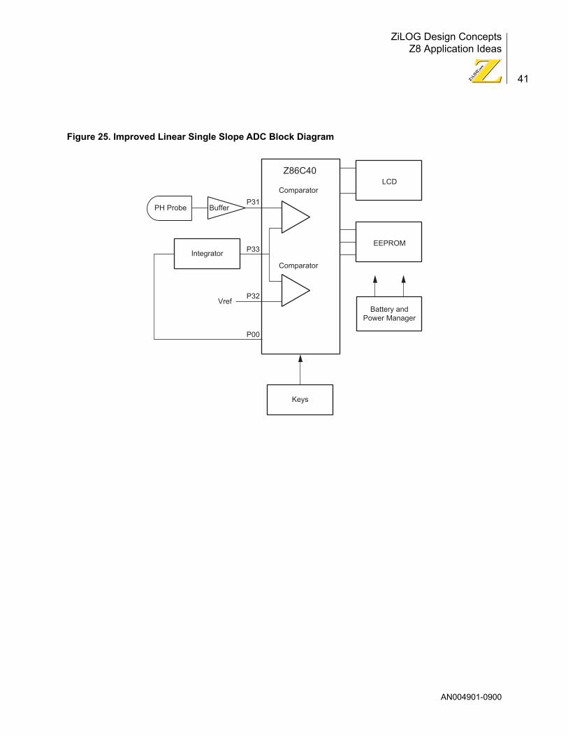
ZiLOG Design ConceptsZ8 Application Ideas
41
Figure 25. Improved Linear Single Slope ADC Block Diagram
LCDComparator
Comparator
Z86C40
EEPROM
Battery andPower Manager
Keys
P31
P33
P32Vref
P00
Integrator
BufferPH Probe
AN004901-0900

ZiLOG Design ConceptsZ8 Application Ideas
42
Figure 26. Improved Linear Single Slope ADC Schematic Diagram
P20
P21
P22
P23
P24
P25
RE
SE
T
P31
P33
P32
P00
� P04
P05
XT
AL1
XT
AL2
WP
SC
SD
A
Z86
C40
LCD
IC1
24LC
01IC
3
C6
0.04
7
VC
C
VC
C
VC
C
VS
S
GN
D
MA
X61
9IC
2
1 32
8
67
C1
0.22
27pF
27pF10
µF
C2
C3
C7
0.2
2
18
C8
0.2
2
12M
Hz
C4
C5
10µ
F
1/2
MA
X41
8
1/2
MA
X41
8
PH
Pro
be
C9
10µ
F
C10
10µ
F
R2
10K
R3
1KR1
10K
+ +
A1
A2
K1
R4
10K
BE
EP R5
1K
K3
1N41
48
K2
K4
3VB
atte
ry
- -
AN004901-0900
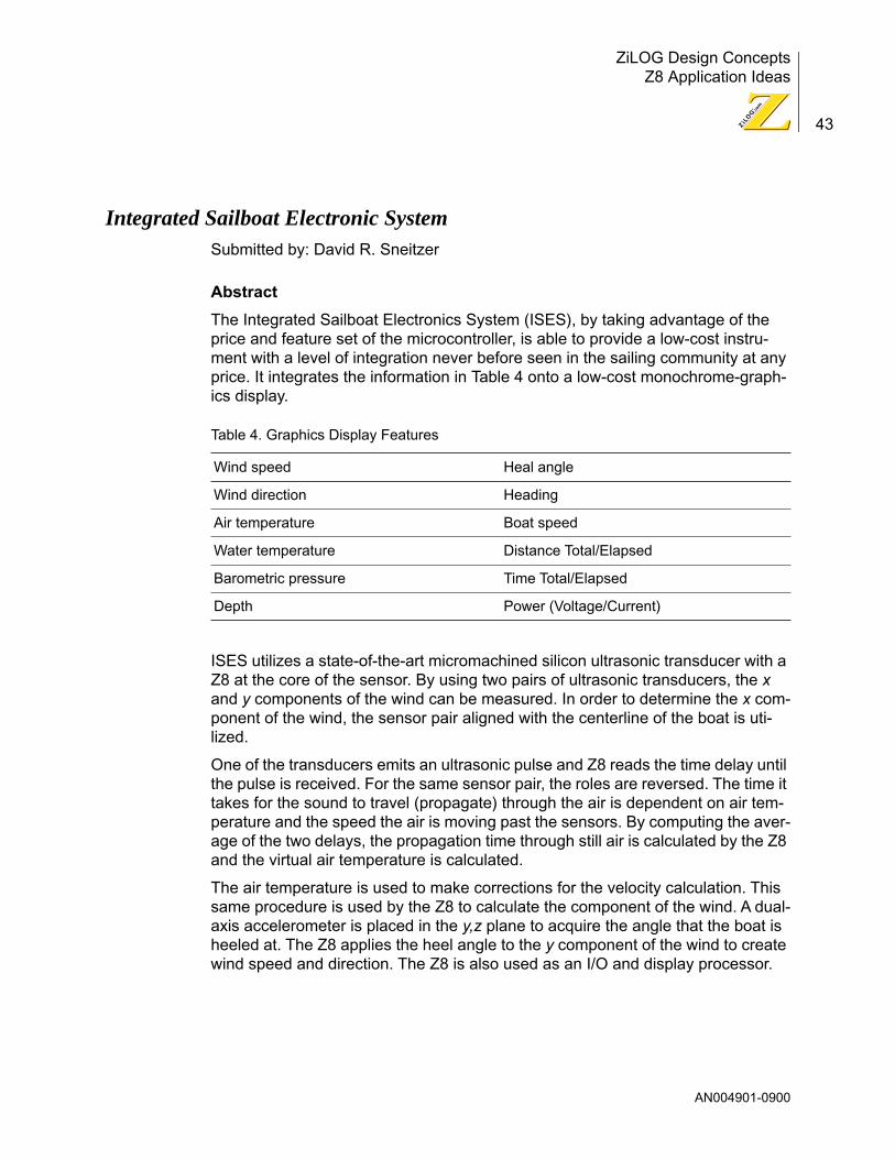
ZiLOG Design ConceptsZ8 Application Ideas
43
Integrated Sailboat Electronic SystemSubmitted by: David R. Sneitzer
Abstract
The Integrated Sailboat Electronics System (ISES), by taking advantage of the price and feature set of the microcontroller, is able to provide a low-cost instru-ment with a level of integration never before seen in the sailing community at any price. It integrates the information in Table 4 onto a low-cost monochrome-graph-ics display.
ISES utilizes a state-of-the-art micromachined silicon ultrasonic transducer with a Z8 at the core of the sensor. By using two pairs of ultrasonic transducers, the x and y components of the wind can be measured. In order to determine the x com-ponent of the wind, the sensor pair aligned with the centerline of the boat is uti-lized.
One of the transducers emits an ultrasonic pulse and Z8 reads the time delay until the pulse is received. For the same sensor pair, the roles are reversed. The time it takes for the sound to travel (propagate) through the air is dependent on air tem-perature and the speed the air is moving past the sensors. By computing the aver-age of the two delays, the propagation time through still air is calculated by the Z8 and the virtual air temperature is calculated.
The air temperature is used to make corrections for the velocity calculation. This same procedure is used by the Z8 to calculate the component of the wind. A dual-axis accelerometer is placed in the y,z plane to acquire the angle that the boat is heeled at. The Z8 applies the heel angle to the y component of the wind to create wind speed and direction. The Z8 is also used as an I/O and display processor.
Table 4. Graphics Display Features
Wind speed Heal angle
Wind direction Heading
Air temperature Boat speed
Water temperature Distance Total/Elapsed
Barometric pressure Time Total/Elapsed
Depth Power (Voltage/Current)
AN004901-0900

ZiLOG Design ConceptsZ8 Application Ideas
44
Figure 27. Integrated Sailboat Electronic System Block Diagram
Figure 28. Integrated Sailboat Electronic System Schematic Diagram
12.5 KTS028¼
6.7 KTS
10.1 mi01:27
7962
59 FT
271
5,023� Miles1825� Hours10.1�� Miles1.4�� Hours
13.2 Volts1.75 Amps
74 Amp hrs since last charge56 Amp hrs estimated remain
air� lo:49¼ high:83¼water�lo:59¼ high:63¼baro� lo:29.1¼ high:31.1¼wind� lo:1.3 avg:10 high:18.7
Mast mounted Z8,Ultrasonic sensors,Interface electronics
Sensoranalog
interface
Non-volatilememory
Serial Com.
Simplekeyboard
Analog inputinterface
Voltagesensor
Headingsensor
Pressuresensor
2-axisacceler-�ometer
Boat speedsensor
Currentsensor
Temperaturesensor
Voltagesensor
Headingsensor
Pressuresensor
2-axisacceler-�ometer
Boat speedsensor
Currentsensor
Temp.sensor
Depthsensor
12.5 KTS028¼
6.7 KTS
10.1 mi01:27
7962
59 FT
271
AN004901-0900

ZiLOG Design ConceptsZ8 Application Ideas
45
Intelligent Guide for the BlindSubmitted by: R. Sharath Kumar
Abstract
This self-contained, self-propelled, intelligent guide incorporates the ZiLOG Z86E31 microcontroller. Using ultrasonic and infrared transducers, the surround-ings are scanned for complete, intricate detail, including pavement-surface defor-mations, puddles, and pits apart from general traffic. The microcontroller analyzes this information, determines the safest path, and controls a propulsion motor to manipulate and lead the handicapped safely through these obstacles. The guide further interacts with the individual via audio messages, informing of the surround-ings and distance traveled. A chosen direction of travel is commanded via push-button keys. The microcontroller immediately repositions the scanners toward this direction. An indicator lamp pulses on/off, together with a beeper, to alert a person of any slow-moving traffic or obstruction. The guide can also be programmed to remember the direction traveled automatically when commanded.
The direction commands include Straight Ahead, Turn Left, Turn Right, and Reverse Back, and are received from keys SW1ÐSW4. The stepper motor is con-trolled in half-steps for increased position control by the microcontroller. A ping-pulse wave is emitted and transmitted through the air by the microcontroller through a 40-kHz ultrasonic transmitting transducer. The wave, reflected off objects in its path, is detected by the receiving transducer. The received echo is amplified, centered, and compared against a fixed reference voltage by an LM6132, and fed to the microcontroller. The microcontroller measures the timing of the wave from the instant it leaves the transmitter to the instant an echo is received (taking the Doppler effect into account) and calculates the distance.
After the guide orients itself in the commanded direction, scanning continues in an oscillating mode. During this mode, the microcontroller continuously monitors the echo signals and maneuvers the movement accordingly.
An infrared sensor is activated at the same time as the ultrasonic transceiver. This sensor scans the pavement surface ahead. Infrared transmitter D1A is pulsed on/off at 1kHz, and the bounced signal is captured by D1B. The signal strength depends on the distance from the obstruction. This variable-strength signal is con-verted proportionally into pulses by the voltage-to-frequency converter, LM331.
All information is updated to the individual via prerecorded messages. The sound chip is configured to operate in MESSAGE CUEING mode.
AN004901-0900

ZiLOG Design ConceptsZ8 Application Ideas
46
Figure 29. Intelligent Guide for the Blind Block Diagram
Speaker
Z86E31Micro Controller
User DesiredDirection Inputs
ISO2590 Sound Chip
Roll-on Motor 1
Roll-on Motor 2
RPM Pulses Input
Beeper
Lamp Indicator
LM6132 OpAmpAmplifier andComparator
ULN2803Stepper Motor
Driver
LM331Voltage toFrequencyConverter
Infra-redReceiver
D1B
Infra-redTransmitter
D1A
400 KHzUltrasonic
Transmitter
400 KHzUltrasonicReceiver
7.5 DegreeStepper MotorM
AN004901-0900

ZiLOG Design ConceptsZ8 Application Ideas
47
Figure 30. Intelligent Guide for the Blind Schematic Diagram
16 18 9 10 19 20 21 23 24
15 16 17 14 11 28 2 3 4 5 6 7
8
12
SW
4
22
XT
AL
7.32
8MH
z
R11
C4
20pF
R18
6k8
Q1
2N22
22A
C3
20pF
D3
1N41
48C
210
0nF
D2
1N41
48C
147
nF
R4
1k
DIA
Infr
a-re
dtr
ansm
itter
1 23 24 25 2 3 4 6 7 8 11 12 17 18 19 20 21 26
28 14 15 5 9 10 27
1316
1 2 3 4
18 17 16 15
Vcc
+VE
Vcc
Spe
aker
3 2 1 5
6 7
8
R10
R6 10
k x
4 no
s
220
R8
R9
R7
R19
R19
R19
R19
R2
510
R3
510k
R12
R13
R14
DIB
Infr
a-re
dre
ceiv
er
Z86
E31
C6
330p
F
R5
1k2
C5
0.00
1µF
R15
4k7
R16
5k
R17
3k3
SW
3S
W2
SW
1
Vcc
97.
5 D
egre
eS
tepp
er M
otor
Ste
pper
Mot
orS
uppl
y
4k7
Dec
ayad
just
pot
.
Vcc
Ultr
ason
icR
ecei
ver
Vcc
= +
5 V
olts
= G
roun
d
SW
1 =
Fro
ntS
W2
- B
ack
SW
3 =
Rig
htS
W4
= Le
ft
Vcc
R1
27k
Vcc 1 6 7 2
3 5
8 4Vcc
Vcc
RP
MP
ulse
sI/P
Vcc
4
Ultr
ason
icT
rans
mitt
er
Q4
TIP
31A
D6
1N40
07
M1
1
+ Ð
Q5
TIP
31A
D7
1N40
07
M2
Rol
l-on
Mot
or S
uppl
y
Q2
SL1
00
D4
1N41
48
Bee
per
Q3
SL1
00
D5
1N41
48
Vcc
Vcc
A1
A2
B1
B2
ULN
2803
AN004901-0900

ZiLOG Design ConceptsZ8 Application Ideas
48
Internet Email Reporting Engine Submitted by: Michael W. Johnson
Abstract
The Internet Email Reporting Engine is a design that can he embedded inside a device to connect via a dial-up function to an Internet Service Provider, and send email reports to anywhere on the Internet.
A ZiLOG Z02204 modem module provides the connection to the real world via a phone line.
The Seiko iChip (S7600A) provides PPP and PAP authentication, and the Internet protocols IP, UDP, TCP, and ICMP.
The ZiLOG Z8 controller receives commands from a serial connection and com-municates to the Seiko iChip via an 8-bit parallel CPU interface to control the modem and the iChipÕs Internet functionality. The Z8 MCU also provides a higher-level command and Internet functionality via software
The software running on the ZiLOG Z8 CPU receives commands via a serial inter-face and processes them. Based on those commands, the Z8 performs dial-up and connects to the Internet, establishes an Internet connection to an ISP via the PPP protocol (authenticated with PAP), and opens a connection to a mail server. It then sends a message, and hangs up.
Commands are sent to the engine via a serial port that is implemented as a soft-ware UART running at 2400bps on the Z8 controller. These commands are pro-cessed, the state of the email engine is updated, and a command status code is reported back through a software UART.
Each command is a parameter string that terminates with a return and a line feed. The software responds to each command using a return code that terminates with a return and a line feed.
Once a connection is made to the Internet, sending email is as simple as configur-ing an email server to connect, choosing a recipient, and sending text as the body of the email.
Table 5. Serial Commands
sn Set phone number sl Set login name sp Set password
sd Set DNS server IP sr Set recipient email address ss Set SRC email address
du Dial-up and connect to ISP cs Connect to email server ps Print message to email body
ms Message send hu Hang up
AN004901-0900

ZiLOG Design ConceptsZ8 Application Ideas
49
Figure 31. Internet Email Reporting Engine Block Diagram
Figure 32. Internet Email Reporting Engine Software Block Diagram
DB9
RJ-11 Phone Jack
ZiLOG Z86E3116 CPU
ZiLOG Z02400 Modem Module
Seiko iChip Internet DataPump (S7600A)P
ower
Sup
ply
7Ð15
V
Clo
ck/D
ivid
er
Optional RS232-C Level
Converter/DB9DCE iface
CMOS/TTLSerial Interface
Header
5 X 2 Header
DC
Seiko CPU Interface
Software UART
Command Processor
SMTP API
Socket APIPPP
CheckSetup/Config Dialer
AN004901-0900

ZiLOG Design ConceptsZ8 Application Ideas
50
Figure 33. Internet Email Reporting Engine Schematic Diagramxp
ar_i
n3xp
ar_i
n4xp
ar_i
n5xp
ar_i
n6xp
ar_i
n7vd
d1xp
ar_o
ut1
xpar
_out
2xp
ar_o
ut3
xpar
_out
4xp
ar_o
ut5
xpar
_out
6xp
ar_o
ut7
xtxd
xrts
jxd
trj
xdcd
xrxd xr
ixd
srj
xtcs
j
xtes
t
vss1
xres
etj
xclo
ck
xsd0
xsd1
xsd2
xsd3
xsd4
xsd5
vdd2
xsca
n_ct
lxs
d6xs
can_
enN
/Cxs
d7xs
ys_b
usyj
xsys
_int
2xs
ys_i
nt1
xsys
_int
ctrl
xsys
_writ
ejxs
ys_p
sxvs
s2xs
ys_r
eadj
xsys
_c86
xsys
_cs
xsys
_rs
48 47 46 45 44 43 42 41 40 39 38 37 36 35 34 33 32 31 30 29 28 27 26
RE
SE
T
25 24 23 22 21 20 19 18 17 16 15 14 13 12 11 10 9 8 7 6 5 2 4 1 3
Sei
ko iC
hip
Inte
rnet
Dat
a P
ump
Opt
iona
l RS
232-
C In
terf
ace
Clo
ck D
ivid
er (
/32)
U2
U3
Sei
ko S
7600
A
HC
4040
C1
27pF
C9 .1 C10 .1
FB
1
FB
2
TX
D+3.
3V
QA
QB
QC
QD
QE
QF
QG
QH QI
QJ
QK
QL
CLR
CLK
9 7 6 5 3 2 4 13 12 14 15 1
XC
LK
/DT
R
/DC
D
RX
D
D0
D1
D2
D3
D4
D5
D7
BU
SY
X
INT
WR
RD
CS
RS
11 10S
YS
CLK
CM
OS
/TT
L �
Ser
ial I
nter
face
Hea
der
5x2
Hea
der
+5V
2 4 6 8 10
1 3 5 7 9
CR
XD
CT
XD
Zilo
g Z
8 C
PU
U1
+5V
X1
7.37
28M
Hz
Zilo
g Z
86E
3116
P24
P23
P22
P21
P20
P03 Vss
P02
P01
P00
P30
P36
P37
P35
P25
P26
P27
P04
P05
P06
P07
Vcc
XT
AL2
XT
AL1
P31
P32
P33
P34
28 27 26 25 24 23 22 21 20 19 18 17 16 15
RS
CS
RS
RX
RS
TX
RD
WR
BU
SY
X
D3
D2
D1
D0
CT
XD
1 2 3 4 5 6 7 8 9 10 11 12 13 14
1
6
2
7
3
8
4
9
5
C6
0.1µ
FC
70.
1µF
C5
0.1µ
F
+5V
C2
27pF
SY
SC
LK
D4
D5
CR
XD
INT
SY
SC
LK
D6
D7
Mod
em M
odul
e
Pow
er S
uppl
y
Dec
oupl
ing
Cap
s
Z02
400
Zilo
g M
odem
Mod
ule
+5V
13
2
GN
DV
in+
5V
U2
78L0
5R
1
200
+3.
3V
N/C
TT
PN
/CR
ING
N/C
Vcc
Gnd
DT
RD
CD
MU
TE
AO
UT
N/C
RX
DT
XD
J2-1
J2-2
J2-3
J2-4
J2-5
J1-1
J1-2
J1-3
J1-4
J1-5
J1-6
J1-7
J1-8
J1-9
RJ1
1Ja
ck
1 2 3 4
7-15
Vdc
Pow
er C
onne
ctor
2 1
/DT
R
/DC
D
RX
D
TX
DD
6
XC
LK
+5V
+5V
+3.
3V
+3.
3V
U5
DB
9 S
eria
l (D
CE
)
+
MA
X23
2E
+5V V
+ �
(pin
2 M
AX
232)
VÐ
�(p
in 6
MA
X23
2)
R1
OU
T
R2
OU
T
T1
OU
T
T2
OU
T
C2+
C2Ð
13 8 11 10 1 3
R1
IN
R2
IN
T1
IN
T2
IN
C1+
C1Ð
C10
.1µ
F
12 9 14 7 4 5
CR
XD
RS
TX
RS
RX
CT
XD
+C
350
µF
+C
410
µF
+C
51µ
F
D1
3.3V
Zen
er
+C
12.1
µF
+C
13.1
µF
+C
10.1
µF
C9
0.1µ
FC
80.
1µF
+3.
3V
AN004901-0900

ZiLOG Design ConceptsZ8 Application Ideas
51
Lunar Telemetry BeaconSubmitted by: Russell McMahon
Abstract
The Lunar Telemetry Beacon (LTB) is a small Z8 microcontroller-controlled telem-etry system and radio transmitter. It is intended for deployment on the lunar sur-face to subsequently return temperature, seismic, and location information to Earth.
No receiver is incorporated in the LTB, due to severe design constraints. Conse-quently, all decisions must be made on a preprogrammed basis.
Key demands on the overall system include the ability to survive impact velocities of over 300kph and decelerations of 1000g, to return data to Earth using a self-contained aerial and transmitter, and to survive in an ambient temperature range of Ð180¼ to +130¼ Celsius (with the transmitter not operating at extreme tempera-tures).
Key demands on the Z8 microcontroller include:
¥ Control of initial deployment from the main payload
¥ Control of the physical orientation of the LTB after landing
¥ Control of a transmitter to return data to Earth
¥ Thermal management of the electronic core to maximize the prospect of surviving the lunar nights (2 weeks at Ð180¼ Celsius)
Because of severe mass, and therefore battery restrictions, the unit operates intermittently, with a decreasing duty cycle over time.
Mechanical survivability is enhanced by the use of surface-mount construction, housing in a custom-fitted mechanically-compliant pressure shroud, encapsula-tion of the whole system in a homogeneous medium, and subsequent mounting in an external matrix-medium that ensures controlled deceleration over the maxi-mum available distance.
The LTBÕs initial objective is met if it transmits successfully from the lunar surface for a period of a few Earth days. Over this period, transmissions are relatively fre-quent. Long term operation (weeks to years) requires surviving the low tempera-tures of lunar nights. Lunar night survivability is targeted by use of a super-insulated core for the key electronics and the provision of very low levels of elec-trical heating under system control. Battery systems utilize two versions of lithium chemistry due to their potential tolerance of the extreme thermal conditions and high energy densities. Thionyl Chloride batteries (800 Watt-hr/kg) are used for core stay-awake electronics (due to their good energy density) and lithium-sulfur
AN004901-0900

ZiLOG Design ConceptsZ8 Application Ideas
52
dioxide batteries (300 Watt-hr/kg) for transmitter power (with a somewhat lower energy density but better high-current performance).
The key technical objectives are:
¥ Survive landing
¥ Deploy aerial system successfully
¥ Return at least one successfully-received message
The above three objectives are listed together because, while each is a separate goal, all must result before success is achieved. The device must additionally be able to:
¥ Send transmission bursts increasingly less frequently throughout one lunar day (2 Earth weeks)
¥ Survive one lunar night (2 weeks at Ð180¼ Celsius)
¥ Send transmissions at regular infrequent intervals throughout the lunar day, and as many possible subsequent lunar days
Message data includes temperature and seismological observations and sponsor dictated content (not necessarily advertising per se). A failure to return some or all data would still be a reasonable success, provided actual transmissions continued to be received.
All activities must be accomplished with a minimum of weight and power con-sumption.
The Lunar Telemetry Beacon is designed to be as independent of the main space-craft and main payload as possible while communicating with it prior to deploy-ment. Communication with the core spacecraft control system is by way of a single bidirectional data serial circuit which interfaces with a bus interface in the spacecraft. Power can be provided to a stay-alive input on the LTB prior to launch to avoid utilizing the internal inaccessible and nonrechargeable batteries. How-ever, this connection is used when the final stage of the countdown commences. A failed LTB prior to launch is not repaired; it is replaced in its entirety.
After launch, the LTB does not function until lunar impact. It can communicate with the main spacecraft as required.
Under strictly predefined conditions, a mission failure mode exists whereby the LTB can self-deploy, if it is obvious that the main mission has failed. The pros-pects are good for an LTB to survive a catastrophic explosive failure of the main craft upon reaching orbit.
As lunar impact is imminent, the LTB arms itself.
AN004901-0900

ZiLOG Design ConceptsZ8 Application Ideas
53
A combination of advice from the main craft and/or loss of communication at the appropriate time determine the approach and occurrence of lunar impact.
On impact, the LTB is ejected horizontally from the main payload to prevent it from being trapped in the main debris. The small pyrotechnic charge for this activity is external to the LTB.
While the LTB can technically initiate this action if the main craft should fail, it is unlikely that its command would be accepted if the main controller fails to initiate the release.
Shortly after impact, and having come to rest, the LTB ascertains its survival, and attempts to determine its attitude using its onboard triple-axis accelerometer. In a preferred orientation, as encouraged by its weight distribution, the LTB deploys its main aerial using a pyrotechnic charge to trigger a release mechanism. The antenna is of spring construction with a deployed orientation normal to the body. It is a simple whip antenna that is mechanically wound around part of the outside body. A nonoptimum orientation of the LTB on the surface can be corrected by deploying a sequence of up to three other similar antennae, followed by the actual antenna. When the antenna is deployed (or if it cannot be), the LTB commences its transmission sequence. Transmissions are initially frequent, and decrease with time.
During two-Earth-week lunar nights, temperatures fall below battery and transmit-ter safe operating limits. Under such circumstances, the LTB shuts down all activ-ities except core activities, and attempts to maintain its core temperature at a minimum but safe level.
With the return of lunar day, the LTB attempts to reestablish its transmissions.
It is intended that the core continue to function after the transmitter fails. If the LTB determines that the transmitter has failed, it ceases transmission, except for occa-sional short retries.
AN004901-0900

ZiLOG Design ConceptsZ8 Application Ideas
54
Magic DiceSubmitted by: Darren Ashby (www.chipcenter.com)
Abstract
The ZiLOG Z8PE001 microcontroller generates a display of six numbers, and the sound effects of rolling dice. The ZiLOG microcontroller also generates the ran-dom numbers rolled on the dice. The LEDs are multiplexed using only the ZiLOG microcontroller and the display components; no other ICs are required. The LEDs are positioned to represent the dots on a pair of dice.
The dice displays are animated, rolling as real dice do. By controlling the bright-ness of each individual LED, (using the timer interrupt capabilities of the ZiLOG part), the user can achieve a visual effect to simulate rolling dice. The animation slowly comes to a stop at the final value of the dice. Each individual die may stop at different times, further enhancing the simulation.
As the dice roll, sound effects simulate the bouncing action of a real die. At the end of the roll, additional sound effects are added as required for various final val-ues. For example, a short victory song can play when a player has rolled double sixes. Such a scenario is fairly simple to create using the TOUT mode on the Z8PE001 to drive the piezoelectric buzzer.
Four controls are provided to the user. Switch 1 causes only one of the dice to be rolled at a time. The first press rolls the first die, leaving the second die blank. The second press rolls the second die (the first roll is still displayed). The process then repeats. Switch 2 rolls both dice at once. Switch 3 is a reset button in case of problems.
Switch 4 is a special toggle feature that causes the dice to be seven-sided, where numbers 1 though 7 are possible. Geometry makes it impossible to create an actual die with seven sides that offers an equal chance of any number occurring. Such is not the case with the Magic Dice board.
AN004901-0900

ZiLOG Design ConceptsZ8 Application Ideas
55
Figure 34. Magic Dice Block Diagram
Simple packaging design
LEDs are positioned torepresent the dots on dice
Roll both dicetogether
Roll one dieat a time
Z8PlusMicrocontroller
7-sidedswitch
Reset
AN004901-0900

ZiLOG Design ConceptsZ8 Application Ideas
56
Figure 35. Magic Dice Schematic Diagram
PB
0
PB
1
PB
2
PB
4
PB
3
/RS
T
PA
7
PA
8
PA
5
Rol
l one
die
Con
nect
ion
to a
4.5
VD
C b
atte
ry p
ack
2PIN
-900
-SLD
R-H
D
Sev
en-s
ided
dice
sw
itch
Rol
l bot
h di
ce
14 15 16 17 13 12 11 10 9
VC
C
VS
S
XT
AL2
XT
AL1
PA
0
PA
1
PA
2
PA
3
PA
4
18 1 2 4 3 5 6 7 8
33 R3
U1
R14
10K
PA
5
Z86
E00
1
C18
0.1µ
F
2N44
03Q
12N
4403
Q2
LD1
RE
SE
T
VC
C
DIC
E1
BU
ZZ
ER
BU
ZZ
ER
RE
SE
T
DIC
E2
R5
10M
Hz
X
1
33P
A0
PA
0
R6
R1
4.7K
DIC
E1
2
1 3
33P
A1
R7
33P
A2
R8
33P
A3
R9
33P
A4
33 R4
PA
6
R12 1K
SW
4
SW
2
SW
1
R11
10K
VC
C
R10
10K
VC
C
R69
PB
1P
iezo
Buz
zer
470
SW
3
R10
10K
VC
C
VC
C
GN
D
VC
C
VC
C
VC
C
C19
0.1µ
F
LD2
PA
1
LD5
PA
3
LD3
PA
2
LD7
PA
4
LD8
PA
5
LD9
PA
6
LD11
PA
0R2
4.7K
DIC
E2
2
1 3VC
C
LD6
PA
1
LD10
PA
3
LD4
PA
2
LD12
PA
4
LD14
PA
5
LD13
PA
6
AN004901-0900

ZiLOG Design ConceptsZ8 Application Ideas
57
Modular Light Display PanelSubmitted by: Phillip King
Abstract
Each Modular Light Display Panel is made up of an 8x8 array of pixels. Each pixel contains 3 LEDs (red, green, and blue), which are controlled by a Z8 microcontrol-ler. Panels provide a modular building block for expandable full-color LED dis-plays. A single panel, running alone, can serve as electronic art, providing algorithmically-generated patterns of light and color. A linear array of panels becomes a full-color scrolling text and graphic display, such as a marquee, or an attractive enunciator panel. By connecting together a two-dimensional array of panels, users can construct large color displays. As a result, users can buy a small number of panels to start their display, and add panels as required.
Every 8x8 panel contains a Z86E21 OTP microcontroller. 192 bytes of the Z8 on-chip RAM form the image buffer containing the current state of the display. Three 64-byte arrays make up each color plane. The intensity of every LED is controlled using pulse-width modulation. At any given instant, an LED is either fully on or fully off, but by varying the duty cycle of on-time to off-time, the Z8 can vary the perceived intensity of every LED. The array can be built to allow strobing of one row of the panel at a time, or allow additional discrete latches to be used for a fully-static display (at slightly higher cost). In either case, the fully-digital control system can provide a seemingly analog variation in the color intensity of each pixel.
The software control is offered by two pads. A periodic interrupt routine updates the state of the currently-driven row of the LED array, providing the appearance of varied intensity of every pixel. The mainline code modifies the image buffer as directed by serial communication with the control computer and those panels around it. Because every panel communicates with those around it, the array itself can perform simple image manipulations such as wipes and simple animations. The total bandwidth required is reduced within the array, because not every panel must receive a fully-updated state during every frame.
When multiple panels are assembled to form larger displays, each panel commu-nicates serially with the four around it. At power-on, each panel queries the four compass directions, and the top left panel becomes position (0,0). Every other panel determines its position successively from those above and to the left of it. When running, an external PC controlling the array can address every panel inde-pendently. The control PC coordinates the array, handling tasks such as scaling images to the available number of panels.
AN004901-0900

ZiLOG Design ConceptsZ8 Application Ideas
58
Figure 36. Modular Light Display Panel Module Block Diagram
ZiLOG Z8Microcontroller
3�- COLORLED ARRAY
Column Driver FETs
RowLatch(Blue)
Serial Link toUpper and Left
Panels
Serial Link toLower and Right
Panels
RowLatch(Blue)
RowLatch(Blue)
AN004901-0900

ZiLOG Design ConceptsZ8 Application Ideas
59
Figure 37. Modular Light Display Panel Module Schematic DiagramP
20P
21P
22P
23P
24P
25P
26P
27
P30
P31
P32
P33
P34
P35
P36
P37
XT
AL2
XT
AL1
RE
SE
T
R/W DS
AS
R/R
L
VC
C
VC
C
29U
1LA
TC
H1
CLK
LAT
CH
2 C
LKLA
TC
H3
CLK
CO
L S
EL0
CO
L S
EL1
CO
L S
EL2
CO
L S
EL3
CO
L S
EL4
CO
L S
EL5
CO
L S
EL6
CO
L S
EL7
Dat
a0D
ata1
Dat
a2D
ata3
Dat
a4D
ata5
Dat
a6D
ata7
Latc
h1 C
lk
2 5 6 9 12 15 16 19
ÐPix
el D
rive
10�
ÐPix
el D
rive
11ÐP
ixel
Driv
e 12
ÐPix
el D
rive
13ÐP
ixel
Driv
e 14
ÐPix
el D
rive
15ÐP
ixel
Driv
e 16
ÐPix
el D
rive
17
41 42 43 1 2 3 4 5 7 8 9 10 11 12 13 14
6222839
P00
P01
P02
P03
P04
P05
P06
P07
P10
P11
P12
P13
P14
P15
P16
P17
1 2 3 4 5 6 7 8 9 10
Dat
a0D
ata0
Dat
a0D
ata0
Dat
a0D
ata0
Dat
a0D
ata0
UA
RT
inW
est i
nE
ast i
nS
outh
inN
orth
Out
Wes
t Out
Eas
t Out
UA
RT
Out
17 18 19 20 21 22 23 24 33 26 40 16 15 38 27 32 30 31 34 35 36 37 44
GNDGNDGNDGND
ZiL
OG
�Z
86E
21
Q0
Q1
Q2
Q3
Q4
Q5
Q6
Q7
U2
3 4 7 8 13 14 17 18 1 11
D0
D1
D2
D3
D4
D5
D6
D7
CC
CLK
74A
CT
374
J1
CO
N10
(VC
C is
pro
vide
d by
an
exte
rnal
pow
er s
uppl
y th
roug
h th
e fr
ame,
or a
bac
k co
nnec
tor
on th
est
and-
alon
g pa
nel.)
Not
e: T
his
desi
gn u
ses
the
min
imal
num
ber
ofex
tern
al la
tche
s to
hav
e an
y on
e co
lum
n of
the
disp
lay
ener
gize
d at
a ti
me.
Mor
e la
tche
s an
d on
eex
tra
laye
r of
latc
h cl
ock
deco
der
logi
c ca
n be
use
dfo
r a
high
er-d
uty-
cycl
e or
fully
-sta
tic d
ispl
ay.
Inte
r-pa
nel s
eria
lin
terc
onne
ctio
n.(O
n-bo
ard
UA
RT
is
for
prim
ary
Nor
th-S
outh
com
mun
icat
ion
chan
nel.)
C1
22pF
Y1
12M
Hz
S1
(Rec
esse
d�in
tern
alre
set s
witc
h)
C2
22pF
C3
.1µ
FC
4.1
µF
C5
.1µ
FC
6.1
µF
C7
.1µ
F
VC
C
VC
C
Dat
a0D
ata1
Dat
a2D
ata3
Dat
a4D
ata5
Dat
a6D
ata7
Latc
h2 C
lk
2 5 6 9 12 15 16 19
ÐPix
el D
rive
20�
ÐPix
el D
rive
21ÐP
ixel
Driv
e 22
ÐPix
el D
rive
23ÐP
ixel
Driv
e 24
ÐPix
el D
rive
25ÐP
ixel
Driv
e 26
ÐPix
el D
rive
27
Q0
Q1
Q2
Q3
Q4
Q5
Q6
Q7
U3
3 4 7 8 13 14 17 18 1 11
D0
D1
D2
D3
D4
D5
D6
D7
CC
CLK
74A
CT
374
Dat
a0D
ata1
Dat
a2D
ata3
Dat
a4D
ata5
Dat
a6D
ata7
Latc
h3 C
lk
2 5 6 9 12 15 16 19
ÐPix
el D
rive
30�
ÐPix
el D
rive
31ÐP
ixel
Driv
e 32
ÐPix
el D
rive
33ÐP
ixel
Driv
e 34
ÐPix
el D
rive
35ÐP
ixel
Driv
e 36
ÐPix
el D
rive
37
Q0
Q1
Q2
Q3
Q4
Q5
Q6
Q7
U4
3 4 7 8 13 14 17 18 1 11
D0
D1
D2
D3
D4
D5
D6
D7
CC
CLK
74A
CT
374
AN004901-0900

ZiLOG Design ConceptsZ8 Application Ideas
60
Nasal Oscillatory TransducerSubmitted by: Sarah Brandenberger and Doug Keithley
Abstract
The Nasal Oscillatory Transducer (N.O.T.) is an electronic device that does not use drugs or chemicals. It acts as a nasal decongestant and uses a piezoelectric speaker, hooked up to the speaker of a frequency generator.
Press the N.O.T. to the offending sinus area and press the start button. The N.O.T. immediately starts alleviating sinus congestion. For greater effectiveness, set the switch to HIGH-POWER mode and an LED illuminates. In five minutes, the N.O.T. stops making sounds, and turns itself off.
By exciting the sinusÕ resonance frequencies, mucus becomes more fluid and is easily expelled. Various sinus cavities tend to resonate at frequencies within the audio range. Variances in individuals and even variances in sinus size within the same person dictate the requirement for exciting the sinus cavities at multiple fre-quencies. The N.O.T. sweeps through a range of frequencies. Through micro-phone feedback, the N.O.T. determines the specific resonant frequencies that are excited for a short duration. Because the resonant frequencies are dynamic (due to changing volumes), the sweep and excite process is repeated every 30 sec-onds for 5 minutes.
Circuit Description:
¥ Power SupplyÑLM2937 was chosen because of low voltage drop-out. The unregulated 9 volts is supplied by a battery and powers the output the output driver directly.
¥ Output DriverÑsimple single transistor drives a 45-ohm speaker. Fidelity is not necessary.
¥ Reset circuitÑsimple RC time constant as specified by data sheet
¥ Variable Output VoltageÑthe Z8 timer is configured as PWM per data sheet and output on PB1. The signal is passed through an active 2nd order low-pass filter and is used as the reference on the analog comparator inside the Z8.
¥ Microphone feedbackÑan electric condenser microphone is AC-coupled to an active 2nd-order low-pass filter and peak detector. The output of the peak detector is fed into the analog comparator of the Z8.
¥ Z8Ñdirect drive of the LED indicator and the watch-dog timer prevents excessive on-time, a ceramic resonator provides acceptable timing, and a security bit protects firmware features from competitors.
¥ FirmwareÑprovides all timing using a 16-bit internal timer, algorithms for modulating the output driver pin to generate sounds out of speakers, and
AN004901-0900

ZiLOG Design ConceptsZ8 Application Ideas
61
monitoring resonance by comparing the peak microphone signal to the PWM-generated reference.
Figure 38. Nasal Oscillatory Transducer Block Diagram
Z8Plus
RESET
PB4
PB4
POR
(RC+Diode forfast recovery)
Input Sensor
(Electret Microphone)
Filter(Active 2nd Order
Lowpass and PeakFollower)
User I/O
(High-power Switchand LED Indicator)
Clock Circuit
(Ceramic Resonator)
Power Supply
(+9VDC unreg,+5VDC reg)
Output Driver andAudio Transducer
(Transistor & Speaker)
PA1
PA0
PB1PWM
IRQ3 PB2/PA7
DAC(PWM through anactive 2nd OrderLowpass Filter)
+
Ð
AN004901-0900

ZiLOG Design ConceptsZ8 Application Ideas
62
Figure 39. Nasal Oscillatory Transducer Schematic Diagram
LED
DR
V (
PA
1)
SP
KR
DR
V (
PA
0)
PW
M O
UT
(P
B1)
(PB
0)
(PA
6)
(PA
5)
(PA
4)
(PA
3)
(PA
2)
(PB
2) IR
Q3
(PA
7) H
IGH
SW
XT
AL1
XT
AL2
RS
T
(PB
4) A
N IN
(PB
3) R
EF
IN
12 13 1 18 7 8 9 10 11
NC
NC
NC
NC
NC
NC
2 6 17 16 5 4 3
ZIL
OG
Z8E
0011
0SE
C
U1
9VD
C
9VD
CV
CC
S2 O
pen
for
Hig
h P
ower
C14
0.1µ
F5%
C12
0.1
µF
5%
+-
LM29
04N
R6
15k
R7
567
15k
VS
S
VC
C14
15
C3
22pF
C4
Cer
amic
Res
onat
orC
ircui
t Lay
out i
s C
ritic
al
22pF
X1
10M
Hz
C16
0.1µ
F5%
+-
LM29
04N
C13
0.1
µF
5%
R9
Ele
cC
onde
nser
2nd
Ord
er L
owpa
ss F
ilter
and
Pea
k F
ollo
wer
Hig
h P
ower
Sel
ect a
nd In
dica
tor
Out
put D
river
and
Tra
nsdu
cer
2nd
Ord
er L
owpa
ss F
ilter
R12
47k
R13
10k
R1
100k
Q1
2N44
01
4.7k
R3
1.5k
C15
1µF
R10
321
120k
R5
470k C
180.
1µF
C5
10µ
F16
V
9VD
C
VC
C
9VD
C C6
0.1µ
F9VD
C C7
0.1µ
F
VC
C C8
0.1µ
F
C2
10µ
F10
V
VC
C C9
0.1µ
FVC
C C10
0.1µ
F
VC
C
VC
C
R4
100k
D1
1N91
4
C11
1µF
VC
C
VC
C
R8
6.8k
9VD
C
MIC
1
45oh
m
SP
K1
+C
10.
1µF
R2
300 LE
D1
Gre
en/
Yel
low
VC
C
+
2
35V9V
C2
C1 B1
9V1
VO
UT
VIN
V1
S1
Sta
rt B
utto
n
500m
A L
DO
5V
Reg
ulat
or
GN
D
LM29
37
AN004901-0900

ZiLOG Design ConceptsZ8 Application Ideas
63
New Sensor TechnologiesSubmitted by: James Champion
Abstract
The ZiLOG Z8 is ideal for use in applications where a small, minimal I/O proces-sor is required. Incorporating different levels of capability in the same pin-out foot-print makes the Z8 family an excellent choice where a series of increasingly feature-rich products are made with the same basic high-volume circuit design.
Micropower Impulse Radar (MIR) is an emerging technology that has recently attracted attention. The technology can be licensed from Lawrence Livermore Laboratories (LLNL) to develop a new series of products aimed at in-tankfluid-level sensing, and fuel-level applications. However, unlike the cover of Popular Science, a full Radar on a Chip is a few years away. As with any emerging tech-nology, the first products must be flexible (programmable), avoid the develop-ment-risk ASIC or custom chip (because the technology is still emerging), and yet be cost-effective.
A ZiLOG OTP processor can perform some of the functions performed by discrete components in basic MIR Circuits, provide the required flexibility, and keep cost low on product design.
The technology employs a method of Equivalent-Time Sampling, where many thousands of pulses are sent out, and the reflected response is built-up by adding up a single time-delayed sample from each reflected pulse to form a response sig-nal at a lower frequency than the original.
The outgoing pulses are sent at a Pulse Rate Frequency (PRF) of 4 MHz (the oscillator frequency used for the Z8). A simple reset pulse from the Z8 to start the sample time base initializes a sample delay circuit. The recovered sample signal for the fluid measuring probe features a maximum length of typically 20msec, determined by the rate the reset pulse is sent by the Z8. Given a PRF of 4MHz and a sample time base of 20 msec, 80,000 pulses are sampled to create the equivalent-time waveform.
An example of a reset pulse and recovered waveform are shown as the top and bottom waveforms in Figure 40. This waveform is applied to the comparator circuit of the Z8. The Z8 timer measures the time from the reset pulse to the reflection to determine the fluid level.
By using an OTP Z8, fuel tanks with unusual shapes can exhibit a level indication, compensated for the nonlinear volume response with a look-up table. Additionally, by using techniques outlined in US patent 5898308, contaminated fuel can be detected by measuring both the return pulse from the fluid level, and the return pulse from the probe end.
AN004901-0900
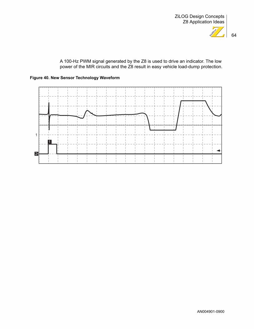
ZiLOG Design ConceptsZ8 Application Ideas
64
A 100-Hz PWM signal generated by the Z8 is used to drive an indicator. The low power of the MIR circuits and the Z8 result in easy vehicle load-dump protection.
Figure 40. New Sensor Technology Waveform
1
2
1
AN004901-0900

ZiLOG Design ConceptsZ8 Application Ideas
65
Figure 41. New Sensor Technology Block Diagram
ZiLOG Z8
POWERMOSFET
RESET
VCC
REF
PWM
AMP
LOAD DUMPPROTECTION
OSC
PRF
POWERREGULATOR
VCCOUT
TELEFLEX MICROPROCESSORMIR FUEL LEVEL SENDER
12/24 VINPUT
OPTIONJUMPERS
FIXEDDELAY
TRANSMIT
SIGNAL
SAMPLE
SIGNALVARIABLE
DELAYSAMPLE
GATE
RAMPCIRCUIT
PULSEDRIVE
DIRECTIONALNETWORK COAXIAL
PROBE
TANKPULSEDRIVE
AN004901-0900

ZiLOG Design ConceptsZ8 Application Ideas
66
Phone DialerSubmitted by: Daniel Dina
Abstract
The Phone Dialer is a device that attaches to a telephone and monitors all activity from either the line or the phone. The line activity being monitored involves detect-ing several phone line conditions such as on-hook, off-hook, and ringing. The ana-log portion of the circuit detects these conditions and provides logic levels and wake-from-sleep-mode interrupts to the microcontroller.
The phone activity being monitored starts when the Phone Dialer device either detects the handset being picked up, or if programmed accordingly, answers the phone. Should a customer pick up the phone and start dialing, the Phone Dialer receives all key presses and, based on the phone number dialed by the user, gen-erates a new string that ultimately dials out on the line. This new string contains all the prefixes and codes necessary to utilize the lowest-cost carrier available to the user. Through proper filtering, all phone numbers entered by the user are blocked from reaching the line, thus preventing the an outgoing call.
The Phone Dialer device ultimately dials the numbers, along with the proper pre-fixes and suffixes. The Phone Dialer device can also be programmed through the phone (by turning on the answer feature), or by picking up the phone and entering the program mode (by the use of a password).
A simple example of operation for the device is as follows:
1. A user picks up the phone.
2. The circuit detects an off-hook condition and wakes up the Z8 microcontroller, enables the filter, and starts listening for a tone generated by the phone.
3. The user dials a number.
4. The firmware begins decoding the phone number being dialed, and makes decisions based on the area code and the prefixes, using programmed routing numbers.
5. Based on all programmed variables, the device forms the complete string and dials the number.
The Z86E08 device additionally helps to reduce part count by incorporating a built-in reset circuit. Its low sleep-mode current drain enables the shut-down oper-ation of the circuit. The device analog circuitry (D4ÐD7) allows the Phone Dialer to be connected to any phone line regardless of polarity.
AN004901-0900

ZiLOG Design ConceptsZ8 Application Ideas
67
Figure 42. Phone Dialer Block Diagram
Telephone
Phone dialer device
PhoneCompany
AN004901-0900

ZiLOG Design ConceptsZ8 Application Ideas
68
Figure 43. Phone Dialer Schematic Diagram
VD
D
St/G
T
ES
t
D3
D2
D1
D0
IRQ
/CP
DS
/RD
RS
O
1 2 3 4 5 6 7 8 9 10
15 16 17 18 1 2 3 4
IN+
INÐ
GS
VR
EF
VS
S
OS
C1
OS
C2
TO
NE
R/W
/WR
/CS
20 19 18 17 16 15 14 13 12 11
Q1A
MP
Q�
3904
MT
88L8
9AE
U2
XT
AL2
3.57
95M
Hz
R6
100k
R13
R4
12k
R4
12k
R10
100
Q5
2N70
00
Q2
2N70
00
R16
2kR
152k
C10
100n
F
R17
374k
C2
.1µ
F
3.3V +V
100k
C7
100n
F
C6
D4
1N
4002
Red
Wire
(tip
)
Gre
en W
ire (
ring)
Gre
en W
ire (
ring)
Cus
tom
er p
hone
jack
Red
Wire
(tip
)
U4
LP29
50C
ZT
elec
o P
hone
Jac
k
D6
1N
4002
D5
1N
4002
D7
1N
4002
L1 1
0mH
.1µ
F
R12
2.2
k
R11
CN
TR
L3
1Meg
R1
1M
eg
uP C
NT
RL1
R8
470
k
14
Mic
ropr
oces
sor
sam
plin
g no
de
P00
P01
P02
XT
AL1
XT
AL2
P31
P32
P33
P20
P21
P22
� P23
P24
P25
P26
P27
11 12 13 7 6 8 9 10
Z86
E08
U1
5 6 7 8
GN
D A2
A1
A0
SD
A
SC
L
WP
VC
C
4 3 2 124
LC01
/02B
U3
XT
AL1
12M
Hz
C5
12p
F
C4
12p
F
J1
C8
10m
F
3.3V
Pow
er S
uppl
yfo
r uP
and
Mem
ory
3.3V +V
3.3V +V
3.3V +V
3.3V +V
3.3V +V
VC
C
GN
D
V3
J2
J3
InO
ut
Com
D FG
DF G
C1
47µ
FC
9.1
µF
C3
.1µ
F
R9
470k
Q3
2N70
00
R7
CN
TR
L2
D1
Zen
erD
2M
MS
Z5
V1T
1D
3M
MS
Z5
V1T
11M
eg
R3
470k
R2
470k
D FG
Q4
2N 3904
AN004901-0900

ZiLOG Design ConceptsZ8 Application Ideas
69
Pocket Music SynthesizerSubmitted by: Stan Sasaki
Abstract
The pocket music synthesizer is an instructional aid and motivational tool for ele-mentary and middle school band and orchestra students and teachers. The syn-thesizer is loaded with a variety of scores, and the student can play back selected pieces and parts of any score. For example, the cello track can be removed, or just the flute track can be played. Tempo can be adjusted without affecting pitch, so that students can practice at home at their own pace. The student can jump to any location in a composition to repeatedly listen to and play along with challeng-ing passages. This jump location corresponds to the sheet music measure num-ber and call loop between measures. Other features include a metronome, instrument tuner, and scale transposer. Sound is output via an RF modulator played over any FM radio. The unit is similar in appearance and size to a TV remote with an LCD display. It can stand on-end on a music stand. For durability, the only connector is for battery charging.
A Z86C96 microcontroller interprets the score and the various instrument waveta-bles stored in a single 1-Mbyte Flash memory chip. The Flash chip contains both program and data memory. The Z86C96 features a 64-KB external memory inter-face. An additional four I/O lines extend the data space range to 1Mbyte. A small complex programmable logic device (CPLD) manages the program/data memory segmentation; the CPLD also performs other I/O signal management. Each instrument track is stored in digital notation (for example, MIDI) where a note is encoded as instrument type, pitch, duration, and volume. For each note, the microcontroller reads the template note for that instrument out of the wavetable. The wavetable memory contains sound chunks of the actual instrument at selected points in its pitch range and with a prototype attack-sustain-decay enve-lope. The microcontroller adjusts for intermediate pitches by sample rate adjust-ment. The playback code is straightforward, because the wavetables are not compressedÑthe microcontroller simply reads and sums data arrays from mem-ory.
The composite digital audio signal is written to a D/A converter, and the analog signal drives an FM broadcast band modulator. The carrier is phase-locked to allow exact tuning, because receivers are now also synthesized.
The Z86C96 scans the keypad for user commands and displays operating status in the LCD display. For example, the LCD displays the real-time measure number during playback. The microcontroller requires a crystal oscillator for pitch and modulator tuning accuracy.
The score and wavetable flash memory is downloaded from a PC by the instructor at the beginning of a school year. For grade school, the entire yearÕs orchestration
AN004901-0900

ZiLOG Design ConceptsZ8 Application Ideas
70
can be stored, while middle-school applications require periodic updates due to the complexity and length of scores. The memory is loaded via an infrared link directly decoded by the Z86C96Õs UART port. The UART interface allows any PC serial port driving an infrared diode pod to load the memory. The synthesizers for an entire class can be loaded in parallel by pointing them all at the emitter; each unitÕs LCD display verifies download integrity.
Figure 44. Pocket Music Synthesizer Block Diagram
Keypad4x4 matrix
Z86C96Microcontroller
20 MHz
RF Modulator -FM broadcast band
PLL synthesized-monaural
IR detector(for download)
Data Mem(1008 kbytes)
+5V
Prog Mem(16 kbytes)
1 MByteFlash Memory
asymmetrically-blocked
8-bit D/Aconverter
2.4Vrechargeable
battery
DC-DCconverter
4-char LCDdisplay
AN004901-0900

ZiLOG Design ConceptsZ8 Application Ideas
71
Figure 45. Pocket Music Synthesizer Schematic Diagram
P07
P06
P05
P04
P03
P02
P01
P00
P17
P16
P15
P14
P13
P12
P11
P10 AS
DS
R/W P27
P26
P25
P24
P23
P22
P21
P20
P37
P36
P35
P34
P0D
SP
1DS
24 25 26 27 28 29 30 58 41 42 43 44 45 46 37 38 16 12 10 58 59 60 61 62 63 54 55 7 67 18 49 11 15
A15
A14
A13
A12
A11
A10
A9
A8
AD
7A
D6
AD
5A
D4
AD
3A
D2
AD
1A
D0
P2H
S
DM
9 19 53 5 6 13 14 4 1 2 68 64 65 40 39 33 34 35 36 22 23 47 48 57 58 50 21 66 8
RS
T
R/R
L
SC
LK
X2
X1
P47
P46
P45
P44
P43
P42
P41
P40
P57
P56
P55
P54
P53
P52
P51
P50
P63
P62
P61
P60
P33
P32
P31
P30
VIN
GN
D
Z86
C96
Mic
roco
ntro
ller
U5
U6
U9
U3
74H
C57
4A
ddr
latc
h
PZ
5064
-10A
44C
PLD
U7
MC
3406
4
4-D
IGIT
MU
X'D
LCD
4X4
KE
YP
AD
MA
TR
IX
C1
+
C15
C12
+
C10
C9
C8
R15
Q2
Q1
C11 L2
C14
C7
D4
D6
D5
L3
D2
L1
D3
tric
kle
only
2-ce
llre
plac
eabl
epa
k
J1D
C in
R3
VC
C
VC
C
VC
C
VC
CV
CC
VC
C
VC
C
VC
C
RE
SE
T
VC
C
R1
R11
R2 R19
PLL
filte
r
R5
R18
R17
D1
R12
R7
C0
C1
R8
R9
R10
R4
R16
VC
C
R13
R14
R6
RS
T2 3
1
VC
C
20M
Hz
C5
C6
Y1
SC
LK
SC
LK
SC
LK
VC
CV
CC
VC
CV
CC
GN
DG
ND
GN
DG
ND
IN0
IN1
IN2
IN3
A0
A2
A5
A8
A11
A12
A13
A15
B0
B2
B3
B4
24 25 26 27 28 29 31 32 41 40 39 38 37 36 34 33 17 16 14 13
ser
data
load
pll
ser
clk
load
dac
enab
le fl
ash
read
flas
hw
rite
flash
low
bat
tery
r1 r2 r3 r4 c1 c2 c3 c4
D1
D2
D3
D4
D5
D6
D7
D8
CLK
OC
addr
stb
Q1
Q2
Q3
Q4
Q5
Q6
Q7
Q8
E28
F80
0B5-
B60
8 M
bit F
lash
MC
1451
70P
LL s
ynth
esiz
er
A18
A17
A16
A15
A14
A13
A12
A11
A10
A9
A8
A7
A6
A5
A4
A3
A2
A1
A0
A-1
A19
A18
A17
A16
A15
A14
A13
A12
A11
A10
A9
A8
19 18 17 16 15 14 13 12
29 31 33 35 38 40 42 44 12 16 14 11 28 26
16 17 48 1 2 3 4 5 6 7 8 18 19 20 21 22 23 24 25 45
DQ
0D
Q1
DQ
2D
Q3
DQ
4D
Q5
DQ
6D
Q7
RP
BY
WP
WE
OE
CE
U2
C13 C3
C4
OS
CI
OS
CO
RE
FO
FIN
DIN
EN
BC
LKD
OU
T
16 15 14 13 12 11 10 9
1 2 3 4 5 6 7 8
VD
DO
VO
RP
DV
SS
LD FV
FR
AD
5301
DA
C
U8 VO
GN
DV
DD
6 5 4
1 2 3
SY
SC
KD
IN
AD
7 2
AD
6 3
AD
5 4
AD
4 5
AD
3 6
AD
2 7
AD
1 8
AD
0 9 11 1
A19
A18
A17
A16
C0
C2
C3
C4
C7
C8
C13
C15 D
0D
2D
7D
8D
11D
12D
13D
15 B8
B10
B13
B15
3 15 23 35 10 22 30 42 43 1 44 2 4 5 6 7 8 9 11 12 21 20 19 18
PN
A46
02M
Inte
grat
ed IR
dem
odul
ator
U1 VD
D
GN
D
1 2 3O
UT
MA
X16
74B
oost
con
vert
er
U4 FB
GN
D
LBI
RE
F
7 4 3
1 8 2
LX
OU
T
LBO
L4
VC
C
AN004901-0900

ZiLOG Design ConceptsZ8 Application Ideas
72
Portable Individual Navigator (PIN)Submitted by: Leonard Lee
Abstract
A ZiLOG 16-MHz Z86E83 microcontroller serves as the controller for a small, self-contained, belt-carried device that provides an individual with bearing and dis-tance traveled on foot from an initial location. It can be used for individual naviga-tion both indoors and outdoors. The device combines data from a solid-state magnetic compass sensor and an accelerometer-based stride sensor. The accel-erometer is also used to compensate for mounting tilt. Iterative algorithms are used to compute the accumulated bearing/distance vector on the fixed-point microcontroller in an efficient way.
A typical application might be an individual who is hiking. The portable navigator can also be used indoors to track the location of people wearing the device in a certain area. When the device is initialized, the wearer can wander freely on foot, both indoors and outdoors. When it is time to return home, the device displays the required compass bearing and distance in meters to the starting point or most recent waypoint.
The design requires the sensing of voltage from several sensors. It also provides user input and display control; therefore, a microcontroller with a large number of I/O pins is required. It is possible to sense analog voltages using Z8 devices with-out analog-to-digital (A/D) converters (for example, measuring the charge time of an RC circuit connected to a comparator input). However, these methods require external circuitry and can be considered somewhat ad hoc measures. Conse-quently, the ZiLOG Z86E83 (OTP version) was chosen because it features an 8-channel A/D converter and a relatively large number of I/O pins. These features permit the PIN to include minimal glue logic and external analog circuitry. Z86E83 software is the heart of the system and performs all functions, such as reading the sensors, converting the data into distance and bearing, and managing the user interface.
The Z86E83 is configured to use a crystal oscillator clocked at 16 MHz to offer maximum code flexibility for the prototype software. To keep power supply design simple, an LM2930T-5.0 low drop-out linear voltage regulator is used to regulate the 6-V battery voltage (from two 3-volt lithium CR3032 coin batteries) down to 5volts. The efficiency of the linear regulator in this case is 5V Ö 6V = 83%, which is comparable to a switching supply, because the input-output differential is only 1V.
AN004901-0900

ZiLOG Design ConceptsZ8 Application Ideas
73
Figure 46. Portable Individual Navigator A/D Ratio Over Time
Peaks due to footfallsthresholdfor footfalldetection
Stridecorrection basedon time interval
Increased tilt lowersaverage level(0 degree tilt = 098)
A/Dreading
fromaccel.
Time
AN004901-0900

ZiLOG Design ConceptsZ8 Application Ideas
74
Figure 47. Portable Individual Navigator Schematic Diagram
Z86
E83
16P
EC
Zilo
g
AC
0/P
20
AC
1/P
21
AC
2/P
22
P32
RE
SE
T
P33
P24
VC
C
VE
E
VS
S
2 3 1
+5V
+5V
Din
smor
e 16
55 H
alle
ffect
com
pass
sen
sor
910
16M
Hz
E
6
10k
10k
Thr
esho
ld fo
r fo
ot im
pact
s
D2
1
NC
98
47
11
10
1314
12U
CA
0V
in
Aou
t
LCD
cont
rast
45
1413
1211
109
87
RS
75 D
egre
es
1312
�m
RW
D7
D6
OP
TR
EX
DM
C-1
6117
N 1
6x1
LC
D
D5
D4
D3
D2
D1
D0
XT
AL
20pF
20pF
XTAL1
P06
P05
P04
P03
P02
P01
P00
25
24
23
22
21
20
19
XTAL2
+5V
+5V
+5V
+5V
31
2
6V Tw
o C
R30
32 3
V li
thiu
mco
in c
ells
in s
erie
s
LM29
30T
-5.0
, 5V
low
dro
pout
reg
ulat
or
Line
ar s
lider
pot
.fo
r sc
rolli
ng c
ontr
ol
Spa
re u
nuse
d in
put
LCD
FR
ON
TS
IDE
Slid
er p
otP
ushb
utto
n
+O
UT
IN
GN
D
NC
(s
pare
ou
tput
s)
1 23
456
Vcc
AV
cc
P25
P26
P27
P34
P35
P36
AC
33/P
23
P31
GN
D
AG
ND
28 1 2 14 8 15 4
12 27 5 6 7 16 18 17 3 13 11 26
10k
+5V
10k
2.2k
100k
50k
.22µ
F
.1µ
F
AD
XL1
05ac
cele
rom
eter
-AQ
Cva
riant
(ext
. tem
p.ra
nge)
Not
es:�
-�M
agne
tic n
orth
and
true
geo
grap
hica
l nor
th d
iffer
by
the
��m
agne
tic d
eclin
atio
n -
can
be ig
nore
d fo
r re
lativ
e m
easu
rem
ents
.�
-�A
/D is
use
d to
dig
itize
sig
nals
nea
r D
C o
nly.
Ant
ialia
sing
filte
r��
not n
eede
d. S
enso
rs h
ave
limite
d ba
ndw
idth
and
this
lim
its n
oise
.�
AN004901-0900

ZiLOG Design ConceptsZ8 Application Ideas
75
Postal Shock RecorderSubmitted by Bryon Eckert
Abstract
The increased competition between shipping companies has brought lower costs for business and the consumer. Demand from these sectors has caused the speed with which packages are handled to become more important than care in their handling. The result has been increased breakage of fragile items.
An inexpensive shock recorder can be very helpful in pinpointing the probable time of breakage by recording the amplitude of each shock, along with a time stamp in serial EEPROM. Low cost is the most important requirement. Light weight and small volume is also important, as it relates to cost of use.
The heart of the shock recorder is the sensing element. Three sensors are used (one for each axis), each consisting of a ceramic magnet epoxied to the end of a metal strip. A shock causes the metal strip to vibrate and produce a time-varying magnetic field proportional to the amplitude of the shock.
The magnetic field variation produces a voltage across a sensing coil. Balanced amplifiers minimize interference pick-up. AC coupling to the subsequent amplifier stages eliminates the requirement for DC offset adjustment. U3C provides low-impedance virtual Ground, allowing single-supply operation while adding minimal additional power consumption. Each sensing amplifier feeds an inverting peak detector. The diodes are inside feedback loops to minimize temperature drift. All three amplifier outputs are connected across a single tantalum capacitor for charge storage.
The Z86E04 usually runs in STANDBY mode, minimizing power consumption. When a shock is detected, the peak detector voltage rises above the level preset by R27 and R28, triggering IRQ3 (rising edge). The CPU wakes and starts the A/D conversion routine. Voltage readings are taken for several seconds, with the high-est reading stored in EEPROM (8-bit value), together with a time stamp (24-bit value). A second comparator is used to monitor battery voltage. A low drop-out reg-ulator provides a stable reference voltage and makes efficient use of a low-cost carbon-zinc 9-V battery. With LM324A operational amplifiers, the overall current consumption is about 5 mA, allowing up to 100 hours of operation.
A 93LC66 EEPROM contains 512 bytes of memory, allowing up to 125 events to be stored (leaving room for the base date and time and a tracking number in BCD format). The user interface consists of a serial port and an alarm LED. The serial port is implemented in firmware, and can run at up to 38.4K baud for a 4-MHz crystal in low-EMI mode. The serial cable must be kept short (less than 6 feet), because the interface is not a RS-232-level interface. The base date and time is set through the serial port, and the EEPROM is read and erased through the
AN004901-0900

ZiLOG Design ConceptsZ8 Application Ideas
76
serial port. The alarm LED indicates that a shock threshold is exceeded, and/or the battery is low. PC-based software allows a user-friendly interface when the postal shock recorder is connected to a personal computer.
Figure 48. Postal Shock Recorder Block Diagram
P01
P02
P00
P32
P33
CPU
SERIAL
EPROM
LOW DROPOUT
REGULATOR
CHARGE
STORAGE
PEAK VALUE
AMPLIFIER
SHOCK
SENSOR
PEAK VALUE
AMPLIFIER
SHOCK
SENSOR
PEAK VALUE
AMPLIFIER
SHOCK
SENSOR
LM2951-5.0
Z86E04
ADC RAMP COMPARATORS
93LC66
ALARM LED
BATT
CS
DATA IN
DATA OUT
CLOCK
BATTERY SAMPLE IN
Inductive Sensor(Magnet wire around
iron nail)
Ceramic magnet
Spring steel
RAMP
SENSOR
X AXIS
Y AXIS
Z AXIS
TO IRQ3
COMPARATOR
RXD SERIAL DATA
LEVEL REFERENCE
1 MHZ
TXD INTERFACE
X
Z
Y
AN004901-0900
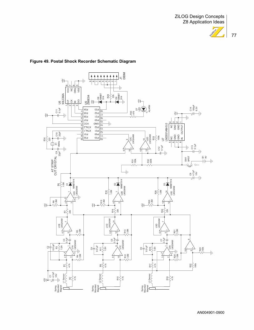
ZiLOG Design ConceptsZ8 Application Ideas
77
Figure 49. Postal Shock Recorder Schematic Diagram
NC
GN
D
GN
D
IN
4 3 2 1
NC
GN
D
GN
D
OU
TP
UT
5 6 7 8
AT
ST
RIP
CU
T C
RY
ST
AL
C14
100µ
F6.
3V
U2D
LM32
4AM
Ð +
13
1412
U2C
LM32
4AM
Ð +
9
810
U2A
LM32
4AM
U1B
LM32
4AM
U1A
LM32
4AM
Ð +
2
1
114
114
3
Ð +
6
75
Ð +
2
13
+5V
+5V
+5V
R32
220k
R31
100k
R30
470
D7
LED
ALA
RM
U7
LM29
31A
M-5
.0
P33
P00
P01
P02
GND
P20
P21
P22
P23
9
8
7
6
5
4
3
2
1
P32
P31
XTAL1
XTAL2
VCC
P27
P26
P25
P24
10
11
12
13
14
15
16
17
18
C11
0.1µ
F
+5V
R34
220
C10
22pF
C9
22pF
X1
4MH
z
C13
0.1µ
F
B1
9V
SW
1S
PD
T
CF
CK
BI
DO
9 8 7 6 5 4 3 2 1
8 7 6 5
VC
C
NC
OR
G
VS
S
1 2 3 4
U6
93LC
66A
J1 DB
9M
+5V
+5V
C8
4.7µ
F10
V
+
C1
4.7µ
F10
V
+5V
+
+
C12
0.1µ
F
R33
100k
R8
1.0M D1
MM
BT
914
R1
4.7k
L1 S
enso
r
Spr
ing
Mou
nted
Mag
net
Spr
ing
Mou
nted
Mag
net
R2
4.7k
R7
R6
1.8M
C3
0.1µ
F
22k
R3
1.0HC2
0.01
µF
R5
1.0M
R4
1.0M
R29
D9
MM
BT
914
D8
MM
BT
914 22
k
U5
Z86
E04
U2B
LM32
4AM
U1D
LM32
4AM
U1C
LM32
4AM
Ð +
6
75
Ð +
13
1412
Ð +
9
810
+5V
R16
1.0M
D2
MM
BT
914
R10
4.7k
R14
R15
1.8M
C5
0.1µ
F
22k
R11
1.0HC4
0.01
µF
R13
1.0M
R12
1.0M
R9
4.7k
L2 S
enso
r
Spr
ing
Mou
nted
Mag
net
U3D
LM32
4AM
U3D
LM32
4AM
U3A
LM32
4AM
Ð +
13
1412
Ð +
6
75
Ð +
34 11
12
+5V
R26
1.0M
D3
MM
BT
914
R18
4.7k
R24
R25
1.8M
C7
0.1µ
F
22k
R19
1.0HC6
0.01
µF
R21
1.0M
R20
1.0M
Ð +
10
89 R
2310
0k
R17
4.7k
L3 S
enso
r
R22
180k
AN004901-0900

ZiLOG Design ConceptsZ8 Application Ideas
78
PWM Input/Output Interface ModuleSubmitted by: Fernando Garcia Sedano
Abstract
The PWM I/O interface module is designed to process pulse-width monitor (PWM) input and output signals, very often used on railroad vehicles to transport analog information on train lines (for example, brake demand). With a PWM signal, ana-log information is a function of duty-cycle index modulation. Usage of PWM sig-nals to transport analog information is due to the very high electrical noise immunity. It is also easy to isolate a PWM signal from other voltages, due to the pseudodigital appearance, making these signals suitable to be demodulated using only digital circuits.
The circuit receives three different PWM input signals with galvanic isolation at two different voltage levels (depending on R10 and R11 value). There are three input stages (U2, U3, and U4) with their corresponding overload protection (T6, R12, T7, R7, T8, and R8), and with EMC protection (D1, D2). The third PWM input channel (U4) feeds back the PWM output signal (24VPP maximum).
The Z8 microcontroller is programmed to demodulate PWM input signals, to count the times where PWM input is at high and low levels, and to perform the corre-sponding division. Obtained values are loaded in the DPRAM. The Z8 is pro-grammed to address external memory using Port 0 and Port 1 to send address and data lines.
DPRAM works as a data buffer between the Z8 microcontroller and any other external microprocessor or microcontroller.
AN004901-0900

ZiLOG Design ConceptsZ8 Application Ideas
79
Figure 50. PWM Input Output/Interface Module Block Diagram
DP
RA
MA
ddre
ss L
ogic
(74H
C13
9+79
HC
02)
EM
CF
ilter
Out
put
Isol
atio
nB
arrie
r(1
XH
CP
L310
1)
Isol
ated
DC
ÐDC
Con
vert
er
Inpu
tIs
olat
ion
Bar
rier
(3X
HC
PL2
211)
Add
ress
Logi
c74
HC
139
DPRAM I/OData Bus Buffer
74HCT245
74HC374D_LATCH
CER\
6.4MHz
SEMR\
24V
24V
PWM Output
DP
RA
M(I
DT
7314
LA70
JB)
4Kx8
AB
[14,
13]
IOB
HE
\, IO
SE
L\
AB
[12.
.1]
IOW
R\,
IOR
D\
+5V
dc fi
ltere
dfo
r in
tern
al p
ower
supp
ly
Ext
erna
l BC
U(I
ntel
80C
196)
�In
terf
ace
(Dat
a, A
ddre
ss a
nd �
Con
trol
Bus
es)
DB
[7..0
]
+5V
dc
SE
ML\
PW
M1
PW
M2
PW
M3
PW
M In
put1
Ext
erna
l Tra
in-li
neIn
terf
ace
PW
M2
Inpu
t2
PW
M3
Inpu
t3
On/
Off
Con
trol
DB
[7..0
]
DA
B[7
..0]
AB
[11.
.8]
CE
L\
P1 P0
Z8 Microcontroller (Z86E40)
P3 P2
Mai
n C
ryst
al O
scill
ator
(TC
X0)
(T67
PZ
12.8
+M
C12
083P
)
PW
M O
utpu
tF
requ
ency
Sel
ectio
n(7
4HC
4020
+74
HC
151)
Fre
quen
cy to
Cur
rent
Con
vert
er(L
M23
1J)
Cur
rent
Out
put
AN004901-0900

ZiLOG Design ConceptsZ8 Application Ideas
80
Reaction TesterSubmitted by: Martin Bass
Abstract
The Reaction Tester measures the reaction time of an automobile driver using repeated cycles of signaling, time measurement, data display, data transmission via serial interface (to a PC that performs evaluation over the entire runtime), and waiting randomly for the next signal. Power-on also performs a system check (dis-play, lamps, buzzer, and serial interface) at this time.
All system functionality is performed by software:
¥ LED-multiplex for 7-segment display and lamps
¥ Sound via buzzer
¥ Reading status of the contact switches
¥ Serial output
This device is built into a car simulator (a box containing seat, steering wheel, and two pedals) and uses contact switches to check for steering left, steering right, gas, and brake.
A Z86E0812-1866 is the heart of this device, which is optimized for maximum integration and minimum parts count. The power supply is an AC/DC wall adapter that delivers an unregulated 9volts to 12volts at a 500-mA load. A capacitor and standard linear voltage regulator uses a diode in series to protect against a wrong connection and a ZORB diode for overvoltage protection. The multiplexed display consists of 3-digit drivers and the 74AC164 shift register; these components per-form I/O expansion and power-sink driving for segment currents.
Multiplexing drives three of the four LED lamps. The buzzer is driven by the con-troller port pin via a small electrolyte capacitor in series, and is controlled by soft-ware. The serial interface yields real RS-232 voltages (approximately +4V, +8V, and Ð9V under load) to be operable even on problematic PCs (for example, some laptops do not interpret 0V for the more negative voltage). If there is an immense cost problem, it can be easily downgraded to +5V/0V.
To read the status of the contact switches, the Reaction Tester includes an inter-face consisting of pull-up resistors, capacitors for noise clamping, and input pro-tection for the controller port. The oscillator is run by an 8-MHz quartz crystal.
AN004901-0900

ZiLOG Design ConceptsZ8 Application Ideas
81
Figure 51. Reaction Tester Block Diagram
Buzzer
Z86E0842-1866
Contact-Interface
Tx RxGND
CPU
10 MBJ2
Contact Switches
LED-Driver
Power
ACDC
AC/DCAdaptor500mA9-12V
7 Seg.LED-Display LED Lamps
J4
J3
RS-232Converter
AN004901-0900

ZiLOG Design ConceptsZ8 Application Ideas
82
Figure 52. Reaction Tester Schematic Diagram
P25
2
4
9
13 12 11 5 4 6
P27
345610111213
7 14
D C
9
P24
P23
P22
P26
4µ7/10V
P32
47k
Tx RxGND
1k
330
1N4148
1N4148
47µ/16V
10k
100k
4x100k
4x100W
8x68E
4xLED-Lamp
3x7 Seg. Disp.C.A., Red
P02
+5V
+5V
P01 P00
P33
4x4k72x
1N4148
P34 P21 P20 BUZZER
Vcc Vss C
Z86E0812-1866
IC2
IC1
C (MB) J2
7
1
18
17
3
10 8 16 15
7 2 8
7E5
2E2
T5BC337-25
+5V
T68C556C
J1
+5V
T2T1 T3
1N4148
22µ1613
T4100W
74AC164
+5V
+5V 2x22pF
100nQUARZ8MHz
3k3
+
+
470µ16V
100n
1SKE18A
1N400R
9-12Vdc500mA
J3
+
+
7805
IC3
AN004901-0900

ZiLOG Design ConceptsZ8 Application Ideas
83
Remote-Controlled Air ConditionerSubmitted by: Shailendra S. Vengutlekar
Abstract
The Z86E30 controls an electronic air conditioner. Remote-controlled operations are available together with manual key operations. The remote range is 10 meters.
There are two different sensing points for temperature control. A/D conversion uses two analog comparators. The A/D channels work simultaneously with PWM reference P33. Previous settings are restored when the unit is powered on.
The electronic air conditioner uses two timers. INTR4 tracks the time of the On/Off timer control mode, stepper motor control pulses, SLEEP mode, day-mode time track, remote-control pulse count, and display refresh pulses. PWM generation for A/D conversion uses INTR5.
The Remote-Controlled Air Conditioner features the following items:
¥ Fuzzy temperature control
¥ Four modes of operation
¥ Three fan speeds
¥ Automatic fan speed
¥ Stepper motor control for split air conditioner
¥ 12-hour On/Off timer
¥ Selectable room temperature
¥ Air-swing On/Off control
¥ ZiLOG Z86E30 microcontroller
AN004901-0900

ZiLOG Design ConceptsZ8 Application Ideas
84
Figure 53. Remote-Control Air Conditioner Block Diagram
DISPLAY AC MCU
OPTIONAL
IR
RECEIVER
IIC MEMORY
TEMIC
TSIL6400,
TEMIC
1N4148
ASP621
TEMIC �TDSG5160,�TLHX5405
KBD AND
DISPLAY
CONTROL
POWER SUPPLY
AND RELAY
CONTROL
IR LED
IR
TRANSMITTER
LOW/HIGH
VOLTAGE
PROTECTION
TURBO IC �24C02
AIR CONDITIONER CONTROL REMOTE CONTROL
ZILOG �Z86E30
TI ULN2003,TI UA7805CKC,TI 74HCT374,
TEMICBYT41M DIODE
T174LS145 TEMICTFMS5380
TEMIC4N33
AN004901-0900

ZiLOG Design ConceptsZ8 Application Ideas
85
Figure 54. Remote-Control Air Conditioner Schematic DiagramP
25P
26P
27P
04P
05P
06P
07V
CC
XT
AL2
XT
AL1
P31
P32
P33
P34
28 27 26 25 24 23 22 21 20 19 18 17 16 15
1 2 3 4 5 6 7 8 9 10 11 12 13 14
P24
P23
P21
P03
P02
P01
P00
P30
P25
SD
AP
27P
04P
05P
06P
07
XT
ALK
2X
TA
LK1
P31
P32
P33
P24
P23
P22
P21
P20
P03
VS
SP
02P
01P
00P
30P
36P
37P
35
Z86
E30
U1
Q0
Q1
Q2
Q3
Q4
Q5
Q6
Q7
3 4 7 8 13 14 17 18 1 11
2 5 6 9 12 15 16 19
P00
P01
P02
P03
P04
P05
P06
P07
P21
SO
LVO
LLF M
FH
F
D0
D1
D2
D3
D4
D5
D6
D7
OC
CLK 74
HC
T37
4
U6
U3
FN
D50
0
8 7 6 5 4 3 2 1
SO
LVO
LC
OM
CO
NH
FLF M
FA
IR_S
WIN
G
CO
N8
J5
1 2 3 4
P30
CO
N4
J21 2 3 4
CO
N4
J3
1 2 3 4
CO
N4
J6
A B C D
15 14 13 12
0 1 2 3 4 5 6 7 8 9
1 2 3 4 5 6 7 9 10 11
L1 L2 L3 L4 L5 L6 L7 L8
74LS
145
U2
12 C
6 0
.1µF
C3
47pF
21
1
2
L1
1
1
22X
1
8MH
z
C14
4.7
µF
C11
0.
1µF
XT
ALK
1
XT
ALK
2
SC
L
AIR
_SW
ING
VC
C
R1
390E
12
P00
P0Ð
0
VC
CN
/CS
CL
SD
A
WP A2
VS
S
1 2 3 4
8 7 6 5
AT
24C
04M
emor
y
U5
R14
C5
0.1µ
FM
PX
BU
Z
BU
Z
P0Ð
22
D2
FA
N
L21
P0Ð
32
D3
CO
OL
1
BU
ZZ
ER
BZ
1
VC
C
VC
C
VC
C
VC
C
Too
_war
mS
1
VC
C
22µF
25V
TA
NT
ALU
M
VC
C
VC
C1
1
1
2
22
100k
MF
R 1
%
3
L2
4
L3
5
L4
6
L5
7
L6
8
L7
9
L8
C2
47pF
1 2
C13
4.7µ
F
1 2R17
330E
1/4W
1 2
C12
1 2
2200
µF25
V
C1
0.1µ
FC
40.
1µF
1
P31
P32
21 2
C10
1 2
VC
CC
7
0.1µ
F
P0Ð
42
D4
DR
Y
L31
P0Ð
52
D5
SLE
EP
1
P0Ð
62
D6
HE
AT
1P
0Ð1
2D
7
TIM
ER
L1
CO
MC
ON
P23
1
12
VC
C
C9
0.1
µFV
CC
12
R2
390E
12
P01
P0Ð
1
CO
MC
OM
05
3
XT
ALK
1P
30
83 8
AB
CD
EF
G
76
42
19
1
D P
R3
390E
12
P02
P0Ð
2
R4
390E
12
P03
P0Ð
3
R5
390E
12
P04
P0Ð
4
R10
120E R9
120E
12
SC
L
12
SD
A
R6
390E
12
P05
P0Ð
5
R7
390E
12
P06
P0Ð
6
P0Ð0P0Ð1P0Ð2P0Ð3P0Ð4P0Ð5P0Ð6
U4
FN
D50
0
CO
M
1 2
D10
Dio
de
XT
ALK
2
1 2
D18
Dio
de1 2
D8
Dio
de P31
1 2
D8
Dio
de
P32
1 2
D10
Dio
de
P33
1 2
D11
Dio
de
CO
M
D14
Dio
de1
2
D15
Dio
de1
2
D17
Dio
de1
2 D16
Dio
de1
2
D12
Dio
de2
1
05
AB
CD
EF
G
76
42
19
1
D P
P0Ð0P0Ð1P0Ð2P0Ð3P0Ð4P0Ð5P0Ð6
VC
C R12
10k
1 2
R13
10k
1 2
R15
6.8k
1 2R
166.
8k
1 2
R8
2k2
1 2
Rem
ote
Sen
sor
The
rmis
ter1
: F
or s
ensi
ng r
oom
tem
pera
ture
The
rmis
ter2
: F
or s
ensi
ng c
oil t
empe
ratu
re
Too
_coo
lS
2F
an_s
peed
S3
Air_
swin
gS
4M
ode_
sel
S5
On_
timr_
set
S6
P27
P25
P31
P32
The
rmis
ter1
RP
1R
_Arr
ay
The
rmis
ter2
D13
Dio
de2
1D
1 D
iode
21
Off_
timer
S7
Set
_tem
pS
8O
n_of
fS
9
R11
2k2
1 2
PC
B S
ize
150m
m x
70m
mP
ut s
epar
ate
GN
D a
nd P
ower
Tra
ck fo
r M
icon
2200
µF c
ap (
C10
) sh
ould
be
near
Pow
er S
uppl
y C
onne
ctor
Hor
izon
tal h
oles
for
LED
sM
ount
ing
hole
s di
amet
er 4
.2m
m
AN004901-0900
ZiLOG Design ConceptsZ8 Application Ideas
86
Remote-Control Antenna PositionerSubmitted by: R. Sharath Kumar
Abstract
Antennae, parabolic dishes, and other types of wireless signal-receiving devices are today a common essential necessity in almost every home, office, and military application. Owing to the present number of communication satellites, it is often necessary to precisely reorient an antenna to different positions. Generally, this procedure involves laborious cranking of mechanical gears while observing a cal-ibration scale.
A microcontrolled antenna-positioning device allows a user to align an antenna to the required elevation/azimuth precisely to the nearest degree by pushing a but-ton on an infrared hand-held remote.
The device consists of two modules: a controller and a hand-held infrared trans-mitter. The controller module based on the Z86E31 manages reception of coded commands from the hand-held remote. The Z86E31 decodes a command and drives the two motors to align the elevation/azimuth. The LCD display is updated to indicate the exact aligned position. Up to 20 positions can be preset on the sys-tem memory and recalled for alignment. Positive feedback is incorporated to ensure precision up to the nearest degree. Fault tolerance is embedded to avoid an erroneous command value from overdriving and damaging the antenna or the mast. The motion circuitry is biased-off and a beeper sounds along with the mes-sage Error: Out Of Range flashed on the LCD of each module.
Encoded commands from the hand-held remote are received on the infrared receiver D1A and processed by the microcontroller. The beeper is pulsed On/Off to indicate a successful decode. The power transistors T5ÐT8 and T13ÐT16 are biased-on to drive the elevation and azimuth motors M1 and M2, respectively.
AN004901-0900

ZiLOG Design ConceptsZ8 Application Ideas
87
Figure 55. Remote Controlled Antenna Positioner Block Diagram
Figure 56. Hand-Held Remote Block Diagram
Beeper
Infra-red�Receiver
D1A
Elevation Feed Back
Azimuth Feed Back
Elevation�Control Motor
Azimuth�Control Motor
Z86E31Microcontroller
LM331Voltage to Frequency
Converter
LM331Voltage to Frequency
Converter
LCD Module
PowerBridgeMotorDriver
M
M
Infra-red�Transmitter
D1B
4X4 Keypad
Z86E02Microcontroller
LCD Module
0 1 2 3
4 5 6 7
8 9
CLR P C
AN004901-0900

ZiLOG Design ConceptsZ8 Application Ideas
88
Figure 57. Remote Controlled Antenna Positioner Schematic Diagram
T2
SL1
00
T3
SL1
00
T11
SL1
00
R4
10k
R5
10k
T4
SK
100
T5
TIP
32A
D2
1N40
07x4
NO
S
D4
T7
TIP
32A
T8
TIP
31A
T9
SK
100
T10
SL1
00
T6
TIP
31A
15 14 24 25 26 27 28 1 2 3 16 4 5 6 7
11 9 10
RS
CE
D0
D1
D2
D3
D4
D5
D6
D7
RW
VLC
46
78
910
1112
1314
53
1
22128
VC
C
D10
1N41
48
Bee
per
Z86
E31
LCD
Mod
ule
13
C1
20pF
C2
20pFX
TA
L7.
328M
Hz
R3
10k
M1
R6
10k
R7
10k
R8
3k3
R12
6k8 C
433
0pF
R2
4k7
PO
T
2N22
22A
R1
4k7
DIA
Infr
a-re
dre
ceiv
erdi
ode
VC
C
D5
D3
VC
CV
CC
VC
C
+VE
Mot
or S
uppl
y
Azi
mut
h M
otor
For
war
d D
irect
ion
Con
trol
Azi
mut
h M
otor
Rev
erse
Dire
ctio
n C
ontr
ol
Ele
vatio
n M
otor
For
war
d D
irect
ion
Con
trol
Cou
pled
toA
zim
uth
Mot
orfo
r F
eedb
ack
Elevation Motor Reverse Direction Control
VC
C
Azi
mut
hM
otor
R18
10k
R19
10k
T4
SK
100
T13
TIP
32A
D6
1N40
07x4
NO
S
D8
T15
TIP
32A
T16
TIP
31A
T17
SK
100
T18
SL1
00
T14
TIP
31A
M1
R20
10k
R21
10k
VC
C
D9
D7
+VE
Mot
or S
uppl
yV
CC
Ele
vatio
nM
otor
1 6 7 2
3 5
8
4R
11 5k
R9
4k7
R10
10k
PO
T
C3
0.00
1µF
R13
3k3
R17
6k8 C
633
0pF
VC
C
Cou
pled
toE
leva
tion
Mot
orfo
r F
eedb
ack
1 6 7 2
3 5
8
4R
16 5k
R14
4k7
R15
10k
PO
T
C5
0.00
1µF
LM33
1 LM33
1
VC
C =
5 v
olts
Mot
or S
uppl
y <
40V
DC
AN004901-0900

ZiLOG Design ConceptsZ8 Application Ideas
89
RF Dog CollarSubmitted by: John Kocurck
Abstract
Current electronic fencing relies on a wire that is buried around the perimeter of the area to be fenced. A signal is sent through the wire that activates a dog collar should a dog stray too close to the barrier. If the dog decides to chase a varmint, it triggers a beep (or shock) when it enters the area around the buried wire, and nothing more.
Using the ZiLOG Z86E02 on both the transmitter and the receiver, a better system can be designed. This system addresses the weak points of the electronic fencing systems currently on the market. Each transmitter features a unique 64-bit num-ber supplied by a Dallas Semiconductor DS-2401. That number, along with a con-trol byte, is transmitted via a Convergent Inc. radio transmitter at approximately 2Kbps. Each transmission lasts for less than 50ms and is repeated every 250ms. The dog collar receives the packet and checks if the serial number is stored in its 128-bit serial EEPROM. If it checks out, the processor in the collar resets. If the collar does not receive a valid packet within 800ms, it enters ALARM mode and sounds the buzzer. As a result, the dog returns to the house. When the dog is back in range, the collar resets and turns off the buzzer. New transmitters can be added by bringing the collar into range and pressing the button on the transmitter. The transmitter then sends out a special control packet and serial number that the collar recognizes, and stores it into the EEPROM for future reference. This method allows the building of short-range jammers to deny certain areas and also small hand-held units for RF leashes. Because of the unique 64-bit serial number, neighbors using the same dog-control system do not extend the dogÕs range because of overlapping areas.
AN004901-0900
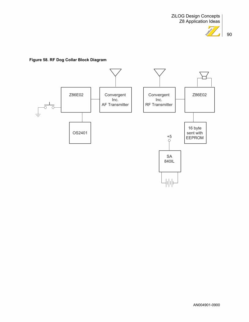
ZiLOG Design ConceptsZ8 Application Ideas
90
Figure 58. RF Dog Collar Block Diagram
Z86E02 Z86E02ConvergentInc.
AF Transmitter
OS2401+5
ConvergentInc.
RF Transmitter
16 bytesent withEEPROM
SA840IL
AN004901-0900

ZiLOG Design ConceptsZ8 Application Ideas
91
Signature Recognition and AuthenticationSubmitted by: James Doscher and Harvey Weinberg
Abstract
As more transactions are completed electronically, concerns about threats to data security increase. In particular, a user is required to be able to ensure that no one else can forge a signature or a password. There are new products on the market that attempt to solve this problem. For example, there are mouse devices that claim to be able to read fingerprints, and much development is occurring in the area of digital signature analysis.
An alternative solution is a pen device that recognizes the unique characteristics of a signature to authenticate the user. Typical applications could be encryption, secure web transactions, receiving (signing for a UPS package), and controlled access to secure data.
Existing systems, such as pen tablets, record the shape of a signature, but not necessarily the speed or emphasis (pen pressure) of the signature. By using a micromachined accelerometer to sense pen movement, an individualÕs distinctive signature motions can be recorded and compared against a stored copy. Recog-nition algorithms from speech processing are used to compare and correlate a personÕs signature. Prototype systems have already shown greater than 90% accuracy in recognition.
At the heart of the system is a ZiLOG Z8 for recognition algorithms, and the Ana-log Devices ADXL202 dual-axis accelerometer. The Z8 fans the recognition algo-rithms, decodes the accelerometer signal, and administers power management for the accelerometer. The accelerometer measures pen movements in the X and Y-axis in the plan of the paper.
Figure 59. Signature Recognition and Authentication Module Block Diagram
Power
Acceleration Host Alarm�Interface
ADXL202 Z86C06
AN004901-0900

ZiLOG Design ConceptsZ8 Application Ideas
92
Figure 60. Signature Recognition and Authentication Module Schematic Diagram
V
120K
Reset
COM
ADXL202
P22
P23
P24
Vcc
P35
P21
P20
GND
Z86C06
.1µF .1µF
47µF
4MHz
47µF
+5V
Host SerialInterface
.47µF
PWM OUTPUTS
DD
OUTX
OUTY
FILTX
FILTY
AN004901-0900

ZiLOG Design ConceptsZ8 Application Ideas
93
Smart Phone AccessorySubmitted by: Syed Naqvi
Abstract
The Smart Phone Accessory eliminates the hassle of dialing long strings of tele-phone numbers by employing predefined user-programmed keysets. The Z8 microcontroller offers many advantages toward this solution, by providing the required power, RAM, and ROM to perform the application. The Z8 features scal-able software compatibility and a configurable I/O that offers great flexibility in the design. The Z8 is also relatively inexpensive.
Caller ID offers unique usability to the party receiving the phone call. In most cases (depending on the service provider), the name and telephone number of the calling party is displayed. The receiving party can then keep a log of received calls for future use, or accept a choice of not answering the telephone call. On the other hand, most telephone companies offer the choice of an unlisted (unpub-lished) telephone number. However, if a person with an unlisted phone number makes a call, there is a possibility that his/her phone number will be displayed to other parties. The Caller ID feature can be disabled by dialing a predefined key sequence prior to calling. This step can be cumbersome and hard to remember on a regular basis.
Another very popular and fast-growing telephone service is the 10-10 calling ser-vice. Customers can secure very competitive long distance rates by predialing 7 more digits plus the phone number. The Smart Phone Accessory automatically dials the numbers prior to each call.
The Smart Phone Accessory is designed to work in series with the telephone handset. The product can use the telephone handset number pad, or it can dis-play its own number pad. The predefined keys (for caller ID and long distance) are programmed into the product. The Smart Phone Accessory can be reprogrammed or removed from the phone line very easily, thus offering customers complete flex-ibility. The power for the complete circuit is derived from the telephone line.
Figure 61. Smart Phone Accessory Block Diagram
Smart PhoneAccessory
PSTN
AN004901-0900

ZiLOG Design ConceptsZ8 Application Ideas
94
Figure 62. Smart Phone Accessory Schematic Diagram
TelephoneInterface &
Power Circuits
Touch ToneGenerator
Circuit
PSTN
To Handset
Keyboard Interface
1 2 3
4 5 6
7 8 9
* 0 #
1
2
3
4
1
2
3
4
13
14
15
12
11
8
5
6
7
8
PB0Vcc1
GND
PB1
PB2
PB3
PB4
RST
XTAL2
XTAL1
PA0
PA1
PA2
PA3
PA4
PA5
PA6
PA7
Z8E001
AN004901-0900

ZiLOG Design ConceptsZ8 Application Ideas
95
Smart Solar Water Heating SystemSubmitted by: Eduardo Jose Manzini
Abstract
The goal of the Smart Solar Water Heating System is to control the heating of the water supply for a home. After power-up, the microcontroller checks the value in EEPROM of the target value for temperature, and turns the LED on. The micro-controller reads the boiler temperature sensor (BTS), the sun collector tempera-ture sensor (SCTS), and turns on a corresponding LED.
If the value of SCTS is higher than BTS, the water flow pump (WFP) is powered up to increase/speed the heating of the water by the sun until BTS becomes equal to SCTS. If both are lower than the target temperature, the microcontroller turns off the WFP and turns the electrical heater on and up to the required temperature.
There are two control keys and five LEDs used for the required temperature. Each time a target temperature is selected, the microcontroller saves it in EEPROM. The required temperature is kept in case VAC is missing (110 ~227 failure). The other five LEDs (10 total) reflect the current temperature of the boiler.
AN004901-0900

ZiLOG Design ConceptsZ8 Application Ideas
96
Figure 63. Smart Solar Water Heating System Block Diagram
50¼C or
Fill up pumpor solenoid
VR
VR
Begin
Save valve targetLED on.
Turn off others.
or
temperature?
T. boiler <T. sun collector?
Reads temperaturesensor and lights
the nearest LED red
Heater off
Vcc
Vss
Vcc
Heater off
Comp 1
EPROM
PowerSupply
BatterySystem
OPTIONAL
*WFC pump on
*WFC pump = Water �Flow Control Pump
Z86E31
T. target>
T. boiler
WFC pump off
Heater on
Y
N
N
45¼C or
40¼C or
35¼C or
Lower than 30¼C
45¼C or
40¼C or
35¼C or
Lower than 30¼C
Water flowcontrol
VR
Heater
Decreasethe target
temperature
Increasethe target
temperature
Targettemperature
indicator
Current boilertemperature
indicator
VR
VREF2
TemperatorBoiler
Vcc
Vcc
VREF1
Vcc
TemperatorBoiler
Vcc
AN004901-0900

ZiLOG Design ConceptsZ8 Application Ideas
97
Smart Window with Fuzzy ControlSubmitted by: Tan Boon Lee
Abstract
Many homes in Southeast Asia contain sliding windows because of their lower cost. Most people open the windows when they are at home and close them dur-ing rains or when nobody is at home.
The Smart Window with Fuzzy Control design features an automatic window con-troller using the Z8. The Z8 uses a formula implemented in fuzzy logic to control the opening of a single sliding window that is proportional to the temperature, force of wind, and intensity of rain.
Port 2, pin 20 and pin 21 drive a 12-V DC motor via two relays. The motor features a current sense resistor (5R) connected to a comparator circuit to detect motor stall. The comparator circuit consists of a 100-ohm and 10-µF low-pass filter and a threshold detector implemented using LM339.
The wind and rain detector features a similar circuit. Both charge a 10-µF capaci-tor until a certain voltage is exceeded to trigger the Z8. The trigger voltage can be adjusted via a 20-ohm variable resistor.
The innovative feature of this design is the use of a single-slope ADC to read three switches and the temperature. The arrangement of the switchesÑopen, close, and autoÑpresent different voltages to P32. Different temperatures indi-cate different voltage outputs from the LM358 operational amplifier. The Z8 reads the temperature or the switch using the 74HC4006 analog switch.
The single-slope ADC yields consistent readings. A timer measures the charging of the capacitor (pin 33). When pin 33 reaches the input voltage of either the switch or the temperature, an interrupt is issued. The timer values are inversely proportional to the input voltage, because the timer is a downcounter. The range of the timer can be divided into 50 divisions very accurately but only 5 are required for 10¼C above the minimum set by the 20-ohm variable resistor.
Upon power-on reset, the Z8 reads the switches to check for AUTO mode. In AUTO mode, the position of the window away from the closed position is based on a weighted average of the temperature and wind. When rainy weather begins, the window shuts to a closed position. Manual positioning is possible in MANUAL mode. An LED indicates AUTO mode, and a buzzer sounds should the motor stall or the window is open during a rain.
AN004901-0900

ZiLOG Design ConceptsZ8 Application Ideas
98
Figure 64. Smart Window with Fuzzy Control
Threaded Rails
Limit switchClosed position
Hidden Z8board
Reflective stripsfor position sensor
Rain sensorThe resistivity decreaseswhen water ÔconnectsÕ theinterdigit of the sensor.
DC motor and gears
Smart Window with Fuzzy Control
Switch boxand LED
AN004901-0900

ZiLOG Design ConceptsZ8 Application Ideas
99
Figure 65. Smart Window with Fuzzy Control Schematic Diagram
22pF
P32
: Sw
itch/
Tem
p
22pF
P23
P22
P21
P20
P02
P01
P00
Rai
n
Win
d
Pos
ition
Sen
sor
Clo
sed
Pos
ition
Mot
or S
tall
Sw
itch/
Tem
p
AD
C
Sw
itche
s
Tem
p
Vcc
P24
P25
P26
P27
P31
P32
P33 X
T1
X
T2
Z86
E04
ULN2003 74HC4066
AD
C d
isch
arge
Sw
itche
s
Tem
p
On/
Off
For
/Rev
Buz
zer
LED
+-
10k
100k
10µ
F
0.1µ
F
Sin
gle-
Slo
peA
DC
+-
2k2
10k
10k
33k
6k8
10k
Vcc
Vcc
Ope
n
Vcc
Vcc
Mot
orS
tall
Mot
orS
tall
1/4
LM33
9
+-10
µF
1M10
k20k
VR
20k
VR
30k
VR
20k
VR
t¼ 6
.8K
ther
mis
tor
+-
+-
6k8
3k9
1k8
3k9
1k
5R
1k10
0R
10k
10k
Win
dde
tect
or
1/4
LM33
9
10k
VR
+-
10µ
F1M
10k20
kV
R
12V
Rel
ay
12V
12 D
CM
otor
and
Gea
rsR
ain
dete
ctor
AD
Cdi
scha
rge
1/4
4066
Aut
o/M
anua
l
Clo
se
AN004901-0900

ZiLOG Design ConceptsZ8 Application Ideas
100
Solar TrackerSubmitted by: David Ellis
Abstract
To achieve maximum efficiency from a solar device, the greatest possible amount of solar radiation must be collected. With a fixed angle, only a small portion of the available energy can be collected. The purpose of the solar tracker is to lock on to the location of the sun and to continually position the device to follow the path of the sun. The addition of a solar tracking device produces a smaller, more efficient photovoltaic system, allowing it to collect the greatest amount of energy over a longer period of time.
The solar tracker uses four CdS (Cadmium Sulfide 0 photoconductive) cells, wired in series and mounted on opposite sides of a vertical blind. When these cells are pointed directly at a light source, typically the sun, they exhibit approximately the same resistance. The output of the amplifier is half the supply voltage. This volt-age is converted by the Z8 microcontroller into digital data, and set equal to 128, or half of an 8-bit conversion. By comparing this digital value to 128, the direction of the light source can be determined. If the value is larger than 128, move the tracker to the left. If lower than 128, move the tracker to the right. Using two sen-sor setups allows the unit to control two axes and position itself directly at the brightest light source. At the same time, using relays or MOSFETs to drive a larger unit, the solar tracker can keep one or more devices pointing at the brightest source.
U1A provides a virtual Ground. U1B and U1C provide a buffer for the sensors. R5 and R6 form the primary sensor. RV2 allows for adjustments for difference in the CdS cells. RV1 allows for adjustments to the overall gain of the amplifier, forming the X position sensor. R9, R10, RV3, and RV4 form the Y position sensor. The outputs of the sensors are fed to a 2-to-1 analog multiplexer made from a dual-switch ADG273 device. The output is fed to the comparator input of the Z8E001, which is set up as an A/D converter. Connectors P1 and P2 provide the control signals for the positioning motors, and are connected to a set of relays or H-bridge drivers.
AN004901-0900

ZiLOG Design ConceptsZ8 Application Ideas
101
Figure 66. Solar Tracker Block Diagram
X PositionSensor
Processor
X Motor Drive
Y PositionSensor
Y Motor Drive
AN004901-0900

ZiLOG Design ConceptsZ8 Application Ideas
102
Figure 67. Solar Tracker Schematic Diagram
PB
1
PB
2
PB
3
PB
4
RE
SE
T*
PA
7
PA
8
PA
5
PA
4
18 17 16 15 14 13 12 11 10
1 2 3 4 5 6 7 8 9
PB
0
XT
AL1
XT
AL2
VS
S
VC
C
PA
0
PA
1
PA
2
PA
3
S1
D1
IN2
VD
D
8 7 6 5
1 2 3 4
IN1
D2
S2
GN
D
C4
0.1µ
F
Ð +
U1B
RV
1
100K
AD
G72
3
U2
VR
278
ST
105H
3+5V
+9V
+Vout
GND
+Vin
100K
TL0
84(4
=+
5VA
, 11=
GN
D)
1
13
R3
R6
CdS1
11
2
R4
10K
R7
15K
2
2
100K
R13
12
47uH
L11
2
2
+ Ð
GN
D
P1
TB
3PO
SY
Mot
or
P2
TB
3PO
SX
Mot
or
1 2 3
1 2 3
23
Ð +
U1A
TL0
84(4
=+
5VA
, 11=
GN
D)
1 23
1KR15
SW
1
GN
DG
ND
7x7�
mm
12
R5
CdS
1 2
RV
210
0K
1 3
1 2
R14
100K
1+5V
2
D1
S1D
PR
OC
ES
SO
R C
IRC
UIT
CE
NT
ER
VO
LTA
GE
RE
FE
RE
NC
EX
ÐPO
SIT
ION
SE
NS
OR
YÐP
OS
ITIO
N S
EN
SO
RP
OW
ER
SU
PP
LY
1 2
1 2
1R
410
K21
R4
10K
2
Ð +
U1C
RV
3
100K
100K
TL0
84(4
++
5VA
, 11=
GN
D)
1
13
R8
R10
CdS1
11
2G
ND
R12
10K
R11
15K
2
2
2
23
R9
CdS
1 2
RV
410
0K
1 3
1 2
C2
10µ
F
1 2
C5
1µF
1 2
C6
1 2
C7
47pF
47pF
1 2
C3
10µ
F
1+5V
2
+
C1
100µ
F
1 2
+
+
+ ÐGN
D
1
C9
12
+ 100µ
F
C10
12
0.01
µF
C8
12
1µF
2
Z8E
001
AN004901-0900

ZiLOG Design ConceptsZ8 Application Ideas
103
SpeedometerSubmitted by: Mylnikov Pavel
Abstract
This speedometer design is intended for measuring the speed of a walking pedes-trian. It can be worn on a waist-belt. The design uses a Z86C06 microcontroller because of its small size (18 pins) and speed (12MHz).
The speedometer measures the difference in travel time of an ultrasonic signal from the speedometer to the ground and back. The signal consists of two short impulses with a short interval.
When turning on the speedometer, the user must remain motionless for a few sec-onds so that the speedometer can define its height over ground. The height is defined using the following formula:
h = t x V ÷ 2
where:
h = height
t = passage time of impulse
v = velocity of sound in air (331 ms)
The speedometer is ready after the height is defined and the indicator light illumi-nates. During movement, the height changes are fixed automatically. The speed-ometer indicates horizontal speed only. Vertical movement can be approximated by linear functions.
The speedometer indicates average speed over a period of a few seconds. The speedometer can indicate an individualÕs speed and travel distance. Indication of speed or length is switched using a button. A reset button clears the displayed travel distance.
AN004901-0900
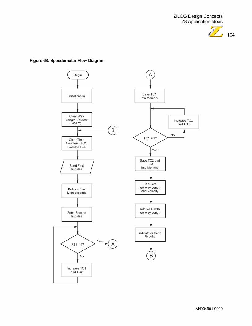
ZiLOG Design ConceptsZ8 Application Ideas
104
Figure 68. Speedometer Flow Diagram
Begin
Initialization Save TC1into Memory
Clear WayLength Counter
(WLC)
Clear TimeCounters (TC1,TC2 and TC3)
Send FirstImpulse
Save TC2 andTC3
into Memory
Calculatenew way Length
and Velocity
Add WLC withnew way Length
Indicate or SendResults
Delay a FewMicroseconds
Increase TC2and TC3
Send SecondImpulse
Increase TC1and TC2
P31 = 1?Yes
A
No
P31 = 1?No
Yes
A
B
B
AN004901-0900

ZiLOG Design ConceptsZ8 Application Ideas
105
Figure 69. Speedometer Block Diagram
P34
1
R>10 k½
1,3 = Amplifier
2 = Ultrasonic Speaker
4 = Microphone
5 = Indicator
P31
Vcc
Vcc P33
P2
XTAL1
12MHzXTAL2
Spd/len
Unit
Reset
P25
P26
P27
VCC
GND
3V
Z86C062
3
5
4
Vcc+ -
AN004901-0900

ZiLOG Design ConceptsZ8 Application Ideas
106
Stages Baby MonitorSubmitted by: Joe Peck
Abstract
There are a wealth of baby monitors on the market today, all with one purpose in mind: to alert the parents of the slightest noise, regardless of the necessity of doing so. The Stages baby monitor empowers the parents to balance between parentsÕ necessity to hear their babyÕs every move and their necessity to get a good nightÕs sleep.
The monitor can act as a traditional baby monitor, and broadcasts every little noise. Typically, parents only want to respond if the baby is awake or requires help, not if it rolls over and bumps a toy. The Stages monitor can be set to turn on for a fixed period of time if there is a particularly loud noise, or if a medium volume is sustained for a longer period. The sensitivity can be set by the parents to match their particular comfort level and environment. The monitor can also be set to help soothe the baby prior to actually turning the transmitter on. The monitor, upon detecting noise, can be set to play a short recording made by the parents if the noise exceeds the set level. If the noise continues or becomes significantly louder, the playback is stopped and the transmitter is turned on.
A ZiLOG Z86E83 Z8 OTP is the core of the Stages baby monitor.
Circuit Overview
¥ The On/Off Switch connects the 5-volt external power supply to the monitor.
¥ The mode switch is connected to digital input lines on the Z8. These lines are periodically sampled to set the operating mode appropriately.
¥ The Record switch is connected to another digital input. Holding the Record button causes the Z8 to record the audio from the microphone and write it to Flash memory.
¥ The sensitivity setting is controlled by a linear potentiometer and is connected to an ADC channel.
¥ The playback volume is controlled by a linear potentiometer and is connected to another ADC channel.
¥ The microphone is connected through a basic audio amplifier to another ADC channel. The Z8 uses this data differently depending upon the mode of operation.
¥ There are many transmitter circuits to choose from, depending upon required performance levels. This product uses a general transmitter black box.
AN004901-0900

ZiLOG Design ConceptsZ8 Application Ideas
107
¥ An audio amplifier connected to a PWM output drives the speaker. The PWM output is RC-filtered to create he audio output signal.
¥ The flash ROM uses a latched address scheme to reduce the number of pins required from the Z8.
Figure 70. Stages Baby Monitor Block Diagram
Wireless
Transmitter
Flash
Memory
PWM
Audio Amp
Audio Amp
Microphone
1 32
Stage
SpeakerZ86E83
Low High
Playback Volume
Low High
Sensitivity
On Off
Power
Record
AN004901-0900

ZiLOG Design ConceptsZ8 Application Ideas
108
Figure 71. Stages Baby Monitor Schematic DiagramW
irele
ss
Tra
nsm
itter
PW
M
Pow
erJa
ck
Dual 8-bit latch
Z86
E83
Fla
sh
Dat
a
Add
ress
+5V
+5V +
5V
+5V
Mod
e
Mod
e
Rec
ord
+5V
+5V
RD
WR
7 . . 0 15 . . 0
Vcc
AV
cc
Gnd
AG
nd
Res
et
XT
AL1
XT
AL2
AC
0
AC
1
AC
2
P31
P32
P33
Not
e: M
inor
com
pone
nts
(byp
ass
caps
, etc
.)
are
om
itted
from
this
sch
emat
ic.
P27
P26
P36
P34
P35
P23
P06
P00
P25
P24. .
AN004901-0900

ZiLOG Design ConceptsZ8 Application Ideas
109
Sun Tracking to Optimize Solar Power Generation Submitted by: Willy Tjanaka
Abstract
To gain optimal efficiency, and hence maximum solar power generation, solar cells must be positioned directly toward the sun. This project, incorporating a ZiLOG Z8E001 processor, offers a solution for tracking the location of the sun and moving the solar cell panel correspondingly. The solar panel attaches to a mechanical fixture that allows the solar panel to rotate vertically and horizontally.
The 13 photosensors are arranged with equal spacing on top of a hemispheri-cally-shaped housing. Each sensor is equipped with an optical filter to prevent the sensor from signal saturation. An A/D converter with a multiplexer samples the sensor signal and sends it to the Z8E001. The Z8E001 controls the vertical and horizontal rotational movement of the solar cell panel using the DC motors. Verti-cal and horizontal absolute encoders provide location feedback to the Z8.
The Z8E00110PSC is the controller chosen for this application. The PWM output on port PB1 provides a control signal for the motors (M1 and M2). Because only one PWM output is available, glue logic is required to control M1 and M2 one at a time. A Low on PB0 selects the horizontal motor (M2). A High on PB0 selects the vertical motor (M1).
B1 is an H-bridge-style motor driver that translates the PWM signal and direction signal to drive a DC motor.
M1 and M2 are the DC motors used to rotate the solar cell panel vertically and horizontally, respectively. B2 and B3 are absolute position encoders to track the position of the solar panel. The outputs of B2 and B3 are connected to the control-ler through serial interfaces (ENC_CLK, ENC_HDATA, and ENC_VDATA).
B5 controls the 13 photosensors arranged on a hemispherical housing. Optical fil-ters are used to reduce the light intensity from the sun and prevent the sensors from saturating. The signal from each sensor is sampled sequentially by the A/D converter (B4). The ADC_SEL0 to ADC_SEL3 signals determine which A/D con-verter channel to sample. Data is transferred to the controller through a serial interface (ADC_CLK and ADC_DATA).
The program scans the signals of all the photosensors (B5) using the A/D con-verter (B4). By knowing the location of each photosensor and comparing all the intensity values to each other, the program determines the location of the sun. The program computes the horizontal and vertical rotations required to move the solar panel. Next, the program selects the horizontal motor (M2) and generates the PWM signal to move the solar panel with the signal from B3 as feedback. Sim-ilarly, the solar panel is rotated vertically by driving the vertical motor (M1) and using B2 as position feedback.
AN004901-0900

ZiLOG Design ConceptsZ8 Application Ideas
110
Figure 72. Sun Tracking Block Diagram
VerticalRotationDC Motor
13 Photosensorswith Optical Filters
arranged on aHemispherical Housing
SolarCells
AbsolutePositionEncoder
MotorDrivers
AbsolutePositionEncoder
HorizontalRotationDC Motor
Z8E001A/D
Converter
SUN
AN004901-0900

ZiLOG Design ConceptsZ8 Application Ideas
111
Figure 73. Sun Tracking Schematic Diagram
DO
UT
CLK
SE
L0
SE
L1
SE
L2
SE
L3
PS
1
PS
2
PS
3
PS
4
PS
5
PS
6
PS
7
PS
8
PS
9
PS
10
PS
11
PS
12
PS
13
1 2 3 4 5 6 7 8 9 10 11 12 13
1 2 3 4 5 6 7 8 9 10 11 12 13
B5
13 P
hoto
sens
ors
on a
Hem
isph
ere
Pho
to S
enso
rs a
nd a
n A
/D C
onve
rter
with
an
Inpu
t Mul
tiple
xer
B4
13 C
hann
el A
/D C
onve
rter
AIN
1
AIN
2
AIN
3
AIN
4
AIN
5
AIN
6
AIN
7
AIN
8
AIN
9
AIN
10
AIN
11
AIN
12
AIN
13
14 15 16 17 18 19
C2
1µF
+
AM1
DC
Mot
or
Dat
a C
lock
B2
Abs
olut
eE
ncod
er
U2B
74H
CT
02
U2A
74H
CT
02
U2C
74H
CT
02U
2D74
HC
T02
12 3
45 6
108 9
1311 12
C5
10µ
F
+
+5V
VC
C
+5V
C1
0.1µ
F
D1
1N41
48R
110
0kR
21k
S1
SW
PB
C4
15pF
C3
15pF
Y1
10M
Hz
C1
0.1µ
F
+5V
+5V
P1
Pow
er C
onn
1 2
V D
IR
V P
WM
H D
IR
H P
WM
8 7 6 5
VM
+
VM
Ð
HM
+
HM
Ð
1 2 3 4
VC
C
VS
S
RS
T
XT
AL2
XT
AL1
18 1 2 3 4 13 12 11 10 9 8 7 6
PW
M S
ELE
CT
PW
M S
IGN
AL
PW
M V
DIR
PW
M H
DIR
EN
C C
LK
EN
C H
DA
TA
EN
C V
DA
TA
AD
C D
AT
A
AD
C C
LK
AD
C S
EL0
AD
C S
EL1
AD
C S
EL2
AD
C S
EL3
U1
Z8E
0011
0PS
CD
IP-1
8
PB
0
PB
1
PB
2
PB
3
PB
4
PA
0
PA
1
PA
2
PA
3
PA
4
PA
5
PA
6
PA
7
14 15 5 16 17
+ - AM2
DC
Mot
or
Ver
tical
Rot
atio
n M
otor
and
Pos
ition
Enc
oder
B1
H-B
ridge
Mot
or D
river
Hor
izon
tal R
otat
ion
Mot
oran
d P
ositi
on E
ncod
er
Dat
a C
lock
B3
Abs
olut
eE
ncod
er
1 2
+ -
1 2
AN004901-0900

ZiLOG Design ConceptsZ8 Application Ideas
112
Tandy Light ControlSubmitted by: Jerry Heep
Abstract
The Tandy Corporate headquarters building is a two-tower complex located in downtown Fort Worth, Texas. There are over 1800 lamp sockets on the east and west tower shear walls. Designed to accomodate 40-watt lamps, the sockets are arranged in an array that is six across at the upper levels and pyramid down to 14 across at the third-floor level. A strip of lamps, six wide, is used to display public service messages, for example: United Way, Stock-Show, May Fest, and Think Best. Prior to 1998, adding or removing the light bulbs from the sockets created these messages. Due to the height above street level, window washers from a local company were hired to build messages.
A better system was developed using Z8 OTPs. This system allows the building engineer to control these Tandy Center lights by computer.
The system consists of a master computer, two custom light computers, and 420 lamp controller boards. Each controller board contains a Z86E08 OTP, and can control up to five lamps. Twelve boards are used on each floor of both towers.
The master computer, a conventional PC, is located in the Tandy Center engi-neering office. This computer runs a Visual Basic program to allow message cre-ation, editing, and downloading. The message is formed by using a predefined library of letters, or by clicking individual lamps on and off. Once the message design is complete, it is compiled and downloaded to the two light computers, which are located on the tenth floor of each tower. The download is accomplished with standard 1200 baud RS-232, using a very simple packet protocol. There is no hardware handshaking.
There are slightly more than 50 branch circuits feeding the lamps in each tower. Each branch may contain 18 to 30 lamps. The light computer takes the lamp data downloaded from the master computer and converts it into lamp locations. The light computer signals individual lamp controllers using the AC power source as a medium.
The controllers can display simple messages or can be programmed to display up to eight screens that are separated by up to 255 seconds of display time per screen. The Z8 knows 16 light commands.
AN004901-0900

ZiLOG Design ConceptsZ8 Application Ideas
113
Figure 74. Tandy Light Control Block Diagram
Six
Z8
Ligh
tC
ontr
olle
rs
Exi
stin
g W
ire
19th
Flo
or30
Lam
ps
Six
Z8
Ligh
tC
ontr
olle
rs
18th
Flo
or18
Lam
ps
Fift
yC
ircui
tB
reak
ers
Fift
yS
olid
-Sta
teR
elay
s
Tow
er 1
Ligh
tC
ompu
ter
Pha
se A
Ref
eren
ce
Thr
ee P
hase
Pow
er
Six
Z8
Ligh
tC
ontr
olle
rs
17th
Flo
or18
Lam
ps
Six
Z8
Ligh
tC
ontr
olle
rs
4th
Flo
or24
Lam
ps
19th
Flo
or30
Lam
ps
18th
Flo
or18
Lam
ps
17th
Flo
or18
Lam
ps
5th
Flo
or24
Lam
ps
Six
Z8
Ligh
tC
ontr
olle
rs
Six
Z8
Ligh
tC
ontr
olle
rs
Six
Z8
Ligh
tC
ontr
olle
rs
Six
Z8
Ligh
tC
ontr
olle
rs
Exi
stin
g W
ire
1100
Fee
t, D
ual S
hiel
ded
Tw
iste
d P
air
1200
Bau
d, R
S-2
3210
0 F
eet D
ual,
Shi
elde
d T
wis
ted
Pai
r12
00 B
aud,
RS
-232
Exi
stin
g W
ireE
xist
ing
Wire
EAST WALL
WEST WALL
TA
ND
Y T
OW
ER
1
Six
Z8
Ligh
tC
ontr
olle
rsExi
stin
g W
ire 20th
Flo
or30
Lam
ps
Six
Z8
Ligh
tC
ontr
olle
rs
18th
Flo
or18
Lam
ps
Fift
y-F
our
Circ
uit
Bre
aker
s
Fift
y-F
our
Sol
id-S
tate
Rel
ays
Tow
er 2
Ligh
tC
ompu
ter
Pha
se A
Ref
eren
ce
Six
Z8
Ligh
tC
ontr
olle
rs
17th
Flo
or18
Lam
ps
Six
Z8
Ligh
tC
ontr
olle
rs
3rd
Flo
or24
Lam
ps
Sam
e as
Wes
t Wal
l
Exi
stin
g W
ire
EAST WALL
WEST WALL
TA
ND
Y T
OW
ER
2
Mas
ter
Com
pute
r
Loca
ted
in B
uild
ing
Eng
inee
r's O
ffice
Com
1C
om2
AN004901-0900

ZiLOG Design ConceptsZ8 Application Ideas
114
Figure 75. Tandy Light Control Schematic Diagram
C6
30P
C7
30P
Y1
147
6
3.57
9545
MH
z
Cut
res
isto
rs to
cod
e bo
ard
P27
P26
P25
P24
P23
P22
P21
P20
P31
P32
P33
P00
P01
P02
4 3 2 1 18 17 16 15 8 9 10 11 12 13
R9 100k
R10 100k
R11 100k
R14
4
4
2 1
32
1
R13
R12
Z86
E08
12P
SC
GND
XTAL1
VCC
7654321
C3
5 V
OLT
S
DA
TA
NO
TDA
TA
CLO
CK
DA
TA
CLO
CK
RE
LAY
DR
IVE
PIN
2
PO
WE
R
PO
WE
R
HID
AT
AN
OT
RE
LAY
PW
R
RE
LAY
PW
R
BLA
CK
BLA
CK
BLA
CK
BLA
CK
WH
ITE
BLA
CK
RE
LAY
PW
R
RE
LAY
DR
IVE
PIN
3
RE
LAY
DR
IVE
PIN
4
RE
LAY
DR
IVE
PIN
5
LAM
PP
WR
PIN
6
LAM
PP
WR
PIN
5
LAM
PP
WR
PIN
4
LAM
PP
WR
PIN
3
LAM
PP
WR
PIN
2
RELAYDRIVEPIN6
U3
5
.1
XTAL2
C5
1000
16
+C4
.01
D5
1N47
324.
7V
760
25W
Hea
tsin
kR
6
Hea
tsin
k1.
5K 1
0W
R5
D4
1N40
02
D3
1N75
04.
7V
R2
51k
R1
51k
R4
51k
D6
1N52
304.
7V
C1
1000
16
D1
1N47
4010
V
R8
51k
10 V
OLT
SP
OW
ER
R3
5.1k
2W
WH
ITE
4
2 1
3
4
2 1
3
4
2 1
3
4
2 1
3
+C
2.1
GND
IN1
2
3
U1
LM78
M05
OU
T
AN004901-0900

ZiLOG Design ConceptsZ8 Application Ideas
115
Temperature Measuring DeviceSubmitted by: Hong Yu Qing
Abstract
The purpose of this Z8-based system is to measure temperature in a simple and precise way. A 9-volt battery powers the temperature-measuring device, eliminat-ing the use of complex wiring.
The Z8 features two analog comparators that measure absolute temperature. An IrDA encoder sends the measured value through an infrared LED. A notebook computer with an IrDA interface receives the IrDA serial-infrared data.
The AD590 temperature sensors IC1 and IC2 generate a constant current that is proportional to absolute temperature. R1 and R2 determine the reference voltage VREF. The VREF is connected to the comparatorÕs inverting input (P3.3). Lines P2.5 and P2.6 are configured as outputs.
In the beginning of every cycle, capacitor C1 is discharged through D1 by setting P2.5 to Low. When the Z86E04 timer turns on, P2.5 is set to High. C1 is charged with constant current. The constant current is produced by the IC1 temperature sensor and is proportional to the absolute temperature until the voltage reaches VREF. As the comparator interrupt takes place, the timer stops and P2.5 is set to Low and C1 starts discharging.
The absolute temperature (t) equation is:
T = C x V REF ÷ T
where T is the time C1 takes to charge.
The measured temperatures are encoded using a software IrDA encoder, accord-ing to Infrared Data Associated protocols. The encoded measured temperatures are sent via infrared LEDs D3 and D4. S1 and S2 select the communicating baud rate. The data sending cycle is selected by S3 and S4.
AN004901-0900
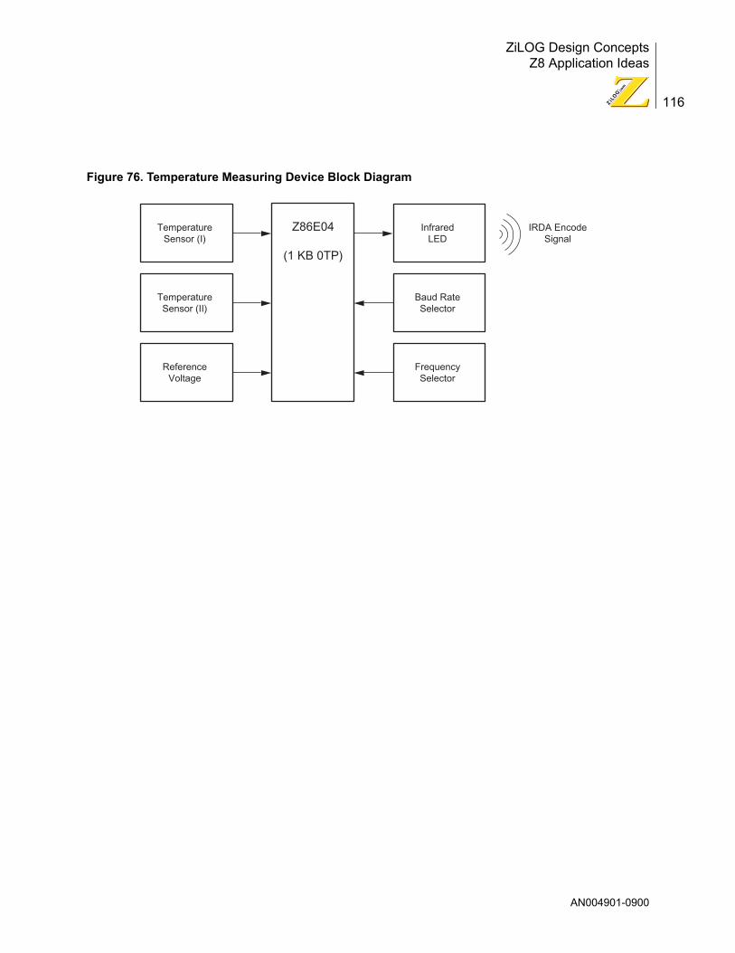
ZiLOG Design ConceptsZ8 Application Ideas
116
Figure 76. Temperature Measuring Device Block Diagram
TemperatureSensor (I)
InfraredLED
IRDA EncodeSignal
TemperatureSensor (II)
Baud RateSelector
ReferenceVoltage
FrequencySelector
Z86E04
(1 KB 0TP)
AN004901-0900

ZiLOG Design ConceptsZ8 Application Ideas
117
Figure 77. Temperature Measuring Device Schematic Diagram
VR
EF
P2.
5V
CC
3
2
1IC
3
D1
104
104
470µ
/10V
D2
P2.
6
P3.
1
P3.
2
P3.
3
XT
AL2
XT
AL1
GN
D
PA
2.7
PA
2.0
PA
2.1
PA
2.2
PA
2.3
Z86
E04
T
R4
S1
D3
D4
S2
S3
S4
9VB
AT
TE
RY
R1
C2
C1
27P
x212M
R2
IC2
IC1
AD
590
x2
R3
78L0
5
S1
S2
BA
UD
RA
TE
OF
F
ON
OF
F
ON
OF
F
OF
F
ON
ON
600
1200
2400
4800
S3
S4
FR
EQ
UE
NC
Y
OF
F
ON
OF
F
ON
OF
F
OF
F
ON
ON
2 S
EC
ON
D
1 S
EC
ON
D
1/2
SE
CO
ND
1/4
SE
CO
ND
AN004901-0900

ZiLOG Design ConceptsZ8 Application Ideas
118
Transmission TrainerSubmitted by: Robert Ashby
Abstract
The Transmission Trainer enables CDL (Commercial DriverÕs License) students to learn to shift the gears of large trucks in a classroom setting prior to actual high-way experience driving a truck, where inexperience may potentially be hazardous on public roads.
The Transmission Trainer consists of mock-up clutch, brake, and accelerator ped-als. Mounted to the clutch is a momentary switch that closes when the clutch is activated. The brake and accelerator pedals include mounted potentiometers that reflect the position of the pedal.
A transmission tower set next to the driver includes momentary switches that close as the user attempts to shift into any one of the six positions of the transmis-sion. The tower also includes solenoids that, when activated, prevent the gear shift from going into position. A small motor with an offset weight attached to the gear shift provides the realistic vibration when shifting gears.
A set of displays provides feedback of RPM, speed, incline of the road, and weight of the vehicle. The instructor can use a set of provided buttons to adjust the weight or incline while the driver experiences different situations and different responses of the vehicle to different situations.
Reading of the accelerator and brake is accomplished using the time to charge a capacitor method of A/D conversion. A small speaker or piezoelectric buzzer pro-vides the changing engine noise (using TOUT mode).
The ZiLOG chip can easily figure the mathematics to provide the driver with a realistic situation in shifting that can take years to perfect in the real world of the highway. Factors that are taken into account are incline, weight of vehicle, road speed, and position of the accelerator pedal. The gears must be closely matched in order to complete the shift.
The feedback of motor sound, RPM and speed gauges, and the vibration on the gear shift allows students to learn shifting techniques in a variety of situations without spending large amounts of time and money with an actual vehicle. It is ideal to be able to demonstrate this method in a classroom situation, which could save the driver and teaching institution thousands of dollars in time and money and prevent repairs on vehicles.
AN004901-0900

ZiLOG Design ConceptsZ8 Application Ideas
119
Figure 78. Transmission Trainer Block Diagram
RP
MCO
NS
OLE
AS
SE
MB
LY
Clu
tch C
lutc
hS
witc
h
MP
H
INC
LIN
E
WE
IGH
T
Slid
eP
oten
tiom
eter
Slid
eP
oten
tiom
eter
Sol
enoi
ds(e
xten
ded)
Sen
sing
switc
hed
Ped
alA
ssem
bly
Tra
nsm
issi
onT
ower
Con
sole
Ass
embl
yC
hair
Hi-L
oS
witc
hIn
clin
e�U
pIn
clin
e�D
own
Wei
ght
Up
Wei
ght�
Dow
n
Bra
keA
ccel
erat
or
AN004901-0900
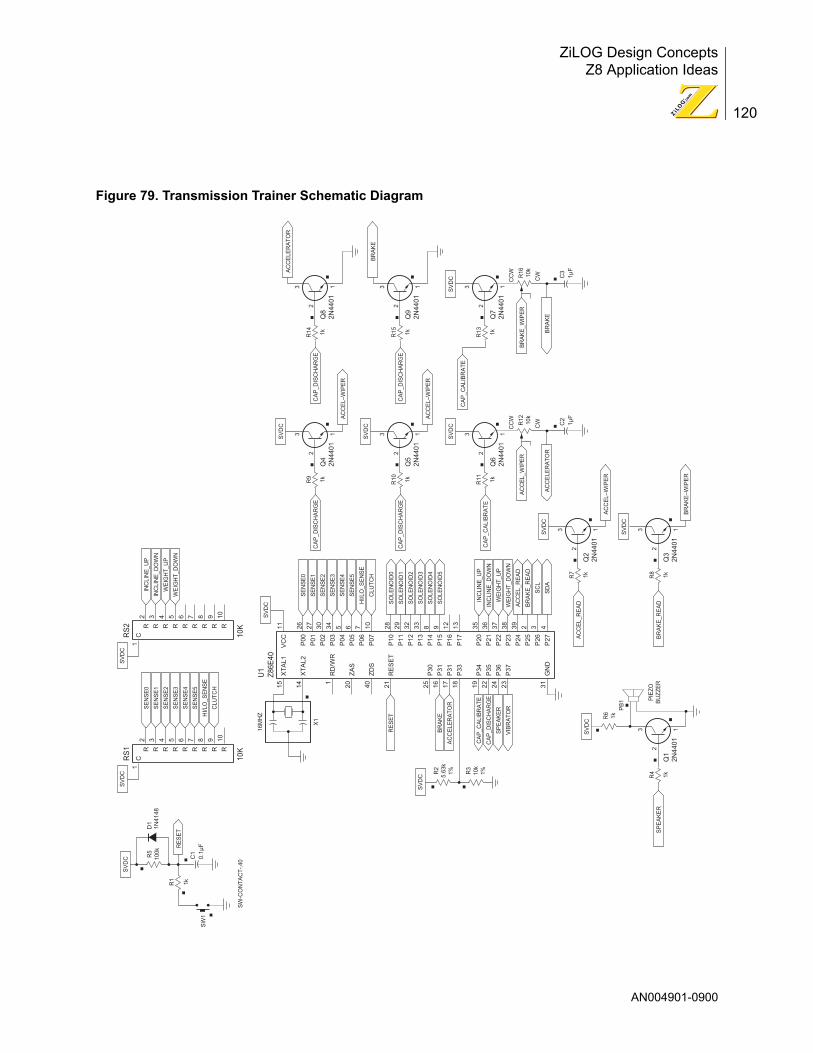
ZiLOG Design ConceptsZ8 Application Ideas
120
Figure 79. Transmission Trainer Schematic Diagram
R14
13
2C
AP
_DIS
CH
AR
GE
1k
C2
1µF
XT
AL1
XT
AL2
RD
/WR
ZA
S
ZD
S
RE
SE
T
P30
P31
P31
P33
P34
P35
P36
P37
GN
D
11 26 27 30 34 5 6 7 10 28 29 32 33 8 9 12 13 35 36 37 38 39 2 3 4
VC
C
P00
P01
P02
P03
P04
P05
P06
P07
P10
P11
P12
P13
P14
P15
P16
P17
P20
P21
P22
P23
P24
P25
P26
P27
15 14 1 20 40 21 25 16 17 18 19 22 24 23 31
U1
Z86
E40
RS
1
10K
R12
10k
R3
10k
1%R2
5.63
k1%
D1
1N41
48
Q8
2N44
01
R9
SV
DC
13
2C
AP
_DIS
CH
AR
GE
1k
AC
CE
LÐW
IPE
R
SV
DC
SV
DC
SV
DC
Q4
2N44
01
R7
SV
DC
13
2
16M
HZ
X1
AC
CE
L_R
EA
D1k
AC
CE
LÐW
IPE
R
Q2
2N44
01
R8
SV
DC
13
2B
RA
KE
_RE
AD
1k
BR
AK
EÐW
IPE
R
Q3
2N44
01
R4
SV
DC
PIE
ZO
BU
ZZ
ER
13
PB
1
2S
PE
AK
ER
1kQ
12N
4401
R5
100k
R1
SW
1
SW
-CO
NT
AC
T-.
40
1k
SV
DC
R15
13
2C
AP
_DIS
CH
AR
GE
1k
AC
CE
LER
AT
OR
BR
AK
E
Q9
2N44
01
R10
SV
DC
13
2C
AP
_DIS
CH
AR
GE
1k
AC
CE
LÐW
IPE
R
Q5
2N44
01
R13
SV
DC
13
2
CA
P_C
ALI
BR
AT
E
1kQ
72N
4401
R11
SV
DC
13
2
CC
W
CW
CA
P_C
ALI
BR
AT
E1k
AC
CE
L_W
IPE
R
AC
CE
LER
AT
OR
Q6
2N44
01
C1
0.1µ
F
C3
1µF
R16
10k
R6
1k
CC
W
CW
BR
AK
E_W
IPE
R
BR
AK
E
SE
NS
E0
SE
NS
E1
SE
NS
E2
SE
NS
E3
SE
NS
E4
2 3 4 5 6 7 8 9 10
R R R R R R R R R
SE
NS
E0
SE
NS
E1
SE
NS
E2
SE
NS
E3
SE
NS
E4
SE
NS
E5
HI/L
O_S
EN
SE
CLU
TC
H
SE
NS
E5
SO
LEN
OID
0
RE
SE
T
SO
LEN
OID
1
SO
LEN
OID
2
RE
SE
T
BR
AK
E
AC
CE
LER
AT
OR
SO
LEN
OID
3
SO
LEN
OID
4
SO
LEN
OID
5
HI/L
O_S
EN
SE
CLU
TC
H
INC
LIN
E_U
P
INC
LIN
E_D
OW
N
AC
CE
L_R
EA
D
BR
AK
E_R
EA
D
SC
L
SD
A
WE
IGH
T_U
P
WE
IGH
T_D
OW
N
CA
P_C
ALI
BR
AT
E
CA
P_D
ISC
HA
RG
E
SP
EA
KE
R
VIB
RA
TO
R
C1
RS
2
10K
SV
DC
2 3 4 5 6 7 8 9 10
R R R R R R R R R
INC
LIN
E_U
P
INC
LIN
E_D
OW
N
WE
IGH
T_U
P
WE
IGH
T_D
OW
N
C1
AN004901-0900

ZiLOG Design ConceptsZ8 Application Ideas
121
UFO Flight Regulation SystemSubmitted by: Martin Gundel
Abstract
The heart of the UFO Flight Regulation System is a ZiLOG Z86E08 microcontrol-ler. Because the receiver of this radio-control system is sensitive to electromag-netic interference, the Z8 operates in low-EMI mode with a clock frequency of 4MHz.
The versatile interrupt capability of the Z8 makes it possible to measure the pulse width of the sensor and generate 4 PWM output signals to drive the motors.
For sensing the inclination of an aircraft, a two-axis acceleration-sensor, the Ana-log Devices ADXL202, is employed. The output is a PWM signal with a pulse width between 2.5 to 7.5ms and a frequency of about 100Hz; making it possible for the UFO to accelerate at a rate of ±2g. If the sensor is at plane level, the out-put pulse is about 5ms long. An acceleration of 1g is equal to a pulse variation of 1.25ms. This variation corresponds to an inclination of 90 degrees. To measure an inclination of one degree, there must be a resolution of 13 microseconds or better. Timer 0 is clocked by 1 MHz, to achieve a better resolution.
Two radio control channels move the UFO in the X and Y directions. Another channel determines the average speed of the motors for take-off and landing. The signals of the RC unit are also pulses, with a pulse width between 1 and 2 milli-seconds. The necessary resolution to obtain a good regulation is 6 bits.
The four motors are driven by four PWM output stages. The Z8 microcontroller software calculates the necessary impulse width for the motors to keep the UFO on a plane level.
Depending on the RC signals, the motor speed is changed slightly to move the aircraft. The output PWM signals are generated under the control of Timer 1.
A soft start for the motors is absolutely necessary. The PWM signal of the motors attains the same frequency, but are slightly shifted, to prevent high current peaks.
AN004901-0900

ZiLOG Design ConceptsZ8 Application Ideas
122
Figure 80. UFO Flight Regulation System Block Diagram
2-AxisAcceleration Sensor
Radio Control Receiver
Glue - Logic Lo Batt
Z86E08Microcontroller
PushButton
LEDBuzzer
P2.4
P3.3
P3.2
X
XY LOBATSEL_XY CH
AN
1
CH
AN
2
CH
AN
3
IRQ
2
Y CH1 CH2 CH3
P2.7 P0.0 P0.1 P0.2 P3.1 P2.5
P2.6 P2.0 P2.1 P2.2 P2.3
Motor-DriverStages
AN004901-0900

ZiLOG Design ConceptsZ8 Application Ideas
123
Figure 81. UFO Flight Regulation System Schematic Diagram
XT
AL1
XT
AL2
P20
P21
P22
P23
P24
P25
P26
P27
P31
P32
P33
P00
P01
P02
MO
T 1
MO
T 2
MO
T 3
MO
T 4
BU
ZZ
ER
LOB
AT
LED
SE
L X
Y
IRQ
2
XY
B I
N
CH
AN
1
CH
AN
2
CH
AN
3
7
CR
14M
Hz
C7
22pF
C6
22pF
6
15 16 17 18 1 2 3 4 8 9 10 11 12 13
IC1A
4030
D1
CH
AN
1
IRQ
2
CH
AN
2
31 2
R1
JP1
RC
-Cha
nnel
DIR
X
RC
-Cha
nnel
DIR
Y
RC
-Cha
nnel
SP
EE
D
12 131N
4148
Z86
C08
C1
1nF
XO
UT
YO
UT
Y_F
ILT
X_F
ILT T2
VD
DV
DD
ST
VT
PN
CN
CN
CC
OM
CO
M
14 13 3 2 1 6 8 7 4
10 9 11 12 5
AD
XL2
02
IC5
LM78
L05
IC4
IC1A
4030
11
VC
C
VC
C
VC
C
VC
C
47K
21
JP4
UB
AT
UB
AT
GN
D21 JP
5M
OT
OR
1
21
IC1C
4030
IC2A
4011
D3
108 9
R3
JP3
1N41
48C
11n
F
BZ
1
BU
ZZ
ER
LED
1
RE
D
47K
R8
470R
21
IC1B
4030
D2
45 6
R2
JP2
1N41
48C
11n
F
C4
47nF C5
47nF
47K
R4
47K
R6
1K
R5
1M2
21
CH
AN
3
SE
L X
Y
MO
T 1
XY
B I
N
B I
N
LOB
AT
LED
IC2B
4011
10
1311
12
SW
1
SW
Pus
hbut
ton
64
5
32
VO
GN
D
D4
Q2
IRF
540
1
23
BY
TO
8
31
2
VI
1
98
IC2D
4011
IC2C
4011
VC
C
C8
100n
FC
922
µF
/10V
R7
10K
C9
22µ
F/1
0V
C11
100n
FC
1022
0µF
/16V
JP6
MO
TO
R2
21M
OT
2
D5
Q3
IRF
540
1
23
BY
TO
8
JP7
MO
TO
R3
21M
OT
3
D6
Q4
IRF
540
1
23
BY
TO
8
JP8
MO
TO
R4
21M
OT
4
D7
Q5
IRF
540
1
23
BY
TO
8Q
1B
C23
8
AN004901-0900

ZiLOG Design ConceptsZ8 Application Ideas
124
Vehicle Anti-Theft ModuleSubmitted by: James Doscher and Harvey Weinberg
Abstract
Traditional car alarms protect a vehicle from theft when a door is opened, a win-dow is broken, or the ignition is disabled. These alarms cannot protect from being towed by a tow or flatbed truck, or the wheels from being stolen. These chal-lenges can be solved by adding a tilt-sensing module to the alarm system. The tilt sensor must be able to resolve very small changes in the inclination of the car.
It is possible to free the wheels of a sports car by lifting one end of the car as little as 1.5 degrees. The module must be intelligent enough to reject minor long-term changes in tilt due to settling suspension, melting snow, and (relatively) large short-term movement due to wind or passing trucks.
The Z86C06 provides the system intelligence, while the tilt sensor is the ADXL202 dual-axis accelerometer from Analog Devices. Conventional liquid tilt sensors are inconvenient to use because of their fragility. In addition, the high resolution required in this application would necessitate a high-accuracy A/D converter (12-bit or better) if using a liquid tilt sensor. The ADXL202 outputs a 14-bit accurate PWM signal that is proportional to the inclination. The PWM signal is read by the Z86C06 by using both timers simultaneously. One timer is used with the 6-bit prescaler, while the other timer counts at full speed. The concatenation of the two timers results in a 14-bit timer range.
A software temperature-compensation method must be considered, because the tilt sensor grows in temperature sensitivity such that changes in temperature may appear to be changes in inclination. An intelligent algorithm can sample one set of tilt samples measured every half-second, and compare the result to the previous set of samples. If the rate of change of tilt (da/dt) does not fall within a specified window (for example, 0.0125 to 0.3 degrees per second), no alarm signal is issued. Because the temperature does not change significantly in 0.5 seconds, temperature drift is ignored. The windowing function also rejects false alarms due to minor long-term and large short-term tilt changes.
Low power consumption (1mA average current) is required, because the alarm runs while the car is off. Because sampling only occurs twice per second, the Z86C06 is in STOP mode most of the time to conserve power. To reduce the power consumption even further, the Z86C06 cycles power to the ADXL202, turn-ing it off between sample periods.
Communication to the main alarm module occurs via the Z86C06 SPI interface.
AN004901-0900
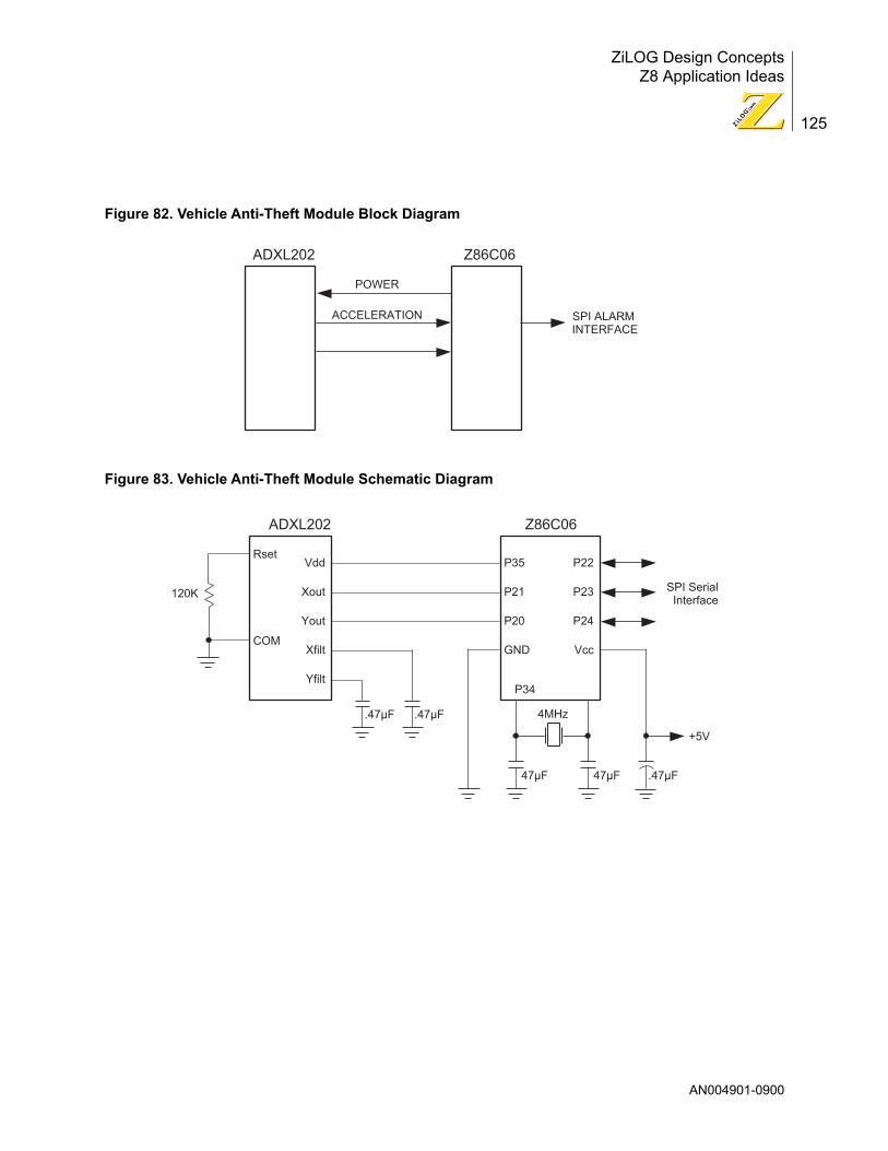
ZiLOG Design ConceptsZ8 Application Ideas
125
Figure 82. Vehicle Anti-Theft Module Block Diagram
Figure 83. Vehicle Anti-Theft Module Schematic Diagram
POWER
ACCELERATION SPI ALARM �INTERFACE
ADXL202 Z86C06
Vdd
Xout
Yout
Xfilt
Yfilt
120K
Rset
COM
ADXL202
P22
P23
P24
Vcc
P35
P21
P20
GND
P34
Z86C06
.47µF .47µF
47µF
4MHz
47µF
+5V
SPI SerialInterface
.47µF
AN004901-0900

ZiLOG Design ConceptsZ8 Application Ideas
126
Windmill CommanderSubmitted by: Nathan Novosel
Abstract
Using the Z8 OTP microcontroller to serve as a windmill commander to heat water to a comfortable temperature can extend the swimming season of many home pools. The Z8 microcontroller harnesses the maximum wind energy by controlling the windmill blade pitch and the alternator output current. The resistive load for heating can receive a wide range of electric current without constraint on fre-quency, voltage, or current levels. As a result, the load is the ideal type for a vari-able-speed alternator, driven by the wind.
The Z8 microcontroller, the heart of the windmill commander, responds to control inputs, monitors system status, and controls the output power by both alternator control and windmill blade pitch control. Additionally, a battery charger function is included in the Z8 program to maintain battery power for periods of decreased wind activity.
The Z8 microcontroller determines the speed of the alternator, and the output power by measuring the voltage across the load resistors. Using the flash A/D converter in the Z86E83, the instantaneous voltage drops across the load resis-tors can be measured. The output power can be determined by averaging over several AC cycles. The temperature is measured by utilizing two analog channels that receive a differential voltage from a thermistor in the pool water. The flash converter allows accurate differential measurements, because the high speed of the flash converter can minimize sampling time between channels.
The required output temperature is set by push-button control, with one button serving to increment and the other to decrement the target temperature. A two-digit LED display shows the temperature setting for five seconds following push-button entry, and then returns to power-off state.
The Z8 microcontroller is programmed to determine the state of the system, based on the alternator speed and output power. Using coefficients for the partic-ular windmill hardware that are programmed into the OTP memory, the windmill commander can determine how to adapt to the particular conditions at any given moment.
The commander controls the state of the system by varying the field current to the alternator by using pulse-width modulation (PWM) and a power MOS transistor. The field current directly controls the output current of the alternator that causes the mechanical load to the windmill to change proportionally. The windmill com-mander can adjust the blade pitch to adapt to both the load and the wind condi-tions as determined by the propeller speed (derived from the alternator frequency). The position of the blade pitch is determined by a potentiometer
AN004901-0900

ZiLOG Design ConceptsZ8 Application Ideas
127
located in the drive actuator configured as a resistor divider to provide an analog voltage that corresponds to the pitch position.
The power supply utilizes a 12-volt battery, and a battery charger function is built into the Z8 program to maintain battery voltage. The battery voltage is divided and measured by another channel of the Z8 A/D converter, and the microcontroller triggers an SCR to supply current to the battery via a ballast resistor.
Figure 84. Windmill Commander Block Diagram
Pitch ControlActuator Propeller
Alternator
PWMField Control
3-PhaseRectifier
ActuatorPosition Sensor
BidirectionalPower Bridge
BatteryCharger
Battery
Temperature SetpointInput
VoltageRegulator
TemperatureSensor
PowerResistors
Temperature SetpointDisplay
Z86E83
PWM
PWM
battery voltage
POOL
position measure
voltage & frequency measure
temperature measure
AN004901-0900

ZiLOG Design ConceptsZ8 Application Ideas
128
Figure 85. Windmill Commander Schematic Diagram
AC
0
AV
CC
AG
ND
P06
P05
P04
P03
P02
P01
P00
P35
P36
P34
P33
VC
C
VC
C
1K1µ
FA
C1
AC
2
AC
3
AC
4
AC
5
AC
6
AC
7
RE
SE
T
XT
AL1
XT
AL2
GN
D
VC
C
P31
P32
a b c d e f g
A B C D LT BL
LE
Q2
Q1
2.7K
2.7K
a b c d e f g com
Z86
C83
PO
OL
7805
2.7K
25K
The
rmis
tor
Sha
ft po
sitio
n se
nsor
DC
pitc
h co
ntro
l �ac
tuat
orA
ltern
ator
Pro
pelle
r
Hea
ting
elem
ents
2.7K
910
9.1K
D3
D2
VC
C
2.7K
2.7K
D1
Z1
2.7K
M1
X3
20
SC
R1 + Ð
2.7K
1K1µ
F
9.1K
910
1µF
1µF
1µF
22pF
4.33
MH
z
Tem
pera
ture
disp
lay
Tem
pera
ture
adju
st
22pF
1µF
1µF
VC
C
VC
C
a b c d e f g com
X1
M3
X2
M2
M4
AN004901-0900

ZiLOG Design ConceptsZ8 Application Ideas
129
Wireless AccelerometerSubmitted by: Mark Nelson
Abstract
One of the frustrations of playing video games is the tangle of wires connected from the computer to the controller. Another frustration is the wire length that limits the distance and freedom of playing the games. A solution to this problem is to use a ZiLOG Z8 microcontroller, Analog Devices accelerometer, and the Abacom transmitter-receiver pair for wireless operation.
The accelerometer is the Analog Devices micromachined ADXL202, which is an A2G device used for measuring tilt in two axes, making it ideal for joystick applica-tions. The output is pulse-width modulated and easily read by the microcontroller.
The heart of this system is the ZiLOG Z86C06 microcontroller, which samples the accelerometer digital outputs and the states of six push-buttons. It stores the instantaneous values into a register where it is converted into serial format to be output to the transmitter section. The high clock frequency of the microcontroller enables the sampling to be fast enough to recreate the original PWM information from the accelerometer and push-buttons. Serial transmission at 9600 baud ensures that the operator does not notice any delay in the video.
The Abacom XRT418 transmitter offers a maximum data rate of 10Kbps and operates at 418MHz. The serial data from the microcontroller is applied to the dig-ital input and is transmitted to a matching receiver at the PC. Its range is 100 meters, suitable for use with very large monitors.
The Abacom RCVR 418 receiver offers analog and digital outputs. Test results indicate that reconstruction of the input signal is very good. The design uses another Z8 microcontroller to translate the incoming serial stream into a digital output byte. The accelerometer bits are converted to current sources to drive the game port inputs.
This design highlights the many functions and processing capabilities of the Z8 microcontroller. The Z8 collects PWM information, converts it to a standard serial stream, and recreates the original data states at a remote location. With further programming at the receiver, the Z8 can adapt to other game protocols.
AN004901-0900

ZiLOG Design ConceptsZ8 Application Ideas
130
Figure 86. Wireless Accelerometer Block Diagram
8-bit digital outputLynx
ReceiverZ8
CPU
6-bit input
ADXL202Accelerometer
LynxTransmitter
Z8CPU
x
y
AN004901-0900

ZiLOG Design ConceptsZ8 Application Ideas
131
Figure 87. Wireless Accelerometer Schematic Diagram
x
y
PWM Outputs
XL202
P36
5
5
3
1 4
13Serial Out
VCC
P2.0
P2.1
P2.2
P2.3
P2.4
P2.5
P2.6
P2.7
15
16
17
18
24
25
26
27
10
9
12
11
Z86C06
TXM418
2
0.47µF125K 0.47µF
7
7
6
Digital
Inputs
Data
Out
5
13 14
VCC
X2 X1
P2.0
P2.1
P2.2
P2.3
P2.4
P2.5
P2.6
P2.7
15
16
17
18
24
25
26
27
Z86C06
7
X2
P36
X1
1
5
2 4
VCC
RX418
5
13
VCC
7
AN004901-0900

ZiLOG Design ConceptsZ8 Application Ideas
132
Index
Numerics64-byte arrays . . . . . . . . . . . . . . . . . . . . . . .57
AA/D conversion . . . . . . . . . . . .24, 75, 83, 118A/D converter 15, 24, 72, 100, 109, 124, 126,
127Abacom . . . . . . . . . . . . . . . . . . . . . . . . . . .129absolute encoders, vertical and horizontal 109absolute temperature . . . . . . . . . . . . . . . .115AC coupling . . . . . . . . . . . . . . . . . . . . . . . . .75AC line frequency . . . . . . . . . . . . . . . . . . . .24AC power source . . . . . . . . . . . . . . . . . . .112accelerometer . . . . . . . . . . . . . . .91, 124, 129
dual-axis . . . . . . . . . . . . . . . . .43, 91, 124three-axis . . . . . . . . . . . . . . . . . . . . . . .53
accelerometer-based stride sensor . . . . . . .72access key code . . . . . . . . . . . . . . . . . . . . .27actuator . . . . . . . . . . . . . . . . . . . . . . . . .9, 127ADC channel . . . . . . . . . . . . . . . . . . . . . . .106ADC, single-slope . . . . . . . . . . . . . . . . .40, 97address scheme, latched . . . . . . . . . . . . .107air conditioner, electronic . . . . . . . . . . . . . .83air temperature . . . . . . . . . . . . . . . . . . . . . .38Air-Core meter . . . . . . . . . . . . . . . . . . . . . . .4aircraft inclination . . . . . . . . . . . . . . . . . . .121alarm mode . . . . . . . . . . . . . . . . . . . . . . . . .89alarm system . . . . . . . . . . . . . . . . . . . . . . .124algorithmically-generated patterns . . . . . . .57algorithms, iterative . . . . . . . . . . . . . . . . . . .72algorithms, recognition . . . . . . . . . . . . . . . .91alternator output current . . . . . . . . . . . . . .126ambient light . . . . . . . . . . . . . . . . . . . . . . . .12ambient temperature range . . . . . . . . . . . . .51ambient water temperature . . . . . . . . . . . . .15amplitude, shock . . . . . . . . . . . . . . . . . . . . .75analog circuitry . . . . . . . . . . . . . . . . . . .66, 72analog comparator .1, 24, 31, 38, 60, 83, 115analog control voltage . . . . . . . . . . . . . . . . .24
Analog Devices . . . . . . . . . 91, 121, 124, 129analog inputs . . . . . . . . . . . . . . . . . . . . . . . 20analog processing . . . . . . . . . . . . . . . . . . . 24analog voltage . . . . . . . . . . . . . . . . . . . . . . 24analog-to-digital converters . . . . . . . . . . . . 72anti-short cycle . . . . . . . . . . . . . . . . . . . . . 20area code . . . . . . . . . . . . . . . . . . . . . . . . . 66ASC . . . . . . . . . . . . . . . . . . . . . . . . . . . . . . 20asynchronous bus . . . . . . . . . . . . . . . . . . . 27attack-sustain-decay envelope . . . . . . . . . 69audio amplifier . . . . . . . . . . . . . . . . . .106-107authentication . . . . . . . . . . . . . . . . . . . 48, 91auto mode . . . . . . . . . . . . . . . . . . . . . . . . . 97automatic window controller . . . . . . . . . . . 97automobile driver . . . . . . . . . . . . . . . . . . . . 80automobile engine . . . . . . . . . . . . . . . . . . . . 4Automotive Rear Sonar . . . . . . . . . . . . . . . . 1Automotive Speedometer, Odometer,
and Tachometer . . . . . . . . . . . . . . . . . . 4Autonomous Micro-Blimp Controller . . . . . . 6autonomous mobile nodes . . . . . . . . . . . . . 6autonomous robot . . . . . . . . . . . . . . . . . . . 12axle assembly . . . . . . . . . . . . . . . . . . . . . . . 4
Bballast resistor . . . . . . . . . . . . . . . . . . . . . 127barometric pressure . . . . . . . . . . . . . . . . . 38batch process . . . . . . . . . . . . . . . . . . . . . . 27battery rail . . . . . . . . . . . . . . . . . . . . . . . . . . 9battery voltage . . . . . . . . . . 9, 30, 72, 75, 127Battery-Operated Door-Entry System . . . . . 9bidirectional data serial circuit . . . . . . . . . . 52black box, transmitter . . . . . . . . . . . . . . . 106boiler temperature sensor . . . . . . . . . . . . . 95brake demand . . . . . . . . . . . . . . . . . . . . . . 78BTS . . . . . . . . . . . . . . . . . . . . . . . . . . . . . . 95bump switches . . . . . . . . . . . . . . . . . . . . . . 12bumper-switch matrix . . . . . . . . . . . . . . . . . . 6bus interface . . . . . . . . . . . . . . . . . . . . . . . 52
AN004901-0900

ZiLOG Design ConceptsZ8 Application Ideas
133
CCadmium Sulfide . . . . . . . . . . . . . . . . . . . .100calibration . . . . . . . . . . . . . . . . . . . . . . . . . .40
scale . . . . . . . . . . . . . . . . . . . . . . . . . . .86car alarms . . . . . . . . . . . . . . . . . . . . . . . . .124car simulator . . . . . . . . . . . . . . . . . . . . . . . .80carrier frequency . . . . . . . . . . . . . . . . . . . . .33carrier signals . . . . . . . . . . . . . . . . . . . . . . . .6carrier, phase-locked . . . . . . . . . . . . . . . . .69cathode . . . . . . . . . . . . . . . . . . . . . . . . . . . .18CDL . . . . . . . . . . . . . . . . . . . . . . . . . . . . . .118CdS . . . . . . . . . . . . . . . . . . . . . . . . . . . . . .100ceramic magnet . . . . . . . . . . . . . . . . . . . . .75charge time . . . . . . . . . . . . . . . . . . . . . . . . .72CIO . . . . . . . . . . . . . . . . . . . . . . . . . . . . . . .33clock I/O . . . . . . . . . . . . . . . . . . . . . . . . . . .33CMOS . . . . . . . . . . . . . . . . . . . . . . . . . . . . . .6code flexibility . . . . . . . . . . . . . . . . . . . . . . .72coils . . . . . . . . . . . . . . . . . . . . . . . . . . . . . . . .4color intensity . . . . . . . . . . . . . . . . . . . . . . .57color plane . . . . . . . . . . . . . . . . . . . . . . . . .57command status code . . . . . . . . . . . . . . . . .48Commercial DriverÕs License . . . . . . . . . .118comparator circuit . . . . . . . . . . . . . . . . . . . .97comparator input . . . . . . . . . . . . . . . . . .20, 72composite digital audio signal . . . . . . . . . . .69Compressor Discharge Temperature . . . . .21compressor protector . . . . . . . . . . . . . . . . .20configuration switches . . . . . . . . . . . . . . . . . .6Conrad Electronics . . . . . . . . . . . . . . . . . . .18control voltage . . . . . . . . . . . . . . . . . . . .21, 24
acquisition . . . . . . . . . . . . . . . . . . . . . . .24controlled access . . . . . . . . . . . . . . . . . . . .91controller port pin . . . . . . . . . . . . . . . . . . . .80Convergent Inc . . . . . . . . . . . . . . . . . . . . . .89core temperature . . . . . . . . . . . . . . . . . . . . .53counter/timer . . . . . . . . . . . . . . . . . . .1, 24, 33Crab, The . . . . . . . . . . . . . . . . . . . . . . . . . .12crystal oscillator . . . . . . . . . . . . . . . . . .69, 72current sense resistor . . . . . . . . . . . . . . . . .97
DD/A converter . . . . . . . . . . . . . . . . . . . . . . .69
Dallas Semiconductor . . . . . . . . . . . . . . 9, 89data . . . . . . . . . . . . . . . . . . . . . . . . . . . . . . 69
arrays . . . . . . . . . . . . . . . . . . . . . . . . . . 69buffer . . . . . . . . . . . . . . . . . . . . . . . . . . 78display . . . . . . . . . . . . . . . . . . . . . . . . . 80logging . . . . . . . . . . . . . . . . . . . . . . . . . 20security . . . . . . . . . . . . . . . . . . . . . . . . 91transmission . . . . . . . . . . . . . . . . . . . . 80
day-mode time track . . . . . . . . . . . . . . . . . 83DC motors . . . . . . . . . . . . . . . . . . . . . 12, 109DC offset adjustment . . . . . . . . . . . . . . . . . 75DCF77 Clock . . . . . . . . . . . . . . . . . . . . . . . 18DCF77 receiver . . . . . . . . . . . . . . . . . . . . . 18DCF77 Time Radio Signal . . . . . . . . . . . . . 18decelerations . . . . . . . . . . . . . . . . . . . . . . . 51delay circuit . . . . . . . . . . . . . . . . . . . . . . . . 63demodulation . . . . . . . . . . . . . . . . . . . . . . . . 6demultiplexer . . . . . . . . . . . . . . . . . . . . . . . 18Desktop Fountain . . . . . . . . . . . . . . . . . . . 15Diagnostic Compressor Protector . . . . . . . 20dial-up . . . . . . . . . . . . . . . . . . . . . . . . . . . . 48digital circuits . . . . . . . . . . . . . . . . . . . . . . . 78Digital Dimmer Box . . . . . . . . . . . . . . . . . . 24digital input . . . . . . . . . . . . . . . . . . . . . . . 129
lines . . . . . . . . . . . . . . . . . . . . . . . . . . 106digital notation . . . . . . . . . . . . . . . . . . . . . . 69digital signature analysis . . . . . . . . . . . . . . 91display control . . . . . . . . . . . . . . . . . . . . . . 72display refresh pulses . . . . . . . . . . . . . . . . 83DOF-drive . . . . . . . . . . . . . . . . . . . . . . . . . . 6Door Access Controller . . . . . . . . . . . . . . . 27Doppler effect . . . . . . . . . . . . . . . . . . . . . . 45downcounter . . . . . . . . . . . . . . . . . . . . . . . 97DPRAM . . . . . . . . . . . . . . . . . . . . . . . . . . . 78dual-axis accelerometer . . . . . . . . . . . 43, 91duty cycle . . . . . . . . . . . . . . . . . . . 33, 51, 57
index modulation . . . . . . . . . . . . . . . . . 78
Eearly-warning device . . . . . . . . . . . . . . . . . 20EEPROM . . . . . . . . . . . . . . . 9, 27, 40, 89, 95
serial . . . . . . . . . . . . . . . . . . . . . . . . . . 75electric current . . . . . . . . . . . . . . . . . . . . . 126
AN004901-0900

ZiLOG Design ConceptsZ8 Application Ideas
134
electrical brown-outs . . . . . . . . . . . . . . . . . .20electrical noise immunity . . . . . . . . . . . . . . .78electrolyte capacitor . . . . . . . . . . . . . . . . . .80Electrolytic Capacitor ESR Meter . . . . . . . .30electromagnetic interference . . . . . . . . . . .121electronic air conditioner . . . . . . . . . . . . . . .83electronic art . . . . . . . . . . . . . . . . . . . . . . . .57Electronic Door Control . . . . . . . . . . . . . . . .33electronic fencing . . . . . . . . . . . . . . . . . . . .89emitter . . . . . . . . . . . . . . . . . . . . . . . . . . . . .70encryption . . . . . . . . . . . . . . . . . . . . . . . . . .91energy densities . . . . . . . . . . . . . . . . . . . . .51engine noise . . . . . . . . . . . . . . . . . . . . . . .118enunciator panel . . . . . . . . . . . . . . . . . . . . .57Equivalent Series Resistance . . . . . . . . . . .30Equivalent-Time Sampling . . . . . . . . . . . . .63equivalent-time waveform . . . . . . . . . . . . . .63ESR . . . . . . . . . . . . . . . . . . . . . . . . . . . .30–32execution time . . . . . . . . . . . . . . . . . . . . . . . .1external . . . . . . . . . . . . . . . . . . . . . . . . . . . .69
interface . . . . . . . . . . . . . . . . . . . . . . . .20external memory . . . . . . . . . . . . . . . . . . . . .78
interface . . . . . . . . . . . . . . . . . . . . . . . .69extreme thermal conditions . . . . . . . . . . . . .51
Ffault conditions . . . . . . . . . . . . . . . . . . . . . .20Fault tolerance . . . . . . . . . . . . . . . . . . . . . .86feedback . . . . . . . . . . . .2, 9, 60, 86, 109, 118
loops . . . . . . . . . . . . . . . . . . . . . . . . . . .75fingerprints . . . . . . . . . . . . . . . . . . . . . . . . .91Firearm Locking System . . . . . . . . . . . . . . .35firmware . . . . . . . . . . . .15, 30Ð31, 60, 66, 75Flash memory . . . . . . . . . . . . . . . . . . . . . .106
chip . . . . . . . . . . . . . . . . . . . . . . . . . . . .69floor sensors . . . . . . . . . . . . . . . . . . . . . . . .12FLS . . . . . . . . . . . . . . . . . . . . . . . . . . . . . . .35fluid level . . . . . . . . . . . . . . . . . . . . . . . . . . .63fluid-level sensing . . . . . . . . . . . . . . . . . . . .63fluid measuring probe . . . . . . . . . . . . . . . . .63FM broadcast band modulator . . . . . . . . . .69Forecaster Intelligent Water Delivery Valve 38Fort Worth, Texas . . . . . . . . . . . . . . . . . . .112
freely-rotating axle . . . . . . . . . . . . . . . . . . . . 4frequency generator . . . . . . . . . . . . . . . . . 60fuel tanks . . . . . . . . . . . . . . . . . . . . . . . . . . 63fuel-level applications . . . . . . . . . . . . . . . . 63fuzzy logic . . . . . . . . . . . . . . . . . . . . . . . . . 97
Ggain . . . . . . . . . . . . . . . . . . . . . . . . . . . . . 100galvanic . . . . . . . . . . . . . . . . . . . . . . . . . . . 78
isolation . . . . . . . . . . . . . . . . . . . . . . . . 78gear shift . . . . . . . . . . . . . . . . . . . . . . . . . 118Germany . . . . . . . . . . . . . . . . . . . . . . . . . . 18glue logic . . . . . . . . . . . . . . . . . . . . . . 72, 109
HH field . . . . . . . . . . . . . . . . . . . . . . . . . . . . . 4hand-held remote . . . . . . . . . . . . . . . . . . . 86handset . . . . . . . . . . . . . . . . . . . . . . . . 66, 93handshaking . . . . . . . . . . . . . . . . . . . . . . 112H-bridge . . . . . . . . . . . . . . . . . 1, 12, 100, 109heel angle . . . . . . . . . . . . . . . . . . . . . . . . . 43helium envelopes . . . . . . . . . . . . . . . . . . . . 6high energy densities . . . . . . . . . . . . . . . . 51high-power mode . . . . . . . . . . . . . . . . . . . . 60homing behavior . . . . . . . . . . . . . . . . . . . . . 6HVAC . . . . . . . . . . . . . . . . . . . . . . . . . . . . 20
II/O . . . . . . . . . . . . . . . . . . . . 1, 27, 43, 63, 93
expansion . . . . . . . . . . . . . . . . . . . . . . 80interface module, PWM . . . . . . . . . . . . 78lines . . . . . . . . . . . . . . . . . . . . . . . . . . . 69pins . . . . . . . . . . . . . . . . . . . . . . . . . . . 72signal management . . . . . . . . . . . . . . . 69
I2C . . . . . . . . . . . . . . . . . . . . . . . . . . . . . . . 27iButton technology . . . . . . . . . . . . . . . . . . . . 9iChip . . . . . . . . . . . . . . . . . . . . . . . . . . . . . 48
Internet functionality . . . . . . . . . . . . . . 48ICMP protocol . . . . . . . . . . . . . . . . . . . . . . 48image buffer . . . . . . . . . . . . . . . . . . . . . . . 57immunity . . . . . . . . . . . . . . . . . . . . . . . . . . 78
AN004901-0900

ZiLOG Design ConceptsZ8 Application Ideas
135
impact velocities . . . . . . . . . . . . . . . . . . . . .51Improved Linear Single-Slope ADC . . . . . .40incandescent lamp . . . . . . . . . . . . . . . . . . .24inclination, aircraft . . . . . . . . . . . . . . . . . . .121Inclinometer . . . . . . . . . . . . . . . . . . . . . . . .35Infrared Data Associated protocols . . . . . .115infrared diode pod . . . . . . . . . . . . . . . . . . . .70infrared receiver . . . . . . . . . . . . . . . . . . . . .86Infrared reflection sensors . . . . . . . . . . . . .12infrared sensor . . . . . . . . . . . . . . . . . . . . . .45input protection . . . . . . . . . . . . . . . . . . . . . .80input voltage . . . . . . . . . . . . . . . . . . . . . . . .97input-output differential . . . . . . . . . . . . . . . .72instrument tuner . . . . . . . . . . . . . . . . . . . . .69Integrated Sailboat Electronic System . . . .43Intelligent Guide for the Blind . . . . . . . . . . .45intelligent peripheral controller . . . . . . . . . .33Internet Email Reporting Engine . . . . . . . . .48Internet functionality, iChip . . . . . . . . . . . . .48Internet Service Provider . . . . . . . . . . . . . .48Introduction . . . . . . . . . . . . . . . . . . . . . . . . . ixinverting peak detector . . . . . . . . . . . . . . . .75IP protocol . . . . . . . . . . . . . . . . . . . . . . . . . .48IPC . . . . . . . . . . . . . . . . . . . . . . . . . . . . . . .33IR . . . . . . . . . . . . . . . . . . . . . . . . . . . . . . . . .6
bandpass amplifiers . . . . . . . . . . . . . . . .6receiver chip . . . . . . . . . . . . . . . . . . . . .12
IrDA encoder . . . . . . . . . . . . . . . . . . . . . . .115IrDA interface . . . . . . . . . . . . . . . . . . . . . .115IRLEDs . . . . . . . . . . . . . . . . . . . . . . . . . . . .12ISES . . . . . . . . . . . . . . . . . . . . . . . . . . . . . .43ISP . . . . . . . . . . . . . . . . . . . . . . . . . . . . . . .48iterative algorithms . . . . . . . . . . . . . . . . . . .72
Jjoystick applications . . . . . . . . . . . . . . . . .129
Llamp controller . . . . . . . . . . . . . . . . . . . . .112lamp sockets . . . . . . . . . . . . . . . . . . . . . . .112large color displays . . . . . . . . . . . . . . . . . . .57latched address scheme . . . . . . . . . . . . . .107
Lawrence Livermore Laboratories . . . . . . . 63lead resistance zeroing . . . . . . . . . . . . . . . 30Learn mode . . . . . . . . . . . . . . . . . . . . . . . . . 9LED . . . . . 2, 9, 12, 18, 31, 57, 60, 75, 76, 80,
95, 97, 126LED, infrared . . . . . . . . . . . . . . . . . . . . . . 115light intensity . . . . . . . . . . . . . . . . . . . . . . 109line activity . . . . . . . . . . . . . . . . . . . . . . . . . 66linear integrator . . . . . . . . . . . . . . . . . . . . . 40linear perception . . . . . . . . . . . . . . . . . . . . 24linear potentiometer . . . . . . . . . . . . . . . . . 106linear voltage regulator . . . . . . . . . . . . 72, 80lithium chemistry . . . . . . . . . . . . . . . . . . . . 51lithium-sulfur dioxide batteries . . . . . . . . . . 51load-dump protection . . . . . . . . . . . . . . . . . 64look-up table . . . . . . . . . . . . . . . . . . . . 24, 63low-EMI mode . . . . . . . . . . . . . . . . . . 75, 121low-pass filter . . . . . . . . . . . . . . . . . . . . . . 60LTB . . . . . . . . . . . . . . . . . . . . . . . . . . . . . . 51lunar nights . . . . . . . . . . . . . . . . . . . . . . . . 51lunar surface . . . . . . . . . . . . . . . . . . . . . . . 51Lunar Telemetry Beacon . . . . . . . . . . . . . . 51
MMagic Dice . . . . . . . . . . . . . . . . . . . . . . . . . 54magnet, moving . . . . . . . . . . . . . . . . . . . . . . 4magnetic card reader . . . . . . . . . . . . . . . . 27magnetic compass sensor . . . . . . . . . . . . . 72magnetic field strength vector . . . . . . . . . . . 4magnetic field variation . . . . . . . . . . . . . . . 75magnetic field, time-varying . . . . . . . . . . . . 75manual mode . . . . . . . . . . . . . . . . . . . . . . . 97master computer . . . . . . . . . . . . . . . . . . . 112mechanical key . . . . . . . . . . . . . . . . . . . . . . 9Message Cueing mode . . . . . . . . . . . . . . . 45message passing . . . . . . . . . . . . . . . . . . . . 6metronome . . . . . . . . . . . . . . . . . . . . . . . . 69microphone feedback . . . . . . . . . . . . . . . . 60Micropower Impulse Radar . . . . . . . . . . . . 63MIDI . . . . . . . . . . . . . . . . . . . . . . . . . . . . . . 69minimum-protection device . . . . . . . . . . . . 20MIR . . . . . . . . . . . . . . . . . . . . . . . . . . . . . . 63mixer/demodulator channels . . . . . . . . . . . . 6
AN004901-0900

ZiLOG Design ConceptsZ8 Application Ideas
136
modem module . . . . . . . . . . . . . . . . . . . . . .48Modular Light Display Panel . . . . . . . . . . . .57modulator tuning accuracy . . . . . . . . . . . . .69moisture sensor . . . . . . . . . . . . . . . . . . . . .38MOSFETs . . . . . . . . . . . . . . . . . . . . . . . . .100motion circuitry . . . . . . . . . . . . . . . . . . . . . .86motor stall . . . . . . . . . . . . . . . . . . . . . . . . . .97mounting tilt . . . . . . . . . . . . . . . . . . . . . . . . .72multiplexing . . . . . . . . . . . . . . . . . . . . . .18, 80
Nnasal decongestant . . . . . . . . . . . . . . . . . . .60Nasal Oscillatory Transducer . . . . . . . . . . .60natural rainfall . . . . . . . . . . . . . . . . . . . . . . .38New Sensor Technologies . . . . . . . . . . . . .63noise clamping . . . . . . . . . . . . . . . . . . . . . .80nonlinear response . . . . . . . . . . . . . . . . . . .24nonlinear volume response . . . . . . . . . . . . .63
OObstacle detection . . . . . . . . . . . . . . . . . . .12octal D-latch . . . . . . . . . . . . . . . . . . . . . . . .33odometer . . . . . . . . . . . . . . . . . . . . . . . . . . . .4OEMs . . . . . . . . . . . . . . . . . . . . . . . . . . . . .20off-hook condition . . . . . . . . . . . . . . . . . . . .66offset weight . . . . . . . . . . . . . . . . . . . . . . .118on-chip RAM . . . . . . . . . . . . . . . . . . . . . . . .57on-hook condition . . . . . . . . . . . . . . . . . . . .66open-drain mode . . . . . . . . . . . . . . . . . . . . . .6operational amplifier, rail-rail . . . . . . . . . . . .40operational amplifiers . . . . . . . . . . . .6, 40, 75operational modes . . . . . . . . . . . . . . . . . . . .6optical filters . . . . . . . . . . . . . . . . . . . . . . .109oscillator frequency . . . . . . . . . . . . . . . . . . .63OTP Selection Guide . . . . . . . . . . . . . . . . . . .xoutput driver . . . . . . . . . . . . . . . . . . . . . . . .60output pulse . . . . . . . . . . . . . . . . . . . . . . .121overvoltage protection . . . . . . . . . . . . . . . . .80
PPAP protocol . . . . . . . . . . . . . . . . . . . . . . . .48
password . . . . . . . . . . . . . . . . . . . . 48, 66, 91pavement-surface deformations . . . . . . . . 45peak detector . . . . . . . . . . . . . . . . . . . . . . . 60
inverting . . . . . . . . . . . . . . . . . . . . . . . . 75voltage . . . . . . . . . . . . . . . . . . . . . . . . . 75
pen device . . . . . . . . . . . . . . . . . . . . . . . . . 91pen movement . . . . . . . . . . . . . . . . . . . . . . 91pen pressure . . . . . . . . . . . . . . . . . . . . . . . 91pen tablets . . . . . . . . . . . . . . . . . . . . . . . . . 91personal computer . . . . . . . . . . . . . . . . . . . 76phase-locked carrier . . . . . . . . . . . . . . . . . 69phase-triggering . . . . . . . . . . . . . . . . . . . . 24Phone Dialer . . . . . . . . . . . . . . . . . . . . . . . 66photointerrupter . . . . . . . . . . . . . . . . . . . . . 12photosensors . . . . . . . . . . . . . . . . . . . . . . 109phototransistor . . . . . . . . . . . . . . . . . . . . . . 12photovoltaic system . . . . . . . . . . . . . . . . . 100piezoelectric buzzer . . . . . . . . . . . . 2, 54, 118piezoelectric speaker . . . . . . . . . . . . . . . . . 60ping-pulse wave . . . . . . . . . . . . . . . . . . . . 45pin-out compatibility . . . . . . . . . . . . . . . . . . 20pitch range . . . . . . . . . . . . . . . . . . . . . . . . . 69Pocket Music Synthesizer . . . . . . . . . . . . . 69polarity . . . . . . . . . . . . . . . . . . . . . . . . . . . . 66Popular Science . . . . . . . . . . . . . . . . . . . . 63port pin . . . . . . . . . . . . . . . . . . . . . . . . . . . 80Portable Individual Navigator . . . . . . . . . . 72positioning motors . . . . . . . . . . . . . . . . . . 100Postal Shock Recorder . . . . . . . . . . . . . . . 75potential divider . . . . . . . . . . . . . . . . . . . . . . 9potentiometer, linear . . . . . . . . . . . . . . . . 106power . . . . . . . . . . . . . . . . . . . . . . . . . . . . 106
consumption . . . . . . . . . . . . . 52, 75, 124management . . . . . . . . . . . . . . . . . . . . 91supply . . . . . . . . . . . 60, 72, 80, 106, 127transistors . . . . . . . . . . . . . . . . . . . . . . 86
power-sink driving . . . . . . . . . . . . . . . . . . . 80PPP protocol . . . . . . . . . . . . . . . . . . . . . . . 48preprogrammed decisions . . . . . . . . . . . . . 51prescaler . . . . . . . . . . . . . . . . . . . . 1, 24, 124Pressure Switch . . . . . . . . . . . . . . . . . . . . 21PRF . . . . . . . . . . . . . . . . . . . . . . . . . . . . . . 63program memory . . . . . . . . . . . . . . . . . 27, 31program mode . . . . . . . . . . . . . . . . . . . . . . 66
AN004901-0900

ZiLOG Design ConceptsZ8 Application Ideas
137
programmable timer . . . . . . . . . . . . . . . . . .20propagation . . . . . . . . . . . . . . . . . . . . . . .1, 43propeller . . . . . . . . . . . . . . . . . . . . . . . . . . . .6
speed . . . . . . . . . . . . . . . . . . . . . . . . .126propulsion motor . . . . . . . . . . . . . . . . . . . . .45prototype software . . . . . . . . . . . . . . . . . . .72Prototype systems . . . . . . . . . . . . . . . . . . .91pseudodigital appearance . . . . . . . . . . . . . .78pull-up resistor . . . . . . . . . . . . . . . . . . . . . .80pulse count, remote-control . . . . . . . . . . . .83Pulse Rate Frequency . . . . . . . . . . . . . . . .63pulse variation . . . . . . . . . . . . . . . . . . . . . .121pulsed water fountain . . . . . . . . . . . . . . . . .15pulse-width modulation . . . . . . . . . . . .57, 126PWM . . . . . . . . . . . . . . . . . . .12, 60, 126, 129
drive signal . . . . . . . . . . . . . . . . . . . . . . .4generator . . . . . . . . . . . . . . . . . . . . . . . .33input channel . . . . . . . . . . . . . . . . . . . . .78input signal . . . . . . . . . . . . . . . . . . . . . .78Input/Output Interface Module . . . . . . .78output . . . . . . . . . . . . . . . . . . . . .107, 109output signal . . . . . . . . . . . . . . . . . . . . .78output signals . . . . . . . . . . . . . . . . . . .121Ramp ADC . . . . . . . . . . . . . . . . . . . . . .40reference . . . . . . . . . . . . . . . . . . . . . . . .83signal . . . . . . . . . . . . . . . .64, 78, 109, 124
PWM-generated reference . . . . . . . . . . . . .61pyrotechnic charge . . . . . . . . . . . . . . . . . . .53
Qquartz crystal . . . . . . . . . . . . . . . . . . . . . . . .80
RR-2R network . . . . . . . . . . . . . . . . . . . . . . .24Radar on a Chip . . . . . . . . . . . . . . . . . . . . .63radio transmitter . . . . . . . . . . . . . . . . . . . . .51railroad vehicles . . . . . . . . . . . . . . . . . . . . .78rain, intensity of . . . . . . . . . . . . . . . . . . . . . .97ramp-capacitor discharge transistor . . . . . .30random numbers . . . . . . . . . . . . . . . . . . . . .54RC circuit . . . . . . . . . . . . . . . . . . . . . . . . . .72RC filter . . . . . . . . . . . . . . . . . . . . . . . . . . .107
RC time constant . . . . . . . . . . . . . . . . . . . . 60Reaction Tester . . . . . . . . . . . . . . . . . . . . . 80reaction time . . . . . . . . . . . . . . . . . . . . . . . 80receiver detector . . . . . . . . . . . . . . . . . . . . . 1Recognition algorithms . . . . . . . . . . . . . . . 91reference voltage . . . . . . . . . . 24, 45, 75, 115refresh pulses, display . . . . . . . . . . . . . . . . 83relative timing . . . . . . . . . . . . . . . . . . . . . . 38relays . . . . . . . . . . . . . . . . . . . . . . . . . . . . 100remote console . . . . . . . . . . . . . . . . . . . . . 24remote range . . . . . . . . . . . . . . . . . . . . . . . 83Remote-Control Antenna Positioner . . . . . 86remote-control pulse count . . . . . . . . . . . . 83Remote-Controlled Air Conditioner . . . . . . 83reset circuit . . . . . . . . . . . . . . . . . . . . . 60, 66reset pulse . . . . . . . . . . . . . . . . . . . . . . . . . 63resistive load . . . . . . . . . . . . . . . . . . . . . . 126resistor-summing junction . . . . . . . . . . . . . . 6resonance frequencies, sinus . . . . . . . . . . 60return code . . . . . . . . . . . . . . . . . . . . . . . . 48RF Dog Collar . . . . . . . . . . . . . . . . . . . . . . 89Rocker Switch . . . . . . . . . . . . . . . . . . . . . . 35rolling dice . . . . . . . . . . . . . . . . . . . . . . . . . 54rotational movement . . . . . . . . . . . . . . . . 109rotational speed . . . . . . . . . . . . . . . . . . . . . . 4routing numbers . . . . . . . . . . . . . . . . . . . . 66RPM . . . . . . . . . . . . . . . . . . . . . . . . . . . . 118RS-232 interface . . . . . . . . . . . . . . . . . . . . 27RS-485 interface . . . . . . . . . . . . . . . . . . . . 27run cycle . . . . . . . . . . . . . . . . . . . . . . . . . . 20
Ssample rate adjustment . . . . . . . . . . . . . . . 69scale transposer . . . . . . . . . . . . . . . . . . . . 69SCR . . . . . . . . . . . . . . . . . . . . . . . . . . . . . 127SCTS . . . . . . . . . . . . . . . . . . . . . . . . . . . . . 95secure web transactions . . . . . . . . . . . . . . 91security bit . . . . . . . . . . . . . . . . . . . . . . . . . 60segmentation, program/data memory . . . . 69Seiko . . . . . . . . . . . . . . . . . . . . . . . . . . . . . 48seismological observations . . . . . . . . . . . . 52sender . . . . . . . . . . . . . . . . . . . . . . . . . . . . . 6sensing coil . . . . . . . . . . . . . . . . . . . . . . . . 75
AN004901-0900

ZiLOG Design ConceptsZ8 Application Ideas
138
sensing element . . . . . . . . . . . . . . . . . . . . .75sensitivity . . . . . . . . . . . . . . . . . . . . . . .1, 106
temperature . . . . . . . . . . . . . . . . . . . . .124sensor capacitance . . . . . . . . . . . . . . . . . . .38serial cable . . . . . . . . . . . . . . . . . . . . . . . . .75serial communication . . . . . . . . . . . . . . . . .57serial data . . . . . . . . . . . . . . . . . . . . . . . . .129serial interface . . . . . . . . . . . . . . . .48, 80, 109serial port . . . . . . . . . . . . . .20, 48, 70, 75, 76serial-to-parallel shift register . . . . . . . . . . .31shift register . . . . . . . . . . . . . . . . . . . . .31, 80shock amplitude . . . . . . . . . . . . . . . . . . . . .75shock threshold . . . . . . . . . . . . . . . . . . . . . .76shut-down operation . . . . . . . . . . . . . . . . . .66signal strength . . . . . . . . . . . . . . . . . . . . . . .45signature analysis . . . . . . . . . . . . . . . . . . . .91Signature Recognition and Authentication .91single . . . . . . . . . . . . . . . . . . . . . . . . . . . . . .97single-slope ADC . . . . . . . . . . . . . . . . .40, 97single-supply operation . . . . . . . . . . . . . . . .75sinus congestion . . . . . . . . . . . . . . . . . . . . .60sleep mode . . . . . . . . . . . . . . . . . . . . . . . . .83sleep-mode current drain . . . . . . . . . . . . . .66sliding windows . . . . . . . . . . . . . . . . . . . . . .97small-echo signals . . . . . . . . . . . . . . . . . . . .1Smart Phone Accessory . . . . . . . . . . . . . . .93Smart Solar Water Heating System . . . . . .95Smart Window with Fuzzy Control . . . . . . .97soil moisture . . . . . . . . . . . . . . . . . . . . . . . .38solar cell panel . . . . . . . . . . . . . . . . . . . . .109solar radiation . . . . . . . . . . . . . . . . . . . . . .100Solar Tracker . . . . . . . . . . . . . . . . . . . . . .100solenoid . . . . . . . . . . . . . . . . . . . . . .9, 35, 118sonar . . . . . . . . . . . . . . . . . . . . . . . . . . . . .1–2sound effects . . . . . . . . . . . . . . . . . . . . . . . .54spacecraft . . . . . . . . . . . . . . . . . . . . . . . . . .52speedometer . . . . . . . . . . . . . . . . . . . . .4, 103stage illumination . . . . . . . . . . . . . . . . . . . .24Stages Baby Monitor . . . . . . . . . . . . . . . . .106stand-alone clock . . . . . . . . . . . . . . . . . . . .18standby mode . . . . . . . . . . . . . . . . . . . . . . .75stepper motor . . . . . . . . . . . . . . . . . . . .45, 83STOP mode . . . . . . . . . . . . . . . . . . . . .9, 124stride sensor, accelerometer-based . . . . . .72
strobing . . . . . . . . . . . . . . . . . . . . . . . . . . . 57subsumption architecture . . . . . . . . . . . . . 12successive approximation . . . . . . . . . . . . . 24sun collector temperature sensor . . . . . . . 95Sun Tracking to Optimize Solar
Power Generation . . . . . . . . . . . . . . . 109system check . . . . . . . . . . . . . . . . . . . . . . . 80system control block . . . . . . . . . . . . . . . 1, 24
Ttachometer . . . . . . . . . . . . . . . . . . . . . . . . . 4Tandy Corporate headquarters . . . . . . . . 112Tandy Light Control . . . . . . . . . . . . . . . . . 112tantalum capacitor . . . . . . . . . . . . . . . . . . . 75TCP protocol . . . . . . . . . . . . . . . . . . . . . . . 48telemetry system . . . . . . . . . . . . . . . . . . . . 51temperature control . . . . . . . . . . . . . . . . . . 83temperature drift . . . . . . . . . . . . . . . . 75, 124Temperature Measuring Device . . . . . . . 115temperature-compensation method . . . . 124test lead resistance . . . . . . . . . . . . . . . . . . 30test leads . . . . . . . . . . . . . . . . . . . . . . . . . . 30theater . . . . . . . . . . . . . . . . . . . . . . . . . . . . 24Thermal management . . . . . . . . . . . . . . . . 51thermistor . . . . . . . . . . . . . . . . . . . . . . . . 126Thionyl Chloride . . . . . . . . . . . . . . . . . . . . 51threshold detector . . . . . . . . . . . . . . . . . . . 97tilt . . . . . . . . . . . . . . . . . . . . . . . . . . . . . . . . 72tilt-sensing module . . . . . . . . . . . . . . . . . 124time functions . . . . . . . . . . . . . . . . . . . . . . 18time measurement . . . . . . . . . . . . . . . . . . . 80time stamp . . . . . . . . . . . . . . . . . . . . . . . . . 75time track, day-mode . . . . . . . . . . . . . . . . . 83timed actuation . . . . . . . . . . . . . . . . . . . . . 38timer control mode . . . . . . . . . . . . . . . . . . . 83timer values . . . . . . . . . . . . . . . . . . . . . . . . 97time-related thresholds . . . . . . . . . . . . . . . 20time-varying magnetic field . . . . . . . . . . . . 75TOUT mode . . . . . . . . . . . . . . . . . . . . 54, 118train lines . . . . . . . . . . . . . . . . . . . . . . . . . . 78transducer . . . . . . . . . . . . . . . . . . . . . . . . . . 1
infrared . . . . . . . . . . . . . . . . . . . . . . . . 45receiver . . . . . . . . . . . . . . . . . . . . . . . . . 1
AN004901-0900

ZiLOG Design ConceptsZ8 Application Ideas
139
receiving . . . . . . . . . . . . . . . . . . . . . . . .45transmitting . . . . . . . . . . . . . . . . . . . . . .45ultrasonic . . . . . . . . . . . . . . . . . . . . . . . .43
Transmission Trainer . . . . . . . . . . . . . . . .118transmitter . . . . . . . . .1, 6, 45, 52, 53, 89, 106
black box . . . . . . . . . . . . . . . . . . . . . . .106driver . . . . . . . . . . . . . . . . . . . . . . . . . . . .1driver circuit . . . . . . . . . . . . . . . . . . . . . . .1power . . . . . . . . . . . . . . . . . . . . . . . . . .52infrared . . . . . . . . . . . . . . . . . . . .6, 45, 86radio . . . . . . . . . . . . . . . . . . . . . . . .51, 89ultrasonic . . . . . . . . . . . . . . . . . . . . . . . . .1
transmitter-receiver pair . . . . . . . . . . . . . .129trigger . . . . . . . . . . . . . . . . . . . . . . . . . . . . .97
voltage . . . . . . . . . . . . . . . . . . . . . . . . .97triple-axis accelerometer . . . . . . . . . . . . . . .53TV remote- control . . . . . . . . . . . . . . . . . . .12
UUART . . . . . . . . . . . . . . . . . . . . . . . . . .48, 70UDP protocol . . . . . . . . . . . . . . . . . . . . . . . .48UFO Flight Regulation System . . . . . . . . .121ultrasonic signal . . . . . . . . . . . . . . . . . . . .103ultrasonic transceiver . . . . . . . . . . . . . . . . .45ultrasonic transducers . . . . . . . . . . . . . . .1, 43user input . . . . . . . . . . . . . . . . . . . . . . . . . .72
VVariable Output Voltage . . . . . . . . . . . . . . .60variable-speed alternator . . . . . . . . . . . . .126variable-strength signal . . . . . . . . . . . . . . . .45vectored motion patterns . . . . . . . . . . . . . .12Vehicle Anti-Theft Module . . . . . . . . . . . . .124velocity calculation . . . . . . . . . . . . . . . . . . .43Vibration Sensor . . . . . . . . . . . . . . . . . . . . .21virtual air temperature . . . . . . . . . . . . . . . . .43virtual Ground . . . . . . . . . . . . . . . . . . . . . . .75Visual Basic . . . . . . . . . . . . . . . . . . . . . . .112visual response compensation . . . . . . . . . .24voltage drop-out . . . . . . . . . . . . . . . . . . . . .60voltage regulator IC . . . . . . . . . . . . . . . . . . . .2voltage regulator, linear . . . . . . . . . . . .72, 80
voltage-to-frequency converter . . . . . . . . . 45VREF . . . . . . . . . . . . . . . . . . . . . . . . . . . . 115
Wwake-up switch . . . . . . . . . . . . . . . . . . . . . . 9watch-dog timer . . . . . . . . . . . . . . . . . . . . . 60water flow pump . . . . . . . . . . . . . . . . . . . . 95wave burst . . . . . . . . . . . . . . . . . . . . . . . . . . 1waveform, equivalent-time . . . . . . . . . . . . 63wavetables . . . . . . . . . . . . . . . . . . . . . . . . 69web transactions . . . . . . . . . . . . . . . . . . . . 91WFP . . . . . . . . . . . . . . . . . . . . . . . . . . . . . 95wind direction . . . . . . . . . . . . . . . . . . . . . . 43wind energy . . . . . . . . . . . . . . . . . . . . . . . 126wind speed . . . . . . . . . . . . . . . . . . . . . . . . 43wind, force of . . . . . . . . . . . . . . . . . . . . . . . 97windmill blade pitch . . . . . . . . . . . . . . . . . 126Windmill Commander . . . . . . . . . . . . . . . 126Wireless Accelerometer . . . . . . . . . . . . . 129wireless communication . . . . . . . . . . . . . . 12
ZZ02204 . . . . . . . . . . . . . . . . . . . . . . . . . . . 48Z84C15 . . . . . . . . . . . . . . . . . . . . . . . . . . . 33Z86C03 . . . . . . . . . . . . . . . . . . . . . . . . . . . 20Z86C04 . . . . . . . . . . . . . . . . . . . . . . . . . . . 20Z86C06 . . . . . . . . . . . . . . . 20, 103, 124, 129Z86C08 . . . . . . . . . . . . . . . . . . . . . . . . . . . 20Z86C96 . . . . . . . . . . . . . . . . . . . . . . . . 69, 70Z86E04 . . . . . . . . . . . . . . . 4, 30, 31, 75, 115Z86E08 . . . . . . . . 1, 18, 24, 66, 80, 112, 121Z86E21 . . . . . . . . . . . . . . . . . . . . . . . . . . . 57Z86E30 . . . . . . . . . . . . . . . . . . . . . . . . 27, 83Z86E31 . . . . . . . . . . . . . . . . . . . . . 12, 45, 86Z86E40 . . . . . . . . . . . . . . . . . . . . . . . . . . . 33Z86E83 . . . . . . . . . . . . . . . . 35, 72, 106, 126Z8E001 . . . . . . . . . . . . . . . . . . . . . . . . . . 109Z8PE001 . . . . . . . . . . . . . . . . . . . . . . . . . . 54Z8Plus . . . . . . . . . . . . . . . . . . . . . . . . . . . . . 9ZDS . . . . . . . . . . . . . . . . . . . . . . . . . . . . . . 12zero-crossing detection . . . . . . . . . . . . . . . 24ZiLOG CCP emulator . . . . . . . . . . . . . . . . 12
AN004901-0900

ZiLOG Design ConceptsZ8 Application Ideas
140
ZORB diode . . . . . . . . . . . . . . . . . . . . . . . .80
AN004901-0900