Zero field spin splitting in AlSb/InAs/AlSb quantum wells induced by surface proximity effects
14
1 Zero field spin splitting in AlSb/InAs/AlSb quantum wells induced by surface proximity effects Masaya Nishioka, Bruce A. Gurney and Ernesto E. Marinero San Jose Research Center, Hitachi Global Storage Technologies, San Jose, CA 95135, USA Francisco Mireles Centro de Nanociencias y Nanotecnología, UNAM, Apdo. Postal 2681, Ensenada, Baja California, México Abstract: InAs quantum well heterostructures are of considerable interest for mesoscopic device applications such as scanning probe and magnetic recording sensors, which require the channel to be close to the surface. Here we report on magnetotransport measurements of AlSb/InAs/AlSb Hall bars at a shallow depth of 20 nm. Analysis of the observed Shubnikov-de Haas oscillations and modeling show that spin splitting energies in excess of 2.3 meV occur at zero magnetic field. We conclude that the spin-splitting results from the Rashba effect due to the band bending in the quantum well. This is caused by substantial electron transfer from the surface to the quantum well and becomes significant when the quantum well is located near the surface. Keywords: InAs quantum wells, mesoscopic devices, electron transport, Hall effect, spin-orbit interactions.
Transcript of Zero field spin splitting in AlSb/InAs/AlSb quantum wells induced by surface proximity effects

1
Zero field spin splitting in AlSb/InAs/AlSb quantum wells induced by surface
proximity effects
Masaya Nishioka, Bruce A. Gurney and Ernesto E. Marinero San Jose Research Center, Hitachi Global Storage Technologies, San Jose, CA 95135,
USA
Francisco Mireles Centro de Nanociencias y Nanotecnología, UNAM, Apdo. Postal 2681, Ensenada, Baja
California, México Abstract:
InAs quantum well heterostructures are of considerable interest for mesoscopic device
applications such as scanning probe and magnetic recording sensors, which require the
channel to be close to the surface. Here we report on magnetotransport measurements of
AlSb/InAs/AlSb Hall bars at a shallow depth of 20 nm. Analysis of the observed
Shubnikov-de Haas oscillations and modeling show that spin splitting energies in excess
of 2.3 meV occur at zero magnetic field. We conclude that the spin-splitting results from
the Rashba effect due to the band bending in the quantum well. This is caused by
substantial electron transfer from the surface to the quantum well and becomes significant
when the quantum well is located near the surface.
Keywords: InAs quantum wells, mesoscopic devices, electron transport, Hall effect,
spin-orbit interactions.

2
Electron transport in AlSb/InAs/AlSb quantum well (QW) heterostructures is
attractive for device applications for multiple reasons including the pinning of the InAs
surface Fermi level above the conduction band minimum, the small electron effective
mass and the large conduction band offset.1-3 These characteristics make this system
useful for the fabrication of nano-scale devices for electronic and sensor device
applications including scanning probes and magnetic recording sensors, where proximity
of the two dimensional electron gas (2DEG) to the surface is crucial in determining the
spatial resolution. Therefore it is desirable to understand the effect of proximity on the
potential well and carrier populations. Additionally, semiconductors are now being
considered for spintronics applications, so that understanding the behavior of the two spin
subbands during current flow is essential.
A complete understanding of transport properties in these AlSb/InAs/AlSb QW
heterostructures in terms of spin splitting has not been fully investigated. In 2DEG
semiconductor heterostructures, the spin degeneracy can be lifted even in the absence of a
magnetic field due to the structure inversion asymmetry (SIA) of the confinement
potential through the Rashba effect,4 which can be tuned by applying a gate voltage.5,6
This non-degeneracy is known to induce a beating pattern in the Shubnikov-de Haas
(SdH) oscillations at low magnetic fields due to the superposition of oscillations of
different periods originating from the two spin subbands. Such beating patterns have
been observed in several 2DEG systems, for example, GaSb/InAs/GaSb.7,8 However, the
zero-field spin splitting and the observation of beating patterns in AlSb/InAs/AlSb
heterostructures differ in published results. In this work, we report on magnetoresistance
measurements of AlSb/InAs/AlSb heterostructures in which the InAs 2DEG is located

3
near the surface and show that the spin splitting energy is non-zero due to the Rashba
effect on account of proximity of the channel to the surface.
The InAs QW heterostructures were grown by molecular beam epitaxy on GaAs
substrates.9 The 2DEG consisted of AlSb (2 nm)/InAs (12.5 nm)/AlSb (2 nm) layers
grown on a thick buffer layer. The wafer was capped with dual layers of Al0.80Ga0.20Sb
(14 nm) and InAs (4 nm), which placed the top of the InAs QW channel from the surface
at d = 20 nm. To achieve low carrier concentrations, the structures were not intentionally
doped. Hall bars were fabricated using an electron beam lithography process combined
with ion beam etching. The length and width of the transport channel were 80 µm and 5
µm, respectively. Voltage leads on each side of the channel were 1 µm wide and spaced
from each other by 26 µm.
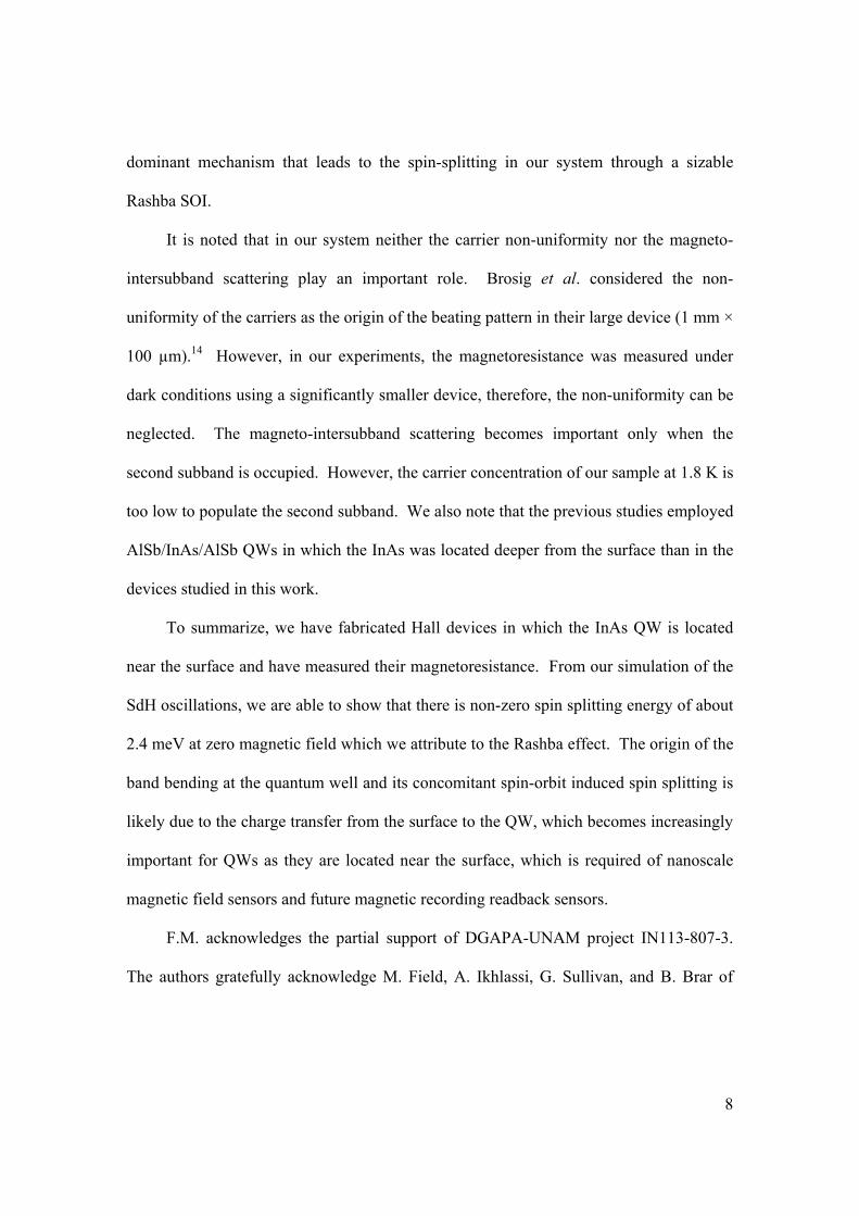
Figure 1(a) shows the sheet carrier density Ns and the mobility as a function of
temperature of the Hall devices. It is known that, even in non-intentionally doped InAs
QWs, Ns can be relatively large.1 This is because electrons are easily transferred from
donor sites into the exceptionally deep InAs QW. Such donors originate from (1) surface
states of the InAs cap layer, (2) the bulk of the AlSb barriers and (3) interface states
between AlSb and the InAs channel.1 Ns in our system was found to be 3.9×1011 cm-2 at
10 K. This is about 30 percent larger than what Nguyen et al found in AlSb/InAs/AlSb
QWs of comparable thickness where the charge transfer from the surface could be
neglected due to the spacing from the surface to the QW of d = 500 nm.10 We attribute
the increase of Ns in our samples to efficient charge transfer from surface states into the
QW on account of its proximity (d = 20 nm). The mobility increases with decreasing
temperature between 50 and 300 K due to the reduction of phonon scattering. Below 50

4
K, impurity and interface roughness scattering becomes dominant, therefore, the mobility
is almost independent of temperature.11
Figure 1(b) provides Hall and longitudinal resistance measurements at 1.8 K. The
Quantum Hall effect including Hall plateaus and SdH oscillations are readily observed
for applied magnetic fields exceeding 1 T. The Hall plateaus are observed at ρxy = h/ne2
for the filling factor n = 2, 3, 4, 6, 8 and 10. The existence of the n = 3 Hall plateau is
due to Zeeman spin splitting. We note that g-factor in InAs is relatively large,12 therefore,
the effect of the Zeeman spin splitting at high magnetic field is evident in the spectrum.
In the low magnetic field regime, we observe a beating node in the SdH oscillations
(Fig. 2(a)), although it is not as clear as reported in other systems such as, for example,
GaSb/InAs/GaSb QWs.7,8 As mentioned above, studies of zero field spin splitting in the
AlSb/InAs/AlSb system have generated conflicting results. Heida et al. observed beating
patterns and found a non-zero spin splitting energy, though the Rashba coupling
parameter αR did not depended on the gate voltage, which is not consistent with theory.13
On the other hand, Brosig et al. did not observe beating patterns in dark measurements.14
However, after illumination, some samples showed beating patterns which was attributed
to light-induced spatial inhomogeneity of the carriers. Sadofyev et al. also found the
beating pattern only during and after illumination, but they claimed that this was not due
to the spatial non-uniformity of the carriers.15 Rowe et al. found the beating patterns in
high carrier density samples (Ns > 2.4×1012 cm-2), but concluded that this was not due to
the zero field spin splitting but due to the magneto-intersubband scattering.16
To determine whether the observed beating node in our data originates from spin
splitting due to the Rashba effect, we fitted the longitudinal resistance via the

5
conductivity tensor. The latter was calculated using the model of the
magnetoconductance earlier employed to study transport in spin orbit interaction (SOI)
systems by Luo et. al.7 The spin-resolved magnetoconductivity tensor of the 2DEG at T
= 0 K is given by the following equation.17
( )∑⎥⎥⎦
⎤
⎢⎢⎣
⎡
Γ−
−⎟⎠⎞
⎜⎝⎛=
±±
n
nFxx B
EEne2
2
2
2
)(exp
21∓
πσ
, (1)
where ±nE are the spin dependent Landau level energies with Rashba SOI, EF is the Fermi
energy of the 2DEG and Г(B) is the Landau level broadening. Г(B) is assumed to be
spin-independent and equal to 010 BBΓ+Γ here, in which B0 = 1 T. Then, the total
magnetoresistivity is defined as
( )
2
⎟⎟⎠
⎞⎜⎜⎝
⎛⋅+≅ −+
Sxxxxxx eN
Bσσρ, (2)
in the limit of high quantizing fields ( ( ) ( )22 ±± >> xxxy σσ ).
The Landau level energies with Rashba SOI is given by18
±± ∆⎟
⎠⎞
⎜⎝⎛ ±+= soncn EnE ,2
121
21 ∓ω
, (3)
in which the spin-splitting ( ) ( ) FRcBcson EnBgE 212122, ±+∆+−=∆ ∗± ωµω . Here,
ωc is the cyclotron frequency, µB is the Bohr magneton, g* is the effective Landé factor of
the InAs quantum well. The magnetic field is applied along the growth direction.
FRR kα2=∆ is the Rashba spin-splitting energy (at zero magnetic field) and kF is the
Fermi wave number.

6
The input parameters for our simulation are the values of Ns, ∆R, G0, G1, g* and m*.
In Fig. 2(a) we show the simulation results of the SdH oscillations. The agreement with
the experimental result is reasonable. The peak locations and amplitudes of the SdH
oscillations are well reproduced by the simulation when the Rashba SOI term is included
in the model. The observed node at B = ~1 T is also reproduced by the simulation. The
best fit is achieved with Ns = 3.65×1011 cm-2, ∆R = 2.37 meV, m* = 0.038m0 (m0 = free
electron mass), G0 = 1.1 meV, G1 = 0.2 meV and g* = -16. The values of N+ and N- are
calculated to be 1.92×1011 cm-2 and 1.74×1011 cm-2, respectively, using the following
equation,
( )2
*
22
FR
S
N km N N
π∆∆ =
− ∆ (4)
in which DN = N+ – N- with Ns = N+ – N- and SNk π2F = .
The total carrier density Ns used in the simulation is consistent with that extracted
from the Hall measurement. The fitted value of ∆R = 2.37 meV is quite similar to that
obtained by Heida et al (~3 meV) for asymmetric QWs.13 The effective mass value is
within the known values of InAs QW effective mass, 0.0320m0 ~ 0.0412m0.19 The
effective Landé factor g* is comparable with g = -14 which has been calculated from
magnetoresistance in tilted magnetic field measurements.12 Therefore, we can state that
the obtained parameters from our simulation compare well with published results.
Moreover, the carrier densities of two channels derived from fast Fourier transform (FFT)
of our experimental SdH oscillations are 2.01×1011 cm-2 and 1.82×1011 cm-2, which yields,
using E↑ – E↓ = 2π∆Nћ2/m*, a spin-splitting of E↑ – E↓ = 2.46 meV that is very close to
what we obtained from the simulation (Fig. 2(b)). These results support the validity of

7
our model, and, therefore, we can conclude that there is spin imbalance due to the Rashba
SOI in our AlSb/InAs/AlSb heterostructures.
We propose that non-zero spin splitting at zero magnetic field due to the Rashba
effect is caused by an asymmetric electric potential in the QW. The asymmetric potential
is the result of the charge transfer from surface donors to the QW, which becomes
important when the 2DEG is located near the surface. The value of αR arising from such
an asymmetric potential can be estimated by the following equation.18,20
( ) ( )z
zEEzEEdzdz
mE
FF
pR Ψ⎟
⎟⎠
⎞⎜⎜⎝
⎛
−−
−Ψ=
ΓΓ )(1
)(1
6870
2
α (5)
Here, Ψ(z), Ep, EΓ7(z) and EΓ8(z) are the wave function, the interband matrix element
(Kane parameter) and the energies of the valance band edge for Γ7 and Γ8 bands,
respectively. z is the depth from the heterostructure surface. In order to estimate the
value of αR, we derived Ψ(z), EΓ7(z) and EΓ8(z) through a self-consistent (1D Schrödinger-
Poisson) calculation of the band structure of the AlSb/InAs/AlSb heterostructure.21 In
Fig. 2(c), we plot Ψ(z), EΓ7(z), EΓ8(z) and EΓ6(z) (the energy of the conduction band edge
for Γ6 band) as a function of z. We found that the calculated non-zero slopes of EΓ7(z),
EΓ8(z) and EΓ6(z) in the QW are mainly due to the charge transfer from the capping InAs
layer to the QW. Using these parameter values, the value of αR is estimated to be
5.37×10⁻¹² eV·m, which is close to the value we obtained from the simulation (7.82×10⁻¹²
eV·m).22 We note that the linear Dresselhaus contribution to the spin-splitting in InAs
leads to 1.76×10⁻¹² eV·m while the interface contribution is just 0.3×10⁻¹² eV·m.
Therefore, we conclude that the charge transfer from the surface to the QW is the
8
dominant mechanism that leads to the spin-splitting in our system through a sizable
Rashba SOI.
It is noted that in our system neither the carrier non-uniformity nor the magneto-
intersubband scattering play an important role. Brosig et al. considered the non-
uniformity of the carriers as the origin of the beating pattern in their large device (1 mm ×
100 µm).14 However, in our experiments, the magnetoresistance was measured under
dark conditions using a significantly smaller device, therefore, the non-uniformity can be
neglected. The magneto-intersubband scattering becomes important only when the
second subband is occupied. However, the carrier concentration of our sample at 1.8 K is
too low to populate the second subband. We also note that the previous studies employed
AlSb/InAs/AlSb QWs in which the InAs was located deeper from the surface than in the
devices studied in this work.
To summarize, we have fabricated Hall devices in which the InAs QW is located
near the surface and have measured their magnetoresistance. From our simulation of the
SdH oscillations, we are able to show that there is non-zero spin splitting energy of about
2.4 meV at zero magnetic field which we attribute to the Rashba effect. The origin of the
band bending at the quantum well and its concomitant spin-orbit induced spin splitting is
likely due to the charge transfer from the surface to the QW, which becomes increasingly
important for QWs as they are located near the surface, which is required of nanoscale
magnetic field sensors and future magnetic recording readback sensors.
F.M. acknowledges the partial support of DGAPA-UNAM project IN113-807-3.
The authors gratefully acknowledge M. Field, A. Ikhlassi, G. Sullivan, and B. Brar of

9
Teledyne Scientific, Inc., Thousand Oaks, CA, for the development and growth of the
heterostructures used in this study.

10
References:
1H. Kroemer, Physica E 20, 196 (2004).
2G. Tuttle and H. Kroemer, IEEE Trans. Electron Devices, ED-34, 2358 (1987).
3C. Kadow, H.-K. Lin, M. Dahlstroem, M. Rodwell, A.C. Gossard, B. Brar and G.
Sullivan, J. Cryst. Growth, 251, 543 (2003).
4Y. A. Bychkov and E. I. Rashba, J. Phys. C 17, 6039 (1984).
5J. Nitta, T. Akazaki, H. Takayanagi, and T. Enoki, Phys. Rev. Lett. 78, 1335 (1997).
6Th. Schäpers, G. Engels, J. Lamge, Th. Klocke, M. Hollfelder, and H. Lüth, J. Appl.
Phys. 83, 4324 (1998).
7J. Luo, H. Munekata, F. F. Fang, and P. J. Stiles, Phys. Rev. B 41, 7685 (1990).
8B. Das, D. C. Miller, S. Datta, R. Reifenberger, W. P. Hong, P. K. Bhattacharya, J.
Singh, and M. Jaffe, Phys. Rev. B 39, 1411 (1989).
9T. D. Boone, L. Folks, J. A. Katine, S. Maat, E. Marinero, S. Nicoletti, M. Field, G. J.
Sullivan, A. Ikhlassi, B. Brar, and B. A. Gurney, IEEE Trans. Magn. 42, 3270 (2006).
10C. Nguyen, B. Brar, H. Kroemer, and J. H. English, Appl. Phys. Lett. 60, 1854 (1992).
11C. R. Bolognesi, H. Kroemer, and J. H. English, J. Vac. Sci. Technol. B 10, 877 (1992).
12S. Brosig, K. Ensslin, A. G. Jansen, C. Nguyen, B. Brar, M. Thomas, and H. Kroemer,
Phys. Rev. B 61, 13045 (2000).
13J. P. Heida, B. J. van Wees, J. J. Kuipers, T. M. Klapwijk, and G. Borghs, Phys. Rev. B
57, 11911 (1998).
14S. Brosig, K. Ensslin, R. J. Warburton, C. Nguyen, B. Brar, M. Thomas, and H.
Kroemer, Phys. Rev. B 60, R13989 (1999).

11
15Yu. G. Sadofyev, A. Ramamoorthy, J. P. Bird, S. R. Johnson, and Y.-H. Zhang, J. Cryst.
Growth 278, 661 (2005).
16A. C. H. Rowe, J. Nehls, R. A. Stradling, and R. S. Ferguson, Phys. Rev. B 63,
201307(R) (2001).
17T. Englert, D. Tsui, A. Gossard and C. Uihlein, Surf. Sci. 113, 295 (1982).
18R. Winkler, Spin-Orbit Coupling Effects in Two-Dimensional Electron Hole Systems,
Springer Tracts in Modern Physics, Vol. 191 (Springer-Verlag, Berlin, 2003).
19M. J. Yang, P. J. Lin-Chung, R. J. Wagner, J. R. Waterman, W. J. Moore, and B. V.
Shanabrook, Semicond. Sci. Technol. 8, S129 (1993).
20J. Nitta, T. Bergsten, Y. Kunihashi, and M. Kohda, J. Appl. Phys. 105, 122402 (2009).
21G. L. Snider, I. -H. Tan, and E. L. Hu, J. Appl. Phys. 68, 2849 (1990).
22The small difference might come from the non-parabolic nature of the band structure
or/and the strain induced in the QW. Both effects are not included in Eq. (5).
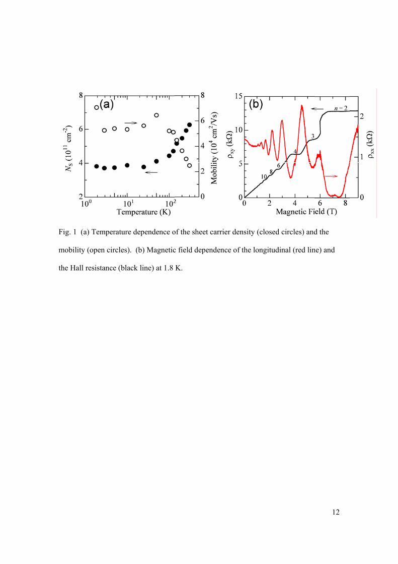
Fig.
mob
the
. 1 (a) Tem
bility (open
Hall resista
mperature de
circles). (b
ance (black l
ependence o
b) Magnetic
line) at 1.8
of the sheet
c field depen
K.
carrier dens
ndence of th
sity (closed
he longitudi
circles) and
inal (red lin
12
d the
ne) and

Fig.
show
resp
incr
bou
The
the
don
resp
. 2 (a) SdH
w the measu
pectively. T
rease of the
undary scatte
e arrows ind
heterostruct
nor concentr
pectively, an
H oscillation
ured data an
The location
measured m
ering. (b) F
dicate the lo
ture obtaine
rations of 3.
nd the accep
s at low ma
nd the simu
n of the beat
magnetoresi
FFT analysi
cation of tw
ed by self-c
.9×1019 and
ptor concen
agnetic field
ulation data
ting node at
istance at B
is of the Sd
wo channels
onsistent Sc
d 5×1014 cm
ntration of 3
d at 1.8 K. T
with and wi
t ~ 1T is ind
~ 0.5 T is l
dH oscillatio
s. (c) Band
chrödinger-
-3 in the InA
.5×1016 cm
The black, r
ithout the R
dicated by th
likely due to
ons between
structure an
-Poisson cal
As and AlGa
-3 in the AlS
red and blue
Rashba SOI,
he arrow. T
o diffusive
n 0.15 and 4
nd wavefun
lculations.
aSb layers,
Sb layers w
13
e lines
,
The
4 T-1.
nction in
The
ere

14
assumed. The band bending of the bandstructure at the QW is due to charge transfer
from the surface. The estimated carrier density at the QW region is 3.82×1011 cm-2 and
E1 – EF = -24.05 meV. Here, E1 is the first subband energy in QW. The solid horizontal
line in QW and the dashed line indicate the location of E1 and EF, respectively.