Within-die gate delay variability measurement using reconfigurable ring oscillator
12
256 IEEE TRANSACTIONS ON SEMICONDUCTOR MANUFACTURING, VOL. 22, NO. 2, MAY 2009 Within-Die Gate Delay Variability Measurement Using Reconfigurable Ring Oscillator Bishnu Prasad Das, Student Member, IEEE, Bharadwaj Amrutur, H. S. Jamadagni, Senior Member, IEEE, N. V. Arvind, and V. Visvanathan Abstract—We report the design and characterization of a circuit technique to measure the on-chip delay of an individual logic gate (both inverting and noninverting) in its unmodified form. The test circuit comprises of digitally reconfigurable ring oscillator (RO). The gate under test is embedded in each stage of the ring oscillator. A system of linear equations is then formed with different configu- ration settings of the RO, relating the individual gate delay to the measured period of the RO, whose solution gives the delay of the individual gates. Experimental results from a test chip in 65-nm process node show the feasibility of measuring the delay of an in- dividual inverter to within 1 ps accuracy. Delay measurements of different nominally identical inverters in close physical proximity show variations of up to 28% indicating the large impact of local variations. As a demonstration of this technique, we have studied delay variation with poly-pitch, length of diffusion (LOD) and dif- ferent orientations of layout in silicon. The proposed technique is quite suitable for early process characterization, monitoring ma- ture process in manufacturing and correlating model-to-hardware. Index Terms—Gate delay measurement, local variations, on-chip measurement, reconfigurable ring oscillator. I. INTRODUCTION W ITH the advancement in the deep submicron (DSM) CMOS technology beyond 65 nm, process-induced effects are leading to increasing variations in design parameters like delay and power [1]. Process parameter variations consist of both die-to-die and within-die variations. Die-to-die (or inter-die or global) variations affect all transistors within a die in the same way and have identical effect on each gate in the chip. Within-die (or intra-die or local) variations affect different gates within the same chip differently. These can have two components: a spatially correlated component and a random component. For spatially correlated variations, gates within a small region are more correlated compared to gate spread over larger region. Random local variations affect each gate independently. Their origin can be traced to gate length variation due to line edge roughness (LER) [2], oxide thickness Manuscript received September 09, 2008; revised January 15, 2009. Current version published May 06, 2009. B. P. Das and H. S. Jamadagni are with the Center for Electronics Design and Technology (CEDT), Indian Institute of Science (IISc), Bangalore 560 012, India (e-mail: [email protected]; [email protected]). B. Amrutur is with the Department of Electrical Communication Engi- neering, Indian Institute of Science (IISc), Bangalore 560 012, India (e-mail: [email protected]). N. V. Arvind and V. Visvanathan are with the Texas Instruments, Bangalore 560 093, India (e-mail: [email protected]; [email protected]). Color versions of one or more of the figures in this paper are available online at http://ieeexplore.ieee.org. Digital Object Identifier 10.1109/TSM.2009.2017662 variation (OTV) and threshold voltage variation due to random dopant fluctuations (RDF) [3]. Atomistic simulations in [3] show that these fluctuations become significant in technologies below 35 nm, with standard deviation of threshold voltage reaching 100 mV for a nominally sized transistor in a 9 nm process node. Hence, it has become important to develop metrology techniques that can measure not only global and spatially correlated variations, but also the impact of random local variations. Process metrology can measure the impact of these variations on either static or dynamic parameters. A static parameter like the DC drain current in a transistor across different voltage con- ditions gives information on the transistor’s threshold voltage and drive strength. Since this measures the characteristics of an individual transistor, this approach can give information about global, spatially correlated local and random local components of the process variations. However measurements need to be carried out on separately laid out individual transistors. Mea- surement of a dynamic parameter like delay gives additional in- formation about parasitics [4] and is usually easier to imple- ment than a static measurement. Dynamic measurements are typically carried out by measuring the period of ring oscilla- tors, which is determined by the sum of delays of all the stages in the ring. Such measurements give information on combined global as well as spatially correlated local variations. However, they do not give any information on random local variations of individual gate in a ring. In addition to process parameter fluc- tuations, layout induced fluctuations due to poly-pitch spacing, active overhang etc are becoming important in determining tran- sistor performance. This is because of the influence they have both on lithography as well as stress and hence the mobility of the carriers. Hence, there is a need for a measurement technique which can work at the level of an individual logic gate. Such a technique can then be used to characterize the impact of random local variations as well as that of the layout and neighborhood topology. If is the delay of a logic gate then: (1) where, is the nominal delay of the gate. is global delay variation, is spatially correlated local delay variation and is the random local delay variation [10]. The two compo- nents and are shared by many gates within a small region with spatial correlation and hence standard ring oscil- lator based measurement techniques suffice. The final compo- nent is unique to each gate and hence needs to be mea- sured at the level of a single gate. 0894-6507/$25.00 © 2009 IEEE Authorized licensed use limited to: INDIAN INSTITUTE OF SCIENCE. Downloaded on December 18, 2009 at 00:59 from IEEE Xplore. Restrictions apply.
-
Upload
independent -
Category
Documents
-
view
4 -
download
0
Transcript of Within-die gate delay variability measurement using reconfigurable ring oscillator
256 IEEE TRANSACTIONS ON SEMICONDUCTOR MANUFACTURING, VOL. 22, NO. 2, MAY 2009
Within-Die Gate Delay Variability MeasurementUsing Reconfigurable Ring Oscillator
Bishnu Prasad Das, Student Member, IEEE, Bharadwaj Amrutur, H. S. Jamadagni, Senior Member, IEEE,N. V. Arvind, and V. Visvanathan
Abstract—We report the design and characterization of a circuittechnique to measure the on-chip delay of an individual logic gate(both inverting and noninverting) in its unmodified form. The testcircuit comprises of digitally reconfigurable ring oscillator (RO).The gate under test is embedded in each stage of the ring oscillator.A system of linear equations is then formed with different configu-ration settings of the RO, relating the individual gate delay to themeasured period of the RO, whose solution gives the delay of theindividual gates. Experimental results from a test chip in 65-nmprocess node show the feasibility of measuring the delay of an in-dividual inverter to within 1 ps accuracy. Delay measurements ofdifferent nominally identical inverters in close physical proximityshow variations of up to 28% indicating the large impact of localvariations. As a demonstration of this technique, we have studieddelay variation with poly-pitch, length of diffusion (LOD) and dif-ferent orientations of layout in silicon. The proposed technique isquite suitable for early process characterization, monitoring ma-ture process in manufacturing and correlating model-to-hardware.
Index Terms—Gate delay measurement, local variations, on-chipmeasurement, reconfigurable ring oscillator.
I. INTRODUCTION
W ITH the advancement in the deep submicron (DSM)CMOS technology beyond 65 nm, process-induced
effects are leading to increasing variations in design parameterslike delay and power [1]. Process parameter variations consistof both die-to-die and within-die variations. Die-to-die (orinter-die or global) variations affect all transistors within adie in the same way and have identical effect on each gatein the chip. Within-die (or intra-die or local) variations affectdifferent gates within the same chip differently. These canhave two components: a spatially correlated component and arandom component. For spatially correlated variations, gateswithin a small region are more correlated compared to gatespread over larger region. Random local variations affect eachgate independently. Their origin can be traced to gate lengthvariation due to line edge roughness (LER) [2], oxide thickness
Manuscript received September 09, 2008; revised January 15, 2009. Currentversion published May 06, 2009.
B. P. Das and H. S. Jamadagni are with the Center for Electronics Designand Technology (CEDT), Indian Institute of Science (IISc), Bangalore 560 012,India (e-mail: [email protected]; [email protected]).
B. Amrutur is with the Department of Electrical Communication Engi-neering, Indian Institute of Science (IISc), Bangalore 560 012, India (e-mail:[email protected]).
N. V. Arvind and V. Visvanathan are with the Texas Instruments, Bangalore560 093, India (e-mail: [email protected]; [email protected]).
Color versions of one or more of the figures in this paper are available onlineat http://ieeexplore.ieee.org.
Digital Object Identifier 10.1109/TSM.2009.2017662
variation (OTV) and threshold voltage variation due to randomdopant fluctuations (RDF) [3]. Atomistic simulations in [3]show that these fluctuations become significant in technologiesbelow 35 nm, with standard deviation of threshold voltagereaching 100 mV for a nominally sized transistor in a 9 nmprocess node. Hence, it has become important to developmetrology techniques that can measure not only global andspatially correlated variations, but also the impact of randomlocal variations.
Process metrology can measure the impact of these variationson either static or dynamic parameters. A static parameter likethe DC drain current in a transistor across different voltage con-ditions gives information on the transistor’s threshold voltageand drive strength. Since this measures the characteristics of anindividual transistor, this approach can give information aboutglobal, spatially correlated local and random local componentsof the process variations. However measurements need to becarried out on separately laid out individual transistors. Mea-surement of a dynamic parameter like delay gives additional in-formation about parasitics [4] and is usually easier to imple-ment than a static measurement. Dynamic measurements aretypically carried out by measuring the period of ring oscilla-tors, which is determined by the sum of delays of all the stagesin the ring. Such measurements give information on combinedglobal as well as spatially correlated local variations. However,they do not give any information on random local variations ofindividual gate in a ring. In addition to process parameter fluc-tuations, layout induced fluctuations due to poly-pitch spacing,active overhang etc are becoming important in determining tran-sistor performance. This is because of the influence they haveboth on lithography as well as stress and hence the mobility ofthe carriers. Hence, there is a need for a measurement techniquewhich can work at the level of an individual logic gate. Such atechnique can then be used to characterize the impact of randomlocal variations as well as that of the layout and neighborhoodtopology.
If is the delay of a logic gate then:
(1)
where, is the nominal delay of the gate. is global delayvariation, is spatially correlated local delay variation and
is the random local delay variation [10]. The two compo-nents and are shared by many gates within a smallregion with spatial correlation and hence standard ring oscil-lator based measurement techniques suffice. The final compo-nent is unique to each gate and hence needs to be mea-sured at the level of a single gate.
0894-6507/$25.00 © 2009 IEEE
Authorized licensed use limited to: INDIAN INSTITUTE OF SCIENCE. Downloaded on December 18, 2009 at 00:59 from IEEE Xplore. Restrictions apply.
DAS et al.: WITHIN-DIE GATE DELAY VARIABILITY MEASUREMENT USING RECONFIGURABLE RING OSCILLATOR 257
Authors in [5]–[9] measured the random local variability ofstatic parameters such as threshold voltage, oxide thickness etc.Authors in [5] proposed an all-digital process control monitorwhich converts the process variability into digital code which isa measure of local process variability. An approach to measurelocal threshold voltage variation [6] has been proposed basedon current drawn from design under test (DUT) which controlsfrequency of voltage controlled oscillator (VCO). A currentlatch type sense amplifier test structure [7] has been proposedto measure mismatch of threshold voltage between two closelyspaced device. Authors in [8] proposed sensors to monitornegative-bias-temperature-instability (NBTI) and oxide degra-dation. Delay is a key parameter of interest in digital design,hence we would like to directly measure the delay of individualgate in standard cell library.
Measurement of delay variation due to process variations isusually performed with ring oscillator (RO) because of its easyon-chip implementation and high sensitivity to process param-eters [4], [11]–[14]. In a RO with large number of stages, therandom component of delay will average out. Hence, it is diffi-cult to extract gate to gate delay variation from a simple ring os-cillator. It might be possible to use very small rings with three tofive stages, but the frequency will be very high leading to com-plexity in implementation.
Picosecond imaging circuit analysis (PICA) [15], [16] canbe used to obtain a gate’s delay information by counting thenumber of infrared photons from the back side of a thinnedpackage chip. However, the technique requires infrared mea-surement which makes it costly and tedious.
The delay of a gate can be measured using delay locked loop(DLL) as in [17]. However, DLL requires phase detector andcharge pump leading to complexity of the on-chip measurementcircuitry which limits its large scale implementation which willbe needed for characterizing variations. Another drawback ofsuch an implementation is that the measurement circuitry suf-fers from process variations and hence measurements will beinaccurate and so is not a cost effective solution.
The authors in [18] proposed random sampling technique tomeasure the delay of standard cells. In this technique, a peri-odic signal is given to the input of the gate under test and thenrandom sampling is applied to the input and output of the gate.Then the gate delay is measured from joint signal probabilityof the samples. The main advantage of the technique is that riseand fall delay of a gate can be measured under different load andslew conditions. However, due to local process variation [19],the two samplers will suffer from variation. The samplers canbe made larger to reduce variations. But, this will lead to areaoverhead because large scale implementation is needed for mea-suring local process variation. Another drawback is that a largersampler will load the output of gate under test leading to diffi-culty in delay measurement in low-load condition.
Authors in [20] have presented a technique to measure incre-mental delay, i.e., the difference between the two propagationdelays of the same cell. In this technique, the authors have mod-ified the cell as shown in Fig. 1 and formed ring oscillator usingthese cells. The main drawback of this approach is that the mod-ified cells are not a part of the standard cell library. Hence, thisapproach is not suitable for delay mismatch measurement of a
Fig. 1. Modified cell in [20].
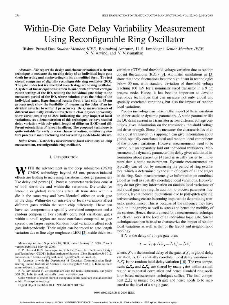
Fig. 2. Modified cell in [21].
standard cell library. In addition such modification reduces thesensitivity to those variations which affect both the configura-tions in the same way.
A method to measure cell-to-cell delay mismatch due toprocess variations is presented in [21]. The cell used in thisapproach is shown in Fig. 2. The authors in [21], point outthe importance of the symmetry in the ring oscillator basedmeasurement technique. However, the layout of the structure isnot regular because of multiplexer used outside the ring.
Our proposed technique is a modification of this scheme toenable accurate delay measurement of an unmodified, indi-vidual logic gate, and is validated by silicon characterizationin a 65-nm test chip [22]. In this paper, we extend this workto show how the delays of noninverting logic gates can also bemeasured in a similar fashion. We include some measurementresults and discussions from characterization of gates withdifferent poly-pitch spacing, lengths of diffusions and layoutorientations. We provide some mathematical justification tothe measurement procedure. Based on our analysis of themeasurement inaccuracies, we propose a modification to thedelay measurement cell proposed in [22], which results in animprovement of accuracy to within 0.2 ps. The main applicationof this technique will be to characterize the local variationsin a gate’s delay, which could arise due to any local effectslike process variations, neighborhood layout effects, and localvoltage and temperature variations.
The organization of the paper is as follows. Section II de-scribes the proposed gate delay measurement cell. The proposeddelay measurement technique is outlined in Section III. The ar-chitecture of the delay measurement unit is depicted in Sec-tion IV. Section V gives the delay measurement procedure using
Authorized licensed use limited to: INDIAN INSTITUTE OF SCIENCE. Downloaded on December 18, 2009 at 00:59 from IEEE Xplore. Restrictions apply.
258 IEEE TRANSACTIONS ON SEMICONDUCTOR MANUFACTURING, VOL. 22, NO. 2, MAY 2009
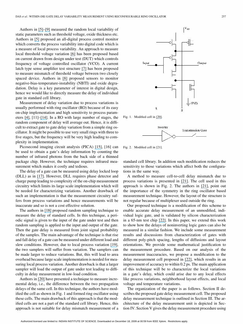
Fig. 3. Concept of gate delay measurement.
Fig. 4. Schematic of a gate delay measurement cell.
a digital storage oscilloscope (DSO). Experimental results anddiscussions are presented in Section VI. The improvement ofgate delay measurement cell is explained in Section VII and fi-nally conclusions in Section VIII.
II. GATE DELAY MEASUREMENT CELL
Fig. 3 shows the basic concept of delay measurement tech-nique. There are two paths from input to output. The differenceof delay between the two paths conceptually gives the delay ofthe gate under test. Fig. 4 shows the schematic of proposed gatedelay measurement cell (GDMC) [22]. This cell consists of thegate under test (GUT), two identical multiplexers and four in-verters. We are interested to measure the delay of the GUT .The inverters , , and are used for buffering and loadmatching. The multiplexer allows bypassing of the logicgate, thus enabling the calculation of the gate’s delay by the dif-ference of two period measurements of the ring oscillator. Thus,the calculated delay will be the sum of the delay of the logic gateand the difference in path delays between the two inputs andoutput of the multiplexer (i.e., between input A to outputY and input B to output Y) due to unequal slew input to twoinputs of for the two different multiplexer settings. Thus,the mismatch in multiplexer delay can limits the accuracyof the gate’s delay measurement. The multiplexer mismatch canoccur due to two reasons: local mismatch in the multiplexer tran-sistors and slew rate variations in the multiplexer inputs. Withthe latter being the dominant one in most cases and hence carefulsizing and buffering can mitigate both these effects.
The input signal to the stage is connected both directly andthrough GUT , to the two inputs of the multiplexer .
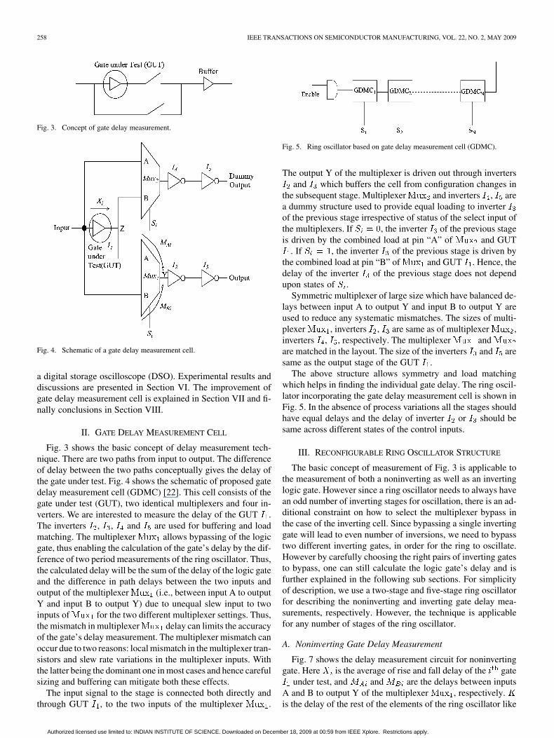
Fig. 5. Ring oscillator based on gate delay measurement cell (GDMC).
The output Y of the multiplexer is driven out through invertersand which buffers the cell from configuration changes in
the subsequent stage. Multiplexer and inverters , area dummy structure used to provide equal loading to inverterof the previous stage irrespective of status of the select input ofthe multiplexers. If , the inverter of the previous stageis driven by the combined load at pin “A” of and GUT
. If , the inverter of the previous stage is driven bythe combined load at pin “B” of and GUT . Hence, thedelay of the inverter of the previous stage does not dependupon states of .
Symmetric multiplexer of large size which have balanced de-lays between input A to output Y and input B to output Y areused to reduce any systematic mismatches. The sizes of multi-plexer , inverters , are same as of multiplexer ,inverters , , respectively. The multiplexer andare matched in the layout. The size of the inverters and aresame as the output stage of the GUT .
The above structure allows symmetry and load matchingwhich helps in finding the individual gate delay. The ring oscil-lator incorporating the gate delay measurement cell is shown inFig. 5. In the absence of process variations all the stages shouldhave equal delays and the delay of inverter or should besame across different states of the control inputs.
III. RECONFIGURABLE RING OSCILLATOR STRUCTURE
The basic concept of measurement of Fig. 3 is applicable tothe measurement of both a noninverting as well as an invertinglogic gate. However since a ring oscillator needs to always havean odd number of inverting stages for oscillation, there is an ad-ditional constraint on how to select the multiplexer bypass inthe case of the inverting cell. Since bypassing a single invertinggate will lead to even number of inversions, we need to bypasstwo different inverting gates, in order for the ring to oscillate.However by carefully choosing the right pairs of inverting gatesto bypass, one can still calculate the logic gate’s delay and isfurther explained in the following sub sections. For simplicityof description, we use a two-stage and five-stage ring oscillatorfor describing the noninverting and inverting gate delay mea-surements, respectively. However, the technique is applicablefor any number of stages of the ring oscillator.
A. Noninverting Gate Delay Measurement
Fig. 7 shows the delay measurement circuit for noninvertinggate. Here is the average of rise and fall delay of the gate
under test, and and are the delays between inputsA and B to output Y of the multiplexer , respectively.is the delay of the rest of the elements of the ring oscillator like
Authorized licensed use limited to: INDIAN INSTITUTE OF SCIENCE. Downloaded on December 18, 2009 at 00:59 from IEEE Xplore. Restrictions apply.

DAS et al.: WITHIN-DIE GATE DELAY VARIABILITY MEASUREMENT USING RECONFIGURABLE RING OSCILLATOR 259
Fig. 6. Layout of GDMC where multiplexers ��� and ��� are matchedand inverters � and � are matched with inverters � and � , respectively.
Fig. 7. Noninverting gate delay measurement showing buffer under test.
the buffers consisting of inverters , of all the cells, the wiresetc. , will not contribute to the frequency of the RO, becauseit is not part of the ring. Note all the delays are average of riseand fall delays. The technique of delay measurement of nonin-verting gate is as follows. Let us consider a noninverting gate(e.g., buffer) is placed in second stage instead of GUT (referFig. 4). The minimum number of stages of GDMC needed fornoninverting gate delay measurement is 2. Let S be the statusvector consisting of 2 bits. If , then input A to output Yof the multiplexer of the stage GDMC is selected. If
, then input B to output Y of the multiplexer of thestage GDMC is selected. and are the period of RO for
two status vectors , respectively. Since, each GDMCswitches twice during a complete cycle, twice the sum of all theaverage cell delays equates to a period of the RO signal.
When select status vector , then the input A to outputY of stages 1 and 2 are connected.
(2)
When select status vector , then the input A to outputY of stage 1 is connected and the input B to output Y of stage 2is connected:
(3)
Taking the difference of (2) and (3), we get
(4)
Period measurements of the ring oscillator , with twodifferent control word settings lead to the (4) for the delay ofbuffer in the second stage along with the residual error term,which is the difference in delay from input A to output Y andfrom input B to output Y of the multiplexer .
B. Inverting Gate Delay Measurement
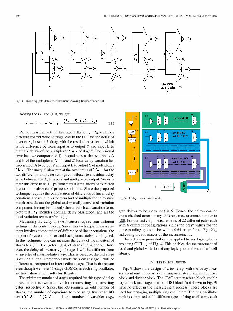
Fig. 8 shows the delay measurement circuit for an invertinggate (e.g., inverter). The status vector S, , and andK are defined as in the previous section. The minimum numberof stages of GDMC needed for inverting gate delay measure-ment is 5. Hence, the status vector is 5 bits. , , andare the period of RO for four status vectors , 00011,00110, 00101, respectively.
When select status vector , then the input A tooutput Y of stages 1, 2, 3, 4, and 5 are connected. Then,
(5)
When select status vector , then the input A tooutput Y of stages 1, 2, and 3 are connected and the input B tooutput Y of stages 4 and 5 are connected.
(6)
Taking the difference between (5) and (6), we get
(7)
When select status vector , then the input A tooutput Y of stages 1, 2, and 5 are connected and the input B tooutput Y of stages 3 and 4 are connected:
(8)
When select status vector , then the input A to outputY of stages 1, 2, and 4 are connected and the input B to outputY of stages 3 and 5 are connected:
(9)
Taking the difference between (8) and (9), we get
(10)
Authorized licensed use limited to: INDIAN INSTITUTE OF SCIENCE. Downloaded on December 18, 2009 at 00:59 from IEEE Xplore. Restrictions apply.
260 IEEE TRANSACTIONS ON SEMICONDUCTOR MANUFACTURING, VOL. 22, NO. 2, MAY 2009
Fig. 8. Inverting gate delay measurement showing Inverter under test.
Adding the (7) and (10), we get
(11)
Period measurements of the ring oscillator , with fourdifferent control word settings lead to the (11) for the delay ofinverter in stage 5 along with the residual error term, whichis the difference between input A to output Y and input B tooutput Y delays of the multiplexer of stage 5. The residualerror has two components: 1) unequal slew at the two inputs Aand B of the multiplexer and 2) local delay variation be-tween input A to output Y and input B to output Y of multiplexer
. The unequal slew rate at the two inputs of for thetwo different multiplexer settings contributes to a residual delayerror between the A, B inputs and multiplexer output. We esti-mate this error to be 1.2 ps from circuit simulations of extractedlayout in the absence of process variations. Since the proposedtechnique requires the computation of difference of linear delayequations, the residual error term for the multiplexer delay mis-match cancels out the global and spatially correlated variationcomponent leaving behind only the random local variation term.Note that, includes nominal delay plus global and all thelocal variation terms (refer to (1)).
Measuring the delay of two inverters require four differentsettings of the control words. Since, this technique of measure-ment involves computation of difference of linear equations, theimpact of systematic error and background noise is mitigated.In this technique, one can measure the delay of the inverters ofstages (e.g., GUT (refer Fig. 4) of stages 2, 3, 4, and 5). How-ever, the delay of inverter of stage 1 will be different from
inverter of intermediate stage. This is because, the last stageis driving a long interconnect while the slew at stage 1 will bedifferent as compared to intermediate stage. That is the reasoneven though we have 11-stage GDMCs in each ring oscillator,we have shown the results for 10 gates.
The minimum number of stages required for this type of delaymeasurement is two and five for noninverting and invertinggates, respectively. Since, the RO requires an odd number ofstages, the number of equations formed using five-stage ROare and number of variables (e.g.,
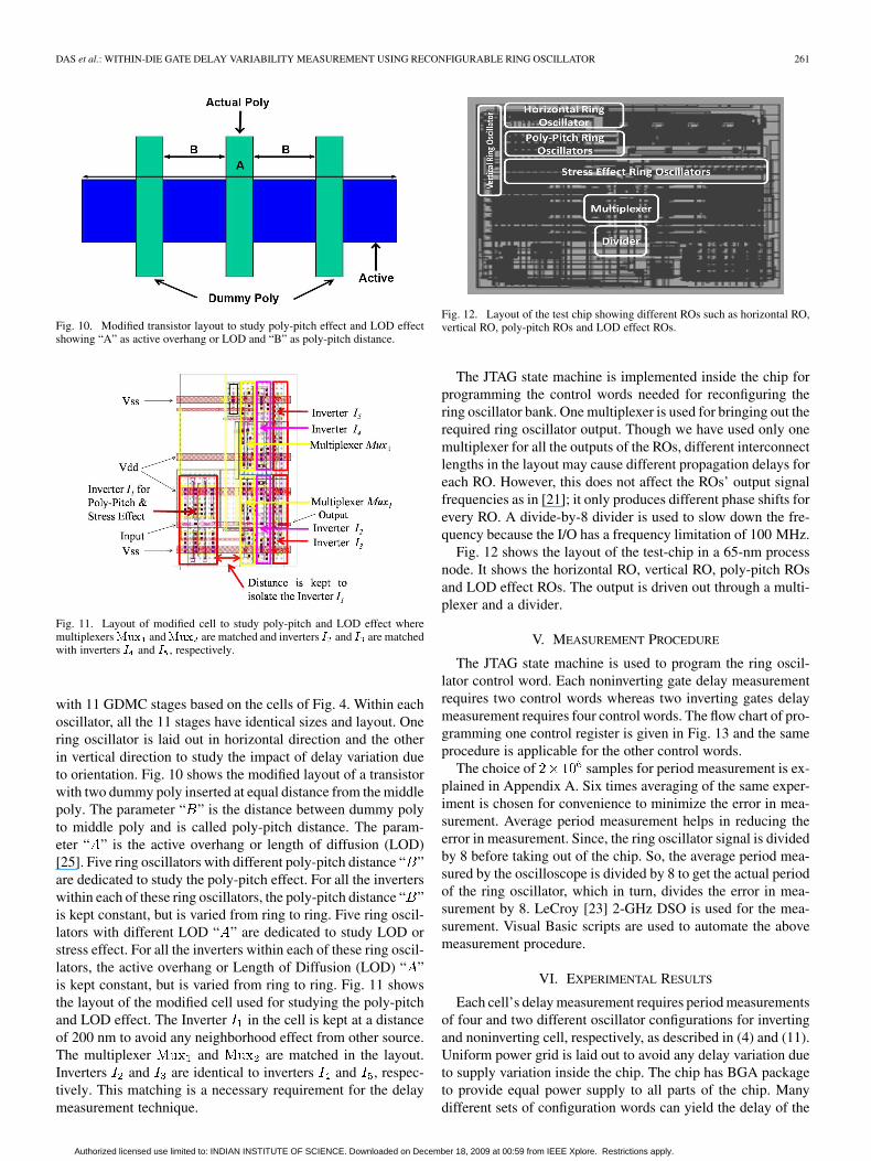
Fig. 9. Delay measurement unit.
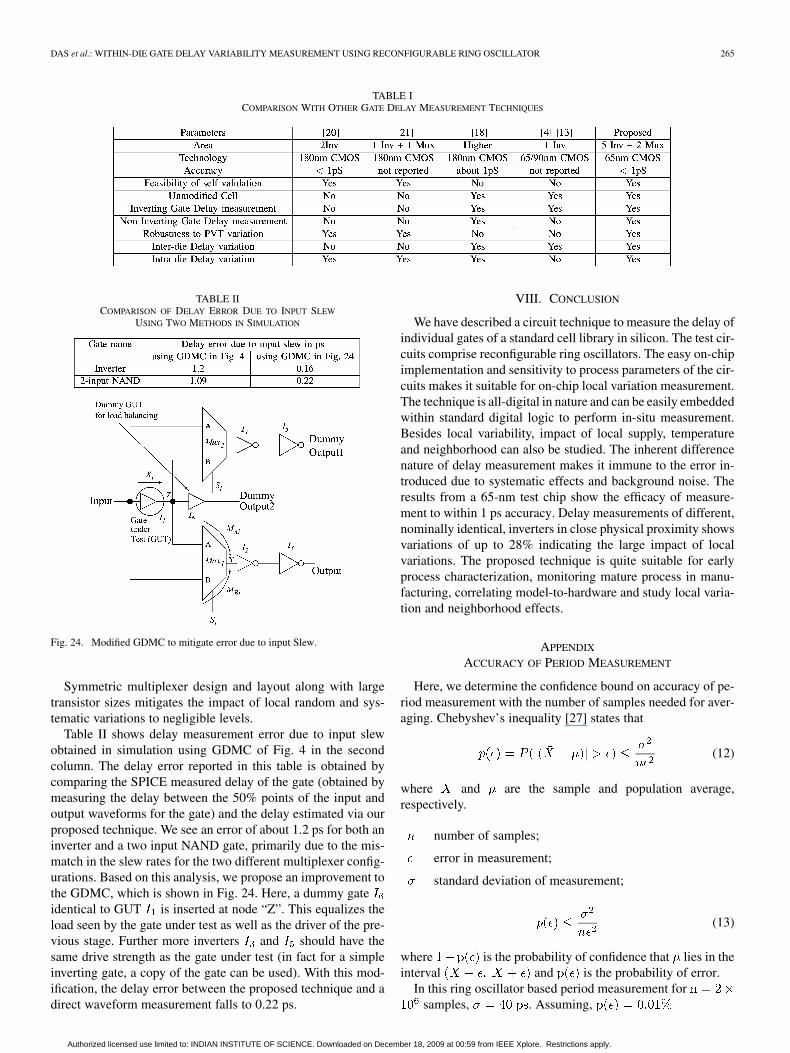
gate delays to be measured) is 5. Hence, the delays can becross checked across many different measurements similar to[20]. For our test chip, measurements of 22 different gates eachwith 6 different configurations yields the delay values for thecorresponding gates to be within 0.64 ps (refer to Fig. 23),indicating the robustness of the measurements.
The technique presented can be applied to any logic gate byreplacing GUT of Fig. 4. This enables the measurement oflocal and global variation of any logic gate in the standard celllibrary.
IV. TEST CHIP DESIGN
Fig. 9 shows the design of a test chip with the delay mea-surement unit. It consists of a ring oscillator bank, multiplexerblock and divider block. The JTAG state machine block, enablelogic block and stage control of RO block (not shown in Fig. 9)have no effect in the measurement process. These blocks areused for managing multiple ring oscillators. The ring oscillatorbank is composed of 11 different types of ring oscillators, each
Authorized licensed use limited to: INDIAN INSTITUTE OF SCIENCE. Downloaded on December 18, 2009 at 00:59 from IEEE Xplore. Restrictions apply.
DAS et al.: WITHIN-DIE GATE DELAY VARIABILITY MEASUREMENT USING RECONFIGURABLE RING OSCILLATOR 261
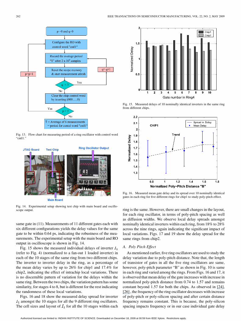
Fig. 10. Modified transistor layout to study poly-pitch effect and LOD effectshowing “A” as active overhang or LOD and “B” as poly-pitch distance.
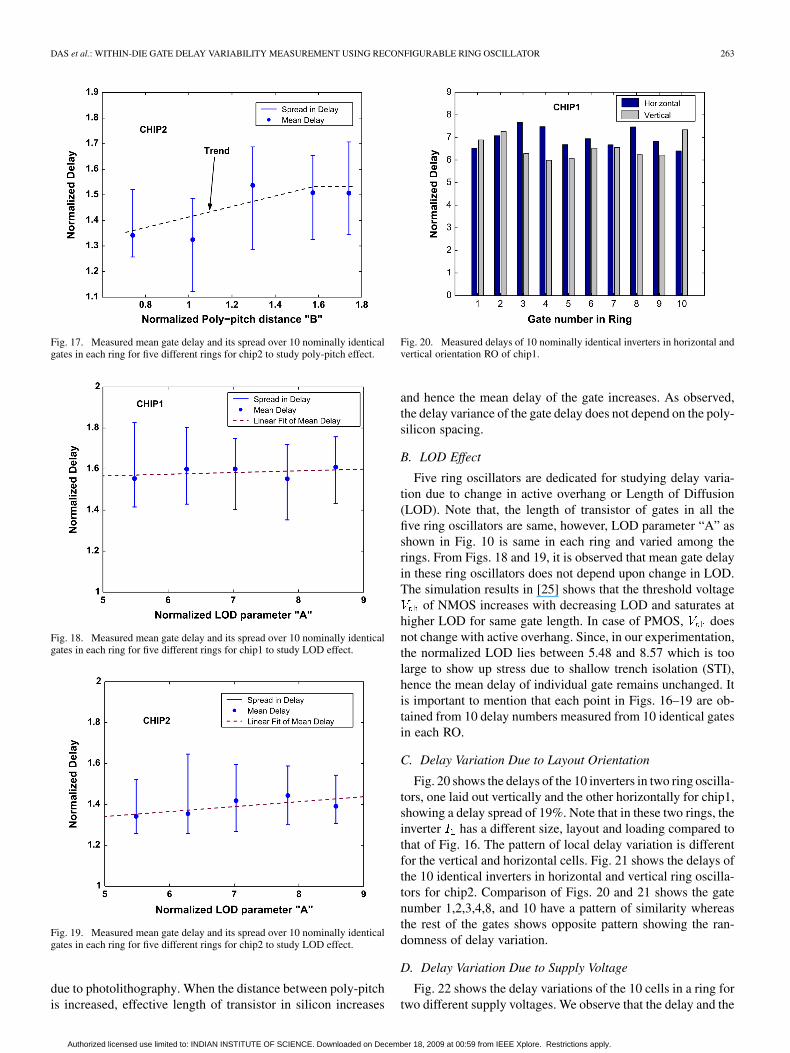
Fig. 11. Layout of modified cell to study poly-pitch and LOD effect wheremultiplexers��� and��� are matched and inverters � and � are matchedwith inverters � and � , respectively.
with 11 GDMC stages based on the cells of Fig. 4. Within eachoscillator, all the 11 stages have identical sizes and layout. Onering oscillator is laid out in horizontal direction and the otherin vertical direction to study the impact of delay variation dueto orientation. Fig. 10 shows the modified layout of a transistorwith two dummy poly inserted at equal distance from the middlepoly. The parameter “ ” is the distance between dummy polyto middle poly and is called poly-pitch distance. The param-eter “ ” is the active overhang or length of diffusion (LOD)[25]. Five ring oscillators with different poly-pitch distance “ ”are dedicated to study the poly-pitch effect. For all the inverterswithin each of these ring oscillators, the poly-pitch distance “ ”is kept constant, but is varied from ring to ring. Five ring oscil-lators with different LOD “ ” are dedicated to study LOD orstress effect. For all the inverters within each of these ring oscil-lators, the active overhang or Length of Diffusion (LOD) “ ”is kept constant, but is varied from ring to ring. Fig. 11 showsthe layout of the modified cell used for studying the poly-pitchand LOD effect. The Inverter in the cell is kept at a distanceof 200 nm to avoid any neighborhood effect from other source.The multiplexer and are matched in the layout.Inverters and are identical to inverters and , respec-tively. This matching is a necessary requirement for the delaymeasurement technique.
Fig. 12. Layout of the test chip showing different ROs such as horizontal RO,vertical RO, poly-pitch ROs and LOD effect ROs.
The JTAG state machine is implemented inside the chip forprogramming the control words needed for reconfiguring thering oscillator bank. One multiplexer is used for bringing out therequired ring oscillator output. Though we have used only onemultiplexer for all the outputs of the ROs, different interconnectlengths in the layout may cause different propagation delays foreach RO. However, this does not affect the ROs’ output signalfrequencies as in [21]; it only produces different phase shifts forevery RO. A divide-by-8 divider is used to slow down the fre-quency because the I/O has a frequency limitation of 100 MHz.
Fig. 12 shows the layout of the test-chip in a 65-nm processnode. It shows the horizontal RO, vertical RO, poly-pitch ROsand LOD effect ROs. The output is driven out through a multi-plexer and a divider.
V. MEASUREMENT PROCEDURE
The JTAG state machine is used to program the ring oscil-lator control word. Each noninverting gate delay measurementrequires two control words whereas two inverting gates delaymeasurement requires four control words. The flow chart of pro-gramming one control register is given in Fig. 13 and the sameprocedure is applicable for the other control words.
The choice of samples for period measurement is ex-plained in Appendix A. Six times averaging of the same exper-iment is chosen for convenience to minimize the error in mea-surement. Average period measurement helps in reducing theerror in measurement. Since, the ring oscillator signal is dividedby 8 before taking out of the chip. So, the average period mea-sured by the oscilloscope is divided by 8 to get the actual periodof the ring oscillator, which in turn, divides the error in mea-surement by 8. LeCroy [23] 2-GHz DSO is used for the mea-surement. Visual Basic scripts are used to automate the abovemeasurement procedure.
VI. EXPERIMENTAL RESULTS
Each cell’s delay measurement requires period measurementsof four and two different oscillator configurations for invertingand noninverting cell, respectively, as described in (4) and (11).Uniform power grid is laid out to avoid any delay variation dueto supply variation inside the chip. The chip has BGA packageto provide equal power supply to all parts of the chip. Manydifferent sets of configuration words can yield the delay of the
Authorized licensed use limited to: INDIAN INSTITUTE OF SCIENCE. Downloaded on December 18, 2009 at 00:59 from IEEE Xplore. Restrictions apply.
262 IEEE TRANSACTIONS ON SEMICONDUCTOR MANUFACTURING, VOL. 22, NO. 2, MAY 2009
Fig. 13. Flow chart for measuring period of a ring oscillator with control word“cntl1.”
Fig. 14. Experimental setup showing test chip with main board and oscillo-scope output.
same gate in (11). Measurements of 11 different gates each withsix different configurations yields the delay values for the samegate to be within 0.64 ps, indicating the robustness of the mea-surements. The experimental setup with the main board and ROoutput in oscilloscope is shown in Fig. 14.
Fig. 15 shows the measured individual delays of inverter(refer to Fig. 4) (normalized to a fan-out 1 loaded inverter) ineach of the 10 stages of the same ring from two different chips.The inverter to inverter delay in the ring, as a percentage ofthe mean delay varies by up to 26% for chip1 and 17.4% forchip2, indicating the effect of intrachip local variations. Thereis no discernible pattern of variation for the delays within thesame ring. Between the two chips, the variation pattern has somesimilarity, for stages 4 to 8, but is different for the rest indicatingthe randomness of these local variations.
Figs. 16 and 18 show the measured delay spread for inverteramongst the 10 stages for all the 9 different ring oscillators.
The cell sizes and layout of for all the 10 stages within each
Fig. 15. Measured delays of 10 nominally identical inverters in the same ringfrom different chips.
Fig. 16. Measured mean gate delay and its spread over 10 nominally identicalgates in each ring for five different rings for chip1 to study poly-pitch effect.
ring is the same. However, there are small changes in the layout,for each ring oscillator, in terms of poly-pitch spacing as wellas diffusion widths. We observe local delay spreads amongstnominally identical inverters within each ring, from 18% to 28%across the nine rings, again indicating the significant impact oflocal variations. Figs. 17 and 19 show the delay spread for thesame rings from chip2.
A. Poly Pitch Effect
As mentioned earlier, five ring oscillators are used to study thedelay variation due to poly-pitch distance. Note that, the lengthof transistor of gates in all the five ring oscillators are same,however, poly-pitch parameter “B” as shown in Fig. 10 is samein each ring and varied among the rings. From Figs. 16 and 17, itis observed that mean delay of the gate increases with increase innormalized poly-pitch distance from 0.74 to 1.57 and remainsconstant beyond 1.57 for both the chips. As observed in [24],[26] , the frequency of the ring oscillator decreases with increaseof poly-pitch or poly-silicon spacing and after certain distancefrequency remains constant. This is because, the poly-siliconspacing impacts frequency or in our case individual gate delay
Authorized licensed use limited to: INDIAN INSTITUTE OF SCIENCE. Downloaded on December 18, 2009 at 00:59 from IEEE Xplore. Restrictions apply.
DAS et al.: WITHIN-DIE GATE DELAY VARIABILITY MEASUREMENT USING RECONFIGURABLE RING OSCILLATOR 263
Fig. 17. Measured mean gate delay and its spread over 10 nominally identicalgates in each ring for five different rings for chip2 to study poly-pitch effect.
Fig. 18. Measured mean gate delay and its spread over 10 nominally identicalgates in each ring for five different rings for chip1 to study LOD effect.
Fig. 19. Measured mean gate delay and its spread over 10 nominally identicalgates in each ring for five different rings for chip2 to study LOD effect.
due to photolithography. When the distance between poly-pitchis increased, effective length of transistor in silicon increases
Fig. 20. Measured delays of 10 nominally identical inverters in horizontal andvertical orientation RO of chip1.
and hence the mean delay of the gate increases. As observed,the delay variance of the gate delay does not depend on the poly-silicon spacing.
B. LOD Effect
Five ring oscillators are dedicated for studying delay varia-tion due to change in active overhang or Length of Diffusion(LOD). Note that, the length of transistor of gates in all thefive ring oscillators are same, however, LOD parameter “A” asshown in Fig. 10 is same in each ring and varied among therings. From Figs. 18 and 19, it is observed that mean gate delayin these ring oscillators does not depend upon change in LOD.The simulation results in [25] shows that the threshold voltage
of NMOS increases with decreasing LOD and saturates athigher LOD for same gate length. In case of PMOS, doesnot change with active overhang. Since, in our experimentation,the normalized LOD lies between 5.48 and 8.57 which is toolarge to show up stress due to shallow trench isolation (STI),hence the mean delay of individual gate remains unchanged. Itis important to mention that each point in Figs. 16–19 are ob-tained from 10 delay numbers measured from 10 identical gatesin each RO.
C. Delay Variation Due to Layout Orientation
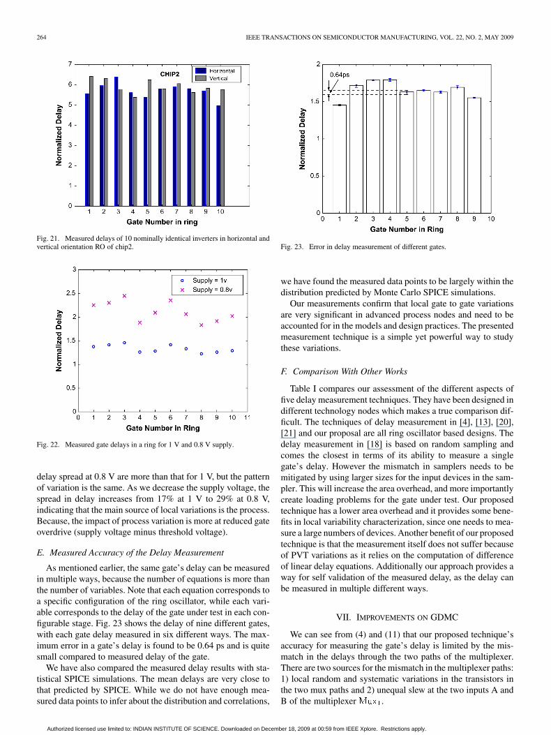
Fig. 20 shows the delays of the 10 inverters in two ring oscilla-tors, one laid out vertically and the other horizontally for chip1,showing a delay spread of 19%. Note that in these two rings, theinverter has a different size, layout and loading compared tothat of Fig. 16. The pattern of local delay variation is differentfor the vertical and horizontal cells. Fig. 21 shows the delays ofthe 10 identical inverters in horizontal and vertical ring oscilla-tors for chip2. Comparison of Figs. 20 and 21 shows the gatenumber 1,2,3,4,8, and 10 have a pattern of similarity whereasthe rest of the gates shows opposite pattern showing the ran-domness of delay variation.
D. Delay Variation Due to Supply Voltage
Fig. 22 shows the delay variations of the 10 cells in a ring fortwo different supply voltages. We observe that the delay and the
Authorized licensed use limited to: INDIAN INSTITUTE OF SCIENCE. Downloaded on December 18, 2009 at 00:59 from IEEE Xplore. Restrictions apply.
264 IEEE TRANSACTIONS ON SEMICONDUCTOR MANUFACTURING, VOL. 22, NO. 2, MAY 2009
Fig. 21. Measured delays of 10 nominally identical inverters in horizontal andvertical orientation RO of chip2.
Fig. 22. Measured gate delays in a ring for 1 V and 0.8 V supply.
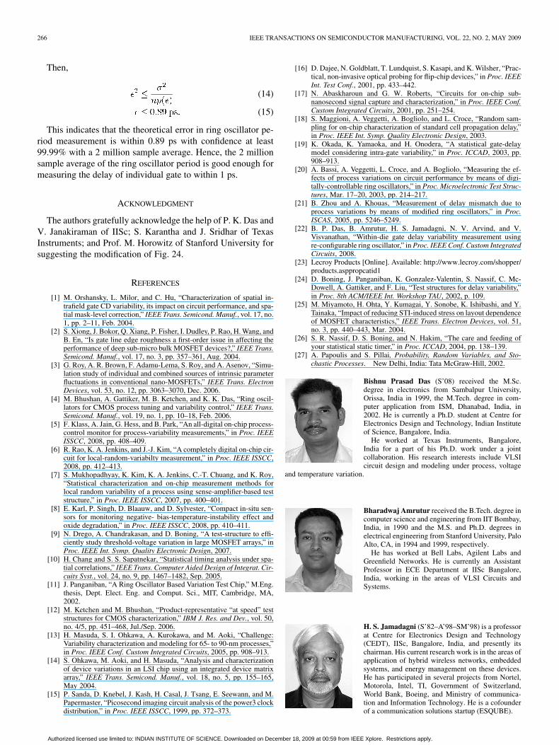
delay spread at 0.8 V are more than that for 1 V, but the patternof variation is the same. As we decrease the supply voltage, thespread in delay increases from 17% at 1 V to 29% at 0.8 V,indicating that the main source of local variations is the process.Because, the impact of process variation is more at reduced gateoverdrive (supply voltage minus threshold voltage).
E. Measured Accuracy of the Delay Measurement
As mentioned earlier, the same gate’s delay can be measuredin multiple ways, because the number of equations is more thanthe number of variables. Note that each equation corresponds toa specific configuration of the ring oscillator, while each vari-able corresponds to the delay of the gate under test in each con-figurable stage. Fig. 23 shows the delay of nine different gates,with each gate delay measured in six different ways. The max-imum error in a gate’s delay is found to be 0.64 ps and is quitesmall compared to measured delay of the gate.
We have also compared the measured delay results with sta-tistical SPICE simulations. The mean delays are very close tothat predicted by SPICE. While we do not have enough mea-sured data points to infer about the distribution and correlations,
Fig. 23. Error in delay measurement of different gates.
we have found the measured data points to be largely within thedistribution predicted by Monte Carlo SPICE simulations.
Our measurements confirm that local gate to gate variationsare very significant in advanced process nodes and need to beaccounted for in the models and design practices. The presentedmeasurement technique is a simple yet powerful way to studythese variations.
F. Comparison With Other Works
Table I compares our assessment of the different aspects offive delay measurement techniques. They have been designed indifferent technology nodes which makes a true comparison dif-ficult. The techniques of delay measurement in [4], [13], [20],[21] and our proposal are all ring oscillator based designs. Thedelay measurement in [18] is based on random sampling andcomes the closest in terms of its ability to measure a singlegate’s delay. However the mismatch in samplers needs to bemitigated by using larger sizes for the input devices in the sam-pler. This will increase the area overhead, and more importantlycreate loading problems for the gate under test. Our proposedtechnique has a lower area overhead and it provides some bene-fits in local variability characterization, since one needs to mea-sure a large numbers of devices. Another benefit of our proposedtechnique is that the measurement itself does not suffer becauseof PVT variations as it relies on the computation of differenceof linear delay equations. Additionally our approach provides away for self validation of the measured delay, as the delay canbe measured in multiple different ways.
VII. IMPROVEMENTS ON GDMC
We can see from (4) and (11) that our proposed technique’saccuracy for measuring the gate’s delay is limited by the mis-match in the delays through the two paths of the multiplexer.There are two sources for the mismatch in the multiplexer paths:1) local random and systematic variations in the transistors inthe two mux paths and 2) unequal slew at the two inputs A andB of the multiplexer .
Authorized licensed use limited to: INDIAN INSTITUTE OF SCIENCE. Downloaded on December 18, 2009 at 00:59 from IEEE Xplore. Restrictions apply.
DAS et al.: WITHIN-DIE GATE DELAY VARIABILITY MEASUREMENT USING RECONFIGURABLE RING OSCILLATOR 265
TABLE ICOMPARISON WITH OTHER GATE DELAY MEASUREMENT TECHNIQUES
TABLE IICOMPARISON OF DELAY ERROR DUE TO INPUT SLEW
USING TWO METHODS IN SIMULATION
Fig. 24. Modified GDMC to mitigate error due to input Slew.
Symmetric multiplexer design and layout along with largetransistor sizes mitigates the impact of local random and sys-tematic variations to negligible levels.
Table II shows delay measurement error due to input slewobtained in simulation using GDMC of Fig. 4 in the secondcolumn. The delay error reported in this table is obtained bycomparing the SPICE measured delay of the gate (obtained bymeasuring the delay between the 50% points of the input andoutput waveforms for the gate) and the delay estimated via ourproposed technique. We see an error of about 1.2 ps for both aninverter and a two input NAND gate, primarily due to the mis-match in the slew rates for the two different multiplexer config-urations. Based on this analysis, we propose an improvement tothe GDMC, which is shown in Fig. 24. Here, a dummy gateidentical to GUT is inserted at node “Z”. This equalizes theload seen by the gate under test as well as the driver of the pre-vious stage. Further more inverters and should have thesame drive strength as the gate under test (in fact for a simpleinverting gate, a copy of the gate can be used). With this mod-ification, the delay error between the proposed technique and adirect waveform measurement falls to 0.22 ps.
VIII. CONCLUSION
We have described a circuit technique to measure the delay ofindividual gates of a standard cell library in silicon. The test cir-cuits comprise reconfigurable ring oscillators. The easy on-chipimplementation and sensitivity to process parameters of the cir-cuits makes it suitable for on-chip local variation measurement.The technique is all-digital in nature and can be easily embeddedwithin standard digital logic to perform in-situ measurement.Besides local variability, impact of local supply, temperatureand neighborhood can also be studied. The inherent differencenature of delay measurement makes it immune to the error in-troduced due to systematic effects and background noise. Theresults from a 65-nm test chip show the efficacy of measure-ment to within 1 ps accuracy. Delay measurements of different,nominally identical, inverters in close physical proximity showsvariations of up to 28% indicating the large impact of localvariations. The proposed technique is quite suitable for earlyprocess characterization, monitoring mature process in manu-facturing, correlating model-to-hardware and study local varia-tion and neighborhood effects.
APPENDIX
ACCURACY OF PERIOD MEASUREMENT
Here, we determine the confidence bound on accuracy of pe-riod measurement with the number of samples needed for aver-aging. Chebyshev’s inequality [27] states that
(12)
where and are the sample and population average,respectively.
number of samples;
error in measurement;
standard deviation of measurement;
(13)
where is the probability of confidence that lies in theinterval and is the probability of error.
In this ring oscillator based period measurement forsamples, . Assuming,
Authorized licensed use limited to: INDIAN INSTITUTE OF SCIENCE. Downloaded on December 18, 2009 at 00:59 from IEEE Xplore. Restrictions apply.
266 IEEE TRANSACTIONS ON SEMICONDUCTOR MANUFACTURING, VOL. 22, NO. 2, MAY 2009
Then,
(14)
(15)
This indicates that the theoretical error in ring oscillator pe-riod measurement is within 0.89 ps with confidence at least99.99% with a 2 million sample average. Hence, the 2 millionsample average of the ring oscillator period is good enough formeasuring the delay of individual gate to within 1 ps.
ACKNOWLEDGMENT
The authors gratefully acknowledge the help of P. K. Das andV. Janakiraman of IISc; S. Karantha and J. Sridhar of TexasInstruments; and Prof. M. Horowitz of Stanford University forsuggesting the modification of Fig. 24.
REFERENCES
[1] M. Orshansky, L. Milor, and C. Hu, “Characterization of spatial in-trafield gate CD variability, its impact on circuit performance, and spa-tial mask-level correction,” IEEE Trans. Semicond. Manuf., vol. 17, no.1, pp. 2–11, Feb. 2004.
[2] S. Xiong, J. Bokor, Q. Xiang, P. Fisher, I. Dudley, P. Rao, H. Wang, andB. En, “Is gate line edge roughness a first-order issue in affecting theperformance of deep sub-micro bulk MOSFET devices?,” IEEE Trans.Semicond. Manuf., vol. 17, no. 3, pp. 357–361, Aug. 2004.
[3] G. Roy, A. R. Brown, F. Adamu-Lema, S. Roy, and A. Asenov, “Simu-lation study of individual and combined sources of intrinsic parameterfluctuations in conventional nano-MOSFETs,” IEEE Trans. ElectronDevices, vol. 53, no. 12, pp. 3063–3070, Dec. 2006.
[4] M. Bhushan, A. Gattiker, M. B. Ketchen, and K. K. Das, “Ring oscil-lators for CMOS process tuning and variability control,” IEEE Trans.Semicond. Manuf., vol. 19, no. 1, pp. 10–18, Feb. 2006.
[5] F. Klass, A. Jain, G. Hess, and B. Park, “An all-digital on-chip process-control monitor for process-variability measurements,” in Proc. IEEEISSCC, 2008, pp. 408–409.
[6] R. Rao, K. A. Jenkins, and J.-J. Kim, “A completely digital on-chip cir-cuit for local-random-variabilty measurement,” in Proc. IEEE ISSCC,2008, pp. 412–413.
[7] S. Mukhopadhyay, K. Kim, K. A. Jenkins, C.-T. Chuang, and K. Roy,“Statistical characterization and on-chip measurement methods forlocal random variability of a process using sense-amplifier-based teststructure,” in Proc. IEEE ISSCC, 2007, pp. 400–401.
[8] E. Karl, P. Singh, D. Blaauw, and D. Sylvester, “Compact in-situ sen-sors for monitoring negative- bias-temperature-instability effect andoxide degradation,” in Proc. IEEE ISSCC, 2008, pp. 410–411.
[9] N. Drego, A. Chandrakasan, and D. Boning, “A test-structure to effi-ciently study threshold-voltage variation in large MOSFET arrays,” inProc. IEEE Int. Symp. Quality Electronic Design, 2007.
[10] H. Chang and S. S. Sapatnekar, “Statistical timing analysis under spa-tial correlations,” IEEE Trans. Computer Aided Design of Integrat. Cir-cuits Syst., vol. 24, no. 9, pp. 1467–1482, Sep. 2005.
[11] J. Panganiban, “A Ring Oscillator Based Variation Test Chip,” M.Eng.thesis, Dept. Elect. Eng. and Comput. Sci., MIT, Cambridge, MA,2002.
[12] M. Ketchen and M. Bhushan, “Product-representative “at speed” teststructures for CMOS characterization,” IBM J. Res. and Dev., vol. 50,no. 4/5, pp. 451–468, Jul./Sep. 2006.
[13] H. Masuda, S. I. Ohkawa, A. Kurokawa, and M. Aoki, “Challenge:Variability characterization and modeling for 65- to 90-nm processes,”in Proc. IEEE Conf. Custom Integrated Circuits, 2005, pp. 908–913.
[14] S. Ohkawa, M. Aoki, and H. Masuda, “Analysis and characterizationof device variations in an LSI chip using an integrated device matrixarray,” IEEE Trans. Semicond. Manuf., vol. 18, no. 5, pp. 155–165,May 2004.
[15] P. Sanda, D. Knebel, J. Kash, H. Casal, J. Tsang, E. Seewann, and M.Papermaster, “Picosecond imaging circuit analysis of the power3 clockdistribution,” in Proc. IEEE ISSCC, 1999, pp. 372–373.
[16] D. Dajee, N. Goldblatt, T. Lundquist, S. Kasapi, and K. Wilsher, “Prac-tical, non-invasive optical probing for flip-chip devices,” in Proc. IEEEInt. Test Conf., 2001, pp. 433–442.
[17] N. Abaskharoun and G. W. Roberts, “Circuits for on-chip sub-nanosecond signal capture and characterization,” in Proc. IEEE Conf.Custom Integrated Circuits, 2001, pp. 251–254.
[18] S. Maggioni, A. Veggetti, A. Bogliolo, and L. Croce, “Random sam-pling for on-chip characterization of standard cell propagation delay,”in Proc. IEEE Int. Symp. Quality Electronic Design, 2003.
[19] K. Okada, K. Yamaoka, and H. Onodera, “A statistical gate-delaymodel considering intra-gate variability,” in Proc. ICCAD, 2003, pp.908–913.
[20] A. Bassi, A. Veggetti, L. Croce, and A. Bogliolo, “Measuring the ef-fects of process variations on circuit performance by means of digi-tally-controllable ring oscillators,” in Proc. Microelectronic Test Struc-tures, Mar. 17–20, 2003, pp. 214–217.
[21] B. Zhou and A. Khouas, “Measurement of delay mismatch due toprocess variations by means of modified ring oscillators,” in Proc.ISCAS, 2005, pp. 5246–5249.
[22] B. P. Das, B. Amrutur, H. S. Jamadagni, N. V. Arvind, and V.Visvanathan, “Within-die gate delay variability measurement usingre-configurable ring oscillator,” in Proc. IEEE Conf. Custom IntegratedCircuits, 2008.
[23] Lecroy Products [Online]. Available: http://www.lecroy.com/shopper/products.asppropcatid1
[24] D. Boning, J. Panganiban, K. Gonzalez-Valentin, S. Nassif, C. Mc-Dowell, A. Gattiker, and F. Liu, “Test structures for delay variability,”in Proc. 8th ACM/IEEE Int. Workshop TAU, 2002, p. 109.
[25] M. Miyamoto, H. Ohta, Y. Kumagai, Y. Sonobe, K. Ishibashi, and Y.Tainaka, “Impact of reducing STI-induced stress on layout dependenceof MOSFET characteristics,” IEEE Trans. Electron Devices, vol. 51,no. 3, pp. 440–443, Mar. 2004.
[26] S. R. Nassif, D. S. Boning, and N. Hakim, “The care and feeding ofyour statistical static timer,” in Proc. ICCAD, 2004, pp. 138–139.
[27] A. Papoulis and S. Pillai, Probability, Random Variables, and Sto-chastic Processes. New Delhi, India: Tata McGraw-Hill, 2002.
Bishnu Prasad Das (S’08) received the M.Sc.degree in electronics from Sambalpur University,Orissa, India in 1999, the M.Tech. degree in com-puter application from ISM, Dhanabad, India, in2002. He is currently a Ph.D. student at Centre forElectronics Design and Technology, Indian Instituteof Science, Bangalore, India.
He worked at Texas Instruments, Bangalore,India for a part of his Ph.D. work under a jointcollaboration. His research interests include VLSIcircuit design and modeling under process, voltage
and temperature variation.
Bharadwaj Amrutur received the B.Tech. degree incomputer science and engineering from IIT Bombay,India, in 1990 and the M.S. and Ph.D. degrees inelectrical engineering from Stanford University, PaloAlto, CA, in 1994 and 1999, respectively.
He has worked at Bell Labs, Agilent Labs andGreenfield Networks. He is currently an AssistantProfessor in ECE Department at IISc Bangalore,India, working in the areas of VLSI Circuits andSystems.
H. S. Jamadagni (S’82–A’98–SM’98) is a professorat Centre for Electronics Design and Technology(CEDT), IISc, Bangalore, India, and presently itschairman. His current research work is in the areas ofapplication of hybrid wireless networks, embeddedsystems, and energy management on these devices.He has participated in several projects from Nortel,Motorola, Intel, TI, Government of Switzerland,World Bank, Boeing, and Ministry of communica-tion and Information Technology. He is a cofounderof a communication solutions startup (ESQUBE).
Authorized licensed use limited to: INDIAN INSTITUTE OF SCIENCE. Downloaded on December 18, 2009 at 00:59 from IEEE Xplore. Restrictions apply.
DAS et al.: WITHIN-DIE GATE DELAY VARIABILITY MEASUREMENT USING RECONFIGURABLE RING OSCILLATOR 267
N. V. Arvind received the B.E. degree in electricaland electronics engineering from Birla Institute ofTechnology and Science (BITS), Pilani, India.
He is currently a Senior Member of the TechnicalStaff and Senior Technologist—ASIC India, at TexasInstruments, Bangalore, India. He has worked on de-veloping solutions for several backend analysis in-cluding parasitics extraction, STA, crosstalk delay/noise analysis. His current areas of work include de-veloping variation aware analysis solutions and in im-proving capacity/cycletime of backend analysis flows
for multimillion gate designs.
V. Visvanathan received the B.Tech degree from IITDelhi, India, and the Ph.D. degree from the Univer-sity of California, Berkeley.
He is currently a Distinguished Member of theTechnical Staff and Chief Technologist—ASICIndia, at Texas Instruments, Bangalore, India. Hehas more than twenty five years of professionalexperience, which is split between Industry andAcademia. He has previously been on the faculty ofthe University of Maryland, College Park and theIndian Institute of Science Bangalore. He has also
worked at Bell Labs, Murray Hill, NJ, where he received the DistinguishedTechnical Staff award in 1989. His current area of work is on system-on-chipdesign methodologies and VLSI design automation.
Dr. Visvanathan has numerous refereed conference and journal publicationson various aspects of VLSI Design and CAD and holds three U.S. patents.
Authorized licensed use limited to: INDIAN INSTITUTE OF SCIENCE. Downloaded on December 18, 2009 at 00:59 from IEEE Xplore. Restrictions apply.