Wireless System-on-Chip and System-on-Package Design for ...
177
Wireless System-on-Chip and System-on-Package Design for Biomedical Applications by Atif Shamim A thesis submitted to the Department of Electronics in partial fulfillment of the requirements for the degree of Doctor of Philosophy in Engineering. Ottawa-Carleton Institute for Electrical Engineering Department of Electronics Faculty of Engineering Carleton University Ottawa, Canada © Atif Shamim, 2009 Reproduced with permission of the copyright owner. Further reproduction prohibited without permission.
-
Upload
khangminh22 -
Category
Documents
-
view
1 -
download
0
Transcript of Wireless System-on-Chip and System-on-Package Design for ...

Wireless System-on-Chip and System-on-Package
Design for Biomedical Applications
by
Atif Shamim
A thesis submitted to the Department of Electronics in partial fulfillment of
the requirements for the degree of Doctor of Philosophy in Engineering.
Ottawa-Carleton Institute for Electrical Engineering
Department of Electronics
Faculty of Engineering
Carleton University
Ottawa, Canada
© Atif Shamim, 2009
Reproduced with permission of the copyright owner. Further reproduction prohibited without permission.

1*1 Library and Archives Canada
Bibliotheque et Archives Canada
Published Heritage Branch
Direction du Patrimoine de I'edition
395 Wellington Street Ottawa ON K1A0N4 Canada
395, rue Wellington Ottawa ON K1A0N4 Canada
Your file Votre reference ISBN: 978-0-494-52065-9 Our file Notre reference ISBN: 978-0-494-52065-9
NOTICE: The author has granted a nonexclusive license allowing Library and Archives Canada to reproduce, publish, archive, preserve, conserve, communicate to the public by telecommunication or on the Internet, loan, distribute and sell theses worldwide, for commercial or noncommercial purposes, in microform, paper, electronic and/or any other formats.
AVIS: L'auteur a accorde une licence non exclusive permettant a la Bibliotheque et Archives Canada de reproduire, publier, archiver, sauvegarder, conserver, transmettre au public par telecommunication ou par Nntemet, preter, distribuer et vendre des theses partout dans le monde, a des fins commerciales ou autres, sur support microforme, papier, electronique et/ou autres formats.
The author retains copyright ownership and moral rights in this thesis. Neither the thesis nor substantial extracts from it may be printed or otherwise reproduced without the author's permission.
L'auteur conserve la propriete du droit d'auteur et des droits moraux qui protege cette these. Ni la these ni des extraits substantiels de celle-ci ne doivent etre imprimes ou autrement reproduits sans son autorisation.
In compliance with the Canadian Privacy Act some supporting forms may have been removed from this thesis.
While these forms may be included in the document page count, their removal does not represent any loss of content from the thesis.
Conformement a la loi canadienne sur la protection de la vie privee, quelques formulaires secondaires ont ete enleves de cette these.
Bien que ces formulaires aient inclus dans la pagination, il n'y aura aucun contenu manquant.
i*I
Canada Reproduced with permission of the copyright owner. Further reproduction prohibited without permission.
Abstract In this thesis, novel wireless System-on-Chip (SoC) and System-on-Package (SoP) have been
developed for biomedical applications. A radiation dose measurement system for the
treatment of cancer patients is the chosen application. Typically this measurement requires a
wired sensor which uses the change in Radiation Field Effect Transistor (RADFET) threshold
voltage before and after the radiation exposure to measure the dose. While these dosimeters
have good sensitivity, the wires employed deflect and scatter the radiation away from the
targeted region during the irradiation process. To avoid these ill effects and to relieve patients
from a cluster of wires on their bodies, a short range radio for transmitting the sensor data is
proposed. The complete system is highly compact and small in size. The SoC part includes the
design of a 5.2 GHz transmitter (TX) with a unique on-chip antenna. The on-chip antenna
performs double duty and acts as an inductor for the TX Voltage Controlled Oscillator (VCO).
The SoC designed in IBM CMOS 0.13 um process occupies only 1.5 mm2 of chip space and
successfully transmits the sensor data up to 2 m of range with a power consumption of 3 mW.
Similarly, a receive side on-chip antenna has also been designed which is conjugately matched
to the LNA over a wide bandwidth.
In order to package the TX chip, Low Temperature Co-fired Ceramic (LTCC) technology in
employed. Custom LTCC packages provide high levels of integration and reduction in size due to
their embedded 3D-structured passives. An efficient SoP has been designed in Ferro A6-S LTCC,
accommodating the sensor and TX chips in tailor-made cavities. It has an LTCC antenna
integrated to the TX chip through isolating buffer amplifiers. The SoP design increases the
communication range to 75 m with the efficient antenna; however the power consumption also
rises to 38 mW due to the buffers. To reduce power consumption and still use an efficient
antenna, a novel LTCC package is designed where the package antenna is fed
electromagnetically from the TX's on-chip antenna. This wireless coupling eliminates the need
for buffer amplifiers, bond wires and matching circuit elements, and hence improves the
communication range with no additional power consumption. As an enhancement of SoP,
ferrite LTCC is also investigated for tuneable and reconfigurable antennas. The introduction of
ferrite material into the LTCC package permits control of the devices made from it. Completely
embedded transformers in ferrite LTCC are designed and fabricated for material
characterization. These transformers are also utilized as biasing circuits for the antennas. A
measured tuning range of up to 550 MHz is observed from ferrite LTCC based patch antennas.
As a result of embedding the bias windings, the typically required external fields of the order of
1000 Oe to tune ferrite based antennas have been reduced to the order of 50 Oe. This makes
ferrite LTCC a suitable candidate for tuneable and re-configurable wireless SoP.
-iii-
Reproduced with permission of the copyright owner. Further reproduction prohibited without permission.

Acknowledgements
First of all, I wish to thank God for giving me this opportunity to pursue my educational
goals. Then, I wish to express my sincere appreciation to my thesis supervisor, Dr. Langis Roy
for his immense support, encouragement and continuous guidance throughout this thesis
project. I consider myself fortunate to have him as my supervisor, as he has not only taught
me technical things but has also coached me in numerous issues related to the professional
life. He has inspired me with his dedication to work and with his positive attitude towards
life. I thank him for all the knowledge he has imparted and for all the time he has dedicated
to this thesis.
A special thanks to Dr. Joey Bray and Dr. Nasrin Hojjat for their assistance in this work. I
also wish to thank Dr. Garry Tarr and Dr. Calvin Plett for their technical advice during this
thesis.
I wish to acknowledge NSERC and Dr. Langis Roy for the financial support to conduct this
work.
I like to express my gratitude for fellow PhD student and a personal friend Muhammad
Arsalan for the collaborative work we have done together. He provided phenomenal support
during all these years and we achieved many land marks together. This thesis would not
have been the same without his input. I also like to appreciate the help of V. Karam and P.
-iv-
Reproduced with permission of the copyright owner. Further reproduction prohibited without permission.

Popplewell for the collaborative work done with them. A special thanks to Igor Miletic and
Steve Mcgarry for their help during the post processing of the prototypes.
I will like to thank all my graduate student friends for the laughs and valuable
discussions. In particular, I want to mention the names of G. Brzezina, B. Tamer, M. Usama,
and Z. El-Khatib.
Finally, I wish to thank my family who has been praying for my success throughout this
time. Specially, my wife Sumaira Haque for her endless support and patience, and my two little
angels Raameen and Hiba for all the excitement they bring into my life.
I dedicate this thesis to the memories of my loving mother, who believed in me right
from the start. Her thoughts have always motivated me in hard times.
Reproduced with permission of the copyright owner. Further reproduction prohibited without permission.

Table of Contents
Chapter 1 1
1 Introduction 1
1.1 Motivation 2
1.2 Challenges 3
1.3 Research Objectives 7
1.4 Thesis Contributions 9
1.5 Thesis Outline 12
Chapter 2 13
2 SoC and SoP Overview 13
2.1 System-on-Chip (SoC) 14
2.2 System-in-Package (SiP) 15
2.3 System-on-Package (SoP) 17
2.4 RF SoC Overview 18
2.4.1 Oscillator Transmitter 19
2.4.2 On-chip antenna 20
2.5 RF SoP 24
2.5.1 Low Temperature Co-fired Ceramic 26
-vi-
Reproduced with permission of the copyright owner. Further reproduction prohibited without permission.

2.5.2 LTCC Antenna 27
2.6 Ferrite LTCC Based Tunable RF SoP 29
2.6.1 Ferrite Based Tunable antennas 29
2.7 Summary 30
Chapter 3 31
3 SoC Design 31
3.1 On-chip Inductor/Antenna 31
3.1.1 Novel on-chip inductor/antenna design 32
3.1.2 Lumped Model 36
3.2 Oscillator Transmitter Implementations 39
3.2.1 Phase lock loop with on-chip antenna 39
Inductor Measurements 40
Antenna Measurements 42
3.2.2 Voltage Controlled Oscillator TX with on-chip antenna 46
Modified On-chip Inductor/Antenna Design 47
Voltage Controlled Oscillator Design 48
Layout and and Fabrication 52
Measurements 53
3.3 RX Side On-chip Antenna 57
-vii-
Reproduced with permission of the copyright owner. Further reproduction prohibited without permission.

3.3.1 Design 59
3.3.2 Fabrication and Measurements 61
3.4 RF SoC Design Issues 63
3.5 Summary and Contribution 66
Chapter 4 67
4 RF LTCC SoP 67
4.1 Conventional LTCC package with antenna 68
4.1.1 LTCC antenna/package co-design 69
4.2 Aperture Coupled LTCC SoP 73
4.2.1 Design and Simulation 75
4.2.2 Fabrication and Measurements 82
4.3 Analytical Modeling of Chip Antenna Aperture-Coupling 86
4.4 RF SoP Design Issues 95
4.5 Summary and Contributions 97
Chapter 5 99
5 Tunable and Reconfigurable LTCC SoP 99
5.1 Ferrite LTCC material characterization 100
5.1.1 Microwave Characterization 101
5.1.2 Microwave Characterization under Biased Conditions 104
-viii-
Reproduced with permission of the copyright owner. Further reproduction prohibited without permission.

5.1.3 Magnetostatic Characterization 106
5.1.4 Discussion 112
5.2 Tunable antennas 113
5.2.1 Theory 114
5.2.2 Antenna Design 116
5.2.3 Tunable Patch Impedance Measurements and Discussion 118
5.2.4 Antenna Gain and Radiation Pattern Measurements 123
5.3 Ferrite LTCC SoP Implementations 125
5.3.1 Antennas 125
5.3.2 Reflectarray 126
5.3.3 Other tunable circuits 126
5.4 Ferrite based Tunable RF SoP Design Issues 127
5.5 Summary and Contributions 130
Chapter 6 132
6 Conclusions and Future Work 132
6.1 Conclusions 132
6.2 Future Work 135
RF SoC Design 135
RF SoP Design 136
-ix-
Reproduced with permission of the copyright owner. Further reproduction prohibited without permission.

Bibliography 139
-x-
Reproduced with permission of the copyright owner. Further reproduction prohibited without permission.

List of Tables Table 2.1 Antenna Comparisons with Previously Published Work 22
Table 3.1 Lumped element values from ADS 38
Table 4.1 Material Properties For Ferro A6 Ltcc Tape System [110] 70
Table 4.2 Performance Comparison for Different TX Modules 82
Table 5.1 Measured eR and Tan8 Parameters 102
-xi-
Reproduced with permission of the copyright owner. Further reproduction prohibited without permission.

List of Figures Figure 1.1 Demonstration of wired dosimeter from Best Medical Canada 3
Figure 1.2 Existing wired dosimeter with TX module 3
Figure 1.3 Off chip antennas in iPhone 5
Figure 1.4 On-chip antenna in a 10 GHz receiver module (antenna occupies 0.3 mm2) 5
Figure 1.5 3D integration concept in SoP module 6
Figure 1.6 Wireless dosimeter (a) SoC block diagram (b) SoP block diagram 8
Figure 2.1 Future generation Nokia Morph phone concept 14
Figure 2.2 SoC Concept 15
Figure 2.3 MCM Concept 16
Figure 2.4 SiP Concept 16
Figure 2.5 SoP Concept 18
Figure 2.6 CMOS Transceiver SoC architecture 19
Figure 2.7 24 GHz RX chip with on-chip antenna 23
Figure 2.8 RF integration of IC and passives on SoP 25
Figure 2.9 3D integration of buried passives in LTCC medium 27
Figure 2.10 RF circuit integration with antenna in SOP format 28
Figure 3.1 On-chip antenna structure (a) CMOS process stack up (b) loop antenna geometry
(defined on top Aluminum layer) 35
Figure 3.2 Antenna/ Inductor HFSS model 35
Figure 3.3 Antenna/ inductor simulated radiation pattern 36
-xii-
Reproduced with permission of the copyright owner. Further reproduction prohibited without permission.

Figure 3.4 Differential inductor lumped model 37
Figure 3.5 HFSS and ADS S-parameters from lumped model optimization set up 38
Figure 3.6 Microphotograph of PLLTX with on-chip antenna 40
Figure 3.7 Simulated vs measured Qof inductor/antenna 41
Figure 3.8 Simulated versus measured inductance of inductor/antenna 41
Figure 3.9 On-chip antenna radiation pattern measurement setup 43
Figure 3.10 Measured radiation pattern 45
Figure 3.11 Measured range comparison with theory 46
Figure 3.12 Modified On-chip inductor/antenna HFSS model 48
Figure 3.13 VCO schematic (core only) 49
Figure 3.14 Buffer schematic 51
Figure 3.15 VCO time domain output through the integrated buffer 51
Figure 3.16 VCO simulated phase noise 52
Figure 3.17 Microphotograph of VCO TX with on-chip antenna 53
Figure 3.18 On-chip antenna (a) radiation pattern measurement setup (b) zoom in of probe
feeding 54
Figure 3.19 On-chip antenna measured radiation pattern 55
Figure 3.20 TX VCO measured response 56
Figure 3.21 Measured phase noise 56
Figure 3.22 Demonstration of wireless dosimeter 57
Figure 3.23 RX side on-chip folded dipole 58
Figure 3.24. Simulated Sll of on-chip antenna (referenced to complex impedance of LNA)60
-xiii-
Reproduced with permission of the copyright owner. Further reproduction prohibited without permission.

Figure 3.25. Microphotograph of the receiver chip 61
Figure 3.26 On-chip antenna radiation pattern (simulated and measured) 63
Figure 3.27 SoC design issues 65
Figure 3.28 SoC design issues (metal fill) 65
Figure 4.1 HFSS Simulation Model for LTCC module 70
Figure 4.2 Simulated LTCC dipole radiation 71
Figure 4.3 Photograph of LTCC module 71
Figure 4.4 Conventional aperture coupled patch concept (fed through microstrip line) 74
Figure 4.5 Proposed aperture coupled patch concept (fed through TX on-chip antenna)... 75
Figure 4.6 Layer by layer description of the complete LTCC TX module 79
Figure 4.7 Cross-sectional view of the complete LTCCTX module 79
Figure 4.8 Aperture coupled LTCC patch antenna gain and radiation pattern 80
Figure 4.9 TX VCO inductor performance with and without aperture coupling 80
Figure 4.10 LTCC antenna gain versus air gap thickness for aperture-coupling 81
Figure 4.11 TX aperture coupled SoP (a) TX chip placed in LTCC substrate (b) ground plane
with slot and LTCC post placed on substrate with the TX chip (c) superstrate with patch antenna
placed on the rest of the module (d) complete SoP module 83
Figure 4.12 TX SoP measured radiation pattern 84
Figure 4.13 TX SoP zoomed in view of fabrication tolerances 86
Figure 4.14 Problem definition (a) Case 1 with no slot (b) Case 2 with slot 88
Figure 4.15 Image theory for case 1 (with no slot) 91
Figure 4.16 Comparison of coupling between a microstrip feed and an loop antenna feed 92
-xiv-
Reproduced with permission of the copyright owner. Further reproduction prohibited without permission.

Figure 4.17 Comparison of coupling between the loop and the slot at various positions
through HFSS and analytical model 95
Figure 4.18 EM analysis used to determine area of high sensitivity 97
Figure 5.1 Fabricated ferrite LTCC structures 103
Figure 5.2 Attenuation constant extracted from ferrite CPW line 104
Figure 5.3 Setup for microwave characterization under biased conditions 106
Figure 5.4 Magnetic hysteresis measurement test circuit 107
Figure 5.5 Ferrite LTCC LTCC (a) solenoid unit cell cross section and (b) toroid tilted front
view (c) & (d) solenoid & toroid fabricated layer top view 109
Figure 5.6 Measured hysteresis curves from the LTCC transformers 110
Figure 5.7 Measured peak B versus peak H for ESL 40012 LTCC Ill
Figure 5.8 Measured relative linear permeability of ESL 40012 112
Figure 5.9 Patch antenna orientations with respect to H0 direction 116
Figure 5.10 Tunable antenna module (cross-sectional view) 117
Figure 5.11 Fabricated antennas on ESL 40012 ferrite LTCC (a) small patch on toroid (b)
transverse small patch on solenoid (c) large patch with slot on solenoid (d) longitudinal small
patch on solenoid (e) longitudinal small patch placed in the corner with a microstrip line 118
Figure 5.12 Tuneable antenna measurement setup 119
Figure 5.13 Measured Results (a) 9-15 GHz range (b) zoomed in at 12 GHz range 120
Figure 5.14 Ferrite antenna gain and radiation pattern measurement setup 123
Figure 5.15 Ferrite antenna measured gain and radiation pattern 125
Figure 5.16 Ferrite microstrip line measured attenuation constant 127
-xv-
Reproduced with permission of the copyright owner. Further reproduction prohibited without permission.

Figure 6.1 Proposed SoC in hybrid CMOS process (MEMS based) 136
Figure 6.2 3D integration of components in SoP module [8] 137
Figure 6.3 3D flexible SoP 137
Figure 6.4 Ferrite LTCC based adaptive matching network 138
-xvi-
Reproduced with permission of the copyright owner. Further reproduction prohibited without permission.

List of Abbreviations and Symbols
X any wavelength in general
X0 wavelength in free space
Xg wavelength in dielectric medium (guided wavelength)
Q ohm
a attenuation constant
P phase constant
Al feed gap length
a conductivity
k pi
(0 angular frequency dB decibel
dBi decibel with reference to isotropic antenna
dBm decibel with reference to milli-watt
e permittivity
er relative permittivity (dielectric constant)
e0 permittivity of free space 3D three dimensional
ADS advance design system
Bs saturation flux density
Br remanence flux density
BEOL back end of line
C capacitor
CPS coplanar strips CPW coplanar wave-guide
Cox oxide capacitance Cox substrate capacitance
D distance
DRA dielectric resonator antenna
CBPA cavity backed patch antenna
CAD computer aided design
CMC Canadian microelectronics corporation
CMOS complementary metal oxide semiconductor
DRC design rule check E electric field EM electromagnetic ESD electrstatic discharge EuWIT eurpean wireless technology conference
G gain Gp gain of patch antenna
-xvii-
Reproduced with permission of the copyright owner. Further reproduction prohibited without permission.

Gc gain of on-chip antenna
GHz gega hertz
GPS global positioning system
GSG ground signal ground
gm transconductance
HFSS high frequncy structural simulator
Hc coercivity
1 current
IC integrated circuit
J current density
K Boltzman constant T tesla
Is slot length Ls series inductance
LCP liquid crystal polymer
LTCC low temperature co-fired ceramic
M magnetic field
MCM multichip module
MHz mega hertz
MIM metal insulator metal
Ms saturation magnetization
NF noise figure
NMOS n-type metal oxide semiconductor
Oe Oerstds
P power
PCB printed circuit board
PLL phase lock loop
PMOS p-type metal oxide semiconductor
PTFE polytetraflourethylene
Pt transmitted power
Pr received power
Prp received power from ptch antenna
Pre received power from on-chip antenna
0 quality factor
R distance between receive and transmit antennas
RF radio frequency RFIC radio frequency integrated circuit RFID radio frequency identification
RADFET Radiation Field effect Transistor
Rs series resistance
Rsub substrate resistance
RXC rectangular waveguide cavity
RX Receiver
-xviii-
Reproduced with permission of the copyright owner. Further reproduction prohibited without permission.

s surface
Si silicon
S21 transmission gain
S11 input return loss
SiP system-in-package
SoC system-on-chip
SoP system-on-package
SOI silicon on insulator
TE transverse electric
TX transmitter
Tan£ loss tangent
LNA low noise amplifier
U-NII unlicensed national information infrastructure
permeability
Ro permeability of free space
l^lin Linear permeability
relative permeability
V volume
VDD drain voltage VCO voltage-controlled oscillators VH horizontal voltage
Vv vertical voltage
WLAN wireless local area networks
ws slot width
Zl load impedance
Zin input impedance
Zr receive antenna impedance
Zs source impedance
Zant antenna impedance
Z0 characteristic impedance
-xix-
Reproduced with permission of the copyright owner. Further reproduction prohibited without permission.

Chapter 1
1 Introduction Low cost wireless sensor systems are becoming crucial in modern day health care. These can be
utilized in a number of applications like continuous monitoring of human vital signs, remote
health care, locating patients in a hospital environment, communicating the dose of automated
medicine to medical staff and measuring radiation dose in radiotherapy applications. The
wireless aspect is not only revolutionary for health care delivery but also brings in added
convenience for the patients. The desired characteristics for such a wireless device are very
small size, minimum power consumption and low cost. The miniaturization and low cost
requirements can be achieved by employing low cost CMOS integrated circuit (IC) technology in
a System-on-Chip (SoC) format with a minimum number of off-chip components. For added
flexibility, functionality and efficiency, a System-on-Package (SoP) approach can be followed as
an alternate solution for such wireless biomedical sensor systems. In this regard, Low
Temperature Co-fired Ceramics (LTCC) technology offers many attractive features and
possibilities. Size reduction is possible because of the 3D nature of the multi-layer, low loss
P a g e | 1
Reproduced with permission of the copyright owner. Further reproduction prohibited without permission.

medium and because passive components such as capacitors, resistors, inductors and antennas
can be embedded, allowing for a high degree of integration.
1.1 Motivation
A miniature SoC or SoP would be an ideal solution for many short-range wireless sensor
applications. For example, in the treatment of cancer patients by means of high energy
radiation, precise knowledge of the dose and location of radiation experienced by the body is
essential. Typically this measurement is made by a wired sensor to record the high energy
radiation dose as shown in Figure 1.1 [1]. These radiation sensors are small enough to be placed
on any part of the body during a radiotherapy session, helping doctors to appropriately treat
malignant tumors by providing real-time data on the radiation doses reaching the organs. These
radiation measurement systems are called dosimeters, and while they have good sensitivity,
the required wiring harness (shown in Figure 1.2) is large and can deflect or scatter radiation
away from the targeted region during the irradiation process. To avoid these ill effects and to
relieve patients from a cluster of wires on their bodies, a short range radio for transmitting the
sensor data would be preferred. A similar application is the Extra Vehicular Activity Radiation
Monitoring (EVARM) project which is designed to measure radiation doses absorbed by
astronauts in extra vehicular activity i.e., spacewalks [2]. The uncertainty of the space radiation
environment can lead to significant risks to both humans and electronics. Existing systems do
not allow real time continuous monitoring of the radiation experienced by the astronauts and
the electronics.
P a g e | 2
Reproduced with permission of the copyright owner. Further reproduction prohibited without permission.

Figure 1.1 Demonstration of wired dosimeter from Best Medical Canada [1]
Figure 1.2 Existing wired dosimeter with TX module [1]
1.2 Challenges
Over the last few years researchers have been striving to find a reliable solution for a
wearable wireless biomedical sensor system; however a compact, dependable and low cost
wireless device is still a farfetched dream. Furthermore, a non-invasive, wearable, low power,
continuous monitoring and miniaturized wireless dosimeter is still in the research phase and far
P a g e | 3
Reproduced with permission of the copyright owner. Further reproduction prohibited without permission.

from commercialization. The major challenges associated with the development of such a
system are designing accurate non-invasive sensors, realizing low power transmitter (TX) and
receiver (RX) circuits with miniature integrated antennas, designing on-chip interface signal
processing circuitry between the sensors and the TX circuit, incorporating a very small battery
that is transparent to high energy radiation and, of prime importance, integrating all of the
above components on a small, and low cost platform. Details of the specific challenges related
to this work are given below.
Miniature Integrated Antenna
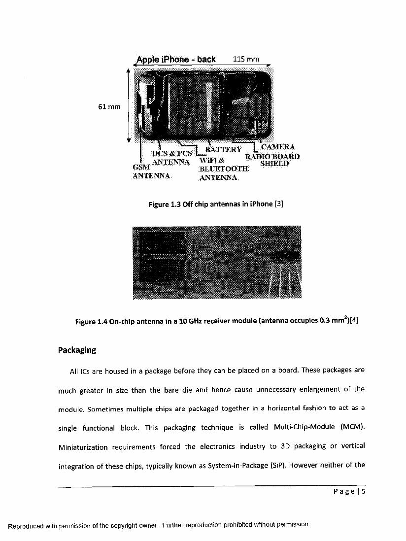
In order to keep the TX size to a minimum, the antenna (which is the largest part of a typical
TX module) has to be miniaturized. Figure 1.3 shows that the major portion of a modern hand
held wireless device like the iphone is occupied by the antenna and the battery [3]. If the
antenna can be integrated with circuits on the chip, a very low cost and compact system could
result, as shown in Figure 1.4 [4]. However standard CMOS silicon substrate is a very lossy
medium for antenna realization, which results in in-efficient antennas. Furthermore, it is
extremely difficult to fit these antennas on-chip, as they are generally a significant fraction of a
wavelength in size. This becomes increasingly challenging for lower frequency bands. The
presence of on-chip circuitry and other metals in close vicinity of the antenna makes the design
even more complicated. Experimental characterization of such small on-chip antennas requires
custom jigs and innovative techniques [5]. In addition, the realization of miniature antennas
within a package presents a number of antenna package co-design challenges.
P a g e | 4
Reproduced with permission of the copyright owner. Further reproduction prohibited without permission.
G S M ' - ' B L U E T O O T H ANTENNA ANTENNA
Figure 1.3 Off chip antennas in iPhone [3]
Figure 1.4 On-chip antenna in a 10 GHz receiver module (antenna occupies 0.3 mm2)[4]
Packaging
All ICs are housed in a package before they can be placed on a board. These packages are
much greater in size than the bare die and hence cause unnecessary enlargement of the
module. Sometimes multiple chips are packaged together in a horizontal fashion to act as a
single functional block. This packaging technique is called Multi-Chip-Module (MCM).
Miniaturization requirements forced the electronics industry to 3D packaging or vertical
integration of these chips, typically known as System-in-Package (SiP). However neither of the
P a g e | 5
Reproduced with permission of the copyright owner. Further reproduction prohibited without permission.

above approaches addresses the bulk of the components in any electronic system, passive
components and interconnections. Greater integration and functionality can be achieved if
passives like inductors, capacitors, filters, couplers and antennas are realized within the
package itself. Modern packaging materials like LTCC and Liquid Crystal Polymer (LCP) enable
designers to achieve this goal, thus paving the way to a new generation of packaging now
known as SoP as shown in Figure 1.5[6]. The combination of multiple technologies in a single 3D
system shown in Figure 1.5 is still in the research phase and far from being employed as a
commercial device. Here the major design challenge is the requirement for IC, circuit and
package co-design. Large volume production and fabrication tolerances are also an issue with
these modules.
Thermal
Optical Integration
Assembly integration
Composite Substrate
High modulus
Figure 1.5 3D integration concept in SoP module [6]
P a g e | 6
Reproduced with permission of the copyright owner. Further reproduction prohibited without permission.

1.3 Research Objectives
This work is part of a collaborative project regarding a wireless dosimeter design with a
fellow PhD student Muhammad Arsalan. The concept of the wireless dosimeter is shown in
Figure 1.6. Two design approaches have been shown, namely, SoC and SoP.
This thesis focuses on the design and development of a TX chip with an on-chip antenna for
the SoC approach. For the SoP, it will deal with the LTCC package design with integrated
antenna suitable for the wireless dosimeter application. It investigates the design aspects of
different components required to realize efficient SoC and SoP solutions. It also compares the
performance of the two approaches. Finally, it investigates novel packaging techniques and
materials to not only lower the power consumption and cost of the system, but also to make it
tunable and reconfigurable. Specifically, the following are the objectives for operation in the
Unlicensed National Information Infrastructure (U-NII) 5 GHz radio band [7].
a) Design a miniaturized on-chip antenna suitable for integration with a standard CMOS
technology based TX circuit.
b) Design a standard CMOS technology based TX chip which makes use of the on-chip
antenna for a SoC demonstration of short range communication. It must have the
capability to function with an off-chip antenna for a SoP demonstration having an
extended communication range.
c) Design an on-chip antenna for integration with a standard CMOS technology based RX
circuit.
P a g e | 7
Reproduced with permission of the copyright owner. Further reproduction prohibited without permission.

d) Design an LTCC package with an efficient antenna for the SoP demonstration.
e) Investigate novel packaging techniques for reduced part count and improved
efficiency.
f) Develop an analytical model to support the novel SoP design in (e).
g) Investigate novel LTCC packaging materials such as ferrite ceramics to achieve
tunablity and reconfigurability.
Wireless Dosimeter (SoCl ss m&Mfs $ yf
Battery
Radiations Sensor
Signal Prates Electronics,
" jV>rocess*,r>g / s
TX SoC ^ On-chip Antenna «
§ i ( I i
f « • I
~rnr~i' *1
§ i ( I i
f « • I
~rnr~i' *1
(a)
Wireless Dosimeter (SoP)
) '—~ j ! 1 / Power Source
J — ( V V V V
l' Processing.
"•"H. Electronics TX
LTCC Antenna
(b)
Figure 1.6 Wireless dosimeter (a) SoC block diagram (b) SoP block diagram
P a g e | 8
Reproduced with permission of the copyright owner. Further reproduction prohibited without permission.

1.4 Thesis Contributions
The major contributions of this work are listed below:
Contribution # 1: Oscillator TX with On-chip Inductor/Antenna
The smallest reported oscillator TX and on-chip antenna design for 5 GHz band has been
demonstrated. The design is unique because the on-chip antenna performs double duty as an
inductor in the resonant tank of the oscillator transmitter.
Contribution # 2: LTCC SoP Design
An advanced packaging technique has been developed which connects the transceiver
circuits of a silicon chip to an embedded package antenna in a completely novel way. This new
design eliminates the requirement of additional components such as buffer amplifiers,
matching circuits and interconnects lines.
Contribution # 3: Novel LTCC SoP Analytical Model
A simple analytical model has been developed to support the new aperture coupled LTCC
SoP module. It provides insight into the designable parameters of the SoP. In particular, it
allows the determination of the optimum position for the TX chip in the package.
Contribution # 4: Ferrite LTCC Material Characterization
Magnetostatic and microwave characterization of the ferrite LTCC tape system ESL 40012
[8] is performed in this thesis, employing novel solenoid and toroid transformers that are
completely embedded in the LTCC material under test. This is the first demonstration of
P a g e | 9
Reproduced with permission of the copyright owner. Further reproduction prohibited without permission.

completely embedded toroid transformers in ferrite LTCC, showing better performance as
compared to the solenoids. For the first time, material parameters (E0 Tan6, Ms etc) needed for
the design of tunable SoPs have been accurately determined.
Contribution # 5: Ferrite LTCC Based Antennas for Tunable SoP
Novel tunable antennas are designed in a ferrite LTCC medium. These antennas operate in
the ferrite's partially-biased state and are frequency tuned by the magnetostatic field produced
in a winding that, for the first time, is completely embedded in the ferrite LTCC substrate.
Publications and Patent
Two journal papers [9][10] and ten conference publications [11-20] have already been
published. One more journal paper has been accepted for publication [23]. Two more journal
papers have been submitted recently [21-22]. A pending US patent has also resulted from this
work [24].
Statement of original Contributions in Joint Publications
Some parts of this thesis were done in collaboration with other students. The details of the
collaborative work and the resultant publications are listed below.
The phase lock loop transmitter chip was done in collaboration with Victor Karam and Peter
Popplewell. The author was responsible for on-chip antenna design and measurement aspects.
One journal [9] and four conference publications resulted from this collaboration.
P a g e | 1 0
Reproduced with permission of the copyright owner. Further reproduction prohibited without permission.

The receiver chip was done in collaboration with Muhammad Arsalan. Again the author was
responsible for the on-chip antenna design and measurements. One journal paper [23] has
been accepted for publication from this work.
Faculty members Dr. Joey Bray, Dr. Nasrin Hojjat, Dr. Calvin Plett, Dr. John Rogers and Dr.
Maitham Shams have been providing assistance in an advisory role and are co-authors of some
publications as well.
Significance of Work
This work is the first demonstration of a wearable wireless dosimeter which can measure
the radiation dose in real time. The prototype developed in this work demonstrates the
feasibility of highly miniaturized, ultra-low power, wireless biomedical sensor systems in
standard low cost CMOS process. Though the design is specific to radiotherapy application, the
concept can be applied to other applications like legal badges in nuclear labs, radiation
monitoring for astronauts during space walks, radon gas detection and UV index monitoring.
The work in thesis has received many awards. The conference paper [19] won the 'overall best
paper prize' in European Wireless Technology Conference (EuWiT) at European Microwave
Week in Amsterdam [124]. The demonstration of conventional LTCC TX module won the
national technology innovation competition during the Canadian Microelectronics Texpo [125].
The author also received the Ottawa Carleton Research Innovation (OCRI) "2008 Researcher of
the year award" for this work.
P a g e | 1 1
Reproduced with permission of the copyright owner. Further reproduction prohibited without permission.

1.5 Thesis Outline
There are six chapters in this thesis, organized as follows.
Chapter 1 covers the introduction to the thesis. It highlights the concept, major challenges
and thesis contributions.
Chapter 2 gives a brief overview and theory for the SoC and SoP approaches. It also
presents the literature review for all the major components of the RF SoP. It highlights the short
comings of the existing components in comparison to the proposed ones.
Chapter 3 explains the oscillator TX with on-chip antenna design. The design strategy from
Electromagnetic (EM) simulations to circuit simulations and realization is described. Some
design tradeoffs and measurement challenges are described for SoC applications.
Chapter 4 describes the LTCC SoP and passives design. It demonstrates the tradeoffs
between SoC and SoP designs. A novel aperture coupled LTCC SoP design is also explained in
this chapter.
Chapter 5 encompasses the ferrite LTCC part. The first half of the chapter deals with the
material characterization techniques and measurements. The remainder of the chapter deals
with tunable antenna design. Possible short-comings are highlighted and improvements in the
design are suggested.
Chapter 6 concludes the thesis with a summary of the work and some recommendations for
future research.
P a g e | 12
Reproduced with permission of the copyright owner. Further reproduction prohibited without permission.

Chapter 2
2 SoC and SoP Overview In the past, portable electronic consumer products were discrete, meaning that they were
expected to perform only one job. Telephones would only provide voice communication service
and audio, video products would only provide audio and video functions. Computers were used
to process data and there were individual modules for cameras and video games. However with
the emergence of cell phones, in particular 3G phones like iPhone, trends have shifted from
discrete systems to highly integrated systems with built in multi-functions. This is not only
restricted to the cell phone industry; in fact, it has penetrated in to the consumer, automotive,
and biomedical industries as well. The future personal handheld (or wearable device) is
expected to have features such as cell phone, camera, GPS, internet, satellite TV, advanced
computing and health monitoring. One possible concept of a future device is the Nokia Morph
phone, shown in Figure 2.1 [25]. This surge of highly integrated and multifunction devices has
necessitated the designers to think outside the box for solutions which are unconventional. The
new trends have provided the impetus for low cost and compact SoC and SoP approaches. This
P a g e | 1 3
Reproduced with permission of the copyright owner. Further reproduction prohibited without permission.

chapter will deal with the background literature related to these concepts and will compare
different solutions. It will focus on the various RF systems reported in the literature realized in
Soc and SoP formats, with particular interest in the co-design aspects of circuits and integrated
antennas. The chapter will conclude with the discussion of some novel packaging materials and
techniques.
Figure 2.1 Future generation Nokia Morph phone concept [25]
2.1 System-on-Chip (SoC)
SoC integrates all components of an electronic system into a single IC (chip). It may contain
analog, digital and RF functions as shown in Fig 2.2 [6]. An extension of SoC is to fabricate a
complete end product with all the circuit blocks and passives (like antennas and filters) built on-
chip. This would be the ultimate in light weight, compact and low cost system design for mass
production. The major advantages of SoC are miniaturization and cost reduction. Lower cost
results from the reduction of total component count, both in terms of ICs and passives. Further
cost reduction comes from lower overheads of interconnects between different ICs and
discrete surface mount components. However, the realization of a complete end product on a
single chip is still a farfetched dream because of numerous challenges. At the system level, this
P a g e | 14
Reproduced with permission of the copyright owner. Further reproduction prohibited without permission.

requires long design times due to complex integration requirements, which also increases the
cost per wafer as a result of the numerous mask steps involved. Intellectual property issues
become prominent when designs from the analog, digital and RF worlds are brought together
on a single chip [6]. Testing complexities and costs, performance and power dissipation are also
challenges. At the component level, a lack of upgrade flexibility of any one element
independently is a major limitation. On-chip passives are inefficient and their size at lower
frequencies is unsuitable for on-chip realization. This is especially true for on-chip antennas
[26],
Storage Capacitance
Flash High VoHag 'unnei Oxide jlSi
System MWMHK --5MMI
J 1 1 1 1 , • i , U Processor lmaS,nS L'
Light Sensitive Devi
SRAM
Figure 2.2 SoC Concept [6]
2.2 System-in-Package (SiP)
System-in-Package is an extension of the Multi-Chip-Module (MCM) approach. In an MCM,
instead of integrating all functions on a single chip, several small chips are fabricated and are
interconnected on a single platform [27]. The chips are placed horizontally as shown in Figure
2.3[6]. However the emergence of cell phones necessitated 3D vertical interconnects of chips
instead of horizontal. This vertical stacking of similar or dissimilar chips in a package is referred
to as SiP as shown in Figure 2.4 [6].
P a g e | 15
Reproduced with permission of the copyright owner. Further reproduction prohibited without permission.

In contrast to SoC, SiP has clear advantages like simpler IC designs and fabrication, faster
time to market, and minimal IP issues. It miniaturizes by combining multiple ICs and discrete
components into a single 3D package. It allows a system to be partitioned into separate
RF/analog/digital blocks. The SiP approach to system-level integration allows designers the
flexibility they require to upgrade discrete ICs and reduce cost. It can be said that SiP occupies a
"sweet spot" between SoC and traditional, separately packaged parts. SiP provides the desired
SoC performance benefits of lower power and higher speed in a small footprint, while avoiding
the high cost of fabrication, test, and time-to-market delays [28].
Despite all the advantages of SiP over SoC, in large volumes SoC is believed to be more cost
effective than SiP since the former fabrication increases the yield and because its packaging is
simpler. Moreover SiP design requires advanced combinations of CAD tools, IC technology and
packaging capabilities [6].
OE IC RF IC Digital IC
Substrate
Figure 2.3 MCM Concept [6]
-m I I 1} Super IC Stack (ASET) 2> Stacked IC tAmkof)
SIP-IC
Figure 2.4 SiP Concept [6]
P a g e | 16
Reproduced with permission of the copyright owner. Further reproduction prohibited without permission.

2.3 System-on-Package (SoP)
All the above mentioned packaging techniques have one fundamental limitation. They have
traditionally depended primarily on CMOS ICs for the system characteristics, and the packaging
is used for mere interconnects. Though SiP can embed both active and passive components, it
can only accommodate bulky thick film passive components. SoP goes one step farther by
integrating thin film passive components on the package substrate. In typical consumer
electronics systems, such as cell phones, only 10% of the system components are made up of
ICs [27]. The remaining 90% are passive components, boards, and interconnections. This so-
called "90% of the system problem" is being addressed by systems-on-package (SoP). SoP
transforms millimeter-scale discrete components into micrometer or nanometer-scale
embedded thin-film components, thus reducing system size by up to a million times [27].
RF components like capacitors, filters, high Q inductors and antennas are realized within the
package in an efficient way. This added functionality in the package ensures that it is not only a
medium for interconnects; rather, it is the system itself as shown in Figure 2.5 [6]. The SoP
approach is very useful for future highly integrated, multi-technology, multi-function systems
like bioelectronics Radio Frequency Identification (RFID) tags or hand held personal
communication devices. It can not only embed RF passives but can accommodate high speed
optical interconnects and waveguides. Another major advantage of SoP is that it can have
micro-scale interconnects which can reduce the delay caused by the extra resistance of nano-
scale interconnects in SoC. In short, the SoP concept integrates multiple system functions into a
single, compact, low cost and high performance packaged system.
P a g e | 17
Reproduced with permission of the copyright owner. Further reproduction prohibited without permission.

IC if , Packa9e
DIGITAL IC
tVAVEGulDES
DIGITAL SDECCUP
Figure 2.5 SoP Concept [6]
2.4 RF SoC Overview
The performance improvement in advanced CMOS technology has paved the way to RF
component integration with analog and digital circuitry on a single chip [29-31]. These scaled-
down CMOS devices exhibit high cut-off frequencies, high performance integrated passives and
operate at lower voltages. This progress of RF CMOS SoC has enabled highly compact handheld
and portable devices. The attractiveness of these systems is that they can offer low cost, small
physical size and low power consumption This concept has been widely accepted in applications
like Wireless LAN and Bluetooth and is making inroads to cellular transceivers and GPS receivers
[32]. It has also found its utility in many modern wireless sensor networks [33].
Though substrate noise coupling and low Q passives in standard low resistivity bulk silicon
are still a challenge for efficient SoC implementation, a few completely integrated components
and transceiver systems have nonetheless been successfully demonstrated [34]. Even these are
not perfect SoC embodiments due to their requirement for off-chip components or non
standard IC processes. A Bluetooth CMOS based transceiver SoC is shown in Figure 2.6 [35].
However, this SoC leaves the reference crystal and antenna off-chip. Recently, a 77 GHz phased
array transceiver with on-chip antennas has been demonstrated [36]. However in order to
P a g e | 18
Reproduced with permission of the copyright owner. Further reproduction prohibited without permission.

achieve acceptable antenna efficiency many additional fabrication steps were performed. In
another example of an RF SoC, a 24 GHz receiver with an on-chip antenna was demonstrated,
but on a high resistivity SiGe platform [37].
Part of this thesis deals with an RF transmitter having an integrated antenna in SoC format.
Accordingly, the following sections will highlight some of the previous work done on oscillator
IC TX's and IC antennas. Very little prior work exists on monolithic designs that combine both
parts. Section 2.4.1 discusses some relevant examples of oscillator transmitters, whereas on-
chip antennas are discussed in section 2.4.2.
2.4.1 Oscillator Transmitter
The function of the TX is to transmit a low frequency signal on a RF carrier via an antenna.
For the wireless transmission of medical sensor data, the TX design considerations are small
size, low power, low data rate and short range. An oscillator TX is the simplest architecture,
which generally consists of just an oscillator. The control line of the oscillator can directly be
Reproduced with permission of the copyright owner. Further reproduction prohibited without permission.
Single-Chip
Demodulati DATA OUT
Calibration Clock Generator
Synthesizer
Modulator
Figure 2.6 CMOS Transceiver SoC architecture [35]
P a g e | 19

modulated in this scheme. In terms of performance parameters like low power consumption
and efficiency, the oscillator TX is one of the leading architectures [38]. The major drawbacks
are that the design is susceptible to temperature and environment variations because it is not
locked to a reference frequency. In [39], a fully differential LC tank based oscillator transmitter
has been demonstrated for neural recording applications at 433 MHz. This design employs an
off-chip monopole antenna and can communicate over only 1 m of range. Oscillator
transmitters are generally intended for short range communication, so, a power amplifier is not
required and the oscillator drives the antenna directly. In some examples of oscillator TX for
wireless sensor networks, however, very low power amplifiers are also employed [40][41].
None of these transmitters employ an on-chip antenna. An interesting example of a low power
oscillator TX utilizes the inductor of the resonant tank of the oscillator as the radiating element
[42]. This work has been done for 400 MHz biotelemetry application. However, it does not
qualify as a true monolithic design as it combines an off the shelf transistor with a non-standard
silicon process. Despite micromachining efforts to reduce the loss of the inductor, it can only
communicate over a distance of 0.9 m.
2.4.2 On-chip antenna
This section will discuss on-chip antennas, with the last part dedicated to the inductive on-
chip antennas.
An on-chip antenna represents a possible solution for a fully integrated wireless system
with no off-chip components. Antenna impedance can be utilized to replace the matching
network interfacing between antenna and the RF front-end circuitries. The replacement not
P a g e | 20
Reproduced with permission of the copyright owner. Further reproduction prohibited without permission.

only reduces cost but also improves circuit performance because bond pads and bond wires are
eliminated. The field of on-chip antennas is still quite young, but it is growing at a fast pace.
Many monolithic Si integrated antennas have previously been demonstrated, with some of
them summarized in Table 2.1. The on-chip antenna design in literature is mostly restricted to
higher frequencies like 10 GHz and above due to large size of antennas at lower frequencies.
On-chip antennas, as described in the literature, are either utilized to provide inter and intra-
chip wireless interconnects [43-46] or for short range air transmission [47-53]. The former
antennas display high transmission loss and are not characterized for element gain and
radiation pattern whereas the latter often utilize additional processing steps to increase the
resistivity of Si substrates in an attempt to enhance the antenna performance. These additional
wafer processing steps like proton implantation and Back End of Line (BEOL) add to the
processing cost of Si wafers. However, the major challenge is the poor radiation efficiency due
to lossy Si substrate. Also, realizing on-chip antennas for lower microwave frequencies is a
challenge. Additional problems are faced during the experimental characterization of such
miniature antennas [54].
Recently an attempt has been made to improve the radiation efficiency and gain of on-chip
antennas but an un-doped silicon substrate is used under a standard wafer [36]. Moreover
many post processing steps are performed to incorporate matching layer and a large silicon
lens on the backside of the chip to enhance the antenna gain from -8 dBi to 2 dBi. Similarly in
[37], a high resistivity SiGe platform is used to enhance the antenna gain to -2 dBi. The 24 GHz
Rx chip with on-chip antenna is shown in Figure 2.7.
P a g e | 21
Reproduced with permission of the copyright owner. Further reproduction prohibited without permission.

Table 2.1 Antenna Comparisons with Previously Published Work
Ref Application Antenna
Type Size
L x W Substrate Material Gain Comments
[43] Wireless
Interconnect * Dipole 2mm x lOum Si 1 Oil-cm -56dB@18GHz* High transmission loss
[44] Wireless
Interconnect Dipole 2mm x lum Si 5il-cm -65dB@18GHz High transmission loss
[45] Wireless
Interconnect Dipole 2mm x lOum Si 106il-cm -36.5dB@18GHz Additional Si
processing steps, high loss
[46] Wireless
Interconnect Dipole 2mm Si 20il-cm -45dB@24GHz High transmission loss
[47] Air
Transmission PIFA 10mm x
5mm Si 1 Oil-cm Not characterized
Substrate too lossy to measure
[48] Air Transmission
Monopole 900um x
920um Si lOfi-cm -6dBi@40GHz**
Single-ended antenna, non-uniform radiation pattern, high frequency
[48] Air Transmission
Monopole 900um x 920um
Si 106fi-cm 3dBi@40GHz**
Single-ended antenna, non-uniform radiation pattern, high frequency
[49] Air
Transmission Dipole 620um x
380um Si(hi-res) [email protected]
**
Additional Si processing steps, high
frequency
[50] Air
Transmission Folded
patch 3mm x 3mm Si 104il-cm Not characterized
Additional Si processing steps, large size
[51] Air
Transmission Zigzag
antennas 3mm x 0.03 mm
Si 20il-cm -70 dB@24GHz High transmission loss at a range of 0.1m.
[52] Air
Transmission
Inverted-F 2mm x 0.01 mm
Si 1 Oil-cm -19dBi@61GHz Additional Si processing steps, high frequency, no radiation pattern measurement
[52] Air
Transmission Quasi-
Yagi 1.2mm x
0.01mm Si lOQ-cm -12.5dBi@65GHz
Additional Si processing steps, high frequency, no radiation pattern measurement
[36] Air Transmission
Dipole 4um x 20um x 1150um
Si 1 Oil-cm over un-doped Si 2 dBi @ 77GHz
High frequency, Low loss un-doped Si substrate,
Si lens to improve the gain
[53] Air
Transmission Coil 1mm x 0.5 mm
Si 1 Oil-cm Not characterized Post processing on Si,
short communication range
[5] Air Transmission
Conductor Backed Dipole
3mm x 0.5mm Si 1 Oil-cm -8dBi@24GHz
Differential, low cost Si, reasonable gain and good
radiation pattern
[37] Air Transmission
Folded dipole
3.6 mm x 0.18 mm
SiGe 1000 il-cm
-2dBi@24GHz Employing non
standard high resistivity substrate
* for wireless interconnect, the gain is measured as transmission gain in dB (instead of dBi), and ** gain improves as frequency increases for a given antenna size
P a g e | 22
Reproduced with permission of the copyright owner. Further reproduction prohibited without permission.

Figure 2.7 24 GHz RX chip with on-chip antenna [37]
It is interesting to consider a design in which the antenna acts as an on-chip inductor and
provides the required inductance and quality factor for the RF circuit it drives. This approach
relies on inductive coupling between a TX and a RX, and has been reported in [55]. Though this
antenna/inductor concept is economical in space and well suited for applications like RFID tags
and biomedical sensor systems [56], it has traditionally been limited to very short range RF
telemetry for biomedical applications [42][57][58]. In previous demonstrations, small inductors
are just used as coils for near-field coupling and not optimized or characterized for their
radiation properties. For example in [53], an inductor communicates over only 1 mm with a
larger input power as it has not been optimized as an antenna. It, therefore, acts just as a near-
field sensor and not an antenna in the classical sense.
In essence, most of the antennas reported in literature either suffer from large physical
dimensions, digital CMOS incompatible material, non-standard processing or high transmission
P a g e | 23
Reproduced with permission of the copyright owner. Further reproduction prohibited without permission.
loss resulting in limited transmission range. Recent proliferation of on-chip antennas have not
been properly characterized, in particular, for their radiation pattern. When this work was
started, there was no demonstration of a functional, well characterized, on-chip antenna in
standard CMOS process for 5GHz band. Four years later, there is only one reported design [59],
which has been published recently. It will be discussed in detail in chapter 3.
2.5 RF SoP
Though SoC offers advantages like miniaturization and lower cost, there still remain many
obstacles to the actual implementation of an efficient and complete RF system on a single chip.
Components like antennas, reference crystals, high Q. inductors, filters, couplers and duplexers
are better realized as off-chip components. Moreover, it is challenging to integrate the battery
or a power source on a miniaturized chip. Practically, SoP has better potential to integrate all
these components efficiently on a single platform while still maintaining very small form
factors, as is shown in Figure 2.8 [60]. This concept enables the package, and not the traditional
bulky board, to be the system. A SoP provides all the system functions in one single module,
where all these individual components are embedded in the package instead of a typical
assembly of discrete components connected together. Components can be realized on the
package through a thin film implementation in mediums like LTCC and LCP [61][62][63]. On one
hand such SoP components not only reduce the overall cost by eliminating the discrete
components and on the other hand they can exhibit better performance than their on-chip
counterparts.
P a g e | 24
Reproduced with permission of the copyright owner. Further reproduction prohibited without permission.

RF building blocks ',V.W<»A
§h_»bga
^-LTCC board Embedded RF passt
<1 BGA
FR4 mother board
Figure 2.8 RF integration of IC and passives on SoP [60]
Various RF SoP implementations have been reported [60, 64, 65]. Most of the SoP designs
have employed LTCC substrate; however examples of RF SoP in other mediums like LCP have
also been reported [66]. Three dimensional high Q. embedded passives have been successfully
demonstrated for SoP applications [67][68]. Initially, individual RF components like power
amplifiers utilized package embedded passives to improve the performance [69][70]. Lately, an
LTCC based TX module has been reported which make use of a low loss band pass filter [71].
Recently, a passive LTCC based RF front end solution has been presented for V-band, which
shows an antenna and a bandpass filter integration [72], Complete RF SoP design which
employs embedded passives combined with RF circuits is demonstrated in [73].
Despite all the advancements in the SoP concept, some performance limitations still remain
due to parasitic coupling and thermal management of these modules. LTCC based SoP also
suffers from slightly higher fabrication tolerances, especially when it comes to the fired layer
thickness. At the design automation level, modern CAD tools still lack the system level
P a g e | 25
Reproduced with permission of the copyright owner. Further reproduction prohibited without permission.

computational ability which can handle electromagnetic and circuit simulation on a single
platform. This makes the simulation of SoP, which requires mixed signal circuits, passive
components and package co-design, quite challenging.
Since this thesis focuses on LTCC SoP design, the following sections present this particular
SoP technology in detail.
2.5.1 Low Temperature Co-fired Ceramic
LTCC is a multilayer ceramic medium, generally used for RF and microwave packaging. It
provides many advantages as compared to the typically used organic substrates like FR4, the
most important being the low losses at higher frequencies. Though there are printed circuit
boards (PCB) which can be multilayer and capable of high frequency operation, they are
typically made of polytetraflourethylene (PTFE), glass or ceramic which is more expensive than
FR4. LTCC substrates are more suitable for multilayer circuits as compared to PCB and PTFE due
to their reliability and provide higher degrees of integration with buried passives, as shown in
Fig 2.9 [74]. LTCC modules are rugged and offer better thermal conductivity. Moreover the high
volume production costs of small modules can be very low. An LTCC foundry can provide better
yield because each layer can be manufactured and inspected in parallel before being stacked
for lamination.
P a g e | 26
Reproduced with permission of the copyright owner. Further reproduction prohibited without permission.

2.5.2 LTCC Antenna
One of the prime reasons to develop RF SoP is the possibility of realizing an integrated
antenna on the package. Having an antenna on the package not only reduces the overall size of
the module but also reduces the feeder losses. However, initial LTCC based RF SoP modules did
not benefit from an integrated antenna [67][71][75]. This concept is challenging for lower
microwave frequencies since the required antenna size may be too large to fit onto the
package. Moreover very compact modules can suffer from RF circuit-antenna interference.
Figure 2.9 3D integration of buried passives in LTCC medium [74]
Over the years, many researchers have highlighted the significance of an integrated LTCC
antenna on the package [68, 76-84]. In [85], a stacked patch antenna design is presented which
P a g e | 27
Reproduced with permission of the copyright owner. Further reproduction prohibited without permission.

exploits the multilayer LTCC medium. In order to realize efficient LTCC antennas at 76.5 GHz,
[86] proposes material modulation which enables designers to optimize the antenna radiation
performance. Most of the published literature revolved either around LTCC antenna design or
antenna/package co-design, but the circuit/antenna co-design aspect was missing. Not until
recently has the circuit, antenna and package co-design been demonstrated [72, 87, 88]. A 5
GHz Cavity Backed Patch Antenna (CBPA) has been proposed in [60] which discuss the issues
related to this co-design approach. Nonetheless, still the issues related to bare die placement in
cavities and interference between circuit and antenna in LTCC medium have not been
rigorously investigated. Perhaps the SoP design which most closely considers these issues is
shown in Figure 2.10 [73]. It shows how a shielding layer between the two vertically stacked
layers of RF circuits and antenna can resolve the interference problem.
Figure 2.10 RF circuit integration with antenna in SOP format [73]
P a g e | 28
Reproduced with permission of the copyright owner. Further reproduction prohibited without permission.

2.6 Ferrite LTCC Based Tunable RF SoP
Traditionally RF systems have been tuned or reconfigured through or by
Microelectromechanical systems (bridges, membranes, etc) or electronic control (varactors,
PIN, etc). Ferrite based RF components are, however, inherently tunable by control of their
magnetic bias. In the past, such circuits have relied on large external magnets which make the
system bulky and incompatible with the compact SoP concept. LTCC based RF SoP is a relatively
new concept and the introduction of ferrite into the LTCC material system is still in the
experimental phase. Ferrite LTCC package changes its material properties with magnetic bias
and can contain embedded bias windings so that external magnets are not required. This
concept was demonstrated for the first time in [89]. However, many challenges still exist which
need to be resolved before the realization of a compact and efficient tunable RF SoP in ferrite
LTCC.
Since part of this thesis presents ferrite LTCC based tunable antennas, the following section
will discuss some ferrite based relevant antenna designs.
2.6.1 Ferrite Based Tunable antennas
Although antennas printed on ferrite substrates have been previously documented, they
have relied on traditional ferrite substrates that are inherently difficult to magnetize. Unbiased
ferrite substrates have been investigated as a means of reducing the size of antennas owing to
the high permittivity of the ferrite medium [90, 91]. Frequency tuning of antennas has been
accomplished by biasing the ferrite substrate in the low GHz frequency range [92-96]. Pattern
and polarization control of ferrite-based antennas have also been successfully achieved over 5-
P a g e | 29
Reproduced with permission of the copyright owner. Further reproduction prohibited without permission.

8 GHz frequency range [97, 98]. Most of these designs assumed uniform bias across the ferrite
substrate. In [99], non-uniform biasing conditions for patch antennas on ferromagnetic
substrates have been investigated. Recently, the concept of tunability has been applied to a
ferrite microstrip array antenna, which can function at discrete bias points [100]. However,
most of these antennas are tuned to operate in the magnetically saturated state [97]. Given
that they are fabricated on traditional ferrite substrates, large external magnets (permanent or
electro-magnets) must be used to provide the high magnetostatic fields. Such magnets are
bulky and impractical given that 1) the substrates must operate in saturation and 2) the
external fields are commensurate with the demagnetization factors of the substrates. This has
typically required an external magnetic field intensity H on the order of 80 000 A/m (1000 Oe).
In summary, no work has been done on tunable LTCC ferrite antennas, which makes this topic
suitable for the present thesis.
2.7 Summary
SoC and SoP solutions have their own benefits and drawbacks. However, SoP appears to be
a more viable solution for wireless biomedical sensor applications since it can accommodate
the off-chip components in a compact 3D module. Both SoC and SoP designs presently have
numerous challenges and there is great potential for improvement and innovation. For the SoC
approach, on-chip antenna design and its experimental verification are some of those
challenges. Similarly, antenna/circuit/package co-design has numerous unresolved issues.
Ferrite LTCC based RF SoP can open a completely new era of tunable and reconfigurable devices
provided several problems related to the biasing are resolved.
P a g e | 30
Reproduced with permission of the copyright owner. Further reproduction prohibited without permission.

Chapter 3
3 SoC Design The ever growing requirement for miniature and compact wireless devices can be met by
SoC solutions. The SoC concept is beneficial for short range applications like RFID tags and
wireless medical sensor systems. The attractiveness of SoC is that it can offer low cost, small
physical size and low power consumption. An on-chip antenna enables designers to realize
highly integrated and cost efficient systems. In accordance with the first three thesis objectives,
this chapter presents the design of an RF oscillator TX, which makes use of an on-chip antenna.
The design is extremely miniaturized and low power, and suitable for short range wireless
dosimeter application. In addition, a new on-chip antenna design is presented for a RX SoC.
3.1 On-chip Inductor /Antenna
The oscillator TX presented in this chapter includes an on-chip antenna which is inductive
and serves double duty as the inductor in the Voltage-controlled oscillator (VCO) tank. Inductive
antennas have been presented previously; and these antennas were seen to either suffer from
large physical size and low communication range or rely on a high resistivity substrate to
P a g e | 31
Reproduced with permission of the copyright owner. Further reproduction prohibited without permission.

compensate for the low antenna gain and large losses of silicon [55, 57, 58,101]. Furthermore,
none of these inductor antennas were well characterized. In [42] a MHz-range oscillator TX
inductor is also used as an antenna to radiate. Unfortunately, micromachining techniques are
required to fabricate the dielectrically suspended loop inductor in a hybrid technology based
VCO. A similar hybrid oscillator TX is presented in [56] which makes use of a large inductive
antenna with short transmission range. Overall, previous on-chip inductor/antenna work has
been limited to lower frequency, near field coils which have been neither designed nor
characterized as antennas.
3.1.1 Novel on-chip inductor/antenna design
The design procedure adopted in this work is as follows. Since the antenna serves as an
inductor for the transmitter VCO, full 3-D electromagnetic simulations using Ansoft HFSS™ are
employed to obtain the required inductance "L" and quality factor "Q" while optimizing the
radiation efficiency. A lumped element model is then derived for the antenna/inductor. This
model allows circuit simulation of the complete antenna/TX combination using tools such as
Agilent ADS™ and Cadence™.
In order for the antenna to also serve as an inductor, it must be able to retain power at the
same time as it radiates power. The design is therefore required to yield a reasonably high-0
inductor as well as an appropriate antenna radiation pattern and efficiency. The loop antenna is
a natural candidate for an antenna/inductor design as it is inherently inductive in nature and
exhibits a broad radiation pattern. Moreover, since the loop is a differential antenna, it can be
integrated with differential CMOS circuitry directly without needing a balun. Finally, its
P a g e | 32
Reproduced with permission of the copyright owner. Further reproduction prohibited without permission.

geometry allows placement of the active TX and RX circuitry in the center of the loop, thus
minimizing the die size.
The antenna is designed and implemented in IBM's standard 0.13 |a.m CMOS process, having
a Si substrate resistivity of 13.5 Q-cm. The metals stack up (not to scale) and loop antenna
geometry are shown in Figure 3.1. In [5], the on-chip antenna is placed on top of the Si
substrate and insulating oxide layer. This way the antenna is not embedded in oxide and is
exposed to the air directly. However, the modern Si based CMOS processes do not allow a
metal layer on top of the insulating oxide and all the metal layers are embedded in the
insulating silicon-di-oxide (Si02) layer as shown in Figure 3.1. Though 0.13 |im CMOS process is
a six metal layer process, only three are shown here for simplicity. The top two metal layers
(Aluminum and Copper) are generally used for on-chip inductor design. The bottom metal layer
Ml can be used for realizing a shielding ground plane. Full details of the 0.13 pim CMOS process
are available through Canadian Microelectronics Corporation (CMC). The antenna is realized on
the top metal layer only. The loop antenna/inductor model simulated in HFSS is shown in Figure
3.2. Based on circuit analysis of a 5.2 GHz oscillator (to be described later), the objective is to
obtain 1-2 nH inductor/antenna in less than 1 mm2 chip area with a Q greater than 10 and
acceptable radiation properties for the intended application.
Square and octagonal loop antenna geometries have been investigated in HFSS and their
inductive and radiation characteristics compared. A square loop is not the best choice for an
on-chip inductor because it has sharp 90° bends which increase the series resistance and
therefore degrade the Q. Yet the sharp bends for the square loop tend to increase the radiation
P a g e | 33
Reproduced with permission of the copyright owner. Further reproduction prohibited without permission.

resistance and consequently the gain of the antenna. The square loop displays 1 dB more
antenna gain as compared to that of the octagonal loop antenna. For approximately same area,
the octagonal loop antenna does exhibit a marginally better extracted inductance than the
square loop antenna. The results suggest, the octagonal loop is a better choice for an on-chip
inductor, but that the square loop is more suitable as an on-chip antenna/inductor because it
offers 1 dB more gain with a minor loss in Q and L. It is worth mentioning here that this gain is
achieved without a patterned ground plane. A ground plane on metal level Ml would improve
the Q and L marginally by preventing the buildup of image currents and restraining the fields
from reaching the lossy substrate, but at the same time it decreases the gain considerably due
to its very close placement to the antenna. Further parametric analysis reveals that widening
the metal strip increases the gain strongly and Q marginally. The inductance is not affected
greatly by varying the width; however increases in the inner diameter of the loop antenna
increase the inductance and Q considerably. After extensive analysis and optimization, a 1 mm
x 1 mm square loop is designed in HFSS which provides an inductance of around 2 nH. However
due to layout issues and limited chip space, the size was reduced to 825 x 675 |am2 rectangular
loop. HFSS predicts an inductance of 1.45 nH and a Q of 17 at 5.2 GHz for the new dimensions.
The 3D radiation pattern is shown in Figure 3.3. As expected from an electrically small loop
antenna, the maximum radiation is along the plane of the loop. A useful parameter for
evaluating the effectiveness of an antenna is the antenna efficiency (eA), which is the ratio of
radiated power to the total power dissipated by the antenna. The radiation efficiency can be
calculated through (3.1), where Rr and RL are the radiation and loss resistance of the antenna
respectively.
P a g e | 34
Reproduced with permission of the copyright owner. Further reproduction prohibited without permission.
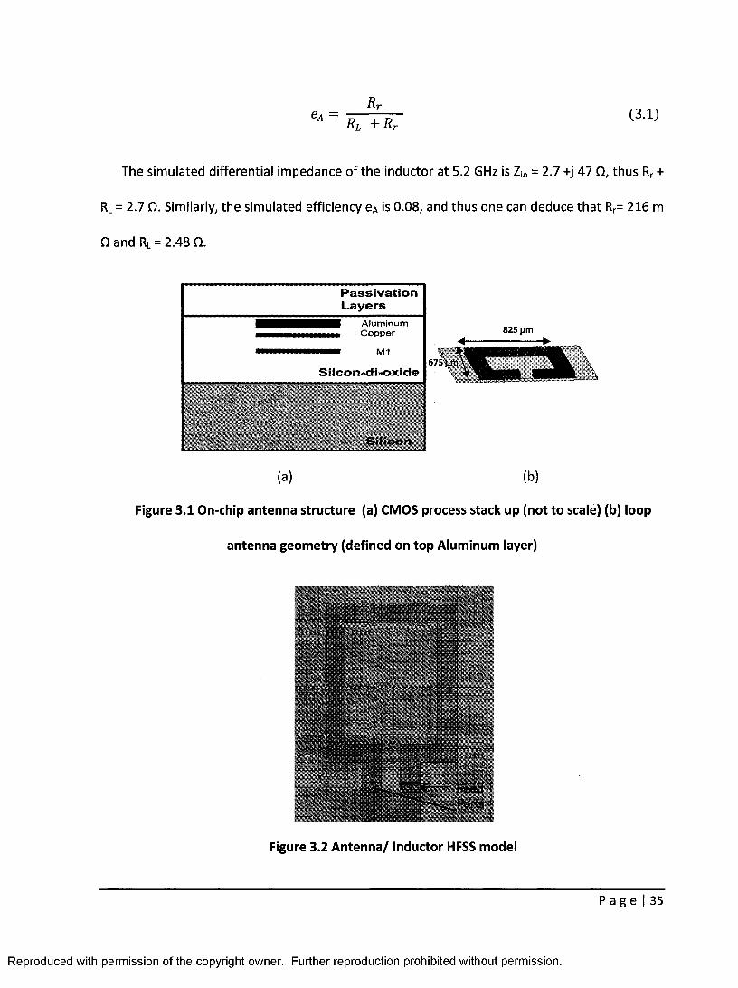
The simulated differential impedance of the inductor at 5.2 GHz is Zin = 2.7 +j 47 Q, thus Rr +
Rl = 2.7 Q. Similarly, the simulated efficiency eA is 0.08, and thus one can deduce that RR= 216 m
Q and RL = 2.48 Q.
Passivation Layers
Aluminum Copper
ma—m M1
Sllcon-dl-oxido
Silicon I
825 nm
675 nm
(a) (b)
Figure 3.1 On-chip antenna structure (a) CMOS process stack up (not to scale) (b) loop
antenna geometry (defined on top Aluminum layer)
Figure 3.2 Antenna/ Inductor HFSS model
P a g e | 35
Reproduced with permission of the copyright owner. Further reproduction prohibited without permission.

dB(GainTotal) Z i Normalized Theta
Figure 3.3 Antenna/ inductor simulated radiation pattern
3.1.2 Lumped Model
Precise equivalent lumped element modeling of on-chip inductors is critical for circuit
design. At microwave frequencies, circuit design becomes considerably more difficult with the
inclusion of many parasitic elements which are insignificant at lower frequencies. Using an
accurate model, integrated circuit designers can reduce the overall turnaround time and design
cost. Full-wave electromagnetic simulator tools can be utilized to extract the required lumped
models, but at the cost of large computing times. Alternatively, measured/simulated S-
parameters can be utilized to extract a lumped element model through optimization
techniques. Many researchers have reported on the modeling of inductors on a silicon
substrate and have established a very well known equivalent lumped model [102, 103], yet a
modified lumped model topology is needed to represent a differential inductor. This modified
model is shown in Figure 3.4 where Rs, RSUb, Cox, Cs and Ls represent the series resistance,
substrate resistance, oxide capacitance, substrate capacitance and the inductance associated
with the on-chip inductor respectively [104]. The typical single-ended lumped model has two
P a g e | 36
Reproduced with permission of the copyright owner. Further reproduction prohibited without permission.

separate branches connected to ground. Each branch has its own RSUb, Cox and Cs in contrast to
the differential model where the two branches are connected to each other, resulting in single
Rsub, Cox and Cs elements.
Rs Ls
-| WA, p-r
^sub
Figure 3.4 Differential inductor lumped model
A strategy to extract the element values of the model is to develop an optimization
technique which will match the simulated on-chip inductor S-parameters with the lumped
model S-parameters for the frequency range of interest. ADS simulator is utilized for this
optimization procedure. The ADS test bench is loaded with the HFSS simulated on-chip inductor
S-parameter file. The lumped model is simulated from 100 MHz to 10 GHz (the same frequency
range as that of the input S-parameter file from HFSS) and the optimization goal is set to
achieve the minimum possible error between the two sets of S-parameters. The initial values
for the series resistance and inductance are estimated from the simulated on-chip inductor
input impedance, whereas the oxide capacitance value is roughly expected from the oxide
dimensions. Table 3.1 shows the values of the lumped elements extracted from ADS. With
these values, an acceptable match is observed between the HFSS and ADS S-parameters at 5.2
GHz, as shown in Figure 3.5. Though it is possible to import the s-parameters of the
P a g e | 37
Reproduced with permission of the copyright owner. Further reproduction prohibited without permission.

inductor/antenna directly into Cadence, the differential lumped model was developed as an
intermediate verification step. Also, since this design only requires good matching at 5.2 GHz,
the lumped model was not optimized further for a wide band match. For a wideband design,
well -known techniques can be adopted to develop a lumped model which has a good match in
the entire band of interest. It is worth mentioning here that the simple differential model
shown here is unable to represent any common mode present in the design.
Table 3.1 Lumped element values from ADS
Rs 2.3 n
Ls 1.4 nH
Rsub 4.9 KO
Cs 7 fF
Cox 500 fF
ml (HFSS 5.2 GHz)
freq (0.1 GHz to 10.0 GHz)
Figure 3.5 HFSS and ADS S-parameters from lumped model optimization set up
P a g e | 38
Reproduced with permission of the copyright owner. Further reproduction prohibited without permission.

3.2 Oscillator Transmitter Implementations
The developed on-chip inductor/ antenna will be implemented in two oscillator transmitter
circuits presented in the following sections.
3.2.1 Phase lock loop with on-chip antenna
As an initial test vehicle for the 5 GHz on-chip antenna, a Phase Lock Loop (PLL) based
oscillator TX circuit was developed in collaboration with a fellow PhD student Victor Karam, the
details of which are given in [14]. The fabricated TX chip, is shown in Figure 3.6. The total size of
the chip is 1.4 mm by 1.4 mm, in which 825 |im by 675 |im of area is occupied by the on-chip
antenna. As mentioned in section 3.1.1, the antenna size was reduced in the layout because of
the limited chip space. This reduced the inductance associated with the inductor/antenna and
in turn shifted the operation frequency of the VCO to 6.3 GHz. The metal width of the antenna
is 100 nm and it is fed differentially by the VCO placed in its centre. The rest of the chip is
occupied by the bond pads, and PLL circuits which are placed outside the loop to avoid
complicating the routing between the circuits and the bond pads. The VCO is placed in the
centre of the loop through feed lines with microsurgery points. The bond pads can be removed
through a laser trimming technique for normal operation of the VCO connected to the antenna.
On the other hand, independent testing of inductor/antenna is possible through the bond pads
after disconnecting the VCO from the other end of the antenna.
P a g e | 39
Reproduced with permission of the copyright owner. Further reproduction prohibited without permission.

Figure 3.6 Microphotograph of PLL TX with on-chip antenna
Inductor Measurements
The inductor/antenna was disconnected from the VCO using a semiconductor microsurgery
technique, and probed for characterization as a passive single-ended inductor due to test
equipment limitations. Figure 3.7 compares the inductor's simulated and measured single-
ended Q with the simulated differential Q. In Figure 3.8 the same comparisons are made for L.
The measured and simulated single-ended Q are in close agreement across the band of interest,
which validates the simulation technique. This also confirms that the simulated results for
differential Qare reliable. As can be seen from Figure 3.7, the differential Q value is significantly
higher (as expected) and this value was employed in the TX circuit analyses. At the design
frequency of 5.2 GHz, an input impedance of Zin = 9.6 + j58 Q was measured, corresponding to
an inductance of 1.75 nH. The discrepancy between the simulated and measured inductance is
P a g e | 40
Reproduced with permission of the copyright owner. Further reproduction prohibited without permission.

0.3 nH, which can be attributed to extra narrow interconnects leading to the bond pads from
the antenna's feeding paths. Also, the measured inductance appears to have a lower self-
resonate frequency, which is probably a result of the bond pads' parasitic capacitance.
25
20
15
a
10
5
0. *
Frequency (GHz)
Figure 3.7 Simulated vs measured Q of inductor/antenna
3.00-
2.25_
_ 1.50-X c >w< —I
0.75_
Figure 3.8 Simulated versus measured inductance of inductor/antenna
P a g e | 41
% *• _
*
—Measured Single-Ended Q —Simulated Single-Ended Q • Simulated Differential Q
% *• _
*
I
* • *•.
vv
Measured S Simulated S Simulated C
ingle-Endec ingle-Ende ifferential L
i L i L
\
_____ \ \ \ \ \ \ \ 1
\ \ \ \
rst - n K ' El — —<
Freq [GHz]
Reproduced with permission of the copyright owner. Further reproduction prohibited without permission.

Antenna Measurements
A challenging part of this work is to measure the gain and radiation pattern of the miniature
antenna. In order to avoid the complexities of an external balun and the accompanying de-
embedding procedure, or the use of elaborate differential test equipment, the antenna is
tested while connected to the VCO. Since the antenna is fed by the TX VCO, it does not require
to be connected to the signal source for testing in the usual way. Rather, the radiating chip is
mounted on a printed circuit board with RF connectors and placed vertically in an anechoic
chamber, with the received signal collected by a spectrum analyzer via a patch antenna. The
setup is shown in Figure 3.9. The measurement setup is first calibrated using two identical
microstrip patch antennas at a distance of 30 cm from each other. The TX patch antenna is
connected to the signal generator whereas the RX patch antenna is connected to the spectrum
analyzer. The transmit power (Pt) at the patch antenna must be the same as that supplied by
the VCO to the on-chip antenna.
Considering that the supply voltage for this technology is 1.2 V, the differential peak voltage
across the inductive antenna VANT_diff is assumed to be 1.2 V. The power delivered can then be
calculated by applying this voltage across the differential real impedance of the antenna,
RANT_diff- According to the antenna's series resistance RANT = 2.7 Q and quality factor QANT = 17,
the differential resistance can be found with the following impedance transformation
Rant_ DIFF-^ANT (QANT 2+1) = 783 Q (3.2)
P a g e | 42
Reproduced with permission of the copyright owner. Further reproduction prohibited without permission.

Thus, the power delivered to the antenna is expected to be Pt = VANT_diff2 / (2RANT_diff) = 920
^W, or approximately 0 dBm. Since the antenna's radiation efficiency is 8%, the power radiated
is Prad = 0.08 • Pt = 73.5 |iW.
Both the patch antennas have a gain (Gp) of 6.7 dBi and by supplying the required power to
the TX patch antenna, a received power (Prp) of -24.8 dBm is recorded. Next, the TX patch
antenna is replaced by the TX chip having the on-chip antenna. The RX patch antenna is left
untouched. In this measurement setup, a received power (Prc) of -69.8 dBm is recorded. The
gain of the chip antenna (Gc) can now be calculated from (3.3), which is derived from the Friis
transmission equation [105], knowing that the frequency, distance and transmit power remain
the same as in the calibration measurement.
Figure 3.9 On-chip antenna radiation pattern measurement setup
P a g e | 43
Reproduced with permission of the copyright owner. Further reproduction prohibited without permission.

The chip antenna is next rotated in the azimuthal plane (in steps of 159, from +90° to -90°
off boresight) and the gain is plotted for every step. Note that ± 90° corresponds to the plane of
the loop. The resultant radiation pattern is shown in Figure 3.10. A spline interpolation method
is employed to plot a smooth radiation pattern from a discrete set of data points. The peak gain
lobe is slightly off from the plane of the loop; however a null is measured at boresight, as
expected. The region from boresight to -90° did not produce a symmetrical pattern due to
strong parasitic coupling and interference from the PLL circuits (and the large loop filter
capacitors) on that side of the chip. In comparison to the simulated radiation pattern, the
measured radiation pattern is more tilted towards boresight because of the asymmetrical
position of the antenna with respect to the edges of the die. Additionally, the measured
antenna is mounted on a printed circuit board (PCB) with a large ground plane and numerous
passive components, none of which are present in the HFSS model. A maximum gain of -22 dBi
is achieved. Positioning the on-chip antenna at the maximum gain angle, the RX patch antenna
is then moved back in steps of 30 cm. The received power is recorded for different separation
distances and the results are plotted in Figure 3.11. A close match is observed between theory
and the measured results. With a transmitted power of 1.3 dBm, the on-chip antenna on the TX
side can communicate with an off-chip patch antenna on the RX side placed 2 m away. The
range is limited by the RX sensitivity which is -70 dBm in this case.
P a g e | 44
Reproduced with permission of the copyright owner. Further reproduction prohibited without permission.

A Gain for 15 degrees steps
Interference from RF circuits / asymmetric loop/die
Peak shifted due to
geometry
-50 0 Angle (Degrees)
50 100
Figure 3.10 Measured radiation pattern
Reproduced with permission of the copyright owner. Further reproduction prohibited without permission.
P a g e | 45

Friis Transmission Equation * Measurements
* * * -
_i i i i i i i i 0.2 0.4 0.6 0.8 1 1.2 1.4 1.6 1.8 2
Distance from TX to RX (m)
Figure 3.11 Measured range comparison with theory
3.2.2 Voltage Controlled Oscillator TX with on-chip antenna
In the PLL based implementation, some of the active circuits were placed outside the loop
and were very close to one of the antenna edges. This resulted in deteriorated radiation
performance. Therefore a new TX chip has been designed which operates as an oscillator TX
and does not require the PLL circuits and an off-chip reference crystal. This design has been
completely conducted by the author, and is customized for subsequent integration with
radiation sensors. The TX here makes use of direct modulation of VCO with no closed feedback
loop. This method has the advantage of the data rate not being limited by the loop bandwidth
of a phase lock loop circuit. Moreover, the direct modulation of a closed loop VCO would cause
the modulated waveform to distort by the negative feedback loop of a PLL [106]. Above all, a
PLL circuit would consume more power than a simple VCO and would require a reference
P a g e | 46
-20
-25
-30
I-45 "O a> -50
"a5 g -55 en
-60
-65
-70
Reproduced with permission of the copyright owner. Further reproduction prohibited without permission.

signal, which is an off-chip crystal in most cases. On the other hand, the open loop direct VCO
modulation does suffer from the fact that the output frequency is susceptible to undesired
perturbation and noise. For the biomedical application being pursued in this work, the absolute
value of the free running VCO frequency is less important than the variation in the carrier
frequency due to modulation. Moreover, dosimeter sensor data modulation would cause the
free running VCO frequency to vary in only one direction permanently. Therefore any frequency
drift due to temperature or jitter can be easily identified and compensated for.
Modified On-chip Inductor/Antenna Design
In the present design, care has been taken that the antenna remains close to the chip edges
without any active circuits blocking it. The shape of the inductor/antenna is slightly altered to
fit it in the available chip space of 1.5 mm2 (Canadian Microelectronics chip allocation) as
shown in Figure 3.12 (VCO not part of the HFSS model). For this design, HFSS model includes
the bond pads, connecting lines and the microsurgery points. For the modified loop, HFSS
predicts an inductance of 1.4 nH and a Q of 14 at 5.2 GHz.
Reproduced with permission of the copyright owner. Further reproduction prohibited without permission.
P a g e | 47

VCO
Microsurgery Points
Bond Pads
x*
Figure 3.12 Modified On-chip inductor/antenna HFSS model
Voltage Controlled Oscillator Design
An LC cross-coupled differential VCO topology has been chosen for this work, and is shown
in Figure 3.13. It utilizes both PMOS and NMOS transistors, which generate negative resistance
to cancel the resonant tank losses. The resonant tank consists of the inductor/antenna, three
band switching capacitors and two tuning varactors. In order to increase the output voltage
swing, transistor sizing is employed to adjust the bias current instead of using a current source.
A power amplifier is not required for short range communication.
P a g e | 4 8
Reproduced with permission of the copyright owner. Further reproduction prohibited without permission.

XX Modulated
Transmitted
Inductor/.. ^ *** Signal ^sntemi^^^i"
Band Switching Capacitors
Fixed Ca pacitor
Modulating Signal from
Sen
il— II—
AY— ii it i_> 111 mmmmmm nsor I
*ik * yf-Varacto rs
Figure 3.13 VCO schematic (core only)
The VCO design is based on a simultaneous transconductance 'gm' and impedance matching
technique. This approach reduces the flicker noise, improves output signal power and VCO
phase noise performance. To maximize the output power in the complementary VCO, the
voltage swing has to be maximized. This can be achieved by setting the dc operating voltage at
the resonator to half of the drain voltage (VDD) by matching the gm of the PMOS to that of the
NMOS. For gm matching, the PMOS width is kept 2.5 times that of the NMOS as a rule of thumb
to account for lower mobility in PMOS devices. The gate lengths of NMOS and PMOS are
identical in this case. However, for simultaneous gm and impedance matching, the length of the
P a g e | 49
Reproduced with permission of the copyright owner. Further reproduction prohibited without permission.

PMOS is chosen to be the minimum possible gate length whereas for NMOS a larger gate length
is used. The widths for both types of transistors are estimated analytically and then optimized
through circuit simulation.
The MOS varactors employed in this work exhibit the maximum tunability for a biasing
range of -0.2 to +0.2 V. Since the sensor data will modulate the carrier frequency through the
control line of these varactors, maximum TX sensitivity will be achieved by providing control
signal in this biasing range. The band switching capacitor bank comprises three Metal Insulator
Metal (MIM) capacitors. Provision has been made to disconnect two of these MIM capacitors,
in the case of wide fabrication tolerances. This can switch the operating band from 5 GHz to
5.25 GHz or 5.5 GHz respectively. The varactors can provide a fine tuning of ± 200 MHz around
any of these bands. The VCO outputs are buffered through cascaded inverters as shown in
Figure 3.14. The three stage buffer on either side of the differential circuit ensures minimum
loading of the VCO core. The buffers are included only for measurements or connection to an
external antenna, and will remain off during the normal operation of the Soc transmitter. A
separate bias line for the buffers ensures that the buffers are turned on only when required.
The simulated time domain output of the VCO through the buffers is shown in Figure 3.15,
which confirms the 5.2 GHz frequency of operation. The post layout simulations of the VCO
demonstrate a phase noise of -118 dBc/Hz at 1MHz offset as shown in Figure 3.16. The phase
noise is strongly dependent on the Q of the on-chip inductor, which if increased will turn the
inductor into a poor radiator.
P a g e | 50
Reproduced with permission of the copyright owner. Further reproduction prohibited without permission.

IN
.
I- -•Out
Figure 3.14 Buffer schematic
^ 700
at 600
o 500
I 400
VCO Output Signal
3^8 3.4 3.6 Time(ns)
Figure 3.15 VCO time domain output through the integrated buffer
P a g e | 51
Reproduced with permission of the copyright owner. Further reproduction prohibited without permission.

-20 Phase Noise
-40
£ -80
o -120 to (0 a. -140
-160
-180
Relative Frequency (Hz)
Figure 3.16 VCO simulated phase noise
Layout and and Fabrication
The chip microphotograph is shown in Figure 3.17. Its size is 1 x 1.5 mm2, which is the
smallest reported TX chip with an on-chip antenna for the 5 GHz band. The antenna is placed in
the centre with two sides close to the chip edges and having no active circuitry, or bond pads in
close vicinity. A metal width of 100 pirn is employed which is more than the 25 |im maximum
permissible metal width for the top metal layer. The violation of this design rule was achieved
by inclusion of an additional layer on top of the antenna. The VCO is placed in the centre of the
loop antenna and has a guard ring protection for noise suppression (not shown in Figure 3.17).
A separate set of bond pads is provided for passive inductor testing. The VCO can be tested
through the two buffers at the differential outputs. Electrostatic discharge (ESD) structures
have been implemented with all the bond pads for protection. Appropriate microsurgery points
have been incorporated in the layout for isolating and testing different structures independent
P a g e | 52
Reproduced with permission of the copyright owner. Further reproduction prohibited without permission.

of each other. Metal is inserted in order to meet the metal fill density specifications of the
process. However, care has been taken that no top metal layer is filled close to the antenna,
and the least amount of metal is placed inside the loop.
o n ! r \ i :
Figure 3.17 Microphotograph of VCO TX with on-chip antenna
Measurements
The modified on-chip antenna gain and radiation pattern are measured with the same
technique described in section 3.2.1, however, this time the TX chip is not mounted on a PCB.
Instead, the measurements are done on bare die glued to a glass plate as shown in Figure 3.18.
A custom stand is used to measure the radiated power at different angles and the scanning is
done manually. A measured gain of-22 dB is achieved, which is consistent with the previous on-
chip antenna measurements. The measured radiation pattern is given in Figure 3.19. It is
significantly improved from the previous measured radiation pattern as the maximum radiation
is achieved along the plane of the loop (± 90°), as expected. This confirms the validity of the
P a ge | 53
Reproduced with permission of the copyright owner. Further reproduction prohibited without permission.

design precautions applied to this chip. There is, however, still a difference of 3 to 4 dBs
between the levels of each radiation pattern peak. The asymmetry can be attributed to
measurement error, namely the presence of metal obstructions at +90°.
R\
I TX with <
(b)
Figure 3.18 On-chip antenna (a) radiation pattern measurement setup (b) zoom in of
probe feeding
P a g e | 54
Reproduced with permission of the copyright owner. Further reproduction prohibited without permission.

A. Measured Data —— spline Sf OQ
S 1
50 100 -50 Angle (Degrees)
Figure 3.19 On-chip antenna measured radiation pattern
The VCO draws an average current of 2.8 mA and consumes 3.3 mW of power from a 1.2V
supply. The power dissipation, in general, is higher for differential circuits; however with high Q
inductors it can be reduced. The power dissipation can also be reduced by using a lower current
value at the expense of reduced output power and range. The oscillation frequency
measurement done on a spectrum analyzer via the output buffers is shown in Figure 3.20. It
confirms the frequency of operation to be 5.26 GHz as designed. A phase noise of -107 dBc/Hz
is measured at 20 MHz offset, and is shown in Figure 3.21. As previously discussed, such phase
noise performance is expected with the relatively low Q inductor/antenna employed.
P a g e | 55
Reproduced with permission of the copyright owner. Further reproduction prohibited without permission.

RTTEH 10dB MKR -31.33dBm RL 0dBm 10dB/* 5. 2663GHz
A
1 Jj -ti-" L^J 1,1 1.. Il • —*tjj •
CENTER 5.2700GHz SPRN 100.0MHz RBW 1.0MHz UBUI 1.0MHz SWP 50.0ms
Figure 3.20 TX VCO measured response
10 dB/ SPOT FRQ = 20.0 MHz RL -50 dBc/Hz -107.00 dBC/Hz
t
FREQUENCY OFFSET FROM 5.149 GHz CARRIER
100 MHz
Figure 3.21 Measured phase noise
P a g e | 56
Reproduced with permission of the copyright owner. Further reproduction prohibited without permission.

With the integration of a suitable power source, the complete wireless dosimeter can be
smaller than a dime as shown in Figure 3.22.
3.3 RX Side On-chip Antenna
This section presents an on-chip antenna design for a monolithic receiver chip realized in a
standard 0.13um CMOS process. This work was done collaboratively with fellow PhD student
Muhammad Arsalan who designed the circuits for the receiver chip. The on-chip antenna has
been conjugately matched to the differential Low Noise Amplifier (LNA) for a wide frequency
range through co-design of the circuits and antenna. In order to optimize the chip space, the
circuits are placed inside the antenna as shown in Figure 3.23.
Recently, many RX SoC designs have been reported which employ on-chip antennas
[36][107][108]. However, all these designs are for very high frequencies where on-chip antenna
Transmitter
Sensor
Figure 3.22 Demonstration of wireless dosimeter
P a g e | 57
Reproduced with permission of the copyright owner. Further reproduction prohibited without permission.
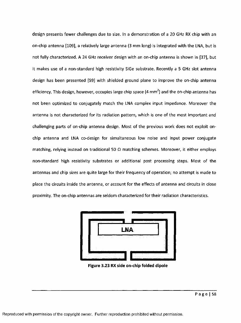
design presents fewer challenges due to size. In a demonstration of a 20 GHz RX chip with an
on-chip antenna [109], a relatively large antenna (3 mm long) is integrated with the LNA, but is
not fully characterized. A 24 GHz receiver design with an on-chip antenna is shown in [37], but
it makes use of a non-standard high resistivity SiGe substrate. Recently a 5 GHz slot antenna
design has been presented [59] with shielded ground plane to improve the on-chip antenna
efficiency. This design, however, occupies large chip space (4 mm2) and the on-chip antenna has
not been optimized to conjugately match the LNA complex input impedance. Moreover the
antenna is not characterized for its radiation pattern, which is one of the most important and
challenging parts of on-chip antenna design. Most of the previous work does not exploit on-
chip antenna and LNA co-design for simultaneous low noise and input power conjugate
matching, relying instead on traditional 50 Q matching schemes. Moreover, it either employs
non-standard high resistivity substrates or additional post processing steps. Most of the
antennas and chip sizes are quite large for their frequency of operation; no attempt is made to
place the circuits inside the antenna, or account for the effects of antenna and circuits in close
proximity. The on-chip antennas are seldom characterized for their radiation characteristics.
1 f
LNA
Figure 3.23 RX side on-chip folded dipole
P a g e | 58
Reproduced with permission of the copyright owner. Further reproduction prohibited without permission.
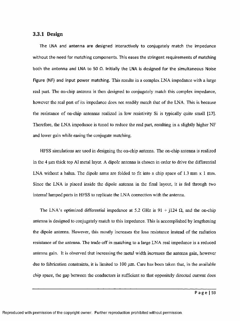
3.3.1 Design
The LNA and antenna are designed interactively to conjugately match the impedance
without the need for matching components. This eases the stringent requirements of matching
both the antenna and LNA to 50 Q. Initially the LNA is designed for the simultaneous Noise
Figure (NF) and input power matching. This results in a complex LNA impedance with a large
real part. The on-chip antenna is then designed to conjugately match this complex impedance,
however the real part of its impedance does not readily match that of the LNA. This is because
the resistance of on-chip antennas realized in low resistivity Si is typically quite small [17].
Therefore, the LNA impedance is tuned to reduce the real part, resulting in a slightly higher NF
and lower gain while easing the conjugate matching.
HFSS simulations are used in designing the on-chip antenna. The on-chip antenna is realized
in the 4 jim thick top A1 metal layer. A dipole antenna is chosen in order to drive the differential
LNA without a balun. The dipole arms are folded to fit into a chip space of 1.3 mm x 1 mm.
Since the LNA is placed inside the dipole antenna in the final layout, it is fed through two
internal lumped ports in HFSS to replicate the LNA connection with the antenna.
The LNA's optimized differential impedance at 5.2 GHz is 91 + j 124 Q, and the on-chip
antenna is designed to conjugately match to this impedance. This is accomplished by lengthening
the dipole antenna. However, this mostly increases the loss resistance instead of the radiation
resistance of the antenna. The trade-off in matching to a large LNA real impedance is a reduced
antenna gain. It is observed that increasing the metal width increases the antenna gain, however
due to fabrication constraints, it is limited to 100 |J,m. Care has been taken that, in the available
chip space, the gap between the conductors is sufficient so that oppositely directed current does
P a g e | 59
Reproduced with permission of the copyright owner. Further reproduction prohibited without permission.

not cancel the radiated fields. Nonetheless, due to the lossy nature of the Si substrate, this effect
is minimal. In simulations, a sensitivity analysis is done to choose suitable locations of the LNA
elements with respect to the antenna so as to achieve minimum spacing between the various
elements. The final dimensions of the antenna are 1.3 mm x 0.7 mm, resulting in a differential
impedance of 90 - j 133 £2 at 5.2 GHz. This yields an excellent match between the on-chip
antenna and the LNA impedances over a broad bandwidth, as shown in Figure 3.24. It is worth
mentioning here that the co-design of antenna and LNA has helped to achieve a wide impedance
bandwidth. Simulations reveal a bore-sight maximum radiation pattern with a gain of -35 dBi. It
is also observed in simulations that placing the antenna closer to the chip edges slightly increases
the gain.
o
-10
-20
-30
CD -O -40
w SO
-so
-70
-SO 1 2 3 4 5 6 7 8 9 1 (
Frequency (GHz)
Figure 3.24. Simulated Sll of on-chip antenna (referenced to complex impedance of LNA)
1 1 1
10dB bandwidth
P a g e | 60
Reproduced with permission of the copyright owner. Further reproduction prohibited without permission.
3.3.2 Fabrication and Measurements
Since the circuits are placed inside the antenna, there are several challenges associated with
the layout of the chip. Placement of several inductors inside a small area without affecting the
performance of the circuits or the antenna, and facilitating independent testing of different sub-
modules, are the most difficult aspects. Also, routing the bias, signal and ground traces to the
pads through a complex circuit without breaking any design rules is difficult. Nonetheless,
insight gained from EM and post layout circuit simulations and inclusion of microsurgery points
eases some of these challenges. Another consideration is to make the layout as symmetric as
possible to ensure true differential operation. As shown in the microphotograph (Figure 3.25), of
the realized chip the antenna remains close to the chip edges with minimal interference from
nearby metals.
Figure 3.25. Microphotograph of the receiver chip
P a g e | 61
Reproduced with permission of the copyright owner. Further reproduction prohibited without permission.

As was seen with the two previous SoC designs, experimental characterization of the
radiation properties of the on-chip dipole antenna is challenging. A moveable microscope with
a custom stand is employed to perform the measurements. A transmitter patch antenna with gain
Gp is mounted on the stand which can rotate around the receiver chip. It is fed through the signal
generator with a known transmit power Pt. The power is received at bore-sight by another patch
antenna placed on the probe station chuck and recorded through the spectrum analyser as Prp.
The receive patch antenna is then replaced by the receiver chip while the rest of the setup
remains the same. The power received by the on-chip antenna, after being amplified by the
LNA, is measured and is denoted as Prc. The on-chip antenna gain Gc can now be calculated
through (3.4), where LNAq is the amplifier gain obtained from a separate measurement of the
micro-surgically disconnected LNA [23].
Gc = Prc ~ Prp +GP~ LNAG (3.4)
The measured antenna gain from (3.2) is -35 dBi, which is 0.25 dB of the simulated antenna
gain. In simulations, it is observed that the on-chip antenna gain varies from -45 dBi at 3 GHz to
-25 dBi at 10 GHz. The measured radiation pattern is shown in Figure 3.26, and seen to be in
good agreement with the simulated radiation pattern of the dipole antenna.
P a g e | 62
Reproduced with permission of the copyright owner. Further reproduction prohibited without permission.

0
-2
-4
-6
a -8 •o IT-10
12
14
16
ia
n 0
-J XT"—«.»/
>
1 1
/
/ /
\ 1 \ \ \
V \ \ \ \ \ \\
I t
1 ' 1 1 —Measured » — Simulated
1 ' 1 1 —Measured » — Simulated
-40 -20 0 20 Angle (Degrees)
40 60 80
Figure 3.26 On-chip antenna radiation pattern (simulated and measured)
3.4 RF SoC Design Issues
Following the design and experimental work conducted in this chapter, it is important to
highlight the major challenges and issues involved in advanced RF SoC development. These
points will be useful for continued research on the topic.
1. No single simulation tool can handle the SoC design efficiently. Therefore, a co-design
methodology is required through EM, microwave and circuit simulators to tackle this
multi-domain problem.
2. Antenna is not typically on-chip, therefore its layout along with circuits, and metal fill is
challenging. Since there are no dedicated metal layers or rules for on-chip antennas,
many Design Rule Checks (DRC) result in errors. These have to be tackled in unique
ways. An example is that the antenna's large metal width connected to the transistors
P a g e | 63
Reproduced with permission of the copyright owner. Further reproduction prohibited without permission.

violates the antenna rule. This error is resolved by providing a ground connection to
one of the antenna arm. This ground connection must be removed through
microsurgery (laser) before the measurements.
3. Parasitic coupling from circuits, inductors, and nearby bond pads can deteriorate
antenna's performance so their placement with respect to antenna has to be carefully
investigated in EM simulations.
4. Interference in circuits due to nearby radiator element could not be investigated in post
layout circuit simulations, due to the simulator's limitations.
5. Placement of close by inductors requires the currents to be in opposite directions in
order to cancel the mutual coupling between them as shown in Figure 3.27.
6. Undesired coupling through the substrate must be blocked through guard rings around
circuits and inductors.
7. It is hard to plan metal fill till the layout is near completion, therefore metal fill must be
done with back and forth simulations in EM and circuit simulator a shown in Figure 3.28.
8. Tuning elements are added to compensate for any process variations. For example the
band switching capacitors in the TX VCO are designed to adjust the operational
frequency if required.
9. On-chip antenna radiation characteristics cannot be measured in anechoic chamber
unless the chip is mounted on a board. Mounting the chip results in erroneous results
P a g e | 64
Reproduced with permission of the copyright owner. Further reproduction prohibited without permission.

because of blocking and interference from other components as observed in Figure
3.10. It is therefore better to measure the radiation pattern on the bare die. However,
this requires custom setup and careful use of probes.
Inductors placement
4
Metal fill
Figure 3.27 SoC design issues
Metal fill Check in EM Sims
Figure 3.28 SoC design issues (metal fill)
P a g e | 65
Reproduced with permission of the copyright owner. Further reproduction prohibited without permission.

3.5 Summary and Contribution
In fulfillment of the first three objectives of the thesis, this chapter has presented three
novel SoC designs having on-chip antennas combined with RF transmitter and receiver circuitry.
A highly integrated, low power CMOS VCO TX has been demonstrated for short range wireless
radiation sensor applications. The VCO tank inductor has been optimized to act as an on-chip
inductor-antenna, thus minimizing chip area. Its 0.5mm2 size is the smallest reported on-chip
antenna in the UN II band. This is the first ever demonstration of experimental characterization
of an on-chip inductor/antenna for its radiation properties. The tradeoffs in the design and
challenges in the experimental work have been highlighted. The complete TX chip sized 1.5mm2
consumes 3.3 mW of power and can communicate with a low noise receiver connected to a
patch antenna 2 m away from the TX. With the integration of a suitable power source, the
complete wireless dosimeter can be smaller than a dime as shown in Figure 3.22. On the RX
side, co-design of on-chip dipole antenna and LNA has been demonstrated for conjugate
matching. These results represent the first contribution of this thesis, namely 'Oscillator TX with
On-chip Inductor/Antenna'.
The work of this chapter has led to many publications. One journal [9] and seven
conference papers have already been published [11-15][17][18]. One more journal paper has
been accepted recently [23].
P a g e | 66
Reproduced with permission of the copyright owner. Further reproduction prohibited without permission.

Chapter 4
4 RFLTCCSoP SoC, while highly miniaturized, has a number of limitations as was described in Sec 3.4.
Excellent miniaturization of RF electronics is possible through innovative SoP designs to achieve
compact yet efficient wireless systems. Within the SoP domain, LTCC can offer numerous
advantages, including the possibility of using an arbitrary number of layers to embed passives
and enable vertical integration of RF components within a single module. Moreover, the low
loss nature of LTCC substrates makes them very suitable for efficient antenna design. This
chapter will investigate innovative ways to package RFICs in order to make the overall wireless
dosimeter system compact, low power and efficient. In accordance with the fourth and fifth
objectives of this thesis, two 5 GHz SoP designs are proposed in this chapter. An LTCC TX
package with a conventionally connected antenna will first be described. This will serve as a
reference design for a second LTCC TX package having a highly innovative aperture coupled
antenna. Finally, to fulfill the six objective of the thesis, an analytical model for the antenna
coupling scheme of the latter design will be given.
P a g e | 67
Reproduced with permission of the copyright owner. Further reproduction prohibited without permission.

4.1 Conventional LTCC package with antenna
The oscillator TX chip described in section 3.2.2 has been shown to work independently
through its on-chip antenna, although its range was limited due largely to poor antenna gain.
One way to enhance the range for applications like EVARM is by employing an efficient package
antenna in a low loss medium. The chip has to be packaged in any case, so if the package
houses an integrated antenna it can be connected to the chip through the conventional bond
pad and bond wire arrangement, or through a flip-chip and solder balls option. Generally, the
RF transceiver circuits are quite sensitive to this external loading and therefore require an
isolating buffer amplifier in between the chip circuitry and the external components. A major
advantage of integrated antennas is their ability to conjugately match the circuit's impedance
without any matching components. In this context, the LTCC antenna for the proposed SoP is
designed to conjugately match the output impedance of the oscillator TX's buffer amplifiers.
Since the TX chip (the same one as in Sec. 3.2.2) has differential circuits, it is best to employ a
differential antenna. Moreover, the antenna simulation must take into account the complete
package along with the antenna as this is an attempt to co-design the two. With the buffer
amplifiers turned on and properly matched to the package antenna, most of the power will be
supplied to it and efficiently radiated. Nonetheless, some power will still be lost through
radiation of the on-chip inductor, as it was originally optimized as an antenna.
P a g e | 68
Reproduced with permission of the copyright owner. Further reproduction prohibited without permission.

4.1.1 LTCC antenna/package co-design
The proposed SoP's simulation geometry is shown in Figure 4.1. The module employs an
efficient LTCC antenna in addition to having a cavity to accommodate the TX chip. In this work,
the LTCC package with integrated antenna is designed in an eight layer (800 |im) thick Ferro A6-
S process. The material properties of the LTCC tape system are listed in Table 4.1 [110]. This
antenna must be connected to the TX VCO through the buffer amplifiers to avoid loading of the
VCO. The buffer amplifiers exhibit a differential impedance of 32-jl2 Q, so the antenna is
designed to provide a good return loss with reference to this impedance at 5.2 GHz. A dipole
antenna is chosen and its arms are folded to optimize space consumption. The final antenna
structure resulted in a differential impedance of 48+j25 Q, which in turn provided a return loss
of 13 dB at 5.2 GHz. The dipole displays a gain of -1 dB with a broadside radiation pattern as
shown in Figure 4.2. The final SoP layout contains an additional cavity to house the sensor chip.
The complete LTCC package, sized 1.6 cm X 1.6 cm, contains cavities with appropriate ground
and supply connections for both the sensor and the TX chips. Both cavities are tailored to the
respective chip dimensions and are five layers deep. The control signal line from the sensor to
the TX chip is routed through the package, and wire bonded at each end. The package could
easily accommodate a power source by means of a cavity formed on its backside, with the
necessary interconnects embedded in the package. The fabricated package, mounted on a test
board, is shown in Figure 4.3. The bias and ground connections are also provided through
package interconnects.
P a g e | 69
Reproduced with permission of the copyright owner. Further reproduction prohibited without permission.
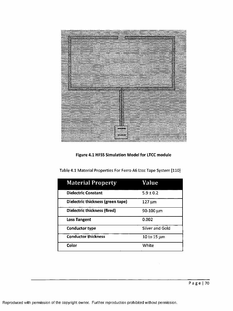
Figure 4.1 HFSS Simulation Model for LTCC module
Table 4.1 Material Properties For Ferro A6 Ltcc Tape System [110]
Dielectric Constant 5.9 ±0.2
Dielectric thickness (green tape) 127 |iim
Dielectric thickness (fired) 90-100 |im
Loss Tangent 0.002
Conductor type Silver and Gold
Conductor thickness 10 to 15 jam
Color White
P a g e | 70
Reproduced with permission of the copyright owner. Further reproduction prohibited without permission.

liB(UainTotal) -1,05106+000
1-1.8139e+000 -2.5?68e+000 -3.S398ef000 -%,1027e+000 -H,86566+000 -5.6285e+0Q0
I -8. 3914e+000 1 -7,1544e+000 1-7,91736+000 | -8* .68026+000
-9. Ht31;«+000 *1,02066*001 ^l,0969e+001 «1.1732e+001 -1.2H95e+031 -1.3258e+001
Figure 4.2 Simulated LTCC dipole radiation
—
Figure 4.3 Photograph of LTCC module
P a g e | 71
Reproduced with permission of the copyright owner. Further reproduction prohibited without permission.

Testing of the LTCC SoP module was performed with the TX chip duly connected to the
antenna through bond wires as shown in Figure 4.3. A horn antenna connected to a spectrum
analyzer received the power from the wireless SoP module under test. Initially the buffer
amplifiers were turned off and the power received through the on-chip antenna (SoC approach)
was recorded. Then, the buffer amplifiers were turned on and power was measured through
the LTCC antenna (SoP approach). Larger current is required in this case to operate the buffer
amplifiers which were turned off in the SoC implementation. The wireless LTCC SoP was seen to
provide 12 dB more transmitted power as compared to the SoC design. Though a substantial
increase in TX power is observed, the power actually delivered to the LTCC antenna was lower
than expected. This discrepancy is attributed to the mismatch loss resulting from the presence
of bond wires (the simulation setup did not include the bond wires). It was not deemed
necessary to perform more extensive testing of this LTCC SoP because 1) this is only a reference
design, 2) the appropriate test structures (probe pads, etc) were not available. Nonetheless,
assuming no mismatch loss, range calculations similar to the ones done for the SoC case
(Section 3.2.1), reveal that the conventional LTCC SoP module can communicate up to a range
of 75 m. This is a significant extension in wireless communication distance compared to the 2 m
obtained with the SoC design. However, such an increase comes at the expense of increased DC
power consumption from 3.3 mW to 38 mW due to the biasing required for the buffer
amplifiers.
P a g e | 72
Reproduced with permission of the copyright owner. Further reproduction prohibited without permission.

4.2 Aperture Coupled LTCC SoP
Previous SoP (section 4.1) demonstrated an increase in communication range with an
efficient LTCC antenna, but with increasd power consumption. Though, the enhanced
communication range is attractive, but it is desirable to achieve it with minimal increase in
power consumption. The aperture coupled LTCC SoP design is targeted towards the same goal.
Generally, the RF circuits are connected to the feed line of an LTCC antenna through bond wires
or solder balls as shown in the previous section. Typically, this arrangement requires an
isolating buffer amplifier and bond pads on the chip, as well as impedance matching elements
between the antenna and RF circuits. This approach not only adds to the number of design
steps, cost and overall power consumption, but also makes the module less attractive due to
the presence of bond wires.
An interesting approach to overcome the above limitations is to establish a wireless
connection between the RF circuit and the LTCC antenna. Aperture coupling is a well
established technique for non-contact or wireless feeding of microstrip patch antennas [111].
The conventional aperture coupled patch antenna is shown in Figure 4.4. Lately, an active
integrated patch antenna fed with the aperture coupling technique has been demonstrated
[112]. In addition, a silicon based aperture coupled patch antenna is demonstrated in [113];
however they both utilize a conventional microstrip feed line. This only eliminates the physical
connection between the feed line and the antenna; the connections and components required
between the integrated circuit (IC) and the antenna feed line cannot be removed. In [83], a
parasitic coupling approach is demonstrated to couple an array of patches to the IC; however
P a g e | 73
Reproduced with permission of the copyright owner. Further reproduction prohibited without permission.

this is done through a hypothetical IC and antenna. The measured results in [83] are obtained
using a microstrip feed and via combination, which does not reflect the complexities of real
chip-to-package coupling. This proposed design alleviates the above problems by a novel SoP
implementation, which employs a wireless interconnect between the RF chip and the LTCC
antenna as shown in Figure 4.5. This is done by electromagnetic coupling from the on-chip
antenna to a coupling aperture or slot in the ground plane and eventually to the LTCC patch
antenna. The design requires neither a buffer amplifier and connecting bond pad on the chip,
nor matching elements or feed lines on the package. It also eliminates the requirement for a
balun to connect differential circuits to the single ended antennas or vice versa. To the author's
knowledge, this is the first ever LTCC aperture coupled patch antenna implementation with
direct feeding from a TX on-chip antenna.
X"
X
microstrip patch
— antenna substrate
coupling aperture
A— ground plane
^— feed substrate
microstrip feed line
Figure 4.4 Conventional aperture coupled patch concept (fed through microstrip line)
P a g e | 74
Reproduced with permission of the copyright owner. Further reproduction prohibited without permission.

-X. ^— ground plane
^ >*__ |g.e5j su^strate
antenna substrate
coupling aperture
microstrip patch:
Figure 4.5 Proposed aperture coupled patch concept (fed through TX on-chip antenna)
4.2.1 Design and Simulation
The aperture coupled patch topology utilizes a common ground plane between the
radiating antenna and the feed line [114]. For this work, aperture coupling is employed mainly
because it will allow direct coupling of the TX on-chip antenna to the LTCC patch antenna
without the need of a microstrip feed line. In addition, the buffer circuits can remain off. Also,
the ground plane in between the patch antenna and the TX chip will act as a shield for the TX
circuits. However, a limitation of this technique is that the slot in the ground plane can radiate
considerably in the backward direction. This unwanted radiation can be minimized by choosing
the optimum slot length with respect to the patch size.
P a g e | 75
Reproduced with permission of the copyright owner. Further reproduction prohibited without permission.

The Ferro A6-S LTTC tape system is again employed in this design. Each layer has a fired
thickness of 100 |im. The substrate is chosen to be 8 layers thick because it will house a 300 |im
thick RF chip in a cavity. The cavity thickness is chosen to be 600 ^m to accommodate the chip
and the biasing bond wires. The LTCC fabrication rules require a minimum of two layers
beneath the cavity, thus resulting in a total substrate thickness of 800 urn. The superstrate
which will contain the antenna can be of any other LTCC material, however for simplicity the
same LTCC tape system is used for the antenna as well.
The design procedure is as follows. First, a conventional aperture coupled patch antenna
with a microstrip feed line is simulated in HFSS. This determines the approximate size of the
patch antenna at 5.2 GHz, the feed location and the slot dimensions. Next, the microstrip line is
replaced with the TX chip. The design is optimized for maximum coupling between the on-chip
antenna and the LTCC patch antenna through the slot in the ground plane. This maximizes the
overall gain of the TX module. The thicknesses of the air gap and the superstrate determined
this way are an initial estimate of the design and will change during the final optimization. The
patch antenna dimensions of 1.7 cm x 1.7 cm are obtained in simulations. The substrate,
superstrate and ground plane dimensions are 2cm x 2cm. The feed line is placed below the
centre of the patch antenna to maximize magnetic field coupling.
After determination of the approximate patch size and feed point location, the microstrip
feed line is replaced with the TX chip. The chip is placed in a cavity sized 4.8mm x 3.8mm
exactly at the location where the microstrip line fed the patch. The size of the cavity is chosen
so as to leave enough room for the power routing and bond wires after placing the chip in the
P a g e | 76
Reproduced with permission of the copyright owner. Further reproduction prohibited without permission.

cavity. The cavity size remains the same for the lower four layers, however it is made the same
width as that of the slot in the ground plane for the top two layers. This is done to avoid
fabrication complexities. The patch antenna is on the bottom-most layer of the superstrate. The
air gap is realized through four corner posts made of the same LTCC tape system as the
substrate. The layer by layer layout of the aperture coupled module along with the final
dimensions is shown in Figure 4.6. The cross-sectional view of the module is shown in Figure
4.7. The bottom 6 layers of the substrate are fired together, whereas the top two layers (layer
7and 8) are fired separately. This is done in order to ease the placement and wire bonding of
the chip in the cavity. The top two layers of the substrate, along with the four corner posts and
superstrate are glued to the substrate after the placement of the chip. The power and ground
pads in the cavity connect to the pads on the bottom of the substrate through vias. The bottom
pads can be connected to the contacts of a custom made lithium polymer battery. The battery
would have the same lateral dimensions as that of the substrate and it could be simply glued to
the bottom of the substrate as shown in Figure 4.7.
The design is sensitive to a number of parameters, the most important being the location,
length, and width of the slot in the ground plane. Other important parameters are the air gap
and superstrate thicknesses. Extensive parametric simulations are required to optimize many
parameters at the same time. The goal is to maximize the gain of the module by efficient
coupling between the on-chip antenna and the LTCC antenna through the slot in the ground
plane, without affecting the RF properties of the circuit. Initially, keeping the slot length and
width the same as that of the microstrip fed case, the thicknesses of the air gap and superstrate
are optimized. After achieving a reasonable gain value, the thicknesses are kept constant and
P a g e | 77
Reproduced with permission of the copyright owner. Further reproduction prohibited without permission.

the slot length and width are optimized. It is observed in simulations that extending the slot
length to the extreme right edge of the substrate results in maximum gain (this behaviour is
investigated analytically in section 4.3). Finally, the thicknesses of the air gap and superstrate
are optimized again with the new slot dimensions. It is worth mentioning that this technique
works on the near field coupling and thus the far field radiation pattern of the on-chip antenna
is insignificant here.
A combination of air gap thickness of 2 mm and superstrate thickness of 1.8 mm increases
the gain of the module from the on-chip antenna gain of -34 dBi to 0.5 dBi. This remarkable
result is achieved without any physical connection or elaborate matching of the RF circuit to the
external antenna. However, the superstrate thickness of 1.8 mm (18 LTCC layers) is not an
economically viable solution because it does not contain any other passives except the patch
antenna. Therefore the design is re-optimized for a thinner superstrate by compromising
somewhat on the gain. The final superstrate thickness of 0.2 mm, with an air gap thickness of
2.4 mm, yields a gain of -2.3 dBi. This gain is still 32 dB more than that of the on-chip antenna
gain.
Reproduced with permission of the copyright owner. Further reproduction prohibited without permission.
P a g e | 78

LTCC Superstrate (2 Layers Thick)
Patch Antenna at the Bottom
Ground Plane with Slot and Posts (2 Layers Thick)
LTCC Substrate with Cavity (4 Layers Thick)
TX Chip
LTCC Substrate with Power and Ground Pads (2 Layers Thick)
Battery
Figure 4.6 Layer by layer description of the complete LTCC TX module
LTCC Superstrate
LTCC Post
LTCC Substrate Battery
f Patch TXChip Slot
\ i Antenna \ f 1
f Pad Air Gap
" 1
1 1 Figure 4.7 Cross-sectional view of the complete LTCC TX module
Figure 4.8 shows the gain and radiation pattern of the LTCC aperture coupled patch
antenna. The back lobe is reduced to a level approximately 10 dB lower than the front lobe by
optimizing the slot length. The on-chip antenna/inductor's RF performance has been affected
slightly but is still within acceptable operational limits of the TX module. Figure 4.9 compares
the L and Q of the on-chip inductor with and without coupling to the slot and the patch
P a g e | 79
Reproduced with permission of the copyright owner. Further reproduction prohibited without permission.

antenna. A clear notch can be seen in both the L and Q. curves at the frequency of interest,
which shows the coupling; however, the deviation from the nominal values is not detrimental.
Gain (dBi) Phi =0deg
-30
Gain (dBi). |2,gpophi =90deg
30
-2.0 -23.0 -2.0
Figure 4.8 Aperture coupled LTCC patch antenna gain and radiation pattern
22
20
18
16
14.
1 j
| Q (Uncoupled) L (Uncoupled)
N — -Q (coupled) \ —L (coupled)
r
!
\ : / ..*• \ •' X X / .••• ; ii ! ..•••
i * / -•
A i I
! x
1 V s,
i ! i » 1 !
1.42
1.42
1.38
1.36 ,
1.34
1.32
1.30
X c
5 6 Frequency (GHz)
8
Figure 4.9 TX VCO inductor performance with and without aperture coupling
P a g e | 80
Reproduced with permission of the copyright owner. Further reproduction prohibited without permission.

The variation of the antenna gain with respect to the thickness of the air gap, while keeping
other parameters constant, is shown in Figure 4.10. It shows that a fabrication tolerance of up
to 300 |am is permissible without affecting maximum gain. Table 4.2 compares the performance
of the three TX modules developed in this thesis. All modules utilize a receiver with a sensitivity
of -70 dBm which is attached to an antenna having a gain of 6.5 dBi. It is evident that the
proposed aperture coupled LTCC module is the best solution in terms of achieving a balance
between communication range and power consumption. From the Friis formula, the aperture
coupled design provides 22 m more range than the TX with on chip antenna, without increasing
the power consumption. The conventional LTCC package, on the other hand, provides 3 times
more range than the proposed design but consumes 12 times more power.
u c-1° (0 0
-15
-20 2.5 1.5 2
Air Gap Thickness 'h' (mm)
Figure 4.10 LTCC antenna gain versus air gap thickness for aperture-coupling
P a g e | 81
Reproduced with permission of the copyright owner. Further reproduction prohibited without permission.

Table 4.2 Performance Comparison for Different TX Modules
Stand alone TX chip 3.3 mW -34 dBi 2 m
TX chip in conventional LTCC package 38 mW -ldBi 75 m
TX chip in proposed LTCC package 3.3 mW -2.3 dBi 24 m
4.2.2 Fabrication and Measurements
Since the aperture coupled module requires the TX chip to be placed in a cavity embedded
underneath two layers and a ground plane, it cannot be fabricated as a single piece without
subjecting the TX chip to high firing temperatures. Also the fabrication complexities do not
allow simultaneous firing of the LTCC layers with the ground plane, the four posts and the
superstrate with patch antenna. Therefore the module is fabricated in four parts, (1) the 6
substrate layers with a cavity, (2) the 7th and 8th substrate layers with ground plane, (3) the
four corner posts, and (4) the two superstrate layers with integrated patch antenna.
The next step is to place the TX chip in the cavity. This is done by utilizing silver epoxy in the
cavity and baking the substrate with the TX chip at 150° C. The TX chip is now wire bonded to
the bias pads. After the placement of the chip and wire bonding, the remaining substrate layers
with ground plane are placed on top of the chip in the cavity. Then the LTCC posts are
positioned on the four comers of the ground plane and the superstrate with patch antenna is
supported on these posts. All the bonding between the different parts of the modules is
P a g e | 82
Reproduced with permission of the copyright owner. Further reproduction prohibited without permission.
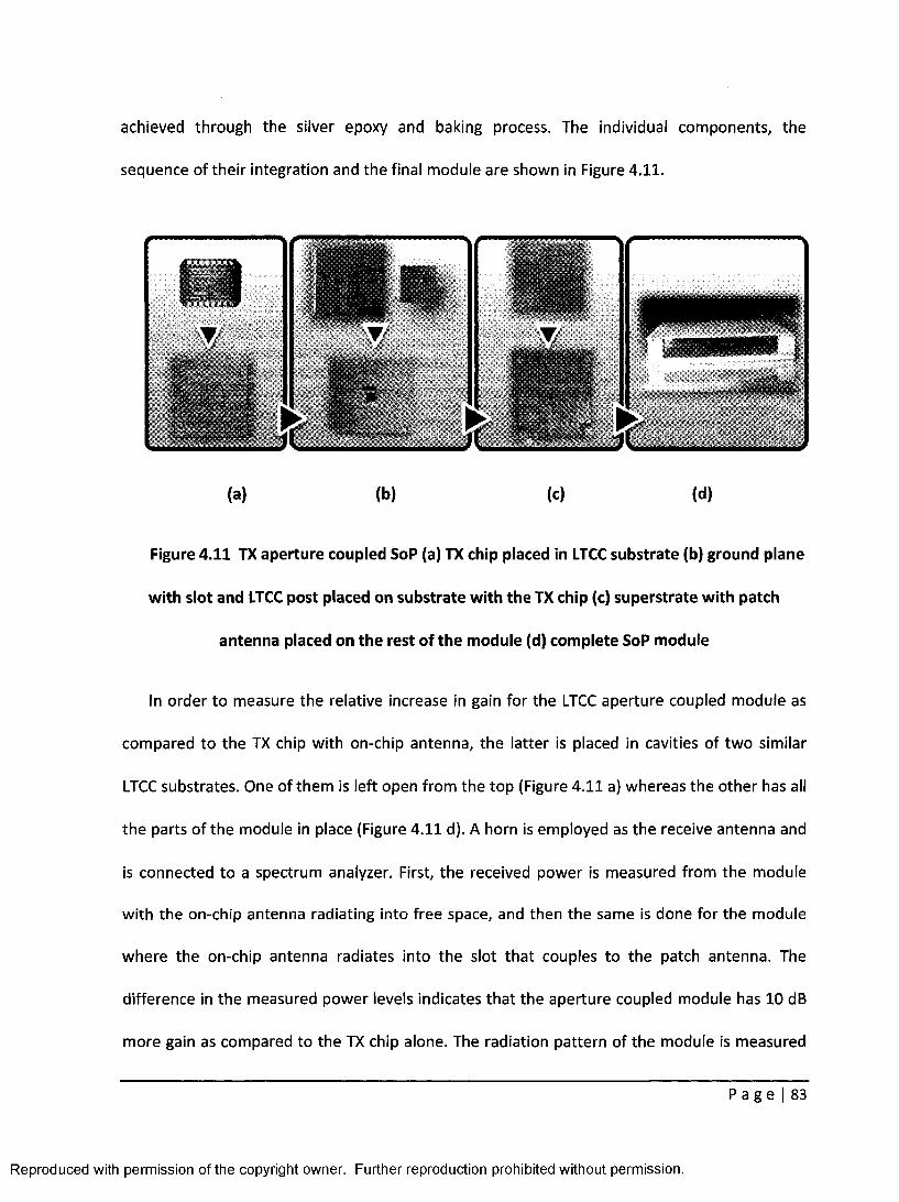
achieved through the silver epoxy and baking process. The individual components, the
sequence of their integration and the final module are shown in Figure 4.11.
(a) (b) (c) (d)
Figure 4.11 TX aperture coupled SoP (a) TX chip placed in LTCC substrate (b) ground plane
with slot and LTCC post placed on substrate with the TX chip (c) superstrate with patch
antenna placed on the rest of the module (d) complete SoP module
In order to measure the relative increase in gain for the LTCC aperture coupled module as
compared to the TX chip with on-chip antenna, the latter is placed in cavities of two similar
LTCC substrates. One of them is left open from the top (Figure 4.11 a) whereas the other has all
the parts of the module in place (Figure 4.11 d). A horn is employed as the receive antenna and
is connected to a spectrum analyzer. First, the received power is measured from the module
with the on-chip antenna radiating into free space, and then the same is done for the module
where the on-chip antenna radiates into the slot that couples to the patch antenna. The
difference in the measured power levels indicates that the aperture coupled module has 10 dB
more gain as compared to the TX chip alone. The radiation pattern of the module is measured
P a g e | 83
Reproduced with permission of the copyright owner. Further reproduction prohibited without permission.

through a custom jig, which rotates the receive antenna around the TX SoP and records the
level of power at different angles. The normalized radiation pattern is shown in Figure 4.12. The
measured radiation pattern shows a bore-sight maximum which is expected if the patch mode
is excited. Consistent with simulations, the module which contains the uncovered TX chip
demonstrates the maximum radiated power to be along the chip edges or 90° from the bore-
sight. However, the same module, when covered with the rest of the SoP components displays
the maximum radiated power to be at bore-sight. This shift in radiation pattern confirms the
desired operation of the aperture coupled patch antenna. The measured radiation pattern
shows a rather sharp main beam, with a 3 dB beamwidth of approximately 60°. This is slightly
narrower than the conventional patch antenna's 3 dB beamwidth, but this is expected due to
the patch's finite ground plane. However, the most attractive feature of this design is that the
10 dB increase in the TX SoP radiated power as compared to that of the SoC approach comes
without any increase in DC power consumption. It was observed in the measurements, that
both the designs, SoC and aperture coupled LTCC SoP, consume 3.3 mW of DC power.
C <D
C o CB
£ km
Figure 4.12 TX SoP measured radiation pattern
P a g e | 84
Angle (Degrees)
Reproduced with permission of the copyright owner. Further reproduction prohibited without permission.

Though the measured relative gain is less than what is observed in simulations, a number of
factors explain this result. It has been observed in simulations that the design is quite sensitive
to many parameters, in particular to the thickness of the air gap, length and width of the slot,
placement of the chip with respect to the slot and the position of the posts on the ground
plane. Close inspection and thickness measurements of the fabricated modules revealed that
there are many things which are not according to the simulation model. Firstly, the substrate
thickness is 0.734 mm which is less than the simulated 0.8mm. The four posts height, which is
responsible for the air thickness, varies between 2.2 to 2.3 mm instead of 2.4 mm. Moreover,
the slot width is not uniform for the entire length as can be clearly seen in Figure 4.13. The slot
becomes wider over the cavity as compared to the regular substrate. The cavity itself has
rounded corners, contrary to the original design. Furthermore, the deposition of silver epoxy is
done manually, so the thickness and uniformity could not be controlled as shown in Figure 4.13.
It not only reduces the distance between the on-chip antenna and the slot but also causes the
chip to be slightly tilted. Similar issues are observed in the manual placement and gluing of the
four posts. Finally, this particular fabricated TX chip is working at 5.3 GHz which is different
from the LTCC package design frequency of 5.2 GHz. All these measured dicrepancies were
subsequently checked in simulations and the simulated results verified the lower gain value in
measurements. However, by adequately addressing the tolerance issues in fabrication and
automating the postprocessiong process, the optimum results predicted in simulations can be
achieved with ease. Continuing maturity of LTCC fabrication processes should remedy this
situation.
P a g e | 85
Reproduced with permission of the copyright owner. Further reproduction prohibited without permission.

Figure 4.13 TX SoP zoomed in view of fabrication tolerances
4.3 Analytical Modeling of Chip Antenna Aperture-Coupling
The aperture coupled patch antenna fed through a microstrip line has been extensively
modeled. The initial model developed by Pozar made use of the cavity model of the patch
antenna and the small hole coupling theory [111]. He later demonstrated an analytical model
based on the reciprocity method [115]. This was followed by many investigations based on
different methods like the moment method [116], cavity technique [117][118] and transmission
line analysis [119]. A simple analytical model described in [120] employs an optimization
technique but can only be used for initial approximate predictions. A full wave analysis using
the spectral domain approach was reported in [121]. However, all these models deal with a
microstrip feed of the aperture coupled patch, which is not the case here. In order to model the
coupling through an on-chip loop antenna instead of a microstrip line, a simple analytical model
is derived here. The principle of the method is similar to the reciprocity theorem.
With reference to Figure 4.5, the fields from the on-chip loop couple to the slot in the
ground plane, and from the slot they couple to the patch antenna. The latter coupling is
identical to previous implementations and thus the new analytical model need not investigate
P a g e | 86
Reproduced with permission of the copyright owner. Further reproduction prohibited without permission.

it. The coupling between the on-chip loop antenna and the slot in the ground plane is the focus
of this analysis. The goals are to 1) find the effect of a slot opening in the ground plane on a
conducting loop near it, 2) obtain an expression to quantify the coupling from the loop to the
slot, and 3) determine the optimum position of the loop with respect to the slot for best
coupling.
Consider a conducting loop near a ground plane with excitation current Ji, enclosed in a
hemisphere with surface S and volume V as shown in Figure 4.14. Let us assume that the
electric and magnetic fields in the hemisphere, due to source Ji, are Ei and Hi respectively. For
this case, it is assumed that there is no slot in the ground plane as shown in Figure 4.14 (a). Let
the length of source Ji to be denoted as Al. Since Al is quite small, Ji is assumed to be equal to a
constant current density J0. For the second case (shown in Figure 4.14 (b)), a slot of length ls
and width ws is present in the ground plane. The electric and magnetic fields, due to excitation
source J2, are denoted as E2 and H2 respectively. Consistent with the first case, J2 is assumed to
be equal to J0. Applying Maxwell equations to both cases,
Case 1
V x is, = - j0JfiHx
VxH l = jmEx + Jx
(4.1)
(4.2)
Case2
VXE2 =-j(OfiH1
V x//2 = jco£E2 + J 2
(4.3)
(4.4)
Multiplying both sides of (4.1) with H2 and (4.2) with E2:
P a g e | 87
Reproduced with permission of the copyright owner. Further reproduction prohibited without permission.

H2 • (V x Ex) = -jo)juHx • H2 (4.5)
E2 • (V x Hx) - jcoeEx -E2+Jx-E2 (4.6)
Similarly, multiplying both sides of (4.3) with Hi and (4.4) with Ei:
H r(VxE2) = -jcofjH1 • Hx (4.7)
EX (VXH 2) = jco£ E 2 - E X + J 2 - E X (4.8)
Hemisphere Volume "V Surface "S'
First field set:E,^i Ji=J0 V,=E,xAI
(a)
Hemisphere Volume "V" Surface "S"
Second field set: E-..H J2=J« V2=E2xAi
(b)
Figure 4.14 Problem definition (a) Case 1 with no slot (b) Case 2 with slot
P a g e | 88
Reproduced with permission of the copyright owner. Further reproduction prohibited without permission.

Subtracting (4.8) from (4.5), and (4.7) from (4.6):
H2 • (VxEj)- Ex - (Vx/ / 2 ) = - jo)£E2 EX-J2EX - joofiHxH2
-V-(£, XH2)=jmE2 Ex + J2EX + jcojLiHXH2 (4.9)
E 2 *(VxHj ) H, - (Vxis 2 ) = j(OEE2 E] + JXE2 + jcojnHlH2
-V-(£2 x//,)-jco£E2 EX + JXE2+ ja)jjHxH2 (4.10)
Subtracting (4.10) from (4.9):
- V ( E X X H 2 - E2X H1)=J2Ex-J1E2 (4.11)
Equation (4.11) is consistent with reciprocity theorem, without the magnetic sources [122].
Applying this to the complete hemisphere:
]*(£, XH 2 - E 2XH x ).ds = ^ ( E X J 2 - E 2 - J x )dv (4.12) S v
S = S„+Sg+S s l o t
The integral over the remaining surface (Soo) and the ground (Sg) is zero. Also Ei is zero over
the slot surface SS|0t because the slot is not present in the first case. Therefore (4.12) can be
simplified as follows:
\ { - E 2 x H x ) - d s = J ( ^ j J 2 - E 2 • J x ) d v (4.13) slot V
Since, the analysis is based on the assumption that the source current density stays constant
(Ji=J2=J0), the coupling between the slot in the ground plane and the conducting loop will be
P a g e | 89
Reproduced with permission of the copyright owner. Further reproduction prohibited without permission.

reflected as a change in the source voltage. Let us assume that Vi represents the source voltage
in case 1 and V2 the source voltage in case 2, and the change in the voltage is denoted as AV.
Since the excitation current is only defined over the feed gap and is zero elsewhere, the volume
integral is limited to the area of the feed gap AL. Equation (4.13) can now be written as:
J( - E2 x H1) • ds = Ex Al • AsJl - E2Al • AsJ2
slot
J( - E 2 x H x ) - d s = E l A l I l - E 2 A l l 2
slot
Where liand l2 are the currents in case 1 and case 2 and are equal to a constant current l0. As
represents the surface area of the loop feed gap. Now the loop terminal voltages are found
through:
J ( - £ 2 X / f , ) A = ( r , - F 2 ) / 0
slot
j ( - E 2 x H l ) - d s = A V I 0
slot
— j ( - E 2 x H l ) - d s = A V (4.14) Io slot
This is an important conclusion as it relates the electric field of the slot in the ground plane to
the loop's change in the voltage due to the coupling between them. In (4.14), Hi can be found
by applying image theory to the fields of case 1, as shown in Figure 4.15. This field is
proportional to J0 and is a function of the position of the loop. The electric field over the slot
can be represented by (4.15), where E0 is the amplitude of the slot's electric field [123].
P a g e | 90
Reproduced with permission of the copyright owner. Further reproduction prohibited without permission.

E2 =E0cos(7ty/ls)x
Since ds is in the z direction, (4.15) can be written as:
J( - is 0 cos{7iy I ds = AVI0
slot
l ( - E „ c o s ( n y / I , ) H y ) d s = A V I 0
slot
(x0,y0,d)
(x0,y0,-d)
Center of ground plan is set to (0,0,0)
Figure 4.15 Image theory for case 1 (with no slot)
Hy varies with the position of the loop and therefore (4.16) can evaluate the optimum relative
position of the loop with respect to the slot for best coupling. From (4.16), it is clear that the
position of the loop with respect to the slot must be unsymmetrical in order to have better
coupling. If the loop is symmetrically located below the slot, the opposite directed fields will
P a g e | 91
(4.15)
(4.16)
Reproduced with permission of the copyright owner. Further reproduction prohibited without permission.
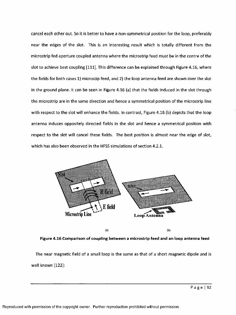
cancel each other out. So it is better to have a non-symmetrical position for the loop, preferably
near the edges of the slot. This is an interesting result which is totally different from the
microstrip fed aperture coupled antenna where the microstrip feed must be in the centre of the
slot to achieve best coupling [111]. This difference can be explained through Figure 4.16, where
the fields for both cases 1) microstip feed, and 2) the loop antenna feed are shown over the slot
in the ground plane. It can be seen in Figure 4.16 (a) that the fields induced in the slot through
the microstrip are in the same direction and hence a symmetrical position of the microstrip line
with respect to the slot will enhance the fields. In contrast, Figure 4.16 (b) depicts that the loop
antenna induces oppositely directed fields in the slot and hence a symmetrical position with
respect to the slot will cancel these fields. The best position is almost near the edge of slot,
which has also been observed in the HFSS simulations of section 4.2.1.
Microstrip Line Loop Antenna
(a) (b)
Figure 4.16 Comparison of coupling between a microstrip feed and an loop antenna feed
The near magnetic field of a small loop is the same as that of a short magnetic dipole and is
well known [122]:
P a g e | 92
Reproduced with permission of the copyright owner. Further reproduction prohibited without permission.

=L£.e-*-(4 + -i.)costf 2K r r
t t Ins -ikr,— k1 ik 1 . . _
He =r e ( + J~Y + — )sm^ Alt r r r
where 'l0s' is the magnetic moment, 's' is the area of the loop. Transforming these spherical
coordinates into cartesian coordinates,
H = H y
H - — e 7 f e"(^ + -!r)cos6?sin0sin^ + — e ^ + + -^-)sin0cos#sin(/) In r r AK r r r
H> = IoS - jk(x2+y2+z2yi
A/r(x2 + y2 +z2 y 3 jk(x2 + y z + z2 y 2 +3 -k2(x z+y2+ z2) 2 / 2 (zy) (4.17)
Let us assume that'd' is the vertical distance of the slot from the loop and it is placed at the
coordinates shown in Figure 4.15. Employing image theory, it is assumed that a similar current
source is present on the other side of the ground plane. The total field on the slot will be the
superposition of the fields from both the loop and its image.
If the H field due to the loop is Hyi and due to its image is HVj, the total magnetic field HTy on
the slot is:
HTy = Hyl+Hyi
H T y = 2 H y (4.18)
P a g e | 93
Reproduced with permission of the copyright owner. Further reproduction prohibited without permission.

If x0, y0 and d are the coordinates of the loop, then the relative distance between the loop
and any position along the slot can be expressed as (x-x0, y-y0, z-d). Inserting Hy of (4.17) into
(4.18) yields:
HT(x,y,z)=-2Is -jk[(x-x0)2-Ky-y0)2+d2)/2
MQc-xJ+fy-yJ+^fi
3M(x-xS +(y-yj +3-e[(x-xJ2 +<y-ya f +rf !)]l (d(y-yj) (4.19)
Inserting this magnetic field in (4.15) yields:
IoAV= J*(-£o cos(^v//s) slot
21 s
4n[( x-x0)2 +(y-y0)2 +d2)y2
, -jk[(x-x0 fHy-yof+d2)/1
X 3jk{(x-x, f +(y -y ,Y +d')] r 2 +i-k1[(x-xj2 +(y-y„f +</2)] (d(y-y0))ds (4.20)
The current l0 cancels out from both sides of (4.20). Taking the design values of d, s and /s in
(4.20) and plotting AV against varying positions across the length of the slot, results in Figure
4.17. It can be seen that the maximum coupling happens close to both ends of the slot and the
coupling goes to zero when the loop is exactly at the centre of the slot. HFSS simulation results
of the same are also plotted for comparison. A good match between the two curves is obtained,
which validates the simple analytical model. Many approximations (loop geometry, uniform
current distribution) have been used in this model which can explain the discrepancy in Figure
P a g e | 94
Reproduced with permission of the copyright owner. Further reproduction prohibited without permission.

4.17. Nonetheless, the model can provide a very good initial estimate of the on-chip antenna
optimum position with respect to the slot in the ground plane.
1
0.8 O) c Q.
N "co 0.4 E o z
0.2
-6 -4 -2 0 2 4 6 On-Chip Antenna Longitudinal Position With Respect to Slot (mm)
Figure 4.17 Comparison of coupling between the loop and the slot at various positions
through HFSS and analytical model
4.4 RF SoP Design Issues
Following the extensive design work conducted in this chapter, it is important to highlight
the major challenges and issues involved in advanced RF SoP development. These points will be
useful for continued research on the topic.
1. SoP requires co-design of IC and package. This is achieved through simultaneous circuit
and EM simulations.
P a g e | 95
Analytical Model HFSS Simulation
Reproduced with permission of the copyright owner. Further reproduction prohibited without permission.

2. Fine details must be considered in an SoP design. For example, the simulation model of
package passives must include the bond wires, bond pads and the IC cavity to avoid any
mismatch with the measured results.
3. The size of the conventionally-connected LTCC module could be further reduced if the
sensor and TX ICs were placed inside the antenna. However, this would require
considerable study of antenna-circuit coupling effects.
4. To reduce long simulation times, sensitivity analysis must be performed on limited parts
of the module based on insight gained from EM/Circuit modeling as shown in Figure
4.18.
5. Complex packages, such as the aperture coupled SoP module, require frequent
communication and coordination with the fabrication staff during the design phase to
ensure the smooth realization. Many times the design was altered due to the fabrication
limitations.
6. The aperture coupled module is a sensitive design; therefore the LTCC process
tolerances and fabrication limitations have pronounced effects on its performance.
Continuing maturity of LTCC fabrication processes should remedy this situation. Other
multilayer technologies like Liquid Crystal Polymer (LCP) can also be explored.
7. For the aperture coupled module, bond wires for biasing could be avoided by employing
solder balls in a flip chip arrangement. Thus, total removal of bond wires would be
achieved.
P a g e | 96
Reproduced with permission of the copyright owner. Further reproduction prohibited without permission.

8. Manual post processing of the LTCC modules, in particular the aperture coupled
module, is not recommended.
E FieldtV/m] 3.19466+004 2.9949e+004 2.7953e+004 2.5956e+004 2, 3960e+004 2,19636+004 1.99675+004 1.79706+004 1.59746+004 1.39776+004 1.19816+004 9.98426+003 7.9877S+003
S.9912e+003 3.9947e+003 1.99826+003 1.6546e+00Q
m ir
Figure 4.18 EM analysis used to determine area of high sensitivity
4.5 Summary and Contributions
Two RF SoP designs suitable for wireless biomedical applications have been presented. A novel
LTCC based TX SoP implementation has been demonstrated which makes use of on-chip-
antenna-to-LTCC-package antenna coupling through an aperture in the common ground plane.
The strategy is useful as it eliminates the need for isolating buffers, bond pads, bond wires,
matching elements, baluns and transmission lines. It not only reduces the number of
components and simplifies SoP design but also consumes lower power. The chip coupling to
LTCC patch antenna improves the TX module gain by 32 dB (in simulation) and range by 22 m as
compared to the on-chip antenna alone, without affecting the RF circuit performance and
power consumption. The conventional LTCC package provides 3 times more range than the
proposed design but consumes 12 times more power. To the author's knowledge, this is the
P a g e | 97
Reproduced with permission of the copyright owner. Further reproduction prohibited without permission.

first ever LTCC aperture coupled patch antenna implementation with direct feeding from a TX
on-chip antenna. A simple analytical method is described to model the new coupling between
the on-chip antenna and the slot in the ground plane. The work in this chapter completes the
second and third contributions of the thesis, namely 'LTCC SoP Design' and 'Novel LTCC SoP
Analytical Model'.
The work in this chapter has resulted in one journal paper [10] and a conference paper [19].
Another journal paper has recently been submitted [22].
Reproduced with permission of the copyright owner. Further reproduction prohibited without permission.
P a g e | 98

Chapter 5
5 Tunable and Reconfigurable LTCC SoP The novel LTCC SoP designs presented in chapter 4 of this thesis were successful in
achieving compact and efficient wireless RF transmitters for biomedical applications. Further
enhancements that can be considered for LTCC SoP are increased miniaturization and
component tunability and reconfigurability. The introduction of ferrite material in the package
not only helps in the miniaturization of the components but it also permits the control of the
devices made from it. Ferrite allows the properties of the package to be dynamically altered,
meaning that the package will have the ability to control the signals that are passing through it.
Therefore ferrite LTCC is a perfect candidate for tunable passive elements. In accordance with
the final thesis objective, this chapter investigates the suitability of ferrite LTCC for tunable and
reconfigurable SoP designs. An experimental ferrite tape material will first be characterized,
following which the development of novel tunable antennas will be presented. The properties
of the ferrite LTCC material that was available for this work prohibit the use in the 5GHz band
(as will be described in this chapter); therefore, the designs presented here are in the 12 GHz
band. The System-on-Package (SoP) work is an attempt to push the package beyond merely
P a g e | 99
Reproduced with permission of the copyright owner. Further reproduction prohibited without permission.

providing embedded passives, wiring, and physical protection: the package itself would become
the device. This concept is useful for applications like DBS-TV (Direct Broadcast Satellite
Television) reflect array, where reconfigurable coverage is required, or for multi-band wireless
sensor systems.
5.1 Ferrite LTCC material characterization
Ferrite integration in the LTCC medium is a fairly new concept. A limited number of
experimental ferrite tape materials are currently available and can be used as standalone
systems or sandwiched between standard LTCC dielectric layers. It is therefore necessary to
characterize these substrates for their material properties such as sr, \iu dielectric loss
tangents, and saturation magnetization. This section focuses on the extraction of these
properties for an experimental ferrite LTCC tape system ESL 40012 [8]. Generally, material
characterization of ferrite substrates has been limited to microwave properties and very little
work has been done to explore their magnetostatic properties, which are equally important.
Previous work that was performed at microwave frequencies could only extract the product of
£r and Ho as well as the loss tangent [89]. In the present work, the individual values have been
isolated independently using a cavity resonance technique. Magnetostatic characterization is
also performed here, employing both solenoid and toroid transformers that are completely
embedded in the LTCC material under test. The novel toroid transformer has been chosen to
eliminate the end-effects and magnetic flux leakage that are associated with solenoid
transformer designs.
P a g e | 100
Reproduced with permission of the copyright owner. Further reproduction prohibited without permission.

5.1.1 Microwave Characterization
Microwave frequency characterization is required to extract £r, |ir and the loss tangents of
the LTCC ferrite substrate. The properties for the substrate in the unbiased state are obtained
here; whereas, biasing considerations are discussed in the next section. These measurements
are done in collaboration with XLIM, France [126]. Generally, transmission line methods are
used to obtain the material parameters; they are wideband and simple, but are less reliable. In
contrast, resonant cavity methods measure complex permittivity and permeability at discrete
frequencies but are very accurate. The resonant method employed here has been applied in
many studies and compared to many other methods [127]. This technique does not require any
preparation of the sample (cutting, polishing, or metallization) and makes no theoretical
approximations. The test substrate is inserted between the two halves of a cylindrical cavity. It
is excited in the TEoi,2q+i mode to minimize the measurement uncertainties. Using the TE0i,2q+i
(2q+l = 1,3 or 5) modes, the electric field is parallel to the plane of the sample and has
negligible values close to the gap between the sample and the cavity wall. Two cavities with
resonant frequencies near 10 and 25 GHz have been used. In such a configuration, the resonant
frequency and quality factor of the resonant cavity mode can be computed exactly. Based on
iterative computation, the complex permittivity and permeability of the sample can be
extracted from the measured resonant frequency and quality factor. The loaded quality factor
of one of the TE0i,2q+i modes is used to compute the power losses due to the metallic walls. In
order to determine the permittivity and the loss tangent of the substrate we only need the
measurement of the resonant frequency and quality factor of the cavity loaded with the
sample. The uncertainties of £r and tan5 are due to the uncertainties of the measured quality
P a g e | 101
Reproduced with permission of the copyright owner. Further reproduction prohibited without permission.

factors and resonant frequencies and of the manufacturing tolerances of the cavity (radius and
height) and of the sample thickness.
Two LTCC ferrite samples have been tested and characterized. In both cases, the unbiased
state is considered, and the permeability |Ir is found to be 1. Due to the sample size constraints,
the lowest measurement frequency was 9.86 GHz. It is well known that the initial permeability
of the ferrite materials goes to 1 at frequencies higher than a few GHz, which is consistent with
the measured results. Table 5.1 lists the 8r and tan8 parameters for the two samples at the two
measurement frequencies.
Table 5.1 Measured eR and Tan8 Parameters
Sample 1 9.86 230+ 10 13.70±0.59 4.24+0.37
Sample 2 27.2 230 ± 10 14.14±0.65 1.11+0.10
In addition to the resonant cavity method, a transmission line characterization technique
has also been utilized with printed Coplanar waveguide (CPW) lines to assess the line losses for
the ferrite under test. The calibration structures which were measured between 0.1 GHz and 14
GHz are shown in Figure 5.1. The attenuation constant a was extracted from the calibration
structures built on the ferrite substrate and is shown in Figure 5.2.
P a g e | 102
Reproduced with permission of the copyright owner. Further reproduction prohibited without permission.

Except for the 2 GHz to 9 GHz band, the 01 values of around 0.5 dB/cm confirm the low loss
behavior of this material. However, the large loss observed in Figure 5.2, which peaks around 7
GHz, is due to the resonance of domain wall rotation inside the ferrite. It is a phenomenon that
is related to low-field losses in unsaturated polycrystalline ferrites. For practical circuit
applications, the domain wall resonance and associated loss would be removed by adequately
magnetizing the ferrite material [128].
Figure 5.1 Fabricated ferrite LTCC structures
Reproduced with permission of the copyright owner. Further reproduction prohibited without permission.
P a g e | 103

0 2 4 6 8 10 12 14 Frequency [GHz]
Figure 5.2 Attenuation constant extracted from ferrite CPW line
5.1.2 Microwave Characterization under Biased Conditions
In order to measure the ferrite LTCC microwave properties under biased conditions, the
resonant cavity perturbation technique is employed [129], this time in an X-band rectangular
waveguide cavity (RWC). The empty RWC is measured first for its S- parameters. Next the cavity
is loaded with a very small sample of ferrite LTCC, which will perturb the resonance. From the
change in the resonant frequency and Q of the cavity, the microwave properties (s, n, tan6) can
be extracted. Similarly, measurements can be made for different magnetic biasing levels and
therefore the material properties in these biased states can be extracted. The biasing is
provided by two large external electromagnets.
P a g e | 104
Reproduced with permission of the copyright owner. Further reproduction prohibited without permission.

For the electrical properties (E, tan6E), the sample has to be placed in the center of the
cavity where the electrical field is maximum and the magnetic field is zero. The sample must fit
exactly in the height of the RWG cavity for uniform fields and to avoid complex matching
problems. For the magnetic properties, the sample has to be placed at the end of the cavity
(short circuit) where the magnetic field is maximum and the electric field is zero. The sample
has to be very small and uniform for the magnetic property measurements.
To hold the sample in the RWC, the ferrite is placed in styro-foam and inserted through the
back end. It is pulled out of the RWC with the help of a thread in the foam. This way the feed
point is never required to be opened. The RWC along with the sample is shown in Figure 5.3. A
sharp resonance is required for accurate measurement, which is achieved with the help of a
tuning screw in the RWC. The sample is placed in the center of the cavity which is operated in
the TEios mode for the electrical properties. Numerous challenges were encountered:
1. The resonance is very sensitive to the tuning screw. A slight movement affects the
resonance strength and frequency, making accurate measurements impossible with
this setup.
2. Very small and uniform sample preparation is difficult as the ferrite LTCC material is
quite brittle, leading to frequent breakage during preparation and positioning of the
ferrite.
3. The manual placement of the sample fouls the measurements. A slight variation in
the placement produces different results. With this technique the measurements
P a g e | 105
Reproduced with permission of the copyright owner. Further reproduction prohibited without permission.

are not repeatable. A custom jig would need to be developed to keep the sample
more accurately in place.
4. The thread position and size also affects the measurements. Again, a custom jig
would be required to insert/remove the sample without threads.
On the basis of the above, useful microwave characterization of the ferrite under magnetic
bias could not be performed. Nonetheless, the microwave characterization carried out under
zero bias, and the magnetostatic characterization described in the following section, enabled
development of preliminary working SoP devices.
Figure 5.3 Setup for microwave characterization under biased conditions
5.1.3 Magnetostatic Characterization
Magnetostatic characterization is done through hysteresis measurements. These
measurements allow the extraction of important ferrite characteristics such as the relative
permeability, saturation magnetization, squareness and coercivity. The hysteresis curve
P a g e | 106
Reproduced with permission of the copyright owner. Further reproduction prohibited without permission.

(magnetic flux density B versus magnetic field H), should be measured at DC but it is also
acceptable in the lower frequency range. The 1 kHz test circuit used to perform magnetostatic
characterization is shown in Figure 5.4 and it employs embedded transformers built in the
ferrite under test. The primary side of the transformer is connected to an oscillator followed by
an audio power amplifier to provide variable current to the winding. The series resistor Ri has a
value of 3.5 £2 and is used to measure the voltage VH across it. The voltage VH is directly
proportional to the magnetic field H inside the transformer core and it is applied to the
horizontal deflection of an oscilloscope.
It is easily shown that the voltage at the output of the integrator is directly proportional to
the magnetic flux density B in the core, and this voltage is applied to the vertical deflection of
the oscilloscope. The desired hysteresis curve can be viewed directly on the oscilloscope by
plotting Vv versus Vh.
audio power Vg0 amplifier
J ferrite material under test
Figure 5.4 Magnetic hysteresis measurement test circuit.
Two different types of transformers have been designed for this work. A straight solenoid
transformer completely embedded within the ferrite LTCC material under test was first
P a g e | 107
Reproduced with permission of the copyright owner. Further reproduction prohibited without permission.

designed, similar to previous work [89]. The front cross-sectional view of a unit cell is shown in
Figure 5.5 (a). The turns are made of 200 |xm wide silver conductors that are connected to the
top and bottom conductors through 150 |im diameter vias, and the pitch between conductors
is 375 jxm. Each unit cell is comprised of 7 primary turns and 3 secondary turns. The complete
transformer fits into a 10 layer thick ferrite LTCC module with each layer being 124 urn thick. In
order to fit the solenoid transformer in a maximum permissible part size of 20 mm x 20 mm, 11
unit cells are used. The complete solenoid employs 77 primary and 33 secondary turns which
required 1198 transitions and 1108 vias in all.
A finite-length solenoid is subject to end-effects which can introduce errors in the
measurements. Further, leakage out of the sides of the solenoid is also a concern, which can
potentially lead to overestimates of the flux inside its core. A toroid, on the other hand, entirely
encloses the magnetic fields within its core and is less prone to leakage effects. A toroid
transformer has therefore also been designed in which unit cells are closely spaced and the
fields are more tightly contained within the windings, as shown in Figure 5.5 (b). The 112
primary turns and the 48 secondary turns are completely embedded in 10 ferrite LTCC layers.
The inner diameter of the toroid transformer is 10.3 mm and the outer diameter is 18.7 mm. It
has 16 unit cells which are spaced at 171 |j.m on the inner side and 1.28 mm at the outer side.
The top view of one of the fabricated layers (before firing of LTCC) of solenoid and toroid are
shown in Figure 5.5 (c) and (d) respectively.
P a g e | 108
Reproduced with permission of the copyright owner. Further reproduction prohibited without permission.

(a)
(b)
Figure 5.5 Ferrite LTCC LTCC (a) solenoid unit cell cross section and (b) toroid tilted front
view (c) & (d) solenoid & toroid fabricated layer top view
The measurement procedure consists of incrementing the primary current periodically and
recording the corresponding VH and Vv voltages which are then converted to actual values of H
and B, respectively. The results are then plotted to obtain the B(H) curves for every current
setting. The major B(H) curve, which was obtained at saturation using the solenoid transformer,
is shown in Figure 5.6 by a dotted line.
P a g e | 109
Reproduced with permission of the copyright owner. Further reproduction prohibited without permission.

400
200
32 0 <D
CD
-200
TOR
^
fv
SOLI ENOID „
/ j 1 1 1 I 1
\ •*"*
1
4000
2000
O
~o <D
M=
-2000
-%00 -2000 -1000 0 1000 2000 306$°°° Magnetic field (H) [A/m]
Figure 5.6 Measured hysteresis curves from the LTCC transformers.
The major hysteresis loop was obtained by energizing the primary winding with a peak
current of 650 mA. Based on the solenoid measurements, the saturation flux density Bs is 330
mT for an applied magnetic field of 2100 A/m. The remanent flux density Br is 180, the
squareness is 0.55, and the coercive magnetic field Hc is 520 A/m. The same procedure was
used for the toroid. Due to the curvature of the toroid, the resulting turn density of the primary
winding of the toroid is lower than that of the solenoid by a factor of 0.6. The maximum B(H)
curve for the toroid, is shown in Figure 5.6 by a solid line.
A comparison of the curves in Figure 5.6 and the results obtained from the toroid indicate
that ESL 40012 is easier to magnetize than it would appear to be with the solenoid. This is
expected since the toroid suffers from less leakage effects than the solenoid. This difference is
clearly evident in Figure 5.7, which plots the peak B field versus the peak H field for each
P a g e | 110
Reproduced with permission of the copyright owner. Further reproduction prohibited without permission.

current setting. Although saturation could not quite be achieved with the toroid, the trend
clearly indicates that the saturation magnetization Bs approaches 400 mT instead of the 330 mT
obtained using the solenoid. For the toroid, Br = 250 mT, the squareness is approximately 0.63,
and Hc ~ 330 A/m.
The results of Figure 5.7 may be used to calculate the linear permeability of the material.
For any given operating point, the linear permeability |inn is the slope of the line that extends
from the origin to that operating point. The resulting curves for the solenoid and the toroid are
shown in Figure 5.8. The maximum pi|in of 205 is achieved for an H-field of 715 A/m for the
solenoid, whereas it is estimated to be 370 at an H-field of 430 A/m for the toroid.
400
„ 300 i-
E
1 200 ID
ra a> 0_
100
0.
TOROID
1
SOLdNOID
i i
500 1000 1500 2000 2500 3000 Peak H-field [A/m]
Figure 5.7 Measured peak B versus peak H for ESL 40012 LTCC.
P a g e | 1 1 1
Reproduced with permission of the copyright owner. Further reproduction prohibited without permission.

400
350
§ 3 0 0 ca <D
E 250 <D
© 200 > CO , _ a) 150 (T
100
0 500 1000 1500 2000 2500 3000 Peak H-field [A/m]
Figure 5.8 Measured relative linear permeability of ESL 40012.
5.1.4 Discussion
A number of important observations can be made based on the microwave and
magnetostatic measurement results obtained thus far. The value of £r (13.7) falls in the range
of typical microwave substrates useful for circuit and antenna designs. In the unbiased state,
the measured loss tangents of the ferrite are quite low (4 xlO"3) and decrease with frequency.
Since the guided wavelength is a function of both £r and nr, this will help miniaturize antenna
and passive elements design.
In the biased state, the high value of Bs = 400 mT indicates that a large degree of magnetic
control can be achieved with ESL 40012, which is beneficial for the design of in-package
P a g e | 112
TOROID
SOLENOID
Reproduced with permission of the copyright owner. Further reproduction prohibited without permission.

reconfigurable and tunable microwave components. The measured results also indicate that
the remanent magnetization is sufficient to yield practical nonreciprocal devices operating at
remanence. The measured high values of Jinn also indicate that high Q inductors and
transformers can be manufactured with this material. These results are encouraging as far as
the implementation of microwave components in ferrite SoP is concerned.
5.2 Tunable antennas
Most of the previous ferrite based antennas are tuned to operate in the magnetically
saturated state. Given that they are fabricated on traditional ferrite substrates, large external
magnets (permanent or electro-magnets) must be used to provide the high magnetostatic
fields. Such magnets are bulky and impractical given that 1) the substrates must operate in
saturation and 2) the external fields are commensurate with the demagnetization factors of the
substrates. This has typically required an external magnetic field intensity H on the order of 80
000 A/m (1000 Oe) and makes the resulting system extremely bulky and unsuitable for the
compact SoP approach. The designs presented in this chapter use a tunable patch antenna that
is fabricated on a multilayer ferrite LTCC substrate with a completely embedded bias winding.
Demagnetization factors are largely absent from such an arrangement, which greatly lowers the
magnetostatic field strength required for tuning. Additionally, these antennas operate at a high
enough frequency such that low-field losses are negligible, implying that unsaturated ferrite
regions within the LTCC substrate are tolerable, which further serves to reduce the required
magnetostatic field strength. This novel approach enables tuning of the antenna with field
strengths on the order of 2000 to 4000 A/m (25-50 Oe).
P a g e | 113
Reproduced with permission of the copyright owner. Further reproduction prohibited without permission.

5.2.1 Theory
Ferrite-based antennas typically use a variable magnetostatic bias to achieve tuneability and
reconfigurability [130][131]. For such antennas, the resonance frequency variation is
dependent on the bias direction and strength [132]. Usually, ferrite materials at microwave
frequencies are used in the saturated state. In this regime, the well-established Polder
equations [129] can be used to represent the permeability of ferrite in terms of applied
magnetostatic field (H0) and saturation magnetization (Ms). These equations indicate that the
elements of the permeability tensor exhibit a resonance around a specific frequency, called
Larmor frequency fo, which is dependent on Ho- Ferrite is very lossy in the vicinity of its Larmor
frequency, thus it is customary to operate the ferrite above this frequency for microwave
applications, even though the ability to tune the ferrite decreases with frequency in this range
[128]. Previous characterization efforts have revealed that an internal H-field of over 2500 A/m
is required to fully saturate ESL 40012 ferrite LTCC to its magnetization value of |ioMs = 0.4 T.
Providing such high, uniform bias fields within a miniature LTCC package is quite challenging
without the use of an external magnet. Failure to fully saturate the ferrite results in additional
low-field losses, which are incurred up to approximately the magnetization frequency fm = (2.8
x 1010 Hz/T) • |0oMs = 11.2 GHz for this particular ferrite material. For consistentency with the
SoP work presented in this thesis so far, the initial plan was to design ferrite LTCC based
antennas for the 5 GHz band. Given the unlikelihood of achieving uniform bias and eliminating
the low field losses (see the 2-9 GHz band in Figure 5.2), an operating frequency of 12 GHz was
chosen [20].
P a g e | 114
Reproduced with permission of the copyright owner. Further reproduction prohibited without permission.

Due to their anisotropic behavior, ferrites show different properties depending on the
orientation of H0 with respect to the direction of both the wave propagation and the RF
magnetic field. Two different orientations of patch antennas are investigated here with respect
to H0/ as shown in Figure 5.9. In the first case, the antenna is placed in a longitudinal orientation
with respect to H0 whereas in the second case, H0 is perpendicular to the resonant dimension of
the patch antenna (transverse to the RF propagation). According to Pozar, the second case
should be more sensitive to the applied bias fields [92].
In the proposed design, the ferrite underneath the patch antennas will be partially biased
using embedded electromagnet windings. Such internal windings do not suffer from
demagnetization factors as do external bias field sources. Magnetostatic simulations have
revealed that the a relatively low DC current of no more than 500 mA is sufficient to generate
magnetic field strengths ranging from 2000 to 4000 A/m (25-50 Oe) within the core of the
windings [20]. Tunability of the antenna will be achieved by varying the current flowing
through the windings. This methodology has been used successfully in previous work for ferrite
[20],
Reproduced with permission of the copyright owner. Further reproduction prohibited without permission.
P a g e | 115

•3 £ ra
I
Embedded Winding for £)C.Magiaetk.c.
Bias——
DC; Magnetic Bias I^iiection
|L
Figure 5.9 Patch antenna orientations with respect to H0 direction
5.2.2 Antenna Design
For proof of concept, a microstrip patch antenna designed to operate at 12 GHz has been
fabricated over the existing ferrite LTCC substrates with embedded windings that were used for
material characterization. The cross-sectional view of the tunable antenna is shown in Figure
5.10. The module consists of a 10 layer thick ferrite LTCC (hi=1.09mm) out of which the biasing
windings occupy the bottom eight layers (h2=0.87mm). The patch antennas made of copper
P a g e | 116
Reproduced with permission of the copyright owner. Further reproduction prohibited without permission.

metallization are realized on the top of the substrate, while the ground plane is placed beneath
the substrate.
Two slightly different antenna designs (small indented patch and large slotted patch) are
investigated in different orientations as shown in Figure 5.11. The basic microstrip fed indented
patch antenna is placed either in a longitudinal (Figure 5.11 d) or transverse orientation (Figure
5.11 b) with respect to the underlying solenoid bias winding. In one of the variations, the same
antenna has been placed in a corner, slightly away from the solenoid winding (Figure 5.11 e).
The same antenna has also been placed on toroidal transformer, as shown in Figure 5.11 (a).
The second antenna design consists of a large slotted patch antenna that operates in its 3rd
resonance at 12 GHz (Figure 5.11 c). It has been designed with a slot in the center in order to
increase its electrical length and fit it in the available substrate space.
Patch Antenna
BiasWinflma
DC Current
Figure 5.10 Tunable antenna module (cross-sectional view)
P a g e | 117
Reproduced with permission of the copyright owner. Further reproduction prohibited without permission.

M o»>
(c) (d) (e)
Figure 5.11 Fabricated antennas on ESL 40012 ferrite LTCC (a) small patch on toroid (b)
transverse small patch on solenoid (c) large patch with slot on solenoid (d) longitudinal small
patch on solenoid (e) longitudinal small patch placed in the corner with a microstrip line
5.2.3 Tunable Patch Impedance Measurements and Discussion
The measurement setup employed for obtaining the antenna's input impedance is shown in
Figure 5.12. It consists of a universal jig to feed the patch antenna and record the s-parameters
through a network analyzer. The embedded underlying winding is biased through DC probes
and pads on the top layer connected to a variable power supply.
P a ge | 118
Reproduced with permission of the copyright owner. Further reproduction prohibited without permission.

The antennas are measured under both zero bias and biased conditions. For the latter case,
current is increased in steps of 50 mA until the maximum value of 500 mA for the solenoid
winding and 700 mA for the toroid winding. The solenoid winding exhibits a measured series
resistance Rs of 5 Q, whereas the toroid demonstrates Rs of 5. 8 Q. The measured results for the
small transverse antenna (Figure 5.11 b) on the solenoid are shown in Figure 5.13 (a). The 12
GHz resonance, highlighted with a circle in Figure 5.13 (a) has been expanded for clarity in
Figure 5.13 (b) showing intermediate bias steps. A very large tunability of the resonance
frequency is observed with varying magnetic bias. The other structures of Figure 5.11 exhibited
less tunability.
Figure 5.12 Tuneable antenna measurement setup
P a g e | 119
Reproduced with permission of the copyright owner. Further reproduction prohibited without permission.

-10 0 mA
500 mA -15
-20
tn
-25
-30
-35
-40,
Frequency [GHz]
(a)
Small Transverse Antenna on Solenoid
-i'V • ; / /
R
-O
sod
Tuning range fori 1 OdB ref ! -14
All data, 0 to 500 mA
18
11.4 11.5 11.6 11.7 11.8 11.9 12 Frequency [GHz]
(b)
Figure 5.13 Measured Results (a) 9-15 GHz range (b) zoomed in at 12 GHz range
P a g e | 120
Reproduced with permission of the copyright owner. Further reproduction prohibited without permission.

Figure 5.13 (b) reveals that the maximum tunability is 550 MHz around 12 GHz achieved for
the transverse orientation with respect to the solenoid winding. In this orientation the bias
magnetic field is transverse to the resonant direction of the patch. The resonant frequency for
this orientation decreases with the bias. This is consistent with the results in [92] which show
maximum tuning for similar orientation. This result is quite encouraging keeping in mind that
the antenna structure employs a non-optimized bias network. The multiple dips in the
measured results are also attributed to the embedded windings. When the same antenna is
placed in the longitudinal orientation with respect to the bias magnetic field (shown in Figure
5.11 d), the tuning range reduces to approximately 300 MHz around 12 GHz. It is also observed
that if the same antenna is in the corner of the substrate (antenna partially covers the winding
as shown in Figure 5.11 (e) the tuning range reduces to approximately 200 MHz. The large
patch antenna with slot (shown in Figure 5.11 c) displays a tuning range of 500 MHz. This
tuning range is achieved with the antenna placed in a longitudinal orientation with respect to
the bias field. It is believed that if the antenna with the slot is placed in the transverse
orientation with respect to H0, it will provide a tuning range in excess of 500 MHz. Lastly, the
small antenna on a substrate with toroid transformer (shown in Figure 5.11 a) showed a tuning
range of 200 MHz for the same or slightly higher bias field as compared to the solenoid biased
antennas. This agrees well with the hysteresis measurements because the toroid transformer
shows maximum fields to be confined within the windings and the leakage fields are
considerably reduced as compared to the solenoid. It is clear that the antennas used herein are
not only responding to the magnetic flux within the core of the transformers, but also to the
leakage flux lines around the cores of the transformers (flux return paths). This proof of concept
P a g e | 121
Reproduced with permission of the copyright owner. Further reproduction prohibited without permission.

has re-used transformer cores that were previously used to characterize the ferrite. As such,
the windings have not been optimized for antenna-specific tuning. Despite this, good tuning
ability is observed for the aforementioned antennas, albeit for high bias currents. For 500 mA of
bias current in a bias winding with Rs = 5 Q, requires 2.5 V of voltage drop and results in 1.25
watts of power consumption. Though the power consumption seems high, it is in the
acceptable range if the current does not have to be supplied continuously. For practical ferrite
based circuits, the bias current has to be provided for very short period of time as ferrite holds
its magnetization in remanence. This means that the circuits tuned to discrete points through
applied bias can hold on to their state even if the bias current is removed. Moreover,
substantial reductions of bias current are expected if the bias windings and their placement are
optimized for antenna applications.
In order to optimize the tuning range, there must be enhanced interaction between the RF
magnetic field of the patch antenna and dc bias magnetic field. Despite the need of placing the
antennas close to strong bias field zones, i.e. close to the windings, practically it becomes
difficult due to the interference of RF fields with these windings. A stronger perturbation is
experienced in the case when the microstrip feed line is placed on the windings (see Figure 5.11
c and Figure 5.11 d). This strong perturbation suggests that the microstrip feed lines are very
sensitive to the presence of embedded windings. This fact must be carefully considered in
tunable antenna designs on substrates with embedded windings.
P a g e | 122
Reproduced with permission of the copyright owner. Further reproduction prohibited without permission.

5.2.4 Antenna Gain and Radiation Pattern Measurements
A challenging part of characterizing the ferrite based tunable antennas is measuring its gain
and radiation pattern under biased conditions. This is because the antennas have to be
mounted and rotated in the anechoic chamber along with the DC probes which are required to
provide biasing to the windings underneath the antenna. A custom jig has been made for this
purpose as shown in Figure 5.14. The DC probes are mounted on a metallic plate and then this
plate is screwed to the base plate in the anechoic chamber. The microstrip based universal test
jig has also been screwed to the base plate. The antennas are fed through the universal test jig
and biased through the probes. A horn antenna acted as a transmit antenna on the other end.
It is observed that at certain angles the probes blocked the radiation pattern measurement.
However, the testing is not affected by the presence of the probes in most of the measurement
scans. This fact is established by doing two sets of measurements, one with and the other
without the probes. The measurements are preceded by the calibration procedure which is
done through two horn antennas for the 11-13 GHz frequency range.
Figure 5.14 Ferrite antenna gain and radiation pattern measurement setup
P a g e | 123
Reproduced with permission of the copyright owner. Further reproduction prohibited without permission.

The measured gain and E-plane radiation pattern for the transverse patch on the solenoid is
shown in Figure 5.15 under bias and unbiased conditions. A maximum gain of approximately 2
dB is measured at 12.5 GHz. The low gain value and the variation of the radiation pattern at
various angles are attributed to the presence of strong surface waves which radiate from the
edges of the substrate. These surface waves are expected due to the high permittivity of the
thick LTCC substrate. As was the case with the impedance measurements, the parasitic
influence of the windings within the substrate is apparent in the measured radiation pattern.
With little variation in the radiation pattern for the unbiased and biased conditions (see Figure
5.15), tunable antenna performance can be controlled with ease. It is worth mentioning here
that the gain has been corrected for mismatch loss due to varying bias levels. Measurements of
the large antenna with the slot suffered the most due to severe blockage from the probes,
mount and jig. The radiation pattern from the toroid based antennas appeared to be the
cleanest and resembled the typical patch antenna pattern; however the gain values are slightly
lower. This further confirms the power lost due to surface waves as toroid substrates are larger
in terms of area as compared to the solenoid substrates.
Reproduced with permission of the copyright owner. Further reproduction prohibited without permission.
P a g e | I 2 4

Transverse Antenna on Solenoid
T5
O -10
—Under no bias — •Under 500mA
-15
-20 -80 -60 -40 -20 0 20
Angular position [deg.]
Figure 5.15 Ferrite antenna measured gain and radiation pattern
5.3 Ferrite LTCC SoP Implementations
Based on the measured results, the concept of ferrite LTCC tunability can be applied to SoP
modules that extend beyond antennas. The possible extension of this work applicable to
antennas and other SoP components can be summarized as follows.
5.3.1 Antennas
The performance of ferrite LTCC based antennas can be considerably improved by co-design
of antenna and the underlying winding. In order to optimize the tuning range, this co-design of
antenna and bias network must enhance the interaction of antenna RF magnetic field and the
dc bias magnetic field. To reduce the interference from the bias winding, the design must be
optimized in terms of size of the winding and its placement with respect to the antenna. New
configurations for the bias winding must also be explored. Similarly, it is expected that alternate
P a g e | 125
Reproduced with permission of the copyright owner. Further reproduction prohibited without permission.

radiators like CPW patch and slot antennas can also reduce the perturbation from the bias
winding. In order to maximize the efficient use of the 3D substrate, radiators like Dielectric
resonator antennas (DRAs) and helical antennas can also be employed.
5.3.2 Reflectarray
Though not shown here, microstrip line measurements under varying bias conditions
demonstrated strong phase change capability. Also, it is well known that patch antennas
whose resonant frequencies change with magnetic bias also exhibit strong phase change of the
radiated wave. Therefore ferrite LTCC based patch antennas are ideal candidates for
reconfigurable reflectarrays.
5.3.3 Other tunable circuits
Several possibilities exist for tunable microwave components within a ferrite LTCC SoP. For
instance, Figure 5.16 shows the attenuation constant of a microstrip line placed above the bias
winding of Figure 5.5 (c). Though the transmission is affected by the interference from the
underlying winding, it can be seen that over a narrow frequency band in which the combined
microstrip/winding structure is resonant, the line's propagation losses vary by 10 dB/cm with
magnetic bias. Such a result proves the feasibility of distributed tunable switching, phase
shifting and filtering circuits. Similarly, lumped element realizations of these components would
also be tunable if an inductor is employed. For example an embedded tunable filter or matching
network can be built inside the bias winding to make use of the high magnetic field intensity.
P a g e | 126
Reproduced with permission of the copyright owner. Further reproduction prohibited without permission.

The measured results are encouraging as far as the implementation of tunable microwave
components in ferrite SoP is concerned. The low loss material property makes it an attractive
substrate for in-package passive element design in the microwave frequency range. However,
the true advantage of ferrite LTCC is its ability to change its permeability tensor with applied
magnetic bias, thereby giving an additional dimension of freedom to microwave designers.
14 — Under no bias -—under 500mA
-I- -
- -i
Frequency (GHz)
Figure 5.16 Ferrite microstrip line measured attenuation constant
5.4 Ferrite based Tunable RF SoP Design Issues
Following the experimental work done in this chapter, it is important to highlight the major
challenges and issues involved in advanced ferrite based tunable RF SoP development. These
points will be useful for continued research on the topic.
P a g e | 127
Reproduced with permission of the copyright owner. Further reproduction prohibited without permission.

1. The layout of the solenoid and toroid transformers is very complex and requires
extremely large CAD tool memory. The module must be broken into individual unit cells
which are then repeated to realize the complete winding.
2. The magnetostatic measurements performed using embedded LTCC transformers are
quite challenging as they require high currents. Special arrangements are required to
cool off the modules to avoid the burning of the embedded windings. Also the current is
passed in very short intervals of time to avoid overheating of the modules.
3. Microwave measurements under the biased state required very small size ferrite LTCC
samples to be placed very accurately at specific locations in the waveguide. The
precision required was beyond the manual placement of the samples and hence
resulted in non-repeatable measurements. A custom jig is required to accurately place
the sample in the waveguide. The setup also required large electromagnets to overcome
the demagnetization fields.
4. The tunable antennas employ the same transformers which are used to characterize the
material to avoid expensive fabrication costs. These are far from optimum for antenna
design but do serve to prove the concept.
5. Ansoft HFSS has many limitations with respect to modeling the ferrite based designs. In
this tool, the magnetized state of a ferrite material can be specified with the value of Ms.
The direction and value of Ho are also important parameters for the simulation model.
The distribution of the DC-bias field inside the ferrite is usually assumed to be uniform.
Another approximation which HFSS makes is that the ferrite is always operating in its
P a g e | 128
Reproduced with permission of the copyright owner. Further reproduction prohibited without permission.

saturation state. It is worth mentioning here that HFSS has the ability to define a diagonal
non-linear permeability tensor (B-H curve), however this property cannot be used for
ferrite modelling due to the simulator's inability to employ the non-diagonal elements of
the permeability tensor. Due to the simulator's limitation, most of this work relied on
experimental verifications. Other simulators like CST microwave must be employed in
future investigations.
6. Radiation measurements of these antennas over embedded windings are very difficult
as they require the dc biasing through the probes at the same time as the antennas are
being rotated and measured for RF power. A custom jig has been made for it as shown
in Figure 5.14.
7. Due to the inability to perform RF measurements in the active region of the windings
(embedded in the substrate), it was hard to assess the remanent magnetization in the
biased microwave state. For future attempts, a strip line structure may provide better
prediction of the residual magnetic fields.
8. The microstrip line mode was subjected to strong interference from the embedded
windings, hence the measurements could not provide very clear results about phase
tuning with respect to the applied bias.
9. Finally, for the same reason as mentioned in point 6, it was difficult to assess whether or
not the low field losses disappear for the biased state.
P a g e | 129
Reproduced with permission of the copyright owner. Further reproduction prohibited without permission.

5.5 Summary and Contributions
ESL 40012 experimental ferrite LTCC tape has been characterized for its microwave and
magnetostatic properties. Microwave measurements performed at 9.86 GHz and 27.2 GHz reveal
an £r value of 13.6 and tanS values of 0.004 and 0.001. Novel embedded LTCC transformers
have been used to measure the magnetostatic properties. These measurement results show that Bs
is nearly 400 mT for an applied magnetic field approaching 2000 A/m. The remanent flux
density Br is 250 mT, the squareness is 0.63, and the coercive magnetic field Hc is 430 A/m.
For the first time, ferrite Low Temperature Co-fired Ceramic (LTCC) tunable antennas are
presented that operate in the ferrite's partially-biased state. These antennas are frequency
tuned by the magnetostatic field produced in a winding that is completely embedded in the
ferrite LTCC substrate. Due to the embedded windings, the typically required magnetic bias (of
the order of 1000 Oersted) for antenna tuning has been reduced by 95% (to the order of 50
Oersted). The fact that large electromagnets are not required for tuning makes ferrite LTCC
with embedded bias windings an ideal platform for advanced tunable System-on-Package (SoP)
applications. Measurements reveal a tuning range of 550 MHz in the 12 GHz band for a single
microstrip patch antenna on a ferrite LTCC substrate. Two different biasing structures and their
effect on the antenna performance are discussed. The effect of antenna position and
orientation with respect to the biasing winding is also investigated. Finally, the antenna
radiation characteristics are compared under biased and unbiased conditions. An antenna gain
of 2 dB is measured. These results constitute the fourth and fifth contributions of the thesis,
namely 'Ferrite LTCC Material Characterization' and ' Ferrite LTCC Based Antennas for Tunable
SoP'.
P a g e | 130
Reproduced with permission of the copyright owner. Further reproduction prohibited without permission.

The work in this chapter has resulted in a conference paper [20]. A journal paper has recently
been submitted [21].
P a g e | 1 3 1
Reproduced with permission of the copyright owner. Further reproduction prohibited without permission.

Chapter 6
6 Conclusions and Future Work
This chapter summarizes the research work and the contributions of this thesis and
proposes future work which will help researchers to advance the art of RF SoC and SoP design.
6.1 Conclusions
Chapter 3 has presented three novel SoC designs having on-chip antennas combined with
RF transmitter and receiver circuitry. A highly integrated, low power CMOS VCO TX has been
demonstrated for short range wireless radiation sensor applications. The VCO tank inductor has
been optimized to act as an on-chip inductor-antenna, thus minimizing chip area. Its 0.5mm2
size is the smallest reported on-chip antenna in the UN II band. This is the first ever
demonstration of experimental characterization of an on-chip inductor/antenna for its
radiation properties. The tradeoffs in the design and challenges in the experimental work have
been highlighted. The complete TX chip sized 1.5mm2 consumes 3.3 mW of power and can
communicate with a low noise receiver connected to a patch antenna 2 m away from the TX.
With the integration of a suitable power source, the complete wireless dosimeter can be
P a g e | 1 3 2
Reproduced with permission of the copyright owner. Further reproduction prohibited without permission.

smaller than a dime as shown in Figure 3.22. On the RX side, co-design of on-chip dipole
antenna and LNA has been demonstrated for conjugate matching. These results represent the
first contribution of this thesis, namely 'Oscillator TX with On-chip Inductor/Antenna'.
The work of this chapter has led to many publications. One journal [9] and seven
conference papers have already been published [11-15][17][18]. One more journal paper has
been accepted recently [23].
Two RF SoP designs suitable for wireless biomedical applications have been presented in
chapter 4. A novel LTCC based TX SoP implementation has been demonstrated which makes use
of on-chip-antenna-to-LTCC-package antenna coupling through an aperture in the common
ground plane. The strategy is useful as it eliminates the need for isolating buffers, bond pads,
bond wires, matching elements, baluns and transmission lines. It not only reduces the number
of components and simplifies SoP design but also consumes lower power. The chip coupling to
LTCC patch antenna improves the TX module gain by 32 dB (in simulation) and range by 22 m as
compared to the on-chip antenna alone, without affecting the RF circuit performance and
power consumption. The conventional LTCC package provides 3 times more range than the
proposed design but consumes 12 times more power. To the author's knowledge, this is the
first ever LTCC aperture coupled patch antenna implementation with direct feeding from a TX
on-chip antenna. A simple analytical method is described to model the new coupling between
the on-chip antenna and the slot in the ground plane. The work in chapter 4 completes the
second and third contributions of the thesis, namely 'LTCC SoP Design' and 'Novel LTCC SoP
Analytical Model'.
P a g e | 133
Reproduced with permission of the copyright owner. Further reproduction prohibited without permission.

The work in chapter 4 has resulted in one journal paper [10] and a conference paper [19].
Another journal paper has recently been submitted [22]. The conference paper [19] won the
'overall best paper prize' in European Wireless Technology Conference (EuWiT) at European
Microwave Week in Amsterdam [124]. The demonstration of conventional LTCC TX module won
the national technology innovation competition during the Canadian Microelectronics Texpo
[125],
ESL 40012 experimental ferrite LTCC tape has been characterized for its microwave and
magnetostatic properties in chapter 5. Microwave measurements performed at 9.86 GHz and 27.2
GHz reveal an er value of 13.6 and tan8 values of 0.004 and 0.001. Novel embedded LTCC
transformers have been used to measure the magnetostatic properties. These measurement results
show that Bs is nearly 400 mT for an applied magnetic field approaching 2000 A/m. The
remanent flux density Br is 250 mT, the squareness is 0.63, and the coercive magnetic field Hc is
430 A/m.
For the first time, ferrite Low Temperature Co-fired Ceramic (LTCC) tunable antennas are
also presented in chapter 5, that operate in the ferrite's partially-biased state. These antennas
are frequency tuned by the magnetostatic field produced in a winding that is completely
embedded in the ferrite LTCC substrate. Due to the embedded windings, the typically required
magnetic bias (of the order of 1000 Oersted) for antenna tuning has been reduced by 95% (to
the order of 50 Oersted). The fact that large electromagnets are not required for tuning makes
ferrite LTCC with embedded bias windings an ideal platform for advanced tunable System-on-
Package (SoP) applications. Measurements reveal a tuning range of 550 MHz in the 12 GHz
band for a single microstrip patch antenna on a ferrite LTCC substrate. Two different biasing
P a g e | 134
Reproduced with permission of the copyright owner. Further reproduction prohibited without permission.

structures and their effect on the antenna performance are discussed. The effect of antenna
position and orientation with respect to the biasing winding is also investigated. Finally, the
antenna radiation characteristics are compared under biased and unbiased conditions. An
antenna gain of 2 dB is measured. These results constitute the fourth and fifth contributions of
the thesis, namely 'Ferrite LTCC Material Characterization' and 'Ferrite LTCC Based Antennas for
Tunable SoP'.
The work in chapter 5 has resulted in a conference paper [20]. A journal paper has recently
been submitted [21].
6.2 Future Work
Specific recommendations for future work were made in the "Design Issues" sections of
chapters 3,4 and 5. In addition the following research is proposed.
RF SoC Design
All measures were taken in this thesis to ensure an efficient on-chip antenna design, like
increasing the metal width and placing it close to the edges of the chip. However it is very
difficult to design an efficient on-chip antenna on low resistivity bulk silicon (10 Q-cm). Though
the on-chip antenna performance in terms of its communication range is satisfactory for this
particular application, it must be enhanced for other applications. The antennas can be made
efficient by employing high resistivity substrates, but this will 1) increase the cost and 2) make it
a non-compatible substrate for the circuits.
P a g e | 135
Reproduced with permission of the copyright owner. Further reproduction prohibited without permission.

One solution can be to make use of a hybrid process which can accommodate MEMS on
conventional CMOS substrates. This has recently been offered by DALSA semiconductors. By
virtue of this hybrid technology, the antenna can be realized as a MEMS structure away from
the lossy Si substrate as shown in Figure 6.1.
MEMS EMS Antenna nna^
Air Gap
connecting Antenna with Circuits
T fifii 111
Figure 6.1 Proposed SoC in hybrid CMOS process (MEMS based)
RF SoP Design
The future of SoP may well lie in hybrid packages with application specific layers as shown in
Figure 6.2. These will employ ferrite layers for magnetically tuned elements and ferro-electric
layers for electrically tuned circuits. Such futuristic SoP will employ flip chip dies with integrated
MEMS structures. Also future SoP research will focus on flexible materials to realize state of the
art wearable devices as shown in Figure 6.3.
P a g e | 136
Reproduced with permission of the copyright owner. Further reproduction prohibited without permission.

RESISTOR PARTLY TRANSPARENT SEALING
PCB
so ia
Deposited layers
Piezoelectric layer for sensing and actuating
MICROWAVE FILTER
Ferroelectric layer for electrical tuning
THERMAL VI AS AND GROUND
COUPLER
Ferromagnetic layer for radiation protection or electrical shortening
TRANSMSSIQH LINE CAPACITOR
Figure 6.2 3D integration of components in SoP module [8]
Figure 6.3 3D flexible SoP
In particular, ferrite LTCC can be a very good medium for tunable inductors which can be
employed in filters, couplers and matching networks to make them tunable. The LTCC inductors
can be realized right in the active region of the windings and hence much more tuning can be
expected as compared to the antenna work reported in this thesis. Similarly, the winding can be
placed inside the inductor to achieve high inductance values for low frequency switching
P a g e | 137
Reproduced with permission of the copyright owner. Further reproduction prohibited without permission.

applications. A potential application for the tunable matching elements is the cellular handset
front end. In order to maintain the efficiency of the power amplifier for varying input power
levels and load conditions, its matching network must always adapt to the optimum load. This
could be achieved through ferrite LTCC based adaptive matching network as shown in Figure
6.4.
LTCC System on Package (SoP)
Adaptive Matching Network
»lk
/ L Ferrite LTCC based_embedded LC matching network with bias winding
Antenna 1 i Uttuu
Figure 6.4 Ferrite LTCC based adaptive matching network
P a g e | 138
Reproduced with permission of the copyright owner. Further reproduction prohibited without permission.

Bibliography
[1] "Best Medical Canada," [online]. Available: http://www.bestmedicalcanada.com/.
[2] "EVARM," [online]. Available: http://www.thomson-elec.com/space/evarm.htm.
[3] "Apple iphone back," [online]. Available: http://antennaguy.com/.
[4] N. Behdad, D. Shi, Wonbin Hong, K. Sarabandi and M. P. Flynn, "A 0.3mm2 Miniaturized
X-Band On-Chip Slot Antenna in 0.13μm CMOS," Radio Frequency Integrated Circuits (RFIC)
Symposium, 2007 IEEE, pp. 441-444, 2007.
[5] A. Shamim, L. Roy, N. Fong and N. G. Tarr, "24 GHz On-Chip Antennas and Balun on Bulk
Si for Air Transmission," Antennas and Propagation, IEEE Transactions on, vol. 56, pp. 303-311,
2008.
[6] R. R. Tummala, "Packaging: past, present and future," Electronic Packaging Technology,
2005 6th International Conference on, pp. 3-7, 2005.
[7] "U-NII band," [online]. Available: http://en.wikipedia.org/wiki/U-NII
[8] ESL Electro-Science specification data sheet: 40012 [online]. Available:
http://www.electroscience.com/pdf/4001.pdf.
P a g e | 139
Reproduced with permission of the copyright owner. Further reproduction prohibited without permission.

[9] P. Popplewell, V. Karam, A. Shamim, J. Rogers, L. Roy and C. Plett, "A 5.2-GHz BFSK
Transceiver Using Injection-Locking and an On-Chip Antenna," Solid-State Circuits, IEEE Journal
of, vol. 43, pp. 981-990, 2008.
[10] A. Shamim, M. Arsalan, L. Roy, M. Shams and G. Tarr, "Wireless Dosimeter: System-on-
Chip Versus System-in-Package for Biomedical and Space Applications," Circuits and Systems II:
Express Briefs, IEEE Transactions on, vol. 55, pp. 643-647, 2008.
[11] A. Shamim, P. Popplewell, V. Karam, L. Roy, J. Rogers and C. Plett, "5.2 GHz On-Chip
Antenna/ Inductor for Short Range Wireless Communication Applications," Antenna Technology
Small Antennas and Novel Metamaterials, 2006 IEEE International Workshop on, pp. 213-216,
2006.
[12] A. Shamim, P. Popplewell, V. Karam, L. Roy, J. Rogers and C. Plett, "Silicon Differential
Antenna/Inductor for Short Range Wireless Communication Applications," Electrical and
Computer Engineering, 2006. CCECE '06. Canadian Conference on, pp. 94-97, 2006.
[13] P. H. R. Popplewell, V. Karam, A. Shamim, J. Rogers, M. Cloutier and C. Plett, "5.2 GHz
self-powered lock and roll radio using VCO injection-locking and on-chip antennas," Circuits and
Systems, 2006. ISCAS2006. Proceedings. 2006 IEEE International Symposium on, pp. 4 pp.-5206,
2006.
[14] V. Karam, P. H. R. Popplewell, A. Shamim, J. Rogers and C. Plett, "A 6.3 GHz BFSK
Transmitter with On-Chip Antenna for Self-Powered Medical Sensor Applications," Radio
Frequency Integrated Circuits (RFIC) Symposium, 2007 IEEE, pp. 101-104, 2007.
P a g e | 140
Reproduced with permission of the copyright owner. Further reproduction prohibited without permission.

[15] P. H. R. Popplewell, V. Karam, A. Shamim, J. Rogers and C. Plett, "An Injection-Locked
5.2 GHz SoC Transceiver with On-Chip Antenna for Self-Powered RFID and Medical Sensor
Applications," VLSI Circuits, 2007 IEEE Symposium on, pp. 88-89, 2007.
[16] P. H. R. Popplewell, V. Karam, A. Shamim, J. Rogers and C. Plett, "A 5.2 GHz BFSK
Receiver with On-Chip Antenna for Self-Powered RFID Tags and Medical Sensors," Radio
Frequency Integrated Circuits (RFIC) Symposium, 2007 IEEE, pp. 669-672, 2007.
[17] A. Shamim, V. Karam, P. Popplewell, L. Roy, J. Rogers and C. Plett, "A CMOS active
antenna/inductor for System on a Chip (SoC) applications," Antennas and Propagation Society
International Symposium, 2008. AP-S2008. IEEE, pp. 1-4, 2008.
[18] A. Shamim, M. Arsalan and L. Roy, "5 GHz Monolithic CMOS Transmitter and Antenna
for Short-Range Communications," Antennas and Propagation, 2007. EuCAP 2007. the Second
European Conference on, pp. 1-5, 2007.
[19] A. Shamim, M. Arsalan and L. Roy, "Wireless interconnect between on-chip and LTCC
antennas for system-in-package applications," Wireless Technology, 2008. EuWiT2008.
European Conference on, pp. 21-24, 2008.
[20] A. Shamim, J. Bray, N. Hojjat, R. A. Elasoued and D. Baillargeat, "Microwave and
Magnetostatic Characterization of Ferrite LTCC for Tunable and Reconfigurable SiP
Applications," Microwave Symposium, 2007. IEEE/MTT-S International, pp. 691-694, 2007.
P a g e | 141
Reproduced with permission of the copyright owner. Further reproduction prohibited without permission.

[21] A. Shamim, J. Bray, N. Hojjat and L. Roy, "Ferrite LTCC Based Antennas for Tunable SoP
Applications,", IEEE Transactions on Microwave Theory and techniques, submitted April2009.
[22] A. Shamim, M. Arsalan, N. Hojjat and L. Roy, "5GHz LTCC-Based Aperture Coupled
Wireless Transmitter for System-on-Package Applications," IEEE Transactions on Microwave
Theory and techniques, submitted May 2009.
[23] M. Arsalan, A. Shamim, L. Roy and M. Shams, "A Fully Differential Monolithic LNA with
On-chip Antenna for a Short Range Wireless Receiver," IEEE Microwave Wireless and
Components Letter, accepted to publish, May 2009.
[24] A. Shamim, M. Arsalan, L. Roy, G. Tarr, "Miniature Wearable Wireless Biomedical
Sensor System", Pending US Patent, Application # 61105921, Confirmation # 7791, Docket #
08912408 US, 16th Oct 2008.
[25] "Nokia Morph Phone," [online]. Available: http://www.nokia.com/A4852062.
[26] K. Eshraghian, "SoC Emerging Technologies," Proceedings of the IEEE, vol. 94, pp. 1197-
1213, 2006.
[27] "SoC vs. MCM vs SiP vs. SoP," [online]. Available:
http://ap.pennnet.eom/display_article/260449/36/ARTCL/none/none/l/SoC-vs-MCM-vS"
SiP-vs-SoP.
[28] "SiP versus SoC: Partitioning instead of Integrating," [online]. Available:
http://www.eetimes.com/editorial/2000/systemdesign0010.html.
P a g e | 142
Reproduced with permission of the copyright owner. Further reproduction prohibited without permission.
[29] Heng-Ming Hsu, Jiong-Guang Su, Chih-Wei Chen, D. D. Tang, Chun Hsiung Chen and J. Y.
Sun, "Integrated power transistor in 0.18-μm CMOS technology for RF system-on-chip
applications," Microwave Theory and Techniques, IEEE Transactions on, vol. 50, pp. 2873-2881,
2002.
[30] G. C. -. Yeap, J. Chen, P. Grudowski, Y. Jeon, Y. Shiho, W. Oi, S. Jallepalli, N. Ramani, K.
Hellig, L. Vishnubhotla, T. Luo, H. Tseng, Y. Du, S. Urn, P. Abramowitz, C. Reddy, S. Parihar, R.
Singh, M. Wright, K. Patterson, N. Benavides, D. Bonser, T. V. Gompel, J. Conner, J. J. Lee, M.
Rendon, D. Hall, A. Nghiem, R. Stout, K. Weidemann, A. Duvallet, J. Alvis, D. Dyer, D. Burnett, P.
Ingersoll, K. Wimmer, S. Veeraraghavan, M. Foisy, M. Hall, J. Pellerin, D. Wristers, M. Woo and
C. Lage, "A 100 nm copper/low-k bulk CMOS technology with multi Vt and multi gate oxide
integrated transistors for low standby power, high performance and RF/analog system on chip
applications," VLSI Technology, 2002. Digest of Technical Papers. 2002 Symposium on, pp. 16-
17, 2002.
[31] J. -. Yang, K. Benaissa, D. Crenshaw, B. Williams, S. Sridhar, J. Ai, G. Boselli, S. Zhao, S. -.
Tang, N. Mahalingam, S. Ashburn, P. Madhani, T. Blythe and H. Shichijo, "0.1 μm RFCMOS
on high resistivity substrates for system on chip (SOC) applications," Electron Devices Meeting,
2002. IEDM '02. Digest. International, pp. 667-670, 2002.
[32] A. A. Abidi, "RF CMOS comes of age," Solid-State Circuits, IEEE Journal of, vol. 39, pp.
549-561, 2004.
P a g e | 1 4 3
Reproduced with permission of the copyright owner. Further reproduction prohibited without permission.

[33] L. Wang, N. Aydin, A. Astaras, M. Ahmadiari, P. A. Hammond, T. B. Tang, E.
Johannessen, T. Arslan, S. P. Beaumont, B. W. Flynn, A. F. Murray, J. M. Cooper and D. R. S.
Cumming, "A sensor system on chip for wireless microsystems," Circuits and Systems, 2006.
ISCAS 2006. Proceedings. 2006 IEEE International Symposium on, pp. 4 pp.-858, 2006.
[34] W. Jeamsaksiri, A. Mercha, J. Ramos, D. Linten, S. Thijs, S. Jenei, C. Detcheverry, P.
Wambacq, R. Velghe and S. Decoutere, "Integration of a 90nm RF CMOS technology (200GHz
fmax - 150GHz fT NMOS) demonstrated on a 5GHz LNA," VLSI Technology, 2004. Digest of
Technical Papers. 2004 Symposium on, pp. 100-101, 2004.
[35] H. Darabi, S. Khorram, Hung-Ming Chien, Meng-An Pan, S. Wu, S. Moloudi, J. C. Leete, J.
J. Rael, M. Syed, R. Lee, B. Ibrahim, M. Rofougaran and A. Rofougaran, "A 2.4-GHz CMOS
transceiver for Bluetooth," Solid-State Circuits, IEEE Journal of, vol. 36, pp. 2016-2024, 2001.
[36] A. Babakhani, Xiang Guan, A. Komijani, A. Natarajan and A. Hajimiri, "A 77-GHz Phased-
Array Transceiver With On-Chip Antennas in Silicon: Receiver and Antennas," Solid-State
Circuits, IEEE Journal of, vol. 41, pp. 2795-2806, 2006.
[37] E. Ojefors, E. Sonmez, S. Chartier, P. Lindberg, C. Schick, A. Rydberg and H. Schumacher,
"Monolithic Integration of a Folded Dipole Antenna With a 24-GHz Receiver in SiGe HBT
Technology," Microwave Theory and Techniques, IEEE Transactions on, vol. 55, pp. 1467-1475,
2007.
P a g e | 144
Reproduced with permission of the copyright owner. Further reproduction prohibited without permission.

[38] Y. H. Chee, A. M. Niknejad and J. Rabaey, "A 46% Efficient 0.8dBm Transmitter for
Wireless Sensor Networks," VLSI Circuits, 2006. Digest of Technical Papers. 2006 Symposium on,
pp. 43-44, 2006.
[39] N. M. Neihart and R. R. Harrison, "A low-power FM transmitter for use in neural
recording applications," Engineering in Medicine and Biology Society, 2004. IEMBS '04. 26th
Annual International Conference of the IEEE, vol. 1, pp. 2117-2120, 2004.
[40] B. Otis, Y. H. Chee and J. Rabaey, "A 400 μW-RX, 1.6mW-TX super-regenerative
transceiver for wireless sensor networks," Solid-State Circuits Conference, 2005. Digest of
Technical Papers. ISSCC. 2005 IEEE International, pp. 396-606 Vol. 1, 2005.
[41] B. W. Cook, A. Berny, A. Molnar, S. Lanzisera and K. S. J. Pister, "Low-Power 2.4-GHz
Transceiver With Passive RX Front-End and 400-mV Supply," Solid-State Circuits, IEEE Journal of,
vol. 41, pp. 2757-2766, 2006.
[42] B. Ziaie, K. Najafi and D. J. Anderson, "A low-power miniature transmitter using a low-
loss silicon platform for biotelemetry," Engineering in Medicine and Biology Society, 1997.
Proceedings of the 19th Annual International Conference of the IEEE, vol. 5, pp. 2221-2224 vol.5,
1997.
[43] Kihong Kim, Hyun Yoon and K. K. O, "On-chip wireless interconnection with integrated
antennas," Electron Devices Meeting, 2000. IEDM Technical Digest. International, pp. 485-488,
2000.
P a g e | 145
Reproduced with permission of the copyright owner. Further reproduction prohibited without permission.

[44] K. Kim and K. K. 0, "Characteristics of integrated dipole antennas on bulk, SOI, and SOS
substrates for wireless communication," Interconnect Technology Conference, 1998.
Proceedings of the IEEE 1998 International, pp. 21-23,1998.
[45] A. B. M. H. Rashid, S. Watanabe and T. Kikkawa, "High transmission gain integrated
antenna on extremely high resistivity Si for ULSI wireless interconnect," Electron Device Letters,
IEEE, vol. 23, pp. 731-733, 2002.
[46] R. Li, W. Bomstad, J. Caserta, X. Guo and 0. Kenneth, "Evaluation of integrated
antennas for wireless connection between an integrated circuit and an off-chip antenna,"
Interconnect Technology Conference, 2003. Proceedings of the IEEE 2003 International, pp. 120-
122, 2003.
[47] K. T. Chan, A. Chin, Y. B. Chen, Y. -. Lin, T. S. Duh and W. J. Lin, "Integrated antennas on
Si, proton-implanted Si and Si-on-quartz," Electron Devices Meeting, 2001. IEDM Technical
Digest. International, pp. 40.6.1-40.6.4, 2001.
[48] K. T. Chan, A. Chin, Y. D. Lin, C. Y. Chang, C. X. Zhu, M. F. Li, D. L. Kwong, S. McAlister, D.
S. Duh and W. J. Lin, "Integrated antennas on Si with over 100 GHz performance, fabricated
using an optimized proton implantation process," Microwave and Wireless Components Letters,
IEEE, vol. 13, pp. 487-489, 2003.
[49] M. Singer, K. M. Strohm, J. -. Luy and E. M. Biebl, "Active SIMMWIC-antenna for
automotive applications," Microwave Symposium Digest, 1997., IEEE MTT-S International, vol.
3, pp. 1265-1268 vol.3,1997.
P a g e | 146
Reproduced with permission of the copyright owner. Further reproduction prohibited without permission.

[50] P. M. Merides, S. Sinaga, A. Polyakov, M. Bartek, J. N. Burghartz and J. H. Correia,
"Wafer-level integration of on-chip antennas and RF passives using high-resistivity polysilicon
substrate technology," Electronic Components and Technology Conference, 2004. Proceedings.
54th, vol. 2, pp. 1879-1884 Vol.2, 2004.
[51] Jau-Jr Lin, Xiaoling Guo, Ran Li, J. Branch, J. E. Brewer and K. K. 0, "lO×
improvement of power transmission over free space using integrated antennas on silicon
substrates," Custom Integrated Circuits Conference, 2004. Proceedings of the IEEE 2004, pp.
697-700, 2004.
[52] Y. P. Zhang, M. Sun and L. H. Guo, "On-chip antennas for 60-GHz radios in silicon
technology," Electron Devices, IEEE Transactions on, vol. 52, pp. 1664-1668, 2005.
[53] L. H. Guo, A. P. Popov, H. Y. Li, Y. H. Wang, V. Bliznetsov, G. Q. Lo, N. Balasubramanian
and D. -. Kwong, "A small OCA on a l×0.5-mm2 2.45-GHz RFID Tag-design and integration
based on a CMOS-compatible manufacturing technology," Electron Device Letters, IEEE, vol. 27,
pp. 96-98, 2006.
[54] A. Shamim, L. Roy, N. Fong, G. Tarr and V. Levenets, "On-Chip Antenna Measurements:
Calibration and De-embedding Considerations," Instrumentation and Measurement Technology
Conference, 2005. IMTC2005. Proceedings of the IEEE, vol. 1, pp. 463-466, 2005.
[55] J. A. Von Arx and K. Najafi, "On-chip coils with integrated cores for remote inductive
powering," Solid State Sensors and Actuators, 1997. TRANSDUCERS '97 Chicago., 1997
International Conference on, vol. 2, pp. 999-1002 vol.2,1997.
P a g e | 147
Reproduced with permission of the copyright owner. Further reproduction prohibited without permission.

[56] M. Suster, D. J. Young and W. H. Ko, "Micro-power wireless transmitter for high-
temperature MEMS sensing and communication applications," Micro Electro Mechanical
Systems, 2002. the Fifteenth IEEE International Conference on, pp. 641-644, 2002.
[57] R. N. Simons, D. G. Hall and F. A. Miranda, "RF telemetry system for an implantable bio-
MEMS sensor," Microwave Symposium Digest, 2004 IEEE MTT-S International, vol. 3, pp. 1433-
1436 Vol.3, 2004.
[58] T. Eggers, C. Marschner, U. Marschner, B. Clasbrummel, R. Laur and J. Binder,
"Advanced hybrid integrated low-power telemetric pressure monitoring system for biomedical
applications," Micro Electro Mechanical Systems, 2000. MEMS 2000. the Thirteenth Annual
International Conference on, pp. 329-334, 2000.
[59] Dan Shi, N. Behdad, Jia-Yi Chen and M. P. Flynn, "A 5GHz fully integrated super-
regenerative receiver with on-chip slot antenna in 0.13|im CMOS," VLSI Circuits, 2008 IEEE
Symposium on, pp. 34-35, 2008.
[60] R. R. TUMMALA and J. LASKAR, "Gigabit wireless: system-on-a-package technology,"
Proceedings of the IEEE, vol. 92, pp. 376-387, 2004.
[61] R. R. Tummala, M. Swaminathan, M. M. Tentzeris, J. Laskar, Gee-Kung Chang, S.
Sitaraman, D. Keezer, D. Guidotti, Zhaoran Huang, Kyutae Lim, Lixi Wan, S. K. Bhattacharya, V.
Sundaram, Fuhan Liu and P. M. Raj, "The SOP for miniaturized, mixed-signal computing,
communication, and consumer systems of the next decade," Advanced Packaging, IEEE
Transactions on, vol. 27, pp. 250-267, 2004.
P a g e | 148
Reproduced with permission of the copyright owner. Further reproduction prohibited without permission.

[62] Majid Baghaei Nejad, Hannu Tenhunen and Li-Rong Zheng, "Chip-Package and Antenna
Co-Design of a Tunable UWB Transmitter in System-on-Package with On-Chip versus Off-Chip
Passives," Electronics System-Integration Technology Conference, 2006.1st, vol. 1, pp. 291-298,
2006.
[63] I. Wolff, "Design and Technology of Microwave and Millimeterwave LTCC Circuits and
Systems," Signals, Systems and Electronics, 2007. ISSSE '07. International Symposium on, pp.
505-512, 2007.
[64] J. Laskar, A. Sutono, C. -. Lee, M. F. Davis, M. Maeng, N. Lai, K. Lim, S. Pinel, M. Tentzeris
and A. Obatoyinbo, "Development of integrated 3D radio front-end system-on-package (SOP),"
Gallium Arsenide Integrated Circuit (GaAs IC) Symposium, 2001. 23rd Annual Technical Digest,
pp. 215-218, 2001.
[65] S. K. Lim, "Physical design for 3D system on package," Design & Test of Computers, IEEE,
vol. 22, pp. 532-539, 2005.
[66] R. Bairavasubramanian and J. Papapolymerou, "Development ofV-band Integrated
Front-Ends on Liquid Crystal Polymer (LCP) Technology," Antennas and Wireless Propagation
Letters, IEEE, vol. 7, pp. 134-137, 2008.
[67] A. Sutono, D. Heo, Y. -. Emery Chen and J. Laskar, "High-Q LTCC-based passive library
for wireless system-on-package (SOP) module development," Microwave Theory and
Techniques, IEEE Transactions on, vol. 49, pp. 1715-1724, 2001.
P a g e | 149
Reproduced with permission of the copyright owner. Further reproduction prohibited without permission.

[68] Jong-Hoon Lee, G. DeJean, S. Sarkar, S. Pinel, Kyutae Lim, J. Papapolymerou, J. Laskar
and M. M. Tentzeris, "Highly integrated millimeter-wave passive components using 3-D LTCC
system-on-package (SOP) technology," Microwave Theory and Techniques, IEEE Transactions
on, vol. 53, pp. 2220-2229, 2005.
[69] Y. J. E. Chen, M. Hamai, D. Heo, A. Sutono, S. Yoo and J. Laskar, "RF power amplifier
integration in CMOS technology," Microwave Symposium Digest., 2000 IEEE MTT-S
International, vol. 1, pp. 545-548 vol.1, 2000.
[70] S. Pinel, K. Lim, R. G. DeJean, L. Li, C. Lee, M. Maeng, M. F. Davis, M. Tentzeris and J.
Laskar, "System-on-Package (SOP) Architectures for compact and low cost RF Front-end
modules," European Microwave Conference, 2003. 33rd, pp. 307-310, 2003.
[71] Chang-Ho Lee, A. Sutono, Sangwoo Han, Kyutae Lim, S. Pinel, E. M. Tentzeris and J.
Laskar, "A compact LTCC-based Ku-band transmitter module," Advanced Packaging, IEEE
Transactions on, vol. 25, pp. 374-384, 2002.
[72] Jong-Hoon Lee, N. Kidera, S. Pinel, J. Laskar and M. M. Tentzeris, "Fully Integrated
Passive Front-End Solutions for a V-band LTCC Wireless System," Antennas and Wireless
Propagation Letters, IEEE, vol. 6, pp. 285-288, 2007.
[73] S. Brebels, J. Ryckaert, B. Come, S. Donnay, Walter De Raedt, E. Beyne and R. P.
Mertens, "SOP integration and codesign of antennas," Advanced Packaging, IEEE Transactions
on, vol. 27, pp. 341-351, 2004.
P a g e | 150
Reproduced with permission of the copyright owner. Further reproduction prohibited without permission.

[74] "LTCC-M Lamina," [online]. Available: www.laminaceramics.com.
[75] Yo-Shen Lin, Chien-Chang Liu, Ko-Mai Li and Chun Hsiung Chen, "Design of an LTCC tri-
band transceiver module for GPRS mobile applications," Microwave Theory and Techniques,
IEEE Transactions on, vol. 52, pp. 2718-2724, 2004.
[76] G. Brzezina, L. Roy and L. MacEachern, "Planar antennas in LTCC technology with
transceiver integration capability for ultra-wideband applications," Microwave Theory and
Techniques, IEEE Transactions on, vol. 54, pp. 2830-2839, 2006.
[77] Jin-Seok Kim, Sang-Hyuk Wi, Jun-Chul Kim and Jong-Gwan Yook, "5 GHz band LTCC
antenna for WMAN applications," Antennas and Propagation Society International Symposium,
2005 IEEE, vol. IB, pp. 385-388 vol. IB, 2005.
[78] O. Litschke, W. Simon and S. Holzwarth, "A 30 GHz highly integrated LTCC antenna
element for digital beam forming arrays," Antennas and Propagation Society International
Symposium, 2005 IEEE, vol. 3B, pp. 297-300 vol. 3B, 2005.
[79] Sang-Hyuk Wi, Yong-Bin Sun, In-Sang Song, Sung-Hoon Choa and Jong-Gwan Yook,
"Package-level integration of LTCC antenna," Antennas and Propagation Society International
Symposium, 2005 IEEE, vol. IB, pp. 389-392 vol. IB, 2005.
[80] S. Holzwarth, R. Kulke and J. Kassner, "Integrated stacked patch antenna array on LTCC
material operating at 24 GHz [automotive radar applications]," Antennas and Propagation
Society International Symposium, 2004. IEEE, vol. 2, pp. 1583-1586 Vol.2, 2004.
P a g e | 151
Reproduced with permission of the copyright owner. Further reproduction prohibited without permission.

[81] G. B. Han, D. G. Fang and H. Wang, "Design of the LTCC tooth-like-slot antenna,"
Microwave and Millimeter Wave Technology, 2004. ICMMT4th International Conference on,
Proceedings, pp. 23-26, 2004.
[82] Chen Ying and Y. P. Zhang, "A planar antenna in LTCC for single-package ultrawide-band
radio," Antennas and Propagation, IEEE Transactions on, vol. 53, pp. 3089-3093, 2005.
[83] T. Seki, N. Honma, K. Nishikawa and K. Tsunekawa, "A 60-GHz multilayer parasitic
microstrip array antenna on LTCC substrate for system-on-package," Microwave and Wireless
Components Letters, IEEE, vol. 15, pp. 339-341, 2005.
[84] Y. Dakeya, T. Suesada, K. Asakura, N. Nakajima and H. Mandai, "Chip multilayer
antenna for 2.45 GHz-band application using LTCC technology," Microwave Symposium Digest.,
2000 IEEE MTT-S International, vol. 3, pp. 1693-1696 vol.3, 2000.
[85] RongLin Li, G. DeJean, Moonkyun Maeng, Kyutae Lim, S. Pinel, M. M. Tentzeris and J.
Laskar, "Design of compact stacked-patch antennas in LTCC multilayer packaging modules for
wireless applications," Advanced Packaging, IEEE Transactions on, vol. 27, pp. 581-589, 2004.
[86] K. Schuler, Y. Venot and W. Wiesbeck, "Innovative Material Modulation for Multilayer
LTCC Antenna Design at 76.5 GHz in Radar and Communication Applications," European
Microwave Conference, 2003. 33rd, pp. 707-710, 2003.
P a g e | 152
Reproduced with permission of the copyright owner. Further reproduction prohibited without permission.

[87] S. Wi, J. Kim, N. Kang, J. Kim, H. Yang, Y. Kim and J. Yook, "Package-Level
Integrated LTCC Antenna for RF Package Application," Advanced Packaging, IEEE Transactions
on, vol. 30, pp. 132-141, 2007.
[88] Y. P. Zhang, M. Sun and W. Lin, "Novel Antenna-in-Package Design in LTCC for Single-
Chip RF Transceivers," Antennas and Propagation, IEEE Transactions on, vol. 56, pp. 2079-2088,
2008.
[89] J. R. Bray, K. T. Kautio and L. Roy, "Characterization of an experimental ferrite LTCC tape
system for microwave and millimeter-wave applications," Advanced Packaging, IEEE
Transactions on, vol. 27, pp. 558-565, 2004.
[90] S. Das and S. Chowdhury, "Rectangular microstrip antenna on a ferrite substrate,"
Antennas and Propagation, IEEE Transactions on, vol. 30, pp. 499-502,1982.
[91] N. Das, S. Chowdhury and J. Chatterjee, "Circular microstrip antenna on ferrimagnetic
substrate," Antennas and Propagation, IEEE Transactions on, vol. 31, pp. 188-190,1983.
[92] D. M. Pozar and V. Sanchez, "Magnetic tuning of a microstrip antenna on a ferrite
substrate," Electronics Letters, vol. 24, pp. 729-731,1988.
[93] P. J. Rainville and F. J. Harackiewicz, "Magnetic tuning of a microstrip patch antenna
fabricated on a ferrite film," Microwave and Guided Wave Letters, IEEE, vol. 2, pp. 483-485,
1992.
P a g e | 153
Reproduced with permission of the copyright owner. Further reproduction prohibited without permission.

[94] R. K. Mishra, S. S. Pattnaik and N. Das, "Tuning of microstrip antenna on ferrite
substrate," Antennas and Propagation, IEEE Transactions on, vol. 41, pp. 230-233,1993.
[95] H. How, P. Rainville, F. Harackiewicz and C. Vittoria, "Radiation frequencies of ferrite
patch antennas," Electronics Letters, vol. 28, pp. 1405-1406,1992.
[96] A. Petosa, R. K. Mongia, M. Cuhaci and J. S. Wight, "Magnetically tunable ferrite
resonator antenna," Electronics Letters, vol. 30, pp. 1021-1022,1994.
[97] A. Henderson and J. R. James, "Magnetised microstrip antenna with pattern control,"
Electronics Letters, vol. 24, pp. 45-47,1988.
[98] D. M. Pozar, "Radiation and scattering characteristics of microstrip antennas on
normally biased ferrite substrates," Antennas and Propagation, IEEE Transactions on, vol. 40,
pp. 1084-1092,1992.
[99] A. D. Brown, J. L. Volakis, L. C. Kempel and Y. Botros, "Patch antennas on ferromagnetic
substrates," Antennas and Propagation, IEEE Transactions on, vol. 47, pp. 26-32,1999.
[100] R. Pourush, G. S. Tyagi, G. P. Srivastava and P. K. S. Pourush, "Radiation Performance
of Switchable Ferrite Microstrip Array Antenna," Antennas and Wireless Propagation Letters,
IEEE, vol. 5, pp. 195-198, 2006.
[101] S. Ullerich, W. Mokwa, G. vom Bogel and U. Schnakenberg, "Micro coils for an
advanced system for measuring intraocular pressure," Microtechnologies in Medicine and
Biology, 1st Annual International, Conference on. 2000, pp. 470-474, 2000.
P a g e | 154
Reproduced with permission of the copyright owner. Further reproduction prohibited without permission.
[102] J. R. Long and M. A. Copeland, "Modeling, characterization and design of monolithic
inductors for silicon RFICs," Custom Integrated Circuits Conference, 1996., Proceedings of the
IEEE 1996, pp. 185-188,1996.
[103] J. Gil and Hyungcheol Shin, "A simple wide-band on-chip inductor model for silicon-
based RF ICs," Microwave Theory and Techniques, IEEE Transactions on, vol. 51, pp. 2023-2028,
2003.
[104] M. Danesh and J. R. Long, "Differentially driven symmetric microstrip inductors,"
Microwave Theory and Techniques, IEEE Transactions on, vol. 50, pp. 332-341, 2002.
[105] Balanis. C. A, Antenna Theory Analysis and Design, ,2nd ed.John Wiley & Sons, 1997,
pp. 86.
[106] SeongHwan Cho and A. P. Chadrakasan, "A 6.5-GHz energy-efficient BFSK modulator
for wireless sensor applications," Solid-State Circuits, IEEE Journal of, vol. 39, pp. 731-739, 2004.
[107] S. T. Nicolson, A. Tomkins, K. W. Tang, A. Cathelin, D. Belot and S. P. Voinigescu, "A
1.2V, 140GHz receiver with on-die antenna in 65nm CMOS," Radio Frequency Integrated
Circuits Symposium, 2008. RFIC2008. IEEE, pp. 229-232, 2008.
[108] S. E. Gunnarsson, N. Wadefalk, J. Svedin, S. Cherednichenko, I. Angelov, H. Zirath, I.
Kallfass and A. Leuther, "A 220 GHz Single-Chip Receiver MMIC With Integrated Antenna,"
Microwave and Wireless Components Letters, IEEE, vol. 18, pp. 284-286, 2008.
P a g e | 155
Reproduced with permission of the copyright owner. Further reproduction prohibited without permission.

[109] Yu Su, J. Jau Lin and K. 0. Kenneth, "A 20 GHz CMOS RF down-converter with an on-
chip antenna," Solid-State Circuits Conference, 2005. Digest of Technical Papers. ISSCC. 2005
IEEE International, pp. 270-597 Vol. 1, 2005.
[110] "Ferro A6 LTCC tape system," [online]. Available: http://www.ferro.com/non-
cms/EMS/ltcc/LTCCDesignGuide-_Datasheets_2.pdf
[111] D. M. Pozar, "Microstrip antenna aperture-coupled to a microstripline," Electronics
Letters, vol. 21, pp. 49-50,1985.
[112] K. M. Chan, E. Lee, P. Gardner and T. E. Dodgson, "Differential aperture coupling
technique for passive and active integrated antenna design," Microwaves, Antennas &
Propagation, IET, vol. 1, pp. 458-464, 2007.
[113] I. K. Itotia and R. F. Drayton, "Aperture coupled patch antenna chip performance on
lossy silicon substrates," Antennas and Propagation Society International Symposium, 2005
IEEE, vol. IB, pp. 377-380 vol. IB, 2005.
[114] F. Croq and A. Papiernik, "Large bandwidth aperture-coupled microstrip antenna,"
Electronics Letters, vol. 26, pp. 1293-1294,1990.
[115] D. Pozar, "A reciprocity method of analysis for printed slot and slot-coupled microstrip
antennas," Antennas and Propagation, IEEE Transactions on, vol. 34, pp. 1439-1446,1986.
[116] P. Sullivan and D. Schaubert, "Analysis of an aperture coupled microstrip antenna,"
Antennas and Propagation, IEEE Transactions on, vol. 34, pp. 977-984,1986.
P a g e | 156
Reproduced with permission of the copyright owner. Further reproduction prohibited without permission.

[117] A. Ittipiboon, R. Oostlander and Y. M. M. Antar, "Modal expansion method of analysis
for slot-coupled microstrip antenna," Electronics Letters, vol. 25, pp. 1338-1340,1989.
[118] M. Himdi, J. P. Daniel and C. Terret, "Analysis of aperture-coupled microstrip antenna
using cavity method," Electronics Letters, vol. 25, pp. 391-392,1989.
[119] M. Himdi, J. P. Daniel and C. Terret, "Transmission line analysis of aperture-coupled
microstrip antenna," Electronics Letters, vol. 25, pp. 1229-1230,1989.
[120] M. A. Saed, "Efficient method for analysis and design of aperture-coupled rectangular
microstrip antennas," Antennas and Propagation, IEEE Transactions on, vol. 41, pp. 986-988,
1993.
[121] A. K. Bhattacharyya, Y. M. M. Antar and A. Ittipiboon, "Full wave analysis of an
aperture-coupled patch antenna," Electronics Letters, vol. 27, pp. 153-155,1991.
[122] Harrington. R. F, Time-Harmonic Electromagnetic Fields. McGraw-Hill Book Company,
1961, pp. 93-116.
[123] Harrington. R. F, Time-Harmonic Electromagnetic Fields. 1961, pp. 184.
[124] "EuWiT Best paper Prize," [online]. Available:
http://www.mwiournal.com/News/article.asp9HH ID=AR 6767.
[125] "CMC TEXPO Award," [online]. Available:
http://www.cmc.ca/news/awards/smc_award.html.
P a g e | 157
Reproduced with permission of the copyright owner. Further reproduction prohibited without permission.

[126] "XLIM france,"[online]. Available: http://www.xlim.fr.
[127] D. C. Thompson, O. Tantot, H. Jallageas, G. E. Ponchak, M. M. Tentzeris and J.
Papapolymerou, "Characterization of liquid crystal polymer (LCP) material and transmission
lines on LCP substrates from 30 to 110 GHz," Microwave Theory and Techniques, IEEE
Transactions on, vol. 52, pp. 1343-1352, 2004.
[128] Hord. W. E, "Microwave and millimeter-wave ferrite phase shifters," Microwave
Journal, vol. 32, pp. 81,1989.
[129] R. F. Soohoo, Theory and Application of Ferrites. Englewood Cliffs, NJ: Prentice-Hall,
1960, pp. pp. 83-111.
[130] K. K. Tsang and R. J. Langley, "Design of circular patch antennas on ferrite substrates,"
Microwaves, Antennas and Propagation, I EE Proceedings -, vol. 145, pp. 49-55,1998.
[131] N. P. Mahalik, "Tuning procedure in microstrip antennas on ferrite substrate,"
Antennas and Propagation, Tenth International Conference on (Conf Publ. no. 436), vol. 1, pp.
294-297 vol.1,1997.
[132] G. Leon, R. R. Boix and F. Medina, "Full-wave analysis of a wide class of microstrip
resonators fabricated on magnetized ferrites with arbitrarily oriented bias magnetic field,"
Microwave Theory and Techniques, IEEE Transactions on, vol. 50, pp. 1510-1519, 2002.
P a g e | 158
Reproduced with permission of the copyright owner. Further reproduction prohibited without permission.