
Wireless sensor node with low-power sensing
19
FACTA UNIVERSITATIS Series: Electronics and Energetics Vol. 27, N o 3, September 2014, pp. 435 - 453 DOI: 10.2298/FUEE1403435N WIRELESS SENSOR NODE WITH LOW-POWER SENSING Goran Nikolić 1 , Mile Stojčev 1 , Zoran Stamenković 2 , Goran Panić 2 , Branislav Petrović 1 1 Faculty of Electronic Engineering, University of Niš, Niš, Serbia 2 IHP - Innovations for High Performance Microelectronics, Frankfurt, Germany Abstract. Wireless sensor network consists of a large number of simple sensor nodes that collect information from external environment with sensors, then process the information, and communicate with other neighboring nodes in the network. Usually, sensor nodes operate with exhaustible batteries unattended. Since manual replacement or recharging of the batteries is not an easy, desirable or always possible task, the power consumption becomes a very important issue in the development of these networks. The total power consumption of a node is a result of all steps of the operation: sensing, data processing and radio transmission. In most published papers in literature it is assumed that the sensing subsystem consumes significantly less energy than a radio block. However, this assumption does not apply in numerous applications, especially in the case when power consumption of the sensing activity is comparably bigger than that of a radio. In that context, in this work we focus on the impact of the sensing hardware on the total power consumption of a sensor node. Firstly, we describe the structure of the sensor node architecture, identify its key energy consumption sources, and introduce an energy model for the sensing subsystem as a building block of a node. Secondly, with the aim to reduce energy consumption we investigate joint effectiveness of two common power-saving techniques in a specific sensor node: duty-cycling and power-gating. Duty-cycling is effective at the system level. It is used for switching a node between active and sleep mode (with the duty- cycle factor of 1%, the reduction of in dynamic energy consumption is achieved). Power-gating is used at the circuit level with the goal to decrease the power loss due to the leakage current (in our design, the reduction of dynamic and static energy consumption of off-chip sensor elements as constituents of sensing hardware within a node of is achieved). Compared to a sensor node architecture in which both energy saving techniques are omitted, the conducted MATLAB simulation results suggest that in total, thanks to involving duty-cycling and power-gating techniques, a three order of magnitude reduction for sensing activities in energy consumption can be achieved. Key words: wireless sensor networks, sensor elements, power cosumption, duty-cycling, power-gating Received February 18, 2014; received in revised form May 29, 2014 Corresponding author: Goran Nikolić Faculty of Electronic Engineering, Aleksandra Medvedeva 14, 18000 Niš, Serbia ([email protected])
Transcript of Wireless sensor node with low-power sensing

FACTA UNIVERSITATIS
Series: Electronics and Energetics Vol. 27, No 3, September 2014, pp. 435 - 453
DOI: 10.2298/FUEE1403435N
WIRELESS SENSOR NODE WITH LOW-POWER SENSING
Goran Nikolić1, Mile Stojčev
1, Zoran Stamenković
2, Goran Panić
2,
Branislav Petrović1
1Faculty of Electronic Engineering, University of Niš, Niš, Serbia
2IHP - Innovations for High Performance Microelectronics, Frankfurt, Germany
Abstract. Wireless sensor network consists of a large number of simple sensor nodes
that collect information from external environment with sensors, then process the
information, and communicate with other neighboring nodes in the network. Usually,
sensor nodes operate with exhaustible batteries unattended. Since manual replacement
or recharging of the batteries is not an easy, desirable or always possible task, the
power consumption becomes a very important issue in the development of these
networks. The total power consumption of a node is a result of all steps of the
operation: sensing, data processing and radio transmission. In most published papers
in literature it is assumed that the sensing subsystem consumes significantly less energy
than a radio block. However, this assumption does not apply in numerous applications,
especially in the case when power consumption of the sensing activity is comparably
bigger than that of a radio. In that context, in this work we focus on the impact of the
sensing hardware on the total power consumption of a sensor node. Firstly, we
describe the structure of the sensor node architecture, identify its key energy
consumption sources, and introduce an energy model for the sensing subsystem as a
building block of a node. Secondly, with the aim to reduce energy consumption we
investigate joint effectiveness of two common power-saving techniques in a specific
sensor node: duty-cycling and power-gating. Duty-cycling is effective at the system
level. It is used for switching a node between active and sleep mode (with the duty-
cycle factor of 1%, the reduction of in dynamic energy consumption is achieved).
Power-gating is used at the circuit level with the goal to decrease the power loss due to
the leakage current (in our design, the reduction of dynamic and static energy
consumption of off-chip sensor elements as constituents of sensing hardware within a
node of is achieved). Compared to a sensor node architecture in which both energy
saving techniques are omitted, the conducted MATLAB simulation results suggest that
in total, thanks to involving duty-cycling and power-gating techniques, a three order of
magnitude reduction for sensing activities in energy consumption can be achieved.
Key words: wireless sensor networks, sensor elements, power cosumption,
duty-cycling, power-gating
Received February 18, 2014; received in revised form May 29, 2014
Corresponding author: Goran Nikolić
Faculty of Electronic Engineering, Aleksandra Medvedeva 14, 18000 Niš, Serbia
436 G. NIKOLIĆ, M. STOJĈEV, Z. STAMENKOVIĆ, G. PANIĆ, B. PETROVIĆ
1. INTRODUCTION
Wireless sensor networks, WSNs, consist of a large number of sensor nodes, SNs,
deployed randomly (or in some specific places) within a restricted area. Applications for
WSNs range from consumer electronics, military target tracking, industrial monitoring,
health monitoring, home environmental control, forest fire detection, greenhouse
monitoring, etc [1]. Since SNs are usually battery-powered devices and operate
unattended for a relatively long period of time, maximizing energy efficiency of SN is
critical [1], [2]. Typically, this constraint is imposed by the limited capacity of the SN's
battery [3]. To optimize the design of SN, an accurate power consumption model, which
allows a good forecast of battery lifetime, is needed. In order to extend the lifetime of SN,
a wide variety of techniques for minimizing SN's energy consumption have been proposed
in literature [4], [5], [6]. Some of them deal with saving energy at MAC (Media Access
Control) level [7], [8], [9], others at routing protocols [10], [11], [12], third with
dissemination data aggregations or fusion [13], [14], fourth with involving novel
architectures that utilize the optimized radio and digital parts [15], [16], [17], fifth employ
on-chip power gating in order to reduce the static power loss [18], [19]. To address the
problem of power saving within a SN, two promising approaches based on dynamic
voltage scaling [20], [21] and power gating [22], [23] are used. The first represents a
useful solution for high performance SNs, while the second is effective in SNs operating
with low duty-cycle where the SNs alter between off and on states to minimize the energy
consumption [22], [16], [17].
SNs, as constituents of WSN, are capable of performing computation, communication
and sensing of oriented tasks. Accurate prediction of the SN lifetime requires an accurate
energy consumption model and estimation of sensor activities. The energy model which
accurately reveals the energy consumption of SN is an extremely important part of the
protocol development, sensor node micro-architecture design (radio, microcontroller and
sensing subsystem), battery capacity, and performance evaluation in WSNs. There have
been various attempts to model SN energy consumption. In [24] a model that includes
MCU processing and radio transmission and receiving is considered. In [25] and [26]
sensing activities including sensor sensing, sensor logging and actuation are omitted. In
[23] a comprehensive energy model for WSN that takes into account all key energy
consumption sources within a SN is described. By studying component energy consumption
in different SN states the authors in [27] present the energy models of the SN core
components. In [28] a combination of two complementary approaches intended to reduce
the energy consumed by a sensor node, duty cycling (waking up a sensing board only for
the time needed to acquire a new set of samples and powering it off immediately
afterwards) and adaptive sensing strategy (a huge computation approach which is able to
dynamically adapt the sensor activity to the real dynamics of the process) is proposed.
As is reported in [4], [29], [30], on time radio operation dominates the system power
budget for order of magnitude in respect to the other two operations (data processing and
sensing) combined, even when the radio module operates at a low duty cycle (approximately
from 1 to 2 %). Since data processing and sensing activities account for a small fraction
of power budget, the authors suggest that SN's lifetime improvement requires a significant
reduction in communication activities. However, our current research shows that by using
a more realistic power consumption model of the sensing subsystem which clearly
separates the power consumption of each sensor element, it is possible to derive clearer
Wireless Sensor Node with Low-Power Sensing 437
results which provide insight into which sensing elements are limiting the WSN
performance. In other words, in this work we extract the impact of sensing hardware on
the total power consumption and point to the fact that the contribution of the sensing
subsystem to the total power consumption of the SN cannot be neglected (ignored)
especially in the case when WSNs with medium- (high-) energy consuming sensor elements
are used. In other words, the main novelty presented in this paper deals with involving a joint
combination of two common power saving techniques (duty cycling and power gating)
during the operation of a sensor node. Due to space constraints this paper concentrates only
on sensing subsystem power consumption. For discussions on wireless communications and
data processing activities, readers can refer to the following papers [6], [27], [30], [31].
The rest of the paper is organized as follows. In Section 2, sensor node architecture is
involved and operating functionalities of all constituents are identified. In addition, details
which deal with specifics of connectivity at sensor elements and the power supply are
given. Section 3 concentrates on sensor node energy profile. Justification of involving two
power saving techniques, duty-cycling, at system level, and off-chip power-gating, at
sensing subsystem level is discussed, too. Section 4 deals with power estimation. Also,
the energy profile during initialization and sensing activities is calculated. Section 5
concludes the paper.
2. SENSOR NODE ARCHITECTURE
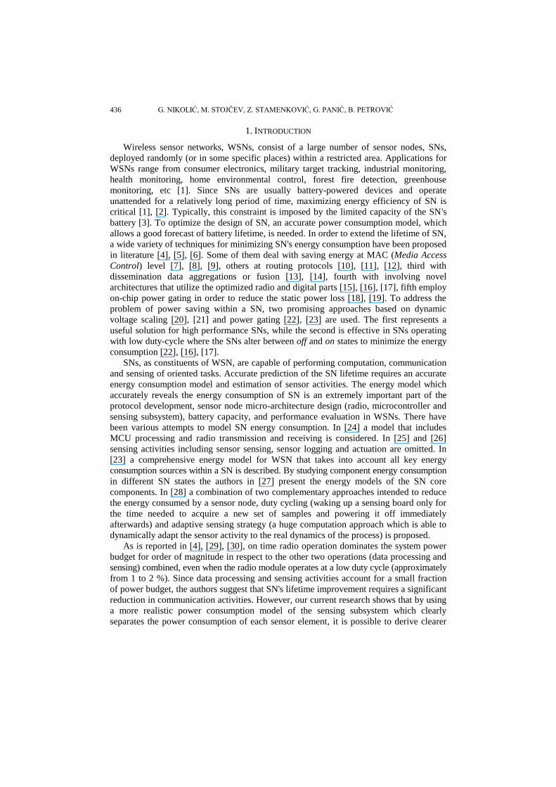
An overall hardware structure of a SN is presented in Fig. 1
Fig. 1 Overall block scheme of a sensor node.
The SN consists of several building blocks:
a) MCU- referred as a processing subsystem, controls the operation of all constituents
within the SN and performs data processing. The MCU includes microcontroller and
memory for local data processing. Most existing processing subsystems employ
microcontrollers, notably Texas Instruments' MSP430, Intel's Strong ARM, or Atmel's
AVR. These microcontrollers enable some of their internal components to be turned-off
completely when they are idle or sleep. CMOS compatible memories including static
random-access memory, SRAM, and embedded dynamic random-access memory,
DRAM, permit SNs to perform more complex digital signal processing algorithms
(collection, aggregation, and compression) and log more sensor data.

438 G. NIKOLIĆ, M. STOJĈEV, Z. STAMENKOVIĆ, G. PANIĆ, B. PETROVIĆ
b) Off-Chip Sensor Elements (OCSE) – called a sensing subsystem, implemented as a
set of passive and active sensors (digital or analog) convert input information from the
external environment into electrical signals. In most applications, wireless SNs are used
for monitoring light, pressure, vibration, flow rates in pipelines, temperature, ventilation,
electricity, etc. Commonly, sensor elements generate voltage or current signals at their
outputs. These signals are first amplified (conditioned) and then digitized with an analog-
to-digital converter, ADC, before data are digitally processed, stored and transmitted.
c) Radio Block (RB) – implemented as a short range transceiver which provides
wireless communication with the host or SNs within a WSN. The power consumption of a
transceiver can be reduced both at: i) the circuit level by developing more energy-efficient
RF circuits (using weak inversion operation in the RF building blocks, RF-MEMS passive
components, ultra-wideband transceivers which send narrow pulses of energy to transmit
data), and ii) at a system level by using RF communication (including shortening the
communication distance, minimizing the amount of data sent over the RF link or using
energy-efficient communication protocols, or powering down the transceiver during idle
periods, i.e., using a duty-cycling concept). For more details about this problematic see
reference [30].
d) Battery Supply Unit (BSU) – is a part of the power subsystem acting as a controllable
unit which individually switches on/off the power supply of each SN's building blocks.
BSU is responsible for providing the right amount of supply voltage to each individual SN
hardware component. A bulky battery is included in the BSU to power the SN's subsystems.
The BSU is a very important building block of the SN intended to improve the WSN
lifetime, and therefore numerous techniques based on the efficient exploitation of energy
resources have been introduced with the aim to prolong the WSN lifetime. For more details
see [31]. As we have already mentioned, currently, SNs are powered by batteries. However,
batteries are characterized by several disadvantages, including: i) the need to either replace
or recharge then periodically; and ii) being of a big size and weight compared to SN
electronics. One promising solution to overcome these drawbacks is to harvest energy from
the environment to either recharge a battery or even to directly power the SN. As is
presented in Table 1, the energy harvesting circuits can be classified into two groups.
Table 1 Classifications of energy harvesting circuits
energy source type of energy
human kinetic, thermal
environment kinetic, thermal and radiation
For more details see references [32], [33]. Among the most popular harvesting circuits
used in SNs are those based on converting solar energy, as a radiation type of energy. The
main advantages for using solar energy are as follows: i) it is excellent in remote or
difficult access location; ii) it is a totally clean and renewable source; iii) for supplying
small current loads such as SNs; and iv) in any country the use of solar energy like this is
feasible throughout the entire territory.
Depending on the specific application, SNs may also include additional components
like the location finding system to determine their position, a mobilizing unit to change
their location, etc. More details about SN architectures and functionalities of their
Wireless Sensor Node with Low-Power Sensing 439
building blocks can be found in [34]. Different types of communication interfaces, such as
parallel and serial buses interconnect the aforementioned subsystems. Among serial buses
the most frequently used interconnects are SPI (Serial Peripheral Interface) and I2C (Inter-
Integrated Circuit). A SPI is a preferable design solution for high-speed, while I2C for
low-speed communication.
Today's wireless SN is a simple device, and its components that make up its subsystems are
commonplace off-the-shelf components usually located on a printed circuit board.
2.1. Connecting sensor elements
Within an SN architecture, sensor elements can be implemented as:
a) on-chip constituents - typical for future generation (advanced system-on-chip, SoC
design) of wireless SN designs, and
b) off-chip constituents - SN composed of discrete components typical for currently
common market available (on-the-shelf) wireless SN systems.
The recent progress in ultra-low power circuit design is creating new opportunities in
SN architectures with on-chip for temperature and image sensor elements [35], [36].
Important advances have been made to achieve millimeter-scale SN and standby power as
low as 30 pW [37], or microwatt successive approximation register SAR-ADC with the
figure of merit down to 4.4 fJ per conversion step [38], but many design challenges remain
yet open.
Our design choice is based on the use of the off-the-shelf components. Such solution
implies that sensor elements are of the off-chip type, i.e., externally connected components
to the ADC (in our proposal ADC is a constituent of the MCU). In this paper, by involving
adequate energy models, we will consider implementations of duty-cycling and power-
gating techniques and investigate how to reduce the dynamic and static power when both
power saving approaches are used.
2.2. Power supply subsystems
In a SN, each subsystem/circuitry requires different supply voltage for its operation.
For example, in most common currently used designs, the MCU and other digital circuits
can run at supply voltage which ranges from 3 V to 1.8 V. Analog components such are
RF transceiver and sensor elements, in order to provide correct operation and noise
margins, require higher supply voltages which range from 1.2 V
to 2.5 V. Batteries
(Lithium 3.3 V−4.2 V) incorporated as power sources in SNs are limited in their output
voltage by their chemistries, and their voltages degrade with use. Since battery voltages
do not usually match the desired subsystem/circuit supply voltages, switching dc-to-dc or
linear low drop-out voltage regulator power converting electronics is used. Bearing in
mind that a current consumption of SN is within a range of several tens of mA (in active
mode) down to several A (in sleep mode) the power electronics must be specifically
designed for a low-power operation. As a preferable solution, we propose linear low
drop-out voltage regulator for powering the SN subsystem. In general, for powering low-
level of power devices, such as SN, the linear low drop-out voltage regulator has a better
performance in respect to dc-to-dc converter (dc-to-dc converters are usually designed for
high output power levels and do not efficiently convert the low level of the power needed
by SNs [30]).
440 G. NIKOLIĆ, M. STOJĈEV, Z. STAMENKOVIĆ, G. PANIĆ, B. PETROVIĆ
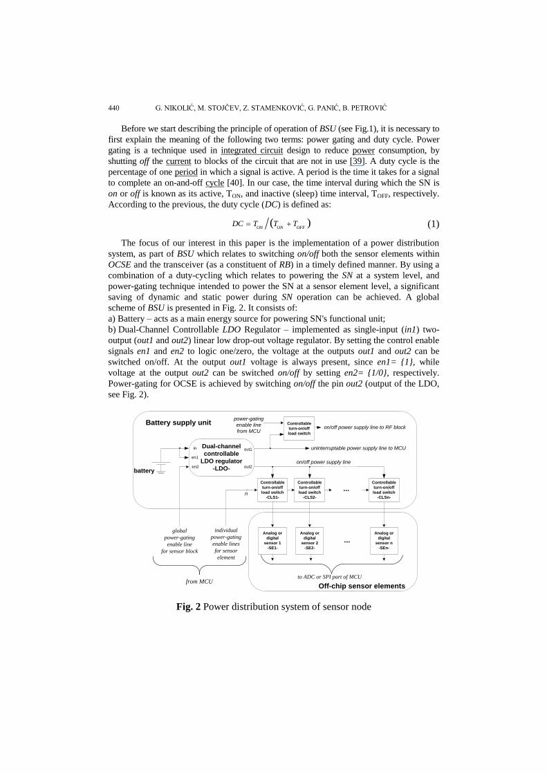
Before we start describing the principle of operation of BSU (see Fig.1), it is necessary to
first explain the meaning of the following two terms: power gating and duty cycle. Power
gating is a technique used in integrated circuit design to reduce power consumption, by
shutting off the current to blocks of the circuit that are not in use [39]. A duty cycle is the
percentage of one period in which a signal is active. A period is the time it takes for a signal
to complete an on-and-off cycle [40]. In our case, the time interval during which the SN is
on or off is known as its active, TON, and inactive (sleep) time interval, TOFF, respectively.
According to the previous, the duty cycle (DC) is defined as:
( )
ON ON OFFDC T T T (1)
The focus of our interest in this paper is the implementation of a power distribution
system, as part of BSU which relates to switching on/off both the sensor elements within
OCSE and the transceiver (as a constituent of RB) in a timely defined manner. By using a
combination of a duty-cycling which relates to powering the SN at a system level, and
power-gating technique intended to power the SN at a sensor element level, a significant
saving of dynamic and static power during SN operation can be achieved. A global
scheme of BSU is presented in Fig. 2. It consists of:
a) Battery – acts as a main energy source for powering SN's functional unit;
b) Dual-Channel Controllable LDO Regulator – implemented as single-input (in1) two-
output (out1 and out2) linear low drop-out voltage regulator. By setting the control enable
signals en1 and en2 to logic one/zero, the voltage at the outputs out1 and out2 can be
switched on/off. At the output out1 voltage is always present, since en1= {1}, while
voltage at the output out2 can be switched on/off by setting en2= {1/0}, respectively.
Power-gating for OCSE is achieved by switching on/off the pin out2 (output of the LDO,
see Fig. 2).
Dual-channel
controllable
LDO regulator
-LDO-
Controllable
turn-on/off
load switch
-CLS1-
Controllable
turn-on/off
load switch
-CLSn-
Controllable
turn-on/off
load switch
-CLS2-
battery
uninterruptable power supply line to MCU
...
Analog or
digital
sensor 1
-SE1-
Analog or
digital
sensor 2
-SE2-
Analog or
digital
sensor n
-SEn-
on/off power supply line
out1
out2
en1
en2
global
power-gating
enable line
for sensor block
n
individual
power-gating
enable lines
for sensor
element
from MCU
in
Off-chip sensor elements
Battery supply unit Controllable
turn-on/off
load switch
on/off power supply line to RF block
power-gating
enable line
from MCU
to ADC or SPI part of MCU
...
Fig. 2 Power distribution system of sensor node

Wireless Sensor Node with Low-Power Sensing 441
c) Controllable Turn On/Off Load Switches (CLSs) – each CLS is implemented as a P-
channel, or N-channel MOSFET transistor which can be individually switched on/off. In
this manner power-gating at a local control level within the sensing subsystem is provided
(i.e., MCU can separately switches on/off the power supply voltage for each sensor
element by setting a corresponding control line to logic one/zero).
3. ENERGY PROFILE
The proposed WSN considered in this paper is composed of several SNs deployed in a
restricted area. This system is primarily intended to monitor scalar values like acceleration,
space orientation, and audio signals. In this type of application almost all of the mentioned
sensor measurements do not need to be taken continuously which implies that the
environmental conditions can be periodically sampled. For example, taking one sample per
two minutes could be adequate to monitor temperature, pressure, light, humidity, etc. Power
management is an efficient way to conserve energy in WSN. The crucial idea of power
management is to dynamically make the SNs inactive in order to reduce their energy
consumption, i.e. to decide when a SN should go to the inactive state and the amount of time
to stay so. Most power management strategies proposed in literature [31], [41] assume that
data acquisition (sensing activity) consumes significantly less energy than wireless data
transmission [4]. However, in a large number of practical applications, this assumption does
not hold, especially in the case when the power consumption of active (not passive) sensor
element can be comparable to that of the communication subsystem. Similar problem was
considered in reference [42], [43]. In order to cope with this challenge in an effective way,
we propose to implement the power management concept into two levels, system and
component level, respectively. At the first level, a duty cycle technique is used, by which we
identify the idle and active time periods of SN's constituents. At the second level, power
gating technique is used, by which unutilized sensor elements are switched off while the
analyzed sensor element is switched on. In other words, our goal is that during most of the
time, the inefficient (unnecessary) power consumption of sensor elements due to not-optimal
configuration of hardware and software components is significantly reduced.
Let us note that a sensor node as an electrical system is time invariant, i.e. the total
energy consumption depends on its individual energy consumption components. Having
this in mind, in the sequel we will separately analyze the effects and benefits of
implementation of duty-cycling and power-gating techniques on energy consumption only
for the sensing subsystem as SN constituent.
3.1. Duty cycling
Duty cycling is a well-known technique for minimization of power consumption in wireless
SNs. The main idea behind this is clear: keep hardware (sensing-, communication-, and some
parts of power- and processing-subsystems – see Fig. 1.) in a low power sleep state, except
during instances when the hardware is needed. Many realizations of duty-cycling technique
allows even the MCU to be put into a low power state for long time periods, while its internal or
external clock tracks the time in order to trigger a later wake-up. The wake-up time is the time
from activation of the interrupt signal (by a Real Time Clock, RTC, circuit) to the beginning of
an interrupt service routine. Let us note that, all activities which deal with the duty cycle

442 G. NIKOLIĆ, M. STOJĈEV, Z. STAMENKOVIĆ, G. PANIĆ, B. PETROVIĆ
operation (switching into different power modes the transceiver, MCU, and low-drop out
regulator) are performed by the MCU under software control.
The total energy consumed by SN, Et, depends on the dynamic (active), Ed, and static
(leakage) power loss, Es.
t d s LF d LF s
E E E DC T P T P (2)
where, 0 < DC < 1, TLF is the lifetime of a SN, and Pd
and Ps correspond to dynamic and
static power, respectively. From Eq. 2, the portion of energy lost due to the leakage is
1
1
s
dt
s
E
PEDC
P
(3)
The ratio Pd / Ps is technology dependent and is proportional to the MOS transistor
channel properties. Similarly as in [18]1, taking the corresponding Pd / Ps for three different
CMOS technologies, we have calculated the impact of energy loss in respect to the total
energy consumption in terms of a DC factor. The obtained results are presented in Fig. 3.
00.10.20.30.40.50.60.70.80.90
10
20
30
40
50
60
70
80
90
100
Duty-cycle
Es/E
t [%
]
Energy loss due to leakage as a function of duty-cycle for different CMOS technologies
For 0.18 um
CMOS technology
For 0.13 um
CMOS technology
For 0.25 um
CMOS technology
Fig. 3 Energy loss due to leakage as a function of duty-cycle for different CMOS technologies
For digital components of the SN, similarly as in reference [44], we assume that Pd / Ps
is 1000 for 0.25 m technology, 20 for 0.18 m
technology, and 4 for 0.13 m
technology. By analyzing Fig. 3 we can conclude the following:
1 For the sake of clarity, the reference [18] defines the power consumption in active state (Pa = Pd + Ps) and the
power consumption in inactive state (Pi = Ps)
Wireless Sensor Node with Low-Power Sensing 443
1. With CMOS technology, scaling the energy loss due to static power increases. In
other words, the static power loss is comparable to dynamic power loss (high
amount of power is lost due to the leakage currents of CMOS circuitry [45]).
2. In standard applications a DC factor of the SN is low ( 1% ), which makes the total
system power dominated by the standby power, i.e. static power losses.
3. Theoretically, better energy efficiency (achieved by decreasing ED) can be obtained by
further decreasing the DC factor. However, in this case the influence of the clock
system, as components of SN, on the overall time synchronization accuracy of the
WSN becomes critical [46], [47].
Namely, the impact of variations in environmental temperature on clock drift in highly
duty-cycled wireless SNs is emphasized [47].
3.2. Power gating
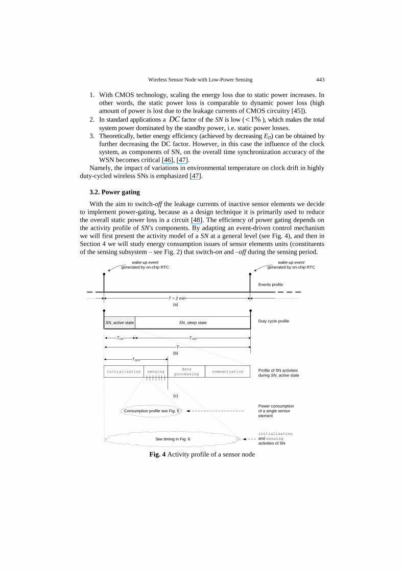
With the aim to switch-off the leakage currents of inactive sensor elements we decide
to implement power-gating, because as a design technique it is primarily used to reduce
the overall static power loss in a circuit [48]. The efficiency of power gating depends on
the activity profile of SN's components. By adapting an event-driven control mechanism
we will first present the activity model of a SN at a general level (see Fig. 4), and then in
Section 4 we will study energy consumption issues of sensor elements units (constituents
of the sensing subsystem – see Fig. 2) that switch-on and –off during the sensing period.
SN_active state SN_sleep state
See timing in Fig. 6
T = 2 min
wake-up event
generated by on-chip RTC
wake-up event
generated by on-chip RTC
T
TOFFTON
initialization sensingdata
processingcommunication
Duty cycle profile
Profile of SN activities
during SN_active state
Events profile
Power consumption
of a single sensor
element
TSEN
Consumption profile see Fig. 5
initialization
and sensing
activities of SN
(a)
(b)
(c)
Fig. 4 Activity profile of a sensor node

444 G. NIKOLIĆ, M. STOJĈEV, Z. STAMENKOVIĆ, G. PANIĆ, B. PETROVIĆ
As can be seen from Fig. 4 a), the RTC circuit, as a building block of the MCU,
periodically generates an interrupt signal called wakeup. The period of wakeup is T, in
our case T = 2 min. The appearance of the signal wakeup initiates a SN and it enters into
SN_active state (see Fig. 4b)). During SN_active state (Fig. 4c)) four sequential activities
are performed, initialization, sensing, data processing, and communication.
Activity initialization deals with restoring the content of MCU registers to the
preceding SN_active state and setting peripherals (LDO regulator, Controllable load
switches, and Transceiver – see Fig. 2) into the corresponding operating mode. The
sensing activity is responsible for information collection and analog-to-digital
conversion. The energy consumption during this activity comes from multiple operations,
including power-on (-off) switching of sensor elements, signal sampling, and analog-to-
digital conversion/SPI communication. If we assume that n sensor elements are connected
to the MCU (see Fig. 2), then the total energy consumption of the sensing subsystem, EST,
can be expressed as:
1
( )n
ST FOi OFi wi Ci
i
E N e e E E
(4)
where:
eFOi (eOFi) is the one time energy consumption of opening (closing) sensor element
operation – switching sensor element i from OFF (ON) to ON (OFF) state;
Ewi – energy consumption during warm-up time period of sensor element i;
ECi – energy consumption during analog-to-digital conversion period;
N – number of SN active states during lifetime of a SN, and
n – number of sensor elements in a SN.
Power consumption profile of a SN during single sensing activity of a sensor
element is sketched in Fig. 5.
Power
TimeOFF ONt
WUT
CONT
ON OFFt
OFFP
ONP
SENSOR PERIODT
Fig. 5 Power consumption profile of a single sensor element
Notice: A time interval tOFFON (tONOFF) includes transient time of Controllable load switch CLSi,
i = 1,...,8, and transient time of a sensor element SEi
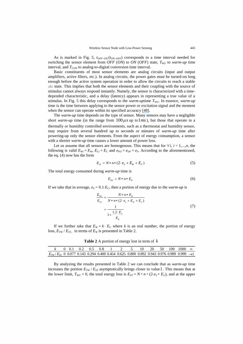
Wireless Sensor Node with Low-Power Sensing 445
As is marked in Fig. 5, tOFFON (tONOFF) corresponds to a time interval needed for
switching the sensor element from OFF (ON) to ON (OFF) state, TWU to warm-up time
interval, and TCON to analog-to-digital conversion time interval.
Basic constituents of most sensor elements are analog circuits (input and output
amplifiers, active filters, etc.). In analog circuits, the power gates must be turned-on long
enough before the active system operation in order to allow the circuits to reach a stable
dc state. This implies that both the sensor elements and their coupling with the source of
stimulus cannot always respond instantly. Namely, the sensor is characterized with a time-
depended characteristic, and a delay (latency) appears in representing a true value of a
stimulus. In Fig. 5 this delay corresponds to the warm-uptime TWU. In essence, warm-up
time is the time between applying to the sensor power or excitation signal and the moment
when the sensor can operate within its specified accuracy [48].
The warm-up time depends on the type of sensor. Many sensors may have a negligible
short warm-up time (in the range from 100 s up to1ms ), but those that operate in a
thermally or humidity controlled environments, such as a thermostat and humidity sensor,
may require from several hundred up to seconds or minutes of warm-up time after
powering-up only the sensor elements. From the aspect of energy consumption, a sensor
with a shorter warm-up time causes a lower amount of power loss.
Let us assume that all sensors are homogenous. This means that for i, i = 1,...,n, the
following is valid EWi = EW, ECi = EC and eFO = eOF = eS. According to the aforementioned,
the eq. (4) now has the form
( )2
ST S W CE N n e E E (5)
The total energy consumed during warm-up time is
TW W
E N n E (6)
If we take that in average, eS = 0.1EC, then a portion of energy due to the warm-up is
(2 )
1
1.21
TW W
ST S W C
C
W
E N n E
E N n e E E
E
E
(7)
If we further take that EW = k EC where k is an real number, the portion of energy
loss, ETW / EST, in terms of EW is presented in Table 2.
Table 2 A portion of energy lost in term of k
k 0 0.1 0.2 0.5 0.8 1 2 5 10 20 50 100 1000 ∞
ETW / EST 0 0.077 0.143 0.294 0.400 0.454 0.625 0.800 0.892 0.943 0.976 0.989 0.999 1
By analyzing the results presented in Table 2 we can conclude that as warm-up time
increases the portion ETW / EST asymptotically brings closer to value1 . This means that at
the lower limit, TWU = 0, the total energy loss is EST = N * n * (2eS + EC), and at the upper

446 G. NIKOLIĆ, M. STOJĈEV, Z. STAMENKOVIĆ, G. PANIĆ, B. PETROVIĆ
limit TWU , the total energy loss is EST N * n * EW, i.e. EW becomes dominant. In
general, better design solution concerning ETW is one in which TSW 0, but in this case
the sensor elements are all time active. As a direct consequence of this approach the
power consumption of a sensing subsystem will be high. To cope efficiently with this
problem, involving of power gating technique represents a good compromise. But in such
a solution, the sensor warm-up time cannot be ignored when SN's energy model is
considered.
4. POWER ESTIMATION
In this article we continue our work [49], and present a complete energy consumption
profile of the wireless sensor node during the activities initialization, and sensing,
only within the SN_active state.
In our case, the sensing subsystem OCSE (see Fig.2) is composed of eight sensor
elements, SE1, ..,SE8. Sensor elements from SE1up to SE7 are of analog type and drive the
on-chip ADC (as a component of MCU (MSP430FR59xx)). These sensor elements are
used for sensing temperature (LMT87), humidity (SHT21S), acceleration (ADXL377),
ambient light (ISL76671), position (SS345PT), motion (L3G3250A), and audio
microphone (MP33AB01), respectively. The last sensor (T5400) is used for measurement
pressure and it transfers data to MCU via an SPI interface. For more details about
electrical and time specifications of sensor elements see Farnell website [50]. The power
supply voltage out 2 = 3V
(marked as VOUT2 output of a low-drop out dual-channel
voltage regulator TLV716 [51]). ACLSi is implemented as a P-channel MOSFET
transistor TPS22908 [52] (see Fig.2).
Electrical and time specifications (found in the devices documentations and determined
by direct measurements) and energy consumption per sensor element (determined by
calculation and direct measurements) are presented in Table 3.
Table 3 Electrical and timing specifications, and calculated energy consumption per
sensor element
Sen
sor
elem
ent
Type
senso
r
out2
[V]
SE
iav.
curr
ent
[mA
]
t OF
F-O
N[m
s]
e FO
[uJ]
TW
U[m
s]
EW
[u
J]
TC
ON*[m
s]
EC
[uJ]
t ON
-OF
F [
ms]
e OF
[uJ]
1 LMT87
3
0.0041 2.01 0.012 n.a.
0.0
035
0.000043
0.0
05
0.000031
2 SHT21 0.1811 150.11 40.778 8000 4346.400 0.001902 0.001358 3 ADXL377 0.3011 5.11 2.308 n.a. 0.003162 0.002258
4 ISL76671 0.0361 0.205 0.011 0.350 0.038 0.000379 0.000271 5 SS345PT 3.0011 0.11 0.495 0.0015 0.014 0.031512 0.022508 6 L3G3250A 6.3011 0.11 1.040 0.3 5.671 0.066162 0.047258 7 MP33AB01 0.3011 0.11 0.050 n.a. 0.003162 0.002258
8 T5400 0.7911 2.61 3.097 10 23.733 16 37.9728 0.005933
Notice: Conversion time TCON is determined by SAR-ADC, as constituent of MCU, and for 12-bit
resolution and it is 3.5 s (identical for all sensor elements); n.a. stands for not available data
from catalog

Wireless Sensor Node with Low-Power Sensing 447
According to eq. (4) and data presented in Table 3, under the assumption that N = 1
and n = 8, the estimated energy consumption of our design during powering-up of sensor
elements (initial phase of sensing activity) can be expressed as
8
1
47.791 0.081875 4375.856 38.07912)
4461.808
( )ST FOi OFi wi Ci
i
E e e E E
J
(8)
Let us note that this value corresponds to the worst-case of energy consumption for all
CLSi and SEi during the sensing activity (Namely, after powering-up of sensor elements
this activity happens only once during the life-time of the sensor node. It is typical for
sensor element stabilization to environment conditions. Therefore, its impact, concerning
power estimation, can be neglected).
4.1. Energy profile during initialization and sensing activities
With the aim to determine the total energy consumption during the active state of a
sensor node it is necessary to take into account the energy loss of other building blocks
(MCU and BSU (see Fig. 1 and 2)) during the time period TSEN (see Fig. 4).
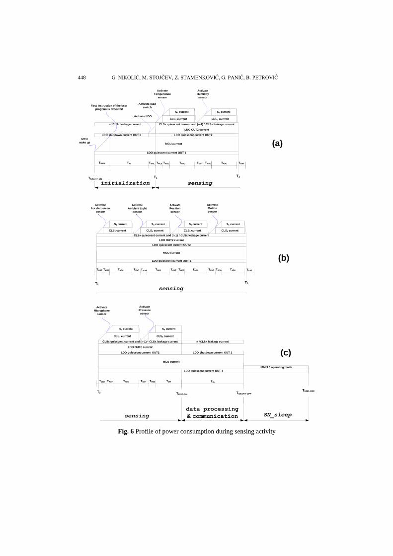
A detailed timing diagram during initialization and sensing activities is
presented in Fig. 6.
As can be seen from Fig. 6a) the initialization activity begins at TSTARTON and
ends with T1. The activity sensing deals with the right part of Fig 6 a), time interval
from T1 to T2, continues with Fig. 6 b), time interval from T2 to T3, and ends with the left
part of Fig. 6c), time interval from T3 to TENDON. The right part of Fig. 6c) includes data
processing and communication activities, time interval from TENDON to TSTARTOFF,
and SN_sleep state, time interval from TSTARTOFF to TENDOFF. Duration of a time interval
from TSTARTON to TENDOFF is 2min.
In Table 4, details concerning time interval durations of all activities during
initialization and sensing activities (defined in Fig. 6) including the average
current and energy consumption for each time-subinterval are given. Total time duration
of initialization and sensing activities is TSEN = 191.036ms and the corresponding
energy consumption during this period is 278.31J.
Timing diagrams and power consumption profile during initialization and
sensing activities (obtained by MATLAB,) are presented in Fig. 7. Figure Subplot 1
(down-left part of Fig. 7) deals with the initialization activity and acquiring data
from SE1 and SE2. Figure Subplot 2 (down-right part of Fig. 7) refers to acquiring data
from SE3 to SE8.
448 G. NIKOLIĆ, M. STOJĈEV, Z. STAMENKOVIĆ, G. PANIĆ, B. PETROVIĆ
(a)
(b)
MCU current
First instruction of the user
program is executed
Activate LDO
MCU
wake up
LDO OUT2 current
CLS1 current
Activate load
switch
LDO shutdown current OUT 2 LDO quiescent current OUT2
LDO quiescent current OUT 1
n *CLSx leakage current CLSx quiescent current and (n-1) * CLSx leakage current
Activate
Temperature
sensor
S1 current S2 current
Activate
Humidity
sensor
CLS2 current
TSTART-ONT1
T2
TWUM TIN TWUL TWLS TWS1 TADC TCMT TWS1 TADC TCMT
sensinginitialization
MCU current
LDO OUT2 current
CLS3 current
LDO quiescent current OUT2
LDO quiescent current OUT 1
CLSx quiescent current and (n-1) * CLSx leakage current
S3 current S4 current S5 current
CLS4 current CLS5 current
S6 current
CLS6 current
Activate
Accelerometer
sensor
Activate
Ambient Light
sensor
Activate
Position
sensor
Activate
Motion
sensor
T2
TCMT TWS3 TADC TCMT TWS4 TADC TCMT TWS5 TADC TCMT TWS6 TADC TCMT
T3
sensing
MCU current
LDO OUT2 current
LDO quiescent current OUT2
LDO quiescent current OUT 1
CLSx quiescent current and (n-1) * CLSx leakage current
S7 current
Activate
Microphone
sensor
CLS7 current
S8 current
Activate
Pressure
sensor
CLS8 current
LDO shutdown current OUT 2
n *CLSx leakage current
LPM 3.5 operating mode
TCMT TADC TCMTTWS7 TWS8 TSPI TOL
T3 TEND-ON TSTART-OFF
TEND-OFF
data processing
& communication SN_sleep sensing
(c)
Fig. 6 Profile of power consumption during sensing activity

Wireless Sensor Node with Low-Power Sensing 449
Table 4 Time interval duration, average current and energy consumption during
initialization and sensing activities for each MCU and OCSE sub-interval
Time interval Duration
[ms]
Average current
[mA]
Energy
[J]
TWUM 0.3500 0.290 0.1522500
TIN 1.0000 0.495 1.4850000
TWUL 0.9000 0.495 0.6682500
TWLS 0.1600 0.570 0.1368000
TWS1 1.9000 0.590 1.6815000
TADC 0.0035 0.720 0.0075600
TCMT 0.0050 0.075 0.0005625
0.1600 0.078 0.0187200
TWS2 150.000 0.729 164.02500
TADC 0.0035 0.877 0.0092085
TCMT 0.0050 0.075 0.0005625
0.1600 0.235 0.0564000
TWS3 5.0000 0.869 6.5175000
TADC 0.0035 1.017 0.0106785
TCMT 0.0050 0.075 0.0005625
0.1600 0.375 0.0900000
TWS4 0.4450 0.604 0.4031700
TADC 0.0035 0.752 0.0078960
TCMT 0.0050 0.075 0.0005625
0.1600 0.110 0.0264000
TWS5 0.0015 3.569 0.00803025
TADC 0.0035 3.717 0.0390285
TCMT 0.0050 0.075 0.0056250
0.1600 3.075 0.7380000
TWS6 1.0000 6.869 10.303500
TADC 0.0035 7.017 0.0736785
TCMT 0.0050 0.075 0.0056250
0.1600 6.375 1.5300000
TWS7 3.0000 0.869 3.9105000
TADC 0.0035 1.017 0.0106785
TCMT 0.0050 0.075 0.0056250
0.1600 0.078 0.0187200
TWS8 10.000 1.359 20.385000
TSPI 16.000 1.373 65.904000
TOL 0.1000 0.496 0.0744000
Notice: Where TWUM – wake-up time of the MCU; TIN – MCU initialization; TWUL – out2 wake-up
time of the LDO; TWLS – wake-up time of the CLS; TWSx – warm-up time of a sensor x={1,2, ..,8};
TADCx – conversion time x={1,2, ..,7}; TCMT – switching time which includes Tturn-off(LSx+Sx) + T turn-
on(LSx); TSPI – SPI time; TOL – time-off LDO

450 G. NIKOLIĆ, M. STOJĈEV, Z. STAMENKOVIĆ, G. PANIĆ, B. PETROVIĆ
Fig. 7 Diagrams of power consumption during initialization and sensing activities
for MCU and OCSE blocks
In order to evaluate the performance of our design concerning energy reduction, we
have compared the following two design solutions: a) total energy consumption of a
sensor subsystem Epg
during initialization and sensing activities, with the
implemented duty-cycling and power-gating techniques (Epg
= 638J ); and b) total
energy consumption of a sensor subsystem Ewpg without implementation of duty-cycling
and power-gating techniques (Ewpg = 3.92 J). The estimated ratio is Ewpg / Epg = 6146. The
obtained result justifies the involvement of both power saving techniques in a sensing
subsystem of a wireless sensor node.
5. CONCLUSION
Wireless sensor nodes place sensor elements in the physical world in order to gather
information. This activity consumes energy. Due to the limited battery capacity, energy
conservation becomes a goal. This paper attempts to provide a comprehensive insight into
aspects of energy consumption of a sensing subsystem within a sensor node architecture.
In order to achieve reduction in energy consumption in a sensor node operation, we
propose using a combination of two power saving techniques. The first one, called duty-
cycling, is used for power reduction at a system level, i.e. switching on/off the sensor node
architecture between active and sleep state. The second one, referred to as power
Wireless Sensor Node with Low-Power Sensing 451
gating, is intended for switching on/off the sensor elements (constituent of the sensing
subsystem within SN), during acquiring information from the external environment. The
obtained results based on the analysis and validation by MATLAB show that on average,
three order of reduction in energy consumption can be achieved when the mentioned two
techniques intended for power saving are implemented with respect to the case when they
are turned off.
For the time period of two minutes the energy consumption when the two techniques
are used is 638 J compared to 3.92 J
in the case when the duty-cycling and power-
gating techniques are turned off.
Acknowledgement: This work was supported by the Serbian Ministry of Education, Science and
Technological Development, Project No. TR-32009 – “Low-Power Reconfigurable Fault-Tolerant
Platforms”.
REFERENCES
[1] I. F. Akyildiz, and M. C.Vuran, "Wireless Sensor Networks", John Wiley & Sons Ltd, 2010
[2] A.J. Goldsmith, and S. B. Wicker, "Design Challenges for Energy Constrained Ad Hoc Wireless
Networks", IEEE Wireless Communications, 2002, Vol. 9, No. 4, (pp. 8-27)
[3] G. Pistoria, "Battery Operated Devices and Systems", Elsevier BV., Amsterdam, The Netherlands, 2009
[4] V. Raghunathan,S. Ganerival, andM. Srivastava, "Emerging Techniques for Long Lived Wireless Sensor
Networks", IEEE Communication Magazine, 2006,Vol.41, No. 4,(pp. 130-141)
[5] G.Anastasi, M. Conti, M. Di Francesco, and A.Passarella, "Energy Conservation in Wireless Sensor
Networks: A survey", Ad Hoc Networks, 2009, Vol. 7, (pp. 537–568)
[6] M. N. Halgamuge, M. Zukerman, and K. Ramamohanarao, "An Estimation of Sensor Energy
Consumption, Progress in Electromagnetics Research B", 2009, Vol. 12, (pp. 259-295)
[7] W. Ye, J. Heidemann, and D. Estrin, "An Energy-Efficient Mac Protocol for Wireless Sensor Networks,"
Proc. IEEE Infocom, New York (USA) 2002, (pp. 1567-1576).
[8] M. Al Ameen, S.M. Riazul Islam, and K.Kwak, "Energy Saving Mechanisms for MAC Protocols in
Wireless Sensor Networks", Hindawi Publishing Corporation International Journal of Distributed Sensor
Networks, Volume 2010 (2010), Article ID 163413, (pp 1-16)
[9] M. R. Ahmad, E.Dutkiewicz, and X. Huang (2011), "A Survey of Low Duty Cycle MAC Protocols in
Wireless Sensor Networks", Ch. 5,(pp. 69 – 90), in "Emerging Communications for Wireless Sensor
Networks", Eds. A. Foerster and A. Foerster, Pub. by InTech, 2011, Rijeka, Croatia
[10] J. N. Al-Karaki and A. E. Kamal, "Routing Techniques in Wireless Sensor Networks: A Survey,", IEEE
Wireless Communications, 2004, Vol. 11, No. 6, (pp. 6-28).
[11] E. Y. Lin, "A Comprehensive Study of Power-Efficient Rendezvous Schemes for Wireless Sensor
Networks", PhD thesis, University of California, Berkeley, 2005
[12] E. A. Lin, J. M. Rabaey, and A.Wolisz, "Power-Efficient Rendez-vous Schemes for Dense Wireless
Sensor Networks", In Proceeding of ICC2004, Paris, France, June 2004, Vol.7, (pp. 3769 – 3776)
[13] M. Hempstead, N. Tripathi, P. Mauro, G.-Y. Wei, and D. Brooks, "An Ultra Low Power System
Architecture for Sensor Network Applications," Proc. 32nd Annual International Symposium on
Computer Architecture, Madison (USA) 2005, (pp. 208-219).
[14] A. Boulis, S. Ganeriwal, and M. Srivastava, "Aggregation in Sensor Networks: An Energy Accuracy
Trade-Off", Ad Hoc Networks, Vol. 1, 2003, (pp. 317–331)
[15] B. H. Calhoun, D. C. Daly, N. Verma, D. Finchelstein, D. D. Wentzloff, A. Wang, S.-H. Cho, and A. P.
Chandrakasan, "Design Considerations for Ultra-Low Energy Wireless Micro-sensor nodes," IEEE Trans.
Computers, 2005, Vol. 54, No. 6, (pp. 727-740)
[16] C. Lynch, and F. O'Reilly, "Processor Choice for Wireless Sensor Networks", Workshop on Real-World
Wireless Sensor Networks, REALWSN'05, Stockholm, Sweden, 20-21 June 2005, (pp. 1-5)
[17] D. Singh, "Micro-Controller for Sensor Networks", MsC. Th., Department of Computer Science and
Engineering, Indian Institute of Technology, Kharagpur, India, May 2008

452 G. NIKOLIĆ, M. STOJĈEV, Z. STAMENKOVIĆ, G. PANIĆ, B. PETROVIĆ
[18] G. Panić, Z.Stamenković, and R.Kraemer, "Power Gating in Wireless Sensor Networks", Wireless
Pervasive Computing, 2008.ISWPC2008. 3rd International Symposium on, Santorini,Greece,May 2008,
(pp. 499-503)
[19] H. Jiang, M. Marek-Sadowska, and S. Nassif, "Benefits and Costs of Power-Gating Technique", Proc.
IEEE Int'l Conf. Computer Design: VLSI in Computers and Processors (ICCD '05), San Jose, CA, USA,
2-5. Oct. 2005, (pp. 559-566)
[20] T. Burd, and R. Brodersen, "Energy Efficient Microprocessor Design", Kluwer Academic Publishers,
Norwell MA, USA, 2002
[21] N. Weste and D. Harris, "Integrated Circuit Design", Pearson Education, Boston, USA, 2011
[22] G. Panić, D. Dietterle, and Z. Stamenković, "Architecture of a Power-Gated Wireless Sensor Node" ,
Proc. 11th Euromicro Conference on Digital System Design, 2008, Parma, Italy, (pp. 844-849)
[23] Y. Lee, G. Chen, S. Hanson, D. Sylvester and D. Blaauw, "Ultra-Low Power Circuit Techniques for a
New Class Of Sub-Mm3 Sensor Nodes", Custom Integrated Circuits Conference (CICC), 2010 IEEE, 19-
22 Sept. 2010, San Jose, CA, USA, (pp. 1 – 8)
[24] W. Heizelman, A. Chadrakasan, and H. Balakrishnan, "An Application-Specific Protocol Architecture for
Wireless Micro-Sensor Networks", IEEE Trans. on Wireless Communications, Vol. 1, No. 4, Oct. 2002,
(pp. 666-670)
[25] J. Zhu, and S. Papavassilion, "On the Energy-Efficient Organization and the Lifetime of Multi-Hop
Sensor Networks", IEEE Communication Letters, Vol. 7, No. 11, Nov. 2003, (pp. 537-539)
[26] M. Mille and N. Vaidya, "A Mac Protocol to Reduce Sensor Network Energy Consumption Using a
Wake-Up Radio", IEEE Trans on Mobile Computing, Vol. 4, No. 3, May, 2005, (pp. 228-242)
[27] H.Y. Zhou, D. Luo, Y. Gao, and D. Zuo, "Modeling of Node Energy Consumption for Wireless Sensor
Networks", Wireless Sensor Networks, Vol. 3, 2011, (pp. 18-23)
[28] C. Alippi, G. Anastasi, M. Di Francesco, and M. Roveri, "Energy Management in Wireless Sensor
Networks with Energy-Hungry Sensors", IEEE Instrumentation and Measurement Magazine, Vol.12, No.
2, April 2009, pp. 16-23
[29] P. Dutta, D. Culler and S. Shenker, "Procrastination Might Lead to a Longer and More Useful Life", In
Proceedings of the ACM Sixth Workshop on Hot Topics in Networks (HotNets-VI), 2007, Atlanta,
Georgia, USA, (pp. 1-7)
[30] G. Chen, S. Hanson, D. Blaauw, and D. Silvester, "Circuit Design Advances for Wireless Sensing
Applications", Proceedings of the IEEE, Vol. 98, No. 11, November 2010, (pp. 1808-1826)
[31] W. Dargie, “Dynamic Power Management in Wireless Sensor Networks: State-of-the-Art”, Sensors Journal,
IEEE, Vol. 12, No. 5, 2012, (pp. 1518 - 1528)
[32] L. Mateu; and F. Moll, "Review of Energy Harvesting Techniques and Applications for Microelectronics",
Proc. SPIE 5837, VLSI Circuits and Systems II, Seville, Spain, May 09, 2005, (pp. 1- 15 );
[33] S. Beeby, and N. White, "Energy Harvesting for Autonomous Systems", Artech House, Norwood, MA
USA, 2010
[34] M.A.M Viera, C.N. Coelho, D.C. da Silva Jr., J.M. Mata, ”Survey on Wireless Sensor Network Devices”,
IEEE Conference Emerging Technologies and Factory Automation, Lisbon, Portugal, 16-19 Sept. 2003,
Vol.1, (pp. 537-544)
[35] A.L. Aita, M. Pertijs, K. Makinwa, and J.H. Hujsing, "A CMOS Smart Temperature Sensor with a Batch-
Calibrated Inaccuracy of ±0,250c(3δ) from -700c to 1300c" in Proceedings of the IEEE Solid State
Circuits Conference, San Francisco, CA, USA, Feb. 2009, (pp. 342-343,343a)
[36] S. Hanson and D. Sylvester, "A 0.45-0.7 V Sub-microwatt CMOS Image Sensor for Ultra-Low Power
Applications", In Proceedings of the Symposium on Very Large Scale Integration (VLSI) Circuits, Vol. 1,
Kyoto, Japan, Jun. 2009, (pp. 176-177)
[37] S. Hansen, M. Seok, Y.S. Liu, Z.Y. Fao, D. Kim, Y. Lee, N. Liu, D. Sylvester, and D. Blaauw, "A Low-
Voltage Processor for Sensing Applications with Picowatt Standby Mode", IEEE Journal of Solid-State
Circuits, Vol. 44, No.4 April 2009, (pp. 1145-1155)
[38] N. Verma, and A.F.Chandrakasan, "An Ultra-Low Energy 12-bit Rate Resolution Scalable SAR ADC for
Wireless Sensor Nodes", IEEE Journal of Solid-State Circuits, Vol. 42, No. 6, June 2007, (pp. 1196-1205)
[39] M. Kuorilehto, M. Kohvakka, J. Suhonen, P. Hamalainen, M. Hannikainen, and T. D. Hamalainen,
"Ultra-Low Energy Wireless Sensor Networks in Practice: Theory, Realization and Deployment", John
Wiley & Sons Ltd, 2007, Chichester, UK
[40] B. Krishnamachari, "Networking Wireless Sensors", Cambridge University Press 2005, Cambridge, UK
[41] F. Juan, B. Lian, and Z. Hongwei, "Hierarchically Coordinated Power Management for Target Tracking in
Wireless Sensor Networks", International Journal of Advanced Robotic Systems, Feb. 2013, Vol. 10, (pp. 1 - 14)
Wireless Sensor Node with Low-Power Sensing 453
[42] V. Jeliĉić, "Power Management in Wireless Sensor Networks with High-Consuming Sensors", Technical
project report, April 2011, University of Zagreb, Faculty of Electrical Engineering and Computing, (pp.
1-9), av. February 2014 at http://www.ztel.fer.unizg.hr/_download/repository/VJelicic,KDI.pdf
[43] H. Joe, J. Park, C. Lim, D. Woo, and H. Kim, "Instruction-Level Power Estimator for Sensor Networks",
ETRI Journal, Vol. 30, No. 1, February 2008, (pp. 47 - 58)
[44] Leibniz Institute for High Performance Microelectronics – IHP, Frankfurt (Oder), Germany,
http://www.ihp-microelectronics.com
[45] N.S. Kim, T. Austin, D Baauw, T. Mudge, K.Flautner, J.S. Hu, M.J. Irwin, M.Kandemir, and V.
Narayanan "Leakage Current: Moore's Law Meets Static Power ", IEEE Computer, Dec. 2003, Vol.36,
No. 12, (pp. 68 - 75)
[46] M. Kosanovic, M. Stojcev, "RPATS – Reliable Power Time Synchronization Protocol", Microelectronics
Reliability, Vol. 54. No. 1, 2014, (pp.303-315)
[47] T. Schmid, R. Shea, Z. Charbiwala, J. Friedman, M. Srivastava, and Y. Cho, "On the Interaction of
Clocks, Power, and Synchronization in Duty-Cycled Embedded Sensor Nodes", ACM Transactions on
Sensor Network, Vol. 7, No. 3, 2010, (pp. 1-19), article No. 24
[48] J. Fraden, "Handbook of Modern Sensors: Physics, Designs, and Applications", Fourth Edition, Springer
New York, 2010
[49] G. Nikolic, G. Panic, Z. Stamenkovic, G. Jovanovic and M. Stojcev, "Implementation of External Power-
Gating Technique During Sensing Phase in Wireless Sensor Networks", 29th International Conference on
Microelectronics MIEL 2014, Belgrade, Serbia, 12-15 May 2014, accepted for presentation
[50] Online catalogue of www.farnell.com av. at January. 2014
[51] Texas Instruments, Low-Dropout Voltage Regulator, av. at www.ti.com/lit/gpn/tlv716120275p, January. 2014
[52] Texas Instruments, Low Ron Load Switch, av. at http://www.ti.com/lit/ds/symlink/tps22908.pdf, January. 2014