Wireless sensor networks: Enabling technology for ambient intelligence
11
Microelectronics Journal 37 (2006) 1639–1649 Wireless sensor networks: Enabling technology for ambient intelligence L. Benini , E. Farella, C. Guiducci Dipartimento di Elettronica Informatica e Sistemistica, Universita` di Bologna, Viale Risorgimento 2, 40136 Bologna, Italy Received 22 August 2005; received in revised form 22 February 2006; accepted 19 April 2006 Available online 18 September 2006 Abstract Wireless sensor networks are one of the most rapidly evolving research and development fields for microelectronics. Their applications are countless, and the market potentials are huge. However, many technical hurdles have to be overcome to achieve a widespread diffusion of wireless sensor network technology. This paper summarizes the trends of evolution in wireless sensor network nodes, focusing on hardware architectures and fabrication technology. We describe four generations of sensor networks (obtrusive, parasitic, symbiotic and bio-inspired), moving from the recent past to the future. We outline the key research challenges and the common themes in the field. r 2006 Elsevier Ltd. All rights reserved. Keywords: Wireless sensor networks; Embedded systems; Energy efficiency; Bio-sensors 1. Introduction Embedded electronic systems are pervasive: from alarm clocks to PDAs, from mobile phones to cars, almost all the devices we use are controlled by embedded electronics. Over 99% of the microprocessors produced today are used in embedded systems, and recently the number of embedded systems in use has become larger than the number of humans on the planet. Ideally, we should be able to interact with embedded systems through user interfaces that are an extension of our natural interaction paradigms (spoken language, gestures, facial expression, etc.). Embedded devices should ‘‘disappear into the environment’’ and behave ‘‘intelligently’’: intelligent sys- tems respond to and even anticipate our needs by under- standing what is implied by the sound of our voice, movements, expressions. Ambient intelligence (AmI) is the vision that technology will become not simply embedded, but invisible, fully hidden in our natural surroundings, but present whenever we need it, enabled by simple and effortless interactions [1–3]. The term AmI has been defined by the ISTAG (Advisory Group to the EU Information Society Technol- ogy Program) as ‘‘the convergence of three major key technologies: ubiquitous computing, ubiquitous commu- nication, and interfaces adapting to the user’’. Wireless sensor networks [4,5] (WSNs) are commonly recognized as one of the technological cornerstones of AmI. Agile, low-cost, ultra-low power networks of sensors can collect a huge amount of critical information from the environment. Using a biological analogy, a sensor network can be seen as the sensory system of the intelligent environment ‘‘organism’’. Sensor networks are irregular aggregations of communicating sensor-nodes, which collect and process information coming from on-board sensors, and they exchange part of this information with neighbor- ing nodes or with nearby collection stations. Sensor network applications in AmI are countless, ranging from monitoring of ecosystems and industrial processes, to asset and people tracking, to maintenance of buildings, etc. [6]: each application domain has distinct requirements and constraint which will drive the develop- ment of sensor node architectures. In this survey we choose to focus our attention on one specific application driver, namely monitoring of humans and animals (in short, bio- monitoring). There are several reasons for this choice. First, human monitoring is an extremely important field, both for ethical and commercial reasons. Second, its field of application poses extremely challenging requisites on ARTICLE IN PRESS www.elsevier.com/locate/mejo 0026-2692/$ - see front matter r 2006 Elsevier Ltd. All rights reserved. doi:10.1016/j.mejo.2006.04.021 Corresponding author. E-mail address: [email protected] (L. Benini).
-
Upload
independent -
Category
Documents
-
view
2 -
download
0
Transcript of Wireless sensor networks: Enabling technology for ambient intelligence
ARTICLE IN PRESS
0026-2692/$ - se
doi:10.1016/j.m
�CorrespondE-mail addr
Microelectronics Journal 37 (2006) 1639–1649
www.elsevier.com/locate/mejo
Wireless sensor networks: Enabling technology for ambient intelligence
L. Benini�, E. Farella, C. Guiducci
Dipartimento di Elettronica Informatica e Sistemistica, Universita di Bologna, Viale Risorgimento 2, 40136 Bologna, Italy
Received 22 August 2005; received in revised form 22 February 2006; accepted 19 April 2006
Available online 18 September 2006
Abstract
Wireless sensor networks are one of the most rapidly evolving research and development fields for microelectronics. Their applications
are countless, and the market potentials are huge. However, many technical hurdles have to be overcome to achieve a widespread
diffusion of wireless sensor network technology. This paper summarizes the trends of evolution in wireless sensor network nodes,
focusing on hardware architectures and fabrication technology. We describe four generations of sensor networks (obtrusive, parasitic,
symbiotic and bio-inspired), moving from the recent past to the future. We outline the key research challenges and the common themes in
the field.
r 2006 Elsevier Ltd. All rights reserved.
Keywords: Wireless sensor networks; Embedded systems; Energy efficiency; Bio-sensors
1. Introduction
Embedded electronic systems are pervasive: from alarmclocks to PDAs, from mobile phones to cars, almost all thedevices we use are controlled by embedded electronics.Over 99% of the microprocessors produced today are usedin embedded systems, and recently the number ofembedded systems in use has become larger than thenumber of humans on the planet. Ideally, we should beable to interact with embedded systems through userinterfaces that are an extension of our natural interactionparadigms (spoken language, gestures, facial expression,etc.). Embedded devices should ‘‘disappear into theenvironment’’ and behave ‘‘intelligently’’: intelligent sys-tems respond to and even anticipate our needs by under-standing what is implied by the sound of our voice,movements, expressions.
Ambient intelligence (AmI) is the vision that technologywill become not simply embedded, but invisible, fullyhidden in our natural surroundings, but present wheneverwe need it, enabled by simple and effortless interactions[1–3]. The term AmI has been defined by the ISTAG(Advisory Group to the EU Information Society Technol-
e front matter r 2006 Elsevier Ltd. All rights reserved.
ejo.2006.04.021
ing author.
ess: [email protected] (L. Benini).
ogy Program) as ‘‘the convergence of three major keytechnologies: ubiquitous computing, ubiquitous commu-nication, and interfaces adapting to the user’’.Wireless sensor networks [4,5] (WSNs) are commonly
recognized as one of the technological cornerstones ofAmI. Agile, low-cost, ultra-low power networks of sensorscan collect a huge amount of critical information from theenvironment. Using a biological analogy, a sensor networkcan be seen as the sensory system of the intelligentenvironment ‘‘organism’’. Sensor networks are irregularaggregations of communicating sensor-nodes, which collectand process information coming from on-board sensors,and they exchange part of this information with neighbor-ing nodes or with nearby collection stations.Sensor network applications in AmI are countless,
ranging from monitoring of ecosystems and industrialprocesses, to asset and people tracking, to maintenance ofbuildings, etc. [6]: each application domain has distinctrequirements and constraint which will drive the develop-ment of sensor node architectures. In this survey we chooseto focus our attention on one specific application driver,namely monitoring of humans and animals (in short, bio-
monitoring). There are several reasons for this choice. First,human monitoring is an extremely important field, both forethical and commercial reasons. Second, its field ofapplication poses extremely challenging requisites on

ARTICLE IN PRESSL. Benini et al. / Microelectronics Journal 37 (2006) 1639–16491640
unobtrusiveness, security and safety. Finally, this is one ofthe AmI application fields where research and develop-ments are most active.
Design, implementation, and deployment of a WSNinvolves a wide range of disciplines and considerations fornumerous application-specific constraints. In the last fiveyears, significant progress has been made in the develop-ment of WSNs, and some WSN-based commercialproducts have already appeared on the market. Thepurpose of this paper is to give a snapshot oncurrent development and future direction of evolution inthis field. Our survey will emphasize node architectures andhardware technology, while only passingly mentioningsoftware and network architecture issues. This choice offocus is dictated by space limitations. We refer readersinterested in the very significant research challenges insoftware and network architectures to one of the manyexcellent surveys that have recently been published on thesetopics [7,8].
2. Trends in sensor networks
In bio-monitoring, the ‘‘physical world’’ that has to bemonitored is a living body. Hence, sensor nodes should beplaced in close proximity of the subject’s body, and theyconstitute a body-area network. The evolution of sensornodes for bio-monitoring is driven by the ‘‘disappearance’’requirement, and it leverages all technology optionsavailable, from the ever-shrinking standard microelectronictechnology, to the emerging microfabrication processesallowing the integration of heterogeneous devices onto asmall physical volume. As a result, we can clearly see adirection of fast evolution. We summarize this trend byintroducing an evolutionary sequence of four generationsof sensor nodes, characterized by a progressively decreas-ing level of obtrusiveness:
�
Obtrusive. These devices are constantly perceived by thetarget subject because their size and weight is largeenough to be a source of nuisance. Nevertheless, theyare portable and they can communicate with othernodes or with data-collection gateways. Many currentcommercial devices are obtrusive: examples includehalter electro-cardiographs and body tracking systemsbased on wearable cameras and markers (which limitmovements to the area where markers are present).Obtrusiveness is dictated mainly because of two keyissues: high power dissipation (a significant fraction of1W), which implies large batteries and/or short timebetween recharges, and a cumbersome sensory interface(e.g. electrodes glued on the skin, needles, fixedinfrastructure required in the environment, etc.). � Parasitic. These nodes are perceived by the subject asphysical objects, but their size, weight and structure doesnot pose serious limitations to normal behavior.Examples of parasitic devices are bio-metric watchesand body-tracking inertial sensors. The physical volume
of these nodes should not exceed a few cubic centi-meters, and their weight should be in the order of thetens of grams. Considering the volumetric energydensity of current battery technology, the powerconsumption of these nodes must not be larger than afew milliwatts. Several parasitic nodes have beenrecently commercialized, and these devices representthe current state-of-the-art in WSN.
� Symbiotic. Moving beyond the state of the art, theresearch community is pushing toward more aggres-sively scaled, cubic millimeter-sized devices (called‘‘smart dust’’ [9]) which may enable a number of newin-body bio-monitoring applications. The technicalchallenges to be solved are, first, the implementationof autonomously-powered nodes, able to scavengepower from the body (temperature gradients, move-ment, in-body chemical reactions, etc.). Battery freeoperation limits average power consumption to a fewtens of microwatts. Second, their size limitation imposesdemanding requirements on process integration andmicrofabrication: wireless communication, electronicprocessing, chemical processing, microfluidic capabil-ities must be packed within a few cubic millimeters.Finally, even bigger challenges are posed by safetyrequirements: the nodes should be short and long termbio-compatible. We call these nodes symbiotic becausethey have a true mutual advantage relationship with thetarget organism.
� Bio-hybrid. As an end point of our evolution trend, weenvision bio-inspired nodes, both from the architectureand from the technology viewpoint. The physical scaleof these devices approaches a few cubic microns (orless), and the interface between the sensor target and thesensor itself disappears. Molecular engineering andnanotechnology may make these device a reality in thenear future. Several exploratory research efforts havedemonstrated that some of the key functionalityrequired in a sensor node can be implemented bymolecular-scale devices that are often engineered usingbio-molecules. These devices operate autonomously,powered by chemical reactions inspired to biologicalsystems. The construction process and the architectureof these devices will also resemble natural processes inbiology: bottom-up self-assembly, self-replication andself-repair will be required in addition to safety and bio-compatibility.
The trend and the fundamental characteristics of the fourgenerations of sensor nodes are summarized in Table 1. Inthe following sections, we discuss in details the architec-tures and the main features of existing obtrusive andparasitic sensor nodes, drawing examples from commercialproducts as well as from innovative research prototypes.We then move to symbiotic and bio-hybrid devices, forwhich only incomplete, but very promising researchsolutions have been investigated.

ARTICLE IN PRESS
Table 1
Summary of the four sensor node generations
Node Maturity Power (W) Size (m3)
Obtrusive Commercial 1–10�1 10�3
Parasitic Prototype/commercial 10�2–10�3 10�6
Symbiotic Research/prototype 10�5–10�6 10�9
Bio-hybrid Concept/research o10�7 10�15
Fig. 1. Sensor node functional components.
L. Benini et al. / Microelectronics Journal 37 (2006) 1639–1649 1641
3. The state of the art: from obtrusive to parasitic sensor
nodes
The design space of WSN is multidimensional: eachpractical implementation is the result of a complex trade-off among design choices [6]. Characteristics such asresources, energy, form-factor and consequently costs, willguide our survey along the evolution of sensor nodes fromshoebox-size devices to dust-like. Reducing physical size hasalways been one of the key design issues. Therefore, thegoal is to provide powerful processor, memory, radio andother components while keeping a reasonably small size,dictated by a specific application.
Shoe box: Commercial personal digital assistants (PDAs)contain significant computing power in a small package(about 200 cm3). They can be considered general-purposesensor nodes for their multiple sensing (e.g. from video/audio sensors to temperature and accelerometers) andtransmission capabilities (Bluetooth, WiFi, infrared inter-faces). They are usually based on RISC microprocessorsand run off-the-shelf operating systems such as WindowsCE, Linux, or real-time operating systems. These systemshave maximum flexibility and programmability to adapt tovarious context and applications.
Sensor nodes based on PDA-class hardware and soft-ware are power hungry and expensive in terms ofmanufacturing cost per unit. Usually this kind of nodesconsists of a stack of base circuits comprising theprocessor, radio and power supply, which are coupledwith the desired sensors, packaged in a ruggedized box forprotection from hostile environments. Examples of thisclass of sensors nodes are WINS [10], iBadge from UCLA[11] and mAmps [12].
Dice: Dedicated embedded sensor nodes of the dimen-sion of a matchbox or a dice are usually based on low-power microcontrollers and small components. Theseplatforms still use commercial off-the-shelf components,but they focus on small form factor devices, low-powerprocessing and communication, and simple sensor inter-faces. Examples includes the Berkeley Mote family [13], theUCLA Medusa family [14], Ember nodes [15]. Because ofthe simple microcontroller used, these platform typicallysupport a very lightweight programming environment.
Dust: At present, almost all prototype and commercialwireless sensor nodes are made with commercial off-the-shelf components. However, some of the WSN companies
are developing new chips that will combine several of thenow separate functions, for example radio and processingcapabilities, analog to digital conversion and memoryfunctions. Clearly, the integration of functions on a singlechip is advantageous, for both power and size. Researchprototypes of system-on-chip (SoC) nodes are the first steptoward the goal of symbiotic systems. Examples of SoChardware include Smart Dust [16], the BWRC picoradionode [17], and the PASTA node [18].
3.1. Sensor node architecture
A generic sensor network node hardware consists ofseveral subsystems [19]: a microprocessor, data storage,sensors, actuators, a data transceiver, and an energy source(see Fig. 1). In the next subsections, we investigate andanalyze the main characteristic of processing unit, powerblock, sensor and communication unit. Subsequently, thefinal subsection introduce a case study of a wireless sensorsystem for motion capture with accelerometers, calledWiMoCA.
3.1.1. Processing unit and memory
A sensor node is a multi-functional unit performingmany different tasks, from managing acquisition tohandling communication protocol schedule and preparingdata packets for transmission, after filtering, synchronizingand signal processing on data gathered from sensors. Thus,each sensor node requires processing and storage capabil-ities. The choice of the processing unit not only decides theintrinsic ‘‘intelligence’’ of the node but also influences itssize and power consumption.A first and most common choice is to use general-
purpose microprocessors and microcontrollers of differentpower and resources. Intel StrongARM microprocessor,Texas Instruments MSP 430 and Atmel AVR microcon-troller are examples of commonly used processors.Commercial PDAs, that we can consider as high-endsensor nodes, use the StrongARM microprocessor. Thesesystems have maximum flexibility and programmability toadapt to various context and applications. However, a

ARTICLE IN PRESSL. Benini et al. / Microelectronics Journal 37 (2006) 1639–16491642
processor executing software is far less efficient (in terms ofenergy consumption, manufacturing cost per unit, andperformance) than a fixed-logic application specific inte-grated circuit (ASIC). Moreover, the size of their batteriesmakes these devices obtrusive.
Nowadays, microcontroller are essentially general-pur-pose computers on a single chip including not only memoryand processor, but non-volatile memory and interfacessuch as ADCs (analog-to-digital converters), UART, SPI,counters and timers. Thus, such devices can be consideredboth highly capable and quite inexpensive. They usuallycan switch between various operating modes, such asactive, idle, and sleep modes, each characterized by adifferent amount of energy consumed. Recently, veryinteresting solutions in terms of power consumption havebeen designed, obtaining an ultra-low energy microcon-troller consuming even less than 12 pJ/instruction in certainconditions [20]. However, microcontrollers do not havehigh clock speeds as microprocessors for PDAs andgenerally cannot run complex and resource-hungry operat-ing systems. They can be programmed in assemblylanguages that are usually specific to the particular devicesor family of devices. The main advantage is that assemblycode take relatively less memory and run fast.
Standard processing can be augmented or substitutedwith DSP (a dedicated digital signal processing unit), PLD(programmable logic devices) or ASIC or reconfigurablehardware that implements computational demanding orperformance constrained tasks. DSP can be viewed asefficient specialized micro-controllers for performing themathematics involved in manipulation of analog informa-tion, data compression and general digital signal processingfor sound, images and video.
PLD are, as the name implies, devices that can beprogrammed to fulfill user-specified tasks. Most popularPLD devices are the field-programmable gate array(FPGA). FPGAs are generally used to design specialpurpose functional units that may be very efficient for acertain limited task, thus being useful when computation-ally intensive signal or image processing are required. Useof FPGA in sensor nodes is an area of current exploration[19]. The main drawbacks with this technology are cost andpower consumption, compared to microcontrollers.Although some low-power FPGAs are in the market, theirconsumption is not as low as a sensor node should be, andtheir cost is also excessive for most WSN applications. Thedevelopment of ultra low-power, low-cost FPGs is anecessary condition for the diffusion of these devices insensor nodes.
ASIC implementation is usually characterized minimumby size and power consumption for the task targeted, aswell as maximum speed. On the other hand, an ASIC doesnot have flexibility for node-level adaptation. A particularcase of sensing nodes where ASICs have an important roleis represented by video sensors, needing much morepowerful processing capabilities w.r.t. a microcontroller.Vision sensors are effective for medium to long-range
sensing, because vision data is rich in information that isvery easily accessible to human operators. However, theyproduce a large amount of data that must be processed toreduce the information content before being transmittedover low-bandwidth radio interfaces. On the other end,video compression itself can dominate the energy cost dueto its high computational requirements. For this reason,exploiting hybrid architectures with programmable micro-controllers and ASIC accelerators helps decreasing powerconsumption [21].Memory elements should be carefully designed as they
affect in several ways node processing capabilities. Theyare used to store not only control software (such as anembedded operating system) but also application code anddata. As such, they must have the capability of bufferingdata coming from sensor to allow their processing beforetransmission. However, low-power microprocessors havelimited storage, typically less than 10KB of RAM for dataand less than 100KB of ROM for program storage. Thislimited amount of memory consumes most of the chip areaand much of the power budget. Designers typicallyincorporate larger amounts of flash storage on a separatechip [4]. Flash memory chips have become both very denseand relatively inexpensive due to their use in electroniccameras and voice recorders. Hence, they offer anattractive means for data storage on a sensor node.The ultimate limit in energy-efficient computing and
storage can be achieved by ultra-low power circuits withsupply voltage much lower than 1V [22,23], with CMOSdevices in weak inversion. In fact, energy analysis ofCMOS circuits shows that the optimal power supplytypically occurs when the devices are operated at very low-voltage supply. Clearly, this approach requires memoriesworking reliably in the same conditions. Recently, a 65 nmSRAM energy per operation for logic has been presented[24] which minimizes the operating voltage to 180mV.ULP circuits have not yet become mainstream for sensornetwork applications mainly because of their strongsensitivity to temperature and their low-noise margins.
3.1.2. Power supply
The power supply block usually consists of a battery anda DC–DC converter. Although batteries in the last decadehave become smaller and less expensive, battery energydensity does not scale exponentially as other technologies(disk capacity, CPU speed, available RAM, etc.). Never-theless, for short lifetimes and small-size sensor networks,batteries are still a reasonable solution.Alternative power sources must be explored [25]. Fuel
cells are a possible chemical alternative to lithium batteries.Research efforts is addressed at miniaturizing this energysource with the result to extend a node lifetime up toseveral times compared to usual batteries, through micro-fuel cells on a chip (output power 12mW=cm2 [26]).However, many open research issues still remain to beaddressed before microfuel cells can be used to power upsensor nodes [27]. Other alternative power sources are

ARTICLE IN PRESSL. Benini et al. / Microelectronics Journal 37 (2006) 1639–1649 1643
nuclear ones, microheat engines and microturbines. Ingeneral, all these sources are in early stages of developmentand not yet available in a variety of configurations at lowcost, are noisy and must be improved in terms ofrobustness. Moreover they pose safety issues.
There are many option for harvesting energy from theenvironment instead of using energy stored locally on thenode [28]. The most common example is the use of solarcells for outdoor systems [29]. They offer 15mW=cm2 indirect sun, but their power density decreases in cloudy daysand drastically reduces in indoor environment [30].Vibration can be used as a source of scavenged energy,obtained through piezoelectric or electrostatic conversion.Vibration can have different order of magnitude whetherthe excitation is coming from industrial machines, vehiclesor floors and walls and human-body movements. Studies[31,32] showed that we can expect a range of power densityvarying from 4mW=cm3 provided by a vibrational micro-generators of 1 cm3 in volume and 800mW=cm3 frommachine-induced stimuli (2 nm motion at 2.5 kHz). Elec-tronic systems harvesting energy from ambient-radiationsources are another possibility, but they need to be close tothe radiating source or benefit of a large collection area. Inany case they collect extremely limited power (less than1mW=cm2). Finally power can be harvested from human-body motion, temperature, explicit interaction such assqueezing, shaking, pushing and pumping objects. Onemajor challenge in this field is design of non-invasive powerharvesting devices. A notable work in this area is the one ofParadiso et al. [32,33]. From this short overview, it is quiteevident that no single energy source will fit all environ-ments and applications, thus designers must choose one ora combination of power-sources depending on applicationrequirements.
Whether the power source is stored or harvested, powermanagement at hardware–software level must be doneboth to optimize power consumption and monitoringavailable energy for power-awareness. Dynamic powermanagement is mainly based on exploiting node compo-nents inactivity [34]. Unused devices or components can beshut down and activated when required. This can be doneboth at node level and at network level. Moreover, thecommunication protocol among nodes can drasticallyinfluence power consumption of the overall network [7],being the transceiver generally the major contributor toenergy consumption. Minimizing the duration and therange of communication consistently with network para-meters, together with algorithms for energy use by theoverall network can be used for example to distributetransmission tasks and delay death of nodes withcoordinator role.
3.2. Communication
The shift from wired to wireless links for communicationin sensor networks is the first revolutionary design elementfacilitating an unobtrusive introduction in the environment
of sensory and smart embedded systems enabling ambientintelligence. The networking capability of WSNs is built upin layers. The link corresponds to a physical level. Radio-frequency (RF), acoustic, optical and infrared links arepossible. Each has advantages and limitations.Optical systems can be based on laser light, LEDs or
IrDA interfaces. Generally, they are not energy hungry butrequire a free line of sight between the transmitter and thereceiver. Both LEDs and IrDA [35] enables short-rangecommunication, while laser light can cover longer dis-tances. Furthermore, it enables transmission at rates up toaround 1GHz without the need of an antenna.Another possible physical link can be based on ultra-
sonic carriers, but communication ranges are too short forWSN applications. However, acoustic communication ofsensor data are employed heavily underwater where typicallimitations and challenges are: acoustic frequencies limitthe bit rates that can be transmitted; carrier frequenciesfrom a few kilohertz to a few tens of kilohertz arecommonly employed underwater; transmission rates areless than 10 kbits per second; multi-path propagation ofsignals is frequently verified.RF is the most common channel used in sensor network
systems although it uses the often-limited energy in asensor node at a relatively high rate. Therefore, a consistenteffort is made on designing ultra-low power transceivers[36]. Several aspects affect the power consumption of aradio, including the type of modulation scheme used, datarate and transmit power. Dynamic power managementtechniques are possible switching among operation modes:transmit, receive, idle and sleep. Many prototypes andcommercial solutions adopted very simple radio transcei-vers (such as the RFM TR1001 [37] or the ChipconCC2420 [38]) with ad hoc and low-power networkprotocols for medium access control (MAC) and routingwhen necessary.Communication is not only about the physical link, but
it regards also the protocol level. Fig. 2 shows differenttechnologies representing the evolution of wireless com-munication in terms of bit rate, communication range andapplication mobility. General purpose systems such asultra-portable devices (PDAs, cell phones) use radiocommunication based on WiFi, GSM, GPRS and Blue-tooth standards. WiFi is particularly power hungry, thusbeing inadequate to WSNs. GSM and GPRS are con-trolled by telephone companies. Bluetooth is designedmainly for computer cable replacement, so it is not the bestchoice for a sensor network. Nevertheless, the relativelyhigh data rate of Bluetooth suggests to use it for gatewaysbetween sensor nodes and infrastructure networks.Zigbee and IEEE802.15.4 [39,40] are standards devel-
oped for wireless sensor networking. IEEE802.15.4 is a lowdata rate solution from 20 to 250 kbps, depending on thefrequency band used—compared to a nominal 1Mbps forBluetooth and 54Mbps for Wi-Fi’s 802:11g technology.For sending sensor readings, which are typically a few tensof bytes, high bandwidth is not necessary, and ZigBee’s low
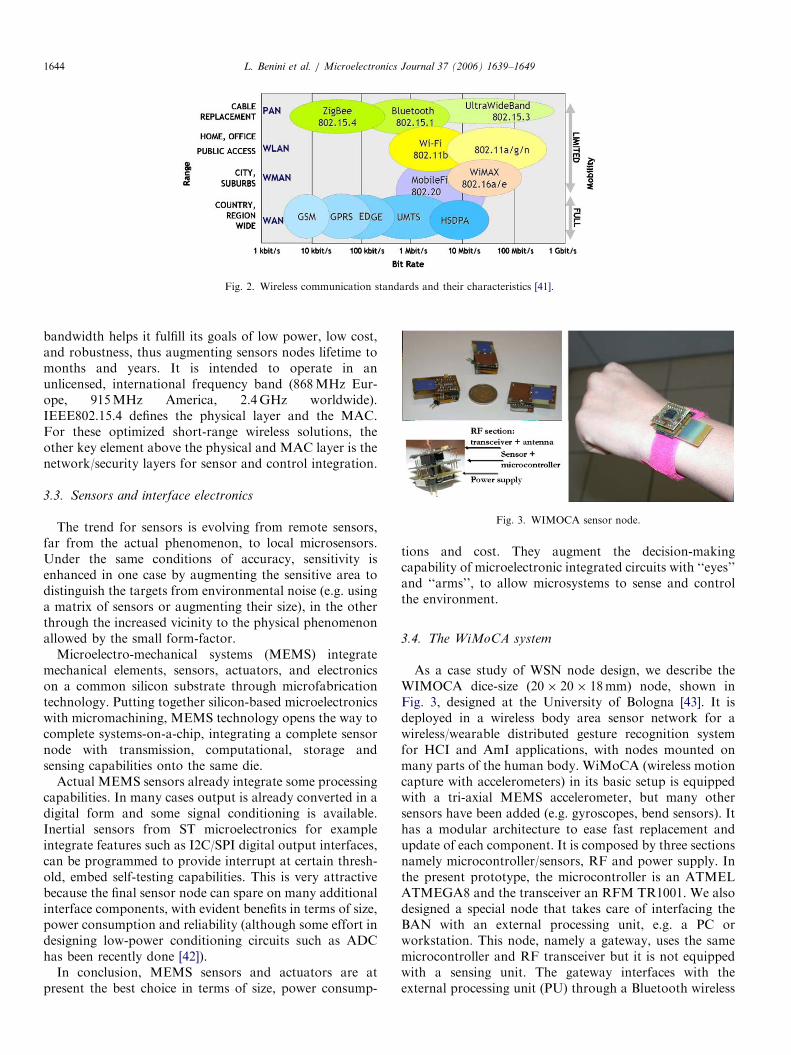
ARTICLE IN PRESS
Fig. 3. WIMOCA sensor node.
Fig. 2. Wireless communication standards and their characteristics [41].
L. Benini et al. / Microelectronics Journal 37 (2006) 1639–16491644
bandwidth helps it fulfill its goals of low power, low cost,and robustness, thus augmenting sensors nodes lifetime tomonths and years. It is intended to operate in anunlicensed, international frequency band (868MHz Eur-ope, 915MHz America, 2.4GHz worldwide).IEEE802.15.4 defines the physical layer and the MAC.For these optimized short-range wireless solutions, theother key element above the physical and MAC layer is thenetwork/security layers for sensor and control integration.
3.3. Sensors and interface electronics
The trend for sensors is evolving from remote sensors,far from the actual phenomenon, to local microsensors.Under the same conditions of accuracy, sensitivity isenhanced in one case by augmenting the sensitive area todistinguish the targets from environmental noise (e.g. usinga matrix of sensors or augmenting their size), in the otherthrough the increased vicinity to the physical phenomenonallowed by the small form-factor.
Microelectro-mechanical systems (MEMS) integratemechanical elements, sensors, actuators, and electronicson a common silicon substrate through microfabricationtechnology. Putting together silicon-based microelectronicswith micromachining, MEMS technology opens the way tocomplete systems-on-a-chip, integrating a complete sensornode with transmission, computational, storage andsensing capabilities onto the same die.
Actual MEMS sensors already integrate some processingcapabilities. In many cases output is already converted in adigital form and some signal conditioning is available.Inertial sensors from ST microelectronics for exampleintegrate features such as I2C/SPI digital output interfaces,can be programmed to provide interrupt at certain thresh-old, embed self-testing capabilities. This is very attractivebecause the final sensor node can spare on many additionalinterface components, with evident benefits in terms of size,power consumption and reliability (although some effort indesigning low-power conditioning circuits such as ADChas been recently done [42]).
In conclusion, MEMS sensors and actuators are atpresent the best choice in terms of size, power consump-
tions and cost. They augment the decision-makingcapability of microelectronic integrated circuits with ‘‘eyes’’and ‘‘arms’’, to allow microsystems to sense and controlthe environment.
3.4. The WiMoCA system
As a case study of WSN node design, we describe theWIMOCA dice-size ð20� 20� 18mmÞ node, shown inFig. 3, designed at the University of Bologna [43]. It isdeployed in a wireless body area sensor network for awireless/wearable distributed gesture recognition systemfor HCI and AmI applications, with nodes mounted onmany parts of the human body. WiMoCA (wireless motioncapture with accelerometers) in its basic setup is equippedwith a tri-axial MEMS accelerometer, but many othersensors have been added (e.g. gyroscopes, bend sensors). Ithas a modular architecture to ease fast replacement andupdate of each component. It is composed by three sectionsnamely microcontroller/sensors, RF and power supply. Inthe present prototype, the microcontroller is an ATMELATMEGA8 and the transceiver an RFM TR1001. We alsodesigned a special node that takes care of interfacing theBAN with an external processing unit, e.g. a PC orworkstation. This node, namely a gateway, uses the samemicrocontroller and RF transceiver but it is not equippedwith a sensing unit. The gateway interfaces with theexternal processing unit (PU) through a Bluetooth wireless
ARTICLE IN PRESSL. Benini et al. / Microelectronics Journal 37 (2006) 1639–1649 1645
link. Network support has been developed. Our system hasbeen designed for real-time interactive applications withlow-power requirements and for this reason we focused onminimizing software overhead by implementing our owncomponent drivers and communication layer.
The goal of WIMOCA is enabling natural interactionand context-aware services to inhabitants of a smartenvironment. WIMOCA nodes are worn to form a bodyarea network (BAN), which captures and processesbehavioral information about the user, enabling theenvironment to react consistently and contextually to theuser’s personal needs and activities. This is achievedtransparently from the user and proactively if possible, orthrough natural interaction if an explicit request is issuedby the user. For this purpose, WIMOCA BAN is mainlybased on inertial sensors for user activity detection andgesture recognition.
4. Looking forward: symbiotic and bio-inspired sensor nodes
Some of the most exciting and challenging fields ofapplication of future, wireless sensor networks are deeplyrelated to areas as bioscience, biotechnology and na-noscience. We can mention for instance: (i) point-of-careportable or in-body, easy-to-use, stand-alone systems toperform medical analysis out of clinical laboratories[44,45]; (ii) in vivo controlled drug release systems, whichcan be ingested or injected into a human body and whichmust act to deliver appropriate quantity of drugs or othercaring means in a pre-determined, self-regulating or real-time-controllable way [46,47].
In order to be adapted to these applications, systemsshould be autonomous in terms of avoiding as much aspossible the direct contribution of a human operator totheir functions—which can be achieved by integratingdifferent devices and circuitry for data processing—and interms of power supply. In addition, a key factor for thedevelopment will be the possibility to connect them toobtain information and to control them from remote. Thehardware design of nodes for medical and biologicalapplications has to address bio-compatibility issues andthe high specific interaction properties at the molecular andatomic level. This can be achieved through development ofseveral technologies, as: (i) advanced synthetic—or not—molecular receptors [48]; (ii) innovative three-dimensionalmembranes for highly-controlled molecular release [49];(iii) bio-hybrid systems as bio-coated nanoparticles tovehicle drugs or transfection agents inside cells [50]; (iv)bio-inspired systems, to mimic peculiar characteristics ofbio-systems as adaptability and self-regulation [51]; (v)smart organic surfaces to transduce electronically specificmechanical or optical stimuli [52]. From this incompletelist, it is clear that the high bio-nanoscience contentinvolved in the design of new sensor systems will fuelinnovation in many fields as molecular sensing, newtransduction techniques of physical signals, new smart,multi-functional materials.
The conceivable evolution of sensor systems could bedepicted as developed along two phases. The first one is theapplication of conventional (micro) and non-conventional(nano) technology to the bio-physical world and, inparticular, by patterning and disposing biological matterand by handling fluids in a microscopic, high-controlledway to separate and process small volumes of sample orselectively interact with single cells (see Section 4.1). Thesecond phase will be dominated by the exploitation ofbioscience for the creation of micro and nanoscale systemsand materials with unique properties and functions. Thesesystems will be characterized by properties of self-assembly, reversibility, adaptability, self-replication, possi-bility of interaction at the atomic scale [53] (see Section4.2). Examples of existing systems and promising elementsfor the deployment in WSNs will be given for both phasesfocusing on the cited bio-monitoring applications (Sections4.1.1 and 4.2.1).
4.1. Symbiotic sensor nodes
The first phase consists in the development of lab-on-a-chip, BioMEMS, micro total analysis systems ðmTASÞ.These systems are characterized by deep integration andminiaturization.Integration will exploit microtechnology to create
structures using both standard microelectronics materialsand non-conventional materials. Silicon, glass and metalswill be employed to integrate data and signal processing,semiconductor sensors, microchannels, electro-mechanicalmicrocomponents, thermal actuators. New-concept mate-rials of polymeric nature (e.g., polydimethylsiloxane) willbe preferred for their bio-compatibility, and their suit-ability to be patterned to create channels for handling andprocessing of biological samples. Aggressive integrationwill lead to (i) self-contained, easy-to-use, reliable analysissystems, by integrating on a single chip microfluidics andheating-control elements for the pretreatment of thesamples (processing, separation); (ii) high-throughput andflexible systems, by integrating sensors of different natureon the same device; (iii) improved speed and reliability byallowing the same sample to be tested at the same time withdifferent probes patterned on microsites into a uniquesubstrate. Integration of batteries and communicationmodules (as outlined in the previous section) will lead tostand-alone, self-contained controllable-programmable on-field systems.Miniaturization is a key factor for the development of in-
body devices as it reduces dramatically obtrusiveness. Atthe same time, it leads to some key advantages. Miniatur-ization of sensing element, sample pretreatment, actuatorsand delivery chambers reduce the amounts of reagentsneeded and, thus, costs necessary to conduct a chemicalprocess: miniaturized handling volumes are in the nanoliterto picoliter range rather than the microliter range or largerin conventional experiments; moreover, small volumes leadto higher effective concentrations [54], thus reducing time
ARTICLE IN PRESS
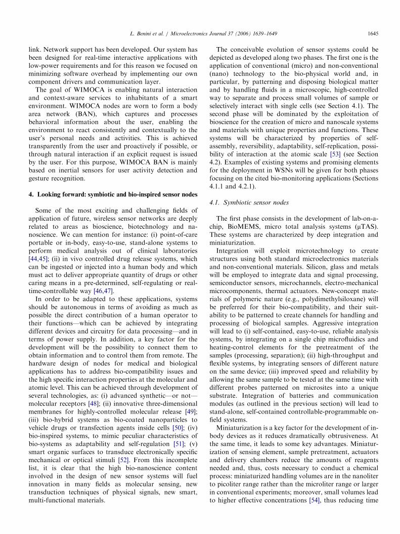
Fig. 4. Infineon technologies has designed a silicon chip for chemical-
mediated electronic detection of DNA sequences. Gold electrodes, which
can be modified with DNA sensing elements have been exposed on the
chip surface and connected to the internal circuitry of the chip. Courtesy of
Infineon Technologies.
L. Benini et al. / Microelectronics Journal 37 (2006) 1639–16491646
to result and improving performance. It should be notedthat the ability to handle molecular receptors andtherapeutic agents which are at the scale of the targetmolecules is needed to provide the necessary sensitivity andselectivity.
4.1.1. Examples and applications
Point-of-care devices for the implementation of out-patient clinics to enable high level of care outsidelaboratories and hospitals is extremely desirable forreasons related to cost, comfort and efficiency. Micro-fabricated systems for in-body molecular detection andbio-parameters monitoring would be a breakthrough inthis domain [55]. Many attempts have been done in thedirection of implementing on-chip common analyticaltechniques. The most successful are gas chromatography[56], capillary electrophoresis [57] and polymerase chainreaction [58]. The latter is one of the most interestingapproaches of microfabricated implementation which relieson the good properties of thermal conductivity of siliconand the possibility to easily integrate thermal resistances.Existing devices integrate only a few of the basic stepsinvolved in molecular detection which is the most promis-ing, challenging and complex analysis demand. The stepscan be subdivided according to their function: (i) pre-
sensing steps: extraction, separation, amplification; (ii)sensing steps: sensing, transduction for the generation ofelectrical signals; (iii) read-out steps: signal conditioningand data processing.
Handling of microfluidic samples for the integration ofpre-sensing steps can be achieved by assembling basicfluidic components like electrokinetic and chemical separa-tion channels, valves, mixing structures and chemicalreactors. Even nanoliter-scale structures have been usedfor continuous flow, stopped flow, and thermal cyclingreactions [59,60].
The integration and miniaturization of the sensing stepsinvolves patterning and immobilization of molecularreceptors on surfaces in an array format [61], theimplementation of matrices of sensors, transducers andactuators on active substrates which can contain circuitsfor signal processing. Some examples report the use ofarray of microfabricated electrodes used as substrates ofmolecular-receptor sites for active receptor immobilization[62], target manipulation [63], electronic transduction oftarget recognition [64]. The latter demonstrates theelectrical detection of chemical-labeled-DNA moleculeson a silicon chip developed with standard 0:5mm CMOSprocess. A section of the die which exhibits surface post-processing to expose sensing gold sites is shown in Fig. 4.Recently, the feasibility of a label-free fully-electrical DNAdetection technique easily integrable on chip has been alsodemonstrated [65].
Some very interesting applications of integrated semi-conductor sensors for DNA and protein detection includethe use of field-effect transistors where the gate has beensubstituted with an electrolyte conductive solution [66–68].
The use of surface and bulk acoustic wave sensors[69], nanowire potentiometric sensors based on field effect[70] and microcantilever employed as surface-stress andgravimetric transducers [71] have also been recentlyinvestigated.The possibility to release drugs from in-body controlled
microsystems could have a tremendous impact on medicalprocedures, eliminating the injection pain and infectionsdue to frequent injections and offering a mean to reduceside effects and drug volumes by allowing a more preciseand efficient delivery. The use of conventional microma-chined devices, equipped with wells, microfluidics andcircuitry has been tested. Santini et al. presented a multi-well silicon chip. The release of drugs from the compart-ments is controlled by an electrochemical stimulus whichselectively dissolve covering gold membranes. This signalcould be pre-programmed or controlled real-time bysensors coupled with the device [72].Microfabricated devices are usually built on 0.5mm-
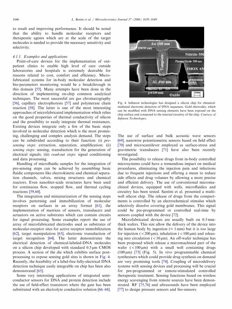
thick wafers. This size allow the delivery of the device intothe human body by ingestion ð� 1mmÞ but it is too largefor injection ðo200mmÞ, inhalation ðo100mmÞ and releas-ing into circulation ðo10mmÞ. An off-wafer technique hasbeen proposed which release a micromachined part of thewafer ðo100mmÞ with a small well containing drugsð100 mmÞ [73] (Fig. 5). In vivo programmable chemicalsynthesisers which could provide drug synthesis on demandare very promising tools [74]. Coupling of microdeliverysystems with sensing devices and processing will be crucialfor pre-programmed or remote-stimulated controlledtherapeutic treatment. Sensing functions based on wirelessenergy scavenging from remote sources have been demon-strated. RF [75,76] and ultrasounds have been employed[77] to design pressure sensors and bio-sensors.
ARTICLE IN PRESS
Fig. 5. Required dimensions of in vivo drug-delivery devices are indicated
with respect to the different delivery approaches. Standard and innovative
microfabrication techniques which can provide the adapted level of
miniaturization are reported. Off-wafer technique is based on surface and
bulk micromachining of silicon and polymeric materials to obtain
micrometric structures (an example has been sketched [73]). Bottom-up
techniques refer to the employment of self-assembly and the specific bio-
modification of nanoparticles.
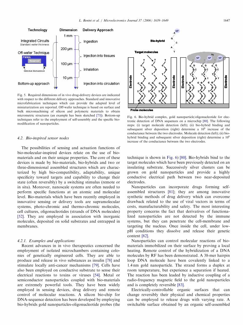
Fig. 6. Bio-hybrid complex, gold nanoparticle/oligonucleotide for elec-
tronic detection of DNA sequences on a microchip [80]. The following
steps: (i) target molecule detection (left); (ii) bio-hybrid binding and
subsequent silver deposition (right) determine a 106 increase of the
conductance between the two electrodes. Molecule detection (left); (ii) bio-
hybrid binding and subsequent silver deposition (right) determine a 106
increase of the conductance between the two electrodes.
L. Benini et al. / Microelectronics Journal 37 (2006) 1639–1649 1647
4.2. Bio-inspired sensor nodes
The possibilities of sensing and actuation functions ofbio-molecular-inspired devices relate on the use of bio-materials and on their unique properties. The core of thesedevices is made by bio-materials, bio-hybrids and two orthree-dimensional assembled structures which are charac-terized by high bio-compatibility, adaptability, uniquespecificity toward targets and capability to change theirstate (often reversibly) by a switching stimulus (remote orin situ). Moreover, nanoscale systems are often needed toperform specific functions at an atomic and molecularlevel. Bio-materials which have been recently employed ininnovative sensing or delivery tools are supramolecularsystems, photo-chromic and thermo-chromic molecules,cell cultures, oligonucleotides (strands of DNA molecules)[52]. They are employed in association with inorganicmolecules, deposited on solid substrates and entrapped inmembranes.
4.2.1. Examples and applications
Recent advances in in vivo therapeutics concerned theemployment of isolated microchambers containing colo-nies of genetically engineered cells. They are able toproduce and release in vivo substances as insulin [78] andstimulate locally anti-cancer mechanisms [79]. Cells havealso been employed on conductive substrate to sense theirelectrical reactions to toxins or viruses [54]. Metal orsemiconductor nanoparticles coupled with bio-materialsare extremely powerful tools. They have been widelyemployed in sensing devices, drug delivery and remotecontrol of molecular reactions. A silicon bio-chip forDNA-sequence detection has been developed by employingbio-hybrids gold nanoparticles-oligonucleotide probes (the
technique is shown in Fig. 6) [80]. Bio-hybrids bind to thetarget molecules which have been previously detected on aninsulating substrate. Successively silver clusters can begrown on gold nanoparticles and provide a highlyconductive electrical path between two near-depositedelectrodes.Nanoparticles can incorporate drugs forming self-
assembled structures [81]; they are among innovativesynthetic methods of drug delivery which can overcomedrawback related to the use of viral vectors in terms ofcosts, manufacturability and safety. The most interestingproperty concerns the fact that derivatives of functiona-lized nanoparticles are not detected by the immunesystems, but they can penetrate the cell-membrane andtargeting the nucleus. Once inside the cell, under low-pH conditions they dissolve and release their geneticcontent [82].Nanoparticles can control molecular reactions of bio-
materials immobilized on their surface by proving a localheating. Remote control of the hybridization of a DNAmolecules by RF has been demonstrated. A 38-mer hairpinloop DNA molecule have been covalently linked to a1.4 nm gold nanoparticle. The strand forms a duplex atroom temperature, but experience a separation if heated.The reaction has been leaded by inductive coupling of aradio-frequency magnetic field to the gold nanoparticlesand is completely reversible [83].Electrically-controllable organic surfaces that can
change reversibly their physical and chemical propertiescan be employed to release drugs with varying rate. Aswitchable surface obtained by an organic self-assembled
ARTICLE IN PRESSL. Benini et al. / Microelectronics Journal 37 (2006) 1639–16491648
monolayer of mercaptohexadecanoic acid on gold changesits hydrophobicity as a consequence of small alterations ofthe substrate potential [84].
5. Conclusion
In this paper, we surveyed the evolution of wirelesssensor networks, starting from early shoebox-sized obtru-sive devices and moving to forward-looking bio-hybriddevices based on nanoscale molecular engineering. A fewcommon themes have emerged: the quest for a flexible andinexpensive micro-fabrication technology to reach theultimate limits of integration and bio-compatibility, thestrong push toward power reduction, from watts tomicrowatts (or less), the requirement for a holistic designapproach, where all system components are jointlyoptimized. The opportunities are immense. WSNs canopen huge markets in consumer applications, as well as insecurity and environmental monitoring. Looking forward,the evolution of sensor networks toward symbiotic andbio-inspired architectures could drastically improve thehealth conditions and lifetime expectation of a largenumber of people.
References
[1] S. Marzano, E. Aarts, The new everyday view on ambient
intelligence, Uitgeverij 010 (2003).
[2] T. Basten, M. Geilen, H. De Groot (Eds.), Ambient Intelligence:
Impact on Embedded System Design, Springer, Berlin, 2003.
[3] W. Weber, J.M. Rabaey, E. Aarts (Eds.), Ambient Intelligence,
Springer, Berlin, 2005.
[4] D. Culler, D. Estrin, M. Srivastava, Overview of sensor networks,
IEEE Comput. 37 (8) (2004) 41.
[5] F. Zhao, L. Guibas, Wireless Sensor Networks: An Information
Processing Approach, Morgan Kaufmann, Los Altos, CA, 2004.
[6] K. Romer, F. Mattern, The design space of wireless sensor networks,
IEEE Wireless Commun. 11 (6) (2004) 54.
[7] J.A. Stankovic, T.E. Abdelzaher, Chenyang Lu, Lui Sha, J.C. Hou,
Real-time communication and coordination in embedded sensor
networks, Proc. IEEE 91 (7) (2003) 1002.
[8] I.F. Akyildiz, W. Su, Y. Sankarasubramaniam, E. Cayirci, Wireless
sensor networks: a survey, Comput. Networks 38 (4) (2002) 393.
[9] J.M. Kahn, R.H. Katz, K.S.J. Pister, Emerging challenges: mobile
networking for smart dust, J. Commun. Networks 2 (3) (2000) 188.
[10] hhttp://wins.rockwellscientific.com/WST_Content.htmli.
[11] hhttp://nesl.ee.ucla.edu/projects/ibadge/default.htmi.
[12] S. Park, et al., Proc. Int. Symp. Wearable Comput. (2002) 0231.
[13] J. Hill, D. Culler, A wireless embedded sensor architecture for
system-level optimization, Technical Report, Computer Science
Department, University of California at Berkeley, 2002.
[14] hhttp://nesl.ee.ucla.edu/projects/ahlosi.
[15] hhttp://www.ember.comi.
[16] J.M. Kahn, R.H. Katz, K. Poster, Real-time communication and
coordination in embedded sensor networks, Proceedings of the Fifth
International Conference on Mobile Computing and Networking,
Mobicom 1999, 1999, p. 271.
[17] J. Rabaey, J. Ammer, J. da Silva, D. Patel, S. Roundy, Picoradio
supports ad-hoc ultra low-power wireless networking, IEEE Comput.
Mag. (2002) 42.
[18] hhttp://pasta.east.isi.edui.
[19] J. Feng, F. Koushanfar, M. Potkonjak, System-architectures for
sensor networks issues, alternatives, and directions, IEEE Int. Conf.
Comput. Design (ICCD) (2002) 226.
[20] B.A. Warneke, K.S.J. Pister, An ultra-low energy microcontroller for
Smart Dust wireless sensor networks, Solid-State Circuits Confer-
ence, 2004, Digest of Technical Papers, ISSCC, 2004 IEEE
International, vol. 1, 2004, p. 316.
[21] J.M. Rabaey, M.J. Hammer, J.L. Da Silva, PicoRadio supports ad-hoc
ultra low-power wireless networking, IEEE Comput. 33 (7) (2000) 42.
[22] A. Wang, A.P. Chandrakasan, A 180mV subthreshold FFT
processor using a minimum energy design methodology, IEEE J.
Solid-State Circuits 40 (1) (2005) 310.
[23] B.H. Calhoun, D.C. Daly, N. Verma, D.F. Finchelstein, D.D.
Wentzloff, A. Wang, Seong-Hwan Cho, A.P. Chandrakasan, Design
considerations for ultra-low energy wireless microsensor nodes, IEEE
Trans. Comput. 54 (6) (2005) 727.
[24] B.H. Calhoun, A. Chandrakasan, A 256 kb sub-threshold SRAM in
65nm CMOS, IEEE ISSCC06, 2006, p. 628.
[25] S. Roundy, P.K. Wright, J. Rabaey, A study of low level vibrations as
a power source for wireless sensor nodes, Comput. Commun. 26
(2003) 1131.
[26] Z. Xiao, G. Yan, C. Feng, P.C.H. Chan, I.-M. Hsing, Integrated fuel
cell micro power system by microfabrication technique, Transducers
’05, vol. 2, 2005, p. 1856.
[27] C. Dyer, Fuel cells and portable electronics, Symp. VLSI Circuits
(2004) 124.
[28] M. Laibowitz, J.A. Paradiso, Parasitic mobility for pervasive sensor
networks, Pervasive 2005, 2005, p. 255.
[29] R. Amirtharajah, J. Collier, J. Siebert, B. Zhou, A. Chandrakasan,
DSPs for energy harvesting sensors: applications and architectures,
IEEE Pervasive Comput. 4 (3) (2005) 72.
[30] V. Raghunathan, A. Kansal, J. Hsu, J. Friedman, M. Srivastava,
Design considerations for solar energy harvesting wireless embedded
systems, IPSN (2005) 457.
[31] P.D. Mitcheson, et al., Architectures for vibration-driven micropower
generators, J. Microelectromechanical Syst. 13 (2004) 429.
[32] J.A. Paradiso, T. Starner, IEEE Pervasive Comput. 04 (1) (2005) 18.
[33] N.S. Shenck, J.A. Paradiso, Energy scavenging for mobile and
wireless electronics, IEEE Micro 21 (3) (2001) 30.
[34] L. Benini, G. de Micheli, Dynamic Power Management, Springer,
Berlin, 1998.
[35] hwww.irda.orgi.
[36] B.W.Cook, A.D. Berny, A. Molnar, S. Lanzisera, K.S.J. Pister, An
ultra-low power 2.4GHz RF transceiver for wireless sensor networks
in 130 nm CMOS with 400mV supply and an integrated passive RX
front-end, IEEE ISSCC06, 2006, p. 370.
[37] hhttp://www.rfm.comi.
[38] hhttp://www.chipcon.comi.
[39] hhttp://www.zigbee.orgi.
[40] S.C. Ergen, ZigBee/IEEE 802.15.4 Summary, 2004.
[41] hhttp://www.ictc.it/decina/i.
[42] N. Verma, A.P. Chandrakasan, A 25mW 100kS/s 12b ADC for
wireless micro-sensor applications, IEEE ISSCC06, 2006, p. 222.
[43] E. Farella, A. Pieracci, D. Brunelli, A. Acquaviva, L. Benini, B.
Ricco, Design and implementation of WiMoCA node for a body area
wireless sensor network, IEEE International Conference on Sensor
Networks, SENET05, 2005, p. 342.
[44] hhttp://www.devicelink.com/ivdt/archive/02/04/002.htmli.
[45] R. Langer, N.A. Peppas, Advances in biomaterials, drug delivery,
and bionanotechnology, Bioengineering, Food, and Natural Products
49 (12) (2003) 2990.
[46] D.A. LaVan, D.M. Lynn, R. Langer, Moving smaller in drug
discovery and delivery, Nat. Rev. 1 (2001) 77.
[47] D.A. LaVan, T. McGuire, R. Langer, Small-scale systems for in vivo
drug delivery, Nature Biotechnol. 21 (10) (2003) 1184.
[48] A.B. Sanghvi, K.P.-H. Miller, A.M. Belcher, C.E. Schmidt,
Biomaterials functionalization using a novel peptide that selectively
binds to a conducting polymer, Nat. Mater. 4 (2005) 496.

ARTICLE IN PRESSL. Benini et al. / Microelectronics Journal 37 (2006) 1639–1649 1649
[49] N.A. Peppas, Y. Huang, M. Torres-Lugo, J.H. Ward, J. Zhang,
Physicochemical Foundations and Structural Design of Hydrogels in
Medicine and Biology, Annu. Rev. Biomed. Eng. 2 (2000) 9.
[50] L. Brannon-Peppas, J.O. Blanchette, Nanoparticle and targeted
systems for cancer therapy, Adv. Drug Delivery Rev. 56 (11) (2004)
1649.
[51] R.S. Tu, M. Tirrel, Bottom-up design of biomimetic assemblies, Adv.
Drug Delivery Rev. 56 (11) (2004) 1537.
[52] A.N. Shipway, I. Willner, Electronically transduced molecular
mechanical and information functions on surfaces, Acc. Chem. Res.
34 (2001) 421.
[53] J.Z. Hilt, Nanotechnology and biomimetic methods in therapeutics:
molecular scale control with some help from nature, Adv. Drug
Delivery Rev. 56 (11) (2004) 1533.
[54] R. Bashir, BioMEMS: State-of-the-art in detection, opportunities
and prospects, Adv. Drug Delivery Rev. 56 (2004) 1565.
[55] L.J. Kricka, Microchip, microarrays, biochips and nanochips:
personal laboratories for the 21st century, Clin. Chim. Acta 307
(2001) 219.
[56] R.H. Lambert, J.A. Owens, Utilization of a portable microchip gas
chromatograph to identify and reduce fugitive emissions at a
pharmaceutical manufacturing plant, Field Anal. Chem. Tech. 1 (6)
(1997) 367.
[57] V. Dolnik, S. Liu, S. Jovanovich, Capillary electrophoresis on
microchip, Electrophoresis 21 (2000) 41.
[58] I. Rodriguez, M. Lesaicherre, Y. Tie, Q. Zou, C. Yu, J. Singh, L.T.
Meng, S. Uppili, S.F.Y. Li, P. Gopalakrishnakone, Z.E. Selvanaya-
gam, Practical integration of polymerase chain reaction amplification
and electrophoretic analysis in microfluidic devices for genetic
analysis, Electrophoresis 24 (2003) 172.
[59] A.T. Wooley, et al., High-speed DNA genotyping using microfab-
ricated capillary array electrophoresis chips, Anal. Chem. 69 (11)
(1997) 2181.
[60] Y. Shi, et al., Radial capillary array electrophoresis microplate and
scanner for high-performance nucleic acid analysis, Anal. Chem. 71
(23) (1999) 5354.
[61] M.C. Pirrung, How to make a DNA chip, Ang. Chem. Int. Ed. 41
(2002) 1276.
[62] P. Caillat, D. David, M. Belleville, F. Clerc, C. Massit, F. Revol-
Cavalier, P. Peltie, T. Livache, G. Bidan, A. Roget, E. Crapez,
Biochips on CMOS: an active matrix address array for DNA
analysis, Sensors Actuators B 61 (1999) 154–162.
[63] M.J. Heller, A.H. Forster, E. Tu, Active microelectronic chip devices
which utilize controlled electrophoretic fields for multiplex DNA
hybridization and other genomic applications, Electrophoresis 21
(2000) 157.
[64] F. Hofmann, A. Frey, B. Holzapfl, M. Schienle, C. Paulus, P.
Schindler-Bauer, D. Kuhlmeier, J. Krause, R. Hintsche, E. Nebling,
J. Albers, W. Gumbrecht, K. Plehnert, G. Eckstein, R. Thewes, Fully
electronic DNA detection on a CMOS chip: device and process
issues, Proceedings of IEEE International Electron Devices Meeting,
San Francisco, USA, 2002, p. 488.
[65] C. Guiducci, C. Stagni, G. Zuccheri, A. Bogliolo, L. Benini, B.
Samorı, B. Ricco, DNA detection by integrable electronics,
Biosensors Bioelectron. 19 (8) (2004) 781.
[66] J. Fritz, E.B. Cooper, S. Gaudet, Peter K. Sorger, Scott R. Manalis,
Electronic detection of DNA by its intrinsic molecular charge, Proc.
Natl. Acad. Sci. 99 (8) (2002) 14142.
[67] F. Uslu, et al., Labelfree fully electronic nucleic acid detection system
based on a field-effect transistor device, Biosensors Bioelectron. 19
(12) (2004) 1723.
[68] F. Pouthas, et al., DNA detection on transistor arrays following mutation
specific enzymatic amplification, Appl. Phys. Lett. 84 (2004) 1594.
[69] I. Willner, et al., Amplified detection of single-base mismatches in
DNA using microgravimetric quartz-crystal-microbalance transduc-
tion, Talanta 56 (5) (2002) 847.
[70] Z. Li, Y. Chen, X. Li, T.I. Kamins, K. Nauka, R.S. Williams,
Sequence-specific label-free DNA sensors based on silicon nanowires,
Nano Lett. 4 (2) (2004) 245.
[71] J. Fritz, M.K. Baller, H.P. Lang, H. Rothuizen, P. Vettiger, E.
Meyer, H.J. Guntherodt, Ch. Gerber, J.K. Gimzewski, Translating
biomolecular recognition into nanomechanics, Science 288 (2000)
316.
[72] J.T. Santini Jr., M.J. Cima, R. Langer, A controlled release
microchip, Nature 397 (1999) 335.
[73] S.L. Tao, M.W. Lubeley, T.A. Desay, Bioadesive poly(methyl
methacrylate) microdevices for controlled drug delivery, J. Controlled
Release 88 (2003) 215.
[74] C.L. Hansen, E. Skordalakes, J.M. Berger, S.R. Quake, A robust and
scalable microfluidic metering method that allows protein crystal
growth by free interface diffusion, Proc. Natl. Acad. Sci. 99 (2002)
16531.
[75] A.D. DeHennis, K.D. Wise, A wireless microsystem for the remote
sensing of pressure, temperature, humidity, J. Microelectromechani-
cal Syst. 14 (1) (2005) 12.
[76] M.A. Fonseca, J.M. English, M. von Arx, M.G. Allen, Wireless
micromachined ceramic pressure sensor fro high-temperature appli-
cations, J. Microelectromechanical Syst. 11 (4) (2002) 337.
[77] Y. Porat, A. Penner, E. Doron, Implantable acoustic bio-sensing
system and method, US patent 6432050, 2002.
[78] T.A. Desai, et al., Microfabricated biocapsules provide short-term
immunoisolation of insulinoma xenografts, Biomed. Microdevices 1
(1999) 131.
[79] J.H. Brauker, R.L. Geller, W.D. Johnston, S.A. Levon, D.A.
Maryanov, Implanted tumor cells for the prevention and treatment
of cancer, US Patent 6156305, 2000.
[80] S.J. Park, T.A. Taton, C.A. Mirkin, Array-based electrical detection
of DNA with nanoparticle probes, Science 295 (2002) 1503.
[81] H. Cohen, et al., Sustained delivery and expression of DNA
encapsulated in polymeric nanoparticles, Gene Ther. 7 (2000) 1896.
[82] D.G. Anderson, D.M. Lynn, R. Langer, Semi-automated synthesis
and screening of a large library of degradable cationic polymers for
gene delivery, Angew. Chem. Int. Ed. 42 (2003) 3153.
[83] K. Hamad-Schifferli, J.J. Schwartz, A.T. Santos, S. Zhang, J.M.
Jacobson, Remote electronic control of DNA hybridization through
inductive coupling to an attached metal nanocrystal antenna, Nature
415 (2002) 152.
[84] J. Lahann, S. Mitragotri, T.-N. Tran, H. kaido, J. Sundaram, I.S.
Choi, S. Hoffer, G.A. Somorjai, R. Langer, A reversibly switching
surface, Science 299 (2003) 371.