Rotational Quenching Rate Coefficients for H2 in Collisions with H2 from 2 to 10,000 K
Upload
khangminh22Category
view
1download
0
Wide band gap materials and devices for NOx, H2 and O2 gas sensing applications
Dissertation zur Erlangung des
akademischen Grades Doktor-Ingenieur (Dr.-Ing.)
vorgelegt der Fakultät Elektrotechnik und
Informationstechnik der Technischen Universität Ilmenau
von Dipl.-Ing Majdeddin Ali
geboren am 08.09.1976 in Homs, Syrien
1. Gutachter: Univ.-Prof. Dr. rer. nat. habil. Oliver Ambacher, Fraunhofer-Institut
für Angewandte Festkörperphysik, Freiburg
2. Gutachter: PD Dr.-Ing. habil. Frank Schwierz, TU Ilmenau
3. Gutachter: Dr. Martin Eickhoff, Walter Schottky Institut, TU München
Tag der Einreichung: 28.06.2007
Tag der wissenschaftlichen Aussprache: 22.01.2008
urn:nbn:de:gbv:ilm1-2007000323
Abstract III
Abstract
In this thesis, field effect gas sensors (Schottky diodes, MOS capacitors, and
MOSFET transistors) based on wide band gap semiconductors like silicon carbide
(SiC) and gallium nitride (GaN), as well as resistive gas sensors based on indium
oxide (In2O3), have been developed for the detection of reducing gases (H2, D2) and
oxidising gases (NOx, O2). The development of the sensors has been performed at
the Institute for Micro- and Nanoelectronic, Technical University Ilmenau in co-
operation with (GE) General Electric Global Research (USA) and Umwelt-Sensor-
Technik GmbH (Geschwenda).
Chapter 1: serves as an introduction into the scientific fields related to this
work. The theoretical fundamentals of solid-state gas sensors are provided and the
relevant properties of wide band gap materials (SiC and GaN) are summarized.
In chapter 2: The performance of Pt/GaN Schottky diodes with different
thickness of the catalytic metal were investigated as hydrogen gas detectors. The
area as well as the thickness of the Pt were varied between 250 × 250 µm2 and 1000
× 1000 µm2, 8 and 40 nm, respectively. The response to hydrogen gas was
investigated in dependence on the active area, the Pt thickness and the operating
temperature for 1 vol.% hydrogen in synthetic air. We observed a significant increase
of the sensitivity and a decrease of the response and recovery times by increasing
the temperature of operation to about 350°C and by decreasing the Pt thickness
down to 8 nm. Electron microscopy of the microstructure showed that the thinner
platinum had a higher grain boundary density. The increase in sensitivity with
decreasing Pt thickness points to the dissociation of molecular hydrogen on the
surface, the diffusion of atomic hydrogen along the platinum grain boundaries and
the adsorption of hydrogen at the Pt/GaN interface as a possible mechanism of
sensing hydrogen by Schottky diodes.
The response to deuterium D2, NOx, and O2 of metal-oxide-semiconductor
(MOS) and metal-metal oxide-oxide-semiconductor (MMOOS) structures with
rhodium (Rh) gate were investigated in dependence on the operating temperature
and gas partial pressures was investigated in chapter 3. The response of the sensor
was measured as a shift in the capacitance-voltge (C-V) curve along the voltage axis.
Positive and negative flat-band voltage shifts up to 1 V were observed for oxidizing
and reducing gases, respectively. Depending on the type of insulator that is chosen,
differences in the sensitivity of the sensor were observed.
IV Abstract
In chapter 4: The performance of SiC-based field effect transistors (FETs) with
different gate materials (mixture of metal oxides: indium oxide and tin oxide
(InxSnyOz), indium oxide and vanadium oxide (InxVyOz), as well as mixtures of metal
oxides with metal additives) were investigated as NOx, O2, and D2 gas detectors. The
response to these gases was investigated in dependence on the operating
temperature and gas partial pressures. The composition and microstructure of the
sensing gate electrode are the key parameters that influence the sensing
mechanism, and hence key performance parameters: sensitivity, selectivity, and
response time. By choosing the appropriate temperature and catalyst material (gate
material), devices that are significantly sensitive to certain gases may be realized. In
addition, the temperature of maximum response varies dependent on the gas
species being measured. This information, along with a careful choice of catalyst
(gate material) can be used to enhance device selectivity.
In chapter 5: Polycrystalline and nano-structured In2O3 thin films were
investigated with the aim to obtain information about their NOx and O2 gas sensing
properties. The response to these gases was investigated in dependence on the
operating temperature and gas partial pressures. The analysis in the presence of
different partial pressures of NOx has shown that both thin films are able to detect
nitrogen oxide, but their responses exhibit different characteristics. In particular,
nano-structured In2O3 thin films were found to have the higher response to NOx. This
is most probably due to the enlarged overall active surface area of the sensing layer
as a consequence of the small grain size (higher surface to volume ratio) so that the
relative interactive surface area is larger, and the density of charged carriers per
volume is higher. We have found that reducing the grain size of the sensing material
to the ~10 nm regime can have a substantial effect on performance. The optimum
detection temperatures of the nano-structured In2O3 occur in the range of 100-175°C
for NOx considering the sensitivity as well as the response time. In this range of
temperatures the response to O2 is very low indicating that the sensor is very suitable
for selective detection of NOx at low temperatures In addition, nano-structured In2O3
thin films were found to be more suitable to be used in the field of application for
detecting low partial pressures.
Chapter 6: offers conclusions of the current work. In this chapter we compare
also all studied gas sensors according to their sensitivity, selectivity, and response

Abstract V
time and then we compare them with the related works by other authors available in
the scientific literature.

VI Abstract

Zusammenfassung VII
Zusammenfassung
Im Rahmen dieser Arbeit sind Feldeffektgassensoren (Schottky Dioden, MOS
Kapazitäten, und MOSFET Transistoren) auf der Basis von Halbleitern mit großer
Bandlücke (Siliziumkarbid (SiC) und Gallium Nitrid (GaN), sowie resistive
Gassensoren, die auf aktiven Indiumoxid-Schichten (In2O3) basieren, für die
Detektion von reduzierenden Gasen (H2, D2) und oxidierenden Gasen (NOx, O2),
entwickelt worden. Die Entwicklung der Sensoren ist am Institut für Mikro- und
Nanoelektronik der Technischen Universität Ilmenau in Zusammenarbeit mit General
Electric (GE) Global Research (USA) und der Umwelt- und Sensortechnik GmbH
(Geschwenda) durchgeführt worden.
Kapitel 1: dient als eine Einführung in das mit dieser Arbeit verbundene
wissenschaftliche Feld. Die theoretischen Grundlagen der Festkörper-Gassensoren
werden dargestellt. Zusätzlich werden in diesem Kapitel die relevanten
Eigenschaften der Materialien mit großer Bandlücke (SiC und GaN) präsentiert.
Kapitel 2: Pt/GaN Schottky Dioden mit verschiedener Dicke des katalytischen
Metalls werden als Wasserstoffgasdetektoren vorgestellt. Die Fläche sowie die Dicke
von Pt-gates wurden zwischen 250 × 250 µm2 und 1000 × 1000 µm2, 8 und 40 nm,
systematisch variiert. Die Sensorantwort (Sensorsreaktion) auf 1 vol.% Wasserstoff
in synthetischer Luft wurde in Abhängigkeit von der aktiven Fläche, der Pt-Dicke, und
der Betriebstemperatur untersucht. Durch Anheben der Betriebstemperatur auf ca.
350°C und durch Reduzierung der Dicke des Pt auf 8 nm beobachteten wir eine
beträchtliche Erhöhung der Empfindlichkeit sowie eine Verkürzung der Ansprech-
und Erholzeiten. Untersuchungen am Elektronenmikroskop zeigten, dass das
dünnere Platin eine höhere Korngrenzendichte aufwies. Die Erhöhung der
Empfindlichkeit gemeinsam mit der Reduzierung der Dicke des Pt deuten auf die
Dissoziierung von molekularem Wasserstoff an der Oberfläche, die Diffusion
atomaren Wasserstoffs entlang der Korngrenzen des Platins und die Adsorption von
Wasserstoff an der Pt/GaN Grenzfläche als ein möglicher Mechanismus der
Detektion von Wasserstoff durch Schottky Dioden hin.
Die Reaktion auf D2, NOx, and O2 von Metall-Oxid-Halbleiter (MOS) Strukturen
mit Rhodium Schottky-Kontakten mit einer Dicke von 30 nm in Abhängigkeit von der
Betriebstemperatur und der Gaspartialdrücke wurde in Kapitel 3 untersucht. Die
Reaktion dieses Gates wurde als Verschiebung entlang der Spannungsachse in der
Kapazität-Spannungs Kurve (C-V) nachgewiesen. Positive und negative Flachband-

VIII Zusammenfassung
Verschiebungen jeweils bis zu 1 V wurden für oxidierende und reduzierende Gase
beobachtet. Abhängig vom gewählten Typ des Isolators wurden Unterschiede in den
Empfindlichkeiten beobachtet.
In Kapitel 4: SiC-basierten FETs mit verschiedenen Materialien für das Gate
(Gemisch aus Metalloxiden: Indiumoxide und Zinnoxid (InxSnyOz), Indiumoxid und
Vanadiumoxid (InxVyOz) sowie ein Gemisch aus Metalloxiden mit Zugabe einer
entsprechenden Menge Metallzusätzen) wurden als NOx, O2, und D2 Gasdetektoren
untersucht. Die Reaktion auf diese Gase wurde in Abhängigkeit von der
Betriebstemperatur und der Gaspartialdrücke untersucht. Die Zusammensetzung der
aktiven Metalloxid-Schicht und die Mikrostruktur der sensitiven Gateelektrode sind
die entscheidenden Parameter mit Einfluss auf den Messmechanismus und somit die
entscheidenden Leistungsparameter des Sensors: Empfindlichkeit, Selektivität und
Reaktionszeit. Durch die Optimierung der Temperatur und des richtigen Materials
des Katalysators können Sensoren mit sehr hoher Empfindlichkeit gegenüber
relevanten Gasen realisiert werden. Wird auch der Katalysator sorgfältig ausgewählt,
können diese Erkenntnisse für eine Erhöhung der Selektivität des Sensors genutzt
werden.
In Kapitel 5: Polykristalle von 200 nm Dicke und 10 nm nanostrukturierten
Dünnschichten aus In2O3, die durch MOCVD (metallorganische
Gasphasenabscheidung) gewachsen sind, wurden untersucht, um Informationen
über ihre Eigenschaften hinsichtlich der Detektion von NOx- and O2-Gasen zu
erhalten. Die Reaktion auf diese Gase wurde in Abhängigkeit von der
Betriebstemperatur und der Gaspartialdrücke untersucht. Die Experimente in
Anwesenheit verschiedener Partialdrücke des NOx haben gezeigt, das beide
Dünnschichten in der Lage sind, Stickoxide zu detektieren. Es wurde festgestellt,
dass besonders die nanostrukturierte In2O3-Dünnschicht stärker auf NOx reagiert.
Dieser Effekt wird durch das höhe Oberflächen-zu-Volumenverhältnis infolge der
niedrigen Korngröße verbessert, so dass der relative interaktive Oberflächenbereich
größer und die Dichte der Ladungsträger höher ist. Wir haben ermittelt, dass die
Reduzierung der Korngröße des messenden Materials auf unter 10 nm erhebliche
Auswirkung auf die Empfindlichkeit des Sensors hat. Die hinsichtlich der
Empfindlichkeit und Reaktion optimalen Temperaturen des nanostrukturierten In2O3
für den Nachweis von NOx treten im Bereich von 100-175°C auf. In diesem
Temperaturbereich ist die Reaktion auf O2 sehr schwach, was darauf hinweist, das

Zusammenfassung IX
der Sensor für die selektive Erkennung von NOx bei niedrigen Temperaturen sehr gut
geeignet ist. Zudem wurde festgestellt, dass die nanostrukturierte In2O3-Dünnschicht
für den Einsatz in der Erkennung niedriger Partialdrücke die optimale ist.
Kapitel 6 enthält Schlussfolgerungen aus den gegenwärtigen Arbeiten. In
diesem Kapitel vergleichen wir alle untersuchten Gassensoren in Bezug auf deren
Empfindlichkeit, Selektivität und Reaktionszeit und stellen diese anschließend den
entsprechenden Ergebnissen anderer, in der wissenschaftlichen Literatur zu
findenden Autoren gegenüber.

X Zusammenfassung

Acknowledgement XI
Acknowledgement
The research for this thesis was carried out at the Laboratory of the Institute for Micro-
and Nanoelectronic, Department of Nanotechnology at the Technical University Ilmenau
during the years 2003-2007, under the supervision of Prof. Dr. rer. nat. Dr. habil. Oliver
Ambacher and Dr.-Ing. Volker Cimalla.
First of all, I would like to thank my two supervisors Prof. Oliver Ambacher and Dr.-
Ing. Volker Cimalla for the invaluable help and advice and their continuous guidance
those I have received during this work.
I am thankful to Dr.-Ing. Gernot Ecke for AES measurements. To Dr.-Ing. Thomas
Stauden for his technical assistance during the gas sensing measurements. Dr.-Ing.
Henry Romanus from the Department of Werkstoffe der Elektrotechnik is thanked for the
SEM measurements.
I would like to express my deep thankfulness to all members of the
Nanotechnology group for fruitful collaboration especially, Dr. Vadim Lebedev, Dr. Jörg
Pezold, Dipl.-Ing. Gabriel Kittler, Dipl.-Ing. Chunyu Wang, Dipl.-Ing. Benedikt Lübbers,
Dipl.-Ing. Claus-Christian Röhlig, Dipl.-Ing. Merten Niebelschütz, Dipl.-Ing. Ulrich
Liebold, Ms. Silvia Probst, Ms. Ilona Marquardt, and Dr.-Ing. Christian Förster.
I also want to give my thanks to Dr. Peter Sandvik, and Dr. Vinayak Tilak from
General Electric (GE) for supplying samples to be studied.
I am grateful to Dipl.-Ing. Ingo Hörselmann, Dipl.-Ing. Andrej Herasimovich and Ms.
Gundis Bauer from the Department of Festkörperelektronik who had helped me
effectively by providing experimental set up for sensor characterization.
My hearty thanks go to Dr. Abdallah Ghandour from Department of electronics,
Faculty of mechanical and electrical engineering at Al-Baath University in Homs, Syria
for the effective help and support.
Finally, I want to express my deep thanks to my parents, my wife, and my sisters
and brothers for their unconditional love and support, their constant encouragement and
persistent confidence in me.

XII Acknowledgement
List of Publications XIII
List of Publications:
This thesis based on the following papers:
[1] V. Tilak, M. Ali, V. Cimalla, V. Manivannan, P. Sandvik, J. Fedison, O. Ambacher,
D. Merfeld, “Influence of metal thickness to sensitivity of Pt/GaN Schottky diodes for
gas sensing applications”, in: Proceedings of the MRS Fall Meeting, 798 (2003)
Y.11.5.1.
[2] M. Ali, V. Cimalla, V. Tilak, P. Sandvik, D. Merfeld, and O. Ambacher, “Pt-GaN
based Schottky diodes for gas sensing applications”, in Proc. IEEE Sensors, 2004,
pp. 959-962.
[3] M. Ali, V. Cimalla, V. Lebedev, H. Romanus, V. Tilak, D. Merfeld, P. Sandvik, O.
Ambacher, “Pt/GaN Schottky diodes for hydrogen gas sensors”, Sensors and
Actuators B 113 (2006) 797-804.
[4] M. Ali, V. Cimalla, V. Lebedev, V. Tilak, P. M. Sandvik, D. W. Merfeld, and O.
Ambacher: “A study of hydrogen sensing performance of Pt-GaN Schottky diodes”,
IEEE Sensors Journal 6 (2006) 1115-1119.
[5] M. Ali, G. Ecke, V. Cimalla, Th. Stauden, V. Tilak, P. Sandvik, and O. Ambacher:
SiC-based FET for NOx gas sensing applications using InVOx metal oxides as a gate
material”, 51st Internationales Wissenschaftliches Kolloquium Technische Universität
Ilmenau, September 11-15, (2006) 245-246.
[6] P. Sandvik, M. Ali, V. Tilak, K. Matocha, Th. Stauden, J. Tucker, J. Deluca, and
O. Ambacher, ” SiC-based MOSFETS for harsh environment emissions sensors”,
Materials Science Forum 527-529 (2006) 1457-1460.
[7] Ch. Y. Wang, V. Cimalla, H. Romanus, Th. Kups, G. Ecke, Th. Stauden, M. Ali, V.
Lebedev, J. Pezoldt, and O. Ambacher, “Phase selective growth and properties of
rhombohedral and cubic indium oxide”, Appl. Phys. Lett. 89 (2006) 011904.
[8] M. Ali, V. Cimalla, V. Lebedev, Th. Stauden, G. Ecke, V. Tilak, P. Sandvik and O.
Ambacher, “SiC-based FET for detection of NOx and O2 using InSnOx as a gate
material“, Sensors and Actuators B 122 (2007) 182-186.
[9] Ch. Y. Wang, V. Cimalla, G. Cherkashinin, H. Romanus, M. Ali, and O.
Ambacher: “Transparent conducting indium oxide thin films grown by low-
temperature metal organic chemical vapor deposition”, Thin Solid Films 515 (2007)
2921-2925.

XIV List of Publications
[10] M. Ali, V. Cimalla, V. Lebedev, Th. Stauden, Ch. Y. Wang, G. Ecke, V. Tilak, P.
Sandvik and O. Ambacher, “Reactively sputtered InxVyOz films for detection of NOx,
D2, and O2”, Sensors and Actuators B 123 (2007) 779-783.
[11] M. Ali, Ch. Y. Wang, C.-C. Röhlig, V. Cimalla, Th. Stauden, and O. Ambacher,
“NOx sensing properties of In2O3 thin films grown by MOCVD”, Sensors and
actuators B 129 (2008) 467-472.
[12] Ch. Y. Wang, M. Ali, C.-C. Röhling, V. Cimalla, and O. Ambacher, “NOx sensing
properties of In2O3 nanoparticles prepared by metal organic chemical vapor
deposition”, Sensors and actuators B accepted (2008).
List of Acronyms XV
List of Acronyms:
2DEG Two Dimensional Electron Gas
AC Alternating Current
AES Auger Electron Spectroscopy
AFM Atomic Force Microscopy
BAW Bulk Acoustic Wave
BH Barrier Height
BOE Buffered Oxide Etch
CCFET Capacitively Coupled Field Effect Transistor
ChemFET Chemical Field Effect Transistor
CMOS Complementary Metal Oxide Semiconductor
CP Conducting Polymer
CRR Constant Retard Ratio
CVD Chemical Vapour Deposition
ECR Electron-Cyclotron Resonance
FCC Face Centered Cubic
FET Field Effect Transistor
GasFET Gas Sensitive Field Effect Transistor
HCP Hexagonal Closed Packed
HEMT High Electron Mobility Transistor
HR-SEM High Resolution- Scanning Electron Microscopy
HR-TEM High Resolution-Transmission Electron Microscopy
HSGFET Hybrid Suspended Gate Field Effect Transistor
IR Infrared
ISFET Ion Selective Field Effect Transistor
ITO Indium Tin Oxide
LD Laser Diode
LED Light Emitting Diode
LEL Lower Explosive Limit
LPCVD Low Pressure Chemical Vapour Deposition
MBE Molecular Beam Epitaxy
MFC Mass Flow Controller
MIM Metal-Insulator-Metal
XVI List of Acronyms
MIS Metal-Insulator-Semiconductor
MISFET Metal-Oxide-Semiconductor Field Effect Transistor
MMOOS Metal-Metal Oxide-Oxide-Semiconductor
MOCVD Metal Organic Chemical Vapor Deposition
MOMBE Metal Organic Molecular Beam Epitaxy
MOS Metal-Oxide-Semiconductor
MOSFET Metal-Oxide-Semiconductor Field Effect Transistor
nc Nanocrystalline
PIMBE Plasma-Induced Molecular Beam Epitaxy
PLD Pulsed Laser Deposition
QCM Quartz Crystal Microbalance
QMS Quadrupole Mass Spectrometer
RF Radio-Frequency
SAW Surface Acoustic Wave
SBH Schottky Barrier Height
SEM Scanning Electron Microscopy
SGFET suspended gate field effect transistors
TDS Thermal Desorption Spectroscopy
TEM Transmission Electron Microscopy
TMA Trimethylamine
TMIn Trimethylindium
TPD Temperature-Programmed Desorption
TWC Three-Way Catalyst
UHV Ultra-High Vacuum
UV Ultraviolet
VOC Volatile Organic Compound
XRD X-ray Diffraction

Table of Contents XVII
Table of Contents Abstract III Zusammenfassung VII Acknowledgement XI List of Publications XIII List of Acronyms XV Table of Contents XVII Introduction and Motivation 1 Chapter 1: Solid State Gas Sensors: State of the Art and Fundamentals 7 1.1 Chemical gas sensors 7 1.2 The electronic nose (e-nose) 9 1.2.1 Principle of operation of e-nose systems 9 1.2.2 E-nose sensor response to odorants 10 1.2.3 Sensors employed in e-nose systems 12 1.2.3.1 Metal oxide sensors 13 1.2.3.2 Metal-oxide-semiconductor field-effect transistor sensors 15 1.3 Sorption processes 17 1.3.1 Adsorption 17 1.3.2 Adsorption isotherms 19 1.3.3 Langmuir isotherm 21 1.4 Introduction to catalysis 23 1.5 Properties of wide band gap semiconductors 25 1.5.1 The properties of SiC 25 1.5.2 The properties of GaN 29 References 33 Chapter 2: Study of Hydrogen-Sensing Performances of Pt/GaN Based Schotky Diodes
39
2.1 Introduction 39 2.2 Hydrogen sensing mechanism of Pt/GaN Schottky diodes 40 2.3 Theory of Schottky diode 42 2.3.1 Metal-semiconductor contact 42 2.3.2 Current-Voltage characteristics 46 2.3.3 Other methods to determine the barrier height ФB 49 2.4 Device structure and fabrication 51
XVIII Table of Contents
2.5 Experiments 53 2.5.1 AES and SEM (surface and interface measurements) 53 2.5.2 Electrical measurements without gas 54 2.5.3 Experimental set-up for gas-sensing characterization 54 2.6 Results and Discussion 57 2.6.1 Chemical characterization of the Pt/GaN Schottky diodes 57 2.6.2 Electrical characterization in air 58 2.6.3 Hydrogen sensing performances 64 2.7 Temperature-programmed desorption (TPD) measurements 86 2.7.1 TPD background and fundamentals 86 2.7.2 Experimental 88 2.7.3 Results 91 2.8 Conclusion 101 2.9 Outlook and future work 102 References 102 Chapter 3: Study of Gas-Sensing Performances of SiC-Based Metal oxide-Semiconductor (MOS) and Metal-Metal Oxide-Oxide- Semiconductor (MMOOS) Capacitors
107
3.1 Introduction 107 3.2 Gas sensing principle 108 3.3 The MIS SiC capacitor 110 3.4 Device structure and fabrication 113 3.4.1 Sample A 114 3.4.2 Sample B 114 3.5 Experiments 115 3.5.1 AES Measurements 115 3.5.2 Gas-sensing measurements (set-up and procedure) 116 3.6 Results 118 3.6.1 Sample A4 118 3.6.1.1 Chemical characterization (AES results) 118 3.6.1.2 NOx detection 119 3.6.1.3 O2 detection 122 3.6.1.4 D2 detection 123 3.6.1.5 Conclusion 126
Table of Contents XIX
3.6.2 Sample A1 127 3.6.2.1 Chemical characterization (AES results) 127 3.6.2.2 NOx detection 127 3.6.2.3 D2 detection 128 3.6.2.4 Conclusion 128 3.6.3 Sample B4 130 3.6.3.1 Chemical characterization (AES results) 130 3.6.3.2 NOx detection 131 3.6.3.3 O2 detection 132 3.6.3.4 D2 detection 133 3.6.3.5 Conclusion 134 3.6.4 Comparisons and discussion 135 3.6.41 D2 detection 135 3.6.4.2 NOx and O2 136 3.6.4.3 Comparison 138 3.7 Conclusion 140 3.8 Outlook and future work 140 References 141 Chapter 4: Study of Gas-Sensing Performances of SiC-Based FET using Mixtures of Metal oxides as Gate Materials
143
4.1 Introduction 143 4.2 Theory of field-effect-transistor (FET) 144 4.2.1 Principles of a MOSFET 144 4.2.2 The GasFET 147 4.3 Principle of gas sensing via work function 148 4.4 Device structure and fabrication 150 4.4.1 Devices with InxSnyOz and InxVyOz gate 150 4.4.2 Devices with Pt-InxSnyOz gate 151 4.5 Experiments 153 4.5.1 AES measurements (surface and interface measurements) 153 4.5.2 Gas sensing measurements 153 4.6 Results and discussion 155 4.6.1 Sensor with InxSnyOz gate 155 4.6.1.1 Chemical characterization of the gate electrode 155
XX Table of Contents
4.6.1.2 NOx detection 156 4.6.1.3 O2 detection 160 4.6.1.4 Conclusion 162 4.6.2 Sensor with InxVyOz gate 164 4.6.2.1 Chemical characterization of the gate electrode 164 4.6.2.2 NOx detection 165 4.6.2.3 Deuterium detection 168 4.6.2.4 O2 detection 171 4.6.2.5 Conclusion 173 4.6.3 Sensor with Pt-InxSnyOz gate (sample EN17) 174 4.6.3.1 SEM and AES of the sample 174 4.6.3.2 NOx detection 175 4.6.3.3 O2 detection 179 4.6.3.4 Conclusion 180 4.6.4 Sensor with Pt-InxSnyOz gate (sample EN16) 181 4.6.4.1 SEM and AES of the sample 181 4.6.4.2 NOx detection 182 4.6.4.3 O2 detection 186 4.6.4.4 Conclusion 189 4.7 Comparison 190 4.8 Conclusion 191 4.9 Outlook and future work 192 References 192 Chapter 5: NOx and O2 Sensing Properties of In2O3 Thin Films grown by MOCVD
197
5.1 Introduction 197 5.2 Fundamentals of metal oxide gas sensors 198 5.2.1 Electrical conductivity of metal oxide semiconductor 199 5.2.2 Structure and equivalent circuit models 200 5.2.3 Sensing mechanism of metal oxide semiconductor gas sensor
201
5.2.4 Effects of grain size and the geometry of grain connections 204 5.3 In2O3 properties 206 5.4 Nanocrystalline materials 207
Table of Contents XXI
5.5 Film depostion and sensor structure 208 5.6 Experiments 209 5.6.1 Film characterization 209 5.6.2 Gas sensing measurements 209 5.7 Results and discussion 211 5.7.1 Characterization of the In2O3 thin films 211 5.7.2 Gas sensitivity 213 5.7.2.1 Sample A 213 5.7.2.1.1 NOx detection 213 5.7.2.1.2 O2 detection 217 5.7.2.1.3 Conclusion 219 5.7.2.2 Sample B 219 5.7.2.2.1 NOx detection 219 5.7.2.2.2 O2 detection 223 5.7.2.2.3 Conclusion 224 5.7.2.3 Comparison between polycrystalline and nano-structured
In2O3 thin films 225
5.8 Conclusion 227 5.9 Outlook and future work 228 Reference 228 Chapter 6: Comparison and conclusion 233 6.1. Comparison of all sensors studied 234 6.2. Comparison with other results present in the literature 235 6.3. Conclusion 241 References 241 Appendix A 245 Appendix B 247
Introduction and Motivation 1
Introduction and Motivation
The high advance in the technology and industry has been accompanied by a variety
of serious environmental problems, for example, the release of various chemical
pollutants, including NOx, SOx, CO2, volatile organic compounds (VOCs) and
fluorocarbon, from industry and homes, into the atmosphere, resulting in global
environmental issues, such as acid rain, the greenhouse effect, and ozone depletion.
The atmospheric pollution can cause major disasters within a short period of time,
since this type of pollution can diffuse rapidly over large areas. The emitting sources
of the atmospheric pollution can be a stationary or mobile source. Stationary sources
include houses, workplaces, thermal power stations, whereas mobile sources include
automobiles, trains, ships, and so forth. Stationary emitting sources also cover many
diverse fields, such as oil refineries, chemical plants, metal refineries, and grocery
plants. In particular, with the tremendous increase in automobiles and consumption
of fossil fuel, the atmospheric environment has deteriorated significantly.
Automobiles and combustion facilities are the two major contaminants of the
atmosphere. In the case of automobiles, for example, new legislation in the European
Union and the United States will force that the future automotive exhaust emission
must drop substantially from its actual levels. In a car, the less complete the
combustion of fuel in the working cylinder, the higher is the emission of toxic
substances in the exhaust gas. Of the exhaust gas, about 1% is harmful to the
environment. This harmful part of the exhaust consists of carbon monoxide (CO)
oxides of nitrogen (NOx) and hydrocarbons (HC). Concentration of these components
in the exhaust strongly depends on the type of engines and operating conditions, but
could be in the order of several % for CO, ~1000ppm of HCs, and ~100ppm of NOx
[1]. To see the importance of car emissions, it is interesting to note that more than
the 40% of the NOx emissions are produced in Europe by automobiles. The
importance becomes obvious in this particular case.
To prevent or minimize the damage caused by atmospheric pollution, monitoring
and controlling systems are needed that can rapidly and reliably detect and quantify
pollution sources within the range of the regulating standard values. Analytic
instruments using optical spectroscopy or gas chromatography/mass spectrometry
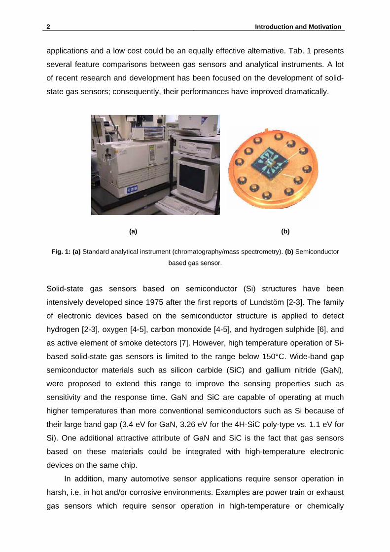
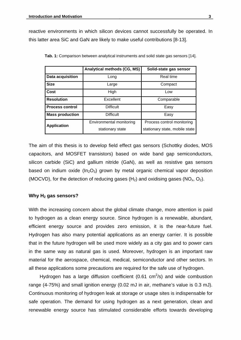
(CG/MS) (Fig.1) have been used for air pollutant measurements. These instruments
can give a precise analysis, they are time-consuming, expensive, and can seldom be
used in real-time in the field. A gas sensor that is compact, robust, with versatile
2 Introduction and Motivation
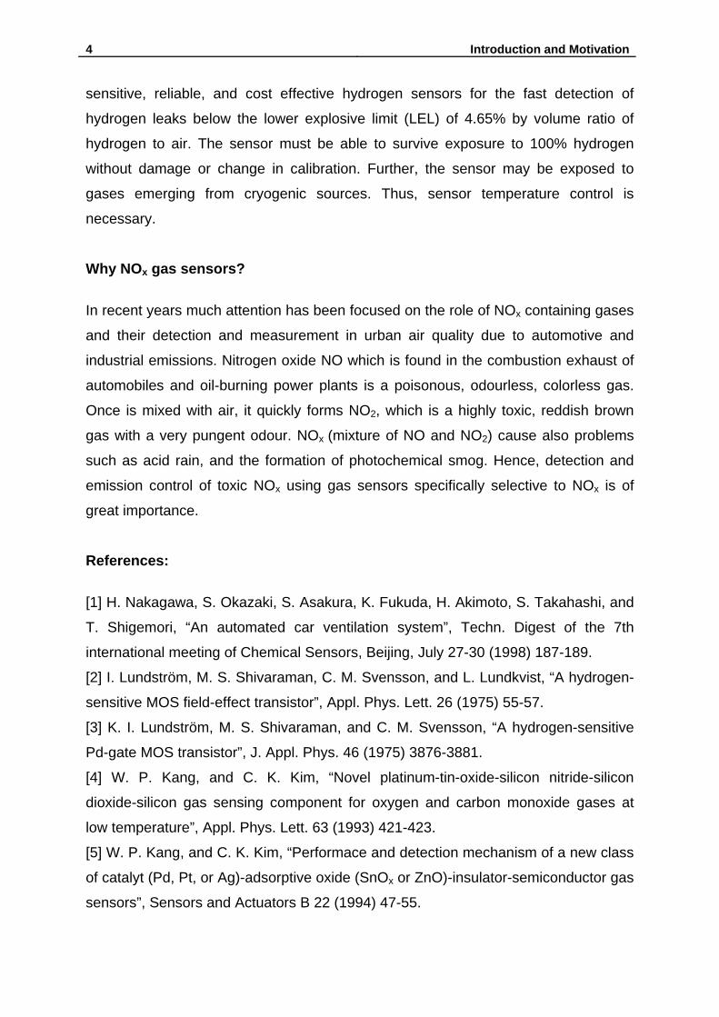
applications and a low cost could be an equally effective alternative. Tab. 1 presents
several feature comparisons between gas sensors and analytical instruments. A lot
of recent research and development has been focused on the development of solid-
state gas sensors; consequently, their performances have improved dramatically.
(a) (b)
Fig. 1: (a) Standard analytical instrument (chromatography/mass spectrometry). (b) Semiconductor
based gas sensor.
Solid-state gas sensors based on semiconductor (Si) structures have been
intensively developed since 1975 after the first reports of Lundstöm [2-3]. The family
of electronic devices based on the semiconductor structure is applied to detect
hydrogen [2-3], oxygen [4-5], carbon monoxide [4-5], and hydrogen sulphide [6], and
as active element of smoke detectors [7]. However, high temperature operation of Si-
based solid-state gas sensors is limited to the range below 150°C. Wide-band gap
semiconductor materials such as silicon carbide (SiC) and gallium nitride (GaN),
were proposed to extend this range to improve the sensing properties such as
sensitivity and the response time. GaN and SiC are capable of operating at much
higher temperatures than more conventional semiconductors such as Si because of
their large band gap (3.4 eV for GaN, 3.26 eV for the 4H-SiC poly-type vs. 1.1 eV for
Si). One additional attractive attribute of GaN and SiC is the fact that gas sensors
based on these materials could be integrated with high-temperature electronic
devices on the same chip.
In addition, many automotive sensor applications require sensor operation in
harsh, i.e. in hot and/or corrosive environments. Examples are power train or exhaust
gas sensors which require sensor operation in high-temperature or chemically
Introduction and Motivation 3
reactive environments in which silicon devices cannot successfully be operated. In
this latter area SiC and GaN are likely to make useful contributions [8-13].
Tab. 1: Comparison between analytical instruments and solid state gas sensors [14].
Analytical methods (CG, MS) Solid-state gas sensor
Data acquisition Long Real time
Size Large Compact
Cost High Low
Resolution Excellent Comparable
Process control Difficult Easy
Mass production Difficult Easy
Application Environmental monitoring
stationary state
Process control monitoring
stationary state, mobile state
The aim of this thesis is to develop field effect gas sensors (Schottky diodes, MOS
capacitors, and MOSFET transistors) based on wide band gap semiconductors,
silicon carbide (SiC) and gallium nitride (GaN), as well as resistive gas sensors
based on indium oxide (In2O3) grown by metal organic chemical vapor deposition
(MOCVD), for the detection of reducing gases (H2) and oxidising gases (NOx, O2).
Why H2 gas sensors?
With the increasing concern about the global climate change, more attention is paid
to hydrogen as a clean energy source. Since hydrogen is a renewable, abundant,
efficient energy source and provides zero emission, it is the near-future fuel.
Hydrogen has also many potential applications as an energy carrier. It is possible
that in the future hydrogen will be used more widely as a city gas and to power cars
in the same way as natural gas is used. Moreover, hydrogen is an important raw
material for the aerospace, chemical, medical, semiconductor and other sectors. In
all these applications some precautions are required for the safe use of hydrogen.
Hydrogen has a large diffusion coefficient (0.61 cm2/s) and wide combustion
range (4-75%) and small ignition energy (0.02 mJ in air, methane’s value is 0.3 mJ).
Continuous monitoring of hydrogen leak at storage or usage sites is indispensable for
safe operation. The demand for using hydrogen as a next generation, clean and
renewable energy source has stimulated considerable efforts towards developing
4 Introduction and Motivation
sensitive, reliable, and cost effective hydrogen sensors for the fast detection of
hydrogen leaks below the lower explosive limit (LEL) of 4.65% by volume ratio of
hydrogen to air. The sensor must be able to survive exposure to 100% hydrogen
without damage or change in calibration. Further, the sensor may be exposed to
gases emerging from cryogenic sources. Thus, sensor temperature control is
necessary.
Why NOx gas sensors?
In recent years much attention has been focused on the role of NOx containing gases
and their detection and measurement in urban air quality due to automotive and
industrial emissions. Nitrogen oxide NO which is found in the combustion exhaust of
automobiles and oil-burning power plants is a poisonous, odourless, colorless gas.
Once is mixed with air, it quickly forms NO2, which is a highly toxic, reddish brown
gas with a very pungent odour. NOx (mixture of NO and NO2) cause also problems
such as acid rain, and the formation of photochemical smog. Hence, detection and
emission control of toxic NOx using gas sensors specifically selective to NOx is of
great importance.
References:
[1] H. Nakagawa, S. Okazaki, S. Asakura, K. Fukuda, H. Akimoto, S. Takahashi, and
T. Shigemori, “An automated car ventilation system”, Techn. Digest of the 7th
international meeting of Chemical Sensors, Beijing, July 27-30 (1998) 187-189.
[2] I. Lundström, M. S. Shivaraman, C. M. Svensson, and L. Lundkvist, “A hydrogen-
sensitive MOS field-effect transistor”, Appl. Phys. Lett. 26 (1975) 55-57.
[3] K. I. Lundström, M. S. Shivaraman, and C. M. Svensson, “A hydrogen-sensitive
Pd-gate MOS transistor”, J. Appl. Phys. 46 (1975) 3876-3881.
[4] W. P. Kang, and C. K. Kim, “Novel platinum-tin-oxide-silicon nitride-silicon
dioxide-silicon gas sensing component for oxygen and carbon monoxide gases at
low temperature”, Appl. Phys. Lett. 63 (1993) 421-423.
[5] W. P. Kang, and C. K. Kim, “Performace and detection mechanism of a new class
of catalyt (Pd, Pt, or Ag)-adsorptive oxide (SnOx or ZnO)-insulator-semiconductor gas
sensors”, Sensors and Actuators B 22 (1994) 47-55.
Introduction and Motivation 5
[6] S. Shivaraman, “Detection of H2S with pd gate MOSFETs”, J. Appl. Phys. 47
(1976) 3592-3593.
[7] I. Lundstöm, S. Shivaraman, L. Stiblert, and C. Svenson, Hydrogen in Smoke
detected by the palladium-gat-field-effect transistor”, Rev. Sci. Instrum. 47 (1976)
738-740.
[8] J. Schalwig, G. Müller, M. Eickhoff, O. Ambacher, and M. Stutzmann, “Group III-
nitride-based gas sensors for combustion monitoring“, Mater. Sci. Eng. B 93 (2002)
207-214.
[9] J. Schalwig, P. Kreisl, S. Ahlers, and G. Müller, “Response mechanism of SiC-
based MOS field-effect gas sensors“, IEEE Sensors J. 2 (2002) 394-402.
[10] H. Wingbrant, L. Uneus, M. Andersson, J. Cerda, S. Savage, H. Svenningstorp,
P. Salomonsson P. Ljung, M. Mattsson, Salomonsson, J. H. Visser, D. Kubinski, R.
Soltis, S. G. Ejakov, M. Löfdahl, M. Einehag, M. Persson, and A. Lloyd Spetz,
“MISiCFET chemical sensors for applications in exhaust gases and flue gases”,
Material Science Forum 433-436 (2003) 953-956.
[11] M. Andersson, P. Ljung, M. Mattsson, M. Löfdahl, A. Lloyd Spetz, “Investigations
on the possibilities of a MISiCFET sensor system for OBD and combustion control
utilizing different catalytic gate materials”, Springer Verlag, Berlin, 30-31 (2004), 365-
368.
[12] I. Belov, H. Wingbrant, A. Lloyd Spetz, H. Sundgren, B. Thuner, H.
Svenningstorp, and P. Leisner, “Thermal and flow analysis of SiC-based gas sensors
for automotive applications”, Proc. of 5th IEEE conference EuroSimE 2004, Brussels,
May 9-12 (2004) 475-482.
[13] H. Wingbrant, H. Svenningstorp, P. Salomonsson, D. Kubinski, J. H. Visser, M.
Löfdahl, A. Lloyd Spetz, “Using a MISiC-FET sensor for detecting NH3 in SCR
systems”, IEEE Sensors J. 5 (2005) 1099-1105.
[14] N. Yamazoe and N. Miura, “Environmental gas sensing”, Sensors and Actuators
B 20 (1994) 95-102.

6 Introduction and Motivation
Chapter 1 7
Chapter 1
1 Solid-State Gas Sensors: State of the Art and Fundamentals
1.1 Chemical gas sensors:
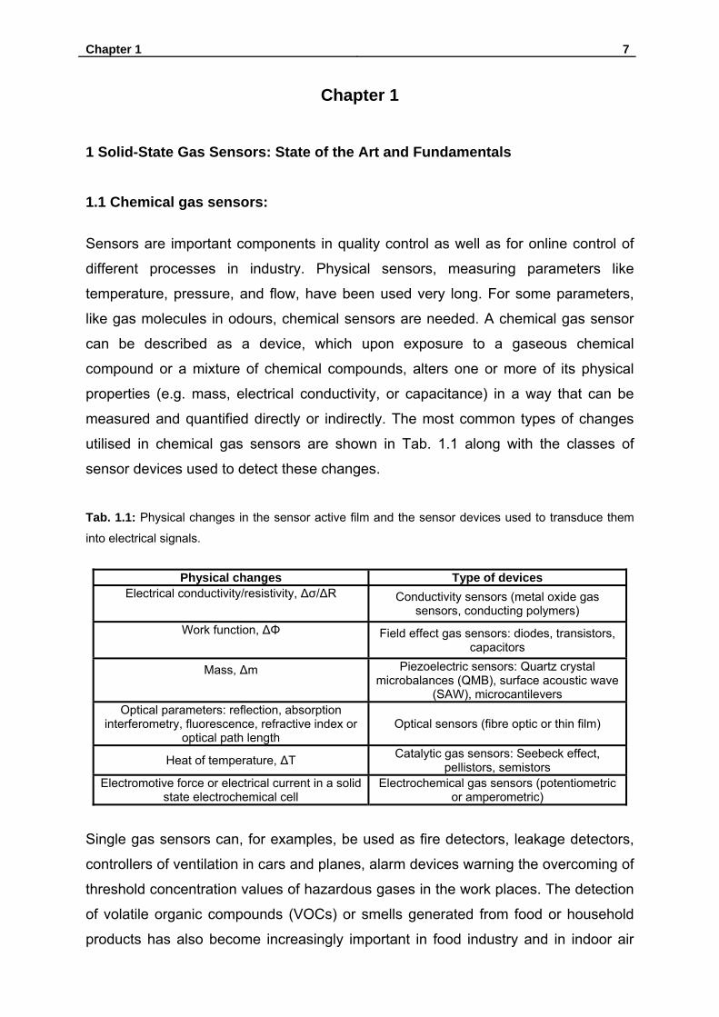
Sensors are important components in quality control as well as for online control of
different processes in industry. Physical sensors, measuring parameters like
temperature, pressure, and flow, have been used very long. For some parameters,
like gas molecules in odours, chemical sensors are needed. A chemical gas sensor
can be described as a device, which upon exposure to a gaseous chemical
compound or a mixture of chemical compounds, alters one or more of its physical
properties (e.g. mass, electrical conductivity, or capacitance) in a way that can be
measured and quantified directly or indirectly. The most common types of changes
utilised in chemical gas sensors are shown in Tab. 1.1 along with the classes of
sensor devices used to detect these changes.
Tab. 1.1: Physical changes in the sensor active film and the sensor devices used to transduce them
into electrical signals.
Physical changes Type of devices Electrical conductivity/resistivity, Δσ/ΔR
Conductivity sensors (metal oxide gas
sensors, conducting polymers) Work function, ΔΦ
Field effect gas sensors: diodes, transistors,
capacitors
Mass, Δm
Piezoelectric sensors: Quartz crystal microbalances (QMB), surface acoustic wave
(SAW), microcantilevers Optical parameters: reflection, absorption
interferometry, fluorescence, refractive index or optical path length
Optical sensors (fibre optic or thin film)
Heat of temperature, ΔT Catalytic gas sensors: Seebeck effect, pellistors, semistors
Electromotive force or electrical current in a solid state electrochemical cell
Electrochemical gas sensors (potentiometric or amperometric)
Single gas sensors can, for examples, be used as fire detectors, leakage detectors,
controllers of ventilation in cars and planes, alarm devices warning the overcoming of
threshold concentration values of hazardous gases in the work places. The detection
of volatile organic compounds (VOCs) or smells generated from food or household
products has also become increasingly important in food industry and in indoor air

8 Chapter 1
quality, and multisensor systems (often referred to as electronic noses) are the
modern gas sensing devices designed to analyse such complex environmental
mixtures [1.1-1.3]. In Tab. 2.2 examples of application for gas sensors and electronic
noses are reported.
Tab. 2.2: Example of applications for gas sensors and electronic noses [1.4].
Applications Automobiles
• Car ventilation control • Filter control • Gas-online vapour detection • Alcohol breath tests
Safety • Fire detection • Leak detection • Toxic/flammable/explosive gas detectors • Boiler control • Personal gas monitor
Indoor air quality • Air purifiers • Ventilation control • Cooking control
Environmental control • Weather stations • Pollution monitoring
Food • Food quality control • Process control • Packaging quality control (off-odours)
Industrial production • Fermentation control • Process control
Medicine • Breath analysis • Disease detection
Solid-state gas sensors, based on a variety of principles and materials, are the
best candidates to the development of commercial gas sensors for a wide range of
such applications [1.5-1.8]. The great interest of industrial and scientific world on
solid state gas sensors comes from their numerous advantages, like small sizes, high
sensitivities in detecting very low concentrations (at level of ppm or even ppb) of a
wide range of gaseous chemical compounds, possibility of on-line operation and, due
to possible bench production, low cost. On the contrary, traditional analytical
instruments such as mass spectrometer and chromatography are expensive,
complex, and large in size. In addition, most analysis requires sample preparation, so
Chapter 1 9
that on-line, real-time analysis is difficult. Solid-state chemical sensors have been
widely used, but they also suffer from limited measurement accuracy and problems
of long-time stability. However, recent advances in nanotechnology, i.e. in the cluster
of technologies related to the synthesis of materials with new properties by means of
the controlled manipulation of their microstructure on a nanometer scale, produce
novel classes of nanostructured materials with enhanced gas sensing properties
providing in such a way the opportunity to dramatically increase the performances of
solid state gas sensors.
1.2 The electronic nose (e-nose):
An electronic nose is an instrument comprised of an array of different gas sensors
and signal multiplexing electronics, capable of recognizing individual or mixtures of
analytes through pattern recognition [1.9-1.11]. It is based on the multi-sensing
principle in which the distributed response of an array is used to identify the
constituents of a gaseous environment, emulating the olfactory sense. Individual
sensor elements may or may not be selective to any one gas. But by using an array
of different sensors, gases can be distinguished and identified by a distinct
“fingerprint” each gas produces in the form of a pattern of measured electrical
responses. The e-nose is a cost-effective solution to the problems associated with
sensory panels and with chromatographic and mass-spectrometric techniques and
can accommodate real time performance in the field when implemented in portable
form.
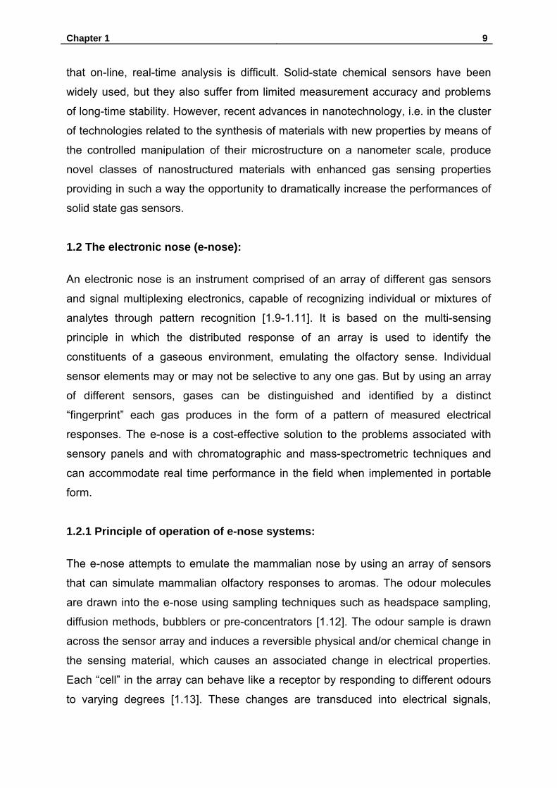
1.2.1 Principle of operation of e-nose systems:
The e-nose attempts to emulate the mammalian nose by using an array of sensors
that can simulate mammalian olfactory responses to aromas. The odour molecules
are drawn into the e-nose using sampling techniques such as headspace sampling,
diffusion methods, bubblers or pre-concentrators [1.12]. The odour sample is drawn
across the sensor array and induces a reversible physical and/or chemical change in
the sensing material, which causes an associated change in electrical properties.
Each “cell” in the array can behave like a receptor by responding to different odours
to varying degrees [1.13]. These changes are transduced into electrical signals,
10 Chapter 1
which are pre-processed and conditioned before identification by a pattern
recognition system as shown in Fig. 1.1.
Fig. 1.1: Comparison of the mammalian olfactory system and the e-nose system [1.13].
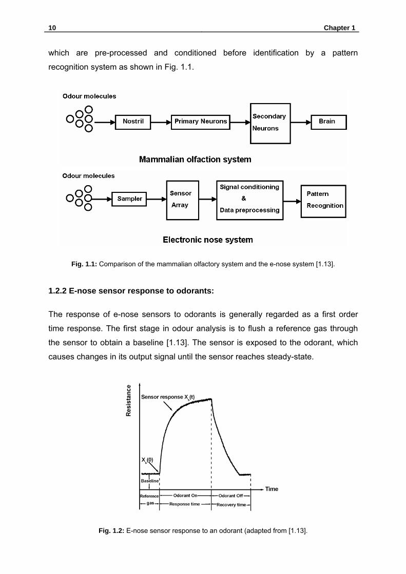
1.2.2 E-nose sensor response to odorants:
The response of e-nose sensors to odorants is generally regarded as a first order
time response. The first stage in odour analysis is to flush a reference gas through
the sensor to obtain a baseline [1.13]. The sensor is exposed to the odorant, which
causes changes in its output signal until the sensor reaches steady-state.
Fig. 1.2: E-nose sensor response to an odorant (adapted from [1.13].
Chapter 1 11
The odorant is finally flushed out of the sensor using the reference gas and the
sensor returns back to its baseline as shown in Fig. 1.2. The time during which the
sensor is exposed to the odorant is referred to as the response time while the time it
takes the sensor to return to its baseline resistance is called the recovery time [1.13].
The next stage in analysing the odour is sensor response manipulation with
respect to the baseline. This process compensates for noise, drift and also for
inherently large or small signals. The three most commonly used methods as defined
by Pearce et al. [1.12] are as follows.
(1) Differential: the baseline xs(0) is subtracted from the sensor response xs(t)
to remove any noise or drift δA present. The baseline manipulated response ys(t) is
determined by:
)0()())0(())(()( ssAsAss xtxxtxty −=+−+= δδ . (1.1)
(2) Relative: the sensor response is divided by the baseline. This process
eliminates multiplicative drift δM and a dimensionless response ys(t) is obtained.
)0()(
)1)(0()1)((
)(s
s
Ms
Mss x
txx
txty =
++
=δδ . (1.2)
(3) Fractional: the baseline is subtracted from the response xs(t) and then
divided by the baseline xs(0) from the sensor response which provides a
dimensionless, normalised response ys(t) that can compensate for inherently large or
small signals.
( ) ( ) ( )( )0
0
s
stss x
xxty
−= . (1.3)
The choice of baseline manipulation depends on the sensor type being used, the
sensor applications and also the researcher’s preference. However, certain
manipulation techniques have been shown to be more suitable to certain sensor
types and also variations in the manipulation techniques can occur in the literature.
Sensitivity is the measure of the change in output of a sensor for a change in the
input. This is the standard definition given for the sensitivity of a sensor in several
texts on sensor related topics [1.14, 1.15]. In the case of e-nose sensors, the
sensitivity of the sensor (S) to the odorant is the change in the sensor output
parameter (y) for a change in the concentration of the odorant (x) as shown in
equation (1.4).
xyS
ΔΔ
= . (1.4)

12 Chapter 1
However, in the literature several authors use different values to measure sensitivity,
usually calculated from baseline-manipulated data.
1.2.3 Sensors employed in e-nose systems:
The ideal sensors to be integrated in an electronic nose should fulfil the following
criteria [1.16-1.18]:
• high sensitivity toward chemical compounds, i.e. similar to that of the human
nose (down to 10-12 g/mL),
• low sensitivity towards humidity and temperature,
• medium selectivity, i.e. must respond to different compounds present in the
headspace of the sample,
• high stability,
• high reproducibility and reliability,
• short reaction and recovery time,
• robust and durable,
• easy calibration,
• easily processable data output and
• small dimensions.
As the sensors are designed for industrial purposes, especially as on-line systems, a
minimal working temperature with low power consumption, a high safety level, and
low manufacturing costs present valuable advantages.
Most manufacturers are looking for highly selective sensors. In the case of an
“electronic nose”, every compound present in the gaseous phase should be detected
by at least one sensor. If a new compound is added to a mixture, at least one sensor
must detect this addition. The use of too many sensors leads to an over complex
system with a large amount of unnecessary data. Various kinds of gas sensors are
available, but only four technologies are currently used in commercialised “electronic
noses”
- Metal oxide gas sensors
- Metal oxide semiconductor field effect transistors (MOSFET)
- Conducting organic polymers (CP)
- Piezoelectric crystals (bulk acoustic wave (BAW)).
The metal oxide and MOSFETs gas sensors will be discussed in the following:
Chapter 1 13
1.2.3.1 Metal oxide gas sensors:
Metal oxide gas sensors were first commercialised in the 1960s as household gas
alarms in Japan with the names Taguchi (the inventor) or Figaro (the company’s
name). These sensors, also called oxide or ceramic gas sensors [1.19].
The principle of operation of metal oxide sensors is based on the change in
conductance of the oxide on interaction with a gas and the change is usually
proportional to the concentration of the gas [1.13]. There are two types of metal oxide
sensors; n-type (zinc oxide (ZnO), tin dioxide (SnO2), titanium dioxide (TiO2), indium
oxide (In2O3) or iron (III) oxide (Fe2O3)) which respond to oxidising gases and p-type
(nickel oxide (NiO), cobalt oxide(CoO)) which respond to reducing gases [1.12].
Thermal or photolytic excitation of an n-type (n = negative electron) or donor
semiconductor results in an excess of electrons in its conduction band which
increases the reactivity with oxidising molecules. An excited p-type (p = positive hole)
or acceptor semiconductor shows an electron deficiency in its valence band which
promotes reactions with reducing compounds [1.20].
The n-type sensor operates as follows: oxygen in the air reacts with the surface
of the sensor and traps any free electrons on the surface or at the grain boundaries
of the oxide grains. This produces large resistance in these areas due to the lack of
carriers and the resulting potential barriers produced between the grains inhibit the
carrier mobility. However, if the sensor is introduced to a reducing gas like H2, CH4,
CO, C2H5 or H2S the resistance drops because the gas reacts with the oxygen and
releases an electron [1.13].
This lowers the potential barrier and allows the electrons to flow, thereby increasing
the conductivity. p-type sensors respond to oxidising gases like O2, NO2, and Cl2 as
these gases remove electrons and produce holes, i.e. producing charge carriers
[1.13]. Equations (1.5) and (1.6) describe the reactions occurring at the surface:
)(21
2 sOeO −− →+ , (1.5)
( ) −− +→+ egROsOgR )()( . (1.6)
where e is an electron from the oxide. R(g) is the reducing gas and g and s are the
surface and gas, respectively [1.12,1.21].
The film deposition technique further divides each sensor type into thin (5
to1000 nm) or thick (1 to 300 µm) film metal oxide sensors [1.22]. Film deposition
includes screen printing [1.23], spin coating [1.24], RF sputtering [1.25] physical or
14 Chapter 1
chemical vapour deposition [1.26]. The metal oxide films are deposited onto a flat or
tube type substrate made of alumina, glass, silicon or some other ceramic. Gold,
platinum, silver or aluminium electrodes are deposited onto the substrate using the
same methods. There are various electrode designs but the interdigitated structure
appears to be the most common approach. A heating element is printed onto the
back of the substrate to provide the high temperatures required for metal oxides to
operate as gas sensors, typically 200-500°C.
The main advantages of metal oxide sensors are fast response and recovery
times, which mainly depend on the temperature and the level of interaction between
the sensor and gas [1.26]. Thin film metal oxide sensors are small, and relatively
inexpensive to fabricate, have lower power consumption than thick film sensors and
can be integrated directly into the measurement circuitry [1.26]. However, they have
many disadvantages due to their high operating temperatures, which results in
increased power consumption over sensors fabricated from materials other than
metal oxides. As a result, no handheld e-nose system has been fabricated utilising
sensors prepared from metal oxides [1.12].
Other important disadvantages are the sensitivity to water vapour and the lack
of selectivity. Metal oxide-based gas sensors are normally sensitive to more than one
chemical species in air and usually show cross-sensitivities. This non-specificity of
the response to chemical species whose presence, identity and concentration in air
have to be determined is by now considered an intrinsic property of metal oxide-
based gas sensors. It’s easy to understand how this disadvantage represents a real
problem when different reactive gases are present simultaneously in the same
atmosphere and interference effects between them can occur. Unselectivity cannot
be eliminated completely but it can be improved in different ways, like:
• The use of filters [1.27] or chromatographic columns to discriminate between
gases on the basis of their molecular size or other physical properties [1.28].
• The use of catalysts and promoters or more specific surface additives [1.29,
1.30].
• The selection of the material for the sensing layer [1.31] and its physical
preparation.
• The analysis of the transient sensor response [1.32].
• The selection of a fixed temperature to maximize sensitivity to a particular
analyte gas [1.33].
Chapter 1 15
• The use of temperature modulated operation mode [1.34].
A different approach to the problem of unselectivity is based on the development of
the above mentioned electronic nose, that consists in an array of different sensing
elements with partially overlapping sensitivity and a pattern recognition system.
Basically the idea of an electronic nose is to exploit the unavoidable cross-sensitivity
of the sensors instead of trying to eliminate it, by linking the sensors in an array
configuration and by analyzing the responses of the sensors in a subsequent data
processing step in order to perform a qualitative and/or quantitative analysis of the
ambient under examination.
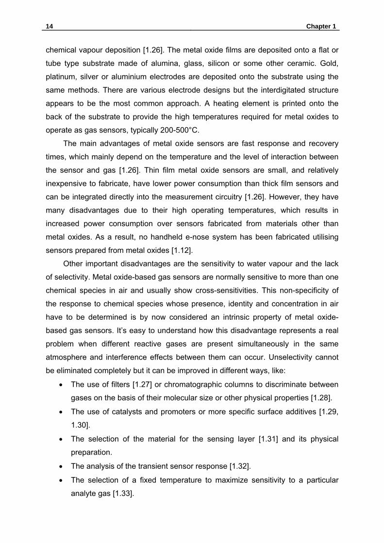
1.2.3.2 Metal-oxide-semiconductor field-effect transistor sensor (MOSFET):
The metal-oxide-semiconductor field-effect transistor (MOSFET) used in gas sensing
is a device in which conduction between the source and drain of the transistor (Fig.
1.3) is controlled by charge or potential on the gate electrode. The device performs
as a capacitor with one electrode the gate and the other the channel between source
and drain. Charge present at the gate gives rise to a reflected charge induced in the
channel and this modifies the conductance between source and drain. Any process
that alters either the charge on the gate or its potential will alter the conduction of the
channel and this can be detected as a useful electrical signal.
Fig. 1.3: MOSFET gas sensor with gas sensitive membrane deposited on top of SiO2 [1.35].
This particular sensor works on the principle that the threshold voltage of the
MOSFET sensor changes on interaction of the gate material [1.13], usually a
catalytic metal, with certain gases, such as hydrogen, due to corresponding changes
in the work functions of the metal and the oxide layers [1.12]. The changes in the
16 Chapter 1
work functions occur due to the polarization of the surface and interface of the
catalytic metal and oxide layer when the gas interacts with the catalytically active
surface [1.36]. In order for the physical changes in the sensor to occur, the metal-
insulator interface has to be accessible to the gas. Therefore, a porous gas sensitive
gate material is used to facilitate diffusion of gas into the material [1.35]. It has been
observed that the change in the threshold voltage is proportional to the concentration
of the analyte and is used as the response mechanism for the gas. Changes in the
drain-source current and the gate voltage have also been used as the response
mechanisms for the MOSFET gas sensors as they are also affected by changes in
the work function [1.21, 1.37].
Gas sensing MOSFETs are produced by standard microfabrication techniques,
which incorporate the deposition of gas sensitive catalytic metals onto the silicon
dioxide gate layer. In the case of catalytic metals, such as platinum (Pt), palladium
(Pd), rhodium (Rh) and iridium (Ir), the gate material is thermally evaporated onto the
gate oxide surface through a mask forming 100-400 nm thick films or 3-30 nm thin
films depending on the application [1.21].
Polymers have also been used as the gate material for MOSFET gas sensors
[1.38] Covington et al. used three polymers (poly(ethylene-co-vinylacetate),
poly(styrene co-butadiene), poly(9-vinylcarbazole)) mixed with 20 per cent carbon
black, which were deposited onto the FETs using a spray system. The polymer
thickness was between 1.9 and 3.7 μm, respectively [1.39]. These MOSFETs, which
use polymers can operate at room temperature. A part from the standard MOSFET
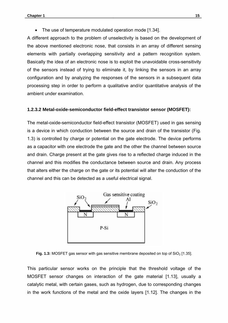
gas sensor architecture, a hybrid suspended gate FET (HSGFET) gas sensor can
also be fabricated by micromachining (Fig. 1.4).
The HSGFET is a metal air-gap insulator (MAIS) device. The air-gap allows easy
access to both the gate material and the insulator, so diffusion is not necessary and
therefore a wider choice of gas sensitive materials can be used [1.12,1.35].
The selectivity and sensitivity of MOSFET sensors may be influenced by the
operating temperature (50-200°C), the composition of the metal gate, and the
microstructure of the catalytic metal [1.37].
MOSFET sensors have a number of advantages and disadvantages when used
in e-nose arrays. Gas sensing MOSFETs are produced by microfabrication, therefore
reproducibility is quite good and the sensor can be incorporated into CMOS
technology resulting in small, low cost sensors [1.12, 1.37]. The sensors can suffer
Chapter 1 17
from baseline drift and instability depending on the sensing material used. If CMOS is
used, the electronic components of the chip have to be sealed because the sensor
needs a gas inlet so it can penetrate the gate [1.37].
Fig. 1.4: Hybrid suspended gate field effect transistor [1.35].
1.3 Sorption processes:
When a gas or vapour is brought into contact with a solid, it will be partly taken up by
the solid until equilibrium of the concentrations in the two phases is reached. The
molecules either enter the inside of the solid, called absorption or dissolution, or
remain on the outside attached to the surface, named adsorption. The general term
for all possible processes is sorption.
It concludes adsorption, absorption, clustering of sorbate molecules, and
incorporation into microvoids of the sorbent. Several modes of sorption may occur
simultaneously depending on the nature of the sorbate and sorbent, the ambient
conditions, namely pressure and temperature, and the concentration of the sorbate in
the gas phase. The amount of sorbed molecules as a function of the partial pressure
in the gas phase at a fixed temperature is modelled by a sorption isotherm.
1.3.1 Adsorption:
A solid material usually exhibits a heterogeneous distribution of surface energy. Gas,
vapor, or liquid molecules may become bound to the surface if they approach
sufficiently close to interact. The solid is called the adsorbent; the gas or vapor
molecule prior to being adsorbed is called the adsorptive and while bound to the solid
18 Chapter 1
surface, the adsorbate. The adsorbed amount depends on the pressure of the
adsorbate, the temperature and the properties of the adsorbent.
The phenomenon of adsorption plays an important role in both heterogeneous
catalysis and in adsorption and membrane applications. Two main types of
adsorption processes exists; physisorption and chemisorption.
Chemisorption involves the creation of bonds between the adsorbent and the
adsorbate and resembles chemical reactions. Most of the reactions being catalysed
by a solid are believed to involve an intermediate step with chemisorption of at least
one of the reactants.
Physisorption is caused by weak intermolecular forces such as van-der-Waals,
induced dipoles and dipole-dipole interactions and adsorption energy usually not
exceeding 80 kJ/mole, with typical energies being considerably less. Physisorption
resembles condensation of vapours rather than actual chemical reactions as in
chemisorption. Physisorption is the main phenomenon used in adsorptive separation
processes. Further, physisorption is used to determine the specific surface area as
well as pore sizes and pore size distributions of the adsorbent.
Chemical bonds involving chemical reactions are stronger than the ones
involving van-der-Waal forces. The heat of adsorption is a direct measure of the bond
strength between the surface and the adsorbate. This parameter will yield information
on which adsorption process is taking place. For physisorption the heat of adsorption
is approximately 2-3 times smaller than the heat of vaporization [1.40]. Physisorption
from gas phase is always an exothermic process.
Physisorption is an equilibrium process, which is fully reversible. Equilibrium is
quickly achieved unless the process is restricted by slow diffusion of the adsorbate.
Physisorption is usually nonspecific in contrast to chemisorption, which is highly
specific taking place on certain specific sites on the surface. As a consequence
chemisorption is restricted to forming a monolayer, whilst in physisorption both
monolayers as well as multilayers may form. At low partial pressures monolayer
adsorption is dominating whilst at higher partial pressures multilayers may form.
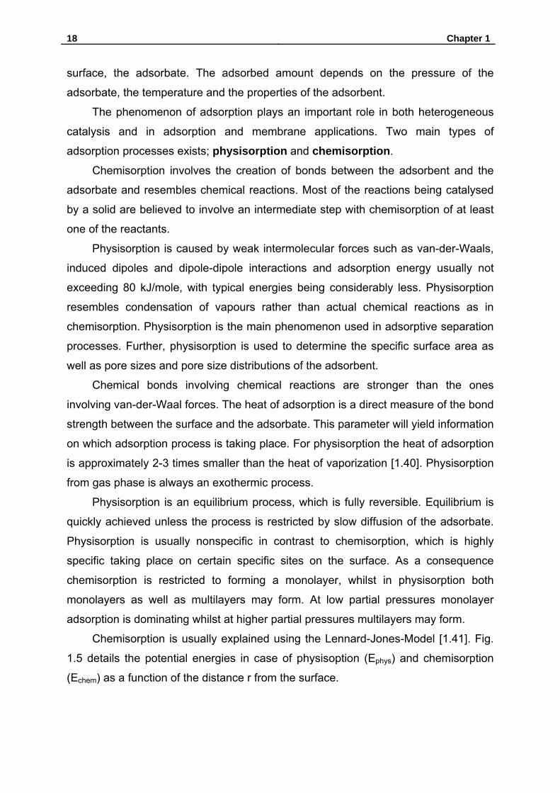
Chemisorption is usually explained using the Lennard-Jones-Model [1.41]. Fig.
1.5 details the potential energies in case of physisoption (Ephys) and chemisorption
(Echem) as a function of the distance r from the surface.
Chapter 1 19
Fig. 1.5: Lennard-Jones model of physisorption and chemisorption: (a) physisorption of a molecule;
(b) chemisorption of a molecule. Activation energy Ea, dissociation energy Ediss, desorption energy Edes
(adapted from [1.41]).
If a gaseous molecule approaches the surface it will first be physisorbed, gaining ΔE
equal to Ephys. Upon a further approach towards the surface the molecule encounters
a growing energy barrier, tending towards an infinite energy for a finite distance r. By
spending the activation energy Ea the gaseous molecule can dissociate, thereby
allowing a further approach to the surface. This stronger interaction with the surface
(chemisorption) results in a higher energy gain ΔE equal to Echem than during
physisorption. This energy gain Echem depends strongly on the individual surface sites
available and their reactivity. The most reactive sites will therefore be occupied with
gaseous molecules during thermodynamic equilibration. However, the chemisorption
energy not only depends on the number of reactive sites (high potential gain in
ΔEchem) but also on the ambient gas concentration pgas and temperature T (probability
of molecules overcoming the energy barrier Ea).
As for chemisorption, desorption also requires the molecule to overcome an
energy barrier Edes = Echem + Ea. Therefore chemisorption and desorption are both
activated processes requiring an activation energy supplied either thermally or by
photoexcitation, contrary to physisorption which is a slightly exothermic process.
1.3.2 Adsorption isotherms:
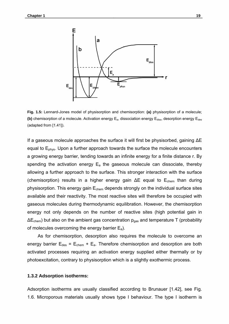
Adsorption isotherms are usually classified according to Brunauer [1.42], see Fig.
1.6. Microporous materials usually shows type I behaviour. The type I isotherm is
20 Chapter 1
also referred to as a Langmuir type of isotherm, with a steep increase in surface
coverage at low partial pressures. At higher partial pressures the isotherms starts to
level off towards a distinct saturation limit when the pore system is completely filled
with the adsorbate. Type II isotherms represent multilayer adsorption on non-porous
solids. Type IV isotherms are typical for porous materials containing mesopores
where capillary condensation occurs in the mesopores. Types III and V are rare and
occurs in systems where the forces of adsorption are relatively weak.
Fig. 1.6: Brunauer’s five types of adsorption isotherms [1.43].
At low partial pressures of the adsorbate there will be a low surface coverage, and
the adsorbed molecules may be regarded as isolated from the neighbours. Assuming
that the surface is uniform, the relationship between the partial pressure and the
amount adsorbed on the surface will be linear.
This relationship is often referred to as Henry’s law because of the similarity to
the limiting behaviour of gases dissolved in liquids. For a Henry constant expressed
in pressure the Henry law is written as:
PKq H= . (1.7)
The loading of the adsorbate is q (mol kg-1), KH is the Henry constant (mol kg-1 Pa-1)
and P is the partial pressure of the adsorbate in gas phase.
At higher partial pressures molecules adsorbed at adjoining sites will interact
with each other. The surface will begin to reach monolayer coverage alt. These
factors will affect the amount adsorbed so that the linear relationship between the
partial pressure and the surface coverage according to Eq. 1.7 is no longer valid. To
model this behavior a number of adsorption models have been proposed, a common
model is the so-called Langmuir model or the Langmuir isotherm.

Chapter 1 21
1.3.3 Langmuir isotherm:
This simplest physically plausible isotherm is based on three assumptions:
Adsorption cannot proceed beyond the point at which the adsorbates are one
layer thick on the surface (monolayer).
All adsorption sites are equivalent.
The ability of a molecule to adsorb at a given site is independent of the
occupation of neighboring sites.
The Langmuir isotherm describes the surface coverage (θ) of an adsorbed gas and is
dependent upon the pressure (P) at a fixed temperature [1.44]. It can easily be
derived by assuming that the rate of adsorption is proportional to the rate of
molecular collisions with vacant sites:
( )θ−= 1PkR Aads . (1.8)
In the expression, kA is the adsorption constant; P is the partial pressure of the
adsorbate. Further, if qs is the saturation capacity of the surface and by letting θ be
the fractional surface coverage, θ = q/qs, this implies that 1-θ is the fraction of vacant
sites.
The disengagement of an atom or molecule from a surface is termed
”desorption”. At low temperatures a molecule adsorbed on a surface could remain for
an indefinite time. However, as the surface temperature increases the molecule will
receive energy, and so one of the following processes can occur:
the molecules can react with the surface,
the molecules can break down to two or more other molecules (either in
gaseous or solid state),
the molecules can desorb.
The last option is the desorption process, which could also occur in the second
option if one of the products is a gas. The rate constant of the desorption process
with respects to the change of the surface coverage by desorption is given by:
θDdes kR = . (1.9)
In the expression, the desorption constant is denoted kD. At equilibrium the rate of
adsorption and desorption rates in equations (1.8) and (1.9) are equal, so that:
( ) θθ DA kPk =−1 . (1.10)
By setting b = kA/kD and by solving for θ the following expression is obtained:

22 Chapter 1
bPbP
s +==
1θ . (1.11)
At high partial pressures q →qs and θ →1 while at low partial pressures bP << 1. As
a consequence, at low partial pressures, Henry’s law is valid. The adsorption
equilibrium constant, b, is easily obtained from experimental data Eq. (1.11) is
linearised to:
bqqP
qP
ss
1+= . (1.12)
A plot of P/q as a function of P should yield a straight line with slope equal to 1/qs and
the intercept with the y-axis equal to 1/(qsb).
Fig. 1.7 shows the characteristics of several Langmuir isotherms for different values
of b(T). A surface with high desorption relative to the adsorption rate has a small
surface coverage (b(T) is small). With an increase in desorption rate (and thus b(T))
the surface coverage will rise.
Fig. 1.7: Characteristics of several Langmuir isotherms for different b(T) [1.45].
When considering an adsorption process of two gases (gas A and gas B) on a
surface it is necessary to modify Eq. (1.11) to:
BBAA
AAA PbPb
Pb++
=1
θ . (1.13)
and
BBAA
BBB PbPb
Pb++
=1
θ . (1.14)
Chapter 1 23
These equations allow to express the surface coverage of two gases, which react
with each other on the surface in the following way:
gfast
adsadsads ABABBA ⎯⎯→⎯→+ . (1.15)
This model suitably describes the surface coverage of oxygen in terms of oxygen
partial pressure and the concentration of gaseous co-reactants. Examples of such
reactions are:
−− +→+ eCOOCO 2 , (1.16)
and
−− +→+ eNOONO 2 . (1.17)
1.4 Introduction to catalysis:
Catalytic effects play an important role in the field of gas detection. Solid-state gas
sensors are directly related to the phenomenon of catalysis. Catalytic processes not
only control the rate at which a chemical reaction approaches equilibrium (this affects
the response time in the case of gas detection) but also affect the sensitivity and
selectivity. The ideal catalyst is one which increases the rate of the gas-surface
reaction without itself becoming permanently affected by the reaction. Thus the
response time will be fast and the process will be reversible.
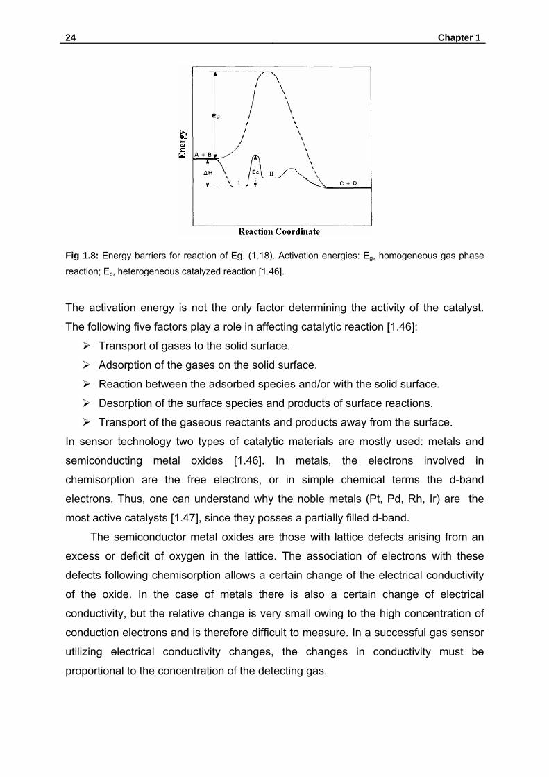
Fig. 1.8 shows schematically the energetic of the reaction (both catalyzed and
uncatalyzed):
DCBA +↔+ . (1.18)
The uncatalyzed reaction is characterized by extremely high activation energy, Eg. In
the catalyzed reaction the gaseous species A and B adsorb on the surface with an
exothermic heat of adsorption ΔH (state I). The state I is followed by state II toward
the reaction products C and D (state II) characterized by the activation energy Ec,
which is much lower than Eg It can be seen from Fig 1.8 that if the heats of
adsorption (ΔH) are too large, that is if the species are too strongly adsorbed, the
activation energy Ec may become too high for the reaction to be accelerated
However, the value of the activation energy alone does not define the activity of the
catalyst, for example, as the heat of adsorption, and hence the activation energy,
falls, so does the surface concentration of the reactants. Consequently, although the
reaction becomes energetically easier, fewer species are available for reaction.
24 Chapter 1
Fig 1.8: Energy barriers for reaction of Eg. (1.18). Activation energies: Eg, homogeneous gas phase
reaction; Ec, heterogeneous catalyzed reaction [1.46].
The activation energy is not the only factor determining the activity of the catalyst.
The following five factors play a role in affecting catalytic reaction [1.46]:
Transport of gases to the solid surface.
Adsorption of the gases on the solid surface.
Reaction between the adsorbed species and/or with the solid surface.
Desorption of the surface species and products of surface reactions.
Transport of the gaseous reactants and products away from the surface.
In sensor technology two types of catalytic materials are mostly used: metals and
semiconducting metal oxides [1.46]. In metals, the electrons involved in
chemisorption are the free electrons, or in simple chemical terms the d-band
electrons. Thus, one can understand why the noble metals (Pt, Pd, Rh, Ir) are the
most active catalysts [1.47], since they posses a partially filled d-band.
The semiconductor metal oxides are those with lattice defects arising from an
excess or deficit of oxygen in the lattice. The association of electrons with these
defects following chemisorption allows a certain change of the electrical conductivity
of the oxide. In the case of metals there is also a certain change of electrical
conductivity, but the relative change is very small owing to the high concentration of
conduction electrons and is therefore difficult to measure. In a successful gas sensor
utilizing electrical conductivity changes, the changes in conductivity must be
proportional to the concentration of the detecting gas.
Chapter 1 25
1.5 Properties of wide bandgap semiconductors:
The substrate materials chosen for the sensors described in this thesis are wide
bandgap semiconductor materials SiC and GaN, which are capable of operating at
much higher temperatures than more conventional semiconductors such as Si. This,
as well as other properties of the material, will be treated in the following.
1.5.1 The properties of SiC:
Silicon carbide (SiC) is a very promising material for semiconductor devices which
have to work under extreme conditions, such as high temperature, high power, and
high frequency. Because of the good thermal conductivity, the high radiation
resistance, and the high breakdown voltages, SiC is well suited for demanding
applications in harsh environments. These properties make SiC a suitable material
for use in exhaust gas applications. The atmosphere inside the exhaust pipe of an
engine is very warm (up to 1000°C in the case with a gasoline engine) and contain
many different gases and particles, which altogether creates a very harsh
environment. It is necessary to use a material that is chemically inert so that it does
not degrade in this atmosphere.
1.5.1.1 Crystallography-Polytyes:
Silicon carbide occurs in many different crystal structures, called polytypes. Despite
the fact that all SiC polytypes chemically consist of 50% carbon atoms covalently
bonded with 50% silicon atoms, each SiC polytype has its own distinct set of
electrical and physical properties. While there are over 200 known polytypes of SiC,
only a few are commonly grown in a reproducible form acceptable for use as an
electronic semiconductor. The most common polytypes of SiC presently being
developed for electronics are 3C-SiC, 4H-SiC, and 6H-SiC, due to the ability to
synthesize these poly types in thin films and/or wafer forms using conventional
methods.
3C-SiC, also referred to as β-SiC, is the only form of SiC with a cubic crystal
lattice structure. The non-cubic polytypes of SiC are sometimes ambiguously referred
to as α-SiC. 4H-SiC and 6H-SiC are only two of many possible SiC polytypes with
hexagonal crystal structure. Similarly, 15R-SiC is the most common of many possible
26 Chapter 1
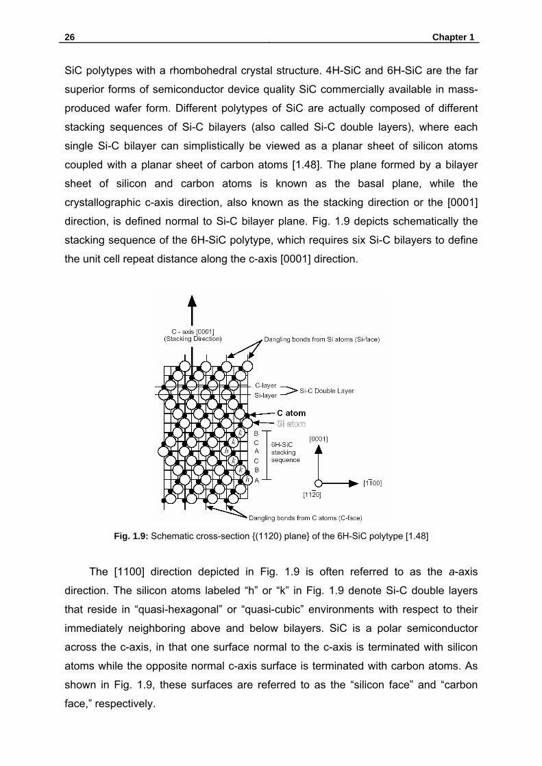
SiC polytypes with a rhombohedral crystal structure. 4H-SiC and 6H-SiC are the far
superior forms of semiconductor device quality SiC commercially available in mass-
produced wafer form. Different polytypes of SiC are actually composed of different
stacking sequences of Si-C bilayers (also called Si-C double layers), where each
single Si-C bilayer can simplistically be viewed as a planar sheet of silicon atoms
coupled with a planar sheet of carbon atoms [1.48]. The plane formed by a bilayer
sheet of silicon and carbon atoms is known as the basal plane, while the
crystallographic c-axis direction, also known as the stacking direction or the [0001]
direction, is defined normal to Si-C bilayer plane. Fig. 1.9 depicts schematically the
stacking sequence of the 6H-SiC polytype, which requires six Si-C bilayers to define
the unit cell repeat distance along the c-axis [0001] direction.
Fig. 1.9: Schematic cross-section (1120) plane of the 6H-SiC polytype [1.48]
The [1100] direction depicted in Fig. 1.9 is often referred to as the a-axis
direction. The silicon atoms labeled “h” or “k” in Fig. 1.9 denote Si-C double layers
that reside in “quasi-hexagonal” or “quasi-cubic” environments with respect to their
immediately neighboring above and below bilayers. SiC is a polar semiconductor
across the c-axis, in that one surface normal to the c-axis is terminated with silicon
atoms while the opposite normal c-axis surface is terminated with carbon atoms. As
shown in Fig. 1.9, these surfaces are referred to as the “silicon face” and “carbon
face,” respectively.
Chapter 1 27
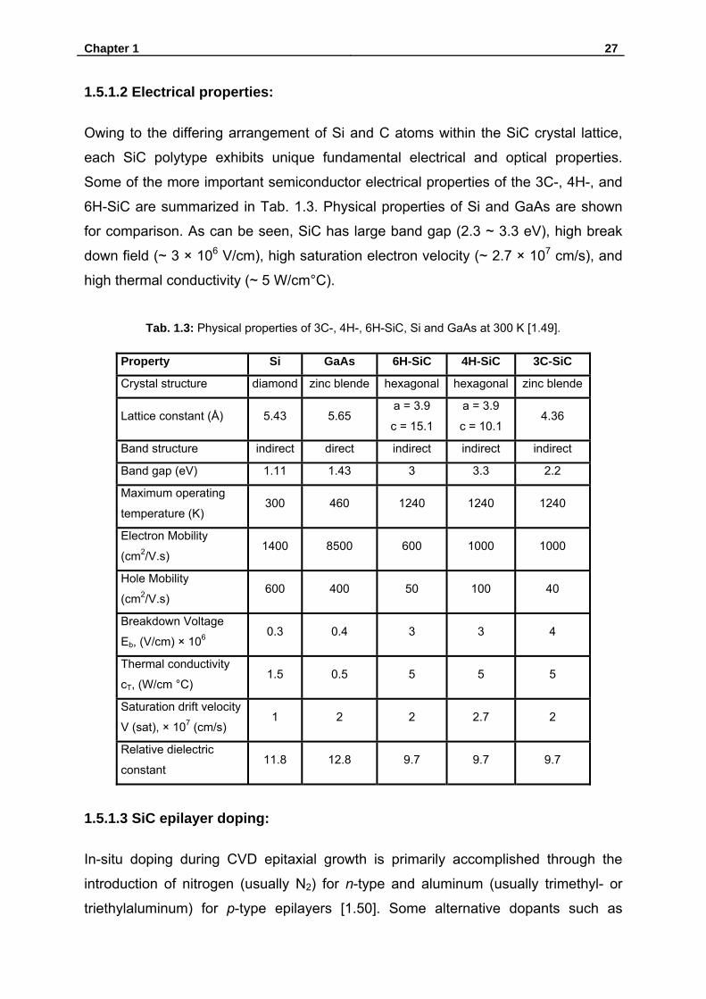
1.5.1.2 Electrical properties:
Owing to the differing arrangement of Si and C atoms within the SiC crystal lattice,
each SiC polytype exhibits unique fundamental electrical and optical properties.
Some of the more important semiconductor electrical properties of the 3C-, 4H-, and
6H-SiC are summarized in Tab. 1.3. Physical properties of Si and GaAs are shown
for comparison. As can be seen, SiC has large band gap (2.3 ~ 3.3 eV), high break
down field (~ 3 × 10⁶ V/cm), high saturation electron velocity (~ 2.7 × 107 cm/s), and
high thermal conductivity (~ 5 W/cm°C).
Tab. 1.3: Physical properties of 3C-, 4H-, 6H-SiC, Si and GaAs at 300 K [1.49].
Property Si GaAs 6H-SiC 4H-SiC 3C-SiC
Crystal structure diamond zinc blende hexagonal hexagonal zinc blende
Lattice constant (Å) 5.43 5.65 a = 3.9
c = 15.1
a = 3.9
c = 10.1 4.36
Band structure indirect direct indirect indirect indirect
Band gap (eV) 1.11 1.43 3 3.3 2.2
Maximum operating
temperature (K) 300 460 1240 1240 1240
Electron Mobility
(cm2/V.s) 1400 8500 600 1000 1000
Hole Mobility
(cm2/V.s) 600 400 50 100 40
Breakdown Voltage
Eb, (V/cm) × 106 0.3 0.4 3 3 4
Thermal conductivity
cT, (W/cm °C) 1.5 0.5 5 5 5
Saturation drift velocity
V (sat), × 107 (cm/s) 1 2 2 2.7 2
Relative dielectric
constant 11.8 12.8 9.7 9.7 9.7
1.5.1.3 SiC epilayer doping:
In-situ doping during CVD epitaxial growth is primarily accomplished through the
introduction of nitrogen (usually N2) for n-type and aluminum (usually trimethyl- or
triethylaluminum) for p-type epilayers [1.50]. Some alternative dopants such as
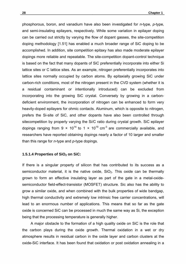
28 Chapter 1
phosphorous, boron, and vanadium have also been investigated for n-type, p-type,
and semi-insulating epilayers, respectively. While some variation in epilayer doping
can be carried out strictly by varying the flow of dopant gasses, the site-competition
doping methodology [1.51] has enabled a much broader range of SiC doping to be
accomplished. In addition, site competition epitaxy has also made moderate epilayer
dopings more reliable and repeatable. The site-competition dopant-control technique
is based on the fact that many dopants of SiC preferentially incorporate into either Si
lattice sites or C lattice sites. As an example, nitrogen preferentially incorporates into
lattice sites normally occupied by carbon atoms. By epitaxially growing SiC under
carbon-rich conditions, most of the nitrogen present in the CVD system (whether it is
a residual contaminant or intentionally introduced) can be excluded from
incorporating into the growing SiC crystal. Conversely by growing in a carbon-
deficient environment, the incorporation of nitrogen can be enhanced to form very
heavily-doped epilayers for ohmic contacts. Aluminum, which is opposite to nitrogen,
prefers the Si-site of SiC, and other dopants have also been controlled through
sitecompetition by properly varying the Si/C ratio during crystal growth. SiC epilayer
dopings ranging from 9 × 10¹⁴ to 1 × 10¹⁹
cm-3 are commercially available, and
researchers have reported obtaining dopings nearly a factor of 10 larger and smaller
than this range for n-type and p-type dopings.
1.5.1.4 Properties of SiO2 on SiC:
If there is a singular property of silicon that has contributed to its success as a
semiconductor material, it is the native oxide, SiO2. This oxide can be thermally
grown to form an effective insulating layer as part of the gate in a metal-oxide-
semiconductor field-effect-transistor (MOSFET) structure. Sic also has the ability to
grow a similar oxide, and when combined with the bulk properties of wide bandgap,
high thermal conductivity and extremely low intrinsic free carrier concentrations, will
lead to an enormous number of applications. This means that so far as the gate
oxide is concerned SiC can be processed in much the same way as Si, the exception
being that the processing temperature is generally higher.
A major obstacle to the formation of a high quality oxide on SiC is the role that
the carbon plays during the oxide growth. Thermal oxidation in a wet or dry
atmosphere results in residual carbon in the oxide layer and carbon clusters at the
oxide-SiC interface. It has been found that oxidation or post oxidation annealing in a
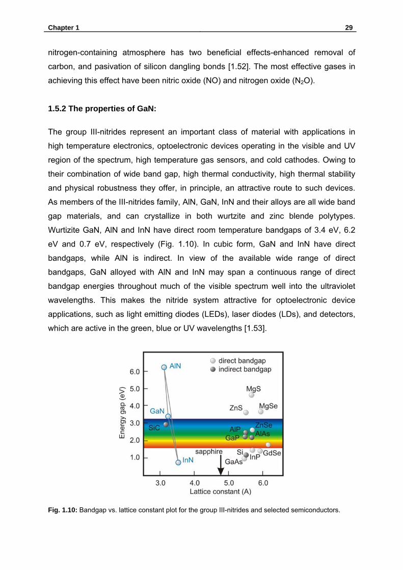
Chapter 1 29
nitrogen-containing atmosphere has two beneficial effects-enhanced removal of
carbon, and pasivation of silicon dangling bonds [1.52]. The most effective gases in
achieving this effect have been nitric oxide (NO) and nitrogen oxide (N2O).
1.5.2 The properties of GaN:
The group III-nitrides represent an important class of material with applications in
high temperature electronics, optoelectronic devices operating in the visible and UV
region of the spectrum, high temperature gas sensors, and cold cathodes. Owing to
their combination of wide band gap, high thermal conductivity, high thermal stability
and physical robustness they offer, in principle, an attractive route to such devices.
As members of the III-nitrides family, AlN, GaN, InN and their alloys are all wide band
gap materials, and can crystallize in both wurtzite and zinc blende polytypes.
Wurtizite GaN, AlN and InN have direct room temperature bandgaps of 3.4 eV, 6.2
eV and 0.7 eV, respectively (Fig. 1.10). In cubic form, GaN and InN have direct
bandgaps, while AlN is indirect. In view of the available wide range of direct
bandgaps, GaN alloyed with AlN and InN may span a continuous range of direct
bandgap energies throughout much of the visible spectrum well into the ultraviolet
wavelengths. This makes the nitride system attractive for optoelectronic device
applications, such as light emitting diodes (LEDs), laser diodes (LDs), and detectors,
which are active in the green, blue or UV wavelengths [1.53].
Fig. 1.10: Bandgap vs. lattice constant plot for the group III-nitrides and selected semiconductors.
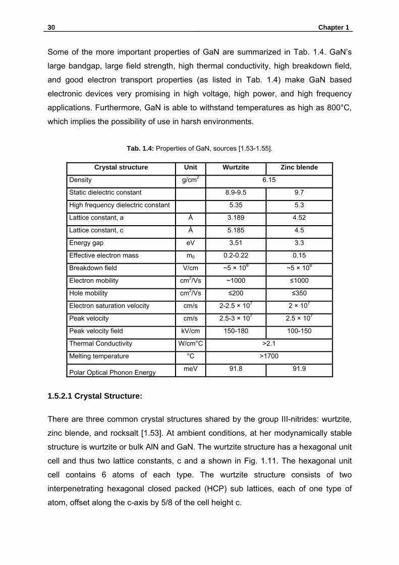
30 Chapter 1
Some of the more important properties of GaN are summarized in Tab. 1.4. GaN’s
large bandgap, large field strength, high thermal conductivity, high breakdown field,
and good electron transport properties (as listed in Tab. 1.4) make GaN based
electronic devices very promising in high voltage, high power, and high frequency
applications. Furthermore, GaN is able to withstand temperatures as high as 800°C,
which implies the possibility of use in harsh environments.
Tab. 1.4: Properties of GaN, sources [1.53-1.55].
Crystal structure Unit Wurtzite Zinc blende
Density g/cm2 6.15
Static dielectric constant 8.9-9.5 9.7
High frequency dielectric constant 5.35 5.3
Lattice constant, a Ǻ 3.189 4.52
Lattice constant, c Ǻ 5.185 4.5
Energy gap eV 3.51 3.3
Effective electron mass m0 0.2-0.22 0.15
Breakdown field V/cm ~5 × 10⁶ ~5 × 10⁶
Electron mobility cm2/Vs ~1000 ≤1000
Hole mobility cm2/Vs ≤200 ≤350
Electron saturation velocity cm/s 2-2.5 × 10⁷ 2 × 10⁷
Peak velocity cm/s 2.5-3 × 10⁷ 2.5 × 10⁷
Peak velocity field kV/cm 150-180 100-150
Thermal Conductivity W/cm°C >2.1
Melting temperature °C >1700
Polar Optical Phonon Energy meV 91.8 91.9
1.5.2.1 Crystal Structure:
There are three common crystal structures shared by the group III-nitrides: wurtzite,
zinc blende, and rocksalt [1.53]. At ambient conditions, at her modynamically stable
structure is wurtzite or bulk AlN and GaN. The wurtzite structure has a hexagonal unit
cell and thus two lattice constants, c and a shown in Fig. 1.11. The hexagonal unit
cell contains 6 atoms of each type. The wurtzite structure consists of two
interpenetrating hexagonal closed packed (HCP) sub lattices, each of one type of
atom, offset along the c-axis by 5/8 of the cell height c.
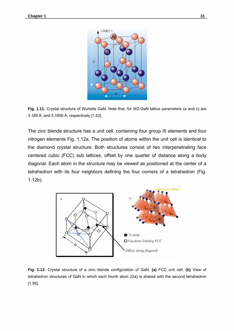
Chapter 1 31
Fig. 1.11: Crystal structure of Wurtzite GaN. Note that, for WZ-GaN lattice parameters (a and c) are
3.189 Å, and 5.1850 Å, respectively [1.53].
The zinc blende structure has a unit cell, containing four group III elements and four
nitrogen elements Fig. 1.12a. The position of atoms within the unit cell is identical to
the diamond crystal structure. Both structures consist of two interpenetrating face
centered cubic (FCC) sub lattices, offset by one quarter of distance along a body
diagonal. Each atom in the structure may be viewed as positioned at the center of a
tetrahedron with its four neighbors defining the four corners of a tetrahedron (Fig.
1.12b).
Fig. 1.12: Crystal structure of a zinc blende configuration of GaN. (a) FCC unit cell. (b) View of
tetrahedron structures of GaN in which each fourth atom (Ga) is shared with the second tetrahedron
[1.56].

32 Chapter 1
1.5.2.2 Growth of GaN layers:
The high melting temperatures and dissociation pressures are the main obstacles in
obtaining large single crystals of III-N compounds, which can serve as substrates for
the homoepitaxial growth (when a material is grown epitaxial on a substrate of the
same material). Therefore, III-V films have been grown heteroepitaxially (if the layer
and the substrate are different materials, like GaN on SiC, GaN on Sapphire, GaN on
Si) on a number of substrates which match more or less close to the lattice constants
and thermal expansion coefficient of III-V nitrides. Remarkable progress in the growth
of high-quality epitaxial layers of III-nitrides by a variety of methods has been recently
achieved.
The most successful among them are metal organic chemical vapor deposition
(MOCVD) and molecular beam epitaxy (MBE). MBE plays an important role in the
development of modern quantum devices because it is able to prepare
compositionally sharp interfaces with atomic layer precision of the designed device
over a large substrate area. Typical MBE growth rate is approximately 0.1-1 mkm/h,
although much higher growth rates can be attained. The MOCVD technique for the
growth of III-nitrides had become mature by the mid of 1990s. Until recently, most
nitride-based devices were fabricated using MOCVD. The development of MBE as a
growth technique for the III-nitrides has been slow enough. This has happened
because the MBE growth is usually performed at relatively low temperatures of 600-
800°C. The molecular nitrogen is inert and does not chemisorb on the III-N surface
below 950°C due to the strong N-N bond of the nitrogen molecule. Therefore, atomic
nitrogen or nitrogen containing molecule with weaker bonds should be provided for
the III-nitride epitaxy. Several modifications to conventional MBE method have been
implemented for III-nitride growth: growth with ammonia or hydrazine, plasma-
assisted MBE (PAMBE), metalorganic MBE (MOMBE), pulsed laser deposition
(PLD), etc. Amongother methods, radio-frequency (RF) and electron-cyclotron
resonance (ECR) plasma sources are the most commonly employed devices to
activate the neutral nitrogen species in the MBE environment.
1.5.2.3 GaN doping:
Conductivity modulation can be achieved in GaN by doping with donors such as Si,
O and Ge or with acceptor such as Mg, Zn, and Be. Si and Mg are primarily the n-

Chapter 1 33
type and p-type dopands of choice, respectively. Si-doping has been successfully
used to produce films with electron concentration from low 1017 to the mid 1019 cm-3
with almost complete room temperature donor activation. For example, catalytic/GaN
Schottky diodes used as gas sensors use GaN doped with Si where the electron
concentration is usually in the range from 1016 to 1018 cm-3. It will be seen that
Pt/GaN gas sensors based on Schottky diodes discussed in the second chapter use
Si-doping with concentration of ~ 1× 1017 cm-3.
The ionization energy of the Si level (temperature dependent) in GaN was
reported approx. 27 meV [1.57], and 12-17 meV as measured by Hall effect [1.58].
The solubility of Si in GaN is high, of the order of 1020 cm-3. Therefore, Si is suitable
for III-Nitrides doping and most frequently used.
References:
[1.1] J. W. Gardner, P. N. Bartlett, “Electronic noses-Principles and Applications”,
Oxford University Press 1999.
[1.2] J. W. Gardner, K. C. Persaud (eds.), “Electronic noses and olfaction 2000”,
Proceedings of 7th Symposium on Olfaction and Electronic Noses, Brighton, UK, July
2000, IOP Publishing (2001).
[2.3] P. Mielle, F. Marquis, C. Latrasse, "Electronic noses: specify or disappear”,
Sensors and Actuators B 69 (2000) 287-294.
[1.4] S. Capone, A. Forleo, L. Francioso, R. Rella, P. Siciliano, J. Spadavecchia, D.
S. Presicce, A. M. Taurino, “Solid state gas sensors: state of the art and future
activities”, Journal of Optoelectronics and Advanced Materials 5 (2003) 1335-1348.
[1.5] M. J. Madou, S. R. Morrison (eds.), “Chemical sensing with solid state devices”,
Academic Press, New York, 1989.
[2.6] A. Mandelis, C. Christofides (eds.), “Physics, Chemistry and technology of solid
state gas sensor devices”, Wiley (1993).
[1.7] P. T. Moseley, “Solid state gas sensors“, Meas. Sci. Technol. 8 (1997) 223-237.
[1.8] I. Lundström, “Approaches and mechanisms to solid state based sensing”,
Sensors and Actuators B 35-36 (1996) 11-19.
[1.9] J. Tiffany, R. E. Cavicchi, and S. Semancik, “Microarray study of temperature
dependent sensitivity and selectivity of metal/oxide sensing interfaces”, Proc. SPIE
4205 (2000) 240-247.
34 Chapter 1
[1.10] J. W. Gardner and P. N. Barlett, “A brief history of electronic noses”, Sensors
and Actuators B 18 (1994) 210-211.
[1.11] M. C. Horrillo, J. Getino, L. Ares, J. I. Robla, I. Sayago, and F. J.
Gutierrez,“Measurements of VOCs with a Semiconductor Electronic Nose”, J.
Electrochem. Soc. 145 (1998) 2486-2489.
[1.12] T. C. Pearce, S. S. Schiffman, H. T. Nagle, and J. W. Gardner, Handbook of
Machine Olfaction, Wiley-VCH, Weinheim (2003).
[1.13] K. Arshak, E. Moore, G.M. Lyons, J. Harris and S. Clifford, “A review of gas
sensors employed in electronic nose applications”, Sensor Review 24 (2004)181-
198.
[1.14] W. Göpel, J. Hesse, and J. N. Zemel (eds.), ”Magnetic Sensors“, VCH,
Weinheim, 1989.
[1.15] J. Fraden. “AIP handbook of modern sensors”, American Institute of Physics,
New York, 1993.
[1.16] V. Demarne and R. Sanjin, “Thin film semiconducting metal oxide gas
sensors”. In: G. Sberveglieri. (Ed), “Gas Sensors”, Kluwer Academic Publishers,
Dordrecht, NL, (1992) 89-116.
[1.17] D. Hodgins, “The electronic nose: Sensor array-based instruments that
emulate the human nose”. In: R. Marsili (Ed), “Techniques for analyzing food aroma.
New York”, Marcel Dekker Inc., New York, US, (1997) 331-371.
[1.18] C. M. Mari and G. B. Barbi, “Electrochemical gas sensors”. In: G. Sberveglieri
(Ed), Gas Sensors, Kluwer Academic Publishers, Dordrecht, NL, (1992) 29-364.
[1.19] N. Tagushi, Jpn. Patent 45-38200 (1962).
[1.20] N. N. Greenwood and A. Earnshaw, Silicium. In: N. N. Greenwood and A.
Earnshaw (Eds), Chemie der Elemente. Weinheim: VCH Verlag, pp. 424-426 (1988).
[1.21] K. J. Albert and N. S. Lewis, “Cross-reactive chemical sensor arrays”, Chem.
Rev. 100 (2000) 2595-2626.
[1.22] E. Schaller, J. O. Bosset, and F. Escher, “’Electronic noses’ and their
application to food”, Lebensmittel-Wissenschaft und-Technologie 31 (1998) 305-316.
[1.23] W. Schmid, N. Barsan and U. Weimar, “Sensing of hydrocarbons with tin oxide
sensors: possible reaction path as revealed by consumption measurements”,
Sensors and Actuators B 89 (2003) 232-236.
Chapter 1 35
[1.24] S. Hamakawa, L. Li, A. Li and E. Iglesia, “Synthesis and hydrogen permeation
properties of membranes based on dense SrCe0.95Yb0.05O3-α thin films”, Solid State
Ionics 148 (2002) 71-81.
[1.25] W-H. Tao and C-H. Tsai, “H2S sensing properties of noble metal doped WO3
thin film sensor fabricated by micromachining”, Sensors and Actuators B 81 (2002)
237-247.
[1.26] G. Dai, “A study of the sensing properties of thin film sensor to trimethylamine”,
Sensors and Actuators B 53 (1998) 8-12.
[1.27] C. O. Park, S. A. Akbar, J. Hwang, “Selective gas detection with catalytic filter“,
Mater. Chem. Phys. 75, (2002) 56-60.
[1.28] I. Heberle, A. Liebminger, U. Weimar, W. Göpel, ”Optimised sensor arrays with
chromatographic preseparation: characterisation of alcoholic beverages“, Sensors
and Actuators B 68, (2000) 53-57.
[1.29] M. Penza, G. Cassano, F. Tortorella, and G. Zaccaria, “Classification of food,
beverages and perfumes by WO3 thin-film sensors array and pattern recognition
techniques”, Sensors and Actuators B 73 (2001) 76-87.
[1.30] D. S. Vlachos, C. A. Papadopolos, and J. A. Avaritsiotis, “Characterisation of
the catalyst-semiconductor interaction mechanism in metal-oxide gas sensors“,
Sensors and Actuators B 44 (1997) 458-461.
[1.31] P. T. Moseley, ”Materials selection for semiconductor gas sensors“, Sensors
and Actuators B 6 (1992) 149-156.
[1.32] C. Distante, M. Leo, P. Siciliano, K. Persaud, “On the study of feature
extraction methods for an electronic nose“, Sensors and Actuators B 87 (2002) 274-
288.
[1.33] S. Capone, Ph.D. Thesis, University of Lecce, (2001).
[1.34] Andrew P. Lee, Brian J. Reedy, “Temperature modulation in semiconductor
gas sensing“, Sensors and Actuators B 60 (1999) 35-42.
[1.35] I. Eisele, T. Doll and M. Burgmair, “Low power gas detection with FET
sensors”, Sensors and Actuators B 78 (2001) 9-25.
[1.36] E-L. Kalman, A. Lofvendahl, F. Winquist and I. Lundström, “Classification of
complex gas mixtures from automotive leather using an electronic nose”, Analytica
Chimica Acta 403 (2000) 31-38.
[1.37] H. T. Nagle, R. Gutierrez-Osuna and S. S. Schiffman, “The how and why of
electronic hoses”, IEEE Spectrum 35 (1998) 22-31.
36 Chapter 1
[1.38] J. V. Hatfield, J. A. Covington and J. W. Gardner, “GasFETs incorporating
conducting polymers as gate materials”, Sensors and Actuators B 65 (2000) 253-
256.
[1.39] J. A. Covington, J. W. Gardner, D. Briand and N. F. de Rooij, “A polymer gate
FET sensor array for detecting organic vapours”, Sensors and Actuators B 77 (2001)
155-62.
[1.40] D. Rutven, “Principles of adsorption and adsorption processes”, Wiley-
Interscience, New York, (1984).
[1.41] W. Göpel, “Solid state chemical sensors: Atomistic models and research
trends”, Sensors and Actuators 16 (1989) 167-193.
[1.42] D. Shaw, “Introduction to colloid & surface chemistry”, Butterworth-Heineman,
Oxford, (1992).
[1.43] R. I. Mase, “Principles of adsorption and reaction on solid surfaces”, Wiley,
New York (1996).
[1.44] I. Langmuir, “The Adsorption of gases on plane surface of glass, mica and
platinum”, Journal of the American Chemical Society 40 (1918) 1361-1403.
[1.45] http://www.chem.qmul.ac.uk/surfaces/scc/scat3_4.htm.
[1.46] S. J. Gentry, and T. A. Jones, “The role of catalysis in solid-state gas sensors”,
Sensors and Actuators 16 (1986) 141-163.
[1.47] D. Kohl, “The role of noble metals in the chemistry of solid-state gas sensors”,
Sensors and Actuators B 1 (1990) 158-165.
[1.48] J. A. Powell, P. Pirouz, and W. J. Choyke, “Growth and characterization of
silicon carbide polytypes for electronic applications”, Semiconductor Interfaces,
Microstructures, and Devices: Properties and Applications, Z. C. Feng, Eds., Institute
of Physics Publishing, Bristol, United Kingdom, 1993, 257.
[1.49] A. Itoh, and H. Matsunami, “Single crystal growth of SiC and electronic
devices“, Critical reviews in solid state and Material Science 22 (1997) 111-197.
[1.50] W. J. Choyke, H. Matsunami, and G. Pensl, “Silicon Carbide - A Review of
fundamental questions and applications to current device technology”, Wiley-VCH,
Berlin, 1997.
[1.51] D. J. Larkin, “SiC dopant incorporation control using site-competition CVD”,
phys. stat. sol. (b) 202 (1997) 305-320.
[1.52] P. Jamet, S. Dimitrijev, and P. Tanner. “Effects of nitridation in gate oxides
grown on 4H-SiC”, J. Appl. Phys. 90 (2001) 5058-5063.

Chapter 1 37
[1.53] O. Ambacher, ”Growth and applications of group III-nitrides“, J. Phys. D: Appl.
Phys. 31 (1998) 2653-2710.
[1.54] H. Harima, “Properties of GaN and related compounds studied by means of
Raman scattering“, Journal of physics: Cond. Matter 14 (2002) R967-R993.
[1.55] J. G. Kim, A. C. Frenkel, T. Liu, and R. M. Park, “Growth of molecular beam
epitaxy and electrical characteristics of Si-doped zinc blende and wurtzite GaN films
deposited on beta-SiC coated (001) Si substrates”, Appl. Phys. Lett. 65 (1994) 91-93.
[1.56] A. M. Malik,”Technology and physics of gate recessed GaN/AlGaN FETs”,
Masters thesis, Stuttgart University, Stuttgart, Germany, 2003.
[1.57] D. K. Gaskill, A. E. Wickenden, K. Doverspike, B. Tadayon, and L. B. Rowland,
”The effect of organometallic vapor phase epitaxial growth conditions on wurtzite
GaN electron transport properties”, J. Electron. Mater. 24 (1995) 1525-1530.
[1.58] W. Götz, N. M. Johnson, C. Chen, H. Liu, C. Kuo, and w. Imler, “Activation
energies of Si donors in GaN”, Appl. Phys. Lett. 68 (1994) 3144-3146.

38 Chapter 1

Chapter 2 39
Chapter 2
2. Study of Hydrogen-Sensing Performances of Pt/GaN Based Schottky Diodes
2.1 Introduction:
Recently, the use of molecular hydrogen has gained a considerable attention in
industrial fabrication processes, medical installations, laboratories and fuelled motor
vehicles. For safety reasons, the determination of hazardous hydrogen concentration
in air (4.65-74.5%) is an important issue in many areas of human activity. Hence, it is
encouraging and interesting to fabricate a hydrogen sensor having high sensitivity,
high accuracy, chemical selectivity, small size, short response times, reproducibility,
wide operating temperature regimes, simple operation, ease to fabrication, and,
finally, low cost.
Lundström et al. [2.1] reported on the hydrogen detector fabricated using a Si-
based Pd gate field-effect transistor (FET). However, high-temperature operation of
silicon-based FETs is limited to the range below 150°C. High band gap
semiconductors, especially GaN, were proposed to extend this range to improve the
sensitivity and the response time. GaN-based wide band gap semiconductors have
become one of the most extensively studied materials and rapid progress has been
demonstrated in both optical and electrical devices. Due to their wide band gap and
good thermal and chemical stability, GaN based semiconductor materials are also
very promising for high temperature gas sensor devices. In addition the small Fermi
level pinning characteristics of GaN are also important features that may lead in high
gas sensitivity.
Moreover, it was recently demonstrated that a Pt/GaN Schottky contact is very
sensitive to the hydrogen exposure. Pt/GaN Schottky diodes [2.2] and AlGaN/GaN
transistors [2.3] have been shown to detect hydrogen and hydrocarbon molecules.
These devices have the same principles of operation as the hydrogen-sensitive FET
sensors based on Si [2.1] and SiC [2.4-2.6]. On the Pt surface, molecular hydrogen is
dissociated into the atomic hydrogen, which diffuses through the Pt contact and is
adsorbed at the metal-semiconductor interface. Hydrogen accumulation at the
interface changes the work function of the metal gate and therefore the barrier height
of the Schottky contact. This effect can be proven by measuring current-voltage (I-V)
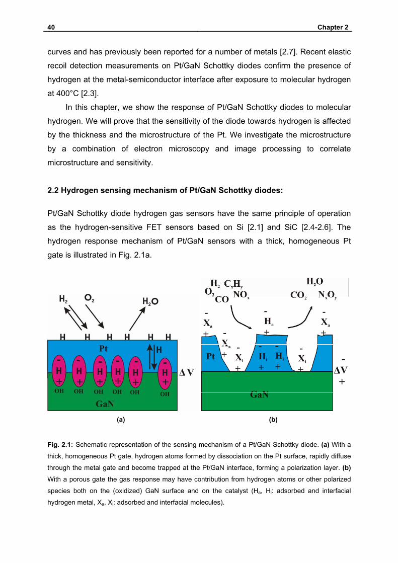
40 Chapter 2
curves and has previously been reported for a number of metals [2.7]. Recent elastic
recoil detection measurements on Pt/GaN Schottky diodes confirm the presence of
hydrogen at the metal-semiconductor interface after exposure to molecular hydrogen
at 400°C [2.3].
In this chapter, we show the response of Pt/GaN Schottky diodes to molecular
hydrogen. We will prove that the sensitivity of the diode towards hydrogen is affected
by the thickness and the microstructure of the Pt. We investigate the microstructure
by a combination of electron microscopy and image processing to correlate
microstructure and sensitivity.
2.2 Hydrogen sensing mechanism of Pt/GaN Schottky diodes:
Pt/GaN Schottky diode hydrogen gas sensors have the same principle of operation
as the hydrogen-sensitive FET sensors based on Si [2.1] and SiC [2.4-2.6]. The
hydrogen response mechanism of Pt/GaN sensors with a thick, homogeneous Pt
gate is illustrated in Fig. 2.1a.
(a) (b)
Fig. 2.1: Schematic representation of the sensing mechanism of a Pt/GaN Schottky diode. (a) With a
thick, homogeneous Pt gate, hydrogen atoms formed by dissociation on the Pt surface, rapidly diffuse
through the metal gate and become trapped at the Pt/GaN interface, forming a polarization layer. (b) With a porous gate the gas response may have contribution from hydrogen atoms or other polarized
species both on the (oxidized) GaN surface and on the catalyst (Ha, Hi: adsorbed and interfacial
hydrogen metal, Xa, Xi: adsorbed and interfacial molecules).
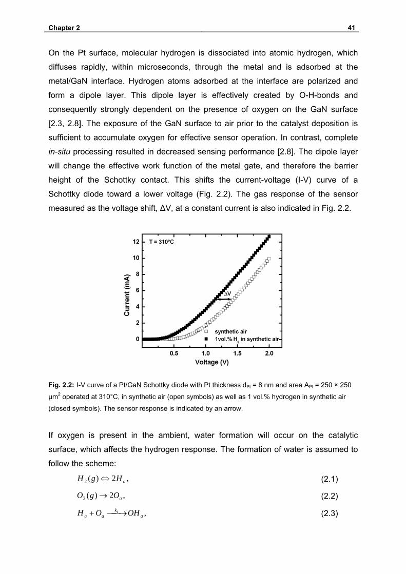
Chapter 2 41
On the Pt surface, molecular hydrogen is dissociated into atomic hydrogen, which
diffuses rapidly, within microseconds, through the metal and is adsorbed at the
metal/GaN interface. Hydrogen atoms adsorbed at the interface are polarized and
form a dipole layer. This dipole layer is effectively created by O-H-bonds and
consequently strongly dependent on the presence of oxygen on the GaN surface
[2.3, 2.8]. The exposure of the GaN surface to air prior to the catalyst deposition is
sufficient to accumulate oxygen for effective sensor operation. In contrast, complete
in-situ processing resulted in decreased sensing performance [2.8]. The dipole layer
will change the effective work function of the metal gate, and therefore the barrier
height of the Schottky contact. This shifts the current-voltage (I-V) curve of a
Schottky diode toward a lower voltage (Fig. 2.2). The gas response of the sensor
measured as the voltage shift, ΔV, at a constant current is also indicated in Fig. 2.2.
Fig. 2.2: I-V curve of a Pt/GaN Schottky diode with Pt thickness dPt = 8 nm and area APt = 250 × 250
μm2 operated at 310°C, in synthetic air (open symbols) as well as 1 vol.% hydrogen in synthetic air
(closed symbols). The sensor response is indicated by an arrow.
If oxygen is present in the ambient, water formation will occur on the catalytic
surface, which affects the hydrogen response. The formation of water is assumed to
follow the scheme:
,2)(2 aHgH ⇔ (2.1)
,2)(2 aOgO → (2.2)
,1a
kaa OHOH ⎯→⎯+ (2.3)
42 Chapter 2
).(22 gOHOHH k
aa ⎯→⎯+ (2.4)
If the device is operated at an elevated temperature (>100°C), which desorbs the
formed water from the surface.
However, Pt/GaN sensors exhibit sensitivity to both oxidizing and reducing
gases [2-9, 2-10]. Since hydrogen is the only specie that can diffuse through the
catalyst, an alternating transport mechanism was proposed [2-10] taken the porosity
of Pt into account (Fig. 2.1b). At porous Pt gates, patches of GaN are directly
exposed to the gas ambient thus allowing a direct interaction of the test gases with
the polar (oxidized) GaN surface leading to polarized adsorbates. This model was
confirmed by the investigation of the CO sensitivity of Pt/GaN Schottky diodes [2.11].
By decreasing the catalyst thickness and thermal annealing, the response on CO
was increased due to the surface restructuring of the Pt film, which opens channels
(pores) for gas transports towards a free GaN surface.
2.3 Theory of Schottky diode:
Before the investigation of the hydrogen sensing performance of the Schottky diode,
a theoretical understanding of its functionality is necessary. It is also necessary to
know how its parameters can be calculated (extracted) from I-V and C-V curves. The
most important parameters of the Schottky diodes used as H2 gas sensors are: the
barrier height qΦB, ideality factor n, saturation current density Js, and the series
resistance Rs since the exposure to H2 influence them.
2.3.1 Metal-semiconductor contact:
In 1874, i.e., 133 years ago Braun [2.12] first reported on rectifying metal-
semiconductor contacts. Schottky et al. explained this behavior by space-charge
layers on the semiconductor side of the interface that are depleted of mobile majority
carriers [2.13]. The most characteristic parameter of such a Schottky contact is its
barrier height, i.e., the energy separation between the Fermi level and the edge of
the majority carrier band right at the interface. Fig. 2.3a shows the energy band
diagram of a metal adjacent to n-type semiconductor.
The metal work function is generally different from the semiconductor work
function. The work function is the energy difference between the Fermi level EF and
the vacuum level Evacuum (qΦm for the metal and qΦs for the semiconductor).

Chapter 2 43
(a) (b)
Fig. 2.3: Energy band diagram of metal contact to n-type semiconductor. (a) Neutral materials
separated from each other. (b) Thermal equilibrium situation after contact has been made.
Work functions of metals that are commonly used for fabrication of metal-
semiconductor contacts are listed in the Tab. 2.1. From these elements Pt, Ni, Pd,
and Au are commonly used for Schottky contact processing. Pd and Pt have very
large work functions which makes them ideal for use as Schottky contacts on most n-
type semiconductors, including n-type GaN. They are also useful for contacts
because of their resistance to oxidation and corrosion. In this work Pt was selected to
serve as a catalytic metal due to its high work function and stability during the
exposure to hydrogen.
Tab. 2.1: Work functions of metals commonly used for fabrication of metal-semiconductor contacts.
Metal Work function (eV) Metal Work function (eV)
Pt 5.65 Zn 4.33
Ni 5.15 Al 4.28
Pd 5.12 Ag 4.26
Au 4.65 Pb 4.25
Cu 4.65 Ta 4.25
W 4.55 Cd 4.22
Cr 4.5 Ga 4.2
Hg 4.49 In 4.12
Sn 4.42 Zr 4.05
Ti 4.33 Cs 2.14

44 Chapter 2
The electron affinity qχs is the energy difference between the conduction band edge
and the vacuum level. When metal is making intimate contact with a semiconductor,
the Fermi levels in the two materials must be coincident at thermal equilibrium. In
addition, the vacuum level must be continuous. These tow requirements determine a
unique energy band diagram for the ideal metal-semiconductor contact as shown in
Fig.2.3b. For this ideal case the Barrier height qΦBn is simply the difference between
the metal work function and the electron affinity of the semiconductor:
( )χ−Φ=Φ mBn qq . (2.5)
Elemental Pt Schottky diodes exhibit ideal Schottky behaviour and have a reasonably
high barrier height of ~ 1 eV on n-GaN [2.14, 2.15]. For an ideal contact between a
metal and a p-type semiconductor, the Barrier height qΦBp can be determined using
a similar procedure:
( )χ−Φ−=Φ mgBp qEq . (2.6)
where Eg is the bandgap of the semiconductor, Therefore, for a given semiconductor
and for any metal, the sum of the barrier heights on n-type and p-type substrates is
expected to be equal to the bandgap:
gBpBn Eq =Φ+Φ )( . (2.7)
The energy band diagrams for metal on n-type semiconductor are shown in Fig. 2.4
for different biasing conditions. The built-in potential Vbi for the n-type semiconductor
is given by:
nBnbi VV −Φ= , (2.8)
where Vn is the potential difference between the Fermi level and conduction band
edge EC.
(a) (b)
Fig. 2.4: Energy band diagram of metal contact to n-type semiconductor under different biasing
conditions. (a) Forward bias. (b) Reverse bias.
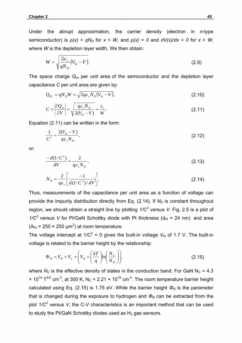
Chapter 2 45
Under the abrupt approximation, the carrier density (electron in n-type
semiconductor) is ρ(x) = qND for x < W, and ρ(x) = 0 and dV(x)/dx = 0 for x > W,
where W is the depletion layer width, We then obtain:
( )VVqN
W biD
s −=ε2
. (2.9)
The space charge Qsc per unit area of the semiconductor and the depletion layer
capacitance C per unit area are given by:
( )VVNqWqNQ biDsDSC −== ε2 , (2.10)
WVV
NqV
QC s
bi
Dssc εε=
−=
∂∂
=)(2
. (2.11)
Equation (2.11) can be written in the form:
Ds
bi
NqVV
C ε)(21
2
−= , (2.12)
or:
Ds NqdV
Cdε
2)/1( 2
=− , (2.13)
⎥⎦
⎤⎢⎣
⎡ −=
dVCdqN
sD /)/1(
122ε
. (2.14)
Thus, measurements of the capacitance per unit area as a function of voltage can
provide the impurity distribution directly from Eq. (2.14). If ND is constant throughout
region, we should obtain a straight line by plotting 1/C2 versus V. Fig. 2.5 is a plot of
1/C2 versus V for Pt/GaN Schottky diode with Pt thickness (dPt = 24 nm) and area
(APt = 250 × 250 µm2) at room temperature.
The voltage intercept at 1/C2 = 0 gives the built-in voltage Vbi of 1.7 V. The built-in
voltage is related to the barrier height by the relationship:
⎟⎟⎠
⎞⎜⎜⎝
⎛⎟⎟⎠
⎞⎜⎜⎝
⎛⎟⎟⎠
⎞⎜⎜⎝
⎛+=+=Φ
D
CbinbiB N
Nq
kTVVV ln , (2.15)
where NC is the effective density of states in the conduction band. For GaN NC = 4.3
× 1014 T3/2 cm-3, at 300 K, NC = 2.21 × 1018 cm-3. The room temperature barrier height
calculated using Eq. (2.15) is 1.75 eV. While the barrier height ΦB is the parameter
that is changed during the exposure to hydrogen and ΦB can be extracted from the
plot 1/C2 versus V, the C-V characteristics is an important method that can be used
to study the Pt/GaN Schottky diodes used as H2 gas sensors.
46 Chapter 2
Fig. 2.5: Plot of 1/C2 versus applied voltage for a Pt/GaN Schottky diode with dPt = 40 nm and APt =
250 × 250 μm2.
2.3.2 Current-Voltage Characteristics:
The current transport in metal-semiconductor contacts is due mainly to majority
carriers, in contrast to p-n junctions, where current transport is due mainly to minority
carriers. The current can be transported in various ways under forward bias
conditions as shown in Fig. 2.6. The four processes are [2.16]:
(a) emission of electrons from the semiconductor over the top of the barrier into the
metal. This is the dominant process for Schottky diodes with moderately doped
semiconductors operating at or near room temperature); (b) quantum mechanical
tunneling through the barrier in heavily doped semiconductors; (c) electron-hole
recombination in the space-charge region; and (d) recombination in the neutral
region (equivalent hole injection from the metal to the semiconductor).
The transport of electrons over the potential barrier have been discussed in terms of
thermionic emission diffusion by Crowell and Sze [2.17], who have shown that the
complete expression of the current density-voltage (J-V) characteristics for the
Schottky diode is:
⎥⎦
⎤⎢⎣
⎡⎟⎠⎞
⎜⎝⎛ −= 1exp
kTqVJJ sideal , (2.16)
where the saturation current Is and the saturation current density Js are defined by:

Chapter 2 47
⎟⎠⎞
⎜⎝⎛ Φ−=⎟⎟
⎠
⎞⎜⎜⎝
⎛=
kTqTA
AIJ B
d
ss exp2** , (2.17)
The quantities Ad , A**, T, q, k and ΦB are the diode area, the effective Richardson
constant, temperature in Kelvin, the electronic charge, Boltzmann’s constant and the
barrier height, respectively.
Fig. 2.6: Four basic transport processes in forward-biased Schottky barrier on an n-type
semiconductor [2.16].
The barrier height is commonly calculated from the saturation current Is, determined
by the extrapolation of the log(I) versus V to V = 0. The current axis intercept for the
staight-line portion of this semi-logarithmic plot at V = 0 is given by Is. The barrier
height ФB is calculated from Is in Eq. (2.17) according to
⎟⎠⎞
⎜⎝⎛=⎟⎟
⎠
⎞⎜⎜⎝
⎛=Φ 2**
2**
lnlnTA
Jq
kTI
TAAq
kT s
s
dB . (2.18)
The ideality factor n is introduced to describe the deviation of the experimental I-V
data from the ideal TE model using the definition:
1ln −
⎟⎠⎞
⎜⎝⎛=
dVId
kTqn . (2.19)
However, a deviation from the ideal behaviour is frequently observed and the I-V
curves cannot be fitted by Eq. (2.16). The Schottky effect, series and parallel
resistance, the presence of other mechanisms and inhomogeneous Schottky barrier
heights (SBHs) have been established by several authors as the most important
causes of non-ideal behaviour. Regarding the linear increase of barrier height with
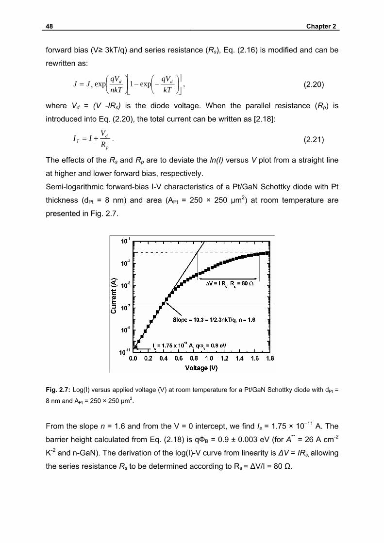
48 Chapter 2
forward bias (V≥ 3kT/q) and series resistance (Rs), Eq. (2.16) is modified and can be
rewritten as:
⎥⎦
⎤⎢⎣
⎡⎟⎠⎞
⎜⎝⎛−−⎟
⎠⎞
⎜⎝⎛=
kTqV
nkTqV
JJ dds exp1exp , (2.20)
where Vd = (V -IRs) is the diode voltage. When the parallel resistance (Rp) is
introduced into Eq. (2.20), the total current can be written as [2.18]:
p
dT R
VII += . (2.21)
The effects of the Rs and Rp are to deviate the ln(I) versus V plot from a straight line
at higher and lower forward bias, respectively.
Semi-logarithmic forward-bias I-V characteristics of a Pt/GaN Schottky diode with Pt
thickness (dPt = 8 nm) and area (APt = 250 × 250 µm2) at room temperature are
presented in Fig. 2.7.
Fig. 2.7: Log(I) versus applied voltage (V) at room temperature for a Pt/GaN Schottky diode with dPt =
8 nm and APt = 250 × 250 μm2.
From the slope n = 1.6 and from the V = 0 intercept, we find Is = 1.75 × 10⁻¹¹ A. The
barrier height calculated from Eq. (2.18) is qФB = 0.9 ± 0.003 eV (for A** = 26 A cm-2
K-2 and n-GaN). The derivation of the log(I)-V curve from linearity is ΔV = IRs, allowing
the series resistance Rs to be determined according to Rs = ΔV/I = 80 Ω.
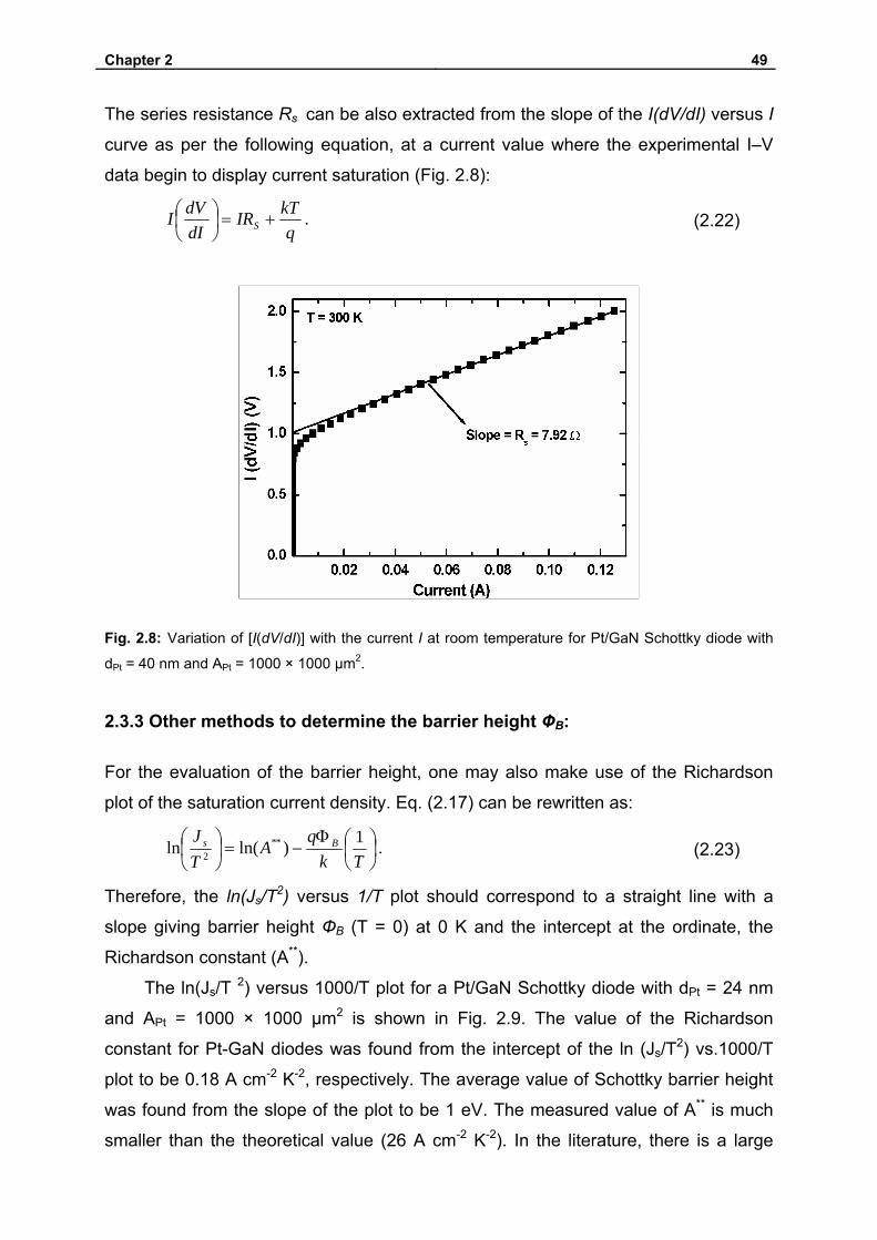
Chapter 2 49
The series resistance Rs can be also extracted from the slope of the I(dV/dI) versus I
curve as per the following equation, at a current value where the experimental I–V
data begin to display current saturation (Fig. 2.8):
q
kTIRdIdVI S +=⎟
⎠⎞
⎜⎝⎛ . (2.22)
Fig. 2.8: Variation of [I(dV/dI)] with the current I at room temperature for Pt/GaN Schottky diode with
dPt = 40 nm and APt = 1000 × 1000 μm2.
2.3.3 Other methods to determine the barrier height ФB:
For the evaluation of the barrier height, one may also make use of the Richardson
plot of the saturation current density. Eq. (2.17) can be rewritten as:
⎟⎠⎞
⎜⎝⎛Φ
−=⎟⎠⎞
⎜⎝⎛
TkqA
TJ Bs 1)ln(ln **
2 . (2.23)
Therefore, the ln(Js/T2) versus 1/T plot should correspond to a straight line with a
slope giving barrier height ФB (T = 0) at 0 K and the intercept at the ordinate, the
Richardson constant (A**).
The ln(Js/T 2) versus 1000/T plot for a Pt/GaN Schottky diode with dPt = 24 nm
and APt = 1000 × 1000 μm2 is shown in Fig. 2.9. The value of the Richardson
constant for Pt-GaN diodes was found from the intercept of the ln (Js/T2) vs.1000/T
plot to be 0.18 A cm-2 K-2, respectively. The average value of Schottky barrier height
was found from the slope of the plot to be 1 eV. The measured value of A** is much
smaller than the theoretical value (26 A cm-2 K-2). In the literature, there is a large
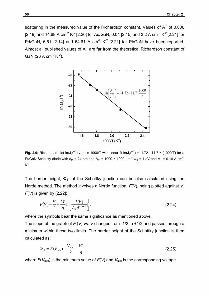
50 Chapter 2
scattering in the measured value of the Richardson constant. Values of A** of 0.006
[2.19] and 14.68 A cm-2 K-2 [2.20] for Au/GaN, 0.04 [2.15] and 3.2 A cm-2 K-2 [2.21] for
Pd/GaN, 6.61 [2.14] and 64.61 A cm-2 K-2 [2.21] for Pt/GaN have been reported.
Almost all published values of A** are far from the theoretical Richardson constant of
GaN (26 A cm-2 K-2).
Fig. 2.9: Richadrson plot ln(Js/T2) versus 1000/T with linear fit ln(Js/T2) = -1.72 - 11.7 × (1000/T) for a
Pt/GaN Schottky diode with dPt = 24 nm and APt = 1000 × 1000 μm2, ФB = 1 eV and A** = 0.18 A cm-2
K-2.
The barrier height, ΦB, of the Schottky junction can be also calculated using the
Norde method. The method involves a Norde function, F(V), being plotted against V.
F(V) is given by [2.22]:
( ) ⎥⎦
⎤⎢⎣
⎡−= ∗∗ 2
)(ln2 TAA
VIq
kTVVFd
, (2.24)
where the symbols bear the same significance as mentioned above.
The slope of the graph of F (V) vs. V changes from -1/2 to +1/2 and passes through a
minimum within these two limits. The barrier height of the Schottky junction is then
calculated as:
q
kTVVFB −+=Φ
2)( min
min , (2.25)
where F(Vmin) is the minimum value of F(V) and Vmin is the corresponding voltage.
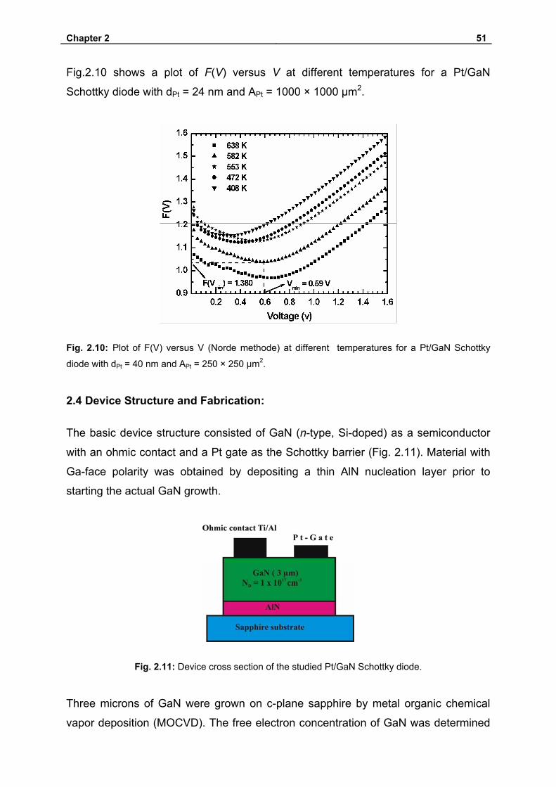
Chapter 2 51
Fig.2.10 shows a plot of F(V) versus V at different temperatures for a Pt/GaN
Schottky diode with dPt = 24 nm and APt = 1000 × 1000 μm2.
Fig. 2.10: Plot of F(V) versus V (Norde methode) at different temperatures for a Pt/GaN Schottky
diode with dPt = 40 nm and APt = 250 × 250 μm2.
2.4 Device Structure and Fabrication:
The basic device structure consisted of GaN (n-type, Si-doped) as a semiconductor
with an ohmic contact and a Pt gate as the Schottky barrier (Fig. 2.11). Material with
Ga-face polarity was obtained by depositing a thin AlN nucleation layer prior to
starting the actual GaN growth.
Fig. 2.11: Device cross section of the studied Pt/GaN Schottky diode.
Three microns of GaN were grown on c-plane sapphire by metal organic chemical
vapor deposition (MOCVD). The free electron concentration of GaN was determined
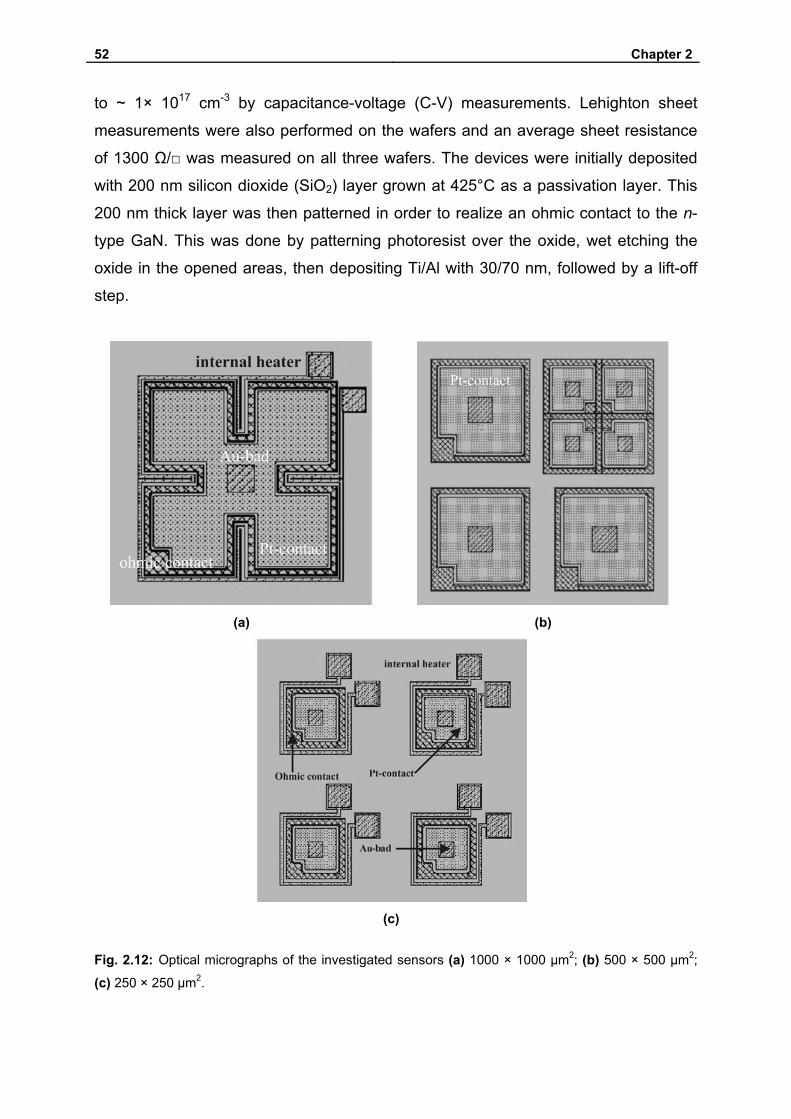
52 Chapter 2
to ~ 1× 1017 cm-3 by capacitance-voltage (C-V) measurements. Lehighton sheet
measurements were also performed on the wafers and an average sheet resistance
of 1300 Ω/ was measured on all three wafers. The devices were initially deposited
with 200 nm silicon dioxide (SiO2) layer grown at 425°C as a passivation layer. This
200 nm thick layer was then patterned in order to realize an ohmic contact to the n-
type GaN. This was done by patterning photoresist over the oxide, wet etching the
oxide in the opened areas, then depositing Ti/Al with 30/70 nm, followed by a lift-off
step.
(a)
(b)
(c)
Fig. 2.12: Optical micrographs of the investigated sensors (a) 1000 × 1000 µm2; (b) 500 × 500 µm2;
(c) 250 × 250 µm2.
Chapter 2 53
The ohmic contact was annealed at 800°C for 1 min in nitrogen atmosphere to
reduce contact resistance. Next, the Schottky contact was made in the same fashion.
Three different sets Schottky diodes were processed with either 8, 24, or 40 nm thick
continuous layer of platinum as Schottky contacts evaporated using e-beam
evaporation. The GaN surface was treated with buffered oxide etch (BOE) (7:1) to
remove the surface oxide before evaporation. An internal heater consisting of Ti/Al/Ti
with 20/100/80 nm was fabricated around the device to facilitate resistive heating.
Finally, gold bond pads were evaporated on the ohmic and Schottky contacts, then
the devices were wire bonded to a 16 pin TO-8 header package. An external heating
element was presented in this package to increase the temperature of the device up
to 365°C during operation. The active gate area was varied between 250 × 250 µm2
and 1000 × 1000 µm2. The optical micrographs of the investigated sensors are
shown in Fig. 2.12.
2.5. Experiments:
2.5.1 AES and SEM measurements (surface and interface measurements):
The surface and interface properties of Pt/GaN Schottky diode gas sensors studied
in this chapter are investigated using Auger Electron Spectroscopy (AES), Scanning
Electron Microscopy (SEM). The AES system used for this work was a Riber ASC
2000 (Fig. 2.13) equipped with a differential pumped ion gun VG X5.
The Auger sputter depth profiling procedures were carried out in the Auger
spectrometer Riber ASC 2000 (Fig.2.13) equipped with differential pumped ion gun
VG X5. The electron gun was operated at 3 keV with the current 1 µA. The spot size
was approximately 20 µm. The emitted electrons were analysed by cylindrical mirror
analyser with coaxially placed electron gun working with resolution 0.3%. The Auger
transition were recorded in the differentiated mode. The ion gun was operated at 1
keV, argon was used as the sputtering gas. The ion beam was rastered over an area
of some mm2. The ion beam current density was approximately 42 µA/cm2 measured
perpendicular to the ion beam direction. The angle between the electron and ion gun
was fixed in the spectrometer. For sputtering under 60° with respect to the surface
normal the angle between surface normal and the electron beam was 22°.
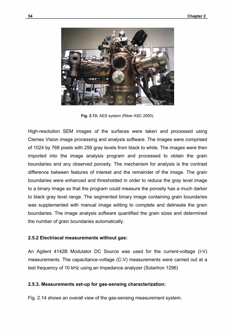
54 Chapter 2
Fig. 2.13: AES system (Riber ASC 2000).
High-resolution SEM images of the surfaces were taken and processed using
Clemex Vision image processing and analysis software. The images were comprised
of 1024 by 768 pixels with 256 gray levels from black to white. The images were then
imported into the image analysis program and processed to obtain the grain
boundaries and any observed porosity. The mechanism for analysis is the contrast
difference between features of interest and the remainder of the image. The grain
boundaries were enhanced and thresholded in order to reduce the gray level image
to a binary image so that the program could measure the porosity has a much darker
to black gray level range. The segmented binary image containing grain boundaries
was supplemented with manual image editing to complete and delineate the grain
boundaries. The image analysis software quantified the grain sizes and determined
the number of grain boundaries automatically.
2.5.2 Electriacal measurements without gas:
An Agilent 4142B Modulator DC Source was used for the current-voltage (I-V)
measurements. The capacitance-voltage (C-V) measurements were carried out at a
test frequency of 10 kHz using an Impedance analyzer (Solartron 1296)
2.5.3. Measurements set-up for gas-sensing characterization:
Fig. 2.14 shows an overall view of the gas-sensing measurement system.

Chapter 2 55
The important features, such as the measurement chamber, gas delivery system,
and control units are indicated in the picture.
1: Mass flow controller (MFC)
2: Bubbler
3: Magnetic valve type Versa
4: Storage tank
5: Primary pressure regulator
6: Control unit type WIGHA
2000
8: Pressure control unit
7: Sensor chamber
Fig. 2.14: Overall view of the measurement set-up for the gas-sensing characterization of Pt/GaN gas
sensors.
2.5.3.1 Gas delivery system:
The schematic details of the gas delivery system, including the magnetic valves
(MV), two mass flow controllers (MFC), the first (maximum flow rate: 1l/min) for dry
synthetic air (20% O2 and 80% N2) and the other (maximum flow rate: 50 ml/min
1l/min) for the analysing gas (1%H2 in synthetic air) is presented in Fig. 2.15. The
control unit (type WIGHA 2000) controls the MFCs and magnetic valves; the gas
concentration can be adjusted within the range of 1 to 10000 ppm depending on the
initial gas concentration supplied. All gases used were of 99.999% purity or better.
2.5.3.2 Gas-sensing measurement chamber:
Gas-sensing measurements require defined atmospheres. Consequently, the gas
must be introduced into a defined reaction volume. This volume is assured by a
closed measurement chamber. The measurement chamber, with a reaction volume
of 1 cm3 (1 ml), is fabricated out of stainless steel (Fig. 2.14). The gases were
supplied to the gas chamber through tubes with a diameter of 2 mm.
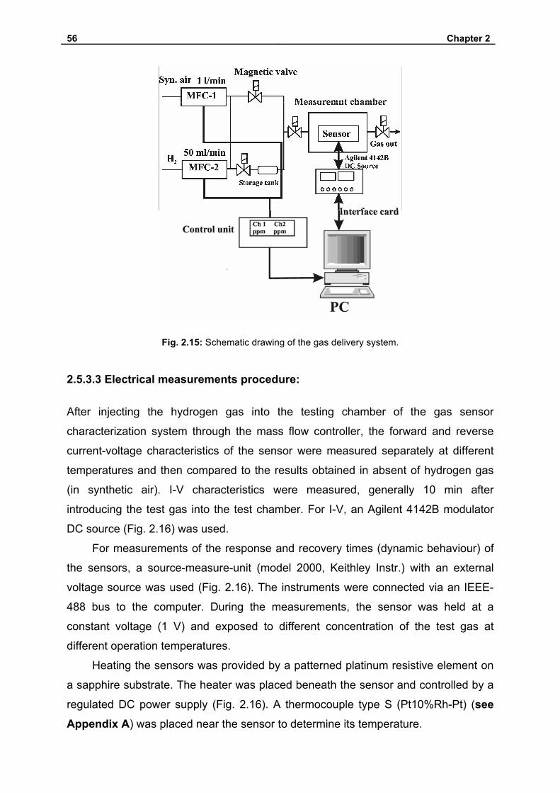
56 Chapter 2
Fig. 2.15: Schematic drawing of the gas delivery system.
2.5.3.3 Electrical measurements procedure:
After injecting the hydrogen gas into the testing chamber of the gas sensor
characterization system through the mass flow controller, the forward and reverse
current-voltage characteristics of the sensor were measured separately at different
temperatures and then compared to the results obtained in absent of hydrogen gas
(in synthetic air). I-V characteristics were measured, generally 10 min after
introducing the test gas into the test chamber. For I-V, an Agilent 4142B modulator
DC source (Fig. 2.16) was used.
For measurements of the response and recovery times (dynamic behaviour) of
the sensors, a source-measure-unit (model 2000, Keithley Instr.) with an external
voltage source was used (Fig. 2.16). The instruments were connected via an IEEE-
488 bus to the computer. During the measurements, the sensor was held at a
constant voltage (1 V) and exposed to different concentration of the test gas at
different operation temperatures.
Heating the sensors was provided by a patterned platinum resistive element on
a sapphire substrate. The heater was placed beneath the sensor and controlled by a
regulated DC power supply (Fig. 2.16). A thermocouple type S (Pt10%Rh-Pt) (see Appendix A) was placed near the sensor to determine its temperature.
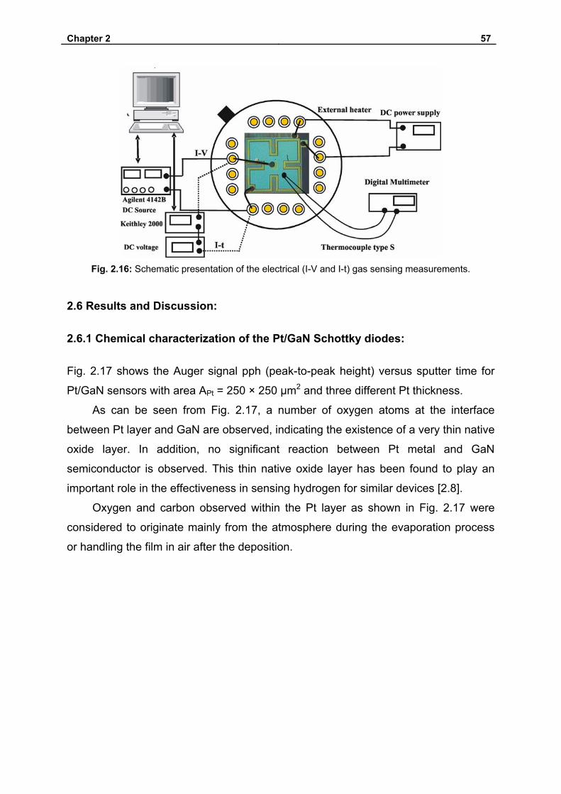
Chapter 2 57
Fig. 2.16: Schematic presentation of the electrical (I-V and I-t) gas sensing measurements.
2.6 Results and Discussion:
2.6.1 Chemical characterization of the Pt/GaN Schottky diodes:
Fig. 2.17 shows the Auger signal pph (peak-to-peak height) versus sputter time for
Pt/GaN sensors with area APt = 250 × 250 μm2 and three different Pt thickness.
As can be seen from Fig. 2.17, a number of oxygen atoms at the interface
between Pt layer and GaN are observed, indicating the existence of a very thin native
oxide layer. In addition, no significant reaction between Pt metal and GaN
semiconductor is observed. This thin native oxide layer has been found to play an
important role in the effectiveness in sensing hydrogen for similar devices [2.8].
Oxygen and carbon observed within the Pt layer as shown in Fig. 2.17 were
considered to originate mainly from the atmosphere during the evaporation process
or handling the film in air after the deposition.
58 Chapter 2
(a) (b)
(c) (d)
Fig. 2.17: AES depth profiles of the Pt/GaN sensors with area APt = 250 × 250 μm2 and three different
Pt thickness. (a) and (b): 8 nm, (c): 24 nm, and (d): 40 nm.
2.6.2 Electrical characterization in air:
2.6.2.1 Room temperature measurements:
The Pt/GaN Schottky diodes characterized by (I-V) measurements exhibited at room
temperature ideality factors between n = 1.2 and 3.15 as well as saturation current
densities between 1 x 10⁻⁹ and 8 × 10⁻⁶ (A/cm2), respectively. A series and parallel
resistance of 0.35-1 (Ω cm2) and 0.0005-2.88 (MΩ cm2) can be extracted. The barrier
heights (BHs) were calculated from the thermionic emission theory yielding an
effective barrier height of ΦB = 0.95 eV. This value is in agreement with results
reported in the literature [2.15]. Schalwig et al. [2.9] reported a Pt/GaN Schottky
barrier height of 1.15 eV as determined by (I-V) measurements, whereas Schmitz et
al. [2.21] obtained a value of 1.08 eV. The observed disparities in the measured
Chapter 2 59
barrier heights between the different authors may be attributed to variations in
material characteristics and measurement techniques used.
Capacitance-voltage (C-V) measurements at 10 kHz showed higher values for
the (BHs) between 1.27 and 2.2 eV at room temperature and doping concentrations
Nd between 4.8 × 10¹⁶ and 3.4 × 1017 cm-3. Our data clearly show that the diodes
have ideality factors that are considerably large. The high values of n can be
attributed to the presence of a wide distribution of low Schottky barrier height (low-
SBH) patches as a consequence of the quality of the GaN used.
The experimental effective (BHs) and ideality factors obtained from the (I-V) and
(C-V) characteristics differ from diode to diode even if they are identically prepared
(on the same sample). It has been reported theoretically by Tung and co-worker
[2.23, 2.24] and experimentally by Mönch and co-worker [2.25-2.28] that the linear
relationship between effective BHs and ideality factor may be explained by the BH
inhomogeneity, that is, the BHs become smaller as the ideality factors increase. This
finding may be attributed to lateral inhomogeneities of the BH [2.23-2.28].
Fig. 2.18 shows a plot of the experimentally determined BHs of 24 diodes as a
function of their ideality factors at room temperature. As can be seen from Fig. 2.18,
there is a linear relationship between the experimental effective BHs and the ideality
factors of the Schottky contacts. That is, the BHs become smaller as the ideality
factors increase.
Fig. 2.18: Plot of experimental BH versus ideality factor of the Pt/GaN Schottky diodes. The
extrapolation of the effective barrier height to ideality factors of 1.02 provides the zero bias barrier
height.
60 Chapter 2
For homogeneous metal-semiconductor contacts, the effective barrier height is
lowered due to the image force and becomes voltage dependent. The extrapolation
to n = 1.02 for the plot in Fig. 2.18 result in a laterally homogeneous BH of 0.92 eV
[2.29].
2.6.2.2 Measurements as a function of temperature:
2.6.2.2.1 Temperature dependent (I-V) characteristics:
Fig. 2.19 shows (I-V) characteristics from the Pt/GaN Schottky diodes with dPt = 40
nm and APt = 250 × 250 μm2, as a function of measurement temperature. The
forward current increases with increasing temperature. The extracted values of
saturation current density JS were 2 × 10⁻⁹ A cm-2 at 300 K, and 10-3 A cm-2 at about
640 K (Fig. 2.20).
Fig. 2.19: I-V characteristics of a Pt/GaN Schottky diode with dPt = 40 nm and APt = 250 × 250 μm2, for
temperatures varying from 300 to 638 K.
The value of Rs determined from Eq. (2.22) increases with increasing temperature
and Rp decreases with increasing temperature (Fig. 2.21). However, as Rp dominates
in the lower bias region, a significant contribution from the parallel resistance on n
and Js was not observed.
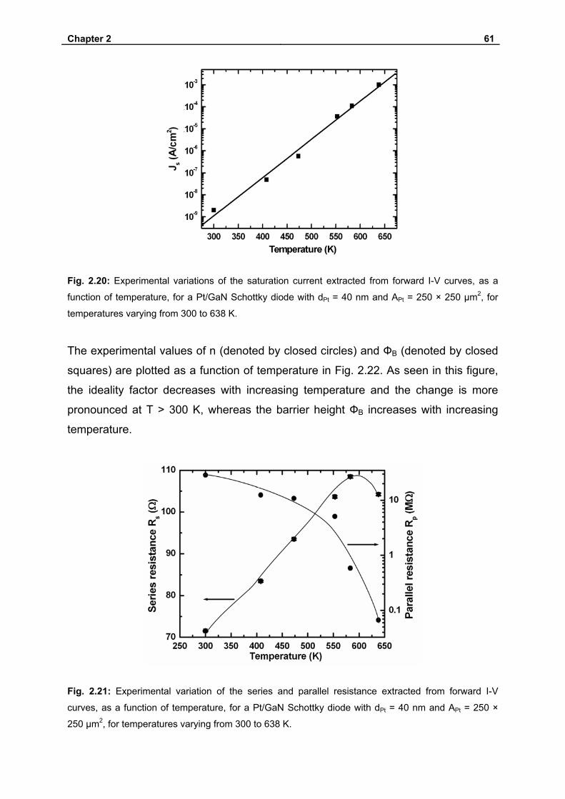
Chapter 2 61
Fig. 2.20: Experimental variations of the saturation current extracted from forward I-V curves, as a
function of temperature, for a Pt/GaN Schottky diode with dPt = 40 nm and APt = 250 × 250 μm2, for
temperatures varying from 300 to 638 K.
The experimental values of n (denoted by closed circles) and ФB (denoted by closed
squares) are plotted as a function of temperature in Fig. 2.22. As seen in this figure,
the ideality factor decreases with increasing temperature and the change is more
pronounced at T > 300 K, whereas the barrier height ФB increases with increasing
temperature.
Fig. 2.21: Experimental variation of the series and parallel resistance extracted from forward I-V
curves, as a function of temperature, for a Pt/GaN Schottky diode with dPt = 40 nm and APt = 250 ×
250 μm2, for temperatures varying from 300 to 638 K.
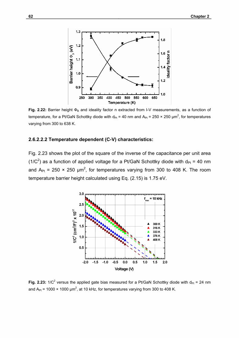
62 Chapter 2
Fig. 2.22: Barrier height ФB and ideality factor n extracted from I-V measurements, as a function of
temperature, for a Pt/GaN Schottky diode with dPt = 40 nm and APt = 250 × 250 μm2, for temperatures
varying from 300 to 638 K.
2.6.2.2.2 Temperature dependent (C-V) characteristics:
Fig. 2.23 shows the plot of the square of the inverse of the capacitance per unit area
(1/C2) as a function of applied voltage for a Pt/GaN Schottky diode with dPt = 40 nm
and APt = 250 × 250 μm2, for temperatures varying from 300 to 408 K. The room
temperature barrier height calculated using Eq. (2.15) is 1.75 eV.
Fig. 2.23: 1/C2 versus the applied gate bias measured for a Pt/GaN Schottky diode with dPt = 24 nm
and APt = 1000 × 1000 μm2, at 10 kHz, for temperatures varying from 300 to 408 K.
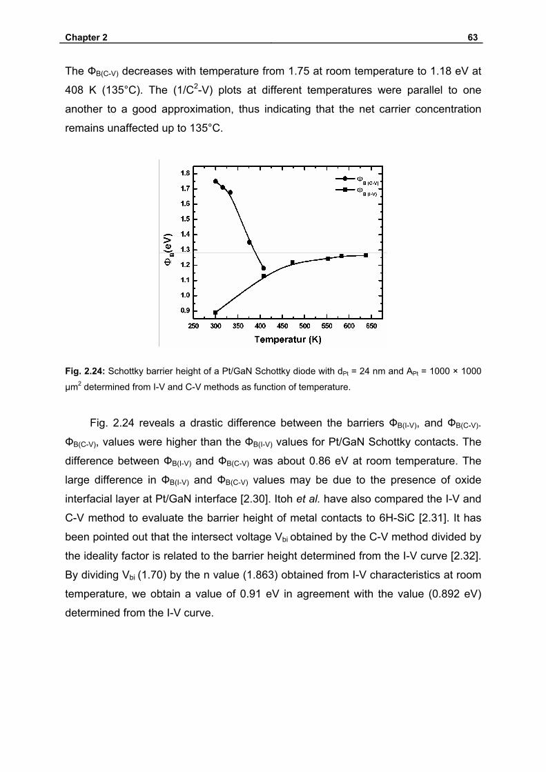
Chapter 2 63
The ФB(C-V) decreases with temperature from 1.75 at room temperature to 1.18 eV at
408 K (135°C). The (1/C2-V) plots at different temperatures were parallel to one
another to a good approximation, thus indicating that the net carrier concentration
remains unaffected up to 135°C.
Fig. 2.24: Schottky barrier height of a Pt/GaN Schottky diode with dPt = 24 nm and APt = 1000 × 1000
μm2 determined from I-V and C-V methods as function of temperature.
Fig. 2.24 reveals a drastic difference between the barriers ФB(I-V), and ФB(C-V).
ФB(C-V), values were higher than the ФB(I-V) values for Pt/GaN Schottky contacts. The
difference between ФB(I-V) and ФB(C-V) was about 0.86 eV at room temperature. The
large difference in ФB(I-V) and ФB(C-V) values may be due to the presence of oxide
interfacial layer at Pt/GaN interface [2.30]. Itoh et al. have also compared the I-V and
C-V method to evaluate the barrier height of metal contacts to 6H-SiC [2.31]. It has
been pointed out that the intersect voltage Vbi obtained by the C-V method divided by
the ideality factor is related to the barrier height determined from the I-V curve [2.32].
By dividing Vbi (1.70) by the n value (1.863) obtained from I-V characteristics at room
temperature, we obtain a value of 0.91 eV in agreement with the value (0.892 eV)
determined from the I-V curve.
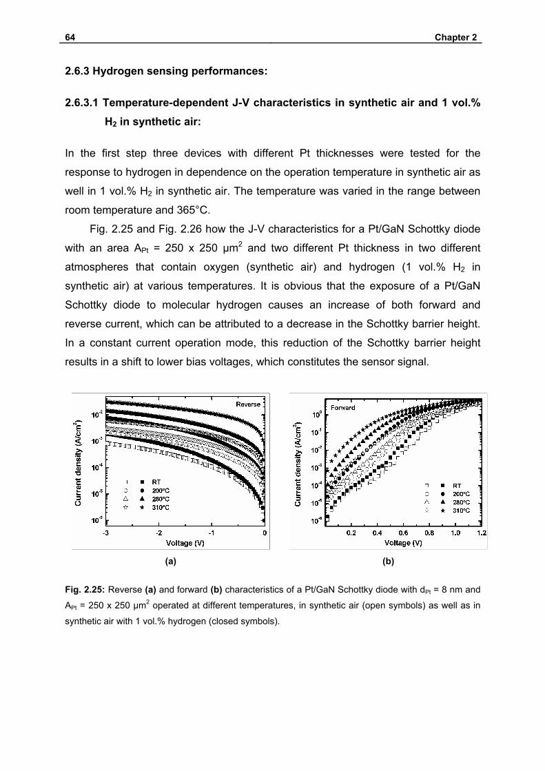
64 Chapter 2
2.6.3 Hydrogen sensing performances:
2.6.3.1 Temperature-dependent J-V characteristics in synthetic air and 1 vol.% H2 in synthetic air:
In the first step three devices with different Pt thicknesses were tested for the
response to hydrogen in dependence on the operation temperature in synthetic air as
well in 1 vol.% H2 in synthetic air. The temperature was varied in the range between
room temperature and 365°C.
Fig. 2.25 and Fig. 2.26 how the J-V characteristics for a Pt/GaN Schottky diode
with an area APt = 250 x 250 μm2 and two different Pt thickness in two different
atmospheres that contain oxygen (synthetic air) and hydrogen (1 vol.% H2 in
synthetic air) at various temperatures. It is obvious that the exposure of a Pt/GaN
Schottky diode to molecular hydrogen causes an increase of both forward and
reverse current, which can be attributed to a decrease in the Schottky barrier height.
In a constant current operation mode, this reduction of the Schottky barrier height
results in a shift to lower bias voltages, which constitutes the sensor signal.
(a) (b)
Fig. 2.25: Reverse (a) and forward (b) characteristics of a Pt/GaN Schottky diode with dPt = 8 nm and
APt = 250 x 250 μm2 operated at different temperatures, in synthetic air (open symbols) as well as in
synthetic air with 1 vol.% hydrogen (closed symbols).
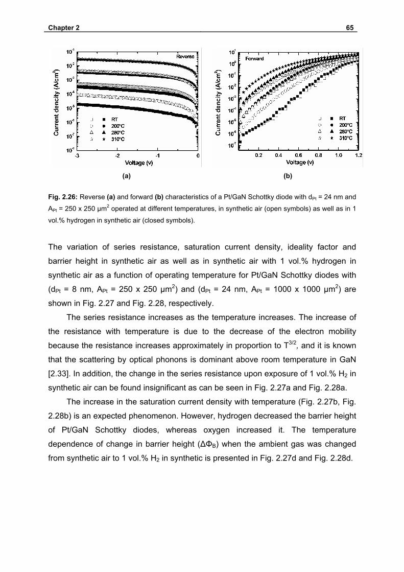
Chapter 2 65
(a) (b)
Fig. 2.26: Reverse (a) and forward (b) characteristics of a Pt/GaN Schottky diode with dPt = 24 nm and
APt = 250 x 250 μm2 operated at different temperatures, in synthetic air (open symbols) as well as in 1
vol.% hydrogen in synthetic air (closed symbols).
The variation of series resistance, saturation current density, ideality factor and
barrier height in synthetic air as well as in synthetic air with 1 vol.% hydrogen in
synthetic air as a function of operating temperature for Pt/GaN Schottky diodes with
(dPt = 8 nm, APt = 250 x 250 μm2) and (dPt = 24 nm, APt = 1000 x 1000 μm2) are
shown in Fig. 2.27 and Fig. 2.28, respectively.
The series resistance increases as the temperature increases. The increase of
the resistance with temperature is due to the decrease of the electron mobility
because the resistance increases approximately in proportion to T3/2, and it is known
that the scattering by optical phonons is dominant above room temperature in GaN
[2.33]. In addition, the change in the series resistance upon exposure of 1 vol.% H2 in
synthetic air can be found insignificant as can be seen in Fig. 2.27a and Fig. 2.28a.
The increase in the saturation current density with temperature (Fig. 2.27b, Fig.
2.28b) is an expected phenomenon. However, hydrogen decreased the barrier height
of Pt/GaN Schottky diodes, whereas oxygen increased it. The temperature
dependence of change in barrier height (ΔΦB) when the ambient gas was changed
from synthetic air to 1 vol.% H2 in synthetic is presented in Fig. 2.27d and Fig. 2.28d.
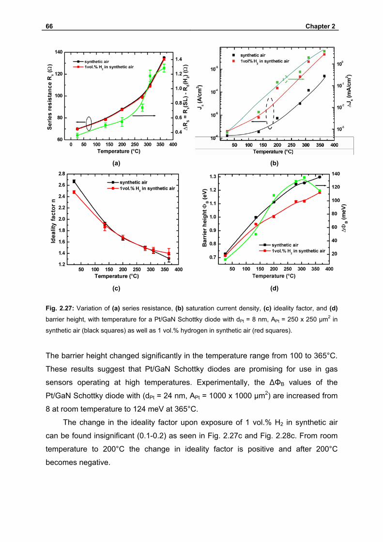
66 Chapter 2
(a) (b)
(c) (d)
Fig. 2.27: Variation of (a) series resistance, (b) saturation current density, (c) ideality factor, and (d) barrier height, with temperature for a Pt/GaN Schottky diode with dPt = 8 nm, APt = 250 x 250 μm2 in
synthetic air (black squares) as well as 1 vol.% hydrogen in synthetic air (red squares).
The barrier height changed significantly in the temperature range from 100 to 365°C.
These results suggest that Pt/GaN Schottky diodes are promising for use in gas
sensors operating at high temperatures. Experimentally, the ΔΦB values of the
Pt/GaN Schottky diode with (dPt = 24 nm, APt = 1000 x 1000 μm2) are increased from
8 at room temperature to 124 meV at 365°C.
The change in the ideality factor upon exposure of 1 vol.% H2 in synthetic air
can be found insignificant (0.1-0.2) as seen in Fig. 2.27c and Fig. 2.28c. From room
temperature to 200°C the change in ideality factor is positive and after 200°C
becomes negative.
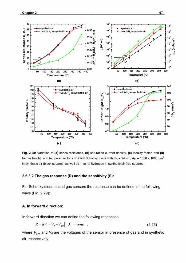
Chapter 2 67
(a) (b)
(c) (d)
Fig. 2.28: Variation of (a) series resistance, (b) saturation current density, (c) ideality factor, and (d) barrier height, with temperature for a Pt/GaN Schottky diode with dPt = 24 nm, APt = 1000 x 1000 μm2
in synthetic air (black squares) as well as 1 vol.% hydrogen in synthetic air (red squares).
2.6.3.2 The gas response (R) and the sensitivity (S):
For Schottky diode based gas sensors the response can be defined in the following
ways (Fig. 2.29):
A. In forward direction:
In forward direction we can define the following responses:
gasVVVR −=Δ= 0 , .constJ F = , (2.26)
where Vgas and V0 are the voltages of the sensor in presence of gas and in synthetic
air, respectively.
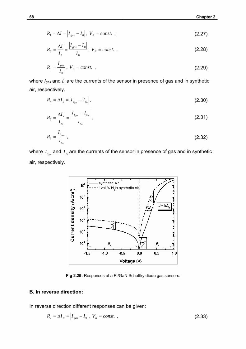
68 Chapter 2
01 IIIR gas −=Δ= , .constVF = , (2.27)
0
0
02 I
IIIIR gas −=
Δ= , .constVF = , (2.28)
0
3 II
R gas= , .constVF = , (2.29)
where Igas and I0 are the currents of the sensor in presence of gas and in synthetic
air, respectively.
04 sss IIIR
gas−=Δ= , (2.30)
0
0
0
5s
ss
s
s
I
II
II
R gas−
=Δ
= , (2.31)
0
6s
s
I
IR gas= , (2.32)
where gassI and
0sI are the currents of the sensor in presence of gas and in synthetic
air, respectively.
Fig 2.29: Responses of a Pt/GaN Schottky diode gas sensors.
B. In reverse direction:
In reverse direction different responses can be given:
07 IIIR gasR −=Δ= , .constVR = , (2.33)
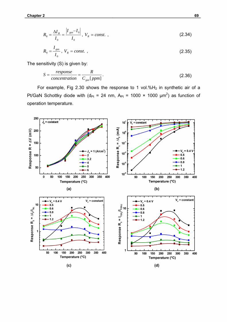
Chapter 2 69
0
0
08 I
IIIIR gasR
−=
Δ= , .constVR = , (2.34)
0
9 II
R gas= , .constVR = , (2.35)
The sensitivity (S) is given by:
][ ppmCR
ionconcentratresponseS
gas
== . (2.36)
For example, Fig 2.30 shows the response to 1 vol.%H2 in synthetic air of a
Pt/GaN Schottky diode with (dPt = 24 nm, APt = 1000 × 1000 μm2) as function of
operation temperature.
(a) (b)
(c) (d)
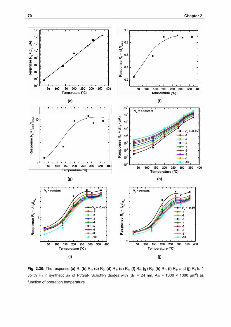
70 Chapter 2
(e) (f)
(g) (h)
(i) (j)
Fig. 2.30: The response (a) R, (b) R1, (c) R2, (d) R3, (e) R4, (f) R5, (g) R6, (h) R7, (i) R8, and (j) R9 to 1
vol.% H2 in synthetic air of Pt/GaN Schottky diodes with (dPt = 24 nm, APt = 1000 × 1000 μm2) as
function of operation temperature.
Chapter 2 71
It becomes obvious that the responses can be enhanced by increasing the operation
temperature. At 310°C and above a general decrease of the responses R2, R3, R5,
R6, R8, and R9 were observed, very likely due to an increased thermal desorption of
the test gas species from the sensor surface. In order to study this effect
temperature-programmed desorption (TPD) measurements were performed (section
2.7). In this thesis we focus on the sensor response R (Eq. 2.26) but we consider
also the other responses to compare our results with the results present in the
literature.
The response R to H2 was investigated in dependence on the active area, Pt
thickness and the operating temperature. The change in the voltage of the diode at a
fixed current density was monitored as the diode was exposed to 1 vol.% H2 in
synthetic air and for comparison to dry synthetic air in order to determine the voltage
difference as a measure for the response torward hydrogen. In this work we have
defined the response as the signal level after exposure to hydrogen for 10 minutes at
various temperatures. Fig. 2.31 plots the response R at different temperatures of the
three set of the Schottky diodes. During this measurement, we held the device at a
constant current density level of 3.2 A/cm2 and monitored the voltage.
A response to hydrogen was observed already at room temperature for all three
kinds of sensors. The data in Fig.2.31a can be explained as follows. At lower
temperatures, the diffusion of hydrogen through platinum to reach the semiconductor
surface is faster through thinner in comparison to thicker Pt. This explains the nearly
20% higher signal we observe in the 8 nm in comparison to the 24 nm device. As we
go higher in temperature the difference in response between the 8 nm and 24 nm
device is decreasing. This is because at elevated temperatures, the diffusion rate
through the 24 nm metal is much higher than at room temperature. The 40 nm device
also shows enhanced sensitivity once the temperature crosses 280°C. Thus at
310°C, we determine the sensitivity of all three devices with different metal thickness
to be very similar. This could be due to the fact that at this temperature the time
constant of hydrogen diffusion for all three Schottky contacts is of the same order of
magnitude and negligible in comparison to the time needed to detect the signal. At
310°C and above a general decrease of the response was observed, very likely due
to an increased thermal desorption of the test gas species from the sensor surface. A
significant increase of response has been observed by increasing the temperature of
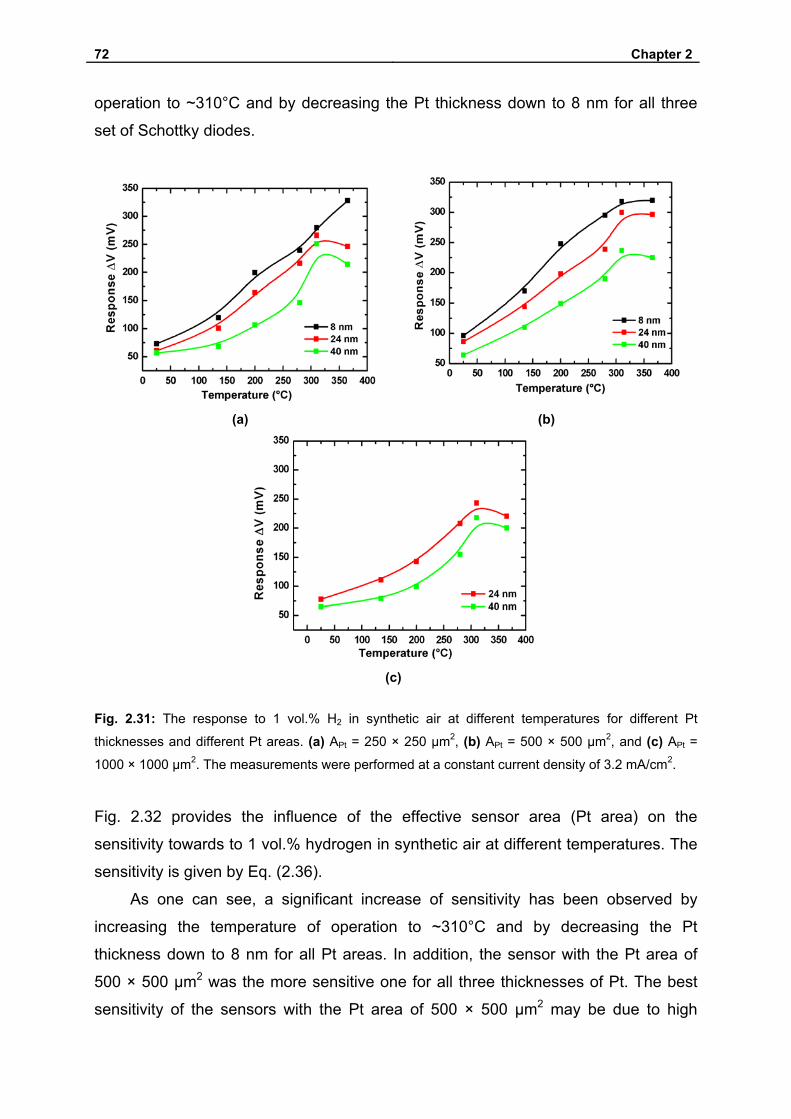
72 Chapter 2
operation to ~310°C and by decreasing the Pt thickness down to 8 nm for all three
set of Schottky diodes.
(a) (b)
(c)
Fig. 2.31: The response to 1 vol.% H2 in synthetic air at different temperatures for different Pt
thicknesses and different Pt areas. (a) APt = 250 × 250 μm2, (b) APt = 500 × 500 μm2, and (c) APt =
1000 × 1000 μm2. The measurements were performed at a constant current density of 3.2 mA/cm2.
Fig. 2.32 provides the influence of the effective sensor area (Pt area) on the
sensitivity towards to 1 vol.% hydrogen in synthetic air at different temperatures. The
sensitivity is given by Eq. (2.36).
As one can see, a significant increase of sensitivity has been observed by
increasing the temperature of operation to ~310°C and by decreasing the Pt
thickness down to 8 nm for all Pt areas. In addition, the sensor with the Pt area of
500 × 500 μm2 was the more sensitive one for all three thicknesses of Pt. The best
sensitivity of the sensors with the Pt area of 500 × 500 μm2 may be due to high
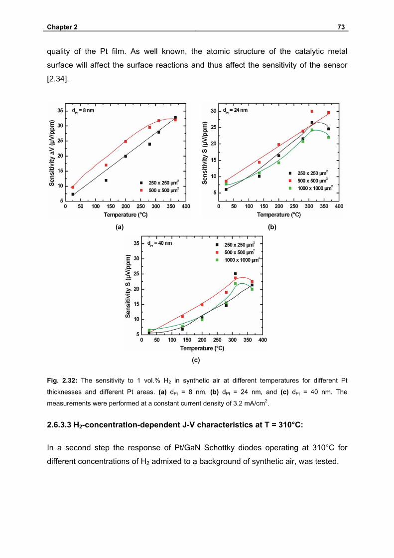
Chapter 2 73
quality of the Pt film. As well known, the atomic structure of the catalytic metal
surface will affect the surface reactions and thus affect the sensitivity of the sensor
[2.34].
(a) (b)
(c)
Fig. 2.32: The sensitivity to 1 vol.% H2 in synthetic air at different temperatures for different Pt
thicknesses and different Pt areas. (a) dPt = 8 nm, (b) dPt = 24 nm, and (c) dPt = 40 nm. The
measurements were performed at a constant current density of 3.2 mA/cm2.
2.6.3.3 H2-concentration-dependent J-V characteristics at T = 310°C:
In a second step the response of Pt/GaN Schottky diodes operating at 310°C for
different concentrations of H2 admixed to a background of synthetic air, was tested.
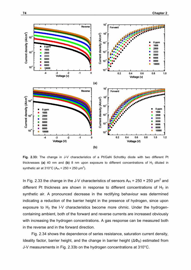
74 Chapter 2
(a)
(b)
Fig. 2.33: The change in J-V characteristics of a Pt/GaN Schottky diode with two different Pt
thicknesses (a) 40 nm and (b) 8 nm upon exposure to different concentrations of H2 diluted in
synthetic air at 310°C (APt = 250 × 250 μm2).
In Fig. 2.33 the change in the J-V characteristics of sensors APt = 250 × 250 μm2 and
different Pt thickness are shown in response to different concentrations of H2 in
synthetic air. A pronounced decrease in the rectifying behaviour was determined
indicating a reduction of the barrier height in the presence of hydrogen, since upon
exposure to H2 the I-V characteristics become more ohmic. Under the hydrogen-
containing ambient, both of the forward and reverse currents are increased obviously
with increasing the hydrogen concentrations. A gas response can be measured both
in the reverse and in the forward direction.
Fig. 2.34 shows the dependence of series resistance, saturation current density,
Ideality factor, barrier height, and the change in barrier height (ΔΦB) estimated from
J-V measurements in Fig. 2.33b on the hydrogen concentrations at 310°C.
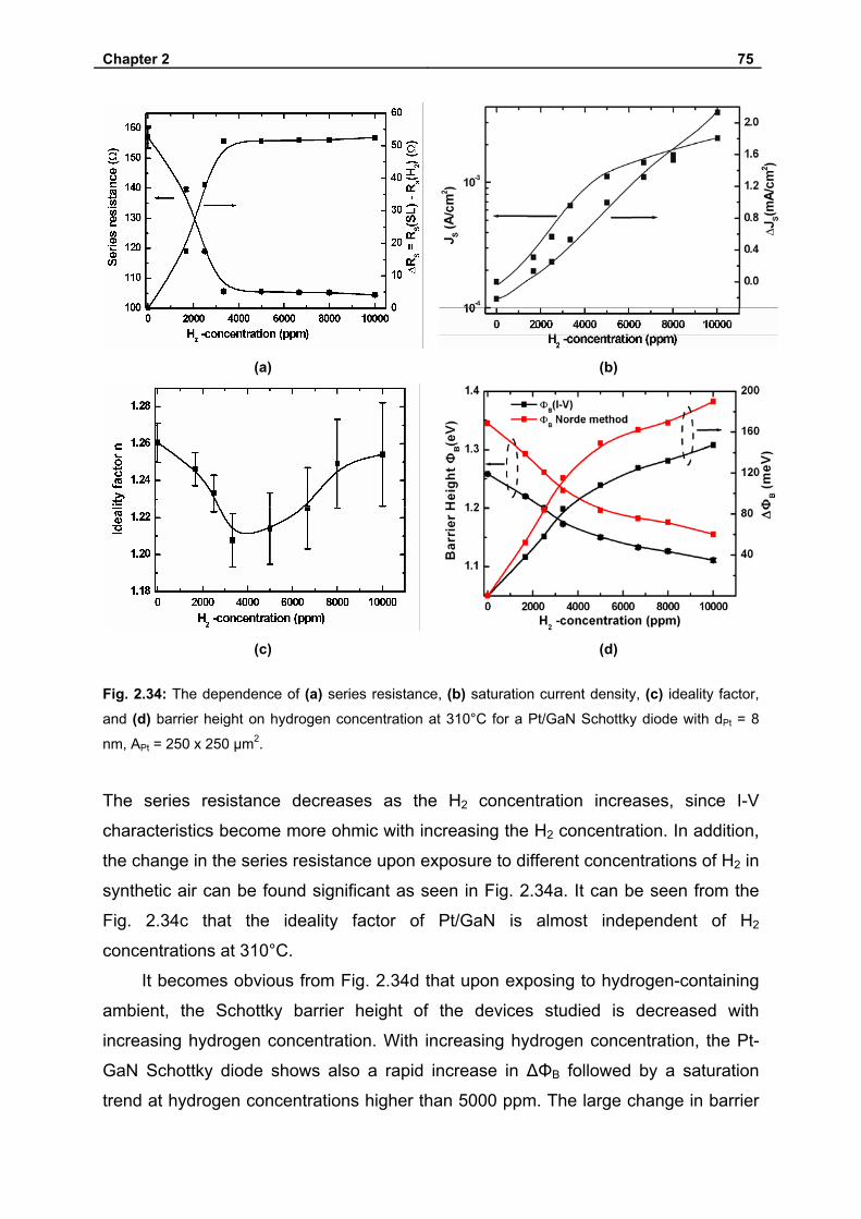
Chapter 2 75
(a) (b)
(c) (d)
Fig. 2.34: The dependence of (a) series resistance, (b) saturation current density, (c) ideality factor,
and (d) barrier height on hydrogen concentration at 310°C for a Pt/GaN Schottky diode with dPt = 8
nm, APt = 250 x 250 μm2.
The series resistance decreases as the H2 concentration increases, since I-V
characteristics become more ohmic with increasing the H2 concentration. In addition,
the change in the series resistance upon exposure to different concentrations of H2 in
synthetic air can be found significant as seen in Fig. 2.34a. It can be seen from the
Fig. 2.34c that the ideality factor of Pt/GaN is almost independent of H2
concentrations at 310°C.
It becomes obvious from Fig. 2.34d that upon exposing to hydrogen-containing
ambient, the Schottky barrier height of the devices studied is decreased with
increasing hydrogen concentration. With increasing hydrogen concentration, the Pt-
GaN Schottky diode shows also a rapid increase in ΔΦB followed by a saturation
trend at hydrogen concentrations higher than 5000 ppm. The large change in barrier

76 Chapter 2
height (ΔΦB) is responsible for the high hydrogen sensitivity of Pt/GaN Schottky
diodes. Experimentally, the ΔΦB values of the studied Pt/GaN Schottky diodes are
increased from 38 (1666 ppm H2 in synthetic air) to 147 meV (1 vol.% H2 in synthetic
air).
Fig 2.35 shows the all responses of Pt/GaN Schottky diodes with (dPt = 40 nm,
APt = 250 × 250 μm2) as function of H2 concentration at a temperature of 310°C. As
can be seen in Fig. 2.35, all responses increase non-linearly and complete saturation
is observed at concentrations above 8000 ppm.
(a) (b)
(c) (d)
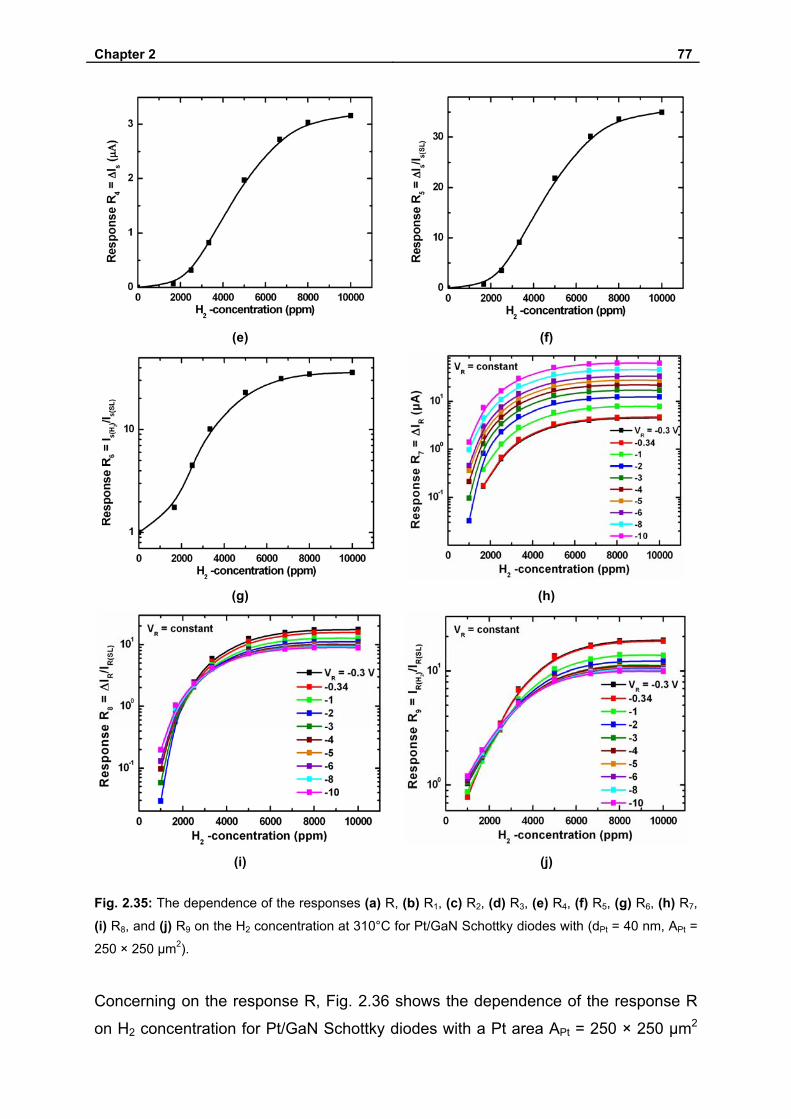
Chapter 2 77
(e) (f)
(g) (h)
(i) (j)
Fig. 2.35: The dependence of the responses (a) R, (b) R1, (c) R2, (d) R3, (e) R4, (f) R5, (g) R6, (h) R7,
(i) R8, and (j) R9 on the H2 concentration at 310°C for Pt/GaN Schottky diodes with (dPt = 40 nm, APt =
250 × 250 μm2).
Concerning on the response R, Fig. 2.36 shows the dependence of the response R
on H2 concentration for Pt/GaN Schottky diodes with a Pt area APt = 250 × 250 μm2
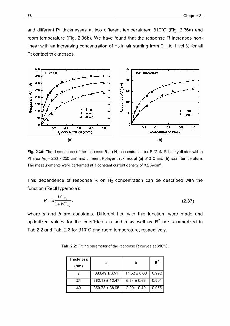
78 Chapter 2
and different Pt thicknesses at two different temperatures: 310°C (Fig. 2.36a) and
room temperature (Fig. 2.36b). We have found that the response R increases non-
linear with an increasing concentration of H2 in air starting from 0.1 to 1 vol.% for all
Pt contact thicknesses.
(a) (b)
Fig. 2.36: The dependence of the response R on H2 concentration for Pt/GaN Schottky diodes with a
Pt area APt = 250 × 250 μm2 and different Pt-layer thickness at (a) 310°C and (b) room temperature.
The measurements were performed at a constant current density of 3.2 A/cm2.
This dependence of response R on H2 concentration can be described with the
function (RectHyperbola):
2
2
1 H
H
bCbC
aR+
= , (2.37)
where a and b are constants. Different fits, with this function, were made and
optimitzed values for the coefficients a and b as well as R2 are summarized in
Tab.2.2 and Tab. 2.3 for 310°C and room temperature, respectively.
Tab. 2.2: Fitting parameter of the response R curves at 310°C.
Thickness (nm)
a b R2
8 383.49 ± 6.51 11.52 ± 0.68 0.992
24 362.18 ± 12.47 5.54 ± 0.63 0.991
40 359.78 ± 38.95 2.09 ± 0.49 0.975
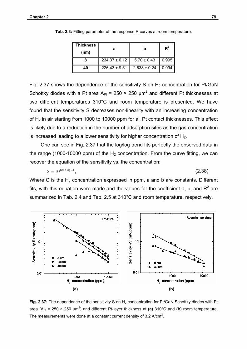
Chapter 2 79
Tab. 2.3: Fitting parameter of the response R curves at room temperature.
Thickness (nm)
a b R2
8 234.37 ± 6.12 5.70 ± 0.43 0.995
40 226.43 ± 9.51 2.638 ± 0.24 0.994
Fig. 2.37 shows the dependence of the sensitivity S on H2 concentration for Pt/GaN
Schottky diodes with a Pt area APt = 250 × 250 μm2 and different Pt thicknesses at
two different temperatures 310°C and room temperature is presented. We have
found that the sensitivity S decreases non-linearity with an increasing concentration
of H2 in air starting from 1000 to 10000 ppm for all Pt contact thicknesses. This effect
is likely due to a reduction in the number of adsorption sites as the gas concentration
is increased leading to a lower sensitivity for higher concentration of H2.
One can see in Fig. 2.37 that the log/log trend fits perfectly the observed data in
the range (1000-10000 ppm) of the H2 concentration. From the curve fitting, we can
recover the equation of the sensitivity vs. the concentration:
)log(10 CbaS += , (2.38)
Where C is the H2 concentration expressed in ppm, a and b are constants. Different
fits, with this equation were made and the values for the coefficient a, b, and R2 are
summarized in Tab. 2.4 and Tab. 2.5 at 310°C and room temperature, respectively.
(a) (b)
Fig. 2.37: The dependence of the sensitivity S on H2 concentration for Pt/GaN Schottky diodes with Pt
area (APt = 250 × 250 μm2) and different Pt-layer thickness at (a) 310°C and (b) room temperature.
The measurements were done at a constant current density of 3.2 A/cm2.
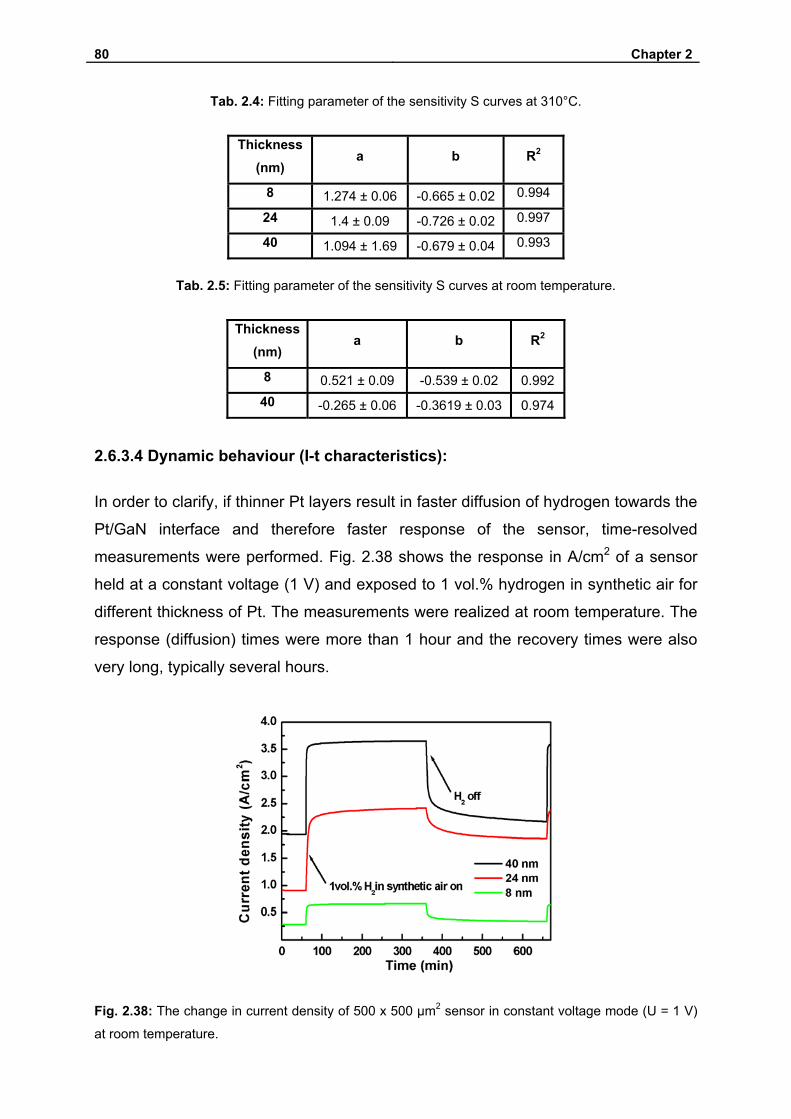
80 Chapter 2
Tab. 2.4: Fitting parameter of the sensitivity S curves at 310°C.
Thickness (nm)
a b R2
8 1.274 ± 0.06 -0.665 ± 0.02 0.994
24 1.4 ± 0.09 -0.726 ± 0.02 0.997
40 1.094 ± 1.69 -0.679 ± 0.04 0.993
Tab. 2.5: Fitting parameter of the sensitivity S curves at room temperature.
Thickness (nm)
a b R2
8 0.521 ± 0.09 -0.539 ± 0.02 0.992 40 -0.265 ± 0.06 -0.3619 ± 0.03 0.974
2.6.3.4 Dynamic behaviour (I-t characteristics):
In order to clarify, if thinner Pt layers result in faster diffusion of hydrogen towards the
Pt/GaN interface and therefore faster response of the sensor, time-resolved
measurements were performed. Fig. 2.38 shows the response in A/cm2 of a sensor
held at a constant voltage (1 V) and exposed to 1 vol.% hydrogen in synthetic air for
different thickness of Pt. The measurements were realized at room temperature. The
response (diffusion) times were more than 1 hour and the recovery times were also
very long, typically several hours.
Fig. 2.38: The change in current density of 500 x 500 μm2 sensor in constant voltage mode (U = 1 V)
at room temperature.
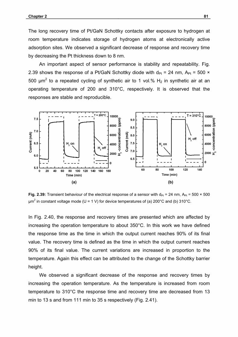
Chapter 2 81
The long recovery time of Pt/GaN Schottky contacts after exposure to hydrogen at
room temperature indicates storage of hydrogen atoms at electronically active
adsorption sites. We observed a significant decrease of response and recovery time
by decreasing the Pt thickness down to 8 nm.
An important aspect of sensor performance is stability and repeatability. Fig.
2.39 shows the response of a Pt/GaN Schottky diode with dPt = 24 nm, APt = 500 ×
500 μm2 to a repeated cycling of synthetic air to 1 vol.% H2 in synthetic air at an
operating temperature of 200 and 310°C, respectively. It is observed that the
responses are stable and reproducible.
(a) (b)
Fig. 2.39: Transient behaviour of the electrical response of a sensor with dPt = 24 nm, APt = 500 × 500
μm2 in constant voltage mode (U = 1 V) for device temperatures of (a) 200°C and (b) 310°C.
In Fig. 2.40, the response and recovery times are presented which are affected by
increasing the operation temperature to about 350°C. In this work we have defined
the response time as the time in which the output current reaches 90% of its final
value. The recovery time is defined as the time in which the output current reaches
90% of its final value. The current variations are increased in proportion to the
temperature. Again this effect can be attributed to the change of the Schottky barrier
height.
We observed a significant decrease of the response and recovery times by
increasing the operation temperature. As the temperature is increased from room
temperature to 310°C the response time and recovery time are decreased from 13
min to 13 s and from 111 min to 35 s respectively (Fig. 2.41).
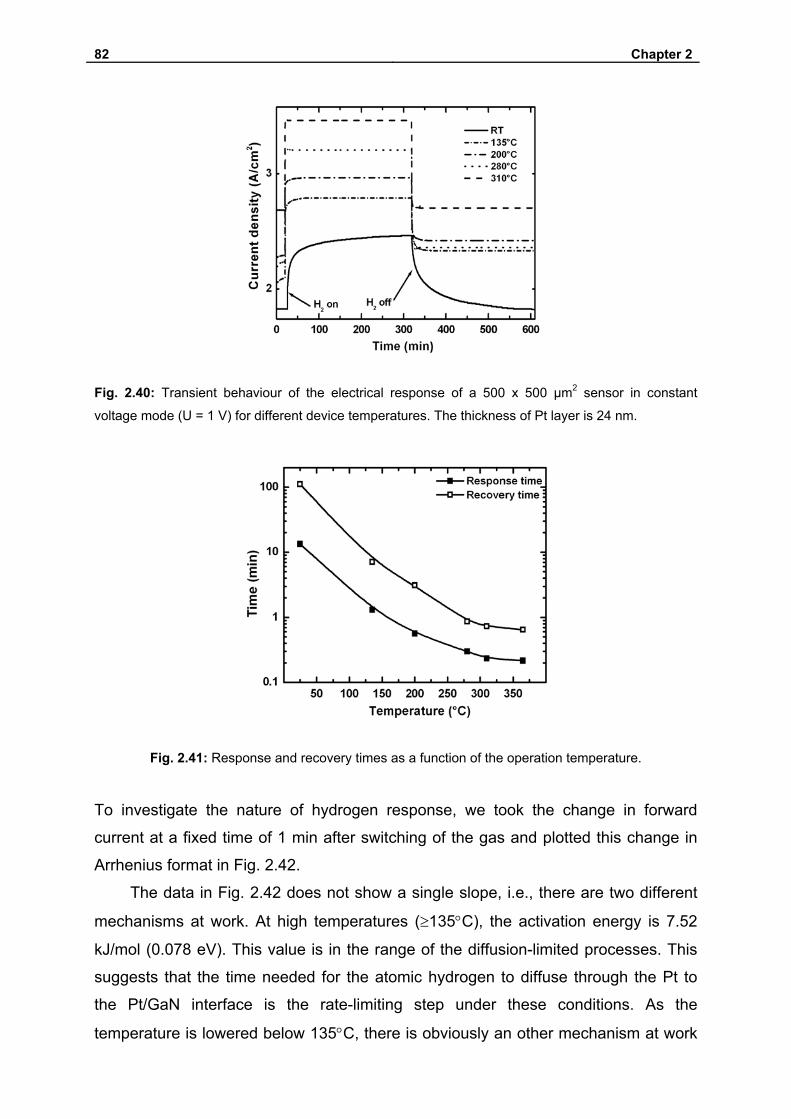
82 Chapter 2
Fig. 2.40: Transient behaviour of the electrical response of a 500 x 500 μm2 sensor in constant
voltage mode (U = 1 V) for different device temperatures. The thickness of Pt layer is 24 nm.
Fig. 2.41: Response and recovery times as a function of the operation temperature.
To investigate the nature of hydrogen response, we took the change in forward
current at a fixed time of 1 min after switching of the gas and plotted this change in
Arrhenius format in Fig. 2.42.
The data in Fig. 2.42 does not show a single slope, i.e., there are two different
mechanisms at work. At high temperatures (≥135°C), the activation energy is 7.52
kJ/mol (0.078 eV). This value is in the range of the diffusion-limited processes. This
suggests that the time needed for the atomic hydrogen to diffuse through the Pt to
the Pt/GaN interface is the rate-limiting step under these conditions. As the
temperature is lowered below 135°C, there is obviously an other mechanism at work
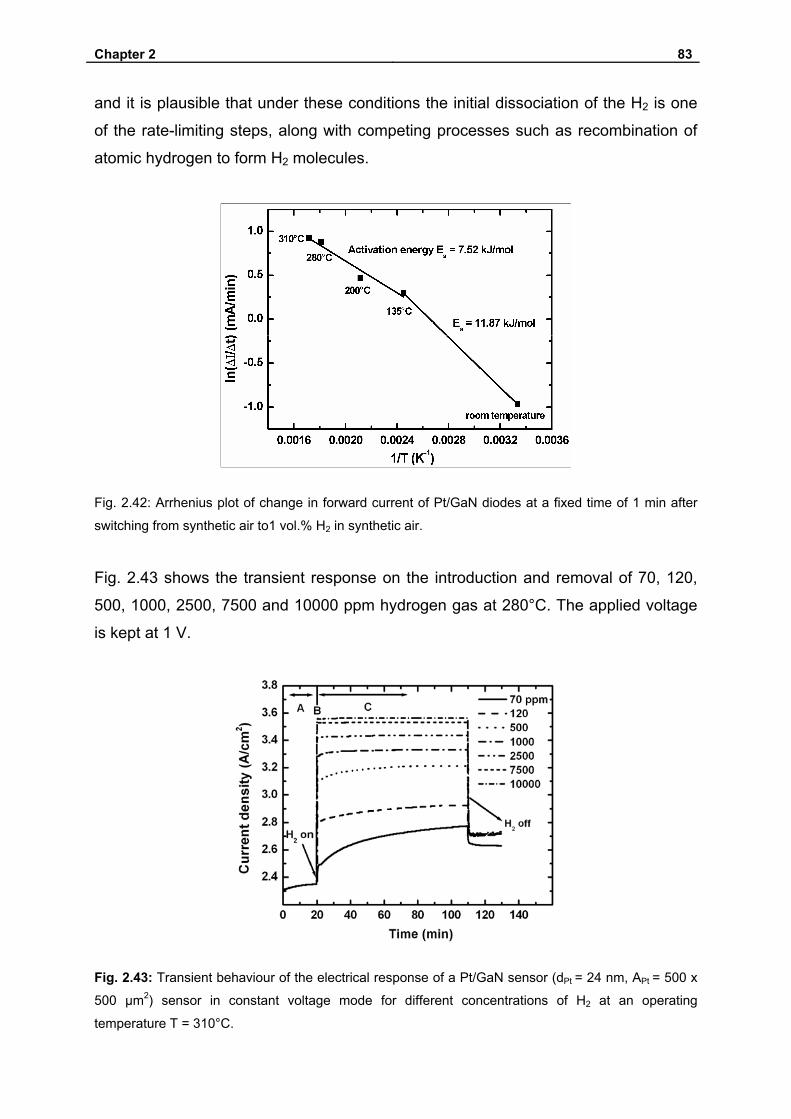
Chapter 2 83
and it is plausible that under these conditions the initial dissociation of the H2 is one
of the rate-limiting steps, along with competing processes such as recombination of
atomic hydrogen to form H2 molecules.
Fig. 2.42: Arrhenius plot of change in forward current of Pt/GaN diodes at a fixed time of 1 min after
switching from synthetic air to1 vol.% H2 in synthetic air.
Fig. 2.43 shows the transient response on the introduction and removal of 70, 120,
500, 1000, 2500, 7500 and 10000 ppm hydrogen gas at 280°C. The applied voltage
is kept at 1 V.
Fig. 2.43: Transient behaviour of the electrical response of a Pt/GaN sensor (dPt = 24 nm, APt = 500 x
500 μm2) sensor in constant voltage mode for different concentrations of H2 at an operating
temperature T = 310°C.
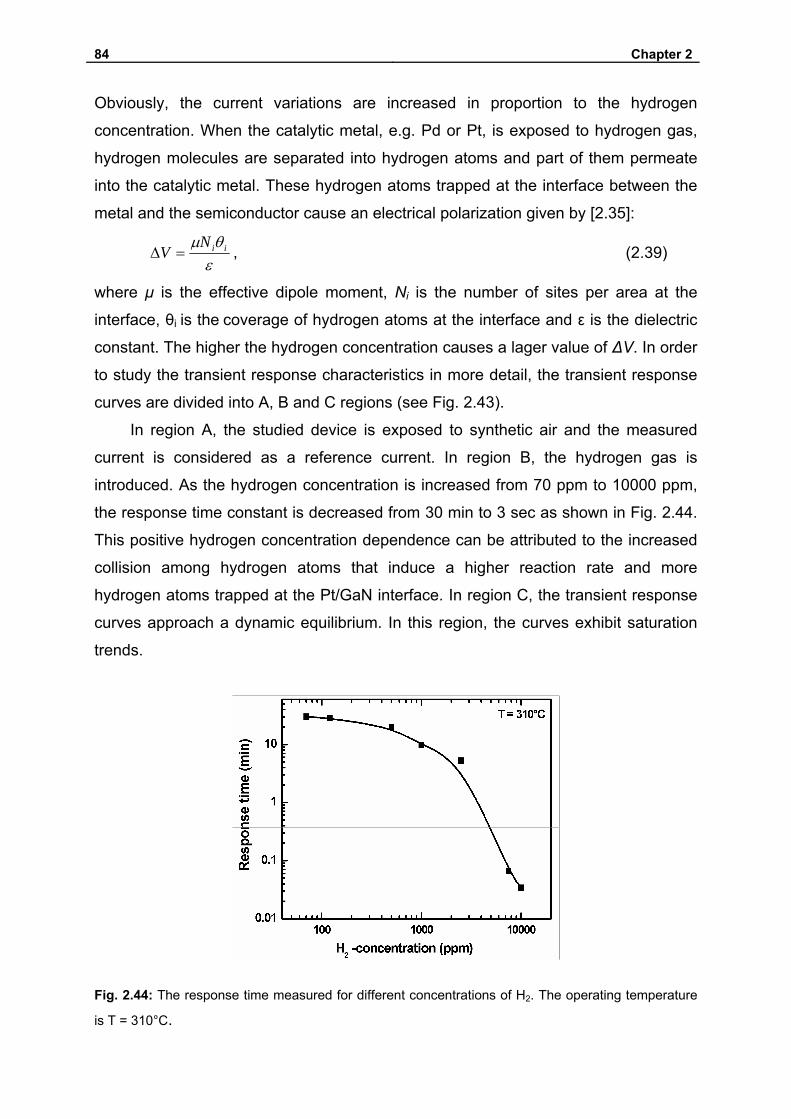
84 Chapter 2
Obviously, the current variations are increased in proportion to the hydrogen
concentration. When the catalytic metal, e.g. Pd or Pt, is exposed to hydrogen gas,
hydrogen molecules are separated into hydrogen atoms and part of them permeate
into the catalytic metal. These hydrogen atoms trapped at the interface between the
metal and the semiconductor cause an electrical polarization given by [2.35]:
εθμ iiN
V =Δ , (2.39)
where μ is the effective dipole moment, Ni is the number of sites per area at the
interface, θi is the coverage of hydrogen atoms at the interface and ε is the dielectric
constant. The higher the hydrogen concentration causes a lager value of ΔV. In order
to study the transient response characteristics in more detail, the transient response
curves are divided into A, B and C regions (see Fig. 2.43).
In region A, the studied device is exposed to synthetic air and the measured
current is considered as a reference current. In region B, the hydrogen gas is
introduced. As the hydrogen concentration is increased from 70 ppm to 10000 ppm,
the response time constant is decreased from 30 min to 3 sec as shown in Fig. 2.44.
This positive hydrogen concentration dependence can be attributed to the increased
collision among hydrogen atoms that induce a higher reaction rate and more
hydrogen atoms trapped at the Pt/GaN interface. In region C, the transient response
curves approach a dynamic equilibrium. In this region, the curves exhibit saturation
trends.
Fig. 2.44: The response time measured for different concentrations of H2. The operating temperature
is T = 310°C.
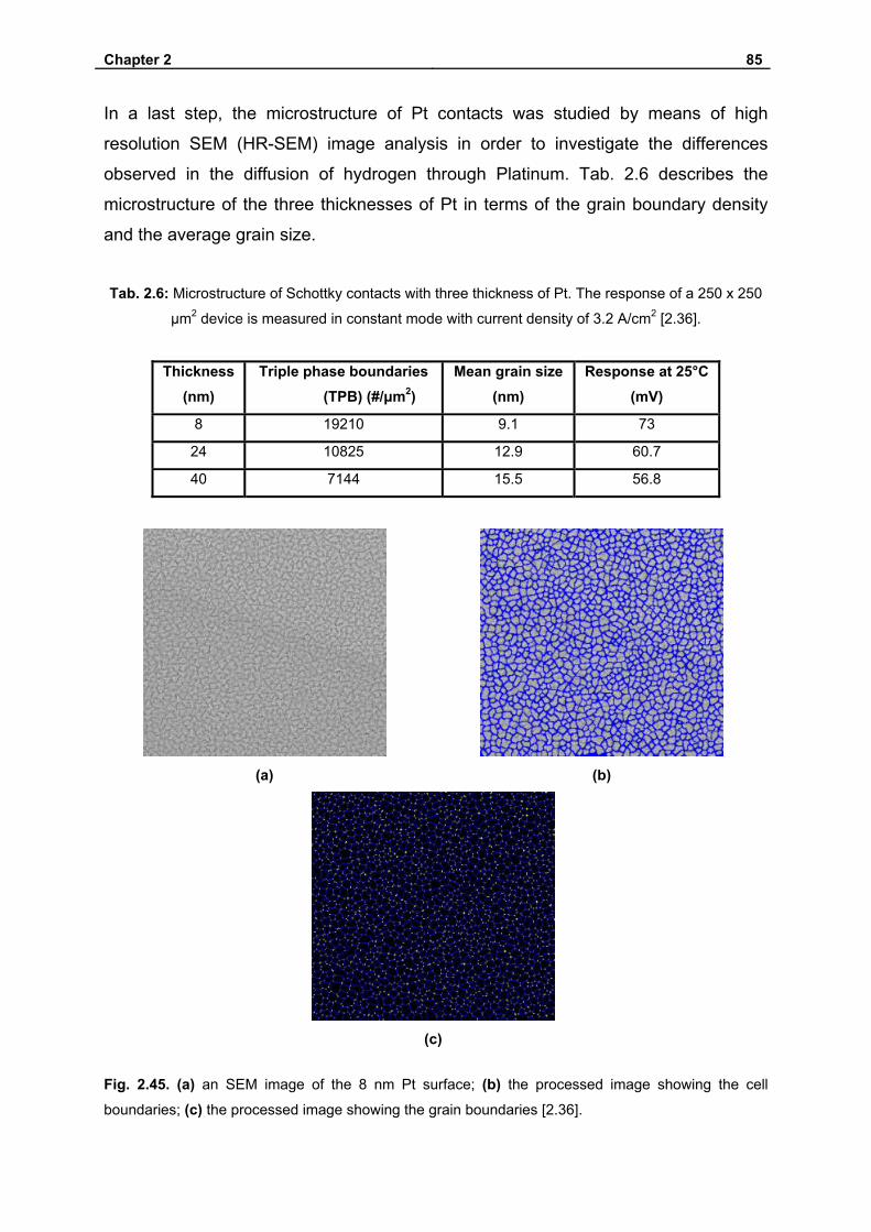
Chapter 2 85
In a last step, the microstructure of Pt contacts was studied by means of high
resolution SEM (HR-SEM) image analysis in order to investigate the differences
observed in the diffusion of hydrogen through Platinum. Tab. 2.6 describes the
microstructure of the three thicknesses of Pt in terms of the grain boundary density
and the average grain size.
Tab. 2.6: Microstructure of Schottky contacts with three thickness of Pt. The response of a 250 x 250
µm2 device is measured in constant mode with current density of 3.2 A/cm2 [2.36].
Thickness (nm)
Triple phase boundaries (TPB) (#/μm2)
Mean grain size (nm)
Response at 25°C (mV)
8 19210 9.1 73
24 10825 12.9 60.7
40 7144 15.5 56.8
(a) (b)
(c)
Fig. 2.45. (a) an SEM image of the 8 nm Pt surface; (b) the processed image showing the cell
boundaries; (c) the processed image showing the grain boundaries [2.36].

86 Chapter 2
As expected, the higher response film also has the higher grain boundary density
proving that hydrogen molecules dissociate on the Pt surface and diffuse along the
grain boundaries reaching the Pt/GaN interface (Fig. 2.45).
2.7 Temperature-programmed desorption (TPD) measurements:
2.7.1 TPD background and fundamentals:
Temperature-programmed desorption (TPD) techniques are important methods for
the determination of kinetic and thermodynamic parameters of desorption processes
or decomposition reactions. A sample is heated with a temperature ramp β(t) = dT/dt
(with the temperature T usually being a linear function of the time t) and the partial
pressures of atoms and molecules evolving from the sample are measured, e.g. by
quadrupole mass spectrometer (QMS). When experiments are performed using well-
defined surfaces of single-crystalline samples in a continuously pumped ultra-high
vacuum (UHV) chamber then this experimental technique is often also referred to as
thermal desorption spectroscopy (TDS).
2.7.1.1 Kinetics of desorption:
The disengagement of an atom or molecule from a surface is termed ”desorption”. At
low temperatures a molecule adsorbed on a surface could remain for an indefinite
time. However, as the surface temperature increases the molecule will receive
energy, and so one of the following processes can occur:
the molecules can react with the surface,
the molecules can break down to two or more other molecules (either in
gaseous or solid state),
the molecules can desorb.
The last option is the desorption process, which could also occur in the second
option if one of the products is a gas.
2.7.1.1.1 Polanyi-Wigner Equation:
The desorption rate is usually expressed by a rate law of nth order [2.37]:
nndes k
dtdr θθ
=−= , (2.40)
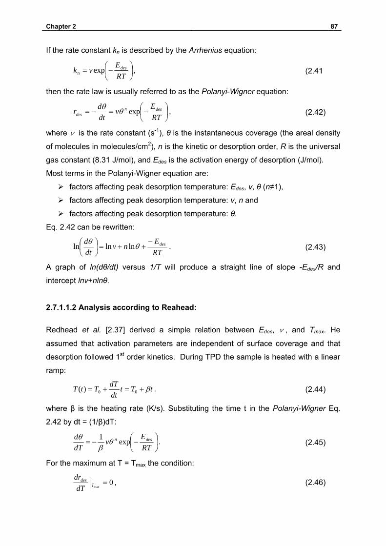
Chapter 2 87
If the rate constant kn is described by the Arrhenius equation:
⎟⎠⎞
⎜⎝⎛−=
RTE
vk desn exp , (2.41
then the rate law is usually referred to as the Polanyi-Wigner equation:
⎟⎠⎞
⎜⎝⎛−=−=
RTE
vdtdr desn
des expθθ , (2.42)
where ν is the rate constant (s-1), θ is the instantaneous coverage (the areal density
of molecules in molecules/cm2), n is the kinetic or desorption order, R is the universal
gas constant (8.31 J/mol), and Edes is the activation energy of desorption (J/mol).
Most terms in the Polanyi-Wigner equation are:
factors affecting peak desorption temperature: Edes, v, θ (n≠1),
factors affecting peak desorption temperature: v, n and
factors affecting peak desorption temperature: θ.
Eq. 2.42 can be rewritten:
RTE
nvdtd des−
++=⎟⎠⎞
⎜⎝⎛ θθ lnlnln . (2.43)
A graph of ln(dθ/dt) versus 1/T will produce a straight line of slope -Edes/R and
intercept lnv+nlnθ.
2.7.1.1.2 Analysis according to Reahead:
Redhead et al. [2.37] derived a simple relation between Edes, ν , and Tmax. He
assumed that activation parameters are independent of surface coverage and that
desorption followed 1st order kinetics. During TPD the sample is heated with a linear
ramp:
tTtdtdTTtT β+=+= 00)( . (2.44)
where β is the heating rate (K/s). Substituting the time t in the Polanyi-Wigner Eq.
2.42 by dt = (1/β)dT:
⎟⎠⎞
⎜⎝⎛−−=
RTE
vdTd desn exp1 θ
βθ . (2.45)
For the maximum at T = Tmax the condition:
0max
=Tdes
dTdr , (2.46)

88 Chapter 2
must be fulfilled, or, because of dTd
dtdrdes
θβθ−=−= :
2max
2
2
max RTE
dTdn
dTd desn
T θθθθ+= . (2.47)
Inserting (2.45) for dθ/dT and solving for 2maxRT
Edes provides
⎟⎟⎠
⎞⎜⎜⎝
⎛−= −
max
12
max
exp1RTEvn
RTE desndes θ
β. (2.48)
If 1st order desorption (n = 1) takes place then Tmax is independent of the coverage θ,
but dependent on the heating rate β:
⎟⎟⎠
⎞⎜⎜⎝
⎛−=
max2
max
exp1RTE
vRTE desdes
β. (2.49)
Solving (2.49) for Edes provides
⎥⎦
⎤⎢⎣
⎡−=
max
maxmax lnln
RTET
RTE desdes β
ν , (2.50)
where the second part in brackets is small relative to the first and is estimated as
ln(Edes/RTmax) = 3.64. The error introduced through this estimate is less than 1.5% for
108 < ν / β< 1013 K-1.
Eq (2.50) becomes:
⎥⎦
⎤⎢⎣
⎡−= 64.3ln max
max βvT
RTEdes . (2.51)
The Redhead method is often employed to extract activation energies from a single
desorption spectrum. This requires that an approximate value for ν is known (ν =
1013 s-1 is a commonly chosen value).
2.7.2 Experimental:
2.7.2.1 UHV system:
TPD experiments were performed in an ultra-high vacuum (UHV) system consisting
of a pumping system and the vacuum chamber. The chamber consists of a closed
quartz tube of about 25 cm in length and 1 cm in diameter. A photograph and
schematic drawing of the UHV apparatus for this experiment and all devices mounted
in it is shown in Fig. 2.46.
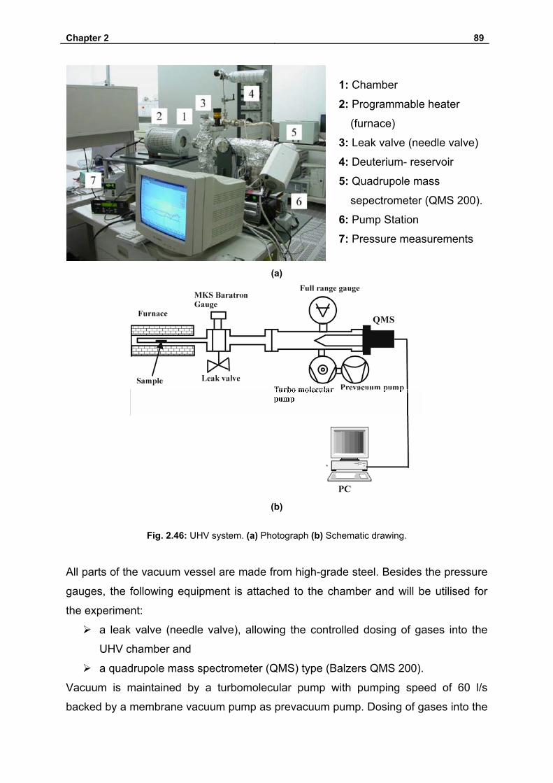
Chapter 2 89
1: Chamber
2: Programmable heater
(furnace)
3: Leak valve (needle valve)
4: Deuterium- reservoir
5: Quadrupole mass
sepectrometer (QMS 200).
6: Pump Station
7: Pressure measurements
(a)
(b)
Fig. 2.46: UHV system. (a) Photograph (b) Schematic drawing.
All parts of the vacuum vessel are made from high-grade steel. Besides the pressure
gauges, the following equipment is attached to the chamber and will be utilised for
the experiment:
a leak valve (needle valve), allowing the controlled dosing of gases into the
UHV chamber and
a quadrupole mass spectrometer (QMS) type (Balzers QMS 200).
Vacuum is maintained by a turbomolecular pump with pumping speed of 60 l/s
backed by a membrane vacuum pump as prevacuum pump. Dosing of gases into the
90 Chapter 2
chamber is achieved by use of a leak valve. The final pressure Pf measured during
dosing is the sum of the base pressure P0 and the partial pressure Pi of the gas
flowing into the system, i.e., Pf -P0 = Pi (or Pi = Pf for P0 << Pf).
2.7.2.2 Sample preparation for TPD measurements:
High-purity platinum (99.995%) was evaporated with an electron-beam evaporator
(Ardeene LA 440 S) with areas of 0.6 × 2.1 cm2 on Si-doped GaN layers grown on
the c-plane of sapphire substrates by (MBE) molecular-beam epitaxy. The thickness
of Pt metal was of about 24 mm as determined by profilometer. The GaN surface
was treated 1min with BOE (7:1) to remove the surface oxide before Pt evaporation.
The deposition conditions were as follows:
base pressure ~ 2×10⁻⁶ mbar,
deposition pressure~ 10-5 mbar and
substrate temperature: room temperature.
2.7.2.3 Measurements procedure:
The Pt/GaN sample with Pt thickness of 24 nm and area of 1.26 cm2 was put in the
quartz tube which was placed in an electrical furnace. The sample was exposed at
different temperatures to different partial pressures of deuterium (D2) for different
times, and then the sample was heated with a linear temperature ramp (24°C/min)
from 100°C up to 800°C. Four procedures were performed:
• The sample was exposed to D2 of 4 mbar for different times (from 10 min to 20
h) at room temperature and then D2 was pumped away and the quartz tube
was evacuated to less than 2 × 10⁻⁸ mbar before starting the measurement
(Procedure I).
• The sample was exposed to D2 of 40 mbar for 3 min at different temperatures
(from room temperature to 300°C) and then D2 was pumped away and the
quartz tube was evacuated to less than 2 × 10⁻⁸ mbar before starting the
measurement (Procedure II).
• The sample was exposed to D2 of 40 mbar for different times (from 1/2 min to
10 min) at 100°C and then D2 was pumped away and the quart tube was
evacuated to less than 2 × 10⁻⁸ mbar before starting the measurement
(Procedure III).
Chapter 2 91
• The sample was exposed to D2 of different partial pressures (from 0.5 t0 50
mbar) for 3 min at 15°C and then D2 was pumped away and the quartz tube
was evacuated to less than 2 × 10⁻⁸ mbar before starting the measurement
(Procedure IV). The products of desorption were measured using a Balzers QMS 200 type
quadropole mass spectrometer with a detection limit of 10-14 mbar and the ability to
detect 9 masses in one cycle (cycletime ≈ 30 s). During the experiment the total
pressure was always below 10-7 mbar to ensure that the mean free path of the
effused radicals and molecules is longer than the distance between the sample and
the entrance of the mass spectrometer. The partial pressures of D2, H2O, CO, N2,
and O2 in the quartz tube were determined at the same time. To calculate the
concentration of the desorbed species or the deuterium flux from the sample surface,
the effective pumping speed at the position of the quadrupole mass spectrometer
(QMS) was determined for deuterium [Seff (D2) = 41.66 l/s].
Because of the turbomolecular pumping system used, the pumping rate is
constant over the whole measurement range so that the partial pressure values allow
the calculation of the flux or desorption rate F(x) of molecules x evolved at the
temperature T from the measured partial pressure p(x) (mbar) and effective constant
pumping rate S(x) [mbar l/s]. Under the assumption that the desorbed gases can be
treated as ideal gases (NA Avogadro's number, p0 pressure under normal conditions)
one obtains:
( ) ( ) )(
4.22)( 12
0
−−⋅= scmAp
xSxpl
NxF A . (2.52)
By integrating the molecular flux over the measured time, it is possible to determine
the total amount (x) of desorbed molecules.
2.7.3 Results:
Fig. 2.47 shows the residual gas spectrum of the quartz tube at 100°C. As it can be
seen, the peaks are observed at mass of 2, 16, 18, 28 and 32. This is exactly the
composition of air with water, hydrogen, nitrogen and oxygen. A further peak is to be
recognized on mass 44. This is with large probability carbon dioxide.

92 Chapter 2
Fig. 2.47: The residual gas spectrum of the quartz tube at 100°C.
The partial pressures of D2, CO, O2, H2O, and H2 desorbed from the fresh sample
versus time, as well as versus desorption temperature are shown in Fig. 2.48a and
Fig. 2.48b, respectively. The sample was exposed to D2 of 4 mbar for 30 min at room
temperature and then D2 was pumped away and the quartz tube was evacuated to
less than 2 × 10⁻⁸ mbar before the desorption from the sample was measured.
(a) (b)
Fig 2.48: The partial pressures of D2, CO, O2, H2O, and H2 desorbed from the fresh sample versus
time (a), as well as versus desorption temperature (b). The sample was exposed to D2 of 4 mbar for
30 min at room temperature.
As can be seen in Fig. 2.49, four peaks are found in the case of D2. These peaks are
centred on 200, 250, 290 and 310°C, respectively.
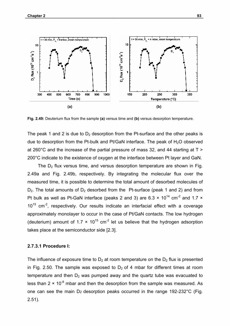
Chapter 2 93
(a) (b)
Fig. 2.49: Deuterium flux from the sample (a) versus time and (b) versus desorption temperature.
The peak 1 and 2 is due to D2 desorption from the Pt-surface and the other peaks is
due to desorption from the Pt-bulk and Pt/GaN interface. The peak of H2O observed
at 260°C and the increase of the partial pressure of mass 32, and 44 starting at T >
200°C indicate to the existence of oxygen at the interface between Pt layer and GaN.
The D2 flux versus time, and versus desorption temperature are shown in Fig.
2.49a and Fig. 2.49b, respectively. By integrating the molecular flux over the
measured time, it is possible to determine the total amount of desorbed molecules of
D2. The total amounts of D2 desorbed from the Pt-surface (peak 1 and 2) and from
Pt bulk as well as Pt-GaN interface (peaks 2 and 3) are 6.3 × 1014 cm-2 and 1.7 ×
1015 cm-2, respectively. Our results indicate an interfacial effect with a coverage
approximately monolayer to occur in the case of Pt/GaN contacts. The low hydrogen
(deuterium) amount of 1.7 × 1015 cm-2 let us believe that the hydrogen adsorption
takes place at the semiconductor side [2.3].
2.7.3.1 Procedure I:
The influence of exposure time to D2 at room temperature on the D2 flux is presented
in Fig. 2.50. The sample was exposed to D2 of 4 mbar for different times at room
temperature and then D2 was pumped away and the quartz tube was evacuated to
less than 2 × 10⁻⁸ mbar and then the desorption from the sample was measured. As
one can see the main D2 desorption peaks occurred in the range 192-232°C (Fig.
2.51).
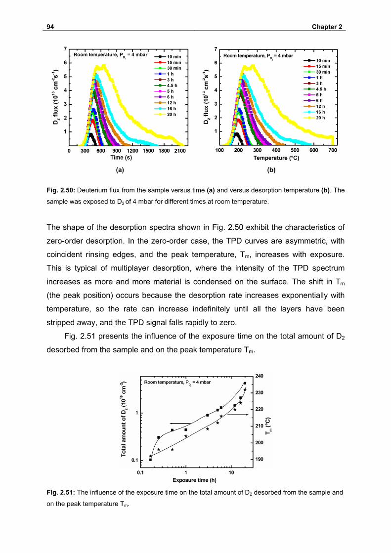
94 Chapter 2
(a) (b)
Fig. 2.50: Deuterium flux from the sample versus time (a) and versus desorption temperature (b). The
sample was exposed to D2 of 4 mbar for different times at room temperature.
The shape of the desorption spectra shown in Fig. 2.50 exhibit the characteristics of
zero-order desorption. In the zero-order case, the TPD curves are asymmetric, with
coincident rinsing edges, and the peak temperature, Tm, increases with exposure.
This is typical of multiplayer desorption, where the intensity of the TPD spectrum
increases as more and more material is condensed on the surface. The shift in Tm
(the peak position) occurs because the desorption rate increases exponentially with
temperature, so the rate can increase indefinitely until all the layers have been
stripped away, and the TPD signal falls rapidly to zero.
Fig. 2.51 presents the influence of the exposure time on the total amount of D2
desorbed from the sample and on the peak temperature Tm.
Fig. 2.51: The influence of the exposure time on the total amount of D2 desorbed from the sample and
on the peak temperature Tm.
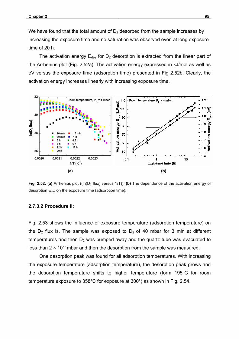
Chapter 2 95
We have found that the total amount of D2 desorbed from the sample increases by
increasing the exposure time and no saturation was observed even at long exposure
time of 20 h.
The activation energy Edes for D2 desorption is extracted from the linear part of
the Arrhenius plot (Fig. 2.52a). The activation energy expressed in kJ/mol as well as
eV versus the exposure time (adsorption time) presented in Fig 2.52b. Clearly, the
activation energy increases linearly with increasing exposure time.
(a) (b)
Fig. 2.52: (a) Arrhenius plot ((ln(D2 flux) versus 1/T)); (b) The dependence of the activation energy of
desorption Edes on the exposure time (adsorption time).
2.7.3.2 Procedure II:
Fig. 2.53 shows the influence of exposure temperature (adsorption temperature) on
the D2 flux is. The sample was exposed to D2 of 40 mbar for 3 min at different
temperatures and then D2 was pumped away and the quartz tube was evacuated to
less than 2 × 10⁻⁸ mbar and then the desorption from the sample was measured.
One desorption peak was found for all adsorption temperatures. With increasing
the exposure temperature (adsorption temperature), the desorption peak grows and
the desorption temperature shifts to higher temperature (form 195°C for room
temperature exposure to 358°C for exposure at 300°) as shown in Fig. 2.54.
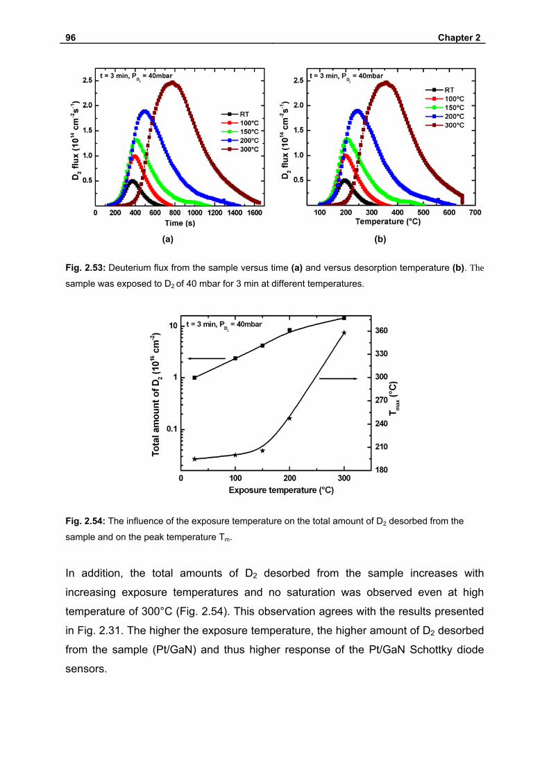
96 Chapter 2
(a) (b)
Fig. 2.53: Deuterium flux from the sample versus time (a) and versus desorption temperature (b). The
sample was exposed to D2 of 40 mbar for 3 min at different temperatures.
Fig. 2.54: The influence of the exposure temperature on the total amount of D2 desorbed from the
sample and on the peak temperature Tm.
In addition, the total amounts of D2 desorbed from the sample increases with
increasing exposure temperatures and no saturation was observed even at high
temperature of 300°C (Fig. 2.54). This observation agrees with the results presented
in Fig. 2.31. The higher the exposure temperature, the higher amount of D2 desorbed
from the sample (Pt/GaN) and thus higher response of the Pt/GaN Schottky diode
sensors.

Chapter 2 97
(a) (b)
Fig. 2.55: (a) Arrhenius plot ((ln(D2 flux) versus 1/T)); (b) The dependence of the activation energy of
desorption Edes on the exposure temperature (adsorption temperature).
The activation energy Edes of D2 desorption is extracted from the linear part of the
Arrhenius plot that slopes down indicating to that the deuterium have completely
desorbed from the sample (Fig. 2.55a). The activation energy expressed in kJ/mol
and eV versus the exposure temperature (adsorption temperature) is shown in Fig.
2.55b. We have found that the activation energy increases non-linearly with
increasing exposure temperature.
2.7.3.3 Procedure III:
The influence of exposure time to D2 at 100°C temperature on the D2 flux is
presented in Fig. 2.56. The sample was exposed to D2 of 40 mbar for different times
at 100°C and then D2 was pumped away and the quartz tube was evacuated to less
than 2 × 10⁻⁸ mbar and then the desorption from the sample was measured.
The shape of the desorption spectra shown in Fig. 2.56 exhibits the
characteristics of first order desorption: constant peak temperature and asymmetric
desorption curves about a single Tm value of 200°C. A first order analysis of the
leading edges of these spectra reveals an activation energy for desorption of about
70 kJ/mol (0.732 eV) (Fig. 2.57).

98 Chapter 2
(a) (b)
Fig. 2.56: Deuterium flux from the sample versus time (a) and versus desorption temperature (b). The
sample was exposed to D2 of 40 mbar for different times at 100°C.
The total amount of D2 desorbed from the sample versus the exposure time is shown
in Fig. 2.58. The longer the exposure time, the wider the desorption peak (Fig. 2.56)
and the higher amount of D2 desorbed from the sample. We have found that the total
amount of D2 desorbed from the sample increases non-linearly with increasing
exposure time and saturation trend was observed at exposure time longer than 3
min.
Fig. 2.57: (a) Arrhenius plot ((ln(D2 flux) versus 1/T)). The sample was exposed to D2 of 40 mbar for
different times at 100°C.
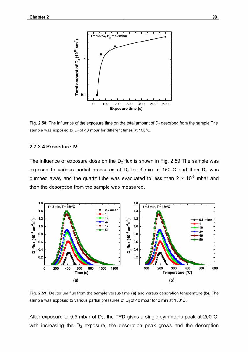
Chapter 2 99
Fig. 2.58: The influence of the exposure time on the total amount of D2 desorbed from the sample.The
sample was exposed to D2 of 40 mbar for different times at 100°C.
2.7.3.4 Procedure IV:
The influence of exposure dose on the D2 flux is shown in Fig. 2.59 The sample was
exposed to various partial pressures of D2 for 3 min at 150°C and then D2 was
pumped away and the quartz tube was evacuated to less than 2 × 10⁻⁸ mbar and
then the desorption from the sample was measured.
(a) (b)
Fig. 2.59: Deuterium flux from the sample versus time (a) and versus desorption temperature (b). The
sample was exposed to various partial pressures of D2 of 40 mbar for 3 min at 150°C.
After exposure to 0.5 mbar of D2, the TPD gives a single symmetric peak at 200°C;
with increasing the D2 exposure, the desorption peak grows and the desorption
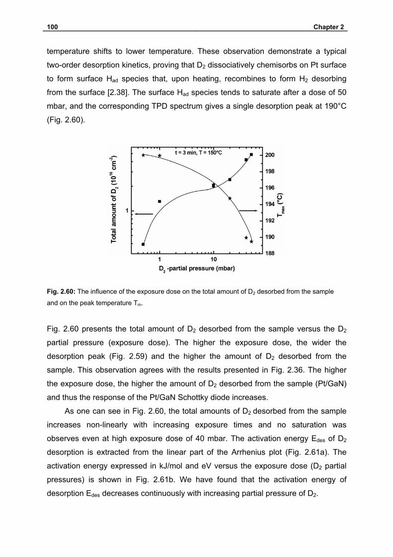
100 Chapter 2
temperature shifts to lower temperature. These observation demonstrate a typical
two-order desorption kinetics, proving that D2 dissociatively chemisorbs on Pt surface
to form surface Had species that, upon heating, recombines to form H2 desorbing
from the surface [2.38]. The surface Had species tends to saturate after a dose of 50
mbar, and the corresponding TPD spectrum gives a single desorption peak at 190°C
(Fig. 2.60).
Fig. 2.60: The influence of the exposure dose on the total amount of D2 desorbed from the sample
and on the peak temperature Tm.
Fig. 2.60 presents the total amount of D2 desorbed from the sample versus the D2
partial pressure (exposure dose). The higher the exposure dose, the wider the
desorption peak (Fig. 2.59) and the higher the amount of D2 desorbed from the
sample. This observation agrees with the results presented in Fig. 2.36. The higher
the exposure dose, the higher the amount of D2 desorbed from the sample (Pt/GaN)
and thus the response of the Pt/GaN Schottky diode increases.
As one can see in Fig. 2.60, the total amounts of D2 desorbed from the sample
increases non-linearly with increasing exposure times and no saturation was
observes even at high exposure dose of 40 mbar. The activation energy Edes of D2
desorption is extracted from the linear part of the Arrhenius plot (Fig. 2.61a). The
activation energy expressed in kJ/mol and eV versus the exposure dose (D2 partial
pressures) is shown in Fig. 2.61b. We have found that the activation energy of
desorption Edes decreases continuously with increasing partial pressure of D2.

Chapter 2 101
(a) (b)
Fig. 2.61: (a) Arrhenius plot ((ln(D2 flux) versus 1/T)); (b) The dependence of the activation energy of
desorption Edes on the D2 partial pressure (exposure dose).
2.8. Conclusion:
The performance of Pt/GaN Schottky diodes with different thickness of the catalytic
metal were investigated as hydrogen gas detectors. The area as well as the
thickness of the Pt was varied between 250 × 250 µm2 and 1000 × 1000 µm2, 8 and
40 nm, respectively.
The response to hydrogen gas was investigated in dependence on the active
area, the Pt thickness and the operating temperature for 1 vol.% hydrogen in
synthetic air. We observed a significant increase of the sensitivity and a decrease of
the response and recovery times by increasing the temperature of operation to about
350°C and by decreasing the Pt thickness down to 8 nm. The sensors with the
thinnest Pt layer showed the maximum sensitivity at room temperature indicating that
an effective sensor operation at room temperature is possible.
Electron microscopy of the microstructure showed that the thinner platinum had
a higher grain boundary density. The increase in sensitivity with decreasing Pt
thickness points to the dissociation of molecular hydrogen on the surface, the
diffusion of atomic hydrogen along the platinum grain boundaries and the adsorption
of hydrogen at the Pt/GaN interface as From TPD measurements we could prove
that the hydrogen adsorbs mainly at the Pt surface and at the Pt/GaN interface.
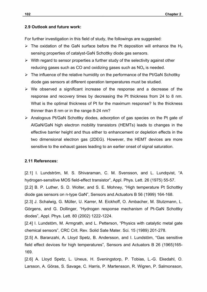
102 Chapter 2
2.9 Outlook and future work:
For further investigation in this field of study, the followings are suggested:
The oxidation of the GaN surface before the Pt deposition will enhance the H2
sensing properties of catalyst-GaN Schottky diode gas sensors.
With regard to sensor properties a further study of the selectivity against other
reducing gases such as CO and oxidizing gases such as NOx is needed.
The influence of the relative humidity on the performance of the Pt/GaN Schottky
diode gas sensors at different operation temperatures must be studied.
We observed a significant increase of the response and a decrease of the
response and recovery times by decreasing the Pt thickness from 24 to 8 nm.
What is the optimal thickness of Pt for the maximum response? Is the thickness
thinner than 8 nm or in the range 8-24 nm?
Analogous Pt/GaN Schottky diodes, adsorption of gas species on the Pt gate of
AlGaN/GaN high electron mobility transistors (HEMTs) leads to changes in the
effective barrier height and thus either to enhancement or depletion effects in the
two dimensional electron gas (2DEG). However, the HEMT devices are more
sensitive to the exhaust gases leading to an earlier onset of signal saturation.
2.11 References:
[2.1] I. Lundström, M. S. Shivaraman, C. M. Svensson, and L. Lundqvist, “A
hydrogen-sensitive MOS field-effect transistor”, Appl. Phys. Lett. 26 (1975) 55-57.
[2.2] B. P. Luther, S. D. Wolter, and S. E. Mohney, “High temperature Pt Schottky
diode gas sensors on n-type GaN”, Sensors and.Actuators B 56 (1999) 164-168.
[2.3] J. Schalwig, G. Müller, U. Karrer, M. Eickhoff, O. Ambacher, M. Stutzmann, L.
Görgens, and G. Dollinger, “Hydrogen response mechanism of Pt-GaN Schottky
diodes”, Appl. Phys. Lett. 80 (2002) 1222-1224.
[2.4] I. Lundstöm, M. Armgrath, and L. Petterson, “Physics with catalytic metal gate
chemical sensors”, CRC Crit. Rev. Solid Sate Mater. Sci. 15 (1989) 201-278.
[2.5] A. Baranzahi, A. Lloyd Spetz, B. Andersson, and I. Lundstöm, “Gas sensitive
field effect devices for high temperatures”, Sensors and Actuators B 26 (1965)165-
169.
[2.6] A. Lloyd Spetz, L. Uneus, H. Sveningstorp, P. Tobias, L.-G. Ekedahl, O.
Larsson, A. Göras, S. Savage, C. Harris, P. Martensson, R. Wigren, P. Salmonsson,
Chapter 2 103
B. Häggendahl, P. Ljung, M. Marttsson, and I. Lundstöm, “SiC based field effect gas
sensors for industrial applications”, phys. stat. sol. A 185 (2001) 15-25.
[2.7] R. Dus, “Hydrogen adsorption and absorption on evaporated palladium films
study by surface potential measurements”, Surf. Sci. 42 (1973) 324-328.
[2.8] O. Weidemann, M. Hermann, G. Steinhoff, H. Wingbrant, A. Lloyd Spetz, M.
Stutzmann, and M. Eickhoff, “Influence of surface oxides on the hydrogen-sensitive
of Pd:GaN Schottky diodes”, Appl. Phys. Lett. 83 (2003) 773-775.
[2.9] J. Schalwig, G. Müller, O. Ambacher, and M. Stutzmann, “Group-III Nitride
based gas sensing devices”, phys. stat. sol. A 185 (2001) 39-45.
[2.10] J. Schalwig, G. Müller, M. Eickhoff, O. Ambacher, and M. Stutzmann, “Group
III-nitride-based gas sensors for combustion monitoring”, Mater. Sci. Eng. B 93
(2002) 207-214.
[2.11] E. J. Cho, D. Pavlidis, G. Y. Zhao, S. M. Hubbard, and J. Schwank,
“Improvement of CO sensitivity in GaN-based gas sensors”, IEICE Trans. Electron.
E89C (2006) 1047-1051.
[2.12] F. Braun, Pogg. Ann. Phys. 153 (1874) 556.
[2.13] W. Schottky, “Halbleitertheorie der Sperrschicht“, Naturwissenschaften 26
(1938) 843.
[2.14] J. D. Guo, M. S. Feng, R. J. Guo, F. M. Pan, and C. Y. Chang, “Study of
Schottky barriers on n-type GaN grown by low-pressure metalorganic chemical vapor
deposition”, Appl. Phys. Lett. 67 (1995) 2657-2659.
[2.15] L. Wang, M. I. Nathan, T. H. Lim, M. A. Khan, and Q. Chen, “High barrier
height GaN Schottky diodes: Pt/GaN and Pd/GaN”, Appl. Phys. Lett. 68 (1996) 1267-
1269.
[2.16] E. R. Rhoderick, “Metal semiconductor contacts”, IEE Proc. 129 (1982) 1-14.
[2.17] C. R. Crowell and S. M. Sze, “Current transport in metal-semiconductor
barriers“. Solid-State Electron. 9 (1966) 1035-1048.
[2.18] M. P. Hernandez, C. F. Alonso and J. L. Pena, “Barrier height determination in
homogeneous nonideal Schottky contacts“. J. Phys. D: Appl. Phys. 34 (2001) 1157-
1161.
[2.19] P. Hacke, T. Detchprohm, K. Hiramatsu, and N. Sawaki, “Schottky barrier on
n-type GaN grown by hydride vapor phase epitaxy“, Appl. Phys. Lett. 63 (1993)
2676-2678.
104 Chapter 2
[2.20] A. T. Ping, A. C. Schmitz, M. A. Khan, and I. Adesida, “Characterisation of Pd
Schottky barrier on n-type GaN“, Electron. Lett. 32 (1996) 68-70.
[2.21] A. C. Schmitz, A. T. Ping, M. Asif Khan, Q. Chen, J. W. Yang, and I. Adesida,
“Schottky barrier properties of various metals on n-type GaN“, Semicond. Sci.
Technol. 11 (1996) 1464-1967.
[2.22] H. Norde, “A modified forward I-V plot for Schottky diodes with high series
resistance”, J. Appl. Phys. 50 (1979) 5052-5053.
[2.23] R. T. Tung, “Recent advances in Schottky barrier concepts”, Mater. Sci. Eng. R
35 (2001) 1-138
[2.24] J. P. Sullivan, M. R. Pinto, and W. R. Graham, “Electron transport of
inhomogeneous Schottky barriers: A numerical study”, J. Appl. Phys. 70 (1991)
7403-7424.
[2.25] T. U. Kampen and W. Mönch, “Lead contacts on Si(111):H-1 × 1 surfaces”,
Surf. Sci. 331-333 (1995) 490-495.
[2.26] W. Mönch, “Chemical trends in Schottky barriers: Charge transfer into
adsorbate-induced gap states and defects”, Phys. Rev. B 37 (1988) 7129-7132.
[2.27] R. F. Schmitsdorf, T. U. Kampen, and W. Mönch, “Explanation of the linear
correlation between barrier heights and ideality factors of real metal-semiconductor
contacts by laterally non uniform Schottky barriers”, J. Vac. Sci. Techno. B 15 (1997)
1221-1226.
[2.28] W. Mönch, “Barrier heights of real Schottky contacts explained by metal-
induced gap states and lateral inhomogeneities,” J. Vac. Sci. Technol. B 17 (1999)
1867-1876.
[2.29] R. T. Tung, “Electron transport at metal-semiconductor interfaces: General
theory,” Phys. Rev. B 45 (1992) 13509-13523
[2.30] V. M. Bremudez,”Simple interpretation of metal/wurtzite-GaN barrier heights“,
J. Appl. Phys. 86 (1999) 1170-1171.
[2.31] A. Itoh and H. Malsunami, “Schottky barrier heights of Metal/SiC contacts“,
phys. stat. sol. (a) 162 (1997) 389-408.
[2.32] S. S. Cohen, “VLSI electronics-Micromstucture Science, vol. 13. Metal-
Semiconductor Contacts and Devices“, New York. Academic Press (1986) p. 269.
[2.33] M. Shur, B. Geimont and M. A. Khan, “Electron mobility in two-dimensional
electron gas in AlGaN/GaN heterostructures and in bulk GaN”, J. Electron. Mater. 25
(1996) 777-785.
Chapter 2 105
[2.34] A. E. Abom, R. T. Haasch, N. Hellgren, N. Finnegan, L. Hultman, and M.
Eriksson, “Characterization of the metal-insulator interface of field-effect chemical
sensors”, J. Appl. Phys. 93 (2003) 9760-9768.
[2.35] M. Johansson, I. Lundstöm, and L.-G. Ekedahl, “Bridging the pressure gap for
palladium metal-insulator-semiconductor hydrogen sensors in oxygen containing
environments”, J. Appl. Phys. 84 (1998) 44-51.
[2.36] V. Tilak, M. Ali, V. Cimalla, V. Manivannan, P. Sandvik, J. Fedison, O.
Ambacher, and D. Merfeld, “Influence of metal thickness to sensitivity of Pt/GaN
Schottky diodes for gas sensing applications”, in: Proceedings of the MRS Fall
Meeting, 798 (2003) Y.11.5.1.
[2.37] P. A. Redhead,”Thermal desorption of gases”, Vacuum 12 (1962) 203-211.
[2.38] K. Christmann and G .Ertl, “Interaction of hydrogen with Pt(111): The role of
atomic steps”, Surf. Sci. 60 (1976) 365-384.

106 Chapter 2
Chapter 3 107
Chapter 3
3. Study of Gas-Sensing Performance of SiC-Based Metal-Oxide-Semiconductor (MOS) and Metal-Metal Oxide-Oxide-Semiconductor (MMOOS) Capacitors
3.1 Introduction:
Gas-sensitive silicon metal-oxide-semiconductor (MOS) devices with catalytically
active palladium (Pd) Gates were first reported by Lundström et al. in 1975 [3.1]. In
the case of a thick, continuous gate, such devices work as selective hydrogen
sensors. Intensive research led to a model which attributes the sensing mechanism
to the formation of a H-induced dipole layer at the Pd-SiO2 interface [3.2].
In order to allow continuous operation of field-effect gas sensors even at
temperatures higher than 300°C, the Lundström group later introduced MOS sensors
based on silicon carbide (SiC) with platinum (Pt) gates [3.3, 3.4]. A natural extension
of the work on SiC-based hydrogen and hydrocarbon sensors is the development of
a NOx sensor using the same baseline structures. Lunström et al. have demonstrated
the use of capacitive structure for NOx detection [3.3].
In this chapter, we focus on fabrication of SiC capacitors for NOx, O2, and D2
sensing applications. The capacitors were fabricated using either silicon dioxide or
silicon dioxide-silicon nitride stack as the dielectric. This stack is potentially more
stable than a silicon dioxide dielectric as the silicon nitride can act as a good barrier
layer to prevent the diffusion of mobile ions to the oxide-carbide interface and thereby
reducing drifts. In addition, we change the catalytic gate to a material more sensitive
to the presence of NOx. A prime candidate material is rhodium Rh. Changes in the
Rh upon exposure to NOx is thought to change the electronic properties of the
capacitor. These changes can be correlated to changes in the NOx concentration in
the ambient and thus be used to quantitatively measure the NOx concentration. The
most important property of the sensors studied in this chapter is that the sensors can
be used as NOx gas sensor at room temperature.
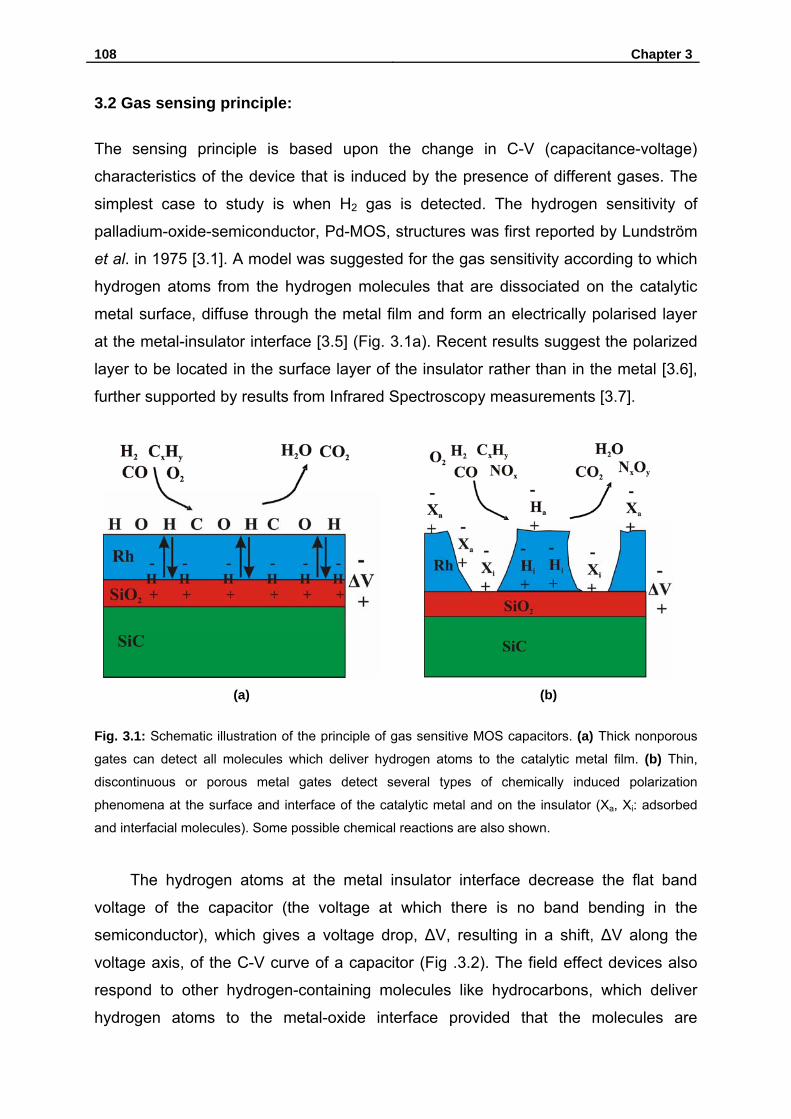
108 Chapter 3
3.2 Gas sensing principle:
The sensing principle is based upon the change in C-V (capacitance-voltage)
characteristics of the device that is induced by the presence of different gases. The
simplest case to study is when H2 gas is detected. The hydrogen sensitivity of
palladium-oxide-semiconductor, Pd-MOS, structures was first reported by Lundström
et al. in 1975 [3.1]. A model was suggested for the gas sensitivity according to which
hydrogen atoms from the hydrogen molecules that are dissociated on the catalytic
metal surface, diffuse through the metal film and form an electrically polarised layer
at the metal-insulator interface [3.5] (Fig. 3.1a). Recent results suggest the polarized
layer to be located in the surface layer of the insulator rather than in the metal [3.6],
further supported by results from Infrared Spectroscopy measurements [3.7].
(a) (b)
Fig. 3.1: Schematic illustration of the principle of gas sensitive MOS capacitors. (a) Thick nonporous
gates can detect all molecules which deliver hydrogen atoms to the catalytic metal film. (b) Thin,
discontinuous or porous metal gates detect several types of chemically induced polarization
phenomena at the surface and interface of the catalytic metal and on the insulator (Xa, Xi: adsorbed
and interfacial molecules). Some possible chemical reactions are also shown.
The hydrogen atoms at the metal insulator interface decrease the flat band
voltage of the capacitor (the voltage at which there is no band bending in the
semiconductor), which gives a voltage drop, ΔV, resulting in a shift, ΔV along the
voltage axis, of the C-V curve of a capacitor (Fig .3.2). The field effect devices also
respond to other hydrogen-containing molecules like hydrocarbons, which deliver
hydrogen atoms to the metal-oxide interface provided that the molecules are
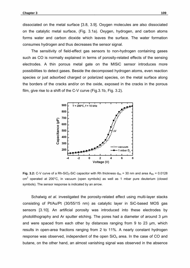
Chapter 3 109
dissociated on the metal surface [3.8, 3.9]. Oxygen molecules are also dissociated
on the catalytic metal surface, (Fig. 3.1a). Oxygen, hydrogen, and carbon atoms
forms water and carbon dioxide which leaves the surface. The water formation
consumes hydrogen and thus decreases the sensor signal.
The sensitivity of field-effect gas sensors to non-hydrogen containing gases
such as CO is normally explained in terms of porosity-related effects of the sensing
electrodes. A thin porous metal gate on the MISiC sensor introduces more
possibilities to detect gases. Beside the decomposed hydrogen atoms, even reaction
species or just adsorbed charged or polarized species, on the metal surface along
the borders of the cracks and/or on the oxide, exposed in the cracks in the porous
film, give rise to a shift of the C-V curve (Fig.3.1b, Fig. 3.2).
Fig. 3.2: C-V curve of a Rh-SiO2-SiC capacitor with Rh thickness dRh = 30 nm and area ARh = 0.0128
cm2 operated at 200°C, in vacuum (open symbols) as well as 1 mbar pure deuterium (closed
symbols). The sensor response is indicated by an arrow.
Schalwig et al. investigated the porosity-related effect using multi-layer stacks
consisting of Pt/Au/Pt (30/55/15 nm) as catalytic layer in SiC-based MOS gas
sensors [3.10]. An artificial porosity was introduced into these electrodes by
photolithography and Ar sputter etching. The pores had a diameter of around 3 µm
and were spaced from each other by distances ranging from 9 to 23 µm, which
results in open-area fractions ranging from 2 to 11%. A nearly constant hydrogen
response was observed, independent of the open SiOx area. In the case of CO and
butane, on the other hand, an almost vanishing signal was observed in the absence
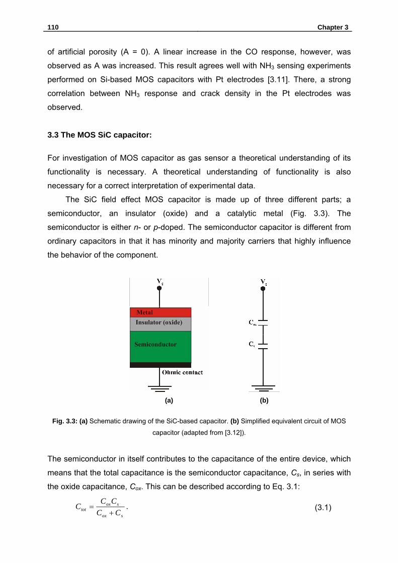
110 Chapter 3
of artificial porosity (A = 0). A linear increase in the CO response, however, was
observed as A was increased. This result agrees well with NH3 sensing experiments
performed on Si-based MOS capacitors with Pt electrodes [3.11]. There, a strong
correlation between NH3 response and crack density in the Pt electrodes was
observed.
3.3 The MOS SiC capacitor:
For investigation of MOS capacitor as gas sensor a theoretical understanding of its
functionality is necessary. A theoretical understanding of functionality is also
necessary for a correct interpretation of experimental data.
The SiC field effect MOS capacitor is made up of three different parts; a
semiconductor, an insulator (oxide) and a catalytic metal (Fig. 3.3). The
semiconductor is either n- or p-doped. The semiconductor capacitor is different from
ordinary capacitors in that it has minority and majority carriers that highly influence
the behavior of the component.
(a) (b)
Fig. 3.3: (a) Schematic drawing of the SiC-based capacitor. (b) Simplified equivalent circuit of MOS
capacitor (adapted from [3.12]).
The semiconductor in itself contributes to the capacitance of the entire device, which
means that the total capacitance is the semiconductor capacitance, Cs, in series with
the oxide capacitance, Cox. This can be described according to Eq. 3.1:
sox
soxtot CC
CCC
+= . (3.1)
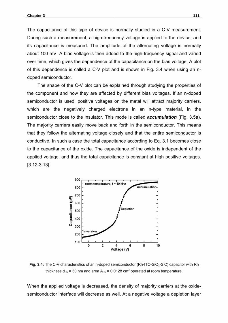
Chapter 3 111
The capacitance of this type of device is normally studied in a C-V measurement.
During such a measurement, a high-frequency voltage is applied to the device, and
its capacitance is measured. The amplitude of the alternating voltage is normally
about 100 mV. A bias voltage is then added to the high-frequency signal and varied
over time, which gives the dependence of the capacitance on the bias voltage. A plot
of this dependence is called a C-V plot and is shown in Fig. 3.4 when using an n-
doped semiconductor.
The shape of the C-V plot can be explained through studying the properties of
the component and how they are affected by different bias voltages. If an n-doped
semiconductor is used, positive voltages on the metal will attract majority carriers,
which are the negatively charged electrons in an n-type material, in the
semiconductor close to the insulator. This mode is called accumulation (Fig. 3.5a).
The majority carriers easily move back and forth in the semiconductor. This means
that they follow the alternating voltage closely and that the entire semiconductor is
conductive. In such a case the total capacitance according to Eq. 3.1 becomes close
to the capacitance of the oxide. The capacitance of the oxide is independent of the
applied voltage, and thus the total capacitance is constant at high positive voltages.
[3.12-3.13].
Fig. 3.4: The C-V characteristics of an n-doped semiconductor (Rh-ITO-SiO2-SiC) capacitor with Rh
thickness dRh = 30 nm and area ARh = 0.0128 cm2 operated at room temperature.
When the applied voltage is decreased, the density of majority carriers at the oxide-
semiconductor interface will decrease as well. At a negative voltage a depletion layer
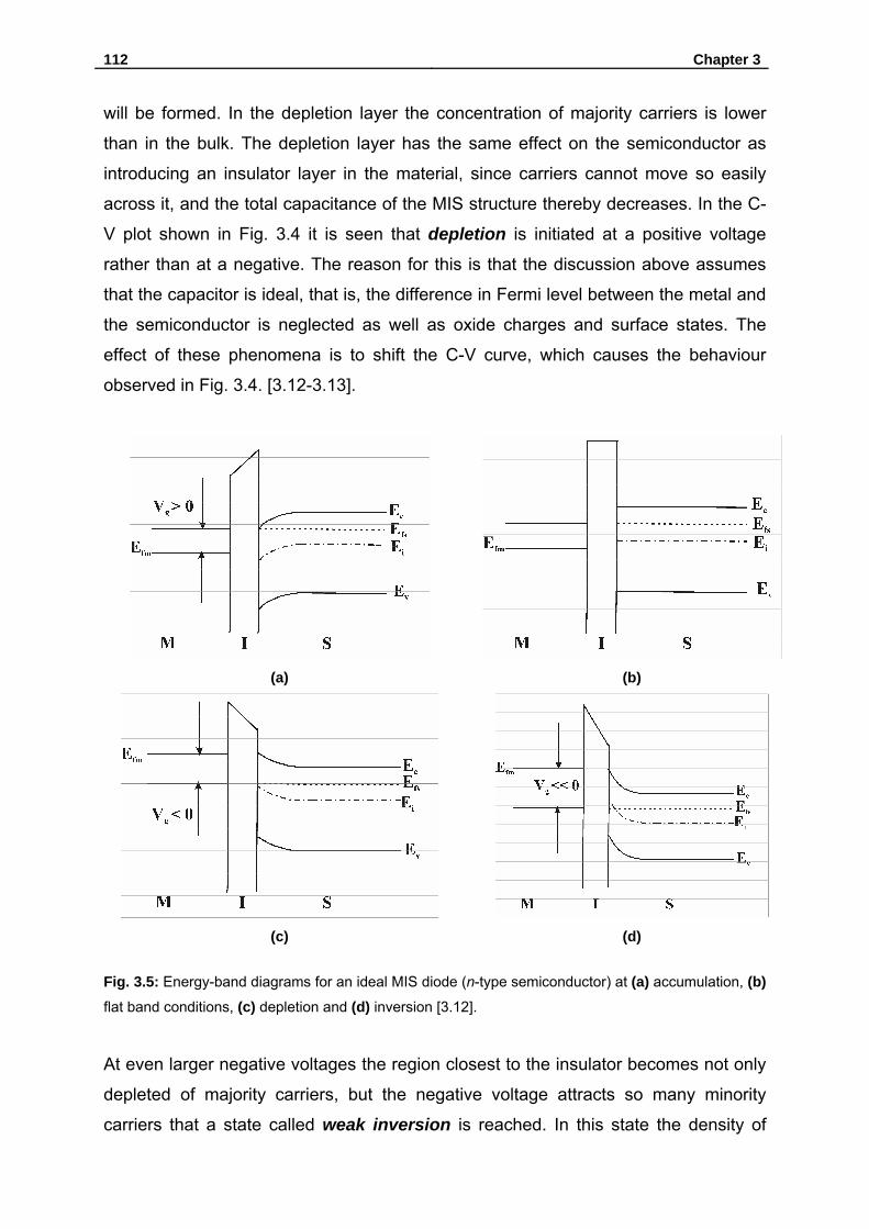
112 Chapter 3
will be formed. In the depletion layer the concentration of majority carriers is lower
than in the bulk. The depletion layer has the same effect on the semiconductor as
introducing an insulator layer in the material, since carriers cannot move so easily
across it, and the total capacitance of the MIS structure thereby decreases. In the C-
V plot shown in Fig. 3.4 it is seen that depletion is initiated at a positive voltage
rather than at a negative. The reason for this is that the discussion above assumes
that the capacitor is ideal, that is, the difference in Fermi level between the metal and
the semiconductor is neglected as well as oxide charges and surface states. The
effect of these phenomena is to shift the C-V curve, which causes the behaviour
observed in Fig. 3.4. [3.12-3.13].
(a) (b)
(c) (d)
Fig. 3.5: Energy-band diagrams for an ideal MIS diode (n-type semiconductor) at (a) accumulation, (b) flat band conditions, (c) depletion and (d) inversion [3.12].
At even larger negative voltages the region closest to the insulator becomes not only
depleted of majority carriers, but the negative voltage attracts so many minority
carriers that a state called weak inversion is reached. In this state the density of
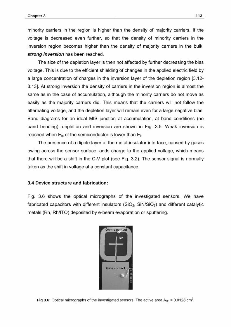
Chapter 3 113
minority carriers in the region is higher than the density of majority carriers. If the
voltage is decreased even further, so that the density of minority carriers in the
inversion region becomes higher than the density of majority carriers in the bulk,
strong inversion has been reached.
The size of the depletion layer is then not affected by further decreasing the bias
voltage. This is due to the efficient shielding of changes in the applied electric field by
a large concentration of charges in the inversion layer of the depletion region [3.12-
3.13]. At strong inversion the density of carriers in the inversion region is almost the
same as in the case of accumulation, although the minority carriers do not move as
easily as the majority carriers did. This means that the carriers will not follow the
alternating voltage, and the depletion layer will remain even for a large negative bias.
Band diagrams for an ideal MIS junction at accumulation, at band conditions (no
band bending), depletion and inversion are shown in Fig. 3.5. Weak inversion is
reached when Efs of the semiconductor is lower than Ei.
The presence of a dipole layer at the metal-insulator interface, caused by gases
owing across the sensor surface, adds charge to the applied voltage, which means
that there will be a shift in the C-V plot (see Fig. 3.2). The sensor signal is normally
taken as the shift in voltage at a constant capacitance.
3.4 Device structure and fabrication:
Fig. 3.6 shows the optical micrographs of the investigated sensors. We have
fabricated capacitors with different insulators (SiO2, SiN/SiO2) and different catalytic
metals (Rh, Rh/ITO) deposited by e-beam evaporation or sputtering.
Fig 3.6: Optical micrographs of the investigated sensors. The active area ARh = 0.0128 cm2.

114 Chapter 3
3.4.1 Sample A:
The epitaxial structure for the MOS capacitor was 3 micron of 1 × 1016 cm-3 n-type
SiC grown on 4H-SiC substrates. After mesa etching, a 50 nm gate oxide (SiO2) was
thermally grown with N2O at 1250°C. Nickel ohmic contacts (55 nm) were deposited
by sputtering by a lift off process after patterning with photoresist and were annealed
at 975°C for 1 min in nitrogen ambient. Finally catalysts were deposited as gate
electrodes.
Two types of catalysts were deposited on the wafers: rhodium (30nm) (sample
A4) and rhodium (30 nm)/Indium oxide-tin oxide (40 nm) (sample A1) stack. The
indium oxide-tin oxide was deposited by co-sputtering indium oxide and tin oxide
simultaneously. Rhodium was deposited by e-beam evaporation for the sample A4
and by puttering for the sample A1. Two types of capacitors were fabricated, a Metal-
Insulator-Silicon Carbide (MOSiC) capacitor and a Metal-Metal Oxide-Insulator-
Silicon Carbide (MMOOSiC) capacitor. The wafer were then diced and individual
chips were attached to TO-8 headers with a ceramic die attach compound. The chips
were then wire bonded to TO-8 heater pins. The cross section of the finished
capacitors (sample A1 and A4) is shown in Fig.3.7.
(a) (b)
Fig. 3.7: Schematic cross section of (a) MMOOSiC capacitor (sample A1) and (b) MOSiC capacitor
(sample A4). The active area of the sensor ARh = 0.0128 cm2.
3.4.2 Sample B:
The epitaxial structure for the MIS capacitor was 1 micron of 2 × 1016 cm-3 n-type SiC
grown on 4H-SiC substrates. After mesa etching, a 33 nm gate oxide (SiO2) was
thermally grown with N2O at 1250°C. Next, 33 nm silicon nitride was deposited at
725°C by low pressure chemical vapor deposition (LPCVD). Nickel ohmic contacts
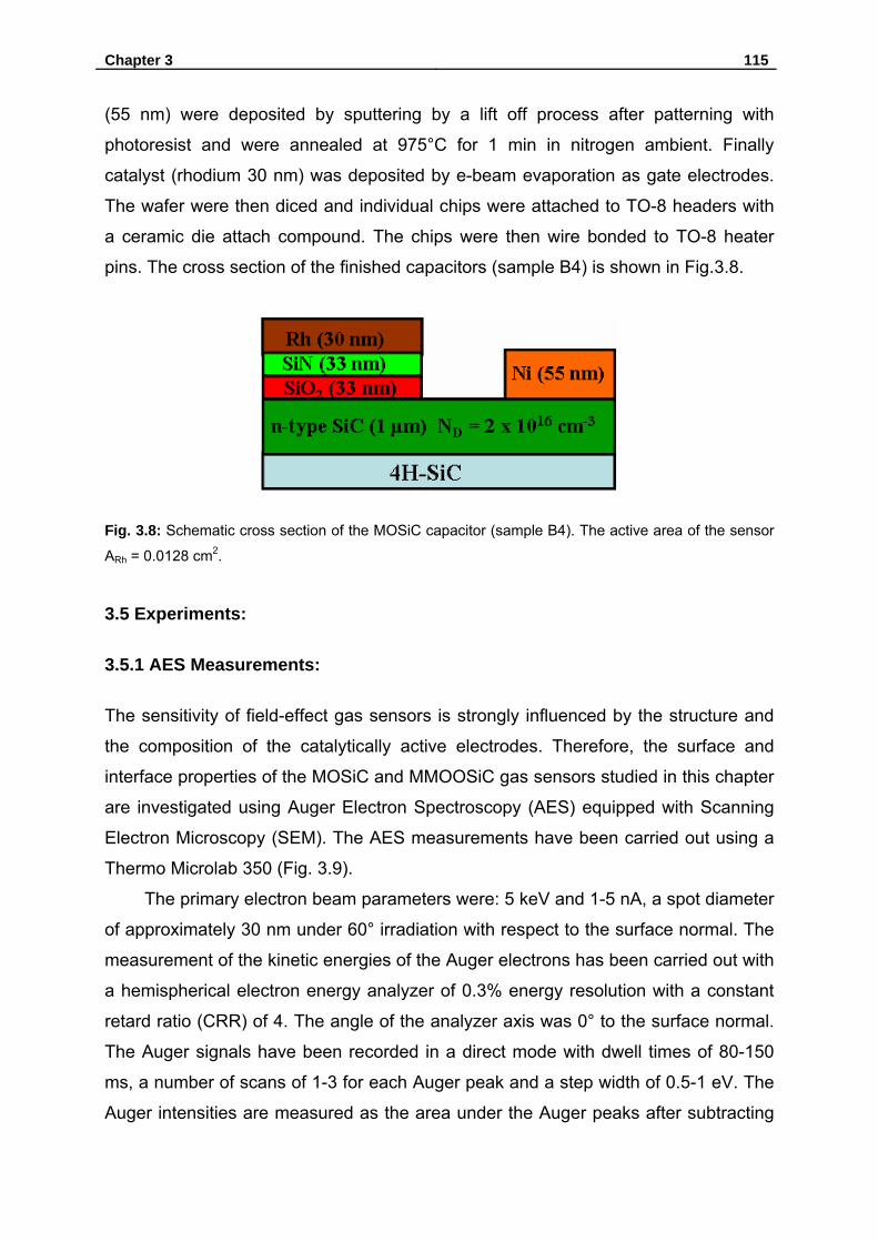
Chapter 3 115
(55 nm) were deposited by sputtering by a lift off process after patterning with
photoresist and were annealed at 975°C for 1 min in nitrogen ambient. Finally
catalyst (rhodium 30 nm) was deposited by e-beam evaporation as gate electrodes.
The wafer were then diced and individual chips were attached to TO-8 headers with
a ceramic die attach compound. The chips were then wire bonded to TO-8 heater
pins. The cross section of the finished capacitors (sample B4) is shown in Fig.3.8.
Fig. 3.8: Schematic cross section of the MOSiC capacitor (sample B4). The active area of the sensor
ARh = 0.0128 cm2.
3.5 Experiments:
3.5.1 AES Measurements:
The sensitivity of field-effect gas sensors is strongly influenced by the structure and
the composition of the catalytically active electrodes. Therefore, the surface and
interface properties of the MOSiC and MMOOSiC gas sensors studied in this chapter
are investigated using Auger Electron Spectroscopy (AES) equipped with Scanning
Electron Microscopy (SEM). The AES measurements have been carried out using a
Thermo Microlab 350 (Fig. 3.9).
The primary electron beam parameters were: 5 keV and 1-5 nA, a spot diameter
of approximately 30 nm under 60° irradiation with respect to the surface normal. The
measurement of the kinetic energies of the Auger electrons has been carried out with
a hemispherical electron energy analyzer of 0.3% energy resolution with a constant
retard ratio (CRR) of 4. The angle of the analyzer axis was 0° to the surface normal.
The Auger signals have been recorded in a direct mode with dwell times of 80-150
ms, a number of scans of 1-3 for each Auger peak and a step width of 0.5-1 eV. The
Auger intensities are measured as the area under the Auger peaks after subtracting
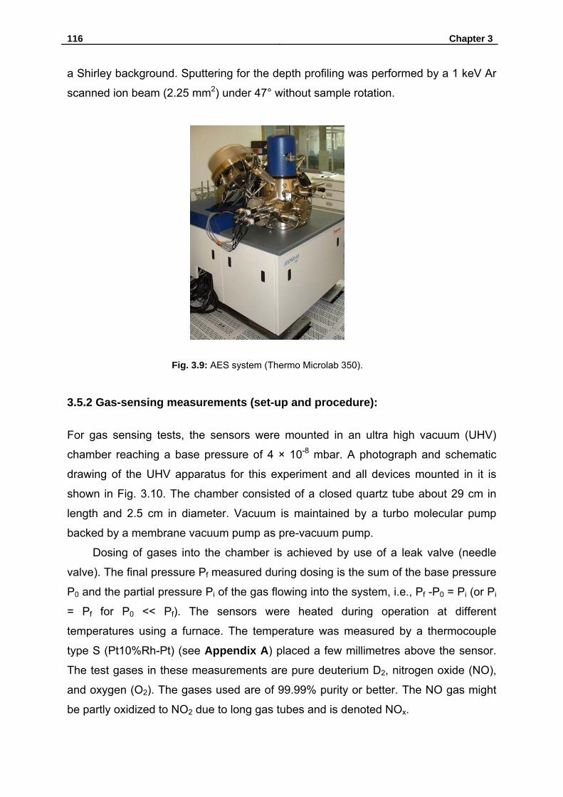
116 Chapter 3
a Shirley background. Sputtering for the depth profiling was performed by a 1 keV Ar
scanned ion beam (2.25 mm2) under 47° without sample rotation.
Fig. 3.9: AES system (Thermo Microlab 350).
3.5.2 Gas-sensing measurements (set-up and procedure):
For gas sensing tests, the sensors were mounted in an ultra high vacuum (UHV)
chamber reaching a base pressure of 4 × 10⁻⁸ mbar. A photograph and schematic
drawing of the UHV apparatus for this experiment and all devices mounted in it is
shown in Fig. 3.10. The chamber consisted of a closed quartz tube about 29 cm in
length and 2.5 cm in diameter. Vacuum is maintained by a turbo molecular pump
backed by a membrane vacuum pump as pre-vacuum pump.
Dosing of gases into the chamber is achieved by use of a leak valve (needle
valve). The final pressure Pf measured during dosing is the sum of the base pressure
P0 and the partial pressure Pi of the gas flowing into the system, i.e., Pf -P0 = Pi (or Pi
= Pf for P0 << Pf). The sensors were heated during operation at different
temperatures using a furnace. The temperature was measured by a thermocouple
type S (Pt10%Rh-Pt) (see Appendix A) placed a few millimetres above the sensor.
The test gases in these measurements are pure deuterium D2, nitrogen oxide (NO),
and oxygen (O2). The gases used are of 99.99% purity or better. The NO gas might
be partly oxidized to NO2 due to long gas tubes and is denoted NOx.

Chapter 3 117
1: Sensor
2: Quartz tube
3: Furnace
4: Pressure measurements
5: MKS Baratron guage
6: Pump station
7: Sensor contacts
8: Needle valve
9: NO bottle
10: H2 bottle
11: O2 bottle (a)
(b)
Fig. 3.10: Gas measurements system. (a) Photograph (b) Schematic drawing.
The electrical properties were evaluated by measuring capacitance-voltage (C-V)
characteristics, obtained from an Impedance Analyzer (Solartron 1296) operated at
10 kHz. Measuring the (C-V) characteristics of MOS devices at high frequencies, a
118 Chapter 3
low capacitance is observed in the case of inversion and a high capacitance in the
case of accumulation. The interaction of gas molecules with MOS-SiC devices gives
rise to changes in the (C-V) curves. In the case of reducing gases like D2, the C-V
curve is shifted toward negative voltages, i.e., to the left and into the opposite
direction in the case of oxidizing gases (NOx, O2). During exposure to gas, the
capacitance was held constant by controlling the bias voltage. This bias voltage is
the sensor signal.
The gas response R is the difference between the steady state voltages
measured at the test gas exposure and in vacuum. We have defined the gas
response R as the voltage variation at constant capacitance:
gv VVVR −=Δ= , .constC = , (3.2)
where Vv and Vg are the voltage of the sensor in vacuum and in the presence of gas,
respectively. The voltage shift obtained in the case of reducing gases was defined as
positive and in the case of oxidizing gases as negative.
The sensitivity S is given by:
[ ]mbarCRS
gas
= , (3.3)
where Cg is the gas partial pressure in mbar.
3.6 Results:
3.6.1 Sample A4:
3.6.1.1 Chemical characterization (AES results):
Fig. 3.11a shows a typical Auger spectrum taken from two different areas of the
active sensor area as shown in the SEM image (Fig. 3.11b). The only impurity
detected from Rh film is carbon (C), which remains even after sputtering process for
8 min. One reason we can think of is the packaging process.
The AES depth profile in Fig. 3.12 revealed shows that the sample structure
includes Rh, SiOx, and SiC layers, as well as carbon or carbon containing molecules.
Silicon and oxygen was detected both in the bulk and on the surface of Rh due to
annealing in N2.

Chapter 3 119
(a) (b)
Fig. 3.11: (a) Typical Auger spectrum of the active sensor area. (b) SEM image of Rh surface.
Fig. 3.12: Auger depth profiles of the active sensor area.
3.6.1.2 NOx detection:
Fig. 3.13 shows the high frequency (10 kHz) C-V and 1/C2-V characteristics of the
sensor A4 at room temperature in vacuum and in the presence of different partial
pressures of pure NOx. Exposure to NOx results in a flat band voltage occurring at a
more positive bias than in vacuum. The shifts in the flat-band voltages due to NOx
were estimated by measuring the voltage differences at a capacitance of 400 pF.
This value, ΔV, is shown in Fig. 3.14a as a function of NOx partial pressures
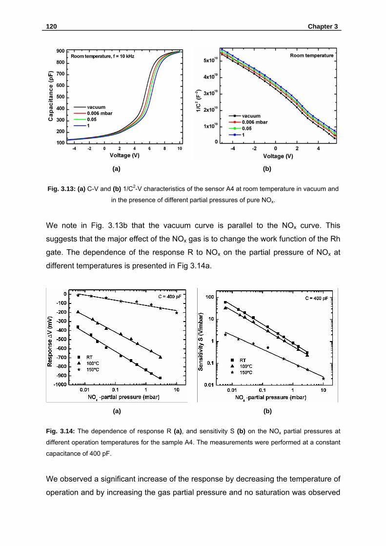
120 Chapter 3
(a) (b)
Fig. 3.13: (a) C-V and (b) 1/C2-V characteristics of the sensor A4 at room temperature in vacuum and
in the presence of different partial pressures of pure NOx.
We note in Fig. 3.13b that the vacuum curve is parallel to the NOx curve. This
suggests that the major effect of the NOx gas is to change the work function of the Rh
gate. The dependence of the response R to NOx on the partial pressure of NOx at
different temperatures is presented in Fig 3.14a.
(a) (b)
Fig. 3.14: The dependence of response R (a), and sensitivity S (b) on the NOx partial pressures at
different operation temperatures for the sample A4. The measurements were performed at a constant
capacitance of 400 pF.
We observed a significant increase of the response by decreasing the temperature of
operation and by increasing the gas partial pressure and no saturation was observed
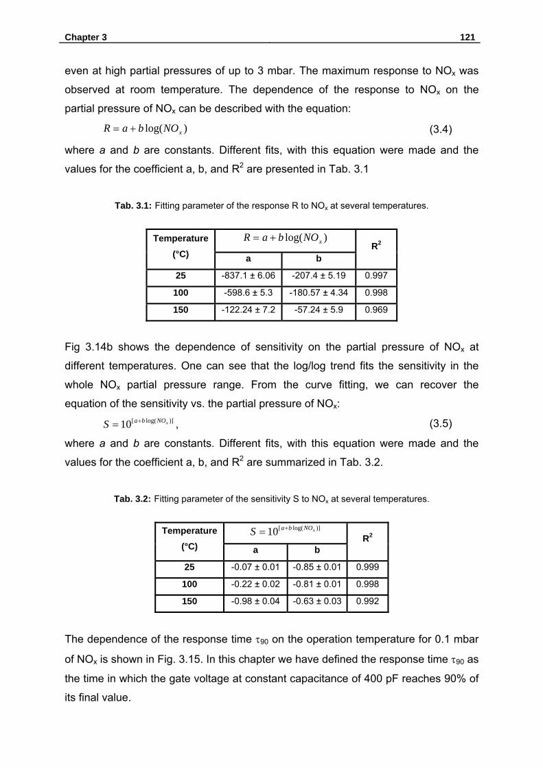
Chapter 3 121
even at high partial pressures of up to 3 mbar. The maximum response to NOx was
observed at room temperature. The dependence of the response to NOx on the
partial pressure of NOx can be described with the equation:
)log( xNObaR += (3.4)
where a and b are constants. Different fits, with this equation were made and the
values for the coefficient a, b, and R2 are presented in Tab. 3.1
Tab. 3.1: Fitting parameter of the response R to NOx at several temperatures.
)log( xNObaR += Temperature (°C) a b
R2
25 -837.1 ± 6.06 -207.4 ± 5.19 0.997
100 -598.6 ± 5.3 -180.57 ± 4.34 0.998
150 -122.24 ± 7.2 -57.24 ± 5.9 0.969
Fig 3.14b shows the dependence of sensitivity on the partial pressure of NOx at
different temperatures. One can see that the log/log trend fits the sensitivity in the
whole NOx partial pressure range. From the curve fitting, we can recover the
equation of the sensitivity vs. the partial pressure of NOx:
)]log([10 xNObaS += , (3.5)
where a and b are constants. Different fits, with this equation were made and the
values for the coefficient a, b, and R2 are summarized in Tab. 3.2.
Tab. 3.2: Fitting parameter of the sensitivity S to NOx at several temperatures.
)]log([10 xNObaS += Temperature (°C) a b
R2
25 -0.07 ± 0.01 -0.85 ± 0.01 0.999
100 -0.22 ± 0.02 -0.81 ± 0.01 0.998
150 -0.98 ± 0.04 -0.63 ± 0.03 0.992
The dependence of the response time τ90 on the operation temperature for 0.1 mbar
of NOx is shown in Fig. 3.15. In this chapter we have defined the response time τ90 as
the time in which the gate voltage at constant capacitance of 400 pF reaches 90% of
its final value.
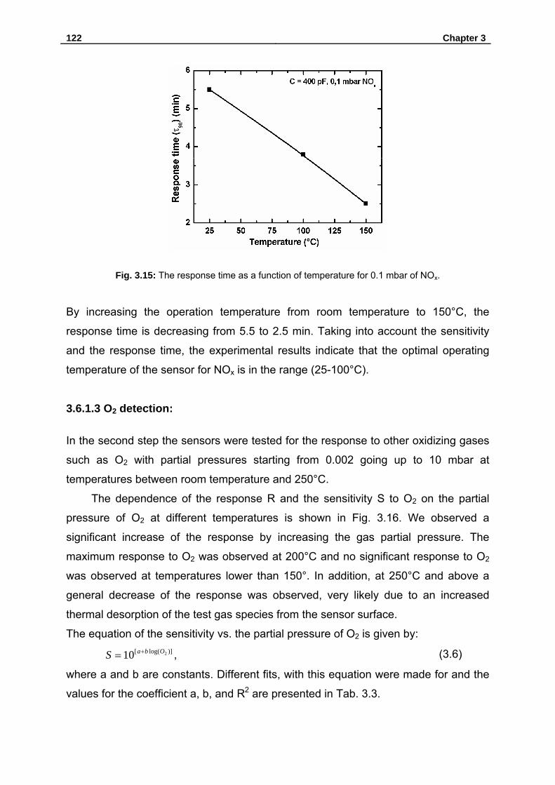
122 Chapter 3
Fig. 3.15: The response time as a function of temperature for 0.1 mbar of NOx.
By increasing the operation temperature from room temperature to 150°C, the
response time is decreasing from 5.5 to 2.5 min. Taking into account the sensitivity
and the response time, the experimental results indicate that the optimal operating
temperature of the sensor for NOx is in the range (25-100°C).
3.6.1.3 O2 detection:
In the second step the sensors were tested for the response to other oxidizing gases
such as O2 with partial pressures starting from 0.002 going up to 10 mbar at
temperatures between room temperature and 250°C.
The dependence of the response R and the sensitivity S to O2 on the partial
pressure of O2 at different temperatures is shown in Fig. 3.16. We observed a
significant increase of the response by increasing the gas partial pressure. The
maximum response to O2 was observed at 200°C and no significant response to O2
was observed at temperatures lower than 150°. In addition, at 250°C and above a
general decrease of the response was observed, very likely due to an increased
thermal desorption of the test gas species from the sensor surface.
The equation of the sensitivity vs. the partial pressure of O2 is given by:
)]log([ 210 ObaS += , (3.6)
where a and b are constants. Different fits, with this equation were made for and the
values for the coefficient a, b, and R2 are presented in Tab. 3.3.
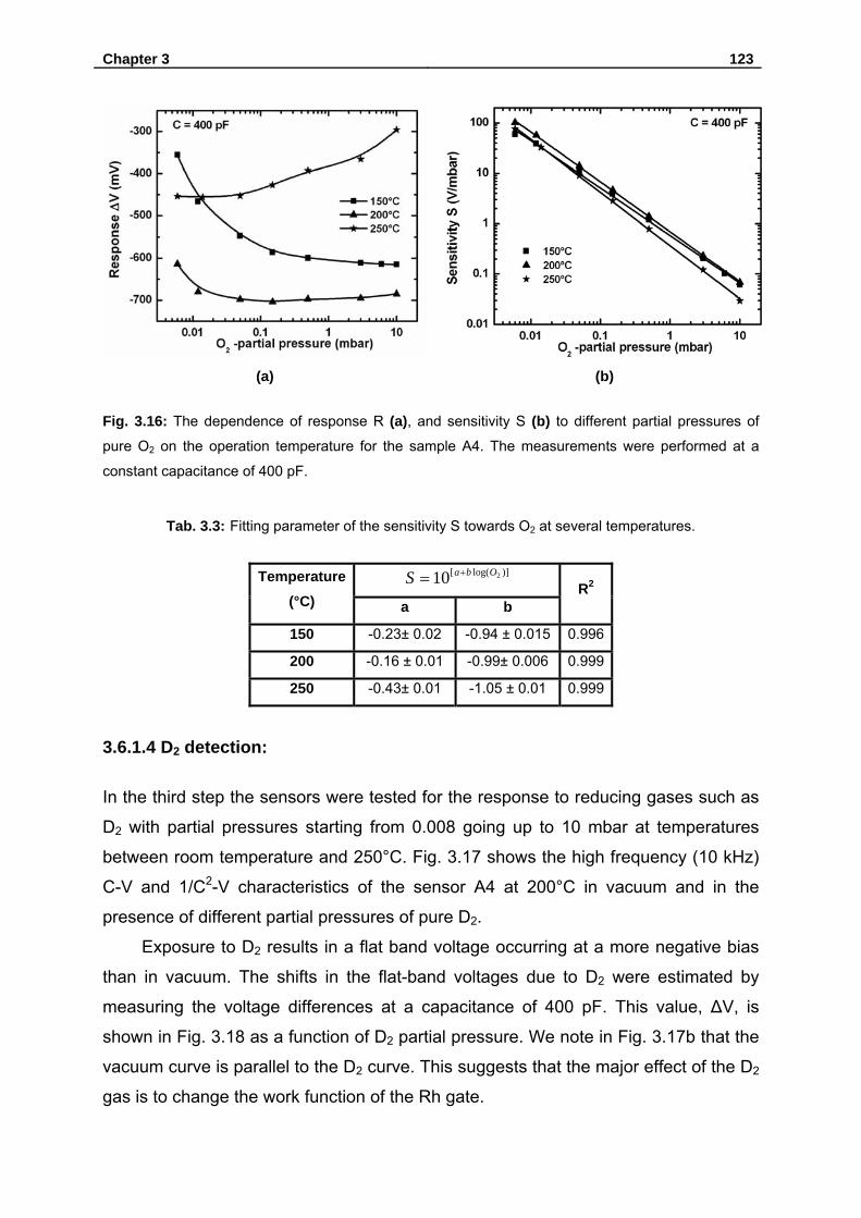
Chapter 3 123
(a) (b)
Fig. 3.16: The dependence of response R (a), and sensitivity S (b) to different partial pressures of
pure O2 on the operation temperature for the sample A4. The measurements were performed at a
constant capacitance of 400 pF.
Tab. 3.3: Fitting parameter of the sensitivity S towards O2 at several temperatures.
)]log([ 210 ObaS += Temperature (°C) a b
R2
150 -0.23± 0.02 -0.94 ± 0.015 0.996
200 -0.16 ± 0.01 -0.99± 0.006 0.999
250 -0.43± 0.01 -1.05 ± 0.01 0.999
3.6.1.4 D2 detection:
In the third step the sensors were tested for the response to reducing gases such as
D2 with partial pressures starting from 0.008 going up to 10 mbar at temperatures
between room temperature and 250°C. Fig. 3.17 shows the high frequency (10 kHz)
C-V and 1/C2-V characteristics of the sensor A4 at 200°C in vacuum and in the
presence of different partial pressures of pure D2.
Exposure to D2 results in a flat band voltage occurring at a more negative bias
than in vacuum. The shifts in the flat-band voltages due to D2 were estimated by
measuring the voltage differences at a capacitance of 400 pF. This value, ΔV, is
shown in Fig. 3.18 as a function of D2 partial pressure. We note in Fig. 3.17b that the
vacuum curve is parallel to the D2 curve. This suggests that the major effect of the D2
gas is to change the work function of the Rh gate.
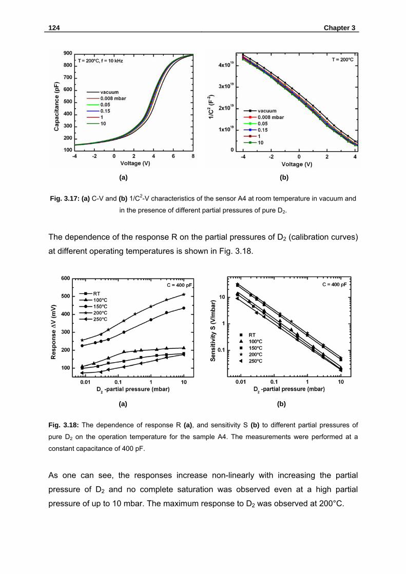
124 Chapter 3
(a) (b)
Fig. 3.17: (a) C-V and (b) 1/C2-V characteristics of the sensor A4 at room temperature in vacuum and
in the presence of different partial pressures of pure D2.
The dependence of the response R on the partial pressures of D2 (calibration curves)
at different operating temperatures is shown in Fig. 3.18.
(a) (b)
Fig. 3.18: The dependence of response R (a), and sensitivity S (b) to different partial pressures of
pure D2 on the operation temperature for the sample A4. The measurements were performed at a
constant capacitance of 400 pF.
As one can see, the responses increase non-linearly with increasing the partial
pressure of D2 and no complete saturation was observed even at a high partial
pressure of up to 10 mbar. The maximum response to D2 was observed at 200°C.
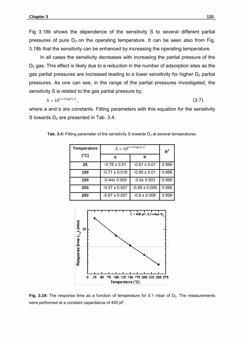
Chapter 3 125
Fig 3.18b shows the dependence of the sensitivity S to several different partial
pressures of pure D2 on the operating temperature. It can be seen also from Fig.
3.18b that the sensitivity can be enhanced by increasing the operating temperature.
In all cases the sensitivity decreases with increasing the partial pressure of the
D2 gas. This effect is likely due to a reduction in the number of adsorption sites as the
gas partial pressures are increased leading to a lower sensitivity for higher D2 partial
pressures. As one can see, in the range of the partial pressures investigated, the
sensitivity S is related to the gas partial pressure by:
)]log([ 210 DbaS += , (3.7)
where a and b are constants. Fitting parameters with this equation for the sensitivity
S towards D2 are presented in Tab. 3.4.
Tab. 3.4: Fitting parameter of the sensitivity S towards D2 at several temperatures.
)]log([ 210 DbaS += Temperature (°C) a b
R2
25 -0.78 ± 0.01 -0.91 ± 0.01 0.999
100 -0.71 ± 0.018 -0.90 ± 0.01 0.998
150 -0.44± 0.005 -0.9± 0.003 0.999
200 -0.37 ± 0.007 -0.89 ± 0.006 0.999
250 -0.87 ± 0.007 -0.9 ± 0.006 0.999
Fig. 3.19: The response time as a function of temperature for 0.1 mbar of D2. The measurements
were performed at a constant capacitance of 400 pF.

126 Chapter 3
Fig. 3.19 reveals the response time as a function of temperature for 0.1 mbar of D2. It
becomes obvious from Fig. 3.19 that the response time can be reduced by increasing
the operating temperature. The response time is decreasing from 15 to ~ 2 min by
increasing the temperature of operation from room temperature to 250°C.
3.6.1.5 Conclusion:
The operating temperature defines the single most effective control of sensor
performance. The response of the sensors can be tailored via control of the
temperature of the sensor. The dependence of the responses R to 0.05, 0.15, and 3
mbar of pure NOx, O2, and D2 on the operating temperature is presented in Fig. 3.20.
(a) (b)
Fig. 3.20: (a) The dependence of the response R to 0.05, 0.15 and 3 mbar of NOx, O2, and D2, on the
operating temperature. The measurements were performed at a constant capacitance of 400 pF. (b) Block presentations for 0.15 mbar of the all three gases.
As one can see, the optimum detection temperatures occur in the range of 25-
75 °C for NOx. In this range no response to O2 was observed and the cross response
to D2 is very low indicating that the sensor is very suitable for selective detection of
NOx at low temperatures. The optimum temperature of operation for detection of
deuterium is determined to be between 115-140°C. In this range no significant
response to O2 and NOx is observed indicating that the sensor is very suitable for
selective D2 detection at very low temperatures. In the range 225-250°C the
response to D2 is low and no response to NOx was observed, therefore, the sensor
A4 can be used as O2 gas sensor in this range.
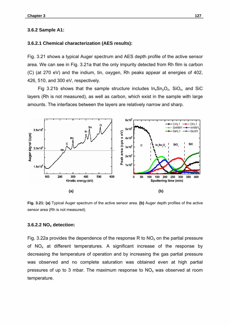
Chapter 3 127
3.6.2 Sample A1:
3.6.2.1 Chemical characterization (AES results):
Fig. 3.21 shows a typical Auger spectrum and AES depth profile of the active sensor
area. We can see in Fig. 3.21a that the only impurity detected from Rh film is carbon
(C) (at 270 eV) and the indium, tin, oxygen, Rh peaks appear at energies of 402,
426, 510, and 300 eV, respectively.
Fig 3.21b shows that the sample structure includes InxSnyOz, SiOx, and SiC
layers (Rh is not measured), as well as carbon, which exist in the sample with large
amounts. The interfaces between the layers are relatively narrow and sharp.
(a) (b)
Fig. 3.21: (a) Typical Auger spectrum of the active sensor area. (b) Auger depth profiles of the active
sensor area (Rh is not measured).
3.6.2.2 NOx detection:
Fig. 3.22a provides the dependence of the response R to NOx on the partial pressure
of NOx at different temperatures. A significant increase of the response by
decreasing the temperature of operation and by increasing the gas partial pressure
was observed and no complete saturation was obtained even at high partial
pressures of up to 3 mbar. The maximum response to NOx was observed at room
temperature.
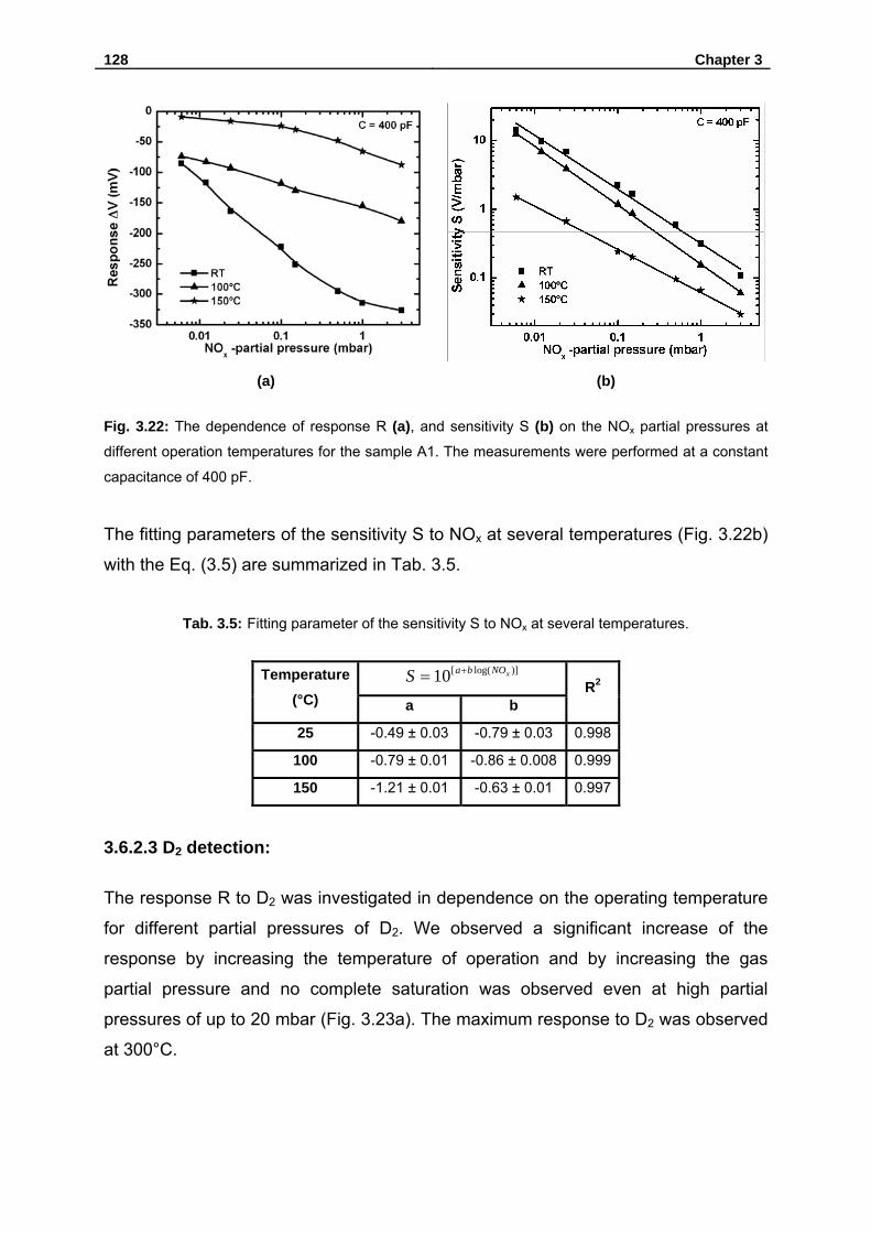
128 Chapter 3
(a) (b)
Fig. 3.22: The dependence of response R (a), and sensitivity S (b) on the NOx partial pressures at
different operation temperatures for the sample A1. The measurements were performed at a constant
capacitance of 400 pF.
The fitting parameters of the sensitivity S to NOx at several temperatures (Fig. 3.22b)
with the Eq. (3.5) are summarized in Tab. 3.5.
Tab. 3.5: Fitting parameter of the sensitivity S to NOx at several temperatures.
)]log([10 xNObaS += Temperature (°C) a b
R2
25 -0.49 ± 0.03 -0.79 ± 0.03 0.998
100 -0.79 ± 0.01 -0.86 ± 0.008 0.999
150 -1.21 ± 0.01 -0.63 ± 0.01 0.997
3.6.2.3 D2 detection:
The response R to D2 was investigated in dependence on the operating temperature
for different partial pressures of D2. We observed a significant increase of the
response by increasing the temperature of operation and by increasing the gas
partial pressure and no complete saturation was observed even at high partial
pressures of up to 20 mbar (Fig. 3.23a). The maximum response to D2 was observed
at 300°C.
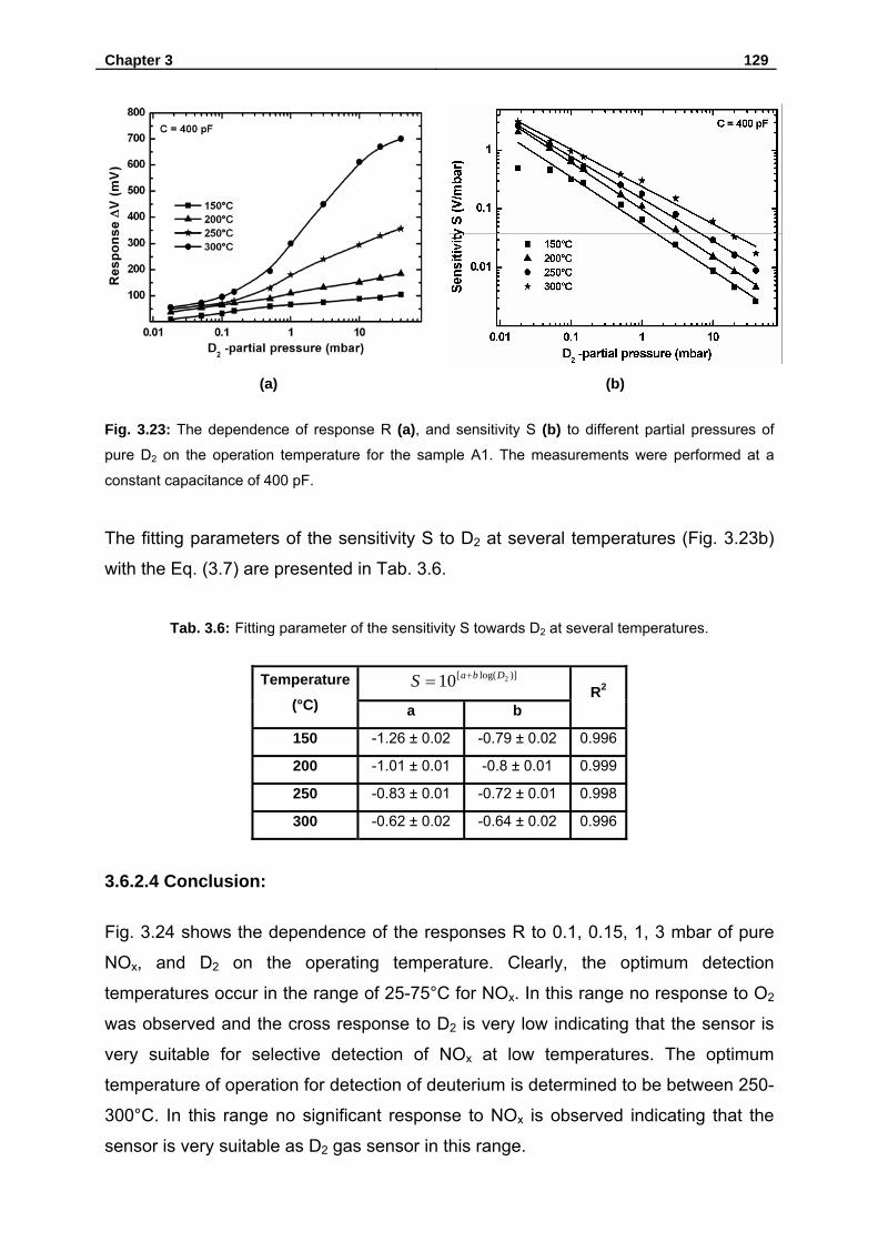
Chapter 3 129
(a) (b)
Fig. 3.23: The dependence of response R (a), and sensitivity S (b) to different partial pressures of
pure D2 on the operation temperature for the sample A1. The measurements were performed at a
constant capacitance of 400 pF.
The fitting parameters of the sensitivity S to D2 at several temperatures (Fig. 3.23b)
with the Eq. (3.7) are presented in Tab. 3.6.
Tab. 3.6: Fitting parameter of the sensitivity S towards D2 at several temperatures.
)]log([ 210 DbaS += Temperature (°C) a b
R2
150 -1.26 ± 0.02 -0.79 ± 0.02 0.996
200 -1.01 ± 0.01 -0.8 ± 0.01 0.999
250 -0.83 ± 0.01 -0.72 ± 0.01 0.998
300 -0.62 ± 0.02 -0.64 ± 0.02 0.996
3.6.2.4 Conclusion:
Fig. 3.24 shows the dependence of the responses R to 0.1, 0.15, 1, 3 mbar of pure
NOx, and D2 on the operating temperature. Clearly, the optimum detection
temperatures occur in the range of 25-75°C for NOx. In this range no response to O2
was observed and the cross response to D2 is very low indicating that the sensor is
very suitable for selective detection of NOx at low temperatures. The optimum
temperature of operation for detection of deuterium is determined to be between 250-
300°C. In this range no significant response to NOx is observed indicating that the
sensor is very suitable as D2 gas sensor in this range.
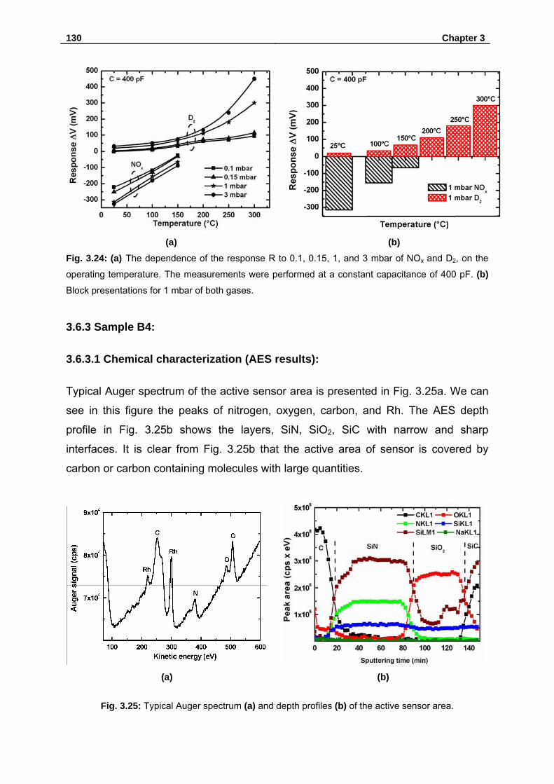
130 Chapter 3
(a) (b) Fig. 3.24: (a) The dependence of the response R to 0.1, 0.15, 1, and 3 mbar of NOx and D2, on the
operating temperature. The measurements were performed at a constant capacitance of 400 pF. (b) Block presentations for 1 mbar of both gases.
3.6.3 Sample B4:
3.6.3.1 Chemical characterization (AES results):
Typical Auger spectrum of the active sensor area is presented in Fig. 3.25a. We can
see in this figure the peaks of nitrogen, oxygen, carbon, and Rh. The AES depth
profile in Fig. 3.25b shows the layers, SiN, SiO2, SiC with narrow and sharp
interfaces. It is clear from Fig. 3.25b that the active area of sensor is covered by
carbon or carbon containing molecules with large quantities.
(a) (b)
Fig. 3.25: Typical Auger spectrum (a) and depth profiles (b) of the active sensor area.
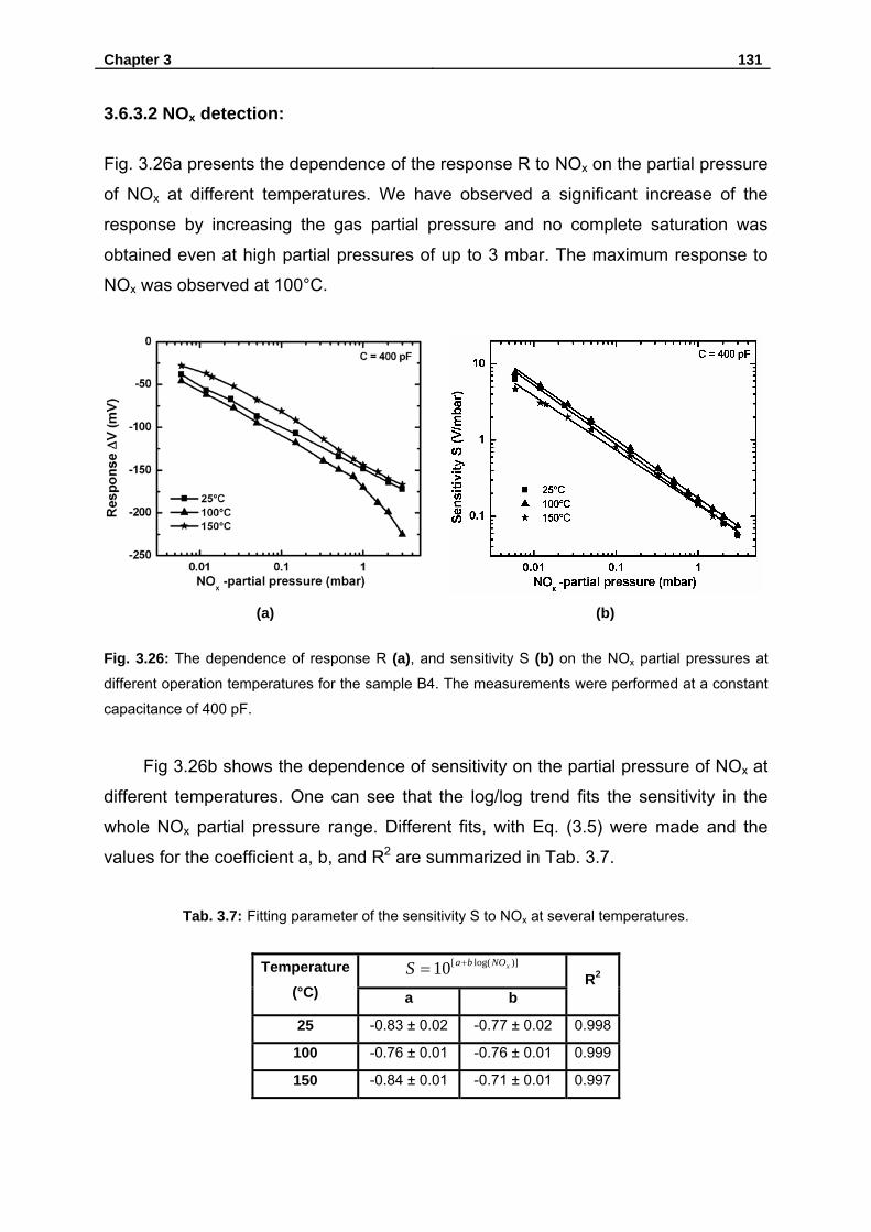
Chapter 3 131
3.6.3.2 NOx detection:
Fig. 3.26a presents the dependence of the response R to NOx on the partial pressure
of NOx at different temperatures. We have observed a significant increase of the
response by increasing the gas partial pressure and no complete saturation was
obtained even at high partial pressures of up to 3 mbar. The maximum response to
NOx was observed at 100°C.
(a) (b)
Fig. 3.26: The dependence of response R (a), and sensitivity S (b) on the NOx partial pressures at
different operation temperatures for the sample B4. The measurements were performed at a constant
capacitance of 400 pF.
Fig 3.26b shows the dependence of sensitivity on the partial pressure of NOx at
different temperatures. One can see that the log/log trend fits the sensitivity in the
whole NOx partial pressure range. Different fits, with Eq. (3.5) were made and the
values for the coefficient a, b, and R2 are summarized in Tab. 3.7.
Tab. 3.7: Fitting parameter of the sensitivity S to NOx at several temperatures.
)]log([10 xNObaS += Temperature (°C) a b
R2
25 -0.83 ± 0.02 -0.77 ± 0.02 0.998
100 -0.76 ± 0.01 -0.76 ± 0.01 0.999
150 -0.84 ± 0.01 -0.71 ± 0.01 0.997
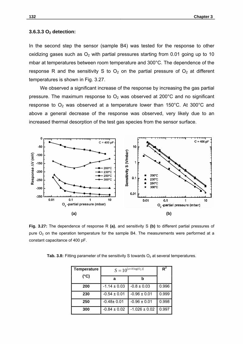
132 Chapter 3
3.6.3.3 O2 detection:
In the second step the sensor (sample B4) was tested for the response to other
oxidizing gases such as O2 with partial pressures starting from 0.01 going up to 10
mbar at temperatures between room temperature and 300°C. The dependence of the
response R and the sensitivity S to O2 on the partial pressure of O2 at different
temperatures is shown in Fig. 3.27.
We observed a significant increase of the response by increasing the gas partial
pressure. The maximum response to O2 was observed at 200°C and no significant
response to O2 was observed at a temperature lower than 150°C. At 300°C and
above a general decrease of the response was observed, very likely due to an
increased thermal desorption of the test gas species from the sensor surface.
(a) (b)
Fig. 3.27: The dependence of response R (a), and sensitivity S (b) to different partial pressures of
pure O2 on the operation temperature for the sample B4. The measurements were performed at a
constant capacitance of 400 pF.
Tab. 3.8: Fitting parameter of the sensitivity S towards O2 at several temperatures.
)]log([ 210 ObaS += Temperature (°C) a b
R2
200 -1.14 ± 0.03 -0.8 ± 0.03 0.996
230 -0.54 ± 0.01 -0.96 ± 0.01 0.999
250 -0.48± 0.01 -0.96 ± 0.01 0.998
300 -0.84 ± 0.02 -1.026 ± 0.02 0.997
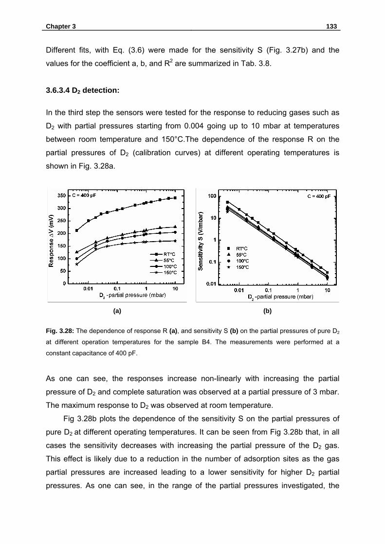
Chapter 3 133
Different fits, with Eq. (3.6) were made for the sensitivity S (Fig. 3.27b) and the
values for the coefficient a, b, and R2 are summarized in Tab. 3.8.
3.6.3.4 D2 detection:
In the third step the sensors were tested for the response to reducing gases such as
D2 with partial pressures starting from 0.004 going up to 10 mbar at temperatures
between room temperature and 150°C.The dependence of the response R on the
partial pressures of D2 (calibration curves) at different operating temperatures is
shown in Fig. 3.28a.
(a) (b)
Fig. 3.28: The dependence of response R (a), and sensitivity S (b) on the partial pressures of pure D2
at different operation temperatures for the sample B4. The measurements were performed at a
constant capacitance of 400 pF.
As one can see, the responses increase non-linearly with increasing the partial
pressure of D2 and complete saturation was observed at a partial pressure of 3 mbar.
The maximum response to D2 was observed at room temperature.
Fig 3.28b plots the dependence of the sensitivity S on the partial pressures of
pure D2 at different operating temperatures. It can be seen from Fig 3.28b that, in all
cases the sensitivity decreases with increasing the partial pressure of the D2 gas.
This effect is likely due to a reduction in the number of adsorption sites as the gas
partial pressures are increased leading to a lower sensitivity for higher D2 partial
pressures. As one can see, in the range of the partial pressures investigated, the
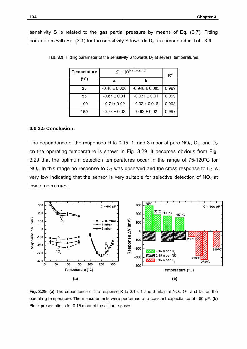
134 Chapter 3
sensitivity S is related to the gas partial pressure by means of Eq. (3.7). Fitting
parameters with Eq. (3.4) for the sensitivity S towards D2 are presented in Tab. 3.9.
Tab. 3.9: Fitting parameter of the sensitivity S towards D2 at several temperatures.
)]log([ 210 DbaS += Temperature (°C) a b
R2
25 -0.48 ± 0.006 -0.948 ± 0.005 0.999
55 -0.67 ± 0.01 -0.931 ± 0.01 0.999
100 -0.71± 0.02 -0.92 ± 0.016 0.998
150 -0.78 ± 0.03 -0.92 ± 0.02 0.997
3.6.3.5 Conclusion:
The dependence of the responses R to 0.15, 1, and 3 mbar of pure NOx, O2, and D2
on the operating temperature is shown in Fig. 3.29. It becomes obvious from Fig.
3.29 that the optimum detection temperatures occur in the range of 75-120°C for
NOx. In this range no response to O2 was observed and the cross response to D2 is
very low indicating that the sensor is very suitable for selective detection of NOx at
low temperatures.
(a) (b)
Fig. 3.29: (a) The dependence of the response R to 0.15, 1 and 3 mbar of NOx, O2, and D2, on the
operating temperature. The measurements were performed at a constant capacitance of 400 pF. (b) Block presentations for 0.15 mbar of the all three gases.
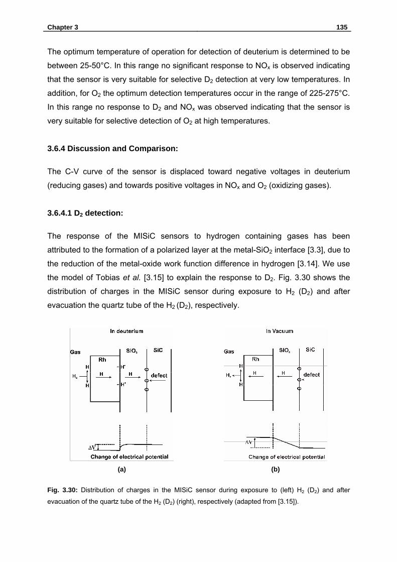
Chapter 3 135
The optimum temperature of operation for detection of deuterium is determined to be
between 25-50°C. In this range no significant response to NOx is observed indicating
that the sensor is very suitable for selective D2 detection at very low temperatures. In
addition, for O2 the optimum detection temperatures occur in the range of 225-275°C.
In this range no response to D2 and NOx was observed indicating that the sensor is
very suitable for selective detection of O2 at high temperatures.
3.6.4 Discussion and Comparison:
The C-V curve of the sensor is displaced toward negative voltages in deuterium
(reducing gases) and towards positive voltages in NOx and O2 (oxidizing gases).
3.6.4.1 D2 detection:
The response of the MISiC sensors to hydrogen containing gases has been
attributed to the formation of a polarized layer at the metal-SiO2 interface [3.3], due to
the reduction of the metal-oxide work function difference in hydrogen [3.14]. We use
the model of Tobias et al. [3.15] to explain the response to D2. Fig. 3.30 shows the
distribution of charges in the MISiC sensor during exposure to H2 (D2) and after
evacuation the quartz tube of the H2 (D2), respectively.
(a) (b)
Fig. 3.30: Distribution of charges in the MISiC sensor during exposure to (left) H2 (D2) and after
evacuation of the quartz tube of the H2 (D2) (right), respectively (adapted from [3.15]).
136 Chapter 3
For an MISiC device biased at constant capacitance, the potentials in the SiC are
constant, regardless of gas exposure. In a hydrogen (deuterium) ambient, the
hydrogen (deuterium) is dissociating at the Rh surface and diffusing relatively fast
into the sensor. A polarized layer builds up at the Rh-SiO2 interface with the protons
in the SiO2 and the electrons in the metal. With the polarized layer present, the
potential of the Rh decreases in hydrogen (deuterium). As a result, the flat band
voltage of the capacitor decreases, which gives a voltage drop, ΔV, resulting in a
shift, ΔV along the voltage axis, of the C-V curve of a capacitor. After evacuation of
the quartz tube of the D2, the disappearance of the polarized layer at the metal-SiO2
interface increases the potential of the Rh and the sensor signal returns to initial
value after a few minutes.
3.6.4.2 O2 and NOx detection:
We use the model of Schalwig et al. [3.10] to explain the response to O2 and NOx. It
is supposed in Fig. 3.31a that, at the beginning, no electrical connection exists
between the porous catalytic metal electrode and the semiconductor contact.
Assuming that the Rh-MOSiC gas sensor is operated in an oxygen-containing gas
ambient, molecular oxygen will dissociate and chemisorb as individual atoms on the
Rh surface.
Oxygen atoms will also be present on the neighboring exposed patches of oxide due
to spillover effects [3.16]. This spillover leaves negative ionic surface charge on the
exposed patches of oxide and positive electronic charge on the Rh clusters of the
porous electrode. These surface charges will be balanced by immobile positive donor
and mobile negative electron charges in the semiconductor [3.10]. Therefore, an
electrostatic potential between the Rh and the SiC arises due to the positive charge
on the Rh electrode.
Within the band picture (Fig. 3.31a), which neglects the effects of electrode
porosity, the overall effect of spillover-induced charge separation is modeled by an
increase in the metal work function Φm relative to the semiconductor [3.10].
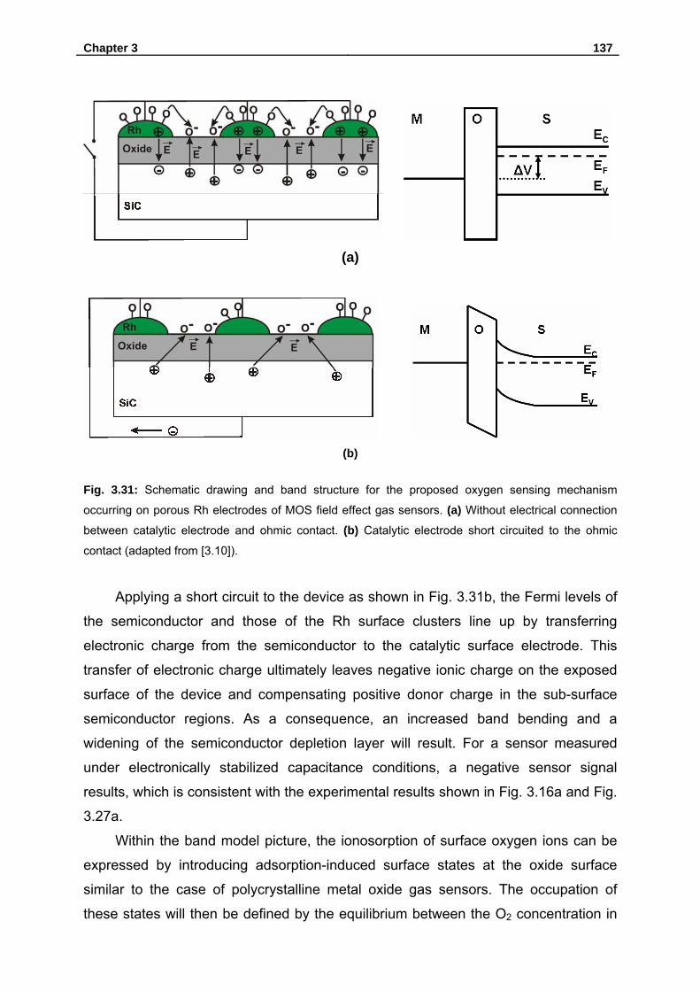
Chapter 3 137
(a)
(b)
Fig. 3.31: Schematic drawing and band structure for the proposed oxygen sensing mechanism
occurring on porous Rh electrodes of MOS field effect gas sensors. (a) Without electrical connection
between catalytic electrode and ohmic contact. (b) Catalytic electrode short circuited to the ohmic
contact (adapted from [3.10]).
Applying a short circuit to the device as shown in Fig. 3.31b, the Fermi levels of
the semiconductor and those of the Rh surface clusters line up by transferring
electronic charge from the semiconductor to the catalytic surface electrode. This
transfer of electronic charge ultimately leaves negative ionic charge on the exposed
surface of the device and compensating positive donor charge in the sub-surface
semiconductor regions. As a consequence, an increased band bending and a
widening of the semiconductor depletion layer will result. For a sensor measured
under electronically stabilized capacitance conditions, a negative sensor signal
results, which is consistent with the experimental results shown in Fig. 3.16a and Fig.
3.27a.
Within the band model picture, the ionosorption of surface oxygen ions can be
expressed by introducing adsorption-induced surface states at the oxide surface
similar to the case of polycrystalline metal oxide gas sensors. The occupation of
these states will then be defined by the equilibrium between the O2 concentration in
138 Chapter 3
the gas phase, on the one hand, and the semiconductor Fermi energy, on the other
hand [3.10]. Similarly, the sensitivity of Rh-MOSiC sensors toward NOx can also be
explained in terms of ionosorption on patches of exposed oxide. On metal oxide gas
sensors, nitric dioxide normally leads to an increased resistance with respect to
oxygen. This behavior is explained in terms of NOx related surface states on the
oxide surface that are energetically lower than the O-induced ones [3.10]. As a
consequence, an increased band bending and a reduced conductivity across
neighboring metal oxide crystallites is obtained. The model can easily be extended to
the MOSiC case. Supposing that also in the case of NO2 negatively charged species,
for instance, −3NO or −2
42ON [3.10, 3.17], spill over to the exposed oxide areas, the
energetically deeper, NO2 related adsorption states will lead to an increased negative
surface charge on patches of exposed oxide and therefore to an increased band
bending with respect to an oxygen-containing atmosphere.
3.6.4.3 Comparison:
The responses R to 0.15 and 3 mbar of D2, NOx, and O2 as a function of operating
temperature for all three studied sensors are shown in Fig. 3.32, Fig. 3.33, and Fig.
3.34. Several quantitative conclusions can be drawn from these figures:
1. The sensor A4 has the best response to NOx in the temperature range (25-125°C)
with a maximum value at 25°C. indicating that an effective sensor operation at
room temperature is possible.
2. At 300°C and above the sensor A1 in the best D2 gas sensor. At this temperature
no response to NOx was observed and the response to O2 is very low indicating
that the sensor A1 is very suitable for selective detection of D2 at 300°C.
3. The best response to O2 in the temperature range 150-225°C was observed for
the sensor A4. But in this range the response to D2 is very high. As a
consequence the sensor A4 is not suitable for selective detection of O2 or D2 in
this range.
4. The sensor B4 is very suitable for selective detection of D2 at room temperature
since at this temperature no response to O2 is observed and the response to NOx
is very low.
5. The different responses of sensors A4 and B4 to all test gases are attributed to
the differences in the insulating materials (SiO2, SiN/SiO2).
Chapter 3 139
6. The response to all test gases differs for the different metal micostructure
(sensors A1 and A4).
7. The temperature of the maximum response is dependent on the gas species
being measured. This information, along with a careful choice of insulating
materials and catalyst microstructure can be used to enhance device sensitivity
and selectivity.
(a) (b)
Fig. 3.32: (a) The dependence of the responses R of all three studied sensors investigated to 0.15,
and 3 mbar of D2 on the operating temperature. (b) Blocks presentation for 0.15 mbar D2.
(a) (b)
Fig. 3.33: (a) The dependence of the responses R of all three sensors studied to 0.15, and 3 mbar of
NOx on the operating temperature. (b) Block presentations for 0.15 mbar of NOx.

140 Chapter 3
(a) (b)
Fig. 3.34: (a) The dependence of the responses R of all three sensors studied to 0.15, and 3 mbar of
O2 on the operating temperature. (b) Block presentations for 0.15 mbar of O2.
3.7 Conclusion:
The response to reducing (D2) and oxidizing gases (NOx, and O2) of MOSiC and
MMOOSiC structures with Rh gate with a thickness of 30 nm in dependence on the
operating temperature and gas partial pressures was investigated. The response was
measured as a shift in the capacitance-voltge (C-V) curve along the voltage axis.
Positive and negative flat-band voltage shifts up to 1 V were observed for oxidizing
and reducing gases, respectively. The most important property of the sensors studied
in this chapter is that the sensors can be used as NOx gas sensor at room
temperature. Depending on the type of insulator that is chosen, and the Rh structure,
differences in the sensitivity properties are achieved.
3.8 Outlook and future work:
The following additional experiments are suggested for further investigation in this
field of study:
The fundamental properties of the gate microstructure (Rh, Rh/ITO) and the
insulators (SiO2, SiN/SiO2) should be investigated by a wide set of structural
characterisation techniques, including Transmission Electron Microscopy, X-ray
diffraction, Raman, Fourier Transform infrared, and X-ray photoelectron
spectroscopy. The combined use of the different techniques allows an improved
understanding of the sensing mechanism of Rh-MOSiC gas sensors.

Chapter 3 141
The selectivity against other gases such as CO, and NH3 should be investigated.
The investigation of the stability or reliability of the sensor is needed.
The influence of the catalytic (Rh) thickness on the gas sensing properties of the
Rh-MOSiC gas sensors should be tested.
References:
[3.1] I. Lundström, M. S. Shivaraman, C. M. Svensson, and L. Lundqvist, “A
hydrogen-sensitive MOS field-effect transistor”, Appl. Phys. Lett. 26 (1975) 55-57.
[3.2] J. Fogelberg, M. Eriksson, H. Dannetun, and L.-G. Petersson, “Kinetic modelling
of hydrogen adsorption/absorption in thin films on hydrogen-sensitive field-effect
device: Observation of larger hydrogen-induced dipoles at the Pd-SiO2 interface”, J.
Appl. Phys. 78 (1995) 988-996.
[3.3] A. Lloyd Spetz, A. Baranzahi, P. Tobias, and I. Lundström, ”High temperature
sensors based on metal-insulator-silicon carbide device”, phys. stat. sol. A 162
(1997) 493-511.
[3.4] A. Lloyd Spetz, P. Tobias, L. Uneus, H. Svenningstorp, L.-G. Ekedahl, and I.
Lundström, “High temperature catalytic metal field effect transistors for industrial
applications”, Sensors and Actuators B 70 (2000) 67-76.
[3.5] I. Lundström, M. Armgarth, and L.-G. Petersson, “ Physics with catalytic metal
gate chemical sensors”, CRC Crit. Rev. Solid State Mater. Sci. 15 (1989) 201.
[3.6] L. -G. Ekedahl, M. Eriksson, and J. Lundström, “Hydrogen Sensing mechanism
of metal-insulator interfaces”, Acc. Chem. Res. 31 (1998) 249-256 .
[3.7] M. Wallin, H. Grönbeck, A. Lloyd Spetz, and M. Skoglundh, “Vibrational study of
ammonia adsorption on Pt/SiO2” , Appl. Surf. Sci. 235 (2004) 487-500.
[3.8] A. Arbab, A. Spetz, Q. ul Wahab, M. Willander, and I. Lundström, ”Chemical
sensors for high temperatures based on silicon carbide structures”, Sensors and
Mater. 4 (1993) 173.
[3.9] H. Dannetun, I. Lundström, and L.-G. Petersson, “Dehydrogenation of acetylene
and ethylene studied on clean and oxygen covered palladium surfaces”, Surf. Sci.
173 (1986) 148-149.
[3.10] J. Schalwig, P. Kreisl, S. Ahlers, and G. Müller, “Response mechanism of SiC-
based MOS field-effect gas sensors”, IEEE sensors J. 2 (2002) 394-402.
142 Chapter 3
[3.11] M. Eriksson, C. Utaiwasin, A. Carlsson, and M. Löfdahl, “Gas response
dependence on gate metal morphology of field-effect devices”, in Proc. Transducers,
Sendai, Japan, June 7-10, 1999, pp. 950-953.
[3.12] S. M. Sze, “Physics of semiconductor devices”, ISBN 0-471-09837-X, 1981.
[3.13] E. S. Yang, “Fundamentals of semiconductor devices”, McGraw-Hill, Inc., USA,
ISBN 0 07-072236-6, 1978.
[3.14] I. Lundström, and t. DiStefano, “Influence of hydrogen on the Pt-SiO2-Si
structures”, Solid State Comm. 19 (1976) 871-875.
[3.15] P. Tobias, B. Golding, and N. Ghosh, “Interface state in high-temperature gas
sensors based on silicon carbide”, IEEE Sensor J. 2 (2003) 543-547.
[3.16] W. C. Corner, G. M. Pajonk, and S. T. Teichner, “Spillover of sorbed species”,
Adv. Catalysis 34, (1986) 1-79.
[3.17] S. R. Morrison, “Selectivity in semiconductor gas sensors”, Sensors and
Actuators B12 (1987) 425-440.
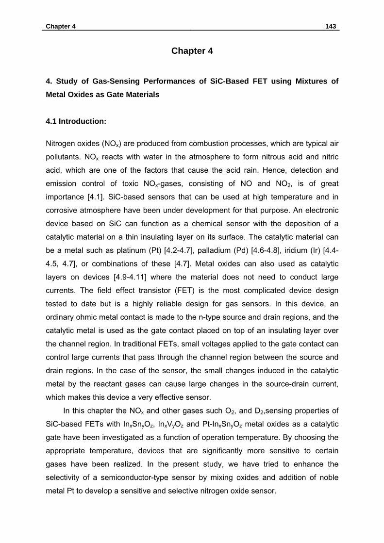
Chapter 4 143
Chapter 4
4. Study of Gas-Sensing Performances of SiC-Based FET using Mixtures of Metal Oxides as Gate Materials
4.1 Introduction:
Nitrogen oxides (NOx) are produced from combustion processes, which are typical air
pollutants. NOx reacts with water in the atmosphere to form nitrous acid and nitric
acid, which are one of the factors that cause the acid rain. Hence, detection and
emission control of toxic NOx-gases, consisting of NO and NO2, is of great
importance [4.1]. SiC-based sensors that can be used at high temperature and in
corrosive atmosphere have been under development for that purpose. An electronic
device based on SiC can function as a chemical sensor with the deposition of a
catalytic material on a thin insulating layer on its surface. The catalytic material can
be a metal such as platinum (Pt) [4.2-4.7], palladium (Pd) [4.6-4.8], iridium (Ir) [4.4-
4.5, 4.7], or combinations of these [4.7]. Metal oxides can also used as catalytic
layers on devices [4.9-4.11] where the material does not need to conduct large
currents. The field effect transistor (FET) is the most complicated device design
tested to date but is a highly reliable design for gas sensors. In this device, an
ordinary ohmic metal contact is made to the n-type source and drain regions, and the
catalytic metal is used as the gate contact placed on top of an insulating layer over
the channel region. In traditional FETs, small voltages applied to the gate contact can
control large currents that pass through the channel region between the source and
drain regions. In the case of the sensor, the small changes induced in the catalytic
metal by the reactant gases can cause large changes in the source-drain current,
which makes this device a very effective sensor.
In this chapter the NOx and other gases such O2, and D2,sensing properties of
SiC-based FETs with InxSnyOz, InxVyOz and Pt-InxSnyOz metal oxides as a catalytic
gate have been investigated as a function of operation temperature. By choosing the
appropriate temperature, devices that are significantly more sensitive to certain
gases have been realized. In the present study, we have tried to enhance the
selectivity of a semiconductor-type sensor by mixing oxides and addition of noble
metal Pt to develop a sensitive and selective nitrogen oxide sensor.

144 Chapter 4
4.2 Theory of field-effect-transistor (FET):
This section of this chapter describes the functionality of a Metal-Oxide-
Semiconductor field effect transistor, commonly denoted MOSFET. The purpose of
this section is to introduce fundamental concepts within semiconductor electronics
and to give a basic understanding of how a MOSFET operates.
4.2.1 Principles of a MOSFET:
The metal insulator semiconductor field effect transistor (MISFET) is the most
prominent device based on a metal insulator semiconductor (MIS) structure next to
the so-called MISCAP. If the insulator layer is chosen to be an oxide like silicon
dioxide it is termed MOSFET. A high temperature design is based on SiC as
semiconductor.
The general working principle of a MOSFET is quite simple. A MOSFET
consists of a source, a drain, and a gate. A voltage is applied between the source
and drain contact resulting in a current, the source-drain current IDS. The current can
be regulated by a potential applied to the gate, VGS.
The term metal oxide semiconductor describes the three principal layers of a
MOSFET: a metal (the gate) on top of an oxide insulator and a semiconductor
substrate (including source and drain) as illustrated in Fig. 4.1.
Fig. 4.1: Schematic representation of a MOSFET [4.12].
The regions of the source and drain are made of the same semiconductor material
but are oppositely doped resulting in a n-p-n or p-n-p structure. The source provides

Chapter 4 145
charge carriers and the drain collects charge carriers, whereas the substrate
between the two acts as a conductive channel. For a n-channel MOSFET the charge
carries are electrons. For a p-channel MOSFET the charge carriers are positively
charged holes. An n-channel MOSFET is based on a n-p-n structure. In some
designs the transistor is embedded in a transistor well to allow several independent
transistors on one single substrate.
There are basically four different types of MOSFET, depending on the type of
the conductive channel. If, at zero gate bias VGS, a conductive n-channel exists (IDS >
0) and a negative voltage has to be applied to the gate to reduce the channel
conductance, then the device is an n-channel “normally on” MOSFET (illustrated in
Fig. 4.2a. If the channel conductance is very low at zero gate bias and a positive
voltage larger than the threshold voltage VT must be applied to the gate to form a n-
channel, then the device is a n-channel “normally off” MOSFET. Similarly, p-channel
normally on and p-channel normally of MOSFETs are available.
Fig. 4.2: Characteristics of a MOSFET device (a) Transconductance curves for a “normally on” and
“normally off” MOSFET (b) Output conductance curves for different values of VGS [4.12].
The channel geometry, charge carrier mobility, and the number of available
charge carriers determine the conductance of this channel. The later can be
modulated by varying the gate voltage VGS or a substrate bias voltage. The electric
field established by VGS across the dielectric layer, in the direction traverse to the
current flow, influences the type and concentration of charge carriers. Let us consider
a n-channel MOSFET. If a low positive potential is applied to the gate the major
carriers in the substrate (holes) are repelled and a depletion region is formed. At high
potential the minor charge carriers (electrons) are attracted to the semiconductor
surface (inversion layer). The inversion layer occurs if VGS > VT. Now the channel is
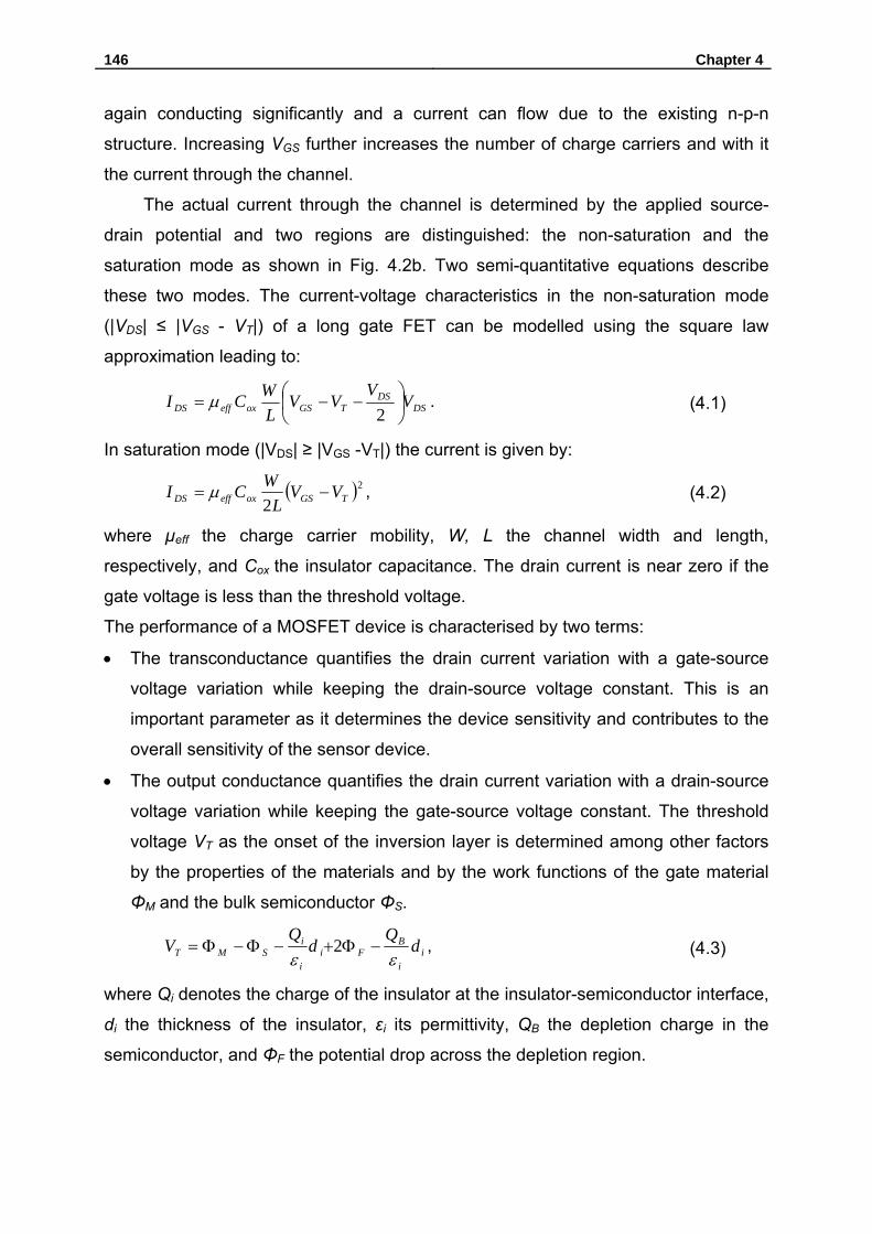
146 Chapter 4
again conducting significantly and a current can flow due to the existing n-p-n
structure. Increasing VGS further increases the number of charge carriers and with it
the current through the channel.
The actual current through the channel is determined by the applied source-
drain potential and two regions are distinguished: the non-saturation and the
saturation mode as shown in Fig. 4.2b. Two semi-quantitative equations describe
these two modes. The current-voltage characteristics in the non-saturation mode
(|VDS| ≤ |VGS - VT|) of a long gate FET can be modelled using the square law
approximation leading to:
DSDS
TGSoxeffDS VV
VVLWCI ⎟
⎠⎞
⎜⎝⎛ −−=
2μ . (4.1)
In saturation mode (|VDS| ≥ |VGS -VT|) the current is given by:
( )2
2 TGSoxeffDS VVL
WCI −= μ , (4.2)
where µeff the charge carrier mobility, W, L the channel width and length,
respectively, and Cox the insulator capacitance. The drain current is near zero if the
gate voltage is less than the threshold voltage.
The performance of a MOSFET device is characterised by two terms:
• The transconductance quantifies the drain current variation with a gate-source
voltage variation while keeping the drain-source voltage constant. This is an
important parameter as it determines the device sensitivity and contributes to the
overall sensitivity of the sensor device.
• The output conductance quantifies the drain current variation with a drain-source
voltage variation while keeping the gate-source voltage constant. The threshold
voltage VT as the onset of the inversion layer is determined among other factors
by the properties of the materials and by the work functions of the gate material
ΦM and the bulk semiconductor ΦS.
ii
BFi
i
iSMT dQd
QV
εε−Φ+−Φ−Φ= 2 , (4.3)
where Qi denotes the charge of the insulator at the insulator-semiconductor interface,
di the thickness of the insulator, εi its permittivity, QB the depletion charge in the
semiconductor, and ΦF the potential drop across the depletion region.
Chapter 4 147
4.2.2 The GasFET:
The term chemical field effect transistor (ChemFET) is the generic term for chemical
sensors based on the MOSFET design. This class is commonly divided into two
major subgroups: gas sensitive field effect transistor (GasFET) for gas sensing and
ion selective field effect transistor (ISFET) for sensing in liquids. The ISFET is the first
MOSFET sensor and was proposed by Bergveld et al. [4.13].
The best-known example for (GasFET) is the Pd-FET (“Lundström FET”)
reported by Lundström et al. [4.8]. Actually the device is a normal MOSFET with the
usual aluminium gate replaced by a palladium gate. For a measurement the gate
should be connected to the source plus bulk of the device. Palladium was chosen,
because of its catalytic properties and its permeability to H atoms. Hydrogen in the
ambient dissociatively adsorbs at the outer Pd surface and the resulting hydrogen
atoms diffuse into the thin layer. This process occurs relatively fast at elevated
temperatures (about 150°C). Lundström et al. showed that the amount of hydrogen
inside the Pd is too low to influence the bulk part of its work function, but than on the
other hand the hydrogen atoms are adsorbed at the Pd/SiO2 interface, forming a
dipole layer that thus influences the surface energy part of the work function. The
magnitude of the modulation depends on the coverage θ with H atoms of the
available number of adsorption sites per unit area at the Pd/SiO2 interface. The
observed modulation of the threshold voltage ΔVT of the Pd-gate MOSFET was
modelled with respect to the maximum achievable shift of the dipole-layer voltage
ΔXmax at maximum coverage:
θmaxXXVT Δ=Δ≈Δ , (4.4)
where the coverage 0<θ<1 was modelled as a function of the partial hydrogen
pressure of the ambient, 2HP , according to
2
2
1 H
H
P
P
α
αθ
+= , (4.5)
where α is an overall equilibrium constant which appears to be oxygen and
temperature dependent. VT is altered by the analyte gas by influencing the work
function of the metal gate, ΦM, and consequently IDS: the I-V curve is shifted by ΔV
(Fig. 4.3).

148 Chapter 4
The MOSFET sensors are usually operated under the constant drain current mode,
which means that the change of the drain current due to the change of the work
function is compensated for by the adjustment of the gate voltage.
Fig. 4.3: A shift of the I-V curve of a GasFET (FET with Pt-InxSnyOz gate) induced by gas adsorption
and a change of work function at the metal/insulator interface.
One limitation of the Pd-FET is the fact, that only hydrogen can diffuse through
the gate and therefore only few gases can be detected like hydrocarbons and
ammonia. Variations in sensitivity and selectivity are possible by different operation
temperatures. To overcome this limitation ultra thin, non-continuous layers of metals
(among others Pt, Au, Ir) or porous materials can be used as gate materials.
The palladium gate has been replaced by SnO2 [4.14], conducting polymers
[4.15], ZrO2 [4.16], LaF3 [4.17-4.18], phthalocyanines [4.19], and porphyrins [4.20].
Apart from a modification of the gate material, structuring of the gate is applied
successfully leading to the suspended gate field effect transistors (SGFET) device:
the gate is suspended over the insulator and optionally coated with a sensitive
material.
4.3 Principle of gas sensing via work function:
Field effect devices are mainly based on metal-insulator-semiconductor (MIS)
capacitors. They act as capacitive voltage divider as depicted in the energy diagram
of Fig. 4.4. In contrast to a conventional metal-insulator-metal (MIM) capacitor the
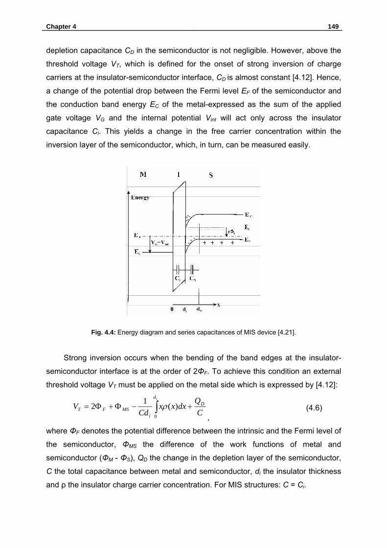
Chapter 4 149
depletion capacitance CD in the semiconductor is not negligible. However, above the
threshold voltage VT, which is defined for the onset of strong inversion of charge
carriers at the insulator-semiconductor interface, CD is almost constant [4.12]. Hence,
a change of the potential drop between the Fermi level EF of the semiconductor and
the conduction band energy EC of the metal-expressed as the sum of the applied
gate voltage VG and the internal potential Vint will act only across the insulator
capacitance Ci. This yields a change in the free carrier concentration within the
inversion layer of the semiconductor, which, in turn, can be measured easily.
Fig. 4.4: Energy diagram and series capacitances of MIS device [4.21].
Strong inversion occurs when the bending of the band edges at the insulator-
semiconductor interface is at the order of 2ΦF. To achieve this condition an external
threshold voltage VT must be applied on the metal side which is expressed by [4.12]:
∫ +−Φ+Φ=id
D
iMSFT C
Qdxxx
CdV
0
)(12 ρ,
(4.6)
where ΦF denotes the potential difference between the intrinsic and the Fermi level of
the semiconductor, ΦMS the difference of the work functions of metal and
semiconductor (ΦM - ΦS), QD the change in the depletion layer of the semiconductor,
C the total capacitance between metal and semiconductor, di the insulator thickness
and ρ the insulator charge carrier concentration. For MIS structures: C = Ci.
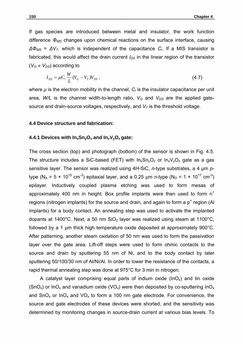
150 Chapter 4
If gas species are introduced between metal and insulator, the work function
difference ΦMS changes upon chemical reactions on the surface interface, causing
ΔΦMS = ΔVT, which is independent of the capacitance Ci. If a MIS transistor is
fabricated, this would affect the drain current IDS in the linear region of the transistor
(VG « VDS) according to
DSTGiDS VVVLWCI )( −= μ , (4.7)
where µ is the electron mobility in the channel, Ci is the insulator capacitance per unit
area, W/L is the channel width-to-length ratio, VG and VDS are the applied gate-
source and drain-source voltages, respectively, and VT is the threshold voltage.
4.4 Device structure and fabrication:
4.4.1 Devices with InxSnyOz and InxVyOz gate:
The cross section (top) and photograph (bottom) of the sensor is shown in Fig. 4.5.
The structure includes a SiC-based (FET) with InxSnyOz or InxVyOz gate as a gas
sensitive layer. The sensor was realized using 4H-SiC, n-type substrates, a 4 µm p-
type (NA = 5 × 1015 cm-3) epitaxial layer, and a 0.25 µm n-type (ND = 1 × 1017 cm-3)
epilayer. Inductively coupled plasma etching was used to form mesas of
approximately 400 nm in height. Box profile implants were then used to form n+
regions (nitrogen implants) for the source and drain, and again to form a p+ region (Al
implants) for a body contact. An annealing step was used to activate the implanted
dopants at 1400°C. Next, a 50 nm SiO2 layer was realized using steam at 1100°C,
followed by a 1 µm thick high temperature oxide deposited at approximately 900°C.
After patterning, another steam oxidation of 50 nm was used to form the passivation
layer over the gate area. Lift-off steps were used to form ohmic contacts to the
source and drain by sputtering 55 nm of Ni, and to the body contact by later
sputtering 50/100/30 nm of Al/Ni/Al. In order to lower the resistance of the contacts, a
rapid thermal annealing step was done at 975°C for 3 min in nitrogen.
A catalyst layer comprising equal parts of indium oxide (InOx) and tin oxide
(SnOx) or InOx and vanadium oxide (VOx) were then deposited by co-sputtering InOx
and SnOx or InOx and VOx to form a 100 nm gate electrode. For convenience, the
source and gate electrodes of these devices were shorted, and the sensitivity was
determined by monitoring changes in source-drain current at various bias levels. To

Chapter 4 151
prepare the catalytic films for exposure to high temperature an annealing step was
used to condition the catalysts at 600°C for 10 minutes in N2. A stack of Ti/Ni/Au/Ti
metalization of 50/50/400/7.5 nm was evaporated over the electrodes to form bond
pads for wirebonding. Lastly a low temperature oxide was deposited over the devices
at 430°C, resulting in a 60 nm SiO2 layer. The sensors were then diced, and placed
on TO-8 headers using ceramic-based die attach material [4.24]. The active and total
areas of the sensors are 450 × 9 µm2 and 1 mm2, respectively.
Fig. 4.5: Schematic cross-section (top) [4.22-4.23] and photograph (bottom) of the SiC-based FET
sensor. The active and total areas are 450 × 9 µm2 and 1 mm2, respectively.
4.4.2 Devices with Pt-InxSnyOz gate:
The schematic cross-section (top) and the layout (bottom) of the studied sensors are
shown in Fig. 4.6. The structure includes a SiC-based (FET) with Pt-InxSnyOz gate as
a gas sensitive layer. The sensor was realized using 4H-SiC, n-type substrates, a 2.2
µm p-type (NA = 5 × 1016 cm-3) epitaxial layer, and a 0.19 µm n-type (ND = 2 × 10¹⁷
cm-3) epilayer.

152 Chapter 4
Fig. 4.6: Schematic cross-section (top) and the sensor layout (bottom) of the studied SiC-based FET
sensor. The active area is 4 × 500 µm2.
Inductively coupled plasma etching was used to form mesas of approximately 500
nm in height. Box profile implants were then used to form n+ regions (N implants) for
the source and drain, and again to form a p+ region (Al implants) for a body contact.
An annealing step was used to activate the implanted dopants at 1400°C. Next, a
field oxide was realized using a high temperature (1100°C) deposition process to get
a 50 nm SiO2, followed by a 1 µm thick high temperature oxide deposited at
approximately 900°C, and then those were annealed.
A gate oxide was realized by deposition of 22.5 nm of SiO2 then 22.5 nm of
Si3N4. Next, lift-off steps were used to form ohmic contacts to the source and drain by
sputtering 55 nm of Ni, and to the body contact by later sputtering 50/100/30 nm of
Al/Ni/Al. In order to lower the resistance of the contacts, a rapid thermal annealing
step was done at 1050°C for 3 min in nitrogen. A catalyst layer comprising equal
parts of indium oxide and tin oxide was then deposited by co-sputtering InOx and
SnOx to form a 75 nm gate electrode, then 10 nm Pt layer was sputtered on the top
Chapter 4 153
of InxSnyOz layer. To prepare the catalytic films for exposure to high temperature an
annealing step was used to condition the catalysts at 600°C for 10 minutes in N2. A
stack of Ti/Ni/Au/Ti metalization of 50/50/1100/7.5 nm was evaporated over the
electrodes to form bond pads for wirebonding. Lastly a low temperature oxide was
deposited over the devices at 430°C, resulting in a 60 nm SiO2 layer followed by 50
nm Si3N4. The sensors were then diced, and placed on TO-8 headers using ceramic-
based die attach material. All devices have the following dimensions: 10 µm = gate
length, 500 µm = gate width, source-drain spacing = 14 µm. The whole device is
covered with a thick passivation and there is an opening 4 × 500 µm2 of the
passivation above the gate.
4.5. Experiments:
4.5.1 AES measurements (surface and interface measurements):
The sensitivity of FET gas sensors is strongly influenced by the structure and the
composition of the active electrode (gate electrode). Therefore, structure and
composition of the InxSnyOz, InxVyOz, and Pt-InxSnyOz gates of the FET gas sensors
were analyzed by Auger electron spectroscopy (AES). AES measurements have
been carried out using a Thermo Microlab 350 described in Chapter 3 (section 3.5.1).
4.5.2 Gas sensing measurements:
For gas sensing tests, the sensors were mounted in an UHV system described in
Chapter 3 (section 3.5.2). The sensors were placed directly into a quartz tube, which
was pumped to a base pressure of 4 × 10⁻⁸ mbar. Fig. 4.7 shows schematic drawing
of the UHV apparatus for this experiment and all devices mounted in it.
Current-voltage (I-V) characteristics have been carried out at different partial
pressures of the test gases (NOx, O2, and D2) above the sensors, which were heated
during operation at different temperatures using a furnace. The temperature was
measured by a thermocouple type K (NiCr-Ni) (see Appendix A) placed a few
millimetres above the sensor.
We have defined the response R as the relative current variation at constant voltage
expressed in percent:
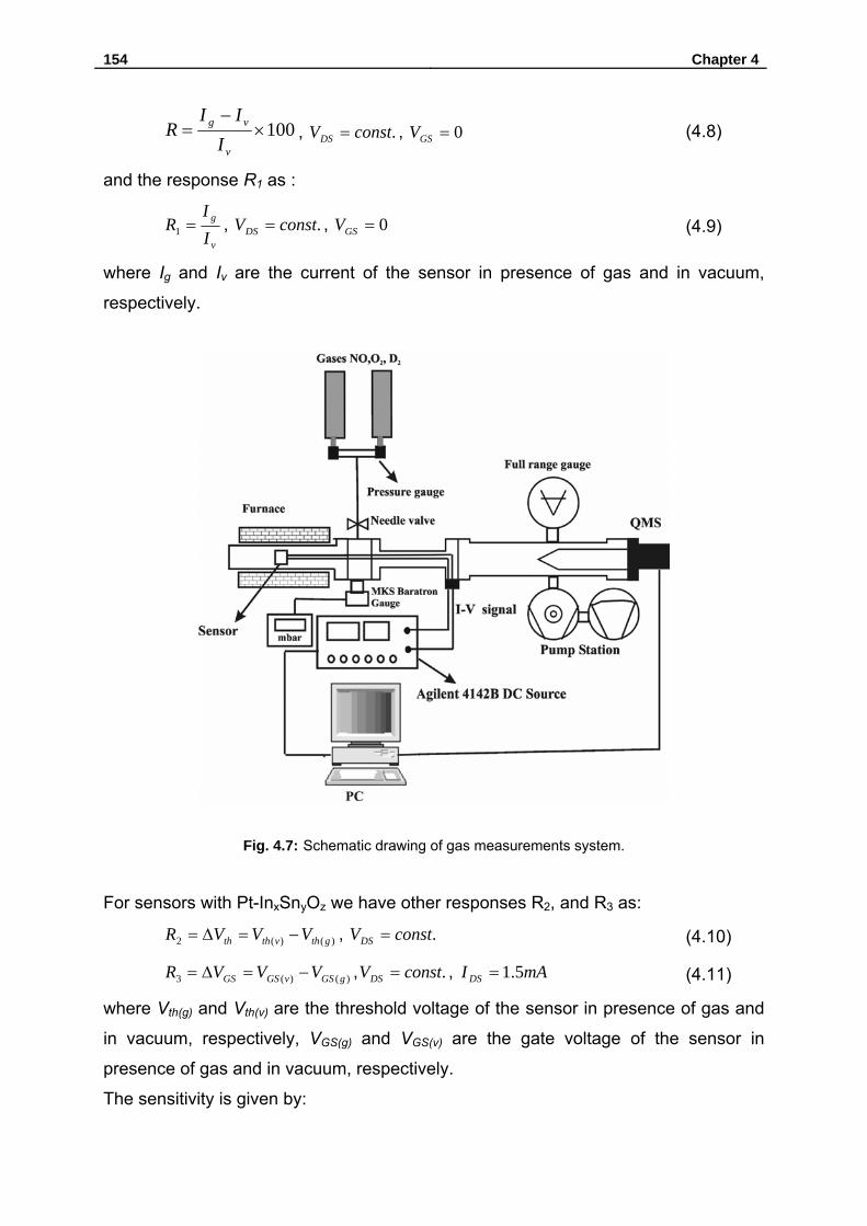
154 Chapter 4
100×−
=v
vg
III
R , .constVDS = , 0=GSV (4.8)
and the response R1 as :
v
g
II
R =1 , .constVDS = , 0=GSV (4.9)
where Ig and Iv are the current of the sensor in presence of gas and in vacuum,
respectively.
Fig. 4.7: Schematic drawing of gas measurements system.
For sensors with Pt-InxSnyOz we have other responses R2, and R3 as:
)()(2 gthvthth VVVR −=Δ= , .constVDS = (4.10)
)()(3 gGSvGSGS VVVR −=Δ= , .constVDS = , mAI DS 5.1= (4.11)
where Vth(g) and Vth(v) are the threshold voltage of the sensor in presence of gas and
in vacuum, respectively, VGS(g) and VGS(v) are the gate voltage of the sensor in
presence of gas and in vacuum, respectively.
The sensitivity is given by:
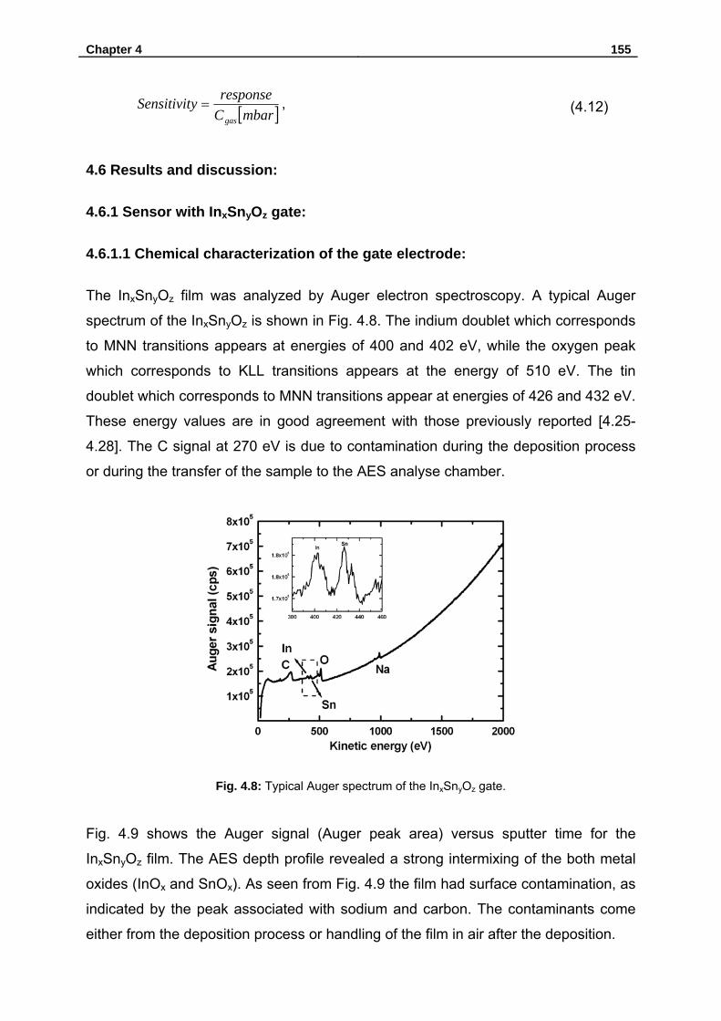
Chapter 4 155
[ ]mbarCresponseySensitivitgas
= , (4.12)
4.6 Results and discussion:
4.6.1 Sensor with InxSnyOz gate:
4.6.1.1 Chemical characterization of the gate electrode:
The InxSnyOz film was analyzed by Auger electron spectroscopy. A typical Auger
spectrum of the InxSnyOz is shown in Fig. 4.8. The indium doublet which corresponds
to MNN transitions appears at energies of 400 and 402 eV, while the oxygen peak
which corresponds to KLL transitions appears at the energy of 510 eV. The tin
doublet which corresponds to MNN transitions appear at energies of 426 and 432 eV.
These energy values are in good agreement with those previously reported [4.25-
4.28]. The C signal at 270 eV is due to contamination during the deposition process
or during the transfer of the sample to the AES analyse chamber.
Fig. 4.8: Typical Auger spectrum of the InxSnyOz gate.
Fig. 4.9 shows the Auger signal (Auger peak area) versus sputter time for the
InxSnyOz film. The AES depth profile revealed a strong intermixing of the both metal
oxides (InOx and SnOx). As seen from Fig. 4.9 the film had surface contamination, as
indicated by the peak associated with sodium and carbon. The contaminants come
either from the deposition process or handling of the film in air after the deposition.
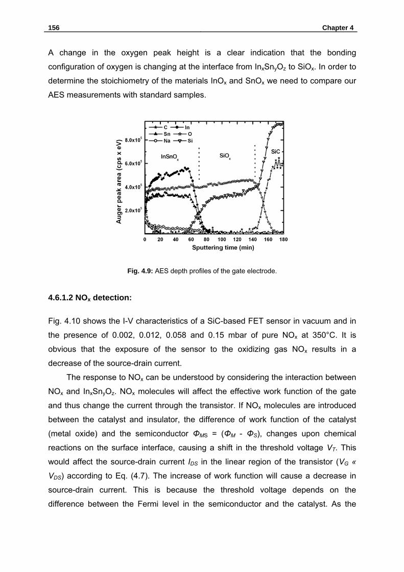
156 Chapter 4
A change in the oxygen peak height is a clear indication that the bonding
configuration of oxygen is changing at the interface from InxSnyOz to SiOx. In order to
determine the stoichiometry of the materials InOx and SnOx we need to compare our
AES measurements with standard samples.
Fig. 4.9: AES depth profiles of the gate electrode.
4.6.1.2 NOx detection:
Fig. 4.10 shows the I-V characteristics of a SiC-based FET sensor in vacuum and in
the presence of 0.002, 0.012, 0.058 and 0.15 mbar of pure NOx at 350°C. It is
obvious that the exposure of the sensor to the oxidizing gas NOx results in a
decrease of the source-drain current.
The response to NOx can be understood by considering the interaction between
NOx and InxSnyOz. NOx molecules will affect the effective work function of the gate
and thus change the current through the transistor. If NOx molecules are introduced
between the catalyst and insulator, the difference of work function of the catalyst
(metal oxide) and the semiconductor ΦMS = (ΦM - ΦS), changes upon chemical
reactions on the surface interface, causing a shift in the threshold voltage VT. This
would affect the source-drain current IDS in the linear region of the transistor (VG «
VDS) according to Eq. (4.7). The increase of work function will cause a decrease in
source-drain current. This is because the threshold voltage depends on the
difference between the Fermi level in the semiconductor and the catalyst. As the
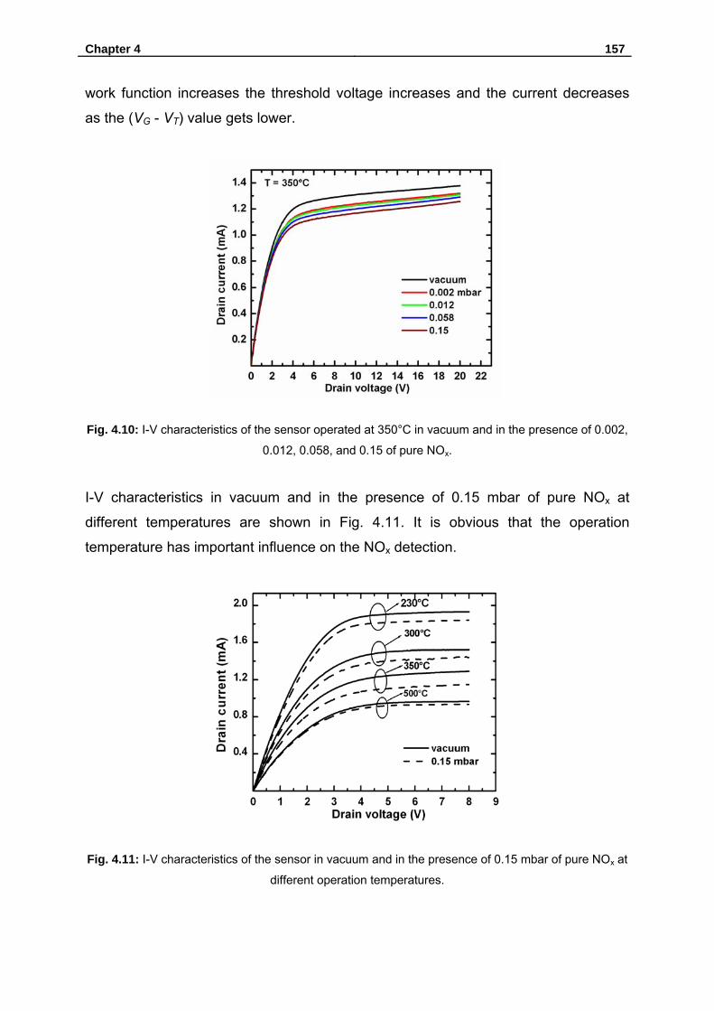
Chapter 4 157
work function increases the threshold voltage increases and the current decreases
as the (VG - VT) value gets lower.
Fig. 4.10: I-V characteristics of the sensor operated at 350°C in vacuum and in the presence of 0.002,
0.012, 0.058, and 0.15 of pure NOx.
I-V characteristics in vacuum and in the presence of 0.15 mbar of pure NOx at
different temperatures are shown in Fig. 4.11. It is obvious that the operation
temperature has important influence on the NOx detection.
Fig. 4.11: I-V characteristics of the sensor in vacuum and in the presence of 0.15 mbar of pure NOx at
different operation temperatures.
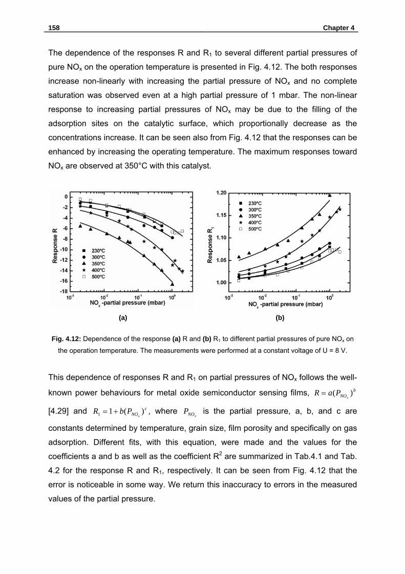
158 Chapter 4
The dependence of the responses R and R1 to several different partial pressures of
pure NOx on the operation temperature is presented in Fig. 4.12. The both responses
increase non-linearly with increasing the partial pressure of NOx and no complete
saturation was observed even at a high partial pressure of 1 mbar. The non-linear
response to increasing partial pressures of NOx may be due to the filling of the
adsorption sites on the catalytic surface, which proportionally decrease as the
concentrations increase. It can be seen also from Fig. 4.12 that the responses can be
enhanced by increasing the operating temperature. The maximum responses toward
NOx are observed at 350°C with this catalyst.
(a) (b)
Fig. 4.12: Dependence of the response (a) R and (b) R1 to different partial pressures of pure NOx on
the operation temperature. The measurements were performed at a constant voltage of U = 8 V.
This dependence of responses R and R1 on partial pressures of NOx follows the well-
known power behaviours for metal oxide semiconductor sensing films, bNOx
PaR )(=
[4.29] and cNOx
PbR )(11 += , where xNOP is the partial pressure, a, b, and c are
constants determined by temperature, grain size, film porosity and specifically on gas
adsorption. Different fits, with this equation, were made and the values for the
coefficients a and b as well as the coefficient R2 are summarized in Tab.4.1 and Tab.
4.2 for the response R and R1, respectively. It can be seen from Fig. 4.12 that the
error is noticeable in some way. We return this inaccuracy to errors in the measured
values of the partial pressure.
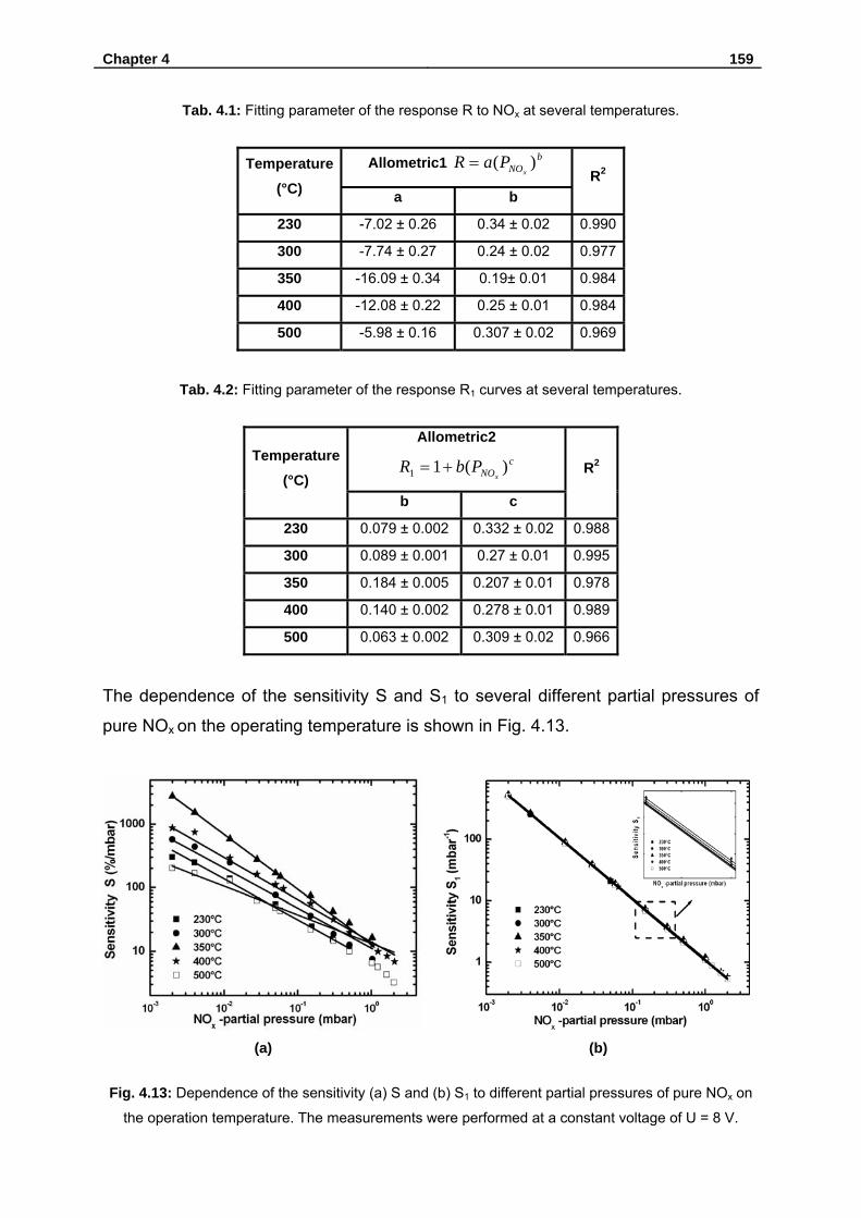
Chapter 4 159
Tab. 4.1: Fitting parameter of the response R to NOx at several temperatures.
Allometric1 bNOx
PaR )(= Temperature (°C) a b
R2
230 -7.02 ± 0.26 0.34 ± 0.02 0.990
300 -7.74 ± 0.27 0.24 ± 0.02 0.977
350 -16.09 ± 0.34 0.19± 0.01 0.984
400 -12.08 ± 0.22 0.25 ± 0.01 0.984
500 -5.98 ± 0.16 0.307 ± 0.02 0.969
Tab. 4.2: Fitting parameter of the response R1 curves at several temperatures.
Allometric2 c
NOxPbR )(11 +=
Temperature (°C)
b c
R2
230 0.079 ± 0.002 0.332 ± 0.02 0.988
300 0.089 ± 0.001 0.27 ± 0.01 0.995
350 0.184 ± 0.005 0.207 ± 0.01 0.978
400 0.140 ± 0.002 0.278 ± 0.01 0.989
500 0.063 ± 0.002 0.309 ± 0.02 0.966
The dependence of the sensitivity S and S1 to several different partial pressures of
pure NOx on the operating temperature is shown in Fig. 4.13.
(a) (b)
Fig. 4.13: Dependence of the sensitivity (a) S and (b) S1 to different partial pressures of pure NOx on
the operation temperature. The measurements were performed at a constant voltage of U = 8 V.
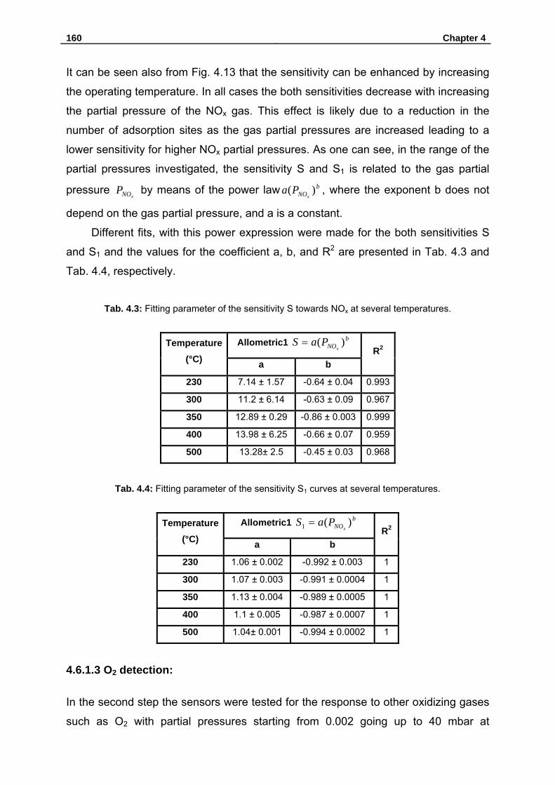
160 Chapter 4
It can be seen also from Fig. 4.13 that the sensitivity can be enhanced by increasing
the operating temperature. In all cases the both sensitivities decrease with increasing
the partial pressure of the NOx gas. This effect is likely due to a reduction in the
number of adsorption sites as the gas partial pressures are increased leading to a
lower sensitivity for higher NOx partial pressures. As one can see, in the range of the
partial pressures investigated, the sensitivity S and S1 is related to the gas partial
pressure xNOP by means of the power law b
NOxPa )( , where the exponent b does not
depend on the gas partial pressure, and a is a constant.
Different fits, with this power expression were made for the both sensitivities S
and S1 and the values for the coefficient a, b, and R2 are presented in Tab. 4.3 and
Tab. 4.4, respectively.
Tab. 4.3: Fitting parameter of the sensitivity S towards NOx at several temperatures.
Allometric1 bNOx
PaS )(= Temperature (°C) a b
R2
230 7.14 ± 1.57 -0.64 ± 0.04 0.993
300 11.2 ± 6.14 -0.63 ± 0.09 0.967
350 12.89 ± 0.29 -0.86 ± 0.003 0.999
400 13.98 ± 6.25 -0.66 ± 0.07 0.959
500 13.28± 2.5 -0.45 ± 0.03 0.968
Tab. 4.4: Fitting parameter of the sensitivity S1 curves at several temperatures.
Allometric1 bNOx
PaS )(1 = Temperature (°C) a b
R2
230 1.06 ± 0.002 -0.992 ± 0.003 1
300 1.07 ± 0.003 -0.991 ± 0.0004 1
350 1.13 ± 0.004 -0.989 ± 0.0005 1
400 1.1 ± 0.005 -0.987 ± 0.0007 1
500 1.04± 0.001 -0.994 ± 0.0002 1
4.6.1.3 O2 detection:
In the second step the sensors were tested for the response to other oxidizing gases
such as O2 with partial pressures starting from 0.002 going up to 40 mbar at
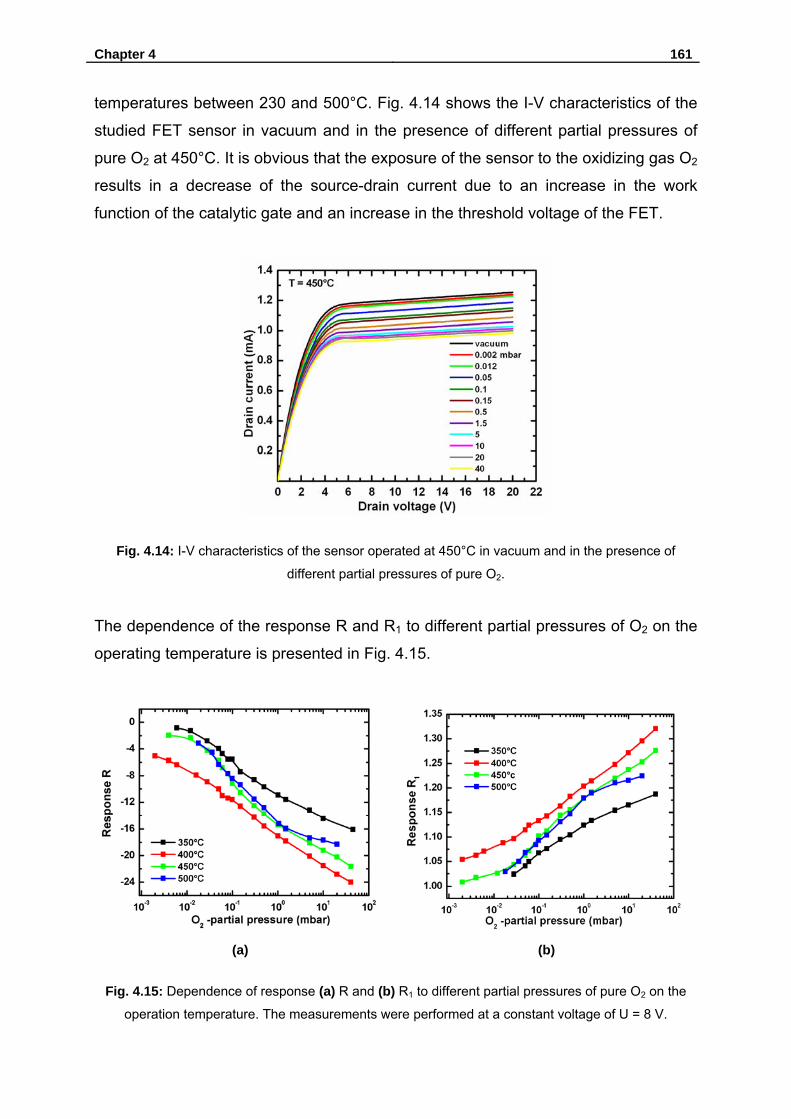
Chapter 4 161
temperatures between 230 and 500°C. Fig. 4.14 shows the I-V characteristics of the
studied FET sensor in vacuum and in the presence of different partial pressures of
pure O2 at 450°C. It is obvious that the exposure of the sensor to the oxidizing gas O2
results in a decrease of the source-drain current due to an increase in the work
function of the catalytic gate and an increase in the threshold voltage of the FET.
Fig. 4.14: I-V characteristics of the sensor operated at 450°C in vacuum and in the presence of
different partial pressures of pure O2.
The dependence of the response R and R1 to different partial pressures of O2 on the
operating temperature is presented in Fig. 4.15.
(a) (b)
Fig. 4.15: Dependence of response (a) R and (b) R1 to different partial pressures of pure O2 on the
operation temperature. The measurements were performed at a constant voltage of U = 8 V.
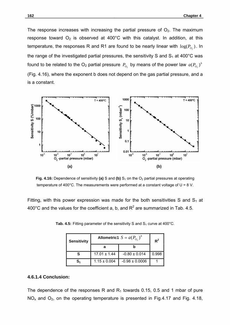
162 Chapter 4
The response increases with increasing the partial pressure of O2. The maximum
response toward O2 is observed at 400°C with this catalyst. In addition, at this
temperature, the responses R and R1 are found to be nearly linear with )log(2OP . In
the range of the investigated partial pressures, the sensitivity S and S1 at 400°C was
found to be related to the O2 partial pressure 2OP by means of the power law b
OPa )(2
(Fig. 4.16), where the exponent b does not depend on the gas partial pressure, and a
is a constant.
(a) (b)
Fig. 4.16: Dependence of sensitivity (a) S and (b) S1 on the O2 partial pressures at operating
temperature of 400°C. The measurements were performed at a constant voltage of U = 8 V.
Fitting, with this power expression was made for the both sensitivities S and S1 at
400°C and the values for the coefficient a, b, and R2 are summarized in Tab. 4.5.
Tab. 4.5: Fitting parameter of the sensitivity S and S1 curve at 400°C.
Allometric1 bOPaS )(
2=
Sensitivity a b
R2
S 17.01 ± 1.44 -0.80 ± 0.014 0.998
S1 1.15 ± 0.004 -0.98 ± 0.0006 1
4.6.1.4 Conclusion:
The dependence of the responses R and R1 towards 0.15, 0.5 and 1 mbar of pure
NOx and O2, on the operating temperature is presented in Fig.4.17 and Fig. 4.18,

Chapter 4 163
respectively. It becomes obvious from Fig. 4.17 and Fig. 4.18 that the optimum
detection temperatures occur in the range of 325-370°C for NOx. In this range the
cross response to O2 is low indicating that the sensor is suitable for selective
detection of NOx. The optimum temperature of operation for detection of O2 is
determined to be between 400-500°C. In this range no significant response NOx is
observed indicating that the sensor is very suitable for selective O2 detection at very
high temperatures.
(a) (b)
Fig. 4.17: (a) The dependence of the response R to 0.15, 0.5 and 1 mbar of NOx and O2, on the
operating temperature. The measurements were performed at a constant voltage of 8 V. (b) Block
presentations for 0.15 mbar of the both gases.
(a) (b)
Fig. 4.18: (a) The dependence of the response R1 to 0.15, 0.5 and 1 mbar of NOx and O2, on the
operating temperature. The measurements were performed at a constant voltage of 8 V. (b) Block
presentations for 0.15 mbar of the both gases.

164 Chapter 4
4.6.2 Sensor with InxVyOz gate:
4.6.2.1 Chemical characterization of the gate electrode:
The Auger spectrum of the InxVyOz is shown in Fig. 4.19. The indium peaks which
correspond to MNN transitions appear at energies of 402 and 452 eV, while the
oxygen peak which corresponds to KLL transitions appears at the energy of 506 eV.
The vanadium peaks which correspond to LMM transitions are at 464 and 485 eV.
Fig. 4.19: Typical Auger spectrum of the InxVyOz gate.
Fig. 4.20: Auger depth profiles of the gate electrode.
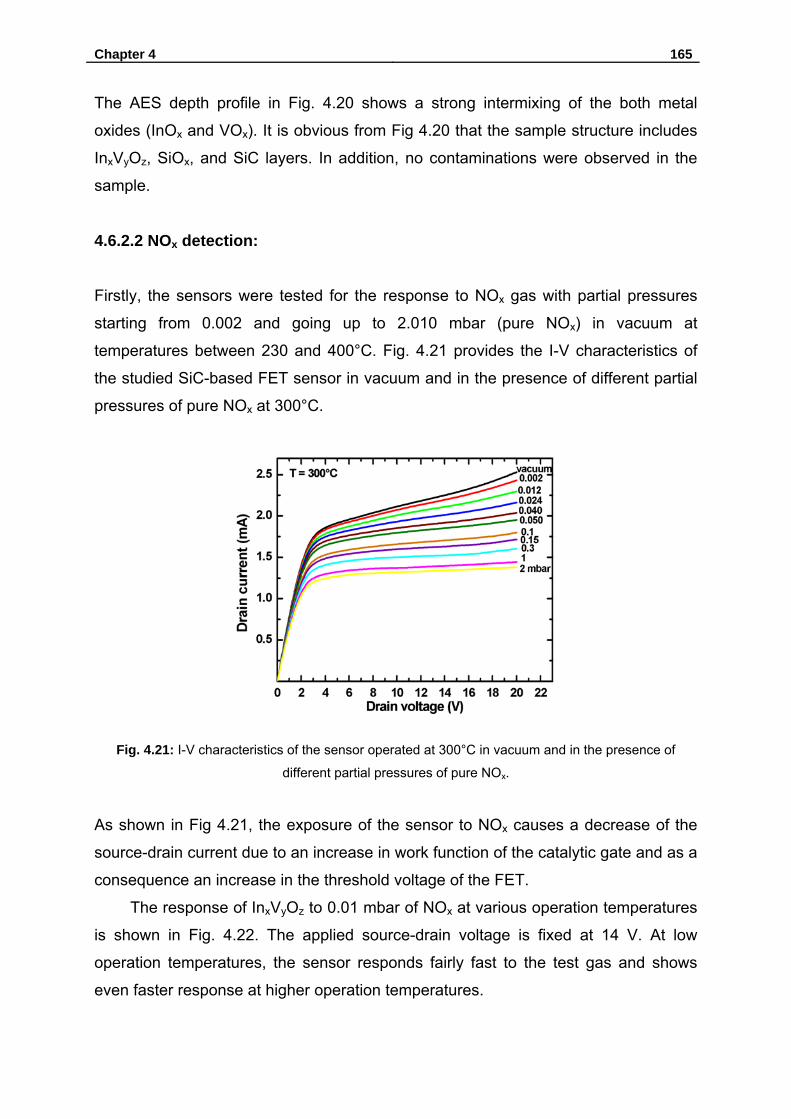
Chapter 4 165
The AES depth profile in Fig. 4.20 shows a strong intermixing of the both metal
oxides (InOx and VOx). It is obvious from Fig 4.20 that the sample structure includes
InxVyOz, SiOx, and SiC layers. In addition, no contaminations were observed in the
sample.
4.6.2.2 NOx detection:
Firstly, the sensors were tested for the response to NOx gas with partial pressures
starting from 0.002 and going up to 2.010 mbar (pure NOx) in vacuum at
temperatures between 230 and 400°C. Fig. 4.21 provides the I-V characteristics of
the studied SiC-based FET sensor in vacuum and in the presence of different partial
pressures of pure NOx at 300°C.
Fig. 4.21: I-V characteristics of the sensor operated at 300°C in vacuum and in the presence of
different partial pressures of pure NOx.
As shown in Fig 4.21, the exposure of the sensor to NOx causes a decrease of the
source-drain current due to an increase in work function of the catalytic gate and as a
consequence an increase in the threshold voltage of the FET.
The response of InxVyOz to 0.01 mbar of NOx at various operation temperatures
is shown in Fig. 4.22. The applied source-drain voltage is fixed at 14 V. At low
operation temperatures, the sensor responds fairly fast to the test gas and shows
even faster response at higher operation temperatures.
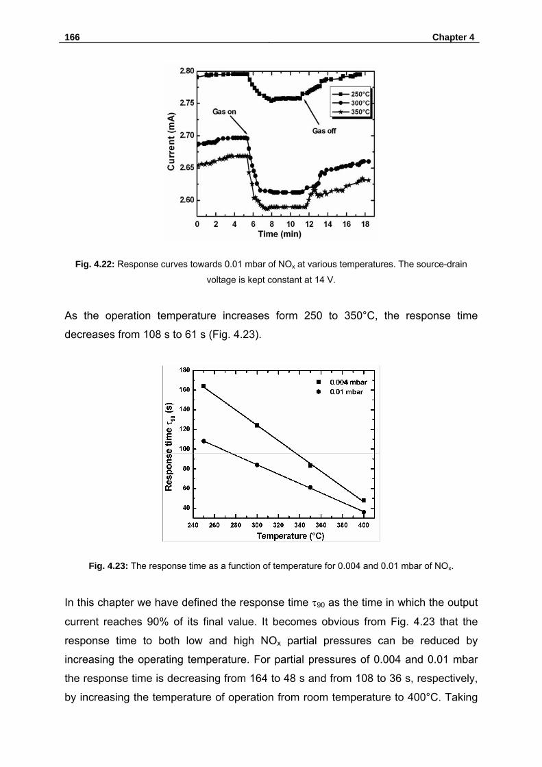
166 Chapter 4
Fig. 4.22: Response curves towards 0.01 mbar of NOx at various temperatures. The source-drain
voltage is kept constant at 14 V.
As the operation temperature increases form 250 to 350°C, the response time
decreases from 108 s to 61 s (Fig. 4.23).
Fig. 4.23: The response time as a function of temperature for 0.004 and 0.01 mbar of NOx.
In this chapter we have defined the response time τ90 as the time in which the output
current reaches 90% of its final value. It becomes obvious from Fig. 4.23 that the
response time to both low and high NOx partial pressures can be reduced by
increasing the operating temperature. For partial pressures of 0.004 and 0.01 mbar
the response time is decreasing from 164 to 48 s and from 108 to 36 s, respectively,
by increasing the temperature of operation from room temperature to 400°C. Taking
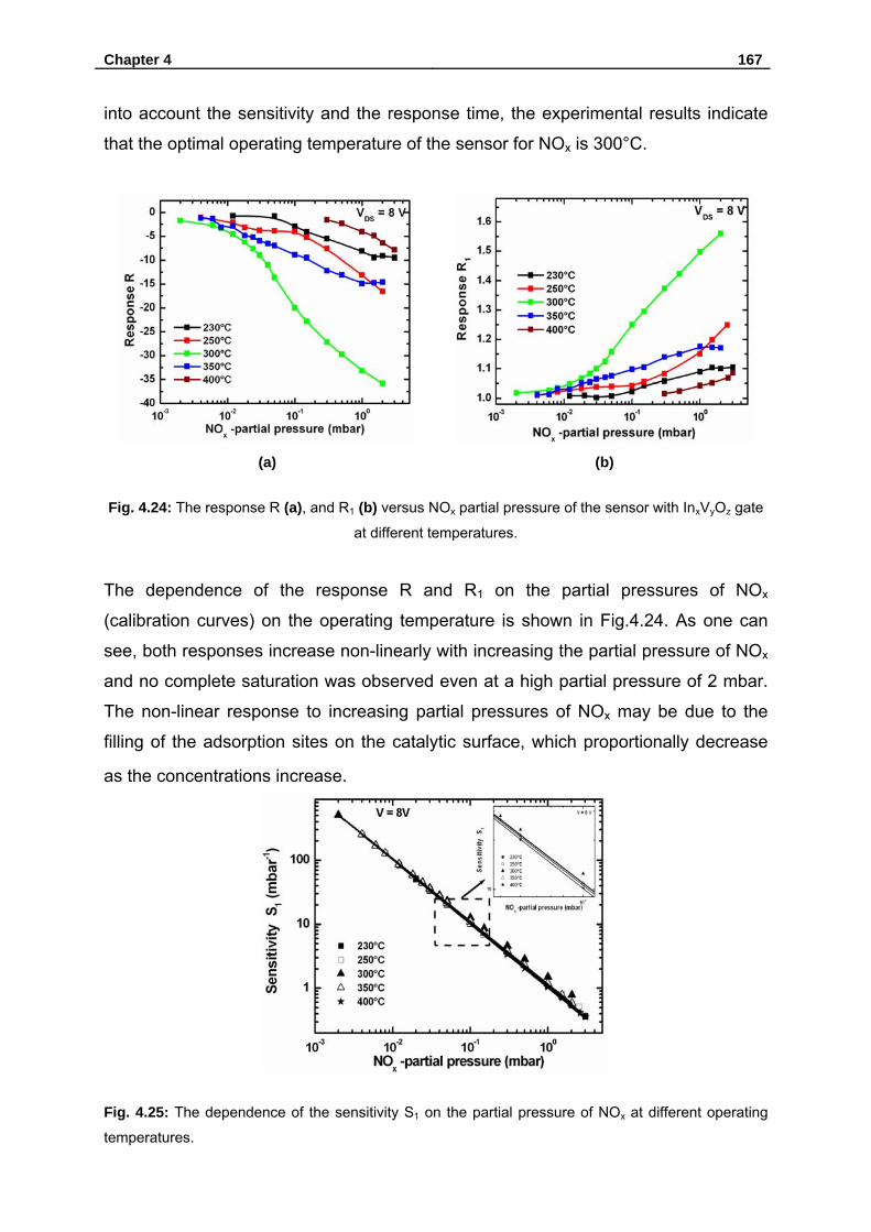
Chapter 4 167
into account the sensitivity and the response time, the experimental results indicate
that the optimal operating temperature of the sensor for NOx is 300°C.
(a) (b)
Fig. 4.24: The response R (a), and R1 (b) versus NOx partial pressure of the sensor with InxVyOz gate
at different temperatures.
The dependence of the response R and R1 on the partial pressures of NOx
(calibration curves) on the operating temperature is shown in Fig.4.24. As one can
see, both responses increase non-linearly with increasing the partial pressure of NOx
and no complete saturation was observed even at a high partial pressure of 2 mbar.
The non-linear response to increasing partial pressures of NOx may be due to the
filling of the adsorption sites on the catalytic surface, which proportionally decrease
as the concentrations increase.
Fig. 4.25: The dependence of the sensitivity S1 on the partial pressure of NOx at different operating
temperatures.
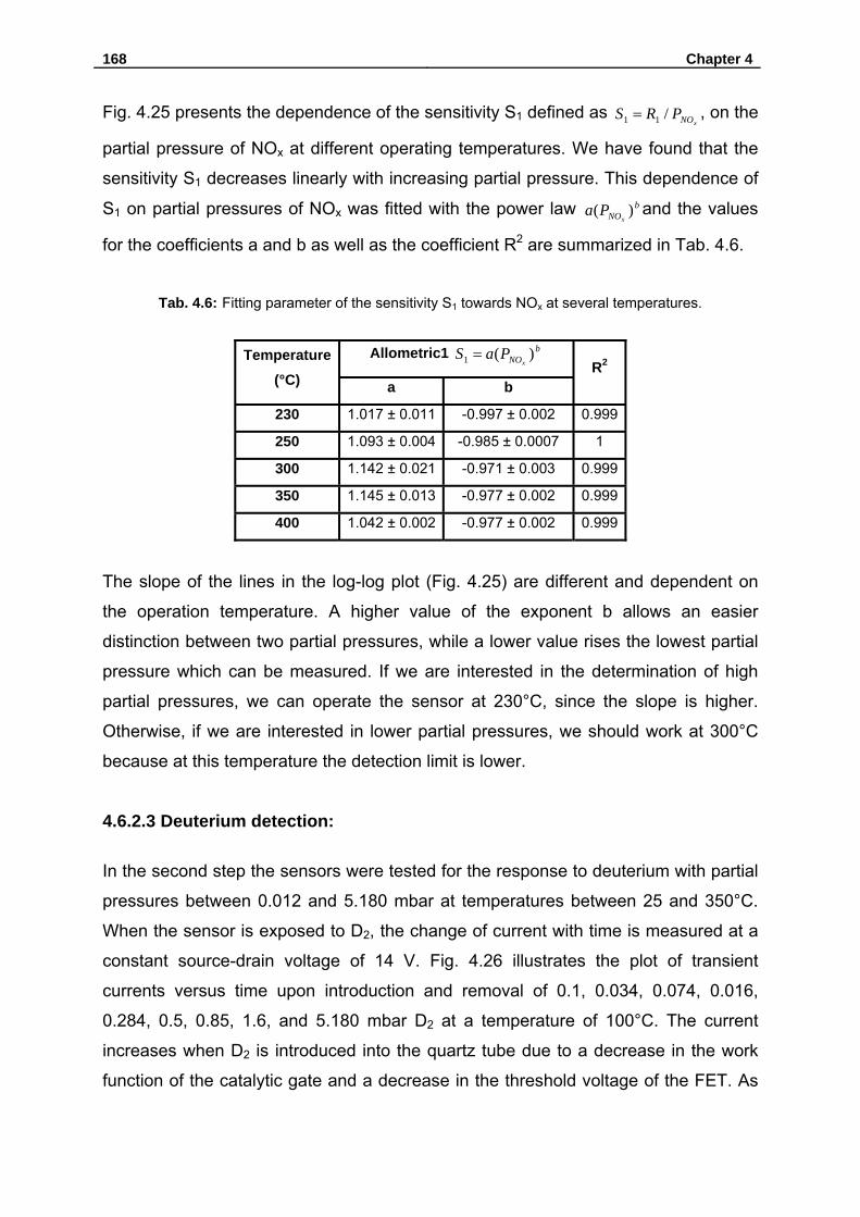
168 Chapter 4
Fig. 4.25 presents the dependence of the sensitivity S1 defined as xNOPRS /11 = , on the
partial pressure of NOx at different operating temperatures. We have found that the
sensitivity S1 decreases linearly with increasing partial pressure. This dependence of
S1 on partial pressures of NOx was fitted with the power law bNOx
Pa )( and the values
for the coefficients a and b as well as the coefficient R2 are summarized in Tab. 4.6.
Tab. 4.6: Fitting parameter of the sensitivity S1 towards NOx at several temperatures.
Allometric1 bNOx
PaS )(1 = Temperature (°C) a b
R2
230 1.017 ± 0.011 -0.997 ± 0.002 0.999
250 1.093 ± 0.004 -0.985 ± 0.0007 1
300 1.142 ± 0.021 -0.971 ± 0.003 0.999
350 1.145 ± 0.013 -0.977 ± 0.002 0.999
400 1.042 ± 0.002 -0.977 ± 0.002 0.999
The slope of the lines in the log-log plot (Fig. 4.25) are different and dependent on
the operation temperature. A higher value of the exponent b allows an easier
distinction between two partial pressures, while a lower value rises the lowest partial
pressure which can be measured. If we are interested in the determination of high
partial pressures, we can operate the sensor at 230°C, since the slope is higher.
Otherwise, if we are interested in lower partial pressures, we should work at 300°C
because at this temperature the detection limit is lower.
4.6.2.3 Deuterium detection:
In the second step the sensors were tested for the response to deuterium with partial
pressures between 0.012 and 5.180 mbar at temperatures between 25 and 350°C.
When the sensor is exposed to D2, the change of current with time is measured at a
constant source-drain voltage of 14 V. Fig. 4.26 illustrates the plot of transient
currents versus time upon introduction and removal of 0.1, 0.034, 0.074, 0.016,
0.284, 0.5, 0.85, 1.6, and 5.180 mbar D2 at a temperature of 100°C. The current
increases when D2 is introduced into the quartz tube due to a decrease in the work
function of the catalytic gate and a decrease in the threshold voltage of the FET. As
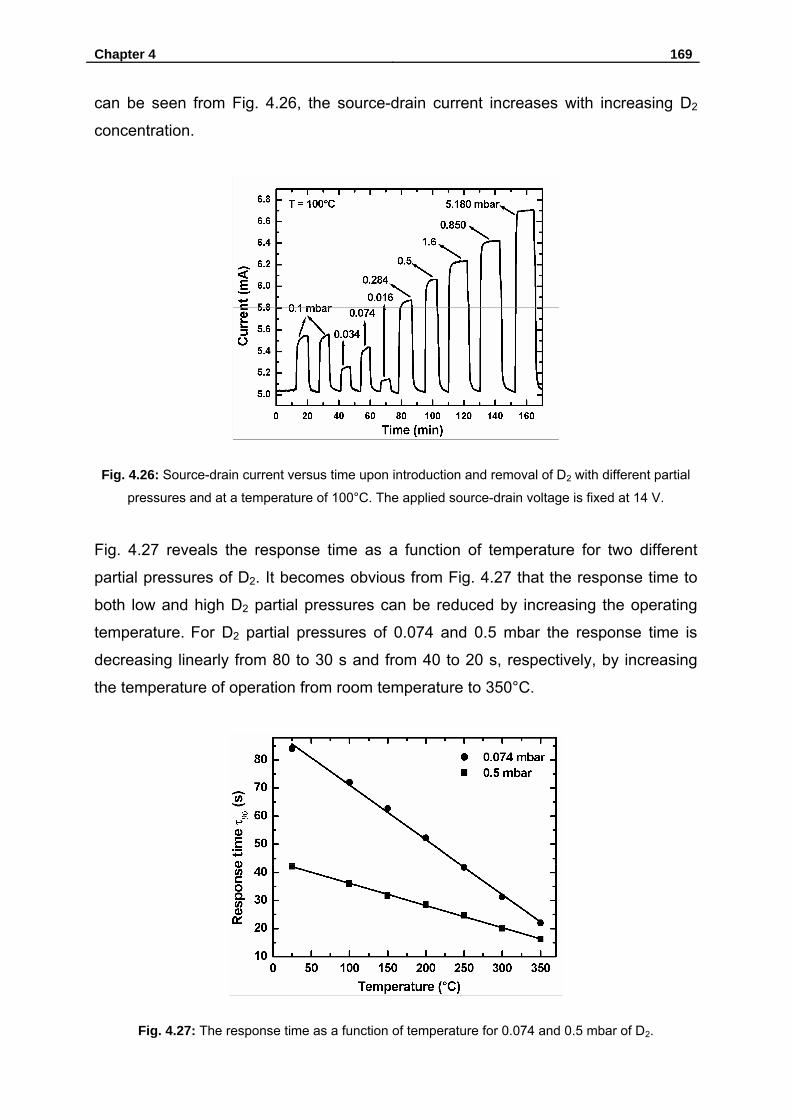
Chapter 4 169
can be seen from Fig. 4.26, the source-drain current increases with increasing D2
concentration.
Fig. 4.26: Source-drain current versus time upon introduction and removal of D2 with different partial
pressures and at a temperature of 100°C. The applied source-drain voltage is fixed at 14 V.
Fig. 4.27 reveals the response time as a function of temperature for two different
partial pressures of D2. It becomes obvious from Fig. 4.27 that the response time to
both low and high D2 partial pressures can be reduced by increasing the operating
temperature. For D2 partial pressures of 0.074 and 0.5 mbar the response time is
decreasing linearly from 80 to 30 s and from 40 to 20 s, respectively, by increasing
the temperature of operation from room temperature to 350°C.
Fig. 4.27: The response time as a function of temperature for 0.074 and 0.5 mbar of D2.
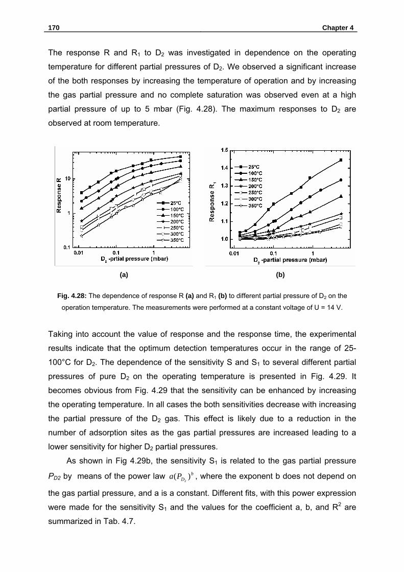
170 Chapter 4
The response R and R1 to D2 was investigated in dependence on the operating
temperature for different partial pressures of D2. We observed a significant increase
of the both responses by increasing the temperature of operation and by increasing
the gas partial pressure and no complete saturation was observed even at a high
partial pressure of up to 5 mbar (Fig. 4.28). The maximum responses to D2 are
observed at room temperature.
(a) (b)
Fig. 4.28: The dependence of response R (a) and R1 (b) to different partial pressure of D2 on the
operation temperature. The measurements were performed at a constant voltage of U = 14 V.
Taking into account the value of response and the response time, the experimental
results indicate that the optimum detection temperatures occur in the range of 25-
100°C for D2. The dependence of the sensitivity S and S1 to several different partial
pressures of pure D2 on the operating temperature is presented in Fig. 4.29. It
becomes obvious from Fig. 4.29 that the sensitivity can be enhanced by increasing
the operating temperature. In all cases the both sensitivities decrease with increasing
the partial pressure of the D2 gas. This effect is likely due to a reduction in the
number of adsorption sites as the gas partial pressures are increased leading to a
lower sensitivity for higher D2 partial pressures.
As shown in Fig 4.29b, the sensitivity S1 is related to the gas partial pressure
PD2 by means of the power law bDPa )(
2, where the exponent b does not depend on
the gas partial pressure, and a is a constant. Different fits, with this power expression
were made for the sensitivity S1 and the values for the coefficient a, b, and R2 are
summarized in Tab. 4.7.
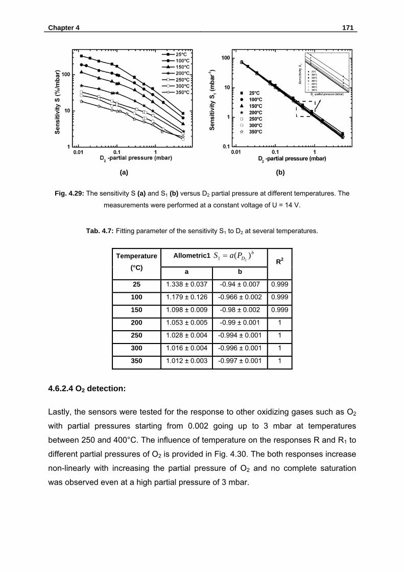
Chapter 4 171
(a) (b)
Fig. 4.29: The sensitivity S (a) and S1 (b) versus D2 partial pressure at different temperatures. The
measurements were performed at a constant voltage of U = 14 V.
Tab. 4.7: Fitting parameter of the sensitivity S1 to D2 at several temperatures.
Allometric1 bDPaS )(
21 = Temperature (°C) a b
R2
25 1.338 ± 0.037 -0.94 ± 0.007 0.999
100 1.179 ± 0.126 -0.966 ± 0.002 0.999
150 1.098 ± 0.009 -0.98 ± 0.002 0.999
200 1.053 ± 0.005 -0.99 ± 0.001 1
250 1.028 ± 0.004 -0.994 ± 0.001 1
300 1.016 ± 0.004 -0.996 ± 0.001 1
350 1.012 ± 0.003 -0.997 ± 0.001 1
4.6.2.4 O2 detection:
Lastly, the sensors were tested for the response to other oxidizing gases such as O2
with partial pressures starting from 0.002 going up to 3 mbar at temperatures
between 250 and 400°C. The influence of temperature on the responses R and R1 to
different partial pressures of O2 is provided in Fig. 4.30. The both responses increase
non-linearly with increasing the partial pressure of O2 and no complete saturation
was observed even at a high partial pressure of 3 mbar.

172 Chapter 4
(a) (b)
Fig. 4.30: The dependence of the response R (a) and R1 (b) on the O2 partial pressure of the sensor
with InxVyOz gate at different temperatures.
It can be seen from Fig. 4.30 that the responses can be enhanced by increasing the
operating temperature. The maximum responses toward O2 are observed at 300°C
for this sensor. At this temperature, fitting with the power expression bOPa )(
2was
made for the both sensitivities S and S1 (Fig. 4.31) and the values for the coefficient
a, b, and R2 are summarized in Tab. 4.8.
(a) (b)
Fig. 4.31: Dependence of sensitivity (a) S and (b) S1 on the O2 partial pressures at operating
temperature of 300°C. The measurements were performed at a constant voltage of U = 8 V.
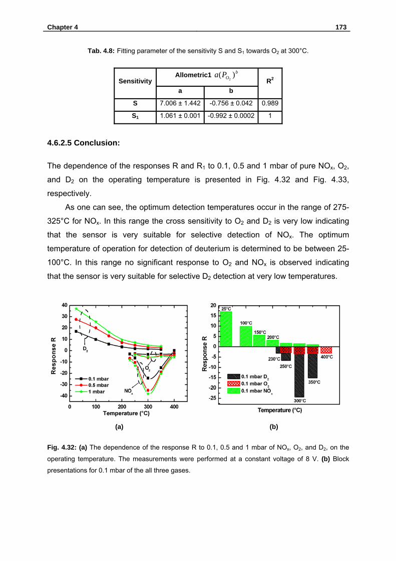
Chapter 4 173
Tab. 4.8: Fitting parameter of the sensitivity S and S1 towards O2 at 300°C.
Allometric1 bOPa )(
2
Sensitivity a b
R2
S 7.006 ± 1.442 -0.756 ± 0.042 0.989
S1 1.061 ± 0.001 -0.992 ± 0.0002 1
4.6.2.5 Conclusion:
The dependence of the responses R and R1 to 0.1, 0.5 and 1 mbar of pure NOx, O2,
and D2 on the operating temperature is presented in Fig. 4.32 and Fig. 4.33,
respectively.
As one can see, the optimum detection temperatures occur in the range of 275-
325°C for NOx. In this range the cross sensitivity to O2 and D2 is very low indicating
that the sensor is very suitable for selective detection of NOx. The optimum
temperature of operation for detection of deuterium is determined to be between 25-
100°C. In this range no significant response to O2 and NOx is observed indicating
that the sensor is very suitable for selective D2 detection at very low temperatures.
(a) (b)
Fig. 4.32: (a) The dependence of the response R to 0.1, 0.5 and 1 mbar of NOx, O2, and D2, on the
operating temperature. The measurements were performed at a constant voltage of 8 V. (b) Block
presentations for 0.1 mbar of the all three gases.
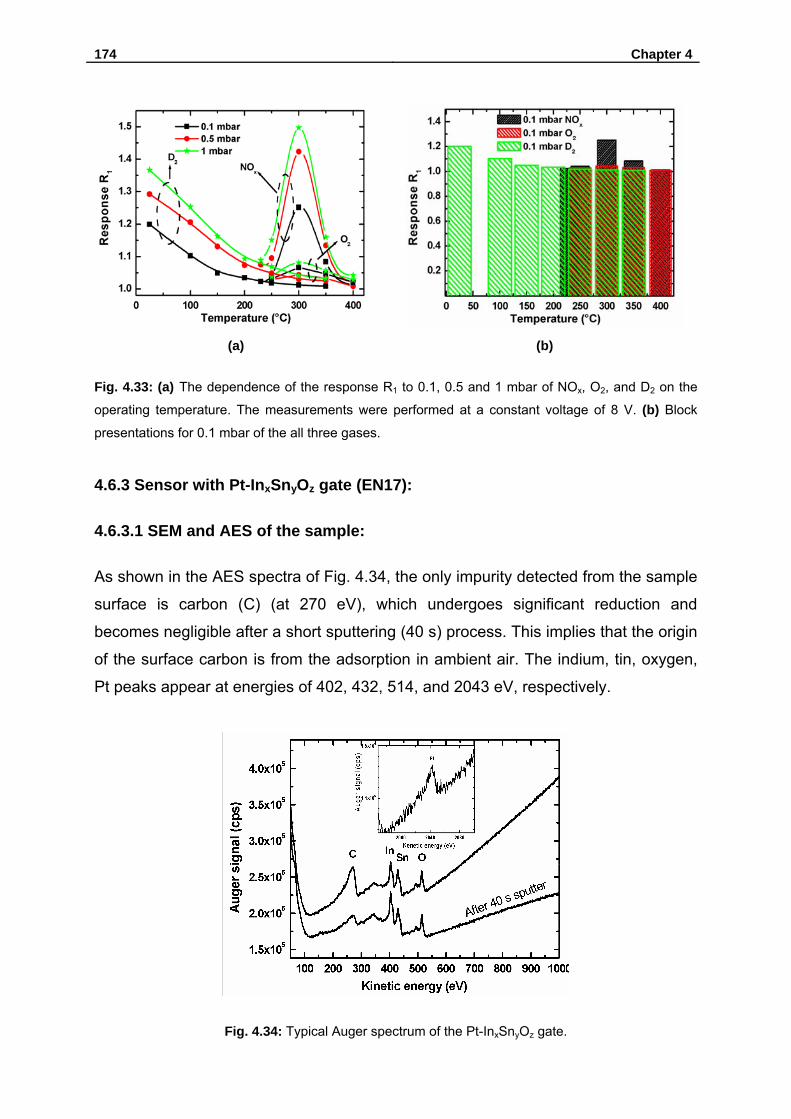
174 Chapter 4
(a) (b)
Fig. 4.33: (a) The dependence of the response R1 to 0.1, 0.5 and 1 mbar of NOx, O2, and D2 on the
operating temperature. The measurements were performed at a constant voltage of 8 V. (b) Block
presentations for 0.1 mbar of the all three gases.
4.6.3 Sensor with Pt-InxSnyOz gate (EN17):
4.6.3.1 SEM and AES of the sample:
As shown in the AES spectra of Fig. 4.34, the only impurity detected from the sample
surface is carbon (C) (at 270 eV), which undergoes significant reduction and
becomes negligible after a short sputtering (40 s) process. This implies that the origin
of the surface carbon is from the adsorption in ambient air. The indium, tin, oxygen,
Pt peaks appear at energies of 402, 432, 514, and 2043 eV, respectively.
Fig. 4.34: Typical Auger spectrum of the Pt-InxSnyOz gate.
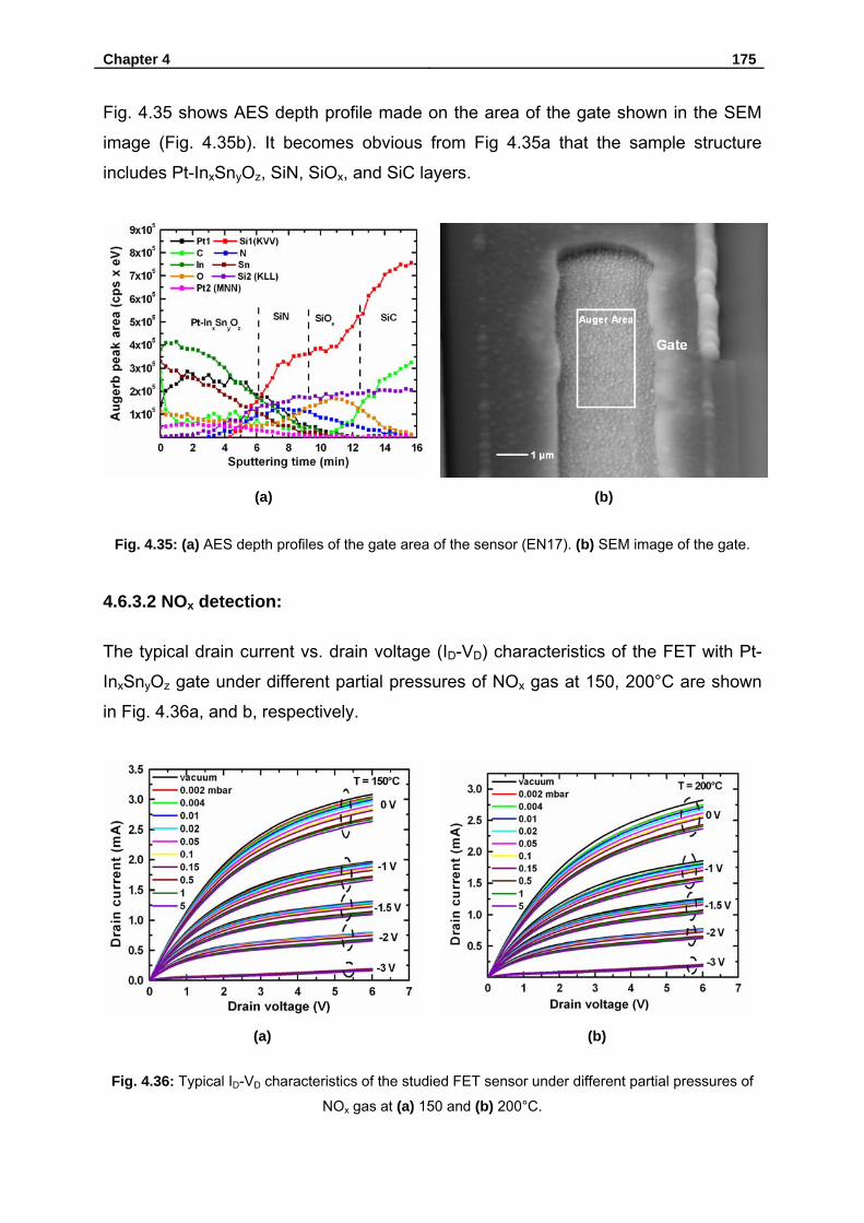
Chapter 4 175
Fig. 4.35 shows AES depth profile made on the area of the gate shown in the SEM
image (Fig. 4.35b). It becomes obvious from Fig 4.35a that the sample structure
includes Pt-InxSnyOz, SiN, SiOx, and SiC layers.
(a) (b)
Fig. 4.35: (a) AES depth profiles of the gate area of the sensor (EN17). (b) SEM image of the gate.
4.6.3.2 NOx detection:
The typical drain current vs. drain voltage (ID-VD) characteristics of the FET with Pt-
InxSnyOz gate under different partial pressures of NOx gas at 150, 200°C are shown
in Fig. 4.36a, and b, respectively.
(a) (b)
Fig. 4.36: Typical ID-VD characteristics of the studied FET sensor under different partial pressures of
NOx gas at (a) 150 and (b) 200°C.
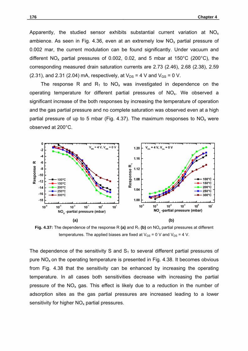
176 Chapter 4
Apparently, the studied sensor exhibits substantial current variation at NOx
ambience. As seen in Fig. 4.36, even at an extremely low NOx partial pressure of
0.002 mar, the current modulation can be found significantly. Under vacuum and
different NOx partial pressures of 0.002, 0.02, and 5 mbar at 150°C (200°C), the
corresponding measured drain saturation currents are 2.73 (2.46), 2.68 (2.38), 2.59
(2.31), and 2.31 (2.04) mA, respectively, at VDS = 4 V and VGS = 0 V.
The response R and R1 to NOx was investigated in dependence on the
operating temperature for different partial pressures of NOx. We observed a
significant increase of the both responses by increasing the temperature of operation
and the gas partial pressure and no complete saturation was observed even at a high
partial pressure of up to 5 mbar (Fig. 4.37). The maximum responses to NOx were
observed at 200°C.
(a) (b)
Fig. 4.37: The dependence of the response R (a) and R1 (b) on NOx partial pressures at different
temperatures. The applied biases are fixed at VGS = 0 V and VDS = 4 V.
The dependence of the sensitivity S and S1 to several different partial pressures of
pure NOx on the operating temperature is presented in Fig. 4.38. It becomes obvious
from Fig. 4.38 that the sensitivity can be enhanced by increasing the operating
temperature. In all cases both sensitivities decrease with increasing the partial
pressure of the NOx gas. This effect is likely due to a reduction in the number of
adsorption sites as the gas partial pressures are increased leading to a lower
sensitivity for higher NOx partial pressures.
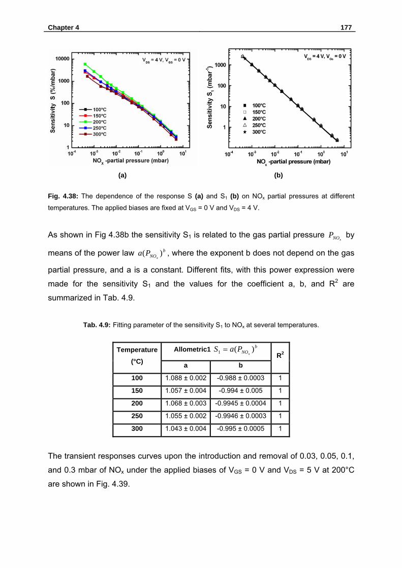
Chapter 4 177
(a) (b)
Fig. 4.38: The dependence of the response S (a) and S1 (b) on NOx partial pressures at different
temperatures. The applied biases are fixed at VGS = 0 V and VDS = 4 V.
As shown in Fig 4.38b the sensitivity S1 is related to the gas partial pressure xNOP by
means of the power law bNOx
Pa )( , where the exponent b does not depend on the gas
partial pressure, and a is a constant. Different fits, with this power expression were
made for the sensitivity S1 and the values for the coefficient a, b, and R2 are
summarized in Tab. 4.9.
Tab. 4.9: Fitting parameter of the sensitivity S1 to NOx at several temperatures.
Allometric1 bNOx
PaS )(1 = Temperature (°C) a b
R2
100 1.088 ± 0.002 -0.988 ± 0.0003 1
150 1.057 ± 0.004 -0.994 ± 0.005 1
200 1.068 ± 0.003 -0.9945 ± 0.0004 1
250 1.055 ± 0.002 -0.9946 ± 0.0003 1
300 1.043 ± 0.004 -0.995 ± 0.0005 1
The transient responses curves upon the introduction and removal of 0.03, 0.05, 0.1,
and 0.3 mbar of NOx under the applied biases of VGS = 0 V and VDS = 5 V at 200°C
are shown in Fig. 4.39.
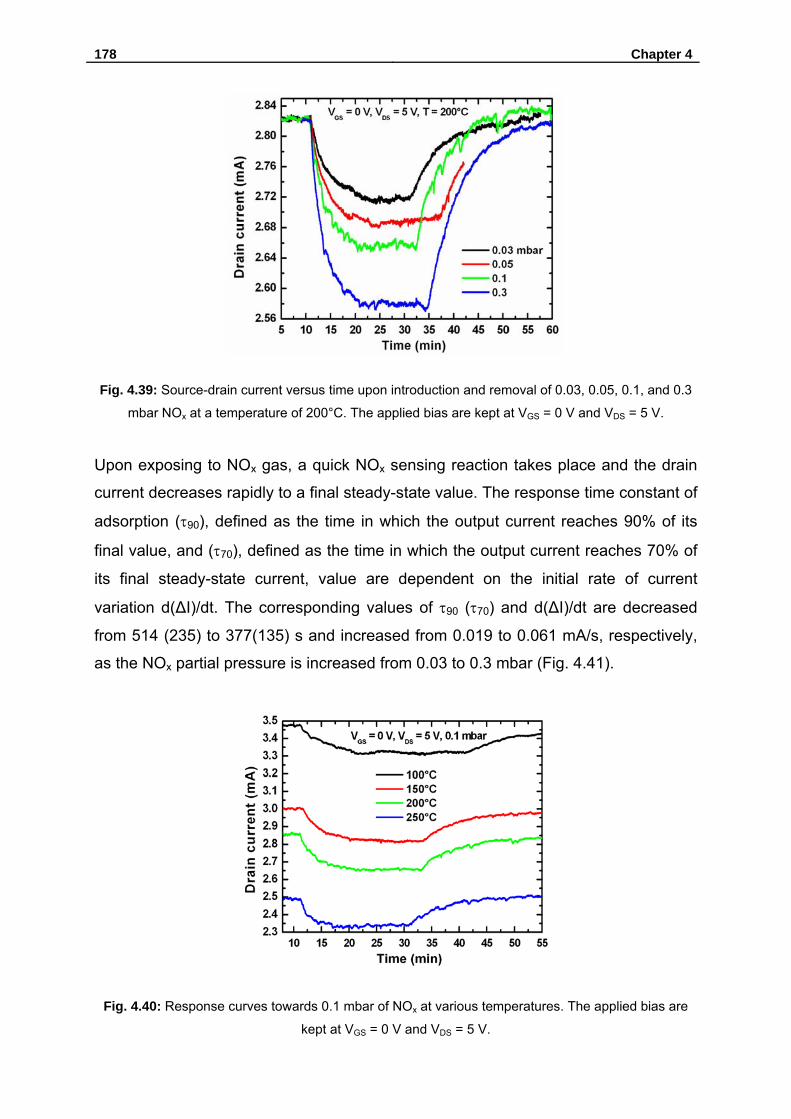
178 Chapter 4
Fig. 4.39: Source-drain current versus time upon introduction and removal of 0.03, 0.05, 0.1, and 0.3
mbar NOx at a temperature of 200°C. The applied bias are kept at VGS = 0 V and VDS = 5 V.
Upon exposing to NOx gas, a quick NOx sensing reaction takes place and the drain
current decreases rapidly to a final steady-state value. The response time constant of
adsorption (τ90), defined as the time in which the output current reaches 90% of its
final value, and (τ70), defined as the time in which the output current reaches 70% of
its final steady-state current, value are dependent on the initial rate of current
variation d(ΔI)/dt. The corresponding values of τ90 (τ70) and d(ΔI)/dt are decreased
from 514 (235) to 377(135) s and increased from 0.019 to 0.061 mA/s, respectively,
as the NOx partial pressure is increased from 0.03 to 0.3 mbar (Fig. 4.41).
Fig. 4.40: Response curves towards 0.1 mbar of NOx at various temperatures. The applied bias are
kept at VGS = 0 V and VDS = 5 V.
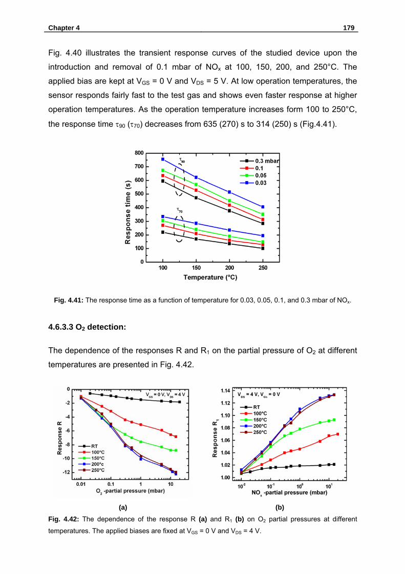
Chapter 4 179
Fig. 4.40 illustrates the transient response curves of the studied device upon the
introduction and removal of 0.1 mbar of NOx at 100, 150, 200, and 250°C. The
applied bias are kept at VGS = 0 V and VDS = 5 V. At low operation temperatures, the
sensor responds fairly fast to the test gas and shows even faster response at higher
operation temperatures. As the operation temperature increases form 100 to 250°C,
the response time τ90 (τ70) decreases from 635 (270) s to 314 (250) s (Fig.4.41).
Fig. 4.41: The response time as a function of temperature for 0.03, 0.05, 0.1, and 0.3 mbar of NOx.
4.6.3.3 O2 detection:
The dependence of the responses R and R1 on the partial pressure of O2 at different
temperatures are presented in Fig. 4.42.
(a) (b)
Fig. 4.42: The dependence of the response R (a) and R1 (b) on O2 partial pressures at different
temperatures. The applied biases are fixed at VGS = 0 V and VDS = 4 V.
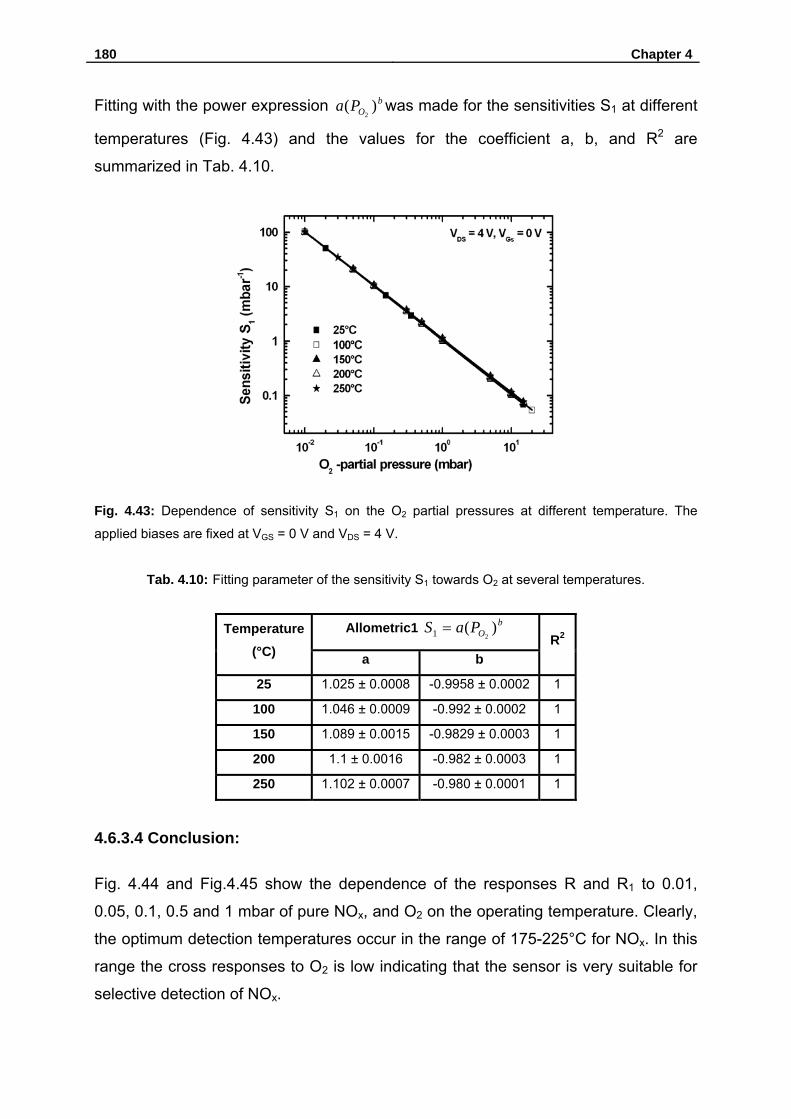
180 Chapter 4
Fitting with the power expression bOPa )(
2was made for the sensitivities S1 at different
temperatures (Fig. 4.43) and the values for the coefficient a, b, and R2 are
summarized in Tab. 4.10.
Fig. 4.43: Dependence of sensitivity S1 on the O2 partial pressures at different temperature. The
applied biases are fixed at VGS = 0 V and VDS = 4 V.
Tab. 4.10: Fitting parameter of the sensitivity S1 towards O2 at several temperatures.
Allometric1 bOPaS )(
21 = Temperature (°C) a b
R2
25 1.025 ± 0.0008 -0.9958 ± 0.0002 1
100 1.046 ± 0.0009 -0.992 ± 0.0002 1
150 1.089 ± 0.0015 -0.9829 ± 0.0003 1
200 1.1 ± 0.0016 -0.982 ± 0.0003 1
250 1.102 ± 0.0007 -0.980 ± 0.0001 1
4.6.3.4 Conclusion:
Fig. 4.44 and Fig.4.45 show the dependence of the responses R and R1 to 0.01,
0.05, 0.1, 0.5 and 1 mbar of pure NOx, and O2 on the operating temperature. Clearly,
the optimum detection temperatures occur in the range of 175-225°C for NOx. In this
range the cross responses to O2 is low indicating that the sensor is very suitable for
selective detection of NOx.
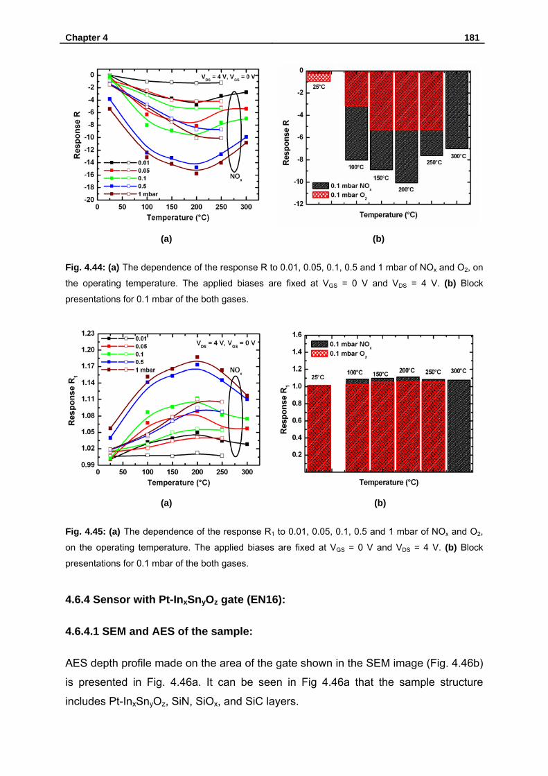
Chapter 4 181
(a) (b)
Fig. 4.44: (a) The dependence of the response R to 0.01, 0.05, 0.1, 0.5 and 1 mbar of NOx and O2, on
the operating temperature. The applied biases are fixed at VGS = 0 V and VDS = 4 V. (b) Block
presentations for 0.1 mbar of the both gases.
(a) (b)
Fig. 4.45: (a) The dependence of the response R1 to 0.01, 0.05, 0.1, 0.5 and 1 mbar of NOx and O2,
on the operating temperature. The applied biases are fixed at VGS = 0 V and VDS = 4 V. (b) Block
presentations for 0.1 mbar of the both gases.
4.6.4 Sensor with Pt-InxSnyOz gate (EN16):
4.6.4.1 SEM and AES of the sample:
AES depth profile made on the area of the gate shown in the SEM image (Fig. 4.46b)
is presented in Fig. 4.46a. It can be seen in Fig 4.46a that the sample structure
includes Pt-InxSnyOz, SiN, SiOx, and SiC layers.
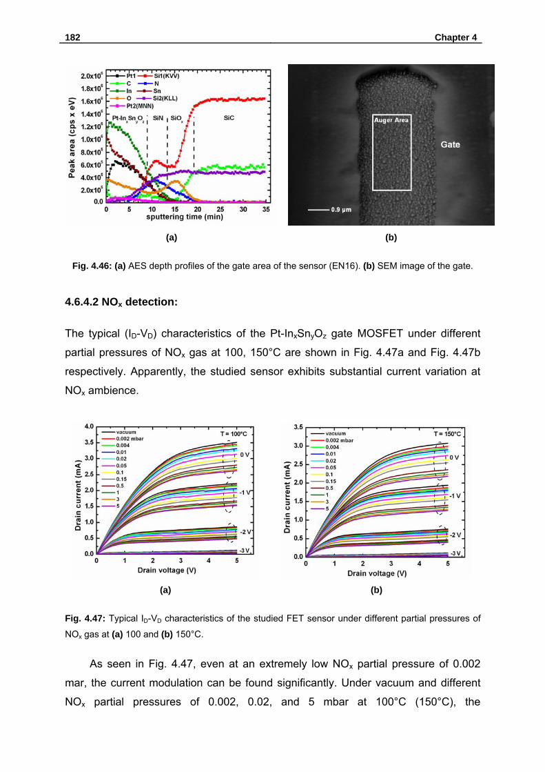
182 Chapter 4
(a) (b)
Fig. 4.46: (a) AES depth profiles of the gate area of the sensor (EN16). (b) SEM image of the gate.
4.6.4.2 NOx detection:
The typical (ID-VD) characteristics of the Pt-InxSnyOz gate MOSFET under different
partial pressures of NOx gas at 100, 150°C are shown in Fig. 4.47a and Fig. 4.47b
respectively. Apparently, the studied sensor exhibits substantial current variation at
NOx ambience.
(a) (b)
Fig. 4.47: Typical ID-VD characteristics of the studied FET sensor under different partial pressures of
NOx gas at (a) 100 and (b) 150°C.
As seen in Fig. 4.47, even at an extremely low NOx partial pressure of 0.002
mar, the current modulation can be found significantly. Under vacuum and different
NOx partial pressures of 0.002, 0.02, and 5 mbar at 100°C (150°C), the
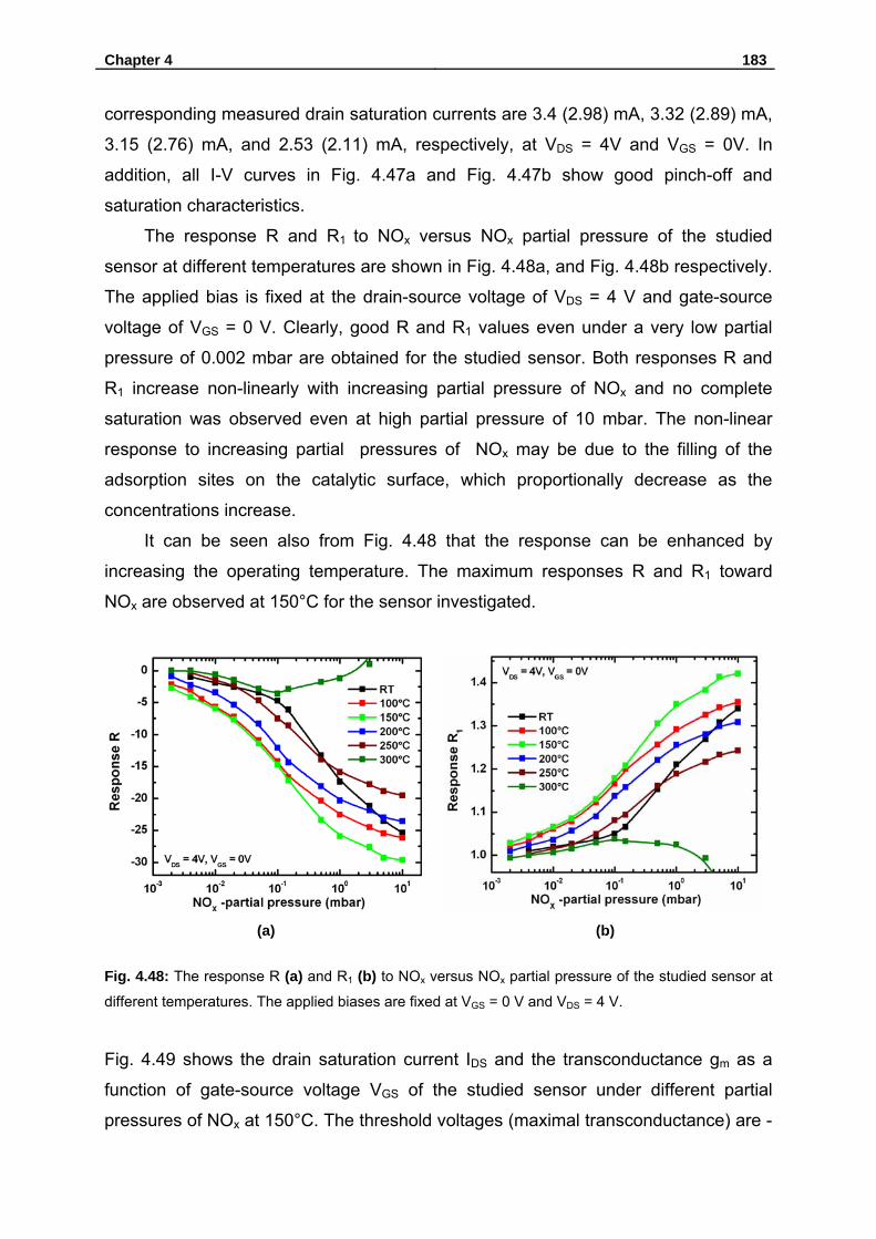
Chapter 4 183
corresponding measured drain saturation currents are 3.4 (2.98) mA, 3.32 (2.89) mA,
3.15 (2.76) mA, and 2.53 (2.11) mA, respectively, at VDS = 4V and VGS = 0V. In
addition, all I-V curves in Fig. 4.47a and Fig. 4.47b show good pinch-off and
saturation characteristics.
The response R and R1 to NOx versus NOx partial pressure of the studied
sensor at different temperatures are shown in Fig. 4.48a, and Fig. 4.48b respectively.
The applied bias is fixed at the drain-source voltage of VDS = 4 V and gate-source
voltage of VGS = 0 V. Clearly, good R and R1 values even under a very low partial
pressure of 0.002 mbar are obtained for the studied sensor. Both responses R and
R1 increase non-linearly with increasing partial pressure of NOx and no complete
saturation was observed even at high partial pressure of 10 mbar. The non-linear
response to increasing partial pressures of NOx may be due to the filling of the
adsorption sites on the catalytic surface, which proportionally decrease as the
concentrations increase.
It can be seen also from Fig. 4.48 that the response can be enhanced by
increasing the operating temperature. The maximum responses R and R1 toward
NOx are observed at 150°C for the sensor investigated.
(a) (b)
Fig. 4.48: The response R (a) and R1 (b) to NOx versus NOx partial pressure of the studied sensor at
different temperatures. The applied biases are fixed at VGS = 0 V and VDS = 4 V.
Fig. 4.49 shows the drain saturation current IDS and the transconductance gm as a
function of gate-source voltage VGS of the studied sensor under different partial
pressures of NOx at 150°C. The threshold voltages (maximal transconductance) are -
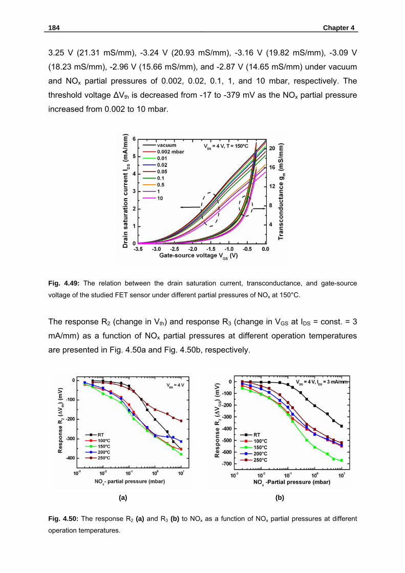
184 Chapter 4
3.25 V (21.31 mS/mm), -3.24 V (20.93 mS/mm), -3.16 V (19.82 mS/mm), -3.09 V
(18.23 mS/mm), -2.96 V (15.66 mS/mm), and -2.87 V (14.65 mS/mm) under vacuum
and NOx partial pressures of 0.002, 0.02, 0.1, 1, and 10 mbar, respectively. The
threshold voltage ΔVth is decreased from -17 to -379 mV as the NOx partial pressure
increased from 0.002 to 10 mbar.
Fig. 4.49: The relation between the drain saturation current, transconductance, and gate-source
voltage of the studied FET sensor under different partial pressures of NOx at 150°C.
The response R2 (change in Vth) and response R3 (change in VGS at IDS = const. = 3
mA/mm) as a function of NOx partial pressures at different operation temperatures
are presented in Fig. 4.50a and Fig. 4.50b, respectively.
(a) (b)
Fig. 4.50: The response R2 (a) and R3 (b) to NOx as a function of NOx partial pressures at different
operation temperatures.
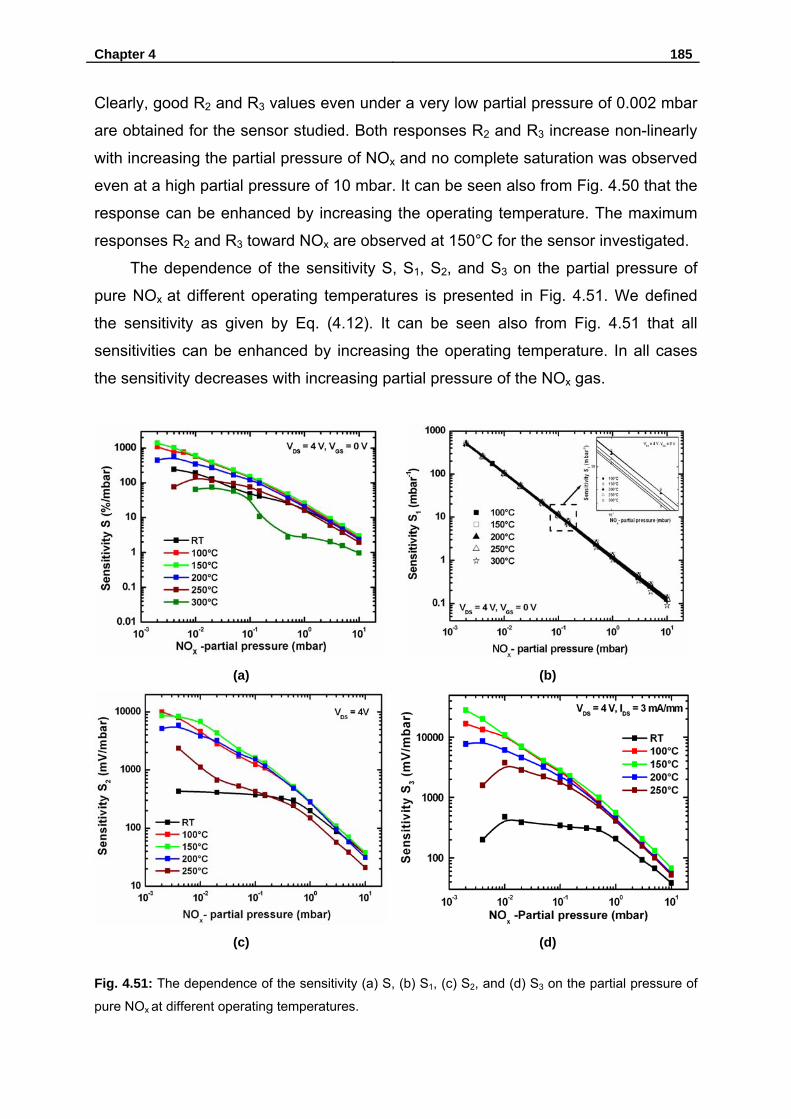
Chapter 4 185
Clearly, good R2 and R3 values even under a very low partial pressure of 0.002 mbar
are obtained for the sensor studied. Both responses R2 and R3 increase non-linearly
with increasing the partial pressure of NOx and no complete saturation was observed
even at a high partial pressure of 10 mbar. It can be seen also from Fig. 4.50 that the
response can be enhanced by increasing the operating temperature. The maximum
responses R2 and R3 toward NOx are observed at 150°C for the sensor investigated.
The dependence of the sensitivity S, S1, S2, and S3 on the partial pressure of
pure NOx at different operating temperatures is presented in Fig. 4.51. We defined
the sensitivity as given by Eq. (4.12). It can be seen also from Fig. 4.51 that all
sensitivities can be enhanced by increasing the operating temperature. In all cases
the sensitivity decreases with increasing partial pressure of the NOx gas.
(a) (b)
(c) (d)
Fig. 4.51: The dependence of the sensitivity (a) S, (b) S1, (c) S2, and (d) S3 on the partial pressure of
pure NOx at different operating temperatures.
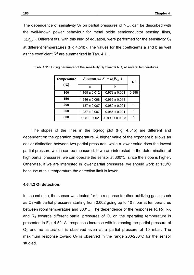
186 Chapter 4
The dependence of sensitivity S1 on partial pressures of NOx can be described with
the well-known power behaviour for metal oxide semiconductor sensing films,
)(xNOPa . Different fits, with this kind of equation, were performed for the sensitivity S1
at different temperatures (Fig.4.51b). The values for the coefficients a and b as well
as the coefficient R2 are summarized in Tab. 4.11.
Tab. 4.11: Fitting parameter of the sensitivity S1 towards NOx at several temperatures.
Allometric1 )(1 xNOPaS = Temperature (°C) a b
R2
100 1.165 ± 0.012 -0.978 ± 0.001 0.998
150 1.246 ± 0.098 -0.965 ± 0.013 1
200 1.137 ± 0.007 -0.980 ± 0.001 1
250 1.087 ± 0.007 -0.985 ± 0.001 1
300 1.05 ± 0.002 -0.990 ± 0.0003 1
The slopes of the lines in the log-log plot (Fig. 4.51b) are different and
dependent on the operation temperature. A higher value of the exponent b allows an
easier distinction between two partial pressures, while a lower value rises the lowest
partial pressure which can be measured. If we are interested in the determination of
high partial pressures, we can operate the sensor at 300°C, since the slope is higher.
Otherwise, if we are interested in lower partial pressures, we should work at 150°C
because at this temperature the detection limit is lower.
4.6.4.3 O2 detection:
In second step, the sensor was tested for the response to other oxidizing gases such
as O2 with partial pressures starting from 0.002 going up to 10 mbar at temperatures
between room temperature and 300°C. The dependence of the responses R, R1, R2,
and R3 towards different partial pressures of O2 on the operating temperature is
presented in Fig. 4.52. All responses increase with increasing the partial pressure of
O2 and no saturation is observed even at a partial pressure of 10 mbar. The
maximum response toward O2 is observed in the range 200-250°C for the sensor
studied.
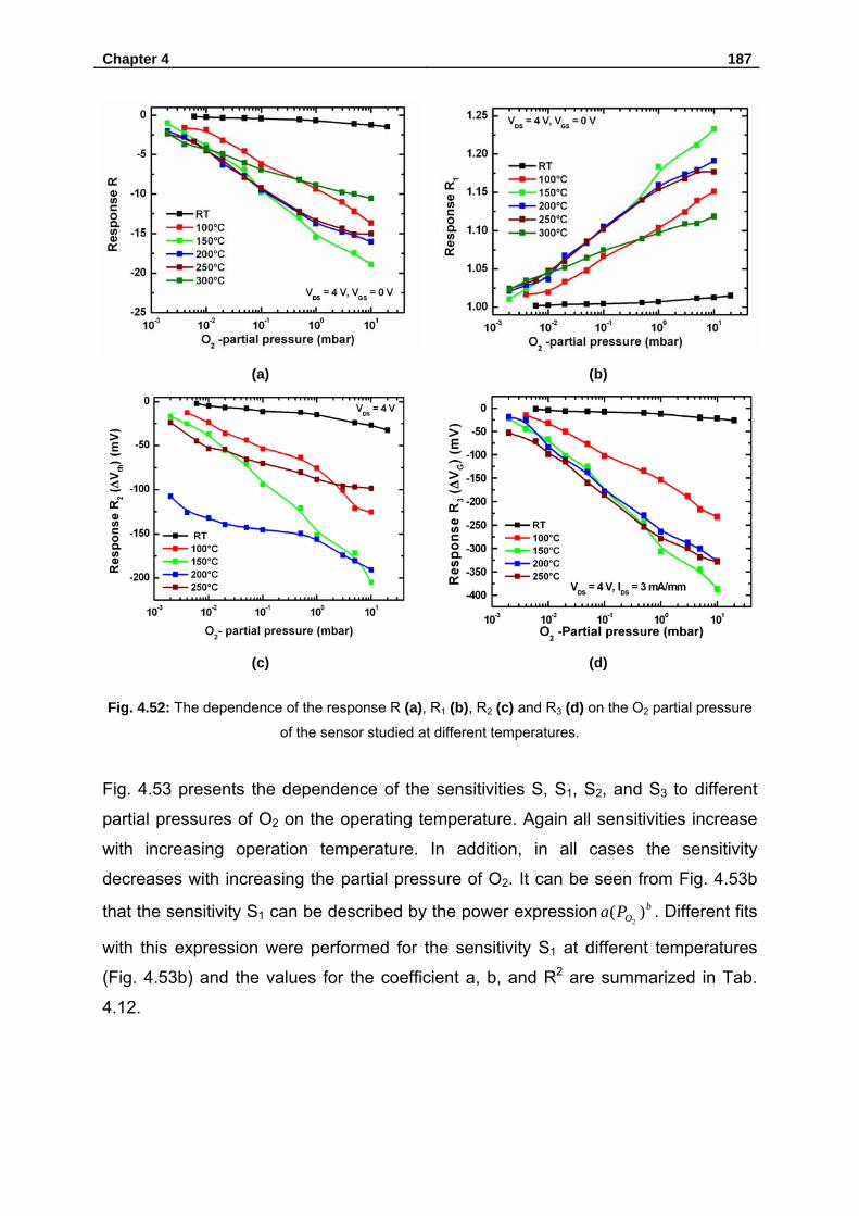
Chapter 4 187
(a) (b)
(c) (d)
Fig. 4.52: The dependence of the response R (a), R1 (b), R2 (c) and R3 (d) on the O2 partial pressure
of the sensor studied at different temperatures.
Fig. 4.53 presents the dependence of the sensitivities S, S1, S2, and S3 to different
partial pressures of O2 on the operating temperature. Again all sensitivities increase
with increasing operation temperature. In addition, in all cases the sensitivity
decreases with increasing the partial pressure of O2. It can be seen from Fig. 4.53b
that the sensitivity S1 can be described by the power expression bOPa )(
2. Different fits
with this expression were performed for the sensitivity S1 at different temperatures
(Fig. 4.53b) and the values for the coefficient a, b, and R2 are summarized in Tab.
4.12.
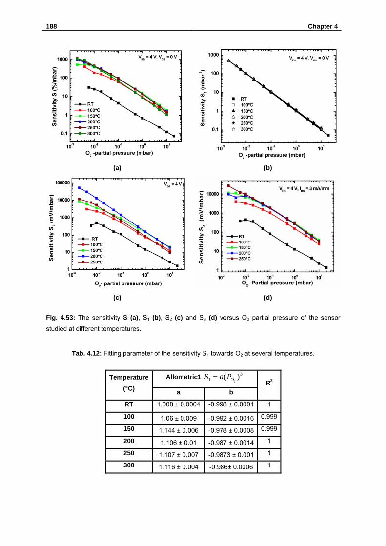
188 Chapter 4
(a) (b)
(c) (d)
Fig. 4.53: The sensitivity S (a), S1 (b), S2 (c) and S3 (d) versus O2 partial pressure of the sensor
studied at different temperatures.
Tab. 4.12: Fitting parameter of the sensitivity S1 towards O2 at several temperatures.
Allometric1 bOPaS )(
21 = Temperature (°C) a b
R2
RT 1.008 ± 0.0004 -0.998 ± 0.0001 1
100 1.06 ± 0.009 -0.992 ± 0.0016 0.999
150 1.144 ± 0.006 -0.978 ± 0.0008 0.999
200 1.106 ± 0.01 -0.987 ± 0.0014 1
250 1.107 ± 0.007 -0.9873 ± 0.001 1
300 1.116 ± 0.004 -0.986± 0.0006 1
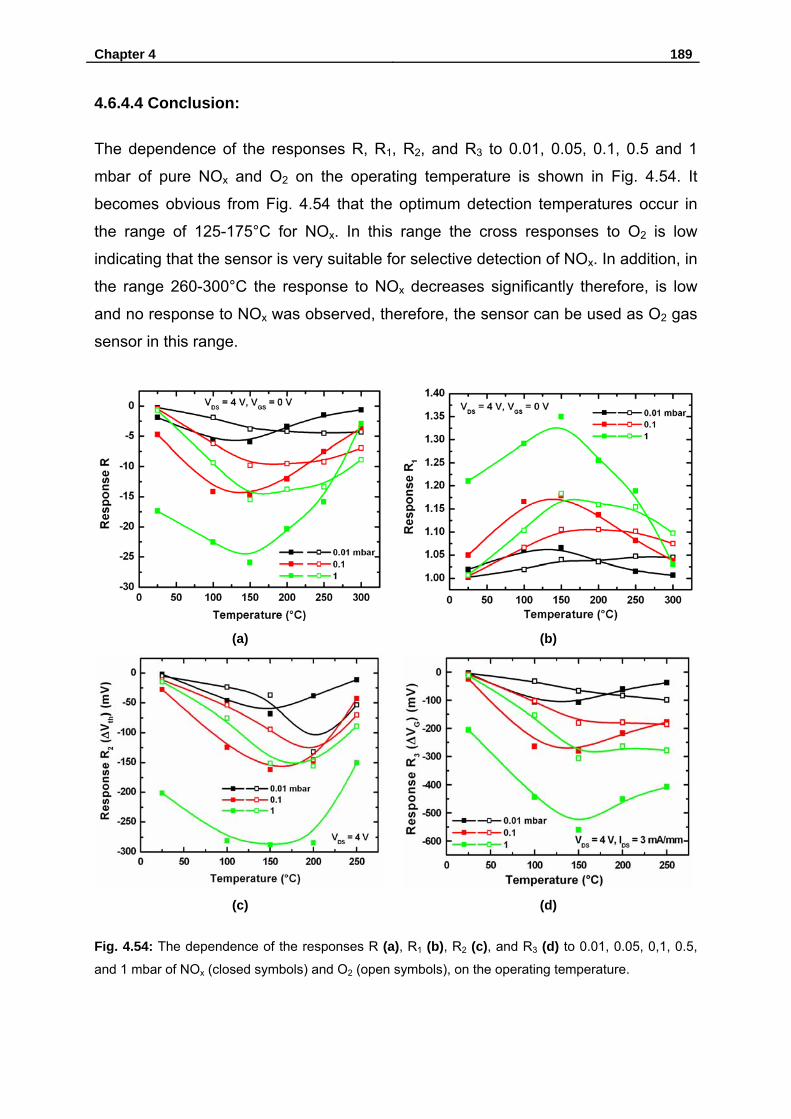
Chapter 4 189
4.6.4.4 Conclusion:
The dependence of the responses R, R1, R2, and R3 to 0.01, 0.05, 0.1, 0.5 and 1
mbar of pure NOx and O2 on the operating temperature is shown in Fig. 4.54. It
becomes obvious from Fig. 4.54 that the optimum detection temperatures occur in
the range of 125-175°C for NOx. In this range the cross responses to O2 is low
indicating that the sensor is very suitable for selective detection of NOx. In addition, in
the range 260-300°C the response to NOx decreases significantly therefore, is low
and no response to NOx was observed, therefore, the sensor can be used as O2 gas
sensor in this range.
(a) (b)
(c) (d)
Fig. 4.54: The dependence of the responses R (a), R1 (b), R2 (c), and R3 (d) to 0.01, 0.05, 0,1, 0.5,
and 1 mbar of NOx (closed symbols) and O2 (open symbols), on the operating temperature.
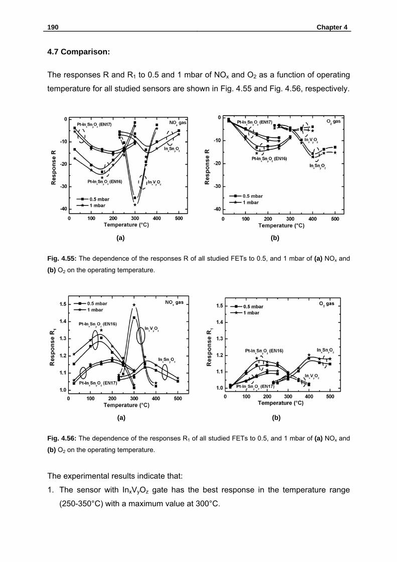
190 Chapter 4
4.7 Comparison:
The responses R and R1 to 0.5 and 1 mbar of NOx and O2 as a function of operating
temperature for all studied sensors are shown in Fig. 4.55 and Fig. 4.56, respectively.
(a) (b)
Fig. 4.55: The dependence of the responses R of all studied FETs to 0.5, and 1 mbar of (a) NOx and
(b) O2 on the operating temperature.
(a) (b)
Fig. 4.56: The dependence of the responses R1 of all studied FETs to 0.5, and 1 mbar of (a) NOx and
(b) O2 on the operating temperature.
The experimental results indicate that:
1. The sensor with InxVyOz gate has the best response in the temperature range
(250-350°C) with a maximum value at 300°C.
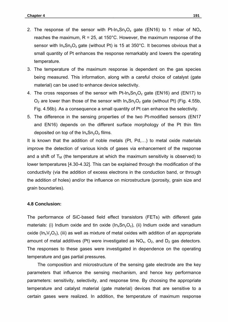
Chapter 4 191
2. The response of the sensor with Pt-InxSnyOz gate (EN16) to 1 mbar of NOx
reaches the maximum, R = 25, at 150°C. However, the maximum response of the
sensor with InxSnyOz gate (without Pt) is 15 at 350°C. It becomes obvious that a
small quantity of Pt enhances the response remarkably and lowers the operating
temperature.
3. The temperature of the maximum response is dependent on the gas species
being measured. This information, along with a careful choice of catalyst (gate
material) can be used to enhance device selectivity.
4. The cross responses of the sensor with Pt-InxSnyOz gate (EN16) and (EN17) to
O2 are lower than those of the sensor with InxSnyOz gate (without Pt) (Fig. 4.55b,
Fig. 4.56b). As a consequence a small quantity of Pt can enhance the selectivity.
5. The difference in the sensing properties of the two Pt-modified sensors (EN17
and EN16) depends on the different surface morphology of the Pt thin film
deposited on top of the InxSnyOz films.
It is known that the addition of noble metals (Pt, Pd,…) to metal oxide materials
improve the detection of various kinds of gases via enhancement of the response
and a shift of TM (the temperature at which the maximum sensitivity is observed) to
lower temperatures [4.30-4.32]. This can be explained through the modification of the
conductivity (via the addition of excess electrons in the conduction band, or through
the addition of holes) and/or the influence on microstructure (porosity, grain size and
grain boundaries).
4.8 Conclusion:
The performance of SiC-based field effect transistors (FETs) with different gate
materials: (i) Indium oxide and tin oxide (InxSnyOz), (ii) Indium oxide and vanadium
oxide (InxVyOz), (iii) as well as mixture of metal oxides with addition of an appropriate
amount of metal additives (Pt) were investigated as NOx, O2, and D2 gas detectors.
The responses to these gases were investigated in dependence on the operating
temperature and gas partial pressures.
The composition and microstructure of the sensing gate electrode are the key
parameters that influence the sensing mechanism, and hence key performance
parameters: sensitivity, selectivity, and response time. By choosing the appropriate
temperature and catalyst material (gate material) devices that are sensitive to a
certain gases were realized. In addition, the temperature of maximum response
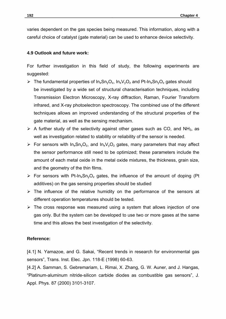
192 Chapter 4
varies dependent on the gas species being measured. This information, along with a
careful choice of catalyst (gate material) can be used to enhance device selectivity.
4.9 Outlook and future work:
For further investigation in this field of study, the following experiments are
suggested:
The fundamental properties of InxSnyOz, InxVyOz and Pt-InxSnyOz gates should
be investigated by a wide set of structural characterisation techniques, including
Transmission Electron Microscopy, X-ray diffraction, Raman, Fourier Transform
infrared, and X-ray photoelectron spectroscopy. The combined use of the different
techniques allows an improved understanding of the structural properties of the
gate material, as well as the sensing mechanism.
A further study of the selectivity against other gases such as CO, and NH3, as
well as investigation related to stability or reliability of the sensor is needed.
For sensors with InxSnyOz, and InxVyOz gates, many parameters that may affect
the sensor performance still need to be optimized; these parameters include the
amount of each metal oxide in the metal oxide mixtures, the thickness, grain size,
and the geometry of the thin films.
For sensors with Pt-InxSnyOz gates, the influence of the amount of doping (Pt
additives) on the gas sensing properties should be studied
The influence of the relative humidity on the performance of the sensors at
different operation temperatures should be tested.
The cross response was measured using a system that allows injection of one
gas only. But the system can be developed to use two or more gases at the same
time and this allows the best investigation of the selectivity.
Reference:
[4.1] N. Yamazoe, and G. Sakai, “Recent trends in research for environmental gas
sensors”, Trans. Inst. Elec. Jpn. 118-E (1998) 60-63.
[4.2] A. Samman, S. Gebremariam, L. Rimai, X. Zhang, G. W. Auner, and J. Hangas,
“Platinum-aluminum nitride-silicon carbide diodes as combustible gas sensors”, J.
Appl. Phys. 87 (2000) 3101-3107.
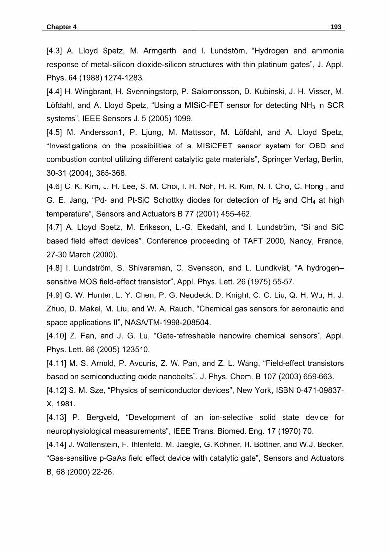
Chapter 4 193
[4.3] A. Lloyd Spetz, M. Armgarth, and I. Lundstöm, “Hydrogen and ammonia
response of metal-silicon dioxide-silicon structures with thin platinum gates”, J. Appl.
Phys. 64 (1988) 1274-1283.
[4.4] H. Wingbrant, H. Svenningstorp, P. Salomonsson, D. Kubinski, J. H. Visser, M.
Löfdahl, and A. Lloyd Spetz, “Using a MISiC-FET sensor for detecting NH3 in SCR
systems”, IEEE Sensors J. 5 (2005) 1099.
[4.5] M. Andersson1, P. Ljung, M. Mattsson, M. Löfdahl, and A. Lloyd Spetz,
“Investigations on the possibilities of a MISiCFET sensor system for OBD and
combustion control utilizing different catalytic gate materials”, Springer Verlag, Berlin,
30-31 (2004), 365-368.
[4.6] C. K. Kim, J. H. Lee, S. M. Choi, I. H. Noh, H. R. Kim, N. I. Cho, C. Hong , and
G. E. Jang, “Pd- and Pt-SiC Schottky diodes for detection of H2 and CH4 at high
temperature”, Sensors and Actuators B 77 (2001) 455-462.
[4.7] A. Lloyd Spetz, M. Eriksson, L.-G. Ekedahl, and I. Lundström, “Si and SiC
based field effect devices”, Conference proceeding of TAFT 2000, Nancy, France,
27-30 March (2000).
[4.8] I. Lundström, S. Shivaraman, C. Svensson, and L. Lundkvist, “A hydrogen–
sensitive MOS field-effect transistor”, Appl. Phys. Lett. 26 (1975) 55-57.
[4.9] G. W. Hunter, L. Y. Chen, P. G. Neudeck, D. Knight, C. C. Liu, Q. H. Wu, H. J.
Zhuo, D. Makel, M. Liu, and W. A. Rauch, “Chemical gas sensors for aeronautic and
space applications II”, NASA/TM-1998-208504.
[4.10] Z. Fan, and J. G. Lu, “Gate-refreshable nanowire chemical sensors”, Appl.
Phys. Lett. 86 (2005) 123510.
[4.11] M. S. Arnold, P. Avouris, Z. W. Pan, and Z. L. Wang, “Field-effect transistors
based on semiconducting oxide nanobelts”, J. Phys. Chem. B 107 (2003) 659-663.
[4.12] S. M. Sze, “Physics of semiconductor devices”, New York, ISBN 0-471-09837-
X, 1981.
[4.13] P. Bergveld, “Development of an ion-selective solid state device for
neurophysiological measurements”, IEEE Trans. Biomed. Eng. 17 (1970) 70.
[4.14] J. Wöllenstein, F. Ihlenfeld, M. Jaegle, G. Köhner, H. Böttner, and W.J. Becker,
“Gas-sensitive p-GaAs field effect device with catalytic gate”, Sensors and Actuators
B, 68 (2000) 22-26.
194 Chapter 4
[4.15] J. V. Hatfield, J.A. Covington, and J. W. Gardner, ”GasFETs incorporating
conducting polymers as gate materials”, Sensors and Actuators B 65 (2000) 253-
256.
[4.16] Y. Miyahara, Tsukada K., and H. Miyagi, ”Field-effect transistor using a solid
electrolyte as a new oxygen sensor”, J. Appl. Phys. 63 (1988) 2431-2434.
[4.17] W. I. Cho, C. W. Yi, J. B. Ju, B. W. Cho, and K. S. Yun, “Characteristics of a
thin-film LaF3 solid electrolyte for oxygen sensing”, Sensors and Actuators B 5 (1991)
149-153.
[4.18] S. K. Choi, C. W. Yi, W. I. Cho, B. C. Cho, J. B. Ju, K. S. Yun, and N.
Yamazoe, ”A MOSFET type sensor for oxygen sensing LaF3 as a gate material”,
Sensors and Actuators B 13 (1993) 45-48.
[4.19] M. Bouvet, G. Guillaudb, A. Leroy, A. Maillard, A. Spirkovitch, and F.-G.
Tournilhac, ”Phthalocyanine-based field-effect transistor as ozone sensor”, Sensors
and Actuators B 73 (2001) 63-70.
[4.20] M. Andersson, M. Holmberg, I. Lundström, A. Lloyd-Spetz, P. Martenson, R.
Paolesse, C. Falconi, E. Proiett, C. Di Natale, and A. D’Amico, ”Development of a
ChemFET sensor with molecular films of phorphyrins as sensitive layer”, Sensors
and Actuators B (2001) 567-571.
[4.21] I. Eisele, T. Doll, and M. Burgmaier, “Low power gas detection with FET
sensors”, Sensors and Actuators B 78 (2001) 19-25.
[4.22] M. Ali, V. Cimalla, V. Lebedev, Th. Stauden, G. Ecke, V. Tilak, P. Sandvik and
O. Ambacher, “SiC-based FET for detection of NOx and O2 using InSnOx as a gate
material”, Sensors and Actuators B 122 (2007) 182-186.
[4.23] M. Ali, V. Cimalla, V. Lebedev, Th. Stauden, Ch. Y. Wang, G. Ecke, V. Tilak, P.
Sandvik and O. Ambacher, “Reactively sputtered InxVyOz films for detection of NOx,
D2, and O2”, Sensors and Actuators B 123 (2007) 779-783.
[4.24] P. Sandvik, M. Ali, V. Tilak, K. Matocha, Th. Stauden, J. Tucker, J. Deluca, and
O. Ambacher, “SiC-based MOSFET for harsh environment emissions sensors”,
Conference proceeding of ICSCRM 2005, Pittsburgh, Pennsylvania, 18-23
September (2005).
[4.25] G. Kriakidis, N. Katsarakis, M. Bender, E. Gagaudakis, and V. Cimalla, “InOx
thin films, candidates for novel chemical and optoelectronic applications”, Mater.
Phys. Mech. 1 (2000) 83-97.
Chapter 4 195
[4.26] P. W. Palmberg, G. E. Riach, R. E. Weber, and N. C. MacDonald, “Handbook
of Auger Electron Spectroscopy”, (Physical Electronics Industries, Minesota, 1972).
[4.27] R. Ramamoorthy, M. K. Kennedy, H. Nienhaus, A. Lorke, F. E. Kruis, and H.
Fissan, “Surface oxidation of monodisperse SnOx nanoparticles”, Sensors and
Actuators B 88 (2003) 281-285.
[4.28] R. Larcipretea, E. Borsella, P. D. Padova, P. Perfetti, and C. Crotti, “Surface
analysis study of the oxidation of organotin films deposited by ArF excimer laser
chemical vapor deposition”, J. Vac. Sci. Technol. A 15 (1997) 2492-2501.
[4.29] M. J. Madou, and S. R. Morrison, “Chemical sensing with solid state devices”,
Academic Press, New York, 1988, pp. 67-104.
[4.30] N. Yamazoe, Y. Kurokawa, and T. Seiyaama,” Enzyme semiconductor sensor
based on butyrylcholinesterase”, Sensors and Actuators B 4 (1983) 283-286.
[4.31] Y. Takao, Y. Iwanaga , Y. Shimizu, and M. Egashira, “Trimethylamine-sensing
mechanism of TiO2-based sensors 1. Effects of metal additives on trimethylamine-
sensing properties of TiO2 sensors”, Sensors and Actuators B 10 (1993) 229-234.
[4.32] H. Kuwabara, T. Okuhara, and M. Misono, “Catalytic removal of
trimethylamine, an offensive-odor component, by selective oxidative decomposition
to N2, CO2, and H2O over copper-exchanged zeolites”, Chem. Lett. 1992 (1992) 947-
950.

196 Chapter 4

Chapter 5 197
Chapter 5
5. NOx and O2 Sensing Properties of In2O3 Thin Films grown by MOCVD
5.1 Introduction:
Demands for exact monitoring of nitrogen oxide gases (NOx), which are air pollutants
released from combustion facilities and automobiles, have become more serious all
over the world in recent years. For air quality monitoring or exhaust gas control, NOx
is the main gas to be detected. In order to detect the partial pressure of hazardous
NOx gas, there have been a lot of efforts in developing a variety of sensors such as
electrochemical [5.1], SAW [5.2], and polymer based sensors [5.3]. Recently, much
interest has been focused on metal oxide based sensors because of their structural
simplicity, high sensitivity, short response time, small size, low cost and good
compatibility with the fabrication process for microelectronic devices. The
semiconductor metal oxide (SMO) gas sensors operate on the principle that a
chemical reaction between the gas species to be detected and a SMO sensing film
produces a change in the film’s resistance. Although several different metal oxide
semiconductors can be used as gas sensing materials the most popular include, tin
oxide (SnO2) [5.4-5.7], tungsten trioxide (WO3) [5.4, 5.8], titanium oxide (TiO2) [5.9-
5.10], zinc oxide (ZnO) [5.4, 5.11] and indium oxide (In2O3) [5.4, 5.12-5.13]. It was
found that indium oxide exhibits high sensitivity to oxidizing gases, such as NOx
[5.14-5.15] and O3 [5.12, 5.16] and therefore can be used as active layers in
detectors for these gases.
Several methods have been used to prepare In2O3 thin films, such as dc and rf
sputtering [5.16-5.17], reactive evaporation [5.18-5.19], evaporation of metallic
indium and subsequent oxidation [5.20-5.21], chemical vapour deposition [5.22],
spray pyrolysis [5.23] sol-gel [5.14] and laser ablation [5.24]. Metal organic chemical
vapor deposition (MOCVD) technique is a new and low cost approach for thin film
deposition of indium oxide films which offers the opportunity to control the
stoichiometry and morphology by varying the process parameters.
In this chapter the NOx, and O2 sensing properties of In2O3 thin films grown by
MOCVD technique have been investigated as a function of the operation temperature
and partial pressure.
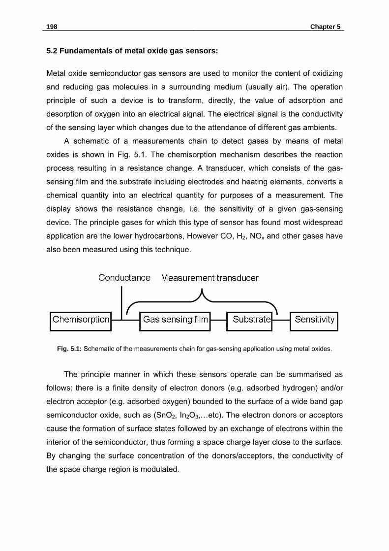
198 Chapter 5
5.2 Fundamentals of metal oxide gas sensors:
Metal oxide semiconductor gas sensors are used to monitor the content of oxidizing
and reducing gas molecules in a surrounding medium (usually air). The operation
principle of such a device is to transform, directly, the value of adsorption and
desorption of oxygen into an electrical signal. The electrical signal is the conductivity
of the sensing layer which changes due to the attendance of different gas ambients.
A schematic of a measurements chain to detect gases by means of metal
oxides is shown in Fig. 5.1. The chemisorption mechanism describes the reaction
process resulting in a resistance change. A transducer, which consists of the gas-
sensing film and the substrate including electrodes and heating elements, converts a
chemical quantity into an electrical quantity for purposes of a measurement. The
display shows the resistance change, i.e. the sensitivity of a given gas-sensing
device. The principle gases for which this type of sensor has found most widespread
application are the lower hydrocarbons, However CO, H2, NOx and other gases have
also been measured using this technique.
Fig. 5.1: Schematic of the measurements chain for gas-sensing application using metal oxides.
The principle manner in which these sensors operate can be summarised as
follows: there is a finite density of electron donors (e.g. adsorbed hydrogen) and/or
electron acceptor (e.g. adsorbed oxygen) bounded to the surface of a wide band gap
semiconductor oxide, such as (SnO2, In2O3,…etc). The electron donors or acceptors
cause the formation of surface states followed by an exchange of electrons within the
interior of the semiconductor, thus forming a space charge layer close to the surface.
By changing the surface concentration of the donors/acceptors, the conductivity of
the space charge region is modulated.
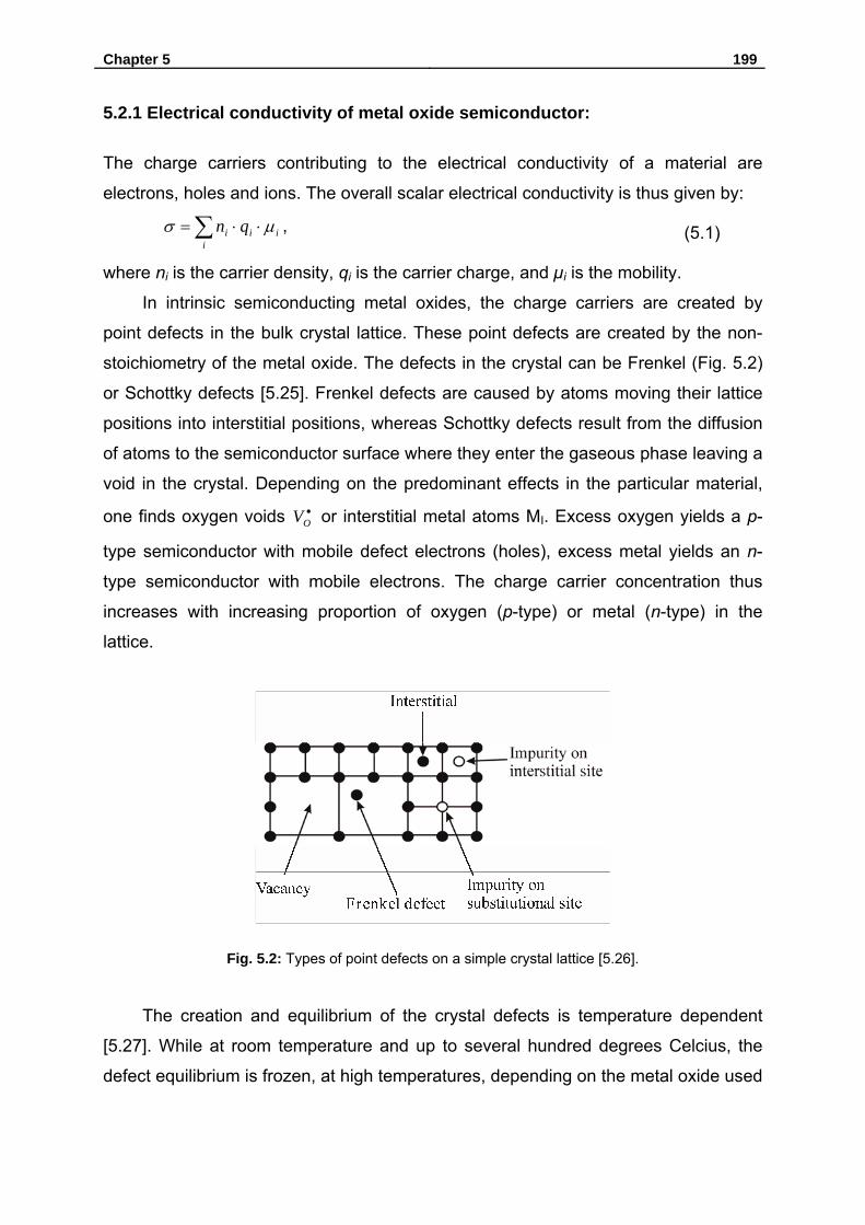
Chapter 5 199
5.2.1 Electrical conductivity of metal oxide semiconductor:
The charge carriers contributing to the electrical conductivity of a material are
electrons, holes and ions. The overall scalar electrical conductivity is thus given by:
iii
i qn μσ ⋅⋅= ∑ , (5.1)
where ni is the carrier density, qi is the carrier charge, and µi is the mobility.
In intrinsic semiconducting metal oxides, the charge carriers are created by
point defects in the bulk crystal lattice. These point defects are created by the non-
stoichiometry of the metal oxide. The defects in the crystal can be Frenkel (Fig. 5.2)
or Schottky defects [5.25]. Frenkel defects are caused by atoms moving their lattice
positions into interstitial positions, whereas Schottky defects result from the diffusion
of atoms to the semiconductor surface where they enter the gaseous phase leaving a
void in the crystal. Depending on the predominant effects in the particular material,
one finds oxygen voids •OV or interstitial metal atoms MI. Excess oxygen yields a p-
type semiconductor with mobile defect electrons (holes), excess metal yields an n-
type semiconductor with mobile electrons. The charge carrier concentration thus
increases with increasing proportion of oxygen (p-type) or metal (n-type) in the
lattice.
Fig. 5.2: Types of point defects on a simple crystal lattice [5.26].
The creation and equilibrium of the crystal defects is temperature dependent
[5.27]. While at room temperature and up to several hundred degrees Celcius, the
defect equilibrium is frozen, at high temperatures, depending on the metal oxide used

200 Chapter 5
(e.g. ~800°C for Ga2O3), the lattice oxygen is in thermodynamic equilibrium with the
ambient air oxygen partial pressure2OP .
The ionisation of the crystal defects is also temperature dependent. The free charge
carrier concentration thus depends on the energy required for defect formation
(Gibbs energy GD) and for ionisation EI.
A hopping mechanism can be used to explain the electrical conductivity of
semiconductors with low charge carrier mobility and high band gap [5.28]. I.e. in a p-
type metal oxide the conductivity results from carrier dissociation or phonon induced
hopping of holes from one void to another requiring a hopping activation energy. We
thus obtain a temperature dependant carrier mobility µ(T). For n-type metal oxides
similar hopping mechanisms have been postulated, where the electron hopping is
hindered by defect potential barriers [5.28]. The defect concentration is again
temperature dependant. At high defect concentrations electron tunneling through the
potential barriers is possible. For all metal oxides we do however obtain an electrical
conductivity following:
⎟⎠⎞
⎜⎝⎛≅
kTEAexpσ . (5.2)
EA being the activation energy consisting of the energy required for defect creation,
the energy required for ionisation of the charge carriers and the temperature
dependent hopping energy [5.29].
5.2.2 Structure and equivalent circuit models:
The basic structure for a metal oxide semiconductor sensor consists of a metal oxide
film and contact electrodes. The film either has an amorphous or polycrystalline
microstructure. To obtain an amorphous structure the film deposited at room
temperature and is not heat-treated after deposition.
An amorphous film is highly disordered and exhibits no periodicity, which helps
to eliminate the effects of the intercrystalline boundaries. In an equivalent circuit, it
can be represented as a resistor between the tow contacts (Fig. 5.3a). The dc
equivalent circuit for the amorphous film in Fig. 5.3a includes the electrode finger
resistance, Rs, the metal-semiconductor junction resistance, Rc, and the resistance
between the two contacts, Rg.

Chapter 5 201
Polycrystalline films are deposited at higher temperature or annealed after
deposition. A polycrystalline film consists of many randomly orientated
microcrystalline regions, each of which exhibits periodicity. Each semiconductor
crystallite is connected with its neighbours by a grain boundary (Fig. 5.3b). Electrons
can move across the potential barrier at each boundary. The gas-film interaction can
change the barrier height and the number of free carriers, which results in a change
of the electrical resistance of the film. In case of the polycrystalline film (Fig. 5.3b), it
is assumed that the film consists of only a single layer of crystallites. In addition to Rs
and Rc, the dc equivalent circuit includes the grain boundary resistance, Rbi, and the
individual crystallite resistances, Rgi (i = 1,…….,n). One can combine each of the
circuit elements to obtain an equivalent resistance fo the sensing element. When
significant interactions occur between the sensing element and the gas measured the
values of the resistive circuit elements change.
(a) Amorphous film
(b) Polycrystalline film
Fig. 5.3: Physical structure and equivalent circuit of a semiconducting metal oxide sensing element for
(a) amorphous film and (b) polycrystalline film [5.30].
5.2.3 Sensing mechanism of metal oxide semiconductor gas sensor:
Metal oxide semiconductor gas sensors detect gases via variation in their resistance
(or conductance). The gas-sensing mechanism in the case of n-type semiconductor
can be described in detail via a chemisorption process combined with a charge

202 Chapter 5
transfer process at the n-semiconductor surface at temperatures above 100°C. This
process makes it possible to use semiconducting gas sensors having a fast and
appreciable interaction of the surrounding gas molecules with the surface.
At temperatures below 100°C, the oxygen molecules are adsorbed by a
physisorption process. At room temperature, the coverage of physisorbed molecules
is less than one monolayer. This process is accomplished by weak van der Waals
forces. The binding forces are very small (20 kJ/mol~0.2 eV per molecule) and the
molecules are mobile on the surface of the semiconductor without changing their
electrical properties. The low value of the physisorption enthalpy of about 20 kJ/mol
causes physisorption to disappear almost totally at higher temperatures. The
activation energy for diffusion jumps of physisorbed molecules is smaller than the
adsorption energy. Consequently, the probability that a molecule jumps to a
neighbouring site is greater than in the desorption process [5.31].
Where a metal-oxide semiconducting gas sensor is used at temperatures below
100°C, additional equipment is required. It has been demonstrated that UV light
illumination can be used to enhance the sensitivity of SnO2 thin film gas sensors to
nitrogen dioxide (NO2) [5.32]. Photoexcitation can affect the charge carrier transport
across grain boundaries by increasing the density of free carriers throughout the
material and decreasing the intergrain barrier height.
At higher temperatures (>100°C), oxygen molecules are dissociated via a
chemisorption process. Firstly, oxygen is connected via dipole bonding to the
semiconductor surface atoms. Under this condition, electrons are removed from the
semiconductor surface via a charge transfer mechanism; this is followed by the
formation of chemical bonds with the semiconductor surface atoms. The bond and
activation energy of the surface reaction depends on the lattice and defect structure
of the surface. Active sites for a chemisorption reaction can be normal sites,
adatoms, dislocation cores or impurity atoms. The reactants can be impinging gas
molecules, electrons, and atoms or defects on the regular charge or on specific sites
of the substrate. The chemisorption species can have an electrical charge and
consist of one or more atoms. It is assumed that oxygen vacancies are primarily
responsible for the chemisorption reaction. Typical chemisorption species on the
surface of semiconductive metal oxides in air are −2O , −O , and −2O [5.33]. The case
of n-type semiconductive metal oxides, the formation of these oxygen adsorbates
builds a space-charge region on the surfaces of the metal-oxide grains, resulting in
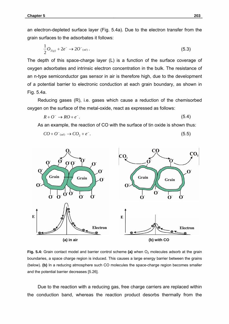
Chapter 5 203
an electron-depleted surface layer (Fig. 5.4a). Due to the electron transfer from the
grain surfaces to the adsorbates it follows:
)()(2 2221
adg OeO −− →+ . (5.3)
The depth of this space-charge layer (L) is a function of the surface coverage of
oxygen adsorbates and intrinsic electron concentration in the bulk. The resistance of
an n-type semiconductor gas sensor in air is therefore high, due to the development
of a potential barrier to electronic conduction at each grain boundary, as shown in
Fig. 5.4a.
Reducing gases (R), i.e. gases which cause a reduction of the chemisorbed
oxygen on the surface of the metal-oxide, react as expressed as follows:
.−− +→+ eROOR (5.4)
As an example, the reaction of CO with the surface of tin oxide is shown thus:
.2)(−− +→+ eCOOCO ad (5.5)
(a) in air (b) with CO
Fig. 5.4: Grain contact model and barrier control scheme (a) when O2 molecules adsorb at the grain
boundaries, a space charge region is induced. This causes a large energy barrier between the grains
(below). (b) In a reducing atmosphere such CO molecules the space-charge region becomes smaller
and the potential barrier decreases [5.26].
Due to the reaction with a reducing gas, free charge carriers are replaced within
the conduction band, whereas the reaction product desorbs thermally from the
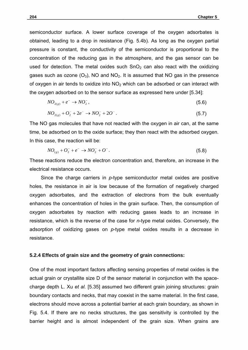
204 Chapter 5
semiconductor surface. A lower surface coverage of the oxygen adsorbates is
obtained, leading to a drop in resistance (Fig. 5.4b). As long as the oxygen partial
pressure is constant, the conductivity of the semiconductor is proportional to the
concentration of the reducing gas in the atmosphere, and the gas sensor can be
used for detection. The metal oxides such SnO2 can also react with the oxidizing
gases such as ozone (O3), NO and NO2. It is assumed that NO gas in the presence
of oxygen in air tends to oxidize into NO2 which can be adsorbed or can interact with
the oxygen adsorbed on to the sensor surface as expressed here under [5.34]:
−− →+ 2)(2 NOeNO g , (5.6)
−−−− +→++ ONOeONO g 22 22)(2 . (5.7)
The NO gas molecules that have not reacted with the oxygen in air can, at the same
time, be adsorbed on to the oxide surface; they then react with the adsorbed oxygen.
In this case, the reaction will be:
−−−− +→++ ONOeONO g 22)( . (5.8)
These reactions reduce the electron concentration and, therefore, an increase in the
electrical resistance occurs.
Since the charge carriers in p-type semiconductor metal oxides are positive
holes, the resistance in air is low because of the formation of negatively charged
oxygen adsorbates, and the extraction of electrons from the bulk eventually
enhances the concentration of holes in the grain surface. Then, the consumption of
oxygen adsorbates by reaction with reducing gases leads to an increase in
resistance, which is the reverse of the case for n-type metal oxides. Conversely, the
adsorption of oxidizing gases on p-type metal oxides results in a decrease in
resistance.
5.2.4 Effects of grain size and the geometry of grain connections:
One of the most important factors affecting sensing properties of metal oxides is the
actual grain or crystallite size D of the sensor material in conjunction with the space-
charge depth L. Xu et al. [5.35] assumed two different grain joining structures: grain
boundary contacts and necks, that may coexist in the same material. In the first case,
electrons should move across a potential barrier at each grain boundary, as shown in
Fig. 5.4. If there are no necks structures, the gas sensitivity is controlled by the
barrier height and is almost independent of the grain size. When grains are
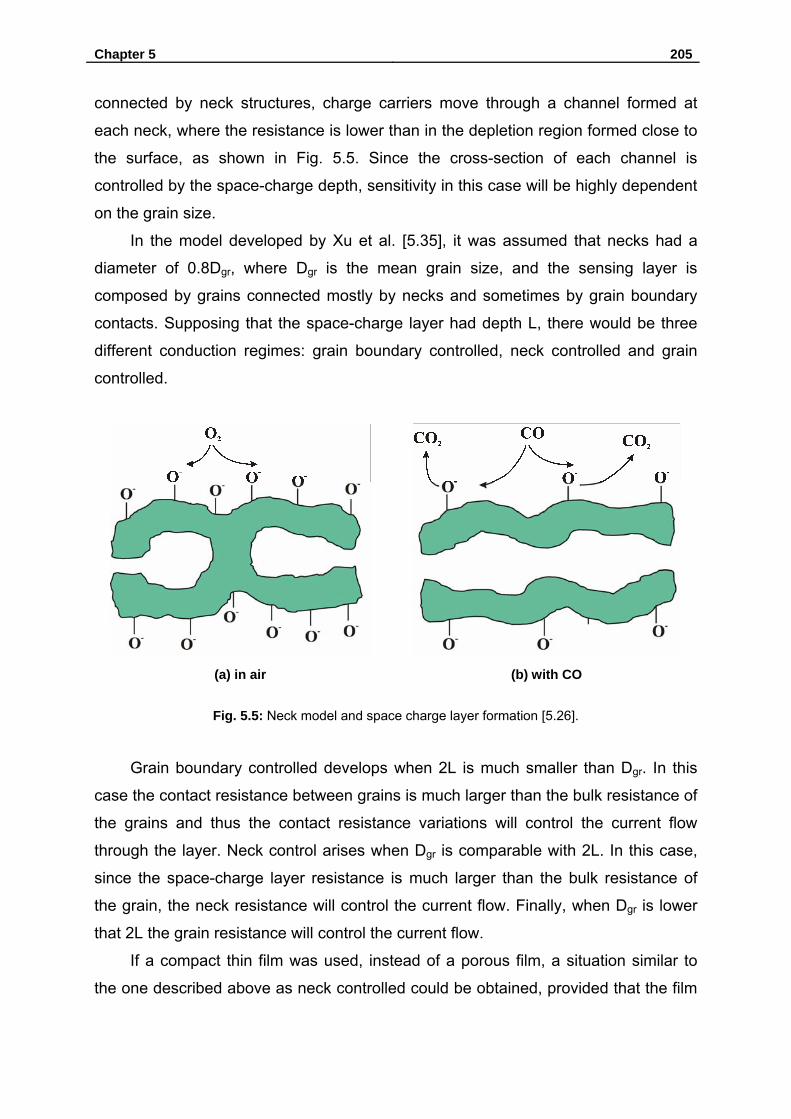
Chapter 5 205
connected by neck structures, charge carriers move through a channel formed at
each neck, where the resistance is lower than in the depletion region formed close to
the surface, as shown in Fig. 5.5. Since the cross-section of each channel is
controlled by the space-charge depth, sensitivity in this case will be highly dependent
on the grain size.
In the model developed by Xu et al. [5.35], it was assumed that necks had a
diameter of 0.8Dgr, where Dgr is the mean grain size, and the sensing layer is
composed by grains connected mostly by necks and sometimes by grain boundary
contacts. Supposing that the space-charge layer had depth L, there would be three
different conduction regimes: grain boundary controlled, neck controlled and grain
controlled.
(a) in air (b) with CO
Fig. 5.5: Neck model and space charge layer formation [5.26].
Grain boundary controlled develops when 2L is much smaller than Dgr. In this
case the contact resistance between grains is much larger than the bulk resistance of
the grains and thus the contact resistance variations will control the current flow
through the layer. Neck control arises when Dgr is comparable with 2L. In this case,
since the space-charge layer resistance is much larger than the bulk resistance of
the grain, the neck resistance will control the current flow. Finally, when Dgr is lower
that 2L the grain resistance will control the current flow.
If a compact thin film was used, instead of a porous film, a situation similar to
the one described above as neck controlled could be obtained, provided that the film
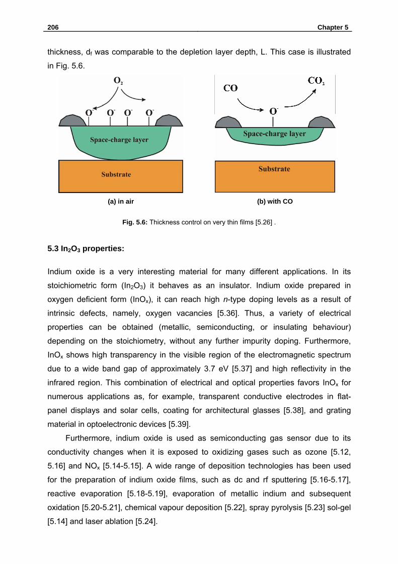
206 Chapter 5
thickness, df was comparable to the depletion layer depth, L. This case is illustrated
in Fig. 5.6.
(a) in air (b) with CO
Fig. 5.6: Thickness control on very thin films [5.26] .
5.3 In2O3 properties:
Indium oxide is a very interesting material for many different applications. In its
stoichiometric form (In2O3) it behaves as an insulator. Indium oxide prepared in
oxygen deficient form (InOx), it can reach high n-type doping levels as a result of
intrinsic defects, namely, oxygen vacancies [5.36]. Thus, a variety of electrical
properties can be obtained (metallic, semiconducting, or insulating behaviour)
depending on the stoichiometry, without any further impurity doping. Furthermore,
InOx shows high transparency in the visible region of the electromagnetic spectrum
due to a wide band gap of approximately 3.7 eV [5.37] and high reflectivity in the
infrared region. This combination of electrical and optical properties favors InOx for
numerous applications as, for example, transparent conductive electrodes in flat-
panel displays and solar cells, coating for architectural glasses [5.38], and grating
material in optoelectronic devices [5.39].
Furthermore, indium oxide is used as semiconducting gas sensor due to its
conductivity changes when it is exposed to oxidizing gases such as ozone [5.12,
5.16] and NOx [5.14-5.15]. A wide range of deposition technologies has been used
for the preparation of indium oxide films, such as dc and rf sputtering [5.16-5.17],
reactive evaporation [5.18-5.19], evaporation of metallic indium and subsequent
oxidation [5.20-5.21], chemical vapour deposition [5.22], spray pyrolysis [5.23] sol-gel
[5.14] and laser ablation [5.24].
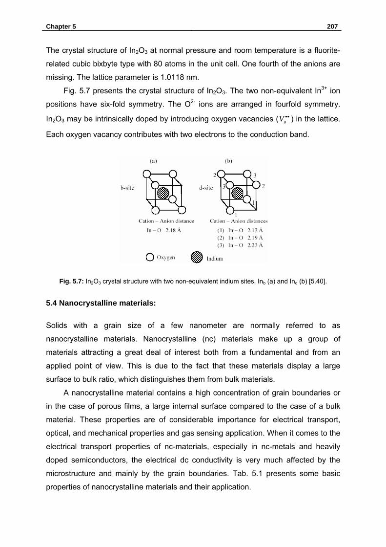
Chapter 5 207
The crystal structure of In2O3 at normal pressure and room temperature is a fluorite-
related cubic bixbyte type with 80 atoms in the unit cell. One fourth of the anions are
missing. The lattice parameter is 1.0118 nm.
Fig. 5.7 presents the crystal structure of In2O3. The two non-equivalent In3+ ion
positions have six-fold symmetry. The O2- ions are arranged in fourfold symmetry.
In2O3 may be intrinsically doped by introducing oxygen vacancies ( ••oV ) in the lattice.
Each oxygen vacancy contributes with two electrons to the conduction band.
Fig. 5.7: In2O3 crystal structure with two non-equivalent indium sites, Inb (a) and Ind (b) [5.40].
5.4 Nanocrystalline materials:
Solids with a grain size of a few nanometer are normally referred to as
nanocrystalline materials. Nanocrystalline (nc) materials make up a group of
materials attracting a great deal of interest both from a fundamental and from an
applied point of view. This is due to the fact that these materials display a large
surface to bulk ratio, which distinguishes them from bulk materials.
A nanocrystalline material contains a high concentration of grain boundaries or
in the case of porous films, a large internal surface compared to the case of a bulk
material. These properties are of considerable importance for electrical transport,
optical, and mechanical properties and gas sensing application. When it comes to the
electrical transport properties of nc-materials, especially in nc-metals and heavily
doped semiconductors, the electrical dc conductivity is very much affected by the
microstructure and mainly by the grain boundaries. Tab. 5.1 presents some basic
properties of nanocrystalline materials and their application.

208 Chapter 5
Tab. 5.1: Some basic properties and applications of nanoparticles and nanocrystalline materials.
Property Application
Wavelength selective optical absorption Solar collectors
High flow stress Jet engines
Giant magnetoresistance Reader heads in computer
High magnetic coercive force Data storage
Large surface-to-bulk ratio Sensors
Nanocrystalline materials are classified into different categories depending on the
number of dimensions which are nano-structured: the generally acknowledged
classification is [5.41] layered nano-structures (one nano-structured dimension, 1D),
filamentary structures (2D), and equiaxial nano-structured materials (3D). The
realization and the study of 1D and 3D nanostructures were actively explored,
whereas the 2D structures have been less investigated. For gas sensing, typically a
three-dimensional (3D) nanostructure is considered. However, 3D nanostructures
often highlight a tendency to change the electrical properties owing to grain
coalescence, porosity modification, and grain-boundary alteration. The problem
becomes still more complex because the layers must be kept at a relatively high
temperature in order to guarantee the reversibility of chemical reactions at the
surface. Thus, several solutions have been put forward to stabilize the nanostructure,
e.g., addition of a foreign element [5.42] or phase [5.43]. A technique that renders the
material sufficiently crystalline to guarantee long-term stability while maintaining a
high sensitivity would be the optimal.
5.5 Films deposition and sensor structure:
The growth of In2O3 thin films was carried out in a horizontal MOCVD reactor
(AIXTRON 200). Trimethylindium (TMIn) and H2O vapor were used as indium and
oxygen precursors, respectively. The In2O3 thin films were synthesized on sapphire
(0001) substrates by supplying TMIn and H2O vapor with flow rates of 15 and 1160
µmol/min, respectively.
The substrate temperature varied in the range of 150 and 600°C. Highly-
textured In2O3 films with a thickness of ~ 200 nm were obtained at a substrate
temperature of 600°C by using a 10 nm thick low-temperature (300°C) grown InxOy
nucleation layer (sample A) [5.44]. nano-structured In2O3 with a thickness of ~ 10 nm

Chapter 5 209
was deposited at a substrate temperature of 200°C and process pressure of 200
mbar (sample B). Samples for gas testing were prepared by sputtering two Ni
contacts onto the film surface in a gap configuration. Fig. 5.8 shows cross section of
the studied sensors. The active area of the sensor was 5 × 1 mm2.
(a) (b)
Fig. 5.8: Device cross section of the studied In2O3 gas sensors. (a) sample A. (b) sample B.
5.6 Experiments:
5.6.1 Film characterization:
After growth, the In2O3 thin films were ex-situ characterized by means of scanning
electron microscopy (SEM), atomic force microscopy (AFM), high-resolution
transmission electron microscopy (HRTEM) and x-ray diffraction (XRD).
5.6.2 Gas sensing measurements:
For gas sensing tests, the sensors were mounted in an UHV system described in
chapter 3 (section 3.5.2). The sensors were placed directly into a quartz tube, which
was pumped to a base pressure of 4 x 10⁻⁸ mbar. Fig. 5.9 shows schematic drawing
of the UHV apparatus for this experiment and all devices mounted in it. For
measurements of the response and dynamic behaviour of the sensors, a source-
measure-unit (model 2000, Keithley Instr./Germany) with an external voltage source
was used. The instruments were connected via an IEEE-488 bus to the computer.

210 Chapter 5
Fig. 5.9: Schematic drawing of gas measurements system.
The sensor resistance is determined under various partial pressures of the test gases
und temperatures by applying a constant ac voltage and measuring the current I. The
response and recovery of the films exposed to different gas partial pressures were
obtained by plotting their resistance as a function of time. The recovery process has
been accelerated by UV-light (λ = 365 nm) with an output power of 1.4 mW. The
sensors were heated during operation at different temperatures using a furnace. The
temperature was measured by a thermocouple type K (NiCr-Ni) (see Appendix A)
placed a few millimetres above the sensor. The operating temperature was varied
from room temperature to 300°C to determine the optimum response, which was
defined by:
v
g
RR
R = , (5.9)
where Rv is the stable base resistance in vacuum (after 20 min UV-light exposure)
and Rg the resistance after 10 min of gas exposure.
The sensitivity S is given by:
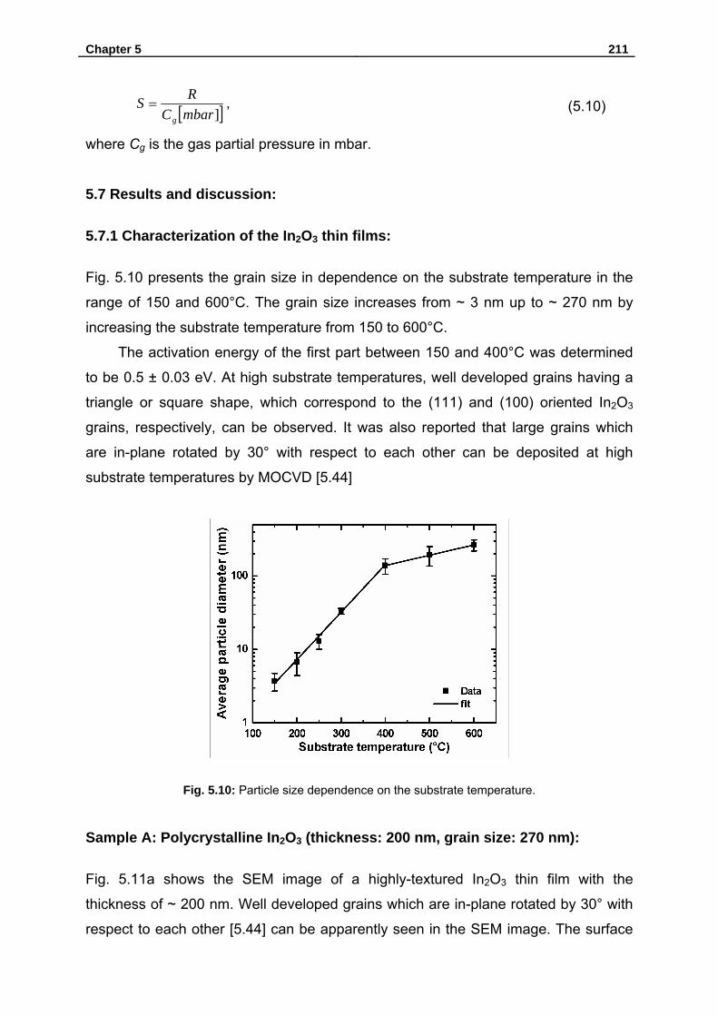
Chapter 5 211
[ ]]mbarCRS
g
= , (5.10)
where Cg is the gas partial pressure in mbar.
5.7 Results and discussion:
5.7.1 Characterization of the In2O3 thin films:
Fig. 5.10 presents the grain size in dependence on the substrate temperature in the
range of 150 and 600°C. The grain size increases from ~ 3 nm up to ~ 270 nm by
increasing the substrate temperature from 150 to 600°C.
The activation energy of the first part between 150 and 400°C was determined
to be 0.5 ± 0.03 eV. At high substrate temperatures, well developed grains having a
triangle or square shape, which correspond to the (111) and (100) oriented In2O3
grains, respectively, can be observed. It was also reported that large grains which
are in-plane rotated by 30° with respect to each other can be deposited at high
substrate temperatures by MOCVD [5.44]
Fig. 5.10: Particle size dependence on the substrate temperature.
Sample A: Polycrystalline In2O3 (thickness: 200 nm, grain size: 270 nm):
Fig. 5.11a shows the SEM image of a highly-textured In2O3 thin film with the
thickness of ~ 200 nm. Well developed grains which are in-plane rotated by 30° with
respect to each other [5.44] can be apparently seen in the SEM image. The surface
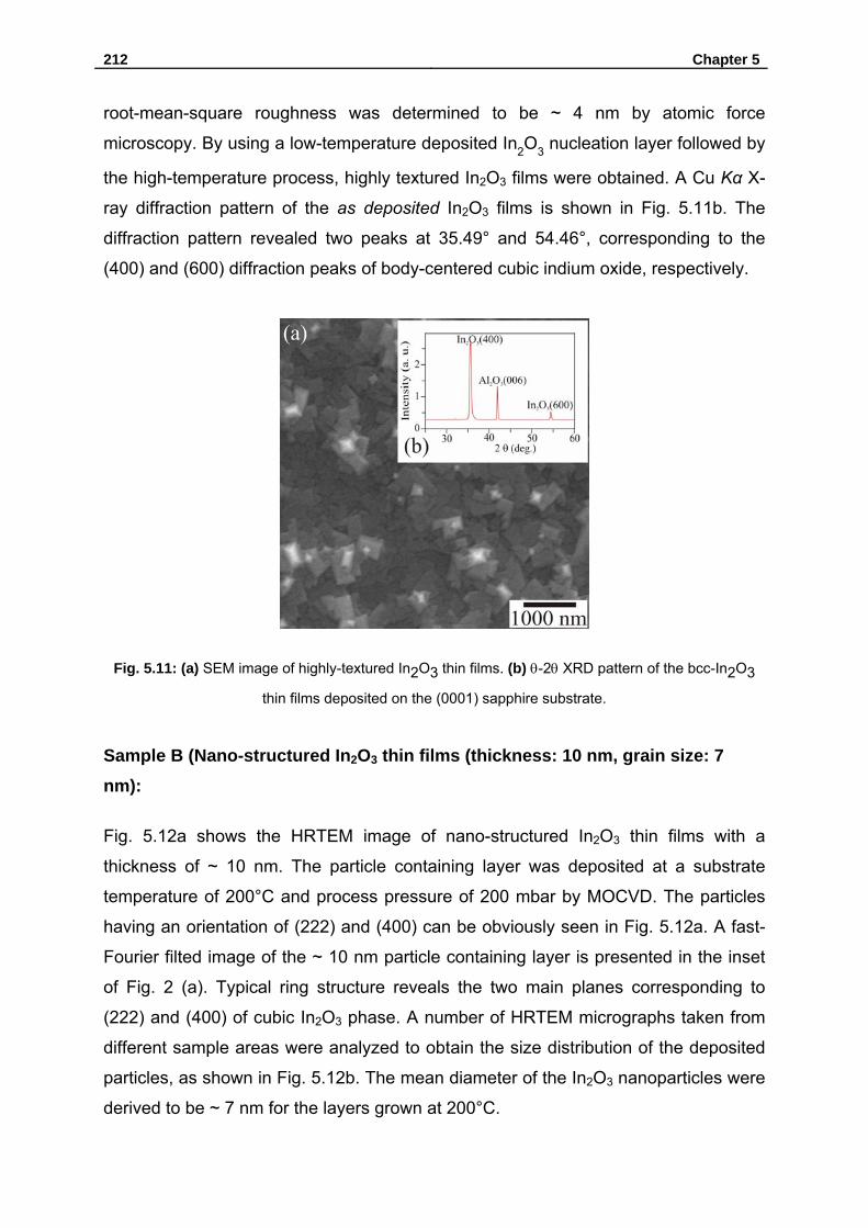
212 Chapter 5
root-mean-square roughness was determined to be ~ 4 nm by atomic force
microscopy. By using a low-temperature deposited In2O3 nucleation layer followed by
the high-temperature process, highly textured In2O3 films were obtained. A Cu Kα X-
ray diffraction pattern of the as deposited In2O3 films is shown in Fig. 5.11b. The
diffraction pattern revealed two peaks at 35.49° and 54.46°, corresponding to the
(400) and (600) diffraction peaks of body-centered cubic indium oxide, respectively.
Fig. 5.11: (a) SEM image of highly-textured In2O3 thin films. (b) θ-2θ XRD pattern of the bcc-In2O3
thin films deposited on the (0001) sapphire substrate.
Sample B (Nano-structured In2O3 thin films (thickness: 10 nm, grain size: 7 nm):
Fig. 5.12a shows the HRTEM image of nano-structured In2O3 thin films with a
thickness of ~ 10 nm. The particle containing layer was deposited at a substrate
temperature of 200°C and process pressure of 200 mbar by MOCVD. The particles
having an orientation of (222) and (400) can be obviously seen in Fig. 5.12a. A fast-
Fourier filted image of the ~ 10 nm particle containing layer is presented in the inset
of Fig. 2 (a). Typical ring structure reveals the two main planes corresponding to
(222) and (400) of cubic In2O3 phase. A number of HRTEM micrographs taken from
different sample areas were analyzed to obtain the size distribution of the deposited
particles, as shown in Fig. 5.12b. The mean diameter of the In2O3 nanoparticles were
derived to be ~ 7 nm for the layers grown at 200°C.

Chapter 5 213
Fig. 5.12: (a) HRTEM image of as grown nano-structured In2O3 thin film with a thickness of ~ 10 nm.
The inset shows the fast-Fourier filted image of the thin film. (b) Size contribution of the In2O3
nanoparticles.
5.7.2 Gas sensitivity:
5.7.2.1 Sample A:
5.7.2.1.1 NOx detection:
Firstly, the sensors were tested for the response to NOx gas with partial pressures
starting from 0.002 to 10 mbar (pure NOx) at temperatures between room
temperature and 250°C. Fig. 5.13 presents the resistance variation versus time as a
function of the successive increase of NOx partial pressure at a working temperature
of 150°C. The resistance of In2O3 thin films increases after exposure to the oxidizing
gas NOx and it returns to the initial value when the NOx gas is removed.
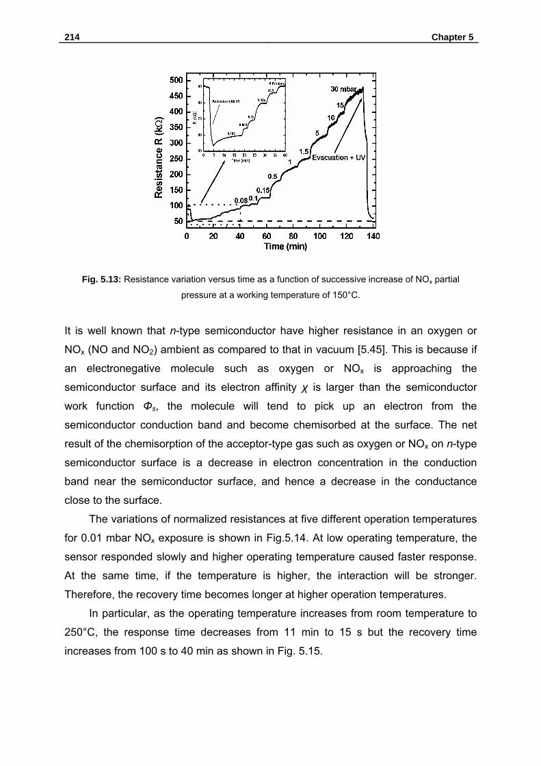
214 Chapter 5
Fig. 5.13: Resistance variation versus time as a function of successive increase of NOx partial
pressure at a working temperature of 150°C.
It is well known that n-type semiconductor have higher resistance in an oxygen or
NOx (NO and NO2) ambient as compared to that in vacuum [5.45]. This is because if
an electronegative molecule such as oxygen or NOx is approaching the
semiconductor surface and its electron affinity χ is larger than the semiconductor
work function Φs, the molecule will tend to pick up an electron from the
semiconductor conduction band and become chemisorbed at the surface. The net
result of the chemisorption of the acceptor-type gas such as oxygen or NOx on n-type
semiconductor surface is a decrease in electron concentration in the conduction
band near the semiconductor surface, and hence a decrease in the conductance
close to the surface.
The variations of normalized resistances at five different operation temperatures
for 0.01 mbar NOx exposure is shown in Fig.5.14. At low operating temperature, the
sensor responded slowly and higher operating temperature caused faster response.
At the same time, if the temperature is higher, the interaction will be stronger.
Therefore, the recovery time becomes longer at higher operation temperatures.
In particular, as the operating temperature increases from room temperature to
250°C, the response time decreases from 11 min to 15 s but the recovery time
increases from 100 s to 40 min as shown in Fig. 5.15.
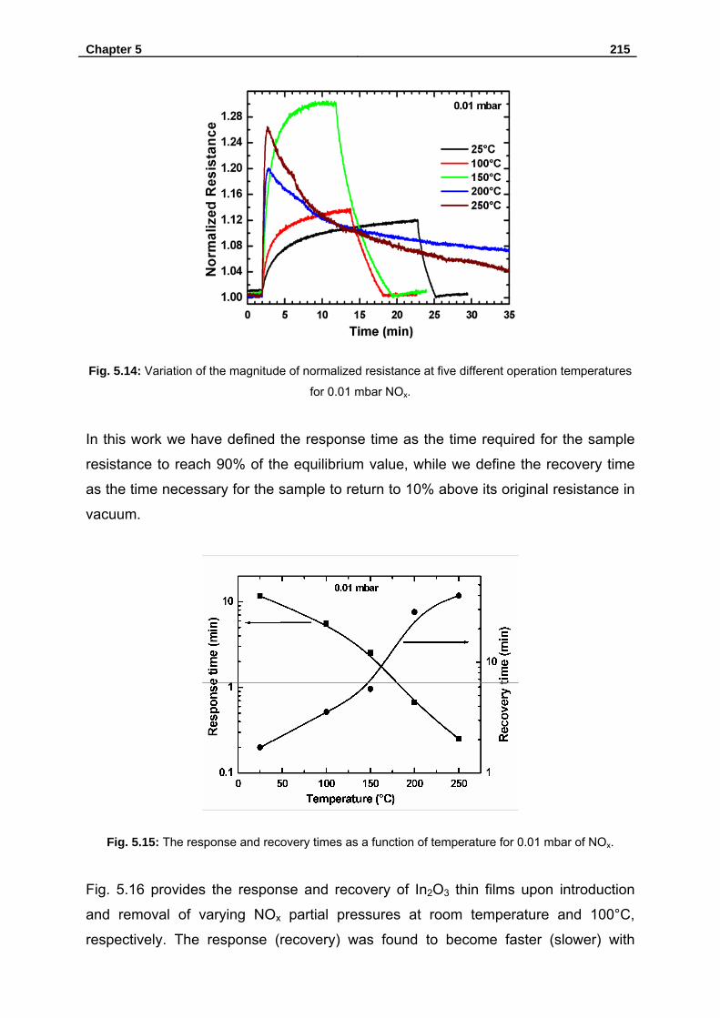
Chapter 5 215
Fig. 5.14: Variation of the magnitude of normalized resistance at five different operation temperatures
for 0.01 mbar NOx.
In this work we have defined the response time as the time required for the sample
resistance to reach 90% of the equilibrium value, while we define the recovery time
as the time necessary for the sample to return to 10% above its original resistance in
vacuum.
Fig. 5.15: The response and recovery times as a function of temperature for 0.01 mbar of NOx.
Fig. 5.16 provides the response and recovery of In2O3 thin films upon introduction
and removal of varying NOx partial pressures at room temperature and 100°C,
respectively. The response (recovery) was found to become faster (slower) with
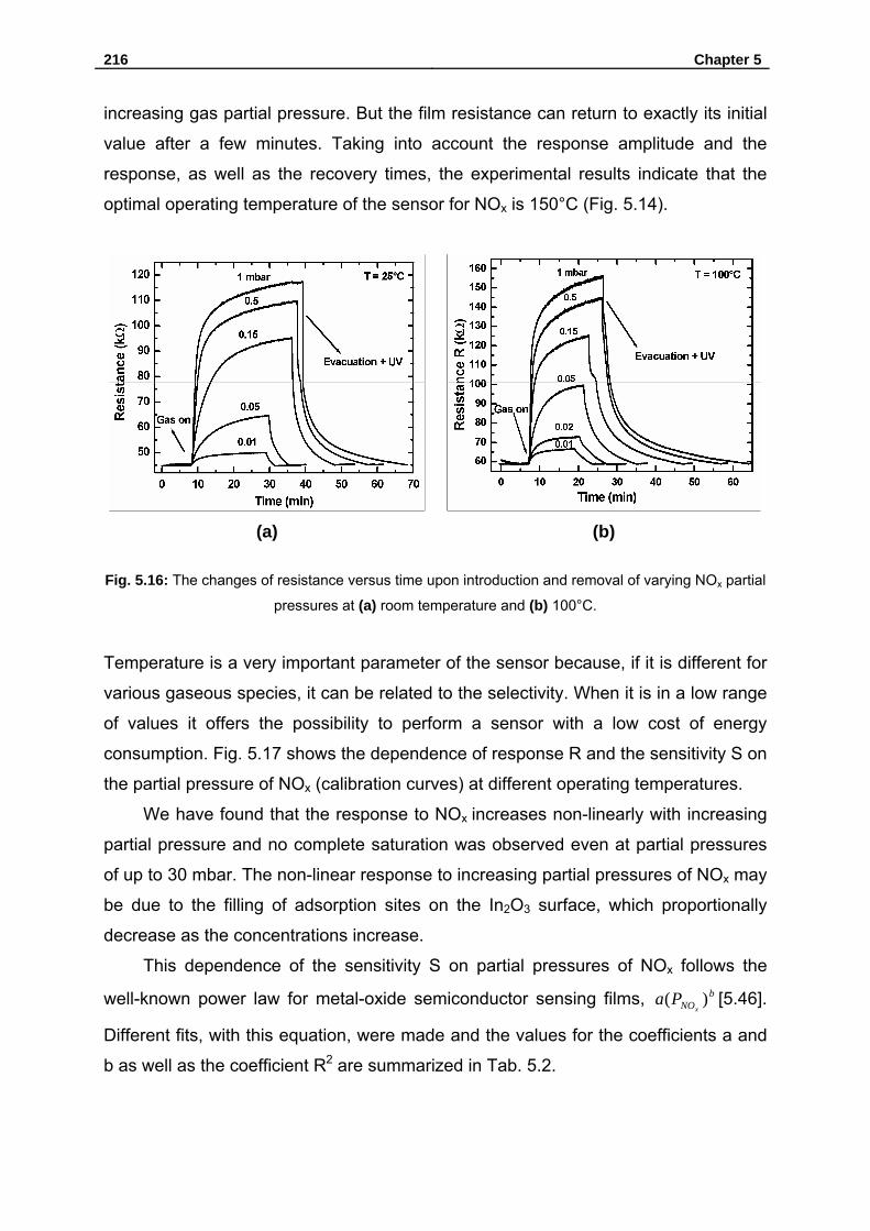
216 Chapter 5
increasing gas partial pressure. But the film resistance can return to exactly its initial
value after a few minutes. Taking into account the response amplitude and the
response, as well as the recovery times, the experimental results indicate that the
optimal operating temperature of the sensor for NOx is 150°C (Fig. 5.14).
(a) (b)
Fig. 5.16: The changes of resistance versus time upon introduction and removal of varying NOx partial
pressures at (a) room temperature and (b) 100°C.
Temperature is a very important parameter of the sensor because, if it is different for
various gaseous species, it can be related to the selectivity. When it is in a low range
of values it offers the possibility to perform a sensor with a low cost of energy
consumption. Fig. 5.17 shows the dependence of response R and the sensitivity S on
the partial pressure of NOx (calibration curves) at different operating temperatures.
We have found that the response to NOx increases non-linearly with increasing
partial pressure and no complete saturation was observed even at partial pressures
of up to 30 mbar. The non-linear response to increasing partial pressures of NOx may
be due to the filling of adsorption sites on the In2O3 surface, which proportionally
decrease as the concentrations increase.
This dependence of the sensitivity S on partial pressures of NOx follows the
well-known power law for metal-oxide semiconductor sensing films, bNOx
Pa )( [5.46].
Different fits, with this equation, were made and the values for the coefficients a and
b as well as the coefficient R2 are summarized in Tab. 5.2.

Chapter 5 217
(a) (b)
Fig. 5.17: The dependence of response R (a) and the sensitivity S (b) on the partial pressures of NOx
at different temperatures.
The slopes of the lines in the log-log plot (Fig. 5.17b) are different and dependent on
the operation temperature. A higher value of the exponent b allows an easier
distinction between two partial pressures, while a lower value rises the lowest partial
pressure which can be measured. If we are interested in the determination of high
partial pressures, we can operate the sensor at 150°C, since the slope is higher.
Otherwise, if we are interested in lower partial pressures, we should work at 250°C
because at this temperature the detection limit is lower.
Tab. 5.2: Fitting parameter of the sensitivity S curves at several temperatures.
Allometric1 bNOx
PaS )(= Temperature (°C) a b
R2
25 2.51 ± 0.48 -0.77 ± 0.05 0.968
100 2.74 ± 0.47 -0.79 ± 0.03 0.987
150 2.90 ± 0.67 -0.76 ± 0.05 0.974
200 3.01 ± 0.14 -0.79 ± 0.01 0.998
250 2.67 ± 0.65 -0.8 ± 0.05 0.984
5.7.2.1.2 O2 detection:
In the second step the sensors were tested for the response to O2 gas with partial
pressures ranging from 0.006 up to 30 mbar (pure O2) at temperatures between 25
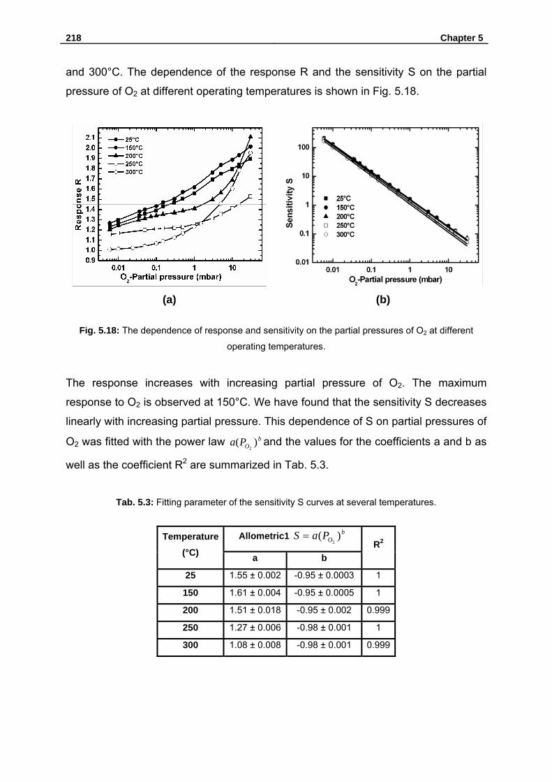
218 Chapter 5
and 300°C. The dependence of the response R and the sensitivity S on the partial
pressure of O2 at different operating temperatures is shown in Fig. 5.18.
(a) (b)
Fig. 5.18: The dependence of response and sensitivity on the partial pressures of O2 at different
operating temperatures.
The response increases with increasing partial pressure of O2. The maximum
response to O2 is observed at 150°C. We have found that the sensitivity S decreases
linearly with increasing partial pressure. This dependence of S on partial pressures of
O2 was fitted with the power law bOPa )(
2and the values for the coefficients a and b as
well as the coefficient R2 are summarized in Tab. 5.3.
Tab. 5.3: Fitting parameter of the sensitivity S curves at several temperatures.
Allometric1 bOPaS )(
2= Temperature
(°C) a b R2
25 1.55 ± 0.002 -0.95 ± 0.0003 1
150 1.61 ± 0.004 -0.95 ± 0.0005 1
200 1.51 ± 0.018 -0.95 ± 0.002 0.999
250 1.27 ± 0.006 -0.98 ± 0.001 1
300 1.08 ± 0.008 -0.98 ± 0.001 0.999
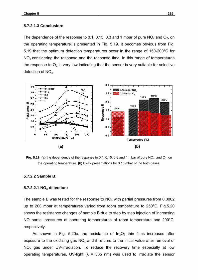
Chapter 5 219
5.7.2.1.3 Conclusion:
The dependence of the response to 0.1, 0.15, 0.3 and 1 mbar of pure NOx and O2, on
the operating temperature is presented in Fig. 5.19. It becomes obvious from Fig.
5.19 that the optimum detection temperatures occur in the range of 150-200°C for
NOx considering the response and the response time. In this range of temperatures
the response to O2 is very low indicating that the sensor is very suitable for selective
detection of NOx.
(a) (b)
Fig. 5.19: (a) the dependence of the response to 0.1, 0.15, 0.3 and 1 mbar of pure NOx, and O2, on
the operating temperature. (b) Block presentations for 0.15 mbar of the both gases.
5.7.2.2 Sample B:
5.7.2.2.1 NOx detection:
The sample B was tested for the response to NOx with partial pressures from 0.0002
up to 200 mbar at temperatures varied from room temperature to 250°C. Fig.5.20
shows the resistance changes of sample B due to step by step injection of increasing
NO partial pressures at operating temperatures of room temperature and 200°C,
respectively.
As shown in Fig. 5.20a, the resistance of In2O3 thin films increases after
exposure to the oxidizing gas NOx and it returns to the initial value after removal of
NOx gas under UV-irradiation. To reduce the recovery time especially at low
operating temperatures, UV-light (λ = 365 nm) was used to irradiate the sensor
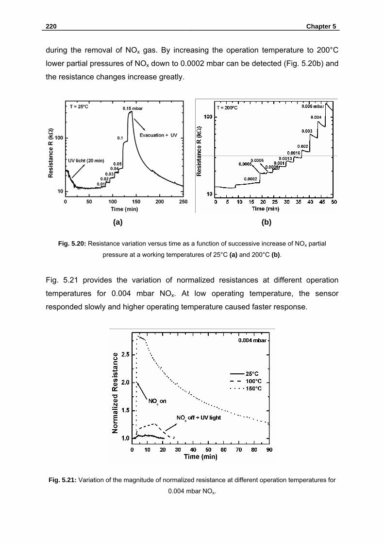
220 Chapter 5
during the removal of NOx gas. By increasing the operation temperature to 200°C
lower partial pressures of NOx down to 0.0002 mbar can be detected (Fig. 5.20b) and
the resistance changes increase greatly.
(a) (b)
Fig. 5.20: Resistance variation versus time as a function of successive increase of NOx partial
pressure at a working temperatures of 25°C (a) and 200°C (b).
Fig. 5.21 provides the variation of normalized resistances at different operation
temperatures for 0.004 mbar NOx. At low operating temperature, the sensor
responded slowly and higher operating temperature caused faster response.
Fig. 5.21: Variation of the magnitude of normalized resistance at different operation temperatures for
0.004 mbar NOx.
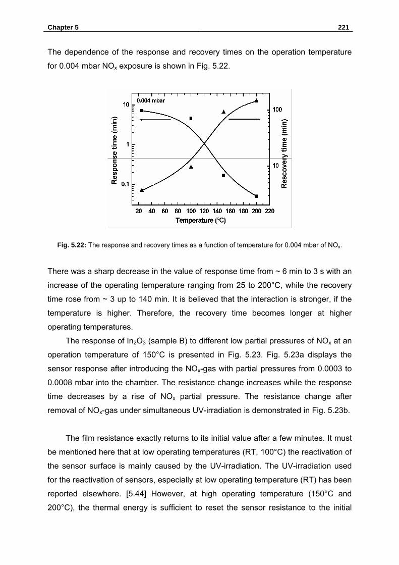
Chapter 5 221
The dependence of the response and recovery times on the operation temperature
for 0.004 mbar NOx exposure is shown in Fig. 5.22.
Fig. 5.22: The response and recovery times as a function of temperature for 0.004 mbar of NOx.
There was a sharp decrease in the value of response time from ~ 6 min to 3 s with an
increase of the operating temperature ranging from 25 to 200°C, while the recovery
time rose from ~ 3 up to 140 min. It is believed that the interaction is stronger, if the
temperature is higher. Therefore, the recovery time becomes longer at higher
operating temperatures.
The response of In2O3 (sample B) to different low partial pressures of NOx at an
operation temperature of 150°C is presented in Fig. 5.23. Fig. 5.23a displays the
sensor response after introducing the NOx-gas with partial pressures from 0.0003 to
0.0008 mbar into the chamber. The resistance change increases while the response
time decreases by a rise of NOx partial pressure. The resistance change after
removal of NOx-gas under simultaneous UV-irradiation is demonstrated in Fig. 5.23b.
The film resistance exactly returns to its initial value after a few minutes. It must
be mentioned here that at low operating temperatures (RT, 100°C) the reactivation of
the sensor surface is mainly caused by the UV-irradiation. The UV-irradiation used
for the reactivation of sensors, especially at low operating temperature (RT) has been
reported elsewhere. [5.44] However, at high operating temperature (150°C and
200°C), the thermal energy is sufficient to reset the sensor resistance to the initial
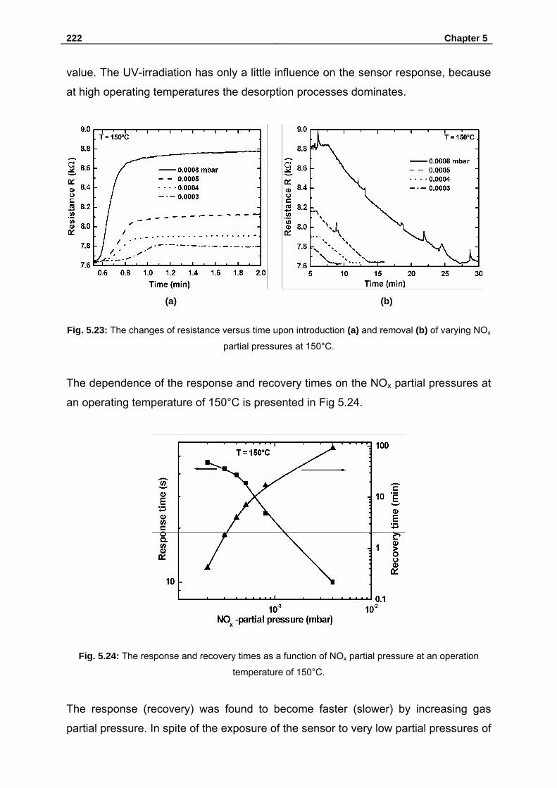
222 Chapter 5
value. The UV-irradiation has only a little influence on the sensor response, because
at high operating temperatures the desorption processes dominates.
(a) (b)
Fig. 5.23: The changes of resistance versus time upon introduction (a) and removal (b) of varying NOx
partial pressures at 150°C.
The dependence of the response and recovery times on the NOx partial pressures at
an operating temperature of 150°C is presented in Fig 5.24.
Fig. 5.24: The response and recovery times as a function of NOx partial pressure at an operation
temperature of 150°C.
The response (recovery) was found to become faster (slower) by increasing gas
partial pressure. In spite of the exposure of the sensor to very low partial pressures of
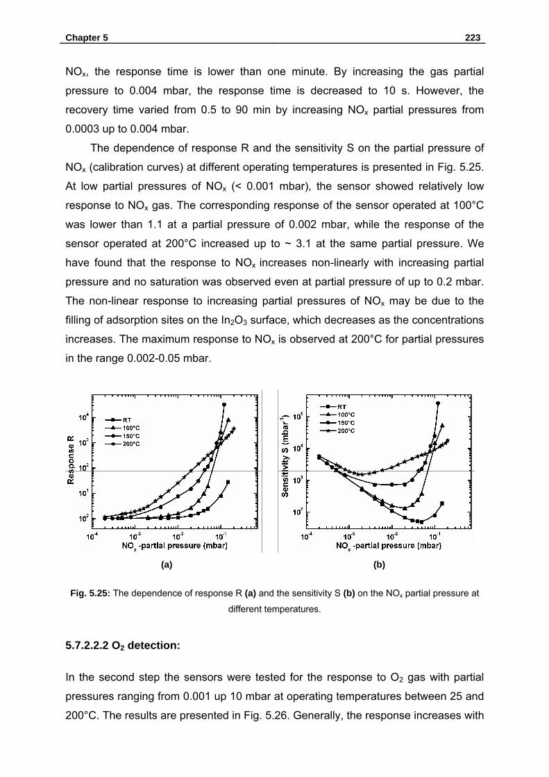
Chapter 5 223
NOx, the response time is lower than one minute. By increasing the gas partial
pressure to 0.004 mbar, the response time is decreased to 10 s. However, the
recovery time varied from 0.5 to 90 min by increasing NOx partial pressures from
0.0003 up to 0.004 mbar.
The dependence of response R and the sensitivity S on the partial pressure of
NOx (calibration curves) at different operating temperatures is presented in Fig. 5.25.
At low partial pressures of NOx (< 0.001 mbar), the sensor showed relatively low
response to NOx gas. The corresponding response of the sensor operated at 100°C
was lower than 1.1 at a partial pressure of 0.002 mbar, while the response of the
sensor operated at 200°C increased up to ~ 3.1 at the same partial pressure. We
have found that the response to NOx increases non-linearly with increasing partial
pressure and no saturation was observed even at partial pressure of up to 0.2 mbar.
The non-linear response to increasing partial pressures of NOx may be due to the
filling of adsorption sites on the In2O3 surface, which decreases as the concentrations
increases. The maximum response to NOx is observed at 200°C for partial pressures
in the range 0.002-0.05 mbar.
(a) (b)
Fig. 5.25: The dependence of response R (a) and the sensitivity S (b) on the NOx partial pressure at
different temperatures.
5.7.2.2.2 O2 detection:
In the second step the sensors were tested for the response to O2 gas with partial
pressures ranging from 0.001 up 10 mbar at operating temperatures between 25 and
200°C. The results are presented in Fig. 5.26. Generally, the response increases with
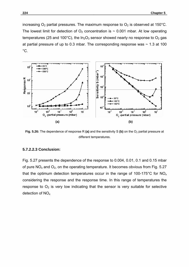
224 Chapter 5
increasing O2 partial pressures. The maximum response to O2 is observed at 150°C.
The lowest limit for detection of O2 concentration is ~ 0.001 mbar. At low operating
temperatures (25 and 100°C), the In2O3 sensor showed nearly no response to O2 gas
at partial pressure of up to 0.3 mbar. The corresponding response was ~ 1.3 at 100
°C.
(a) (b)
Fig. 5.26: The dependence of response R (a) and the sensitivity S (b) on the O2 partial pressure at
different temperatures.
5.7.2.2.3 Conclusion:
Fig. 5.27 presents the dependence of the response to 0.004, 0.01, 0.1 and 0.15 mbar
of pure NOx and O2, on the operating temperature. It becomes obvious from Fig. 5.27
that the optimum detection temperatures occur in the range of 100-175°C for NOx
considering the response and the response time. In this range of temperatures the
response to O2 is very low indicating that the sensor is very suitable for selective
detection of NOx
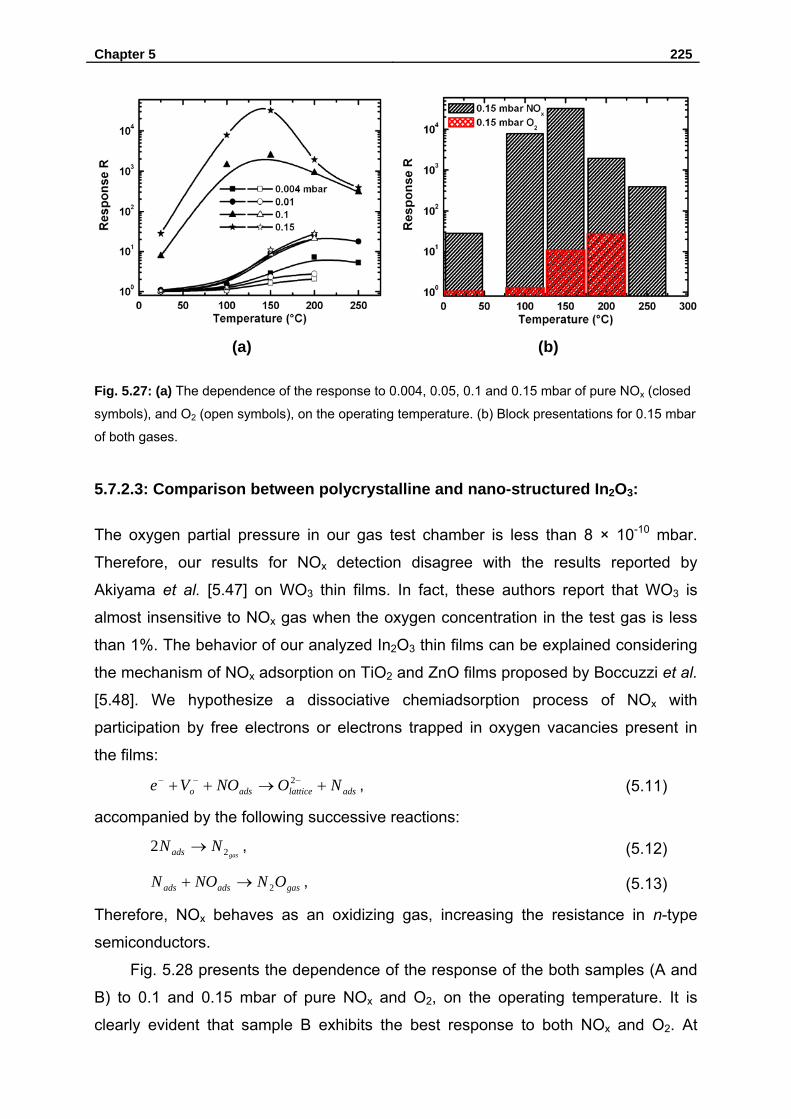
Chapter 5 225
(a) (b)
Fig. 5.27: (a) The dependence of the response to 0.004, 0.05, 0.1 and 0.15 mbar of pure NOx (closed
symbols), and O2 (open symbols), on the operating temperature. (b) Block presentations for 0.15 mbar
of both gases.
5.7.2.3: Comparison between polycrystalline and nano-structured In2O3:
The oxygen partial pressure in our gas test chamber is less than 8 × 10⁻¹⁰ mbar.
Therefore, our results for NOx detection disagree with the results reported by
Akiyama et al. [5.47] on WO3 thin films. In fact, these authors report that WO3 is
almost insensitive to NOx gas when the oxygen concentration in the test gas is less
than 1%. The behavior of our analyzed In2O3 thin films can be explained considering
the mechanism of NOx adsorption on TiO2 and ZnO films proposed by Boccuzzi et al.
[5.48]. We hypothesize a dissociative chemiadsorption process of NOx with
participation by free electrons or electrons trapped in oxygen vacancies present in
the films:
adslatticeadso NONOVe +→++ −−− 2 , (5.11)
accompanied by the following successive reactions:
gasNNads 22 → , (5.12)
gasadsads ONNON 2→+ , (5.13)
Therefore, NOx behaves as an oxidizing gas, increasing the resistance in n-type
semiconductors.
Fig. 5.28 presents the dependence of the response of the both samples (A and
B) to 0.1 and 0.15 mbar of pure NOx and O2, on the operating temperature. It is
clearly evident that sample B exhibits the best response to both NOx and O2. At
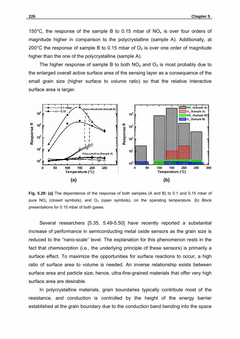
226 Chapter 5
150°C, the response of the sample B to 0.15 mbar of NOx is over four orders of
magnitude higher in comparison to the polycrystalline (sample A). Additionally, at
200°C the response of sample B to 0.15 mbar of O2 is over one order of magnitude
higher than the one of the polycrystalline (sample A).
The higher response of sample B to both NOx and O2 is most probably due to
the enlarged overall active surface area of the sensing layer as a consequence of the
small grain size (higher surface to volume ratio) so that the relative interactive
surface area is larger.
(a) (b)
Fig. 5.28: (a) The dependence of the response of both samples (A and B) to 0.1 and 0.15 mbar of
pure NOx (closed symbols), and O2 (open symbols), on the operating temperature. (b) Block
presentations for 0.15 mbar of both gases.
Several researchers [5.35, 5.49-5.50] have recently reported a substantial
increase of performance in semiconducting metal oxide sensors as the grain size is
reduced to the “nano-scale” level. The explanation for this phenomenon rests in the
fact that chemisorption (i.e., the underlying principle of these sensors) is primarily a
surface effect. To maximize the opportunities for surface reactions to occur, a high
ratio of surface area to volume is needed. An inverse relationship exists between
surface area and particle size; hence, ultra-fine-grained materials that offer very high
surface area are desirable.
In polycrystalline materials, grain boundaries typically contribute most of the
resistance, and conduction is controlled by the height of the energy barrier
established at the grain boundary due to the conduction band bending into the space

Chapter 5 227
charge layer. Large grain size significantly reduces the concentration of grain
boundaries, which in turn reduces sensitivity to changes in the gaseous environment.
Boundary layer effects are also present where “necking” of individual grains occurs.
In this case, the resistance is controlled by the width of the bulk conduction channel,
which narrows as the space charge layer forms. The population of such sites also
increases with decreasing grain size, as does the likelihood that such
interconnections will be of small enough size to enable the presence of boundary
layer effects. Consequently, both mechanisms contribute best when the individual
grains are very small, thereby increasing the sensor response.
5.8 Conclusion:
The response of In2O3 thin films grown by MOCVD to NOx, and O2 gases was
investigated as a function of operating temperature for different partial pressures of
the test gases. NOx behaves as an oxidizing gas, increasing the resistance in n-type
semiconductors. The analysis of resistance variation indicates that the adsorption
mechanism of NOx gas on In2O3 films does not involve oxygen. According to the
conclusion of Boccuzzi et al. [5.48] for TiO2 and ZnO films, a dissociative
chemiadsorption process of NO with participation by free electrons or electrons
trapped in oxygen vacancies occurs.
In particular, nano-structured In2O3 thin films were found to have the higher
response to NOx This is most probably due to the enlarged overall active surface
area of the sensing layer as a consequence of the small grain size (better surface to
volume ratio) so that the relative interactive surface area is larger, and the density of
charge carriers per volume is higher. We have found that reducing the grain size of
the sensing material to the sub-10-nm regime can have a substantial effect on
performance.
The optimum detection temperatures of the nano-structured In2O3 occur in the
range of 100-175°C for NOx considering the sensitivity and the response time. In this
range of temperatures the response to O2 is very low indicating that the sensor is
very suitable for selective detection of NOx at low temperatures. In addition, nano-
structured In2O3 thin films were found to be more suitable to be used in the field of
application for detecting low partial pressures.
228 Chapter 5
5.9 Outlook and future work:
For further investigation in this field of study, the following additional experiments are
suggested:
With regard to sensor properties a further study of the selectivity against
reducing gases such as CO and H2, and other oxidizing gases as well as the
stability and reliability of the sensor is needed.
The influence of the relative humidity on the response and the selectivity of the
sensors at different operation temperatures must be studied.
Adsorption of gas species on the gate of AlGaN/GaN high electron mobility
transistors (HEMTs) leads to enhancement or depletion effects in the two
dimensional electron gas (2DEG). Nano-structure In2O3 can be used to
develop very sensitive but robust sensors for the detection of NOx.
The influence of the addition of amount of noble metals (Pt, Pd,…) or other
metal oxides to In2O3 thin films on the gas sensing properties should be
studied.
References:
[5.1] N. Yamazoe, and N. Miura, “Enviromental gas sensing”, Sensors and Actuators
B 20 (1994) 95-102.
[5.2] M. S. Nieuwenhuizen, and A. J. Nederlof, “Preliminary results with silicon-based
surface acoustic wave chemical sensor for NO2”, Sensors and Actuators B 19 (1989)
385-392.
[5.3] C. J. Liu, S. Y. Wang, J. C. Hsieh, and Y. H. Ju, “Gas sensing properties of
vacuum deposited titanyl phthalocyanine film”, Sensors and Actuator B 65 (200) 371-
374.
[5.4] T. Seiyman, A. Kato, K. Fujiishi, and M. Negatani, “A new detector for gaseous
components using semiconductive thin films”, Anal. Chem. 34 (1962) 1502-1503.
[5.5] A. A. Tomchenko, G. P. Harmer, B. T. Marquis, and J. W. Allen,
“Semiconducting metal oxide sensor array for the selective detection of combustion
gases”, Sensors and Actuators B 93 (2003) 126-134.
Chapter 5 229
[5.6] C.-D. Feng, Y. Shimizu, and M. Egashira, “Effect of gas sensing diffusion
process on sensing properties of SnO2 thin film sensors in a SiO2/SnO2 layer-built
structure fabricated by sol-gel process”, J. Electrochem. Soc. 141 (1994) 220-225.
[5.7] T. Hyodo, S. Abe, Y. Shimizu, and M. Egashira, “Gas-sensing properties of
ordered mesoporous SnO2 and effects of coatings thereof”, Sensors and Actuators B
93 (2003) 590-600.
[5.8] S. C. Moulzolf, L. J. LeGore, and R. J. Lad, “Heteroepitaxial growth of tungsten
trioxide films on sapphire substrate for chemical gas sensor”, Thin Solid Film 400
(2001) 56-63.
[5.9] Y. Yamada, Y. Sano, Y. Masuoka, T. Nakamura, and K. Yamashita, “NO2
Sensing Characteristics of Nb Doped TiO2 Thin Films and their Electronic
Properties”, Sensors and Actuators B 66 (2000).164-166.
[5.10] L. Zheng, M. Xu, and T. Xu, “TiO2-x Thin films as oxygen sensor”, Sensors and
Actuators B 66 (2000) 28-30.
[5.11] M. Egashira, Y. Shimizu, Y. Takao, and S. Sako, “Variations in I–V
characteristics of oxide semiconductors induced by oxidizing gases”, Sensors and
Actuators B 35-36 (1996) 62-67.
[5.12] T. Doll, A. Fuchs, I. Eisele, G. Faglia, S. Groppelli, and G. Sberveglieri,
“Conductivity and work function ozone sensors based on indium oxide”, Sensors and
Actuators B 49 (1998) 63-67.
[5.13] B. P. J. de Lacy Costello, R. J. Ewen, N. M. Ratcliffe, and P. S. Sivanand,
“Thick film organic vapour sensors based on binary mixtures of metal oxides”, Sens.
Actuators B92 (2003) 159-166.
[5.14] A. Gurlo, M. Ivanovskaya, A. Pfau, U. Weimar and W. Göpel, “Sol-gel prepared
In2O3 thin films”, Thin Solid Films 307 (1997) 288-293.
[5.15] M. Liess, “Electric field-induced migration of chemisorbed gas molecules on a
sensitive film-a new chemical sensor”, Thin Solid Film 410 (2002) 183-187.
[5.16] G. Kiriakidis, M. Bender, N. Katsarakis , E. Gagoudaskis, E. Hourdakis, E.
Douloufakis, and V. Cimalla, “Ozone sensing properties of polycrystalline indium
oxide films at room temperature”, phys. stat. sol. (a) 185 (2001) 27-32.
[5.17] A. N. H. Alajili, and S. C. Bayliss, “A study of the optical, electrical and
structural properties of reactively sputtered InOx and ITOx thin films”, Thin Solid Film
305 (1997) 116-123.
230 Chapter 5
[5.18] P. Thilakau and J. Kumar, “Reactive thermal deposition of indium oxide and
tin-doped indium oxide thin films on inp substrates”, Thin Solid Films 292 (1997) 50-
54.
[5.19] K. G. Copchandran, B. Joseph, J. T. Abraham, P. Koshy and V. K. Vaidyan,
“The preparation of transparent electrically conducting indium oxide films by reactive
vacuum evaporation”, Vacuum 48 (1997) 547-550.
[5.20] K. B. Sundaram and G. K. Bhagavat, “Preparation and properties of indium
oxide films”, phys. stat. sol. (a) 63 (1981) K15-K18.
[5.21] V. Damodara Das, S. Kirupavathy, L. Damodare and N. Lakshminarayan,
“Optical and electrical investigations of indium oxide thin films prepared by thermal
oxidation of indium thin films”, J. Appl. Phys. 79 (1996) 8521-8530.
[5.22] A. P. Mammana, E. S. Braga, I. Torriani and R. P.Anderson, “Structural
characterization of transparent semiconducting thin films of SnO2 and In2O3”, Thin
Solid Films 85 (1981) 355-359.
[5.23] W. Siefert, “Properties of thin In2O3 and SnO2 films prepared by corona spray
pyrolysis, and a discussion of the spray pyrolysis process”, Thin Solid Films 120
(1984) 275-282.
[5.24] S. Mailis, C. Grivas, D. Gill, L. Boutsikaris, N.A. Vainos, C. Xirouchaki, G.
Vasiliou, N. Garawal, G. Kiriakidis and H. Fritzsche, “Dynamic holography in indium
Oxide and Indium-Tin-Oxide Thin Films”, Optical Memory and Neural Networks 5
(1996)191-196.
[5.25] V. Demarne and R. Sanjinés, “Thin film semiconducting metal oxide gas
sensors”, Gas Sensors, G. Sberveglieri (ed.), Kluwer Academic Publishers,
Dordrecht, The Netherlands, 1992, pp.89-106.
[5.26] J. Pires, “Thin films for gas sensors”, PhD thesis, Minho University, Braga,
Portugal, 2003.
[5.27] V. L. Bonc-Bruevic and S. G. Kalasnikov, “Halbleiterphysik“, Deutscher Verlag
der Wissenschaften, Berlin 1982.
[5.28] M. Fleischer, “Präparation und Charakterisierung von Ga2O3 Dünnschichten,
Untersuchung der gassensitiven elektrischen Leitfähigkeitseigenschaften“,
Technische Universität München, Dissertation, 1992.
[5.29] A. Bielanski and J. Haber, “Oxygen in catalysis on transition metal oxides”,
Catal. Rev.-Sci. Eng. 19 (1979) 1-41.
Chapter 5 231
[5.30] S. Pitcher, J. A. Thiele, H. Ren and J. F. Vetelino, “Current/voltage
characteristics of a semiconductor metal oxide gas sensor”, Sensors and Actuators B
93 (2003) 454-462.
[5.31] E. Fromm, “Kinetics of metal-gas interactions at low temperature”, Springer-
Verlag Berlin-Heidelberg, 16 (1998).
[5.32] E. Comini, G. Faglia and G. Sberveglieri, “UV light activation of tin oxide thin
films for NO2 sensing at low temperatures”, Sensors and Actuators B 78 (2001) 73-
77.
[5.33] N. Yamazoe, J. Fuchigami, M. Kishikawa, and T. Seiyama, “Interactions of tin
oxide surface with O2, H2O and H2”, Surf. Sci. 86 (1979) 335-344.
[5.34] S. Capone, R. Rella, P. Siciliano, and L. Vasanelli, “A comparison between
V2O5 and WO3 thin films as sensitive elements for NO detection”, Thin Solid Films
350 (1999) 264-268.
[5.35] C. Xu, J. Tamaki, N. Miura, and N. Yamazoe,”Grain size effects on gas
sensitivity of porous SnO2-based elements”, Sensors and Actuators B 3 (1991) 147-
155.
[5.36] P. Thilakan and J. Kumar, “Oxidation dependent crystallization behaviour of IO
and ITO thin films deposited by reactive thermal deposition technique”, Mater. Sci.
Eng. B 55 (1998)195-200.
[5.37] C. Xirouchaki, G. Kiriakidis, T. F. Pedersen, and H. Fritzsche, “Photoreduction
and oxidation of as-desposited microcrystalline indium oxide”, J. Appl. Phys. 79
(1996) 9349-9352.
[5.38] C. G. Granqvist,”Transparent Conductive Electrodes for Electrochromic
Devices:A Review”, Appl. Phys. A: Solids. Surf. 57 (1993) 19-24.
[5.39] S. Pissadakis, S. Mailis, L. Reekie, J. S. Wilkinson, R. W. Eason, N. A. Vainos,
K. Moschovis, and G. Kiriakidis, ”Permanent holographic recording in indium oxide
thin films using 193 nm excimer laser radiation”, Appl. Phys. A: Mater. Sci. Process.
69 (1999) 333-336.
[5.40] J. Ederth, “Electrical transport in nanoparticle thin films of gold and indium tin
oxide”, PhD thesis, Uppsala university, Uppsala, Sweden, 2003.
[5.41] C. Suryanarayana and C. C. Koch, “Nanocrystalline materials-current research
and future directions”, Hyperfine Interact. 130 (2000) 5-44.
232 Chapter 5
[5.42] N. Bovini, M. C. Carotta, V. Guidi, C. Malaga, G. Martinelli, L. Paglialonga, and
M. Sacerdoti, “Doping of a nanostructured titania thick film: structural and electrical
investigations”, Sensors and Actuators, B 68 (2000) 274-280.
[5.43] E. Comini, G. Sberveglieri, M. Ferroni, V. Guidi, C. Frigeri, and D. J. Boscarino,
“Production and characterization of titanium and iron oxide nano-sized thin films”, J.
Mater. Res. 16 (2001) 1559-1564.
[5.44] Ch. Y. Wang, V. Cimalla, H. Romanus, Th. Kups, G. Ecke, Th. Stauden, M. Ali,
V. Lebedev, J. Pezoldt, and O. Ambacher, “Phase selective growth and properties of
rhombohedral and cubic indium oxide”, Appl. Phys. Lett. 89 (2006) 011904-1-3.
[5.45] S. -C. Chang, “Thin-film semiconductor NOx sensor”, IEEE Trans. Elec. Dev.
ED26 (1979) 1875-1880.
[5.46] M. J. Madou, S. R. Morrison, “Chemical sensing with solid state devices”,
Academic Press, New York, 1988, pp. 67-104.
[5.47] M. Akiyama, Z. Zhang, J. Tamaki, N. Miura, N. Yamazoe, and T. Harata, ”
Tungsten oxide-based semiconductor sensor for detection of nitrogen oxides in
combustion exhaust”, Sensors and Actuators B 14 (1993) 619-620.
[5.48] F. Boccuzzi, E. Guglielminotti, and A. Chiorino, ”IR study of gas-sensor
materials: NO interaction on ZnO and TiO2, pure or modified by metals”, Sensors
and Actuators B 7 (1992) 645-650.
[5.49] Z. H. Jin, H. J. Zhou, Z. L. Jin, R. F. Savinelli, and C. C. Liu, “Application of
nano-crystalline porous tin oxide thin film for CO sensing”, Sensors and Actuators B
52 (1998)188-194.
[5.50] O. K. Varghese, L. K. Malhotra, and G. L. Sharma, “High ethanol sensitivity in
sol-gel derived SnO2 thin films”, Sensors and Actuators B 55 (1999) 161-165.
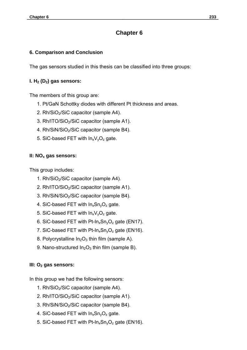
Chapter 6 233
Chapter 6
6. Comparison and Conclusion
The gas sensors studied in this thesis can be classified into three groups:
I. H2 (D2) gas sensors:
The members of this group are:
1. Pt/GaN Schottky diodes with different Pt thickness and areas.
2. Rh/SiO2/SiC capacitor (sample A4).
3. Rh/ITO/SiO2/SiC capacitor (sample A1).
4. Rh/SiN/SiO2/SiC capacitor (sample B4).
5. SiC-based FET with InxVyOz gate.
II: NOx gas sensors:
This group includes:
1. Rh/SiO2/SiC capacitor (sample A4).
2. Rh/ITO/SiO2/SiC capacitor (sample A1).
3. Rh/SiN/SiO2/SiC capacitor (sample B4).
4. SiC-based FET with InxSnyOz gate.
5. SiC-based FET with InxVyOz gate.
6. SiC-based FET with Pt-InxSnyOz gate (EN17).
7. SiC-based FET with Pt-InxSnyOz gate (EN16).
8. Polycrystalline In2O3 thin film (sample A).
9. Nano-structured In2O3 thin film (sample B).
III: O2 gas sensors:
In this group we had the following sensors:
1. Rh/SiO2/SiC capacitor (sample A4).
2. Rh/ITO/SiO2/SiC capacitor (sample A1).
3. Rh/SiN/SiO2/SiC capacitor (sample B4).
4. SiC-based FET with InxSnyOz gate.
5. SiC-based FET with Pt-InxSnyOz gate (EN16).

234 Chapter 6
6. Nano-structured In2O3 thin film (sample B).
6.1. Comparison of all sensors studied:
Since the sensitivity (S), selectivity (SE), response time τres, recovery time τrec, and
the range of operating temperature for the optimum detection Topt are the most
important parameters that decide which sensor is better than the others we have
arranged our results in Tab. 6.1 to enable an easy comparison.
Tab. 6.1: Comparison of the sensors studied according to the most important parameters.
Group Sensor Topt (°C) S SE τres τrec
Pt/GaN Schottky diodes 300-325 + + + + + + + + + + + + +
Rh/SiO2/SiC capacitor (A4) 115-140 + + + + + + + + +
Rh/ITO/SiO2/SiC capacitor (A1) 250-300 + + + + + + + + + + +
Rh/SiN/SiO2/SiC capacitor (B4) 25-50 + + + + + + + +
H2 (D2) gas
sensors FET with InxVyOz gate 25-100 + + + + + + + + + + + + + +
Rh/SiO2/SiC capacitor (A4) 25-75 + + + + + + + + + + + +
Rh/ITO/SiO2/SiC capacitor (A1) 25-75 + + + + + + + + + + +
Rh/SiN/SiO2/SiC capacitor (B4) 75-120 + + + + + + +
FET with InxSnyOz gate 325-370 + + + + + + + + + +
FET with InxVyOz gate 275-325 + + + + + + + + + + + + + +
FET with Pt-InxSnyOz gate (EN17) 175-225 + + + + + + + +
FET with Pt-InxSnyOz gate (EN16) 125-175 + + + + + + + + +
Polycrystalline In2O3 (sample A) 150-200 + + + + + + + + -
NOx gas sensors
Nano-structured In2O3 (sample B) 100-175 + + + + + + + + + + + - -
Rh/SiO2/SiC capacitor (A4) 225-250 + + + + + + + + + + + +
Rh/ITO/SiO2/SiC capacitor (A1) 150-225 + + + + + + + + + + + +
Rh/SiN/SiO2/SiC capacitor (B4) 225-275 + + + + + + + + + + +
FET with InxSnyOz gate 400-500 + + + + + + + + + + + +
FET with Pt-InxSnyOz gate (EN16) 260-300 + + + + + + + + +
O2 gas sensors
Nano-structured In2O3 (sample B) 200-250 + + + + + + +
+: reasonable; + +: good; + + +: very good; + + + +: excellent; -: bad; - -: very bad.
When we compare the sensors in the first group we can easily conclude that the best
H2 (D2) sensors are Pt/GaN Schottky diodes and FET with InxVyOz gate. But when
the Topt are compared we can see that the sensor FET with InxVyOz gate is better for

Chapter 6 235
low temperature sensing applications with the consequence of low power
consumption, what makes this sensor cheap in operation.
In the second group the sensors (FET with InxVyOz gate) and (Rh/SiO2/SiC
capacitor (A4)) are the best. But when operation at low temperatures is required, the
second should be preferred. However, the recovery time of the sensor (nano-
structured In2O3 (sample B)) is not acceptable although it has an excellent sensitivity
and selectivity as well as a very good response time. So the improvement of its
recovery time should be the subject of future investigations.
In the third group we find that all sensors have good parameters, so the
selection of one of them depends on the field of application.
6.2. Comparison with other results present in the literature:
6.2.1. H2 gas sensors:
The results from other researchers who have studied H2 gas sensors are listed in
Tab. 6.2.
Tab. 6.2: Comparison with other results of H2 gas sensors present in the literature.
Sensitive layer Sensor Thickness
(nm) Deposition method
C[H2] (ppm)
T (°C)
Response/ Sensitivity
τres
(s) Ref.
Pt/GaN Schottky diode 75 e-beam evaporation 2000 500 R = 400 mV - [6.1]
Pt/GaN Schottky diode 8-40 e-beam evaporation 2000 310 R = 250 mV - This
thesis
Pt/GaN Schottky diode 15 e-beam evaporation 10% 150 R = 200 mV - [6.2]
Pt/GaN Schottky diode 8 e-beam evaporation 1% 310 R = 325 mV - This
thesis
Pt/SiC Schottky diode 100 dc-magnetron
sputtering 1000 300
R2 = 0.3-
0.75 - [6.3]
Pt/GaN Schottky diode 8-40 e-beam evaporation 1000 310 R2 = 0.3-1.2 - This
thesis
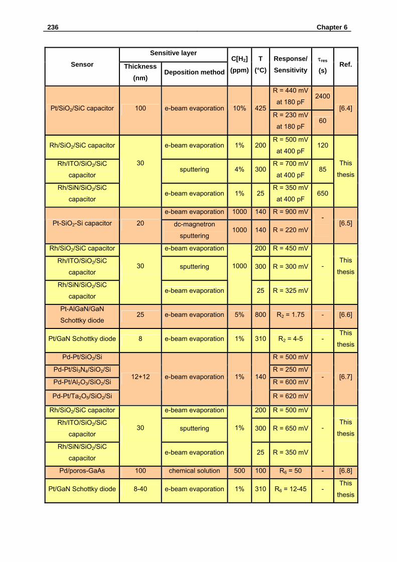
236 Chapter 6
Sensitive layer Sensor Thickness
(nm) Deposition method
C[H2] (ppm)
T (°C)
Response/ Sensitivity
τres
(s) Ref.
R = 440 mV
at 180 pF 2400
Pt/SiO2/SiC capacitor 100 e-beam evaporation 10% 425R = 230 mV
at 180 pF 60
[6.4]
Rh/SiO2/SiC capacitor e-beam evaporation 1% 200R = 500 mV
at 400 pF 120
Rh/ITO/SiO2/SiC
capacitor sputtering 4% 300
R = 700 mV
at 400 pF 85
Rh/SiN/SiO2/SiC
capacitor
30
e-beam evaporation 1% 25 R = 350 mV
at 400 pF 650
This
thesis
e-beam evaporation 1000 140 R = 900 mV
Pt-SiO2-Si capacitor 20 dc-magnetron
sputtering 1000 140 R = 220 mV
-
[6.5]
Rh/SiO2/SiC capacitor e-beam evaporation 200 R = 450 mV
Rh/ITO/SiO2/SiC
capacitor sputtering 300 R = 300 mV
Rh/SiN/SiO2/SiC
capacitor
30
e-beam evaporation
1000
25 R = 325 mV
-
This
thesis
Pt-AlGaN/GaN
Schottky diode 25 e-beam evaporation 5% 800 R2 = 1.75 - [6.6]
Pt/GaN Schottky diode 8 e-beam evaporation 1% 310 R2 = 4-5 - This
thesis
Pd-Pt/SiO2/Si R = 500 mV
Pd-Pt/Si3N4/SiO2/Si R = 250 mV
Pd-Pt/Al2O3/SiO2/Si R = 600 mV
Pd-Pt/Ta2O5/SiO2/Si
12+12 e-beam evaporation 1% 140
R = 620 mV
- [6.7]
Rh/SiO2/SiC capacitor e-beam evaporation 200 R = 500 mV
Rh/ITO/SiO2/SiC
capacitor sputtering 300 R = 650 mV
Rh/SiN/SiO2/SiC
capacitor
30
e-beam evaporation
1%
25 R = 350 mV
-
This
thesis
Pd/poros-GaAs 100 chemical solution 500 100 R6 = 50 - [6.8]
Pt/GaN Schottky diode 8-40 e-beam evaporation 1% 310 R6 = 12-45 - This
thesis
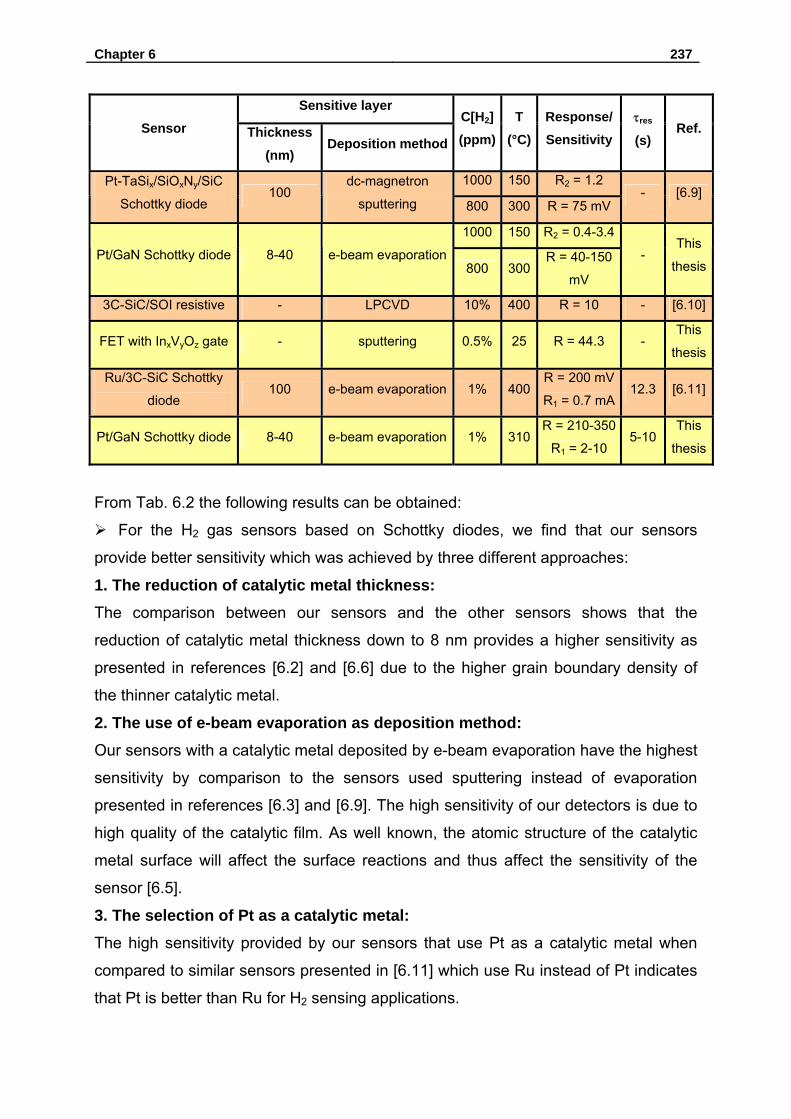
Chapter 6 237
Sensitive layer Sensor Thickness
(nm) Deposition method
C[H2] (ppm)
T (°C)
Response/ Sensitivity
τres
(s) Ref.
1000 150 R2 = 1.2 Pt-TaSix/SiOxNy/SiC
Schottky diode 100
dc-magnetron
sputtering 800 300 R = 75 mV - [6.9]
1000 150 R2 = 0.4-3.4
Pt/GaN Schottky diode 8-40 e-beam evaporation800 300
R = 40-150
mV
- This
thesis
3C-SiC/SOI resistive - LPCVD 10% 400 R = 10 - [6.10]
FET with InxVyOz gate - sputtering 0.5% 25 R = 44.3 - This
thesis
Ru/3C-SiC Schottky
diode 100 e-beam evaporation 1% 400
R = 200 mV
R1 = 0.7 mA 12.3 [6.11]
Pt/GaN Schottky diode 8-40 e-beam evaporation 1% 310R = 210-350
R1 = 2-10 5-10
This
thesis
From Tab. 6.2 the following results can be obtained:
For the H2 gas sensors based on Schottky diodes, we find that our sensors
provide better sensitivity which was achieved by three different approaches:
1. The reduction of catalytic metal thickness: The comparison between our sensors and the other sensors shows that the
reduction of catalytic metal thickness down to 8 nm provides a higher sensitivity as
presented in references [6.2] and [6.6] due to the higher grain boundary density of
the thinner catalytic metal.
2. The use of e-beam evaporation as deposition method: Our sensors with a catalytic metal deposited by e-beam evaporation have the highest
sensitivity by comparison to the sensors used sputtering instead of evaporation
presented in references [6.3] and [6.9]. The high sensitivity of our detectors is due to
high quality of the catalytic film. As well known, the atomic structure of the catalytic
metal surface will affect the surface reactions and thus affect the sensitivity of the
sensor [6.5].
3. The selection of Pt as a catalytic metal: The high sensitivity provided by our sensors that use Pt as a catalytic metal when
compared to similar sensors presented in [6.11] which use Ru instead of Pt indicates
that Pt is better than Ru for H2 sensing applications.
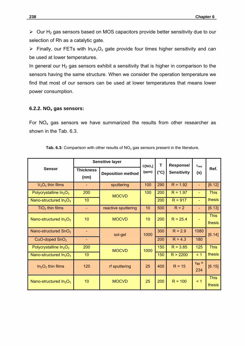
238 Chapter 6
Our H2 gas sensors based on MOS capacitors provide better sensitivity due to our
selection of Rh as a catalytic gate.
Finally, our FETs with InxvyOz gate provide four times higher sensitivity and can
be used at lower temperatures.
In general our H2 gas sensors exhibit a sensitivity that is higher in comparison to the
sensors having the same structure. When we consider the operation temperature we
find that most of our sensors can be used at lower temperatures that means lower
power consumption.
6.2.2. NOx gas sensors:
For NOx gas sensors we have summarized the results from other researcher as
shown in the Tab. 6.3.
Tab. 6.3: Comparison with other results of NOx gas sensors present in the literature.
Sensitive layer Sensor Thickness
(nm) Deposition method
C[NOx] (ppm)
T (°C)
Response/ Sensitivity
τres
(s) Ref.
V2O3 thin films - sputtering 100 290 R = 1.92 - [6.12]
Polycrystalline In2O3 200 200 R = 1.97 -
Nano-structured In2O3 10 MOCVD
100
200 R = 917 -
This
thesis
TiO2 thin films - reactive sputtering 10 500 R = 2 - [6.13]
Nano-structured In2O3 10 MOCVD 10 200 R = 25.4 - This
thesis
Nano-structured SnO2 - 300 R = 2.9 1080
CuO-doped SnO2 - sol-gel 1000
200 R = 4.3 180 [6.14]
Polycrystalline In2O3 200 150 R = 3.85 125
Nano-structured In2O3 10 MOCVD 1000
150 R > 2200 < 1
This
thesis
In2O3 thin films 120 rf sputtering 25 400 R = 15 τ50 =
234 [6.15]
Nano-structured In2O3 10 MOCVD 25 200 R = 100 < 1 This
thesis
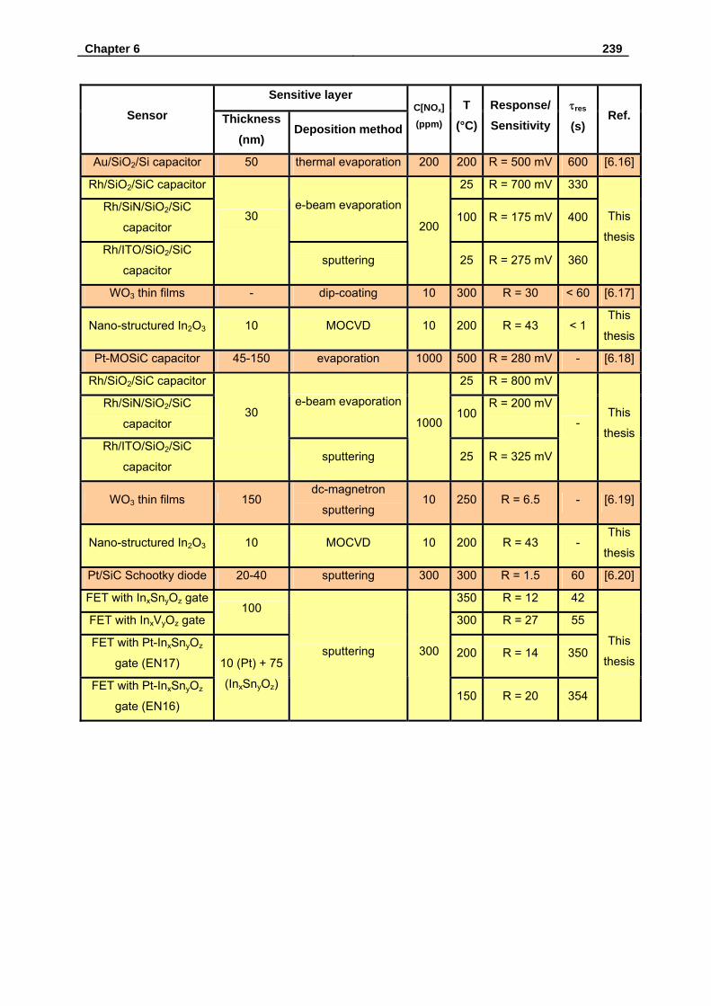
Chapter 6 239
Sensitive layer Sensor Thickness
(nm) Deposition method
C[NOx] (ppm)
T (°C)
Response/ Sensitivity
τres
(s) Ref.
Au/SiO2/Si capacitor 50 thermal evaporation 200 200 R = 500 mV 600 [6.16]
Rh/SiO2/SiC capacitor 25 R = 700 mV 330
Rh/SiN/SiO2/SiC
capacitor
e-beam evaporation100 R = 175 mV 400
Rh/ITO/SiO2/SiC
capacitor
30
sputtering
200
25 R = 275 mV 360
This
thesis
WO3 thin films - dip-coating 10 300 R = 30 < 60 [6.17]
Nano-structured In2O3 10 MOCVD 10 200 R = 43 < 1 This
thesis
Pt-MOSiC capacitor 45-150 evaporation 1000 500 R = 280 mV - [6.18]
Rh/SiO2/SiC capacitor 25 R = 800 mV
Rh/SiN/SiO2/SiC
capacitor
e-beam evaporation100
R = 200 mV
Rh/ITO/SiO2/SiC
capacitor
30
sputtering
1000
25 R = 325 mV
- This
thesis
WO3 thin films 150 dc-magnetron
sputtering 10 250 R = 6.5 - [6.19]
Nano-structured In2O3 10 MOCVD 10 200 R = 43 - This
thesis
Pt/SiC Schootky diode 20-40 sputtering 300 300 R = 1.5 60 [6.20]
FET with InxSnyOz gate 350 R = 12 42
FET with InxVyOz gate 100
300 R = 27 55
FET with Pt-InxSnyOz
gate (EN17) 200 R = 14 350
FET with Pt-InxSnyOz
gate (EN16)
10 (Pt) + 75
(InxSnyOz)
sputtering 300
150 R = 20 354
This
thesis
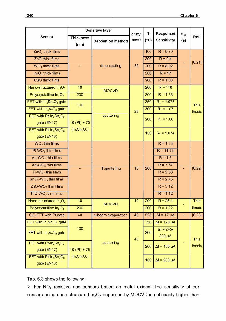
240 Chapter 6
Sensitive layer Sensor Thickness
(nm) Deposition method
C[NOx] (ppm)
T (°C)
Response/ Sensitivity
τres
(s) Ref.
SnO2 thick films 100 R = 9.39
ZnO thick films 300 R = 9.4
WO3 thick films 200 R = 8.92
In2O3 thick films 200 R = 17
CuO thick films
- drop-coating 25
200 R = 1.03
-
[6.21]
Nano-structured In2O3 10 200 R = 110
Polycrystalline In2O3 200 MOCVD
200 R = 1.38
FET with InxSnyOz gate 350 R1 = 1.075
FET with InxVyOz gate 100
300 R1 = 1.07
FET with Pt-InxSnyOz
gate (EN17) 200 R1 = 1.06
FET with Pt-InxSnyOz
gate (EN16)
10 (Pt) + 75
(InxSnyOz)
sputtering
25
150 R1 = 1.074
-
This
thesis
WO3 thin films R = 1.33
Pt-WO3 thin films R = 11.73 Au-WO3 thin films R = 1.3 Ag-WO3 thin films R = 7.57 Ti-WO3 thin films R = 2.53
SnO2-WO3 thin films R = 2.75 ZnO-WO3 thin films R = 3.12 ITO-WO3 thin films
- rf sputtering 10 260
R = 1.12
- [6.22]
Nano-structured In2O3 10 200 R = 25.4
Polycrystalline In2O3 200 MOCVD
10
200 R = 1.22 -
This
thesis
SiC-FET with Pt gate 40 e-beam evaporation 40 525 ΔI = 17 µA - [6.23]
FET with InxSnyOz gate 350 ΔI = 120 µA
FET with InxVyOz gate 100
300ΔI = 245-
300 µA
FET with Pt-InxSnyOz
gate (EN17) 200 ΔI = 185 µA
FET with Pt-InxSnyOz
gate (EN16)
10 (Pt) + 75
(InxSnyOz)
sputtering 40
150 ΔI = 260 µA
- This
thesis
Tab. 6.3 shows the following:
For NOx resistive gas sensors based on metal oxides: The sensitivity of our
sensors using nano-structured In2O3 deposited by MOCVD is noticeably higher than
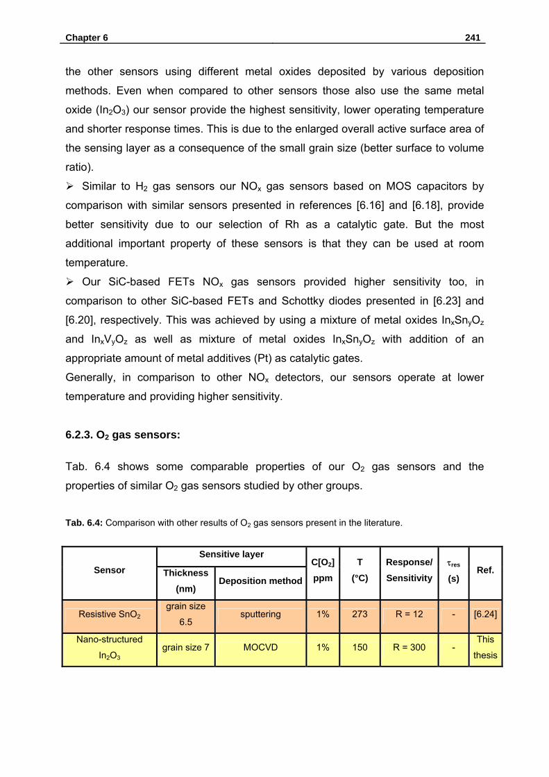
Chapter 6 241
the other sensors using different metal oxides deposited by various deposition
methods. Even when compared to other sensors those also use the same metal
oxide (In2O3) our sensor provide the highest sensitivity, lower operating temperature
and shorter response times. This is due to the enlarged overall active surface area of
the sensing layer as a consequence of the small grain size (better surface to volume
ratio).
Similar to H2 gas sensors our NOx gas sensors based on MOS capacitors by
comparison with similar sensors presented in references [6.16] and [6.18], provide
better sensitivity due to our selection of Rh as a catalytic gate. But the most
additional important property of these sensors is that they can be used at room
temperature.
Our SiC-based FETs NOx gas sensors provided higher sensitivity too, in
comparison to other SiC-based FETs and Schottky diodes presented in [6.23] and
[6.20], respectively. This was achieved by using a mixture of metal oxides InxSnyOz
and InxVyOz as well as mixture of metal oxides InxSnyOz with addition of an
appropriate amount of metal additives (Pt) as catalytic gates.
Generally, in comparison to other NOx detectors, our sensors operate at lower
temperature and providing higher sensitivity.
6.2.3. O2 gas sensors:
Tab. 6.4 shows some comparable properties of our O2 gas sensors and the
properties of similar O2 gas sensors studied by other groups.
Tab. 6.4: Comparison with other results of O2 gas sensors present in the literature.
Sensitive layer Sensor Thickness
(nm) Deposition method
C[O2] ppm
T (°C)
Response/ Sensitivity
τres
(s) Ref.
Resistive SnO2 grain size
6.5 sputtering 1% 273 R = 12 - [6.24]
Nano-structured
In2O3 grain size 7 MOCVD 1% 150 R = 300 -
This
thesis
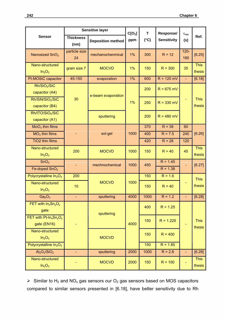
242 Chapter 6
Sensitive layer Sensor Thickness
(nm) Deposition method
C[O2] ppm
T (°C)
Response/ Sensitivity
τres
(s) Ref.
Nanosized SnO2 particle size
24 mechanochenmical 1% 300 R = 12
120-
180 [6.25]
Nano-structured
In2O3 grain size 7 MOCVD 1% 150 R = 300 35
This
thesis
Pt-MOSiC capacitor 45-150 evaporation 1% 600 R = 120 mV - [6.18]
Rh/SiO2/SiC
capacitor (A4) 200 R = 675 mV
Rh/SiN/SiO2/SiC
capacitor (B4)
e-beam evaporation
250 R = 330 mV
Rh/ITO/SiO2/SiC
capacitor (A1)
30
sputtering
1%
200 R = 480 mV
-
This
thesis
MoO3 thin films 370 R = 39 60
MO3 thin films 400 R = 7.5 240
TiO2 thin films
- sol-gel 1000
420 R = 28 120
[6.26]
Nano-structured
In2O3 200 MOCVD 1000 150 R = 40 45
This
thesis
SnO2 R = 1.45
Fe-doped SnO2 - mechnochemical 1000 450
R = 1.38 - [6.27]
Polycrystalline In2O3 200 150 R = 1.6
Nano-structured
In2O3 10
MOCVD 1000 150 R = 40
- This
thesis
Ga2O3 - sputtering 4000 1000 R = 1.2 - [6.28]
FET with InxSnyOz
gate 400 R = 1.25
FET with Pt-InxSnyOz
gate (EN16)
sputtering
150 R = 1.225
Nano-structured
In2O3 150 R = 400
Polycrystalline In2O3
-
MOCVD
4000
150 R = 1.85
- This
thesis
Al2O3/SiO2 - sputtering 2000 1000 R = 2.8 - [6.28]
Nano-structured
In2O3 - MOCVD 2000 150 R = 100 -
This
thesis
Similar to H2 and NOx gas sensors our O2 gas sensors based on MOS capacitors
compared to similar sensors presented in [6.18], have better sensitivity due to Rh

Chapter 6 243
selected as a catalytic gate and can be operated at lower temperatures making the
power consumption lower.
The situation of our O2 resistive gas sensor based on nano-structured In2O3 did
not differ from that of our NOx resistive gas sensor which exhibit higher sensitivity
and lower operation temperatures in comparison to results presented in [6.24-6.28].
In relation to the SiC-based FETs O2 gas sensors, Tab. 6.4 shows that our sensor
sensitivity is higher than the sensitivity of resistive O2 sensors presented in [6.28].
6.3. Conclusion:
Field effect devices (Schottky diodes, MOS capacitors, and MOSFET transistors)
based on wide band gap semiconductors like SiC and GaN as well as resistive gas
sensors based In2O3, have been developed as H2, NOx, and O2 gas sensors.
In chapter 2: The sensitivity to hydrogen of Pt/GaN Schottky diodes was
investigated in dependence on the active area, the Pt thickness and the operating
temperature. A significant increase of the sensitivity and a decrease of the response
and recovery times by increasing the temperature of operation to about 350°C and by
decreasing the Pt thickness down to 8 nm were observed. By decreasing the
catalytic metal thickness down to 8 nm, the use of e-beam evaporation as deposition
method of the catalytic metal, and the selection of Pt as catalytic metal, caused better
sensitivity in comparison to the other sensors presented in the literature.
In chapter 3: The responses to D2, NOx, and O2 of MOSiC and MMOOSiC
structures were investigated in dependence on the operating temperature and gas
partial pressures. The most important property of these sensors is that they can be
used as NOx gas sensor at room temperature. Depending on the type of insulator
that is chosen and the Rh structure, differences in the sensitivity are observed. The
selection of Rh as a catalytic gate provided better sensitivity to H2, NOx, and O2 by
comparison to similar sensors having the same structure described in the scientific
literature.
In chapter 4: SiC-based FETs were investigated as NOx, and O2 gas detectors.
The responses to these gases were investigated in dependence on the operating
temperature and gas partial pressures. By using a mixture of metal oxides InxSnyOz
and InxVyOz as well as mixture of metal oxides InxSnyOz with addition of an
appropriate amount of metal additives (Pt) as catalytic gates our NOx and O2 SiC-
244 Chapter 6
based FETs gas sensors provided higher sensitivity and lower operation
temperatures in comparison to other SiC-based FETs presented in the literature.
In chapter 5: Polycrystalline and nano-structured In2O3 thin films were
investigated as NOx and O2 gas sensors exhibiting higher sensitivity and lower
operation temperatures when compared to other sensors using different metal oxides
deposited by various deposition methods. The higher sensitivity of the nano-
structured In2O3 is due to the enlarged overall active surface area of the sensing
layer as a consequence of the small grain size (better surface to volume ratio).
The best H2 (D2) sensors studied in this work are Pt/GaN Schottky diodes and
FET with InxVyOz gate taking in account, sensitivity, selectivity, and the response and
recovery times. In addition, the sensor FET with InxVyOz gate is better for low
temperature sensing applications.
Sensors (FET with InxVyOz gate) and (Rh/SiO2/SiC capacitor (A4)) are the best
NOx sensors presented in this work. When operation at low temperatures is required,
the second should be preferred. However, the recovery time of the NOx sensor
(nano-structured In2O3 (sample B)) is not acceptable although it has an excellent
sensitivity and selectivity as well as a very good response time. So the improvement
of its recovery time should be the subject of future investigations.
All O2 sensors investigated in this thesis have good parameters, so the selection
of one of them depends on the field of application.
As a final result we can conclude that the sensors we have improved are comparable
to those obtained by other researchers and have been published in the literature.
Chapter 6 245
References:
[6.1] J. Schalwig, G. Müller, M. Eickhoff, O. Ambacher, and M. Stutzmann, “Group III-
nitride-based gas sensors for combustion monitoring”, Mater. Sci. Eng. B 93 (2002)
207-214.
[6.2] J. Kim, F. Ren, B. P. Gila, C. R. Abernathy, and S. J. Pearton, “Reversible
barrier height changes in hydrogen-sensitive Pd/GaN and Pt/GaN diodes”, Appl.
Phys. Lett. 82 (2003) 739-741.
[6.3] J. P. Xu, P. T. Lai, D. G. Zhong, and C. L. Chan, “Improved hydrogen sensitive
properties of MISiC Schottky sensor with thin NO-grown oxynitride as gate insulator”,
IEEE electron device Lett. 24 (2003) 13-15.
[6.4] P. Tobias, B. Golding, and N. Ghosh, “Interface state in high-temperature gas
sensors based on silicon carbide”, IEEE Sensor J. 2 (2003) 543-547.
[6.5] A. E. Abom, R. T. Haasch, N. Hellgren, N. Finnegan, L. Hultman, and M.
Eriksson, “Characterization of the metal-insulator interface of field-effect chemical
sensors”, J. Appl. Phys. 93 (2003) 9760-9768.
[6.6] J. Song, W. Lu, J. S. Flynn, and G. R. Brandes, “Pt-AlGaN/GaN Schottky diodes
operated at 800°C for hydrogen sensing”, Appl. Phys. Lett. 87 (2005). 133501-1-3.
[6.7] M. Eriksson, A. Salomonsson, and I. Lundström, “The influence of the insulator
surface properties on the hydrogen response of field gas sensors”, J. Appl. Phys. 98
(2005) 034903-1-6.
[6.8] A. Salehi , A. Nikfarjam, D. J. Kalantari, “Pd/porous-GaAs Schottky contact for
hydrogen sensing application”, Sensors and Actuators B 113 (2006) 419-427.
[6.9] W. M. Tang, P. T. Lai, J. P. Xu, C. L. Chan, “Enhanced hydrogen-sensing
characteristics of MISiC Schottky-diode hydrogen sensor trichloroethylene oxidation”,
Sensors and Actuators A 119 (2005) 63-67.
[6.10] T. J. Fawcett, J. T. Wolan, M. Reyes, S. E. Saddow, and A. Lloyd Spetz,
“Thermal detection mechanism of SiC based hydrogen resistive sensors”, Appl.
Phys. Lett. 89 (2006) 182102-1-3.
[6.11] S. Roy, C. Jacob, and S. Basu, “Studies on Ru/3C-SiC Schottky junction for
high temperature hydrogen sensors”, J. Electochem. Soc. 150 (2003) H135-H139.
[6.12] S. Capone, R. Rella, P. Siciliano, and L. Vasanelli, “A comparison between
V2O5 and WO3 thin films as sensitive elements for NO detection”, Thin Solid Films
350 (1999) 264-268.
246 Chapter 6
[6.13] T. Gessner, K. Gottfried, R. Hoffmann, C. Kaufmann, U. Weiss, E.
Charetdinov, P. Hauptmann, R. Lucklum, B. Zimmermann, U. Dietel, G. Springer,
and M. Vogel, “Metal oxide gas sensor for high temperature application“,
Microsystem Technology 6 (2000) 169-174.
[6.14] G. Zhang, M. Liu, “Effect of particle size and dopant on properties of SnO2-
based gas sensors”, Sensors and Actuators B 69 (2000) 144-152.
[6.15] H. Steffes, C. Imawan, F. Solzbacher, E. Obemeier, “Fabrication parameters
and NO2 sensitivity of reactively RF-sputtered In2O3 thin films”, Sensors and
Actuators B 68 (2000) 249-253.
[6.16] D. Filippini, R. Aragon, and U. Weimar, “NO2 sensitive gate metal-oxide-
semiconductor capacitors”, J. Appl. Phys. 90 (2001) 1883-1886.
[6.17] W. Y. Chung, “Tungsten oxide thin films prepared for NO2 sensors by using the
hydrothermal method and dip coating”, Journal of the Korea Physical Society 41
(2002) L181-L183.
[6.18] J. Schalwig, P. Kreisl, S. Ahlers, and G. Müller, “Response mechanism of SiC-
based MOS fiel-effect gas sensors”, IEEE sensor J. 2 (2002) 394-402.
[6.19] X. He, J. Li, X. Gao, and L. Wang, “NO2 sensing characteristics of WO3 thin
film microgas sensor”, Sensors and Actuators B 93 (2003) 463-467.
[6.20] Shabbir A. Khan, Elder A. de Vasconcelos, Y. Hasegawa, and T. Katsube,
“High-temperature thin-catalytic gate devices for combustion emissions control”,
Brazilian Journal of Physics 34 (2004) 577-580.
[6.21] A. A. Tomchenko, G. P. Harmer, B. T. Marquis, J. W. Allen, “Semiconducting
metal oxide sensor array for the selective detection of combustion gases“, Sensors
and Actuators B 93 (2003) 126-134.
[6.22] M. Stankova, X. Vilanova, J. Caldere, E. Liobet, J. Brezmes, I. Gracia, C.
Cane, X. Correig, ”Sensitivity and selectivity improvement of rf sputtered WO3
microhotplate gas sensors”, Sensors and Actuators B 113 (2006) 241-248.
[6.23] K. Matocha, V. Tilak, P. Sandvik, J. Tucker, “High-temperature Sic MOSFET
gas sensor”, in: Proceedings of the MRS Fall Meeting, 828 (2004) A7.9.
[6.24] J. P. Santos, J. A. de Agapito, ”The interaction of oxygen with nanocystalline
SnO2 thin films in the framework of the electron theory of adsorption”, Thin Solid
Films 338 (1999) 276-280.
Chapter 6 247
[6.25] L. M. Cukrov, P. G. McComick, K. Galatsis, W. Wlodarski, ”Gas sensing
properties of nanosized tin oxide synthesised by mechanochemical processing”,
Sensors and Actuatores B 77 (2001) 491-495.
[6.26] K. Galatsis, Y. X. Li, W. Wlodarski, E. Comini, G. Sberveglieri, C. Canalini, S.
Cantucci, and M. Passacantando, ”Comparison of single and binary oxide MoO3,
TiO2, and WO3 sol-gel gas sensors”, Sensors and Actuators B 83 (2002) 276-280.
[6.27] K. Galatsis, L. Curkrov, , W. Wlodarski, P. McCormick, K. Kalantar-zadeh, E.
Comini, G. Sberveglieri, C. Canalini, S. Cantucci, and M. Passacantando,
”Comparison of single and binary oxide MoO3, TiO2, and WO3 sol-gel gas sensors”,
Sensors and Actuators B 83 (2002) 276-280.
[6.28] C. Baban, Y. Toyoda, M. Ogita, ”Oxygen sensor based on Ga2O3 films
operating at high temperature”, Journal of Optoelectronics and Advanced Materials 7
(2005) 891-896.

248 Chapter 6

Appendix A 249
Appendix A
Thermocouple type K and S [A.1, A.2]:
Type NiCr-Ni
(K) Pt10%Rh-Pt
(S) Type
NiCr-Ni (K)
Pt10%Rh-Pt (S)
°C mV mV °C mV mV
25 1 0.143 600 24.905 5.239
50 2.023 0.299 625 25.967 5.495
75 3.059 0.467 650 27.025 5.753
100 4.096 0.646 675 28.079 6.013
125 5.124 0.834 700 29.129 6.275
150 6.138 1.029 725 30.174 6.539
175 7.140 1.232 750 31.213 6.806
200 8.138 1.441 800 33.275 7.345
225 9.141 1.655 825 34.297 7.618
250 10.153 1.874 850 35.313 7.893
275 11.176 2.096 875 36.323 8.170
300 12.209 2.323 900 37.326 8.449
325 13.248 2.553 925 38.323 8.731
350 14.293 2.786 950 39.314 9.014
375 15.343 3.021 975 40.298 9.300
400 16.397 3.259 1000 41.276 9.587
425 17.455 3.500 1100 45.119 10.757
450 18.516 3.742 1200 48.838 11.951
475 19.579 3.987 1250 50.644 12.554
500 20.644 4.233 1300 - 13.159
525 21.710 4.482 1400 14.373
550 22.776 4.732 1500 - 15.582
575 23.842 4.984 1600 - 16.777
[A.1] http://www.thermometricscorp.com/thertypk.html.
[A.2] http://www.thermometricscorp.com/thertyps1to5.html.

250 Appendix A

Appendix B 251
Appendix B
B.1. Relative ion currents from fragment ions for ionization energy of 90 eV [B.1].
(m/e) H2 He CH4 H2O Ne N2 CO C2H6 O2 Ar CO2 C3H8
1 2 4
3
100
100 16.5 2.4 9.6 5.0
12 13 14
3.0
7.8
16.0
14
6.3
0.8
0.7
1.2
3.3
9.7
0.6
0.9
2.3
15 16 17
85.0
100
1.2
1.8
26
2.8 4.7
18
16.0 7.2
18 20 22
100
100 10.2
22.6
2.1
25 26 27
3.8
22.2
33.4
0.8
9.8
43.5
28 29 30
100 0.7
100
1.2
100 20.0
22.2
13.0
61.0
100 21.7
31 32 34
100 0.4
36 37 38
0.34
0.06
4.6
6.7
39 40 41
100
20.2
2.6
15.0
42 43 44 45
100 1.2
4.8
22.8
24.0
0.8

252 Appendix B
B.2. Sensitivity for QMA 200 [B.1]
Gas Mass number
of the basis peak Sensitivity for basis peak
× 10-5 [A/mbar] Sum of the fragment ions
× 10-5 [A/mbar]
He Ne Ar
4
20
40
6.4
6.4
24
-
7.2
30
Kr H2
N2
84
2
28
6.8
13
20
17
-
23
CO O2
CO2
28
32
44
20
14
13
22
16
19
CH4
C2H6 C3H8
16
28
29
28
34
26
54
68
74
C4H10 (n) C4H10 (iso)
H2O
43
43
18
22
24
20
74
68
26
[B.1] Fa. Balzers: Partialdruckmessung in der Vakuumtechnik, Firmenbroschüre.

Erklärung
Ich versichere, dass ich die vorliegende Arbeit ohne unzulässige Hilfe Dritter und
ohne Benutzung anderer als der angegebenen Hilfsmittel angefertigt habe. Die aus
anderen Quellen direkt oder indirekt übernommenen Daten und Konzepte sind unter
Angabe der Quelle gekennzeichnet.
Bei der Auswahl und Auswertung folgenden Materials haben mir die
nachstehend aufgeführten Personen in der jeweils beschriebenen Weise
unentgeltlich geholfen:
1. Prof.-Dr. Oliver Ambacher - Betreuer,
2. Dr. -Ing. Volker Cimalla - Betreuer,
3. Dr. -Ing Gernot Ecke - Durchführung der AES Messungen,
4. Dr. -Ing Henry Romanus - Durchführung der SEM Messungen.
Weitere Personen waren an der inhaltlich-materiellen Erstellung der vorliegenden
Arbeit nicht beteiligt. Insbesondere habe ich hierfür nicht die entgeltliche Hilfe von
Vermittlungs- bzw. Beratungsdiensten (Promotionsberater oder anderer Personen) in
Anspruch genommen. Niemand hat von mir unmittelbar oder mittelbar geldwerte
Leistungen für Arbeiten erhalten, die im Zusammenhang mit dem Inhalte der
vorgelegten Dissertation stehen.
Die Arbeit wurde bisher weder im In- noch im Ausland in gleicher oder ähnlicher
Form einer Prüfungsbehörde vorgelegt.
Ich bin darauf hingewiesen worden, dass die Unrichtigkeit der vorstehenden
Erklärung als Täuschungsversuch angesehen wird und den erfolglosen Abbruch des
Promotionsverfahrens zu Folge hat.
(Ort, Datum) Unterschrift Ilmenau, den 28.06.2007
Thesen zur Dissertation “Wide band gap materials and devices for NOx, H2, and O2 gas
sensing applications”, vorgelegt von Dipl.-Ing. Majdeddin Ali
1) Selektive Erkennung von Stickoxiden (NOx) bei niedrigen Temperaturen durch den
Einsatz von nanostrukturierten Metalloxid-Dünnschichten.
2) Die Reduzierung der Korngröße der Indiumoxid-Dünneschichten auf unter 10 nm hat
erhebliche Auswirkung auf die Empfindlichkeit auf NOx von In2O3-basierenden resistiven
Gassensoren.
3) Entwicklung und Optimierung von AlGaN/GaN-basierenden HEMTs zum Nachweis von
NOx-Gasen durch den Einsatz von nanostrukturierten In2O3-Dünnschichten als
gassensitives Gate.
4) Charakterisierung und Weiterentwicklung von NOx-Gassensoren auf der Basis von SiC-
basierten Feldeffekttransistoren mit verschiedenen Gemischen aus Metalloxiden für das
Gate.
5) Die Zugabe einer entsprechenden Menge Metallzusätzen (Pt,Pd,…) beeinflusst die
Empfindlichkeit, die Selektivität, und die Ansprech- und Erholzeiten von
nanostrukturierten In2O3-basierenden Gassensoren.
6) Die Mikrostruktur der Gateelektrode von SiC-basierten FETs ist entscheident für den
Detektionsmechanismus und somit die entscheidenden Leistungsparameter des Sensors:
Empfindlichkeit, Selektivität und Reaktionszeit.
7) In2O3-basierende resistive Gassensoren besitzen hohe Empfindlichkeit auf NOx, gute
Selektivität, schnelle Reaktionszeit und relative lange Erholzeiten. Für eine effektive
Entwicklung solcher NOx-Gassensoren ist eine Reduzierung der Erholzeit notwendig.
8) Die Mikrostruktur des Gates der Gassensoren (Schottky Dioden, MOS Kapazitäten, und
SiC-basierte FETs) muss mit der Hilfe von TEM, AFM, und Röntgenbeugung optimiert
werden.
9) Feuchtigkeit auf In2O3-basierenden resistiven Gassensoren und die Feldeffektgassensoren
(Pt/GaN Schottky Dioden, MOS Kapazitäten, MOSFET Transistoren) in Anwesenheit
von reduzierenden und oxidierenden Gasen reduziert die Empfindlichkeit.
10) Die Anwendung von Rhodium (Rh) als Gateelektode von Schottky Dioden, MOS
Kapazitäten und MOSFET Transistoren ermöglicht die Entwicklung von Gassensoren für
die Detektion von Stickoxiden (NOx) bei niedrigen Temperaturen.
Lebenslauf
Vorname: Majdeddin
Nachname Ali
Geburtsdatum 08.09.1976
Geburtsort Homs, Syrien
Familienstand: verheiratet
Nationalität: syrisch
Anschrift: Geschwister-Scholl-Str. 8d, 98693 Ilmenau
1982 - 1991 Grund- und Mittelschule in Homs
1991 - 1994 Oberschule in Homs mit dem Abschluss:
Reifezeugnis des naturwissenschaftlichen Zweiges
1994 - 1999 Studium an der Aleppo Universität in Aleppo mit dem Abschluss:
Bachelor in Elektrotechnik und Elektronik
1999 - 2001 Studium an der Aleppo Universität in Aleppo mit dem Abschluss:
Diplom Ingenieur in Elektrotechnik und Elektronik
02.2000 - 03.2001 wissenschaftlicher Mitarbeiter an der Al-Baath Universität in Homs
10.2001 - 04.2002 Deutschkurs (Grundstufe) an der TU Ilmenau
04.2002 - 07.2002 Deutschkurs (Mittelstufe) an der TU Dresden mit dem Abschluss:
DSH Zeugnis
2003 - 2007 Doktorand und wissenschaftlicher Mitarbeiter am Fachgebiet
Nanotechnologie, Institut für Mikro- und Nanoelektronik der
Technischen Universität Ilmenau
Anfertigung der Dissertation mit dem Thema: Wide band gap
materials and devices for NOx, H2 and O2 gas sensing applications
Copyright © 2022 FDOKUMEN


![SACI [e]motion - V-NOX TWIN PUMP](https://static.fdokumen.com/doc/165x107/6334ac3db9085e0bf50921cd/saci-emotion-v-nox-twin-pump.jpg)