April 2021 Volume 28 Issue 2.3 - English Language Education ...
Upload
khangminh22Category
view
1download
0
Copyright © 1999 Wimborne Publishing Ltd andMaxfield & Montrose Interactive Inc
EPE Online, Febuary 1999 - www.epemag.com - XXX
Volume 2 Issue 4April 2000

Copyright © 2000 Wimborne Publishing Ltd andMaxfield & Montrose Interactive Inc
EPE Online, April 2000 - www.epemag.com - 242
Copyright 1999, Wimborne Publishing Ltdand Maxfield & Montrose Interactive Inc.,
PO Box 857, Madison, Alabama 35758, USAAll rights reserved.
WARNING!The materials and works contained within EPE Online — which are made available
by Wimborne Publishing Ltd and Maxfield & Montrose Interactive Inc — arecopyrighted. You are permitted to download locally these materials and works and tomake one (1) hard copy of such materials and works for your personal use. Internationalcopyright laws, however, prohibit any further copying or reproduction of such materialsand works, or any republication of any kind.
Maxfield & Montrose Interactive Inc and Wimborne Publishing Ltd have used theirbest efforts in preparing these materials and works. However, Maxfield & MontroseInteractive Inc and Wimborne Publishing Ltd make no warranties of any kind, expressedor implied, with regard to the documentation or data contained herein, and specificallydisclaim, without limitation, any implied warranties of merchantability and fitness for aparticular purpose. Because of possible variances in the quality and condition ofmaterials and workmanship used by readers, EPE Online, its publishers and agentsdisclaim any responsibility for the safe and proper functioning of reader-constructedprojects based on or from information published in these materials and works.
In no event shall Maxfield & Montrose Interactive Inc or Wimborne Publishing Ltd beresponsible or liable for any loss of profit or any other commercial damages, includingbut not limited to special, incidental, consequential, or any other damages in connectionwith or arising out of furnishing, performance, or use of these materials and works.

Copyright © 1999 Wimborne Publishing Ltd andMaxfield & Montrose Interactive Inc
EPE Online, February 1999 - www.epemag.com - XXXCopyright © 2000 Wimborne Publishing Ltd andMaxfield & Montrose Interactive Inc
EPE Online, April 2000 - www.epemag.com - 243
TECHNOLOGY TIMELINES - Part 3 - Communications and RelatedTechnologies 1900 to 1999 - by Clive Maxfield and Alvin Brown
The fascinating story of how technology developed in the last millennium
285
NET WORK - THE INTERNET PAGE surfed by Alan Winstanley 283
CIRCUIT SURGERY - by Alan WinstanleyOpamps - Getting Loaded; Biased Approach; Socket to Me; Surface-Mount Selection
315
REGULARS AND SERVICES
NEWS - Barry Fox highlights technology’s leading edge. Plus everydaynews from the world of electronics.
326
READOUT - John Becker addresses general points arising. 333
SHOPTALK - with David Barrington The essential guide to componentbuying for EPE Online projects.
331
EDITORIAL 244
SERIES AND FEATURESNEW TECHNOLOGY UPDATE - by Ian Poole
Electronic Ink - Is this the real dawn of the paper-less office?281
HIGH PERFORMANCE REGENERATIVE RECEIVER - Part 2by Raymond Haigh Construction of our “art-deco” receiver.
276
TELCAN HOME VIDEO - by Barrie Blake-ColemanA British first in home video recording
319
PROJECTS AND CIRCUITS
GARAGE LINK - by Terry de Vaux-BalbirnieAn open and shut case for a 418MHz Transmitter/Receiver link
FLASH SLAVE - by Robert PenfoldMake a striking image with this latest Starter Project
INGENUITY UNLIMITED - hosted by Alan WinstanleyPC Controlled DC Motor; Omnidirectional Pendulum: Brushless Fan
Speed Control
272
MICRO-PICSCOPE - by John Becker Plenty of scope for this ingenious piece of portable test gear
263
INTERFACE - by Ian PooleBidirectional Printer Ports
295
TEACH-IN 2000 - Part 6. Logic gates, Binary and Hex Logicby John Becker Essential info for the electronics novice 299
251
246

Copyright © 2000 Wimborne Publishing Ltd andMaxfield & Montrose Interactive Inc
EPE Online, April 2000 - www.epemag.com - 244
ODD REQUESTSWe get some odd requests via email at EPE Online and at the printed edition EPE (including the
occasional rude comment (see Readout). In fact there seems to a lack of understanding about therelationship between EPE and EPE Online in some cases. The printed edition of EPE is based in the UK,and virtually all of the magazine’s content is edited by the EPE Editorial Office in the UK. EPE Online andthe EPE Online web site is run for by Clive (Max) Maxfield and Alvin Brown based in the USA.
The idea of EPE Online is that readers can purchase and download the magazine online fromanywhere in the world, almost instantly. You log on to the www.epemag.com web site, punch in yourcredit card details to pay for an issue $5 (US) or a year’s subscription at $9.99 (US) and then you candownload the magazine from that web site to your computer, read it on screen, or print it out as required.It is not sent to you via email, but you will get an email telling you when each issue is available (usuallyjust after the printed issue is on sale in UK shops) so you can then log on and download the magazine.
We charge for EPE Online in US dollars, but that charge will be automatically converted to your localcurrency by your credit card provider. If you pay from the UK, for example, a 12-month subscription to theonline edition will cost about 6.25 UK Pounds, depending on the pound/dollar exchange rate at the time.
The online edition presently carries no advertising from component suppliers etc., but we are in theprocess of changing that and no doubt some printed issue advertisers will take up online advertising in thecoming months. Incidentally, the EPE Online web site presently receives about 22,000 hits a week.
EDITORIAL QUERIESBecause the editorial material for EPE Online is produced by the editorial office in the UK, technical
queries on projects etc. should be directed to [email protected] and not to the onlineoffices in the USA (who will only forward them to the UK for reply).
We are not able to supply material – either individual articles or whole issues – by email. If yourequire material on an “instant” basis then you can buy back issues and download them from the EPEOnline web site. Alternatively, you can order printed back issues from the UK web site, these are thenposted out, usually within five working days. The EPE Online web site carries material from the November1998 issue onwards so you cannot obtain earlier articles by download via the web, you will then have toorder printed back issues.
We hope this makes everything clearer (as clear as mud some might say), if not please let us know.
EPE Online, April 2000 - www.epemag.com - 244

Copyright © 2000 Wimborne Publishing Ltd andMaxfield & Montrose Interactive Inc
EPE Online, April 2000 - www.epemag.com - 245
VERSATILE MICROPHONE/AUDIO PREAMPLIFIEROne of the latest chips on the block, the Analog Device SSM2166P, is a low noise, low
distortion, dynamic range compressor with a number of interesting features. In this design itprovides a very versatile preamplifier with automatic gain control, signal limiting, variablecompression and noise reduction circuitry. The design is suitable for a wide range of appli-cations from PA and surveillance systems to amateur radio and audio. Additional circuitry isgiven for readers who require a signal strength meter.
SIXTEEN-CHANNEL TWO-WIRE TRANSMISSION SYSTEMThe uses for this PIC-based project are limited only by the ingenuity of the constructor.
Everything from extra inputs for simple security projects to communications, signaling andcontrol of complex systems over long distances can be handled, and the modules describedmay be tailored to give only the degree of sophistication required for minimum cost.
The units can be configured to provide either eight or sixteen channels, and where eightare used the system may be upgraded later by simply plugging in extra PICs, It will operatein both directions or just one, and with one-way operation the transmitter may be poweredfrom the receiver through the signaling circuit, making it easy to monitor up to sixteen re-mote inputs through just a two-cor
e connecting lead. There is an optional interface for use with low-amplitude audio circuitswhich can be omitted where direct cable connection is possible. These options should allowthis to find many uses in signaling, security and remote control projects.

Copyright © 2000 Wimborne Publishing Ltd andMaxfield & Montrose Interactive Inc
Visit the EPE Online Store atwww.epemag.com and place your order today!
A selection of ELECTRONIC Books
The Great Logo AdventureA cartoon-illustrated, family activity book for ex-ploring animation, graphics, math, geometry, ...Ideal for teaching programming concepts toyoung people of all ages.FREE CD-ROM (for PCs and Macs) containsLogo software plus lots of other stuff.
Controlling theWorld With Your PCConnect your MS-DOS/Win-dows PC to the real world withthis best-selling book!Comes with all software(executable files plus C, Basic,and Pascal
Forrest MimsEngineer'sNotebookThis revised editionincludes hundreds ofuseful circuits de-signed and built byForrest using com-monly available inte-grated circuits andother components.
Bebop to theBoolean Boogie(An UnconventionalGuide to Electronics)This in-depth, highly readable,up to the minute guide showsyou how electronic deviceswork and how they're made --the only electronics bookwhere you can learn about mu-sical socks and the best timeof the day to eat smoked fish!
Bebop BYTES Back(An UnconventionalGuide to Computers)
This follow-on to Bebop to the BooleanBoogie is a multimedia extravaganza ofinformation about how computers work.FREE CD ROM contains theBeboputer Computer Simulator, along withover 200 megabytes of mega-cool multi-media.
More details areavailable on the
EPE Online web site

Copyright © 2000 Wimborne Publishing Ltd andMaxfield & Montrose Interactive Inc
A selection of ELECTRONIC Books
Visit the EPE Online Store atwww.epemag.com and place your order today!
Programming Micro-controllers in C MoreInfo or Buy Now!This book opens with a quickreview of the essentials of Cprogramming and then exam-ines in depth the issues facedwhen writing C code for micro-controllers.
Designus MaximusUnleashed(Banned in Alabama)
This unabridged and unexpur-gated tome contains the defini-tive collection of Clive "Max"Maxfield's wildly popular arti-cles published in leading elec-tronics magazines. FREE CD-ROM contains a logic synthe-sis tool, a digital logic designsystem, & ...
3D Graphics Super-computing on Win-dows NTExplains the concepts behind2D and 3D computer graphics.In addition to easy to under-stand text, the book is packedwith superb color graphics thatfully illustrate the points behindeach topic. ($9.99 Special Of-fer! -- While Stocks Last!)
Simple, Low-CostElectronics ProjectsMore Info or Buy Now!Whether you're a beginner toelectronics or an old hand, don'tmiss this new book of do-it-yourself electronics projects.
Integrated CircuitHobbyist HandbookMore Info or Buy Now!Work with CMOS or TTL digitalICs? Use op amps and otherlinear devices? Need an appli-cation circuit using popular,readily available ICs? Then thishandy reference is a "musthave"!
More details areavailable on the
EPE Online web site

Copyright © 2000 Wimborne Publishing Ltd andMaxfield & Montrose Interactive Inc
EPE Online, April 2000 - www.epemag.com - 246
Cameras have undoubtedlyincreased in sophistication overthe last ten years or so, withfeatures such as auto-focus andbuilt-in flashguns now beingcommonplace. On the otherhand, a few “standard” featuresseem to have become raritiesthat are featured on little morethan a few up-market cameras.
The humble flash socketcertainly falls into this category.At one time even the cheapest ofcompact cameras had thisfeature, but it seems to havedisappeared in favor of anintegral flashgun. It is actuallyquite a rarity on modern SLRcameras, although most sport a“hot shoe” that can be connectedto a standard flash lead via an
natural light and the camera canhandle this type of lighting.
A more practical solution isto use a second flashgun, wellseparated from the mainflashgun, to provide some fill-inlighting. Ideally the second gunshould be a type that hasvariable output power so thatthe fill-in light can be balancedproperly with the main light.However, even the cheapest offlashguns is good enough toprovide a bit of fill-in lighting.
If a camera lacks a flashsocket but does have a built-inflashgun, it is actually possibleto use a second gun. In factseveral additional guns can beused, but with more flashguns itobviously becomes moredifficult to get the requiredlighting effect and the correctexposure. In order to fire thesecondary guns it is merelynecessary to have each onetriggered via a slave unit. Aflash slave is just a high-speedlight activated switch thattriggers a secondary flashgun
Create the right image with this low-costphotographic aid.
FLASH SLAVE by ROBERT PENFOLD
adapter. Most digital camerasseem to be styled on 35millimeter and APS compactcameras, and have a built-inflashgun and no flash socket.
SECONDS OUTFor most users this lack of
an external flash connector isprobably of little consequence,but it is a major drawback foranyone wishing to go beyondsimple “point and shoot” flashphotography. The problem witha single flashgun is that it tendsto produce a single shadow thatis very strong and over-obvious.A balance of flash light andnatural light generally givesbetter results, but is onlypossible if there is sufficient
Finished unit showing the“light window” and extensionlead socket.
b
c
e
bc
e
b
c
e
C2330p
C147�
FLASHGUNC3330p
TR1BPX25
R44k7
TR2BC327
R2100�
R347�
R110k
TR3ZTX857
S1
ON/OFF
SK1
B19V
(PP3)
+ +
(2N3440)
Fig.1. Complete circuit diagram for the Flash Slave.

Copyright © 2000 Wimborne Publishing Ltd andMaxfield & Montrose Interactive Inc
EPE Online, April 2000 - www.epemag.com - 247
when it detects the flash of lightfrom the main gun.
Provided the camera has abuilt-in flash unit, flash slavesenable any number of extraflashguns to be used without theneed for any form of externalflash connections on thecamera. Even if you use acamera that has a standardflash socket, it can still beadvantageous to use flash slaveunits.
Multi-flash photographyusing connecting cables is
slightly risky because there areinevitably long trailing cablesthat are easily tripped over.Apart from the personal safetyaspect, with such a set up it isvery easy to do a lot ofexpensive damage to theequipment.
CIRCUIT OPERATIONThe full circuit diagram for
the Flash Slave appears inFig.1. For many years flashslave units used a triac or athyristor as the switching device
flows once the flash has beentriggered causes this oddbehavior. Unlike a transistor, atriac or thyristor remains switchedon until the current flow falls to alow level.
With older flashguns there isa high current flow duringtriggering, followed by anegligible current flow thereafter,causing the device to switch off.With low voltage trigger circuitsthe current flow is high enough tohold the triac or thyristor switchedon. This usually stops the gunfrom operating, rather thancausing it to fire each time anadequate charge is reached.
TRANSISTOR
Constructional Project
COMPONENTSResistors
R1 10kR2 100 ohmsR3 47 ohmsR4 4k7
See also theSHOP TALK Page!
All 0.25W 5% carbon film
CapacitorsC1 47u radial electrolytic, 25VC2, C3 330p ceramic plate (2 off)
SemiconductorsTR1 BPX25 silicon npn phototransistor (see text)TR2 BC327 pnp medium power transistorTR3 ZTX857 (or 2N3440) npn high-voltage transistor
MiscellaneousSK1 flash pocket (see text)B1 9V (PP3 size) batteryS1 s.p.s.t. miniature toggle switch
Small plastic case, approximately100mm x 60mm x 23mm; 0.1-inchstripboard, 16holes by 13 strips;battery connector; multistrandconnecting wire, solder pins;solder, etc.
$22Approx. CostGuidance Only(Excluding Batts)
The two halves of the completed Flash Slave caseshowing positioning of the circuit board and mounting
of the On/Off switch.at the output. A device of eithertype was a good choice in thedays when flashguns had highvoltage trigger circuits thatoperated at around 150V to180V.
An inexpensive thyristor ortriac could handle the highvoltages, and the switchingaction provided by one of thesedevices was all that was neededin this application.Unfortunately, most modernflashguns operate with muchlower trigger voltages of around12V to 24V, and the voltage
drop through a triac or thyristorcan prevent them fromtriggering these flashgunsreliably.
Another common problem isthat of the flash being triggeredcorrectly the first time, but notfiring on subsequent attempts.The unit can be made to workagain by switching it off, waitinga few seconds, and then turningit back on. However, the flashonly triggers once and thenrefuses to co-operate again!
The significant current that

Copyright © 2000 Wimborne Publishing Ltd andMaxfield & Montrose Interactive Inc
EPE Online, April 2000 - www.epemag.com - 248
SWITCHINGModern flash slave units
use an ordinary transistor as theswitching element. When drivenwith a suitably strong base (b)current a transistor will reliablytrigger virtually any flashgun,ancient or modern. Once thepulse of light from the main gunhas ceased, the base current tothe transistor ends and thedevice switches off. Thisensures that the flashgun canrecycle properly, even if it is atype that has a low voltagetrigger circuit.
Of course, the transistor mustbe a high voltage type if the slaveunit is to be used to trigger aflashgun that has a high voltagetrigger circuit. The switchingtransistor in this circuit is TR3,and the specified component hasa collector-to-emitter voltagerating of 300V, which iscomfortably higher than themaximum voltage it is likely toreceive. It also has a high peakcollector (c) current rating of 5A,which is substantially higher thanits likely operating current in thisapplication.
Other transistors having asimilarly high voltage and currentratings should work equally wellin this design, such as the2N3440 (which has a TO39encapsulation and not an E-Linetype). Lower voltage types shouldonly be used if the unit will beused exclusively to control gunshaving low voltage triggercircuits.
RESPONSE TIMEIt is important that the slave
unit has a very short responsetime. If there is fast subjectmovement, a gap of even a fewmilliseconds between the twoflashes could produce anoticeable double-image effect.Another problem is that of theshutter closing before thesecond flash has a chance tofire.
This is not a problem if thecamera gives a degree ofmanual control, since the usercan set a shutter speed that islong enough to embrace thesecond flash. It is a potentialproblem if the cameraautomatically sets the minimumacceptable shutter speed forflash operation when the built-inflash unit is used. With the leafshutters used in most compactcameras the highest shutterspeed for flash can be less thantwo-milliseconds (1/500thsecond).
In order to ensure that theslave reacts quickly enough it isimportant to use a fastphotocell, and in practice thismeans using either aphototransistor or a photodiode.Cadmium sulphide photo-resistors and photo-Darlingtondevices are not fast enough.
A phototransistor (TR1) isused in this design, but aphotodiode can be used ifpreferred. Under dark conditionsa phototransistor operates muchlike any other transistor, andwith no base current appliedonly minute leakage currentsflow in the collector-emittercircuit.
When a phototransistor issubject to light the leakagecurrents become much larger.The higher the light level thegreater the leakage current that
Constructional Project
1
1
5
5
10
10
15
15
A
D
EF
GHI
JK
M
B
L
C
A
DEF
GHI
JK
M
B
L
C
TR2
TR1 TR3
R1
R2 R
3 R4
C2 C1C
3
ee
e
cc
c
b b
b
SK1
FLASHGUN
TO BATTERY B1
RED ( )
BLACK ( )
ON/OFF
S1
+
+
+
Fig.2. Flash Slave component layout and interwiring.

Copyright © 2000 Wimborne Publishing Ltd andMaxfield & Montrose Interactive Inc
EPE Online, April 2000 - www.epemag.com - 249
flows. Under standby conditionsthe leakage current throughphototransistor TR1 isinadequate to bias the pnptransistor TR2 into conduction,but TR2 is switched on duringthe brief pulse of current fromthe primary flashgun. It in turnsupplies a strong base currentto transistor TR3, whichconducts heavily and triggersthe secondary flashgun. Notethat the flashgun must beconnected to TR3 with thepolarity shown in Fig.1 in orderto obtain reliable triggering.
Resistors R2 and R3respectively limit the collectorcurrents of TR1 and TR2 to safelevels, and capacitors C2 andC3 slightly improve theresponse time of the circuit. ABPX25 is specified for TR1, buton trying several silicon npnphototransistor in the circuitthey all provided satisfactoryresults.
For the fastest responsetime a photo-diode should beused in place of TR1. Connectthe anode (a) and cathode (k)terminals in place of TR1’semitter (e) and collector (c)respectively.
The sensitivity of aphotodiode is much less thanthat of a phototransistor, butomitting resistor R1 will largelycompensate for this. Anygeneral-purpose photodiodeshould be suitable, but infraredtypes do not seem to work wellin this application.
The current consumption ofthe circuit under standbyconditions is only the leakagecurrent through phototransistorTR1, which is normally less than50mA. A PP3 size battery istherefore adequate to power theunit, and should provide morethan 1000 hours of operation.
Constructional Project
CONSTRUCTIONThe Flash Slave circuit is
built up on a small piece ofstripboard having 16 holes by13 copper strips. The topsidecomponent layout, together withthe underside details, is shownin Fig.2. Only two breaks in thecopper strips are needed.
Unless you have a suitableoff-cut, commence constructionby cutting a standard piece ofstripboard down to size using ahacksaw and then drilling thetwo 3����3mm dia. mounting holes.These will accept either 6BA ormetric M3 mounting bolts.
Plastic stand-offs are not agood choice for use withstripboard because most typesdo not provide a securemounting when used with thistype of board. The two breaks inthe strips can be made usingthe special tool, or a twist drillbit of about 5mm in diameterwill do the job well.
Although there are fewcomponents to deal with, thereis not much space for them onthe circuit board. Everythingshould still fit into place withouttoo much difficulty providedminiature components are used.In particular, C2 and C3 mustbe ceramic plate capacitors orsome other miniature ceramictype. It is unlikely that othertypes such as polystyrenecapacitors will fit successfullyinto this layout.
Transistor TR3, used in theprototype, has an unusualencapsulation know as an E-Line case. At first glance it lookssymmetrical, but if you look at itclosely it becomes apparent thatone side is flat and the otherhas slightly rounded corners.The type number is on the sidethat has the rounded corners,and this side faces towardscapacitor C3, see Fig.2 and
photographs. Fit solder pins tothe board at the points whereconnections will be made to thein-line socket SK1, switch S1,and the battery.CASING UP
Virtually any small plasticbox should be adequate toaccommodate this smallproject. The prototype is housedin a case that measures about100mm x 60mm x 23mm, andthis is slightly larger than thebare minimum.
The circuit board ismounted on the rear panel ofthe case, well towards one endso that there is sufficient spacefor the battery at the other end.On/Off switch S1 is mounted atany convenient position on thefront panel.
A “window” for photocellTR1 is needed in the frontpanel, and there are two waysof tackling this. The methodused on the prototype is to drilla hole of about 5mm diameterin the front panel, directly infront of TR1. With the leads ofTR1 left quite long this brings itinto the hole when the twohalves of the case are fittedtogether.
The alternative, and slightlyeasier method, is to crop theleads of TR1 quite short, and tomake a much larger “window” inthe front panel. Some clearplastic should be glued over therear of the “window” to keepdust out of the case.
FLASH CONNECTORThe miniature coaxial
connectors used for flashgunsseem to be impossible to obtainthese days, but flash extensionleads can be obtained fromphotographic shops atreasonable prices. Cut thesocket from the extension lead,

Copyright © 2000 Wimborne Publishing Ltd andMaxfield & Montrose Interactive Inc
EPE Online, April 2000 - www.epemag.com - 250
together with about 150mm to250mm of cable. Incidentally,the in-line version of the socketfitted to flash extension leads isactually the one that looks like aplug.
Drill a hole of about 4mmdiameter in the case for thelead, thread it through the hole,prepare the end of the cable,and then connect the two wiresto the circuit board. The unit willnot work properly unless theflash lead is connected with thepolarity indicated in Fig.2.
Ideally a voltmeter shouldbe used to check the polarity ofthe potential on this lead, buttrial and error can be used ifnecessary. It is very unlikelythat connecting the flash leadwith the wrong polarity willdamage anything. Most flashleads have black and whiteinsulation on the leads, and theblack lead is usually thenegative (–) lead.
To complete the unit,connect the black (–) batteryclip lead and the lead fromswitch S1 to the circuit board.The red (+) lead from thebattery clip goes to the switch,see Fig.2. After a final checkthrough the unit is now ready fortesting.
Constructional Project
IN USEWhen initially testing the
unit it is best to try it at almostpoint blank range. If all is welltry it at longer ranges, butswitch off immediately andrecheck the wiring if it fails totrigger the flashgun properly.Avoid aiming photocell TR1towards strong light sources asthis could result in the unit beingheld in the triggered state. Thiswill prevent it from working andwill greatly reduce the life of thebattery.
The maximum rangedepends on the power of theprimary flashgun and theprecise characteristics of thephotocell used for TR1, but itshould be several meters ormore. Raising the value ofresistor R1 will increase thesensitivity of the unit, but thisalso increases the possibility ofa strong ambient light levelholding the unit in the triggeredstate.
When used indoors it is notnormally necessary to aim thephotocell at the primaryflashgun, because lightreflected from the walls, ceiling,etc. is usually sufficient totrigger the unit. When used in a
large building or out of doorsthere will be less reflected lightand it will then be necessary toaim it at the master flash unit inorder to obtain reliabletriggering.
The easy way of handlingthis is to fix the slave on oneside of the secondary flashgunor on a separate lighting standusing something like Bostik Blu-Tack. The Blu-Tack provides asort of universal joint thatmakes it easy to aim theflashgun in practically anydesired direction.
Bear in mind that the lightfrom the secondary flashgun willincrease the exposure slightly.Provided the light from thesecondary gun is relativelyweak it will not alter theexposure sufficiently to give anymajor problems, even whenusing transparency film. Theexposure latitude of print filmsis such that even an extra stopor so of exposure from thesecondary flashgun should stillachieve good results.
If you wish to check that theunit is responding quicklyenough, the only sure test is totake some test shots. If you takea photograph of the slaveflashgun and it comes outproperly, the slave is not actingquickly enough and a longershutter speed must be used. Ifyou get what looks like aphotograph of an explosion(below), the slave flashgun isbeing triggered fast enough.
Test shot result showing “light burst” produced bypointing the “master” directly at the “slave”.

Copyright © 2000 Wimborne Publishing Ltd andMaxfield & Montrose Interactive Inc
EPE Online, April 2000 - www.epemag.com - 251
Have you ever gone to getthe car out of the garage andfound that you left the door openall night? With luck, the car is stillthere and everything inside thegarage untouched. You breath asigh of relief and vow to be morecareful in future.
OPEN DOORBut what if the car had been
stolen? How would you squarethat with the insurance companywhen you declared that the car isleft overnight “in a securegarage”? What about theexpensive power tools, bicycles,and gardening equipment youkeep there?
These would be easilyremoved by any opportunistprowler. You could hardly showthe “forcible entry” needed tomake a claim on your householdpolicy when all he had to do waswalk in and take what he wanted!
WIRELESS LINKThis Garage Link circuit helps
to prevent the garage door (oreither door in the case of adouble garage having twin doors)being left open all night. It worksby establishing a radio linkbetween the garage transmitterand some point inside the house.The indoor receiver then providesan audible warning in the form ofa short bleep every 45 seconds.
The likely operating range isdifficult to predict. In the open air,
is essential to check that thereare suitable positions for the twounits. The garage Transmitterdoes not need to be particularlyclose to the door as long as apiece of twin wire can beconnected to it from a “remote”trigger switch there. It is better,in fact, if it is kept away fromthe door if this is made of metal.
Both units should be sitedclear of large metallic objects.There should be a mains socketnear the house-based Receiverbecause it is operated using aplug-in power supply unit.
The garage section isbattery-operated, using a packof four “AA” size cells inside thecase. This avoids the need for amains supply in the garage withpossible safety implications.The batteries should last for oneyear approximately.
Of course, applications forthis circuit are not confined tomonitoring garage doors andmany readers will have their
Have you left the garage door open all night again? Youneed this versatile, license exempt, coded radio link.
GARAGE LINK by TERRY de VAUX_BALBIRNIE
the prototype operated reliablyat a distance of over 20 meters(66ft). However, the range willbe much less when used inbuildings. The presence ofmetallic objects and evenordinary building materials willreduce the signal.
The prototype units were setup under “fair” conditions. Thegarage was built with singlebrick walls and the house withdouble walls made of brick andbreeze block. The easily-obtainable range wasapproximately 8 to 10 meters(26ft to 33ft). Obviously workingto as short a range aspracticable will give the mostreliable results.
ON SITEWith the likely operating
distance in mind and beforebeginning construction work, it
Self-contained Transmitter.

Copyright © 2000 Wimborne Publishing Ltd andMaxfield & Montrose Interactive Inc
EPE Online, April 2000 - www.epemag.com - 252
own ideas about how to use it.Because the Transmitter is self-contained, it could be used tomonitor other doors, gates,windows, etc. In somesituations, it would be necessaryto use a waterproof enclosurebut this is left up to theconstructor.
LIGHT WORKSince people often wish to
leave the garage door openduring the day, operation is heldoff until the light falls to acertain preset level. Anotherpoint is that the door might havebeen left open in the evening onpurpose – perhaps because amember of the family isexpected home soon.
This is one reason why thewarning is given intermittently.It may then be ignored ifrequired. The other reason isthat it saves battery power.
Designing a circuit whichwould sound a warning if thegarage door was left openwould be easy if there was aclear path for a length of wire to
be laid between a switch at thedoor and a unit inside thehouse. Unfortunately, this is notusually the case.
Even where it would betheoretically possible to runsuch a wire, it is unlikely thatthere would be a neat andsimple way of doing it. It wouldalso involve drilling holesthrough walls or window frames.This is why it was decided touse a different approach andbase this system on a radio link.
FOLLOW THE BANDThe use of the radio
frequency (RF) spectrum iscarefully controlled with specificbands being allocated forvarious purposes. In the UK, thebody that oversees this is theDepartment of Trade andIndustry (DTI). Some frequencybands are reserved for radio
and TV broadcasting, some formilitary, some for radio amateurs,some for the public services andso on.
Some small bands offrequencies are left on a license-exempt basis and may be usedby anyone. However, strictregulations exist for their use. Inparticular, the power radiatedmust be extremely small so thatno appreciable signal may bedetected more than a shortdistance from the transmitter.
One such frequency is418MHz and this is used forcertain local pagers, car securitydevices, “wireless” house alarms
Constructional ProjectAERIAL AERIAL
TRANSMITTER RECEIVER
a
k
L.E.D.
SWITCH
RADIO WAVES
Fig.1. Block schematic of a simple radio link.
+
B16V
(4 x AA)
22�R43M3
R2L.D.R.
R1470k
VR14M7
R566M
6IC17611
2
3
7
4
8
R33M3
R62M7
D11N4148
R710k
C1
OUTGND
THRES.
TRIG.
1
6
2
IC27555
+VRST
DIS.7
Rt10k
4 8
TEST LINKNORMALLYCONNECTSD TO C
(SEE TEXT)
R847k LK1
S6
3
6
14
S5 5
S3
S4
3
4
S2
S1 1
2
C347�
C2220p
R91M5
16
IC3HT12E
OUTPUTDATA
INPUTSADDRESS
VSS
9
17
12 13111087
OSC2
ADDRESSINPUTS
VDDOSC1
15
18
LOOPAERIAL
(ANTENNA)
VC12p TO 5p
R10680�
IC4AM-TX1-418
D21N4001
S7
+a k
*
*
*
*SEE TEXT
C
ED
+
ak
TE+
n.c.n.c. = NORMALLY CLOSED
DOOROPERATED
Fig.3. Circuit diagram for the Transmitter section of the Garage Link. Note that the normally closedcontacts of microswitch S7 are used and that closing the garage door opens them. The “TE”
designation at IC3 pin 14 means Transmit Enable (the bar over it means this signal’sactive state is
ON
OFF0 01 1 1 1
Fig.2. Transmitter code.

Copyright © 2000 Wimborne Publishing Ltd andMaxfield & Montrose Interactive Inc
EPE Online, April 2000 - www.epemag.com - 253
and so on. However, due to so-called TETRA servicesoperating at around thisfrequency and more so in thefuture, the DTI have licensed433MHz for the same purpose.
This frequency is already inwidespread use in mainlandEurope. Note that these areactually narrow bands (that is,ranges) of frequencies but forthe sake of simplicity they arestated as spot values – 418MHzand 433MHz.
NO GUARANTEESAlthough 433MHz
equipment is probably lesslikely to suffer from interferenceproblems especially in thecoming years, there is alwayssome risk of this occurringwhichever frequency is used.Correct operation thereforecannot be guaranteed under allcircumstances.
The prototype unit operatesat 418MHz because thenecessary modules were readilyavailable at the time. However,there is no reason why similar433MHz modules could not beused.
Another choice is whetherto use AM (amplitudemodulation) or FM (frequencymodulation). Frequencymodulation is more immunefrom interference, wouldprovide a greater range and, forcritical applications, wouldprobably be better. However,here the less sophisticated AMsystem was used and itperformed perfectly well.
For those who areinterested, modulation is theway in which radio waves carry
data. With AM it is the signalstrength (amplitude of the waves)emitted by the transmitter whichis varied with the frequencyremaining constant. In thesimplest case, this is performedby switching it on and off. WithFM it is the frequency of thewaves which is shifted slightly
while keeping a constantamplitude.COMMERCIALMODULES
To allow the use of home-made transmitters would leadthe way to potentially botchedequipment causing interference
Constructional Project
COMPONENTS
All 0.25W 5% carbon film, except R2
See also theSHOP TALK Page!
$27Approx. CostGuidance Only
Transmitter(Excl. batts) $37Receiver
(Excl. mains adapter)
TRANSMITTER RECEIVERResistors
R1 470kR2 sub-miniature light dependent resistor (LDR) -- dark resistance approximately 5 megohm (see text)R3, R4 3M3 (2 off)R5 66M (2 x 33M connected in series -- see text)R6 2M7R7 10kR8 47kR9 1M5 (or 1M and 470k in series -- see text)R10 680 ohmsRt 10k (test -- see text)
CapacitorsC1 22u radial electrolytic, 10VC2 220p polystyreneC3 47u radial electrolytic, 10VVC1 miniature preset trimmer 2pF to 5pF
PotentiometerVR1 4M7 miniature preset, horizontal
SemiconductorsD1 1N4148 signal diodeD2 1N4001 1A 50V rectifier diodeIC1 ICL7611 micropower opampIC2 ICM7555IPA CMOS timerIC3 HT12E encoderIC4 AM-TX1-418 transmitter module (see text)
MiscellaneousS1 to S6 DIP switches (one strip of six)S7 lever-arm microswitchB1 6V battery pack (4 x AA)
PCB available from the EPE OnlineStore (code 7000261 -- transmitter) atwww.epemag.com; plastic case size118mm x 98mm x 45mm; 8-pin DILIC socket (2 off); 18-pin DIL IC socket;battery connector (PP3 type); bracketfor microswitch -- see text; connectingwire, solder, etc.
ResistorsR1 100kR2 10k
CapacitorsC1, C2 470n miniature metallized polyester -- 2.5mm pin spacing (2 off)C3, C4 220n miniature metallized polyester -- 2.5mm pin spacing (2 off)C5 100u radial electrolytic, 25V
SemiconductorsD1 1N4001 1A 50V rectifier diodeTR1 ZTX300 npn general-purpose transistorIC1 AM-HRR3-418 receiver moduleIC2 HT12F decoderIC3 78L05 5V 100mA voltage regulator
MiscellaneousS1 to S6 DIP switches (one strip of six)WD1 piezo buzzer -- DC operation 3V to 24V at 10mAFS1 250mA miniature PCB mounting fuse (see text)
Printed circuit board available fromthe EPE Online Store (code 7000262-- receiver) at www.epemag.com;plastic case size 102mm x 76mm x38mm; 9V 300mA (unregulated)mains adapter plus socket to suit;18-pin DIL IC socket; SIL socket forreceiver module, see text; connectingwire, solder, etc.
Both 0.25W 5% carbon film
Copyright © 2000 Wimborne Publishing Ltd andMaxfield & Montrose Interactive Inc
EPE Online, April 2000 - www.epemag.com - 254
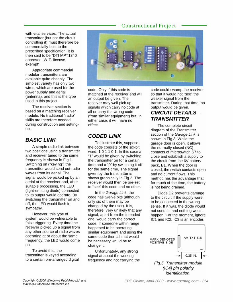
with vital services. The actualtransmitter (but not the circuitcontrolling it) must therefore becommercially-built to theprescribed specification. It isthen said to be “DTI MPT1340approved, W.T. licenseexempt”.
Appropriate commercialmodular transmitters areavailable quite cheaply. Thesimplest variety has only twowires, which are used for thepower supply and aerial(antenna), and this is the typeused in this project.
The receiver section isbased on a matching receivermodule. No traditional “radio”skills are therefore neededduring construction and setting-up.
BASIC LINKA simple radio link between
two positions using a transmitterand receiver tuned to the samefrequency is shown in Fig.1.Switching on (“keying”) thetransmitter would send out radiowaves from its aerial. Thesignal would be picked up by anaerial at the receiver and, aftersuitable processing, the LED(light-emitting diode) connectedto its output would operate. Byswitching the transmitter on andoff, the LED would flash insympathy.
However, this type ofsystem would be vulnerable tofalse triggering. Every time thereceiver picked up a signal fromany other source of radio wavesoperating at or about the samefrequency, the LED would comeon.
To avoid this, thetransmitter is keyed accordingto a certain pre-arranged digital
Constructional Project
code. Only if this code ismatched at the receiver end willan output be given. Thereceiver may well pick upsignals which carry no code atall or carry the wrong code(from similar equipment) but, ineither case, it will have noeffect.
CODED LINKTo illustrate this, suppose
the code consists of the six-bitword: 1 0 1 1 0 1. In this case a“1” would be given by switchingthe transmitter on for a certaintime and a “0” by switching it offfor the same time. The signalgiven by the transmitter isshown graphically in Fig.2. Thereceiver would then be pre-setto “see” this code and no other.
In the Garage Link, thecode has twelve bits (althoughonly six of them may bechanged by the user). It is,therefore, very unlikely that anysignal, apart from the intendedone, would carry the correctcode. If someone within rangehappened to be operatingsimilar equipment and using thesame code then all that wouldbe necessary would be tochange it.
Unfortunately, any strongsignal at about the workingfrequency and not carrying the
code could swamp the receiverso that it would not “see” theweaker signal from thetransmitter. During that time, nooutput would be given.CIRCUIT DETAILS –TRANSMITTER
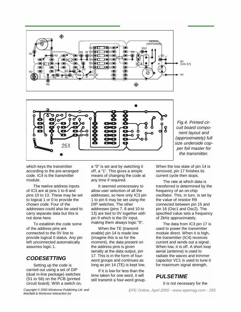
The complete circuitdiagram of the Transmittersection of the Garage Link isshown in Fig.3. While thegarage door is open, it allowsthe normally-closed (NC)contacts of microswitch S7 toclose and establish a supply tothe circuit from the 6V batterypack, B1. When the door isclosed, the switch contacts openand no current flows. Thismethod has the advantage thatfor much of the time, the batteryis not being drained.
Diode D2 prevents damageto the circuit if the supply wereto be connected in the wrongsense. If it was, the diode wouldnot conduct and nothing wouldhappen. For the moment, ignoreIC1 and IC2. IC3 is an encoder,
AM-TX1-418
0.35 IN.
+
MARK DENOTESPOSITIVE SIDE
Fig.5. Transmitter module(IC4) pin polarity
identification.
Copyright © 2000 Wimborne Publishing Ltd andMaxfield & Montrose Interactive Inc
EPE Online, April 2000 - www.epemag.com - 255
which keys the transmitteraccording to the pre-arrangedcode. IC4 is the transmittermodule.
The twelve address inputsof IC3 are at pins 1 to 8 andpins 10 to 13. These may be setto logical 1 or 0 to provide thechosen code. Four of theaddresses could also be used tocarry separate data but this isnot done here.
To establish the code someof the address pins areconnected to the 0V line toprovide logical 0 status. Any pinleft unconnected automaticallyassumes logic 1.
CODESETTINGSetting up the code is
carried out using a set of DIP(dual in-line package) switches(S1 to S6) on the PCB (printedcircuit board). With a switch on,
a “0” is set and by switching itoff, a “1”. This gives a simplemeans of changing the code atany time if required.
It seemed unnecessary toallow user selection of all theaddresses, so here only IC3 pin1 to pin 6 may be set using theDIP switches. The otheraddresses (pins 7, 8 and 10 to13) are tied to 0V together withpin 9 which is the 0V input,making them always logic “0”.
When the TE (transmitenable) pin 14 is made low(imagine this is so for themoment), the data present onthe address pins is givenserially at the data output, pin17. This is in the form of four-word groups and continues aslong as pin 14 (TE) is kept low.
If it is low for less than thetime taken for one word, it willstill transmit a four-word group.
When the low state of pin 14 isremoved, pin 17 finishes itscurrent cycle then stops.
The rate at which data istransferred is determined by thefrequency of an on-chiposcillator. This, in turn, is set bythe value of resistor R9connected between pin 15 andpin 16 (Osc1 and Osc2). Thespecified value sets a frequencyof 2kHz approximately.
The data from IC3 pin 17 isused to power the transmittermodule direct. When it is high,the transmitter (IC4) receivescurrent and sends out a signal.When low, it is off. A short loopaerial (antenna) is used toradiate the waves and trimmercapacitor VC1 is used to tune itfor maximum signal strength.
PULSETIMEIt is not necessary for the
R8
D1
A
B
R3
C
DELK1
IC3
S1S2S3S4S5S6
++
+
VR1
IC1IC2
R2
R4
R5C1
R6 Rt
R7
R9
C2
R10
IC4VC1 C3
D2R1
AERIAL(ANTENNA)
6V(VIA S7)
0V
Fig.4. Printed cir-cuit board compo-
nent layout and(approximately) fullsize underside cop-per foil master for
the transmitter.

Copyright © 2000 Wimborne Publishing Ltd andMaxfield & Montrose Interactive Inc
EPE Online, April 2000 - www.epemag.com - 256
Transmitter to be providing datacontinuously – in fact, thiswould run down the batterieswithout good reason. IC3 pin 14(transmit enable) only needs tobe pulsed low for sufficient timeto provide the bleeps at theReceiver.
To provide these pulses,IC3 pin 14 is connected viaresistor R8 and test link LK1, tothe output (pin 3) of the astablebased on timer IC2. Acontinuous string of pulses isthen produced.
The frequency and mark/space ratio (that is, how longeach pulse is high comparedwith low) is determined by thevalues of resistors R6 and R7 inconjunction with capacitor C1.With the values specified, onecycle is produced every 42seconds with each “low” taking0����2s but this is subject to a fairlywide tolerance.
Test resistor Rt isconnected in parallel withresistor R6 to begin with. Thissets a much shorter time period(about half a second) so thebuzzer bleeps rapidly. This willbe useful for testing and setting-up purposes. At the end ofsetting up one of Rt end leads iscut to disconnect it from thecircuit.
SEEING THE LIGHTThe light-sensing aspect of
the circuit is based onoperational amplifier (opamp)IC1. This inhibits the action ofthe encoder when the light levelis high enough. The opamp is ofa type which requires very littlequiescent current (10uAapprox.). It therefore hasnegligible effect on the life ofthe batteries.
The non-inverting input (pin3) of IC1 receives a voltageequal to one-half that of thesupply (nominally 3V) due to thepotential divider action ofresistors R3 and R4. Theinverting input (pin 2) isconnected to a further potential
Constructional Project
bc
e
R1100k
C147n
9 8 10 11 12 137
AERIAL(ANTENNA)
OUTDATA
IC1AM-HRR3-418
A.F. VCC
R.F.0VA.F.0V
DATA IN
R.F. VCC
VSS
C247n
14
15
17
16
DATAOUTPUT
IC2HT12F
ADDRESSINPUTS
OSC2
ADDRESSINPUTS
OSC1
18
VDD
S6 6
S5 5
S3
S4
3
4
S2
S1 1
2
C5100�
D11N4001
C3220n
WD13V TO 24V
10mA
TR1ZTX300R2
10k
C4220n
COM.
INOUT IC378L05
FS1250mA
3
1
10
12
15
2 711
14
+
ak
+
TB1/1
TB1/2
9V
0V
++
DATA IN(VT)
5V
Fig.6. Full circuit diagram for the Receiver section of the Garage Link. The designation “VT” atIC2 pin 17 means Valid Transmission.
PIN NO.
1
2
3
4,5,6
7
8,9
10
11
12
13
14
15
FUNCTION
R.F. VCCR.F. GND
ANTENNA
NOT CONNECTED
NOT CONNECTED
R.F. GND
A.F. VCC
A.F. VCC
A.F. GND
TEST POINT
DATA OUTPUT
A.F. VCC
13.7mm
38.1mm
1.27mm
P.C.B. HOLES ON 0.1 INCH PITCH
AM-HRR3-418
1 2 3 7 10 15
2mm
*
*
NOT USED
Fig.7. Receiver module pinlayout and function details.

Copyright © 2000 Wimborne Publishing Ltd andMaxfield & Montrose Interactive Inc
EPE Online, April 2000 - www.epemag.com - 257
divider. Its top arm consists offixed resistor R1 connected inseries with preset potentiometerVR1. The lower arm is light-dependent resistor (LDR) R2.
When the LDR is brightlyilluminated, its resistance will belower than the R1/VR1combination and the voltage atpin 2 will be less than 3V – thatis, less than that at pin 3. Withthe opamp non-inverting inputvoltage exceeding the invertingone, the output at pin 6 will behigh.
This state is transferredthrough diode D1 to IC3 pin 14.Whatever the state of IC2output, IC3 “transmit enable” pinwill be made high so operationis inhibited.
FAILING LIGHTAs the light level falls, the
resistance of the LDR increasesand at some point will exceedthat of the R1/VR1 combination.The voltage at the invertinginput will then exceed 3V – thatis, greater than that at the non-inverting one. The opamp will
switch off and pin 6 will go low.This state is blocked by diodeD1 so it has no effect on theencoder (IC3) which is nowcontrolled by the astable (IC2)alone.
The exact light level atwhich the transition occurs isdetermined by the adjustment ofpreset VR1. Resistor R5, whichis connected between IC1 non-inverting input and the output,introduces a small amount ofpositive feedback and ensures asharp switching action at thecritical light level.
While actually transmittingdata the circuit requires some2mA, but between pulses theprototype used less than 95uA.Due to the short pulse length,the average current is verysmall. Remembering that whenthe garage door is closed thereis no current drain at all, theoverall current needed by theTransmitter is even less.
CONSTRUCTION –TRANSMITTER
Important Note: Thedesign of the aerial is specifiedby UK regulations. There aretwo configurations possible but,of these, a tuned loop is usedhere. The enclosed area mustnot exceed 700 square mm andit must be integral within the unit– it cannot be placed externallyand driven through a feeder.Radio amateurs please note:this transmitter is not typeapproved for use with a quarterwave or helical antenna .
All components for theTransmitter (apart from thebattery pack) are mounted on asingle-sided printed circuitboard (PCB). The topsidecomponent layout and(approximately) full sizeunderside copper foil trackmaster are shown in Fig. 4. Thisboard is available from the EPEOnline Store (code 7000261) atwww.epemag.com
Begin construction bydrilling the two fixing holes andsoldering the IC sockets, DIPswitches S1 to S6, and the twolink wires in position. One ofthese is soldered between
Constructional Project
WD1
IC1IC2
IC3C2
C3C4
C5
D1 FS1
TB1
1
2
ak
e
b
c
TR1
C1
R1
S1S2
S3S4
S5
S6
+
+
+
INCOM
OUT
R21
7
15
10
9V
OV
AERIAL(ANTENNA) 262
Fig.8. Printed circuit board component layout and (approximately) full size copper foil track mas-ter for the Receiver.

Copyright © 2000 Wimborne Publishing Ltd andMaxfield & Montrose Interactive Inc
EPE Online, April 2000 - www.epemag.com - 258
points A and B. The other is thetest link (LK1 – C-D-E). Thewire should be soldered asshown between C and D fornormal operation.
Next, the resistors,capacitors and diodes (takingcare with the polarity ofcapacitors C1, C3 and thediodes) can be mounted andsoldered in position. If a 1����5M�resistor is not available for R9,connect one 1M� and one470k� in series.
In the prototype, resistor R5(66M�) consisted of two 33M�units connected in series tomake up the value. You coulduse a single resistor having avalue of between 56M� and100M� if this is available.
Cut the LDR (R2) leads to alength of about 15mm andsolder it in place. Bend theleads through right angles sothat the “window” points to theside (see photograph). Solderthe positive (red) and negative(black) wires of the PP3-typebattery connector to the “+6V”(via switch S7) and “0V” pointsrespectively on the PCB.
LOOP AERIALThe prototype aerial was
made using a piece of light-dutysingle-core insulated wire cut toa length of 80mm. The end1mm or so was stripped and thewire bent into a loop. It was thensoldered into the “aerial”
position on the PCB.
TRANSMITTERMODULE
Before unpacking thetransmitter module, remove any
closely at it while rotating thetop screw). This gives theminimum capacitance of 2pF,which worked well in theprototype.
RECEIVER
Constructional Project
The lever-arm microswitchmounted on a small metalbracket.
Garage door closed – mi-croswitch arm compressed,
power off!
Garage door open – mi-croswitch arm released,
power on!static charge that might exist onthe body by touching somethingwhich is “earthed” such as ametal water tap. This is becauseit is a static-sensitive deviceand such charge could damageit.
Cut its leads to a length of15mm and solder it in place onthe PCB, using minimum heatfrom the soldering iron. Takecare over the polarity – thepositive end is identified by ablack mark on the body.
Taking the same anti-staticprecautions, unpack IC2 andIC3. Insert them in their socketstaking care over the orientation.By leaving IC1 position emptyfor the moment, the light-sensing aspect of the circuit willbe disabled and this will simplifytesting.
Adjust trimmer capacitorVC1 so that the plates are notmeshed or only slightly so (look
The complete circuitdiagram of the Receiver sectionof the Garage Link is shown inFig.6. The receiver module IC1requires a 4����5V to 5����5V supply.
The total currentrequirement of the circuit is5mA approximately, whichcould not be maintained by abattery over a long period ofoperation. This is why a mainspower adapter (sometimesreferred to as a batteryeliminator) is called for.
The power adapter suppliesa nominal 9V to the input ofvoltage regulator IC3, via fuseFS1 and diode D1. The outputof IC3 provides the 5V neededby the receiver module, and thisis also used by the rest of thecircuit. Fuse FS1 preventspossible damage in the event ofa short-circuit.
Diode D1 prevents damageif the supply were to be

Copyright © 2000 Wimborne Publishing Ltd andMaxfield & Montrose Interactive Inc
EPE Online, April 2000 - www.epemag.com - 259
connected the wrong way round.This is a possibility where plug-in power supply adapters areused, because the outputpolarity is sometimes uncertain.If the supply was reversed, D1would not conduct and nothingwould happen.
The receiver module is inthe form of a single-in-linepackage – that is, it has onlyone row of pins. Not all the pinsare present and gaps are leftwhere they would have been.The numbering takes intoaccount those which are presentas well as those which are notso, although there are 15numbered “pins”, only 10 ofthem actually exist. The pinlayout and designations areshown in Fig.7.
There are separate pins forthe positive supply feed to theRF (radio frequency) and theAF (audio frequency) sections.These are pin 1 and pins 10, 12and 15 respectively. There arealso separate ground (0V)connections for these (pins 2and 7 for RF and pin 11 for AF).
The same power supply isused for both sections, but theyare decoupled separately usingcapacitors C1 and C2. Theaerial is connected to IC1 pin 3(Data In). The amplified dataappears at output pin 14.
DECODINGThe decoder IC2 is, in many
respects, similar to the encoder(IC3) in the Transmitter unit.The receiving code is set up inthe same way using a set of DIPswitches S1 to S6. The non-settable address pins 7, 8 and10 to 13 are fixed with a logicstate of 0, by tying them to the0Vline. Pin 9 is connected alongwith these because it is the 0Vinput. Data is applied to pin 14(Data In) from the receiver
module output, pin 14.Resistor R1 connected
between pin 15 and pin 16(Osc1 and Osc2) sets thedecoder oscillator frequency.This needs to be approximatelyfifty times higher than that usedin the transmitter section andthe specified resistor sets it at100kHz approximately.
When correct data arrivesat IC2 pin 14, pin 17 (ValidTransmission) goes high.Current then flows, via theresistor R2, into the base (b) oftransistor TR1 and the buzzerWD1 in the collector (c) circuitoperates. Since data is receivedin short bursts as determined bythe Transmitter output, thebuzzer will sound with regularbleeps.
CONSTRUCTION –RECEIVER
All components for theReceiver (apart from the supplyinput socket) are also mountedon a single-sided printed circuitboard (PCB). The topsidecomponent layout and full sizeunderside copper foil trackmaster are shown in Fig.8. Thisboard is available from the EPEOnline Store (code 7000262) atwww.epemag.com
Begin construction bydrilling the two fixing holes thensolder the terminal block TB1,link wire, IC sockets, and DIPswitches S1 to S6 in position.Use pieces of single in-line(SIL) socket for receiver moduleIC1 – do not solder this ICdirectly onto the board. Youcould make these by cutting upa dual-in-line socket.
Solder all resistors andcapacitors in position takingcare over the orientation ofelectrolytic capacitor C5. Addfuse FS1. In the prototype this
was the PCB-mounting type;this is convenient because it willprobably never blow.
Follow with diode D1,transistor TR1, regulator IC3and buzzer WD1, again, takingcare over their orientation. Notethat the flat face of the regulatoris downwards and that of thetransistor to the right. Someregulators have a different pinarrangement so check this pointif necessary.PRELIMINARYSET-UP
Attach a PP3-type batteryconnector to terminal blockTB1, taking care over thepolarity. A 9V battery will beused for testing but it will bereplaced with the plug-in, mainsadapter, power supply at theend.
Solder a piece of light-dutystranded wire 18cm long to the“aerial” point. This correspondsto one-quarter of a wavelengthapproximately. Note that, unlikethe Transmitter aerial, this couldbe placed outside the case. Youcould even use a shorttelescopic aerial, if you wish.
Observing the anti-staticprecautions again, insert IC2and the receiver module, IC1,into their sockets. IC1 will onlyfit one way – that is, with thecomponents side facing IC2.Take great care when insertingit. If too much force is used, thepins will bend and possiblydamage it. Note also that thepins are fairly long and will notpush fully “home”.
PRELIMINARYTESTS
Decide on a code for thetwo units. It does not matterwhat it is, but the DIP switches(S1 to S6) in each unit must beset in exactly the same way.
Constructional Project
Copyright © 2000 Wimborne Publishing Ltd andMaxfield & Montrose Interactive Inc
EPE Online, April 2000 - www.epemag.com - 260
Connect a PP3 battery tothe Receiver and pull out theaerial into a straight line. Placethe two units approximately 2m(6ft approx.) apart. Insert thecells into the Transmitter batteryholder and connect it up. Notethat the maximum voltage to beused with the Transmitter is 6V– more than that will damage it.
With luck, the buzzer willbegin sounding with rapidbleeps! Remember, resistor Rtis in the circuit and the timeperiod has been reduced fortesting.
If it fails to work, change thealignment of the transmitteraerial. Try moving the unitscloser together to see if thatimproves matters. Experimentwith the adjustment of capacitorVC1. If it still doesn’t work,check that the code switches ineach unit are definitely set inthe same way. A faulty solderedjoint at a DIP switch in eitherunit could set the wrong codeand prevent the system fromworking.
AT FAULTIf there is still a fault, it is
more likely to be in theTransmitter, because this hastwo distinct sections. These arethe encoder and transmitter onone hand and the light sensor(but this part has beentemporarily disabled) andastable on the other. If there isa persistent fault, you could tryisolating it to one of thesesections.
First, remove the ICsobserving the anti-staticprecautions mentioned earlier.Now, change the connection ofthe “test link” LK1 on the PCBso that C connects to E. Thistakes IC3 pin 14 to 0V andallows the Transmitter to senddata continuously. If it now
works, check the earlier stages.If nothing happens, it is morelikely that the fault lies in theReceiver. Assuming the twounits are operating over a shortrange, try increasing it. Movethem to the point where thebuzzer operates intermittently orin a “chirping” way due toperiods which lack proper data.Adjust VC1 using a plastictrimming tool (a metalscrewdriver blade will affectoperation) to tune theTransmitter aerial for the bestsignal. Increase the range to 10meters and make furtheradjustments as necessary.Experiment with the orientationof the aerials.LIGHT WORK
To check the light-sensingstage (IC1), first disconnect theTransmitter battery. Observingthe anti-static precautions,insert IC1 taking care over theorientation. Adjust preset VR1fully anti-clockwise (this meansit does not have to be very darkto operate and simplifiestesting).
Re-connect the battery andtest the system. With sufficientlight reaching the LDR (R2)sensitive surface, the buzzershould stop sounding. When theLDR is covered, it should beginagain. If this does not work, trycovering the LDR morecarefully – perhaps sufficientlight is still reaching it. Coverthe LDR with black opaque PVCtape so that the transmitterworks continuously again.
ON TRIALWith the aid of an assistant,
hold the two units in various trialpositions to find the best ones.As with any very low-powerradio equipment, there will begood and bad spots. Check withthe car in the garage. The
orientation of the Transmitterloop is important. Set this andthe Receiver aerial for besteffect.
Do not use metal boxes tohouse the units – only plasticones. Metal boxes would screenthe circuits and prevent radiowaves passing in or out!
FINAL ASSEMBLY –TRANSMITTER
Place the Transmitter PCBand battery holder on thebottom of the box in theircorrect positions. Whendeciding on the orientation ofthe PCB take account of thedirection from which the LDRwill receive light. Ideally, itshould end up pointing towardsthe garage door so that whenthis is open, it will receive“outside” light. Alternatively, tryto direct it towards a window.
Mark through the fixingholes, remove everything againand drill them through. Holdingthe PCB in place, a smalldistance above the base of thebox, mark the LDR position.Measure the position of presetVR1 and mark the lid directlyabove it. Remove the PCB anddrill these holes.
The one for the LDR shouldbe about the same diameter asits window. The hole for VR1should be large enough to allowit to be adjusted from theoutside using a smallscrewdriver or trimming tool.Drill a hole near the right-handside of the PCB for the wiresleading through from the garagedoor switch.
Before attaching the PCB,drill two holes in the back of thebox clear of all internalcomponents. These will be usedfor attaching the unit to the walllater. Secure the PCB using
Constructional Project

Copyright © 2000 Wimborne Publishing Ltd andMaxfield & Montrose Interactive Inc
EPE Online, April 2000 - www.epemag.com - 261
plastic washers on the boltshanks. The LDR leads shouldbe bent so that the window liesa few millimeters behind thehole drilled for it. Secure thebattery holder using adhesivefixing pads or a small bracket.
– RECEIVERDisconnect the battery and
remove the connector from theterminal block TB1. Place theReceiver PCB on the bottom ofits box and mark through thefixing holes. Take it out and drillthese through. Measure theposition of the buzzer and drill ahole in the lid larger than that inthe buzzer itself for the sound topass through.
Check the type of connectorfitted to the mains adapterpower supply unit. Drill a hole inthe side for a socket of thesame type and attach it. Drilltwo holes in the back of the box(clear of the PCB) to attach it tothe wall later. Secure the PCBusing plastic washers on thebolt shanks.
Solder two pieces ofconnecting wire to the powersocket. Take care that thecorrect tags are used. Checkthe polarity of the power supplyunit output and connect thewires to terminal block TB1observing the correct polarity.
If you are unsure about this,do not worry. If the receiverdoes not work at the end it willbe simply a matter of reversing
these wires. If you are using apower supply unit with anadjustable output, you may findthat the “6V” setting actuallyprovides over 9V when usedunder the low-load conditions ofthis circuit.
Attach the Transmitter andReceiver units in their finalpositions.
SWITCHED ONDecide on the switching
arrangement for switch (S7) atthe garage door. In theprototype, a lever-armmicroswitch was used. This wasattached to a small aluminumbracket (see photograph) whichwas, in turn, secured to thedoorframe. The microswitch hada large paddle-style lever, whichallowed for some tolerance infitting, although any type couldprobably be used.
The switch should beoperated by some part of thedoor mechanism, which movesrelatively slowly when the dooris operated. This will avoidheavy jarring as the doorcloses.
Hold the switch assembly inposition and check that thelever will be pressed to the pointwhere the switch clicks as thedoor reaches its closed position.Check carefully that this doesnot interfere with normaloperation of the door.
Attach the switch and makeany adjustments as necessary.
Make sure the switch lever stillhas some movement left whenthe door is closed so that it isnot placed under any unduestrain.
CONNECTING UPIdentify the switch contacts
that “break” (open) when thedoor is closed (that is, thenormally-closed contacts).There is usually a diagram ofthis on the side of themicroswitch. Using spadereceptacle connectors, attach ashort piece of light-duty twinstranded wire to the appropriatetags. This should be sufficient toreach a small junction box (theburglar alarm type is ideal)attached near the doorframe.
Referring to Fig.9, completethe external wiring. Any light-duty twin stranded wire will besuitable. You will need to placea 2-way piece of screw terminalblock TB2 inside the transmittercase.
Cut the red batteryconnector wire and connect itsfree ends to the terminal block.Connect the switch wires to theblock, via the junction box, asshown. If two switches are usedfor two doors, connect them inparallel.
Connect the power supplyunit to the Receiver and test thewhole system. If it fails to work,reverse the polarity of the powersupply wires.
The Receiver aerial wirecould be either routed aroundthe inside of the case (makesure the end is insulated so thatit cannot make metallic contactwith any internal components.Alternatively, it can be allowedto hang outside through a smallhole.
LIGHTING-UP TIME
Constructional Project
TRANSMITTERP.C.B.
6V0V
6VBATTERY
PACK
TB2
TERMINALBLOCK JUNCTION
BOX
LIGHT-DUTYTWIN WIRE
DOOR-OPERATEDMICROSWITCH
++
Fig.9. Interwiring between the Transmitter and remote door-operated microswitch.

Copyright © 2000 Wimborne Publishing Ltd andMaxfield & Montrose Interactive Inc
EPE Online, April 2000 - www.epemag.com - 262
It is now time to remove thetape from the LDR in theTransmitter so that the light-sensing part operates. Wait untilit is dark enough and, with thelid in place and the garage dooropen, adjust preset VR1 so thatthe system just responds at thispoint.
You will find that the lightlevel at which the unit starts tooperate (going dark) is not quitethe same as that at which itstops operating (going light).This is due to the effect offeedback resistor R5 in theTransmitter. If the effect is toopronounced, increase its valueor remove it.
You may find that the LDR“sees” the garage light whenthis is switched on. Of course,this would hold the buzzer off.This would probably be anadvantage because if someone
was working in the garage atnight with the door open, thebuzzer would not sound.
If you want it to operateunder these circumstances,shield the LDR so that thegarage light does not reach it.Bending its leads so that it liesfurther behind the hole anddirecting the unit more carefullyat the source of “outside” lightwill also help.
Remove the Transmitter lidand cut through one of the leadsof test resistor, Rt. Move the cutends apart to prevent them fromtouching. The buzzer shouldnow give a short bleep every 45seconds approximately.ON APPROVAL
Before putting the systeminto permanent service, it isimportant to display a mark onthe transmitter stating that it
conforms to DTI SpecificationMPT1340. This must state thewording “MPT1340 W.T.License Exempt”. The size mustnot be less than 10mm x 15mmand the figure height must notbe less than 2mm.
Constructional Project

Copyright © 2000 Wimborne Publishing Ltd andMaxfield & Montrose Interactive Inc
EPE Online, April 2000 - www.epemag.com - 263
It is astonishing whatopportunities are continuing to berevealed for the recentlyintroduced PIC16F87x series ofmicrocontrollers. This Micro-PICscope is a prime example of adesign idea whoseimplementation was greatlysimplified by using one of thesedevices.
The Micro-PICscope is ahandy little item of test gear andof benefit to anyone’s workshop.Using an alphanumeric liquidcrystal display (LCD), it isbasically a signal tracer, but onewith the great advantage that itshows a representation of thesignal waveform that is beingtraced. This is shown across eightof the LCD character cells and isa real-time trace of the monitoredwaveform.
Not only that, the display alsoshows the frequency of the signalbeing monitored, and its peak-to-peak voltage. The frequencyrange covered is basically for
www.epemag.com, Ed.)He had already designed
and published a similar purposeunit based on multiplexed LED(light emitting diode) displays. Inthat unit (PE June ’92), anLM3914 bargraph IC was usedin conjunction with shift registersand digital multiplexers toportray a waveform across four5 x 7 bit matrixed LEDs. It wasvery effective, althoughsomewhat power hungry.
At the time though,microcontrollers were anunknown to the author and amethod by which an LCD screencould be similarly used eludedhim. Whereas LED matricesrequire only logic control,alphanumeric displays require avariety of data commands to beprovided under program control.
For some simple operationsLCD commands can begenerated using codes pre-programmed into an EPROM(electrically programmable readonly memory). This techniquehad already been successfullyused by the author in a real-timeMorse Code Decoder (EE Jan’87), but did not lend itself tocircuit board signal tracing andmonitoring.
The introduction of theversatile PIC16x84microcontroller re-sparkedinterest in the idea, and it couldhave been done using that PICwith a separate analogue-to-digital converter (ADC). Thenalong comes the PIC16F87xfamily – with built-in ADC. Bingo,the idea was now as good as
Visual signal monitoring with frills!
MICRO PICSCOPE by JOHN BECKER
audio, but frequencies well toeither side of this range can betraced.
Several ranges of controlare offered by switch selection,covering the sampling rate, andsynchronization on/off for the‘scope display. The signal inputis switchable to provide differentmaximum peak voltagemonitoring ranges. Selection ofAC or DC input is provided.
The entire design requiresonly two ICs, a PIC micro andan opamp, plus a 2-line by 16-character LCD. An optional thirdIC provides power regulation ifrequired.
A typical example of theLCD screen display is shownbelow.
DESIGN HISTORYSome 12 or more years
ago, when the author firstbecame familiar with “intelligent”alphanumeric LCDs, it became
apparent that byusing the internalprogrammablecharacter generator,their screens mightbe capable ofdisplaying a simplerepresentation of asignal beingmonitored. (There isa GREAT article onthese displays in theEPE Online Libraryat
Example of the screen display obtainableon the LCD module.

Copyright © 2000 Wimborne Publishing Ltd andMaxfield & Montrose Interactive Inc
EPE Online, April 2000 - www.epemag.com - 264
constructed to full workshopworking order as a single chipdesign – apart from writing thecommand program, of course!
CIRCUIT DETAILSIn fact, as you will see from
the complete circuit diagram forthe Micro-PICscope in Fig.1, thepractical implementation of theidea has been expanded a bit touse more than just amicrocontroller (IC2). A bufferingand gain setting opamp (IC1a)has been included as well. Sotoo has a 5V regulator (IC3),allowing the unit to be poweredfrom 9V or 12V supplies. If youhave an existing well-stabilized5V supply, IC3 may be omitted.
The signal being monitoredis brought into opamp IC1a. Asset by resistors R1 to R3, the
gain can be selected by switchS1 to be x1 (unity – via R2) orx10 (via R1). Other gain-settingvalues could be chosen instead.For example, a 10k� resistorcould be used for R3 instead ofa 100k�. This would provideswitchable gains of unity and
1/10.Switch S2 provides selection
of AC or DC signal coupling,switching capacitor C1 in and outof circuit. The output from IC1 tothe microcontroller is DC coupled.You will spot that the opamp is
Constructional Project
Completed Micro-PICscope showinggeneral layout of display and controls.
B19V C6
22µ
C110µ
C222µ
C5100n
S6
+VE
D4
D5
D6
D7
RS
E
0V
R61k
R410k
R510k
C7100n
X15MHz
a k
D11N4148
C310p
C410p
+
+
IC378L05
IN OUT
COM
IC1a
IC1b
2
6
3
5
8
4
1
7
+5V
R710k
VR110k
2
3
4
5
6
7
9
10
7
8
9
10
11
12
13
14
4
6
5
21
22
23
24
25
26
27
28
11
12
13
14
15
16
17
18
IC2PIC16F876-20P
X2LCDMODULE
RA0/AN0
RA1/AN1
RA2/AN2/V –
RA3/AN3/V +
RA4/TOCKI
RA5/AN4/SS
OSC1/CLKIN
OSC2/CLKOUT
REF
REF
D0
D1
D2
D3
D4
D5
D6
D7
RS
E
R/W
INT/RB0
RB1
RB2
PGM/RB3D
RB4
RB5
PGCLK/RB6
PGDA/RB7
T1OSO/TICK1/RC0
T1OSI/CCP2/RC1
CCP1/RC2
SCK/SCL/RC3
SDI/SDA/RC4
SDO/RC5
TX/CK/RC6
RX/DT/RC7
+VE
+VE
GND GND
GND
2
1 3
S3
S4
S5
ADC RATE
CONTRAST
SYNC
FREQ
X1
X10
AC/DC
ON/OFF
*
**
R3100k*
*
*
*
*
*
CX
R2100k
R110k
S1
S2
SEE TEXT
IC1 MAX492
TB2
0VVPP DATA
CLK
PROGRAMMER
SK1
N.C.
N.C.
N.C.
MCLR1
8 19
20
TB1
CX
Fig.1. Complete circuit diagram for the Micro-PICscope. The voltage regulator IC3is optional – see text.

Copyright © 2000 Wimborne Publishing Ltd andMaxfield & Montrose Interactive Inc
EPE Online, April 2000 - www.epemag.com - 265
used in inversion configuration.Software ensures that the signalis seen the “right way up”!
A MAX492 dual opamp isused for IC1, with the secondhalf ignored. This device is partof the author’s stock “library”and has proved itself for itsnearly rail-to-rail output swing.The circuit has also been usedwith a TL082 device, whichprovides good frequency range,although does not offer full rail-to-rail output (typically more like4V swing for a 5V split supply asused here – split by resistors R4and R5).
MICROCONTROLLERMicrocontroller IC2 is a
PIC16F876 device, operated ata clock rate of 5MHz, as set bycrystal X1. Because of this clockrate, the 20MHz version of thePIC should be used. The“standard” version has amaximum guaranteed clock ratelimit of 4MHz. However, youmay find it interesting to notethat the author has successfullyused the 4MHz version at rateswell in excess of 5MHz.
The PIC16F87x family hasbeen discussed at length inprevious issues of EPE and the’876 will not be described indetail here. Suffice to say that ithas three input/output (I/O)ports, one of which, PORTA,can be used for analog-to-digitalconversion via five of its pins(RA0 to RA3, plus RA5). In thisdesign, only RA0 (pin 2) is used,its input being taken directlyfrom the output of opamp IC1aat pin 1.
Internally, the PIC isprogrammed by the software sothat the voltage reference for theADC is taken as 0V to 5V (thepower line voltage range).Consequently, an A-Dconversion value of 255 results
when the input to RA0 is at thepositive supply line level of 5V. Aresult of zero occurs when theRA0 input is at 0V.
Output to the LCD (X2) is viaPORTB, using lines RB0 to RB5to control the display inconventional 4-bit mode.Connections to the LCD are viathe terminal pin block TB1. Theorder of the pins, both physicallyon the printed circuit board (PCB)and in terms of program control,is identical to that used by theauthor in many of his recentlypublished designs. Displaycontrast of the LCD screen is setby preset VR1.
EXTERNAL CONTROLExternal control of the PIC’s
monitoring and timing functions isactioned via PORTC, through pinsRC0 to RC2. The functionscontrolled are the ADC samplingrate (via S3), waveformsynchronization on/off (S4), andfrequency counter display on/off(S5). These will be discussedlater.
Pins RB6 and RB7, whilst notactively used by the design itself,can be used to program the PICvia a suitable programmer, suchas PIC Toolkit Mk2 (May-June‘99). The MCLR pin (master reset)is normally powered at 4����3V (5V –0����7V) via diode D1 and bufferingresistor R6. This allowsprogramming voltage controlwithout disturbing the normal 5Vsupply rail from voltage regulatorIC3.
Terminal pin block TB2provides access to MCLR, RB6,RB7 and the 0V common line.The pin order on the PCB is thealso same as that used by theauthor in previous designs. Thiswill be welcomed by those whohave established a plug-in linkbetween Toolkit Mk2 and suchdesigns! (The author intends for
all his future PIC designs to usethis same pin configuration forLCD and programmingconnections.)
CONSTRUCTIONDetails of the PCB
component and track layoutsare shown in Fig.2. This board isavailable from the EPE OnlineStore (code 7000259) atwww.epemag.com
Regular readers will knowthis author’s preferredconstructional order: wire links,resistors, diodes, smallcapacitors, IC sockets and thenon upwards in order ofcomponent size.
Dual-in-line sockets shouldbe used for IC1 and IC2. Notethat microcontroller IC2 is thenarrow version (0����3in widthbetween pin rows, as opposedto 0����6in).
Details of the switch andsignal input connections are alsoshown in Fig.2. Socket SK1 maybe a different type to that shownif preferred.
The LCD module mighthave one of two possible pinconnection arrangements. Theyare shown in Fig.3.
As always, do a thoroughcheck of the componentpositioning, orientation andsolder joint integrity beforeapplying power. Do not insertIC1, IC2 or the LCD until theoutput from regulator IC3 hasbeen validated, exactly 5V(within a few millivolts) for asupply between 7V and 12V.
An output voltage from IC3other than 5V will usuallyindicate a fault in construction –too high and IC3 is wronglyinserted, too low and there maybe a short circuit somewhere onthe board.FIRST RUN
Constructional Project

Copyright © 2000 Wimborne Publishing Ltd andMaxfield & Montrose Interactive Inc
EPE Online, April 2000 - www.epemag.com - 266
When happy about thepower supply, test the circuitwith IC1, IC2 and the LCDplugged in (correctly!). Setswitch S4 (Sync) off and S5(Frequency) on. When power isapplied, the PIC first goes intoan LCD initialization routine, inwhich it sets the LCD for 2-line4-bit mode.
Following this, textmessages similar to those in thephotographs should appear. Thesignal trace display in the top leftLCD character cells shouldshow as a straight line abouthalf way up the screen. Adjustpreset VR1 to set the screencontrast (you may see nothing atall until you have adjusted it).
Having read the sections allabout the control program, youcan then feed in an audio signal,play with the switches, and seethe results on screen. The inputsignal amplitude should beselected so that the majority ofthe LCD vertical pixel range isused.
ENCLOSUREA small plastic box was
used to house the prototype.The PCB has been designed sothat the LCD can be mountedabove it using stand-off pillars,although the prototype did notuse this option.
The rectangular viewing slotwas cut by first drilling smallperimeter holes and using a fileto smooth the edges to shapeand size. Holes must also bedrilled to suit the switches andinput socket. The prototypeused a 3����5mm jack socket forthe power input, but othertechniques, such as a batteryconnector, can be used.
A-TO-DCONVERSION
Constructional Project
C4
C7
C5
C3
k
aD1
++
+
R2
R6
R7
R1
C2
C1
C6
R4
R3
R5
MCLRDATA RB7CLK RB6
0V
ERSD7D6D5D4
CXVE
0V0V
+
VR1
X1
IC3IN
COM
OUT
AC/DC
FREQ SYNC
X1
S6
X10
S2
S1
S3
S5 S4
S1
SK1
0VBATTERY
+9V
POWERON/OFF
TB1
Fig.2. Printed circuit board component layout, wiring to theoff-board components and (approximately) full-size copper
foil master for the Micro-PICscope.

Copyright © 2000 Wimborne Publishing Ltd andMaxfield & Montrose Interactive Inc
EPE Online, April 2000 - www.epemag.com - 267
Basic A-to-D conversionusing a PIC was discussed inthe Mini PIC16F87x Tutorial ofOct ’99. A simplified version ofthe routine described there isused here:
In the START routine whilein PAGE1, register ADCON1 isset with the binary value of%00000101, which tells the PICthat the 2-byte ADC register is tobe justified left, with RA0 as ananalog input referenced to +VEand 0V.
Then, back in PAGE0, byloading register ADCON0 with abinary value of %010000001,ADC conversion is activated atan oscillator rate of one-eighthof the clock rate (Fosc/8).
(Readers who write theirown PIC software should notethat in order for PAGEcommands to be used with theToolkit programmer and thePIC16F87x family, bit RP1 of thePIC’s STATUS register must beset to 0 – as it is in the STARTroutine of the Micro-PICscopesource code.)
A single ADC sample istaken when the command BSFADCON,GO is issued, wherethe quaint GO term (Microchip’sdescription!) refers to bit 2.Sampling and conversion are
not quite instantaneous and theprogram repeatedly polls the GObit until it goes low, signifying anend to the conversion process.There are several subroutineswhich are used in the programto perform this task, one of thembeing:
WAITS1: BTFSCADCON0,GO GOTO WAITS1 MOVF ADRESH,W
When the GO bit is clear,the command MOVFADRESH,W retrieves the highbyte of the 2-byte conversionresult. Because the display isonly eight pixels high, the lowbyte is not needed (see the MiniTutorial, or the PIC16F87x databook, for details of theconversion result formatoptions).
The value held in ADRESH(and now also in W) is thatwhich represents the voltagelevel of the signal beingsampled. It cannot yet, however,be put out to the LCD screen,there’s a great deal of work tobe done first! For the moment,this value is simply stored in oneof a set of temporary memorylocations. The conversion andstorage is performed 128 timesbefore further action is needed.
DISPLAY PRINCIPLEBefore that “further action”
is described, it is first necessaryto understand the conceptbehind the way in which awaveform can be displayed onthe LCD by making use of itscharacter generator.
You already know that theLCD used here has two displaylines each having 16 charactercells. Each of these 32 cellsconsists of a matrix of LCDpixels, arranged as five acrossby eight down (see Fig.4a).
Normally, the LCD moduleplaces pre-programmed (as partof the module’s control chipmanufacturing process)alphanumeric data into thesecells according to commandcodes from an external source,a PIC in this case.
However, the module hasthe facility to allow eightcharacters to be “designed” bythe user and called as well asthe standard alphanumeric set.These characters are stored atmodule address locations 0 to 7.
At first sight, whenexamining the LCD data sheet,it might appear that addresslocations 8 to 15 can also beused to hold custom charactersas well. Regrettably for anapplication such as thisPICscope, addresses 8 to 15only hold repeats of the data ataddresses 0 to 7. Thus onlyeight addresses can be used foralternative character data,hence the PICscope only havingeight cells for waveform display.
Eight cells each having fivepixels horizontally allows 40waveform samples to have theirvalues plotted at eight verticalpixel levels.
The reason that 128samples are taken even thoughonly 40 will be displayed fromeach block is to allow forfrequency and amplitude valuesto be more readily established.
CHARACTERGENERATOR
The way in which data for acharacter cell is evaluated isillustrated in Fig.4b. Each of theseven rows making up the celldisplay are treated individually.The five pixels of each row arenumbered from 4 to 0, allowinga 5-bit binary number to becompiled. Logic 1 in a bit
Constructional Project
Fig.3. Pinout arrangement ofthe two basic LCD formats.

Copyright © 2000 Wimborne Publishing Ltd andMaxfield & Montrose Interactive Inc
EPE Online, April 2000 - www.epemag.com - 268
position turns on the equivalentpixel, while logic 0 turns it off.
Having established whichbits are to be active, the 5-bitbinary number for each row(expanded to 8-bit with zero inbits 7 to 5) is sent to therequired character generatoraddress, of between 0 and 7.The same procedure can beused for the other sevenpossible addresses, each ofthem storing different data, asappropriate.
When character data isbeing generated in this way, theLCD is first told that the dataabout to arrive is destined forthe character generator ratherthan for the screen display. Inthe program the initial commandis given by:
MOVLW %01000000CALL LCDLINBSF RSLINE,4
which sets the charactergenerator to address 0 fromwhich address onwards the
“designed” data is to be stored,the address incrementing eachtime a data byte is written to the
LCD. The LCDLIN call is to oneof several standard routines,which the author wrote someyears ago to send variouscommands and data to an LCDmodule.
For all eight character cellsto be fully programmed, 8 x 8 =64 bytes of data are written tothe character generator.
Once the charactergenerator has beenprogrammed, the data held ateach of the eight address blockscan be called to the screen bysimply accessing that address inthe same way that “normal”alphanumeric data is accessed.
For example, to displayletter “A” on screen you mightuse either MOVLW ’A’, CALLLCDOUT, or MOVLW 65, CALLLCDOUT, the value of 65 beingthe ASCII value for capital letter‘A’. In both cases the characterheld at character generatoraddress decimal 65 would bedisplayed on screen, which,
Constructional Project
Completed unit showing the LCD module mounted on the lid ofthe case and wiring to the PCB.
COMPONENTSResistors
R1, R4, R5, R7 10k (4 off)R2, R3 100k (2 off)R6 1k
All 0.25W 5% carbon film
CapacitorsC1 radial electrolytic, 16VC2, C6 22u radial electrolytic, 25V (2 off)C3, C4 10p ceramic, 5mm pin spacing (2 off)C5, C7 100n ceramic, 5mm pin spacing (2 off)
See also theSHOP TALK Page!
$31Approx. CostGuidance Only
PotentiometerVR1 10k miniature round preset
SemiconductorsD1 1N4148 signal diodeIC1 MAX492 dual opampIC2 PIC16F876-20P microcontroller (20MHz version, 0.3-inch width) preprogrammedIC3 78L05 +5V 100mA voltage regulator (see text)
MiscellaneousS1, S2, S4, S5 miniature s.p.d.t. toggle switches (4 off)S3 miniature push-to-make switchS6 miniature s.p.s.t. (or s.p.d.t.) toggle switchSK1 BNC socket (see text)X1 5MHz crystalX2 2 line x 16 characters per line alphanumeric crystal display
Printed circuit board available fromthe EPE Online Store (code 7000259)www.epemag.com; powere supplyconnector (see text); plastic case,150mm x 80mm x 50mm; 8-pin DILsocket; 28-pin DIL socket; 1mmterminalpins (or strips) for TB1 and TB2; PCBand LCD supports (8 off); connectingwire; cable ties; solder, etc.

Copyright © 2000 Wimborne Publishing Ltd andMaxfield & Montrose Interactive Inc
EPE Online, April 2000 - www.epemag.com - 269
fortunately for us all is indeedthe letter “A”.
Similarly, to show thecharacter newly programmedinto address 3, the commandswould be MOVLW 3, CALLLCDOUT.
The data held at charactergenerator addresses 0 to 7 canbe changed as often asrequired. In this design it istypically changed about twiceper second (faster with S4 andS5 off). All data at theseaddresses is lost when power isswitched off.
WAVEFORMCHARACTERS
When a full block ofsamples has been convertedand stored, the data is thenanalyzed for amplitude andcompiled into 64 bytes forsending to the charactergenerator. Row 8 is the top rowand (naturally) represents thehighest voltage range that canbe displayed. The display is, ofcourse, compressed to one-eighth of the conversion valuereceived.
The analysis procedure isfar more complex than can bedescribed here. It is not just amatter of ascertaining which rowa value should be allocated to.The result also has to be“doctored” so that the activepixels are seen to be as close to
a continuous line as possible.For instance, suppose the
waveform is alternating rapidlybetween high and low levels at arate faster than the samplingcan keep pace with. Withoutcorrective action, you might onlysee pixels on the upper andlower lines, those betweenremaining blank.
The corrective action fills inthose blank pixels so that they
appear as though they naturallyfollow on from each other. Thiswas an extremely difficultprocess to write the program for!Even experienced programmersmight have difficulty analyzingthe way in which the sourcecode has been written – bewarned!
However, you don’t need tounderstand the program in orderto use it. Just load it into your
PIC (or buy a ready-programmed PIC – see later).
Although there is a greatdeal of processing being carriedout, each batch of sampled datais displayed in rapid successionand really does give a “real-time” display of what ishappening in a monitored circuit.
FREQUENCY ANDAMPLITUDE
Each batch of data is alsoanalyzed for waveformfrequency and peak-to-peakamplitude values.
Amplitude is easilydetermined by simply looking forthe maximum and minimumconversion values and thenrelating them to the maximumpossible sample level of 255.The latter, as said earlier,represents the positive line level,which has been assumed to beexactly 5V. If you need greateraccuracy for signal levelvoltages use your multimeter toread them! The PICscope isonly intended for providing anapproximate value (but it’s stillpretty accurate).
Note that the PIC does notmonitor which gain setting hasbeen selected. It simply reportsthe voltage it finds on its RA0pin. You must mentally adjustthe value shown if the gain is
Constructional Project
FIg.3(a). LCD character cell matrix with allpixels on, (b) example of waveform represen-
tation across two character cells.
Close-up of typical screen dis-play. There are three rates,the maximum counting fre-
quency is about 17kHz.

Copyright © 2000 Wimborne Publishing Ltd andMaxfield & Montrose Interactive Inc
EPE Online, April 2000 - www.epemag.com - 270
other than unity.Frequency is assessed by
counting the number of timesthe voltage level crosses apreset threshold value. Theresult is then divided by two toobtain the equivalent number ofcycles per batch, the rate of dataacquisition being pre-determined by the samplingrate, which in turn is relative tothe master clock rate.
Much effort went into writingthe software so that relativetimings were maintainedconsistently, irrespective ofconditional branch timings in thesampling routines.
There are three rates atwhich the ADC can be set tosample waveforms, selectableby pressing switch S3. The ratescycle as a repeating group ofthree, numbered from 0 to 2.The number of the selected rateis shown at the top right of thescreen. It is not a representationof the frequency range covered.
The rates are set accordingto the value by which the masterclock oscillator is divided via theADCON0 prescaler. This valueis set by bits 6 and 7 in theADCON0 register. Rate 0 setsFosc/2, rate 1 sets Fosc/8, rate2 sets Fosc/32. The routinewhich reads S3 and sets the bitscommences at label TESTIT,following on into GETRATE,near the end of the source codelisting.
FREQUENCYCALCULATION
Relating the ADCON0sample rate to the actualfrequency of the signal has totake into account the time takenfor all the commands in thesampling routine to beperformed. As experiencedprogrammers will acknowledge,such matters are not always
readily calculated (friend andEPE author Andy Flind hasresearched heavily into this – wehope he’ll one day share it withus all!).
The solution here was tocount the swings above andbelow the threshold level andthen divide the answer by aconversion factor, with aseparate factor for each of thethree sampling rates.
Using a subtractivetechnique, the conversioninvolves fractions, which arefixed in the software as two-bytebinary numbers.
For example, for Rate 0, theMSB is set at decimal 85 andthe LSB at 70, which has anequivalent decimal value of21830 (256 x 85 + 70). Fromthis value is repeatedlysubtracted the count valuedetermined when counting theswing changes, each successfulsubtraction incrementing acounter. Thus the cycle count isdivided into the conversionfactor, the secondary counterproviding the answer. The resultis remarkably accurate. (MSBand LSB, incidentally, mean
Most and Least SignificantBytes, respectively.)
During prototype testing, theunit was fed with a frequency of4000Hz and the “fraction” valuesrepeatedly adjusted by trial anderror until the LCD also showeda value of 4000Hz.
Having established thevalues for the three ranges, theinput frequency was raised tosee how far accuracy wasmaintained, the results were:
Rate Generator Display0 17007Hz 16984Hz1 17007Hz 16998Hz2 5827Hz 5812Hz
Beyond those frequencies,the unit began to displayharmonic frequency valuesbecause the generator rateexceeded the rate at which thewaveform could be sampled.
The values programmedinto the unit depend, of course,on the exact frequency at whichthe crystal controlled oscillatorfunctions. However, crystalcontrolled oscillators, while notbeing perfectly tuned to a givenfrequency, do stick closely to it.
Constructional Project
Completed circuit board mounted on self-adhesiveplastic stand-off pillars.

Copyright © 2000 Wimborne Publishing Ltd andMaxfield & Montrose Interactive Inc
EPE Online, April 2000 - www.epemag.com - 271
Consequently, other unitsshould achieve results that arenot too different from theauthor’s.
Those who which toexperiment are referred to thesub-routines at GETFREQ0,GETFREQ1 and GETFREQ2,where the preset values can bechanged. The program willnaturally need to be re-assembled and reprogrammedinto the PIC.
Analysis of the peak-to-peakand frequency values can beswitched off using S5. Thisspeeds up the rate at which thescreen is fed with a freshwaveform display.
SYNCHRONISATIONSwitch S4 turns the
waveform synchronizationfacility on and off. Whensynchronization is on, beforeeach sampling batch is startedthe software waits until thewaveform voltage has twicepassed through a preset triggerlevel. Only then does it startsampling the rest of that batch.
This facility allows thewaveform display to start abouthalf-way up the screen,providing a degree of stability to
a repetitive waveform.Inevitably, the process increasesthe wait period before each newdisplay is shown. There is atime-out counter, which preventsthe system from “locking-up”should the waveform not crossthe sync thresholds.
It is best to start offsampling any new signal withsync off, only turning it on onceadequate signal levels are beingreceived. The source routines,which control sync start at labelWAITS1. The full batchsampling routine commences atWAITAD0.
IN THE PIPELINEThat, in a nutshell, is really
all there is to tell about thisastonishingly simple signalmonitor (simple in hardwareterms – but certainly notregarding software writing!).Designing it has fulfilled one ofthe author’s ambitions. Softwareis in TASM.
Another yet to be fulfilled isto design a more advanced LCDbased scope, which will give fargreater resolution to thewaveform shapes displayed.Such a design, though will haveto wait until the exorbitant cost
of LCD graphics displays comesdown greatly!
What is in the pipeline,however, is the Virtual PICscopein which one of the PIC16F87xfamily is used to sample twowaveforms simultaneously andoutput the data to a PCcomputer for display on itsscreen.
Finally, if you have anyideas for PIC-based workshopdesigns (or any other type ofdesign, of any sort), please letus know.
Constructional Project

Copyright © 2000 Wimborne Publishing Ltd andMaxfield & Montrose Interactive Inc
This interactive presentation uses the speciallydeveloped Virtual PIC simulator to show exactlywhat is happening as you run, or step through,a program. In this way, the CD brings the EPEPIC Tutorial series to life and provides theeasiest and best-ever introduction to thissubject.
Nearly 40 tutorials cover almost every aspectof PIC programming in an easy-to-followsequence.
HARDWARE: Whilst the CD-ROM can be used on its own, thephysical demonstration provided by the PICtutor development Kit,plus the ability to program and test your own PIC16x84s, reallyreinforces the lessons learned. The hardware will also be an in-valuable development and programming tool for future work onceyou have mastered PIC software writing.
Two levels of PICtutor hardware are available -- Standard and Deluxe. The Standardunit comes with a battery holder, a reduced number of switches, and no displays. Thisversion will allow you to complete 25 of the 39 tutorials -- it can be upgraded to Deluxeat a later date, by adding components, if required.
The Deluxe development kit also has a battery holder (so it can be used around the world), allswitches for both PIC ports, plus LCD and 4-digit 7-segment LED displays. It allows you toprogram and control all functions and both ports of the PIC, and to follow all 39 tutorialson the CD-ROM.
All hardware is supplied fully built and tested and includes a PIC16F84 electrically erasableprogrammable microcontroller.
PRICING: CD-ROM (Hobbyist/Student): $70 US Dollars (plus S&H)Standard PICtutor Development Kit: $75 US Dollars (plus S&H)Deluxe PICtutor Development Kit: $160 US Dollars (plus S&H)
Visit the EPE Online store now to BUY!MINIMUM SYSTEM REQUIREMENTS: PC with 486/33MHz or higher, VGA+256 colors or better, CD-ROMdrive, 8MB RAM, 8MB free space on hard disk. Windows 3.1/95/98/NT, mouse.
Interested in programming PIC microcontrollers?
Deluxe PICtutor Hardware

Copyright © 2000 Wimborne Publishing Ltd andMaxfield & Montrose Interactive Inc
EPE Online, April 2000 - www.epemag.com - 272
ROLL-UP, ROLL-UP!Ingenuity is our regular round-up of readers' own
circuits. We pay between $16 and $80 for all materialpublished, depending on length and technical merit.We're looking for novel applications and circuit tips, notsimply mechanical or electrical ideas. Ideas must be thereader's own work and must not have been submittedfor publication elsewhere. The circuits shown haveNOT been proven by us. Ingenuity Unlimited is open toALL abilities, but items for consideration in this columnshould preferably be typed or word-processed, with abrief circuit description (between 100 and 500 wordsmaximum) and full circuit diagram showing all relevantcomponent values. Please draw all circuit schematicsas clearly as possible.
Send your circuit ideas to: Alan Winstanley,Ingenuity Unlimited, Wimborne Publishing Ltd., AllenHouse, East Borough, Wimborne, Dorset BH21 1PF.They could earn you some real cash and a prize!
Win a Pico PC-Based Oscilloscope• 50MSPS Dual Channel Storage
Oscilloscope• 25MHz Spectrum Analyzer• Multimeter• Frequency Meter• Signal Generator
If you have a novel circuit idea whichwould be of use to other readers, then a PicoTechnology PC based oscilloscope could beyours.
Every six months, Pico Technology will beawarding an ADC200-50 digital storage oscil-loscope for the best IU submission. In addi-tion, two single channel ADC-40s will be pre-sented to the runners up.
PC Controlled DC Motor – Key-board Control
A PC can be used to control thespeed and the direction of a DC motorusing the circuit of Fig. 1 along with thebrief BASIC listing provided. The circuitis used to interface a DC motor to theparallel port (LPT1) of an IBM-compatible PC. It consists of comple-mentary transistors connected in an H-bridge network. Four diodes are used toprovide a free-wheeling action.
Two general-purpose small-signaltransistors TR5 and TR6 (type2SC1483, or perhaps a BC548 or equiv-alent – ARW) are used to interface thepower driver stage to the parallel port ofthe PC. The data bits D0 and D1 (pin 2and pin 3) of the parallel port are usedto drive the bridge circuit, whilst pin 25is referenced to the ground of the bridgepower supply. A simple QuickBasic pro-gram to run the DC motor at any speedand in any direction is given in Listing 1.The address of the parallel port is 378H.When a low on data bit D0 and a highon data bit D1 is sent, this switchestransistors TR1 and TR3 on. The result
is a current flow through the motor in one direction.When a high on data bit D0 and a low on data bit D1
is sent, this switches transistor TR2 and transistor TR4on instead. A current flows through the motor in the op-posite direction hence changing its direction of rotation.
bc
e
bc
e
bc
e
bc
e
b
c
eb
c
e
D11N4001
D21N4001
D31N4001
D41N4001
a a
a a
k k
k k
M1
TR1BDX53C
TR52SC1483
TR62SC1483
TR4BDX54C
TR2BDX53C
TR3BDX54C
24V MOTOR(D.C. PM)
MOTOR SUPPLY24V D.C.+
+30V D.C.
+30V D.C.
R21k
R110k
R310k
R41k
D0D1
PIN 2
PIN 3
PL1
PIN 25 0V
TR1 TO TR4NEED HEATSINKING
Fig.1. Circuit diagram for the PC Controlled DC MotorSpeed Control.

Copyright © 2000 Wimborne Publishing Ltd andMaxfield & Montrose Interactive Inc
EPE Online, April 2000 - www.epemag.com - 273
Listing 1: Motor Speed Controller BASIC Program
ON KEY(1) GOSUB Speed KEY(1) ON ON KEY(2) GOSUB Direction KEY(2) ON d = 1: h = 500: M =
0
INPUT “Speed 0-500 = ”; s 20 FOR i% = 0 TO h - s: NEXT
i% OUT &H378, d FOR j% = 0 TO M + s: NEXT
j% OUT &H378, 0 GOTO 20
Speed: INPUT “Speed 0.500 =’’; s RETURN
Direction:
Ingenuity Unlimited
Speed ControlThe speed of the motor is
controlled using pulse widthmodulation through software. IfTR1 is on for example (D0 =low) then current flow throughthe motor is controlled byswitching on alternately thetransistor TR2 and TR3. Theduration of two FOR TO NEXTloops in the program determinesthe speed of motor. If the dura-tion of one FOR TO NEXT loopis increased, then the durationof the second FOR TO NEXTloop is decreased accordingly tomaintain constant overall looptiming. This results in fixed-frequency output pulses at databit D0 or data bit D1. The pulsewidth of the output is controlledby the loops’ timing hence con-trolling the speed of motor. Inmy case the QuickBasic pro-gram running on a Pentium166MHz PC produced a fre-quency of about 7kHz at theoutput, with the speed and di-rection of the motor controlledby the function keys F1 and F2.The H-bridge T0220 power tran-sistor types shown are rated for3A and alternative types couldreadily be used.
M T IqbalRawalpindi, Pakistan
Omnidirectional Pendu-lum – In The Swing
A pendulum swinging in asingle plane is highly pre-dictable, and can easily be en-hanced electronically. An omni-directional pendulum, however,falls towards its center of gravityat different velocities and frommany different angles, thus pos-ing a greater electronic chal-lenge.
My Omnidirectional Pendu-lum described here is continu-
ally in motion, swinging rapidlythrough its center, or occasion-ally spiraling around it or bounc-ing away from it. It will form aninteresting novelty display.
A neodymium (super-strength) permanent magnet issuspended from a point by aninelastic line, which preventsthe magnet from jumping to thecore of an electromagnet L1.The electromagnet is fixed be-low the pendulum at its centerof gravity, see Fig.2b.
The pendulum’s length ofswing is about 25cm and thepoint of suspension is 25cm to50cm above the electromagnet(28cm is recommended). Themagnet should pass with about5mm clearance above the elec-tromagnet’s core.
The electromagnet was sal-vaged from a 12V 200 ohmminiature mains relay, and ispolarized to repel the pendulumwhen overhead. The magnetused was a small slug about8mm long and 4mm in diame-
ter. (Consider a small voice coilmagnet from an old speaker.ARW.)
A network of miniatureglass reed switches, S1 to S15,surrounds the electromagnetand detects the incoming pen-dulum. The trigger network isbuilt by soldering the reedswitches to a thin wire perimeter(thick wire might cause themagnet to jump to the wire) at2cm intervals to form the outercircle, see Fig.2c.
A thin wire ring is then sol-dered around its center to pro-duce a circle of reed switches ofabout 11cm in diameter. Thetrigger network should be laidflush with the top of the electro-magnet’s core, and wires takenfrom its inner and outer rings tothe rest of the circuit.
Circuit DetailReferring to the circuit dia-
gram of Fig2a, as the pendulumfalls towards the trigger net-work’s outer perimeter, monos-table timer IC1 pulses and trig-gers 1C2a, which in turn dis-ables the 555 monostable at pin4 until the pendulum hascrossed the entire trigger net-work.
At the same time, IC1 trig-gers 1C2b, via diode D3, whichpowers the electromagnet usingtransistor TR2. In order to kick-start the pendulum should itstall in a circular pattern of mo-tion (particularly if a longer pen-dulum is used), componentsTR1 to C5 are included, causingthe magnetic field to collapse atintervals indicated by LED D6.(It may be found that thesecomponents can be omitted.)
To set up, centralize allthree presets VR1 to VR3 thenpower up (there will be a shortdelay before the pendulum kick-starts). Adjust preset VR1 so

Copyright © 2000 Wimborne Publishing Ltd andMaxfield & Montrose Interactive Inc
EPE Online, April 2000 - www.epemag.com - 274
Brushless Fan SpeedControl – Fine Tuning
It may not be generally real-ized that the speed of brushlessfans commonly found in comput-ers can be controlled down to justtwo or three revolutions per sec-ond if necessary. This could allowtheir use in other applicationssuch as displays, lighting effects,or even driving the “Nipkow Disk”described in Ingenuity UnlimitedDecember 1999.
The motors within these fansgenerally consist of an outer re-volving armature containing per-manent magnets surrounding astatic inner coil assembly. Thecoils are switched sequentially toproduce the rotation by an inter-nal electronic circuit, using Hall
Ingenuity Unlimited
that green LED D1 pulses onceonly as the pendulum falls to-wards the center of gravity – notas it shoots away.
Some experimentation isneeded using preset VR2 tosynchronize the electromagnet’srepulsion with the pendulum’sswing, as indicated by LED D4(note that too vigorous a swingmay render the kick-start use-less).
A 12V mains adapter is rec-ommended as a power supply,since batteries would soon beexhausted.
Rev. Thomas ScarboroughCape Town, South Africa
Fig.2. (a) Circuit diagram for an Omnidirectional Pendulum, (b) pendulum and magnet position-ing and (c) reed switch arrangement surrounding the magnet.
Effect devices to sense the po-sition of the magnets. Althoughthe motor speed can be reducedto some extent by lowering thesupply voltage, a point isquickly reached where the volt-age becomes too low for theelectronics to operate, so it sim-ply stops.
Much lower speeds can beachieved with a pulse-widthmodulated (PWM) supply wherethe power is applied as briefpulses of the full supply voltage,with a constant frequency but avariable width. The circuit ofFig. 3 has been used success-fully to achieve this.
How It WorksThe circuit works as follows.
Opamp IC1a acts as an integra-

Copyright © 2000 Wimborne Publishing Ltd andMaxfield & Montrose Interactive Inc
EPE Online, April 2000 - www.epemag.com - 275
eration of rail-to-rail CMOS types.(Also see our Opamp SelectorChart in Circuit Surgery, March2000 – ARW.)
Motors used with this circuitshould be 12V types. Whentested, a 75mm fan from ascrapped 386 computer and a47mm Pentium CPU fan bothworked without any problems.The motors were surprisingly tol-erant of high pulse rates, frequen-cies up to 100Hz being acceptedwith no performance loss. Thelarger fan produced some audionoise at higher frequencies, thesmaller unit much less, and this
Ingenuity Unlimitedtor and IC1b as a comparatorwith hysteresis set by resistorsR4 and R5. Together these twocircuit elements form an oscilla-tor with a triangle wave output.Note that the triangle wave fromthe output of IC1a is applied tothe inverting input (pin 2) ofIC2, whilst the non-inverting in-put of IC2 is connected to acontrol voltage set by VR1, thespeed control which provides arange spanning zero to fullpower. The value of VR1 isshunted by resistor R7 to coun-teract the wide tolerance typicalof these controls. IC2 acts as acomparator and drives outputtransistor TR1 (a general-purpose npn medium powertransistor), which in turn powersthe brushless motor. Diode D1counters any back-EMF thatmay be present.
The opamp used for IC2,e.g. the 3130 should have anoutput capable of reaching neg-ative rail so that the transistor isturned completely off when it islow. No external compensatingcapacitor is necessary for theopamp in this switching applica-tion. Some other opamps whichcould be used in this positioninclude the 3140, half an LM358or perhaps one of the new gen-
could be minimized by adjustingthe frequency through the val-ues of R3 and C1. The valuesshown produce a frequency ofabout 33Hz for good perfor-mance and minimal noise. Ex-periment if necessary by attach-ing extra mass to the motor’sarmature to increase inertia,otherwise the rotation may beslightly jerky. A drop of dry lubeoil on the bearing may alsohelp.
Andy FlindTaunton, Somerset, UK
+
bc
e
R210k
R110k
VR1100KLIN
R715k
R810k
C1100n
R410k
R3180k
R522k
R610k
TR1BD135R9
2k2
D11N4001
12V
12V
BRUSHLESSFAN
TRIANGLEWAVE
CONTROLVOLTAGE
OUTPUTTO TR1CIRCUIT WAVEFORMS
IC1bTL062
Ma
k
0V
7
4
6
2
3
12
3
5
6
7
BD135
SPEED
TOP VIEW(MOUNTINGFACE UNDER)
e
c
b
+TLO62IC1a
4
8
+IC23130
Fig.3. Circuit diagram for the Brushless Fan Speed Controller.

Copyright © 2000 Wimborne Publishing Ltd andMaxfield & Montrose Interactive Inc
EPE Online, April 2000 - www.epemag.com - 276
Last month we explored themerits, and problems, ofregenerative receivers and gavean in-depth circuit description. Wealso included the componentlisting and offered the option of-“electronic tuning.”
We conclude this month withthe assembly, plug-in tuning coildetails, and setting-up procedure.
CONSTRUCTIONThe receiver, power amplifier,
and the alternative electronictuning system are assembled on
track masters of the three PCBsare illustrated in Fig.4, Fig.5,and Fig.6.
Starting with the mainReceiver board, mount thesmallest components first,working up to the largest, butsolder the semiconductors on tothe board last. It is a wiseprecaution to clip a small heatshunt (such as a crocodile clip)to the leads of the field effecttransistors (FETs) when theyare being soldered.
Use solder pins, insertedthrough the board at the dual-gate MOSFET lead-outs, toenable it to be located on thecomponent side. Solder pins
Provides continuous coverage from 130kHz to 30Mhz.
HIGH PERFORMANCE REGENERATIVERECEIVER by RAYMOND HAIGH
three small printed circuit boards(PCBs). This enablesconstructors to select what theywant from the design and to usetuning components that may beto hand. Many will already havesuitable audio amplifiers, andnot everyone will wish to adoptelectronic tuning.
The three printed circuitboards are available as a setfrom the EPE Online Store(codes 7000254, 7000255 and7000256) atwww.epemag.com. Thetopside component layout and(approximately) full-size copper
RF Attenuator VR1 Headphone socket AF Gain VR8
Audio poweramplifier
PCB.
Electronic tuning PCB.Wave trap
Layout andwiring of thethree PCBs,headphonesocket, and
under-chassiscontrols.

Copyright © 2000 Wimborne Publishing Ltd andMaxfield & Montrose Interactive Inc
EPE Online, April 2000 - www.epemag.com - 277
Constructional Project
Tuning board mountedon the side of the
chassis.
VR7
C21
R15
C22
C20
D1
TO +9V TO +12VTUNING CAPACITORTO g1 OF TR3
TO RECEIVERGROUND (0V)
BANDSET
BANDSPREAD
VR5
VR6
Fig.4. Printed circuit board layout for the electronic tuningsystem (approximately full size).
VR3
C11R1
R4
C3
C5
C9
C6
R5
TR2
TR1
C4
R3
TR3
VR4
C12
C10
C13
R10
R14
C16
C19R13
C15C14
R12
R11
R8
R9
C17
C18
TR4
C2
R2
R7
e
e
b
b
c
c
s
g
d
g1
g2
s
d
c8
+
+
+
++
+
+
+
+
VR2
REGEN.
TO AERIAL SK1(VIA WAVE TRAP IF USED)
VR1
R.F.ATTEN.
VC1
MOVINGVANES
FIXEDVANES
VC2
TUNE
FINETUNE
TO "HOT" END OF L2
TO COIL TAP
TO GROUNDED END OF COIL
TO RECEIVER BATTERY +VEVIA S1A
TO BATTERY VE
TO VR8(VOLUME)
VIEWEDFROMREAR
SK3A
SK3D
SK3B
SK3CTO "HOT" END OF L2 VIA C7 (IF USED)
Chassis topside layout show-ing D-type socket for the
tuning coils.
Fig.5. MainPCB layout and
wiring and(below) approxi-mately full-sizecopper foil mas-
ter for thisboard.

Copyright © 2000 Wimborne Publishing Ltd andMaxfield & Montrose Interactive Inc
EPE Online, April 2000 - www.epemag.com - 278
should also be inserted, just tothe right of VR4, so thatcapacitor C8 can be temporarilysoldered across preset VR4during the setting up process.
Solder pins inserted at thePCB interwiring points will easethe task of off-board wiring. Useof an 8-pin DIL socket willfacilitate the substitution andchecking of IC1.
The same constructionapproach should be adopted forthe two smaller boards.
BAND CHANGINGTuning coils (L2) could be
connected into circuit by means ofminiature crocodile clips and short(50mm maximum) wire links.However, a much betterarrangement is to wire them,together with C7, R6, and C8
(when used), to 9-pin D-typecomputer plugs to make up plug-in modules and to mount amatching socket on the Receiverframe (see photographs). Howthis can be achieved is shown inFig.7. Also illustrated are thedifferent methods of connectingthe coil windings.
Constructional Project
C23
C24
IC1
+
SK4
TO C19 ONRECEIVER
P.C.B.
TO 8SPEAKER
�
TO AMPLIFIERBATTERY B2 +VE
VIA S1B
TO BATTERY B2 VE
VR8
VOLUME
The audio amplifier PCB mounted on the sideFig.6. The audio power amplifier PCB(approximately full size).
With care a neat constructionfor L2 can be achieved.
TOKO Coils and a 10pF-365pF Variable Capacitor(see Fig.7 for details of coil base wiring)
TOKOCoil
BaseWiring
C7pF
R6ohms
C8pF
Minfreq.MHz
Maxfreq.MHz
CAN1A350EKRWO6A7752EKRWR331208NO154FN8A6438EKKANK3426RKANK3337RMKXNAK3428RKXNK3767EK
CCACAAAB
------
47047047022047
12k6k822k8k212k3k38k212k
----
1000--
10001000100010
0.3220.7651.6003.0345.100
11.97023.50030.500
0.1300.2570.5101.2462.1434.900
11.20022.000
Table 2: Tuning Ranges
Notes:(1) Adjustable cores permit wide variation in tuning range.(2) The 470PF capacitor, C7, reduces the variable capacitorswing to 10pF-205pF: with the 220pF capacitor, the swing is10pF-137pF; and , with a 47pF capacitor as C7, 8pF-40pF.(3) The RW06A7752EK coil is useful for covering the I.f. end ofthe Medium Wave band.

Copyright © 2000 Wimborne Publishing Ltd andMaxfield & Montrose Interactive Inc
EPE Online, April 2000 - www.epemag.com - 279
RECEIVERASSEMBLY
Layout is not critical, butconnections between the tuningcomponents and the receiverPCB must be short and directand signal input and outputleads should be kept wellseparated.
For the satisfactoryreception of weak, amateur,SSB transmissions (wherecorrect tuning is extremelycritical), the PCBs and tuningcapacitors must be very rigidlymounted and screened in ametal box or case. Theprototype is assembled in andon a small aluminum box with apiece of double-sided PCBforming a screened front panel.
The photographs show howthis is done. The arrangementhas proved quite satisfactory,but a heavier, diecast metal boxwould be preferable, if one is tohand.
Some form of reductiondrive to the Bandset capacitorVC1 will make tuning easier,and dial calibrations can bemarked on a piece of card stuckto the front panel.
SETTING UPThis is very much a switch-
on-and-go receiver, and thesetting up process only involvesoptimizing the feedback levelsso that the Regen. control VR2is smooth and effective over the
Constructional Project
full swing of the tuning capacitoron all coil ranges.
First, check the PCBs forany bridged tracks or poorjoints. Check the orientation ofthe semiconductors andpolarized capacitors.
Set VR3 to minimum andVR4 to maximum resistance.Connect the Medium Wave coilinto circuit, wire in capacitor C8,connect an aerial, and switchon.
Turn up the RF attenuator(VR1) and AF gain (VR8), thenadvance regeneration controlVR2. Transmissions should bepicked up, loud and clear,around the dial.
With the tuning capacitorVC1 fully meshed, set presetVR4 to the highest possibleresistance consistent with the Q-multiplier just oscillating whenRegen. control VR2 is turned tomaximum. Measure theresistance of VR4 andpermanently wire a fixed resistorof the same value, R6, in serieswith the tapping on the coil.
Preset potentiometer VR3determines the voltage acrossthe regeneration control. Set it tothe highest possible resistanceconsistent with effectiveregeneration being obtained onall ranges.
The optimum values ofresistor R6, measured on theprototype receiver, are listed inTable 2. They may not holdgood for all dual-gate
MOSFETs, but they will certainlybe a useful guide.
Tabulated values of swing-reducing capacitors (C7) relateto a 365pF variable capacitor. Ifa different component is used,they will need modifying. Indeed,if its maximum value is as lowas 200pF, swing reducers willonly be required on the twohighest shortwave ranges.
Coil cores should be set togive continuous coverage.Varying the inductance causesslight changes in the optimumvalue of resistor R6, and thispart of the procedure should becarried out before the resistorsare selected.
OPERATIONBest results will be obtained
by attenuating the RF input asmuch as possible and adjustingAF gain to ensure audibility.
The regeneration controlVR2 should be set just short ofthe oscillation point whenreceiving broadcasttransmissions. When amateurSSB signals are being tuned in,it must be advanced until the Q-multiplier stage is justoscillating. (The internallygenerated oscillation replacesthe carrier removed at thetransmitter so that the detectorcan render the signal intelligiblein the usual way.)
If the set is reluctant toregenerate, strong signals tendto spread across the dial, ordifficulty is encountered whentrying to clarify SSB signals,reducing the input from theaerial will invariably cure theproblem. In cases where localMedium Wave or, less likely,Long Wave transmitters swampthe receiver, a wave trap(L1/C1) will have to be fitted.
Various versions of L2 for full frequency coverage.

Copyright © 2000 Wimborne Publishing Ltd andMaxfield & Montrose Interactive Inc
EPE Online, April 2000 - www.epemag.com - 280
CALIBRATIONA crystal marker or signal
generator can be used forcalibration purposes.Alternatively, an “all-band” radiowith an accurate dial (preferablydigital) should prove suitable.
Take a short aerial wirefrom the calibrating receiver andplace it close to the Q-multiplierwhilst it is oscillating. This willenable the radio to pick up theradiated energy.
The two receivers can nowbe tuned in step whilst the dial ismarked out. Even if thecalibrating receiver does nothave a BFO (beat frequency
oscillator) to make theoscillations audible as a tone,the presence of the signalshould be discernible.
Refer to Table 2 forguidance on the frequencycoverage to be expected withindividual coils. It is easy to beconfused by harmonicswhatever method of calibrationis adopted.PERFORMANCE
When correctly set up andoperated, the radio is sensitive,selective, and capable ofreceiving broadcast andamateur transmissions from allover the world.
If a reasonable aerial isused, say 15 meters or 20meters of wire located as highas possible and clear of earthedobjects, the RF input control willhave to be turned well downwhen listening to all but theweakest stations. An earth (ametal rod in the ground)connection can improvereception, especially at lowfrequencies.
The receiver has a clear,pleasant tone, and audio outputis more than adequate.
Constructional Project

Copyright © 2000 Wimborne Publishing Ltd andMaxfield & Montrose Interactive Inc
EPE Online, April 2000 - www.epemag.com - 281
The paperless office issomething that has been longtalked about but has neverhappened. Rather than reducingthe amount of paper that isproduced, computers andcomputer technology appear tohave had exactly the oppositeeffect, causing paper to be usedin vastly greater quantities thanbefore the computer revolution.
Using computers it is fareasier to produce enormousquantities of paper. Multiplecopies of a document can easilybe printed out. Also looking at adocument on screen is neverthere same as reading a hardcopy. Proof checking and evenlooking at the document orpicture to see whether it is rightcan all be done more easilywhen a hard copy is to hand.
There have been manyattempts to introduce thepaperless office. New facilitieslike email have been introducedand have helped in many ways,but initiatives like these oftenjust seem to increase theamount of traffic traveling to andfro without reducing the actualamount of paper produced.
Many companies would liketo reduce the amount of paperthat is produced. Apart fromimportant factors like greenissues, paper documents anddrawings are costly and takespace to store. If they could bestored electronically and theimpetus to print things onto ahard copy could be reducedthen the paperless office mighthave a chance.
NEW IDEAIn an attempt to overcome
this problem, a new idea knowas electronic ink is beingdeveloped. A new companynamed ImmediaTM isdeveloping a thin light weightdisplay. Its format is such that itcan almost be considered as
technologies. The first is theelectronic ink itself, and thesecond is the carbon basedorganic transistors that arebeing developed by LucentTechnology’s Bell Laboratories.
ELECTRONIC INKThe ink consists of millions
of minute spheres. These arethe key to the new technology,containing a dark dye and verysmall particles of titanium oxidesuspended in a light oil. Thetitanium oxide pigments arewhite in color and carry anegative charge. Accordingly,under the influence of an electricfield the oxide particles willeither move to the back or frontof the sphere. With the oxideparticles at the back of thesphere, the dye is seen, and thearea appears dark, but when theoxide particles are at the front ofthe sphere, the area appearswhite. In view of the size of themicrocapsules, the definition ofthe display is governed by thecontrol of the electric charge.
One of the advantages ofpaper is that it offers a very highdegree of contrast providing atrue black on white image,rather than the gray on grayprovided by a liquid crystaldisplay. A further advantage isthat the electronic ink gives avery wide angle of view. This isone of the main disadvantagesof liquid crystal displays.
Running from suppliesbetween 10 and 100 volts, thedisplays consume very littlepower, as they operate by theattraction of charges and do notrequire current to flow. This will
IAN POOLE REPORTS THAT THE DEVELOPMENT OF ELECTRONIC INK MAYINDEED HELP TO ACHIEVE THAT ELUSIVE DREAM – THE PAPER-LESS OFFICE!
MICROCAPSULE
MICROCAPSULE
BLUE DYE
BLUE DYE
WHITE PARTICLESWITH NEGATIVE
CHARGE
WHITE PARTICLESWITH NEGATIVE
CHARGE
INK APPEARS DARKWHEN VIEWED FROM HERE
INK APPEARS WHITE
TRANSPARENTTOP ELECTRODE
+
+
Fig.1. Operation of electronicink.
paper on which messages canbe displayed and changedelectronically.
This gives an enormousscope for new methods ofdisplaying information. Not onlycan it be used for emulatingpaper, but it can also be used inmany other ways for displays ona variety of surfaces, as thetechnology does not have thelimitations of cathode ray orliquid crystal technology whererigid constructions are needed.
The idea involves the use oftwo new and developing

Copyright © 2000 Wimborne Publishing Ltd andMaxfield & Montrose Interactive Inc
EPE Online, April 2000 - www.epemag.com - 282
be of particular interest todevelopers of battery-poweredequipment. It is also found thatonce the control is removed thepattern remains in place,providing a non-volatile display –a facet that could be widely usedto advantage.
FLEXIBLETRANSISTORS
The charge required tocontrol the ink capsules can beapplied through transistors.However to enable the display tobe made sufficiently thin, thenew organic transistortechnology being developed byLucent will be used. Thesedevices have the furtheradvantage that they are alsoflexible, enabling the display tobe printed onto a variety ofsurfaces and not be containedby a rigid mechanicalenvironment like that of acathode ray tube, or a liquidcrystal display.
It is also anticipated that itwill be possible to print thedisplays onto other surfacesusing traditional printingtechnology. This would be atremendous step forward,enabling electronic displays to
be situated almost anywhere.This is achieved by suspendingthe microcapsules in traditionalink as the transport mechanism.It would then be possible tocontrol the capsules.
The goal is to be able toprint the transistors onto aflexible plastic film containingthe microcapsules. Thetransistors will then be able toactivate small areas (pixels)within the display area to createwhatever shapes are required.
Development of both areasof the technology required forthe display is still under way.Nevertheless a prototype displayusing traditional semiconductortechnology has been puttogether and has shownencouraging results.
DEVELOPMENTSAlthough the basic idea has
been proven, there is still muchdevelopment to be undertakenbefore displays in the final formare seen. Those developing thedrive system using the newtransistors are exploring therequirements for them.Decisions have to be madeabout the characteristics of thedevices including whether theyshould be p-type or n-type.
Research is alsoprogressing in the area of theelectronic ink itself. One areathey are investigating is variouscombinations of dye and whitepigment. These too are crucialto the operation of the system.
Obviously the first aim is tomove towards a small-scaledemonstration of the system. Itis hoped to build a display withabout 100 pixels within the nextyear. This will demonstrate theperformance of the wholesystem, and give information toenable the development tomove on to the next stage.
Moving on from this, the firstmajor goal will be to producesigns or paper that can beremotely updated. At this stageit may also be possible toproduce low cost flexibledisplays for the many portableproducts that will be available.Ultimately the goal is to producean electronic book, with pagesthat can be viewed in the sameway that a traditional paper bookcan be viewed. Whether thisbecomes reality, or whethertechnology takes thedevelopment down a differentroad remains to be seen.
However, it is certainly aninteresting development, andone that may have a significanteffect on the format of electronicproducts and the man machineinterface in the years to come. Itmay even help resolve theproblem of the paperless office.
New technology Updates

Copyright © 2000 Wimborne Publishing Ltd andMaxfield & Montrose Interactive Inc
EPE Online, April 2000 - www.epemag.com - 283
I’m all .sch.uk upOne of the first things to
ponder when creating an Inter-net presence is what domainname to adopt, and it is herethat many organizations mayimmediately face a difficulty:someone may already havebeaten them to it, so they maybe forced into using somethingless relevant (or memorable)instead.
The fact is that the demandfor domain names has rocketedsince the late 1990’s. In effect, ifyou can think of a name, a wordor a place then there is a goodchance that the domain namehas already been spoken for.However the practice of“cybersquatting” on a domainname is increasingly frownedupon, and there have been sev-eral celebrated cases of failedattempts to profit from a name,by trying to sell it to its rightfulbut less forward-thinking owner(e.g. marksandspencer.co.uk).
The laws of attemptedpassing-off and trademark in-fringement may also be invoked.In short, you cannot apply foryour “own” domain name soonenough, if only to prevent com-petitors from beating you to it, soif you are contemplating creatingan Internet presence now or inthe future, then you should in-vestigate this aspect with someurgency.
The issuing of the .uk top-level domain (TLD) name is con-trolled by Nominet(www.nominet.org.uk), and thecost of a dot-UK name hasfallen dramatically to reflect theincreased uptake. Second-level
domains (SLDs) include .co.ukfor commercial organizations, orif the names are registered atCompanies House, .plc.uk forpublic limited companies and.ltd.uk for limited liability compa-nies, together with .sch.uk forUK schools.
It is important to note thatdomains are issued on a first-come, first-served basis, andnames are sometimes boughtas a defensive measure to pre-vent them falling into the handsof other parties. A whole differ-ent set of rules relates to thepopular dot com domains, andyou should refer to Network So-lutions atwww.networksolutions.com ifnecessary.
Although it is easier thanever before to apply for a do-main name, things can getrather complicated becausethere are several parties to theNominet agreement. Firstly,there’s you – the Registrant. Thedomain name is registered inyour name (literally), so you gainthe right to its exclusive use pro-vided that Nominet’s fees andterms are met. An Administra-tive Contact will be assigned,together with Billing and Techni-cal Contacts; often these are thesame. Using the NominetWHOIS look-up(www.nominet.org.uk/whois.html), you can find out if.uk domain names are alreadytaken. Also seewww.netnames.co.uk tosearch for .uk and .com names.
The simplest way of acquir-ing a domain name is to ask anISP to arrange it for you. Hope-fully they will be members of
Nominet, noting that the ISPacts as your agent only whencompleting the formalities onyour behalf, using their creditaccount with Nominet.
You can also opt to buy yourname directly from Nominet at acost of 80 UK pounds + VAT forthe first two years. The systemis quite transparent as regardsthe registration costs, though,and Nominet members pay aheavily discounted price – only 5UK pounds plus VAT for twoyears, although membership it-self costs 500 UK pounds plusVAT to start with.
I’ll name that domainin one
The market in web domainsis now global, and on-line auc-tions such as those at Ama-zon.co.uk list names offered forsale for as much as $1,000,000.Some domain name and webdesign companies are doing aroaring trade in marketing do-main names simply by cashingin on the ignorance of users inorder to make a profit. One re-cent case involves an acquain-tance working in the electronicsindustry who was approached bya dubious Internet companyfrom the south of England. Therepresentative phoned to saythat somebody had recently triedto register my friend’s companyname as a domain and in orderto prevent this happening again,he should register his name im-mediately. The Internet com-pany “could do this for him for afee” (surprise) and faxedthrough the application formstwice. I can imagine many inex-
By Alan Winstanley
SURFING THE INTERNET

Copyright © 2000 Wimborne Publishing Ltd andMaxfield & Montrose Interactive Inc
EPE Online, April 2000 - www.epemag.com - 284
perienced people falling for it.Happily my friend suspected
something fishy was going on.Clearly they were simply goingthrough a directory of businessnames, picking out likely-lookingsales leads and checking if adomain is already registered be-fore phoning to drum up sometrade. Beware of any suchagreements, especially if theyhandicap your ability to movethe name elsewhere. Most rep-utable ISPs will co-operate witheach other if you decide tomove, especially if they areISPA members.
FREENETNAMESIn the event my colleague
responded by getting his domainname for free instead! The Inter-net Service Provider Freenet-name(www.freenetname.co.uk)adopts an altogether differentapproach. They will offer youyour choice of domain name forfree, along with 20MB of freeweb space and email as well.You must dial in via a local rateFreenetname dial-up account,which is how the offer is fi-nanced. A CD ROM is providedwith pre-configured software.
This deal almost seems toogood to be true, yet there ap-pear to be no catches. Ratherconfusingly, Freenetname saysin its FAQ that the domain isregistered “in the name of theperson entered when the origi-nal Freenetname dialup accountwas created” and later says that“as long as the Freenetname
Terms and Conditions... are up-held, the domain can continue tobe used by the customer free ofcharge.”
However, if your accountlapses (after 90 days or more ofdisuse), or if your Freenetnamedialup account is terminated,then the domain name “remainsthe property of Freenetname”says the FAQ. At least you canchoose to buy it outright fromFreenetname for payment of anominal fee, or transfer it to an-other firm. The whole situationregarding the rights to use a do-main name can become veryconfusing, and it’s worth lookingaround the Nominet site andalso downloading their termsand conditions.
An associate is currentlytesting Freenetname and thedial-up bandwidth appears to beaverage and fairly uninspiring(as a 5MB download proved).However it beats paying a cold-calling salesman trying to cashin on your entitlement to a do-main name.
Even English village names(15,000 of them) have beenhoovered up and registered bythe parochial portal builder Web-hound Ltd. (www.any-web.co.uk). Judging by the de-fensive and indignant tone oftheir on-line FAQs (seewww.any-web.co.uk/Portal/Towns/Towns_FAQ.asp),Webhound’sshopping spree has had somestick and upset many prospec-tive domain name users. Thefirm was forced to withdraw its
original plan to sell a number ofvillage domains to finance therest of their portal-building pro-ject, saying that their site wouldultimately be financed by paid-for advertising. They will alsocharge customers for the privi-lege of a domain-related emailaddress. Their proposal to de-velop an entire portal atwww.ANY-Town.co.uk contain-ing a localized web content for15,000 villages in Great Britain,seems an overly ambitious un-dertaking.
Webhound also aspires tobuild a genealogy portal site,and to facilitate this they claimunashamedly to have registereda large number of surnames asdot-com domains. Their web sitedeclares that in their view“surname domain names shouldbe shared by all people of thatname and not the lucky individ-ual who registered it first.” Ofcourse, this disingenuous ployoverlooks the fact that Web-hound Ltd. was a “lucky” com-pany which used exactly thesame rules of first-come, first-served to grab all those sur-names for itself in the first place.Perhaps the whole lot will besold off one day in another Inter-net merger or takeover, villagenames and all. Winstanley dotcom is already spoken for, bythe way.
You can contact me byemail [email protected] web site is at http://home-pages.tcp.co.uk/~alanwin
Net Work

Copyright © 1999 Wimborne Publishing Ltd andMaxfield & Montrose Interactive Inc
Computer Desktop EncyclopediaThe award-winning source of computer terms, concepts, important products andinteresting stuff!! An invaluable reference and an unmatched resource for anyoneinterested in computers. ($14.99 Special Offer! -- While Stocks Last!)
The PhizzyB Computer SimulatorThe PhizzyB Simulator provides an accurate representation of the real PhizzyB, in-cluding the ability to step and run through programs. Comes equipped with an as-sembler and other tools, plus user manuals (as PDF files on the CD ROM).
PICtutor by John BeckerThis CD-ROM, together with the PICtutor development board (as described whenyou click on "more info"), will teach you how to use PIC microcontrollers. The boardalso acts as a development test bed and programmer for future projects.
Electronic Circuits & ComponentsThis CD provides an introduction to the principles and application of the most com-mon types of electronic components, and shows how they are used to form circuits.The CD also includes the "Parts Gallery".
Digital Electronics (Mike Tooley)This CD builds on the knowledge of logic gates covered on the Electronic Circuitsand Components CD (described above), and takes users through the subject of dig-ital electronics up to the operation and architecture of microprocessors
Analog Electronics (Mike Tooley)This is a complete learning resource for the most difficult branch of electronics. TheCD includes a host of virtual laboratories, animations, diagrams, photos, and text,as well as a SPICE electronic circuit simulator with over
Modular Circuit DesignThis "web on a CD"-based educational software package contains essential infor-mation for anyone undertaking high school-level electronics or technology courses,and for hobbyists who want to get to grips with project design..
Visit the EPE Online Store atwww.epemag.com and place your order today!
A selection of ELECTRONIC CD-ROMS
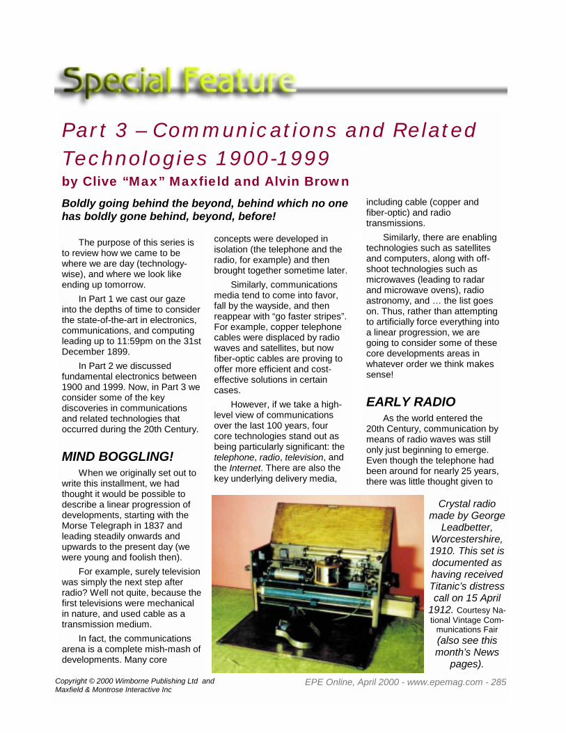
Copyright © 2000 Wimborne Publishing Ltd andMaxfield & Montrose Interactive Inc
EPE Online, April 2000 - www.epemag.com - 285
The purpose of this series isto review how we came to bewhere we are day (technology-wise), and where we look likeending up tomorrow.
In Part 1 we cast our gazeinto the depths of time to considerthe state-of-the-art in electronics,communications, and computingleading up to 11:59pm on the 31stDecember 1899.
In Part 2 we discussedfundamental electronics between1900 and 1999. Now, in Part 3 weconsider some of the keydiscoveries in communicationsand related technologies thatoccurred during the 20th Century.
MIND BOGGLING!When we originally set out to
write this installment, we hadthought it would be possible todescribe a linear progression ofdevelopments, starting with theMorse Telegraph in 1837 andleading steadily onwards andupwards to the present day (wewere young and foolish then).
For example, surely televisionwas simply the next step afterradio? Well not quite, because thefirst televisions were mechanicalin nature, and used cable as atransmission medium.
In fact, the communicationsarena is a complete mish-mash ofdevelopments. Many core
including cable (copper andfiber-optic) and radiotransmissions.
Similarly, there are enablingtechnologies such as satellitesand computers, along with off-shoot technologies such asmicrowaves (leading to radarand microwave ovens), radioastronomy, and … the list goeson. Thus, rather than attemptingto artificially force everything intoa linear progression, we aregoing to consider some of thesecore developments areas inwhatever order we think makessense!
EARLY RADIOAs the world entered the
20th Century, communication bymeans of radio waves was stillonly just beginning to emerge.Even though the telephone hadbeen around for nearly 25 years,there was little thought given to
Part 3 – Communications and RelatedTechnologies 1900-1999by Clive “Max” Maxfield and Alvin Brown
concepts were developed inisolation (the telephone and theradio, for example) and thenbrought together sometime later.
Similarly, communicationsmedia tend to come into favor,fall by the wayside, and thenreappear with “go faster stripes”.For example, copper telephonecables were displaced by radiowaves and satellites, but nowfiber-optic cables are proving tooffer more efficient and cost-effective solutions in certaincases.
However, if we take a high-level view of communicationsover the last 100 years, fourcore technologies stand out asbeing particularly significant: thetelephone, radio, television, andthe Internet. There are also thekey underlying delivery media,
Boldly going behind the beyond, behind which no onehas boldly gone behind, beyond, before!
Crystal radiomade by George
Leadbetter,Worcestershire,1910. This set isdocumented ashaving receivedTitanic’s distresscall on 15 April
1912. Courtesy Na-tional Vintage Com-
munications Fair(also see thismonth’s News
pages).
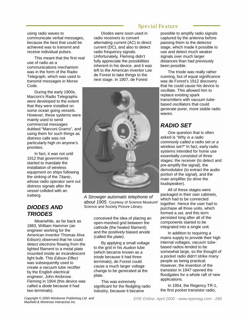
Copyright © 2000 Wimborne Publishing Ltd andMaxfield & Montrose Interactive Inc
EPE Online, April 2000 - www.epemag.com - 286
using radio waves tocommunicate verbal messages,because the best that could beachieved was to transmit andreceive individual pulses.
This meant that the first realuse of radio as acommunications mechanismwas in the form of the RadioTelegraph, which was used totransmit messages in MorseCode.
During the early 1900s,Marconi’s Radio Telegraphswere developed to the extentthat they were installed onsome ocean going vessels.However, these systems weremainly used to sendcommercial messagesdubbed “Marconi Grams”, andusing them for such things asdistress calls was notparticularly high on anyone’spriorities.
In fact, it was not until1912 that governmentsstarted to mandate theinstallation of wirelessequipment on ships followingthe sinking of the Titanic,whose radio operator sent outdistress signals after thevessel collided with aniceberg.
DIODES ANDTRIODES
Meanwhile, as far back as1883, William Hammer (anengineer working for theAmerican inventor Thomas AlvaEdison) observed that he coulddetect electrons flowing from thelighted filament to a metal platemounted inside an incandescentlight bulb. This Edison Effectwas subsequently used tocreate a vacuum tube rectifierby the English electricalengineer, John AmbroseFleming in 1904 (this device wascalled a diode because it hadtwo terminals).
Diodes were soon used inradio receivers to convertalternating current (AC) to directcurrent (DC), and also to detectradio frequency signals.Unfortunately, Fleming didn’tfully appreciate the possibilitiesinherent in his device, and it wasleft to the American inventor Leede Forest to take things to thenext stage. In 1907, de Forest
conceived the idea of placing anopen-meshed grid between thecathode (the heated filament)and the positively biased anode(called the plate).
By applying a small voltageto the grid in his Audion tube(which became known as atriode because it had threeterminals), de Forest couldcause a much larger voltagechange to be generated at theplate.
This was extremelysignificant for the fledgling radioindustry, because it became
possible to amplify radio signalscaptured by the antenna beforepassing them to the detectorstage, which made it possible touse and detect much weakersignals over much largerdistances than had previouslybeen possible.
The triode was really rathercunning, but of equal significancewas de Forest’s 1912 discoverythat he could cause his device tooscillate. This allowed him toreplace existing sparktransmitters with vacuum tube-based oscillators that couldgenerate purer, more stable radiowaves.
RADIO SETOne question that is often
asked is “Why is a radiocommonly called a radio set or awireless set?” In fact, early radiosystems intended for home useessentially consisted of threestages: the receiver (to detect andpre-amplify the signal), thedemodulator (to extract the audioportion of the signal), and themain amplifier (to drive theloudspeaker).
All of these stages werepackaged in their own cabinets,which had to be connectedtogether. Hence the user had topurchase all three units, whichformed a set, and this termpersisted long after all of thecomponents started to beintegrated into a single unit.
In addition to requiring amains supply to provide their highinternal voltages, vacuum tube-based radios tended to besomewhat large, so the thought ofa pocket radio didn’t strike manypeople as being practical.However, the invention of thetransistor in 1947 opened thefloodgates for a whole raft of newapplications.
In 1954, the Regency TR-1,the first pocket transistor radio,
Special Feature
A Strowger automatic telephone ofabout 1905. Courtesy of Science Museum/Science and Society Picture Library.

Copyright © 2000 Wimborne Publishing Ltd andMaxfield & Montrose Interactive Inc
EPE Online, April 2000 - www.epemag.com - 287
was introduced in the USA. TheJapanese transistor radio (TR-52) was produced, but not puton sale. It was the TR-55, whichwas the first commercialJapanese “tranny”, introduced in1955 by Sony. (SONY used tobe called Tokyo Tsushin KogyoLtd in those now far-off days, butthis didn’t exactly roll off thetongue so you can see why theydecided to change it).
THE TELEPHONEConsidering the fact that
Alexander Graham Bell filed hispatent for the first telephone in1876, the actual development ofthis device has, in many ways,been remarkably slow comparedto other consumer-orientatedtechnologies. In the early daysthis was due to several reasons,not the least that there was noexisting infrastructure (why havea phone if none of your friendshave one and there is no one tocall?).
By some strange quirk offate, when an infrastructureeventually came along, it was socostly and huge that thetechnology had to migrateforward slowly. The fact thatnew systems had to workalongside old ones served tocurtail revolutionary changesand to dictate an evolutionaryadoption of new technology.
For example, it took BritishTelecom more than ten years totransition fromelectromechanical technology toits digital equivalent.Furthermore, theseelectromechanical switchingexchanges, many of whichpersisted well into the 1990s,were themselves based ontechniques that had beeninvented in America by Almon B.Strowger 100 years earlier.
AUTOMATICSWITCHING
As fate would have it,Strowger was an unlikelycharacter to have had such animpact on the development oftelephone exchanges aroundthe world. As an undertaker inKansas City, USA, Strowgerwas an “early adopter” oftelephone technology, becausehe thought it would facilitatepotential customers (or at leasttheir relatives) contacting him.
However, telephoneexchanges in those days weremanual, which meant that theperson placing the call firstcontacted an operator, who thenphysically made the connectionbetween the caller and theintended recipient.
As fate would have it, theoperator who handledStrowger’s calls was the wife ofa competing undertaker. Thus,when potential clients tried tocontact Strowger, she wouldinstead connect them to herhusband’s business (the littlerascal).
Not surprisingly Strowgerfound this state of affairs to besomewhat frustrating, so he setabout designing an automaticsystem that would remove theoperator (in the form of hiscompetitor’s wife) from thepicture.
In fact, Strowger did notreally invent the concept ofautomatic switching – Connollyand McTigthe had discussed theidea as early as 1879 – but withthe help of his nephew (WalterS. Strowger) he was the first tocome up with a practicalimplementation based on banksof electromechanical relayselectors in 1888.
In 1901, Joseph Harrislicensed Strowger’s selectors to
Special FeatureTIMELINES1901: Marconi sends a radiosignal across the Atlantic.1902: US Navy installs radiotelephones aboard ships.1902: Transpacific cable linksCanada and Australia.1904: Telephone answeringmachine is invented.1905: Dial telephone is in-vented.1906: Dunwoody and Pickardbuild a crystal-and-cats-whiskerradio.1906: America. First radio pro-gram of voice and music isbroadcast.1907: Lee de Forest begins reg-ular radio music broadcasts.1909: Radio distress signalsaves 1900 lives after ships col-lide.1909: Marconi shares Nobelprize in physics for outstandingcontribution made to telegra-phy.1910: America. First installationof teleprinters on postal linesbetween New York City andBoston.1912: Titanic sends out radiodistress signal when it collideswith iceberg.1912: Feedback and hetero-dyne systems usher in modernradio reception.1914: Better triode valve im-proves radio reception.1914: Radio message is sentfrom the ground to an airplane.1914: First trans-continentaltelephone call.1915: First transatlantic radiotelephone conversation.1916: Radios get tuners.1917: Frank Conrad builds aradio station (becomes KDKA –call sign still in use to this day).1917: Condensor microphoneaids broadcast recording.1918: First radio link betweenUK and Australia.1919: People can dial their owntelephone numbers.1919: Shortwave radio is in-vented.

Copyright © 2000 Wimborne Publishing Ltd andMaxfield & Montrose Interactive Inc
EPE Online, April 2000 - www.epemag.com - 288
the Automatic Electric Co (AE).The first dial telephone wasinvented in 1905, and thecombination of dial telephonesand Strowger selectors pavedthe way for automatic telephoneexchanges, such as the firstpublic automatic telephoneexchange in the UK, whichopened in Epsom, Surrey in1912.
Of course, Strowgerexchanges were initially onlyused to process local calls –operator assistance was stillrequired for long distance andinternational calls. In fact, itwasn’t until 1971 that it becamepossible to direct-dial betweenthe US and Europe!
TESTING, 1, 2, 3With the advent of the triode
valve in 1907 and the discoveryof vacuum tube-basedoscillators in 1912, it becameapparent that speech could betransmitted by radio. The firstsignificant demonstration of thisconcept occurred in 1915, whenspeech signals weresuccessfully transmitted acrossthe Atlantic between Arlington,Virginia, and Paris, France.
One year later, a ground-to-air radiotelephone message wastransmitted from an airfield atBrooklands, England, to anaircraft flying overhead.
The first commercialradiotelephone service cameinto being in St Louis, Missouri,USA in 1946, but once againprogress was somewhat slow
due to the infrastructure andbureaucracy.
Following a number ofattempts, the first mobile phoneservice started operating inNorth America in 1978. Acrossthe Atlantic, the first cellularservice was introduced inEurope in 1981 in the form ofthe Nordic mobile telephonesystem.
In fact, it is interesting tonote that although America wasthe first to deploy a cellularservice, the multiple competingstandards in the USA havecaused that market to becomesegmented and fragmented.
By comparison, Europe andJapan are now years ahead ofthe USA, because they werequick to adopt a commonstandard. For example, as of1998 there were 100 million cellphone subscribers in Europe,with 5 million new subscribersjoining each month.
MECHANICAL TV
Special Feature
1921: Quartz crystal keeps radiofrom wandering.1922: First commercials broad-cast ($100 for 10 minute advert).1922: Lewis Alan Hazeltine in-vents the neutrodyne whicheliminates squeaks and howls ofearlier radio receivers.1923: First ship-to-ship commu-nications (people on one shipcan talk to people on another).1925: First commercial picture/facsimile radio service acrossUSA.1926: First commercial picture/facsimile radio service acrossAtlantic.1926: John Logie Baird demon-strates an electromechanical TVsystem.1927: Philo Farnsworth assem-bles complete electronic TV sys-tem.1927: First public demonstrationof long-distance television trans-mission (basically a Nipkowdisk).1929: Experiments begin onelectronic colour television.1929: First ship-to-shore com-munications (passengers cancall relatives at home – at aprice).1929: The first car radio is in-stalled.1929: In Germany, magneticsound recording on plastic tape.1929: British mechanical TVsroll off production lines1933: Edwin Howard Armstrongconceives a new system for ra-dio communication – widebandfrequency modulation (FM).1934: Half the homes in theUSA have radios.1935: Audio tape recordings goon sale.1935: All-electronic VHF televi-sion comes out of the lab.1935: England. First demonstra-tion of radar, at Daventry.1936: Munich Olympics tele-vised.1936: First electronic speechsynthesis (vodar).1937: Pulse-code modulation
Ferguson Model 993T 14-inch console television, origi-nal invoice dated 29/5/54 for75 pounds and 12 shillings.
Courtesy Dreweatt-Neate.
QUOTABLE QUOTES“The radio craze will die out
in time’’, Thomas Edison, 1922“While theoretically and
technically television may befeasible, commercially and fi-nancially I consider it an impos-sibility’’, Lee de Forest, 1926

Copyright © 2000 Wimborne Publishing Ltd andMaxfield & Montrose Interactive Inc
EPE Online, April 2000 - www.epemag.com - 289
Television, which comesfrom the Greek tele, meaningdistant and the Latin visio,meaning seeing or sight, hasarguably become one of thewonders of the 20th Century.
Prior to the advent ofelectronic scanning, all workabletelevision systems depended onsome form or variation of themechanical sequential scanningmethod exemplified by theNipkow disk (as discussed inPart 1).
Modern television systemsare based on the cathode raytube (CRT). The idea of using acathode ray tube to displaytelevision images was proposedas early as 1905, but progresswas hard fought for, and itwasn’t until the latter half of the1920s that the first rudimentarytelevision systems based oncathode ray tubes becameoperational in the laboratory.
There are two primaryrequirements for a functionaltelevision system: a techniquefor capturing an image and away to display it. FollowingNipkow’s experiments, otherinventors tried to move thingsforward with limited success.The history books mentionseveral names in this regard,such as John Logie Baird, aScotsman who used a derivationof Nipkow’s disks for capturingand displaying pictures duringthe latter half of the 1920s andthe early 1930s.
The British BroadcastingCorporation (BBC) allowed Bairdto transmit his pictures on theirunused radio channels in theevening. By 1934, even thoughhe could only transmit simplepictures with a aximumresolution of around 50 lines,Baird had sold thousands of hisTelevisor receivers aroundEurope in the form of do-it-yourself kits.
Meanwhile, on the other
side of the Atlantic, the RadioCorporation of America (RCA)experimented with a systemconsisting of a mechanical diskcamera combined with acathode ray tube display. Usingthis system, RCA transmitted apicture of a model of Felix theCat endlessly rotating on theturntable of a record player inthe early 1930s.
PHILOFARNSWORTH
Strange as it may seem,relatively few reference sourcesseem to be aware of the realgenius behind television as weknow it today – an Americanfarm boy named Philo T.Farnsworth from Rigby, Idaho.In 1922, at the age of 14, withvirtually no knowledge ofelectronics, Philo conceived theidea for a fully electronictelevision system. Flushed withenthusiasm, he sketched hisidea on a blackboard for his highschool science teacher.
Over the years, Philo solvedthe problems that had thwartedother contenders. He invented adevice called an ImageDissector, which was theforerunner to modern televisioncameras, and he also designedthe circuitry to implementhorizontal and vertical flybackblanking signals on his cathoderay tube, which solved theproblems of ghosting images.
By the early 1930s, Philocould transmit moving pictureswith resolutions of severalhundred lines, and allsubsequent televisions aredirectly descended from hisoriginal designs.
As video historian PaulSchatzkin told the authors:“Many engineers and scientistscontributed to the emergence ofthe television medium, but acareful examination of the
Special Featurepoints the way towards digitaltransmission.1938: John Logie Baird demon-strates live TV in colour.1938: Television broadcasts canbe taped and edited.1938: Radio drama War of theWorlds causes widespreadpanic.1939: Regular TV broadcastsbegin.1939: Bell labs begin testinghigh-frequency radar.1940: Bell labs conceive theidea of cell phone (technologywon’t exist to bring it to marketfor another 30 years).1941: First touch-tone phonesystems (too expensive for gen-eral use).1941: First microwave transmis-sions.1945: Sci-fi author Arthur C.Clark envisions geo-synchronous communicationssatellites.1946: Automobile radiotele-phones connect to the telephonenetwork.1948: America. Airplane re-broadcasts TV signal to nineStates.1949: America. Start of networkTV.1950: Vidicon camera tubes im-prove TV pictures.1952: Sony demonstrates firstJapanese miniature transistorradio (produces it commerciallyin 1955).1953: America. First TV dinneris marketed by the C.A. Swan-son company.1954: Launch of giant ballooncalled Echo 1 – used to bouncetelephone calls coast to coast.1954: Number of radio sets inworld out-numbers newspaperssold each day.1956: First transatlantic tele-phone cable goes into operation.1957: Russia launches Sputnik1, the world’s first artificial satel-lite.
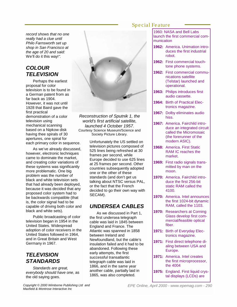
Copyright © 2000 Wimborne Publishing Ltd andMaxfield & Montrose Interactive Inc
EPE Online, April 2000 - www.epemag.com - 290
record shows that no onereally had a clue untilPhilo Farnsworth set upshop in San Francisco atthe age of 20 and said:We’ll do it this way!”.
COLOURTELEVISION
Perhaps the earliestproposal for colortelevision is to be found ina German patent from asfar back as 1904.However, it was not until1928 that Baird gave thefirst practicaldemonstration of a colortelevision usingmechanical scanningbased on a Nipkow diskhaving thee spirals of 30apertures, one spiral foreach primary color in sequence.
As we’ve already discussed,however, electronic techniquescame to dominate the market,and creating color variations ofthese systems was significantlymore problematic. One bigproblem was the number ofblack and white television setsthat had already been deployed,because it was decided that anyproposed color system had tobe backwards compatible (thatis, the color signal had to becapable of driving both color andblack and white sets).
Public broadcasting of colortelevision began in 1954 in theUnited States. Widespreadadoption of color receivers in theUnited States followed in 1964,and in Great Britain and WestGermany in 1967.
TELEVISIONSTANDARDS
Standards are great,everybody should have one, asthe old saying goes.
Unfortunately the US settled ontelevision pictures composed of525 lines being refreshed at 30frames per second, whileEurope decided to use 625 linesat 25 frames per second. Othercountries subsequently adoptedone or the other of thesestandards (and don’t get ustalking about NTSC versus PAL,or the fact that the Frenchdecided to go their own way withSECAM).
UNDERSEA CABLESAs we discussed in Part 1,
the first undersea telegraphcable was laid in 1845 betweenEngland and France. TheAtlantic was spanned in 1858between Ireland andNewfoundland, but the cable’sinsulation failed and it had to beabandoned. Following theseearly attempts, the firstsuccessful transatlantictelegraph cable was laid in1866, and in the same yearanother cable, partially laid in1865, was also completed.
Special Feature1960: NASA and Bell Labslaunch the first commercial com-munication1962: America. Unimation intro-
duces the first industrialrobot.
1962: First commercial touch-tone phone systems.
1962: First commercial commu-nications satellite(Telstar) launched andoperational.
1963: Philips introduces firstaudio cassette.
1964: Birth of Practical Elec-tronics magazine.
1967: Dolby eliminates audiohiss.
1967: America. Fairchild intro-duce an integrated circuitcalled the Micromosaic(the forerunner of themodern ASIC).
1968: America. First StaticRAM IC reaches themarket.
1969: First radio signals trans-mitted by man on themoon.
1970: America. Fairchild intro-duce the first 256-bitstatic RAM called the4100.
1970: America. Intel announcesthe first 1024-bit dynamicRAM, called the 1103.
1970: Researchers at CorningGlass develop first com-mercial/feasible opticalfiber.
1971: Birth of Everyday Elec-tronics magazine.
1971: First direct telephone di-aling between USA andEurope.
1971: America. Intel createsthe first microprocessor,the 4004
1975: England. First liquid crys-tal displays (LCDs) are
Reconstruction of Sputnik 1, theworld’s first artificial satellite,launched 4 October 1957.
Courtesy Science Museum/Science andSociety Picture Library.

Copyright © 2000 Wimborne Publishing Ltd andMaxfield & Montrose Interactive Inc
EPE Online, April 2000 - www.epemag.com - 291
These early attempts wereplagued by deterioration of thesignal over these hugedistances and also by a lack ofunderstanding of theenvironment 2,000 fathomsbeneath the sea (could there bea film title here?).
Of course, the problemswere significantly more dauntingin the case of audio signals. Infact, these issues were notresolved until the invention ofvacuum tube-based repeatersthat could operate continuouslyand flawlessly with no attentionfor at least 20 years at thesedepths. These made possiblethe first transatlantic telephonecable, from Scotland toNewfoundland in 1956.
Following the success ofthis first cable, similar systemswere deployed betweenCalifornia and Hawaii andbetween Hawaii and Japan in1964. More recent underseacables employ transistorizedrepeaters and provide evenmore voice circuits, and someare even capable of transmittingtelevision pictures.
Today’s cables, such as thePacific cable laid in 1998, usetechnology based on fiber-opticsand can handle 40,000simultaneous conversations!
SATELLITESIn 1952, the International
Council of Scientific Unions statedthat July 1957 to December 1958would be the InternationalGeophysical Year (IGY), becausesolar activity would be at a highpoint during this period. Twoyears later, in October 1954, thecouncil adopted a resolutioncalling for artificial satellites to belaunched during the IGY to mapthe Earth’s surface.
In 1955, in a fit ofexuberance, the Americangovernment announced plans tolaunch an Earth-orbiting satellitefor the IGY, and set to work onthe project. But much to theirdismay, the (former) Soviet Unionsuccessfully launched Sputnik 1,the world’s first artificial satelliteon October 4, 1957.
Sputnik 1 was small (aboutthe size of a basketball weighingin at 183 pounds, 83kg) and itssole function was to repeatedlybeep a simple Morse Code-typemessage (to annoy theAmericans). However, thesignificance of this event cannotbe understated as it paved theway to a wide range of political,military, technological, and
Special Feature
scientific developments.
SPACE RACEThe Russian’s ability to
launch a satellite 50 times themass of the American’sproposed 3·5 pound (1·6kg)payload sent shivers of fearthroughout the Western world. Itwas obvious to all thatintercontinental ballistic missileswere now more than apossibility. Thus, in addition tocausing the Americans to formNASA (which gave us Velcrofasteners and Teflon for ourfrying pans), Sputnik 1 initiatedthe so-called “Space Race”.
This culminated withAmerica putting a man on themoon, but also led to deepspace probes throughout thesolar system, and droveelectronic developments likeminiaturization in the form ofintegrated circuits, more efficientsolar cells, and others toonumerous to mention.
BALLOONSWhilst working at Bell
Laboratories in 1960, JohnRobinson Pierce developed thefirst experimental
Echo 1, the first experimentalcommunications satellite,
during inflation tests. CourtesyScience Museum/Science and So-
ciety Picture Library.
Telstar 1, first commercialcommunications satellite. Itwas a multi-faceted sphereone meter in diameter. Cour-tesy of BT Archives.
1980: Faxes can be sent overregular phone lines.
1980: Cordless and cell phonesare developed.
1989: Pacific fiber-optic link/cable opens (supports40,000 simultaneousconversations).
1992: PE and EE combine tobecome EPE.
1993: MOSAIC web browserbecomes available.

Copyright © 2000 Wimborne Publishing Ltd andMaxfield & Montrose Interactive Inc
EPE Online, April 2000 - www.epemag.com - 292
waves in 1887, he discovered thatthey could be transmitted throughsome materials, but that theywould be reflected by others.Almost 50 years later, scientistsbegan to discover how to useradio waves to detect and locateobjects.
In 1935, a report entitled TheDetection of Aircraft by RadioMethods was presented to theBritish Air Ministry by Sir RobertWatson-Watt and his assistantArnold Wilkins. This was soonfollowed by a trial, in which theBBC’s short wave radiotransmitter at Daventry, Englandwas used to detect a BritishHeyford Bomber.
The success of this trial led toa chain of Radio Detecting andRanging (RADAR) stations alongthe South and East coasts ofEngland. These were to providevital advance information that wasto help the Royal Air Force win theBattle of Britain.
Special Featurecommunications satellite bybouncing radio signals of a 150-foot (45m) aluminum-coated high-altitude balloon called Echo 1.
These experiments wereclosely followed by the Telstarseries of communicationssatellites, which initiated a newage in electronic communications.Unlike the passive reflectionemployed by Echo 1, Telstarreceived signals transmitted froma ground station, amplified them,and re-transmitted them toanother ground station.
Following Telstar’s launch on10 July 1962, the first televisionpictures were transmitted acrossthe Atlantic Ocean from a giantantenna near Andover, Maine, toa receiver located at Goonhilly inEngland. These television pictureswere quickly followed bytransmissions of telephone,telegraph, facsimile (FAX), andcomputer data.
CRYSTAL BALLSAs far back as 1945, Arthur
C. Clarke (who was to gain fameas a Science Fiction writer)proposed that microwave signalscould be beamed to an unmannedorbiting satellite and bouncedback to a different part of theworld. But his key suggestion wasthat three satellites parked in ageo-synchronous orbit 36,000kilometers above the Equatorcould be used to provide world-wide coverage. Clark’s vision waseventually realized by Telstar’ssuccessors. Today, thousands ofsatellites race around the Earth, tothe extent that it’s becomingincreasingly difficult to select anorbit for a new satellite so as tomaintain a safe separation fromexisting devices.
RADARWhen Heinrich Hertz first
began experimenting with radio
MAGNETRONSSad to relate, early RADAR
sets were not as efficacious asone might have hoped for. Whatwas required was a newgeneration of high and lowpower signal generators. Onesolution that was to find favorwas the magnetron, which wasdeveloped by British physicistsat the University of Birminghamin 1939.
A magnetron is a diodevacuum tube-like device that iscapable of generating extremelyhigh frequencies and also shortbursts of very high power.
The need to manufacturetens of thousands of magnetrontubes to satisfy the war effortdrove the British government toseek help from Americanindustry. One company that wasconsulted was Raytheon, whichalready had been experimentingwith their own microwave tubes.
After listening to the British
Goonhilly Earth Station. Courtesy of BT Archives.

Copyright © 2000 Wimborne Publishing Ltd andMaxfield & Montrose Interactive Inc
EPE Online, April 2000 - www.epemag.com - 293
Scientistsalready knew thatmagnetronsgenerated heatwhilst radiatingmicrowaves, butSpencer was thefirst to discoverthat one couldcook food usingmicrowave radiosignals.
Based onSpencer’sdiscovery,Raytheondemonstrated thefirst commercialmicrowave oven in1947. Thesebeasts were
presented in refrigerator-sizedcabinets and cost $2000 to$3000 (which was an expensiveway to cook one’s popcorn).THE INTERNET
The latest development inthe communications arena is theInternet, which combines thewidespread availability ofcomputers with every othercommunications technologyknown to man.
The Internet had its origin in
a US Department of Defenseprogram called ARPANET(Advanced Research ProjectsAgency Network), which wasestablished in 1969 to provide asecure and survivablecommunications network fororganizations engaged indefense-related research.
By the 1980s, ARPANET hadevolved into a fledgling version oftoday’s Internet that waspredominantly used by academicsas a way to publish textual dataand as a text-based searchengine.
One of the original uses of theInternet was electronic mail(commonly called email), bulletinboards and newsgroups, andremote computer access. Thesubsequent development of theWorld Wide Web (WWW), whichenables simple and intuitivenavigation of Internet sitesthrough a graphical interfacecalled a Web Browser (such asNetscape or Internet Explorer)was popularized by the release ofthe MOSAIC web browser in1993.
In December 1999, thenumber of daily emails passeddaily conventional mail letters forthe first time.
Special Feature
scientists describe their methodof producing the magnetrontubes, one of Raytheon’sengineers, Percy L. Spencerboldly stated that their techniquewas “awkward and impractical”.Percy took the tube home overthe weekend and came up withradical changes that would bothsimplify the manufacturingprocess and improve thefunctioning of the radar.
Britain awarded the little-known Raytheon a contract tosupply the magnetrons, and bythe end of the war Raytheonwas producing 80 percent of allmagnetrons in the world.Spencer, a man with only abasic school education, becameRaytheon’s chief engineer.
MICROWAVE OVENSThe discovery of microwave
cooking in 1945 is alsoattributed to Raytheon’s PercySpencer. A candy bar inSpencer’s pocket began to meltas he stood in front of amagnetron tube that had beenswitched on. Spencer nextplaced popcorn kernels in frontof the tube – and they popped.
Original cavity magnetron, 1940. Developedby John Randall and Harry Boot of Birming-ham University. Courtesy of Science Museum/Sci-
ence and Society Picture Library.
Interior of a Sony TR-63 transistor radio. 114,536 ofthem were manufactured between March 1957 and
November 1958. Courtesy Radio Bygones.

Copyright © 2000 Wimborne Publishing Ltd andMaxfield & Montrose Interactive Inc
EPE Online, April 2000 - www.epemag.com - 294
The Internet now uses radio,satellites, the telephonenetwork, cable TV, amateurradio, and numerous otherdelivery media. In addition toraw computer data, the Internetis itself used to deliver staticimages, telephoneconversations, music andtelevision pictures. Cuttingacross national boundaries, theuncensored Internet is seen bymany as being one of the mostmomentous achievements ofthe 20th Century.
The most amazing thing isthat the Internet today is still inits infancy. In many respects,the state of the Internet at the
Special Featurebeginning of the year 2000 iscomparable to that of thetelephone as the world enteredthe 1900s. However, the speedof the Internet’s development isexponential compared to that ofthe telephone, and the socialimpact of the Internet will bemore profound than most peoplecan conceive.
NEXT MONTHIn Part 4 we shall turn our
attention to computing in the20th Century, and in Part 5 weshall polish up our crystal balland peer into the future in adesperate attempt to predict the
new and wonderful ideas andtechniques that are racingtowards us like a runaway trainat the beginning of this newmillennium!

Copyright © 2000 Wimborne Publishing Ltd andMaxfield & Montrose Interactive Inc
EPE Online, April 2000 - www.epemag.com - 295
ROBERT PENFOLDBidirectional Printer Ports
As regular readers will beaware, there have recently beenchanges to the way PC add-onsare tackled in this series of arti-cles. Good old GW-BASIC andQ BASIC have been replaced byvisual programming languagessuch as Visual BASIC 6.0 andDelphi 1 or 2.
Most projects now require abidirectional printer port,whereas those featured in thepast needed only a standardprinter port. I think most wouldagree that these changes haveresulted in projects that are su-perior to their predecessors,even though in most cases thehardware and software are actu-ally simpler.
However, these changesseem to have caused an in-crease in the number of lettersand emails relating to Interfacearticles. A number of projectsthat utilize a bidirectional printerport and (or) software written ina visual language will feature infuture Interface articles, so it isperhaps worthwhile clarifyingsome points raised by readersbefore getting embroiled inthese designs.
ONGOINGI think it is worth making the
point that the Interface articlesare largely self-contained, butthey are also part of an ongoingseries. It is a series that is notreally aimed at beginners. Whena design is featured in an Inter-face article, most of the informa-tion provided is specific to thatproject.
In general, background in-formation is not provided. Someof this information is the type ofthing that anyone having a rea-sonable amount of experiencewith computer add-ons shouldknow. The rest is subject matterthat has been covered in recentInterface articles.
In short articles of this typethere is not enough space avail-able to keep repeating thingsover and over again. If an articledoes not tell you everything youneed to know it may be neces-sary to delve back a few issuesfor the answers.
BIDIRECTIONALOne or two readers seem to
have run into trouble becausethey have tried to use projectsrequiring a bidirectional port withold PCs that have standardprinter ports. In general, Pen-tium PCs have bidirectionalports while 80486 and earlierPCs do not. However, someearly Pentium PCs lack this fa-cility and a few 80486 basedPCs do have this bidirectionalcapability.
Some PCs that have bidi-rectional printer ports default tothe standard mode of operation,and must be set to the bidirec-tional mode using the BIOSSetup program. The documen-tation supplied with the PCshould give details of the BIOSSetup program and changingthe mode of the printer port. It isSPP mode that is required, butEPP mode also seems to besuitable. ECP is an advancedmode that does not seem to
support simple bidirectional op-eration.
The only sure way to deter-mine whether or not a port canread data on its eight data linesis to run a simple test. Writing avalue of 32 to the handshakeoutput register sets a port to in-put operation, and data can thenbe read from the data lines atthe base address of the port.
RIGHT ADDRESSThis brings us to another
source of problems, which is de-termining the right addressrange for the printer port. Thereare three address ranges usedfor printer ports, as shown here:
Data H/S Input H/S OutputRegister Register Register&H3BC &H3BD &H3BE&H378 &H379 &H37A&H278 &H279 &H27A
Most PCs have one printerport as standard, and this isusually at a base address of&H378, but some seem to use&H3BC. Where there is morethan one printer port, the operat-ing system designates the portat the highest address port one,the one at the next highest ad-dress port two, and if there arethree ports, the one at the low-est address will be port three. Ifthere are ports at addresses&H378 and &H278 for example,these will respectively be usedas ports one and two by the op-erating system.
If you do not know the ad-dresses of the ports in your PCthe easiest way to find out is touse the Windows 95/98 SystemInformation program. Operatingthe Windows Start button andthen selecting Programs, Acces-

Copyright © 2000 Wimborne Publishing Ltd andMaxfield & Montrose Interactive Inc
EPE Online, April 2000 - www.epemag.com - 296
sories, System Tools, and Sys-tem Information will launch thisprogram.
Double click on Resourcesand then on I/O to bring up a listof the input/output address as-signments. This will provide alist of the type shown in Fig.1,which should include the serialand parallel ports.
SIMPLE TESTA very simple test routine is
all that is needed to checkwhether the port supports bidi-rectional operation. This GWBASIC program will do the job.The addresses are correct forwhat will normally be printer porttwo, but they are easily changedif necessary.
10 CLS20 OUT &H27A,3230 LOCATE 10,2040 PRINT INP(&H278)50 GOTO 10
Line 20 sets the port to theinput mode, and a loop then re-peatedly reads the data linesand prints the results at thesame point on the screen. Feed-ing various logic patterns to thedata inputs of the port (pins 2 to9) should produce the appropri-ate readings on the screen.
It is best to drive the port viacurrent limiting resistors of about220 ohms in value. If the port isstill working as an output typethese resistors will limit the cur-rent flow to a level that will pre-vent anything from being dam-aged.
ON THE CARDSIf the readings from the port
do not change, it is clearly not abidirectional type. The easiestsolution is to fit the PC with a
printer port card (see Fig.2) andany modern card of this typeshould support simple bidirec-tional operation. A card of thistype should cost about 10 to 20UK pounds from any large com-puter store, which is not bad fora port that provides a total of 17input and output lines.
Since most PCs have aprinter connected to parallel portone, adding a second portspecifically for use with your a-dd-ons is a good idea anyway.Assuming the existing port is ata base address of &H3BC or&H378, the new port should beconfigured for a base address of&H278, to use IRQ5, and forEPP or SPP operation.
DELPHIUsing visual languages with
your own add-on devices is notas straightforward as using atraditional BASIC such as GWBASIC. Direct accessing ofports is permitted under Win-dows 95 and 98, but there is lit-tle support for doing this withWindows programming lan-guages.
Borland’s Delphi (a sort ofvisual Pascal) does have a Port
function that can be used toread from and write to ports.However, this facility is only sup-ported by version One of theprogram, and is absent from allthe subsequent versions. Thesoftware for most user add-onsis fairly basic, and Delphi 1.0 ismore than adequate for this typeof thing.
Although it is no longeravailable as a separate entity, itis supplied with later versions ofDelphi (both the commercial ver-sions and the “free” versions oc-casionally given away with com-puter magazines). The originalDelphi language produces pro-grams that will run under Win-dows 3.1, but later releases arestrictly for use with the 32-bitversions of Windows. Version1.0 of Delphi is therefore in-cluded with later versions to pro-vide 16-bit compatibility. Delphi1.0 programs will run properlyunder Windows 95 and 98 inci-dentally.
Delphi 1.0 has definite ad-vantages over the alternatives,and will probably be used to pro-duce the programs featured infuture Interface articles. One ad-vantage is that it producesstand-alone programs that do
InterFACE
Fig. 1. The Windows System Information program can providea list of address ranges for the hardware.

Copyright © 2000 Wimborne Publishing Ltd andMaxfield & Montrose Interactive Inc
EPE Online, April 2000 - www.epemag.com - 297
InterFACE
not have to be installed, and ataround 200k to 250k they arenot particularly big either.
As explained previously,Delphi 1.0 programs will run un-der Windows 3.1, 95, and 98.Because of the built-in Portfunction it is not necessary toresort to any software add-ons,keeping things simple andstraightforward.
GETTING IN-LINEAlthough Delphi 2.0 and be-
yond do not have a Port functionthey are equipped with a simplebut effective in-line assembler.Reading from and writing toports can therefore be accom-plished using a few lines of as-sembler.
Due to the lack of a Portfunction it is not possible tocompile any Delphi 1.0 listingsprovided in Interface articles us-ing Delphi 2.0 or later. However,it should be possible to rewritethem to use assembler routinesinstead of the Port function, andthe programs should then com-pile successfully under the 32-bitversions of Delphi.
As far as I am aware, the“free” versions of Delphi are notavailable for download at anyweb site. The size of these pro-grams is such that it would takea very long time to downloadthem anyway.
Versions up to Delphi 3.0Professional have appearedfrom time to time as freebies onmagazine cover discs. Theseare the same as the full com-mercial equivalents, but they arefor personal use only. In otherwords, if you start to distributeyour programs commercially youmust buy “the real thing”.
Programming user add-onsusing Delphi 1.0 was covered inthe June ‘99 issue of EPE On-
of these adds INP and OUTfunctions to Visual BASIC, andthese functions are used in ex-actly the same way as their GWBASIC counterparts.
One or two readers havequeried whether or not this filewill be included when a programis compiled. Visual BASIC doesnot compile programs into stan-dalone files, but instead pro-duces a group of files completewith an install/uninstall program.A DLL file such as inpout32.dllwill be included with the programgroup, and the installed programwill function properly. Unfortu-nately, the smallest of VisualBASIC programs seems to com-pile into almost two megabytesof files!
WORKING MODELThere is a “working model”
version of Visual BASIC 6, butthis does not seem to be avail-able as a download from the Mi-crosoft web site. Again, it would
line, and using the assembler inlater versions was coveredbriefly in the August ‘99 issue.
GOING VISUALVisual BASIC is now the
most popular programming lan-guage, and it is probably themost simple to use. In recentyears I have received a steadyflow of enquiries about using thislanguage with PC projects.
Unfortunately, as far as Ican ascertain there are no INPor OUT functions in Visual BA-SIC 6.0 or any of the earlier ver-sions. Neither is there a built-inassembler or any other integralfunction that provides access tothe ports.
It is possible to access theports using this language, butonly with the aid of a softwareadd-on. Anyone interested inusing Visual BASIC with useradd-ons should certainly pay avisit to the web site at http://www.lvr.com where there is alot of information, software add-ons, and links to other usefulsites.
If nothing more than basicport access is needed, and thisis certainly all that is needed formost projects, the freeware DLLcalled inpout32.dll would seemto be the best option. Use in-pout16.dll for 16-bit versions ofVisual BASIC. Using either
Fig. 2. A bidirectional printer port card.

Copyright © 2000 Wimborne Publishing Ltd andMaxfield & Montrose Interactive Inc
EPE Online, April 2000 - www.epemag.com - 298
InterFACE
probably take too long to down-load anyway.
The working model is al-most the complete program, butit cannot compile programs.They can be run from within Vi-sual BASIC though, rather likerunning programs under GWBASIC or Q BASIC. When run inthis way the programs seem torun at full speed and without anyrestrictions.
The usual way of obtainingthe Visual BASIC working modelis to buy a book that includes iton the accompanying “free” CD-ROM. Although I hate to admit it,I found “The Complete Idiot’sGuide To Visual BASIC 6” byClayton Walnum (ISBN 0-7897-1812-X) an excellent introduc-tion to Visual BASIC program-ming.
At around 15 uk pounds,complete with the working
site mentioned earlier), but thisis doing things the hard way.Windows 95 and 98 are a betterchoice for a PC that will be usedwith PC based projects.LIBERTY BASIC
It is perhaps worth mention-ing a little known BASIC pro-gramming language called Lib-erty BASIC. This shareware pro-gram is a traditional BASIC thatwill produce Windows programs,and it includes INP and OUTfunctions.
Being shareware, this pro-gram can be tried out for thecost of downloading it from oneof the source web sites. Thereare several of these includinghttp://www.liberty-basic.com
model version of the program, itprobably represents the cheap-est way of trying Visual BASIC6. Using Visual BASIC with useradd-ons was covered in the Au-gust ‘99 issue of EPE Online in-cidentally.
WINDOWS NT4Windows 3.1, 95, and 98 all
permit direct accessing of theports, but Windows NT4 doesnot. It is designed to be moresecure than other versions ofWindows, and it only permitsport accesses via the operatingsystem. This ensures that twoprograms cannot simultaneouslyattempt to access the samepiece of hardware.
There are add-ons that canprovide programming languageswith a port access facility in Win-dows NT4 (see the lvr.com web

Copyright © 2000 Wimborne Publishing Ltd andMaxfield & Montrose Interactive Inc
EPE Online, April 2000 - www.epemag.com - 299
In previous parts of Teach-In,the term AND has been usedfrom time-to-time. Indeed, in Part4 we gave a brief description ofwhat it does. The term occurs inboth computing and electronics.In both instances, the implemen-tation of AND is physically carriedout by an electronic device or cir-cuit somewhere in the system.
We explained that if two logicbits are ANDed together then theresult will be logic 1 only if bothsource bits are also at logic 1. Ifeither or both bits are at logic 0,the result will also be logic 0.
AND NOW THEGATES
The first subject to be cov-ered this month is the expansionof the AND concept, and to de-scribe not only integrated devicesthat use AND, but those that usethe other five main logic functions,NAND, OR, NOR, XOR andXNOR.
One of the uses for an ANDgate is as a signal (data) switch,only allowing the signal on oneinput to pass to the output if the
PART 6 – Logic Gates, Binary,and Hex Logic by John Becker
other input is high. Another is toindicate whether or not all inputsare high, allowing, for example,a process to start if several pre-ceding processes have beencompleted.
Let’s use your breadboardand the oscillator you were us-ing last month, plus an elec-tronic AND gate, to demonstratethe AND principle, and in doingso to show its use as a signalswitch.
The symbol for a 2-inputAND gate is given at the top ofFig.6.1a (the table below it willbe discussed presently).
From your bag of compo-nents, select a 74HC08 inte-grated circuit (IC). This IC is an-other digital electronic device(as are the 74HC04 and74HC14 inverters you have al-ready been using). It is a quad2-input AND gate, and as suchhas four separate AND gate cir-cuits within it. Its pinouts areshown in Fig.6.2.
Whereas the inverters eachhad one input and one output,the AND gate we are about touse has two inputs (as stated in
So we now have five parts of Teach-In 2000under our belts and we know that you aregreatly enjoying and learning from this 10-partseries. We are pleased to have been told onmany occasions that you appreciate the way inwhich we are leading you by the hand, on theassumption that you knew little or nothingabout electronics before you started readingthe series. Your complementary comments arevery welcome.
We have covered the basic “passive”components and provided you with a means bywhich to create waveforms and display themon a PC-compatible computer screen. Thisenables us to now explore somewhat moresophisticated components of an “active”nature. Our experimental subjects this monthare not only gates but binary counters tocomplement the Tutorial, and a decimalcounter – for fun as well as instruction!
its functional title) and one out-put. The logic levels applied tothe two inputs can be regardedas the bits to which we referreda few paragraphs earlier whenstating what AND means in anelectronic or computing context.
It is worth noting that thereare other AND gates which havemore than two inputs. We shallnot discuss them, but just com-ment that similar principles applyto all types. There are also otherquad 2-input AND gates withdifferent type numbers (indeedall the devices we use in this Tu-torial are available with differenttype numbers to those quoted,but not necessarily with thesame pinouts).
PRELIMINARIESBefore you remove the
74HC08 from its packaging,briefly touch something that isearthed to discharge any staticelectricity from your body. (Seealso Panel 6.1.)
Plug the IC (call it IC3) intoyour breadboard and connect itup as shown in Fig.6.3. Ensure

Copyright © 2000 Wimborne Publishing Ltd andMaxfield & Montrose Interactive Inc
EPE Online, April 2000 - www.epemag.com - 300
that it is placed in the correctway round (as we discussed inPart 2).
We are using just one ANDgate from within IC3, and shallrefer to it as IC3a. Pin 1 (call itInput A) of IC3a connects backto the output of oscillator IC1apin 2 (see Part 4). Pin 2 (InputB) of IC3a is linked to the posi-tive power line via resistor R11.
The power line connectionsfor IC3 are positive to pin 14 and0V to pin 7. With the breadboardlinks as shown, these connec-
tions are automatically made tothe battery when it is connectedto the board as in previous ex-periments.
A LED (D4) is connected tothe output of IC3a (pin 3) via theusual ballast resistor (R12).
The circuit diagram for thisset up is shown in Fig.6.4.
Capacitor C1 of the oscilla-
TEACH-IN 2000
1
0
B
0
1
NAND GATE
0
0
0
0
B
AB)
11
01 1
11 0
11 1
YB
AD)
0
AB Y
1
0 0
1 0
01 0
AND GATE
B
AA)
A
B
C)
Y
AB Y
00 1
01 1
01 0
B
A
1 1
Y
F)
00
AB Y
1
NOR GATE
0 0
11
0 1
010
111
001
1 1 0
XNOR GATE
Y
0
B
0
A Y
1
0 0 0
0 1 1
1 0 1
B
AY
OR GATEE)
A Y
XOR GATE
Y
B A Y
Fig.6.1. Symbols and truth tables for the six 2-input logicgate functions.
+VE
B2
Y2
GND7
6
5
8
9
10
QUAD 2-INPUT AND
B1
A11
2
3
A24
Y1
74HC08
14
13
12
11
A3
Y3
B3
B4
Y4
A4
Fig.6.2. Pinouts for a 74HC082-input AND gate.
FROM 1C1aPIN 2
ALTERNATIVE LINK(SEE TEXT)
0V
INPUT "A"
+6V
R1110k
D4
R12470�
7
1
IC3a74HC0814
23
(A)
(B)
(Y)
a
k
Fig.6.4. Circuit diagram forthe AND gate experiment.The circuits for the other
gates are similar.32
32
2020 21
2222
2323
2424
2525
2626
2727
2828
2929
3030
3131
SIGNAL IN (A)FROM IC1a PIN 2 SIGNAL OUT (Y)
IC3
LINK (B)(SEE TEXT)
R11
R12
D4a
k
Fig.6.3. Breadboard layoutfor the AND, NAND, OR and
XOR 2-input gateexperiments.
Photo 6.1. Breadboard showingthe 74HC00 and 74HC02 con-figured for the demos. Note thatthey are not in the final recom-mended board positions.
tor should be 100uF.Incidentally, the A and B
names given to the gate inputsdo not have to be in that order,or even with those names. Theycould even be called Input Johnand Input Gill if you wanted to.Nor is it necessary to use thesame suffix letters as those
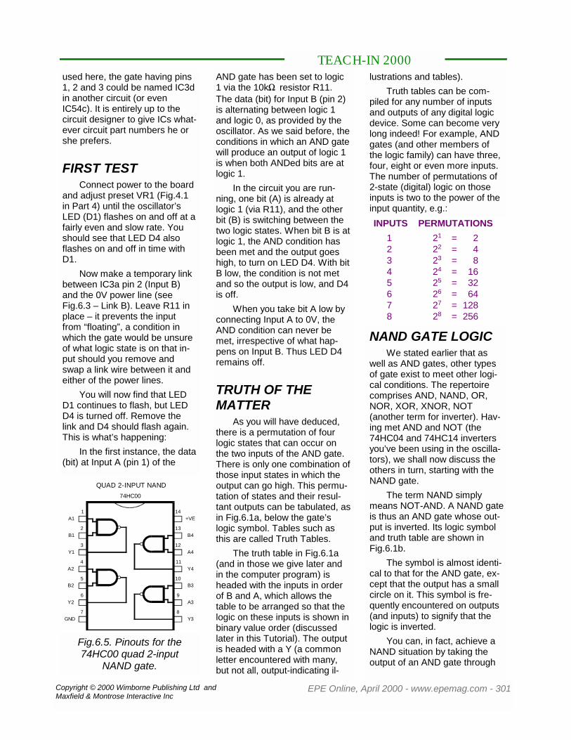
Copyright © 2000 Wimborne Publishing Ltd andMaxfield & Montrose Interactive Inc
EPE Online, April 2000 - www.epemag.com - 301
used here, the gate having pins1, 2 and 3 could be named IC3din another circuit (or evenIC54c). It is entirely up to thecircuit designer to give ICs what-ever circuit part numbers he orshe prefers.
FIRST TESTConnect power to the board
and adjust preset VR1 (Fig.4.1in Part 4) until the oscillator’sLED (D1) flashes on and off at afairly even and slow rate. Youshould see that LED D4 alsoflashes on and off in time withD1.
Now make a temporary linkbetween IC3a pin 2 (Input B)and the 0V power line (seeFig.6.3 – Link B). Leave R11 inplace – it prevents the inputfrom “floating”, a condition inwhich the gate would be unsureof what logic state is on that in-put should you remove andswap a link wire between it andeither of the power lines.
You will now find that LEDD1 continues to flash, but LEDD4 is turned off. Remove thelink and D4 should flash again.This is what’s happening:
In the first instance, the data(bit) at Input A (pin 1) of the
AND gate has been set to logic1 via the 10k� resistor R11.The data (bit) for Input B (pin 2)is alternating between logic 1and logic 0, as provided by theoscillator. As we said before, theconditions in which an AND gatewill produce an output of logic 1is when both ANDed bits are atlogic 1.
In the circuit you are run-ning, one bit (A) is already atlogic 1 (via R11), and the otherbit (B) is switching between thetwo logic states. When bit B is atlogic 1, the AND condition hasbeen met and the output goeshigh, to turn on LED D4. With bitB low, the condition is not metand so the output is low, and D4is off.
When you take bit A low byconnecting Input A to 0V, theAND condition can never bemet, irrespective of what hap-pens on Input B. Thus LED D4remains off.
TRUTH OF THEMATTER
As you will have deduced,there is a permutation of fourlogic states that can occur onthe two inputs of the AND gate.There is only one combination ofthose input states in which theoutput can go high. This permu-tation of states and their resul-tant outputs can be tabulated, asin Fig.6.1a, below the gate’slogic symbol. Tables such asthis are called Truth Tables.
The truth table in Fig.6.1a(and in those we give later andin the computer program) isheaded with the inputs in orderof B and A, which allows thetable to be arranged so that thelogic on these inputs is shown inbinary value order (discussedlater in this Tutorial). The outputis headed with a Y (a commonletter encountered with many,but not all, output-indicating il-
lustrations and tables).Truth tables can be com-
piled for any number of inputsand outputs of any digital logicdevice. Some can become verylong indeed! For example, ANDgates (and other members ofthe logic family) can have three,four, eight or even more inputs.The number of permutations of2-state (digital) logic on thoseinputs is two to the power of theinput quantity, e.g.:
TEACH-IN 2000
+VE
Y2
GND7
6
8
9
QUAD 2-INPUT NAND
B1
A11
2
3
B2
A24
5
Y1
74HC00
14
13
12
10
11
A3
Y3
B4
B3
Y4
A4
Fig.6.5. Pinouts for the74HC00 quad 2-input
NAND gate.
INPUTS PERMUTATIONS12345678
21
22
23
24
25
26
27
28
========
248
163264
128256
NAND GATE LOGICWe stated earlier that as
well as AND gates, other typesof gate exist to meet other logi-cal conditions. The repertoirecomprises AND, NAND, OR,NOR, XOR, XNOR, NOT(another term for inverter). Hav-ing met AND and NOT (the74HC04 and 74HC14 invertersyou’ve been using in the oscilla-tors), we shall now discuss theothers in turn, starting with theNAND gate.
The term NAND simplymeans NOT-AND. A NAND gateis thus an AND gate whose out-put is inverted. Its logic symboland truth table are shown inFig.6.1b.
The symbol is almost identi-cal to that for the AND gate, ex-cept that the output has a smallcircle on it. This symbol is fre-quently encountered on outputs(and inputs) to signify that thelogic is inverted.
You can, in fact, achieve aNAND situation by taking theoutput of an AND gate through

Copyright © 2000 Wimborne Publishing Ltd andMaxfield & Montrose Interactive Inc
EPE Online, April 2000 - www.epemag.com - 302
TEACH-IN 2000Whilst NOR gates are avail-
able with several inputs, it is oneof the quad 2-input types we usenow, the 74HC02. Its pinoutsare shown in Fig.6.7. Note thatits pinouts are different per gatesection to the previous gates.
The reason for this differ-ence is unknown – it seems il-logical. It has to be said, though,that there are occasional incon-sistencies between what onemight expect of a digital IC com-pared to what the situation actu-ally is.
One reason given to the au-thor many years ago is that digi-tal logic devices were originallydesigned for the United StatesMilitary and that this had an af-fect upon how devices weremanufactured.
Insert a 74HC02 into thebreadboard in place of the previ-ous OR gate, but connect it,plus the resistor and LED, ac-cording to Fig.6.8. Do your testsin the same way as before.
XOR GATE LOGICThe term XOR stands for
Exclusive-OR and such gatesare only likely to be encounteredas 2-input types. The logic sym-bol and truth table are given inFig.6.1e.
The important thing to noteabout an XOR gate is that theoutput only goes high if the twoinputs do not have equal logicvalues on them. If the inputs dohave equal logic, then the outputwill be low.
This condition is highly use-ful in many situations, such aswhen you need to comparewhether or not signals from twosources have equal logic values.The principle in computing al-lows easy assessment for theequality between byte values (8-bits being compared simultane-ously, with a single output bit
an inverter (try it sometime).There are, though, logic devicesmanufactured to specifically per-form the NAND function. Onesuch is the 74HC00.
The 74HC00 is a quad 2-input NAND gate, and its pinoutsare shown in Fig.6.5. Note thatthe order of the pins per gate isidentical to that for the 74HC08AND gate.
With the breadboard poweroff, remove the 74HC08 and inits place put a 74HC00. Againtouch something that is earthedimmediately prior to handling it(as we advise you in Panel 6.1).
With power on again, do thesame tests as you did with the74HC08, connecting Input A (pin1) variously between +VE (viaR11) and 0V. Note the way inwhich LED D4 flashes compared with LED D1.
You should find that D4 willonly be turned off when inputs Aand B are both at logic 1, theopposite of the situation with theAND gate. Indeed, your findingsshould correspond to the datashown in the NAND gate truthtable in Fig.6.1b.
OR GATE LOGICWith a 2-input OR gate, the
output is high if either Input AOR Input B is high. If neither ishigh, the output will be low. Aswith the AND and NAND gates,OR gates are available withmore than two inputs. In thesecases if any of the inputs arehigh, so too will be the output.
OR gates allow, for exam-ple, a process to start or con-tinue if any preceding processeshave been completed or are stillin progress.
The logic symbol and truthtable for a 2-input OR gate areshown in Fig.6.1c.
An example of a quad 2-
input OR gate is the 74HC32.Put one into your breadboard inplace of the 74HC00. Thepinouts are identical to the previ-ous two gates.
Do the same tests as youdid before, and compare yourresults with the truth table.
NOR GATE LOGICFor a given input combina-
tion, a NOR (NOT-OR) gate pro-duces an inverted output com-pared to that for an OR gate.The symbol and truth table for a2-input NOR gate are shown inFig.6.1d. Again note the inver-sion circle on the output.
QUAD 2-INPUT OR
B2
A2
Y2
GND
Y1
4
7
6
5
B1
A1
74HC32
1
2
3
8
9
10
11
A3
Y3
B3
Y4
A4
14
13
12
B4
+VE
Fig.6.6. Pinouts for the74HC32.
B2
A2
GND7
6
5
8
9
10Y3
A3
B3
QUAD 2-INPUT NOR
Y1
A1
Y2
B1
74HC02
1
2
3
4
14
13
12
Y4
+VE
11A4
B4
Fig.6.7. Pinouts for the74HC02. Note that the pin
order is different to the othergates discussed.

Copyright © 2000 Wimborne Publishing Ltd andMaxfield & Montrose Interactive Inc
EPE Online, April 2000 - www.epemag.com - 303
TEACH-IN 2000being set to represent the an-swer).
XOR gates also allow, forinstance, signal logic levels tobe dealt with “as are” or in-verted, just by changing thelogic level on one input. One ap-plication for this is in the controlof some simple types of liquidcrystal display (LCD) – as weshall see later in the Teach-Inseries.
The quad 2-input XOR gatewe want you to examine now isthe 74HC86. Its pinouts areshown in Fig.6.9 – they are inthe same order as the first threegates you examined. Use thebreadboard layout shown inFig.6.3, and run the usual tests.
XNOR GATE LOGICWith an XNOR gate
(Exclusive-NOT-OR), the outputlogic is the inversion of thatwhich applies to an XOR gate.The logic symbol and truth tableare shown in Fig.6.1f. Again thecircle on the output indicates theinversion.
Whilst XNOR gates aremanufactured, they are notreadily available through hobby-ist retailers and are not amongstthe list of components we sug-gested that you bought for thisTeach-In series.
However, we can activelydemonstrate an XNOR gate viaanother of our interactive com-puter programs. The same pro-
32
32
2020 21
2222
2323
2424
2525
2626
2727
2828
2929
3030
3131
SIGNAL IN (A)FROM IC1a PIN 2SIGNAL OUT (Y)
LINK (B)(SEE TEXT)
R11
R12
D4a
k
74HC02
Fig.6.8. Breadboard layoutfor the NOR gate
PANEL 6.1 – HANDLING INTEGRATED CIRCUITSAlthough modern integrated circuits (ICs) are very reliable, they have to be handled with respect. They
must be inserted into circuit boards the correct way round, stated maximum voltages should not be ex-ceeded, and current limits should be adhered to (although many devices have current limiting circuits builtinto them). One point which must always be observed, is that ICs should not be exposed to the dangerscreated by static electricity discharges, especially ICs which have the term CMOS (complementary metaloxide silicon) in their datasheet/catalog description.
Although we have not mentioned it before, all the ICs with the 74HC prefix that you have, and will behandling for this Teach-In, are CMOS devices. The 74HC type was chosen for its particularly hardy nature,including the ability to operate at up to 7V and to provide a reasonable amount of current to drive the LEDs.(Note that there are many other digital logic devices with a 74 prefix, but with a different set of letters follow-ing it, and with different characteristics.) Whilst CMOS devices have diodes protecting certain external con-nections, particularly the inputs, the diodes can only drain away excessive applied voltages up to finite lim-its. The discharges from static electricity can be many thousands of volts, levels that are way beyond whatthe protecting diodes can handle.
It is easy to avoid static electricity from discharging into an IC when handled by always touching agrounded item (one which is connected to electrical “earth”) before touching it. This discharges static fromyour body or the tool you might be handling. The metal rear panel of a plugged-in mains-powered computeris a good place to touch; even its printer port cable has bare metal earthed connectors at each end.
In professional electronics, those handling ICs do so in conditions where sophisticated earthing tech-niques are used to prevent static electricity build-up. There is no need for the average constructor to go tosuch lengths and the “touching ground” method normally proves satisfactory. Also, any mains powered itemof test or construction gear (e.g. soldering iron) should be firmly earthed.
Whenever possible, use sockets for ICs on any printed circuit board or stripboard (e.g. Veroboard) as-sembly where soldering is required. This enables the ICs to be easily replaced if necessary. It also preventsthem from becoming overheated during soldering, even though they can be quite robust in this situation.
Do not feel unduly alarmed by the warnings about static electricity and its effect on ICs. Providing youobserve the basic precautions, you can enjoy using ICs without endangering them, and most are actuallyfar more resilient than many texts suggest.

Copyright © 2000 Wimborne Publishing Ltd andMaxfield & Montrose Interactive Inc
EPE Online, April 2000 - www.epemag.com - 304
SELF-TESTWhen you are confident
enough, have a go at another ofour Self-Test options. Press <S>and correctly answer the ques-tions asked! (We hope you will bemildly amused by the result of cor-rectly answering each of them –and doubly so for getting all right!)
LOGIC WAVEFORMSDEMO
The next demonstration we’veprepared illustrates two wave-forms before and after they passthrough three logic gates, AND,OR and XOR. Run program Digi-tal Sampling and Logic Demo.
The cycle width for the inputsquare waves displayed (SignalsA and B) is changeable, and thewaveforms traverse the screen toshow how their relationshipschange with time.
All the control key optionsare stated on screen. When youpress <P> the waveform for Sig-nal B alternates between a nar-row pulse and a square wave.
Whilst experimenting withdifferent frequency rates, con-sider the implications of whatthe result would be if you wereusing one waveform to samplethe other. In the screen demo,it’s the AND result that is yourbest guide to sampling results.
You will see, for example,that when the edges of Signal Aand Signal B cross, the ANDedresult can be a pulse muchshorter than Signal B’s pulse. Inany practical sampling circuit itis likely that some sort of addi-tional circuit would be requiredto detect whether or not a sam-pled result occurs for less than aspecified minimum duration.
If the result is too short, it
TEACH-IN 2000
gram allows you to examine on-screen the other logic gateswe’ve been discussing. Fromthe main menu, run the 2-InputLogic Gates program.
LOGIC GATESPROGRAM
With the 2-Input LogicGates program running, thescreen displays the logic sym-bols and truth tables for the six2-input gates just discussed.
You can interact with any ofthe symbols, using the left andright keyboard arrows to selectwhich one. The selected table isindicated by a light-blue back-ground in the table heading.
Up and down keyboard ar-rows highlight different rows inthe selected table. Notations onthe logic symbol reflect the logicshown for the selected row. It isstated in binary (0 or 1) and red“flags’’ also show whether thelogic is high or low (just a bit offun the author enjoyed puttingin!).
We suggest you explore thesymbols and try to memorize thelogic tables (or at least the logicbehind the creation of the tables,as discussed earlier).
+VE
B2
A2
Y2
GND
4
7
6
5
Y1
8
9
10
11
QUAD 2-INPUT XOR
B1
A11
2
3
74HC86
14
13
12
A3
Y3
B3
Y4
A4
B4
Fig. 6.9. Pinouts for the74HC86.
PANEL 6.2 – SAMPLING RATIOSYou will recall that when discussing frequency counting in Part 4,
we commented on the problems created by sampling at too slow arate.
There is a simple ratio of minimum sampling rate to original fre-quency rate that allows the essence of the waveform (whether it’sabove or below a midway reference level) to still be discerned. Theratio is 2:1, i.e. sampling should be at a frequency no less than twicethat of the waveform being sampled.
It was a certain Mr. Nyquist (dates and history unknown) who for-mally expressed this ratio, apparently defining the minimum samplingrate that allows accurate reconstruction of a signal in pulse-codedcommunications systems.
So far as audio signal sampling is concerned, where the shape ofthe waveform needs to be closely preserved, rather than its high orlow status, a sampling frequency that is much higher than the fre-quency of the audio signal is required. This is very much apparent inthe ADC Demo, which we discussed last month.
There does, though, seem to be a general consensus that for theupper audio frequencies (at the top end of human hearing) a mini-mum ratio of 3:1 is acceptable. It is worth noting that when reconsti-tuting a digitally sampled audio signal back to analog, the harmonicscreated by the original sampling frequency need to be filtered out us-ing additional electronic circuits.

Copyright © 2000 Wimborne Publishing Ltd andMaxfield & Montrose Interactive Inc
EPE Online, April 2000 - www.epemag.com - 305
could be that it has been causedby “noise” in other parts of acomplex circuit (think of how theelectrical noise from some vehi-cles can interfere with your TVor radio reception).
There’s a snippet of furtherinfo on sampling in Panel 6.2.You will find Panel 6.3 interest-ing as well (relatively speaking!).
8-BIT LOGICEarlier in this Tutorial we
discussed digital logic from thepoint of view of 2-input (2-bit)gates. It is now worth consider-ing 8-bit logic, not in terms ofactual electronic logic gate de-vices, but from the point of viewof computers and computingprograms. From the main menuselect 8-Bit Binary Logic.
The screen now displays sixboxes comprising data for eightcombined 2-bit versions (twobytes) of the logic functions pre-viously discussed. The formulafor each function is shown as(for example) Y = A OR B wherethe three letters are the same asthose used in the 2-input gatelogic demo.
Below the formulae are theeight 2-bit values for A and B,together with their Y answer.Eight steps are needed for youto produce the answer, taking
each of the A/B bit pairs as sep-arate items, combining them asrequired by the logic functionstated. For information only, thedecimal values for the full 8-bitbinary values are given in green.(Binary/decimal conversion isexamined a bit later in this Tuto-rial.)
We believe the rest of thescreen’s functions are obvious,including the Self-Test option.Except – there’s a small clarifi-cation: when in the Self-Testmode and you want to use <M>or <S> to return to the menu orterminate Self-Test, you mustpress <ENTER> to activate theletter once keyed in. Otherwise,with the Control keys stated, justpress and see what happens!
BINARY TABLEBefore we get into the busi-
ness of illustrating binary con-version, have a look at the pro-gram Binary, Hex, DecimalTable 0-255. It’s what it says itis, decimal values from 0 to 255,with their 8-bit binary and hex-adecimal equivalents.
There are three screenpages, rotating on a cycle ateach press of the space bar (orany key except <M>, whichbrings back the menu display).
This table will prove invalu-able on many a future occasion!Keep it on screen while you readthis next section.
There is also a text file ofthe data that you can print outfrom your usual word processor
TEACH-IN 2000
Photo 6.2. The interactive logic gatesscreen, in which all permutations of 2-input
logic are demonstrated.
Photo 6.3. Interactive digital samplingdemo screen, which highlights the rela-
tionship between two logic signals.
Photo 6.5. Interactive screen illustrating the principle of 8-bit logic functions.

Copyright © 2000 Wimborne Publishing Ltd andMaxfield & Montrose Interactive Inc
EPE Online, April 2000 - www.epemag.com - 306
software. It’s in directory C:\TY2KPROG (where the rest ofyour Teach-In 2000 programsare held) and is namedTY2KBDHX.TXT.
BINARY CONVER-SION
So, you’ve had a glance atthe binary conversion programpages, and you’ve been ex-posed to binary numbers in vari-ous ways since we discussedthe installation and operation ofyour computer interface board inPart 4.
In case you’ve not yetfigured-out the logic behind bi-nary numbers, let’s explain ithere and now!
We’ve told you severaltimes that digital logic can be inone of two states, variously ex-pressed as high or low, logic 1or logic 0, 1 or 0, on or off, H orL, set or cleared. Using 1 or 0 isthe most convenient method ofexpressing binary numbers, inthe same way that decimal val-ues are expressed using the nu-meric symbols 0 to 9.
As you well know, in deci-mal we count from 0 to 9 andthen cycle over to 0 again, butplacing symbol 1 in front of 0 toproduce 10 (ten), and so on.
In binary, we count from 0 to1 and cycle back to 0, againplacing a 1 in front of 0 to pro-duce 10, but this time the sym-bol “10” represents decimal 2.Next we get “11” (decimal 3) fol-lowed by “100” (decimal 4), andso on. The sequence from 0 to
TEACH-IN 200016 is as shownin Table 6.1.
In many in-stances it is con-ventional toplace leadingzeros before thebinary value, sothat its length is,
for example, eight digits long (or8 bits to use the commonplaceterm, where “bit” stands for bi-nary digit).
Referring back to the con-version table still on yourscreen, you will see the 8-bitstructure applied to the first 256binary values. Yes, we deliber-ately said “256” rather than“255” – remember that 0 is avalue as well!
So what about binary num-bers beyond decimal 255? Youjust extend the principle: keepon increasing the length of thebinary number, but, perhapsshowing as two (or more) 8-bitlengths, separated by a space,e.g. 256 could be shown as:
00000001 00000000or just 100000000
What you have probablyspotted is that there are severalsituations in a binary numberwhen just one bit is a 1, the oth-ers being 0. Run through the bi-nary table on your screen – con-firm that the single bit numbersand their decimal conversionsare as shown in Table 6.2. Eachof the decimal values is, ofcourse, twice that of the previ-ous one, and it is also a powerof 2, as shown in the third col-umn. From Table 2 we can getthe values shown in Table 6.3.
You will recall that the bitnumbers in binary are numberedfrom left to right as 7 to 0, whichis the same order and numberof the above power values.
What we can say, then, is
Photo 6.4. Part of the decimal-binary-hexconversion screen displays, covering decimal
0 to 255.
that if a bit in a binary number isa 1, it represents the same deci-mal power of 2 as its bit number.If there is a 0 in a bit position,the value represented by that bitis also 0. For example, take thebinary number 11010110, wecan analyze it as illustrated inTable 6.4.
Try this with other binarynumbers you think up, andcross-check your result with theconversion table.
HEXADECIMALNUMBERS
We have commented thatthe symbols for decimal num-bers run from 0 to 9 and that bi-nary just uses 0 and 1. The hex-adecimal (hex) system uses 16symbols, 0 to 9 plus A to F. The
DECIMAL BINARY0123456789
10111213141516
etc.
01
1011
100101110111
10001001101010111100110111101111
10000etc.
Table 6.1: Decimal andBinary Symbols
following thus applies:
Decimal 16 then becomeshex 10, decimal 17 = hex 11,decimal 31 = hex 1F, decimal 32= hex 20, etc., always incre-menting through groups of 16before roll-over to the next prefix
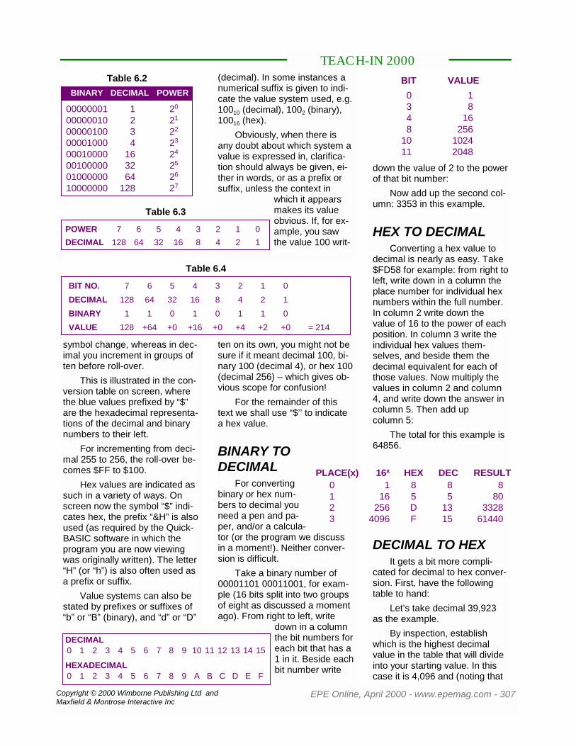
Copyright © 2000 Wimborne Publishing Ltd andMaxfield & Montrose Interactive Inc
EPE Online, April 2000 - www.epemag.com - 307
symbol change, whereas in dec-imal you increment in groups often before roll-over.
This is illustrated in the con-version table on screen, wherethe blue values prefixed by “$”are the hexadecimal representa-tions of the decimal and binarynumbers to their left.
For incrementing from deci-mal 255 to 256, the roll-over be-comes $FF to $100.
Hex values are indicated assuch in a variety of ways. Onscreen now the symbol “$” indi-cates hex, the prefix “&H” is alsoused (as required by the Quick-BASIC software in which theprogram you are now viewingwas originally written). The letter“H” (or “h”) is also often used asa prefix or suffix.
Value systems can also bestated by prefixes or suffixes of“b” or “B” (binary), and “d” or “D”
TEACH-IN 2000
BINARY DECIMAL
0000000100000010000001000000100000010000001000000100000010000000
1234
163264
128
Table 6.2POWER
20
21
22
23
24
25
26
27
(decimal). In some instances anumerical suffix is given to indi-cate the value system used, e.g.10010 (decimal), 1002 (binary),10016 (hex).
Obviously, when there isany doubt about which system avalue is expressed in, clarifica-tion should always be given, ei-ther in words, or as a prefix orsuffix, unless the context in
which it appearsmakes its valueobvious. If, for ex-ample, you sawthe value 100 writ-
POWERDECIMAL
Table 6.3
128 64 32 16 8 4 2 17 6 5 4 3 2 1 0
BIT NO.DECIMAL
Table 6.4
7 6 5 4 3 2 1 0
BINARYVALUE
128 64 32 16 8 4 2 11 1 0 1 0 1 1 0
128 +64 +0 +16 +0 +4 +2 +0 = 214
ten on its own, you might not besure if it meant decimal 100, bi-nary 100 (decimal 4), or hex 100(decimal 256) – which gives ob-vious scope for confusion!
For the remainder of thistext we shall use “$’’ to indicatea hex value.
BINARY TODECIMAL
For convertingbinary or hex num-bers to decimal youneed a pen and pa-per, and/or a calcula-tor (or the program we discussin a moment!). Neither conver-sion is difficult.
Take a binary number of00001101 00011001, for exam-ple (16 bits split into two groupsof eight as discussed a momentago). From right to left, write
down in a columnthe bit numbers foreach bit that has a1 in it. Beside eachbit number write
down the value of 2 to the powerof that bit number:
Now add up the second col-umn: 3353 in this example.
HEX TO DECIMALConverting a hex value to
decimal is nearly as easy. Take$FD58 for example: from right toleft, write down in a column theplace number for individual hexnumbers within the full number.In column 2 write down thevalue of 16 to the power of eachposition. In column 3 write theindividual hex values them-selves, and beside them thedecimal equivalent for each ofthose values. Now multiply thevalues in column 2 and column4, and write down the answer incolumn 5. Then add upcolumn 5:
The total for this example is64856.
DECIMAL0 1 2 3 4 5 6 7 8 9 10 11 12 13 14 15
HEXADECIMAL0 1 2 3 4 5 6 7 8 9 A B C D E F
PLACE(x) 16x
0123
HEX DEC RESULT1
16256
4096
85DF
85
1315
880
332861440
BIT VALUE0348
1011
18
16256
10242048
DECIMAL TO HEXIt gets a bit more compli-
cated for decimal to hex conver-sion. First, have the followingtable to hand:
Let’s take decimal 39,923as the example.
By inspection, establishwhich is the highest decimalvalue in the table that will divideinto your starting value. In thiscase it is 4,096 and (noting that

Copyright © 2000 Wimborne Publishing Ltd andMaxfield & Montrose Interactive Inc
EPE Online, April 2000 - www.epemag.com - 308
TEACH-IN 2000
In reverse order, from 3 to0, write down your nibbles:
1010 0111 0101 1101
which is the binary conver-sion for $A75D (or 1010011101011101 as a 2-byte valuerather than four nibbles).
VALUE CONVER-SION PROGRAM
A program that allows con-version between decimal, binaryand hex is available from themain menu: run Binary, Hex,
Decimal Converter.The program caters
for binary numbers up to32 bits long – decimaland hex maximums of4,294,967,295 and
$FFFFFFFF.The central box is split into
seven horizontal sections (seePhoto 6.6). Sections 3 to 7(Binary to Decimal) can be se-lected using the up/down arrow
keys. In each section anyindividual characterwithin the full value canbe accessed using theleft and right arrows.
The selected charac-ter can be changed andthe result of that changeis calculated in relation tothe other four control-
only integer values – wholenumbers – are used in the divi-sion answers) the sequence be-comes: binary:
First write down as a tablethe powers of 2 that make up a4-bit binary value (nibble):
POWER VALUE160
161
162
163
164
165
166
167
116
2564,096
65,5361,048,576
16,777,216268,435,456
39923 / 4096 = 9 (= $9)4096 x 9 = 3686439923 - 36864 = 3059
3059 / 256 = 11 (= $B)256 x 11 = 28163059 - 2816 = 243
243 / 16 = 15 (= $F)16 x 15 = 240243 - 240 = 3 (= $3)
POWERDECIMAL 8 4 2 1
23 22 21 20
Collecting the integer an-swers plus the final remaindergives us: 9, 11, 15, 3. Convert-ing the decimal integer answersto hex gives: $9BF3.
HEX TO BINARYWe before go any further we
must explain the term nibblethat’s about to be used. A nibble(or nybble) is a quaint computingterm and refers to a group offour bits, whereas a group ofeight bits is generally known asa byte.
Conventionally, a byte issplit equally into two nibbles, leftand right, comprising bits 7 to 4,and 3 to 0. You would not, forexample, take the group com-prising bit 5 to 2 as being a nib-ble.
Having clarified that, here’show to convert a hex value to
Photo 6.6. Interactive decimal-binary-hex conversionscreen, catering for up to 32-bit numbers.
Take as our example$A75D. The right-hand value is$D. Hopefully, you will recall, orcan work it out, that D is decimal13, which is made up from thefollowing power-of-two values:
8 + 4 + 1 = 13
So your table now becomes:
POWER 23 22 21 20
DECIMAL 8 4 2 1$D = 13 = 8 4 0 1BINARY 1 1 0 1 (nibble 0)
Therefore $D = 13 decimal= binary 1101.
In a similar fashion, workright to left taking each hexvalue in turn. In this instance toproduce:
$5 = 5 = 0 4 0 1BINARY 0 1 0 1 (nibble 1)
$A = 10 = 8 0 2 0BINARY 1 0 1 0 (nibble 3)
$7 = 7 = 0 4 2 1BINARY 0 1 1 1 (nibble 2)

Copyright © 2000 Wimborne Publishing Ltd andMaxfield & Montrose Interactive Inc
EPE Online, April 2000 - www.epemag.com - 309
TEACH-IN 2000lable sections and the resultsdisplayed. Try it! The full rangeof control keys available isstated in the left-hand box.
We believe the display andits options are obvious, but wewill just clarify one small matter:the “^’’ symbol will be seen inthe Bit Value line, this indicatesthat the following number is apower (index), e.g. 2^4 means24.
DIRECT ENTRYThe Binary, Hex and Deci-
mal Converter program allowsyou to directly enter your ownvalues for conversion. When thehighlight is active on one of thefive Binary to Decimal options,press <ENTER>. At the bottomof the screen, value entry thenbecomes available. Enter thevalue, press <ENTER> againand the value is converted to theother modes.
There are a few interceptsto prevent you “crashing” theprogram with most practical jokeentries! (But nothing to stop ma-licious intent if you are really seton it! If you do get the screenmessed up, return to the menuand re-select the program.)
SELF-TESTPress <S> to test your un-
derstanding of bin-hex-dec con-version! With a bit of practice,and reference to our earlier dis-cussions, you should find thatit’s actually easier than youmight think.
Note that when asked toconvert a value to binary, youenter the answer in groups ofnibbles separated by a space.This makes it easier to examineyour answer if it’s wrong.
If you really cannot work outan answer, press <A> plus<ENTER> for it to be revealed.But it’s worth trying to get an-
swers for yourself, the ability todo such conversions is invalu-able.
MORE EXPERI-MENTS
You’ve learned that you cancount on us to offer you someinteresting hands-on ideas eachmonth – you can count on usagain in this month’s Experi-mental section, so clock onto it!
NEXT MONTHIn part 7 we examine
opamps, which are integratedcircuits for use with analog sig-nals and voltages. Amongstother things, opamps allowwaveforms to be amplified,mixed, and generally processedin a variety of ways. We shallillustrate their principles andsome of the ways in which theycan be used, to allow you, forexample, to listen to the wave-forms we discussed in Part 5.
PANEL 6.3 – RELATIVELY SPEAKINGAn important concept to appreciate in electronics is that nothing
happens instantaneously; everything takes a certain length of time tochange from one state to another, whether it is a switch changingfrom on to off, or a voltage changing from one level to another, or justa fuse blowing.
It may seem that the switch is either open or closed, contacts ei-ther apart or touching, and at a molecular level this is true, but thephysical nature of a switch means that because of the broad area ofits conducting contacts, there is a period during switching off, for ex-ample, when the area of each contact which is actually touching theother is changing progressively from full-area contact to point contact,and only at the very final moment is the ultimate point contact broken.
During this period, the resistance between the contacts increasesto the current flowing between them, and even at the moment whenthe physical point contact is broken, an electrical arc might be formedbetween the two open points, allowing current to still flow across themuntil they are even further apart. So much for the instantaneous na-ture of an on-off switch!
In digital electronic circuits, it is customary to think of the logicgates involved as responding to an instantaneous change from, say,logic 0 to logic 1 (from a low voltage to a high one). No such immedi-ate change takes place, it takes time for the change to occur andthere is a constant gradient through which the actual voltage level hasto pass; it does not just suddenly jump from 0V to 5V, for example.
The time taken to make the transition may be short, possibly onlyfractions of a millionth of a second, but it still exists, and the conceptof synchronicity – two things occurring at the same moment – is onlya convenience when working out the logic of a digital circuit.
In reality, the synchronization of various actions taking place inorder to create a further change is related to a “window” in time, dur-ing which all the required changes can occur at their own separaterates. The window could be a mere picosecond; it could be half ofeternity; how it matters depends on what the circuit is required to do,and as long as all those changes happen while the window is “open”,the circuit will behave as though they had all occurred at the samemoment. But, if any of them occur outside the window, the result maybe unpredictable and undesirable.

Copyright © 2000 Wimborne Publishing Ltd andMaxfield & Montrose Interactive Inc
EPE Online, April 2000 - www.epemag.com - 310
In the latter part of thismonth’s Tutorial, we discussedbinary numbers and the way inwhich they relate to decimal andhexadecimal values. We arenow in a position to introduce anintegrated circuit that allows youto physically see the binarycounting process in action. Werefer, of course, to a binarycounter plus some LEDs!
There are numerous typesof counter manufactured, withsuch descriptive names as bi-nary ripple counter, synchronousbinary counter, asynchronousbinary counter, binary-coded-decimal counter, Gray counter,decade counter, Johnsoncounter, up/down counter, andso on. Far too many to discussin detail – and there are evenvariants on these!
We shall just concentrate ontwo types, a 7-bit binary ripplecounter, and an 11-outputdecade counter.
BINARY COUNTERThe 7-bit binary ripple
counter we shall use is the74HC4024. Find one from yourcomponents bag and connect itinto your breadboard, togetherwith the required LEDs and re-sistors, as shown in Fig.6.10. Asusual, touch a grounded(earthed) item to dischargestatic electricity from your bodybefore handling the device (andensure that it’s the right wayround!).
If you only have five 470�resistors available, you coulduse any value between 100�and 1k� for the other two.
Connect up power andwatch the LEDs while adjustingthe oscillator for different fre-
quencies.
SYMBOLICSThe circuit diagram for this
setup is shown in Fig.6.11, andthe pinouts for the 74HC4024are in Fig.6.12. Unlike with logicgates, there is no “official” sym-bol to illustrate the nature of this
TEACH-IN 2000
device (which is increasingly thecase with integrated circuits thatbecome more and more com-plex).
What we have to contentourselves with is a boxed outlinewith some pin numbers and theirdescriptions. In the circuit dia-gram, note first the pins to whichthe power lines are connected.As with the logic gates dis-cussed in the Tutorial these arepin 7 for 0V (GND) and pin 14for +VE (this is not always truefor other digital devices). Therecommended operating volt-ages are between 2V and 6V,although this device will with-stand up to 7V for short periods(but never above 7V).
The Clock input is the nextimportant pin. This is the pin intowhich the data pulses that thecounter has to count are input.The “>” symbol in the pinout dia-gram also indicates that this isthe Clock input pin. It is fre-quently omitted in many circuitdiagrams.
Note also the small circle atthis input pin. It indicates thatinside the device the pulse logiclevel to which the device re-sponds is “inverted”. You met a
TEACH-IN 2000 – EXPERIMENTAL 6BINARY AND DECIMAL COUNTERS
3533 34
2222
2323
2424
2525
2626
2727
2828
2929
30 33
30
CLOCK INFROM IC1a PIN 2
R0
R1
R2
74HC4024
R6
R5
R4
R3
D4
D3
a a
k k
D
DD
DD0 1 2
56
a a
aa
a
k
k k
k k
Fig.6.10. Breadboard layoutfor the binary ripple counter
experiment.
0V
CLOCKINPUT
+6V
k k k
R6 R5 R4 R3 R2 R1 R0470� 470� 470� 470� 470� 470� 470�
D6
+VE
7
Q1
Q0
Q2
Q3
Q4
Q6
Q5
CLOCK
RESET2
1
74HC4024
GND
3
4
5
6
911
12
14
a a a
D5 D4
k k k k
a a
D3 D2 D1
a a
D0
Fig.6.11. Circuit diagram for the binary ripple counterexperiment.

Copyright © 2000 Wimborne Publishing Ltd andMaxfield & Montrose Interactive Inc
EPE Online, April 2000 - www.epemag.com - 311
TEACH-IN 2000
function (Reset, Clock, Enable,etc.) is permitted or occurs whenthat pin is taken (or is already at)high.
“Q” OUTPUTSThe remaining useful pins
are labeled Q0 to Q6 (in somecircuits or pinout diagrams, theymay be labeled as Q1 to Q7).Note that three pins have nofunction (8, 10 and 13). Notealso the use of “Q” to signify anoutput; conventionally, this is theletter normally used with digitaldevices such as counters(whereas “Y” was used with thegates, earlier).
We have said that the74H4024 is a 7-bit counter. PinsQ0 to Q6 are the outputs atwhich the seven bits of the inter-nal binary count value are ac-cessed. Referring you back towhat you have learned aboutbinary numbers, output Q0 cor-responds to bit 0, Q1 to bit 1,etc. It is to tie in with this num-bering that the resistors andLEDs are numbered from 0 to 6in Fig.6.11.BINARY COUNT-UP
similar situation with the NAND,NOR and XNOR gates, althoughin their case the inversion tookplace on the output data.
The significance about thelogic level to which a devicesuch as a counter responds isimportant to note. Many devicesdo not respond to the actualvoltage level at an input (as didthe logic gates in the Tutorial)but to the change in logic level.
In the case of the74HC4024, the change re-sponded to is that from high tolow, and the counter adds 1 toits internal count value. The de-vice is said to respond to thetrailing edge of a pulse (a termwe used when looking at pulsesin the Tutorial).
When the pulse changesfrom low to high, the devicedoes not respond in any wayand the count remains as it was.(The 74HC4017 we shall uselater responds to the changefrom low to high – i.e. to theleading edge).
Be aware that not all circuitdiagrams show the inversion cir-
cle even though inversion oc-curs. Some circuits show a barline above the description forsuch a pin (as we have done inFig.6.11). Indeed, the use of abar to signify inversion is ar-guably more commonplace thanthe circle.
RESET LOGICPin 2 of the 74HC4024 is
the Reset pin. When Reset is atlogic 0 (low), the counter is per-mitted to count any pulses thatenter the Clock pin. Two thingshappen when the Reset pin istaken high (logic 1). First, theentire count within the device isreset to zero. Second, thecounter is prevented from count-ing any further pulses until Re-set has been returned low.
Note that in some types ofcounter, Reset may be active-low, in other words, Reset oc-curs when the pin is set low(logic 0), but counting is permit-ted when the pin is high.
The terms active-low andactive-high are frequently en-countered in electronics. Thelatter means that the stated
Photo 6.7. Breadboard showing the binarycounter and LEDs. Part of the oscillator is
shown at the left.
ADVANCE TO NEXT STATE
ALL OUTPUTS ARE LOW
OUTPUT STATE
NO CHANGE
CLOCK
RESET
N.C. = NO CONNECTION
X = DON'T CARE
X H
L
L
FUNCTION TABLE
11
12
GND
7
CLOCK RESET
CLOCK
RESET2
1Q1
Q0
Q2
Q3
Q4
Q6
Q5
9
6
5
4
3
+VE
SYMBOL(SEE TEXT)
14
7
4
5
6
2
3
1
Q3
GND
Q4
Q5
Q6
74HC4024
Q2
N.C.
9
8
+VE
Q0
Q1
N.C.
N.C.
10
11
13
12
14
PINOUTS
Fig.6.12. Symbol, pinouts andfunction table for a 74HC4024
binary ripple counter.
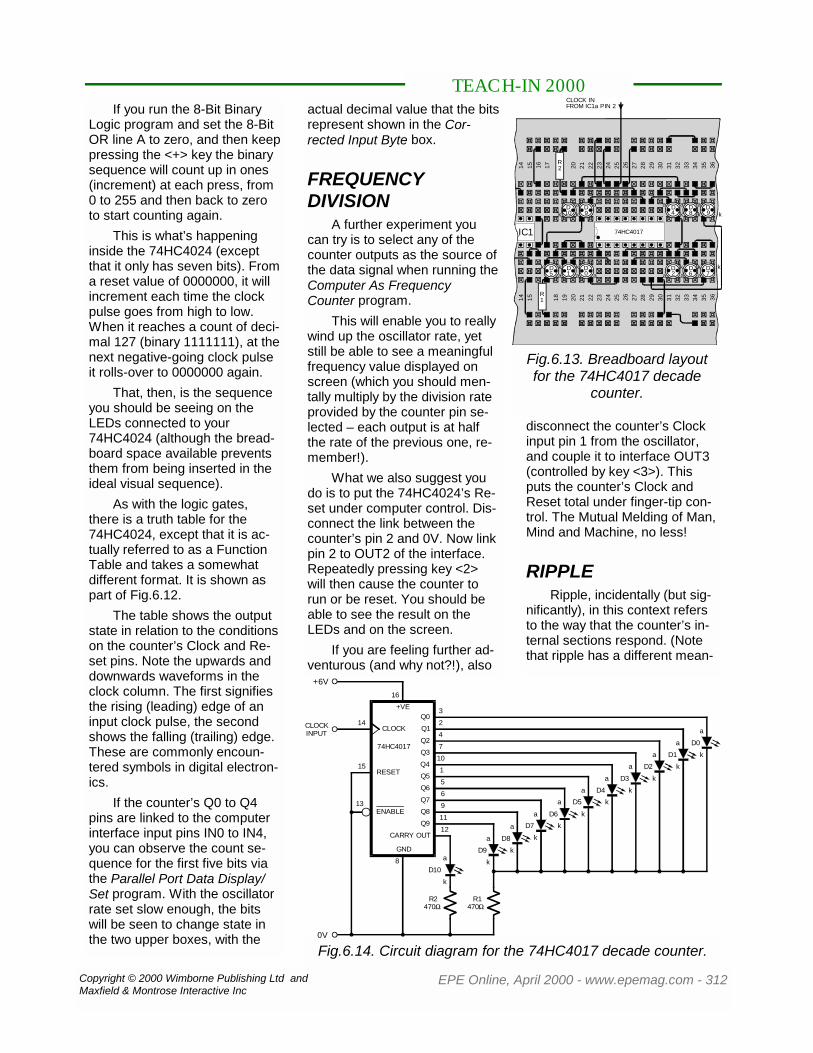
Copyright © 2000 Wimborne Publishing Ltd andMaxfield & Montrose Interactive Inc
EPE Online, April 2000 - www.epemag.com - 312
TEACH-IN 2000
disconnect the counter’s Clockinput pin 1 from the oscillator,and couple it to interface OUT3(controlled by key <3>). Thisputs the counter’s Clock andReset total under finger-tip con-trol. The Mutual Melding of Man,Mind and Machine, no less!
RIPPLERipple, incidentally (but sig-
nificantly), in this context refersto the way that the counter’s in-ternal sections respond. (Notethat ripple has a different mean-
If you run the 8-Bit BinaryLogic program and set the 8-BitOR line A to zero, and then keeppressing the <+> key the binarysequence will count up in ones(increment) at each press, from0 to 255 and then back to zeroto start counting again.
This is what’s happeninginside the 74HC4024 (exceptthat it only has seven bits). Froma reset value of 0000000, it willincrement each time the clockpulse goes from high to low.When it reaches a count of deci-mal 127 (binary 1111111), at thenext negative-going clock pulseit rolls-over to 0000000 again.
That, then, is the sequenceyou should be seeing on theLEDs connected to your74HC4024 (although the bread-board space available preventsthem from being inserted in theideal visual sequence).
As with the logic gates,there is a truth table for the74HC4024, except that it is ac-tually referred to as a FunctionTable and takes a somewhatdifferent format. It is shown aspart of Fig.6.12.
The table shows the outputstate in relation to the conditionson the counter’s Clock and Re-set pins. Note the upwards anddownwards waveforms in theclock column. The first signifiesthe rising (leading) edge of aninput clock pulse, the secondshows the falling (trailing) edge.These are commonly encoun-tered symbols in digital electron-ics.
If the counter’s Q0 to Q4pins are linked to the computerinterface input pins IN0 to IN4,you can observe the count se-quence for the first five bits viathe Parallel Port Data Display/Set program. With the oscillatorrate set slow enough, the bitswill be seen to change state inthe two upper boxes, with the
actual decimal value that the bitsrepresent shown in the Cor-rected Input Byte box.
FREQUENCYDIVISION
A further experiment youcan try is to select any of thecounter outputs as the source ofthe data signal when running theComputer As FrequencyCounter program.
This will enable you to reallywind up the oscillator rate, yetstill be able to see a meaningfulfrequency value displayed onscreen (which you should men-tally multiply by the division rateprovided by the counter pin se-lected – each output is at halfthe rate of the previous one, re-member!).
What we also suggest youdo is to put the 74HC4024’s Re-set under computer control. Dis-connect the link between thecounter’s pin 2 and 0V. Now linkpin 2 to OUT2 of the interface.Repeatedly pressing key <2>will then cause the counter torun or be reset. You should beable to see the result on theLEDs and on the screen.
If you are feeling further ad-venturous (and why not?!), also
CLOCK INFROM IC1a PIN 2
26
26
29
2930
30
31
3132
32
33
3334
34
35
35
2727
2828
14
14
15
15 16 17
18
19 20
2021
21
2222
2323
24
2425
25
36
36
IC1
R2
D
D D D D D D
D D D D10 9 4
a
a a a a a a
a a a a
k
k k k kkk
k k kk 8 9
74HC4017
5 1 0
R1
2 6 7
Fig.6.13. Breadboard layoutfor the 74HC4017 decade
counter.
a
k
0V
CLOCKINPUT
+6V
k
R2470�
R1470�
D10
CARRY OUT
Q9
Q8ENABLE
GND
8
Q7
Q2
Q3
Q4
Q6
Q515
13
RESET
74HC4017
Q1
Q014
CLOCK
16
+VE
4
D7
9
11
12D8
D9
k
a
a
ka
6
7
10
1
5
3
2
D5a k
D6
k
k
D4
D3
a
a
a
k
a
D0
D1
D2
a
k
a
k
k
Fig.6.14. Circuit diagram for the 74HC4017 decade counter.

Copyright © 2000 Wimborne Publishing Ltd andMaxfield & Montrose Interactive Inc
EPE Online, April 2000 - www.epemag.com - 313
TEACH-IN 2000
needed for the 10 LEDs D0 to D9,since only one can ever be on atonce.
You will see from the circuitdiagram that, in common withthe binary counter, this decadecounter has a Clock input (pin14) and a Reset pin (pin 15). Aswe said earlier, the 74HC4017increments the count on eachrising edge of the clock pulse.
The count is reset to 0 whenthe Reset pin is high. However,when the Reset pin is low, thecontinuation of the count de-pends on the status of a thirdpin, Enable, pin 13. Not surpris-ingly, this pin enables or inhibitsthe clock count. Because thereis a bar-line above the word En-able (or a circle on its input), weknow that the counter is enabledwhen the pin is low.
The ten outputs are labeledQ0 to Q9, which ties in with thecount value that a logic 1 on therespective pin represents.
The function table for the
ing in the context of power sup-plies – which we will discusslater in this Teach-In series.) Insimple terms, the counter con-tains several divide-by-two cir-cuits in a chain. It takes time foreach counter to react to a triggerpulse from the precedingcounter.
The delay is only short(nanoseconds for the74HC4024), but the total delayas the pulses ripple throughstages to the final output can becritical to other circuits, whichmay rely on the synchronizationbetween a multi-stage counter’sclock pulse and the setting of anoutput pin.
There are counters in whichthe internal circuitry is designedso that each section is triggeredat the same time. These coun-ters are referred to as syn-chronous.
DECIMAL COUNTERWhen you can tear yourself
away from the fascination of bi-nary counting, have a look at theattributes of a decade counter,the 74HC4017. Remove the
74HC4024 and in-sert the74HC4017. Con-nect its pins asshown inFig.6.13, complete with LEDsD0 to D9 and resistors R1 andR2. You will need to “steal” thetenth LED from the oscillator,unless you bought more thanthe suggested quantity of 10.Ignore D10 for the moment.
Power up your breadboardand watch the sequence of theLEDs. Adjust the oscillator rateso that you clearly see the stepsof the count.
Whereas the 74HC4024counted in binary, from 0 to 127,the 74HC4017 decade countercounts in steps from 0 to 9,rolling over to begin the countfrom 0 again following 9. Duringthe count only one output is everhigh at any time.
The pinouts for the74HC4017 are shown inFig.6.15, the circuit diagram forthe connections on your bread-board is illustrated in Fig.6.14.Again the LEDs are numberedfrom zero to correspond with theoutput numbers. Note that onlyone ballast resistor (R1) is
Photo 6.8. Breadboard showing thedecade counter experimental circuit,with part of the oscillator seen to the
left, and part of the ADC chip tothe right. Take care that crossing
link wires do not touch.X = DON'T CARE
CARRY OUT = H FOR Q0, Q1, Q2, Q3 OR Q4 = HCARRY OUT = L OTHERWISE
FUNCTION TABLE
74HC4017
Q2
X
H
CARRY OUT
X
L
X
CLOCK
ENABLE
RESET15
13
L
L
L
L
L
X
RESET
L
L
H
H
X
X
CLOCKENABLE
Q811
Q9
GND
8
12
6Q7
9
Q3
Q4
Q6
Q5
7
10
1
5
CLOCK
SYMBOL
14
16
Q1
Q0+VE
3
2
4 RESETQ12 15
RESET COUNTERQ0=H, Q1 TO Q9=LC.O.=H
ADVANCE TO NEXT STATE
ADVANCE TO NEXT STATE
NO CHANGE
NO CHANGE
NO CHANGE
NO CHANGE
OUTPUT STATE
Q3
GND
7
8
Q4
Q8
CARRY OUT
ENABLE
CLOCK
Q24
Q6
Q7
5
6
Q03
Q9
10
9
13
11
12
14
Q51
PINOUTS
+VE 16
*
*
Fig.6.15. Symbol, pinouts and functiontable for the 74HC4017 decade counter.

Copyright © 2000 Wimborne Publishing Ltd andMaxfield & Montrose Interactive Inc
EPE Online, April 2000 - www.epemag.com - 314
TEACH-IN 2000LED from one of the outputs(but not from outputs 0 or 5).Add the LED to the Carry Outpin as D10, via the already in-serted resistor R2). Power backup again and observe the se-quence.
As with the 74HC4024, youcan connect up to five outputs tothe computer interface at IN0 toIN4. You can also connect theClock, Reset and Enable pins tothe interface outputs OUT2 toOUT4, controlling them fromyour keyboard when runningprogram Parallel Port Data Dis-play/Set.
So there’s a whole raft ofideas to play around with untilnext month. You could also in-clude some experiments withthe logic gates, interfacing themto the computer and counters aswell. Till then this author’s outfor the count!
CORRECTIONIn Part 5, Fig.5.6. Add link
wire to join rows E and F of col-umn 42.
74HC4017 is shown as part ofFig.6.14. An interesting point tonote is that the Enable pin canalso act as a clock signal to thecounter. When Clock is heldhigh and Enable is taken fromhigh to low, the count advancesto the next state.
In most circuits it is moreusual to use Clock rather thanEnable as the clocking signal.However, what this option high-lights is that Enable shouldnever be taken low when theclock is high if you wish to pre-serve the count value existing atthe last clock pulse.
It is subtleties like this thatabound in digital electronic cir-cuits, especially when the overallcircuit complexity is great. Youalways need to consider the im-plications of how the timing ofdifferent signals can affect theresponse. In reality, at this stageof your learning, you need notconcern yourself about them.
When you are ready to considerthem, you’ll find that data sheetsgive typical timing values forpractically everything!
There is an eleventh outputpin, the Carry Out pin. This pingoes high when the counter isreset or rolls over to zero. It re-mains high until a count of five isreached.
The Carry Out signal is ofbenefit in a variety of situations;such as where you might wish tocouple (cascade) two or moredecade counters in series, forexample. In this case the risingedge of the Carry Out signalwould be used as the clockpulse for the next stage. Thusthe first counter would countunits from 0 to 9 and the secondstage count the decades from10 to 90. A third stage couldcount the hundreds, 100 to 900,and so on.
Observe the Carry Out pinin action by removing, say, the
Copyright © 2000 Wimborne Publishing Ltd andMaxfield & Montrose Interactive Inc
EPE Online, April 2000 - www.epemag.com - 315
Following several readers’enquiries we receivedconcerning opamps (operationalamplifiers), last month weprovided a summary opampselector chart, which illustratedthe often-gargantuan differencesbetween individual types. Thereare thousands of opampsavailable, often optimized for aparticular use and in demandingapplications (e.g.instrumentation or low-powercircuits) the choice of devicetype can be very critical.
It’s a good idea to decide onthe factors which are mostimportant in your application(input impedance/slew-rate/power consumption?) and thenchoose a likely-looking deviceusing our selector as a guide, orcheck the major catalogs forguidance. Also, manymanufacturers now have websites from which data sheetscan be downloaded, and usingthe data in our previous articlesyou will be able to navigatethrough the minefield of opampparameters and specificationsmore easily.
OPAMPS – GETTINGLOADED
We now continue toinvestigate opampcharacteristics and techniques.We described the basicdifferential amplifier last month,which we have drawn again inFig.1. Opamps should have a
very high voltage gain, so thevoltage gain of our differentialamplifier should be as high aspossible.
Any transistor used in theamplifier will have a (more orless) fixed gain, but this is interms of its current output, i.e.its collector current. Variationsin the transistor’s base-emittervoltage and base current willcause large variations in itscollector current. The collectorcurrent flows through thecollector resistor, Rc, givingrise to the output voltage, Vo.
By Ohm’s Law, V=IR, sofor a given current variation,then the larger we make R thelarger the voltage variation willbe. This means that the largerwe make Rc, the larger thevoltage gain of the differential
amplifier. This seemsstraightforward enough – justuse large values of Rc and weget a nice high gain: after allresistors are cheap and largevalues don’t cost any more thansmaller ones!
Unfortunately it’s not thatsimple. First of all opamps areusually integrated circuits (ICs)where large resistors do costmore – they take up more space(silicon real estate!).
Furthermore, it is difficult forIC makers to fabricate preciseresistance values, so there canbe comparatively few resistorson a typical chip. Secondly, thetransistors have to operatewithin a certain range of biascurrents, below which they maygive poor performance in termsof gain etc.
If we use large resistors andkeep the supply voltage thesame, we have to reduce thebias current, possibly to anunacceptable level. Alternatively,we can always increase thesupply voltage, but do you reallywant an opamp that requires a100V supply?
This seems like a no-winsituation, but happily the currentmirror circuit comes to ourrescue. Although a current
Onwards with our opamps extravaganza we go,unearthing more of the inner workings of theseessential electronic workhourses. Plus more questionsand answers from our postbag as well.
by ALAN WINSTANLEY & IAN BELL
Fig.1. Differential amplifierformed from a matched pair
of npn transistors
Fig.2. simple single-transistoramplifier.
Copyright © 2000 Wimborne Publishing Ltd andMaxfield & Montrose Interactive Inc
EPE Online, April 2000 - www.epemag.com - 316
source has a very highresistance (ideally infinite, infact), any current we choose canflow from it.
Thus, in our opamp circuitwe can set up a current sourceoutputting the appropriate biascurrent, and use it in place ofthe collector resistor; thetransistor gets the correctoperating current it needs, andwe get a high voltage gain dueto the very large effectiveresistance of the current source.See May and June ’99 CircuitSurgery for a detailedexplanation of transistor currentsources.
shown in Fig.4.We can use an active load
with the differential amplifier, butthe situation is a little morecomplex because we have to becareful not to upset thesymmetry of the circuit. If weused two separate currentsources for the two transistors,we may not be able to match thecurrents accurately enough tothe emitter bias current.
The reason this matching isdifficult (unlike the twotransistors in the differentialamplifier itself which are wellmatched) is that if the emittercurrent source and differentialamplifier transistors are npnthen the active load will be pnp,and it is difficult to match npnwith pnp transistors. Thesolution is use a current mirrorwith its reference connected toone differential transistor and itsoutput to other. This is shown inFig.5.
It looks like even thisapproach breaks the symmetryof the circuit (TR3’s baseconnection is not the same asTR4’s), but as far as current flowis concerned the circuit is stillsymmetrical. When a differentialinput voltage is applied, theamplified output differencecurrent on TR2’s side is droppedacross the current mirror’s very
0����66V. The bias current causesa certain collector current to flow(call this IBIAS) which results in acertain voltage drop across thecollector resistor.
As the signal varies, thecollector current varies aroundIBIAS causing the voltage dropacross the collector resistor tovary as well. This actionproduces the (amplified) outputvoltage signal. We can think ofthe bias and the signal as twoseparate components of thecollector signal, which whenadded together give the overallaction of the circuit.
It does not matter where thebias “comes from”, so we couldapply the bias current directly tothe collector circuit by using acurrent source as shown inFig.3. With no signal applied thebase voltage would adopt theappropriate voltage (0����65V in ourexample), always assumingthan the required base currentcould be supplied to the base(the means for this is not shown,but in a real circuit the basewould obviously be connectedsomewhere to achieve this).
ACTIVE LOADWhen we applied the signal
to the amplifier, we would forcethe collector current tosomething other than IBIAS, andin order for the current to bemaintained through the constantcurrent source the difference,i.e. the signal current, would flowin the internal resistance of thecurrent source. Now this resistoris large and therefore results ina very large voltage gain (asmall current change results in alarge voltage change).
A current source used to gethigh gain from an amplifier inthis manner is known as anactive load. The schematic for abasic implementation of Fig.2 is
Circuit Surgery
BIASED APPROACHBefore seeing how we apply
this to our differential amplifier, itis easier to have a look at asimple one-transistor amplifier,and at this point it is useful torecall the idea of biasing in moredetail. Consider Fig.2, a verybasic transistor amplifier. It isbiased by applying a DC voltageto the base (not shown), andoften a potential divider is usedfor this purpose.
The input signal variesaround the bias voltage, so forexample if the bias voltage was0����65V and the signal was 0����02Vpeak-to-peak, then the biasvoltage would vary from 0����64V to
Fig.3. Simple transistor am-plifier with current source
load (active load).
Fig.4. Schematic of transistoramplifier with active load.

Copyright © 2000 Wimborne Publishing Ltd andMaxfield & Montrose Interactive Inc
EPE Online, April 2000 - www.epemag.com - 317
large internal (output)resistance. So we get a highlyamplified voltage signal at TR2’scollector.
However, TR4 is wired like aforward biased diode (thetransistor’s base-emitterjunction) and therefore has alow resistance. The voltage gainat TR1’s collector is thereforelow and this output cannot beused. With an active load thedifferential amplifier has to beused with a single ended output.
We’ll be rounding off ouropamp mini-tutorial next month,by looking at the output side ofthings, including ways ofimplementing short-circuitprotection. IMB.
SOCKET TO MEDavid Preston asks: “I
have a question on the use ofdual in-line (DIL) sockets. I haveseveral designs that use anopto-triac operating at mainsvoltages. Could you tell me themaximum ratings of a DILsocket? Would they be suitablefor a DIL opto-triac or should Isolder the device straight to theboard?”
The typical contact rating ofa DIL socket is at least 1A ormore. Harwin is a well-knownmaker and their catalog ofturned-pin sockets quotes arating of 2A per pin, with aninsulation resistance of 500V(which I would interpret as themaximum voltage allowedbetween two adjacent pins).
Another maker (Augat) isquoted at up to 3A with adielectric strength of 1kV RMS(1����4kV peak). However, I wouldhate to hang a 750W mains loadon such a socket! I would prefersay 50W to 100W or somaximum as a safe rule ofthumb.
There are two types of DILsocket – the “leaf” type uses apair of wiping spring contacts onevery pin. The entrance to eachcontact is large, and the IC pinsare gradually guided intoalignment using automatic ormanual insertion equipment.
More expensive precision“turned-pin” sockets make agood contact with the fourcorners of each IC pin andrequire that the chip must bepre-aligned, but they tend to beeasier and smoother to workwith. The idea is to produce agas-tight seal around the fourpoints of contact, to ensure anoise-free and reliable joint. Thecurrent ratings of both types isabout the same, but I would saythat the “leaf” type will have astronger joint.
Personally speaking, withany opto-isolator or triac devicecontrolling mains loads, I wouldwant to solder it directly to theboard, so that there are nice“meaty” solder joints that willhelp with the current-carryingcapacity of the joint. The PCB’s
copper tracks will also help toheatsink the device as well, andfor this reason audio amplifierICs are always best soldereddirect to the board rather thanusing a DIL socket. ARW.
SURFACE-MOUNTSELECTION
“I would like to ask what theterm “MSOP” stands for: I havea school project in mind using aTC07 to detect temperature andwondered if the MSOP versionwould be suitable? Thank you!”
This question was posed inthe EPE Chat Zone messageboard of our web site. MSOPsimply means Moulded SmallOutline Package. Anything with“SO” in its description means“Small Outline” and shouldimmediately set alarm bellsringing!
It means you’re looking atthe tiny surface-mount version,which will be unsuitable for mostschool or hobbyist projectsbecause of the steady handneeded to position and solderthem reliably by hand, althoughyou could try if you fancy achallenge. Otherwise be sure tobuy the ordinary discrete versioninstead.
Here is a mini-glossary ofsome abbreviations used in thisarea:
CERDIP: Ceramic dual-in-linepackage
DIP: Dual-in line packageLCCC: Leadless ceramic chip
carrier (20 to 84 pin,square body, noleads).
LDCC: Leaded ceramic chipcarrier
PLCC: Plastic leaded chipcarrier (square-styleSM chip)
PQFP: Plastic quad flat-pack
Circuit Surgery
Fig.5. Differential amplifierwith higher gain due to active
load. Transistors TR3 andTR4 form a current mirror

Copyright © 2000 Wimborne Publishing Ltd andMaxfield & Montrose Interactive Inc
EPE Online, April 2000 - www.epemag.com - 318
Circuit SurgeryQFP: Quad flat-packSMC: Surface mount
componentSMD: Surface mount deviceSMT: Surface mount
technologySOIC: Small-outline
integrated circuit(generic surface-mount IC)
SOJ: Small-outline with “J”-shaped leads
SOMP/MSOP: Molded small-outline package
SOP: Small-outline package(for surface mounting)
SOT: Small-outlinetransistor
Take it from someone whoknows, it’s dead easy to order asurface-mount device byaccident so you need to payclose attention to the catalogs(and data sheets) whenordering. ARW.

Copyright © 2000 Wimborne Publishing Ltd andMaxfield & Montrose Interactive Inc
EPE Online, April 2000 - www.epemag.com - 319
Britain stands pre-eminent increative science and engineering,but the depressingly long list of“lost” British firsts in inventionshows how often thwarted ordisillusioned British inventors andinnovators have either abandonedtheir ideas or gone abroad,thereby reducing Britishcompetitiveness. Decades ofBritish under-investment in Britishideas and British technologies hasmeant that other nations eitherindependently develop the sameideas, or directly capitalize onBritish technical creativity – andsoon overtake Britain in their ownmarkets.
Just such a story is that ofNorman Rutherford and hispartner Michael Turner, who havelearnt this lesson and are quick toremind us. They should know,back in the early 1960’s they notonly developed the first domesticvideo record and replay system,but also the first combined TV andVTR and the first Camcorder; but,it is claimed, poor foresight bytheir backers and investors lostthem the edge.
MAKING A PICTUREThe announcement of the
Cathodian Vidicon 3-inch TVcamera tube early in 1960 tookthe attention of both NormanTurner and Michael Rutherford.The possibility of a new productfor their Nottingham ElectronicValve Company (N.E.V.Co) was
competitor, but the“transistorized” version soonappeared from theirdevelopment bench and at 72UK pounds was even moreastonishing.
Advertisements elicited aninspiring response. Domesticand international sales rocketed– an order for 4000 camerascame in from Germany. Anabsolute triumph given that theGermans held the Britishelectronics industry in lowregard.
TAKE OVERThe then senior engineer at
Granada TV, Reg Hammons,saw a trade advert for the NEV2and thought the camera wouldbe good for mobile outsidebroadcasts and rehearsals. Hementioned his viewing of thecamera to Sidney (later Lord)Bernstein then head ofGranada.
Bernstein flew toNottingham and at a meetingwith both Norman and Michaellearnt that not only wasmanufacturing capacity verylimited, but the development ofthe camera had so depleted thecompany’s reserves that theywere unable to meet anythingapproaching a substantial order.He then asked how much theywould need to continue R&Dand production. “Too much.”said Norman “About half thevalue of the Company”.
“What is that amount” askedBernstein. “About £20,000,” said
TELCAN HOME VIDEOby Barrie Blake-Coleman
compelling. They wanted todevelop a small CCTV systembut the broadcast standardcamera tubes were far too bulkyand expensive.
The Cathodian device nowmade matters simpler. Cost wasstill a problem so, not requiringthe full TV standard quality, theynegotiated with Cathodian to buyall the slightly imperfect tubes(one or two drop-outs on thevideo array).
Oftimes a genius in circuitdesign, Michael developed thecamera electronics using justfour stages from two thermionicvalves. This miracle of economywas based on an ECC82 doubletriode and an ECL82 triodepentode valve. The first provideda video amplifier and diodemixer, the second a triode RFoscillator and power outputstage for the horizontal scancoils.
The vertical signal wasobtained from a mains-ripplesupply, giving a usable mainslocked sawtooth. “It was aunique – if not eccentric, pieceof design typical of Michael andmyself, but it worked like anabsolute dream,” so commentedNorman Rutherford recently.
The whole cameraassembly, designated NEV1Mini-Eye in its initial design, soldfor 150 UK pounds andoutpriced and outperformedanything around. It was 250 UKpounds less than its nearest
The true story of a British “first” in home video recording.

Copyright © 2000 Wimborne Publishing Ltd andMaxfield & Montrose Interactive Inc
EPE Online, April 2000 - www.epemag.com - 320
Norman.“That’s petty cash.”
Bernstein said and instructed hisaccountant to write a checkthere and then.
The company now had anew owner, but thoughBernstein had a 75 per centstake, both the original partnerswere appointed directors withfull management of thecompany’s operations. All debtswere paid off. More to the pointthey now had no limits to whatthey could spend on R&D.
IN A SPINReg Hammons made
frequent trips from Granada toliaise with the company onbehalf of Bernstein. On oneoccasion he mentioned that hewas aware of a large efforttaking place in the US andJapan to develop a videosystem for recording broadcastTV at home. Ampex haddeveloped the helical scansystem for professional users inthe US in the middle fifties andthe same approach was beingtried for domestic recorders.
Hammons thought therecould be a large market forhome video recorders and urgedthe two to have a go atdeveloping a system for theBritish market. The idea found areceptive audience, the mini-eyecamera had sold well but noworders were tailing off.
It was known that Ampexhad solved the video tapeproblem using four rotatingheads producing a helical scan– but this was an expensiveoption for a home video system.
At first they tried a narrowbandwidth design based on adomestic audio recorder toemulate the high-speed wire andmetal tape recorders alreadyused by the big broadcastingoperations.
It was the path of leastresistance – no one actuallyknew what the maximumfrequency limit was on very highspeed recording and so theyconverted two 0����25-inch reel-to-reel Grundig and Ferrograph AFrecorders to run at 60 and 120inches per second (IPS).Surprisingly, enough videoinformation could be recorded at60 IPS to create a shadow of apicture; at 120 IPS it was “justrecognizable” but a lot morework needed to be done.
But months of work gavelittle in the way ofencouragement. Then, inJanuary of 1962, Michael Turnerdiscovered in the course ofexamining head driver methodsthat a considerableimprovement in signal-to-noisecould be achieved byintroducing significant pre-emphasis on the driver signal.
The improvement was soprofound that it implied that abroadcast quality picture couldbe achieved quite soon.Unfortunately it was also adamaging revelation – theimprovement was genuine butsimply took the existingoperational limits in a differentdirection.
HEAD TO HEADThe main problem was
identified as the record and
replay heads. The head gap wastoo wide to give the highfrequency response necessary toapproach the ideal 3MHz neededto reproduce the full videobandwidth of the 405-line system.It was also determined that thelowest response able to give awide enough gray scale to enablethe picture to have clarity was2����5MHz.
Something needed to be doneto eliminate the head problem andgive the designers a chance tograpple with the other aspects ofthe video processing. A narrowgap head was produced from anexisting Ferrograph unit, but evenwithout AC bias on the tape(rather, a heavy DC bias directlyapplied to the tape by means of apermanent magnet) and heavypre-emphasis on the video signal,the best that could be achievedwas 2MHz. “It just got by” NormanRutherford recounted, but it hadto be better.
Unfortunately they had aseemingly intractable problem.The narrower the head gap, thelower the magnetic pathreluctance around the gapbecame. Thus, the greater theflux shunt around the gap, themore the signal field was sharedbetween the gap and the leakagepath.
The result was that as theresponse was increased with anarrowing gap, so the signal-to-noise ratio worsened. A mu-metalAmpex head (intended for HFtelemetry and imported from theStates) was one possible solution,but it was prohibitively expensive.The only recourse was to designone themselves!
Many months of work ledinevitably to a design whichavoided the conventionalproblems associated with ordinaryheads – they plumped for a cross-field head where the passivesection was made of two screwadjustable copper arms nominally
Special Feature
“There is a popular point of view, originated by Emerson,which assumes that building the first, or a better mousetrap,results in people beating a path to your door – this must be themost pernicious fallacy ever to misrepresent invention.”
Copyright © 2000 Wimborne Publishing Ltd andMaxfield & Montrose Interactive Inc
EPE Online, April 2000 - www.epemag.com - 321
separated at the rear by a 200micron gap with a tape face gapof just under 50 micron. Theactive section carrying the coillaterally straddled the twocopper arms and this designgave the necessary bandwidth.
Nevertheless, DC bias wasstill employed as too aconsiderable amount of pre-emphasis. But by contriving anoverwind on the final videodriver stage’s inductive load, theeffective bandwidth shot up towell in excess of 2����6MHz. Thereplay signal was, of course, stillhighly differentiated and this wasequalized by employing a seriesof 3db/Octave integrators and
phase correction circuits torecover the original signal.
Tape speed still needed tobe high (120 IPS for broadcaststandard recording) but by using12,000 feet of 0����25-inch tripleplay tape on 10����5-inch spools(for increased play time andbetter head wrap) the recordtime was extended to over 20minutes. An added advantagewas the narrow video and audiotrack widths (the latter FMmodulated on a second head),this narrow track enabled thetape to be turned over andrecorded on the other side.
More to the point, the replayproduced a very good video
Special Feature
FIRST MEETINGNorman Rutherford and
Michael Turner were schoolfriends in the war years, havingmet one Wednesday afternoonon the school football field dur-ing a sports period. They foundthemselves in trouble when thesports master espied themrooted to the spot in mid-field,deeply engrossed in discussinga design for a radio control cir-cuit – a small error for both,since Michael was on one sideand Norman was the opposinggoalie!
Norman’s father owned aradio retailers and then, later inthe fifties, a television retail andrepairs shop in Nottingham.Michael’s father was the propri-etor of a garage, and thus bothboys developed against a back-ground of technology and engi-neering.
Later, in 1952, the two boysmet again as college chums atthe Peoples College in Notting-ham, where both developed anabiding interest in electronic de-sign, becoming immersed in thewhite heat of the post warbroadcasting and electronicsage. They bought government
Telcan unit playback demon-stration at its launch in 1963.The early prototype (1962)
model is shown in the heading.
Norman Rutherford (right) and Michael Turner(left) with their wives and a Telcan “Combi”set at the press launch, June 1963.
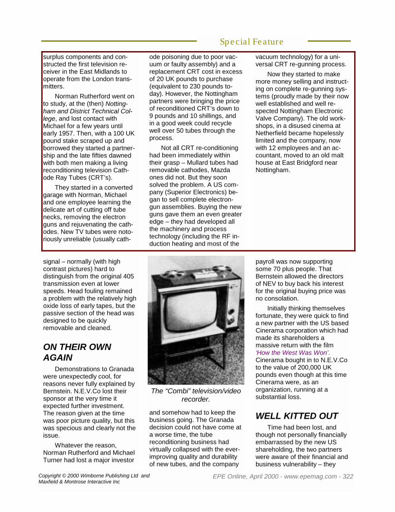
Copyright © 2000 Wimborne Publishing Ltd andMaxfield & Montrose Interactive Inc
EPE Online, April 2000 - www.epemag.com - 322
signal – normally (with highcontrast pictures) hard todistinguish from the original 405transmission even at lowerspeeds. Head fouling remaineda problem with the relatively highoxide loss of early tapes, but thepassive section of the head wasdesigned to be quicklyremovable and cleaned.
ON THEIR OWNAGAIN
Demonstrations to Granadawere unexpectedly cool, forreasons never fully explained byBernstein. N.E.V.Co lost theirsponsor at the very time itexpected further investment.The reason given at the timewas poor picture quality, but thiswas specious and clearly not theissue.
Whatever the reason,Norman Rutherford and MichaelTurner had lost a major investor
and somehow had to keep thebusiness going. The Granadadecision could not have come ata worse time, the tubereconditioning business hadvirtually collapsed with the ever-improving quality and durabilityof new tubes, and the company
Special Feature
surplus components and con-structed the first television re-ceiver in the East Midlands tooperate from the London trans-mitters.
Norman Rutherford went onto study, at the (then) Notting-ham and District Technical Col-lege, and lost contact withMichael for a few years untilearly 1957. Then, with a 100 UKpound stake scraped up andborrowed they started a partner-ship and the late fifties dawnedwith both men making a livingreconditioning television Cath-ode Ray Tubes (CRT’s).
They started in a convertedgarage with Norman, Michaeland one employee learning thedelicate art of cutting off tubenecks, removing the electronguns and rejuvenating the cath-odes. New TV tubes were noto-riously unreliable (usually cath-
ode poisoning due to poor vac-uum or faulty assembly) and areplacement CRT cost in excessof 20 UK pounds to purchase(equivalent to 230 pounds to-day). However, the Nottinghampartners were bringing the priceof reconditioned CRT’s down to9 pounds and 10 shillings, andin a good week could recyclewell over 50 tubes through theprocess.
Not all CRT re-conditioninghad been immediately withintheir grasp – Mullard tubes hadremovable cathodes, Mazdaones did not. But they soonsolved the problem. A US com-pany (Superior Electronics) be-gan to sell complete electron-gun assemblies. Buying the newguns gave them an even greateredge – they had developed allthe machinery and processtechnology (including the RF in-duction heating and most of the
vacuum technology) for a uni-versal CRT re-gunning process.
Now they started to makemore money selling and instruct-ing on complete re-gunning sys-tems (proudly made by their nowwell established and well re-spected Nottingham ElectronicValve Company). The old work-shops, in a disused cinema atNetherfield became hopelesslylimited and the company, nowwith 12 employees and an ac-countant, moved to an old malthouse at East Bridgford nearNottingham.
payroll was now supportingsome 70 plus people. ThatBernstein allowed the directorsof NEV to buy back his interestfor the original buying price wasno consolation.
Initially thinking themselvesfortunate, they were quick to finda new partner with the US basedCinerama corporation which hadmade its shareholders amassive return with the film‘How the West Was Won’.Cinerama bought in to N.E.V.Coto the value of 200,000 UKpounds even though at this timeCinerama were, as anorganization, running at asubstantial loss.
WELL KITTED OUTTime had been lost, and
though not personally financiallyembarrassed by the new USshareholding, the two partnerswere aware of their financial andbusiness vulnerability – they
The “Combi” television/videorecorder.

Copyright © 2000 Wimborne Publishing Ltd andMaxfield & Montrose Interactive Inc
EPE Online, April 2000 - www.epemag.com - 323
were on their own once againand looking to develop theirproducts and product rangefurther. Hoping to salvage theprofitable divisions of thecompany Norman, as ManagingDirector, split the operation byforming Telcan (Research andDevelopment) and Telcan TV,the latter being mainly involvedin manufacturing.
Trading again in early 1963,the partners (now including afinancial manager, Brian North)set out to provide the video unitsin kit form (as the Telcan TKR500). The new operationmanufactured every majorcomponent necessary includingthe record/replay heads, printedcircuit boards, video circuits,tape transport and a variablecapstan size system (0����25 HPmotor). With variable speedoperation (60, 120 or 180 inchesper second) the kit, if correctlyassembled, produced a recorderof very satisfactoryperformance.
A public demonstration andpress conference at the AldwichHotel, London, held on June24th 1963 created a wealth ofinterest and publicity, but theattitude of the press and thepublic appeared to be diffident. Itwas staggering that few couldactually see the need for “homevideo recording” – even if theyhad the slightest notion of howtechnically awesome thedevelopment of Telcan was!
Norman Rutherforddemonstrated Telcan on theBBC 9 O’clock News (replayingthe opening few minutes of thebroadcast) but this was asineffective as a next day ATVinterview was ridiculous – theinterviewer continually askingthe originators if they thoughtTelcan a “gimmick”. They werelater to maintain that theinterviewer could not grasp the
concept of electronic recording,and mistakenly believed that theTelcan method involved the useof an 8mm movie camera(similar to a system already inuse).
Orders for the Telcan unitswere slow. The kits sold for 60UK pounds (some 700 poundstoday) – only the technicallyskilled and well off could affordthem. A number of pre-builtunits did sell well, as too didspecial “Combi” examples fittedinto TV’s, but of the total numbersold the greater majority werekits.
As sales of the TKR 500faltered, the partners designed aminiature battery driven portablerecord player for 7 inch 45 RPMrecords which, entirely selfcontained and enclosed,operated like a modern floppydisk drive. A fair number wereproduced and for a short whilewere popular.
ORDERS FROMOVERSEAS
However, Cinerama, alreadya stockholder in N.E.V.Co,proposed through its ChairmanNicholas Riesini, the formationof a joint company forexploitation of Telcan in the USand, given the other possiblefinancial holdings of stock inN.E.V.Co, agreed to purchaseany stock willing to be releasedby other interests. Thisultimately resulted in a fairly
Special Featurelarge injection of new cash forthe company and R&D was thefirst to benefit. For a momentthere appeared to be yetanother new beginning for thecompany.
Unfortunately, what wasdesirable in one context was notin another, and the two partnersfound themselves embroiled inbusiness negotiations and legalentanglements to the detrimentof the company’s mainbusiness. In December of 1963Norman and Michael wereasked to demonstrate the videorecorder at a crucialshareholders meeting of theailing Cinerama Corporation atthe Capital Theatre, Broadwayin New York.
However, they were askedto try something novel – to videothe shareholders themselves atthe meeting. Being away frombase, and unable to get one oftheir own Mini-Eye 4 inchcameras, Norman got hold of a525-line studio standard Vidiconcamera and videoed all andsundry, amazing everyone byplaying back the pictures at themeeting.
The technology was enoughto placate all of the unhappyshareholders – now absolutelyconvinced that Cinerama had areal winner. However, all wasnot sweetness and light,Cinerama itself was not actuallyable to invest any further – eventhough its individual principalswere well able to. The partnersreturned from the US with themistaken expectation of a largeorder for the new “Telcan”system but it failed tomaterialize.
As Cinerama floundered theChairmanship changed to that ofWilliam Foreman, a creditor ofCinerama. Foreman was notslow to convey his personaldistrust of the Telcan businessto the new Executive.
Close-up shot of the TVscreen during Telcan replay.

Copyright © 2000 Wimborne Publishing Ltd andMaxfield & Montrose Interactive Inc
EPE Online, April 2000 - www.epemag.com - 324
Sensing mounting hostilityfrom their new principals, thetwo partners decided to lookfurther afield for investment andgave demonstrations in the USto the Filco (Ford Motor Co.)and Admiral Corporations. Butthe interest and enthusiasm wasless than it might have been inthe face of an ever-growinghostility and starvation of funds.
In hindsight, NormanRutherford admits that had they“toadied” a little to their newpartners things may have gonebetter. In short, there was onlyone way out and in August of1964 Norman Rutherford, asManaging Director, put thecompany into voluntaryliquidation.
OVERSTRETCHEDUndaunted, and with the
greater number of their 70 oddoriginal staff still at hand, the twopartners set up again at Basfordunder the name Wesgrove.Again this was a kit formrecorder business though, asalways, customers couldpurchase a fully assembledversion.
Unfortunately, by this time,the Ampex helical scan systemhad already appeared in
competingdomestic videorecorders. Oneleader was theSony 0����5-inchreel-to-reel videorecorder; Philipswere alsocompeting whilea further systemwas marketed byLoewe Opta inGermany.
The message was obvious,the Telcan linear system neededto be updated to record in thehelical scan mode in order torival other products. But this wasbeyond the resource of thealready ailing and overstretchedTelcan-Wesgrove operation.Talks with various potentialbackers, even Japaneseinterests, got nowhere. TheWesgrove business, like itspredecessor, was put intovoluntary liquidation just 19months after the Cineramadebacle.
EPILOGUEOnly two of the original
Telcan units built by NormanRutherford and his Companysurvive to this day – one in SanFrancisco, owned by Al Cox the
Special Feature
owner of a music shop and FMradio station, and one now to beseen at the Wollaton HallIndustrial Museum inNottingham. Norman and hispartner Michael Turner becamedisaffected and parted companyjust after the firm was wound up.
Norman continued to dosome consultancy work inelectronics; he eventually gaveup and went into propertydevelopment with his brother,only returning to his first love inthe early 1980’s when hebecame involved in developingan infrared transmission systemfor closed circuit TV. He finallyfound lasting fame by way of anentry into the Guinness Book ofRecords in 1982.
Much could be said aboutthis lost opportunity for Britishenterprise in terms of too littletoo late, but the reality is
The Wesgrove (Telcan) kit ofcomponents (1963).
One of the last remaining examples of theTelcan video recorders on show at the Wolla-ton Hall Industrial Museum, Nottingham, UK.
Acknowledgements.The author offers his sincere thanks to Mr. Nor-man Rutherford (for patiently retelling his story
for the umpteenth time), to Mr. Rob Cox, curatorof the Wollaton Hall Industrial Museum in Not-tingham, Mr. John Brunton at the Nottingham
Post, and to all those that gave their time to find,or process, material for this article.

Copyright © 2000 Wimborne Publishing Ltd andMaxfield & Montrose Interactive Inc
EPE Online, April 2000 - www.epemag.com - 325
different. The technical principlewas only good enough to provethe value of the product – for allthe negativity faced at theTelcan launch, everyone quicklycame to see how useful a homevideo unit could be and that amassive market awaited.
Although the originaltechnical principle of Telcandefined the operational limits,
the linear record system wasnever going to have the technicalflexibility required by the market(for convenient long play, highresolution monochrome or colorrecording). Also, the short record /replay time, and poor long-termhead dependability were verymuch a weakness.
Yet, for all that the promisewas there, and had the
Special Featureinvestment vision comeanywhere close to the technicalvision, then a good deal moremight have been accomplished.
As it was, the two partners,Norman Rutherford, MichaelTurner and their associates didunequivocally demonstrate andsell the first commercial homevideo recorder, the firstCamcorder (and the first“Combi” TV and video recorder).What price “vision”?

Copyright © 2000 Wimborne Publishing Ltd andMaxfield & Montrose Interactive Inc
EPE Online, April 2000 - www.epemag.com - 326
The music and electronicsindustries have agreed on thetechnology they will use to burya watermark in music recordingsto control unauthorized copyingfrom the Internet. The SecureDigital Music Initiative, a com-mittee of 120 hardware and soft-ware companies, has chosenMusiCode from Aris Technolo-gies of Cambridge, Massachus-setts, USA.
The SDMI was formed whenrecord industry trade body theRecording Industry Associationof America failed in its legal bidto block sales of Diamond Multi-media’s Rio, the pager-sizedsolid state recorder that usesMP3 compression technology todownload and replay music fromthe Internet.
WATERMARKEDSOURCE
SDMI agreed that music willbe watermarked at the recordingstudio with digital code whichidentifies the copyright ownerand tells how the music is in-tended to be sold, for instanceon a CD. An “SDMI-compliant”Internet music player will searchfor any watermark, which re-veals that a recording is anunauthorized copy from the In-ternet, and refuse to play it.Laws will be tightened to stoppeople modifying players so thatthey ignore “don’t play me”marks.
The SDMI wanted a mark
that can survive to-and-fro con-version between the analog anddigital domains and resist hack-ers who try and wash it out,while not degrading the sound.4C Entity, a consortium of IBM,Intel, Matsushita (Panasonic)and Toshiba, took on the job oftesting 11 different proposals.
Some spread a thin layer ofmodulated noise under the au-dio; others suck notches fromthe music and add modulatednoise to the gaps. MusiCodeworks in a completely differentway.
CODED SYMBOLSThe encoder in the record-
ing studio holds a library of sym-bols, digitally coded letters of thealphabet and numbers, whichare represented by pre-determined patterns of a musi-cal waveform. These can bepeaks within a limited range ofheights, which occur within afixed period of time. The en-coder analyses the music, look-ing for patterns that are similarto the library patterns. When aclose match is found for a sym-bol that is to be buried in themusic, the encoder modifies themusic peaks so that they exactlymatch the library symbol.
A decoder in the playerholds a library of symbol repre-sentations like those in the en-coder. When it finds a matchingpattern in the music it triggersthe appropriate symbol. To-gether the symbols build up a
copyright message.The symbol data rate varies
depending on the music content,but is typically around 100 bitsper second. So it takes a fewseconds for the decoder to rec-ognize all the symbols neededfor a copyright message orcopy-control signal.
GOLDEN EAR TESTSAris claims that although the
music waveform is slightly al-tered to convey the symbols,there is no noticeable effect onthe sound, even when it comesfrom a super hi-fi source suchas a DVD-Audio player, with fre-quency range of 100kHz anddynamic volume range of140dB.
Audio enthusiasts have al-ways been wary of anything thatalters the sound but Aris saysthe tests done by 4C prove thesystem works. 4C built on theso-called Muse tests of CD wa-termarking which were carriedout in Europe with EU funding bythe music industry’s trade bodythe International Federation ofthe Phonographic Industry. Allthe major record companiesplayed music in their studios topanels of “golden ear” audio ex-perts listening to marked andunmarked music without know-ing which was which.
Paul Jessop, the IFPI’sTechnical Director, organisedthe European tests has confi-dence in the SDMI’s findings.
WATERMARKING MUSICBarry Fox reports on the arrival of a new method
to prevent unauthorized music copying.
A ROUNDUP OF THE LATEST EVERYDAY NEWSFROM THE WORLD OF ELECTRONICS

Copyright © 2000 Wimborne Publishing Ltd andMaxfield & Montrose Interactive Inc
EPE Online, April 2000 - www.epemag.com - 327
LIFE, THE UNIVERSE, AND THE UKThe British National Space Center has announced that the search
in the UK for life in the Universe is on! Astrobiology – a new scienceto search for life across the Universe – was launched in mid-December ‘99 and the excellence of UK scientists puts us in a strongworld position.
Dr Don Cowan, Chair of the panel of experts that spent last yearinvestigating work currently underway in the UK, recently made thefollowing statement:
“This is a really exciting time in Astrobiology. In our investigationwe found many British scientists who were Astrobiologists withoutknowing it; biologists were studying how life survives in the harsh en-vironment of Antarctica, astronomers were developing new missionsto find new planets, chemists were developing new techniques toidentify biochemical markers, geologists were studying the way lifetransforms the properties of our planet. Brought together they make apowerful force in Astrobiology which will enable us to find out stillmore about where we come from and what other life might exist orhave existed in the universe.”
In a separate statement, Science Minister Lord Sainsbury has an-nounced that the UK is to invest 1.4 million UK pounds in the experi-mental and research opportunities offered by the European SpaceAgency’s EMIR-2 program. The funding includes 15 million poundsinvestment in the UK small satellite sector, helping transfer the UK’sworld-leading capability in small satellites from the academic into sci-entific and commercial markets.
Furthermore, Surrey Space Center, run by the University of Sur-rey at Guildford, tell us that NASA has once again selected SurreySatellite Technology Ltd (SSTL) as the only non-US supplier for itsRapid Spacecraft Acquisition contracts over the next five years.
Under the contract, SSTL will supply its flight-proven off-the-shelfmini-satellite platform for space and science technology missions toall of NASA’s centers and other US Government agencies.
SSTL’s first mini-satellite, UoSAT-12 was launched in early ‘99and their sixteenth, Clementine, was launched in December ‘99.
All-in-all it seems an excellent start to the new millennium for theUK’s involvement with Space. Surf www.sstl.co.uk
NEWS......“I am delighted” he says
“that we have found a technol-ogy that independent listeningtests have shown to be inaudi-ble”.
SCEPTICISM MAYREMAIN
The SDMI, like the IFPI, re-fuses to name any of the“internationally recognizedgolden ears,” which it claimswere satisfied. Paul Jessop sayshe knows what this means. Au-dio enthusiasts will refuse to be-lieve that any mark can be in-audible and be sure they canhear degradation even whenthere is none.
Renowned US masteringand recording engineer BobLudwig had previously warnedthat although watermarkingmight be inaudible on lo-fi Inter-net music, its effect on super hi-fi DVD-Audio would be notice-able. He said he was wary ofany reassurances from theRIAA, which had argued in the1980s that the Copycode notchsystem was inaudible.
Ludwig now says “my fer-vent hope is that digital signalprocessing has improved to thepoint where watermarking canbe totally inaudible under all rea-sonable circumstances”.
Guiding InventorsA step-by-step guide to help inventors make an informed choice about using invention promotion com-
panies has recently been published on the Internet by Lord Sainsbury, DTI (Department of Trade and In-dustry) Minister with responsibility for science and innovation. The guide is intended to help inventors getthe most out of promotion services and provides advice on finding sources of free or low cost information.
Said Lord Sainsbury, “I do not want creative individuals to become unsuspecting victims of unscrupu-lous firms. I am confident that the easy-to-follow steps will help inventors avoid making costly mistakes”.
The DTI factsheet can be accessed at www.innovation.gov.uk. Another useful Web address is thatof the Patent Office, at www.patent.gov.uk. The DTI’s phone number is +44 (0) 171-215-5000.

Copyright © 2000 Wimborne Publishing Ltd andMaxfield & Montrose Interactive Inc
EPE Online, April 2000 - www.epemag.com - 328
NEWS......
QX3 INTELPLAY MICROSCOPEMatel, the world’s best-known toy maker responsible for favorites such as
the Barbie doll, has teamed up with Intel to produce a range of toys to com-plement the personal computer. Aimed at the six year-plus market, the mar-velous Intelplay QX3 microscope is a Universal Serial Bus (USB) compatibledevice that allows color images to be captured on a Pentium PC at severalmagnification factors, from x10 to x200. This allows youngsters to explore thefascinating world of microscopy and see images live on-screen.
Magnification factors refer approximately to the size of the image whenviewed on a 15-inch computer monitor, say Mattel: this would, for example,enable a 1mm mustard seed to become a wonderful 20cm knobbly spheroidon a 19in monitor. The microscope resolution is 512 x 384 pixels, which ismore than adequate for most investigations.
The excellent Windows software, replete with brilliant and fun sound ef-fects, permits live viewing of the object (the frame delay depends on thethroughput performance of the PC – it can appear virtually real-time on a350MHz desktop). Still-capture and time-lapse movies can also be produced,perhaps to illustrate the growth of a mung bean or the movement of star-struck creepy crawlies. Slide-shows of microscopic montages, accompanied by some great sound tracks,can easily be put together by budding young boffins. Images can be printed or exported as bitmaps, andthere is a great paint package included which allows pictures to be suitably enhanced.
The microscope has colorful chunky controls to allow youngsters to control the magnification and fo-cus, and a push-button allows still images to be captured on disk for future reference. The QX3 incorpo-rates two filament light sources (above or backlit) which are selectable through the software. The micro-scope unit can be detached from its stand to allow free-standing use, and the USB lead is approximatelythree meters long for this purpose.
It is completely powered through the USB connection and requires no extra mains adaptor or batteries.This also means that it could be used as a stand-alone device with a USB-enabled laptop computer, per-haps for junior field studies.
A complete kit is supplied by Mattel, including an Activity Book, sample slides and containment cap-sules. Everything is safely molded in plastic of a high quality, with no glass parts or sharp edges being pre-sent. Although it was launched towards the end of 1999 in the USA, our reviewer managed to obtain one ofthe first in Europe earlier this year, and had great fun exploring various natural objects, such as seeds,shrimps, sugar crystals and the anatomy of honey bees. Surface-mount electronic devices found their wayunder the lens too, and some reasonable photos captured of SMD chips and close-ups of soldering.
The QX3 is a fantastically creative educational gadget – much more than a toy – and is bound to be abig success with children, parents and teachers. Expect a UK launch in late Summer 2000, at a price of ap-proximately 90 UK pounds.
Alan Winstanley
EMF FactsThere has been a lot of publicity for the topic of EMF (electromagnetic fields), much of it having a
negatively-biased approach. We have been advised that the new Safety Test Solutions web site,www.safety-test-solutions.de, offers a wide range of information on this topic. It tells you about the char-acteristics of EMF, where they occur and their effects. It also explains technical terms.
The website information is available in English, French, German and Spanish, on a wide variety of sub-ject areas. “On our new website, every visitor will quickly find the information they need, no matter whetherthey are getting involved with electromagnetic fields for the first time, or if they are an EMF expert lookingfor detailed information”, stated Hans J. Forster, Executive Director of Safety Test Solutions.

Copyright © 2000 Wimborne Publishing Ltd andMaxfield & Montrose Interactive Inc
EPE Online, April 2000 - www.epemag.com - 329
NEWS......
TITANICRECEIVER
DISCOVEREDA unique and valuable Ed-
wardian crystal receiver, madein England in 1910, has recentlybeen unearthed by a Midlandsantique dealer, and has beenacquired for a major privatewireless collection in this coun-try.
Early radios of this periodare rare enough, but whatmakes this particular set espe-cially unique is that its maker, MrGeorge Leadbetter (a machineturner and clock repairer thenliving in Ledbury, Worcester-shire), while listening-in on theset’s earphone on the morningof Monday 15th April 1912, sud-denly tuned into the sinking Ti-tanic’s CQD/SOS Morse dis-tress signals.
Unfortunately, having runround to the local police stationto tell the sergeant what he hadheard, he was turned away,none of the police officers onduty believing what he had tosay!
It would be difficult to knowwhat help Mr Leadbetter”s newscould have been had he beenbelieved (the Titanic was some3,000 miles away across theother side of the Atlantic), buthelp was nearby and the dis-tress signals were picked up byships close at hand, resulting inthe rescue of over 700 passen-gers and crew.
Such a pivotal role did wire-less play in saving many hun-dreds of lives on board thestricken ship that its value wasdramatically demonstrated andacknowledged around the world.
This beautiful engineer-made radio, measuring some24in x 14in x 9in (60cm x 35mm
x 7cm) and weighing 42lb(18kgs), is the only surviving ra-dio receiver documented ashaving heard the distress criesfrom the Titanic – a fantasticrelic from this most famous ofhistoric disasters. A photo of thereceiver is shown in this month’sTechnology Timelines feature.
The receiver will be on showin pride of place at the next Na-tional Vintage CommunicationsFair, which will be held at theNEC in Birmingham on Sunday30th April 2000.
Other exhibition items onshow at the fair will be a com-prehensive collection of WWIIspy radio transmitters and re-ceivers, a Horophone time-signal receiver (another uniqueEdwardian radio), and a displaydepicting the history of recordedsound.
For more information con-tact The National Vintage Com-munications Fair, Spice House,13 Belmont Road, Exeter, De-von EX1 2HF, UK.Tel: + 44 (0) 1392-411565Email: [email protected]: www.angelfire.com/tx/sunpress/index.html
(If you are interested in vin-tage radio, why not take out asubscription to our sister maga-zine, Radio Bygones? For de-tails seewww.radiobygones.com)

Copyright © 2000 Wimborne Publishing Ltd andMaxfield & Montrose Interactive Inc
EPE Online, April 2000 - www.epemag.com - 331
AntexWeb: www.antex.co.uk
Bull Electrical (UK)Tel: +44 (0) 1273-203500Email: [email protected]: www.bullnet.co.uk
CPC Preston (UK)Tel: +44 (0) 1772-654455
EPE Online Store and LibraryWeb: www.epemag.com
Electromail (UK)Tel: +44 (0) 1536-204555
ESR (UK)Tel: +44 (0) 191-2514363Fax: +44 (0) 191-2522296Email: [email protected]: www.esr.co.uk
Farnell (UK)Tel: +44 (0) 113-263-6311Web: www.farnell.com
Gothic Crellon (UK)Tel: +44 (0) 1743-788878
Greenweld (UK)Fax: +44 (0) 1992-613020Email: [email protected]:www.greenweld.co.uk
Maplin (UK)Web: www.maplin.co.uk
Magenta Electronics (UK)Tel: +44 (0) 1283-565435Email:[email protected]:www.magenta2000.co.uk
MicrochipWeb: www.microchip.com
Rapid Electronics (UK)Tel: +44 (0) 1206-751166
RF Solutions (UK)Tel: +44 (0) 1273-488880Web: www.rfsolution.co.uk
RS (Radio Spares) (UK)Web: www.rswww.com
Speak & Co. Ltd.Tel: +44 (0) 1873-811281
Micro-PICscopeFor those readers who like
the look of the neat orangeplastic box used in the Micro-PICscope project, this is an RSproduct and can be purchasedthrough their mail order outletElectromail (code 281-681).They can also supply theMAX492 dual opamp (code182,2738).
The 2-line 16-characteralphanumeric liquid crystaldisplay module, complete withconnector, used in the prototypewas originally purchased fromMagenta Electronics and weunderstand that they still havestocks of this device.
The PIC16F876-20P used inthis project is the 20MHzversion. For those readersunable to program their ownPICs, a ready-programmed16F876 can be purchased fromMagenta (see above) for theinclusive price of 10 UK pounds(overseas readers add 1 UKpound for postage). Software forthe Micro-PICscope (written inTASM) is also available for freedownload from the EPE OnlineLibrary at www.epemag.com
The printed circuit board isavailable from the EPE OnlineStore (code 7000259) at
www.epemag.com. Finally,data sheets for the PIC16F87xfamily (and other PIC products)are available for free downloadfrom Microchip’s web site:www.microchip.com. Maximmanufacture the MAX492opamp used in this design. Theirweb site is at: www.maxim-ic.com
Garage LinkThe main items of concern
regarding the Garage Linkproject are likely to be thetransmitter and receivermodules and the Holtek encoderand decoder chips.
Starting with the HT12Eencoder and HT12F decoder,the last time we looked forsimilar Holtek chips they were invery short supply and FMLElectronics (Tel: +44 (0) 1677-425840) bought some in. Onceagain, we understand they arehappy to supply the aboveencoder and decoder ICs.
Regarding the RF SolutionsAM transmitter and receivermodules, several componentsuppliers, such as SumaDesigns (Tel: +44 (0) 1827-714476), Quasar Electronics(Tel: +44 (0) 1279-306504), andVeronica Kits (Tel: +44 (0) 1274-883434) may be able to help.Also, Maplin are currently listinga low cost pair, quote codeVY47B.
The last mentionedcompany also supplied thelever-arm microswitch (codeNF21X) and the miniature LDR(code AZ83E). You can, if youwish, use the good old ORP12.The 66M� resistor for R5 in theTransmitter was made up fromtwo 33M� “high voltage” types(code V33M). The two printed
with DAVID BARRINGTON
Some Component Suppliers for EPE Online Construc-tional Articles

Copyright © 2000 Wimborne Publishing Ltd andMaxfield & Montrose Interactive Inc
EPE Online, April 2000 - www.epemag.com - 332
circuit boards come as a pairand are available from the EPEOnline Store (codes 7000261 –transmitter, and 7000262 –receiver) at www.epemag.com
Flash SlaveNot much can go wrong
when shopping for parts for theFlash Slave, this month’s simpleStarter Project. Thephototransistor may cause somelocal sourcing concerns, but, asthe author states in the article,several npn types have beensuccessfully used in the unit.The BPX25 npn phototransistorused in the prototype came fromMaplin (code QF30H).
We understand that someoverseas readers are havingdifficulty finding ZTX typetransistors locally, so wesuggest they opt for the 2N3440type. Other, high voltage andhigh current transistors shouldwork equally well in this design.One important point though, likethe 2N version, the pinout andencapsulation may differ andmust be carefully checkedbefore inserting on the circuitboard.
High PerformanceRegenerative Receiver
As we highlighted lastmonth, some of the typenumbers quoted for the “plug-in”TOKO coils called for in theHigh Performance RegenerativeReceiver did not tally with ourinformation. However, thanks toefforts on the part od the
designer – Raymond Haig – theTOKO coil numbers and rangesused in the Receiver have beenset out in Table 2 in the articleand were purchased from BonexLtd (Tel: +44 (0) 1753-549502),type numbers and order codesare as follows: CAN1A350EK,380-350; RWO6A7752EK,3357-752; RWR331208NO,351-208; 154FN8A6438EK,356-438; KANK3426R, 363-426;KANK3337R, 363-337;MKXNAK3428R, 363-767. Wehave also been informed thatJAB Electronic Components(Tel: +44 (0) 121-682-7045)stock an extensive range ofTOKO coils.
One item we neglected lastmonth was the slow-motionreduction ball-drive for thetuning capacitor. Glancingthrough a “flyer” from MainlineSurplus Sales (Tel: +44 (0) 870-241-0810) we see they list onefor just 2.50 UK Pounds, plus a3 pound (UK) post and packingcharge. Quote order code 81-0224.
The three small printedcircuit boards are available as aset from the EPE Online Store(codes 7000254, 7000255, and7000256) at www.epemag.com
Teach-In 2000No additional components
are called for in this month'sinstallment of the Teach-In 2000series. For details of specialpacks readers should contact:
ESR ElectronicComponents – Hardware/Tools
and Components Pack.Magenta Electronics –
Multimeter and components, Kit879.
FML Electronics (Tel: +44(0) 1677-425840) – Basiccomponent sets.
N. R. Bardwell (Tel: +44 (0)114 255-2886) – DigitalMultimeter special offer.
PLEASE TAKE NOTE: VideoCleaner Feb '00Amended software is nowavailable via the EPE OnlineLibrary at www.epemag.com.The INIT routine should read:
INIT CLRF PORTABSF STATUS,
PAGE1MOVLW B‘00000000’
This configures PORTA asoutputs only.
Shop Talk

Copyright © 2000 Wimborne Publishing Ltd andMaxfield & Montrose Interactive Inc
EPE Online, April 2000 - www.epemag.com - 333
WIN A DIGITALMULTIMETER
The DMT-1010 is a 3 1/2 digitpocket-sized LCD multi-meterwhich measures a.c. and d.c.voltage, d.c. current, and re-sistance. It can also testdiodes and bipolar transistors.Every month we will give aDMT-1010 Digital Multimeterto the author of the best Read-out letter.
FUSED COIL FORMERSDear EPE,
Reading much of the seriesrecently on Practical OscillatorDesign (Jul-Dec ’99), hasprompted me to come up with apractical idea for constructors ofRF oscillators etc.
Basically the idea, which Ihave already put into practice,makes use of the ordinary house-hold 3A/13A ceramic fuse. Pre-pare to dismantle the fuse by eas-ing off one end with pliers, whilstthe other end is secured by sol-dering it to a piece of scrap PCBfor support. Discard the internalfuse wire plus sand, and a verynice ceramic coil former remains,also keep the connector at oneend, this will prove useful too.
Ceramic type coil formers areoften referred to in the ARRLHandbook in numerous construc-tion articles for VFOs etc, andapart from the excellent mechani-cal and temperature stability theyoffer, coils can easily be wound
and secured using the followingmethod:
By soldering the lower con-tact of the fuse to a small pad onthe etched oscillator PCB, thecoil can be wound as in Fig.1,and the turns held tightly, whilstthe “hot end” of the coil is sol-dered to its intended point of thecircuit, before any other compo-nents are mounted. By applyinga smear of Araldite to the coillayers, and holding a 25W ironnear, heat and melt the resinwhilst turning the former, this willensure a uniform, covering andultimately hold the turns perma-nently in place.
In fact, many of your read-ers will probably be familiar withheating of Araldite to increase itsflow and quicken its setting time,and in this application the coilwill appear glazed, as if encasedin glass!
Using 28 or 30swg enam-eled copper wire and using mostof the length of the former, pop-ular MF frequencies and beyondcan be covered with the appro-priate value of capacitor.
Hopefully readers can beencouraged to experiment usingitems such as fuses to providepotentially excellent coil formers,
rather than the seemingly everelusive pre-wound coils – oncefound in constructors’ cata-logues. In fact the humble fusecan also be used as PCB stand-offs!
D.B. VenutiThurgarton, Norwich, UK
A very useful suggestion,and one which we are pleasedto publicize. Thank you DB –enjoy your new meter!
PC SCREEN DUMPSDear EPE,
I commend John Beckerand your team on your intuitivetreatment and presentation ofelectronics in the Teach-In 2000series. The accompanying inter-active computer program is alsovery impressive.
It looks as if the printedscreen-shots are actual pho-tographs of a PC monitor takenwith a camera. Indeed, thisseems to be your method forreproducing any PC graphicaloutput. You probably have yourown reasons, but just in case, Ihave a suggestion that wouldsave time and effort, while alsodramatically improving the qual-ity of the reproductions. The fol-lowing applies to IBM-compatible PCs only, runningWindows 3.1, 95, 98 or NT.
Pressing the <PRINTSCREEN> button (located be-side the <SCROLL LOCK> key)on the keyboard causes themonitor output at that time to bestored to the clipboard. The“Edit Paste” command, available
John Becker addresses some of the general points readers have raised. Haveyou anything interesting to say? Email us at [email protected]!

Copyright © 2000 Wimborne Publishing Ltd andMaxfield & Montrose Interactive Inc
EPE Online, April 2000 - www.epemag.com - 334
in most Windows-based editingsoftware, can then be used todump the image into a docu-ment, or in the case of a graph-ics editing package, into an im-age file.
To capture DOS output, runthe DOS-based program fromWindows at the full screen set-ting, hit <PRINT SCREEN> tocapture the desired output anduse the <ALT> <TAB> key com-bination to return to the Win-dows editing program for subse-quent pasting. It is then alsovery easy to label the image withgraphics editing software if de-sired.
Active Dialog/Messageboxes can be neatly captured tothe clipboard by pressing <ALT><PRINT SCREEN>. Thiscauses the background graphicsto be omitted from the capture.
I thoroughly enjoy your mag-azine, and with practical circuits,it certainly lives up to its name.
John HarrisCo. Longford
Ireland
Your assumption about us-ing screen photos is absolutelycorrect. I did not know that mycomputers were capable ofscreen saving in this way from aDOS-based program. Other au-thors have previously providedus with electronically capturedimages, but I had assumed theyhad special software.
I tried it when I saw your e-mail and it worked nicely, en-abling the images to be stored todisk and passed to our in-housetypesetting team. The screenimages in this month’s Teach-Inhave been done this way. Thankyou.
Your e-mail was actuallypassed to us by Max, our Onlineedition editor in the USA. He
added the following additionaladvice:
If you want to see how easyit is in normal Windows mode,just press (and release) the PrintScreen button now, then useStart > Programs > Accessories> Paint to open the simplest ofpaint programs and then useEdit > Paste and see what hap-pens – you can then save thisimage as a .BMP file, and thenuse Adobe Photoshop to shrinkit and/or change it into other for-mats.
It’s also worth noting thatpressing the Print Screen buttonon it’s own captures the entirescreen, while pressing and hold-ing the <Alt> key and thenpressing the Print Screen buttonwill only capture whichever win-dow is currently active. Cheers –Max
UP TO SCRATCHDear EPE,
EPE Jan 2000 – best issuefor a long time, as well as beingPIC-free! Glad I renewed mysubscription.
The mag arrived as I wasfinishing writing up notes anddrawing the circuit diagram forsomething I’ve just finished andI was trying to remember thesymbol for a thermistor (notsomething you use everyday),so I was well pleased withFig.3.3 on page 33. I really thinkthe Teach-Ins are one of thebest things you do. I have beena hobbyist on and off for nearly50 years since I built a one-valve set, later converted tomains for the HT, given the priceof 90V HT batteries, and my firstserious electric shock (nonamby-pamby PP3 batteriesthen!). I have found there is al-ways something new to learn. Infact the reason I read EPE today
is down to picking up the Jan ’93issue in WH Smiths, glancingthrough Teach-In 93 Part 3 andthat is why I subscribe!
Regarding “Notations” onpage 32 (Jan ’00), I have usedquite a few pots made by Ra-diohm that are labeled, for ex-ample, 10KA, 10KB or 10KCwhere A, B and C indicate lin,log, and reverse-log respec-tively. I always assumed that thiswas a house code, but I haveseen it used on published circuitdiagrams too. Also, an Omegpot I have is labeled 10K LIN.A.By the way, if you take two dual-gang Radiohm or Omeg potsand disassemble them, you canrebuild them as one 3-gang anda single-gang pot (nothingwasted!). The 3-gang pot makesa passable 18dB/octave variableSallen and Key filter a possibil-ity. I have assembled a 4-gangpot but it’s no good trying for a24dB/octave filter as the match-ing is not good enough.
Robert Penfold’s PracticallySpeaking feature on page 58demonstrates how difficult it is toinsulate transformers of the styleillustrated in Fig.2 since the cen-ter tap is not insulated nor arethe vertical parts of the tagswhere the ends of the windingsare soldered to. If possible, Iusually try to mount a trans-former so that the primary tagsare difficult to touch and haveoften thought this would be eas-ier if the primary tags were atthe bottom of a transformer andnot the top. Where this is impos-sible I have either stuck a pieceof acrylic sheet on top of it withdouble-sided sticky foam padsor fashioned a shroud from“Masticard” as used by modelmakers. I cannot think of anybetter way and it does seem daftthat you can buy a boot for themains inlet but have to impro-vise on the transformer.
Readout

Copyright © 2000 Wimborne Publishing Ltd andMaxfield & Montrose Interactive Inc
EPE Online, April 2000 - www.epemag.com - 335
I also studied Robert’sScratch Blanker (Jan ’00) verycarefully as I am about to build asimilar device using a ReticonSAD1024 CCD delay line that Ibought years ago for the purposeand never got round to. I had dugout my old notes and cuttings.One of the cuttings was An Exper-imental Scratch Eliminator (Hi-FiNews Sept-Oct ’79) by one R.A.Penfold, which makes me wonderif it is coincidence that 20 yearslater when I am about to buildwhat I started thinking about in1979, Robert Penfold publishesanother design. Spooky!
Barry Taylorvia the Net
Thank you Barry for anotherinteresting contribution to Read-out. Sorry we can’t publish it in itsentirety.
TEACH-IN 2000 HELP!Dear EPE,
Thanks for the wonderfulmagazine. I had been trying to getinvolved with electronics for awhile, but our local library did nothave enough info. Then I foundout about EPE. I began readingthe magazine in Aug ’99, under-standing little and eventually sub-scribed to EPE Online. TheTeach-In 2000 series has reallyhelped me to begin understandingelectronics.
I was working on the experi-mental section of Part 4 andfound that on my computer thereadings I get for the 8-bit dataoutput are -5V for low and 0V forhigh. The same with the inputs. Ireversed the polarity of my inputvoltage to get the programs towork. I hope this will not affect theprograms in any way and that Iwill be able to continue with thewonderful Tutorials.
The computer was pur-chased as is, second-hand andhas a Pentium 166MHz proces-sor, that’s about all I can tell youabout it. I also used a length of25-way ribbon cable with a male25-way D-type snap-in adapteron one end and soldering theends of the cable to strip boardon the other end. I did this so Idon’t need to make a PCB forthe Centronics adaptor.
Hitesh LalaSouth Africa
Great to know you appreci-ate us! The only reason I canthink of for the negative valuesis that you are connecting themeter in back-to-front. The COMlead should go to 0V, i.e. thenegative terminal of your bat-tery, or the metal chassis orother known ground (0V) pointof your computer or its connect-ing lead.
The Centronics parallel con-nector to the breadboard forTeach-In has more than just onepin that can be used for ground(0V) connection. Pins 19 to 29provide separate grounds for thescreening on individual signalwires, pin 16 is Logical ground,pin 17 is Chassis ground, whilepins 30 and 33 are quoted in mysource book as just beingGround.
Look closely at the connec-tor for the identity of the pins.Note that once you have foundpin 1, the numbers follow se-quentially to the end of that row,and continue on the second rowfrom the pin immediately oppo-site pin 1. This is contrary to theorder in which DIL IC pins arenumbered, going down one sideand then back up the next. Thisexplains the cause of the pinnumbering error in Fig.4.6 (Feb),as reported last month (March);the author (me!) had erro-
neously counted in the wrongdirection – how infantile!
TEACH-IN AND PSION (2)Dear EPE,
As a person who is involvedmainly in Computers/IT, andonly dabbles in Electronics as avery part-time hobby, I feel rela-tively refreshed to be able to an-swer one of the questions posedin your Readout section.
I refer to the letter from Fed-erica Appolloni in the January2000 Issue of EPE Online. Fed-erica is trying to use the Teach-In 2000 software on an XT-Emulator.
Normally, I don’t think thatthere would be a significantproblem in using the software ona Real XT based PC. I think thatthe problem is caused by thedisplay mode used by the soft-ware. The display resolution re-quired by the Teach-In 2000software is just not possible on aPsion series 5 palmtop. The er-ror generated would be consis-tent with an attempt to switch toa different display mode failing.
Mike Inschvia the Net
Thank you Mike. The resolu-tion of the screen mode used(Screen 9 in QBasic/QuickBA-SIC, EGA/VGA) is 640 x 350pixels, with text set for 80 char-acters x 25 lines, 16 color at-tributes.
Interestingly, with regard tothe “hieroglyphs” problem beingexperienced by some readers(see several previous Read-outs), I have succeeded in simu-lating the situation (via code-page commands) on two of mymachines and found that prob-lem then exists with text set for80 x 25, but not with it set for 80x 43.
Readout

Copyright © 2000 Wimborne Publishing Ltd andMaxfield & Montrose Interactive Inc
EPE Online, April 2000 - www.epemag.com - 336
DOING IT RIGHT!Dear EPE,
I bought a copy of your maga-zine the other day after a nineyear gap. I was pleasantly sur-prised to find that the comfortableold format was pretty much intact,and that the regular contributorslike Robert Penfold were still hardat it, doing their best to instil theirwisdom to us readers, and eventhe familiar old Bull Electrical ad.inside the front cover was stillthere after all this time. The smalldetails such as the componentlists and the stripboard layouts,and even the little cartoon illustra-tions brought the memories backas if I’d only bought a copy lastmonth.
The noticeable changes in-cluded things like the Internet fea-ture Net Work and the fact thatmost advertisers now have websites (which is good news), andthat everyone seems to be goingon about this PIC processorthingy (sorry to be an ignoramus).But it was reassuring to know thatsome institutions like EPE haveremained essentially unchangedover nearly a decade, even de-spite a merger with another publi-cation (when I was a regularreader in ’91 it was of course Ev-eryday Electronics I read).
Some might say that thisshows a lack of progress on thepart of the publication, but I saythat in reality what it means is thatthe formula is right and thereforedoesn’t need to change.
My life veered away fromelectronics in ’91, but now afterthe re-igniting of my interest inhobby electronics thanks to an-other interest of mine, cycling, andthe desire to build a two-stagesealed lead acid battery chargerto charge my self-designed frontlighting rig, I am glad I did pick upa copy of EPE, as I found it as en-joyable to read now as I did backthen.
I also found/find EPE a valu-able source of suppliers of partsthanks to the ads, but I noticedthat your Online issue (judgingby the sample issue only) doesnot contain these ads. I see theadverts as almost as an impor-tant part of the magazine as thearticles, and thus it seems ashame to omit them from theelectronic version, especiallywhen so many have web pres-ence these days that overseassubscribers can also contactthem very easily. Just a thought.
Please keep up the goodwork and the high quality of EPEand be assured that your publi-cation is probably amongst avery small minority that seemsto have got it right.
Jason WebbReading, Berks
Thanks for your kind com-ments, Jason. Some may regardus as a bit staid, but as yousaid, it seems to work OK. Weare moving towards ads in theOnline version. Watch thatspace!
TEACH-IN BUGDear EPE,
While using the TY2K(Teach-In 2000) software I havestumbled on a bug with the self-test of the Resistor Values andColor Codes program. The firstfour questions ask for the resis-tance to be typed in, and this isfollowed by four questions whichask for the resistance to be se-lected graphically.
When the last of thesequestions is answered correctly(eight questions), the programgets into a loop where the ques-tion remains unchanged and thegraphical value of the resistancechanges to what the programthinks should be the correct nextanswer. Typing <Enter> several
times just gives the correct an-swer. After pressing <A> to getthe answer, the program getsback to normal, only to repeatthe same after the 16th ques-tion, and so on.
Thanks for a great Teach-Inseries and for a great magazine.
Federica Appollonivia the Net
So it did! I’ve now fixed itand the fix will be released whensoftware version V1.1 (withmore demo routines) is releasedwith Teach-In 2000 Part 7. Inthe meantime, just rememberthat this bug is lurking (but it’snot malignant and it’s not a Y2Kbug – has anyone encounteredone of those yet? I haven’t)
.SOLDERING TIPDear EPE,
I have a question on solder-ing iron tips. After a job is done Ihave been told to put a smallamount of solder on the tip andthen unplug the soldering iron. Ihave also been told do not do it.Who is right?
Michael Powellvia the Net
On-line Editor Alan Winstan-ley received Michael’s query,and replies to it:
I always dab a small amountof solder on the tip to tin it, wipeit clean on a damp sponge andthen unplug the iron and let itcool while the tip is still nice andshiny. This preserves the clean-liness of the tip ready for thenext job. However, you MUSTWIPE it clean before unplug-ging, or the excess solder andflux will just burn and “dull” thetip and lead to unwanted de-posits before the iron has gone
Readout

Copyright © 2000 Wimborne Publishing Ltd andMaxfield & Montrose Interactive Inc
EPE Online, April 2000 - www.epemag.com - 337
cold.If you don’t use the iron for a
time (say 5 to 10 minutes ormore) before switching off, the tipis bound to be dirty when it coolsdown due to baked-on flux de-posits, oxides etc. This couldmake it harder to clean up the tipwhen you next switch it on.(Brand new tips can gradually bemade unusable for this reason.Hence you must always thor-oughly tin a new tip straightaway.)
If a tip is always kept nice andshiny, it is always easier to use. Itwill accept solder readily and letyou solder accurately and morequickly. So whoever told you toadd some solder is right – pro-vided you wipe the tip to removeany excess solder, before the ironhas gone cold.
(Also, don’t forget that AlanWinstanley’s Soldering Guide fea-turing lots of cool photographs isavailable in the EPE Online Li-brary at www.epemag.com).
SERIAL LOGDear EPE,
I’m designing and building anautomatic weather station basedaround the PIC16F877. I’ve beenpinching ideas and bits of circuitfrom your PIC Data Logger (Aug’99) and PIC Altimeter (Sep ’98).
I’ve been trying to get a serialRS232 link from the PIC’s USARTto my PC working (to transfer re-sults). I used exactly the circuitand cable pinout you have in the
Data Logger except that, notfinding a spare 7404 buffer inthe components box, I used acouple of NAND gates with par-alleled inputs from a 4011 in-stead. I eventually succeeded ingetting it going, but only by usingone of the gates, not two in se-quence as in the Data Loggercircuit. In other words I had toinvert the output from the PIC’sRC6 pin.
I checked with Microchiptechnical support about this. TheRC6 output is indeed inverted,and is intended to be used withan RS232 transceiver, most ofwhich invert the input signal (sothat on the line side of thetransceiver chip the output iscorrect).
Since your design puts thesignal through two invertingbuffers in sequence, i.e. retainsthe inverted signal as output bythe PIC, how did you ever get itto work at all? I looked throughyour PC comms input program(DATLOG02.BAS), but I couldn’tsee anything that was doinganything strange to the hard-ware – but I don’t use QuickBA-SIC so I’m not an expert in it.
But if you get any queriesfrom folks with older kits whocan’t get it to work, you mightsuggest that they try usingsomething like the MAX232CPEinstead of the 74HC04. R.A.Penfold had a useful article onusing this chip (Interface July’96).
Malcolm Wilesvia the Net
As I explained in the DataLogger article, and advised toMalcolm, I am not an expert incomms port use and had to re-search heavily before achievinga working circuit, which wassubsequently proved on my sev-eral computers.
What Malcolm missed whenexamining the .BAS code is thata machine code routine is alsoaccessed, this doing the actualreading of the comms port. In itthe data is indeed re-inverted.The full machine code text canbe read in file DATLOG02.J.
Readout
Copyright © 2022 FDOKUMEN