VISVESVARAYA TECHNOLOGICAL UNIVERSITY “AN ...
63
VISVESVARAYA TECHNOLOGICAL UNIVERSITY Jnana Sangama, Belagavi -590014, Karnataka, INDIA PROJECT REPORT On “AN ELECTRONIC HELP DESK KIT FOR PATIENTS” Submitted in partial fulfillment of the requirements for the award of the degree of Bachelor of Engineering In ELECTRONICS AND COMMUNICATION ENGINEERING For the Academic Year 2015-2016 BY RAVI KUMAR M SUMANTH R DIXIT TEJASWINI S (1NH12EC085) (1NH12EC111) (1NH12EC116) UNDER THE GUIDANCE OF Mrs. APEKSHA PRABHU Asst Professor, Dept. of ECE, NHCE Department of Electronics and Communication Engineering NEW HORIZON COLLEGE OF ENGINEERING Outer Ring Road, Marathalli, Bangalore-560103
-
Upload
khangminh22 -
Category
Documents
-
view
3 -
download
0
Transcript of VISVESVARAYA TECHNOLOGICAL UNIVERSITY “AN ...

VISVESVARAYA TECHNOLOGICAL UNIVERSITY
Jnana Sangama, Belagavi -590014, Karnataka, INDIA
PROJECT REPORT
On
“AN ELECTRONIC HELP DESK KIT FOR PATIENTS”
Submitted in partial fulfillment of the requirements for the award of the degree of
Bachelor of Engineering
In
ELECTRONICS AND COMMUNICATION ENGINEERING
For the Academic Year
2015-2016
BY
RAVI KUMAR M SUMANTH R DIXIT TEJASWINI S
(1NH12EC085) (1NH12EC111) (1NH12EC116)
UNDER THE GUIDANCE OF
Mrs. APEKSHA PRABHU
Asst Professor, Dept. of ECE, NHCE
Department of Electronics and Communication Engineering
NEW HORIZON COLLEGE OF ENGINEERING
Outer Ring Road, Marathalli, Bangalore-560103
NEW HORIZON COLLEGE OF ENGINEERING
Outer Ring Road, Marathalli, Bangalore-560103
Department of Electronics and Communication Engineering
CERTIFICATE
This is to certify that the project work entitled “AN ELECTRONIC HELP DESK KIT
FOR PATIENTS” carried out by RAVI KUMAR M, SUMANTH R DIXIT and
TEJASWINI S bearing USNs 1NH12EC085, 1NH12EC111, 1NH12EC116
respectively in partial fulfillment for the award of Degree of BACHELOR OF
ENGINEERING in ELECTRONICS AND COMMUNICATION ENGINEERING
of VISVESVARAYA TECHNOLOGICAL UNIVERSITY, BELGAUM during the
year 2015-2016.It is certified that all corrections/suggestions indicated for internal
assessment have been incorporated in the Report. The project report has been approved as
it satisfies the academic requirements in respect of project work prescribed for said
degree.
_________________ __________________ _________________
Signature of Guide Signature of HOD Signature of Principal
Mrs.Apeksha Prabhu Dr.Sanjay Jain Dr.Manjunatha
Asst.Professor Head of Dept. Principal
Dept. of ECE, NHCE Dept. of ECE, NHCE NHCE
External Viva / Orals
Name of the examiner Signature with date
1. ……………………………. ……………………
2. ………………………… ……………………

ACKNOWLEDGEMENT
The satisfaction that accompanies the successful completion of task would be but
incomplete without mention of the people, who made it possible, whose constant
guidance and encouragement crown all efforts with success.
We wish to express our sincere thanks to Dr. MANJUNATHA, Principal, NHCE, for
all his support and guidance.
We wish to express our sincere thanks to Dr. SANJAY JAIN, Head of the
Department of Electronics and Communication Engineering, NHCE, for permitting us
to pursue our Project in college and encouraging us throughout the Project.
We are highly indebted to our project guide Mrs. APEKSHA PRABHU,
Assistant Professor,Electronics and CommunicationEngineering Department,Project
co-ordinators Mrs.ISHANI MISHRA & Mrs.DIVYA SHARMA Professor,Electronics and
Communication Engineering Department, who has given us all the necessary technical
guidance in carrying out this Project.
Mere thanks will not be enough for the immense love and blessings of our beloved parents
who gave us financial support,strong moral support and a spirit to believe in ourselves throughout
this journey.
We definitely would like to thank whole-heartedly to all our friends for their support and
suggestions.
(iii)

ABSTRACT
One of the important problems that our society faces is that people with disabilities are finding it
hard to cope up with the fast growing technology. The access to communication technologies has
become essential for the handicapped people.
Generally deaf and dumb people use sign language for communication but they find
difficulty in communicating with others who don’t understand sign language. Sign language is an
expressive and natural way for communication between normal and dumb people (information
majorly conveyed through the hand gesture).
Speech –impaired people have difficulty in communicating with normal people
because the hand gestures used by them to communicate their information is not easily
understandable ;only trained people can understand these. Most expressions and emotions remain
un-conveyed, sometimes even misinterpreted. So hand gestures (limited gestures) are not an
effective method of communication for the speech impaired people.
To take care of this issue, an electronic help desk kit can be used to enhance the
passage of communication .Here, the electronic device consists of specialized keypad in which
each key corresponds to pre assigned recorded audio the message by the speech impaired person.
(iv)


CONTENTS
CHAPTER 1:- INTRODUCTION
1.1 CONCEPT ………………………………………3
1.2 MOTIVATION……………………………………3
1.3 LITERATURE SURVEY…………………………3
CHAPTER 2:- REQUIREMENTS ANDSPECIFICATIONS
2.1 SYSTEM STRUCTURE …………………………………..4
2.2 HARDWARE
2.2.1 ARDUINO UNO (ATMEGA 328) CONTROLLER
2.2.2 LCD DISPLAY (16 *2) ……………………...8
2.2.3 APR (33A3) VOICE BOARD…………….
2.2.4 POWER SUPPLY…………………………….16
2.2.5 SPEAKER……………………………………..18
2.3 SOFTWARE
2.3.1 ARDUINO IDE 1.6.7 (C LANGUAGE)
CHAPTER 3:- HARDWARE
3.1 BLOCK DIAGRAM
3.1.1 BLOCK OF TRANSMITTER SIDE………....32
3.1.2 BLOCK OF TRANSMITTER SIDE………....33
3.2 HARDWARE SUB-SYSTEMS
3.2.1 RELAY CIRCUITS…………………………….34
3.2.2 POWER SUPPLY………………………………35
3.2.3 LCD……………………………………………..37
3.2.4GSM…………………………………………….38
3.2.4 SPEAKER………………………………………….43
3.2.4 ARM-LPC2148………………………….………....45
3.2.4 APR-33A3……………………………………….…50

CHAPTER 4:- IMPLEMENTATION
4.1 PROCESS FLOW…………………………………………………55
4.2 SOFTWARE FLOW
4.2.1 TRANSMITTER SIDE…………………………….....56
4.2.1 RECEIVER SIDE…………………………………….57
CHAPTER 5:- CONCLUSION & FUTURE SCOPE
5.1 CONCLUSION………………………………………………....59
5.2 APPLICATIONS……………………………………………….59
5.3 FUTURE SCOPE……………………………………………….59
REFERENCES…………………………………………………………………………61
APPENDIX
LIST OF FIGURE
1. ARM CONTROLLER ………………………………………………….5
2. PIN DIAGRAM OF ARM ………..…………………………………….6
3. LCD DISPLAY …………………………………………………………9

4. GSM MODULE …….…………………………………………………13
5. APR PIN DIAGRAM ……….…………………………………………16
6. POWER SUPPLY DIAGRAM ……….……………………………….17
7. MULTIMEDIA SPEAKER …….……………………………………...18
8. HYPER TERMINAL SCREEN …….………………………………....20
9. MODEM TEST SCREEN ……………………………………………..21
10. PCI PROPERTIES SCREEN …….……………………………………22
11. SERIAL PORT SCREEN …….……………………………………….24
12. HYPER TERMINAL EXE SCREEN …………………………………25
13. CONNECTING SCREEN ……….…………………………………….25
14. COM PROPERTY SCREEN …………………………………………..25
15. MOBILE PHONE CONNECTION SCREEN ………………………....26
16. KEIL PROCEDURE SCREEN ………………………………………...31
17. BLOCK DIAGRAM OF SYSTEM ……………………………………32
18. TRANSMITTER BLOCK ……………………………………………..33
19. RECEIVER BLOCK …………………………………………………..34
20. RELAY …….…………………………………………………………..35
21. BLOCK DIAGRAM OF RELAY …….……………………………….35
22. POWER SUPPLY …….………………………………………………..37
23. DISCRIPTION OF LCD ……..………………………………………...41
24. BLOCK DIAGRAM OF UART ….…………………………………....42
25. PIN DESCRIPTION OF UART ……………………………………….42
26. HANDSHAKING IN UART …………………………………………..43
27. BLOCK DIAGRAM OF SPEAKER …..………………………………46
28. BLOCK DIAGRAM OF MESSAGE MODE …….……………………51
29. BLOCK DIAGRAM OF AUTO REWIND TAPE MODE ……………52
30. BLOCK DIAGRAM OF NON-AUTO REWIND RECORD MODE....52
31. BLOCK DIG OF NON-AUTO REWIND PLAYBACK MODE ……..53
32. BLOCK DIAGRAM OF BUSY MODE …..…………………………..54
33. RESET BLOCK DIAGRAM ………………………………………….54
34. FLOW DIAGRAM OF TRANSMITTER SIDE ………………………50
35. FLOW DIAGRAM OF RECEIVER …………………………………..57

TABLE OF CONTENTS
1. PIN DESCRIPTION OF LPC-2148 ………………………………Appendix-A
2. LCD PIN DESCRIPITON ….………………………………………….14
3. AT COMMAND SET ………………………………………………….17
4. MEMORY MAP OF S-RAM IN ARM ………………………………..51
5. CHARACTERISTIC OF LPC-2148 …………………………………...59

An Electronic help desk kit for patients
Department of ECE, NHCE 2016 Page 1
CHAPTER 1
INTRODUCTION
We design an electronic help desk kit, designed to facilitate an easy communication through
recorded speech (voice message) for the benefit of speechless patients. Generally, a speech-
less person communicates through sign language which is not understood by the majority of
people. This project is designed to solve this problem. To overcome this problem an electron-
ic device can be used to enhance patient communication. Here, the electronic kit consists of
specialized keypad (cell phone) in which each key corresponds to a pre-assigned recorded
audio that can be played to convey the message by any speech impaired person.
The proposed model is a microcontroller based device that produces alert sounds on the press
of a control button. Each button is associated with a predefined message like asking for wa-
ter, washroom etc.
Here an Arduino Uno controller is used to store data in the form of text. When the patient
presses a control button the corresponding message is retrieved from the memory of the con-
troller and displayed on an LCD screen and played back with the help of voice board module.
The LCD and voice board module are kept at the receiver end((doctor/nurse) room). Here the
16*2 LCD and APR33A3 voice board modules are used .The communication between the
two modules is done using Bluetooth technology.
This device helps the deaf, dumb and partially paralyzed people by producing voice based
announcement for the user i.e. the user gets the voice which pronounces his need as and when
it is required. By this the person who is not near can understand their need and help them.
This saves the time to understand each other and ease the communication.

An Electronic help desk kit for patients
Department of ECE, NHCE 2016 Page 2
1.1 MOTIVATION
Message passing or information passing is very important since decades. Real time hardware
implementation of text to speech system has been drawing attention in society. The main mo-
tivation for the project is to design an electronic kit which helps the patients who are deaf,
dumb and partially paralyzed. The standard of living is pretty average in a developing coun-
try like India where 75% of people use smart phones. All are comfortable with smartphone
and Bluetooth technology, so we are making use of these technologies for our project.
1.2 LITERATURE SURVEY
The communication between a dumb and hearing person poses to be an important disadvan-
tage compared to communication between blind and ancient visual people. This creates an
extreme little house for them with communication being associate elementary aspect of hu-
man life.
The blind people can speak freely by implies that of ancient language whereas the dumb
have their own manual-visual language referred to as sign language. Sign language is also a
non-verbal form of intercourse that's found among deaf communities .The sign languages
haven't got a typical origin and hence hard to interpret. A Dumb communication interpreter is
also a tool that interprets the hand gestures to sensibility speech. A gesture in associate degree
extreme language is also a certain movement of the hands with a particular kind created out
of them.
Compared to the entire human body, the hand is a smaller object with more complex articula-
tions and more easily affected by segmentation errors. It is thus a very challenging problem to
recognize hand gestures. This paper focuses on designing an electronic kit which helps pa-
tients who are disabled or partially paralyzed using smartphone and Bluetooth technology.
Bluetooth is a low cost, low power, short-range radio technology intended to replace the ca-
ble connections between hand phones, PDAs and other portable devices. It can clean up the
desk considerably; hence making wires between the workstation, mouse, laptop, computer
and many other devices look arranged or legitimate. Ericsson Mobile Communication started
developing their Bluetooth system in 1994, looking for a replacement to the cables connect-

An Electronic help desk kit for patients
Department of ECE, NHCE 2016 Page 3
ing their hand phones and their accessories. The Bluetooth system is named after a tenth-
century Danish Viking King, Harald Blatand, who united and controlled Norway and Den-
mark. The first Bluetooth devices hit market around 1999.
Figure 1.1: Bluetooth Official Icon
The Bluetooth SIG is responsible for the further development of the Bluetooth standard. Sony
Ericsson, Intel, IBM, Toshiba, Nokia, Microsoft and Motorola are some of the companies in-
volved in the SIG. The composition of the Bluetooth SIG is one of the major strength of the
Bluetooth technology. The mixture of both software and hardware supplier participating in
the further development of the Bluetooth technology ensures that Bluetooth products are
made available to end users. Microsoft support Bluetooth in their Microsoft Windows Oper-
ating System. Bluetooth software is made available to the vast majority of the desktop soft-
ware market. Nokia and Sony Ericsson include Bluetooth technology in their latest hand
phones. This all adds up to a wide availability of the Bluetooth technology for end users.
Bluetooth was originally initiated by Ericsson as a cable replacement technology and person-
al ad-hoc networks. Together with Intel, IBM, Nokia and Toshiba, they formed the Bluetooth
Special Interest Group (SIG) in May 1998 that focuses on specific areas such as engineering,
qualifications and marketing. Later, they were joined by other leaders in the telecommunica-
tions and computing industry such as Lucent, Microsoft and Motorola.
Bluetooth operates in the 2.4GHz Industrial, Scientific and Medical (ISM) band, using the
fast frequency hopping spread spectrum (FHSS) technique. FHSS divides the frequency
range into 79.1 MHz sub-channels and hops from channel to channel 1600 times per second.
Only synchronized transmitters and receivers are able to access the transmitted data. In the
ISM band, Bluetooth technology has a maximum theoretical data rate of 1 Mbps. Actual
maximum throughput is approximately 400-700kbps depending on the channel configura-
tions (Gehrmann, 2002). Bluetooth devices are divided into 3 classes of power management
that is Class 1, Class 2 and Class 3. Table 1.1 shows the Bluetooth device classes of power
management with the corresponding operating range.

An Electronic help desk kit for patients
Department of ECE, NHCE 2016 Page 4
Type Power Consumption Operating Range
Class 1 100mW (20 dBm) Up to 100 meters (300 feet)
Class 2 2.5mW (4 dBm) Up to 10 meters (30 feet)
Class 3 1 mW (0 dBm) 0.1-10 meters (less than 30 feet)
Table 1.1: Bluetooth device classes of power management with the corresponding operating
range.
1.3 CONCEPT
The electronic help desk kit is used to overcome the communication barrier between normal
people and disabled people. This kit is used to enhance the patient communication. Here, the
device consists of specialized keypad in which each key corresponds to pre assigned recorded
audio that can be played to convey the message by the speech impaired person. This device is
user friendly device for deaf, dumb and partially paralyzed people in this world. To make
communication easier this device is helpful. They can also control the things around with the
help of others and they can be as normal human being.
Patient can send the message through Bluetooth by the press of key in keypad of
smartphone. At the receiver, the device connected to Bluetooth receives the message which
displays the message on LCD and voice playback through APR33A3 voice board. This voice
board can be used to record the messages also, so recording of different messages are availa-
ble for patient. This voice board is capable of recording eight different messages.
The special app called ARDUINO BLUETOOTH CONTROL is used to connect
Bluetooth of smartphone with Bluetooth interface with Arduino Uno. So through this app dif-
ferent smartphones can be connected to Bluetooth interfaced Arduino Uno device. Smart-
phone is at transmitter side and LCD and APR33A3 voice board interface with Arduino Uno
device is at receiver side.

An Electronic help desk kit for patients
Department of ECE, NHCE 2016 Page 5
CHAPTER 2
REQUIREMENT AND SPECIFICATION
2.1 SYSTEM STRUCTURE
There exist two segments for the complete system. First is the transmitter side, which
consists of a Smartphone. ARDUINO BLUETOOTH CONTROL app is installed in
Smartphone for Bluetooth connection with Arduino Uno device. Each key in Smartphone
corresponds to pre assigned recorded audio that can be played to convey the message by the
speech impaired person. So here particular key in keypad (cell phone) is pressed by the user
and is sent to the receiver side. Second is the receiver side which consists of Arduino Uno
controller that acts as the brain of the system and APR 33A3 voice board. The message or
code received through the Bluetooth will be proceed by Arduino controller and gives the cor-
responding output through speaker and simultaneously displayed in the LCD display.
2.2 HARDWARE
The Hardware includes:
Arduino Uno (ATMEGA 328) controller
16 * 2 LCD display
APR-33A3 Audio recorder chip
Speaker
Power supply
Bluetooth HC05
Smartphone
All the hardware components are described in detail in the sections that follow.
An Electronic help desk kit for patients
Department of ECE, NHCE 2016 Page 6
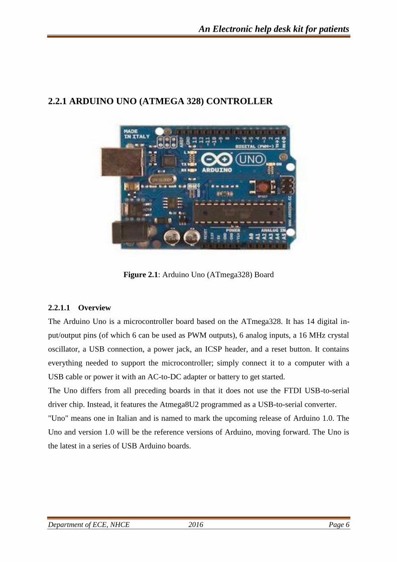
2.2.1 ARDUINO UNO (ATMEGA 328) CONTROLLER
Figure 2.1: Arduino Uno (ATmega328) Board
2.2.1.1 Overview
The Arduino Uno is a microcontroller board based on the ATmega328. It has 14 digital in-
put/output pins (of which 6 can be used as PWM outputs), 6 analog inputs, a 16 MHz crystal
oscillator, a USB connection, a power jack, an ICSP header, and a reset button. It contains
everything needed to support the microcontroller; simply connect it to a computer with a
USB cable or power it with an AC-to-DC adapter or battery to get started.
The Uno differs from all preceding boards in that it does not use the FTDI USB-to-serial
driver chip. Instead, it features the Atmega8U2 programmed as a USB-to-serial converter.
"Uno" means one in Italian and is named to mark the upcoming release of Arduino 1.0. The
Uno and version 1.0 will be the reference versions of Arduino, moving forward. The Uno is
the latest in a series of USB Arduino boards.

An Electronic help desk kit for patients
Department of ECE, NHCE 2016 Page 7
2.2.1.2 Summary
Microcontroller ATmega328
Operating Voltage 5V
Input Voltage (recommended) 7-9V
Input Voltage (limits) 6-20V
Digital I/O Pins 14 (of which 6 provide PWM output)
Analog Input Pins 6
DC Current per I/O Pin 40 mA
DC Current for 3.3V Pin 50 mA
Flash Memory 32 KB (ATmega328) (0.5 KB used by
boot loader)
SRAM 2 KB (ATmega328)
EEPROM 1 KB (ATmega328)
Clock Speed 16 MHz
Table 2.1:Arduino Uno Specification
2.2.1.3 Power
The Arduino Uno can be powered via the USB connection or with an external power supply.
The power source is selected automatically.
External (non-USB) power can come either from an AC-to-DC adapter (wall-wart) or battery.
The adapter can be connected by plugging a 2.1mm Centre-positive plug into the board's
power jack. Leads from a battery can be inserted in the Gnd and Vin pin headers of the
POWER connector.
The board can operate on an external supply of 6 to 20 volts. If supplied with less than 7V,
however, the 5V pin may supply less than five volts and the board may be unstable. If using
more than 12V, the voltage regulator may overheat and damage the board. The recommended
range is 7 to 12 volts.
The power pins are as follows:

An Electronic help desk kit for patients
Department of ECE, NHCE 2016 Page 8
VIN. The input voltage to the Arduino board when it's using an external power source
(as opposed to 5 volts from the USB connection or other regulated power source).
You can supply voltage through this pin, or, if supplying voltage via the power jack,
access it through this pin.
5V. The regulated power supply used to power the microcontroller and other compo-
nents on the board. This can come either from VIN via an on-board regulator, or be
supplied by USB or another regulated 5V supply.
3V3. A 3.3 volt supply generated by the on-board regulator. Maximum current draw
is 50 mA.
GND. Ground pins.
2.2.1.4 Memory
The ATmega328 has 32 KB (with 0.5 KB used for the boot loader). It also has 2 KB of
SRAM and 1 KB of EEPROM (which can be read and written with the EEPROM library).
2.2.1.5 Input and Output
Each of the 14 digital pins on the Uno can be used as an input or output, using pin Mode (),
digital Write (), and digital Read () functions. They operate at 5 volts. Each pin can provide
or receive a maximum of 40 mA and has an internal pull-up resistor (disconnected by default)
of 20-50 kilo Ohms. In addition, some pins have specialized functions:
Serial: 0 (RX) and Serial: 1 (TX): Used to receive (RX) and transmit (TX) TTL
serial data. These pins are connected to the corresponding pins of the ATmega8U2
USB-to-TTL Serial chip.
External Interrupts: 2 and 3: These pins can be configured to trigger an interrupt on
a low value, a rising or falling edge, or a change in value.
PWM: 3, 5, 6, 9, 10, and 11: Provide 8-bit PWM output with the analog Write ()
function.
SPI: 10 (SS), 11 (MOSI), 12 (MISO), 13 (SCK): These pins support SPI communi-
cation using the SPI library.
LED: 13. There is a built-in LED connected to digital pin 13. When the pin is HIGH ,
the LED is on, when the pin is LOW, it's off.
An Electronic help desk kit for patients
Department of ECE, NHCE 2016 Page 9
2.2.1.6 Specialized function of Arduino Uno
The Uno has 6 analog inputs, labeled A0 through A5, each of which provide 10 bits of reso-
lution (i.e. 1024 different values). By default they measure from ground to 5 volts, though is
it possible to change the upper end of their range using the AREF pin and the analog Refer-
ence () function. Additionally, some pins have specialized functionality:
I2C: 4 (SDA) and 5 (SCL). Support I2C (TWI) communication using the Wire li-
brary.
There are a couple of other pins on the board:
AREF. Reference voltage for the analog inputs. Used with analog Reference ().
Reset. Bring this line LOW to reset the microcontroller. Typically used to add a reset
button to shields which block the one on the board.
2.2.1.7 Communication
The Arduino Uno has a number of facilities for communicating with a computer, another Ar-
duino, or other microcontrollers. The ATmega328 provides UART TTL (5V) serial commu-
nication, which is available on digital pins 0 (RX) and 1 (TX). An ATmega8U2 on the board
channels this serial communication over USB and appears as a virtual com port to software
on the computer. The '8U2 firmware uses the standard USB COM drivers, and no external
driver is needed. However, on Windows, a .inf file is required. The Arduino software in-
cludes a serial monitor which allows simple textual data to be sent to and from the Arduino
board. The RX and TX LEDs on the board will flash when data is being transmitted via the
USB-to-serial chip and USB connection to the computer (but not for serial communication on
pins 0 and 1).
A Software Serial library allows for serial communication on any of the Uno's digital pins.
The ATmega328 also supports I2C (TWI) and SPI communication. The Arduino software
includes a Wire library to simplify the use of the I2C bus.
2.2.1.8 Programming
The Arduino Uno can be programmed with the Arduino software (download). Select "Ardui-
no Uno from the Tools > Board menu (according to the microcontroller on your board).

An Electronic help desk kit for patients
Department of ECE, NHCE 2016 Page 10
The ATmega328 on the Arduino Uno comes preburned with a boot loader that allows you to
upload new code to it without the use of an external hardware programmer. It communicates
using the original STK500 protocol.
We can also bypass the boot loader and program the microcontroller through the ICSP (In-
Circuit Serial Programming) header. The ATmega8U2 firmware source code is available.
The ATmega8U2 is loaded with a DFU boot loader, which can be activated by connecting the
solder jumper on the back of the board (near the map of Italy) and then resetting the 8U2.
You can then use Atmel's FLIP software (Windows) or the DFU programmer (Mac OS X and
Linux) to load a new firmware. Or you can use the ISP header with an external programmer
(overwriting the DFU boot loader).
The ATmega16U2 (or 8U2 in the rev1 and rev2 boards) firmware is where source code is
available. The ATmega16U2/8U2 is loaded with a DFU boot loader, which can be activated
by:
On Rev1 board: connecting the solder jumper on the back of the board (near the map
of Italy) and then resetting the 8U2.
On Rev2 or later boards: there is a resistor that pulling the 8U2/16U2 HWB line to
ground, making it easier to put into DFU mode.
We can then use Atmel's FLIP software (Windows) or the DFU programmer (Mac OS X and
Linux) to load a new firmware. Or you can use the ISP header with an external programmer
(overwriting the DFU boot loader).
2.2.1.9 Automatic (Software) Reset
Rather than requiring a physical press of the reset button before an upload, the Arduino Uno
is designed in a way that allows it to be reset by software running on a connected computer.
One of the hardware flow control lines (DTR) of the ATmega8U2/16U2 is connected to the
reset line of the ATmega328 via a 100 nanofarad capacitor. When this line is asserted (taken
low), the reset line drops long enough to reset the chip. The Arduino software uses this capa-
bility to allow you to upload code by simply pressing the upload button in the Arduino envi-
ronment. This means that the boot loader can have a shorter timeout, as the lowering of DTR
can be well-coordinated with the start of the upload.
This setup has other implications. When the Uno is connected to either a computer running
Mac OS X or Linux, it resets each time a connection is made to it from software (via USB).

An Electronic help desk kit for patients
Department of ECE, NHCE 2016 Page 11
For the following half-second or so, the boot loader is running on the Uno. While it is pro-
grammed to ignore malformed data (i.e. anything besides an upload of new code), it will in-
tercept the first few bytes of data sent to the board after a connection is opened. If a sketch
running on the board receives one-time configuration or other data when it first starts, make
sure that the software with which it communicates waits a second after opening the connec-
tion and before sending this data.
The Uno contains a trace that can be cut to disable the auto-reset. The pads on either side of
the trace can be soldered together to re-enable it. It's labeled "RESET-EN". We may be able
to disable the auto-reset by connecting a 110 ohm resistor from 5V to the reset line.
2.2.1.10 USB Overcurrent Protection
The Arduino Uno has a resettable polyfuse that protects the computer's USB ports from
shorts and overcurrent. Although most computers provide their own internal protection, the
fuse provides an extra layer of protection. If more than 500 mA is applied to the USB port,
the fuse will automatically break the connection until the short or overload is removed.
2.2.1.11 Physical Characteristics
The maximum length and width of the Uno PCB are 2.7 and 2.1 inches respectively, with the
USB connector and power jack extending beyond the former dimension. Four screw holes
allow the board to be attached to a surface or case.
Figure 2.2: Arduino Uno pin description

An Electronic help desk kit for patients
Department of ECE, NHCE 2016 Page 12
Figure 2.3: Description of Arduino Uno Board
2.2.2 16*2 Line LCD module
LCD stands for Liquid Crystal Display. Liquid crystal was discovered by the Austrian
botanist Fredreich Rheinizer in 1888. "Liquid crystal" is neither solid nor liquid (an example
is soapy water). The most common liquid-crystal displays (LCDs) in use today rely on
picture elements, or pixels, formed by liquid-crystal (LC) cells that change the polarization
due to the direction of light passing through them in response to an electrical voltage.
2.2.2.1 Features
• 5 × 8 and 5 × 10 dot matrix possible
• Low power operation support: 2.7 to 5.5V
• Wide range of liquid crystal display driver power: 3.0 to 11V
• Liquid crystal drive waveform
• Correspond to high speed MPU bus interface-2 MHz (when VCC = 5V)
• 4-bit or 8-bit MPU interface enabled

An Electronic help desk kit for patients
Department of ECE, NHCE 2016 Page 13
• 80 × 8-bit display RAM (80 characters max.)
• 9,920-bit character generator ROM for a total of 240 character fonts - 208 character fonts
(5 × 8 dot) - 32 character fonts (5 × 10 dot)HD44780U2
• 64 × 8-bit character generator RAM - 8 character fonts (5 × 8 dot) - 4 character fonts (5 ×
10 dot)
• Programmable duty cycles - 1/8 for one line of 5 × 8 dots with cursor - 1/11 for one line of
5 × 10 dots with cursor - 1/16 for two lines of 5 × 8 dots with cursor
• Wide range of instruction functions: - Display clear, cursor home, display on/off, cursor
on/off, display character blink, cursor shift and display shift
• Automatic reset circuit that initializes the controller/driver after power on
• Internal oscillator with external resistors
• Low power consumption
Figure 2.4:The LCD display and pin description
An Electronic help desk kit for patients
Department of ECE, NHCE 2016 Page 14
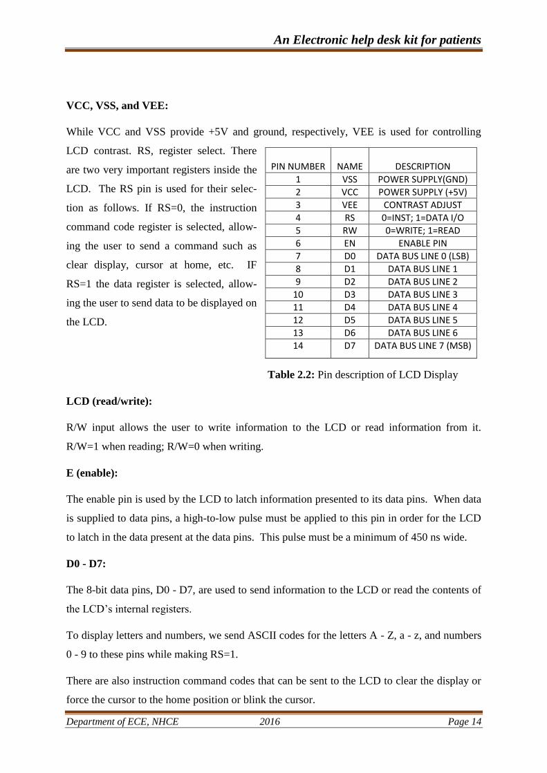
VCC, VSS, and VEE:
While VCC and VSS provide +5V and ground, respectively, VEE is used for controlling
LCD contrast. RS, register select. There
are two very important registers inside the
LCD. The RS pin is used for their selec-
tion as follows. If RS=0, the instruction
command code register is selected, allow-
ing the user to send a command such as
clear display, cursor at home, etc. IF
RS=1 the data register is selected, allow-
ing the user to send data to be displayed on
the LCD.
Table 2.2: Pin description of LCD Display
LCD (read/write):
R/W input allows the user to write information to the LCD or read information from it.
R/W=1 when reading; R/W=0 when writing.
E (enable):
The enable pin is used by the LCD to latch information presented to its data pins. When data
is supplied to data pins, a high-to-low pulse must be applied to this pin in order for the LCD
to latch in the data present at the data pins. This pulse must be a minimum of 450 ns wide.
D0 - D7:
The 8-bit data pins, D0 - D7, are used to send information to the LCD or read the contents of
the LCD’s internal registers.
To display letters and numbers, we send ASCII codes for the letters A - Z, a - z, and numbers
0 - 9 to these pins while making RS=1.
There are also instruction command codes that can be sent to the LCD to clear the display or
force the cursor to the home position or blink the cursor.
PIN NUMBER
NAME
DESCRIPTION
1 VSS POWER SUPPLY(GND)
2 VCC POWER SUPPLY (+5V)
3 VEE CONTRAST ADJUST
4 RS 0=INST; 1=DATA I/O
5 RW 0=WRITE; 1=READ
6 EN ENABLE PIN
7 D0 DATA BUS LINE 0 (LSB)
8 D1 DATA BUS LINE 1
9 D2 DATA BUS LINE 2
10 D3 DATA BUS LINE 3
11 D4 DATA BUS LINE 4
12 D5 DATA BUS LINE 5
13 D6 DATA BUS LINE 6
14 D7 DATA BUS LINE 7 (MSB)
An Electronic help desk kit for patients
Department of ECE, NHCE 2016 Page 15
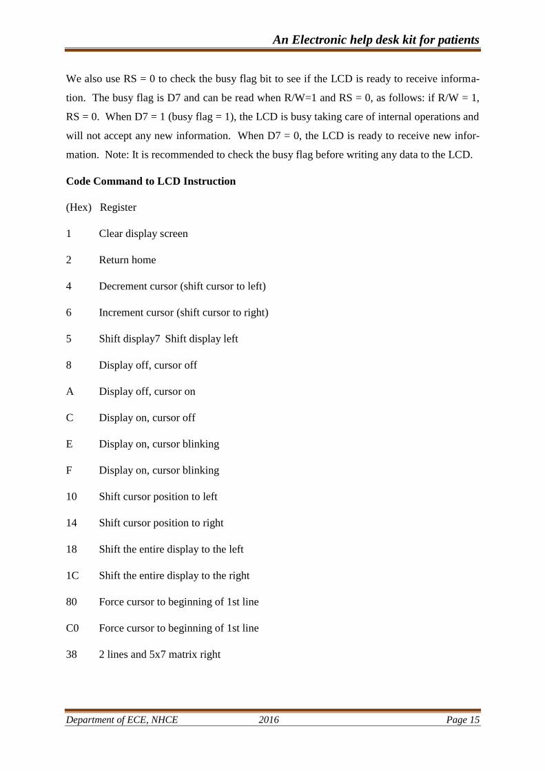
We also use RS = 0 to check the busy flag bit to see if the LCD is ready to receive informa-
tion. The busy flag is D7 and can be read when R/W=1 and RS = 0, as follows: if R/W = 1,
RS = 0. When D7 = 1 (busy flag = 1), the LCD is busy taking care of internal operations and
will not accept any new information. When D7 = 0, the LCD is ready to receive new infor-
mation. Note: It is recommended to check the busy flag before writing any data to the LCD.
Code Command to LCD Instruction
(Hex) Register
1 Clear display screen
2 Return home
4 Decrement cursor (shift cursor to left)
6 Increment cursor (shift cursor to right)
5 Shift display7 Shift display left
8 Display off, cursor off
A Display off, cursor on
C Display on, cursor off
E Display on, cursor blinking
F Display on, cursor blinking
10 Shift cursor position to left
14 Shift cursor position to right
18 Shift the entire display to the left
1C Shift the entire display to the right
80 Force cursor to beginning of 1st line
C0 Force cursor to beginning of 1st line
38 2 lines and 5x7 matrix right

An Electronic help desk kit for patients
Department of ECE, NHCE 2016 Page 16
2.2.3 APR-33A3
Today’s consumers demand the best in audio/voice. They want crystal-clear sound wherever
they are in whatever format they want to use. APLUS delivers the technology to enhance a
listener’s audio/voice experience.
The APR33A3 series are powerful audio processor along with high performance audio ana-
log-to-digital converters (ADCs) and digital-to-analog converters (DACs). The aPR33A se-
ries are a fully integrated solution offering high performance and unparalleled integration
with analog input, digital processing and analog output functionality. The APR33A3 series
incorporates all the functionality required to perform demanding audio/voice applications.
High quality audio/voice systems with lower bill-of-material costs can be implemented with
the APR33A3 series because of its integrated analog data converters and full suite of quality-
enhancing features such as sample-rate convertor.
The APR33A3 series C3.1 in Tape mode manages messages sequentially
much like traditional cassette tape recorders. Within tape mode two options exist, auto rewind
and non-auto rewind. Auto rewind mode configures the device to automatically rewind to the
beginning of the message immediately following recording or playback of the message. In
tape mode, using either option, messages must be recorded or played back sequentially, much
like a traditional cassette tape recorder specially designed for simple key trigger, user can
record and playback the message. Meanwhile, this mode provides the power-management
system. Users can let the chip enter power-down mode when unused. It can effectively reduce
electric current consuming to 15uA and increase the using time in any projects powered by
batteries.
2.2.3.1 Features:
Operating Voltage Range: 3V ~ 6.5V
Single Chip, High Quality Audio/Voice Recording & Playback Solution
No External ICs Required
Minimum External Components
User Friendly, Easy to Use Operation
Programming & Development Systems Not Required

An Electronic help desk kit for patients
Department of ECE, NHCE 2016 Page 17
170/ 680 sec. Voice Recording Length in aPR33A1/aPR33A3
Powerful 16-Bits Digital Audio Processor.
Nonvolatile Flash Memory Technology
No Battery Backup Required
External Reset pin.
Powerful Power Management Unit
Very Low Standby Current: 1uA
Low Power-Down Current: 15uA
Supports Power-Down Mode for Power Saving
Built-in Audio-Recording Microphone Amplifier
No External OPAMP or BJT Required
Easy to PCB layout
Configurable analog interface
Differential-ended MIC pre-amp for Low Noise
High Quality Line Receiver
High Quality Analog to Digital, DAC and PWM module
Resolution up to 16-bits
Simple and Direct User Interface
Figure 2.5: APR33A3 Voice Recorder and Playback

An Electronic help desk kit for patients
Department of ECE, NHCE 2016 Page 18
2.2.3.2 PIN Description
Figure 2.6: The APR audio recording chip pin diagram.
A
P
R
3
3
A
3

An Electronic help desk kit for patients
Department of ECE, NHCE 2016 Page 19
Figure 2.6: Description of APR33A3 Voice Board.
2.2.4 POWER SUPPLY
Electrical power is the rate of movement of electrons that create energy. As a result of the
electronic age many products need electrical power to perform certain activities. Being able
to manipulate electrical power comes at a cost. In today's world there is always the bottom
line, cost. Power supplies are the devices that can manipulate electrical power to be used in
various applications. Power supplies can be expensive but there are cheaper alternative solu-
tions that can produce the same output. A power supply includes conversion steps and has to
be reliable enough not to damage what it is hooked up to. Both aspects need specific parts in
a certain orientations to create those specific outputs.

An Electronic help desk kit for patients
Department of ECE, NHCE 2016 Page 20
Figure 2.7: Block diagram of Power Supply
2.2.5 SPEAKER
Figure 2.8: Multimedia speaker

An Electronic help desk kit for patients
Department of ECE, NHCE 2016 Page 21
Speaker is a device that converts analog audio signals into the equivalent air vibrations in or-
der to make audible sound. Although CRT usage has faded, speakers designed for computers
are shielded to avoid magnetic interference with the CRT's magnetic coil.
2.2.6.1 Features:
RoHS Information-GF0778B Cert of Compliance
Catalog Drawings-GF0778B Side
Standard Package-1,000
Type-Magnetic
Frequency Range -250Hz ~ 15kHz
Impedance-8 Ohm
Sound Pressure Level-95dB
Power Rated-3W
Power Max-5W
Height-27.50mm
Size / Dimension-77.00mm L x 77.00mm W
Shape-Round, Square Frame
Termination-Solder Eyelet(s)
Material-Cone Paper
Material-Magnet Ferrite
Dynamic Catalog-GF Series
2.2.6 Bluetooth Module (HC05)
HC-05 module is an easy to use Bluetooth SPP (Serial Port Protocol) module, designed for
transparent wireless serial connection setup.
Serial port Bluetooth module is fully qualified Bluetooth V2.0+EDR (Enhanced Data Rate)
3Mbps Modulation with complete 2.4GHz radio transceiver and baseband. It uses CSR Blue
core04-External single chip Bluetooth system with CMOS technology and with AFH (Adap-
tive Frequency Hopping Feature). It has the footprint as small as 12.7mmx27mm.

An Electronic help desk kit for patients
Department of ECE, NHCE 2016 Page 22
Specifications
Hardware Features
Typical -80dBm sensitivity
Up to +4dBm RF transmit power
Low Power 1.8V Operation ,1.8 to 3.6V I/O
PIO control
UART interface with programmable baud rate
Integrated antenna
Edge connector
Software Features
Default Baud rate: 38400, Data bits: 8, Stop bit: 1, Parity: No parity, Data control: has.
Supported baud rate: 9600,19200,38400,57600, 115200, 230400, and 460800.
Given a rising pulse in PIO0, device will be disconnected.
Status instruction port PIO1: low-disconnected, high-connected;
PIO10 and PIO11 can be connected to red and blue led separately. When master and
slave are paired, red and blue led blinks 1time/2s in interval, while disconnected only
blue led blinks 2times/s.
Auto-connect to the last device on power as default.
Permit pairing device to connect as default.
Auto-pairing PINCODE:”1234” as default
Auto-reconnect in 30 min when disconnected as a result of beyond the range of connec-
tion.
Figure 2.9: Serial Port Bluetooth Module HC05
An Electronic help desk kit for patients
Department of ECE, NHCE 2016 Page 23
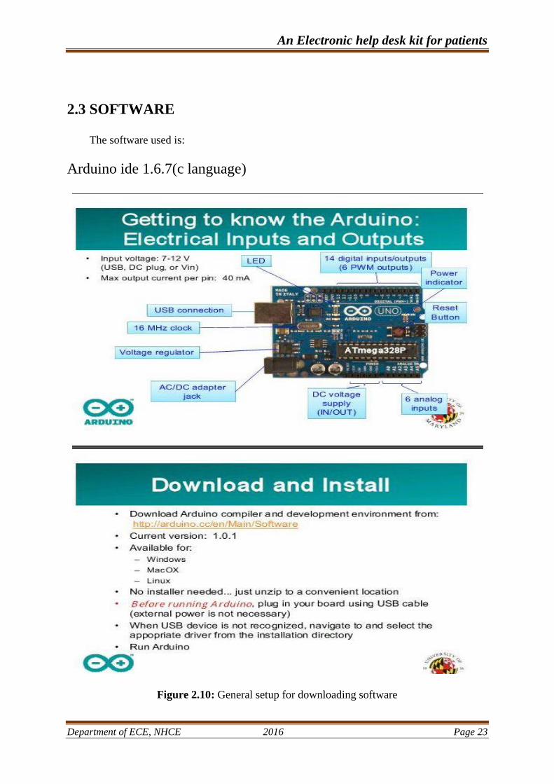
2.3 SOFTWARE
The software used is:
Arduino ide 1.6.7(c language)
Figure 2.10: General setup for downloading software

An Electronic help desk kit for patients
Department of ECE, NHCE 2016 Page 24
Figure 2.11: Steps for selecting Arduino Board and COM Port

An Electronic help desk kit for patients
Department of ECE, NHCE 2016 Page 25
Figure 2.12: Elements and Using of Arduino IDE

An Electronic help desk kit for patients
Department of ECE, NHCE 2016 Page 26
Figure 2.13: Arduino Reference and Sketch Structure

An Electronic help desk kit for patients
Department of ECE, NHCE 2016 Page 27
CHAPTER 3
HARDWARE
This chapter gives details of the hardware subsystems and the main circuit of the sys-
tem. The chapter has three parts. First part describes the system as a block, second part shows
the circuit, concepts of individual blocks and the third part contains the circuit diagram of the
system.
3.1 Block diagram:
The block diagram of the complete system is shown below:
Figure 3.1: Block Diagram for Pre-Recording
Transmitter side Receiver side
Figure 3.2: The block diagram of the system
KEYPAD
APR
33A3
voice re-
corder
MIC
Mobile
phone (Blue
tooth)
Arduino Uno
(Atmega 328) Voice
playback
Bluetooth
module HC05
LCD

An Electronic help desk kit for patients
Department of ECE, NHCE 2016 Page 28
The system can be broadly classified into two parts
(i) Transmitter side
(ii) Receiver side
The system consists of Arduino Uno board, power supply, Bluetooth Module, APR module,
speakers, LCD display and Smartphone.
3.1.1 Transmitter:
In the transmitter side, the Bluetooth is powered on and the initialization process is
done in Smartphone. Once the Bluetooth is ready to communicate, the message to be trans-
mitted will be input by the system through AT commands. The communication between Blu-
etooth and Arduino controller is made possible using USB cable.
3.1.2 Receiver:
The message is received by the receiver Bluetooth module and is given to Arduino
Uno controller for further processing. The Arduino Uno stores the message in its memory and
reads the message. The condition will be decoded and output is given to specified speak-
er/speakers. The notifications will be pre-recorded and the code word for each notification is
specified. In the message the code word will be extracted and the particular message channel
in the APR-33A3 pre-recording audio chip will be triggered. The audio is then made audible.
The notification code word is also made visible in the LCD display.
3.2 Hardware subsystems
This section of the chapter describes various parts of the hardware and related circuits.
3.2.1 Serial Port Bluetooth Module(master/slave):HC05
HC 05 is a slave Bluetooth to serial adapter. It measures a dimensions of only 28mm x 15
mm x 2.35mm.It is easy to handle and can be used as wireless UART Communication from
PC to any microcontroller. HC-05 is a slave only device.
By default, HC-05 has Baud Rate – 9600,
Pairing Code – 1234,
Name/ ID – linvor

An Electronic help desk kit for patients
Department of ECE, NHCE 2016 Page 29
Figure 3.3: Bluetooth module HC05
Establishing a Bluetooth connection
Bluetooth supports simultaneous connections between multiple devices in a wireless network
called a piconet. A maximum of 8 Bluetooth devices can be active in a piconet. Each piconet
has a single master device and at least one slave device. Multiple, overlapping piconets in the
same area are referred to as a scatternet. A device can switch role when jumping from one
piconet to another. However, a device is not allowed to be a master in more than one piconet
at the same time.
A typical Bluetooth communication involves three steps: device discovery, service discovery
and pairing. In a device discovery, a Bluetooth device detects the presence of any other Blu-
etooth device that is within its coverage range. The initiating device can only detect devices
that are set to “discoverable”. Upon successful detection, the device’s “friendly name” is re-
turned. Afterwards, the initiating device starts a service discovery to search for specific ser-
vices offered in the other device. These services are based on profiles defined in the Blu-
etooth specification. Profiles implementation in Bluetooth devices is important to ensure inte-
roperability of devices from different manufacturers. Common profiles supported are Service
Discovery Application Profile, Serial Port Profile and Dial-Up Networking Profile.

An Electronic help desk kit for patients
Department of ECE, NHCE 2016 Page 30
This optional pairing procedure initiates a private connection between both devices. Matching
PIN or passkey is inserted in both devices before a connection is allowed.
Testing the Bluetooth Module:
Step1: Uploading the Code
Upload the below sketch to the Arduino Uno,
void setup ()
{
Serial.begin(9600);//set the baud rate
Serial.println(“start”);//send data to the android phone
}
void loop()
{
Serial.println(“Hoi, Android”);// send data to the android phone
delay(10000)
}
Step2: Connections
The HC-05 Module communicates with the Arduino Uno via serial connection. Four pins are
used:
VCC -> VCC is used to power the module. It is connected to the Arduino 5v pin.
GND -> GND is the ground pin. It is connected to the Arduino Ground pin.
TX -> TXD is used to send data from the module to the Arduino. It is connected to the serial
receive pin (RX) of the Arduino, which is pin 0 in case of the Uno. Incase different Arduino
board is used, and then its schematics has to be checked in order to make sure that the right
pins are used.
RX -> RXD is used to receive data from the Arduino. It is connected to the Arduino serial
transmit pin (TX), which is pin 1 of Arduino Uno.
KEY -> This pin is used for changing the settings (AT Command Mode).At present, KEY pin
is left open.
HC-05 to Arduino Uno Connections
VCC -> VCC (5V)
GND ->GND

An Electronic help desk kit for patients
Department of ECE, NHCE 2016 Page 31
TX ->RX (D0)
RX ->TX (D1)
Step 4: Pairing the Bluetooth and setting the Blueterm Software
After the power up of the Bluetooth device, turn on the Bluetooth in the android phone.
Search for the new devices. A Bluetooth device name is found. Click on the Bluetooth device
name, a pairing window appears, type a password. Paring is done and an android phone and
Arduino Uno is connected.
Figure 3.4: Image of bluetooth pairng process
Hardware
Figure 3.5: Hardware diagram of Bluetooth module

An Electronic help desk kit for patients
Department of ECE, NHCE 2016 Page 32
There are many Bluetooth modules and even Arduino shields: my choice has fallen on Serial
port Bluetooth module HC05.It belongs to class2 Bluetooth module that acts like a serial port
with no need of any software configuration on the Arduino. This module is available in sev-
eral configurations, and this has been the first hurdle to overcome.
The one we need to make the connection between Arduino and the Android phone is a Slave
Module
To make things very simple, there are two types of devices: Master and Slave; a Master can
communicate with more than one Slave while a Slave can communicate with a single Master
at a time, Master-Master and Slave-Slave communication is not allowed. Since the Bluetooth
module in all smartphones is of Master type, the one we need for Arduino must be a Slave
(this has nothing to do with client server communication).
3.2.2 Power supply
A simple power supply can be made with a component called a "3-pin regulator or 3-terminal
regulator” It will provide a very low ripple output (about 4mV to 10mV provided electrolytic
are on the input and output. The diagram below shows how to connect a regulator to create a
power supply. The 7805 regulators can handle 100mA, 500mA and 1 amp, and produce an
output of 5v.These regulators are called linear regulators and drop about 4v across them -
minimum. If the current flow is 1 amp, 4watts of heat must be dissipated via a large heat sink.
If the output is 5v and input 12v, 7volts will be dropped across the regulator and 7 watts must
be dissipated.

An Electronic help desk kit for patients
Department of ECE, NHCE 2016 Page 33
Figure 3.6: The circuit diagram of power supply
Voltage regulator:
As we require a 5V we need LM7805 Voltage Regulator IC.
7805 IC Rating
Input voltage range 7V- 35V
Current rating Ic = 1A
Output voltage range VMax=5.2V ,VMin=4.8V
Capacitors:
Knowledge of Ripple factor is essential while designing the values of capacitors
It is given by
Y=1/(4√3fRC) (as the capacitor filter is used)
f= frequency of AC (50 Hz)
C= filtering capacitance
R= value of resistor
We have to determine this capacitance for filtering
Y=Vac-rms/Vdc................................................................................ (3.1)
Vac-rms = Vr/2√3......................................................................…… (3.2)
Vdc= VMax-(Vr/2)................................................………………… (3.3)
Vr= VMax- VMin............................................................................... (3.4)
Vr = 5.2-4.8 =0. 4V
Vac-rms = .3464V
Vdc = 5V
Y=0 .06928
Hence the capacitor value is found out by substituting the ripple factor in Y=1/(4√3fR)
Thus, C= 2314 µF and standard 2200µF is chosen

An Electronic help desk kit for patients
Department of ECE, NHCE 2016 Page 34
Datasheet of 7805 prescribes to use a 0.01μF capacitor at the output Side toavoid transient
changes in the voltages due to changes in load and a 0.33μF at theinputside of regulator to avoid
ripples if the filtering is far away from regulator.
In the similar manner one can design regulation for 12V supply too. The IC used would be
LM7812 in this case. Same design values of capacitors hold good.
This can be mounted on the board as well.
3.2.3 LCD Display:
A Liquid Crystal Display commonly abbreviated as LCD is basically a display unit built us-
ing Liquid Crystal technology. When we build real life/real world electronics based projects,
we need a medium/device to display output values and messages. The most basic form of
electronic display available is 7 Segment displays – which have its own limitations. The next
best available option is Liquid Crystal Displays which comes in different size specifications.
Out of all available LCD modules in market, the most commonly used one is 16×2 LCD.
Module which can display 32 ASCII characters in 2 lines (16 characters in 1 line).
Interfacing 16×2 LCD to Arduino Uno
LCD modules form a very important part in many Arduino based embedded system designs.
So the knowledge on interfacing LCD module to Arduino is very essential in designing em-
bedded systems. Here it deals with interfacing an Arduino to 16×2 LCD. JHD162A is the
LCD module used here. JHD162A is a 16×2 LCD module based on the HD44780 driver from
Hitachi. The JHD162A has 16 pins and can be operated in 4-bit mode (using only 4 data
lines) or 8-bit mode (using all 8 data lines). Here we are using the LCD module in 4-bit
mode. We can display a plain text messages on the LCD module using Arduino Uno.
Figure 3.7: 16×2 LCD Module Pin Out Diagram

An Electronic help desk kit for patients
Department of ECE, NHCE 2016 Page 35
The name and functions of each pin of the 16×2 LCD module is given below.
Pin1 (Vss): Ground pin of the LCD module.
Pin2 (Vcc): Power to LCD module (+5V supply is given to this pin)
Pin3 (VEE): Contrast adjustment pin. This is done by connecting the ends of a 10K potenti-
ometer to +5V and ground and then connecting the slider pin to the VEE pin. The voltage at
the VEE pin defines the contrast. The normal setting is between 0.4 and 0.9V.
Pin4 (RS): Register select pin. The JHD162A has two registers namely command register
and data register. Logic HIGH at RS pin selects data register and logic LOW at RS pin selects
command register. If we make the RS pin HIGH and feed an input to the data lines (DB0 to
DB7), this input will be treated as data to display on LCD screen. If we make the RS pin
LOW and feed an input to the data lines, then this will be treated as a command (a command
to be written to LCD controller – like positioning cursor or clear screen or scroll).
Pin5 (R/W): Read/Write modes. This pin is used for selecting between read and write modes.
Logic HIGH at this pin activates read mode and logic LOW at this pin activates write mode.
Pin6 (E): This pin is meant for enabling the LCD module. A HIGH to LOW signal at this pin
will enable the module.
Pin7 (DB0) to Pin14 (DB7): These are data pins. The commands and data are fed to the LCD
module though these pins.
Pin15 (LED+): Anode of the back light LED. When operated on 5V, a 560 ohm resistor
should be connected in series to this pin. In Arduino based projects the back light LED can be
powered from the 3.3V source on the Arduino board.
Pin16 (LED-): Cathode of the back light LED.
The circuit diagram of interfacing LCD to Arduino for displaying a text message is shown
below.
An Electronic help desk kit for patients
Department of ECE, NHCE 2016 Page 36
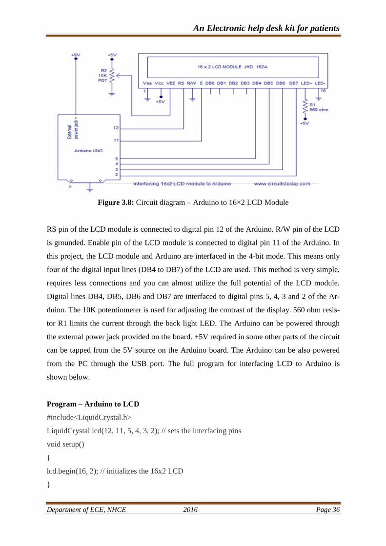
Figure 3.8: Circuit diagram – Arduino to 16×2 LCD Module
RS pin of the LCD module is connected to digital pin 12 of the Arduino. R/W pin of the LCD
is grounded. Enable pin of the LCD module is connected to digital pin 11 of the Arduino. In
this project, the LCD module and Arduino are interfaced in the 4-bit mode. This means only
four of the digital input lines (DB4 to DB7) of the LCD are used. This method is very simple,
requires less connections and you can almost utilize the full potential of the LCD module.
Digital lines DB4, DB5, DB6 and DB7 are interfaced to digital pins 5, 4, 3 and 2 of the Ar-
duino. The 10K potentiometer is used for adjusting the contrast of the display. 560 ohm resis-
tor R1 limits the current through the back light LED. The Arduino can be powered through
the external power jack provided on the board. +5V required in some other parts of the circuit
can be tapped from the 5V source on the Arduino board. The Arduino can be also powered
from the PC through the USB port. The full program for interfacing LCD to Arduino is
shown below.
Program – Arduino to LCD
#include<LiquidCrystal.h>
LiquidCrystal lcd(12, 11, 5, 4, 3, 2); // sets the interfacing pins
void setup()
{
lcd.begin(16, 2); // initializes the 16x2 LCD
}

An Electronic help desk kit for patients
Department of ECE, NHCE 2016 Page 37
void loop()
{
lcd.setCursor(0,0); //sets the cursor at row 0 column 0
lcd.print("16x2 LCD MODULE"); // prints 16x2 LCD MODULE
lcd.setCursor(2,1); //sets the cursor at row 1 column 2
lcd.print("HELLO WORLD"); // prints HELLO WORLD
}
To facilitate communication between Arduino and LCD module, we make use of a built in
library in Arduino <LiquidCrystal.h> – which is written for LCD modules making use of
the Hitachi HD44780 chipset (or a compatible chipset). This library can handle both 4 bit
mode and 8 bit mode wiring of LCD. Library “LiquidCrystal.h” is used for easily control-
ling the LCD module using Arduino board with the help of built in methods defined inside
the library For example, data string can be printed on the LCD module by merely calling a
method lcd.print(). If you want to print “Hello World” at row 1, starting from column 3; first
set the cursor at the desired position using method lcd.setCursor(1,3) and then write the
command to print the characters as lcd.print(“Hello World”). The library is readily available
with the Arduino IDE (as it’s a pre-installed standard library). Any library can be accessed
manually through the “Import library” in the “sketch” tab in the main menu bar. The Li-
quidCrystal.h library provides functions/methods for almost all applications like printing a
string, setting the cursor, initializing the LCD, scrolling the display, auto scroll, clear LCD,
blink cursor etc.
3.2.4 USB data Communication
As the name suggests, Universal Serial Bus (USB) is external bus architecture for Connecting
USB-capable peripheral devices to a host compute. The USB was formed in 1994 by a group
of 7 companies namely Compaq, DEC, IBM, Intel, Microsoft, NEC and Nortel.
Earlier, the objective of this standardization is to enable the convenience of connecting exter-
nal devices to PCs by replacing the multitude of connectors at the back of the PCs. But as
technology advanced that lead to faster data transmission rate, USB technology has gradually
evolved from just a connection between external devices to the PCs, to a serial single port on
the computer that becomes a link for a myriad of devices (up to 127 devices in a USB sys-
tem). USB 1.0 was released in January 1996 with only a data transfer rate of 1.5Mbps.

An Electronic help desk kit for patients
Department of ECE, NHCE 2016 Page 38
Moving on to USB 1.1 with a maximum data transfer rate of 12Mbps was soon introduced
in September 1998.Next, the USB 2.0 specification was launched in April 2000 and was
standardized by the USB-IF (Implementers Forum, Inc) at the end of 2001. Hewlett-Packard,
Intel, Lucent Technologies (now Alcatel-Lucent), NEC and Philips jointly led the initiative to
develop a higher data transfer rate, with the resulting specification achieving 480 Mbps, 40
times faster than the original USB 1.1 specification. The USB 3.0 specifications were re-
leased on November 2008. Here in USB 3.0, it has an increased data transfer rate (up to
5Gbps), decreased power consumption, increased power output and most importantly, USB
3.0 is backwards-compatible with USB 2.0. Also, USB 3.0consists of a new higher speed bus
known as super speed that is in parallel with the USB 2.0 bus.
In USB data communication, the USB encodes the data by using the Non-Return-to Zero In-
verted (NRZI) transmission scheme. In NRZI coding, a “1” bit is represented by a transition
of the physical level and “0” bit is represented by no transition of the physical layer. In addi-
tion, in order to ensure a minimum density of signal transitions that remains in the bit stream,
an additional “0” bit is injected onto the data bus after the occurrence of 6 consecutive “1”
bits. Here, in this method, is commonly known as bit stuffing or simply insertion of non-
information bits into data. All this is done to ensure the presence of sufficient signal transi-
tions for clock recovery.
Figure 3.9: Example of NRZI encoding used by USB Data Communication.

An Electronic help desk kit for patients
Department of ECE, NHCE 2016 Page 39
Figure 3.10: Type B of USB (used for communication)
3.2.5 Speaker
Speaker is a device that converts analog audio signals into the equivalent air vibrations in or-
der to make audible sound. Although CRT usage has faded, speakers designed for computers
are shielded to avoid magnetic interference with the CRT's magnetic coil.
If we connect our amplifier to the wrong speaker impedance, we risk damaging the
amp. In tube amps, too high a load impedance (or a disconnected load) can result in damage
to the output tubes or output transformer, while in solid state amps, if the speaker impedance
is too low, the amplifier will tend to overheat and more power is used up in the amplifier than
is delivered to the speaker. Too many speakers on a solid state amp can burn up the power
output section.
The amplifier will deliver maximum power (volume) to the speaker when the speaker
impedance matches (is equal to) the internal impedance (called the OUTPUT IMPEDANCE)
of the amplifier. Too low impedance will result in weak output and poor tone. If the speaker
impedance is higher than that of the amplifier, its power output will again be less than it is
capable of.
An Electronic help desk kit for patients
Department of ECE, NHCE 2016 Page 40
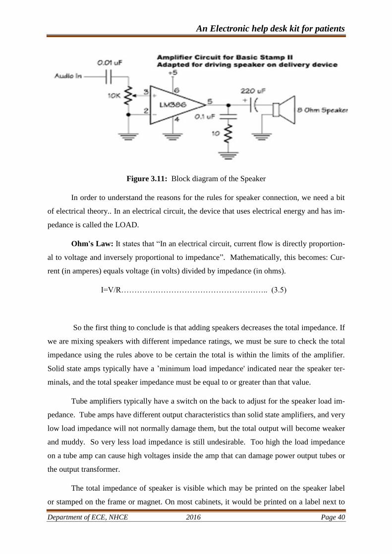
Figure 3.11: Block diagram of the Speaker
In order to understand the reasons for the rules for speaker connection, we need a bit
of electrical theory.. In an electrical circuit, the device that uses electrical energy and has im-
pedance is called the LOAD.
Ohm's Law: It states that “In an electrical circuit, current flow is directly proportion-
al to voltage and inversely proportional to impedance”. Mathematically, this becomes: Cur-
rent (in amperes) equals voltage (in volts) divided by impedance (in ohms).
I=V/R……………………………………………….. (3.5)
So the first thing to conclude is that adding speakers decreases the total impedance. If
we are mixing speakers with different impedance ratings, we must be sure to check the total
impedance using the rules above to be certain the total is within the limits of the amplifier.
Solid state amps typically have a ’minimum load impedance' indicated near the speaker ter-
minals, and the total speaker impedance must be equal to or greater than that value.
Tube amplifiers typically have a switch on the back to adjust for the speaker load im-
pedance. Tube amps have different output characteristics than solid state amplifiers, and very
low load impedance will not normally damage them, but the total output will become weaker
and muddy. So very less load impedance is still undesirable. Too high the load impedance
on a tube amp can cause high voltages inside the amp that can damage power output tubes or
the output transformer.
The total impedance of speaker is visible which may be printed on the speaker label
or stamped on the frame or magnet. On most cabinets, it would be printed on a label next to
An Electronic help desk kit for patients
Department of ECE, NHCE 2016 Page 41
the jack .To measure the true impedance of a speaker or cabinet requires a rather complex
procedure involving signal generators, power amplifiers and high frequency AC voltmeters.
However, with raw speakers and many cabinets, the ohmmeter function of a digital multime-
ter can help us identify what the impedance of the speaker should be. Generally, the reading
given by an ohmmeter will be about 2/3 to 3/4 of the impedance of the speaker. So, a 4 ohm
speaker will typically measure about 2.5 - 3 ohms, and an 8 ohm speaker will typically read
about 5-6 ohms, while a 16 ohm speaker will measure around 12 ohms.
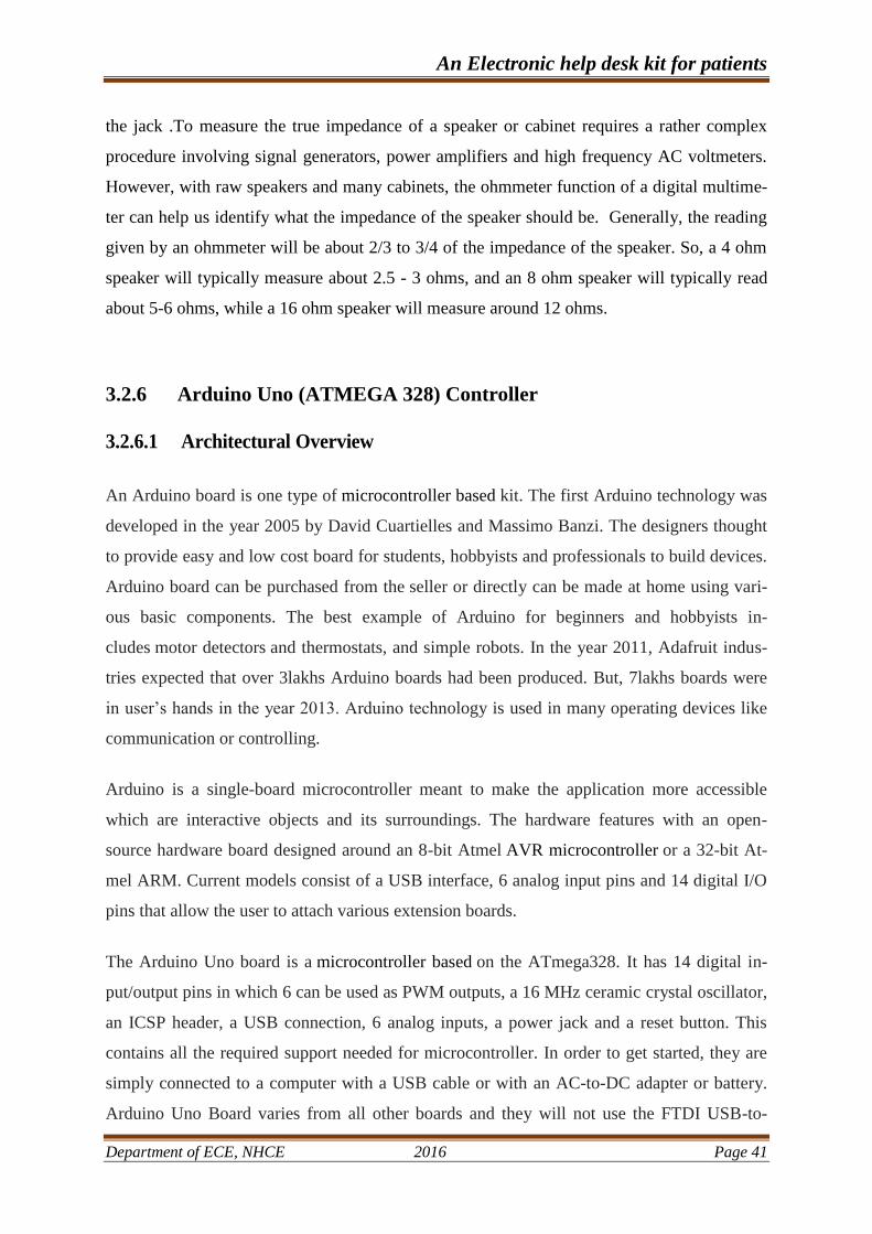
3.2.6 Arduino Uno (ATMEGA 328) Controller
3.2.6.1 Architectural Overview
An Arduino board is one type of microcontroller based kit. The first Arduino technology was
developed in the year 2005 by David Cuartielles and Massimo Banzi. The designers thought
to provide easy and low cost board for students, hobbyists and professionals to build devices.
Arduino board can be purchased from the seller or directly can be made at home using vari-
ous basic components. The best example of Arduino for beginners and hobbyists in-
cludes motor detectors and thermostats, and simple robots. In the year 2011, Adafruit indus-
tries expected that over 3lakhs Arduino boards had been produced. But, 7lakhs boards were
in user’s hands in the year 2013. Arduino technology is used in many operating devices like
communication or controlling.
Arduino is a single-board microcontroller meant to make the application more accessible
which are interactive objects and its surroundings. The hardware features with an open-
source hardware board designed around an 8-bit Atmel AVR microcontroller or a 32-bit At-
mel ARM. Current models consist of a USB interface, 6 analog input pins and 14 digital I/O
pins that allow the user to attach various extension boards.
The Arduino Uno board is a microcontroller based on the ATmega328. It has 14 digital in-
put/output pins in which 6 can be used as PWM outputs, a 16 MHz ceramic crystal oscillator,
an ICSP header, a USB connection, 6 analog inputs, a power jack and a reset button. This
contains all the required support needed for microcontroller. In order to get started, they are
simply connected to a computer with a USB cable or with an AC-to-DC adapter or battery.
Arduino Uno Board varies from all other boards and they will not use the FTDI USB-to-

An Electronic help desk kit for patients
Department of ECE, NHCE 2016 Page 42
serial driver chip in them. It is featured by the Atmega16U2 (Atmega8U2 up to version R2)
programmed as a USB-to-serial converter.
Figure 3.12: Arduino Uno board with internal connections
Features:
It is an easy USB interface. This allows interface with USB as this is a serial device.
The chip on the board plugs straight into the USB port and supports on the computer
as a virtual serial port. The benefit of this setup is that serial communication is an ex-
tremely easy protocol which is time-tested and USB makes connection with modern
computers and makes it comfortable.
It is easy-to-find the microcontroller brain which is the ATmega328 chip. It has more
number of hardware features like timers, external and internal interrupts, PWM pins
and multiple sleep modes.
It is an open source design and the advantage of being open source is that it has a
large community of people using and troubleshooting it. This makes it easy to help in
debugging projects.
It is a 16 MHz clock which is fast enough for most applications and does not speeds
up the microcontroller.

An Electronic help desk kit for patients
Department of ECE, NHCE 2016 Page 43
It is very convenient to manage power inside it and has a feature of built-in voltage
regulation. This can also be powered directly off a USB port without any external
power. We can connect an external power source of upto 12v and this regulates it to
both 5v and 3.3v.
13 digital pins and 6 analog pins. This sort of pins allows you to connect hardware to
your Arduino Uno board externally. These pins are used as a key for extending the
computing capability of the Arduino Uno into the real world. Simply plug the elec-
tronic devices and sensors into the sockets that correspond to each of these pins and
you are good to go.
This has an ICSP connector for bypassing the USB port and interfacing the Arduino
directly as a serial device. This port is necessary to re-boot load the chip if it corrupts
and can no longer used in the computer.
It has a 32 KB of flash memory for storing your code.
An on-board LED is attached to digital pin 13 for faster debugging of code and to
make the debug process easy.
Finally, it has a button to reset the program on the chip.
Arduino Uno microcontroller can sense the environment by receiving input from a variety of
sensors and can affect its surroundings by controlling lights, motors, and other actuators. The
microcontroller is programmed using the Arduino programming language (based on Wiring)
and the Arduino development environment (based on Processing).
ATmega168/328-Arduino Pin Mapping:

An Electronic help desk kit for patients
Department of ECE, NHCE 2016 Page 44
Figure3.13: ATmega168-328Arduino Pin Mapping
Programming:
The Arduino Integrated Development Environment (IDE) is a cross-platform applica-
tion written in Java, and is derived from the IDE for the Processing programming lan-
guage and the Wiring projects
The Arduino Uno board can be programmed with the Arduino software.
Select “Arduino Uno from the Tools > Board menu (according to the microcontroller
on the board).
The ATmega328 on the Arduino Uno comes preburned with a boot loader that allows
us to upload new code to it without the use of an external hardware programmer. It
communicates using the original STK500 protocol.
We can also bypass the boot loader and program the microcontroller through the ICSP
(In-Circuit Serial Programming) header.

An Electronic help desk kit for patients
Department of ECE, NHCE 2016 Page 45
Figure 3.14: Arduino Uno Starter Kit
Memory Architecture of Arduino Uno
Microcontrollers such as the ones that power the Arduino are designed for embedded applica-
tions. Unlike general purpose computers, an embedded processor typically has a well-defined
task that it must perform reliably and efficiently - and at minimal cost, Microcontroller de-
signs tend to be rather spartan. They forego the luxuries of multi-layer caching and disk-
based virtual memory systems and stick to what is essential to the task.
The Harvard model turns out to be a good match for embedded applications and the Atmega
328 used in the Arduino UNO use a relatively pure Harvard architecture. Programs are stored
in Flash Memory and data is stored in SRAM.
Arduino Technology
A typical example of the Arduino board is Arduino Uno. It includes an ATmega328 micro-
controller and it has 28-pins

An Electronic help desk kit for patients
Department of ECE, NHCE 2016 Page 46
Figure 3.15: Arduino Pin Diagram
The pin configuration of the Arduino Uno consists of 14-digital I/O pins wherein 6 pins are
used as pulse width modulation o/ps and 6 analog i/ps, a USB connection, powers jack, a
16MHz crystal oscillator, a reset button and an ICSP header. Arduino board can be powered
either from the personal computer through a USB or external source like a battery or an adap-
tor. This board can operate with an external supply of 7-12V by giving voltage reference
through the IORef pin or through the pin VIN.
Digital I/Ps
It comprises of 14-digital I/O pins, each pin take up and provides 40mA current. Some of the
pins have special functions like pins 0 & 1, which acts as a transmitter and receiver respec-
tively. For serial communication, pins-2 & 3 are external interrupts, 3, 5, 6,9,11 pins delivers
PWM o/p and pin-13 is used to connect LED.
Analog i/ps: It has 6-analog I/O pins, each pin provide a 10 bits resolution.
Aref: This pin gives a reference to the analog i/ps.
Reset: When the pin is low, then it resets the microcontroller.
Arduino Architecture
Basically, the processor of the Arduino board uses the Harvard architecture where the pro-
gram code and program data have separate memory. It consists of two memories such as pro-
gram memory and data memory. Wherein the data is stored in data memory and the code is
stored in the flash program memory. The Atmega328 microcontroller has 32kb of flash
memory, 2kb of SRAM 1kb of EPROM and operates with a 16MHz clock speed.

An Electronic help desk kit for patients
Department of ECE, NHCE 2016 Page 47
Figure 3.16: Arduino Architecture
The main advantage of the Arduino technology is, we can directly load the programs into the
device without the need of a hardware programmer to burn the program. This is done because
of the presence of the 0.5KB of boot loader that allows the program to be dumped into the
circuit. The Arduino tool window contains a toolbar with a various buttons like new, open,
verify, upload and serial monitor. And additionally it comprises of a text editor (employed to
write the code), a message space (displays the feedback) like showing the errors, the text con-
sole, that displays the o/p & a series of menus just like the file, tool menu & edit.

An Electronic help desk kit for patients
Department of ECE, NHCE 2016 Page 48
Figure 3.17: Arduino Program
Programming into the Arduino board is called as sketches. Each sketch contains of
three parts such as Variables Declaration, Initialization and Control code where, In-
itialization is written in the setup function and Control code is written in the loop
function.
The sketch is saved with .ino and any operation like opening a sketch, verifying and
saving can be done using the tool menu.
The sketch must be stored in the sketchbook directory.
Select the suitable board from the serial port numbers and tools menu.
Select the tools menu and click on the upload button, then the boot loader uploads the
code on the microcontroller.

An Electronic help desk kit for patients
Department of ECE, NHCE 2016 Page 49
Basic Functions
Digital read pin reads the digital value of the given pin.
Digital write pin is used to write the digital value of the given pin.
Pin mode pin is used to set the pin to I/O mode.
Analog read pin reads and returns the value.
Analog write pin writes the value of the pin.
Serial. Begin pin sets the beginning of serial communication by setting the rate of bit.
Advantages of Arduino
It is cheap.
It comes with an open supply hardware feature and permits users to develop their own
kit.
The software of the Arduino is well-suited with all kinds of in operation systems like
Linux, Windows, and Macintosh, etc.
It also comes with open supply software system feature that permits tough software
system developers to use the Arduino code to merge with the prevailing programming
language libraries and may be extended and changed.
For beginners, it is very simple to use.
Figure 3.18: Features of Arduino

An Electronic help desk kit for patients
Department of ECE, NHCE 2016 Page 50
3.2.7 APR-33A3
8 –MESSAGE- MODE
The memory will be divided to 8 messages averagely when both MSEL0 and MSEL1 pin
float after chip reset.
Figure 3.19: 8-Message-Mode circuit
4 -MESSAGE -MODE
The memory will be divided to 4 messages averagely when MSEL0 pin connected to VSS
and MSEL1 pin float after chip reset.
Figure 3.20: 4-Message-Mode circuit
An Electronic help desk kit for patients
Department of ECE, NHCE 2016 Page 51
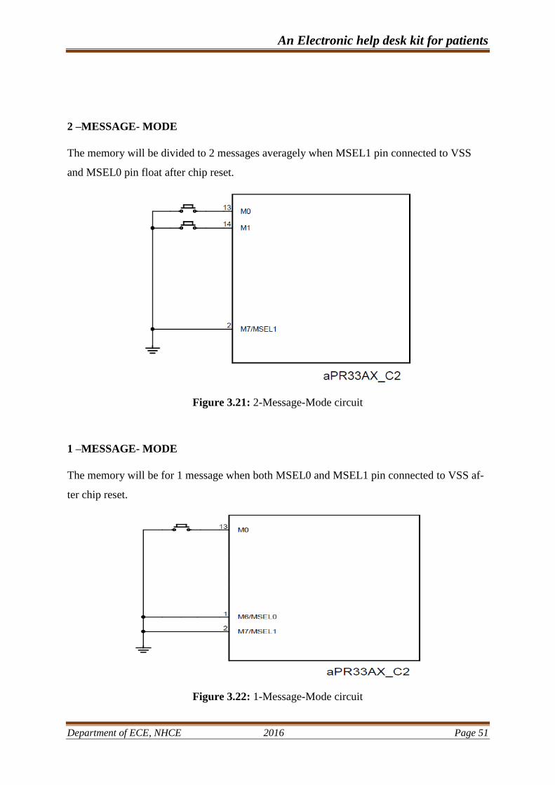
2 –MESSAGE- MODE
The memory will be divided to 2 messages averagely when MSEL1 pin connected to VSS
and MSEL0 pin float after chip reset.
Figure 3.21: 2-Message-Mode circuit
1 –MESSAGE- MODE
The memory will be for 1 message when both MSEL0 and MSEL1 pin connected to VSS af-
ter chip reset.
Figure 3.22: 1-Message-Mode circuit

An Electronic help desk kit for patients
Department of ECE, NHCE 2016 Page 52
HOW TO RECORD SOUND
During the /REC pin drove to VIL, chip in the record mode. When the message pin (M0, M1,
M2 … M7) drove to VIL in record mode, the chip will playback “beep” tone and message
record starting.
The message record will continue until message pin released or full of this message, and the
chip will playback “beep” tone 2 times to indicate the message record finished.
If the message already exist and user record again, the old one’s message will be replaced.
Figure 3.23: Circuit for recording a message
The following fig. shows a typical record circuit for 8-message mode. We connected a slide-
switch between /REC pin and VSS, and connected 8 tact-switches between M0 ~ M7 pin and
VSS. When the slide-switch fixed in VSS side and any tact-switch will be pressed, chip will
start message record and until the user releases the tact-switch.

An Electronic help desk kit for patients
Department of ECE, NHCE 2016 Page 53
PLAY BACK
During the /REC pin drove to VIH, chip in the playback mode. When the message pin (M0,
M1, M2 … M7) drove from VIH to VIL in playback mode, the message playback starting.
The message playback will continue until message pin drove from VIH to VIL again or end
of this message.
Figure 3.24: Circuit for playing back a message
The following fig. shows a typical playback circuit for 8-message mode. We connected a
Slide-switch between /REC and VSS, and connected 8 tact-switches between M0 ~ M7 and
VSS.
When the slide-switch fixed in float side and any tact-switch will be pressed, chip will start
message playback and until the user pressed the tact-switch again or end of message.

An Electronic help desk kit for patients
Department of ECE, NHCE 2016 Page 54